


May 1997
ML2264*
4-Channel High-Speed 8-Bit
A/D Converter with T/H (S/H)
GENERAL DESCRIPTION
The ML2264 is a high-speed, µP compatible, 4-channel
8-bit A/D converter with a conversion time of 680ns over
the operating temperature range and supply voltage
tolerance. The ML2264 operates from a single 5V supply
and has an analog input range from GND to VCC.
The ML2264 has two different pin selectable modes. The
T/H mode has an internal track and hold. The S/H mode
has a true internal sample and hold and can digitize 0 to
5V sinusoidal signals as high as 500kHz.
The ML2264 digital interface has been designed so that
the device appears as a memory location or I/O port to a
µP. Analog input channels are selected by the latched and
decoded multiplexer address inputs.
The ML2264 is an enhanced, pin compatible second
source for the industry standard AD7824. The ML2264
enhancements are faster conversion time, parameters
guaranteed over the supply tolerance and temperature
range, improved digital interface timing, superior power
supply rejection, and better latchup immunity on analog
inputs.
FEATURES
■ Conversion time, WR-RD mode over temperature and
supply voltage tolerance
Track & Hold Mode ................................. 830ns max
Sample & Hold Mode .............................. 700ns max
■ Total unadjusted error..................... ±1/2 LSB or ±1 LSB
■ Capable of digitizing a 5V, 250kHz sine wave
■ 4-analog input channels
■ No missing codes
■ 0V to 5V analog input range with single 5V power
supply
■ No zero or full scale adjust required
■ Analog input protection ............................... 25mA min
■ Operates ratiometrically or with up to 5V voltage
reference
■ No external clock required
■ Power-on reset circuitry
■ Low power .......................................................100mW
■ Narrow 24-pin DIP, SOIC, or SSOP
■ Superior pin compatible replacement for AD7824
BLOCK DIAGRAM
VCC+V
A IN 1
A IN 2
A IN 3
A IN 4
4-CH
MUX
ADDRESS
LATCH
DECODE
A0 A1
SAMPLE
&
HOLD
PIN CONNECTIONS
–V
REF
SH/TH
+V
REF
4-BIT
FLASH
A/D
(MSB)
–V
REF
+V
REF
4-BIT
–V
–
+
Σ
–V
D/A
REF
+V
REF
16
4-BIT
FLASH
A/D
REF
(LSB)
16
TIMING
CONTROL
INT CS WR/RDY RD SH/TH MODE
REF
&
GND
DECODE
LOGIC,
LATCH
THREE
OUTPUT
BUFFER
&
STATE
DB7
DB6
DB5
DB4
DB3
DB2
DB1
DB0
A IN 4
A IN 3
A IN 2
A IN 1
MODE
DB0
DB1
DB2
DB3
RD
INT
GND
24-Pin DIP 24-Pin SOIC
24-Pin SSOP
1
2
3
4
5
6
7
8
9
10
11
12
TOP VIEW
24
23
22
21
20
19
18
17
16
15
14
13
V
CC
A IN 4
SH/TH
A IN 3
A0
A IN 2
A1
A IN 1
DB7
MODE
DB6
DB5
DB4
CS
WR/RDY
+V
REF
–V
REF
GND
DB0
DB1
DB2
DB3
RD
INT
1
2
3
4
5
6
7
8
9
10
11
12
TOP VIEW
*This Part Is End Of Life As Of August 1, 2000
24
23
22
21
20
19
18
17
16
15
14
13
V
CC
SH/TH
A0
A1
DB7
DB6
DB5
DB4
CS
WR/RDY
+V
REF
–V
REF
1

ML2264
PIN DESCRIPTION
PIN# NAME FUNCTION PIN# NAME FUNCTION
1 A IN 4 Analog input 4.
2 A IN 3 Analog input 3.
3 A IN 2 Analog input 2.
4 A IN 1 Analog input 1.
5 MODE Mode select input.
MODE = GND: RD mode
MODE = VCC: WR-RD mode
Pin has internal current source
pulldown to GND.
6 DB0 Data output — bit 0 (LSB).
7 DB1 Data output — bit 1.
8 DB2 Data output — bit 2.
8 DB3 Data output — bit 3.
10 RD Read input. In RD mode, this pin
initiates a conversion. In WR-RD
mode, this pin latches data into output
latches. See Digital Interface section.
11 INT Interrupt output. This output signals
the end of a conversion and indicates
that data is valid on the data outputs.
See Digital Interface section.
12 GND Ground.
13 –V
REF
Negative reference voltage for
A/D converter.
15 WR/RDY Write input or ready output. In WR-RD
mode, this pin is WR input. In RD
mode, this pin is RDY open drain
output. See Digital Interface section.
16 CS Chip select input. This pin must be
held low for the device to perform a
conversion.
17 DB4 Data output — bit 4.
18 DB5 Data output — bit 5.
19 DB6 Data output — bit 6.
20 DB7 Data output — bit 7 (MSB).
21 A1 Digital address input 1 that selects
analog input channel. See multiplexer
addressing section.
22 A0 Digital address input 0 that selects
analog input channel. See multiplexer
addressing section.
23 SH/TH S/H, T/H mode select. When SH/TH =
VCC, the device is in sample and hold
mode. When SH/TH = GND, the
device is in track and hold mode. Pin
has internal pulldown current source
to GND.
24 V
CC
Positive supply. +5 volts ± 5%.
14 +V
REF
Positive reference voltage for
A/D converter.
ABSOLUTE MAXIMUM RATINGS
Absolute maximum ratings are those values beyond which
the device could be permanently damaged. Absolute
maximum ratings are stress ratings only and functional
device operation is not implied.
Supply Voltage, VCC................................................. 6.5V
Voltage
Logic Inputs ................................. –0.3V to VCC + 0.3V
Analog Inputs .............................. –0.3V to VCC + 0.3V
Input Current per Pin (Note 2) .............................. ±25mA
Storage Temperature .............................. –65°C to +150°C
Package Dissipation
at TA = 25°C (Board Mount) .............................875mW
Lead Temperature (Soldering 10 sec.)
Dual-In-Line Package (Plastic)............................ 260°C
Dual-In-Line Package (Ceramic)......................... 300°C
SOIC
Vapor Phase (60 sec.) ..................................... 215°C
Infrared (15 sec.) ............................................ 220°C
OPERATING CONDITIONS
Supply Voltage, VCC............................ 4.5VDC to 6.0V
Temperature Range (Note 3) ................. T
ML2264CCS
ML2264CCP
ML2264CCR ........................................... 0°C to +70°C
MIN
- TA - T
DC
MAX
2
ML2264
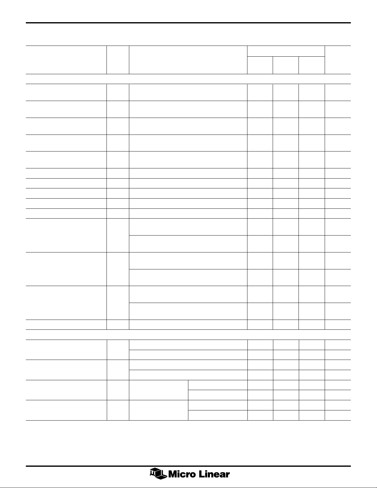
ELECTRICAL CHARACTERISTICS
Unless otherwise specified, TA = T
PARAMETER NOTES CONDITIONS MIN (NOTE 3) MAX UNITS
Converter
Total Unadjusted Error
ML2264CXX 4, 6 ±1 LSB
Integral Linearity Error
ML2264CXX 4, 6 ±1 LSB
Differential Linearity Error
ML2264CXX 4 ±1 LSB
Full Scale Error
ML2264CXX 4 ±1 LSB
Zero Scale Error
ML2264CXX 4 ±1 LSB
Channel to Channel Mismatch 4 ±1/4 LSB
+V
Voltage Range 5 –V
REF
–V
Voltage Range 5 GND–0.1 +V
REF
Reference Input Resistance 4 1 2.5 4 k ý
Analog Input Range 4, 7 GND–0.1 VCC+0.1 V
Power Supply Sensitivity 4 DC ±1/32 ±1/4 LSB
Analog Input Leakage Current, 4 ON Channel = V
OFF Channel OFF Channel = 0V
Analog Input Leakage Current, 4 ON Channel = 0V –1 µA
ON Channel OFF Channel = V
Analog Input Capacitance During Acquisition Period 45 pF
Digital and DC
V
, Logical “1” Input Voltage 4 WR, RD, CS, A0, A1 2.0 V
IN(1)
V
, Logical “0” Input Voltage 4 WR, RD, CS, A0, A1 0.8 V
IN(0)
I
, Logical “1” Input Current 4 VIH = V
IN(1)
I
, Logical “0” Input Current 4 VIL = GND WR, RD, CS –1 µA
IN(0)
MIN
to T
, VCC = +V
MAX
= 5V ± 5%, and –V
REF
= GND (Note 1)
REF
ML2264XCX
TYP
VCC+0.1 V
V
=5V ± 5%, V
CC
REF
REF
= 4.50V
100mVp-p ±1/16 LSB
100kHz sine on VCC, VIN = 0
CC
–1 µA
ON Channel = 0V 1 µA
OFF Channel = V
ON Channel = V
CC
CC
CC
OFF Channel = 0V
MODE, SH/TH VCC–0.5 V
MODE, SH/TH 0.5 V
CC
WR, RD, CS, A0, A1 1 µA
MODE, SH/TH 15 50 150 µA
MODE, SH/TH –20 µA
REF
V
1µA
3
ML2264
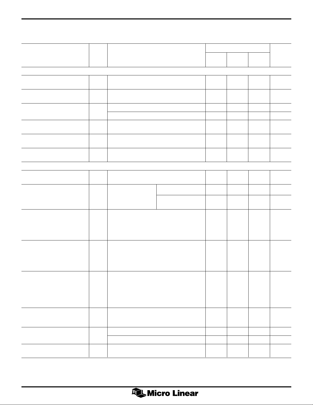
ELECTRICAL CHARACTERISTICS (Continued)
Unless otherwise specified, TA = T
CL = 100pF. (Note 1)
PARAMETER NOTES CONDITIONS MIN (NOTE 3) MAX UNITS
Digital and DC (Continued)
V
Output Voltage
V
Output Voltage
I
Current
C
Capacitance
C
Capacitance
I
AC and Dynamic Performance (Note 9)
t
Read Mode
t
Write-Read Mode Edge to INT,
SNR, Signal to Noise Ratio VIN = 5V, 250kHz 48 dB
HD, Harmonic Distortion V
IMD, Intermodulation Distortion fa = 2.5V, 250kHz –60 dB
FR, Frequency Response V
SR, Slew Rate Tracking 5 SH/TH = V
t
Setup Time (Track & Hold Operation)
, Logical “1” 4 I
OUT(1)
, Logical “0” 4 I
OUT(0)
, Three-State Output 4 V
OUT
, Logic Output 5pF
OUT
, Logic Input 5pF
IN
, Supply Current 4 CS = WR = RD = “1”, 18 mA
CC
, Conversion Time, 4 RD to INT, MODE = 0V 1020 ns
CRD
, Conversion Time, 4, 8 WR Falling SH/TH = V
CWR-RD
, Multiplexer Address 4 SH/TH = GND, Figure 1 0 ns
AS
MIN
to T
, VCC = +V
MAX
= 5V ± 5%, and –V
REF
= GND, and timing measured at 1.4V,
REF
ML2264XCX
TYP
= –2mA 4.0 V
OUT
= 2mA 0.4 V
OUT
= 0V –1 µA
OUT
= V
V
OUT
CC
No Output Load
CC
< t
t
RD
MODE = V
, SH/TH = GND 830 ns
INT
CC
Noise is sum of all nonfundamental
components from 0–500kHz.
SH/TH = V
f
SAMPLING
= 5V, 250kHz –63 dB
IN
, MODE = V
CC
= 1.0 MHz
CC
THD is sum of 2–5th harmonics relative to
fundamental.
SH/TH = V
f
SAMPLING
, MODE = V
CC
= 1.0 MHz
CC
fb = 2.5V, 248kHz
IMB is (fa + fb), (fa – fb), (2fa + fb), (2fa – fb),
(fa + 2fb), or (fa – 2fb) relative to fundamental.
SH/TH = V
f
SAMPLING
= 5V, 0–250kHz Relative to 1kHz ±0.1 dB
IN
SH/TH = V
f
SAMPLING
, MODE = V
CC
= 1.0 MHz
, MODE = V
CC
= 1.0 MHz
CC
CC
CC
SH/TH = GND 0.25 V/µs
1µA
700 ns
4.0 V/µs
4
ML2264
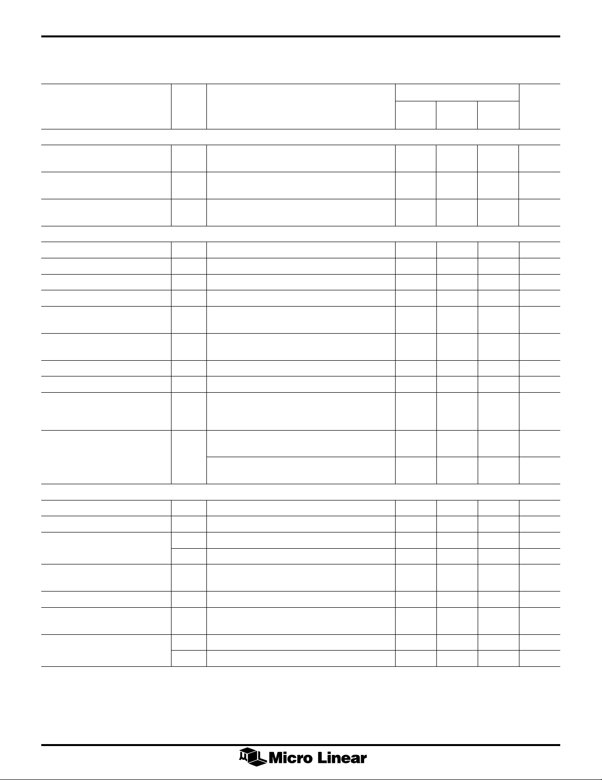
ELECTRICAL CHARACTERISTICS (Continued)
Unless otherwise specified, TA = T
CL = 100pF. (Note 1)
PARAMETER NOTES CONDITIONS MIN (NOTE 3) MAX UNITS
AC and Dynamic Performance (Note 9) (Continued)
t
, Multiplexer Address 4 SH/TH = GND, Figure 1 60 ns
AH
Hold Time (Track & Hold Operation)
t
, Multiplexer Address 4 SH/TH = VCC, Figure 2 225 ns
AS
Setup Time (Sample & Hold Operation)
t
, Multiplexer Address 4 SH/TH = VCC, Figure 2 60 ns
AH
Hold Time (Sample & Hold Operation)
AC Performance Read Mode (Pin 5 = 0V), Figure 4
t
, CS to RDY Delay 4 0 60 ns
RDY
t
, RD Low to RDY Delay 4, 9 Figure 3 1020 ns
RDD
t
, CS to RD, WR Setup Time 4 0 ns
CSS
t
, CS to RD, WR Hold Time 4 0 ns
CSH
t
, Conversion Time — 4, 9 1020 ns
CRD
RD Low to INT low
t
, Data Access Time 4 t
ACC0
RD to Data Valid
t
, RD Pulse Width 4 t
RDPW
t
, RD to INT Delay 4, 9 0 65 ns
INTH
t
, Data Hold Time — 5, 9 Figure 3 0 50 ns
DH
RD Rising Edge to Data
High Impedance State
t
, Delay Time Between 4, 9 Sample & Hold Mode, 300 ns
P
Conversions — INT Low SH/TH = V
to RD Low
AC Performance Write-Read Mode (Pin 5 = 5V), Figures 5 and 6
t
, CS to RD, WR Setup Time 4 0 ns
CSS
t
, CS to RD, WR Hold Time 4 0 ns
CSH
tWR, WR Pulse Width 4 SH/TH = V
t
, Read Time — WR 4tRD < t
RD
High to RD Low Delay
tRI, RD to INT Delay 4, 9 tRD < t
t
, Data Access Time 4 tRD < t
ACC1
— RD Low to Data Valid
t
— WR Falling Edge to INT Low
, Conversion Time 4, 8, 9 tRD < t
CWR-RD
MIN
to T
, VCC = +V
MAX
= 5V ± 5%, and –V
REF
= GND, and timing measured at 1.4V,
REF
ML2264XCX
TYP
CC
–10 t
CRD
+30 ns
CRD
+20 ns
CRD
Track & Hold Mode, 240 ns
SH/TH = GND
CC
190 50K ns
5 SH/TH = GND 320 50K ns
275 ns
0 235 ns
0 240 ns
700 ns
5, 8, 9 t
RD
INTL
INTL
INTL
, SH/TH = V
INTL
< t
, SH/TH = GND 830 ns
INTL
CC
5
ML2264
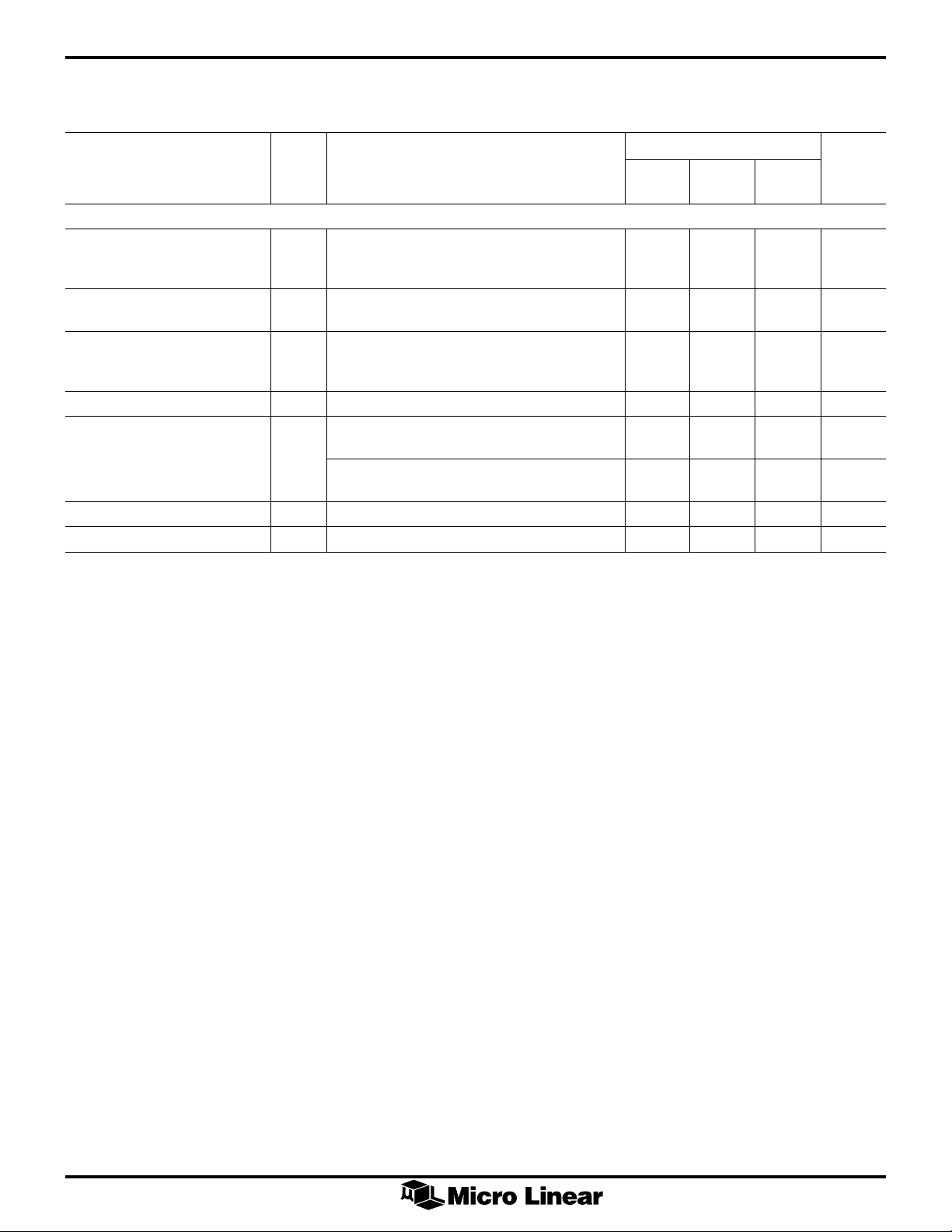
ELECTRICAL CHARACTERISTICS (Continued)
Unless otherwise specified, TA = T
CL = 100pF. (Note 1)
PARAMETER NOTES CONDITIONS MIN (NOTE 3) MAX UNITS
AC Performance Write-Read Mode (Pin 5 = 5V) Figures 5 and 6 (Continued)
t
, Internal Comparison 4, 9 tRD > t
INTL
Time — WR Rising Edge
to INT Low
, Data Access Time 4 tRD > t
t
ACC2
— RD to Data Valid
, Data Hold Time — 5, 9 Figure 3 0 50 ns
t
DH
RD Rising Edge to Data
High Impedance State
t
, RD to INT Delay 4, 9 0 65 ns
INTH
t
, Delay Time Between 4, 9 Sample & Hold Mode, 300 ns
P
Conversions — INT Low SH/TH = V
to WR Low
t
, WR to INT Delay 4, 9 Standalone Mode 0 90 ns
IHWR
tID, INTØ to Data Valid Delay 4, 9 Standalone Mode 0 20 ns
MIN
to T
, VCC = +V
MAX
= 5V ± 5%, and –V
REF
= GND, and timing measured at 1.4V,
REF
ML2264XCX
TYP
INTL
INTL
CC
050ns
Track & Hold Mode, 240 ns
SH/TH = GND
620 ns
Note 1: Limits are guaranteed by 100% testing, sampling, or correlation with worst-case test conditions.
Note 2: When the voltage at any pin exceeds the power supply rails (V
Note 3: Typicals are parametric norm at 25°C.
Note 4: Parameter guaranteed and 100% production tested.
Note 5: Parameter guaranteed. Parameters not 100% tested are not in outgoing quality level calculation.
Note 6: Total unadjusted error includes offset, full scale, linearity, sample and hold, and multiplexer errors. Total unadjusted error is tested at the minimum specified times
for WR, RD, t
(cycle time of 1000ns).
Note 7: For –V
diode drop below ground or one diode drop greater than the V
cause this input diode to conduct — especially at elevated temperatures, and cause errors for analog inputs near full scale. The spec allows 100mV forward bias of
either diode. This means that as long as the analog V
an absolute 0V
loading.
Note 8: Conversion time, write-read mode = t
Note 9: Defined from the time an output crosses 0.8V or 2.4V.
, and tP. For example, for the ML2264XCX in the sample and hold mode, WR/RD mode: tWR = 190ns, tRD = 275ns with a frequency of 1.000MHz
R1
• VIN the digital output code will be 0000 0000. Two on-chip diodes are tied to the analog input which will forward conduct for analog input voltages one
REF
to 5VDC input voltage range will therefore require a minimum supply voltage of 4.900VDC over temperature variations, initial tolerance and
DC
+ tRD + tRI.
WR
IN
< GND or VIN > VCC) the absolute value of current at that pin should be limited to 25mA or less.
IN
supply. Be careful, during testing at low VCC levels (4.5V), as high level analog inputs (5V) can
CC
or V
does not exceed the supply voltage by more than 100mV, the output code will be correct. To achieve
REF
6

ML2264
A0, A1
RD
ADDR
VALID
t
AH
t
AS
A0, A1
WR
t
AS
a) RD Mode (Pin 5 = GND)
ADDR
VALID
t
AH
b) WR-RD Mode (Pin 5 = VCC)
Figure 1. Analog Multiplexer Address Timing for Track & Hold Mode (Pin 23 = GND)
CS
t
A0, A1
AS
ADDR
VALID
t
AH
Figure 2. Analog Multiplexer Address Timing for Sample & Hold Mode (Pin 23 = VCC)
t
DATA
OUTPUT
DATA
OUTPUT
10pF
10pF
V
GND
V
OH
GND
V
GND
V
V
CC
CC
CC
OL
OUTPUT
5k
V
CC
5k
ENABLE
OUTPUT
OUTPUT
ENABLE
OUTPUT
50%
10%
50%
10%
f
90%
t
1H
VOH – 100mV
t
f
90%
t
0H
VOL + 100mV
Figure 3. High Impedance Test Circuits and Waveforms
7

ML2264
CS
t
t
t
RDD
t
CRD
t
ACC0
RDPW
RD
RDY
INT
DB0–DB7
*In SAMPLE & HOLD mode a pull up resistor on RDY should not be used unless
CSØ is • 20ns before RDØ.
t
RDY
t
CSS
CSH
t
P
WITH EXTERNAL PULL-UP
t
INTH
VALID
DATA
t
DH
Figure 4. RD Mode Timing
CS
CS
t
t
ACC1
CSH
t
RD
t
P
t
RI
VALID
DATA
t
WR
t
RD
INT
DB0–DB7
CSS
t
WR
Figure 6. WR-RD Mode Timing (tRD < t
DH
t
INTH
INTL
)
WR
RD
INT
DB0–DB7
t
WR
t
CSS
t
CSH
t
INTL
t
P
t
RD
VALID
DATA
t
ACC2
Figure 5. WR-RD Mode Timing (tRD > t
INTL
t
INTL
t
WR
t
INTH
t
DH
INT
DB0–DB7
WR
t
IHWR
t
P
t
ID
VALID
DATA
Figure 7. WR-RD Mode Stand-Alone Timing CS = RD = 0
)
8

ML2264
1.0 FUNCTIONAL DESCRIPTION
The ML2264 uses a two stage flash technique for A/D
conversion. This technique first performs a 4 bit flash
conversion on VIN to determine the 4 MSB’s. These 4
MSB’s are then cycled through an internal DAC to
recreate the analog input. This reconstructed analog input
signal from the DAC is then subtracted from the input, and
the difference voltage is converted by a second 4 bit flash
conversion, providing the 4 LSB’s of the output data word.
1.1 MULTIPLEXER ADDRESSING
The ML2264 contains a 4-channel single ended analog
multiplexer. A particular input channel is selected by using
the address inputs A0 and A1. The relationship between
the address inputs, A0 and A1, and the analog input
selected is shown in Table 1.
Selected
Analog Channel A0 A1
A IN 1 0 0
A IN 2 1 0
A IN 3 0 1
A IN 4 1 1
Table 1. Multiplexer Address Decoding
The address inputs are latched into the ML2264 on the
falling edge of the RD, WR, or CS depending on the state
of pins SH/TH and mode as shown in Table 2.
Address Latching
Signal Mode Operation Mode
RDØ GND GND
WRØ V
CSØ GND V
CSØ V
In the Sample & Hold mode of operation CS is used as the
address latch enable, allowing for continuous conversions
without addressing a given analog input for each
conversion.
The Track & Hold mode of operation requires an analog
input to be addressed and latched for each conversion
that the ML2264 performs.
1.2 ANALOG INPUTS
The analog input on the ML2264 behaves differently than
inputs on conventional converters. The analog input
current requirements change while the conversion is in
progress, and the amount of input current depends on
what cycle the converter is in.
Address Input
CC
CC
Table 2.
GND
CC
V
CC
The equivalent input circuit for the converter is shown in
Figure 8. When the conversion starts in the T/H mode
(WRØ in the WR-RD mode or RDØ in the RD mode) S1,
S4 and S6 close and S3 opens. This period is known as the
acquisition period where the MSB flash converter tracks
the input signal and the LSB flash converter samples it.
During this period, VIN is connected to the 16 MSB and
15 LSB comparators. Thus 38pF of input capacitance must
be charged up through the combined RON resistance of
the internal analog switches plus any external source
resistance, RS. In addition, there is a stray capacitance of
approximately 11pF that needs to be charged through the
external source resistance RS. This period ends in the WRRD mode when WR or by an internal timer in the RD
mode. At this point S1 and S4 open and the analog input
at VIN is no longer being sampled; thus during this time
the analog voltage on VIN does not affect converter
performance.
As shown above, the critical period for charging up the
analog input occurs when the MSB and LSB comparators
are sampling the input, known as the acquisition period.
The source of the external signal on VIN must adequately
charge up the analog voltage during the acquisition
period. To do this, the input must settle within the
required analog accuracy tolerance at least 50ns before
the end of the acquisition period so that the MSB
comparators have adequate time to make the correct
decision. If more time is needed due to finite charging or
settling time of the external source, the WR low period
can be extended in WR-RD mode. In RD mode, since the
acquisition time is fixed by internal delays, the burden is
on the external source to charge up and settle the input
adequately.
When the ML2264 operates in the S/H mode (pin 23 =
VCC) both the MSB and the LSB flash converter perform a
true sample and hold operation during the acquisition or
sampling period. This period starts after the falling edge of
INT and ends with the falling edge of WR in the WR-RD
mode or the falling edge of RD in the RD mode. The
duration of this period is user controlled and must satisfy a
minimum of tP.
During this period S1, S3, S4 and S6 close, therefore
46pF of input capacitance must be charged up in addition
to the 11pF of stray capacitance.
1.3 TRACK AND HOLD vs. SAMPLE AND HOLD
The MSB Flash Converter of the ML2264 in T/H mode has
a track and hold mechanism for sampling the input. The
input is attached to the MSB comparators directly in the
MSB compare cycle, or acquisition period. When the MSB
compare cycle ends, the state of the MSB comparators is
latched. The LSB Flash Converter always performs a S/H
operation. Thus, the analog input signal can be changing
during the MSB compare cycle, or acquisition period, and
9

ML2264
the MSB comparators will be tracking it as long as the
slew rate of the analog input is slow enough so that the
MSB comparators can respond. The ML2264 can track
and hold signals with slew rates as high as 0.25V/µs
(16kHz @ 5 volts) without sacrificing conversion
accuracy.
The ML2264 in S/H mode does not have the slew rate
limitation of the T/H mode since an internal sample and
hold acquires the analog signal, holds it internally, and
then performs a conversion. Since this is a true sample
and hold function, the S/H mode can theoretically digitize
signals of frequencies much higher than the T/H mode.
The ML2264 in S/H mode can digitize signals of
frequencies as high as 250kHz @ 5V (slew rates as high as
4V/µs) without sacrificing conversion accuracy. In most
applications, the S/H mode is more desirable than T/H
mode because of the better dynamic performance.
11pF
R
S
V
IN
R
ON
4K
TO MS
LADDER
16 MSB COMPARATORS
R
ON
6.4K
TO LS
LADDER
S1
S2
S4
S5
15 LSB COMPARATORS
1pF
1.34pF
0.65pF
1pF
1pF
1.2K
R
ON
S3
3.6K
R
ON
S6
1.3.1 Converter — T/H Mode
The operating sequence for the WR-RD mode is illustrated
in Figure 9a. Initially, the internal comparators are autozeroed while WR is high. A conversion is initiated by the
falling edge of WR. While WR is low, the MSB
comparators are tracking the analog input and comparing
this voltage against voltages from the internal resistor
ladder. At the same time, the input is being acquired or
sampled by LSB comparators. On the rising edge of WR,
the MSB comparator results are latched, and the LSB
acquisition time is ended by closing the sampling switch
to the LSB comparators. While WR is high, the LSB
comparators then compare the residual input voltage
against internal voltages from the resistor ladder to
determine the 4 LSB’s. When the LSB comparison or
conversion is complete, INT goes low and latches the
conversion result into the output latches. Then, the
comparators are auto-zeroed while WR is high before
another conversion can start.
The operating sequence for RD mode, is similar to that
described above for the WR-RD mode, except the
conversion is initiated by the falling edge of RD, and the
MSB and LSB conversions are generated by internal clock
edges that are generated while RD is low.
Figure 8. Converter Equivalent Input Circuit
1.3.2 Converter — S/H Mode
The operating sequence for S/H mode is illustrated in
Figure 9b. Notice that it is similar to T/H mode described
above except this mode has a true sample and hold
function. The falling edge of INT closes the sampling
switch and starts the acquisition period where the analog
input is sampled at the same time all comparators are
auto-zeroed. The falling edge of WR opens the internal
sampling switch, ends the acquisition period, and starts
the conversion on the internally sample and held signal.
The MSB comparators make their decisions while WR is
low. On the rising edge of WR, the MSB comparator
results are latched. The LSB comparators make their
decision when WR is high. When the LSB comparison or
conversion is complete, INT goes low and latches the
conversion result into the output buffers. Then, the
acquisition period begins again and the converter is ready
for the next conversion.
The operating sequence for the RD mode is the same as
the WR-RD mode, except the conversion is initiated by
the falling edge of RD, and the MSB and LSB conversions
are generated by internal clock edges that are generated
while RD is low.
10

(a) S/H Mode
FULL SCALE
TRANSITION
OUTPUT
CODE
11111111
11111110
11111101
00000011
00000010
00000001
00000000
0
1LSB
2LSB’S
3LSB’S
FS
FS – 1LSB
AIN, INPUT VOLTAGE (IN TERMS OF LSB’S)
ML2264
WR
(a) T/H Mode
WR
ACQUISITION
OR SAMPLING
PERIOD. ALL
COMPARATORS
AUTOZEROED.
CONVERSION
STARTS.
V
IN
ENDS. HOLD
TIME STARTS.
ALL
COMPARATORS
AUTOZEROED.
CONVERSION
STARTS.
MSB
COMPARATORS
DECIDING.
SAMPLING
ACQUISITION
PERIOD. MSB
COMPARATORS
ARE TRACKING
V
IN
COMPARATORS
ARE SAMPLING
V
IN
. LSB
.
LSB
COMPARATORS
DECIDING.
MSB
COMPARATOR
RESULTS ARE
LATCHED.
LSB
COMPARATORS
DECIDING.
VIN SAMPLING
ENDS. MSB
COMPARATOR
RESULTS ARE
LATCHED.
RD BROUGHT LOW
LATCHES LSB
COMPARATOR
RESULTS AND
BRINGS INT LOW.
RD BROUGHT LOW
LATCHES LSB
COMPARATOR
RESULTS AND
BRINGS INT LOW.
Figure 9. Operating Sequence (WR-RD Mode)
1.4 REFERENCE
The +V
REF
and –V
inputs are the reference voltages that
REF
determine the full scale and zero input voltages,
respectively, for the A/D converter. Thus, +V
defines
REF
the analog input which produces a full scale output and
–V
defines the analog input which produces an output
REF
code of all zeroes. The transfer function for the A/D
converter is shown in Figure 10.
+V
and –V
REF
and VCC. This means that the reference voltages can be
offset from GND and the difference between +V
–V
– can be made small to increase the resolution of the
REF
can be set to any voltage between GND
REF
REF
conversion. Note that the total unadjusted error increases
when [+V
REF
– (–V
)] decreases.
REF
1.5 POWER SUPPLY AND REFERENCE DECOUPLING
A 0.1µF ceramic disc capacitor is recommended to bypass
VCC to GND, using as short a lead length as possible.
If REF+ and REF– inputs are driven by long lines, they
should be bypassed by 0.1µF ceramic disc capacitors at
the reference input pins.
+ and
Figure 10. A/D Transfer Characteristic
11

ML2264
1.6 DYNAMIC PERFORMANCE
1.6.1 Sinusoidal Inputs
Since the ML2264 has an internal sample and hold, the
device can digitize high frequency sinusoids with little or
no signal degradations. Using the Nyquist criteria, the
highest frequency input to the converter could
theoretically be 1/2 the sampling rate (fS). Any frequency
components above fS/2 will be aliased below fS/2. In most
applications, these aliased components cause
unacceptable distortion and must be filtered out of the
input. If the input frequency is too close to fS/2, then the
requirements on the anti-alias filter become difficult to
impossible to realize with standard component and
tolerances. In most practical applications, the highest
input frequency has to be limited to 1/3 to 1/4 of f
MAX
in
order to relax the filtering requirements enough to make a
realizable anti-alias filter.
The maximum sampling rate (f
WR-RD mode, (tRD < t
f
=
max
tttt
WR RD RI P
f
=
max
190 275 235 300
f
= 1.000 MHz
max
1
+++
ns ns ns ns
+++
) can be calculated as follows:
INTL
1
) for the ML2264 in the
max
tWR = Write Pulse Width
tRD = Delay Time between WR and RD Pulses
tRI = RD to INT Delay
In applications where aliased frequency components are
acceptable and filtering of the input signal is not needed,
or where a filter with a steep amplitude response is
available, the user can apply an input sinusoid higher than
250kHz to the device. Note, however, that as the input
frequency increases above 500kHz, dynamic performance
degradation will occur due to the finite bandwidth of the
internal sample and hold.
The Figure 11 plots are 4096 point FFT’s of the ML2264
converting a 257kHz and a 491kHz, 0 to 4.5V, low
distortion sine wave input. The ML2264 samples and
digitizes at its specified accuracy, dynamic input signals
with frequency components up to the Nyquist frequency
(one-half the sampling rate). The output spectra yields
precise measure-ments of the input signal level, harmonic
components, and signal to noise ratio up to the 8-bit level.
The near ideal signal to noise ratio is maintained
independent of increasing analog input frequencies to
500kHz.
1.6.2 Signal-To-Noise Ratio
Signal-to-noise ratio (SNR) is the measured signal to noise
at the output of the converter. The signal is the rms
magnitude of the fundamental. Noise is the rms sum of all
the nonfundamental signals up to half the sampling
frequency. SNR is dependent on the number of
quantization levels used in the digitization process; the
more the levels, the smaller the quantization noise. The
theoretical SNR for a sine wave is given by
SNR = (6.02N + 1.76) dB
where N is the number of bits. Thus for ideal 8-bit
converter, SNR = 49.92 dB.
tP = Delay Time between Conversions
This permits a maximum sampling rate of 1MHz for the
ML2264. The dynamic performance specifications (SNR,
HD, IMD, and FR) for the ML2264 are all specified at
1.6.3 HARMONIC DISTORTION
Harmonic distortion is the ratio of the rms sum of
harmonics to the fundamental. Total harmonic distortion
(THD) of the ML2264 is defined as
250kHz, which is approximately 1/4 of the sampling rate, fS.
0
–10
SNR 48.4dB
HD –62.87dB
–20
V
= V
CC
T
–30
–40
–50
–60
–70
–80
MAGNITUDE (dB)
–90
–100
–110
–120
= 25 C
A
REF
= 5.0V
4002000
FREQUENCY (kHz)
0
–10
SNR 49.1dB
HD –58.33dB
–20
V
= V
CC
T
–30
–40
–50
–60
–70
–80
MAGNITUDE (dB)
–90
–100
–110
–120
= 25 C
A
REF
= 5.0V
4002000
FREQUENCY (kHz)
a) Output Spectrum with fIN = 257kHz, fS = 1MHz b) Output Spectrum with fIN = 491kHz, fS = 1MHz
12
Figure 11. Dynamic Performance, Sample and Hold Mode

ML2264
2
()VVVV
+++
2
20
log
3
2
V
1
425
2
12
where V1 is the rms amplitude of the fundamental and
V2, V3, V4, V5 are the rms amplitudes of the individual
harmonics.
1.6.2 Signal-To-Noise Ratio
Signal-to-noise ratio (SNR) is the measured signal to noise
at the output of the converter. The signal is the rms
magnitude of the fundamental. Noise is the rms sum of all
the nonfundamental signals up to half the sampling
frequency. SNR is dependent on the number of
quantization levels used in the digitization process; the
more the levels, the smaller the quantization noise. The
theoretical SNR for a sine wave is given by
SNR = (6.02N + 1.76) dB
where N is the number of bits. Thus for ideal 8-bit
converter, SNR = 49.92 dB.
1.6.3 HARMONIC DISTORTION
Harmonic distortion is the ratio of the rms sum of
harmonics to the fundamental. Total harmonic distortion
(THD) of the ML2264 is defined as
on the falling edge of RD. While RD is low, the MSB and
LSB decisions are made with internally generated clock
edges. When the conversion is complete, RDY goes high
and INT goes low signaling the end of the conversion.
After INT goes low, the data outputs go from high
impedance to active state with valid output data. Data
stays valid until either RD or CS goes high. When either
signal goes high, the output data lines return to the high
impedance state and INT returns high.
1.7.2 WR-RD Mode
In the WR-RD mode, the WR/RDY pin is configured as the
WR input. In this mode, WR initiates the conversion and
RD controls reading the output data. This can be done in
several ways, described below.
1.7.3 WR-RD Mode — Using Internal Delay
(tRD > t
INTL
)
The timing is shown in Figure 5. To do a conversion, CS
must be low to select the device. Then, WR falling edge
triggers the conversion. While WR is low, the MSB
comparison is made. When WR returns high the LSB
decision is made. After some internal delay, INT goes low
indicating end of conversion. Valid data will appear on
DB0–7 when RD is pulled low. INT is then reset by the
rising edge of either CS or RD.
2
()VVVV
+++
2
20
log
3
2
V
1
425
2
12
where V1 is the rms amplitude of the fundamental and
V2, V3, V4, V5 are the rms amplitudes of the individual
harmonics.
1.6.4 Intermodulation Distortion
With inputs consisting of sine waves at two frequencies,
fA and fB, any active device with nonlinearities will create
distortion products, of order (m + n), at sum and
difference frequencies of mfA + nfB, where m, n = 0, 1, 2,
3 … Intermodulation terms are those for which m or n is
not equal to zero. The (IMD) intermodulation distortion
specification includes the second order terms (fA + fB) and
fA – fB) and the third order terms (2fA + fB), (2fA – fB),
(fA + 2fB), and (fA – 2fB) only.
1.7 DIGITAL INTERFACE
The ML2264 has two basic interface modes, RD and WR-
RD, which are selected by the MODE input pin.
1.7.1 RD Mode
In the RD mode, WR/RDY pin is configured as the RDY
output. The read mode performs a conversion with a
single RD pulse. This allows the µP to start a conversion,
wait, and then read data with a single read instruction.
The timing for the RD mode is shown in Figure 4. To do a
conversion, CS must be low to select the device. After CS
goes low, the RDY output goes low indicating that the
device is ready to do a conversion. The conversion starts
1.7.4 WR-RD Mode — Reading Before Delay
(tRD < t
INTL
)
The internally generated delay for the LSB decision when
tRD > t
tolerances of t
is longer than necessary due to circuit design
INTL
delay. If desired, a faster conversion
INTL
will result without loss of accuracy by bringing RD low
within the minimum time specified for tRD. The timing
diagram for this mode is shown in Figure 6. WR is the
same as when tRD > t
. But in this case, RD is brought
INTL
low tRD ns after WR rising edge and before INT. INT goes
low indicating an end of conversion after the falling edge
of RD and is reset on the rising edge of RD or CS. When
RD is brought low before INT goes low the data bus
always remains in the high-impedance state until INTØ.
1.7.5 WR-RD Mode — Stand Alone Operation
Stand alone operation can be implemented by tying CS
and RD low as shown in Figure 7. WR initiates a
conversion as before. When WR is low, the MSB
comparison is made. When, WR goes high, the LSB
comparison is made. Since RD is already low, the output
data will appear automatically at end of conversion. Since
RD is always low, INT is reset on rising edge of WR and
goes low at end of conversion.
1.7.6 Power-On Reset
When power is first applied, an internal power-on reset
and timer circuit inhibits the CS input and resets the
internal circuitry to prevent the ML2264 from starting in
an unknown state. During this period of approximately
3µs, INT remains high and the data bus is in the highimpedance state.
13

ML2264
2.0 TYPICAL APPLICATIONS
5V
+15V
DC
*
+
–
–15V
*NO PROTECTION REQUIRED IF INPUT CURRENT <25mA
*
DC
A
IN
ML2264
V
CC
+
0.1µF
Figure 12. Protecting the Input
ML2264
V
CC
A
0 ≤ VIN ≤ V
CC
IN
+V
REF
–V
REF
GND
+
0.1µF
Figure 13. Using VCC as Reference for
Ratiometric Operation
5V
68008
ML2264
CS
A0
A1
INT
RD
DB7
DB0
DATA
ADDRESS
DECODE
AS
DTACK
R/W
DB7
DB0
Figure 15. 68000 Type Interface to ML2264
5V
50K
V
IN
25K
–
+
ML2264
A IN 1
A IN 2
A IN 3
A IN 4
0 ≤ VIN ≤ 4.5
+
0.1µF
4.50V
µP
V
REFOUT
ML2340
D/A
WITH
REFERENCE
+V
ML2264
REF
Figure 14. Using External Reference of D/A
Figure 16. ±2.5V Analog Input Range
12V
V
CC
A IN 1
V
OUT
A IN 2
A IN 3
A IN 4
ML2264 8051
CS
A0
A1
WR
RD
INT
DB7
DB0
DATA
P3, 1
P3, 2
P3, 3
P3, 4
P3, 5
P3, 6
P1, 7
P1, 0
Figure 17. 8051 Interface to ML2264
14

2.0 TYPICAL APPLICATIONS (Continued)
ML2264
A IN 1
A IN 2
A IN 3
A IN 4
DB7
DB0
ML2264
INT
RD
A0
A1
WR
CS
CLOCK
SOURCE
OR
TIMER
V
OUT
DATA
ADDRESS
DECODE
DB7
DB0
ML2341
D/A
CS
WR
Figure 18. TMS320 Interface with D/A Output
V
CC
DB7
DB0
INT
DEN
HEN
TMS320
/E14
C15
PA0
PA1
PA2
WE
(5VDC)
ANALOG
SOURCES
20k
1k
3k
4k
1k
24k
ZERO ADJ
FS ADJ
–
+V
CC
CC
+
0.1µF
+
0.1µF
A IN 1
A IN 2
A IN 3
A IN 4
–V
+
0.85V
–
+
0.15V
REF
ML2264
REF
V
CC
+
0.1µF
Figure 19. Operating with a Ratiometric Analog Signal of 15% of VCC to 85% of V
CC
15

ML2264
PHYSICAL DIMENSIONS inches (millimeters)
Package: P24N
24-Pin Narrow PDIP
1.240 - 1.260
(31.49 - 32.01)
24
0.070 MIN
(1.77 MIN)
(4 PLACES)
0.170 MAX
(4.32 MAX)
0.125 MIN
(3.18 MIN)
24
PIN 1 ID
1
0.600 - 0.614
(15.24 - 15.60)
0.050 - 0.065
(1.27 - 1.65)
0.016 - 0.022
(0.40 - 0.56)
0.100 BSC
(2.54 BSC)
Package: S24
24-Pin SOIC
0.240 - 0.270
(6.09 - 6.86)
SEATING PLANE
0.015 MIN
(0.38 MIN)
0.295 - 0.325
(7.49 - 8.26)
0º - 15º
0.008 - 0.012
(0.20 - 0.31)
16
0.024 - 0.034
(0.61 - 0.86)
(4 PLACES)
0.090 - 0.094
(2.28 - 2.39)
0.291 - 0.301
(7.39 - 7.65)
PIN 1 ID
1
0.050 BSC
(1.27 BSC)
0.012 - 0.020
(0.30 - 0.51)
0.095 - 0.107
(2.41 - 2.72)
SEATING PLANE
0.398 - 0.412
(10.11 - 10.47)
0.005 - 0.013
(0.13 - 0.33)
0º - 8º
0.022 - 0.042
(0.56 - 1.07)
0.009 - 0.013
(0.22 - 0.33)

PHYSICAL DIMENSIONS inches (millimeters) (Continued)
Package: R24
24-Pin SSOP
0.318 - 0.328
(8.08 - 8.33)
24
ML2264
0.066 - 0.070
(1.68 - 1.78)
1
PIN 1 ID
0.026 BSC
(0.65 BSC)
0.009 - 0.015
(0.23 - 0.38)
0.205 - 0.213
(5.20 - 5.40)
0.068 - 0.078
(1.73 - 1.98)
SEATING PLANE
0.301 - 0.313
(7.65 - 7.95)
0.002 - 0.008
(0.05 - 0.20)
0º - 8º
0.022 - 0.038
(0.55 - 0.95)
0.004 - 0.008
(0.10 - 0.20)
ORDERING INFORMATION
TOTAL TEMPERATURE
PART NUMBER UNADJUSTED ERROR RANGE PACKAGE
ML2264CCP (Obsolete) 0°C to +70°C Molded DIP (P24)
ML2264CCS (End Of Life) ±1 LSB 0°C to +70°C Molded SOIC (S24)
ML2264CCR (Obsolete) 0°C to +70°C Molded SSOP (R24)
© Micro Linear 1997 is a registered trademark of Micro Linear Corporation
Products described in this document may be covered by one or more of the following patents, U.S.: 4,897,611; 4,964,026; 5,027,116; 5,281,862; 5,283,483; 5,418,502; 5,508,570; 5,510,727; 5,523,940; 5,546,017;
5,559,470; 5,565,761; 5,592,128; 5,594,376; Japan: 2598946; 2619299. Other patents are pending.
Micro Linear reserves the right to make changes to any product herein to improve reliability, function or
design. Micro Linear does not assume any liability arising out of the application or use of any product
described herein, neither does it convey any license under its patent right nor the rights of others. The
circuits contained in this data sheet are offered as possible applications only. Micro Linear makes no
warranties or representations as to whether the illustrated circuits infringe any intellectual property rights of
others, and will accept no responsibility or liability for use of any application herein. The customer is urged
to consult with appropriate legal counsel before deciding on a particular application.
2092 Concourse Drive
San Jose, CA 95131
Tel: 408/433-5200
Fax: 408/432-0295
DS2264-01
17
 Loading...