

Page 1

FEDL2201-01
1
Semiconductor
This version: Mar. 2000
ML2201-XXX
Speech Synthesizer LSI with on-chip 384K Mask ROM
GENERAL DESCRIPTION
The ML2201 is a PCM-based speech synthesizer LSI having an on-chip 384K Mask ROM, D/A Converter and
Low Pass Filter. Utilizing the serial interface enables smaller footprint packaging, which makes the chip an ideal
choice for a pre-recorded message subsystem used with today’s size-critical applications.
FEATURES
•
Sampling Frequency (Selectable for each single phrase)
4.0/5.3/6.4/8.0/10.6/12.8/16.0 kHz
•
On-chip 384 Kbit Mask ROM
•
Maximum Playback Time (At f
12.0 sec At f
6.0 sec At f
3.0 sec At f
•
External Clock Frequency Range
f
= 3.5 to 4.096 MHz (Typ.) to 17.0 MHz
EXTCLK
•
On-chip Phrase Control Table
•
Maximum Number of Phrase s: 31 Phrases
•
Built-in 10-bit Current-Output Type D/A Converter
•
Built-in LPF
•
Packaging: 8-pin Plastic SSOP (SSOP8-P-44-0.65-K)
(Product Code: ML2201-XXX MBZ060)
•
Power Supply Voltage: +2.0 to +5.5 V
= 4.0 kHz
SAM
= 8.0 kHz
SAM
= 16.0 kHz
SAM
= 4.096 MHz)
EXTCLK
*
*
Note: As of February 2000, ceramic oscillation on this chip is under development and thus the chip is not
functional with a ceramic oscillator. The manufacturer intends to add a ceramic oscillation option to the
chip. For more information on availability in commercial quantity, contact your sales representative.
1/20
Page 2
Semiconductor
1
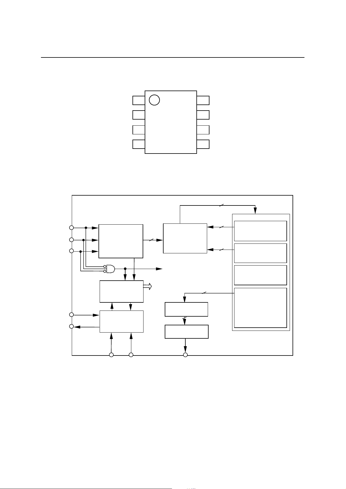
PIN LAYOUT (TOP VIEW)
FEDL2201-01
ML2201–XXX
BLOCK DIAGRAM
ST
PI
PDWN
ST
PI
GND
AOUT
Serial
Interface
1
2
3
4
8-Pin Plastic SSOP
5
16 bit Address
controller
PDWN
8
XT
7
6
XT
5
V
DD
16
384 Kbit ROM
8
Edit ROM 2 Kbit
(Phrase Control Table)
8
Address ROM 2 Kbit
(Phrase Address Table)
XT
XT
Timing
Controller
OSC
Circuit
DD
Reset, Power Down
8
PCM
Synthesizer
10
10 bit DAC
LPF
AOUTGNDV
Test ROM 2 Kbit
PCM data Area
378 Kbit
2/20
Page 3
Semiconductor
1
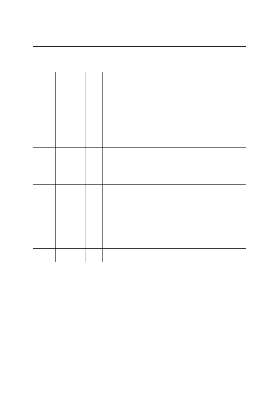
PIN DESCRIPTION
Pin No. Pin Name I/O Description
The playback trigger pin.
The number of pulses input to the PI pin, while this pin is held “L”,
1 ST I
2 PI I
3 GND — The ground pin.
4AOUTO
5VDD—
6XTI
7 XT O
8 PDWN I
determines the Phrase Address for playback. At the ST’s rising edge, the
phrase address data is loaded into the LSI and playback starts. When no
pulse input to PI occurs w hile this p in is held “L”, the LS I recognizes it as the
“Stop Code” that results in stopping playback.
The address input pin.
The number of pulses input to this pin, while the ST pin is held “L”,
determines the Phrase Address for playback.
When 32 pulses are input, th e interna l counter ret urns to its initial v alue, “0”.
The analog output pin.
Configured as N-MOS open drain, analog signal is output in the form of
change in output (attraction) current. While the PDWN pin being held “H”,
this pin is sustained at 1/2 level and thus the current keeps on flowing.
When shifting to standby state and shifting back to ready state from
standby, the pop-noise canceller is put to work.
The power supply pin.
Insert a 0.1 µF bypass capacitor between this pin and the GND pin.
The external clock input pin.
The ceramic resonator connection pin for ceramic oscillation option under
development.
Keep this pin open.
The LSI’s operations may become unstable if this pin includes any
capacitive component.
The ceramic resonator connection pin for ceramic oscillation option under
development.
The power down pin.
The LSI stays standby state while the pin being held “L”.
FEDL2201-01
ML2201–XXX
3/20
Page 4
FEDL2201-01
Semiconductor
1
ML2201–XXX
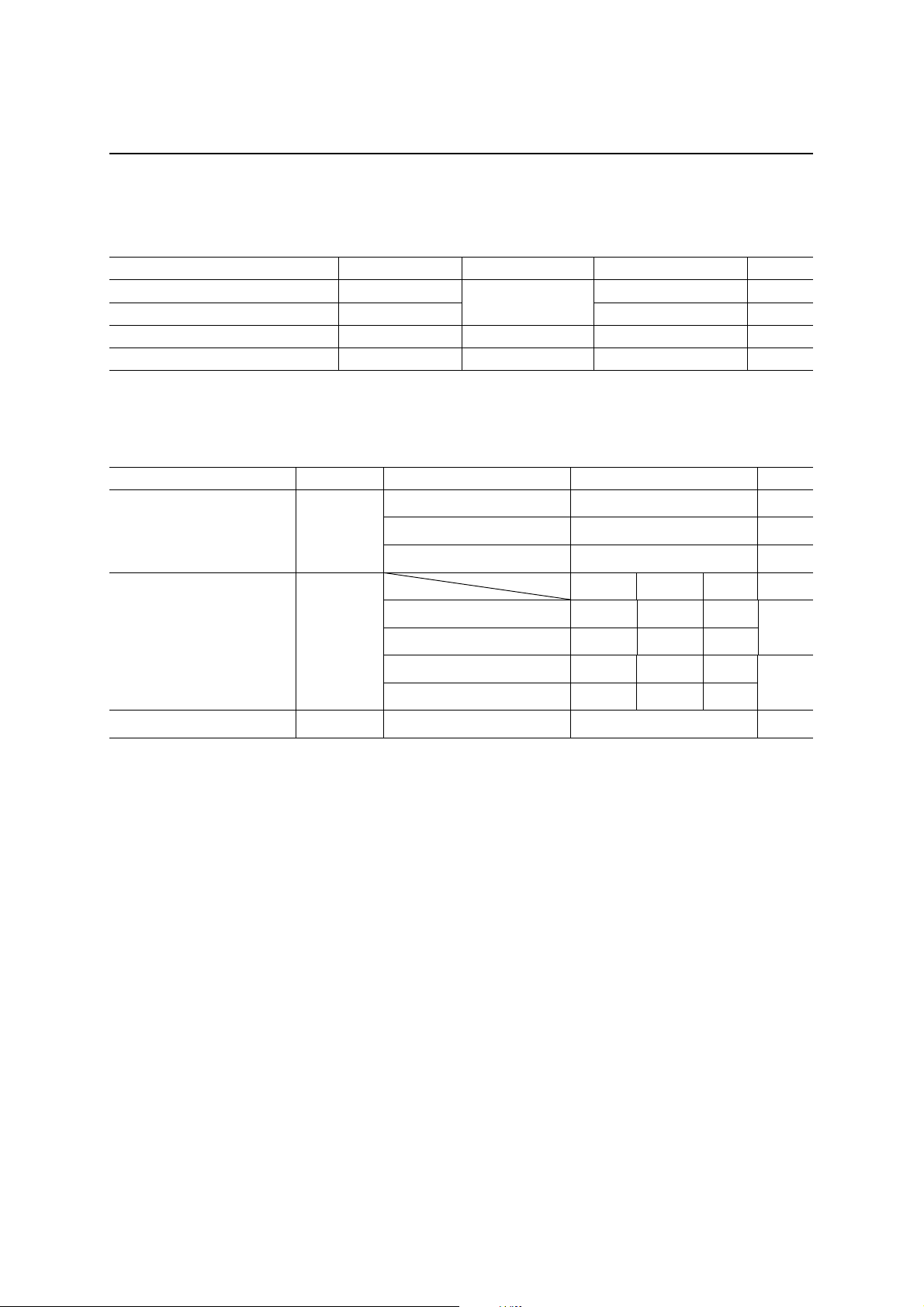
ABSOLUTE MAXIMUM RATINGS
(GND = 0 V)
Parameter Symbol Condition Rating Unit
Power Supply Voltage V
Input Voltage V
Storage Temperature T
DD
STG
IN
Ta = 25°C
— –55 to +150 °C
–0.3 to +7.0 V
–0.3 to V
+0.3 V
DD
Power Drain Allowance Pd Ta = 25°C 250 mW
RECOMMENDED OPERATING CONDITIONS
(GND = 0 V)
Parameter Symbol Condition Range Unit
f
= 3.5 to 4.5 MHz +2.0 to +5.5 V
EXTCLK
f
Power Supply Voltage V
DD
= 3.5 to 13.5 MHz +2.6 to +5.5 V
EXTCLK
f
= 3.5 to 17.0 MHz +3.0 to +5.5 V
EXTCLK
Min. Typ. Max.
VDD = 2.0 to 5.5 V 3.5 4.096 4.5
MHz
External Clock Frequency f
EXTCLK
Operating Temperature T
OP
V
= 2.6 to 5.5 V 3.5 — 13.5
DD
V
= 2.7 to 5.5 V 3.5 — 14.5
DD
VDD = 3.0 to 5.5 V 3.5 — 17.0
— –40 to +85 °C
4/20
Page 5
Semiconductor
1
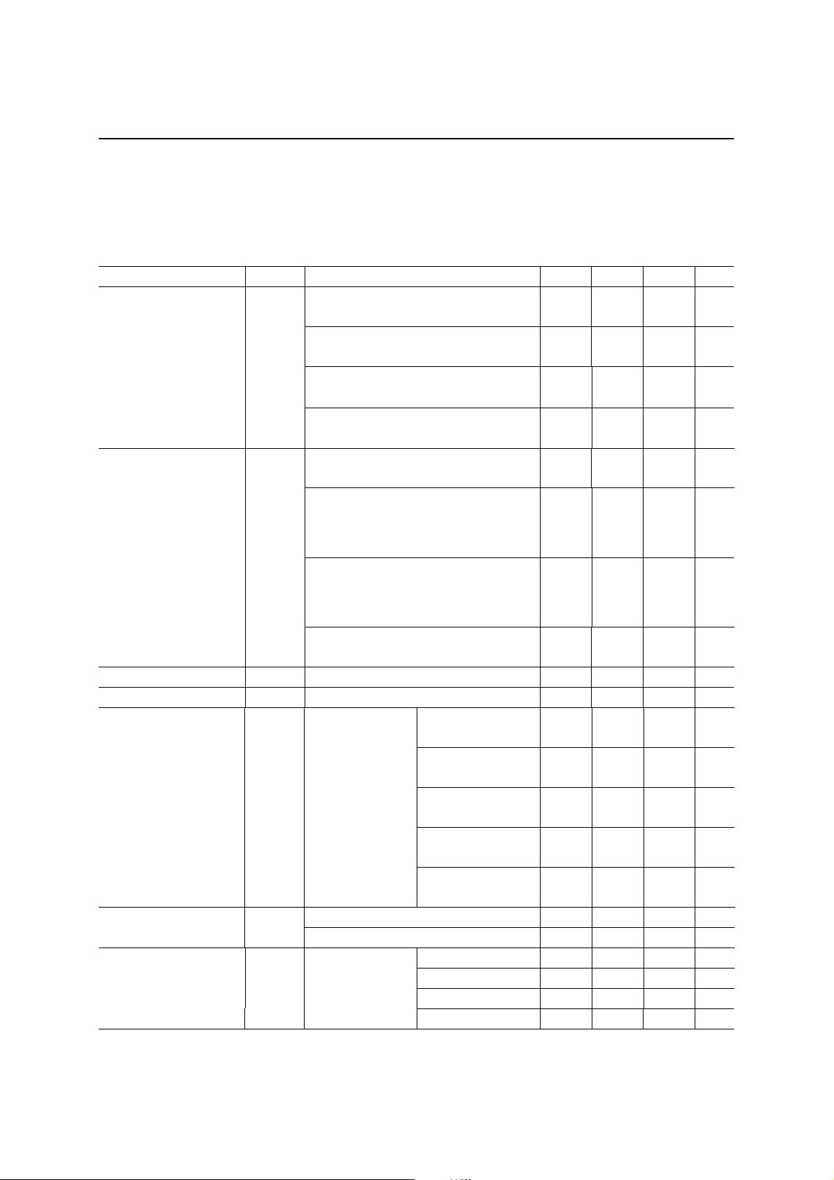
ELECTRICAL CHARACTERISTICS
DC Characteristics
FEDL2201-01
ML2201–XXX
VDD = 2.0 to 5.5 V, GND = 0 V, f
= 4.096 MHz, Ta = –40 to +85°C (unless otherwise specified)
EXTCLK
Parameter Symbol Condition Min. Typ. Max. Unit
F
“H” Input Voltage V
“L” Input Voltage V
“H” Input Current I
“L” Input Current I
Supply Current I
Standby Current I
IH
IL
IH
IL
DD
DS
EXTCLK
VDD = 3.0 to 5.5 V
f
EXTCLK
V
f
EXTCLK
V
f
V
F
EXTCLK
VDD = 3.0 to 5.5 V
f
EXTCLK
V
f
EXTCLK
VDD = 2.6 to 2.7 V
f
V
Except AOUT
output current
Ta = –40 to +70°C——10µA
Ta = –40 to +85°C — — 50 µA
> 14.5 MHz
≤ 14.5 MHz
= 2.7 to 5.5 V
DD
≤ 13.5 MHz
= 2.6 to 2.7 V
DD
≤ 4.5 MHz
EXTCLK
= 2.0 to 5.5 V
DD
> 14.5 MHz
≤ 14.5 MHz
= 2.7 to 5.5 V
DD
≤ 13.5 MHz
≤ 4.5 MHz
EXTCLK
= 2.0 to 5.5 V
DD
VIH = V
DD
VIL = GND –10 — — µA
VDD = 5.5 V
f
= 4.096 MHz
EXTCLK
VDD = 3.0 V
f
= 4.096 MHz
EXTCLK
VDD = 2.0 V
f
= 4.096 MHz
EXTCLK
VDD = 5.5 V
f
= 16 MHz
EXTCLK
V
= 3.0 V
DD
f
= 16 MHz
EXTCLK
V
DD
× 0.85
V
DD
× 0.8
V
DD
× 0.85
V
DD
× 0.8
——V
——V
——V
——V
——
——
——
——
——10µA
—1.73.9mA
—0.92.1mA
—0.51.4mA
— 4.6 12.0 mA
—1.86.5mA
VDD = 2.0 to 5.5 V 0.5 — 10.0 mA
AOUT Output Current I
AOUT
At max.
output current
VDD = 5.5 V 4.3 6.8 10.0 mA
VDD = 3.0 V 1.4 2.7 3.9 mA
V
= 2.0 V 0.5 1.2 2.2 mA
DD
V
DD
× 0.15
V
DD
× 0.2
V
DD
× 0.15
V
DD
× 0.2
V
V
V
V
5/20
Page 6
Semiconductor
1
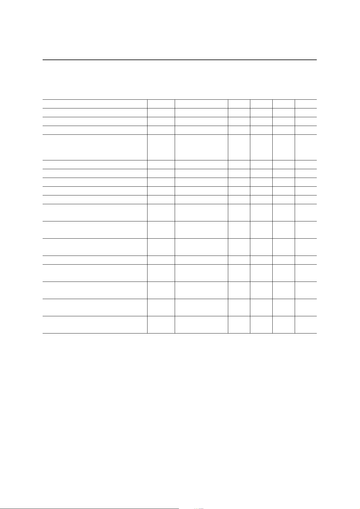
AC Characteristics
FEDL2201-01
ML2201–XXX
VDD = 2.0 to 5.5 V, GND = 0 V, f
Parameter Symbol Condition Min. Typ. Max. Unit
Clock Oscillation Duty Cycle f
Reset Input Time after Powering Up t
PDWN Hold Time after Reset Input t
D/A Converter Transit Time
(Pop-Noise Canceller Work Time)
t
DAR
Note *1
PDWN – ST Setup Time t
ST – PI Setup Time t
PI Pulse Width t
PI Cycle Time t
ST – PI Hold Time t
ST – AOUT Setup Time
Note *2
Phrase Stop Time
Note *2
Silence Time between Phrases
Note *2
Stop ST Pulse Wi dth t
Phrase ST – Phrase ST Pulse Duration
Note *2
Phrase ST – Stop ST Pulse Duration
Note *2
Stop ST – Phrase ST Pulse Duration
Note *2
Sampling Frequency
Note *3
= 4.096 MHz, Ta = –40 to +85°C (unless otherwise specified)
EXTCLK
DUTY
RST
PDH
, t
PDSS
SPS
PW
PC
SPH
t
SAS
t
DPS
t
BLN
SSW
t
PP
t
PS
t
SP
f
SAM
DAF
— 405060%
—10——µs
—10——µs
— 606468ms
—1——µs
—1——µs
— 0.35 — 2000 µs
— 0.7 — 4000 µs
—1——µs
At f
= 8.0 kHz — 1050 µs
SAM
At f
= 8.0 kHz — 700 µs
SAM
At f
= 8.0 kHz — 700 µs
SAM
— 0.35 — 2000 µs
At f
= 8.0 kHz 1050 — — µs
SAM
At f
= 8.0 kHz 1050 — — µs
SAM
At f
= 8.0 kHz 500 — — µs
SAM
— 3.9 — 28.0 kHz
Note *1: The value changes in proportion to the external clock frequency, f
Note *2: The value changes in proportion to the sampling frequency, f
SAM
EXTCLK
.
Note *3: The sampling frequency is determined by the external clock frequency, f
factor that is selected for each phrase.
.
, and the dividing
EXTCLK
6/20
Page 7
Semiconductor
1
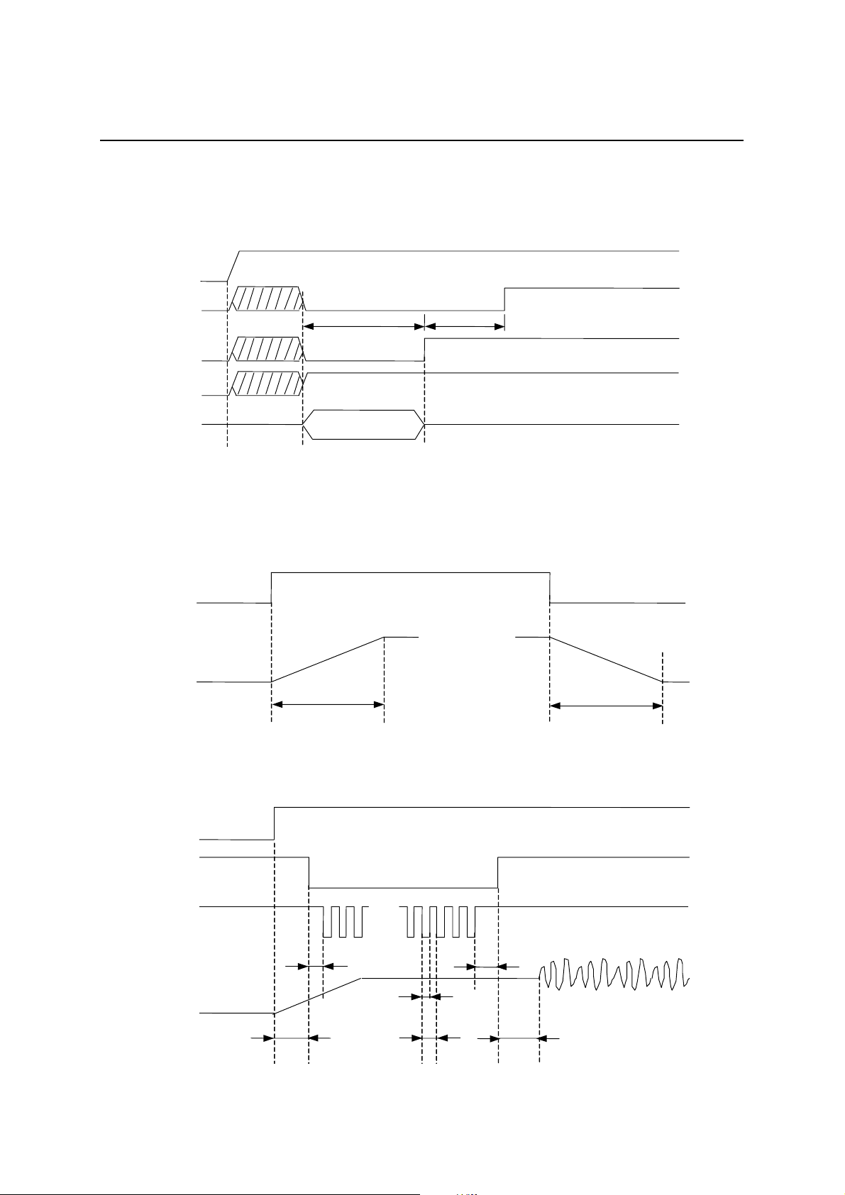
TIMING DIAGRAMS
Timing Diagram at Powering On
V
DD
FEDL2201-01
ML2201–XXX
PDWN
t
RST
t
PDH
ST
PI
Reset
Power Down
NOTE: The LSI’s reset op eration c an be perf orm ed b y using a le vel input c om bination of
= “L” and PI = “H”. After powering on, the initial reset operation is required at the above timing.
ST
Timing Diagram at Powering Up and Standby State
PDWN
1/2 I
AOUT
AOUT
PDWN
= “L”,
Timing Diagram for Playback
PDWN
ST
PI
AOUT
t
PDSS
t
DAR
t
SPS
......
t
PW
t
PC
t
SPH
t
SAS
t
DAF
7/20
Page 8
Semiconductor
T
T
1
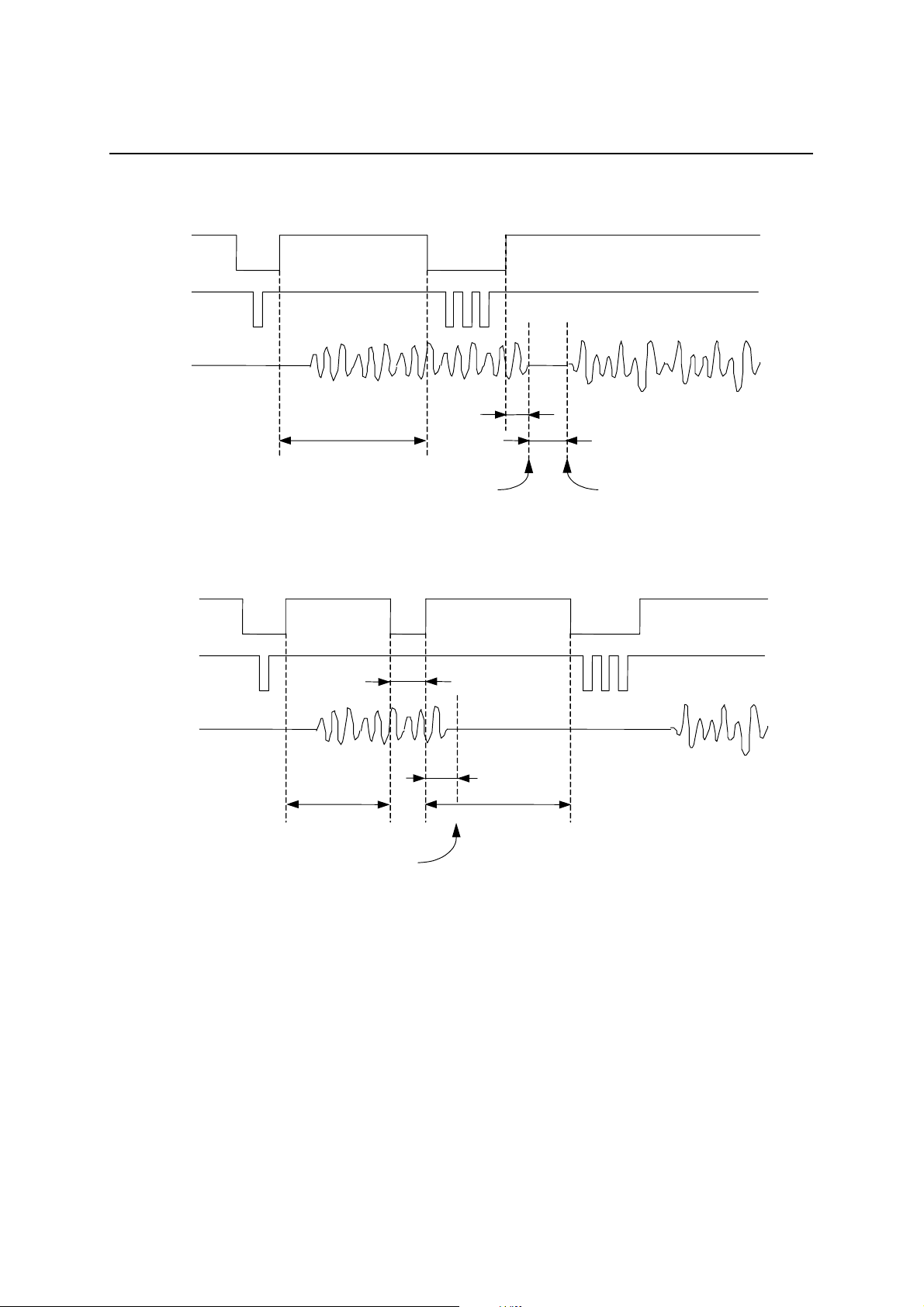
Timing Diagram on Re-addressing while Playing
S
PI
AOUT
t
PP
Stop playing the current phrase Start playing the next phrase
t
DPS
t
FEDL2201-01
ML2201–XXX
BLN
Timing Diagram on Stop Code Input
S
PI
AOUT
t
PS
Stop playing the current phrase
t
SSW
t
DPS
t
SP
8/20
Page 9
FEDL2201-01
Semiconductor
1
ML2201–XXX
FUNCTIONAL DESCRIPTION
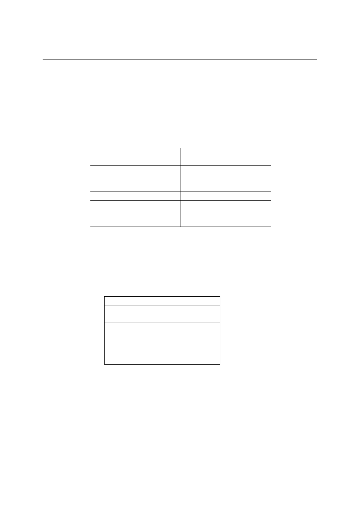
Sampling Frequency
You can select a sampling frequency for each phrase address from the following list while you are working on
sound data. Sel ect a sampli ng frequenc y that sati sfies f
dividing factors as shown in the Table 1 below.
Table 1 Sampling Frequency
= 3.9 to 28.0 kHz from the values obtained with the
SAM
Sampling Frequency
At f
= 4.096 MHz
EXTCLK
4.0 kHz f
5.3 kHz f
6.4 kHz f
8.0 kHz f
10.6 kHz f
12.8 kHz f
16.0 kHz f
Dividing Factor
/1024
EXTCLK
/768
EXTCLK
/640
EXTCLK
/512
EXTCLK
/384
EXTCLK
/320
EXTCLK
/256
EXTCLK
Memory Allocation and Playback Time Length
As shown in the Figure 1, th e on- chip Mas k RO M of ML2201 is partition ed into four areas, Phrase C ontrol Table,
Address Control Table, Test Data area and User’s Data area. The actual data area where user’s sound data can be
stored is 378 Kbit, that is the total on-chip Mask ROM capacity minus 6 Kbit.
Phrase Control Table Area
Address Control Table Area
Test Data Area
2 Kbit
2 Kbit
2 Kbit
User’s Sound Data Area
378 Kbit
Figure 1 On-chip Mask ROM (384 Kbit) Memory Allocation
9/20
Page 10

FEDL2201-01
Semiconductor
1
ML2201–XXX
You can calculate playback time length with memory size divided by a bit rate. The following formula can be used
for 8-bit PCM-based ML2201;
Playback Time (sec) = =
Memory Size (Bit)
Bit Rate (bps)
Memory Size (Bit)
Ext. Clock Frequency (Hz) × 8
For example, when you store all phrases at 8.0 kHz Sampling Frequency, the maximum playback time is
calculated as follows;
Playback Time (sec) = ≅ 6.0 sec
(384 – 6) × 1024 Bit
8000 (Hz) × 8 Bit
Playback Algorithm
ML2201 uses
OKI
Non-Linear PCM algorithm, an advanced variation of PCM.
In mid-range wave-form, this algorithm has precision and quality equivalent to those of 10-bit Straight PCM.
Inserting Silence
In addition to playing normal recorded soun d ph rases , ML 2201 allows y ou to ins ert s ilence (a silent ph rase) . You
can define time length of s ilen ce freely in 32 ms steps, within th e rang e of minim um 32 ms and maximum 992 ms
at f
= 4.096 MHz. Those time length vary in proportion to the external clock frequency, f
EXTCLK
EXTCLK
.
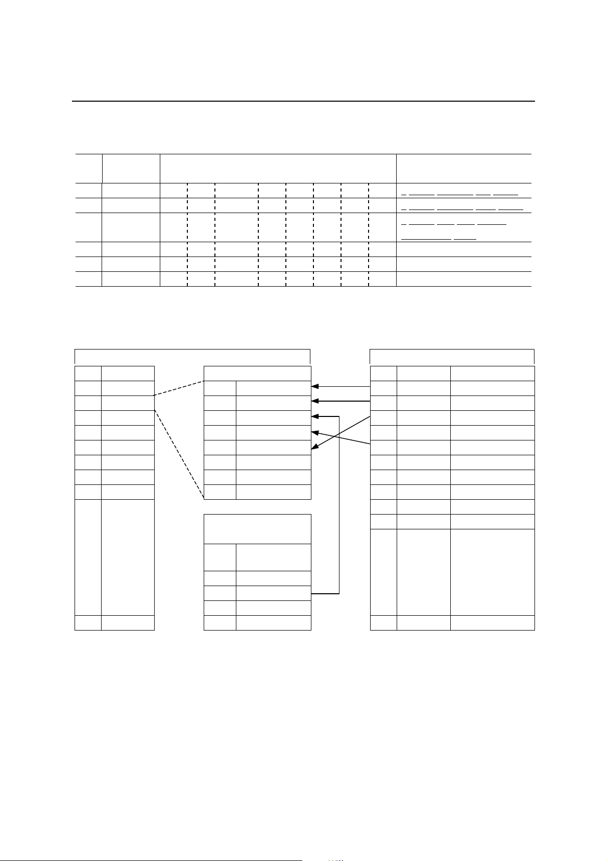
Phrase Control Table
The user-definable on-chip Phrase Control Table feature enables you to play back multiple phrases in a s ingle
continuous session with just the same simple control as in a regular single phrase playback. You can assign up to 8
phrases including a silent phrase (s) to a single address. This allows you to get the most out of limited memory
space because you can eliminate duplicate sound data.
As an example, let’s assume you want to create several similar phrases like “It will be xxxxx today”. “xxxxx” can
be “sunny”, “rainy” or “cloudy”. The common words such as “It”, “will be” and “today” are created separately as
an independent phrase, and ph rasing order inf ormation is stored in th e Phrase Cont rol Table, as shown in the Table
2 and Figure 2.1. From the external control, sim ply selecting an X address causes the LSI to play multiple phras es
continuously. In this example shown in the Table 2, selecting [01] address starts to play “It will be fine today,
while selecting [02] “It will be rainy today”.
You can also insert a silent phrase to the Phrase Control Table without consuming any memory space.
Minimum T ime Length o f Silence 32 ms
Maximum Time length of Silence 992 ms
Incremental Step 32 ms
10/20
Page 11
1
Semiconductor
FEDL2201-01
ML2201–XXX
Table 2 Phrase Control Table Data
X Address
No.
1 01 [01] [02] Silence [04] [03] It will be (Silence) fine today.
2 02 [01] [02] Silence [05] [03] It will be (Silence) rainy today.
3 03 [01] [02] [04] [09] [06] [0A] [05] [03]
30 1 E
31 1 F
(HEX)
:: :
Y Address (Phrasing Order)
(Up to 8 phrases)
Playback
It will be
occasionally rainy.
fine, later cloudy,
Phrase Control Table Data Address Control Table Data
No. X Address Phrasing Order No. Y Address Phrase
1 01 1 [01] “It” 1 01 It
2 02 2 [02] “Will be” 2 02 will be
3 03 3 Silence (64 ms) 3 03 today
4 04 4 [05] “rainy” 4 04 fine
5 05 5 [03] “today” 5 05 rainy
6 06 6 — 6 06 cloudy
7 07 7 — 7 07 snowy
8 08 8 — 8 08 occasionally
9 09 later
10 0A in some areaSet length of silence
:
:
:
31 1F 31 992 ms 31 1F —
:
:
:
(32 ms × n)
n
1 32 ms
2 64 ms
::
Length of
Silence
:
:
:
:
:
:
:
:
:
Time unit of silence varies
in proportion to the dividing
factor of f
EXTCLK
.
Figure 2.1 Phrase Data Combination for Use with Phrase Control Table
11/20
Page 12
1
T
I
T
N
Semiconductor
Stop Code
1st Phrase3rd Phrase2nd Phrase1st Phrase
It will be……….
1st Phrase
FEDL2201-01
ML2201–XXX
Power Down
Shifting to
Standby
Stop playing
Playing
It will be fine today,
later occasionally...
It will be rainy
It will be fine
today
today
2nd Phrase
1st Phrase
Stop playing the
earlier phrase
Playing
3rd Phrase
Playing
Playing
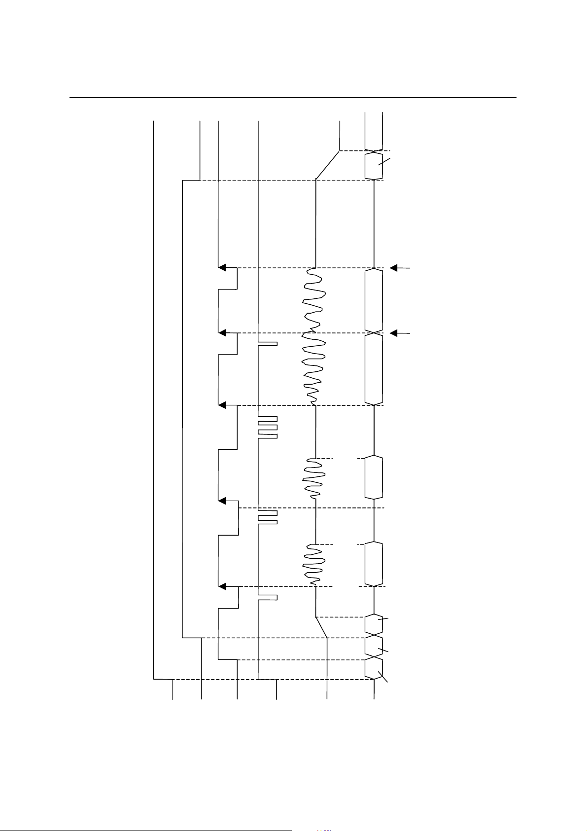
Figure 2.2 Timing Diagram for Playback with Phrase Control Table Function
Shifting to
Standby
Power Down
DD
V
S
PDW
P
Reset
AOU
12/20
Page 13

Semiconductor
1
External Clock Input
The Figure 3 shows wiring of an external timing source.
(A type of the external clock should be determined at selecting chip options.)
FEDL2201-01
ML2201–XXX
XT
An external
timing source
XT
Keep this
pin open
Figure 3 External Clock Input
*
Note: As of July 1999, ceramic oscillation on this chip is under development and thus the chip is not
functional with a ceramic oscillator. The manufacturer intends to add a ceramic oscillation option to the
chip. For more information on availability in commercial quantity, contact your sales representative.
13/20
Page 14
FEDL2201-01
Semiconductor
1
ML2201–XXX
Low Pass Filter
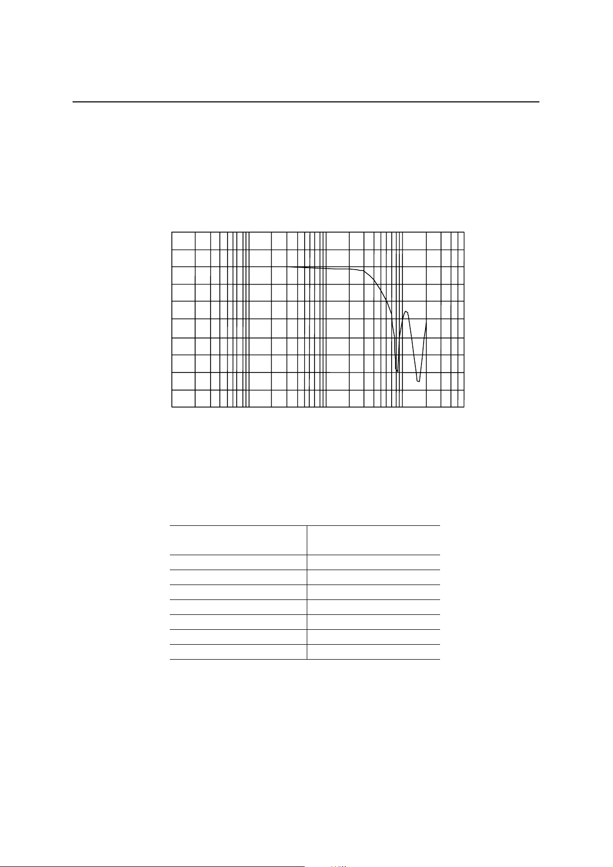
ML2201’s analog output goes through the built-in Low Pass Filter. The Figure 4 below shows Frequency
Characteristics and the Table 3 shows Cut-Off Frequency of the LPF.
The LPF’s Frequency Characteristics an d Cu t-Off Frequency chang e in proportion to t h e sampling frequency. No
analog output directly from the D/A converter is unavailable on this chip.
[dB]
20
10
0
–10
–20
–30
–40
–50
–60
–70
–80
10 100 1 k 10 k
Figure 4 LPF Frequency Characteristics (f
Table 3 LPF Cut-Off Frequency
Sampling Frequency (kHz)
(f
)
SAM
4.0 1.2
5.3 1.6
6.4 2.0
8.0 2.5
10.6 3.2
12.8 4.0
16.0 5.0
Cut-Off Frequency (kHz)
(f
CUT
= 8.0 kHz)
SAM
)
[Hz]
14/20
Page 15
FEDL2201-01
P
S
P
P
STP
Semiconductor
1
ML2201–XXX
CONNECTING ML2201 TO A SPEAKER DRIVER
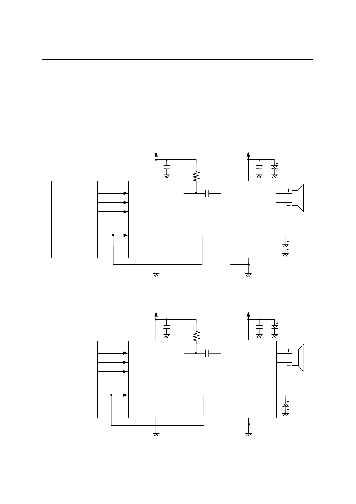
ML2201 uses a D/A converter of current-output type.
To connect ML2201 to a voltage-input type speaker driver, you should convert “Changes in Current” output to
“Changes in Voltage” signal. The following samples show connections of ML2201 and MSC1157 (OKI Speaker
Driver Amplifier) using a resistor (RL) for conversion.
SAMPLE CIRCUIT 1: AT VDD = 5.0 V, MSC1157’S Ain AMPLIFICATION = 2.5 V
+5 V +5 V
0.1 µF
V
CC
SP
SP
VR
V
DD
P1.2
P1.1
P1.0
T
I
DWN
MCU ML2201
CLK
XT
GND GND
0.1 µF
AOUT
XT
430
47 µF
Ω
Ain
MSC1157
STBY
SEL
SAMPLE CIRCUIT 2: AT VDD = 3.0 V, MSC1157’S Ain AMPLIFICATION = 1.5 V
P-P
10 µF
4.7 µF
P-P
P1.2
P1.1
P1.0
MCU
CLK XT
I
DWN
+3 V
V
DD
ML2201
GND
0.1 µF
AOUT
XT
510
47 µF
+3 V
0.1 µF
Ω
V
CC
Ain
10 µF
SP
SP
MSC1157
STBY
SEL
GND
VR
4.7 µF
15/20
Page 16
FEDL2201-01
p
p
p
p
Semiconductor
1
ML2201–XXX
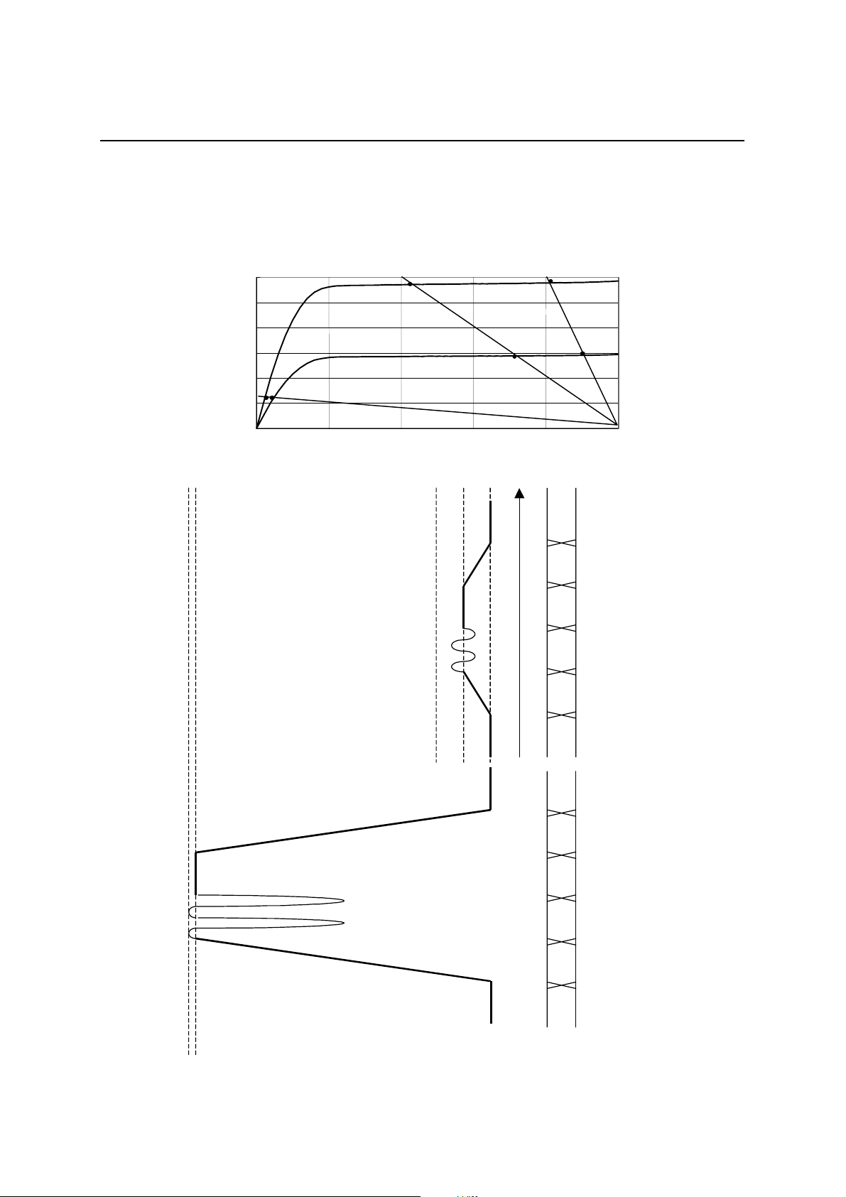
Co-relationship between output voltage and the value of a resistor for current-voltage conversion is shown in the
figure below. You may want to use the figure as a reference in determining a proper value for the resistor.
AOUT Voltage VS. AOUT Output Current at VDD = 5.0 V
6
RL = 500
Ω
RL = 200
5
4
3
IAOUT (mA)
2
RL = 5 k
Ω
1
0
012345
VAOUT (V)
Ω
Power
Shifting to
Shifting to
Power
PowerDown
Shifting to
Down
Standby
Ready
ut shown.
Playing
Standby
er waveform out
Down
Standby
(1) At RL = 200 ΩPro
-noise shown.
o
Ready
Playing
Shifting to
Standby
Power
Down
Ω
(2) At RL = 5 k
Distorted waveform and obvious
16/20
Page 17
Semiconductor
1
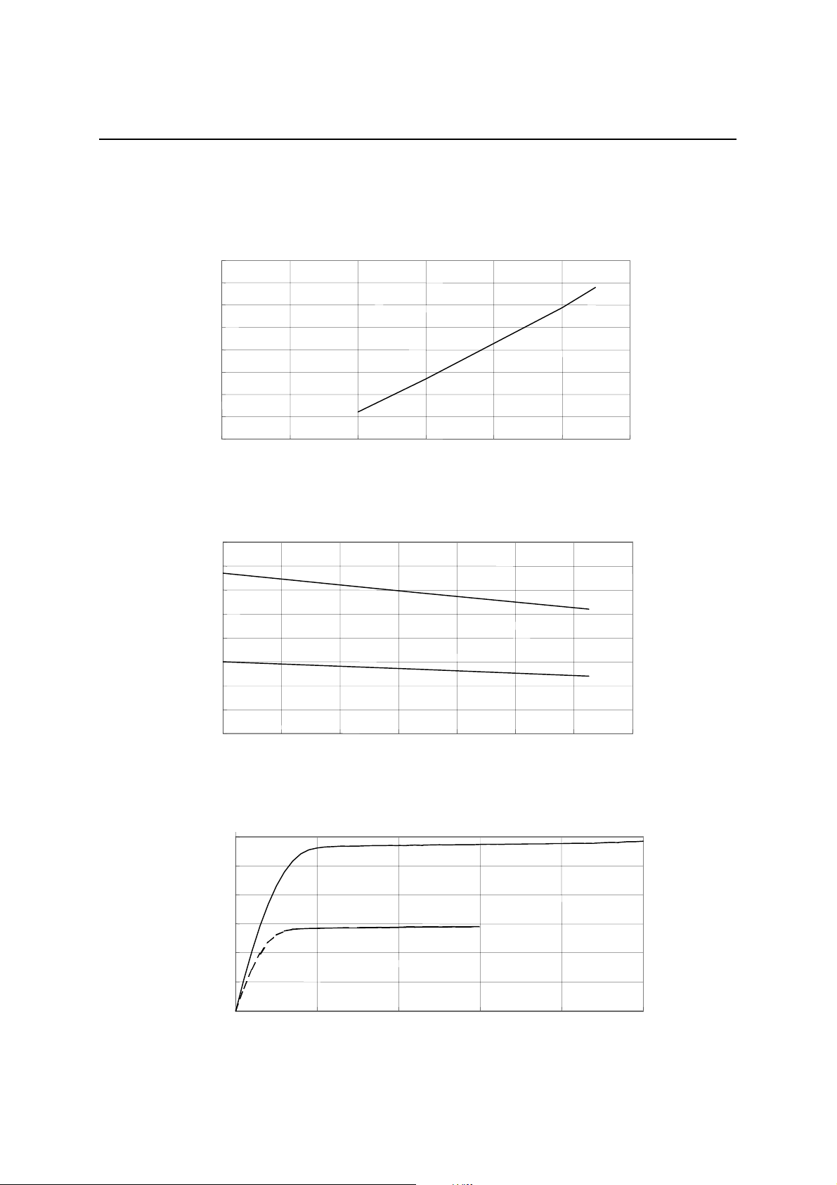
A SAMPLE CHARACTERISTICS OF D/A CONVERTER OUTPUT CURRENT
FEDL2201-01
ML2201–XXX
A Sample Characteristics : Power Supply Voltage VS. AOUT Output Current
(Ta = 25°C, VAO UT = V
8
7
6
5
4
3
IAOUT (mA)
2
1
0
0123456
, PCM at Max. level)
DD
(V)
V
DD
A Sample Characteristics : Operating Temperature VS. AOUT Output Current
, PCM at Max. level)
DD
VDD = 5 V
= 3 V
V
DD
IAOUT (mA)
8
(VAOUT = V
7
6
5
4
3
2
1
0
–40 –20 0 20 40 60 80 100
Ta (°C)
A Sample Characteristics: Voltage on AOUT Pin VS. AOUT Output Current
(Ta = 25°C, PCM at Max. level)
6
5
4
3
IAOUT (mA)
2
1
0
012345
= 3 V
V
DD
VAOUT (V )
VDD = 5 V
17/20
Page 18
FEDL2201-01
A
Semiconductor
1
ML2201–XXX
NOTES ON USAGE
Type of the Built-in D/A Converter
ML2201 has the bui lt-in current- output ty pe D/A convert er an d thus th e design of analog output circui t is dif f erent
from the one with a voltage-output type D/A converter (e.g. MSM6650 family).
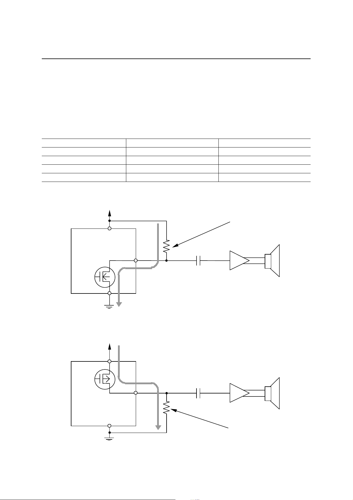
ML2201’s D/A converter is designed as current attraction type with the same circuit configuration with the one
used on MSM9831. So, the analog output circuit is different from MSM9800 family that uses a current discharge
type D/A converter. (See the table below)
Product D/A Converter Type D/A Converter Output Circuit
ML2201 Current Output N- MOS Open Drain
MSM9831 Current Output N- MOS Open Drain
MSM9800 Family Current Output P-MOS Open Drain
MSM6650 Family Voltage Output —
A sample circuit of connecting ML2201 and an amplifier chip
V
DD
ML2201
D/A Converter
GND
AOUT
Direction of flowing current
resistor for converting current to voltage
A sample circuit of connecting MSM9800 family and an amplifier chip
V
DD
D/A Converter
Direction of flowing current
AOUT
AMP
AMP
MSM9800 Family
GND
A resistor for converting current to voltage
18/20
Page 19
Semiconductor
SSOP8-P-44-0.65-K
5
Package material
Lead frame material
Pin treatment
Package weight (g)
Rev. No./Last Revised
Epoxy resin
42 alloy
Solder plating (≥5µm)
0.044 TYP.
1/May.12,1999
1
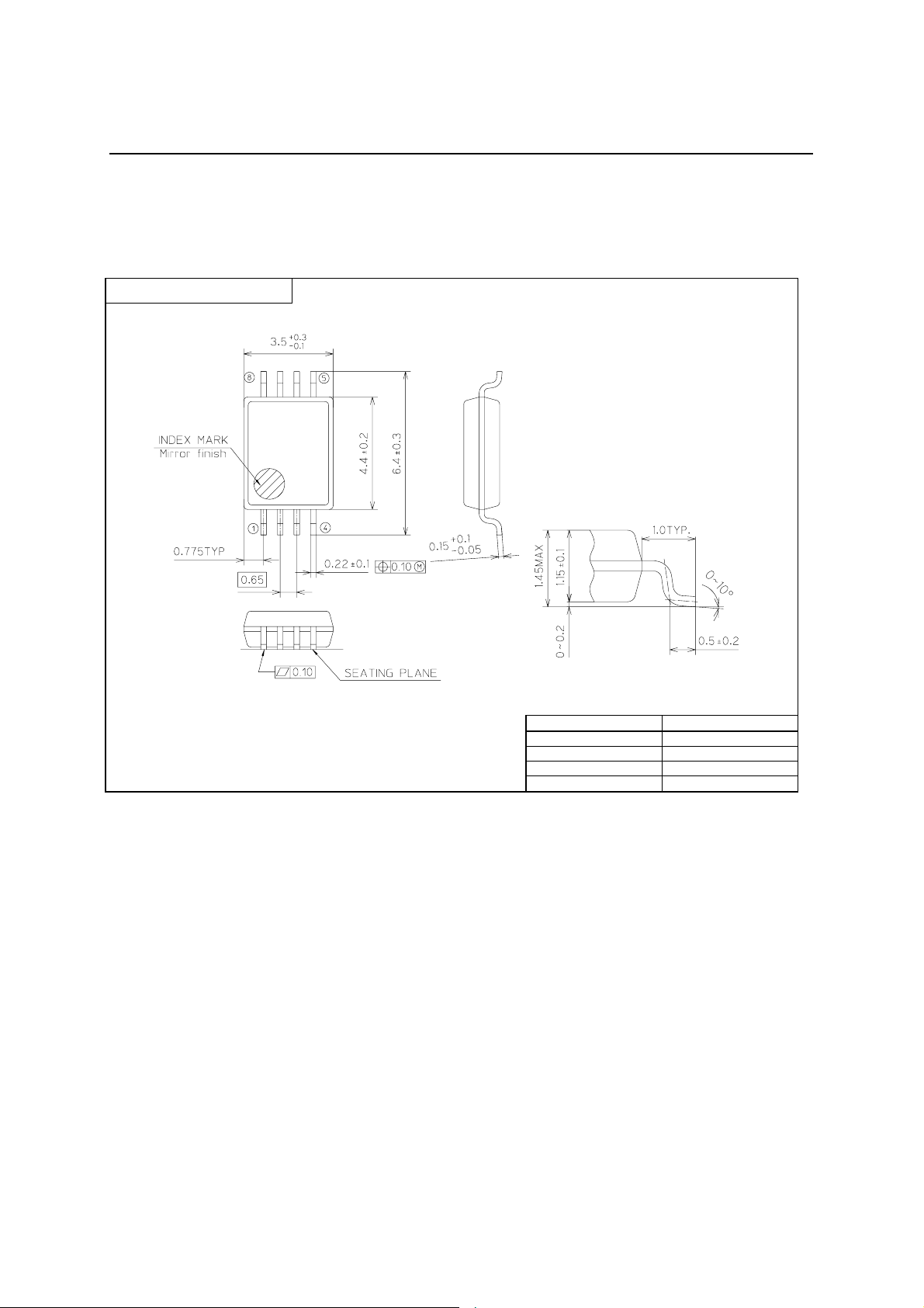
PACKAGE DIMENSIONS
FEDL2201-01
ML2201–XXX
(Unit: mm)
Notes for Mounting the Surface Mount Type Packages
The surface mount type packages are very susceptible to heat in reflow mounting and humidity
absorbed in storage.
Therefore, before you perf orm r eflow mounting, contac t Oki’s responsible s ales pers on on the pr oduct
name, package name, pin n umber, package code and desired m ounting conditions (reflow method,
temperature and times).
19/20
Page 20

FEDL2201-01
Semiconductor
1
ML2201–XXX
NOTICE
1. The information contained herein can change w ithout notice owing to product and/or techn ical improvements.
Before using the product, please make sure that the information being referred to is up-to-date.
2. The outline of action and examples for application circuits described herein have been chosen as an
explanation for the standard action and performa nce of the product. When planning to use the product, please
ensure that the external conditions are reflected in the actual circuit, assembly, and program designs.
3. When designing your product, please use our product below the specified maximum ratings and within the
specified operating ranges including, but not limited to, operating voltage, power dissipation, and operating
temperature.
4. Oki assumes no responsibility or liability whatsoever for any failure or unusual or unexpected operation
resulting from misuse, neglect, improper installation, repair, alteration or accident, improper handling, or
unusual physical or electrical stress including, but not limited to, exposure to parameters beyond the specified
maximum ratings or operation outside the specified operating range.
5. Neither indemnity against nor license of a third party’s industrial and intellectual property right, etc. is
granted by us in connection with the use of the product and/or t he information and draw ings contained herei n.
No responsibility is assumed by us for any infringement of a third party’s right which may result from the use
thereof.
6. The products listed in this document are intended for use in general electronics equipment for commercial
applications (e.g., office automation, communication equipment, measurement equipment, consumer
electronics, etc.). These products are not authorized f or us e in any system or application th at requires special
or enhanced quality and reliability characteristics nor in any system or app lication where the failure of s uch
system or application may result in the loss or damage of property, or death or injury to humans.
Such applications include, but are not limited to, traff ic and autom otive equipment, safety devices, aeros pace
equipment, nuclear power control, medical equipment, and life-support systems.
7. Certain products in this document may need government approval before they can be exported to particular
countries. The purchaser assumes the responsibility of determining the legality of export of these products
and will take appropriate and necessary steps at their own expense for these.
8. No part of the contents contained herein may be reprinted or reproduced without our prior permission.
Copyright 2000 Oki Electric Industry Co., Ltd.
20/20
 Loading...