

Datasheet ML2009CP, ML2009CQ, ML2008IP, ML2008CQ, ML2009IQ Datasheet (Micro Linear Corporation)
...
March 1997
ML2008*, ML2009**
µP Compatible Logarithmic Gain/Attenuator
GENERAL DESCRIPTION
The ML2008 and ML2009 are digitally controlled
logarithmic gain/attenuators with a range of –24 to +24dB
in 0.1dB steps.
Easy interface to microprocessors is provided by an input
latch and control signals consisting of chip select and
write.
The interface for gain setting of the ML2008 is by an 8-bit
data word, while the ML2009 is designed to interface to a
16-bit data bus with a single write operation by hardwiring the gain/attenuation pin or LSB pin. The ML2008
can be power downed by the microprocessor utilizing a
bit in the second write operation.
FEATURES
■ Low noise 0dBrnc max with +24dB gain
■ Low harmonic distortion –60dB max
■ Gain range –24 to +24dB
■ Resolution 0.1dB steps
■ Flat frequency response ±0.05dB from 0.3-4kHz
±0.10dB from 0.1-20kHz
■ Low supply current 4mA max from ±5V supplies
■ TTL/CMOS compatible digital interface
■ ML2008 is designed to interface to an 8-bit data bus;
ML2009 to 16-bit data bus
Absolute gain accuracy is 0.05dB max over supply
tolerance of ±10% and temperature range.
These CMOS logarithmic gain/attenuators are designed for * This Part Is End Of Life As Of August 1, 2000
a wide variety of applications in telecom, audio, sonar or ** This Part Is Obsolete
general purpose function generation.
BLOCK DIAGRAM
V
V
WR
CS
A0
CCVSS
+5 –5
IN
ML2008ML2009*
GND AGND
+
COARSE
–
RESISTORS/
SWITCHES
16 16
+
–
RESISTORS/
SWITCHES
DECODERS
8
REGISTER 0
D1–D8
FINE
1
REGISTER 1
8
PDN
V
CCVSS
+5 –5
V
IN
+
BUFFER
–
1
V
OUT
WR
CS
GND AGND
+
COARSE
–
RESISTORS/
SWITCHES
16 16
+
–
RESISTORS/
SWITCHES
DECODERS
9
REGISTER 0
9
D0–D8
FINE
+
BUFFER
–
V
OUT
1
ML2008, ML2009
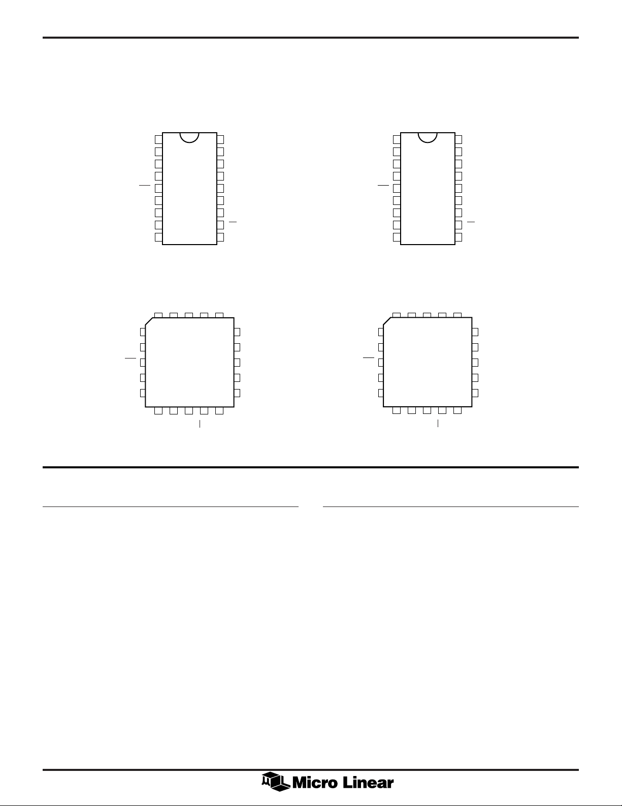
PIN CONFIGURATION
ML2008
18-Pin DIP (P18)
D7
1
2
D6
3
D5
4
D4
5
WR
6
D3
7
D2
8
D1
GND
9
TOP VIEW
D8
18
V
17
CC
16
V
OUT
15
V
SS
14
AGND
13
V
IN
12
NC
11
CS
10
A0
18-Pin DIP (P18)
1
D7
2
D6
3
D5
4
D4
5
WR
6
D3
7
D2
8
D1
GND
9
20-Pin PLCC (Q20) 20-Pin PLCC (Q20)
D4
NC
WR
D3
D2
D5
D6
D7
D8
3212019
4
5
6
7
8
910111213
CC
V
18
V
OUT
17
V
SS
16
AGND
15
NC
14
NC
D4
NC
WR
D3
D2
D5
3212019
4
5
6
7
8
910111213
ML2009*
TOP VIEW
D6
D7
18
D8
17
V
CC
16
V
OUT
15
V
SS
14
AGND
13
V
IN
12
NC
11
CS
10
D0
CC
D8
V
18
V
OUT
17
V
SS
16
AGND
15
NC
14
NC
D1
TOP VIEW
GND
V
IN
CS
A0
PIN DESCRIPTION
NAME FUNCTION
V
SS
V
CC
GND Digital ground. 0Volts. All digital
AGND Analog ground. 0Volts. Analog input
V
IN
V
OUT
D8 Data bit, ATTEN/GAIN
D7 Data bit, C3
D6 Data bit, C2
D5 Data bit, C1
D4 Data bit, C0
Negative supply. –5Volts ±10%
Positive supply. 5Volts ±10%
inputs are referenced to this ground.
and output are referenced to this
ground.
Analog input
Analog output
GND
D0
CS
V
D1
TOP VIEW
IN
NAME FUNCTION
D3 Data bit, F3
D2 Data bit, PDN, F2 ML2008; F2 ML2009
D1 Data bit, F0, F1 ML2008; F1 ML2009
D0 Data bit, F0 ML2009 only
WR Write enable. This input latches the
data bits into the registers on rising
edges of WR.
CS Chip select. This input selects the
device by only allowing the WR signal
to latch in data when CS is low.
A0 Address select. This input determines
(ML2008 only) which data word is being written into
the registers.
2
ML2008, ML2009
ABSOLUTE MAXIMUM RATINGS
OPERATING CONDITIONS
(Note 1)
Temperature Range (Note 2)
Supply Voltage
VCC.................................................................... +6.5V
VSS......................................................................–6.5V
AGND with Respect to GND....................... VCC to V
Analog Inputs and Outputs ..... VSS –0.3V to VCC +0.3V
SS
ML2008CX, ML2009CX .......................... 0°C to +70°C
ML2008IX, ML2009IX ......................... –40°C to +85°C
Supply Voltage
VCC................................................................ 4V to 6V
VSS............................................................. –4V to –6V
Digital Inputs and Outputs... GND –0.3V to VCC +0.3V
Input Current Per Pin ........................................ ±25mA
Power Dissipation ........................................... 750mW
Storage Temperature Range ............... –65°C to +150°C
Lead Temperature (Soldering 10 sec.) ................. 300°C
ELECTRICAL CHARACTERISTICS
Unless otherwise specified, TA = T
Other Bits = 0, (0dB Ideal Gain), CL = 100pF, R
measured at 1.4V.
SYMBOL PARAMETER NOTES CONDITIONS MIN TYP MAX UNITS
Analog
AG Absolute Gain Accuracy 4 VIN = 8dBm, 1kHz –0.05 +0.05 dB
RG Relative Gain Accuracy 4 100000001 –0.05 +0.05 dB
FR Frequency Response 4 300-4000Hz –0.05 +0.05 dB
V
OS
I
CN
HD Harmonic Distortion 4 V
SD Signal to Distortion 4 V
PSRR Power Supply Rejection 4 200mV
Z
IN
V
INR
V
OSW
Output Offset Voltage 4 V
Idle Channel Noise 4 VIN = 0, +24dB, C msg weighted –6 0 dBrnc
Input Impedance, V
Input Voltage Range 4 ±3.0 V
Output Voltage Swing 4 ±3.0 V
IN
MIN
to T
, V
MAX
5V
4 1 Meg
= 5V ±10%, VSS = –5V ±10%, Data Word: D8 (ATTEN/GAIN) = 1,
CC
= 600Ω, dBm measurements use 600Ω as reference load, digital timing
L
NOTE 3
000000000 –0.05 +0.05 dB
000000001 –0.05 +0.05 dB
All other gain settings –0.1 +0.1 dB
All values referenced to 100000000
gain when D8 (ATTEN/GAIN) = 1,
= 8dBm when D8 (ATTEN/GAIN) = 0,
V
IN
VIN = (8dBm – Ideal Gain) in dB
100-20,000Hz –0.1 +0.1 dB
Relative to 1kHz
= 0, +24dB gain ±100 mV
IN
= 0, +24dB, 1kHz 450 900 nv/√Hz
IN
= 8dBm, 1kHz –60 dB
IN
Measure 2nd, 3rd, harmonic relative
to fundamental
= 8dBm, 1kHz +60 dB
IN
C msg weighted
, 1kHz sine, VIN = 0
P-P
on V
on V
CC
SS
–60 –40 dB
–60 –40 dB
3
ML2008, ML2009
ELECTRICAL CHARACTERISTICS
(Continued)
SYMBOL PARAMETER NOTES CONDITIONS MIN TYP MAX UNITS
NOTE 3
Digital and DC
V
IL
V
IH
I
IN
I
IN
I
CC
Digital Input Low Voltage 4 0.8 V
Digital Input High Voltage 4 2.0 V
Input Current, Low 4 V
Input Current, High 4 VIH = V
= GND –10 µA
IH
CC
10 µA
VCC Supply Current 4 No output load, VIL = GND, 4 mA
VIH = VCC, VIN = 0
I
SS
VSS Supply Current 4 No output load, VIL = GND, –4 mA
VIH = VCC, VIN = 0
I
CCP
I
SSP
VCC Supply Current, ML2008 4 No output load, VIL = GND, 0.5 mA
Powerdown Mode Only VIH = V
CC
VSS Supply Current, ML2008 4 No output load, VIL = GND, –0.1 mA
Powerdown Mode Only VIH = V
CC
AC Characteristics
t
SET
Settling Time 4 V
OUT
= 0.185V. Change gain from –24 20 µs
IN
V
to +24dB. Measure from WR rising
edge to when V
settles to within
OUT
0.05dB of final value.
t
STEP
Step Response 4 Gain = +24dB. V
OUT
Measure from V
= –3V to +3V step. 20 µs
IN
= –3V to when V
IN
OUT
V
settles to within 0.05dB of final value.
t
DS
t
DH
t
AS
t
AH
t
CSS
t
CSH
t
PW
Note 1: Absolute maximum ratings are limits beyond which the life of the integrated circuit may be impaired. All voltages unless otherwise specified are measured with
Note 2: 0°C to +70°C and –40°C to +85°C operating temperature range devices are 100% tested with temperature limits guaranteed by 100% testing, sampling, or by
Note 3: Typicals are parametric norm at 25°C.
Note 4: Parameter guaranteed and 100% production tested.
Note 5: Parameter guaranteed. Parameters not 100% tested are not in outgoing quality level calculation.
Data Setup Time 4 50 ns
Data Hold Time 4 50 ns
A0 Setup Time 4 0 ns
A0 Hold Time 4 0 ns
CS* Setup Time 4 0 ns
CS* Hold Time 4 0 ns
WR* Pulse Width 4 50 ns
respect to ground.
correlation with worst-case test conditions.
4

TIMING DIAGRAM
ML2008, ML2009
D0-D8
WR
A0
CS
TYPICAL PERFORMANCE CURVES
0
–0.5
ATTEN: VIN = 0.5V
GAIN: VIN = 0.5V
–.10
–.15
–.20
–.25
–.30
–.35
AMPLITUDE (dB)
–.40
–.45
–.50
100 1K 10K 100K
RMS
/GAIN SETTING
RMS
FREQUENCY (Hz)
GAIN = +24dB
GAIN = +18dB
GAIN = +12dB
GAIN = +0, –24dB
AS
t
CSS
DATA
VALID
t
DS
t
PW
0
–0.5
–.10
–.15
–.20
–.25
–.30
–.35
AMPLITUDE (dB)
–.40
–.45
–.50
t
DH
t
AHt
t
CSH
ATTEN: VIN = 2V
GAIN: VIN = 2V
100 1K 10K 100K
RMS
/GAIN SETTING
RMS
GAIN = +24dB
FREQUENCY (Hz)
GAIN = 0dB
GAIN = –24dB
Figure 2. Amplitude vs Frequency
(VIN/V
2
1.8
1.6
1.4
1.2
1
0.8
0.6
0.4
OUTPUT NOISE VOLTAGE (µV/√Hz)
0.2
0
10 100 1K 10K
= 0.5V
OUT
GAIN = +24dB
GAIN = +12dB
GAIN = –24dB
FREQUENCY (Hz)
RMS
)
–2
–3
–4
–5
–6
–7
OUTPUT (NOISE) (dBrnc)
–8
MSG
C
–9
–10
–24
Figure 4. Output Noise Voltage vs Frequency Figure 5. C
Figure 3. Amplitude vs Frequency
(VIN/V
VIN = 0
–18 –12 –6 0 6 12 18 24
Output Noise vs Gain Setting
MSG
= 2V
OUT
GAIN SETTING (dB)
RMS
)
5

ML2008, ML2009
TYPICAL PERFORMANCE CURVES
100
ATTEN: VIN = 8dBm
GAIN: V
90
1kHZ
80
70
S/N (DB)
MSG
C
60
50
40
80
70
60
50
40
S/N + D (dB)
30
20
ATTEN: VIN = 2V
GAIN: VIN = 2V
10
–24
= 8dBm/GAIN SETTING
IN
–6–12–18–24
0 6 12 18 24
GAIN SETTING (dB)
Figure 6. C
RMS
RMS
–18 –12 –6 0 6 12 18 24
S/N vs Gain Setting
MSG
/GAIN SETTING
GAIN SETTING (dB)
VIN = 1kHz
VIN = 20kHz
VIN = 50kHz
(Continued)
0.1
.08
.06
.04
(dB)
.02
0
–.02
GAIN ERROR
–.04
–.06
–.08
–1.0
–24
–18 –12 –6 0 6 12 18 24
Figure 7. Gain Error vs Gain Setting
80
70
60
50
S/N + D (dB)
40
30
ATTEN: V
IN
GAIN: VIN = 0.5V
20
–24 –18 –12 –6
= 0.5V
GAIN SETTING (dB)
RMS
/GAIN SETTING
RMS
GAIN SETTING (dB)
VIN = 1kHz
VIN = 20kHz
VIN = 50kHz
0 6 12 18 24
Figure 8. S/N +D vs Gain Setting (VIN/V
OUT
= 2V
RMS
)
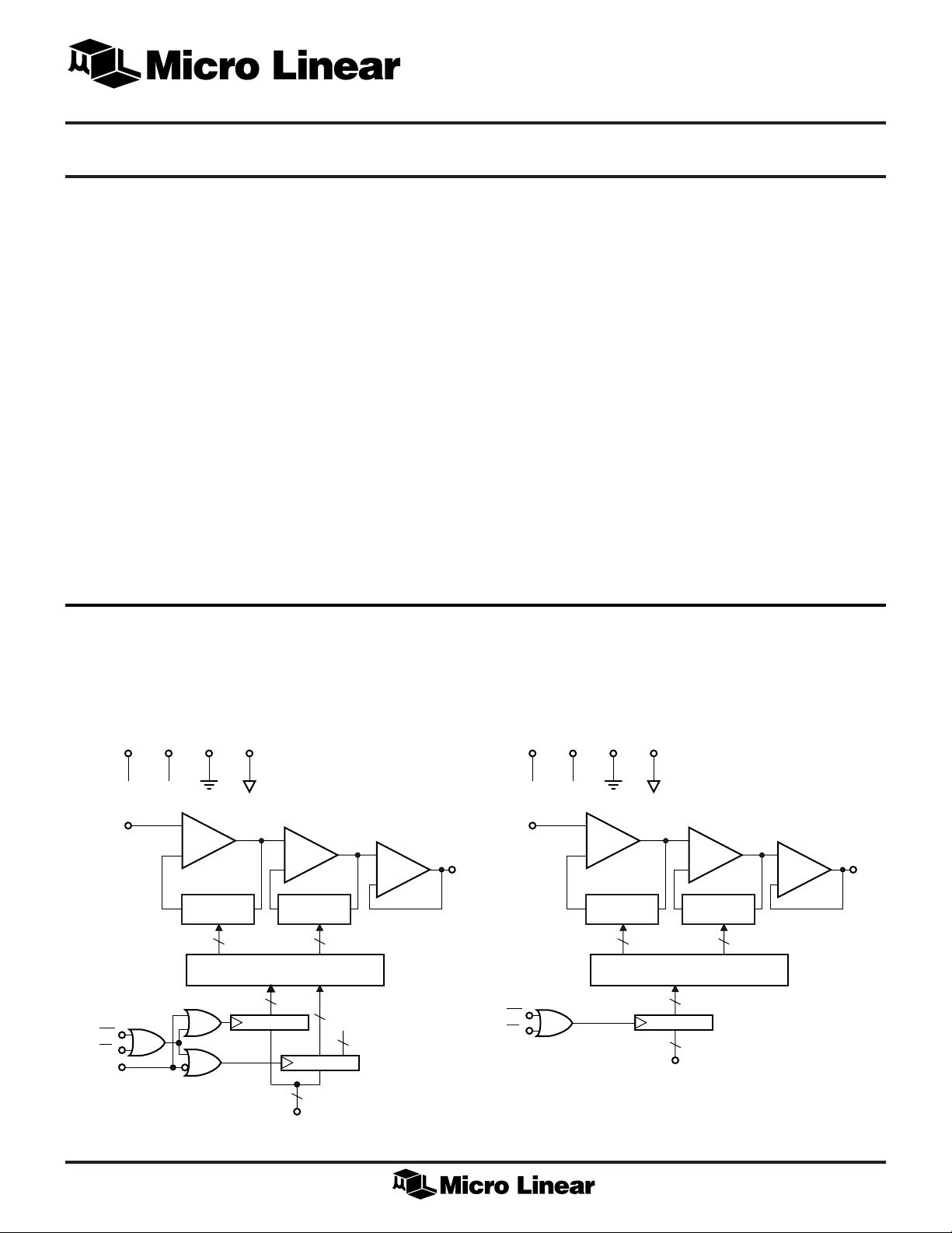
1.0 FUNCTIONAL DESCRIPTION
The ML2008, ML2009 consists of a coarse gain stage, a
fine gain stage, an output buffer, and a µP compatible
parallel digital interface.
1.1 Gain Stages
The analog input, VIN, goes directly into the op amp input
in the coarse gain stage. The coarse gain stage has a gain
range of 0 to 22.5dB in 1.5dB steps.
The fine gain stage is cascaded onto the coarse section.
The fine gain stage has a gain range of 0 to 1.5dB in 0.1dB
steps.
Both stages can be programmed for either gain or
attenuation, thus doubling the effective gain range.
6
Figure 9. S/N +D vs Gain Setting (VIN/V
OUT
= 0.5V
RMS
The logarithmic steps in each gains stage are generated by
placing the input signal across a resistor string of 16 series
resistors. Analog switches allow the voltage to be tapped
from the resistor string at 16 points. The resistors are sized
such that each output voltage is at the proper logarithmic
ratio relative to the input signal at the top of the string.
Attenuation is implemented by using the resistor string as
a simple voltage divider, and gain is implemented by
using the resistor string as a feedback resistor around an
internal op amp.
1.2 Gain Settings
Since the coarse and fine gain stages are cascaded, their
gains can be summed logarithmically. Thus, any gain from
–24dB to +24dB in 0.1dB steps can be obtained by
combining the coarse and fine gain setting to yield the
)

ML2008, ML2009
desired gain setting. The relationship between the register
0 and 1 bits and the corresponding analog gain values is
shown in Tables 1 and 2. Note that C3-C0 select the
coarse gain, F3-F0 select the fine gain, and ATTEN/GAIN
selects either gain or attenuation.
1.3 Output Buffer
The final analog stage is the output buffer. This amplifier
has internal gain of 1 and is designed to drive 600Ω,
100pF loads. Thus, it is suitable for driving a telephone
hybrid circuit directly without any external amplifier.
Table 1. Fine Gain Settings (C3 – C0 = 0)
Ideal Gain (dB)
F3 F2 F1 F0 ATTEN/GAIN = 1 ATTEN/GAIN = 0
0000 0.0 0.0
0001 –0.1 0.1
0010 –0.2 0.2
0011 –0.3 0.3
0100 –0.4 0.4
0101 –0.5 0.5
0110 –0.6 0.6
0111 –0.7 0.7
1000 –0.8 0.8
1001 –0.9 0.9
1010 –1.0 1.0
1011 –1.1 1.1
1100 –1.2 1.2
1101 –1.3 1.3
1110 –1.4 1.4
1111 –1.5 1.5
1.4 Power Supplies
The digital section is powered between VCC and GND,
or 5V. The analog section is powered between VCC and
V
and uses AGND as the reference point, or ±5V.
SS
GND and AGND are totally isolated inside the device to
minimize coupling from the digital section into the analog
section. Typically this is less than 100µV. However, AGND
and GND should be tied together physically near the
device and ideally close to the common power supply
ground connection.
Typically, the power supply rejection of VCC and V
SS
to the analog output is greater than –60dB at 1KHz. If
decoupling of the power supplies is still necessary in a
system, VCC and VSS should be decoupled with respect
to AGND.
Table 2. Coarse Gain Settings (F3 – F0 = 0)
Ideal Gain (dB)
C3 C2 C1 C0 ATTEN/GAIN = 1 ATTEN/GAIN = 0
0000 0.0 0.0
0001 –1.5 1.5
0010 –3.0 3.0
0011 –4.5 4.5
0100 –6.0 6.0
0101 –7.5 7.5
0110 –9.0 9.0
0111 –10.5 10.5
1000 –12.0 12.0
1001 –13.5 13.5
1010 –15.0 15.0
1011 –16.5 16.5
1100 –18.0 18.0
1101 –19.5 19.5
1110 –21.0 21.0
1111 –22.5 22.5
2.0 DIGITAL INTERFACE
The architecture of the digital section is shown in the
preceding black diagram.
The structure of the data registers or latches is shown in
Figures 10 and 11 for the ML2008 and ML2009,
respectively. The registers control the attenuation/gain
setting bits and with the ML2008 the power down bit.
Tables 1 and 2 describe how the data word programs the
gain.
The difference between the ML2008 and ML2009 is in the
register structure. The ML2008 is an 8-bit data bus
version. This device has one 8-bit register and one 2-bit
register to store the 9 gain setting bits and 1 powerdown
bit. Two write operations are necessary to program the full
10 data bits from eight external data pins. The address pin
A0 controls which register is being written into. The
powerdown bit, PDN, causes the device to be placed in
powerdown. When PDN = 1, the device is powered
down. In this state, the power consumption is reduced by
removing power from the analog section and forcing the
analog output, V
, to a high impedance state. While the
OUT
device is in powerdown, the digital section is still
functional and the current data word remains stored in the
registers. When PDN = 0, device is in normal operation.
The ML2009 is a 9-bit data bus version. This device has
one 9-bit register to store the 9 gain setting bits. The full 9
data bits can be programmed with one write operation
from nine external data pins.
The internal registers or latches are edge triggered. The
data is transferred from the external pins to the register
output on the rising edge of WR. The address pin, A0,
controls which register the data will be written into as
shown in Figures 1 and 2. The CS control signal selects
the device by allowing the WR signal to latch in the data
only when CS is low. When CS is high, WR is inhibited
from latching in new data into the registers.
7

ML2008, ML2009
REG 0ATTEN/GAIN C3 C2 C1 C0 F3 F2 F1 F0
D8 D7 D6 D5 D4 D3 D2 D1 BITD0
D8 D7 D6 D5 D4 D3 D2 D1 BIT
A0 = 0
A0 = 1
DN
REG 0ATTEN/GAIN C3 C2 C1 C0 F3 F2 F1
F0
REG 1P
Figure 10. ML2008 Register Structure
ML2008
A0 D1-D8
8
V
OUT
µP
V
CS
IN
WR
Figure 12. Typical 8-Bit µP Interface, Double Write
Figure 11. ML2009 Register Structure
ML2009
D1-D8
8
V
OUT
D0
+5V
µP
V
IN
CS
WR
Figure 13. Typical 8-Bit µP Interface, Single Write
ML2009
CS
WR
µP
9
Figure 14. Typical 16-Bit µP Interface Figure 15. AGC for DSP or Modem Front End
8
D0-D8
ML2009
V
WR
OUTV
CS
IN
D0-D8
ML2233
12-BIT
V
IN
+ SIGN
A/D
µP
OR
DSP

ML2008, ML2009
+5V
2.5V
REF
V
–5V
IN
ML2009
D0-D8
V
OUT
Figure 16. Operation as Logarithmic D/A Converter
ML2008
V
IN
CS1
CS2
CS
A0
D1-D8
A0
WR
µP
D
E
ADDRESS
C
O
D
E
R
ML2008
D1-D8
CS
A0
Figure 17. Controlling Multiple Gain/Attenuators
9

PHYSICAL DIMENSIONS inches (millimeters)
0.385 - 0.395
(8.89 - 10.03)
0.350 - 0.356
(8.89 - 9.04)
1
ML2008, ML2009
Package: Q20
20-Pin PLCC
0.042 - 0.056
(1.07 - 1.42)
0.025 - 0.045
(0.63 - 1.14)
(RADIUS)
0.042 - 0.048
(1.07 - 1.22)
PIN 1 ID
6
0.050 BSC
(1.27 BSC)
0.026 - 0.032
(0.66 - 0.81)
0.013 - 0.021
(0.33 - 0.53)
11
SEATING PLANE
0.350 - 0.356
16
(8.89 - 9.04)
0.165 - 0.180
(4.19 - 4.57)
0.385 - 0.395
(8.89 - 10.03)
0.146 - 0.156
(3.71 - 3.96)
0.009 - 0.011
(0.23 - 0.28)
0.100 - 0.110
(2.54 - 2.79)
0.200 BSC
(5.08 BSC)
0.290 - 0.330
(7.36 - 8.38)
10

ML2008, ML2009
PHYSICAL DIMENSIONS inches (millimeters)
0.890 - 0.910
(22.60 - 23.12)
18
Package: P18
18-Pin PDIP
PIN 1 ID
0.045 MIN
(1.14 MIN)
(4 PLACES)
0.170 MAX
(4.32 MAX)
0.125 MIN
(3.18 MIN)
1
ORDERING INFORMATION
PART NUMBER TEMPERATURE RANGE PACKAGE
0.050 - 0.065
(1.27 - 1.65)
0.016 - 0.022
(0.40 - 0.56)
0.100 BSC
(2.54 BSC)
SEATING PLANE
0.240 - 0.260
(6.09 - 6.61)
0.015 MIN
(0.38 MIN)
0.295 - 0.325
(7.49 - 8.26)
0º - 15º
0.008 - 0.012
(0.20 - 0.31)
ML2008IP–40°C to 85°CMolded PDIP (P18) (EOL)
ML2008IQ–40°C to 85°CMolded PLCC (Q20) (EOL)
ML2008CP0°C to +70°CMolded PDIP (P18) (EOL)
ML2008CQ0°C to +70°CMolded PLCC (Q20) (EOL)
ML2009IP–40°C to 85°CMolded PDIP (P18) (OBS)
ML2009IQ–40°C to 85°CMolded PLCC (Q20) (OBS)
ML2009CP0°C to +70°CMolded PDIP (P18) (OBS)
ML2009CQ0°C to +70°CMolded PLCC (Q20) (OBS)
© Micro Linear 1997 is a registered trademark of Micro Linear Corporation
Products described in this document may be covered by one or more of the following patents, U.S.: 4,897,611; 4,964,026; 5,027,116; 5,281,862; 5,283,483; 5,418,502; 5,508,570; 5,510,727; 5,523,940;
5,546,017; 5,559,470; 5,565,761; 5,592,128; 5,594,376; Japan: 2598946. Other patents are pending.
Micro Linear reserves the right to make changes to any product herein to improve reliability, function or design.
Micro Linear does not assume any liability arising out of the application or use of any product described herein,
neither does it convey any license under its patent right nor the rights of others. The circuits contained in this
data sheet are offered as possible applications only. Micro Linear makes no warranties or representations as to
whether the illustrated circuits infringe any intellectual property rights of others, and will accept no responsibility
or liability for use of any application herein. The customer is urged to consult with appropriate legal counsel
before deciding on a particular application.
11
2092 Concourse Drive
San Jose, CA 95131
Tel: 408/433-5200
Fax: 408/432-0295
DS2008_09-01
 Loading...