

Microchip Technology Inc PIC16F871-I-P, PIC16F870-I-SO, PIC16F870-I-SS, PIC16F871-I-L Datasheet
1999 Microchip Technology Inc.
Preliminary DS30569A-page 1
Devices Included in this Data Sheet:
Microcontroller Core Features:
•High-performance RISC CPU
•Only 35 single word instructions to learn
•All single cycle instructions except for program
branches which are two cycle
•Operating speed:DC - 20 MHz clock input
DC - 200 ns instruction cycle
•2K x 14 words of FLASH Program Memory
128 x 8 bytes of Data Memory (RAM)
64 x 8 bytes of EEPROM Data Memory
•Pinout compatible to the PIC16CXXX 28 and 40pin devices
•Interrupt capability (up to 11 sources)
•Eight level deep hardware stack
•Direct, indirect and relative addressing modes
•Power-on Reset (POR)
•Power-up Timer (PWRT) and
Oscillator Start-up Timer (OST)
•Watchdog Timer (WDT) with its own on-chip RC
oscillator for reliable operation
•Programmable code-protection
•Power saving SLEEP mode
•Selectable oscillator options
•Low-power, high-speed CMOS FLASH/EEPROM
technology
•Fully static design
•In-Circuit Serial Programming (ICSP) via two
pins
•Single 5V In-Circuit Serial Programming capability
•In-Circuit Debugging via two pins
•Processor read/write access to program memory
•Wide operating voltage range: 2.0V to 5.5V
•High Sink/Source Current: 25 mA
•Commercial and Industrial temperature ranges
•Low-power consumption:
-< 1.6 mA typical @ 5V, 4 MHz
-20 µA typical @ 3V, 32 kHz
-< 1 µA typical standby current
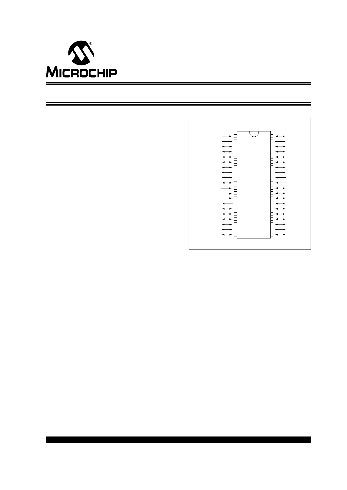
Pin Diagram
Peripheral Features:
•Timer0: 8-bit timer/counter with 8-bit prescaler
•Timer1: 16-bit timer/counter with prescaler,
can be incremented during sleep via external
crystal/clock
•Timer2: 8-bit timer/counter with 8-bit period
register, prescaler and postscaler
•One Capture, Compare, PWM module
-Capture is 16-bit, max. resolution is 12.5 ns
-Compare is 16-bit, max. resolution is 200 ns
-PWM max. resolution is 10-bit
•10-bit multi-channel Analog-to-Digital converter
•Universal Synchronous Asynchronous Receiver
Transmitter (USART/SCI) with 9-bit address
detection
•Parallel Slave Port (PSP) 8-bits wide, with
external RD
, WR and CS controls (40/44-pin only)
•Brown-out detection circuitry for
Brown-out Reset (BOR)
•PIC16F870 •PIC16F871
RB7/PGD
RB6/PGC
RB5
RB4
RB3/PGM
RB2
RB1
RB0/INT
VDD
VSS
RD7/PSP7
RD6/PSP6
RD5/PSP5
RD4/PSP4
RC7/RX/DT
RC6/TX/CK
RC5
RC4
RD3/PSP3
RD2/PSP2
MCLR/VPP/THV
RA0/AN0
RA1/AN1
RA2/AN2/VREF-
RA3/AN3/VREF+
RA4/T0CKI
RA5/AN4
RE0/RD/AN5
RE1/WR/AN6
RE2/CS/AN7
VDD
VSS
OSC1/CLKIN
OSC2/CLKOUT
RC0/T1OSO/T1CKI
RC1/T1OSI
RC2/CCP1
RC3
RD0/PSP0
RD1/PSP1
1
2
3
4
5
6
7
8
9
10
11
12
13
14
15
16
17
18
19
20
40
39
38
37
36
35
34
33
32
31
30
29
28
27
26
25
24
23
22
21
PIC16F871
PDIP
PIC16F870/871
28/40-Pin 8-Bit CMOS FLASH Microcontrollers
PIC16F870/871
DS30569A-page 2 Preliminary
1999 Microchip Technology Inc.
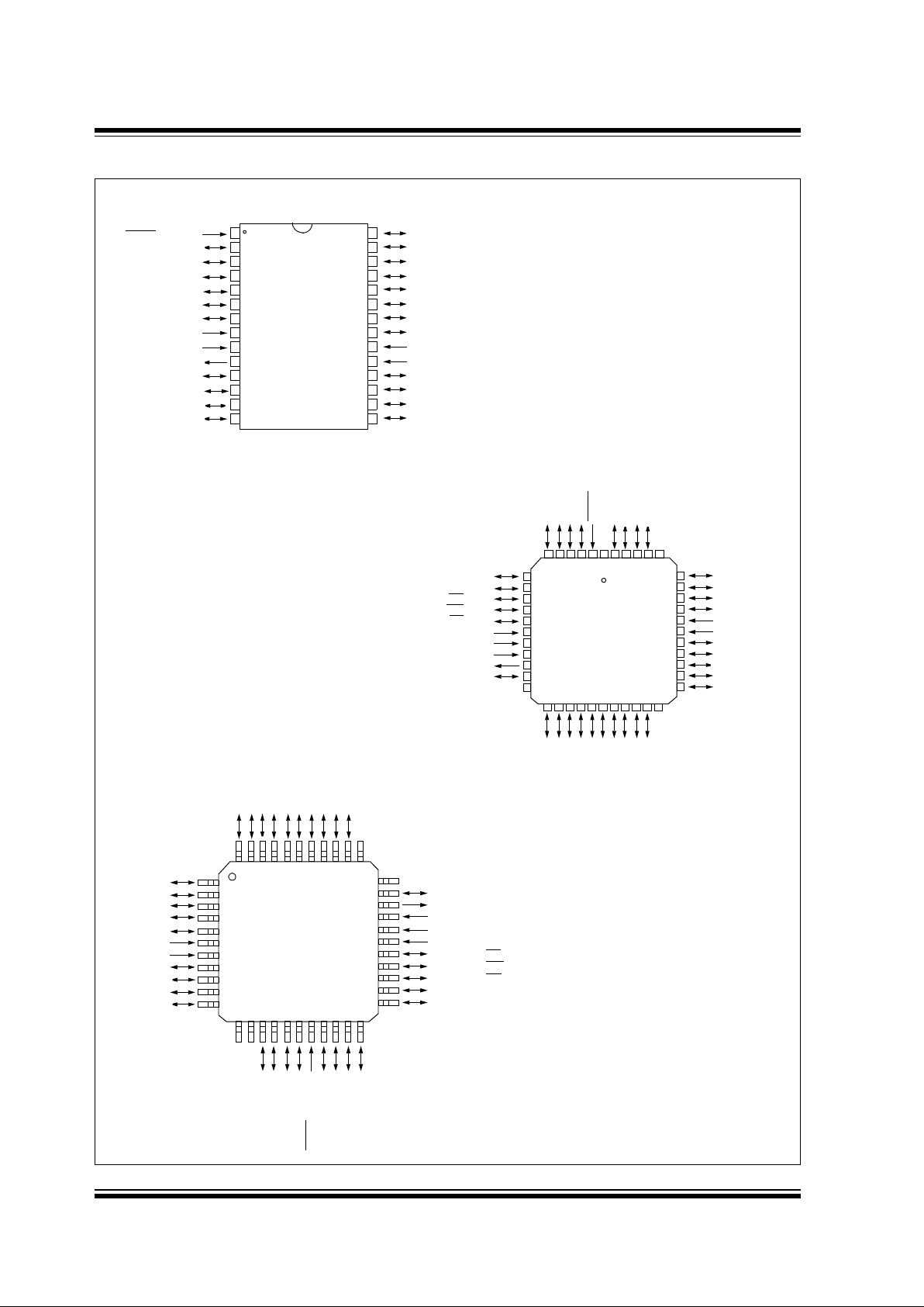
Pin Diagrams
PIC16F870
10
11
2
3
4
5
6
1
8
7
9
12
13
14
15
16
17
18
19
20
23
24
25
26
27
28
22
21
MCLR/VPP/THV
RA0/AN0
RA1/AN1
RA2/AN2/V
REF-
RA3/AN3/V
REF+
RA4/T0CKI
RA5/AN4
V
SS
OSC1/CLKIN
OSC2/CLKOUT
RC0/T1OSO/T1CKI
RC1/T1OSI
RC2/CCP1
RC3
RB7/PGD
RB6/PGC
RB5
RB4
RB3/PGM
RB2
RB1
RB0/INT
V
DD
VSS
RC7/RX/DT
RC6/TX/CK
RC5
RC4
10
11
12
13
14
15
16
17
181920212223242526
44
8
7
65432
1
27
28
29
30
31
32
33
34
35
36
37
38
39
40
41
42
43
9
PIC16F871
RA4/T0CKI
RA5/AN4
RE0/RD
/AN5
OSC1/CLKIN
OSC2/CLKOUT
RC0/T1OSO/T1CK1
NC
RE1/WR
/AN6
RE2/CS
/AN7
V
DD
VSS
RB3/PGM
RB2
RB1
RB0/INT
V
DD
VSS
RD7/PSP7
RD6/PSP6
RD5/PSP5
RD4/PSP4
RC7/RX/DT
RA3/AN3/VREF+
RA2/AN2/V
REF-
RA1/AN1
RA0/AN0
MCLR
/VPP/THV
NC
RB7/PGD
RB6/PGC
RB5
RB4
NC
NC
RC6/TX/CK
RC5
RC4
RD3/PSP3
RD2/PSP2
RD1/PSP1
RD0/PSP0
RC3
RC2/CCP1
RC1/T1OSI
10
11
2
3
4
5
6
1
1819202122
121314
15
38
8
7
4443424140
39
16
17
29
30
31
32
33
23
24
25
26
27
28
363435
9
PIC16F871
37
RA3/AN3/VREF+
RA2/AN2/V
REF-
RA1/AN1
RA0/AN0
MCLR
/VPP/THV
NC
RB7/PGD
RB6/PGC
RB5
RB4
NC
RC6/TX/CK
RC5
RC4
RD3/PSP3
RD2/PSP2
RD1/PSP1
RD0/PSP0
RC3
RC2/CCP1
RC1/T1OSI
NC
NC
RC0/T1OSO/T1CKI
OSC2/CLKOUT
OSC1/CLKIN
V
SS
VDD
RE2/AN7/CS
RE1/AN6/WR
RE0/AN5/RD
RA5/AN4
RA4/T0CKI
RC7/RX/DT
RD4/PSP4
RD5/PSP5
RD6/PSP6
RD7/PSP7
V
SS
VDD
RB0/INT
RB1
RB2
RB3/PGM
PLCC
TQFP
DIP, SOIC, SSOP

1999 Microchip Technology Inc.
Preliminary DS30569A-page 3
PIC16F870/871
Key Features
PICmicro™ Mid-Range Reference Manual (DS33023)
PIC16F870 PIC16F871
Operating Frequency DC - 20 MHz DC - 20 MHz
Resets (and Delays) POR, BOR
(PWRT, OST)
POR, BOR
(PWRT, OST)
FLASH Program Memory
(14-bit words)
2K 2K
Data Memory (bytes) 128 128
EEPROM Data Memory 64 64
Interrupts 10 11
I/O Ports Ports A,B,C Ports A,B,C,D,E
Timers 3 3
Capture/Compare/PWM modules 1 1
Serial Communications USART USART
Parallel Communications — PSP
10-bit Analog-to-Digital Module 5 input channels 8 input channels
Instruction Set 35 Instructions 35 Instructions

PIC16F870/871
DS30569A-page 4 Preliminary
1999 Microchip Technology Inc.
Table of Contents
1.0 Device Overview............................. ..... ...... ..... ................................................... ...... ..... .. .... ..... ...... ...... .................5
2.0 Memory Organization..........................................................................................................................................11
3.0 I/O Ports..............................................................................................................................................................27
4.0 Data EEPROM and FLASH Program Memory.................................................................................................... 39
5.0 Timer0 Module....................................................................................................................................................47
6.0 Timer1 Module....................................................................................................................................................51
7.0 Timer2 Module....................................................................................................................................................55
8.0 Capture/Compare/PWM Module.........................................................................................................................57
9.0 Addressable Universal Synchronous Asynchronous Receiver Transmitter (USART) ........................................63
10.0 Analog-to-Digital Converter (A/D) Module...........................................................................................................79
11.0 Special Features of the CPU...............................................................................................................................89
12.0 Instruction Set Summary...................................................................................................................................105
13.0 Development Support.......................................................................................................................................113
14.0 Electrical Characteristics.................................................. ................................................... ..... .........................119
15.0 DC and AC Characteristics Graphs and Tables................................................................................................135
16.0 Packaging Information ...................................................................................................................................... 137
Index .......................................................................................................................................................................... 145
On-Line Support..........................................................................................................................................................151
Reader Response.......................................................................................................................................................152
Product Identification System......................................................................................................................................153
To Our Valued Customers
Most Current Data Sheet
To obtain the most up-to-date version of this data sheet, please register at our Worldwide Web site at:
http://www.microchip.com
You can determine the version of a data sheet by examining its literature number found on the bottom outside corner of any page.
The last character of the literature number is the version number. e.g., DS30000A is version A of document DS30000.
New Customer Notification System
Register on our web site (www.microchip.com/cn) to receive the most current information on our products.
Errata
An errata sheet may exist for current devices, describing minor operational differences (from the data sheet) and recomm ended
workarounds. As device/documentation issues become known to us, we wil l pub lish an errata sheet. The errata will specify the revision of silicon and revision of document to which it applies.
To determine if an errata sheet exists for a particular device, please check with one of the following:
• Microchip’s Worldwide Web site; http://www.microchip.com
• Your local Microchip sales office (see last page)
• The Microchip Corporate Literature Center; U.S. FAX: (480) 786-7277
When contacting a sales office or the literature center, please specify which device, revision of silicon and data sheet (include liter-
ature number) you are using.
Corrections to this Data Sheet
We constantly strive to improve the quality of all our products and documentation. We have spent a great deal of time to ensure
that this document is correct. However , w e realize that we ma y have missed a few things. If you find any information that is missin g
or appears in error, please:
• Fill out and mail in the reader response form in the back of this data sheet.
• E-mail us at webmaster@microchip.com.
We appreciate your assistance in making this a better document.
1999 Microchip Technology Inc.
Preliminary DS30569A-page 5
PIC16F870/871
1.0 DEVICE OVERVIEW
This document contains device-specific information.
Additional information may be found in the PICmicro™
Mid-Range Reference Manual, (DS33023), which may
be obtained from your local Microchip Sales Representative or downloaded from the Microchip website. The
Reference Manual should be considered a complementary document to this data she et, and is high ly recommended reading for a better understanding of the
device architecture and operation of the peripheral
modules.
There are two devices (PIC16F870 and PIC16F871 )
covered by this data sheet. The PIC16F870 device
comes in a 28-pin package and the PIC16F871 device
comes in a 40-pin package. The 28-pin device does not
have a Parallel Slave Port implemented.
The following two figures are device block diagrams
sorted by pin number; 28-pin for Figure 1-1 and 40-pin
for Figure 1-2. The 28-pin and 40-pin pinouts are listed
in Table 1-1 and Table 1-2, respectively.
FIGURE 1-1: PIC16F870 BLOCK DIAGRAM
FLASH
Program
Memory
13
Data Bus
8
14
Program
Bus
Instruction reg
Program Counter
8 Level Stack
(13-bit)
RAM
File
Registers
Direct Addr
7
RAM Addr (1)
9
Addr MUX
Indirect
Addr
FSR reg
STATUS reg
MUX
ALU
W reg
Power-up
Timer
Oscillator
Start-up Timer
Power-on
Reset
Watchdog
Timer
Instruction
Decode &
Control
Timing
Generation
OSC1/CLKIN
OSC2/CLKOUT
MCLR
VDD, VSS
PORTA
PORTB
PORTC
RA4/T0CKI
RA5/AN4
RB0/INT
RC0/T1OSO/T1CKI
RC1/T1OSI
RC2/CCP1
RC3
RC4
RC5
RC6/TX/CK
RC7/RX/DT
8
8
Brown-out
Reset
Note 1: Higher order bits are from the STATUS register.
USART
CCP1
10-bit A/DTimer0 Timer1 Timer2
RA3/AN3/VREF+
RA2/AN2/VREF-
RA1/AN1
RA0/AN0
8
3
Data EEPROM
RB1
RB2
RB3/PGM
RB4
RB5
RB6/PGC
RB7/PGD
Device Program
FLASH
Data Memory Data
EEPROM
PIC16F870 2K 128 Bytes 64 Bytes
In-Circuit
Debugger
Low-Voltage
Programming
PIC16F870/871
DS30569A-page 6 Preliminary
1999 Microchip Technology Inc.
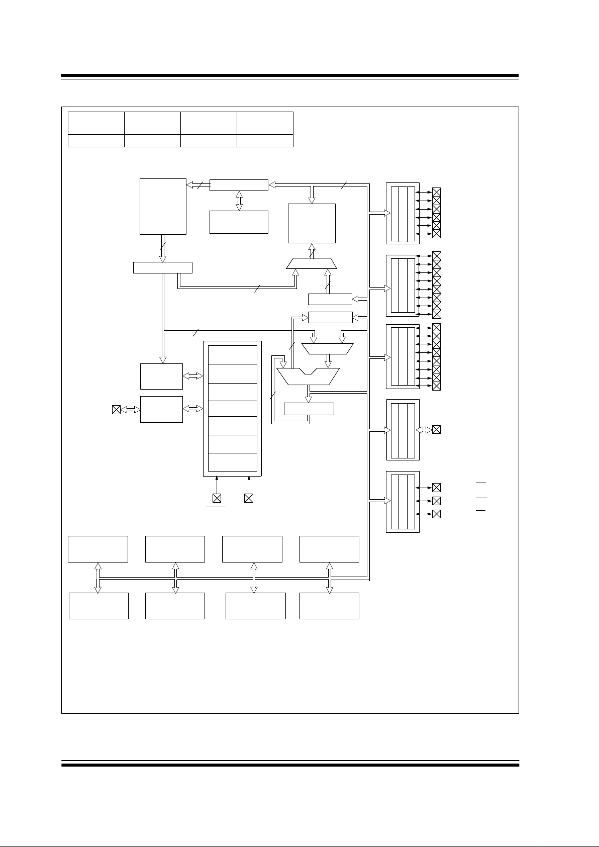
FIGURE 1-2: PIC16F871 BLOCK DIAGRAM
FLASH
Program
Memory
13
Data Bus
8
14
Program
Bus
Instruction reg
Program Counter
8 Level Stack
(13-bit)
RAM
File
Registers
Direct Addr
7
RAM Addr (1)
9
Addr MUX
Indirect
Addr
FSR reg
STATUS reg
MUX
ALU
W reg
Power-up
Timer
Oscillator
Start-up Tim er
Power-on
Reset
Watchdog
Timer
Instruction
Decode &
Control
Timing
Generation
OSC1/CLKIN
OSC2/CLKOUT
MCLR
VDD, VSS
PORTA
PORTB
PORTC
PORTD
PORTE
RA4/T0CKI
RA5/AN4
RC0/T1OSO/T1CKI
RC1/T1OSI
RC2/CCP1
RC3
RC4
RC5
RC6/TX/CK
RC7/RX/DT
RD7/PSP7:RD0/PSP0
RE0/AN5/RD
RE1/AN6/WR
RE2/AN7/CS
8
8
Brown-out
Reset
Note 1: Higher order bits are from the STATUS register.
USART
CCP1
10-bit A/DTimer0 Timer1 Timer2
RA3/AN3/VREF+
RA2/AN2/VREF-
RA1/AN1
RA0/AN0
8
3
Data EEPROM
RB0/INT
RB1
RB2
RB3/PGM
RB4
RB5
RB6/PGC
RB7/PGD
Device Program
FLASH
Data Memory Data
EEPROM
PIC16F871 2K 128 Bytes 64 Bytes
In-Circuit
Debugger
Low-Voltage
Programming
Parallel Slave Port

1999 Microchip Technology Inc.
Preliminary DS30569A-page 7
PIC16F870/871
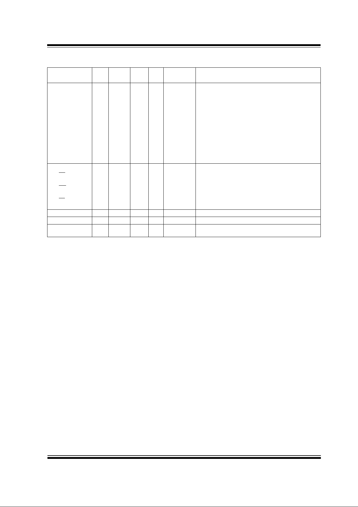
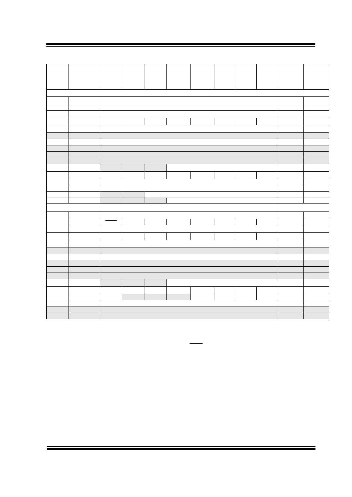
TABLE 1-1: PIC16F870 PINOUT DESCRIPTION
Pin Name
DIP
Pin#
SOIC
Pin#
I/O/P
Type
Buffer
Type
Description
OSC1/CLKIN 9 9 I
ST/CMOS
(3)
Oscillator crystal input/external clock source input.
OSC2/CLKOUT 10 10 O — Oscillator crystal output. Connects to crystal or resonator in crystal
oscillator mode. In RC mode, the OSC2 pin outputs CLKOUT
which has 1/4 the frequency of OSC1 , and denot es th e instruc tion
cycle rate.
MCLR
/VPP/THV 1 1 I/P ST Master clear (reset) input or programming voltage input or high
voltage test mode control. This pin is an active low reset to the
device.
PORTA is a bi-directional I/O port.
RA0/AN0 2 2 I/O TTL RA0 can also be analog input0
RA1/AN1 3 3 I/O TTL RA1 can also be analog input1
RA2/AN2/V
REF- 4 4 I/O TTL RA2 can also be analog input2 or negative analog reference
voltage
RA3/AN3/V
REF+ 5 5 I/O TTL RA3 can also be analog input3 or positive analog reference
voltage
RA4/T0CKI 6 6 I/O ST RA4 can also be the clock input to the Timer0 module. Output
is open drain type.
RA5/AN4 7 7 I/O TTL RA5 can also be analog input4
PORTB is a bi-directi onal I/O port. PORTB can be software
programmed for internal weak pull-up on all inputs.
RB0/INT 21 21 I/O
TTL/ST
(1)
RB0 can also be the exte rnal interrupt pin.
RB1 22 22 I/O TTL
RB2 23 23 I/O TTL
RB3/PGM 24 24 I/O
TTL/ST
(1)
RB3 can als o be the low voltage pro gramming inp u t
RB4 25 25 I/O TTL Interrupt on cha n g e pi n .
RB5 26 26 I/O TTL Interrupt on cha n g e pi n .
RB6/PGC 27 27 I/O
TTL/ST
(2)
Interrupt on change pin or In-Circuit Debugger pin. Serial
programming clock.
RB7/PGD 28 28 I/O
TTL/ST
(2)
Interrupt on change pin or In-Circuit Debugger pin. Serial
programming data.
PORTC is a bi-directional I/O port.
RC0/T1OSO /T 1 C K I 11 11 I/O ST RC0 can al so be the Timer1 os ci l lat o r ou tp ut or Timer1 cl ock
input.
RC1/T1OSI 12 12 I/O ST RC1 can also be the Timer1 oscillator input
RC2/CCP1 13 13 I/O ST RC2 can also be the Capture1 input/Compar e1 output/PWM1
output.
RC3 14 14 I/O ST
RC4 15 15 I/O ST
RC5 16 16 I/O ST
RC6/TX/CK 17 17 I/O ST RC6 can also be the USART Asynchronous Transmit or
Synchron ou s C l ock.
RC7/RX/DT 18 18 I/O ST RC7 can also be the USART Asynchronou s Receive or
Synchron ou s D at a.
V
SS 8, 19 8, 19 P — Ground reference f or logic and I/O pins.
V
DD 20 20 P — Positive suppl y for logic and I/O pins.
Legend: I = input O = output I/O = input/output P = power
— = Not used TTL = TTL input ST = Schmitt Trigger input
Note 1: This buffer is a Schmitt Trigger input when configured as t he external interrupt or LVP mode.
2: This buffer is a Schmitt Trigger input when use d i n serial programming mode.
3: This buffer is a Schmitt Trigger input when configured in RC oscillator mode and a CMOS input otherwise.

PIC16F870/871
DS30569A-page 8 Preliminary
1999 Microchip Technology Inc.
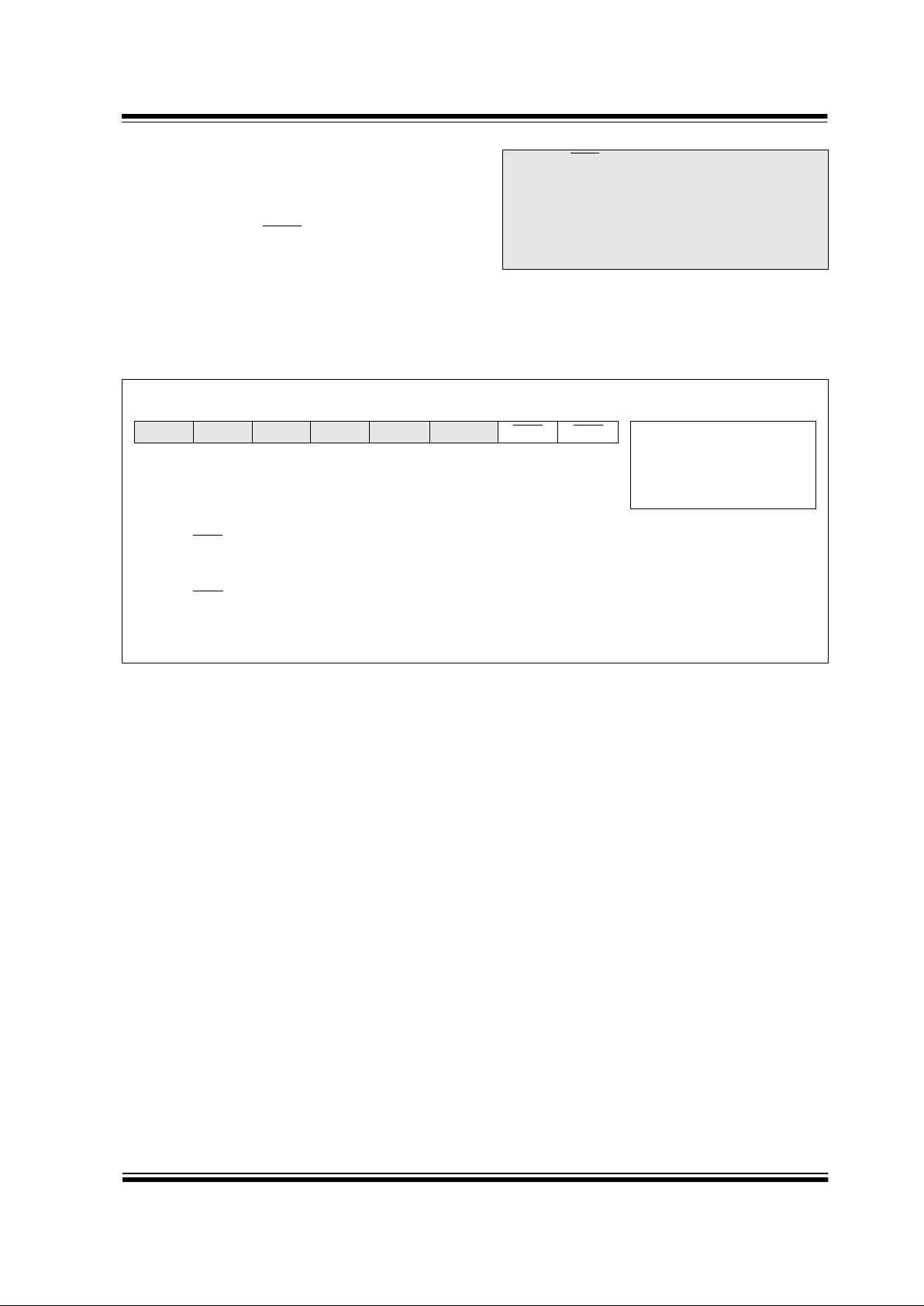
TABLE 1-2: PIC16F871 PINOUT DESCRIPTION
Pin Name
DIP
Pin#
PLCC
Pin#
QFP
Pin#
I/O/P
Type
Buffer
Type
Description
OSC1/CLKIN 13 14 30 I
ST/CMOS
(4)
Oscillator crystal input/external clock source input.
OSC2/CLKOUT 14 15 31 O — Oscillator crystal output. Connects to crystal or resonator in
crystal oscillator mode. In RC mode, OSC2 pin outputs CLKOUT which has 1/4 the frequency of OSC1, and denotes the
instruction cycle rate.
MCLR
/VPP/THV 1 2 18 I/P ST Master clear (reset) input or prog r amming v oltag e inpu t o r high
voltage test mode control. This pin is an active low reset to the
device.
PORTA is a bi-direction al I/O port.
RA0/AN0 2 3 19 I/O TTL RA0 can also be analog input0
RA1/AN1 3 4 20 I/O TTL RA1 can also be analog input1
RA2/AN2/V
REF- 4 5 21 I/O TTL RA2 can also be analog input2 or negative analog
reference voltage
RA3/AN3/V
REF+ 5 6 22 I/O TTL RA3 can also be analog input3 or positive analog
reference voltage
RA4/T0CKI 6 7 23 I/O ST RA4 can also be the clock input to the Timer0 timer/
counter. Output is open drain type.
RA5/AN4 7 8 24 I/O TTL RA5 can also be analog input4
PORTB is a bi-directional I/O port. PORTB can be software
programmed for internal weak pull-up on all inputs.
RB0/INT 33 36 8 I/O
TTL/ST
(1)
RB0 can also be the exte rnal interrupt pin.
RB1 34 37 9 I/O TTL
RB2 35 38 10 I/O TTL
RB3/PGM 36 39 11 I/O
TTL/ST
(1)
RB3 can also be the low voltage programming input
RB4 37 41 14 I/O TTL Interrupt on change pin.
RB5 38 42 15 I/O TTL Interrupt on change pin.
RB6/PGC 39 43 16 I/O
TTL/ST
(2)
Interrupt on change pin or In-Circuit Debugger pin. Serial
programming clock.
RB7/PGD 40 44 17 I/O
TTL/ST
(2)
Interrupt on change pin or In-Circuit Debugger pin. Serial
programming data.
PORTC is a bi-directional I/O port.
RC0/T1OSO/T1CKI 15 16 32 I/O ST RC0 can also be the Timer1 oscillator output or a Timer1
clock input.
RC1/T1OSI 16 18 35 I/O ST RC1 can also be the Timer1 oscillator input
RC2/CCP1 17 19 36 I/O ST RC2 can also be the Capture1 input/Compare1 output/
PWM1 output.
RC3 18 20 37 I/O ST
RC4 23 25 42 I/O ST
RC5 24 26 43 I/O ST
RC6/TX/CK 25 27 44 I/O ST RC6 can also be the USART Asynchronous Transmit or
Synchronous Clock.
RC7/RX/DT 26 29 1 I/O S T RC7 can also be the USART Asynchronous Receive or
Synchronous Data.
Legend: I = input O = output I/O = input/output P = power
— = Not used TTL = TTL input ST = Schmitt Trigger input
Note 1: This buffer is a Schmitt Trigger input when configured as an external interrupt or LVP mode.
2: This buffer is a Schmitt Trigger input when use d i n serial programming mode.
3: This buffer is a Schmitt Trigger input when con figured as general purpose I/O and a TTL input when used in the Parallel Slave
Port mode (for int erfacing to a mic r op r ocessor bus).
4: This buffer is a Schmitt Trigger input when configured in RC oscillat or mode and a CMOS input otherwise.
1999 Microchip Technology Inc.
Preliminary DS30569A-page 9
PIC16F870/871
PORTD is a bi-directional I/O port or parallel slave port when
interfacing to a mi croprocessor bus.
RD0/PSP0 19 21 38 I/O
ST/TTL
(3)
RD1/PSP1 20 22 39 I/O
ST/TTL
(3)
RD2/PSP2 21 23 40 I/O
ST/TTL
(3)
RD3/PSP3 22 24 41 I/O
ST/TTL
(3)
RD4/PSP4 27 30 2 I/O
ST/TTL
(3)
RD5/PSP5 28 31 3 I/O
ST/TTL
(3)
RD6/PSP6 29 32 4 I/O
ST/TTL
(3)
RD7/PSP7 30 33 5 I/O
ST/TTL
(3)
PORTE is a bi-directional I/O port.
RE0/RD
/AN5 8 9 25 I/O
ST/TTL
(3)
RE0 can also be read control fo r the par alle l sla v e port, or
analog input5.
RE1/WR
/AN6 9 10 26 I/O
ST/TTL
(3)
RE1 can also be write control for the parallel slave port, or
analog input6.
RE2/CS
/AN7 10 11 27 I/O
ST/TTL
(3)
RE2 can also be select control for the parallel slave port,
or analog input7.
V
SS 12,31 13,34 6,29 P — Ground reference for logic and I /O pins.
V
DD 11,32 12,35 7,28 P — Positive supply for logic and I/O pins.
NC — 1,17,28,4012,13,
33,34
— These pins are not internally con nected. These pins should be
left unconnected.
TABLE 1-2: PIC16F871 PINOUT DESCRIPTION (CONTINUED)
Pin Name
DIP
Pin#
PLCC
Pin#
QFP
Pin#
I/O/P
Type
Buffer
Type
Description
Legend: I = input O = output I/O = input/output P = power
— = Not used TTL = TTL input ST = Schmitt Trigger input
Note 1: This buffer is a Schmitt Trigger input when configured as an external interrupt or LVP mode.
2: This buffer is a Schmitt Trigger input when use d i n serial programming mode.
3: This buffer is a Schmitt Trigger input when configured as general purpose I/O and a TTL input when used in the Parallel Slave
Port mode (for int erfacing to a mic r op r ocessor bus).
4: This buffer is a Schmitt Trigger input when configured in RC oscillator mode and a CMOS input otherwise.

PIC16F870/871
DS30569A-page 10 Preliminary
1999 Microchip Technology Inc.
NOTES:

1999 Microchip Technology Inc.
Preliminary DS30569A-page 11
PIC16F870/871
2.0 MEMORY ORGANIZATION
There are three memory blocks in each of these
PICmicro
®
MCUs. The Program Memory and Data
Memory have separate buses, so that concurrent
access can occur, and is detailed in this section. The
EEPROM data memory block is detailed in
Section 4.0.
Additional inf ormation on de vice m emory may be f ound
in the PICmicro Mid-Range Reference Manual,
(DS33023).
2.1 Program Memory Organization
The PIC16F870/871 devices have a 13-bit program
counter capable of addressing an 8K x 14 program
memory space. The PIC16F870/871 devices have 2K
x 14 words of FLASH program memor y. Accessing a
location above the physically implemented address will
cause a wraparound.
The reset vector is at 0000h and the interrupt vector is
at 0004h.
FIGURE 2-1: PIC16F870/871 PROGRAM
MEMORY MAP AND STACK
2.2 Data Memory Organization
The data memory is partitioned into multiple banks
which contain the General Purpose Registers and the
Special Function Regi sters. Bits RP1(STA TUS<6 >) and
RP0 (STATUS<5>) are the bank select bits.
Each bank extends up to 7Fh (128 bytes). The lower
locations of each bank are reserved for the Special
Function Registers . Abo v e the Spec ial Fun ction Re gisters are General Purpose Registers, implemented as
static RAM. All implemented banks contain Special
Function Registers. Some “high use” Special Function
Registers from one bank may be mirrored in another
bank for code reduction and quicker access.
2.2.1 GENERAL PURPOSE REGISTER FILE
The register file can be a ccessed ei ther direc tly, or indi-
rectly through the File Select Register FSR.
PC<12:0>
13
0000h
0004h
0005h
Stack Level 1
Stack Level 8
Reset Vector
Interrupt Vector
On-Chip
CALL, RETURN
RETFIE, RETLW
1FFFh
Stack Level 2
Program
Memory
Page 0
07FFh
0800h
RP<1:0> Bank
00 0
01 1
10 2
11 3
Note: EEPROM Data Memory description can be
found in Section 4.0 of this Data Sheet
PIC16F870/871
DS30569A-page 12 Preliminary
1999 Microchip Technology Inc.
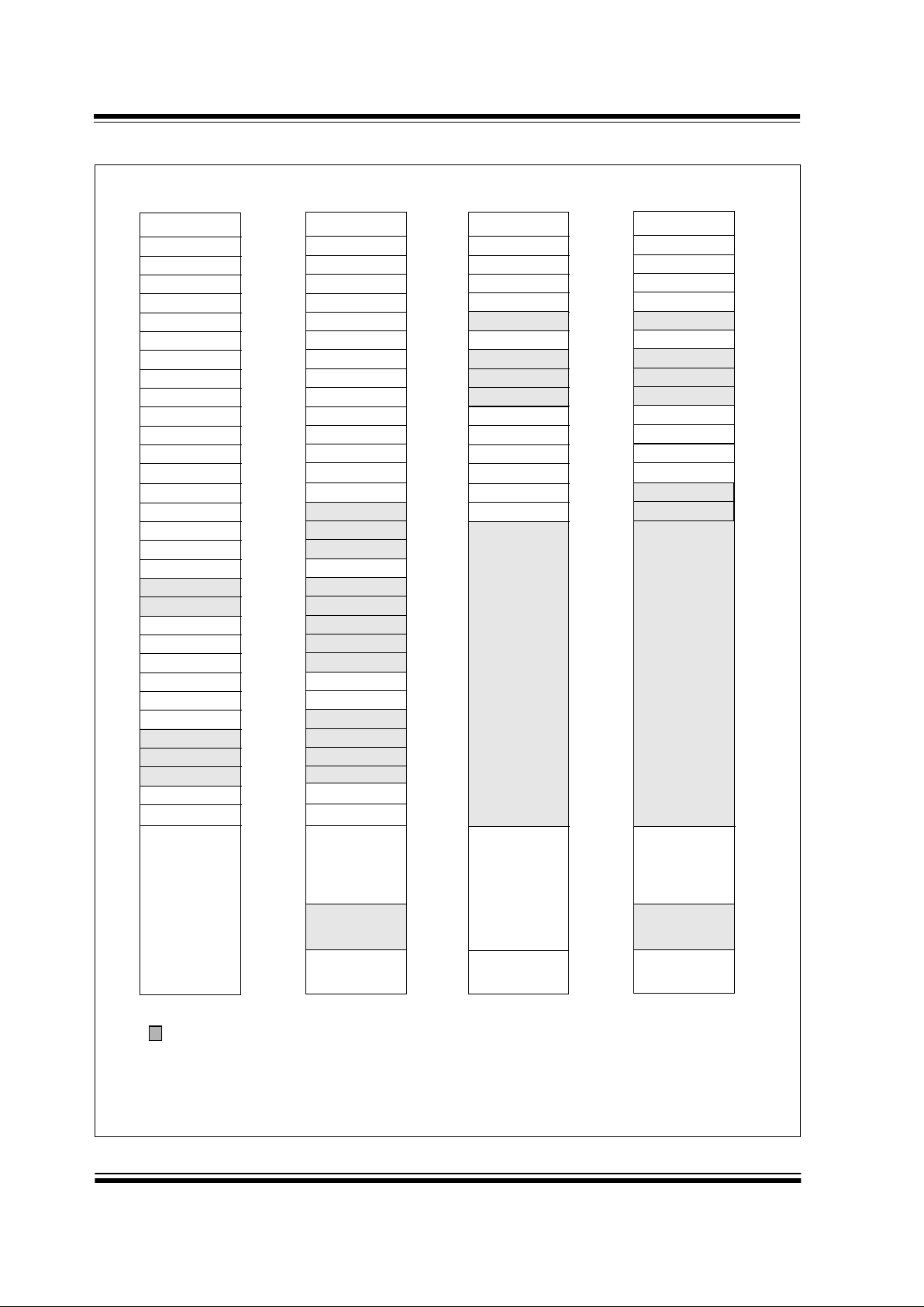
FIGURE 2-2: PIC16F870/871 REGISTER FILE MAP
Indirect addr.
(*)
TMR0
PCL
STATUS
FSR
PORTA
PORTB
PORTC
PCLATH
INTCON
PIR1
TMR1L
TMR1H
T1CON
TMR2
T2CON
CCPR1L
CCPR1H
RCSTA
OPTION_REG
PCL
STATUS
FSR
TRISA
TRISB
TRISC
PCLATH
INTCON
PIE1
PCON
PR2
00h
01h
02h
03h
04h
05h
06h
07h
08h
09h
0Ah
0Bh
0Ch
0Dh
0Eh
0Fh
10h
11h
12h
13h
14h
15h
16h
17h
18h
19h
1Ah
1Bh
1Ch
1Dh
1Eh
1Fh
80h
81h
82h
83h
84h
85h
86h
87h
88h
89h
8Ah
8Bh
8Ch
8Dh
8Eh
8Fh
90h
91h
92h
93h
94h
95h
96h
97h
98h
99h
9Ah
9Bh
9Ch
9Dh
9Eh
9Fh
20h
A0h
7Fh
FFh
Bank 0
Bank 1
File
Address
Indirect addr .
(*)
Indirect addr.
(*)
PCL
STATUS
FSR
PCLATH
INTCON
PCL
STATUS
FSR
PCLATH
INTCON
100h
101h
102h
103h
104h
105h
106h
107h
108h
109h
10Ah
10Bh
180h
181h
182h
183h
184h
185h
186h
187h
188h
189h
18Ah
18Bh
17Fh
1FFh
Bank 2
Bank 3
Indirect addr.
(*)
ADRESL
TMR0
OPTION_REG
PIR2
PIE2
ADRESH
ADCON0 ADCON1
General
Purpose
Register
General
Purpose
Register
1EFh
1F0h
accesses
A0h - BFh
16Fh
170h
accesses
70h-7Fh
TRISB
PORTB
96 Bytes
32 Bytes
10Ch
10Dh
10Eh
10Fh
110h
18Ch
18Dh
18Eh
18Fh
190h
EEDATA
EEADR
EECON1
EECON2
EEDATH
EEADRH
Reserved
(1)
Reserved
(1)
Unimplemented data memory locations, read as ’0’.
* Not a physical register.
Note 1: These registers are reserved; maintain these registers clear.
2: These registers are not implemented on the PIC16F870.
120h
1A0h
accesses
70h-7Fh
accesses
70h-7Fh
accesses
20h-7Fh
C0h
EFh
F0h
1C0h
1BFh
BFh
TXREG
RCREG
CCP1CON
TXSTA
SPBRG
PORTD
(2)
PORTE
(2)
TRISD
(2)
TRISE
(2)
File
Address
File
Address
File
Address
1999 Microchip Technology Inc.
Preliminary DS30569A-page 13
PIC16F870/871
2.2.2 SPECIAL FUNCTION REGISTERS
The Special Function Registers are registers used by
the CPU and peripheral modules for controlling the
desired operation of the device. These registers are
implemented as static RAM. A list of these registers is
given in Table 2-1.
The Special Function Registers can be classified into
two sets; core (CPU) and peripheral. Those registers
associated with the core functions are described in
detail in this section. Those related to the operation of
the peripheral features are described in detail in the
peripheral feature section.
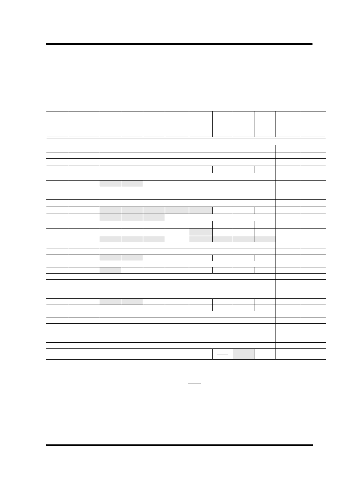
TABLE 2-1: SPECIAL FUNCTION REGISTER SUMMARY
Address Name Bit 7 Bit 6 Bit 5 Bit 4 B it 3 Bit 2 Bit 1 Bit 0
Value on:
POR,
BOR
Value on
all other
resets
(2)
Bank 0
00h
(4)
INDF Addressing this location uses contents of FSR to address data memory (not a physical register) 0000 0000 0000 0000
01h TMR0 Timer0 module’s register xxxx xxxx uuuu uuuu
02h
(4)
PCL Program Counter's (PC) Least Significant Byte 0000 0000 0000 0000
03h
(4)
STATUS IRP RP1 RP0 TO PD ZDCC0001 1xxx 000q quuu
04h
(4)
FSR Indirect data memory address pointer xxxx xxxx uuuu uuuu
05h PORTA
— — PORTA Data Latch when written: PORTA pins when read --0x 0000 --0u 0000
06h PORTB PORTB Data Latch when written: PORTB pins when read xxxx xxxx uuuu uuuu
07h PORTC PORTC Data Latch when written: PORTC pins when read xxxx xxxx uuuu uuuu
08h
(5)
PORTD PORTD Data Latch when written: PORTD pins when read xxxx xxxx uuuu uuuu
09h
(5)
PORTE — — — — —RE2RE1RE0---- -xxx ---- -uuu
0Ah
(1,4)
PCLATH — — — Write Buffer for the upper 5 bits of the Program Counter ---0 0000 ---0 0000
0Bh
(4)
INTCON GIE PEIE T0IE INTE RBIE T0IF INTF RBIF 0000 000x 0000 000u
0Ch PIR1
PSPIF
(3)
ADIF RCIF TXIF — CCP1IF TMR2IF TMR1IF 0000 -000 0000 -000
0Dh PIR2
— — — EEIF — — — — ---0 ---- ---0 ----
0Eh TMR1L Holding register for the Least Significant Byte of the 16-bit TMR1 register xxxx xxxx uuuu uuuu
0Fh TMR1H Holding register for the Most Significant Byte of the 16-bit TMR1 register xxxx xxxx uuuu uuuu
10h T1CON
— — T1CKPS1 T1CKPS0 T1OSCEN T1SYNC TMR1CS TMR1ON --00 0000 --uu uuuu
11h TMR2 Timer2 module’s register 0000 0000 0000 0000
12h T2CON
— TOUTPS3 TOUTPS2 TOUTPS1 TOUTPS0 TMR2ON T2CKPS1 T2CKPS0 -000 0000 -000 0000
13h
14h
15h CCPR1L Capture/Compare/PWM Register1 (LSB) xxxx xxxx uuuu uuuu
16h CCPR1H Capture/Compare/PWM Register1 (MSB) xxxx xxxx uuuu uuuu
17h CCP1CON
— — CCP1X CCP1Y CCP1M3 CCP1M2 CCP1M1 CCP1M0 --00 0000 --00 0000
18h RCSTA SPEN RX9 SREN CREN ADDEN FERR OERR RX9D 0000 000x 0000 000x
19h TXREG USART Transmit Data Register 0000 0000 0000 0000
1Ah RCREG USART Receive Data Register 0000 0000 0000 0000
1Bh
1Ch
1Dh
1Eh ADRESH A/D Result Register High Byte xxxx xxxx uuuu uuuu
1Fh ADCON0 ADCS1 ADCS0 CHS2 CHS1 CHS0
GO/
DONE
—ADON0000 00-0 0000 00-0
Legend: x = unknown, u = unchanged, q = value depends on condition, - = unimplemented read as ’0’, r = reserved.
Shaded locations are unimplemented, read as ‘0’.
Note 1: The upper byte of the program counter is not directly accessible. PCLATH is a holding register for the PC<12:8> whose
contents are transferred to the upper byte of the program counter.
2: Other (non power-up) resets include external reset through MCLR
and Watchdog Timer Reset.
3: Bits PSPIE and PSPIF are reserved on the 28-pin devices; always maintain these bits clear.
4: These registers can be addressed from any bank.
5: PORTD, PORTE, TRISD and TRISE are not physically implemented on the 28-pin devices, read as ‘0’.
PIC16F870/871
DS30569A-page 14 Preliminary
1999 Microchip Technology Inc.
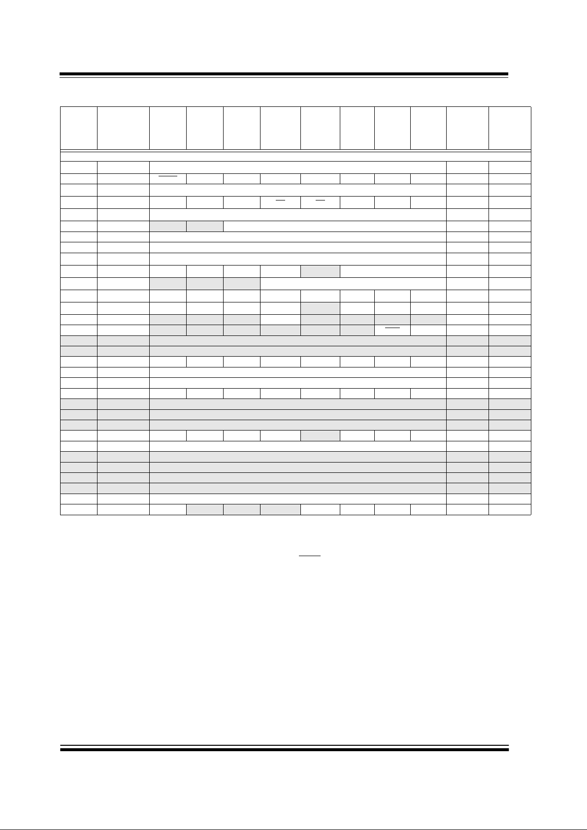
Bank 1
80h
(4)
INDF Addressing this location uses contents of FSR to address data memory (not a physical register) 0000 0000 0000 0000
81h OPTION_REG RBPU
INTEDG T0CS T0SE PSA PS2 PS1 PS0 1111 1111 1111 1111
82h
(4)
PCL Program Counter’s (PC) Least Significant Byte 0000 0000 0000 0000
83h
(4)
STATUS IRP RP1 RP0 TO PD ZDCC0001 1xxx 000q quuu
84h
(4)
FSR Indirect data memory address pointer xxxx xxxx uuuu uuuu
85h TRISA
— — PORTA Data Direction Register --11 1111 --11 1111
86h TRISB PORTB Data Direction Register 1111 1111 1111 1111
87h TRISC PORTC Data Direction Register 1111 1111 1111 1111
88h
(5)
TRISD PORTD Data Direction Register 1111 1111 1111 1111
89h
(5)
TRISE IBF OBF IBOV PSPMODE — PORTE Data Direction Bits 0000 -111 0000 -111
8Ah
(1,4)
PCLATH — — — Write Buffer for the upper 5 bits of the Program Counter ---0 0000 ---0 0000
8Bh
(4)
INTCON GIE PEIE T0IE INTE RBIE T0IF INTF RBIF 0000 000x 0000 000u
8Ch PIE1
PSPIE
(3)
ADIE RCIE TXIE — CCP1IE TMR2IE TMR1IE 0000 -000 0000 -000
8Dh PIE2
— — — EEIE — — — — ---0 ---- ---0 ----
8Eh PCON
— — — — — —PORBOR ---- --qq ---- --uu
8Fh — Unimplemented — —
90h — Unimplemented — —
91h
92h PR2 Timer2 Period Register 1111 1111 1111 1111
93h
94h
95h — Unimplemented — —
96h — Unimplemented — —
97h — Unimplemented — —
98h TXSTA CSRC TX9 TXEN SYNC
— BRGH TRMT TX9D 0000 -010 0000 -010
99h SPBRG Baud Rate Generator Register 0000 0000 0000 0000
9Ah — Unimplemented — —
9Bh — Unimplemented — —
9Ch — Unimplemented — —
9Dh — Unimplemented — —
9Eh ADRESL A/D Result Register Low Byte xxxx xxxx uuuu uuuu
9Fh ADCON1 ADFM
— — — PCFG3 PCFG2 PCFG1 PCFG0 0--- 0000 0--- 0000
TABLE 2-1: SPECIAL FUNCTION REGISTER SUMMARY (CONTINUED)
Address Name Bit 7 Bit 6 Bit 5 Bit 4 B it 3 Bit 2 Bit 1 Bit 0
Value on:
POR,
BOR
Value on
all other
resets
(2)
Legend: x = unknown, u = unchanged, q = value depends on condition, - = unimplemented read as ’0’, r = reserved.
Shaded locations are unimplemented, read as ‘0’.
Note 1: The upper byte of the program counter is not directly accessible. PCLATH is a holding register for the PC<12:8> whose
contents are transferred to the upper byte of the program counter.
2: Other (non power-up) resets include external reset through MCLR
and Watchdog Timer Reset.
3: Bits PSPIE and PSPIF are reserved on the 28-pin devices; always maintain these bits clear.
4: These registers can be addressed from any bank.
5: PORTD, PORTE, TRISD and TRISE are not physically implemented on the 28-pin devices, read as ‘0’.
1999 Microchip Technology Inc.
Preliminary DS30569A-page 15
PIC16F870/871
Bank 2
100h
(4)
INDF Addressing this location uses contents of FSR to address data memory (not a physical register) 0000 0000 0000 0000
101h TMR0 Timer0 module’s register xxxx xxxx uuuu uuuu
102h
(4)
PCL Program Counter's (PC) Least Significant Byte 0000 0000 0000 0000
103h
(4)
STATUS IRP RP1 RP0 TO PD Z DC C 0001 1xxx 000q quuu
104h
(4)
FSR Indirect data memory address pointer xxxx xxxx uuuu uuuu
105h — Unimplemented — —
106h PORTB PORTB Data Latch when written: PORTB pins when read xxxx xxxx uuuu uuuu
107h — Unimplemented — —
108h — Unimplemented — —
109h — Unimplemented — —
10Ah
(1,4)
PCLATH — — — Write Buffer for the upper 5 bits of the Program Counter ---0 0000 ---0 0000
10Bh
(4)
INTCON GIE PEIE T0IE INTE RBIE T0IF INTF RBIF 0000 000x 0000 000u
10Ch EEDATA EEPROM data register xxxx xxxx uuuu uuuu
10Dh EEADR EEPROM address register xxxx xxxx uuuu uuuu
10Eh EEDATH
— — EEPROM data register high byte xxxx xxxx uuuu uuuu
10Fh EEADRH
— — — EEPROM address register high byte xxxx xxxx uuuu uuuu
Bank 3
180h
(4)
INDF Addressing this location uses contents of FSR to address data memory (not a physical register) 0000 0000 0000 0000
181h OPTION_REG RBPU
INTEDG T0CS T0SE PSA PS2 PS1 PS0 1111 1111 1111 1111
182h
(4)
PCL Program Counter's (PC) Least Significant Byte 0000 0000 0000 0000
183h
(4)
STATUS IRP RP1 RP0 TO PD Z DC C 0001 1xxx 000q quuu
184h
(4)
FSR Indirect data memory address pointer xxxx xxxx uuuu uuuu
185h — Unimplemented — —
186h TRISB PORTB Data Direction Register 1111 1111 1111 1111
187h — Unimplemented — —
188h — Unimplemented — —
189h — Unimplemented — —
18Ah
(1,4)
PCLATH — — —
Write Buffer for the upper 5 bits of the Program Counter
---0 0000 ---0 0000
18Bh
(4)
INTCON GIE PEIE T0IE INTE RBIE T0IF INTF RBIF 0000 000x 0000 000u
18Ch EECON1 EEPGD
— — — WRERR WREN WR RD x--- x000 x--- u000
18Dh EECON2 EEPROM control register2 (not a physical register) ---- ---- ---- ---18Eh — Reserved maintain clear 0000 0000 0000 0000
18Fh — Reserved maintain clear 0000 0000 0000 0000
TABLE 2-1: SPECIAL FUNCTION REGISTER SUMMARY (CONTINUED)
Address Name Bit 7 Bit 6 Bit 5 Bit 4 B it 3 Bit 2 Bit 1 Bit 0
Value on:
POR,
BOR
Value on
all other
resets
(2)
Legend: x = unknown, u = unchanged, q = value depends on condition, - = unimplemented read as ’0’, r = reserved.
Shaded locations are unimplemented, read as ‘0’.
Note 1: The upper byte of the program counter is not directly accessible. PCLATH is a holding register for the PC<12:8> whose
contents are transferred to the upper byte of the program counter.
2: Other (non power-up) resets include external reset through MCLR
and Watchdog Timer Reset.
3: Bits PSPIE and PSPIF are reserved on the 28-pin devices; always maintain these bits clear.
4: These registers can be addressed from any bank.
5: PORTD, PORTE, TRISD and TRISE are not physically implemented on the 28-pin devices, read as ‘0’.

PIC16F870/871
DS30569A-page 16 Preliminary
1999 Microchip Technology Inc.
2.2.2.1 STATUS REGISTER
The STATUS Registe r con tain s the arithmet ic s tatus of
the ALU, the R ESET st atus an d the ba nk sel ect bi ts f or
data memory.
The STATUS Register can be the destination for any
instruction, as with any other register. If the STATUS
Register is the destina tion f or an ins truction tha t aff ects
the Z, DC or C bits, then the write to these three bits is
disabled. The se bi ts ar e set or c leared a ccordi ng to the
device logic. Fur th erm ore, the TO
and PD bits are not
writable, therefore, the result of an instruction with the
STATUS Register as destination may be different than
intended.
For example, CLRF STATUS will clea r t h e up per -t h r ee
bits and set the Z bi t. T his l ea v es the STATUS register
as 000u u1uu (where u = unchanged).
It is recommended, therefore, that only BCF, BSF,
SWAPF and MOVWF instructions are used to alter the
STATUS register, because these instructions do not
affect the Z, C or DC bi ts from the STATUS Regi ster.
For other instructions not affecting any status bits, see
the "Instruction Set Summary."
REGISTER 2-1: STATUS REGISTER (ADDRESS 03h, 83h, 103h, 183h)
Note 1: The C and DC bits operate as a borrow
and digit borrow bit, respectively, in subtraction. See the SUBLW and SUBWF
instructions for examples.
R/W-0 R/W-0 R/W-0 R-1 R-1 R/W-x R/W-x R/W-x
IRP RP1 RP0 TO PD Z DC C R = Readable bit
W = Writable bit
U = Unimplemented bit,
read as ‘0’
- n= Value at POR reset
bit7 bit0
bit 7: IRP: Register Bank Select bit (used for indirec t addressing)
1 = Bank 2, 3 (100h - 1FFh)
0 = Bank 0, 1 (0 0h - FFh)
bit 6-5: RP1:RP0: Register Bank Select bits (used for direct addressing)
11 = Bank 3 (180h - 1FFh)
10 = Bank 2 (100h - 17Fh)
01 = Bank 1 (80h - FFh)
00 = Bank 0 (00h - 7Fh)
Each bank is 128 bytes
bit 4: TO
: Time-out bit
1 = After power-up, CLRWDT instruction, or SLEEP instruction
0 = A WDT time-out occurred
bit 3: PD
: Power-down bit
1 = After power-up or by the CLRWDT instruction
0 = By execution of the SLEEP in struction
bit 2: Z: Zero bit
1 = The result of an arithmetic or logic operation is zero
0 = The result of an arithmetic or logic operation is not zero
bit 1: DC: Digit carry/borrow
bit (ADDWF, ADDLW,SUBLW,SUBWF instructions)
(for borrow
the polarity is reversed)
1 = A carry-out from the 4th low order bit of the result occurred
0 = No carry-out from the 4th low order bit of the result
bit 0: C: Carry/borrow
bit (ADDWF, ADDLW,SUBLW,SUBWF instructions)
1 = A carry-out from the most significant bit of the result occurred
0 = No carry-out from the most significant bit of the result occurred
Note: For borrow
the polarity is reversed. A subtraction is executed by adding the two’s complement of
the second operand . For rotate (RRF, RLF) instructions, this bit is loade d w it h ei the r the hig h or l o w o rder
bit of the source register.

1999 Microchip Technology Inc.
Preliminary DS30569A-page 17
PIC16F870/871
2.2.2.2 OPTION_REG REGISTER
The OPTION_REG Register i s a read ab le and writab le
register , which contai ns various c ontrol bits to c onfigure
the TMR0 prescaler/WDT postscaler (single assignable regist er kno wn also as the prescale r), the Ext ernal
INT Interrupt, TMR0 and the w eak pul l-ups on PO R TB .
REGISTER 2-2: OPTION_REG REGISTER (ADDRESS 81h, 181h)
Note: To achieve a 1:1 pres caler assi gnment for
the TMR0 register, assign the prescaler to
the Watchdog Timer.
R/W-1 R/W-1 R/W-1 R/W-1 R/W-1 R/W-1 R/W-1 R/W-1
RBPU INTEDG T0CS T0SE PSA PS2 PS1 PS0 R = Readable bit
W = Writable bit
U = Unimplemented bit,
read as ‘0’
- n= Value at POR reset
bit7 bit0
bit 7: RBPU: PORTB Pull-up Enable bit
1 = PORTB pull-ups are disabled
0 = PORTB pull-ups are enabled by individual port latch values
bit 6: INTEDG: Interrupt Edge Select bit
1 = Interrupt on rising edge of RB0/INT pin
0 = Interrupt on falling edge of RB0/INT pin
bit 5: T0CS: TMR0 Clock Source Select bit
1 = Transition on RA4/T0CKI pin
0 = Internal instruction cycle clock (CLKOUT)
bit 4: T0SE: TMR0 Source Edge Select bit
1 = Increment on high-to-low transition on RA4/T0CKI pin
0 = Increment on low-to-high transition on RA4/T0CKI pin
bit 3: PSA: Prescaler Assignment bit
1 = Prescaler is assigned to the WDT
0 = Prescaler is assigned to the Timer0 module
bit 2-0: PS2:PS0: Prescaler Rate Select bits
000
001
010
011
100
101
110
111
1 : 2
1 : 4
1 : 8
1 : 16
1 : 32
1 : 64
1 : 128
1 : 256
1 : 1
1 : 2
1 : 4
1 : 8
1 : 16
1 : 32
1 : 64
1 : 128
Bit Value TMR0 Rate WDT Rate

PIC16F870/871
DS30569A-page 18 Preliminary
1999 Microchip Technology Inc.
2.2.2.3 INTCON REGISTER
The INTCON Regi ster i s a rea dab le a nd w ritabl e regi s-
ter, which contains various enable and flag bits for the
TMR0 register overflow, RB Port change and External
RB0/INT pin interrupts.
REGISTER 2-3: INTCON REGISTER (ADDRESS 0Bh, 8Bh, 10Bh, 18Bh)
Note: Interrupt flag bits get set when an interrupt
condition occurs , regardless of the state of
its corresponding enable bit or the global
enable bit, GIE (INTCON<7>). User software should ensure the appropriate interrupt flag bits are clear prior to enabling an
interrupt.
R/W-0 R/W-0 R/W-0 R/W-0 R/W-0 R/W-0 R/W-0 R/W-x
GIE PEIE T0IE INTE R BIE T0IF INTF RBIF R = Readable bit
W = Writable bit
U = Unimplement ed bit,
read as ‘0’
- n= Value at POR reset
bit7 bit0
bit 7: GIE: Global Interrupt Enable bit
1 = Enables all un-masked interrupts
0 = Disables all interrupts
bit 6: PEIE: Peripheral Interrupt Enable bit
1 = Enables all un-masked peripheral interrupts
0 = Disables all peripheral interrupts
bit 5: T0IE: TMR0 Overflow Interrupt Enable bit
1 = Enables the TMR0 interrupt
0 = Disables the TMR0 interrupt
bit 4: INTE: RB0/INT External Interrupt Enable bit
1 = Enables the RB0/INT external interrupt
0 = Disables the RB0/INT external interrupt
bit 3: RBIE: RB Port Change Interrupt Enable bit
1 = Enables the RB port change interrupt
0 = Disables the RB port change interrupt
bit 2: T0IF: TMR0 Overflow Interrupt Flag bit
1 = TMR0 register has overflowed (must be cleared in software)
0 = TMR0 register did not overflow
bit 1: INTF: RB0/INT External Interrupt Flag bit
1 = The RB0/INT external interrupt occurred (must be cleared in software)
0 = The RB0/INT external interrupt did not occur
bit 0: RBIF: RB Port Change Interrupt Flag bit
1 = At least one of the RB7:RB4 pins changed state (must be cleared in software)
0 = None of the RB7:RB4 pins have changed state

1999 Microchip Technology Inc.
Preliminary DS30569A-page 19
PIC16F870/871
2.2.2.4 PIE1 REGISTER
The PIE1 Register contains the individual enable bits
for the peripheral interrupts.
REGISTER 2-4: PIE1 REGISTER (ADDRESS 8Ch)
Note: Bit PEIE (INTCON<6>) must be set to
enable any peripheral interrupt.
R/W-0 R/W-0 R/W-0 R/W-0 U-0 R/W-0 R/W-0 R/W-0
PSPIE
(1)
ADIE RCIE TXIE CCP1IE TMR2IE TMR1IE R = Readable bit
W = Writable bit
U = Unimplemented bit,
read as ‘0’
- n= Value at POR reset
bit7 bit0
bit 7: PSPIE
(1)
: Parallel Slave Port Read/Write Interrupt Enable bit
1 = Enables the PSP read/write interrupt
0 = Disables the PSP read/write interrupt
bit 6: ADIE: A/D Converter Interrupt Enable bit
1 = Enables the A/D converter interrupt
0 = Disables the A/D converter interrupt
bit 5: RCIE: USART Receive Interrupt Enable bit
1 = Enables the USART receive interrupt
0 = Disables the USART receive interrupt
bit 4: TXIE: USART Transmit Interrupt Enable bit
1 = Enables the USART transmit interrupt
0 = Disables the USART transmit interrupt
bit 3: Unimplemented: Read as ‘0’
bit 2: CCP1IE: CCP1 Interrupt Enable bit
1 = Enables the CCP1 interrupt
0 = Disables the CCP1 interrupt
bit 1: TMR2IE: TMR2 to PR2 Match Interrupt Enable bit
1 = Enables the TMR2 to PR2 match interrupt
0 = Disables the TMR2 to PR2 match interrupt
bit 0: TMR1IE: TMR1 Overflow Interrupt Enable bit
1 = Enables the TMR1 overflow interrupt
0 = Disables the TMR1 overflow interrupt
Note 1: PSPIE is reserved on the PIC16F870; always maintain this bit clear.

PIC16F870/871
DS30569A-page 20 Preliminary
1999 Microchip Technology Inc.
2.2.2.5 PIR1 REGISTER
The PIR1 Register contains the individual flag bits for
the peripheral interrupts.
REGISTER 2-5: PIR1 REGISTER (ADDRESS 0Ch)
Note: Interrupt flag bits get set when an interrupt
condition occurs , regardless of the state of
its corresponding enable bit or the global
enable bit, GIE (INTCON<7>). User software should ensure the appropriate interrupt bits are clear prior to enabling an
interrupt.
R/W-0 R/W-0 R-0 R-0 U-0 R/W-0 R/W-0 R/W-0
PSPIF
(1)
ADIF RCIF TXIF CCP1IF TMR2IF TMR1IF R = Readable bit
W = Writable bit
- n= Value at POR reset
bit7 bit0
bit 7: PSPIF
(1)
: Parallel Slave Port Read/Write Interrupt Flag bit
1 = A read or a write operation has taken place (must be cleared in software)
0 = No read or write has occurred
bit 6: ADIF: A/D Converter Interrupt Flag bit
1 = An A/D conversion completed
0 = The A/D conversion is not complete
bit 5: RCIF: USART Receive Interrupt Flag bit
1 = The USART receive buffer is full
0 = The USART receive buffer is empty
bit 4: TXIF: USART Transmit Interrupt Flag bit
1 = The USART transmit buffer is empty
0 = The USART transmit buffer is full
bit 7: Unimplemented: Read as ‘0’
bit 2: CCP1IF: CCP1 Interrupt Flag bit
Capture Mode
1 = A TMR1 register capture occurred (must be cleared in software)
0 = No TMR1 register capture occurred
Compare Mode
1 = A TMR1 register compare match occurred (must be cleared in software)
0 = No TMR1 register compare match occurred
PWM Mode
Unused in this mode
bit 1: TMR2IF: TMR2 to PR2 Match Interrupt Flag bit
1 = TMR2 to PR2 match occurred (must be cleared in software)
0 = No TMR2 to PR2 match occurred
bit 0: TMR1IF: TMR1 Overflow Interrupt Flag bit
1 = TMR1 register overflowed (must be cleared in software)
0 = TMR1 register did not overflow
Note 1: PSPIF is reserved on the PIC16F870; always maintain this bit clear.

1999 Microchip Technology Inc.
Preliminary DS30569A-page 21
PIC16F870/871
2.2.2.6 PIE2 REGISTER
The PIE2 Register contains the individual enab le bit for
the EEPROM write operation interrupt.
REGISTER 2-6: PIE2 REGISTER (ADDRESS 8Dh)
U-0 U-0 U-0 R/W-0 U-0 U-0 U-0 U-0
——— EEIE — — — — R = Readable bit
W = Writable bit
U = Unimplemented bit,
read as ‘0’
- n= Value at POR reset
bit7 bit0
bit 7-5: Unimplemented: Read as '0'
bit 4: EEIE: EEPROM Write Operation Interrupt Enable
1 = Enable EE Write Interrupt
0 = Disable EE Write Interrupt
bit 3-0: Unimplemented: Read as '0'

PIC16F870/871
DS30569A-page 22 Preliminary
1999 Microchip Technology Inc.
2.2.2.7 PIR2 REGISTER
The PIR2 Register contains the flag bit for the
EEPROM write operation interrupt.
.
REGISTER 2-7: PIR2 REGISTER (ADDRESS 0Dh)
Note: Interrupt flag bits get set when an interrupt
condition occurs , regardless of the state of
its corresponding enable bit or the global
enable bit, GIE (INTCON<7>). User software should ensure the appropriate interrupt flag bits are clear prior to enabling an
interrupt.
U-0 U-0 U-0 R/W-0 U-0 U-0 U-0 U-0
— — — EEIF — — — — R = Readable bit
W = Writable bit
U = Unimplemented bit,
read as ‘0’
- n= Value at POR reset
bit7 bit0
bit 7-5: Unimplemented: Read as '0'
bit 4: EEIF: EEPROM Write Operation Interrupt Flag bit
1 = The write operation completed (must be cleared in software)
0 = The write operation is not complete or has not been started
bit 3-0: Unimplemented: Read as '0'
1999 Microchip Technology Inc.
Preliminary DS30569A-page 23
PIC16F870/871
2.2.2.8 PCON REGISTER
The Power Control (PCON) Register contains flag bits
to allow differentiation between a Power-on Reset
(POR), a Brown-o ut Re set ( BOR) , a Watch-d og Re set
(WDT) and an external MCLR
Reset.
REGISTER 2-8: PCON REGISTER (ADDRESS 8Eh)
Note: BOR is unknown on POR. It must be set by
the user and c hecked on subsequent rests
to see if BOR is clear, indicating a brownout has occurred. The BOR status bit is a
don’t care and is not predictable if the
brown-out circuit is disabled (by clearing
the BODEN bit in the configuration word).
U-0 U-0 U-0 U-0 U-0 U-0 R/W-0 R/W-1
— — — — — —PORBOR R = Readable bit
W = Writable bit
U = Unimplemented bit,
read as ‘0’
- n= Value at POR reset
bit7 bit0
bit 7-2: Unimplemented: Read as '0'
bit 1: POR
: Power-on Reset Status bit
1 = No Power-on Reset occurred
0 = A Power-on Reset occurred (must be set in software after a Power-on Reset occurs)
bit 0: BOR
: Brown-out Reset Status bit
1 = No Brown-out Reset occurred
0 = A Brown-out Reset occurred (must be set in software after a Brown-out Reset occurs)
PIC16F870/871
DS30569A-page 24 Preliminary
1999 Microchip Technology Inc.
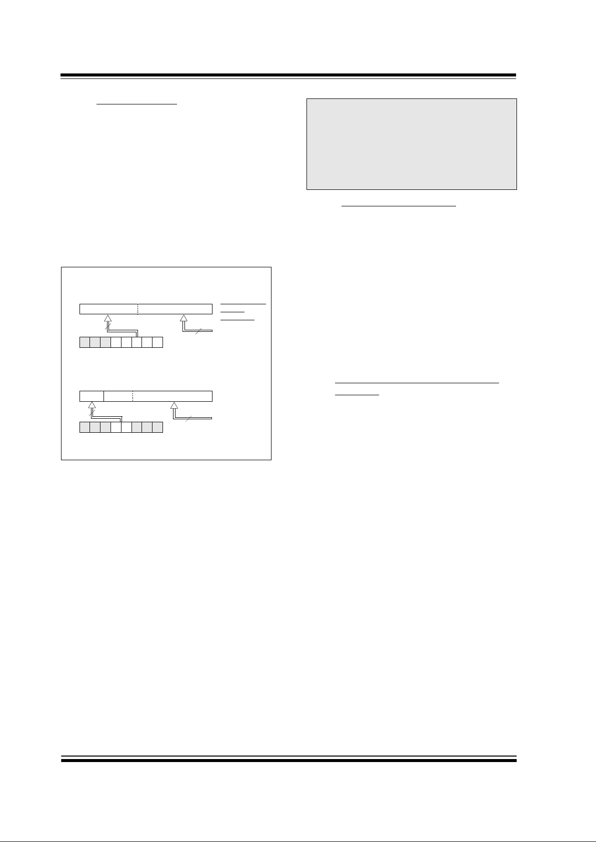
2.3 PCL and PCLATH
The Program Counter (PC) is 13-bits wide. The low
byte comes from the PC L Register , w hich is a readab le
and writable register. The upper bits (PC<12:8>) are
not readable, but are indirectly writable through the
PCLA TH register . On an y reset, the upp er bits of the PC
will be cleared. Figure2-3 shows the two situations for
the loading of the PC. The upper example in the figure
shows how the PC is loaded on a write to PCL
(PCLATH<4:0> → PCH). The lower example in the fig-
ure shows ho w the PC is loaded during a CALL or GOTO
instruction (PCLATH<4:3> → PCH).
FIGURE 2-3: LOADING OF PC IN
DIFFERENT SITUATIONS
2.3.1 COMPUTED GOTO
A computed GOTO is accompli shed by adding an offset
to the program counter (ADDWF PCL). When doing a
table read using a computed GOTO method, care
should be exercised if t he table location crosse s a PCL
memory boundary (each 256 byte block). Refer to the
application note,
“Implementing a Table Read"
(AN556).
2.3.2 STACK
The PIC16FXXX family has an 8-level deep x 13-bit
wide hardware stack. The stack space is not part of
either program or data space and the stack pointer is
not readable or writable. The PC is PUSHed onto the
stack when a CALL instru ctio n is executed or an inte rrupt causes a branch. The stack is POPed in the event
of a RETURN,RETLW or a RETFIE instruction execution. PCLATH is not affected by a PUSH or POP operation.
The stack oper ates as a circular b uffer . This means that
after the stack has been PUSHed e ight ti mes , th e nin th
push overw rites th e value that was stored fro m the firs t
push. The tenth push overwrites the second push (an d
so on).
2.4 Program Memory Paging
The PIC16FXXX architecture is capable of addressing
a continuous 8K word block of program memory. The
CALL and GOTO instructions provide 11 bits of the
address, which al lows br anche s within an y 2K prog ram
memory page. Therefore, the 8K words of program
memory are broken into four pages. Since the
PIC16F872 has only 2K words of program memory or
one page, ad ditional code is not requ ired to e nsure th at
the correct page is selected before a CALL or GOTO
instruction is executed. The PCLATH<4:3> bits should
always be maintai ned as z ero s. If a return from a CALL
instruction (or interrupt) is executed, the entire 13-bit
PC is popped off the stack. Manipulation of the
PCLATH is not required for the return instructions.
2.5 Indirect Addressing, INDF and FSR
Registers
The INDF Register is not a physical register. Addressing the INDF Register will cause indirect addressing.
Indirect addressing is possible by using the INDF Register. Any instruction using the INDF Register actually
accesses the register po inted to b y the File Sele ct Register, FSR. Reading the INDF Register itself indirectly
(FSR = ’0’) will read 00h. Writing to the INDF Register
indirectly results i n a no-operation (alth ou gh st atus bits
may be affected). An eff ectiv e 9-bit addres s is obta ined
by concatenatin g the 8-bit FSR Register a nd the IRP bit
(STATUS<7>), as shown in Figure 2-4.
A simple program to clear RAM locations 20h-2Fh
using indirect addressing is shown in Example2-1.
EXAMPLE 2-1: INDIRECT ADDRESSING
movlw 0x20 ;initialize pointer
movwf FSR ;to RAM
NEXT clrf INDF ;clear INDF register
incf FSR,F ;inc pointer
btfss FSR,4 ;all done?
goto NEXT ;no clear next
CONTINUE
: ;yes continue
PC
12 8 7 0
5
PCLATH<4:0>
PCLATH
Instruction with
ALU
GOTO,CALL
Opcode <10:0>
8
PC
12 11 10 0
11
PCLATH<4:3>
PCH PCL
87
2
PCLATH
PCH PCL
PCL as
Destination
Note 1: There are no status bits to indicate stack
overflow or stack underflow conditions.
2: There are no instructions/mnemonics
called PUSH or POP. These are actions that
occur from the execution of the CALL,
RETURN, RETLW and RETFIE instructions or the vectoring to an interrupt
address.
1999 Microchip Technology Inc.
Preliminary DS30569A-page 25
PIC16F870/871
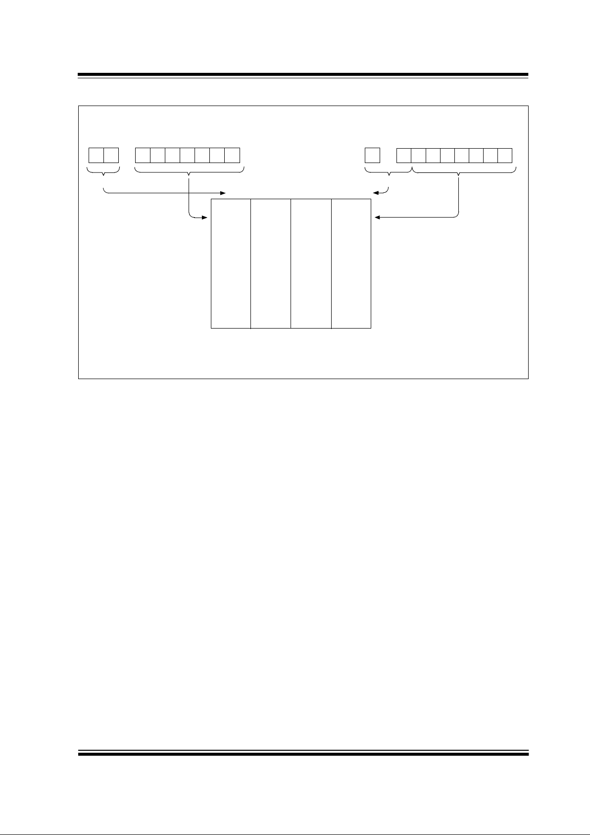
FIGURE 2-4: DIRECT/INDIRECT ADDRESSING
Note 1: For register file map detail see Figure 2-2.
Data
Memory
(1)
Indirect AddressingDirect Addressing
bank select location select
RP1:RP0 6
0
from opcode
IRP FSR register
7
0
bank select
location select
00 01 10 11
Bank 0 Bank 1 Bank 2 Bank 3
FFh
80h
7Fh
00h
17Fh
100h
1FFh
180h

PIC16F870/871
DS30569A-page 26 Preliminary
1999 Microchip Technology Inc.
NOTES:
1999 Microchip Technology Inc.
Preliminary DS30569A-page 27
PIC16F870/871
3.0 I/O PORTS
Some pins for these I/O ports are multiplexed with an
alternate function for the peripheral features on the
device. In general, when a peripheral is enabled, that
pin may not be used as a general purpose I/O pin.
Additional information on I/O ports may be found in the
PICmicro™ Mid-Range Reference Manual,
(DS33023).
3.1 PORTA and the TRISA Register
PORTA is a 6-bit wide bi-directional port. The corresponding data direction register is TRISA. Setting a
TRISA bit (=1) will m ak e the corresponding POR TA pin
an input (i.e., put the corresponding output driver in a
hi-impedance mode). Clearing a TRISA bit (=0) will
make the corresp onding POR TA pin an output (i.e., put
the contents of the output latch on the selected pin).
Reading the PORTA Register reads the status of the
pins, whereas writin g to it w i ll write t o th e p ort latch. All
write operations are read-modify-write operations.
Therefore , a write to a port implies that the port pins are
read, the value is modified and then written to the port
data latch.
Pin RA4 is multiplexed with the Timer0 module clock
input to become the RA4/T0CKI pin. The RA4/T0CKI
pin is a Schmitt Trigger input and an open drain output.
All other PORTA pins have TTL input levels and full
CMOS output drivers.
Other PORTA pins are multiplexed with analog inputs
and analog V
REF input. The operation of each pin is
selected by clearing/setting the control bits in the
ADCON1 Register (A/D Control Register1).
The TRISA R egister controls the direction of the RA
pins, even when they are being used as analog inputs.
The user must ensure the bits in the TRISA Register
are maintained set wh en us ing th em as an alo g i np uts.
EXAMPLE 3-1: INITIALIZING PORTA
BCF STATUS, RP0 ;
BCF STATUS, RP1 ; Bank0
CLRF PORTA ; Initialize PORTA by
; clearing output
; data latches
BSF STATUS, RP0 ; Select Bank 1
MOVLW 0x06 ; Configure all pins
MOVWF ADCON1 ; as digital inputs
MOVLW 0xCF ; Value used to
; initialize data
; direction
MOVWF TRISA ; Set RA<3:0> as inputs
; RA<5:4> as outputs
; TRISA<7:6> are always
; read as ’0’.
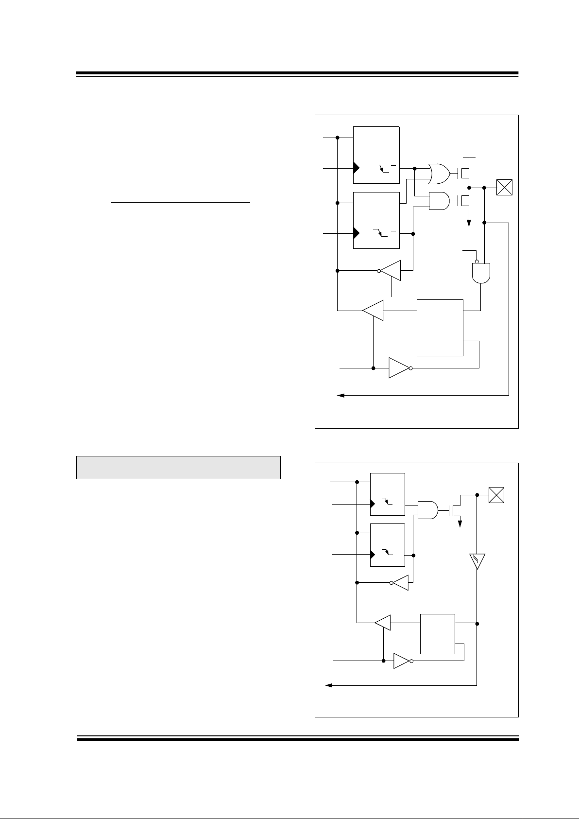
FIGURE 3-1: BLOCK DIAGRAM OF
RA3:RA0 AND RA5 PINS
FIGURE 3-2: BLOCK DIAGRAM OF RA4/
T0CKI PIN
Note: On a Power-on Reset, these pins are con-
figured as analog inputs and read as '0'.
Data
Bus
QD
Q
CK
QD
Q
CK
QD
EN
P
N
WR
Port
WR
TRIS
Data Latch
TRIS Latch
RD TRIS
RD PORT
V
SS
VDD
I/O pin
(1)
Note 1: I/O pins have protection diodes to VDD and VSS.
Analog
Input
Mode
TTL
Input
Buffer
To A/D Converter
Data
Bus
WR
PORT
WR
TRIS
RD PORT
Data Latch
TRIS Latch
RD TRIS
Schmitt
Trigger
Input
Buffer
N
V
SS
I/O pin
(1)
TMR0 clock input
QD
Q
CK
QD
Q
CK
EN
QD
EN
Note 1: I/O pin has protection diodes to VSS only.

PIC16F870/871
DS30569A-page 28 Preliminary
1999 Microchip Technology Inc.
TABLE 3-1: PORTA FUNCTIONS
TABLE 3-2: SUMMARY OF REGISTERS ASSOCIATED WITH PORTA
Name Bit# Buffer Function
RA0/AN0 bit0 TTL Input/output or analog input
RA1/AN1 bit1 TTL Input/output or analog input
RA2/AN2 bit2 TTL Input/output or analog input
RA3/AN3/VREF bit3 TTL Input/output or analog input or VREF
RA4/T0CKI bit4 ST Input/output or external clock input for Timer0
Output is open drain type
RA5/AN4 bit5 TTL Input/output or analog input
Legend: TTL = TTL input, ST = Schmitt Trigger input
Address Name Bit 7 Bit 6 Bit 5 Bit 4 Bit 3 Bit 2 Bit 1 Bit 0
Value on:
POR,
BOR
Value on
all
other
resets
05h P ORTA — — RA5 RA4 RA3 RA2 RA1 RA0
--0x 0000 --0u 0000
85h TRISA — — PORTA Data Direction Register
--11 1111 --11 1111
9Fh ADCON1 ADFM — — — PCFG3 PCFG2 PCFG1 PCFG0
--0- 0000 --0- 0000
Legend: x = unknown, u = unchanged, - = unimplemented locations read as '0'. Shaded cells are not used by
PORTA.
1999 Microchip Technology Inc.
Preliminary DS30569A-page 29
PIC16F870/871
3.2 PORTB and the TRISB Register
PORTB is an 8-bit wide, bi-directional port. The corresponding data direction register is TRISB. Setting a
TRISB bit (=1) will make the correspon ding POR TB pin
an input (i.e., put the corresponding output driver in a
hi-impedance mode). Clearing a TRISB bit (=0) will
make the corresponding PORTB pin an output (i.e., put
the contents of the output latch on the selected pin).
Three pins of PORTB a re multiple xed wit h the Low V oltage Programming function; RB3/PGM, RB6/PGC and
RB7/PGD. The alternate functions of these pins are
described in the Special F eat ures Secti on.
Each of the PORTB pins has a w ea k in ternal p ull -up. A
single control bit ca n turn on all the pull-ups . This is performed by clea ring bit R BPU
(OPTION_REG<7>). The
weak pull-up i s automa tically tur ned off wh en the po rt
pin is configured as an output. The pull-ups are disabled on a Power-on Reset.
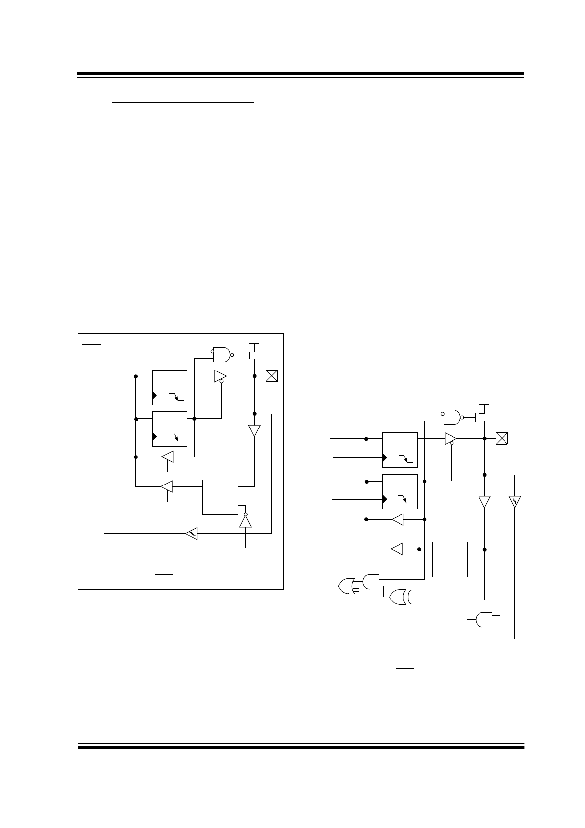
FIGURE 3-3: BLOCK DIAGRAM OF
RB3:RB0 PINS
Four of PORTB’s pins, RB7:RB4, have an interrupt on
change feature. Only pins configured as inputs can
cause this interrupt to oc cur (i.e . any RB7:RB4 pin configured as an output is excluded from the interrupt on
change comparison). The input pins (of RB7:RB4) are
compared with th e o ld value latched on the la st rea d of
PORTB. The “mismatch” outputs of RB7:RB4 are
OR’ed together to generate the RB Port Change Interrupt with flag bit RBIF (INTCON<0>).
This interrupt can wake the device from SLEEP. The
user, i n the interrupt service routine , can clea r the interrupt in the following manner:
a) Any read or write of PORTB. This will end the
mismatch condition.
b) Clear flag bit RBIF.
A mismatch condition will continue to set flag bit RBIF.
Reading PORTB will end the mismatch condition and
allow flag bit RBIF to be cleared.
The interrupt on change feature is recommended for
wake-up on key depression operation and opera tions
where PORTB is only used for the interrupt on change
feature. Polling of PORTB is not recommended while
using the interrupt on change feature.
This interrupt on mismatch feature, together with software configurable pull-ups on these four pins, allow
easy interface to a keypad and make it possible for
wake-up on key-depression. Refer to the Embedded
Control Handbook,
“Implementing Wake-Up on Key
Stroke”
(AN552).
RB0/INT is an external interrupt inp ut pin and is confi gured using the INTEDG bit (OPTION_REG<6>).
RB0/INT is discussed in detail in Section 11.10.1.
FIGURE 3-4: BLOCK DIAGRAM OF
RB7:RB4 PINS
Data Latch
RBPU
(2)
P
V
DD
QD
CK
QD
CK
QD
EN
Data Bus
WR Port
WR TRIS
RD TRIS
RD Port
weak
pull-up
RD Port
RB0/INT
I/O
pin
(1)
TTL
Input
Buffer
Schmitt Trigger
Buffer
TRIS Latch
Note 1: I/O pins have diode protection to V
DD and VSS.
2: To enable weak pull-ups, set the appropriate TRIS bit(s)
and clear the RBPU
bit (OPTION_REG<7>).
RB3/PGM
Data Latch
From other
RBPU
(2)
P
V
DD
I/O
QD
CK
QD
CK
QD
EN
QD
EN
Data Bus
WR Port
WR TRIS
Set RBIF
TRIS Latch
RD TRIS
RD Port
RB7:RB4 pins
weak
pull-up
RD Port
Latch
TTL
Input
Buffer
pin
(1)
ST
Buffer
RB7:RB6 in serial programming mode
Q3
Q1
Note 1: I/O pins have diode protection to V
DD and VSS.
2: To enable weak pull-ups, set the appropriate TRIS bit(s)
and clear the RBPU
bit (OPTION_REG<7>).
PIC16F870/871
DS30569A-page 30 Preliminary
1999 Microchip Technology Inc.
TABLE 3-3: PORTB FUNCTIONS
TABLE 3-4: SUMMARY OF REGISTERS ASSOCIATED WITH PORTB
Name Bit# Buffer Function
RB0/INT bit0 TTL/ST
(1)
Input/output pin or external interrupt input. Internal software
programmable weak pull-up.
RB1 bit1 TTL Input/output pin. Internal software programmable weak pull-up.
RB2 bit2 TTL Input/output pin. Internal software programmable weak pull-up.
RB3/PGM bit3 TTL/ST
(1)
Input/output pin or programming pin in LVP mode. Internal software
programmable weak pull-up.
RB4 bit4 TTL Input/output pin (with interrupt on change). In ternal softw are prog ra mmab l e
weak pull-up .
RB5 bit5 TTL Input/output pin (with interrupt on change). In ternal softw are prog ra mmab l e
weak pull-up .
RB6/PGC bit6 TTL/ST
(2)
Input/output pin (with interrupt on change) or In-Circuit Debugger pin.
Internal software programmable weak pull-up. Serial programming clock.
RB7/PGD bit7 TTL/ST
(2)
Input/output pin (with interrupt on change) or In-Circuit Debugger pin.
Internal software programmable weak pull-up. Serial programming data.
Legend: TTL = TTL input, ST = Schmitt Trigger input
Note 1: This buffer is a Schmitt Trigger input when configured as the external interrupt or LVP mode.
2: This buffer is a Schmitt Trigger input when used in serial programming mode.
Address Name Bit 7 Bit 6 Bit 5 Bit 4 Bit 3 Bit 2 Bit 1 Bit 0
Value on:
POR,
BOR
Value on all
other
resets
06h, 106h PORTB RB7 RB6 RB5 RB4 RB3 RB2 RB1 RB0 xxxx xxxx uuuu uuuu
86h, 186h T RISB PORTB Data Direction Register 1111 1111 1111 1111
81h, 181h O P TION_REG RBPU
INTEDG T0CS T0SE PSA PS2 PS1 PS0 1111 1111 1111 1111
Legend: x = unknown, u = unchanged. Shaded cells are not used by PORTB.

1999 Microchip Technology Inc.
Preliminary DS30569A-page 31
PIC16F870/871
3.3 PORTC and the TRISC Register
PORTC is an 8-bit wide, bi-directional port. The corresponding data direction register is TRISC. Setting a
TRISC bit (=1) will mak e the correspon ding POR TC pin
an input (i.e., put the corresponding output driver in a
hi-impedance mode). Clearing a TRISC bit (=0) will
make the cor respon ding POR T C pin an output (i .e., p ut
the contents of the output latch on the selected pin).
PORTC is mul tiple x ed with se v eral peripheral fun ctions
(Table 3-5). PORTC pins have Schmitt Trigger input
buffers.
When enabling peripheral functions, care should be
taken in defining TRIS bits for each PORTC pin. Some
peripherals override the TRIS bit to make a pin an output, while other peripherals override the TRIS bit to
make a pin an input. Since the TRIS bit override is in
effect while the peripheral is enabled, read-modifywrite instructions (BS F, BCF, XORWF) with TRISC as
destination shou ld be a voi ded. The us er should refe r to
the corresponding peripheral section for the correct
TRIS bit settings.
FIGURE 3-5: PORTC BLOCK DIAGRAM
(PERIPHERAL OUTPUT
OVERRIDE)
PORT/PERIPHERAL Select
(2)
Data Bus
WR
PORT
WR
TRIS
RD
Data Latch
TRIS Latch
RD TRIS
Schmitt
Trigger
QD
Q
CK
QD
EN
Peripheral Data Out
0
1
QD
Q
CK
P
N
V
DD
VSS
PORT
Peripheral
OE
(3)
Peripheral Input
I/O
pin
(1)
Note 1: I/O pins have diode protection to VDD and VSS.
2: Port/Peripheral select signal selects between port
data and peripheral output.
3: Peripheral OE (output enable) is only activated if
peripheral select is active.

PIC16F870/871
DS30569A-page 32 Preliminary
1999 Microchip Technology Inc.
TABLE 3-5: PORTC FUNCTIONS
TABLE 3-6: SUMMARY OF REGISTERS ASSOCIATED WITH PORTC
Name Bit# Buffer Type Function
RC0/T1OSO/T1CKI bit0 ST Input/output port pin or Timer1 oscillator output/Timer1 clock input
RC1/T1OSI bit1 ST Input/output port pin or Timer1 oscillator input
RC2/CCP1 bit2 ST Input/output port pin or Capture1 input/Compare1 output/PWM1
output
RC3 bit3 ST Input/output port pin
RC4 bit4 ST Input/output port pin
RC5 bit5 ST Input/output port pin
RC6/TX/CK bit6 ST Input/output port pin or USART Asynchronous Transmit or Synchro-
nous Clock
RC7/RX/DT bit7 ST Input/output port pin or USART Asynchronous Receive or Synchro-
nous Data
Legend: ST = Schmitt Trigger input
Address Name Bit 7 Bit 6 Bit 5 Bit 4 Bit 3 Bit 2 Bit 1 Bit 0
Value on:
POR,
BOR
Value on
all
other
resets
07h PORTC RC7 RC6 RC5 RC4 RC3 RC2 RC1 RC0
xxxx xxxx uuuu uuuu
87h TRISC PORTC Data Direction Register
1111 1111 1111 1111
Legend: x = unknown, u = unchanged.

1999 Microchip Technology Inc.
Preliminary DS30569A-page 33
PIC16F870/871
3.4 PORTD and TRISD Registers
This section is not applicable to the PIC16F870.
PORTD is an 8-bit port with Schmitt Tr igger input buff-
ers. Each pin is individually configurable as an input or
output.
PORTD can be configured as an 8-bit wide microprocessor por t (parallel slave port) by sett ing control bit
PSPMODE (TRISE<4>). In this mode, the input buff ers
are TTL.
FIGURE 3-6: PORTD BLOCK DIAGRAM (IN
I/O PORT MODE)
TABLE 3-7: PORTD FUNCTIONS
TABLE 3-8: SUMMARY OF REGISTERS ASSOCIATED WITH PORTD
Data
Bus
WR
PORT
WR
TRIS
RD PORT
Data Latch
TRIS Latch
RD TRIS
Schmitt
Trig ger
Input
Buffer
I/O pin
(1)
Note 1: I/O pins have protection diodes to VDD and VSS.
QD
CK
QD
CK
EN
QD
EN
Name Bit# Buffer Type Function
RD0/PSP0 bit0
ST/TTL
(1)
Input/output port pin or parallel slave port bit0
RD1/PSP1 bit1
ST/TTL
(1)
Input/output port pin or parallel slave port bit1
RD2/PSP2 bit2
ST/TTL
(1)
Input/output port pin or parallel slave port bit2
RD3/PSP3 bit3
ST/TTL
(1)
Input/output port pin or parallel slave port bit3
RD4/PSP4 bit4
ST/TTL
(1)
Input/output port pin or parallel slave port bit4
RD5/PSP5 bit5
ST/TTL
(1)
Input/output port pin or parallel slave port bit5
RD6/PSP6 bit6
ST/TTL
(1)
Input/output port pin or parallel slave port bit6
RD7/PSP7 bit7
ST/TTL
(1)
Input/output port pin or parallel slave port bit7
Legend: ST = Schmitt Trigger input TTL = TTL input
Note 1: Input buffers are Schmitt Triggers when in I/O mode and TTL buffer when in Parallel Slave Port Mode.
Address Name Bit 7 Bit 6 Bit 5 Bit 4 Bit 3 Bit 2 Bit 1 Bit 0
Val ue on :
POR,
BOR
Value on all
other resets
08h PORTD RD7 RD6 RD5 RD4 RD 3 RD2 RD1 RD0 xxxx xxxx uuuu uuuu
88h TRISD PORTD Data Direction Register 1111 1111 1111 1111
89h TRISE
IBF OBF IBOV PSPMODE — PORTE Data Direction Bits 0000 -111 0000 -111
Legend: x = unknown, u = unchanged, - = unimplemented read as ’0’. Shaded cells are not used by PORTD.

PIC16F870/871
DS30569A-page 34 Preliminary
1999 Microchip Technology Inc.
3.5 PORTE and TRISE Register
This section is not applicable to the PIC16F870.
PORTE has three pins, RE0/RD
/AN5, RE1/WR/AN6
and RE2/CS
/AN7, which are individually configurable
as inputs or outputs. These pins have Schmitt Trigger
input buffers.
I/O PORTE becomes control inputs for the micr oprocessor port when bit PSPMODE (TRISE<4>) is set. In
this mode, the user must make sure that the
TRISE<2:0> bits are set (pins are configured as digital
inputs). Ensure ADCON 1 is confi gured f or di gital I/O. In
this mode, the input buffers are TTL.
Register 3-1 shows the TRISE Register, which also
controls the parallel slave port operation.
PORTE pins are multiplexed with analog inputs. When
selected as an an alog input, the se pins will r ead as ’ 0’s .
TRISE controls the direction of the R E pins, e v en when
they are being used as analog inputs. The user must
make sure to keep the pins configured as inputs when
using them as analog inputs.
FIGURE 3-7: PORTE BLOCK DIAGRAM (IN
I/O PORT MODE)
REGISTER 3-1: TRISE REGISTER (ADDRESS 89h)
Note: On a Power-on Reset, these pins are con-
figured as analog inputs.
Data
Bus
WR
PORT
WR
TRIS
RD PORT
Data Latch
TRIS Latch
RD TRIS
Schmitt
Trigger
input
buffer
QD
CK
QD
CK
QD
EN
I/O pin
(1)
Note 1: I/O pins have protection diodes to VDD and VSS.
R-0 R-0 R/W-0 R/W-0 U-0 R/W-1 R/W-1 R/W-1
IBF OBF IBOV PSPMODE — bit2 bit1 bit0
R = Readable bit
W=Writable bit
U = Unimplemented bit,
read as ‘0’
- n= Value at POR reset
bit7 bit0
Parallel Slave Port Status/Control Bits
bit 7 : IBF: Input Buffer Full Status bit
1 = A word has been received and is waiting to be read by the CPU
0 = No word has been received
bit 6: OBF: Output Buffer Full Status bit
1 = The output buffer still holds a previously written word
0 = The output buffer has been read
bit 5: IBOV: Input Buffer Overflow Detect bit (in microprocessor mode)
1 = A write occurred when a previously input word has not been read (must be cleared in software)
0 = No overf low occur r ed
bit 4: PSPMODE: Parallel Slave Port Mode Select bit
1 = Parallel slave port mode
0 = General purpose I/O mode
bit 3: Unimplemented: Read as ’0’
PORTE Data Direction Bits
bit 2: Bit2: Direction Control bit for pin RE2/CS/AN7
1 = Input
0 = Output
bit 1: Bit1: Direction Control bit for pin RE1/WR
/AN6
1 = Input
0 = Output
bit 0: Bit0: Direction Control bit for pin RE0/RD
/AN5
1 = Input
0 = Output

1999 Microchip Technology Inc.
Preliminary DS30569A-page 35
PIC16F870/871
TABLE 3-9: PORTE FUNCTIONS
TABLE 3-10: SUMMARY OF REGISTERS ASSOCIATED WITH PORTE
Name Bit# Buffer Type Function
RE0/RD/AN5 bit0 ST/TTL
(1)
Input/output port pin or rea d c on t rol in put in p arallel slave po rt mode or
analog input:
RD
1 = Not a read operation
0 = Read operation. Reads PORTD register (if chip selected)
RE1/WR/AN6 bit1 ST/TTL
(1)
Input/output port pin or write con trol in put in par alle l sla v e port mode or
analog input:
WR
1 = Not a write operation
0 = Write operation. Writes PORTD register (if chip selected)
RE2/CS/AN7 bit2 ST/TTL
(1)
Input/output port pin or chip select control input in parallel slave port
mode or analog input:
CS
1 = Device is not selected
0 = Device is selected
Legend: ST = Schmitt Trigger input TTL = TTL input
Note 1: Input buffers are Schmitt Triggers when in I/O mode and TTL buffers when in Parallel Slave Port Mode.
Addr Name Bit 7 Bit 6 Bit 5 Bit 4 Bit 3 Bit 2 Bit 1 Bit 0
Value on:
POR,
BOR
Value on all
other resets
09h PORTE
— — — — —RE2RE1RE0---- -xxx ---- -uuu
89h TRISE IBF OBF IBOV PSPMODE
— PORTE Data Direction Bits 0000 -111 0000 -111
9Fh ADCON1 ADFM
— — — PCFG3 PCFG2 PCFG1 PCFG0 --0- 0000 --0- 0000
Legend: x = unknown, u = unchanged, - = unimplemented read as '0'. Shaded cells are not used by PORTE.
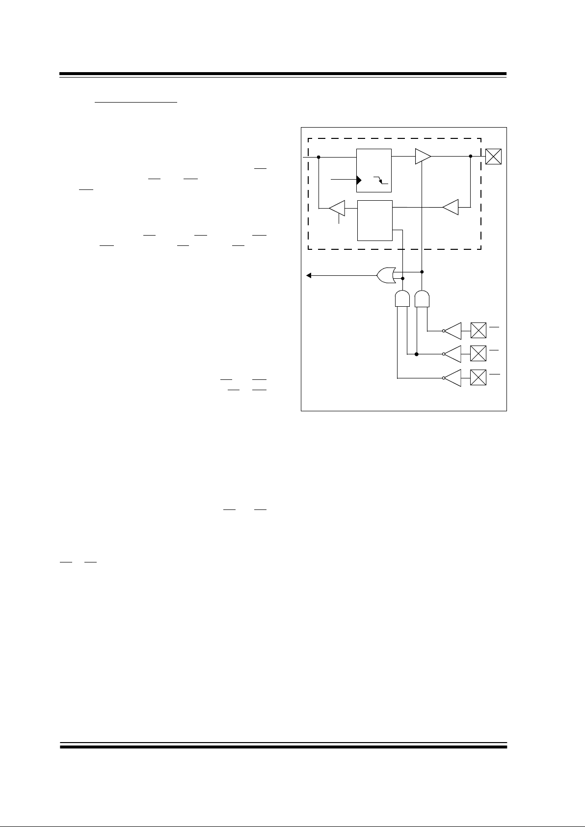
PIC16F870/871
DS30569A-page 36 Preliminary
1999 Microchip Technology Inc.
3.6 Parallel Slave Port
The Parallel Slave Port is not implemented on the
PIC16F870.
PORTD operat es as an 8-bit wid e Par allel Sla ve P ort or
microprocessor port when control bit PSPMODE
(TRISE<4>) is set. In slave mode, it is asynchronously
readable and writab le by the external world thro ugh RD
control input pin RE0/RD and WR control input pin
RE1/WR
.
It can directly interface to an 8-bit microprocessor data
bus. The e xte rnal micro processo r can read or write the
PORTD latch as an 8-bit latch. Setting bit PSPMODE
enables port pin RE0/RD
to be the RD input, RE1/WR
to be the WR input and RE2/CS to be the CS (chip
select) input. For this functionality, the corresponding
data direction bits of the TRISE register (TRISE<2:0>)
must be configured as inputs (set). The A/D port configuration bits PCFG3:PCFG0 (ADCON1<3:0>) must
be set to configure pins RE2:RE0 as digital I/O.
There are actually two 8-bit latches. One for data-out
and one fo r data i nput. T he user writes 8-bi t data to the
PORTD data latch and reads data from the port pin
latch (note that they have the same address). In this
mode, the TRIS D regi ster is i gnored , since t he micro processor is controlling the direction of data flow.
A write to the PSP occurs when both the CS
and WR
lines are f irs t de t ec ted l ow. When eith er th e C S or WR
lines become high (le vel triggered ), the Input Buffer Ful l
(IBF) status flag bit (TRISE<7>) is set on the Q4 clock
cycle, following the next Q2 cycle, to signal the write is
complete (Figure 3-9). The interrupt flag bit PSPIF
(PIR1<7>) is also se t on the same Q4 clock cycle. IBF
can only be cleared by reading the PORT D inp ut l atc h.
The Input Buffer Overflow (IBOV) status flag bit
(TRISE<5>) is set if a second write to the PSP is
attempted when the previous byte has not been read
out of the buffer.
A read from the PSP occurs when both the CS
and RD
lines are first detected low. The Output Buffer Full
(OBF) status flag bit (TRISE<6>) is cleared immediately (Figu re 3-10) indicating that the P ORTD latch is
waiting to be rea d by the external bus. When either the
CS
or RD pin becomes high (level triggered), the interrupt flag bit PSPIF is set on the Q4 clock cycle, following the next Q2 cycle, indicating that the read is
complete. OBF remains low until data is written to
PORTD by the user firmware.
When not in PSP mode , the IBF an d O BF b its are hel d
clear. However, if flag bit IBOV was previously set, it
must be cleared in firmware.
An interrupt is generated and latched into flag bit
PSPIF when a read or write operation is completed.
PSPIF must be cleared b y the u ser in firmware a nd the
interrupt can be disabled by clearing the interrupt
enable bit PSPIE (PIE1<7>).
FIGURE 3-8: PORTD AND PORTE BLOCK
DIAGRAM (PARALLEL SLAVE
PORT)
Data Bus
WR
PORT
RD
RDx
QD
CK
EN
QD
EN
PORT
pin
One bit of PORTD
Set interrupt flag
PSPIF (PIR1<7>)
Read
Chip Select
Write
RD
CS
WR
Note: I/O pin has protection diodes to VDD and VSS.
TTL
TTL
TTL
TTL
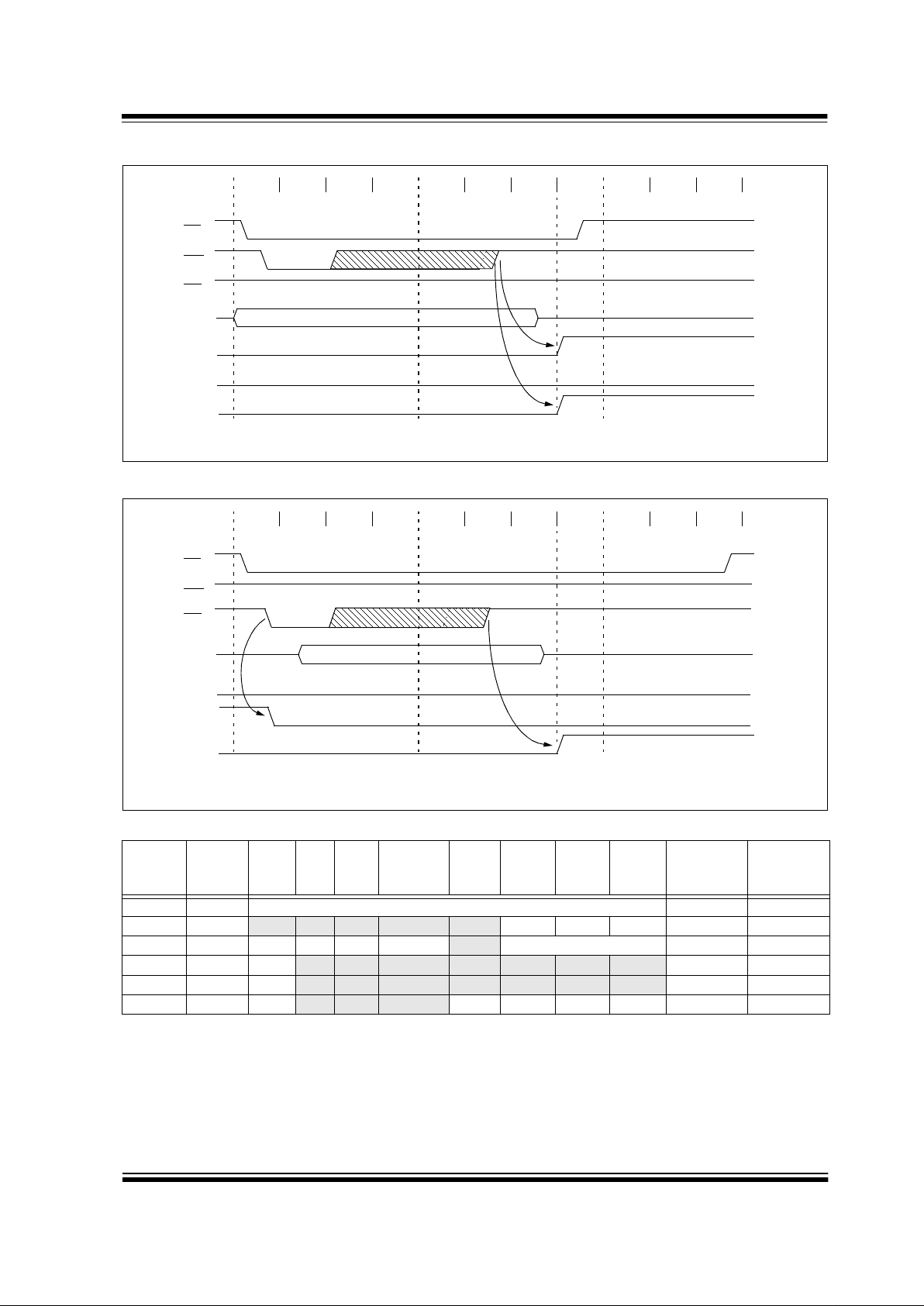
1999 Microchip Technology Inc.
Preliminary DS30569A-page 37
PIC16F870/871
FIGURE 3-9: PARALLEL SLAVE PORT WRITE WAVEFORMS
FIGURE 3-10: PARALLEL SLAVE PORT READ WAVEFORMS
TABLE 3-11: REGISTERS ASSOCIATED WITH PARALLEL SLAVE PORT
Address Name Bit 7 Bit 6 Bit 5 Bit 4 Bit 3 Bit 2 Bit 1 Bit 0
Val ue on :
POR,
BOR
Value on all
other resets
08h PORTD Port data latch when written: Port pins when read xxxx xxxx uuuu uuuu
09h PORTE
— — — — —RE2RE1RE0---- -xxx ---- -uuu
89h TRISE IBF OBF IBOV PSPMODE
— PORTE Data Direction Bits 0000 -111 0000 -111
0Ch PIR1 PSPIF
ADIF RCIF TXIF — CCP1IF TMR2IF TMR1IF 0000 0000 0000 0000
8Ch PIE1 PSPIE
ADIE RCIE TXIE — CCP 1IE TMR2IE TMR1IE 0000 0000 0000 0000
9Fh ADCON1 ADFM
— — — PCFG3 PCFG2 PCFG1 PCFG0 --0- 0000 --0- 0000
Legend: x = unknown, u = unchanged, - = unimplemented read as '0'. Shaded cells are not used by the Parallel Slave Port.
Q1 Q2 Q3 Q4CSQ1 Q2 Q3 Q4 Q1 Q2 Q3 Q4
WR
RD
IBF
OBF
PSPIF
PORTD<7:0>
Q1 Q2 Q3 Q4CSQ1 Q2 Q3 Q4 Q1 Q2 Q3 Q4
WR
IBF
PSPIF
RD
OBF
PORTD<7:0>

PIC16F870/871
DS30569A-page 38 Preliminary
1999 Microchip Technology Inc.
NOTES:

1999 Microchip Technology Inc.
Preliminary DS30569A-page 39
PIC16F870/871
4.0 DATA EEPROM AND FLASH
PROGRAM MEMORY
The Data EEPROM and FLASH Program Memory are
readable an d writab le during normal oper atio n o v e r the
entire VDD ra nge. A bulk erase operation may not be
issued from user code (which includes removing code
protection). The data memory is not dire ctly m apped in
the register file space. Instead, it is indirectly
addressed through the Special Function Registers
(SFR).
There are six SFRs used to r ead and writ e the prog ram
and data EEPROM memory. These registers are:
• EECON1
• EECON2
• EEDATA
• EEDATH
• EEADR
• EEADRH
The EEPROM data memory allo ws byte read and write.
When interfacing to the data memory block, EEDATA
holds the 8-bit data f or read/write and EEA DR holds the
address of the EEPROM location being accessed. The
registers EEDATH and EEADRH are not used for data
EEPROM access. The PIC16F870/871 devices have
64 bytes of data EEPROM with an address range from
0h to 3Fh.
The EEPROM data memory is rated for high erase/
write cycles. The write tim e is co ntro lle d by an on-chip
timer . The write t ime will v ary with v oltag e and temp erature, as well as from chip-to-chip. Please refer to the
specifications for exact limits.
The program m emory allows word read s and writes.
Program memory access allows for checksum calculation and ca librat ion table stora ge. A byt e or wo rd w rit e
automatically erases the location and writes the new
data (erase before write). Writing to program memory
will cease opera tion until the write is complete. T he program memory cannot be accessed during the write,
therefore c ode c ann ot execute. D uring t he w rite op er ation, the oscillator continues to clock the peripherals,
and therefore, they continue to operate. Interrupt
events will be detected and essentially “queued” until
the write is completed. When the write completes, the
next instruction in the pipeline is executed and the
branch to the interrupt vector address will occur.
When interfacing to the program memory block, the
EEDATH:EEDATA registers form a two byte word,
which holds the 14-bit data for read/write. The
EEADRH:EEADR registers form a two byte word,
which holds the 13-bit address of the FLASH location
being accessed. The PIC16F870/8 71 devi ces hav e 2K
words of program FLASH with an address range from
0h to 7FFh. The unused upper bits in both the EEDA TH
and EEDATA registers all read as “0’s”.
The value written to pro gram m emory does not need to
be a valid instruction. Therefore, up to 14-bit numbers
can be stored in memory for use as calibration parameters, serial numbers, packed 7-bit ASCII, etc. Executing a program memory location containing data that
forms an invalid instruction results in a NOP.
4.1 EEADR
The address registers can address up to a maxim um of
256 bytes of data EEPROM or up to a maximum of 8K
words of program FLASH. However, the PIC16F870/
871 have 64 bytes of data EEPROM and 2K words of
program FLASH.
When selecting a program address value, the MSByte
of the address is written to the EEADRH register and
the LSByte is written to the EEADR register. When
selecting a data address value, only the LSByte of the
address is written to the EEADR register.
On the PIC16F870/871 devices, the upper two bits of
the EEADR must always be cleared to prevent inadvertent access to the wrong loc atio n in data EEPROM.
This also applies to the program memory. The upper
five MSbits of EEADRH must always be clear during
program FLASH access.
4.2 EECON1 and EECON2 Registers
EECON1 is the control register for memory accesses.
EECON2 is not a physical register. Reading EECON2
will read all '0's. The EECON2 register is used
exclusively in the memory write sequence.
Control bit EEPGD determines if the access will be a
program or a data memory access. When clear, any
subsequent operations will operate on the data memory . Whe n set, any subseq uen t oper ations will o pera te
on the program memory.
Control bits RD and WR initiate read and write operations, respectively. These bits cannot be cleared, only
set, in software. They are cleared in hardware at the
completion of the read or write operation. The inability
to clear the WR bit in software prevents the accidental
or premature termination of a write operation.
The WREN bit, when set, will allow a write operation.
On power-up , the WR EN bit is clear . The WRERR bit i s
set when a write operation is interrupted by a MCLR
reset or a WD T ti me-out rese t duri ng n ormal oper atio n.
In these situations, following reset, the user can check
the WRERR bit and rewrite the location. The value of
the data and address registers and the EEPGD bit
remains unchanged.
Interrupt flag bit EEIF, in the PIR2 register, is set when
write is complete. It must be cleared in software.

PIC16F870/871
DS30569A-page 40 Preliminary
1999 Microchip Technology Inc.
REGISTER 4-1: EECON1 REGISTER (ADDRESS 18Ch)
R/W-x U-0 U-0 U-0 R/W-x R/W-0 R/W-0 R/W-0
EEPGD — — — WRERR WREN WR RD R = Readable bit
W = Writable bit
U = Unimplemented bit,
read as ‘0’
- n= Value at POR reset
bit7 bit0
bit 7: EEPGD: Program / Data EEPROM Select bit
1 = Accesses Program memory
0 = Accesses data memory
(This bit cannot be changed while a read or write operation is in progress)
bit 6-4: Unimplemented: Read as '0'
bit 3: WRERR: EEPROM Error Flag bit
1 = A write operation is prematurely terminated
(any MCLR
reset or any WDT reset during normal operation)
0 = The write operation completed
bit 2: WREN: EEPROM Write Enable bit
1 = Allows write cycles
0 = Inhibits write to the EEPROM
bit 1: WR: Write Control bit
1 = Initiates a write cycle. (The bit is cleared by hardware once write is complete.) The WR bit can only
be set (not cleared) in software.
0 = Write cycle to the EEPROM is complete
bit 0: RD: Read Control bit
1 = Initiates an EEPROM read RD is cleared in hardware. The RD bit can only be set (not cleared) in
software.
0 = Does not initiate an EEPROM read

1999 Microchip Technology Inc.
Preliminary DS30569A-page 41
PIC16F870/871
4.3 Reading the Data EEPROM Memory
T o read a data memory locatio n, the user m ust write the
address to the EEADR register, clear the EEPGD control bit (EECON1<7>) and then set control bit RD
(EECON1<0>). The data is available in the very next
instruction cycle of the EEDATA register, therefore it
can be read by the next instruction. EEDATA will hold
this value until another read operation or until it is written to by the user (during a write operation).
EXAMPLE 4-1: DATA EEPROM READ
BSF STATUS, RP1 ;
BCF STATUS, RP0 ;Bank 2
MOVLW DATA_EE_ADDR ;
MOVWF EEADR ;Data Memory Address to read
BSF STATUS, RP0 ;Bank 3
BCF EECON1, EEPGD ;Point to DATA memory
BSF EECON1, RD ;EEPROM Read
BCF STATUS, RP0 ;Bank 2
MOVF EEDATA, W ;W = EEDATA
4.4 Writing to the Data EEPROM Memory
To write an EEPROM data location, the address must
first be written to the EEADR register and the data written to the EEDATA register. Then the sequence in
Example 4-2 must be fo llowed to initi ate the write cycle.
EXAMPLE 4-2: DATA EEPROM WRITE
The write will not initiate if the above sequence is not
exactly followed (write 55h to EECON2, write AAh to
EECON2, then set WR bit) for each byte. It is strongly
recommended that interrupts be disabled during this
code segm ent.
Additionally, the WREN bit in EECON1 must be set to
enable writes. This mechanism prevents accidental
writes to data EEPROM due to unexpected code execution (i.e., runaway programs). The WREN bit should
be kept clear at all times, except when updating the
EEPROM. The WREN bit is not cleared by hardware
After a write sequence has been initiated, clearing the
WREN bit will not aff ect the current write cycle . The WR
bit will be inhibited from be ing set unles s the WREN bit
is set. The WREN bit m ust be set on a previous instruction. Both WR and WREN ca nno t be s et w i th t he sam e
instruction.
At the completion of the write cycle, the WR bit is
cleared in hardware and the EEPROM Write Compl ete
Interrupt Flag bit (EEIF) is set. EEIF m ust be cl eared by
software.
BSF STATUS, RP1 ;
BCF STATUS, RP0 ; Bank 2
MOVLW DATA_EE_ADDR ;
MOVWF EEADR ; Data Memory Address to write
MOVLW DATA_EE_DATA ;
MOVWF EEDATA ; Data Memory Value to write
BSF STATUS, RP0 ; Bank 3
BCF EECON1, EEPGD ; Point to DATA memory
BSF EECON1, WREN ; Enable writes
BCF INTCON, GIE ; Disable Interrupts
MOVLW 55h ;
Required MOVWF EECON2 ; Write 55h
Sequence MOVLW AAh ;
MOVWF EECON2 ; Write AAh
BSF EECON1, WR ; Set WR bit to begin write
BSF INTCON, GIE ; Enable Interrupts
SLEEP ; Wait for interrupt to signal write complete
BCF EECON1, WREN ; Disable writes

PIC16F870/871
DS30569A-page 42 Preliminary
1999 Microchip Technology Inc.
4.5 Reading the FLASH Program Memory
A program me mory location ma y be rea d by writing tw o
bytes of the address to the EEADR and EEADRH registers, setting the EEPGD control bit (EECON1<7>)
and then setting control bit RD (EECON1<0>). Once
the read control bit is set, the microcontroller will use
the next two instruction cycles to read the data. The
data is available in the EEDATA and EEDATH registers
after the second NOP instruction. Therefore, it can be
read as two bytes in the following instructions. The
EEDAT A and EED ATH registers will hold t his v alue u ntil
another read operati on or until it is written to b y the user
(during a write operation).
EXAMPLE 4-3: FLASH PROGRAM READ
BSF STATUS, RP1 ;
BCF STATUS, RP0 ; Bank 2
MOVLW ADDRH ;
MOVWF EEADRH ; MSByte of Program Address to read
MOVLW ADDRL ;
MOVWF EEADR ; LSByte of Program Address to read
BSF STATUS, RP0 ; Bank 3
BSF EECON1, EEPGD ; Point to PROGRAM memory
Required BSF EECON1, RD ; EEPROM Read
Sequence
NOP ; memory is read in the next two cycles after BSF EECON1,RD
NOP ;
BCF STATUS, RP0 ; Bank 2
MOVF EEDATA, W ; W = LSByte of Program EEDATA
MOVF EEDATH, W ; W = MSByte of Program EEDATA

1999 Microchip Technology Inc.
Preliminary DS30569A-page 43
PIC16F870/871
4.6 Writing to the FLASH Program
Memory
When the PIC16F870/871 are fully code protected or
not code protected, a word of the FLASH program
memory may be wr itten provided the W RT configuration bit is set. If the PIC16F870/871 are partially code
protected, then a word of FLASH program memory
may be written if the word is in a non-code protected
segment of memory and the WRT configuration bit is
set. To write a FLASH program location, the first two
bytes of the address m ust be written to the EEADR and
EEADRH registers and two bytes of the data to the
EEDATA and EEDATH registers, set the EEPGD con-
trol bit (EECON1<7>), and then set control bit WR
(EECON1<1>). The sequence in Examp le 4-4 must be
followed to initiate a write to program memory.
The microcontroller will then halt internal operations
during the next two instruction cycles for the T
PEW
(parameter D133) in which the write takes place. This
is not SLEEP mode, as the clocks and peripherals will
continue to run. Therefore, the two instructions follow-
ing the “BSF EECON, WR” should be NOP instructions.
After the write cycle, the microcontroller will resume
operation with the 3rd instruction after the EECON1
write instruction.
EXAMPLE 4-4: FLASH PROGRAM WRITE
BSF STATUS, RP1 ;
BCF STATUS, RP0 ; Bank 2
MOVLW ADDRH ;
MOVWF EEADRH ; MSByte of Program Address to read
MOVLW ADDRL ;
MOVWF EEADR ; LSByte of Program Address to read
MOVLW DATAH ;
MOVWF EEDATH ; MS Program Memory Value to write
MOVLW DATAL ;
MOVWF EEDATA ; LS Program Memory Value to write
BSF STATUS, RP0 ; Bank 3
BSF EECON1, EEPGD ; Point to PROGRAM memory
BSF EECON1, WREN ; Enable writes
BCF INTCON, GIE ; Disable Interrupts
MOVLW 55h ;
Required MOVWF EECON2 ; Write 55h
Sequence MOVLW AAh ;
MOVWF EECON2 ; Write AAh
BSF EECON1, WR ; Set WR bit to begin write
NOP ; Instructions here are ignored by the microcontroller
NOP
; Microcontroller will halt operation and wait for
; a write complete. After the write
; the microcontroller continues with 3rd instruction
BSF INTCON, GIE ; Enable Interrupts
BCF EECON1, WREN ; Disable writes

PIC16F870/871
DS30569A-page 44 Preliminary
1999 Microchip Technology Inc.
4.7 Write Verify
Depending on the a pplicati on, good p rogr amming pr actice may dictate that the value written to the memory
should be verified against the original value. This
should be used in applications where excessive writes
can stress bits near the specification limit.
Generally a write failure will be a bit which was written
as a ’1’, but reads back as a ’0’ (due to l eak age off the
bit).
4.8 Protection Against Spurious Write
4.8.1 EEPROM DATA MEMORY
There are c ond ition s w hen t he device m ay not want to
write to the data EEPROM memory. To protect against
spurious EEPROM writes, various mechanisms have
been built-in. On power-up, the WREN bit is cleared.
Also, the Power-up Timer (72 ms duration) prevents
EEPROM write.
The write initiate sequence and the WREN bit together
help prevent an accidental write during brown-out,
power glitch, or software malfunction.
4.8.2 PROGRAM FLASH MEMORY
To protect ag ainst spurio us writes to FL ASH program
memory, the WRT bit in the configuration word may be
programmed to ‘0’ to prevent writes. The write initiate
sequence must also be f ollo we d. WRT and the configuration word cannot be programmed by user code, only
through the use of an external programmer.
4.9 Operation during Code Protect
Each reprogrammable memory block has its own code
protect mechanism. External Read and Write operations are disabled if either of these mechanisms are
enabled.
4.9.1 DATA EEPROM MEMORY
The microcontroller it self c an both read a nd write to the
internal Data EEPROM, regardless of the state of the
code protect configuration bit.
When data memory is code protected (CONFIG<8>=0 )
any further external programming access of program
memory is disabled. To reenable programming access
to program memory, both bulk erase and removal of
code protection must be performed on program and
data memory.
4.9.2 PROGRAM FLASH MEMORY
The microcontroller can read and execute instructions
out of the internal FLASH prog ram memory , re ga rdle ss
of the state of the code protect configuration bits. However, the WRT configuration bit and the code protect
bits have different effects on writing to program memory. Table 4-1 shows the various configurations and
status of reads and writes. To erase the WRT or code
protection bits in the configuration word requires that
the device be fully erased.
TABLE 4-1: READ/WRITE STATE OF INTERNAL FLASH PROGRAM MEMORY
Configuration Bits
Memory Location
Internal
Read
Internal
Write
ICSP Read ICSP Write
CP1 CP0 WRT
001All program memory Yes Yes No No
000All program memory Yes No No No
110All program memory Yes No Yes Yes
111All program memory Yes Yes Yes Yes

1999 Microchip Technology Inc.
Preliminary DS30569A-page 45
PIC16F870/871
TABLE 4-2: REGISTERS ASSOCIATED WITH DATA EEPROM/PROGRAM FLASH
AddressNameBit 7Bit 6Bit 5Bit 4Bit 3Bit 2Bit 1Bit 0
Value on:
POR,
BOR
Value on
all other
resets
0Bh, 8Bh,
10Bh, 18Bh
INTCON GIE PEIE T0IE INTE RBIE T0IF INTF RBIF 0000 000x 0000 000u
10Dh EEADR EEPROM address register xxxx xxxx uuuu uuuu
10Fh EEADRH —————EEPROM address high xxxx xxxx uuuu uuuu
10Ch EEDATA EEPROM data resister xxxx xxxx uuuu uuuu
10Eh EEDATH — — EEPROM data resister high xxxx xxxx uuuu uuuu
18Ch EECON1 EEPGD — — — WRERR WREN WR
RD x--- x000 x--- u000
18Dh EECON2 EEPROM control resister2 (not a physical resister)
8Dh PIE2
— — — EEIE — — — — ---0 ---- ---0 ----
0Dh PIR2
— — — EEIF — — — — ---0 ---- ---0 ----
Legend: x = unknown, u = unchanged, r = reserved, - = unimplemented read as ’0’. Shaded cells are not used by the
Timer1 module.

PIC16F870/871
DS30569A-page 46 Preliminary
1999 Microchip Technology Inc.
NOTES:

1999 Microchip Technology Inc.
Preliminary DS30569A-page 47
PIC16F870/871
5.0 TIMER0 MODUL E
The Timer0 module timer/co unter has th e fol lowing f eatures:
• 8-bit timer/counter
• Readable and writable
• 8-bit software programmable prescaler
• Internal or external clock select
• Interrupt on overflow from FFh to 00h
• Edge select for external clock
Figure 5-1 is a block diagram of the Timer0 module and
the prescal e r s ha r ed w i th th e W D T.
Additional information on the Timer0 module is available
in the PICmicro™ Mid-Range MCU Family Reference
Manual (DS33023).
Timer mode is selected by clearing bit T0CS
(OPTION_REG<5>). In timer mode, the Timer0 module will increment every instruction cycle (without prescaler). If the TMR0 register is written, the increment is
inhibited for the following two instruction cycles. The
user can work around this by writing an adjusted val ue
to the TMR0 register.
Counter mode is selected by setting bit T0CS
(OPTION_REG<5>). In counter mode, Timer0 will
increment either on every ri sing or falling edge of pin
RA4/T0CKI. The incrementing edge is determined by
the Timer0 Source Edge Select bit T0SE
(OPTION_REG<4>). Clearing bit T0SE selects the rising edge. Restrictions on the external clock input are
discussed in detail in S ection 5.2.
The prescaler is mutually exclusively shared between
the Timer0 module and the watchdog timer. The prescaler is not readab le o r writab le . Sec tion5.3 details the
operation of the prescale r.
5.1 Timer0 Interrupt
The TMR0 interrupt is generated when the TMR0 register overflows from FFh to 00 h. This overflow sets bit
T0IF (INTCON<2>). The interrupt can be masked by
clearing bit T0IE (INTCON<5>). Bit T0IF must be
cleared in softwa re b y th e Tim er0 mo dule interrupt s ervice routine before re-enabling this interrupt. The
TMR0 interrupt cannot awaken the processor from
SLEEP since the timer is shut off during SLEEP.
FIGURE 5-1: BLOCK DIAGRAM OF THE TIMER0/WDT PRESCALER
RA4/T0CKI
T0SE
Pin
M
U
X
CLKOUT (= F
OSC/4)
SYNC
2
Cycles
TMR0 reg
8-bit Prescaler
8 - to - 1MUX
M
U
X
M U X
Watchdog
Timer
PSA
0
1
0
1
WDT
Time-out
PS2:PS0
8
Note: T0CS, T0SE, PSA, PS2:PS0 are (OPTION_REG<5:0>).
PSA
WDT Enable bit
M
U
X
0
1
0
1
Data Bus
Set Flag Bit T0IF
on Overflow
8
PSA
T0CS
PRESCALER

PIC16F870/871
DS30569A-page 48 Preliminary
1999 Microchip Technology Inc.
5.2 Using Timer0 with an External Clock
When no prescaler is used, the external clock input is
the same as the prescaler output. The synchronization
of T0CKI with the internal phase clocks is accomplished by sam pling the presca ler output on th e Q2 and
Q4 cycles of the internal phase clocks. Therefore, it is
necessary for T0CKI to be high for at least 2Tosc (and
a small RC delay of 20 ns) and low for at least 2Tosc
(and a small RC delay of 20 ns). Refer to the electrical
specification of the desired device.
5.3 Prescaler
There is only one prescaler available, which is mutually
exclusively shared between the Timer0 module and the
watchdog timer. A prescaler assignment for the Timer0
module means that there is no prescaler for the watchdog timer, and vice-v ersa. This prescaler is not readab le
or writable (see Figure 5-1).
The PSA and PS2:PS0 bits (OPTION_REG<3:0>) determine the prescaler assignment and prescale ratio.
When assigned to the Timer0 module, all instructions
writing to the TMR0 register (e.g. CLRF
1, MOVWF 1,
BSF
1,x.. ..etc.) will clear th e prescaler . When assigned
to WDT, a CLRWDT inst ruction will cl ear the prescale r
along with the Watchdog Timer. The prescaler is not
readable or writable.
REGISTER 5-1: OPTION_REG REGISTER
Note: Writing to TMR0, when the prescaler is
assigned to Timer0, will clear the prescaler
count, but will not change the prescaler
assignment.
R/W-1 R/W-1 R/W-1 R/W-1 R/W-1 R/W-1 R/W-1 R/W-1
RBP
U INTEDG T0CS T0SE PSA PS2 PS1 PS0
R = Readable bit
W = Writable bit
U = Unimplemented bit,
read as ‘0’
- n = Value at POR reset
bit 7 bit 0
bit 7: RBPU
bit 6: INTEDG
bit 5: T0CS: TMR0 Clock Source Select bit
1 = Transition on T0CKI pin
0 = Internal instruction cycle clock (CLKOUT)
bit 4: T0SE: TMR0 Source Edge Select bit
1 = Incremen t on high-to-low transiti on on T0CKI pin
0 = Increment on low-to-high transition on T0CKI pin
bit 3: PSA: Prescaler Assignment bit
1 = Prescaler is assigned to the WDT
0 = Prescaler is assigned to the Timer0 module
bit 2-0: PS2:PS0: Prescaler Rate Select bits
000
001
010
011
100
101
110
111
1 : 2
1 : 4
1 : 8
1 : 16
1 : 32
1 : 64
1 : 128
1 : 256
1 : 1
1 : 2
1 : 4
1 : 8
1 : 16
1 : 32
1 : 64
1 : 128
Bit Value TMR0 Rate WDT Rate
Note: T o a vo id an un intended de vice RESET, the instruction sequence s hown in the PICmicro™ Mid-Ran ge MCU
Family Reference Manual (DS33023) must be executed when changing the prescaler assignment from
Timer0 to the WDT. This sequence must be followed even if the WDT is disabled.

1999 Microchip Technology Inc.
Preliminary DS30569A-page 49
PIC16F870/871
TABLE 5-1: REGISTERS ASSOCIATED WITH TIMER0
Address Name Bit 7 Bit 6 Bit 5 Bit 4 Bit 3 Bit 2 Bit 1 Bit 0
Value on:
POR,
BOR
Value on all
other resets
01h,101h TMR0 Timer0 module’s register xxxx xxxx uuuu uuuu
0Bh,8Bh,
10Bh,18Bh
INTCON GIE PEIE T0IE
INTE RBIE T0IF INTF RBIF 0000 000x 0000 000u
81h,181h OPTION_REG
RBPU INTEDG T0CS T0SE PSA PS2 PS1 PS0 1111 1111 1111 1111
Legend: x = unknown, u = unchanged, - = unimplemented locations read as '0'. Shaded cells are not used by Timer0.

PIC16F870/871
DS30569A-page 50 Preliminary
1999 Microchip Technology Inc.
NOTES:

1999 Microchip Technology Inc.
Preliminary DS30569A-page 51
PIC16F870/871
6.0 TIMER1 MODUL E
The Timer1 module is a 1 6-bi t ti me r/co unter consisting
of two 8-bit registers (TMR1H and TMR1L), which are
readable and writable. The TMR1 Register pair
(TMR1H:TMR1L) increments from 0000h to FFFFh
and rolls ove r to 0000h. The TMR1 Int errupt, if enabled,
is generated on overflow, which is latched in interrupt
flag bit TMR1IF (PIR1<0>). This interrupt can be
enabled/disabled by setting/clearing TMR1 interrupt
enable bit TMR1IE (PIE1<0>).
Timer1 can operate in one of two modes:
•As a timer
•As a counter
The operating mode is determined by the clock select
bit, TMR1CS (T1CON<1>).
In timer mode, Timer1 increments every instruction
cycle. In coun ter mo de, it in crement s on every risi ng
edge of the external clock input.
Timer1 can be enabled/disabled by setting/clearing
control bit TMR1ON (T1CON<0> ) .
Timer1 also has an in ternal “reset input ”. This reset can
be generated by the CCP module (Section 8.0).
Register 6-1 shows the Timer1 control register.
When the Timer1 oscillator is enabled (T1OSCEN is
set), the RC1/T1OSI and RC0/T1OSO/T1CKI pins
become inputs. That is, the TRISC<1:0> value is
ignored.
Additional information on timer modules is available in
the PICmicro™ Mid-range MCU Family Reference
Manual (DS33023).
REGISTER 6-1: T1CON: TIMER1 CONTROL REGISTER (ADDRESS 10h)
U-0 U-0 R/W-0 R/W-0 R/W-0 R/W-0 R/W-0 R/W-0
— — T1CKPS1 T1CKPS0 T1OSCEN T1SYNC TMR1CS TMR1ON
R = Readable bit
W = Writable bit
U = Unimplemented bit,
read as ‘0’
- n = Value at POR reset
bit7 bit0
bit 7-6: Unimplemented: Read as '0'
bit 5-4: T1CKPS<1:0>: Timer1 Input Clock Prescale Select bits
11 = 1:8 Prescale val ue
10 = 1:4 Prescale val ue
01 = 1:2 Prescale val ue
00 = 1:1 Prescale val ue
bit 3: T1OSCEN: Timer1 Oscillator Enable Control bit
1 = Oscillator is enabled
0 = Oscillator is shut off (The oscillator inverter is turned off to eliminate power drain)
bit 2: T1SYNC
: Timer1 External Clock Input Synchronization Control bit
TMR1CS = 1
1 = Do not synchronize external clock input
0 = Synchronize external clock input
T
MR1CS = 0
This bit is ignored. Timer1 uses the internal clock when TMR1CS = 0.
bit 1: TMR1CS: Timer1 Clock Source Select bit
1 = External clock from pin RC0/T1OSO/T1CKI (on the rising edge)
0 = Internal clock (F
OSC/4)
bit 0: TMR1ON: Timer1 On bit
1 = Enables Timer1
0 = Stops Timer1

PIC16F870/871
DS30569A-page 52 Preliminary
1999 Microchip Technology Inc.
6.1 Timer1 Operation in Timer Mode
Timer mode is selected by clearing the TMR1CS
(T1CON<1>) bit. In this mode, the input clock to the
timer is FOSC/4. The synchronize control bit T1SYNC
(T1CON<2>) has no effect since the internal clock is
always in sync.
6.2 Timer1 Counter Operation
Timer1 may operate in asynchronous or usynchronous
mode depending on the setting of the TMR1CS bit.
When Timer1 is being incremented via an external
source, increments occur on a rising edge. After
Timer1 is enabled in counter mode, the module must
first have a falling edge before the counter begins to
increment .
FIGURE 6-1: TIMER1 INCREMENTING EDGE
6.3 Timer1 Operation in Synchronized
Counter Mode
Counter mode is selected by setting bit TMR1CS. In
this mode, the timer inc rements on e v ery rising edge of
clock input on pin RC1/T1OSI, when bit T1OSCEN is
set, or on pin RC0/T1OSO /T1CKI, when bit T1OSCEN
is cleared.
If T1SYNC
is cleared, then the external clock input is
synchronized with internal phase clocks. The synchronization is done after the prescaler stage. The prescaler stage is an asynchronous ripple-counter.
In this configuration, during SLEEP mode, Timer1 will
not increment even if the external clock is present,
since the synchronization circuit is shut off. The prescaler however will conti nue to increment.
FIGURE 6-2: TIMER1 BLOCK DIAGRAM
T1CKI
(Default high)
T1CKI
(Default low)
Note: Arrows indicate counter increments.
TMR1H
TMR1L
T1OSC
T1SYNC
TMR1CS
T1CKPS<1:0>
Q Clock
T1OSCEN
Enable
Oscillator
(1)
FOSC/4
Internal
Clock
TMR1ON
on/off
Prescaler
1, 2, 4, 8
Synchronize
det
1
0
0
1
Synchronized
clock input
2
RC0/T1OSO/T1CKI
RC1/T1OSI
(2)
Note 1: When the T1OSCEN bit is cleared, the inverter is turned off. This eliminates power drain.
2: For the PIC16F870/871, the Schmitt Trigger is not implemented in external clock mode.
Set flag bit
TMR1IF on
Overflow
TMR1
(2)

1999 Microchip Technology Inc.
Preliminary DS30569A-page 53
PIC16F870/871
6.4 Timer1 Operation in Asynchronous
Counter Mode
If control bit T1SYNC (T1CON<2>) is set, the external
clock input is not synchronized. The timer continues to
increment asynchronous to the internal phase clocks.
The timer will continue to run during SLEEP and can
generate an i nterrupt on overflow, which will wake-up
the processor. However, special precautions in software are needed to read/write the time r (Section 6.4.1).
In asynchronous counter mode, Timer1 can not be used
as a time-base for capture or compare operations.
6.4.1 READING AND WRITING TIMER1 IN
ASYNCHRONOUS COUNTER MODE
Reading TMR1H or TMR1L while the timer is running
from an external asynchronous clock will guarantee a
valid read (taken care of in hardware). However, the
user should keep in mind that reading the 16-bit timer
in two 8-bit values itself poses certain problems, since
the timer may overflow between the reads.
For writes, it is recommended t hat th e u se r s im pl y sto p
the timer and write the desired values. A write contention may occur by writing to the timer registers, while
the register is incrementing. This may produce an
unpredictable value in the timer register.
Reading the 16-bit value requires some care . Exam ples
12-2 and 12-3 in the PICmicro™ Mid-Range MCU F am-
ily Reference Manual (DS33023) show how to read and
write Timer1 when it is running in asynchronous mode.
6.5 Timer1 Oscillator
A crystal oscillator circuit is bu ilt-in between pins T1OSI
(input) and T1OSO (amplifier output). It is enabled by
setting control bit T1OSCEN (T 1CON<3>). The oscill ator is a low power oscillator rated up to 200 kHz. It will
continue to run during SLEEP. It is primarily intended
for use with a 32 kHz crystal. Table 6-1 shows the
capacitor selection for the Timer1 oscillator.
The Timer1 oscillator is identical to the LP oscillator.
The user must provide a software time delay to ensure
proper oscillator start-up.
TABLE 6-1: CAPACITOR SELECTION FOR
THE TIMER1 OSCILLATOR
6.6 Resetting Timer1 using CCP1 Trigger
Output
If the CCP1 module is configured in compare mode to
generate a “special event trigger” (CCP1M<3:0> =
1011), this signal will reset Timer1.
Timer1 must be configured for either timer or synchronized counter mode to tak e advan tage of this fea ture. If
Timer1 is running in asynchronous counter mode, this
reset operation may not work.
In the ev ent that a write t o Timer1 coinc ides with a sp ecial event trigger from CCP1, the write will take precedence.
In this mode of op erati on, the CC PR1H:CCPR 1L register pair effectively becomes the period register for
Timer1.
6.7 Resetting of Timer1 Register Pair
(TMR1H, TMR1L)
TMR1H and TMR1 L reg ist ers a r e not re set to 00h on a
POR or any other reset except by the CCP1 special
event trigger.
T1CON register is reset t o 00h on a Power-on Res et or
a Brown-out Reset, which shuts off the timer and
leaves a 1:1 prescale. In all other resets, the register is
unaffected.
6.8 Timer1 Prescaler
The prescaler counter is cleared on writes to the
TMR1H or TMR1L registers.
Osc Type Freq C1 C2
LP 32 kHz 33 pF 33 pF
100 kHz 15 pF 15 pF
200 kHz 15 pF 15 pF
These values are for design guidance only.
Crystals Tested:
32.768 kHz Epson C-001R32.768K-A ± 20 PPM
100 kHz Epson C-2 100.00 KC-P ± 20 PPM
200 kHz STD XTL 200.000 kHz ± 20 PPM
Note 1: Higher capacitance increases the stability of
oscillator, but also increases the star t-up time.
2: Since each resonator/crystal has its own charac-
teristics, the user should consult the resonator/
crystal manufacturer for appropriate values of
external components.
Note: The special event trigger from the CCP1
module will not set interrupt flag bit
TMR1IF (PIR1<0>).

PIC16F870/871
DS30569A-page 54 Preliminary
1999 Microchip Technology Inc.
TABLE 6-2: REGISTERS ASSOCIATED WITH TIMER1 AS A TIMER/COUNTER
Address Name Bit 7 Bit 6 Bit 5 Bit 4 Bit 3 Bit 2 Bit 1 Bit 0
Value on:
POR,
BOR
Value on
all other
resets
0Bh,8Bh,
10Bh,
18Bh
INTCON GIE PEIE
T0IE INTE RBIE T0IF INTF RBIF 0000 000x 0000 000u
0Ch PIR1
PSPIF
(1)
ADIF RCIF TXIF — CCP1IF TMR2IF TMR1IF 0000 -000 0000 -000
8Ch PIE1
PSPIE
(1)
ADIE RCIE TXIE — CCP1IE TMR2IE TMR1IE 0000 -000 0000 -000
0Eh TMR1L Holding register for the Least Significant Byte of the 16-bit TMR1 register xxxx xxxx uuuu uuuu
0Fh TMR1H Holding register for the Most Significant Byte of the 16-bit TMR1 register xxxx xxxx uuuu uuuu
10h T1CON
— — T1CKPS1 T1CKPS0 T1OSCEN T1SYNC TMR1CS TMR1ON --00 0000 --uu uuuu
Legend: x = unknown, u = unchanged, - = unimplemented read as '0'. Shaded cells are not used by the Timer1 module.
Note 1: Bits PSPIE and PSPIF are reserved on the PIC16F870; always maintain these bits clear.
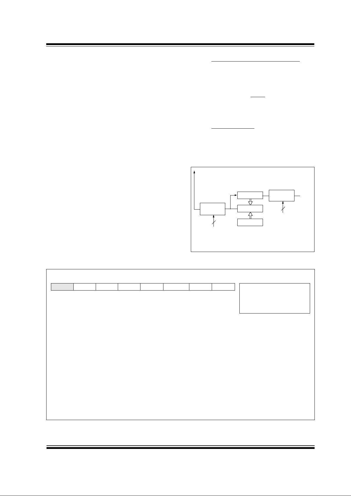
1999 Microchip Technology Inc.
Preliminary DS30569A-page 55
PIC16F870/871
7.0 TIMER2 MODUL E
Timer2 is an 8-bit timer with a prescaler and a
postscaler. It can be used as the PWM time-base for
the PWM mode of the CCP module (s). The TMR2 register is readable and writable, and is cleared on any
device reset.
The input clock (F
OSC/4) has a prescale option of 1:1,
1:4 or 1:16, selected by control bits
T2CKPS1:T2CKPS0 (T2CON<1:0>).
The Timer2 module has an 8-bit period register PR2.
Timer2 increments from 00h until it matches PR2 and
then resets to 00h on the next increment cycle. PR2 is
a readable and writable regi ster . The PR2 register is initialized to FFh upon reset.
The match output of TMR2 goes through a 4-bit
postscaler (which gives a 1:1 to 1:16 scaling inclusive)
to generate a TMR2 interrupt (latched in flag bit
TMR2IF, (PIR1<1>)).
Timer2 can be s hut off by clearing control bit T MR2O N
(T2CON<2>) to minimize power consumption.
Register 7-1 shows the Timer2 control register.
Additional information on timer modules is available in
the PICmicro™ Mid-Range MCU Family Reference
Manual (DS33023).
7.1 Timer2 Prescaler and Postscaler
The prescaler and postscaler counters are cleared
when any of the following occurs:
• a write to the TMR2 register
• a write to the T2CON register
• any device reset (POR, MCLR
reset, WDT reset
or BOR)
TMR2 is not cleared when T2CON is written.
7.2 Output of TMR2
The output of TMR2 (bef ore th e postscaler) i s fed t o the
SSPort module, which optionally uses it to generate
shift clock.
FIGURE 7-1: TIMER2 BLOCK DIAGRAM
REGISTER 7-1: T2CON: TIMER2 CONTROL REGISTER (ADDRESS 12h)
Comparator
Sets flag
TMR2 reg
Postscaler
Prescaler
PR2 reg
2
F
OSC/4
1:1 1:16
1:1, 1:4, 1:16
4
bit TMR2IF
to
T2OUTPS3:
T2OUTPS0
T2CKPS1:
T2CKPS0
EQ
U-0 R/W-0 R/W-0 R/W-0 R/W-0 R/W-0 R/W-0 R/W-0
— TOUTPS3 TOUTPS2 TOUTPS1 TOUTPS0 TMR2ON T2CKPS1 T2CKPS0 R = Readable bit
W = Writable bit
U = Unimplemented bit,
read as ‘0’
- n = Value at POR reset
bit7 bit0
bit 7: Unimplemented: Read as '0'
bit 6-3: TOUTPS3:TOUTPS0: Timer2 Output Postscale Select bits
0000 = 1:1 Postscale
0001 = 1:2 Postscale
0010 = 1:3 Postscale
•
•
•
1111 = 1:16 Postscale
bit 2: TMR2ON : Timer2 On bit
1 = Timer2 is on
0 = Timer2 is off
bit 1-0: T2CKPS1:T2CKPS0: Timer2 Clock Prescale Select bits
00 = Prescaler is 1
01 = Prescaler is 4
1x = Prescaler is 16

PIC16F870/871
DS30569A-page 56 Preliminary
1999 Microchip Technology Inc.
TABLE 7-1: REGISTERS ASSOCIATED WITH TIMER2 AS A TIMER/COUNTER
Address Name Bit 7 Bit 6 Bit 5 Bit 4 Bit 3 Bit 2 Bit 1 Bit 0
Value on:
POR,
BOR
Value on
all other
resets
0Bh,8Bh,
10Bh,18Bh
INTCON GIE PEIE
T0IE INTE RBIE T0IF INTF RBIF
0000 000x 0000 000u
0Ch PIR1
PSPIF
(1)
ADIF RCIF TXIF — CCP1IF TMR2IF TMR1IF
0000 -000 0000 -000
8Ch PIE1
PSPIE
(1)
ADIE RCIE TXIE — CCP1IE TMR2IE TMR1IE
0000 -000 0000 -000
11h TMR2 Timer2 module’s register
0000 0000 0000 0000
12h T2CON
— TOUTPS3 TOUTPS2 TOUTPS1 TOUTPS0 TMR2ON T2CKPS1 T2CKPS0
-000 0000 -000 0000
92h PR2 Timer2 Period Register
1111 1111 1111 1111
Legend: x = unknown, u = unchanged, - = unimplemented read as '0'. Shaded cells are not used by the Timer2 module.
Note 1: Bits PSPIE and PSPIF are reserved on the PIC16F870; always maintain these bits clear.

1999 Microchip Technology Inc.
Preliminary DS30569A -page 57
PIC16F870/871
8.0 CAPTURE/COMPARE/PWM
MODULE
The Capture/Comp are/ PWM (CC P) m od ule c on tain s a
16-bit register which can operate as a:
• 16-bit Capture register
• 16-bit Compare register
• PWM master/slave Duty Cycle register
Table 8-1 shows the resources used by the CCP module. In the following sections, th e operation o f a CCP
module is described.
CCP1 Module:
Capture/Compare/PWM Register1 (CCPR1) is comprised o f two 8-bit regis ters: CCPR1L (l ow byte) and
CCPR1H (high byte). The CCP1CON register controls
the operation of CC P1. The specia l ev ent trigger is generated by a compare match and will reset Timer1 and
start an A/D conversion (if the A/D module is enabled).
Additional information on CCP modules is available in
the PICmicro™ Mid-Range MCU Family Reference
Manual (DS33023) and in Appl ication Note 594, “Usin g
the CCP Modules” (DS00594).
TABLE 8-1: CCP MODE - TIMER
RESOURCES REQUIRED
REGISTER 8-1: CCP1CON REGISTER (ADDRESS: 17h)
CCP Mode Timer Resource
Capture
Compare
PWM
Timer1
Timer1
Timer2
U-0 U-0 R/W-0 R/W-0 R/W-0 R/W-0 R/W-0 R/W-0
— — CCP1X CCP1Y CCP1M3 CCP1M2 CCP1M1 CCP1M0 R =Readable bit
W =Writable bit
U =Unimplemented bit, read as ‘0’
- n =Value at POR reset
bit7 bit0
bit 7-6: Unimplemented: Read as ’0’
bit 5-4: CCP1<X:Y>: PWM Least Significant bits
Capture Mo de: Unused
Compare Mode: Unused
PWM Mode: These bi ts are the two LSbs of the PWM duty cyc le. The eight MSbs are found in CCPR1L.
bit 3-0: CCP1M<3:0>: CCPx Mode Select bits
0000 = Capture/Compare/PWM off (resets CCP module)
0100 = Capture mode, every falling edge
0101 = Capture mode, every rising edge
0110 = Capture mode, every 4th rising edge
0111 = Capture mode, every 16th rising edge
1000 = Compare mode, set output on match (CCP1IF bit is set)
1001 = Compare mode, clear output on mat ch (CCP 1IF bit is set)
1010 = Compare mode, generate softwar e i nte rrupt on ma tch (C CP 1I F b it i s se t, C CP pin is unaffected)
1011 = Compare mode, trigger special event (CCP1IF bit is set, CCP1 pin is unaffected); CCP1 resets
TMR1 and starts an A/D conversion (if A/D module is enabled)
11xx = PWM mode

PIC16F870/871
DS30569A -page 58 Preliminary
1999 Microchip Technology Inc.
8.1 Capture Mode
In Capture mode, CCPR1H:CCPR1L captures the
16-bit value of th e TMR1 register wh en an ev ent oc curs
on pin RC2/CCP1. An event is defined as:
• Ev ery f al lin g edge
• Ev ery rising edge
• Ev ery 4th rising edge
• Every 16th rising edge
An event is selected by control bits CCP1M<3:0>
(CCP1CON<3:0>). When a capture is made, the interrupt request flag bit CCP1IF (PIR1<2>) is set. The
interrupt flag must be cleared in software. If another
capture occurs before the value in register CCPR1 is
read, the old captured value will be lost.
8.1.1 CCP PIN CONFIGURATION
In Capture mode, the R C2/C CP1 pin should be config-
ured as an input by setting the TRISC<2> bit.
FIGURE 8-1: CAPTURE MODE OP ERATION
BLOCK DIAGRAM
8.1.2 TIMER1 MODE SELECTION
Timer1 must be running in timer mode or synchronized
counter mode for the CCP modul e to use the c apture
feature. In asynchronous counter mode, the capture
operation may not work.
8.1.3 SOFTWARE INTERRUPT
When the capture mode is changed, a false capture
interrupt may be generated. The user should keep bit
CCP1IE (PIE1<2>) clear to avoid false interrupts and
should clear the flag bit CCP1IF following any such
change in operating mode.
8.1.4 CCP PRESCALER
There are four prescaler settings, specified by bits
CCP1M<3:0>. Whene ve r the CCP module is turned off,
or the CCP module is not in capture mode, the prescaler counter is cleared. Any reset will clear the prescaler counter.
Switching from one capture prescaler to another may
generate an interrupt. Also, the prescaler counter will
not be cleared, therefore, the first capture may be from
a non-zero prescaler. Example 8-1 shows the recommended method for switching between capture prescalers. This example also clears the prescaler counter
and will not generate the “false” interrupt.
EXAMPLE 8-1: CHANGING BETWEEN
CAPTURE PRESCALERS
CLRF CCP1CON ;Turn CCP module off
MOVLW NEW_CAPT_PS;Load the W reg with
; the new precscaler
; move value and CCP ON
MOVWF CCP1CON ;Load CCP1CON with this
; value
Note: If the RC2/CCP1 pin is configured as an
output, a write to the port can cause a ca pture condition.
CCPR1H CCPR1L
TMR1H TMR1L
Set flag bit CCP1IF
(PIR1<2>)
Capture
Enable
Q’s
CCP1CON<3:0>
RC2/CCP1
Prescaler
÷
1, 4, 16
and
edge detect
Pin

1999 Microchip Technology Inc.
Preliminary DS30569A -page 59
PIC16F870/871
8.2 Compare Mode
In Compare mode, the 16-bit CCPR1 register value is
constantly compared against the TMR1 register pair
value. When a match occurs, the RC2/CCP1 pin is:
• Driven high
•Driven low
• Remains unchanged
The action on the pin is based on the value of control
bits CCP1M<3:0> (CCP1CON<3:0>). At the same
time, interrupt flag bit CCP1IF is set.
FIGURE 8-2: COMPARE MODE OPERATION
BLOCK DIAGRAM
8.2.1 CCP PIN CONFIGURATION
The user must configure the RC2/CCP1 pin as an output by clearing the TRISC<2> bit.
8.2.2 TIMER1 MODE SELECTION
Timer1 must be running in Timer mode or Synchronized Counter mode if the CCP module is using the
compare feature. In Asynchronous Counter mode, the
compare operation may not work.
8.2.3 SOFTWARE INTERRUPT MODE
When Generate Softw are Interrupt mode i s chosen, the
CCP1 pin is not affected. The CCPIF bit is set causing
a CCP interrupt (if enabled).
8.2.4 SPECIAL EVENT TRIGGER
In this mode, an i nternal hardw a re trigger is g ener ated,
which may be used to initiate an action.
The special event trigger output of CCP1 resets the
TMR1 register pair and st arts an A/D co nversion (if the
A/D module is enabled). This allows the CCPR1 register to effectively be a 16-bit programmable period register for Timer1.
.
8.3 PWM Mode (PWM)
In pulse width modulation mode, the CCP1 pin produces up to a 10-bit resolution PWM output. Since the
CCP1 pin is multiple xe d with the PORTC data latch, the
TRISC<2> bit must be cleared to make the CCP1 pin
an output.
Figure 8-3 shows a si mplified b lock diag ram of the CCP
module in PWM mode.
For a step-by-step procedure on how to set up the CCP
module for PWM operation, see Section8.3.3.
FIGURE 8-3: SIMPLIFIED PWM BLOCK
DIAGRAM
Note: Clearing the CCP1CON register will force
the RC2/CCP1 comp are output lat ch to the
default low level. This is not the data latch.
CCPR1H CCPR1L
TMR1H TMR1L
Comparator
QS
R
Output
Logic
Special Event Trigger
Set flag bit CCP1IF
(PIR1<2>)
match
RC2/CCP1
TRISC<2>
CCP1CON<3:0>
Mode Select
Output Enable
Pin
Special event trigger will:
reset Timer1, but not set interrupt flag bit TMR1IF (PIR1<0>),
and set bit GO/DONE (ADCON0<2>).
Note: The special event trigger from the CCP1
module will not set interrupt flag bit
TMR1IF (PIR1<0>).
Note: Clear ing the CCP1CON re gister wi ll force
the CCP1 PWM output latch to the default
low level. This is not the PORTC I/O data
latch.
CCPR1L
CCPR1H (Slave)
Comparator
TMR2
Comparator
PR2
(Note 1)
R
Q
S
Duty Cycle Registers
CCP1CON<5:4>
Clear Timer,
CCP1 pin and
latch D.C.
TRISC<2>
RC2/CCP1
Note 1: 8-bit timer is concatenated with 2-bit internal Q clock
or 2 bits of the prescaler to create 10-bit time-base.

PIC16F870/871
DS30569A -page 60 Preliminary
1999 Microchip Technology Inc.
A PWM output (Figure 8-4) has a time-base (period)
and a time that the output stays high (duty cycle). The
frequency of the PWM is the inverse of the period (1/
period).
FIGURE 8-4: PWM OUTPUT
8.3.1 PWM PERIOD
The PWM period is specifi ed b y writing to the PR2 reg -
ister. The PWM period can be calculated using the following formula:
When TMR2 is equal to PR2, the follow ing three e vents
occur on the next increment cycle:
•TMR2 is cleared
• The CCP1 pin is set (exception: if PWM duty
cycle = 0%, the CCP1 pin will not be set)
• The PWM duty cycl e is latched from CCPR1L into
CCPR1H
8.3.2 PWM DUTY CYCLE
The PWM duty cycle is specified by writing to the
CCPR1L register and to the CCP1CON<5:4> bits. Up
to 10-bit resolution is available. The CCPR1L contains
the eight MSbs and the CCP1CON<5:4> contains the
two LSbs. This 10-bit value is represented by
CCPR1L:CCP1CON<5:4>. The following equation is
used to calculate the PWM duty cycle in time:
PWM duty cycle = (CCPR1L:CCP1CON<5:4>) •
Tosc • (TMR2 prescale value)
CCPR1L and CCP1CON<5:4> can be written to at any
time, but the duty cycle value is not latched into
CCPR1H until after a match between PR2 and TMR2
occurs (i.e., the period is complete). In PWM mode,
CCPR1H is a read-only register.
The CCPR1H register and a 2-bit internal latch are
used to double buffer the PWM duty cyc le . Thi s do uble
buffering is essential for glitchless PWM operation.
When the C CPR1H and 2-bit lat ch match T MR2 concatenated with an internal 2-bit Q clock or 2 bits of the
TMR2 prescaler, the CCP1 pin is cleared.
Maximum PWM resolution (bits) for a given PWM
frequency:
8.3.3 SET-UP FOR PWM OPERATION
The following steps should be taken when configuring
the CCP module for PWM operation:
1. Set the PWM period b y writing to t he PR2 regis ter.
2. Set the PWM duty cycle by writing to the
CCPR1L register and CCP1CON<5:4> bits.
3. Make the CCP1 pin an output by clearing the
TRISC<2> bit.
4. Set the TMR2 prescale val ue and enabl e Timer2
by writing to T2CON.
5. Configure the CCP1 modu le f or PWM oper ation.
Note: The Timer2 postscaler (see Section 8.1) is
not used in the determination of the PWM
frequency. The postscaler could be used to
have a servo update rate at a different frequency than the PWM output.
Period
Duty Cycle
TMR2 = PR2
TMR2 = Duty Cycle
TMR2 = PR2
FOSC
4 • FPWM • TMR2 Prescale value
PR2 =
— 1
Note: If the PWM duty cycle value is longer than
the PWM period, the CCP1 pin will not be
cleared.
log(
FPWM
log(2)
F
OSC
)
bits
=
Resolution

1999 Microchip Technology Inc.
Preliminary DS30569A -page 61
PIC16F870/871
TABLE 8-2: REGISTERS ASSOCIATED WITH CAPTURE, COMPARE, AND TIMER1
TABLE 8-3: REGISTERS ASSOCIATED WITH PWM AND TIMER2
Address Name Bit 7 Bit 6 Bit 5 Bit 4 Bit 3 Bit 2 Bit 1 Bit 0
Value on:
POR,
BOR
Value on
all other
resets
0Bh,8Bh,
10Bh,18Bh
INTCON GIE PEIE T0IE INTE RBIE T0IF INTF RBIF 0000 000x 0000 000u
0Ch PIR1
PSPIF
(1)
ADIF RCIF TXIF —CCP1IFTMR2IF TMR1IF 0000 -000 0000 -000
8Ch PIE1
PSPIE
(1)
ADIE RCIE TXIE —CCP1IETMR2IE TMR1IE 0000 -000 0000 -000
87h TRISC PORTC Data Direction Register 1111 1111 1111 1111
0Eh TMR1L Holding register for the Least Sign ificant Byte of th e 16- bit TMR1 regis ter xxxx xxxx uuuu uuuu
0Fh TMR1H Holding register for the Most Significant Byte o f the 16-bit T MR1 r egister xxxx xxxx uuuu uuuu
10h T1CON
— — T1CKPS1 T1CKPS0 T1OSCEN T1SYNC TMR1CS TMR1ON --00 0000 --uu uuuu
15h CCPR1L Capture/Comp are /PWM register 1 (LSB) xxxx xxxx uuuu uuuu
16h CCPR1H Capture/Compare/PWM register1 (MSB) xxxx xxxx uuuu uuuu
17h CCP1CON
— — CCP1X CCP1Y CCP1M3 CCP1M2 CCP1M1 CCP1M0 --00 0000 --00 0000
Legend: x = unknown, u = unchanged, - = unimplemented read as ’0’. Shaded cells are not used by Capture and Timer1.
Note 1:The PSP is not implemented on the PIC16F870; always maintain these bits clear.
Addr e ss Name Bit 7 Bit 6 Bit 5 Bit 4 Bit 3 Bit 2 Bit 1 Bit 0
Value on:
POR,
BOR
Value on
all other
resets
0Bh,8Bh,
10Bh,18B h
INTCON GIE PEIE T0IE INTE RBIE T0IF INTF RBIF
0000 000x 0000 000u
0Ch PIR1 PSPIF
(1)
ADIF RCIF TXIF — CCP1IF TMR2IF TMR1IF
0000 -000 0000 -000
8Ch PIE1 PSPIE
(1)
ADIE RCIE TXIE — CCP1IE TMR2IE TMR1IE
0000 -000 0000 -000
87h TRISC PORTC Data Direction Register 1111 1111 1111 1111
11h TMR2 Timer2 module’s register
0000 0000 0000 0000
92h PR2 Timer2 module’s period register
1111 1111 1111 1111
12h T2CON — TOUTPS3 TOUTPS2 TOUTPS1 TOUTPS0 TMR2ON T2CKPS1 T2CKPS0
-000 0000 -000 0000
15h CCPR1L Capture/Compare/PWM registe r1 (LSB)
xxxx xxxx uuuu uuuu
16h CCPR1H Capture/Compare/PWM register1 (MSB)
xxxx xxxx uuuu uuuu
17h CCP1CON — — CCP1X CCP1Y CCP1M3 CCP1M2 C CP1M1 CCP1M0
--00 0000 --00 0000
Legend: x = unknown, u = unchanged, - = unimplemented read as '0'. Shaded cells are not used by PWM and Timer2.
Note 1:Bits PSPIE and PSPIF are reserved on the PIC16F870; always maintain these bits clear.

PIC16F870/871
DS30569A -page 62 Preliminary
1999 Microchip Technology Inc.
NOTES:

1999 Microchip Technology Inc.
Preliminary DS30569A-page 63
PIC16F870/871
9.0 ADDRESSABLE UNIVERSAL
SYNCHRONOUS
ASYNCHRONOUS RECEIVER
TRANSMITTER (USART)
The Universal Synchronous Asynchronous Receiver
Transmitter (USART) module is one of the two serial
I/O modules. (USART is also known as a Serial Communications Interface or SCI). The USAR T can be co nfigured as a full duplex asynchronous system that can
communicate w ith peripheral de vi ce s such as CRT ter minals and personal computers , or it can be co nfigured
as a half duple x sy nc hro nou s sy s tem that c an co mmunicate with peripher al devices such as A/D or D/A integrated circuits, serial EEPROMs etc.
The USART can be configured in the following modes:
• Asynchronous (full duplex)
• Synchronous - Master (half duplex)
• Synchronous - Slave (half duplex)
Bit SPEN (RCSTA<7>) and bits TRISC<7:6> have to
be set in order to configure pins RC6/TX/CK and
RC7/RX/DT as the Univers al Synchronou s Asynchronous Receiver Transmitter.
The USART module a lso has a multi-pr ocessor communication capability using 9-bit address detection.
REGISTER 9-1: TXSTA: TRANSMIT STATUS AND CONTROL REGISTER (ADDRESS 98h)
R/W-0 R/W-0 R/W-0 R/W-0 U-0 R/W-0 R-1 R/W-0
CSRC TX9 TXEN SYNC
— BRGH TRMT TX9D R = Readable bit
W = Writable bit
U = Unimplemented bit,
read as ‘0’
- n = Va lue at POR reset
bit7 bit0
bit 7: CSRC: Clock Source Select bit
Asynchronous mode
Don’t care
Synchronous mode
1 = Master mode (Clock generated internally from BRG)
0 = Slave mode (Clock from external source)
bit 6: TX9: 9-bit Transmit Enable bit
1 = Selects 9-bit transmission
0 = Selects 8-bit transmission
bit 5: TXEN: Transmit Enable bit
1 = Transmit enabled
0 = Transmit disabled
Note: SREN/CREN overrides TXEN in SYNC mode.
bit 4: SYNC: USART Mode Select bit
1 = Synchronous mode
0 = Asynchronous mode
bit 3: Unimplemented: Read as '0'
bit 2: BRGH: High Baud Rate Select bit
Asynchronous mode
1 = High speed
0 = Low speed
Synchronous mode
Unused in this mode
bit 1: TRMT: Transmit Shift Register Status bit
1 = TSR empty
0 = TSR full
bit 0: TX9D: 9th bit of transmit data. Can be parity bit.

PIC16F870/871
DS30569A-page 64 Preliminary
1999 Microchip Technology Inc.
REGISTER 9-2: RCSTA: RECEIVE STATUS AND CONTROL REGISTER (ADDRESS 18h)
R/W-0 R/W-0 R/W-0 R/W-0 R/W-0 R-0 R-0 R-x
SPEN RX9 SREN CREN ADDEN FERR OERR RX9D R = Readable bit
W = Writable bit
U = Unimplemented bit,
read as ‘0’
- n = Value at POR reset
bit7 bit0
bit 7: SPEN: Serial Port Enable bit
1 = Serial port enabled (Configures RC7/RX/DT and RC6/TX/CK pins as serial port pins)
0 = Serial port disabled
bit 6: RX9: 9-bit Receive Enable bit
1 = Selects 9-bit reception
0 = Selects 8-bit reception
bit 5: SREN: Single Receive Enable bit
Asynchronous mode
Don’t care
Synchronous mode - master
1 = Enables single receive
0 = Disables single receive
This bit is cleared after reception is complete.
Synchronous mode - slave
Unused in this mode
bit 4: CREN: Continuous Receive Enable bit
Asynchronous mode
1 = Enables continuous receive
0 = Disables continuous receive
Synchronous mode
1 = Enables continuous receive until enable bit CREN is cleared (CREN overrides SREN)
0 = Disables continuous receive
bit 3: ADDEN: Address Detect Enable bit
Asynchronous mode 9-bit (RX9 = 1)
1 = Enables address detection, enable interrupt and load of the receive burffer when RSR<8> is set
0 = Disables address detection, all bytes are received, and ninth bit can be used as parity bit
bit 2: FERR: Framing Error bit
1 = Framing error (Can be updated by reading RCREG register and receive next valid byte)
0 = No framing error
bit 1: OERR: Overrun Error bit
1 = Overrun error (Can be cleared by clearing bit CREN)
0 = No overrun er ror
bit 0: RX9D: 9th bit of received data (Can be parity bit)

1999 Microchip Technology Inc.
Preliminary DS30569A-page 65
PIC16F870/871
9.1 USART Baud Rate Generator (BRG)
The BRG supports both the asynchronous and synchronous modes of the USART. It is a dedicated 8-bit
baud rate generator. The SPBRG register controls the
period of a free running 8-bit timer. In asynchronous
mode, bit BRGH ( TXSTA< 2>) also controls t he baud
rate. In synchronous mode, bit BRGH is ignored.
Table 9-1 shows the formula for computation of the
baud rate for different USART modes which only apply
in master mode (internal clock).
Given the d esired b aud rat e and F osc , the nearest integer value for the SPBRG register can be calculated
using the formula in Table 9-1. From this, the error in
baud rate can be determined.
It may be advantageous to use the high baud rate
(BRGH = 1) even for slower baud clocks. This is
because the F
OSC/(16(X + 1)) equation can reduc e the
baud rate error in some cases.
Writing a new value to the SPBRG register causes the
BRG timer to be reset (or cleared). This ensures the
BRG does no t wait for a ti mer overflow b efore outp utting the new baud rate.
9.1.1 SAMPLING
The data on the RC7/RX/DT pi n is sampled three ti mes
by a majority detect circuit to determine if a high or a
low level is present at the RX pin.
TABLE 9-1: BAUD RATE FORMULA
TABLE 9-2: REGISTERS ASSOCIATED WITH BAUD RATE GENERATOR
SYNC BRGH = 0 (Low Speed) BRGH = 1 (High Speed)
0
1
(Asynchronous) Baud Rate = FOSC/(64(X+1))
(Synchronous) Baud Rate = F
OSC/(4(X+1))
Baud Rate= F
OSC/(16(X+1))
NA
X = value in SPBRG (0 to 255)
Address Name Bit 7 Bit 6 Bit 5 Bit 4 Bit 3 Bit 2 Bit 1 Bit 0
Value on:
POR,
BOR
Value on all
other
resets
98h TXSTA CSRC TX9 TXEN SYNC —BRGHTRMT TX9D
0000 -010 0000 -010
18h RCSTA SPEN RX9 SREN CREN ADDEN FERR OERR RX9D
0000 000x 0000 000x
99h SPBRG Baud Rate Generator Register
0000 0000 0000 0000
Legend: x = unknown, - = unimplemented read as '0'. Shaded cells are not used by the BRG.

PIC16F870/871
DS30569A-page 66 Preliminary
1999 Microchip Technology Inc.
-
TABLE 9-3: BAUD RATES FOR ASYNCHRONOUS MODE (BRGH = 0)
BAUD
RATE
(K)
F
OSC = 20 MHz FOSC = 16 MHz FOSC = 10 MHz
KBAUD%ERROR
SPBRG
value
(decimal)
KBAUD%ERROR
SPBRG
value
(decimal)
KBAUD%ERROR
SPBRG
value
(decimal)
0.3------- --
1.2 1.221 1.75 255 1.202 0.17 207 1.202 0.17 129
2.4 2.404 0.17 129 2.404 0.17 103 2.404 0.17 64
9.6 9.766 1.73 31 9.615 0.16 25 9.766 1.73 15
19.2 19.531 1.72 15 19.231 0.16 12 19.53 1 1.7 2 7
28.8 31.250 8.51 9 27.778 3.55 8 31.250 8.51 4
33.6 34.722 3.34 8 35.714 6.29 6 31.250 6.99 4
57.6 62.500 8.51 4 62.500 8.51 3 52.083 9.58 2
HIGH 1.221 - 255 0.977 - 255 0.610 - 255
LOW 312.500 - 0 250.000 - 0 156.250 - 0
BAUD
RATE
(K)
F
OSC = 4 MHz FOSC = 3.6864 MHz
KBAUD
%
ERROR
SPBRG
value
(decimal) KBAUD
%
ERROR
SPBRG
value
(decimal)
0.3 0.300 0 207 0.301 0.33 185
1.2 1.202 0.17 51 1.216 1.33 46
2.4 2.404 0.17 25 2.432 1.33 22
9.6 8.929 6.99 6 9.322 2.90 5
19.2 20.833 8.51 2 18.643 2.90 2
28.8 31.250 8.51 1 - - -
33.6 - - - - - -
57.6 62.500 8.51 0 55.930 2.90 0
HIGH 0.244 - 255 0.218 - 255
LOW 62.500 - 0 55.930 - 0
TABLE 9-4: BAUD RATES FOR ASYNCHRONOUS MODE (BRGH = 1)
BAUD
RATE
(K)
F
OSC = 20 MHz FOSC = 16 MHz FOSC = 10 MHz
KBAUD%ERROR
SPBRG
value
(decimal)
KBAUD%ERROR
SPBRG
value
(decimal)
KBAUD%ERROR
SPBRG
value
(decimal)
0.3---------
1.2---------
2.4 - - - - - - 2.441 1.71 255
9.6 9.615 0.16 129 9.615 0.16 103 9.615 0.16 64
19.2 19.231 0.16 64 19.231 0.16 51 19.531 1.72 31
28.8 29.070 0.94 42 29.412 2.13 33 28.409 1.36 21
33.6 33.784 0.55 36 33.333 0.79 29 32.895 2.10 18
57.6 59.524 3.34 20 58.824 2.13 16 56.818 1.36 10
HIGH 4.883 - 255 3.906 - 255 2.441 - 255
LOW 1250.000 - 0 1000.000 0 625.000 - 0
BAUD
RATE
(K)
F
OSC = 4 MHz FOSC = 3.6864 MHz
KBAUD
%
ERROR
SPBRG
value
(decimal) KBAUD
%
ERROR
SPBRG
value
(decimal)
0.3 - - - - - -
1.2 1.202 0.17 207 1.203 0.25 185
2.4 2.404 0.17 103 2.406 0.25 92
9.6 9.615 0.16 25 9.727 1.32 22
19.2 19.231 0.16 12 18.643 2.90 11
28.8 27.798 3.55 8 27.965 2.90 7
33.6 35.714 6.29 6 31.960 4.88 6
57.6 62.500 8.51 3 55.930 2.90 3
HIGH 0.977 - 255 0.874 - 255
LOW 250.000 - 0 273.722 - 0

1999 Microchip Technology Inc.
Preliminary DS30569A-page 67
PIC16F870/871
9.2 USART Asynchronous Mode
In this mode, the USART uses standard non-return-tozero (NRZ) f ormat (one sta rt bit, eight or nine da ta bits ,
and one stop bit). The most common data format is 8
bits. An on-chip, dedicated, 8-bit baud rate generator
can be used to derive standard baud rate frequencies
from the oscillator. The USART transmits and receives
the LSb first. The USAR T’ s transmit ter and receive r are
functionally indep endent, b ut us e the sam e data f ormat
and baud rate. The baud rate generator produces a
clock either x16 or x64 of the bit shift rate, depending
on bit BRGH (TXSTA<2>). Parity is not supported by
the hardware , bu t can be implemen ted in sof tware (and
stored as the ninth data bit). Asynchronous mode is
stopped during SLEEP.
Asynchronous mode is selected by clearing bit SYNC
(TXSTA<4>).
The USART Asynchronous module consists of the following important elements:
• Baud Rate Ge ner ator
• Sampling Circuit
• Asynchronous Transmitter
• Asynchronous Receiver
9.2.1 USART ASYNCHRONOUS TRANSMITTER
The USART transmitter block diagram is shown in
Figure 9-1. The heart of the transmitter is the transmit
(serial) shift register (TSR). The shi ft register obtains it s
data from the read/write transmit buffer, TXREG. The
TXREG register is loaded with data in software. The
TSR register is not loaded until the STOP bit has been
transmitted from the previous load. As soon as the
STOP bit is transmitted, the TSR is loaded with new
data from the TXREG register (if available). Once the
TXREG regis ter tran sfers th e dat a t o th e T SR re gist er
(occurs in one T
CY), the TXREG register is empty and
flag bit TXIF (PIR1<4>) is set. This interrupt can be
enabled/disabled by setting/clearing enable bit TXIE
( PIE1<4>). Flag bit TXIF will be set, regardless of the
state of enable bit TXIE and cannot be cleared in software. It will reset onl y when ne w data is load ed into the
TXREG register . While flag b it TXIF indicates the status
of the TXREG register, another bit TRMT (TXSTA<1>)
shows the status of the TSR register. Status bit TRMT
is a read only bi t, w h ic h i s se t w he n the TSR r egi ste r i s
empty. No interrupt logic is tied to this bit, so the user
has to poll this bit in order to determine if the TSR register is empty.
Transmission is enabled by setting enable bit TXEN
(TXSTA<5>). The actual transmission will not occur
until the TXREG register has been loaded with data
and the baud rate generator (BRG) has produced a
shift clock (Figure9-2). The transmission can also be
started by first loading the TXREG register and then
setting enable bit TXEN. Normally, when transmission
is first started, the TSR register is empty. At that point,
transfer to the TXR EG regi st er w il l resul t in an immediate transfer to TSR, resulting in an empty TXREG. A
back-to-back transfer is thus possible (Figure 9-3).
Clearing enable bit TXEN during a transmission will
cause the transmissio n to be aborted and will res et the
transmitter. As a result, the RC6/TX/CK pin will revert
to hi-impedance.
In order to select 9-bit transmission, transmit bit TX9
(TXSTA<6>) should be set and the ninth bit should be
written to TX9D (TXSTA<0>). The ninth bit must be
written before writing the 8-bit data to the TXREG register. This is because a data write to the TXREG register can result in an immediate tr ansf er of the data to the
TSR register (if the TSR is empty). In such a case, an
incorrect ninth data bit may be loaded in the TSR
register.
FIGURE 9-1: USART TRANSMIT BLOCK DIAGRAM
Note 1: The TSR register is not mapped in data
memory, so it is not available to the user.
2: Flag b it TXIF is set wh en ena ble bi t TXEN
is set. TXIF is cleared by loading TXREG.
TXIF
TXIE
Interrupt
TXEN
Baud Rate CLK
SPBRG
Baud Rate Generator
TX9D
MSb
LSb
Data Bus
TXREG register
TSR register
(8)
0
TX9
TRMT
SPEN
RC6/TX/CK pin
Pin Buffer
and Control
8
• • •

PIC16F870/871
DS30569A-page 68 Preliminary
1999 Microchip Technology Inc.
Steps to follow when setting up an Asynchronous
Transmission:
1. Initialize the SPBRG registe r for the appropriate
baud rate. If a high speed baud rate is desired,
set bit BRGH. (Section 9.1)
2. Enable the asynchronous serial port by clearing
bit SYNC and setting bit SPEN.
3. If interrupts are desired, then set enable bit
TXIE.
4. If 9-bit transmis si on is d esi red, then set transmit
bit TX9.
5. Enable the transmission by setting bit TXEN,
which will also set bit TXIF.
6. If 9-bit transmission is selected, the ninth bit
should be loaded in bit TX9D.
7. Load data to the TXREG register (starts transmission).
FIGURE 9-2: ASYNCHRONOUS MASTER TRANSMISSION
FIGURE 9-3: ASYNCHRONOUS MASTER TRANSMISSION (BACK TO BACK)
TABLE 9-5: REGISTERS ASSOCIATED WITH ASYNCHRONOUS TRANSMISSION
Address Name
Bit 7
Bit 6 Bit 5 Bit 4 Bit 3 Bit 2 Bit 1 Bit 0
Value on:
POR,
BOR
Value on
all other
Resets
0Ch PIR1
PSPIF
(1)
ADIF RCIF TXIF
—
CCP1IF TMR2IF TMR1IF 0000 -000 0000 -000
18h RCSTA
SPEN RX9 SREN CREN — FERR OERR RX9D 0000 -00x 0000 -00x
19h TXREG
USART Transmit Register 0000 0000 0000 0000
8Ch PIE1
PSPIE
(1)
ADIE RCIE TXIE — CCP1IE TMR2IE TMR1IE 0000 -000 0000 -000
98h TXSTA
CSRC TX9 TXEN SYNC — BRGH TRMT TX9D 0000 -010 0000 -010
99h SPBRG Baud Rate Generator Register 0000 0000 0000 0000
Legend: x = unknown, - = unimplemented locations read as '0'. Shaded cells are not used for asynchronous transmission.
Note 1: Bits PSPIE and PSPIF are reserved on the PIC16F870; always maintain these bits clear.
Word 1
Stop Bit
Word 1
Transmit Shift Reg
Start Bit Bit 0 Bit 1 Bit 7/8
Write to TXREG
Word 1
BRG output
(shift clock)
RC6/TX/CK (pin)
TXIF bit
(Transmit buffer
reg. empty flag)
TRMT bit
(Transmit shift
reg. empty flag)
Transmit Shift Reg.
Write to TXREG
BRG output
(shift clock)
RC6/TX/CK (pin)
TXIF bit
(interrupt reg. flag)
TRMT bit
(Transmit shift
reg. empty flag)
Word 1
Word 2
Word 1
Word 2
Start Bit
Stop Bit
Start Bit
Transmit Shift Reg.
Word 1
Word 2
Bit 0 Bit 1
Bit 7/8 Bit 0
Note: This timing diagram shows two consecutive transmissions.
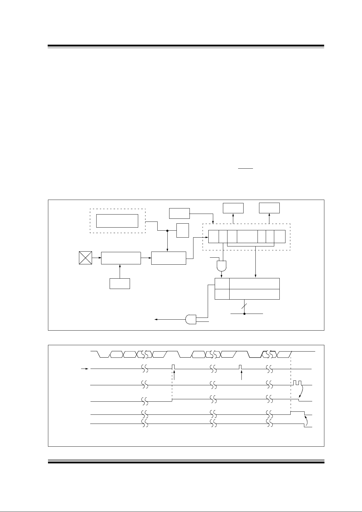
1999 Microchip Technology Inc.
Preliminary DS30569A-page 69
PIC16F870/871
9.2.2 USART ASYNCHRONOUS RECEIVER
The receiver b loc k diagr am is shown in Figure 9-4. The
data is received on the RC7/RX/DT pin and drives the
data recovery block. The data recovery block is actually
a high speed shifter operating at x16 times the baud
rate, whereas the main receive serial shifter oper ates at
the bit rate or at F
OSC.
Once asynchronous mode is selected, reception is
enabled by setting bit CREN (RCSTA<4>).
The heart of the receiver i s the receiv e (serial) shi ft register (RSR). After sampling the STOP bit, the received
data in the RSR is transferred to the RCREG register (if
it is empty). If the transfer is complete, flag bit RCIF
(PIR1<5>) is set. The actual interrupt can be enabled/
disabled b y setting/clearing enab le bit RCIE (PIE1<5 >).
Flag bit RCIF is a read only bit which is cleared by the
hardware. It is cleared when the RCREG register has
been read and is empty. The RCREG is a double buffered register (i.e. it is a two deep FIFO). It is possible
for two bytes of data to be received and transferred to
the RCREG FIFO and a third byte to begin shifting to
the RSR register. On the detection of the STOP bit of
the third byte, if the RCREG register is still full, the overrun error bit OERR (RCSTA<1>) will be set. The word
in the RSR will be lost. The RCREG register can be
read twice to retrieve the two bytes in the FIFO. Overrun bit OERR has to be cleared in software. This is
done by resetting the receive logic (CREN is cleared
and then set). If bit OERR is set, transfers from the
RSR register to the RCREG register are inhibited, so it
is essential to clear error bit OERR if it is set. Framing
error bit FERR (RCSTA<2>) is set if a stop bit is
detected as clear. Bit FERR and the 9th receive bit are
buffered the same way as the receive data. Reading
the RCREG will load bits RX9D and FERR with new
values, therefore it is essential for the user to read the
RCSTA register before
reading RCREG register in
order not to lose th e o ld FERR an d RX 9 D information.
FIGURE 9-4: USART RECEVE BLOCK DIAGRAM
FIGURE 9-5: ASYNCHRONOUS RECEPTION
x64 Baud Rate CLK
SPBRG
Baud Rate Generator
RC7/RX/DT
Pin Buffer
and Control
SPEN
Data
Recovery
CREN
OERR
FERR
RSR register
MSb
LSb
RX9D
RCREG Register
FIFO
Interrupt
RCIF
RCIE
Data Bus
8
÷
64
÷
16
or
Stop
Start
(8)
7
1
0
RX9
• • •
Start
bit
bit7/8
bit1bit0
bit7/8 bit0Stop
bit
Start
bit
Start
bit
bit7/8
Stop
bit
RX (pin)
reg
Rcv buffer reg
Rcv shift
Read Rcv
buffer reg
RCREG
RCIF
(interrupt flag)
OERR bit
CREN
WORD 1
RCREG
WORD 2
RCREG
Stop
bit
Note: This timing diagram shows three words appearing on the RX input. The RCREG (receive buffer) is read after the third word,
causing the OERR (overrun) bit to be set.

PIC16F870/871
DS30569A-page 70 Preliminary
1999 Microchip Technology Inc.
Steps to follow when setting up an Asynchronous
Reception:
1. Initialize the SPBRG registe r for the appropriate
baud rate. If a high speed baud rate is desired,
set bit BRGH. (Section 9.1).
2. Enable the asynchronous serial port by clearing
bit SYNC and setting bit SPEN.
3. If interrupts are desired, then set enable bit
RCIE.
4. If 9-bit reception is desired, then set bit RX9.
5. Enable the reception by setting bit CREN.
6. Flag bit RCIF will be set w he n rec ept ion is com plete and an interrupt will be gener ated if e nabl e
bit RCIE is set.
7. Read the RCSTA register to get the ninth bit (if
enabled) and determine if any error occurred
during reception.
8. Read the 8-bit received data by reading the
RCREG register.
9. If any error occurred, clear the error by clearing
enable bit CREN.
TABLE 9-6: REGISTERS ASSOCIATED WITH ASYNCHRONOUS RECEPTION
Address Name Bit 7 Bit 6 B it 5 Bit 4 Bit 3 Bit 2 Bit 1 Bit 0
Value on:
POR,
BOR
Value on
all other
Resets
0Ch PIR1
PSPIF
(1)
ADIF RCIF TXIF
—
CCP1IF TMR2IF TMR1IF 0000 -000 0000 -000
18h RCSTA SPEN RX9
SREN CREN — FERR OERR RX9D 0000 -00x 0000 -00x
1Ah RCREG USART Receive Register 0000 0000 0000 0000
8Ch PIE1
PSPIE
(1)
ADIE RCIE TXIE — CCP1IE TMR2IE TMR1IE 0000 -000 0000 -000
98h TXSTA
CSRC TX9 TXEN SYNC —BRGHTRMT TX9D 0000 -010 0000 -010
99h SPBRG Baud Rate Generator Register 0000 0000 0000 0000
Legend: x = unknown, - = unimplemented locations read as '0'. Shaded cells are not used for asynchronous reception.
Note 1: Bits PSPIE and PSPIF are reserved on the PIC16F870; always maintain these bits clear.
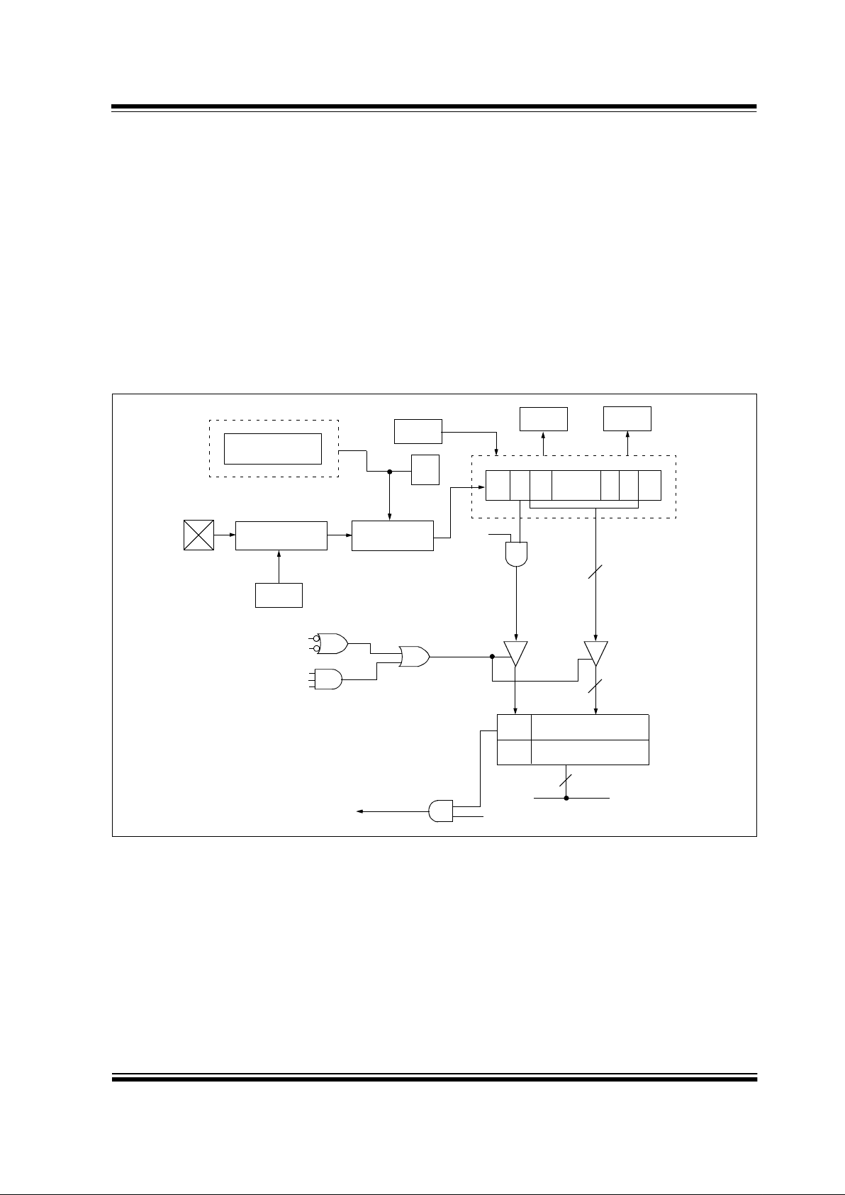
1999 Microchip Technology Inc.
Preliminary DS30569A-page 71
PIC16F870/871
9.2.3 SETTING UP 9-BIT MODE WITH ADDRESS
DETECT
Steps to follow when setting up an Asynchronous
Reception with Address Detect Enabled:
• Initialize the SPBRG register for the appropriate
baud rate. If a hi gh speed baud r ate is desired , set
bit BRGH.
• Enable the asynchronous serial port by clearing
bit SYNC and setting bit SPEN.
• If interrupts are desired, then set enable bit RCIE.
• Set bit RX9 to enable 9-bit reception.
• Set ADDEN to enable address detect.
• Enable the reception by setting enable bit CREN.
• Flag bit RCIF will be set when reception is complete, and an interrupt will be generated if enable
bit RCIE was set.
• Read the RCSTA register to get the ninth bit and
determine if any error occurred during reception.
• Read the 8-bit received data by reading the
RCREG register, to determine if the device is
being addressed.
• If any error occurred, clear the error by clearing
enable bit CREN.
• If the device has been addressed, clear the
ADDEN bit to allow data bytes and address bytes
to be read into the receiv e b uff er, and interrupt the
CPU.
FIGURE 9-6: USART RECEIVE BLOCK DIAGRAM
x64 Baud Rate CLK
SPBRG
Baud Rate Generator
RC7/RX/DT
Pin Buffer
and Control
SPEN
Data
Recovery
CREN
OERR
FERR
RSR register
MSb
LSb
RX9D
RCREG Register
FIFO
Interrupt
RCIF
RCIE
Data Bus
8
÷ 64
÷ 16
or
Stop
Start
(8)
7
1
0
RX9
• • •
RX9
ADDEN
RX9
ADDEN
RSR<8>
Enable
Load of
Receive
Buffer
8
8

PIC16F870/871
DS30569A-page 72 Preliminary
1999 Microchip Technology Inc.
FIGURE 9-7: ASYNCHRONOUS RECEPTION WITH ADDRESS DETECT
FIGURE 9-8: ASYNCHRONOUS RECEPTION WITH ADDRESS BYTE FIRST
TABLE 9-7: REGISTERS ASSOCIATED WITH ASYNCHRONOUS RECEPTION
Address Name Bit 7 Bit 6 Bit 5 Bit 4 Bit 3 Bit 2 Bit 1 Bit 0
Val ue on :
POR,
BOR
Value on
all other
Resets
0Ch PIR1
PSPIF
(1)
ADIF RCIF TXIF — CCP1IF TMR2IF TMR1IF 0000 -000 0000 -000
18h RCSTA SPEN RX9
SREN CREN ADDEN FERR OERR RX9D 0000 000x 0000 000x
1Ah RCREG USART Receive Register 0000 0000 0000 0000
8Ch PIE1
PSPIE
(1)
ADIE RCIE TXIE — CCP1IE TMR2IE TMR1IE 0000 -000 0000 -000
98h TXSTA
CSRC TX9 TXEN SYNC —BRGHTRMT TX9D 0000 -010 0000 -010
99h SPBRG Baud Rate Generator Register 0000 0000 0000 0000
Legend: x = unknown, - = unimplemented locations read as '0'. Shaded cells are not used for Asynchronous Reception.
Note 1: Bits PSPIE and PSPIF are reserved on the PIC16F870; always maintain these bits clear.
Start
bit
bit1bit0
bit8 bit0Stop
bit
Start
bit bit8
Stop
bit
RC7/RX/DT (pin)
Load RSR
Read
RCIF
WORD 1
RCREG
Bit8 = 0, Data Byte B it8 = 1, Address Byt e
Note: This timing diagram shows a data byte followed by an address byte. The data byte is not read into the RCREG
(receive buffer) because ADDEN = 1.
Start
bit
bit1bit0
bit8 bit0Stop
bit
Start
bit bit8
Stop
bit
RC7/RX/DT (pin)
Load RSR
Read
RCIF
WORD 1
RCREG
Bit8 = 1, Address Byte Bit8 = 0, Data Byte
Note: This timing diagram shows a data byte followed by an address byte. The data byte is not read into the RCREG
(receive buffer) because ADDEN was not updated and still = 0.

1999 Microchip Technology Inc.
Preliminary DS30569A-page 73
PIC16F870/871
9.3 USART Synchronous Master Mode
In Synchronous Mas ter mode , the data i s transmitte d in
a half-duplex manne (i.e., transmission and reception
do not occur at the sam e time). When tran smitting data,
the reception is inhibited and vice versa. Synchronous
mode is entered by setting bit SYNC (TXSTA<4>). In
addition, enable bit SPEN (RCSTA<7>) is set in order
to configure the RC6/TX/CK and RC7/RX/DT I/O pins
to CK (clock) and DT (data) lines respectively. The
Master mode in dicates tha t the p rocessor transm its the
master clock on the CK line. The Master mode is
entered by setting bit CSRC (TXSTA<7>).
9.3.1 USART SYNCHRONOUS MASTER
TRANSMISSION
The USART transmitter block diagram is shown in
Figure 9-6. The heart of the transmitter is the transmit
(serial) shift register (TSR). The shi ft register obtains it s
data from the read/write transmit buffer register
TXREG. The TXREG register is loaded with data in
software. The TSR register is not loaded until the last
bit has been transmitted from the previous load. As
soon as the last bit is transmitted, the TSR is loaded
with new data from the TXREG (if available). Once the
TXREG regis ter tran sfers th e dat a t o th e T SR re gist er
(occurs in one Tcycle), the TXREG is empty and interrupt bit TXIF (PIR1<4>) is set. The interrupt can be
enabled/disabled by setting/clearing enable bit TXIE
(PIE1<4>). Flag bit TXIF will be set regardless of the
state of enable bit TXIE and cannot be cleared in software. It will reset only when ne w data is l oaded into th e
TXREG register. While flag bit TXIF indicates the status
of the TXREG register, another bit TRMT (TXSTA<1>)
shows the status of the TSR register. TRMT is a read
only bit which is set when the TSR is empty. No interrupt logic is tied to this bit, so the user has to poll this
bit in order to determ ine if the TSR re gister is empt y.
The TSR is not mapped in data memory, so it is not
available to the user.
Transmission is enabled by setting enable bit TXEN
(TXSTA<5>). The actual transmission will not occur
until the TXREG register has been loaded with data.
The first data bit wi ll be shifted out on the ne xt a v ailab le
rising edge of the clock on the CK line. Data out is stable around the falling edge of the synchronous clock
(Figure 9-9). The transmission can also be started by
first loading the TXREG register and then setting bit
TXEN (Figure 9-10). This is advantageous when slow
baud rates are selec ted , s inc e th e BR G is kept in reset
when bits TXEN, CREN and SREN are clear. Setting
enable bit TXEN will start the BRG, creating a shift
clock immediately. Normally, when transmission is first
started, the TSR register is empty, so a transfer to the
TXREG register will result in an immediate transfer to
TSR resulting in an empty TXREG. Back-to-back transfers are possible.
Clearing enable bit TXEN during a transmission will
cause the transmiss ion to be ab orted and will reset the
transmitter. The DT and CK pins will re v ert to hi-im pedance. If either bit CREN or bit SREN is set during a
transmission, the transmission is aborted and the DT
pin reverts to a hi-impedance state (for a reception).
The CK pin will remain an output if bit CSRC is set
(internal clock). The transmitter logic, however, is not
reset, although it is disconnected fr om the pins. In ord er
to reset the transmitter, the user has to clear bit TXEN.
If bit SREN is set (to i nterrupt an on -going tr ansmissio n
and receive a s ingle word ), then after t he single word is
received, bit SREN will be cleared and the serial port
will revert back to transmitting, since bit TXEN is still
set. The DT line will immediately switch from hi-impedance receive mode to transmit and start driving. To
avoid this, bit TXEN should be cleared.
In order to select 9-bit transmission, the TX9
(TXSTA<6>) bit should be set and the ninth bit should
be written to bit TX9D (TXSTA<0>). The ninth bit must
be written before writing the 8-bit data to the TXREG
register . This is because a dat a write to the TXREG can
result in an immediate transfer of the data to the TSR
register (if the TSR is empty). If the TSR was empty and
the TXREG was written before writing the “new” TX9D,
the “present” value of bit TX9D is loaded.
Steps to follow when setting up a Synchronous Master
Transmission:
1. Initialize the SPBRG register for the appropriate
baud rate (Section9.1).
2. Enable the synchronous master serial port by
setting bits SYNC, SPEN and CSRC.
3. If interrupts are desired, set enable bit TXIE.
4. If 9-bit transmission is desired, set bit TX9.
5. Enable the transmission by setting bit TXEN.
6. If 9-bit transmission is selected, the ninth bit
should be loaded in bit TX9D.
7. Start transmission by loading data to the
TXREG register.

PIC16F870/871
DS30569A-page 74 Preliminary
1999 Microchip Technology Inc.
TABLE 9-8: REGISTERS ASSOCIATED WITH SYNCHRONOUS MASTER TRANSMISSION
FIGURE 9-9: SYNCHRONOUS TRANSMISSION
FIGURE 9-10: SYNCHRONOUS TRANSMISSION (THROUGH TXEN)
Address Name Bit 7 Bit 6 B it 5 Bit 4 B it 3 Bit 2 Bit 1 Bi t 0
Val ue on :
POR,
BOR
Value on all
other Resets
0Ch PIR1
PSPIF
(1)
ADIF RCIF TXIF — CCP1IF TMR2IF TMR1IF 0000 -000 0000 -000
18h RCSTA SPEN
RX9 SREN CREN — FERR OERR RX9D 0000 -00x 0000 -00x
19h TXREG USART Transmit Register 0000 0000 0000 0000
8Ch PIE1
PSPIE
(1)
ADIE RCIE TXIE — CCP1IE TMR2IE TMR1IE 0000 -000 0000 -000
98h TXSTA CSRC TX9 TXEN SYNC
— BRGH TRMT TX9D 0000 -010 0000 -010
99h SPBRG Baud Rate Generator Register 0000 0000 0000 0000
Legend: x = unknown, - = unimplemented, read as '0'. Shaded cells are not used for synchronous master transmission.
Note 1: Bits PSPIE and PSPIF are reserved on the PIC16F870; always maintain these bits clear.
bit 0 bit 1 bit 7
WORD 1
Q1Q2Q3Q4Q1 Q2Q3 Q4Q1Q2Q3Q4Q1 Q2Q3Q4Q1Q2 Q3Q4 Q3Q4 Q1Q2 Q3Q4 Q1Q2Q3Q4Q1Q2 Q3 Q4Q1Q2Q3 Q4Q1 Q2Q3Q4Q1 Q2Q3 Q4
bit 2 bit 0 bit 1 bit 7
RC7/RX/DT pin
RC6/TX/CK pin
Write to
TXREG reg
TXIF bit
(Interrupt flag)
TRMT
TXEN bit
’1’ ’1’
Note: Sync master mode; SPBRG = '0'. Continuous transmission of two 8-bit words
WORD 2
TRMT bit
Write word1
Write word2
RC7/RX/DT pin
RC6/TX/CK pin
Write to
TXREG reg
TXIF bit
TRMT bit
bit0
bit1
bit2
bit6 bit7
TXEN bit

1999 Microchip Technology Inc.
Preliminary DS30569A-page 75
PIC16F870/871
9.3.2 USART SYNCHRONOUS MASTER
RECEPTION
Once synchronous mode is selected, reception is
enabled b y setting either enab le bit SREN (RCSTA<5>)
or enable bit CREN (RCSTA<4>). Data is sampled on
the RC7/RX/DT pin on the falling edge of the clock. If
enable bit SREN is set, then only a single word is
received. If enable bit CREN is set, the reception is
continuous until CREN is cleared. If both bits are set,
CREN takes preced ence. After cloc king the las t bit, the
received data in the Receive Shif t Register (RSR) is
transferred to the RCREG register (if it is empty). When
the transfer is complete, interrupt flag bit RCIF
(PIR1<5>) is set. The actual interrupt can be enabled/
disabled b y setting/clearing enab le bit RCIE (PIE1<5 >).
Flag bit RCIF is a read only bit, which is reset by the
hardware. In t his case, it is reset when t he RCREG register has been read and is empty. The RCREG is a double buffered register (i.e., it is a two deep FIFO). It is
possible for two bytes of d ata to be received and tran sferred to the RCREG FIFO and a third byte to begin
shifting into the R SR register . On th e clocking of the last
bit of the third byte, if the RCREG register is still full,
then overrun error bi t OERR (RCS TA<1>) is set. The
word in the RSR will be lost. The RCREG register can
be read twice to retrieve the two bytes in the FIFO. Bit
OERR has to be cl eared in software (by clear ing bit
CREN). If bit OERR is set, transfers from the RSR to
the RCREG are inhibited, so it is essential to clear bit
OERR if it is set. The ninth receive bit is buffered the
same way as the receive data. Reading the RCREG
register will load bit RX9D wi th a new v alue , theref or e it
is essential for the user to read the RCSTA register
before reading RCREG in order not to lose the old
RX9D information.
Steps to follow when setting up a Synchronous Master
Reception:
1. Initialize the SPBRG register for the appropriate
baud rate. (Section 9.1)
2. Enable the synchronous master serial port by
setting bits SYNC, SPEN and CSRC.
3. Ensure bits CREN and SREN are clear.
4. If interrupts are desired, then set enable bit RCIE.
5. If 9-bit reception is desired, then set bit RX9.
6. If a single reception is required, set bit SREN.
For continuous reception set bit CREN.
7. Interrupt flag bit RCIF will be set when receptio n
is complete and an interrupt will be generated if
enable bit RCIE was set.
8. Read the RCSTA register to get the ninth bit (if
enabled) and determine if any error occurred
during reception.
9. Read the 8-bit received data by reading the
RCREG register.
10. If any error occurred, clear the error by clearing
bit CREN.
TABLE 9-9: REGISTERS ASSOCIATED WITH SYNCHRONOUS MASTER RECEPTION
FIGURE 9-11: SYNCHRONOUS RECEPTION (MASTER MODE, SREN)
Address Name Bit 7 Bit 6 Bit 5 Bit 4 Bit 3 Bit 2 Bit 1 Bit 0
Value on:
POR,
BOR
Value on all
other Resets
0Ch PIR1
PSPIF
(1)
ADIF RCIF TXIF — CCP1IF TMR2IF TMR1IF 0000 -000 0000 -000
18h RCSTA SPEN RX9
SREN CREN — FERR OERR RX9D 0000 -00x 0000 -00x
1Ah RCREG USART Receive Register 0000 0000 0000 0000
8Ch PIE1
PSPIE
(1)
ADIE RCIE TXIE — CCP1IE TMR2IE TMR1IE 0000 -000 0000 -000
98h TXSTA CSRC
TX9 TXEN SYNC — BRGH TRMT TX9D 0000 -010 0000 -010
99h SPBRG Baud Rate Generator Register 0000 0000 0000 0000
Legend: x = unknown, - = unimplemented read as '0'. Shaded cells are not used for synchronous master reception.
Note 1: Bits PSPIE and PSPIF are reserved on the PIC16F870; always maintain these bits clear.
CREN bit
RC7/RX/DT pin
RC6/TX/CK pin
Write to
bit SREN
SREN bit
RCIF bit
(interrupt)
Read
RXREG
Note: Timing diagram demonstrates SYNC master mode with bit SREN = '1' and bit BRG = '0'.
Q3Q4 Q1 Q2Q3 Q4 Q1Q2 Q3 Q4Q2 Q1Q2Q3 Q4Q1 Q2Q3Q4 Q1Q2 Q3 Q4Q1 Q2Q3Q4 Q1 Q2 Q3Q4Q1 Q2 Q3Q4 Q1Q2 Q3Q4
’0’
bit0 bit1 bit2 bit3 bit4 bit5 bit6 bit7
’0’
Q1Q2 Q3 Q4

PIC16F870/871
DS30569A-page 76 Preliminary
1999 Microchip Technology Inc.
9.4 USART Synchronous Slave Mode
Synchronous sla v e mo de dif f ers fro m the M aster mod e
in the fact that the shift clock is supplied externally at
the RC6/TX/CK pin (inste ad of being suppl ied internally
in master mode). This allows the device to transfer or
receive data while in SLEEP mode. Slave mode is
entered by clearing bit CSRC (TXSTA<7>).
9.4.1 USART SYNCHRONOUS SLAVE
TRANSMIT
The operation of the synchronous master and slave
modes are identical except in the case of the SLEEP
mode.
If two words are written to the TXREG and then the
SLEEP instruction is executed, the following will occur:
a) The first word will immediately transfer to the
TSR register and transmit.
b) The second word will remain in TXR EG register .
c) Flag bit TXIF will not be set.
d) When the first word has been shifted o ut of TSR,
the TXREG register will transfer the second
word to the TSR and flag bit TXIF will now be
set.
e) If enable bit TXIE is set, the interrupt will wake
the chip from SLEEP and if the global interrupt
is enabled, the program will branch to the inter-
rupt vector (0004h).
Steps to follow when setting up a Synchronous Slave
Transmission:
1. Enable the synchron ous sla v e serial port by set-
ting bits SYNC and SPEN and clearing bit
CSRC.
2. Clear bits CREN and SREN.
3. If interrupts are desired, then set enable bit
TXIE.
4. If 9-bit transmission is desired, then set bit TX9.
5. Enable the transmission by setting enable bit
TXEN.
6. If 9-bit transmission is selected, the ninth bit
should be loaded in bit TX9D.
7. Start transmission by loading data to the
TXREG register.
9.4.2 USART SYNCHRONOUS SLAVE
RECEPTION
The operation of the synchronous master and slave
modes is identical, except in the case of the SLEEP
mode. Bit SREN is a “don't care” in slave mode.
If receive is enabled by setting bit CREN prior to the
SLEEP instruction, then a word may be received during
SLEEP. On completely receiving the word, the RSR
register will transfer the data to the RCREG register
and if enable bit RCIE bit is set, the interrupt generate d
will wake the chip from SLEEP. If the global interrupt is
enabled, the p rog ram will branch to the interrupt vector
(0004h).
Steps to follow when setting up a Synchronous Slave
Reception:
1. Enable the synchronous master serial port by
setting bits SYNC and SPEN and clearing bit
CSRC.
2. If interrupts are desired, set enable bit RCIE.
3. If 9-bit reception is desired, set bit RX9.
4. To enable reception, set enable bit CREN.
5. Flag bit RCIF will be set w he n rec ept ion is com -
plete and an interrupt will be generated, if
enable bit RCIE was set.
6. Read the RCSTA register to get the ninth bit (if
enabled) and determine if any error occurred
during reception.
7. Read the 8-bit received data by reading the
RCREG register.
8. If any error occurred, clear the error by clearing
bit CREN.

1999 Microchip Technology Inc.
Preliminary DS30569A-page 77
PIC16F870/871
TABLE 9-10: REGISTERS ASSOCIATED WITH SYNCHRONOUS SLAVE TRANSMISSION
TABLE 9-11: REGISTERS ASSOCIATED WITH SYNCHRONOUS SLAVE RECEPTION
Address Name Bit 7 Bit 6 Bit 5 Bit 4 Bit 3 Bit 2 Bit 1 Bit 0
Val ue on :
POR,
BOR
Value on all
other Resets
0Ch PIR1
PSPIF
(1)
ADIF RCIF TXIF — CCP1IF TMR2IF TMR1IF 0000 -000 0000 -000
18h RCSTA SPEN
RX9 SREN CREN ADDEN FERR OERR RX9D 0000 000x 0000 000x
19h TXREG USART Transmit Register 0000 0000 0000 0000
8Ch PIE1
PSPIE
(1)
ADIE RCIE TXIE — CCP1IE TMR2IE TMR1IE 0000 -000 0000 -000
98h TXSTA CSRC TX9 TXEN SYNC
— BRGH TRMT TX9D 0000 -010 0000 -010
99h SPBRG Baud Rate Generator Register 0000 0000 0000 0000
Legend: x = unknown, - = unimplemented read as '0'. Shaded cells are not used for Synchronous Slave Transmission.
Note 1: Bits PSPIE and PSPIF are reserved on the PIC16F870; always maintain these bits clear.
Address Name Bit 7 Bit 6 Bit 5 Bit 4 Bit 3 Bit 2 Bit 1 Bit 0
Value on:
POR,
BOR
Value on all
other Resets
0Ch PIR1
PSPIF
(1)
ADIF RCIF TXIF — CCP1IF TMR2IF TMR1IF 0000 -000 0000 -000
18h RCSTA SPEN RX9
SREN CREN ADDEN FERR OERR RX9D 0000 000x 0000 000x
1Ah RCREG USART Receive Register 0000 0000 0000 0000
8Ch PIE1
PSPIE
(1)
ADIE RCIE TXIE — CCP1IE TMR2IE TMR1IE 0000 -000 0000 -000
98h TXSTA CSRC
TX9 TXEN SYNC — BRGH TRMT TX9D 0000 -010 0000 -010
99h SPBRG Baud Rate Generator Register 0000 0000 0000 0000
Legend: x = unknown, - = unimplemented read as '0'. Shaded cells are not used for Synchronous Slave Reception.
Note 1: Bits PSPIE and PSPIF are reserved on the PIC16F870, always maintain these bits clear.

PIC16F870/871
DS30569A-page 78 Preliminary
1999 Microchip Technology Inc.
NOTES:

1999 Microchip Technology Inc.
Preliminary DS30569A-page 79
PIC16F870/871
10.0 ANALOG-TO-DIGITAL
CONVERTER (A/D) MODULE
The Analog-to-Digital (A/D) Converter module has five
inputs for the PIC16 F870 and ei ght f or the PIC 16F87 1.
The analog input charges a sample and hold capacitor.
The output of the sample and hold capacitor is the
input into the converter. The converter then generates
a digital result of this analog level via successive
approximation. The A/D conversion of the analog input
signal results in a corresponding 10-bit digital number.
The A/D module has high and low voltage reference
input that is software selectable to some combination
of V
DD, VSS, RA2 or RA3.
The A/D conv erter has a unique f eature of being ab le to
operate while the de vice is in SLEEP mode. To operate
in sleep, the A/D clock must be derived from the A/D’s
internal RC oscillator.
The A/D module has four registers. These registers
are:
• A/D Result High Register (ADRESH)
• A/D Result Low Register (ADRESL)
• A/D Control Register0 (ADCON0)
• A/D Control Register1 (ADCON1)
The ADCON0 register, shown in Register 10-1, controls the operation of the A/D module. The ADCON1
register, shown in Register 10-2, configures the functions of the port pins. The port pins can be configured
as analog inputs (RA3 can also be the voltage reference) or as digital I/O.
Additional inf o rmation on us ing the A/D mo dul e c an b e
found in the PICmicro™ Mid-Range MCU Family Reference Manual (DS33023).
REGISTER 10-1: ADCON0 REGISTER (ADDRESS: 1Fh)
R/W-0 R/W-0 R/W-0 R/W-0 R/W-0 R/W-0 U-0 R/W-0
ADCS1 ADCS0 CHS2 CHS1 CHS0 GO/DONE
— ADON R = Readable bit
W = Writable bit
U = Unimplemented bit,
read as ‘0’
- n = Value at POR reset
bit7 bit0
bit 7-6: ADCS1:ADCS0: A/D Conversion Clock Select bits
00 = F
OSC/2
01 = F
OSC/8
10 = F
OSC/32
11 = F
RC (clock derived from an RC oscillation)
bit 5-3: CHS2:CHS0: Analog Channel Select bits
000 = channel 0, (RA0/AN0)
001 = channel 1, (RA1/AN1)
010 = channel 2, (RA2/AN2)
011 = channel 3, (RA3/AN3)
100 = channel 4, (RA5/AN4)
101 = channel 5, (RE0/AN5)
(1)
110 = channel 6, (RE1/AN6)
(1)
111 = channel 7, (RE2/AN7)
(1)
bit 2: GO/DONE: A/D Conversion Status bit
If ADON = 1
1 = A/D conversion in progress (setting this bit starts the A/D conversion)
0 = A/D conversion not in progress (This bit is automatically cleared by hardware when the A/D conversion is complete)
bit 1: Unimplemented: Read as '0'
bit 0: ADON: A/D On bit
1 = A/D converter module is operating
0 = A/D converter module is shutoff and consumes no operating current
Note 1: These channels are not available on the PIC16F870.

PIC16F870/871
DS30569A-page 80 Preliminary
1999 Microchip Technology Inc.
REGISTER 10-2: ADCON1 REGISTER (ADDRESS 9Fh)
U-0 U-0 R/W-0 U-0 R/W-0 R/W-0 R/W-0 R/W-0
ADFM
— — — PCFG3 PCFG2 PCFG1 PCFG0 R = Readable bit
W = Writable bit
U = Unimplemented bit,
read as ‘0’
- n = Value at POR reset
bit7 bit0
bit 7: ADFM: A/D Result format select
1 = Right Justified. 6 most significant bits of ADRESH are read as ‘0’.
0 = Left Justified. 6 least significant bits of ADRESL are read as ‘0’.
bit 6-4: Unimplemented: Read as ’0’
bit 3-0: PCFG3:PCFG0: A/D Port Configuration Control bits
A = Analog input
D = Digital I/O
Note 1: These channels are not available on the PIC16F870.
2: This column indicates the number of analog channels available as A/D inputs and the numer of analog channels
used as voltage reference inputs.
PCFG3:
PCFG0
AN7
(1)
RE2
AN6
(1)
RE1
AN5
(1)
RE0
AN4
RA5
AN3
RA3
AN2
RA2
AN1
RA1
AN0
RA0
V
REF+VREF-
C
HAN /
Refs
(2)
0000 AAAAA AAAVDD VSS 8/0
0001 AAAAV
REF+AAARA3VSS 7/1
0010 DDDA A AAAV
DD VSS 5/0
0011 DDDAV
REF+AAARA3VSS 4/1
0100 DDDD A DAAV
DD VSS 3/0
0101 DDDDV
REF+D A A RA3VSS 2/1
011x DDDD D DDDV
DD VSS 0/0
1000 AAAAV
REF+VREF-A A RA3RA2 6/2
1001 DDAAA AAAV
DD VSS 6/0
1010 DDAAV
REF+AAARA3VSS 5/1
1011 DDAAV
REF+VREF-A A RA3RA2 4/2
1100 DDDAV
REF+VREF-A A RA3RA2 3/2
1101 DDDDV
REF+VREF-A A RA3RA2 2/2
1110 DDDD D DDAV
DD VSS 1/0
1111 DDDDV
REF+VREF-D A RA3RA2 1/2

1999 Microchip Technology Inc.
Preliminary DS30569A-page 81
PIC16F870/871
The ADRESH:ADRESL registers contain the 10-bit
result of the A/D conversion. When the A/D conversion
is complete, the result is loaded into this A/D result register pair, the GO/DONE
bit (ADCON0<2>) is cleared
and the A/D interrupt flag bit ADIF i s set. The b loc k diagram of the A/D module is shown in Figure 10-1.
After the A/D module has been configured as desired,
the selected channel must be acquired before the conversion is started. The analog input channels must
have their corresponding TRIS bits selected as inputs.
To determine sample time, see Section 10.1. After this
acquisition time has elapsed, the A/D conversion can
be started. The following steps should be followed for
doing an A/D conversion:
1. Confi gure the A/D module:
• Configure analog pins / voltage reference /
and digital I/O (ADCON1)
• Select A/D input channel (ADCON0)
• Select A/D conversion clock (ADCON0)
• Turn on A/D module (ADCON0)
2. Confi gure A/D interrupt (if desired):
• Clear ADIF bit
• Set ADIE bit
• Set GIE bit
3. Wait the required acqu is iti on tim e .
4. Start conversion:
• Set GO/DONE
bit (ADCON0)
5. Wait for A/D conversion to complete, by either:
• Polling for the GO/DONE bit to be cleared
OR
• Waiting for the A/D interrupt
6. Read A/D Result register pair
(ADRESH:ADRESL), clear bit ADIF if required.
7. For next conversion, go to step 1 or step 2 as
required. The A/D conversion time per bit is
defined as T
AD. A minimum wait of 2TAD is
required before next acquisition starts.

PIC16F870/871
DS30569A-page 82 Preliminary
1999 Microchip Technology Inc.
FIGURE 10-1: A/D BLOCK DIAGRAM
10.1 A
/D Acquisition Requirements
For the A/D converter to meet its specified accuracy,
the charge holding capacitor (C
HOLD) must be allowed
to fully charge to the input channel voltage level. The
analog input model is shown in Figure 10-2. The
source impedance (R
S) and the internal sampling
switch (R
SS) impedance directly affect the time
required to charge the capacitor C
HOLD. The sampling
switch (R
SS) impedance varies over the device voltage
(V
DD), Figure 10-2. The maximum recommended
impedance for analog sources is 10 kΩ. As the
impedance is decreased, the acquisition time may be
decreased. After the analog input channel is selected
(changed), this acquisition must be done before the
conversion can be started.
To calculate the minimum acquisition time,
Equation 10-1 may be used. This equation assumes
that 1/2 LSb error is used (1024 step s f or the A/D). Th e
1/2 LSb error is the max im um erro r all o wed for the A/D
to meet its specified resolution.
To calculate the minimum acquisition time, T
ACQ, see
the PICmicro™ Mid-Range Reference Manual
(DS33023).
(Input voltage)
V
AIN
VREF+
(Reference
voltage)
V
DD
PCFG3:PCFG0
CHS2:CHS0
RE2/AN7
(1)
RE1/AN6
(1)
RE0/AN5
(1)
RA5/AN4
RA3/AN3/V
REF+
RA2/AN2/V
REF-
RA1/AN1
RA0/AN0
111
110
101
100
011
010
001
000
A/D
Converter
Note 1: Not available on PIC16F870.
VREF-
(Reference
voltage)
V
SS
PCFG3:PCFG0

1999 Microchip Technology Inc.
Preliminary DS30569A-page 83
PIC16F870/871
EQUATION 10-1: ACQUISITION TIME
FIGURE 10-2: ANALOG INPUT MODEL
TACQ
TC
TACQ
=
=
=
=
=
=
=
=
Amplifier Settling Time +
Hold Capacitor Charging Tim e +
Temperature Coefficient
T
AMP + TC + TCOFF
2µS + TC + [(Temperature -25°C)(0.05µS/°C)]
C
HOLD (RIC + RSS + RS) In(1/2047)
- 120pF (1kΩ + 7kΩ + 10kΩ) In(0.0004885)
16.47µS
2µS + 16.47µS + [(50°C -25×C)(0.05µS/×C)
19.72µS
Note 1: The reference voltage (VREF) has no effect on the equation, since it cancels itself out.
2: The charge holding capacitor (C
HOLD) is not discharged after each conversion.
3: Th e maximum r ecommended impedance f or analog so urces is 10 kΩ. This is required to meet the pin leak-
age specification.
4: After a conversion has completed, a 2.0T
AD delay must complete before acquisition can begin again.
During this time, the holding capacitor is not connected to the selected A/D input channel.
CPIN
VA
R
S
ANx
5 pF
V
DD
VT = 0.6V
V
T = 0.6V
I LEAKAGE
RIC ≤ 1k
Sampling
Switch
SS
R
SS
CHOLD
= DAC capacitance
V
SS
6V
Sampling Switch
5V
4V
3V
2V
5 6 7 8 9 1011
( kΩ )
VDD
= 120 pF
± 500 nA
Legend CPIN
VT
I LEAKAGE
RIC
SS
C
HOLD
= input capacitance
= threshold voltage
= leakage current at the pin due to
= interconnect resistance
= sampling switch
= sample/hold capacitance (from DAC)
various junctions

PIC16F870/871
DS30569A-page 84 Preliminary
1999 Microchip Technology Inc.
10.2 Selecting the A/D Conversion Clock
The A/D conversion time per bit is defined as TAD. The
A/D conversion requires a minimum 12T
AD per 10-bit
conversion. The source of the A/D conversion clock is
software selected. The four possible options for T
AD
are:
•2T
OSC
•8TOSC
•32TOSC
• Internal RC oscillator
For correct A/D conversions, the A/D conversion clock
(TAD) must be select ed to ens ure a minimu m TAD time
of 1.6 µs.
Table 10-1shows the resultant TAD times derived from
the device operating frequencies and the A/D clock
source selected.
TABLE 10-1: TAD vs. MAXIMUM DEVICE OPERATING FREQUENCIES (STANDARD DEVICES (C))
10.3 Configuring Analog Port Pins
The ADCON1, and TRIS registers control the operation
of the A/D port pins. The port pins that are desired as
analog inputs must have their corresponding TRIS bits
set (input). If the TRIS bit is cleared (output), the digital
output level (V
OH or VOL) will be converted.
The A/D operation is independent of the state of the
CHS2:CHS0 bits and the TRIS bits.
AD Clock Source (TAD) Maximum Device Frequenc y
Operation ADCS1:ADCS0 Max.
2T
OSC 00 1.25 MHz
8TOSC 01 5 MHz
32TOSC 10 20 MHz
RC
(1, 2, 3)
11 Note 1
Note 1: The RC source has a typical TAD time of 4 µs but can vary between 2-6 µs.
2: When the device frequencies are greater than 1 MHz, the RC A/D conversion clock source is only recommended for sleep
operation.
3: For extended voltage devices (LC), please refer to the Electrical Specifications section.
Note 1: When reading the port register, any pin
configured as an a nalog inpu t ch ann el wil l
read as cleared (a low level). Pins configured as dig ital in puts w il l conver t an a nalog input. Analog levels on a digitally
configured input will not affect the conversion accuracy.
2: An alog le v els on any pi n that is defined as
a digital input (including the AN7:AN0
pins), may cause the input buffer to consume current that is out of the device
specifications.

1999 Microchip Technology Inc.
Preliminary DS30569A-page 85
PIC16F870/871
10.4 A/D Conversions
Clearing the GO/DONE bit during a conversion will
abort the current conversion. The A/D result register
pair will NOT be updated with the partially completed
A/D conversion sample. That is, the
ADRESH:ADRESL registers will continue to contain
the value of the last completed conversion (or the last
value written to the ADRESH:ADRESL registers).
After the A/D conversion is aborted, a 2T
AD wait is
required before the next acquisition is started. After
this 2TAD wait, acquisition on the selected channel is
automatically started.
In Figure 10-3, after the GO bit is set, the first time se gmant has a minimum of T
CY and a maximu m of TAD.
FIGURE 10-3: A/D CONVERSION TAD CYCLES
Note: The GO/DONE bit should NOT be set in
the same instruction that turns on the A/D.
TAD1
TAD2
TAD3
TAD4
TAD5 TAD6
TAD7 TAD8
TAD9
Set GO bit
Holding capacitor is disconnected from analog input (typically 100 ns)
b9 b8 b7 b6 b5 b4 b3 b2
TAD10 TAD11
b1 b0
TCY to TAD
Conversion Starts
ADRES is loaded,
GO bit is cleared,
ADIF bit is set,
holding capacitor is connected to analog input.

PIC16F870/871
DS30569A-page 86 Preliminary
1999 Microchip Technology Inc.
10.4.1 A/D RESULT REGISTERS
The ADRESH:ADRESL register pair is the location
where the 10-bit A/D result is loaded at the completion
of the A/D conversion. This register pair is 16-bits
wide. The A/D module gives the fle xibility to left or right
justify the 10-bit result in the 16-bit result register. The
A/D Format Select bit (ADFM) controls this justification. Figure 10-4 shows the operation of the A/D result
justification. The extra bits are loaded with ’0’s’. When
an A/D result will not overwrite these locations (A/D
disable), these registers may be used as two general
purpose 8-bit registers.
10.5 A/D Operation During Sleep
The A/D module can oper ate during SLEEP mode . This
requires that the A/D clock source be set to RC
(ADCS1:ADCS0 = 11). When the RC clock source is
selected, the A/D module waits one instruction cycle
before starting the conversion. This allows the SLEEP
instruction to be executed, which eliminates all digital
switching no ise from the con v e rsion. Wh en the con version is completed the GO/DONE
bit will be cleared and
the result loaded into the ADRES register. If the A/D
interrupt is enabled, the device will wake-up from
SLEEP. If the A/D interrupt is not enabled, the A/D module will then be turned off, although the ADON bit will
remain set.
When the A/D cloc k sou rce is a nother c loc k o ption (n ot
RC), a SLEEP instruction will cause the present con v ersion to be aborted and the A/D modul e to be turned off ,
though the ADON bit will remain set.
Turning off the A/D places the A/D module in its lowest
current consumption state.
10.6 Effects of a Reset
A device reset forces all registers to their reset state.
This forces the A/D module to be turned off, and any
conve rsi on is abo rted.
The value that is in the ADRESH:ADRESL registers is
not modified for a Power-on Reset. The
ADRESH:ADRESL registers wil l contain unknow n data
after a Power-on Reset.
FIGURE 10-4: A/D RESULT JUSTIFICATION
Note: For the A/D module to operate in SLEEP,
the A/D clock source must be set to RC
(ADCS1:ADCS0 = 11). To allow the conversion to occur during SLEEP, ensure the
SLEEP instruction immediately follows the
instruction that sets the GO/DONE
bit.
10-Bit Result
ADRESH ADRESL
0000 00
ADFM = 0
0
2 1 0 77
10-bit Result
ADRESH ADRESL
10-bit Result
0000 00
7
0 7 6 5 0
ADFM = 1
Right Justified
Left Justified

1999 Microchip Technology Inc.
Preliminary DS30569A-page 87
PIC16F870/871
TABLE 10-2: REGISTERS/BITS ASSOCIATED WITH A/D
Addr Name Bit 7 Bit 6 Bit 5 Bit 4 Bit 3 Bit 2 Bit 1 Bit 0
POR,
BOR
MCLR
,
WDT
0Bh INTCON GIE PEIE T0IE INTE RBIE T0IF INTF RBIF 0000 000x 0000 000u
0Ch PIR1
PSPIF
(1)
ADIF RCIF TXIF — CCP1IF TMR2IF TMR1IF 0000 -000 0000 -000
8Ch PIE1
PSPIE
(1)
ADIE RCIE TXIE — CCP1IE TMR2IE TMR1IE 0000 -000 0000 -000
1Eh ADRESH A/D Result Register High Byte xxxx xxxx uuuu uuuu
9Eh ADRESL A/D Result Register Low Byte xxxx xxxx uuuu uuuu
1Fh ADCON0 ADCS1 A DCS0 CHS2 CHS1 CHS0 GO/DONE
—ADON0000 00-0 0000 00-0
9Fh ADCON1 ADFM
— — — PCFG3 PCFG2 PCFG1 PCFG0 --0- 0000 --0- 0000
85h TRISA
— — PORT A Data Direction Register --11 1111 --11 1111
05h PORTA
— — PORTA Data Latch when written: PORTA pins when read --0x 0000 --0u 0000
89h
(1)
TRISE IBF OBF IBOV PSPMODE — PORTE Data Direction Bits 0000 -111 0000 -111
09h
(1)
PORTE — — — — — RE2 RE1 RE0 ---- -xxx ---- -uuu
Legend: x = unknown, u = unchanged, - = unimplemented read as '0'. Shaded cells are not used for A/D conversion.
Note 1: These register s/bits are not available on the PIC16F870.

PIC16F870/871
DS30569A-page 88 Preliminary
1999 Microchip Technology Inc.
NOTES:

1999 Microchip Technology Inc.
Preliminary DS30569A-page 89
PIC16F870/871
11.0 SPECIAL FEATURES OF THE
CPU
These devic es hav e a hos t of fe atures in tended to ma ximize system reliability, minimize cost through elimination of external components, provide power saving
operating modes and o ffer code protection. These a re:
• OSC Selection
• Reset
- Power-on Reset (POR)
- P o w e r-up Tim er (PWRT)
- Oscillator Start-up Timer (OST)
- Brown-out Reset (BOR)
• Interrupts
• Watchdog Timer (WDT)
• SLEEP
• Code protection
• ID locations
• In-Circuit Serial Programming
• Low Voltage In-Circuit Serial Programming
• In-Circuit Debugger
These devices have a watchdog timer, which can be
shut off only through configuration bits. It runs off its
own RC oscillator for added reliability. There are two
timers that offer necessary delays on power-up. One i s
the Oscillator Start-up Timer (OST), intended to keep
the chip in reset un til the c rystal oscilla tor is st able . The
other is the Power-up Timer (PWR T), wh ic h provides a
fixed delay of 72 ms (nominal) on power-up only. It is
designed to kee p the pa rt in reset while the po we r supply stabilizes. With these two timers on-chip, most
applications need no external reset circuitry.
SLEEP mode is designed to offer a very low current
power-down mode. The user can wake-up from SLEEP
through external reset, Watchdog Timer Wake-up, or
through an interrupt. Se v er al oscil lator opt ions are also
made available to allow the part to fit the application.
The RC oscillator option saves system cost while the
LP crystal option saves power. A set of configuration
bits are used to select various options.
Additional inf ormation on special f eatures is a vail able in
the PICmicro™ Mid-Range Reference Manual,
(DS33023).
11.1 Configuration Bits
The configurati on bits can be prog ra mmed (read as '0')
or left unprogrammed (read as '1') to select various
device configurations. These bits are mapped in program memory location 2007h.
The user will note that address 2007h is beyond the
user program memory space. In fact, it belongs to the
special test/configuration memory space (2000h 3FFFh), whic h can be ac cessed on ly dur ing pro gramming.

PIC16F870/871
DS30569A-page 90 Preliminary
1999 Microchip Technology Inc.
REGISTER 11-1: CONFIGURATION WORD
CP1 CP0 DEBUG — WRT CPD LVP BODEN CP1 CP0 PWRTE WDTE F0SC1 F0SC0 Register: CONFIG
Address 2007h
bit13 bit0
bit 13-12:
bit 5-4: CP<1:0>: Flash Program Memory Code Protection bits
(2)
11 = Code protection off
10 = Not supported
01 = Not supported
00 = Code protection on
bit 11: DEBUG: In-Circuit Debugger Mode
1 = In-Circuit Debugger disabled, RB6 and RB7 are general purpose I/O pins.
0 = In-Circuit Debugger enabled, RB6 and RB7 are dedicated to the debugger.
bit 10: Unimplemented: Read as ‘1’
bit 9: WRT: Flash Program Memory Write Enable
1 = Unprotected program memory may be written to by EECON control
0 = Unprotected program memory may not be written to by EECON control
bit 8: CPD: Data EE Memory Code Protection
1 = Code protection off
0 = Data EEPROM memory code protected
bit 7: LV P: Low Voltage In-Circuit Serial Programming Enable bit
1 = RB3/PGM pin has PGM function, low voltage programming enabled
0 = RB3 is digital I/O, HV on MCLR
must be used for programming
bit 6: BODEN: Brown-out Reset Enable bit
(1)
1 = BOR enabled
0 = BOR disabled
bit 3: PW RTE
: Power-up Timer Enable bit
(1)
1 = PWRT disabled
0 = PWRT enabled
bit 2: WDTE: Watchdog Timer Enable bit
1 = WDT enabled
0 = WDT disabled
bit 1-0: FOSC1:FOSC0: Oscillator Selection bits
11 = RC oscillator
10 = HS oscillator
01 = XT oscillator
00 = LP oscillator
Note 1: Enabling Brown-out Reset automatically enables Power-up Timer (PWRT), regardless of the value of bit PWRTE
. Ensure
the Power-up Timer is enabled anytime Brown-out Reset is enabled.
2: All of the CP<1:0> pairs have to be given the same value to enable the code protection scheme listed.

1999 Microchip Technology Inc.
Preliminary DS30569A-page 91
PIC16F870/871
11.2 Oscillator Configurations
11.2.1 OSCILLATOR TYPES
The PIC16F870/871 can be operated in four different
oscillator mode s . T he user can program two c on fig uration bits (FOSC1 and FOSC0) to select one of these
four modes:
• LP Low Power Crystal
• XT Crystal/Resonator
• HS High Speed Crystal/Resonator
• RC Resistor/Capacitor
11.2.2 CRYSTAL OSCILLATOR/CERAMIC
RESONATORS
In XT, LP or HS modes, a crystal or ceramic resonator
is connected to the OSC1/CLKIN and OSC2/CLKOUT
pins to establish oscillation (Figure 11-1). The
PIC16F870/871 oscillator design requires the use of a
parallel cut crystal. Use of a se ries cut c rystal may give
a frequency out of the crystal manufacturers specifications. When in XT, LP or HS modes, the device can
have an external clock source to drive the OSC1/
CLKIN pin (Figure 11-2).
FIGURE 11-1: CRYSTAL/CE RAMI C
RESONATOR OPERATION
(HS, XT OR LP
OSC CONFIGURATION)
FIGURE 11-2: EXTERNAL CLOCK INPUT
OPERATION (HS, XT OR LP
OSC CONFIGURATION)
TABLE 11-1: CERAMIC RESONATORS
Note 1: See Table 11-1 and Table 11-2 for rec-
ommended values of C1 and C2.
2: A series resistor (RS) may be required
for AT strip cut crystals.
3: RF varies with the crystal chosen.
C1
(1)
C2
(1)
XTAL
OSC2
OSC1
RF
(3)
SLEEP
To
logic
PIC16F870/871
RS
(2)
internal
OSC1
OSC2
Open
Clock from
ext. system
PIC16F870/871
Ranges Tested:
Mode Freq OSC1 OSC2
XT 455 kHz
2.0 MHz
4.0 MHz
68 - 100 pF
15 - 68 pF
15 - 68 pF
68 - 100 pF
15 - 68 pF
15 - 68 pF
HS 8 .0 MHz
16.0 MHz
10 - 68 pF
10 - 22 pF
10 - 68 pF
10 - 22 pF
These values are for design guidance only. See
notes at bottom of page.
Resonators Used:
455 kHz Panasonic EFO-A455K04B ± 0.3%
2.0 MHz Murata Erie CSA2.00MG ± 0.5%
4.0 MHz Murata Erie CSA4.00MG ± 0.5%
8.0 MHz Murata Erie CSA8.00MT ± 0.5%
16.0 MHz Murata Erie CSA16.00MX ± 0.5%
All resonators used did not have built-in capacitors.

PIC16F870/871
DS30569A-page 92 Preliminary
1999 Microchip Technology Inc.
TABLE 11-2: CAPACITOR SELECTION FOR
CRYSTAL OSCILLATOR
11.2.3 RC OSCIL LATOR
For timing insensitive applications, the “RC” device
option offers additional cost savings. The RC oscillator
frequency is a function of the supply voltage, the resistor (R
EXT) and capacitor (CEXT) values, and th e ope rat-
ing temperature. In addition to this, the oscillator
frequency will vary from unit to unit due to normal process parameter variation. Furthermore, the difference
in lead frame capacitance between package types will
also affect the oscillation frequency, especially for low
C
EXT values. The user also needs to take into account
variation du e to to leranc e of exter nal R and C com ponents used. Figure 11-3 shows how the R/C combination is connected to the PIC16F870/871.
FIGURE 11-3: RC OSCILLATOR MODE
Osc Type
Crystal
Freq
Cap. Range
C1
Cap.
Range
C2
LP 32 kHz 33 pF 33 pF
200 kHz 15 pF 15 pF
XT 200 kHz 47-68 pF 47-68 pF
1 MHz 15 pF 15 pF
4 MHz 15 pF 15 pF
HS 4 MHz 15 pF 15 pF
8 MHz 15-33 pF 15-33 pF
20 MHz 15-33 pF 15-33 pF
These values are for design guidance only.
See notes at bottom of page.
Crystals Used
32 kHz Epson C-001R32.768K-A ± 20 PPM
200 kHz STD XTL 200.000 kHz ± 20 PPM
1 MHz ECS ECS-10-13-1 ± 50 PPM
4 MHz ECS ECS-40-20-1 ± 50 PPM
8 MHz EPSON CA-301 8.000M-C ± 30 PPM
20 MHz EPSON CA-301 20.000M-C ± 30 PPM
Note 1: Higher capacitance increases the stability
of oscillator b ut also increa ses the start-up
time.
2: Since each resonator/crystal has its own
characteristics, the user should consult
the resonator/crystal manufacturer for
appropriate values of external components.
3: Rs may be required in HS mode, as well
as XT mode, t o avoid overdr i vi n g crystals
with low drive level specification.
4: When migrating from other PICmicro
devices, oscillator performance should be
verified.
OSC2/CLKOUT
Cext
Rext
PIC16F870/871
OSC1
F
OSC/4
Internal
Clock
VDD
VSS
Recommended values: 3 kΩ ≤ Rext ≤ 100 k
Ω
Cext > 20pF

1999 Microchip Technology Inc.
Preliminary DS30569A-page 93
PIC16F870/871
11.3 Reset
The PIC16F870/871 differentiates between various
kinds of reset:
• Power-on Reset (POR)
•MCLR
reset during normal operation
•MCLR reset during SLEEP
• WDT Reset (during normal operation)
• WDT Wake-up (during SLEEP)
• Brown-out Reset (BOR)
Some registers are not affected in any reset condition.
Their status is unknown on POR and unchanged in an y
other reset. Most other registers are reset to a “reset
state” on Power-on Reset (POR), on the MCLR
and
WDT Reset, on MCLR
reset during SLEEP, and Brownout Reset (BOR). They are not affected by a WDT
Wake-up, which is viewed as the resumption of normal
operation. The T O
and PD bits are set or cleared diff erently in different reset situations as indicated in
Table 11-4. These bits are used in software to determine the nature of the reset. See Table 11-6 for a full
description of reset states of all registers.
A simplified bloc k diag ram of the on-ch ip res et circui t is
shown in Figure 11-4.
These devices have a MCLR
noise filter in the MCLR
reset path. The filter wi ll detect and igno re small pulses .
It should be noted that a WDT Reset
does not drive
MCLR
pin low.
FIGURE 11-4: SIMPLIFIED BLOCK DIAGRAM OF ON-CHIP RESET CIRCUIT
S
RQ
External
Reset
MCLR
VDD
OSC1
WDT
Module
V
DD rise
detect
OST/PWRT
On-chip
RC OSC
WDT
Time-out
Power-on Reset
OST
10-bit Ripple counter
PWRT
Chip_Reset
10-bit Ripple counter
Reset
Enable OST
Enable PWRT
SLEEP
Note 1: This is a separate oscillator from the RC oscillator of the CLKIN pin.
Brown-out
Reset
BODEN
(1)

PIC16F870/871
DS30569A-page 94 Preliminary
1999 Microchip Technology Inc.
11.4 Power-On Reset (POR)
A Power-on Reset pulse is generated on-chip when
V
DD rise is detected (in the range of 1.2V - 1.7V). To
take advantage of the POR, tie the MCLR
pin directly
(or through a resistor) to V
DD. This will eliminate exter-
nal RC compone nts u sua ll y n ee ded to create a P oweron Reset. A maximum rise time for VDD is specified.
See Electrical Specifications for details.
When the device starts normal operation (exits the
reset condition), device operating param ete rs (voltage,
frequency , te mperature ,...) must be met t o ensure operation. If these conditions are not met, the device must
be held in reset until the operating conditions are met.
Brown-out Reset may be used to meet the start-up conditions. For additional information, refer to Application
Note, AN007, “Power-up Trouble Shooting”,
(DS00007).
11.5 Power-up Timer (PWRT)
The Power-up Timer provides a fixed 72 ms nominal
time-out on power-up only from the POR. The Powerup Timer operates on an internal RC oscillator. The
chip is kept in re set a s long as th e PWR T i s act iv e . The
PWRT’s time delay allows V
DD to rise to an acceptable
level. A configuration bit is provided to enable/disable
the PWRT.
The power-up time de la y will v ary from chip to chip due
to V
DD, temperature and process variation. See DC
parameters for details (T
PWRT, parameter #33).
11.6 Oscillator Start-up Timer (OST)
The Oscillator Start-up Timer (OST) provides 1024
oscillator cycle (from OSC1 input) delay after the
PWRT dela y is o v er. This ensures that t he crystal oscillator or resonator has started and stabilized.
The OST time-out is invoked only for XT, LP and HS
modes and only on Power-on Reset or wake-up from
SLEEP.
11.7 Brown-Out Reset (BOR)
The configuration b it, BODEN, ca n enable or di sable
the Brown-out Reset cir cuit. If V
DD falls below VBOR
(parameter D005, about 4V) for longer than TBOR
(parameter #35, a bout 100µS), the brown-out si tuation will reset the device. If V
DD falls below VBOR for
less than T
BOR, a reset may not occur.
Once the brown-out occu rs, the device will rem ain in
brown-out reset until V
DD rises above VBOR. The
power-up timer then keeps the device in reset for
TPWRT (parameter #33, about 72mS). If VDD should
fall below V
BOR during TPWRT, the brown-out reset
process will restar t when V
DD rises above VBOR with
the power-up timer reset. The power-up timer is
always enabled when the brown-out reset circuit is
enabled regardless of the state of the PWRT configuration bit.
11.8 Time-out Sequence
On power-up, the time-out sequence is as follows: The
PWRT delay starts (if enabled) when a POR reset
occurs. Then OST starts counting 1024 oscillator
cycles when PWRT ends (LP, XT, HS). When the OST
ends, the device comes out of RESET.
If MCLR
is kept low long enough, the time-outs will
expire. Bringing MCLR
high will begin execution im m e-
diately . This is useful f or testing pu rposes or to synchronize more than one PIC16CXX device operating in
parallel.
Table 11-5 shows the reset conditions for the STATUS,
PCON and PC registers, while Table 11-6 shows the
reset conditions for all the registers.
11.9 P ower Control/Status Register
(PCON)
The Power Control/Status Register, PCON, has up to
two bits depending upon the device.
Bit0 is Brown-out Reset Status bit, BOR
. Bit BOR is
unknown on a Power-on Reset. It must then be set by
the user and ch eck ed o n subse quent res ets to s ee if b it
BOR
cleared, indicating a BOR occurred. The BOR bit
is a "don’t care" bit and is not nece ssarily predic tabl e if
the Brown-out Reset circuitry is disabled (by clearing
bit BODEN in the Configuration Word).
Bit1 is POR
(Power-on Reset Status bit). It is cleared on
a Power-on Reset and unaffected otherwise. The user
must set this bit following a Power-on Reset.

1999 Microchip Technology Inc.
Preliminary DS30569A-page 95
PIC16F870/871
TABLE 11-3: TIME-OUT IN VARIOUS SITUATIONS
TABLE 11-4: STATUS BITS AND THEIR SIGNIFICANCE
TABLE 11-5: RESET CONDITION FOR SPECIAL REGISTERS
Oscillator Configuration Power-up Brown-out Wake-up from
SLEEP
PWRTE
= 0 PWRTE = 1
XT, HS, LP 72 ms + 1024TOSC 1024TOSC 72 ms + 1024TOSC 1024TOSC
RC 72 ms —72 ms —
POR BOR TO PD
0x11Power-on Reset
0x0xIllegal, TO
is set on POR
0xx0Illegal, PD is set on POR
1011Brown-out Reset
1101WDT Reset
1100WDT Wake-up
11uuMCLR
Reset during norm al operation
1110MCLR Reset during SLEEP or interrupt wake-up from SLEEP
Condition
Program
Counter
STATUS
Register
PCON
Register
Power-on Reset 000h 0001 1xxx ---- --0x
MCLR
Reset during normal operation 000h 000u uuuu ---- --uu
MCLR Reset during SLEEP 000h 0001 0uuu ---- --uu
WDT Reset 000h 0000 1uuu ---- --uu
WDT Wake-up PC + 1 uuu0 0uuu ---- --uu
Brown-out Reset 000h 0001 1uuu ---- --u0
Interrupt wake-up from SLEEP PC + 1
(1)
uuu1 0uuu ---- --uu
Legend: u = unchanged, x = unknow n, - = unimplemented bit read as '0'.
Note 1: When the wake-up is due to an interrupt and the GIE bit is set, the PC is loaded with the interrupt vector
(0004h).

PIC16F870/871
DS30569A-page 96 Preliminary
1999 Microchip Technology Inc.
TABLE 11-6: INITIALIZATION CONDITIONS FOR ALL REGISTERS
Register Devices Power-on Reset,
Brown-out Reset
MCLR Resets
WDT Reset
Wake-up via WDT or
Interrupt
W 870 871 xxxx xxxx uuuu uuuu uuuu uuuu
INDF 870 871 N/A N/A N/A
TMR0 870 871 xxxx xxxx uuuu uuuu uuuu uuuu
PCL 870 871 0000h 0000h PC + 1
(2)
STATUS 870 871 0001 1xxx 000q quuu
(3)
uuuq quuu
(3)
FSR 870 871 xxxx xxxx uuuu uuuu uuuu uuuu
PORTA 870 871 --0x 0000 --0u 0000 --uu uuuu
PORTB 870 871 xxxx xxxx uuuu uuuu uuuu uuuu
PORTC 870 871 xxxx xxxx uuuu uuuu uuuu uuuu
PORTD
870 871 xxxx xxxx uuuu uuuu uuuu uuuu
PORTE
870 871 ---- -xxx ---- -uuu ---- -uuu
PCLATH 870 871 ---0 0000 ---0 0000 ---u uuuu
INTCON 870 871 0000 000x 0000 000u uuuu uuuu
(1)
PIR1 870 871 r000 -000 r000 -000 ruuu -uuu
(1)
870 871 0000 -000 0000 -000 uuuu -uuu
(1)
PIR2 870 871 ---0 ---- ---0 ---- ---u ----
(1)
TMR1L 870 871 xxxx xxxx uuuu uuuu uuuu uuuu
TMR1H 870 871 xxxx xxxx uuuu uuuu uuuu uuuu
T1CON 870 871 --00 0000 --uu uuuu --uu uuuu
TMR2 870 871 0000 0000 0000 0000 uuuu uuuu
T2CON 870 871 -000 0000 -000 0000 -uuu uuuu
CCPR1L 870 871 xxxx xxxx uuuu uuuu uuuu uuuu
CCPR1H 870 871 xxxx xxxx uuuu uuuu uuuu uuuu
CCP1CON 870 871 --00 0000 --00 0000 --uu uuuu
RCSTA 870 871 0000 000x 0000 000x uuuu uuuu
TXREG 870 871 0000 0000 0000 0000 uuuu uuuu
RCREG 870 871 0000 0000 0000 0000 uuuu uuuu
ADRESH 870 871 xxxx xxxx uuuu uuuu uuuu uuuu
ADCON0 870 871 0000 00-0 0000 00-0 uuuu uu-u
OPTION_REG 870 871 1111 1111 1111 1111 uuuu uuuu
TRISA 870 871 --11 1111 --11 1111 --uu uuuu
TRISB 870 871 1111 1111 1111 1111 uuuu uuuu
TRISC 870 871 1111 1111 1111 1111 uuuu uuuu
TRISD
870 871 1111 1111 1111 1111 uuuu uuuu
TRISE
870 871 0000 -111 0000 -111 uuuu -uuu
PIE1 870 871 r000 -000 r000 -000 ruuu -uuu
870 871 0000 0000 0000 0000 uuuu uuuu
PIE2 870 871 ---0 ---- ---0 ---- ---u ----
PCON 870 871 ---- --qq ---- --uu ---- --uu
PR2 870 871 1111 1111 1111 1111 1111 1111
TXSTA 870 871 0000 -010 0000 -010 uuuu -uuu
SPBRG 870 871 0000 0000 0000 0000 uuuu uuuu
ADRESL 870 871 xxxx xxxx uuuu uuuu uuuu uuuu
Legend: u = unchanged, x = unknown, - = unimplemented bit, read as ’0’, q = value depends
on condition, r = reserved maintain clear.
Note 1: One or more bits in INTCON, PIR1 and/or PIR2 will be affected (t o cause wake-up).
2: When the wake-up is due to an interrupt and the GIE bit is set, the PC is loaded with the inter-
rupt vector (0004h).
3: See Table 11-5 for reset value for specific condition.

1999 Microchip Technology Inc.
Preliminary DS30569A-page 97
PIC16F870/871
FIGURE 11-5: TIME-OUT SEQUENCE ON POWER-UP (MCLR TIED TO VDD)
FIGURE 11-6: TIME-OUT SEQUENCE ON POWER-UP (MCLR
NOT TIED TO VDD): CASE 1
ADCON1 870 871 0--- 0000 0--- 0000 u--- uuuu
EEDATA 870 871 0--- 0000 0--- 0000 u--- uuuu
EEADR 870 871 xxxx xxxx uuuu uuuu uuuu uuuu
EEDATH 870 871 xxxx xxxx uuuu uuuu uuuu uuuu
EEADRH 870 871 xxxx xxxx uuuu uuuu uuuu uuuu
EECON1 870 871 x--- x000 u--- u000 u--- uuuu
EECON2 870 871 ---- ---- ---- ---- ---- ----
TABLE 11-6: INITIALIZATION CONDITIONS FOR ALL REGISTERS (CONTINUED)
Register Devices Power-on Reset,
Brown-out Reset
MCLR Resets
WDT Reset
Wake-up via WDT or
Interrupt
Legend: u = unchanged, x = unknown, - = unimplemented bit, read as ’0’, q = value depends
on condition, r = reserved maintain clear.
Note 1: One or more bits in INTCON, PIR1 and/or PIR2 will be affected (t o cause wake-up).
2: When the wake-up is due to an interrupt and the GIE bit is set, the PC is loaded with the inter-
rupt vector (0004h).
3: See Table 11-5 for reset value for specific condition.
TPWRT
TOST
VDD
MCLR
INTERNAL POR
PWRT TIME-OUT
OST TIME-OUT
INTERNAL RESET
TPWRT
TOST
VDD
MCLR
INTERNAL POR
PWRT TIME-OUT
OST TIME-OUT
INTERNAL RESET

PIC16F870/871
DS30569A-page 98 Preliminary
1999 Microchip Technology Inc.
FIGURE 11-7: TIME-OUT SEQUENCE ON POWER-UP (MCLR NOT TIED TO VDD): CASE 2
FIGURE 11-8: SLOW RISE TIME (MCLR
TIED TO VDD)
VDD
MCLR
INTERNAL POR
PWRT TIME-OUT
OST TIME-OUT
INTERNAL RESET
T
PWRT
TOST
VDD
MCLR
INTERNAL POR
PWRT TIME-OUT
OST TIME-OUT
INTERNAL RESET
0V
1V
5V
T
PWRT
TOST

1999 Microchip Technology Inc.
Preliminary DS30569A-page 99
PIC16F870/871
11.10 Interrupts
The PIC16F870/871 family has up to 11 sources of
interrupt. The interrupt control register (INTCON)
records individual interrupt requests in flag bits. It also
has individual and global interrupt enable bits.
A global interrupt enable bit, GIE (INTCON<7>)
enables (if set) all un-masked interrupts or disables (if
cleared) all interrupts . W hen bit GIE is enab le d, and a n
interrupt’s fl ag bit and mask bit a re set, the interrupt will
vector immediately. Individual interrupts can be disabled through their corresponding enable bits in various registers. Individual interrupt bits are set
regardless of the status of the GIE bit. The GIE bit is
cleared on reset.
The “return from interrupt” instruction, RETFIE, exits
the interrupt routine, as well as sets the GIE bit, which
re-enables interrupts.
The RB0/INT pin interru pt, the RB port change interrupt
and the TMR0 overflow interrupt flags are contained in
the INTCON register.
The peripheral interrupt flags are contained in the special function regist ers, PIR1 and PIR 2. The corresponding interrupt enable bits are contained in special
function registers, PIE1 and PIE2, and the peripheral
interrupt enable bi t i s co nta ine d i n special function register INTCON.
When an interrupt is responded to, the GIE bit is
cleared to disable any further interrupt, the return
address is pushed o nto the stack and the PC is lo ade d
with 0004h. Once in the interrupt service routine, the
source(s) of the interrupt can be determined by polling
the interrupt flag bits. The interrupt flag bit(s) must be
cleared in software before re-enabling interrupts to
avoid recursive interrupts.
For external interrupt events, such as the INT pin or
PORTB change interrupt, the interrupt latency will be
three or four instruction cycles. The exact latency
depends when the interrupt event occurs. The latency
is the same fo r one or two cycle instructions . Individual
interrupt flag bits are set regardless of the status of
their corresponding mask bit or the GIE bit
FIGURE 11-9: INTERRUPT LOGIC
Note: Individual interrupt flag bits are s et, regard-
less of the status of the ir corresponding
mask bit or the GIE bit.
PSPIF
PSPIE
ADIF
ADIE
RCIF
RCIE
TXIF
TXIE
CCP1IF
CCP1IE
TMR2IF
TMR2IE
TMR1IF
TMR1IE
T0IF
T0IE
INTF
INTE
RBIF
RBIE
GIE
PEIE
Wake-up (If in SLEEP mode)
Interrupt to CPU
The following table s hows which devices have which interrupts.
Device T0IF INTF RBIF PSPIF ADIF RCIF TXIF CCP1IF TMR2IF TMR1IF EEIF
PIC16F870 Yes Yes Yes - Yes Yes Yes Yes Yes Yes Yes
PIC16F871 Yes Yes Yes Yes Yes Yes Yes Yes Yes Yes Yes
EEIF
EEIE

PIC16F870/871
DS30569A-page 100 Preliminary
1999 Microchip Technology Inc.
11.10.1 INT INTERRUPT
External interrupt on the RB0/INT pin is edge trigg ered,
either rising, if bit INTEDG (OPTION_REG<6>) is set,
or falling, if the INTEDG bit is clear. When a valid edge
appears on the RB0/INT pin, flag bit INTF
(INTCON<1>) is set. This interrupt can be disabled by
clearing enable bit INTE (INTCON<4>). Flag bit INTF
must be cleared in softw are i n the in terrupt service routine before re-enabling this interrupt. The INT interrupt
can wake-up the proces sor from SLEE P, if bit INTE w as
set prior to going into SLEEP. The status of globa l interrupt enable bit GIE decides whether or not the processor branches t o th e in t errupt vector follow ing wa ke-up.
See Section 11.13 for details on SLEEP mode.
11.10.2 TMR0 INTERRUPT
An overf l ow (F Fh → 00h) in the TMR0 register will set
flag bit T0IF (INTCON<2>). The interrupt can be
enabled/disabled by setting/clearing enable bit T0IE
(INTCON<5>). (Section 5.0)
11.10.3 PORTB INTCON CHANGE
An input change on PORTB<7:4> sets flag bit RBIF
(INTCON<0>). The interrupt can be enabled/disabled
by setting/clearing enable bit RBIE (INTCON<4>).
(Section 3.2)
11.11 Context Saving During Interrupts
During an interrupt, only the return PC value is saved
on the stac k. Typically, users may wish to s ave key re gisters during an interrupt, (i.e., W register and STATUS
register). This will have to be implemented in software.
Since the upper 16 bytes of each bank are common in
the PIC16F870/871 devices, temporary holding registers W_TEMP, STATUS_TEMP and PCLATH_TEMP
should be placed in here. These 16 locations don’t
require banking and therefore, make it easier for context save and restore. Example 11-1 can be used to
save and restore context for interrupts.
EXAMPLE 11-1: SAVING STATUS, W, AND PCLATH REGISTERS IN RAM
MOVWF W_TEMP ;Copy W to TEMP register
SWAPF STATUS,W ;Swap status to be saved into W
CLRF STATUS ;bank 0, regardless of current bank, Clears IRP,RP1,RP0
MOVWF STATUS_TEMP ;Save status to bank zero STATUS_TEMP register
MOVF PCLATH, W ;Only required if using pages 1, 2 and/or 3
MOVWF PCLATH_TEMP ;Save PCLATH into W
CLRF PCLATH ;Page zero, regardless of current page
:
:(ISR)
:
MOVF PCLATH_TEMP, W ;Restore PCLATH
MOVWF PCLATH ;Move W into PCLATH
SWAPF STATUS_TEMP,W ;Swap STATUS_TEMP register into W
;(sets bank to original state)
MOVWF STATUS ;Move W into STATUS register
SWAPF W_TEMP,F ;Swap W_TEMP
SWAPF W_TEMP,W ;Swap W_TEMP into W
 Loading...