

Microchip Technology Inc PIC16F628-20I-SO, PIC16F627-04-P, PIC16F627-04I-SO, PIC16F627-04I-SS, PIC16F627-20I-P Datasheet
...
PIC16F62X
FLASH-Based 8-Bit CMOS Microcontrollers
Devices included in this data sheet:
• PIC16F627 • PIC16F628
Referred to collectively as PIC16F62X .
High Performance RISC CPU:
• Only 35 instructions to learn
• All single-cycle instructions (200 ns), except for
program branches which are t wo- cy c le
• Operating speed:
- DC - 20 MHz clock input
- DC - 200 ns instruct ion cycle
Memory
Device
PIC16F627 1024 x 14 224 x 8 128 x 8
PIC16F628 2048 x 14 224 x 8 128 x 8
• Interrupt capability
• 16 special function hardware registers
• 8-level deep hardware stack
• Direct, Indirect and Relative ad dressing modes
FLASH
Program
RAM
Data
EEPROM
Data
Peripheral Features:
• 15 I/O pins with individual direction control
• High current sink/source for direct LED drive
• Analog comparator module with:
- Two analog comparators
- Programmable on-chip voltage reference
REF) module
(V
- Programmable input multi plexing fr om device
inputs and internal voltage reference
- Comparator outputs are ext erna lly ac ce ss ibl e
• Timer0: 8-bit timer/counter with 8-bit
programmable prescaler
• Timer1: 16-bit timer/counter with external crystal/
clock capability
• Timer2: 8-bit timer/counter with 8-bit period register, prescaler and postscaler
• Capture, Compare, PWM (CCP) module
- Capture is 16-bit, max. resolution is 12.5 ns
- Compare is 16-bit, max. resolution is 200 ns
- PWM max. resolution is 10-bit
• Universal Synchronous/Asynchronous Receiver/
Transmitter USART/SCI
• 16 Bytes of common RAM
Special Microcontroller Features:
• Power-on Reset (POR)
• Power-up Timer (PWRT) and Oscillator Start-up
Timer (OST)
• Brown-out Detect (BOD)
• Watchdog Timer (WDT) with its own on-chip RC
oscillator for reliable operation
• Multiplexed MCLR
• Programmable weak pull-ups on PORTB
• Programmable code protection
• Low voltage programming
• Power saving SLEEP mode
• Selectab le oscillat or options
- FLASH configuration bits for oscillator options
- ER (External Resistor) oscillator
- Reduced part count
- Dual speed INTRC
- Lower current consumption
- EC External Clock input
- XT oscillator mode
- HS oscillator mode
- LP oscillator mode
• Serial in-circuit programming (via two pins)
• Four user programmable ID locations
-pin
CMOS Technology:
• Low-power, high-speed CMOS FLASH technology
• Fully stat ic design
• Wide operating voltage range
- PIC16F627 - 3.0V to 5.5V
- PIC16F628 - 3.0V to 5.5V
- PIC16LF627 - 2.0V to 5.5V
- PIC16LF628 - 2.0V to 5.5V
• Commercial, industrial and extended temperature
range
• Low power consumption
- < 2.0 mA @ 5.0V, 4.0 MHz
-15 µA typical @ 3.0V, 32 kHz
-< 1.0 µA typical standby current @ 3.0V
1999 Microchip Technology Inc. Preliminary DS40300B-page 1
PIC16F62X
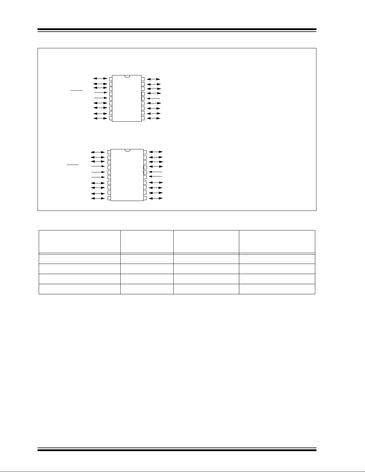
Pin Diagrams
PDIP, SOIC
RA2/AN2/V
RA3/AN3/CMP1
RA4/TOCKI/CMP2
RA5/MCLR
REF
/THV
VSS
RB0/INT
RB1/RX/DT
RB2/TX/CK
RB3/CCP1
•1
2
3
4
5
6
7
8
9
18
PIC16F62X
17
16
15
14
13
12
11
10
RA1/AN1
RA0/AN0
RA7/OSC1/CLKIN
RA6/OSC2/CLKOUT
DD
V
RB7/T1OSI
RB6/T1OSO/T1CKI
RB5
RB4/PGM
SSOP
RA2/AN2/V
RA3/AN3/CMP1
RA4/TOCKI/CMP2
RA5/MCLR
REF
/THV
SS
V
VSS
RB0/INT
RB1/RX/DT
RB2/TX/CK
RB3/CCP1 RB4/PGM
•1
2
3
4
5
6
7
8
9
10
20
19
PIC16F62X
18
17
16
15
14
13
12
11
RA1/AN1
RA0/AN0
RA7/OSC1/CLKIN
RA6/OSC2/CLKOUT
VDD
VDD
RB7/T1OSI
RB6/T1OSO/T1CKI
RB5
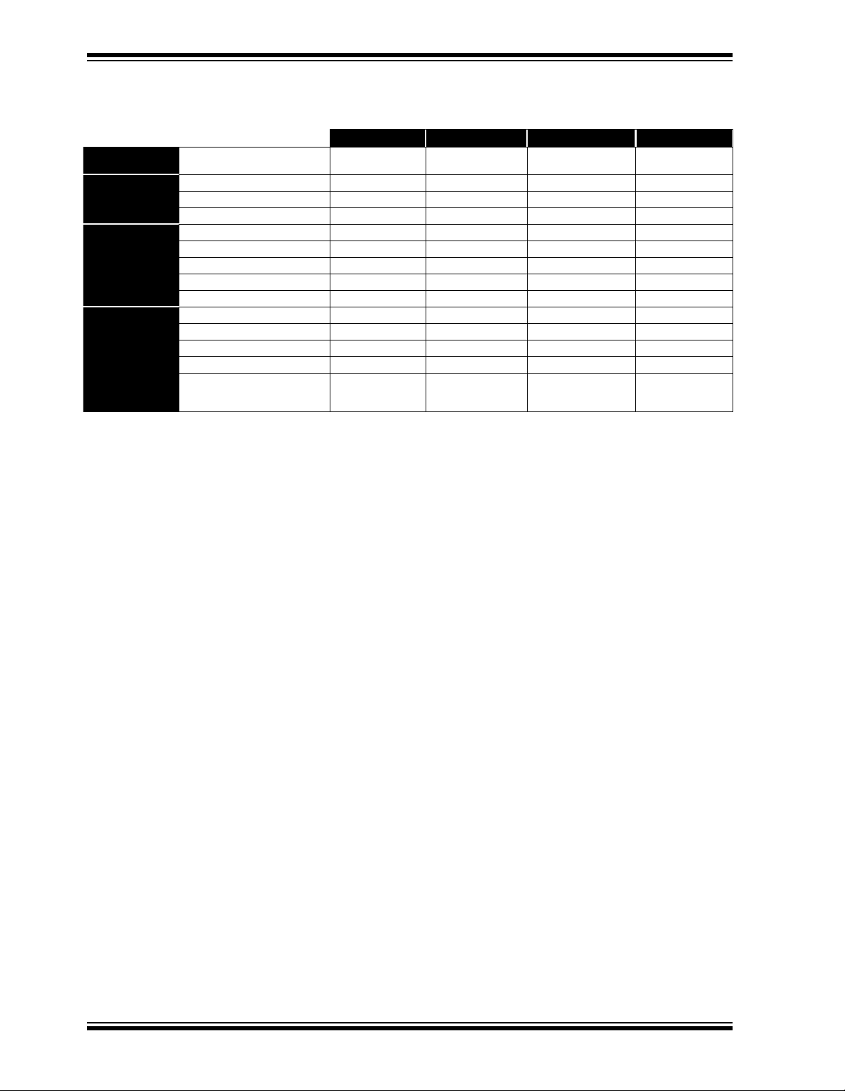
Device Differences
Device
Voltage
Range
Oscillator
PIC16F627 3.0 - 5.5 See Note 1 0.7
Process
Technology
(Microns)
PIC16F628 3.0 - 5.5 See Note 1 0.7
PIC16LF627 2.0 - 5.5 See Note 1 0.7
PIC16LF628 2.0 - 5.5 See Note 1 0.7
Note 1: If you change from this device to another device, please verify oscillator characteristics in your application.
DS40300B-page 2 Preliminary 1999 Microchip Technology Inc.

PIC16F62X
Table of Contents
1.0 General Description.......................................... ........................................ ................................. ............. ......................... ............5
2.0 PIC16F62X Device Varieties......................... ........................... ........................................ ...... ............. ............ .......................... .7
3.0 Architectural Overview................................................................................................................................................................9
4.0 Memory Organization................................................................................................................................................................ 13
5.0 I/O Ports............................... .......................... ......................... ......................... .................................. ......................... ..............27
6.0 Timer0 Module .......................................................................................................................................................................... 45
7.0 Timer1 Module .......................................................................................................................................................................... 50
8.0 Timer2 Module .......................................................................................................................................................................... 54
9.0 Comparator Module.......................................... ........................... ............................................................. ......................... ........ 57
10.0 Capture/Compare/PWM (CCP) Module ................................................. ............................. ...................................................... 63
11.0 Voltage Reference Module.................................................. ........................... ............................................ ......................... ...... 69
12.0 Universal Synchronous Asynchronous Receiver Transmitter (USART).............................. ...................................................... 71
13.0 Data EEPROM Memory.................... ............. ......................... ......................... ................................ ......................... ................ 91
14.0 Special Features of the CPU..................................................................................................................................................... 95
15.0 Instruction Set Summary......................................................................................................................................................... 113
16.0 Development Support.............................................................................................................................................................. 125
17.0 Electrical Specifications...........................................................................................................................................................131
18.0 Device Characterization Information....................................................................................................................................... 145
19.0 Packaging Information........................... ........................................ ........................... ................... .......................... .................. 147
Index............................................................ ............. ......................... ............ ......................................................... ......................... ..151
On-Line Support.................... ........................................ ........................... ............................................................. ............. ................ 155
Reader Response..............................................................................................................................................................................156
PIC16F62X Product Identification System............. ........................... ........................... ............................................................... ...... 157
To Our Valued Customers
Most Current Data Sheet
To obtain the most up-to-date version of this data sheet, please register at our Worldwide Web site at:
http://www.microchip.com
You can determine the version of a data sheet by examining its literature number found on the bottom outside corner of any page.
The last character of the literature number is the version number. e.g., DS30000A is version A of document DS30000.
New Customer Notification System
Register on our web site (www.microchip.com/cn) to receive the most current information on our products.
Errata
An errata sheet may exist for current devices, des cribing minor operational differences (from the data sheet) a nd recommended
workarounds. As device/documentation issues become known to us, we will publish an errata sheet. The errata will specify the revision of silicon and revision of document to which it applies.
To determine if an errata sheet exists for a particular device, please check with one of the following:
• Microchip’s Worldwide Web site; http://www.microchip.com
• Your local Microchip sales office (see last page)
• The Microchip Corporate Literature Center; U.S. FAX: (602) 786-7277
When contacting a sales office or the literature center , please speci fy which device, revision of silicon and data sheet (include liter-
ature number) you are using.
Corrections to this Data Sheet
We constantly strive to improve the quality of all our products and documentation. We have spent a great deal of time to ensure
that this document is correct. However, we realize that we may have missed a few things. If you find any information that is missing
or appears in error, please:
• Fill out and mail in the reader response form in the back of this data sheet.
• E-mail us at webmaster@microchip.com.
We appreciate your assistance in making this a better document.
1999 Microchip Technology Inc. Preliminary DS40300B-page 3

PIC16F62X
NOTES:
DS40300B-page 4 Preliminary 1999 Microchip Technology Inc.

PIC16F62X
1.0 GENERAL DESCRIPTION
The PIC16F62X are 18-Pin FLASH-based mem bers of
the versatile PIC16CXX family of low-cost,
high-performance, CMOS, fully-static, 8-bit
microcontrollers.
®
All PICmicro
RISC architecture. The PIC16F62X have enhanced
core features, eight- level deep stack, and multi ple internal and external interrupt sources. The separate
instruction and data buses of the Harvard architec ture
allow a 14-bit wide instruction word with the separate
8-bit wide data. The two-stage instruction pipeline
allows all instructions to execute in a single-cycle,
except for program branches (which require two
cycles). A total of 35 instructions (reduced instruction
set) are available . Additionally , a large register set gives
some of the architectural in novation s used to achieve a
very high performance.
PIC16F62X microcontrollers typically achieve a 2:1
code compression and a 4:1 speed improvement over
other 8-bit microcontrollers in their class.
PIC16F62X de vices have spec ial features to r educe
external components, thus reducing system cost,
enhancing system reliability and reducing power consumption. There are eight oscillator configurations, of
which the single pin ER oscillator provides a low-cost
solution. The LP os ci ll ator minimizes power consumption, XT is a standard crystal, INTRC is a self-contained
internal oscillator and the HS is for High Speed crystals. The SLEEP (power-down) mode offers power savings. The user can wake up the chip from SLEEP
through several external and internal interrupts and
reset.
A highly reliable Watchdog Timer with its own on-chip
RC oscillator provides protection against software
lock- up.
Table 1-1 shows the features of the PIC16F62X
mid-range mic r o c on t r o l l e r fa m ilies.
A simplified block d iagram of the PIC16F62 X is shown
in Figure 3-1.
The PIC16F62X series fits in applica tions ranging fro m
battery chargers to low-power remote sensors. The
FLASH technology makes customization of applicatio n
programs (detection levels, pulse generation, timers,
etc.) extremely fas t and conv enient. The small foo tprint
packages make this microcontroller series ideal for all
applications with space limitations. Low-cost,
low-power , high-p erformance, eas e of use and I/O flexibility make the PIC16F62X ve ry versatile.
microcontrollers employ an advanced
1.1 Development Support
The PIC16F62X family is supported by a full-featured
macro assembler, a software simulator, an in-circuit
emulator, a low-cost development programmer and a
full-featured programmer. A Third Party “C” compiler
support tool is also available.
1999 Microchip Technology Inc. Preliminary DS40300B-page 5
PIC16F62X
TABLE 1-1: PIC16F62X FAMILY OF DEVICES
PIC16F627 PIC16F628 PIC16LF627 PIC16LF628
Clock
Memory
Peripherals
Features
Maximum Frequency
of Operation (MHz)
FLASH Program Memory (words) 1024 2048 1024 2048
RAM Data Memory (bytes) 224 224 224 224
EEPROM Data Memory (bytes) 128 128 128 128
Timer Module(s) TMR0, TMR1, TMR2 TMR0, TMR1, TMR2 TMR0, TMR1, TMR2 TMR0, TMR1, TMR2
Comparators(s) 2 2 2 2
Capture/Compare/PWM modules 1 1 1 1
Serial Communications USART USART USART USART
Internal Voltage Reference Yes Yes Yes Yes
Interrupt Sources 10 10 10 10
I/O Pins 16 16 16 16
Voltage Range (Volts) 3.0-5.5 3.0-5.5 2.0-5.5 2.0-5.5
Brown-out Detect Yes Yes Yes Yes
Packages 18-pin DIP ,
All PICmicro® Family devices have Power-on Reset, selectable Watchdog Timer, selectable code protect and high I/O current
capability. All P IC 16F62X Family devices use serial programming with clock pin RB6 and data pin RB7.
20 20 20 20
SOIC;
20-pin SSOP
18-pin DIP,
SOIC;
20-pin SSOP
18-pin DIP,
SOIC;
20-pin SSOP
18-pin DIP,
SOIC;
20-pin SSOP
DS40300B-page 6 Preliminary 1999 Microchip Technology Inc.

2.0 PIC16F62X DEVICE VARIETIES
A variety of frequency ranges and packaging options are
available. Depending on application and production
requirements the proper device option can be selected
using the information in the PIC16F62X Product
Identification System section at the end of this data
sheet. When placing orders, please use this page of the
data sheet to specify the correct part number.
2.1 Flash Devices
These devices are offered in the lower cost plastic
package, even though the device can be erased and
reprogrammed. This al lows the same device to be used
for prototype development and pilot programs as well
as production.
A further advantage of the electrically-erasable Flash
version is that it can be erased and reprogrammed
in-circuit, or by device programmers, such as
Microchip’s PICSTART
programmers.
®
Plus or PRO MATE® II
PIC16F62X
2.2 Quick-Turnaround-Production (QTP) Devices
Microchip offers a QTP Programming Service for
factory production orders. This service is made
available for users who chose not to program a medium
to high quantity of un its a nd whose code patterns have
stabilized. The devices are standard FLASH devices
but with all progr am locations and configu ration option s
already pro gramme d by th e fact ory. Certain code and
prototype verification procedures apply before
production shipments are available. Please contact
your Microchip T ec hnology sal es office for more deta ils.
2.3 Serialized Quick-T urnar ound-Production (SQTPSM) Devices
Microchip offers a unique programming service where
a few user-defined locations in each device are
programmed with different serial numbers. The serial
numbers may be random, pseudo-random or
sequential.
Serial programming allows each device to have a
unique number which can serve as an entry-code,
password or ID number.
1999 Microchip Technology Inc. Preliminary DS40300B-page 7

PIC16F62X
NOTES:
DS40300B-page 8 Preliminary 1999 Microchip Technology Inc.

PIC16F62X
3.0 ARCHITECTURAL OVERVIEW
The high performance of the PIC1 6F62X family can be
attributed to a number of architectural features
commonly found in RISC microprocessors. To begin
with, the PIC16F62X uses a Harvard architecture, in
which, program and data are accessed from separate
memories using separate busses. This improves
bandwidth over traditional von Neumann architecture
where program and data are fetched from the same
memory . Separa ting prog ram and data memory furth er
allows instructi ons to be si zed differe ntly than 8-bit wide
data word. Instruction op codes are 14-bits w ide making
it possible to have all single word instructions. A 14-bit
wide program memory access bus fetches a 14-bit
instruction in a single cycle. A two-stage pipeline overlaps fetch and exec ution of instructions. Consequently,
all instructions (3 5) execute in a sing le-cycle (200 ns @
20 MHz) except for program branches.
The Table below lists program memory (Flash, Data
and EEPROM).
Memory
Device
PIC16F627 1024 x 14 224 x 8 128 x 8
PIC16F628 2048 x 14 224 x 8 128 x 8
PIC16LF627 1024 x 14 224 x 8 128 x 8
PIC16LF628 2048 x 14 224 x 8 128 x 8
The PIC16F62X can directly or indirectly address its
register files or data memory. All special function
registers including the program counter are mapped in
the data memory. The PIC16F62X have an orthog onal
(symmetrica l) instruct ion set that m akes it possib le to
carry out any operation on any register using any
addressing mode. This symmetrical nature and lack of
‘special optimal situations’ make programming with the
PIC16F62X simple yet efficient. In addition, the
learning curve is reduced significantly.
FLASH
Program
RAM
Data
EEPROM
Data
The PIC16F62X devices contain an 8-bit ALU and
working register. The ALU is a general purpose
arithmetic unit. It performs arithmetic and Boolean
functions between d ata i n t he w ork ing re gi ste r a nd any
register file.
The ALU is 8-bit wide and capable of addition,
subtraction, shift and logical operations. Unless
otherwise mentioned, arithmetic operations are two's
complement in nature. In two-operand instructions,
typically one operand is the working register
(W register). The other operand is a file register or an
immediate constant . In sin gle ope rand in structi ons, th e
operand is either the W register or a file register.
The W register is an 8-bit working regi ster used for ALU
operations. It is not an addressable register.
Depending on the instruction executed, the ALU may
affect the values of the Carry (C), Digit Carry (DC), and
Zero (Z) bits in the STATUS regi ster . The C and D C bits
operate as a Bo
respectively, bit in subtraction. See the SUBLW and
SUBWF instructions for examples.
A simplified block diagram is shown in Figure 3-1, with
a description of the device pins in Table 3-1.
Two types of data memory are provided on the
PIC16F62X devices. Non-volatile EEPROM data
memory is provided for long term storage of data such
as calibration value s, look up table da ta, and any oth er
data which may require periodic updating in the field.
This data is not lost when po wer is removed. Th e other
data memory provided is regular RAM data memory.
Regular RAM data memory is provide d for tempo rary
storage of data during norm al operati on. It is lost when
power is removed.
rrow and Digit Borrow out bit,
1999 Microchip Technology Inc. Preliminary DS40300B-page 9
PIC16F62X
FIGURE 3-1: BLOCK DIAGRAM
Program
Bus
OSC1/CLKIN
OSC2/CLKOUT
FLASH
Program
Memory
14
Instruction reg
Instruction
Decode &
Control
Timing
Generation
13
Program Counter
8 Level Stack
Direct Addr
8
Power-up
Oscillator
Start-up Timer
Power-on
Watchdog
Brown-out
Low-Voltage
Programming
(13-bit)
Timer
Reset
Timer
Detect
RAM Addr (1)
7
8
Data Bus
Addr MUX
3
RAM
File
Registers
FSR reg
STATUS reg
ALU
W reg
9
8
MUX
8
Indirect
Addr
Data EEPROM
PORTA
PORTB
RA0/AN0
RA1/AN1
RA2/AN2/VREF
RA3/AN3/CMP1
RA4/T0CK1/CMP2
RA5/MCLR
RA6/OSC2/CLKOUT
RA7/OSC1/CLKIN
RB0/INT
RB1/RX/DT
RB2/TX/CK
RB3/CCP1
RB4/PGM
RB5
RB6/T1OSO/T1CKI
RB7/T1OSI
/THV
VDD, VSS
MCLR
Comparator
VREF
Timer0 Timer1 Timer2
CCP1
USART
Memory
Device
FLASH
Program
RAM
Data
EEPROM
Data
PIC16F627 1024 x 14 224 x 8 128 x 8
PIC16F628 2048 x 14 224 x 8 128 x 8
PIC16LF627 1024 x 14 224 x 8 128 x 8
PIC16LF628 2048 x 14 224 x 8 128 x 8
Note 1: Higher order bits are from the STATUS register.
DS40300B-page 10 Preliminary 1999 Microchip Technology Inc.

PIC16F62X
TABLE 3-1: PIC16F62X PINOUT DESCRIPTION
DIP/
Name
RA0/AN0 17 19 I/O ST Bi-directional I/O port/Analog comparator input
RA1/AN1 18 20 I/O ST Bi-directional I/O port/Analog comparator input
RA2/AN2/V
RA3/AN3/CMP1 2 2 I/O ST Bi-directional I/O port/Analog comparator input/compara-
RA4/T0CKI/CMP2 3 3 I/O ST Bi-directional I/O port/Can be configured as T0CKI/com-
RA5/MCLR
RA6/OSC2/CLKOUT 15 17 I/O ST Bi-directional I/O port/Oscillator crystal output. Connects
RA7/OSC1/CLKIN 16 18 I/O ST Bi-directional I/O port/Oscillator crystal input/external
RB0/INT 6 7 I/O
RB1/RX/DT 7 8 I/O TTL/ST
RB2/TX/CK 8 9 I/O TTL/ST
RB3/CCP1 9 10 I/O TTL/ST
RB4/PGM 10 11 I/O TTL/ST
RB5 11 12 I/O TTL Bi-directional I/O port/Wake-up from SLEEP on pin
RB6/T1OSO/T1CKI 12 13 I/O TTL/ST
RB7/T1OSI 13 14 I/O TTL/ST
SS 55,6 P — Ground reference for logic and I/O pins.
V
DD 14 15,16 P — Pos itive supply for logic and I/O pins.
V
REF 1 1 I/O ST Bi-directional I/O port/Analog comparator input/VREF out-
/THV 4 4 I ST In put port/master clear (reset input/programming voltage
SOIC
Pin #
SSOP
Pin #
Legend: O = output I/O = input/output P = power
— = Not used I = Input ST = Schmitt Trigger input
TTL = TTL input I/OD =input/open drain output
Note 1: This buffer is a Schmitt Trigger input when config ured as the external interrupt.
Note 2: This buffer is a Schmitt Trigger input when used in serial programming mode.
Note 3: This buffer is a Schmitt Trigger I/O when used in USART/Synchronous mode.
Note 4: This buffer is a Schmitt Trigger I/O when used in CCP mode.
Note 5: This buffer is a Schmitt Trigger input when used in low voltage program mode.
I/O/P
Type
Buffer
Type
TTL/ST
(3)
(3)
(4)
(5)
(2)
(2)
Description
put
tor output
parator output
input. When configured as MCLR
reset to the device. Voltage on MCLR
exceed V
to crystal or resonator in crystal oscillator mode. In ER
mode, OSC2 pin outputs CLKOUT which has 1/4 the frequency of OSC1, and denotes the instruction cycle rate.
clock source input. ER biasing pin.
(1)
Bi-directional I/O port/external interrupt. Can be software
programmed for internal weak pull-up.
Bi-directional I/O port/ USART receive pin/synchronous
data I/O. Can be software programmed for internal weak
pull-up.
Bi-directional I/O port/ USART transmit pin/synchronous
clock I/O. Can be software programmed for internal weak
pull-up.
Bi-directional I/O port/Capture/Compare/PWM I/O. Can
be software programmed for internal weak pull-up.
Bi-directional I/O port/Low voltage programming input pin.
Wake-up from SLEEP on pin change. Can be software
programmed for internal weak pull-up. When low voltage
programming is enabled, the interrupt on pin change and
weak pull-up resistor are disabled.
change. Can be software programmed for internal weak
pull-up.
Bi-directional I/O port/Timer1 oscillator output/Timer1
clock input. Wake up from SLEEP on pin change. Can be
software programmed for internal weak pull-up.
Bi-directional I/O port/Timer1 oscillator input. Wake up
from SLEEP on pin change. Can be software programmed
for internal weak pull-up.
DD during normal device operation.
, this pin is an active low
/THV must not
1999 Microchip Technology Inc. Preliminary DS40300B-page 11
PIC16F62X
3.1 Clocking Scheme/Instruction Cycle
The clock input (OSC1/CLKIN/RA7 pin) is internally
divided by four to generate four non-overlapping
quadrature clocks namely Q 1, Q2, Q3 and Q4. Internally, the program coun ter (PC) is inc remented ever y
Q1, the instruction is fetched from the program memo ry
and latched into the instruction register in Q4. The
instruction is decoded and executed during the
following Q1 through Q4. The clocks and instruction
execution flow is shown in Figure 3-2.
FIGURE 3-2: CLOCK/INSTRUCTION CYCLE
Q2 Q3 Q4
OSC1
Q1
Q2
Q3
Q4
PC
OSC2/CLKOUT
(ER mode)
Q1
PC PC+1 PC+2
Fetch INST (PC)
Execute INST (PC-1) Fetch INST (PC+1)
Q1
3.2 Instruction Flow/Pipelining
An “Instructi on Cycle” consists of four Q cy cles (Q1,
Q2, Q3 and Q4). The instruc tio n fe tch and ex ecu te a r e
pipelined such that fetch takes one instruction cycle
while decode and execute takes another instruction
cycle. However, due to the pipelining, each instruction
effectively executes in one cycle. If an instruction
causes the program counter to change (e.g., GOTO)
then two cycles a re required to c omplete the i nstruction
(Example 3-1).
A fetch cycle begins with the program counter (PC)
incrementing in Q1.
In the execution cy cle, the fetched instruction i s latched
into the “Instruction Register (IR)” in cycle Q1. This
instruction is then decoded and executed during the
Q2, Q3, and Q4 cycles. Data memory is read duri ng Q2
(operand read) and written during Q4 (destination
write).
Q2 Q3 Q4
Execute INST (PC) Fetch INST (PC+2)
Q2 Q3 Q4
Q1
Execute INST (PC+1)
Internal
phase
clock
EXAMPLE 3-1: INSTRUCTION PIPELINE FLOW
1. MOVLW 55h
2. MOVWF PORTB
3. CALL SUB_1
4. BSF PORTA, BIT3
All instructions are single cycle, except for any program branches. These take two cycles since the fetch
instruction is “flushed” from the pipeline while the new instruction is being fetched and then executed.
DS40300B-page 12 Preliminary 1999 Microchip Technology Inc.
Fetch 1 Execute 1
Fetch 2 Execute 2
Fetch 3 Execute 3
Fetch 4 Flush
Fetch SUB_1 Execute SUB_1
PIC16F62X
4.0 MEMORY ORGANIZATION
4.1 Program Memory Organization
The PIC16F62X has a 13-bi t program c ounter capabl e
of addressing an 8K x 14 program memory space . Only
the first 1K x 14 (0000h - 03FFh) for the PIC16F627
and 2K x 14 (0000h - 07FFh) for the PIC16F628 are
physically implemented. Accessing a location above
these boundaries will cause a wrap-around within the
first 1K x 14 space (PIC16F627) or 2K x 14 space
(PIC16F628). The reset vector is at 0000h and the
interrupt vector is at 0004h (Figu re 4-1 and Figure 4-2).
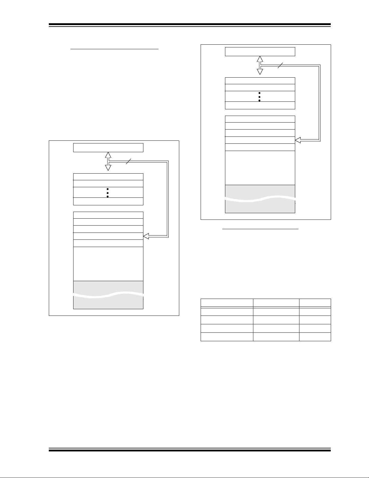
FIGURE 4-1: PROGRAM MEMORY MAP
AND STACK FOR THE
PIC16F627
PC<12:0>
CALL, RETURN
RETFIE, RETLW
Stack Level 1
Stack Level 2
Stack Level 8
Reset Vector
13
000h
FIGURE 4-2: PROGRAM MEMORY MAP AND
STACK FOR THE PIC16F628
PC<12:0>
CALL, RETURN
RETFIE, RETLW
Stack Level 1
Stack Level 2
Stack Level 8
Reset Vector
Interrupt Vector
On-chip Program
Memory
13
000h
0004
0005
07FFh
0800h
1FFFh
4.2 Data Memory Organization
Interrupt Vector
On-chip Program
Memory
0004
0005
03FFh
0400h
1FFFh
The data memory (Figure4-3) is partitioned into four
Banks which contain the general purpos e registers and
the special function registers. The Special Function
Registers are located in the first 32 locations of ea ch
Bank. Register l ocations 20-7 Fh, A0h-FF h, 120h-14F h,
170h-17Fh and 1F0h-1FFh are general purpose registers implem ented as static RAM.
The Table below lists how to access the four banks of
registers:
RP1 RP0
Bank0 0 0
Bank1 0 1
Bank2 1 0
Bank3 1 1
Addresses F0h-FFh, 170h-17Fh and 1F0h-1FFh are
implemented as common RAM and mapped back to
addresses 70h-7Fh.
4.2.1 GENERAL PURPOSE REGISTER FILE The register file is organized as 224 x 8 in the
PIC16F62X. Each is accessed either directly or indirectly through the File Select Register FSR
(Section 4.4).
1999 Microchip Technology Inc. Preliminary DS40300B-page 13
PIC16F62X
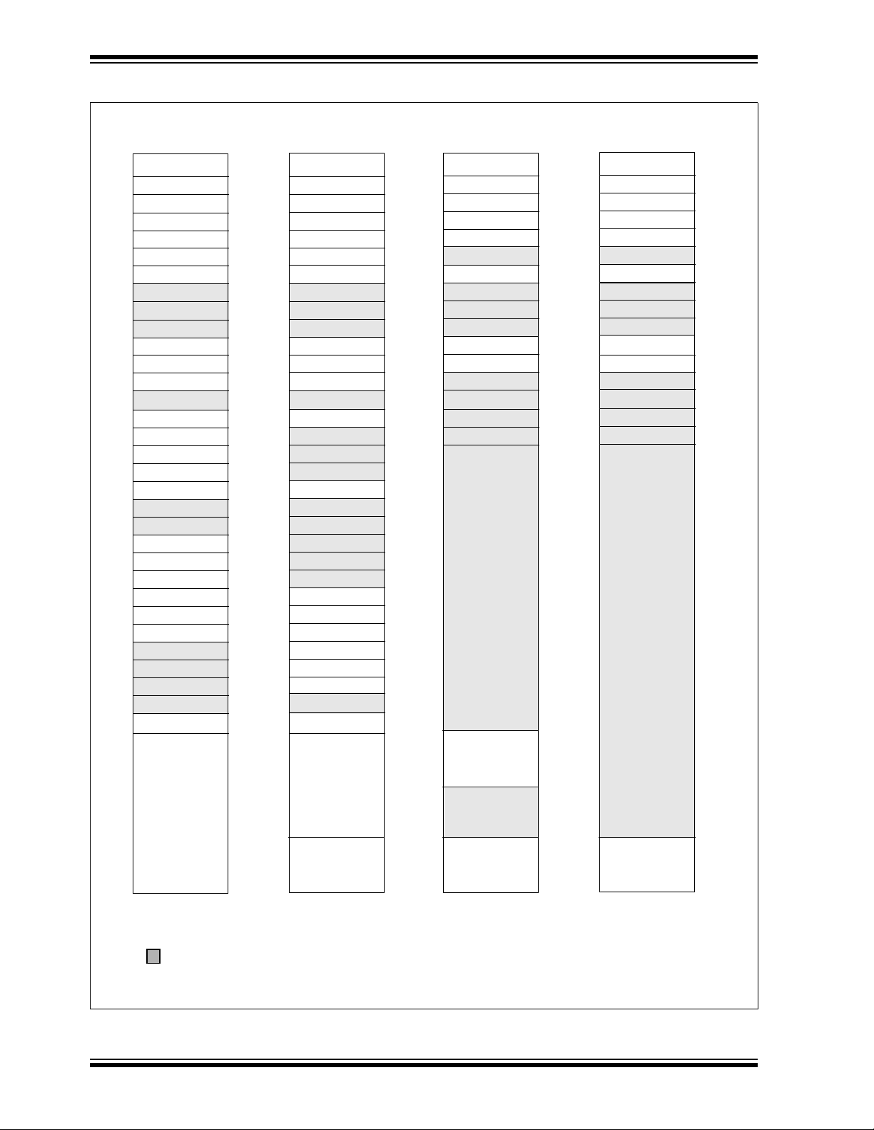
FIGURE 4-3: DATA MEMORY MAP OF THE PIC16F627 AND PIC16F628
File
Address
Indirect addr.(*)
TMR0
PCL
STATUS
FSR
PORTA
PORTB
PCLATH
INTCON
PIR1
TMR1L
TMR1H
T1CON
TMR2
T2CON
CCPR1L
CCPR1H
CCP1CON
RCSTA
TXREG
RCREG
CMCON
General
Purpose
Register
96 Bytes
Bank 0
00h
01h
02h
03h
04h
05h
06h
07h
08h
09h
0Ah
0Bh
0Ch
0Dh
0Eh
0Fh
10h
11h
12h
13h
14h
15h
16h
17h
18h
19h
1Ah
1Bh
1Ch
1Dh
1Eh
1Fh
20h
7Fh
Indirect addr.(*)
OPTION
PCL
STATUS
FSR
TRISA
TRISB
PCLATH
INTCON
PIE1
PCON
PR2
TXSTA
SPBRG
EEDATA
EEADR
EECON1
EECON2*
VRCON
General
Purpose
Register
80 Bytes
accesses
70h-7Fh
Bank 1
80h
81h
82h
83h
84h
85h
86h
87h
88h
89h
8Ah
8Bh
8Ch
8Dh
8Eh
8Fh
90h
91h
92h
93h
94h
95h
96h
97h
98h
99h
9Ah
9Bh
9Ch
9Dh
9Eh
9Fh
A0h
EFh
F0h
FFh
Indirect addr.(*)
TMR0
PCL
STATUS
FSR
PORTB
PCLATH
INTCON
General
Purpose
Register
48 Bytes
accesses
70h-7Fh
Bank 2
100h
101h
102h
103h
104h
105h
106h
107h
108h
109h
10Ah
10Bh
10Ch
10Dh
10Eh
10Fh
11Fh
120h
14Fh
150h
16Fh
170h
17Fh
Indirect addr.(*)
OPTION
PCL
STATUS
FSR
TRISB
PCLATH
INTCON
accesses
70h - 7Fh
Bank 3
180h
181h
182h
183h
184h
185h
186h
187h
188h
189h
18Ah
18Bh
18Ch
18Dh
18Eh
18Fh
1EFh
1F0h
1FFh
Unimplemented data memory locations, read as ’0’.
* Not a physical register.
DS40300B-page 14 Preliminary 1999 Microchip Technology Inc.
PIC16F62X
4.2.2 SPECIAL FUNCTION REGISTERS The special fu nctio n regi sters are re gisters us ed by the
CPU and Peripheral functions for controlling the
desired operation of the device (Table 4-1). These
registers are static RAM.
The special registers can be classified into two sets
(core and peripheral). The special function registers
associated with the “core” functions are described in
this section. Those related to the operation of the
peripheral features are described in the section of that
peripheral feature.
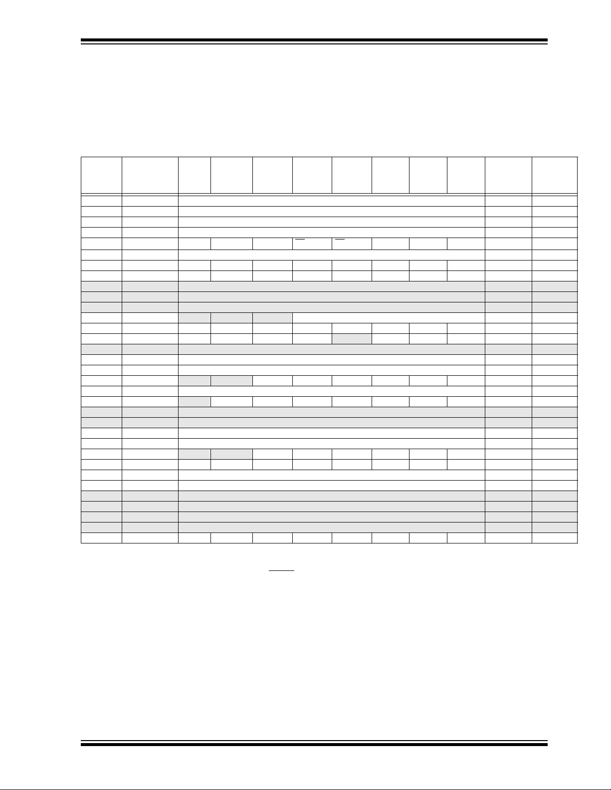
TABLE 4-1: SPECIAL REGISTERS SUMMARY BANK0
Address Name Bit 7 Bit 6 Bit 5 Bit 4 Bit 3 Bit 2 Bit 1 Bit 0
POR
Reset
Bank 0
Value on
00h INDF Addressing this location uses contents of FSR to address data memory (not a physical register) xxxx xxxx xxxx xxxx
01h TMR0 Timer0 Module’s Register xxxx xxxx uuuu uuuu
02h PCL Program Counter's (PC) Least Significant Byte 0000 0000 0000 0000
03h STATUS
04h FSR Indirect data memory address pointer xxxx xxxx uuuu uuuu
05h PORTA
06h PORTB RB7 RB6 RB5 RB4 RB3 RB2 RB1 RB0 xxxx xxxx uuuu uuuu
07h Unimplemented — —
08h Unimplemented — —
09h Unimplemented — —
0Ah PCLATH — — — Write buffer for upper 5 bits of program counter ---0 0000 ---0 0000
0Bh INTCON GIE PEIE T0IE INTE RBIE T0IF INTF RBIF 0000 000x 0000 000u
0Ch PIR1
0Dh Unimplemented — —
0Eh TMR1L Holding register for the least significant byte of the 16-bit TMR1 xxxx xxxx uuuu uuuu
0Fh TMR1H Holding register for the most significant byte of the 16-bit TMR1 xxxx xxxx uuuu uuuu
10h T1CON
11h TMR2 TMR2 module’s register 0000 0000 0000 0000
12h T2CON
13h Unimplemented — —
14h Unimplemented — —
15h CCPR1L Capture/Compare/PWM register (LSB) xxxx xxxx uuuu uuuu
16h CCPR1H Capture/Compare/PWM register (MSB) xxxx xxxx uuuu uuuu
17h CCP1CON
18h RCSTA SPEN RX9 SREN CREN ADEN FERR OERR RX9D 0000 -00x 0000 -00x
19h TXREG USART Transmit data register 0000 0000 0000 0000
1Ah RCREG USART Receive data register 0000 0000 0000 0000
1Bh Unimplemented — —
1Ch Unimplemented — —
1Dh Unimplemented — —
1Eh Unimplemented — —
1Fh CMCON C2OUT C1OUT
IRP RP1
RA7 RA6 RA5 RA4 RA3 RA2 RA1 RA0 xxxx 0000 xxxx 0000
EEIF CMIF RCIF TXIF — CCP1IF TMR2IF TMR1IF 0000 -000 0000 -000
— — T1CKPS1 T1CKPS0 T1OSCEN T1SYNC TMR1CS TMR1ON --00 0000 --uu uuuu
— TOUTPS3 TOUTPS2 TOUTPS1 TOUTPS0 TMR2ON T2CKPS1 T2CKPS0 -000 0000 -uuu uuuu
— — CCP1X CCP1Y CCP1M3 CCP1M2 CCP1M1 CCP1M0 --00 0000 --00 0000
RP0 TO
C2INV C1INV CIS CM2 CM1 CM0 0000 0000 0000 0000
PD ZDCC0001 1xxx 000q quuu
Legend: — = Unimplemented locati ons read as ‘0’, u = unchanged, x = un known, q = value depends on c on diti on ,
shaded = unimplemented
Note 1: Other (non power-up) resets include MCLR
Reset, Brown-out Detect and Watchdog Timer Reset during
normal operation.
Value on
all other
Resets
(1)
1999 Microchip Technology Inc. Preliminary DS40300B-page 15
PIC16F62X
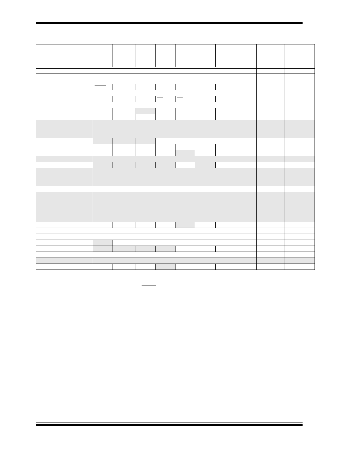
TABLE 4-2: SPECIAL FUNCTION REGISTERS SUMMARY BANK1
Value on
Address Name Bit 7 Bit 6 Bit 5 Bit 4 Bit 3 Bit 2 Bit 1 Bit 0
POR
Reset
Bank 1
80h INDF Addressing this location uses contents of FSR to address data memory (not a physical reg-
81h OPTION RBPU
82h PCL Program Counter’s (PC) Least Significant Byte 0000 0000 0000 0000
83h STATUS IRP RP1 RP0 TO
84h FSR Indirect data memory address pointer xxxx xxxx uuuu uuuu
85h TRISA TRISA7 TRISA6
86h TRISB TRISB7 TRISB6 TRISB5 TRISB4 TRISB3 TRISB2 TRISB1 TRISB0 1111 1111 1111 1111
87h Unimplemented — —
88h Unimplemented — —
89h Unimplemented — —
8Ah PCLATH
8Bh INTCON GIE PEIE T0IE INTE RBIE T0IF INTF RBIF 0000 000x 0000 000u
8Ch PIE1 EEIE CMIE RCIE TXIE
8Dh Unimplemented — —
8Eh PCON
8Fh Unimplemented
90h Unimplemented — —
91h Unimplemented — —
92h PR2 Timer2 Period Register 11111111 11111111
93h Unimplemented — —
94h Unimplemented — —
95h Unimplemented — —
96h Unimplemented — —
97h Unimplemented — —
98h TXSTA CSRC TX9 TXEN SYNC
99h SPBRG Baud Rate Generator Register 0000 0000 0000 0000
9Ah EEDATA EEPROM data register xxxx xxxx uuuu uuuu
9Bh EEADR
9Ch EECON1
9Dh EECON2 EEPROM control register 2 (not a physical register) -------- -------9Eh Unimplemented — —
9Fh VRCON VREN VROE VRR
ister)
INTEDG T0CS T0SE PSA PS2 PS1 PS0 1111 1111 1111 1111
PD ZDCC0001 1xxx 000q quuu
— TRISA4 TRISA3 TRISA2 TRISA1 TRISA0 11-1 1111 11-1 1111
— — — Write buffer for upper 5 bits of program counter ---0 0000 ---0 0000
— CCP1IE TMR2IE TMR1IE 0000 -000 0000 -000
— — — — OSCF —POR BOD ---- 1-0x ---- 1-uq
— BRGH TRMT TX9D 0000 -010 0000 -010
— EEPROM address register xxxx xxxx uuuu uuuu
— — — — WRERR WREN WR RD ---- x000 ---- q000
— VR3 VR2 VR1 VR0 000- 0000 000- 0000
xxxx xxxx xxxx xxxx
Value on
all other
resets
Legend: : — = Unimplemented locations read as ‘0’, u = unchanged, x = unknown, q = value depends on condition,
shaded = unimplemented
Note 1: Other (non power-up) resets include MCLR Reset, Brown-out Detect and Watchdog Timer Reset during
normal operation.
(1)
DS40300B-page 16 Preliminary 1999 Microchip Technology Inc.
TABLE 4-3: SPECIAL FUNCTION REGISTERS SUMMARY BANK2
PIC16F62X
Value on
Address Name Bit 7 Bit 6 Bit 5 Bit 4 Bit 3 Bit 2 Bit 1 Bit 0
POR
Reset
Bank 1
100h INDF Addressing this location uses contents of FSR to address data memory (not a physical reg-
101h TMR0 RBPU
102h PCL Program Counter’s (PC) Least Significant Byte 0000 0000 0000 0000
103h STATUS IRP RP1 RP0 TO
104h FSR Indirect data memory address pointer xxxx xxxx uuuu uuuu
105h
106h
107h Unimplemented — —
108h Unimplemented — —
109h Unimplemented — —
10Ah PCLATH
10Bh INTCON GIE PEIE T0IE INTE RBIE T0IF INTF RBIF 0000 000x 0000 000u
10Ch — —
10Dh Unimplemented — —
10Eh — —
10Fh Unimplemented
110h Unimplemented — —
111h Unimplemented — —
112h
113h Unimplemented — —
114h Unimplemented — —
115h Unimplemented — —
116h Unimplemented — —
117h Unimplemented — —
118h
119h
11Ah
11Bh
11Ch
11Dh
11Eh Unimplemented — —
11Fh
Unimplemented — —
PORTB TRISB7 TRISB6 TRISB5 TRISB4 TRISB3 TRISB2 TRISB1 TRISB0 1111 1111 1111 1111
ister)
INTEDG T0CS T0SE PSA PS2 PS1 PS0 1111 1111 1111 1111
PD ZDCC0001 1xxx 000q quuu
— — — Write buffer for upper 5 bits of program counter ---0 0000 ---0 0000
xxxx xxxx xxxx xxxx
— —
— —
— —
— —
— —
— —
— —
Value on
all other
resets
Legend: — = Unimplemented locations read as ‘0’, u = unchanged, x = unknown, q = value depends on condition,
shaded = unimplemented
Note 1: Other (non pow e r-up) res ets in cl ude M C LR R eset, Brown-out Detect and Watchdog Timer Reset during
normal operation.
(1)
1999 Microchip Technology Inc. Preliminary DS40300B-page 17
PIC16F62X
TABLE 4-4: SPECIAL FUNCTION REGISTERS SUMMARY BANK3
Value on
Address Name Bit 7 Bit 6 Bit 5 Bit 4 Bit 3 Bit 2 Bit 1 Bit 0
POR
Reset
Bank 1
180h INDF Addressing this location uses contents of FSR to address data memory (not a physical reg-
181h OPTION RBPU
182h PCL Program Counter’s (PC) Least Significant Byte 0000 0000 0000 0000
183h STATUS IRP RP1 RP0 TO
184h FSR Indirect data memory address pointer xxxx xxxx uuuu uuuu
185h Unimplemented — —
186h TRISB TRISB7 TRISB6 TRISB5 TRISB4 TRISB3 TRISB2 TRISB1 TRISB0 1111 1111 1111 1111
187h Unimplemented — —
188h Unimplemented — —
189h Unimplemented — —
18Ah PCLATH
18Bh INTCON GIE PEIE T0IE INTE RBIE T0IF INTF RBIF 0000 000x 0000 000u
18Ch
18Dh
18Eh
18Fh
190h
191h
192h
193h
194h
195h
196h
197h
198h
199h
19Ah
19Bh
19Ch
19Dh
19Eh
19Fh
ister)
INTEDG T0CS T0SE PSA PS2 PS1 PS0 1111 1111 1111 1111
PD ZDCC0001 1xxx 000q quuu
— — — Write buffer for upper 5 bits of program counter ---0 0000 ---0 0000
xxxx xxxx xxxx xxxx
Value on
all other
resets
Legend: — = Unimplemented locations read as ‘0’, u = unchanged, x = unknown, q = value depends on condition,
shaded = unimplemented
Note 1: Other (non pow e r-up) res ets in cl ude M C LR R eset, Brown-out Detect and Watchdog Timer Reset during
normal operation.
(1)
DS40300B-page 18 Preliminary 1999 Microchip Technology Inc.

PIC16F62X
4.2.2.1 STATUS REGISTER
The STATUS register, shown in Register 4-1, contains
the arithmetic status o f the ALU, the RESET status and
the bank select bits for data memory (SRAM).
The STATUS register can be the destination for any
instruction, like any other register. If the STATUS
register is the destination for an instruction that affects
the Z, DC or C bits, then the write to these three bits is
disabled. These bits ar e set or cl eared acco rding to the
device logic. Furthermore, the TO
writable. Therefore, the result of an instruction with the
STATUS regis ter as destina tion may be differen t than
intended.
For example, CLRF STATUS will clear the upper-three
bits and set the Z bi t. This lea ves the status register as
000uu1uu (where u = unchanged).
and PD bits are not
It is recommended, therefore, that only BCF, BSF,
SWAPF and MOVWF instructions are used to alter the
STATUS register because these instructions do not
affect any stat us bit. For other instructi ons, not affectin g
any status bits, see the “Instruction Set Summary”.
Note 1: The C and DC bits operate as a Borrow
and Digit Borrow out bit, respectively, in
subtractio n. See the SUBLW and SUBWF
instructi ons for examples.
REGISTER 4-1: STATUS REGISTER (ADDRESS 03H OR 83H)
R/W-0 R/W-0 R/W-0 R-1 R-1 R/W-x R/W-x R/W-x
IRP RP1 RP0 TO PD Z DC C R = Readable bit
bit7 bit0
bit 7: IRP: Register Bank Select bit (used for indirect addressing)
1 = Bank 2, 3 (100h - 1FFh)
0 = Bank 0, 1 (00h - FFh)
bit 6-5: RP1:RP0: Register Bank Select bits (used for direct addressing)
11 = Bank 3 (180h - 1FFh)
10 = Bank 2 (100h - 17Fh)
01 = Bank 1 (80h - FFh)
00 = Bank 0 (00h - 7Fh)
bit 4: TO
bit 3: PD
bit 2: Z: Zero bit
bit 1: DC: Digit carry/borrow
bit 0: C: Carry/borrow
: Time-out bit
1 = After power-up, CLRWDT instruction, or SLEEP instruction
0 = A WDT time-out occurred
: Power-down bit
1 = After power-up or by the CLRWDT instruction
0 = By execution of the SLEEP instruction
1 = The result of an arithmetic or logic operation is zero
0 = The result of an arithmetic or logic operation is not zero
bit (ADDWF, ADDLW,SUBLW,SUBWF instructions)(for borrow the polarity is reversed)
1 = A carry-out from the 4th low order bit of the result occurred
0 = No carry-out from the 4th low order bit of the result
bit (ADDWF, ADDLW,SUBLW,SUBWF instructions)
1 = A carry-out from the most significant bit of the result occurred
0 = No carry-out from the most si gnificant bit of the result occurred
Note: For borrow
second operand. For rotate (RRF, RLF) instructions, this bit is loaded with either the high or low or der bit of
the source register.
the polarity is re versed. A subtraction is executed by add in g th e two’s complement of the
W = Writable bit
U = Unimplemented bit,
read as ’0’
-n = Value at POR reset
-x = Unknown at POR reset
1999 Microchip Technology Inc. Preliminary DS40300B-page 19

PIC16F62X
4.2.2.2 OPTION REGISTER
The OPTION register is a readable and writable
register which conta ins vario us control bits to conf igure
the TMR0/WDT prescaler, the external RB0/INT
interrupt, TMR0, and the weak pull-ups on PORTB.
REGISTER 4-2: OPTION REGISTER (ADDRESS 81H)
R/W-1 R/W-1 R/W-1 R/W-1 R/W-1 R/W-1 R/W-1 R/W-1
RBPU INTEDG T0CS T0SE PSA PS2 PS1 PS0 R = Readable bit
bit7 bit0
bit 7: RBPU
bit 6: INTEDG: Interrupt Edge Select bit
bit 5: T0CS: TMR0 Clock Source Select bit
bit 4: T0SE: TMR0 Source Edge Select bit
bit 3: PSA: Prescaler Assignment bit
bit 2-0: PS2:PS0: Prescaler Rate Select bits
: PORTB Pull-up Enable bit
1 = PORTB pull-ups are disabled
0 = PORTB pull-ups are enabled by individual port latch values
1 = Interrupt on rising edge of RB0/INT pin
0 = Interrupt on falling edge of RB0/INT pin
1 = Transition on RA4/T0CKI pin
0 = Internal in struction cycle clock (CLKOUT)
1 = Increment on high-to-low transition on RA4/T0CKI pin
0 = Increment on low-to-high transition on RA4/T0CKI pin
1 = Prescaler is assigned to the WDT
0 = Prescaler is assigned to the Timer0 module
Bit Value TMR0 Rate WDT Rate
000
001
010
011
100
101
110
111
1 : 2
1 : 4
1 : 8
1 : 16
1 : 32
1 : 64
1 : 128
1 : 256
1 : 1
1 : 2
1 : 4
1 : 8
1 : 16
1 : 32
1 : 64
1 : 128
Note: To achieve a 1:1 prescaler assignment for
TMR0, assign the prescaler to the WDT
(PSA = 1). See Section 6.3.1
W = Writable bit
-n = Value at POR reset
DS40300B-page 20 Preliminary 1999 Microchip Technology Inc.

PIC16F62X
4.2.2.3 INTCON REGISTER
The INTCON register is a readable and writable
register which cont ains the v arious enable and flag bits
for all interrupt sourc es e xcept the com parator modul e.
See Section 4.2.2.4 and Section 4.2.2.5 for a
description of the co mparator enable and flag bits.
Note: Interrupt flag bits get set when an interrupt
condition occurs regardless of the state of
its corresponding enable bit or the global
enable bit, GIE (INTCON<7>).
REGISTER 4-3: INTCON REGISTER (ADDRESS 0BH OR 8BH)
R/W-0 R/W-0 R/W-0 R/W-0 R/W-0 R/W-0 R/W-0 R/W-x
GIE PEIE T0IE INTE RBIE T0IF INTF RBIF R = Readable bit
bit7 bit0
bit 7: GIE: Global Interrupt Enable bit
1 = Enables all un-masked interrupts
0 = Disables all interrupts
bit 6: PEIE: Peripheral Interrupt Enable bit
1 = Enables all un-masked peripheral interrupts
0 = Disables all peripheral interrupts
bit 5: T0IE: TMR0 Overflow Interrupt Enable bit
1 = Enables the TMR0 interrupt
0 = Disables the TMR0 interrupt
bit 4: INTE: RB0/INT External Interrupt Enable bit
1 = Enables the RB0/INT external interrupt
0 = Disables the RB0/INT external interrupt
bit 3: RBIE: RB Port Change Interrupt Enable bit
1 = Enables the RB port change interrupt
0 = Disables the RB port change inter rupt
bit 2: T0IF: TMR0 Overflow Interrupt Flag bit
1 = TMR0 register has over flowed (must be cleared in software)
0 = TMR0 register did not overflow
bit 1: INTF: RB0/INT External Interrupt Flag bit
1 = The RB0/INT external interrupt occurred (must be cleared in software)
0 = The RB0/INT external interrupt did not occur
bit 0: RBIF: RB Port Change Interrupt Flag bit
1 = When at least one of the RB7:RB4 pins changed state (must be cleared in software)
0 = None of the RB7:RB4 pins have changed state
W = Writable bit
U = Unimplemented bit, read
as ’0’
-n = Value at POR reset
-x = Unknown at POR reset
1999 Microchip Technology Inc. Preliminary DS40300B-page 21

PIC16F62X
4.2.2.4 PIE1 REGISTER
This register contains interrupt enable bits.
REGISTER 4-4: PIE1 REGISTER (ADDRESS 8CH)
R/W-0 R/W-0 R/W-0 R/W-0 U R/W-0 R/W-0 R/W-0
EEIE CMIE RCIE TXIE - CCP1IE TMR2IE TMR1IE R = Readable bit
bit7 bit0
bit 7: EEIE: EE Write Complete Interrupt Enable Bit
1 = Enables the EE write complete interrupt
0 = Disables the EE write complete interrupt
bit 6: CMIE: Comparator Interrupt Enable bit
1 = Enables the comparator interrupt
0 = Disables the comparator interrupt
bit 5: RCIE: USART Receive Interrupt Enable bit
1 = Enables the USART receive interrupt
0 = Disables the USART receive interrupt
bit 4: TXIE: USART Transmit Interrupt Enable bit
1 = Enables the USART transmit interrupt
0 = Disables the USART transmit interrupt
bit 3: Unimplemented: Read as ‘0’
bit 2: CCP1IE: CCP1 Interrupt Enable bit
1 = Enables the CCP1 interrupt
0 = Disables the CCP1 interrupt
bit 1: TMR2IE: TMR2 to PR2 Match Interrupt Enable bit
1 = Enables the TMR2 to PR2 match interrupt
0 = Disables the TMR2 to PR2 match interrupt
bit 0: TMR1IE: TMR1 Overflow Interrupt Enable bit
1 = Enables the TMR1 overfl ow interrupt
0 = Disables the TMR1 overflow interrupt
W = Writable bit
U = Unimplemented bit, read
as ’0’
-n = Value at POR reset
DS40300B-page 22 Preliminary 1999 Microchip Technology Inc.

PIC16F62X
4.2.2.5 PIR1 REGISTER
This register contains interrupt flag bits.
Note: Interrupt flag bits get set when an interrupt
condition occurs regardless of the state of
its corresponding enable bit or the global
enable bit, GIE (INTCON<7>). User
software should ensure the appropriate
interrupt flag bits are clear prior to enabling
an interrupt.
REGISTER 4-5: PIR1 REGISTER (ADDRESS 0CH)
R/W-0 R/W-0 R-0 R-0 U R/W-0 R/W-0 R/W-0
EEIF CMIF RCIF TXIF - CCP1IF TMR2IF TMR1IF R = Readable bit
bit7 bit0
bit 7: EEIF: EEPROM Write Operation Interrupt Flag bit
1 = The write operation completed (must be cleared in software)
0 = The write operation has not completed or has not been started
bit 6: CMIF: Comparator Interrupt Flag bit
1 = Comparator input has changed
0 = Comparator input has not changed
bit 5: RCIF: USART Receive Interrupt Flag bit
1 = The USART receive buffer is full
0 = The USART receive buffer is empty
bit 4: TXIF: USART Transmit Interrupt Flag bit
1 = The USART transmit buffer is empty
0 = The USART transmit buffer is full
bit 3: Unimplemented: Read as ‘0’
bit 2: CCP1IF: CCP1 Interrupt Flag bit
Capture Mode
1 = A TMR1 register capture occurred (must be cleared in software)
0 = No TMR1 register capture occurred
Compare Mode
1 = A TMR1 register compare match occurred (must be cleared in software)
0 = No TMR1 register compare match occurred
PWM Mode
Unused in this mode
bit 1: TMR2IF: TMR2 to PR2 Match Interrupt Flag bit
1 = TMR2 to PR2 match occurred (must be cleared in so ftware)
0 = No TMR2 to PR2 match occurred
bit 0: TMR1IF: TMR1 Overflow Interrupt Flag bit
1 = TMR1 register overflowed (must be cleared in software)
0 = TMR1 register did not overflow
W = Writable bit
U = Unimplemented bit, read
as ’0’
-n = Value at POR reset
1999 Microchip Technology Inc. Preliminary DS40300B-page 23

PIC16F62X
4.2.2.6 PCON REGISTER
The PCON register contains flag bits to differentiate
between a Power-on Reset, an external MCLR
WDT reset or a Brown-out Detec t.
Note: BOD is unknown on Power-on Reset. It
must then be set by the user and checked
on subsequent resets to see if BOD
cleared, indicating a brown-out has
occurred. The BOD status bit is a "don’t
care" and is not necessarily predictable if
the brown-out circuit is disabled (by
programming BOREN bit in the
Configuration word).
REGISTER 4-6: PCON REGISTER (ADDRESS 8Eh)
U-0 U-0 U-0 U-0 R/W-1 U-0 R/W-q R/W-q
— — — — OSCF —PORBOD R = Readable bit
bit7 bit0
bit 7-4,2:Unimplemented: Read as '0'
bit 3: OSCF: INTRC/ER oscillator speed
1 = 4 MHz typical
0 = 37 KHz typical
bit 1: POR
bit 0: BOD
: Power-on Reset Status bit
1 = No Power-on Reset occurred
0 = A Power-on Reset occurred (must be set in software after a Power-on Reset occurs)
: Brown-out Detect Status bit
1 = No Brown-out Reset occurred
0 = A Brown-out Reset occurred (must be set in software after a Brown-out Reset occurs)
(1)
reset,
is
W = Writable bit
U = Unimplemented bit, read
as ’0’
-n = Value at POR reset
Note 1: When in ER o scillator mode, setting OSCF = 1 w ill cause the osc illator speed to c hange to the spee d
specified by the external resistor.
DS40300B-page 24 Preliminary 1999 Microchip Technology Inc.
PIC16F62X
4.3 PCL and PCLATH
The program counter (PC) is 13-bits wide. Th e low byte
comes from the PCL register, which is a readable a nd
writable register. The high byte (PC<12:8>) is not directly
readable or writable and co mes from PCLATH. On any
reset, the PC is cleared. Figure 4-7 shows the two
situations for the loading of the PC. The upper example in
the figure shows how the PC is loaded on a write to PCL
(PCLATH<4:0> → PCH). The lower example in the figure
shows how the PC is loaded during a CALL or GOTO
instruction (PCLATH<4:3> → PCH).
FIGURE 4-7: LOADING OF PC IN
DIFFERENT SITUATIONS
PCH PCL
12 8 7 0
PC
PCLATH<4:0>
5
PCLATH
PCH PCL
12 11 10 0
PC
2
87
PCLATH<4:3>
11
8
Instruction with
PCL as
Destination
ALU result
GOTO, CALL
Opcode <10:0>
4.3.2 STACK The PIC16F62X family has an 8 level deep x 13-bit
wide hardware stack (Figure 4-1 and Figure 4-2). The
stack space is not part of either program or data space
and the stack pointer is not readable or writable. The
PC is PUSHed onto the stac k when a CALL instruction
is executed or an interrupt causes a branch. The stack
is POPed in the event of a RETURN, RETLW or a RET-
FIE instruction execution. PCLATH is not affected by a
PUSH or POP operation.
The stack operates as a circular buf fer . This means th at
after the stack has been PUSH ed eight times , the ninth
push overwrites th e valu e that was s tored fro m the firs t
push. The tenth pus h ov erwr i tes the se cond push (and
so on).
Note 1: There are no STATUS bits to
indicate stack overflow or stack
underflow conditions.
Note 2: There are no instructions/mnemonics
called PUSH or POP. These are actions
that occur from the execution of the
CALL, RETURN, RETLW and RETFIE
instructions, or the vectoring to an
interrupt address.
PCLATH
4.3.1 COMPUTED GOTO A computed GOTO is accomplished by adding an offset
to the program counter (ADDWF PCL). When doing a
table read using a computed GOTO method, care
should be exercised if the tab le locati on cro sses a PCL
memory boundary (each 256 byte block). Refer to the
application note
“Implementing a T able Read"
(AN556).
1999 Microchip Technology Inc. Preliminary DS40300B-page 25
PIC16F62X
4.4 Indirect Addressing, INDF and FSR
EXAMPLE 4-1: INDIRECT ADDRESSING
Registers
The INDF register is not a physical register. Addressing
the INDF register will cause indirect addressing.
Indirect address ing is possible by using the INDF register .
Any instruction u sing the I NDF regis ter actuall y accesse s
data pointed to by the file select register (FSR). Reading
INDF itself indire ctly will pro duce 00h. W riting t o the INDF
register indirectly results in a no-operation (although status bits may be affected). An effective 9-bit address is
obtained by concatenating the 8-bit FSR register and the
IRP bit (STATUS<7>), as shown in Figure 4-8.
A simple program to clear RAM location 20h-2Fh using
indirect addressing is shown in Example 4-1.
NEXT clrf INDF ;clear INDF register
CONTINUE:
FIGURE 4-8: DIRECT/INDIRECT ADDRESSING PIC16F62X
RP1 RP0 6
from opcode
0
movlw 0x20 ;initialize pointer
movwf FSR ;to RAM
incf FSR ;inc pointer
btfss FSR,4 ;all done?
goto NEXT ;no clear next
;yes continue
Indirect AddressingDirect Addressing
IRP FSR register
7
0
bank select location select
00h
Data
Memory
7Fh
Bank 0 Bank 1 Bank 2 Bank 3
For memory map detail see Figure 4-3.
00 01 10 11
bank select
180h
1FFh
location select
DS40300B-page 26 Preliminary 1999 Microchip Technology Inc.

PIC16F62X
5.0 I/O PORTS
The PIC1 6F6 2X have two ports, PORTA and PORTB.
Some pins for these I/O ports are multiplexed with an
alternate function for the peripheral features on the
device. In general, when a peripheral is enabled, that
pin may not be used as a general purpose I/O pin.
5.1 PORTA and TR ISA Registers
PORTA is an 8-bit wide latch. RA4 i s a Schmitt Trigger
input and an open drain o utput. Port RA4 is multiplexed
with the T0CKI clock input. RA5 is a Schmitt Trigger input
only and has no output drivers. All other RA port pins have
Schmitt Trigger input levels and full CMOS output drivers.
All pins have data direction bits (TRIS registers) which can
configure these pins as input or output.
A ’1’ in the TRISA register p uts the cor responding o utput
driver in a hi- impedance mode. A ’0’ in the TRISA register
puts the contents of the output latch on the selected pin(s).
Reading the PORT A register reads the status of the pins
whereas writing to it will write to the port latch. All write
operations are read-modify-write operations. So a write
to a port implies that the port pins are first read, then this
value is modified and written to the port data latch.
The PORTA pins are multiplexed with comparator and
voltage reference functions. The operation of these
pins are selected by control bits in the CMCON
(comparator control register) register and the VRCON
(voltage reference control register) register. When
selected as a comparator input, these pins will read
as ’0 ’s.
Note 1: On reset, the TRISA register is set to all
inputs. The digi tal in puts are disabled and
the comparator inputs are forced to
ground to reduce excess current consumption.
Note 2: When RA6/OSC2/CLKOUT is configured
as CLKOUT , the corresponding TRI S bit is
overridden and the p in is conf igured as a n
output. The PORTA data bit reads 0, and
the PORTA TRIS bit reads 0.
TRISA controls the di rection of the RA pins , even whe n
they are being used as comparator inputs. The user
must make sure to keep the pins configured as inputs
when using them as comparator inputs.
The RA2 pin will also function as the output for the
voltage reference. W hen in th is mode, th e V
very high impedance output. The user must configure
TRISA<2> bit as an input and use high impedance
loads.
In one of the comparator modes defined by the
CMCON register, pins RA3 and RA4 become outputs
of the comparators. The TRISA<4:3> bits must be
cleared to enable outputs to use this function.
REF pin is a
EXAMPLE 5-1: INITIALIZING PORTA
CLRF PORTA ;Initialize PORTA by setting
MOVLW 0X07 ;Turn comparators off and
MOVWF CMCON ;enable pins for I/O
BCF STATUS, RP1
BSF STATUS, RP0 ;Select Bank1
MOVLW 0x1F ;Value used to initialize
MOVWF TRISA ;Set RA<4:0> as inputs
;output data latches
;functions
;data direction
;TRISA<7:5> are always
;read as ’0’.
1999 Microchip Technology Inc. Preliminary DS40300B-page 27
PIC16F62X
FIGURE 5-1: BLOCK DIAGRAM OF
RA0/AN0:RA1/AN1 PINS
Data
Bus
WR
PORTA
Data Latch
WR
TRISA
TRIS Latch
RD PORTA
To Comparator
CK
CK
RD TRISA
QD
VDD
Q
QD
Q
Analog
Input Mode
Schmitt Trigger
P
N
SS
V
Input Buffer
DQ
EN
VDD
VSS
I/O Pin
FIGURE 5-2: BLOCK DIAGRAM OF
REF PIN
RA2/V
Data
Bus
WR
PORTA
Data Latch
WR
TRISA
TRIS Latch
RD PORTA
To Comparator
CK
CK
RD TRISA
VROE
QD
VDD
Q
QD
Q
Analog
Input Mode
Schmitt Trigger
P
N
SS
V
Input Buffer
DQ
EN
VDD
RA2 Pin
VSS
VREF
DS40300B-page 28 Preliminary 1999 Microchip Technology Inc.
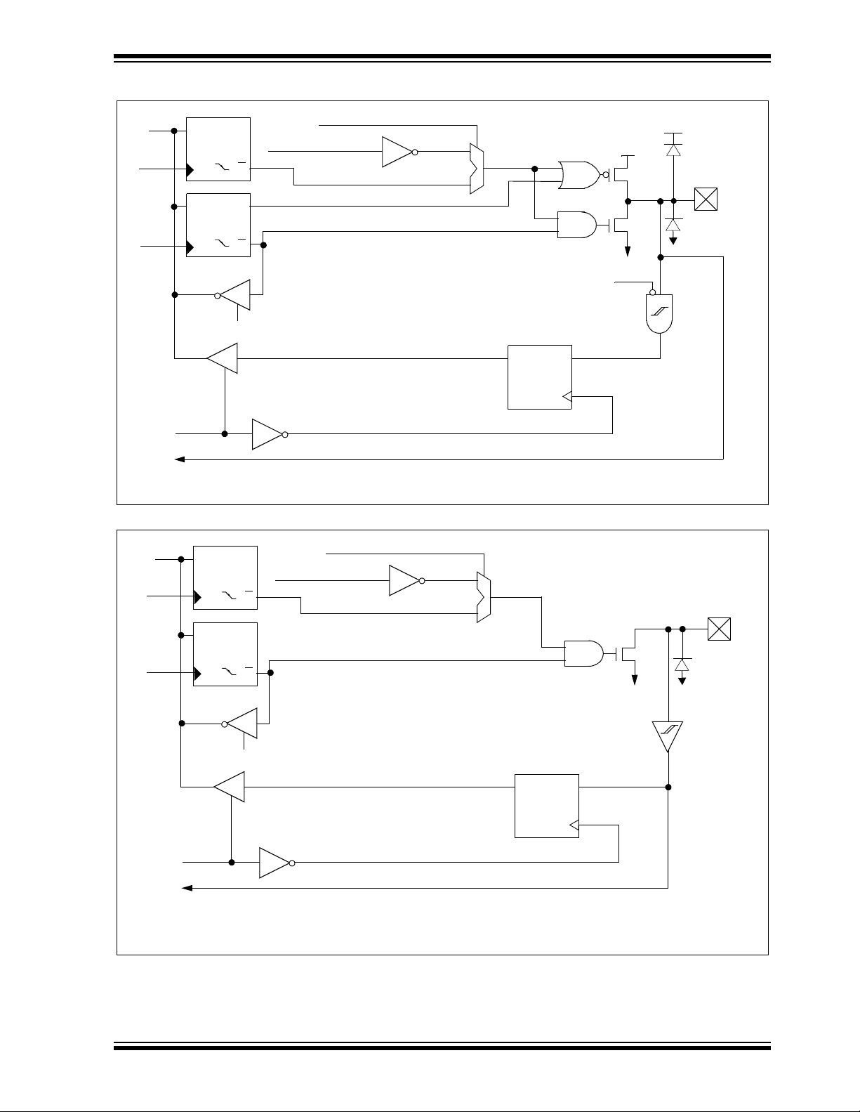
FIGURE 5-3: BLOCK DIAGRAM OF THE RA3/AN3 PIN
Data
Bus
WR
PORTA
WR
TRISA
Data Latch
TRIS Latch
RD PORTA
CK
CK
RD TRISA
QD
Comparator Output
Q
QD
Q
Comparator Mode = 110
PIC16F62X
VDD
1
0
Input Mode
DQ
EN
VDD
P
N
SS
V
Analog
Schmitt Trigger
Input Buffer
RA3 Pin
VSS
To Comparator
FIGURE 5-4: BLOCK DIAGRAM OF RA4/T0CKI PIN
Data
Bus
WR
PORTA
WR
TRISA
Data Latch
TRIS Latch
RD PORTA
CK
CK
RD TRISA
QD
Comparator Output
Q
QD
Q
Comparator Mode = 110
1
0
RA4 Pin
VSS
DQ
EN
N
SS
V
Schmitt Trigger
Input Buffer
TMR0 Clock Input
1999 Microchip Technology Inc. Preliminary DS40300B-page 29
PIC16F62X
FIGURE 5-5: BLOCK DIAGRAM OF THE RA5/MCLR/THV PIN
MCLRE
MCLR circuit
Program mode
Data
Bus
WR
PORT
WR
TRIS
CK
Data Latch
D
CK
TRIS Latch
RD TRIS
MCLR
Filter(1)
HV Detect
QD
Q
Q
Q
DQ
VDD
P
N
V
SS
VDD
RA5/MCLR/THV
VSS
RD Port
EN
DS40300B-page 30 Preliminary 1999 Microchip Technology Inc.

FIGURE 5-6: BLOCK DIAGRAM OF RA6/OSC2/CLKOUT PIN
(Fosc=101,111)
PIC16F62X
CLKOUT (FOSC/4)
Data
Bus
WR
PORTA
WR
TRISA
Data Latch
D
TRIS Latch
CK
CK
RD TRISA
From OSC1
1
0
QD
Q
Q
Q
(Fosc=100, 101, 110, 111)
(Fosc=110, 100)
DQ
EN
VDD
P
N
V
Oscillator
Circuit
VDD
RA6/OSC2/CLKOUT Pin
VSS
SS
Schmitt Trigger
Input Buffer
RD PORTA
CLKOUT is 1/4 of the Fosc frequency.
1999 Microchip Technology Inc. Preliminary DS40300B-page 31

PIC16F62X
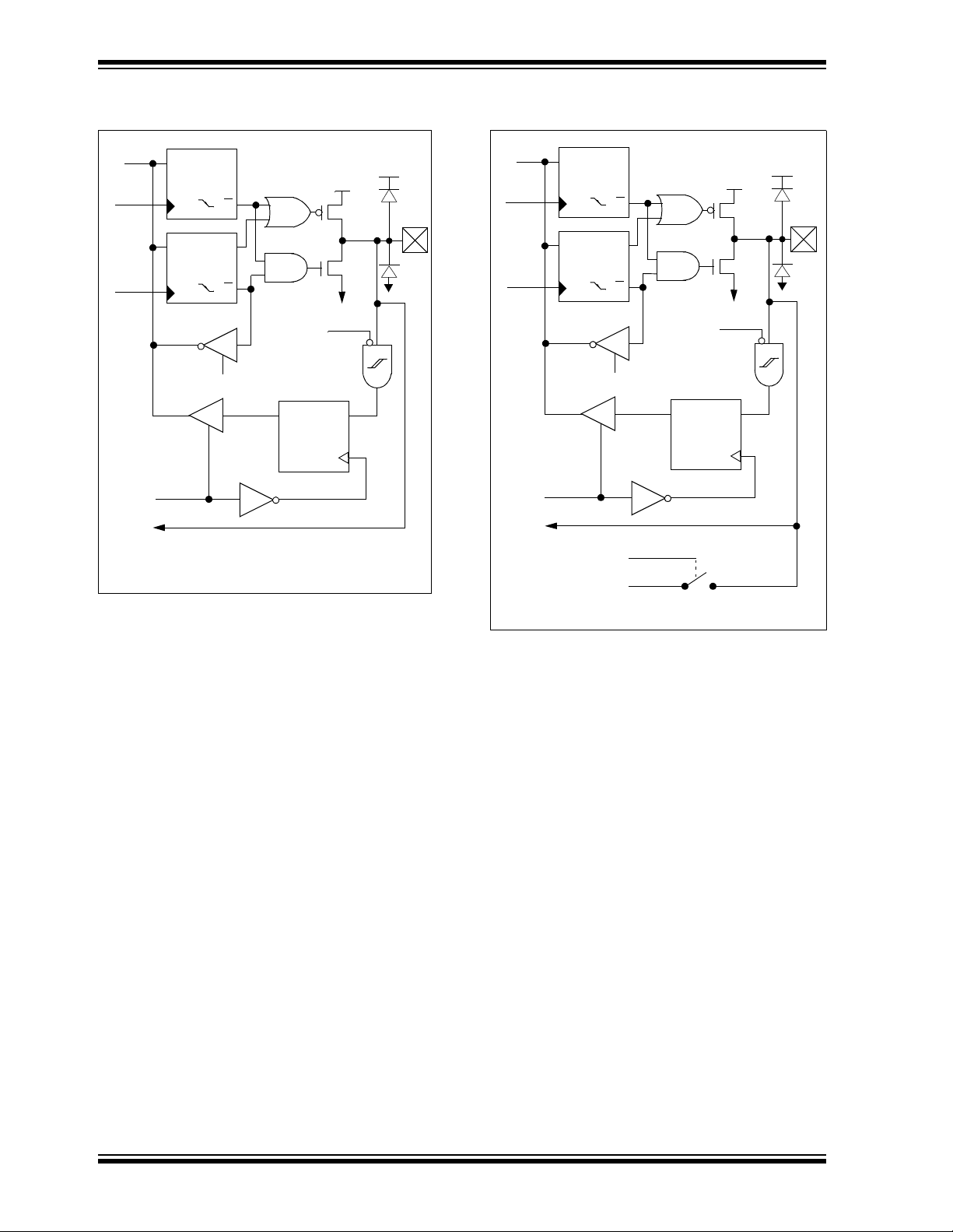
FIGURE 5-7: BLOCK DIAGRAM OF RA7/OSC1/CLKIN PIN
Data
Bus
WR
PORTA
WR
TRISA
CK
Data Latch
D
CK
TRIS Latch
RD PORTA
QD
Q
Q
Q
RD TRISA
(Fosc=101, 100)
EN
To OSC2
CLKIN to core
VDD
P
N
SS
V
DQ
Oscillator
Circuit
Schmitt Trigger
(Fosc=101, 100)
VDD
RA7/OSC1/CLKIN Pin
VSS
Schmitt Trigger
Input Buffer
DS40300B-page 32 Preliminary 1999 Microchip Technology Inc.

TABLE 5-1: PORTA FUNCTIONS
PIC16F62X
Name Bit #
Buffer
Type
Function
RA0/AN0 bit0 ST Bi-directional I/O port/comparator input
RA1/AN1 bit1 ST Bi-directional I/O port/comparator input
RA2/AN2/V
REF bit2 ST Bi-directional I/O port/analog/comparator input or VREF output
RA3/AN3 bit3 ST Bi-directional I/O port/analog/comparator input/comparator output
RA4/T0CKI bit4 ST Bi-directional I/O port/external clock inpu t for TMR 0 or com parator output .
Output is open drain type.
RA5/MCLR
RA6/OSC2/CLKOUT
/THV bit5 ST Input port/master clear (reset input/programming voltage input. When
configured as MCLR
on MCLR
/THV must not exceed VDD during normal device operation.
, this pin is an active low reset to the device. Voltage
bit6 ST Bi-directional I/O port/Oscillator crystal output. Connects to crystal or res-
onator in crystal oscillator mode. In ER mode, OSC2 pin outputs CLKOUT
which has 1/4 the frequency of OSC1, and denotes the instruction cycle
rate.
RA7/OSC1/CLKIN bit7 ST Bi-directional I/O port/oscillator crystal input/external clock source input.
Legend: ST = Schmitt Trigger input
TABLE 5-2: SUMMARY OF REGISTERS ASSO CIATED WITH PORTA
Address Name Bit 7 Bit 6 Bit 5 Bit 4 Bit 3 Bit 2 Bit 1 Bit 0
05h PORTA RA7 RA6 RA5 RA4 RA3 RA2 RA1 RA0 xxxx 0000 xxxu 0000
85h TRISA TRISA7 TRISA6
1Fh CMCON
9Fh VRCON VREN VROE
C2OUT C1OUT C2INV C1INV CIS CM2 CM1 CM0 0000 0000 0000 0000
— TRISA4 TRISA3 TRISA2 TRISA1 TRISA0 11-1 1111 11-1 1111
VRR — VR3 VR2 VR1 VR0 000- 0000 000- 0000
Value on
POR
Legend: — = Unimplemented locations, read as ‘0’, u = unchanged, x = unknown
Note: Shaded bits are not used by PORTA.
Value on
All Other
Resets
1999 Microchip Technology Inc. Preliminary DS40300B-page 33

PIC16F62X
5.2 PORTB and TRISB Registers
PORTB is an 8-bit wide bi-directional port. The
corresponding data direction register is TRISB. A ’1’ in
the TRISB register put s the correspon ding output driver
in a high impedance mode. A ’0’ in the TRISB register
puts the contents of the output latch on the selected
pin(s).
PORTB is multiplexed with the interrupt, USART, CCP
module and the TMR1 c lock input/outp ut. The standa rd
port functions and the alternate port functions are
shown in Table 5-3.
Reading PORTB register reads the status of the pins,
whereas writing to it will write to the port latch. All write
operations are read- modify-write op erations. So a wri te
to a port implies that the port pins are first read, then
this value is modified an d w ritt en to the port data latch.
Each of the PORTB pins has a weak internal pull-up
(≈200 µA t ypical). A si ngle con trol bit can turn o n all the
pull-ups. This is done by clearing the RBPU
(OPTION<7>) bit. The weak pull-up is automatically
turned off when the port pin is configured as an output.
The pull-ups are disabled on Power-on Reset.
Four of PORTB’s pins, R B7:RB4, have an interrupt on
change feature. Only pins configured as inputs can
cause this interrupt to occur (i.e., any RB7:RB4 pin
configured as an output is excluded from the interrupt
on change comparison). The input pins (of RB7:RB4)
are compared with the old value latched on the last
read of PORTB. The “mismatch” outputs of RB7:RB4
are OR’ed together to generat e the RBIF interrup t (flag
latched in INTCON<0>).
This interrupt can wake the device from SLEEP. The
user, in the interrupt service routine, can clear the
interrupt in the following manner:
a) Any read or write of PORTB. This will end the
mismatch condition.
b) Clear flag bit RBIF.
A mismatch c ond it i on w i ll co nt i n ue t o s et fl ag bi t R BI F.
Reading PORTB will end the mism atch condition, and
allow flag bit RBIF to be cleared.
This interrupt on mismatch feature, together with
software configurable pull-ups on these four pins allow
easy interface to a key pad and make it possible for
wake-up on key-depression. (See AN552 in the
Microchip
Note: If a change on the I/O pin should occur
The interrupt on change feature is recommended for
wake-up on key depression operation and operations
where PORTB is only used for the interrupt on change
feature. Polling of PORTB is not recommended while
using the interrupt on change feature.
Embedded Control Handbook
when the read operatio n is bein g exec uted
(start of the Q2 cyc le ), t hen th e RBIF interrupt flag may not getset.
.)
DS40300B-page 34 Preliminary 1999 Microchip Technology Inc.

FIGURE 5-8: BLOCK DIAGRAM OF RB0/INT PIN
RBPU
Data Bus
WR PORTB
D
CK
Data Latch
D
Q
Q
PIC16F62X
V
DD
P
weak
pull-up
VDD
RB0/INT pin
VSS
WR TRISB
RD PORTB
INT input
CK
TRIS Latch
RD TRISB
QD
EN
EN
TTL
input
buffer
Schmitt Trigger
Buffer
1999 Microchip Technology Inc. Preliminary DS40300B-page 35

PIC16F62X
FIGURE 5-9: BLOCK DIAGRAM OF RB1/TX/DT PIN
PORT/PERIPHERAL
USART data output
Data Bus
Peripheral OE
(2)
USART receive input
Select
(1)
WR PORTB
WR TRISB
RD TRISB
RD PORTB
D
CK
Data Latch
D
CK
TRIS Latch
RBPU
0
1
Q
Q
Q
Q
QD
EN
TTL
input
buffer
VDD
P
N
V
SS
VDD
weak pull-up
P
VDD
VSS
RB1/RX/DT
pin
Schmitt
Trigger
Note 1: Port/Peripheral select signal selects between port data and peripheral output.
Note 2: Peripheral OE( output enable) is only active if peripheral select is active.
RD PORTB
DS40300B-page 36 Preliminary 1999 Microchip Technology Inc.

FIGURE 5-10: BLOCK DIAGRAM OF RB2/TX/CK PIN
PIC16F62X
PORT/PERIPHERAL
USART TX/CK output
Data Bus
Peripheral OE
(2)
USART Slave Clock in
Select
(1)
WR PORTB
WR TRISB
RD TRISB
RD PORTB
D
CK
Data Latch
D
CK
TRIS Latch
TTL
input
buffer
VDD
weak pull-up
P
VDD
VSS
RB2/TX/CK
pin
RBPU
0
1
Q
Q
Q
Q
QD
EN
EN
VDD
P
N
Vss
Schmitt
Trigger
Note 1: Port/Peripheral select signal selects between port data and peripheral output.
Note 2: Peripheral OE( output enable) is only active if peripheral select is active.
RD PORTB
1999 Microchip Technology Inc. Preliminary DS40300B-page 37

PIC16F62X
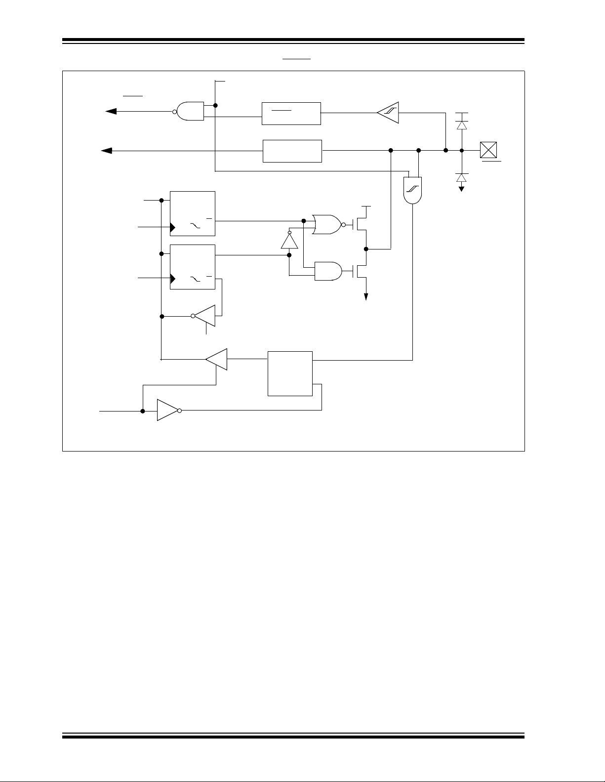
FIGURE 5-11: BLOCK DIAGRAM OF THE RB3/CCP1 PIN
Port/Peripheral
PWM/Compare output
Data Bus
Select
CCP input
(1)
WR PORTB
WR TRISB
RD TRISB
RD PORTB
D
CK
Data Latch
D
CK
TRIS Latch
RBPU
0
1
Q
Q
Q
Q
QD
EN
EN
VDD
P
N
Vss
TTL
input
buffer
VDD
P
weak pull-up
VDD
VSS
RB3/CCP1
pin
Schmitt
Trigger
Note 1: Peripheral Select is defined by CCP1M3:CCP1M0. (CCP1CON<3:0>)
RD PORTB
DS40300B-page 38 Preliminary 1999 Microchip Technology Inc.

FIGURE 5-12: BLOCK DIAGRAM OF RB4/PGM PIN
PIC16F62X
Data Bus
LVP
PGM input
WR PORTB
WR TRISB
RD TRISB
RD PORTB
D
CK
Data Latch
D
CK
TRIS Latch
RBPU
VDD
Q
Q
Q
Q
Schmitt
Trigger
P
N
SS
V
TTL
input
buffer
VDD
P
weak pull-up
VDD
VSS
RB4/PGM
QD
Set RBIF
From other
RB<7:4> pins
EN
QD
EN
Note: The low voltage programming disables the interrupt on change and the weak pullups on RB4.
Q1
RD Port
Q3
1999 Microchip Technology Inc. Preliminary DS40300B-page 39

PIC16F62X
FIGURE 5-13: BLOCK DIAGRAM OF RB5 PIN
RBPU
V
DD
P
weak
pull-up
VDD
Data Bus
WR PORTB
WR TRISB
Set RBIF
D
Q
CK
Data Latch
D
CK
TRIS Latch
RD TRISB
RD PORTB
From other
RB<7:4> pins
RB5 pin
VSS
Q
TTL
input
buffer
QD
EN
QD
EN
Q1
RD Port
Q3
DS40300B-page 40 Preliminary 1999 Microchip Technology Inc.

FIGURE 5-14: BLOCK DIAGRAM OF RB6/T1OSO/T1CKI PIN
PIC16F62X
Data Bus
T1OSCEN
TMR1 Clock
From RB7
WR PORTB
WR TRISB
RD TRISB
RD PORTB
D
CK
Data Latch
D
CK
TRIS Latch
RBPU
VDD
Q
Q
Q
Q
Schmitt
Trigger
P
N
SS
V
VDD
P
TTL
input
buffer
weak pull-up
VDD
RB6/
T1OSO/
T1CKI
pin
VSS
Serial programming clock
Set RBIF
From other
RB<7:4> pins
TMR1 oscillator
QD
EN
QD
EN
Q1
RD Port
Q3
1999 Microchip Technology Inc. Preliminary DS40300B-page 41

PIC16F62X
FIGURE 5-15: BLOCK DIAGRAM OF THE RB7/T1OSI PIN
RBPU
VDD
weak pull-up
P
TMR1 oscillator
To RB6
T1OSCEN
Data Bus
T10SCEN
Serial programming input
WR PORTB
WR TRISB
RD TRISB
RD PORTB
D
Data Latch
D
TRIS Latch
Schmitt
Trigger
Set RBIF
CK
CK
VDD
Q
Q
Q
Q
QD
EN
P
N
Vss
Q1
VDD
VSS
TTL
input
buffer
RB7/T1OSI
pin
From other
RB<7:4> pins
QD
EN
RD Port
Q3
DS40300B-page 42 Preliminary 1999 Microchip Technology Inc.

TABLE 5-3: PORTB FUNCTIONS
PIC16F62X
Name Bit #
RB0/INT
bit0
Buffer
Type
TTL/ST
Function
(1)
Bi-directional I/O port/external interrupt. Can be software programmed for
internal weak pull-up.
RB1/RX/DT
bit1
TTL/ST
(3)
Bi-directional I/O port/ USART receive pin/synchronous data I/O. Can be
software programmed for internal weak pull-up.
RB2/TX/CK
bit2
TTL/ST
(3)
Bi-directional I/O port/ USART transmit pin/synchronous clock I/O. Can be
software programmed for internal weak pull-up.
RB3/CCP1
bit3
TTL/ST
(4)
Bi-directional I/O port/Capture/Com pare/PWM I/O. Can be software programmed fo r internal weak pull-up.
RB4/PGM
bit4
TTL/ST
(5)
Bi-directional I/O port/Low voltage programming input pin. Wake-up from
SLEEP on pin change. Can be software programmed for internal weak
pull-up. When low voltage programming is enabled, the interrupt on pin
change and weak pull-up resistor are disabled.
RB5
bit5 TTL Bi-directional I/O port/Wake-up from SLEEP on pin change. Can be soft-
ware programmed for internal weak pull-up.
RB6/T1OSO/T1CKI
bit6
TTL/ST
(2)
Bi-directional I/O port/Timer1 oscillator output/Timer1 clock input. Wake up
from SLEEP on pin change. Can be software programmed for internal weak
pull-up.
RB7/T1OSI
bit7
TTL/ST
(2)
Bi-directional I/O port/Timer1 oscillator input. Wake up from SLEEP on pin
change. Can be software programmed for internal weak pull-up.
Legend: ST = Schmitt Trigger, TTL = TTL input
Note 1: This buffer is a Schmitt Trigger input when configured as the external interrupt.
Note 2: This buffer is a Schmitt Trigger input when used in serial programming mode.
Note 3: This buffer is a Schmitt Trigger I/O when used in USART/synchronous mode.
Note 4: This buffer is a Schmitt Trigger I/O when used in CCP mode.
Note 5: This buffer is a Schmitt Trigger input when used in low voltage program mode.
TABLE 5-4: SUMMARY OF REGISTERS ASSO CIATED WITH PORT
Address Name Bit 7 Bit 6 Bit 5 Bit 4 Bit 3 Bit 2 Bi t 1 Bit 0
06h PORTB RB7 RB6 RB5 RB4 RB3 RB2 RB1 RB0 xxxx xxxx uuuu uuuu
86h TRISB TRISB7 TRISB6 TRISB5 TRISB4 TRISB3 TRISB2 TRISB1 TRISB0 1111 1111 1111 1111
81h OPTION RBPU
INTEDG T0CS T0SE PSA PS2 PS1 PS0 1111 1111 1111 1111
Value on
POR
Legend: u = unchanged, x = unknown
Note: Shaded bits are not used by PORTB.
Value on
All Other
Resets
1999 Microchip Technology Inc. Preliminary DS40300B-page 43

PIC16F62X
Q2
MOVWF PORTB
Write to
PORTB
5.3 I/O Programming Considerations
5.3.1 BI-DIRECTIONAL I/O PORTS Any instruction which writes, operates internally as a
read follo wed by a write operation . The BCF and BSF
instructions, for example, read the register into the
CPU, execute the bi t operation and write the result back
to the register. Caution must be used when these
instructions are applied to a port with both inputs and
outputs defi ned. For ex am ple, a BSF operation on bit5
of PORTB will cause all eight bits of PORTB to be read
into the CPU. Then the BSF operation takes place on
bit5 and PORTB is written to the output latches. If
another bit of PORTB is used as a bidirectional I/O pin
(e.g., bit0) and it is defined as an input at this time, the
input signal prese nt on the p in i tse lf w ou ld b e rea d into
the CPU and re-written to the data latch of this
particular pin, overwriti ng the previ ous content. As long
as the pin stays in the input mode, no problem occurs.
However, if bit0 is s witche d int o out put m ode la ter on,
the content of the data latch may now be unknown.
Reading a port register, reads the values of the port
pins. Writing to the port register writes the value to the
port latch. When using read modify write instructions
(ex. BCF, BSF , etc.) on a port, the value of the po rt pins
is read, the desire d opera tion is done to this value , and
this value is then written to the port latch.
Example 5-2 shows the effect of two sequential
read-modify-write instruction s (ex ., BCF, BSF, etc.) on
an I/O port.
A pin actively outputting a Low or High should not be
driven from external devices at the same time in order
to change the level on this pin (“wired-or”, “wired-and”).
The resulting high output currents may damage
the chip.
EXAMPLE 5-2: READ-MODIFY -WRITE
INSTRUCTIONS ON AN
I/O PORT
;;Initial PORT settings: PORTB<7:4> Inputs
; PORTB<3:0> Outputs
;;PORTB<7:6> have external pull-up and are not
connected to other circuitry
;
; PORT latch PORT pins
; ---------- -------- --
BDF STATUS,RPO ;
BCF PORTB, 7 ; 01pp pppp 11pp pppp
BCF PORTB, 6 ; 10pp pppp 11pp pppp
BSF STATUS,RP0 ;
BCF TRISB, 7 ; 10pp pppp 11pp pppp
BCF TRISB, 6 ; 10pp pppp 10pp pppp
;
; Note that the user may have expected the pin
; values to be 00pp pppp. The 2nd BCF caused
; RB7 to be latched as the pin value (High).
5.3.2 SUCCESS IVE OPER ATI ONS ON I/O P ORTS The actual write to a n I/O port happe ns at the e nd of an
instruction cycle, whereas for reading, the data must be
valid at the beginning of the instruction cycle
(Figure 5-16). Therefore, care must be exercised if a
write followed by a read operation is carried out on the
same I/O port. The sequence of instructions should be
such to allow the pin voltage to stabilize (load
dependent) before the next instruction which causes
that file to be read into the CPU is execut ed. Otherwise,
the previous state of that pin m ay be read i nto the C PU
rather than the new state. When in doubt, it is better to
separate these instructions with a NOP or another
instruction not accessing this I/O port.
FIGURE 5-16: SUCCESSIVE I/O OPERATION
Q1 Q2 Q3 Q4 Q1 Q2 Q3 Q4 Q1 Q2 Q3 Q4 Q1 Q2 Q3 Q4
Q1 Q2 Q3 Q4 Q1 Q2 Q3 Q4 Q1
PC
PC
Instruction
Instru ction
fetched
fetche d
RB<7:0>
RB <7:0>
DS40300B-page 44 Preliminary 1999 Microchip Technology Inc.
PC
PC
MOWF PORTB
Write to PO RTB
PC + 1
PC + 1 P C + 2 PC + 3
MOVF PORTB, W
Read to PORTB
Read PORTB
TPD
T
PD
Execute
Execute
MOVWF
MOVWF
PORTB
PORTB
Q3 Q4 Q1 Q2 Q3 Q4
PC + 2
NOP NOP
Port pin
Port pin
sampled he re
sampled here
Execute
Execute
MOVWF
MOVF
PORTB
PORTB, W
PC + 3
NOPNOPMOVF PORTB, W
Execute
Execute
NOP
NOP
Note:
This example shows write to PORTB
followed by a read from PORTB.
Note that:
data setup time = (0.25 T
CY = instruction cycle and
where T
TPD = propagation delay of Q1 cycle
to output valid.
Therefore, at hig her clock freq uencies,
a write followed by a read may be
problematic.
CY - TPD)

PIC16F62X
6.0 TIMER0 MODULE
The Timer0 module timer/counter has the following
features:
• 8-bit timer/counter
• Readable and writable
• 8-bit software programmable prescaler
• Internal or external clock select
• Interrupt on overflow from FFh to 00h
• Edge select for external clock
Figure 6-1 is a simplified block diagram of the Timer0
module.
Timer mode is selected by clearing the T0CS bit
(OPTION<5>). In ti me r m ode , t he TMR0 will increment
every instruction cycle (without prescaler). If Timer0 is
written, the increment is inhibited for the following two
cycles (Figure 6-2 and Figure 6-3). The user can work
around this by writing an adjusted value to TMR0.
Counter mode is selected by setting the T0CS bit. In
this mode Timer0 will inc rement either o n every rising
or falling edge of pin RA4/T0CKI. The incrementing
edge is determined by the source edge (T0SE) control
bit (OPTION<4>). Clearing the T0SE bit selects the
rising edge. Restrictio ns on the exter nal clock input are
discussed in detail in Section 6.2.
The prescaler is shared between the Timer0 module
and the Watchdog Timer. The prescaler assignment is
controlled in software by the control bit PSA
(OPTION<3>). Clearing the PSA bit will assign the
prescaler to Timer0. The prescaler is not readable or
writable. When the pres ca ler i s as si gne d to the Timer0
module, prescale value of 1:2, 1:4, ..., 1:256 are
selectable. Section 6.3 details the operation of the
prescaler.
6.1 TIMER0 Interrupt
Timer0 interrupt is generated when the TMR0 register
timer/counter overflow s from FFh to 00h . This ov erflow
sets the T0IF bit. The interrupt can be masked by
clearing the T0IE bit (INTCON<5>). The T0IF bit
(INTCON<2>) must be cleared in software by the
Timer0 module interrupt service routine before
re-enabling this interrupt. The Timer0 interrupt cannot
wake the processor from SLEEP since the timer is shut
off during SLEEP. See Figure 6-4 for Timer0 interrupt
timing.
FIGURE 6-1: TIMER0 BLOCK DIAGRAM
RA4/T0CKI
pin
Note 1: B its T0SE, T0CS, PS2, PS1, PS0 and PSA are located in the OPTION register.
2: The prescaler is shared with Watchdog Timer (Figure 6-6)
FOSC/4
T0SE
0
1
T0CS
Programmable
Prescaler
PS2:PS0
1
0
PSA
PSout
Sync with
Internal
clocks
CY delay)
(2 T
PSout
FIGURE 6-2: TIMER0 (TMR0) TIMING: INTERNAL CLOCK/NO PRESCALER
PC
(Program
Counter)
Instruction
Fetch
TMR0
Instruction
Executed
Q1 Q2 Q3 Q4 Q1 Q2 Q3 Q4 Q1 Q2 Q3 Q4 Q1 Q2 Q3 Q4 Q1 Q2 Q3 Q4 Q1 Q2 Q3 Q4 Q1 Q2 Q3 Q4 Q1 Q2 Q3 Q4
PC-1
T0
PC PC+1 PC+2 PC+3 PC+4 PC+5 PC+6
MOVWF TMR0
T0+1 T0+2
MOVF TMR0,W MOVF TMR0,W MOVF TMR0,W MOVF TMR0,W MOVF TMR0,W
Write TMR0
executed
Read TMR0
reads NT0
NT0
Read TMR0
reads NT0
Read TMR0
reads NT0
NT0+1 NT0+2
Read TMR0
reads NT0 + 1
Data bus
TMR0
8
Set Flag bit T0IF
on Overflow
Read TMR0
reads NT0 + 2
T0
1999 Microchip Technology Inc. Preliminary DS40300B-page 45

PIC16F62X
FIGURE 6-3: TIMER0 TIMING: INTERNAL CLOCK/PRESCALE 1:2
PC
(Program
Counter)
Instruction
Fetch
TMR0
Instruction
Execute
Q1 Q2 Q3 Q4 Q1 Q2 Q3 Q4 Q1 Q2 Q3 Q4 Q1 Q2 Q3 Q4 Q1 Q2 Q3 Q4 Q1 Q2 Q3 Q4 Q1 Q2 Q3 Q4 Q1 Q2 Q3 Q4
PC-1
T0 NT0+1
PC PC+1 PC+2 PC+3 PC+4 PC+5 PC+6
MOVWF TMR0
T0+1
MOVF TMR0,W MOVF TMR0,W MOVF TMR0,W MOVF TMR0,W MOVF TMR0,W
Write TMR0
executed
Read TMR0
reads NT0
FIGURE 6-4: TIMER0 INTERRUPT TIMING
Q2Q1 Q3 Q4Q2Q1 Q3 Q4 Q2Q1 Q3 Q4 Q2Q1 Q3 Q4 Q2Q1 Q3 Q4
OSC1
CLKOUT(3)
TMR0 timer
T0IF bit
(INTCON<2>)
GIE bit
(INTCON<7>)
INSTRUCTION FLOW
PC
Instruction
fetched
FEh
1
PC
Inst (PC)
FFh 00h 01h 02h
1
PC +1 PC +1 0004h 0005h
Inst (PC+1)
NT0
Read TMR0
reads NT0
Interrupt Latency Time
Read TMR0
reads NT0
Inst (0004h) Inst (0005h)
Read TMR0
reads NT0
Read TMR0
reads NT0 + 1
Instruction
executed
Inst (PC-1)
Note 1: T0IF interrupt flag is sampled here (every Q1).
2: Interrupt latency = 3T
3: CLKOUT is available only in ER and INTRC (with clockout) oscillator modes.
Inst (PC)
CY, where TCY = instruction cycle time.
Inst (0004h)Dummy cycle Dummy cycle
DS40300B-page 46 Preliminary 1999 Microchip Technology Inc.

PIC16F62X
6.2 Using Timer0 with External Clock
When a prescaler is used, the external clock input is
divided by the asynchronous ripple-counter type
When an external clock inp ut is used f or Ti mer0, it mus t
meet certain requirements. The external clock
requirement is due to internal phase clock (TOSC)
synchronization. Also, there is a delay in the actual
incrementing of Timer0 after synchronization.
6.2.1 EXTERNAL CLOCK SYNCHRONIZATION When no pres cal er is us ed, t he ex ternal cloc k inp ut is
the same as the prescaler output. The synchronization
of T0CKI with the internal phase clocks is
accomplished by sampling the prescaler output on the
Q2 and Q4 cycles of the internal phase clocks
(Figure 6-5). Therefore, it is necessary for T0CKI to be
high for at least 2T
and low for at least 2T
OSC (and a small RC del ay of 20 ns)
OSC (and a small RC delay of
20 ns). Refer to the electrical specification of the
desired device.
prescaler so that the prescaler output is symmetrical.
For the external clock to meet the sampling
requirement, the ripple-counter must be taken into
account. Therefore, it is neces sary for T0CKI to h ave a
period of at least 4T
divided by th e prescaler val ue. The on ly requirement o n
T0CKI high and low time is that they do not violate the
minimum pulse width requirement of 10 ns. Refer to
parameters 40, 4 1 and 4 2 i n the electrical specification
of the desired device.
6.2.2 TIMER0 INCREMENT DELAY Since the prescaler output is synchronized with the
internal clocks, there is a small delay from the time the
external clock edge occurs to the time the TMR0 is
actually incremented. Figure 6-5 shows the delay from
the external clock edge to the timer incrementing.
FIGURE 6-5: TIMER0 TIMING WITH EXTERNAL CLOCK
Q1 Q2 Q3 Q4 Q1 Q2 Q3 Q4 Q1 Q2 Q3 Q4 Q1 Q2 Q3 Q4
External Clock Input or
Prescaler output
External Clock/Prescaler
Output after sampling
Increment Timer0 (Q4)
(2)
(1)
(3)
OSC (and a small RC delay of 40 ns)
Small pulse
misses sampling
Timer0
Note 1: Delay from clock input change to Timer0 increment is 3Tosc to 7Tosc. (Duration of Q = Tosc). Therefore, the error in
measuring the interval between two edges on Timer0 input = ±4Tosc m a x.
2: External clock if no prescaler selected, Prescaler output otherwise.
3: The arrows indicate the points in time where sampling occurs.
T0 T0 + 1 T0 + 2
1999 Microchip Technology Inc. Preliminary DS40300B-page 47

PIC16F62X
6.3 Prescaler
The PSA and PS2:PS0 bits (OPTION<3:0>) de termin e
the prescaler assignment and prescale ratio.
An 8-bit counter is available as a prescaler for the
Timer0 module, or as a postscaler for the Watchdog
Timer, respectively (Figure 6-6). For simplicity, this
counter is being referred to as “prescaler” throughout
this data sheet. Note that there is only one prescaler
available which is mutually exclusive between the
Timer0 module and the Watchdog Timer. Thus, a
When assigned to the Timer0 module, all instructions
writing to the TMR0 register (e.g., CLRF 1,
MOVWF 1, BSF 1, x....etc.) will clear the pr es-
caler. When assigned to WDT, a CLRWDT instruction
will clear the prescal er al ong with the Watchdog Time r.
The prescaler is not readable or writable.
prescaler assignment for the Timer0 module means
that there is no prescaler for the Watchdog Timer, and
vice-versa.
FIGURE 6-6: BLOCK DIAGRAM OF THE TIMER0/WDT PRESCALER
CLKOUT (=Fosc/4)
T0CKI
pin
T0SE
0
1
T0CS
M
U
X
1
M
U
0
X
PSA
SYNC
2
Cycles
Data Bus
8
TMR0 reg
Set flag bit T0IF
on Overflow
0
M
U
1
Watchdog
Timer
WDT Enable bit
Note: T0SE, T0CS, PSA, PS0-PS2 are bits in the OPTION register.
X
PSA
8-bit Prescaler
8
8-to-1MUX
0
M U X
WDT
Time-out
1
PS0 - PS2
PSA
DS40300B-page 48 Preliminary 1999 Microchip Technology Inc.

PIC16F62X
6.3.1 SWITCHING PRESCALER ASSIGNMENT The prescaler assignment is fully under software
To change prescaler from the WDT to the TMR0
module use the sequence shown in Example 6-2. This
precaution must be tak en even if the WDT is di sabl ed.
control (i.e., it can be changed “on the fly” during
program execution). To avoid an unintended device
RESET, the following instruction sequence
(Example 6-1) must be executed when changing the
prescaler assignment from Timer0 to WDT.
EXAMPLE 6-1: CHANGING PRESCALER
(TIMER0→WDT)
1.BCF STATUS, RP0 ;Skip if already in
; Bank 0
2.CLRWDT ;Clear WDT
3.CLRF TMR0 ;Clear TMR0 & Prescaler
4.BSF STATUS, RP0 ;Bank 1
5.MOVLW '00101111’b ;These 3 lines (5, 6, 7)
6.MOVWF OPTION ; are required only if
; desired PS<2:0> are
7.CLRWDT ; 000 or 001
8.MOVLW '00101xxx’b ;Set Postscaler to
9.MOVWF OPTION ; desired WDT rate
10.BCF STATUS, RP0 ;Return to Bank 0
EXAMPLE 6-2: CHANGIN G PRESCALER
(WDT→TIMER0)
CLRWDT ;Clear WDT and
BSF STATUS, RP0
MOVLW b'xxxx0xxx' ;Select TMR0, new
MOVWF OPTION_REG
BCF STATUS, RP0
TABLE 6-1: REGISTERS ASSOCIATED WITH TIMER0
Address Name Bit 7 Bit 6 Bit 5 Bit 4 Bit 3 Bit 2 Bit 1 Bit 0
;prescaler
;prescale value and
;clock source
Value on
POR
Value on
All Other
Resets
01h TMR0 Timer0 module register xxxx xxxx uuuu uuuu
0Bh/8Bh/
10Bh/18Bh
81h OPTION
85h TRISA
INTCON GIE
RBPU INTEDG T0CS T0SE PSA PS2 PS1 PS0 1111 1111 1111 1111
TRISA7 TRISA6
—T0IEINTE RBIE T0IF INTF RBIF 0000 000x 0000 000u
TRISA4
—
TRISA3 TRISA2 TRISA1 TRISA0 11-1 1111 11-1 1111
Legend: — = Unimplemented locations, read as ‘0’, u = unchanged, x = unknown
Note: Shaded bits are not used by TMR0 module.
1999 Microchip Technology Inc. Preliminary DS40300B-page 49

PIC16F62X
7.0 TIMER1 MODULE
The Timer1 module is a 16-bit timer/counter consisting
of two 8-bit registers (TMR1H and TMR1L) which are
readable and writable. The TMR1 Register pair
(TMR1H:TMR1L) increments from 0000h to FFFFh
and rolls over to 0000 h. The TMR1 Interrupt , if enabled,
is generated on overflow which is latched in interrupt
flag bit TMR1IF (PIR1<0>). This interrupt can be
enabled/disabled by setting/clearing TMR1 interrupt
enable bit TMR1IE (PIE1<0>).
Timer1 can operate in one of two modes:
•As a timer
•As a counter
The operating mode is determined by the clock select
bit, TMR1CS (T1CON<1>).
In timer mode, Timer1 increments every instruction
cycle. In counter mode, it increments on every rising
edge of the external clock input.
Timer1 can be enabled/disabled by setting/clearing
control bit TMR1ON (T1CON<0>).
Timer1 als o has an intern al “reset input”. Th is reset ca n
be generated by the CCP module (Section10.0).
Register 7-1 shows the Timer1 control register.
For the PIC16F627 and PIC16F628, when the Timer1
oscillator is enabl ed (T1OSCEN is se t), the RB7/T1O SI
and RB6/T1OSO/T1CKI pins become inputs. That is,
the TRISB<7:6> value is ignored.
REGISTER 7-1: T1CON: TIMER1 CONTROL REGISTER (ADDRESS 10h)
U-0 U-0 R/W-0 R/W-0 R/W-0 R/W-0 R/W-0 R/W-0
— — T1CKPS1 T1CKPS0 T1OSCEN T1SYNC TMR1CS TMR1ON
bit7 bit0
bit 7-6: Unimplemented: Read as '0'
bit 5-4: T1CKPS1:T1CKPS0: Timer1 Input Clock Prescale Select bits
11 = 1:8 Prescale value
10 = 1:4 Prescale value
01 = 1:2 Prescale value
00 = 1:1 Prescale value
bit 3: T1OSCEN: Timer1 Oscillator Enable Control bit
1 = Oscillator is enabled
0 = Oscillator is shut off
Note: The oscillator inverter and feedback resistor are turned off to eliminate power drain
bit 2: T1SYNC
: Timer1 External Clock Input Synchronization Control bit
R = Readable bit
W = Writable bit
U = Unimplemented bit,
read as ‘0’
- n = Value at POR reset
TMR1CS = 1
1 = Do not synchronize external clock input
0 = Synchronize external cl ock input
TMR1CS = 0
This bit is ignored. Timer1 uses the inte rnal clock when TMR1CS = 0.
bit 1: TMR1CS: Timer1 Clock Source Select bit
1 = External clock from pin RB6/T1OSO/T1CKI (on the rising edge)
0 = Internal clock (F
bit 0: TMR1ON: Timer1 On bit
1 = Enables Timer1
0 = Stops Timer1
DS40300B-page 50 Preliminary 1999 Microchip Technology Inc.
OSC/4)

PIC16F62X
7.1 Timer1 Operation in Timer Mode
Timer mode is selected by clearing the TMR1CS
(T1CON<1>) bit. In this mode, the input clock to the
timer is F
OSC/4. The synchronize control bit T1SYNC
(T1CON<2>) has no effect sinc e the internal c lock is
always in sync.
7.2 Timer1 Operation in Synchronized
Counter Mode
Counter mode is selected by setting bit TMR1CS. In
this mode the timer increments on every rising edge of
clock input on pin RB7/T1O SI when bit T1OSCEN is
set or pin RB6/T1OSO/T1CKI when bit T1OSCEN is
cleared.
If T1SYNC
synchronized with internal phase clocks. The synchronization is done after the prescal er stage. The prescaler stage is an asynchronous ripple-counter.
In this configuration, during SLEEP mode, Timer1 will
not increment even if the external clock is present,
since the synch ronizati on circuit i s shut off. Th e prescaler however will continue to increment.
7.2.1 EXTERNAL CLOCK INPUT TIMING FOR
is cleared, then the exter nal clock inp ut is
SYNCHRONIZED COUNTER MODE
internal phase clock (Tosc) synchro nization. Also, the re
is a delay in t he actual increme nting of TMR1 af ter synchronization.
When the prescaler is 1:1, the external clock input is
the same as the prescaler output. The synchronization
of T1CKI with the internal phase clocks is accomplished by sampli ng the presc aler output on the Q2 and
Q4 cycles of the internal phase clocks. Therefore, it is
necessary for T1CKI to be high for at least 2Tosc (and
a small RC delay of 20 ns) and low for at least 2Tosc
(and a small RC delay of 20 ns). Refer to the appropriate electrical spec ifications, paramet ers 45, 46, and 47.
When a prescaler other than 1:1 is used, the external
clock input is divided by the asynchronous ripple-counter type prescaler so that the prescaler output
is symmetrical. In order for the external clock to meet
the sampling requirement, the ripple-counter must be
taken into account. T herefore, it is necess ary for T1CKI
to have a period of at le ast 4Tosc (and a small RC delay
of 40 ns) divided by the prescaler value. The only
requirement on T1CKI hi gh and low tim e is that they d o
not violate the minimum pulse width requirements of
10 ns). Refer to the appropriate electrical specifications, parameters 40, 42, 45, 46, and 47.
When an external clock in pu t is used for T im er1 in synchronized counter mode, it must meet certain requirements. The external clock requirement is due to
FIGURE 7-1: TIMER1 BLOCK DIAGRAM
Set flag bit
TMR1IF on
Overflow
RB6/T1OSO/T1CKI
RB7/T1OSI
Note 1: When the T1OSCEN bit is cleared, the inverter and feedback resistor are turned off. This eliminates power drain.
TMR1H
T1OSC
TMR1
TMR1L
T1OSCEN
Enable
Oscillator
(1)
FOSC/4
Internal
Clock
TMR1ON
on/off
1
0
T1CKPS1:T1CKPS0
TMR1CS
0
1
T1SYNC
Prescaler
1, 2, 4, 8
2
Synchronized
clock input
Synchronize
det
SLEEP input
1999 Microchip Technology Inc. Preliminary DS40300B-page 51

PIC16F62X
FIGURE 7-2: TIMER1 INCREMENTING EDGE
T1CKI
(Default high)
T1CKI
(Default low)
Note: Arrows indicate counter increments.
7.3 Timer1 Operation in Asynchronous Counter Mode
If control bit T1SYN C (T1CON<2>) is set, the external
clock input is not synchronized. The timer continues to
increment asynchronous to the internal phase clocks.
The timer will continue to run during SLEEP and can
generate an interrupt on overflow which will wake-up
the processor. However, special precautions in software are needed to read/write the time r (Section 7.3.2).
In asynchronous counter mode, Timer1 can not be
used as a time-base for capt ure or compare operations.
7.3.1 EXTERNAL CLOCK INPUT TIMING WITH UNSYNCHRONIZED CLOCK
If control bi t T 1SYNC
completely asynch ronous ly. The input clock must meet
certain minimum high time and low time requirements.
Refer to the appropriate Electrical Specifications Section, timing parameters 45, 46, and 47.
7.3.2 READING AND WRITING TIMER1 IN ASYNCHRONOUS COUNTER MODE
Reading TMR1H or TMR1L while the timer is running,
from an external asynchronous clock, will guarantee a
valid read (taken care of in hardware). However, the
user should keep i n mind t hat re adin g the 16 -bit t imer
in two 8-bit values itself poses certain problems since
the timer may overflow between the reads.
For writes, it is recomm ended that the us er sim ply sto p
the timer and write the desired values. A write contention may occur by writing to the timer registers wh ile the
register is incrementing. This may produce an unpredictable value in the timer register.
Reading the 16-bit value requires some care.
Example 7-1 is an example routine to read the 16-bit
timer value. This is useful if the timer cannot be
stopped.
is set, the timer will incremen t
EXAMPLE 7-1: READING A 16-BIT
FREE-RUNNING TIMER
; All interrupts are disabled
MOVF TMR1H, W ;Read high byte
MOVWF TMPH ;
MOVF TMR1L, W ;Read low byte
MOVWF TMPL ;
MOVF TMR1H, W ;Read high byte
SUBWF TMPH, W ;Sub 1st read
; with 2nd read
BTFSC STATUS,Z ;Is result = 0
GOTO CONTINUE ;Good 16-bit read
;
; TMR1L may have rolled over between the read
; of the high and low bytes. Reading the high
; and low bytes now will read a good value.
;
MOVF TMR1H, W ;Read high byte
MOVWF TMPH ;
MOVF TMR1L, W ;Read low byte
MOVWF TMPL ;
; Re-enable the Interrupt (if required)
CONTINUE ;Continue with your code
7.4 Timer1 Oscillator
A crystal oscillator circui t is built in between pins T1OSI
(input) and T1OSO (amplifier output). It is enabled by
setting control bit T1OSCEN (T1CON<3>). The oscillator is a low power oscillator rated up to 200 kHz. It will
continue to run during SLEEP. It is primarily intended
for a 32 kHz crystal. Table 7-1 shows the capacitor
selection for the Timer1 oscillator.
The Timer1 oscillator is identical to the LP oscillator.
The user must provide a soft w are ti me del ay to en su re
proper oscillator start-up.
TABLE 7-1: CAPACITOR SELECTION FOR
THE TIMER1 OSCILLATOR
Osc Type Freq C1 C2
LP 32 kHz 33 pF 33 pF
100 kHz 15 pF 15 pF
200 kHz 15 pF 15 pF
These values are for design guidance only.
DS40300B-page 52 Preliminary 1999 Microchip Technology Inc.

PIC16F62X
7.5 Resetting Timer1 using a CCP Trigger Output
If the CCP1 module is configured in compare mode to
generate a “ special ev ent trig ger" (CCP 1M3:CCP1M 0
= 1011), this signal will reset Timer1.
Note: The special event triggers from the CCP1
module will not set interrupt flag bit
TMR1IF (PIR1<0>).
Timer1 must be configured for either timer or synchronized counter mode to tak e advantage of this fe ature. If
Timer1 is running in asynchronous counter mode, this
reset operation may not work.
7.6 Resetting of Timer1 Register Pair (TMR1H, TMR1L)
TMR1H and TMR1 L registers are not reset to 00h o n a
POR or any other reset except by the CCP1 special
event triggers.
T1CON register is reset to 00 h on a Powe r-on Reset or
a Brown-out Reset, which shuts off the timer and
leaves a 1:1 prescale. In all oth er resets, the register i s
unaffected.
7.7 Timer1 Prescaler
The prescaler counter is cleared on writes to the
TMR1H or TMR1L registers.
In the event that a write to Timer1 coincides with a special event tri gge r from CCP1 , the w rite wil l tak e prece dence.
In this mode of operation, the CCPRxH :CCPRxL regi sters pair effectively becomes the period register for
Timer1.
TABLE 7-2: REGISTERS ASSOCIATED WITH TIMER1 AS A TIMER/COUNTER
Address Name Bit 7 Bit 6 Bit 5 Bit 4 Bit 3 Bit 2 Bit 1 Bit 0
0Bh/8Bh/
10Bh/18Bh
0Ch PIR1
8Ch PIE1
0Eh TMR1L Holding register for the Least Significant Byte of the 16-bit TMR1 register
0Fh TMR1H Holding register for the Most Significant Byte of the 16-bit TMR1 register
10h T1CON
Legend: x = unknown, u = unchanged, - = unimplemented read as '0'. Shaded cells are not used by the Timer1 module.
INTCON GIE PEIE
EEIF CMIF RCIF TXIF — CCP1IF TMR2IF TMR1 IF
EEIE CMIE RC IE TXIE — CCP1IE TMR2IE TMR1IE
— — T1CKPS1 T1CKPS0 T1OSCEN T1SYNC TMR1CS TMR1ON
T0IE INTE RBIE T0 IF INTF RBIF
Value on
POR
0000 000x 0000 000u
0000 -000 0000 -000
0000 -000 0000 -000
xxxx xxxx uuuu uuuu
xxxx xxxx uuuu uuuu
--00 0000 --uu uuuu
Value on
all other
resets
1999 Microchip Technology Inc. Preliminary DS40300B-page 53

PIC16F62X
8.0 TIMER2 MODULE
Timer2 is an 8-bit timer with a prescaler and a
postscaler. It can be used as the PWM time-base for
PWM mode of the CCP module. The TMR2 register is
readable and writable, and is cleared on any device
reset.
The input clock (F
1:4 or 1:16, selected by control bits
T2CKPS1:T2CKPS0 (T2CON<1:0>).
The Timer2 module has an 8-bit period register PR2.
Timer2 increments from 00h until it matches PR2 and
then resets to 00h on the next increment cycle. PR2 is
a readable and writable register . The PR2 register is initialized to FFh upon reset.
The match output of TMR2 goes through a 4-bit
postscaler (which gives a 1:1 to 1:16 scaling inclusive)
to generate a TMR2 interrupt (latched in flag bit
TMR2IF, (PIR1<1>)).
Timer2 ca n be sh ut off by clearing control bit TMR2ON
(T2CON<2>) to minimize power consumption.
Register 8-1 shows the Timer2 control register.
OSC/4) has a prescal e opti on of 1 :1,
8.1 Timer2 Prescaler and Postscaler
The prescaler and postscaler counters are cleared
when any of the following occurs:
• a write to the TMR2 register
• a write to the T2CON register
• any device reset (Power-on Rese t, MCLR
reset,
Watchdog Timer reset, or Brown-out Reset)
TMR2 is not cleared when T2CON is written.
8.2 Output of TMR2
The output of TMR2 (before the posts caler) is fed to the
Synchronous Serial Port module w hi ch op tio nal ly uses
it to generate shift clock.
FIGURE 8-1: TIMER2 BLOCK DIAGRAM
Sets flag
bit TMR2IF
Postscaler
1:1 1:16
TMR2
(1)
output
Reset
to
4
EQ
TMR2 reg
Comparator
PR2 reg
Prescaler
1:1, 1:4, 1:16
2
OSC/4
F
Note 1: TMR2 registe r output can be software selected
by the SSP Module as a baud clock.
DS40300B-page 54 Preliminary 1999 Microchip Technology Inc.

REGISTER 8-1: T2CON: TIMER2 CONTROL REGISTER (ADDRESS 12h)
U-0 R/W-0 R/W-0 R/W-0 R/W-0 R/W-0 R/W-0 R/W-0
— TOUTPS3 TOUTPS2 TOUTPS1 TOUTPS0 TMR2ON T2CKPS1 T2CKPS0 R = Readable bit
bit7 bit0
bit 7: Unimplemented: Read as '0'
bit 6-3: TOUTPS3:TOUTPS0: Timer2 Output Postscale Select bits
0000 = 1:1 Postscale
0001 = 1:2 Postscale
•
•
•
1111 = 1:16 Postscale
bit 2: TMR2ON: Timer2 On bit
1 = Timer2 is on
0 = Timer2 is off
bit 1-0: T2CKPS1:T2CKPS0: Timer2 Clock Prescale Select bits
00 = Prescaler is 1
01 = Prescaler is 4
1x = Prescaler is 16
W = Writable bit
U = Unimplemented bit,
- n = Value at POR reset
PIC16F62X
read as ‘0’
TABLE 8-1: REGISTERS ASSOCIATED WITH TIMER2 AS A TIMER/COUNTER
Address Name Bit 7 Bit 6 Bit 5 Bit 4 Bit 3 Bit 2 Bit 1 Bit 0
0Bh/8Bh/
10Bh/18Bh
0Ch PIR1
8Ch PIE1
11h TMR2 Timer2 module’s register
12h T2CON
92h PR2 Timer2 Period Register
Legend: x = unknown, u = unchanged, - = unimplemented read as '0'. Shaded cells are not used by the Timer2 module.
INTCON GIE PEIE
EEIF CMIF RCIF TXIF — CCP1IF TMR2IF TMR1IF
EEIE CMIE RCIE TXIE — CCP1IE TMR2IE TMR1IE
— TOUTPS3 TOUTPS2 TOUTPS1 TOUTPS0 TMR2ON T2CKPS1 T2CKPS0
T0IE INTE RBIE T0IF INTF RBIF
Value on
POR
0000 000x 0000 000u
0000 -000 0000 -000
0000 -000 0000 -000
0000 0000 0000 0000
-000 0000 -000 0000
1111 1111 1111 1111
Value on
all other
resets
1999 Microchip Technology Inc. Preliminary DS40300B-page 55

PIC16F62X
NOTES:
DS40300B-page 56 Preliminary 1999 Microchip Technology Inc.

PIC16F62X
9.0 COMPARATOR MODULE
The comparator module contains two analog
comparators. The inputs to the comparators are
The CMCON register, shown in Register 9-1, controls
the comparator input and output multiplexers. A block
diagram of the comparator is shown in Figure 9-1.
multiplexed with the RA0 through RA3 pins. The
on-chip Voltage Reference (Section 11.0) can also be
an input to the comparators.
REGISTER 9-1: CMCON REGISTER (ADDRESS 01Fh)
R-0 R-0 R/W-0 R/W-0 R/W-0 R/W-0 R/W-0 R/W-0
C2OUT C1OUT
bit7 bit0
bit 7: C2OUT: Comparator 2 output
When C2INV=0;
1 = C2 V
0 = C2 V
When C2INV=1;
0 = C2 V
1 = C2 V
bit 6: C1OUT: Comparator 1 output
When C1INV=0;
1 = C1 V
0 = C1 V
C2INV C1INV CIS CM2 CM1 CM0 R = Readable bit
IN+ > C2 VIN–
IN+ < C2 VIN–
IN+ > C2 VIN–
IN+ < C2 VIN–
IN+ > C1 VIN–
IN+ < C1 VIN–
W = Writable bit
U = Unimplemented bit, read
as ’0’
-n = Value at POR reset
When C1INV=1;
0 = C1 V
1 = C1 V
IN+ > C1 VIN–
IN+ < C1 VIN–
bit 5: C2INV: Comparator 2 output inversion
1 = C2 Output inverted
0 = C2 Output not inverted
bit 4: C1INV: Comparator 1 output inversion
1 = C1 Output inverted
0 = C1 Output not inverted
bit 3: CIS: Comparator Input Switch
When CM2:CM0: = 001:
Then:
1 = C1 V
0 = C1 V
IN– connects to RA3
IN– connects to RA0
When CM2:CM0 = 010:
Then:
1 = C1 V
C2 V
0 = C1 V
C2 V
IN– connects to RA3
IN– connects to RA2
IN– connects to RA0
IN– connects to RA1
bit 2-0: CM2:CM0: Compara tor mode
Figure 9-1 shows the comparator modes and CM2:CM0 bit settings.
1999 Microchip Technology Inc. Preliminary DS40300B-page 57

PIC16F62X
e
9.1 Comparator Configuration
mode is changed, the com parator output level may not
be valid for the specified mode change delay shown
There are eight modes of operation for the
in Table 12-2.
comparators. The CMCON register is used to select
the mode. Figure 9-1 shows the eight possible modes.
The TRISA register controls the data direction of the
comparator pins for each mode. If the comparator
FIGURE 9-1: COMPARATOR I/O OPERATING MODES
Comparators Reset (POR Default Value)
CM2:CM0 = 000
A
RA0/AN0
RA3/AN3/C10
RA1/AN1
RA2/AN2
Two Independent Comparators
CM2:CM0 = 100
RA0/AN0
RA3/AN3/C10
RA1/AN1
RA2/AN2
Vin-
C1
Vin+
A
A
Vin-
C2
Vin+
A
A
Vin-
C1
Vin+
A
A
Vin-
C2
Vin+
A
Off (Read as ’0’)
Off (Read as ’0’)
C1OUT
C2OUT
Comparators Off
CM2:CM0 = 111
RA0/AN0
RA3/AN3/C10
RA1/AN1
RA2/AN2
Four Inputs Multiplexed to Two Compar ators
CM2:CM0 = 010
RA0/AN0
RA3/AN3/C10
RA1/AN1
RA2/AN2
Note: Comparator interrupts should be disabled
during a comparator mode change otherwise a false interrupt may occur.
D
Vin-
C1
Vin+
D
D
Vin-
C2
Vin+
D
A
CIS = 0
A
CIS = 1
A
CIS = 0
A
CIS = 1
VinVin+
VinVin+
Off (Read as ’0’)
Off (Read as ’0’)
C1
C2
C1OUT
C2OUT
Two Common Reference Comparators
CM2:CM0 = 011
A
RA0/AN0
RA3/AN3/C10
RA1/AN1
RA2/AN2
One Independent Comparator
CM2:CM0 = 101
RA0/AN0
RA3/AN3/C10
RA1/AN1
RA2/AN2
D
D
A
A
Vin-
C1
Vin+
D
A
Vin-
C2
Vin+
A
Vin-
C1
Vin+
Vin-
C2
Vin+
C1OUT
C2OUT
Off (Read as ’0’)
C2OUT
From Vref Modul
Two Common Reference Comparators with Outputs
CM2:CM0 = 110
A
RA0/AN0
RA3/AN3/C10
RA1/AN1
RA2/AN2
RA4/T0CKI/C20
Three Inputs Multiplexed to Two Com parators
CM2:CM0 = 001
RA0/AN0
RA3/AN3/C10
RA1/AN1
RA2/AN2
A
A
A
A
VinVin+
D
A
VinVin+
A
Open Drain
CIS = 0
CIS = 1
C1
C2
VinVin+
VinVin+
C1
C2
C1OUT
C2OUT
C1OUT
C2OUT
A = Analog Input, port reads zeros always.
D = Digital Input.
CIS (CMCON<3>) is the Comparator Input Switch.
DS40300B-page 58 Preliminary 1999 Microchip Technology Inc.

PIC16F62X
The code example in Example 9-1 depicts the steps
required to configure th e comp arator mo dule. R A3 and
RA4 are configured as digita l output. RA0 and RA1 ar e
configured as the V- inputs and RA2 as the V+ input to
both comparators.
EXAMPLE 9-1: INITIALIZING
COMPARATOR MODULE
FLAG_REG EQU 0X20
CLRF FLAG_REG ;Init flag r egist er
CLRF PORTA ;Init PORTA
MOVF CMCON, W ;Load comparator bits
ANDLW 0xC0 ;Mask co mpar ator bits
IORWF FLAG_REG,F ;Store bits in fl ag r egist er
MOVLW 0x03 ;Init co mpar ator mode
MOVWF CMCON ;CM<2:0> = 011
BSF STATUS, RP0 ;Select Bank1
MOVLW 0x07 ;Initial ize data direction
MOVWF TRISA ;Set RA<2:0> as inputs
;RA<4:3> as outputs
;TRISA<7:5> always read ‘0 ’
BCF STATUS, RP0 ;Select Bank 0
CALL DELAY 10 ;10µs delay
MOVF CMCON,F ;Read CMCON to end change condition
BCF PIR1,CM IF ;Cl ear p endi ng in terrupts
BSF STATUS, RP0 ;Select Bank 1
BSF PIE1,CM IE ;Enable comp arator interru pts
BCF STATUS, RP0 ;Select Bank 0
BSF INTCON, PEIE ;Enable periphera l interrupts
BSF INTCON, GIE ;Global interrupt enable
9.3 Comparator Reference
An external or internal reference signal may be used
depending on the comparator operating mode. The
analog signal that is pre sent at VIN – is compared to the
signal at V
IN+, and the digital output of the comparator
is adjusted accordingly (Figure 9-2).
FIGURE 9-2: SINGLE COMPARATOR
VIN+
IN–
V
V
IN–
V
IN+
+
Output
–
Output
9.2 Comparator Operation
A single comparator is shown in Figure 9-2 along with
the relationship between the analog input levels and
the digital output. When the analog inp ut at VIN+ is les s
than the analog input V
comparator is a digital lo w level. When th e analog input
at VIN+ is greater than the anal og input V IN–, the output
of the comparator is a digital high level. The shaded
areas of the output of the comparator in Figure 9-2
represent the uncertainty due to input offsets and
response time.
IN–, the output of the
9.3.1 EXTERNAL REFERENCE SIGNAL When external voltage references are used, the
comparator modul e can be configured to have the com parators operate from the same or different reference
sources. However, threshold detector appli cations may
require the same refere nce . Th e re fere nce si gn al m us t
be between V
SS and VDD, and can be applied to either
pin of the comparator(s).
9.3.2 INTERNAL REFERENCE SIGNAL The comparator module also allows the selection of an
internally generated voltage reference for the
comparators. Section 13, Instruction Sets, contains a
detailed description of the Voltage Reference Module
that provides this signal. The internal reference signal
is used when the comparators are in mode
CM<2:0>=010 (Figure 9-1). In this mode, the internal
voltage reference is applied to the V
IN+ pin of both
comparators.
1999 Microchip Technology Inc. Preliminary DS40300B-page 59

PIC16F62X
9.4 Comparator Response Time
Response time is the minimum time, after selecting a
new reference voltage or input source, before the
comparator output is guaranteed to have a valid level.
If the internal reference is changed, the maximum d elay
of the internal voltage reference must be considered
when using the comparator outputs. Otherwise the
maximum delay of the comparators should be used
(Table 12-2 ).
9.5 Comparator Outputs
The comparator outputs are read through the CMCON
register. These bits are read only. The comparator
outputs may also be directly output to the RA3 and RA4
I/O pins. When the CM<2:0> = 1 1 0 or 001, multiplexor s
in the output path of the RA3 and RA4/T0CK1 pins will
switch and the outp ut of each pi n will be t he unsynch ronized output o f the com parator . T he uncertain ty of eac h
of the comparators is related to the input offset voltage
and the response time given in the specifications.
Figure 9-3 shows the comparator output bloc k diagram.
The TRISA bits will still function as an output
enable/disable for the RA3 and RA4/T0CK1 pins while
in this mode.
Note 1: When reading the PORT registe r , all pins
configured as analog inputs will read as
a ‘0’. Pins c onfigu red a s di gital inpu ts w ill
convert an analog input according to the
Schmitt Trigger input specification.
2: Ana log levels on any pin that is defined
as a digital input may cause the input
buffer to consume more current than is
specified.
FIGURE 9-3: MODIFIED COMPARATOR OUTPUT BLOCK DIAGRAM
Port Pins
MULTIPLEX
To RA3 or RA4/T0CK1 pin
To Data Bus
RD CMCON
Set CMIF bit
EN
DQ
Q1
DQ
EN
CL
CnINV
Q3 * RD CMCON
From other Comparator
DS40300B-page 60 Preliminary 1999 Microchip Technology Inc.
NRESET

PIC16F62X
9.6 Comparator Interrupts
The comparator interrupt flag is set whenever there is
a change in the output value of either comparator.
Software will need to maintain information about the
status of the output b its, as read fr om CMCON<7:6>, to
determine the actual change that has occurred. The
CMIF bit, PIR1<6>, is the comparator interrupt flag.
The CMIF bit must be reset by clearing ‘0’. Since it is
also possible to write a '1' t o this reg ister, a simulated
interrupt may be initiated.
The CMIE bit (PIE1<6>) and the PEIE bit
(INTCON<6>) must be set to enable the interrupt. In
addition, the GIE bit must also be set. If any of these
bits are clea r, the interrupt is not enabled, th ough the
CMIF bit will still be set if an interrupt condition occurs.
Note: If a change in the CMCON register
(C1OUT or C2OU T) should oc cur when a
read operation is being executed (start of
the Q2 cycle), then the CMIF (PIR1<6>)
interrupt flag may not get set.
The user, in the inte r ru pt se rv i c e ro ut i ne , ca n cl ea r t he
interrupt in the following manner:
a) Any read or write of CMCON. This will end the
mismatch condition.
b) Clear flag bit CMIF.
A mismatch condition will continue to set flag bit CMIF.
Reading CMCON will end the mismatch condition, an d
allow flag bit CMIF to be cleared.
9.7 Comparator Operation During SLEEP
When a comparator is active and the device is placed
in SLEEP mode, the comparator remains active and
the interrupt is functional if enabled. This interrupt will
wake up the device from SLEEP mode when enabled.
While the comparator is powered-up, higher sleep
currents than shown in the power down current
specification will occur. Each comparator that is
operational will cons ume additional cu rrent as shown in
the comparator specifications. To minimize power
consumption while in SLEEP mode, turn off the
comparators, CM<2:0> = 111, before entering sleep. If
the device wakes-up from sleep, the contents of the
CMCON register are not affected.
9.8 Effects of a RESET
A device reset forces the CMCON register to its reset
state. This forces the comparator module to be in the
comparator reset mode, CM2:CM0 = 000. This
ensures that all potential inputs are analog inputs.
Device current is minimized when analog inputs are
present at reset time. The comparators will be
powered-down during the reset interval.
9.9 Analog Input Connection Considerations
A simplified circuit for an analog input is shown in
Figure 9 -4. Since the analog pins are connected to a
digital output, they have reverse biased diodes to VDD
and VSS. The analog input therefore, must be between
SS and VDD. If the input voltage deviates from this
V
range by more than 0.6V in either direction, one of the
diodes is forward biased and a latch-up may occur. A
maximum source impedance of 10 kΩ is
recommended for the analog sources. Any external
component connected to an analog input pin, such as
a capacitor or a Zener di ode, should have very little
leakage current.
FIGURE 9-4: ANALOG INPUT MODEL
DD
V
RS < 10K
A
IN
VA
Legend CPIN = Input Capacitance
1999 Microchip Technology Inc. Preliminary DS40300B-page 61
CPIN
5 pF
V
T = Threshold Voltage
LEAKAGE = Leakage Current At The Pin Due To Various Junctions
I
IC = Interconnect Resistance
R
R
S = Source Impedance
VA = Analog Voltage
VT = 0.6V
V
T = 0.6V
ILEAKAGE
±500 nA
V
SS
RIC

PIC16F62X
TABLE 9-1: REGISTERS ASSOCIATED WITH COMPARATOR MODULE
Address Name Bit 7 Bit 6 Bit 5 Bit 4 Bit 3 Bit 2 Bit 1 Bit 0
1Fh CMCON C2OUT C1OUT C2INV C1NV CIS CM2 CM1 CM0 0000 0000 0000 0000
9Fh VRCON VREN VROE VRR
0Bh/8Bh/
10Bh/18Bh
0Ch PIR1
8Ch PIE1
85h TRISA
INTCON GIE PEIE
EEIF CMIF RCIF TXIF — CCP1IF TMR2IF TMR1IF 0000 -000 0000 -000
EEIE CMIE RCIE TXIE — CCP1IE TMR2IE TMR1IE 0000 -000 0000 -000
TRISA7 TRISA6 — TRISA4 TRISA3 TRISA2 TRISA1 TRISA0 11-1 1111 11-1 1111
T0IE INTE RBIE T0IF INTF RBIF 0000 000x 0000 000u
— VR3 VR2 VR1 VR0 000- 0000 000- 0000
Value on
POR
Value on
All Other
Resets
Legend: x = unknown, u = unchanged, - = unimplemented, read as "0"
DS40300B-page 62 Preliminary 1999 Microchip Technology Inc.

PIC16F62X
10.0 CAPTURE/COMPARE/PWM (CCP) MODULE
The CCP (Capture/Com pare /PWM ) mod ule c on tain s a
16-bit register which can operate as a 16-bit capture
register, as a 16-bit compare register or as a PWM
master/slave Duty Cycle registe r . Table 10-1 shows the
timer resources of the CCP module modes.
CCP1 Module
Capture/Compare/PWM Register1 (CCPR1) is com-
prised of two 8-bit registers: CCPR1L (low byte) and
CCPR1H (high byte). The CCP1CON register controls
the operation of CCP1. All are readable and writable.
REGISTER 10-1: CCP1CON REGISTER (ADDRESS 17h)
U-0 U-0 R/W-0 R/W-0 R/W-0 R/W-0 R/W-0 R/W-0
— — CCP1X CCP1Y CCP1M3 CCP1M2 CCP1M1 CCP1M0
bit7 bit0
bit 7-6: Unimplemented: Read as '0'
bit 5-4: CCP1X:CCP1Y : PWM Least Si gnificant bits
Capture Mode: Unused
Compare Mode: Unused
PWM Mode: These bi ts are the two LSbs of the PWM duty cycle. The e ig ht M S bs ar e fo und in CCPRxL.
bit 3-0: CCP1M3:CCP1M0: CCPx Mode Select bits
0000 = Capture/Compare/PWM off (resets CCP1 module)
0100 = Capture mode, every falling edge
0101 = Capture mode, every rising edge
0110 = Capture mode, every 4th rising edge
0111 = Capture mode, every 16th rising edge
1000 = Compare mode, set output on match (CCP1IF bit is set)
1001 = Compare mode, clear output on match (CCP1IF bit is set)
1010 = Compare mode, gene rate software interrupt on matc h (CCP1IF bit i s set, CCP1 pin is unaffect ed)
1011 = Compare mode, trigger special event (CCP1IF bit is set; CCP1 resets TMR1
11xx = PWM mode
Additional information on the CCP module is available
in the PICmicro™ Mid-Range Reference Manual,
(DS33023).
TABLE 10-1 CCP MODE - TIMER
RESOURCE
CCP Mode Time r Resource
Capture
Compare
PWM
R = Readable bit
W = Writable bit
U = Unimplemented bit, read
as ’0’
-n = Value at POR reset
Timer1
Timer1
Timer2
1999 Microchip Technology Inc. Preliminary DS40300B-page 63

PIC16F62X
10.1 Capture Mode
In Capture mode, CCPR1H:CCPR1L captures the
16-bit value of the TMR1 register when an event occurs
on pin RB3/CCP1. An event is defined as:
• every falling edge
• every rising edge
• every 4th rising edge
• every 16th rising edge
An event is selected by control bits CCP1M3:CCP1M0
(CCP1CON<3:0>). When a capture is made, the interrupt request flag bit CCP1IF (PIR1<2>) is set. It must
be cleared in software. If another capture occurs before
the value in register CCPR1 is read, the old captured
value will be lost.
10.1.1 CCP PIN CONFIGURATION In Capture mode, the RB3/CCP1 pin should be config-
ured as an input by setting the TRISB<3> bit.
Note: If the RB3/CCP1 is configured as an out-
put, a write to the port can cause a captu re
condition.
FIGURE 10-1: CAPTURE MODE OPERATION
BLOCK DIAGRAM
10.1.4 CCP PRESCALER There are four prescaler settings, specified by bits
CCP1M3:CCP1M0. Whenever the CCP module is
turned off, or the CCP module is not in capture mode,
the prescaler counter is cleared. This means that any
reset will clear the prescaler counter.
Switching from one capture prescaler to another may
generate an interrupt. Also, the prescaler counter will
not be cleared, therefore the first capture may be from
a non-zero prescaler. Example 10-1 shows the recommended method for switching between capture prescalers. This example also clears the prescaler counter
and will not generate the “false” interrupt.
EXAMPLE 10-1: CHANGING BETWEEN
CAPTURE PRESCALERS
CLRF CCP1CON ;Turn CCP module off
MOVLW NEW_CAPT_PS ;Load the W reg with
; the new prescaler
; mode value and CCP ON
MOVWF CCP1CON ;Load CCP1CON with this
; value
Set flag bit CCP1IF
(PIR1<2>)
CCPR1H CCPR1L
Capture
Enable
TMR1H TMR1L
RB3/CCP1
Pin
Prescaler
³ 1, 4, 16
and
edge detect
CCP1CON<3:0>
Q’s
10.1.2 TIMER1 MODE SELECTION Timer1 must be running in timer mode or synchronized
counter mode for the CCP module to use the capture
feature. In asynchronous counter mode, the capture
operation may not work.
10.1.3 SOFTWARE INTERRUPT When the Capture mode is changed, a false capture
interrupt may be generated. The user should keep bit
CCP1IE (PIE1<2>) clear to avoid false in terrupts and
should clear the flag bit CCP1IF following any such
change in operating mode.
DS40300B-page 64 Preliminary 1999 Microchip Technology Inc.

PIC16F62X
10.2 Compare Mode
In Compare mode, the 16-bit CCPR1 register value is
constantly compared against the TMR1 register pair
value. When a match occurs, the RB3/CCP1 pin is:
• driven High
• driven Low
• remains Unchanged
The action on the pin is based on the value of control
bits CCP1M3:CCP1M0 (CCP1CON<3:0>). At the
same time, interrupt flag bit CCP1IF is set.
FIGURE 10-2: COMPARE MODE
OPERATION BLOCK
DIAGRAM
Special event trigger will reset Timer1, but not
set interrupt flag bit TMR1IF (PIR1<0>)
Special Event Trigger (CCP2 only)
Set flag bit CCP1IF
(PIR1<2>)
CCPR1H CCPR1L
QS
RB3/CCP1
Pin
TRISB<3>
Output Enable
Output
Logic
R
CCP1CON<3:0>
Mode Select
match
Comparator
TMR1H TMR1L
10.2.1 CCP PIN CONFIGURATION The user must configure the RB3/CCP1 pin as an out-
put by clearing the TRISB<3> bit.
Note: Clearing the CCP1CON register will force
the RB3/CCP1 co mpare out put latch to the
default low level. T his is not the data latch.
10.2.2 TIMER1 MODE SELECTION Timer1 must be running in Timer mode or Synchro-
nized Counter mode if the CCP module is using the
compare feature. In Asynchronous Counter mode, the
compare operation may not work .
10.2.3 SOFTWARE INTERRUPT MODE When generate software interrupt is chosen the CCP1
pin is not affected . Only a CCP interrup t is generated ( if
enabled).
10.2.4 SPECIAL EVENT TRIGGER In this mode, an internal hardware trigger is generated
which may be used to initiate an acti on.
The special event trigger output of CCP1 resets the
TMR1 register pair. This allows the CCPR1 register to
effectively b e a 16-bit progra mmable pe riod registe r for
Timer1.
TABLE 10-2 REGISTERS ASSOCIATED WITH CAPTURE, COMPARE, AND TIMER1
Address Name Bit 7 Bit 6 Bit 5 Bit 4 Bit 3 Bit 2 Bit 1 Bit 0
0Bh/8Bh/1
0Bh/18Bh
0Ch
8Ch
87h
0Eh
0Fh
10h
15h
16h
17h
Legend: x = unknown, u = unchanged, - = unimplemented read as '0'. Shaded cells are not used by Capture and Timer1.
INTCON GIE PEIE
PIR1
PIE1
TRISB
TMR1L
TMR1H
T1CON
CCPR1L
CCPR1H
CCP1CON
EEIF CMIF RCIF TXIF —CCP1IFTMR2IF TMR1IF
EEIE CMIF RCIE TXIE — CCP1IE TMR2IE TMR1IE
PORTB Data Direction Register 1111 1111 1111 1111
Holding register for the Least Significant Byte of the 16-bit TMR1 register xxxx xxxx uuuu uuuu
Holding register for the Most Significant Byte of the 16-bit TMR1register xxxx xxxx uuuu uuuu
— — T1CKPS1 T1CKPS0 T1OSCEN T1SYNC TMR1CS TMR1ON
Capture/Compare/PWM register1 (LSB) xxxx xxxx uuuu uuuu
Capture/Compare/PWM register1 (MSB) xxxx xxxx uuuu uuuu
— — CCP1X CCP1Y CCP1M3 CCP1M2 CCP1M1 CCP1M0
T0IE INTE RBIE T0IF INTF RBIF
Value on
POR
0000 000x 0000 000u
0000 -000 0000 -000
0000 -000 0000 -000
--00 0000 --uu uuuu
--00 0000 --00 0000
Value on
all other
resets
1999 Microchip Technology Inc. Preliminary DS40300B-page 65

PIC16F62X
10.3 PWM Mode
In Pulse Width Mo dulati on (PWM ) mod e, the CCP1 pin
produces up to a 10-bit resolution PWM output. Since
the CCP1 pin is multiplexed wi th the PORT C data latch,
the TRISB<3> bit must be cleared to make the CCP1
pin an output.
Note: Clearing the CCP1CON register will force
the CCP1 PWM output latch to the default
low level. This is not the PORTB I/O data
latch.
Figure 10-3 shows a simplified block diagram of the
CCP module in PWM mode.
For a step by step proce dure on h ow to set up the CC P
module for PWM operation, see Section 10.3.3.
FIGURE 10-3: SIMPLIFIED PWM BLOCK
DIAGRAM
Duty cycle registers
CCPR1L
CCPR1H (Slave)
Comparator
TMR2
Comparator
PR2
Note 1: 8-bit timer is concatenated with 2-bit internal Q clock
or 2 bits of the prescaler to create 10-bit time-base.
(Note 1)
Clear Timer,
CCP1 pin and
latch D.C.
A PWM output (Figure 10-4) has a time base (period)
and a time that the output stays high (duty cycle). The
frequency of the PWM is the inverse of the period
(1/period).
CCP1CON<5:4>
Q
R
S
RB3/CCP1
TRISB<3>
FIGURE 10-4: PWM OUTPUT
Period
Duty Cycle
TMR2 = PR2
TMR2 = Duty Cycle
TMR2 = PR2
10.3.1 PWM PERIOD The PWM period is spec ified by writi ng to the PR2 reg-
ister. The PWM period can be calculated using the following formula:
PWM period = [(PR2) + 1] • 4 • T
OSC •
(TMR2 prescale value)
PWM frequency is defined as 1 / [PWM period].
When TMR2 is equal to PR2, the follow ing three events
occur on the next increment cycle:
• TMR2 is cleared
• The CCP1 pin is set (exception: if PWM duty
cycle = 0%, the CCP1 pin will not be set)
• The PWM duty cycle is latc hed from CC PR1L into
CCPR1H
Note: The Timer2 postscaler (see Sec tio n 8.0) is
not used in the determination of the PWM
frequency . The postsc aler could be used to
have a servo update rate at a different frequency than the PWM output.
10.3.2 PWM DUTY CYCLE
The PWM duty cycle is specified by writing to the
CCPR1L register and to the CCP1CON<5:4> bits. Up
to 10-bit resolution is available: the CCPR1L contains
the eight MSbs and the CCP1CON<5:4> contains the
two LSbs. This 10-bit value is represented by
CCPR1L:CCP1CON<5:4>. The following equation is
used to calculate the PWM duty cycle in time:
PWM duty cycle = (CCPR1L:CCP1CON<5:4>) •
Tosc • (TMR2 prescale value)
CCPR1L and CCP1CON<5:4> can be written to at any
time, but the duty cycle value is not latched into
CCPR1H until after a match between PR2 and TMR2
occurs (i.e., the period is complete). In PWM mode,
CCPR1H is a read-only register.
The CCPR1H register and a 2-bit internal latch are
used to double buffer th e PWM duty cycle. Thi s double
buffering is essential for glitchless PWM operation.
When the CCPR1H and 2-bit latch match TMR2 concatenated with an internal 2-bit Q clock or 2 bits of the
TMR2 prescaler, the CCP1 pin is cleared.
Maximum PWM resolution (bits) for a given PWM
frequency:
Fosc
Fpwm
)
bits
log (
=
log (2)
Note: If the PWM duty cycle value is longer than
the PWM period the CCP1 pin will not be
cleared.
For an example PWM period and duty cycle calcula-
tion, see the PICmicro™ Mid-Range R eference Manual
(DS33023).
DS40300B-page 66 Preliminary 1999 Microchip Technology Inc.

PIC16F62X
10.3.3 SET-UP FOR PWM OPERATION The following steps should be taken when configuring
the CCP module for PWM operation:
1. Set the PWM period by writing to the PR2 register.
2. Set the PWM duty cycle by writing to the
CCPR1L register and CCP1CON<5:4> bits.
3. Make the CCP1 pin an output by clearing the
TRISB<3> bit.
4. Set the TMR2 prescale value and enable T imer2
by writing to T2CON.
5. Configure the CCP1 module for PWM operation.
TABLE 10-3 EXAMPLE PWM FREQUENCIES AND RESOLUTIONS AT 20 MHz
PWM Frequency 1.22 kHz 4.88 kHz 19.53 kHz 78.12 kHz 156.3 kHz 208.3 kHz
Timer Prescaler (1, 4, 16) 16 4 1 1 1 1
PR2 Value 0xFF 0xFF 0xFF 0x3F 0x1F 0x17
Maximum Resolut ion (bits) 10 10 10 8 7 5.5
TABLE 10-4 REGISTERS ASSOCIATED WITH PWM AND TIMER2
Address Name Bit 7 Bit 6 Bit 5 Bit 4 Bit 3 Bit 2 Bit 1 Bit 0
0Bh/8Bh/
10Bh/18Bh
0Ch PIR1 EEIF CMIF RCIF TXIF — CCP1IF TMR2IF TMR1IF
8Ch PIE1 EEIE CMIE RCIE TXIE — CCP1IE TMR2IE TMR1IE
87h TRISB
11h TMR2
92h PR2
12h T2CON —
15h CCPR1L
16h CCPR1H
17h CCP1CON — — CCP1X CCP1Y CCP1M3 CCP1M2 CCP1M1 CCP1M0
Legend: x = unknown, u = unchanged, - = unimplemented read as '0'. Shaded cells are not used by PWM and Tim er2.
INTCON GIE PEIE
PORTB Data Direction Register
Timer2 module’s register
Timer2 module’s period register
TOUTPS3TOUTPS2TOUTPS1TOUTPS0TMR2ON T2CKPS1T2CKPS
Capture/Compare/PWM register1 (LSB)
Capture/Compare/PWM register1 (MSB)
T0IE INTE RBIE T0IF INTF RBIF
Value on
POR
0000 000x 0000 000u
0000 -000 0000 -000
0000 -000 0000 -000
1111 1111 1111 1111
0000 0000 0000 0000
1111 1111 1111 1111
-000 0000 uuuu uuuu
0
xxxx xxxx uuuu uuuu
xxxx xxxx uuuu uuuu
--00 0000 --00 0000
Value on
all other
resets
1999 Microchip Technology Inc. Preliminary DS40300B-page 67

PIC16F62X
NOTES:
DS40300B-page 68 Preliminary 1999 Microchip Technology Inc.

PIC16F62X
11.0 VOLTAGE REFERENCE
MODULE
The Voltage Reference is a 16-tap resistor ladder
network that provides a selectable voltage reference.
The resistor ladder is segment ed to provide two range s
REF values and has a power-down function to
of V
conserve power when the reference is not being used.
The VRCON register controls the operation of the
reference as shown in Figure 11-1. The block diagram
is given in Figure 11-2.
11.1 Configuring the Voltage Reference
The Voltage Reference can output 16 distinct voltage
levels for each range.
The equations used to calculate the output of the
Voltage Reference are as follows:
RR = 1: VREF = (VR<3:0>/24) x VDD
if V
if VRR = 0: VREF = (VDD x 1/4) + (VR<3:0>/32) x VDD
The setting time of the Voltage Reference must be
considered when changing the V
(Table 12-2). Example 11-1 shows an ex ample of how
to configure the Voltage Reference for an output voltage of 1.25V with V
DD = 5.0V.
FIGURE 11-1: VRCON REGISTER(ADDRESS 9Fh)
R/W-0 R/W-0 R/W-0 U-0 R/W-0 R/W-0 R/W-0 R/W-0
VREN VROE VRR —VR3 VR2 VR1 VR0 R = Readable bit
bit7 bit0
bit 7: V
bit 6: V
bit 5: V
REN: VREF Enable
REF circuit powered on
1 = V
REF circuit powered down, no IDD drain
0 = V
ROE: VREF Output Enable
1 = V
REF is output on RA2 pin
REF is disconnected from RA2 pin
0 = V
RR: VREF Range selection
1 = Low Range
0 = High Range
bit 4: Unimplemented: Read as '0'
bit 3-0: V
R<3:0>: VREF value selection 0 ≤ VR [3:0] ≤ 15
RR = 1: VREF = (VR<3:0>/ 24) * VDD
when V
when VRR = 0: VREF = 1/4 * VDD + (VR<3:0>/ 32) * VDD
W = Writable bit
U = Unimplemented bit, read
as ’0’
-n = Value at POR reset
REF output
FIGURE 11-2: VOLTAGE REFERENCE BLOCK DIAGRAM
16 Stages
VREN
VREF
8R
Note: R is defined in Table 12-3.
1999 Microchip Technology Inc. Preliminary DS40300B-page 69
R
R
R
16-1 Analog Mux
R
8R
R3
V
(From VRCON<3:0>)
R0
V
VRR

PIC16F62X
EXAMPLE 11-1: VO LTAGE REFERENCE
CONFIGURATION
MOVLW 0x02 ; 4 Inputs Muxed
MOVWF CMCON ; to 2 comps.
BSF STATUS,RP0 ; go to Bank 1
MOVLW 0x07 ; RA3-RA0 are
MOVWF TRISA ; outputs
MOVLW 0xA6 ; enable V
MOVWF VRCON ; low range
; set V
BCF STATUS,RP0 ; go to Bank 0
CALL DELAY10 ; 10µs delay
REF
R<3:0>=6
11.2 Voltage Reference Accuracy/Error
The full range of VSS to VDD cannot be realized due to
the construction of the module. The transistors on the
top and bottom of the resistor ladder network
(Figure 11-2) keep V
The Voltage Reference is V
REF output changes with fluctuations in VDD. The
the V
REF from approach ing VSS or VDD.
DD derived and th erefore,
tested absolute accu racy o f t he Voltage Reference can
be found in Table 17-2.
11.3 Operation During Sleep
11.4 Effects of a Reset
A device reset disables the V oltage Referenc e by clearing bit V
the reference from the RA2 pin by clearing bit V
REN (VRCON<7>). This reset a ls o dis co nne ct s
ROE
(VRCON<6>) and selects the high voltage range by
clearing bit V
RR (VRCON<5>). The VREF value select
bits, VRCON<3:0>, are also cleared.
11.5 Connection Considerations
The Voltage Reference Module operates
independently of the co mparator modul e. The output of
the reference generator may be connected to the RA2
pin if the TRISA<2> bit is set and the V
VRCON<6>, is set. Enabling the Voltage Reference
output onto the RA2 pi n with an inpu t signal pres ent will
increase c urrent consumption. Connecting RA2 as a
digital output with V
REF enabled will also increase
current consumption.
The RA2 pin can be used as a simple D/A output with
limited drive capability. Due to the limited drive
capability , a buffer must be used in conjunction with the
Voltage Reference output for external connections to
REF. Figure 11-3 shows an example buffering
V
technique.
ROE bit,
When the device wakes up from sleep through an
interrupt or a W atchd og T i mer tim e-out, th e conte nts of
the VRCON register are not affected. To minimize
current consumption in SLEEP mode, the Voltage
Reference should be disabled.
FIGURE 11-3: VOLTAGE REFERENCE OUTPUT BUFFER EXAMPLE
(1)
VREF
Module
R
Voltage
Reference
Output
Impedance
Note 1: R is dependent upon the Voltage Reference Configuration VRCON<3:0> and VRCON<5>.
RA2
•
+
–
•
VREF Output
TABLE 11-1: REGISTERS ASSOCIATED WITH VOLTAGE REFERENCE
Address Name Bit 7 Bit 6 Bit 5 Bit 4 Bit 3 Bit 2 Bit 1 Bit 0
9Fh VRCON VREN VROE VRR
1Fh CMCON
85h TRISA
C2OUT C1OUT C2INV C1INV CIS CM2 CM1 CM0 0000 0000 0000 0000
TRISA7 TRISA6
—
— VR3 VR2 VR1 VR0 000- 0000 000- 0000
TRISA4 TRISA3 TRISA2 TRISA1 TRISA0 11-1 1111 11-1 1111
Value On
POR
Value On
All Other
Resets
Note: - = Unimplemented, read as "0"
DS40300B-page 70 Preliminary 1999 Microchip Technology Inc.

PIC16F62X
12.0 UNIVERSAL SYNCHRONOUS ASYNCHRONOUS RECEIVER TRANSMITTER (USART)
The Universal Synchronous Asynchronous Receiver
Transmitter (USART) module is one of the two serial
I/O modules . (USA RT is als o know n as a S erial Communications Interface or SCI). The USART can be configured as a full duplex asynchronous system that can
communicate with periph eral de vices such as CR T terminals and personal compute rs, or it can be co nfigured
as a half duplex sync hro nous system that can communicate with periphera l de vic es such as A/D or D/A integrated circuits, Serial EEPROMs etc.
The USART can be configured in the following modes:
• Asynchronous (full duplex)
• Synchronous - Master (half duplex)
• Synchronous - Slave (half duplex)
Bit SPEN (RCSTA<7>), and bits TRISB<2:1>, have
to be set in order to configure pins RB2/TX/CK and
RB1/RX/DT as the Universal Synchronous Asynchronous Receiver Transmitter.
REGISTER 12-1: TXSTA: TRANSMIT STATUS AND CONTROL REGISTER (ADDRESS 98h)
R/W-0 R/W-0 R/W-0 R/W-0 U-0 R/W-0 R-1 R/W-0
CSRC TX9 TXEN SYNC
bit7 bit0
bit 7: CSRC: Clock Source Select bit
Asynchronous mode
Don’t care
Synchronous mode
1 = Master mode (Clock generated internally from BRG)
0 = Slave mode (Clock from external source)
bit 6: TX9 : 9-bit Transmit Enable bit
1 = Selects 9-bit transmission
0 = Selects 8-bit transmission
bit 5: TXEN: Transmit Enable bit
1 = Transmit enabled
0 = Transmit disabled
Note: SREN/CREN overrides TXEN in SYNC mode.
bit 4: SYNC: USART Mode Select bit
1 = Synchronous mode
0 = Asynchronous mode
bit 3: Unimplemented: Read as '0'
bit 2: BRGH: High Baud Rate Select bit
Asynchronous mode
1 = High speed
0 = Low speed
Synchronous mode
Unused in this mode
bit 1: TRMT: Transmit Shift Register Status bit
1 = TSR empty
0 = TSR full
bit 0: TX9D: 9th bit of transmit data. Can be parity bit.
— BRGH TRMT TX9D R = Readable bit
W = Writable bit
U = Unimple mented bit,
read as ’0’
-n = Value at POR reset
1999 Microchip Technology Inc. Preliminary DS40300B-page 71

PIC16F62X
REGISTER 12-2: RCSTA: RECEIVE STATUS AND CONTROL REGISTER (ADDRESS 18h)
R/W-0 R/W-0 R/W-0 R/W-0 R/W-0 R-0 R-0 R-x
SPEN RX9 SREN CREN ADEN FERR OERR RX9D R = Readable bit
bit7 bit0
bit 7: SPEN: Serial Port Enable bit
(Configures RB1/RX/DT and RB2/TX/CK pins as serial port pins when bits TRISB<2:17> are set)
1 = Serial port enabled
0 = Serial port disabled
bit 6: RX9: 9-bit Receive Enable bit
1 = Selects 9-bit reception
0 = Selects 8-bit reception
bit 5: SREN: Single Receive Enable bit
Asynchronous mode:
Don’t care
Synchronous mode - master:
1 = Enables single receive
0 = Disables single receive
This bit is cleared after reception is complete.
Synchronous mode - slave:
Unused in this mode
bit 4: CREN: Continuous Receiv e Enable bit
Asynchronous mode:
1 = Enables continuous receive
0 = Disables continuous receive
Synchronous mode:
1 = Enables continuous receive until enable bit CREN is cleared (CREN overrides SREN)
0 = Disables continuous receive
bit 3: ADEN: Address Detect Enable bit
Asynchronous mode 9-bit (RX9 = 1):
1 = Enables address detection, enable interrupt and load of the receive buffer when RSR<8> is set
0 = Disables address detection, all bytes are received, and ninth bit can be used as parity bit
Asynchronous mode 8-bit (RX9=0):
Unused in this mode
Synchronous mode
Unused in this mode
bit 2: FERR: Framing Error bit
1 = Framing error (Can be updated by reading RCREG register and receive next valid byte)
0 = No framing error
bit 1: OERR: Overrun Error bit
1 = Overrun error (Can be cleared by clearing bit CREN)
0 = No overrun error
bit 0: RX9D: 9th bit of received data (Can be parity bit)
W = Writable bit
U = Unimple mented bit,
read as ’0’
-n = Value at POR reset
x = unknown
DS40300B-page 72 Preliminary 1999 Microchip Technology Inc.

PIC16F62X
12.1 USART Baud Rate Generator (BRG)
The BRG supports both the Asynchronous and Synchronous modes of the USART. It is a dedicated 8-bit
baud rate generator. The SPBRG register controls the
period of a free running 8-bit timer. In asynchronous
mode bit BRGH (TXSTA<2>) also controls the baud
rate. In synchronous mode bit BRGH is ignored.
Table 12-1 shows the formula for computation of the
baud rate for different USART modes which only apply
in master mode (internal clock).
Given the desir ed baud rate an d Fosc, the n earest in teger value for the SPBRG register can be calculated
using the formula in Table 12-1. From this, the error in
baud rate can be determined.
Example 12-1 shows the calculation of the baud rate
error for the following conditions:
OSC = 16 MHz
F
Desired Baud Rate = 9600
BRGH = 0
SYNC = 0
EXAMPLE 12-1: CALCULATING BAUD RATE
ERROR
Desired Baud rate = Fosc / (64 (X + 1))
9600 = 16000000 /(64 (X + 1))
X=Î25.042° = 25
Calculated Baud Rate=16000000 / (64 (25 + 1))
= 9615
Error = (Calculated Baud Rate - Desired Baud Rate)
Desired Baud Rate
= (9615 - 9600) / 9600
= 0.16%
It may be advantageous to use the high baud rate
(BRGH = 1) even for slower baud clocks. This is
because the F OSC/(16(X + 1)) equation can reduce the
baud rate error in some cases.
Writing a new value to the SPBRG register, causes the
BRG timer to be reset (or cleared), this ensures the
BRG does not wait for a timer overflow before outputting the new baud rate.
TABLE 12-1: BAUD RATE FORMULA
SYNC BRGH = 0 (Low Speed) BRGH = 1 (High Speed)
0
1
(Asynchronous) Baud Rate = FOSC/(64(X+1))
(Synchronous) Baud Rate = F
OSC/(4(X+1))
Baud Rate= F
OSC/(16(X+1))
NA
X = value in SPBRG (0 to 255)
TABLE 12-2: REGISTERS ASSOCIATED WITH BAUD RATE GENERATOR
Address Name Bit 7 Bit 6 Bit 5 Bit 4 Bit 3 Bit 2 Bit 1 Bit 0
98h TXSTA
CSRC TX9 TXEN SYNC —BRGHTRMT TX9D
18h RCSTA SPEN RX9 SREN CREN ADEN FERR OERR RX9D
99h SPBRG Baud Rate Generator Register
Legend: x = unknown, - = unimplemented read as '0'. Shaded cells are not used by the BRG.
Value on
POR
0000 -010 0000 -010
0000 -00x 0000 -00x
0000 0000 0000 0000
Value on all
other resets
1999 Microchip Technology Inc. Preliminary DS40300B-page 73

PIC16F62X
TABLE 12-3: BAUD RATES FOR SYNCHRONOUS MODE
FOSC = 20 MHz
BAUD
RATE
KBAUD
(K)
0.3NA - -NA - -NA - -NA - -
1.2NA - -NA - -NA - -NA - -
2.4NA - -NA - -NA - -NA - -
9.6 NA - - NA - - 9.766 +1.73 255 9.622 +0.23 185
19.2 19.53 +1.73 255 19.23 +0.16 207 19.23 +0.16 129 19.24 +0.23 92
76.8 76.92 +0.16 6 4 76.92 +0.16 51 75.76 -1.36 32 77.82 +1 .32 22
96 96.15 +0 .16 51 95.24 - 0.7 9 41 96.15 + 0 .16 25 94.20 -1.8 8 18
300 294.1 -1.96 16 307.69 +2.56 12 312.5 +4.17 7 298.3 -0.57 5
500 500 0 9 500 0 7 500 0 4 NA - -
HIGH 5000 - 0 4000 - 0 2500 - 0 1789.8 - 0
LOW 19.53 - 255 15.625 - 255 9.766 - 255 6.991 - 255
%
ERROR
(decimal)
FOSC = 5.0688 MHz
BAUD
KBAUD %
RATE
(K)
0.3NA- -NA- -NA- -NA- -0.303+1.1426
1.2 NA - - NA - - NA - - 1.202 +0.16 2 07 1. 170 -2.48 6
2.4 NA - - NA - - NA - - 2.404 +0.16 1 03 NA - -
9.6 9.6 0 131 9.615 +0.16 103 9.622 +0.23 92 9.615 +0.16 25 NA - -
19.2 19.2 0 65 19.231 +0.16 51 19.04 -0.83 46 19.24 +0.16 12 NA - -
76.8 79.2 +3.13 15 76.923 +0.16 12 74.57 -2.90 11 83.34 +8.51 2 NA - 96 97.48 +1.54 12 1000 +4.17 9 99.43 +3.57 8 NA - - NA - -
300 316.8 +5.60 3 NA - - 298.3 -0.57 2 NA - - NA - 500NA- -NA- -NA- -NA- -NA- -
HIGH 1267 - 0 100 - 0 894.9 - 0 250 - 0 8.192 - 0
LOW 4.950 - 255 3.906 - 255 3.496 - 255 0.9766 - 255 0.032 - 255
ERROR
SPBRG
value
(decimal)
SPBRG
value
16 MHz
KBAUD
4 MHz
KBAUD %
ERROR
%
ERROR
SPBRG
value
(decimal)
SPBRG
value
(decimal)
10 MHz
KBAUD
3.579545 MHz
KBAUD %
ERROR
%
ERROR
SPBRG
(decimal)
value
SPBRG
value
(decimal)
1 MHz
KBAUD %
7.15909 MHz
KBAUD
ERROR
%
ERROR
SPBRG
value
(decimal)
SPBRG
value
(decimal)
32.768 kHz
KBAUD %
ERROR
SPBRG
value
(decimal)
TABLE 12-4: BAUD RATES FOR ASYNCHRONOUS MODE (BRGH = 0)
FOSC = 20 MHz
BAUD
RATE
(K)
0.3NA--NA --NA --NA--
1.2 1.221 +1.73 255 1.202 +0.16 207 1.202 +0.16 129 1.203 +0.23 92
2.4 2.404 +0.16 129 2.404 +0.16 103 2.404 +0.16 64 2.380 -0.83 46
9.6 9.469 -1.36 32 9.615 +0.16 25 9.766 +1.73 15 9.322 -2.90 11
19.2 19.53 +1.73 15 19.23 +0.16 12 19.53 +1.73 7 18.64 -2.90 5
76.8 78.13 +1.73 3 83.33 +8.51 2 78.13 +1.73 1 NA - 96 104.2 +8.51 2 NA - - NA - - NA - -
300 312.5 +4.17 0 NA - - NA - - NA - 500NA - -NA - -NA - -NA - -
HIGH 312.5 - 0 250 - 0 156.3 - 0 111.9 - 0
LOW 1.221 - 255 0.977 - 255 0.6104 - 255 0.437 - 255
(decimal)
FOSC = 5.0688 MHz
BAUD
RATE
(K)
0.3 0.31 +3.13 255 0.3005 -0.17 207 0.301 +0.23 185 0.300 +0.16 51 0.256 -14.67 1
1.2 1.2 0 65 1.202 +1.67 51 1.190 -0.83 46 1.202 +0.16 12 NA - -
2.4 2.4 0 32 2.404 +1.67 25 2.432 +1.32 22 2.232 -6.99 6 NA - -
9.6 9.9 +3.13 7 NA - - 9.322 -2.90 5 NA - - NA - -
19.2 19.8 +3.13 3 NA - - 18.64 -2.90 2 NA - - NA - -
76.8 79.2 +3.13 0 NA - - NA - - NA - - NA - 96NA--NA--NA--NA--NA--
300NA- -NA- -NA- -NA- -NA- 500NA- -NA- -NA- -NA- -NA- -
HIGH 79.2 - 0 62.500 - 0 55.93 - 0 15.63 - 0 0.512 - 0
LOW 0.3094 - 255 3.906 - 255 0.2185 - 255 0.0610 - 255 0.0020 - 255
SPBRG
value
(decimal) KBAUD%ERROR KBAUD%ERROR KBAUD%ERROR KBAUD%ERROR
SPBRG
value
16 MHz
4 MHz
SPBRG
value
(decimal)
SPBRG
value
(decimal)
10 MHz
3.579545 MHz
(decimal)
SPBRG
value
(decimal)
SPBRG
value
1 MHz
7.15909 MHz
SPBRG
value
(decimal)
SPBRG
value
(decimal)KBAUD%ERROR KBAUD%ERROR KBAUD%ERROR KBAUD%ERROR
32.768 kHz
SPBRG
value
(decimal)KBAUD%ERROR
DS40300B-page 74 Preliminary 1999 Microchip Technology Inc.

TABLE 12-5: BAUD RATES FOR ASYNCHRONOUS MODE (BRGH = 1)
PIC16F62X
FOSC = 20 MHz
BAUD
RATE
(K)
9.6 9.615 +0.16 129 9.615 +0.16 103 9.615 +0.16 64 9.520 -0.83 46
19.2 19.230 +0.16 64 19.230 +0.16 51 18.939 -1.36 32 19.454 +1.32 22
38.4 37.878 -1.36 32 38.461 +0.16 25 39.062 +1.7 15 37.286 -2.90 11
57.6 56.818 -1.36 21 58.823 +2.12 16 56.818 -1.36 10 55.930 -2.90 7
115.2 113.636 -1.36 10 111.111 -3.55 8 125 +8.51 4 111.860 -2.90 3
250 250 0 4 250 0 3 NA - - NA - 625 625 0 1 NA - - 625 0 0 NA - -
1250 1250 0 0 NA - - NA - - NA - -
FOSC = 5.068 MHz
BAUD
RATE
(K)
9.6 9.6 0 32 NA - - 9.727 +1.32 22 8.928 -6.99 6 NA - -
19.2 18.645 -2.94 16 1.202
38.4 39.6 +3.12 7 2.403 +0.13 103 37.286 -2.90 5 31.25 -18.61 1 NA - -
57.6 52.8 -8.33 5 9.615 +0.16 25 55.930 -2.90 3 62.5 +8.51 0 NA - -
115.2 105.6 -8.33 2 19.231 +0.16 12 111.860 -2.90 1 NA - - NA - 250 NA - - NA - - 223.721 -10.51 0 NA - - NA - 625NA- -NA- -NA- -NA- -NA- -
1250 NA - - NA - - NA - - NA - - NA - -
(decimal)
SPBRG
(decimal)
SPBRG
value
value
16 MHz
4 MHz
+0.17
10 MHz
SPBRG
value
(decimal)
3.579 MHz
SPBRG
value
(decimal)
207 18.643 -2.90 11 20.833 +8.51 2 NA - -
(decimal)
SPBRG
value
(decimal)
SPBRG
value
1 MHz
7.16 MHz
SPBRG
value
(decimal)
SPBRG
value
(decimal)KBAUD%ERROR KBAUD%ERROR KBAUD%ERROR KBAUD%ERROR
32.768 kHz
SPBRG
value
(decimal)KBAUD%ERROR KBAUD%ERROR KBAUD%ERROR KBAUD%ERROR KBAUD%ERROR
1999 Microchip Technology Inc. Preliminary DS40300B-page 75

PIC16F62X
12.1.1 SAMPLING The data on the RB1/RX /DT pin i s sampled three time s
by a majorit y detect circ uit to determ ine if a high o r a
low level is present at the RX pin. If bit BRGH
(TXSTA<2>) is clear (i.e., at the low baud rates), the
sampling is done on the seventh, eighth and ninth falling edges of a x16 clock (Figure12-3). If bit BRGH is
set (i.e., at the high baud rates), the sampling is done
on the 3 clock edges preceding the second rising edg e
after the first fal ling edge of a x4 clock (Figure12-4 and
Figure 12-5).
FIGURE 12-1: RX PIN SAMPLING SCHEME. BRGH = 0
(RB1/RX/DT pin)
RX
baud CLK
x16 CLK
1 2 3 4 5 6 7 8 9 10 11 12 13 14 15 16 1 2 3
Samples
Start bit
FIGURE 12-2: RX PIN SAMPLING SCHEME, BRGH = 1
RX pin
baud clk
x4 clk
Q2, Q4 clk
Start Bit
First falling edge after RX pin goes low
Second rising edge
1234123412
Bit0
Baud CLK for all but start bit
bit0 bit1
Samples Samples Samples
DS40300B-page 76 Preliminary 1999 Microchip Technology Inc.

FIGURE 12-3: RX PIN SAMPLING SCHEME, BRGH = 1
RX pin
Start Bit
PIC16F62X
bit0
Baud CLK
First falling edge after RX pin goes low
x4 CLK
123 4
Q2, Q4 CLK
Samples
Baud CLK for all but start bit
Second rising edge
FIGURE 12-4: RX PIN SAMPLING SCHEME, BRGH = 0 OR BRGH = 1
(RB1/RX/DT pin)
RX
Baud CLK
x16 CLK
1 2 3 4 5 6 7 8 9 10 11 12 13 14 15 16 1 2 3
Samples
Start bit
Baud CLK for all but start bit
Bit0
1999 Microchip Technology Inc. Preliminary DS40300B-page 77

PIC16F62X
12.2 USART Asynchronous Mode
In this mode, the USART uses standard nonreturn-tozero (NRZ) format (one start bit, eight or nine data bits
and one stop bit). The most common data format is
8-bits. An on-chip dedicated 8-bit baud rate generator
can be used to derive standard baud rate frequencies
from the oscillator. The USART transmits and receives
the LSb first. The USAR T’ s transmitter an d receiver a re
functionally independent but use the same data format
and baud rate. The baud rate generator produces a
clock either x16 or x64 of the bit shift rate, depending
on bit BRGH (TXSTA<2>). Parity is not supported by
the hardware, but can be implemented in software (an d
stored as the ninth data bit). Asynchronous mode is
stopped during SLEEP.
Asynchronous mode is selected by clearing bit SYNC
(TXSTA<4>).
The USART Asynchronous module consists of the following imp ortant elements:
• Baud Rate Generator
• Sampling Circuit
• Asynchronous Transmitter
• Asynchronous Receiver
12.2.1 USART ASYNCHRONOUS TRANSMITTER The USART transmitter block diagram is shown in
Figure 12-5. T he hea rt of the tr ansmi tter is the trans mit
(serial) shift register (TSR). The shift regis ter obtains its
data from the read/write transmit buffer, TXREG. The
TXREG register is loaded with data in software. The
TSR register is not loaded until the STOP bit has been
transmitted from the previous load. As soon as the
STOP bit is transmitted, the TSR is loaded with new
data from the TXREG register (if available). Once the
TXREG register transfers the data to the TSR register
(occurs in one T
flag bit TXIF (PIR1<4>) is set. This interrupt can be
enabled/disabled by setting/clearing enable bit TXIE
( PIE1<4>). Flag bit TXIF will be set regardless of the
CY), the TXR EG re giste r i s em pty a nd
state of enable bit TXIE and cannot be cleared in software. It will reset only when new data is loaded into the
TXREG register. While flag bit TXIF indicated the status of the TXREG register, another bit TRMT
(TXST A<1>) show s the status of the TSR regi ster . Status bit TRM T is a read onl y bit which i s set when the
TSR register is empty. No interrupt logic is tied to this
bit, so the user has to poll this bit in order to determine
if the TSR register is empty.
Note 1: The TSR register is not mapped in data
memory so it is not available to the user.
Note 2: Flag bit TXIF is set when ena ble bi t TXEN
is set.
Transmission is enabled by setting enable bit TXEN
(TXSTA<5>). The actual transmission will not occur
until the TXREG register has been loaded with data
and the baud rate generator (BRG) has produced a
shift clock (Figure12-5). The transmission can also be
started by first loading the TXREG register and then
setting enable bit TXEN. Normally when transmission
is first started, the TSR register is empty, so a transfer
to the TXREG register will result in an immedia te transfer to TSR r esulting in an empty TXREG. A ba ck-toback transfer is thus possible (Figure 12-7). Clearing
enable bit TXEN during a transmission will cause the
transmission to be aborted and will reset the transmitter. As a result the RB2/TX/CK pin will revert to hiimpedance.
In order to select 9-bit transmission, transmit bit TX9
(TXSTA<6>) should be set and the ninth bit should be
written to TX9D (TXSTA<0>). The ninth bit must be
written before writing the 8-bit data to the TXREG register. This is because a data write to the TXREG register can result in an immediate tran sfer of the data to th e
TSR register (if the TSR is empty). In such a case, an
incorrect ninth data bi t m ay be lo ade d i n the TSR register.
FIGURE 12-5: USART TRANSMIT BLOCK DIAGRAM
Data Bus
TXIE
Interrupt
DS40300B-page 78 Preliminary 1999 Microchip Technology Inc.
TXIF
TXEN
Baud Rate CLK
SPBRG
Baud Rate Generator
MSb
(8)
TXREG register
TSR register
TX9
TX9D
• • •
8
LSb
0
TRMT
Pin Buffer
and Control
SPEN
RB2/TX/CK pin

PIC16F62X
Steps to follow when setting up an Asynchronous
Transmission:
1. Initialize the SPBRG re gis te r for the ap prop ria te
baud rate. If a high speed baud rate is desired,
set bit BRGH. (Section 12.1)
2. Enable the as ynchronous serial port by clearing
bit SYNC and setting bit SPEN.
3. If interrupts are desired, then set enable bit
4. If 9-bit transmission is desired, then set transmit
bit TX9.
5. Enable the transmission by setting bit TXEN,
which will also set bit TXIF.
6. If 9-bit transmission is selected, the ninth bit
should be loaded in bit TX9D.
7. Load data to the TXREG register (starts transmission).
TXIE.
FIGURE 12-6: ASYNCHRONOUS MASTER TRANSMISSION
Write to TXREG
BRG output
(shift clock)
RB2/TX/CK (pin)
TXIF bit
(Transmit buffer
reg. empty flag)
TRMT bit
(Transmit shift
reg. empty flag)
Word 1
Start Bit Bit 0 Bit 1 Bit 7/8
WORD 1
Transmit Shift Reg
WORD 1
Stop Bit
FIGURE 12-7: ASYNCHRONOUS MASTER TRANSMISSION (BACK TO BACK)
Write to TXREG
BRG output
(shift clock)
RB2/TX/CK (pin)
TXIF bit
(interrupt reg. flag)
TRMT bit
(Transmit shift
reg. empty flag)
Word 1
WORD 1
Transmit Shift Reg.
Note: This timing diagram shows two consecutive transmissions.
Word 2
Start Bit
Bit 0 Bit 1
WORD 1
Bit 7/8 Bit 0
Stop Bit
WORD 2
Transmit Shift Reg.
Start Bit
WORD 2
TABLE 12-6: REGISTERS ASSOCIATED WITH ASYNCHRONOUS TRANSMISSION
Address Name Bit 7 Bit 6 Bit 5 Bit 4 Bit 3 Bit 2 Bit 1 Bit 0
0Ch PIR1
18h RCSTA
19h TXREG
8Ch PIE1
98h TXSTA
99h SPBRG Baud Rate Generator Register 0000 0000 0000 0000
Legend: x = unknown, - = unimplemented locations read as '0'. Shaded cells are not used for Asynchronous Transmission.
EEIF CMIF RCIF TXIF — CCP1IF TMR2IF TMR1IF
SPEN RX9 SREN CREN ADEN FERR OERR RX9D
USART Transmit Register
EEIE CMIE RCIE TXIE — CCP1IE TMR2IE TMR1IE
CSRC TX9 TXEN SY NC — BRGH TRMT TX9D
Value on
POR
0000 -000 0000 -000
0000 -00x 0000 -00x
0000 0000 0000 0000
0000 -000 0000 -000
0000 -010 0000 -010
Value on
all other
Resets
1999 Microchip Technology Inc. Preliminary DS40300B-page 79

PIC16F62X
12.2.2 USART ASYNCHRONOUS RECEIVER The receiver block diagram is shown in Figure 12-8.
The data is received on the RB1/RX/DT pin and drives
the data recovery block. The data recovery block is
actually a high speed shifter operating at x16 times the
baud rate, whereas th e main receive serial shifter op erates at the bit rate or at F
OSC.
Once Asynchronous mode is selected, reception is
enabled by setting bit CREN (RCSTA<4>).
The heart of the rece iver is the r eceive (serial) shift register (RSR). After sampling the STOP bit, the received
data in the RSR is transferred to the RCREG register (if
it is empty). If the transfer is complete, flag bit RCIF
(PIR1<5>) i s se t. T he ac tua l in ter rupt can be enabl ed/
disabled by setti ng/clearing enabl e bit RCIE (PIE1<5 >).
Flag bit RCIF is a read only bit which is cleared by the
hardware. It is cleared when the RCREG register has
been read and is empty. The RCREG is a double buff-
FIGURE 12-8: USART RECEIVE BLOCK DIAGRAM
x64 Baud Rate CLK
CREN
SPBRG
Baud Rate Generator
64
÷
or
16
÷
ered register, i.e. it is a two deep FI FO. I t is pos sible f or
two bytes of data to be received and transferred to the
RCREG FIFO and a third byte begin shift ing to the RSR
register. On the detection of the STOP bit of the third
byte, if the RCREG register is still full then overrun error
bit OERR (RCST A<1>) will be set. The word in the RSR
will be lost. The RCREG register can be read twice to
retrieve the two bytes in the FIFO. Overrun bit OERR
has to be cleared in software. This is done by resetting
the receive logic (CREN is cleared and then set). If bit
OERR is set, transfers from the RSR register to the
RCREG register are inhibited, so it is essential to clear
error bit OERR if it is set. Framing error bit FERR
(RCSTA<2>) is set if a stop bit is detected as clear. Bit
FERR and the 9th receive bit are buffered the same
way as the receive data. Readi ng the RCREG, will loa d
bits RX9D and FERR with new values, therefore it is
essential for the user to read the RCSTA register before
reading RCREG register in order not to lose the old
FERR and RX9 D information.
1
FERR
0
LSb
Start
MSb
Stop
(8)
OERR
7
RSR register
• • •
RB1/RX/DT
Pin Buffer
and Control
SPEN
RX9
ADEN
RX9
ADEN
RSR<8>
Data
Recovery
Interrupt
Enable
Load of
Receive
Buffer
RCIF
RCIE
RX9
RX9D
RX9D
8
8
RCREG register
RCREG register
8
Data Bus
FIFO
DS40300B-page 80 Preliminary 1999 Microchip Technology Inc.

PIC16F62X
FIGURE 12-9: ASYNCHRONOUS RECEPTION WITH ADDRESS DETECT
RC7/RX/DT (pin)
Rcv shift reg
Rcv buffer reg
Read Rcv
buffer reg
RCREG
RCIF
(interru pt flag)
ADEN = 1
(address match
enable)
Note: This timing diagram shows a data byte followed by an address byte. The data byte is not read into the RCREG (receive buffer)
because ADEN = 1 and bit8 = 0.
Start
bit
’1’ ’1’
bit1bit0
Bit8 = 0, Data Byte Bit8 = 1, Address Byte
bit8 bit0Stop
FIGURE 12-10: ASYNCHRONOUS RECEPTION WITH ADDRESS BYTE FIRST
RC7/RX/DT (pin)
Rcv shift
reg
Rcv buffer reg
Read Rcv
buffer reg
RCREG
RCIF
(interru pt flag)
ADEN = 1
(address match
enable)
Note: This timing diagram shows an address byte followed by an data byte. The data byte is not read into the RCREG (receive buffer)
because ADEN was not updated (still = 1) and bit8 = 0.
Start
bit
’1’ ’1’
bit1bit0
Bit8 = 1, Address Byte Bit8 = 0, Data Byte
bit8 bit0Stop
Start
bit bit8
bit
Start
bit bit8
bit
WORD 1
RCREG
Stop
bit
Stop
bit
WORD 1
RCREG
FIGURE 12-11: ASYNCHRONOUS RECEPTION WITH ADDRESS BYTE FIRST FOLLOWED BY V ALID
DATA BYTE
RC7/RX/DT (pin)
Rcv shift
reg
Rcv buffer reg
Read Rcv
buffer reg
RCREG
RCIF
(interru pt flag)
ADEN
(address match
enable)
Note: This timing diagram shows an address byte followed by an data byte. The data byte is read into the RCREG (receive buffer)
because AD EN was updated after an address match, and was cleared to a ‘0’, so the contents of the receive shift register (RSR)
are read into the receive buffer regardless of the value of bit8.
Start
bit
bit1bit0
Bit8 = 1, Address Byte Bit8 = 0, Data Byte
bit8 bit0Stop
Start
bit bit8
bit
WORD 1
RCREG
Stop
bit
WORD 2
RCREG
1999 Microchip Technology Inc. Preliminary DS40300B-page 81

PIC16F62X
Steps to follow when setting up an Asynchronous
Reception:
1. Initialize the SPBRG re gis te r for the ap prop ria te
baud rate. If a high speed baud rate is desired,
set bit BRGH. (Section 12.1).
2. Enable the as ynchronous serial port by clearing
bit SYNC, and setting bit SPEN.
3. If interrupts are desired, then set enable bit
RCIE.
4. If 9-bit reception is desired, then set bit RX9.
6. Flag bit RCIF will be set when reception is complete and an interrupt w ill be g enerated if enable
bit RCIE was set.
7. Read the RCSTA register to get the ninth bit (if
enabled) and determine if any error occurred
during reception.
8. Read the 8-bit received data by reading the
RCREG register.
9. If any error occurred, clear the error by clearing
enable bit CREN.
5. Enable the reception by setting bit CREN.
TABLE 12-7: REGISTERS ASSOCIATED WITH ASYNCHRONOUS RECEPTION
Address Name Bit 7 Bit 6 Bit 5 Bit 4 Bit 3 Bit 2 Bit 1 Bit 0
0Ch PIR1
18h RCSTA SPEN RX9
1Ah RCREG USART Receive Register 0000 0000 0000 0000
8Ch PIE1
98h TXSTA
99h SPBRG Baud Rate Generator Register 0000 0000 0000 0000
Legend: x = unknown, - = unimplemented locations read as '0'. Shaded cells are not used for Asynchronous Reception.
EEIF CMIF RCIF TXIF — CCP1IF TMR2IF TMR1IF 0000 -000 0000 -000
SREN CREN ADEN FERR OERR RX9D 0000 -00x 0000 -00x
EEIE CMIE RCIE TXIE — CCP1IE TMR2IE TMR1IE 0000 -000 0000 -000
CSRC TX9 TXEN SYNC —BRGHTRMT TX9D 0000 -010 0000 -010
Value on
POR
Value on
all other
Resets
DS40300B-page 82 Preliminary 1999 Microchip Technology Inc.

PIC16F62X
12.3 USART Function
The USART function is similar to that on the
PIC16C74B, which includes the BRGH = 1 fix.
12.3.1 USART 9-BIT RECEIVER WITH ADDRESS DETECT
When the RX9 bit is set in the RCSTA register, 9-bits
are received and the ni nth bit i s pl ac ed in the R X9 D b it
of the RCSTA register. The USART mo dule has a sp ecial provision for m ul ti-p r oc es so r co mm un ic atio n. Multiprocessor communication is enabled by setting the
ADEN bit (RCST A<3>) along with the RX9 bi t. The port
is now programmed such that when the last bit is
received, the contents of the receive shift register
(RSR) are transferred to the rece ive buffer , the nin th bit
of the RSR (RSR<8>) is transferred to RX9D, and the
receive in ter r u p t i s se t if an d onl y if RS R < 8> = 1 . Th is
feature can be us ed in a mul ti-proc esso r sys tem as follows:
A master processor intends to transmit a block of data
to one of many slaves . It must first send o ut an address
byte that identifies the targ et slave. An ad dress by te is
identified by setting the ninth bit (RSR<8>) to a ’1’
(instead of a ’0’ for a data byte). If the ADEN and RX9
bits are set in the slave’s RCSTA register, enabling mul-
tiprocessor communication, all data bytes will be
ignored. However, if the ninth received bit is equ al to a
‘1’, indicating that the received byte is an address, the
slave will be interrupted and the contents of the RSR
register will be transferred into the receive buffer. This
allows the slave to be interrupted only by addresses, so
that the slave can exam ine th e rece ived byte t o s ee if it
is being addressed. The addressed slave will then
clear its A DEN bit and prep are to receive da ta bytes
from the master.
When ADEN is enabled (='1'), all data bytes are
ignored. Following the STOP bit, the data will not be
loaded into the receive buffer, and no interrupt will
occur. If another byte is shifted into the RSR register,
the previous data byte will be lost.
The ADEN bit will only take effect when the receiver is
configured in 9-bit mode (RX9 = '1'). When ADEN is
disabled (='0 '), all d ata byte s are rec eived and the 9t h
bit can be used as the parity bit.
The receive block diagram is shown in Figure 12-8.
Reception is enabled by setting bit CREN (RCSTA<4>).
12.3.1.1 SETTING UP 9-BIT MODE WITH
ADDRESS DETECT
Steps to follow when setting up an Asynchronous or
Synchronous Reception with Address Detect Enabled:
1. Initialize the SPBRG register for the appropriate
baud rate. If a high speed baud rate is desired,
set bit BRGH.
2. Enable asynchronous or synchronous commu-
nication by setting o r clea ring bi t SYNC an d setting bit SPEN.
3. If interrupts are desired, then set enable bit
RCIE.
4. Set bit RX9 to enable 9-bit reception.
5. Set ADEN to enable address detect.
6. Enable the reception by setting enable bit CREN
or SREN.
7. Flag bit RCIF will be set when reception is com-
plete, and an interrupt will be generated if
enable bit RCIE was set.
8. Read the 8-bit received data by reading the
RCREG register to determine if the device is
being addressed.
9. If any error occurred, clear the error by clearing
enable bit CREN if it was already set.
10. If the device has been addressed (RSR<8> = 1
with address match enabled), clear the ADEN
and RCIF bits to allow data bytes and address
bytes to be read into the receive buf fer and interrupt the CPU.
1999 Microchip Technology Inc. Preliminary DS40300B-page 83

PIC16F62X
TABLE 12-1: REGISTERS ASSOCIATED WITH ASYNCHRONOUS RECEPTION
Addr Name Bit 7 Bit 6 Bit 5 Bit 4 Bit 3 Bit 2 Bit 1 Bit 0
0Ch PIR1
18h RCSTA SPEN RX9 SREN CREN ADEN FERR OERR RX9D 0000 -00x 0000 -00x
1Ah RCREG RX7 RX6 RX5 RX4 RX3 RX2 RX1 RX0 0000 0000 0000 0000
8Ch PIE1
98h TXSTA
99h SPBRG Baud Rate Generator Register 0000 0000 0000 0000
Legend: x = unknown, - = unimplemented locations read as '0'. Shaded cells are not used for Asynchronous Reception.
12.4 USART Synchronous Master Mode
In Synchronous Master mo de, the dat a is trans mitted in
a half-duplex manner, i.e. transmission and reception
do not occur at t he sa me time. Whe n trans mitting dat a,
the reception is inhibited and vice versa. Synchronous
mode is entered by setting bit SYNC (TXSTA<4>). In
addition enable bit SPEN (RCSTA<7>) is set in order to
configure the RB2/TX/CK and RB1/RX/DT I/O pins to
CK (clock) and DT (data) lines respectively. The Master
mode indicates t hat the proces sor transm its the master
clock on the CK line. The Master mode is entered by
setting bit CSRC (TXSTA<7>).
EEIF CMIF RCIF TXIF — CCP1IF TMR2IF TMR1IF 0000 -000 0000 -000
EEIE CMIE RCIE TXIE — CCP1IE TMR2IE TMR1IE 0000 -000 0000 -000
CSRC TX9 TXEN SYNC —BRGHTRMT TX9D 0000 -010 0000 -010
ble around the falling edge of the synchronous clock
(Figure 12-12). The transmission can also be started
by first loading th e T XR EG register and then setting bit
TXEN (Figure 12-13). This is advantageous when slow
baud rates are selected, since the BR G is kept in reset
when bits T XEN, CRE N, and SR EN are c lear. Setting
enable bit TXEN will start the BRG, creating a shift
clock immediately. Normally when transmiss ion is first
started, the TSR register is empty, so a transfer to the
TXREG regist er will r esult in an imme diate tr ansfer t o
TSR resulting in an empty TXREG. Back-to-back transfers are possible.
Value on
POR
Value on
all other
Resets
Clearing enab le bit TXEN, durin g a transmission, will
12.4.1 USART SYNCHRONOUS MASTER TRANSMISSION
The USART transmitter block diagram is shown in
Figure 12-5. T he hea rt of the tr ansmi tter is the trans mit
(serial) shift register (TSR). The shift regis ter obtains its
data from the read/write transmit buffer register
TXREG. The TXREG register is loaded with data in
software. The TSR register is not loaded until the last
bit has been transmitted from the previous load. As
soon as the last bit is transmitted, the TSR is loaded
with new data from the TXREG (if available). Once the
TXREG register transfers the data to the TSR register
(occurs in one Tcycle), the TXREG is empty and interrupt bit, TXIF (PIR1<4>) is set. The interrupt can be
enabled/disabled by setting/clearing enable bit TXIE
(PIE1<4>). Flag bit TXIF will be set regardless of the
state of enable bit TXIE and cannot be cleared in software. It will reset only when new data is loaded into the
TXREG register . While fl ag bit TXIF indica tes the status
of the TXREG register, another bit TRMT (TXSTA<1>)
shows the status of the TSR register. TRMT is a read
only bit which is set when the TSR is empty. No interrupt logic is tied to this bit, so the user has to poll this
bit in order to determine if the TSR regis ter is empty.
The TSR is not mapped in data memory so it is not
cause the transmis s ion to be aborted and will reset the
transmitter. The DT and CK pins will revert to hi-impedance. If either bit CREN or bit SREN is set, during a
transmission, the transmission is aborted and the DT
pin reverts to a hi-impedance state (for a reception).
The CK pin will remain an output if bit CSRC is set
(internal clock). The transmitter logic however is not
reset although it is di sconnected from the pi ns. In order
to reset the transmitter, the user has to clear bit TXEN.
If bit SREN is set (to i nterrupt an on-going t ransmiss ion
and receive a sing le word), th en after th e single w ord is
received, bit SREN will be cleared and the serial port
will revert back t o transmittin g since bit TXEN is still set.
The DT line will immediately switch from hi-impedance
receive mode to transmit and start driving. To avoid
this, bit TXEN should be cleared.
In order to select 9-bit transmission, the TX9
(TXSTA<6>) bit should be set and the ninth bit should
be written to bit TX9D (TXSTA<0>). The ninth bit must
be written before writing the 8-bit data to the TXREG
register. This is because a data write to the TXREG can
result in an immedia te transf er of the data to th e TSR
register (if the TSR is empty). If the TSR was empty and
the TXREG was written b efore writ ing the “new” TX9D,
the “present” value of bit TX9D is loaded.
available to the user.
Transmission is enabled by setting enable bit TXEN
(TXSTA<5>). The actual transmission will not occur
until the TXREG register has been loaded with data.
The first data bit will be shifted out on the next available
rising edge of the clock on the CK line. Data out is sta-
DS40300B-page 84 Preliminary 1999 Microchip Technology Inc.

PIC16F62X
Steps to follow when setting up a Synchronous Master
Transmission:
1. Initialize the SPBRG re gis te r for the ap prop ria te
baud rate (Section 12.1).
2. Enable the sy nchronous master serial port by
setting bits SYNC, SPEN, and CSRC.
4. If 9-bit transmission is desired, then set bit TX9.
5. Enable the transmission by setting bit TXEN.
6. If 9-bit transmission is selected, the ninth bit
should be loaded in bit TX9D.
7. Start transmission by loading data to the
TXREG register.
3. If interrupts are desired, then set enable bit
TXIE.
T ABLE 12-2: REGISTERS ASSOCIATED WITH SYNCHRONOUS MASTER T RANSMISSION
Address Name Bit 7 Bit 6 Bit 5 Bit 4 Bit 3 Bit 2 Bit 1 Bit 0
0Ch PIR1
18h RCSTA SPEN
19h TXREG USART Transmit Register
8Ch PIE1
98h TXSTA CSRC TX9 TXEN SYNC
99h SPBRG Baud Rate Generator Register
Legend: x = unknown, - = unimplemented, read as '0'. Shaded cells are not used for Synchronous Master Transmission.
EEIF CMIF RCIF TXIF — CCP1IF TMR2IF TMR1IF
RX9 SREN CREN ADEN FERR OERR RX9D
EEIE CMIE RCIE TXIE — CCP1IE TMR2IE TMR1IE
— BRGH TRMT TX9D
Value on
POR
0000 -000 0000 -000
0000 -00x 0000 -00x
0000 0000 0000 0000
0000 -000 0000 -000
0000 -010 0000 -010
0000 0000 0000 0000
Value on all
other Resets
FIGURE 12-12: SYNCHRONOUS TRANSMISSION
Q1Q2 Q3Q4 Q1 Q2Q3 Q4Q1 Q2Q3 Q4Q1 Q2Q3 Q4Q1 Q2 Q3Q4 Q3Q4 Q1Q2 Q3Q4 Q1Q2 Q3Q4 Q1Q2 Q3 Q4Q1 Q2Q3 Q4 Q1 Q2Q3 Q4Q1 Q2Q3 Q4
RB1/RX/DT pin
RB2/TX/CK pin
Write to
TXREG reg
TXIF bit
(Interrupt flag)
TRMT
TRMT bit
TXEN bit
Write word1
’1’ ’1’
Note: Sync master mode; SPBRG = ’0’. Continuous transmission of two 8-bit words
Bit 0 Bit 1 Bit 7
WORD 1
Write word2
Bit 2 Bit 0 Bit 1 Bit 7
FIGURE 12-13: SYNCHRONOUS TRANSMISSION (THROUGH TXEN)
RB1/RX/DT pin
RB2/TX/CK pin
Write to
TXREG reg
TXIF bit
bit0
bit1
bit2
WORD 2
bit6 bit7
TRMT bit
TXEN bit
1999 Microchip Technology Inc. Preliminary DS40300B-page 85

PIC16F62X
12.4.2 USART SYNCHRONOUS MASTER RECEPTION
Once Synchronous mode is selected, reception is
enabled by setti ng either enab le bit SREN (RCSTA<5>)
or enable bit CREN (RCSTA<4>). Data is sampled on
the RB1/RX/DT pin on the falling edge of the clock. If
enable bit SREN is set, then only a single word is
received. If enable bit CREN is set, the reception is
continuous until CREN is cleared. If both bits are set
then CREN takes precedence. After clocking the last
bit, the received data in the Receive Shift Register
(RSR) is transferred to the RCREG register (if it is
empty). When the transfer is complete, interrupt flag bit
RCIF (PIR1<5>) is set. The actual interrupt can be
enabled/disabled by setting/clearing enable bit RCIE
(PIE1<5>). Flag bit RCIF is a read only bit which is
reset by the hardware. In this case it is reset when the
RCREG register has been read and is empty. The
RCREG is a double buffered register, i.e. it is a two
deep FIFO. It is possible for two bytes of data to be
received and transferred to the RCREG FIFO and a
third byte to begin shifting into the RSR register. On the
clocking of the last bit of the third byte, if the RCREG
register is still full then overrun error bit OERR
(RCSTA<1>) is set. The word in the RSR will be lost.
The RCREG register can be read twice to retrieve the
two bytes in the FIFO. Bit OERR has to be cl eared in
software (by clearing bit CREN). If bit OERR is set,
transfers from the RSR to the RCREG are inhibited, so
it is essential to clear bit OERR if it is set. The 9th
receive bit is buffered the same way as the receive
data. Reading the RCREG register, will load bit RX9D
with a new value, therefo re it is essen tial for the use r to
read the RCSTA register before reading RCREG in
order not to lose the old RX9D information.
Steps to follow when setting up a Synchronous Master
Reception:
1. Initialize the SPBRG register for the appropriate
baud rate. (Section 12.1)
2. Enable the synchronous master serial port by
setting bits SYNC, SPEN, and CSRC.
3. Ensure bits CREN and SREN are clear.
4. If interrupts are desired, then set enable bit
RCIE.
5. If 9-bit reception is desired, then set bit RX9.
6. If a single reception is required, set bit SREN.
For continuous reception set bit CREN.
7. Interrupt flag bit RCIF will be set when reception
is complete and an interrupt will be generated if
enable bit RCIE was set.
8. Read the RCSTA register to get the ninth bit (if
enabled) and determine if any error occurred
during reception.
9. Read the 8-bit received data by reading the
RCREG register.
10. If any error occurred, clear the error by clearing
bit CREN.
TABLE 12-3: REGISTERS ASSOCIATED WITH SYNCHRONOUS MASTER RECEPTION
Address Name Bit 7 Bit 6 Bit 5 Bit 4 Bit 3 Bit 2 Bit 1 Bit 0
0Ch PIR1
18h RCSTA SPEN RX9
1Ah RCREG USART Receive Register
8Ch PIE1
98h TXSTA CSRC
99h SPBRG Baud Rate Generator Register
Legend: x = unknown, - = unimplemented read as '0'. Shaded cells are not used for Synchronous Master Reception.
EEIF CMIF RCIF TXIF — CCP1IF TMR2IF TMR1IF
SREN CREN ADEN FERR OERR RX9D
EEPIE CMIE RCIE TXIE — CCP1IE TMR2IE TMR1IE
TX9 TXEN SYNC — BRGH TRMT TX9D
Value on:
POR
0000 -000 0000 -000
0000 -00x 0000 -00x
0000 0000 0000 0000
-000 0000 -000 -000
0000 -010 0000 -010
0000 0000 0000 0000
Value on all
other Resets
DS40300B-page 86 Preliminary 1999 Microchip Technology Inc.

FIGURE 12-14: SYNCHRONOUS RECEPTION (MASTER MODE, SREN)
PIC16F62X
RB1/RX/DT pin
RB2/TX/CK pin
Write to
bit SREN
SREN bit
CREN bit
RCIF bit
(interrupt)
Read
RXREG
Q3Q4 Q1 Q2Q3 Q4 Q1Q2Q3 Q4Q2 Q1Q2Q3 Q4Q1Q2 Q3Q4 Q1 Q2Q3Q4Q1Q2Q3 Q4Q1 Q2Q3Q4Q1 Q2 Q3Q4 Q1Q2 Q3 Q4
bit0 bit1 bit2 bit3 bit4 bit5 bit6 bit7
’0’
Note: Timing diagram demonstrates SYNC master mode with bit SREN = ’1’ and bit BRG = ’0’ .
Q1Q2 Q3 Q4
’0’
1999 Microchip Technology Inc. Preliminary DS40300B-page 87

PIC16F62X
12.5 USART Synchronous Slave Mode
Synchronous slave mo de dif fers from th e Master mod e
in the fact that the shift clock is supplied externally at
the RB2/TX/CK pin (instead of being suppl ied internall y
in master mode). This allows the device to transfer or
receive data while in SLEEP mode. Slave mode is
entered by clearing bit CSRC (TXSTA<7>).
12.5.1 USART SYNCHRONOUS SLAVE TRANSMIT
The operation of the synchronous master and slave
modes are ide ntical exce pt in the case of the SLEEP
mode.
If two words are written to the TXREG and then the
SLEEP instruction is executed, the following will occur:
a) The first word will immediately transfer to the
TSR register and transmit.
b) The second word will remain in TXREG register.
c) Flag bit TXIF will not be set.
d) When the first word has been shifted ou t of TSR,
the TXREG register will transfer the second
word to the TSR and flag bit TXIF will now be
set.
e) If enable bit TXIE is set, the interrupt will wake
the chip from SLEEP and if the global interrupt
is enabled, the program will branch to the inter-
rupt vector (0004h).
Steps to follow when setting up a Synchronous Slave
Transmission:
1. Enable the synchronous slave serial port by set-
ting bits SYNC and SPEN and clearing bit
CSRC.
2. Clear bits CREN and SREN.
3. If interrupts are desired, then set enable bit
TXIE.
4. If 9-bit transmission is desired, then set bit TX9.
5. Enable the transmission by setting enable bit
TXEN.
6. If 9-bit transmission is selected, the ninth bit
should be loaded in bit TX9D.
7. Start transmission by loading data to the
TXREG register.
12.5.2 USART SYNCHRONOUS SLAVE RECEPTION
The operation of the synchronous master and slave
modes is identical except in the case of the SLEEP
mode. Also, bit SREN is a don’t care in slave mode.
If receive is enabled, by setting bit CREN, prior to the
SLEEP instruction, then a word may be received during
SLEEP. On completely receiving the word, the RSR
register will transfer the data to the RCREG register
and if enable bit RCIE b it is set, the interrup t gene rated
will wake the chip from SLEEP. If the global interrupt is
enabled, the program will br anch to the int errup t vect or
(0004h).
Steps to follow when setting up a Synchronous Slave
Reception:
1. Enable the synchronous master serial port by
setting bits SYNC and SPEN and clearing bit
CSRC.
2. If interrupts are desired, then set enable bit
RCIE.
3. If 9-bit reception is desired, then set bit RX9.
4. To enable reception, set enable bit CREN.
5. Flag bit RCIF will be set when reception is com-
plete and an interrupt will be generated, if
enable bit RCIE was set.
6. Read the RCSTA register to get the ninth bit (if
enabled) and determine if any error occurred
during reception.
7. Read the 8-bit received data by reading the
RCREG register.
8. If any error occurred, clear the error by clearing
bit CREN.
DS40300B-page 88 Preliminary 1999 Microchip Technology Inc.

PIC16F62X
TABLE 12-4: REGISTERS ASSOCIATED WITH SYNCHRONOUS SLAVE TRANSMISSION
Address Name Bit 7 Bit 6 Bit 5 Bit 4 Bit 3 Bit 2 Bit 1 Bit 0
0Ch PIR1
18h RCSTA SPEN
19h TXREG USART Transmit Register
8Ch PIE1
98h TXSTA CSRC TX9 TXEN SYNC
99h SPBRG Baud Rate Generator Register
Legend: x = unknown, - = unimplemented read as '0'. Shaded cells are not used for Synchronous Slave Transmission.
EEIF CMIF RCIF TXIF — CCP1IF TMR2IF TMR1IF
RX9 SREN CREN ADEN FERR OERR RX9D
EEIE CMIE RCIE TXIE — CCP1IE TMR2IE TMR1IE
— BRGH TRMT TX9D
Value on
POR
0000 -000 0000 -000
0000 -00x 0000 -00x
0000 0000 0000 0000
0000 -000 0000 -000
0000 -010 0000 -010
0000 0000 0000 0000
TABLE 12-5: REGISTERS ASSOCIATED WITH SYNCHRONOUS SLAVE RECEPTION
Address Name Bit 7 Bit 6 Bit 5 Bit 4 Bit 3 Bit 2 Bit 1 Bit 0
0Ch PIR1
18h RCSTA SPEN RX9
1Ah RCREG USART Receive Register
8Ch PIE1
98h TXSTA CSRC
99h SPBRG Baud Rate Generator Register
Legend: x = unknown, - = unimplemented read as '0'. Shaded cells are not used for Synchronous Slave Reception.
EEIF CMIF RCIF TXIF — CCP1IF TMR2IF TMR1IF
SREN CREN ADEN FERR OERR RX9D
EEIE CMIE RCIE TXIE — CCP1IE TMR2IE TMR1IE
TX9 TXEN SYNC — BRGH TRMT TX9D
Value on
POR
0000 -000 0000 -000
0000 -00x 0000 -00x
0000 0000 0000 0000
0000 -000 0000 -000
0000 -010 0000 -010
0000 0000 0000 0000
Value on all
other Resets
Value on all
other Resets
1999 Microchip Technology Inc. Preliminary DS40300B-page 89

PIC16F62X
NOTES:
DS40300B-page 90 Preliminary 1999 Microchip Technology Inc.

PIC16F62X
13.0 DATA EEPROM MEMORY
The EEPROM data memory is readable and writable
during normal operation (full V
is not directly mapped in the register file space. Instead
it is indirectly addressed through the Special Function
Registers. There are four SFRs used to read and write
this memory. These registers are:
• EECON1
• EECON2 (Not a physically implemented register)
• EEDA TA
• EEADR
EEDA T A holds the 8-bit data for read/write, and EEADR
holds the address of the EEPROM location being
accessed. PIC16F62X devic es have 128 bytes of data
EEPROM with an address range from 0h to 7Fh.
DD range). This memory
The EEPROM data memory allows by te read and write.
A byte write automatically erases the location and
writes the new data (erase bef ore write). The EEPROM
data memory is rated for high erase/write cycles. The
write time is controlled by an on-chip timer. The writetime will vary with voltage and temperature as well as
from chip to c hip. Pl ease refe r to A C s peci ficat io ns fo r
exact limits.
When the device is code protected, the CPU may
continue to read and write the data EEPROM memory.
The device programmer can no longer access
this memory.
Additional information on the Data EEPROM is available in the PICmicro™ Mid-Range Reference Manual,
(DS33023).
REGISTER 13-1: EEADR REGISTER (ADDRESS 9Bh)
U R/W R/W R/W R/W R/W R/W R/W
— EADR6 EADR5 EADR4 EADR3 EADR2 EADR1 EADR0 R = Readable bit
bit7 bit0
bit 7 Unimplemented Address: Must be set to '0'
bit 6:0 EEADR: Specifies one of 128 location s for EEPROM Read/Write Operation
W = Writable bit
S = Settable bit
U = Unimplemented bit, read
as ‘0’
-n = Value at POR reset
13.1 EEADR
The EEADR register can address up to a maximum of
256 bytes of data EEPROM. Only the firs t 1 28 b yt es of
data EEPROM are implemented and only seven of the
eight bits in the register (EEADR<6:0>) are required.
The upper bit is address decoded. This means that
this bit shou ld al w ay s be ’0’ to ensure that the address
is in the 128 byte memory space.
1999 Microchip Technology Inc. Preliminary DS40300B-page 91

PIC16F62X
13.2 EECON1 AND EECON2 REGISTERS
EECON1 is the control register with five low order bits
physically implemented. The upper-three bits are nonexistent and read as ’0’s.
Control bits RD and WR initiate read and write,
respectively. These bits cannot be cleared, only set, in
software. They are cleared in hardware at completion
of the read or wr i t e ope r a ti on. T he in abi l it y t o cl ea r t he
WR bit in software prevents the accidental, premature
termination of a write operation.
The WREN bit, when set, will allow a write operation.
On power-up, the WREN bit is clear. The WRERR bit
is set when a write operation is interrupted by a MCLR
reset or a WDT time-out reset during normal operation. In these situations, following reset, the user can
check the WRERR bit and rewrite the location. The
data and address will be unchanged in the EEDATA
and EEADR registers.
Interrupt flag bit EEIF in the PIR1 register is set when
write is complete. This bit must be cleared in software.
EECON2 is not a physical register. Reading EECON2
will read all ’0’s. The EECON2 register is used
exclusively in the Data EEPROM write sequence.
REGISTER 13-2: EECON1 REGISTER (ADDRESS 9Ch) DEVICES
UUUUR/W-xR/W-0R/S-0R/S-x
— — — — WRERR WREN WR RD R = Readable bit
bit7 bit0
W = Writable bit
S = Settable bit
U = Unimplemented bit,
read as ‘0’
-n = Value at POR reset
bit 7:4 Unimpleme nted : Read as '0'
bit 3 WRERR: EEPROM Error Flag bit
1 = A write operation is prematurely terminated
(any MCLR
0 = The write operation completed
bit 2 WREN: EEPROM Write Enable bit
1 = Allows write cycles
0 = Inhibits write to the data EEPROM
bit 1 WR: Wri te Control bit
1 = initiates a write cycle. (The bit is cleared by hardware once write is complete. The WR bit can only
be set (not cleared) in software.
0 = Write cycle to the data EEPROM is complete
bit 0 RD: Read Control bit
1 = Initiates an EEPROM read (read takes one cy c le. RD is cleared in hardware. The R D bit can only be
set (not cleared) in software).
0 = Does not initiate an EEPROM read
reset, any WDT reset during normal operation or BOD detect)
DS40300B-page 92 Preliminary 1999 Microchip Technology Inc.

PIC16F62X
q
13.3 READING THE EEPROM DATA
MEMORY
To rea d a data memory location, th e user must write
the address to the EEADR register and then set control bit RD (EECON1<0>). The data is available, in the
very next cycle, in the EEDATA register; therefore it
can be read in the next instruction. EEDATA wi ll hold
this value until another read or until it is written to by
the user (during a write operation).
EXAMPLE 13-1: DATA EEPROM READ
BCF STATUS, RP0 ; Bank 0
MOVLW CONFIG_ADDR ;
MOVWF EEADR ; Address to read
BSF STATUS, RP0 ; Bank 1
BSF EECON1, RD ; EE Read
BCF STATUS, RP0 ; Bank 0
MOVF EEDATA, W ; W = EEDATA
13.4 WRITING TO THE EEPROM DATA
MEMORY
To write an EEPROM data location, the user mu st first
write the address to the EEADR register and the data
to the EEDATA register. Then the user must follow a
specific sequence to initiate the write for each byte.
EXAMPLE 13-2: DATA EEPROM WRITE
BSF STATUS, RP0 ; Bank 1
BSF EECON1, WREN ; Enable write
BCF INTCON, GIE ; Disable INTs.
MOVLW 55h ;
MOVWF EECON2 ; Write 55h
uence
MOVLW AAh ;
MOVWF EECON2 ; Write AAh
Required
Se
BSF EECON1,WR ; Set WR bit
; begin write
BSF INTCON, GIE ; Enable INTs
The write will not initiate if the above sequence is not
exactly followed (write 55h to EECON2, write AAh to
EECON2, then set WR bit) for each byte. We strongly
recommend that interrupts be disabled during this
code segment. A cycle count is executed during the
required sequence. Any number what is not equal to
the required cycles to execute the required sequence
will cause the data not to be written into the EEPROM.
Additionally, the WREN bit in EECON1 must be set to
enable write. This mechanism prevents accidental
writes to data EEPROM due to errant (unexpected)
code execution (i.e., lost programs). The user should
keep the WREN bit clear at all times, except when
updating EEPROM. The WREN bit is not cleared
by hardware
After a write sequence has been initiated, clearing the
WREN bit will not affect this write cycle. The WR bit
will be inhibited from being set unless the WREN bit is
set.
.
At the completion of the write cycle, the WR bit is
cleared in hardware and the EE Write Complete
Interrupt Flag bit (EEIF) is set. The user can either
enable this interrupt or poll this bit. The EEIF bit in the
PIR1 registers must be cleared by software.
13.5 WRITE VERIFY
Depending on the application, good programming
practice may dictate that the value written to the Data
EEPROM should be verified (Example 13-3) to the
desired value to be written. This should be used in
applications where an EEPROM bit will be stressed
near the specification limit.
EXAMPLE 13-3: WRITE VERIFY
BCF STATUS, RP0 ; Bank 0
: ; Any code can go here
: ;
MOVF EEDATA, W ; Must be in Bank 0
BSF STATUS, RP0 ; Bank 1 READ
BSF EECON1, RD ; YES, Read the
; value written
BCF STATUS, RP0 ; Bank 0
;
; Is the value written (in W reg) and
; read (in EEDATA) the same?
;
SUBWF EEDATA, W ;
BTFSS STATUS, Z ; Is difference 0?
GOTO WRITE_ERR ; NO, Write error
: ; YES, Good write
: ; Continue program
13.6 PROTECTION AGAINST SPURIOUS WRITE
There are conditions when the device may not want to
write to the data EEPROM memory. To protect against
spurious EEPROM writes, various mechanisms have
been built in. On power-up, WREN is cleared. Also,
the Power-up Timer (72 ms duration) prevents
EEPROM write.
The write initiate seque nce an d the WREN bit together
help prevent an accidental write during brown-out,
power glitch, or softw are malfunction.
13.7 DATA EEPROM OPERATION DURING CODE PROTECT
When the device is code protected, the CPU is able to
read and write unscrambled data to the Data
EEPROM.
1999 Microchip Technology Inc. Preliminary DS40300B-page 93

PIC16F62X
TABLE 13-1 REGISTERS/BITS ASSOCIATED WITH DATA EEPROM
Address Name Bit 7 Bit 6 Bit 5 Bit 4 Bit 3 Bit 2 Bit 1 Bit 0
9Ah EEDATA EEPROM data register xxxx xxxx uuuu uuuu
9Bh EEADR EEPROM address register xxxx xxxx uuuu uuuu
9Ch EECON1
9Dh EECON2
Legend: x = unknown, u = unchanged, - = unimplemented read as ’0’, q = value depends upon condition. Shaded cells are not used
by data EEPROM.
Note 1: EECON2 is not a physical register
— — — — WRERR WREN WR RD ---- x000 ---- q000
(1)
EEPROM control register 2 ---- ---- ---- ----
Value on
Power-on
Reset
Value on all
other resets
DS40300B-page 94 Preliminary 1999 Microchip Technology Inc.

PIC16F62X
14.0 SPECIAL FEATURES OF THE CPU
Special circuits to deal w ith the ne eds of r eal time a pplications are what sets a microcontr oller apart from other
processors. The PIC16F 62 X f am ily h as a host of such
features intended to maximize system reliability, minimize cost through elimination of external components,
provide power saving operating modes and offer code
protection.
These are:
1. OSC selectio n
2. Reset
Power-on Reset (POR)
Power-up Timer (PWRT)
Oscillator Start-Up Timer (OST)
Brown-out Reset (BOD)
3. Interrupts
4. Watchdog Timer (WDT)
5. SLEEP
6. Code protection
7. ID Locations
8. In-circuit serial programming
The PIC16F62X has a Watchdog Timer which is
controlled by configuration bits. It runs off its own RC
oscillator for added reli abili ty. There are two timers that
offer necessary delays on power-up. One is the
Oscillator Start-up Timer (OST), intended to keep the
chip in reset until the crystal oscillator is stable. The
other is the Power-up T imer (PWR T), wh ich provide s a
fixed delay of 72 ms (nominal) on power-up only,
designed to keep the part in reset while the power
supply stabilizes. There is also circuitry to reset the
device if a brown-out occurs which provides at least a
72 ms reset. With these three functions on-chip, most
applications need no external reset circui try.
The SLEEP mode is designed to offer a very low
current power-down mode. The user ca n wake-up from
SLEEP through external reset, Watchdog Timer
wake-up or through an interrupt. Several oscillator
options are also made available to allow the part to fit
the application. The ER oscillator option saves system
cost while t he LP cryst al opt ion sav es po wer. A set of
configuration bits are used to select various options.
1999 Microchip Technology Inc. Preliminary DS40300B-page 95

PIC16F62X
14.1 Configuration Bits
The user will note that address 2007h is beyond
the user program memory space. In fact, it belongs
The configuration b its c an be progra mmed (re ad as ’ 0’ )
or left unprogrammed (read as ’1’) to select various
device configurations. These bits are mapped in
to the special configuration memory space (2000h
– 3FFFh), w hich can be acce ssed only dur ing programming.
program memory location 2007h.
FIGURE 14-1: CONFIGURATION WORD
CP1 CP0 CP1 CP0 - CPD LVP BODEN MCLRE FOSC2 PWRTE WDTE F0SC1 F0SC0
bit13 bit0
bit 13-10:CP1:CP0: Code Protection bits
Code protection for 2K program memory
11 = Program memory code protection off
10 = 0400h-07FFh code protected
01 = 0200h-07FFh code protected
00 = 0000h-07FFhcode protected
Code protection for 1K program memory
11 = Program memory code protection off
10 = Program memory code protection off
01 = 0200h-03FFh code protected
00 = 0000h-03FFh code protected
bit 8: CPD: Data Code Protection bit
1 = Data memory code protection off
0 = Data memory code protected
bit 7: LVP: Low Voltage Programming Enab le
1 = RB4/PGM pin has PGM function, low voltage programming enabled
0 = RB4/PGM is digital I/O, HV on MCLR
bit 6: BODEN: Brown-out Detect Enable bit
1 = BOD enabled
0 = BOD disabled
bit 5: MCLRE: RA5/MCLR
1 = RA5/MCLR
0 = RA5/MCLR
pin function select
pin function is MCLR
pin function is digital I/O, MCLR internally tied to VDD
bit 3: PWRTE: Power-up Timer Enable bit
1 = PWRT disabled
0 = PWRT enabled
bit 2: WDTE: Watchdog Timer Enable bit
1 = WDT enabled
0 = WDT disabled
bit 4,1-0:FOSC2:FOSC0: Oscillator Selection b its
111 = ER oscillator: CLKOUT function on RA6/OSC2/CLKOUT pin, Resistor on RA7/OSC1/CLKIN
110 = ER oscillator: I/O function on RA6/OSC2/CLKOUT pin, Resistor on RA7/OSC1/CLKIN
101 = INTRC oscillator: CLKOUT function on RA6/OSC2/CLKOUT pin, I/O function on RA7/OSC1/CLKIN
100 = INTRC oscillator: I/O function on RA6/OSC2/CLKOUT pin, I/O function on RA7/OSC1/CLKIN
011 = EC: I/O function on RA6/OSC2/CLKOUT pin, CLKIN on RA7/OSC1/CLKIN
010 = HS oscillator: High speed crystal/resonator on RA6/OSC2/CLKOUT and RA7/OSC1/CLKIN
001 = XT oscillator: Crystal/resonator on RA6/OSC2/CLKOUT and RA7/OSC1/CLKIN
000 = LP oscillator: Low power crystal on RA6/OSC2/CLKOUT and RA7/OSC1/CLKIN
(2)
(3)
must be used for programming
(1)
(1)
(4)
Register:CONFIG
Address2007h
Note 1: E nabling Brown-out Reset automatically enables Power-up Timer (PWRT) regardless of the value of bit PWRTE. Ensure the
Power-up Timer is enabled anytime Brown-out Reset is enabled.
2: A ll of the CP1:CP0 pairs have to be given the same value to enable the code protection scheme listed.
3: The entire data EEPROM will be erased when the code protection is turned off.
4: When MCLR
DS40300B-page 96 Preliminary 1999 Microchip Technology Inc.
is asserted in INTRC or ER mode, the internal clock oscillator is disabled.

PIC16F62X
14.2 Oscillator Configurations
14.2.1 OSCILLATOR TYPES The PIC16F62X can be operated in eight different
oscillator options. The user can program three
configuration bits (FOSC 2 thru FOSC0) to select one of
these eight modes:
• LP Low Power Crystal
• XT Crystal/Resonator
• HS High Speed Crystal/Resonator
• ER External Resistor (2 modes)
• INTRC Internal Resistor/Capacitor (2 modes)
• EC External Clock In
14.2.2 CRYSTAL OSCILLATOR / CERAMIC RESONATORS
In XT, LP or HS modes a crystal or ceramic resonator
is connected to the OSC1 and OSC2 pins to establish
oscillation (Figure 14-2). The PIC16F62X oscillator
design requires the use of a parallel cut crystal. Use of
a series cut crystal may give a frequency out of the
crystal manufacturers specifications. When in XT , LP or
HS modes, the device can have an external clock
source to drive the OSC1 pin (Figure 14-3).
FIGURE 14-2: CRYSTAL OPERATION
(OR CERAMIC RESONATOR)
(HS, XT OR LP OSC
CONFIGURATION)
OSC1
C1
XTAL
OSC2
RS
see Note
C2
RF
To internal logic
SLEEP
PIC16F62X
TABLE 14-1: CAPACITOR SELECTION FOR
CERAMIC RESONATORS
Ranges Characterized:
Mode Freq OSC1(C1) OSC2(C2)
XT
HS
Higher capacitance increases the stability of the oscillator
but also increases the start-up time. These values are for
design guidance only. Since each resonator has its own
characteristics, the user should consult the resonator manufacturer for appropriate values of external components.
455 kHz
2.0 MHz
4.0 MHz
8.0 MHz
16.0 MHz
22 - 100 pF
15 - 68 pF
15 - 68 pF
10 - 68 pF
10 - 22 pF
22 - 100 pF
15 - 68 pF
15 - 68 pF
10 - 68 pF
10 - 22 pF
TABLE 14-2: CAPACITOR SELECTION FOR
CRYSTAL OSCILLATOR
Mode Freq OSC1(C1) OSC2(C2)
LP 32 kHz
XT 100 kHz
HS 8 MHz
Higher capacitance increases the stability of the oscillator
but also increases the start-up time. These values are for
design guidance only. Rs may be required in HS mode as
well as XT mode to avoid overdriving crystals with low drive
level specification. Since each crystal has its own
characteristics, the user should consult the crystal manufacturer for appropriate values of external components.
200 kHz
2 MHz
4 MHz
10 MHz
20 MHz
68 - 100 pF
15 - 30 pF
68 - 150 pF
15 - 30 pF
15 - 30 pF
15 - 30 pF
15 - 30 pF
15 - 30 pF
68 - 100 pF
15 - 30 pF
150 - 200 pF
15 - 30 pF
15 - 30 pF
15 - 30 pF
15 - 30 pF
15 - 30 pF
See Table 14-1 and Table 14-2 for recommended
values of C1 and C2.
Note: A series resistor may be required for
AT strip cut crystals.
FIGURE 14-3: EXTERNAL CLOCK INPUT
OPERATION (HS, XT OR LP
OSC CONFIGURATION)
Clock from
ext. system
Open
1999 Microchip Technology Inc. Preliminary DS40300B-page 97
OSC1
PIC16F62X
OSC2

PIC16F62X
14.2.3 EXTERNAL CRYSTAL OSCILLATOR CIRCUIT
Either a prepackage d oscillator ca n be used or a sim ple
oscillator circuit with TTL gates can be built.
Prepackaged oscillators provide a wide operating
range and better stability. A well-designed crystal
oscillator will provide good performance with TTL
gates. Two types of crystal oscillator circuits can be
used; one with series resonance, or one with parallel
resonance.
Figure 14-4 shows i mplementation of a parallel resonant oscillator ci rcuit. Th e circu it is desi gned to u se the
fundamental frequency of the crystal. The 74AS04
inverter performs the 180° phase shift that a parallel
oscillator requires. The 4.7 kΩ resistor provides the
negative feedback for stability. The 10 kΩ
potentiometers bias the 74AS04 in the linear region.
This could be used for external oscillator designs.
FIGURE 14-4: EXTERNAL PARALLEL
RESONANT CRYSTAL
OSCILLATOR CIRCUIT
+5V
10k
4.7k
74AS04
10k
XTAL
10k
20 pF
20 pF
Figure 14-5 shows a series resonant oscillator circuit.
This circuit is also designed to use the fundamental
frequency of the cryst al. The inverter perform s a 180°
phase shift in a series resonant oscillator circuit. The
330 kΩ resistors provide the ne gative feedback to bias
the inverters in their linear region.
74AS04
To other
Devices
PIC16F62X
CLKIN
FIGURE 14-5: EXTERNAL SERIES
RESONANT CRYSTAL
OSCILLATOR CIRCUIT
14.2.4 EXTERNAL CLOCK IN For applications where a clock is alrea dy available els e-
where, users may directly drive the PIC16F62X provided that this external clock source meets the AC/DC
timing requirements listed in Section 17.4. Figure 14-6
below shows how an external clock circuit should be
configured.
FIGURE 14-6: EXTERNAL CLOCK INPUT
OPERATION (HS, XT OR LP
OSC CONFIGURATION)
Clock from
ext. system
RA6
14.2.5 ER OSCILLATOR For timing insensitive applications, the ER (External
Resistor) clock mode offers additional cost savings.
Only one external component, a resistor to V
needed to set the operating frequency of the internal
oscillator. The resistor draws a DC bias current which
controls the oscillation frequency. In addition to the
resistance value , the osci llator fre quenc y will va ry from
unit to unit, and as a function of supply vol tage and temperature. Since the controlling parameter is a DC current and not a capac itance, t he particu lar packa ge type
and lead frame will not have a significant effect on the
resultant frequency.
Figure 14-7 shows how the controlling resistor is connected to the PIC16F 62X. For Rext values below 38k,
the oscillator operation may become unstable, or stop
completely. For very high Rext values (e.g. 1M), the
oscillator becomes sensitive to noise, humidity and
leakage. Thus, we recommend keeping Rext between
38k and 1M.
OSC1/RA7
PIC16F62X
OSC2/RA6
SS, is
FIGURE 14-7: EXTERNAL RESISTOR
RA7/OSC1/CLKIN
RA6/OSC2/CLKOUT
To other
74AS04
Devices
PIC16F62X
CLKIN
The Electrical Specification section shows the relatio nship between the resistance value and the operating
frequency as well as frequency variations due to operating temperature for given R and V
DD values.
330 k
74AS04
330 k
Ω
0.1 µF
Ω
74AS04
The ER oscillator m ode has two op tions that control the
unused OSC2 pin. The first allows it to be used as a
XTAL
general purpose I/O port . The othe r co nfi gure s th e pi n
as an output providing the Fosc signal (internal clock
divided by 4) for test or external synchronization purposes.
DS40300B-page 98 Preliminary 1999 Microchip Technology Inc.

PIC16F62X
14.2.6 INTERNAL 4 MHZ OSCILLATOR The internal RC oscillato r provides a fixed 4 MHz (nom-
inal) system cloc k at Vdd = 5V an d 25°C, see “Electrical
Specifications” secti on for information on variati on over
voltage and temperature.
14.2.7 CLKOUT The PIC16F62X can be configured to provide a clock
out signal by programm ing the confi guration word. Th e
oscillator frequency, divided by 4 can be used for test
purposes or to synchronize other logic.
14.3 Special Feature: Dual Speed Oscillator Modes
A software programmable dual speed oscillator mode
is provided when the PIC16F62X is configured in either
ER or INTRC oscillator modes. This feature allows
users to dynamically toggle the oscillator speed
between 4MHz and 37kHz. In ER mode, the 4M Hz setting will vary depending on the size of the external
resistor . Also in ER mode, t he 37kHz op eration is f ixed
and does not vary with resistor size. Applications that
require low current power savings, but cannot tolerate
putting the part into sleep, may use this mode.
The OSCF bit in the PCON register is used to control
dual speed mode. See Section 4.2.2.6, Figure 4-9.
14.4 Reset
The PIC16F62X differentiates between various kinds
of reset:
a) Power-on reset (POR)
b) MCLR
c) MCLR reset during SLEEP
d) WDT reset (normal operation)
e) WDT wake-up (SLEEP)
f) Brown-out Detect (BOD)
Some registe rs a r e not a ffect ed in any r e set con d iti on ;
their status is unknown on PO R an d un cha nged in any
other reset. Most other registers are reset to a “reset
state” on Power-on res et, MCLR
MCLR
WDT wake-up , since thi s is viewed as th e resumpt ion
of normal operation. TO and PD bits are set or cleared
differently in different reset situations as indicated in
Table 14-4. These bits are used in software to determine the nature of the reset. See Table 14-7 for a full
description of reset states of all registers.
A simplified block diagram of the on-chip reset circuit is
shown in Figure 14-8.
The MCLR
ignore small pulses. See Table 12-6 for pulse width
specification.
reset during normal operation
reset, WDT reset and
reset during SLEEP. They are not affected by a
reset path has a noise filter to detect and
1999 Microchip Technology Inc. Preliminary DS40300B-page 99

PIC16F62X
FIGURE 14-8: SIMPLIFIED BLOCK DIAGRAM OF ON-CHIP RESET CIRCUIT
External
Reset
MCLR/
V
PP Pin
DD
V
OSC1/
CLKIN
Pin
Module
V
detect
Brown-out
detect
OST/PWRT
(1)
On-chip
ER OSC
WDT
DD rise
OST
PWRT
SLEEP
WDT
Time-out
Reset
Power-on Reset
BODEN
10-bit Ripple-counter
10-bit Ripple-counter
S
R
Q
Chip_Reset
Q
Enable PWRT
Enable OST
Note 1: This is a separate oscillator from the INTRC/EC oscillator.
See Table 14-3 for time-out situations.
DS40300B-page 100 Preliminary 1999 Microchip Technology Inc.
 Loading...