

Microchip Technology Inc PIC14000-04-JW, PIC14000-04-SO, PIC14000-04-SP, PIC14000-04-SS, PIC14000-04I-JW Datasheet
...
1996 Microchip Technology Inc.
Preliminary
DS40122B-page 1
High-Performance RISC CPU:
• Only 35 single word instructions to learn
• All single cycle instructions except for program
branches which are two cycle
• Operating speed: DC - 20 MHz clock input
• 4096 x 14 on-chip EPROM program memory
• 192 x 8 general purpose registers (SRAM)
• 6 internal and 5 external interrupt sources
• 38 special function hardware registers
• Eight-level hardware stack
Analog Peripherals Features:
• Slope Analog-to-Digital (A/D) converter
- Eight external input channels including two
channels with selectable level shift inputs
- Six internal input channels
- 16-bit programmable timer with capture
register
- 16 ms maximum conversion time at maxi-
mum (16-bit) resolution and 4 MHz clock
- 4-bit programmable current source
• Internal bandgap voltage reference
• Factory calibrated with calibration constants
stored in EPROM
• On-chip temperature sensor
• Voltage regulator control output
• Two comparators with programmable references
• On-chip low voltage detector
Special Microcontroller Features:
• Power-on Reset (POR), Power-up Timer (PWRT)
and Oscillator Start-up Timer (OST)
• Watchdog Timer (WDT) with its own on-chip RC
oscillator for reliable operation
• Multi-segment programmable code-protection
• Selectable oscillator options
- Internal 4 MHz oscillator
- External crystal oscillator
• Serial in-system programming (via two pins)
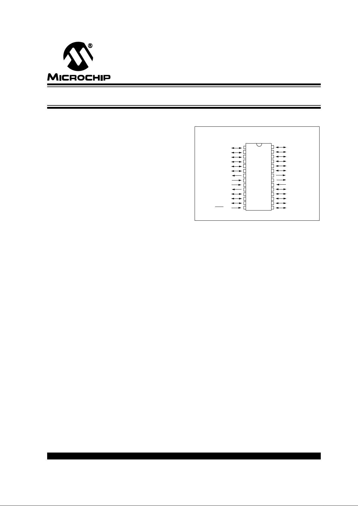
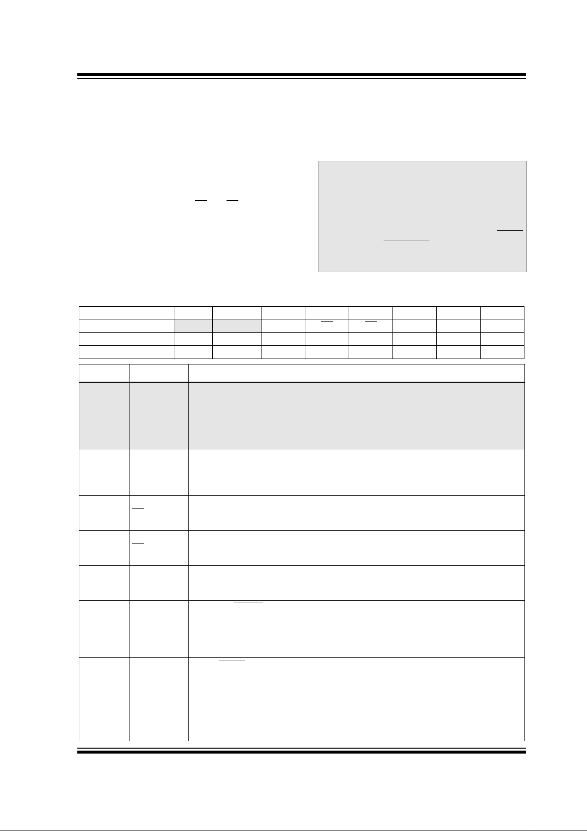
PIC14000
28-Pin Programmable Mixed Signal Controller
Pin Diagram
Digital Peripherals Features:
• 22 I/O pins with individual direction control
• High current sink/source for direct LED drive
• TMR0: 8-bit timer/counter with 8-bit
programmable prescaler
• 16-bit A/D timer: can be used as a general
purpose timer
•I
2
C
serial port compatible with System
Management Bus
CMOS Technology:
• Low-power, high-speed CMOS EPROM technology
• Fully static design
• Wide-operating voltage range (2.7V to 6.0V)
• Commercial and Industrial Temperature Range
• Low power dissipation (typical)
- < 3 mA @5V, 4 MHz operating mode
- < 300 µ A @3V (Sleep mode: clocks stopped
with analog circuits active)
- < 5 µ A @3V (Hibernate mode: clocks
stopped, analog inactive, and WDT disabled)
Applications:
• Battery Chargers
• Battery Capacity Monitoring
• Uninterruptable Power Supply Controllers
• Power Management Controllers
• HVAC Controllers
• Sensing and Data Acquisition
PDIP, SOIC, SSOP, Windowed CERDIP
28
27
26
25
24
23
22
21
20
19
18
17
16
15
RA2/AN2
RA3/AN3
RD4/AN4
RD5/AN5
RD6/AN6
RD7/AN7
CDAC
SUM
V
SS
RC0/REFA
RC1/CMPA
RC2
RC3/T0CKI
RC4
PIC14000
• 1
2
3
4
5
6
7
8
9
10
11
12
13
14
RA1/AN1
RA0/AN0
RD3/REFB
RD2/CMPB
RD1/SDAB
RD0/SCLB
OSC2/CLKOUT
OSC1/PBTN
V
DD
VREG
RC7/SDAA
RC6/SCLA
RC5
MCLR/VPP

PIC14000
DS40122B-page 2
Preliminary
1996 Microchip Technology Inc.
TABLE OF CONTENTS
1.0: General Description........................................................................................................................... 3
2.0: Device Varieties ................................................................................................................................ 5
3.0: Architectural Overview ...................................................................................................................... 7
4.0: Memory Organization...................................................................................................................... 13
5.0: I/O Ports.......................................................................................................................................... 25
6.0: Timer Modules................................................................................................................................. 37
7.0: Inter-integrated Circuit Serial Port (I
2
C
)........................................................................................ 41
8.0: Analog Modules for A/D Conversion............................................................................................... 57
9.0: Other Analog Modules..................................................................................................................... 65
10.0: Special Features of the CPU........................................................................................................... 75
11.0: Instruction Set Summary................................................................................................................. 91
12.0: Development Support.................................................................................................................... 103
13.0: Electrical Characteristics for PIC14000..........................................................................................107
14.0: Analog Specifications: PIC14000-04 (Commercial, Industrial)...................................................... 123
Appendix A:PIC16/17 Microcontrollers ....................................................................................................133
Index.........................................................................................................................................................143
PIC14000 Product Identification System..................................................................................................149
To Our Valued Customers
We constantly strive to improve the quality of all our products and documentation. To this end, we recently converted
to a new publishing software package which we believe will enhance our entire documentation process and product.
As in any conversion process, information may have accidently been altered or deleted. We have spent an exceptional amount of time to ensure that these documents are correct. However, we realize that we may have missed a
few things. If you find any information that is missing or appears in error, please use the reader response form in the
back of this data sheet to inform us. We appreciate your assistance in making this a better document.

1996 Microchip Technology Inc.
Preliminary
DS40122B-page 3
PIC14000
1.0 GENERAL DESCRIPTION
The PIC14000 features include medium to high resolution A/D conversion (10 to 16 bits), temperature sensing, closed loop charge control, serial communication,
and low power operation.
The PIC14000 uses a RISC Harvard architecture CPU
with separate 14-bit instruction and 8-bit data buses. A
two-stage instruction pipeline allows all instructions to
execute in a single cycle, except for program branches,
which require two cycles. A total of 35 instructions are
available. Additionally, a large register set is included.
PIC16/17 microcontrollers typically achieve a 2:1 code
compression and a 4:1 speed improvement over other
8-bit microcontrollers.
Features:
The PIC14000 is a 28-pin device with these features:
• 4K of EPROM
• 192 bytes of RAM
• 22 I/O pins
The analog peripherals include:
• 8 external analog input channels, two with level
shift inputs
• 6 internal analog input channels
• 2 comparators with programmable references
• A bandgap reference
• An internal temperature sensor
• A programmable current source
In addition, the I
2
C serial port through a multiplexer
supports two separate I
2
C channels.
A special oscillator option allows either an internal
4 MHz oscillator or an external crystal oscillator. Using
the internal 4 MHz oscillator requires no external components.
The PIC14000 contains three timers, the Watchdog
Timer (WDT), Timer0 (TMR0), and A/D Timer
(ADTMR). The Watchdog Timer includes its own
on-chip RC oscillator providing protection against
software lock-up. TMR0 is a general purpose 8-bit
timer/counter with an 8-bit prescaler. It may be clocked
externally using the RC3/T0CKI pin. The ADTMR is
intended for use with the slope A/D converter, but can
also be used as a general purpose timer. It has an
associated capture register which can be used to measure the time between events.
An internal low-voltage detect circuit allows for tracking
of voltage levels. Upon detecting the low voltage condition, the PIC14000 can be instructed to save its operating state then enter an idle state.
The internal band-gap reference is used for calibrating
the measurements of the analog peripherals. The
calibration factors are stored in EPROM and can be
used to achieve high measurement accuracy.
Power savings modes are available for portable applications. The SLEEP and HIBERNATE modes offer different levels of power savings. The PIC14000 can
wake up from these modes through interrupts or reset.
A UV erasable CERDIP packaged version is ideal for
code development, while the cost-effective One-Time
Programmable (OTP) version is suitable for production
in any volume.
The PIC14000 fits perfectly in applications for battery
charging, capacity monitoring, and data logging. The
EPROM technology makes customization of
application programs (battery characteristics, feature
sets, etc.) extremely fast and convenient. The small
footprint packages make this microcontroller based
mixed signal device perfect for all applications with
space limitations. Low-cost, low-power, high performance, ease of use and I/O flexibility make the
PIC14000 very versatile in other applications such as
temperature monitors/controllers.
1.1 F
amily and Upward Compatibility
Code written for PIC16C6X/7X can be easily ported to
the PIC14000 (see Appendix A).
1.2 De
velopment Support
The PIC14000 is supported by a full-featured macro
assembler, a software simulator, an in-circuit emulator,
a low-cost development programmer and a
full-featured programmer. A “C” compiler and fuzzy
logic support tools are also available.

PIC14000
DS40122B-page 4
Preliminary
1996 Microchip Technology Inc.
NOTES:

1996 Microchip Technology Inc.
Preliminary
DS40122B-page 5
PIC14000
2.0 DEVICE V ARIETIES
A variety of frequency ranges and packaging options
are available. The PIC14000 Product Selection System
section at the end of this data sheet provides the
devices options to be selected for your specific application and production requirements. When placing
orders, please use the “PIC14000 Product Identification System” at the back of this data sheet to specify the
correct part number.
2.1 UV Erasab
le Devices
The UV erasable version, offered in CERDIP package,
is optimal for prototype development and pilot
programs.
The UV erasable version can be erased and
reprogrammed to any of the configuration modes.
Microchip's PICSTART
,
PICSTART-PLUS and
PRO MATE
programmers all support programming of
the PIC14000. Third party programmers also are available; refer to the
Microchip
Third Party Guide
for a list
of sources.
2.2 One-Time-Pr
ogrammable (OTP)
Devices
The availability of OTP devices is especially useful for
customers who need the flexibility for frequent code
updates or small volume applications.
The OTP devices, packaged in plastic packages permit
the user to program them once. In addition to the
program memory, the configuration bits must also be
programmed.
Note: Please note that erasing the device will
also erase the pre-programmed calibration
factors. Please refer to AN621 for more
information.
2.3 Quic
k-Turnaround-Production (QTP)
Devices
Microchip offers a QTP Programming Service for
factory production orders. This service is made
available for users who choose not to program a
medium to high quantity of units and whose code
patterns have stabilized. The devices are identical to
the OTP devices but with all EPROM locations and
fuse options already programmed by the factory.
Certain code and prototype verification procedures do
apply before production shipments are available.
Please contact your local Microchip Technology sales
office for more details.
2.4 Serializ
ed Quick-Turnaround
Production (SQTP
SM
) De
vices
Microchip offers a unique programming service where
a few user-defined locations in each device are
programmed with different serial numbers. The serial
numbers may be random, pseudo-random or
sequential.
Serial programming allows each device to have a
unique number which can serve as an entry-code,
password or ID number.

PIC14000
DS40122B-page 6
Preliminary
1996 Microchip Technology Inc.
NOTES:

1996 Microchip Technology Inc.
Preliminary
DS40122B-page 7
PIC14000
3.0 ARCHITECTURAL OVERVIEW
The PIC14000 addresses 4K x 14 program memory. All
program memory is internal. The PIC14000 can directly
or indirectly address its register files or data memory. All
special function registers including the program counter
are mapped in the data memory. The PIC14000 has an
orthogonal instruction set that makes it possible to
carry out any operation on any register using any
addressing mode. This symmetrical nature and lack of
‘special optimal situations’ make programming with the
PIC14000 simple yet efficient. In addition, the learning
curve is reduced significantly.
The PIC14000 contains an 8-bit ALU and working
register. The ALU performs arithmetic and Boolean
functions between data in the working register and any
register file.
The ALU is capable of addition, subtraction, shift, and
logical operations. Unless otherwise mentioned,
arithmetic operations are two's complement. In
two-operand instructions, typically one operand is the
working register (W register). The other operand is a
file register or an immediate constant. In single
operand instructions, the operand is either the
W register or a file register.
Depending on the instruction executed, the ALU may
affect the values of the Carry (C), Digit Carry (DC), and
Zero (Z) bits in the STATUS register. The C and DC bits
operate as a borrow
bit and a digit borrow out bit,
respectively, in subtraction. See the SUBLW and SUBWF
instructions for examples.
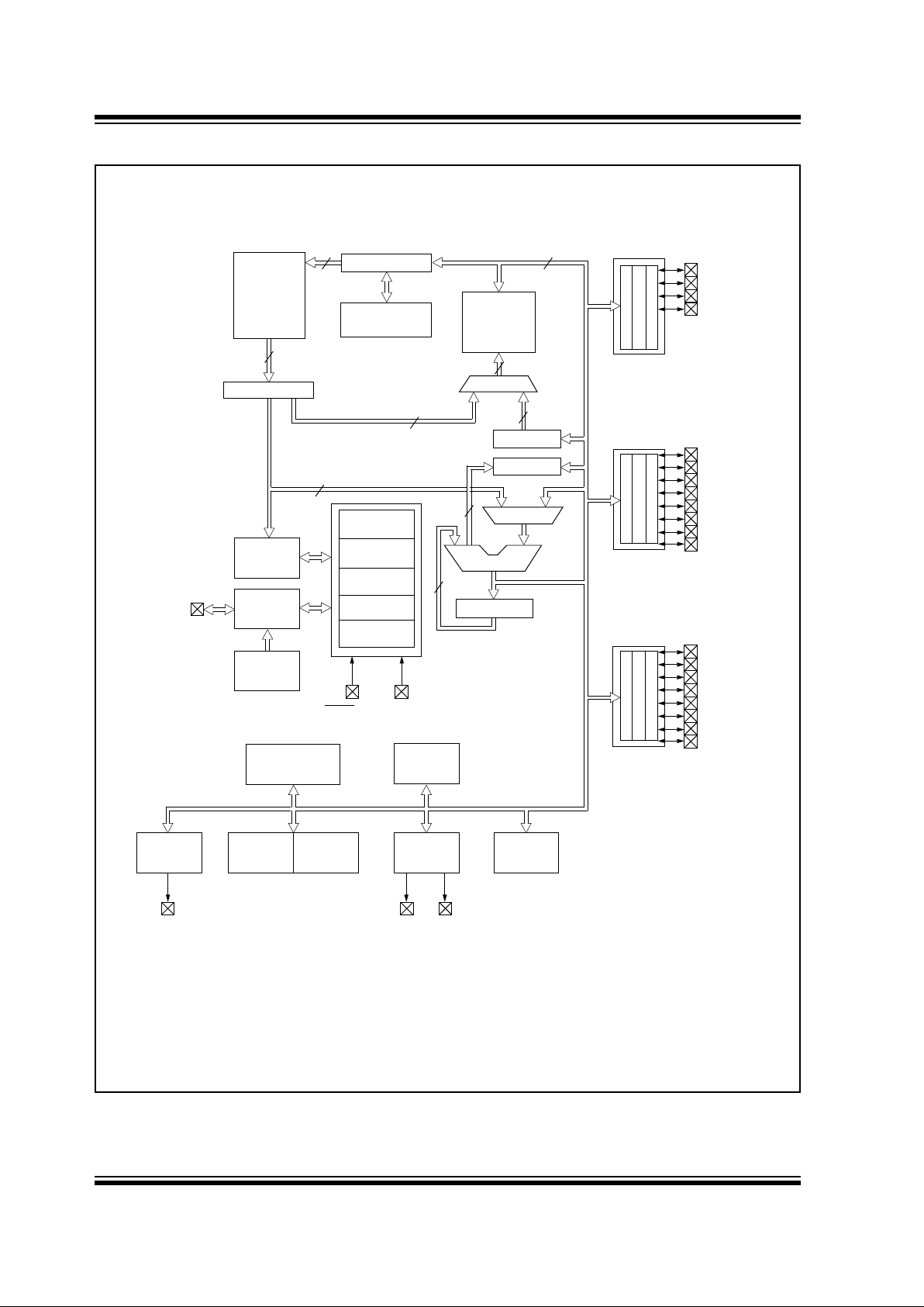
A simplified block diagram for the PIC14000 is shown
in Figure 3-1, its corresponding pin description is
shown in Table 3-1.
PIC14000
DS40122B-page 8
Preliminary
1996 Microchip Technology Inc.
FIGURE 3-1: PIC14000 BLOCK DIAGRAM
EPROM
Program
Memory
4K x 14
13
Data Bus
8
14
Program
Bus
Instruction reg
Program Counter
8 Level Stack
(13-bit)
RAM
File
Registers
192 x 8
Direct Addr
7
RAM Addr
(1)
9
Addr MUX
Indirect
Addr
FSR reg
STATUS reg
MUX
ALU
W reg
Power-up
Timer
Oscillator
Start-up Timer
Power-on
Reset
Watchdog
Timer
Instruction
Decode &
Control
Timing
Generation
OSC1/PBTN
OSC2/CLKOUT
MCLR
/VPP VDD, VSS
PORTA
PORTC
RC0/REFA
RC1/CMPA
RC2
RC3/T0CKI
RC4
RC5
RC6/SCLA
RC7/SDAA
8
8
Low Voltage
Detector
Note 1: Higher order bits are from the STATUS register.
I2C
Timer0
Serial Port
RA3/AN3
RA2/AN2
RA1/AN1
RA0/AN0
8
3
RD0/SCLB
RD1/SDAB
SUM CDAC
Slope A/D
PORTD
RD2/CMPB
RD3/REFB
RD4/AN4
RD5/AN5
RD6/AN6
RD7/AN7
Internal
Oscillator
BandgapT emp
Programmable
Sensor Reference
Reference A & B
with Comparators
VREG
Voltage
Regulator
Support

1996 Microchip Technology Inc.
Preliminary
DS40122B-page 9
PIC14000
TABLE 3-1: PIN DESCRIPTIONS
Pin Name
Pin
No.
I/O
Pin Type
Input Output
Description
CDAC 22 O — AN A/D ramp current source output. Normally connected to
external capacitor to generate a linear voltage ramp.
RA0/AN0 2 I/O AN/ST CMOS Analog input channel 0. This pin can also serve as a
general-purpose I/O.
RA1/AN1 1 I/O AN/ST CMOS Analog input channel 1. This pin can connect to a level
shift network. If enabled, a +0.5V offset is added to the
input voltage. This pin can also serve as a generalpurpose I/O.
RA2/AN2 28 I/O AN/ST CMOS Analog input channel 2. This pin can also serve as a
general purpose digital I/O.
RA3/AN3 27 I/O AN/ST CMOS Analog input channel 3. This pin can also serve as a gen-
eral purpose digital I/O.
SUM 21 O — AN AN1 summing junction output. This pin can be connected
to an external capacitor for averaging small duration
pulses.
RC0/REFA 19 I/O-PU ST CMOS LED direct-drive output or programmable reference A out-
put. This pin can also serve as a GPIO. If enabled, this
pin has a weak internal pull-up to V
DD
.
RC1/CMPA 18 I/O-PU ST CMOS LED direct-drive output or comparator A output. This pin
can also serve as a GPIO. If enabled, this pin has a weak
internal pull-up to V
DD
.
RC2 17 I/O-PU ST CMOS LED direct-drive output. This pin can also serve as a
GPIO. If enabled, this pin has a weak internal pull-up to
V
DD
RC3/T0CKI 16 I/O-PU ST CMOS LED direct-drive output. This pin can also serve as a
GPIO, or an external clock input for Timer0. If enabled,
this pin has a weak internal pull-up to V
DD
.
RC4 15 I/O-PU ST CMOS LED direct-drive output. This pin can also serve as a
GPIO. If enabled, a change on this pin can cause a CPU
interrupt. If enabled, this pin has a weak internal pull-up
to V
DD
.
RC5 13 I/O-PU ST CMOS LED direct-drive output. This pin can also serve as a
GPIO. If enabled, a change on this pin can cause a CPU
interrupt. If enabled, this pin has a weak internal pull-up
to V
DD
.
RC6/SCLA 12 I/O ST/SM NPU/OD
(No P-diode)
General purpose I/O. If enabled, is multiplexed as
synchronous serial clock for I
2
C interface. Also is the
serial programming clock. If enabled, a change on this pin
can cause a CPU interrupt. This pin has an N-channel
pull-up device which is disabled in I
2
C mode.
RC7/SDAA 11 I/O ST/SM NPU/OD
(No P-diode)
General purpose I/O. If enabled, is multiplexed as
synchronous serial data I/O for I
2
C interface. Also is the
serial programming data line. If enabled, a change on this
pin can cause a CPU interrupt. This pin has an N-channel
pull-up device which is disabled in I
2
C mode.
RD0/SCLB 6 I/O ST/SM NPU/OD
(No P-diode)
General purpose I/O. If enabled, is multiplexed as
synchronous serial clock for I
2
C interface. This pin has an
N-channel pull-up device which is disabled in I
2
C mode.
RD1/SDAB 5 I/O ST/SM NPU/OD
(No P-diode)
General purpose I/O. If enabled, is multiplexed as
synchronous serial data I/O for I
2
C interface. This pin has
an N-channel pull-up device which is disabled in I
2
C
mode.
RD2/CMPB 4 I/O-PU AN/ST CMOS General purpose I/O or comparator B output.

PIC14000
DS40122B-page 10
Preliminary
1996 Microchip Technology Inc.
Legend:
RD3/REFB 3 I/O-PU AN/ST CMOS General purpose I/O or programmable reference B
output.
RD4/AN4 26 I/O AN/ST CMOS Analog input channel 4. This pin can also serve as a
GPIO.
RD5/AN5 25 I/O AN/ST CMOS Analog input channel 5. This pin can connect to a level
shift network. If enabled, a +0.5V offset is added to the
input voltage. This pin can also serve as a GPIO.
RD6/AN6 24 I/O AN/ST CMOS Analog input channel 6. This pin can also serve as a
GPIO.
RD7/AN7 23 I/O AN/ST CMOS Analog input channel 7. This pin can also serve as a
GPIO.
VREG 10 O — AN This pin is an output to control the gate of an external
N-FET for voltage regulation.
OSC1/PBTN 8 I-PU ST — IN Mode: Input with weak pull-up resistor, can be used to
generate an interrupt.
HS Mode: External oscillator input.
OSC2/
CLKOUT
7 O — CMOS IN Mode: General purpose output.
HS Mode: External oscillator/clock output.
MCLR
/VPP 14 I/PWR ST Master clear (reset) input / programming voltage input.
This pin is an active low reset to the device.
V
DD
9 PWR Positive supply connection
V
SS
20 GND Return supply connection
Type: Definition:
TTL TTL-compatible input
CMOS CMOS-compatible input or output
ST Schmitt Trigger input, with CMOS levels
SM SMBus compatible input
OD Open-drain output. An external pull-up resistor is required if this pin is used as an output.
NPU N-channel pull-up. This pin will pull-up to approximately V
DD
- 1.0V when outputting a logical ‘1’.
PU Weak internal pull-up (10K-50K ohms)
No-P diode No P-diode to V
DD
. This pin may be pulled above the supply rail (to 6.0V maximum).
AN Analog input or output
TABLE 3-1: PIN DESCRIPTIONS (CONTINUED)
Pin Name
Pin
No.
I/O
Pin Type
Input Output
Description
1996 Microchip Technology Inc.
Preliminary
DS40122B-page 11
PIC14000
3.1 Cloc
king Scheme/Instruction Cycle
The clock input (from OSC1 or the internal oscillator) is
internally divided by four to generate four
non-overlapping quadrature clocks, namely Q1, Q2,
Q3 and Q4. The program counter (PC) is incremented
every Q1, the instruction is fetched from the program
memory and latched into the instruction register in Q4.
The instruction is decoded and executed during the
following Q1 through Q4. The clocks and instruction
execution flow are shown in Figure 3-2.
3.2 Instruction Flo
w/Pipelining
An “Instruction Cycle” consists of four Q cycles (Q1,
Q2, Q3 and Q4). The instruction fetch and execute are
pipelined such that fetch takes one instruction cycle
while decode and execute takes another instruction
cycle. However, due to the pipelining, each instruction
effectively executes in one cycle. If an instruction
causes the program counter to change (e.g., GOTO)
then two cycles are required to complete the instruction
(Example 3-1).
A fetch cycle begins with the program counter (PC)
incrementing in Q1.
In the execution cycle, the fetched instruction is latched
into the “Instruction Register (IR)” in cycle Q1. This
instruction is then decoded and executed during the
Q2, Q3, and Q4 cycles. Data memory is read during Q2
(operand read) and written during Q4 (destination
write).
FIGURE 3-2: CLOCK/INSTRUCTION CYCLE
EXAMPLE 3-1: INSTRUCTION PIPELINE FLOW
Q1
Q2 Q3 Q4
Q1
Q2 Q3 Q4
Q1
Q2 Q3 Q4
OSC1
Q1
Q2
Q3
Q4
PC
CLKOUT
(IN mode)
PC PC+1 PC+2
Fetch INST (PC)
Execute INST (PC-1) Fetch INST (PC+1)
Execute INST (PC) Fetch INST (PC+2)
Execute INST (PC+1)
Internal
Phase
Clock
1. MOVLW 55h
2. MOVWF PORTB
3. CALL SUB_1
4. BSF PORTA, BIT3
Fetch 1
Fetch 2
Fetch 3
Fetch SUB_1
Execute 1
Flush
All instructions are single cycle, except for program branches. These take two cycles
since the fetched instruction is “flushed” from the pipeline while the new instruction is
being fetched and then executed.
Execute 2
Flush
Fetch 4
Fetch SUB_1
Execute 3

PIC14000
DS40122B-page 12
Preliminary
1996 Microchip Technology Inc.
NOTES:
1996 Microchip Technology Inc.
Preliminary
DS40122B-page 13
PIC14000
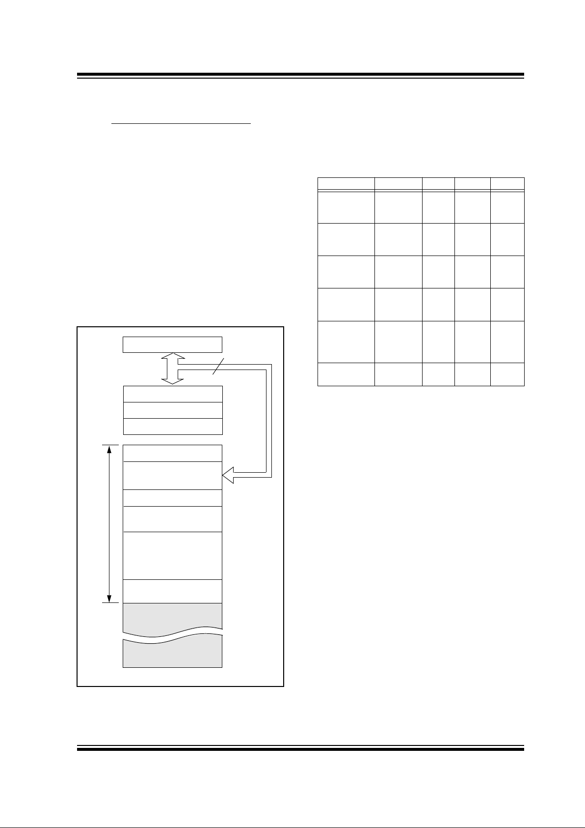
4.0 MEMORY ORGANIZATION
4.1 Pr
ogram Memory Organization
The PIC14000 has a 13-bit program counter capable of
addressing an 8K x 14 program memory space. Only
the first 4K x 14 (0000-0FFFh) are physically implemented. Accessing a location above the physically
implemented address will cause a wraparound. The
reset vector is at 0000h and the interrupt vector is at
0004h (Figure 4-1).
The 4096 words of Program Memory space are divided
into:
• Address Vectors (addr 0000h-0004h)
• Program Memory Page 0 (addr 0005h-07FFH)
• Program Memory Page 1 (addr 0800h-0FBFh)
• Calibration Space (64 words, addr 0FC0h-0FFFh)
Program code may reside in Page 0 and Page 1.
FIGURE 4-1: PIC14000 PROGRAM
MEMORY MAP AND STACK
PC<12:0>
Stack Level 1
Stack Level 8
Reset Vector
Interrupt Vector
Program Memory & Calibration Space
•
•
•
•
•
CALL, RETURN,
RETFIE, RETLW
13
0000h
0004h
0005h
0FFFh
1000h
20FFh
07FFh
(4096 words)
On-chip Program
Memory (Page 0)
0800h
On-chip Program
Memory (Page 1)
Calibration Space
(64 words)
0FC0h
0FBFh
4.1.1 CALIBRATION SPACE
The calibration space is not used for instructions. This
section stores constants and factors for the arithmetic
calculations to calibrate the analog measurements.
TABLE 4-1: CALIBRATION DATA
OVERVIEW*
*
Refer to AN621 for details.
** Microchip modified IEEE754 32-bit floating point format.
Refer to application note AN575 for details.
Address Parameter Symbol Units Format
0FC0h-0FC3h
Slope
reference
ratio
K
REF
N/A
32-bit
floating
point **
0FC4h-0FC7h
Bandgap
reference
voltage
K
BG
Volts
32-bit
floating
point
0FC8h-0FCBh
Temperature sensor
voltage
V
THERM
Volts
32-bit
floating
point
0FCCh-0FCFh
Temperature sensor
coefficient
K
TC
Volts/
degree
Celsius
32-bit
floating
point
0FD0h
Internal
oscillator
frequency
multiplier
F
OSC
N/A byte
0FD2h
WDT
time-out
T
WDT
ms byte
PIC14000
DS40122B-page 14
Preliminary
1996 Microchip Technology Inc.
TABLE 4-2: CALIBRATION CONSTANT
ADDRESSES
4.2 Data Memor
y Organization
The data memory (Figure 4-2) is partitioned into two
banks which contain the general purpose registers and
the special function registers. Bank 0 is selected when
the RP0 bit in the STATUS register is cleared. Bank 1
is selected when the RP0 bit in the STATUS register is
set. Each bank extends up to 7Fh (128 bytes). The first
32 locations of each bank are reserved for the Special
Function Registers. Several Special Function
Registers are mapped in both Bank 0 and Bank 1. The
general purpose registers, implemented as static RAM,
are located from address 20h through 7Fh, and A0
through FF.
Address Data
0FC0h
K
REF
, exponent
0FC1h
K
REF
, mantissa high byte
0FC2h
K
REF
, mantissa middle byte
0FC3h
K
REF
, mantissa low byte
0FC4h
K
BG
, exponent
0FC5h
K
BG
, mantissa high byte
0FC6h
K
BG
, mantissa middle byte
0FC7h
K
BG
, mantissa low byte
0FC8h
V
THERM
, exponent
0FC9h
V
THERM
, mantissa high byte
0FCAh
V
THERM
, mantissa middle byte
0FCBh
V
THERM
, mantissa low byte
0FCCh
K
TC
, exponent
0FCDh
K
TC
, mantissa high byte
0FCEh
K
TC
, mantissa middle byte
0FCFh
K
TC
, mantissa low byte
0FD0h
F
OSC
, unsigned byte
0FD1h reserved
0FD2h
T
WDT
, unsigned byte
0FD3h -
0FF8h
reserved
0FF9h-Fh calibration space checksums
4.2.1 GENERAL PURPOSE REGISTER FILE
The register file is accessed either directly, or indirectly
through the file select register FSR (Section 4.4).
FIGURE 4-2: REGISTER FILE MAP
File Address
* Not a physical register.
Shaded areas are unimplemented memory locations,
read as ‘0’s.
00h Indirect add.(*) Indirect addr.(*) 80h
01h TMR0 OPTION 81h
02h PCL PCL 82h
03h STATUS STATUS 83h
04h FSR FSR 84h
05h PORTA TRISA 85h
06h
RESERVED RESERVED 86h
07h PORTC TRISC 87h
08h PORTD TRISD 88h
09h
89h
0Ah PCLATH PCLATH 8Ah
0Bh INTCON INTCON 8Bh
0Ch PIR1 PIE1 8Ch
0Dh
8Dh
0Eh ADTMRL PCON 8Eh
0Fh ADTMRH SLPCON 8Fh
10h
90h
11h
91h
12h
92h
13h
I
2
CBUF I
2
CADD
93h
14h
I
2
CCON I
2
CSTAT
94h
15h ADCAPL
95h
16h ADCAPH
96h
17h
97h
18h
98h
19h
99h
1Ah
9Ah
1Bh
PREFA 9Bh
1Ch
PREFB 9Ch
1Dh
CMCON 9Dh
1Eh
MISC 9Eh
1Fh ADCON0 ADCON1 9Fh
20h
General
Purpose
Register
(96 Bytes)
General
Purpose
Register
(96 Bytes)
A0h
7F FF
1996 Microchip Technology Inc.
Preliminary
DS40122B-page 15
PIC14000
4.2.2 SPECIAL FUNCTION REGISTERS
The special function registers are registers used by the
CPU and peripheral functions for controlling the
desired operation of the device (Table 4-3). These registers are static RAM.
The special registers are classified into two sets.
Special registers associated with the “core” functions
are described in this section. Those registers related to
the operation of the peripheral features are described
in the section specific to that peripheral.
TABLE 4-3: SPECIAL FUNCTION REGISTERS FOR THE PIC14000
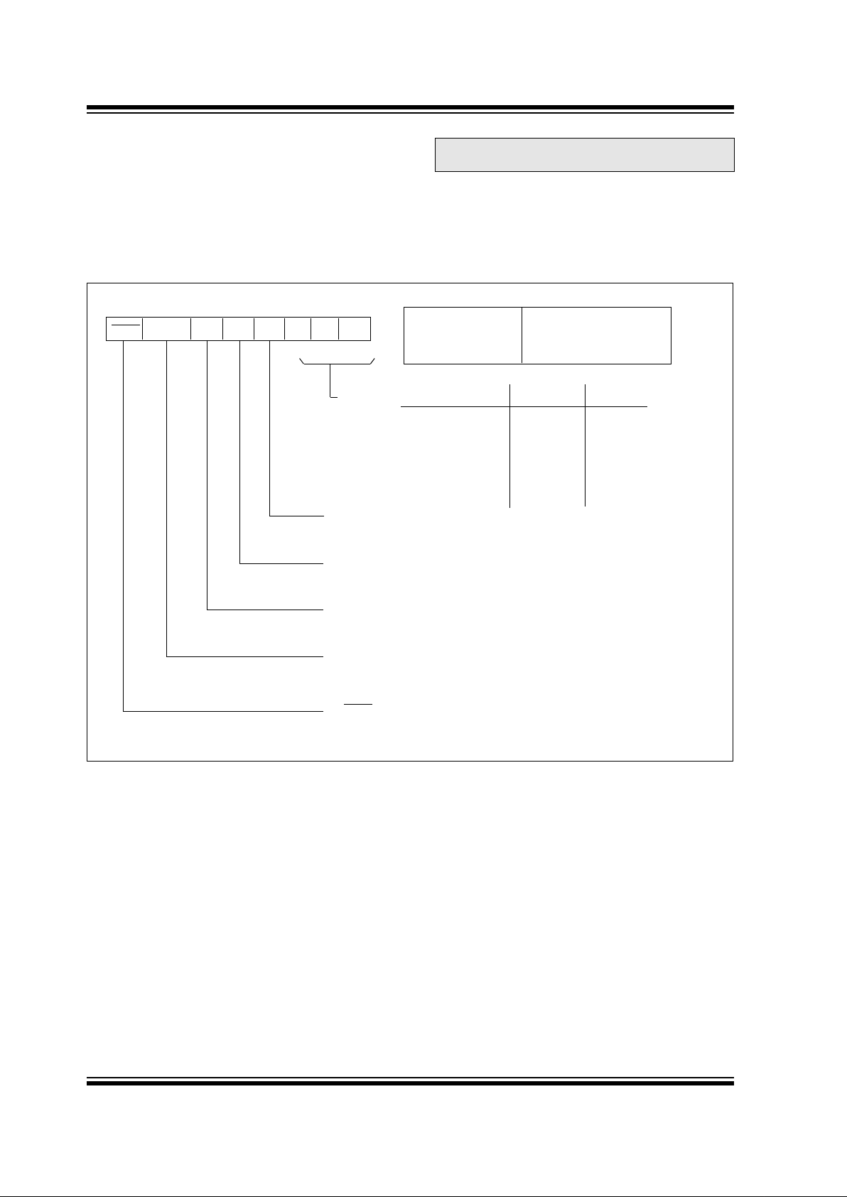
Address Name Bit 7 Bit 6 Bit 5 Bit 4 Bit 3 Bit 2 Bit 1 Bit 0
Bank0
00h*
INDF
(Indirect
Address)
Addressing this location uses contents of the FSR to address data memory (not a physical
register).
01h TMR0 Timer0 data
02h* PCL Program Counter’s (PC’s) least significant byte
03h* STATUS
IRP RP1 RP0 TO PD Z DC C
04h* FSR Indirect data memory address pointer
05h PORTA PORTA data latch.
06h Reserved Reserved for emulation.
07h PORTC PORTC data latch
08h PORTD PORTD data latch
09h Reserved
0Ah* PCLATH Buffered register for the upper 5 bits of the Program Counter (PC)
0Bh* INTCON GIE PEIE T0IE r r T0IF r r
0Ch PIR1 CMIF — — PBIF I
2
CIF RCIF ADCIF OVFIF
0Dh Reserved
0Eh ADTMRL A/D capture timer data least significant byte
0Fh ADTMRH A/D capture timer data most significant byte
10h Reserved
11h Reserved
12h Reserved
13h I
2
CBUF I
2
C Serial Port Receive Buffer/Transmit Register
14h I
2
CCON WCOL I
2
COV I
2
CEN CKP I
2
CM3 I
2
CM2 I
2
CM1 I
2
CM0
15h ADCAPL A/D capture latch least significant byte
16h ADCAPH A/D capture latch most significant byte
17h Reserved
18h Reserved
19h Reserved
1Ah Reserved
1Bh Reserved
1Ch Reserved
1Dh Reserved
1Eh Reserved
1Fh ADCON0 ADCS3 ADCS2 ADCS1 ADCS0 — AMUXOE ADRST ADZERO
Legend
— = unimplemented bits, read as ‘0’ but cannot be overwritten
r = reserved bits, default is POR value and should not be overwritten with any value
Reserved indicates reserved register and should not be overwritten with any value
* indicates registers that can be addressed from either bank
PIC14000
DS40122B-page 16
Preliminary
1996 Microchip Technology Inc.
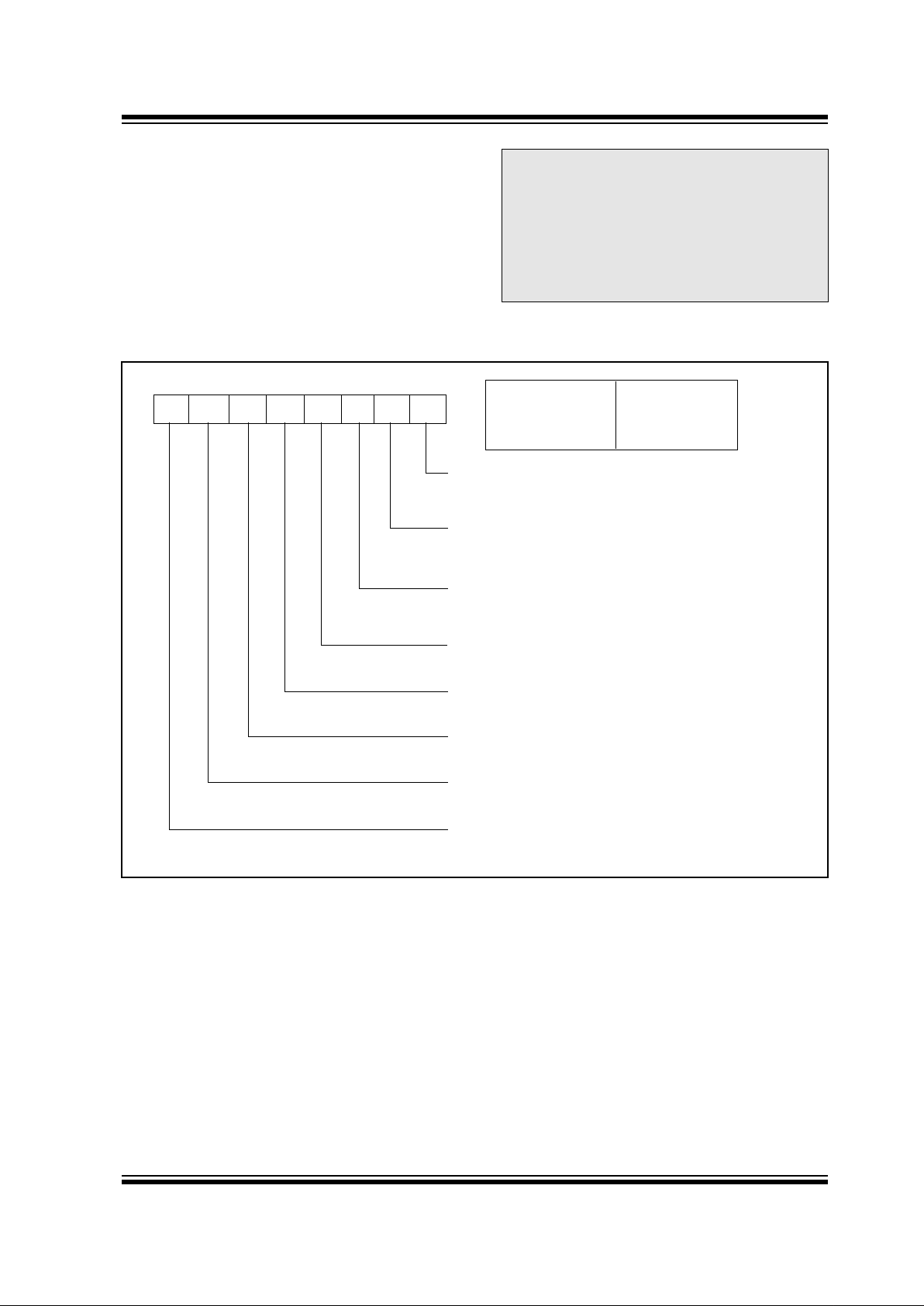
Bank1
80h*
INDF
(Indirect Address)
Addressing this location uses contents of FSR to address data memory (not a physical register).
81h OPTION RCPU
r TOCS TOSE PSA PS2 PS1 PS0
82h* PCL Program Counter’s (PC’s) least significant byte
83h* STATUS IRP RP1 RP0 TO PD Z DC C
84h* FSR Indirect data memory address pointer
85h TRISA PORTA Data Direction Register
86h Reserved Reserved for emulation
87h TRISC PORTC Data Direction Register
88h TRISD PORTD Data Direction Register
89h Reserved
8Ah* PCLATH Buffered register for the upper 5 bits of the Program Counter (PC)
8Bh* INTCON GIE PEIE T0IE r r T0IF r r
8Ch PIE1 CMIE — — PBIE I
2
CIE RCIE ADCIE OVFIE
8Dh Reserved
8Eh PCON r — — — — — POR LVD
8Fh SLPCON HIBEN — REFOFF LSOFF OSCOFF CMOFF TEMPOFF ADOFF
90h Reserved
91h Reserved
92h Reserved
93h I
2
CADD I
2
C Synchronous Serial Port Address Register
94h I
2
CSTAT — — D/A
P S R/W UA BF
95h Reserved
96h Reserved
97h Reserved
98h Reserved
99h Reserved
9Ah Reserved
9Bh PREFA PRA7 PRA6 PRA5 PRA4 PRA3 PRA2 PRA1 PRA0
9Ch PREFB PRB7 PRB6 PRB5 PRB4 PRB3 PRB2 PRB1 PRB0
9Dh CMCON — CMBOUT CMBOE CPOLB — CMAOUT CMAOE CPOLA
9Eh MISC SMHOG SPGNDB SPGNDA I
2
CSEL SMBUS INCLKEN OSC2 OSC1
9Fh ADCON1 ADDAC3 ADDAC2 ADDAC1 ADDAC0 PCFG3 PCFG2 PCFG1 PCFG0
TABLE 4-3: SPECIAL FUNCTION REGISTERS FOR THE PIC14000 (CONTINUED)
Address Name Bit 7 Bit 6 Bit 5 Bit 4 Bit 3 Bit 2 Bit 1 Bit 0
Legend
— = unimplemented bits, read as ‘0’ but cannot be overwritten
r = reserved bits, default is POR value and should not be overwritten with any value
Reserved indicates reserved register and should not be overwritten with any value
* indicates registers that can be addressed from either bank
1996 Microchip Technology Inc.
Preliminary
DS40122B-page 17
PIC14000
4.2.2.1 STATUS REGISTER
The STATUS register, shown in Figure 4-3, contains
the arithmetic status of the ALU, the RESET status and
the bank select bits for data memory.
The STATUS register can be the destination for any
instruction, as with any other register. If the STATUS
register is the destination for an instruction that affects
the Z, DC or C bits, then the write to these three bits is
disabled. These bits are set or cleared according to the
device logic. Furthermore, the T
O and PD bits are not
writable. Therefore, the result of an instruction with the
STATUS register as destination may be different than
intended.
For example, CLRF STATUS will clear the upper-three
bits and set the Z bit. This leaves the ST ATUS register
as 000u u1uu (where u = unchanged).
It is recommended, therefore, that only BCF, BSF,
SWAPF and MOVWF instructions are used to alter the
STATUS register because these instructions do not
affect the Z, C or DC bits from the ST A TUS register . For
other instructions, not affecting any status bits, see the
“Instruction Set Summary.”
Note 1: The IRP and RP1 bits (ST A TUS<7:6>) are
not used by the PIC14000 and should be
programmed as cleared. Use of these bits
as general purpose R/W bits is NOT
recommended, since this may affect
upward compatibility with future products.
Note 2: The C and DC bits operate as a borrow
and digit borrow out bit, respectively, in
subtraction. See the SUBLW and SUBWF
instructions for examples.
FIGURE 4-3: STATUS REGISTER
83h Bit 7 Bit 6 Bit 5 Bit 4 Bit 3 Bit 2 Bit 1 Bit 0
STATUS
IRP
RP1 RP0 TO PD Z DC C
Read/Write
R/W R/W R/W R R R/W R/W R/W
POR value FFh
00 011XXX
Bit Name Function
B7
IRP
Not used. This bit should be programmed as ‘0’.
Use of this bit as a general purpose read/write bit is not recommended, since this may
affect upward compatibility with future products.
B6 RP1
Not used. This bit should be programmed as ‘0’.
Use of this bit as a general purpose read/write bit is not recommended, since this may
affect upward compatibility with future products.
B5 RP0
Register page select for direct addressing.
1 = Bank1 (80h - FFh)
0 = Bank0 (00h - 7Fh)
Each page is 128 bytes. Only the RP0 bit is used.
B4 T
O
Time-out bit.
1 = After power-up and by the CLRWDT and SLEEP instruction.
0 = A watchdog timer time-out has occurred.
B3 PD
Power down bit.
1 = After power-up or by a CLRWDT instruction.
0 = By execution of the SLEEP instruction.
B2 Z
Zero bit.
1 = The result of an arithmetic or logic operation is zero.
0 = The result of an arithmetic or logical operation is not zero.
B1 DC
Digit carry /
borrow bit.
For ADDWF and ADDLW instructions.
1 = A carry-out from the 4th low order bit of the result.
0 = No carry-out from the 4th low order bit of the result.
Note: For Borrow, the polarity is reversed.
B0 C
Carry / borrow
bit.
For ADDWF and ADDLW instructions.
1 = A carry-out from the most significant bit of the result occurred. Note that a
subtraction is executed by adding the two’s complement of the second operand. For
rotate ( RRF, RLF ) instructions, this bit is loaded with either the high or low order bit of
the source register.
0 = No carry-out from the most significant bit of the result.
Note: For Borrow the polarity is reversed.
PIC14000
DS40122B-page 18
Preliminary
1996 Microchip Technology Inc.
4.2.2.2 OPTION REGISTER
The OPTION register (Address 81h) is a readable and
writable register which contains various control bits to
configure the TMR0/WDT prescaler, TMR0, and the
weak pull-ups on PORTC<5:0>. Bit 6 is reserved.
Note: To achieve a 1:1 prescaler assignment,
assign the prescaler to the WDT (PSA=1)
FIGURE 4-4: OPTION REGISTER
RCPU: PORTC pull-up enable
PSA PS2 PS1 PS0
R/W R/W R/W R/W R/W R/W R/W R/W
bit0
RCPU r T0CS T0SE
bit7
PS2 PS1 PS0
PSA: Prescaler assignment bit
T0SE: TMR0 source edge
T0CS: TMR0 clock source
PRESCALER VALUE
0
0
0
0
1
1
1
0
0
1
1
0
0
1
0
1
0
1
0
1
0
1 : 2
1 : 4
1 : 8
1 : 16
1 : 32
1 : 64
1 : 128
1 : 256
1 : 1
1 : 2
1 : 4
1 : 8
1 : 16
1 : 32
1 : 64
1 : 128
Reserved. This bit should be programmed as a ‘1’. Use of this bit as
Address: 81h
POR value: FFh
W: Writable
R: Readable
U: Unimplemented.
Read as '0'
TMR0 RATE WDT RATE
1 = Prescaler assigned to the WDT
0 = Prescaler assigned to TMR0
1 = Increment on high-to-low transition on RC3/T0CKI pin
0 = Increment on low-to-high transition on RC3/T0CKI pin
1 = Transition on RC3/T0CKI pin
0 = Internal instruction cycle clock (CLKOUT)
1 = PORTC pull-ups are disabled overriding any port latch value (RC<5:0> only)
0 = PORTC pull-ups are enabled by individual port-latch values (RC<5:0>)
PS2:PS0
111
Register: OPTION
general purpose read/write is not recommended since this may affect
upward compatibility with future products.
1996 Microchip Technology Inc. Preliminary DS40122B-page 19
PIC14000
4.2.2.3 INTCON REGISTER
The INTCON Register is a readable and writable
register which contains the various enable and flag bits
for the Timer0 overflow and peripheral interrupts.
Figure 4-5 shows the bits for the INTCON register.
Note: The T0IF will be set by the specified
condition even if the corresponding Interrupt Enable Bit is cleared (interrupt
disabled) or the GIE bit is cleared (all
interrupts disabled). Before enabling
interrupt, clear the interrupt flag, to ensure
that the program does not immediately
branch to the peripheral interrupt service
routine
FIGURE 4-5: INTCON REGISTER
GIE PEIE T0IE r
R/W R/W R/W R/W R/W R/W R/W R/W
W: Writable
R: Readable
U: Unimplemented,
read as '0'
Register: INTCON
Address:
0Bh or 8Bh
POR value: 0000 000xb
T0IF: TMR0 overflow interrupt flag
1 = The TMR0 has overflowed
Must be cleared by software
0 = TMR0 did not overflow
T0IE: TMR0 interrupt enable bit
1 = Enables T0IF interrupt
0 = Disables T0IF interrupt
PEIE: Peripheral interrupt enable bit
1 = Enables all un-masked peripheral interrupts
0 = Disables all peripheral interrupts
GIE: Global interrupt enable
1 = Enables all un-masked interrupts
0 = Disables all interrupts
bit7
bit0
r
r r
T0IF
Reserved. This bit should be programmed as ‘0’. Use of this bit
as a general purpose read/write bit is not recommended, since
this may affect upward compatibility with future products.
Reserved. This bit should be programmed as ‘0’. Use of this bit
as a general purpose read/write bit is not recommended, since
this may affect upward compatibility with future products.
Reserved. This bit should be programmed as ‘0’. Use of this bit
as a general purpose read/write bit is not recommended, since
this may affect upward compatibility with future products.
Reserved. This bit should be programmed as ‘0’. Use of this bit
as a general purpose read/write bit is not recommended, since
this may affect upward compatibility with future products.
PIC14000
DS40122B-page 20 Preliminary 1996 Microchip Technology Inc.
4.2.2.4 PIE1 REGISTER
This register contains the individual enable bits for the
Peripheral interrupts including A/D capture event, I
2
C
serial port, PORTC change and A/D capture timer
overflow, and external push button.
Note: INTCON<6> must be enabled to enable
any interrupt in PIE1.
FIGURE 4-6: PIE1 REGISTER
W: Writable
R: Readable
U: Unimplemented,
read as '0'
Register: PIE1
Address:
8Ch
POR value:
00h
R/W R R R/W R/W R/W R/W R/W
bit0
bit7
OVFIE: A/D Counter Overflow Interrupt Enable
1 = Enables A/D counter overflow interrupt
0 = Disables A/D counter overflow interrupt
ADCIE: A/D Capture Interrupt Enable
1 = A/D capture interrupt is enabled
0 = A/D capture interrupt is disabled
RCIE: PORTC Interrupt on change Enable
1 = Enables RCIF interrupt on pins, RC<7:4>
0 = Disables RCIF interrupt
I
2
CIE: I2C Port Interrupt Enable
1 = Enables I
2
CIF interrupt
0 = Disables I
2
CIF interrupt
PBIE: External Pushbutton Interrupt Enable
0 = Disable PBTN interrupt on OSC1/PBTN
1 = Enable PBTN (pushbutton) interrupt on OSC1/PBTN.
Unimplemented. Read as ‘0’
Unimplemented. Read as ‘0’
CMIE: Programmable Reference Comparator Interrupt Enable
1 = Enable programmable reference comparator trip
0 = Disable programmable reference comparator trip
CMIE
—
— PBIE I
2
CIE RCIE ADCIE OVFIE
(Note this interrupt not available in HS mode).
1996 Microchip Technology Inc. Preliminary DS40122B-page 21
PIC14000
4.2.2.5 PIR1 REGISTER
This register contains the individual flag bits for the
Peripheral interrupts (Figure 4-7).
Note: These bits will be set by the specified
condition, even if the corresponding
Interrupt Enable bit is cleared (interrupt
disabled) or the GIE bit is cleared (all
interrupts disabled). Before enabling an
interrupt, the user may wish to clear the
corresponding interrupt flag, to ensure that
the program does not immediately branch
to the Peripheral Interrupt service routine.
FIGURE 4-7: PIR1 REGISTER
CMIF
R/W R R
R/W R/W R/W R/W R/W
bit0bit7
CMIF: Programmable Reference Comparator Interrupt Flag
1 =The comparator output has tripped. This is a
0 = The interrupt did not occur
Unimplemented. Read as ‘0’
W: Writable
R: Readable
U: Unimplemented,
read as ‘0’
Register: PIR1
Address: 0Ch
POR value: 00h
—
—
PBIF
I
2
CIF RCIF ADCIF
OVFIF
Unimplemented. Read as ‘0’
OVFIF: A/D counter Overflow Interrupt Flag
1 =An A/D counter overflow has occurred.
Must be cleared in software.
0 = An A/D counter overflow has not occurred
ADCIF: A/D Capture Interrupt Flag
1 =An A/D capture has occurred.
Must be cleared in software.
0 = An A/D capture has not occurred
RCIF: PORTC Interrupt on Change Flag
1 =At least one RC<7:4> input changed.
Must be cleared in software.
0 =None of the RC<7:4> inputs have changed
I
2
CIF: I
2
C Port Interrupt Flag
1 =A transmission/reception is completed.
Must be cleared in software.
0 =Waiting to transmit/receive
PBIF: External Pushbutton Interrupt Flag
1 =The external pushbutton interrupt has occurred
0 =The external pushbutton interrupt did not occur
on OSC1/PBTN. Note: This interrupt is not available
in HS mode.
level-sensitive interrupt.
PIC14000
DS40122B-page 22 Preliminary 1996 Microchip Technology Inc.
4.2.2.6 PCON REGISTER
The Power Control (PCON) register status contains
2 flag bits to allow differentiation between a Power-on
Reset, an external MCLR
reset, WDT reset, or low-volt-
age condition (Figure 4-8).
These bits are cleared on POR. The user must set
these bits following POR. On a subsequent reset if
POR is cleared, this is an indication that the reset was
due to a power-on reset condition.
Note: LVD is unknown on Power-on Reset. It
must then be set by the user and checked
on subsequent resets to see if L
VD is
cleared, indicating a low voltage condition
has occurred.
FIGURE 4-8: PCON REGISTER
bit7 bit0
LVD —
POR
LVD:
Low Voltage Detect Flag
1 = A low-voltage detect condition has not occurred.
0 = A low-voltage detect condition has occurred.
Software must set this bit after a
power-on-reset condition has occurred.
Reserved. Bit 7 is reserved. This bit should be
R/W R/W
R/W U U U U U
r — — —
—
W: Writable
R: Readable
U: Unimplemented,
read as ‘0’
Register: PCON
Address: 8Eh
POR value:
0000_000xb
POR: Power on Reset Flag
1 = A power on reset condition has not occurred.
0 = A power on reset condition has occurred.
Software must set this bit after a
power-on-reset condition has occurred.
Reset must be due to some other source
(WDT, MCLR
).
programmed as ‘0’ .
Unimplemented. Read as ‘0’
Unimplemented. Read as ‘0’
Unimplemented. Read as ‘0’
Unimplemented. Read as ‘0’
Unimplemented. Read as ‘0’
1996 Microchip Technology Inc. Preliminary DS40122B-page 23
PIC14000
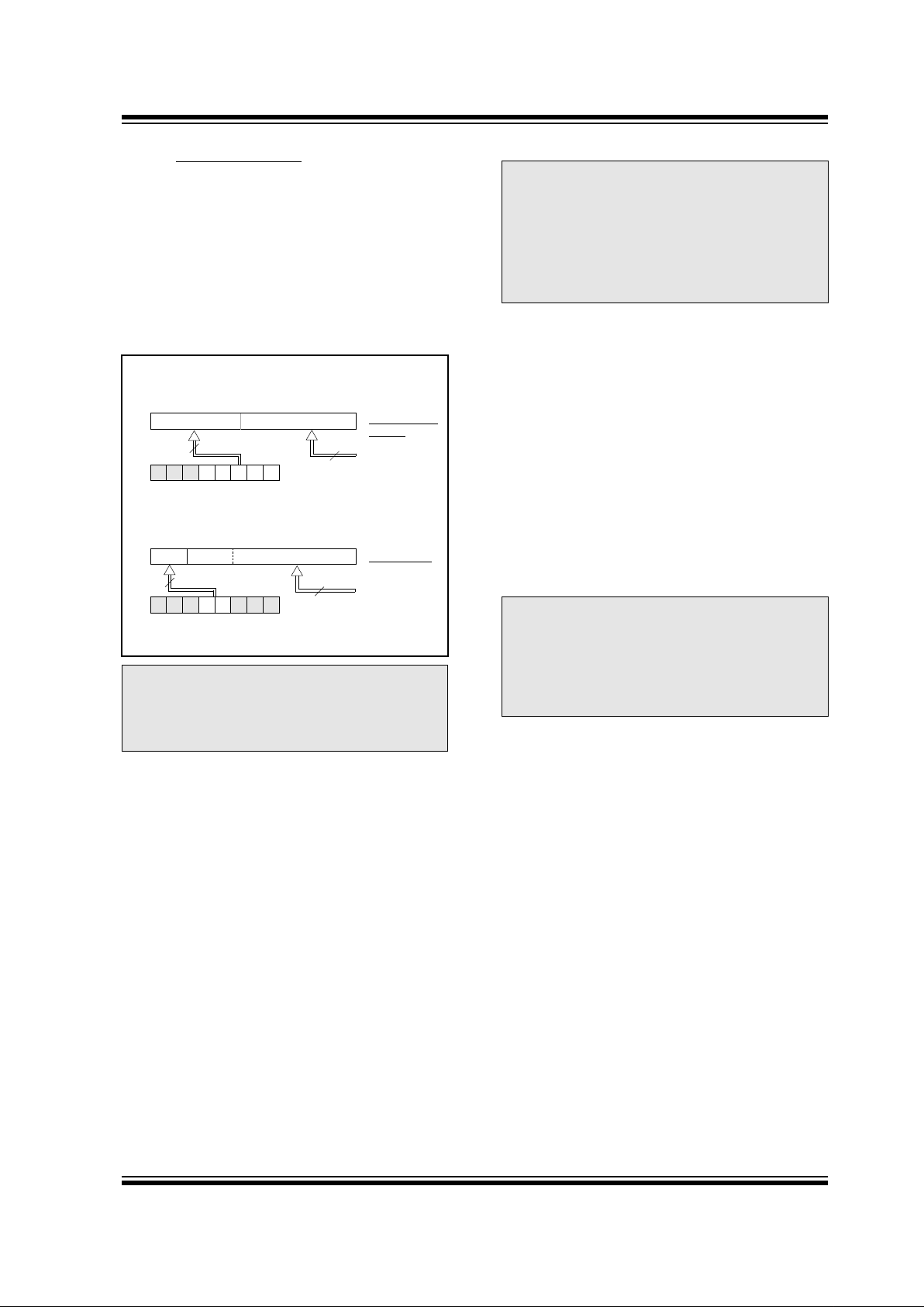
4.3 PCL and PCLATH
The program counter (PC) is 13-bits wide. The low
byte, PCL, is a readable and writable register. The high
byte of the PC (PCH) is not directly readable or
writable. PCLATH is a holding register for PC<12:8>
where contents are transferred to the upper byte of the
program counter. When PC is loaded with a new value
during a CALL, GOTO or a write to PCL, the high bits of
PC are loaded from PCLATH as shown in Figure 4-9.
FIGURE 4-9: LOADING OF PC IN
DIFFERENT SITUATIONS
4.3.1 COMPUTED GOTO
When doing a table read using a computed GOTO
method, care should be exercised if the table location
crosses a PCL memory boundary (each 256 byte
block). Refer to the application note “Table Read Using
the PIC16CXX”(AN556).
4.3.2 STACK
The PIC14000 has an 8 deep x 13-bit wide hardware
stack (Figure 4-1). The stack space is not part of either
program or data space and the stack pointer is not
readable or writable. The PC is PUSHed in the stack
when a CALL instruction is executed or an interrupt is
acknowledged. The stack is POPed in the event of a
RETURN, RETLW or a RETFIE instruction execution.
PCLATH is not affected by a “PUSH” or a “POP”
operation.
The stack operates as a circular buffer. This means
that after the stack has been “PUSHed” eight times, the
ninth push overwrites the value that was stored from
the first push. The tenth push overwrites the second
push (and so on).
Note: On POR, the contents of the PCLATH
register are unknown. The PCLA TH should
be initialized before a CALL, GOTO, or any
instruction that modifies the PCL register is
executed.
PC
12 8 7 0
5
PCLATH<4:0>
PCLATH
INST
with PCL
as dest
ALU result
GOT
O, CALL
Opcode <10:0>
8
PC
12 11 10 0
11
PCLATH<4:3>
PCH PCL
87
2
PCLATH
PCH PCL
4.3.3 PROGRAM MEMORY PAGING
The PIC14000 has 4K of program memory, but the
CALL and GOTO instructions only have a 11-bit address
range. This 1 1-bit address range allows a branch within
a 2K program memory page size. To allow CALL and
GOTO instructions to address the entire 4K program
memory address range, there must be another bit to
specify the program memory page. This paging bit
comes from the PCLATH<3> bit (Figure 4-9). When
doing a CALL or GOTO instruction, the user must ensure
that this page bit (PCLATH<3>) is programmed to the
desired program memory page. If a CALL instruction (or
interrupt) is executed, the entire 13-bit PC is pushed
onto the stack. Therefore, manipulation of the
PCLATH<3> is not required for the return instructions
(which pops the PC from the stack).
Example 4-1 shows the calling of a subroutine in
page 1 of the program memory. This example assumes
that the PCLATH is saved and restored by the interrupt
service routine (if interrupts are used).
EXAMPLE 4-1: CALL OF A SUBROUTINE IN
PAGE 1 FROM PAGE 0
Note 1: There are no STATUS bits to indicate
stack overflow or stack underflow
conditions.
Note 2: There are no instruction mnemonics
called PUSH nor POP. These are actions
that occur from the execution of the CALL,
RETURN, RETLW, or RETFIE instructions,
or the vectoring to an interrupt address
Note: The PIC14000 ignores the PCLATH<4>
bit, which is used for program memory
pages 2 and 3 (1000h-1FFFh). The use of
PCLATH<4> as a general purpose
read/write bit is not recommended since
this may affect upward compatibility with
future products.
ORG 0X500
BSF PCLATH, 3 ; Select page 1 (800h-FFFh)
CALL SUB1_P1 ; Call subroutine in
: ; page 1 (800h-FFFh)
:
:
ORG 0X900
SUB1 P1 : ; called subroutine
: ; page 1 (800h-FFFh)
:
RETURN ; return to page 0
; (000h-7FFh)

PIC14000
DS40122B-page 24 Preliminary 1996 Microchip Technology Inc.
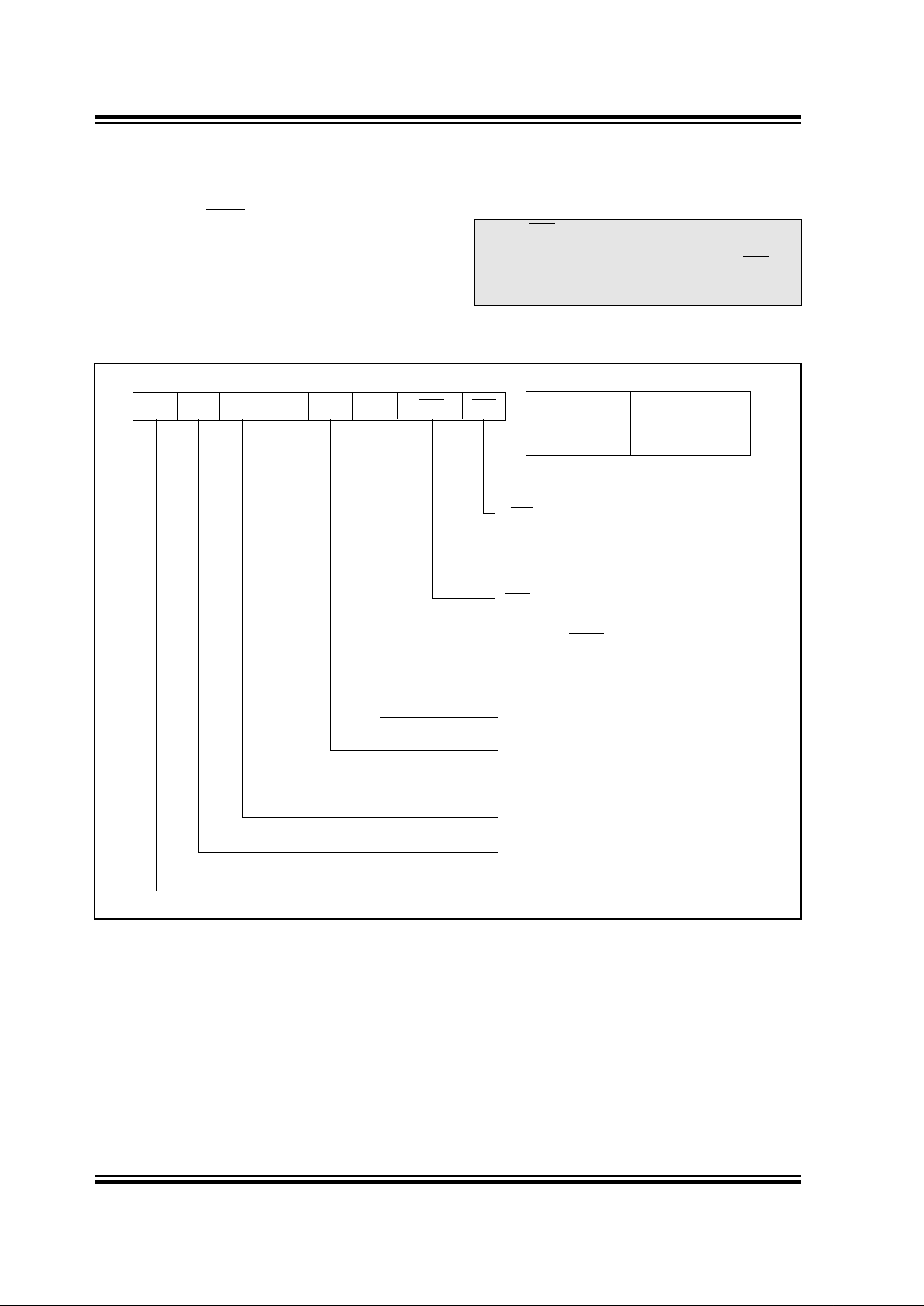
4.4 Indirect Addressing, INDF and FSR
Registers
The INDF register is not a physical register. Addressing
the INDF register will cause indirect addressing.
Indirect addressing is possible by using the INDF
register. Any instruction using the INDF register
actually accesses data pointed to by the file select
register (FSR). Reading INDF itself indirectly will
produce 00h. Writing to the INDF register indirectly
results in a no-operation (although status bits may be
affected). An effective 9-bit address is obtained by
concatenating the 8-bit FSR register and the IRP bit
(STATUS<7>), as shown in Figure 4-10. However, IRP
is not used in the PIC14000.
A simple program to clear RAM location 20h-2Fh using
indirect addressing is shown in Example 4-2.
EXAMPLE 4-2: INDIRECT ADDRESSING
movlw 0x20 ;initialize pointer
movf FSR ;to RAM
NEXT clrf INDF ;clear INDF register
incf FSR ;inc pointer
btfss FSR,4 ;all done?
goto NEXT ;no clear next
;yes continue
CONTINUE:
FIGURE 4-10: INDIRECT/INDIRECT ADDRESSING
Note: For memory map detail see Figure 4-1.
00
00
01 10 11
00
IRP 7 FSR 00
bank select
location select
0
6
from opcode
location select
bank select
RP1
RP0
Indirect Addressing
Direct Addressing
Data
Memory
not used
Bank 0
Bank 1 Bank 2 Bank 3
7F
7F
1996 Microchip Technology Inc.
Preliminary
DS40122B-page 25
PIC14000
5.0 I/O PORTS
The PIC14000 has three ports, PORTA, PORTC and
PORTD, described in the following paragraphs.
Generally, PORTA is used as the analog input port.
PORTC is used for general purpose I/O and for host
communication. PORTD provides additional I/O lines.
Four lines of PORTD may function as analog inputs.
5.1 POR
TA and TRISA
PORT A is a 4-bit wide port with data register located at
location 05h and corresponding data direction register
(TRISA) at 85h. PORTA can operate as either
analog inputs for the internal A/D converter or as
general purpose digital I/O ports. These inputs are
Schmitt Triggers when used as digital inputs, and have
CMOS drivers as outputs.
PORTA pins are multiplexed with analog inputs.
ADCON1<1:0> bits control whether these pins are
analog or digital as shown in Section 8.7. When configured to the digital mode, reading the PORTA register
reads the status of the pins whereas writing to it will
write to the port latch. When selected as an analog
input, these pins will read as ‘0’s.
The TRISA register controls the direction of the POR T A
pins, even when they are being used as analog inputs.
The user must make sure to keep the pins configured
as inputs when using them as analog inputs. A ‘1’ in
each location configures the corresponding port pin as
an input. This register resets to all ‘1’s, meaning all
PORTA pins are initially inputs. The data register
should be initialized prior to configuring the port as outputs. See Figure 5-2 and Figure 5-3.
PORTA inputs go through a Schmitt Trigger AND gate
that is disabled when the input is in analog mode. Refer
to Figure 5-1.
Note that bits RA<7:4> are unimplemented and always
read as ‘0’. Unused inputs should not be left floating to
avoid leakage currents. All pins have input protection
diodes to V
DD
and V
SS
.
EXAMPLE 5-1: INITIALIZING PORTA
Note: On Reset, PORT A is configured as analog
inputs
CLRF PORTA ;Initialize PORTA by setting
;output data latches
BSF STATUS, RP0 ;Select Bank1
MOVLW 0x0F ;Value used to initialize
;data direction
MOVWF TRISA ;Set RA<3:0> as inputs
FIGURE 5-1: PORTA BLOCK DIAGRAM
D
Q
CK
Q
D
Q
CK
Q
D
Q
EN
Data
Bus
Write
PORTA
Write
TRISA
Read
TRISA
Read
PORTA
T o A/D Converter
Note: I/O pins have protection diodes to V
DD and VSS.
P
N
I/O
Pin
VSS
VDD
Schmitt Trigger
Analog Input Mode
Input Buffer
PIC14000
DS40122B-page 26
Preliminary
1996 Microchip Technology Inc.
FIGURE 5-2: PORTA DATA REGISTER
05h Bit 7 Bit 6 Bit 5 Bit 4 Bit 3 Bit 2 Bit 1 Bit 0
PORTA
— — — — RA3/AN3 RA2/AN2 RA1/AN1 RA0/AN0
Read/Write
U U U U R/W R/W R/W R/W
POR value 0xh
0000XXXX
Bit Name Function
B7-B4
—
Unimplemented. Reads as‘0’.
B3 RA3/AN3 GPIO or analog input. Returns value on pin RA3/AN3 when used as a digital
input. When configured as an analog input, reads as ‘0’.
B2 RA2/AN2 GPIO or analog input. Returns value on pin RA2/AN2 when used as a digital
input. When configured as an analog input, reads as ‘0’.
B1 RA1/AN1 GPIO or analog input. Returns value on RA1/AN1 when used as a digital input.
This pin can connect to a level shift network. If enabled, a +0.5V offset is added
to the input voltage. When configured as an analog input, reads as ‘0’.
B0 RA0/AN0 GPIO or analog input. Returns value on pin RA0/AN0 when used as a digital
input. When configured as an analog input, reads as ‘0’.
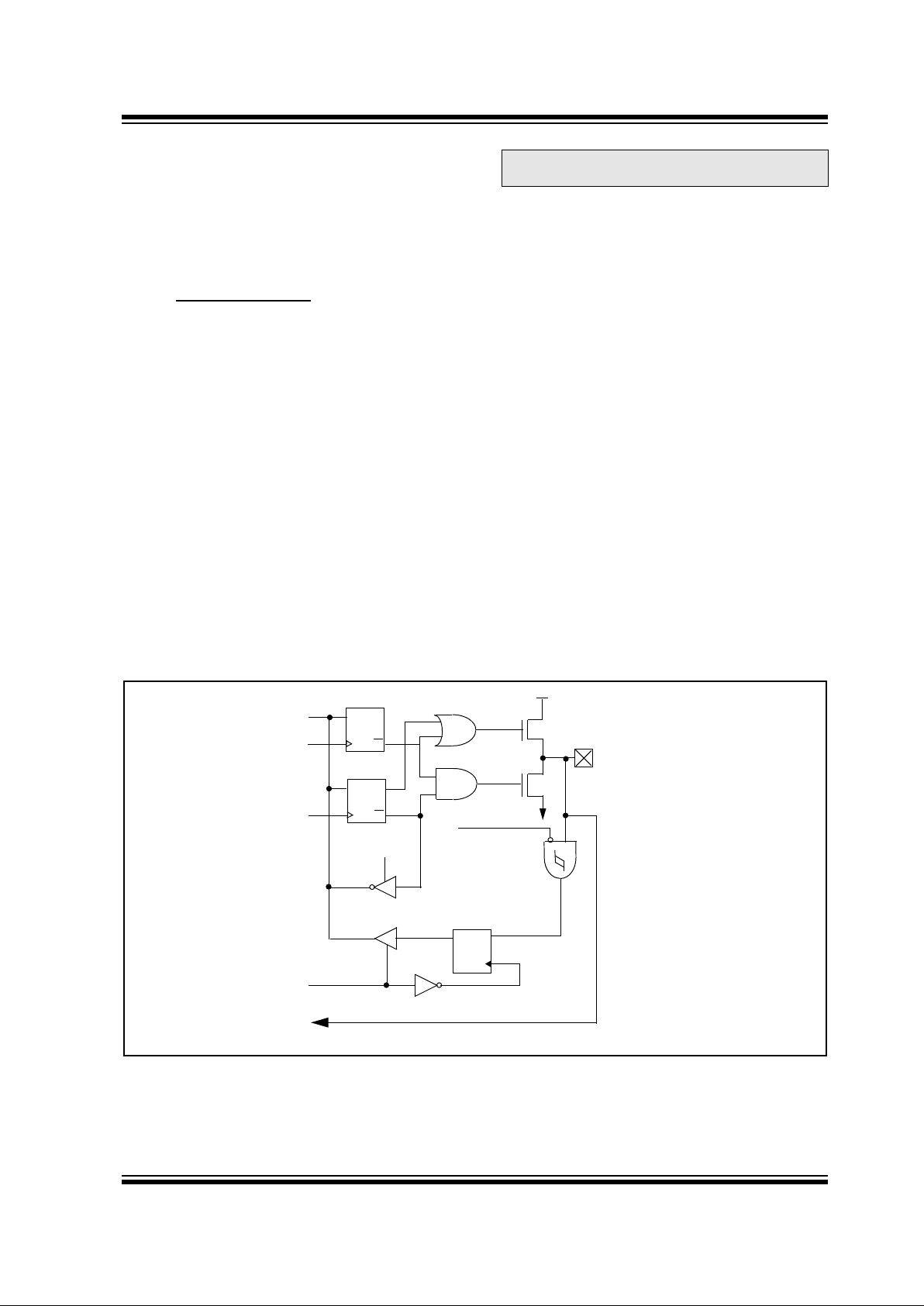
5.2 POR
TC and TRISC
PORTC is a 8-bit wide bidirectional port, with Schmitt
Trigger inputs, that serves the following functions
depending on programming:
• Direct LED drive (PORTC<7:0>).
•I
2
C communication lines (PORTC<7:6>), refer to
Section 7.0 I
2
C Serial Port.
• Interrupt on change function (PORTC<7:4>),
discussed below and in Section 10.3 Interrupts.
• Programmable reference and comparator
outputs.
• Timer0 clock source on RC3
The PORTC data register is located at location 07h and
its data direction register (TRISC) is at 87h.
PORTC<5:0> have weak internal pull-ups (~100 uA
typical). A single control bit can turn on all the pull-ups.
This is done by clearing bit RCPU
(OPTION<7>). The
weak pull-up is automatically turned off when the port
pin is configured as an output. The pull-ups are
disabled on power-on reset and in hibernate mode.
When using PORTC<0> as an analog output
(CMCON<1> bit is set), the TRISC<0> bit should be
cleared to disable the weak pull-up on this pin. Refer to
Table 5-1.
Four of the PORTC pins, RC<7:4> have an interrupt on
change feature. Only pins configured as inputs can
cause this interrupt to occur. In other words, any pin
RC<7:4> configured as an output is excluded from the
interrupt on change comparison. The input pins of
RC<7:4> are compared with the old value latched on
the last read of PORTC. The “mismatch” outputs of
RC<7:4> are OR’ed together to assert the RCIF flag
(PIR1 register<2>) and cause a CPU interrupt, if
enabled.
Note: If the I
2
C function is enabled,
(I
2
CCON<5>, address 14h), RC<7:6> are
automatically excluded from the
interrupt-on-change comparison.
1996 Microchip Technology Inc.
Preliminary
DS40122B-page 27
PIC14000
This interrupt can wake the device up from SLEEP. The
user, in the interrupt service routine, can clear the
interrupt in one of two ways:
• Disable the interrupt by clearing the RCIE
(PIE1<2>) bit
• Read PORTC. This will end mismatch condition.
Then, clear the RCIF (PIR1<2>) bit.
A mismatch condition will continue to set the RCIF bit.
Reading PORTC will end the mismatch condition, and
allow the RCIF bit to be cleared.
If bit CMAOE (CMCON<1>) is set, the RC0/REFA pin
becomes the programmable reference A and analog
output. Pin RC1/CMPA becomes the comparator A output.
PORTC<7:6> also serves multiple functions. These
pins act as the I
2
C data and clock lines when the I
2
C
module is enabled. They also serve as the serial programming interface data and clock line for in-circuit
programming of the EPROM.
Note: Setting CMAOE changes the definition of
RC0/REFA and RC1/CMPA, bypassing
the PORTC data and TRISC register settings.
The TRISC register controls the direction of the
PORTC pin. A ‘1’ in each location configures the
corresponding port pin as an input. Upon reset, this
register sets to FFh, meaning all PORTC pins are initially inputs. The data register should be initialized prior
to configuring the port as outputs.
Unused inputs should not be left floating to avoid
leakage currents. All pins have input protection diodes
to V
DD
and V
SS
.
EXAMPLE 5-2: INITIALIZING PORTC
CLRF PORTC ; Initialize PORTC data
; latches before setting
; the data direction
; register
BSF STATUS, RPO ; Select Bank1
MOVLW 0xCF ; Value used to initialize
; data direction
MOVWF TRISC ; Set RC<3:0> as inputs
; RC<5:4> as outputs
;
RC<7:6> as inputs
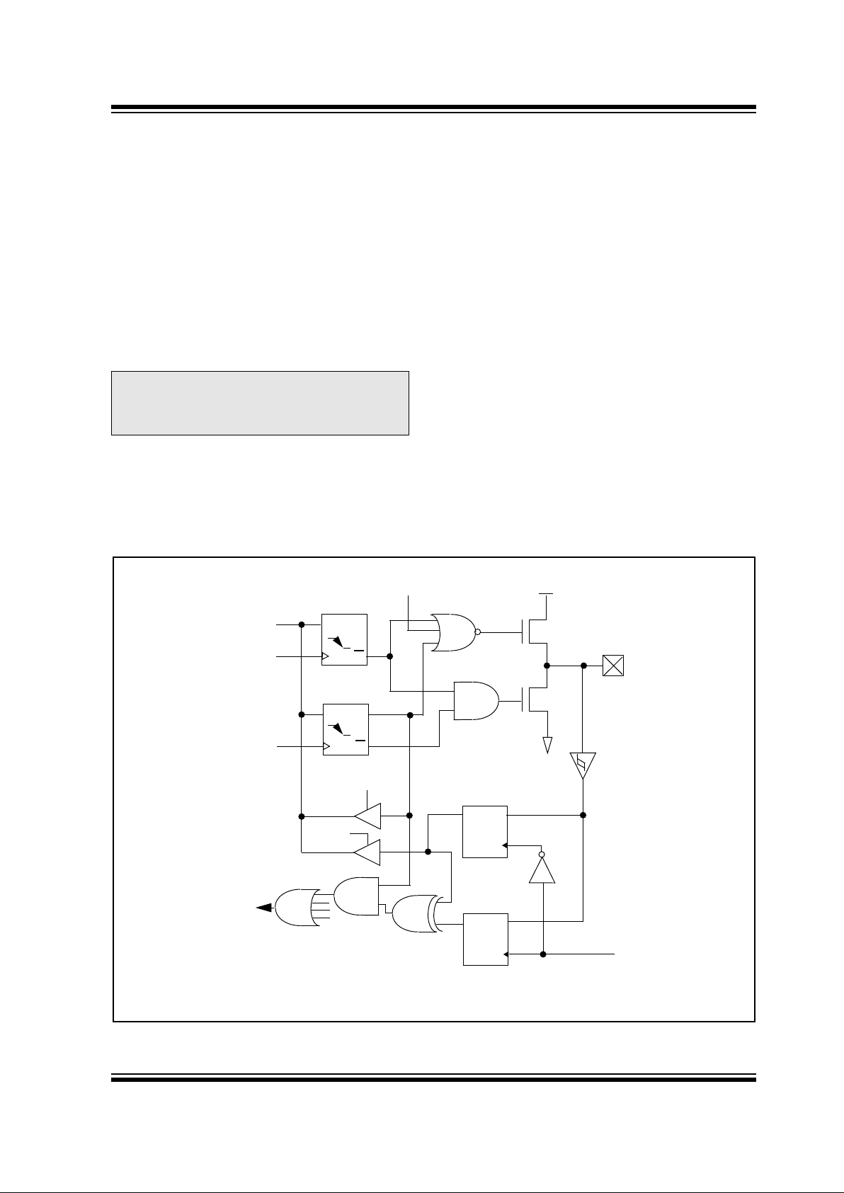
FIGURE 5-3: BLOCK DIAGRAM OF PORTC<7:6> PINS
D
Q
CK
Q
D
Q
CK
Q
D
Q
EN
Data
Bus
Write
PORTC
Write
TRISC
Read
TRISC
N
I/O
Pin
V
DD
Schmitt Trigger
Input
Buffer
D
Q
EN
Read
PORTC
Read PORTC
From other
PORTC pins
Set
RCIF
Note: I/O pins have protection diodes to VDD and VSS. These pins do not have a P-channel pull-up.
I2CCON<5>
N
V
SS
PIC14000
DS40122B-page 28
Preliminary
1996 Microchip Technology Inc.
TABLE 5-1: PORT RC0 PIN CONFIGURATION SUMMARY
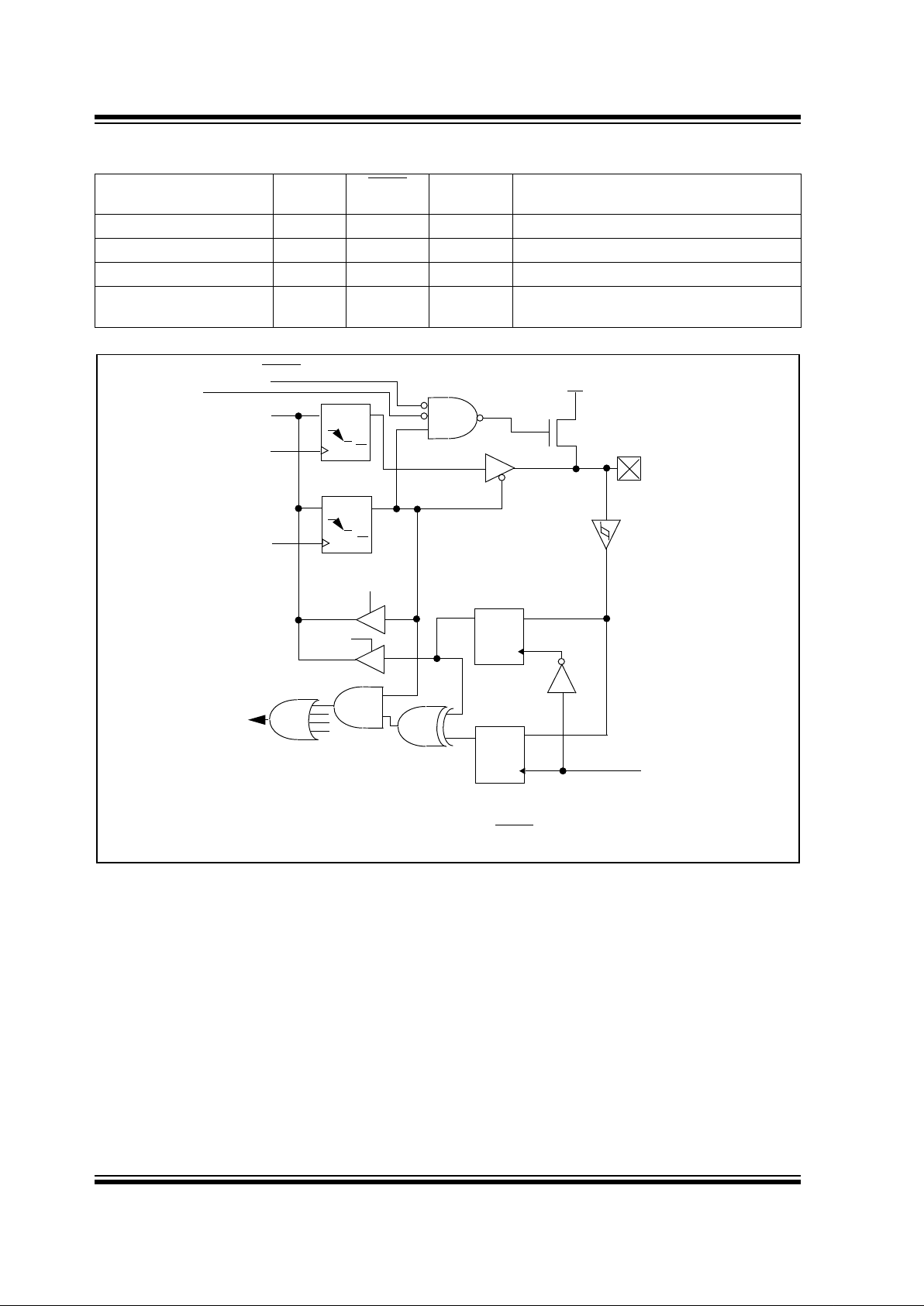
FIGURE 5-4: BLOCK DIAGRAM OF PORTC<5:4> PINS
RC0 Pin
Configuration
TRISC<0>
RCPU
OPTION<7>
CMAOE
CMCON<1>
Comment
Digital Input (weak pull-up) 1 0 0
Digital Input (no pull-up) 1 1 0
Digital Output 0 X 0
Analog Output 0 X 1 Must clear TRISC<0> to disable pull-up when
used as an analog output.
D
Q
CK
Q
D
Q
CK
Q
D
Q
EN
Data
Bus
Write
PORTC
Write
TRISC
Read
TRISC
P
I/O
Pin
V
DD
Schmitt Trigger
Input
Buffer
RCPU
D
Q
EN
Read
PORTC
Read PORTC
From other
PORTC pins
Set
RCIF
1. I/O pins have protection diodes to VDD and VSS.
2. Port Latch = ‘1’ and TRISC = ‘1’ enables weak pull-up if RCPU
= ‘0’ in OPTION register.
HIBERNATE
1996 Microchip Technology Inc.
Preliminary
DS40122B-page 29
PIC14000
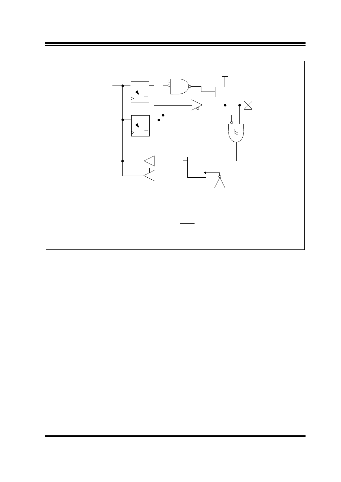
FIGURE 5-5: BLOCK DIAGRAM OF PORTC<3:0> PINS
1. I/O pins have protection diodes to VDD and VSS.
2. Port Latch =‘1’ and TRISC =‘1’ enables weak pull-up if RCPU
=‘0’ in OPTION register.
3. If the CMAOE bit (CMCON<1>) is set to‘1’, RC0 becomes REFA, RC1 becomes CMPA,
ignoring the PORTC<1:0> data and TRISC<1:0> register settings.
D
Q
CK
Q
D
Q
CK
Q
Data
Bus
Write
PORTC
Write
TRISC
Read
TRISC
P
I/O
Pin
V
DD
Schmitt Trigger
Input
Buffer
RCPU
D
Q
EN
Read
PORTC
Read PORTC
HIBERNATE

PIC14000
DS40122B-page 30
Preliminary
1996 Microchip Technology Inc.
FIGURE 5-6:
PORTC DATA REGISTER
U= unimplemented, X = unknown.
07h Bit 7 Bit 6 Bit 5 Bit 4 Bit 3 Bit 2 Bit 1 Bit 0
PORTC
RC7/SDAA RC6/SCLA RC5 RC4 RC3/T0CKI RC2 RC1/CMPA RC0/REFA
Read/Write
R/W R/W R/W R/W R/W R/W R/W R/W
POR value xxh
x xxxxxx x
Bit Name Function
B7 RC7/SDAA
Synchronous serial data I/O for I
2
C interface. Also is the serial programming data line.
This pin can also serve as a general purpose I/O. If enabled, a change on this pin can
cause a CPU interrupt. This pin has an N-channel pull-up to V
DD
which is disabled in
I
2
C mode.
B6 RC6/SCLA
Synchronous serial clock for I
2
C interface. Also is the serial programming clock. This pin
can also serve as a general purpose I/O. If enabled, a change on this pin can cause a
CPU interrupt. This pin has an N-channel pull-up to V
DD
which is disabled in I
2
C mode.
B5 RC5 LED direct-drive output. This pin can also serve as a GPIO. If enabled, a change on this
pin can cause a CPU interrupt. If enabled, this pin has a weak internal pull-up to V
DD
.
B4 RC4 LED direct-drive output. This pin can also serve as a GPIO. If enabled, a change on this
pin can cause a CPU interrupt. If enabled, this pin has a weak internal pull-up to V
DD
.
B3 RC3/T0CKI LED direct-drive output. This pin can also serve as a GPIO. If enabled, this pin has a
weak internal pull-up to V
DD
. T0CKI is enabled as TMR0 clock via the OPTION register .
B2 RC2 LED direct-drive output. This pin can also serve as a GPIO. If enabled, this pin has a
weak internal pull-up to V
DD
.
B1 RC1/CMPA LED direct-drive output. This pin can also serve as a GPIO, or comparator A output. If
enabled, this pin has a weak internal pull-up to V
DD
.
B0 RC0/REFA LED direct-drive output. This pin can also serve as a GPIO, or programmable reference
A output. If enabled, this pin has a weak internal pull-up to V
DD
.

1996 Microchip Technology Inc.
Preliminary
DS40122B-page 31
PIC14000
5.2.1 TRISC PORTC DATA DIRECTION
REGISTER
This register defines each pin of PORTC as either an
input or output under software control. A ‘1’ in each
location configures the corresponding port pin as an
input. This register resets to all ‘1’s, meaning all
PORTC pins are initially inputs. The data register
should be initialized prior to configuring the port as
outputs.
FIGURE 5-7: TRISC REGISTER
U= unimplemented, X = unknown.
87h Bit 7 Bit 6 Bit 5 Bit 4 Bit 3 Bit 2 Bit 1 Bit 0
TRISC
TRISC7 TRISC6 TRISC5 TRISC4 TRISC3 TRISC2 TRISC1 TRISC0
Read/Write
R/W R/W R/W R/W R/W R/W R/W R/W
POR value FFh
1111 1 1 1 1
Bit Name Function
B7 TRISC7 Control direction on pin RC7/SDAA (has no effect if I
2
C is enabled):
0 = pin is an output
1 = pin is an input
B6 TRISC6
Control direction on pin RC6/SCLA (has no effect if I
2
C is enabled):
0 = pin is an output
1 = pin is an input
B5 TRISC5 Control direction on pin RC5:
0 = pin is an output
1 = pin is an input
B4 TRISC4 Control direction on pin RC4:
0 = pin is an output
1 = pin is an input
B3 TRISC3 Control direction on pin RC3:
0 = pin is an output
1 = pin is an input
B2 TRISC2 Control direction on pin RC2:
0 = pin is an output
1 = pin is an input
B1 TRISC1 Control direction on pin RC1/CMPA (has no effect if the CMAOE bit is set):
0 = pin is an output
1 = pin is an input
B0 TRISC0 Control direction on pin RC0/REFA (has no effect if the CMAOE bit is set):
0 = pin is an output
1 = pin is an input

PIC14000
DS40122B-page 32
Preliminary
1996 Microchip Technology Inc.
5.3 POR
TD and TRISD
PORTD is an 8-bit port that may be used for general
purpose I/O. Four pins can be configured as analog
inputs.
FIGURE 5-8: BLOCK DIAGRAM OF PORTD<7:4> PINS
FIGURE 5-9: BLOCK DIAGRAM OF PORTD<3:2> PINS
D
Q
CK
Q
D
Q
CK
Q
D
Q
EN
Analog Input Mode
Data
Bus
Write
PORTD
Write
TRISD
Read
TRISD
Read
PortD
T o A/D Converter
Note: I/O pins have protection diodes to V
DD and VSS.
P
N
I/O
Pin
V
SS
VDD
Schmitt Trigger
Input Buffer
D
Q
CK
Q
D
Q
CK
Q
D
Q
EN
Data
Bus
Write
PORTD
Write
TRISD
Read
TRISD
I/O
Pin
Read
PORTD
Read PORTD
1. I/O pins have protection diodes to VDD and VSS.
2. If CMBOE (CMCON<5>) is set to ‘1’, RD2 becomes CMPB,
RD3 becomes REFB, ignoring the PORTD<3:2> data and
TRISD<3:2> register settings.
Schmitt Trigger
Input Buffer

1996 Microchip Technology Inc.
Preliminary
DS40122B-page 33
PIC14000
FIGURE 5-10: BLOCK DIAGRAM OF PORTD<1:0> PINS
FIGURE 5-11: PORTD DATA REGISTER
Legend: U = unimplemented, read as ‘0’, x = unknown.
08h Bit 7 Bit 6 Bit 5 Bit 4 Bit 3 Bit 2 Bit 1 Bit 0
PORTD
RD7/AN7 RD6/AN6 RD5/AN5 RD4/AN4 RD3/REFB RD2/CMPB RD1/SDAB RD0/SCLB
Read/Write
R/W R/W R/W R/W R/W R/W R/W R/W
POR value xxh
XXXX X X X X
Bit Name Function
B7 RD7/AN7
GPIO or analog input. Returns value on pin RD7/AN7 when used as a digital
input. When configured as an analog input, reads as ‘0’.
B6
RD6/AN6 GPIO or analog input. Returns value on pin RD6/AN6 when used as a digital
input. When configured as an analog input, reads as ‘0’.
B5 RD5/AN5
GPIO or analog input. This pin can connect to a level shift network. If
enabled, a +0.5V offset is added to the input voltage. When configured as
an analog input, reads as ‘0’.
B4
RD4/AN4 GPIO or analog input. Returns value on pin RD4/AN4 when used as a digital
input. When configured as an analog input, reads as ‘0’.
B3 RD3/REFB This pin can serve as a GPIO, or programmable reference B output.
B2 RD2/CMPB This pin can serve as a GPIO, or comparator B output.
B1 RD1/SDAB
Alternate synchronous serial data I/O for I
2
C interface enabled by setting
the I
2
CSEL bit in the MISC register. This pin can also serve as a general
purpose I/O. This pin has an N-channel pull-up to VDD which is disabled in
I
2
C mode.
B0 RD0/SCLB
Alternate synchronous serial clock for I
2
C interface, enabled by setting the
I
2
CSEL bit in the MISC register. This pin can also serve as a general pur-
pose I/O. This pin has an N-Channel pull-up to VDD which is disabled in I
2
C
mode.
D
Q
CK
Q
D
Q
CK
Q
D
Q
EN
Data
Bus
Write
PORTD
Write
TRISD
Read
TRISD
Read
PortD
Note: I/O pins have protection diodes to V
DD and VSS. These pins do not have a P-channel pull-up.
N
N
I/O
Pin
V
SS
VDD
Schmitt Trigger
Input Buffer
I
2
CCON<5>

PIC14000
DS40122B-page 34 Preliminary 1996 Microchip Technology Inc.
FIGURE 5-12: TRISD REGISTER
88h Bit 7 Bit 6 Bit 5 Bit 4 Bit 3 Bit 2 Bit 1 Bit 0
TRISD TRISD7 TRISD6 TRISD5 TRISD4 TRISD3 TRISD2 TRISD1 TRISD0
Read/Write R/W R/W R/W R/W R/W R/W R/W R/W
POR value FFh 11111 1 1 1
Bit Name Function
B7 TRISD7
Control direction on pin RD7/AN7:
0 = pin is an output
1 = pin is an input
B6 TRISD6
Control direction on pin RD6/AN6:
0 = pin is an output
1 = pin is an input
B5 TRISD5
Control direction on pin RD5/AN5:
0 = pin is an output
1 = pin is an input
B4 TRISD4
Control direction on pin RD4/AN4:
0 = pin is an output
1 = pin is an input
B3 TRISD3
Control direction on pin RD3/REFB (has no effect if the CMBOE bit is set):
0 = pin is an output
1 = pin is an input
B2 TRISD2
Control direction on pin RD2/CMPB (has no effect if the CMBOE bit is set):
0 = pin is an output
1 = pin is an input
B1 TRISD1
Control direction on pin RD1/SDAB:
0 = pin is an output
1 = pin is an input
B0 TRISD0
Control direction on pin RD0/SCLB:
0 = pin is an output
1 = pin is an input

1996 Microchip Technology Inc. Preliminary DS40122B-page 35
PIC14000
If the CMBOE bit (CMCON<5>) is set, the RD3/REFB
pin becomes the programmable reference B output
and pin RD2/CMPB becomes the comparator B output.
PORTD<1:0> also serve multiple functions. These pins
act as the I
2
C data and clock lines when the I2C module
is enabled.
The TRISD register controls the direction of the Port D
pins. A ‘1’ in each location configures the
corresponding port pin as an input. Upon reset, this
register sets to FFh, meaning all PORTD pins are initially inputs. The data register should be initialized prior
to configuring the port as outputs.
Unused inputs should not be left floating to avoid
leakage currents. All pins have input protection diodes
to V
DD and VSS.
EXAMPLE 5-3: INITIALIZING PORTD
Note: Setting CMBOE changes the definition of
RD3/REFB and RD2/CMPB, bypassing
the PORTD data and TRISD register settings.
CLRF PORTD ; Initialize PORTD data
; latches before setting
; the data direction
; register
BSF STATUS, RP0 ; Select Bank1
MOVLW 0xFF ; Value used to initialize
; data direction
MOVWF TRISD ; Set RD<7:0> as inputs
5.4 I/O Programming Considerations
5.4.1 BI-DIRECTIONAL I/O PORTS
Reading the port register reads the values of the port
pins. Writing to the port register writes the value to the
port latch. Some instructions operate internally as
read-modify-write. The BCF and BSF instructions, for
example, read the register into the CPU, execute the bit
operation, and write the result back to the register.
Caution must be used when these instructions are
applied to a port with both inputs and outputs defined.
For example, a BSF operation on bit5 of PORTC will
cause all eight bits of PORTC to be read into the CPU.
Then the BSF operation takes place on bit5 and
PORTC is written to the output latches. If another bit of
PORTC is used as a bi-directional I/O pin (say bit0) and
it is defined as an input at this time, the input signal
present on the pin itself would be read into the CPU
and re-written to the data latch of this particular pin,
overwriting the previous content. As long as the pin
stays in the input mode, no problem occurs. However,
if bit0 is switched into output mode later on, the content
of the data latch may now be unknown.
A pin actively outputting a LOW or HIGH should not be
driven from external devices at the same time in order
to change the level on this pin (“wire-or”, “wire-and”).
The resulting high output currents may damage the
chip.
Example 5-4 shows the effect of two sequential read
modify write instructions (ex. BCF, BSF, etc.) on an I/O
Port.
EXAMPLE 5-4: READ MODIFY WRITE
INSTRUCTIONS ON AN
I/O PORT
;;Initial PORT settings: PORTC<7:4> Inputs
; PORTC<3:0> Outputs
;;PORTC<7:6> have external pull-up and are not
connected to other circuitry
;
; PORT latch PORT pins
; ---------- ----------
BCF PORTC, 7 ; 01pp pppp 11pp pppp
BCF PORTC, 6 ; 10pp pppp 11pp pppp
BSF STATUS,RP0 ;
BCF TRISC, 7 ; 10pp pppp 11pp pppp
BCF TRISC, 6 ; 10pp pppp 10pp pppp
;
;Note that the user may have expected the pin
;values to be 00pp pppp. The 2nd BCF caused
;RC7 to be latched as the pin value (High).

PIC14000
DS40122B-page 36 Preliminary 1996 Microchip Technology Inc.
5.4.2 SUCCESSIVE OPERATIONS ON I/O
PORTS
The actual write to an I/O port happens at the end of an
instruction cycle, whereas for reading, the data must be
valid at the beginning of the instruction cycle.
Therefore, care must be exercised if a write operation
is followed by a read operation on the same I/O port.
The sequence of instructions should be such to allow
the pin voltage to stabilize before the next instruction
which causes that port to be read into the CPU is
executed. Otherwise, the previous state of that pin may
be read into the CPU rather than the new state. When
in doubt, it is better to separate these instructions with
a NOP or another instruction not accessing this I/O
port.
FIGURE 5-13: SUCCESSIVE I/O OPERATION
Q1 | Q2 | Q3 | Q4
PC PC + 2
PC + 1 PC + 3
MOVWF PORTC
Write to PORTC
MOVF PORTC, W
Read PORTC
NOP
NOP
RC<x>
Port pin sampled
here
Execute MOVWF
PORTC
Pin values
Execute MOVF
PORTC, W
Execute NOP
Example showing write to PORTC followed by immediate read. Some delays in settling may cause “old”
Port data to be read, especially at higher clock frequencies. Data setup time = (0.25 Tcyc- Tpd), where
Tcyc = instruction cycle time.
Q1 | Q2 | Q3 | Q4 Q1 | Q2 | Q3 | Q4 Q1 | Q2 | Q3 | Q4

1996 Microchip Technology Inc.
Preliminary
DS40122B-page 37
PIC14000
6.0 TIMER MODULES
The PIC14000 contains two general purpose timer
modules, Timer0 (TMR0) and the Watchdog Timer
(WDT). The ADTMR is described in the A/D section.
The Timer0 module is identical to the T imer0 module of
the PIC16C7X enhanced core products. It is an 8-bit
overflow counter.
The Timer0 module has a programmable prescaler
option. This prescaler can be assigned to either the
Timer0 module or the Watchdog Timer (WDT). PSA
(OPTION<3>) assigns the prescaler, and PS2:PS0
(OPTION<2:0>) determines the prescaler value.
Timer0 can increment at the following rates: 1:1 (when
prescaler assigned to Watchdog Timer), 1:2, 1:4, 1:8,
1:16, 1:32, 1:64, 1:128, 1:256.
The Timer0 module has the following features:
• 8-bit timer
• Readable and writable (file address 01h)
• 8-bit software programmable prescaler
• Interrupt on overflow from FFh to 00h
Figure 6-1 is a simplified block diagram of the Timer0
module.
The Timer0 module will increment every instruction
cycle (without prescaler). If TMR0 is written, increment
is inhibited for the following two cycles (Figure 6-2 and
Figure 6-3). The user can compensate by writing an
adjusted value to TMR0.
FIGURE 6-1: TIMER0 AND WATCHDOG TIMER BLOCK DIAGRAM
RC3/T0CKI
T0SE
0
1
1
0
pin
T0CS
FOSC/4
Sync with
Internal
clocks
TMR0
PSout
(2 cycle delay)
PSout
Data bus
8
PSA
Set T0IF
Interrupt on
Overflow
8-bit Counter
8-to-1 MUX
18 mS
Timer
PSA
01
WDT
Time-out
PS2:PS0
8
Note: T0CS, T0SE, PSA, PS2:PS0 correspond to (OPTION<5:0>).
PSA
0
1
3
HIBERNATE
WDT
Enable Bit
Local
Oscillator
Prescaler/
Postscaler
Enable
Watchdog Timer
Timer0

PIC14000
DS40122B-page 38
Preliminary
1996 Microchip Technology Inc.
6.1 Timer0 Interrupt
The TMR0 interrupt is generated when the Timer0
overflows from FFh to 00h. This overflow sets the T0IF
bit. The interrupt can be masked by clearing bit T0IE
(INTCON<5>). Flag bit T0IF (INTCON<2>) must be
cleared in software by the TMR0 module interrupt ser-
vice routine before re-enabling this interrupt. The
Timer0 module interrupt cannot wake the processor
from SLEEP since the timer is shut off during SLEEP.
The timing of the Timer0 interrupt is shown in
Figure 6-4.
FIGURE 6-2: TIMER0 TIMING: INTERNAL CLOCK/NO PRESCALE
FIGURE 6-3: TIMER0 TIMING: INTERNAL CLOCK/PRESCALE 1:2
FIGURE 6-4: TIMER0 INTERRUPT TIMING
PC-1
Q1 Q2 Q3 Q4
Q1 Q2 Q3 Q4 Q1 Q2 Q3 Q4 Q1 Q2 Q3 Q4 Q1 Q2 Q3 Q4 Q1 Q2 Q3 Q4 Q1 Q2 Q3 Q4 Q1 Q2 Q3 Q4
PC
(Program
Counter)
Instruction
Fetch
TMR0
PC PC+1 PC+2 PC+3 PC+4 PC+5 PC+6
T0
T0+1 T0+2 NT0 NT0 NT0 NT0+1 NT0+2
MOVWF TMR0
MOVF TMR0,W MOVF TMR0,W MOVF TMR0,W MOVF TMR0,W MOVF TMR0,W
Write TMR0
executed
Read TMR0
reads NT0
Read TMR0
reads NT0
Read TMR0
reads NT0
Read TMR0
reads NT0 + 1
Read TMR0
reads NT0 + 2
Instruction
Executed
PC-1
Q1 Q2 Q3 Q4
Q1 Q2 Q3 Q4 Q1 Q2 Q3 Q4 Q1 Q2 Q3 Q4 Q1 Q2 Q3 Q4 Q1 Q2 Q3 Q4 Q1 Q2 Q3 Q4 Q1 Q2 Q3 Q4
PC
(Program
Counter)
Instruction
Fetch
TMR0
PC PC+1 PC+2 PC+3 PC+4 PC+5 PC+6
T0 NT0+1
MOVWF TMR0
MOVF TMR0,W MOVF TMR0,W MOVF TMR0,W MOVF TMR0,W MOVF TMR0,W
Write TMR0
executed
Read TMR0
reads NT0
Read TMR0
reads NT0
Read TMR0
reads NT0
Read TMR0
reads NT0
Read TMR0
reads NT0 + 1
T0+1
NT0
Instruction
Execute
Q2Q1 Q3 Q4Q2Q1 Q3 Q4 Q2Q1 Q3 Q4 Q2Q1 Q3 Q4 Q2Q1 Q3 Q4
1
1
OSC1
CLKOUT(3)
TMR0 timer
T0IF bit
(INTCON<2>)
FEh
GIE bit
(INTCON<7>)
INSTRUCTION FLOW
PC
Instruction
fetched
PC
PC +1 PC +1 0004h 0005h
Instruction
executed
Inst (PC)
Inst (PC-1)
Inst (PC+1)
Inst (PC)
Inst (0004h) Inst (0005h)
Inst (0004h)Dummy cycle Dummy cycle
FFh 00h 01h 02h
Note 1: T0IF interrupt flag is sampled here (every Q1).
2: Interrupt latency = 4Tcy where Tcy = instruction cycle time.
3: CLKOUT is available only in HS oscillator mode.

1996 Microchip Technology Inc.
Preliminary
DS40122B-page 39
PIC14000
6.2 Using
Timer0 with External Clock
When the external clock input (pin RC3/T0CKI) is used
for Timer0, it must meet certain requirements. The
external clock requirement is due to internal phase
clock (T
OSC
) synchronization. Also, there is a delay in
the actual incrementing of TMR0 after synchronization.
6.2.1 EXTERNAL CLOCK SYNCHRONIZATION
When no prescaler is used, the external clock input is
the same as the prescaler output. The synchronization
of T0CKI with the internal phase clocks is
accomplished by sampling the prescaler output on the
Q2 and Q4 cycles of the internal phase clocks
(Figure 6-5). Therefore, it is necessary for T0CKI to be
high for at least 2Tosc (and a small RC delay of 20 ns)
and low for at least 2Tosc (and a small RC delay of
20 ns).
When a prescaler is used, the external clock input is
divided by the asynchronous ripple counter-type
prescaler so that the prescaler output is symmetrical.
For the external clock to meet the sampling
requirement, the ripple counter must be taken into
account. Therefore, it is necessary for T0CKI to have a
period of at least 4T osc (and a small RC delay of 40 ns)
divided by the prescaler value. The only requirement
on T0CKI high and low time is that they do not violate
the minimum pulse width requirement of 10 ns.
6.2.2 TIMER0 INCREMENT DELAY
Since the prescaler output is synchronized with the
internal clocks, there is a small delay from the time the
external clock edge occurs to the time the Timer0
module is actually incremented. Figure 6-5 shows the
delay from the external clock edge to the timer
incrementing.
6.3 Prescaler
An 8-bit counter is available as a prescaler for the
Timer0 module, or as a post-scaler for the Watchdog
Timer (Figure 6-1). For simplicity, this counter is being
referred to as “prescaler” throughout this data sheet.
Note that there is only one prescaler available which is
mutually exclusive between the Timer0 module and the
Watchdog Timer. Thus, a prescaler assignment for the
Timer0 module means that there is no prescaler for the
Watchdog Timer, and vice-versa.
Bit PSA and PS2:PS0 (OPTION<3:0>) determine the
prescaler assignment and prescale ratio.
When assigned to the Timer0 module, all instructions
writing to the Timer0 module (e.g., CLRF 1, MOVWF 1,
BSF 1,x ) will clear the prescaler. When assigned to
WDT, a CLRWDT instruction will clear the prescaler
along with the Watchdog Timer. The prescaler is not
readable or writable.
FIGURE 6-5: TIMER0 TIMING WITH EXTERNAL CLOCK
INCREMENT TMR0 (Q4)
EXT CLOCK INPUT OR
Q1 Q2 Q3 Q4 Q1 Q2 Q3 Q4 Q1 Q2 Q3 Q4 Q1 Q2 Q3 Q4
TMR0
T0 T0 + 1 T0 + 2
Small pulse
misses sampling
EXT CLOCK/PRESCALER
OUTPUT AFTER SAMPLING
(note 3)
1.
2.
3.
Delay from clock input change to TMR0 increment is 3 TOSC to 7 TOSC. (Duration of Q = TOSC).
Therefore, the error in measuring the interval between two edges on TMR0 input = ± 4 tosc max.
External clock if no prescaler selected, Prescaler output otherwise.
The arrows indicate the points in time where sampling occurs.
Notes:
PRESCALER OUT (NOTE 2)

PIC14000
DS40122B-page 40
Preliminary
1996 Microchip Technology Inc.
6.3.1 SWITCHING PRESCALER ASSIGNMENT
The prescaler assignment is fully under software
control, i.e., it can be changed “on the fly” during
program execution. To avoid an unintended device
RESET, the following instruction sequence
(Example 6-1) must be executed when changing the
prescaler assignment from Timer0 to WDT.
EXAMPLE 6-1: CHANGING PRESCALER
(TIMER0 → WDT)
1.BCF STATUS,RP0 ;Skip if already in
; Bank 0
2.CLRWDT ;Clear WDT
3.CLRF TMR0 ;Clear TMR0 & Prescaler
4.BSF STATUS, RP0 ;Bank 1
5.MOVLW '00101111'b;These 3 lines (5, 6, 7)
6.MOVWF OPTION ; are required only
; if desired PS<2:0>
7.CLRWDT ; are 000 or 001
8.MOVLW '00101xxx'b ;Set Postscaler to
9.MOVWF OPTION ; desired WDT rate
10.BCF STATUS, RP0 ;Return to Bank 0
To change prescaler from the WDT to the Timer0
module use the sequence shown in Example 6-2. This
precaution must be taken even if the WDT is disabled.
EXAMPLE 6-2: CHANGING PRESCALER
(WDT → TIMER0)
CLRWDT ;Clear WDT and
;prescaler
BSF STATUS, RP0
MOVLW B'xxxx0xxx' ;Select TMR0, new
;prescale value and
;clock source
MOVWF OPTION
BCF STATUS, RP0
TABLE 6-1: SUMMARY OF TIMER0 REGISTERS
TABLE 6-2: REGISTERS ASSOCIATED WITH TIMER0
Register Name Function Address Power-on Reset Value
TMR0 Timer/counter register 01h
xxxx xxxx
OPTION Configuration and prescaler assign-
ment bits for TMR0.
81h
1111 1111
INTCON TMR0 overflow interrupt flag and
mask bits.
0Bh
0000 000x
Legend: x = unknown,
Note 1: For reset values of registers in other reset situations refer to Table 10-4.
Address Name Bit 7 Bit 6 Bit 5 Bit 4 Bit 3 Bit 2 Bit 1 Bit 0
01h TMR0 TIMER0 TIMER/COUNTER
0Bh/8Bh INTCON GIE
PEIE T0IE r r T0IF r r
81h OPTION
RCPU r T0CS T0SE PSA PS2 PS1 PS0
87h TRISC
TRISC7 TRISC6 TRISC5 TRISC4 TRISC3 TRISC2 TRISC1 TRISC0
Legend: r = Reserved locations
Shaded boxes are not used by Timer0 module

1996 Microchip Technology Inc.
Preliminary
DS40122B-page 41
PIC14000
7.0 INTER-INTEGRATED CIRCUIT
SERIAL PORT (I
2
C
)
The I
2
C module is a serial interface useful for
communicating with other peripheral or microcontroller
devices. These peripheral devices may be serial
EEPROMs, shift registers, display drivers, A/D
converters, etc. The I
2
C module is compatible with the
following interface specifications:
• Inter-Integrated Circuit (I
2
C)
• System Management Bus (SMBus)
This section provides an overview of the Inter-IC(I
2
C)
bus. The I
2
C bus is a two-wire serial interface
developed by the Philips Corporation. The original
specification, or standard mode, was for data transfers
of up to 100 Kbps. An enhanced specification, or fast
mode, supports data transmission up to 400 Kbps.
Both standard mode and fast mode devices will
inter-operate if attached to the same bus.
The I
2
C interface employs a comprehensive protocol to
ensure reliable transmission and reception of data.
When transmitting data, one device is the “master”
(generates the clock) while the other device(s) acts as
the “slave”. All portions of the slave protocol are
implemented in the I
2
C module’s hardware, except
general call support, while portions of the master protocol will need to be addressed in the PIC14000 software. Table 7-1 defines some of the I
2
C bus
terminology. For additional information on the I
2
C interface specification, please refer to the Philips Corporation document
“The I
2
C-bus and How to Use It”.
Note: The I
2
C module on PIC14000 only
supports I
2
C mode. This is different from
the standard module used on the
PIC16C7X family, which supports both
I
2
C and SPI modes. Caution should be
exercised to avoid enabling SPI mode on
the PIC14000.
In the I
2
C interface protocol each device has an
address. When a master wishes to initiate a data
transfer, it first transmits the address of the device that
it wishes to talk to. All devices “listen” to see if this is
their address. Within this address, a bit specifies if the
master wishes to read from or write to the slave device.
The master and slave are always in opposite modes
(transmitter/receiver) of operation during a data
transfer. They may operate in either of these two
states:
• Master-transmitter and Slave-receiver
• Slave-transmitter and Master-receiver
In both cases the master generates the clock signal.
The output stages of the clock (SCL) and data (SDA)
lines must have an open-drain or open-collector in
order to perform the wired-AND function of the bus.
External pull-up resistors are used to ensure a high
level when no device is pulling the line down. The
number of devices that may be attached to the I
2
C bus
is limited only by the maximum bus loading specification of 400 pF.
7.1 Initiating and
Terminating Data
Transfer
During times of no data transfer (idle time), both the
clock line (SCL) and the data line (SDA) are pulled high
through the external pull-up resistors. The START and
STOP determine the start and stop of data
transmission. The START is defined as a high to low
transition of SDA when SCL is high. The STOP is
defined as a low to high transition of SDA when SCL is
high. Figure 7-1 shows the START and STOP. The
master generates these conditions for starting and terminating data transfer. Due to the definition of the
START and STOP, when data is being transmitted the
SDA line can only change state when the SCL line is
low.
FIGURE 7-1: I
2
C START AND STOP CONDITIONS
S
Start
Condition
Change
of Data
Allowed
Change
of Data
Allowed
Stop
Condition
P
SDA
SCL

PIC14000
DS40122B-page 42
Preliminary
1996 Microchip Technology Inc.
FIGURE 7-2: I
2
CSTAT: I
2
C PORT STATUS REGISTER
BF: Buffer full
Receive
1 = Receive complete, I2CBUF is full
0 = Receive not complete, I2CBUF is empty
T
ransmit
1 = Transmit in progress, I2CBUF is full
0 = Transmit complete, I2CBUF is empty
UA: Update Address (10-bit I
2
C slave mode only)
1 = Indicate that the user needs to update the address in the I
2
CADD
register.
0 = Address does not need to be updated
R/
W: Read/write bit information
This bit holds the R/W
bit information received following the last address
match. This bit is only valid during the transmission.
The user may use this bit in software to determine whether transmission
or reception is in progress.
1 = Read
0 = Write
S: Start bit
This bit is cleared when the I
2
C module is disabled (I2CEN is cleared)
1 = Indicates that a start bit has been detected last. This bit is 0 on
reset.
0 = Start bit was not detected last
P: Stop bit
This bit is cleared when the I
2
C module is disabled (I2CEN is cleared)
1 = Indicates that a stop bit has been detected last.
0 = Stop bit was not detected last
D/
A: Data/Address bit
1 = Indicates that the last byte received was data
0 = Indicates that the last byte received was address
Unimplemented: read as ‘0’
U
_
bit0
bit7
Register: I
2
CSTAT
W: Writable bit
R
S
U_R
D/A
R
P
R
R/WRUARBF
R: Readable bit
U: Unimplemented, read as ‘0’
Address: 94h
POR value: 00h

1996 Microchip Technology Inc.
Preliminary
DS40122B-page 43
PIC14000
FIGURE 7-3: I
2
CCON: I
2
C PORT CONTROL REGISTER
I2CM<3:0>: I2C mode select
0110 = I
2
C slave mode, 7-bit address
0111 = I
2
C slave mode, 10-bit address
1011 = I
2
C firmware controlled master mode (slave idle)
1110 = I
2
C slave mode, 7-bit address with start and stop bit interrupts
enabled
1111 = I
2
C slave mode, 10-bit address with start and stop bit interrupts
enabled
CKP: Clock polarity select
SCK release control
1 = Enable clock
0 = Holds clock low (clock stretch)
Note: Used to ensure data setup time
I
2
CEN: I2C enable
1 = Enables the serial port and configures SDA and SCL pins as serial
port pins. When enabled, these pins must be configured as input
0 = Disables serial port and configures these pins as I/O port pins
I
2
COV: Receive overflow flag
1 = A byte is received while the I
2
CBUF is still holding the previous
byte. I
2
COV is a don't care in transmit mode.
I
2
COV must be cleared in software.
WCOL: Write collision detect
1 = the I
2
CBUF register is written while it is still transmitting the previ-
ous word.
Must be cleared in software.
0 = No collision
bit0
bit7
R/W
I
2
CM3
R/W
I2CEN
R/W
CKP
R/W
I2CM2
R/W
I2CM1
R/W
I2CM0
R/W
I
2
COV
R/W
WCOL
Register: I2CCON
W: Writable bit
R: Readable bit
U: Unimplemented, read as ‘0’
Address: 14h
POR value: 00h
Any other combinations of I2CM<3:0>
are illegal and should NEVER be used.
or output.
0 = No overflow

PIC14000
DS40122B-page 44
Preliminary
1996 Microchip Technology Inc.
TABLE 7-1: I
2
C BUS TERMINOLOGY
Term Description
Transmitter The device that sends the data to the bus.
Receiver The device that receives the data from the bus.
Master The device which initiates the transfer, generates the clock, and terminates the transfer.
Slave The device addressed by a master.
Multi-master More than one master device in a system. These masters can attempt to control the bus
at the same time without corrupting the message.
Arbitration Procedure that ensures that only one of the master devices will control the bus. This
ensures that the transfer data does not get corrupted.
Synchronization Procedure where the clock signals of two or more devices are synchronized.
FIGURE 7-4: I
2
C 7-BIT ADDRESS FORMAT
FIGURE 7-5: I
2
C 10-BIT ADDRESS
FORMAT
S
R/W
ACK
Sent by
Slave
slave address
S
R/W
Read/Write pulse
MSb LSb
Start Condition
ACK
Acknowledge
sent by slave
= 0 for write
S1
S
R/W
ACK
1 1 1 0 A9 A8 RW ACK A7 A6 A5 A4 A3 A2 A1 A0 ACK
-
-
-
Start Condition
Read/Write Pulse
Acknowledge
7.2 Ad
dressing I
2
C De
vices
There are two address formats. The simplest is the
7-bit address format with a R/W bit (Figure 7-4). The
address is the most significant seven bits of the byte.
For example when loading the I
2
CADD register, the
least significant bit is a “don’t care”. The more complex
is the 10-bit address with a R/W
bit (Figure 7-5). For
10-bit address format, two bytes must be transmitted
with the first five bits specifying this to be a 10-bit
address.

1996 Microchip Technology Inc.
Preliminary
DS40122B-page 45
PIC14000
7.3 T
ransfer Acknowledge
All data must be transmitted per byte, with no limit to
the number of bytes transmitted per data transfer. After
each byte, the slave-receiver generates an
acknowledge bit (ACK
). This is shown in Figure 7-6.
When a slave-receiver doesn’t acknowledge the slave
address or received data, the master must abort the
transfer. The slave must leave SDA high so that the
master can generate the STOP (Figure 7-1).
If the master is receiving the data (master-receiver), it
generates an acknowledge signal for each received
byte of data, except for the last byte. To signal the end
of data to the slave-transmitter, the master does not
generate an acknowledge. The slave then releases the
SDA line so the master can generate the STOP. The
master can also generate the STOP during the
acknowledge pulse for valid termination of data
transfer.
If the slave needs to delay the transmission of the next
byte, holding the SCL line low will force the master into
a wait state. Data transfer continues when the slave
releases the SCL line. This allows the slave to move
the received data or fetch the data it needs to transfer
before allowing the clock to start. This wait state can be
accomplished by setting SMHOG (MISC<7>) high.
Clearing MISC<7> will resume the data transfer.
Figure 7-7 shows a data transfer waveform.
Figure 7-8 and Figure 7-9 show master-transmitter and
master-receiver data transfer sequences.
FIGURE 7-6: I
2
C SLAVE-RECEIVER
ACKNOWLEDGE
Data
Output by
Transmitter
Data
Output by
Receiver
SCL from
Master
S
Start
Condition
not acknowledge
acknowledge
12 89
Clock pulse for
acknowledgement
FIGURE 7-7: SAMPLE I
2
C DATA TRANSFER
Address
R/W
ACK
Wait
State
Data ACK
Stop
Condition
P
9
3 • 8
2
acknowledgement
signal from receiver
1
byte complete.
interrupt with receiver
2
1
9
7
8
acknowledgement
signal from receiver
MSB
SDA
SCL
Start
Condition
S
clock line held low while
interrupts are serviced

PIC14000
DS40122B-page 46
Preliminary
1996 Microchip Technology Inc.
When a master does not wish to relinquish the bus (by
generating a STOP condition), a repeated START (Sr)
must be generated. This condition is identical to the
START (SDA goes high-to-low while SCL is high), but
occurs after a data transfer acknowledge pulse (not the
bus-free state). This allows a master to send
“commands” to the slave and then receive the
requested information or to address a different slave
device. This sequence is shown in Figure 7-10.
FIGURE 7-8: MASTER - TRANSMITTER SEQUENCE
FIGURE 7-9: MASTER - RECEIVER SEQUENCE
FIGURE 7-10: COMBINED FORMAT
For 7-bit address:
S Slave Address R/W A DATA A DATA A/A P
"0" (write) data transferred
(n bytes - acknowledge)
A master transmitter addresses a slave receiver with a
7-bit address. The transfer direction is not changed.
For 10-bit address:
S Slave Address
first 7 bits
R/W A1Slave Address
second byte
A2
(write)
A master transmitter addresses a slave receiver with a
10-bit address.
From master to slave
From slave to master
A = acknowledge (SDA low)
A = not acknowledge (SDA high)
S = START condition
P = STOP condition
Data A Data PA/A
For 7-bit address:
S Slave Address R/W A DATA A DATA A P
(read) data transferred
(n bytes - acknowledge)
A master reads a slave immediately after the first byte.
For 10-bit address:
S Slave Address
first 7 bits
R/W A1Slave Address
second byte
A2
(write)
A master transmitter addresses a slave receiver with a
10-bit address.
From master to slave
From slave to master
A = acknowledge (SDA low)
A = not acknowledge (SDA high)
S = START condition
P = STOP condition
Sr
Slave Address
first 7 bits
R/W A3 Data A Data
PA
(read)
S Slave Address R/W A DATA A/A
(read or write)
(n bytes + acknowledge)
Transfer direction of data and acknowledgement bits depends on R/W bits.
Combined Format:
S Slave Address
first 7 bits
R/W A Slave Address
second byte
A
(write)
Combined format -
From master to slave
From slave to master
A = acknowledge (SDA low)
A = not acknowledge (SDA high)
S = START condition
P = STOP condition
Sr Slave Address
first 7 bits
R/W A Data A Data PA
(read)
Sr
Slave Address R/W A DATA A/A P
Sr = repeated
START condition
Direction of transfer
may change at this point
Data A Data A/A
A master addresses a slave with a 10-bit address, then transmits
data to this slave and reads data from this slave.
(read)
(write)

1996 Microchip Technology Inc.
Preliminary
DS40122B-page 47
PIC14000
7.4 Multi-Master Operation
The I
2
C protocol allows a system to have more than
one master. This is called multi-master. When two or
more masters try to transfer data at the same time,
arbitration and synchronization occur.
7.4.1 ARBITRATION
Arbitration takes place on the SDA line, while the SCL
line is high. The master which transmits a high when
the other master transmits a low loses arbitration
(Figure 7-11) and turns off its data output stage. A
master which lost arbitrating can generate clock pulses
until the end of the data byte where it lost arbitration.
When the master devices are addressing the same
device, arbitration continues into the data.
Masters that also incorporate the slave function, and
have lost arbitration must immediately switch over to
slave-receiver mode. This is because the winning
master-transmitter may be addressing it.
Arbitration is not allowed between:
• A repeated START
• A STOP and a data bit
• A repeated START and a STOP
Care needs to be taken to ensure that these conditions
do not occur.
7.4.2 CLOCK SYNCHRONIZATION
Clock synchronization occurs after the devices have
started arbitration. This is performed using a
wired-AND connection to the SCL line. A high to low
transition on the SCL line causes the concerned
devices to start counting off their low period. Once a
device clock has gone low, it will hold the SCL line low
until its SCL high state is reached. The low to high
transition of this clock may not change the state of the
SCL line, if another device clock is still within its low
period. The SCL line is held low by the device with the
longest low period. Devices with shorter low periods
enter a high wait-state, until the SCL line comes high.
When the SCL line comes high, all devices start
counting off their high periods. The first device to
complete its high period will pull the SCL line low. The
SCA line high time is determined by the device with the
shortest high period. This is shown in the Figure 7-12.
FIGURE 7-11: MULTI-MASTER
ARBITRATION (2 MASTERS)
FIGURE 7-12: I
2
C CLOCK
SYNCHRONIZATION
transmitter 1 loses arbitration
DATA 1≠ SDA
DATA 1
DATA 2
SDA
SCL
wait
state
start counting
HIGH period
CLK
1
CLK
2
SCL
counter
reset

PIC14000
DS40122B-page 48
Preliminary
1996 Microchip Technology Inc.
FIGURE 7-13: I
2
C BLOCK DIAGRAM
Read Write
Internal
data bus
RC7/SDAA
I2CSR
I
2
CBUF
MSB
Match Detect
Start and
RC6/SCLA
I2CADD
Stop bit detect
Addr_Match
Set, Reset
S, P bits
(I
2
CSTAT Reg)
Shift
clock
RD1/SDAB
RD0/SCLB
4:2
MUX
SCK
SDA
MISC<4>
7.5 I2C Operation
The I2C module in I2C mode fully implements all slave
functions, and provides support in hardware to facilitate
software implementations of the master functions. The
I
2
C module implements the standard and fast mode
specifications as well as 7-bit and 10-bit addressing.
Two pins are used for data transfer. These are the
RC6/SCLA pin, which is the I
2
C clock, and the
RC7/SDAA pin which acts as the I
2
C data. The I2C
module can also be accessed via the RD0/SCLB and
RD1/SDAB pins by setting I
2
CSEL (MISC<4>).The
user must configure these pins as inputs or outputs
through the TRISC<7:6> or TRISD<1:0> bits. A block
diagram of the I
2
C module in I2C mode is shown in
Figure 7-13. The I
2
C module functions are enabled by
setting the I
2
CCON<5> bit.
The I
2
C module has five registers for I2C operation.
These are the:
•I
2
C Control Register (I2CCON)
•I
2
C Status Register (I2CSTAT)
• Serial Receive/Transmit Buffer (I
2
CBUF)
•I
2
C Shift Register (I2CSR) - Not directly
accessible
• Address Register (I
2
CADD)
The I
2
CCON register (14h) allows control of the I2C
operation. Four mode selection bits (I
2
CCON<3:0>)
allow one of the following I
2
C modes to be selected:
•I
2
C Slave mode (7-bit address)
•I
2
C Slave mode (10-bit address)
•I
2
C Slave mode (7-bit address), with start and
stop bit interrupts enabled
•I
2
C Slave mode (10-bit address), with start and
stop bit interrupts enabled
•I
2
C Firmware Controlled Master mode, slave is
idle
Selection of any I
2
C mode with the I2CEN bit set, forces
the SCL and SDA pins to be open collector, provided
these pins are set to inputs through the TRISC bits.
The I
2
CSTAT register gives the status of the data
transfer. This information includes detection of a
START or STOP bit, specifies if the received byte was
data or address, if the next byte is the completion of
10-bit address, and if this will be a read or write data
transfer. The I
2
CSTAT register is read only.
The I
2
CBUF is the register to which transfer data is
written to or read from. The I
2
CSR register shifts the
data in or out of the device. In receive operations, the
I
2
CBUF and I2CSR create a double buffered receiver.
This allows reception of the next byte before reading
the last byte of received data. When the complete byte
is received, it is transferred to the I
2
CBUF and PIR1<3>
is set. If another complete byte is received before the
I
2
CBUF is read, a receiver overflow has occurred and
the I
2
CCON<6> is set.
The I
2
CADD register holds the slave address. In 10-bit
mode, the user needs to write the high byte of the
address (1 1 1 1 0 A9 A8 0). Following the high byte
address match, the low byte of the address needs to be
loaded (A7-A0).

1996 Microchip Technology Inc. Preliminary DS40122B-page 49
PIC14000
7.5.1 SLAVE MODE
In slave mode, the SCLx and SDAx pins must be
configured as inputs (TRISC<7:6> or TRISD<1:0> are
set). The I
2
C module will override the input state with
the output data when required (slave-transmitter).
When an address is matched or the data transfer from
an address match is received, the hardware
automatically will generate the acknowledge (ACK
)
pulse, and then load the I
2
CBUF with the received
value in the I
2
CSR.
There are two conditions that will cause the I
2
C module
not to give this ACK
pulse. These are if either (or both)
occur:
• the Buffer Full (BF), I
2
CSTAT<0>, bit was set
before the transfer was received, or
• the Overflow (I
2
COV), I2CCON<6> bit was set
before the transfer was received.
In this case, the I
2
CSR value is not loaded into the
I
2
CBUF, but the I2CIF bit is set. Table 7-2 shows what
happens when a data transfer byte is received, given
the status of the BF and I
2
COV bits. The shaded boxes
show the conditions where user software did not
properly clear the overflow condition. The BF flag is
cleared by reading the I
2
CBUF register while the
I
2
COV bit is cleared through software.
The SCL clock input must have a minimum high and
low for proper operation. The high and low times of the
I
2
C specification as well as the requirement of the I2C
module is shown in the AC timing specifications.
TABLE 7-2: DATA TRANSFER RECEIVED BYTE ACTIONS
Status Bits as Data T ransf er
is Received
BF I
2
COV I2CSR-> I2CBUF
Generate A
CK Pulse
Set I
2
CIF bit
(I
2
C interrupt if enabled)
0 0 Yes Yes Yes
1 0 No No Yes
1 1 No No Yes
0 1 No No Yes

PIC14000
DS40122B-page 50 Preliminary 1996 Microchip Technology Inc.
7.5.1.1 ADDRESSING
Once the I
2
C module has been enabled, the I2C waits
for a START to occur. Following the START, the 8-bits
are shifted into the I
2
CSR. All incoming bits are
sampled with the rising edge of the clock (SCL) line.
The I
2
CSR<7:1> is compared to the I2CADD register.
The address is compared on the falling edge of the
eighth clock (SCL) pulse. If the addresses match, and
the BF and I
2
COV bits are clear, the following things
happen:
• I
2
CSR loaded into I2CBUF
• Buffer Full (BF) bit is set
• ACK
pulse is generated
• I
2
C Interrupt Flag (I2CIF) is set (interrupt is
generated if enabled (I
2
CIE set) on falling edge of
ninth SCL pulse.
In 10-bit address mode, two address bytes need to be
received by the slave (Figure 7-5). The five most
significant bits (MSbs) of the first address byte specify
if this is a 10-bit address. The R/W
bit (bit 0) must
specify a write, so the slave device will received the
second address byte. For a 10-bit address the first byte
would equal ‘1 1 1 1 0 A9 A8 0’, where A9 and A8 are
the two MSbs of the address. The sequence of events
for 10-bit address are as follows, with steps 7-9 for
slave-transmitter:
1. Receive first (high) byte of address (I
2
CIF, BF
and UA are set).
2. Update I
2
CADD with second (low) byte of
address (clears UA and releases SCL line).
3. Read I
2
CBUF (clears BF) and clear I2CIF.
4. Receive second (low) byte of address (I2CIF , BF
and UA are set).
5. Update I
2
CADD with first (high) byte of address
(clears UA, if match releases SCL line).
6. Read I
2
CBUF (clears BF) and clear I2CIF
7. Receive Repeated START.
8. Receive first (high) byte of address (I
2
CIF and
BF are set).
9. Read I
2
CBUF (clears BF) and clear I2CIF.
7.5.1.2 RECEPTION
When the R/W
bit of the address byte is clear and an
address match occurs, the R/W
bit of the I2CS TAT
register is cleared. The received address is loaded into
the I
2
CBUF.
When the address byte overflow condition exists then
no acknowledge (ACK
) pulse is given. An overflow
condition is defined as either the BF bit (I
2
CSTAT<0>)
is set or the I
2
COV bit (I2CCON<6>) is set
(Figure 7-14).
An I
2
CIF interrupt is generated for each data transfer
byte. The I
2
CIF bit must be cleared in software, and the
I
2
CSTAT register is used to determine the status of the
byte. In master mode with slave enabled, three interrupt sources are possible. Reading BF, P and S will
indicate the source of the interrupt.
Caution: BF is set after receipt of eight bits and auto-
matically cleared after the I
2
CBUF is read.
However, the flag is not actually cleared
until receipt of the acknowledge pulse. Otherwise extra reads appear to be valid.
FIGURE 7-14: I2C WAVEFORMS FOR RECEPTION (7-BIT ADDRESS)
P
9
8
7
6
5
D0
D1
D2
D3D4
D5
D6D7
S
A7 A6 A5 A4
A3 A2 A1SDA
SCL
1234
5
6
7
8
9
1234
56
7
89
123
4
Bus Master
terminates
transfer
I
2
COV is set
because I2CBUF is
Cleared in software
I2CBUF is read
ACK
Receiving Data
Receiving Data
D0
D1
D2
D3D4
D5
D6D7
ACK
Receiving Address
I
2
CIF (PIR1<3>)
BF (I
2
CSTAT<0>)
I2COV (I2CCON<6>)
ACK
R/W=0
still full. ACK
is not sent.

1996 Microchip Technology Inc. Preliminary DS40122B-page 51
PIC14000
7.5.1.3 TRANSMISSION
When the R/W
bit of the address byte is set and an
address match occurs, the R/W
bit of the I2CS TAT
register is set. The received address is loaded into the
I
2
CBUF The ACK pulse will be sent on the ninth bit, and
the SCL pin is held low. The transmit data must be
loaded into the I
2
CBUF register, which also loads the
I
2
CSR register. Then the SCL pin should be enabled by
setting the CKP bit (I
2
CCON<4>). The eight data bits
are shifted out on the falling edge of the SCL input. This
ensures that the SDA signal is valid during the SCL
high time (Figure 7-15).
A I
2
CIF interrupt is generated for each data transfer
byte. The I
2
CIF bit must be cleared in software, and the
I
2
CSTAT register is used to determine the status of the
byte. The I
2
CIF bit is set on the falling edge of the ninth
clock pulse.
As a slave-transmitter, the ACK
pulse from the
master-receiver is latched on the rising edge of the
ninth SCL input pulse. If the SDA line was high (not
ACK
), then the data transfer is complete. The slave
then monitors for another occurrence of the STAR T bit.
If the SDA line was low (ACK
), the transmit data must
be loaded into the I
2
CBUF register, which also loads
the I
2
CSR register. Then the SCL pin should be
enabled by setting the CKP bit (I
2
CCON<4>).
FIGURE 7-15: I2C WAVEFORMS FOR TRANSMISSION (7-BIT ADDRESS)
SDA
SCL
I
2
CIF (PIR1<3>)
BF (I
2
CSTAT<0>)
CKP (I
2
CCON<4>)
A7 A6 A5 A4 A3 A2 A1 ACK
D7 D6 D5 D4 D3 D2 D1 D0
ACK
Transmitting DataR/W = 1Receiving Address
123456789 123456789
P
cleared in software
I
2
CBUF is written in software
From I
2
CIF interrupt
service routine
Set bit after writing to I
2
CBUF
S
Data in
sampled
SCL held low
while CPU
responds to I
2
CIF

PIC14000
DS40122B-page 52 Preliminary 1996 Microchip Technology Inc.
7.5.2 MASTER MODE
Master mode operation is supported by interrupt
generation on the detection of the START and STOP.
The STOP(P) and START(S) bits are cleared from a
reset or when the I
2
C module is disabled. Control of the
I
2
C bus may be taken when the P bit is set, or the bus
is idle and both the S and P bits are cleared.
In master mode, the SCL and SDA lines are
manipulated by changing the corresponding
TRISC<7:6> or TRISD<1:0> bits to an output (cleared).
The output level is always low, regardless of the
value(s) in PORTC<7:6> or PORTD<1:0>. So when
transmitting data, a “1” data bit must have the
TRISC<7> or TRISD<1> bit set (input) and a “0” data
bit must have the TRISC<7> or TRISD<1> bit cleared
(output). The same scenario is true for the SCL line
with the TRISC<6> or TRISD<0> bit.
The following events will cause the I
2
C interrupt Flag
(I
2
CIF) to be set (I2C interrupt if enabled):
•START
•STOP
• Data transfer byte transmitted/received
Master mode of operation can be done with either the
slave mode idle (I
2
CM3...I2CM0 = 1011b) or with the
slave active. When both master and slave modes are
enabled, the software needs to differentiate the
source(s) of the interrupt.
7.5.3 MULTI-MASTER MODE
In multi-master mode, the interrupt generation on the
detection of the START and STOP allows the
determination of when the bus is free. The STOP (P)
and START (S) bits are cleared from a reset or when
the I
2
C module is disabled. Control of the I2C bus may
be taken when the P bit is set, or the bus is idle and
both the S and P bits are cleared. When the bus is
busy, enabling the I
2
C interrupt will generate the
interrupt when the STOP occurs.
In multi-master operation, the SDA line must be
monitored to see if the signal level is the expected
output level. This check only needs to be done when a
high level is output. If a high level is expected and low
level is present, the device needs to release the SDA
and SCL lines (set TRISC<7:6>). There are two stages
where this arbitration can be lost, these are:
• Address Transfer
• Data Transfer
When the slave logic is enabled, the slave continues to
receive. If arbitration was lost during the address
transfer stage, the device may being addressed. If
addressed an ACK
pulse will be generated. If
arbitration was lost during the data transfer stage, the
device will need to re-transfer the data at a later time.
TABLE 7-3: REGISTERS ASSOCIATED WITH I2C OPERATION
Address Name Bit 7 Bit 6 Bit 5 Bit 4 Bit 3 Bit 2 Bit 1 Bit 0
0B/8Bh INTCON GIE PEIE
T0IE r r T0IF r r
0Ch PIR1
CMIF — — PBIF I2CIF RCIF ADCIF OVFIF
8Ch PIE1
CMIE — — PBIE I2CIE RCIE ADCIE OVFIE
13h I
2
CBUF I2C Serial Port Receive Buffer/Transmit Register
93h I
2
CADD I2C mode Synchronous Serial Port (I2C mode) Address Register
14h I
2
CCON WCOL I2CON I2CEN CKP I2CM3 I2CM2 I2CM1 I2CM0
94h I
2
CSTAT — — D/A P S R/W UA BF
9Eh MISC SMHOG SPGNDB SPGNDA I
2
CSEL SMBUS INCLKEN OSC2 OSC1
87h TRISC TRISC7 TRISC6
TRISC5 TRISC4 TRISC3 TRISC2 TRISC1 TRISC0
88h TRISD
TRISD7 TRISD6 TRISD5 TRISD4 TRISD3 TRISD2 TRISD1 TRISD0
Legend: — = Unimplemented location, read as ‘0’
r = reserved locations, default is POR value and should not be overwritten with any value
Note: Shaded boxes are not used by the I
2
C module.

1996 Microchip Technology Inc. Preliminary DS40122B-page 53
PIC14000
FIGURE 7-16: MISC REGISTER
9Eh Bit 7 Bit 6 Bit 5 Bit 4 Bit 3 Bit 2 Bit 1 Bit 0
MISC SMHOG SPGNDB SPGNDA I
2
CSEL SMBUS INCLKEN OSC2 OSC1
Read/Write R/W R/W R/W R/W R/W
R/W R/W R
POR value 00h 00000
0 0X
Bit Name Function
B7 SMHOG
SMHOG enable
1 = Stretch I
2
C CLK signal (hold low) when receive data buffer is full (refer to
Section 7.5.4). For pausing I
2
C transfers while preventing interruptions of A/D
conversions.
0 = Disable I
2
C CLK stretch.
B6 SPGNDB
Serial Port Ground Select
1 = PORTD<1:0> ground reference is the RD5/AN5 pin.
0 = PORTD<1:0> ground reference is V
SS.
B5 SPGNDA
Serial Port Ground Select
1 = PORTC<7:6> ground reference is the RA1/AN1 pin.
0 = PORTC<7:6> ground reference is V
SS.
B4 I
2
CSEL
I
2
C Port select Bit.
1 = PORTD<1:0> are used as the I
2
C clock and data lines.
0 = PORTC<7:6> are used as the I
2
C clock and data lines.
B3 SMBus
SMBus-Compatibility Select
1 = SMBus compatibility mode is enabled. PORTC<7:6> and PORTD<1:0> have
SMBus-compatible input thresholds.
0 = SMBus-compatibility is disabled. PORTC<7:6> and PORTD<1:0> have Schmitt Trigger input thresholds.
B2 INCLKEN
Oscillator Output Select (available in IN mode only).
1 = Output IN oscillator signal divided by four on OSC2 pin.
0 = Disconnect IN oscillator signal from OSC2 pin.
B1 OSC2
OSC2 output port bit (available in IN mode only).
Writes to this location affect the OSC2 pin in IN mode. Reads return the value of the
output latch.
B0 OSC1
OSC1 input port bit (available in IN mode only).
Reads from this location return the status of the OSC1 pin in IN mode. Writes have no
effect.

PIC14000
DS40122B-page 54 Preliminary 1996 Microchip Technology Inc.
FIGURE 7-17: OPERATION OF THE I2C IN IDLE_MODE, RCV_MODE OR XMIT_MODE
IDLE_MODE (7-bit):
if (Addr_match) { Set interrupt;
if (R/W
= 1) { Send ACK = 0;
set XMIT_MODE;
}
else if (R/W
= 0) set RCV_MODE;
}
RCV_MODE:
if ((I2CBUF=Full) OR (I
2
COV = 1))
{ Set I
2
COV;
Do not acknowledge;
}
else { transfer I
2
CSR → I2CBUF;
send ACK
= 0;
}
Receive 8-bits in I
2
CSR;
Set interrupt;
XMIT_MODE:
While ((I2CBUF = Empty) AND (CKP=0)) Hold SCL Low;
Send byte;
Set interrupt;
if (ACK
Received = 1) { End of transmission;
Go back to IDLE_MODE;
}
else if (ACK
Received = 0) Go back to XMIT_MODE;
IDLE_MODE (10-Bit):
If (High_byte_addr_match AND (R/W
= 0))
{ PRIOR_ADDR_MATCH = FALSE;
Set interrupt;
if ((I2CBUF = Full) OR ((I2COV = 1))
{ Set I2COV;
Do not acknowledge;
}
else { Set UA = 1;
Send ACK
= 0;
While (I2CADD not updated) Hold SCL low;
Clear UA = 0;
Receive Low_addr_byte;
Set interrupt;
Set UA = 1;
If (Low_byte_addr_match)
{ PRIOR_ADDR_MATCH = TRUE;
Send ACK
= 0;
while (I2CADD not updated) Hold SCL low;
Clear UA = 0;
Set RCV_MODE;
}
}
}
else if (High_byte_addr_match AND (R/W
= 1)
{ if (PRIOR_ADDR_MATCH)
{ send ACK
= 0;
set XMIT_MODE;
}
else PRIOR_ADDR_MATCH = FALSE;
}

1996 Microchip Technology Inc. Preliminary DS40122B-page 55
PIC14000
7.5.4 SMBus AND ACCESS.bus
CONSIDERATIONS
PIC14000 is compliant with the SMBus specification
published by Intel. Some key points to note regarding
the bus specifications and how it pertains to the
PIC14000 hardware are listed below:
• SMBus has fixed input voltage thresholds.
PIC14000 I/O buffers have programmable levels
that can be selected to be compatible with both
SMBus threshold levels via the SMBus and
SPGND bits in the MISC register.
• A mechanism to stretch the I
2
C clock time has
been implemented to support SMBus slave
transactions. The SMHOG bit (MISC<7>) allows
hardware to automatically force and hold the I
2
C
clock line low when a data byte has been
received. This prevents the SMBus master from
overflowing the receive buffer in instances where
the microcontroller may be to busy servicing
higher priority tasks to respond to a I
2
C module
interrupt. Or, if the microcontroller is in SLEEP
mode and needs time to wake-up and respond to
the I
2
C interrupt.
FIGURE 7-18: SMHOG STATE MACHINE
SMHOG = 0
SMHOG = 1
I2CIF = 1
SMHOG = 0
SMHOG = 0
SMHOG = 0
SMHOG = 0
I2CIF = 0
I
2
CIF = 0
I
2
CIF = 1
I2CIF = 0
I
2
CIF = 0
I2CIF = 1
SCL = 0
SCL = 1
A
B
C
D
E/DRIVE
SCL
LOW

PIC14000
DS40122B-page 56 Preliminary 1996 Microchip Technology Inc.
NOTES:

1996 Microchip Technology Inc.
Preliminary
DS40122B-page 57
PIC14000
8.0 ANALOG MODULES FOR A/D
CONVERSION
8.1 Over
view
The PIC14000 includes analog components to create a
slope A/D converter including:
• Comparator
• 4-bit programmable current source
• 16-channel analog mux
• 16-bit timer with capture register
Each channel is converted independently by means of
a slope conversion method using a single precision
comparator. The programmable current source feeds
an external 0.1 µ F (nominal) capacitor to generate the
ramp voltage used in the conversion.
8.2 Con
version Process
These are the steps to perform data conversion:
• Clear REFOFF (SLPCON<5>) and ADOFF
(SLPCON<0>) bits to enable the A/D module.
• Initialize ADCON1<7:4> to initialize the program-
mable current source.
• Set ADRST (ADCON0<1>), for a minimum of 200
µ
s to stop the timer and fully discharge the ramp
capacitor to ground.
• The A/D timer (ADTMR) increments from 0000h
to FFFFh and must be initialized before each conversion.
• To start a conversion, clear ADRST through soft-
ware, it will allow the timer to begin counting and
the ramp capacitor to begin charging.
• When the ramp voltage exceeds the analog input,
the comparator output changes from high to low.
• This transition causes a capture event and copies
the current A/D timer value into the 16-bit capture
register.
• An interrupt is generated to the CPU if enabled.
Note: The A/D timer continues to run following a
capture event.
The maximum A/D timer count is 65,536. It can be
clocked by the on-chip or external oscillator. At a 4 MHz
oscillation frequency, the maximum conversion time is
16.38 ms for a full count. A typical conversion should
complete before full-count is reached. A timer overflow
flag is set once the timer rolls over (FFFFh to 0000h),
and an interrupt is sent to the CPU, if enabled.
End-user calibration is simplified or eliminated by making use of the on-chip EPROM. Internal component values are measured at factory final test and stored in the
memory for use by the application firmware.
Periodic conversion cycles should be performed on the
bandgap and slope references (described in
Section 9.0) to compensate for A/D component drift.
Measurements for the reference voltage count are
equated to the voltage value stored into EPROM during
calibration. All other channel measurements are
compensated for by ratioing the actual count with the
bandgap count and multiplying by the bandgap voltage
value stored in EPROM. Since all measurements are
relative to the reference, offset voltages inherent in the
comparator are cancelled out. See AN624, “PIC14000
A/D Theory and Implementation” for further details of
A/D operation.
The analog components used in the conversion and
the A/D timer can be disabled during idle periods for
maximum power savings. Power-saving can be
achieved via software and/or hardware control
(Section 10.8).
8.3 A/D
Timer (ADTMR) Module
The A/D timer (ADTMR) is comprised of a 16-bit up
timer, which is incremented every oscillator cycle.
ADTMR is reset to 0000h by a power-up reset; otherwise the software must initialize it after each conversion. A separate 16-bit capture register (ADCAP) is
used to capture the ADTMR count if an A/D capture
event occurs (see below). Both the A/D timer and capture register are readable and writable. The low byte of
the A/D timer (ADTMRL) is accessed at location 0Eh
while the high byte (ADTMRH) is accessed at location
0Fh. Similarly, the low byte of the A/D capture register
(ADCAP) is accessed at location 15h, and the high byte
is located at 16h.

PIC14000
DS40122B-page 58
Preliminary
1996 Microchip Technology Inc.
Caution: Reading or writing the ADTMR register
during an A/D conversion cycle can produce unpredictable results and is not
recommended.
During conversion one or both of the following events
will occur:
1. capture event
2. timer overflow
In a capture event, the comparator trips when the slope
voltage on the CDAC output exceeds the input voltage,
causing the comparator output to transition from high to
low. This causes a transfer of the current timer count to
the capture register and sets the ADCIF flag
(PIR1<1>).
Note: The correct sequence for writing the
ADTMR register is HI byte followed by LO
byte. Reversing this order will prevent the
A/D timer from running.
A CPU interrupt will be generated if bit ADCIE
(PIE1<1>) is set to ‘1’ (interrupt enabled). In addition,
the Global Interrupt Enable and Peripheral Interrupt
Enables (INTCON<7,6>) must also be set. Software is
responsible for clearing the ADCIF flag prior to the next
conversion cycle. Note that this interrupt can only occur
once per conversion cycle.
In a timer overflow condition, the timer rolls over from
FFFFh to 0000h, and a capture overflow flag (OVFIF)
is asserted (PIR1<0>). The timer continues to increment following a timer overflow. A CPU interrupt can be
generated if bit OVFIE (PIE1<0>) is set (interrupt
enabled). In addition, the Global Interrupt Enable and
Peripheral Interrupt Enables (INTCON<7,6>) must also
be set. Software is responsible for clearing the OVFIF
flag prior to the next conversion cycle.
FIGURE 8-1: A/D BLOCK DIAGRAM
(nominal)
ADOFF
WRITE_TMR
OSC1
1
0
FOSC
(Configuration Bit)
Internal
ADTMRH ADTMRL
Clock
Stop
Logic
Timer
(OVFIF, PIR1<0>)
ADCAPH ADCAPL
Oscillator
Analog
Mux
Prog. Ref. A
7
6
5
4
3
2
1
0
Temp sensor
SREFLO
SREFHI
RA2/AN2
RA1/AN1
RA0/AN0
A/D Capture
A/D
Capture Interrupt
ADOFF
CDAC
~2.5uA~5uA~10uA~20uA
ADCON1<7:4>
0.1µF
ADRST (ADCON0<1>)
RA3/AN3
8
~100 Ω
ADOFF
Bandgap Ref.
Prog. Ref. B
9
~ 1 kohm
RD4/AN4
RD5/AN5
RD6/AN6
RD7/AN7
10
11
12
13
RESERVED
RESERVED
14
15
AMUXOE
(ADCIF, PIR1<1>)
Overflow
Internal
Data
Bus
ADRST
4
Note 2
Note 1: All current sources are disabled if ADRST = ‘1’
Note 2: Approximately 3.5 microsecond time constant
Note 1
4-Bit Current DAC
ADCON0<7:4>
(SLPCON<0>)
(ADCON0<2>)
RA0/AN0

1996 Microchip Technology Inc.
Preliminary
DS40122B-page 59
PIC14000
FIGURE 8-2: EXAMPLE A/D CONVERSION CYCLE
FIGURE 8-3: A/D CAPTURE TIMER (LOW BYTE)
FIGURE 8-4: A/D CAPTURE TIMER (HIGH BYTE)
FIGURE 8-5: A/D CAPTURE REGISTER (LOW BYTE)
FIGURE 8-6: A/D CAPTURE REGISTER (HIGH BYTE)
Legend: U= unimplemented, X = unknown.
0Eh Bit 7 Bit 6 Bit 5 Bit 4 Bit 3 Bit 2 Bit 1 Bit 0
ADTMRL
b7 b6 b5 b4 b3 b2 b1 b0
Read/Write
R/W R/W R/W R/W R/W R/W R/W R/W
POR value 00h
00000 0 0 0
0Fh
Bit 7 Bit 6 Bit 5 Bit 4 Bit 3 Bit 2 Bit 1 Bit 0
ADTMRH
b15 b14 b13 b12 b11 b10 b9 b8
Read/Write
R/W R/W R/W R/W R/W R/W R/W R/W
POR value 00h
00000 0 0 0
15h Bit 7 Bit 6 Bit 5 Bit 4 Bit 3 Bit 2 Bit 1 Bit 0
ADCAPL
b7 b6 b5 b4 b3 b2 b1 b0
Read / Write
R/W R/W R/W R/W R/W R/W R/W R/W
POR value 00h
00000 0 0 0
16h Bit 7 Bit 6 Bit 5 Bit 4 Bit 3 Bit 2 Bit 1 Bit 0
ADCAPH
b15 b14 b13 b12 b11 b10 b9 b8
Read/Write
R/W R/W R/W R/W R/W R/W R/W R/W
POR value 00h
00000 0 0 0
XX
CAPTURE
CLK
ADRST
ADCON0<1>
Capture
Register
CDAC
XX+8
COMPARE
ADCIF,
PIR1<1>
(must be cleared by software)
ADTMR INCREMENTS
XX+1 XX+2 XX+3
ADTMR
COUNT
XX+8 XX+9XX

PIC14000
DS40122B-page 60
Preliminary
1996 Microchip Technology Inc.
8.4 A/D Comparator
The PIC14000 includes a high gain comparator for
A/D conversions. The positive input terminal of the A/D
comparator is connected to the output of an analog
mux through an RC low-pass filter. The nominal
time-constant for the RC filter is 3.5 µ s. The negative
input terminal is connected to the external 0.1 µ F (nominal) ramp capacitor.
8.5 Analog Mux
A total of 16 channels are internally multiplexed to the
single A/D comparator positive input. Four
configuration bits (ADCON0<7:4>) select the channel
to be converted. Refer to Table 8-1 for channel assignments.
TABLE 8-1: A/D CHANNEL ASSIGNMENT
ADCON0(7:4) A/D Channel
0000RA0/AN0 pin
0001RA1/AN1 pin
0010RA2/AN2 pin
0011RA3/AN3 pin
0100Bandgap reference voltage
0101Slope reference SREFHI
0110Slope reference SREFLO
0111Internal temperature sensor
1000Programmable reference A output
1001Programmable reference B output
1010RD4/AN4 pin
1011RD5/AN5 pin
1100RD6/AN6 pin
1101RD7/AN7 pin
1110Reserved
1111Reserved

1996 Microchip Technology Inc.
Preliminary
DS40122B-page 61
PIC14000
8.6 Pr
ogrammable Current Source
Four configuration bits (ADCON1<7:4>) are used to
control a programmable current source for generating
the ramp voltage to the A/D comparator. It allows compensation for full-scale input voltage, clock frequency
and CDAC capacitor tolerance variations. The current
values range from 0 to 33.75 µ A (nominal) in 2.25 µ A
increments. The intermediate values of the current
source are as follows:
TABLE 8-2: PROGRAMMABLE CURRENT
SOURCE SELECTION
ADCON1<7:4>
Current Source
Output
0000OFF - all current
sources disabled
00012.25 µ A
00104.5 µ A
00116.75 µ A
01009
µ
A
010111.25 µ A
011013.5 µ A
011115.75 µ A
100018
µ
A
100120.25 µ A
101022.5 µ A
101124.75 µ A
110027
µ
A
110129.25 µ A
111031.5 µ A
111133.75 µ A
The programmable current source output is tied to the
CDAC pin and is used to charge an external capacitor
to generate the ramp voltage for the A/D comparator.
(Refer to Figure 8-1.) This capacitor should have a low
voltage-coefficient as found in teflon, polypropylene, or
polystyrene capacitors, for optimum results. The
capacitor must be discharged at the beginning of each
conversion cycle by asserting ADRST (ADCON0<1>)
for at least 200 µ s to allow a complete discharge.
Asserting ADRST disables the current sources internally. Current flow begins when ADRST is cleared.

PIC14000
DS40122B-page 62
Preliminary
1996 Microchip Technology Inc.
8.7
A/D Control Registers
Two A/D control registers are provided on the
PIC14000 to control the conversion process. These are
ADCON0 (1Fh) and ADCON1 (9Fh). Both registers are
readable and writable.
TABLE 8-3: A/D CONTROL AND STATUS REGISTER 0
1Fh Bit 7 Bit 6 Bit 5 Bit 4 Bit 3 Bit 2 Bit 1 Bit 0
ADCON0
ADCS3 ADCS2 ADCS1 ADCS0 — AMUXOE ADRST ADZERO
Read/Write
R/W R/W R/W R/W U R/W R/W R/W
POR value 02h
0000 0 0 1 0
Bit Name Function
B7-B4
ADCS3
ADCS2
ADCS1
ADCS0
A/D Channel Selects. Refer to Table 8-1.
B3 — Unimplemented. Read as ‘0’.
B2 AMUXOE
Analog Mux Output Enable
1 = Connect AMUX Output to RA0/AN0 pin (overrides TRISA<0> setting)
0 = RA0/AN0 pin normal
B1 ADRST
A/D Reset Control Bit
1 = Stop the A/D Timer, discharge CDAC capacitor
0 = Normal operation (A/D running)
B0 ADZERO
A/D Zero Select Control. (Refer to Section 9.2)
1 = Enable zeroing operation on RA1/AN1 and RD5/AN5
0 = Normal operation (sample RA1/AN1 and RD5/AN5 pins)

1996 Microchip Technology Inc.
Preliminary
DS40122B-page 63
PIC14000
TABLE 8-4: A/D CONTROL AND STATUS REGISTER 1
TABLE 8-5: PORTA AND PORTD CONFIGURATION
Legend: A = Analog input, D = Digital I/O
9Fh
Bit 7 Bit 6 Bit 5 Bit 4 Bit 3 Bit 2 Bit 1 Bit 0
ADCON1
ADDAC3 ADDAC2 ADDAC1 ADDAC0 PCFG3 PCFG2 PCFG1 PCFG0
Read/Write
R/W R/W R/W R/W R/W R/W R/W R/W
POR value 00h
000000 0 0
Bit Name Function
B7-B4
ADDAC3
ADDAC2
ADDAC1
ADDAC0
A/D Current Source Selects. Refer to Table 8-2.
B3-B2
PCFG3
PCFG2
PORTD Configuration Selects
(See Table 8-5)
B1-B0
PCFG1
PCFG0
PORTA Configuration Selects
(See Table 8-5)
ADCON1<1:0> RA0/AN0 RA1/AN1 RA2/AN2 RA3/AN3
ADCON1<3:2> RD4/AN4 RD5/AN5 RD6/AN6 RD7/AN7
0 0 AAAA
0 1 AAAD
1 0 AADD
1 1 DDDD

PIC14000
DS40122B-page 64
Preliminary
1996 Microchip Technology Inc.
8.8 A/D Speed,
Resolution and Capacitor
Selection
The conversion time for the A/D converter on the
PIC14000 can be calculated using the equation:
Conversion Time = (1/Fosc) x 2
N
Where Fosc is the oscillator frequency and N is the
number of bits of resolution desired.
Therefore at 4MHz, the conversion time for 16 bits is
16.384 msec. Conversely, it is 256 µ sec for 10 bits.
Choosing the correct ramp capacitor for the CDAC pin
is required to achieve the desired resolution, conversion time and full scale input voltage. The equation for
selecting the ramp capacitor value is:
Capacitor = (conversion time in seconds) X
(current source output in amps) / (full scale in volts)
Table 8-6 provides example capacitor values for the
desired A/D resolution, conversion time, and full scale
voltage measurement.
TABLE 8-6: CDAC CAPACITOR SELECTION (EXAMPLES FOR FULL SCALE OF 3.5V AND 1.5V)
A/D
Resolution
(Bits)
Conversion Time
(Seconds)
Full Scale
(Volts)
A/D Current
Source Output
( µ amps)
Calculated
CDAC
Capacitor
(Farads)
CDAC Capacitor
Nearest Standard
Value
16 0.016384 3.5 24.75 1.17E-07 .1uF
14 0.004096 3.5 24.75 2.93E-08 .022uF
12 0.001024 3.5 24.75 7.31E-09 6800pF
16 0.016384 1.5 24.75 2.73E-07 0.22 µ F
14 0.004096 1.5 24.75 6.83E-08 68nF
12 0.001024 1.5 24.75 1.71E-08 15nF
Note: Assumes F
OSC
of 4 MHz.

1996 Microchip Technology Inc.
Preliminary
DS40122B-page 65
PIC14000
9.0 OTHER ANALOG MODULES
The PIC14000 has additional analog modules for
mixed signal applications. These include:
• bandgap voltage reference
• comparators with programmable references
• internal temperature sensor
• voltage regulator control
9.1 Bandgap
Voltage Reference
The bandgap reference circuit is used to generate a
1.2V nominal stable voltage reference for the A/D and
the low-voltage detector. The bandgap reference is
channel 4 of the analog mux. The bandgap reference
voltage is stored in the calibration space EPROM
(See Table 4-2). To enable the bandgap reference
REFOFF (SLPCON<5>) must be cleared.
9.2 Le
vel-Shift Networks
The RA1/AN1 and RA5/AN5 pins have an internal
level-shift network. A current source and resistor are
used to bias the pin voltage by about +0.5V into a range
usable by the A/D converter. The nominal value of bias
current source is 5 µ A and the resistor is 100 kohms.
The level-shift function can be turned on by clearing the
LSOFF bit (SLPCON<4>) to '0'.
Note: The minimum voltage permissible at the
RA1/AN1 and RA5/AN5 pins is -0.3V . The
input protection diodes will begin to turn
on beyond -0.3V, introducing significant
errors in the A/D readings. Under no conditions should the pin voltage fall below
-0.5V.
9.2.1 ZEROING/FILTERING SWITCHES
The RA1/AN1 and RA5/AN5 inputs also have a
matched pair of pass gates useful for current-measurement applications. One gate is connected between the
pin and the level-shift network. The second pass gate
is connected to ground as shown in Figure 9-1. By setting the ADZERO bit (ADCON0<0>), a zero-current
condition is simulated. Subsequent A/D readings are
calculated relative to this zero count from the A/D. This
zeroing of the current provides very high accuracies at
low current values where it is most needed.
For additional noise filtering or for capturing short duration periodic pulses, an optional filter capacitor may be
connected from the SUM pin to ground (this feature is
available for RA1/AN1 only). This forms an RC network
with the internal 100 kohm (nominal) bias resistor to act
as a low pass filter. The capacitor size can be adjusted
for the desired time constant.
A switch is included between the output from the
RA1/AN1 level-shift network and the SUM pin. This
switch is closed during A/D sampling periods and is
automatically opened during a zeroing operation (if
ADZERO = '1'). If not required in the system, this pin
should be left floating (not connected).
Setting the LSOFF bit (SLPCON<4>) disables the
level-shift networks, so the RA1/AN1 and RA5/AN5
pins can continue to be used as general-purpose analog inputs.

PIC14000
DS40122B-page 66
Preliminary
1996 Microchip Technology Inc.
FIGURE 9-1: LEVEL-SHIFT NETWORKS
5 µA (nominal)
100 kΩ
T o A/D mux,
RA1/AN1
SUM
External
Capacitor
(Optional)
(nominal)
*These switches are a matched pair
programmable
LSOFF
(SLPCON<4>)
VDD
Input Protection
Diodes
*
RD5/AN5
RA1/AN1 only
*
LSOFF
(SLPCON<4>)
ADZERO
(ADCON<0>)
reference
comparators
VDD
9.3 Slope Ref
erence Voltage Divider
The slope reference voltage divider circuit, consisting
of a buffer amplifier and resistor divider, is connected to
the internal bandgap reference producing two other
voltage references called SREFHI and SREFLO (see
Figure 9-2). SREFHI is nominally the same as the
bandgap voltage, 1.2V, and SREFLO is nominally
0.13V. These reference voltages are available on two
of the analog multiplexer channels. The A/D module
and firmware can measure the SREFHI and SREFLO
voltages, and in conjunction with the K
REF
and K
BG
calibration data correct for the A/D's offset and slope
errors. See AN624 for further details.
9.4 Internal
Temperature Sensor
The internal temperature sensor is connected to the
channel 7 input of the A/D converter. The sensor voltage is 1.05V nominal at 25 ° C and its temperature coefficient is approximately 3.7mV/ ° C. The sensor voltage
at 25 ° C and the temperature coefficient values are
stored in the calibration space EPROM (See
Table 4-2). To enable the temperature sensor, the
TEMPOFF bit (SLPCON<1>) must be cleared.

1996 Microchip Technology Inc.
Preliminary
DS40122B-page 67
PIC14000
FIGURE 9-2: SLOPE REFERENCE DIVIDER
+
Bandgap
Reference
_
REFOFF (SLPCON<5>)
ADOFF (SLPCON<0>)
SREFHI
SREFLO
V
REF
T o A/D
MUX
SREFLO
SREFHI
~
9
SREFLO
SREFHI - SREFLO
KREF
=
9.5 Comparator and Pr
ogrammable
Reference Modules
9.5.1 COMPARATORS
The PIC14000 includes two independent low-power
comparators for comparing the programmable reference outputs to either the RA1/AN1 or RA5/AN5 pins.
The negative input of each comparator is tied to one of
the reference outputs as shown in Figure 9-3. The
comparator positive inputs are connected to the output
of the RA1/AN1 and RA5/AN5 level-shift networks.
At reset, the RA1/AN1 level-shift output is connected to
the positive inputs of both comparators. This allows a
window comparison of the RA1/AN1 voltage using the
two programmable references and comparators. Setting CMBOE (CMCON<5>) changes the configuration
so that RA1/AN1 and RA5/AN5 may be independently
monitored.
The comparator outputs can be read by the CMAOUT
(CMCON<2>) and CMBOUT (CMCON<6>) bits. These
are read-only bits and writes to these locations have no
effect.
Either a rising or falling comparator output can generate an interrupt to the CPU as controlled by the polarity
bits CPOLA (CMCON<0>) and CPOLB (CMCON<4>).
The CMIF bit (PIR1<7>) interrupt flag is set whenever
the exclusive-OR of the comparator output CMxOUT
and the CPOLx bits equal a logic one. As with other
peripheral interrupts, the corresponding enable bit
CMIE (PIE1<7>) must also be set to enable the comparator interrupt. In addition, the global interrupt enable
and peripheral interrupt enable bits INTCON<7:6>
must also be set. This comparator interrupt is level sensitive.
The comparator outputs are visible at either
RC1/CMPA or RD2/CMPB pins by setting the CMAOE
(CMCON<1>) or CMBOE (CMCON<5>) bits. Setting
CMxOE does not affect the comparator operation. It
only enables the pin function regardless of the port
TRIS register setting.
Both the references and the comparators are enabled
by clearing the CMOFF (SLPCON<2>) bit.
9.5.2 PROGRAMMABLE REFERENCES
The PIC14000 includes two independent, programma-
ble voltage references. Each reference is built using
two resistor ladders, bandgap-referenced current
source, and analog multiplexers. The first ladder contains 32 taps, and is divided into three ranges (upper,
middle, and lower) to provide a coarse voltage adjustment. The coarse ladder includes 1k and 10k resistors
yielding a step size of either 5 or 50 mV (nominal)
depending on the selected range. Figure 9-8 shows the
comparator and reference architecture.
A second ladder contains eight taps, and is connected
across the selected coarse ladder resistor to increase
resolution. This subdivides the coarse ladder step by
approximately 1/8. Thus, resolutions approaching 5/8
mV are obtainable.

PIC14000
DS40122B-page 68
Preliminary
1996 Microchip Technology Inc.
Two registers PREFA (9Bh) and PREFB (9Ch) are
used to select the reference output voltages. The
PREFx<7:3> bits select the output from the coarse ladder, while PREFx<2:0> bits are for the fine-tune adjustment. Table 9-1 and Table 9-2 show the reference
decoding.
These voltages are visible at either RC0/REFA or
RD3/REFB pins by setting the CMAOE (CMCON<1>)
or CMBOE (CMCON<5>) bits. Setting CMxOE does
not affect the reference voltages. It only enables the pin
function regardless of the port TRIS register setting.
These outputs are not buffered, so they cannot directly
drive any DC loads.
The reference outputs are also connected to two independent comparators, COMPA and COMPB. Thus, the
references can be used to set the comparator trippoints. The A/D converter can also monitor the reference outputs via A/D channels 8 and 9. Refer to
Section 8 for the description of the A/D operation.
The programmable reference output is designed to
track the output from the level shift network. However,
there will always be some mismatch due to component
drift. For best accuracy, the A/D should be used to periodically calibrate the references to the desired
set-point.
FIGURE 9-3: COMPARATOR AND PROGRAMMABLE REFERENCE BLOCK DIAGRAM
(ONE OF TWO SHOWN)
From AN1 Level
Shift Network
CMOFF
RC1/CMPA or
RC0/REFA or
~5 µA
PREFx<7:3>
PREFx<7:3>
CPOLx
T o A/D
Converter
Analog
Mux
(1 of 32)
Analog
Mux
(1-of-8)
PREFx<2:0>
~0.15V
~0.85V
Fine Tune Adjust
Coarse Adjust
To CMxOUT bit,
CMCON register
_
+
Programmable
Analog
Mux
(1 of 32)
RD3/REFB
CMxOE
RD2/CMPB
From Other
Comparator
CMIF bit
PIR1<7>
Reference
From AN5 Level
Shift Network
CMBOE
Channel B only

1996 Microchip Technology Inc.
Preliminary
DS40122B-page 69
PIC14000
TABLE 9-1: PROGRAMMABLE REFERENCE COARSE RANGE SELECTION
PREFx<7:3>
Nominal
Output V oltage
Range (V)
Upper
011110.8000 - 0.8500
011100.7500 - 0.8000
011010.7000 - 0.7500
011000.6500 - 0.7000
010110.6000 - 0.6500
010100.5500 - 0.6000
Middle
010010.5450 - 0.5500
010000.5400 - 0.5450
001110.5350 - 0.5400
001100.5300 - 0.5350
001010.5250 - 0.5300
001000.5200 - 0.5250
000110.5150 - 0.5200
000100.5100 - 0.5150
000010.5050 - 0.5100
000000.5000 - 0.5050
100000.4950 - 0.5000
100010.4900 - 0.4950
100100.4850 - 0.4900
100110.4800 - 0.4850
101000.4750 - 0.4800
101010.4700 - 0.4750
101100.4650 - 0.4700
101110.4600 - 0.4650
110000.4550 - 0.4600
110010.4500 - 0.4550
Lower
110100.4000 - 0.4500
110110.3500 - 0.4000
111000.3000 - 0.3500
111010.2500 - 0.3000
111100.2000 - 0.2500
111110.1500 - 0.2000

PIC14000
DS40122B-page 70
Preliminary
1996 Microchip Technology Inc.
TABLE 9-2: PROGRAMMABLE
REFERENCE FINE RANGE
SELECTION
PREFx<2:0>
Fractional Value Of The
Coarse Range
000 1/8
001 1/4
010 3/8
011 1/2
100 5/8
101 3/4
110 7/8
111 1
FIGURE 9-4: PROGRAMMABLE REFERENCE TRANSFER FUNCTION
0.1
0.9
0.8
0.7
0.6
0.5
0.4
0.3
0.2
VOLTS
PREFx Value (hex)
F8C8 D700
50 4F7F
Middle Range Lower RangeUpper Range

1996 Microchip Technology Inc.
Preliminary
DS40122B-page 71
PIC14000
FIGURE 9-5: COMPARATOR CONTROL REGISTER
9Dh Bit 7 Bit 6 Bit 5 Bit 4 Bit 3 Bit 2 Bit 1 Bit 0
CMCON
U CMBOUT CMBOE CPOLB U CMAOUT CMAOE CPOLA
Read/Write
— R R/W R/W — R R/W R/W
POR value 00h
00 0 0 0 0 0 0
Bit Name Function
B7 —
Unimplemented. Read as ‘0’.
B6 CMBOUT
Comparator B Output
Reading this bit returns the status of the comparator B output. Writes to this bit have no
effect.
B5 CMBOE
Comparator B Output Enable
1 = Comparator B output is available on RD2/CMPB pin and Reference B output is
available on RD3/REFB pin.
0 = RD2/CMPB and RD3/REFB assume normal PORTD function.
B4 CPOLB
Comparator B Polarity Bit
1 = Invert the output of comparator B.
0 = Do not invert the output of comparator B.
B3 —
Unimplemented. Read as ‘0’.
B2 CMAOUT
Comparator A Output
Reading this bit returns the status of the comparator A output. Writes to this bit have no
effect.
B1 CMAOE
Comparator A Output Enable
1 = Comparator A output is available on RC1/CMPA pin and Reference A output is
available on RC0/REFA pin.
0 = RC0/REFA and RC1/CMPA assume normal PORTC function.
B0 CPOLA
Comparator A Polarity Bit
1 = Invert the output of comparator A.
0 = Do not invert the output of comparator A.

PIC14000
DS40122B-page 72
Preliminary
1996 Microchip Technology Inc.
FIGURE 9-6: PREFA REGISTER
FIGURE 9-7: PREFB REGISTER
9Bh Bit 7 Bit 6 Bit 5 Bit 4 Bit 3 Bit 2 Bit 1 Bit 0
PREFA
PRA7 PRA6 PRA5 PRA4 PRA3 PRA2 PRA1 PRA0
Read/Write
R/W R/W R/W R/W R/W R/W R/W R/W
POR value 00h
000 0 0 0 00
Bit Name Function
B7-B0
PRA7
PRA6
PRA5
PRA4
PRA3
PRA2
PRA1
PRA0
Programmable Reference A Voltage Select Bits.
See Table 9-1 and Table 9-2 for decoding.
9Ch Bit 7 Bit 6 Bit 5 Bit 4 Bit 3 Bit 2 Bit 1 Bit 0
PREFB
PRB7 PRB6 PRB5 PRB4 PRB3 PRB2 PRB1 PRB0
Read/Write
R/W R/W R/W R/W R/W R/W R/W R/W
POR value 00h
000 0 0 0 00
Bit Name Function
B7-B0
PRB7
PRB6
PRB5
PRB4
PRB3
PRB2
PRB1
PRB0
Programmable Reference B Voltage Select Bits.
See Table 9-1 and Table 9-2 for decoding.

1996 Microchip Technology Inc.
Preliminary
DS40122B-page 73
PIC14000
9.6
V
oltage Regulator Output
For systems with a main supply voltage above 6V, an
inexpensive, low quiescent current voltage regulator
can be formed by connecting the VREG pin to an external resistor and FET as shown in Figure 9-8. This circuit will provide a VDD of about 5V, after the voltage
drop across the FET.
FIGURE 9-8: VOLTAGE REGULATOR CIRCUIT
VREG
VDD
1-10 µA recommended
Main
Supply
Optional External
Voltage Regulator
(Not required for supply voltages
below 6.0 V)
PIC14000
N-FET
6V
Typical
(enhancement)

PIC14000
DS40122B-page 74
Preliminary
1996 Microchip Technology Inc.
NOTES:

1996 Microchip Technology Inc.
Preliminary
DS40122B-page 75
PIC14000
10.0 SPECIAL FEATURES OF THE
CPU
What sets apart a microcontroller from other
processors are special circuits to deal with the needs of
real time applications. The PIC14000 has a host of
such features intended to maximize system reliability,
minimize cost through elimination of external
components, provide power saving operating modes
and offer code protection. These are:
• OSC (oscillator) selection
- Crystal/resonator
- Internal oscillator
• Reset options
- Power-on Reset (POR)
- Power-up Timer (PWRT)
- Oscillator Start-up Timer (OST)
• Interrupts
• Watchdog Timer (WDT)
• SLEEP and HIBERNATE modes
• Code protection
• In-circuit serial programming
These features will be described in the following
sections.
10.1 C
onfiguration Bits
The configuration bits can be programmed (read as '0')
or left unprogrammed (read as '1') to select various
device configurations. These bits are mapped in program memory location 2007h.
The user will note that address 2007h is beyond the
user program memory space. In fact, it belongs to the
special test/configuration memory space (2000h 3FFFh), which can be accessed only during programming.
FIGURE 10-1: CONFIGURATION WORD
2007h Bit 13-8 Bit 7 Bit 6 Bit 5 Bit 4 Bit 3 Bit 2 Bit 1 Bit 0
BITS
r CPC r CPP1 CPP0 PWRTE
WDTE r FOSC
Read/Write
R/W R/W Reserved R/W R/W R/W R/W Reserved R/W
Erased value
111111111
Bit Name Function
B13-B8 r Reserved
B7 CPC
Calibration Space Code Protection Bit
1 = Calibration space is readable and programmable
0 = Calibration space is write protected
B6 r Reserved
B5 CPP1
Program Space Code Protection Bit
1 = Program space is readable and programmable
0 = Program space is read/write protected
B4 CPP0
Program Space Code Protection Bit
1 = Program space is readable and programmable
0 = Program space is read/write protected
B3 PWR
TE
Power-up Timer Enable Bit
1 = Power-up timer is disabled
0 = Power-up timer is enabled
B2 WDTE
Watchdog Timer Enable Bit
1 = WDT is enabled
0 = WDT is disabled
B1 r Reserved
B0 FOSC
Oscillator Selection Bit
1 = IN oscillator (internal)
0 = HS oscillator (crystal/resonator)

PIC14000
DS40122B-page 76
Preliminary
1996 Microchip Technology Inc.
10.2 Oscillator Confi
gurations
The PIC14000 can be operated with two different oscillator options. The user can program a configuration
word (CONFIG<0>) to select one of these:
• HS High Speed Crystal/Ceramic Resonator
(CONFIG<0> =‘0’)
• IN Internal oscillator (CONFIG<0> =‘1’)
(Default)
10.2.1 INTERNAL OSCILLATOR CIRCUIT
The PIC14000 includes an internal oscillator option
that offers additional cost and board-space savings. No
external components are required. The nominal
operating frequency is 4 MHz. The frequency is measured and stored into the calibration space in EPROM.
By selecting IN mode OSC1/PBTN becomes a digital
input (with weak internal pull-up resistor) and can be
read via bit MISC<0>. Writes to this location have no
effect. The OSC1/PBTN input is capable of generating
an interrupt to the CPU if enabled (Section 10.6). Also,
the OSC2 pin becomes a digital output for general purpose use and is accessed via MISC<1>. Writes to this bit
directly affect the OSC2 pin. Reading this bit returns the
contents of the output latch. The MISC register format is
shown in Figure 10-2.
The OSC2 pin can also output the IN oscillator frequency, divided-by-four, by setting INCLKEN
(MISC<2>).
Note: The OSC2 output buffer provides less drive
than standard I/O.
FIGURE 10-2: MISC REGISTER
9Eh Bit 7 Bit 6 Bit 5 Bit 4 Bit 3 Bit 2 Bit 1 Bit 0
MISC
SMHOG
SPGNDB SPGNDA I
2
CSEL
SMBUS INCLKEN OSC2 OSC1
Read/Write
R/W R/W R/W R/W R/W R/W R/W R
POR value 00h
0
0 0 0 00 0X
Bit Name Function
B7 SMHOG
SMHOG enable
1 = Stretch I
2
C CLK signal (hold low) when receive data buffer is full (refer to
Section 7.5.4). For pausing I
2
C transfers while preventing interruptions of A/D
conversions.
0 = Disable I
2
C CLK stretch.
B6 SPGNDB
Serial Port Ground Select
1 = PORTD<1:0> ground reference is the RD5/AN5 pin.
0 = PORTD<1:0> ground reference is V
SS
.
B5 SPGNDA
Serial Port Ground Select
1 = PORTC<7:6> ground reference is the RA1/AN1 pin.
0 = PORTC<7:6> ground reference is V
SS
.
B4 I
2
CSEL
I
2
C Port select Bit.
1 = PORTD<1:0> are used as the I
2
C clock and data lines.
0 = PORTC<7:6> are used as the I
2
C clock and data lines.
B3 SMBus
SMBus-Compatibility Select
1 = SMBus compatibility mode is enabled. PORTC<7:6> and PORTD<1:0> have
SMBus-compatible input thresholds.
0 = SMBus-compatibility is disabled. PORTC<7:6> and PORTD<1:0> have Schmitt Trigger input thresholds.
B2 INCLKEN
Oscillator Output Select (available in IN mode only).
1 = Output IN oscillator signal divided by four on OSC2 pin.
0 = Disconnect IN oscillator signal from OSC2 pin.
B1 OSC2
OSC2 output port bit (available in IN mode only).
Writes to this location affect the OSC2 pin in IN mode. Reads return the value of the
output latch.
B0 OSC1
OSC1 input port bit (available in IN mode only).
Reads from this location return the status of the OSC1 pin in IN mode. Writes have no
effect.

1996 Microchip Technology Inc.
Preliminary
DS40122B-page 77
PIC14000
10.2.2 CRYSTAL OSCILLATOR/CERAMIC
RESONATOR
In HS mode, a crystal or ceramic resonator is connected to the OSC1 and OSC2 pins to establish oscillation. A parallel cut crystal is required. Use of a series
cut crystal may give a frequency outside of the crystal
manufacturer’s specifications. When in HS mode, the
device can have an external clock source to drive the
OSC1 pin.
FIGURE 10-3: CRYSTAL/CERAMIC
RESONATOR OPERATION
(HS OSC CONFIGURATION)
FIGURE 10-4: EXTERNAL CLOCK INPUT
OPERATION (HS OSC
CONFIGURATION)
TABLE 10-1: CERAMIC RESONATORS
Mode Freq C1 C2
HS 4 MHz
8 MHz
16 MHz
15 - 68 pF
10 - 68 pF
10 - 22 pF
15 - 68 pF
10 - 68 pF
10 - 22 pF
Note: Recommended values of C1 and C2 are identical to
the ranges tested table.
Higher capacitance increases the stability of
oscillator but also increases the start-up time.
These values are for design guidance only. Since
each resonator has its own characteristics, the user
should consult the resonator manufacturer for
appropriate values of external components.
Resonators Used:
4 MHz Murata Erie CSA4.00MG +/-.5%
8 MHz Murata Erie CSA8.00MT +/-.5%
16 MHz Murata Erie CSA16.00MX +/-.5%
All resonators used did not have built-in capacitors.
See Table 10-1 and Table 10-2 for recommended
values of C1 and C2.
C1
C2
XTAL
OSC2
Note1
OSC1
RF
SLEEP
To internal
logic
PIC14000
RS
SLPCON<3>
Note 1: A series resistor may be required for AT
strip cut crystals.
OSC1
Clock from
ext. system
OSC2Open
PIC14000
TABLE 10-2: CAPACITOR SELECTION
FOR CRYSTAL OSCILLATOR
10.2.3 EXTERNAL CRYSTAL OSCILLATOR
CIRCUIT
Either a prepackaged oscillator can be used or a simple
oscillator circuit with TTL gates can be built.
Prepackaged oscillators provide a wide operating
range and better stability. A well-designed crystal
oscillator will provide good performance with TTL
gates. Two types of crystal oscillator circuits can be
used; one with series resonance, or one with parallel
resonance.
Figure 10-5 shows implementation of a parallel
resonant oscillator circuit. The circuit is designed to use
the fundamental frequency of the crystal. The 74AS04
inverter performs the 180-degree phase shift that a
parallel oscillator requires. The 4.7 k Ω resistor provides
the negative feedback for stability. The 10 k Ω
potentiometer biases the 74AS04 in the linear region.
This could be used for external oscillator designs.
FIGURE 10-5: EXTERNAL PARALLEL
RESONANT CRYSTAL
OSCILLATOR CIRCUIT
Mode Freq C1 C2
HS 4 MHz
8 MHz
20 MHz
15 - 33 pF
15 - 47 pF
15 - 47 pF
15 - 33 pF
15 - 47 pF
15 - 47 pF
Note: Higher capacitance increases the stability of
oscillator but also increases the start-up time.
These values are for design guidance only. Rs may
be required in HS mode to avoid overdriving
crystals with low drive level specification. Since
each crystal has its own characteristics, the user
should consult the crystal manufacturer for
appropriate values of external components.
For V
DD
> 4.5V, C1 = C2 ≈ 30pf is recommended.
20pF
+5V
20pF
10k
4.7k
10k
74AS04
XTAL
10k
74AS04
OSC1
To Other
Devices

PIC14000
DS40122B-page 78
Preliminary
1996 Microchip Technology Inc.
Figure 10-6 shows a series resonant oscillator circuit.
This circuit is also designed to use the fundamental
frequency of the crystal. The inverter performs a
180-degree phase shift in a series resonant oscillator
circuit. The 330 k Ω resistors provide the negative
feedback to bias the inverters in their linear region.
FIGURE 10-6: EXTERNAL SERIES
RESONANT CRYSTAL
OSCILLATOR CIRCUIT
330kΩ
74AS04
74AS04
PIC14000
OSC1
To Other
Devices
XTAL
330kΩ
74AS04
0.1µF
10.3 Reset
The PIC14000 differentiates between various kinds of
reset:
• Power-on Reset (POR)
• MCLR
Reset during normal operation
• MCLR
Reset during SLEEP
• WDT Reset (normal operation)
Some registers are not affected in any reset condition;
their status is unknown on POR and unchanged in any
other reset. Most other registers are reset to a “reset
state” on Power-on Reset (POR), on the MCLR
and
WDT Reset, and on MCLR
Reset during SLEEP. They
are not affected by a WDT Wake-up, which is viewed
as the resumption of normal operation. The T
O and PD
bits are set or cleared differently in different reset situations as indicated in Table 10-3. These bits are used
in software to determine the nature of the reset. See
T able 10-5 for a full description of reset states of all registers.
A simplified block diagram of the on-chip reset circuit is
shown in Figure 10-7.
The devices all have a MCLR
noise filter in the MCLR
reset path. The filter will detect and ignore small pulses.
It should be noted that a WDT Reset
does not drive
MCLR
pin low.
FIGURE 10-7: SIMPLIFIED BLOCK DIAGRAM OF ON-CHIP RESET CIRCUIT
S
R
Q
External
Reset
MCLR
VDD
OSC1
WDT
Module
V
DD rise
detect
OST/PWRT
On-chip
(1)
RC OSC
WDT
Time-out
Power-on Reset
OST
10-bit Ripple counter
PWRT
Chip_Reset
10-bit Ripple counter
Enable OST
Enable PWRT
SLEEP
Note 1: This is a separate oscillator from the RC
oscillator of the CLKIN pin.

1996 Microchip Technology Inc.
Preliminary
DS40122B-page 79
PIC14000
10.4 Lo
w-Voltage Detector
The PIC14000 contains an integrated low-voltage
detector. The supply voltage is divided and compared
to the bandgap reference output. If the supply voltage
(V
DD
) falls below V
TRIP
-, then the low-voltage detector
will cause L
VD (PCON<0>) to be reset. This bit can be
read by software to determine if a low voltage condition
occurred. This bit must be set by software.
The nominal values of the low-voltage detector trip
points are as follows:
•V
TRIP
- = 2.55V
•V
TRIP
+ = 2.60V
• Hysteresis (V
TRIP
+ – V
TRIP
-) = 55 mV
10.5 P
ower-on Reset (POR), Power-up
Timer (PWRT) and Oscillator Start-up
Timer (OST)
10.5.1 POWER-ON RESET (POR)
A Power-on Reset pulse is generated on-chip when
V
DD
rise is detected (in the range of 1.5V - 2.1V). To
take advantage of the POR, just tie the MCLR
pin
directly (or through a resistor) to V
DD
. This will eliminate external RC components usually needed to create
a Power-on Reset. A maximum rise time for V
DD
is
specified. See Electrical Specifications for details.
When the device starts normal operation (exits the
reset condition), device operating parameters (voltage,
frequency, temperature, ...) must be met to ensure
operation. If these conditions are not met, the device
must be held in reset until the operating conditions are
met.
For additional information, refer to Application Note
AN607, “
Power-up Trouble Shooting
.”
10.5.2 POWER-UP TIMER (PWRT)
The Power-up Timer provides a fixed 72 ms (nominal)
time-out on power-up only, from POR
. The power-up
timer operates from a local internal oscillator. The chip
is kept in reset as long as PWRT is active. The PWRT
delay allows the V
DD
to rise to an acceptable level. A
configuration bit, PWR
TE, can disable (if set, or unprogrammed) or enable (if cleared, or programmed) the
power-up timer.
The power-up timer delay will vary from chip to chip
and due to V
DD
and temperature.
10.5.3 OSCILLATOR START-UP TIMER (OST)
The Oscillator Start-up Timer (OST) provides 1024
oscillator cycles (from OSC1 input) delay after the
PWRT delay is over. This guarantees that the crystal
oscillator or resonator has started and stabilized.
10.5.4 IN OSCILLATOR START-UP
There is an 8-cycle delay in IN mode to ensure stability
only after a Power-on Reset (POR) or wake-up from
SLEEP.
TABLE 10-3: STATUS BITS AND THEIR SIGNIFICANCE
POR
TO PD Meaning
011
Power-On Reset
00X
Illegal, T
O is set on POR
0X0
Illegal, PD
is set on POR
101
WDT reset during normal operation
100
WDT time-out wakeup from sleep
111
MCLR
reset during normal operation
110
MCLR
reset during SLEEP or HIBERNATE, or interrupt wake-up from
SLEEP or HIBERNATE.

PIC14000
DS40122B-page 80
Preliminary
1996 Microchip Technology Inc.
10.5.5 TIMEOUT SEQUENCE
On power-up the time-out sequence is as follows: First
the PWRT time-out is invoked after POR
has expired.
The OST is activated only in HS (crystal oscillator)
mode. The total time-out will vary based on the oscillator configuration and PWR
TE status. For example, in
IN mode, with PWR
TE unprogrammed (PWRT disabled), there will be no time-out delay at all.
Figure 13-4 depicts the power-on reset time-out
sequences.
T able 10-4 shows the reset conditions for some special
registers, while Table 10-5 shows the reset conditions
for all registers.
FIGURE 10-8: EXTERNAL POWER-ON
RESET CIRCUIT (FOR SLOW
V
DD
POWER-UP)
1. External power-on reset circuit is required
only if V
DD power-up slope is too slow. The
diode D helps discharge the capacitor
quickly when V
DD powers down.
2. R < 40 KΩ is recommended to make sure
that voltage drop across R does not exceed
0.2V (max leakage current spec on MCLR
pin is 5 µA). A larger voltage drop will
degrade VIH level on MCLR
pin.
3. R1 = 100 Ω to 1 KΩ will limit any current
flowing into MCLR
from external capacitor C
in the event of MCLR
pin breakdown due to
ESD or EOS.
PIC14000
MCLR
VDD
D
C
R1
R
VDD
TABLE 10-4: RESET CONDITION FOR SPECIAL REGISTERS
Legend: u = unchanged
x = unknown
- = unimplemented, read as ‘0’
Note 1: When the wake-up is due to an interrupt and the GIE bit is set, the PC is loaded with the interrupt vector
(0004h).
Condition
PCL
Addr: 02h
STATUS
Addr: 03h
PCON
Addr: 8Eh
Power-on Reset
000h
0001 1xxx 0--- --0x
MCLR
reset during normal operation
000h
0001 1uuu u--- --ux
MCLR
reset during SLEEP
000h
0001 0uuu u--- --ux
WDT reset during normal operation
000h
0000 1uuu u--- --ux
WDT during SLEEP
PC + 1
uuu0 0uuu u--- --ux
Interrupt wake-up from SLEEP
PC + 1
(1)
uuu1 0uuu u--- --ux

1996 Microchip Technology Inc.
Preliminary
DS40122B-page 81
PIC14000
TABLE 10-5: RESET CONDITIONS FOR REGISTERS
Register Address Power-on Reset
MCLR reset during
- normal operation
- SLEEP
WDT time-out during
normal operation
Wake-up from SLEEP
through interrupt
Wake up from SLEEP
through WDT time-out
W-
xxxx xxxx uuuu uuuu uuuu uuuu
INDF 00h/80h
-- -
TMR0 01h
xxxx xxxx uuuu uuuu uuuu uuuu
PCL 02h/82h 0000h 0000h PC + 1
(2)
STATUS 03h/83h 0001 1xxx 000? ?uuu
(3)
uuu? ?uuu
(3)
FSR 04h/84h xxxx xxxx uuuu uuuu uuuu uuuu
PORTA 05h ---- xxxx ---- uuuu ---- uuuu
PORTC 07h xxxx xxxx uuuu uuuu uuuu uuuu
PORTD 08h xxxx xxxx uuuu uuuu uuuu uuuu
PCLATH 0Ah/8Ah ---0 0000 ---0 0000 ---u uuuu
INTCON 0Bh/8Bh 0000 000x 0000 000u uuuu uuuu
(1)
PIR1 0Ch 0000 0000 0000 0000 uuuu uuuu
(1)
ADTMRL 0Eh 0000 0000 0000 0000 uuuu uuuu
ADTMRH 0Fh 0000 0000 0000 0000 uuuu uuuu
I2CBUF 13h xxxx xxxx uuuu uuuu uuuu uuuu
I2CCON 14h 0000 0000 0000 0000 uuuu uuuu
ADCAPL 15h 0000 0000 0000 0000 uuuu uuuu
ADCAPH 16h 0000 0000 0000 0000 uuuu uuuu
ADCON0 1Fh 0000 0010 0000 0010 uuuu uuuu
OPTION 81h 1111 1111 1111 1111 uuuu uuuu
TRISA 85h ---- 1111 ---- 1111 ---- uuuu
TRISC 87h 1111 1111 1111 1111 uuuu uuuu
TRISD 88h 1111 1111 1111 1111 uuuu uuuu
PIE1 8Ch 0000 0000 0000 0000 uuuu uuuu
PCON 8Eh ---- --0x ---- --uu ---- --uu
SLPCON 8Fh 0011 1111 0011 1111 uuuu uuuu
I2CADD 93h 0000 0000 0000 0000 uuuu uuuu
I2CSTAT 94h --00 0000 --00 0000 --uu uuuu
PREFA 9Bh 0000 0000 0000 0000 uuuu uuuu
PREFB 9Ch 0000 0000 0000 0000 uuuu uuuu
CMCON 9Dh 0x00 0x00 0x00 0x00 uuuu uuuu
MISC 9Eh 0000 000x 0000 000x uuuu uuuu
ADCON1 9Fh 0000 0000 0000 0000 uuuu uuuu
Legend: u=unchanged, x =unknown, - = unimplemented, reads as ‘0’, ? = value depends on condition.
Note 1: One or more bits in INTCON and/or PIR1 will be affected (to cause wake-up).
2: When the wake-up is due to an interrupt and the GIE bit is set, the PC is loaded with the interrupt vector
(0004h).
3: See Table 10-4 for reset value for specific condition.

PIC14000
DS40122B-page 82 Preliminary 1996 Microchip Technology Inc.
10.6 Interrupts
The PIC14000 has several sources of interrupt:
• External interrupt from OSC1/PBTN pin
•I
2
C port interrupt
• PORTC interrupt on change (pins RC<7:4> only)
• Timer0 overflow
• A/D timer overflow
• A/D converter capture event
• Programmable reference comparator interrupt
This section addresses the external and Timer0
interrupts only. Refer to the appropriate sections for
description of the serial port, programmable reference
and A/D interrupts.
INTCON records individual interrupt requests in flag
bits. It also has individual and global enable bits. The
peripheral interrupt flags reside in the PIR1 register.
Peripheral interrupt enable interrupts are contained in
the PIE1 register.
Global interrupt masking is controlled by GIE
(INTCON<7>). Individual interrupts can be disabled
through their corresponding mask bit in the INTCON
register. GIE is cleared on reset to mask interrupts.
When an interrupt is serviced, the GIE is cleared to
disable any further interrupt, the return address is
pushed onto the stack and the PC is loaded with
0004h, the interrupt vector. For external interrupt
events, such as the I
2
C interrupt, the interrupt latency
will be 3 or 4 instruction cycles. The exact latency
depends when the interrupt event occurs. The latency
is the same for 1 or 2 cycle instructions. Once in the
interrupt service routine the source(s) of the interrupt
can be determined by polling the interrupt flag bits. The
interrupt flag bit(s) must be cleared in software before
re-enabling interrupts to avoid infinite interrupt
requests. Individual interrupt flag bits are set
regardless of the status of their corresponding mask bit
or the GIE bit to allow polling.
The return from interrupt instruction, RETFIE, exits the
interrupt routine as well as sets the GIE bit to re-enable
interrupts.
Note 1: The individual interrupt flags will be set by
the specified condition even though the
corresponding interrupt enable bit is
cleared (interrupt disabled) or the GIE bit is
cleared (all interrupts disabled).
Note 2: If an interrupt occurs while the Global
Interrupt Enable (GIE) bit is being cleared,
the GIE bit may unintentionally be
re-enabled by the user’s Interrupt Service
Routine (the RETFIE instruction). The
events that would cause this to occur are:
1. An instruction clears the GIE bit while an
interrupt is acknowledged.
2. The program branches to the interrupt vector
and executes the Interrupt Service Routine.
3. The interrupt service routine completes with the
execution of the RETFIE instruction. This causes
the GIE bit to be set (enables interrupts), and the
program returns to the instruction after the one
which was meant to disable interrupts.
The method to ensure that interrupts are globally
disabled is:
1. Ensure that the GIE bit was cleared by the
instruction, as shown in the following code:
LOOP: BCF INTCON,GIE ; Disable Global Interrupts
BTFSC INTCON,GIE ; Global Interrupts Disabled?
GOTO LOOP ; No, try again
: ; Yes, continue with program
; flow
FIGURE 10-9: INTERRUPT LOGIC SCHEMATIC
PBIF
PBIE
ADCIF
ADCIE
I
2
CIF
I
2
CIE
OVFIF
OVFIE
CMIF
CMIE
T0IF
T0IE
PEIE
Wake-up (If in SLEEP mode)
or terminate long write
Interrupt to CPU
PEIF
RCIF
RCIE
GIE

1996 Microchip Technology Inc. Preliminary DS40122B-page 83
PIC14000
10.6.1 EXTERNAL INTERRUPT
An external interrupt can be generated via the
OSC1/PBTN pin if IN (internal oscillator) mode is
enabled. This interrupt is falling edge triggered. When
a valid edge appears on OSC1/PBTN pin, PBIF
(PIR1<4>) is set. This interrupt can be disabled by
clearing PBIE (PIE1<4>). PBIF must be cleared in soft-
ware in the interrupt service routine before re-enabling
the interrupt. This interrupt can wake up the processor
from SLEEP if PBIE bit is set (interrupt enabled) prior
to going into SLEEP mode. The status of the GIE bit
determines whether or not the processor branches to
the interrupt vector following wake-up. The timing of the
external interrupt is shown in Figure 10-10.
FIGURE 10-10: EXTERNAL (OSC1/PBTN) INTERRUPT TIMING
Q2Q1 Q3 Q4 Q2Q1 Q3 Q4 Q2Q1 Q3 Q4 Q2Q1 Q3 Q4 Q2Q1 Q3 Q4
INTERNAL
CLKOUT(3)
PBTN pin
PBIF flag
(PIR<4>)
GIE bit
(INTCON<7>)
INSTRUCTION FLOW
PC
Instruction
fetched
Instruction
executed
Interrupt Latency
PC PC+1 PC+1 0004h 0005h
Inst (0004h)
Inst (0005h)
Dummy Cycle
Inst (PC)
Inst (PC+1)
Inst (PC-1) Inst (0004h)Dummy CycleInst (PC)
—
1
4
5
1
Notes:
1. PBIF flag is sampled here (every Q1)
2. Interrupt latency = 3-4Tcy where Tcy = instruction cycle time.
Latency is the same whether Inst (PC) is a single cycle or a 2-cycle instruction.
3. Available only in IN oscillator mode on OSC2.
4. For minimum width spec of PBTN pulse, refer to AC specs.
5. PBIF is enabled to be set anytime during the Q4-Q1 cycles.
(Note 2)
OSC

PIC14000
DS40122B-page 84 Preliminary 1996 Microchip Technology Inc.
10.6.2 TIMER0 INTERRUPT
An overflow (FFh → 00h) in Timer0 will set the T0IF
(INTCON<2>) flag. Setting T0IE (INTCON<5>)
enables the interrupt.
10.6.3 PORTC INTERRUPT ON CHANGE
An input change on PORTC<7:4> sets RCIF
(PIR1<2>). Setting RCIE (PIE1<2>) enables the interrupt. For operation of PORTC, refer to Section 5.2.
Note: If a change on the I/O pin should occur
when the read operation is being executed
(start of the Q2 cycle), then the RCIF
interrupt flag may not be set.
10.6.4 CONTEXT SWITCHING DURING
INTERRUPTS
During an interrupt, only the return PC value is saved
on the stack. Typically, users may wish to save key
registers during an interrupt, for example, W register
and Status register. Example 10-1 is an example that
shows saving registers in RAM.
EXAMPLE 10-1: SAVING STATUS AND W REGISTERS IN RAM
MOVWF W_TEMP ;Copy W to TEMP register, could be any bank
SWAPF STATUS,W ;Swap status to be saved into W
BCF STATUS,RP1 ;Change to bank zero, regardless of current bank
BCF STATUS,RP0 ;
MOVWF STATUS_TEMP ;Save status to bank zero STATUS_TEMP register
:
:(ISR)
:
SWAPF STATUS_TEMP,W ;Swap STATUS_TEMP register into W
;(sets bank to original state)
MOVWF STATUS ;Move W into STATUS register
SWAPF W_TEMP,F ;Swap W_TEMP
SWAPF W_TEMP,W ;Swap W_TEMP into W

1996 Microchip Technology Inc. Preliminary DS40122B-page 85
PIC14000
10.7 Watchdog Timer (WDT)
The watchdog timer is realized as a free running
on-chip RC oscillator which does not require any
external components. This RC oscillator is separate
from the IN oscillator used to generate the CPU and
A/D clocks. That means that the WDT will run even if
the clock has been stopped, for example, by execution
of a SLEEP instruction. Refer to Section 10.8.1 for more
information.
During normal operation, a WDT time-out generates a
device RESET. If the device is in SLEEP mode, a WDT
time-out causes the device to wake-up and continue
with normal operation.
The WDT can be permanently disabled by
programming the configuration bit WDTE as a ‘0’. Its
oscillator can be shut down to conserve battery power
by entering HIBERNATE Mode. Refer to
Section 10.8.3 for more information on HIBERNATE
mode.
A block diagram of the watchdog timer is shown in
Figure 10-11. It should be noted that a RESET
generated by the WDT time-out does not drive MCLR
low.
CAUTION: Beware of disabling WDT if software
routines require exiting based on WDT
reset. For example, the MCU will not
exit HIBERNATE mode based on WDT
reset.
FIGURE 10-11: WATCHDOG TIMER BLOCK DIAGRAM (WITH TIMER0)
RC3/T0CKI
T0SE
0
1
1
0
pin
T0CS
FOSC/4
Sync with
Internal
clocks
TMR0
PSout
(2 cycle delay)
PSout
Data bus
8
PSA
Set T0IF
Interrupt on
Overflow
8-bit Counter
8-to-1 MUX
18 mS
Timer
PSA
01
WDT
Time-out
PS2:PS0
8
Note: T0CS, T0SE, PSA, PS2:PS0 correspond to (OPTION<5:0>).
PSA
0
1
3
HIBERNATE
WDT
Enable Bit
Local
Oscillator
Prescaler/
Postscaler
Enable
Watchdog Timer
Timer0

PIC14000
DS40122B-page 86 Preliminary 1996 Microchip Technology Inc.
10.7.1 WDT PERIOD
The WDT has a nominal time-out period of 18 ms (with
no prescaler). The time-out periods vary with
temperature, V
DD and process variations (see DC
specs). If longer time-out periods are desired, a prescaler with a division ratio of up to 1:128 can be
assigned to the WDT under software control by writing
to the OPTION registers. Thus, time-out periods up to
2.3 seconds can be realized. The CLRWDT and SLEEP
instructions clear the WDT and the prescaler, if
assigned to the WDT , and prevent it from timing out and
generating a device RESET.
The T
O bit in the status register will be cleared upon a
watchdog timer time-out. The WDT time-out period (no
prescaler) is measured and stored in calibration space
at location 0FD2h.
10.7.2 WDT PROGRAMMING CONSIDERATIONS
It should also be taken into account that under
worst-case conditions (minimum VDD, maximum
temperature, maximum WDT prescaler) it may take
several seconds before a WDT time-out occurs. Refer
to Section 6.3 for prescaler switching considerations.
10.8 Power Management Options
The PIC14000 has several power management
options to prolong battery lifetime. The SLEEP instruction halts the CPU and can turn off the on-chip oscillators. The CPU can be in SLEEP mode, yet the A/D
converter can continue to run. Several bits are included
in the SLPCON register (8Fh) to control power to analog modules.
TABLE 10-6: SUMMARY OF POWER MANAGEMENT OPTIONS
Function Summary
CPU Clock OFF during SLEEP/HIBERNATE mode, ON otherwise
Main Oscillator ON if NOT in SLEEP mode. In SLEEP mode, controlled by OSCOFF
bit, SLPCON<3>.
Watchdog Timer Controlled by WDTE, 2007h<2> and HIBEN, SLPCON<7>
Temperature Sensor Controlled by TEMPOFF, SLPCON<1>
Low-voltage Detector Controlled by REFOFF, SLPCON<5>
Comparator and
Programmable References
Controlled by CMOFF, SLPCON<2>
A/D Comparator Controlled by ADOFF, SLPCON<0>
Programmable Current Source Controlled by ADOFF, SLPCON<0> and ADCON1<7:4>
Slope Reference Voltage Divider Controlled by ADOFF, SLPCON<0>
Level Shift Networks Controlled by LSOFF, SLPCON<4>
Bandgap Reference Controlled by REFOFF, SLPCON<5>
Voltage Regulator Control Always ON. Does not consume power if unconnected.
Power On Reset Always ON, except in SLEEP/HIBERNATE mode
Note: Refer to analog specs for individual peripheral operating currents.

1996 Microchip Technology Inc. Preliminary DS40122B-page 87
PIC14000
10.8.1 SLEEP MODE
The SLEEP mode is entered by executing a SLEEP
instruction.
If SLEEP mode is enabled, the WDT will be cleared but
keep running. The PD
bit in the STATUS register is
cleared, the T
O bit is set, and on-chip oscillators are
shut off, except the WDT RC oscillator , which continues
to run. The I/O ports maintain the status they had
before the SLEEP command was executed (driving
high, low, or high-impedance).
It is an option while in SLEEP mode to leave the
on-chip oscillator running. This option allows an A/D
conversion to continue while the CPU is in SLEEP
mode. The CPU clocks are stopped in this condition to
preserve power. The operation of the on-chip oscillator
during SLEEP is controlled by OSCOFF
(SLPCON<3>). Clearing this bit to ‘0’ allows the oscillator to continue to run. This bit is only active in SLEEP
mode.
For lowest power consumption in this mode, all I/O pins
should be either at V
DD or VSS with no external circuitry
drawing current from the I/O pin. I/O pins that are
high-impedance inputs should be pulled high or low
externally to avoid leakage currents caused by floating
inputs. The MCLR
pin must be at a logic high level
(V
IH). The contribution from any on-chip pull-up
resistors should be considered.
10.8.2 WAKE-UP FROM SLEEP
The PIC14000 can wake up from SLEEP through one
of the following events:
1. External reset input on MCLR
pin
2. Watchdog Timer time-out (if WDT is enabled)
3. Interrupt from OSC1/PBTN pin
4. RC<7:4> port change
5. I
2
C (serial port) start/stop bit detect interrupt.
6. Wake-up on programmable reference compara-
tor interrupt.
7. A/D conversion complete (comparator trip) inter-
rupt.
8. A/D timer overflow interrupt.
An external reset on MCLR
pin causes a device reset.
The other wake-up events are considered a
continuation of program execution. The T
O and PD bits
in the STATUS register can be used to determine the
cause of device reset. The PD
bit, which is set on
power-up is cleared when SLEEP is invoked. The T
O
bit is cleared if a WDT time-out occurred (and caused
a wake-up).
When the SLEEP instruction is being executed, the next
instruction (PC + 1) is pre-fetched. For the device to
wake-up through an interrupt event, the corresponding
interrupt enable bit must be set. Wake-up occurs
regardless of the state of bit GIE. If bit GIE is clear, the
device continues execution at the instruction after the
SLEEP instruction. If bit GIE is set, the device executes
the instruction after the SLEEP instruction and then
branches to the interrupt address (0004h). In cases
where the execution of the instruction following SLEEP
is not desirable, the user should have a NOP after the
SLEEP instruction.
The WDT is cleared when the device wakes-up from
sleep, regardless of the source of wake-up.
Note: If the global interrupts are disabled (GIE is
cleared), but any interrupt source has both
its interrupt enable bit and the
corresponding interrupt flag bits set, the
device will immediately wake from SLEEP.
10.8.3 HIBERNATE MODE
HIBERNATE mode is an extension of SLEEP mode
with the following additions.
• WDT is forced off
• Weak pull-ups on RC<5:0> are disabled
• Some input buffers are gated-off (refer to
Section 5.0)
The HIBERNATE mode is entered by executing a
SLEEP instruction with HIBEN (SLPCON<7>) bit set.
The PIC14000 wakes up from HIBERNATE mode via
all the same mechanisms as SLEEP mode, except for
WDT time-out. HIBERNATE mode allows power consumption to be reduced to a minimum.

PIC14000
DS40122B-page 88 Preliminary 1996 Microchip Technology Inc.
FIGURE 10-12: SLPCON REGISTER
8Fh Bit 7 Bit 6 Bit 5 Bit 4 Bit 3 Bit 2 Bit 1 Bit 0
SLPCON HIBEN — REFOFF LSOFF OSCOFF CMOFF TEMPOFF ADOFF
Read/Write R/W U R/W R/W R/W R/W R/W R/W
POR value 3Fh 00111111
Bit Name Function
B7 HIBEN
Hibernate Mode Select
1 = Hibernate mode enable
0 = Normal operating mode
B6 – Unimplemented. Read as ‘0’
B5 REFOFF
References Power Control (bandgap reference, low voltage detector,
bias generator)
1 = The references are off
0 = The references are on
B4 LSOFF
Level Shift Network Power Control
1 = The level shift network is off. The RA1/AN1, RD5/AN5 inputs can continue to
function as either analog or digital.
0 = The level shift network is on. The signals at the RA1/AN1, RD5/AN5 inputs are
level shifted by approximately 0.5V.
B3 OSCOFF
Main Oscillator Power Control
1 = The main oscillator is disabled during SLEEP mode
0 = The main oscillator is running during SLEEP mode for A/D conversions to
continue
B2 CMOFF
Programmable Reference and Comparator Power Control
1 = The programmable reference and comparator circuits are off
0 = The programmable reference and comparator circuits are on
B1 TEMPOFF
On-chip Temperature Sensor Power Control
1 = The temperature sensor is off
0 = The temperature sensor is on
B0 ADOFF
A/D Module Power Control (comparator, programmable current source,
slope reference voltage divider)
1 = The A/D module power is off
0 = The A/D module power is on

1996 Microchip Technology Inc. Preliminary DS40122B-page 89
PIC14000
FIGURE 10-13: WAKE-UP FROM SLEEP AND HIBERNATE THROUGH INTERRUPT
Note 1: HS oscillator mode assumed.
2: T
OST = 1024 TOSC (drawing not to scale). This delay will be 8 TOSC for IN osc mode.
3: GIE = 1 assumed. In this case after wake up processor jumps to interrupt routine. If GIE = 0, execution will continue in line.
4: CLKOUT is not available in these osc modes, but shown here for timing reference.
5: Refer to Section 10.8 for sources.
Q1 Q2 Q3 Q4 Q1 Q2 Q3 Q4 Q1 Q1 Q2 Q3 Q4 Q1 Q2 Q3 Q4 Q1 Q2 Q3 Q4 Q1 Q2 Q3 Q4
OSC1
CLKOUT(4)
INTERRUPT
GIE bit
(INTCON<7>)
INSTRUCTION FLOW
PC
Instruction
fetched
Instruction
executed
PC PC+1 PC+2
Inst(PC) = SLEEP
Inst(PC - 1)
Inst(PC + 1)
SLEEP
Processor in
SLEEP
Interrupt Latency
(Note 2)
Inst(PC + 2)
Inst(PC + 1)
Inst(0004h)
Inst(0005h)
Inst(0004h)
Dummy cycle
PC + 2 0004h 0005h
Dummy cycle
T
OST(2)
Flag (5)
10.9 Code Protection
The code in the program memory can be protected by
programming the code protect bits. When code
protected, the contents of the program memory cannot
be read out. In code-protected mode, the configuration
word (2007h) will not be scrambled, allowing reading of
all configuration bits.
10.10 In-Circuit Serial Programming
PIC14000 can be serially programmed while in the end
application circuit. This is simply done with two lines for
clock and data, and three other lines for power, ground
and the programming voltage. This allows customers to
manufacture boards with unprogrammed devices, and
then program the microcontroller just before shipping
the product. This allows the most recent firmware or a
custom firmware to be programmed.
The device is placed into a program/verify mode by
holding the RC6/SCL and RC7/SDA pins low while
raising the MCLR
(VPP) pin from VIL to VIH. RC6 then
becomes the programming clock and RC7 becomes
the programmed data. Both RC6 and RC7 are Schmitt
trigger inputs in this mode.
After reset, to place the device into programming/verify
mode, the program counter (PC) is at location 00h. A
6-bit command is then supplied to the device.
Depending on the command, 14-bits of program data
are then supplied to or from the device. For complete
details about serial programming, please refer to the
PIC16C6X/7X Programming Specifications
(Literature
#DS30228).
A typical in-system serial programming connection is
shown in Figure 10-14.
FIGURE 10-14: TYPICAL IN-SYSTEM SERIAL
PROGRAMMING
CONNECTION
External
Connector
Signals
To Normal
Connections
To Normal
Connections
PIC14000
V
DD
VSS
MCLR/VPP
RC6
RC7
+5V
0V
Vpp
CLK
Data I/O
VDD

PIC14000
DS40122B-page 90 Preliminary 1996 Microchip Technology Inc.
NOTES:

1996 Microchip Technology Inc.
Preliminary
DS40122B-page 91
PIC14000
11.0 INSTRUCTION SET SUMMARY
The PIC14000’s instruction set is the same as
PIC16CXX. Each instruction is a 14-bit word divided
into an OPCODE which specifies the instruction type
and one or more operands which further specify the
operation of the instruction. The instruction set summary in Table 11-2 lists byte-oriented, bit-oriented, and
literal and control operations. Table 11-1 shows the
opcode field descriptions.
For byte-oriented instructions, 'f' represents a file register designator and 'd' represents a destination designator. The file register designator specifies which file
register is to be used by the instruction.
The destination designator specifies where the result of
the operation is to be placed. If 'd' is zero, the result is
placed in the W register. If 'd' is one, the result is placed
in the file register specified in the instruction.
For bit-oriented instructions, 'b' represents a bit field
designator which selects the number of the bit affected
by the operation, while 'f' represents the number of the
file in which the bit is located.
For literal and control operations, 'k' represents an
eight or eleven bit constant or literal value.
TABLE 11-1: OPCODE FIELD
DESCRIPTIONS
Field Description
f
Register file address (0x00 to 0x7F)
W
Working register (accumulator)
b
Bit address within an 8-bit file register
k
Literal field, constant data or label
x
Don't care location (= 0 or 1)
The assembler will generate code with x = 0. It is the
recommended form of use for compatibility with all
Microchip software tools.
d
Destination select; d = 0: store result in W,
d = 1: store result in file register f.
Default is d = 1
label Label name
TOS Top of Stack
PC
Program Counter
PCLATH
Program Counter High Latch
GIE Global Interrupt Enable bit
WDT Watchdog Timer/Counter
TO
Time-out bit
PD
Power-down bit
dest Destination either the W register or the specified
register file location
[ ] Options
( )
Contents
→
Assigned to
< >
Register bit field
∈
In the set of
i
talics
User defined term (font is courier)
The instruction set is highly orthogonal and is grouped
into three basic categories:
• Byte-oriented operations
• Bit-oriented operations
• Literal and control operations
All instructions are executed within one single instruc-
tion cycle, unless a conditional test is true or the program counter is changed as a result of an instruction.
In this case, the execution takes two instruction cycles
with the second cycle executed as a NOP. One instruction cycle consists of four oscillator periods. Thus, for
an oscillator frequency of 4 MHz, the normal instruction
execution time is 1 µ s. If a conditional test is true or the
program counter is changed as a result of an instruction, the instruction execution time is 2 µ s.
Table 11-2 lists the instructions recognized by the
MPASM assembler.
Figure 11-1 shows the three general formats that the
instructions can have.
All examples use the following format to represent a
hexadecimal number:
0xhh
where h signifies a hexadecimal digit.
FIGURE 11-1: GENERAL FORMAT FOR
INSTRUCTIONS
Note: To maintain upward compatibility with
future PIC16CXX products, do not use
the
OPTION and TRIS instructions.
Byte-oriented file register operations
13 8 7 6 0
d = 0 for destination W
OPCODE d f (FILE #)
d = 1 for destination f
f = 7-bit file register address
Bit-oriented file register operations
13 10 9 7 6 0
OPCODE b (BIT #) f (FILE #)
b = 3-bit bit address
f = 7-bit file register address
Literal and control operations
13 8 7 0
OPCODE k (literal)
k = 8-bit immediate value
13 11 10 0
OPCODE k (literal)
k = 11-bit immediate value
General
CALL and GOTO instructions only

PIC14000
DS40122B-page 92
Preliminary
1996 Microchip Technology Inc.
TABLE 11-2: PIC14000 INSTRUCTION SET
Mnemonic,
Operands
Description Cycles 14-Bit Opcode Status
Affected
Notes
MSb LSb
BYTE-ORIENTED FILE REGISTER OPERATIONS
ADDWF
ANDWF
CLRF
CLRW
COMF
DECF
DECFSZ
INCF
INCFSZ
IORWF
MOVF
MOVWF
NOP
RLF
RRF
SUBWF
SWAPF
XORWF
f, d
f, d
f
f, d
f, d
f, d
f, d
f, d
f, d
f, d
f
f, d
f, d
f, d
f, d
f, d
Add W and f
AND W with f
Clear f
Clear W
Complement f
Decrement f
Decrement f, Skip if 0
Increment f
Increment f, Skip if 0
Inclusive OR W with f
Move f
Move W to f
No Operation
Rotate Left f through Carry
Rotate Right f through Carry
Subtract W from f
Swap nibbles in f
Exclusive OR W with f
1
1
1
1
1
1
1(2)
1
1(2)
1
1
1
1
1
1
1
1
1
00
00
00
00
00
00
00
00
00
00
00
00
00
00
00
00
00
00
0111
0101
0001
0001
1001
0011
1011
1010
1111
0100
1000
0000
0000
1101
1100
0010
1110
0110
dfff
dfff
lfff
0xxx
dfff
dfff
dfff
dfff
dfff
dfff
dfff
lfff
0xx0
dfff
dfff
dfff
dfff
dfff
ffff
ffff
ffff
xxxx
ffff
ffff
ffff
ffff
ffff
ffff
ffff
ffff
0000
ffff
ffff
ffff
ffff
ffff
C,DC,Z
Z
Z
Z
Z
Z
Z
Z
Z
C
C
C,DC,Z
Z
1,2
1,2
2
1,2
1,2
1,2,3
1,2
1,2,3
1,2
1,2
1,2
1,2
1,2
1,2
1,2
BIT-ORIENTED FILE REGISTER OPERATIONS
BCF
BSF
BTFSC
BTFSS
f, b
f, b
f, b
f, b
Bit Clear f
Bit Set f
Bit Test f, Skip if Clear
Bit Test f, Skip if Set
1
1
1 (2)
1 (2)
01
01
01
01
00bb
01bb
10bb
11bb
bfff
bfff
bfff
bfff
ffff
ffff
ffff
ffff
1,2
1,2
3
3
LITERAL AND CONTROL OPERATIONS
ADDLW
ANDLW
CALL
CLRWDT
GOTO
IORLW
MOVLW
RETFIE
RETLW
RETURN
SLEEP
SUBLW
XORLW
k
k
k
k
k
k
k
-
k
k
Add literal and W
AND literal with W
Call subroutine
Clear Watchdog Timer
Go to address
Inclusive OR literal with W
Move literal to W
Return from interrupt
Return with literal in W
Return from Subroutine
Go into standby mode
Subtract W from literal
Exclusive OR literal with W
1
1
2
1
2
1
1
2
2
2
1
1
1
11
11
10
00
10
11
11
00
11
00
00
11
11
111x
1001
0kkk
0000
1kkk
1000
00xx
0000
01xx
0000
0000
110x
1010
kkkk
kkkk
kkkk
0110
kkkk
kkkk
kkkk
0000
kkkk
0000
0110
kkkk
kkkk
kkkk
kkkk
kkkk
0100
kkkk
kkkk
kkkk
1001
kkkk
1000
0011
kkkk
kkkk
C,DC,Z
Z
T
O
,
PD
Z
TO
,
PD
C,DC,Z
Z
Note 1: When an I/O register is modified as a function of itself ( e.g., MOVF PORTB, 1 ), the value used will be that value present
on the pins themselves. For example, if the data latch is '1' for a pin configured as input and is driven low by an external
device, the data will be written back with a '0'.
2: If this instruction is executed on the TMR0 register (and, where applicable, d = 1), the prescaler will be cleared if assigned
to the Timer0 Module.
3: If Program Counter (PC) is modified or a conditional test is true, the instruction requires two cycles. The second cycle is
executed as a NOP.

1996 Microchip Technology Inc.
Preliminary
DS40122B-page 93
PIC14000
11.1 Instruction Descriptions
ADDLW Add Literal and W
Syntax: [
label
] ADDLW k
Operands: 0 ≤ k ≤ 255
Operation: (W) + k → (W)
Status Affected: C, DC, Z
Encoding:
11 111x kkkk kkkk
Description:
The contents of the W register are
added to the eight bit literal 'k' and the
result is placed in the W register
.
Words: 1
Cycles: 1
Example
ADDLW 0x15
Before Instruction
W = 0x10
After Instruction
W = 0x25
ADDWF Add W and f
Syntax: [
label
] ADDWF f,d
Operands: 0 ≤ f ≤ 127
d ∈ [0,1]
Operation: (W) + (f) → (dest)
Status Affected: C, DC, Z
Encoding:
00 0111 dfff ffff
Description:
Add the contents of the W register
with register 'f'. If 'd' is 0 the result is
stored in the W register. If 'd' is 1 the
result is stored back in register 'f'
.
Words: 1
Cycles: 1
Example
ADDWF FSR, 0
Before Instruction
W = 0x17
FSR = 0xC2
After Instruction
W = 0xD9
FSR = 0xC2
ANDLW And Literal with W
Syntax: [
label
] ANDLW k
Operands: 0 ≤ k ≤ 255
Operation: (W) .AND. (k) → (W)
Status Affected: Z
Encoding:
11 1001 kkkk kkkk
Description:
The contents of W register are
AND’ed with the eight bit literal 'k'. The
result is placed in the W register
.
Words: 1
Cycles: 1
Example
ANDLW 0x5F
Before Instruction
W = 0xA3
After Instruction
W = 0x03
ANDWF AND W with f
Syntax: [
label
] ANDWF f,d
Operands: 0 ≤ f ≤ 127
d ∈ [0,1]
Operation: (W) .AND. (f) → (dest)
Status Affected: Z
Encoding:
00 0101 dfff ffff
Description:
AND the W register with register 'f'. If
'd' is 0 the result is stored in the W
register. If 'd' is 1 the result is stored
back in register 'f'
.
Words: 1
Cycles: 1
Example
ANDWF FSR, 1
Before Instruction
W = 0x17
FSR = 0xC2
After Instruction
W = 0x17
FSR = 0x02

PIC14000
DS40122B-page 94
Preliminary
1996 Microchip Technology Inc.
BCF Bit Clear f
Syntax: [
label
] BCF f,b
Operands: 0 ≤ f ≤ 127
0 ≤ b ≤ 7
Operation: 0 → (f<b>)
Status Affected: None
Encoding:
01 00bb bfff ffff
Description:
Bit 'b' in register 'f' is cleared
.
Words: 1
Cycles: 1
Example
BCF FLAG_REG, 7
Before Instruction
FLAG_REG = 0xC7
After Instruction
FLAG_REG = 0x47
BSF Bit Set f
Syntax: [
label
] BSF f,b
Operands: 0 ≤ f ≤ 127
0 ≤ b ≤ 7
Operation: 1 → (f<b>)
Status Affected: None
Encoding:
01 01bb bfff ffff
Description:
Bit 'b' in register 'f' is set.
Words: 1
Cycles: 1
Example
BSF FLAG_REG, 7
Before Instruction
FLAG_REG = 0x0A
After Instruction
FLAG_REG = 0x8A
BTFSC Bit Test, Skip if Clear
Syntax: [
label
] BTFSC f,b
Operands: 0 ≤ f ≤ 127
0 ≤ b ≤ 7
Operation: skip if (f<b>) = 0
Status Affected: None
Encoding:
01 10bb bfff ffff
Description:
If bit 'b' in register 'f' is '0' then the next
instruction is skipped.
If bit 'b' is '0' then the next instruction
fetched during the current instruction
execution is discarded, and a NOP is
executed instead, making this a 2 cycle
instruction
.
Words: 1
Cycles: 1(2)
Example
HERE
FALSE
TRUE
BTFSC
GOTO
•
•
•
FLAG,1
PROCESS_CODE
Before Instruction
PC = address HERE
After Instruction
if FLAG<1> = 0,
PC = address TRUE
if FLAG<1>=1,
PC = address FALSE

1996 Microchip Technology Inc. Preliminary DS40122B-page 95
PIC14000
BTFSS Bit Test f, Skip if Set
Syntax: [
label
] BTFSS f,b
Operands: 0 ≤ f ≤ 127
0 ≤ b < 7
Operation: skip if (f<b>) = 1
Status Affected: None
Encoding:
01 11bb bfff ffff
Description:
If bit 'b' in register 'f' is '1' then the next
instruction is skipped.
If bit 'b' is '1', then the next instruction
fetched during the current instruction
execution, is discarded and a NOP is
executed instead, making this a 2 cycle
instruction.
Words: 1
Cycles: 1(2)
Example
HERE
FALSE
TRUE
BTFSC
GOTO
•
•
•
FLAG,1
PROCESS_CODE
Before Instruction
PC = address HERE
After Instruction
if FLAG<1> = 0,
PC = address FALSE
if FLAG<1> = 1,
PC = address TRUE
CALL Call Subroutine
Syntax: [
label
] CALL k
Operands: 0 ≤ k ≤ 2047
Operation: (PC)+ 1→ TOS,
k → PC<10:0>,
(PCLATH<4:3>) → PC<12:11>
Status Affected: None
Encoding:
10 0kkk kkkk kkkk
Description:
Call Subroutine. First, return address
(PC+1) is pushed onto the stack. The
eleven bit immediate address is loaded
into PC bits <10:0>. The upper bits of
the PC are loaded from PCLATH.
CALL is a two cycle instruction.
Words: 1
Cycles: 2
Example
HERE CALL THERE
Before Instruction
PC = Address HERE
After Instruction
PC = Address THERE
TOS= Address HERE+1
CLRF Clear f
Syntax: [
label
] CLRF f
Operands: 0 ≤ f ≤ 127
Operation: 00h → (f)
1 → Z
Status Affected: Z
Encoding:
00 0001 1fff ffff
Description:
The contents of register 'f' are cleared
and the Z bit is set.
Words: 1
Cycles: 1
Example
CLRF FLAG_REG
Before Instruction
FLAG_REG = 0x5A
After Instruction
FLAG_REG = 0x00
Z=1
CLRW Clear W
Syntax: [
label
] CLRW
Operands: None
Operation: 00h → (W)
1 → Z
Status Affected: Z
Encoding:
00 0001 0xxx xxxx
Description:
W register is cleared. Zero bit (Z) is
set.
Words: 1
Cycles: 1
Example
CLRW
Before Instruction
W = 0x5A
After Instruction
W = 0x00
Z=1

PIC14000
DS40122B-page 96 Preliminary 1996 Microchip Technology Inc.
CLRWDT Clear W atchdog Timer
Syntax: [
label
] CLRWDT
Operands: None
Operation: 00h → WDT
0 → WDT prescaler,
1 → T
O
1 → PD
Status Affected: TO, PD
Encoding:
00 0000 0110 0100
Description:
CLRWDT instruction resets the Watch-
dog Timer. It also resets the prescaler
of the WDT. Status bits TO and PD
are set.
Words: 1
Cycles: 1
Example
CLRWDT
Before Instruction
WDT counter = ?
After Instruction
WDT counter = 0x00
WDT prescaler= 0
TO =1
PD =1
COMF Complement f
Syntax: [
label
] COMF f,d
Operands: 0 ≤ f ≤ 127
d ∈ [0,1]
Operation: (f
) → (dest)
Status Affected: Z
Encoding:
00 1001 dfff ffff
Description:
The contents of register 'f' are complemented. If 'd' is 0 the result is stored in
W. If 'd' is 1 the result is stored back in
register 'f'.
Words: 1
Cycles: 1
Example
COMF REG1,0
Before Instruction
REG1 = 0x13
After Instruction
REG1 = 0x13
W = 0xEC
DECF Decrement f
Syntax: [
label
] DECF f,d
Operands: 0 ≤ f ≤ 127
d ∈ [0,1]
Operation: (f) - 1 → (dest)
Status Affected: Z
Encoding:
00 0011 dfff ffff
Description:
Decrement register 'f'. If 'd' is 0 the
result is stored in the W register. If 'd'
is 1 the result is stored back in register
'f'
.
Words: 1
Cycles: 1
Example
DECF CNT, 1
Before Instruction
CNT = 0x01
Z=0
After Instruction
CNT = 0x00
Z=1
DECFSZ Decrement f, Skip if 0
Syntax: [
label
] DECFSZ f,d
Operands: 0 ≤ f ≤ 127
d ∈ [0,1]
Operation: (f) - 1 → (dest); skip if result = 0
Status Affected: None
Encoding:
00 1011 dfff ffff
Description:
The contents of register 'f' are decre-
mented. If 'd' is 0 the result is placed in
the W register. If 'd' is 1 the result is
placed back in register 'f'.
If the result is 0, the next instruction,
which is already fetched, is discarded. A
NOP is executed instead making it a two
cycle instruction.
Words: 1
Cycles: 1(2)
Example
HERE DECFSZ CNT, 1
GOTO LOOP
CONTINUE •
•
•
Before Instruction
PC = address HERE
After Instruction
CNT = CNT - 1
if CNT = 0,
PC = address CONTINUE
if CNT ≠ 0,
PC = address HERE+1

1996 Microchip Technology Inc. Preliminary DS40122B-page 97
PIC14000
GOTO Unconditional Branch
Syntax: [
label
] GOTO k
Operands: 0 ≤ k ≤ 2047
Operation: k → PC<10:0>
PCLATH<4:3> → PC<12:11>
Status Affected: None
Encoding:
10 1kkk kkkk kkkk
Description:
GOTO is an unconditional branch. The
eleven bit immediate value is loaded
into PC bits <10:0>. The upper bits of
PC are loaded from PCLATH<4:3>.
GOTO is a two cycle instruction.
Words: 1
Cycles: 2
Example
GOTO THERE
After Instruction
PC = Address THERE
INCF Increment f
Syntax: [
label
] INCF f,d
Operands: 0 ≤ f ≤ 127
d ∈ [0,1]
Operation: (f) + 1 → (dest)
Status Affected: Z
Encoding:
00 1010 dfff ffff
Description:
The contents of register 'f' are incre-
mented. If 'd' is 0 the result is placed
in the W register. If 'd' is 1 the result is
placed back in register 'f'.
Words: 1
Cycles: 1
Example
INCF CNT, 1
Before Instruction
CNT = 0xFF
Z=0
After Instruction
CNT = 0x00
Z=1
INCFSZ Increment f, Skip if 0
Syntax: [
label
] INCFSZ f,d
Operands: 0 ≤ f ≤ 127
d ∈ [0,1]
Operation: (f) + 1 → (dest), skip if result = 0
Status Affected: None
Encoding:
00 1111 dfff ffff
Description:
The contents of register 'f' are incre-
mented. If 'd' is 0 the result is placed
in the W register. If 'd' is 1 the result is
placed back in register 'f'.
If the result is 0, the next instruction,
which is already fetched, is discarded.
A NOP is executed instead making it a
two cycle instruction
.
Words: 1
Cycles: 1(2)
Example
HERE INCFSZ CNT, 1
GOTO LOOP
CONTINUE •
•
•
Before Instruction
PC = address HERE
After Instruction
CNT = CNT + 1
if CNT= 0,
PC = address CONTINUE
if CNT≠ 0,
PC = address HERE +1
IORLW Inclusive OR Literal with W
Syntax: [
label
] IORLW k
Operands: 0 ≤ k ≤ 255
Operation: (W) .OR. k → (W)
Status Affected: Z
Encoding:
11 1000 kkkk kkkk
Description:
The contents of the W register is
OR’ed with the eight bit literal 'k'. The
result is placed in the W register
.
Words: 1
Cycles: 1
Example
IORLW 0x35
Before Instruction
W = 0x9A
After Instruction
W = 0xBF
Z=1

PIC14000
DS40122B-page 98 Preliminary 1996 Microchip Technology Inc.
IORWF Inclusive OR W with f
Syntax: [
label
] IORWF f,d
Operands: 0 ≤ f ≤ 127
d ∈ [0,1]
Operation: (W) .OR. (f) → (dest)
Status Affected: Z
Encoding:
00 0100 dfff ffff
Description:
Inclusive OR the W register with regis-
ter 'f'. If 'd' is 0 the result is placed in
the W register. If 'd' is 1 the result is
placed back in register 'f'.
Words: 1
Cycles: 1
Example
IORWF RESULT, 0
Before Instruction
RESULT = 0x13
W = 0x91
After Instruction
RESULT = 0x13
W = 0x93
Z=1
MOVLW Move Literal to W
Syntax: [
label
] MOVLW k
Operands: 0 ≤ k ≤ 255
Operation: k → (W)
Status Affected: None
Encoding:
11 00xx kkkk kkkk
Description:
The eight bit literal 'k' is loaded into W
register
. The don’t cares will assemble
as 0’s.
Words: 1
Cycles: 1
Example
MOVLW 0x5A
After Instruction
W = 0x5A
MOVF Move f
Syntax: [
label
] MOVF f,d
Operands: 0 ≤ f ≤ 127
d ∈ [0,1]
Operation: (f) → (dest)
Status Affected: Z
Encoding:
00 1000 dfff ffff
Description:
The contents of register f is moved to
a destination dependant upon the sta-
tus of d. If d = 0, destination is W reg-
ister. If d = 1, the destination is file
register f itself. d = 1 is useful to test a
file register since status flag Z is
affected.
Words: 1
Cycles: 1
Example
MOVF FSR, 0
After Instruction
W = value in FSR register
Z= 1
MOVWF Move W to f
Syntax: [
label
] MOVWF f
Operands: 0 ≤ f ≤ 127
Operation: (W) → (f)
Status Affected: None
Encoding:
00 0000 1fff ffff
Description:
Move data from W register to register
'f'
.
Words: 1
Cycles: 1
Example
MOVWF OPTION
Before Instruction
OPTION = 0xFF
W = 0x4F
After Instruction
OPTION = 0x4F
W = 0x4F

1996 Microchip Technology Inc. Preliminary DS40122B-page 99
PIC14000
NOP No Operation
Syntax: [
label
] NOP
Operands: None
Operation: No operation
Status Affected: None
Encoding:
00 0000 0xx0 0000
Description:
No operation.
Words: 1
Cycles: 1
Example
NOP
OPTION Load Option Register
Syntax: [
label
] OPTION
Operands: None
Operation: (W) → OPTION
Status Affected: None
Encoding:
00 0000 0110 0010
Description:
The contents of the W register are
loaded in the OPTION register. This
instruction is supported for code compatibility with PIC16C5X products.
Since OPTION is a readable/writable
register, the user can directly address
it.
Words: 1
Cycles: 1
Example
To maintain upward compatibility
with future PIC16CXX products, do
not use this instruction.
RETFIE Return from Interrupt
Syntax: [
label
] RETFIE
Operands: None
Operation: TOS → PC,
1 → GIE
Status Affected: None
Encoding:
00 0000 0000 1001
Description:
Return from Interrupt. Stack is POPed
and Top of Stack (TOS) is loaded in
the PC. Interrupts are enabled by set-
ting Global Interrupt Enable bit, GIE
(INTCON<7>). This is a two cycle
instruction.
Words: 1
Cycles: 2
Example
RETFIE
After Interrupt
PC = TOS
GIE = 1
RETLW Return with Literal in W
Syntax: [
label
] RETLW k
Operands: 0 ≤ k ≤ 255
Operation: k → (W);
TOS → PC
Status Affected: None
Encoding:
11 01xx kkkk kkkk
Description:
The W register is loaded with the eight
bit literal 'k'. The program counter is
loaded from the top of the stack (the
return address). This is a two cycle
instruction.
Words: 1
Cycles: 2
Example
TABLE
CALL TABLE ;W contains table
;offset value
• ;W now has table value
•
•
ADDWF PC ;W = offset
RETLW k1 ;Begin table
RETLW k2 ;
•
•
•
RETLW kn ; End of table
Before Instruction
W = 0x07
After Instruction
W = value of k8

PIC14000
DS40122B-page 100 Preliminary 1996 Microchip Technology Inc.
RETURN Return from Subroutine
Syntax: [
label
] RETURN
Operands: None
Operation: TOS → PC
Status Affected: None
Encoding:
00 0000 0000 1000
Description:
Return from subroutine. The stack is
POPed and the top of the stack (TOS)
is loaded into the program counter.
This is a two cycle instruction.
Words: 1
Cycles: 2
Example
RETURN
After Interrupt
PC = TOS
RLF Rotate Left f through Carry
Syntax: [
label
] RLF f,d
Operands: 0 ≤ f ≤ 127
d ∈ [0,1]
Operation: See description below
Status Affected: C
Encoding:
00 1101 dfff ffff
Description:
The contents of register 'f' are rotated
one bit to the left through the Carry
Flag. If 'd' is 0 the result is placed in
the W register. If 'd' is 1 the result is
stored back in register 'f'.
Words: 1
Cycles: 1
Example
RLF REG1,0
Before Instruction
REG1 = 1110 0110
C =0
After Instruction
REG1 = 1110 0110
W = 1100 1100
C =1
Register fC
RRF Rotate Right f through Carry
Syntax: [
label
] RRF f,d
Operands: 0 ≤ f ≤ 127
d ∈ [0,1]
Operation: See description below
Status Affected: C
Encoding:
00 1100 dfff ffff
Description:
The contents of register 'f' are rotated
one bit to the right through the Carry
Flag. If 'd' is 0 the result is placed in
the W register. If 'd' is 1 the result is
placed back in register 'f'.
Words: 1
Cycles: 1
Example
RRF REG1,0
Before Instruction
REG1 = 1110 0110
C =0
After Instruction
REG1 = 1110 0110
W = 0111 0011
C =0
SLEEP
Syntax: [
label
] SLEEP
Operands: None
Operation: 00h → WDT,
0 → WDT prescaler,
1 → T
O,
0 → PD
Status Affected: TO, PD
Encoding:
00 0000 0110 0011
Description:
The power-down status bit, PD is
cleared. Time-out status bit, TO is
set. Watchdog Timer and its pres-
caler are cleared.
The processor is put into SLEEP
mode with the oscillator stopped.
See Section 10.8 for more details.
Words: 1
Cycles: 1
Example: SLEEP
Register fC
 Loading...