

Microchip Technology Inc MCP603-I-SN, MCP602-I-SN, MCP601-I-P, MCP601-I-SN, MCP602-I-P Datasheet
...
2000 Microchip Technology Inc. DS21314D-page 1
MCP601/602/603/604
FEATURES
• Specifications rated from 2.7V to 5.5V supplies
• Rail-to-rail swing at output
• Common-mode input swing below ground
•2.8MHz GBWP
• Unity gain stable
• Low power I
DD
= 325µA max
• Chip Select
capability with MCP603
• Industrial temperature range (-40°C to 85°C)
• Available in single, dual and quad
APPLICATIONS
• Portable Equipment
• A/D Converter Driver
• Photodiode Pre-amps
• Analog Filters
• Data Acquisition
• Notebooks and PDAs
• Sensor Interface
AVAILABLE TOOLS
• Spice Macromodels (at www.microchip.com)
• FilterLab™ Software (at www.microchip.com)
2000 Microchip Technology Inc.
DESCRIPTION
The Microchip Technology Inc. MCP601/602/603/604
family of low
power operational amplifiers are offered in
single (MCP601), single with a Chip Select
pin feature
(MCP603), dual (MCP602) and quad (MCP604) configurations. These operational amplifiers (op amps) utilize
an advanced CMOS technology, which provides low
bias current, high speed operation, high open-loop gain
and rail-to-rail output swing. This product offering oper-
ates with a single supply voltage that can be as low as
2.7V, while drawing less than 325µA of quiescent current. In addition, the common-mode input voltage
range goes 0.3V below ground, making these amplifiers ideal for single supply operation.
These devices are appropriate for low-power battery
operated circuits due to the low quiescent current, for
A/D Converter driver amplifiers because of their wide
bandwidth, or for anti-aliasing filters by virtue of their
low input bias current.
The MCP601, MCP602 and MCP603 are available in
standard 8-lead PDIP, SOIC and TSSOP packages.
The MCP601 is also available in the SOT23-5 package. The quad MCP604 is offered in 14-lead PDIP,
SOIC and TSSOP packages. PDIP and SOIC pack-
ages are fully specified from -40°C to +85°C with power
supplies from 2.7V to 5.5V.
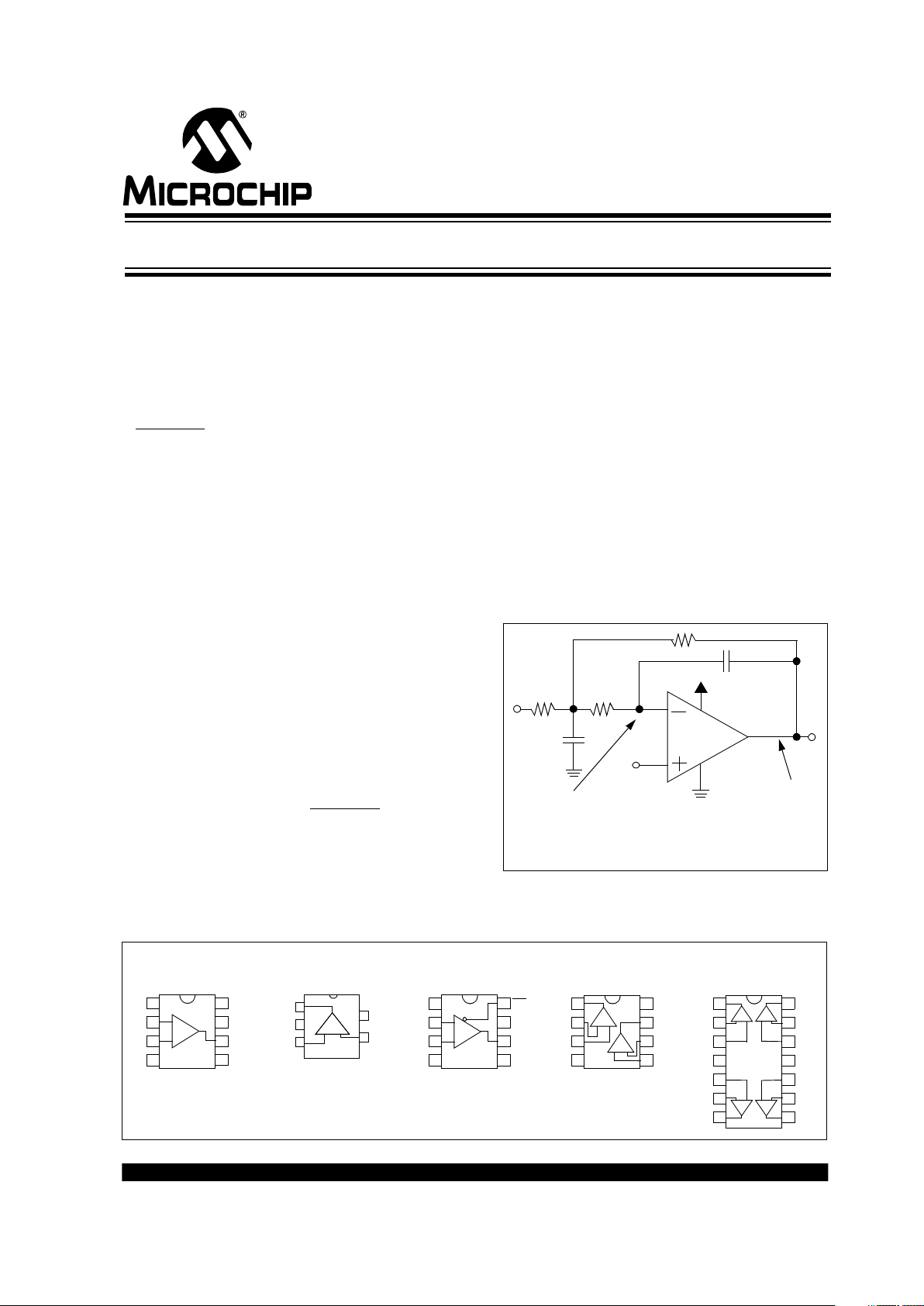
TYPICAL APPLICATION
PACKAGES
MCP60X
V
REF
V
IN
V
OUT
OUT
V
SS
V
DD
-IN
+IN
2nd Order Low Pass Filter
Low Input Bias
Current Over
Temperature
Rail-to-Rail
Output Swing
+IN
-IN
V
SS
1
2
3
4
NC
+INA
-INA
V
DD
-IND
+IND
1
2
3
4
V
SS
OUTD
OUTA
14
13
12
11
-INB
+INB
OUTB
5
6
7
+INA
-INA
V
SS
1
2
3
4
OUTA
+IN
-IN
V
SS
1
2
3
4
NC
V
DD
OUT
NC
CS
8
7
6
5
OUTB
-INB
+INB
V
DD
8
7
6
5
PDIP, SOIC, TSSOP
MCP601 MCP602
V
DD
OUT
PDIP, SOIC, TSSOP
MCP604
-
NC
NC
A
B
MCP603
8
7
6
5
+
+ -
+-
-
+
A
+
-
+INC
-INC
OUTC
10
9
8
D
+
-
B
+
-
C
+
-
PDIP, SOIC, TSSOPPDIP, SOIC, TSSOP
1
2
3
4
5
-+
OUT
V
SS
+IN
V
DD
-IN
MCP601
SOT23-5
2.7V to 5.5V Single Supply CMOS Op Amps
MCP601/602/603/604
DS21314D-page 2 2000 Microchip Technology Inc.
1.0 ELECTRICAL
CHARACTERISTICS
1.1 Maximum Ratings*
VDD..................................................................................7.0V
All inputs and outputs w.r.t. ............. V
SS
-0.3V to VDD +0.3V
Difference Input voltage .......................................|V
DD
- VSS|
Output Short Circuit Current ..................................continuous
Current at Input Pin .......................................................±2mA
Current at Output and Supply Pins .............................±30mA
Storage temperature .....................................-65°C to +150°C
Ambient temp. with power applied ................-55°C to +125°C
Soldering temperature of leads (10 seconds) .............+300°C
ESD Tolerance .................................3KV Human Body Model
*Notice: Stresses above those listed under “Maximum Ratings”
may cause permanent damage to the device. This is a stress rating only and functional operation of the device at those or any
other conditions above those indicated in the operational listings
of this specification is not implied. Exposure to maximum rating
conditions for extended periods may affect device reliability.
PIN FUNCTION TABLE
DC CHARACTERISTICS
NAME FUNCTION
+IN, +INA, +INB, +INC, +IND Non-inverting Input
Te r mi n a l s
-IN, -INA, -INB, -INC, -IND Inverting Input Terminals
V
DD
Positive Power Supply
V
SS
Negative Power Supply
OUT, OUTA, OUTB, OUTC, OUTD Output Terminals
CS
Chip Select
NC No internal connection
to IC
Unless otherwise indicated, all limits are specified for VDD = +2.7V to +5.5V, VSS = GND, TA = 25 °C, VCM = VDD/2, RL = 100kΩ to
V
DD
/2, and V
OUT
~ VDD/2
PARAMETERS SYMBOL MIN. TYP. MAX. UNITS CONDITIONS
INPUT OFFSET VOLTAGE
Input Offset Voltage V
OS
-2 +2 mV
Over Temperature
(1)
V
OS
-3 +3 mV TA= -40°C to +85°C
Drift with Temperature dV
OS
/dT — ±2.5 — µV/°CTA= -40°C to +85°C
Power Supply Rejection PSRR — 40 100
µV/V for V
DD
= 2.7V to 5.5V
INPUT CURRENT AND IMPEDANCE
Input Bias Current I
B
— 1 — pA
Over Temperature
(2)
I
B
— 20 60 pA TA= -40°C to +85°C
Input Offset Bias Current I
OS
— 1 — pA
Common Mode Input Impedance Z
CM
— 1013||6 — Ω||pF
Differential Input Impedance Z
DIFF
— 1013||3 — Ω||pF
COMMON MODE
Common-Mode Input Range V
CM
V
SS
−0.3 — VDD−1.2 V
Common-Mode Rejection Ratio CMRR 75 90 — dB V
DD
= 5V,
V
CM
= -0.3 to 3.8V
OPEN LOOP GAIN
DC Open Loop Gain A
OL
100 115 — dB RL = 25kΩ to VDD/2,
50mV < V
OUT
<
(V
DD
− 50 mV)
DC Open Loop Gain A
OL
95 110 — dB RL = 5kΩ to VDD/2,
100mV < V
OUT
<
(V
DD
− 100mV)
OUTPUT
Low Level/High Level Output Swing V
OL
, V
OHVSS
+ 0.015 — VDD − 0.020 V RL = 25kΩ to VDD/2
V
OL
, V
OHVSS
+ 0.045 — VDD − 0.060 V RL = 5kΩ to VDD/2
Linear Region Maximum Output
Voltage Swing
V
OUT
VSS + 0.050 — VDD − 0.050 V RL = 25kΩ to VDD/2,
A
OL
≥ 100dB
V
OUT
VSS + 0.100 — VDD − 0.100 V RL = 5kΩ to VDD/2,
A
OL
≥ 95dB
Output Short Circuit Current I
SC
20 — mA V
OUT
= 2.5V,
V
DD
= 5V
POWER SUPPLY
Supply Voltage V
DD
2.7 — 5.5 V
Quiescent Current Per Amp I
Q
230 325 µAIL = 0
Note 1: Max. and Min. specified for PDIP and SOIC packages only. Typical refers to all other packages
Note 2: Max. and Min. specified for PDIP, SOIC, and TSSOP packages only. Typical refers to all packages.
2000 Microchip Technology Inc. DS21314D-page 3
MCP601/602/603/604
AC CHARACTERISTICS
SPECIFICATIONS FOR MCP603 CHIP SELECT
FEATURE
TEMPERATURE SPECIFICATIONS
Unless otherwise indicated, all limits are specified for VDD = +2.7V to +5.5V, VSS = GND, TA = 25°C, VCM = VDD/2, RL = 100kΩ to
V
DD
/2, and V
OUT
~ VDD/2
PARAMETERS SYMBOL MIN. TYP. MAX. UNITS CONDITIONS
Gain Bandwidth Product GBWP — 2.8 MHz V
DD
= 5V
Phase Margin
Θ
m
— 50 — degrees CL = 50pF, VDD = 5V
Slew Rate SR — 2.3 — V/
µsG = +1V/V, V
DD
= 5V
Setting Time to 0.01% — 4.5 —
µsfor ∆V
OUT
= 3.8VSTEP,
C
L
= 50pF, VDD = 5V,
G = +1V/V
NOISE
Input Voltage Noise e
n
— 7 — µV
P-P
f = 0.1Hz to 10Hz
Input Voltage Noise Density e
n
— 29 — nV/ f = 1kHz
Input Current Noise Density i
n
— 0.6 — fA/ f = 1kHz
Unless otherwise indicated, all limits are specified for V
DD
= +2.7V to +5.5V, VSS = GND, TA = 25°C, VCM = VDD/2, RL = 100kΩ to
V
DD
/2, and V
OUT
~ VDD/2
PARAMETERS SYMBOL MIN. TYP. MAX. UNITS CONDITIONS
CS
LOW SPECIFICATIONS
CS
Logic Threshold, Low V
IL
V
SS
0.42 V
DD
0.2 V
DD
V For entire V
DD
range
CS
Input Current, Low I
CSL
-1.0 ——µACS = 0.2V
DD
Amplifier Output Leakage, CS High — 1 — nA
CS
HIGH SPECIFICATIONS
CS
Logic Threshold, High V
IH
0.8 V
DD
0.51 V
DD
V
DD
V For entire V
DD
range
CS
Input High, Shutdown CS Pin
Current
I
CSH
— 0.7 2.0 µACS = V
DD
CS Input High, Shutdown GND
Current
I
Q
— 0.7 2.0 µACS = V
DD
DYNAMIC SPECIFICATIONS
CS
Low to Amplifier Output High
Turn-on Time
t
ON
— 3.1 10 µsCS low ≤ 0.2V
DD
CS High to Amplifier Output High Z t
OFF
— 100 — ns CS high ≥ 0.8VDD, No
Load
CS
Threshold Hysteresis — 0.3 — V
Hz
Hz
Unless otherwise indicated, all limits are specified for VDD = +2.7V to +5.5V, VSS = GND
PARAMETERS SYMBOL MIN. TYP. MAX. UNITS CONDITIONS
TEMPERATURE RANGE
Specified Temperature Range T
A
-40 — +85 °C
Operating Temperature Range T
A
-40 — +85 °C
Storage Temperature Range T
A
-65 — +150 °C
THERMAL PACKAGE RESISTANCE
Thermal Resistance, 5L-SOT23-5
θ
JA
— 256 —°C/W
Thermal Resistance, 8L-PDIP
θ
JA
— 85 —°C/W
Thermal Resistance, 8L-SOIC
θ
JA
— 163 —°C/W
Thermal Resistance, 8L-TSSOP
θ
JA
— 124 —°C/W
Thermal Resistance, 14L-PDIP
θ
JA
— 70 —°C/W
Thermal Resistance, 14L-SOIC
θ
JA
— 120 —°C/W
Thermal Resistance, 14L-TSSOP
θ
JA
— 100 —°C/W
MCP601/602/603/604
DS21314D-page 4 2000 Microchip Technology Inc.
2.0 TYPICAL PERFORMANCE CURVES
Note: Unless otherwise indicated, VDD = +2.7V to +5.5V, TA = 25°C, VCM = VDD/2, RL = 25kΩ to VDD/2 and V
OUT
~ VDD/2
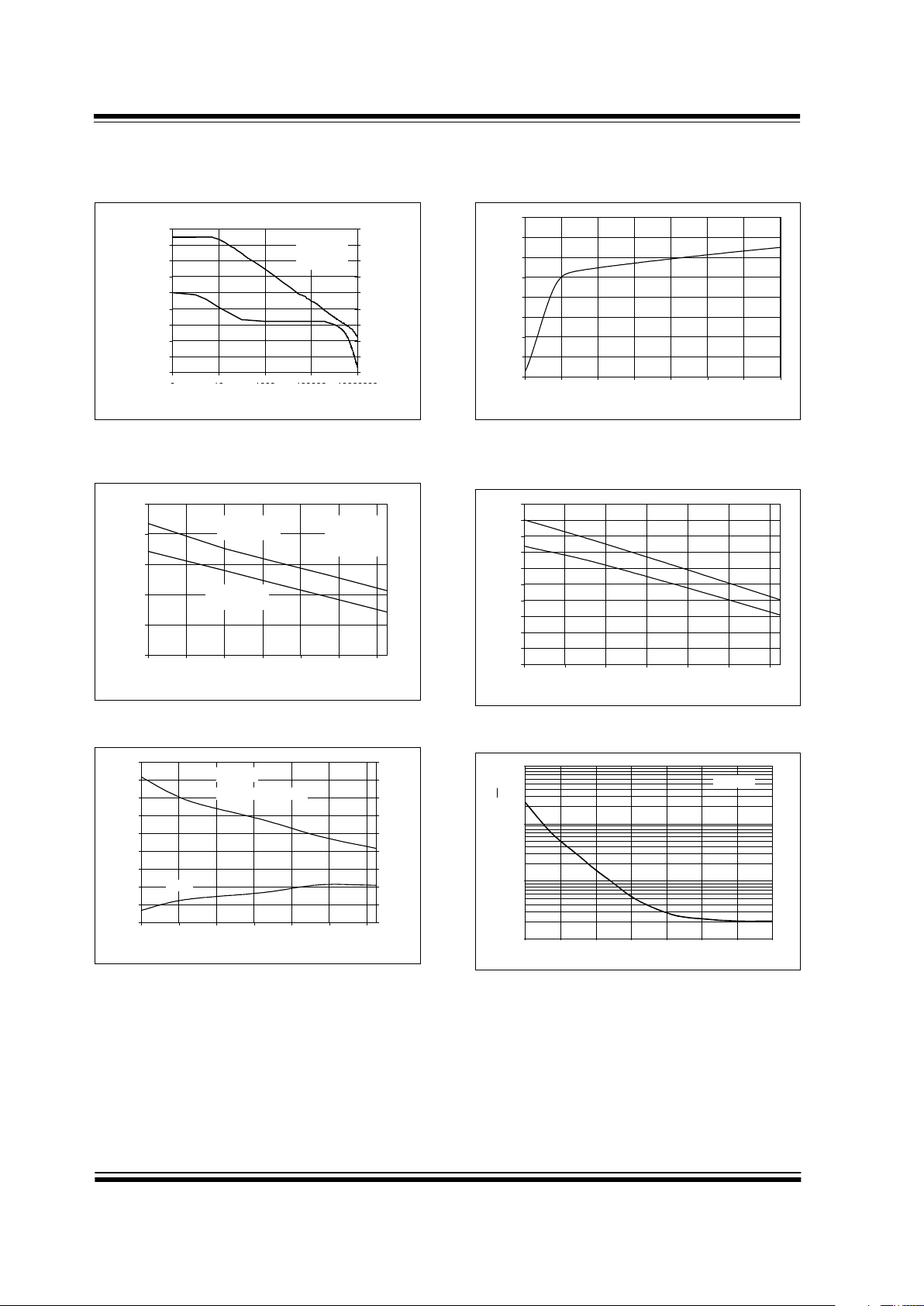
FIGURE 2-1: Open Loop Gain, Phase Margin vs.
Frequency
FIGURE 2-2: Slew Rate vs. Temperature
FIGURE 2-3: Gain Bandwidth Product vs.
Temperature
FIGURE 2-4: Quiescent Current vs. Power Supply
FIGURE 2-5: Quiescent Current vs. Temperature
FIGURE 2-6: Input Voltage Noise Density vs.
Frequency
Phase Margin (degrees)
-60
-40
-20
0
20
40
60
80
100
120
0 10 1000 100000 10000000
Frequency (Hz)
Open Loop Gain (dB)
-250
-200
-150
-100
-50
0
50
100
150
200
CL = 50pF,
R
L
= 100kΩ
V
DD
= 5V
Gain
Phase
0.1 10 1K 100K 10M
1
1.5
2
2.5
3
3.5
-40 -20 0 20 40 60 80
Temperature (°C)
Slew Rate (V/
µ
s)
High-to-Low
Trans ition
Low-to-High
Transition
CL=50pF,
R
L
=100kΩ,
V
DD
=5V
0
0.5
1
1.5
2
2.5
3
3.5
4
4.5
-40-20 0 20406080
Temperature (°C)
Gain Bandwidth Product (MHz)
40
45
50
55
60
65
70
75
80
85
Phase Margin (degrees)
Gain Bandwidth Product
Phase
CL = 55pF
100
120
140
160
180
200
220
240
260
2.0 2.5 3.0 3.5 4.0 4.5 5.0 5.5
Power Supply, V
DD
(V)
Quiescent Current per Amplifier (
µ
A)
IL = 0
100
120
140
160
180
200
220
240
260
280
300
-40-20 0 20406080
Temperature (°C)
Quiescent Current per Amplifier (µA)
VDD = 5.5V
V
DD
= 2.7V
I
L
= 0
0.1 1 10 100 1k 10k 100k 1M
10
100
1000
10000
Frequency (Hz)
Input Voltage Noise Density (nV/ √Hz)
RL = 10kΩ
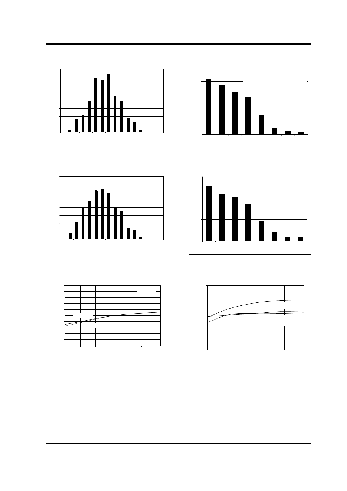
2000 Microchip Technology Inc. DS21314D-page 5
MCP601/602/603/604
Note: Unless otherwise indicated, VDD = +2.7V to +5.5V, TA = 25°C, VCM = VDD/2, RL = 25kΩ to VDD/2 and V
OUT
~ VDD/2
FIGURE 2-7: Offset Voltage vs. Number of
Occurrences with V
DD
= 5.5V
FIGURE 2-8: Offset Voltage vs. Number of
Occurrences with V
DD
= 2.7V.
FIGURE 2-9: Normalized Offset Voltage vs. Temperature with V
DD
= 2.7V
FIGURE 2-10: Offset Voltage Drift vs. Number of
Occurrences with V
DD
= 5.5V
FIGURE 2-11: Offset Voltage Drift vs. Number of
Occurrences with V
DD
= 2.7V
FIGURE 2-12: Common-Mode Rejection Ratio,
Power Supply Rejection Ratio vs. Temperature
0
5
10
15
20
25
30
35
40
-
1.75
-1.50
-1.25
-1.00
-0.75
-0.50
-
0.25
0.00
0.25
0.50
0.75
1.00
1.25
1.50
1.75
2.00
Offset Voltage (mV)
Numb er
o
f Occuracnes
-2
.
00
VDD = 5.5V
R
L
= 100kΩ
Sample Size = 203 op amp
0
5
10
15
20
25
30
35
40
-1.75
-1.50
-1.25
-1.00
-0.75
-0.50
-0.25
0.00
0.25
0.50
0.75
1.00
1.25
1.50
1.75
2.00
Offset Voltage (mV)
Number of Occurances
-2.00
VDD = 2.7V
R
L
= 100kΩ
Sample Size = 203 op amp
-500
-400
-300
-200
-100
0
100
200
300
400
500
-40-20 0 20406080
Temperature (°C)
Offset Voltage (µV)
VDD = 5.5V
VDD = 2.7V
RL = 100kΩ
0
10
20
30
40
50
60
12345678
Change in Offset Voltage with Temperature (
µ
V/°C)
Number of Occurances
0
VDD = 5.5V
R
L
= 100kΩ
Sample Size = 203
Temperature Range = -40°C to +85
°C
0
10
20
30
40
50
60
12345678
Change in Offset Voltage wit h Temperature (
µ
V/°C)
Num
b
er
o
f
O
ccur
a
n
c
es
0
11
VDD = 2.7V
R
L
= 100kΩ
Sample Size = 203
Temperature Range = -40°C to +85
°C
75
80
85
90
95
100
-40-20 0 20406080
Temperature (° C)
Common Mode Rejection Ratio, Power Supply Rejectio
n
Ratio (dB)
CMRR
V
DD
= 2.7V
V
CM
= -0.3V to 1.5V
PSRR,
V
DD
= 2.7V to 5.5V
CMRR
V
DD
= 5.5V
V
CM
= -0.3V to 4.3V
MCP601/602/603/604
DS21314D-page 6 2000 Microchip Technology Inc.
Note: Unless otherwise indicated, VDD = +2.7V to +5.5V, TA = 25°C, VCM = VDD/2, RL = 25kΩ to VDD/2 and V
OUT
~ VDD/2
FIGURE 2-13: Offset Voltage vs. Common-Mode
Voltage
FIGURE 2-14: Input Bias Current, Input Offset
Current vs. Temperature
FIGURE 2-15: DC Open Loop Gain vs. Output Load
FIGURE 2-16: Common-Mode Rejection Ratio,
Power Supply Rejection Ratio vs. Frequency
FIGURE 2-17: Input Bias Current, Input Offset
Current vs. Common Mode Input Voltage
FIGURE 2-18: DC Open Loop Gain vs. Power Supply
40
60
80
100
120
140
160
180
200
220
240
-1012345
Common Mode Voltage (V)
Offset Voltage (µV)
Representative Part
VDD = 2.7V
VDD = 5.5V
0
2
4
6
8
10
12
14
16
18
20
-40-20 0 20406080
Temperature (°C)
Input Bias Current, Input Offset Current (pA)
Input Bias Current Levels are Typically
less than 1pA Below 25°C
Input Bias Current
Input
Offset
Current
VDD = 5.5V
80
90
100
110
120
0 20000 40000 60000 80000 100000
Load Resistance (Ω)
DC Open Loop Gain (dB)
VDD = 5.5V
VDD = 2.7V
0 2K 4K 6K 8K 10K
-20
0
20
40
60
80
100
1 10 100 1000 10000 100000 1000000 10000000
Frequency (Hz)
PSRR, CMRR (dB)
PSRR+
PSRR-
VDD=5.0V,
C
L
=50 pF
CMRR
1 10 100 1K 10K 100K 1M 10M
0
2
4
6
8
10
12
14
16
18
20
0 0.5 1 1.5 2 2.5 3 3.5 4 4.5 5 5.5
Common-mode Voltage (V)
Input Bias, Input Offset Current (pA
)
VDD = 5.5V
R
L
= ∞
T
A
= 85 °C
Input Bias Current
Input Offset
90
95
100
105
110
115
22.533.544.5 55.5
Power Supply Voltage, V
DD
(V)
Open Loop Gain (dB)

2000 Microchip Technology Inc. DS21314D-page 7
MCP601/602/603/604
Note: Unless otherwise indicated, VDD = +2.7V to +5.5V, VSS = GND, TA = 25°C, VCM = VDD/2, RL = 25kΩ to VDD/2 and
V
OUT
~ VDD/2
FIGURE 2-19: Gain Bandwidth, Phase Margin vs.
Load Resistance
FIGURE 2-20: Low Level and High Level Output
Swing vs. Resistive Load
FIGURE 2-21: Maximum Full Scale Output Voltage
Swing vs. Frequency
FIGURE 2-22: DC Open Loop Gain vs. Temperature
FIGURE 2-23: Low Level and High Level Output
Swing vs. Temperature
FIGURE 2-24: Output Short Circuit Current vs.
Temperature
0
0.5
1
1.5
2
2.5
3
3.5
100 1000 10000 1 00000
Resistance (W)
Gain-Bandwidth (MHz)
30
40
50
60
70
80
90
100
Phase Margin (degs)
Gain-Bandwidth
Phase Margin
VDD = 5.0V,
C
L
= 50 pF
100 1K 10K 100K
0
100
200
300
400
500
600
700
100 1000 10000 100000
Load Resistance (Ω)
V
DD
-V
OH
, V
OL
-V
SS
(mV)
VDD-V
OH
VDD=5.5V
VOL - V
SS
VDD=5.5V
VDD-V
OH
VDD=2.7V
VOL - V
SS
VDD=2.7V
100 1K 10K 100K
0
0.5
1
1.5
2
2.5
3
3.5
4
4.5
5
5.5
1000 10000 100000 1000000 10000000
Frequency (Hz)
Full-Scale Output Voltage Swing (V)
VDD = 5V
1K 10K 100K 1M 10M
80
85
90
95
100
105
110
115
120
-40-20 0 20406080
Temperature (°C)
DC Open Loop Gain (dB)
VDD = 2.7V,
V
OUT
= 50mV to 2.65V
VDD = 5.5V,
V
OUT
= 50mV to 5.45V
0
2
4
6
8
10
12
-40-20 0 20406080
Temperature (°C)
V
OH
, V
OL
(mV)
VDD-VOH, VDD=2.7V
VOL-VSS, VDD=5.5V
VDD-VOH, VDD=5.5V
VOL-VSS, VDD=2.7V
-40
-30
-20
-10
0
10
20
30
40
-40-30-20-100 1020304050607080
Temperature (°C)
Short Circuit Current (mA)
Positive Short Circuit Current
V
DD
= 5.5V
Positive Short Circuit Current
V
DD
= 2.7V
Negative Short Circuit Current
V
DD
= 2.7V
Negative Short Circuit Current
V
DD
= 5.5V

MCP601/602/603/604
DS21314D-page 8 2000 Microchip Technology Inc.
Note: Unless otherwise indicated, VDD = +2.7V to +5.5V, VSS = GND, TA = 25°C, VCM = VDD/2, RL = 25kΩ to VDD/2 and
V
OUT
~ VDD/2
FIGURE 2-25: Large Signal Non-Inverting Signal
Pulse Response
FIGURE 2-26: Small Signal Non-inverting Pulse
Response
FIGURE 2-27: Chip Select to Amplifier Output
Response Time
FIGURE 2-28: Large Signal Inverting Signal Pulse
Response
FIGURE 2-29: Small Signal Inverting Signal Pulse
Response
FIGURE 2-30: GND Current vs. CS
Voltage
1µS / div
500 mV / div
VDD = 5V
R
L
= 100kΩ
C
L
= 50pF
G = +1V/V
1µS / div
50 mV/div
VDD = 5V
R
L
= 100k
Ω
C
L
=50 pF
G = +1V/V
5 µS/div
500 mV/div
CS
Amplifier
Output
Active
RL = 100kΩ to GND
C
L
= 50pF
G = +1V/V
V
IN+
= 2.5V
V
DD
= 5V
Hi-Z
1µS / div
500 mV/div
CL=50pF, RL=100kΩ,
V
DD
= 5V, G= -1V/V
1µS / div
50 mV/div
CL=50pF, RL=100kΩ,
V
DD
= 5V, G= -1V/V
-800
-700
-600
-500
-400
-300
-200
-100
0
100
0.0 0.5 1.0 1.5 2.0 2.5 3.0 3.5 4.0 4.5 5.0 5.5
CS Pin Voltage (V)
GND Current (µA)
VDD = 5.5V

2000 Microchip Technology Inc. DS21314D-page 9
MCP601/602/603/604
Note: Unless otherwise indicated, VDD = +2.7V to +5.5V, VSS = GND, TA = 25°C, VCM = VDD/2, RL = 25kΩ to VDD/2 and
V
OUT
~ VDD/2
FIGURE 2-31: Input CS Current vs. CS Voltage
FIGURE 2-32: Channel to Channel Separation
FIGURE 2-33: CS hysteresis
-0.1
0
0.1
0.2
0.3
0.4
0.5
0.6
0.7
0.8
0.9
0.0 1.0 2.0 3.0 4.0 5.0 6.0
CS Pin Voltage (V)
CS Pin Current (uA)
VDD = 5.5V
-150
-145
-140
-135
-130
-125
-120
-115
-110
-105
-100
100 1000 10000 100000 1000000
Frequency (Hz)
Channel to Channel Isolation (dB)
RL =
∞
100 1K 10K 100K 1M
-0.5
0
0.5
1
1.5
2
2.5
3
0123456
CS Input Voltage (V)
Internal CS Switch Output (V)
VDD = 5V
CS Input Low
to Hi
g
h
CS Input High
to Low
Amplifie r Output in
Hi-Z state
Amplifier Output Active (driven)

MCP601/602/603/604
DS21314D-page 10 2000 Microchip Technology Inc.
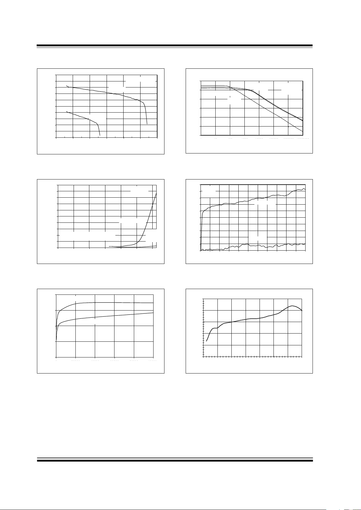
3.0 APPLICATIONS INFORMATION
The MCP601/602/603/604 family of operational amplifiers are fabricated on Microchip’s state-of-the-art
CMOS process. They are unity gain stable and suitable
for a wide range of general purpose applications. With
this family of operational amplifiers, the power supply
pin should be by-passed with a 1µF capacitor.
3.1 Rail-to-Rail Output Swing
There are two specifications that describe the output
swing capability of the MCP601/602/603/604 family of
operational amplifiers. The first specification, Low Level
and High Level Output Voltage Swing, defines the
absolute maximum swing that can be achieved under
specified loaded conditions. For instance, the Low
Level Output Voltage Swing of the MCP601/602/603/
604 family is specified to be able to swing at least to
15mV from the negative rail with a 25kΩ load to V
DD
/2.
This output swing performance is shown in Figure 3-1,
where the output of an MCP601 is configured in a gain
of +2V/V and over driven with a 40kHz triangle wave. In
this figure, the degradation of the output swing linearity
is clearly illustrated. This degradation occurs after the
point at which the open loop gain of the amplifier is
specified and before the amplifier reaches its maximum
and minimum output swing.
FIGURE 3-1: Low Level and High Level Output
Swing
The second specification that describes the output
swing capability of these amplifiers is the Linear Region
Maximum Output Voltage Swing. This specification
defines the maximum output swing that can be
achieved while the amplifier is still operating in its linear
region.
The Linear Region Maximum Output Voltage Swing of
the MCP601/602/603/604 family is specified within
50mV from the positive and negative rail with a 25kΩ
load and 100mV from the rails with a 5kΩ load. The
overriding condition that defines the linear region of the
amplifier is the open loop gain that is specified over that
region. In the voltage output region between V
SS
+
50mV and V
DD
- 50mV, the open loop gain is specified
to 100dB (min) with a 25kΩ load.
The classical definition of the open loop gain of an
amplifier is:
AOL = ∆V
OUT
/ ∆V
OS
where:
A
OL
is the DC open loop gain of the amplifier,
∆V
OUT
is equal to (VDD - 50mV) - (VSS + 50mV)
for R
L
= 25kΩ, and
∆V
OS
is the change in offset voltage with the
changing output voltage of the amplifier.
3.2 Input Voltage and Phase Reversal
Since the MCP601/602/603/604 amplifier family is
designed with CMOS devices, it does not exhibit phase
inversion when the input pins exceed the negative supply voltage. Figure 3-2 shows an input voltage exceeding both supplies with no resulting phase inversion.
FIGURE 3-2: The MCP601/602/603/604 family of op
amps do not have phase reversal issues. For the
graph, the amplifier is in a unity gain or buffer
configuration.
-2
0
2
4
6
8
10
0 1020304050
Time (µs)
Input Signal (V)
-0.7
-0.5
-0.3
-0.1
0.1
0.3
0.5
V
OH
, V
OL
(0.1mV/div)
V
OL
V
OH
G=+2V/V, VDD= 5V
V
DD
V
SS
-1
0
1
2
3
4
5
6
01020304050
Time(µS)
Input and Output Voltage (V)
Input Signal
Output Signal
G = +2V/V
V
DD
= 5V

2000 Microchip Technology Inc. DS21314D-page 11
MCP601/602/603/604
The maximum operating common-mode voltage that
can be applied to the inputs is V
SS
- 0.3V to VDD - 1.2V.
In contrast, the absolute maximum input voltage is V
SS
- 0.3V and VDD + 0.3V. Voltages on the input that
exceed this absolute maximum rating can cause excessive current to flow in or out of the input pins. Current
beyond ±2mA can cause possible reliability problems.
Applications that exceed this rating must be externally
limited with an input resistor as shown in Figure 3-3.
FIGURE 3-3: If the inputs of the amplifier exceed the
Absolute Maximum Specifications, an input resistor,
R
IN
, should be used to limit the current flow into that
pin.
3.3 Capacitive Load and Stability
Driving capacitive loads can cause stability problems
with many of the higher speed amplifiers.
For any closed loop amplifier circuit, a good rule of
thumb is to design for a phase margin that is no less
than 45
°. This is a conservative theoretical value, how-
ever, if the phase margin is lower, layout parasitics can
degrade the phase margin further causing a truly
unstable circuit. A system phase shift of 45
° will have
an overshoot in its step response of approximately
25%.
A buffer configuration with a capacitive load is the most
difficult configuration for an amplifier to maintain stability. The Phase versus Capacitive Load of the MCP60X
amplifier is shown in Figure 3-4. In this figure, it can be
seen that the amplifier has a phase margin above 40
°,
while driving capacitance loads up to 100pF.
FIGURE 3-4: Gain Bandwidth, Phase Margin vs.
Capacitive Load
FIGURE 3-5: Amplifier circuits that can be used
when driving heavy capacitive loads.
If the amplifier is required to drive larger capacitive
loads, the circuit shown in Figure 3-5 can be used. A
small series resistor (R
ISO
) at the output of the amplifier
improves the phase margin when driving large capacitive loads. This resistor decouples the capacitive load
from the amplifier by introducing a zero in the transfer
function.
This zero adjusts the phase margin by approximately:
∆θ
m
= tan-1 (2π GBWP x R
ISO
x CL)
where:
∆θ
m
is the improvement in phase margin,
GBWP is the gain bandwidth product of the
amplifier,
R
ISO
is the capacitive decoupling resistor, and
C
L
is the load capacitance
RIN = (Maximum expected voltage - VDD) / 2mA
or
(V
SS
- Minimum expected voltage)/ 2mA.
R
IN
MCP60X
0
0.5
1
1.5
2
2.5
3
3.5
4
10 100 1000 10000 100000 1000000
Capacitance (p F)
Gain-Bandwidth (MHz)
0
10
20
30
40
50
60
70
80
Phase Margin (degrees)
Gain-Bandwidth
Phase
Margin
VDD=5.0V,
R
L
=100 k
Ω
10 100 1E3 10E3 100E3 1E6
V
IN
C
L
R
ISO
V
OUT
MCP60X
V
DD

MCP601/602/603/604
DS21314D-page 12 2000 Microchip Technology Inc.
3.4 The Chip Select Option of the MCP603
The MCP603 is a single amplifier with a Chip Select
option. When CS is pulled high the supply current
drops to 0.7µA (typ), which is pulled through the CS
pin
to V
SS
. In this state, the amplifier is put into a high
impedance state. By pulling CS
low or letting the pin
float, the amplifier is enabled. Figure 3-6 shows the output voltage and supply current response to a CS
pulse.
FIGURE 3-6: Timing Diagram for the CS Function of the MCP603 Amplifier
3.5 Layout Considerations
In applications where low input bias current is critical,
PC board surface leakage effects and signal coupling
from trace to trace need to be taken into consideration.
3.5.1 SURFACE LEAKAGE
Surface leakage across a PC board is a consequence
of differing DC voltages between two traces combined
with high humidity, dust or contamination on the board.
For instance, the typical resistance from PC board
trace to pad is approximately 10
12
Ω under low humidity
conditions. If an adjacent trace is biased to 5V and the
input pin of the amplifier is biased at or near zero volts,
a 5pA leakage current will appear on the amplifier’s
input node. This type of PCB leakage is five times the
room temperature input bias current (1pA, typ) of the
MCP601/602/603/604 family of amplifiers.
The simplest technique that can be used to reduce the
effects of PC board leakage is to design a ring around
sensitive pins and traces. An example of this type of
layout is shown in Figure 3-7.
FIGURE 3-7: Example of Guard Ring for the
MCP601, the A-amplifier of the MCP602 or the
MCP603 in a PC Board Layout
V
IL
Hi-Z
t
ON
V
IH
t
OFF
Hi-Z
Output
2.0nA (typ)
2.0nA (typ)
V
DD
Supply
Current
230µA (typ)
0.7µA (typ)
0.7µA (typ)
GND
Current
230µA (typ)
0.7µA (typ) 0.7µA (typ)
CS
Current
2nA(typ)
CS
-In +In V-
Guard Ring

2000 Microchip Technology Inc. DS21314D-page 13
MCP601/602/603/604
Circuit examples of ring implementations are shown in
Figure 3-8. In Figure 3-8A, B and C, the guard ring is
biased to the common-mode voltage of the amplifier.
This type of guard ring is most effective for applications
where the common-mode voltage of the input stage
changes, such as buffers, inverting gain amplifiers or
instrumentation amplifiers.
The strategy shown in Figure 3-8D, biases the common-mode voltage and guard ring to ground. This type
of guard ring is typically used in precision photo sensing circuits.
FIGURE 3-8: Examples of how to design PC Board
traces to minimize leakage paths to the high
impedance input pins of the MCP601/602/603/604
amplifiers.
3.5.2 SIGNAL COUPLING
The input pins of the MCP601/602/603/604 amplifiers
have a high impedance providing an opportunity for
noise injection, if layout issues are not considered.
These high impedance input terminals are sensitive to
injected currents. This can occur if the trace from a high
impedance input is next to a trace that has fast changing voltages, such as a digital or clock signal. When a
high impedance trace is in close proximity to a trace
with these types of voltage changes, charge is capacitively coupled into the high impedance trace.
FIGURE 3-9: Capacitors can be built with PCB
traces allowing for coupling of signals from one trace
to another.
As shown in Figure 3-9, the value of the capacitance
between two traces is primarily dependent on the distance (d) between the traces and the distance that the
two traces are in parallel (L). From this model, the
amount of current generated into the high impedance
trace is equal to:
I = C ∂V/∂t
where:
I equals the current that appears on the high
impedance trace,
C equals the value of capacitance between the two
PCB traces,
∂V equals the change in voltage of the trace that is
switching, and
∂t equals the amount of time that the voltage
change took to get from one level to the next.
Voltage
Reference
(could be ground)
MCP60X
MCP60X
MCP60X
MCP60X
V
DD
Figure 3-8A
Figure 3-8C
Figure 3-8B
Figure 3-8D
w= thickness of PCB trace
L= length of PCB trace
d= distance between the two PCB traces
PCB Trace
w
(typ 0.003mm)
PCB
Cross-Section
w x L x eo x e
r
C = pF
d
L
d

MCP601/602/603/604
DS21314D-page 14 2000 Microchip Technology Inc.
3.6 Typical Applications
3.6.1 ANALOG FILTERS
Examples of two second order low pass filters are
shown in Figure 3-10 and Figure 3-11. The filter in Figure 3-10 can be configured for gain of +1V/V or greater.
The filter in Figure 3-11 can be configured for inverting
gains.
FIGURE 3-10: 2nd Order Low Pass Sallen-Key Filter
FIGURE 3-11: 2nd Order Low Pass
Multiple-Feedback Filter
The MCP601/602/603/604 family of operational amplifiers are particularly well suited for these types of filters.
The low input bias current, which is typically 1pA (up to
60pA at temperature), allows the designer to select
higher value resistors, which in turn reduces the capacitive values. This allows the designer to select surface
mount capacitors, which in turn can produce a compact
layout.
The rail-to-rail output operation of the MCP601/602/
603/604 family of amplifiers make these circuits well
suited for single supply operation. Additionally, the wide
bandwidth allows low pass filter design up to 1/10 of the
GBWP or 300kHz.
These filters can be designed using the calculations
provided in the Figures or with Microchip’s interactive
FilterLab software. FilterLab will calculate capacitor
and resistor values, as well as, determine the number
of poles that are required for the application. Finally, the
program will generate a SPICE macromodel, which can
be used for spice simulations.
3.6.2 INSTRUMENTATION AMPLIFIER
CIRCUITS
The instrumentation amplifier has a differential input,
which subtracts one analog signal from another and
rejects common mode signals. This amplifier also provides a single ended analog output signal. The three op
amp instrumentation amplifier is illustrated in Figure
3-12 and the two op amp instrumentation amplifier is
shown in Figure 3-13.
FIGURE 3-12: An instrumentation amplifier can be
built using three operational amplifiers and seven
resistors.
FIGURE 3-13: An instrumentation amplifier can also
be built using two operational amplifiers and five
resistors.
R
2
V
OUT
V
IN
C
2
R
1
R
4
R
3
C
1
Sallen-Key
V
OUT
V
IN
K/(R1R2C2C1)
s
2
+s(1/R1C2+1/R2C2+1/R2C1 – K/R2C1+1/R1R2C2C1)
=
K = 1 + R4/R
3
MCP60X
R
3
V
OUT
V
IN
R
1
C
2
R
2
C
1
V
OUT
V
IN
–1/R1R3C2C
1
s2C2C1 + sC1(1/R1 + 1/R2 + 1/R3) + 1/(R2R3C2C1)
=
MCP60X
*Bypass Capacitor, 1µF
V
2
R
4
R
3 V
OUT
R
G
MCP60X
V
1
R
2
R
2
R
4
R
3
*
*
V
OUT
V1V2–()1
2R
2
R
G
---------+
R
4
R
3
------
V
REF
R
4
R
3
----- -
+=
V
REF
V
DD
V
DD
MCP60X
MCP60X
*
V
OUT
*Bypass Capacitor, 1µF
V
REF
V
2
R
G
R
1
V
OUT
V1V2–()1
R
1
R
2
----- -
2R
1
R
G
---------++
V
REF
+=
V
1
R
2
R
1
R
2
V
DD
MCP60X
MCP60X

2000 Microchip Technology Inc. DS21314D-page 15
MCP601/602/603/604
An advantage of the three op amp configuration is that
it is capable of unity gain operation. A disadvantage, as
compared to the two op amp instrumentation amplifier,
is that the common mode range reduces with higher
gains.
The two op amp configuration uses fewer op amps, so
power consumption is also low. Disadvantages of this
configuration are that the common-mode range
reduces with gain and it must be configured in gains of
two or higher.
3.6.3 PHOTO DETECTION
The amplifiers in the MCP601/602/603/604 family of
devices can be used to easily convert the signal from a
sensor that produces an output current, such as a photodiode, into a voltage. This is implemented with a single resistor and an optional capacitor in the feedback
loop of the amplifier as shown in Figure 3-14.
FIGURE 3-14: Photo Sensing Circuits Using the
MCP60X Amplifier
A photodiode that is configured in the photovoltaic
mode has no voltage potential placed across the element or is zero biased (Figure 3-14). In this mode, the
light sensitivity and linearity is maximized making it
best suited for precision applications. The key amplifier
specifications for this application are low input bias current, low noise and rail-to-tail output swing. The
MCP601/602/603/604 family is capable of meeting all
three of these difficult requirements.
In contrast, a photodiode that is configured in the photoconductive mode has a reverse bias voltage, which is
applied across the photo sensing element as shown in
Figure 3-14. The width of the depletion region is
reduced when this voltage is applied across the photo
detector, which reduces the photodiode parasitic
capacitance significantly. This reduced parasitic capacitance facilitates high speed operation, however, the linearity and offset errors are not optimized. The design
trade off for this action is increased diode leakage current and linearity errors. A key amplifier specification for
this application is high speed digital communication.
The MCP601/602/603/604 family is well suited for
medium speed photoconductive applications with their
wide bandwidth and rail-to-rail output swing.
V
BIAS
R
2
C
2
R
2
V
OUT
V
OUT
= R2 I
D1
D
1
V
OUT
Light
D
1
Light
MCP60X
MCP60X
I
D1
I
D1
Photodiode in Photovoltaic Mode
Photodiode in Photoconductive Mode

MCP601/602/603/604
DS21314D-page 16 2000 Microchip Technology Inc.
4.0 SPICE MACROMODEL
The Spice macromodel for the MCP601, MCP602,
MCP603 and MCP604 simulates the typical amplifier
performance of offset voltage, DC power supply rejection, input capacitance, DC common mode rejection
ratio, open loop gain over frequency, phase margin with
no capacitive load, output swing, DC power supply current, power supply current change with supply voltage,
input common mode range and input voltage noise.
The characteristics of the MCP601, MCP602,
MCP603, and MCP604 amplifiers are similar in terms
of performance and behavior. This single op amp macromodel supports all four devices with the exception of
the chip select function of the MCP603, which is not
modeled.
The listing for this macromodel is shown on the next
page. The most recent revision of the model can be
downloaded from Microchip’s web site at
www.microchip.com.

2000 Microchip Technology Inc. DS21314D-page 17
MCP601/602/603/604
.subckt mcp601 1 2 3 4 5
* | | | | |
* | | | | Output
* | | | Negative supply
* | | Positive Supply
* | Inverting input
* Non-inverting input
*
* Macromodel for MCP601 (single), MCP602 (dual), MCP603 (single w/CS), and MCP604 (quad)
*
* The characteristics of the MCP601, MCP602, MCP603, and MCP604 have the same fundamental
* performance and behavior. Consequently, this single op amp macromodel supports all four
* devices. However, the chip select function of the MCP603 is not modeled.
*
* Revision History:
* REV A : 6-30-99 created BCB
* REV B : 7-10-99 corrected DC Iq BCB
* REV C : 11-30-99 Placed “.subckt” command as first line, added L, W to Ptype model in
: listing BCB
*
* This macromodel models typical amplifier offset voltage, DC power supply rejection, input
* capacitance, DC common mode rejection ratio, open loop gain over frequency, phase margin
* with no capacitive load, output swing, power supply current, input voltage noise.
*
* NOTICE: THE INFORMATION PROVIDED HEREIN IS BELIEVED TO BE RELIABLE,
* HOWEVER, MICROCHIP ASSUMES NO RESPONSIBILITY FOR INACCURACIES OR
* OMISSIONS. MICROCHIP ASSUMES NO RESPONSIBILITY FOR THE USE OF THIS
* INFORMATION, AND ALL USE OF SUCH INFORMATION SHALL BE ENTIRELY AT
* THE USER’S OWN RISK. NO INTELLECTURAL PROPERTY RIGHTS OR LICENSES
* TO ANY OF THE TECNOLOGY DESCRIBED HEREIN ARE IMPLIED OR GRANTED TO
* ANY THIRD PARTY. MICROCHIP RESERVES THE RIGHT TO CHANGE THIS MODEL
* AT ANY TIME WITHOUT NOTICE.
*
*Input Stage, pole at 5MHz
M1 9 64 7 3 Ptype L=2 W=275
M2 8 2 7 3 Ptype L=2 W=275
CDIFF 1 2 3E-12
CCM1 1 4 6E-12
CCM2 2 4 6E-12
IDD 3 7 30e-6
RA 8 6 1.485e3
RB 9 6 1.485e3
CA 8 9 10.71e-12
*Input Stage Common-Mode Clampling
VCMM 4 6 0.35
ECM 55 4 3 64 1
RCM 57 56 1E3
DCMP 56 55 DX
VCMP 57 4 1.2
RST 58 59 1E3
DST 59 55 DX
VST 58 4 1.6
GCMP2 23 4 POLY(2) 57 56 58 59 0 -0.5E-3 0.5E-3
*Input errors (vos, en, psr, cmr)
ERR 64 1 POLY(3) (67,4) (3, 4) (1,34) 0 1 40e-6 3.2e-6
*Second Stage, pole at 3.3Hz
GS 23 4 8 9 5.7e-3
R1 23 4 0.397e9
C2 23 4 122.8e-12

MCP601/602/603/604
DS21314D-page 18 2000 Microchip Technology Inc.
VSOP 3 24 4.784
VSOM 25 4 -3.48
DSOP 23 24 DY
DSOM 25 23 DY
*HCM 23 3 VCMP
FS 3 4 POLY(11) VO3 VO5 VO4 VO6 VO1 VO2 VO9 VO10 VMID1 VSOP VSOM
+ 200E-6 -1 -1 -1 1 -1 -1 1 1 -1 -1 -1
*mid-supply reference, output swing limit
RMID1 3 35 61.62E3
VMID1 35 34 0
RMID2 4 34 61.62E3
ELEVEL 34 4 23 4 -1
*output stage
DO3 34 43 DY
DO4 44 34 DY
DO5 3 45 DY
DO6 3 46 DY
DO7 4 45 DY
DO8 4 46 DY
VO3 43 5 0.1
VO4 5 44 0.1
GO5 3 47 3 34 10E-3
VO5 47 5 0
GO6 4 48 34 4 10E-3
VO6 48 5 0
GO1 49 4 5 34 10E-3
VO1 49 45 0
GO2 50 4 34 5 10E-3
VO2 50 46 0
RO9 3 51 100
VO9 51 5 0
RO10 52 4 100
VO10 52 5 0
* input voltage noise
VN1 65 4 0.6
DN1 65 67 DX
RN1 67 4 13E3
.model Ptype PMOS
.model DY D(IS=1e-15 BV =50)
.model DX D(IS=1e-18 AF=0.6 KF=10e-17)
.ENDS

2000 Microchip Technology Inc. DS21314D-page 19
MCP601/602/603/604
MCP60X PRODUCT IDENTIFICATION SYSTEM
To order or obtain information, e.g., on pricing or delivery, refer to the factory or the listed sales office.
Sales and Support
Package:
P = Plastic DIP (300 mil Body), 8-lead and 14-lead
SN = Plastic SOIC (150 mil Body), 8-lead
SL = Plastic SOIC (150 mil Body), 14-lead
ST = Plastic TSSOP, 8-lead and 14-lead
OT = Plastic SOT23, 5-lead
Temperature
Range:
I = –40°C to +85°C
Device:
MCP601 = Single Operational Amplifier
MCP601T = Single Operational Amplifier (Tape and Reel-SOIC/TSSOP/SOT23-5)
MCP602 = Dual Operational Amplifier
MCP602T = Dual Operational Amplifier (Tape and Reel-SOIC/TSSOP)
MCP603 = Single Operational Amplifier w/CS
Function
MCP603T = Single Operational Amplifier w/CS
Function
(Tape and Reel-SOIC/TSSOP)
MCP604 = Quad Operational Amplifier
MCP604T = Quad Operational Amplifier (Tape and Reel-SOIC/TSSOP)
MCP60X — X /X
Data Sheets
Products supported by a preliminary Data Sheet may have an errata sheet describing minor operational differences
and recommended workarounds. To determine if an errata sheet exists for a particular device, please contact one of
the following:
1. Your local Microchip sales office
2. The Microchip Corporate Literature Center U.S. FAX: (480) 786-7277
3. The Microchip Worldwide Site (www.microchip.com)
Please specify which device, revision of silicon and Data Sheet (include Literature #) you are using.
N
ew Customer Notification System
Register on our web site (www.microchip.com/cn) to receive the most current information on our products.

Information contained in this publication re garding device applications and the like is intended through suggestion only and may be superseded by updates.
It is your responsibility to ensure that your application meets with your specifications. No representation or warranty is given and no liability is assumed by
Microchip Technology Incorporated with respect to the accuracy or use of such information, or infringement of patents or other intellectual property rights
arising from such use or otherwise. Use of Microchip’s products as critical components in life support systems is not authorized except with express written
approval by Microchip. No licenses are conveyed, implicitly or otherwise, except as maybe explicitly expressed herein, under any intellectual property
rights. The Microchip logo and name are registered trademarks of Microchip Technology Inc. in the U.S.A. and other countries. All rights reserved. All other
trademarks mentioned herein are the property of their respective companies.
DS21314D-page 20
2000 Microchip Technology Inc.
All rights reserved. © 2000 Microchip Technology Incorporated. Printed in the USA. 5/00 Printed on recycled paper.
AMERICAS
Corporate Office
Microchip Technology Inc.
2355 West Chandler Blvd.
Chandler, AZ 85224-6199
Tel: 480-786-7200 Fax: 480-786-7277
Technical Support: 480-786-7627
Web Address: http://www.microchip.com
Atlanta
Microchip Technology Inc.
500 Sugar Mill Road, Suite 200B
Atlanta, GA 30350
Tel: 770-640-0034 Fax: 770-640-0307
Boston
Microchip Technology Inc.
5 Mount Royal Avenue
Marlborough, MA 01752
Tel: 508-480-9990 Fax: 508-480-8575
Chicago
Microchip Technology Inc.
333 Pierce Road, Suite 180
Itasca, IL 60143
Tel: 630-285-0071 Fax: 630-285-0075
Dallas
Microchip Technology Inc.
4570 Westgrove Drive, Suite 160
Addison, TX 75248
Tel: 972-818-7423 Fax: 972-818-2924
Dayton
Microchip Technology Inc.
Two Prestige Place, Suite 150
Miamisburg, OH 45342
Tel: 937-291-1654 Fax: 937-291-9175
Detroit
Microchip Technology Inc.
Tri-Atria Office Building
32255 Northwestern Highway, Suite 190
Farmington Hills, MI 48334
Tel: 248-538-2250 Fax: 248-538-2260
Los Angeles
Microchip Technology Inc.
18201 Von Karman, Suite 1090
Irvine, CA 92612
Tel: 949-263-1888 Fax: 949-263-1338
New York
Microchip Technology Inc.
150 Motor Parkway, Suite 202
Hauppauge, NY 11788
Tel: 631-273-5305 Fax: 631-273-5335
San Jose
Microchip Technology Inc.
2107 North First Street, Suite 590
San Jose, CA 95131
Tel: 408-436-7950 Fax: 408-436-7955
AMERICAS (continued)
Toronto
Microchip Technology Inc.
5925 Airport Road, Suite 200
Mississauga, Ontario L4V 1W1, Canada
Tel: 905-405-6279 Fax: 905-405-6253
ASIA/PACIFIC
China - Beijing
Microchip Technology, Beijing
Unit 915, 6 Chaoyangmen Bei Dajie
Dong Erhuan Road, Dongcheng District
New China Hong Kong Manhattan Building
Beijing, 100027, P.R.C.
Tel: 86-10-85282100 Fax: 86-10-85282104
China - Shanghai
Microchip Technology
Unit B701, Far East International Plaza,
No. 317, Xianxia Road
Shanghai, 200051, P.R.C.
Tel: 86-21-6275-5700 Fax: 86-21-6275-5060
Hong Kong
Microchip Asia Pacific
Unit 2101, Tower 2
Metroplaza
223 Hing Fong Road
Kwai Fong, N.T., Hong Kong
Tel: 852-2-401-1200 Fax: 852-2-401-3431
India
Microchip Technology Inc.
India Liaison Office
No. 6, Legacy, Convent Road
Bangalore, 560 025, India
Tel: 91-80-229-0061 Fax: 91-80-229-0062
Japan
Microchip Technology Intl. Inc.
Benex S-1 6F
3-18-20, Shinyokohama
Kohoku-Ku, Yokohama-shi
Kanagawa, 222-0033, Japan
Tel: 81-45-471- 6166 Fax: 81-45-471-6122
Korea
Microchip Technology Korea
168-1, Youngbo Bldg. 3 Floor
Samsung-Dong, Kangnam-Ku
Seoul, Korea
Tel: 82-2-554-7200 Fax: 82-2-558-5934
ASIA/PACIFIC (continued)
Singapore
Microchip Technology Singapore Pte Ltd.
200 Middle Road
#07-02 Prime Centre
Singapore, 188980
Tel: 65-334-8870 Fax: 65-334-8850
Taiwan
Microchip Technology Taiwan
10F-1C 207
Tung Hua North Road
Taipei, Taiwan
Tel: 886-2-2717-7175 Fax: 886-2-2545-0139
EUROPE
Denmark
Microchip Technology Denmark ApS
Regus Business Centre
Lautrup hoj 1-3
Ballerup DK-2750 Denmark
Tel: 45 4420 9895 Fax: 45 4420 9910
France
Arizona Microchip Technology SARL
Parc d’Activite du Moulin de Massy
43 Rue du Saule Trapu
Batiment A - ler Etage
91300 Massy, France
Tel: 33-1-69-53-63-20 Fax: 33-1-69-30-90-79
Germany
Arizona Microchip Technology GmbH
Gustav-Heinemann-Ring 125
D-81739 München, Germany
Tel: 49-89-627-144 0 Fax: 49-89-627-144-44
Italy
Arizona Microchip Technology SRL
Centro Direzionale Colleoni
Palazzo Taurus 1 V. Le Colleoni 1
20041 Agrate Brianza
Milan, Italy
Tel: 39-039-65791-1 Fax: 39-039-6899883
United Kingdom
Arizona Microchip Technology Ltd.
505 Eskdale Road
Winnersh Triangle
Wokingham
Berkshire, England RG41 5TU
Tel: 44 118 921 5858 Fax: 44-118 921-5835
03/23/00
WORLDWIDE SALES AND SERVICE
Microchip received QS-9000 quality system
certification for its worldwide headquarters,
design and wafer fabrication facilities in
Chandler and Tempe, Arizona in July 1999. The
Company’s quality system processes and
procedures are QS-9000 compliant for its
PICmicro
®
8-bit MCUs, KEELOQ
®
code hopping
devices, Serial EEPROMs and microperipheral
products. In addition, Microchip’s quality
system for the design and manufacture of
development systems is ISO 9001 certified.
 Loading...