

Page 1
MCP4725
Resistive
Power-on
Reset
Charge
Pump
EEPROM
I2C Interface Logic
Input
Register
DAC Register
Op
Amp
Power-down
Control
V
DD
V
SS
SCL SDA
V
OUT
A0
String DAC
3
V
DD
SCL
SDA
V
SS
A0
SOT-23-6
V
OUT
2
1
4
5
6
12-Bit Digital-to-Analog Converter with EEPROM Memory
in SOT-23-6
Features
• 12-Bit Resolution
• On-Board Non-Volatile Memory (EEPROM)
• ±0.2 LSB DNL (typical)
• External A0 Address Pin
• Normal or Power-Down Mode
• Fast Settling Time of 6 µs (typical)
• External Voltage Reference (V
• Rail-to-Rail Output
• Low Power Consumption
• Single-Supply Operation: 2.7V to 5.5V
2CTM
•I
• Small 6-lead SOT-23 Package
• Extended Temperature Range: -40°C to +125°C
Interface:
- Eight Available Addresses
- Standard (100 kbps), Fast (400 kbps), and
High-Speed (3.4 Mbps) Modes
DD
)
Applications
• Set Point or Offset Trimming
• Sensor Calibration
• Closed-Loop Servo Control
• Low Power Portable Instrumentation
• PC Peripherals
• Data Acquisition Systems
Block Diagram
DESCRIPTION
The MCP4725 is a low-power, high accuracy, single
channel, 12-bit buffered voltage output Digital-to-Analog Convertor (DAC) with non-volatile memory
(EEPROM). Its on-board precision output amplifier
allows it to achieve rail-to-rail analog output swing.
The DAC input and configuration data can be
programmed to the non-volatile memory (EEPROM) by
the user using I
memory feature enables the DAC device to hold the
DAC input code during power-off time, and the DAC
output is available immediately after power-up. This
feature is very useful when the DAC device is used as
a supporting device for other devices in the network.
The device includes a Power-On-Reset (POR) circuit to
ensure reliable power-up and an on-board charge
pump for the EEPROM programming voltage. The
DAC reference is driven from V
power-down mode, the output amplifier can be configured to present a low, medium, or high resistance output load.
The MCP4725 has an external A0 address pin. This A0
pin can be tied to V
board.
The MCP4725 has a two-wire I
interface for standard (100 kHz), fast (400 kHz), or high
speed (3.4 MHz) mode.
The MCP4725 is an ideal DAC device where design
simplicity and small footprint is desired, and for applications requiring the DAC device settings to be saved
during power-off time.
The device is available in a small 6-pin SOT-23
package.
Package Type
2
C interface command. The non-volatile
DD directly. In
DD or VSS of the user’s application
2
C™ compatible serial
© 2007 Microchip Technology Inc. DS22039C-page 1
Page 2

MCP4725
1.0 ELECTRICAL CHARACTERISTICS
† Notice: Stresses above those listed under “Maximum ratings” may cause permanent damage to the device.
This is a stress rating only and functi onal operation of
the device at these or any other conditions above those
Absolute Maximum Ratings†
VDD...................................................................................6.5V
All inputs and outputs w.r.t V
Current at Input Pins ....................................................±2 mA
Current at Supply Pins ...............................................±50 mA
Current at Output Pins ...............................................±25 mA
Storage Temperature ....................................-65°C to +150°C
Ambient Temp. with Power Applied ..............-55°C to +125°C
ESD protection on all pins ................ ≥ 6kV HBM, ≥ 400V MM
Maximum Junction Temperature (T
.................–0.3V to VDD+0.3V
SS
) ......................... +150°C
J
indicated in the operation listings of this specification is
not implied. Exposure to maximum rating conditions for
extended periods may affect device reliability
ELECTRICAL CHARACTERISTICS
Electrical Specifications: Unless otherwise indicated, all parameters apply at VDD = + 2.7V to 5.5V, VSS = 0V,
RL = 5 kΩ from V
Parameter Sym Min Typ Max Units Conditions
Power Requirements
Operating Voltage V
Supply Current I
Power-Down Current I
Power-On-Reset
Threshold
DC Accuracy
Resolution n 12 — — Bits Code Range = 000h to FFFh
INL Error INL — ±2 ±14.5 LSB Note 1
DNL DNL -0.75 ±0.2 ±0.75 LSB Note 1
Offset Error V
Offset Error Drift ΔV
Gain Error G
Gain Error Drift ΔGE/°C — -3 — ppm/°C
Output Amplifier
Phase Margin
Capacitive Load Stability CL — — 1000 pF RL = 5 kΩ, Note 2
Slew Rate SR — 0.55 — V/µs
Short Circuit Current I
Output Voltage Settling
Time
Note 1: Test Code Range: 100 to 4000.
2: This parameter is ensure by design and not 100% tested.
3: Within 1/2 LSB of the final value when code changes from 1/4 to 3/4 (400h to C00h) of full-scale.
4: Logic state of external address pin (A0 pin).
to VSS, CL = 100 pF, TA = -40°C to +125°C. Typical values are at +25°C.
OUT
DD
D
DDP
V
POR
OS
/°C — ±1 — ppm/°C -45°C to +25°C
OS
2.7 5.5 V
— 210 400 µA Digital input grounded, out-
— 0.06 2.0 µA VDD = 5.5V
—2 — V
0.02 0.75 % of FSR Code = 000h
— ±2 — ppm/°C +25°C to +85°C
-2 -0.1 2 % of FSR Code FFFh, not including
E
p
— 66 — Degree(°) CL = 400 pF, RL = ∞
M
—15 24 mA V
SC
TS —6 — µsNote 3
put unloaded, code = 000h
offset error
= 5V, V
DD
= Grounded
OUT
DS22039C-page 2 © 2007 Microchip Technology Inc.
Page 3
MCP4725
ELECTRICAL CHARACTERISTICS (CONTINUED)
Electrical Specifications: Unless otherwise indicated, all parameters apply at VDD = + 2.7V to 5.5V, VSS = 0V,
RL = 5 kΩ from V
Parameter Sym Min Typ Max Units Conditions
Power Up Time T
DC Output Impedance R
Dynamic Performance
Major Code Transition
Glitch
Digital Feedthrough — <10 — nV-s Note 2
Digital Interface
Output Low Voltage V
Input High Voltage
(SDA and SCL Pins)
Input Low Voltage
(SDA and SCL Pins)
Input High Voltage
(A0 Pin)
Input Low Voltage
(A0 Pin)
Input Leakage I
Pin Capacitance C
EEPROM
EEPROM Write Time T
Data Retention — 200 — Years At +25°C, (Note 2)
Endurance 1 — — Million
Note 1: Test Code Range: 100 to 4000.
2: This parameter is ensure by design and not 100% tested.
3: Within 1/2 LSB of the final value when code changes from 1/4 to 3/4 (400h to C00h) of full-scale.
4: Logic state of external address pin (A0 pin).
to VSS, CL = 100 pF, TA = -40°C to +125°C. Typical values are at +25°C.
OUT
PU
—2.5 — µsV
—5 — µsV
—1 — Ω Normal mode (V
OUT
—1 — kΩ Power-Down Mode 1
—100 — kΩ Power-Down Mode 2
—500 — kΩ Power-Down Mode 3
— 45 — nV-s 1 LSB change around major
— — 0.4 V IOL = 3 mA
OL
VIH 0.7V
V
— —0.3VDDV
IL
V
A0-Hi
V
— — 0.2V
A0-IL
— — ±1 µA SCL = SDA = A0 = V
LI
—— 3 pF Note 2
PIN
WRITE — 25 50 ms EEPROM Write time for 14
0.8V
DD
DD
—— V
—— Note 4
DD
Cycles
= 5V
DD
= 3V
DD
Coming out of Power-down
mode, started from falling
edge of ACK pulse in I
command.
OUT
(V
to VSS)
OUT
(V
to VSS)
OUT
(V
to VSS)
OUT
carry (800h to 7FFh)
(Note 2)
Note 4
SCL = SDA = A0 = V
bits
At +25°C, (Note 2)
2
C
to VSS)
or
SS
DD
© 2007 Microchip Technology Inc. DS22039C-page 3
Page 4
MCP4725
TEMPERATURE CHARACTERISTICS
Electrical Specifications: Unless otherwise indicated, VDD= +2.7V to +5.5V, VSS=GND.
Parameters Sym Min Typ Max Units Conditions
Temperature Ranges
Specified Temperature Range T
Operating Temperature Range T
Storage Temperature Range T
Thermal Package Resistances
Thermal Resistance, 6L-SOT-23 θ
A
A
A
JA
-40 — +125 °C
-40 — +125 °C
-65 — +150 °C
—190—°C/W
DS22039C-page 4 © 2007 Microchip Technology Inc.
Page 5
MCP4725
-0.04
0
0.04
0.08
0.12
0.16
0 1024 2048 3072 4096
Code
DNL (LSB)
-0.1
0
0.1
0.2
0.3
0 1024 2048 3072 4096
Code
DNL (LSB)
VDD = 5.5V
-0.1
0.0
0.1
0.2
0.3
0 1024 2048 3072 4096
Code
DNL (LSB)
-0.1
0.0
0.1
0.2
0.3
0.4
0 1024 2048 3072 4096
Code
DNL (LSB)
VDD = 2.7V
-4
-3
-2
-1
0
1
2
0 1024 2048 3072 4096
Code
INL(LSB)
2.7V
5.5V
-4
-3
-2
-1
0
1
2
0 1024 2048 3072 4096
Code
INL(LSB)
+25C
+125C
- 40C
+85C
2.0 TYPICAL PERFORMANCE CURVES
Note: The graphs and tables provided following this note are a statistical summary based on a limited number of
samples and are provided for informational purposes only. The performance characteristics listed herein
are not tested or guaranteed. In some graphs or tables, the data presented may be outside the specified
operating range (e.g., outside specified power supply range) and therefore, outside the warranted range.
Note: Unless otherwise indicated, TA = +25°C, VDD = +5.0V, VSS = 0V, RL = 5 kΩ to VSS, CL = 100 pF.
FIGURE 2-1: DNL vs. Code (VDD = 5.5V).
FIGURE 2-2: DNL vs. Code and
Temperature (TA = -40°C to +125°C).
FIGURE 2-4: DNL vs. Code and
Temperature (T
= -40°C to +125°C).
A
FIGURE 2-5: INL vs. Code.
FIGURE 2-3: DNL vs. Code (V
© 2007 Microchip Technology Inc. DS22039C-page 5
= 2.7V).
DD
FIGURE 2-6: INL vs. Code and
Temperature (V
= 5.5V).
DD
Page 6
MCP4725
-5
-4
-3
-2
-1
0
1
2
0 1024 2048 3072 4096
Code
INL(LSB)
TA = -40 C TA = 25 C
TA = 85 C TA = 125 C
+125 C
- 40 C
+85 C
+25 C
-1
0
1
2
3
-40 -25 -10 5 20 35 50 65 80 95 110 125
Temperature (°C)
Zero Scale Error (mV)
VDD = 5.5V
VDD = 2.7V
-60
-50
-40
-30
-20
-10
0
-40 -25 -10 5 20 35 50 65 80 95 110 125
Temperature (°C)
Full-Scale Error (mV)
VDD = 2.7V
VDD = 5.5V
-5
-4
-3
-2
-1
0
1
2
3
-40 -25 -10 5 20 35 50 65 80 95 110 125
Temperature (°C)
Output Error (mV)
VDD = 2.7V
VDD = 5.5V
0
50
100
150
200
250
300
350
400
450
-40 -25 -10 5 20 35 50 65 80 95 110 125
Temperature(°C)
I
DD
(uA)
VDD = 2.7V
VDD = 5V
Note: Unless otherwise indicated, TA = +25°C, VDD = +5.0V, VSS = 0V, RL = 5 kΩ to VSS, CL = 100 pF.
FIGURE 2-7: INL vs. Code and
Temperature (V
= 2.7V).
DD
FIGURE 2-8: Zero Scale Error vs. Temperature (Code = 000d).
FIGURE 2-10: Output Error vs. Temperature (Code = 4000d).
FIGURE 2-11: I
vs. Temperature.
DD
FIGURE 2-9: Full-Scale Error vs. Temperature (Code = 4095d).
DS22039C-page 6 © 2007 Microchip Technology Inc.
Page 7
MCP4725
0
10
20
30
40
50
60
70
80
90
100
180
184
188
192
196
200
204
208
212
216
220
224
228
232
236
Current (µA)
Occurance
VDD = 5V
VDD = 2.7V
0
10
20
30
40
50
60
70
80
163
165
167
169
171
173
175
177
179
181
183
185
187
189
191
193
Current (µA)
Occurance
0.00
0.50
1.00
1.50
2.00
2.50
-40 -25 -10 5 20 35 50 65 80 95 110 125
Temperature (°C)
Offset Error (mV)
2.7V
5.5V
0
1
2
3
4
5
6
012345
Load Resistance (kΩ)
V
OUT
(V)
VDD = 5V
Code = FFFh
0
1
2
3
4
5
6
0481216
I
SOURCE/SINK
(mA)
V
OUT
(V)
Code = FFFh
Code = 000h
VDD = 5V
1.00
1.50
2.00
2.50
3.00
3.50
-40 -25 -10 5 20 35 50 65 80 95 110 125
Temperature (°C)
V
IH
Threshold (V)
VDD = 5.5V
VDD = 5.0V
VDD = 2.7V
Note: Unless otherwise indicated, TA = +25°C, VDD = +5.0V, VSS = 0V, RL = 5 kΩ to VSS, CL = 100 pF.
FIGURE 2-12: IDD Histogram .
FIGURE 2-13: I
Histogram.
DD
FIGURE 2-15: V
vs. Resistive Load.
OUT
FIGURE 2-16: Source and Sink Current Capability.
FIGURE 2-14: Offset Error vs. Temperature
and V
© 2007 Microchip Technology Inc. DS22039C-page 7
.
DD
FIGURE 2-17: V
Temperature and V
High Threshold vs.
IN
.
DD
Page 8
MCP4725
0.50
0.70
0.90
1.10
1.30
1.50
1.70
1.90
2.10
2.30
2.50
-40 -25 -10 5 20 35 50 65 80 95 110 125
Temperature (C)
V
IL
Threshold (V)
VDD = 5.5V
VDD = 5.0V
VDD = 2.7V
Full-Scale Code Change: 000h to FFFh
V
OUT
(2V/Div)
CLK
Time (2µs/Div)
Full-Scale Code Change: FFFh to 000h
V
OUT
(2V/Div)
CLK
Time (2µs/Div)
Half-Scale Code Change: 000h to 7FFh
V
OUT
(2V/Div)
CLK
Time (2µs/Div)
V
OUT
(2V/Div)
CLK
Time (2µs/Div)
Half-Scale Code Change: 7FFh to 000h
Code Change: 800h to 7FFh
V
OUT
(20 mV/Div)
Time (1µs/Div)
Note: Unless otherwise indicated, TA = +25°C, VDD = +5.0V, VSS = 0V, RL = 5 kΩ to VSS, CL = 100 pF.
FIGURE 2-18: VIN Low Threshold vs.
Temperature and V
DD
.
FIGURE 2-19: Full-Scale Settling Time.
FIGURE 2-21: Half-Scale Settling Time.
FIGURE 2-22: Half-Scale Settling Time.
FIGURE 2-20: Full-Scale Settling Time.
DS22039C-page 8 © 2007 Microchip Technology Inc.
FIGURE 2-23: Code Change Glitch.
Page 9
MCP4725
V
OUT
(2V/Div)
CLK
Time (2µs/Div)
Note: Unless otherwise indicated, TA = +25°C, VDD = +5.0V, VSS = 0V, RL = 5 kΩ to VSS, CL = 100 pF.
FIGURE 2-24: Exiting Power Down Mode.
© 2007 Microchip Technology Inc. DS22039C-page 9
Page 10
MCP4725
3.0 PIN DESCRIPTIONS
The descriptions of the pins are listed in Table 3-1.
TABLE 3-1: PIN FUNCTION TABLE
Pin No.
SOT-23
1V
2V
3V
4SDAI
5SCLI
6 A0 Device Address Selection pin. This pin can be tied to V
Name Function
OUT
SS
DD
Analog Output Voltage
Ground Reference
Supply Voltage
2
C Serial Data
2
C Serial Clock Input
driven by the digital logic levels. The logic state of this pin determines what the A0
bit of the I
2
C address bits should be.
or VDD, or can be actively
SS
3.1 Analog Output Voltage (V
V
is an analog output voltage from the DAC device.
OUT
OUT
)
DAC output amplifier drives this pin with a range of V
to VDD.
3.2 Supply Voltage (VDD, VSS)
VDD is the power supply pin for the device. The voltage
at the V
DAC reference input. The power supply at the VDD pin
should be clean as possible for a good DAC
performance.
This pin requires an appropriate bypass capacitor of
about 0.1 µF (ceramic) to ground. An addi tional 10 µF
capacitor (tantalum) in parallel is also recommended to
further attenuate high frequency noise present in
application boards. The supply voltage (V
maintained in the 2.7V to 5.5V range for specified
operation.
V
SS
device. The user must connect the V
plane through a low impedance connection. If an
analog ground path is available in the application PCB
(printed circuit board), it is highly recommended that
the V
within an analog ground plane of the circuit board.
pin is used as the supply input as well as the
DD
) must be
DD
is the ground pin and the current return path of the
pin to a ground
SS
pin be tied to the analog ground path or isolated
SS
SS
3.4 Serial Clock Pin (SCL)
SCL is the serial clock pin of the I2C interface. The
MCP4725 acts only as a slave and the SCL pin accepts
only external serial clocks. The input data from the
Master device is shifted into the SDA pin on the rising
edges of the SCL clock and output from the MCP4725
occurs at the falling edges of the SCL clock. The SCL
pin is an open-drain N-channel driver. Therefore, it
needs a pull-up resistor from the V
pin. Refer to Section 7.0 “I
2
C Serial Interface Com-
munication” for more details of I
line to the SCL
DD
2
C Serial Interface
communication.
3.5 Device Address Selection Pin (A0)
This pin is used to select the A0 address bit by the user.
The user can tie this pin to VSS (logic ‘0’), or VDD (logic
‘1’), or can be actively driven by the digital logic levels,
such as the I
“Device Addressing” for more details of the address
bits.
2
C Master Output. See Section 7.2
3.3 Serial Data Pin (SDA)
SDA is the serial data pin of the I2C interface. The SDA
pin is used to write or read the DAC register and
EEPROM data. The SDA pin is an open-drain N-chan
nel driver. Therefore, it needs a pull-up resistor from the
line to the SDA pin. Except for start and stop
V
DD
conditions, the data on the SDA pin must be stable
during the high period of the clock. The high or low
state of the SDA pin can only change when the clock
signal on the SCL pin is low. Refer to Section 7.0 “I
Serial Interface Communication” for more details of
I2C Serial Interface communication.
DS22039C-page 10 © 2007 Microchip Technology Inc.
2
C
Page 11
MCP4725
LSB
Ideal
V
REF
2
n
------------ -
V
Full Scale–
V
Zero Scale–
–()
2
n
1–
---------------------------------------------------------------------
==
Where:
V
REF
= The reference voltage = VDD in the
MCP4725. This V
REF
is the ideal
full-scale voltage range
n = The number of digital input bits.
(n = 12 for MCP4725)
INL
V
OUTVIdeal
–()
LSB
---------------------------------------
=
Where:
V
Ideal
= Code*LSB
V
OUT
= The output voltage measured at
the given input code
010001000
Analog
Output
(LSB)
DAC Input Code
011 111100 101
1
2
3
4
5
6
0
7
110
Ideal Transfer Function
Actual Transfer Function
INL = < -1 LSB
INL = 0.5 LSB
INL = - 1 LSB
DNL
ΔV
OUT
LSB–
LSB
----------------------------------=
Where:
Δ
V
OUT
= The measured DAC output
voltage difference between two
adjacent input codes.
4.0 TERMINOLOGY
4.1 Resolution
The resolution is the number of DAC output states that
divide the full-scale range. For the 12-bit DAC, the
resolution is 212 or the DAC code ranges from 0 to
4095.
4.2 LSB
The least significant bit or the ideal voltage difference
between two successive codes.
EQUATION 4-1:
4.3 Integral Nonlinearity (INL) or Relative Accuracy
INL error is the maximum deviation between an actual
code transition point and its corresponding ideal
transition point (straight line). Figure 2-5 shows the INL
curve of the MCP4725. The end-point method is used
for the calculation. The INL error at a given input DAC
code is calculated as:
FIGURE 4-1: INL Accuracy.
4.4 Differential Nonlinearity (DNL)
Differential nonlinearity error (Figure 4-2) is the
measure of step size between codes in actual transfer
function. The ideal step size between codes is 1 LSB.
A DNL error of zero would imply that every code is
exactly 1 LSB wide. If the DNL error is less than 1 LSB,
the DAC guarantees monotonic output and no missing
codes. The DNL error between any two adjacent codes
is calculated as follows:
EQUATION 4-3:
EQUATION 4-2:
© 2007 Microchip Technology Inc. DS22039C-page 11
Page 12

MCP4725
010
001
000
Analog
Output
(LSB)
DAC Input Code
011
111
100
101
1
2
3
4
5
6
0
7
DNL = 2LSB
DNL = 0.5 LSB
110
Ideal Transfer Function
Actual Transfer Function
Analog
Output
Ideal Transfer Function
Actual Transfer Function
DAC Input Code
0
Offset
Error
FSE
V
OUTVIdeal
–()
LSB
---------------------------------------=
Where:
V
Ideal
=(V
REF
) (1 - 2-n) - V
OFFSET
V
REF
= The reference voltage.
V
REF
= VDD in the MCP4725
Analog
Output
Actual Transfer Function
Actual Transfer Function
DAC Input Code
0
Gain Error
Ideal Transfer Function
after Offset Error Removed
Full-Scale
Error
FIGURE 4-2: DNL Accuracy.
In the MCP4725, the gain error is not calibrated at the
factory and most of the gain error is contributed by the
output op amp saturation near the code range beyond
4000. For the applications which need the gain error
specification less than 1% maximum, the user may
consider using the DAC code range between 100 and
4000 instead of using full code range (code 0 to 4095).
The DAC output of the code range between 100 and
4000 is much linear than full-scale range (0 to 4095).
The gain error can be calibrated by software in applications.
4.7 Full-Scale Error (FSE)
Full-scale error (Figure 4-4) is the sum of offset error
plus gain error. It is the difference between the ideal
and measured DAC output voltage with all bits set to
one (DAC input code = FFFh).
EQUATION 4-4:
4.5 Offset Error
Offset error (Figure 4-3) is the deviation from zero voltage output when the digital input code is zero. This
error affects all codes by the same amount. In the
MCP4725, the offset error is not trimmed at the factory.
However, it can be calibrated by software in application
circuits.
FIGURE 4-3: Offset Error.
4.6 Gain Error
Gain error (see Figure 4-4) is the difference between
the actual full-scale output voltage from the ideal output
voltage on the transfer curve. The gain error is
calculated after nullifying the offset error, or full scale
error minus the offset error.
The gain error indicates how well the slope of the actual
transfer function matche s the slope of th e ideal transfe r
function. The gain error is usually expressed as percent
of full-scale range (% of FSR) or in LSB.
DS22039C-page 12 © 2007 Microchip Technology Inc.
FIGURE 4-4: Gain Error and Full-Scale Error.
4.8 Gain Error Drift
Gain error drift is the variation in gain error due to a
change in ambient temperature. The gain error drift is
typically expressed in ppm/oC.
Page 13

4.9 Offset Error Drift
Offset error drift is the variation in offset error due to a
change in ambient temperature. The offset error drift is
typically expressed in ppm/
o
C.
4.10 Settling Time
The Settling time is the time delay required for the DAC
output to settle to its new output value from the start of
code transition, within specified accuracy. In the
MCP4725, the settling time is a measure of the time
delay until the DAC output reaches its final value
(within 0.5 LSB) when the DAC code changes from
400h to C00h.
4.11 Major-Code Transition Glitch
Major-code transition glitch is the impulse energy
injected into the DAC analog output when the code in
the DAC register changes state. It is normally specified
as the area of the glitch in nV-Sec. and is measured
when the digital code is changed by 1 LSB at the major
carry transition (Example: 011...111 to 100... 000, or
100... 000 to 011 ... 111).
MCP4725
4.12 Digital Feedthrough
Digital feedthrough is the glitch that appears at the
analog output caused by coupling from the digital input
pins of the device. It is specified in nV-Sec. and is
measured with a full scale change on the digital input
pins (Example: 000... 000 to 111... 111, or 111... 111 to
000... 000). The digital feedthrough is measured when
the DAC is not being written to the register.
© 2007 Microchip Technology Inc. DS22039C-page 13
Page 14

MCP4725
V
OUT
V
REFDn
×
()
4096
------------------------------ -
=
Where:
V
REF
=V
DD
Dn= Input code
5.0 GENERAL DESCRIPTION
The MCP4725 is a single channel buffered voltage
output 12-bit DAC with non-volatile memory
(EEPROM). The user can store configuration register
bits (2 bits) and DAC input data (12 bits) in non-volatile
EEPROM (14 bits) memory.
When the device is powered on first, it loads the DAC
code from the EEPROM and outputs the analog output
accordingly with the programmed settings. The user
can reprogram the EEPROM or DAC register any time.
The device uses a resistor string architecture. DAC’s
output is buffered with a low power precision amplifier.
This output amplifier provides low offset voltage and
low noise, as well as rail-to-rail output. The amplifier
can also provide high source currents (V
VSS).
The DAC can be configured to normal or power saving
power-down mode by setting the configuration register
bits.
2
The device uses a two-wire I
C compatible serial
interface and operates from a single power supply
ranging from 2.7V to 5.5V.
5.1 Output Voltage
The input coding to the MCP4725 device i s unsigned
binary. The output volt age range is from 0V to VDD. The
output voltage is given in Equation 5-1:
OUT
pin to
5.1.2 DRIVING RESISTIVE AND
CAPACITIVE LOADS
The MCP4725 output stage is capable of driving loads
up to 1000 pF in parallel with 5 kΩ load resistance.
Figure 2-15 shows the V
vs. Resistive Load. V
OUT
OUT
drops slowly as the load resistance decreases after
about 3.5 kΩ.
5.2 LSB SIZE
One LSB is defined as the ideal voltage difference
between two successive codes. (see Equation 4-1).
Table 5-1 shows an example of the LSB size over
full-scale range (V
DD
).
TABLE 5-1: LSB SIZES FOR MCP4725
(EXAMPLE)
Full-Scale
Range
)
(V
DD
3.0V 0.73 mV 3 / 4096
5.0V 1.22 mV 5 / 4096
LSB
Size
Condition
5.3 Voltage Reference
The MCP4725 device uses the VDD as its voltage
reference. Any variation or noises on the VDD line can
affect directly on the DAC output. The V
as clean as possible for accurate DAC performance.
needs to be
DD
EQUATION 5-1:
5.1.1 OUTPUT AMPLIFIER
The DAC output is buffered with a low-power, precision
CMOS amplifier. This amplifier provides low offset
voltage and low noise. The output stage enables the
device to operate with output voltages close to the
power supply rails. Refer to Section 1.0 “Electrical
Characteristics” for range and load conditions.
The output amplifier can drive the resistive and high
capacitive loads without oscillation. The amplifier can
provide maximum load current as high as 25 mA which
is enough for most of a programmable voltage
reference applications.
5.4 Reset Conditions
In the Reset conditions, the device uploads the
EEPROM data into the DAC register. The devi ce can
be reset by two independent events: (a) by POR or (b)
2
C General Call Reset Command.
by I
The factory default settings for the EEPROM prior to
shipment are shown in Table 4-3 (set for a middle scale
output). The user can rewrite or read the DAC register
or EEPROM anytime after the Power-On-Reset event.
5.4.1 POWER-ON-RESET
The device’s internal Power-On-Reset (POR) circuit
ensures that the device powers up in a defined state.
If the power supply voltage is less than the POR threshold (V
there will be no DAC output. When the V
above the V
the reset period, the device uploads all configurati on
and DAC input codes from EEPROM. The DAC output
will be the same as for the value last stored in the
EEPROM. This enables the device returns to the same
state that it was at the last write to the EEPROM before
it was powered off.
= 2V, typical), all circuits are disabled and
POR
, the device takes a reset state. During
POR
increases
DD
DS22039C-page 14 © 2007 Microchip Technology Inc.
Page 15

5.5 Normal and Power-Down Modes
1kΩ
100 kΩ 500 kΩ
Power-Down
Control Circuit
Resistive
Load
V
OUT
OP
Amp
Resistive String DAC
The device has two modes of operation: Normal mod e
and power-down mode. The mode is selected by
programming the power-down bits (PD1 and PD0) in
the Configuration register. The user can also program
the two power-down bits in non-volatile EEPROM
memory.
When the normal mode is selected, the device
operates a normal digital-to-analog conversion. If the
power-down mode is selected, the device enters a
power saving condition by shutting down most of the
internal circuits. During the power-down mode, all
internal circuits except the I
and there is no data conversion event, and no V
available. The device also switches the output stage
from the output of the amplifier to a known resistive
load. The value of the resistive load is determined by
the state of the power-down bits (PD1 and PD0).
Table 5-2 shows the outcome of the power-down bit
and the resistive load.
During the power-down mode, the device draws about
60 nA (typical). Although most of i nternal circuits are
shutdown, the serial interface remains active in o rder
to receive the I
2
C command.
The device exits the power-down mode immediately
when (a) it receives a new write command for normal
mode or (b) it receives an I
Command.
When the DAC operation mode is changed from
power-down to normal mode, the output settling time
takes less than 10 µs, but greater than the standard
Active mode settling time (6 µs, typ ical).
2
C interface are disabled
OUT
2
C General Call Wake-Up
is
MCP4725
FIGURE 5-1: Output Stage for Power-Down Mode.
TABLE 5-2: POWER-DOWN BITS
PD1 PD0 Function
00Normal Mode
011kΩ resistor to ground
10100 kΩ resistor to ground
11500 kΩ resistor to ground
Note 1: In the power-down mode: V
most of internal circuits are disabled.
© 2007 Microchip Technology Inc. DS22039C-page 15
is off and
OUT
(1)
(1)
(1)
Page 16

MCP4725
5.6 Non-Volatile EEPROM Memory
The MCP4725 device has a 14-bit wide EEPROM
memory to store configuration bit (2 bits) and DAC
input data (12 bits). These bits are readable and re-writable with I
on-chip charge pump circuit to write the EEPROM
memory bits without using an external program voltage.
The EEPROM writing operation is initiated when the
device receives an EEPROM write command (C2 = 0,
C1 = 1, C0 = 1). The configuration and writing data bits
2
C interface commands. The device has an
are transferred to the EEPROM memory block. A
status bit, RDY/BSY
writing and goes high as the write operation is
completed. While the RDY/BSY
EEPROM writing), any new write command is ignored
(for EEPROM or DAC register). Table 5-3 shows the
EEPROM bits and factory default settings. Table 5-4
shows the DAC input register bits of the MCP4725.
TABLE 5-3: EEPROM MEMORY AND FACTORY DEFAULT SETTINGS
(TOTAL NUMBER OF BITS: 14 BITS)
Bit
Name
Bit
Function
Factory
Default
Value
Note 1: See Table 5-2 for details.
PD1 PD0 D11 D10 D9 D8 D7 D6 D5 D4 D3 D2 D1 D0
Power-Down
Select
(2 bits)
00
2: Bit D11 = ‘1’ (while all other bits are “0”) enables the device to output 0.5 * V
(1)
(2)
1
00000000000
DAC Input Data (12 bits)
, stays low during the EEPROM
bit is low (during the
(= middle scale output).
DD
TABLE 5-4: DAC REGISTER
Bit
Name
Bit
Function
Note 1: Write EEPROM status indication bit (0:EEPROM write is not completed. 1:EEPROM write is complete.)
C2 C1 C0
Command
Type
RDY/
PORPD1PD0D11D10D9D8D7D6D5D4D3D2D1D0
BSY
(1) Power-
Down
Select
Data (12 bits)
DS22039C-page 16 © 2007 Microchip Technology Inc.
Page 17

MCP4725
6.0 THEORY OF OPERATION
When the device is connected to the I2C bus line, the
device is working as a slave device. The Master (MCU)
can write/read the DAC input register or EEPROM
using the I
device address contains four fixed bits ( 1100 = device
code) and three address bits (A2, A1, A0). The A2 and
A1 bits are hard-wired during manufacturing, and A0 bit
is determined by the logic state of A0 pin. The A0 pi n
can be connected to V
digital logic levels.
The following sections describe the communication
protocol to send or read the data code and write/read
the EEPROM using the I
2
“I
C Serial Interface Communication”.
6.1 Write Commands
The write commands are used to load the configuration
bits and DAC input code to the DAC register, or to write
to the EEPROM of the device. The write command
types are defined by using three write command type
bits (C2, C1, C0). Table 6-2 shows the write comman d
types and their functions. There are three command
types for the MCP4725. The four “reserved” commands
in Table 6-2 are for future use. The MCP4725 ignores
the “reserved” commands. Write command protocol
examples are shown in Figure 6-1 and Figure 6-2.
The input data code is coded as shown in Table 6-1.
The MSB of the data is always transmitted first and the
format is unipolar binary.
TABLE 6-1: INPUT DATA CODING
111111111111 (FFFh) V
111111111110 (FFEh) V
000000000010 (002h) 2 LSB
000000000001 (001h) 1 LSB
000000000000 (000h) 0
2
C interface command. The MCP4725
or VSS, or actively driven by
DD
2
C interface. See Section 7.0
Input Code
Nominal Output Voltage
(V)
- 1 LSB
DD
- 2 LSB
DD
6.1.1 WRITE COMMAND FOR FAST
MODE (C2 = 0, C1 = 0, C0 = X,
X = DON’T CARE)
The fast write command is used to update the DAC
register. The data in the EEPROM of the device is not
affected by this command. This command updates
Power-Down mode selection bits (PD1 and PD0) and
12 bits of the DAC input code in the DAC register.
Figure 6-1 shows an example of the fast write
command for the MCP4725 device.
6.1.2 WRITE COMMAND FOR DAC INPUT
REGISTER (C2 = 0, C1 = 1, C0 = 0)
In MCP4725, this command performs the same
function as the Fast Mode command in Section 6.1.1
“Write Command for Fast mode (C2 = 0, C1 = 0,
C0 = X, X = Don’t Care)”. Figure 6-2 shows the write
command protocol for the MCP4725.
As shown in Figure 6-2, the D11 - D0 bits in the third
and fourth bytes are DAC input data. The last 4 bits (X,
X, X, X) in the fourth byte are don’t care bits.
The device executes the Master’s write command after
receiving the last byte (4th byte). The Master can send
a STOP bit to terminate the current sequence, or send
a Repeated START bit followed by an address byte. If
the device receives three data bytes continuously after
the 4th byte, it updates from the 2nd to the 4th data
bytes with the last three input data bytes.
The contents of the register are updated at the end of
the 4th byte. The device ignores any partially received
data bytes if the I
ends before completing the 4th byte.
2
C communication with the Master
6.1.3 WRITE COMMAND FOR DAC INPUT
REGISTER AND EEPROM
(C2 = 0, C1 = 1, C0 = 1)
When the device receives this command, it (a) loads
the configuration and data bits to the DAC register, and
(b) also writes the EEPROM. When the device is
writing the EEPROM, the RDY/BSY
stays low until the EEPROM write operation is
completed. The state of the RDY/BSY
monitored by a read command. Figure 6-2 shows the
details of the this write command protocol and
Figure 6-3 shows the details of the read command.
bit goes low and
bit can be
© 2007 Microchip Technology Inc. DS22039C-page 17
Page 18

MCP4725
1st byte (Device Addressing)
Device Code
Address
R/W
ACK (MCP4725)
2nd byte
3rd byte
DAC Register Data (12 bits)
ACK (MCP4725)
Repeat bytes of 2nd and 3rd bytes
Change DAC Code in Fast Mode: (C2,C1) = (0,0)
Fast Mode Command (C2, C1 = 0, 0)
ACK (MCP4725)
Power Down Select
Start Bit
2nd byte
3rd byte
Read/Write Command
Stop Bit
Stop Bit
see Note 1
see Note 2
ACK (MCP4725)
see Note 2
Note 1: A2 and A1 bits are programmed at the factory by hard-wired, and A0 bit is determined by the logic state
of A0 pin.
2: The device updates V
OUT
at the falling edge of the ACK pulse of the 3rd byte.
1100A2 0A1 A0 00PD1PD0D11 D8D10 D9 D7 D6 D5 D4 D3 D0D2 D1
00PD1PD0D11 D8D10 D9 D7 D6 D5 D4 D3 D0D2 D1
Bits
ACK (MCP4725)
TABLE 6-2: WRITE COMMAND TYPE
C2 C1 C0 Command Name
0 0 X Fast Mode This command is used to change the DAC register. EEPROM is not affected
00X “ “
0 1 0 Write DAC Register Load configuration bits and data code to the DAC Register
0 1 1 Write DAC Register
and
EEPROM
1 0 0 Reserved Reserved for future use
1 0 1 Reserved Reserved for future use
1 1 0 Reserved Reserved for future use
1 1 1 Reserved Reserved for future use
Note 1: X = Dont’ Care. Fast Mode does not use C0 bit.
2: The MCP4725 ignores the “Reserved” commands.
Function
(a) Load configuration bits and data code to the DAC Register
and
(b) also write the EEPROM
FIGURE 6-1: Write Command for Fast Mode.
DS22039C-page 18 © 2007 Microchip Technology Inc.
Page 19

MCP4725
(A) Write DAC Register: (C2, C1, C0) = (0,1,0) or
(B) Write DAC Register and EEPROM: (C2, C1, C0) = (0,1,1)
1st byte (Device Addressing)
ACK (MCP4725)
2nd byte 3rd byte
ACK (MCP4725)
4th byte
D3 D2 D0D1
1 1 0 0 A2 A1 A0 0
C2 C1 C0 X X PD1 PD0 X X X X XD11D10 D9 D8 D7 D6 D5 D4
Start Bit
DAC Register Data (12 bits)
Stop
Power Down Selection
Unused
Unused
Unused
Device Code
Address Bits R/W
Bit
Write Command Type:
Write DAC Register: (C2 = 0, C1 = 1, C0 = 0)
Write DAC Register and EEPROM: (C2 = 0, C1 = 1, C0 = 1). See Note 1
• The device updates the V
OUT
after this ACK pulse is issued.
• For EEPROM Write:
- The Charge Pump initiates the EEPROM writing sequence at the falling edge of this ACK pulse.
- The RDY/BSY
bit (pin) goes “low” at the falling edge of this ACK pulse and back to “high” immediately after
the EEPROM write is completed.
ACK (MCP4725)
2nd byte 3rd byte
ACK (MCP4725)
4th byte
D3 D2 D0D1C2C1 C0 X X PD1PD0 X X X X XD11D10 D9 D8D7 D6 D5D4
Stop
Bit
Repeat Bytes of 2nd - 4th bytes
Note 1: RDY/BSY bit stays “low” during the EEPROM write. Any new write command including repeat bytes during the
EEPROM write mode is ignored.
The RDY/BSY
bit sets to “high” after the EEPROM write is completed.
FIGURE 6-2: Write Commands for DAC Input Register and EEPROM.
© 2007 Microchip Technology Inc. DS22039C-page 19
Page 20

MCP4725
1st byte
ACK (MCP4725)
2nd byte 3rd byte
ACK (Master)
4th byte
D3 D2 D0D1
1 1 0 0 A2 A1 A0 1
RDY/
XXXPD1PD0X
XXXX
D11 D10 D9 D8 D7 D6 D5 D4
Start Bit
Device Code Address Bits
R/W
5th byte 6th byte
D7 D6 D4D5 D3 D2 D1 D0
X PD1 PD0 X D11 D10 D9 D 8
Stop
Bit
Note 1: Bytes 2 - 6 are repeated in repeat bytes after byte 6.
2: X is don’t care bit.
Read Command
DAC register Data (12 bits)
in DAC Register
Current Settings
See Note 2
EEPROM Write Status Indicate Bit
(1: Completed, 0: Incomplete)
BSY
EEPROM Data
POR
ACK (Master)
ACK (Master)
6.2 READ COMMAND
If the R/W bit is set to a logic “high”, then the device
outputs on SDA pin, the DAC register and EEPROM
data. Figure 6-3 shows an example of reading the
register and EEPROM data. The 2nd byte in Figure 6-3
indicates the current condition of the device operation.
The RDY/BSY
The RDY/BSY bit stays low during EEPROM writng
and high when the writing is completed..
bit indicates EEPROM writing status.
FIGURE 6-3: Read Command and Output Dat a Format.
DS22039C-page 20 © 2007 Microchip Technology Inc.
Page 21

MCP4725
Star t bit
Read/Write bit
Address Byte
R/W ACK
Acknowledge bit
Slave Address
1
1
0
0
Slave Address for MCP4725
A2
A1
A0
Note: A2 and A1: Programmed (hard-wired) at the factory.
Please Contact Microchip T echnology Inc. for A2 and
A1 programming options.
A0: Use the logic level state of A0 pin.
Device Code Address Bits
7.0 I2C SERIAL INTERFACE COMMUNICATION
7.1 OVERVIEW
The MCP4725 device uses a two-wire I2C serial
interface that can operate on a standard, fast or high
speed mode. A device that sends data onto the bus is
defined as transmitter, and a device receiving data as
receiver. The bus has to be controlled by a master
device which generates the serial clock (SCL), controls
the bus access and generates the START and STOP
conditions. The MCP4725 device works as slave. Both
master and slave can operate as transmitter or
receiver , but the master device determine s which mode
is activated. An example of hardware connection
diagram is shown in Figure 8-1. Communication is
initiated by the master (microcontroller) which sends
the STAR T bit, followed by the slave address byte. The
first byte transmitted is always the slave address byte,
which contains the device code, the address bits, and
the R/W
is 1100.
When the device receives a read command (R/W = 1),
it transmits the contents of the DAC input register and
EEPROM. A non-acknowledge (NAK) or repeated start
bit can be transmitted at any time. See Figure 6-3 for
the read operation example. If writing to the device (R/
W = 0), the device will expect write command type bits
in the following byte. See Figure 6-1 and Figure 6-2 for
the write operation examples.
The MCP4725 supports all three I
• Standard Mode: bit rates up to 100 kbit/s
• Fast Mode: bit rates up to 400 kbit/s
• High Speed Mode (HS mode): bit rates up to
Refer to the Phillips I
the I2C specifications.
bit. The device code for the MCP4725 device
2
C operating modes:
3.4 Mbit/s
2
C document for more details of
7.2 Device Addressing
The address byte is the first byte received following the
ST ART condition from the master device. The first part
of the address byte consists of a 4-bit device code
which is set to 1100 for the MCP4725. The device code
is followed by three address bits (A2, A1, A0) which are
programmed as follows:
• The choice of A2 and A1 bits are provided by the
customer as part of the ordering process. These
bits are then programmed (hard-wired) during
manufacturing
• The A2 and A1 are programmed to ‘00’ (default),
if not requested by customer
• A0 bit is determined by the logic state of A0 pin.
The A0 pin can be tied to V
actively driven by digital logic levels. The advantage of using the A0 pin is that the users can control the A0 bit on their application PCB circuit and
also two identical MCP4725 devices can be used
on the same bus line.
When the device receives an address byte, it compares
the logic state of the A0 pin with the A0 address bit
received before responding with the acknowledge bit.
The logic state of the A0 pin needs to be set prior to the
interface communication.
or VSS, or can be
DD
© 2007 Microchip Technology Inc. DS22039C-page 21
FIGURE 7-1: Device Addressing
Page 22

MCP4725
LSB
First Byte
ACK
x
0
0 0 0 0 0 0 0 A A
xxx
xxx
x
(General Call Address)
Second Byte
ACK
7.3 General Call
The MCP4725 device acknowledges the general call
address (0x00 in the first byte). The meaning of the
general call address is always specified in the second
byte (see Figure 7-2). The I
allow to use “00000000” (00h) in the second byte.
Please refer to the Phillips I
details of the General Call specifications. The
MCP4725 supports the following general calls:
7.3.1 GENERAL CALL RESET
The general reset occurs if the second byte is
“00000110” (06h). At the acknowledgement of this
byte, the device will abort current conversion and
perform an internal reset similar to a power-on-reset
(POR). Immediately after this reset event, the device
uploads the contents of the EEPROM into the DAC
register.
7.3.2 GENERAL CALL WAKE-UP
If the second byte is “00001001” (09h), the device will
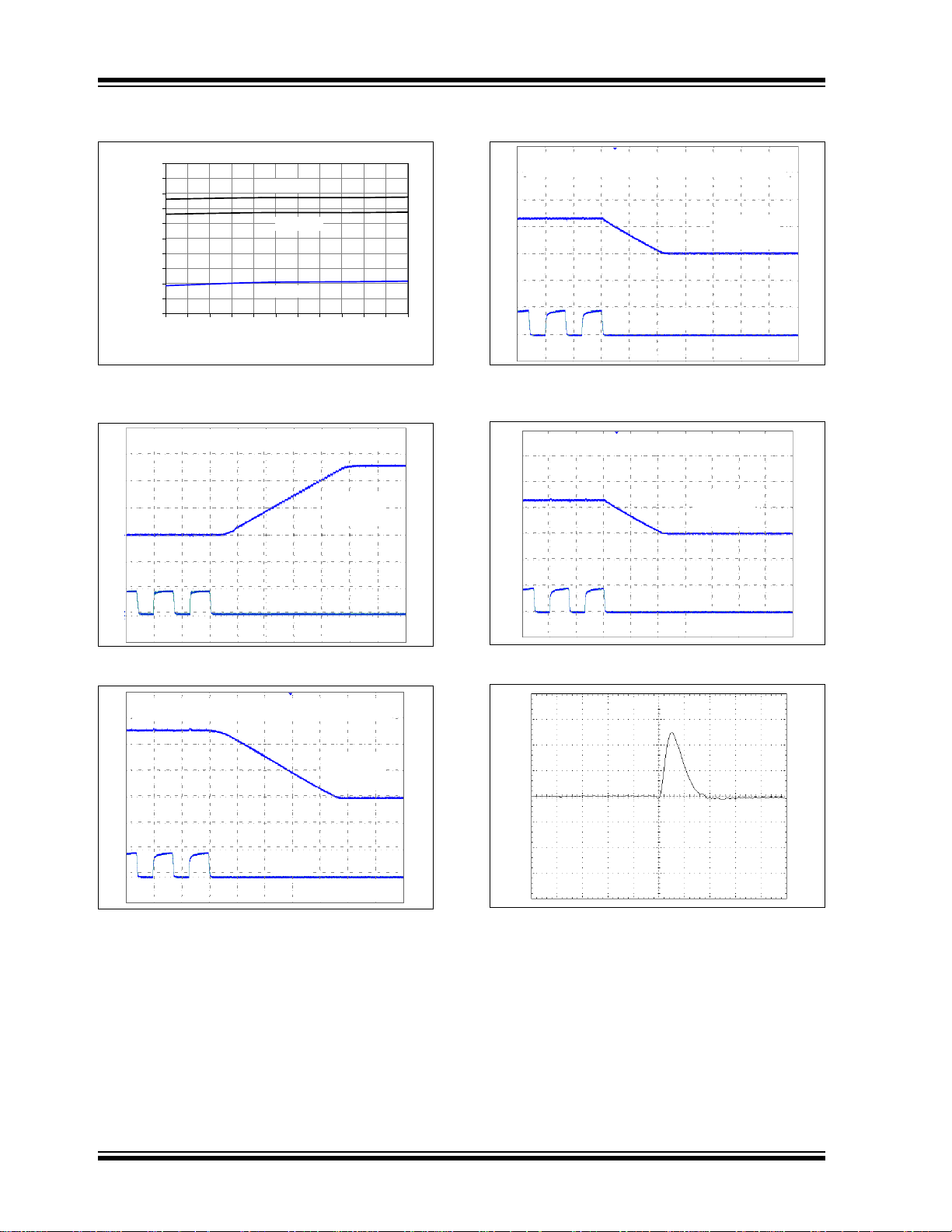
reset the power-down bits. After receiving this command, the power-down bits of the DAC register are set
to a normal operation (PD1, PD2 = 0,0). The
power-down bit settings in EEPROM are not affected.
2
C specification does not
2
C document for more
7.5 I2C BUS CHARACTERISTICS
The I2C specification defines the following bus
protocol:
• Data transfer may be initiated only when the bus
is not busy.
• During data transfer, the data line must remain
stable whenever the clock line is HIGH. Changes
in the data line while the clock line is HIGH will be
interpreted as a START or STOP condition.
Accordingly, the following bus conditions have been
defined using Figure 7-3.
7.5.1 BUS NOT BUSY (A)
Both data and clock lines remain HIGH.
7.5.2 START DATA TRANSFER (B)
A HIGH to LOW transition of the SDA line while the
clock (SCL) is HIGH determines a START condition.
All commands must be preceded by a START
condition.
7.5.3 STOP DATA TRANSFER (C)
A LOW to HIGH transition of the SDA line while the
clock (SCL) is HIGH determines a STOP condition. All
operations must be ended with a STOP condition.
FIGURE 7-2: General Call Address Format.
7.4 High-Speed (HS) Mode
The I2C specification requires that a high-speed mode
device must be ‘activated’ to operate in high-speed
(3.4 Mbit/s) mode. This is done by sending a special
address byte of 00001XXX following the START bit.
The XXX bits are unique to the h igh-speed (HS) mode
Master. This byte is referred to as the high-speed (HS)
Master Mode Code (HSMMC). The MCP4725 device
does not acknowledge this byte. However, upon
receiving this command, the device switches to HS
mode and can communicate at up to 3.4 Mbit/s on SDA
and SCL lines. The device will switch out of the HS
mode on the next STOP condition.
For more information on the HS mode, or other I
modes, please refer to the Phillips I
2
C specification.
2
7.5.4 DATA VALID (D)
The state of the data line represents valid data when,
after a START condition, the data line is stable for the
duration of the HIGH period of the clock signal.
The data on the line must be changed during the LOW
period of the clock signal. There is one clock pulse per
bit of data.
Each data transfer is initiated with a START condition
and terminated with a STOP condition.
C
DS22039C-page 22 © 2007 Microchip Technology Inc.
Page 23

MCP4725
SCL
SDA
(A) (B) (D) (D) (A)(C)
START
CONDITION
ADDRESS OR
ACKNOWLEDGE
VALID
DATA
ALLOWED
TO CHANGE
STOP
CONDITION
7.5.5 ACKNOWLEDGE
Each receiving device, when addressed, is obliged to
generate an acknowledge after the reception of each
byte. The master device must generate an extra clock
pulse which is associated with this acknowledge bit.
The device that acknowledges, has to pull down the
SDA line during the acknowledge clock pulse in such a
way that the SDA line is stable LOW during the HIGH
period of the acknowledge related clock pulse. Of
course, setup and hold times must be taken into
account. During reads, a master must send an end of
data to the slave by not generating an acknowledge bit
on the last byte that has been clocked out of the slave.
In this case, the slave (MCP4725) will leave the data
line HIGH to enable the master to generate the STOP
condition.
FIGURE 7-3: Data Transfer Sequence On The Serial Bus.
© 2007 Microchip Technology Inc. DS22039C-page 23
Page 24

MCP4725
TABLE 7-1: I2C SERIAL TIMING SPECIFICATIONS
Electrical Specifications: Unless otherwise specified, all limits are specified for TA = -40 to +85°C, VDD = +2.7V to +5.0V, VSS = 0V .
Parameters Sym Min Typ Max Units Conditions
Standard Mode
Clock frequency f
Clock high time
Clock low time
SDA and SCL rise time (Note 1)
SDA and SCL fall time (Note 1) T
START condition hold time T
Repeated START condition
setup time
Data hold time (Note 3)
Data input setup time
STOP condition setup time
STOP condition hold time
Output valid from clock
(Notes 2 and 3)
Bus free time
SCL
T
HIGH
T
LOW
T
HD:STA
T
SU:STA
T
HD:DAT
T
SU:DAT
T
SU:STO
T
HD:STD
T
T
BUF
R
F
AA
Fast Mode
Clock frequency
Clock high time
Clock low time
SDA and SCL rise time (Note 1)
SDA and SCL fall time (Note 1) T
START condition hold time T
Repeated START condition
setup time
Data hold time (Note 4) T
Data input setup time
STOP condition setup time
STOP condition hold time
Output valid from clock
(Notes 2 and 3)
Bus free time
T
SCL
T
HIGH
T
LOW
T
HD:STA
T
SU:STA
HD:DAT
T
SU:DAT
T
SU:STO
T
HD:STD
T
T
BUF
R
F
AA
Note 1: This parameter is ensured by characterization and not 100% tested.
2: This specification is not a part of the I2C specification. This specification is equivalent to the Data Hold Time (
plus SDA Fall (or rise) time:
T
AA
3: If this parameter is too short, it can create an unintended Start or Stop condition to other devices on the bus line. If this
parameter is too long, Clock Low time (T
4: For Data Input: This parameter must be longer than t
Clock Low time (T
For Data Output: This parameter is characterized, and tested indirectly by testing T
) can be affected.
LOW
5: All timing parameters in high-speed modes are tested at V
0 — 100 kHz
4000 — — ns
4700 — — ns
— — 1000 ns From VIL to V
— — 300 ns From VIH to V
IH
IL
4000 — — ns After this period, the first clock
pulse is generated.
4700 — — ns Only relevant for repeated Start
condition
0 — 3450 ns
250 — — ns
4000 — — ns
4000 — — ns
0 — 3750 ns
4700 — — ns Time between START and STOP
conditions.
0 — 400 kHz
600 — — ns
1300 — — ns
20 + 0.1Cb — 300 ns From VIL to V
20 + 0.1Cb — 300 ns From VIH to V
IH
IL
600 — — ns After this period, the first clock
pulse is generated
600 — — ns Only relevant for repeated Start
condition
0 — 900 ns
100 — — ns
600 — — ns
600 — — ns
0 — 1200 ns
1300 — — ns Time between START and STOP
conditions.
= T
HD:DAT
+ TF (OR TR).
) can be affected.
LOW
. If this parameter is too long, the Data Input Setup (T
SP
parameter.
AA
DD
= 5V.
T
HD:DAT
SU:DAT
)
) or
DS22039C-page 24 © 2007 Microchip Technology Inc.
Page 25

MCP4725
TABLE 7-1: I2C SERIAL TIMING SPECIFICATIONS (CONTINUED)
Electrical Specifications: Unless otherwise specified, all limits are specified for TA = -40 to +85°C, VDD = +2.7V to +5.0V, VSS = 0V .
Parameters Sym Min Typ Max Units Conditions
High Speed Mode (Note 5)
Clock frequency f
Clock high time
SCL
T
HIGH
0—3.4
1.7
60
——ns
120
Clock low time
SCL rise time (Note 1)
SCL fall time (Note 1)
SDA rise time (Note 1)
SDA fall time (Note 1)
START condition hold time
Repeated START condition
setup time
Data hold time (Note 4)
Data input setup time
STOP condition setup time
STOP condition hold time
Output valid from clock
(Notes 2 and 3)
Bus free time
T
LOW
T
T
T
R: DAT
T
F: DATA
T
HD:STA
T
SU:STA
T
HD:DAT
T
SU:DAT
T
SU:STO
T
HD:STD
T
AA
T
BUF
R
F
160
——nsC
320
——4080ns From VIL to VIH,Cb = 100 pF
——4080ns From VIH to VIL,Cb = 100 pF
——80
160
——80
160
160 — — ns After this period, the first clock
160 — — ns Only relevant for repeated Start
0
0
—70
150
10 — — ns
160 — — ns
160 — — ns
— — 150
310
160 — — ns Time between STAR T and STOP
Note 1: This parameter is ensured by characterization and not 100% tested.
2: This specification is not a part of the I2C specification. This specification is equivalent to the Data Hold Time (
plus SDA Fall (or rise) time:
T
AA
= T
HD:DAT
+ TF (OR TR).
3: If this parameter is too short, it can create an unintended Start or Stop condition to other devices on the bus line. If this
parameter is too long, Clock Low time (T
4: For Data Input: This parameter must be longer than t
Clock Low time (T
) can be affected.
LOW
) can be affected.
LOW
. If this parameter is too long, the Data Input Setup (T
SP
For Data Output: This parameter is characterized, and tested indirectly by testing T
5: All timing parameters in high-speed modes are tested at V
DD
= 5V.
MHz
Cb = 100 pF
MHz
C
= 400 pF
b
Cb = 100 pF
ns
C
= 400 pF
b
= 100 pF
b
C
= 400 pF
b
C
= 400 pF
b
C
= 400 pF
b
ns From VIL to VIH,Cb = 100 pF
C
= 400 pF
b
ns From VIH to VIL,Cb = 100 pF
C
= 400 pF
b
pulse is generated
condition
ns Cb = 100 pF
C
= 400 pF
b
ns Cb = 100 pF
C
= 400 pF
b
conditions.
T
SU:DAT
parameter.
AA
HD:DAT
) or
)
© 2007 Microchip Technology Inc. DS22039C-page 25
Page 26

MCP4725
T
F
SCL
SDA
T
SU:STA
T
SP
T
HD:STA
T
LOW
T
HIGH
T
HD:DAT
T
AA
T
SU:DAT
T
R
T
SU:STO
T
BUF
0.3V
DD
0.7V
DD
FIGURE 7-4: I2C Bus Timing Data.
DS22039C-page 26 © 2007 Microchip Technology Inc.
Page 27

MCP4725
MCP4725
V
OUT
A0
SCL
V
SS
1
2
3
4
5
6
V
DD
SDA
10 µF0.1 µF
R
R
Analog
V
DD
V
DD
To MCU
(MASTER)
Output
Note 1: R is the pull-up resistor. Typically
1 ~ 10 kΩ
2: A0 can be tied to V
SS
, V
DD
or driven by
MCU
123456789
SCL
SDA
11
0
0A2A1A0
1
Start
Bit
Address Byte
Address bits
Device bits
R/W
Start
Bit
MCP4725
ACK
Response
8.0 TYPICAL APPLICATIONS
The MCP4725 device is one of Microchip’s latest DAC
device family with non-volatile EEPROM memory. The
device is a general purpose resistive string DAC
intended to be used in applications where a preci sion,
and low power DAC with moderate bandwidth is
required.
Since the device includes non-volatile EEPROM
memory, the user can use this device for applications
that require the output to return to the previous set-up
value on subsequent power-ups.
Applications generally suited for the MCP4725 device
family include:
• Set Point or Offset Trimming
• Sensor Calibration
• Portable Instrumentation (Battery Powered)
• Motor Speed Control
8.1 Connecting to I2C BUS using Pull-Up Resistors
The SCL and SDA pins of the MCP4725 are open-drain
configurations. These pins require a pull-up resistor as
shown in Figure 8-1. The value of these pull-up
resistors depends on the operating speed (standard,
fast, and high speed) and loading capacitance of the
2
C bus line. Higher value of pull-up resistor consumes
I
less power, but increases the signal transition time
(higher RC time constant) on the bus. Therefore, it can
limit the bus operating speed. The lower resistor value,
on the other hand, consumes higher power, but allows
higher operating speed. If the bus line has higher
capacitance due to long bus line or high number of
devices connected to the bus, a smaller pull-up resistor
is needed to compensate the long RC time constant.
The pull-up resistor is typically chosen between 1 k Ω
and 10 kΩ ranges for standard and fast modes, and
less than 1 kΩ for high speed mode.
Two devices with the same A2 and A1 address bits can
be connected to the same I2C bus by utilizing the A0
address pin (Example: A0 pin of device A is tied to VDD,
and the other device’s pin is tie d to V
SS.)
8.1.1 DEVICE CONNECTION TEST
The user can test the presence of the MCP4725 on the
2
I
C bus line without performing the data conversion.
This test can be achieved by checking an acknowledge
response from the MCP4725 after sending a read or
write command. Here is an example using Figure 8-2:
(a) Set the R/W
(b) If the MCP4725 is connected to the I
bit “HIGH” in the address byte.
2
C bus line, it
will then acknowledge by pulling SDA bus LOW
during the ACK clock and then release the bus
back to the I
(c) A STOP or repeated START bit can then be issued
from the Master and I
2
C Master.
2
C communication can con-
tinue.
FIGURE 8-2: I2C Bus Connection Test.
FIGURE 8-1: I2C Bus Interface
Connection with A0 pin tied to V
© 2007 Microchip Technology Inc. DS22039C-page 27
.
SS
Page 28

MCP4725
8.2 Using Non-Volatile EEPROM Memory
The user can store the DAC input code (12 bits) and
power-down configuration bits (2 bits) in the internal
non-volatile EEPROM memory using the I
command. The user can also read the EEPROM data
using the I
powered after power is shut down, the device uploads
the EEPROM contents to the DAC register automatically and provides the DAC output immediately. This
feature is very useful in applications where the DAC
device is used to provide set point or calibration data for
other devices in the application system. The DAC will
not lose the important system operational parameters
due to the system power failure incidents. See
Section 5.6 “Non-Volatile EEPROM Memory” for
more details of the non-volatile EEPROM memory.
2
C read command. When the device is first
2
C write
8.3 Power Supply Considerations
The power supply to the device is used for both V
and DAC reference voltage. Any noise induced on the
line can affect on the DAC performance. Typical
V
DD
application will require a bypass capacitor in order to
filter out high frequency noise on the VDD line. The
noise can be induced onto the power supply’s traces or
as a result of changes on the DAC output. The bypass
capacitor helps to minimize the effect of these noise
sources on signal integrity. Figure 8-1 shows an
example of using two bypass capacitors (a 10 µF
tantalum capacitor and a 0.1 µF ceramic capacitor) in
parallel on the V
placed as close to the VDD pin as possible (within
4mm).
The power source should be as clean as possible. If the
application circuit has separate digital and analog
power supplies, the V
should reside on the analog plane.
line. These capacitors should be
DD
and VSS pins of the MCP4725
DD
DD
8.4 Layout Considerations
Inductively-coupled AC transients and digital switching
noise from other devices can affect on DAC
performance and DAC output signal integrity. Careful
board layout will minimize these effects. Bench testing
has shown that a multi-layer board utilizing a low-inductance ground plane, isolated inputs, isolated outputs
and proper decoupling are critical to achieving the
performance that the MCP4725 is capable of providing.
Particularly harsh environments may require shielding
of critical signals. Separate digital and analog ground
planes are recommended. In this case, the V
the ground pins of the VDD capacitors of the MCP4725
should be terminated to the analog ground plane.
pin and
SS
8.5 Application Examples
The MCP4725 is a rail-to-rail output DAC designed to
operate with a VDD range of 2.7V to 5.5V. Its output
amplifier is robust enough to drive common, small-signal loads directly, thus eliminating the cost and size of
an external buffer for most applications.
8.5.1 DC SET POINT OR CALIBRATION
A common application for the MCP4725 is a
digitally-controlled set point or a calibration of variable
parameters such as sensor offset or bias point.
Example 8-1 shows an example of the set point setting.
Since the MCP4725 is a 12-bit DAC and uses the V
supply as a reference source, it provides a VDD/4096 of
resolution per step.
DD
DS22039C-page 28 © 2007 Microchip Technology Inc.
Page 29

MCP4725
To MCU
(MASTER)
R
R
V
DD
Comparator
R
1
R
2
0.1 µF
V
TRIP
R
SENSE
MCP4725
V
DD
V
OUT
A0
SCL
V
SS
1
2
3
4
5
6
V
DD
SDA
10 µF0.1 µF
V
DD
D Input Code (0 to 4095)=
V
OUT
V
DD
D
4096
----------- -
×
=
V
TRIP
V
OUT
R
2
R1R2+
-------------------
⎝⎠
⎛⎞
=
Light
(Ceramic) (Tantalum)
8.5.2 DECREASING THE OUTPUT STEP
SIZE
Calibrating the threshold of a diode, transistor or
resistor may require a very small step size in the DAC
output voltage. These applications may require about
200 µV of step resolution within 0.8V of range.
One method of achieving this small step resolution is
using a voltage divider at the DAC output. An example
is shown in Example 8-1. The step size of the DAC out-
put is scaled down by the factor of the ratio of the voltage divider. Note that the bypass capacitor on the
output of the voltage divider plays a critical function in
attenuating the output noise of the DAC and the
induced noise from the environment.
EXAMPLE 8-1: Set Point Or Threshold Calibration.
© 2007 Microchip Technology Inc. DS22039C-page 29
Page 30

MCP4725
V
TRIP
R
1
R
2
0.1 µF
Comparator
R
3
V
CC-
where D = DAC Input Code (0 – 4095)
V
CC+
V
CC+
V
CC-
V
OUT
V
OUT
V
DD
D
2
12
-------
=
R
23
R2R
3
R2R3+
------------------=
V
23
V
CC+R2
()V
CC-R3
()+
R
2R3
+
-----------------------------------------------------=
V
trip
V
OUTR23V23R1
+
R
2R23
+
------------------------------------------- -=
R
1
R
23
V
23
V
OUT
V
O
Thevenin
Equivalent
R
sense
To MCU
(MASTER)
R
R
MCP4725
V
DD
V
OUT
A0
SCL
V
SS
1
2
3
4
5
6
V
DD
SDA
10 µF0.1 µF
V
DD
8.5.3 BUILDING A “WINDOW” DAC
Some sensor applications require very high resolution
around the set point or threshold voltage.
Example 8-2 shows an example of creating a “window”
around the threshold using a voltage divider network
with a pull-up and pull-down resistor. In the circuit, the
output voltage range is scaled down, but its step resolution is increased greatly.
EXAMPLE 8-2: Single-Supply “Window” DAC.
DS22039C-page 30 © 2007 Microchip Technology Inc.
Page 31

MCP4725
V
DD
V
OUT
R
3
R
4
R
2
R
1
VIN+
0.1 µF
V
CC
+
V
CC
–
V
IN+
V
OUTR4
R3R4+
--------------------=
V
O
VOV
IN+
1
R
2
R
1
----- -+
⎝⎠
⎛⎞
V
DD
R
2
R
1
----- -
⎝⎠
⎛⎞
–=
To MCU
(MASTER)
R
R
MCP4725
V
DD
V
OUT
A0
SCL
V
SS
1
2
3
4
5
6
V
DD
SDA
10 µF0.1 µF
V
DD
where D = DAC Input Code (0 – 4095)
V
OUTVDD
D
2
12
-------
=
8.5.4 BIPOLAR OPERATION
Bipolar operation is achievable using the MCP4725 by
using an external operational amplifier (op amp). This
allows a general purpose DAC, with its cost and
availability advantages, to meet almost any desired
output voltage range, power and noise performance.
Example 8-3 illustrates a simple bipolar voltage source
configuration. R
and R2 allow the gain to be selected,
1
while R3 and R4 shift the DAC's output to a selected
offset. Note that R4 can be tied to V
DD
(= V
REF
) instead
of VSS, if a higher offset is desired. Note that a pull-up
to VDD could be used, instead of R4, if a higher offset is
desired.
EXAMPLE 8-3: Digitally-Controlled Bipolar Voltage Source.
© 2007 Microchip Technology Inc. DS22039C-page 31
Page 32

MCP4725
R2–
R
1
-------- -
2.05–
V
DD
-------------
2.05–
4.1
-------------==
R
2
R
1
----- -
1
2
-- -=
→
If R1 = 20 kΩ and R2 = 10 kΩ, the gain will be 0.5.
R
4
R3R4+()
-----------------------
2.05V 0.5 V
DD
⋅()+
1.5 V
DD
⋅
------------------------------------------------
2
3
-- -==
If R4 = 20 kΩ, then R3 = 10 kΩ
8.5.4.1 Design a Bipolar DAC using
Example 8-3
Some applications desires an output step magnitude of
1 mV with an output range of ±2.05V. The following
steps explain the design solution:
1. Calculate the range: +2.05V – (-2.05V) = 4.1V.
2. Calculate the resolution needed:
4.1V/1 mV = 4100
12
Since 2
3. The amplifier gain (R
must be equal to the desired minimum output to
achieve bipolar operation. Since any gain can
be realized by choosing resistor values (R
the V
4.1V is used, solve for the amplifier’s gain by
setting the DAC to 0, knowing that the output
needs to be -2.05V. The equation can be
simplified to:
= 4096 for 12-bit resolution.
), multiplied by VDD,
2/R1
value must be selected first. If a VDD of
DD
1+R2
),
4. Next, solve for R
and R4 by setting the DAC to
3
4096, knowing that the output needs to be
+2.05V .
DS22039C-page 32 © 2007 Microchip Technology Inc.
Page 33

8.5.5 PROGRAMMABLE CURRENT
LOAD
V
DD
I
L
I
B
R
SENSE
R
R
MCP4725
V
DD
V
OUT
A0
SCL
V
SS
1
2
3
4
5
6
V
DD
SDA
10 µF0.1 µF
V
DD
D Input Code (0 to 4095)=
I
L
V
OUT
R
SENSE
------------------
β
β 1+
------------
=
V
OUT
V
DD
D
4096
----------- -
×
=
I
B
I
L
β
----
=
V
OUT
To MCU
(MASTER)
SOURCE
Example 8-3 illustrates an example how to convert the
DAC voltage output to a digitally selectable current
source by adding a voltage follower and a sensor
register.
MCP4725
FIGURE 8-3: Digitally Controllable Current Source.
© 2007 Microchip Technology Inc. DS22039C-page 33
Page 34

MCP4725
USB Cable to PC
PICkit Serial
MCP4725 SOT-23-6 EV Board
DAC Analog Output
1st Write Byte
2nd Write Byte
3rd Write Byte
4th Write Byte
9.0 DEVELOPMENT SUPPORT
9.1 Evaluation & Demonstration
Boards
The MCP4725 SOT-23-6 Evaluation Board is available
from Microchip Technology Inc. This board works with
Microchip’s PICkit™ Serial Analyzer. The user can
program the DAC input codes and EEPROM data, or
read the programmed data using the easy to use PICkit
Serial Analyzer with the Graphic User Interface software. Refer to www.microchip.com for further information on this product’s capabilities and availability.
FIGURE 9-2: Setup for the MCP4725 SOT-23-6 Evaluation Board with PICkit™ Serial Analyzer.
FIGURE 9-1: MCP4725 SOT-23-6 Evaluation Board.
FIGURE 9-3: Example of PICkit™ Serial User Interface.
DS22039C-page 34 © 2007 Microchip Technology Inc.
Page 35

10.0 PACKAGING INFORMATION
1
6-Lead SOT-23
XXNN
Example
1
AJ25
Part Number
Address
Option
Code
MCP4725A0T-E/CH A0 (00) AJNN
MCP4725A1T-E/CH A1 (01) APNN
MCP4725A2T-E/CH A2 (10) AQNN
MCP4725A3T-E/CH A3 (11) ARNN
Legend: XX...X Customer-specific information
Y Year code (last digit of calendar year)
YY Year code (last 2 digits of calendar year)
WW Week code (week of January 1 is week ‘01’)
NNN Alphanumeric traceability code
Pb-free JEDEC designator for Matte Tin (Sn)
* This package is Pb-free. The Pb-free JEDEC designator ( )
can be found on the outer packaging for this package.
Note: In the event the full Microchip part number cannot be marked on one line, it will
be carried over to the next line, thus limiting the number of available
characters for customer-specific information.
3
e
10.1 Package Marking Information
MCP4725
3
e
© 2007 Microchip Technology Inc. DS22039C-page 35
Page 36

MCP4725
6-Lead Plastic Small Outline Transistor (CH) [SOT-23]
Notes:
1. Dimens ions D and E1 do not include mold flash or protrusions. Mold flash or protrusions shall not exceed 0.127 mm per side.
2. Dimens ioning and tolerancing per ASME Y14.5M.
BSC: Basic Dimension. Theoretically exact value shown without tolerances.
Note: For the most current package drawings, please see the Microchip Packaging Specification located at
http://www.microchip.com/packaging
Units MILLIMETERS
Dimension Limits MIN NOM MAX
Number of Pins N 6
Pitch e 0.95 BSC
Outside Lead Pitch e1 1.90 BSC
Overall Height A 0.90 – 1.45
Molded Package Thickness A2 0.89 – 1.30
Standoff A1 0.00 – 0.15
Overall Width E 2.20 – 3.20
Molded Package Width E1 1.30 – 1.80
Overall Length D 2.70 – 3.10
Foot Length L 0.10 – 0.60
Footprint L1 0.35 – 0.80
Foot Angle φ 0° – 30°
Lead Thickness c 0.08 – 0.26
Lead Width b 0.20 – 0.51
b
E
4
N
E1
PIN 1 ID BY
LASER MARK
D
1
2
3
e
e1
A
A1
A2
c
L
L1
φ
Microchip Technology Drawing C04-028B
DS22039C-page 36 © 2007 Microchip Technology Inc.
Page 37

APPENDIX A: REVISION HISTORY
Revision C (November 2007
The following is the list of modifications:
1. Corrected Address Options on Product Identification System page.
Revision B (October 2007)
The following is the list of modifications:
1. Added characterization graphs to document.
2. Numerous edits throughout.
3. Add new package marking address options.
Updated package marking information and
package outline drawings.
4. Added adress options to Product Identification
System page.
Revision A (April 2007)
• Original Release of this Document.
MCP4725
© 2007 Microchip Technology Inc. DS22039C-page 37
Page 38

MCP4725
NOTES:
DS22039C-page 38 © 2007 Microchip Technology Inc.
Page 39

PRODUCT IDENTIFICATION SYSTEM
Device: MCP4725: Single Channel 12-Bit DAC w/EEPROM
Memory
Address Options: XX A2 A1 A0
A0 * = 0 0 External
A1 = 0 1 External
A2 = 1 0 External
A3 = 1 1 External
* Default option. Contact Microchip factory for other
address options
Tape and Reel: T = Tape and Reel
Temperature Range: E = -40°C to +125°C
Package: CH = Plastic Small Outline Transistor (SOT-23-6),
6-lead
Examples:
a) MCP4725A0T-E/CH: T ape and Reel,
Extended Temp.,
6LD SOT-23 pkg.
Address Option = A0
b) MCP4725A1T-E/CH: Tape and Reel,
Extended Temp.,
6LD SOT-23 pkg.
Address Option = A1
c) MCP4725A2T-E/CH: Tape and Reel,
Extended Temp.,
6LD SOT-23 pkg.
Address Option = A2
d) MCP4725A3T-E/CH: Tape and Reel,
Extended Temp.,
6LD SOT-23 pkg.
Address Option = A3
PAR T N O . XXX
Address Temperature
Range
Device
/XX
Package
Options
X
Tape a n d
Reel
To order or obtain information, e.g., on pricing or delivery, refer to the factory or the listed sales office.
MCP4725
© 2007 Microchip Technology Inc. DS22039C-page 39
Page 40

MCP4725
NOTES:
DS22039C-page 40 © 2007 Microchip Technology Inc.
Page 41

Note the following details of the code protection feature on Microchip devices:
• Microchip products meet the specification contained in their particular Microchip Data Sheet.
• Microchip believes that its family of products is one of the most secure families of its kind on the market today, when used in the
intended manner and under normal conditions.
• There are dishonest and possibly illegal methods used to breach the code protection feature. All of these methods, to our
knowledge, require using the Microchip products in a manner outside the operating specifications contained in Microchip’s Data
Sheets. Most likely, the person doing so is engaged in theft of intellectual property.
• Microchip is willing to work with the customer who is concerned about the integrity of their code.
• Neither Microchip nor any other semiconductor manufacturer can guarantee the security of their code. Code protection does not
mean that we are guaranteeing the product as “unbreakable.”
Code protection is constantly evolving. We at Microchip are committed to continuously improving the code protection features of our
products. Attempts to break Microchip’s code protection feature may be a violation of the Digital Millennium Copyright Act. If such acts
allow unauthorized access to your software or other copyrighted work, you may have a right to sue for relief under that Act.
Information contained in this publication regarding device
applications and the like is provided only for your convenience
and may be superseded by updates. It is your responsibility to
ensure that your application meets with your specifications.
MICROCHIP MAKES NO REPRESENTATIONS OR
WARRANTIES OF ANY KIND WHETHER EXPRESS OR
IMPLIED, WRITTEN OR ORAL, STATUTORY OR
OTHERWISE, RELATED TO THE INFORMATION,
INCLUDING BUT NOT LIMITED TO ITS CONDITION,
QUALITY, PERFORMANCE, MERCHANTABILITY OR
FITNESS FOR PURPOSE. Microchip disclaims all liability
arising from this information and its use. Use of Microchip
devices in life support and/or safety applications is entirely at
the buyer’s risk, and the buyer agrees to defend, indemnify and
hold harmless Microchip from any and all damages, claims,
suits, or expenses resulting from such use. No licenses are
conveyed, implicitly or otherwise, under any Microchip
intellectual property rights.
Trademarks
The Microchip name and logo, the Microchip logo, Accuron,
dsPIC, K
EELOQ, KEELOQ logo, microID, MPLAB, PIC,
PICmicro, PICSTART, PRO MATE, rfPIC and SmartShunt are
registered trademarks of Microchip Technology Incorporated
in the U.S.A. and other countries.
AmpLab, FilterLab, Linear Active Thermistor, Migratable
Memory, MXDEV, MXLAB, SEEVAL, SmartSensor and The
Embedded Control Solutions Company are registered
trademarks of Microchip Technology Incorporated in the
U.S.A.
Analog-for-the-Digital Age, Application Maestro, CodeGuard,
dsPICDEM, dsPICDEM.net, dsPICworks, dsSPEAK, ECAN,
ECONOMONITOR, FanSense, FlexROM, fuzzyLAB,
In-Circuit Serial Programming, ICSP, ICEPIC, Mindi, MiWi,
MPASM, MPLAB Certified logo, MPLIB, MPLINK, PICkit,
PICDEM, PICDEM.net, PICLAB, PICtail, PowerCal,
PowerInfo, PowerMate, PowerTool, REAL ICE, rfLAB, Select
Mode, Smart Serial, SmartTel, Total Endurance, UNI/O,
WiperLock and ZENA are trademarks of Microchip
Technology Incorporated in the U.S.A. and other countries.
SQTP is a service mark of Microchip Technology Incorporated
in the U.S.A.
All other trademarks mentioned herein are property of their
respective companies.
© 2007, Microchip Technology Incorporated, Printed in the
U.S.A., All Rights Reserved.
Printed on recycled paper.
Microchip received ISO/TS-16949:2002 certification for its worldwide
headquarters, design and wafer fabrication facilities in Chandler and
T empe, Arizona; Gresham, Oregon and design centers in California
and India. The Company’s quality system processes and procedures
are for its PIC
devices, Serial EEPROMs, microperipherals, nonvolatile memory and
analog products. In addition, Microchip’s quality system for the desig n
and manufacture of development systems is ISO 9001:2000 certified.
®
MCUs and dsPIC® DSCs, KEELOQ
®
code hopping
© 2007 Microchip Technology Inc. DS22039C-page 41
Page 42

WORLDWIDE SALES AND SERVICE
AMERICAS
Corporate Office
2355 West Chandler Blvd.
Chandler, AZ 85224-6199
Tel: 480-792-7200
Fax: 480-792-7277
Technical Support:
http://support.microchip.com
Web Address:
www.microchip.com
Atlanta
Duluth, GA
Tel: 678-957-9614
Fax: 678-957-1455
Boston
Westborough, MA
Tel: 774-760-0087
Fax: 774-760-0088
Chicago
Itasca, IL
Tel: 630-285-0071
Fax: 630-285-0075
Dallas
Addison, TX
Tel: 972-818-7423
Fax: 972-818-2924
Detroit
Farmington Hills, MI
Tel: 248-538-2250
Fax: 248-538-2260
Kokomo
Kokomo, IN
Tel: 765-864-8360
Fax: 765-864-8387
Los Angeles
Mission Viejo, CA
Tel: 949-462-9523
Fax: 949-462-9608
Santa Clara
Santa Clara, CA
Tel: 408-961-6444
Fax: 408-961-6445
Toronto
Mississauga, Ontario,
Canada
Tel: 905-673-0699
Fax: 905-673-6509
ASIA/PACIFIC
Asia Pacific Office
Suites 3707-14, 37th Floor
Tower 6, The Gateway
Harbour City, Kowloon
Hong Kong
Tel: 852-2401-1200
Fax: 852-2401-3431
Australia - Sydney
Tel: 61-2-9868-6733
Fax: 61-2-9868-6755
China - Beijing
Tel: 86-10-8528-2100
Fax: 86-10-8528-2104
China - Chengdu
Tel: 86-28-8665-5511
Fax: 86-28-8665-7889
China - Fuzhou
Tel: 86-591-8750-3506
Fax: 86-591-8750-3521
China - Hong Kong SAR
Tel: 852-2401-1200
Fax: 852-2401-3431
China - Nanjing
Tel: 86-25-8473-2460
Fax: 86-25-8473-2470
China - Qingdao
Tel: 86-532-8502-7355
Fax: 86-532-8502-7205
China - Shanghai
Tel: 86-21-5407-5533
Fax: 86-21-5407-5066
China - Shenyang
Tel: 86-24-2334-2829
Fax: 86-24-2334-2393
China - Shenzhen
Tel: 86-755-8203-2660
Fax: 86-755-8203-1760
China - Shunde
Tel: 86-757-2839-5507
Fax: 86-757-2839-5571
China - Wuhan
Tel: 86-27-5980-5300
Fax: 86-27-5980-5118
China - Xian
Tel: 86-29-8833-7252
Fax: 86-29-8833-7256
ASIA/PACIFIC
India - Bangalore
Tel: 91-80-4182-8400
Fax: 91-80-4182-8422
India - New Delhi
Tel: 91-11-4160-8631
Fax: 91-11-4160-8632
India - Pune
Tel: 91-20-2566-1512
Fax: 91-20-2566-1513
Japan - Yokohama
Tel: 81-45-471- 6166
Fax: 81-45-471-6122
Korea - Daegu
Tel: 82-53-744-4301
Fax: 82-53-744-4302
Korea - Seoul
Tel: 82-2-554-7200
Fax: 82-2-558-5932 or
82-2-558-5934
Malaysia - Kuala Lumpur
Tel: 60-3-6201-9857
Fax: 60-3-6201-9859
Malaysia - Penang
Tel: 60-4-227-8870
Fax: 60-4-227-4068
Philippines - Manila
Tel: 63-2-634-9065
Fax: 63-2-634-9069
Singapore
Tel: 65-6334-8870
Fax: 65-6334-8850
Taiwan - Hsin Chu
Tel: 886-3-572-9526
Fax: 886-3-572-6459
Taiwan - Kaohsiung
Tel: 886-7-536-4818
Fax: 886-7-536-4803
Taiwan - Taipei
Tel: 886-2-2500-6610
Fax: 886-2-2508-0102
Thailand - Bangkok
Tel: 66-2-694-1351
Fax: 66-2-694-1350
EUROPE
Austria - Wels
Tel: 43-7242-2244-39
Fax: 43-7242-2244-393
Denmark - Copenhagen
Tel: 45-4450-2828
Fax: 45-4485-2829
France - Paris
Tel: 33-1-69-53-63-20
Fax: 33-1-69-30-90-79
Germany - Munich
Tel: 49-89-627-144-0
Fax: 49-89-627-144-44
Italy - Milan
Tel: 39-0331-742611
Fax: 39-0331-466781
Netherlands - Drunen
Tel: 31-416-690399
Fax: 31-416-690340
Spain - Madrid
Tel: 34-91-708-08-90
Fax: 34-91-708-08-91
UK - Wokingham
Tel: 44-118-921-5869
Fax: 44-118-921-5820
10/05/07
DS22039C-page 42 © 2007 Microchip Technology Inc.
 Loading...