

Page 1
1999 Microchip Technology Inc. Preliminary DS21291C-page 1
MCP2510
FEATURES
• Implements Full CAN V2.0A and V2.0B at 1 Mb/s
- 0 - 8 byte message length
- Standard and extended data frames
- Programmable bit rate up to 1 Mb/s
- Support for remote frames
- Two receive buffers with prioritized message
storage
- Six full acceptance filters
- Two full acceptance filter masks
- Three transmit buffers with prioritization and
abort features
- Loop-back mode for self test operation
• Hardware Features
- High Speed SPI Interface
(5 MHz at 4.5V I temp)
- Supports SPI modes 0,0 and 1,1
- Clock out pin with programmable prescaler
- Interrupt output pin with selectable enables
- ‘Buffer full’ output pins configureable as interrupt pins for each receive buffer or as general
purpose digital outputs
- ‘Request to Send’ input pins configureable as
control pins to request immediate message
transmission for each transmit buffer or as
general purpose digital inputs
- Low Power Sleep mode
• Low power CMOS technology
- Operates from 3.0V to 5.5V
- 5 mA active current typical
-10 µA standby current typical at 5.5V
• 18-pin PDIP/SOIC and 20-pin TSSOP packages
• Temperature ranges supported:
DESCRIPTION
The Microchip Technology Inc. MCP2510 is a Full Controller Area Network (CAN) protocol controller implementing CAN specification V2.0 A/B. It supports CAN
1.2, CAN 2.0A, CAN 2.0B Passive, and CAN 2.0B Active
versions of the protocol, and is capable of transmitting
and receiving standard and extended messages. It is
also capable of both acceptance filtering and message
management. It includes three transmit buffers and two
receive buffers that reduce the amount of microcontroller
(MCU) management required. The MCU communication
is implemented via an industry standard Serial Peripheral Interface (SPI) with data rates up to 5Mb/s.
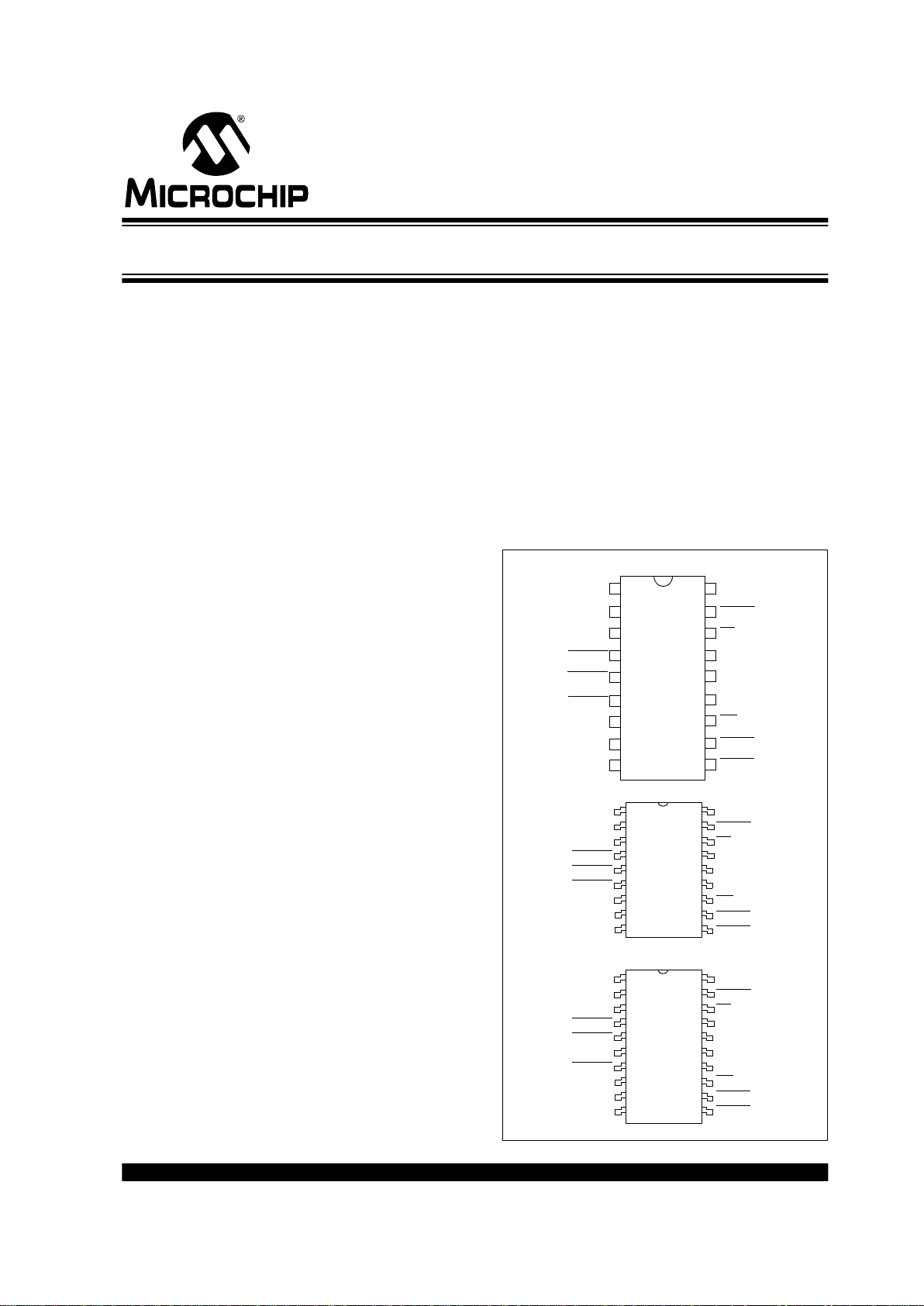
PACKAGE TYPES
- Industrial (I):
-40°Cto+85°C
- Extended (E):
-40°C to +125°C
18 LEAD PDIP
TXCAN
RXCAN
V
DD
RESET
CS
SO
MCP2510
1
2
3
4
18
17
16
15
SI
SCK
INT
RX0BF
14
13
12
11
RX1BF
10
OSC2
OSC1
CLKOUT
TX2RTS
5
6
7
8
Vss
9
MCP2510
TXCAN
RXCAN
TX0RTS
OSC1
CLKOUT
OSC2
CS
VDD
RESET
SO
SCK
INT
SI
RX0BF
RX1BF
Vss
TX0RTS
TX1RTS
TX1RTS
TX2RTS
18 LEAD SOIC
MCP2510
TXCAN
RXCAN
TX0RTS
OSC1
CLKOUT
OSC2
CS
VDD
RESET
SO
SCK
INT
SI
RX0BF
RX1BF
Vss
11
10
TX1RTS
TX2RTS
20 LEAD TSSOP
NC
NC
1
2
3
4
5
6
7
8
9
18
17
16
15
14
13
12
13
12
1
2
3
4
5
6
7
8
9
20
19
18
17
16
15
14
11
10
Stand-Alone CAN Controller with SPI® Interface
SPI is a registered trademark of Motorola Inc.
Page 2

MCP2510
DS21291C-page 2 Preliminary 1999 Microchip Technology Inc.
Table of Contents
1.0 Device Functionality . . . . . . . . . . . . . . . . . . . . . . . . . . . . . . . . . . . . . . . . . . . . . . . . . . . . . . . . . . . . . . . . . . . . . . . . . . . . . . . 3
2.0 Can Message Frames. . . . . . . . . . . . . . . . . . . . . . . . . . . . . . . . . . . . . . . . . . . . . . . . . . . . . . . . . . . . . . . . . . . . . . . . . . . . . . 7
3.0 Message Transmission . . . . . . . . . . . . . . . . . . . . . . . . . . . . . . . . . . . . . . . . . . . . . . . . . . . . . . . . . . . . . . . . . . . . . . . . . . . . 15
4.0 Message Reception . . . . . . . . . . . . . . . . . . . . . . . . . . . . . . . . . . . . . . . . . . . . . . . . . . . . . . . . . . . . . . . . . . . . . . . . . . . . . . 21
5.0 Bit Timing . . . . . . . . . . . . . . . . . . . . . . . . . . . . . . . . . . . . . . . . . . . . . . . . . . . . . . . . . . . . . . . . . . . . . . . . . . . . . . . . . . . . . . 35
6.0 Error Detection . . . . . . . . . . . . . . . . . . . . . . . . . . . . . . . . . . . . . . . . . . . . . . . . . . . . . . . . . . . . . . . . . . . . . . . . . . . . . . . . . . 41
7.0 Interrupts . . . . . . . . . . . . . . . . . . . . . . . . . . . . . . . . . . . . . . . . . . . . . . . . . . . . . . . . . . . . . . . . . . . . . . . . . . . . . . . . . . . . . . . 45
8.0 Oscillator. . . . . . . . . . . . . . . . . . . . . . . . . . . . . . . . . . . . . . . . . . . . . . . . . . . . . . . . . . . . . . . . . . . . . . . . . . . . . . . . . . . . . . . 49
9.0 Modes of Operation . . . . . . . . . . . . . . . . . . . . . . . . . . . . . . . . . . . . . . . . . . . . . . . . . . . . . . . . . . . . . . . . . . . . . . . . . . . . . . 51
10.0 Register Map. . . . . . . . . . . . . . . . . . . . . . . . . . . . . . . . . . . . . . . . . . . . . . . . . . . . . . . . . . . . . . . . . . . . . . . . . . . . . . . . . . . . 55
11.0 SPI Interface . . . . . . . . . . . . . . . . . . . . . . . . . . . . . . . . . . . . . . . . . . . . . . . . . . . . . . . . . . . . . . . . . . . . . . . . . . . . . . . . . . . . 57
12.0 Electrical Characteristics. . . . . . . . . . . . . . . . . . . . . . . . . . . . . . . . . . . . . . . . . . . . . . . . . . . . . . . . . . . . . . . . . . . . . . . . . . . 61
13.0 Packaging Information . . . . . . . . . . . . . . . . . . . . . . . . . . . . . . . . . . . . . . . . . . . . . . . . . . . . . . . . . . . . . . . . . . . . . . . . . . . . 65
On-Line Support . . . . . . . . . . . . . . . . . . . . . . . . . . . . . . . . . . . . . . . . . . . . . . . . . . . . . . . . . . . . . . . . . . . . . . . . . . . . . . . . . . . . . . . . . 69
Reader Response . . . . . . . . . . . . . . . . . . . . . . . . . . . . . . . . . . . . . . . . . . . . . . . . . . . . . . . . . . . . . . . . . . . . . . . . . . . . . . . . . . . . . . . . 70
MCP2510 Product Identification System. . . . . . . . . . . . . . . . . . . . . . . . . . . . . . . . . . . . . . . . . . . . . . . . . . . . . . . . . . . . . . . . . . . . . . . 71
Index . . . . . . . . . . . . . . . . . . . . . . . . . . . . . . . . . . . . . . . . . . . . . . . . . . . . . . . . . . . . . . . . . . . . . . . . . . . . . . . . . . . . . . . . . . . . . . . . . . 73
List Of Figures. . . . . . . . . . . . . . . . . . . . . . . . . . . . . . . . . . . . . . . . . . . . . . . . . . . . . . . . . . . . . . . . . . . . . . . . . . . . . . . . . . . . . . . . . . . 75
List Of Tables . . . . . . . . . . . . . . . . . . . . . . . . . . . . . . . . . . . . . . . . . . . . . . . . . . . . . . . . . . . . . . . . . . . . . . . . . . . . . . . . . . . . . . . . . . . 75
List Of Registers . . . . . . . . . . . . . . . . . . . . . . . . . . . . . . . . . . . . . . . . . . . . . . . . . . . . . . . . . . . . . . . . . . . . . . . . . . . . . . . . . . . . . . . . . 75
Worldwide Sales and Service . . . . . . . . . . . . . . . . . . . . . . . . . . . . . . . . . . . . . . . . . . . . . . . . . . . . . . . . . . . . . . . . . . . . . . . . . . . . . . . 76
To Our Valued Customers
Most Current Data Sheet
To obtain the most up-to-date version of this data sheet, please check our Worldwide Web site at:
http://www.microchip.com
You can determine the version of a data sheet by examining its literature number found on the bottom outside corner of any page.
The last character of the literature number is the version number. e.g., DS30000A is version A of document DS30000.
Errata
An errata sheet may exist for current devices, describing minor operational differences (from the data sheet) and recommended
workarounds. As device/documentation issues become known to us, we will publish an errata sheet. The errata will specify the
revision of silicon and revision of document to which it applies.
To determine if an errata sheet exists for a particular device, please check with one of the following:
• Microchip’s Worldwide Web site; http://www.microchip.com
• Your local Microchip sales office (see last page)
• The Microchip Corporate Literature Center; U.S. FAX: (480) 786-7277
When contacting a sales office or the literature center, please specify which device, revision of silicon and data sheet (include literature number) you are using.
Corrections to this Data Sheet
We constantly strive to improve the quality of all our products and documentation. We have spent a great deal of time to ensure
that this document is correct. However, we realize that we may have missed a few things. If you find any information that is missing
or appears in error, please:
• Fill out and mail in the reader response form in the back of this data sheet.
• E-mail us at webmaster@microchip.com.
We appreciate your assistance in making this a better document.
Page 3
1999 Microchip Technology Inc. Preliminary DS21291C-page 3
MCP2510
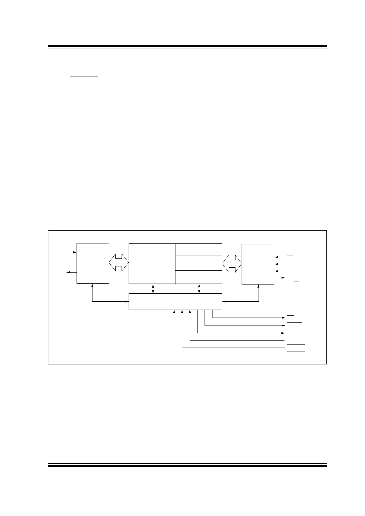
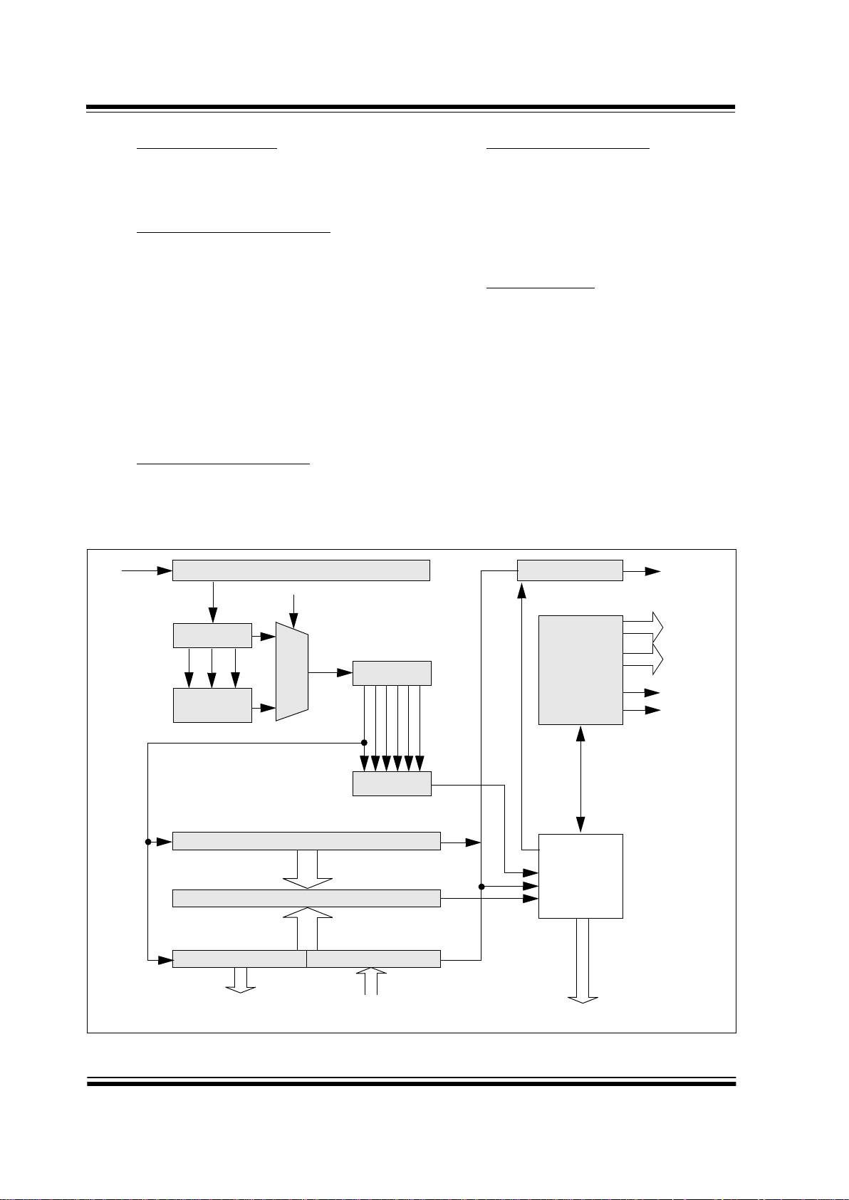
1.0 DEVICE FUNCTIONALITY
1.1 Overview
The MCP2510 is a stand-alone CAN controller developed to simplify applications that require interfacing
with a CAN bus. A simple block diagram of the
MCP2510 is shown in Figure 1-1. The device consists
of three main blocks:
1. the CAN protocol engine,
2. the control logic and SRAM registers that are
used to configure the device and its operation,
and
3. the SPI protocol block.
A typical system implementation using the device is
shown in Figure 1-2.
The CAN protocol engine handles all functions for
receiving and transmitting messages on the bus. Messages are transmitted by first loading the appropriate
message buffer and control registers. Transmission is
initiated by using control register bits, via the SPI interface, or by using the transmit enable pins. Status and
errors can be checked by reading the appropriate registers. Any message detected on the CAN bus is
checked for errors and then matched against the user
defined filters to see if it should be moved into one of
the two receive buffers.
The MCU interfaces to the device via the SPI interface.
Writing to and reading from all registers is done using
standard SPI read and write commands.
Interrupt pins are provided to allow greater system flexibility. There is one multi-purpose interrupt pin as well
as specific interrupt pins for each of the receive registers that can be used to indicate when a valid message
has been received and loaded into one of the receive
buffers. Use of the specific interrupt pins is optional,
and the general purpose interrupt pin as well as status
registers (accessed via the SPI interface) can also be
used to determine when a valid message has been
received.
There are also three pins available to initiate immediate
transmission of a message that has been loaded into
one of the three transmit registers. Use of these pins is
optional and initiating message transmission can also
be done by utilizing control registers accessed via the
SPI interface.
Table 1-1 gives a complete list of all of the pins on the
MCP2510.
FIGURE 1-1: Block Diagram
3 TX
Buffers
2 RX Buffers
Message Assembly
6 Acceptance
Filters
SPI
Interface
Logic
SPI
Bus
INT
Buffer
CS
SCK
SI
SO
CAN
Protocol
Engine
RXCAN
TXCAN
Control Logic
RX0BF
RX1BF
TX0RTS
TX1RTS
TX2RTS
Page 4
MCP2510
DS21291C-page 4 Preliminary 1999 Microchip Technology Inc.
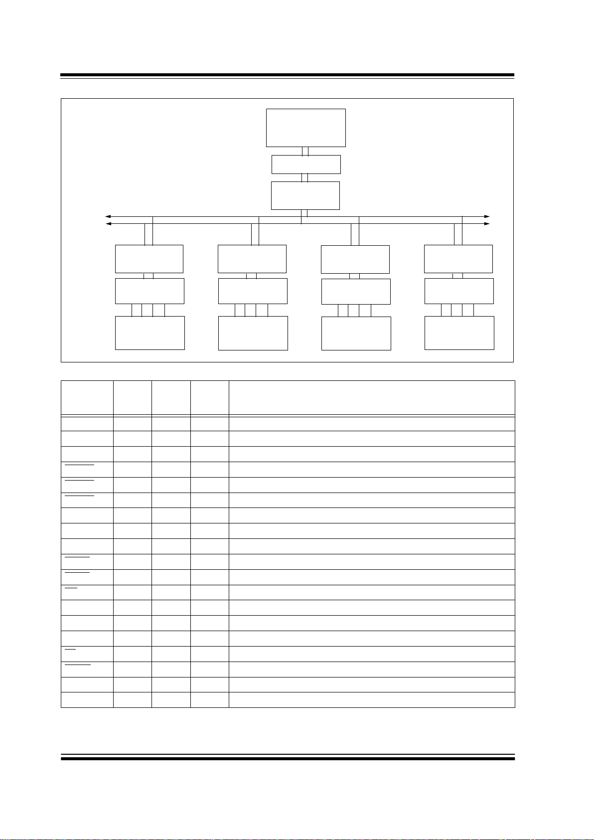
FIGURE 1-2: Typical System Implementation
TABLE 1-1: Pin Descriptions
Name
DIP/
SOIC
Pin #
TSSOP
Pin #
I/O/P
Typ e
Description
TXCAN
11O
Transmit output pin to CAN bus
RXCAN
22 I
Receive input pin from CAN bus
CLKOUT
33O
Clock output pin with programmable prescaler
TX0RTS
44 I
Transmit buffer TXB0 request to send or general purpose digital input. -100K
TX1RTS
55 I
Transmit buffer TXB1 request to send or general purpose digital input. -100K
TX2RTS
67 I
Transmit buffer TXB2 request to send or general purpose digital input. -100K
OSC2
78O
Oscillator output
OSC1
89 I
Oscillator input
V
SS
910P
Ground reference for logic and I/O pins
RX1BF
10 11 O
Receive buffer RXB1 interrupt pin or general purpose digital output
RX0BF
11 12 O
Receive buffer RXB0 interrupt pin or general purpose digital output
INT
12 13 O
Interrupt output pin
SCK
13 14 I
Clock input pin for SPI interface
SI
14 16 I
Data input pin for SPI interface
SO
15 17 O
Data output pin for SPI interface
CS
16 18 I
Chip select input pin for SPI interface
RESET
17 19 I
Active low device reset input
V
DD
18 20 P
Positive supply for logic and I/O pins
NC
— 6,15 —
No internal connection
Note: Type Identification: I=Input; O=Output; P=Power
MCP2510
SPI
MCP2510 MCP2510 MCP2510
INTERFACE
CAN
BUS
MCP2510
CAN
Transceiver
Node
Controller
Main
System
Controller
CAN
Transceiver
CAN
Transceiver
CAN
Tr an s c ei v er
CAN
Transceiver
Node
Controller
Node
Controller
Node
Controller
Page 5
1999 Microchip Technology Inc. Preliminary DS21291C-page 5
MCP2510
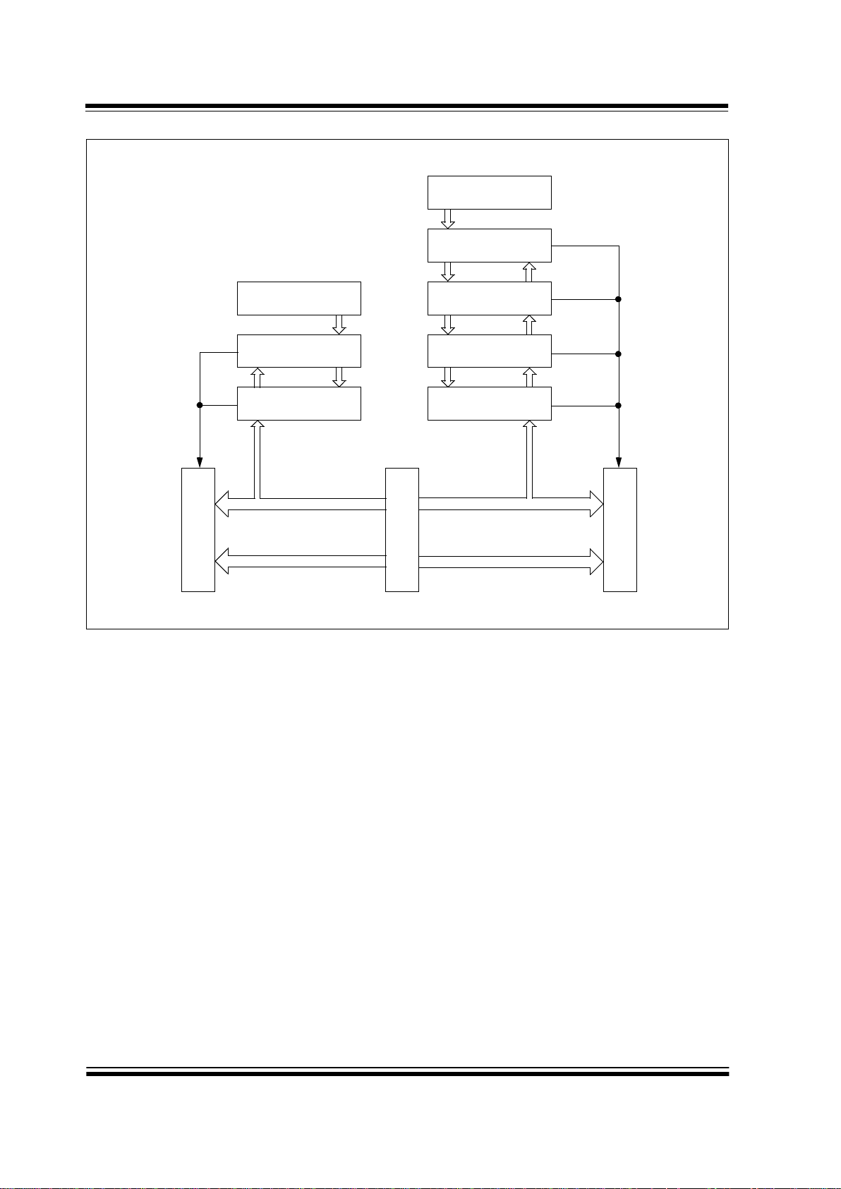
1.2 Transmit/Receive Buffers
The MCP2510 has three transmit and two receive buffers, two acceptance masks (one for each receive buffer), and a
total of six acceptance filters. Figure 1-3 is a block diagram of these buffers and their connection to the protocol engine.
FIGURE 1-3: CAN Buffers and Protocol Engine Block Diagram
Acceptance Filter
RXF2
R
X
B
1
Identifier
Data Field Data Field
Identifier
Acceptance Mask
RXM1
Acceptance Filter
RXF3
Acceptance Filter
RXF4
Acceptance Filter
RXF5
M
A
B
Acceptance Filter
RXF0
Acceptance Filter
RXF1
R
X
B
0
TXREQ
TXB2
ABTF
MLOA
TXERR
MESSAGE
Message
Queue
Control
Transmit Byte Sequencer
TXREQ
TXB0
ABTF
MLOA
TXERR
MESSAGE
CRC<14:0>
Comparator
Receive<7:0>Transmit<7:0>
Receive
Error
Transmit
Error
Protocol
REC
TEC
ErrPas
BusOff
Finite
State
Machine
Counter
Counter
Shift<14:0>
{Transmit<5:0>, Receive<8:0>}
Transmit
Logic
Bit
Timing
Logic
TX RX
Configuration
Registers
Clock
Generator
PROTOCOL
ENGINE
BUFFERS
TXREQ
TXB1
ABTF
MLOA
TXERR
MESSAGE
A
c
c
e
p
t
Acceptance Mask
RXM0
A
c
c
e
p
t
Page 6
MCP2510
DS21291C-page 6 Preliminary 1999 Microchip Technology Inc.
1.3 CAN Protocol Engine
The CAN protocol engine combines several functional
blocks, shown in Figure 1-4. These blocks and their
functions are described below.
1.4 Protocol Finite State Machine
The heart of the engine is the Finite State Machine
(FSM). This state machine sequences through messages on a bit by bit basis, changing states as the fields
of the various frame types are transmitted or received.
The FSM is a sequencer controlling the sequential data
stream between the TX/RX Shift Register, the CRC Register, and the bus line. The FSM also controls the Error
Management Logic (EML) and the parallel data stream
between the TX/RX Shift Registers and the buffers. The
FSM insures that the processes of reception, arbitration,
transmission, and error signaling are performed according to the CAN protocol. The automatic retransmission of
messages on the bus line is also handled by the FSM.
1.5 Cyclic Redundancy Check
The Cyclic Redundancy Check Register generates the
Cyclic Redundancy Check (CRC) code which is transmitted after either the Control Field (for messages with
0 data bytes) or the Data Field, and is used to check the
CRC field of incoming messages.
1.6 Error Management Logic
The Error Management Logic is responsible for the fault
confinement of the CAN device. Its two counters, the
Receive Error Counter (REC) and the Transmit Error
Counter (TEC), are incremented and decremented by
commands from the Bit Stream Processor. According to
the values of the error counters, the CAN controller is set
into the states error-active, error-passive or bus-off.
1.7 Bit Timing Logic
The Bit Timing Logic (BTL) monitors the bus line input
and handles the bus related bit timing according to the
CAN protocol. The BTL synchronizes on a recessive to
dominant bus transition at Start of Frame (hard synchronization) and on any further recessive to dominant
bus line transition if the CAN controller itself does not
transmit a dominant bit (resynchronization). The BTL
also provides programmable time segments to compensate for the propagation delay time, phase shifts,
and to define the position of the Sample Point within the
bit time. The programming of the BTL depends upon
the baud rate and external physical delay times.
FIGURE 1-4: CAN Protocol Engine Block Diagram
Bit Timing Logic
CRC<14:0>
Comparator
Receive<7:0> Transmit<7:0>
Sample<2:0>
Majority
Decision
StuffReg<5:0>
Comparator
Transmit Logic
Receive
Error Counter
Transmit
Error Counter
Protocol
FSM
Rx
SAM
BusMon
Rec/Trm Addr.
RecData<7:0>
TrmData<7:0>
Shift<14:0>
(Transmit<5:0>, Receive<7:0>)
Tx
REC
TEC
ErrPas
BusOff
Interface to Standard Buffer
Page 7

1999 Microchip Technology Inc. Preliminary DS21291C-page 7
MCP2510
2.0 CAN MESSAGE FRAMES
The MCP2510 supports Standard Data Frames,
Extended Data Frames, and Remote Frames (Standard
and Extended) as defined in the CAN 2.0B specification.
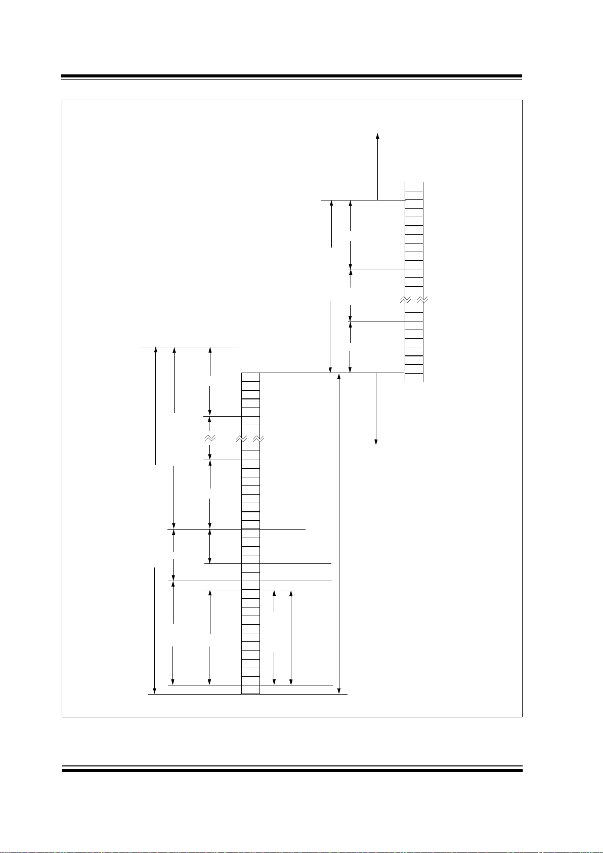
2.1 Standard Data Frame
The CAN Standard Data Frame is shown in Figure 2-1.
In common with all other frames, the frame begins with
a Start Of Frame (SOF) bit, which is of the dominant
state, which allows hard synchronization of all nodes.
The SOF is followed by the arbitration field, consisting
of 12 bits; the 11-bit ldentifier and the Remote Transmission Request (RTR) bit. The RTR bit is used to distinguish a data frame (RTR bit dominant) from a remote
frame (RTR bit recessive).
Following the arbitration field is the control field, consisting of six bits. The first bit of this field is the Identifier
Extension (IDE) bit which must be dominant to specify
a standard frame. The following bit, Reserved Bit Zero
(RB0), is reserved and is defined to be a dominant bit
by the can protocol. the remaining four bits of the control field are the Data Length Code (DLC) which specifies the number of bytes of data contained in the
message.
After the control field is the data field, which contains
any data bytes that are being sent, and is of the length
defined by the DLC above (0-8 bytes).
The Cyclic Redundancy Check (CRC) Field follows the
data field and is used to detect transmission errors. The
CRC Field consists of a 15-bit CRC sequence, followed
by the recessive CRC Delimiter bit.
The final field is the two-bit acknowledge field. During
the ACK Slot bit, the transmitting node sends out a
recessive bit. Any node that has received an error free
frame acknowledges the correct reception of the frame
by sending back a dominant bit (regardless of whether
the node is configured to accept that specific message
or not). The recessive acknowledge delimiter completes the acknowledge field and may not be overwritten by a dominant bit.
2.2 Extended Data Frame
In the Extended CAN Data Frame, shown in Figure 2-2,
the SOF bit is followed by the arbitration field which
consists of 32 bits. The first 11 bits are the most significant bits (Base-lD) of the 29-bit identifier. These 11 bits
are followed by the Substitute Remote Request (SRR)
bit which is defined to be recessive. The SRR bit is followed by the lDE bit which is recessive to denote an
extended CAN frame.
It should be noted that if arbitration remains unresolved
after transmission of the first 11 bits of the identifier,
and one of the nodes involved in the arbitration is sending a standard CAN frame (11-bit identifier), then the
standard CAN frame will win arbitration due to the
assertion of a dominant lDE bit. Also, the SRR bit in an
extended CAN frame must be recessive to allow the
assertion of a dominant RTR bit by a node that is sending a standard CAN remote frame.
The SRR and lDE bits are followed by the remaining 18
bits of the identifier (Extended lD) and the remote transmission request bit.
To enable standard and extended frames to be sent
across a shared network, it is necessary to split the
29-bit extended message identifier into 11-bit (most
significant) and 18-bit (least significant) sections. This
split ensures that the lDE bit can remain at the same bit
position in both standard and extended frames.
Following the arbitration field is the six-bit control field.
the first two bits of this field are reserved and must be
dominant. the remaining four bits of the control field are
the Data Length Code (DLC) which specifies the number of data bytes contained in the message.
The remaining portion of the frame (data field, CRC
field, acknowledge field, end of frame and lntermission)
is constructed in the same way as for a standard data
frame (see Section 2.1).
2.3 Remote Frame
Normally, data transmission is performed on an autonomous basis by the data source node (e.g. a sensor
sending out a data frame). It is possible, however, for a
destination node to request data from the source. To
accomplish this, the destination node sends a remote
frame with an identifier that matches the identifier of the
required data frame. The appropriate data source node
will then send a data frame in response to the remote
frame request.
There are two differences between a remote frame
(shown in Figure 2-3) and a data frame. First, the RTR
bit is at the recessive state, and second, there is no
data field. In the event of a data frame and a remote
frame with the same identifier being transmitted at the
same time, the data frame wins arbitration due to the
dominant RTR bit following the identifier. In this way, the
node that transmitted the remote frame receives the
desired data immediately.
Page 8

MCP2510
DS21291C-page 8 Preliminary 1999 Microchip Technology Inc.
2.4 Error Frame
An Error Frame is generated by any node that detects
a bus error. An error frame, shown in Figure 2-4, consists of two fields, an error flag field followed by an error
delimiter field. There are two types of error flag fields.
Which type of error flag field is sent depends upon the
error status of the node that detects and generates the
error flag field.
If an error-active node detects a bus error then the
node interrupts transmission of the current message by
generating an active error flag. The active error flag is
composed of six consecutive dominant bits. This bit
sequence actively violates the bit stuffing rule. All other
stations recognize the resulting bit stuffing error and in
turn generate error frames themselves, called error
echo flags. The error flag field, therefore, consists of
between six and twelve consecutive dominant bits
(generated by one or more nodes). The error delimiter
field completes the error frame. After completion of the
error frame, bus activity returns to normal and the interrupted node attempts to resend the aborted message.
If an error-passive node detects a bus error then the
node transmits an error-passive flag followed by the
error delimiter field. The error-passive flag consists of
six consecutive recessive bits, and the error frame for
an error-passive node consists of 14 recessive bits.
From this, it follows that unless the bus error is detected
by the node that is actually transmitting, the transmission of an error frame by an error-passive node will not
affect any other node on the network. If the transmitting
node generates an error-passive flag then this will
cause other nodes to generate error frames due to the
resulting bit stuffing violation. After transmission of an
error frame, an error-passive node must wait for six
consecutive recessive bits on the bus before attempting to rejoin bus communications.
The error delimiter consists of eight recessive bits and
allows the bus nodes to restart bus communications
cleanly after an error has occurred.
2.5 Overload Frame
An Overload Frame, shown in Figure 2-5, has the same
format as an active error frame. An overload frame,
however can only be generated during an lnterframe
space. In this way an overload frame can be differentiated from an error frame (an error frame is sent during
the transmission of a message). The overload frame
consists of two fields, an overload flag followed by an
overload delimiter. The overload flag consists of six
dominant bits followed by overload flags generated by
other nodes (and, as for an active error flag, giving a
maximum of twelve dominant bits). The overload delimiter consists of eight recessive bits. An overload frame
can be generated by a node as a result of two conditions. First, the node detects a dominant bit during the
interframe space which is an illegal condition. Second,
due to internal conditions the node is not yet able to
start reception of the next message. A node may generate a maximum of two sequential overload frames to
delay the start of the next message.
2.6 Interframe Space
The lnterframe Space separates a preceeding frame
(of any type) from a subsequent data or remote frame.
The interframe space is composed of at least three
recessive bits called the Intermission. This is provided
to allow nodes time for internal processing before the
start of the next message frame. After the intermission,
the bus line remains in the recessive state (bus idle)
until the next transmission starts.
Page 9
1999 Microchip Technology Inc. Preliminary DS21291C-page 9
MCP2510
FIGURE 2-1: Standard Data Frame
S
0
0
0
0
1
1 1 1
1 1 1 1
Start of Frame
Data Frame (number of bits = 44 + 8N)
12
Arbitration Field
ID 10
11
ID3
ID0
Identifier
Message
Filtering
Stored in Buffers
RTR
IDE
RB0
DLC3
DLC0
6
4
Control
Field
Data
Length
Code
Reserved Bit
8N (0
≤
N
≤
8)
Data Field
8
8
Stored in Transmit/Receive Buffers
Bit Stuffing
16
CRC Field
15
CRC
7
End of
Frame
CRC Del
Ack Slot Bit
ACK Del
IFS
1
1 1
1
Page 10
MCP2510
DS21291C-page 10 Preliminary 1999 Microchip Technology Inc.
FIGURE 2-2: Extended Data Frame
0 1 1 0 0 0 1
Start of Frame
Arbitration Field
32
11
ID10
ID3
ID0
IDE
Identifier
Message
Filtering
Stored in Buffers
SRR
EID17
EID0
RTR
RB1
RB0
DLC3
18
DLC0
6
Control
Field
4
Reserved bits
Data
Length
Code
Stored in Transmit/Receive Buffers
8 8
Data Frame (number of bits = 64 + 8N)
8N (0
≤
N
≤
8)
Data Field
1 1 1 1 1 1 1 1
16
CRC Field
15
CRC
CRC Del
Ack Slot Bit
ACK Del
End of
Frame
7
Bit Stuffing
IFS
Extended Identifier
1 1 1
Page 11
1999 Microchip Technology Inc. Preliminary DS21291C-page 11
MCP2510
FIGURE 2-3: Remote Data Frame
0 1 1 1 0 0
Start of Frame
Arbitration Field
32
11
ID10
ID3
ID0
IDE
Identifier
Message
Filtering
SRR
EID17
EID0
RTR
RB1
RB0
DLC3
18
DLC0
6
Control
Field
4
Reserved bits
Data
Length
Code
Extended Identifier
1 1 1 1 1 1 1 1 1
16
CRC Field
15
CRC
CRC Del
Ack Slot Bit
ACK Del
End of
Frame
7
Remote Data Frame with Extended Identifier
1 1 1
IFS
Page 12
MCP2510
DS21291C-page 12 Preliminary 1999 Microchip Technology Inc.
FIGURE 2-4: Error Frame
0 0
0
0
Start of Frame
Interrupted Data Frame
12
Arbitration Field
ID 10
11
ID3
ID0
Identifier
Message
Filtering
RTR
IDE
RB0
DLC3
DLC0
6
4
Control
Field
Data
Length
Code
Reserved Bit
8N (0
≤
N
≤
8)
Data Field
8
8
Bit Stuffing
0 0 0 0 0 0 0
0
0 1 1 1 1 1 1 1 1 0
Data Frame or
Remote Frame
Error Frame
6
Error
Flag
≤
6
Echo
Error
Flag
8
Error
Delimiter
Inter-Frame Space or
Overload Frame
Page 13

1999 Microchip Technology Inc. Preliminary DS21291C-page 13
MCP2510
FIGURE 2-5: Overload Frame
0 1
0
0
1
1 1 1 1 1 1 1 1
Start of Frame
Remote Frame (number of bits = 44)
12
Arbitration Field
ID 10
11
ID0
RTR
IDE
RB0
DLC3
DLC0
6
4
Control
Field
16
CRC Field
15
CRC
7
End of
Frame
CRC Del
Ack Slot Bit
ACK Del
0 0 0 0 0 0 0 1 1 1 1 1 1 1 1
Overload Frame
End of Frame or
Error Delimiter or
Overload Delimiter
6
Overload
Flag
Overload
Delimiter
8
Inter-Frame Space or
Error Frame
Page 14

MCP2510
DS21291C-page 14 Preliminary 1999 Microchip Technology Inc.
NOTES:
Page 15

1999 Microchip Technology Inc. Preliminary DS21291C-page 15
MCP2510
3.0 MESSAGE TRANSMISSION
3.1 Transmit Buffers
The MCP2510 implements three Transmit Buffers. Each
of these buffers occupies 14 bytes of SRAM and are
mapped into the device memory maps. The first byte,
TXB
NCTRL, is a control register associated with the mes-
sage buffer. The information in this register determines
the conditions under which the message will be transmitted and indicates the status of the message transmission.
(see Register 3-2). Five bytes are used to hold the standard and extended identifiers and other message arbitration information (see Register 3-3 through Register 3-8).
The last eight bytes are for the eight possible data bytes
of the message to be transmitted (see Register 3-8).
For the MCU to have write access to the message buffer,
the TXB
NCTRL.TXREQ bit must be clear, indicating that
the message buffer is clear of any pending message to be
transmitted. At a minimum, the TXB
NSIDH, TXBNSIDL,
and TXB
NDLC registers must be loaded. If data bytes are
present in the message, the TXB
NDm registers must also
be loaded. If the message is to use extended identifiers,
the TXBNEIDm registers must also be loaded and the
TXB
NSIDL.EXIDE bit set.
Prior to sending the message, the MCU must initialize
the CANINTE.TXI
NE bit to enable or disable the gener-
ation of an interrupt when the message is sent. The
MCU must also initialize the TXB
NCTRL.TXP priority
bits (see Section 3.2).
3.2 Transmit Priority
Transmit priority is a prioritization, within the MCP2510,
of the pending transmittable messages. This is independent from, and not necessarily related to, any prioritization implicit in the message arbitration scheme built into
the CAN protocol. Prior to sending the SOF, the priority
of all buffers that are queued for transmission is compared. The transmit buffer with the highest priority will be
sent first. For example, if transmit buffer 0 has a higher
priority setting than transmit buffer 1, buffer 0 will be sent
first. If two buffers have the same priority setting, the
buffer with the highest buffer number will be sent first. For
example, if transmit buffer 1 has the same priority setting
as transmit buffer 0, buffer 1 will be sent first. There are
four levels of transmit priority. If TXB
NCTRL.TXP<1:0>
for a particular message buffer is set to 11, that buffer
has the highest possible priority. If TXB
NC-
TRL.TXP<1:0> for a particular message buffer is 00, that
buffer has the lowest possible priority.
3.3 Initiating Transmission
To initiate message transmission the TXBNCTRL.TXREQ
bit must be set for each buffer to be transmitted. This can
be done by writing to the register via the SPI interface or
by setting the TX
NRTS pin low for the particular transmit
buffer(s) that are to be transmitted. If transmission is initiated via the SPI interface, the TXREQ bit can be set at the
same time as the TXP priority bits.
When TXB
NCTRL.TXREQ is set, the TXBNCTRL.ABTF,
TXB
NCTRL.MLOA and TXBNCTRL.TXERR bits will be
cleared.
Setting the TXB
NCTRL.TXREQ bit does not initiate a
message transmission, it merely flags a message
buffer as ready for transmission. Transmission will start
when the device detects that the bus is available. The
device will then begin transmission of the highest priority message that is ready.
When the transmission has completed successfully the
TXB
NCTRL.TXREQ bit will be cleared, the CAN-
INTF.TX
NIF bit will be set, and an interrupt will be gen-
erated if the CANINTE.TX
NIE bit is set.
If the message transmission fails, the TXB
NCTRL.TXREQ
will remain set indicating that the message is still pending
for transmission and one of the following condition flags
will be set. If the message started to transmit but encountered an error condition, the TXB
NCTRL. TXERR and the
CANINTF.MERRF bits will be set and an interrupt will be
generated on the INT
pin if the CANINTE.MERRE bit is
set. If the message lost arbitration the TXB
NCTRL.MLOA
bit will be set.
3.4 TXnRTS Pins
The TXNRTS Pins are input pins that can be configured
as request-to-send inputs, which provides a secondary
means of initiating the transmission of a message from
any of the transmit buffers, or as standard digital inputs.
Configuration and control of these pins is accomplished
using the TXRTSCTRL register (see Register 3-2). The
TXRTSCTRL register can only be modified when the
MCP2510 is in configuration mode (see Section 9.0). If
configured to operate as a request to send pin, the pin
is mapped into the respective TXB
NCTRL.TXREQ bit
for the transmit buffer. The TXREQ bit is latched by the
falling edge of the TX
NRTS pin. The TXNRTS pins are
designed to allow them to be tied directly to the RX
NBF
pins to automatically initiate a message transmission
when the RX
NBF pin goes low. The TXNRTS pins have
internal pullup resistors of 100K ohms (nominal).
3.5 Aborting Transmission
The MCU can request to abort a message in a specific
message buffer by clearing the associated TXBnCTRL.TXREQ bit. Also, all pending messages can be
requested to be aborted by setting the CANCTRL.ABAT bit. If the CANCTRL.ABAT bit is set to
abort all pending messages, the user MUST reset this
bit (typically after the user verifies that all TXREQ bits
have been cleared) to continue trasmit messages. The
CANCTRL.ABTF flag will only be set if the abort was
requested via the CANCTRL.ABAT bit. Aborting a message by resetting the TXREQ bit does NOT cause the
ATBF bit to be set.
Only messages that have not already begun to be
transmitted can be aborted. Once a message has
begun transmission, it will not be possible for the user
to reset the TXBnCTRL.TXREQ bit. After transmission
Page 16
MCP2510
DS21291C-page 16 Preliminary 1999 Microchip Technology Inc.
of a message has begun, if an error occurs on the bus
or if the message loses arbitration, the message will be
retransmitted regardless of a request to abort.
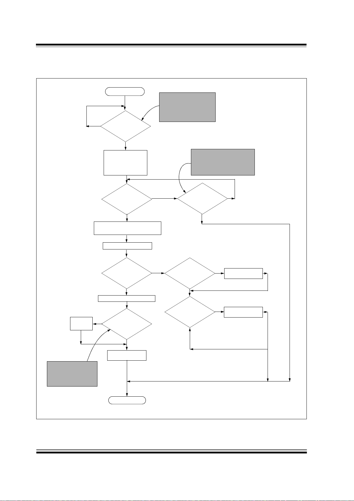
FIGURE 3-1: Transmit Message Flowchart
Start
Is
CAN Bus available
to start transmission
No
Examine TXBNCTRL.TXP <1:0> to
Are any
TXB
NCTRL.TXREQ
?
bits = 1
The message transmission
sequence begins when the
device determines that the
TXB
NCTRL.TXREQ for any of
the transmit registers has b een
set.
Clear:
TXB
NCTRL.ABTF
TXB
NCTRL.MLOA
TXB
NCTRL.TXERR
Ye s
?
is
TXBNCTRL.TXREQ=0
CANCTRL.ABAT=1
Clearing the TxBNCTRL.TXREQ
bit while it is set, or setting the
CANCTRL.ABAT bit before the
message has star ted transmission
will abort the message.
No
Transmit Message
Was
Message Transmitted
Successfully?
No
Ye s
Set TxBNCTRL.TXREQ=0
CANINTE.TXnIE=1?
Generate
Interrupt
Ye s
Ye s
Ye s
Set
Did
a message error
occur?
Was
Arbitration lost during
transmission?
Set
TxBNCTRL.TXERR=1
Ye s
No
No
Determine Highest Priority Message
No
?
Set
TxBNCTRL.MLOA=1
The CANINTE.TXnIE bit
determines if an interrupt
should be generated when
a message is successfully
transmitted.
GOTO START
CANTINF.TX
NIF=1
Ye s
or
No
Page 17

1999 Microchip Technology Inc. Preliminary DS21291C-page 17
MCP2510
REGISTER 3-1: TXBNCTRL Transmit Buffer N Control Register (ADDRESS: 30h, 40h, 50h)
U-0 R-0 R-0 R-0 R/W-0 U-0 R/W-0 R/W-0
— ABTF MLOA TXERR TXREQ — TXP1 TXP0
R = Readable bit
W = Writable bit
C = Bit can be cleared by
MCU but not set
U = Unimplemented -
reads as ‘0’
- n = Value at POR reset
bit 7 bit 0
bit 7: Unimplemented: Reads as ‘0’
bit 6: ABTF: Message Aborted Flag
1 = Message was aborted
0 = Message completed transmission successfully
bit 5: MLOA: Message Lost Arbitration
1 = Message lost arbitration while being sent
0 = Message did not lose arbitration while being sent
bit 4: TXERR: Transmission Error Detected
1 = A bus error occurred while the message was being transmitted
0 = No bus error occurred while the message was being transmitted
bit 3: TXREQ: Message Transmit Request
1 = Buffer is currently pending transmission
(MCU sets this bit to request message be transmitted - bit is automatically cleared when
the message is sent)
0 = Buffer is not currently pending transmission
(MCU can clear this bit to request a message abort)
bit 2: Unimplemented: Reads as ‘0’
bit 1-0: TXP<1:0>: Transmit Buffer Priority
11 = Highest Message Priority
10 = High Intermediate Message Priority
01 = Low Intermediate Message Priority
00 = Lowest Message Priority
Page 18

MCP2510
DS21291C-page 18 Preliminary 1999 Microchip Technology Inc.
REGISTER 3-2: TXRTSCTRL - TXNRTS Pin Control and Status Register (ADDRESS: 0Dh)
REGISTER 3-3: TXB
NSIDH - Transmit Buffer N Standard Identifier High (ADDRESS: 31h, 41h, 51h)
U-0 U-0 R-x R-x R-x R/W-0 R/W-0 R/W-0
— — B2RTS B1RTS B0RTS B2RTSM B1RTSM B0RTSM
R = Readable bit
W = Writable bit
C = Bit can be cleared by
MCU but not set
U = Unimplemented - reads
as ‘0’
- n = Value at POR reset
bit 7 bit 0
bit 7: Unimplemented: Reads as ‘0’
bit 6: Unimplemented: Reads as ‘0’
bit 5: B2RTS: TX2RTS
Pin State
- Reads state of TX2RTS
pin when in digital input mode
- Reads as ‘0’ when pin is in ‘request to send’ mode
bit 4: B1RTS: TX1RTX
Pin State
- Reads state of TX1RTS
pin when in digital input mode
- Reads as ‘0’ when pin is in ‘request to send’ mode
bit 3: B0RTS: TX0RTS
Pin State
- Reads state of TX0RTS pin when in digital input mode
- Reads as ‘0’ when pin is in ‘request to send’ mode
bit 2: B2RTSM: TX2RTS Pin Mode
1 = Pin is used to request message transmission of TXB2 buffer (on falling edge)
0 = Digital input
bit 1: B1RTSM: TX1RTS Pin Mode
1 = Pin is used to request message transmission of TXB1 buffer (on falling edge)
0 = Digital input
bit 0: B0RTSM: TX0RTS Pin Mode
1 = Pin is used to request message transmission of TXB0 buffer (on falling edge)
0 = Digital input
R/W-x R/W-x R/W-x R/W-x R/W-x R/W-x R/W-x R/W-x
SID10 SID9 SID8 SID7 SID6 SID5 SID4 SID3
R = Readable bit
W = Writable bit
C = Bit can be cleared by
MCU but not set
U = Unimplemented -
reads as ‘0’
- n = Value at POR reset
bit 7 bit 0
bit 7-0: SID<10:3>: Standard Identifier Bits <10:3>
Page 19

1999 Microchip Technology Inc. Preliminary DS21291C-page 19
MCP2510
REGISTER 3-4: TXBNSIDL - Transmit Buffer N Standard Identifier Low (ADDRESS: 32h, 42h, 52h)
REGISTER 3-5: TXB
NEID8 - Transmit Buffer N Extended Identifier High (ADDRESS: 33h, 43h, 53h)
REGISTER 3-6: TXB
NEID0 - Transmit Buffer N Extended Identifier LOW (ADDRESS: 34h, 44h, 54h)
R/W-x R/W-x R/W-x R/W-x R/W-x R/W-x R/W-x R/W-x
SID2 SID1 SID0
— EXIDE — EID17 EID16
R = Readable bit
W = Writable bit
C = Bit can be cleared by
MCU but not set
U = Unimplemented -
reads as ‘0’
- n = Value at POR reset
bit 7 bit 0
bit 7-5: SID<2:0>: Standard Identifier Bits <2:0>
bit 4: Unimplemented: Reads as '0’
bit 3: EXIDE: Extended Identifier Enable
1 = Message will transmit extended identifier
0 = Message will transmit standard identifier
bit 2: Unimplemented: Reads as '0’
bit 1-0: EID<17:16>: Extended Identifier Bits <17:16>
R/W-x R/W-x R/W-x R/W-x R/W-x R/W-x R/W-x R/W-x
EID15 EID14 EID13 EID12 EID11 EID10 EID9 EID8
R = Readable bit
W = Writable bit
C = Bit can be cleared by
MCU but not set
U = Unimplemented -
reads as ‘0’
- n = Value at POR reset
bit 7 bit 0
bit 7-0: EID<15:8>: Extended Identifier Bits <15:8>
R/W-x R/W-x R/W-x R/W-x R/W-x R/W-x R/W-x R/W-x
EID7 EID6 EID5 EID4 EID3 EID2 EID1 EID0
R = Readable bit
W = Writable bit
C = Bit can be cleared by
MCU but not set
U = Unimplemented -
reads as ‘0’
- n = Value at POR reset
bit 7 bit 0
bit 7-0: EID<7:0>: Extended Identifier Bits <7:0>
Page 20

MCP2510
DS21291C-page 20 Preliminary 1999 Microchip Technology Inc.
REGISTER 3-7: TXBNDLC - Transmit Buffer N Data Length Code (ADDRESS: 35h, 45h, 55h)
REGISTER 3-8: TXBNDM - Transmit Buffer N Data Field Byte m (ADDRESS: 36h-3Dh, 46h-4Dh, 56h-5Dh)
R/W-x R/W-x R/W-x R/W-x R/W-x R/W-x R/W-x R/W-x
— RTR — — DLC3 DLC2 DLC1 DLC0
R = Readable bit
W = Writable bit
C = Bit can be cleared by
MCU but not set
U = Unimplemented -
reads as ‘0’
- n = Value at POR reset
bit 7 bit 0
bit 7: Unimplemented: Reads as ‘0’
bit 6: RTR: Remote Transmission Request Bit
1 = Transmitted Message will be a Remote Transmit Request
0 = Transmitted Message will be a Data Frame
bit 5-4: Unimplemented: Reads as ‘0’
bit 3-0: DLC<3:0>: Data Length Code
Sets the number of data bytes to be transmitted (0 to 8 bytes)
NOTE: It is possible to set the DLC to a value greater than 8, however only 8 bytes are transmitted
R/W-x R/W-x R/W-x R/W-x R/W-x R/W-x R/W-x R/W-x
TXB
NDm7 TXBNDm6 TXBNDm5 TXBNDm4 TXBNDm3 TXBNDm2 TXBNDm1 TXBNDm0
R = Readable bit
W = Writable bit
C = Bit can be cleared
by
MCU but not set
U = Unimplemented
- reads as ‘0’
- n = Value at POR
reset
bit 7 bit 0
bit 7-0: TXBNDM7:TXBNDM0: Transmit Buffer N Data Field Byte m
Page 21

1999 Microchip Technology Inc. Preliminary DS21291C-page 21
MCP2510
4.0 MESSAGE RECEPTION
4.1 Receive Message Buffering
The MCP2510 includes two full receive buffers with
multiple acceptance filters for each. There is also a
separate Message Assembly Buffer (MAB) which acts
as a third receive buffer (see Figure 4-1).
4.2 Receive Buffers
Of the three Receive Buffers, the MAB is always committed to receiving the next message from the bus. The
remaining two receive buffers are called RXB0 and
RXB1 and can receive a complete message from the
protocol engine. The MCU can access one buffer while
the other buffer is available for message reception or
holding a previously received message.
The MAB assembles all messages received. These
messages will be transferred to the RXB
N buffers (See
Register 4-4 to Register 4-9) only if the acceptance filter criteria are met.
When a message is moved into either of the receive
buffers the appropriate CANINTF.RX
NIF bit is set. This
bit must be cleared by the MCU, when it has completed
processing the message in the buffer, in order to allow
a new message to be received into the buffer. This bit
provides a positive lockout to ensure that the MCU has
finished with the message before the MCP2510
attempts to load a new message into the receive buffer.
If the CANINTE.RX
NIE bit is set an interrupt will be gen-
erated on the INT
pin to indicate that a valid message
has been received.
4.3 Receive Priority
RXB0 is the higher priority buffer and has two message
acceptance filters associated with it. RXB1 is the lower
priority buffer and has four acceptance filters associated with it. The lower number of acceptance filters
makes the match on RXB0 more restrictive and implies
a higher priority for that buffer. Additionally, the
RXB0CTRL register can be configured such that if
RXB0 contains a valid message, and another valid
message is received, an overflow error will not occur
and the new message will be moved into RXB1 regardless of the acceptance criteria of RXB1. There are also
two programmable acceptance filter masks available,
one for each receive buffer (see Section 4.5).
When a message is received, bits <3:0> of the RXB
NCTRL
Register will indicate the acceptance filter number that
enabled reception, and whether the received message is a
remote transfer request.
The RXB
NCTRL.RXM bits set special receive modes.
Normally, these bits are set to 00 to enable reception of
all valid messages as determined by the appropriate
acceptance filters. In this case, the determination of
whether or not to receive standard or extended messages is determined by the RFX
NSIDL.EXIDE bit in the
acceptance filter register. If the RXB
NCTRL.RXM bits
are set to 01 or 10, the receiver will accept only messages with standard or extended identifiers respectively. If an acceptance filter has the RFX
NSIDL.EXIDE
bit set such that it does not correspond with the
RXB
NCTRL.RXM mode, that acceptance filter is ren-
dered useless. These two modes of RXB
NCTRL.RXM
bits can be used in systems where it is known that only
standard or extended messages will be on the bus. If
the RXB
NCTRL.RXM bits are set to 11, the buffer will
receive all messages regardless of the values of the
acceptance filters. Also, if a message has an error
before the end of frame, that portion of the message
assembled in the MAB before the error frame will be
loaded into the buffer. This mode has some value in
debugging a CAN system and would not be used in an
actual system environment.
4.4 RX0BF and RX1BF Pins
In addition to the INT pin which provides an interrupt
signal to the MCU for many different conditions, the
receive buffer full pins (RX0BF
and RX1BF) can be
used to indicate that a valid message has been loaded
into RXB0 or RXB1, respectively.
The RXB
NBF full pins can be configured to act as buffer
full interrupt pins or as standard digital outputs. Configuration and status of these pins is available via the
BFPCTRL register (Register 4-3). When set to operate
in interrupt mode (by setting BFPCTRL.BxBFE and
BFPCTRL.BxBFM bits to a 1), these pins are active low
and are mapped to the CANINTF.RX
NIF bit for each
receive buffer. When this bit goes high for one of the
receive buffers, indicating that a valid message has
been loaded into the buffer, the corresponding RX
NBF
pin will go low. When the CANINTF.RXNIF bit is cleared
by the MCU, then the corresponding interrupt pin will go
to the logic high state until the next message is loaded
into the receive buffer.
When used as digital outputs the BFPCTRL.BxBFM
and BFPCTRL.BxBFE bits must be set to a ‘1’ for the
associated buffer. In this mode the state of the pin is
controlled by the BFPCTRL.BxBFS bits. Writting a ‘1’
to the BxBFS bit will cause a high level to be driven on
the assicated buffer full pin, and a ‘0’ will cause the pin
to drive low. When using the pins in this mode the state
of the pin should be modified only by using the Bit Modify SPI command to prevent glitches from occuring on
either of the buffer full pins.
Note: The entire contents of the MAB is moved into
the receive buffer once a message is
accepted. This means that regardless of the
type of identifier (standard or extended) and
the number of data bytes received, the entire
receive buffer is overwritten with the MAB
contents. Therefore the contents of all registers in the buffer must be assumed to have
been modified when any message is
received.
Page 22
MCP2510
DS21291C-page 22 Preliminary 1999 Microchip Technology Inc.
FIGURE 4-1: Receive Buffer Block Diagram
Acceptance Mask
RXM1
Acceptance Filter
RXF2
Acceptance Filter
RXF3
Acceptance Filter
RXF4
Acceptance Filter
RXF5
Acceptance Mask
RXM0
Acceptance Filter
RXF0
Acceptance Filter
RXF1
Identifier
Data Field Data Field
Identifier
A
c
c
e
p
t
A
c
c
e
p
t
R
X
B
0
R
X
B
1
M
A
B
Page 23
1999 Microchip Technology Inc. Preliminary DS21291C-page 23
MCP2510
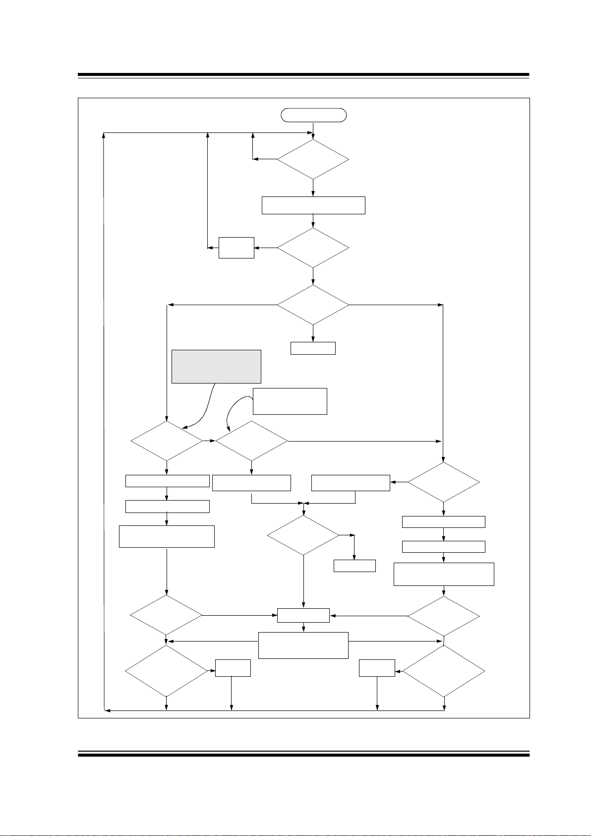
FIGURE 4-2: Message Reception Flowchart
Set RXBF0
Start
Detect
Start of
Message
?
Val id
Message
Received
?
Generate
Error
Message
Identifier meets
a filter criteria
?
Is
CANINTF.RX0IF=0
?
Go to Start
Move message into RXB0
Set RXB0CTRL.FILHIT <2:0>
Is
CANINTF.RX1IF = 0
?
Move message into RXB1
Set CANINTF.RX1IF=1
Yes, meets criteria
for RXBO
No
Generate
Interrupt on INT
Ye s
Ye s
No
No
Ye s
Ye s
No
No
Ye s
Ye s
Fram e
The CANINTF.RX
NIF bit
determines if the receive
register is empty and able
to accept a new message
No
Ye s
No
Begin Loading Message into
Message Assembly Buffer (MAB)
according to which filter criteria
was met
Set RXB0CTRL.FILHIT <0>
according to which filter criteria
Set CANSTAT <3:0> according to which receive buffer
the message was loaded into
Is
RXB0CTRL.BUKT=1
?
The RXB0CTRL.BUKT
bit determines if RXB0
can roll over into RXB1
Generate Overflow Error:
Set EFLG.RX1OVR
Is
CANINTE.ERRIE=1
?
No
Go to Start
Ye s
No
Are
BFPCTRL.B0BFM=1
?
BF1CTRL.B0BFE=1
and
Pin = 0
No
Set RXBF1
Pin = 0
No
Ye s
Ye s
CANINTE.RX0IE=1?
CANINTE.RX1IE=1?
RXB1
RXB0
Yes, meets criteria
for RXB1
Set EFLG.RX0OVR
Generate Overflow Error:
Set CANINTF.RX0IF=1
Are
BFPCTRL. B1BFM=1
?
BF1CTRL.B1BFE=1
and
Page 24

MCP2510
DS21291C-page 24 Preliminary 1999 Microchip Technology Inc.
REGISTER 4-1: RXB0CTRL - Receive Buffer 0 Control Register (ADDRESS: 60h)
U-0 R/W-0 R/W-0 U-0 R-0 R/W-0 R-0 R-0
— RXM1 RXM0 — RXRTR BUKT BUKT1 FILHIT0
R = Readable bit
W = Writable bit
C = Bit can be cleared by
MCU but not set
U = Unimplemented -
reads as ‘0’
- n = Value at POR reset
bit 7 bit 0
bit 7: Unimplemented: Reads as ‘0’
bit 6-5: RXM<1:0>: Receive Buffer Operating Mode
11 = Turn mask/filters off; receive any message
10 = Receive only valid messages with extended identifiers that meet filter criteria
01 = Receive only valid messages with standard identifiers that meet filter criteria
00 = Receive all valid messages using either standard or extended identifiers that meet filter criteria
bit 4: Unimplemented: Reads as ‘0’
bit 3: RXRTR: Received Remote Transfer Request
1 = Remote Transfer Request Received
0 = No Remote Transfer Request Received
bit 2: BUKT: Rollover Enable
1 = RXB0 message will rollover and be written to RXB1 if RXB0 is full
0 = Rollover disabled
bit 1: BUKT1: Read Only Copy of BUKT Bit (used internally by the MCP2510).
bit 0: FILHIT<0>: Filter Hit - indicates which acceptance filter enabled reception of message
1 = Acceptance Filter 1 (RXF1)
0 = Acceptance Filter 0 (RXF0)
Note: If a rollover from RXB0 to RXB1 occurs, the FILHIT bit will reflect the filter that accepted the message that rolled over
Page 25

1999 Microchip Technology Inc. Preliminary DS21291C-page 25
MCP2510
REGISTER 4-2: RXB1CTRL - Receive Buffer 1 Control Register (ADDRESS: 70h)
U-0 R/W-0 R/W-0 U-0 R-0 R-0 R-0 R-0
— RXM1 RXM0 — RXRTR FILHIT2 FILHIT1 FILHIT0
R = Readable bit
W = Writable bit
C = Bit can be cleared by
MCU but not set
U = Unimplemented -
reads as ‘0’
- n = Value at POR reset
bit 7 bit 0
bit 7: Unimplemented: Reads as ‘0’
bit 6-5: RXM<1:0>: Receive Buffer Operating Mode
11 = Turn mask/filters off; receive any message
10 = Receive only valid messages with extended identifiers that meet filter criteria
01 = Receive only valid messages with standard identifiers that meet filter criteria
00 = Receive all valid messages using either standard or extended identifiers that meet filter criteria
bit 4: Unimplemented: Reads as ‘0’
bit 3: RXRTR: Received Remote Transfer Request
1 = Remote Transfer Request Received
0 = No Remote Transfer Request Received
bit 2-0: FILHIT<2:0>: Filter Hit - indicates which acceptance filter enabled reception of message
101 = Acceptance Filter 5 (RXF5)
100 = Acceptance Filter 4 (RXF4)
011 = Acceptance Filter 3 (RXF3)
010 = Acceptance Filter 2 (RXF2)
001 = Acceptance Filter 1 (RXF1) (Only if BUKT bit set in RXB0CTRL)
000 = Acceptance Filter 0 (RXF0) (Only if BUKT bit set in RXB0CTRL)
Page 26

MCP2510
DS21291C-page 26 Preliminary 1999 Microchip Technology Inc.
REGISTER 4-3: BFPCTRL - RXNBF Pin Control and Status Register (ADDRESS: 0Ch)
REGISTER 4-4: RXB
NSIDH - Receive Buffer N Standard Identifier High (ADDRESS: 61h, 71h)
U-0 U-0 R/W-0 R/W-0 R/W-0 R/W-0 R/W-0 R/W-0
— — B1BFS B0BFS B1BFE B0BFE B1BFM B0BFM
R = Readable bit
W = Writable bit
C = Bit can be cleared by
MCU but not set
U = Unimplemented -
reads as ‘0’
- n = Value at POR reset
bit 7 bit 0
bit 7: Unimplemented: Reads as ‘0’
bit 6: Unimplemented: Reads as ‘0’
bit 5: B1BFS: RX1BF
Pin State (digital output mode only)
Reads as 0 when RX1BF is configured as interrupt pin
bit 4: B0BFS: RX0BF
Pin State (digital output mode only)
Reads as 0 when RX0BF is configured as interrupt pin
bit 3: B1BFE: RX1BF
Pin Function Enable
1 = Pin function enabled, operation mode determined by B1BFM bit
0 = Pin function disabled, pin goes to high impedance state
bit 2: B0BFE: RX0BF Pin Function Enable
1 = Pin function enabled, operation mode determined by B0BFM bit
0 = Pin Function disabled, pin goes to high impedance state
bit 1: B1BFM: RX1BF Pin Operation Mode
1 = Pin is used as interrupt when valid message loaded into RXB1
0 = Digital output mode
bit 0: B0BFM: RX0BF Pin Operation Mode
1 = Pin is used as interrupt when valid message loaded into RXB0
0 = Digital output mode
R-x R-x R-x R-x R-x R-x R-x R-x
SID10 SID9 SID8 SID7 SID6 SID5 SID4 SID3
R = Readable bit
W = Writable bit
C = Bit can be cleared by
MCU but not set
U = Unimplemented -
reads as ‘0’
- n = Value at POR reset
bit 7 bit 0
bit 7-0: SID<10:3>: Standard Identifier Bits <10:3>
These bits contain the eight most significant bits of the Standard Identifier for the received message
Page 27

1999 Microchip Technology Inc. Preliminary DS21291C-page 27
MCP2510
REGISTER 4-5: RXBNSIDL - Receive Buffer N Standard Identifier Low (ADDRESS: 62h, 72h)
REGISTER 4-6: RXB
NEID8 - Receive Buffer N Extended Identifier Mid (ADDRESS: 63h, 73h)
REGISTER 4-7: RXBNEID0 - Receive Buffer N Extended Identifier Low (ADDRESS: 64h, 74h)
R-x R-x R-x R-x R-x U-0 R-x R-x
SID2 SID1 SID0 SRR IDE
—
EID17 EID16
R = Readable bit
W = Writable bit
C = Bit can be cleared by
MCU but not set
U = Unimplemented -
reads as ‘0’
- n = Value at POR reset
bit 7 bit 0
bit 7-5: SID<2:0>: Standard Identifier Bits <2:0>
These bits contain the three least significant bits of the Standard Identifier for the received message
bit 4: SRR: Standard Frame Remote Transmit Request Bit (valid only if IDE bit = ‘0’)
1 = Standard Frame Remote Transmit Request Received
0 = Standard Data Frame Recieved
bit 3: IDE: Extended Identifier Flag
This bit indicates whether the received message was a Standard or an Extended Frame
1 = Received message was an Extended Frame
0 = Received message was a Standard Frame
bit 2: Unimplemented: Reads as '0'
bit 1-0: EID<17:16>: Extended Identifier Bits <17:16>
These bits contain the two most significant bits of the Extended Identifier for the received message
R-x R-x R-x R-x R-x R-x R-x R-x
EID15 EID14 EID13 EID12 EID11 EID10 EID9 EID8
R = Readable bit
W = Writable bit
C = Bit can be cleared by
MCU but not set
U = Unimplemented -
reads as ‘0’
- n = Value at POR reset
bit 7 bit 0
bit 7-0: EID<15:8>: Extended Identifier Bits <15:8>
These bits hold bits 15 through 8 of the Extended Identifier for the received message
R-x R-x R-x R-x R-x R-x R-x R-x
EID7 EID6 EID5 EID4 EID3 EID2 EID1 EID0
R = Readable bit
W = Writable bit
C = Bit can be cleared by
MCU but not set
U = Unimplemented -
reads as ‘0’
- n = Value at POR reset
bit 7 bit 0
bit 7-0: EID<7:0>: Extended Identifier Bits <7:0>
These bits hold the least significant eight bits of the Extended Identifier for the received message
Page 28

MCP2510
DS21291C-page 28 Preliminary 1999 Microchip Technology Inc.
REGISTER 4-8: RXBNDLC - Receive Buffer N Data Length Code (ADDRESS: 65h, 75h)
REGISTER 4-9: RXB
NDM - Receive Buffer N Data Field Byte m (ADDRESS: 66h-6Dh, 76h-7Dh)
U-0 R-x R-x R-x R-x R-x R-x R-x
—
RTR RB1 RB0 DLC3 DLC2 DLC1 DLC0
R = Readable bit
W = Writable bit
C = Bit can be cleared by
MCU but not set
U = Unimplemented -
reads as ‘0’
- n = Value at POR reset
bit 7 bit 0
bit 7: Unimplemented: Reads as ’0’
bit 6: RTR: Extended Frame Remote Transmission Request Bit (valid only when RXBnSIDL.IDE = 1)
1 = Extended Frame Remote Transmit Request Received
0 = Extended Data Frame Received
bit 5: RB1: Reserved Bit 1
bit 4: RB0: Reserved Bit 0
bit 3-0: DLC<3:0>: Data Length Code
Indicates number of data bytes that were received
R-x R-x R-x R-x R-x R-x R-x R-x
RB
NDm7 RBNDm6 RBNDm5 RBNDm4 RBNDm3 RBNDm2 RBNDm1 RBNDm0
R = Readable bit
W = Writable bit
C = Bit can be cleared by
MCU but not set
U = Unimplemented -
reads as ‘0’
- n = Value at POR reset
bit 7 bit 0
bit 7-0: RBNDm7:RBNDm0: Receive Buffer N Data Field Byte m
Eight bytes containing the data bytes for the received message
Page 29

1999 Microchip Technology Inc. Preliminary DS21291C-page 29
MCP2510
4.5 Message Acceptance Filters and
Masks
The Message Acceptance Filters And Masks are used
to determine if a message in the message assembly
buffer should be loaded into either of the receive buffers (see Figure 4-3). Once a valid message has been
received into the MAB, the identifier fields of the message are compared to the filter values. If there is a
match, that message will be loaded into the appropriate
receive buffer. The filter masks (see Register 4-10
through Register 4-17) are used to determine which
bits in the identifier are examined with the filters. A truth
table is shown below in Table 4-10 that indicates how
each bit in the identifier is compared to the masks and
filters to determine if a the message should be loaded
into a receive buffer. The mask essentially determines
which bits to apply the acceptance filters to. If any mask
bit is set to a zero, then that bit will automatically be
accepted regardless of the filter bit.
TABLE 4-10: Filter/Mask Truth Table
As shown in the Receive Buffers Block Diagram
(Figure 4-1), acceptance filters RXF0 and RXF1, and
filter mask RXM0 are associated with RXB0. Filters
RXF2, RXF3, RXF4, and RXF5 and mask RXM1 are
associated with RXB1. When a filter matches and a
message is loaded into the receive buffer, the filter
number that enabled the message reception is loaded
into the RXB
NCTRL register FILHIT bit(s). For RXB1
the RXB1CTRL register contains the FILHIT<2:0> bits.
They are coded as follows:
- 101 = Acceptance Filter 5 (RXF5)
- 100 = Acceptance Filter 4 (RXF4)
- 011 = Acceptance Filter 3 (RXF3)
- 010 = Acceptance Filter 2 (RXF2)
- 001 = Acceptance Filter 1 (RXF1)
- 000 = Acceptance Filter 0 (RXF0)
RXB0CTRL contains two copies of the BUKT bit and
the FILHIT<0> bit.
The coding of the BUKT bit enables these three bits to
be used similarly to the RXB1CTRL.FILHIT bits and to
distinguish a hit on filter RXF0 and RXF1 in either
RXB0 or after a roll over into RXB1.
- 111 = Acceptance Filter 1 (RXF1)
- 110 = Acceptance Filter 0 (RXF0)
- 001 = Acceptance Filter 1 (RXF1)
- 000 = Acceptance Filter 0
If the BUKT bit is clear, there are six codes corresponding to the six filters. If the BUKT bit is set, there are six
codes corresponding to the six filters plus two additional codes corresponding to RXF0 and RXF1 filters
that roll over into RXB1.
If more than one acceptance filter matches, the FILHIT
bits will encode the binary value of the lowest numbered filter that matched. In other words, if filter RXF2
and filter RXF4 match, FILHIT will be loaded with the
value for RXF2. This essentially prioritizes the acceptance filters with a lower number filter having higher priority. Messages are compared to filters in ascending
order of filter number.
The mask and filter registers can only be modified
when the MCP2510 is in configuration mode (see
Section 9.0).
Mask Bit nFilter Bit
n
Message
Identifier bit
n001
Accept or
reject bit n
0X XAccept
10 0Accept
10 1Reject
11 0Reject
11 1Accept
Note: X = don’t care
Note: 000 and 001 can only occur if the BUKT bit
(see Table 4-1) is set in the RXB0CTRL
register allowing RXB0 messages to roll
over into RXB1.
Page 30

MCP2510
DS21291C-page 30 Preliminary 1999 Microchip Technology Inc.
FIGURE 4-3: Message Acceptance Mask and Filter Operation
REGISTER 4-10: RXF
NSIDH - Acceptance Filter N Standard Identifier High (Address: 00h, 04h, 08h, 10h, 14h, 18h)
Acceptance Filter Register Acceptance Mask Register
RxRqst
Message Assembly Buffer
RXFn
0
RXFn
1
RXFn
n
RXMn
0
RXMn
1
RXMn
n
Identifier
R/W-x R/W-x R/W-x R/W-x R/W-x R/W-x R/W-x R/W-x
SID10 SID9 SID8 SID7 SID6 SID5 SID4 SID3
R = Readable bit
W = Writable bit
C = Bit can be cleared by
MCU but not set
U = Unimplemented -
reads as ‘0’
- n = Value at POR reset
bit 7 bit 0
bit 7-0: SID<10:3>: Standard Identifier Filter Bits <10:3>
These bits hold the filter bits to be applied to bits <10:3> of the Standard Identifier portion of a received
message
Page 31

1999 Microchip Technology Inc. Preliminary DS21291C-page 31
MCP2510
REGISTER 4-11: RXFNSIDL - Acceptance Filter N Standard Identifier Low (Address: 01h, 05h, 09h, 11h, 15h, 19h)
REGISTER 4-12: RXF
NEID8 - Acceptance Filter N Extended Identifier High (Address: 02h, 06h, 0Ah, 12h, 16h, 1Ah)
REGISTER 4-13: RXF
NEID0 - Acceptance Filter N Extended Identifier Low (Address: 03h, 07h, 0Bh, 13h, 17h, 1Bh)
R/W-x R/W-x R/W-x U-0 R/W-x U-0 R/W-x R/W-x
SID2 SID1 SID0
—
EXIDE
—
EID17 EID16
R = Readable bit
W = Writable bit
C = Bit can be cleared by
MCU but not set
U = Unimplemented -
reads as ‘0’
- n = Value at POR reset
bit 7 bit 0
bit 7-5: SID<2:0>: Standard Identifier Filter Bits <2:0>
These bits hold the filter bits to be applied to bits <2:0> of the Standard Identifier portion of a received
message
bit 4: Unimplemented: Reads as ’0’
bit 3: EXIDE: Extended Identifier Enable
1 = Filter is applied only to Extended Frames
0 = Filter is applied only to Standard Frames
bit 2: Unimplemented: Reads as ’0’
bit 1-0: EID<17:16>: Exended Identifier Filter Bits <17:16>
These bits hold the filter bits to be applied to bits <17:16> of the Extended Identifier portion of a
received message
R/W-x R/W-x R/W-x R/W-x R/W-x R/W-x R/W-x R/W-x
EID15 EID14 EID13 EID12 EID11 EID10 EID9 EID8
R = Readable bit
W = Writable bit
C = Bit can be cleared by
MCU but not set
U = Unimplemented -
reads as ‘0’
- n = Value at POR reset
bit 7 bit 0
bit 7-0: EID<15:8>: Extended Identifier Filter Bits <15:8>
These bits hold the filter bits to be applied to bits <15:8> of the Extended Identifier portion of a received
message
R/W-x R/W-x R/W-x R/W-x R/W-x R/W-x R/W-x R/W-x
EID7 EID6 EID5 EID4 EID3 EID2 EID1 EID0
R = Readable bit
W = Writable bit
C = Bit can be cleared by
MCU but not set
U = Unimplemented -
reads as ‘0’
- n = Value at POR reset
bit 7 bit 0
bit 7-0: EID<7:0>: Extended Identifier Filter Bits <7:0>
These bits hold the filter bits to be applied to the bits <7:0> of the Extended Identifier portion of a received
message
Page 32

MCP2510
DS21291C-page 32 Preliminary 1999 Microchip Technology Inc.
REGISTER 4-14: RXMNSIDH - Acceptance Filter Mask N Standard Identifier High (Address: 20h, 24h)
REGISTER 4-15: RXMNSIDL - Acceptance Filter Mask N Standard Identifier Low (Address: 21h, 25h)
REGISTER 4-16: RXM
NEID8 - Acceptance Filter Mask N Extended Identifier High (Address: 22h, 26h)
R/W-x R/W-x R/W-x R/W-x R/W-x R/W-x R/W-x R/W-x
SID10 SID9 SID8 SID7 SID6 SID5 SID4 SID3
R = Readable bit
W = Writable bit
C = Bit can be cleared by
MCU but not set
U = Unimplemented -
reads as ‘0’
- n = Value at POR reset
bit 7 bit 0
bit 7-0: SID<10:3>: Standard Identifier Mask Bits <10:3>
These bits hold the mask bits to be applied to bits <10:3> of the Standard Identifier portion of a received
message
R/W-x R/W-x R/W-x U-0 U-0 U-0 R/W-x R/W-x
SID2 SID1 SID0
— — —
EID17 EID16
R = Readable bit
W = Writable bit
C = Bit can be cleared by
MCU but not set
U = Unimplemented -
reads as ‘0’
- n = Value at POR reset
bit 7 bit 0
bit 7-5: SID<2:0>: Standard Identifier Mask Bits <2:0>
These bits hold the mask bits to be applied to bits<2:0> of the Standard Identifier portion of a received
message
bit 4-2: Unimplemented: Reads as ’0’
bit 1-0: EID<17:16>: Extended Identifier Mask Bits <17:16>
These bits hold the mask bits to be applied to bits <17:16> of the Extended Identifier portion of a received
message
R/W-x R/W-x R/W-x R/W-x R/W-x R/W-x R/W-x R/W-x
EID15 EID14 EID13 EID12 EID11 EID10 EID9 EID8
R = Readable bit
W = Writable bit
C = Bit can be cleared by
MCU but not set
U = Unimplemented -
reads as ‘0’
- n = Value at POR reset
bit 7 bit 0
bit 7-0: EID<15:8>: Extended Identifier Mask Bits <15:8>
These bits hold the mask bits to be applied to bits <15:8> of the Extended Identifier portion of a received
message
Page 33

1999 Microchip Technology Inc. Preliminary DS21291C-page 33
MCP2510
REGISTER 4-17: RXMNEID0 - Acceptance Filter Mask N Extended Identifier Low (Address: 23h, 27h)
R/W-x R/W-x R/W-x R/W-x R/W-x R/W-x R/W-x R/W-x
EID7 EID6 EID5 EID4 EID3 EID2 EID1 EID0
R = Readable bit
W = Writable bit
C = Bit can be cleared by
MCU but not set
U = Unimplemented -
reads as ‘0’
- n = Value at POR reset
bit 7 bit 0
bit 7-0: EID<7:0>: Extended Identifier Mask Bits <7:0>
These bits hold the mask bits to be applied to bits <7:0> of the Extended Identifier portion of a received
message
Page 34

MCP2510
DS21291C-page 34 Preliminary 1999 Microchip Technology Inc.
NOTES:
Page 35

1999 Microchip Technology Inc. Preliminary DS21291C-page 35
MCP2510
5.0 BIT TIMING
All nodes on a given CAN bus must have the same
nominal bit rate. The CAN protocol uses Non Return to
Zero (NRZ) coding which does not encode a clock
within the data stream. Therefore, the receive clock
must be recovered by the receiving nodes and synchronized to the transmitters clock.
As oscillators and transmission time may vary from
node to node, the receiver must have some type of
Phase Lock Loop (PLL) synchronized to data transmission edges to synchronize and maintain the receiver
clock. Since the data is NRZ coded, it is necessar y to
include bit stuffing to ensure that an edge occurs at
least every six bit times, to maintain the Digital Phase
Lock Loop (DPLL) synchronization.
The bit timing of the MCP2510 is implemented using a
DPLL that is configured to synchronize to the incoming
data, and provide the nominal timing for the transmitted
data. The DPLL breaks each bit time into multiple segments made up of minimal periods of time called the
time quanta (T
Q
).
Bus timing functions executed within the bit time frame,
such as synchronization to the local oscillator, network
transmission delay compensation, and sample point
positioning, are defined by the programmable bit timing
logic of the DPLL.
All devices on the CAN bus must use the same bit rate.
However, all devices are not required to have the same
master oscillator clock frequency. For the different clock
frequencies of the individual devices, the bit rate has to
be adjusted by appropriately setting the baud rate prescaler and number of time quanta in each segment.
The nominal bit rate is the number of bits transmitted
per second assuming an ideal transmitter with an ideal
oscillator, in the absence of resynchronization. The
nominal bit rate is defined to be a maximum of 1Mb/s.
Nominal Bit Time is defined as:
T
BIT
= 1 / NOMlNAL BlT RATE
The nominal bit time can be thought of as being divided
into separate non-overlapping time segments. These
segments are shown in Figure 5-1.
- Synchronization Segment (Sync_Seg)
- Propagation Time Segment (Prop_Seg)
- Phase Buffer Segment 1 (Phase_Seg1)
- Phase Buffer Segment 2 [Phase_Seg2)
Nominal Bit Time = T
Q
* (Sync_Seg + Prop_Seg +
Phase_Seg1 + Phase_Seg2)
The time segments and also the nominal bit time are
made up of integer units of time called time quanta or
T
Q (see Figure 5-1). By definition, the nominal bit time
is programmable from a minimum of 8 T
Q
to a maxi-
mum of 25 T
Q
. Also, by definition the minimum nominal
bit time is 1 µs, corresponding to a maximum 1 Mb/s
rate.
FIGURE 5-1: Bit Time Partitioning
Input Signal
Sync
Prop
Segment
Phase
Segment 1
Phase
Segment 2
Sample Point
T
Q
Page 36

MCP2510
DS21291C-page 36 Preliminary 1999 Microchip Technology Inc.
5.1 Time Quanta
The Time Quanta is a fixed unit of time derived from the
oscillator period. There is a programmable baud-rate
prescaler, with integral values ranging from 1 to 64, in
addition to a fixed divide by two for clock generation.
Time quanta is defined as:
T
Q
= 2 * (Baud Rate +1) * T
OSC
where Baud Rate is the binary value represented by
CNF1.BRP<5:0>
For some examples:
If Fosc = 16 MHz, BRP<5:0> = 00h, and Nominal Bit
Time = 8 T
Q
;
then T
Q
= 125 nsec and Nominal Bit Rate = 1 Mb/s
If F
OSC
= 20 MHz, BRP<5:0> = 01h, and Nominal Bit
Time = 8 T
Q
;
then T
Q
= 200nsec and Nominal Bit Rate = 625 Kb/s
If Fosc = 25 MHz, BRP<5:0> = 3Fh, and Nominal Bit
Time = 25 TQ;
then T
Q
= 5.12 usec and Nominal Bit Rate = 7.8 Kb/s
The frequencies of the oscillators in the different nodes
must be coordinated in order to provide a system-wide
specified nominal bit time. This means that all oscillators must have a T
OSC
that is a integral divisor of TQ. It
should also be noted that although the number of T
Q
is
programmable from 4 to 25, the usable minimum is 6
T
Q.
Attempting to a bit time of less than 6 TQ in length
is not guaranteed to operate correctly
5.2 Synchronization Segment
This part of the bit time is used to synchronize the various CAN nodes on the bus. The edge of the input signal is expected to occur during the sync segment. The
duration is 1 T
Q
.
5.3 Propagation Segment
This part of the bit time is used to compensate for physical delay times within the network. These delay times
consist of the signal propagation time on the bus line
and the internal delay time of the nodes. The delay is
calculated as being the round trip time from transmitter
to receiver (twice the signal’s propagation time on the
bus line), the input comparator delay, and the output
driver delay. The length of the Propagation Segment
can be programmed from 1 T
Q
to 8 TQ by setting the
PRSEG2:PRSEG0 bits of the CNF2 register (Table
6-2).
The total delay is calculated from the following individual delays:
- 2 * physical bus end to end delay; T
BUS
- 2 * input comparator delay; T
COMP
(depends
on application circuit)
- 2 * output driver delay; T
DRIVE
(depends on
application circuit)
- 1 * input to output of CAN controller; T
CAN
(maximum defined as 1 T
Q
+ delay ns)
-T
PROPOGATION
= 2 * (T
BUS
+ T
COMP
+ T
DRIVE
)
+ T
CAN
- Prop_Seg = T
PROPOGATION
/ T
Q
5.4 Phase Buffer Segments
The Phase Buffer Segments are used to optimally locate
the sampling point of the received bit within the nominal
bit time. The sampling point occurs between phase segment 1 and phase segment 2. These segments can be
lengthened or shortened by the resynchronization process (see Section 5.7.2). Thus, the variation of the values of the phase buffer segments represent the DPLL
functionality. The end of phase segment 1 determines
the sampling point within a bit time. phase segment 1 is
programmable from 1 T
Q
to 8 TQ in duration. Phase segment 2 provides delay before the next transmitted data
transition and is also programmable from 1 TQ to 8 TQ in
duration (however due to IPT requirements the actual
minimum length of phase segment 2 is 2 T
Q
- see Section 5.6 below), or it may be defined to be equal to the
greater of phase segment 1 or the Information Processing Time (IPT). (see Section 5.6).
5.5 Sample Point
The Sample Point is the point of time at which the bus
level is read and value of the received bit is determined.
The Sampling point occurs at the end of phase segment 1. If the bit timing is slow and contains many T
Q
,
it is possible to specify multiple sampling of the bus line
at the sample point. The value of the received bit is
determined to be the value of the majority decision of
three values. The three samples are taken at the sample point, and twice before with a time of T
Q
/2 between
each sample.
5.6 Information Processing Time
The Information Processing Time (IPT) is the time segment, starting at the sample point, that is reserved for
calculation of the subsequent bit level. The CAN specification defines this time to be less than or equal to 2 T
Q
.
The MCP2510 defines this time to be 2 T
Q
. Thus, phase
segment 2 must be at least 2 T
Q
long.
Page 37

1999 Microchip Technology Inc. Preliminary DS21291C-page 37
MCP2510
5.7 Synchronization
To compensate for phase shifts between the oscillator
frequencies of each of the nodes on the bus, each CAN
controller must be able to synchronize to the relevant
signal edge of the incoming signal. Synchronization is
the process by which the DPLL function is implemented. When an edge in the transmitted data is
detected, the logic will compare the location of the edge
to the expected time (Sync Seg). The circuit will then
adjust the values of phase segment 1 and phase segment 2 as necessary. There are two mechanisms used
for synchronization.
5.7.1 HARD SYNCHRONIZATION
Hard Synchronization is only done when there is a
recessive to dominant edge during a BUS IDLE condition, indicating the start of a message. After hard synchronization, the bit time counters are restarted with
Sync Seg. Hard synchronization forces the edge which
has occurred to lie within the synchronization segment
of the restarted bit time. Due to the rules of synchronization, if a hard synchronization occurs there will not be
a resynchronization within that bit time.
5.7.2 RESYNCHRONIZATION
As a result of Resynchronization, phase segment 1
may be lengthened or phase segment 2 may be shortened. The amount of lengthening or shortening of the
phase buffer segments has an upper bound given by
the Synchronization Jump Width (SJW). The value of
the SJW will be added to phase segment 1 (see
Figure 5-2) or subtracted from phase segment 2 (see
Figure 5-3). The SJW represents the loop filtering of
the DPLL. The SJW is programmable between 1 T
Q
and 4 TQ.
Clocking information will only be derived from recessive to dominant transitions. The property that only a
fixed maximum number of successive bits have the
same value ensures resynchronization to the bit stream
during a frame.
The phase error of an edge is given by the position of
the edge relative to Sync Seg, measured in T
Q
. The
phase error is defined in magnitude of T
Q
as follows:
• e = 0 if the edge lies within SYNCESEG.
• e > 0 if the edge lies before the SAMPLE POINT.
• e < 0 if the edge lies after the SAMPLE POINT of
the previous bit.
If the magnitude of the phase error is less than or equal
to the programmed value of the synchronization jump
width, the effect of a resynchronization is the same as
that of a hard synchronization.
If the magnitude of the phase error is larger than the
synchronization jump width, and if the phase error is
positive, then phase segment 1 is lengthened by an
amount equal to the synchronization jump width.
If the magnitude of the phase error is larger than the
resynchronization jump width, and if the phase error is
negative, then phase segment 2 is shortened by an
amount equal to the synchronization jump width.
5.7.3 SYNCHRONIZATION RULES
• Only one synchronization within one bit time is
allowed.
• An edge will be used for synchronization only if
the value detected at the previous sample point
(previously read bus value) differs from the bus
value immediately after the edge.
• All other recessive to dominant edges fulfilling
rules 1 and 2 will be used for resynchronization
with the exception that a node transmitting a dominant bit will not perform a resynchronization as a
result of a recessive to dominant edge with a positive phase error.
FIGURE 5-2: Lengthening a Bit Period
Input Signal
Sync
Prop
Segment
Phase
Segment 1
Phase
Segment 2
≤ SJW
Sample
Nominal
Actual Bit
Length
Bit Length
Point
T
Q
Page 38

MCP2510
DS21291C-page 38 Preliminary 1999 Microchip Technology Inc.
FIGURE 5-3: Shortening a Bit Period
5.8 Programming Time Segments
Some requirements for programming of the time segments:
• Prop Seg + Phase Seg 1 >= Phase Seg 2
• Prop Seg + Phase Seg 1 >= T
DELAY
• Phase Seg 2 > Sync Jump Width
For example, assuming that a 125 kHz CAN baud rate
with F
OSC
= 20 MHz is desired:
T
OSC
= 50 nsec, choose BRP<5:0> = 04h, then TQ =
500nsec. To obtain 125 kHz, the bit time must be 16 T
Q
.
Typically, the sampling of the bit should take place at
about 60-70% of the bit time, depending on the system
parameters. Also, typically, the T
DELAY
is 1-2 TQ.
Sync Seg = 1 T
Q
; Prop Seg = 2 TQ; So setting Phase
Seg 1 = 7 T
Q
would place the sample at 10 TQ after the
transition. This would leave 6 T
Q
for Phase Seg 2.
Since Phase Seg 2 is 6, by the rules, SJW could be the
maximum of 4 T
Q
. However, normally a large SJW is
only necessary when the clock generation of the different nodes is inaccurate or unstable, such as using
ceramic resonators. So an SJW of 1 is typically
enough.
5.9 Oscillator Tolerance
The bit timing requirements allow ceramic resonators
to be used in applications with transmission rates of up
to 125 kbit/sec, as a rule of thumb. For the full bus
speed range of the CAN protocol, a quartz oscillator is
required. A maximum node-to-node oscillator variation
of 1.7% is allowed.
Input Signal
Sync
Prop
Segment
Phase
Segment 1
Phase
Segment 2
≤ SJW
Sample
Actual
Nominal
Bit Length
T
Q
Point
Bit Length
Page 39

1999 Microchip Technology Inc. Preliminary DS21291C-page 39
MCP2510
5.10 Bit Timing Configuration Registers
The configuration registers (CNF1, CNF2, CNF3) control the bit timing for the CAN bus interface. These registers can only be modified when the MCP2510 is in
configuration mode (see Section 9.0).
5.10.1 CNF1
The BRP<5:0> bits control the baud rate prescaler.
These bits set the length of T
Q
relative to the OSC1
input frequency, with the minimum length of T
Q
being 2
OSC1 clock cycles in length (when BRP<5:0> are set
to 000000). The SJW<1:0> bits select the synchronization jump width in terms of number of T
Q
’s.
5.10.2 CNF2
The PRSEG<2:0> bits set the length, in T
Q
’s, of the
propagation segment. The PHSEG1<2:0> bits set the
length, in TQ’s, of phase segment 1. The SAM bit controls how many times the RXCAN pin is sampled. Set-
ting this bit to a ‘1’ causes the bus to be sampled three
times; twice at T
Q
/2 before the sample point, and once
at the normal sample point (which is at the end of
phase segment 1). The value of the bus is determined
to be the value read during at least two of the samples.
If the SAM bit is set to a ‘0’ then the RXCAN pin is sampled only once at the sample point. The BTLMODE bit
controls how the length of phase segment 2 is determined. If this bit is set to a ‘1’ then the length of phase
segment 2 is determined by the PHSEG2<2:0> bits of
CNF3 (see Section 5.10.3). If the BTLMODE bit is set
to a ‘0’ then the length of phase segment 2 is the
greater of phase segment 1 and the information processing time (which is fixed at 2 T
Q
for the MCP2510).
5.10.3 CNF3
The PHSEG2<2:0> bits set the length, in T
Q
’s, of
Phase Segment 2, if the CNF2.BTLMODE bit is set to
a ‘1’. If the BTLMODE bit is set to a ‘0’ then the
PHSEG2<2:0> bits have no effect.
REGISTER 5-1: CNF1 - Configuration Register1 (ADDRESS: 2Ah)
R/W-0 R/W-0 R/W-0 R/W-0 R/W-0 R/W-0 R/W-0 R/W-0
SJW1 SJW0 BRP5 BRP4 BRP3 BRP2 BRP1 BRP0
R = Readable bit
W = Writable bit
C = Bit can be cleared by
MCU but not set
U = Unimplemented -
reads as ‘0’
- n = Value at POR reset
bit 7 bit 0
bit 7-6: SJW<1:0>: Synchronization Jump Width Length
11 = Length = 4 x T
Q
10 = Length = 3 x T
Q
01 = Length = 2 x T
Q
00 = Length = 1 x T
Q
bit 5-0: BRP<5:0>: Baud Rate Prescaler
111111 = T
Q
= 2 x 64 x 1/F
OSC
-
-
000000 = T
Q
= 2 x 1 x 1/F
OSC
Page 40

MCP2510
DS21291C-page 40 Preliminary 1999 Microchip Technology Inc.
REGISTER 5-2: CNF2 - Configuration Register2 (ADDRESS: 29h)
REGISTER 5-3: CNF3 - Configuration Register 3 (ADDRESS: 28h)
R/W-0 R/W-0 R/W-0 R/W-0 R/W-0 R/W-0 R/W-0 R/W-0
BTLMODE SAM PHSEG12 PHSEG11 PHSEG10 PRSEG2 PRSEG1 PRSEG0
R = Readable bit
W = Writable bit
C = Bit can be cleared by
MCU but not set
U = Unimplemented -
reads as ‘0’
- n = Value at POR
reset
bit 7 bit 0
bit 7: BTLMODE: Phase Segment 2 Bit Time Length
1 = Length of Phase Seg 2 determined by PHSEG22:PHSEG20 bits of CNF3
0 = Length of Phase Seg 2 is the greater of Phase Seg 1 and IPT (2T
Q
)
bit 6: SAM: Sample Point Configuration
1 = Bus line is sampled three times at the sample point
0 = Bus line is sampled once at the sample point
bit 5-3: PHSEG1<2:0>: Phase Segment 1 Length
111 = Length = 8 x T
Q
-
-
000 = Length = 1 x T
Q
bit 2-0 PRSEG<2:0>: Propagation Segment Length
111 = Length = 8 x T
Q
-
-
000 = Length = 1 x T
Q
U-0 R/W-0 U-0 U-0 U-0 R/W-0 R/W-0 R/W-0
— WA KFI L — — — PHSEG22 PHSEG21 PHSEG20
R = Readable bit
W = Writable bit
C = Bit can be cleared by
MCU but not set
U = Unimplemented -
reads as ‘0’
- n = Value at POR reset
bit 7 bit 0
bit 7: Unimplemented: Reads as ’0’
bit 6: WAKFIL:
0 = Wake-up filter disabled
1 = Wake-up filter enabled
bit 5-3: Unimplemented: Reads as ’0’
bit 2-0 PHSEG2<2:0>: Phase Segment 2 Length
111 = Length = 8 x T
Q
-
-
-
bit 000 = Length = 1 x T
Q Note: Minimum valid setting for Phase Segment 2 is 2TQ
Page 41

1999 Microchip Technology Inc. Preliminary DS21291C-page 41
MCP2510
6.0 ERROR DETECTION
The CAN protocol provides sophisticated error detection mechanisms. The following errors can be detected.
6.1 CRC Error
With the Cyclic Redundancy Check (CRC), the transmitter calculates special check bits for the bit sequence
from the start of a frame until the end of the data field.
This CRC sequence is transmitted in the CRC Field.
The receiving node also calculates the CRC sequence
using the same formula and performs a comparison to
the received sequence. If a mismatch is detected, a
CRC error has occurred and an error frame is generated. The message is repeated.
6.2 Acknowledge Error
In the acknowledge field of a message, the transmitter
checks if the acknowledge slot (which has sent out as
a recessive bit) contains a dominant bit. If not, no other
node has received the frame correctly. An acknowledge
error has occurred; an error frame is generated; and
the message will have to be repeated.
6.3 Form Error
lf a node detects a dominant bit in one of the four segments including end of frame, interframe space,
acknowledge delimiter or CRC delimiter; then a form
error has occurred and an error frame is generated.
The message is repeated.
6.4 Bit Error
A Bit Error occurs if a transmitter sends a dominant bit
and detects a recessive bit or if it sends a recessive bit
and detects a dominant bit when monitoring the actual
bus level and comparing it to the just transmitted bit. In
the case where the transmitter sends a recessive bit
and a dominant bit is detected during the arbitration
field and the acknowledge slot, no bit error is generated
because normal arbitration is occurring.
6.5 Stuff Error
lf, between the start of frame and the CRC delimiter, six
consecutive bits with the same polarity are detected,
the bit stuffing rule has been violated. A stuff error
occurs and an error frame is generated. The message
is repeated.
6.6 Error States
Detected errors are made public to all other nodes via
error frames. The transmission of the erroneous message is aborted and the frame is repeated as soon as
possible. Furthermore, each CAN node is in one of the
three error states “error-active”, “error-passive” or
“bus-off” according to the value of the internal error
counters. The error-active state is the usual state
where the bus node can transmit messages and active
error frames (made of dominant bits) without any
restrictions. In the error-passive state, messages and
passive error frames (made of recessive bits) may be
transmitted. The bus-off state makes it temporarily
impossible for the station to participate in the bus communication. During this state, messages can neither be
received nor transmitted.
6.7 Error Modes and Error Counters
The MCP2510 contains two error counters: the
Receive Error Counter (REC) (see Register 6-2), and
the Transmit Error Counter (TEC) (see Register 6-1).
The values of both counters can be read by the MCU.
These counters are incremented or decremented in
accordance with the CAN bus specification.
The MCP2510 is error-active if both error counters are
below the error-passive limit of 128. It is error-passive
if at least one of the error counters equals or exceeds
128. It goes to bus-off if the transmit error counter
equals or exceeds the bus-off limit of 256. The device
remains in this state, until the bus-off recovery
sequence is received. The bus-off recovery sequence
consists of 128 occurrences and 11 consecutive recessive bits (see Figure 6-1). Note that the MCP2510, after
going bus-off, will recover back to error-active, without
any intervention by the MCU, if the bus remains idle for
128 X 11 bit times. If this is not desired, the error interrupt service routine should address this. The current
error mode of the MCP2510 can be read by the MCU
via the EFLG register (Register 6-3).
Additionally, there is an error state warning flag bit,
EFLG:EWARN, which is set if at least one of the error
counters equals or exceeds the error warning limit of
96. EWARN is reset if both error counters are less than
the error warning limit.
Page 42
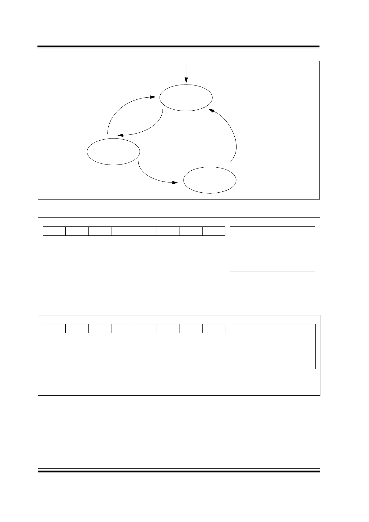
MCP2510
DS21291C-page 42 Preliminary 1999 Microchip Technology Inc.
FIGURE 6-1: Error Modes State Diagram
REGISTER 6-1: TEC - Transmitter Error Counter (ADDRESS: 1Ch)
REGISTER 6-2: REC - Receiver Error Counter (ADDRESS: 1Dh)
Bus-Off
Error-Active
Error-Passive
REC > 127 or
TEC > 127
REC < 127 or
TEC < 127
TEC > 255
RESET
128 occurrences of
11 consecutive
“recessive” bits
R-0 R-0 R-0 R-0 R-0 R-0 R-0 R-0
TEC7 TEC6 TEC5 TEC4 TEC3 TEC2 TEC1 TEC0
R = Readable bit
W = Writable bit
C = Bit can be cleared by
MCU but not set
U = Unimplemented -
reads as ‘0’
- n = Value at POR reset
bit 7 bit 0
bit 7-0: TEC<7:0>: Transmit Error Count
R-0 R-0 R-0 R-0 R-0 R-0 R-0 R-0
REC7 REC6 REC5 REC4 REC3 REC2 REC1 REC0
R = Readable bit
W = Writable bit
C = Bit can be cleared by
MCU but not set
U = Unimplemented -
reads as ‘0’
- n = Value at POR reset
bit 7 bit 0
bit 7-0: REC<7:0>: Receive Error Count
Page 43

1999 Microchip Technology Inc. Preliminary DS21291C-page 43
MCP2510
REGISTER 6-3: EFLG - Error Flag Register (ADDRESS: 2Dh)
R/W-0 R/W-0 R-0 R-0 R-0 R-0 R-0 R-0
RX1OVR RX0OVR TXBO TXEP RXEP TXWAR RXWAR EWARN
R = Readable bit
W = Writable bit
C = Bit can be cleared by
MCU but not set
U = Unimplemented -
reads as ‘0’
- n = Value at POR reset
bit 7 bit 0
bit 7: RX1OVR: Receive Buffer 1 Overflow Flag
- Set when a valid message is received for RXB1 and CANINTF.RX1IF = 1
- Must be reset by MCU
bit 6: RX0OVR: Receive Buffer 0 Overflow Flag
- Set when a valid message is received for RXB0 and CANINTF.RX0IF = 1
- Must be reset by MCU
bit 5: TXBO: Bus-Off Error Flag
- Bit set when TEC reaches 255
- Reset after a successful bus recovery sequence
bit 4: TXEP: Transmit Error-Passive Flag
- Set when TEC is equal to or greater than 128
- Reset when TEC is less than 128
bit 3: RXEP: Receive Error-Passive Flag
- Set when REC is equal to or greater than 128
- Reset when REC is less than 128
bit 2: TXWAR: Transmit Error Warning Flag
- Set when TEC is equal to or greater than 96
- Reset when TEC is less than 96
bit 1: RXWAR: Receive Error Warning Flag
- Set when REC is equal to or greater than 96
- Reset when REC is less than 96
bit 0: EWARN: Error Warning Flag
- Set when TEC or REC is equal to or greater than 96 (TXWAR or RXWAR = 1)
- Reset when both REC and TEC are less than 96
Page 44

MCP2510
DS21291C-page 44 Preliminary 1999 Microchip Technology Inc.
NOTES:
Page 45

1999 Microchip Technology Inc. Preliminary DS21291C-page 45
MCP2510
7.0 INTERRUPTS
The device has eight sources of interrupts. The CANINTE
register contains the individual interrupt enable bits for
each interrupt source. The CANINTF register contains the
corresponding interrupt flag bit for each interrupt source.
When an interrupt occurs the INT
pin is driven low by the
MCP2510 and will remain low until the Interrupt is cleared
by the MCU. An Interrupt can not be cleared if the respective condition still prevails.
It is recommended that the bit modify command be
used to reset flag bits in the CANINTF register rather
than normal write operations. This is to prevent unintentionally changing a flag that changes during the
write command, potentially causing an interrupt to be
missed.
It should be noted that the CANINTF flags are read/
write and an Interrupt can be generated by the MCU
setting any of these bits, provided the associated CANINTE bit is also set.
7.1 Interrupt Code Bits
The source of a pending interrupt is indicated in the
CANSTAT.ICOD (interrupt code) bits as indicated in
Register 9-2. In the event that multiple interrupts occur,
the INT
will remain low until all interrupts have been
reset by the MCU, and the CANSTAT.ICOD bits will
reflect the code for the highest priority interrupt that is
currently pending. Interrupts are internally prioritized
such that the lower the ICOD value the higher the interrupt priority. Once the highest priority interrupt condition has been cleared, the code for the next highest
priority interrupt that is pending (if any) will be reflected
by the ICOD bits (see Table 7-1). Note that only those
interrupt sources that have their associated CANINTE
enable bit set will be reflected in the ICOD bits.
TABLE 7-1: ICOD<2:0> Decode
7.2 Transmit Interrupt
When the Transmit Interrupt is enabled (CANINTE.TXNIE
= 1) an Interrupt will be generated on the INT
pin when
the associated transmit buffer becomes empty and is
ready to be loaded with a new message. The CANINTF.TX
NIF bit will be set to indicate the source of the
interrupt. The interrupt is cleared by the MCU resetting
the TX
NIF bit to a ‘0’.
7.3 Receive Interrupt
When the Receive Interrupt is enabled (CANINTE.RX
NIE = 1) an interrupt will be generated on the
INT
pin when a message has been successfully
received and loaded into the associated receive buffer.
This interrupt is activated immediately after receiving the
EOF field. The CANINTF.RX
NIF bit will be set to indicate
the source of the interrupt. The interrupt is cleared by the
MCU resetting the RX
NIF bit to a ‘0’.
7.4 Message Error Interrupt
When an error occurs during transmission or reception of
a message the message error flag (CANINTF.MERRF)
will be set and, if the CANINTE.MERRE bit is set, an interrupt will be generated on the INT
pin. This is intended to
be used to facilitate baud rate determination when used in
conjunction with listen-only mode.
7.5 Bus Activity Wakeup Interrupt
When the MCP2510 is in sleep mode and the bus activity wakeup interrupt is enabled (CANINTE.WAKIE = 1),
an interrupt will be generated on the INT
pin, and the
CANINTF.WAKIF bit will be set when activity is
detected on the CAN bus. This interrupt causes the
MCP2510 to exit sleep mode. The interrupt is reset by
the MCU clearing the WAKIF bit.
ICOD<2:0> Boolean Expression
000
ERR•WAK•TX0•TX1•TX2•RX0•RX1
001
ERR
010
ERR•WAK
011
ERR•WAK•TX0
100
ERR•WAK•TX0•TX1
101
ERR•WAK•TX0•TX1•TX2
110
ERR•WAK•TX0•TX1•TX2•RX0
111
ERR•WAK•TX0•TX1•TX2•RX0•RX1
Page 46

MCP2510
DS21291C-page 46 Preliminary 1999 Microchip Technology Inc.
7.6 Error Interrupt
When the error interrupt is enabled (CANINTE.ERRIE
= 1) an interrupt is generated on the INT
pin if an overflow condition occurs or if the error state of transmitter
or receiver has changed. The Error Flag Register
(EFLG) will indicate one of the following conditions.
7.6.1 RECEIVER OVERFLOW
An overflow condition occurs when the MAB has assembled a valid received message (the message meets the
criteria of the acceptance filters) and the receive buffer
associated with the filter is not available for loading of a
new message. The associated EFLG.RX
NOVR bit will
be set to indicate the overflow condition. This bit must be
cleared by the MCU.
7.6.2 RECEIVER WARNING
The receive error counter has reached the MCU warning limit of 96.
7.6.3 TRANSMITTER WARNING
The transmit error counter has reached the MCU warning limit of 96.
7.6.4 RECEIVER ERROR-PASSIVE
The receive error counter has exceeded the error- passive limit of 127 and the device has gone to error- passive state.
7.6.5 TRANSMITTER ERROR-PASSIVE
The transmit error counter has exceeded the errorpassive limit of 127 and the device has gone to errorpassive state.
7.6.6 BUS-OFF
The transmit error counter has exceeded 255 and the
device has gone to bus-off state.
7.7 Interrupt Acknowledge
Interrupts are directly associated with one or more status flags in the CANINTF register. Interrupts are pending as long as one of the flags is set. Once an interrupt
flag is set by the device, the flag can not be reset by the
MCU until the interrupt condition is removed.
REGISTER 7-1: CANINTE - Interrupt Enable Register (ADDRESS: 2Bh)
R/W-0 R/W-0 R/W-0 R/W-0 R/W-0 R/W-0 R/W-0 R/W-0
MERRE WAKIE ERRIE TX2IE TX1IE TX0IE RX1IE RX0IE
R = Readable bit
W = Writable bit
C = Bit can be cleared by
MCU but not set
U = Unimplemented -
reads as ‘0’
- n = Value at POR reset
bit 7 bit 0
bit 7: MERRE: Message Error Interrupt Enable
0 = Disabled
1 = Interrupt on error during message reception or transmission
bit 6: WAK IE: Wakeup Interrupt Enable
0 = Disabled
1 = Interrupt on CAN bus activity
bit 5: ERRIE: Error Interrupt Enable (multiple sources in EFLG register)
0 = Disabled
1 = Interrupt on EFLG error condition change
bit 4: TX2IE: Transmit Buffer 2 Empty Interrupt Enable
0 = Disabled
1 = Interrupt on TXB2 becoming empty
bit 3: TX1IE: Transmit Buffer 1 Empty Interrupt Enable
0 = Disabled
1 = Interrupt on TXB1 becoming empty
bit 2: TX0IE: Transmit Buffer 0 Empty Interrupt Enable
0 = Disabled
1 = Interrupt on TXB0 becoming empty
bit 1: RX1IE: Receive Buffer 1 Full Interrupt Enable
0 = Disabled
1 = Interrupt when message received in RXB1
bit 0: RX0IE: Receive Buffer 0 Full Interrupt Enable
0 = Disabled
1 = Interrupt when message received in RXB0
Page 47

1999 Microchip Technology Inc. Preliminary DS21291C-page 47
MCP2510
REGISTER 7-2: CANINTF - Interrupt FLAG Register (ADDRESS: 2Ch)
R/W-0 R/W-0 R/W-0 R/W-0 R/W-0 R/W-0 R/W-0 R/W-0
MERRF WAKIF ERRIF TX2IF TX1IF TX0IF RX1IF RX0IF
R = Readable bit
W = Writable bit
C = Bit can be cleared by
MCU but not set
U = Unimplemented -
reads as ‘0’
- n = Value at POR reset
bit 7 bit 0
bit 7: MERRF: Message Error Interrupt Flag
bit 6: WAKIF: Wakeup Interrupt Flag
bit 5: ERRIF: Error Interrupt Flag (multiple sources in EFLG register)
bit 4: TX2IF: Transmit Buffer 2 Empty Interrupt Flag
bit 3: TX1IF: Transmit Buffer 1 Empty Interrupt Flag
bit 2: TX0IF: Transmit Buffer 0 Empty Interrupt Flag
bit 1: RX1IF: Receive Buffer 1 Full Interrupt Flag
bit 0: RX0IF: Receive Buffer 0 Full Interrupt Flag
For all bits unless otherwise specified:
0 = No interrupt pending
1 = Interrupt pending (must be cleared by MCU to reset interrupt condition)
Page 48

MCP2510
DS21291C-page 48 Preliminary 1999 Microchip Technology Inc.
NOTES:
Page 49

1999 Microchip Technology Inc. Preliminary DS21291C-page 49
MCP2510
8.0 OSCILLATOR
The MCP2510 is designed to be operated with a crystal
or ceramic resonator connected to the OSC1 and
OSC2 pins. The MCP2510 oscillator design requires
the use of a parallel cut crystal. Use of a series cut crystal may give a frequency out of the crystal manufacturers specifications. A typical oscillator circuit is shown in
Figure 8-1. The MCP2510 may also be driven by an
external clock source connected to the OSC1 pin as
shown in Figure 8-2 and Figure 8-3.
8.1 Oscillator Startup Timer
The MCP2510 utilizes an oscillator startup timer
(OST), which holds the MCP2510 in reset, to insure
that the oscillator has stabilized before the internal
state machine begins to operate. The OST maintains
reset for the first 128 OSC1 clock cycles after power up
or wake up from sleep mode occurs. It should be noted
that no SPI operations should be attempted until after
the OST has expired.
8.2 CLKOUT Pin
The clock out pin is provided to the system designer for
use as the main system clock or as a clock input for other
devices in the system. The CLKOUT has an internal
prescaler which can divide F
OSC
by 1, 2, 4 and 8. The
CLKOUT function is enabled and the prescaler is
selected via the CANCNTRL register (see Register 9-1).
The CLKOUT pin will be active upon system reset and
default to the slowest speed (divide by 8) so that it can be
used as the MCU clock. When sleep mode is requested,
the MCP2510 will drive sixteen additional clock cycles on
the CLKOUT pin before entering sleep mode. The idle
state of the CLKOUT pin in sleep mode is low. When the
CLKOUT function is disabled (CANCNTRL.CLKEN = ‘0’)
the CLKOUT pin is in a high impedance state.
The CLKOUT function is designed to guarantee that
t
hCLKOUT
and t
lCLKOUT
timings are preserved when the
CLKOUT pin function is enabled, disabled, or the prescaler value is changed.
FIGURE 8-1: Crystal/Ceramic Resonator Operation
FIGURE 8-2: External Clock Source
C1
C2
XTAL
OSC2
R
S
(1)
OSC1
R
F
(2)
SLEEP
To internal logic
Note 1: A series resistor, RS, may be required for AT strip cut crystals.
Note 2: The feedback resistor,
R
F
, is typically in the range of 2 to 10 MΩ.
clock from
external system
OSC1
OSC2
Open
(1)
Note 1: A resistor to ground may be used to reduce system noise. This may increase system current.
Note 2: Duty cycle restrictions must be observed (see Table 12-2).
Page 50

MCP2510
DS21291C-page 50 Preliminary 1999 Microchip Technology Inc.
FIGURE 8-3: External Series Resonant Crystal Oscillator Circuit
330 kΩ
74AS04
74AS04
MCP2510
OSC1
To O t h e r
Devices
XTAL
330 kΩ
74AS04
0.1 mF
Note 1: Duty cycle restrictions must be observed (see Table 12-2).
Page 51

1999 Microchip Technology Inc. Preliminary DS21291C-page 51
MCP2510
9.0 MODES OF OPERATION
The MCP2510 has five modes of operation. These
modes are:
1. Configuration Mode.
2. Normal Mode.
3. Sleep Mode.
4. Listen-Only Mode.
5. Loopback Mode.
The operational mode is selected via the CANCTRL.
REQOP bits (see Register 9-1). When changing modes,
the mode will not actually change until all pending message transmissions are complete. Because of this, the
user must verify that the device has actually changed
into the requested mode before further operations are
executed. Verification of the current operating mode is
done by reading the CANSTAT. OPMODE bits (see
Register 9-2).
9.1 Configuration Mode
The MCP2510 must be initialized before activation. This
is only possible if the device is in the configuration mode.
Configuration mode is automatically selected after powerup or a reset, or can be entered from any other mode
by setting the CANTRL.REQOP bits to ‘100’. When configuration mode is entered all error counters are cleared.
Configuration mode is the only mode where the following registers are modifiable:
• CNF1, CNF2, CNF3
• TXRTSCTRL
• Acceptance Filter Registers
• Acceptance Mask Registers
Only when the CANSTAT.OPMODE bits read as ‘100’
can the initialization be performed, allowing the configuration registers, acceptance mask registers, and the
acceptance filter registers to be written. After the configuration is complete, the device can be activated by
programming the CANCTRL.REQOP bits for normal
operation mode (or any other mode).
9.2 Sleep Mode
The MCP2510 has an internal sleep mode that is used
to minimize the current consumption of the device. The
SPI interface remains active even when the MCP2510
is in sleep mode, allowing access to all registers.
To enter sleep mode, the mode request bits are set in
the CANCTRL register. The CANSTAT.OPMODE bits
indicate whether the device successfully entered sleep
mode. These bits should be read after sending the
sleep command to the MCP2510. The MCP2510 is
active and has not yet entered sleep mode until these
bits indicate that sleep mode has been entered. When
in internal sleep mode, the wakeup interrupt is still
active (if enabled). This is done so the MCU can also
be placed into a sleep mode and use the MCP2510 to
wake it up upon detecting activity on the bus.
When in sleep mode, the MCP2510 stops its internal
oscillator. The MCP2510 will wake-up when bus activity
occurs or when the MCU sets, via the SPI interface, the
CANINTF.WAKIF bit to ‘generate’ a wake up attempt
(the CANINTF.WAKIF bit must also be set in order for
the wakeup interrupt to occur). The TXCAN pin will
remain in the recessive state while the MCP2510 is in
sleep mode. Note that Sleep Mode will be entered
immediately, even if a message is currently being transmitted, so it is necessary to insure that all TXREQ bits
are clear before setting Sleep Mode.
9.2.1 WAKE-UP FUNCTIONS
The device will monitor the RXCAN pin for activity while
it is in sleep mode. If the CANINTE.WAKIE bit is set, the
device will wake up and generate an interrupt. Since the
internal oscillator is shut down when sleep mode is
entered, it will take some amount of time for the oscillator to start up and the device to enable itself to receive
messages. The device will ignore the message that
caused the wake-up from sleep mode as well as any
messages that occur while the device is ‘waking up.’
The device will wake up in listen-only mode. The MCU
must set normal mode before the MCP2510 will be able
to communicate on the bus.
The device can be programmed to apply a low-pass filter function to the RXCAN input line while in internal
sleep mode. This feature can be used to prevent the
device from waking up due to short glitches on the CAN
bus lines. The CNF3.WAKFIL bit enables or disables
the filter.
9.3 Listen Only Mode
Listen-only mode provides a means for the MCP2510
to receive all messages including messages with
errors. This mode can be used for bus monitor applications or for detecting the baud rate in ‘hot plugging’ situations. For auto-baud detection it is necessary that
there are at least two other nodes, which are communicating with each other. The baud rate can be detected
empirically by testing different values until valid messages are received. The listen-only mode is a silent
mode, meaning no messages will be transmitted while
in this state, including error flags or acknowledge signals. The filters and masks can be used to allow only
particular messages to be loaded into the receive registers, or the filter masks can be set to all zeros to allow
a message with any identifier to pass. The error
counters are reset and deactivated in this state. The listen-only mode is activated by setting the mode request
bits in the CANCTRL register.
Note: Care must be exercised to not enter sleep
mode while the MCP2510 is transmitting a
message. If sleep mode is requested while
transmitting, the transmission will stop
without completing and errors will occur on
the bus. Also, the message will remain
pending and transmit upon wake up.
Page 52

MCP2510
DS21291C-page 52 Preliminary 1999 Microchip Technology Inc.
9.4 Loopback Mode
This mode will allow internal transmission of messages
from the transmit buffers to the receive buffers without
actually transmitting messages on the CAN bus. This
mode can be used in system development and testing.
In this mode the ACK bit is ignored and the device will
allow incoming messages from itself just as if they were
coming from another node. The loopback mode is a
silent mode, meaning no messages will be transmitted
while in this state, including error flags or acknowledge
signals. The TXCAN pin will be in a reccessive state
while the device is in this mode. The filters and masks
can be used to allow only particular messages to be
loaded into the receive registers. The masks can be set
to all zeros to provide a mode that accepts all messages. The loopback mode is activated by setting the
mode request bits in the CANCTRL register.
9.5 Normal Mode
This is the standard operating mode of the MCP2510.
In this mode the device actively monitors all bus messages and generates acknowledge bits, error frames,
etc. This is also the only mode in which the MCP2510
will transmit messages over the CAN bus.
REGISTER 9-1: CANCTRL - CAN Control Register (ADDRESS: xFh)
R/W-1 R/W-1 R/W-1 R/W-0 U-0 R/W-1 R/W-1 R/W-1
REQOP2 REQOP1 REQOP0 ABAT — CLKEN CLKPRE1 CLKPRE0
R = Readable bit
W = Writable bit
C = Bit can be cleared by
MCU but not set
U = Unimplemented -
reads as ‘0’
- n = Value at POR reset
bit 7 bit 0
bit 7-5: REQOP<2:0>: Request Operation Mode
000 = Set Normal Operation Mode
001 = Set Sleep Mode
010 = Set Loopback Mode
011 = Set Listen Only Mode
100 = Set Configuration Mode
All other values for REQOP bits are invalid and should not be used
bit 4: ABAT: Abort All Pending Transmissions
1 = Request abort of all pending transmit buffers
0 = Terminate request to abort all transmissions
bit 3: Unimplemented: Reads as ‘0’
bit 2: CLKEN
: CLKOUT Pin Enable
0 = CLKOUT pin disabled (Pin is in high impedance state)
1 =CLKOUT pin enabled
bit 1-0: CLKPRE<1:0>: CLKOUT Pin Prescaler
00 = F
CLKOUT
= System Clock/1
01 = F
CLKOUT
= System Clock/2
10 = F
CLKOUT
= System Clock/4
11 = F
CLKOUT
= System Clock/8
Page 53

1999 Microchip Technology Inc. Preliminary DS21291C-page 53
MCP2510
REGISTER 9-2: CANSTAT - CAN Status Register (ADDRESS: xEh)
R-1 R-0 R-0 U-0 R-0 R-0 R-0 U-0
OPMOD2 OPMOD1 OPMOD0
— ICOD2 ICOD1 ICOD0 —
R = Readable bit
W = Writable bit
C = Bit can be cleared by
MCU but not set
U = Unimplemented -
reads as ‘0’
- n = Value at POR reset
bit 7 bit 0
bit 7-5: OPMOD<2:0>: Operation Mode
000 = Device is in Normal Operation Mode
001 = Device is in Sleep Mode
010 = Device is in Loopback Mode
011 = Device is in Listen Only Mode
100 = Device is in Configuration Mode
bit 4: Unimplemented: Reads as ‘0’
bit 3-1: ICOD<2:0>: Interrupt Flag Code
000 = No Interrupt
001 = Error Interrupt
010 = Wake Up Interrupt
011 = TXB0 Interrupt
100 = TXB1 Interrupt
101 = TXB2 Interrupt
110 = RXB0 Interrupt
111 = RXB1 Interrupt
bit 0: Unimplemented: Reads as ‘0’
Page 54

MCP2510
DS21291C-page 54 Preliminary 1999 Microchip Technology Inc.
NOTES:
Page 55

1999 Microchip Technology Inc. Preliminary DS21291C-page 55
MCP2510
10.0 REGISTER MAP
The register map for the MCP2510 is shown in
Table 10-1. Address locations for each register are
determined by using the column (higher order 4 bits)
and row (lower order 4 bits) values. The registers have
been arranged to optimize the sequential reading and
writing of data. Some specific control and status registers allow individual bit modification using the SPI Bit
Modify command. The registers that allow this command are shown as shaded locations in Table 10-1. A
summary of the MCP2510 control registers is shown in
Ta bl e 1 0- 2 .
TABLE 10-1: CAN Controller Register Map
TABLE 10-2: Control Register Summary
Lower
Address Bits
Higher Order Address Bits
x000 xxxx x001 xxxx x010 xxxx x0011 xxxx x100 xxxx x101 xxxx x110 xxxx x111 xxxx
0000 RXF0SIDH RXF3SIDH RXM0SIDH
TXB0CTRL TXB1CTRL TXB2CTRL RXB0CTRL RXB1CTRL
0001 RXF0SIDL RXF3SIDL RXM0SIDL TXB0SIDH TXB1SIDH TXB2SIDH RXB0SIDH RXB1SIDH
0010 RXF0EID8 RXF3EID8 RXM0EID8 TXB0SIDL TXB1SIDL TXB2SIDL RXB0SIDL RXB1SIDL
0011 RXF0EID0 RXF3EID0 RXM0EID0 TXB0EID8 TXB1EID8 TXB2EID8 RXB0EID8 RXB1EID8
0100 RXF1SIDH RXF4SIDH RXM1SIDH TXB0EID0 TXB1EID0 TXB2EID0 RXB0EID0 RXB1EID0
0101 RXF1SIDL RXF4SIDL RXM1SIDL TXB0DLC TXB1DLC TXB2DLC RXB0DLC RXB1DLC
0110 RXF1EID8 RXF4EID8 RXM1EID8 TXB0D0 TXB1D0 TXB2D0 RXB0D0 RXB1D0
0111 RXF1EID0 RXF4EID0 RXM1EID0 TXB0D1 TXB1D1 TXB2D1 RXB0D1 RXB1D1
1000 RXF2SIDH RXF5SIDH
CNF3 TXB0D2 TXB1D2 TXB2D2 RXB0D2 RXB1D2
1001 RXF2SIDL RXF5SIDL
CNF2 TXB0D3 TXB1D3 TXB2D3 RXB0D3 RXB1D3
1010 RXF2EID8 RXF5EID8
CNF1 TXB0D4 TXB1D4 TXB2D4 RXB0D4 RXB1D4
1011 RXF2EID0 RXF5EID0
CANINTE TXB0D5 TXB1D5 TXB2D5 RXB0D5 RXB1D5
1100
BFPCTRL TEC CANINTF TXB0D6 TXB1D6 TXB2D6 RXB0D6 RXB1D6
1101
TXRTSCTRL REC EFLG TXB0D7 TXB1D7 TXB2D7 RXB0D7 RXB1D7
1110 CANSTAT CANSTAT CANSTAT CANSTAT CANSTAT CANSTAT CANSTAT CANSTAT
1111
CANCTRL CANCTRL CANCTRL CANCTRL CANCTRL CANCTRL CANCTRL CANCTRL
Note: Shaded register locations indicate that these allow the user to manipulate individual bits using the ‘Bit Modify’
Command
Register
Name
Address
(Hex)
Bit 7 Bit 6 Bit 5 Bit 4 Bit 3 Bit 2 Bit 1 Bit 0
POR/RST
Value
BFPCTRL 0C
––
B1BFS B0BFS B1BFE B0BFE B1BFM B0BFM --00 0000
TXRTSCTRL 0D
––
B2RTS B1RTS B0RTS B2RTSM B1RTSM B0RTSM --xx x000
CANSTAT xE OPMOD2 OPMOD1 OPMOD0
–
ICOD2 ICOD1 ICOD0
–
100- 000-
CANCTRL xF REQOP2 REQOP1 REQOP0 ABAT
–
CLKEN CLKPRE1 CLKPRE0 1110 -111
TEC 1C Transmit Error Counter 0000 0000
REC 1D Receive Error Counter 0000 0000
CNF3 28
–
WAKFIL
–––
PHSEG22 PHSEG21 PHSEG20 -0-- -000
CNF2 29 BTLMODE SAM PHSEG12 PHSEG11 PHSEG10 PRSEG2 PRSEG1 PRSEG0 0000 0000
CNF1 2A SJW1 SJW0 BRP5 BRP4 BRP3 BRP2 BRP1 BRP0 0000 0000
CANINTE 2B MERRE WAKIE ERRIE TX2IE TX1IE TX0IE RX1IE RX0IE 0000 0000
CANINTF 2C MERRF WAKIF ERRIF TX2IF TX1IF TX0IF RX1IF RX0IF 0000 0000
EFLG 2D RX1OVR RX0OVR TXBO TXEP RXEP TXWAR RXWAR EWARN 0000 0000
TXB0CTRL 30
–
ABTF MLOA TXERR TXREQ
–
TXP1 TXP0 -000 0-00
TXB1CTRL 40
–
ABTF MLOA TXERR TXREQ
–
TXP1 TXP0 -000 0-00
TXB2CTRL 50
–
ABTF MLOA TXERR TXREQ
–
TXP1 TXP0 -000 0-00
RXB0CTRL 60
–
RXM1 RXM0
–
RXRTR BUKT BUKT FILHIT0 -00- 0000
RXB1CTRL 70
–
RSM1 RXM0
–
RXRTR FILHIT2 FILHIT1 FILHIT0 -00- 0000
Page 56

MCP2510
DS21291C-page 56 Preliminary 1999 Microchip Technology Inc.
NOTES:
Page 57

1999 Microchip Technology Inc. Preliminary DS21291C-page 57
MCP2510
11.0 SPI INTERFACE
11.1 Overview
The MCP2510 is designed to interface directly with the
Serial Peripheral Interface (SPI) port available on many
microcontrollers and supports Mode 0,0 and Mode 1,1.
Commands and data are sent to the device via the SI
pin, with data being clocked in on the rising edge of
SCK. Data is driven out by the MCP2510, on the SO
line, on the falling edge of SCK. The CS
pin must be
held low while any operation is performed. Table 11-1
shows the instruction bytes for all operations. Refer to
Figure 11-8 and Figure 11-9 for detailed input and output timing diagrams for both Mode 0,0 and Mode 1,1
operation.
11.2 Read Instruction
The Read Instruction is started by lowering the CS pin.
The read instruction is then sent to the MCP2510 followed by the 8-bit address (A7 through A0). After the
read instruction and address are sent, the data stored
in the register at the selected address will be shifted out
on the SO pin. The internal address pointer is automatically incremented to the next address after each byte
of data is shifted out. Therefore it is possible to read the
next consecutive register address by continuing to provide clock pulses. Any number of consecutive register
locations can be read sequentially using this method.
The read operation is terminated by raising the CS
pin
(Figure 11-2).
11.3 Write Instruction
The Write Instruction is started by lowering the CS pin.
The write instruction is then sent to the MCP2510 followed by the address and at least one byte of data. It is
possible to write to sequential registers by continuing to
clock in data bytes, as long as CS
is held low. Data will
actually be written to the register on the rising edge of
the SCK line for the D0 bit. If the CS
line is brought high
before eight bits are loaded, the write will be aborted for
that data byte, previous bytes in the command will have
been written. Refer to the timing diagram in Figure 11-3
for more detailed illustration of the byte write sequence.
11.4 Request To Send (RTS) Instruction
The RTS command can be used to initiate message
transmission for one or more of the transmit buffers.
The part is selected by lowering the CS pin and the RTS
command byte is then sent to the MCP2510. As shown
in Figure 11-4, the last 3 bits of this command indicate
which transmit buffer(s) are enabled to send. This command will set the TxBnCTRL.TXREQ bit for the respective buffer(s). Any or all of the last three bits can be set in
a single command. If the RTS command is sent with
nnn=000, the command will be ignored.
11.5 Read Status Instruction
The Read Status Instruction allows single instruction
access to some of the often used status bits for message reception and transmission.
The part is selected by lowering the CS
pin and the read
status command byte, shown in Figure 11-6, is sent to
the MCP2510. After the command byte is sent, the
MCP2510 will return eight bits of data that contain the
status. If additional clocks are sent after the first eight
bits are transmitted, the MCP2510 will continue to output
the status bits as long as the CS
pin is held low and
clocks are provided on SCK. Each status bit returned in
this command may also be read by using the standard
read command with the appropriate register address.
11.6 Bit Modify Instruction
The Bit Modify Instruction provides a means for setting
or clearing individual bits in specific status and control
registers. This command is not available for all registers. See Section 10.0 (register map) to determine
which registers allow the use of this command.
The part is selected by lowering the CS pin and the Bit
Modify command byte is then sent to the MCP2510.
After the command byte is sent, the address for the register is sent followed by the mask byte and then the
data byte. The mask byte determines which bits in the
register will be allowed to change. A ‘1’ in the mask byte
will allow a bit in the register to change and a ‘0’ will not.
The data byte determines what value the modified bits
in the register will be changed to. A ‘1’ in the data byte
will set the bit and a ‘0’ will clear the bit, provided that
the mask for that bit is set to a ‘1’. (see Figure 11-1)
11.7 Reset Instruction
The Reset Instruction can be used to re-initialize the
internal registers of the MCP2510 and set configuration
mode. This command provides the same functionality,
via the SPI interface, as the RESET
pin. The Reset
instruction is a single byte instruction which requires
selecting the device by pulling CS
low, sending the
instruction byte, and then raising CS
. It is highly recommended that the reset command be sent (or the
RESET pin be lowered) as part of the power-on initialization sequence.
FIGURE 11-1: Bit Modify
Mask byte
Data byte
Previous
Register
Contents
Resulting
Register
Contents
001 11100
XX1 100XX
010 11000
011 10000
Page 58

MCP2510
DS21291C-page 58 Preliminary 1999 Microchip Technology Inc.
TABLE 11-1: SPI Instruction Set
FIGURE 11-2: Read Instruction
FIGURE 11-3: Byte Write Instruction
Instruction Name Instruction Format Description
RESET 1100 0000
Resets internal registers to default state, set configuration mode
READ 0000 0011
Read data from register beginning at selected address
WRITE 0000 0010
Write data to register beginning at selected address
RTS
(Request To Send)
1000 0nnn
Sets TXBnCTRL.TXREQ bit for one or more transmit buffers
Read Status 1010 0000
Polling command that outputs status bits for transmit/receive functions
Bit Modify 0000 0101
Bit modify selected registers
1000 0nnn
Request to send for TXBO
Request to send for TXB1
Request to send for TXB2
SO
SI
SCK
CS
0 23456789101112131415161718192021221
01000001
A7 6 5 4
1A0
76543210
instruction address byte
data out
high impedance
23
32
don’t care
SO
SI
SCK
CS
0 23456789101112131415161718192021221
0000000A7654
1A0
76543 210
instruction
high impedance
23
32
1
address byte
data byte
Page 59
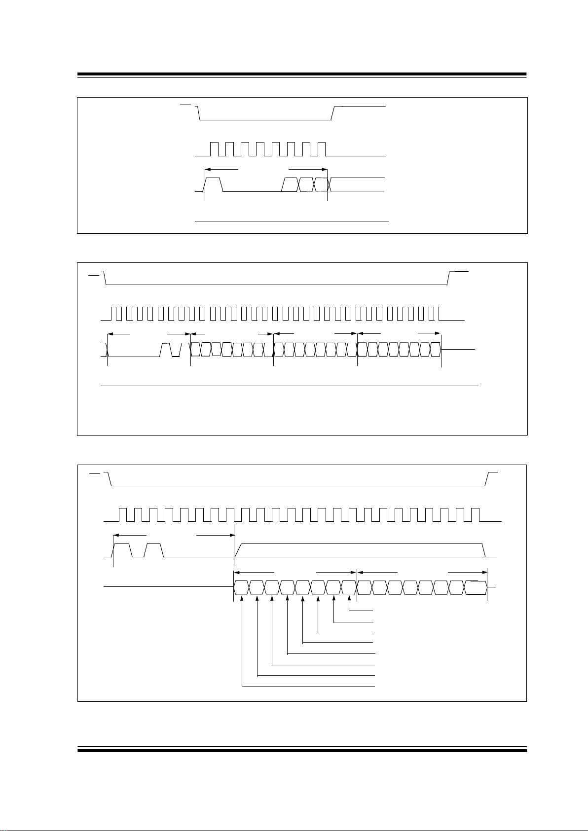
1999 Microchip Technology Inc. Preliminary DS21291C-page 59
MCP2510
FIGURE 11-4: Request To Send Instruction
FIGURE 11-5: BIT Modify instruction
FIGURE 11-6: Read Status Instruction
SO
SI
SCK
CS
0 2345671
T2 T000
0
01
instruction
high impedance
T1
SO
SI
SCK
CS
0 2 3 4 5 6 7 8 9 10 11 12 13 14 15 16 17 18 19 20 21 221
1100000
A7 6 5 4
1
A0
765432 10
instruction
high impedance
32
0
address byte
mask byte
76543210
23 24 25 26 27 28 29 30 31
data byte
Note: Not all registers can be accessed with this command. See the register map in Section 10.0 for a list of
the registers that apply.
SO
SI
SCK
CS
0 23456789101112131415161718192021221
00001010
76543210
instruction
data out
high impedance
23
don’t care
CANINTF.RX0IF
CANINTF.RX1IF
CANINTF.TX0IF
CANINTF.TX1IF
CANINTF.TX2IF
TXB2CNTRL.TXREQ
TXB1CNTRL.TXREQ
TXB0CNTRL.TXREQ
7654321 0
data out
repeat
Page 60
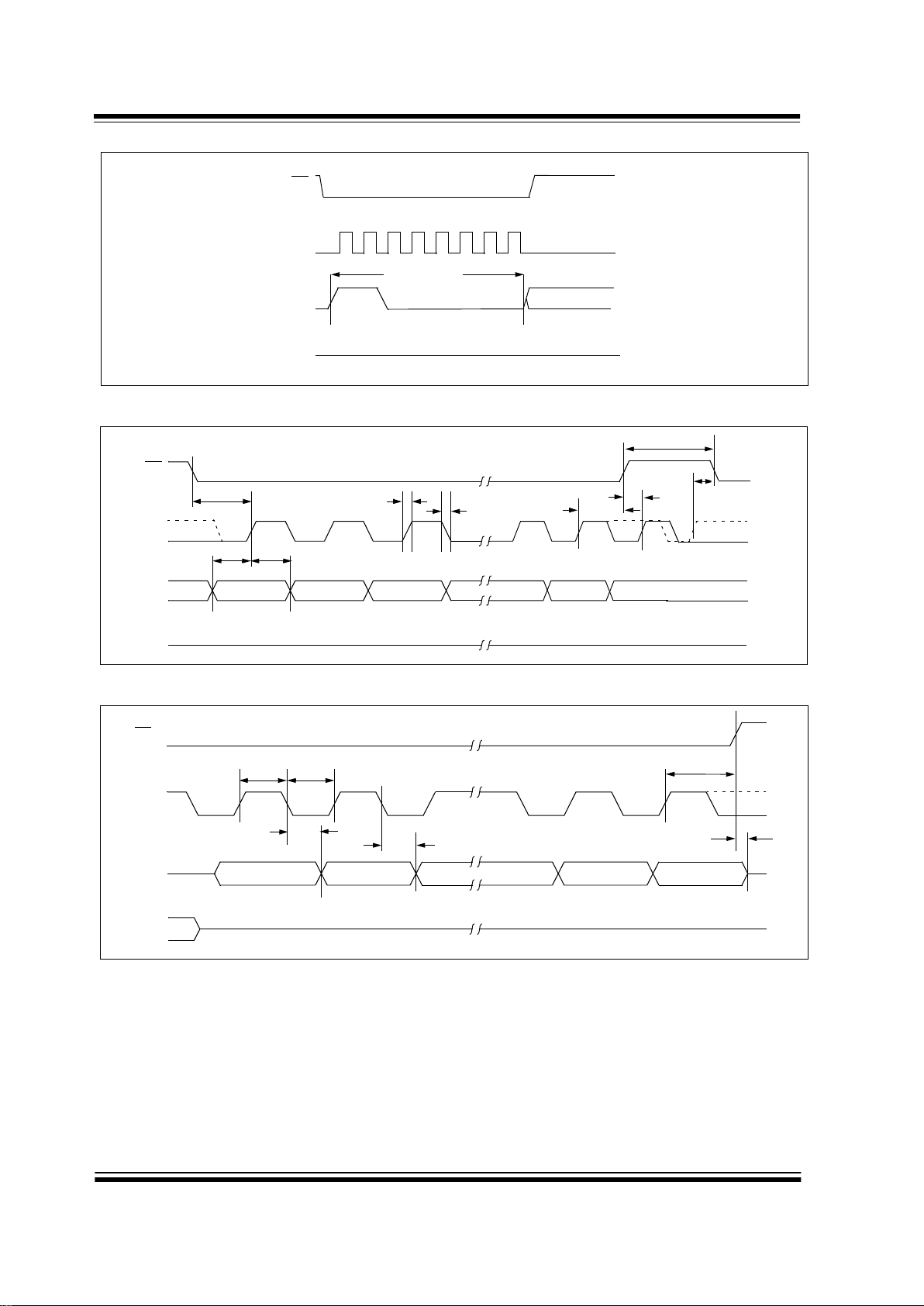
MCP2510
DS21291C-page 60 Preliminary 1999 Microchip Technology Inc.
FIGURE 11-7: RESET Instruction
FIGURE 11-8: SPI Input Timing
FIGURE 11-9: SPI Output Timing
SO
SI
SCK
CS
0 2345671
00
0
11
instruction
high impedance
000
CS
SCK
SI
SO
TCSS
THDTSU
TF
TR
TCSD
TCLD
TCSH
LSB in
MSB in
high impedance
TCLE
Mode 1,1
Mode 0,0
CS
SCK
SO
TLO
THI
THO
TV
MSB out
LSB out
TCSH
TDIS
don’t care
SI
Mode 1,1
Mode 0,0
Page 61

1999 Microchip Technology Inc. Preliminary DS21291C-page 61
MCP2510
12.0 ELECTRICAL CHARACTERISTICS
12.1 Maximum Ratings
VDD...................................................................................7.0V
All inputs and outputs w.r.t. V
SS
............... -0.6V to VDD +1.0V
Storage temperature .....................................-65°C to +150°C
Ambient temp. with power applied ................-65°C to +125°C
Soldering temperature of leads (10 seconds) ............. +300°C
ESD protection on all pins
..................................................≥ 4 kV
*Notice: Stresses above those listed under “Maximum Ratings” may cause permanent damage to the device. This is a
stress rating only and functional operation of the device at
those or any other conditions above those indicated in the
operational listings of this specification is not implied. Exposure to maximum rating conditions for extended periods may
affect device reliability.
TABLE 12-1: DC Characteristics
All parameters apply over the
specified operating ranges
unless otherwise noted.
Industrial (I): T
AMB
= -40°C to +85°C VDD = 3.0V to 5.5V
Automotive (E): T
AMB
= -40°C to +125°C VDD = 4.5V to 5.5V
Parameter Symbol Min Max Units Test Conditions
Supply Voltage V
DD
3.0 5.5 V
Register Retention Voltage V
RET
2.4
–
V
High Level Input Voltage Note
RXCAN V
IH
2V
DD
+1 V
SCK, CS
, SI, TXnRTS Pins .7 V
DD
VDD+1 V
OSC1 .85 V
DD
V
DD
V
RESET
.85 V
DD
V
DD
V
Low Level Input Voltage Note
RXCAN,TXnRTS
Pins V
IL
-0.3 .15 V
DD
V
SCK, CS
, SI -0.3 .4 V
OSC1 V
SS
.3 V
DD
V
RESET
V
SS
.15 V
DD
V
Low Level Output Voltage
TXCAN V
OL
–
0.4 V IOL = -6.0 mA
RXnBF
Pins
–
0.4 V IOL = -8.5 mA, VDD = 4.5V
SO, CLKOUT
–
0.4 V IOL = -2.1 mA, VDD = 4.5V
INT
–
0.6 V IOL = -1.6 mA, VDD = 4.5V
High Level Output Voltage V
TXCAN, RXnBF
Pins V
OH
VDD -0.7
–
VIOH = 3.0mA, VDD = 4.5V, I temp
SO, CLKOUT V
DD
-0.5
–
VI
OH
= 400µA
INT
VDD -0.7
–
VIOH = 1.0mA, VDD = 4.5V
Hysteresis V
HYS
.05 V
DD
V
Input Leakage Current
All I/O except OSC1 and
TXnRTS pins
I
LI
-1 +1 µACS = RESET = VDD, VIN = VSS to V
DD
OSC1 Pin -5 +5 µA
Internal Capacitance
(All Inputs And Outputs)
C
INT
–
7pFT
AMB
= 25°C, fC = 1.0 MHz,
V
DD
= 5.0V (Note)
Operating Current I
DD
–
10 mA VDD = 5.5V; F
CLK
=5.0 MHz; SO = Open
Standby Current (Sleep Mode) I
DDS
-- 5 µACS, TXnRTS = VDD, Inputs tied to VDD or V
SS
Note: This parameter is not 100% tested.
Page 62

MCP2510
DS21291C-page 62 Preliminary 1999 Microchip Technology Inc.
TABLE 12-2: Oscillator Timing Characteristics
TABLE 12-3: CAN Interface AC Characteristics
TABLE 12-4: CLKOUT Pin AC/DC Characteristics
All parameters apply over the
specified operating ranges unless
otherwise noted.
Industrial (I): T
AMB
= -40°C to +85°C VDD = 3.0V to 5.5V
Automotive (E): T
AMB
= -40°C to +125°C VDD = 4.5V to 5.5V
Parameter Symbol Min Max Units Conditions
Clock In Frequency F
OSC
1
1
25
16
MHz
MHz
4.5V to 5.5V
3.0V to 4.5V
Clock In Period T
OSC
40
62.5
1000
1000
nsns4.5V to 5.5V
3.0V to 4.5V
Clock In High, Low Time T
OSL
, T
OSH
10
–
ns Note
Clock In Rise, Fall Time T
OSR
, T
OSF
– 15 ns Note
Duty Cycle (External Clock Input) T
DUTY
.30 .70
–
T
OSH
/ (T
OSH
+ T
OSL
)
Note: This parameter is periodically sampled and not 100% tested.
All parameters apply over the
specified operating ranges
unless otherwise noted.
Industrial (I): T
AMB
= -40°C to +85°C VDD = 3.0V to 5.5V
Automotive (E): T
AMB
= -40°C to +125°C VDD = 4.5V to 5.5V
Parameter Symbol Min Max Units Conditions
Wakeup Noise Filter T
WF
50
–
ns
CLOCKOUT Propagation Delay T
DCLK
–
100 ns
All parameters apply over the
specified operating ranges
unless otherwise noted.
Industrial (I): T
AMB
= -40°C to +85°C VCC = 3.0V to 5.5V
Automotive (E): T
AMB
= -40°C to +125°C VCC = 4.5V to 5.5V
Parameter Symbol Min Max Units Conditions
CLKOUT Pin High Time t
hCLKOUT
15
–
ns T
OSC
= 40 ns, CLKOUT prescaler set
to divide by one
CLKOUT Pin Low Time t
lCLKOUT
15
–
ns T
OSC
= 40 ns, CLKOUT prescaler set
to divide by one
CLKOUT Pin Rise Time t
rCLKOUT
–
5 ns Measured from 0.3 VDD to 0.7 V
DD
CLKOUT Pin Fall Time t
fCLKOUT
–
5 ns Measured from 0.7 VDD to 0.3 V
DD
CLOCKOUT Propagation Delay t
dCLKOUT
–
100 ns
Page 63

1999 Microchip Technology Inc. Preliminary DS21291C-page 63
MCP2510
TABLE 12-5: SPI Interface AC Characteristics
All parameters apply over the
specified operating ranges
unless otherwise noted.
Industrial (I): T
AMB
= -40°C to +85°C VDD = 3.0V to 5.5V
Automotive (E): T
AMB
= -40°C to +125°C VDD = 4.5V to 5.5V
Parameter Symbol Min Max Units Test Conditions
Clock Frequency
F
CLK
–
–
–
5
4
2.5
MHz
MHz
MHz
VDD = 4.5V to 5.5V
V
DD
= 4.5V to 5.5V (E temp)
V
DD
= 3.0V to 4.5V
CS
Setup Time
T
CSS
100 – ns
CS
Hold Time
T
CSH
100
115
180
–
–
–
ns
ns
ns
V
DD
= 4.5V to 5.5V
V
DD
= 4.5V to 5.5V (E temp)
V
DD
=3.0V to 4.5V
CS
Disable Time
T
CSD
100
100
280
–
–
–
ns
ns
ns
V
DD
= 4.5V to 5.5V
V
DD
= 4.5V to 5.5V (E temp)
V
DD
= 3.0V to 4.5V
Data Setup Time T
SU
20
20
30
–
–
–
ns
ns
ns
V
DD
= 4.5V to 5.5V
V
DD
= 4.5V to 5.5V (E temp)
V
DD
= 3.0V to 4.5V
Data Hold Time T
HD
20
20
50
–
–
–
ns
ns
ns
V
DD
= 4.5V to 5.5V
V
DD
= 4.5V to 5.5V (E temp)
V
DD
= 3.0V to 4.5V
CLK Rise Time T
R
– 2msNote
CLK Fall Time T
F
– 2msNote
Clock High Time T
HI
90
115
180
–
–
–
ns
ns
ns
V
DD
= 4.5V to 5.5V
V
DD
= 4.5V to 5.5V (E temp)
V
DD
= 3.0V to 4.5V
Clock Low Time T
LO
90
115
180
–
–
–
ns
ns
ns
VDD = 4.5V to 5.5V
V
DD
= 4.5V to 5.5V (E temp)
V
DD
= 3.0V to 4.5V
Clock Delay Time T
CLD
50 – ns
Clock Enable Time T
CLE
50 – ns
Output Valid from Clock Low T
V
–
–
–
90
115
180
ns
ns
ns
V
DD
= 4.5V to 5.5V
V
DD
= 4.5V to 5.5V (E temp)
V
DD
=3.0V to 4.5V
Output Hold Time T
HO
0 – ns Note
Output Disable Time T
DIS
– 200 ns Note
Note: This parameter is periodically sampled and not 100% tested.
Page 64

MCP2510
DS21291C-page 64 Preliminary 1999 Microchip Technology Inc.
NOTES:
Page 65

1999 Microchip Technology Inc. Preliminary DS21291C-page 65
MCP2510
13.0 PACKAGING INFORMATION
14.1 Package Marking Information
Not available at the time of printing. Will be made
available after definition of QS9000 compliant
standard.
14.2 Package Details
The following sections give the technical details of the
packages.
Page 66

MCP2510
DS21291C-page 66 Preliminary 1999 Microchip Technology Inc.
Package Type: 18-Lead Plastic Dual In-line (P) – 300 mil (PDIP)
1510515105
β
Mold Draft Angle Bottom
1510515105
α
Mold Draft Angle Top
10.929.407.87.430.370.310
eB
Overall Row Spacing
0.560.460.36.022.018.014BLower Lead Width
1.781.461.14.070.058.045B1Upper Lead Width
0.380.290.20.015.012.008
c
Lead Thickness
3.433.303.18.135.130.125LTip to Seating Plane
22.9922.8022.61.905.898.890DOverall Length
6.606.356.10.260.250.240E1Molded Package Width
8.267.947.62.325.313.300EShoulder to Shoulder Width
0.38.015A1Base to Seating Plane
3.683.302.92.145.130.115
A2
Molded Package Thickness
4.323.943.56.170.155.140ATop to Seating Plane
2.54.100
p
Pitch
1818
n
Number of Pins
MAXNOMMINMAXNOMMINDimension Limits
MILLIMETERSINCHES*Units
1
2
D
n
E1
c
eB
β
E
α
p
A2
L
B1
B
A
A1
*Controlling Parameter
Notes:
Dimensions D and E1 do not include mold flash or protrusions. Mold flash or protrusions shall not exceed
.010” (0.254mm) per side.
JEDEC Equivalent: MS-001
Drawing No. C04-007
Page 67

1999 Microchip Technology Inc. Preliminary DS21291C-page 67
MCP2510
Package Type: 18-Lead Plastic Small Outline (SO) – Wide, 300 mil (SOIC)
Foot Angle
φ
048048
1512015120
β
Mold Draft Angle Bottom
1512015120
α
Mold Draft Angle Top
0.510.420.36.020.017.014BLead Width
0.300.270.23.012.011.009
c
Lead Thickness
1.270.840.41.050.033.016LFoot Length
0.740.500.25.029.020.010hChamfer Distance
11.7311.5311.33.462.454.446DOverall Length
7.597.497.39.299.295.291E1Molded Package Width
10.6710.3410.01.420.407.394EOverall Width
0.300.200.10.012.008.004A1Standoff
2.392.312.24.094.091.088A2Molded Package Thickness
2.642.502.36.104.099.093AOverall Height
1.27.050
p
Pitch
1818
n
Number of Pins
MAXNOMMINMAXNOMMINDimension Limits
MILLIMETERSINCHES*Units
L
β
c
φ
h
45°
1
2
D
p
n
B
E1
E
α
A2
A1
A
*Controlling Parameter
Notes:
Dimensions D and E1 do not include mold flash or protrusions. Mold flash or protrusions shall not exceed
.010” (0.254mm) per side.
JEDEC Equivalent: MS-013
Drawing No. C04-051
Page 68

MCP2510
DS21291C-page 68 Preliminary 1999 Microchip Technology Inc.
Package Type: 20-Lead Plastic Thin Shrink Small Outline (ST) – 4.4 mm (TSSOP)
Foot Angle
φ
048048
1512015120
β
Mold Draft Angle Bottom
1512015120
α
Mold Draft Angle Top
0.510.420.36.020.017.014BLead Width
0.300.270.23.012.011.009
c
Lead Thickness
1.270.840.41.050.033.016LFoot Length
0.740.500.25.029.020.010hChamfer Distance
11.7311.5311.33.462.454.446DOverall Length
7.597.497.39.299.295.291E1Molded Package Width
10.6710.3410.01.420.407.394EOverall Width
0.300.200.10.012.008.004A1Standoff
2.392.312.24.094.091.088A2Molded Package Thickness
2.642.502.36.104.099.093AOverall Height
1.27.050
p
Pitch
1818
n
Number of Pins
MAXNOMMINMAXNOMMINDimension Limits
MILLIMETERSINCHESUnits
L
β
c
φ
h
45
°
1
2
D
p
n
B
E1
E
α
A2
A1
A
*Controlling Parameter
Notes:
Dimensions D and E1 do not include mold flash or protrusions. Mold flash or protrusions shall not exceed
.010” (0.254mm) per side.
JEDEC Equivalent: MS-013
Drawing No. C04-051
Page 69

1999 Microchip Technology Inc. Preliminary DS21291C-page 69
MCP2510
Systems Information and Upgrade Hot Line
The Systems Information and Upgrade Line provides
system users a listing of the latest versions of all of
Microchip’s development systems software products.
Plus, this line provides information on how customers
can receive any currently available upgrade kits.The
Hot Line Numbers are:
1-800-755-2345 for U.S. and most of Canada, and
1-480-786-7302 for the rest of the world.
Trademarks: The Microchip name, logo, PIC, PICmicro,
PICSTART, PICMASTER, PRO MATE and MPLAB are
registered trademarks of Microchip Technology Incorporated in the U.S.A. and other countries. FlexROM and
fuzzyLAB are trademarks and SQTP is a service mark of
Microchip in the U.S.A.
All other trademarks mentioned herein are the proper ty of
their respective companies.
ON-LINE SUPPORT
Microchip provides on-line support on the Microchip
World Wide Web (WWW) site.
The web site is used by Microchip as a means to make
files and information easily available to customers. To
view the site, the user must have access to the Internet
and a web browser, such as Netscape or Microsoft
Explorer. Files are also available for FTP download
from our FTP site.
Connecting to the Microchip Internet Web Site
The Microchip web site is available by using your
favorite Internet browser to attach to:
www.microchip.com
The file transfer site is available by using an FTP service to connect to:
ftp://ftp.microchip.com
The web site and file transfer site provide a variety of
services. Users may download files for the latest
Development Tools, Data Sheets, Application Notes,
User’s Guides, Articles and Sample Programs. A variety of Microchip specific business information is also
available, including listings of Microchip sales offices,
distributors and factory representatives. Other data
available for consideration is:
• Latest Microchip Press Releases
• Technical Support Section with Frequently Asked
Questions
• Design Tips
• Device Errata
• Job Postings
• Microchip Consultant Program Member Listing
• Links to other useful web sites related to
Microchip Products
• Conferences for products, Development Systems,
technical information and more
• Listing of seminars and events
990902
Page 70

MCP2510
DS21291C-page 70 Preliminary 1999 Microchip Technology Inc.
READER RESPONSE
It is our intention to provide you with the best documentation possible to ensure successful use of your Microchip product. If you wish to provide your comments on organization, clarity, subject matter, and ways in which our documentation
can better serve you, please FAX your comments to the Technical Publications Manager at (480) 786-7578.
Please list the following information, and use this outline to provide us with your comments about this Data Sheet.
1. What are the best features of this document?
2. How does this document meet your hardware and software development needs?
3. Do you find the organization of this data sheet easy to follow? If not, why?
4. What additions to the data sheet do you think would enhance the structure and subject?
5. What deletions from the data sheet could be made without affecting the overall usefulness?
6. Is there any incorrect or misleading information (what and where)?
7. How would you improve this document?
8. How would you improve our software, systems, and silicon products?
To :
Technical Publications Manager
RE: Reader Response
Total Pages Sent
From:
Name
Company
Address
City / State / ZIP / Country
Telephone: (_______) _________ - _________
Application (optional):
Would you like a reply? Y N
Device:
Literature Number:
Questions:
FAX: (______) _________ - _________
DS21291C
MCP2510
Page 71

1999 Microchip Technology Inc. Preliminary DS21291C-page 71
MCP2510
MCP2510 PRODUCT IDENTIFICATION SYSTEM
To order or obtain information, e.g., on pricing or delivery, refer to the factory or the listed sales office.
Sales and Support
MCP2510 - T /P
Package: P = Plastic DIP (300 mil Body), 18-lead
SO = Plastic SOIC (300 mil Body), 18-lead
ST = TSSOP, (4.4 mil), 20-lead
Temperature I=–40°C to +85°C
Range: E=–40°C to +125°C
Device: MCP2510 =
MCP2510T = (Tape and Reel)
980106
Data Sheets
Products supported by a preliminary Data Sheet may have an errata sheet describing minor operational differences and recommended workarounds. To determine if an errata sheet exists for a particular device, please contact one of the following:
1. Your local Microchip sales office
2. The Microchip Corporate Literature Center U.S. FAX: (480) 786-7277.
3. The Microchip Worldwide Site (www.microchip.com)
Please specify which device, revision of silicon and Data Sheet (include Literature #) you are using.
New Customer Notification System
Register on our web site (www.microchip.com/cn) to receive the most current information on our products.
Page 72

MCP2510
DS21291C-page 72 Preliminary 1999 Microchip Technology Inc.
NOTES:
Page 73

1999 Microchip Technology Inc. Preliminary DS21291C-page 73
MCP2510
INDEX
A
Acknowledge Error . . . . . . . . . . . . . . . . . . . . . . . . . . . . . . 41
B
BFpctrl - RXnBF Pin Control and Status Register . . . . . . . 26
Bit Error
. . . . . . . . . . . . . . . . . . . . . . . . . . . . . . . . . . . . . . . 41
BIT Modify instruction
. . . . . . . . . . . . . . . . . . . . . . . . . . . . 59
Bit Modify Instruction
. . . . . . . . . . . . . . . . . . . . . . . . . . . . . 57
Bit Timing
. . . . . . . . . . . . . . . . . . . . . . . . . . . . . . . . . . . . . . 35
Bit Timing Configuration Registers
. . . . . . . . . . . . . . . . . . 39
Bit Timing Logic
. . . . . . . . . . . . . . . . . . . . . . . . . . . . . . . . . . 6
Bus Activity Wakeup Interrupt
. . . . . . . . . . . . . . . . . . . . . . 45
Bus Off
. . . . . . . . . . . . . . . . . . . . . . . . . . . . . . . . . . . . . . . . 46
Byte Write instruction
. . . . . . . . . . . . . . . . . . . . . . . . . . . . . 58
C
CAN Buffers and Protocol Engine Block Diagram . . . . . . . . 5
CAN controller Register Map
. . . . . . . . . . . . . . . . . . . . . . . 55
CAN Interface AC characteristics
. . . . . . . . . . . . . . . . . . . 62
CAN Protocol Engine
. . . . . . . . . . . . . . . . . . . . . . . . . . . . . . 6
CAN Protocol Engine Block Diagram
. . . . . . . . . . . . . . . . . 6
CANCTRL - CAN Control Register
. . . . . . . . . . . . . . . . . . 52
CANINTE - Interrupt Enable Register
. . . . . . . . . . . . . . . . 46
CANSTAT - CAN Status Register
. . . . . . . . . . . . . . . . . . . 53
CNF1 - Configuration Register1
. . . . . . . . . . . . . . . . . . . . 39
CNF2 - Configuration Register2
. . . . . . . . . . . . . . . . . . . . 40
CNF3 - Configuration Register3
. . . . . . . . . . . . . . . . . . . . 40
Configuration Mode
. . . . . . . . . . . . . . . . . . . . . . . . . . . . . . 51
CRC Error
. . . . . . . . . . . . . . . . . . . . . . . . . . . . . . . . . . . . . 41
Crystal/ceramic resonator operation
. . . . . . . . . . . . . . . . . 49
Cyclic Redundancy Check
. . . . . . . . . . . . . . . . . . . . . . . . . . 6
D
DC Characteristics . . . . . . . . . . . . . . . . . . . . . . . . . . . . . . . 61
Description
. . . . . . . . . . . . . . . . . . . . . . . . . . . . . . . . . . . . . .1
Device Functionality
. . . . . . . . . . . . . . . . . . . . . . . . . . . . . . . 5
E
EFLG - Error Flag Register . . . . . . . . . . . . . . . . . . . . . . . . 43
Electrical Characteristics
. . . . . . . . . . . . . . . . . . . . . . . . . . 61
Errata
. . . . . . . . . . . . . . . . . . . . . . . . . . . . . . . . . . . . . . . . . . 2
Error Detection
. . . . . . . . . . . . . . . . . . . . . . . . . . . . . . . . . .41
Error Frame
. . . . . . . . . . . . . . . . . . . . . . . . . . . . . . . . . 8, 13
Error Interrupt
. . . . . . . . . . . . . . . . . . . . . . . . . . . . . . . . . . 46
Error Management Logic
. . . . . . . . . . . . . . . . . . . . . . . . . . . 6
Error Modes
. . . . . . . . . . . . . . . . . . . . . . . . . . . . . . . . . . . .42
Error Modes and Error Counters
. . . . . . . . . . . . . . . . . . . . 41
Error States
. . . . . . . . . . . . . . . . . . . . . . . . . . . . . . . . . . . . 41
Extended Data Frame
. . . . . . . . . . . . . . . . . . . . . . . . . . . . . 7
External Clock (osc1) Timing characteristics
. . . . . . . . . . . 62
External Clock Source
. . . . . . . . . . . . . . . . . . . . . . . . . . . . 49
External Series Resonant Crystal Oscillator Circuit
. . . . . . 50
F
Features . . . . . . . . . . . . . . . . . . . . . . . . . . . . . . . . . . . . . . . . 1
Filter/Mask Truth Table
. . . . . . . . . . . . . . . . . . . . . . . . . . . 29
Form Error
. . . . . . . . . . . . . . . . . . . . . . . . . . . . . . . . . . . . . 41
Frame Types
. . . . . . . . . . . . . . . . . . . . . . . . . . . . . . . . . . . .7
H
Hard Synchronization . . . . . . . . . . . . . . . . . . . . . . . . . . . . 37
I
Information Processing Time . . . . . . . . . . . . . . . . . . . . . . . 36
Initiating Message Transmission
. . . . . . . . . . . . . . . . . . . . 15
Interframe Space
. . . . . . . . . . . . . . . . . . . . . . . . . . . . . . . . . 8
Interrupt Acknowledge
. . . . . . . . . . . . . . . . . . . . . . . . . . . . 46
Interrupts
. . . . . . . . . . . . . . . . . . . . . . . . . . . . . . . . . . . . . 45
L
Lenghtening a Bit Period . . . . . . . . . . . . . . . . . . . . . . . . . 37
Listen Only Mode
. . . . . . . . . . . . . . . . . . . . . . . . . . . . . . . 51
Loopback Mode
. . . . . . . . . . . . . . . . . . . . . . . . . . . . . . . . 52
M
Maximum Ratings . . . . . . . . . . . . . . . . . . . . . . . . . . . . . . . 61
Message Acceptance Filter
. . . . . . . . . . . . . . . . . . . . . . . 30
Message Acceptance Filters and Masks
. . . . . . . . . . . . . 29
Message Reception
. . . . . . . . . . . . . . . . . . . . . . . . . . . . . 21
Message Reception Flowchart
. . . . . . . . . . . . . . . . . . . . . 23
Message Transmission
. . . . . . . . . . . . . . . . . . . . . . . . . . 14
Modes of Operation
. . . . . . . . . . . . . . . . . . . . . . . . . . . . . 51
N
Normal Mode . . . . . . . . . . . . . . . . . . . . . . . . . . . . . . . . . . 52
O
Oscillator . . . . . . . . . . . . . . . . . . . . . . . . . . . . . . . . . . . . . 49
Oscillator Tolerance
. . . . . . . . . . . . . . . . . . . . . . . . . . . . . 38
Overload Frame
. . . . . . . . . . . . . . . . . . . . . . . . . . . . . . . . . 8
Overview
. . . . . . . . . . . . . . . . . . . . . . . . . . . . . . . . . . . . . . 3
P
Package Types . . . . . . . . . . . . . . . . . . . . . . . . . . . . . . . . . . 1
Packaging Information
. . . . . . . . . . . . . . . . . . . . . . . . . . . 65
Phase Buffer Segments
. . . . . . . . . . . . . . . . . . . . . . . . . . 36
Programming Time Segments
. . . . . . . . . . . . . . . . . . . . . 38
Propagation Segment
. . . . . . . . . . . . . . . . . . . . . . . . . . . . 36
Protocol Finite State Machine
. . . . . . . . . . . . . . . . . . . . . . 6
R
Read Instruction . . . . . . . . . . . . . . . . . . . . . . . . . . . . . . . . 57
Read instruction Diagram
. . . . . . . . . . . . . . . . . . . . . . . . . 58
Read Status Instruction
. . . . . . . . . . . . . . . . . . . . . . . . . . 57
Read Status instruction
. . . . . . . . . . . . . . . . . . . . . . . . . . 59
REC - Receiver Error Count
. . . . . . . . . . . . . . . . . . . . . . . 42
Receive Buffers
. . . . . . . . . . . . . . . . . . . . . . . . . . . . . . . . 21
Receive Buffers Diagram
. . . . . . . . . . . . . . . . . . . . . . . . . 22
Receive Interrupt
. . . . . . . . . . . . . . . . . . . . . . . . . . . . . . . 45
Receive Message Buffering
. . . . . . . . . . . . . . . . . . . . . . . 21
Receiver Error Passive
. . . . . . . . . . . . . . . . . . . . . . . . . . . 46
Receiver Overrun
. . . . . . . . . . . . . . . . . . . . . . . . . . . . . . . 46
Receiver Warning
. . . . . . . . . . . . . . . . . . . . . . . . . . . . . . . 46
Register Map
. . . . . . . . . . . . . . . . . . . . . . . . . . . . . . . . . . 55
Remote Frame
. . . . . . . . . . . . . . . . . . . . . . . . . . . . . . . . . . 7
Request To Send (RTS) Instruction
. . . . . . . . . . . . . . 57, 59
Resynchronization
. . . . . . . . . . . . . . . . . . . . . . . . . . . . . . 37
RXB0BF and RXB1BF Pins
. . . . . . . . . . . . . . . . . . . . . . . 21
RXB0CTRL - Receive Buffer 0 Control Register
. . . . . . . 24
RXB1CTRL - Receive Buffer 1 Control Register
. . . . . . . 25
RXBnDLC - Receive Buffer n Data Length Code
. . . . . . . 28
RXBnDm - Receive Buffer n Data Field Byte m
. . . . . . . . 28
RXBnEID0 - Receive Buffer n Extended Identifier Low
. . 27
RXBnEID8 - Receive Buffer n Extended Identifier Mid
. . 27
RXBnSIDH - Receive Buffer n Standard Identifier High
. . 26
RXBnSIDL - Receive Buffer n Standard Identifier Low
. . 27
RXFnEID0 - Acceptance Filter n Extended Identifier Low
31
RXFnEID8 - Acceptance Filter n Extended Identifier Mid
31
RXFnSIDH - Acceptance Filter n Standard Identifier High
30
RXFnSIDL - Acceptance Filter n Standard Identifier Low
31
RXMnEID0 - Acceptance Filter Mask n Extended Identifier
Low
. . . . . . . . . . . . . . . . . . . . . . . . . . . . . . . . . . . . . . 33
RXMnEID8 - Acceptance Filter Mask n Extended Identifier
Mid
. . . . . . . . . . . . . . . . . . . . . . . . . . . . . . . . . . . . . . 32
RXMnSIDH - Acceptance Filter Mask n Standard Identifier
High
. . . . . . . . . . . . . . . . . . . . . . . . . . . . . . . . . . . . . 32
Page 74

MCP2510
DS21291C-page 74 Preliminary 1999 Microchip Technology Inc.
RXMnSIDL - Acceptance Filter Mask n Standard Identifier
Low
. . . . . . . . . . . . . . . . . . . . . . . . . . . . . . . . . . . . . . 32
S
Sample Point . . . . . . . . . . . . . . . . . . . . . . . . . . . . . . . . . . . 36
Shortening a Bit Period
. . . . . . . . . . . . . . . . . . . . . . . . . . . 38
Sleep Mode
. . . . . . . . . . . . . . . . . . . . . . . . . . . . . . . . . . . . 51
SPI Interface
. . . . . . . . . . . . . . . . . . . . . . . . . . . . . . . . . . . 57
SPI Interface Overview
. . . . . . . . . . . . . . . . . . . . . . . . . . .57
SPI Port AC Characteristics
. . . . . . . . . . . . . . . . . . . . . . . . 63
Standard Data Frame
. . . . . . . . . . . . . . . . . . . . . . . . . . . . . 7
Stuff Error
. . . . . . . . . . . . . . . . . . . . . . . . . . . . . . . . . . . . . 41
Synchronization
. . . . . . . . . . . . . . . . . . . . . . . . . . . . . . . . . 37
Synchronization Rules
. . . . . . . . . . . . . . . . . . . . . . . . . . . .37
Synchronization Segment
. . . . . . . . . . . . . . . . . . . . . . . . . 36
T
TEC - Transmitter Error Count . . . . . . . . . . . . . . . . . . . . . 42
Time Quanta
. . . . . . . . . . . . . . . . . . . . . . . . . . . . . . . . . . . 36
Transmit Interrupt
. . . . . . . . . . . . . . . . . . . . . . . . . . . . . . . 45
Transmit Message Aborting
. . . . . . . . . . . . . . . . . . . . . . . 15
Transmit Message Buffering
. . . . . . . . . . . . . . . . . . . . . . 15
Transmit Message Buffers
. . . . . . . . . . . . . . . . . . . . . . . . 15
Transmit Message flowchart
. . . . . . . . . . . . . . . . . . . . . . 16
Transmit Message Priority
. . . . . . . . . . . . . . . . . . . . . . . . 15
Transmitter Error Passive
. . . . . . . . . . . . . . . . . . . . . . . . . 46
Transmitter Warning
. . . . . . . . . . . . . . . . . . . . . . . . . . . . . 46
TXBnCTRL Transmit buffer n Control Register
. . . . . . . . 17
TXBnDm - Transmit Buffer n Data Field Byte m
. . . . . . . 20
TXBnEID0 - Transmit Buffer n Extended Identifier Low
. . 20
TXBnEID8 - Transmit Buffer n Extended Identifier Mid
. . 19
TXBnEIDH - Transmit Buffer n Extended Identifier High
. 19
TXBnSIDH - Transmit Buffer n Standard Identifier High
. 18
TXBnSIDL - Transmit Buffer n Standard Identifier Low
. . 19
TXnRTS Pins
. . . . . . . . . . . . . . . . . . . . . . . . . . . . . . . . . . 15
TXRTSCTRL - TXBNRTS Pin Control and
Status Register
. . . . . . . . . . . . . . . . . . . . . . . . . . . . . 18
Typical System Implementation
. . . . . . . . . . . . . . . . . . . . . 4
W
WAKE-up functions . . . . . . . . . . . . . . . . . . . . . . . . . . . . . 51
Write Instruction
. . . . . . . . . . . . . . . . . . . . . . . . . . . . . . . . 57
WWW, On-Line Support
. . . . . . . . . . . . . . . . . . . . . . . . . . . 2
Page 75

1999 Microchip Technology Inc. Preliminary DS21291C-page 75
MCP2510
LIST OF FIGURES
Figure 1-1: Block Diagram . . . . . . . . . . . . . . . . . . . . . . 3
Figure 1-2: Typical System Implementation . . . . . . . . . 4
Figure 1-3: CAN Buffers and Protocol Engine
Block Diagram . . . . . . . . . . . . . . . . . . . . . . 5
Figure 1-4: CAN Protocol Engine Block Diagram . . . . . 6
Figure 2-1: Standard Data Frame . . . . . . . . . . . . . . . . . 9
Figure 2-2: Extended Data Frame. . . . . . . . . . . . . . . . 10
Figure 2-3: Remote Data Frame . . . . . . . . . . . . . . . . . 11
Figure 2-4: Error Frame . . . . . . . . . . . . . . . . . . . . . . . 12
Figure 2-5: Overload Frame . . . . . . . . . . . . . . . . . . . . 13
Figure 3-1: Transmit Message Flowchart . . . . . . . . . . 16
Figure 4-1: Receive Buffer Block Diagram . . . . . . . . . 22
Figure 4-2: Message Reception Flowchart . . . . . . . . . 23
Figure 4-3: Message Acceptance Mask and Filter
Operation . . . . . . . . . . . . . . . . . . . . . . . . . 30
Figure 5-1: Bit Time Partitioning . . . . . . . . . . . . . . . . . 35
Figure 5-2: Lengthening a Bit Period . . . . . . . . . . . . . 37
Figure 5-3: Shortening a Bit Period . . . . . . . . . . . . . . . 38
Figure 6-1: Error Modes State Diagram . . . . . . . . . . . 42
Figure 8-1: Crystal/Ceramic Resonator Operation . . . 49
Figure 8-2: External Clock Source . . . . . . . . . . . . . . . 49
Figure 8-3: External Series Resonant Crystal Oscillator
Circuit . . . . . . . . . . . . . . . . . . . . . . . . . . . . 50
Figure 11-1: Bit Modify . . . . . . . . . . . . . . . . . . . . . . . . . 58
Figure 11-2: Read Instruction . . . . . . . . . . . . . . . . . . . . 58
Figure 11-3: Byte Write Instruction . . . . . . . . . . . . . . . . 58
Figure 11-4: Request To Send Instruction . . . . . . . . . . 59
Figure 11-5: BIT Modify instruction. . . . . . . . . . . . . . . . 59
Figure 11-6: Read Status Instruction . . . . . . . . . . . . . . 59
Figure 11-7: RESET Instruction . . . . . . . . . . . . . . . . . . 60
Figure 11-8: SPI Input Timing . . . . . . . . . . . . . . . . . . . . 60
Figure 11-9: SPI Output Timing . . . . . . . . . . . . . . . . . . 60
LIST OF TABLES
Table 1-1: Pin Descriptions . . . . . . . . . . . . . . . . . . . . . 4
Table 4-10: Filter/Mask Truth Table. . . . . . . . . . . . . . . 29
Table 7-1: ICOD<2:0> Decode . . . . . . . . . . . . . . . . . 45
Table 10-1: CAN Controller Register Map . . . . . . . . . . 55
Table 10-2: Control Register Summary . . . . . . . . . . . . 55
Table 11-1: SPI Instruction Set . . . . . . . . . . . . . . . . . . 58
Table 12-1: DC Characteristics. . . . . . . . . . . . . . . . . . 61
Table 12-2: Oscillator Timing Characteristics . . . . . . . 62
Table 12-3: CAN Interface AC Characteristics . . . . . . 62
Table 12-4: CLKOUT Pin AC/DC Characteristics . . . . 62
Table 12-5: SPI Interface AC Characteristics . . . . . . . 63
LIST OF REGISTERS
Register 3-1: TXBnCTRL Transmit Buffer n
Control Register . . . . . . . . . . . . . . . . . . 17
Register 3-2: TXRTSCTRL - TXnRTS Pin Control and
Status Register . . . . . . . . . . . . . . . . . . . 18
Register 3-3: TXBnSIDH - Transmit Buffer n
Standard Identifier High. . . . . . . . . . . . . 18
Register 3-4: TXBnSIDL - Transmit Buffer n
Standard Identifier Low . . . . . . . . . . . . . 19
Register 3-5: TXBnEID8 - Transmit Buffer n
Extended Identifier High . . . . . . . . . . . . 19
Register 3-6: TXBnEID0 - Transmit Buffer n
Extended Identifier LOW . . . . . . . . . . . . 19
Register 3-7: TXBnDLC - Transmit Buffer n
Data Length Code . . . . . . . . . . . . . . . . . 20
Register 3-8: TXBnDm - Transmit Buffer n
Data Field Byte m . . . . . . . . . . . . . . . . . 20
Register 4-1: RXB0CTRL - Receive Buffer 0
Control Register . . . . . . . . . . . . . . . . . . 24
Register 4-2: RXB1CTRL - Receive Buffer 1
Control Register . . . . . . . . . . . . . . . . . . 25
Register 4-3: BFPCTRL - RXnBF Pin Control and
Status Register . . . . . . . . . . . . . . . . . . . 26
Register 4-4: RXBnSIDH - Receive Buffer n
Standard Identifier High. . . . . . . . . . . . . 26
Register 4-5: RXBnSIDL - Receive Buffer n
Standard Identifier Low . . . . . . . . . . . . . 27
Register 4-6: RXBnEID8 - Receive Buffer n
Extended Identifier Mid . . . . . . . . . . . . . 27
Register 4-7: RXBnEID0 - Receive Buffer n
Extended Identifier Low. . . . . . . . . . . . . 27
Register 4-8: RXBnDLC - Receive Buffer n
Data Length Code . . . . . . . . . . . . . . . . . 28
Register 4-9: RXBnD
M - Receive Buffer n
Data Field Byte m . . . . . . . . . . . . . . . . . 28
Register 4-10: RXFnSIDH - Acceptance Filter n
Standard Identifier High. . . . . . . . . . . . . 30
Register 4-11: RXFnSIDL - Acceptance Filter n
Standard Identifier Low . . . . . . . . . . . . . 31
Register 4-12: RXFnEID8 - Acceptance Filter n
Extended Identifier High . . . . . . . . . . . . 31
Register 4-13: RXFnEID0 - Acceptance Filter n
Extended Identifier Low. . . . . . . . . . . . . 31
Register 4-14: RXMnSIDH - Acceptance Filter Mask n
Standard Identifier High. . . . . . . . . . . . . 32
Register 4-15: RXMnSIDL - Acceptance Filter Mask n
Standard Identifier Low . . . . . . . . . . . . . 32
Register 4-16: RXMnEID8 - Acceptance Filter Mask n
Extended Identifier High . . . . . . . . . . . . 32
Register 4-17: RXMnEID0 - Acceptance Filter Mask n
Extended Identifier Low. . . . . . . . . . . . . 33
Register 5-1: CNF1 - Configuration Register1 . . . . . . 39
Register 5-2: CNF2 - Configuration Register2 . . . . . . 40
Register 5-3: CNF3 - Configuration Register3 . . . . . . 40
Register 6-1: TEC - Transmitter Error Counter . . . . . . 42
Register 6-2: REC - Receiver Error Counter. . . . . . . . 42
Register 6-3: EFLG - Error Flag Register . . . . . . . . . . 43
Table 7-1: ICOD<2:0> Decode. . . . . . . . . . . . . . . . 45
Register 7-1: CANINTE - Interrupt Enable Register . . 46
Register 7-2: CANINTF - Interrupt FLAG Register . . . 47
Register 9-1: CANCTRL - CAN Control Register . . . . 52
Register 9-2: CANSTAT - CAN Status Register . . . . . 53
Page 76

Information contained in this publication regarding device applications and the like is i ntended for suggestion only and may be superseded by updat es. No representation or warranty is given and no liability is assumed
by Microchip T echnology Incorporated with respect to the accuracy or use of such information, or infringeme nt of patents or othe r intellec tual property ri ghts arising from such use or otherwis e. Use of Microchi p’s produc ts
as critical components in life support systems is not authorized except with expres s written approval by Microchip. No licenses are conveyed, implicitly or otherwise, under any in te llectual property rights. The Microchip
logo and name are registered trademarks of Mi cr ochip Technology Inc. in the U.S.A. and ot her countries. All rights reserved. All other trademarks mentioned herein are the property of their respective compani es.
DS21291C-page 77 1999 Microchip Technology Inc.
All rights reserved. © 1999 Microchip Technology Incorporated. Printed in the USA. 12/99 Printed on recycled paper.
AMERICAS
Corporate Office
Microchip Technology Inc.
2355 West Chandler Blvd.
Chandler, AZ 85224-6199
Tel: 480-786-7200 Fax: 480-786-7277
Technical Support: 480-786-7627
Web Address: http://www.microchip.com
Atlanta
Microchip Technology Inc.
500 Sugar Mill Road, Suite 200B
Atlanta, GA 30350
Tel: 770-640-0034 Fax: 770-640-0307
Boston
Microchip Technology Inc.
5 Mount Royal Avenue
Marlborough, MA 01752
Tel: 508-480-9990 Fax: 508-480-8575
Chicago
Microchip Technology Inc.
333 Pierce Road, Suite 180
Itasca, IL 60143
Tel: 630-285-0071 Fax: 630-285-0075
Dallas
Microchip Technology Inc.
4570 Westgrove Drive, Suite 160
Addison, TX 75248
Tel: 972-818-7423 Fax: 972-818-2924
Dayton
Microchip Technology Inc.
Two Prestige Place, Suite 150
Miamisburg, OH 45342
Tel: 937-291-1654 Fax: 937-291-9175
Detroit
Microchip Technology Inc.
Tri-Atria Office Building
32255 Northwestern Highway, Suite 190
Farmington Hills, MI 48334
Tel: 248-538-2250 Fax: 248-538-2260
Los Angeles
Microchip Technology Inc.
18201 Von Karman, Suite 1090
Irvine, CA 92612
Tel: 949-263-1888 Fax: 949-263-1338
New York
Microchip Technology Inc.
150 Motor Parkway, Suite 202
Hauppauge, NY 11788
Tel: 631-273-5305 Fax: 631-273-5335
San Jose
Microchip Technology Inc.
2107 North First Street, Suite 590
San Jose, CA 95131
Tel: 408-436-7950 Fax: 408-436-7955
AMERICAS (continued)
Toro nt o
Microchip Technology Inc.
5925 Airpor t Road, Suite 200
Mississauga, Ontario L4V 1W1, Canada
Tel: 905-405-6279 Fax: 905-405-6253
ASIA/PACIFIC
Hong Kong
Microchip Asia Pacific
Unit 2101, Tower 2
Metroplaza
223 Hing Fong Road
Kwai Fong, N.T., Hong Kong
Tel: 852-2-401-1200 Fax: 852-2-401-3431
Beijing
Microchip Technology, Beijing
Unit 915, 6 Chaoyangmen Bei Dajie
Dong Erhuan Road, Dongcheng District
New China Hong Kong Manhattan Building
Beijing 100027 PRC
Tel: 86-10-85282100 Fax: 86-10-85282104
India
Microchip Technology Inc.
India Liaison Office
No. 6, Legacy, Convent Road
Bangalore 560 025, India
Tel: 91-80-229-0061 Fax: 91-80-229-0062
Japan
Microchip Technology Intl. Inc.
Benex S-1 6F
3-18-20, Shinyokohama
Kohoku-Ku, Yokohama-shi
Kanagawa 222-0033 Japan
Tel: 81-45-471- 6166 Fax: 81-45-471-6122
Korea
Microchip Technology Korea
168-1, Youngbo Bldg. 3 Floor
Samsung-Dong, Kangnam-Ku
Seoul, Korea
Tel: 82-2-554-7200 Fax: 82-2-558-5934
Shanghai
Microchip Technology
Unit B701, Far East International Plaza,
No. 317, Xianxia Road
Shanghai, 200051 P.R.C
Tel: 86-21-6275-5700 Fax: 86-21-6275-5060
ASIA/PACIFIC (continued)
Singapore
Microchip Technology Singapore Pte Ltd.
200 Middle Road
#07-02 Prime Centre
Singapore 188980
Tel: 65-334-8870 Fax: 65-334-8850
Taiwan, R.O.C
Microchip Technology Taiwan
10F-1C 207
Tung Hua North Road
Taip e i , Ta i w a n , R O C
Tel: 886-2-2717-7175 Fax: 886-2-2545-0139
EUROPE
United Kingdom
Arizona Microchip Technology Ltd.
505 Eskdale Road
Winnersh Triangle
Wokingham
Berkshire, England RG41 5TU
Tel: 44 118 921 5858 Fax: 44-118 921-5835
Denmark
Microchip Technology Denmark ApS
Regus Business Centre
Lautrup hoj 1-3
Ballerup DK-2750 Denmark
Tel: 45 4420 9895 Fax: 45 4420 9910
France
Arizona Microchip Technology SARL
Parc d’Activite du Moulin de Massy
43 Rue du Saule Trapu
Batiment A - ler Etage
91300 Massy, France
Tel: 33-1-69-53-63-20 Fax: 33-1-69-30-90-79
Germany
Arizona Microchip Technology GmbH
Gustav-Heinemann-Ring 125
D-81739 München, Germany
Tel: 49-89-627-144 0 Fax: 49-89-627-144-44
Italy
Arizona Microchip Technology SRL
Centro Direzionale Colleoni
Palazzo Taurus 1 V. Le Colleoni 1
20041 Agrate Brianza
Milan, Italy
Tel: 39-039-65791-1 Fax: 39-039-6899883
11/23/99
WORLDWIDE SALES AND SERVICE
Microchip received QS-9000 quality system
certification for its worldwide headquarters,
design and wafer fabrication facilities in
Chandler and Tempe, Arizona in July 1999. The
Company’s quality system processes and
procedures are QS-9000 compliant for its
PICmicro
®
8-bit MCUs, KEELOQ
®
code hopping
devices, Serial EEPROMs and microperipheral
products. In addition, Microchip’s quality
system for the design and manufacture of
development systems is ISO 9001 cer tified.
 Loading...