

1997 Microchip Technology Inc. DS40151C-page 1
M
HCS512
FEATURES
Security
• Secure storage of Manufacturer’s Code
• Secure storage of transmitter’s keys
• Up to four transmitters can be learned
•K
EE
L
OQ
code hopping technology
• Normal and secure learning mechanisms
Operating
• 3.0V – 6.0V operation
• 4 MHz RC oscillator
• Learning indication on LRNOUT
• Auto baud rate detection
• Power saving sleep mode
Other
• Stand alone decoder
• On-chip EEPROM for transmitter storage
• Four binary function outputs–15 functions
• 18-pin DIP/SOIC package
Typical Applications
• Automotive remote entry systems
• Automotive alarm systems
• Automotive immobilizers
• Gate and garage openers
• Electronic door locks
• Identity tokens
• Burglar alarm systems
Compatible Encoders
• HCS200, HCS300, HCS301, HCS360, HCS361
• NTQ106
DESCRIPTION
The Microchip Technology Inc. HCS512 is a code hopping decoder designed for secure Remote Keyless
Entry (RKE) systems. The HCS512 utilizes the patented K
EE
L
OQ
code hopping system and high security
learning mechanisms to make this a canned solution
when used with the HCS encoders to implement a unidirectional remote keyless entry system.
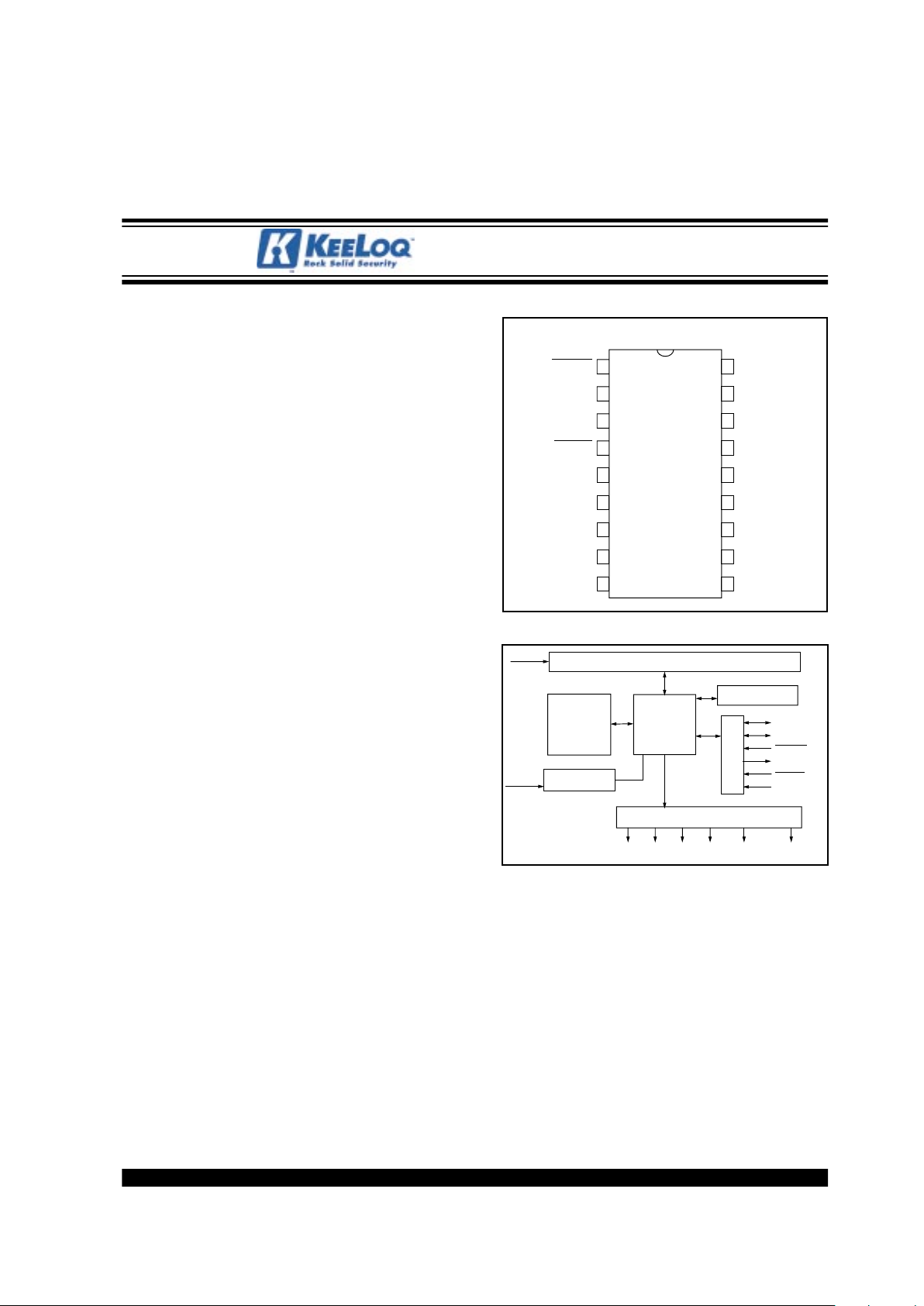
PACKA GE TYPE
BLOCK DIAGRAM
The Manufacturer’s Code, transmitter keys, and synchronization information are stored in protected on-chip
EEPROM. The HCS512 uses the D ATA and CLK inputs
to load the Manufacturer’s Code which cannot be read
out of the device.
The HCS512 operates over a wide voltage range of
3.0 volts to 6.0 volts. The decoder employs automatic
baud rate detection which allows it to compensate for
wide variations in transmitter data rate. The decoder
contains sophisticated error checking algorithms to
ensure only valid codes are accepted.
HCS512
PDIP, SOIC
1
2
3
4
5
6
7
8
9
LRNIN
LRNOUT
NC
MCLR
GND
S0
S1
S2
S3
18
17
16
15
14
13
12
11
10
RFIN
NC
OSCIN
OSCOUT
VDD
DATA
CLK
SLEEP
VLOW
S0 S1 S3S2VLOW
67-Bit Reception Register
EEPROM CONTROL
DECRYPTOR
OUTPUT
SEL
RFIN
OSCILLATOR
OSCIN
CONTROL
LRNOUT
DATA
CLK
LRNIN
MCLR
SLEEP
Code Hopping Decoder
HCS512
DS40151C-page 2
1997 Microchip Technology Inc.
1.0 K
EE
L
OQ
SYSTEM OVERVIEW
1.1 K
ey Terms
• Man
ufacturer’s Code – a 64-bit word, unique to
each manufacturer, used to produce a unique
encoder key in each transmitter (encoder).
• Encoder K
ey – a 64-bit key, unique for each transmitter. The encoder key controls the decryption
algorithm and is stored in EEPROM on the
decoder device.
• Lear
n – The receiver uses information that is
transmitted to derive the transmitter’s secret key,
decrypt the discrimination value and the synchronization counter in learning mode. The encoder
key is a function of the Manufacturer’s Code and
the device serial number and/or seed value.
The HCS encoders and decoders employ the K
EE
L
OQ
code hopping technology and an encryption algorithm
to achieve a high level of security. Code hopping is a
method by which the code transmitted from the transmitter to the receiver is different every time a button is
pushed. This method, coupled with a transmission
length of 66 bits, virtually eliminates the use of code
‘grabbing’ or code ‘scanning’.
1.2 HCS Encoder Over
view
The HCS encoders have a small EEPROM array which
must be loaded with several parameters before use.
The most important of these values are:
• A 28-bit serial number which is meant to be
unique for every encoder
• An encoder key that is generated at the time of
production
• A 16-bit synchronization value
The serial number for each encoder is programmed by
the manufacturer at the time of production. The
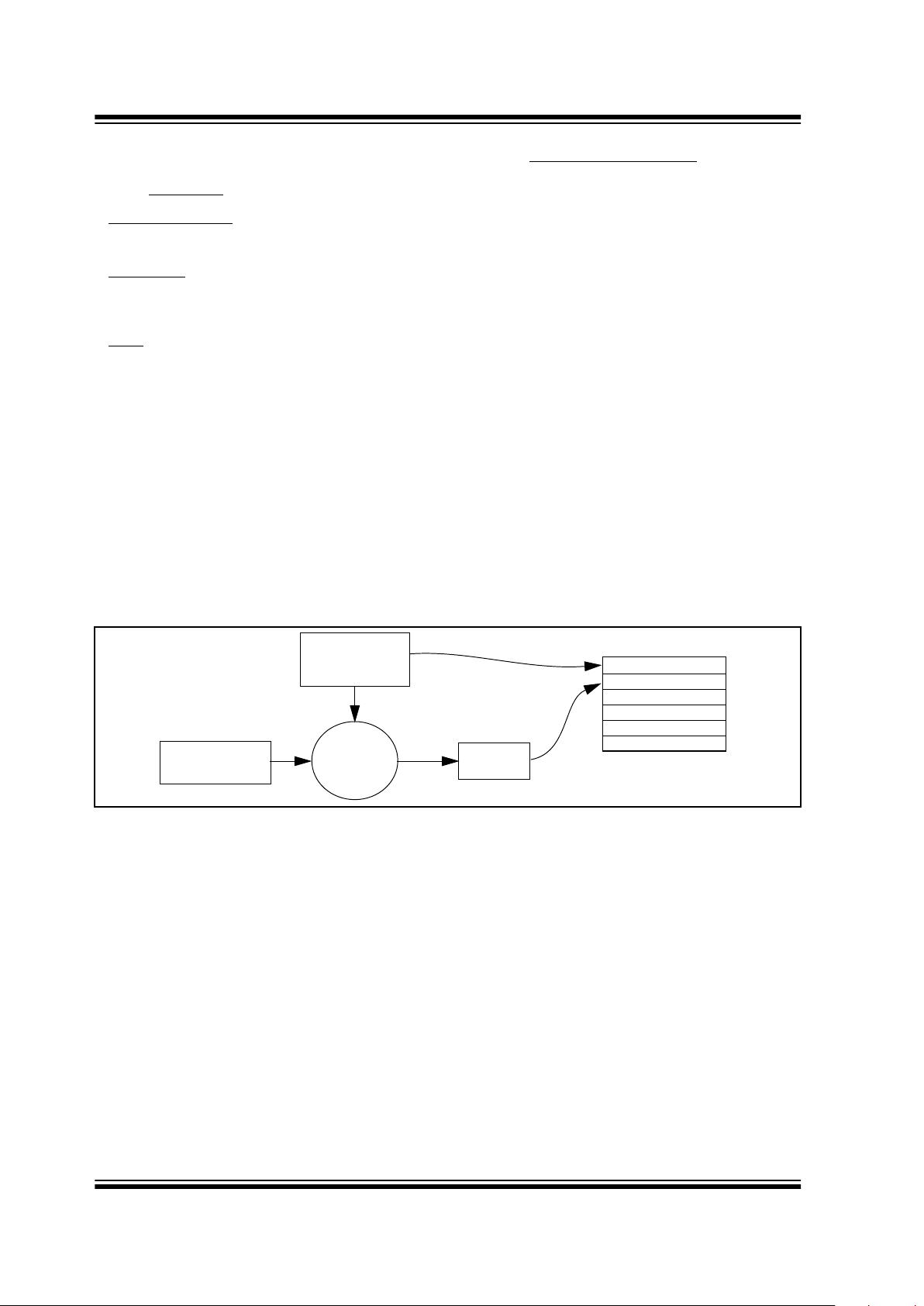
generation of the encoder key is done using a ke y generation algorithm (Figure 1-1). Typically, inputs to the
key generation algorithm are the serial number of the
encoder and a 64-bit manufacturer’s code. The manufacturer’s code is chosen by the system manufacturer
and must be carefully controlled. The manufacturer’s
code is a pivotal part of the overall system security.
FIGURE 1-1: CREATION AND STORAGE OF ENCODER KEY DURING PRODUCTION
Transmitter
Manufacturer’s
Serial Number or
Code
Encoder
Key
Key
Generation
Algorithm
Serial Number
Encoder Key
Sync Counter
.
.
.
HCSXXX EEPROM Array
Seed
HCS512
1997 Microchip Technology Inc. DS40151C-page 3
The 16-bit synchronization value is the basis for the
transmitted code changing for each transmission and is
updated each time a button is pressed. Because of the
complexity of the code hopping encryption algorithm, a
change in one bit of the synchronization value will result
in a large change in the actual transmitted code. There
is a relationship (Figure 1-3) between the key values in
EEPROM and how they are used in the encoder . Once
the encoder detects that a button has been pressed,
the encoder reads the button and updates the synchronization counter. The synchronization value is then
combined with the encoder key in the encryption algorithm, and the output is 32 bits of encrypted information.
This data will change with every button press, hence , it
is referred to as the hopping portion of the code word.
The 32-bit hopping code is combined with the button
information and the serial number to form the code
word transmitted to the receiver.
1.3 HCS Decoder Over
view
Before a transmitter can be used with a particular
receiver, the transmitter must be ‘learned’ by the
receiver. Upon learning a transmitter, information is
stored by the receiver so that it may track the
transmitter, including the serial number of the
transmitter, the current synchronization value for that
transmitter, and the same encoder key that is used on
the transmitter. If a receiv er receives a message of v alid
format, the serial number is checked and, if it is from a
learned transmitter, the message is decrypted and the
decrypted synchronization counter is checked against
what is stored. If the synchronization value is verified,
then the button status is checked to see what operation
is needed. Figure 1-3 shows the relationship between
some of the values stored by the receiver and the values received from the transmitter.
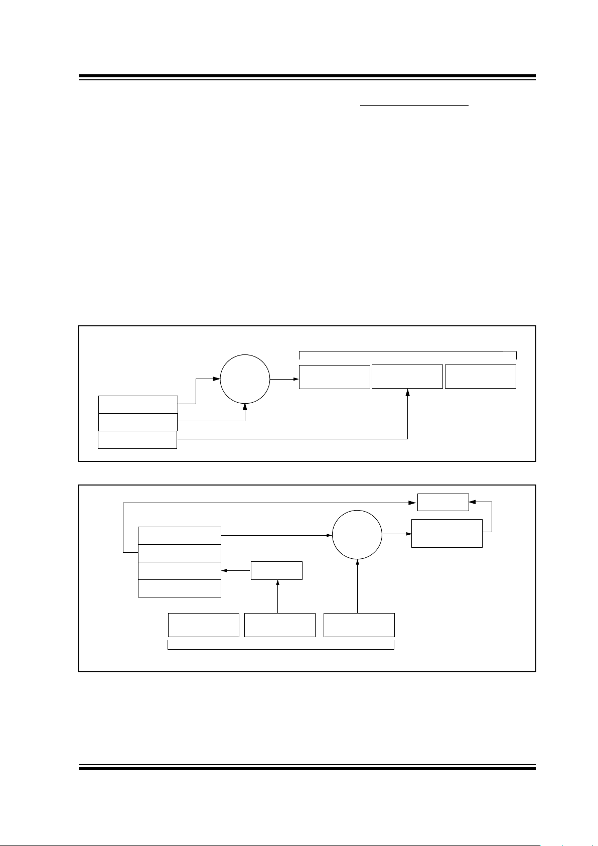
FIGURE 1-2: BASIC OPERATION OF TRANSMITTER (ENCODER)
FIGURE 1-3: BASIC OPERATION OF RECEIVER (DECODER)
KEELOQ
Algorithm
Button Press
Information
Encryption
EEPROM Array
32 Bits of
Encrypted Data
Serial Number
Transmitted Information
Encoder Key
Sync Counter
Serial Number
Button Press
Information
EEPROM Array
Encoder Key
32-Bits of
Encrypted Data
Serial Number
Received Information
Decrypted
Synchronization
Counter
Check for
Match
Check for
Match
KEELOQ
Algorithm
Decryption
Sync Counter
Serial Number
Manufacturer’s Code

HCS512
DS40151C-page 4
1997 Microchip Technology Inc.
2.0 PIN ASSIGNMENT
PIN
Decoder
Function
I/O
(1)
Buffer
Type
(1)
Description
1 LRNIN
I TTL Learn input - initiates learning, 10K pull-up required on input
2 LRNOUT O TTL Learn output - indicates learning
3 NC — TTL Do not connect
4 MCLR
I ST Master clear input
5 Ground P — Ground connection
6 S0 O TTL Switch 0
7 S1 O TTL Switch 1
8 S2 O TTL Switch 2
9 S3 O TTL Switch 3
10 Vlow O TTL Battery low indication output
11 SLEEP I TTL Connect to RFIN to allow wake-up from sleep
12 CLK I/O
TTL/ST
(2)
Clock in programming mode and synchronous mode
13 DATA I/O
TTL/ST
(2)
Data in programming mode and synchronous mode
14 V
DD
P — Power connection
15 OSC
OUT
— — Oscillator out – no connection
16 OSC
IN
(4 MHz) I ST Oscillator in – recommended values 10 k Ω and 10pF
17 NC — —
18 RFIN I TTL RF input from receiver
Note 1: P = power, I = in, O = out, and ST = Schmitt Trigger input.
2:
Pin 12 and Pin 13 have a dual purpose. After reset, these pins are used to determine if programming mode
is selected in which case they are the clock and data lines. In normal operation, they are the clock and data
lines of the synchronous data output stream.
HCS512
1997 Microchip Technology Inc. DS40151C-page 5
3.0 DESCRIPTION OF FUNCTIONS
3.1 P
arallel Interface
The HCS512 activates the S3, S2, S1 & S0 outputs
according to Table 3-1 when a new valid code is
received. The outputs will be activated for approximately 500 ms. If a repeated code is received during
this time, the output extends f or approximately 500 ms.
TABLE 3-1: FUNCTION OUTPUT TABLE
3.2 Serial Interface
The decoder has a PWM/Synchronous interface connection to microcontrollers with limited I/O. An output
data stream is generated when a valid transmission is
received. The data stream consists of one start bit, four
function bits, one bit for battery status, one bit to indicate a repeated transmission, two status bits, and one
stop bit. (Table 3-1). The DATA and CLK lines are used
to send a synchronous event message.
A special status message is transmitted on the second
pass of learn. This allows the controlling microcontroller
to determine if the learn was successful (Result = 1)
and if a previous transmitter was ov erwritten (Overwrite
= 1). The status message is shown in Figure 3-2.
Table 3-2 show the values for TX1:0 and the n umber of
transmitters learned.
TABLE 3-2: STATUS BITS
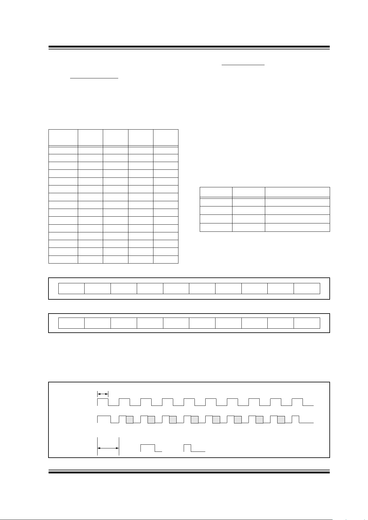
FIGURE 3-1: DATA OUTPUT FORMAT
FIGURE 3-2: STATUS MESSAGE FORMAT
A 1-wire PWM or 2-wire synchronous interface can be used.
In 1-wire mode, the data is transmitted as a PWM signal with a basic pulse width of 400 µ s.
In 2-wire mode, synchronous mode PWM bits start on the rising edge of the clock, and the bits must be sampled on the
falling edge. The start and stop bits are ‘1’.
FIGURE 3-3: PWM TRANSMISSION FORMAT
Function
Code
S3 S2 S1 S0
0001 0 0 0 1
0010 0 0 1 0
0011 0 0 1 1
0100 0 1 0 0
0101 0 1 0 1
0110 0 1 1 0
0111 0 1 1 1
1000 1 0 0 0
1001 1 0 0 1
1010 1 0 1 0
1011 1 0 1 1
1100 1 1 0 0
1101 1 1 0 1
1110 1 1 1 0
1111 1 1 1 1
TX1 TX0 Number of Transmitters
0 0 One
0 1 Two
1 0 Three
1 1 Four
START S3 S2 S1 S0
V
LOW
TX1 TX0 STOPREPEAT
START 0 0 0 0
RESULT
TX1 TX0 STOPOVRWR
S3Start S2 S1 S0 VLOW RPT ReservedReserved Stop
1200µs
CLK
DATA
“1” “0”
600µs
HCS512
DS40151C-page 6
1997 Microchip Technology Inc.
4.0 DECODER OPERATION
4.1 Learning a
Transmitter to a Receiver
Either the serial number-based learning method or the
seed-based learning method can be selected. The
learning method is selected in the configuration byte. In
order for a transmitter to be used with a decoder, the
transmitter must first be ‘learned’. When a transmitter is
learned to a decoder, the decoder stores the encoder
key, a check value of the serial number and current synchronization value in EEPROM. The decoder must
keep track of these values for every transmitter that is
learned. The maximum number of transmitters that can
be learned is four. The decoder must also contain the
Manufacturer’s Code in order to learn a transmitter. The
Manufacturer’ s Code will typically be the same for all
decoders in a system.
The HCS512 has f our memory slots. After an “erase all”
procedure, all the memory slots will be cleared. Erase
all is activated by taking LRNIN
low for approximately
10 seconds. When a new transmitter is learned, the
decoder searches for an empty memory slot and stores
the transmitter’s information in that memory slot. When
all memory slots are full, the decoder randomly overwrites existing transmitters.
4.1.1 LEARNING PROCEDURE
Learning is activated by taking the LRNIN
input low for
longer than 64 ms. This input requires an external pullup resistor.
To learn a new transmitter to the HCS512 decoder, the
following sequence is required:
1. Enter learning mode by pulling LRNIN low for
longer than 64 ms. The LRNOUT output will go
high.
2. Activate the transmitter until the LRNOUT output
goes low indicating reception of a valid code
(hopping message).
3. Activate the transmitter a second time until the
LRNOUT toggles for 4 seconds (in secure learning mode, the seed transmission must be transmitted during the second stage of learn by
activating the appropriate buttons on the transmitter).
If LRNIN
is taken low momentarily during the
learn status indication, the indication will be terminated. Once a successful learning sequence
is detected, the indication can be terminated
allowing quick learning in a manufacturing setup.
4. The transmitter is now learned into the decoder.
5. Repeat steps 1-4 to learn up to four transmitters.
6. Learning will be terminated if two non-sequential
codes were received or if two acceptable codes
were not decoded within 30 seconds.
The following checks are performed on the decoder to
determine if the transmission is valid during learn:
• The first code word is checked for bit integrity.
• The second code word is checked for bit integrity.
• The hopping code is decrypted.
• If all the checks pass, the serial number and synchronization counters are stored in EEPROM
memory.
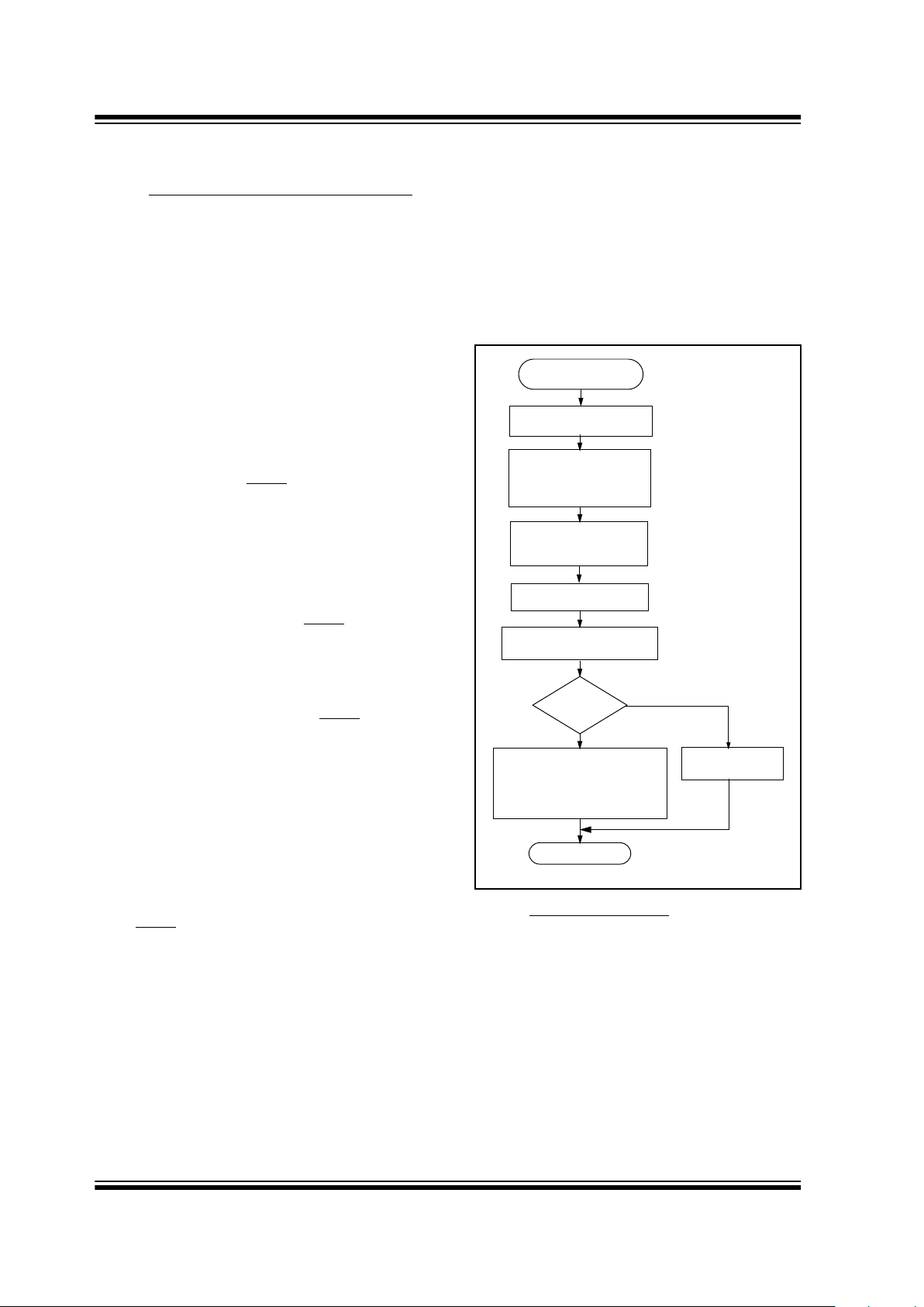
Figure 4-1 shows a flow chart of the learn sequence.
FIGURE 4-1: LEARN SEQUENCE
4.2 V
alidation of Codes
The decoder waits for a transmission and checks the
serial number to determine if the transmitter has been
learned. If learned, the decoder decrypts the encrypted
portion of the transmission using the encoder key. It
uses the discrimination bits to determine if the decryption was valid. If everything up to this point is valid, the
synchronization value is evaluated.
Enter Learn
Mode
Wait for Reception
of Second
Compare Discrimination
Value with Serial Number
Use Generated Key
to Decrypt
Equal
Serial number check value
Synchronization counter
?
Exit
Learn successful. Store:
Learn
Unsuccessful
No
Yes
Wait for Reception
of a Valid Code
Non-Repeated
Valid Code
Generate Key
from Serial Number
or Seed Value
Encoder Key
HCS512
1997 Microchip Technology Inc. DS40151C-page 7
4.3 V
alidation Steps
Validation consists of the following steps:
• Search EEPROM to find the Serial Number Check
Value Match
• Decrypt the Hopping Code
• Compare the 10 bits of discrimination value with
the lower 10 bits of serial number
• Check if the synchronization counter falls within
the first synchronization window.
• Check if the synchronization counter falls within
the second synchronization window.
• If a valid transmission is found, update the synchronization counter, else use the ne xt transmitter
block and repeat the tests.
FIGURE 4-2: DECODER OPERATION
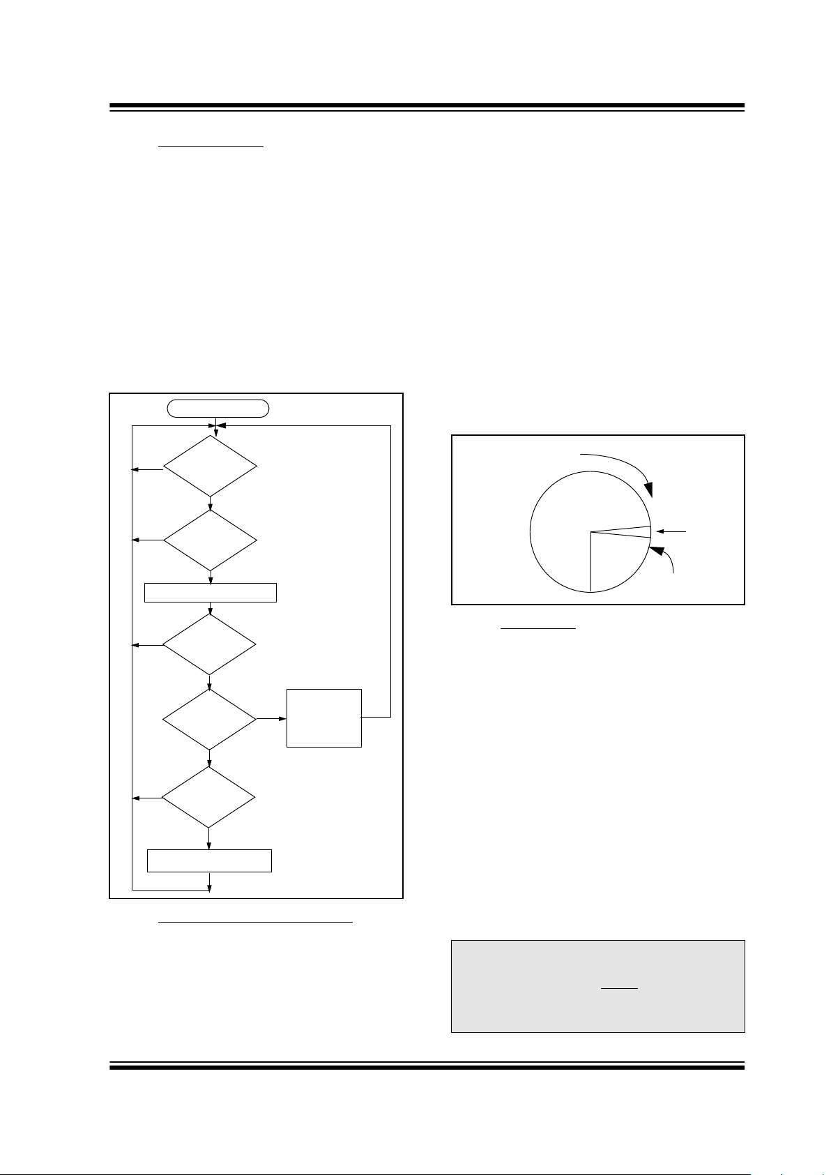
4.4 Synchronization with Decoder
The K
EE
L
OQ
technology features a sophisticated
synchronization technique (Figure 4-3) which does not
require the calculation and storage of future codes. If
the stored counter value for that particular transmitter
and the counter value that was just decrypted are within
a formatted window of 16, the counter is stored and the
command is executed. If the counter value was not
within the single operation window, but is within the
double operation window of 16K, the transmitted synchronization value is stored in a temporary location,
and it goes back to waiting for another transmission.
When the next valid transmission is received, it will
check the new value with the one in temporary storage.
If the two values are sequential, it is assumed that the
counter was outside of the single operation ‘window’,
but is now back in sync, so the new synchronization
value is stored and the command executed. If a transmitter has somehow gotten out of the double operation
window, the transmitter will not work and must be
relearned. Since the entire window rotates after each
valid transmission, codes that hav e been used become
part of the ‘blocked’ (48K) codes and are no longer
valid. This eliminates the possibility of grabbing a previous code and retransmitting it to gain entry.
FIGURE 4-3: SYNCHRONIZATION WINDOW
4.5 Sleep Mode
The sleep mode of the HCS512 is used to reduce current consumption when no RF input signal is present.
Sleep mode will only be effective in systems where the
RF receiver is relatively quiet when no signal is present.
During sleep, the clock stops, thereby significantly
reducing the operating current. Sleep mode is enabled
by the SLEEP bit in the configuration byte.
The HCS512 will enter sleep mode when:
• The RF line is low
• After a function output is switched off
• Learn mode is terminated (time-out reached)
The device will not enter sleep mode when:
• A function output is active
• Learn sequence active
• Device is in programming mode
The device will wake up from sleep when:
• The SLEEP input pin changes state
• The CLOCK line changes state
?
Transmission
Received
Does
Ser # Check Val
Match
?
Decrypt Transmission
Is
Decryption
Valid
?
Is
Counter
Within 16
?
Is
Counter
Within 32K
?
Update
Counter
Execute
Command
Save Counter
in Temp Location
Start
No
No
No
No
Yes
Yes
Yes
Yes
Yes
No
and
Note: During sleep mode the CLK line will
change from an output line to an input line
that can be used to wake up the device.
Connect CLK to LRNIN
via a 100K resistor
to reliably enter the learn mode whenever
sleep mode is active.
Blocked
Entire Window
rotates to eliminate
previously
used codes
Current
Position
(48K Codes)
Double
Operation
(16K
Single Operation
Window (16 Codes)
Codes)

HCS512
DS40151C-page 8
1997 Microchip Technology Inc.
5.0 INTEGRATING THE HCS512
INTO A SYSTEM
The HCS512 can act as a stand alone decoder or be
interfaced to a microcontroller. Typical stand alone
applications include garage door openers and electronic door locks. In stand alone applications, the
HCS512 will handle learning, reception, decryption,
and validation of the received code; and generate the
appropriate output. For a garage door opener, the
HCS512 input will be connected to an RF receiver, and
the output, to a relay driver to connect a motor controller.
Typical systems where the HCS512 will be connected
to a microcontroller include vehicle and home security
systems. The HCS512 input will be connected to an RF
receiver and the function outputs to the microcontroller.
The HCS512 will handle all the decoding functions and
the microcontroller, all the system functions. The serial
output mode with a 1- or 2-wire interface can be used if
the microcontroller is I/O limited.
6.0 DECODER PROGRAMMING
The PG306001 production programmer will allow easy
setup and programming of the configuration byte and
the manufacturer’s code.
6.1 Confi
guration Byte
The configuration byte is used to set system configuration for the decoder. The LRN bits determine which
algorithm (Decrypt or XOR) is used for the key generation. SC_LRN determines whether normal learn (key
derived from serial number) or secure learn (key
derived from seed value) is used.
TABLE 6-1: CONFIGURATION BYTE
TABLE 6-2: LEARN METHOD LRN0, LRN1
DEFINITIONS
Bit Name Description
0 LRN0 Learn algorithm select
1 LRN1 Not used
2 SC_LRN Secure Learn enable (1 = enabled)
3 SLEEP Sleep enable (1 = enabled)
4 RES1 Not used
5 RES2 Not used
6 RES3 Not used
7 RES4 Not used
LRN0 Description
0 Decrypt algorithm
1 XOR algorithm

HCS512
1997 Microchip Technology Inc. DS40151C-page 9
6.2 Pr
ogramming the Manufacturer’s
Code
The manufacturer’s code must be programmed into
EEPROM memory through the synchronous programming interface using the DATA and CLK lines. Provision
must be made for connections to these pins if the
decoder is going to be programmed in circuit.
Programming mode is activated if the CLK is low for at
least 1ms and then goes high within 64 ms after powerup, stays high for longer than 8ms but not longer than
128 ms. After entering programming mode the 64-bit
manufacturer’s code, 8-bit configuration byte, and 8-bit
checksum is sent to the device using the synchronous
interface. After receiving the 80-bit message the checksum is verified and the information is written to
EEPROM. If the programming operation was successful, the HCS512 will respond with an acknowledge
pulse.
After programming the manufacturer’s code, the
HCS512 decoder will automatically activate an
Erase All function, removing all transmitters from the
system.
6.3 Do
wnload Format
The manufacturer’s code and configuration byte must
be downloaded least significant byte, least significant
bit first as shown in Table 6-3.
6.4 Chec
ksum
The checksum is used by the HCS512 to check that the
data downloaded was correctly received before programming the data. The checksum is calculated so that
the 10 bytes added together (discarding the overflow
bits) is zero. The checksum can be calculated b y adding
the first 9 bytes of data together and subtracting the
result from zero. Throughout the calculation the overflow is discarded.
Given a manufacturer’s code of 0123456789ABCDEF
16
and a configuration word of 1
16
, the
checksum is calculated as shown in Figure 6-1. The
checksum is 3F
16
.
6.5 T
est Transmitter
The HCS512 decoder will automatically add a test
transmitter each time an Erase All Function is done. A
test transmitter is defined as a transmitter with a serial
number of zero. After an Erase All, the test transmitter
will always work without learning and will not check the
synchronization counter of the transmitter. Lear ning of
any new transmitters will erase the test transmitter.
TABLE 6-3: DOWNLOAD DATA
FIGURE 6-1: CHECKSUM CALCULATION
Note 1: A transmitter with a serial number of zero
cannot be learned. Learn will fail after the
first transmission.
2:
Always learn at least one transmitter after
an Erase All sequence. This ensures that
the test transmitter is erased.
Byte 9 Byte 8 Byte 7 Byte 6 Byte 5 Byte 4 Byte 3 Byte 2 Byte 1 Byte 0
Check-
sum
Config
Man
Key_7
Man
Key_6
Man
Key_5
Man
Key_4
Man
Key_3
Man
Key_2
Man
Key_1
Man
Key_0
Byte 0, right-most bit downloaded first.
0116 + 2316 = 24
6
2416 + 4516 = 69
16
6916 + 6716 = D0
16
D016 + 8916 = 159
16
5916 + AB16 = 10416 (Carry is discarded)
04
16
+ CD16 = D116 (Carry is discarded)
D1
16
+ EF16 = 1C0
16
C016 + 116 = C116 (Carry is discarded)
(FF
16
- C116) + 116 = 3F
16

HCS512
DS40151C-page 10 1997 Microchip Technology Inc.
FIGURE 6-2: PROGRAMMING WAVEFORMS
TABLE 6-4: PROGRAMMING TIMING
REQUIREMENTS
Bit1Bit0 Bit78 Bit79
Ack
MCLR
CLK
(Clock)
DAT
(Data)
Enter Program Mode
Acknowledge
pulse
T
PS
T
PH1
T
CKL
T
CKH
T
ACK
T
PH2
80-bit Data Package
Parameter Symbol Min. Max. Units
Program mode setup time TPS 1 64 ms
Hold time 1 TPH1 8 128 ms
Hold time 2 TPH2 0.05 320 ms
Clock High Time TCKH 0.05 320 ms
Clock Low Time TCKL 0.050 320 ms
Acknowledge Time TACK — 80 ms
Note: FOSC equals 4 MHz.

HCS512
1997 Microchip Technology Inc. DS40151C-page 11
7.0 KEY GENERATION SCHEMES
The HCS512 decoder has two key generation schemes. Normal learning uses the transmitter’s serial number to derive
two input seeds which aµ re used as inputs to the ke y gener ation algorithm. Secure learning uses the seed transmission
to derive the two input seeds. Two key generation algorithms are available to convert the inputs seeds to secret keys.
The appropriate scheme is selected in the configuration word.
FIGURE 7-1:
7.1 Normal Learning (Serial Number Derived)
The two input seeds are composed from the serial number in two ways, depending on the encoder type. The encoder
type is determined from the number of bits in the incoming transmission. SourceH is used to calculate the upper 32 bits
of the encoder key, and SourceL, for the lower 32 bits.
For 24-bit serial number encoders (56-bit transmissions):
SourceH = 65H + 24 bit Serial Number
SourceL = 2BH + 24 bit Serial Number
For 28-bit serial number encoders (66 / 67-bit transmissions):
SourceH = 6H + 28 bit Serial Number
SourceL = 2H + 28 bit Serial Number
7.2 Secure Learning (Seed Derived)
The two input seeds are composed from the seed value that is transmitted during secure learning. The lower 32 bits of
the seed transmission is used to compose the lower seed, and the upper 32 bits, for the upper seed. The upper 4 bits
(function code) are set to zero.
For 32-bit seed encoders:
SourceH = Serial Number
Lower 28 bits
with upper 4 bits always zero
SourceL = Seed
32 bits
For 48-bit seed encoders:
SourceH = Seed
Upper 16 bits
+ Serial Number
Upper 16 bits
with upper 4 bits always zero
SourceL = Seed
Lower 32 bits
For 64-bit seed encoders:
Note: 64-bit seeds are handled as 48-bit seeds
SourceH = Seed
Upper 16 bits
+ Serial Number
Upper 16 bits
with upper 4 bits always zero
SourceL = Seed
Lower 32 bits
Seed
Patched
Serial
Number
Key Generation
Algorithms
------------------Decrypt
XOR
Encoder
Key
Manufacturer’s
Key

HCS512
DS40151C-page 12 1997 Microchip Technology Inc.
7.3 Key Generation Algorithms
There are two key generation algorithms implemented in the HCS512 decoder. The KEELOQ decryption algorithm pro-
vides a higher level of security than the XOR algorithm. Section 6.1 describes the selection of the algorithms in the configuration byte.
7.3.1 K
EELOQ DECRYPT ALGORITHM
This algorithm uses the K
EELOQ decryption algorithm and the manufacturer’s code to derive the encoder k ey as f ollows:
Key
Upper 32 bits
= F
KEELOQ Decrypt
(SourceH) |
64 Bit Manufacturers Code
Key
Lower 32 bits
= F
KEELOQ Decrypt
(SourceL) |
64 Bit Manufacturers Code
7.3.2 XOR WITH THE MANUFACTURER’S CODE
The two 32-bits seeds are XOR with the manufacturer’s code to form the 64 bit encoder key.
Key
Upper 32 bits
= SourceH ⊗ Manufacturers Code |
Upper 32 bits
Key
Lower 32 bits
= SourceL ⊗ Manufacturers Code |
Lower 32 bits
After programming the manufacturer’s code, the HCS512 decoder will automatically activate an Erase All function,
removing all transmitters from the system.
If LRNIN
is taken low momentarily during the learn status indication, the indication will be terminated. Once a successful
learning sequence is detected, the indication can be terminated, allowing quick learning in a manufacturing set up.
FIGURE 7-2: HCS512 KEY GENERATION
KEELOQ
Decryption
Algorithm
Padding
6/65
28/24-bit Serial Number
Padding
2/2B
28/24-bit Serial Number
MS 32 bits of Encoder Key
LS 32 bits of Encoder Key
SC_LRN = 0
LRN0 = 0
KEELOQ
Decryption
Algorithm
Padding
0000b
MS 28 bits of Seed Transmission
LS 32 bits of Seed Transmission
MS 32 bits of Encoder Key
LS 32 bits of Encoder Key
SC_LRN = 1
XOR
Padding
0000b
MS 28 bits of Seed Transmission
LS 32 bits of Seed Transmission
MS 32 bits of Encoder Key
LS 32 bits of Encoder Key
LRN0 = 1

HCS512
1997 Microchip Technology Inc. DS40151C-page 13
8.0 KEELOQ ENCODERS
8.1 Transmission Format (PWM)
The KEELOQ encoder transmission is made up of several parts (Figure 8-1). Each transmission begins with
a preamble and a header, followed by the encrypted
and then the fixed data. The actual data is 56/66/67 bits
which consists of 32 bits of encrypted data and 24/34/
35 bits of non-encrypted data. Each transmission is
followed by a guard period bef ore another transmission
can begin. The encr ypted portion provides up to four
billion changing code combinations and includes the
button status bits (based on which buttons were activated) along with the synchronization counter value
and some discrimination bits. The non-encr ypted portion is comprised of the status bits, the function bits,
and the 24/28-bit serial number. The encrypted and
non-encrypted combined sections increase the number
of combinations to 7.38 x 10
19
.
8.2 Code Word Organization
The HCSXXX encoder transmits a 66/67-bit code word
when a button is pressed. The 66/67-bit word is constructed from an encryption portion and a nonencrypted code portion (Figure 8-2).
The Encrypted Data is generated from f our button bits ,
two overflow counter bits, ten discrimination bits, and
the 16-bit synchronization value.
The Non-encrypted Data is made up from 2 status
bits, 4 function bits, and the 28/32-bit serial number.
FIGURE 8-1: CODE WORD TRANSMISSION FORMAT
FIGURE 8-2: CODE WORD ORGANIZATION
LOGIC ‘0’
LOGIC ‘1’
Bit
Period
Preamble
Header
Encrypted Portion
of Transmission
Fixed Portion of
Transmission
Guard
Time
TP
TH
THOP
TFIX
TG
Repeat
Vlow
(1 bit)
Button Sta-
tus (4 bits)
28-bit
Serial Number
Button
Status
(4 bits)
Discrimina-
tion bits
(12 bits)
16-bit
Sync Value
CRC1* CRC0*
3/2 bits +
Serial Number and But-
ton Status (32 bits)
+ 32 bits of Encrypted Data
Encrypted DataNon-encrypted Data
*HCS360/361
66/67 bits
of Data
Transmitted

HCS512
DS40151C-page 14 1997 Microchip Technology Inc.
9.0 ELECTRICAL CHARACTERISTICS FOR HCS512
Absolute Maximum Ratings †
Ambient temperature under bias.............................................................................................................-55°C to +125°C
Storage temperature...............................................................................................................................-65°C to +150°C
Voltage on any pin with respect to V
SS (except VDD)......................................................................... -0.6V to VDD +0.6V
Voltage on V
DD with respect to Vss...................................................................................................................0 to +7.5V
Total power dissipation (Note 1)........................................................................................................................... 800 mW
Maximum current out of V
SS pin ........................................................................................................................... 150 mA
Maximum current into V
DD pin .............................................................................................................................. 100 mA
Input clamp current, Iik (V
I < 0 or VI > VDD).........................................................................................................± 20 mA
Output clamp current, IOK (V
O < 0 or VO >VDD)..................................................................................................± 20 mA
Maximum output current sunk by any I/O pin.......................................................................................................... 25 mA
Maximum output current sourced by any I/O pin.....................................................................................................20 mA
Note: Power dissipation is calculated as follows: Pdis = V
DD x {IDD - ∑ IOH} + ∑ {(VDD–VOH) x IOH} + ∑(VOl x IOL)
† NOTICE: Stresses above those listed under “Absolute Maximum Ratings” may cause permanent damage to the
device. This is a stress rating only and functional operation of the device at those or any other conditions above those
indicated in the operation listings of this specification is not implied. Exposure to maximum rating conditions for
extended periods may affect device reliability.

HCS512
1997 Microchip Technology Inc. DS40151C-page 15
TABLE 9-1: DC CHARACTERISTICS
TABLE 9-2: AC CHARACTERISTICS
FIGURE 9-1: RESET WATCHDOG TIMER, OSCILLATOR START-UP TIMER AND POWER-UP
TIMER TIMING
Standard Operating Conditions (unless otherwise stated)
Operating temperature
Commercial (C): 0°C ≤ T
A ≤ +70°C for commercial
Industrial (I): -40°C ≤ T
A ≤ +85°C for industrial and
Symbol Characteristic Min Typ
(†)
Max Units Conditions
V
DD Supply Voltage 3.0 — 6.0 V
V
POR VDD start voltage to
ensure Reset
— VSS — V
S
VDD VDD rise rate to
ensure Reset
0.05* — — V/ms
I
DD Supply Current —
—
1.8
7.3
15
4.5
10
32
mA
mA
µA
FOSC = 4 MHz, VDD = 5.5V
(During EEPROM programming)
In SLEEP mode
VIL Input Low Voltage VSS — 0.16 VDD V except MCLR = 0.2 VDD
VIH Input High Voltage 0.48 VDD — VDD V except MCLR = 0.85 VDD
VOL Output Low Voltage — — 0.6 V IOL = 8.5 mA, VDD = 4.5V
V
OH Output High Voltage VDD-0.7 — — V IOH = -3.0 mA, VDD = 4.5V
†Data in “Typ” column is at 5.0V, 25°C unless otherwise stated. These parameters are for design guidance
only and are not tested.
*These parameters are characterized but not tested.
Note: Negative current is defined as coming out of the pin.
Symbol Characteristic Min Typ Max Units Conditions
F
OSC Oscillator frequency 2.7 4 6.21 MHz Rext = 10K, Cext = 10pF
T
E
PWM elemental
pulse width
65 — 1080 µs 4.5V < V
DD < 5.5V
Oscillator components tolerance < 6%.
130 — 1080 µs 3V < Vdd < 6V
Oscillator components tolerance <10%
T
OD Output delay 70 90 115 ms
T
A Output activation time 322 500 740 ms
T
RPT REPEAT activation time 32 50 74 ms
T
LRN LRNIN activation time 21 32 — ms
T
MCLR MCLR low time 150 — — ns
T
OV Time output valid — 150 222 ms
VDD
MCLR
I/O Pins
TOV
TMCLR

HCS512
DS40151C-page 16 1997 Microchip Technology Inc.
FIGURE 9-2: OUTPUT ACTIVATION
RFIN
S[3,2,1,0]
LRNOUT
0s 1s 2s 3s 4s 5s
1 Code Word 50ms
TOD
TA
TA
VLOW
Note 1: Output is activated as long as code is received.
2: Output is activated if battery low (V
LOW) is detected.
Note 2
Note 1

HCS512
1997 Microchip Technology Inc. DS40151C-page 17
FIGURE 9-3: TYPICAL DECODER APPLICATION CIRCUIT
S1
S2
S3
LRNOUT
S0
V
D
D
G
N
D
G
N
D
V
DD
LOW VOLTAGE DETECTOR—DO NOT OMIT
VI
VO
10K
V
DD
10K
10 pF
14
P2
5
V
DD
10K
1
RECEIVE DATA INPUT
1
2
3
12V
GND
1N4004/7
100 µF
POWER SUPPLY
G
N
D
LM7805
VI
VO
VDD
NC
RFIN
LRNIN
LRNOUT
S0
S1
S2
S3
VLOW
SLEEP
CLK
DAT
MCLR
NC
OSCIN
OSCOUT
4
3
16
15
LEARN
BUTTON
Vlow
P3
1K
1K
1K
1K
1K
1K
100µF
P4
P3
P2
In Circuit
17
18
1
2
6
7
8
9
10
11
12
13
HCS512
P4
100K
Programming Pads
DATA
CLOCK
RESET
GND P1

HCS512
DS40151C-page 18 1997 Microchip Technology Inc.
NOTES:

HCS512
1997 Microchip Technology Inc. DS40151C-page 19
HCS512 PRODUCT IDENTIFICATION SYSTEM
To order or obtain information, e.g., on pricing or delivery, refer to the factory or the listed sales office.
Sales and Support
Package:
P = Plastic DIP (300 mil Body), 8-lead
SN = Plastic SOIC (300 mil Body), 18-lead
Temperature
Range:
Blank = 0˚C to +70˚C
I = -40˚C to +85˚C
Device:
HCS512 Code Hopping Decoder
HCS512T Code Hopping Decoder (Tape and Reel)
HCS512 — /P
Data Sheets
Products supported by a preliminary Data Sheet may have an errata sheet describing minor operational differences and recommended workarounds. To determine if an errata sheet exists for a particular device, please contact one of the following:
1. Your local Microchip sales office.
2. The Microchip Corporate Literature Center U.S. FAX: (602) 786-7277.
3. The Microchip’s Bulletin Board, via your local CompuServe number (CompuServe membership NOT required).
Please specify which device, revision of silicon and Data Sheet (include Literature #) you are using.

Information contained in this publication regarding device applications and the like is intended for suggestion only and may be superseded by updates. No representation or
warranty is given and no liability is assumed by Microchip Technology Incorporated with respect to the accuracy or use of such information, or infringement of patents or other
intellectual property rights arising from such use or otherwise. Use of Microchip’s products as critical components in life support systems is not authorized except with express
written approval by Microchip. No licenses are conv eyed, implicitly or otherwise, under any intellectual property rights. The Microchip logo and name are registered trademarks
of Microchip Technology Inc. in the U.S.A. and other countries. All rights reserved. All other trademarks mentioned herein are the property of their respective companies.
DS40151C-page 20
1997 Microchip Technology Inc.
AMERICAS
Corporate Office
Microchip T echnology Inc.
2355 West Chandler Blvd.
Chandler, AZ 85224-6199
Tel: 602-786-7200 Fax: 602-786-7277
Technical Support:
602 786-7627
Web:
http://www.microchip.com
Atlanta
Microchip T echnology Inc.
500 Sugar Mill Road, Suite 200B
Atlanta, GA 30350
Tel: 770-640-0034 Fax: 770-640-0307
Boston
Microchip T echnology Inc.
5 Mount Royal Avenue
Marlborough, MA 01752
Tel: 508-480-9990 Fax: 508-480-8575
Chicago
Microchip T echnology Inc.
333 Pierce Road, Suite 180
Itasca, IL 60143
Tel: 630-285-0071 Fax: 630-285-0075
Dallas
Microchip T echnology Inc.
14651 Dallas Parkway, Suite 816
Dallas, TX 75240-8809
Tel: 972-991-7177 Fax: 972-991-8588
Dayton
Microchip T echnology Inc.
Two Prestige Place, Suite 150
Miamisburg, OH 45342
Tel: 937-291-1654 Fax: 937-291-9175
Los Angeles
Microchip T echnology Inc.
18201 Von Karman, Suite 1090
Irvine, CA 92612
Tel: 714-263-1888 Fax: 714-263-1338
New Y ork
Microchip T echnology Inc.
150 Motor Parkway, Suite 416
Hauppauge, NY 11788
Tel: 516-273-5305 Fax: 516-273-5335
San Jose
Microchip T echnology Inc.
2107 North First Street, Suite 590
San Jose, CA 95131
Tel: 408-436-7950 Fax: 408-436-7955
Toronto
Microchip T echnology Inc.
5925 Airport Road, Suite 200
Mississauga, Ontario L4V 1W1, Canada
Tel: 905-405-6279 Fax: 905-405-6253
ASIA/PACIFIC
Hong Kong
Microchip Asia Pacific
RM 3801B, Tower Two
Metroplaza
223 Hing Fong Road
Kwai Fong, N.T., Hong Kong
Tel: 852-2-401-1200 Fax: 852-2-401-3431
India
Microchip T echnology Inc.
India Liaison Office
No. 6, Legacy, Convent Road
Bangalore 560 025, India
Tel: 91-80-229-4036 Fax: 91-80-559-9840
Korea
Microchip T echnology Korea
168-1, Youngbo Bldg. 3 Floor
Samsung-Dong, Kangnam-Ku
Seoul, Korea
Tel: 82-2-554-7200 Fax: 82-2-558-5934
Shanghai
Microchip T echnology
RM 406 Shanghai Golden Bridge Bldg.
2077 Yan’an Road West, Hong Qiao District
Shanghai, PRC 200335
Tel: 86-21-6275-5700
Fax: 86 21-6275-5060
Singapore
Microchip T echnology Taiwan
Singapore Branch
200 Middle Road
#10-03 Prime Centre
Singapore 188980
Tel: 65-334-8870 Fax: 65-334-8850
Taiwan, R.O.C
Microchip T echnology Taiwan
10F-1C 207
Tung Hua North Road
T aipei, Taiwan, ROC
Tel: 886 2-717-7175 Fax: 886-2-545-0139
EUROPE
United Kingdom
Arizona Microchip Technology Ltd.
Unit 6, The Courtyard
Meadow Bank, Furlong Road
Bourne End, Buckinghamshire SL8 5AJ
Tel: 44-1628-851077 Fax: 44-1628-850259
France
Arizona Microchip Technology SARL
Zone Industrielle de la Bonde
2 Rue du Buisson aux Fraises
91300 Massy, France
Tel: 33-1-69-53-63-20 Fax: 33-1-69-30-90-79
Germany
Arizona Microchip Technology GmbH
Gustav-Heinemann-Ring 125
D-81739 Müchen, Germany
Tel: 49-89-627-144 0 Fax: 49-89-627-144-44
Italy
Arizona Microchip Technology SRL
Centro Direzionale Colleoni
Palazzo Taurus 1 V. Le Colleoni 1
20041 Agrate Brianza
Milan, Italy
Tel: 39-39-6899939 Fax: 39-39-6899883
JAPAN
Microchip Technology Intl. Inc.
Benex S-1 6F
3-18-20, Shinyokohama
Kohoku-Ku, Yokohama-shi
Kanagawa 222 Japan
Tel: 81-45-471- 6166 Fax: 81-45-471-6122
7/29/97
Printed on recycled paper.
All rights reserved. ©1997, Microchip Technology Incorporated, USA. 6/97
M
W
ORLDWIDE
S
ALES
& S
ERVICE
 Loading...