

Microchip Technology Inc 93LC66BT-I-P, 93LC66BT-ST, 93LC66BT-SN, 93LC66BT-SM, 93LC66BT-P Datasheet
...
1997 Microchip Technology Inc.
Preliminary
DS21209A-page 1
M
93LC66A/B
FEATURES
• Single supply with operation down to 2.5V
• Low power CMOS technology
- 1 mA active current (typical)
-1 µ A standby current (maximum)
• 512 x 8 bit organization (93LC66A)
• 256 x 16 bit organization (93LC66B)
• Self-timed ERASE and WRITE cycles
(including auto-erase)
• Automatic ERAL before WRAL
• Power on/off data protection circuitry
• Industry standard 3-wire serial interface
• Device status signal during ERASE/WRITE cycles
• Sequential READ function
• 1,000,000 E/W cycles guaranteed
• Data retention > 200 years
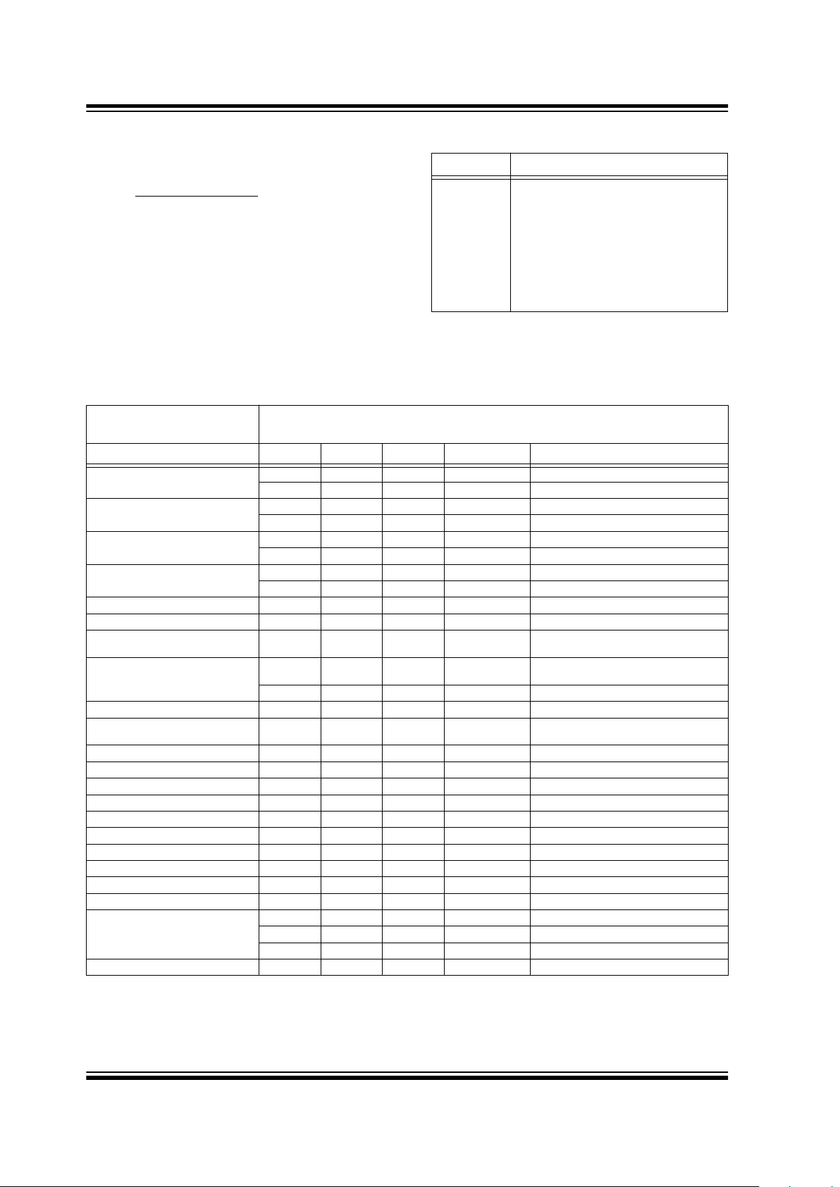
• 8-pin PDIP/SOIC and 8-pin TSSOP packages
• Available for the following temperature ranges:
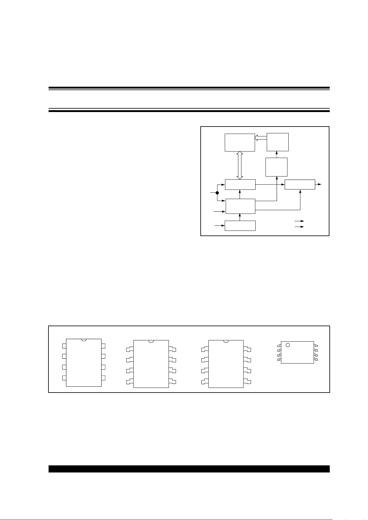
BLOCK DIAGRAM
DESCRIPTION
The Microchip Technology Inc. 93LC66A/B are 4K-bit,
low voltage serial Electrically Erasable PROMs. The
device memory is configured as x8 (93LC66A) or
x16 bits (93LC66B). Advanced CMOS technology
makes these devices ideal for low power nonvolatile
memory applications. The 93LC66A/B is available in
standard 8-pin DIP, surface mount SOIC, and TSSOP
packages. The 93LC66AX/BX are only offered in a 150mil SOIC package.
PACKA GE TYPE
- Commercial (C): 0 ° C to +70 ° C
- Industrial (I): -40 ° C to +85 ° C
Vcc
Vss
DI
CS
CLK
DO
MEMORY
ARRAY
ADDRESS
DECODER
ADDRESS
COUNTER
DATA
REGISTER
OUTPUT
BUFFER
MODE
DECODE
CLOCK
GENERATOR
LOGIC
93LC66A/B
CS
CLK
DI
DO
1
2
3
4
8
7
6
5
Vcc
NC
NC
Vss
CS
CLK
DI
DO
V
CC
NC
NC
Vss
93LC66A/B
NU
Vcc
CS
CLK
NC
Vss
DO
DI
93LC66A/BX
93LC66A/B
CS
CLK
DI
DO
1
2
3
4
8
7
6
5
Vcc
NC
NC
Vss
TSSOP
SOICSOIC
1
2
3
4
DIP
8
7
6
5
1
2
3
4
8
7
6
5
4K 2.5V Microwire
Serial EEPROM
Microwire is a registered trademark of Motorola.
93LC66A/B
DS21209A-page 2
Preliminary
1997 Microchip Technology Inc.
1.0 ELECTRICAL
CHARACTERISTICS
1.1 Maxim
um Ratings*
Vcc...................................................................................7.0V
All inputs and outputs w.r.t. Vss ................-0.6V to Vcc +1.0V
Storage temperature.....................................-65 ° C to +150 ° C
Ambient temp. with power applied.................-65 ° C to +125 ° C
Soldering temperature of leads (10 seconds).............+300 ° C
ESD protection on all pins................................................4 kV
*Notice: Stresses above those listed under “Maximum ratings” may
cause permanent damage to the device. This is a stress rating only and
functional operation of the device at those or any other conditions
above those indicated in the operational listings of this specification is
not implied. Exposure to maximum rating conditions for extended periods may affect device reliability.
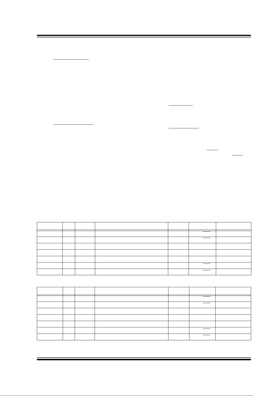
TABLE 1-1 PIN FUNCTION TABLE
Name Function
CS Chip Select
CLK Serial Data Clock
DI Serial Data Input
DO Serial Data Output
V
SS
Ground
NC No Connect
V
CC
Power Supply
TABLE 1-2 DC AND AC ELECTRICAL CHARACTERISTICS
All parameters apply over the specified
operating ranges unless otherwise
noted
Commercial (C): V
CC
= +2.5V to +6.0V Tamb = 0 ° C to +70 ° C
Industrial (I): V
CC
= +2.5V to +6.0V Tamb = -40 ° C to +85 ° C
Parameter Symbol Min. Max. Units Conditions
High level input voltage
V
IH
1 2.0 Vcc +1 V 2.7V ≤ V
CC
≤
5.5V (Note 2)
V
IH
2 0.7 V
CC
Vcc +1 V V
CC
< 2.7V
Low level input voltage
V
IL
1 -0.3 0.8 V V
CC
> 2.7V (Note 2)
V
IL
2 -0.3 0.2 Vcc V V
CC
< 2.7V
Low level output voltage
V
OL
1 — 0.4 V I
OL
= 2.1 µ A; Vcc = 4.5V
V
OL
2 — 0.2 V I
OL
=100 µ A; Vcc = Vcc Min.
High level output voltage
V
OH
1 2.4 — V I
OH
= -400 µ A; Vcc = 4.5V
V
OH
2 V
CC
-0.2 — V I
OH
= -100 µ A; Vcc = Vcc Min.
Input leakage current I
LI
-10 10
µ
A V
IN
= V
SS
to V
CC
Output leakage current I
LO
-10 10
µ
A V
OUT
= V
SS
to V
CC
Pin capacitance
(all inputs/outputs)
C
IN
, C
OUT
— 7 pF
V
IN
/V
OUT
= 0 V (Notes 1 & 2)
Tamb = +25 ° C, F
CLK
= 1 MHz
Operating current
I
CC
read —
1
500
mA
µ
A
F
CLK
= 2 MHz; Vcc = 6.0V
F
CLK
= 1 MHz; Vcc = 3.0V
I
CC
write — 1.5 mA
Standby current I
CCS
— 1
µ
A CS = Vss
Clock frequency F
CLK
—
2
1
MHz
MHz
V
CC
> 4.5V
V
CC
< 4.5V
Clock high time T
CKH
250 — ns
Clock low time T
CKL
250 — ns
Chip select setup time T
CSS
50 — ns Relative to CLK
Chip select hold time T
CSH
0 — ns Relative to CLK
Chip select low time T
CSL
250 — ns
Data input setup time T
DIS
100 — ns Relative to CLK
Data input hold time T
DIH
100 — ns Relative to CLK
Data output delay time T
PD
— 400 ns C
L
= 100 pF
Data output disable time T
CZ
— 100 ns C
L
= 100 pF (Note 2)
Status valid time T
SV
— 500 ns C
L
= 100 pF
Program cycle time
T
WC
— 6 ms ERASE/WRITE mode
T
EC
— 6 ms ERAL mode
T
WL
— 15 ms WRAL mode
Endurance — 1M — cycles 25 ° C, V
CC
= 5.0V, Block Mode (Note 3)
Note 1: This parameter is tested at Tamb = 25 ° C and Fclk = 1 MHz.
2:
This parameter is periodically sampled and not 100% tested.
3:
This application is not tested but guaranteed by characterization. For endurance estimates in a specific application, please consult the Total
Endurance Model which may be obtained on Microchip’s BBS or website.
93LC66A/B
1997 Microchip Technology Inc.
Preliminary
DS21209A-page 3
2.0 PIN DESCRIPTION
2.1 Chip Select (CS)
A high level selects the de vice; a low le vel deselects the
device and forces it into standb y mode. Howev er , a programming cycle which is already in progress will be
completed, regardless of the Chip Select (CS) input
signal. If CS is brought low during a progr am cycle, the
device will go into standby mode as soon as the programming cycle is completed.
CS must be low for 250 ns minimum (T
CSL
) between
consecutive instructions. If CS is low, the internal control logic is held in a RESET status.
2.2 Serial Cloc
k (CLK)
The Serial Clock (CLK) is used to synchronize the communication between a master device and the 93LC66A/
B. Opcode, address , and data bits are clock ed in on the
positive edge of CLK. Data bits are also clocked out on
the positive edge of CLK.
CLK can be stopped anywhere in the transmission
sequence (at high or low level) and can be continued
anytime with respect to clock high time (T
CKH
) and
clock low time (T
CKL
). This gives the controlling master
freedom in preparing opcode, address, and data.
CLK is a “Don't Care” if CS is low (device deselected).
If CS is high, but a START condition has not been
detected, any number of clock cycles can be received
by the device without changing its status (i.e., waiting
for a START condition).
CLK cycles are not required during the self-timed
WRITE (i.e., auto ERASE/WRITE) cycle.
After detection of a ST AR T condition the specified number of clock cycles (respectively low to high transitions
of CLK) must be provided. These clock cycles are
required to clock in all required opcode, address, and
data bits before an instruction is executed (Table 2-1
and Table 2-2). CLK and DI then become don't care
inputs waiting for a new START condition to be
detected.
2.3 Data In (DI)
Data In (DI) is used to clock in a START bit, opcode,
address, and data synchronously with the CLK input.
2.4 Data Out (DO)
Data Out (DO) is used in the READ mode to output data
synchronously with the CLK input (T
PD
after the posi-
tive edge of CLK).
This pin also provides READ Y/B
USY status information
during ERASE and WRITE cycles. READY/B
USY status information is available on the DO pin if CS is
brought high after being low for minimum chip select
low time (T
CSL
) and an ERASE or WRITE operation has
been initiated.
The status signal is not available on DO, if CS is held
low during the entire ERASE or WRITE cycle. In this
case, DO is in the HIGH-Z mode. If status is checked
after the ERASE/WRITE cycle, the data line will be high
to indicate the device is ready.
TABLE 2-1 INSTRUCTION SET FOR 93LC66A
Instruction SB Opcode Address Data In Data Out Req. CLK Cycles
ERASE
1 11 A8 A7 A6 A5 A4 A3 A2 A1 A0 — (RDY/BSY
) 12
ERAL
1 00 1 0 X X X X X X X — (RDY/BSY
) 12
EWDS
1 00 0 0 X X X X X X X — HIGH-Z 12
EWEN
1 00 1 1 X X X X X X X — HIGH-Z 12
READ
1 10 A8 A7 A6 A5 A4 A3 A2 A1 A0 — D7 - D0 20
WRITE
1 01 A8 A7 A6 A5 A4 A3 A2 A1 A0 D7 - D0 (RDY/BSY
) 20
WRAL
1 00 0 1 X X X X X X X D7 - D0 (RDY/BSY
) 20
TABLE 2-2 INSTRUCTION SET FOR 93LC66B
Instruction SB Opcode Address Data In Data Out Req. CLK Cycles
ERASE
1 11 A7 A6 A5 A4 A3 A2 A1 A0 — (RDY/BSY
) 11
ERAL
1 00 1 0 X X X X X X — (RDY/BSY
) 11
EWDS
1 00 0 0 X X X X X X — HIGH-Z 11
EWEN
1 00 1 1 X X X X X X — HIGH-Z 11
READ
1 10 A7 A6 A5 A4 A3 A2 A1 A0 — D15 - D0 27
WRITE
1 01 A7 A6 A5 A4 A3 A2 A1 A0 D15 - D0 (RDY/BSY) 27
WRAL
1 00 0 1 X X X X X X D15 - D0 (RDY/BSY) 27
93LC66A/B
DS21209A-page 4 Preliminary 1997 Microchip Technology Inc.
3.0 FUNCTIONAL DESCRIPTION
Instructions, addresses, and write data are clocked into
the DI pin on the rising edge of the clock (CLK). The DO
pin is normally held in a HIGH-Z state except when
reading data from the device, or when checking the
READY/B
USY status during a programming operation.
The READY/B
USY status can be verified during an
ERASE/WRITE operation by polling the DO pin; DO
low indicates that programming is still in progress, while
DO high indicates the device is ready. The DO will enter
the HIGH-Z state on the falling edge of the CS.
3.1 START Condition
The START bit is detected by the device if CS and DI
are both high with respect to the positive edge of CLK
for the first time.
Before a START condition is detected, CS , CLK, and DI
may change in any combination (except to that of a
START condition), without resulting in any device operation (ERASE, ERAL, EWDS, EWEN, READ, WRITE,
and WRAL). As soon as CS is high, the device is no
longer in the standby mode.
An instruction following a START condition will only be
executed if the required amount of opcodes,
addresses, and data bits for any particular instruction is
clocked in.
After execution of an instruction (i.e., clock in or out of
the last required address or data bit) CLK and DI
become don't care bits until a new START condition is
detected.
3.2 Data In(DI) Data Out (DO)
It is possible to connect the Data In (DI)and Data Out
(DO)pins together. However, with this configuration, if
A0 is a logic-high level, it is possible for a “bus conflict”
to occur during the “dummy zero” that precedes the
READ operation. Under such a condition the voltage
level seen at Data Out is undefined and will depend
upon the relative impedances of Data Out and the signal source driving A0. The higher the current sourcing
capability of A0, the higher the voltage at the Data Out
pin.
3.3 Data Protection
During power-up, all programming modes of operation
are inhibited until V
CC has reached a level greater than
2.2V. During power-down, the source data protection
circuitry acts to inhibit all programming modes when
Vcc has fallen below 2.2V at nominal conditions.
The ERASE/WRITE Disable (EWDS) and ERASE/
WRITE Enable (EWEN) commands give additional protection against accidentally programming during normal operation.
After power-up, the device is automatically in the
EWDS mode. Therefore, an EWEN instruction must be
performed before any ERASE or WRITE instruction can
be executed.
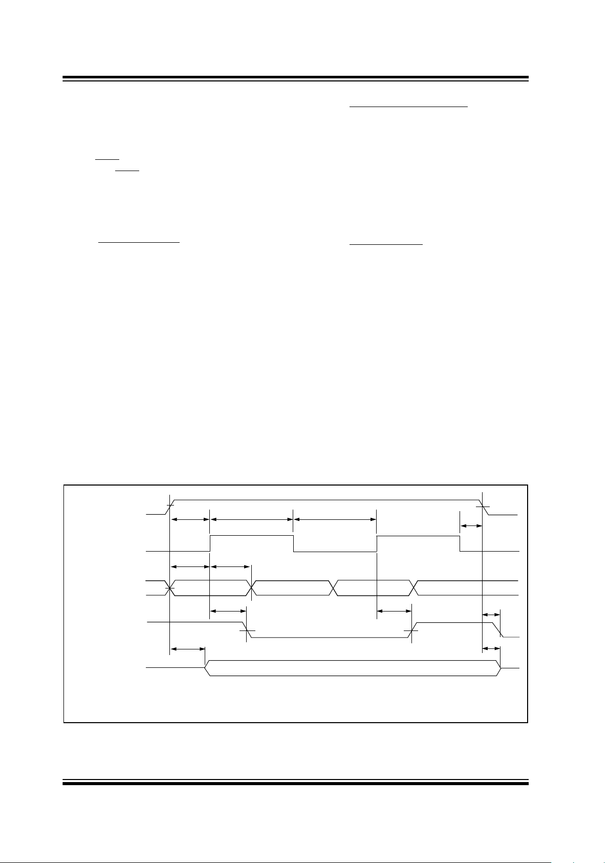
FIGURE 3-1: SYNCHRONOUS DATA TIMING
CS
V
IH
VIL
VIH
VIL
VIH
VIL
VOH
VOL
VOH
VOL
CLK
DI
DO
(READ)
DO
(PROGRAM)
T
CSS
TDIS
TCKH
TCKL
TDIH
TPD
TCSH
TPD
TCZ
STATUS VALID
T
SV
TCZ
Note: AC Test Conditions: VIL = 0.4V, VIH = 2.4V.
 Loading...