

Datasheet 24LCS62T-I-ST, 24LCS62T-I-SN, 24LCS62T-I-P, 24LCS62T-ST, 24LCS62T-SN Datasheet (Microchip Technology Inc)
...
1997 Microchip Technology Inc.
Preliminary
DS21226A-page 1
M
24LCS61/24LCS62
PRODUCT OFFERING
FEATURES
• Low power CMOS technology
- 1 mA active current typical
- 10 µ A standby current typical at 5.5V
• Software addressability allows up to 255 devices
on the same bus
• 2-wire serial interface bus, I
2
C compatible
• Automatic bus arbitration
• Wakes up to control code 0110
• General purpose output pin can be used to
enable other circuitry
• 100 kHz and 400 kHz compatibility
• Page-write buffer for up to 16 bytes
• 10 ms max write cycle time for byte or page write
• 10,000,000 erase/write cycles guaranteed
• 8-pin PDIP, SOIC or TSSOP packages
• Temperature ranges supported:
DESCRIPTION
The Microchip Technology Inc. 24LCS61/62 is a 1K/2K
bit Serial EEPROM developed for applications that
require many devices on the same bus b ut do not ha v e
the I/O pins required to address each one individually.
These devices contain an 8 bit address register that is
set upon power-up and allows the connection of up to
255 devices on the same bus. When the process of
assigning ID values to each device is in progress, the
device will automatically handle bus arbitration if more
than one device is operating on the bus. In addition, an
external open drain output pin is available that can be
used to enable other circuitry associated with each
individual system. Low current design permits operation with typical standby and active currents of only
10 µ A and 1 mA respectively. The device has a pagewrite capability for up to 16 bytes of data. The device is
available in the standard 8-pin PDIP, SOIC (150 mil),
and TSSOP packages.
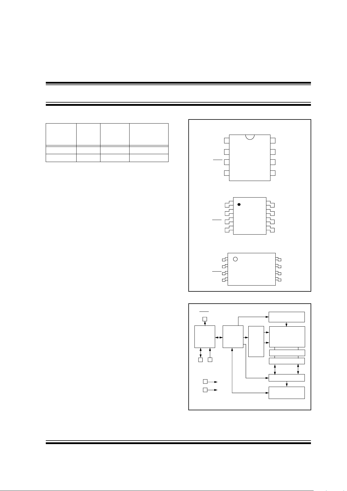
PACKA GE TYPES
BLOCK DIAGRAM
Device
Array
Size
Voltage
Range
Software
Write
Protection
24LCS61 1K bits 2.5V-5.5V Entire Array
24LCS62 2K bits 2.5V-5.5V Lower Half
- Commercial (C): 0 ° C to +70 ° C
- Industrial (I): -40 ° C to +85 ° C
PDIP
NC
NC
EDS
Vss
Vcc
NC
SCL
SDA
24LCS61/62
1
2
3
4
8
7
6
5
NC
NC
EDS
Vss
VCC
NC
SCL
SDA
24LCS61/62
1
2
3
4
8
7
6
5
SOIC
TSSOP
24LCS61/62
NC
NC
EDS
VSS
Vcc
NC
SCL
SDA
1
2
3
4
8
7
6
5
I/O
Control
Logic
Memory
Control
Logic
XDEC
HV Generator
EEPROM
Array
YDEC
Vcc
Vss
SENSE AMP
R/W CONTROL
SDA
SCL
EDS
ID Register
Serial Number
1K/2K Software Addressable I
2
C
™
Serial EEPROM
I
2
C is a trademark of Philips Corporation.

24LCS61/62
DS21226A-page 2
Preliminary
1997 Microchip Technology Inc.
1.0 ELECTRICAL
CHARACTERISTICS
1.1 Maximum Ratings*
V
CC
........................................................................7.0V
All inputs and outputs w.r.t. V
SS
......-0.6V to V
CC
+1.0V
Storage temperature ..........................-65˚C to +150˚C
Ambient temp. with power applied...... -65˚C to +125˚C
Soldering temperature of leads (10 seconds) ..+300˚C
ESD protection on all pins .....................................≥ 4 kV
*Notice: Stresses above those listed under “Maximum ratings” may
cause permanent damage to the device. This is a stress rating only and
functional operation of the device at those or any other conditions
above those indicated in the operational listings of this specification is
not implied. Exposure to maximum rating conditions for extended periods may affect device reliability.
TABLE 1-1: PIN FUNCTION TABLE
Name
Function
V
SS
SDA
SCL
V
CC
NC
EDS
Ground
Serial Data
Serial Clock
+2.5V to 5.5V Power Supply
No Internal Connection
External Device Select Output
TABLE 1-2: DC CHARACTERISTICS
All parameters apply across the specified operating ranges unless otherwise
noted.
V
CC
= +2.5V to +5.5V
Commercial (C): Tamb = 0 ° C to +70 ° C
Industrial (I): Tamb = -40 ° C to +85 ° C
Parameter Symbol Min. Max. Units Conditions
SCL and SDA pins:
High level input voltage
V
IH
0.7 V
CC
V
Low level input voltage V
IL
.3 V
CC
V
Hysteresis of Schmitt trigger inputs V
HYS
0.05 V
CC
—V
Low level output voltage
(SDA and EDS
pins)
V
OL
.40 V I
OL
= 12 mA, V
CC
= 4.5V
I
OL
= 8 mA, V
CC
= 2.5V
Input leakage current I
LI
-10 10
µ
AV
IN
= Vss or Vcc
Output leakage current I
LO
-10 10
µ
AV
OUT
= Vss or Vcc
Pin capacitance (all inputs/outputs) C
IN
,
C
OUT
—10pFV
CC
= 5.0V (Note)
Tamb = 25 ° C, f = 1 MHz
Operating current I
CC
Write — 3 mA V
CC
= 5.5V
I
CC
Read — 1 mA V
CC
= 5.5V, SCL = 400 kHz
Standby current I
CCS
—50 µ AV
CC
= 5.5V, SDA = SCL = V
CC
Note : This parameter is periodically sampled and not 100% tested.
24LCS61/62
1997 Microchip Technology Inc.
Preliminary
DS21226A-page 3
TABLE 1-3: AC CHARACTERISTICS
FIGURE 1-1: BUS TIMING DATA
All parameters apply across the specified
operating ranges unless otherwise noted.
Vcc = +2.5V to 5.5V
Commercial (C): Tamb = 0 ° C to +70 ° C
Industrial (I): Tamb = -40 ° C to +85 ° C
Parameter Symbol
V
CC
= 2.5V - 5.5V
STD MODE
Vcc = 4.5V - 5.5V
FAST MODE
Units Remarks
Min. Max. Min. Max.
Clock frequency F
CLK
— 100 — 400 kHz
Clock high time T
HIGH
4000 — 600 — ns
Clock low time T
LOW
4700 — 1300 — ns
SDA and SCL rise time T
R
— 1000 — 300 ns From V
IL
to V
IH
(Note 1)
SDA and SCL fall time T
F
— 300 — 300 ns From V
IL
to V
IH
(Note 1)
START condition hold time T
HD
:
STA
4000 — 600 — ns After this period the first
clock pulse is generated
START condition setup time T
SU
:
STA
4700 — 600 — ns Only relevant for repeated
START condition
Data input hold time T
HD
:
DAT
0 — 0 — ns (Note 2)
Data input setup time T
SU
:
DAT
250 — 100 — ns
STOP condition setup time T
SU
:
STO
4000 — 600 — ns
Output valid from clock T
AA
— 3500 — 900 ns (Note 2)
Bus free time T
BUF
4700 — 1300 — ns Time the bus must be free
before a new transmission
can start
Output fall time
(from 0.7 V
CC
to 0.3 V
CC
)
T
OF
— 250 20 +0.1
C
B
250 ns (Note 1), C
B
≤
100 pF
Input filter spike suppression
(SDA and SCL pins)
T
SP
— 50 — 50 ns (Notes 1, 3)
Write cycle time T
WC
— 10 — 10 ms Byte or Page mode
Endurance 10M — 10M — cycles 25 ° C, V
CC
= 5.0V, Block
Mode (Note 4)
Note 1: Not 100% tested. C
B
= total capacitance of one bus line in pF.
2:
As a transmitter, the device must provide an internal minimum delay time to bridge the undefined region
(minimum 300 ns) of the falling edge of SCL to avoid unintended generation of START or STOP conditions.
3:
The combined T
SP
and V
HYS
specifications are due to Schmitt trigger inputs which provide improved noise
spike suppression. This eliminates the need for a TI specification for standard operation.
4:
This parameter is not tested but guaranteed by characterization. For endurance estimates in a specific
application, please consult the Total Endurance Model which can be obtained on our BBS or website.
SCL
SDA
IN
Tsu:sta
SDA
OUT
THD:STA
TLOW
THIGH
TR
TBUF
TAA
THD:DAT TSU:DAT TSU:STO
TSP
TF

24LCS61/62
DS21226A-page 4 Preliminary 1997 Microchip Technology Inc.
2.0 PIN DESCRIPTIONS
2.1 SDA (Serial Data)
This is a bi-directional pin used to transfer addresses
and data into and data out of the device. It is an open
drain terminal, therefore the SDA bus requires a pull-up
resistor to V
CC (typical 10 kΩ for 100 kHz, 2 kΩ for
400 kHz).
For normal data transfer SD A is allowed to change only
during SCL low. Changes during SCL high are
reserved for indicating the START and STOP conditions. The SDA pin has Schmitt trigger and filter circuits
which suppress noise spikes to assure proper device
operation even on a noisy bus
2.2 SCL (Serial Clock)
This input is used to synchronize the data transfer from
and to the device. The SCL pin has Schmitt trigger and
filter circuits which suppress noise spikes to assure
proper device operation even on a noisy bus.
2.3 EDS (External Device Select)
The External Device Select (EDS) pin is an open drain
output that is controlled by using the OE bit in the control byte. It can be used to enable other circuitry when
the device is selected. A pull-up resistor must be added
to this pin for proper operation. This pin should not be
pulled up to a voltage higher than Vcc+1V. See
Section 9.0 for more details.
3.0 BUS CHARACTERISTICS
The following bus protocol has been defined:
• Data transfer may be initiated only when the bus
is not busy.
• During data transfer, the data line must remain
stable whenever the clock line is HIGH. Changes
in the data line while the clock line is HIGH will be
interpreted as a START or STOP condition.
Accordingly, the following bus conditions have been
defined (Figure 3-1).
3.1 Bus not Busy (A)
Both data and clock lines remain HIGH.
3.2 Start Data Transfer (B)
A HIGH to LOW transition of the SDA line while the
clock (SCL) is HIGH determines a START condition. All
commands must be preceded by a START condition.
3.3 Stop Data Transfer (C)
A LOW to HIGH transition of the SDA line while the
clock (SCL) is HIGH determines a STOP condition. All
operations must be ended with a STOP condition.
3.4 Data Valid (D)
The state of the data line represents valid data when,
after a START condition, the data line is stable for the
duration of the HIGH period of the clock signal.
The data on the line must be changed during the LOW
period of the clock signal. There is one bit of data per
clock pulse.
Each data transfer is initiated with a START condition
and terminated with a STOP condition. The number of
data bytes transferred between the START and STOP
conditions is determined by the master device and is
theoretically unlimited, although only the last sixteen
will be stored when doing a write operation. When an
overwrite does occur it will replace data in a first in first
out fashion.
FIGURE 3-1: DATA TRANSFER SEQUENCE ON THE SERIAL BUS
(A) (B) (D) (D) (A)(C)
SCL
SDA
START
CONDITION
DATA OR
ACKNOWLEDGE
VALID
DATA
ALLOWED
TO CHANGE
STOP
CONDITION
24LCS61/62
1997 Microchip Technology Inc. Preliminary DS21226A-page 5
3.5 Acknowledge
Each receiving device, when addressed, is required to
generate an acknowledge after the reception of each
byte. The master device must generate an extra clock
pulse which is associated with this acknowledge bit.
The device that acknowledges has to pull down the
SDA line during the acknowledge cloc k pulse in such a
way that the SDA line is stable LOW during the HIGH
period of the acknowledge related clock pulse. Of
course, setup and hold times must be taken into
account. A master must signal an end of data to the
slave by not generating an acknowledge bit on the last
byte that has been clocked out of the sla ve. In this case ,
the slave must leave the data line HIGH to enable the
master to generate the STOP condition (Figure 3-2).
FIGURE 3-2: ACKNOWLEDGE TIMING
Note: The 24LCS61/62 does not generate any
acknowledge bits if an internal programming cycle is in progress.
SCL
987654321 123
Transmitter must release the SDA line at this point
allowing the Receiver to pull the SDA line low to
acknowledge the previous eight bits of data.
Receiver must release the SDA line at this point
so the Transmitter can continue sending data.
Data from transmitter
Data from transmitter
SDA
Acknowledge
Bit

24LCS61/62
DS21226A-page 6 Preliminary 1997 Microchip Technology Inc.
4.0 FUNCTIONAL DESCRIPTION
The 24LCS61/62 supports a bi-directional 2-wire bus
and data transmission protocol compatible with the I
2
C
protocol. The device is configured to reside on a common I
2
C bus with up to 255 total 24LCS61/62 devices
on the bus. Each device has a unique serial number
assigned to it when delivered from the factory. In an
actual system, this serial number will be used to assign
a separate 8-bit ID byte to each device in the system.
After an ID byte is assigned to each device in the system, standard read and write commands can be sent to
each device individually.
4.1 Device Serial Number
The device serial number is stored in a 48-bit (6 byte)
register that is separate from the data array. The serial
number register is non-volatile and cannot be changed
by the user. Before shipment from the factory, this register is programmed with a unique value for every
device. The 48 bit register allows for 2.8•10
14
different
combinations. The serial number is used at pow er-up to
assign the device an ID byte which is then used for all
standard read and write commands sent to that specific
device.
4.2 Device ID Byte
The Device ID byte is an 8-bit value that provides the
means for ev ery device on the bus to be accessed individually. The ID byte is stored in a RAM register separate from the data array. The ID byte register will alw ays
default to address 00 upon power-up.
4.3 Device Addressing
Each command to the device must begin with a start
bit. A control b yte is the first b yte receiv ed following the
start condition from the master device (Figure 4-1). The
control byte consists of a four-bit control code, the OE
bit, and three command select bits. For the 24LCS61/
62, the control code is set to 0110 binary for all operations. The device will not acknowledge any commands
sent with any other control code. The next bit is the Output Enable (OE) bit. This bit controls the operation of
the EDS
pin. See Section 9.0 for more details. The last
three bits of the control byte are the command select
bits (C0-C2). The command select bits determine
which command will be executed. See Table 4-1. Following a valid control byte, the 24LCS61/62 will
acknowledge the command.
FIGURE 4-1: CONTROL BYTE FORMAT
TABLE 4-1: COMMAND CODES
Command
Command Select Bits
(C2 C1 C0)
Set Write Protection Fuse 000
Read 001
Write (Byte or Page) 010
Assign Address 100
Clear Address 110
1010OEC2C1SACK
Control Code
Command Select
Bits
Acknowledge Bit
Start Bit
C0
Output Enable
Bit

24LCS61/62
1997 Microchip Technology Inc. Preliminary DS21226A-page 7
5.0 ASSIGNING THE ID BYTE
The 24LCS61/62 device contains a special register
which holds an 8-bit ID byte that is used as an address
to communicate with a specific device on the bus. All
read and write commands to the device must include
this ID address byte. Upon power-up, the ID byte will
default to 00h. Communicating with the device using
the default address is typically done only at testing or
programming time and not when it is connected to a
bus with more than one device. Before the device can
be used on a common bus with other devices, a unique
ID byte address must be assigned to every device.
5.1 Assign Address Command
The ID byte is assigned by sending the Assign Address
command. This command queries any device connected to the bus and utilizing the automatic bus arbitration feature, assigns an ID byte to the device that
remains on the bus after arbitration is complete. Once
a device has been assigned an ID byte, it will no longer
respond to Assign Address commands until power is
cycled or the Clear Address command is sent. The
Assign Address command must be repeated for each
device on the bus until all devices have been assigned
an ID byte.
The format for the Assign Address command is shown
in Figure 5-1. The command consists of the control
byte, the ID byte to be assigned to the de vice remaining
when the arbitration is complete, and 48 bits of data
being transmitted by devices on the b us. If the OE bit is
set to a 1, then any device who has not been assigned
an address will assert their respective EDS
pin after the
acknowledge bit following the Device ID byte. After the
control byte and ID byte are sent, each device will begin
to transmit its unique 48-bit serial number. The
24LCS61/62 must acknowledge the control byte and
the device ID byte, and the master must acknowledge
each byte of the serial number transmitted by the
device. As each bit is clocked out, each device will
monitor the bus to detect if another device is also transmitting. If any device is outputting a logic ‘1’ on the bus
and it detects that the bus is at a logic ‘0’, then it
assumes that another device is controlling the bus. As
soon as any device detects that it is not controlling the
bus it will immediately stop transmitting data and return
to standby mode. The master must end the command
by sending a no ack after all 6 bytes of the serial number have been transmitted, followed by a Stop bit.
Sending the Stop bit in any other position of the command will result in the command aborting and all
devices releasing the bus with no address assigned. If
a device transmits its entire 48 bit serial number without
releasing the bus to another device, then the ID byte
transmitted within the command is transferred to the
internal ID byte register upon receipt of the Stop bit and
it will now respond only to commands that contain this
ID byte (or the Clear Address command). Once a
device has been assigned an ID byte, it will no longer
respond to Assign Address commands until power is
cycled or the Clear Address command is sent.
This process of assigning ID bytes is repeated by the
controller until no more devices respond to the Assign
Address command. At this point, all de vices on the b us
have been assigned an ID byte and standard read and
write commands can be executed to each individual
device.
The ID byte is stored in a volatile SRAM register, and if
power is removed from the de vice or the Clear Address
command is sent, then the ID byte will default to
address 00 and the process of assigning an ID value
must be repeated.
FIGURE 5-1: ASSIGN ADDRESS COMMAND
S
P
S
T
A
R
T
CONTROL
BYTE
S
T
O
P
Device ID Byte
6 Bytes (48 Bits) of Device Serial Number
with each byte separated by an ack bit
1010
A unique address must be assigned to each
device on the bus
A
C
K
A
C
K
A
C
K
A
C
K
O
100
STOP bit must occur here
or command will abort
E
N
O
A
C
K

24LCS61/62
DS21226A-page 8 Preliminary 1997 Microchip Technology Inc.
5.2 Clear Address Command
The clear address command will clear the device ID
byte from all devices on the bus and will enable all
devices to respond to the Assign Address command.
The master must end the command by sending an ack
after 8 don’t care bits have been transmitted, followed
by a Stop bit. Sending the Stop bit in any other position
of the command will result in the command aborting
and the device releasing the bus.
FIGURE 5-2: CLEAR ADDRESS COMMAND
S
P
S
T
A
R
T
CONTROL
BYTE
S
T
O
P
A
C
K
Device ID Byte
1010
A
C
K
XXXXXXXX
011
O
E

24LCS61/62
1997 Microchip Technology Inc. Preliminary DS21226A-page 9
5.3 Operation State Diagram
The diagram below shows the state diagram for basic
operation of the 24LCS61/62. This diagram shows pos-
sible states and operational flow once power is applied
to the device. Table 5-1 summarizes operation of each
command for the assigned and unassigned states.
FIGURE 5-3: OPERATIONAL STATE DIAGRAM
TABLE 5-1: COMMAND SUMMARY TABLE
Power
Off
Unassigned
State
Assigned
State
Power Off
Power On
Power Off
Assign Address Command:
Device wins Arbitration
Clear Address
Command
Assign Address Command:
Device loses Arbitration
(ID byte not assigned yet)
(ID byte has been assigned)
Command
Result if Device Has Not Yet
Been Assigned an ID Byte
Result if Device Has Already Been
Assigned an ID Byte
Assign Address
command
If device wins arbitration, then ID
byte will become xxh. If device
loses arbitration, then ID byte will
revert back to 00h.
Device will not acknowledge command.
Clear Address
command
Device will remain with ID byte set
to 00h.
Device ID byte will revert back to 00h and will then
acknowledge Assign Address commands.
Read or Write
command with
ID byte set to 00h
Since the default ID byte for the
device is 00h, the device will execute the command.
Device will acknowledge the control byte, but it will not
acknowledge any further bytes and will not respond to
the command.
Read or Write
command with
ID byte set to xxh
(other than 00h)
Device will acknowledge the control
byte, but it will not acknowledge
any further bytes and will not
respond to the command.
If the device ID byte matches the ID byte in the command
(xxh), the device will execute the command. If the device
ID byte does not match the ID byte in the command, then
the device will acknowledge the control b yte, but it will not
acknowledge any further bytes and will not respond to
the command.
Set Write Protect
command with
ID byte set to 00h
Since the default ID address for the
device is 00h, the device will execute the command.
Device will acknowledge the control byte, but it will not
acknowledge any further bytes and will not respond to
the command.
Set Write Protection
command with
ID byte set to xxh
(other than 00h)
Device will acknowledge the control
byte, but it will not acknowledge
any further bytes and will not
respond to the command.
If the device ID byte matches the ID byte in the command
(xxh), the device will execute the command. If the device
ID byte does not match the ID byte in the command, then
the device will acknowledge the control b yte, but it will not
acknowledge any further bytes and will not respond to
the command. Note: Once this command has been executed successfully for a device, the device will no longer
acknowledge any part of this command again.

24LCS61/62
DS21226A-page 10 Preliminary 1997 Microchip Technology Inc.
6.0 WRITE OPERATIONS
6.1 Byte Write
Following the start signal from the master, the control
byte for a write command is sent by the master transmitter. The device will acknowledge this control byte
during the ninth clock pulse. The next byte transmitted
by the master is the ID byte for the device. After receiving another acknowledge signal from the 24LCS61/62,
the master device will transmit the address and then
the data word to be written into the addressed memory
location. The 24LCS61/62 acknowledges between
each byte, and the master then generates a stop condition. This initiates the internal write cycle, and during
this time the 24LCS61/62 will not generate acknowledge signals (Figure 6-1).
6.2 Page Write
The control byte, ID byte, word address, and the first
data byte are transmitted to the 24LCS61/62 in the
same way as in a byte write. But, instead of generating
a stop condition, the master transmits up to 15 additional data bytes to the 24LCS61/62, which are temporarily stored in the on-chip page buffer and will be
written into the memory after the master has transmitted a stop condition. If the master should transmit more
than 16 bytes prior to generating the stop condition, the
address counter will roll over and the previously
received data will be overwritten. As with the byte write
operation, once the stop condition is received an internal write cycle will begin (Figure 6-2) and the 24LCS61/
62 will not generate acknowledge.
6.3 Low Voltage Write Protection
The 24LCS61/62 employs a VCC threshold detector circuit which disables the internal erase/write logic, if the
V
CC is below 1.5 volts at nominal conditions.
6.4 Set Write Protection Command
The Set Write Protection command allows the user to
write protect a portion of the array. For the 24LCS61
this command will write protect the entire array. For the
24LCS62 this command will protect the lower half of
the array. This command is illustrated in Figure 6-3.
This is a one time only command and cannot be
reversed once the protection fuse has been set.
Once the Write protect feature has been set, the de vice
will no longer acknowledge the control byte (or any of
the other bytes) of this command. The STOP bit of this
command initiates an internal write cycle, and during
this time the 24LCS61/62 will not generate acknowledge signals.
FIGURE 6-1: BYTE WRITE
FIGURE 6-2: PAGE WRITE
FIGURE 6-3: SET WRITE PROTECTION COMMAND
S
T
A
R
T
S
T
O
P
DEVICE
ID BYTE
DATA
CONTROL
BYTE
A
C
K
A
C
K
A
C
K
BUS ACTIVITY
MASTER
SDA LINE
BUS ACTIVITY A
C
K
ADDRESS
BYTE
1010O010
S
E
OE Bit = EDS Pin Output Enable; see Section 9.0
S
T
A
R
T
S
T
O
P
CONTROL
BYTE
A
C
K
A
C
K
A
C
K
BUS ACTIVITY
MASTER
SDA LINE
BUS ACTIVITY
A
C
K
ADDRESS
BYTE
DATA BYTE 0
A
C
K
DATA BYTE 15
DEVICE
ID BYTE
1010010
S
O
E
S
S
T
A
R
T
CONTROL
BYTE
A
C
K
1010
A
C
K
000
P
S
T
O
P
A
C
K
XXXXXXXX
A
C
K
XXXXXXXX
DEVICE
ID BYTE
O
E
ADDRESS
BYTE
DATA BYTE

24LCS61/62
1997 Microchip Technology Inc. Preliminary DS21226A-page 11
7.0 ACKNOWLEDGE POLLING
Since the device will not acknowledge during a write
cycle, this can be used to determine when the cycle is
complete (this feature can be used to maximize bus
throughput). Once the stop condition for a write command has been issued from the master, the device initiates the internally timed write cycle. ACK polling can
be initiated immediately . This inv olv es the master sending a start condition followed by the control byte for a
write command and then sending the Device ID byte for
that particular device. If the device is still busy with the
write cycle, then no ACK will be returned after the
Device ID byte. If no ACK is returned, then the start bit,
control byte and ID byte must be re-sent. If the cycle is
complete, then the device will return the ACK and the
master can then proceed with the next command. See
Figure 7-1 for flow diagram.
FIGURE 7-1: ACKNOWLEDGE POLLING
FLOW
Send
Write Command
Send Stop
Condition to
Initiate Write Cycle
Send Start
Did Device
Acknowledge
(ACK = 0)?
Next
Operation
NO
YES
Send Control byte and
Device ID byte
Device ID

24LCS61/62
DS21226A-page 12 Preliminary 1997 Microchip Technology Inc.
8.0 READ OPERATIONS
Read operations are initiated in a similar way as the
write operations. There are three basic types of read
operations: current address read, random read, and
sequential read.
8.1 Current Address Read
The 24LCS61/62 contains an address counter that
maintains the address of the last word accessed, internally incremented by one. Therefore, if the previous
read access was to address n, the next current address
read operation would access data from address n + 1.
Upon receipt of the correct control byte and ID byte, the
24LCS61/62 issues an acknowledge and transmits the
eight bit data word. The master will not acknowledge
the transfer but does generate a stop condition and the
24LCS61/62 discontinues transmission (Figure 8-1).
8.2 Random Read
Random read operations allow the master to access
any memory location in a random manner. To perform
this type of read operation, first the word address must
be set. This is done by sending the word address to the
24LCS61/62 as part of a write operation. After the ID
byte and word address are sent, the master generates
a start condition following the acknowledge. This terminates the write operation, but not before the internal
address pointer is set. Then the master sends the control byte and ID byte for a read command. The
24LCS61/62 will then issue an acknowledge and transmits the eight bit data word. The master will not
acknowledge the transfer but does generate a stop
condition and the 24LCS61/62 discontinues transmission (Figure 8-2).
8.3 Sequential Read
Sequential reads are initiated in the same way as a random read except that after the 24LCS61/62 transmits
the first data byte, the master issues an acknowledge
as opposed to a stop condition in a random read. This
directs the 24LCS61/62 to transmit the next sequentially addressed 8-bit word (Figure 8-3).
To provide sequential reads the 24LCS61/62 contains
an internal address pointer which is incremented by
one at the completion of each operation. This address
pointer allows the entire memory contents to be serially
read during one operation. The internal address pointer
will automatically roll over from address 7Fh
(24LCS61) or FFh (24LCS62) to address 00h.
FIGURE 8-1: CURRENT ADDRESS READ
FIGURE 8-2: RANDOM READ
FIGURE 8-3: SEQUENTIAL READ
BUS ACTIVITY
MASTER
SDA LINE
BUS ACTIVITY
P
S
S
T
O
P
CONTROL
BYTE
S
T
A
R
T
DATA
A
C
K
A
C
K
DEVICE
ID BYTE
N
O
A
C
K
1010O001
E
OE Bit = EDS Pin Output Enable; see Section 9.0
CONTROL
BYTE
A
C
K
A
C
K
A
C
K
ADDRESS
BYTE
CONTROL
BYTE
A
C
K
DATA
BYTE
DEVICE
ID BYTE
A
C
K
DEVICE
ID BYTE
S
T
A
R
T
S
T
A
R
T
S
T
O
P
N
O
A
C
K
1010O010
S
S
1010O001
E
E
BUS ACTIVITY
MASTER
SDA LINE
BUS ACTIVITY
ID
BYTE
DATA n DATA n + 1 DATA n + 2 DATA n + X
A
C
K
A
C
K
A
C
K
A
C
K
P
N
O
A
C
K
S
T
O
P

24LCS61/62
1997 Microchip Technology Inc. Preliminary DS21226A-page 13
9.0 EXTERNAL DEVICE SELECT
(EDS
) PIN AND OUTPUT
ENABLE (OE) BIT
The External Device Select (EDS) pin is an open drain,
low active output and may be used by the system
designer for functions such as enabling other circuitry
when the 24LCS61/62 is being accessed. Because the
pin is an open drain output, a pull-up resistor is required
for proper operation of this pin. When the device is powered up, the EDS
pin will always be in the high imped-
ance state (off). The EDS
pin function is controlled by
using the output enable (OE) bit in the control byte of
each command. If the OE bit is high, the EDS
pin is
enabled and if the OE bit is low the pin is disabled. For
the Assign Address command and standard read or
write commands, the EDS
pin will pull low (providing
that the OE bit is set high) on the rising clock edge after
the ack bit following the ID byte. See Figure 9-1. For
commands such as the Clear Address command, the
EDS
pin will change states at the rising clock edge just
before the Stop bit. It is also possible to control the EDS
pin by sending a partial command such as the control
byte and ID byte for a write command followed by the
Stop bit. The EDS
pin would change states just before
the Stop bit as shown in the lower portion of Figure 9-
1. When the EDS
pin has changed states, it is latched
and will remain in a given state until another command
is sent to the device with the OE bit set to change the
state of the pin, or power to the device is removed.
FIGURE 9-1: EDS PIN OPERATION
SCL
987654321 123
For commands such as the Assign Address command or standard read and
writes, the EDS
pin will be asserted on this rising clock edge if the OE bit was set
to a one in the control byte. If the OE bit is a zero and the previous command
asserted it, then the EDS
pin will be released by the device on this clock edge.
SDA
98765123
0110
Start
Bit
Control
Byte
ACK
BIT
4
ID Byte
ACK
BIT
SCL
987654321 123
For commands such as the Clear Address command, the command is terminated at this point with a STOP bit. The EDS
pin will be asserted on this
rising clock edge if the OE bit was set to a one in the control byte. If the OE
bit is a zero and the previous command asserted it, then the EDS
pin will be
released by the device at this point.
SDA
98765
0110
Start
Bit
Control
Byte
ACK
BIT
4
ID Byte
ACK
BIT
STOP
BIT
EDS
EDS

24LCS61/62
DS21226A-page 14 Preliminary 1997 Microchip Technology Inc.
NOTES:

24LCS61/62
1997 Microchip Technology Inc. Preliminary DS21226A-page 15
24LCS61/62 PRODUCT IDENTIFICATION SYSTEM
To order or obtain information, e.g., on pricing or delivery, refer to the factory or the listed sales office.
Sales and Support
Package:
P = Plastic DIP (300 mil Body), 8-lead
SN = Plastic SOIC (150 mil Body)
ST = TSSOP, 8-lead
Temperature
Range:
Blank = 0˚C to +70˚C
I = –40˚C to +85˚C
Device:
24LCS61 1K 2.5V I
2
C Serial EEPROM
24LCS61T 1K 2.5V I2C Serial EEPROM (Tape and Reel)
24LCS62 2K 2.5V I2C Serial EEPROM
24LCS62T 2K 2.5V I2C Serial EEPROM (Tape and Reel)
24LCS61/62 — /P
Data Sheets
Products supported by a preliminary Data Sheet may have an errata sheet describing minor operational differences and recommended workarounds. To determine if an errata sheet exists for a particular device, please contact one of the following:
1. Your local Microchip sales office (see last page).
2. The Microchip Corporate Literature Center U.S. FAX: (602) 786-7277.
3. The Microchip’s Bulletin Board, via your local CompuServe number (CompuServe membership NOT required).
Please specify which device, revision of silicon and Data Sheet (include Literature #) you are using.

Information contained in this publication regarding device applications and the like is intended for suggestion only and may be superseded by updates. No representation or
warranty is given and no liability is assumed by Microchip Technology Incorporated with respect to the accuracy or use of such information, or infringement of patents or other
intellectual property rights arising from such use or otherwise. Use of Microchip’s products as critical components in life support systems is not authorized except with express
written approval by Microchip. No licenses are conveyed, implicitly or otherwise, under any intellectual property rights. The Microchip logo and name are registered trademarks
of Microchip Technology Inc. in the U.S.A. and other countries. All rights reserved. All other trademarks mentioned herein are the property of their respective companies.
DS21226A-page 16
Preliminary
1997 Microchip Technology Inc.
M
All rights reserved. © 1997, Microchip Technology Incorporated, USA. 10/97 Printed on recycled paper.
AMERICAS
Corporate Office
Microchip Technology Inc.
2355 West Chandler Blvd.
Chandler, AZ 85224-6199
Tel: 602-786-7200 Fax: 602-786-7277
Technical Support:
602 786-7627
Web:
http://www.microchip.com
Atlanta
Microchip Technology Inc.
500 Sugar Mill Road, Suite 200B
Atlanta, GA 30350
Tel: 770-640-0034 Fax: 770-640-0307
Boston
Microchip Technology Inc.
5 Mount Royal Avenue
Marlborough, MA 01752
Tel: 508-480-9990 Fax: 508-480-8575
Chicago
Microchip Technology Inc.
333 Pierce Road, Suite 180
Itasca, IL 60143
Tel: 630-285-0071 Fax: 630-285-0075
Dallas
Microchip Technology Inc.
14651 Dallas Parkway, Suite 816
Dallas, TX 75240-8809
Tel: 972-991-7177 Fax: 972-991-8588
Dayton
Microchip Technology Inc.
Two Prestige Place, Suite 150
Miamisburg, OH 45342
Tel: 937-291-1654 Fax: 937-291-9175
Los Angeles
Microchip Technology Inc.
18201 Von Karman, Suite 1090
Irvine, CA 92612
Tel: 714-263-1888 Fax: 714-263-1338
New York
Microchip Technology Inc.
150 Motor Parkway, Suite 416
Hauppauge, NY 11788
Tel: 516-273-5305 Fax: 516-273-5335
San Jose
Microchip Technology Inc.
2107 North First Street, Suite 590
San Jose, CA 95131
Tel: 408-436-7950 Fax: 408-436-7955
Toronto
Microchip Technology Inc.
5925 Airport Road, Suite 200
Mississauga, Ontario L4V 1W1, Canada
Tel: 905-405-6279 Fax: 905-405-6253
ASIA/PACIFIC
Hong Kong
Microchip Asia Pacific
RM 3801B, Tower Two
Metroplaza
223 Hing Fong Road
Kwai Fong, N.T., Hong Kong
Tel: 852-2-401-1200 Fax: 852-2-401-3431
India
Microchip Technology Inc.
India Liaison Office
No. 6, Legacy, Convent Road
Bangalore 560 025, India
Tel: 91-80-229-0061 Fax: 91-80-559-9840
Korea
Microchip Technology Korea
168-1, Youngbo Bldg. 3 Floor
Samsung-Dong, Kangnam-Ku
Seoul, Korea
Tel: 82-2-554-7200 Fax: 82-2-558-5934
Shanghai
Microchip Technology
RM 406 Shanghai Golden Bridge Bldg.
2077 Yan’an Road West, Hong Qiao District
Shanghai, PRC 200335
Tel: 86-21-6275-5700
Fax: 86 21-6275-5060
Singapore
Microchip Technology Taiwan
Singapore Branch
200 Middle Road
#07-02 Prime Centre
Singapore 188980
Tel: 65-334-8870 Fax: 65-334-8850
Taiwan, R.O.C
Microchip Technology Taiwan
10F-1C 207
Tung Hua North Road
Taipei, Taiwan, ROC
Tel: 886 2-717-7175 Fax: 886-2-545-0139
EUROPE
United Kingdom
Arizona Microchip Technology Ltd.
Unit 6, The Courtyard
Meadow Bank, Furlong Road
Bourne End, Buckinghamshire SL8 5AJ
Tel: 44-1628-851077 Fax: 44-1628-850259
France
Arizona Microchip Technology SARL
Zone Industrielle de la Bonde
2 Rue du Buisson aux Fraises
91300 Massy, France
Tel: 33-1-69-53-63-20 Fax: 33-1-69-30-90-79
Germany
Arizona Microchip Technology GmbH
Gustav-Heinemann-Ring 125
D-81739 Müchen, Germany
Tel: 49-89-627-144 0 Fax: 49-89-627-144-44
Italy
Arizona Microchip Technology SRL
Centro Direzionale Colleoni
Palazzo Taurus 1 V. Le Colleoni 1
20041 Agrate Brianza
Milan, Italy
Tel: 39-39-6899939 Fax: 39-39-6899883
JAPAN
Microchip Technology Intl. Inc.
Benex S-1 6F
3-18-20, Shinyokohama
Kohoku-Ku, Yokohama-shi
Kanagawa 222 Japan
Tel: 81-45-471- 6166 Fax: 81-45-471-6122
9/24/97
W
ORLDWIDE
S
ALES
& S
ERVICE
 Loading...