

Microchip Technology Inc 24LCS21A-P, 24LCS21AT-I-SN, 24LCS21AT-I-P, 24LCS21AT-SN, 24LCS21AT-P Datasheet
...
C
24LCS21A
2
1K 2.5V Dual Mode I
C
Serial EEPROM
FEATURES
• Single supply with operation down to 2.5V
• Completely implements DDC1 /DDC2
interface for monitor identification, including
recovery to DDC1
• Low power CMOS technology
- 1 mA typical active current
- 10 µ A standby current typical at 5.5V
• 2-wire serial interface bus, I
• 100 kHz (2.5V) and 400 kHz (5V) compatibility
• Self-timed write cycle (including auto-erase)
• Hardware write-protect pin
• Page-write buffer for up to eight bytes
• 10,000,000 erase/write cycles guaranteed
• Data retention > 200 years
• ESD Protection > 4000V
• 8-pin PDIP and SOIC package
• Available for extended temperature ranges
- Commercial (C): 0 ° C to +70 ° C
- Industrial (I): -40 ° C to +70 ° C
2
compatible
DESCRIPTION
The Microchip Technology Inc. 24LCS21A is a 128 x 8bit dual-mode Electrically Erasable PROM. This device
is designed for use in applications requiring storage
and serial transmission of configuration and control
information. Two modes of operation have been implemented: Transmit-Only Mode and Bi-directional Mode.
Upon power-up, the device will be in the Transmit-Only
Mode, sending a serial bit stream of the memory array
from 00h to 7Fh, clocked by the VCLK pin. A valid high
to low transition on the SCL pin will cause the device to
enter the transition mode, and look for a valid control
byte on the I
the master, it will switch into Bi-directional Mode, with
byte selectable read/write capability of the memory
array using SCL. If no control byte is received, the
device will revert to the Transmit-Only Mode after it
receives 128 consecutive VCLK pulses while the SCL
pin is idle. The 24LCS21A also enables the user to
write-protect the entire memory array using its writeprotect pin. The 24LCS21A is available in a standard
8-pin PDIP and SOIC package in both commercial and
industrial temperature ranges.
2
C bus. If it detects a valid control byte from
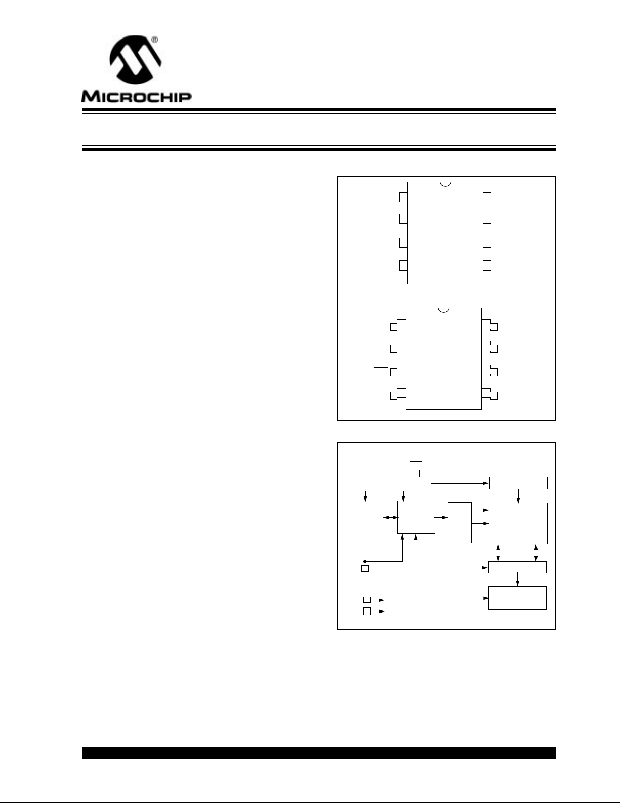
PACKA GE TYPES
PDIP
NC
1
NC
2
WP
3
4
VSS
SOIC
NC
NC
WP
VSS
1
2
3
4
BLOCK DIAGRAM
WP
I/O
CONTROL
LOGIC
SDA SCL
VCLK
V
CC
VSS
MEMORY
CONTROL
LOGIC
8
24LCS21A
7
6
5
8
24LCS21A
7
6
5
XDEC
V
CC
VCLK
SCL
SDA
V
CC
VCLK
SCL
SDA
HV GENERATOR
EEPROM
ARRAY
PAGE LATCHES
YDEC
SENSE AMP
CONTROL
R/W
DDC is a trademark of the Video Electronics Standards Association.
2
I
C is a trademark of Philips Corporation.
1996 Microchip Technology Inc.
Preliminary
DS21161C-page 1
24LCS21A
≥
µ
µ
µ A µ
1.0 ELECTRICAL CHARACTERISTICS
1.1 Maxim
V
........................................................................7.0V
CC
All inputs and outputs w.r.t. V
Storage temperature ..........................-65 ° C to +150 ° C
Ambient temp. with power applied .....-65 ° C to +125 ° C
Soldering temperature of leads (10 seconds) ..+300 ° C
ESD protection on all pins .....................................≥ 4 kV
*Notice: Stresses above those listed under “Maximum ratings”
may cause permanent damage to the device. This is a stress rating only and functional operation of the device at those or any
other conditions above those indicated in the operational listings
of this specification is not implied. Exposure to maximum rating
conditions for extended periods may affect device reliability.
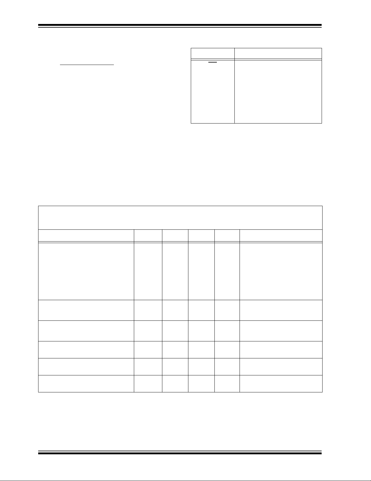
TABLE 1-2: DC CHARACTERISTICS
V
= +2.5V to 5.5V
CC
Commercial (C): Tamb = 0 ° C to +70 ° C
Industrial (I): Tamb =-40 ° C to +85 ° C
um Ratings*
SS
.... -0.6V to V
CC
+1.0V
TABLE 1-1: PIN FUNCTION TABLE
Name Function
WP
SS
V
SDA Serial Address/Data I/O
SCL Serial Clock (Bi-directional Mode)
VCLK Serial Clock (Transmit-Only Mode)
CC
V
NC No Connection
Write Protect (active low)
Ground
+2.5V to 5.5V Power Supply
Parameter Symbol Min Max Units Conditions
SCL and SDA pins:
High level input voltage
Low level input voltage
V
V
0.7 V
IH
IL
—
CC
—
0.3 V
CC
V
V
Input levels on VCLK pin:
High level input voltage
Low level input voltage
Hysteresis of Schmitt trigger inputs V
Low level output voltage V
Low level output voltage V
Input leakage current I
Output leakage current I
V
V
HYS
OL1
OL2
LO
IH
IL
2.0
—
.05 V
CC
—
0.2 V
CC
V
V
— V (Note)
— 0.4 V I
— 0.6 V I
LI
-10 10
-10 10
AV
AV
Pin capacitance (all inputs/outputs) Cin, Cout — 10 pF V
Operating current I
Standby current I
CC
I
CC
Write
Read
CCS
—
—
—
—
3
1
30
100
mAmAV
A
Note: This parameter is periodically sampled and not 100% tested.
CC
V
2.7V (Note)
CC
V
< 2.7V (Note)
OL
= 3 mA, V
OL
= 6 mA, V
= 0.1V to V
IN
= 0.1V to V
OUT
= 5.0V (Note)
CC
Tamb = 25 ° C, F
= 5.5V
CC
V
CC
= 5.5V, SCL = 400 kHz
V
= 3.0V, SDA = SCL = V
CC
CC
V
= 5.5V, SDA = SCL = V
CC
= 2.5V (Note)
CC
= 2.5V
CC
CC
CLK
= 1 MHz
CC
CC
DS21161C-page 2
Preliminary
1996 Microchip Technology Inc.
TABLE 1-3: AC CHARACTERISTICS
24LCS21A
≤
Parameter Symbol
Vcc= 2.5-4.5V
Standard Mode
Vcc= 4.5 - 5.5V
Fast Mode
Units Remarks
Min Max Min Max
Clock frequency F
Clock high time T
Clock low time T
SDA and SCL rise time T
SDA and SCL fall time T
START condition hold time T
HD
CLK
HIGH
LOW
R
F
:
STA
— 100 — 400 kHz
4000 — 600 — ns
4700 — 1300 — ns
— 1000 — 300 ns
— 300 — 300 ns
(Note 1)
(Note 1)
4000 — 600 — ns After this period the first clock
pulse is generated
START condition setup
time
Data input hold time T
Data input setup time T
STOP condition setup time T
Output valid from clock T
Bus free time T
T
SU
STA
:
4700 — 600 — ns Only relevant for repeated
START condition
HD
DAT
SU
SU
:
:
DAT
STO
:
AA
BUF
0—0—ns
(Note 2)
250 — 100 — ns
4000 — 600 — ns
— 3500 — 900 ns
(Note 2)
4700 — 1300 — ns Time the bus must be free
before a new transmission
can start
Output fall time from V
minimum to V
IL
Input filter spike suppres-
IH
maximum
OF
T
T
SP
— 250 20 +
0.1 C
250 ns
B
— 50 — 50 ns
(Note 1), C
(Note 3)
B
100 pF
sion (SDA and SCL pins)
Write cycle time T
WR
— 10 — 10 ms Byte or Page mode
Transmit-Only Mode Parameters
Output valid from VCLK T
VCLK high time T
VAA
VHIGH
— 2000 — 1000 ns
4000 — 600 — ns
VCLK low time TVLOW 4700 — 1300 — ns
VCLK setup time T
VCLK hold time T
Mode transition time T
Transmit-Only power up
VHST 0—0—ns
SPVL 4000 — 600 — ns
VHZ — 1000 — 500 ns
T
VPU 0—0—ns
time
Input filter spike suppres-
SPV — 100 — 100 ns
T
sion (VCLK pin)
Endurance — 10M — 10M — cycles 25°C, Vcc = 5.0V , Block Mode
(Note 4)
Note 1: Not 100% tested. C
B = Total capacitance of one bus line in pF.
2: As a transmitter , the device must provide an internal minimum delay time to bridge the undefined region (min-
imum 300 ns) of the falling edge of SCL to avoid unintended generation of START or STOP conditions.
3: The combined T
suppression. This eliminates the need for a T
SP and VHYS specifications are due to Schmitt trigger inputs which provide noise and spike
I specification for standard operation.
4: This parameter is not tested but guaranteed by characterization. For endurance estimates in a specific appli-
cation, please consult the Total Endurance Model which can be obtained on our BBS or website.
1996 Microchip Technology Inc.
Preliminary
DS21161C-page 3
24LCS21A
2.0 FUNCTIONAL DESCRIPTION
The 24LCS21A is designed to comply to the DDC Standard proposed by VESA (Figure 3-3) with the exception
that it is not Access.bus capable. It operates in two
modes, the Transmit-Only Mode and the Bi-directional
Mode. There is a separate 2-wire protocol to support
each mode, each having a separate clock input but
sharing a common data line (SDA). The device enters
the Transmit-Only Mode upon power-up. In this mode,
the device transmits data bits on the SDA pin in
response to a clock signal on the VCLK pin. The device
will remain in this mode until a valid high to low transition is placed on the SCL input. When a valid transition
on SCL is recognized, the device will switch into the Bidirectional Mode and look for its control byte to be sent
by the master. If it detects its control byte, it will stay in
the Bi-directional Mode. Otherwise, it will revert to the
Transmit-Only Mode after it sees 128 VCLK pulses.
2.1 Transmit-Only Mode
The device will power up in the Transmit-Only Mode at
address 00H. This mode supports a unidirectional
2-wire protocol for continuous transmission of the
contents of the memory array. This device requires that
it be initialized prior to valid data being sent in the Trans-
mit-Only Mode (Section 2.2). In this mode, data is
transmitted on the SDA pin in 8-bit bytes, with each byte
followed by a ninth, null bit (Figure 2-1). The clock
source for the Transmit-Only Mode is provided on the
VCLK pin, and a data bit is output on the rising edge on
this pin. The eight bits in each byte are transmitted most
significant bit first. Each byte within the memory array
will be output in sequence. After address 7Fh in the
memory array is transmitted, the internal address pointers will wrap around to the first memory location (00h)
and continue. The Bi-directional Mode Clock (SCL) pin
must be held high for the device to remain in the
Transmit-Only Mode.
2.2 Initialization Procedure
After VCC has stabilized, the device will be in the
Transmit-Only Mode. Nine clock cycles on the VCLK pin
must be given to the device for it to perform internal
sychronization. During this period, the SDA pin will be
in a high impedance state. On the rising edge of the
tenth clock cycle, the device will output the first valid
data bit which will be the most significant bit in address
00h. (Figure 2-2).
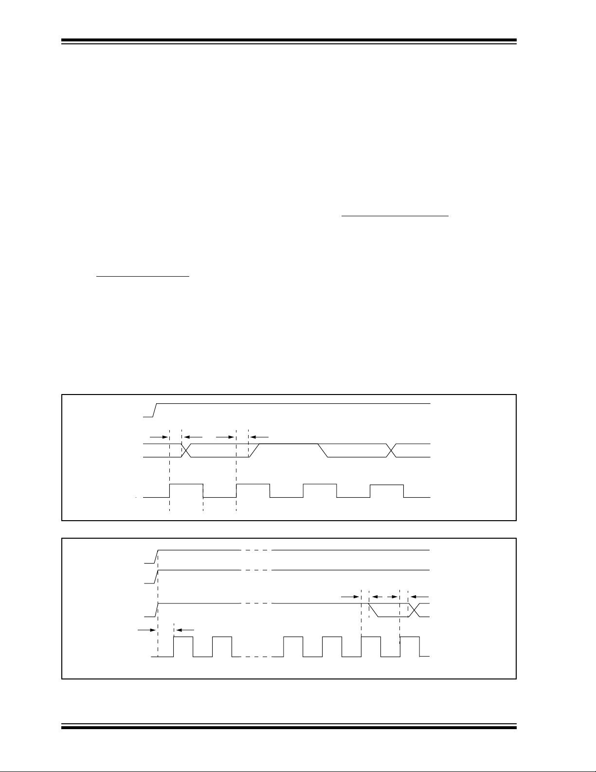
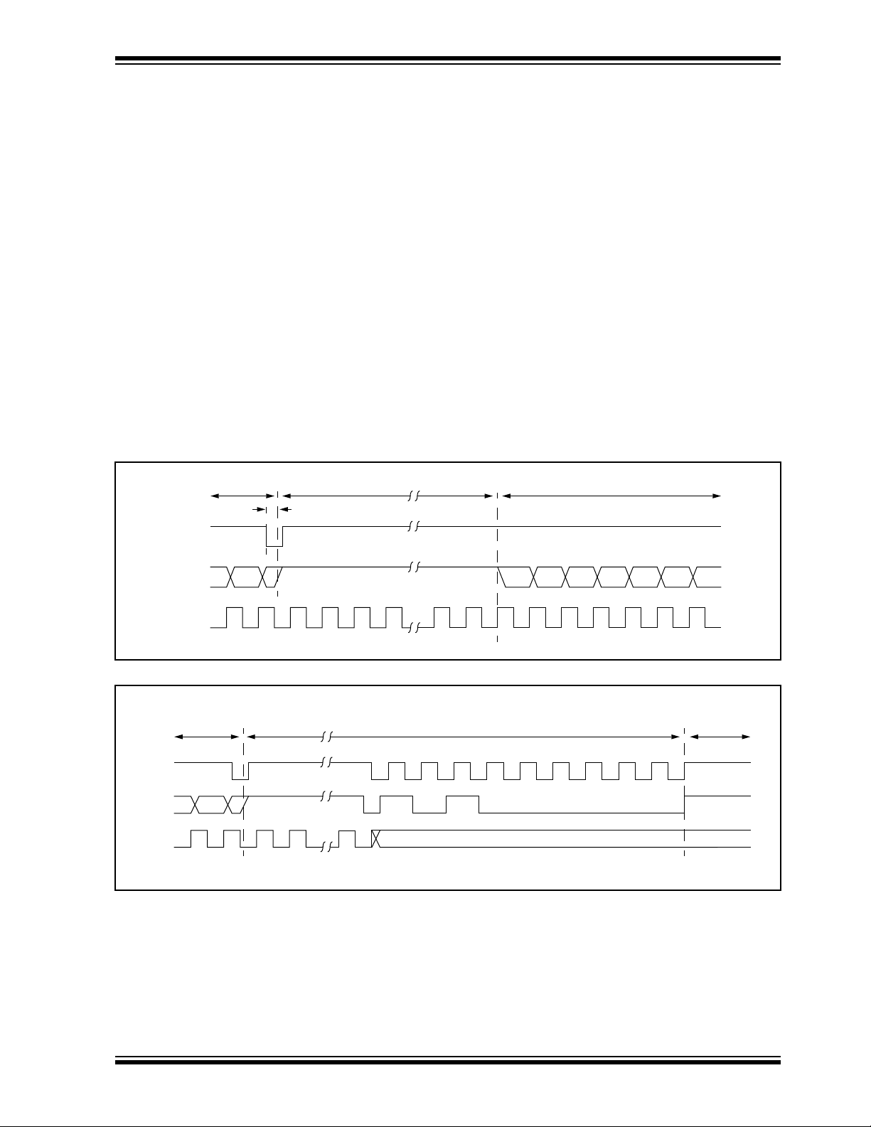
FIGURE 2-1: TRANSMIT-ONLY MODE
SCL
Tvaa Tvaa
SDA
Bit 1 (LSB)
VCLK
TvlowTvhigh
FIGURE 2-2: DEVICE INITIALIZATION
Vcc
SCL
SDA
Tvpu
VCLK
12 891011
Null Bit
Bit 1 (MSB) Bit 7
Tvaa Tvaa
Bit 8 Bit 7High Impedance for 9 clock cycles
DS21161C-page 4 Preliminary 1996 Microchip Technology Inc.
24LCS21A
3.0 BI-DIRECTIONAL MODE
Before the 24LCS21A can be switched into the Bidirectional Mode (Figure 3-1), it must enter the transition mode, which is done by applying a valid high to low
transition on the Bi-directional Mode Clock (SCL). As
soon it enters the transition mode, it looks for a control
byte 1010 000X on the I
pulses on VCLK. Any high to low transition on the SCL
line will reset the count. If it sees a pulse count of 128
on VCLK while the SCL line is idle, it will revert back to
the Transmit-Only Mode, and transmit its contents starting with the most significant bit in address 00h. However, if it detects the control byte on the I
(Figure 3-2) it will switch to the in the Bi-directional
Mode. Once the device has made the transition to the
Bi-directional mode, the only way to switch the device
back to the Transmit-Only Mode is to remove power
from the device. The mode transition process is shown
in detail in Figure 3-3.
2
C bus, and starts to count
2
C bus,
Once the device has switched into the Bi-directional
Mode, the VCLK input is disregarded, with the exception that a logic high level is required to enable write
capability. This mode supports a two-wire Bi-directional
data transmission protocol (I
device that sends data on the bus is defined to be the
transmitter, and a device that receives data from the
bus is defined to be the receiver. The bus must be controlled by a master device that generates the Bi-directional Mode Clock (SCL), controls access to the bus
and generates the START and STOP conditions, while
the 24LCS21A acts as the slave. Both master and
slave can operate as transmitter or receiver, but the
master device determines which mode is activated. In
the Bi-directional mode, the 24LCS21A only responds
to commands for device 1010 000X.
2
C). In this protocol, a
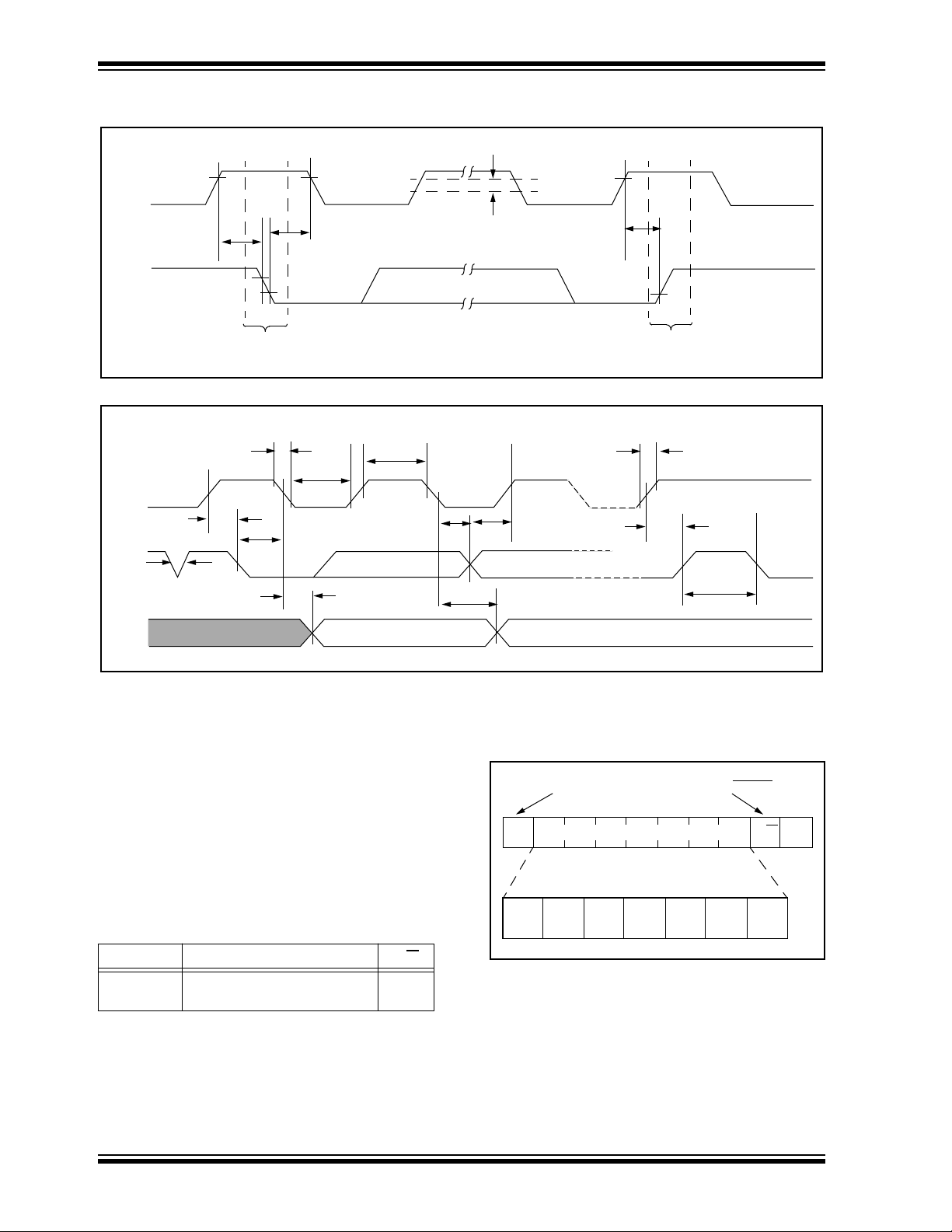
FIGURE 3-1: MODE TRANSITION WITH RECOVERY TO TRANSMIT-ONLY MODE
MODE
Transmit
Only
Bi-directional
TVHZ
Recovery to Transmit-Only Mode
SCL
(MSB of data in 00h)
SDA
VCLK count = 1 2 3 4 127 128
VCLK
Bit8
FIGURE 3-2: SUCCESSFUL MODE TRANSITION TO BI-DIRECTIONAL MODE
Transmit
Only Mode
MODE
SCL
SDA
VCLK count = 1 2 n 0
VCLK
Transition Mode with possibility to return to Transmit-Only Mode
S1010 00 0 0 ACK
n < 128
Bi-directional
permanently
1996 Microchip Technology Inc. Preliminary DS21161C-page 5

24LCS21A
FIGURE 3-3: DISPLAY OPERATION PER DDC STANDARD PROPOSED BY VESA
The 24LCS21A was designed to
Display Power-on
or
DDC Circuit Powered
from +5 volts
Communication
is idle
comply to the portion of flowchart inside dash box
No
No
No
Is Vsync
present?
Yes
Send EDID continuously
using Vsync as clock
High to low
transition on
SCL?
Yes
Stop sending EDID.
Switch to DDC2 mode.
Display has
optional
transition state
?
Yes
Set Vsync counter = 0
or start timer
Change on
SCL, SDA or
VCLK lines?
Yes
High - low
transition on SCL
?
Yes
Reset Vsync counter = 0
Valid
DDC2 address
received?
No
VCLK
cycle?
Yes
Increment VCLK counter
(if appropriate)
No
No
No
Reset counter or timer
Yes
High to low
transition on
SCL?
Yes
DDC2 communication
idle. Display waiting for
address byte.
DDC2B
address
received?
No
Is display
Access.bus
Valid Access.bus
See Access.bus
specification to determine
correct procedure.
TM
capable?
Yes
address?
Yes
No
Yes
Respond to DDC2B
No
No
Receive DDC2B
command
command
No
Counter=128 or
timer expired?
Yes
Switch back to DDC1
mode.
Note 1: The base flowchart is copyright 1993, 1994, 1995 Video Electronic Standard Association (VESA) from
VESA’s Display Data Channel (DDC) Standard Proposal ver. 2p rev. 0, used by permission of VESA.
2: The dash box and text “The 24LCS21A and... inside dash box.” are added by Microchip Technology, Inc.
3: Vsync signal is normally used to derive a signal for VCLK pin on the 24LCS21A.
DS21161C-page 6 Preliminary 1996 Microchip Technology Inc.

24LCS21A
3.1 Bi-directional Mode Bus Characteristics
The following bus protocol has been defined:
• Data transfer may be initiated only when the bus is
not busy.
• During data transfer, the data line must remain
stable whenever the clock line is HIGH. Changes
in the data line while the clock line is HIGH will be
interpreted as a START or STOP condition.
Accordingly, the following bus conditions have been
defined (Figure 3-4).
3.1.1 BUS NOT BUSY (A)
Both data and clock lines remain HIGH.
3.1.2 START DATA TRANSFER (B)
A HIGH to LOW transition of the SDA line while the
clock (SCL) is HIGH determines a STAR T condition. All
commands must be preceded by a START condition.
3.1.3 STOP DATA TRANSFER (C)
A LOW to HIGH transition of the SDA line while the
clock (SCL) is HIGH determines a STOP condition. All
operations must be ended with a STOP condition.
3.1.4 DATA VALID (D)
The state of the data line represents valid data when,
after a START condition, the data line is stable for the
duration of the HIGH period of the clock signal.
The data on the line must be changed during the LOW
period of the clock signal. There is one clock pulse per
bit of data.
Each data transfer is initiated with a START condition
and terminated with a STOP condition. The number of
the data bytes transferred between the START and
STOP conditions is determined by the master device
and is theoretically unlimited, although only the last
eight will be stored when doing a write operation. When
an overwrite does occur it will replace data in a first in
first out fashion.
Note: Once switched into Bi-directional Mode, the
24LCS21A will remain in that mode until
power is removed. Removing power is the
only way to reset the 24LCS21A into the
Transmit-only mode.
3.1.5 ACKNOWLEDGE
Each receiving device, when addressed, is obliged to
generate an acknowledge after the reception of each
byte. The master device must generate an extra clock
pulse which is associated with this acknowledge bit.
Note: The 24LCS21A does not generate any
acknowledge bits if an internal
programming cycle is in progress.
The device that acknowledges has to pull down the
SDA line during the acknowledge clock pulse in such a
way that the SDA line is stable LOW during the HIGH
period of the acknowledge related clock pulse. Of
course, setup and hold times must be taken into
account. A master must signal an end of data to the
slave by not generating an acknowledge bit on the last
byte that has been clocked out of the slave. In this
case, the slave must leave the data line HIGH to enable
the master to generate the STOP condition.
FIGURE 3-4: DATA TRANSFER SEQUENCE ON THE SERIAL BUS
DSCL
DSCL
1996 Microchip Technology Inc. Preliminary DS21161C-page 7
(A) (B) (D) (D) (A)(C)
or
MSCL
or
MSCL
START
CONDITION
ADDRESS OR
ACKNOWLEDGE
VALID
DATA
ALLOWED
TO CHANGE
STOP
CONDITION
24LCS21A
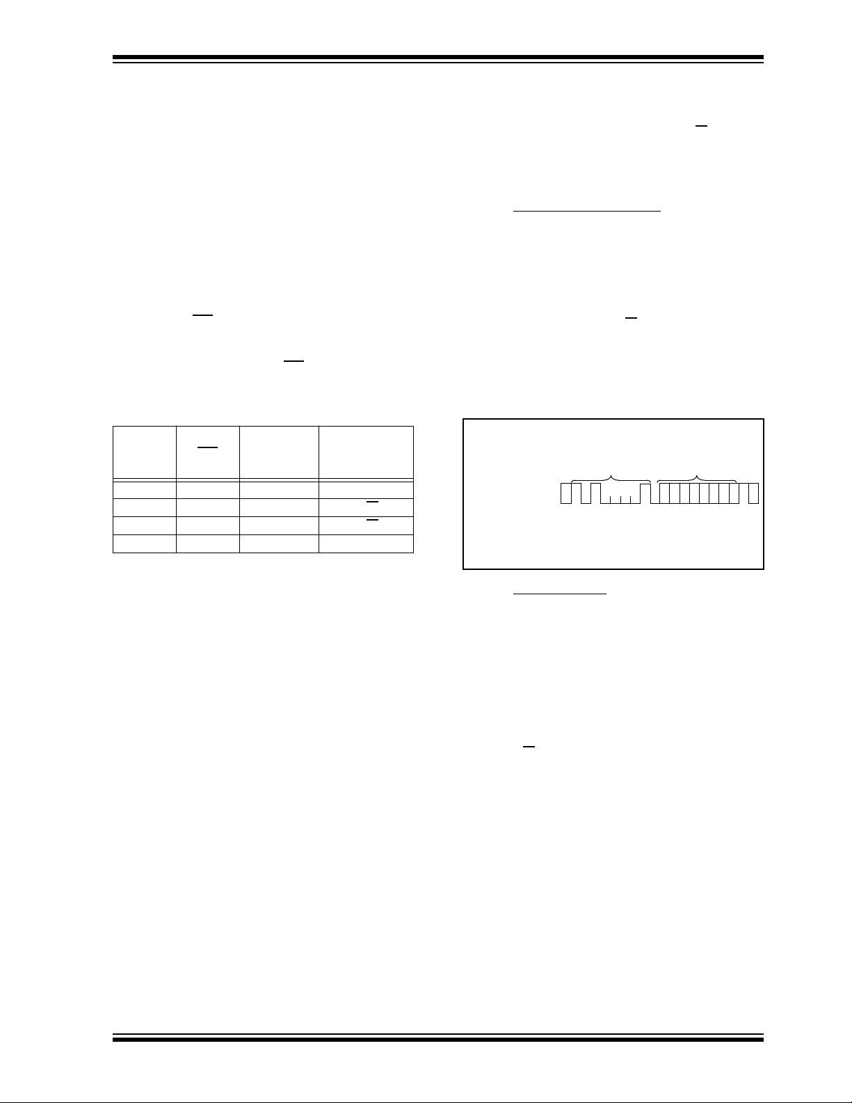
FIGURE 3-5: BUS TIMING START/STOP
SCL
TSU:STA
SDA
START STOP
THD:STA
FIGURE 3-6: BUS TIMING DATA
TF
TLOW
SCL
TSU:STA
THD:STA
SDA
IN
SDA
OUT
TSP
TAA
THIGH
THD:DAT
TAA
VHYS
TSU:DAT
TSU:STO
TR
TSU:STO
TBUF
3.1.6 SLAVE ADDRESS
After generating a START condition, the bus master
transmits the slave address consisting of a 7-bit device
code (1010000) for the 24LCS21A.
The eighth bit of slave address determines whether the
master device wants to read or write to the 24LCS21A
FIGURE 3-7: CONTROL BYTE
ALLOCATION
START
SLAVE ADDRESS
READ/WRITE
R/W A
(Figure 3-7).
The 24LCS21A monitors the bus for its corresponding
slave address continuously. It generates an
acknowledge bit if the slave address was true and it is
not in a programming mode.
1 010000
Operation Slave Address R/W
Read 1010000 1
Write 1010000 0
DS21161C-page 8 Preliminary 1996 Microchip Technology Inc.

24LCS21A
4.0 WRITE OPERATION
4.1 Byte Write
Following the start signal from the master, the slave
address (four bits), three zero bits (000) and the R/W
which is a logic low are placed onto the bus by the
master transmitter. This indicates to the addressed
slave receiver that a byte with a word address will follow
after it has generated an acknowledge bit during the
ninth clock cycle. Therefore, the next byte transmitted
by the master is the word address and will be written
into the address pointer of the 24LCS21A. After receiving another acknowledge signal from the 24LCS21A
the master device will transmit the data word to be written into the addressed memory location. The
24LCS21A acknowledges again and the master
generates a stop condition. This initiates the internal
write cycle, and during this time the 24LCS21A will not
generate acknowledge signals (Figure 4-1).
It is required that VCLK be held at a logic high level
during command and data transfer in order to program
the device. This applies to both byte write and page
write operation. Note, however, that the VCLK is
ignored during the self-timed program operation.
Changing VCLK from high to low during the self-timed
program operation will not
halt programming of the
device.
bit
4.2 Page Write
The write control byte, word address and the first data
byte are transmitted to the 24LCS21A in the same way
as in a byte write. But instead of generating a stop
condition the master transmits up to eight data bytes to
the 24LCS21A which are temporarily stored in the onchip page buffer and will be written into the memory
after the master has transmitted a stop condition. After
the receipt of each word, the three lower order address
pointer bits are internally incremented by one. The
higher order five bits of the word address remains
constant. If the master should transmit more than eight
words prior to generating the stop condition, the
address counter will roll over and the previously
received data will be overwritten. As with the byte write
operation, once the stop condition is received an
internal write cycle will begin (Figure 5-2).
It is required that VCLK be held at a logic high level
during command and data transfer in order to program
the device. This applies to both byte write and page
write operation. Note, however, that the VCLK is
ignored during the self-timed program operation.
Changing VCLK from high to low during the self-timed
program operation will not
device.
halt programming of the
FIGURE 4-1: BYTE WRITE
S
T
CONTROL
BUS ACTIVITY
MASTER
SDA LINE
BUS ACTIVITY
VCLK
A
R
T
S
BYTE
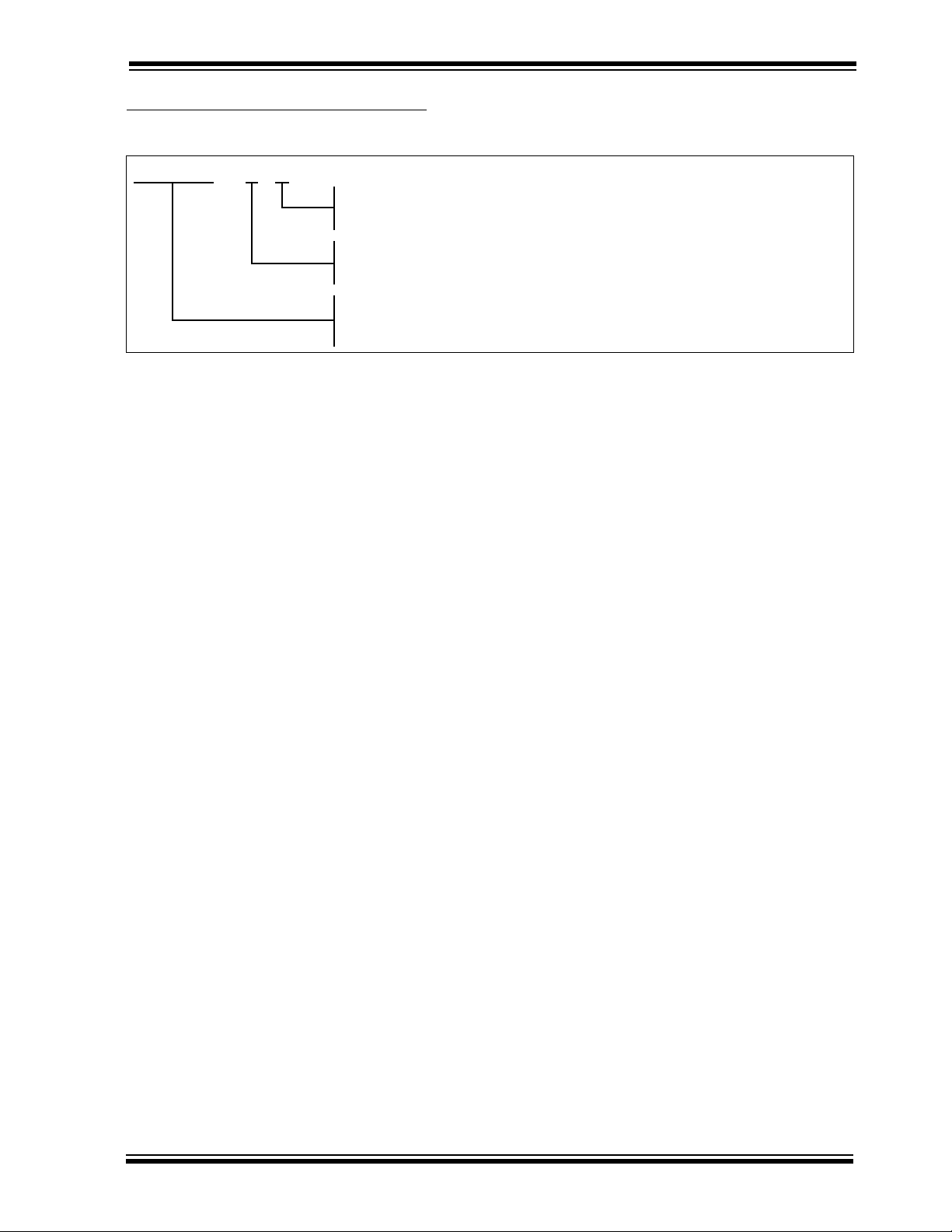
FIGURE 4-2: VCLK WRITE ENABLE TIMING
SCL
HD:STA TSU:STO
SDA
IN
T
A
C
K
WORD
ADDRESS
S
DATA
A
C
K
T
O
P
P
A
C
K
VCLK
TVHST
1996 Microchip Technology Inc. Preliminary DS21161C-page 9
TSPVL

24LCS21A
5.0 ACKNOWLEDGE POLLING
Since the device will not acknowledge during a write
cycle, this can be used to determine when the cycle is
complete (this feature can be used to maximize bus
throughput). Once the stop condition for a write
command has been issued from the master, the device
initiates the internally timed write cycle. ACK polling
can be initiated immediately. This involves the master
sending a start condition followed by the control byte for
a write command (R/W
with the write cycle, then no ACK will be returned. If the
cycle is complete, then the device will return the ACK
and the master can then proceed with the next read or
write command. See Figure 5-1 for the flow diagram.
= 0). If the device is still busy
FIGURE 5-1: ACKNOWLEDGE POLLING
FLOW
Send
Write Command
Send Stop
Condition to
Initiate Write Cycle
Send Start
Send Control Byte
with R/W = 0
Did Device
Acknowledge
(ACK = 0)?
No
FIGURE 5-2: PAGE WRITE
S
BUS ACTIVITY
MASTER
SDA LINE
BUS ACTIVITY
VCLK
T
A
R
T
S
CONTROL
BYTE
WORD
ADDRESS (1)
A
C
K
A
C
K
DATA (n)
A
C
K
Next
Operation
DATA n + 1
Yes
A
C
K
DATA n + 7
S
T
O
P
P
A
C
K
DS21161C-page 10 Preliminary 1996 Microchip Technology Inc.
24LCS21A
6.0 WRITE PROTECTION
When using the 24LCS21A in the Bi-directional Mode,
the VCLK pin can be used as a write protect control pin.
Setting VCLK high allows normal write operations,
while setting VCLK low prevents writing to any location
in the array. Connecting the VCLK pin to V
allow the 24LCS21A to operate as a serial ROM,
although this configuration would prevent using the
device in the Transmit-Only Mode.
Additionally, Pin three performs a flexible write protect
function. The 24LCS21A contains a write-protection
control fuse whose factory default state is cleared.
Writing any data to address 7Fh (normally the
checksum in DDC applications) sets the fuse which
enables the WP
pin. Until this fuse is set, the
24LCS21A is always write enabled (if VCLK = 1). After
the fuse is set, the write capability of the 24LCS21A is
determined by both VCLK and WP
pins (Table 6-1).
TABLE 6-1: WRITE PROTECT TRUTH
TABLE
VCLK WP
0 X X Read Only
1 X No R/W
1 1/open X R/W
1 0 Yes Read Only
Address
7Fh Written
SS would
Mode
for
00h - 7Fh
7.0 READ OPERATION
Read operations are initiated in the same way as write
operations with the exception that the R/W
slave address is set to one. There are three basic types
of read operations: current address read, random read
and sequential read.
7.1 Current Address Read
The 24LCS21A contains an address counter that
maintains the address of the last word accessed,
internally incremented by one. Therefore, if the
previous access (either a read or write operation) was
to address n, the next current address read operation
would access data from address n + 1. Upon receipt of
the slave address with R/W
bit set to one, the
24LCS21A issues an acknowledge and transmits the
eight bit data word. The master will not acknowledge
the transfer but does generate a stop condition and the
24LCS21A discontinues transmission (Figure 7-1).
FIGURE 7-1: CURRENT ADDRESS READ
S
BUS ACTIVITY
MASTER
SDA LINE
BUS ACTIVITY
T
A
CONTROL
R
BYTE
T
SP
101
0000
1
A
C
K
DATA n
bit of the
S
T
O
P
N
O
A
C
K
7.2 Random Read
Random read operations allow the master to access
any memory location in a random manner. To perform
this type of read operation, first the word address must
be set. This is done by sending the word address to the
24LCS21A as part of a write operation. After the word
address is sent, the master generates a start condition
following the acknowledge. This terminates the write
operation, but not before the internal address pointer is
set. Then the master issues the control byte again but
with the R/W
issue an acknowledge and transmits the 8-bit data
word. The master will not acknowledge the transfer but
does generate a stop condition and the 24LCS21A
discontinues transmission (Figure 7-2).
bit set to a one. The 24LCS21A will then
1996 Microchip Technology Inc. Preliminary DS21161C-page 11

24LCS21A
FIGURE 7-2: RANDOM READ
S
T
BUS ACTIVITY
MASTER
SDA LINE
BUS ACTIVITY
FIGURE 7-3: SEQUENTIAL READ
A
CONTROL
R
T
SS
BYTE
10100000 00000111
ADDRESS (n)
A
C
K
WORD
S
T
A
CONTROL
R
T
A
C
K
BYTE
DATA n
A
C
K
S
T
O
P
P
N
O
A
C
K
BUS ACTIVITY
MASTER
CONTROL
BYTE
SDA LINE
BUS ACTIVITY
DATA n DATA n+1
A
C
K
A
C
K
7.3 Sequential Read
Sequential reads are initiated in the same way as a
random read except that after the 24LCS21A transmits
the first data byte, the master issues an acknowledge
as opposed to a stop condition in a random read. This
directs the 24LCS21A to transmit the next sequentially
addressed 8-bit word (Figure 7-3).
T o provide sequential reads the 24LCS21A contains an
internal address pointer which is incremented by one at
the completion of each operation. This address pointer
allows the entire memory contents to be serially read
during one operation.
7.4 Noise Protection
The 24LCS21A employs a VCC threshold detector circuit which disables the internal erase/write logic if the
V
CC is below 1.5 volts at nominal conditions.
The SDA, SCL and VCLK inputs have Schmitt trigger
and filter circuits which suppress noise spikes to assure
proper device operation even on a noisy bus.
DATA n+2 DATA n+X
A
C
K
A
C
K
N
O
A
C
K
8.0 PIN DESCRIPTIONS
8.1 SDA
This pin is used to transfer addresses and data into and
out of the device, when the device is in the Bi-directional Mode. In the Transmit-Only Mode, which only
allows data to be read from the device, data is also
transferred on the SDA pin. This pin is an open drain
terminal, therefore the SDA bus requires a pullup
resistor to V
400 kHz).
For normal data transfer in the Bi-directional Mode,
SDA is allowed to change only during SCL low.
Changes during SCL high are reserved for indicating
the START and STOP conditions.
8.2 SCL
This pin is the clock input for the Bi-directional Mode,
and is used to synchronize data transfer to and from the
device. It is also used as the signaling input to switch
the device from the Transmit-Only Mode to the Bi-directional Mode. It must remain high for the chip to continue
operation in the Transmit-Only Mode.
CC (typical 10 KΩ for 100 kHz, 1 KΩ for
S
T
O
P
P
DS21161C-page 12 Preliminary 1996 Microchip Technology Inc.

8.3 VCLK
This pin is the clock input for the Transmit-Only Mode
(DDC1). In the Transmit-Only Mode, each bit is clocked
out on the rising edge of this signal. In the Bi-directional
Mode, a high logic level is required on this pin to enable
write capability.
8.4 WP
This pin is used for flexible write protection of the
24LCS21A. When the last memory location (7Fh) is
written with any data, this pin is enabled and
determines the write capability of the 24LCS21A
(Table 6-1).
The WP
allow write capability (assuming VCLK = 1) at all times
if this pin is floated.
pin has an internal pull up resistor which will
24LCS21A
1996 Microchip Technology Inc. Preliminary DS21161C-page 13

24LCS21A
NOTES:
DS21161C-page 14 Preliminary 1996 Microchip Technology Inc.
24LCS21A
24LCS21A Product Identification System
To order or to obtain information (e.g., on pricing or delivery), please use the listed part numbers, and refer to the factory or the listed
sales offices.
24LCS21A -/P
Package: P = Plastic DIP (300 mil Body), 8-lead
SN = Plastic SOIC (150 mil Body), 8-lead
Temperature Blank = 0°C to +70°C
Range: I = -40°C to +85°C
2
Device: 24LCS21A Dual Mode I
24LCS21AT Dual Mode I
C Serial EEPROM
2
C Serial EEPROM (Tape and Reel)
1996 Microchip Technology Inc. Preliminary DS21161C-page 15

WORLDWIDE SALES & SERVICE
AMERICAS
Corporate Office
Microchip Technology Inc.
2355 West Chandler Blvd.
Chandler, AZ 85224-6199
Tel: 602 786-7200 Fax: 602 786-7277
Technical Support:
Web:
http://www.microchip.com
Atlanta
Microchip Technology Inc.
500 Sugar Mill Road, Suite 200B
Atlanta, GA 30350
Tel: 770 640-0034 Fax: 770 640-0307
Boston
Microchip Technology Inc.
5 Mount Royal Avenue
Marlborough, MA 01752
Tel: 508 480-9990 Fax: 508 480-8575
Chicago
Microchip Technology Inc.
333 Pierce Road, Suite 180
Itasca, IL 60143
Tel: 708 285-0071 Fax: 708 285-0075
Dallas
Microchip Technology Inc.
14651 Dallas Parkway, Suite 816
Dallas, TX 75240-8809
Tel: 972 991-7177 Fax: 972 991-8588
Dayton
Microchip Technology Inc.
Suite 150
Two Prestige Place
Miamisburg, OH 45342
Tel: 513 291-1654 Fax: 513 291-9175
Los Angeles
Microchip Technology Inc.
18201 Von Karman, Suite 1090
Irvine, CA 92612
Tel: 714 263-1888 Fax: 714 263-1338
New Y ork
Microchip Technmgy Inc.
150 Motor Parkway, Suite 416
Hauppauge, NY 11788
Tel: 516 273-5305 Fax: 516 273-5335
San Jose
Microchip Technology Inc.
2107 North First Street, Suite 590
San Jose, CA 95131
Tel: 408 436-7950 Fax: 408 436-7955
Toronto
Microchip Technology Inc.
5925 Airport Road, Suite 200
Mississauga, Ontario L4V 1W1, Canada
Tel: 905 405-6279 Fax: 905 405-6253
602 786-7627
ASIA/PACIFIC
China
Microchip Technology
Unit 406 of Shanghai Golden Bridge Bldg.
2077 Yan’an Road West, Hongiao District
Shanghai, Peoples Republic of China
Tel: 86 21 6275 5700
Fax: 011 86 21 6275 5060
Hong Kong
Microchip Technology
RM 3801B, Tower Two
Metroplaza
223 Hing Fong Road
Kwai Fong, N.T. Hong Kong
Tel: 852 2 401 1200 Fax: 852 2 401 3431
India
Microchip Technology
No. 6, Legacy, Convent Road
Bangalore 560 025 India
Tel: 91 80 526 3148 Fax: 91 80 559 9840
Korea
Microchip Technology
168-1, Youngbo Bldg. 3 Floor
Samsung-Dong, Kangnam-Ku,
Seoul, Korea
Tel: 82 2 554 7200 Fax: 82 2 558 5934
Singapore
Microchip Technology
200 Middle Road
#10-03 Prime Centre
Singapore 188980
Tel: 65 334 8870 Fax: 65 334 8850
Taiwan, R.O.C
Microchip Technology
10F-1C 207
Tung Hua North Road
Taipei, Taiwan, ROC
Tel: 886 2 717 7175 Fax: 886 2 545 0139
EUROPE
United Kingdom
Arizona Microchip Technology Ltd.
Unit 6, The Courtyard
Meadow Bank, Furlong Road
Bourne End, Buckinghamshire SL8 5AJ
Tel: 44 1628 850303 Fax: 44 1628 850178
France
Arizona Microchip Technology SARL
Zone Industrielle de la Bonde
2 Rue du Buisson aux Fraises
91300 Massy - France
Tel: 33 1 69 53 63 20 Fax: 33 1 69 30 90 79
Germany
Arizona Microchip Technology GmbH
Gustav-Heinemann-Ring 125
D-81739 Muenchen, Germany
Tel: 49 89 627 144 0 Fax: 49 89 627 144 44
Italy
Arizona Microchip Technology SRL
Centro Direzionale Colleone Pas Taurus 1
Viale Colleoni 1
20041 Agrate Brianza
Milan Italy
Tel: 39 39 6899939 Fax: 39 39 689 9883
JAPAN
Microchip Technology Intl. Inc.
Benex S-1 6F
3-18-20, Shin Yokohama
Kohoku-Ku, Y okohama
Kanagawa 222 Japan
Tel: 81 45 471 6166 Fax: 81 45 471 6122
9/3/96
All rights reserved. 1996, Microchip Technology Incorporated, USA. 9/96
Printed on recycled paper.
Information contained in this publication regarding device applications and the like is intended through suggestion only and may be superseded by updates. No representation or warranty is given and no liability is assumed by Microchip Technology Incorporated with respect to the accuracy or use of such information, or infringement
of patents or other intellectual property rights arising from such use or otherwise. Use of Microchip’s products as critical components in life support systems is not authorized except with express written approval by Microchip. No licenses are conveyed, implicitly or otherwise, under any intellectual property rights. The Microchip logo and
name are registered trademarks of Microchip Technology Inc. All rights reserved. All other trademarks mentioned herein are the property of their respective companies.
DS21161C-page 16 Preliminary 1996 Microchip Technology Inc.
 Loading...