

Microchip Technology Inc 24LC65-I-SM, 24LC65-SM, 24LC65-P, 24LC65T-I-SM, 24LC65T-I-P Datasheet
...
C
24LC65
2
64K 2.5V I
C
Smart Serial
EEPROM
FEATURES
• Voltage operating range: 2.5V to 6.0V
- Peak write current 3 mA at 6.0V
- Maximum read current 150 µ A at 6.0V
- Standby current 1 µ A typical
• Industry standard two wire bus protocol I
compatible
• 8 byte page, or byte modes available
• 2 ms typical write cycle time, byte or page
• 64-byte input cache for fast write loads
• Up to 8 devices may be connected to the same
bus for up to 512K bits total memory
• Including 100 kHz (2.5V) and 400 kHz (5.0V)
compatibility
• Programmable block security options
• Programmable endurance options
• Schmitt trigger, filtered inputs for noise suppression
• Output slope control to eliminate ground bounce
• Self-timed ERASE and WRITE cycles
• Power on/off data protection circuitry
• Endurance:
- 10,000,000 E/W cycles guaranteed for a High
Endurance Block
- 1,000,000 E/W cycles guaranteed for a Stan-
dard Endurance Block
• Electrostatic discharge protection > 4000V
• Data retention > 200 years
• 8-pin PDIP/SOIC packages
• Temperature ranges
- Commercial (C): 0 ° C to +70 ° C
- Industrial (I) -40 ° C to +85 ° C
2
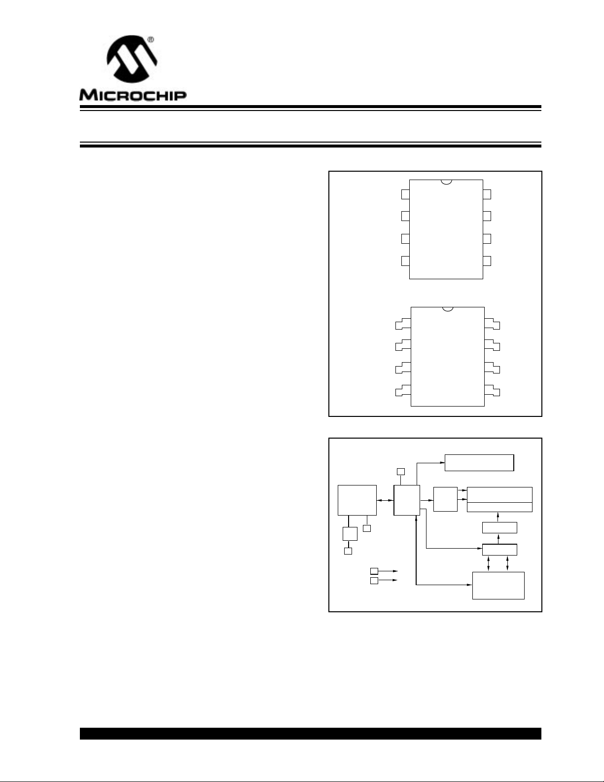
PACKA GE TYPES
PDIP
A0
1
A1
2
A2
3
V
4
SS
SOIC
A0
A1
A2
V
SS
1
2
3
4
BLOCK DIAGRAM
A0..A2
I/O
Control
Logic
Memory
Control
Logic
24LC65
24LC65
XDEC
8
7
6
5
8
7
6
5
HV Generator
EEPROM ARRAY
Page Latches
VCC
NC
SCL
SDA
V
NC
SCL
SDA
CC
DESCRIPTION
The Microchip Technology Inc. 24LC65 is a “smart” 8K
x 8 Serial Electrically Erasable PROM. This device
has been developed for advanced, low power applications such as personal communications, and provides
the systems designer with flexibility through the use of
many new user-programmable features. The 24LC65
offers a relocatable 4K bit block of ultra-high-endurance
memory for data that changes frequently. The remainder of the array, or 60K bits, is rated at 1,000,000
ERASE/WRITE (E/W) cycles guaranteed. The 24LC65
features an input cache for fast write loads with a
capacity of eight pages, or 64 bytes. This device also
features programmable security options for E/W protection of critical data and/or code of up to fifteen 4K
2
I
C is a trademark of Philips Corporation.
Smart Serial is a trademark of Microchip Technology Inc.
1996 Microchip Technology Inc. DS21073E-page 1
I/O
SCL
SDA
Vcc
Vss
blocks. Functional address lines allow the connection of
up to eight 24LC65's on the same bus for up to 512K
bits contiguous EEPROM memory. Advanced CMOS
technology makes this device ideal for low-power nonvolatile code and data applications. The 24LC65 is
available in the standard 8-pin plastic DIP and 8-pin
surface mount SOIC package.
Cache
YDEC
Sense AMP
R/W Control
24LC65
µ
µ
µ
1.0 ELECTRICAL CHARACTERISTICS
1.1 Maxim
CC
V
...................................................................................7.0V
All inputs and outputs w.r.t. V
Storage temperature...................................... -65˚C to+150˚C
Ambient temp. with power applied................ -65˚C to +125˚C
Soldering temperature of leads (10 seconds)............. +300˚C
ESD protection on all pins ..................................................≥ 4 kV
*Notice: Stresses above those listed under “Maximum Ratings”
may cause permanent damage to the device. This is a stress rating only and functional operation of the device at those or any
other conditions above those indicated in the operational listings
of this specification is not implied. Exposure to maximum rating
conditions for extended periods may affect device reliability.
um Ratings*
SS
...............-0.6V to V
CC
+1.0V
TABLE 1-1: PIN FUNCTION TABLE
TABLE 1-2: DC CHARACTERISTICS
CC
V
Commercial (C): Tamb = 0 ° C to +70 ° C
Industrial (I): Tamb = -40 ° C to +85 ° C
Parameter Sym Min Max Units Conditions
A0, A1, A2, SCL and SDA pins:
V
C
CC
CC
I
IN
IH
V
IL
V
HYS
OL
V
LI
LO
, C
W
Read
CCS
OUT
RITE
.7 Vcc
—
.05 V
.3 V
CC
—
-10 10
-10 10
—10pFV
—
—
—5
High level input voltage
Low level input voltage
Hysteresis of Schmitt Trigger inputs
Low level output voltage
Input leakage current I
Output leakage current I
Pin capacitance
(all inputs/outputs)
Operating current I
Standby current I
Note 1: This parameter is periodically sampled and not 100% tested.
Name Function
A0..A2 User Configurable Chip Selects
Vss Ground
SDA Serial Address/Data/I/O
SCL Serial Clock
V
CC
NC
+2.5V to 6.0V Power Supply
No Internal Connection
= +2.5V to +6.0V
—
CC
—
.40
V
V
VV(Note 1)
I
OL
= 3.0 mA
AV
IN
= .1V to V
AV
= .1V to V
OUT
CC
= 5.0V (Note 1)
CC
CC
Tamb = 25˚C, Fclk = 1 MHz
3
150
mA
µ
CC
V
CC
A
V
AV
CC
= 6.0V, SCL = 400 kHz
= 6.0V, SCL = 400 kHz
= 5.0V, SCL = SDA = V
(Note 1)
CC
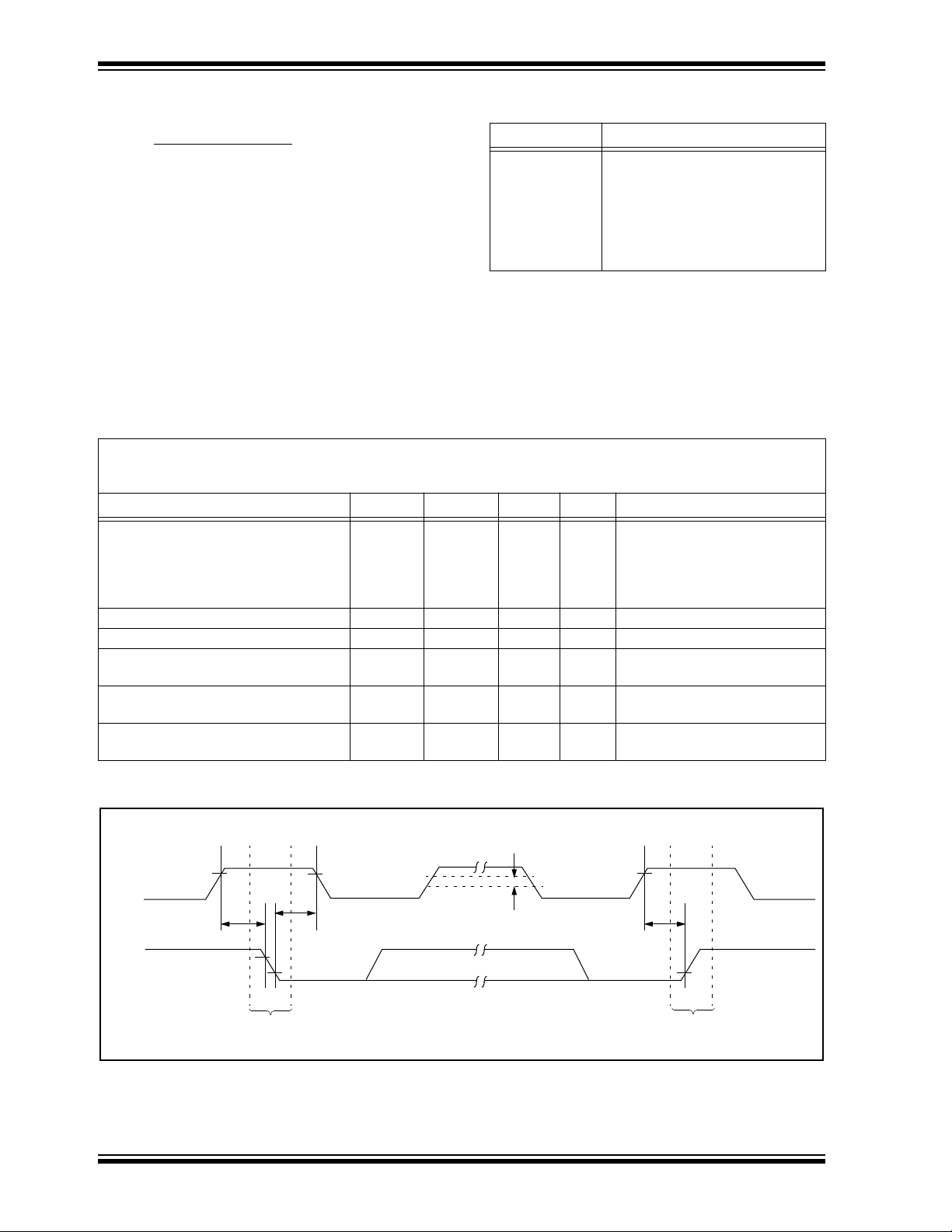
FIGURE 1-1: BUS TIMING START/STOP
SCL
TSU:STA
SDA
START STOP
DS21073E-page 2
THD:STA
VHYS
TSU:STO
1996 Microchip Technology Inc.
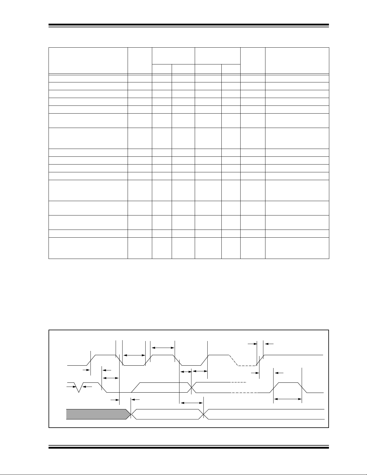
TABLE 1-3: AC CHARACTERISTICS
≤
24LC65
Parameter Symbol
Vcc = 2.5V-6.0V
STD. MODE
V
CC
= 4.5-6.0V
FAST MODE
Units Remarks
Min Max Min Max
Clock frequency F
Clock high time T
Clock low time T
SDA and SCL rise time T
SDA and SCL fall time T
START condition setup time T
HD
CLK
HIGH
LOW
R
F
STA
:
— 100 — 400 kHz
4000 — 600 — ns
4700 — 1300 — ns
— 1000 — 300 ns (Note 1)
— 300 — 300 ns (Note 1)
4000 — 600 — ns After this period the first
clock pulse is generated
START condition setup time T
SU
:
4700 — 600 — ns Only relevant for
STA
repeated START condi-
tion
Data input hold time T
Data input setup time T
STOP condition setup time T
Output valid from clock T
Bus free time T
HD
SU
SU
:
DAT
DAT
:
:
STO
AA
BUF
0— 0 —ns
250 — 100 — ns
4000 — 600 — ns
— 3500 — 900 ns (Note 2)
4700 — 1300 — ns Time the bus must be
free before a new trans-
mission can start
Output fall time from V
V
IL
max
Input filter spike suppression
IH
min to
OF
T
SP
T
— 250 20 + 0.1
C
250 ns (Note 1), C
B
— 50 — 50 ns Note 3
B
(SDA and SCL pins)
Write cycle time T
WR
— 5 — 5 ms/page (Note 4)
Endurance
High Endurance Block
Rest of Array
Note 1: Not 100 percent tested. C
B
= total capacitance of one bus line in pF.
10M
1M
—
—
10M
1M
——cycles 25 ° C, Vcc = 5.0V, Block
Mode (Note 5)
2: As a transmitter, the device must provide an internal minimum delay time to bridge the undefined region
(minimum 300 ns) of the falling edge of SCL to avoid unintended generation of START or STOP conditions.
3: The combined T
SP
and V
specifications are due to new Schmitt trigger inputs which provide improved
HYS
noise and spike suppression. This eliminates the need for a Ti specification for standard operation.
4: The times shown are for a single page of 8 bytes. Multiply by the number of pages loaded into the write
cache for total time.
5: This parameter is not tested but guaranteed by characterization. For endurance estimates in a specific appli-
cation, please consult the Total Endurance Model which can be obtained on our BBS or website.
100 pF
FIGURE 1-2: BUS TIMING DATA
TF
TLOW
SCL
TSU:STA
THD:STA
SDA
IN
SDA
OUT
1996 Microchip Technology Inc. DS21073E-page 3
TSP
TAA
THIGH
THD:DAT
TAA
TSU:DAT
TSU:STO
TR
TBUF
24LC65
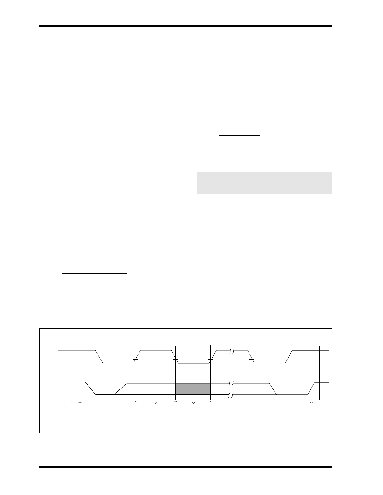
2.0 FUNCTIONAL DESCRIPTION
The 24LC65 supports a bidirectional two-wire bus and
data transmission protocol. A device that sends data
onto the bus is defined as transmitter, and a device
receiving data as receiver. The bus must be controlled
by a master device which generates the serial clock
(SCL), controls the bus access, and generates the
START and STOP conditions, while the 24LC65 works
as slave. Both master and slave can operate as transmitter or receiver but the master device determines
which mode is activated.
3.0 BUS CHARACTERISTICS
The following bus protocol has been defined:
• Data transfer may be initiated only when the bus is
not busy.
• During data transfer, the data line must remain
stable whenever the clock line is HIGH. Changes
in the data line while the clock line is HIGH will be
interpreted as a START or STOP condition.
Accordingly, the following bus conditions have been
defined (Figure 3-1).
3.1 Bus not Busy (A)
Both data and clock lines remain HIGH.
3.2 Start Data Transfer (B)
A HIGH to LOW transition of the SDA line while the
clock (SCL) is HIGH determines a STAR T condition. All
commands must be preceded by a START condition.
3.3 Stop Data Transfer (C)
3.4 Data Valid (D)
The state of the data line represents valid data when,
after a START condition, the data line is stable for the
duration of the HIGH period of the clock signal.
The data on the line must be changed during the LOW
period of the clock signal. There is one clock pulse per
bit of data.
Each data transfer is initiated with a START condition
and terminated with a STOP condition. The number of
the data bytes transferred between the START and
STOP conditions is determined by the master device.
3.5 Acknowledge
Each receiving device, when addressed, is obliged to
generate an acknowledge after the reception of each
byte. The master device must generate an extra clock
pulse which is associated with this acknowledge bit.
Note: The 24LC65 does not generate any
acknowledge bits if an internal programming cycle is in progress.
A device that acknowledges must pull down the SDA
line during the acknowledge clock pulse in such a way
that the SDA line is stable LOW during the HIGH period
of the acknowledge related clock pulse. Of course,
setup and hold times must be taken into account. During reads, a master must signal an end of data to the
slave by NOT generating an acknowledge bit on the last
byte that has been clocked out of the slave. In this case,
the slave (24LC65) must leave the data line HIGH to
enable the master to generate the STOP condition.
A LOW to HIGH transition of the SDA line while the
clock (SCL) is HIGH determines a STOP condition. All
operations must be ended with a STOP condition.
FIGURE 3-1: DATA TRANSFER SEQUENCE ON THE SERIAL BUS
(A) (B) (D) (D) (A)(C)
SCL
SDA
START
CONDITION
ADDRESS OR
ACKNOWLEDGE
VALID
DATA
ALLOWED
TO CHANGE
STOP
CONDITION
DS21073E-page 4 1996 Microchip Technology Inc.
 Loading...