

Datasheet TC9402EJD, TC9401EJD, TC9401CPD, TC9400CPD, TC9400COD Datasheet (Microchip Technology)
TC9400/9401/9402
Voltage-to-Frequency/Frequency-to-Voltage Converters
Features
VOLTAGE-TO-FREQUENCY
• Choice of Linearity
- TC9401: 0.01%
- TC9400: 0.05%
- TC9402: 0.25%
• DC to 100kHz (F/V) or 1Hz to 100kHz (V/F)
• Low Power Dissipation: 27mW (Typ.)
• Single/Dual Supply Operation
- +8V to +15V or ±4V to ±7.5V
• Gain Temperature Stability: ±25 ppm/°C (Typ.)
• Programmable Scale Factor
FREQUENCY-TO-VOLTAGE
• Operation: DC to 100kHz
• Choice of Linearity
- TC9401: 0.02%
- TC9400: 0.05%
- TC9402: 0.25%
• Programmable Scale Factor
Applications
• µP Data Acquisition
• 13-bit Analog-to-Digital Converters
• Analog Data Transmission and Recording
• Phase Locked Loops
• Frequency Meters/Tachometer
• Motor Control
• FM Demodulation
Device Selection Table
Part
Number
TC9400COD 0.05% 14-Pin SOIC
TC9400CPD 0.05% 14-Pin PDIP 0°C to +70°C
TC9400EJD 0.05% 14-Pin CerDIP -40°Cto +85°C
TC9401CPD 0.01% 14-Pin PDIP 0°C to +70°C
TC9401EJD 0.01% 14-Pin CerDIP -40°Cto +85°C
TC9402CPD 0.25% 14-Pin PDIP 0°C to +70°C
TC9402EJD 0.25% 14-Pin CerDIP °C to +85°C
Linearity
(V/F)
Package
(Narrow)
Temperature
Range
0°C to +70°C
General Description
The TC9400/TC9401/TC9402 are low cost voltage-tofrequency ( V/F) converters, utilizing low power CMOS
technology. The converters accept a variable analog
input signal and generatean output pulse train, whose
frequency is linearly proportional to the input voltage.
Thedevicescanalsobeusedashighlyaccuratefrequency-to-voltage (F/V) converters, accepting virtually
any i nput frequency waveform and providing a linearly
proportional voltageoutput.
A complete V/F or F/V system only requires the addition of two capacitors, three resistors, and reference
voltage.
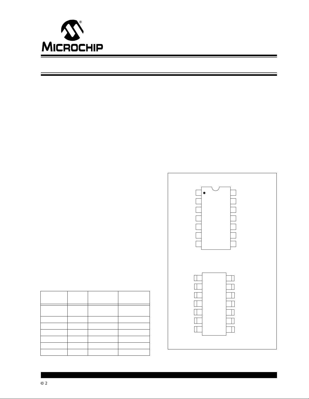
Package Type
14-Pin Plastic DIP/CERDIP
I
BIAS
ZERO ADJ
V
V
OUT
REF
GND
V
REF
I
BIAS
ZERO ADJ
I
V
SS
V
OUT
REF
GND
V
REF
1
2
I
IN
3
4
5
6
7
TC9400
TC9401
TC9402
SS
14-Pin SOIC
1
2
IN
3
TC9400
4
TC9401
TC9402
5
6
7
NC = No Internal Connection
V
14
DD
13
NC
AMPLIFIER OUT
12
THRESHOLD
11
DETECTOR
FREQ/2 OUT
10
9
OUTPUT COMMON
PULSE FREQ OUT
8
14
V
DD
13
NC
AMPLIFIER OUT
12
THRESHOLD
11
DETECTOR
FREQ/2 OUT
10
9
OUTPUT COMMON
8
PULSE FREQ OUT
2002 Microchip TechnologyInc. DS21483B-page 1
TC9400/9401/9402
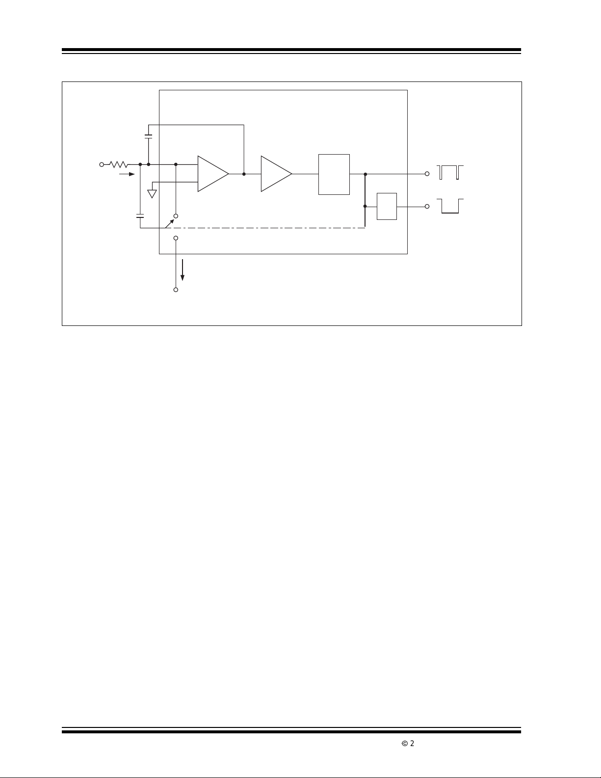
g
Functional Block Diagram
Input
Voltage
Integrator
Capacitor
R
IN
I
IN
Reference
Capacitor
I
REF
Reference
Volta
e
Integrator
Op Amp
Threshold
Detector
TC9400
One
Shot
÷2
Pulse Output
Pulse/2 Output
DS21483B-page 2
2002 Microchip TechnologyInc.
TC9400/9401/9402
1.0 ELECTRICAL
CHARACTERISTICS
Absolute Maximum Ratings*
VDD–VSS...........................................................+18V
........................................................................10mA
I
IN
V
OUTMAX–VOUT
V
REF–VSS
Common......................................23V
..........................................................-1.5V
*Stresses above those listed under "Absolute Maximum
Ratings" may cause permanent damage to the device. These
are stress ratings only and functional operation of the device
at these or any other conditions above those indicated in the
operation sections of the specifications is not implied.
Exposure to Absolute Maximum Rating conditions for
extended periods may affectdevice reliability.
StorageTemperature Range..............-65°C to +150°C
Operating Temperature Range:
C Device ........................................... 0°C to +70°C
E Device.........................................-40°C to +85°C
Package Dissipation (T
≤ 70°C):
A
8-Pin CerDIP..............................................800mW
8-Pin Plastic DIP........................................730mW
8-Pin SOIC. ................................................470mW
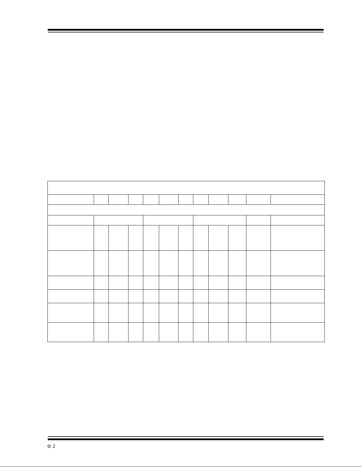
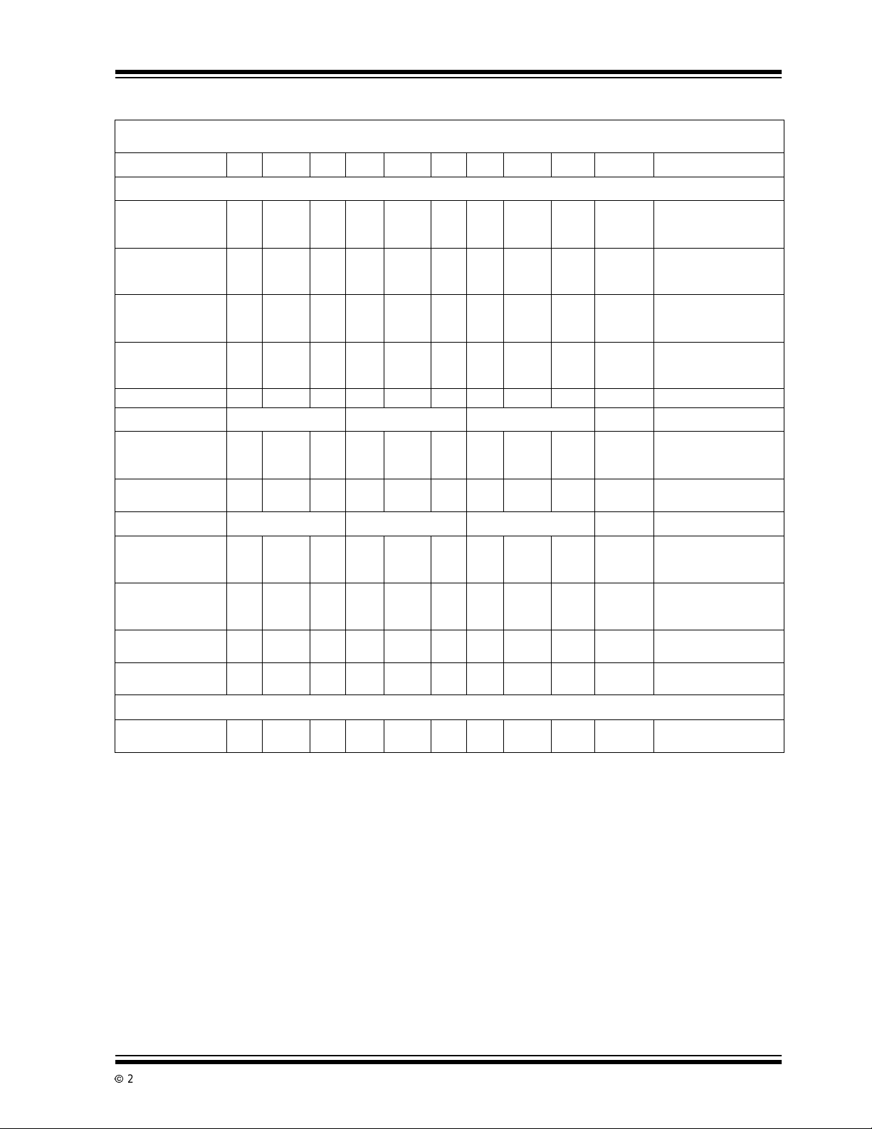
TC940X ELECTRICAL SPECIFICATIONS
Electrical Characteristics: VDD=+5V,VSS=-5V,V
specified. T
Parameter Min Typ Max Min Typ Max Min Typ Max Units Test Conditions
= +25°C, unless temperature rangeis specified (-40°C to +85°C for E device, 0°C to +70°CforC device).
A
Voltage-to-Frequency
GND
=0V,V
REF
=-5V,R
=100kΩ, Full Scale = 10kHz, unless otherwise
BIAS
Accuracy TC9400 TC9401 TC9402
Linearity 10kHz — 0.01 0.05 — 0.004 0.01 — 0.05 0.25 %
Linearity 100kHz — 0.1 0.25 — 0.04 0.08 — 0.25 0.5 %
GainTemperature
Drift (Note 1)
GainVariance — ±10 — — ±10 — — ±10 — % of
Zero Offset
(Note 2)
Zero Temperature
Drift (Note 1)
Note 1: Full temperature range; not tested.
2: I
=0.
IN
3: Full temperature range, I
4: I
OUT
5: ThresholdDetect = 5V, Amp Out = 0V, full temperature range.
6: 10Hz to 100kHz; not tested.
7: 5µsec minimum positivepulse width and 0.5µsec minimum negative pulse width.
8: t
R=tF
9: R
≥ 2kΩ, tested @ 10kΩ.
L
10: Full temperature range, V
— ±25 ±40 — ±25 ±40 — ±50 ±100 ppm/°C
— ±10 ±50 — ±10 ±50 — ±20 ±100 mV Correction at Zero
— ±25 ±50 — ±25 ±50 — ±50 ±100 µV/°C VariationinZeroOffset
=10mA.
=10µA.
=20nsec.
OUT
IN
= -0.1V.
Full Scale
Full Scale
Full Scale
Nominal
Output Deviation from
Straight Line Between
Normalized Zero and
FullScale Input
Output Deviation from
Straight Line Between
Normalized Zero Reading and Full Scale Input
VariationinGainAdue
to Temperature Change
Variation from Ideal
Accuracy
Adjustfor ZeroOutput
whenInputis Zero
DuetoTemperature
Change
2002 Microchip TechnologyInc. DS21483B-page 3
TC9400/9401/9402
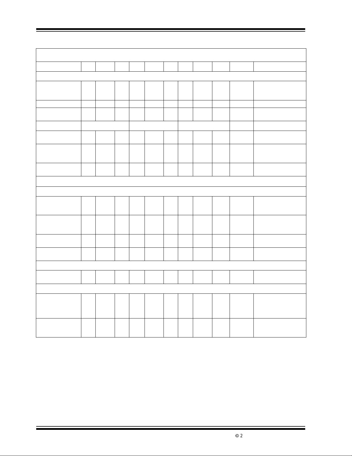
TC940X ELECTRICAL SPECIFICATIONS (CONTINUED)
Electrical Characteristics: VDD=+5V,VSS=-5V,V
specified. T
= +25°C, unless temperature rangeis specified (-40°C to +85°C for E device, 0°C to +70°CforC device).
A
Parameter Min Typ Max Min Typ Max Min Typ Max Units Test Conditions
Analog Input
I
Full Scale — 10 — — 10 — — 10 — µA Full Scale Analog Input
IN
Over Range — — 50 — — 50 — — 50 µA Over RangeCurrent
I
IN
Response Time — 2 — — 2 — — 2 — Cycle Settling Time to 0.1%
Digital Section TC9400 TC9401 TC9402
V
SAT@IOL
V
OUTMAX–VOUT
Common (Note 4)
PulseFrequency
= 10mA — 0.2 0.4 — 0.2 0.4 — 0.2 0.4 V Logic "0" Output
— — 18 — — 18 — — 18 V VoltageRange
—3——3——3 —µsec
OutputWidth
Frequency-to-Voltage
GND
=0V,V
REF
=-5V,R
=100kΩ, Full Scale = 10kHz, unless otherwise
BIAS
Current to achieve
Specified Accuracy
Full Scale
Voltage (Note 3)
Between Output and
Common
Supply Current
Quiescent
I
DD
(Note 5)
— 1.5 6 — 1.5 6 — 3 10 mA Current Required from
Positive Supply during
Operation
Quiescent
I
SS
(Note 5)
— -1.5 -6 — -1.5 -6 — -3 -10 mA Current Required from
Negative Supplyduring
Operation
Supply 4 — 7.5 4 — 7.5 4 — 7.5 V Operating Range of
V
DD
Supply -4 — -7.5 -4 — -7.5 -4 — -7.5 V Operating Range of
V
SS
Positive Supply
Negative Supply
Reference Voltage
V
REF–VSS
-2.5 — — -2.5 — — -2.5 — — V Range of Voltage
Reference Input
Accuracy
Non-Linearity
(Note 10)
— 0.02 0.05 — 0.01 0.02 — 0.05 0.25 %
Full Scale
Deviation from ideal
Transfer Function as a
Percentage Full Scale
Voltage
InputFrequency
Range
10 — 100k 10 — 100k 10 — 100k Hz Frequency Range for
Specified Non-Linearity
(Notes 7 and 8)
Note 1: Full temperature range; not tested.
=0.
2: I
IN
3: Full temperature range, I
4: I
5: ThresholdDetect = 5V, Amp Out = 0V, full temperature range.
OUT
=10µA.
OUT
=10mA.
6: 10Hz to 100kHz; not tested.
7: 5µsec minimum positivepulse width and 0.5µsec minimum negative pulse width.
8: t
9: R
10: Full temperature range, V
=20nsec.
R=tF
≥ 2kΩ, tested @ 10kΩ.
L
= -0.1V.
IN
DS21483B-page 4
2002 Microchip TechnologyInc.
TC9400/9401/9402
TC940X ELECTRICAL SPECIFICATIONS (CONTINUED)
Electrical Characteristics: VDD=+5V,VSS=-5V,V
specified. T
= +25°C, unless temperature rangeis specified (-40°C to +85°C for E device, 0°C to +70°CforC device).
A
Parameter Min Typ Max Min Typ Max Min Typ Max Units Test Conditions
Frequency Input
Positive Excursion 0.4 — V
0.4 — V
DD
Negative Excursion -0.4 -2 -0.4 — -2 -0.4 — -2 V VoltageRequired to
MinimumPositive
—5——5——5 —µsec Time between
Pulse Width
(Note 8)
MinimumNegative
— 0.5 — — 0.5 — — 0.5 — µsec Time Between
Pulse Width
(Note 8)
Input Impedance — 10 — — 10 — — 10 MΩ
Analog Outputs TC9400 TC9401 TC9402
OutputVoltage
(Note 9)
—V
DD
–1 — — VDD–1 — — VDD– 1 — V Voltage Range of Op
OutputLoading 2 — — 2 — — 2 — — kΩ Resistive Loadingat
Supply Current TC9400 TC9401 TC9402
Quiescent
I
DD
(Note 10)
I
Quiescent
SS
— 1.5 6 — 1.5 6 — 3 10 mA Current Requiredfrom
— -1.5 -6 -1.5 -6 — -3 -10 mA Current Required from
(Note 10)
Supply 4 — 7.5 4 — 7.5 4 — 7.5 V Operating Range of
V
DD
Supply -4 — -7.5 -4 — -7.5 -4 — -7.5 V Operating Range of
V
SS
Reference Voltage
V
REF–VSS
-2.5 — — -2.5 — — -2.5 — — V Range of Voltage
Note 1: Full temperature range; not tested.
=0.
2: I
IN
3: Full temperature range, I
4: I
OUT
=10µA.
OUT
=10mA.
5: ThresholdDetect = 5V, Amp Out = 0V, full temperature range.
6: 10Hz to 100kHz; not tested.
7: 5µsec minimum positivepulse width and 0.5µsec minimum negative pulse width.
8: t
9: R
10: Full temperature range, V
=20nsec.
R=tF
≥ 2kΩ, tested @ 10kΩ.
L
= -0.1V.
IN
GND
=0V,V
=-5V,R
REF
0.4 — V
DD
=100kΩ, Full Scale = 10kHz, unless otherwise
BIAS
DD
V VoltageRequired to
Turn Threshold
Detector On
Turn Threshold
Detector Off
Threshold Crossings
Threshold Crossings
Amp Outputfor Specified Non-Linearity
Output of Op Amp
Positive Supply During
Operation
Negative Supply
During Operation
Positive Supply
Negative Supply
Reference Input
2002 Microchip TechnologyInc. DS21483B-page 5
TC9400/9401/9402
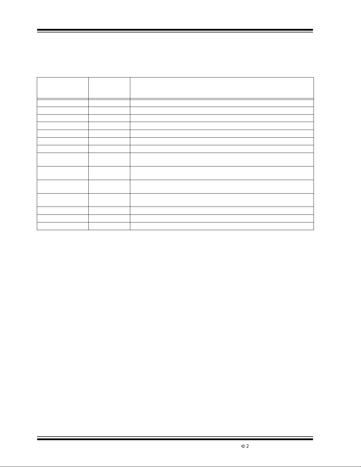
2.0 PIN DESCRIPTIONS
The descriptions of the pins are listed in Table 2-1.
TABLE 2-1: PIN F UNCTION TABLE
Pin No.
14-Pin PDIP/CERDIP
14-Pin SOIC (Narrow)
1I
2 ZERO ADJ Low f requency adjustment input.
3I
4V
5V
6 GND Analog ground.
7V
8 PULSE FREQ
9OUTPUT
10 FREQ/2 OUT This open drain output is a square wave at one-half the frequency of the pulse output
11 THRESHOLD
12 AMPLIFIEROUT Output of the integrator amplifier.
13 NC No internal connection.
14 V
Symbol Description
BIAS
IN
SS
OUT Reference capacitor connection.
REF
REF
OUT
COMMON
DETECTOR
DD
This pin sets bias current in the TC9400. Connect to VSSthrougha 100kΩ resistor.
Inputcurrent connectionfor theV/F converter.
Negative power supply voltage connection, typically -5V.
Voltage reference input, typically -5V.
Frequency output. This opendrain output will pulse LOW each timetheFreq.
Threshold Detectorlimitis reached. The pulse rate is proportional to input voltage.
Sourceconnection for the open drain output FETs.
(Pin 8). Output transitions of this pin occur on the rising edge of Pin8.
Inputto the ThresholdDetector.This pin is the frequency input duringF/V operation.
Positive power supply connection, typically +5V.
DS21483B-page 6
2002 Microchip TechnologyInc.

TC9400/9401/9402
3.0 DETAILED DESCRIPTION
3.1 Voltage-to-Frequency (V/F) Circuit
Description
The TC9400 V/F converter operateson the principalof
charge balancing. The operationof the TC9400 is easilyunderstoodby referringto Figure 3-1.The input voltage (V
resistor. This current is then converted to a charge on
the integrating capacitor and shows up as a linearly
decreasing voltage at the output of the Op Amp. The
lower limit of the output swing is set by the threshold
detector, which causes the reference voltage to be
appliedtothe referencecapacitorfora time period long
enough to charge the capacitor to the reference voltage. This action reduces the charge on the integrating
capacitorby a fixed amount (q = C
the Op Amp output to step up a finite amount.
At the end of the charging period, C
This dissipates the charge stored on the reference
capacitor, so that when the output again crosses zero,
the system is ready to recycle. In this manner, the continued discharging of the integrating capacitor by the
FIGURE 3-1: 10Hz TO 10kHz V/F CONVERTER
) is converted to a current (IIN) by the input
IN
REFxVREF
REF
Threshold
11
Detect
12
AMP OUT
),causing
is shorted out.
-3V
Threshold
Detector
Self-
Start
input is balanced out by fixed charges from the reference voltage. As the input voltage is increased, the
number of reference pulses required to maintain balance increases, which causes the output frequency to
alsoincrease.Sinceeachcharge incrementisfixed,the
increasein frequency with voltage is linear. In addition,
the accuracy of the output pulse width does not directly
affect the linearity of the V/F.The pulse must simply be
long enough f or full charge transferto take place.
The TC9400 containsa "self-start" circuit to ensure the
V/F converter always operates properlywhen power is
first applied. In the event that, during power-on, the Op
Amp output is below the threshold and C
REF
is already
charged, a positive voltage step will not occur. The Op
Ampoutputwillcontinuetodecreaseuntil it crosses the
-3.0V threshold of the "self-start" comparator. When
this happens, an internal resistor i s connected to the
Op Amp input, which forces the output to go positive
until the TC9400 is in its Normal Operating mode.
The TC9400 utilizes low power CMOS pr ocessing for
low input bias and offset currents, with very low power
dissipation. The open drain N-channel output FETs
provide high voltage and high current sink capability.
+5V
V
DD
3µsec
Delay
14
÷2
F
F
OUT
Output
Common
OUT
+
5V
R
L
10kΩ
8
+
5V
R
L
10
9
10kΩ
/2
OUT
V
REF
5
R
BIAS
100kΩ
20kΩ
60pF
–
Op Amp
+
I
BIAS
1
V
SS
4
Reference Voltage
(Typically -5V)
-5V
V
7
REF
TC9400
TC9401
TC9402
GND
6
C
INT
820pF
R
50kΩ
IN
1MΩ
+5V
-5V
Offset
Adjust
INPUT
V
IN
0V –10V
2002 Microchip TechnologyInc. DS21483B-page 7
510kΩ
C
REF
180pF
10kΩ
I
IN
3
Zero Adjust
2
12pF

TC9400/9401/9402
3.2 Voltage-to-Time Measurements
The TC9400 output can be measured in the time
domain as well as the frequency domain. Some microcomputers,forexample,haveextensive timing capability, but limited counter capability. Also, the response
time of a time domain measurement is only the period
between two output pulses, while the frequency measurement must accumulate pulses during the entire
counter time-base period.
Time measurements can be made from either the
TC9400's PULSE FREQ OUT output, or f rom the
FREQ/2 OUT output. The FREQ/2 OUT output
changes state on the rising edge of PULSE FREQ
OUT,so FREQ/2 OUTis a symmetricalsquarewaveat
one-half the pulse output frequency. Timing measurements can, t herefore, be made between successive
PULSE FREQ OUT pulses, or while FREQ/2 OUT is
high (or low).
4.0 PIN FUNCTIONS
4.1 Threshold Detector Input
In the V/F mode, this input is connected to the AMPLIFIER OUT output (Pin 12) and triggers a 3µsec pulse
when the input voltage passes through its threshold. In
the F/V mode, the input frequency is applied to this
input.
The nominal threshold of the detector is half way
betweenthepower supplies,or(V
DD+VSS
The TC9400's c harge balancing V/F technique is not
dependent on a precision comparator threshold,
because the threshold only sets the lower limit of the
Op Amp output. The Op Amp's peak-to-peak output
swing, which determines the frequency, is only
influenced by external capacitors and by V
4.2 Pulse Freq O ut
This output is an open drain N-channel FET, which provides a pulse waveform whose frequency is proportional to the input voltage. This output requires a pullup resistor and interfaces directly with MOS, CMOS,
and TTL logic (see Figure 4-1).
)/2±400mV.
.
REF
FIGURE 4-1: OUTPUT WAVEFORM S
3µsec
F
OUT
F
/2
OUT
Amp Out
Notes: 1. To adjust F
2. To adjust F
3. To increase F
4. For high performance applications, use high stability components for R
resistors and glass capacitors). Also, separate output ground (Pin 9) from input ground (Pin 6).
Typ.
1/f
, set VIN = 10mV and adjust the 50kΩ offset for 10Hz output.
MIN
, set VIN = 10V and adjust R
MAX
to 100kHz, change C
OUTMAX
or V
IN
to 2pF and C
REF
for 10kHz output.
REF
INT
to 75pF.
C
REF
REF
C
INT
V
0V
, C
, V
IN
REF
REF
(metal film
DS21483B-page 8
2002 Microchip TechnologyInc.

TC9400/9401/9402
4.3 Freq/2 Out
This output is an open drain N-channel FET, which provides a square wave one-half the frequency of the
pulse frequency output. The FREQ/2 OUT output will
change state on the rising edge of PULSE FREQ OUT.
This output requires a pull-up resistor and interfaces
directly with MOS, CMOS, and TTL logic.
4.4 Output Common
The sources of both the FREQ/2 OUT and the PULSE
FREQ OUT are connected to this pin. An output level
swing from the drain voltage to ground, or to the V
supply, may be obtained by connecting this pin to the
appropriate point.
4.5 R
An external resistor, connected to VSS, sets the bias
pointfor the TC9400. Specifications for the TC9400 are
based on R
noted.
Increasing the maximum frequency of the TC9400
beyond 100kHz is limited by the pulse width of t he
pulse output (typically 3µsec). Reducing R
decrease the pulse width and increase the maximum
operating frequency, but linearity errors will also
increase. R
typically produce a maximum full scale frequency of
500kHz.
BIAS
= 100kΩ ±10%, unless otherwise
BIAS
can be reduced to 20kΩ,whichwill
BIAS
BIAS
SS
will
4.6 Amplifier Out
This pin is the outputstage of the operationalamplifier.
During V/F operation, a negative going ramp signal is
available at this pin. In the F/V mode, a voltage
proportionalto the frequency input is generated.
4.8 I
The inverting input of the operational amplifier and the
summing junctionwhenconnectedintheV/F mode. An
input current of 10µA is specified, but an over range
current up to 50µA can be used without detrimental
effecttothecircuitoperation. I
junction of an operational amplifier. Voltage sources
cannot be attached directly, but must be buffered by
external resistors.
4.9 V
A reference voltage from either a precision source, or
the V
TC9400 is dependent on the voltage regulation and
temperature characteristics of the reference circuitry.
Since the TC9400 is a charge balancing V/F converter,
the reference current will be equal to the input current.
For this reason, the DC impedance of the reference
voltagesource must be kept lowenough to preventlinearity errors. For linearity of 0.01%,a reference impedance of 200W or less is recommended.A 0.1µFbypass
capacitorshould be connected from V
4.10 V
The charging current for C
pin. When the Op Amp output reaches the threshold
level, this pin is internally connected to the reference
voltageand acharge,equaltoV
fromtheintegratorcapacitor.After about3µsec, this pin
is internally connected to the summing junction of the
OpAmptodischargeC
ing ensures that t he reference voltage is not directly
applied to the summing junction.
IN
connectsthesumming
IN
REF
supply is applied t o this pin. Accuracy of the
SS
to ground.
REF
Out
REF
is supplied through this
REF
REFxCREF
. Break-before-makeswitch-
REF
, is removed
4.7 Zero Adjust
This pin is the non-inverting input of the operational
amplifier. The low frequencyset point is determined by
adjusting the voltage at this pin.
2002 Microchip TechnologyInc. DS21483B-page 9

TC9400/9401/9402
5.0 VOLTAGE-TO-FREQUENCY
(V/F) CONVERTER DESIGN
INFORMATION
5.1 Input/Output Relationships
The output frequency (F
input voltage (V
) by the transfer equation:
IN
EQUATION 5-1:
Frequency Out =
5.2 External Component Selection
5.2.1 R
The value of this component is chosen to give a full
scale input current of approximately 10µA:
EQUATION 5-2:
EQUATION 5-3:
Note that the value is an approximation and the exact
relationshipi s definedby the transferequation.In practice, the value of R
obtain full scale frequency at V
Section 5.3, Adjustment Procedure). Metal film resistors with 1% tolerance or better are recommended for
high accuracy applications because of their thermal
stability and low noise generation.
5.2.2 C
The exact value is not cr itical but is related to C
the relationship:
Improved stability and linearity are obtained when
C
≤ 4C
INT
although mica and ceramic devices can be used in
applications wher e their temperature limits are not
exceeded. Locate as close as possible to Pins 12
and 13.
5.2.3 C
Theexactvalueisnotcriticalandmaybeusedtotrim
the full scale frequency (see Section 7.1, Input/Output
Relationships). Glass film or air trimmer capacitors are
recommended because of their stability and low leakage. Locate as close as possible t o Pins 5 and 3 (see
Figure 5-1).
IN
≅
R
IN
R
IN
IN
INT
3C
REF
. Low leakage types are recommended,
REF
REF
) is related to the analog
OUT
V
R
FULLSCALE
V
IN
IN
,x
IN
(V
REF
1
)(V
REF
)
10µA
10V
≅ =1MΩ
10µA
typicallywouldbetrimmedto
full scale (see
IN
REF
≤ C
≤ 10C
INT
REF
by
FIGURE 5-1: RECOMMENDED
C
VS. V
500
400
300
(pF) +12pF
200
REF
C
100
0
-1
5.2.4 VDD,V
REF
10kHz
100kHz
-2 -3 -4 -5 -6 -7
V
SS
REF
(V)
REF
V
DD
V
SS
R
IN
V
IN
T
A
= +5V
= -5V
= 1MΩ
= +10V
= +25°C
Power supplies of ±5V are recommended. For high
accuracy requirements,0.05% line and load regulation
and 0.1µF disc decouplingcapacitors,locatednearthe
pins, are recommended.
5.3 Adjustment Procedure
Figure 3-1 shows a circuit for trimming the zero location. Full scalemay be trimmed by adjustingR
or C
. Recommended procedure for a 10kHz full
REF
IN,VREF
scale frequency is as follows:
1. Set V
to 10mV and trim the zero adjust circuit
IN
to obtain a 10Hz output frequency.
2. SetV
to10V andtrim eitherRIN,V
IN
REF
,orC
REF
to obtain a 10kHz output frequency.
If adjustments are performed in this order,thereshould
be no interaction and they should not have to be
repeated.
5.4 Improved Single Supply V/F
Converter Operation
A TC9400, which operates from a single12to15V variable power source, is shown in Figure 5-2. This circuit
uses two Zener diodes to set stable biasing levels for
the TC9400. The Zener diodes also provide the reference voltage, so the output impedance and temperature coefficient of the Zeners will directly affect power
supply rejection and temperature performance. Full
scaleadjustmentisaccomplished by trimmingtheinput
current. Trimming the reference voltage is not recommended for high accuracy applications unless an
Op Amp is used as a buffer, because the TC9400
requires a low impedance reference (see Section 4.9,
V
pin description, for more information).
REF
The circuit of Figure 5-2 will directly interface with
CMOS logic operatingat 12V to 15V. TTL or 5V CMOS
logic can be accommodated by connecting the output
pull-up resistors to the +5V supply. An optoisolator can
also be used if an isolated output is required; also, see
Figure 5-3.
,
DS21483B-page 10
2002 Microchip TechnologyInc.

FIGURE 5-2: VOLTAGE TO FREQUENCY
y
1µF
R
Gain
3
100k
Offset
R
100k
R
91k
Rp
20k
4
5
D
2
5.1VZ
D
1
5.1VZ
Analog Ground
C
INT
910k
910k
Input
Voltage
(0 to 10V)
R
1
R
2
1.2k
0.1µ
100k
C
REF
TC9400/9401/9402
+12 to +15V
14
V
DD
Threshold
11
Detect
12
Amp Out
5
C
I
3
IN
Zero Adjust
2
6
GND
7
V
1
I
BIAS
REF
TC9400
REF
V
SS
4
F
OUT
F
OUT
Output
Common
/2
10k 10k
8
10
9
Digital
Ground
Output
Frequenc
Component Selection
F/S FREQ.
1kHz
10kHz
100kHz
C
REF
2200pF
180pF
27pF
C
INT
4700pF
470pF
75pF
FIGURE 5-3: FIXED VOLTAGE - SINGLE SUPPLY OPERATION
V+ = 8V to 15V (Fixed)
R
V
IN
0V–10V
Gain
Adjust
Offset
Adjust
R
1MΩ
2
V
0.9
5V
R
1
8.2
kΩ
2
kΩ
0.2
R
1
820
IN
pF
2
2
6
0.01
µF
7
11
0.01
µF
12
5
180
pF
3
I
IN
100kΩ
14
TC9400
V
REF
I
IN
149
8
10
10kΩ
10kΩ
F
F
OUT
OUT
/2
R
V+
10V
12V
1.4MΩ
15V
2002 Microchip TechnologyInc. DS21483B-page 11
1
1MΩ
2MΩ
R
2
10kΩ
14kΩ
20kΩ
F
OUT
I
IN
= I
IN
(V
IN
=
R
1
–
(V
V7) (C
2
– V2) (V+ – V2)
+
IN
(0.9R
REF
+ 0.2R1)
1
)

TC9400/9401/9402
(a)
y
6.0 FREQUENCY-TO-VOLTAGE
(F/V) CIRCUIT DESCRIPTION
Whenused as an F/V converter,theTC9400generates
an output voltage linearly proportional to the input
frequency waveform.
Each zero crossing at the threshold detector's input
causes a precise amount of charge (q = C
to be dispensed into the Op Amp's summing junction.
This charge, in turn, flows through the feedback resistor, generating voltage pulses at the output of the Op
Amp. A capacitor (C
)acrossR
INT
averages these
INT
pulses into a DC voltage, which is linearly proportional
to the input frequency.
7.0 F/V CONVERTER DESIGN
INFORMATION
7.1 Input/Output Relationships
The output voltage is related to the input frequency
(F
) by the transfer equation:
IN
EQUATION 7-1:
V
=[V
OUT
The r esponse time t o a change in FINis equal to (R
C
). The amount of ripple on V
INT
proportionalto C
REFCREFRINT]FIN
and the input frequency.
INT
OUT
∞ V
REF
REF
INT
is inversely
canbe increasedto lowertheripple. Valuesof 1µF
C
INT
to 100µF are perfectlyacceptable for low frequencies.
When the TC9400 is used in the Single Supply mode,
V
isdefinedasthevoltagedifference betweenPin 7
REF
and Pin 2.
7.2 Input Voltage Levels
)
The input frequency is applied to the Threshold Detector input (Pin 11). As discussed in the V/F circuit section
of this data sheet, the threshold of Pin 11 is approximately (V
DD+VSS
rangeextends fromV
)/2 ±400mV. Pin 11's input voltage
to about 2.5V below the thresh-
DD
old. If the voltage on Pin 11 goes more than 2.5 volts
below the threshold, t he V/F mode start-up comparator
will turn on and corrupt the output voltage. The Threshold Detector input has about 200mV of hysteresis.
In ±5V applications, the input voltage levels for the
TC9400 are ±400mV, minimum. I f the frequency
source being measured is unipolar, such as TTL or
CMOS operating from a +5V source, then an AC coupled level shifter should be used. One such circuit is
showninFigure7-1(a).
The level shifter circuit in Figure 7-1(b) can be used i n
single supply F/V applications. The resistor divider
ensures that the input threshold will track the supply
voltages. The diode clamp prevents the input f rom
going far enough in the negativedirection to turn on the
start-up comparator. The diode's forward voltage
decreases by 2.1mV/°C, so for high ambient temperature operation, two diodes in series are recommended;
also, see Figure 7-2.
FIGURE 7-1: FREQUENCY INPUT LEVEL SHIFTER
+5V
14
V
DD
TC9400
0.01µF
Frequency
Input
+5V
0V
33k
IN914
±5V Suppl
11
1.0M
DET
GND
V
64
-5V
SS
Frequency
Input
+5V
0V
33k
0.01µF
10k
IN914
0.1µF
1.0M
10k
(b) Single Supply
11
+8V to +5V
V
TC9400
DET
DD
V
14
SS
4
DS21483B-page 12
2002 Microchip TechnologyInc.

FIGURE 7-2: F/V SINGLE SUPPLY F/V CONVERTER
10k
6
GND
TC9400/9401/9402
V+ = 10V to 15V
14
V
DD
Frequency
Input
500k
.01µF
IN914
0.1µF
10k
V+
1.0k
11
1.0M
1.0k
6.2V
100k
Offset
Adjust
33k
Note: The output is referenced to Pin 6, which is at 6.2V (Vz). For frequency meter applications,
a 1mA meter with a series scaling resistor can be placed across Pins 6 and 12.
0.01µF
2
TC9400
Zero
Adjust
DET
I
BIAS
100k
V
REF
V
REF
Amp Out
V
7
OUT
GND
SS
4
5
47pF
3
I
IN
1M
12
6
.001µF
V
OUT
7.3 Input Buffer
F
and F
OUT
ever, these outputs may be useful for some applications, suchas a buffertofeed additionalcircuitry. Then,
F
will follow the input frequency waveform, except
OUT
that F
OUT
F
/2 will be square wave with a frequency of
OUT
one-half F
If these outputs are not used, Pins 8, 9 and 10 should be
connected to ground (see Figure 7-3 and Figure 7-4).
2002 Microchip TechnologyInc. DS21483B-page 13
/2 are not used in the F/V mode. How-
OUT
will go high 3µsec after FINgoes high;
.
OUT
FIGURE 7-3: F/V DIGITAL OUTPUTS
0.5µsec
Min
F
Input
F
OUT
OUT
/2
5.0µsec
Min
Delay = 3µsec

TC9400/9401/9402
T
FIGURE 7-4: DC - 10kHz CO N V ER TER
F
-5V
IN
2kΩ
See
Figure 7-1:
"Frequency
Input Level
Shifter"
Offset
Adjust
+5V
100kΩ
2.2kΩ
Threshold
Detect
Zero Adjust
2
TC9400A
TC9401A
TC9402A
11
Threshold
Detector
10kΩ
V
SS
I
BIAS
14
3µsec
Delay
7
+5V
14
V
DD
V
REF
V
REF
(Typically -5V)
42
–
Op
Amp
+
Common
12pF
60pF
GND
6
F
OUT
Output
F
OUT
V
REF
OUT
I
Amp
Out
V+
/2
10
V+
9
*
8
*Optional/If
Buffer is Needed
5
IN
3
R
1MΩ
12
*
*
C
REF
56pF
INT
+
C
INT
1000pF
V
OUT
7.4 Output Filtering
The output of the TC9400 has a sawtooth ripple superimposed on a DC level. The ripplewill be rejected if the
TC9400outputisconvertedto a digital value by anintegratinganalog-to-digitalconverter, suchas the TC7107
or TC7109. The ripple can also be reduced by increasing the value of the integrating capacitor,although this
will reduce the responsetime of the F/V converter.
ThesawtoothrippleontheoutputofanF/Vcanbe
eliminated without affecting the F/V's response time by
using the circuit in Figure 7-5. The circuit is a capacitance multiplier, where the output coupling capacitor is
multipliedby the AC gainof the Op Am p. A moderately
fast Op Amp, such as the TL071, should be used.
FIGURE 7-5: RIPPLE FILTER
OUT
5
47pF
3
I
IN
.001µF
1M
12
200
.01µF
1M
2
–
3
+
V
REF
TC9400
AMP OUT
GND
6
1M
0.1µF
+5
V
6
OU
TL071
7
4
-5
DS21483B-page 14
2002 Microchip TechnologyInc.

TC9400/9401/9402
0
8.0 F/V POWER-ON RESET
In F/V mode, the TC9400 output voltage will occasionally be at its maximum value when power i s first
applied. This condition remains until the first pulse is
applied to F
cations,thisis not a problembecause proper operation
begins as soon as the frequency input is applied.
FIGURE 8-1: POWER-ON OPERATION/RESET
F
IN
. In most f requency measurement appli-
IN
(a) (b)
14
1000pF
1kΩ
11
Threshold
Detector
TC9400
V
DD
V
DD
100kΩ
1µF
In some cases, however, the TC9400 output must be
zero at power-on without a frequency input. In such
cases, a capacitor connected from Pin 11 to V
DD
will
usuallybe sufficient to pulse t he TC9400 and providea
Power-on Reset (see Figure 8-1 (a) and (b)). Where
predictablepower-on operation is critical, a more complicated circuit, such as Figure 8-1 (b), may be
required.
12516
Q
6
F
IN
To TC940
3
4
V
CLRA
A
B R C
CC
CD4538
V
SS
8
2002 Microchip TechnologyInc. DS21483B-page 15

TC9400/9401/9402
(
)
9.0 PACKAGE INFORMATION
9.1 Package Marking Information
Package marking data is not available at t his time.
9.2 Taping Form
Component Taping Orientation for 14-Pin SOIC (Narrow) Devices
PIN 1
Standard Reel Component Orientation
for TR Suffix Device
Carrier Tape, Reel Size, and Number of Components Per Reel
Package Carrier Width (W) Pitch (P) Part Per Full Reel Reel Size
14-Pin SOIC (N) 12 mm 8 mm 2500 13 in
User Direction of Feed
W
P
9.3 Package Dimensions
14-Pin CDIP (Narrow)
.098 (2.49) MAX. .030 (0.76) MIN.
.780 (19.81)
.740 (18.80)
.200 (5.08)
.160 (4.06)
.200 (5.08)
.125 (3.18)
.110 (2.79)
.090 (2.29)
.065 (1.65)
.045
1.14
.020 (0.51)
.016 (0.41)
PIN 1
.300 (7.62)
.230 (5.84)
.040 (1.02)
.020 (0.51)
.150 (3.81)
MIN.
.015 (0.38)
.008 (0.20)
.320 (8.13)
.290 (7.37)
3° MIN.
.400 (10.16)
.320 (8.13)
Dimensions: inches (mm)
DS21483B-page 16
2002 Microchip TechnologyInc.

9.3 Package Dimensions (Continued)
14-Pin PDIP (Narrow)
TC9400/9401/9402
PIN 1
.260 (6.60)
.240 (6.10)
.770 (19.56)
.745 (18.92)
.200 (5.08)
.140 (3.56)
.150 (3.81)
.115 (2.92)
.110 (2.79)
.090 (2.29)
.070 (1.78)
.045 (1.14)
14-Pin SOIC (Narrow)
PIN 1
.157 (3.99)
.150 (3.81)
.022 (0.56)
.015 (0.38)
.244 (6.20)
.228 (5.79)
.040 (1.02)
.020 (0.51)
.015 (0.38)
.008 (0.20)
.310 (7.87)
.290 (7.37)
3° MIN.
.400 (10.16)
.310 (7.87)
Dimensions: inches (mm)
.050 (1.27) TYP.
.344 (8.74)
.337 (8.56)
.069 (1.75)
.053 (1.35)
.018 (0.46)
.014 (0.36)
2002 Microchip TechnologyInc. DS21483B-page 17
.010 (0.25)
.004 (0.10)
8° MAX.
.050 (1.27)
.016 (0.40)
Dimensions: inches (mm)
.010 (0.25)
.007 (0.18)

TC9400/9401/9402
SALES AND SUPPORT
Data Sheets
Products supportedby a preliminary Data Sheet may have an errata sheet describing minor operational differences and recommendedworkarounds.To determine if an errata sheet exists for a particulardevice, please contactoneof the following:
1. Your local Microchip sales office
2. The Microchip Corporate LiteratureCenter U.S. FAX:(480)792-7277
3. The Microchip Worldwide Site (www.microchip.com)
Pleasespecify which device, revision of silicon and Data Sheet (includeLiterature#) you are using.
New Customer Notification System
Register on our web site (www.microchip.com/cn) to receive the most current information on our products.
DS21483B-page 18
2002 Microchip TechnologyInc.

TC9400/9401/9402
Information contained in this publication regarding device
applications and the like is intended through suggestion only
and may be superseded by updates. It is your responsibility to
ensure that your application meets with your specifications.
No representation or warranty is given and no liability is
assumed by Microchip Technology Incorporated with respect
to the accuracy or use of such information, or infringement of
patents or other intellectual property rights arising from such
use or otherwise. Use of Microchip’s products as critical components in life support systems is not authorized except with
express written approval by Microchip. No licenses are conveyed, implicitly or otherwise, under any intellectual property
rights.
Trademarks
The Microchip name and logo, the Microchip logo, FilterLab,
K
EELOQ,microID,MPLAB,PIC,PICmicro,PICMASTER,
PICSTART, PRO MATE, SEEVAL and The Embedded Control
SolutionsCompany areregiste red trademarksof MicrochipTechnologyIncorp or ated in the U.S.A. and other countries .
dsPIC, ECONOMONITOR, FanSense, Fle xRO M , fuzzyLA B,
In-Circuit Serial Programming, ICSP, ICEPIC, microPort,
Migratable Memory, MPASM, MPLIB, MPLINK, MPSIM,
MXDEV, PICC, PICDEM, PICDEM .n et , rfPIC, Select Mode
and TotalEndurancearetrademarksofMicrochipTechnology
Incorporated in the U.S.A.
Serialized Quick Turn Programming (SQTP) is a service mark
of Microchip TechnologyIncorporated in t he U.S.A.
All other trademarks mentioned herein are property of their
respective companies.
© 2002, Microchip Technology Incorporated, Printed in the
U.S.A., All Rights Reserved.
Printed on recycled paper.
Microchip received QS-9000 quality system
certification for its worldwide headquarters,
design and wafer fabrication facilities in
Chandler and Tempe, Arizona in July 1999
and Mountain View,California in March 2002.
The Company’s quality system processes and
procedures are QS-9000 compliant for its
®
PICmicro
devices, Serial EEPROMs, microperipherals,
non-volatile memory and analog products. In
addition, Microchip’s quality system for the
design and manufacture of development
systemsisISO 9001certified.
2002 Microchip TechnologyInc. DS21483B-page 19
8-bit MCUs, KEELOQ®code hopping

WORLDWIDE SALES AND SERVICE
AMERICAS
Corporate Office
2355 West Chandler Blvd.
Chandler, AZ 85224-6199
Tel: 480-792-7200 Fax: 480-792-7277
Technical Support: 480-792-7627
Web Address: http://www.microchip.com
Rocky Mountain
2355 West Chandler Blvd.
Chandler, AZ 85224-6199
Tel: 480-792-7966 Fax: 480-792-7456
Atlanta
500 Sugar Mill Road, Suite 200B
Atlanta, GA 30350
Tel: 770-640-0034 Fax: 770-640-0307
Boston
2 Lan Drive, Suite 120
Westford, MA 01886
Tel: 978-692-3848 Fax: 978-692-3821
Chicago
333 Pierce Road, Suite 180
Itasca, IL 60143
Tel: 630-285-0071 Fax: 630-285-0075
Dallas
4570 Westgrove Drive, Suite 160
Addison, TX 75001
Tel: 972-818-7423 Fax: 972-818-2924
Detroit
Tri-Atria Office Building
32255 Northwestern Highway, Suite 190
Farmington Hills, MI 48334
Tel: 248-538-2250 Fax: 248-538-2260
Kokomo
2767 S. Albright Road
Kokomo, Indiana 46902
Tel: 765-864-8360 Fax: 765-864-8387
Los Angeles
18201 Von Karman, Suite 1090
Irvine, CA 92612
Tel: 949-263-1888 Fax: 949-263-1338
New York
150 Motor Parkway, Suite 202
Hauppauge, NY 11788
Tel: 631-273-5305 Fax: 631-273-5335
San Jose
Microchip Technology Inc.
2107 North First Street, Suite 590
San Jose, CA 95131
Tel: 408-436-7950 Fax: 408-436-7955
Toronto
6285 Northam Drive, Suite 108
Mississauga, Ontario L4V 1X5, Canada
Tel: 905-673-0699 Fax: 905-673-6509
ASIA/PACIFIC
Australia
Microchip Technology Australia Pty Ltd
Suite 22, 41 Rawson Street
Epping 2121, NSW
Australia
Tel: 61-2-9868-6733 Fax: 61-2-9868-6755
China - Beijing
Microchip Tec hnology Consulting (Shanghai)
Co., Ltd., Beijing Liaison Office
Unit 915
Bei Hai Wan Tai Bldg.
No. 6 Chaoyangmen Beidajie
Beijing, 100027, No. China
Tel: 86-10-85282100 Fax: 86-10-85282104
China - Chengdu
Microchip Tec hnology Consulting (Shanghai)
Co., Ltd., Chengdu Liaison Office
Rm. 2401, 24th Floor,
Ming Xing Financial Tower
No. 88 TIDU Street
Chengdu 610016, China
Tel: 86-28-6766200 Fax: 86-28-6766599
China - Fuzhou
Microchip Tec hnology Consulting (Shanghai)
Co., Ltd., Fuzhou Liaison Office
Unit 28F, World Trade Plaza
No. 71 Wusi Road
Fuzhou 350001, China
Tel: 86-591-7503506 Fax: 86-591-7503521
China - Shanghai
Microchip Tec hnology Consulting (Shanghai)
Co., Ltd.
Room 701, Bldg. B
Far East International Plaza
No. 317 Xian Xia Road
Shanghai, 200051
Tel: 86-21-6275-5700 Fax: 86-21-6275-5060
China - Shenzhen
Microchip Tec hnology Consulting (Shanghai)
Co., Ltd., Shenzhen Liaison Office
Rm. 1315, 13/F , Shenzhen Kerry Centre,
Renminnan Lu
Shenzhen 518001, China
Tel: 86-755-2350361 Fax: 86-755-2366086
Hong Kong
Microchip Technology Hongkong Ltd.
Unit 901-6, Tower 2, Metroplaza
223 Hing Fong Road
Kwai Fong, N.T., Hong Kong
Tel: 852-2401-1200 Fax: 852-2401-3431
India
Microchip Technology Inc.
India Liaison Office
Divyasree Chambers
1 Floor, Wing A (A3/A4)
No. 11, O’Shaugnessey Road
Bangalore, 560 025, India
Tel: 91-80-2290061 Fax: 91-80-2290062
Japan
Microchip Technology Japan K.K.
Benex S-1 6F
3-18-20, Shinyokohama
Kohoku-Ku, Yokohama-shi
Kanagawa, 222-0033, Japan
Tel: 81-45-471- 6166 Fax: 81-45-471-6122
Korea
Microchip Technology Korea
168-1, Youngbo Bldg. 3 Floor
Samsung-Dong, Kangnam-Ku
Seoul, Korea 135-882
Tel: 82-2-554-7200 Fax: 82-2-558-5934
Singapore
Microchip Technology Singapore Pte Ltd.
200 Middle Road
#07-02 Prime Centre
Singapore, 188980
Tel: 65-6334-8870 Fax: 65-6334-8850
Taiwan
Microchip Technology Taiwan
11F-3, No. 207
Tung HuaNorth Road
Taipei, 105, Taiwan
Tel: 886-2-2717-7175 Fax: 886-2-2545-0139
EUROPE
Denmark
Microchip Technology Nordic ApS
Regus Business Centre
Lautrup hoj 1-3
Ballerup DK-2750 Denmark
Tel: 45 4420 9895 Fax: 45 4420 9910
France
Microchip Technology SARL
Parc d’Activite du Moulin de Massy
43 Rue du Saule Trapu
Batiment A - ler Etage
91300 Massy, France
Tel: 33-1-69-53-63-20 Fax: 33-1-69-30-90-79
Germany
Microchip Technology GmbH
Gustav-Heinemann Ring 125
D-81739 Munich, Germany
Tel: 49-89-627-144 0 Fax: 49-89-627-144-44
Italy
Microchip Technology SRL
Centro Direzionale Colleoni
Palazzo Taurus 1 V. Le Colleoni 1
20041 Agrate Brianza
Milan, Italy
Tel: 39-039-65791-1 Fax: 39-039-6899883
United Kingdom
Arizona Microchip Technology Ltd.
505 Eskdale Road
Winnersh Triangle
Wokingham
Berkshire, EnglandRG41 5TU
Tel: 44 118 921 5869 Fax: 44-118921-5820
03/01/02
DS21483B-page 20
*DS21483B*
2002 Microchip Technology Inc.
 Loading...