

Page 1
PIC18F2XX0/2X21/2XX5/
4XX0/4X21/4XX5
Flash Microcontroller Programming Specification
1.0 DEVICE OVERVIEW
This document includes the programming specifications
for the following devices:
• PIC18F2221 • PIC18F4221
• PIC18F2321 • PIC18F4321
• PIC18F2410 • PIC18F4410
• PIC18F2420 • PIC18F4420
• PIC18F2455 • PIC18F4455
• PIC18F2480 • PIC18F4480
• PIC18F2510 • PIC18F4510
• PIC18F2515 • PIC18F4515
• PIC18F2520 • PIC18F4520
• PIC18F2525 • PIC18F4525
• PIC18F2550 • PIC18F4550
• PIC18F2580 • PIC18F4580
• PIC18F2585 • PIC18F4585
• PIC18F2610 • PIC18F4610
• PIC18F2620 • PIC18F4620
• PIC18F2680 • PIC18F4680
2.0 PROGRAMMING OVERVIEW
PIC18F2XX0/2X21/2XX5/4XX0/4X21/4XX5 devices
can be programmed using either the high-voltage
In-Circuit Serial Programming™ (ICSP™) method or
the low-voltage ICSP method. Both methods can be
done with the device in the users’ system. The
low-voltage ICSP method is slightly different than the
high-voltage method and these differences are noted
where applicable. This programming specification
applies to PIC18F2XX0/2X21/2XX5/4XX0/4X21/4XX5
devices in all package types.
2.1 Hardware Requirements
In High-Voltage ICSP mode, PIC18F2XX0/2X21/2XX5/
4XX0/4X21/4XX5 devices require two programmable
power supplies: one for VDD and one for MCLR/VPP/
RE3. Both supplies should have a minimum resolution
of 0.25V. Refer to Section 6.0 “AC/DC Characteris-
tics Timing Requirements for Program/Verify Test
Mode” for additional hardware parameters.
2.1.1 LOW-VOLTAGE ICSP PROGRAMMING
In Low-Voltage ICSP mode, PIC18F2XX0/2X21/2XX5/
4XX0/4X21/4XX5 devices can be programmed using a
VDD source in the operating range. The MCLR/VPP/
RE3 does not have to be brought to a different voltage,
but can instead be left at the normal operating voltage.
Refer to Section 6.0 “AC/DC Characteristics Timing
Requirements for Program/Verify Test Mode” for
additional hardware parameters.
2.2 Pin Diagrams
The pin diagrams for the PIC18F2XX0/2X21/2XX5/
4XX0/4X21/4XX5 family are shown in Figure 2-1 and
Figure 2-2.
TABLE 2-1: PIN DESCRIPTIONS (DURING PROGRAMMING):
PIC18F2XX0/2X21/2XX5/4XX0/4X21/4XX5
Pin Name
MCLR
/VPP/RE3 VPP P Programming Enable
(2)
DD
V
(2)
V
SS
RB5 PGM I Low-Voltage ICSP™ Input when LVP
RB6 PGC I Serial Clock
RB7 PGD I/O Serial Data
Legend: I = Input, O = Output, P = Power
Note 1: See Figure 5-1
2: All power supply (V
© 2005 Microchip Technology Inc. DS39622E-page 1
Pin Name Pin Type Pin Description
VDD P Power Supply
VSS P Ground
for more information.
DD) and ground (VSS) pins must be connected.
During Programming
Configuration bit equals ‘1’
(1)
Page 2
PIC18F2XX0/2X21/2XX5/4XX0/4X21/4XX5
FIGURE 2-1: PIC18F2XX0/2X21/2XX5/4XX0/4X21/4XX5 FAMILY PIN DIAGRAMS
28-Pin SDIP, SOIC (300 MIL)
RB7/PGD
RB6/PGC
RB5/PGM
RB4
RB3
RB2
RB1
RB0
V
DD
VSS
RC7
RC6
RC5
RC4
The following devices are included in
28-pin SDIP and SOIC parts:
• PIC18F2221 • PIC18F2520
• PIC18F2321 • PIC18F2525
• PIC18F2410 • PIC18F2550
• PIC18F2420 • PIC18F2580
• PIC18F2455 • PIC18F2585
• PIC18F2480 • PIC18F2610
• PIC18F2510 • PIC18F2620
• PIC18F2515 • PIC18F2680
MCLR/VPP/RE3
RA0
RA1
RA2
RA3
RA4
RA5
V
OSC1
OSC2
RC0
RC1
RC2
RC3
PIC18F2XXX
28
27
26
25
24
23
22
21
20
19
18
17
16
15
1
2
3
4
5
6
SS
7
8
9
10
11
12
13
14
28-Pin QFN
The following devices are included in
28-pin QFN parts:
• PIC18F2221 • PIC18F2480
• PIC18F2321 • PIC18F2510
• PIC18F2410 • PIC18F2520
• PIC18F2420 • PIC18F2580
40-Pin PDIP (600 MIL)
The following devices are included in
40-pin PDIP parts:
• PIC18F4221 • PIC18F4520
• PIC18F4321 • PIC18F4525
• PIC18F4410 • PIC18F4550
• PIC18F4420 • PIC18F4580
• PIC18F4455 • PIC18F4585
• PIC18F4480 • PIC18F4610
• PIC18F4510 • PIC18F4620
• PIC18F4515 • PIC18F4680
RA2
RA3
RA4
RA5
V
OSC1
OSC2
MCLR/VPP/RE3
RA0
RA1
RA2
RA3
RA4
RA5
RE0
RE1
RE2
V
DD
VSS
OSC1
OSC2
RC0
RC1
RC2
RC3
RD0
RD1
/VPP/RE3
RB7/PGD
RB6/PGC
RB5/PGM
232425262728
12 13 14
RC4
RC3
PIC18F4XXX
22
RC5
RB4
21
20
19
18
17
16
15
RC6
40
39
38
37
36
35
34
33
32
31
30
29
28
27
26
25
24
23
22
21
RB3
RB2
RB1
RB0
V
DD
VSS
RC7
RB7/PGD
RB6/PGC
RB5/PGM
RB4
RB3
RB2
RB1
RB0
V
DD
VSS
RD7
RD6
RD5
RD4
RC7
RC6
RC5
RC4
RD3
RD2
RA0
RA1
MCLR
1
2
PIC18F2X21
3
PIC18F24X0
SS
4
5
PIC18F25X0
6
7
10 11
8
9
RC0
RC1
1
2
3
4
5
6
7
8
9
10
11
12
13
14
15
16
17
18
19
20
RC2
DS39622E-page 2 © 2005 Microchip Technology Inc.
Page 3
PIC18F2XX0/2X21/2XX5/4XX0/4X21/4XX5
FIGURE 2-2: PIC18F2XX0/2X21/2XX5/4XX0/4X21/4XX5 FAMILY PIN DIAGRAMS
/ICPORTS
44-Pin TQFP
The following devices are included in
40-pin TQFP parts:
• PIC18F4221 • PIC18F4515
• PIC18F4321 • PIC18F4525
• PIC18F4410 • PIC18F4550
• PIC18F4420 • PIC18F4580
• PIC18F4455 • PIC18F4585
• PIC18F4480 • PIC18F4610
• PIC18F4510 • PIC18F4620
• PIC18F4520 • PIC18F4680
RC7
RD4
RD5
RD6
RD7
V
SS
VDD
RB0
RB1
RB2
RB3
1
2
3
4
5
6
7
8
9
10
11
RC6
RC5
44
43
121314
RC4
RD3
RD2
RD1
414039
42
PIC18F4XXX
15
16
17
(1)
RD0
RC3
RC2
RC1
363435
37
38
1819202122
NC
33
32
31
30
29
28
27
26
25
24
23
(1)
NC
RC0
OSC2
OSC1
V
SS
VDD
RE2
RE1
RE0
RA5
RA4
/ICVPP
Note 1: These pins are NC (No Connect) for all devices listed
above with the exception of the PIC18F4221,
PIC18F4321, PIC18F4455 and the PIC18F4550
devices (see Section 2.8 “Dedicated ICSP/ICD
Port (44-Pin TQFP Only)” for more information on
programming these pins in these devices).
44-Pin QFN
The following devices are included in
44-pin QFN parts:
• PIC18F4221 • PIC18F4515
• PIC18F4321 • PIC18F4525
• PIC18F4410 • PIC18F4550
• PIC18F4420 • PIC18F4580
• PIC18F4455 • PIC18F4585
• PIC18F4480 • PIC18F4610
• PIC18F4510 • PIC18F4620
• PIC18F4520 • PIC18F4680
RC7
RD4
RD5
RD6
RD7
V
AVDD
VDD
RB0
RB1
RB2
SS
/ICPGC
/ICPGD
(1)
(1)
NC
NC
RC6
D+/VP
44
43
1
2
3
4
5
PIC18F4XXX
6
7
8
9
10
11
121314
RB4
RB5/PGM
D-/VM
RD3
414039
42
RB6/PGC
RD2
16
15
RA0
/VPP/RE3
RB7/PGD
MCLR
USB
RD1
RD0
V
37
38
17
1819202122
RA1
RC2
363435
RA2
RC1
RA3
RC0
33
32
31
30
29
28
27
26
25
24
23
OSC2
OSC1
V
SS
AVSS
VDD
AVDD
RE2
RE1
RE0
RA5
RA4
NC
RB3
RB4
RB5/PGM
RB6/PGC
RB7/PGD
RA0
RA3
RA2
RA1
/VPP/RE3
MCLR
© 2005 Microchip Technology Inc. DS39622E-page 3
Page 4
PIC18F2XX0/2X21/2XX5/4XX0/4X21/4XX5
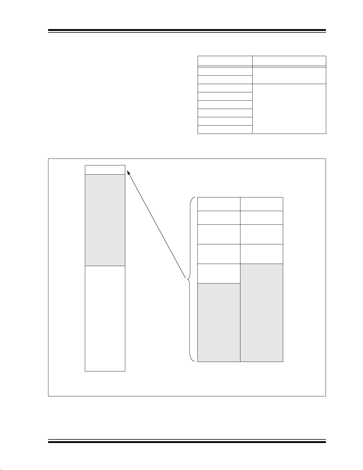
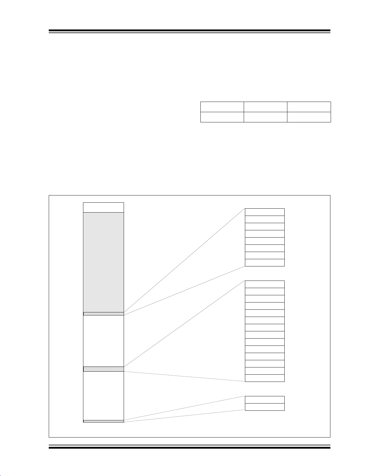
2.3 Memory Maps
TABLE 2-2: IMPLEMENTATION OF CODE
For PIC18FX6X0 devices, the code memory space
extends from 0000h to 0FFFFh (64 Kbytes) in four
16-Kbyte blocks. For PIC18FX5X5 devices, the code
memory space extends from 0000h to 0BFFFFh
(48 Kbytes) in three 16-Kbyte blocks. Addresses
0000h through 07FFh, however, define a “Boot Block”
region that is treated separately from Block 0. All of
these blocks define code protection boundaries within
the code memory space.
The size of the Boot Block in PIC18F2585/2680/4585/
4680 devices can be configured as 1, 2 or 4K words
(see Table 5-1). This is done through the BBSIZ<1:0>
bits in the Configuration register, CONFIG4L. It is
important to note that increasing the size of the Boot
Block decreases the size of Block 0.
Device Code Memory Size (Bytes)
PIC18F2515
PIC18F2525
PIC18F2585
PIC18F4515
PIC18F4525
PIC18F4585
PIC18F2610
PIC18F2620
PIC18F2680
PIC18F4610
PIC18F4620
PIC18F4680
FIGURE 2-3: MEMORY MAP AND THE CODE MEMORY SPACE
FOR PIC18FX5X5/X6X0 DEVICES
000000h
01FFFFh
Code Memory
64 Kbytes
(PIC18FX6X0)
MEMORY SIZE/DEVICE
MEMORY
000000h-00BFFFh (48K)
000000h-00FFFFh (64K)
48 Kbytes
(PIC18FX5X5)
Address
Range
200000h
3FFFFFh
Unimplemented
Read as ‘0’
Configuration
and ID
Space
11/10 01 00
Boot
Block*
Block 0
Boot
Block*
Block 0
Boot
Block*
Block 0
Block 1
Block 1
Block 2
Block 3
Unimplemented
Reads all ‘0’s
BBSIZ<1:0>
11/10 01 00
Boot
Block*
Block 0
Unimplemented
Reads all ‘0’s
Boot
Block*
Block 0
Block 1
Block 2
Boot
Block*
Block 0
000000h
0007FFh
000800h
000FFFh
001000h
001FFFh
002000h
003FFFh
004000h
007FFFh
008000h
00BFFFh
00C000h
00FFFFh
01FFFFh
Note: Sizes of memory areas are not to scale.
* Boot Block size is determined by the BBSIZ1:BBSIZ0 bits in CONFIG4L.
DS39622E-page 4 © 2005 Microchip Technology Inc.
Page 5
PIC18F2XX0/2X21/2XX5/4XX0/4X21/4XX5
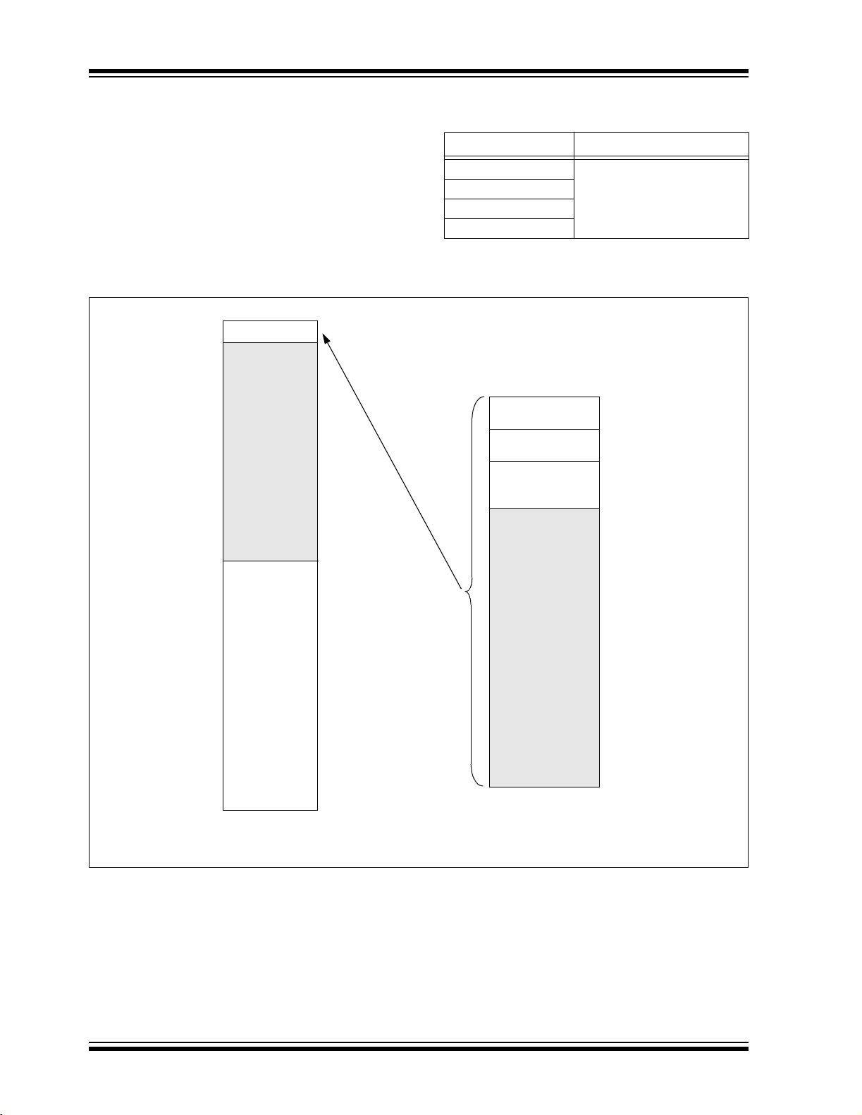
For PIC18FX5X0 devices, the code memory space
TABLE 2-3: IMPLEMENTATION OF CODE
extends from 000000h to 007FFFh (32 Kbytes) in four
8-Kbyte blocks. For PIC18FX4X5 devices, the code
memory space extends from 000000h to 005FFFh
(24 Kbytes) in three 8-Kbyte blocks. Addresses
000000h through 0007FFh, however, define a “Boot
Block” region that is treated separately from Block 0. All
of these blocks define code protection boundaries
within the code memory space.
Device Code Memory Size (Bytes)
PIC18F2455
PIC18F4455
PIC18F2510
PIC18F2520
PIC18F2550
PIC18F4510
PIC18F4520
PIC18F4550
FIGURE 2-4: MEMORY MAP AND THE CODE MEMORY SPACE
FOR PIC18FX4X5/X5X0 DEVICES
000000h
1FFFFFh
200000h
Code Memory
Unimplemented
Read as ‘0’
MEMORY SIZE/DEVICE
32 Kbytes
(PIC18FX5X0)
Boot Block Boot Block
Block 0 Block 0
Block 1 Block 1
Block 2 Block 2
Block 3
008000h
MEMORY
000000h-005FFFh (24K)
000000h-007FFFh (32K)
24 Kbytes
(PIC18FX4X5)
Address
Range
000000h
0007FFh
000800h
001FFFh
002000h
003FFFh
004000h
005FFFh
006000h
007FFFh
Configuration
and ID
Space
3FFFFFh
Note: Sizes of memory areas are not to scale.
© 2005 Microchip Technology Inc. DS39622E-page 5
Unimplemented
Reads all ‘0’s
Unimplemented
Reads all ‘0’s
1FFFFFh
Page 6
PIC18F2XX0/2X21/2XX5/4XX0/4X21/4XX5
For PIC18FX4X0 devices, the code memory space
TABLE 2-4: IMPLEMENTATION OF CODE
extends from 000000h to 003FFFh (16 Kbytes) in two
8-Kbyte blocks. Addresses 000000h through 0003FFh,
however, define a “Boot Block” region that is treated
separately from Block 0. All of these blocks define code
protection boundaries within the code memory space.
Device Code Memory Size (Bytes)
PIC18F2410
PIC18F2420
PIC18F4410
PIC18F4420
FIGURE 2-5: MEMORY MAP AND THE CODE MEMORY SPACE
FOR PIC18FX4X0 DEVICES
000000h
1FFFFFh
Code Memory
Unimplemented
Read as ‘0’
MEMORY SIZE/DEVICE
16 Kbytes
(PIC18FX4X0)
Boot Block
Block 0
Block 1
MEMORY
000000h-003FFFh (16K)
Address
Range
000000h
0007FFh
000800h
001FFFh
002000h
003FFFh
004000h
200000h
Configuration
and ID
Space
3FFFFFh
Note: Sizes of memory areas are not to scale.
005FFFh
006000h
007FFFh
008000h
Unimplemented
Reads all ‘0’s
1FFFFFh
DS39622E-page 6 © 2005 Microchip Technology Inc.
Page 7
PIC18F2XX0/2X21/2XX5/4XX0/4X21/4XX5
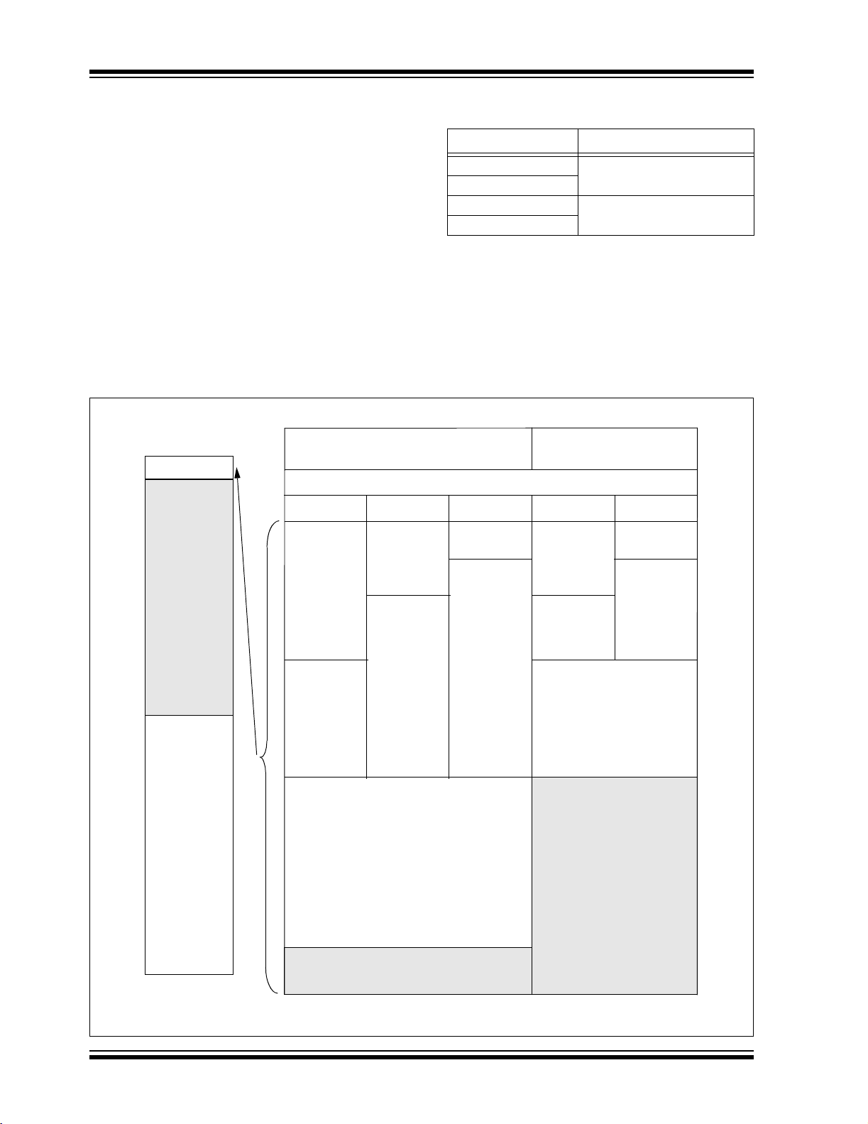
For PIC18F2480/4480 devices, the code memory
TABLE 2-5: IMPLEMENTATION OF CODE
space extends from 0000h to 03FFFh (16 Kbytes) in
one 16-Kbyte block. For PIC18F2580/4580 devices,
the code memory space extends from 0000h to
07FFFh (32 Kbytes) in two 16-Kbyte blocks.
Addresses 0000h through 07FFh, however, define a
“Boot Block” region that is treated separately from
Block 0. All of these blocks define code protection
boundaries within the code memory space.
Device Code Memory Size (Bytes)
PIC18F2480
PIC18F4480
PIC18F2580
PIC18F4580
The size of the Boot Block in PIC18F2480/2580/4480/
4580 devices can be configured as 1 or 2K words (see
Table 5-1). This is done through the BBSIZ bit in the
Configuration register, CONFIG4L. It is important to
note that increasing the size of the Boot Block
decreases the size of Block 0.
FIGURE 2-6: MEMORY MAP AND THE CODE MEMORY SPACE
FOR PIC18F2480/2580/4480/4580 DEVICES
000000h
01FFFFh
Code Memory
Unimplemented
Read as ‘0’
32 Kbytes
(PIC18FX580)
10 1 0
Boot Block*
MEMORY SIZE/DEVICE
BBSIZ<0>
Boot Block*
Boot Block*
MEMORY
000000h-003FFFh (16K)
000000h-007FFFh (32K)
16 Kbytes
(PIC18FX480)
Boot Block*
Address
Range
000000h
0007FFh
000800h
000FFFh
001000h
Block 0 Block 0
200000h
Configuration
and ID
Space
3FFFFFh
Unimplemented
Reads all ‘0’s
Note: Sizes of memory areas are not to scale.
* Boot Block size is determined by the BBSIZ bit in CONFIG4L.
Block 2
Block 3
Block 0 Block 0
001FFFh
002000h
Block 1
003FFFh
004000h
005FFFh
006000h
Unimplemented
Reads all ‘0’s
007FFFh
01FFFFh
© 2005 Microchip Technology Inc. DS39622E-page 7
Page 8
PIC18F2XX0/2X21/2XX5/4XX0/4X21/4XX5
For PIC18F2221/4221 devices, the code memory
TABLE 2-6: IMPLEMENTATION OF CODE
space extends from 0000h to 00FFFh (4 Kbytes) in one
4-Kbyte block. For PIC18F2321/4321 devices, the
code memory space extends from 0000h to 01FFFh
(8 Kbytes) in two 4-Kbyte blocks. Addresses 0000h
through 07FFh, however, define a variable “Boot Block”
region that is treated separately from Block 0. All of
these blocks define code protection boundaries within
the code memory space.
Device Code Memory Size (Bytes)
PIC18F2221
PIC18F4221
PIC18F2321
PIC18F4321
The size of the Boot Block in PIC18F2221/2321/4221/
4321 devices can be configured as 256, 512 or
1024 words (see Figure 2-7). This is done through the
BBSIZ<1:0> bits in the Configuration register,
CONFIG4L (see Table 5-1). It is important to note that
increasing the size of the Boot Block decreases the
size of Block 0.
FIGURE 2-7: MEMORY MAP AND THE CODE MEMORY SPACE
FOR PIC18F2221/2321/4221/4321 DEVICES
MEMORY SIZE/DEVICE
000000h
01FFFFh
200000h
Code Memory
Unimplemented
Read as ‘0’
11/10 01 00 11/10/01 00
Boot Block*
1K word
Block 0
1K word
8Kbytes
(PIC18FX321)
Boot Block*
512 words
Block 0
1.5K words
BBSIZ<1:0>
Boot Block*
256 words
Block 0
1.75K words
MEMORY
4Kbytes
(PIC18FX221)
Boot Block*
512 words
Block 0
0.5K words
000000h-000FFFh (4K)
000000h-001FFFh (8K)
Address
Range
Boot Block*
256 words
Block 0
0.75K words
Block 1
1K word
000000h
0001FFh
000200h
0003FFh
000400h
0007FFh
000800h
000FFFh
001000h
Configuration
and ID
Space
3FFFFFh
Note: Sizes of memory areas are not to scale.
* Boot Block size is determined by the BBSIZ<1:0> bits in CONFIG4L.
DS39622E-page 8 © 2005 Microchip Technology Inc.
Block 1
2K words
Unimplemented
Reads all ‘0’s
Unimplemented
Reads all ‘0’s
001FFFh
002000h
1FFFFFh
Page 9
PIC18F2XX0/2X21/2XX5/4XX0/4X21/4XX5
In addition to the code memory space, there are three
blocks that are accessible to the user through table
reads and table writes. Their locations in the memory
map are shown in Figure 2-8.
Users may store identification information (ID) in eight
ID registers. These ID registers are mapped in
addresses 200000h through 200007h. The ID locations
read out normally, even after code protection is applied.
2.3.1 MEMORY ADDRESS POINTER
Memory in the address space, 0000000h to 3FFFFFh,
is addressed via the Table Pointer register, which is
comprised of three Pointer registers:
• TBLPTRU, at RAM address 0FF8h
• TBLPTRH, at RAM address 0FF7h
• TBLPTRL, at RAM address 0FF6h
Locations 300000h through 30000Dh are reserved for
the configuration bits. These bits select various device
options and are described in Section 5.0 “Configura-
TBLPTRU TBLPTRH TBLPTRL
Addr[21:16] Addr[15:8] Addr[7:0]
tion Word”. These configuration bits read out normally,
even after code protection.
Locations 3FFFFEh and 3FFFFFh are reserved for the
device ID bits. These bits may be used by the program-
The 4-bit command, ‘0000’ (core instruction), is used to
load the Table Pointer prior to using many read or write
operations.
mer to identify what device type is being programmed
and are described in Section 5.0 “Configuration
Word”. These device ID bits read out normally, even
after code protection.
FIGURE 2-8: CONFIGURATION AND ID LOCATIONS FOR PIC18F2XX0/2X21/2XX5/4XX0/4X21/4XX5
DEVICES
000000h
01FFFFh
Code Memory
Unimplemented
Read as ‘0’
ID Location 1 200000h
ID Location 2 200001h
ID Location 3 200002h
ID Location 4 200003h
ID Location 5 200004h
ID Location 6 200005h
ID Location 7 200006h
ID Location 8 200007h
CONFIG1L 300000h
CONFIG1H 300001h
CONFIG2L 300002h
1FFFFFh
Configuration
and ID
Space
2FFFFFh
3FFFFFh
Note: Sizes of memory areas are not to scale.
© 2005 Microchip Technology Inc. DS39622E-page 9
CONFIG2H 300003h
CONFIG3L 300004h
CONFIG3H 300005h
CONFIG4L 300006h
CONFIG4H 300007h
CONFIG5L 300008h
CONFIG5H 300009h
CONFIG6L 30000Ah
CONFIG6H 30000Bh
CONFIG7L 30000Ch
CONFIG7H 30000Dh
Device ID1 3FFFFEh
Device ID2 3FFFFFh
Page 10
PIC18F2XX0/2X21/2XX5/4XX0/4X21/4XX5
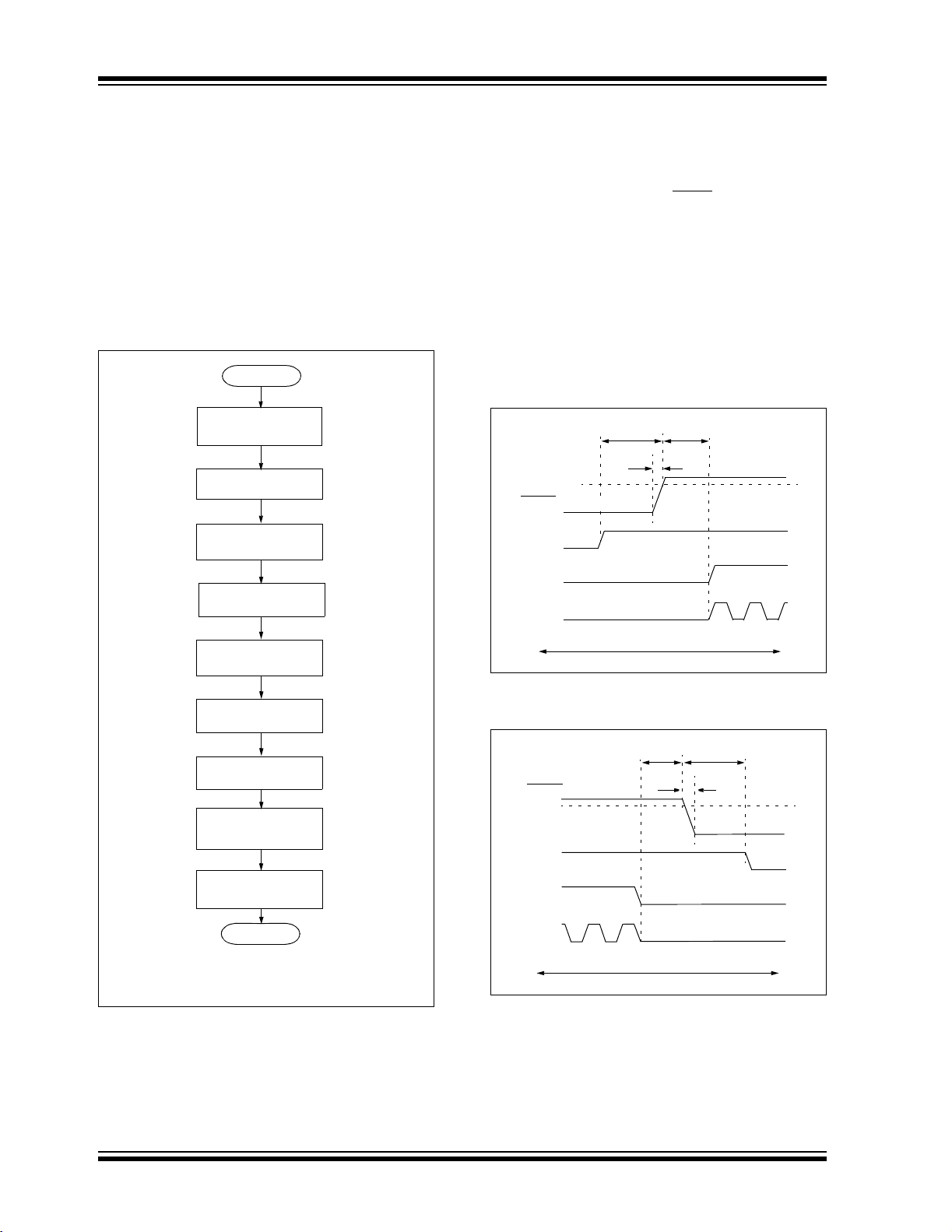
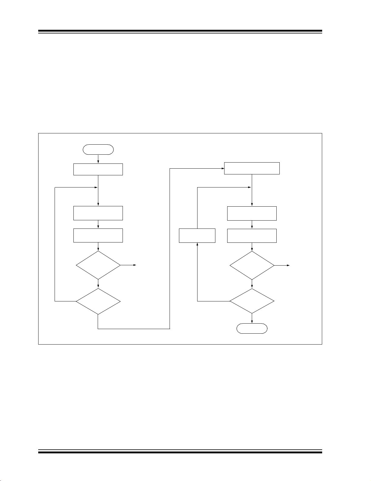
2.4 High-Level Overview of the Programming Process
Figure 2-9 shows the high-level overview of the
programming process. First, a Bulk Erase is performed.
Next, the code memory, ID locations and data EEPROM
are programmed (selected devices only, see Section 3.3
“Data EEPROM Programming”). These memories are
then verified to ensure that programming was successful.
If no errors are detected, the configuration bits are then
programmed and verified.
FIGURE 2-9: HIGH-LEVEL
PROGRAMMING FLOW
Start
Perform Bulk
Erase
Program Memory
Program IDs
2.5 Entering and Exiting High-Voltage ICSP Program/Verify Mode
As shown in Figure 2-10, the High-Voltage ICSP
Program/Verify mode is entered by holding PGC and
PGD low and then raising MCLR/VPP/RE3 to VIHH
(high voltage). Once in this mode, the code memory,
data EEPROM (selected devices only, see Section 3.3
“Data EEPROM Programming”), ID locations and
configuration bits can be accessed and programmed in
serial fashion. Figure 2-11 shows the exit sequence.
The sequence that enters the device into the Program/
Verify mode places all unused I/Os in the high-impedance
state.
FIGURE 2-10: ENTERING HIGH-VOLTAGE
PROGRAM/VERIFY MODE
P13
P1
D110
MCLR/VPP/RE3
VDD
P12
Program Data EE
Verify Program
Verify IDs
Verify Data
Program
Configuration Bits
Verify
Configuration Bits
Done
Note 1: Selected devices only, see Section 3.3
“Data EEPROM Programming”.
(1)
PGD
PGC
PGD = Input
FIGURE 2-11: EXITING HIGH-VOLTAGE
PROGRAM/VERIFY MODE
P16
MCLR/VPP/RE3
D110
VDD
PGD
PGC
PGD = Input
P17
P1
DS39622E-page 10 © 2005 Microchip Technology Inc.
Page 11
PIC18F2XX0/2X21/2XX5/4XX0/4X21/4XX5
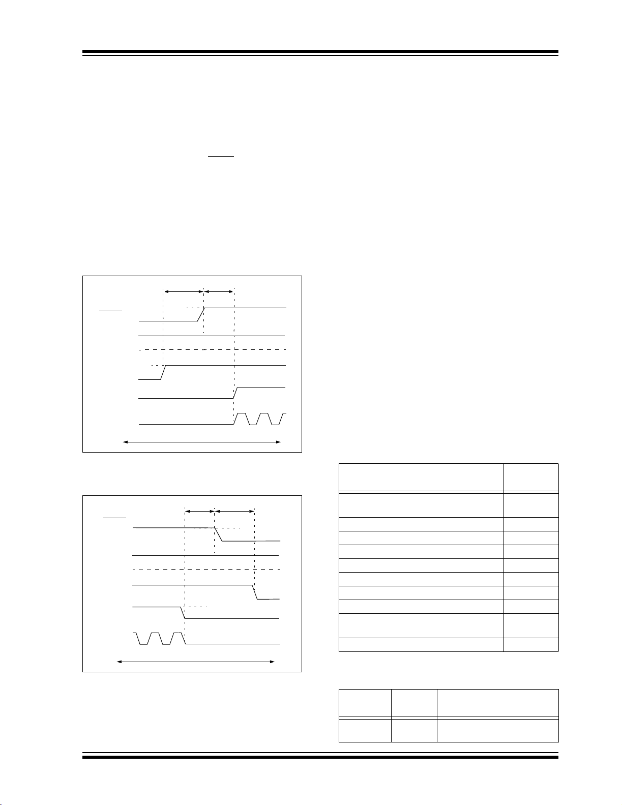
2.6 Entering and Exiting Low-Voltage ICSP Program/Verify Mode
When the LVP configuration bit is ‘1’ (see Section 5.3
“Single-Supply ICSP Programming”), the
Low-Voltage ICSP mode is enabled. As shown in
Figure 2-12, Low-Voltage ICSP Program/Verify mode
is entered by holding PGC and PGD low, placing a logic
high on PGM and then raising MCLR
In this mode, the RB5/PGM pin is dedicated to the
programming function and ceases to be a general
purpose I/O pin. Figure 2-13 shows the exit sequence.
The sequence that enters the device into the Program/
Verify mode places all unused I/Os in the high-impedance
state.
FIGURE 2-12: ENTERING LOW-VOLTAGE
PROGRAM/VERIFY MODE
P15
MCLR/VPP/RE3
VDD
VIH
PGM
PGD
PGC
VIH
PGD = Input
FIGURE 2-13: EXITING LOW-VOLTAGE
PROGRAM/VERIFY MODE
P16
MCLR/VPP/RE3
VDD
PGM
PGD
PGC
VIH
PGD = Input
/VPP/RE3 to VIH.
P12
P18
VIH
2.7 Serial Program/Verify Operation
The PGC pin is used as a clock input pin and the PGD
pin is used for entering command bits and data input/
output during serial operation. Commands and data are
transmitted on the rising edge of PGC, latched on the
falling edge of PGC and are Least Significant bit (LSb)
first.
2.7.1 4-BIT COMMANDS
All instructions are 20 bits, consisting of a leading 4-bit
command followed by a 16-bit operand, which depends
on the type of command being executed. To input a
command, PGC is cycled four times. The commands
needed for programming and verification are shown in
Ta bl e 2 -7 .
Depending on the 4-bit command, the 16-bit operand
represents 16 bits of input data or 8 bits of input data
and 8 bits of output data.
Throughout this specification, commands and data are
presented as illustrated in Table 2-8. The 4-bit
command is shown Most Significant bit (MSb) first. The
command operand, or “Data Payload”, is shown
<MSB><LSB>. Figure 2-14 demonstrates how to
serially present a 20-bit command/operand to the
device.
2.7.2 CORE INSTRUCTION
The core instruction passes a 16-bit instruction to the
CPU core for execution. This is needed to set up
registers as appropriate for use with other commands.
TABLE 2-7: COMMANDS FOR
PROGRAMMING
Description
Core Instruction
(Shift in16-bit instruction)
Shift out TABLAT register 0010
Table Read 1000
Table Read, post-increment 1001
Table Read, post-decrement 1010
Table Read, pre-increment 1011
Table Write 1100
Table Write, post-increment by 2 1101
Table Write, start programming,
post-increment by 2
Table Write, start programming 1111
TABLE 2-8: SAMPLE COMMAND
SEQUENCE
4-Bit
Command
1101 3C 40 Table Write,
Data
Payload
Core Instruction
post-increment by 2
4-Bit
Command
0000
1110
© 2005 Microchip Technology Inc. DS39622E-page 11
Page 12
PIC18F2XX0/2X21/2XX5/4XX0/4X21/4XX5
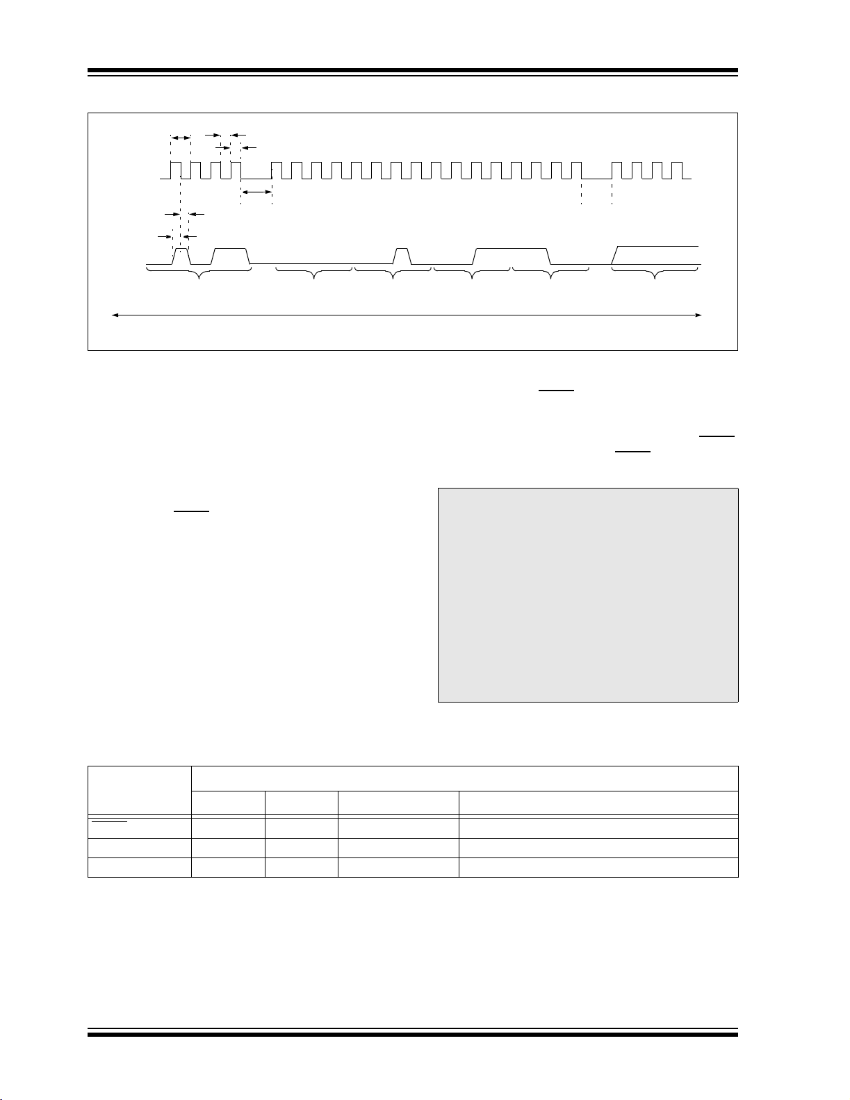
FIGURE 2-14: TABLE WRITE, POST-INCREMENT TIMING (1101)
PGC
PGD
P2
1234
P4
P3
1011
4-Bit Command 16-Bit Data Payload
P2A
P2B
1234
P5
000 000 01000111 1 0
04C3
5678
PGD = Input
2.8 Dedicated ICSP/ICD Port (44-Pin TQFP Only)
The PIC18F4221/4321 and PIC18F4455/4550 44-pin
TQFP devices are designed to support an alternate
programming input, the dedicated ICSP/ICD port. The
primary purpose of this port is to provide an alternate
In-Circuit Debugging (ICD) option and free the pins
(RB6, RB7 and MCLR
debugging the application. In conjunction with ICD
capability, however, the dedicated ICSP/ICD port also
provides an alternate port for ICSP.
Setting the ICPORT configuration bit enables the
dedicated ICSP/ICD port. The dedicated ICSP/ICD
port functions the same as the default ICSP/ICD port;
however, alternate pins are used instead of the default
pins. Table 2-9 identifies the functionally equivalent
pins for ICSP purposes:
The dedicated ICSP/ICD port is an alternate port. Thus,
ICSP is still available through the default port even
though the ICPORT configuration bit is set. When the
) that would normally be used for
10 11 13 15 161412
9
P5A
IH is seen on the MCLR/VPP/RE3 pin prior to applying
V
IH to the ICRST/ICVPP pin, then the state of the
V
ICRST/ICV
seen on ICRST/ICV
PP/RE3, then the state of the MCLR/VPP/RE3 pin is
V
PP pin is ignored. Likewise, when the VIH is
PP prior to applying VIH to MCLR/
234
1
nnnn
Fetch Next 4-Bit Command
ignored.
Note: The ICPORT configuration bit can only be
programmed through the default ICSP
port. Chip Erase functions through the
dedicated ICSP/ICD port do not affect this
bit.
When the ICPORT configuration bit is set
(dedicated ICSP/ICD port enabled), the
NC/ICPORTS pin must be tied to either
DD or VSS.
V
The ICPORT configuration bit must be
maintained clear for all 28-pin and 40-pin
devices; otherwise, unexpected operation
may occur.
TABLE 2-9: ICSP™ EQUIVALENT PINS
Pin Name
Pin Name Pin Type Dedicated Pin Pin Description
MCLR/VPP/RE3 VPP P NC/ICRST/ICVPP Programming Enable
RB6 PGC I NC/ICCK/ICPGC Serial Clock
RB7 PGD I/O NC/ICDT/ICPGD Serial Data
Legend: I = Input, O = Output, P = Power
DS39622E-page 12 © 2005 Microchip Technology Inc.
During Programming
Page 13

PIC18F2XX0/2X21/2XX5/4XX0/4X21/4XX5
3.0 DEVICE PROGRAMMING
Programming includes the ability to erase or write the
various memory regions within the device.
In all cases except high-voltage ICSP Bulk Erase, the
EECON1 register must be configured in order to
operate on a particular memory region.
When using the EECON1 register to act on code
memory, the EEPGD bit must be set (EECON1<7> = 1)
and the CFGS bit must be cleared (EECON1<6> = 0).
The WREN bit must be set (EECON1<2> = 1) to
enable writes of any sort (e.g., erases) and this must be
done prior to initiating a write sequence. The FREE bit
must be set (EECON1<4> = 1) in order to erase the
program space being pointed to by the Table Pointer.
The erase or write sequence is initiated by setting the
WR bit (EECON1<1> = 1). It is strongly recommended
that the WREN bit only be set immediately prior to a
program erase.
3.1 ICSP Erase
3.1.1 HIGH-VOLTAGE ICSP BULK ERASE
Erasing code or data EEPROM is accomplished by
configuring two Bulk Erase Control registers located at
3C0004h and 3C0005h. Code memory may be erased
portions at a time, or the user may erase the entire
device in one action. Bulk Erase operations will also
clear any code-protect settings associated with the
memory block erased. Erase options are detailed in
Table 3-1. If data EEPROM is code-protected
(CPD = 0), the user must request an erase of data
EEPROM (e.g., 0084h as shown in Table 3-1).
The code sequence to erase the entire device is shown
in Table 3-2 and the flowchart is shown in Figure 3-1.
Note: A Bulk Erase is the only way to reprogram
code-protect bits from an ON state to an
OFF state.
TABLE 3-2: BULK ERASE COMMAND
SEQUENCE
4-Bit
Command
0000
0000
0000
0000
0000
0000
1100
0000
0000
0000
0000
0000
0000
1100
0000
0000
Data
Payload
0E 3C
6E F8
0E 00
6E F7
0E 05
6E F6
0F 0F
0E 3C
6E F8
0E 00
6E F7
0E 04
6E F6
87 87
00 00
00 00
Core Instruction
MOVLW 3Ch
MOVWF TBLPTRU
MOVLW 00h
MOVWF TBLPTRH
MOVLW 05h
MOVWF TBLPTRL
Write 0Fh to 3C0005h
MOVLW 3Ch
MOVWF TBLPTRU
MOVLW 00h
MOVWF TBLPTRH
MOVLW 04h
MOVWF TBLPTRL
Write 8787h TO 3C0004h
to erase entire
device.
NOP
Hold PGD low until
erase completes.
FIGURE 3-1: BULK ERASE FLOW
TABLE 3-1: BULK ERASE OPTIONS
Description
Chip Erase 0F87h
Erase Data EEPROM
Erase Boot Block 0081h
Erase Config Bits 0082h
Erase Code EEPROM Block 0 0180h
Erase Code EEPROM Block 1 0280h
Erase Code EEPROM Block 2 0480h
Erase Code EEPROM Block 3 0880h
Note 1: Selected devices only, see Section 3.3
“Data EEPROM Programming”.
The actual Bulk Erase function is a self-timed
operation. Once the erase has started (falling edge of
the 4th PGC after the NOP command), serial execution
will cease until the erase completes (parameter P11).
During this time, PGC may continue to toggle but PGD
must be held low.
(1)
(3C0005h:3C0004h)
Data
0084h
Start
Write 0F0Fh
to 3C0005h
Write 8787h to
3C0004h to Erase
Entire Device
Delay P11 + P10
Time
Done
© 2005 Microchip Technology Inc. DS39622E-page 13
Page 14

PIC18F2XX0/2X21/2XX5/4XX0/4X21/4XX5
FIGURE 3-2: BULK ERASE TIMING
12 34
PGC
1
P5
21516
P5A
123
4
1 2 15 16P5123
P5A
4
P11
P10
12
PGD
4-Bit Command
11
Data Payload
000000
16-Bit
00011
0
4-Bit Command 4-Bit Command
PGD = Input
3.1.2 LOW-VOLTAGE ICSP BULK ERASE
When using low-voltage ICSP, the part must be
supplied by the voltage specified in parameter D111
Bulk Erase is to be executed. All other Bulk Erase
details as described above apply.
If it is determined that a program memory erase must
be performed at a supply voltage below the Bulk Erase
limit, refer to the erase methodology described in
Section 3.1.3 “ICSP Row Erase” and Section 3.2.1
“Modifying Code Memory”.
If it is determined that a data EEPROM erase
(selected devices only, see Section 3.3 “Data
EEPROM Programming”) must be performed at a
supply voltage below the Bulk Erase limit, follow the
methodology described in Section 3.3 “Data
EEPROM Programming” and write ‘1’s to the array.
if a
00
16-Bit
Data Payload
0000
Erase Time
Data Payload
3.1.3 ICSP ROW ERASE
Regardless of whether high or low-voltage ICSP is
used, it is possible to erase one row (64 bytes of data),
provided the block is not code or write-protected. Rows
are located at static boundaries, beginning at program
memory address 000000h, extending to the internal
program memory limit (see Section 2.3 “Memory
Maps”).
The Row Erase duration is externally timed and is
controlled by PGC. After the WR bit in EECON1 is set,
a NOP is issued, where the 4th PGC is held high for the
duration of the programming time, P9.
After PGC is brought low, the programming sequence
is terminated. PGC must be held low for the time
specified by parameter P10 to allow high-voltage
discharge of the memory array.
The code sequence to Row Erase a PIC18F2XX0/2X21/
2XX5/4XX0/4X21/4XX5 device is shown in Table 3-3.
The flowchart shown in Figure 3-3 depicts the logic
necessary to completely erase a PIC18F2XX0/2X21/
2XX5/4XX0/4X21/4XX5 device. The timing diagram that
details the Start Programming command and
parameters P9 and P10 is shown in Figure 3-5.
n
16-Bit
n
Note: The TBLPTR register can point at any byte
within the row intended for erase.
DS39622E-page 14 © 2005 Microchip Technology Inc.
Page 15

PIC18F2XX0/2X21/2XX5/4XX0/4X21/4XX5
TABLE 3-3: ERASE CODE MEMORY CODE SEQUENCE
4-Bit
Command
Step 1: Direct access to code memory and enable writes.
0000
0000
0000
Step 2: Point to first row in code memory.
0000
0000
0000
Step 3: Enable erase and erase single row.
0000
0000
0000
Step 4: Repeat step 3, with address pointer incremented by 64 until all rows are erased.
FIGURE 3-3: SINGLE ROW ERASE CODE MEMORY FLOW
Data Payload Core Instruction
8E A6
9C A6
84 A6
6A F8
6A F7
6A F6
88 A6
82 A6
00 00
BSF EECON1, EEPGD
BCF EECON1, CFGS
BSF EECON1, WREN
CLRF TBLPTRU
CLRF TBLPTRH
CLRF TBLPTRL
BSF EECON1, FREE
BSF EECON1, WR
NOP – hold PGC high for time P9 and low for time P10.
Addr = Addr + 64
Start
Configure
Device for
Row Erases
Start Erase Sequence
and Hold PGC High
for Time P9
Hold PGC Low
for Time P10
No
All
rows
done?
Done
Addr = 0
Yes
© 2005 Microchip Technology Inc. DS39622E-page 15
Page 16

PIC18F2XX0/2X21/2XX5/4XX0/4X21/4XX5
3.2 Code Memory Programming
Programming code memory is accomplished by first
loading data into the write buffer and then initiating a
programming sequence. The write and erase buffer
sizes, shown in Table 3-4, can be mapped to any
location of the same size beginning at 000000h. The
actual memory write sequence takes the contents of
this buffer and programs the proper amount of code
memory that contains the Table Pointer.
The programming duration is externally timed and is
controlled by PGC. After a Start Programming
command is issued (4-bit command, ‘1111’), a NOP is
issued, where the 4th PGC is held high for the duration
of the programming time, P9.
TABLE 3-4: WRITE AND ERASE BUFFER SIZES
Devices (Arranged by Family)
PIC18F2221, PIC18F2321, PIC18F4221, PIC18F4321 8 64
PIC18F2410, PIC18F2510, PIC18F4410, PIC18F4510
PIC18F2420, PIC18F2520, PIC18F4420, PIC18F4520
PIC18F2480, PIC18F2580, PIC18F4480, PIC18F4580
PIC18F2455, PIC18F2550, PIC18F4455, PIC18F4550
PIC18F2515, PIC18F2610, PIC18F4515, PIC18F4610
PIC18F2585, PIC18F2680, PIC18F4585, PIC18F4680
After PGC is brought low, the programming sequence
is terminated. PGC must be held low for the time
specified by parameter P10 to allow high-voltage
discharge of the memory array.
The code sequence to program a PIC18F2XX0/2X21/
2XX5/4XX0/4X21/4XX5 device is shown in Table 3-5.
The flowchart, shown in Figure 3-4, depicts the logic
necessary to completely write a PIC18F2XX0/2X21/
2XX5/4XX0/4X21/4XX5 device. The timing diagram
that details the Start Programming command and
parameters P9 and P10 is shown in Figure 3-5.
Note: The TBLPTR register must point to the
same region when initiating the programming sequence as it did when the write
buffers were loaded.
Write Buffer Size
(bytes)
Erase Buffer Size
(bytes)
32 64
64 64PIC18F2525, PIC18F2620, PIC18F4525, PIC18F4620
TABLE 3-5: WRITE CODE MEMORY CODE SEQUENCE
4-Bit
Command
Step 1: Direct access to code memory and enable writes.
0000
0000
Step 2: Load write buffer.
0000
0000
0000
0000
0000
0000
Step 3: Repeat for all but the last two bytes.
1101 <MSB><LSB> Write 2 bytes and post-increment address by 2.
Step 4: Load write buffer for last two bytes.
1111
0000
To continue writing data, repeat steps 2 through 4, where the address pointer is incremented by 2 at each iteration of the loop.
Data Payload Core Instruction
8E A6
9C A6
0E <Addr[21:16]>
6E F8
0E <Addr[15:8]>
6E F7
0E <Addr[7:0]>
6E F6
<MSB><LSB>
00 00
BSF EECON1, EEPGD
BCF EECON1, CFGS
MOVLW <Addr[21:16]>
MOVWF TBLPTRU
MOVLW <Addr[15:8]>
MOVWF TBLPTRH
MOVLW <Addr[7:0]>
MOVWF TBLPTRL
Write 2 bytes and start programming.
NOP - hold PGC high for time P9 and low for time P10.
DS39622E-page 16 © 2005 Microchip Technology Inc.
Page 17

PIC18F2XX0/2X21/2XX5/4XX0/4X21/4XX5
FIGURE 3-4: PROGRAM CODE MEMORY FLOW
N = N + 1
Start
N = 1
LoopCount = 0
Configure
Device for
Writes
Load 2 Bytes
to Write
Buffer at <Addr>
No
All
bytes
written?
N = 1
LoopCount =
LoopCount + 1
Start Write Sequence
Yes
and Hold PGC
High until Done
and Wait P9
Hold PGC Low
for Time P10
No
All
locations
done?
Yes
Done
FIGURE 3-5: TABLE WRITE AND START PROGRAMMING INSTRUCTION TIMING (1111)
P10
PGC
1234
34 65
1 2 15 16
P5
123 4
P9
P5A
12
PGD
1
11
4-Bit Command 16-Bit Data Payload
nnn
n
nn n n
00
00
4-Bit Command
Programming Time
0
030
16-Bit
Data Payload
1
PGD = Input
© 2005 Microchip Technology Inc. DS39622E-page 17
Page 18

PIC18F2XX0/2X21/2XX5/4XX0/4X21/4XX5
3.2.1 MODIFYING CODE MEMORY
The previous programming example assumed that the
device had been Bulk Erased prior to programming
(see Section 3.1.1 “High-Voltage ICSP Bulk Erase”).
It may be the case, however, that the user wishes to
modify only a section of an already programmed
device.
The appropriate number of bytes required for the erase
buffer must be read out of code memory (as described
in Section 4.2 “Verify Code Memory and ID
Locations”) and buffered. Modifications can be made
on this buffer. Then, the block of code memory that was
read out must be erased and rewritten with the
modified data.
The WREN bit must be set if the WR bit in EECON1 is
used to initiate a write sequence.
TABLE 3-6: MODIFYING CODE MEMORY
4-Bit
Command
Step 1: Direct access to code memory.
Step 2: Read and modify code memory (see Section 4.1 “Read Code Memory, ID Locations and Configuration Bits”).
0000
0000
Step 3: Set the Table Pointer for the block to be erased.
0000
0000
0000
0000
0000
0000
Step 4: Enable memory writes and setup an erase.
0000
0000
Step 5: Initiate erase.
0000
0000
Step 6: Load write buffer. The correct bytes will be selected based on the Table Pointer.
0000
0000
0000
0000
0000
0000
1101
.
.
.
1111
0000
To continue modifying data, repeat Steps 2 through 6, where the address pointer is incremented by the appropriate number of bytes
(see Table 3-4) at each iteration of the loop. The write cycle must be repeated enough times to completely rewrite the contents of
the erase buffer.
Step 7: Disable writes.
0000 94 A6 BCF EECON1, WREN
Data Payload Core Instruction
8E A6
9C A6
0E <Addr[21:16]>
6E F8
0E <Addr[8:15]>
6E F7
0E <Addr[7:0]>
6E F6
84 A6
88 A6
82 A6
00 00
0E <Addr[21:16]>
6E F8
0E <Addr[8:15]>
6E F7
0E <Addr[7:0]>
6E F6
<MSB><LSB>
.
.
.
<MSB><LSB>
00 00
BSF EECON1, EEPGD
BCF EECON1, CFGS
MOVLW <Addr[21:16]>
MOVWF TBLPTRU
MOVLW <Addr[8:15]>
MOVWF TBLPTRH
MOVLW <Addr[7:0]>
MOVWF TBLPTRL
BSF EECON1, WREN
BSF EECON1, FREE
BSF EECON1, WR
NOP - hold PGC high for time P9 and low for time P10.
MOVLW <Addr[21:16]>
MOVWF TBLPTRU
MOVLW <Addr[8:15]>
MOVWF TBLPTRH
MOVLW <Addr[7:0]>
MOVWF TBLPTRL
Write 2 bytes and post-increment address by 2.
Repeat as many times as necessary to fill the write buffer
Write 2 bytes and start programming.
NOP - hold PGC high for time P9 and low for time P10.
DS39622E-page 18 © 2005 Microchip Technology Inc.
Page 19

PIC18F2XX0/2X21/2XX5/4XX0/4X21/4XX5
3.3 Data EEPROM Programming
Note: Data EEPROM programming is not
available on the the following devices:
• PIC18F2410 •PIC18F4410
• PIC18F2510 •PIC18F4510
• PIC18F2515 •PIC18F4515
• PIC18F2610 •PIC18F4610
Data EEPROM is accessed one byte at a time via an
address pointer (register pair EEADRH:EEADR) and a
data latch (EEDATA). Data EEPROM is written by
loading EEADRH:EEADR with the desired memory
location, EEDATA with the data to be written and initiating a memory write by appropriately configuring the
EECON1 register. A byte write automatically erases the
location and writes the new data (erase-before-write).
When using the EECON1 register to perform a data
EEPROM write, both the EEPGD and CFGS bits must
be cleared (EECON1<7:6> = 00). The WREN bit must
be set (EECON1<2> = 1) to enable writes of any sort
and this must be done prior to initiating a write
sequence. The write sequence is initiated by setting the
WR bit (EECON1<1> = 1).
The write begins on the falling edge of the 4th PGC
after the WR bit is set. It ends when the WR bit is
cleared by hardware.
After the programming sequence terminates, PGC must
still be held low for the time specified by parameter P10
to allow high-voltage discharge of the memory array.
FIGURE 3-6: PROGRAM DATA FLOW
Start
Set Address
Set Data
Enable Write
Start W ri te
Sequence
No
No
WR bit
clear?
Yes
Done?
Yes
Done
FIGURE 3-7: DATA EEPROM WRITE TIMING
1234
PGC
PGD
Poll WR bit
0000
PGC
PGD
1
P5
BSF EECON1, WR4-Bit Command
21516
P5A
12 34
P5
0000
PGD = Input
21516 123
1
P5A
MOVF EECON1, W, 04-Bit Command
PGD = Input PGD = Output
P11A
Poll WR bit, Repeat until Clear
(see below)
4
1 2 15 16
P5 P5A
0000
4-Bit Command
MOVWF TABLAT
P10
Shift Out Data
(see Figure 4-4)
12
n
n
16-Bit Data
Payload
© 2005 Microchip Technology Inc. DS39622E-page 19
Page 20

PIC18F2XX0/2X21/2XX5/4XX0/4X21/4XX5
TABLE 3-7: PROGRAMMING DATA MEMORY
4-Bit
Command
Step 1: Direct access to data EEPROM.
0000
0000
Step 2: Set the data EEPROM address pointer.
0000
0000
0000
0000
Step 3: Load the data to be written.
0000
0000
Step 4: Enable memory writes.
0000 84 A6 BSF EECON1, WREN
Step 5: Initiate write.
0000 82 A6 BSF EECON1, WR
Step 6: Poll WR bit, repeat until the bit is clear.
0000
0000
0000
0010
Step 7: Hold PGC low for time P10.
Step 8: Disable writes.
0000 94 A6 BCF EECON1, WREN
Repeat steps 2 through 8 to write more data.
Note 1: See Figure 4-4 for details on shift out data timing.
Data Payload Core Instruction
9E A6
9C A6
0E <Addr>
6E A9
OE <AddrH>
6E AA
0E <Data>
6E A8
50 A6
6E F5
00 00
<MSB><LSB>
BCF EECON1, EEPGD
BCF EECON1, CFGS
MOVLW <Addr>
MOVWF EEADR
MOVLW <AddrH>
MOVWF EEADRH
MOVLW <Data>
MOVWF EEDATA
MOVF EECON1, W, 0
MOVWF TABLAT
NOP
Shift out data
(1)
DS39622E-page 20 © 2005 Microchip Technology Inc.
Page 21

PIC18F2XX0/2X21/2XX5/4XX0/4X21/4XX5
3.4 ID Location Programming
The ID locations are programmed much like the code
memory. The ID registers are mapped in addresses
200000h through 200007h. These locations read out
normally even after code protection.
Note: The user only needs to fill the first 8 bytes
of the write buffer in order to write the ID
locations.
TABLE 3-8: WRITE ID SEQUENCE
4-Bit
Command
Step 1: Direct access to code memory and enable writes.
0000
0000
Step 2: Load write buffer with 8 bytes and write.
0000
0000
0000
0000
0000
0000
1101
1101
1101
1111
0000
Data Payload Core Instruction
8E A6
9C A6
0E 20
6E F8
0E 00
6E F7
0E 00
6E F6
<MSB><LSB>
<MSB><LSB>
<MSB><LSB>
<MSB><LSB>
00 00
BSF EECON1, EEPGD
BCF EECON1, CFGS
MOVLW 20h
MOVWF TBLPTRU
MOVLW 00h
MOVWF TBLPTRH
MOVLW 00h
MOVWF TBLPTRL
Write 2 bytes and post-increment address by 2.
Write 2 bytes and post-increment address by 2.
Write 2 bytes and post-increment address by 2.
Write 2 bytes and start programming.
NOP - hold PGC high for time P9 and low for time P10.
Table 3-8 demonstrates the code sequence required to
write the ID locations.
In order to modify the ID locations, refer to the methodology described in Section 3.2.1 “Modifying Code
Memory”. As with code memory, the ID locations must
be erased before being modified.
© 2005 Microchip Technology Inc. DS39622E-page 21
Page 22

PIC18F2XX0/2X21/2XX5/4XX0/4X21/4XX5
3.5 Boot Block Programming
The code sequence detailed in Table 3-5 should be
used, except that the address used in “Step 2” will be in
the range of 000000h to 0007FFh.
3.6 Configuration Bits Programming
Unlike code memory, the configuration bits are
programmed a byte at a time. The Table Write, Begin
Programming 4-bit command (‘1111’) is used, but only
8 bits of the following 16-bit payload will be written. The
LSB of the payload will be written to even addresses and
the MSB will be written to odd addresses. The code
sequence to program two consecutive configuration
locations is shown in Table 3-9.
Note: The address must be explicitly written for
each byte programmed. The addresses
can not be incremented in this mode.
TABLE 3-9: SET ADDRESS POINTER TO CONFIGURATION LOCATION
4-Bit
Command
Step 1: Enable writes and direct access to config memory.
0000
0000
(1)
Step 2
Note 1: Enabling the write protection of configuration bits (WRTC = 0 in CONFIG6H) will prevent further writing of configuration
: Set Table Pointer for config byte to be written. Write even/odd addresses.
0000
0000
0000
0000
0000
0000
1111
0000
0000
0000
1111
0000
bits. Always write all the configuration bits before enabling the write protection for configuration bits.
Data Payload Core Instruction
8E A6
8C A6
0E 30
6E F8
0E 00
6E F7
0E 00
6E F6
<MSB ignored><LSB>
00 00
0E 01
6E F6
<MSB><LSB ignored>
00 00
BSF EECON1, EEPGD
BSF EECON1, CFGS
MOVLW 30h
MOVWF TBLPTRU
MOVLW 00h
MOVWF TBLPRTH
MOVLW 00h
MOVWF TBLPTRL
Load 2 bytes and start programming.
NOP - hold PGC high for time P9 and low for time P10.
MOVLW 01h
MOVWF TBLPTRL
Load 2 bytes and start programming.
NOP - hold PGC high for time P9 and low for time P10.
FIGURE 3-8: CONFIGURATION PROGRAMMING FLOW
Start
Load Even
Configuration
Address
Program Program
LSB
Delay P9 and P10
Time for Write
Done
DS39622E-page 22 © 2005 Microchip Technology Inc.
Start
Load Odd
Configuration
Address
MSB
Delay P9 and P10
Time for Write
Done
Page 23

PIC18F2XX0/2X21/2XX5/4XX0/4X21/4XX5
4.0 READING THE DEVICE
4.1 Read Code Memory, ID Locations and Configuration Bits
Code memory is accessed one byte at a time via the
4-bit command, ‘1001’ (table read, post-increment).
The contents of memory pointed to by the Table Pointer
(TBLPTRU:TBLPTRH:TBLPTRL) are serially output on
PGD.
TABLE 4-1: READ CODE MEMORY SEQUENCE
4-Bit
Command
Step 1: Set Table Pointer.
0000
0000
0000
0000
0000
0000
Step 2: Read memory and then shift out on PGD, LSb to MSb.
1001 00 00 TBLRD *+
Data Payload Core Instruction
0E <Addr[21:16]>
6E F8
0E <Addr[15:8]>
6E F7
0E <Addr[7:0]>
6E F6
MOVLW Addr[21:16]
MOVWF TBLPTRU
MOVLW <Addr[15:8]>
MOVWF TBLPTRH
MOVLW <Addr[7:0]>
MOVWF TBLPTRL
The 4-bit command is shifted in LSb first. The read is
executed during the next 8 clocks, then shifted out on
PGD during the last 8 clocks, LSb to MSb. A delay of
P6 must be introduced after the falling edge of the 8th
PGC of the operand to allow PGD to transition from an
input to an output. During this time, PGC must be held
low (see Figure 4-1). This operation also increments
the Table Pointer by one, pointing to the next byte in
code memory for the next read.
This technique will work to read any memory in the
000000h to 3FFFFFh address space, so it also applies
to the reading of the ID and Configuration registers.
FIGURE 4-1: TABLE READ POST-INCREMENT INSTRUCTION TIMING (1001)
9
P6
10 11 13 15 161412
P14
LSb
12
Shift Data Out
PGD = Output
34
56
P5A
MSb
Fetch Next 4-Bit Command
PGC
PGD
1234
1001
1234
P5
PGD = Input
5678
1234
nnnn
PGD = Input
© 2005 Microchip Technology Inc. DS39622E-page 23
Page 24
PIC18F2XX0/2X21/2XX5/4XX0/4X21/4XX5
4.2 Verify Code Memory and ID Locations
The verify step involves reading back the code memory
space and comparing it against the copy held in the
programmer’s buffer. Memory reads occur a single byte
at a time, so two bytes must be read to compare
against the word in the programmer’s buffer. Refer to
Section 4.1 “Read Code Memory, ID Locations and
Configuration Bits” for implementation details of
reading code memory.
FIGURE 4-2: VERIFY CODE MEMORY FLOW
Start
Set TBLPTR = 0
Read Low Byte
with Post-increment
The Table Pointer must be manually set to 200000h
(base address of the ID locations) once the code
memory has been verified. The post-increment feature
of the table read 4-bit command may not be used to
increment the Table Pointer beyond the code memory
space. In a 64-Kbyte device, for example, a
post-increment read of address FFFFh will wrap the
Table Pointer back to 000000h, rather than point to
unimplemented address 010000h.
Set TBLPTR = 200000h
Read Low Byte
with Post-Increment
Read High Byte
with Post-increment
Word = Expect
No
code memory
verified?
Does
data?
All
Yes
Yes
No
Failure,
Report
Error
Increment
Pointer
Read High Byte
with Post-Increment
Word = Expect
No
Does
data?
Yes
All
ID locations
verified?
Yes
Done
No
Failure,
Report
Error
DS39622E-page 24 © 2005 Microchip Technology Inc.
Page 25

PIC18F2XX0/2X21/2XX5/4XX0/4X21/4XX5
4.3 Verify Configuration Bits
A configuration address may be read and output on
PGD via the 4-bit command, ‘1001’. Configuration data
is read and written in a byte-wise fashion, so it is not
necessary to merge two bytes into a word prior to a
compare. The result may then be immediately
compared to the appropriate configuration data in the
programmer’s memory for verification. Refer to
Section 4.1 “Read Code Memory, ID Locations and
Configuration Bits” for implementation details of
reading configuration data.
4.4 Read Data EEPROM Memory
Data EEPROM is accessed one byte at a time via an
address pointer (register pair EEADRH:EEADR) and a
data latch (EEDATA). Data EEPROM is read by loading
EEADRH:EEADR with the desired memory location
and initiating a memory read by appropriately configuring the EECON1 register. The data will be loaded into
EEDATA, where it may be serially output on PGD via
the 4-bit command, ‘0010’ (Shift Out Data Holding
register). A delay of P6 must be introduced after the
falling edge of the 8th PGC of the operand to allow
PGD to transition from an input to an output. During this
time, PGC must be held low (see Figure 4-4).
The command sequence to read a single byte of data
is shown in Table 4-2.
FIGURE 4-3: READ DATA EEPROM
FLOW
Start
Set
Address
Read
Byte
Move to TABLAT
Shift Out Data
No
Done?
Yes
Done
TABLE 4-2: READ DATA EEPROM MEMORY
4-Bit
Command
Step 1: Direct access to data EEPROM.
0000
0000
Step 2: Set the data EEPROM address pointer.
0000
0000
0000
0000
Step 3: Initiate a memory read.
0000 80 A6 BSF EECON1, RD
Step 4: Load data into the Serial Data Holding register.
0000
0000
0000
0010
Note 1: The <LSB> is undefined. The <MSB> is the data.
Data Payload Core Instruction
9E A6
9C A6
0E <Addr>
6E A9
OE <AddrH>
6E AA
50 A8
6E F5
00 00
<MSB><LSB>
BCF EECON1, EEPGD
BCF EECON1, CFGS
MOVLW <Addr>
MOVWF EEADR
MOVLW <AddrH>
MOVWF EEADRH
MOVF EEDATA, W, 0
MOVWF TABLAT
NOP
Shift Out Data
(1)
© 2005 Microchip Technology Inc. DS39622E-page 25
Page 26

PIC18F2XX0/2X21/2XX5/4XX0/4X21/4XX5
FIGURE 4-4: SHIFT OUT DATA HOLDING REGISTER TIMING (0010)
PGC
PGD
1234
0100
1234
P5
PGD = Input
5678
4.5 Verify Data EEPROM
A data EEPROM address may be read via a sequence
of core instructions (4-bit command, ‘0000’) and then
output on PGD via the 4-bit command, ‘0010’ (TABLAT
register). The result may then be immediately
compared to the appropriate data in the programmer’s
memory for verification. Refer to Section 4.4 “Read
Data EEPROM Memory” for implementation details of
reading data EEPROM.
4.6 Blank Check
The term “Blank Check” means to verify that the device
has no programmed memory cells. All memories must
be verified: code memory, data EEPROM, ID locations
and configuration bits. The device ID registers
(3FFFFEh:3FFFFFh) should be ignored.
A “blank” or “erased” memory cell will read as a ‘1’.
Therefore, Blank Checking a device merely means to
verify that all bytes read as FFh except the configuration bits. Unused (reserved) configuration bits will
read ‘0’ (programmed). Refer to Table 5-1 for blank
configuration expect data for the various PIC18F2XX0/
2X21/2XX5/4XX0/4X21/4XX5 devices.
Given that Blank Checking is merely code and data
EEPROM verification with FFh expect data, refer to
Section 4.4 “Read Data EEPROM Memory” and
Section 4.2 “Verify Code Memory and ID Locations”
for implementation details.
91011 13 15161412
P6
P14
LSb
12
PGD = Output
34
56
Shift Data Out
1234
P5A
nnnn
MSb
Fetch Next 4-Bit Command
PGD = Input
FIGURE 4-5: BLANK CHECK FLOW
Start
Blank Check Device
Is
device
blank?
No
Abort
Yes
Continue
DS39622E-page 26 © 2005 Microchip Technology Inc.
Page 27

PIC18F2XX0/2X21/2XX5/4XX0/4X21/4XX5
5.0 CONFIGURATION WORD
The PIC18F2XX0/2X21/2XX5/4XX0/4X21/4XX5
devices have several Configuration Words. These bits
can be set or cleared to select various device
configurations. All other memory areas should be
programmed and verified prior to setting Configuration
Words. These bits may be read out normally, even after
read or code protection. See Table 5-1 for a list of
5.2 Device ID Word
The device ID word for the PIC18F2XX0/2X21/2XX5/
4XX0/4X21/4XX5 devices is located at
3FFFFEh:3FFFFFh. These bits may be used by the
programmer to identify what device type is being
programmed and read out normally, even after code or
read protection. See Table 5-2 for a complete list of
device ID values.
configuration bits and device IDs and Table 5-3 for the
configuration bit descriptions.
5.1 ID Locations
A user may store identification information (ID) in eight
FIGURE 5-1: READ DEVICE ID WORD FLOW
Start
Set TBLPTR = 3FFFFE
ID locations mapped in 200000h:200007h. It is recommended that the Most Significant nibble of each ID be
Fh. In doing so, if the user code inadvertently tries to
Read Low Byte
with Post-Increment
execute from the ID space, the ID data will execute as
a NOP.
Read High Byte
with Post-Increment
Done
TABLE 5-1: CONFIGURATION BITS AND DEVICE IDs
File Name Bit 7 Bit 6 Bit 5 Bit 4 Bit 3 Bit 2 Bit 1 Bit 0
(1)
300000h
300001h CONFIG1H IESO FCMEN
300002h CONFIG2L — —
300003h CONFIG2H — — — WDTPS3 WDTPS2 WDTPS1 WDTPS0 WDTEN ---1 1111
300005h CONFIG3H MCLRE
300006h CONFIG4L DEBUG XINST
300008h CONFIG5L — — — —CP3
300009h CONFIG5H CPD CPB
30000Ah CONFIG6L
30000Bh CONFIG6H WRTD WRTB WRTC
30000Ch CONFIG7L
30000Dh CONFIG7H
3FFFFEh DEVID1
3FFFFFh DEVID2
Legend: x = unknown, u = unchanged, - = unimplemented.Shaded cells are unimplemented, read as ‘0’.
Note 1: Implemented in PIC18F2455/2550/4455/4550 devices only.
CONFIG1L — — USBDIV CPUDIV1 CPUDIV0 CLKDIV2 CLKDIV1 CLKDIV0 --00 0000
— — FOSC3 FOSC2 FOSC1 FOSC0
—
VREGEN
— — — — LPT1OSC PBADEN
— —
ICPORT
BBSIZ1
— BBSIZ
BBSIZ1
— — — — — — 11-- ----
— — — —WRT3
— — — — EBTR3
— EBTRB — — — — — — -1-- ----
(7)
DEV2 DEV1 DEV0 REV4 REV3 REV2 REV1 REV0 See Table 5-2
(7)
DEV10 DEV9 DEV8 DEV7 DEV6 DEV5 DEV4 DEV3 See Table 5-2
2: Implemented in PIC18F2221/2321/4221/4321 and PIC18F2585/2680/4585/4680 devices only.
3: Implemented in PIC18F2221/2321/4221/4321 and PIC18F2480/2580/4480/4580 devices only.
4: Implemented in PIC18F4221/4321 devices only.
5: These bits are only implemented on specific devices. Refer to Section 2.3 “Memory Maps” to determine which bits apply based on
available memory.
6: In PIC18F2480/2580/4480/4580 devices, this bit is read-only in normal execution mode; it can be written only in Program mode.
7: DEVID registers are read-only and cannot be programmed by the user.
8: Implemented in all devices with the exception of the PIC18F2480/2580/4480/4580 and PIC18F2585/2680/4585/4680 devices.
BORV1 BORV0 BOREN1 BOREN0 PWRTEN
(1)
(1)
(2)
(2)
(6)
— 100- -1-1
BBSIZ0
(3)
BBSIZ0
— — — — — 111- ----
(2)
(2)
—
ICPORT
LVP
(4)
(5)
(5)
(5)
CP2
WRT2
EBTR2
(5)
CP1 CP0 ---- 1111
(5)
WRT1 WRT0 ---- 1111
(5)
EBTR1 EBTR0 ---- 1111
CCP2MX
— 1--- -01-
—STVREN
Default/
Unprogrammed
00-- 0111
00-- 0101
---1 1111
--01 1111
(8)
1--- -011
10-- -1-1
1000 -1-1
10-0 -1-1
1000 01-1
Valu e
(1)
(1)
(8)
(1)
(2)
(3)
(4)
© 2005 Microchip Technology Inc. DS39622E-page 27
Page 28

PIC18F2XX0/2X21/2XX5/4XX0/4X21/4XX5
TABLE 5-2: DEVICE ID VALUE
Device
DEVID2 DEVID1
PIC18F2221 21h 011x xxxx
PIC18F2321 21h 001x xxxx
PIC18F2410 11h 011x xxxx
PIC18F2420 11h 010x xxxx
PIC18F2455 12h 011x xxxx
PIC18F2480 1Ah 111x xxxx
PIC18F2510 11h 001x xxxx
PIC18F2515 0Ch 111x xxxx
PIC18F2520 11h 000x xxxx
PIC18F2525 0Ch 110x xxxx
PIC18F2550 12h 010x xxxx
PIC18F2580 1Ah 110x xxxx
PIC18F2585 0Eh 111x xxxx
PIC18F2610 0Ch 101x xxxx
PIC18F2620 0Ch 100x xxxx
PIC18F2680 0Eh 110x xxxx
PIC18F4221 21h 010x xxxx
PIC18F4321 21h 000x xxxx
PIC18F4410 10h 111x xxxx
PIC18F4420 10h 110x xxxx
PIC18F4455 12h 001x xxxx
PIC18F4480 1Ah 101x xxxx
PIC18F4510 10h 101x xxxx
PIC18F4515 0Ch 011x xxxx
PIC18F4520 10h 100x xxxx
PIC18F4525 0Ch 010x xxxx
PIC18F4550 12h 000x xxxx
PIC18F4580 1Ah 100x xxxx
PIC18F4585 0Eh 101x xxxx
PIC18F4610 0Ch 001x xxxx
PIC18F4620 0Ch 000x xxxx
PIC18F4680 0Eh 100x xxxx
Note: The ‘x’s in DEVID1 contain the device revision code.
Device ID Value
DS39622E-page 28 © 2005 Microchip Technology Inc.
Page 29

PIC18F2XX0/2X21/2XX5/4XX0/4X21/4XX5
TABLE 5-3: PIC18F2XX0/2X21/2XX5/4XX0/4X21/4XX5 BIT DESCRIPTIONS
Bit Name
IESO CONFIG1H Internal External Switchover bit
FCMEN CONFIG1H Fail-Safe Clock Monitor Enable bit
FOSC3:FOSC0 CONFIG1H Oscillator Selection bits
FOSC3:FOSC0 CONFIG1H Oscillator Selection bits (PIC18F2455/2550/4455/4550 devices only)
USBPLL CONFIG1L USB Clock Selection bit (PIC18F2455/2550/4455/4550 devices only)
CPUDIV1:
CPUDIV0
PLLDIV2:
PLLDIV0
Note 1: The BBSIZ bit and BBSIZ1:BBSIZ0 bits cannot be changed once any of the following code-protect bits are
enabled: CPB or CP0, WRTB or WRT0, EBTRB or EBTR0.
2: Not available in PIC18FXX8X devices.
Configuration
Words
1 = Internal External Switchover mode enabled
0 = Internal External Switchover mode disabled
1 = Fail-Safe Clock Monitor enabled
0 = Fail-Safe Clock Monitor disabled
11xx = External RC oscillator, CLKO function on RA6
101x = External RC oscillator, CLKO function on RA6
1001 = Internal RC oscillator, CLKO function on RA6, port function on RA7
1000 = Internal RC oscillator, port function on RA6, port function on RA7
0111 = External RC oscillator, port function on RA6
0110 = HS oscillator, PLL enabled (clock frequency = 4 x FOSC1)
0101 = EC oscillator, port function on RA6
0100 = EC oscillator, CLKO function on RA6
0011 = External RC oscillator, CLKO function on RA6
0010 = HS oscillator
0001 = XT oscillator
0000 = LP oscillator
111X = HS oscillator, PLL enabled , HS used by USB
110X = HS oscillator, HS used by USB
1011 = Internal oscillator, HS used by USB
1010 = Internal oscillator, XT used by USB
1001 = Internal oscillator, CLKO function on RA6, EC used by USB
1000 = Internal oscillator, port function on RA6, EC used by USB
0111 = EC oscillator, PLL enabled, CLKO function on RA6, EC used by USB
0110 = EC oscillator, PLL enabled, port function on RA6, EC used by USB
0101 = EC oscillator, CLKO function on RA6, EC used by USB
0100 = EC oscillator, port function on RA6, EC used by USB
001X = XT oscillator, PLL enabled, XT used by USB
000X = XT oscillator, XT used by USB
Selects the clock source for full speed USB operation:
1 = USB clock source comes from the 96 MHz PLL divided by 2
0 = USB clock source comes directly from the OSC1/OSC2 oscillator block;
no divide
CONFIG1L CPU System Clock Selection bits (PIC18F2455/2550/4455/4550 devices only)
11 = CPU system clock divided by 4
10 = CPU system clock divided by 3
01 = CPU system clock divided by 2
00 = No CPU system clock divide
CONFIG1L Oscillator Selection bits (PIC18F2455/2550/4455/4550 devices only)
Divider must be selected to provide a 4 MHz input into the 96 MHz PLL:
111 = Oscillator divided by 12 (48 MHz input)
110 = Oscillator divided by 10 (40 MHz input)
101 = Oscillator divided by 6 (24 MHz input)
100 = Oscillator divided by 5 (20 MHz input)
011 = Oscillator divided by 4 (16 MHz input)
010
= Oscillator divided by 3 (12 MHz input)
001 = Oscillator divided by 2 (8 MHz input)
000 = No divide – oscillator used directly (4 MHz input)
Description
© 2005 Microchip Technology Inc. DS39622E-page 29
Page 30

PIC18F2XX0/2X21/2XX5/4XX0/4X21/4XX5
TABLE 5-3: PIC18F2XX0/2X21/2XX5/4XX0/4X21/4XX5 BIT DESCRIPTIONS (CONTINUED)
Bit Name
VREGEN CONFIG2L USB Voltage Regulator Enable bit (PIC18F2455/2550/4455/4550 devices only)
BORV1:BORV0 CONFIG2L Brown-out Reset Voltage bits
BOREN1:BOREN0 CONFIG2L Brown-out Reset Enable bits
PWRTEN CONFIG2L Power-up Timer Enable bit
WDPS3:WDPS0 CONFIG2H Watchdog Timer Postscaler Select bits
WDTEN CONFIG2H Watchdog Timer Enable bit
MCLRE CONFIG3H MCLR
LPT1OSC CONFIG3H Low-Power Timer1 Oscillator Enable bit
PBADEN CONFIG3H PORTB A/D Enable bit
Note 1: The BBSIZ bit and BBSIZ1:BBSIZ0 bits cannot be changed once any of the following code-protect bits are
enabled: CPB or CP0, WRTB or WRT0, EBTRB or EBTR0.
2: Not available in PIC18FXX8X devices.
Configuration
Words
Description
1 = USB voltage regulator enabled
0 = USB voltage regulator disabled
11 =V
BOR set to 2.0V
BOR set to 2.7V
10 =V
BOR set to 4.2V
01 =V
00 =V
BOR set to 4.5V
11 = Brown-out Reset enabled in hardware only (SBOREN is disabled)
10 = Brown-out Reset enabled in hardware only and disabled in Sleep mode
(SBOREN is disabled)
01 = Brown-out Reset enabled and controlled by software (SBOREN is enabled)
00 = Brown-out Reset disabled in hardware and software
1 = PWRT disabled
0 = PWRT enabled
1111 = 1:32,768
1110 = 1:16,384
1101 = 1:8,192
1100 = 1:4,096
1011 = 1:2,048
1010 = 1:1,024
1001 = 1:512
1000 = 1:256
0111 = 1:128
0110 = 1:64
0101 = 1:32
0100 = 1:16
0011 = 1:8
0010 = 1:4
0001 = 1:2
0000 = 1:1
1 = WDT enabled
0 = WDT disabled (control is placed on SWDTEN bit)
Pin Enable bit
1 =MCLR
0 = RE3 input pin enabled, MCLR
1 = Timer1 configured for low-power operation
0 = Timer1 configured for higher power operation
1 = PORTB A/D<4:0> pins are configured as analog input channels on Reset
0 = PORTB A/D<4:0> pins are configured as digital I/O on Reset
pin enabled, RE3 input pin disabled
pin disabled
DS39622E-page 30 © 2005 Microchip Technology Inc.
Page 31

PIC18F2XX0/2X21/2XX5/4XX0/4X21/4XX5
TABLE 5-3: PIC18F2XX0/2X21/2XX5/4XX0/4X21/4XX5 BIT DESCRIPTIONS (CONTINUED)
Bit Name
PBADEN CONFIG3H PORTB A/D Enable bit (PIC18FXX8X devices only)
CCP2MX CONFIG3H CCP2 MUX bit
DEBUG CONFIG4L Background Debugger Enable bit
XINST CONFIG4L Extended Instruction Set Enable bit
ICPORT CONFIG4L Dedicated In-Circuit (ICD/ICSP™) Port Enable bit
BBSIZ1:BBSIZ0
BBSIZ1:BBSIZ0
Configuration
Words
1 = PORTB A/D<4:0> and PORTB A/D<1:0> pins are configured as analog input
channels on Reset
0 = PORTB A/D<4:0> pins are configured as digital I/O on Reset
1 = CCP2 input/output is multiplexed with RC1
0 = CCP2 input/output is multiplexed with RB3
1 = Background debugger disabled, RB6 and RB7 configured as general
purpose I/O pins
0 = Background debugger enabled, RB6 and RB7 are dedicated to In-Circuit
Debug
1 = Instruction set extension and Indexed Addressing mode enabled
0 = Instruction set extension and Indexed Addressing mode disabled
(Legacy mode)
(PIC18F2455/2550/4455/4550 and PIC18F2221/2321/4221/4321
devices only)
1 = ICPORT enabled
0 = ICPORT disabled
(1)
CONFIG4L Boot Block Size Select bits (PIC18F2585/2680/4585/4680 devices only)
11 = 4K words (8 Kbytes) Boot Block
10 = 4K words (8 Kbytes) Boot Block
01 = 2K words (4 Kbytes) Boot Block
00 = 1K words (2 Kbytes) Boot Block
(1)
CONFIG4L Boot Block Size Select bits (PIC18F2321/4321 devices only)
11 = 1K words (2 Kbytes) Boot Block
10 = 1K words (2 Kbytes) Boot Block
01 = 512 words (1 Kbyte) Boot Block
00 = 256 words (512 bytes) Boot Block
Description
(2)
Boot Block Size Select bits (PIC18F2221/4221 devices only)
11 = 512 words (1 Kbyte) Boot Block
10 = 512 words (1 Kbyte) Boot Block
01 = 512 words (1 Kbyte) Boot Block
00 = 256 words (512 bytes) Boot Block
(1)
BBSIZ
LVP CONFIG4L Low-Voltage Programming Enable bit
STVREN CONFIG4L Stack Overflow/Underflow Reset Enable bit
Note 1: The BBSIZ bit and BBSIZ1:BBSIZ0 bits cannot be changed once any of the following code-protect bits are
enabled: CPB or CP0, WRTB or WRT0, EBTRB or EBTR0.
2: Not available in PIC18FXX8X devices.
© 2005 Microchip Technology Inc. DS39622E-page 31
CONFIG4L Boot Block Size Select bits (PIC18F2480/2580/4480/4580 devices only)
1 = 2K words (4 Kbytes) Boot Block
0 = 1K words (2 Kbytes) Boot Block
1 = Low-Voltage Programming enabled, RB5 is the PGM pin
0 = Low-Voltage Programming disabled, RB5 is an I/O pin
1 = Reset on stack overflow/underflow enabled
0 = Reset on stack overflow/underflow disabled
Page 32

PIC18F2XX0/2X21/2XX5/4XX0/4X21/4XX5
TABLE 5-3: PIC18F2XX0/2X21/2XX5/4XX0/4X21/4XX5 BIT DESCRIPTIONS (CONTINUED)
Bit Name
CP3 CONFIG5L Code Protection bits (Block 3 code memory area)
CP2 CONFIG5L Code Protection bits (Block 2 code memory area)
CP1 CONFIG5L Code Protection bits (Block 1 code memory area)
CP0 CONFIG5L Code Protection bits (Block 0 code memory area)
CPD CONFIG5H Code Protection bits (Data EEPROM)
CPB CONFIG5H Code Protection bits (Boot Block memory area)
WRT3 CONFIG6L Write Protection bits (Block 3 code memory area)
WRT2 CONFIG6L Write Protection bits (Block 2 code memory area)
WRT1 CONFIG6L Write Protection bits (Block 1 code memory area)
WRT0 CONFIG6L Write Protection bits (Block 0 code memory area)
WRTD CONFIG6H Write Protection bit (Data EEPROM)
WRTB CONFIG6H Write Protection bit (Boot Block memory area)
WRTC CONFIG6H Write Protection bit (Configuration registers)
Note 1: The BBSIZ bit and BBSIZ1:BBSIZ0 bits cannot be changed once any of the following code-protect bits are
enabled: CPB or CP0, WRTB or WRT0, EBTRB or EBTR0.
2: Not available in PIC18FXX8X devices.
Configuration
Words
Description
1 = Block 3 is not code-protected
0 = Block 3 is code-protected
1 = Block 2 is not code-protected
0 = Block 2 is code-protected
1 = Block 1 is not code-protected
0 = Block 1 is code-protected
1 = Block 0 is not code-protected
0 = Block 0 is code-protected
1 = Data EEPROM is not code-protected
0 = Data EEPROM is code-protected
1 = Boot Block is not code-protected
0 = Boot Block is code-protected
1 = Block 3 is not write-protected
0 = Block 3 is write-protected
1 = Block 2 is not write-protected
0 = Block 2 is write-protected
1 = Block 1 is not write-protected
0 = Block 1 is write-protected
1 = Block 0 is not write-protected
0 = Block 0 is write-protected
1 = Data EEPROM is not write-protected
0 = Data EEPROM is write-protected
1 = Boot Block is not write-protected
0 = Boot Block is write-protected
1 = Configuration registers are not write-protected
0 = Configuration registers are write-protected
DS39622E-page 32 © 2005 Microchip Technology Inc.
Page 33

PIC18F2XX0/2X21/2XX5/4XX0/4X21/4XX5
TABLE 5-3: PIC18F2XX0/2X21/2XX5/4XX0/4X21/4XX5 BIT DESCRIPTIONS (CONTINUED)
Bit Name
EBTR3 CONFIG7L Table Read Protection bit (Block 3 code memory area)
EBTR2 CONFIG7L Table Read Protection bit (Block 2 code memory area)
EBTR1 CONFIG7L Table Read Protection bit (Block 1 code memory area)
EBTR0 CONFIG7L Table Read Protection bit (Block 0 code memory area)
EBTRB CONFIG7H Table Read Protection bit (Boot Block memory area)
DEV10:DEV3 DEVID2 Device ID bits
DEV2:DEV0 DEVID1 Device ID bits
REV4:REV0 DEVID1 Revision ID bits
Note 1: The BBSIZ bit and BBSIZ1:BBSIZ0 bits cannot be changed once any of the following code-protect bits are
enabled: CPB or CP0, WRTB or WRT0, EBTRB or EBTR0.
2: Not available in PIC18FXX8X devices.
Configuration
Words
Description
1 = Block 3 is not protected from table reads executed in other blocks
0 = Block 3 is protected from table reads executed in other blocks
1 = Block 2 is not protected from table reads executed in other blocks
0 = Block 2 is protected from table reads executed in other blocks
1 = Block 1 is not protected from table reads executed in other blocks
0 = Block 1 is protected from table reads executed in other blocks
1 = Block 0 is not protected from table reads executed in other blocks
0 = Block 0 is protected from table reads executed in other blocks
1 = Boot Block is not protected from table reads executed in other blocks
0 = Boot Block is protected from table reads executed in other blocks
These bits are used with the DEV2:DEV0 bits in the DEVID1 register to
identify part number.
These bits are used with the DEV10:DEV3 bits in the DEVID2 register to
identify part number.
These bits are used to indicate the revision of the device.
© 2005 Microchip Technology Inc. DS39622E-page 33
Page 34

PIC18F2XX0/2X21/2XX5/4XX0/4X21/4XX5
5.3 Single-Supply ICSP Programming
The LVP bit in Configuration register, CONFIG4L,
enables Single-Supply (Low-Voltage) ICSP Programming. The LVP bit defaults to a ‘1’ (enabled) from the
factory.
If Single-Supply Programming mode is not used, the
LVP bit can be programmed to a ‘0’ and RB5/PGM
becomes a digital I/O pin. However, the LVP bit may only
be programmed by entering the High-Voltage ICSP
mode, where MCLR
the LVP bit is programmed to a ‘0’, only the High-Voltage
ICSP mode is available and only the High-Voltage ICSP
mode can be used to program the device.
Note 1: The High-Voltage ICSP mode is always
available, regardless of the state of the
LVP bit, by applying VIHH to the MCLR/
V
2: While in Low-Voltage ICSP mode, the
RB5 pin can no longer be used as a
general purpose I/O.
/VPP/RE3 is raised to VIHH. Once
PP/RE3 pin.
5.4 Embedding Configuration Word Information in the HEX File
To allow portability of code, a PIC18F2XX0/2X21/
2XX5/4XX0/4X21/4XX5 programmer is required to
read the Configuration Word locations from the hex file.
If Configuration Word information is not present in the
hex file, then a simple warning message should be
issued. Similarly, while saving a hex file, all Configuration Word information must be included. An option to
not include the Configuration Word information may be
provided. When embedding Configuration Word
information in the hex file, it should start at address
300000h.
Microchip Technology Inc. feels strongly that this
feature is important for the benefit of the end customer.
5.5 Embedding Data EEPROM Information In the HEX File
To allow portability of code, a PIC18F2XX0/2X21/
2XX5/4XX0/4X21/4XX5 programmer is required to
read the data EEPROM information from the hex file. If
data EEPROM information is not present, a simple
warning message should be issued. Similarly, when
saving a hex file, all data EEPROM information must be
included. An option to not include the data EEPROM
information may be provided. When embedding data
EEPROM information in the hex file, it should start at
address F00000h.
Microchip Technology Inc. believes that this feature is
important for the benefit of the end customer.
5.6 Checksum Computation
The checksum is calculated by summing the following:
• The contents of all code memory locations
• The Configuration Words, appropriately masked
• ID locations (if any block is code-protected)
The Least Significant 16 bits of this sum is the
checksum. The contents of the data EEPROM are not
used.
5.6.1 PROGRAM MEMORY
When program memory contents are summed, each
16-bit word is added to the checksum. The contents of
program memory from 000000h to the end of the last
program memory block are used for this calculation.
Overflows from bit 15 may be ignored.
5.6.2 CONFIGURATION WORDS
For checksum calculations, unimplemented bits in
Configuration Words should be ignored as such bits
always read back as ‘1’s. Each 8-bit Configuration
Word is ANDed with a corresponding mask to prevent
unused bits from affecting checksum calculations.
The mask contains a ‘0’ in unimplemented bit positions,
or a ‘1’ where a choice can be made. When ANDed
with the value read out of a Configuration Word, only
implemented bits remain. A list of suitable masks is
provided in Table 5-5.
5.6.3 ID LOCATIONS
Normally, the contents of these locations are defined by
the user, but MPLAB
the device’s unprotected 16-bit checksum in the 16 Most
Significant bits of the ID locations (see MPLAB IDE
“Configure/ID Memory” menu). The lower 16 bits are not
used and remain clear. This is the sum of all program
memory contents and Configuration Words
(appropriately masked) before any code protection is
enabled.
If the user elects to define the contents of the ID locations, nothing about protected blocks can be known. If
the user uses the preprotected checksum provided by
MPLAB IDE, an indirect characteristic of the
programmed code is provided.
5.6.4 CODE PROTECTION
Blocks that are code-protected read back as all ‘0’s and
have no effect on checksum calculations. If any block
is code-protected, then the contents of the ID locations
are included in the checksum calculation.
All Configuration Words and the ID locations can
always be read out normally, even when the device is
fully code-protected. Checking the code protection settings in Configuration Words can direct which, if any, of
the program memory blocks can be read and if the ID
locations should be used for checksum calculations.
®
IDE provides the option of writing
DS39622E-page 34 © 2005 Microchip Technology Inc.
Page 35

PIC18F2XX0/2X21/2XX5/4XX0/4X21/4XX5
TABLE 5-4: DEVICE BLOCK LOCATIONS AND SIZES
Device
PIC18F2221 4K 28
PIC18F2321 8K 28
PIC18F2410 16K 28 0007FF 001FFF 003FFF — — 2048 6144 8192 16384
PIC18F2420 16K 28 0007FF 001FFF 003FFF — — 2048 6144 8192 16384
PIC18F2455 24K 28 0007FF 001FFF 003FFF 005FFF — 2048 14336 16384 24576
PIC18F2480 16K 28
PIC18F2510 32K 28 0007FF 001FFF 003FFF 005FFF 007FFF 2048 14336 16384 32768
PIC18F2515 48K 28
PIC18F2520 32K 28 0007FF 001FFF 003FFF 005FFF 007FFF 2048 14336 16384 32768
PIC18F2525 48K 28
PIC18F2550 32K 28 0007FF 001FFF 003FFF 005FFF 007FFF 2048 14336 16384 32768
PIC18F2580 32K 28
PIC18F2585 48K 28
PIC18F2610 64K 28
PIC18F2620 64K 28
PIC18F2680 64K 28
Legend: — = unimplemented.
Memory
Size
(bytes)
Pins
Boot
Block
0001FF
0003FF 1024 1024
0001FF
0007FF 2048 2048
0007FF
000FFF 4096 4096
0007FF
001FFF 8192 8192
0007FF
001FFF 8192 8192
0007FF
000FFF 4096 4096
0007FF
001FFF 8192 8192
0007FF
001FFF 8192 8192
0007FF
001FFF 8192 8192
0007FF
001FFF 8192 8192
Ending Address Size (bytes)
Block 0 Block 1 Block 2 Block 3
0007FF 000FFF — —
000FFF 001FFF — —
001FFF 003FFF — —
003FFF 007FFF 00BFFF —
003FFF 007FFF 00BFFF —
001FFF 003FFF 005FFF 007FFF
003FFF 007FFF 00BFFF —
003FFF 007FFF 00BFFF 00FFFF
003FFF 007FFF 00BFFF 00FFFF
003FFF 007FFF 00BFFF 00FFFF
Boot
Block
2048 6144
2048 14336
2048 14336
2048 6144
2048 14336
2048 14336
2048 14336
2048 14336
Block 0
512 1536
512 3584
Remaining
Blocks
2048 4096
4096 81920003FF 1024 3072
8192 16384
16384 49152000FFF 4096 12288
16384 49152000FFF 4096 12288
8192 32768
16384 49152000FFF 4096 12288
16384 65536000FFF 4096 12288
16384 65536000FFF 4096 12288
16384 65536000FFF 4096 12288
Device
Total
© 2005 Microchip Technology Inc. DS39622E-page 35
Page 36

PIC18F2XX0/2X21/2XX5/4XX0/4X21/4XX5
TABLE 5-4: DEVICE BLOCK LOCATIONS AND SIZES (CONTINUED)
Device
PIC18F4221 4K 40
PIC18F4321 8K 40
PIC18F4410 16K 40 0007FF 001FFF 003FFF — — 2048 6144 8192 16384
PIC18F4420 16K 40 0007FF 001FFF 003FFF — — 2048 6144 8192 16384
PIC18F4455 24K 40 0007FF 001FFF 003FFF 005FFF — 2048 14336 16384 24576
PIC18F4480 16K 40
PIC18F4510 32K 40 0007FF 001FFF 003FFF 005FFF 007FFF 2048 14336 16384 32768
PIC18F4515 48K 40
PIC18F4520 32K 40 0007FF 001FFF 003FFF 005FFF 007FFF 2048 14336 16384 32768
PIC18F4525 48K 40
PIC18F4550 32K 40 0007FF 001FFF 003FFF 005FFF 007FFF 2048 14336 16384 32768
PIC18F4580 32K 40
PIC18F4585 48K 40
PIC18F4610 64K 40
PIC18F4620 64K 40
PIC18F4680 64K 40
Legend: — = unimplemented.
Memory
Size
(bytes)
Pins
Boot
Block
0001FF
0003FF 1024 1024
0001FF
0007FF 2048 2048
0007FF
000FFF 4096 4096
0007FF
001FFF 8192 8192
0007FF
001FFF 8192 8192
0007FF
000FFF 4096 4096
0007FF
001FFF 8192 8192
0007FF
001FFF 8192 8192
0007FF
001FFF 8192 8192
0007FF
001FFF 8192 8192
Ending Address Size (bytes)
Block 0 Block 1 Block 2 Block 3
0007FF 000FFF — —
000FFF 001FFF — —
001FFF 003FFF — —
003FFF 007FFF 00BFFF —
003FFF 007FFF 00BFFF —
001FFF 003FFF 005FFF 007FFF
003FFF 007FFF 00BFFF —
003FFF 007FFF 00BFFF 00FFFF
003FFF 007FFF 00BFFF 00FFFF
003FFF 007FFF 00BFFF 00FFFF
Boot
Block
512 1536
512 3584
2048 6144
2048 14336
2048 14336
2048 6144
2048 14336
2048 14336
2048 14336
2048 14336
Block 0
Remaining
Blocks
2048 4096
4096 81920003FF 1024 3072
8192 16384
16384 49152000FFF 4096 12288
16384 49152000FFF 4096 12288
8192 32768
16384 49152000FFF 4096 12288
16384 65536000FFF 4096 12288
16384 65536000FFF 4096 12288
16384 65536000FFF 4096 12288
Device
Total
DS39622E-page 36 © 2005 Microchip Technology Inc.
Page 37

PIC18F2XX0/2X21/2XX5/4XX0/4X21/4XX5
TABLE 5-5: CONFIGURATION WORD MASKS FOR COMPUTING CHECKSUMS
Configuration Word (CONFIGxx)
Device
PIC18F2221 00 CF 1F 1F
PIC18F2321 00 CF 1F 1F 00 17 FD 00 03 C0 03 E0 03 40
PIC18F2410 00 CF 1F 1F
PIC18F2420 00 CF 1F 1F 00 87 C5 00 03 C0 03 E0 03 40
PIC18F2455 3F CF 3F 1F 00 87 E5 00 07 C0 07 E0 07 40
PIC18F2480 00 CF 1F 1F
PIC18F2510 00 CF 1F 1F 00 87 C5 00 0F C0 0F E0 0F 40
PIC18F2515 00 CF 1F 1F 00 87 C5 00 0F C0 0F E0 0F 40
PIC18F2520 00 CF 1F 1F
PIC18F2525 00 CF 1F 1F 00 87 C5 00 0F C0 0F E0 0F 40
PIC18F2550 3F CF 3F 1F 00 87 E5 00 0F C0 0F E0 0F 40
PIC18F2580 00 CF 1F 1F
PIC18F2585 00 CF 1F 1F 00 86 C5 00 0F C0 0F E0 0F 40
PIC18F2610 00 CF 1F 1F 00 87 C5 00 0F C0 0F E0 0F 40
PIC18F2620 00 CF 1F 1F
PIC18F2680 00 CF 1F 1F 00 86 C5 00 0F C0 0F E0 0F 40
PIC18F4221 00 CF 1F 1F 00 17 FD 00 03 C0 03 E0 03 40
PIC18F4321 00 CF 1F 1F
PIC18F4410 00 CF 1F 1F 00 87 C5 00 03 C0 03 E0 03 40
PIC18F4420 00 CF 1F 1F 00 87 C5 00 03 C0 03 E0 03 40
PIC18F4455 3F CF 3F 1F
PIC18F4480 00 CF 1F 1F 00 86 E5 00 0F C0 0F E0 0F 40
PIC18F4510 00 CF 1F 1F 00 87 C5 00 0F C0 0F E0 0F 40
PIC18F4515 00 CF 1F 1F
PIC18F4520 00 CF 1F 1F 00 87 C5 00 0F C0 0F E0 0F 40
PIC18F4525 00 CF 1F 1F 00 87 C5 00 0F C0 0F E0 0F 40
PIC18F4550 3F CF 3F 1F
PIC18F4580 00 CF 1F 1F 00 86 E5 00 0F C0 0F E0 0F 40
PIC18F4585 00 CF 1F 1F 00 86 C5 00 0F C0 0F E0 0F 40
PIC18F4610 00 CF 1F 1F
PIC18F4620 00 CF 1F 1F 00 87 C5 00 0F C0 0F E0 0F 40
PIC18F4680 00 CF 1F 1F 00 86 C5 00 0F C0 0F E0 0F 40
Legend: Shaded cells are unimplemented.
1L 1H 2L 2H
0h 1h 2h 3h 4h 5h 6h 7h 8h 9h Ah Bh Ch Dh
3L 3H 4L 4H 5L 5H 6L 6H 7L 7H
Address (30000xh)
00 17 FD 00 03 C0 03 E0 03 40
00 87 C5 00 03 C0 03 E0 03 40
00 86 E5 00 0F C0 0F E0 0F 40
00 87 C5 00 0F C0 0F E0 0F 40
00 86 E5 00 0F C0 0F E0 0F 40
00 87 C5 00 0F C0 0F E0 0F 40
00 17 FD 00 03 C0 03 E0 03 40
00 87 E5 00 07 C0 07 E0 07 40
00 87 C5 00 0F C0 0F E0 0F 40
00 87 E5 00 0F C0 0F E0 0F 40
00 87 C5 00 0F C0 0F E0 0F 40
© 2005 Microchip Technology Inc. DS39622E-page 37
Page 38

PIC18F2XX0/2X21/2XX5/4XX0/4X21/4XX5
6.0 AC/DC CHARACTERISTICS TIMING REQUIREMENTS
FOR PROGRAM/VERIFY TEST MODE
Standard Operating Conditions
Operating Temperature: 25°C is recommended
Param
D110 V
D110A V
Sym Characteristic Min Max Units Conditions
No.
IHH High-Voltage Programming Voltage on
MCLR
/VPP/RE3
IHL Low-Voltage Programming Voltage on
MCLR
/VPP/RE3
DD + 4.0 12.5 V (Note 2)
V
2.00 5.50 V (Note 2)
D111 V DD Supply Voltage During Programming 2.00 5.50 V Self-timed
4.50 5.50 V Externally timed
4.50 5.50 V Bulk Erase operations
D112 I
D113 I
D031 V
D041 V
PP Programming Current on MCLR/VPP/RE3 — 300 μA (Note 2)
DDP Supply Current During Programming — 10 mA
IL Input Low Voltage VSS 0.2 VDD V
IH Input High Voltage 0.8 VDD VDD V
D080 VOL Output Low Voltage — 0.6 V IOL = 8.5 mA @ 4.5V
D090 V
OH Output High Voltage VDD – 0.7 — V IOH = -3.0 mA @ 4.5V
D012 CIO Capacitive Loading on I/O pin (PGD) — 50 pF To meet AC specifications
P1 T
R MCLR/VPP/RE3 Rise Time to Enter
—1.0μs (Note 1, 2)
Program/Verify mode
P2 T
PGC Serial Clock (PGC) Period 100 — ns VDD = 5.0V
1—μsVDD = 2.0V
P2A T
PGCL Serial Clock (PGC) Low Time 40 — ns VDD = 5.0V
400 — ns VDD = 2.0V
P2B T
PGCH Serial Clock (PGC) High Time 40 — ns VDD = 5.0V
400 — ns VDD = 2.0V
P3 T
SET1 Input Data Setup Time to Serial Clock ↓ 15 — ns
P4 THLD1 Input Data Hold Time from PGC ↓ 15 — ns
P5 T
DLY1 Delay between 4-bit Command and Command
40 — ns
Operand
P5A T
DLY1A Delay between 4-bit Command Operand and Next
40 — ns
4-bit Command
P6 T
DLY2 Delay between Last PGC ↓ of Command Byte to
20 — ns
First PGC ↑ of Read of Data Word
P9 T
P10 TDLY6 PGC Low Time after Programming
DLY5 PGC High Time (minimum programming time) 1 — ms Externally Timed
100 — μs
(high-voltage discharge time)
P11 T
DLY7 Delay to allow Self-Timed Data Write or
5—ms
Bulk Erase to occur
P11A T
Note 1: Do not allow excess time when transitioning MCLR
DRWT Data Write Polling Time 4 — ms
between VIL and VIHH; this can cause spurious program
executions to occur. The maximum transition time is:
1 TCY + TPWRT (if enabled) + 1024 TOSC (for LP, HS, HS/PLL and XT modes only) +
2 ms (for HS/PLL mode only) + 1.5 μs (for EC mode only)
where TCY is the instruction cycle time, TPWRT is the Power-up Timer period and TOSC is the oscillator period. For
specific values, refer to the Electrical Characteristics section of the device data sheet for the particular device.
2: When ICPORT = 1, this specification also applies to ICV
PP.
DS39622E-page 38 © 2005 Microchip Technology Inc.
Page 39

PIC18F2XX0/2X21/2XX5/4XX0/4X21/4XX5
6.0 AC/DC CHARACTERISTICS TIMING REQUIREMENTS
FOR PROGRAM/VERIFY TEST MODE (CONTINUED)
Standard Operating Conditions
Operating Temperature: 25°C is recommended
Param
P12 THLD2 Input Data Hold Time from MCLR/VPP/RE3 ↑ 2—μs
P13 T
P14 T
P15 T
P16 T
P17 T
P18 T
Note 1: Do not allow excess time when transitioning MCLR
Sym Characteristic Min Max Units Conditions
No.
SET2VDD ↑ Setup Time to MCLR/VPP/RE3 ↑ 100 — ns (Note 2)
VALID Data Out Valid from PGC ↑ 10 — ns
SET3PGM ↑ Setup Time to MCLR/VPP/RE3 ↑ 2—μs (Note 2)
DLY8 Delay between Last PGC ↓ and MCLR/VPP/RE3 ↓ 0—s
HLD3MCLR/VPP/RE3 ↓ to VDD ↓ —100ns
HLD4MCLR/VPP/RE3 ↓ to PGM ↓ 0—s
between VIL and VIHH; this can cause spurious program
executions to occur. The maximum transition time is:
1 TCY + TPWRT (if enabled) + 1024 TOSC (for LP, HS, HS/PLL and XT modes only) +
2 ms (for HS/PLL mode only) + 1.5 μs (for EC mode only)
where TCY is the instruction cycle time, TPWRT is the Power-up Timer period and TOSC is the oscillator period. For
specific values, refer to the Electrical Characteristics section of the device data sheet for the particular device.
2: When ICPORT = 1, this specification also applies to ICV
PP.
© 2005 Microchip Technology Inc. DS39622E-page 39
Page 40

PIC18F2XX0/2X21/2XX5/4XX0/4X21/4XX5
NOTES:
DS39622E-page 40 © 2005 Microchip Technology Inc.
Page 41

Note the following details of the code protection feature on Microchip devices:
• Microchip products meet the specification contained in their particular Microchip Data Sheet.
• Microchip believes that its family of products is one of the most secure families of its kind on the market today, when used in the
intended manner and under normal conditions.
• There are dishonest and possibly illegal methods used to breach the code protection feature. All of these methods, to our
knowledge, require using the Microchip products in a manner outside the operating specifications contained in Microchip’s Data
Sheets. Most likely, the person doing so is engaged in theft of intellectual property.
• Microchip is willing to work with the customer who is concerned about the integrity of their code.
• Neither Microchip nor any other semiconductor manufacturer can guarantee the security of their code. Code protection does not
mean that we are guaranteeing the product as “unbreakable.”
Code protection is constantly evolving. We at Microchip are committed to continuously improving the code protection features of our
products. Attempts to break Microchip’s code protection feature may be a violation of the Digital Millennium Copyright Act. If such acts
allow unauthorized access to your software or other copyrighted work, you may have a right to sue for relief under that Act.
Information contained in this publication regarding device
applications and the like is provided only for your convenience
and may be superseded by updates. It is your responsibility to
ensure that your application meets with your specifications.
MICROCHIP MAKES NO REPRESENTATIONS OR WARRANTIES OF ANY KIND WHETHER EXPRESS OR IMPLIED,
WRITTEN OR ORAL, STATUTORY OR OTHERWISE,
RELATED TO THE INFORMATION, INCLUDING BUT NOT
LIMITED TO ITS CONDITION, QUALITY, PERFORMANCE,
MERCHANTABILITY OR FITNESS FOR PURPOSE.
Microchip disclaims all liability arising from this information and
its use. Use of Microchip’s products as critical components in
life support systems is not authorized except with express
written approval by Microchip. No licenses are conveyed,
implicitly or otherwise, under any Microchip intellectual property
rights.
Trademarks
The Microchip name and logo, the Microchip logo, Accuron,
dsPIC, K
EELOQ, microID, MPLAB, PIC, PICmicro, PICSTART,
PRO MATE, PowerSmart, rfPIC, and SmartShunt are
registered trademarks of Microchip Technology Incorporated
in the U.S.A. and other countries.
AmpLab, FilterLab, Migratable Memory, MXDEV, MXLAB,
PICMASTER, SEEVAL, SmartSensor and The Embedded
Control Solutions Company are registered trademarks of
Microchip Technology Incorporated in the U.S.A.
Analog-for-the-Digital Age, Application Maestro, dsPICDEM,
dsPICDEM.net, dsPICworks, ECAN, ECONOMONITOR,
FanSense, FlexROM, fuzzyLAB, In-Circuit Serial
Programming, ICSP, ICEPIC, MPASM, MPLIB, MPLINK,
MPSIM, PICkit, PICDEM, PICDEM.net, PICLAB, PICtail,
PowerCal, PowerInfo, PowerMate, PowerTool, rfLAB,
rfPICDEM, Select Mode, Smart Serial, SmartTel, Total
Endurance and WiperLock are trademarks of Microchip
Technology Incorporated in the U.S.A. and other countries.
SQTP is a service mark of Microchip Technology Incorporated
in the U.S.A.
All other trademarks mentioned herein are property of their
respective companies.
© 2005, Microchip Technology Incorporated, Printed in the
U.S.A., All Rights Reserved.
Printed on recycled paper.
Microchip received ISO/TS-16949:2002 quality system certification for
its worldwide headquarters, design and wafer fabrication facilities in
Chandler and Tempe, Arizona and Mountain View, California in
October 2003. The Company’s quality system processes and
procedures are for its PICmicro
devices, Serial EEPROMs, microperipherals, nonvolatile memory and
analog products. In addition, Microchip’s quality system for the design
and manufacture of development systems is ISO 9001:2000 certified.
®
8-bit MCUs, KEEL
®
OQ
code hopping
© 2005 Microchip Technology Inc. DS39622E-page 41
Page 42

WORLDWIDE SALES AND SERVICE
AMERICAS
Corporate Office
2355 West Chandler Blvd.
Chandler, AZ 85224-6199
Tel: 480-792-7200
Fax: 480-792-7277
Technical Support:
http://support.microchip.com
Web Address:
www.microchip.com
Atlanta
Alpharetta, GA
Tel: 770-640-0034
Fax: 770-640-0307
Boston
Westborough, MA
Tel: 774-760-0087
Fax: 774-760-0088
Chicago
Itasca, IL
Tel: 630-285-0071
Fax: 630-285-0075
Dallas
Addison, TX
Tel: 972-818-7423
Fax: 972-818-2924
Detroit
Farmington Hills, MI
Tel: 248-538-2250
Fax: 248-538-2260
Kokomo
Kokomo, IN
Tel: 765-864-8360
Fax: 765-864-8387
Los Angeles
Mission Viejo, CA
Tel: 949-462-9523
Fax: 949-462-9608
San Jose
Mountain View, CA
Tel: 650-215-1444
Fax: 650-961-0286
Toronto
Mississauga, Ontario,
Canada
Tel: 905-673-0699
Fax: 905-673-6509
ASIA/PACIFIC
Australia - Sydney
Tel: 61-2-9868-6733
Fax: 61-2-9868-6755
China - Beijing
Tel: 86-10-8528-2100
Fax: 86-10-8528-2104
China - Chengdu
Tel: 86-28-8676-6200
Fax: 86-28-8676-6599
China - Fuzhou
Tel: 86-591-8750-3506
Fax: 86-591-8750-3521
China - Hong Kong SAR
Tel: 852-2401-1200
Fax: 852-2401-3431
China - Shanghai
Tel: 86-21-5407-5533
Fax: 86-21-5407-5066
China - Shenyang
Tel: 86-24-2334-2829
Fax: 86-24-2334-2393
China - Shenzhen
Tel: 86-755-8203-2660
Fax: 86-755-8203-1760
China - Shunde
Tel: 86-757-2839-5507
Fax: 86-757-2839-5571
China - Qingdao
Tel: 86-532-502-7355
Fax: 86-532-502-7205
ASIA/PACIFIC
India - Bangalore
Tel: 91-80-2229-0061
Fax: 91-80-2229-0062
India - New Delhi
Tel: 91-11-5160-8631
Fax: 91-11-5160-8632
Japan - Kanagawa
Tel: 81-45-471- 6166
Fax: 81-45-471-6122
Korea - Seoul
Tel: 82-2-554-7200
Fax: 82-2-558-5932 or
82-2-558-5934
Singapore
Tel: 65-6334-8870
Fax: 65-6334-8850
Taiwan - Kaohsiung
Tel: 886-7-536-4818
Fax: 886-7-536-4803
Taiwan - Taipei
Tel: 886-2-2500-6610
Fax: 886-2-2508-0102
Taiwan - Hsinchu
Tel: 886-3-572-9526
Fax: 886-3-572-6459
EUROPE
Austria - Weis
Tel: 43-7242-2244-399
Fax: 43-7242-2244-393
Denmark - Ballerup
Tel: 45-4450-2828
Fax: 45-4485-2829
France - Massy
Tel: 33-1-69-53-63-20
Fax: 33-1-69-30-90-79
Germany - Ismaning
Tel: 49-89-627-144-0
Fax: 49-89-627-144-44
Italy - Milan
Tel: 39-0331-742611
Fax: 39-0331-466781
Netherlands - Drunen
Tel: 31-416-690399
Fax: 31-416-690340
England - Berkshire
Tel: 44-118-921-5869
Fax: 44-118-921-5820
03/01/05
DS39622E-page 42 © 2005 Microchip Technology Inc.
 Loading...