


PIC18F2X1X/4X1X
Data Sheet
28/40/44-Pin Flash Microcontrollers
with 10-Bit A/D and nanoWatt Technology
2004 Microchip Technology Inc. Preliminary DS39636A

Note the following details of the code protection feature on Microchip devices:
• Microchip products meet the specification contained in their particular Microchip Data Sheet.
• Microchip believes that its family of products is one of the most secure families of its kind on the market today, when used in the
intended manner and under normal conditions.
• There are dishonest and possibly illegal methods used to breach the code protection feature. All of these methods, to our
knowledge, require using the Microchip products in a manner outside the operating specifications contained in Microchip’s Data
Sheets. Most likely, the person doing so is engaged in theft of intellectual property.
• Microchip is willing to work with the customer who is concerned about the integrity of their code.
• Neither Microchip nor any other semiconductor manufacturer can guarantee the security of their code. Code protection does not
mean that we are guaranteeing the product as “unbreakable.”
Code protection is constantly evolving. We at Microchip are committed to continuously improving the code protection features of our
products. Attempts to break Microchip’s code protection feature may be a violation of the Digit al Millennium Copyright Act. If suc h a c t s
allow unauthorized access to your software or other copyrighted work, you may have a right to sue for relief under that Act.
Information contained in this publication regarding device
applications and the like is intended through suggestion only
and may be superseded by updates. It is your responsibility to
ensure that your application meets with your specifications.
No representation or warranty is given and no liability is
assumed by Microchip Technology Incorporated with respect
to the accuracy or use of such information, or infringement of
patents or other intellectual property rights arising from such
use or otherwise. Use of Microchip’s products as critical
components in life support systems is not authorized except
with express written approval by Microchip. No licenses are
conveyed, implicitly or otherwise, under any intellectual
property rights.
Trademarks
The Microchip name and logo, the Microchip logo, Accuron,
dsPIC, K
EELOQ, microID, MPLAB, PIC, PICmicro, PICSTART,
PRO MATE, PowerSmart, rfPIC, and SmartShunt are
registered trademarks of Microchip Technology Incorporated
in the U.S.A. and other countries.
AmpLab, FilterLab, MXDEV, MXLAB, PICMASTER, SEEVAL,
SmartSensor and The Embedded Control Solutions Company
are registered trademarks of Microchip Technology
Incorporated in the U.S.A.
Analog-for-the-Digital Age, Application Maestro, dsPICDEM,
dsPICDEM.net, dsPICworks, ECAN, ECONOMONITOR,
FanSense, FlexROM, fuzzyLAB, In-Circuit Serial
Programming, ICSP, ICEPIC, Migratable Memory, MPASM,
MPLIB, MPLINK, MPSIM, PICkit, PICDEM, PICDEM.net,
PICLAB, PICtail, PowerCal, PowerInfo, PowerMate,
PowerTool, rfLAB, rfPICDEM, Select Mode, Smart Serial,
SmartTel and Total Endurance are trademarks of Microchip
Technology Incorporated in the U.S.A. and other countries.
SQTP is a service mark of Microchip Technology Incorporated
in the U.S.A.
All other trademarks mentioned herein are property of their
respective companies.
© 2004, Microchip Technology Incorporated, Printed in the
U.S.A., All Rights Reserved.
Printed on recycled paper.
Microchip received ISO/TS-16949:2002 quality system certification for
its worldwide headquarters, design and wafer fabrication facilities in
Chandler and Tempe, Arizona and Mountain View, California in
October 2003. The Company’s quality system processes and
procedures are for its PICmicro
devices, Serial EEPROMs, microperipherals, nonvolatile memory and
analog products. In addition, Microchip’s quality system for the design
and manufacture of development systems is ISO 9001:2000 certified.
®
8-bit MCUs, KEELOQ
®
code hopping
DS39636A-page ii Preliminary 2004 Microchip Technology Inc.

PIC18F2X1X/4X1X
28/40/44-Pin Flash Microcontrollers with
10-bit A/D and nanoWatt Technology
Power Managed Modes:
• Run: CPU on, peripheral s on
• Idle: CPU off, peripheral s on
• Sleep: CPU off, peripherals off
• Idle mode currents down to 3.0 µA typical
• Sleep mode currents down to 20 nA typical
• Timer1 Oscillator: 1.8 µA, 32 kHz, 2V
• Watchdog Timer: 2.1 µA
• T wo -Spe ed Os ci ll ator Start-up
Peripheral Highlights:
• High-current sink/source 25 mA/25 mA
• Up to 2 Capture/Compare/PWM (CCP) modules,
one with Auto-Shutdown (28-pin devices)
• Enhanced Capture/Compare/PWM (ECCP)
module (40/44-pin devices only):
- One, two or four PWM outputs
- Selectable polarity
- Programmable dead time
- Auto-Shutdown and Auto-Restart
• Master Synchronous Serial Port (MSSP) module
supporting 3-wire SPI™ (all 4 modes) and I
Master and Slave Modes
• Enhanced Addressable USART module:
- Supports RS-485, RS-232 and LIN 1.2
- RS-232 operation using internal oscillator
block (no external cryst a l requi red)
- Auto-Wake-up on Start bit
- Auto-Baud Detect
• 10-bit, up to 13-channel Analog-to-Digital
Converter module (A/D):
- Auto-acquisition capability
- Conversion available during Sleep
• Dual analog comparators with input multiplexing
• Programmable 16-level High/Low-Voltage
Detection (HLVD) module:
- Supports interrupt on High/Low-Voltage
Detection
2
C™
Flexible Oscillator Structure:
• Four Crystal modes, up to 40 MHz
• 4x Phase Lock Loop (PLL) – available for crystal
and internal oscillators
• Two External RC modes, up to 4 MHz
• Two External Clock modes, up to 40 MHz
• Internal oscillat or bloc k:
- 8 user selectable frequencies, from 31 kHz to 8 MHz
- Provides a complete range of clock speeds
from 31 kHz to 32 MHz when used with PLL
- User tunable to c o mp en sa te for frequency drift
• Secondary oscillator using Timer1 @ 32 kHz
• Fail-Safe Clock Monitor:
- Allows for safe shutdown if peripheral clock stops
Special Microcontroller Features:
• C compiler optimized architecture:
- Optional extended instruct ion set designed to
optimize re-entrant code
• 100,000 erase/ write cycl e Flash progra m memo ry
typical
• Three programmable external interrupts
• Four input-change interrupts
• Priority levels for interrupts
• 8 x 8 Single-Cycle Hardware Multiplier
• Extended Watchdog Timer (WDT):
- Programmable period from 4 ms to 131s
• Single-supply 5V In-Circuit Serial
Programming™ (ICSP™) via two pins
• In-Circuit Debug (ICD) via two pins
• Wide operating voltage range: 2.0V to 5.5V
• Programmable Brown-out Reset (BOR) with
software enable option
2004 Microchip Technology Inc. Preliminary DS39636A-page 1

PIC18F2X1X/4X1X
Program Memory
Device
PIC18F2410 16K 8192 768 25 10 2/0 Y Y 1 2 1/3
PIC18F2510 32K 16384 1536 25 10 2/0 Y Y 1 2 1/3
PIC18F2515 48K 24576 3968 25 10 2/0 Y Y 1 2 1/3
PIC18F2610 64K 32768 3968 25 10 2/0 Y Y 1 2 1/3
PIC18F4410 16K 8192 768 36 13 1/1 Y Y 1 2 1/3
PIC18F4510 32K 16384 1536 36 13 1/1 Y Y 1 2 1/3
PIC18F4515 48K 24576 3968 36 13 1/1 Y Y 1 2 1/3
PIC18F4610 64K 32768 3968 36 13 1/1 Y Y 1 2 1/3
Flash
(bytes)
# Single-Word
Instructions
Data
Memory
SRAM
(bytes)
I/O
10-bit
A/D (ch)
CCP/ECCP
(PWM)
SPI™
MSSP
Master
2
I
C™
EUSART
Comp.
Timers
8/16-bit
DS39636A-page 2 Preliminary 2004 Microchip Technology Inc.
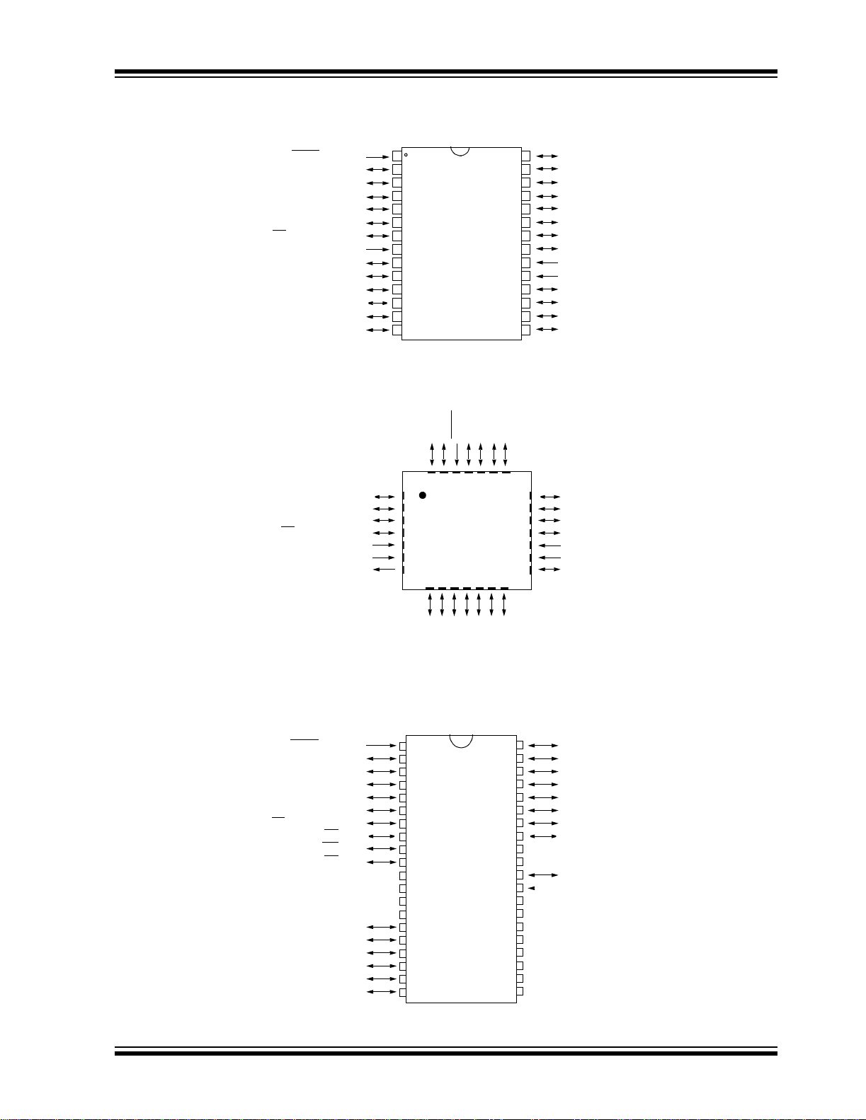
Pin Diagrams
28-pin SPDIP, SOIC
PIC18F2X1X/4X1X
28-pin QFN
RA2/AN2/V
RA4/T0CKI/C1OUT
RA5/AN4/SS
RC0/T1OSO/T13CKI
RC1/T1OSI/CCP2
RA2/AN2/VREF-/CVREF
RA5/AN4/SS
MCLR/VPP/RE3
RA0/AN0
RA1/AN1
REF-/CVREF
RA3/AN3/VREF+
/HLVDIN/C2OUT
OSC1/CLKI/RA7
OSC2/CLKO/RA6
RC3/SCK/SCL
RA3/AN3/VREF+
RA4/T0CKI/C1OUT
/HLVDIN/C2OUT
OSC1/CLKI/RA7
OSC2/CLKO/RA6
V
RC2/CCP1
SS
(1)
V
PIC18F2X1X
RB7/KBI3/PGD
1213 14
28
27
26
25
24
23
22
21
20
19
18
17
16
15
RB6/KBI2/PGC
RB5/KBI1/PGM
RB4KBI0/AN11
22
232425262728
21
20
19
18
17
16
15
RB7/KBI3/PGD
RB6//KBI2/PGC
RB5/KBI1/PGM
RB4/KBI0/AN11
RB3/AN9/CCP2
RB2/INT2/AN8
RB1/INT1/AN10
RB0/INT0/FLT0/AN12
V
DD
VSS
RC7/RX/DT
RC6/TX/CK
RC5/SDO
RC4/SDI/SDA
RB3/AN9/CCP2
RB2/INT2/AN8
RB1/INT1/AN10
RB0/INT0/FLT0/AN12
V
DD
VSS
RC7/RX/DT
(1)
(1)
1
2
3
4
5
6
7
8
9
10
11
12
13
14
/VPP/RE3
MCLR
RA0/AN0
RA1/AN1
1
2
3
PIC18F2410
4
SS
PIC18F2510
5
6
7
8
9
1011
MCLR/VPP/RE3
RA0/AN0
RA1/AN1
RA2/AN2/V
RA5/AN4/SS
Note 1: RB3 is the alternate pin for CCP2 multiplexing.
REF-/CVREF
RA3/AN3/VREF+
RA4/T0CKI/C1OUT
/HLVDIN/C2OUT
OSC1/CLKI/RA7
OSC2/CLKO/RA6
RC0/T1OSO/T13CKI
RC1/T1OSI/CCP2
RC2/CCP1/P1A
RC3/SCK/SCL
RE0/RD
RE1/WR
RE2/CS
RD0/PSP0
RD1/PSP1
/AN5
/AN6
/AN7
V
VSS
DD
(1)
(1)
RC5/SDO
RC2/CCP1
RC1/T1OSI/CCP2
RC0/T1OSO/T13CKI
1
2
3
4
5
6
7
8
9
10
11
12
13
14
15
16
17
18
19
20
RC3/SCK/SCL
RC4/SDI/SDA
40
39
38
37
36
35
34
33
32
31
30
29
28
27
26
25
24
23
22
21
RC6/TX/CK
RB7/KBI3/PGD
RB6/KBI2/PGC
RB5/KBI1/PGM
RB4/KBI0/AN11
RB3/AN9/CCP2
RB2/INT2/AN8
RB1/INT1/AN10
RB0/INT0/FLT0/AN12
V
DD
VSS
RD7/PSP7/P1D
RD6/PSP6/P1C
RD5/PSP5/P1B
RD4/PSP4
RC7/RX/DT
RC6/TX/CK
RC5/SDO
RC4/SDI/SDA
RD3/PSP3
RD2/PSP2
(1)
2004 Microchip Technology Inc. Preliminary DS39636A-page 3
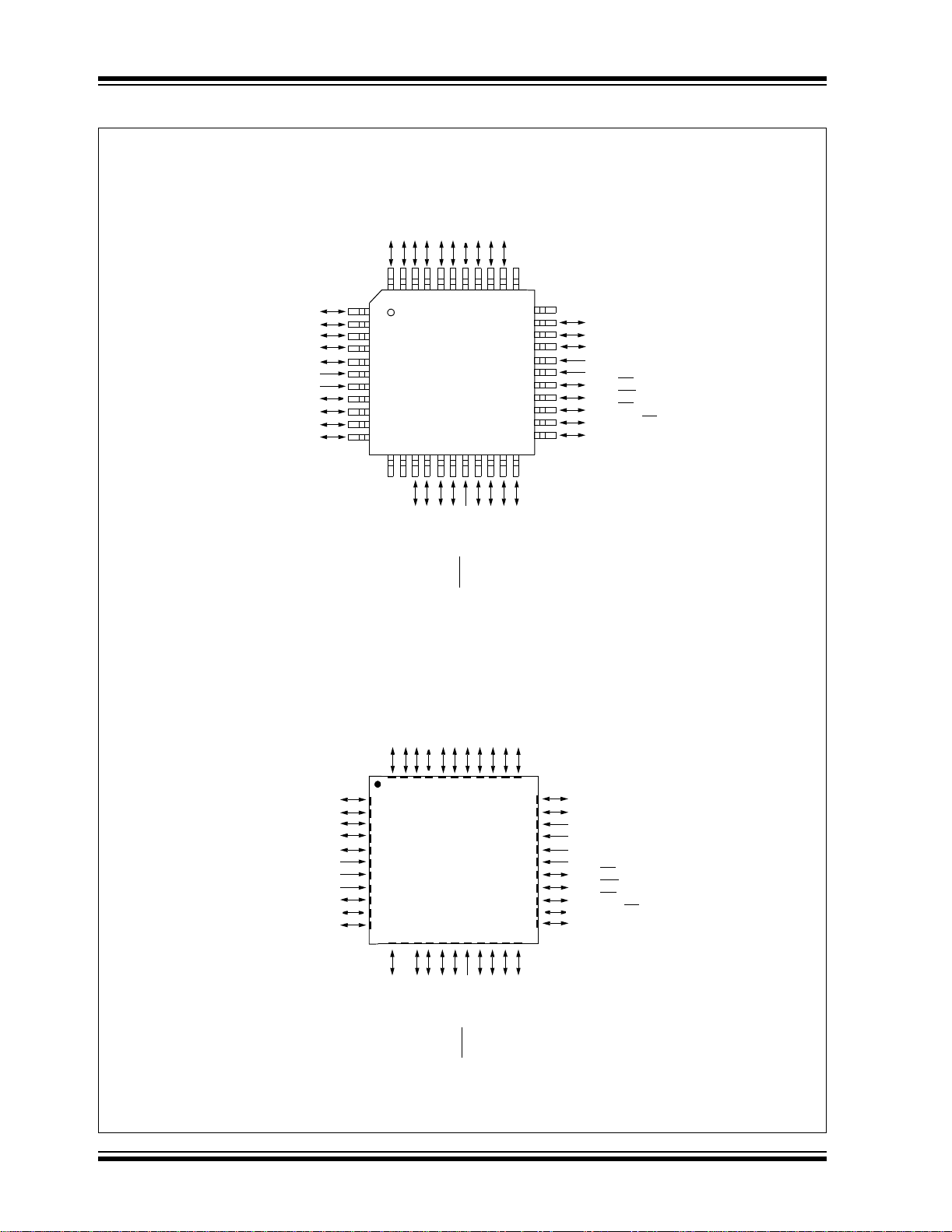
PIC18F2X1X/4X1X
Pin Diagrams (Cont.’d)
44-pin TQFP
RD5/PSP5/P1B
RD6/PSP6/P1C
RD7/PSP7/P1D
RB0/INT0/FLT0/AN12
RB1/INT1/AN10
RB3/AN9/CCP2
RC7/RX/DT
RD4/PSP4
V
VDD
RB2/INT2/AN8
(1)
RC6/TX/CK
RC5/SDO
RC4/SDI/SDA
RD3/PSP3
RD2/PSP2
RD1/PSP1
RD0/PSP0
RC3/SCK/SCL
RC2/CCP1/P1A
RC1/T1OSI/CCP2
NC
15
RB5/KBI1/PGM
39
16
17
RB7/KBI3/PGD
RB6/KBI2/PGC
38
363435
37
1819202122
RA1/AN1
RA0/AN0
/VPP/RE3
REF-/CVREF
MCLR
33
32
31
30
29
28
27
26
25
24
23
RA3/AN3/VREF+
NC
RC0/T1OSO/T13CKI
OSC2/CLKO/RA6
OSC1/CLKI/RA7
SS
V
VDD
RE2/CS/AN7
/AN6
RE1/WR
/AN5
RE0/RD
RA5/AN4/SS
RA4/T0CKI/C1OUT
/HLVDIN/C2OUT
4443424140
1
2
3
4
SS
(1)
5
6
7
8
9
10
11
121314
NC
NC
PIC18F4X1X
RB4/KBI0/AN11
44-pin QFN
RC6/TX/CK
RC5/SDO
RC4/SDI/SDA
RD3/PSP3
RC7/RX/DT
RD4/PSP4
RD5/PSP5/P1B
RD6/PSP6/P1C
RD7/PSP7/P1D
RB0/INT0/FLT0/AN12
RB1/INT1/AN10
RB2/INT2/AN8
Note 1: RB3 is the alternate pin for CCP2 multiplexing.
V
VDD
VDD
SS
4443424140
1
2
3
4
5
6
7
8
9
10
11
121314
(1)
RB3/AN9/CCP2
PIC18F4X1X
15
NC
RB5/KBI1/PGM
RB4/KBI0/AN11
RD2/PSP2
16
RB6/KBI2/PGC
RD1/PSP1
39
17
RB7/KBI3/PGD
RA2/AN2/V
(1)
RD0/PSP0
RC3/SCK/SCL
RC2/CCP1/P1A
RC1/T1OSI/CCP2
38
363435
37
1819202122
RA1/AN1
RA0/AN0
/VPP/RE3
REF-/CVREF
MCLR
RA2/AN2/V
RC0/T1OSO/T13CKI
33
32
31
30
29
28
27
26
25
24
23
REF+
RA3/AN3/V
OSC2/CLKO/RA6
OSC1/CLKI/RA7
V
SS
VSS
VDD
VDD
RE2/CS/AN7
/AN6
RE1/WR
/AN5
RE0/RD
RA5/AN4/SS
RA4/T0CKI/C1OUT
/HLVDIN/C2OUT
DS39636A-page 4 Preliminary 2004 Microchip Technology Inc.

PIC18F2X1X/4X1X
Table of Contents
1.0 Device Overview.......................................................................................................................................................................... 7
2.0 Oscillator Configurations............................................................................................................................................................ 23
3.0 Power Managed Modes ...................................... .. .. .... .. .. ..... .. .. .... .. .. .. .. ....... .. .. .. .. .. .. ....... .. .. .. ...................................................... 33
4.0 Reset..........................................................................................................................................................................................41
5.0 Memory Organization.................................................................................................................................................................53
6.0 Flash Program Memory............ ................ ................. ................. ................................................................................................75
7.0 8 x 8 Hardware Multiplier............................................................................................................................................................ 79
8.0 Interrupts.................................................................................................................................................................................... 81
9.0 I/O Ports................................................. .................................................................................................................................... 95
10.0 Timer0 Module ......................................................................................................................................................................... 113
11.0 Timer1 Module ......................................................................................................................................................................... 117
12.0 Timer2 Module ......................................................................................................................................................................... 123
13.0 Timer3 Module ......................................................................................................................................................................... 125
14.0 Capture/Compare/PWM (CCP) Modules ................................................................................................................................. 129
15.0 Enhanced Capture/Compare/PWM (ECCP) Module ................................................................................................................ 137
16.0 Master Synchronous Serial Port (MSSP) Module ............................................................................... .....................................151
17.0 Enhanced Universal Synchronous Receiver Transmitter (EUSART)....................................................................................... 191
18.0 10-Bit Analog-to-Digital Converter (A/D) Module .....................................................................................................................211
19.0 Comparator Module.......................................................................................................... ........................................................ 221
20.0 Comparator Voltage Reference Module................................................................................................................................... 227
21.0 High/Low-Voltage Detect (HLVD).......................................................................... .... ......... .... ..................................................231
22.0 Special Features of the CPU.......... ................. ................ ................. ................. ....................................................................... 237
23.0 Instruction Set Summary.......................................................................................................................................................... 257
24.0 Development Support............................................................................................................................................................... 307
25.0 Electrical Characteristics.......................................................................................................................................................... 313
26.0 DC and AC Characteristics Graphs And Tables ......................................................................................................................351
27.0 Packaging Informa tio n. ................................................ ................. ............................................................................................ 353
Appendix A: Revision History............................................................................................................................................................. 361
Appendix B: Device Differences ........................................................................................................................................................ 361
Appendix C: Conversion Considerations ...........................................................................................................................................362
Appendix D: Migration From Baseline to Enhanced Devices ............................................................................................................ 362
Appendix E: Migration From Mid-Range to Enhanced Devices.........................................................................................................363
Appendix F: Migration From High-End to Enhanced Devices............................................................................................................363
Index ................................................................................................................................................................................................. 365
On-Line Support.................................................................................................................................................................................375
Systems Information and Upgrade Hot Line...................................................................................................................................... 375
Reader Response.............................................................................................................................................................................. 376
PIC18F2X1X/4X1X Product Identification System . ............................................................................................................................ 377
2004 Microchip Technology Inc. Preliminary DS39636A-page 5

PIC18F2X1X/4X1X
TO OUR VALUED CUSTOMERS
It is our intention to provide our valued customers with the best documentation possible to ensure successful use of your Microchip
products. To this end, we will continue to improve our publications to better suit your needs. Our publications will be refined and
enhanced as new volumes and updates are introduced.
If you have any questions or c omm ents regarding t his publication, p lease c ontact the M arket ing Co mmunications Department via
E-mail at docerrors@mail.microchip.com or fax the Reader Response Form in the back of this data sheet to (480) 792-4150.
We welcome your feedback.
Most Current Data Sheet
To obtain the most up-to-date version of this data sheet, please register at our Worldwide Web site at:
http://www.microchip.com
You can determine the version of a data sheet by examining its literature number found on the bottom outside corner of any page.
The last character of the literature number is the version number, (e.g., DS30000A is version A of document DS30000).
Errata
An errata sheet, describing minor operational differences from the data sheet and recommended workarounds, may exist for current
devices. As device/documentation issues become known to us, we will publish an errata sheet. The errata will specify the revision
of silicon and revision of document to which it applies.
To determine if an errata sheet exists for a particular device, please check with one of the following:
• Microchip’s Worldwide Web site; http://www.microchip.com
• Your local Microchip sales office (see last page)
• The Microchip Corporate Literature Center; U.S. FAX: (480) 792-7277
When contacting a sales office or the literature center, please specify which device, revision of silicon and data sheet (include
literature number) you are using.
Customer Notification System
Register on our Web site at www.microchip.com/cn to receive the most current information on all of our products.
DS39636A-page 6 Preliminary 2004 Microchip Technology Inc.

PIC18F2X1X/4X1X
1.0 DEVICE OVERVIEW
This documen t conta i ns dev ic e spec if i c in for m at i on fo r
the following devices:
• PIC18F2410 • PIC18LF2410
• PIC18F2510 • PIC18LF2510
• PIC18F2515 • PIC18LF2515
• PIC18F2610 • PIC18LF2610
• PIC18F4410 • PIC18LF4410
• PIC18F4510 • PIC18LF4510
• PIC18F4515 • PIC18LF4515
• PIC18F4610 • PIC18LF4610
This family offers the advantages of all PIC18
microcontrollers – namely, high computational
performance at an economical price – with the addition
of high-endurance, Flash program memory. On top of
these features, the PIC18F2X1X/4X1X family introduces
design enhancements that make these microcontrollers
a logical choice for many high-performance, power
sensitive applications.
1.1 New Core Features
1.1.1 nanoWatt TECHNOLOGY
All of the devices in the PIC18F2X1X/4X1X family
incorporate a range of features that can significantly
reduce power consumption during operation. Key
items include:
• Alternate Run Modes: By clocking the controller
from the Timer1 source or the internal oscillator
block, power consumption during code execution
can be reduced by as much as 90%.
• Multiple Idle Modes: The controller can also run
with its CPU core disabled but the peripherals still
active. In these st ates, powe r consumpt ion can be
reduced even further, to as little as 4% of normal
operation requirements.
• On-the-fly Mode Switching: The power
managed modes a re invo ked b y user code durin g
operation, allowing the user to incorporate powersaving ideas into their application’s software
design.
• Lower Consumption in Key Modules: The
power requirements for both Timer1 and the
Watchdog Timer have been minimized. See
Section 25.0 “Electrical Characteristics” for
values.
1.1.2 MULTIPLE OSCILLATOR OPTIONS AND FEATURES
All of the devices in th e PIC 18F2X1X/ 4X1X fam ily of f er
ten different oscillator options, allowing users a wide
range of choices in developing application hardware.
These include:
• Four Crystal modes, using crystals or ceramic
resonators
• Two External Clock modes, offering the option of
using two pins (oscillator input and a divide-by-4
clock output) or one pin (oscillator input, with the
second pin reassigned as general I/O)
• Two External RC Oscillator modes with the same
pin options as the External Clock modes
• An internal oscillator block which provides an
8 MHz clock and an INTRC source (approximately 31 kHz), as well as a range of 6 user
selectable cl ock fre quenc ies, be tween 125 kHz to
4 MHz, for a total of 8 clock frequencies. This
option frees the two oscillator pins for use as
additional general purpose I/O.
• A Phase Lock Loop (PLL) frequency multiplier,
available to both the high-speed crystal and
internal oscillator modes, which allows clock
speeds of up to 40 MHz. Used with the internal
oscillator, the PLL gi ves users a complete sele ction
of clock speeds, from 31 kHz to 32 MHz – all
without using an external crystal or clock circuit.
Besides its ava ilability as a cloc k source, the intern al
oscillator block pro vid es a s t ab le re fere nce source that
gives the family additional features for robust
operation:
• Fail-Safe Clock Monitor: This option constantly
monitors the main clock source against a
reference signal provided by the internal
oscillator. If a clock failure occurs, the controller i s
switched to the internal oscillator block, allowing
for continued low-speed operation or a safe
application shutdown.
• Two-Speed Start-up: This option allows the
internal oscillator to serve as the clock source
from Power-on Reset, or wake-up from Sleep
mode, until the primary clock source is available.
2004 Microchip Technology Inc. Preliminary DS39636A-page 7

PIC18F2X1X/4X1X
1.2 Other Special Features
• Memory Endurance: The Flas h cells f or prog ram
memory are rated to 100,000 erase/write cycles.
Data retention without refresh is conservatively
estimated to be greater than 40 years.
• Extended Instruction Set: The PIC18F2X1X/
4X1X family introduces an optional extension to
the PIC18 instruction set, which adds 8 new
instructions and an Indexed Addressing mode.
This extension, en abled as a de vi ce conf igurati on
option, has been specifi cally des igned to opt imize
re-entrant applica tion cod e origina lly deve loped in
high-level languages, such as C.
• Enhanced CCP Module: In PWM mode, this
module provides 1, 2 or 4 modulated outputs for
controlling half-bridge and full-bridge drivers.
Other features include Auto-S hutdown, for
disabling PWM output s on interrup t or other selec t
conditions and Auto-Rest art, to re activ ate outpu ts
once the condition has cleared.
• Enhanced Addressable USART: This serial
communication module is capable of standard
RS-232 operation an d provides support for th e LIN
bus protocol. Other enhancements include automatic baud r ate detection and a 16-bit Baud Rate
Generator for improved resolution. When the
microcontroller is using the internal oscillator
block, the USART provides stable operation for
applications that talk to the outside world without
using an external crystal (or its accompanying
power requirement).
• 10-bit A/D Converter: This module incorporates
programmable acquisition time, allowing for a
channel to be selected and a conversion to be
initiated withou t wai ting for a sampling period and
thus, reduce code overhead.
• Extended Watchdog Timer (WDT): This
enhanced version in corpora tes a 1 6-bit pre scale r,
allowing an extende d time-o ut rang e that is s ta ble
across operating voltage and temperature. See
Section 25.0 “Electrical Characteristics” for
time-out periods.
1.3 Details on Individual Family Members
Devices in the PIC18F2X1X/4X1X family are available
in 28-pin and 40/44-pin packages. Block diagrams for
the two group s are shown in Figure 1-1 and Figure 1-2.
The devices are differentiated from each other in five
ways:
1. Flash program memory
• 16 Kbytes for PIC18F2410/4410 devices
• 32 Kbytes for PIC18F2510/4510 devices
• 48 Kbytes for PIC18F2515/4515 devices
• 64 Kbytes for PIC18F2610/4610 devices
2. A/D channels (10 for 28-pin devices, 13 for
40/44-pin devices).
3. I/O ports (3 bidirectio nal ports on 28-pin devices,
5 bidirectional ports on 40/44-pin devices).
4. CCP and Enhanced CCP implementation (28-pin
devices have 2 s tandard CCP modules; 40/4 4-pin
devices have one standard CCP module and one
ECCP module).
5. Parallel Slave Port (present only on 40/44-pin
devices).
All other features fo r device s in this family are identi cal.
These are summarized in Table 1-1.
The pinouts for all devices are listed in Table 1-3 and
Table 1-4.
Like all Microchip PIC18 devices, members of the
PIC18F2X1X/4X1X family are available as both
standard and low-voltage devices. Standard devices
with Flash memory, designated with an “F” in the part
number (such as PIC18F2610), accommodate an
operating V
parts, designated by “LF” (such as PIC18LF2610),
function over an extended VDD range of 2.0V to 5.5V.
DD range of 4.2V to 5.5V. Low-voltage
DS39636A-page 8 Preliminary 2004 Microchip Technology Inc.

PIC18F2X1X/4X1X
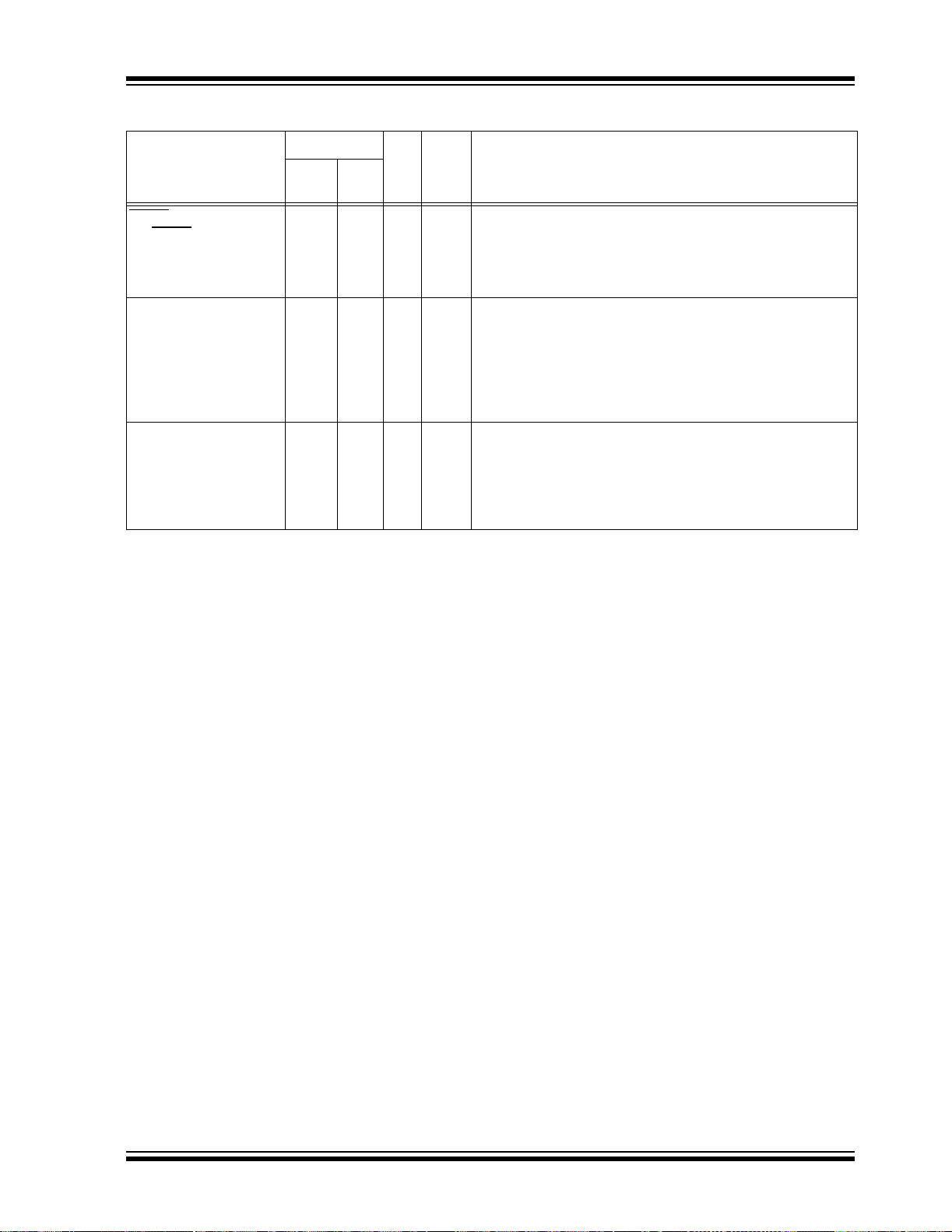
T ABLE 1-1: DEVICE FEATURES (PIC18F2410/2510/2515/2610)
Features PIC18F2410 PIC18F2510 PIC18F2515 PIC18F2610
Operating Frequency DC – 40 MHz DC – 40 MHz DC – 40 MHz DC – 40 MHz
Program Memory (Bytes) 16384 32768 49152 65536
Program Memory
(Instructions)
Data Memory (Bytes) 768 1536 3968 3968
Interrupt Sources 18 18 18 18
I/O Ports Ports A, B, C, (E) Ports A, B, C, (E) Ports A, B, C, (E) Ports A, B, C, (E)
Timers 4444
Capture/Compare/PWM Modules2222
Enhanced
Capture/Compare/PWM Modules
Serial Communications MSSP,
Parallel Communications (PSP) No No No No
10-bit Analog-to-Digital Module 10 Input Channels 10 Input Channels 10 Input Channels 10 Input Channels
Resets (and Delays) POR, BOR,
Programmable
High/Low-Voltage Detect
Programmable
Brown-out Reset
Instruction Set 75 Instructions;
Instruction Set enabled
Packages 28-pin SPDIP
8192 16384 24576 32768
0000
Enhanced USART
RESET Instruction,
Stack Full,
Stack Underflow
(PWRT, OST),
(optional),
MCLR
WDT
Yes Yes Yes Yes
Yes Yes Yes Yes
83 with Extended
28-pin SOIC
28-pin QFN
MSSP,
Enhanced USART
POR, BOR,
RESET Instruction,
Stack Full,
Stack Underflow
(PWRT, OST),
MCLR (optional),
WDT
75 Instructions;
83 with Extended
Instruction Set enabled
28-pin SPDIP
28-pin SOIC
28-pin QFN
MSSP,
Enhanced USART
POR, BOR,
RESET Instruction,
Stack Full,
Stack Underflow
(PWRT, OST),
MCLR (optional),
WDT
75 Instructions;
83 with Extended
Instruction Set enabled
28-pin SPDIP
28-pin SOIC
MSSP,
Enhanced USART
POR, BOR,
RESET Instruction,
Stack Full,
Stack Underflow
(PWRT, OST),
MCLR (optional),
WDT
75 Instructions;
83 with Extended
Instruction Set enabled
28-pin SPDIP
28-pin SOIC
2004 Microchip Technology Inc. Preliminary DS39636A-page 9

PIC18F2X1X/4X1X
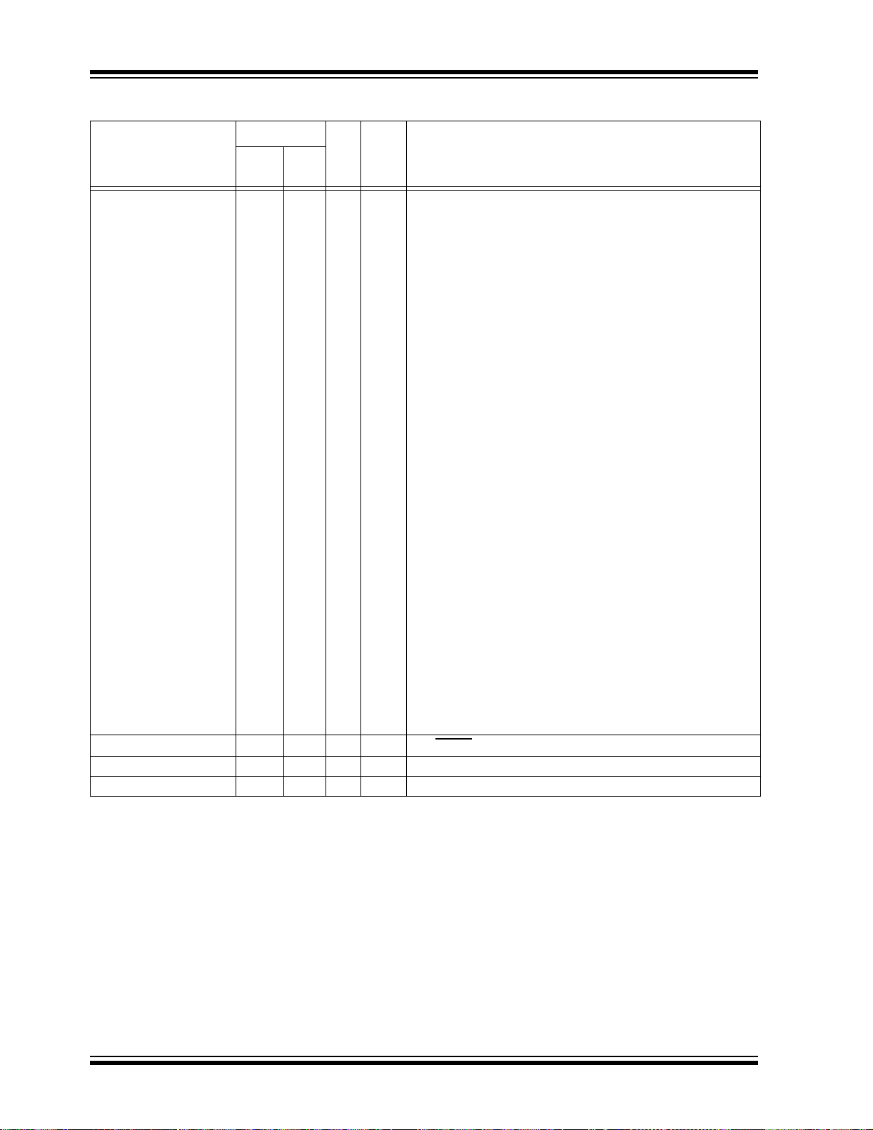
TABLE 1-2: DEVICE FEATURES (PIC18F4410/4510/4515/4610)
Features PIC18F4410 PIC18F4510 PIC18F4515 PIC18F4610
Operating Frequency DC – 40 MHz DC – 40 MHz DC – 40 MHz DC – 40 MHz
Program Memory (Bytes) 16384 32768 49152 65536
Program Memory
(Instructions)
Data Memory (Bytes) 768 1536 3968 3968
Interrupt Sources 19 19 19 19
I/O Ports Ports A, B, C, D, E Ports A, B, C, D, E Ports A, B, C, D, E Ports A, B, C, D, E
Timers 4444
Capture/Compare/PWM Modules 1 1 1 1
Enhanced
Capture/Compare/PWM Modules
Serial Communications MSSP,
Parallel Communications (PSP) Yes Yes Yes Yes
10-bit Analog-to-Digital Module 13 Input Channels 13 Input Channels 13 Input Channels 13 Input Channels
Resets (and Delays) POR, BOR,
Programmable
High/Low-Voltage Detect
Programmable
Brown-out Reset
Instruction Set 75 Instructions;
Instruction Set enabled
Packages 40-pin PDIP
8192 16384 24576 32768
1111
Enhanced USART
RESET Instruction,
Stack Full,
Stack Underflow
(PWRT, OST),
(optional),
MCLR
WDT
Yes Yes Yes Yes
Yes Yes Yes Yes
83 with Extended
44-pin QFN
44-pin T QFP
MSSP,
Enhanced USART
POR, BOR,
RESET Instruction,
Stack Full,
Stack Underflow
(PWRT, OST),
MCLR (optional),
WDT
75 Instructions;
83 with Extended
Instruction Set enabled
40-pin PDIP
44-pin QFN
44-pin TQFP
MSSP,
Enhanced USART
POR, BOR,
RESET Instruction,
Stack Full,
Stack Underflow
(PWRT, OST),
MCLR (optional),
WDT
75 Instructions;
83 with Extended
Instruction Set enabled
40-pin PDIP
44-pin QFN
44-pin TQFP
MSSP,
Enhanced USART
POR, BOR,
RESET Instruction,
Stack Full,
Stack Underflow
(PWRT, OST),
MCLR (optional),
WDT
75 Instructions;
83 with Extended
Instruction Set enabled
40-pin PDIP
44-pin QFN
44-pin TQFP
DS39636A-page 10 Preliminary 2004 Microchip Technology Inc.
PIC18F2X1X/4X1X
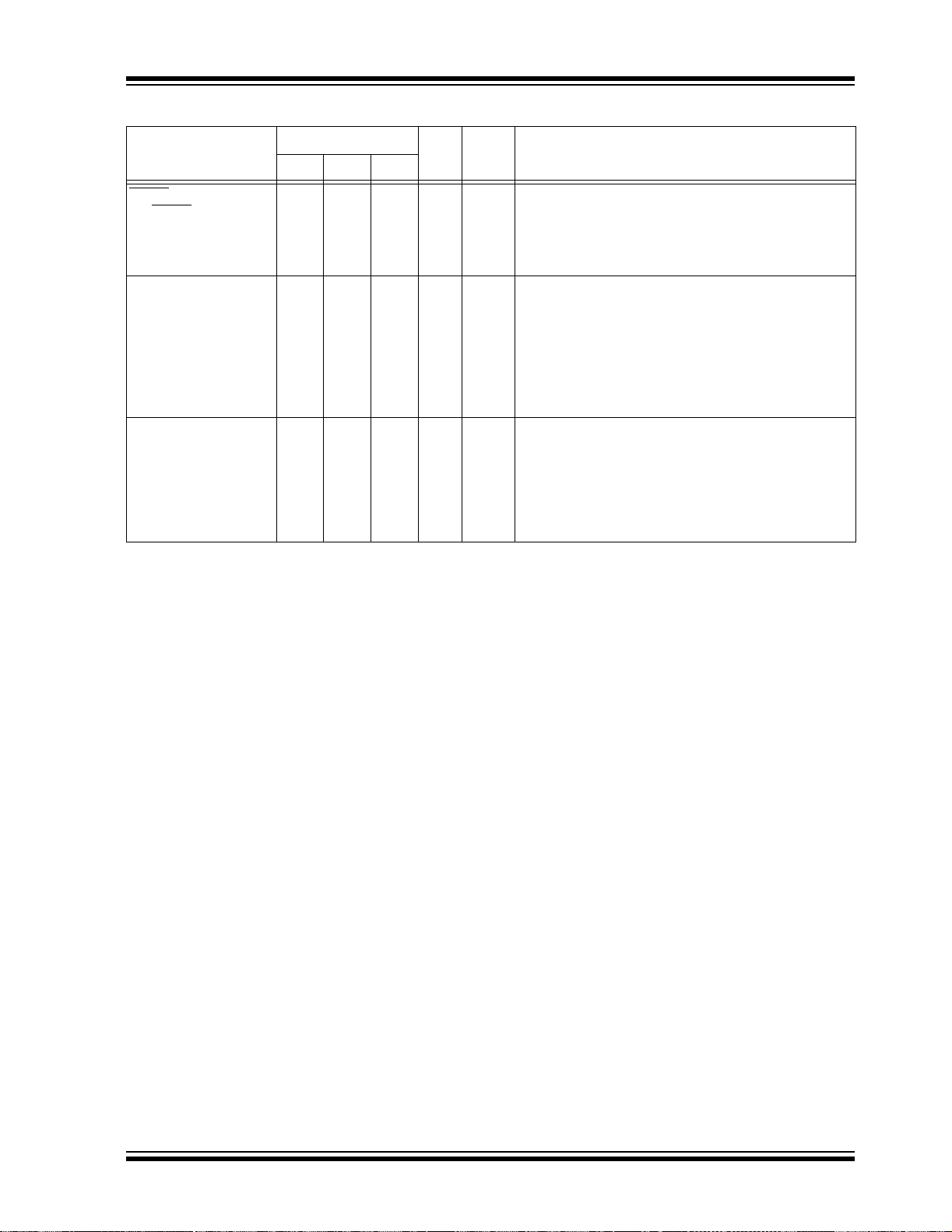
FIGURE 1-1: PIC1 8F2410/ 2510/ 2515/ 2610 ( 28-PIN) BLOCK DI AGRAM
T able Pointer<21>
inc/dec logic
21
20
Address Latch
Program Memory
(16/32/48/64
Kbytes)
Data Latch
8
Instruction Bus <16>
PCLATH
PCLATU
PCU
Program Counter
31 Level Stack
STKPTR
Table Latch
ROM Latch
IR
Data Bus<8>
8
PCH PCL
8
Data Latch
Data Memory
(.7, 1.5, 3.9
Kbytes)
PORTA
Address La t ch
12
Data Address<12>
BSR
4
FSR0
FSR1
FSR2
inc/dec
logic
Address
Decode
4
12
Access
Bank
12
PORTB
RA0/AN0
RA1/AN1
RA2/AN2/VREF-/CVREF
RA3/AN3/VREF+
RA4/T0CKI/C1OUT
RA5/AN4/SS
OSC2/CLKO
OSC1/CLKI
/HLVDIN/C2OUT
(3)
/RA6
(3)
/RA7
RB0/INT0/FLT0/AN12
RB1/INT1/AN10
RB2/INT2/AN8
RB3/AN9/CCP2
(1)
RB4/KBI0/AN11
RB5/KBI1/PGM
RB6/KBI2/PGC
RB7/KBI3/PGD
OSC1
OSC2
T1OSI
T1OSO
MCLR
VDD,
V
BOR
HLVD
Instruction
Decode and
Control
State Machine
Control Signals
BITOP
3
8 x 8 Multiply
W
8
(3)
(3)
(2)
SS
Internal
Oscillator
Block
INTRC
Oscillator
8 MHz
Oscillator
Single-Supply
Programming
In-Circuit
Debugger
Power-up
Timer
Oscillator
Start-up Timer
Power-on
Reset
Watchdog
Timer
Brown-out
Reset
Fail-Safe
Clock Monitor
Precision
Band Gap
Reference
8
ALU<8>
8
PRODLPRODH
8
8
8
PORTC
RC0/T1OSO/T13CKI
RC1/T1OSI/CCP2
(1)
RC2/CCP1
RC3/SCK/SCL
RC4/SDI/SDA
RC5/SDO
8
RC6/TX/CK
RC7/RX/DT
8
PORTE
MCLR/VPP/RE3
(2)
Timer2Timer1 Timer3Timer0
CCP1
CCP2
MSSP
EUSARTComparator
ADC
10-bit
Note 1: CCP2 is multiplexed with RC1 when configuration bit CCP2MX is set, or RB3 when CCP2MX is not set.
2: RE3 is only available when MCLR
3: OSC1/CLKI and OSC2/CLKO are only available in select oscillator modes and when these pins are not being used as digital I/O.
Refer to Section 2.0 “Oscillator Configurations” for additional information.
functionality is disabled.
2004 Microchip Technology Inc. Preliminary DS39636A-page 11
PIC18F2X1X/4X1X
FIGURE 1-2: PIC18F4410/4510/4515/4610 (40/44-PIN) BLOCK DIAGRAM
T able Pointer<21>
inc/dec logic
21
20
Address Latch
Program Memory
(16/32/48/ 64
Data Latch
8
Instruction Bus <16>
PCLATH
PCLATU
PCU
Program Counter
31 Level Stack
STKPTR
Table Latch
ROM Latch
IR
Instruction
Decode and
Control
Data Bus<8>
8
PCH PCL
State M achine
Control Signals
8
Data Latch
Data Memory
(.7, 1.5, 3.9
Address La t ch
Data Address<12>
4
BSR
FSR0
FSR1
FSR2
inc/dec
logic
Address
12
4
12
Access
Bank
12
PRODLPRODH
8 x 8 Multiply
3
BITOP
BOR
HLVD
ECCP1
Note 1: CCP2 is multiplexed with RC1 when configuration bit CCP2MX is set, or RB3 when CCP2MX is not set.
2: RE3 is only available when MCLR
3: OSC1/CLKI and OSC2/CLKO are only available in select oscillator modes and when these pins are not being used as digital I/O.
Refer to Section 2.0 “Oscillator Configurations ” for additional information.
CCP2
MSSP
functionality is disabled.
Timer2Timer1 Timer3Timer0
EUSARTComparator
W
8
ALU<8>
8
8
ADC
10-bit
8
8
8
PORTD
PORTE
RD0/PSP0
RE0/RD/AN5
RE1/WR/AN6
RE2/CS/AN7
MCLR/VPP/RE3
:RD4/PSP4
(2)
DS39636A-page 12 Preliminary 2004 Microchip Technology Inc.
PIC18F2X1X/4X1X
T ABLE 1-3: PIC18F2410/2510/2515/2610 PINOUT I/O DESCRIPTIONS
Pin Name
Pin Number
SPDIP,
SOIC
QFN
Pin
Type
Buffer
Type
Description
/VPP/RE3
MCLR
MCLR
VPP
RE3
OSC1/CLKI/RA7
OSC1
CLKI
RA7
OSC2/CLKO/RA6
OSC2
CLKO
RA6
Legend: TTL = TTL compatible input CMOS = CMOS compatible input or output
ST = Schmitt Trigger input with CMOS levels I = Input
O=Output P =Power
Note 1: Default assignment for CCP2 when configuration bit CCP2MX is set.
2: Alternate assignment for CCP2 when configuration bit CCP2MX is cleared.
126
96
10 7
P
I/O
O
O
I/O
I
I
I
I
ST
ST
ST
CMOS
TTL
—
—
TTL
Master Clear (input) or programming voltage (input).
Master Clear (Reset) input. This pin is an active-low
Reset to the device.
Programming voltage input.
Digital input.
Oscillator crystal or external clock input.
Oscillator crystal input or external clock source input.
ST buffer when configured in RC mode; CMOS otherwise.
External clock source input. Always associated with pin
function OSC1. (See related OSC1/CLKI, OSC2/CLKO
pins.)
General purpose I/O pin.
Oscillator crystal or clock output.
Oscillator crystal output. Connects to crystal or
resonator in Crystal Oscillator mode.
In RC mode, OSC2 pin outputs CLKO, which has 1/4 the
frequency of OSC1 and denotes the instruction cycle rate.
General purpose I/O pin.
2004 Microchip Technology Inc. Preliminary DS39636A-page 13

PIC18F2X1X/4X1X
TABLE 1-3: PIC18F2410/2510/2515/2610 PINOUT I/O DESCRIPTIONS (CONTINUED)
Pin Number
Pin Name
RA0/AN0
RA0
AN0
RA1/AN1
RA1
AN1
RA2/AN2/V
RA2
AN2
VREFCV
RA3/AN3/V
RA3
AN3
V
RA4/T0CKI/C1OUT
RA4
T0CKI
C1OUT
RA5/AN4/SS
C2OUT
RA5
AN4
SS
HLVDIN
C2OUT
RA6 See the OSC2/CLKO/RA6 pin.
RA7 See the OSC1/CLKI/RA7 pin.
Legend: TTL = TTL compatible input CMOS = CMOS compatible input or output
Note 1: Default assignment for CCP2 when configuration bit CCP2MX is set.
REF-/CVREF
REF
REF+
REF+
/HLVDIN/
ST = Schmitt Trigger input with CMOS levels I = Input
O=Output P =Power
2: Alternate assignment for CCP2 when configuration bit CCP2MX is cleared.
SPDIP,
SOIC
227
328
41
52
63
74
QFN
Pin
Buffer
Type
Type
I/OITTL
Analog
I/OITTL
Analog
I/O
I
Analog
I
Analog
O
Analog
I/O
I
Analog
I
Analog
I/O
I
O
I/O
I
Analog
I
I
Analog
O
PORTA is a bidirectional I/O port.
Digital I/O.
Analog input 0.
Digital I/O.
Analog input 1.
TTL
TTL
ST
ST
—
TTL
TTL
—
Digital I/O.
Analog input 2.
A/D reference voltage (low) input.
Comparator r eference voltage output.
Digital I/O.
Analog input 3.
A/D reference voltage (high) input.
Digital I/O.
Timer0 external clock input.
Comparator 1 output.
Digital I/O.
Analog input 4.
SPI™ slave select input.
High/Low-Voltage Detect input.
Comparator 2 output.
Description
DS39636A-page 14 Preliminary 2004 Microchip Technology Inc.

PIC18F2X1X/4X1X
T ABLE 1-3: PIC18F2410/2510/2515/2610 PINOUT I/O DESCRIPTIONS (CONTINUED)
Pin Number
Pin Name
RB0/INT0/FLT0/AN12
RB0
INT0
FLT0
AN12
RB1/INT1/AN10
RB1
INT1
AN10
RB2/INT2/AN8
RB2
INT2
AN8
RB3/AN9/CCP2
RB3
AN9
(1)
CCP2
RB4/KBI0/AN11
RB4
KBI0
AN11
RB5/KBI1/PGM
RB5
KBI1
PGM
RB6/KBI2/PGC
RB6
KBI2
PGC
RB7/KBI3/PGD
RB7
KBI3
PGD
Legend: TTL = TTL compatible input CMOS = CMOS compatible input or output
ST = Schmitt Trigger input with CMOS levels I = Input
O=Output P =Power
Note 1: Default assignment for CCP2 when configuration bit CCP2MX is set.
2: Alternate assignment for CCP2 when configuration bit CCP2MX is cleared.
SPDIP,
SOIC
21 18
22 19
23 20
24 21
25 22
26 23
27 24
28 25
QFN
Pin
Type
I/O
I
I
I
I/O
I
I
I/O
I
I
I/O
I
I/O
I/O
I
I
I/O
I
I/O
I/O
I
I/O
I/O
I
I/O
Buffer
Type
TTL
ST
ST
Analog
TTL
ST
Analog
TTL
ST
Analog
TTL
Analog
ST
TTL
TTL
Analog
TTL
TTL
ST
TTL
TTL
ST
TTL
TTL
ST
Description
PORTB is a bidirectional I/O port. PORTB can be software
programmed for internal weak pull-ups on all inputs.
Digital I/O.
External interrupt 0.
PWM Fault input for CCP1.
Analog input 12.
Digital I/O.
External interrupt 1.
Analog input 10.
Digital I/O.
External interrupt 2.
Analog input 8.
Digital I/O.
Analog input 9.
Capture 2 input/Compare 2 output/PWM 2 output.
Digital I/O.
Interrupt-on-change pin.
Analog input 11.
Digital I/O.
Interrupt-on-change pin.
Low-Voltage ICSP™ Programming enable pin.
Digital I/O.
Interrupt-on-change pin.
In-Circuit Debugger and ICSP programming clock pin.
Digital I/O.
Interrupt-on-change pin.
In-Circuit Debugger and ICSP programming data pin.
2004 Microchip Technology Inc. Preliminary DS39636A-page 15
PIC18F2X1X/4X1X
TABLE 1-3: PIC18F2410/2510/2515/2610 PINOUT I/O DESCRIPTIONS (CONTINUED)
Pin Number
Pin Name
RC0/T1OSO/T13CKI
RC0
T1OSO
T13CKI
RC1/T1OSI/CCP2
RC1
T1OSI
(2)
CCP2
RC2/CCP1
RC2
CCP1
RC3/SCK/SCL
RC3
SCK
SCL
RC4/SDI/SDA
RC4
SDI
SDA
RC5/SDO
RC5
SDO
RC6/TX/CK
RC6
TX
CK
RC7/RX/DT
RC7
RX
DT
RE3 — — — — See MCLR
SS 8, 19 5, 16 P — Ground reference for logic and I/O pins.
V
VDD 20 17 P — Positive supply for logic and I/O pins.
Legend: TTL = TTL compatible input CMOS = CMOS compatible input or output
ST = Schmitt Trigger input with CMOS levels I = Input
O=Output P =Power
Note 1: Default assignment for CCP2 when configuration bit CCP2MX is set.
2: Alternate assignment for CCP2 when configuration bit CCP2MX is cleared.
SPDIP,
SOIC
11 8
12 9
13 10
14 1 1
15 12
16 13
17 14
18 15
QFN
Pin
Buffer
Type
I/O
O
I
I/O
I
Analog
I/O
I/O
I/OSTST
I/O
I/O
I/O
I/O
I
I/O
I/OOST
I/O
O
I/O
I/O
I
I/O
Type
PORTC is a bidirectional I/O port.
ST
—
ST
ST
ST
ST
ST
ST
ST
ST
ST
—
ST
—
ST
ST
ST
ST
Digital I/O.
Timer1 oscillator output.
Timer1/Timer3 external clock input.
Digital I/O.
Timer1 oscillator input.
Capture 2 input/Compare 2 output/PWM 2 output.
Digital I/O.
Capture 1 input/Compare 1 output/PWM 1 output.
Digital I/O.
Synchronous serial clock input/output for SPI™ mode.
Synchronous serial clock input/output for I
Digital I/O.
SPI data in.
I2C data I/O.
Digital I/O.
SPI data out.
Digital I/O.
EUSART asynchronous transmit.
EUSART synchronous clock (see related RX/DT).
Digital I/O.
EUSART asynchronous receive.
EUSART synchronous data (see related TX/CK).
/VPP/RE3 pin.
Description
2
C™ mode.
DS39636A-page 16 Preliminary 2004 Microchip Technology Inc.
PIC18F2X1X/4X1X
T ABLE 1-4: PIC18F4410/4510/4515/4610 PINOUT I/O DESCRIPTIONS
Pin Name
Pin Number
PDIP QFN TQFP
Pin
Type
Buffer
Type
Description
/VPP/RE3
MCLR
MCLR
VPP
RE3
OSC1/CLKI/RA7
OSC1
CLKI
RA7
OSC2/CLKO/RA6
OSC2
CLKO
RA6
Legend: TTL = TTL compatible input CMOS = CMOS compatib le input or output
ST = Schmitt Trigger input with CMOS levels I = Input
O=Output P =Power
Note 1: Default assignment for CCP2 when configuration bit CCP2MX is set.
2: Alternate assignment for CCP2 when configuration bit CCP2MX is cleared.
11818
13 32 30
14 33 31
P
I/O
O
O
I/O
Master Clear (input) or programming voltage (input).
I
ST
I
ST
I
ST
I
CMOS
TTL
—
—
TTL
Master Clear (Reset) input. This pin is an ac tive-low
Reset to the device.
Programming voltage input.
Digital input.
Oscillator crystal or external clock input.
Oscillator crystal input or external clock source input.
ST buffer when configured in RC mode;
analog otherwise.
External clock source input. Always associated with
pin function OSC1. (See related OSC1/CLKI,
OSC2/CLKO pins.)
General purpose I/O pin.
Oscillator crystal or clock output.
Oscillator crystal output. Connects to crystal
or resonator in Crystal Oscillator mode.
In RC mode, OSC2 pin outputs CLKO, which
has 1/4 the frequency of OSC1 and denotes
the instruction cycle rate.
General purpose I/O pin.
2004 Microchip Technology Inc. Preliminary DS39636A-page 17

PIC18F2X1X/4X1X
TABLE 1-4: PIC18F4410/4510/4515/4610 PINOUT I/O DESCRIPTIONS (CONTINUED)
Pin Name
RA0/AN0
RA0
AN0
RA1/AN1
RA1
AN1
RA2/AN2/V
RA3/AN3/V
RA4/T0CKI/C1OUT
RA5/AN4/SS
C2OUT
RA6 See the OSC2/CLKO/RA6 pin.
RA7 See the OSC1/CLKI/RA7 pin.
Legend: TTL = TTL compatible input CMOS = CMOS compatible input or output
Note 1: Default assignment for CCP2 when configuration bit CCP2MX is set.
REF-/CVREF
RA2
AN2
VREF-
REF
CV
REF+
RA3
AN3
REF+
V
RA4
T0CKI
C1OUT
/HLVDIN/
RA5
AN4
SS
HLVDIN
C2OUT
ST = Schmitt Trigger input with CMOS levels I = Input
O=Output P =Power
2: Alternate assignment for CCP2 when configuration bit CCP2MX is cleared.
Pin Number
PDIP QFN TQFP
21919
32020
42121
52222
62323
72424
Pin
Buffer
Type
Type
I/OITTL
Analog
I/OITTL
Analog
I/O
TTL
I
Analog
I
Analog
O
Analog
I/O
TTL
I
Analog
I
Analog
I/O
I
O
I/O
TTL
I
Analog
I
TTL
I
Analog
O
PORTA is a bidirectional I/O port.
Digital I/O.
Analog input 0.
Digital I/O.
Analog input 1.
Digital I/O.
Analog input 2.
A/D reference voltage (low) input.
Comparator reference voltage output.
Digital I/O.
Analog input 3.
A/D reference voltage (high) input.
ST
ST
—
—
Digital I/O.
Timer0 external clock input.
Comparator 1 output.
Digital I/O.
Analog input 4.
SPI™ slave select input.
High/Low-Voltage Detect input.
Comparator 2 output.
Description
DS39636A-page 18 Preliminary 2004 Microchip Technology Inc.

PIC18F2X1X/4X1X
T ABLE 1-4: PIC18F4410/4510/4515/4610 PINOUT I/O DESCRIPTIONS (CONTINUED)
Pin Name
RB0/INT0/FLT0/AN12
RB0
INT0
FLT0
AN12
RB1/INT1/AN10
RB1
INT1
AN10
RB2/INT2/AN8
RB2
INT2
AN8
RB3/AN9/CCP2
RB3
AN9
(1)
CCP2
RB4/KBI0/AN11
RB4
KBI0
AN11
RB5/KBI1/PGM
RB5
KBI1
PGM
RB6/KBI2/PGC
RB6
KBI2
PGC
RB7/KBI3/PGD
RB7
KBI3
PGD
Legend: TTL = TTL compatible input CMOS = CMOS compatib le input or output
ST = Schmitt Trigger input with CMOS levels I = Input
O=Output P =Power
Note 1: Default assignment for CCP2 when configuration bit CCP2MX is set.
2: Alternate assignment for CCP2 when configuration bit CCP2MX is cleared.
Pin Number
PDIP QFN TQFP
33 9 8
34 10 9
35 11 10
36 12 11
37 14 14
38 15 15
39 16 16
40 17 17
Pin
Type
I/O
I
I
I
I/O
I
I
I/O
I
I
I/O
I
I/O
I/O
I
I
I/O
I
I/O
I/O
I
I/O
I/O
I
I/O
Buffer
Type
TTL
ST
ST
Analog
TTL
ST
Analog
TTL
ST
Analog
TTL
Analog
ST
TTL
TTL
Analog
TTL
TTL
ST
TTL
TTL
ST
TTL
TTL
ST
Description
PORTB is a bidirectional I/O port. PORTB can be
software programmed for internal weak pull-u p s on a ll
inputs.
Digital I/O.
External interrupt 0.
PWM Fault input for Enhanced CCP1.
Analog input 12.
Digital I/O.
External interrupt 1.
Analog input 10.
Digital I/O.
External interrupt 2.
Analog input 8.
Digital I/O.
Analog input 9.
Capture 2 input/Compare 2 output/PWM 2 output.
Digital I/O.
Interrupt-on-change pin.
Analog input 11.
Digital I/O.
Interrupt-on-change pin.
Low-Voltage ICSP™ Programming enable pin.
Digital I/O.
Interrupt-on-change pin.
In-Circuit Debugger and ICSP programming
clock pin.
Digital I/O.
Interrupt-on-change pin.
In-Circuit Debugger and ICSP programming
data pin.
2004 Microchip Technology Inc. Preliminary DS39636A-page 19

PIC18F2X1X/4X1X
TABLE 1-4: PIC18F4410/4510/4515/4610 PINOUT I/O DESCRIPTIONS (CONTINUED)
Pin Name
RC0/T1OSO/T13CKI
RC0
T1OSO
T13CKI
RC1/T1OSI/CCP2
RC1
T1OSI
(2)
CCP2
RC2/CCP1/P1A
RC2
CCP1
P1A
RC3/SCK/SCL
RC3
SCK
SCL
RC4/SDI/SDA
RC4
SDI
SDA
RC5/SDO
RC5
SDO
RC6/TX/CK
RC6
TX
CK
RC7/RX/DT
RC7
RX
DT
Legend: TTL = TTL compatible input CMOS = CMOS compatible input or output
ST = Schmitt Trigger input with CMOS levels I = Input
O=Output P =Power
Note 1: Default assignment for CCP2 when configuration bit CCP2MX is set.
2: Alternate assignment for CCP2 when configuration bit CCP2MX is cleared.
Pin Number
PDIP QFN TQFP
15 34 32
16 35 35
17 36 36
18 37 37
23 42 42
24 43 43
25 44 44
26 1 1
Pin
Buffer
Type
I/O
O
I
I/O
I
CMOS
I/O
I/O
I/O
O
I/O
I/O
I/O
I/O
I
I/O
I/OOST
I/O
O
I/O
I/O
I
I/O
Type
PORTC is a bidirectional I/O port.
ST
—
ST
ST
ST
ST
ST
—
ST
ST
ST
ST
ST
ST
—
ST
—
ST
ST
ST
ST
Digital I/O.
Timer1 oscillator output.
Timer1/Timer3 external clock input.
Digital I/O.
Timer1 oscillator input.
Capture 2 input/Compare 2 output/PWM 2 output.
Digital I/O.
Capture1 input/Compare1 output/PWM1 output.
Enhanced CCP1 output.
Digital I/O.
Synchronous serial clock input/output for
SPI™ mode.
Synchronous serial clock input/output for I
Digital I/O.
SPI data in.
2
C data I/O.
I
Digital I/O.
SPI data out.
Digital I/O.
EUSART asynchronous transmit.
EUSART synchronous clock (see related RX/DT).
Digital I/O.
EUSART asynchronous receive.
EUSART synchronous data (see related TX/CK).
Description
2
C™ mode.
DS39636A-page 20 Preliminary 2004 Microchip Technology Inc.

PIC18F2X1X/4X1X
T ABLE 1-4: PIC18F4410/4510/4515/4610 PINOUT I/O DESCRIPTIONS (CONTINUED)
Pin Name
RD0/PSP0
RD0
PSP0
RD1/PSP1
RD1
PSP1
RD2/PSP2
RD2
PSP2
RD3/PSP3
RD3
PSP3
RD4/PSP4
RD4
PSP4
RD5/PSP5/P1B
RD5
PSP5
P1B
RD6/PSP6/P1C
RD6
PSP6
P1C
RD7/PSP7/P1D
RD7
PSP7
P1D
Legend: TTL = TTL compatible input CMOS = CMOS compatib le input or output
ST = Schmitt Trigger input with CMOS levels I = Input
O=Output P =Power
Note 1: Default assignment for CCP2 when configuration bit CCP2MX is set.
2: Alternate assignment for CCP2 when configuration bit CCP2MX is cleared.
Pin Number
PDIP QFN TQFP
19 38 38
20 39 39
21 40 40
22 41 41
27 2 2
28 3 3
29 4 4
30 5 5
Pin
Buffer
Type
Type
I/O
I/OSTTTL
I/O
I/OSTTTL
I/O
I/OSTTTL
I/O
I/OSTTTL
I/O
I/OSTTTL
I/O
I/O
O
I/O
I/O
O
I/O
I/O
O
Description
PORTD is a bidirectional I/O port or a Parallel Slave
Port (PSP) for interfacing to a microprocessor port.
These pins have TTL input buffers when PSP module
is enabled.
Digital I/O.
Parallel Slave Port data.
Digital I/O.
Parallel Slave Port data.
Digital I/O.
Parallel Slave Port data.
Digital I/O.
Parallel Slave Port data.
Digital I/O.
Parallel Slave Port data.
ST
TTL
—
ST
TTL
—
ST
TTL
—
Digital I/O.
Parallel Slave Port data.
Enhanced CCP1 output.
Digital I/O.
Parallel Slave Port data.
Enhanced CCP1 output.
Digital I/O.
Parallel Slave Port data.
Enhanced CCP1 output.
2004 Microchip Technology Inc. Preliminary DS39636A-page 21

PIC18F2X1X/4X1X
TABLE 1-4: PIC18F4410/4510/4515/4610 PINOUT I/O DESCRIPTIONS (CONTINUED)
Pin Name
RE0/RD/AN5
RE0
RD
AN5
RE1/WR/AN6
RE1
WR
AN6
RE2/CS/AN7
RE2
CS
AN7
RE3 — — — — — See MCLR/VPP/RE3 pin.
VSS 12, 31 6, 30, 316, 29 P — Ground reference for logic and I/O pins.
Pin Number
PDIP QFN TQFP
82525
92626
10 27 27
Pin
Type
I/O
I
I
I/O
I
I
I/O
I
I
Buffer
Type
ST
TTL
Analog
ST
TTL
Analog
ST
TTL
Analog
Description
PORTE is a bidirectional I/O port.
Digital I/O.
Read control for Parallel Slave Port
(see also WR
Analog input 5.
Digital I/O.
Write control for Parallel Slave Port
(see CS
Analog input 6.
Digital I/O.
Chip select control for Parallel Slave Port
(see related RD
Analog input 7.
and CS pins).
and RD pins).
and WR).
V
DD 11, 32 7, 8,
28, 29
NC — 13 12, 13,
Legend: TTL = TTL compatible input CMOS = CMOS compatible input or output
ST = Schmitt Trigger input with CMOS levels I = Input
O=Output P =Power
Note 1: Default assignment for CCP2 when configuration bit CCP2MX is set.
2: Alternate assignment for CCP2 when configuration bit CCP2MX is cleared.
7, 28 P — Positive supply for logic and I/O pins.
— — No co nne ct.
33, 34
DS39636A-page 22 Preliminary 2004 Microchip Technology Inc.
PIC18F2X1X/4X1X
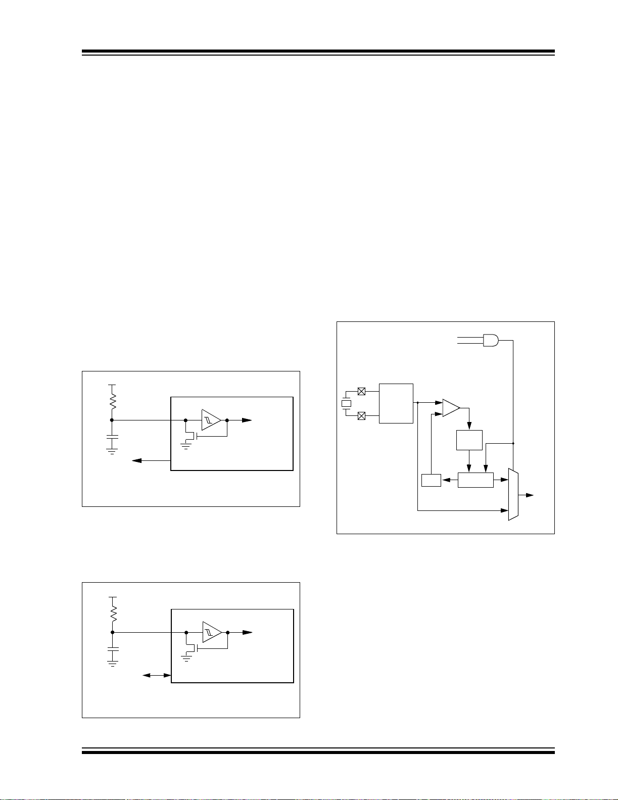
2.0 OSCILLATOR CONFIGURATIONS
2.1 Oscillator Types
PIC18F2X1X/4X1X devices can be operated in ten
different oscillator modes. The user can program the
configuration bits, FOSC3:FOSC0, in Configuration
Register 1H to select one of these ten modes:
1. LP Low-Power Crystal
2. XT Crystal/Resonator
3. HS High-Speed Crystal/Resonator
4. HSPLL High-Speed Crystal/Resonator
with PLL enabled
5. RC External Resistor/Capacitor with
F
OSC/4 output on RA6
6. RCIO External Resistor/Capacitor with I/O
on RA6
7. INTIO1 Internal Oscillator with F
on RA6 and I/O on RA7
8. INTIO2 Internal Oscillator with I/O on RA6
and RA7
9. EC External Clock with F
10. ECIO External Clock with I/O on RA6
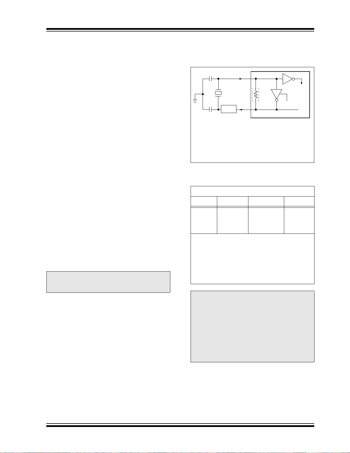
2.2 Crystal Oscilla tor/Ceramic Resonators
In XT, LP, HS or HSPLL Oscillator modes, a crystal or
ceramic resonator is connected to the OSC1 and
OSC2 pins to establish oscillation. Figure 2-1 shows
the pin connections.
The oscillator design requires the use of a parallel cut
crystal.
Note: Use of a series cut crystal may give a
frequency out of the crystal manufacturer’s
specifications.
OSC/4 output
OSC/4 output
FIGURE 2-1: CRYSTAL/CERAMIC
RESONATOR OPERATION
(XT, LP, HS OR HSPLL
CONFIGURATION)
(1)
C1
(1)
C2
Note 1: See T able 2-1 and Table 2-2 for initial values of
2: A series resistor (R
3: R
OSC1
XTAL
(2)
RS
OSC2
C1 and C2.
strip cut crystals.
F varies with the oscillator mode chosen.
(3)
RF
Sleep
PIC18FXXXX
S) may be required for AT
To
Internal
Logic
T ABLE 2-1: CAPACITOR SELECTION FOR
CERAMIC RESONATORS
Typical Capacitor Values Used:
Mode Freq OSC1 OSC2
XT 3.58 MHz
4.19 MHz
4 MHz
4 MHz
Capacitor values are for design guidance only.
Different cap acitor values may be required to prod uce
acceptable oscillator operation. The user should test
the performance of the oscillator over the expected
DD and temperature range for the application.
V
See the notes following Table 2-2 for additional
information.
Note: When using resonators with frequencies
above 3.5 MHz, the use of HS mode,
rather than XT mode, is recommended.
HS mode may be used at any V
which the controller is rated. If HS is
selected, it is possible that the gain of the
oscillator will overdrive the resonator.
Therefore, a series resistor should be
placed between the OSC2 pin and the
resonator. As a good starting point, the
recommended value of R
15 pF
15 pF
30 pF
50 pF
15 pF
15 pF
30 pF
50 pF
DD for
S is 330Ω.
2004 Microchip Technology Inc. Preliminary DS39636A-page 23
PIC18F2X1X/4X1X
TABLE 2-2: CAPACITOR SELECTION FOR
CRYSTAL OSCILLATOR
Osc T y pe
LP 32 kHz 30 pF 30 pF
XT 1 MHz
HS 4 MHz
Capacitor values are for design guidance only.
Different capa citor values may be required to produc e
acceptable oscillator operation. The user should test
the performance of the oscillator over the expected
DD and temperature range for the application.
V
See the notes following this table for additional
information.
Note 1: Higher capacitanc e increases th e stabilit y
Crystal
Freq
4 MHz
10 MHz
20 MHz
25 MHz
of the oscillator but also increases the
start-up time.
2: When operating below 3V V
using certain ceramic resonators at any
voltage, it may be necessary to use the
HS mode or switch to a crystal oscillator.
3: Since each resonator/crystal has its own
characteristics, the user should consult
the resonator/crystal manufacturer for
appropriate values of external
components.
4: Rs may be r equired to av oid overdr iving
crystals with low driv e lev e l spe ci fic ati on.
5: Always verify oscillator perform an ce over
DD and temperature range that is
the V
expected for the application.
T ypical Cap acitor V alues
Tested:
C1 C2
15 pF
15 pF
15 pF
15 pF
15 pF
15 pF
15 pF
15 pF
15 pF
15 pF
15 pF
15 pF
DD, or when
An external clock source may also be connected to the
OSC1 pin in the HS mode, as shown in Figure 2-2.
FIGURE 2-2: EXTERNAL CLOCK INPUT
OPERATION
(HS OSCILLATOR
CONFIGURATION)
Clock from
Ext. System
Open
OSC1
OSC2
PIC18FXXXX
(HS Mode)
2.3 External Clock Input
The EC and ECIO Oscillator mode s require an externa l
clock source to be conn ected to the OSC1 pi n. There is
no oscillator start-up time required after a Power-on
Reset or after an exit from Sleep mode.
In the EC Oscillator mode, the oscillator frequency
divided by 4 is available on the OSC2 pin. This signal
may be used f or t e st pu r pos es or t o sy nc hr o n iz e ot he r
logic. Figure 2-3 shows the pin connections for the EC
Oscillator mode.
FIGURE 2-3: EXTERNAL CLOCK
INPUT OPERATION
(EC CONFIGURATION)
Clock from
Ext. System
F
OSC/4
The ECIO Oscillator mo de func tio ns lik e t he EC mod e,
except that the OSC2 pin becomes an additional
general purpose I/O pin. The I/O pin becomes bit 6 of
PORTA (RA6). Figure 2-4 shows the pin connections
for the ECIO Oscillator mode.
OSC1/CLKI
PIC18FXXXX
OSC2/CLKO
FIGURE 2-4: EXTERNAL CLOCK
INPUT OPERATION
(ECIO CONFIGURATION)
Clock from
Ext. System
RA6
DS39636A-page 24 Preliminary 2004 Microchip Technology Inc.
OSC1/CLKI
PIC18FXXXX
I/O (OSC2)
PIC18F2X1X/4X1X
2.4 RC Oscillator
For timing insensitive applications, the “RC” and
“RCIO” device options offer additional cost savings.
The actual oscillator frequency is a function of several
factors:
• supply voltage
• values of the external resistor (R
capacitor (C
EXT)
• operating temperature
Given the same device, operating voltage and temperature and component values, there will also be unit-to-unit
frequency variations. These are due to factors such as:
• normal manufacturing variation
• difference in lead frame capacitance between
package types (especially for low C
• variations within the t olerance of limits of REXT
EXT
and C
In the RC Oscillator mode, the oscillator frequency
divided by 4 is available on the OSC2 pin. This signal
may be used f or t e st pu r pos es or t o sy nc hr o n iz e ot he r
logic. Figure 2-5 shows how the R/C combination is
connected.
FIGURE 2-5: RC OSCILLATOR MODE
VDD
REXT
OSC1
CEXT
VSS
F
Recommended values: 3 kΩ ≤ REXT ≤ 100 kΩ
OSC/4
OSC2/CLKO
EXT > 20 pF
C
The RCIO Oscillator mode (Figure 2-6) functions like
the RC mode, except that the OSC2 pin becomes an
additional general purpose I/O pin. The I/O pin
becomes bit 6 of PORTA (RA6).
FIGURE 2-6: RCIO OSCILLATOR MODE
VDD
REXT
OSC1
EXT) and
EXT values)
Internal
Clock
PIC18FXXXX
Internal
Clock
2.5 PLL Frequency Multiplier
A Phase Locked Loop (PLL) circuit is provided as an
option for users who wish to use a lower frequency
oscillator circuit or to clock the device up to its highest
rated frequency from a crystal oscillator. This may be
useful for customers who are concerned with EMI due
to high-frequency crystals or users who require higher
clock speeds from an internal oscillator.
2.5.1 HSPLL OSCILLATOR MODE
The HSPLL mode make s use of the HS mode osc illator
for frequencies up t o 10 MHz. A PLL then multipl ies the
oscillator output frequency by 4 to produce an internal
clock frequency up to 40 MHz. The PLLEN bit is not
available in this oscillator mode.
The PLL is only available to the crystal oscillator when
the FOSC3:FOSC0 configu r ati on bi t s are prog ram med
for HSPLL mode (= 0110).
FIGURE 2-7: PLL BLOCK DIAGRAM
(HS MODE)
HS Oscillator Enable
PLL Enable
(from Configuration Register 1H)
OSC2
OSC1
HS Mode
Crystal
Osc
IN
F
FOUT
÷4
2.5.2 PLL AND INTOSC
The PLL is also ava ilabl e to th e inte rnal os cill ator bl ock
in selected oscillator modes. In this configuration, the
PLL is enabled in software and generates a clock
output of up to 32MHz. The operation of INTOSC with
the PLL is describ ed in Section 2.6.4 “PLL in INTOSC
Modes”.
Phase
Comparator
Loop
Filter
VCO
SYSCLK
MUX
CEXT
VSS
RA6
Recommended values: 3 kΩ ≤ REXT ≤ 100 kΩ
2004 Microchip Technology Inc. Preliminary DS39636A-page 25
I/O (OSC2)
C
EXT > 20 pF
PIC18FXXXX

PIC18F2X1X/4X1X
2.6 Internal Oscillator Block
The PIC18F2X1X/4X1X devices include an internal
oscillator block which generates two different clock
signals; either can be used as the microcontroller’s
clock source. This may eliminate the need for external
oscillator circuits on the OSC1 and/or OSC 2 pins.
The main output (INTOSC) is an 8 MHz clock source,
which can be used to directly drive the device clock. It
also drives a postscaler, which can provide a range of
clock frequencies from 31 kHz to 4 MHz. The INTOSC
output is enabled when a clock fre quency from 12 5 kHz
to 8 MHz is selected.
The other clock source is the internal RC oscillator
(INTRC), which provides a nominal 31 kHz output.
INTRC is enabled if it is selected as the device clock
source; it is also ena bled autom atically when an y of the
following are enabled:
• Power-up Timer
• Fail-Safe Clock Monitor
• Watchdog Timer
• T wo-Spe ed Start-up
These features are discussed in greater detail in
Section 22.0 “Special Features of the CPU”.
The clock source frequency (INTOSC direct, INTRC
direct or INTOSC postscaler) is selected by configuring
the IRCF bits of the OSCCON register (page30).
2.6.1 INTIO MODES
Using the internal oscillator as the clock source eliminates the need for up to two external oscillator pins,
which can then be used for digital I/O. Two distinct
configurations are available:
• In INTIO1 mode, the OSC2 pin outputs F
while OSC1 functions as RA 7 fo r dig it a l in put a nd
output.
• In INTIO2 mode, OSC1 functions as RA7 and
OSC2 functions as RA6, both for digital input and
output.
2.6.2 INTOSC OUTPUT FREQUENCY
The internal oscillator block is calibrated at the factory
to produce an INTOSC output frequency of 8.0MHz.
The INTRC oscillator operates independently of the
INTOSC source. Any changes in INTOSC across
voltage and temperature are not necessarily reflected
by changes in INTRC and vice versa.
2.6.3 OSCTUNE REGISTER
The internal oscillator’s output has been calibrated at
the factory but can be adjusted in the user’s application. This is do ne by writi ng to the OSC TUNE regi ster
(Register 2-1). The tuning sensitivity is constant
throughout the tuning range.
OSC/4,
When the OSCTUNE regis ter is mo di fied , the IN T O SC
frequency will begin shifting to the new frequency. The
INTRC clock will reach the new frequency within
8 clock cy cles (approximately 8 * 32 µs=256µs). The
INTOSC clock will stabilize within 1ms. Code execution conti nues during t his shift. There is no indication
that the shift has occurred.
The OSCTUNE register also implements the INTSRC
and PLLEN bits, which control certain features of the
internal oscillator block. The INTSRC bit allows users
to select which internal oscillator provides the clock
source when the 31 kHz frequency option is selected.
This is covered in greater detail in Section 2.7.1
“Oscillator Control Register”.
The PLLEN bit controls the operation of the frequency
multiplier, PLL, in internal oscillator modes.
2.6.4 PLL IN INTOSC MODES
The 4x frequency multiplier can be used with the
internal oscillator block to produce faster device clock
speeds than are normally possible with an internal
oscillator. When enabled, the PLL produces a clock
speed of up to 32MHz.
Unlike HSPLL mode, the PLL is controlled through
software. The control bit, PLLEN (OSCTUNE<6>), is
used to enable or disable its operation.
The PLL is available when the device is configured to
use the internal oscillator block as its primary clock
source (FOSC3:FOSC0 = 1001 or 1000). Additionally,
the PLL will only function when the selected output frequency is either 4 MHz or 8 MHz (OSCCON<6:4> = 111
or 110). If both of these conditions are not met, the PLL
is disabled.
The PLLEN control bit is only functional in those
internal oscillator m ode s w h ere t he PL L is av ai lab le. In
all other modes, it is forced to ‘0’ and is effectively
unavailable.
2.6.5 INTOSC FREQUENCY DRIFT
The factory calibrates the internal oscillator block
output (INTOSC) for 8 MHz. However, this frequency
may drift as VDD or temperature changes, which can
affect the controller operation in a variety of ways. It is
possible to adjust the INTOSC frequency by modifying
the value in the OSCTUNE register. This has no effect
on the INTRC clock source frequency.
Tuning the INTOSC source requires knowing when to
make the adjustment, in which direction it should be
made and in some cases, how large a change is
needed. Three compensation techniques are
discussed in Section 2.6.5.1 “Compensating with
the USART”, Section 2.6.5.2 “Compensating with
the Timers” and Section2.6.5.3 “Compensating
with the CCP Module in Capture Mode”, but other
techniques may be used.
DS39636A-page 26 Preliminary 2004 Microchip Technology Inc.

PIC18F2X1X/4X1X
REGISTER 2-1: OSCTUNE: OSCILLATOR TUNING REGISTER
R/W-0 R/W-0
INTSRC PLLEN
bit 7 bit 0
bit 7 INTSRC: Internal Oscillator Low-Frequency Source Select bit
1 = 31.25 kHz device clock derived from 8 MHz INTOSC source (divide-by-256 enabled)
0 = 31 kHz device clock derived directly from INTRC internal oscillator
bit 6 PLLEN: Frequency Multiplier PLL for INTOSC Enable bit
1 = PLL enabled for INTOSC (4 MHz and 8 MHz only)
0 = PLL disabled
Note 1: Available only in certain oscillator configurations; otherwise, this bit is unavailable
bit 5 Unimplemented: Read as ‘0’
bit 4-0 TUN4:TUN0: Frequency Tuning bits
01111 = Maximum frequency
• •
• •
00001
00000 = Center frequency. Oscillator module is running at the calibrated frequency.
11111
• •
• •
10000 = Minimum frequency
(1)
(1)
and reads as ‘0’. See Section 2.6.4 “PLL in INTOSC Modes” for details.
U-0 R/W-0 R/W-0 R/W-0 R/W-0 R/W-0
— TUN4 TUN3 TUN2 TUN1 TUN0
(1)
Legend:
R = Readable bit W = Writable bit U = Unimplemented bit, read as ‘0’
-n = Value at POR ‘1’ = Bit is set ‘0’ = Bit is cleared x = Bit is unknown
2.6.5.1 Compensating with the USART
An adjustment may be required when the USART
begins to generate frami ng errors or rec eive s dat a with
errors while in Asynchronous mode. Framing errors
indicate that the device clock frequency is too high; to
adjust for this, decrement the value in OSCTUNE to
reduce the clock frequency. On the other hand, errors
in data may suggest that the clock speed is too low; to
compensate, increment OSCTUNE to increase the
clock frequency.
2.6.5.2 Compensating with the Timers
This technique compares device clock speed to some
reference clock. Two timers may be used; one timer is
clocked by the peripheral clock, while the other is
clocked by a fixed reference source, such as the
Timer1 oscillat or.
Both timers are cleared, but the timer clocked by the
reference generates interrupts. When an interrupt
occurs, the internally clocked timer is read and both
timers are cleared. If the internally clocked timer value
is greater than expected, then the internal oscillator
block is ru nning too fast. To adjust for t his, decr ement
the OSCTUNE register.
2.6.5.3 Compensating with the CCP Module
in Capture Mode
A CCP module can use free running Timer1 (or
Timer3), cl oc ked by the internal oscillator bl ock and an
external event with a known period (i.e., AC power
frequency). The time of the first event is capt ured in th e
CCPRxH:CCPRxL registers and is recorded for use
later. When the second event causes a capture, the
time of the first event is su btra cte d fro m the tim e of th e
second event. Since the period of the external event is
known, the time difference between events can be
calculated.
If the measured time is much greater than the calculated time, the internal oscillator block is running too
fast; to compensate, decrement the OSCTUNE register.
If the measured time is much less than the calculate d
time, the internal oscillator block is runn ing t oo slow; to
compensate, increment the OSCTUNE register.
2004 Microchip Technology Inc. Preliminary DS39636A-page 27
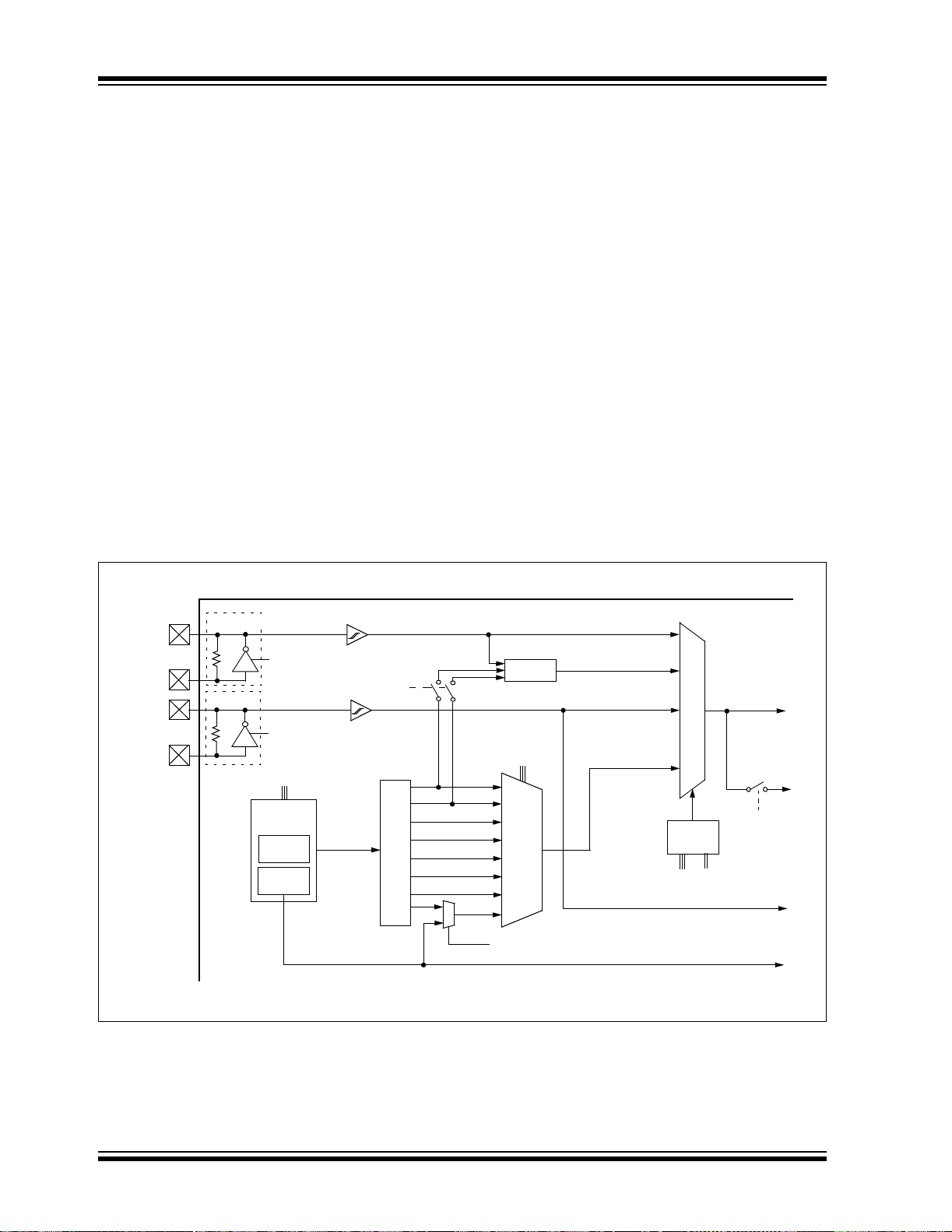
PIC18F2X1X/4X1X
2.7 Clock Sources and Oscillator Switching
Like previous PIC18 devices, the PIC18F2X1X/4X1X
family includes a feature that allows the device clock
source to be switched from the main oscillator to an alternate low-frequency clock source. PIC18F2X1X/4X1X
devices offer two alternate clock sources. When an
alternate clock source is enabled, the various power
managed operating modes are available.
Essentially, there are three clock sources for these
devices:
• Primary oscillators
• Secondary oscillators
• Internal oscillator block
The primary oscillators include the Ex ternal Crystal
and Resonator modes, the External RC modes, the
External Clock modes and the internal oscillator block.
The particular mode is defined by the FOSC3:FOSC0
configuration bits. The details of these modes are
covered earlier in this chapter.
The s econdary oscillators are those external sources
not connected to the OSC1 or OSC2 pins. These
sources may continue to operate even after the
controller is placed in a power managed mode.
PIC18F2X1X/4X1X devices offer the Timer1 oscillator
as a secondary oscillator. This oscillator, in all power
managed modes, is often the time base for functions
such as a real-time clock.
Most often, a 32.768 kHz watch crystal is connected
between the RC0/T1OSO/T13CKI and RC1/T1OSI
pins. Like the LP mode oscillator circuit, loading
capacitors are also connected from each pin to ground.
The Timer1 oscillator is discussed in greater detail in
Section 11.3 “Timer1 Oscillator”.
In addition to being a prim ary clock source, the internal
oscillator block is available as a power managed
mode clock source. T he IN TR C s ource is also used as
the clock source for several special features, such as
the WDT and Fail-Safe Clock Monitor.
The clock sources for the PIC18F2X1X/4X1X devices
are shown in Figure 2-8. See Section 22.0 “Special
Features of the CPU” for Configuration register details.
FIGURE 2-8: PIC18F2X1X/4X1X CLOCK DIAGRAM
OSC2
OSC1
T1OSO
T1OSI
Primary Oscillator
Sleep
Secondary Oscillator
T1OSCEN
Enable
Oscillator
OSCCON<6:4>
Internal
Oscillator
Block
8 MHz
Source
INTRC
Source
31 kHz (INTRC)
OSCTUNE<6>
8 MHz
(INTOSC)
PIC18F2X1X/4X1X
8 MHz
4 MHz
2 MHz
1 MHz
500 kHz
Postscaler
250 kHz
125 kHz
1
31 kHz
0
4 x PLL
OSCCON<6:4>
111
110
101
100
MUX
011
010
001
000
OSCTUNE<7>
LP, XT, HS, RC, EC
HSPLL, INTOSC/PLL
T1OSC
Internal Oscillator
FOSC3:FOSC0
Peripherals
MUX
CPU
Clock
Control
Clock Source Option
for other Modules
WDT, PWRT, FSCM
and Two-Speed Start-up
IDLEN
OSCCON<1:0>
DS39636A-page 28 Preliminary 2004 Microchip Technology Inc.

PIC18F2X1X/4X1X
2.7.1 OSCILLATOR CONTROL REGISTER
The OSCCON register (Register 2-2) controls several
aspects of the device clock’s operation, both in full
power operation and in power managed modes.
The System Clock Select bits, SCS1:SCS0, select the
clock source. The available clock sources are the
primary clock (defined by the FOSC3:FOSC0 configuration bits), the secondary clock (Timer1 oscillator) and
the internal oscillator block. The clock source changes
immediately after one or more of the bits is written to,
following a brief clock transition interval. The SCS bits
are cleared on all forms of Reset.
The Internal Oscillator Frequency Select bits
(IRCF2:IRCF0) select the frequency output of the
internal oscillator block to drive the device clock. The
choices are the INTRC source, the INTOSC source
(8 MHz) or one of the frequencies derived from the
INTOSC postscaler (31.25 kHz to 4 MHz). If the
internal oscillator block is supplying the device clock,
changing the states of these bits will have an immediate change on the internal oscillator’s output. On
device Resets, the default output frequency of the
internal oscillator block is set at 1 MHz.
When a nominal ou tput frequenc y of 31 kHz is selected
(IRCF2:IRCF0 = 000), users may choose which internal oscillator acts as the source. This is done with the
INTSRC bit in the OSCTUNE register (OSCTUNE<7>).
Setting this bit selects INTOSC as a 31.25 kHz clock
source by enabling the divide-by-256 output of the
INTOSC postscaler. Clearing INTSRC sel ects INTRC
(nominally 31 kHz) as the clock source.
This option allows users to select the tunable and more
precise INTOSC as a clock source, while maintaining
power savings with a ve ry low clock speed. R egardless
of the setting of INTSRC, INTRC always remains the
clock source for features such as the Watchdog Timer
and the Fail-Safe Clock Monitor.
The OSTS, IOFS and T1RUN bit s ind ic ate wh ich clock
source is currently providing the device clock. The
OSTS bit indicates that the Oscillator Start-up Timer
has timed out and the primary clock is providing the
device clock in primary clock modes. The IOFS bit
indicates when the internal oscillator block has stabilized and is providing the device clock in RC Clock
modes. The T1RUN bit (T1CON<6>) indicates when
the Timer1 oscillator is providing the device clock in
secondary clock modes. In power managed modes,
only one of these three bits will be set at any time. If
none of these bits are set, the INTRC is providing the
clock or the internal o scillator bloc k has just s tarted and
is not yet stable.
The IDLEN bit dete rmines if th e dev ice go es in to Slee p
mode or one of the Idle modes when the SLEEP
instruction is executed.
The use of the flag and control bits in the OSCCON
register is discussed in more detail in Section 3.0
“Power Managed Modes”.
Note 1: The Timer1 oscillator must be enabled to
select the secondary clock source. The
Timer1 osc illator is enabled by s etting the
T1OSCEN bit in th e T imer1 C ontrol re gister (T1CON<3>). If the Timer1 oscillator
is not enabled, then any at tem pt to se lec t
a secondary clock source will be ignored.
2: It is recommended that the Timer1
oscillator be operating and stable before
selecting the secondary clock source or a
very long delay may occur while the
Timer1 oscillator starts.
2.7.2 OSCILLATOR TRANSITIONS
PIC18F2X1X/4X1X device s con tai n circ uitry to preve nt
clock “glitches” when switch ing between clock sources .
A short pause in the device clock occurs during the
clock switch. Th e leng th of th is p ause is th e sum of two
cycles of the old clock source and three to four cycles
of the new clock s ource. Th is formul a assumes that the
new clock source is stable.
Clock transitions are discussed in greater detail in
Section 3.1.2 “Entering Power Managed Modes”.
2004 Microchip Technology Inc. Preliminary DS39636A-page 29

PIC18F2X1X/4X1X
REGISTER 2-2: OSCCON: OSCILLATOR CONTROL REGISTER
R/W-0 R/W-1 R/W-0 R/W-0 R
IDLEN IRCF2 IRCF1 IRCF0 OSTS IOFS SCS1 SCS0
bit 7 bit 0
bit 7 IDLEN: Idle Enable bit
1 = Device ent ers Idle mode on SLEEP instruction
0 = Device enters Sleep mo de on SLEEP instruction
bit 6-4 IRCF2:IRCF0: Internal Oscillator Frequency Select bits
111 = 8 MHz (INTOSC drives clock directly)
110 = 4 MHz
101 = 2 MHz
100 = 1 MHz
011 = 500 kHz
010 = 250 kHz
001 = 125 kHz
000 = 31 kHz (from either INTOSC/256 or INTRC directly)
bit 3 OSTS: Oscillator Start-up Time-out Status bit
1 = Oscillator start-up time-out timer has expired; primary oscillator is running
0 = Oscillator start-up time-out timer is running; primary oscillator is not ready
bit 2 IOFS: INTOSC Frequency Stable bit
1 = INTOSC frequency is stable
0 = INTOSC frequency is not stable
bit 1-0 SCS1:SCS0: System Clock Select b its
1x = Internal oscillator block
01 = Secondary (Timer1) oscillator
00 = Primary oscillator
(3)
(1)
(1)
(2)
R-0 R/W-0 R/W-0
Note 1: Reset state depends on state of the IESO configuration bit.
2: Source selected by the INTSRC bit (OSCTUNE<7>), see text.
3: Default output frequency of INTOSC on Reset.
Legend:
R = Readable bit W = Writable bit U = Unimplemented bit, read as ‘0’
-n = Value at POR ‘1’ = Bit is set ‘0’ = Bit is cleared x = Bit is unknown
DS39636A-page 30 Preliminary 2004 Microchip Technology Inc.

PIC18F2X1X/4X1X
2.8 Effects of Power Managed Modes on the Various Clock Sources
When PRI_IDLE mode is selected, the designated
primary oscillator continues to run without interruption.
For all other power managed modes, the oscillator
using the OSC1 pin is disabled. The OSC1 pin (and
OSC2 pin, if used by the o scillat or) will sto p oscillat ing.
In secondary clock modes (SEC_RUN and
SEC_IDLE), the Timer1 oscillator is operating and
providing the device clock. The Timer1 oscillator may
also run in all power managed modes if required to
clock Timer1 or Timer3.
In internal oscillator modes (RC_RUN and RC_IDLE),
the internal oscillator block provides the device clock
source. The 31kHz INTRC output can be used d irectl y
to provide the clock and may be enabled to support
various special features, regardless of the power
managed mode (see Section 22.2 “Watchdog Timer
(WDT)”, Section 22.3 “Two-Speed Start-up” and
Section 22.4 “Fail-Safe Clock Monitor” for more
information on WDT, Fail-Safe Clock Monitor and TwoSpeed St art-up ). The INT OSC out put at 8 MHz may be
used directly to clock the device or may be divided
down by the posts caler . The INTO SC output is disable d
if the clock is provided directly from the INTRC output.
If the Sleep mode is selected, all clock sources are
stopped. Since all the transistor switching currents
have been stopped, Sleep mode achieves the lowest
current consumption of the device (only leakage
currents).
Enabling any on-chip feature that will operate during
Sleep will increas e the current cons umed during S leep.
The INTRC is required to support WDT operation. The
Timer1 oscillator may be operating to support a real-
time clock. Ot her features may be operating that do n ot
require a device clock source (i.e., SSP slave, PSP,
INTn pins and others). Peripherals that may add
significant current consumption are listed in
Section 25.2 “DC Characteristics”.
2.9 Power-up Delays
Power-up delays are controlled by two timers, so that
no external Rese t circ ui try is re qui red for most applications. The delays ensure that the device is kept in
Reset until the device powe r supply i s stable under normal circumstan ces and the pri mary clock is ope rating
and stable. For additional information on power-up
delays, see Section 4.5 “Device Reset Timers”.
The first timer is the Power-up Timer (PWRT), which
provides a fixed delay on power-up (parameter 33,
Table 25-10). It is enabled by clearing (= 0) the
PWRTEN
The second timer is the Oscillator Start-up Timer
(OST), intended to keep the chip in Reset until the
crystal oscillator is stable (LP, XT and HS modes). The
OST does this by counting 1024 oscillator cycles
before allowing the oscillator to clock the device.
When the HSPLL Oscillator mode is selected, the
device is kept in Res et for an add iti onal 2ms, following
the HS mode OST delay, so the PLL can lock to the
incoming clock frequ enc y.
There is a delay of interval T
Table 25-10), following POR, while the controller
becomes ready to execute instruc tions. This delay runs
concurrently with any other delays. This may be the
only delay that occurs when an y of the EC, RC or INTIO
modes are used as the primary clock source.
configuration bit.
CSD (parameter 38,
TABLE 2-3: OSC1 AND OSC2 PIN STATES IN SLEEP MODE
Oscillator Mode OSC1 Pin OSC2 Pin
RC, INTIO1 Floating, external resistor should pull high At logic low (clock/4 output)
RCIO Floating, external resistor should pull high Configured as PORTA, bit 6
INTIO2 Configured as PORTA, bit 7 Configured as PORTA, bit 6
ECIO Floating, pulled by external clock Configured as PORTA, bit 6
EC Floating, pulled by external clock At logic low (clock/4 output)
LP, XT and HS Feedback inverter disabled at quiescent
voltage level
Note: See Table 4-2 in Section 4.0 “Reset” for time-outs due to Sleep and MCLR
2004 Microchip Technology Inc. Preliminary DS39636A-page 31
Feedback inverter disabled at quiescent
voltage level
Reset.

PIC18F2X1X/4X1X
NOTES:
DS39636A-page 32 Preliminary 2004 Microchip Technology Inc.

PIC18F2X1X/4X1X
3.0 POWER MANAGED MODES
PIC18F2X1X/4X1X devices offer a total of seven op erating modes for more efficient power management.
These modes provide a variety of options for selective
power conservation in applications where resources
may be limited (i.e., battery-powered devices).
There are three categories of power managed modes:
• Run modes
• Idle modes
• Sleep mode
These categories define which portions of the device
are clocked and some times , what sp eed. The R un and
Idle modes may use any of the three available clock
sources (primary, secondary or internal oscillator
block); the Sleep mode does not use a clock source.
The power managed modes include several powersaving features offered on previous PICmicro
devices. On e is th e clock switchin g featu re, offer ed in
other PIC18 devices, allowing the controller to use the
Timer1 os cil la tor in pl ac e of the prim ary osc il lato r. Also
included is the Sleep mode, offered by all PICmicro
devices, where all device clocks are stopped.
3.1 Selecting Power Managed Modes
Selecting a power managed mode requires two
decisions: if the CPU is to be clocked or not and the
selection of a clock source. The IDLEN bit
(OSCCON<7>) controls CPU clocking, while the
SCS1:SCS0 bits (OSCCON<1:0>) select the clock
source. The individual modes, bit settings, clock sources
and affected modules are summariz ed in Table 3-1.
3.1.1 CLOCK SOURCES
The SCS1:SCS0 bits allow the sele ction of one o f three
clock sources for power managed modes. They are:
• the primary clock, as defined by the
FOSC3:FOSC0 configuration bits
• the secondary clock (the Timer1 oscillator)
• the internal oscillator block (for RC modes)
3.1.2 ENTERING POWER MANAGED
MODES
Switching from one power managed mode to another
begins by loading the OSCCON register. The
SCS1:SCS0 bits selec t the clock sourc e and determin e
which Run or Idle mode is to be used. Changing these
bits causes an immediate switch to the new clock
source, assuming that it is running. The switch may
®
also be sub ject to clock tr ansition delays. These are
discussed in Section 3.1.3 “Clock Transitions and
Status Indicators” and subsequent sections.
Entry to the Power Managed Idle or Sleep modes is
triggered by the execution of a SLEEP instruction. The
actual mode that results depends on the status of the
IDLEN bit.
Depending on the current mode and the mode being
switched to, a change to a power managed mode does
not always require setting all of these bits. Many
transitions may be done by changing the oscillator s elect
bits, or changing the IDLEN bit, prior to issuing a SLEEP
instruction. If the IDLEN bit is already configured
correctly, it may only be necessary to perform a SLEEP
instruction to switch to the desired mode.
TABLE 3-1: POWER MANAGED MODES
OSCCON Bits Module Clocking
Mode
Sleep 0 N/A Off Off None – All clocks are disabled
PRI_RUN N/A 00 Clocked Clocked Primary – LP, XT, HS, HSPLL, RC, EC and
SEC_RUN N/A 01 Clocked Clocked Secondary – Timer1 Oscillator
RC_RUN N/A 1x Clocked Clocked Internal Oscillator Block
PRI_IDLE 100Off Clocked Primary – LP, XT, HS, HSPLL, RC, EC
SEC_IDLE 101 Off Clocked Secondary – Timer1 Oscillator
RC_IDLE 11x Off Clocked Internal Oscillator Block
Note 1: IDLEN reflects its value when the SLEEP instruction is executed.
2: Includes INTOSC and INTOSC postscaler, as well as the INTRC source.
2004 Microchip Technology Inc. DS39636A-page 33
IDLEN
<7>
(1)
SCS1:SCS0
<1:0>
CPU Peripherals
Available Clo ck and Os cill ator Source
Internal Oscillator Block
This is the normal full power execution mode.
(2)
(2)
(2)
.

PIC18F2X1X/4X1X
3.1.3 CLOCK TRANSITIONS AND STATUS INDICATORS
The length of the transition between clock sources is
the sum of two cycles o f the old clo ck so urce an d three
to four cycl es of the new clock so urce. This formula
assumes that the new clock source is stable.
Three bits indicate the current clock source and its
status. They are:
• OSTS (OSCCON<3>)
• IOFS (OSCCON<2>)
• T1RUN (T1CON<6>)
In general, only one of these bits will be set while in a
given power managed mode. When the OSTS bit is
set, the primary clock is providing the device clock.
When the IOFS bit is set, the INTOSC output is
providing a stable 8 MHz clock source to a divider that
actually drives the device clock. When the T1RUN bit is
set, the Timer1 oscillator is providing the clock. If none
of these bits are set, then either the INTRC clock
source is cloc ki ng t he dev ic e, o r th e INTOSC source is
not yet stable.
If the internal oscillator block is configured as the primary clock source b y the FOSC 3:FOSC0 co nfiguratio n
bits, then both the OSTS and IOFS bits may be set
when in PRI_RUN or PRI_IDLE modes. This indicates
that the primary clock (INTOSC output) is generatin g a
stable 8 MHz output. Entering another RC Power
Managed mode at the s am e fre que nc y w ou ld cle ar th e
OSTS bit.
Note 1: Caution should be used when modifying a
single IRCF bit. I f V
possible to select a higher clock speed
than is supported by the low VDD.
Improper device operation may result if
the VDD/FOSC specifications are violated.
2: Executing a SLEEP instruction does not
necessarily place the device into Sleep
mode. It acts as the trigger to place the
controller into either the Sleep mode or
one of the Idle modes, depending on the
setting of the IDLEN bit.
DD is less than 3V, it is
3.1.4 MULTIPLE SLEEP COMMANDS
The power managed mode that is invoked with the
SLEEP instruction is determined by the setting of the
IDLEN bit at the time the instruction is executed. If
another SLEEP instruction is executed, the device will
enter the power managed mode specified by IDLEN at
that time. If IDLEN has changed, the device will enter
the new power managed mode specified by the new
setting.
3.2 Run Modes
In the Run modes, clocks to both the core and
peripherals are active. The difference between these
modes is the clock source.
3.2.1 PRI_RUN MODE
The PRI_RUN mode is the normal, full power execution
mode of the microcontroller. This is also the default
mode upon a device Reset, un less T wo-Speed S tart-up
is enabled (see Section 22.3 “Two-Speed Start-up”
for details). In this m ode, the OSTS bi t is set. Th e IOFS
bit may be set if the internal oscillator block is the
primary clock source (see Section 2.7.1 “Oscillator
Control Register”).
3.2.2 SEC_RUN MODE
The SEC_RUN mode is the compatible mode to the
“clock switching” feature offered in other PIC18
devices. In this mode, the CPU and peripherals are
clocked from the T imer1 os cillator. This gives users the
option of lower power consumption while still using a
high accuracy clock source.
SEC_RUN mode is en tered by sett ing th e SCS1:SCS 0
bits to ‘01’. The device clock source is switched to the
Timer1 oscillator (see Figure 3-1), the primary oscillator is shut down, the T1RUN bit (T1CON<6>) is set and
the OSTS bit is cleared.
Note: The Timer1 oscillator should already be
running prior to entering SEC_RU N mode.
If the T1OSCEN bit is not set when the
SCS1:SCS0 bits are set to ‘01’, entry to
SEC_RUN mode will not occur. If the
Timer1 oscillator is enabled but not yet
On transitions from SEC_RUN mode to PRI_RUN, the
peripherals and CPU continue to be clocked from the
Timer1 oscillator while the primary clock is started.
When the primary clo ck bec omes r eady, a clock switch
back to the primary clock occurs (see Figure 3-2).
When the clock switch is complete, the T1RUN bit is
cleared, the OSTS bit is set and the primary clock is
providing the clock. The IDLEN and SCS bits are not
affected by the wake-up; the Timer1 oscillator
continues to run.
DS39636A-page 34 2004 Microchip Technology Inc.

PIC18F2X1X/4X1X
FIGURE 3-1: TRANSITION TIMING FOR ENTRY TO SEC_RUN MODE
Q4Q3Q2
Q1
Q1
T1OSI
OSC1
CPU
Clock
Peripheral
Clock
Program
Counter
123 n-1n
Clock Transition
PC + 2PC
FIGURE 3-2: TRANSITION TIMING FROM SEC_RUN MODE TO PRI_RUN MODE (HSPLL)
3.2.3 RC_RUN MODE
In RC_RUN mode, the CPU and peripherals are
clocked from the internal oscillator block using the
INTOSC multiplexer. In this mode, the primary clock is
shut down. When using the INTRC source, this mode
provides the best power conservation of all the Run
modes, while still executing code. It works well for user
applications which are not hi ghl y tim in g sen si tiv e or do
This mode is entered by setting SCS1 to ‘1’. Although
it is ignored, it is recommended that SCS0 also be
cleared; this is to maintain software compatibility with
future devices. When the clock source is switched to
the INTOSC multiplexer (see Figure 3-3), the primary
oscillator is shut down and the OSTS bit is cleared. The
IRCF bits may be modified at any time to immediately
change the clock speed.
not require high-speed clocks at all times.
If the primary clock source is the internal oscillator
block (either INTRC or INTOSC), there are no
distinguishable differences between PRI_RUN and
RC_RUN modes during execution. Howeve r, a clock
switch delay will occur during entry to and exit from
RC_RUN mode. Therefore, if the primary clock source
is the internal oscillator block, the use of RC_RUN
mode is not recommended.
2004 Microchip Technology Inc. DS39636A-page 35
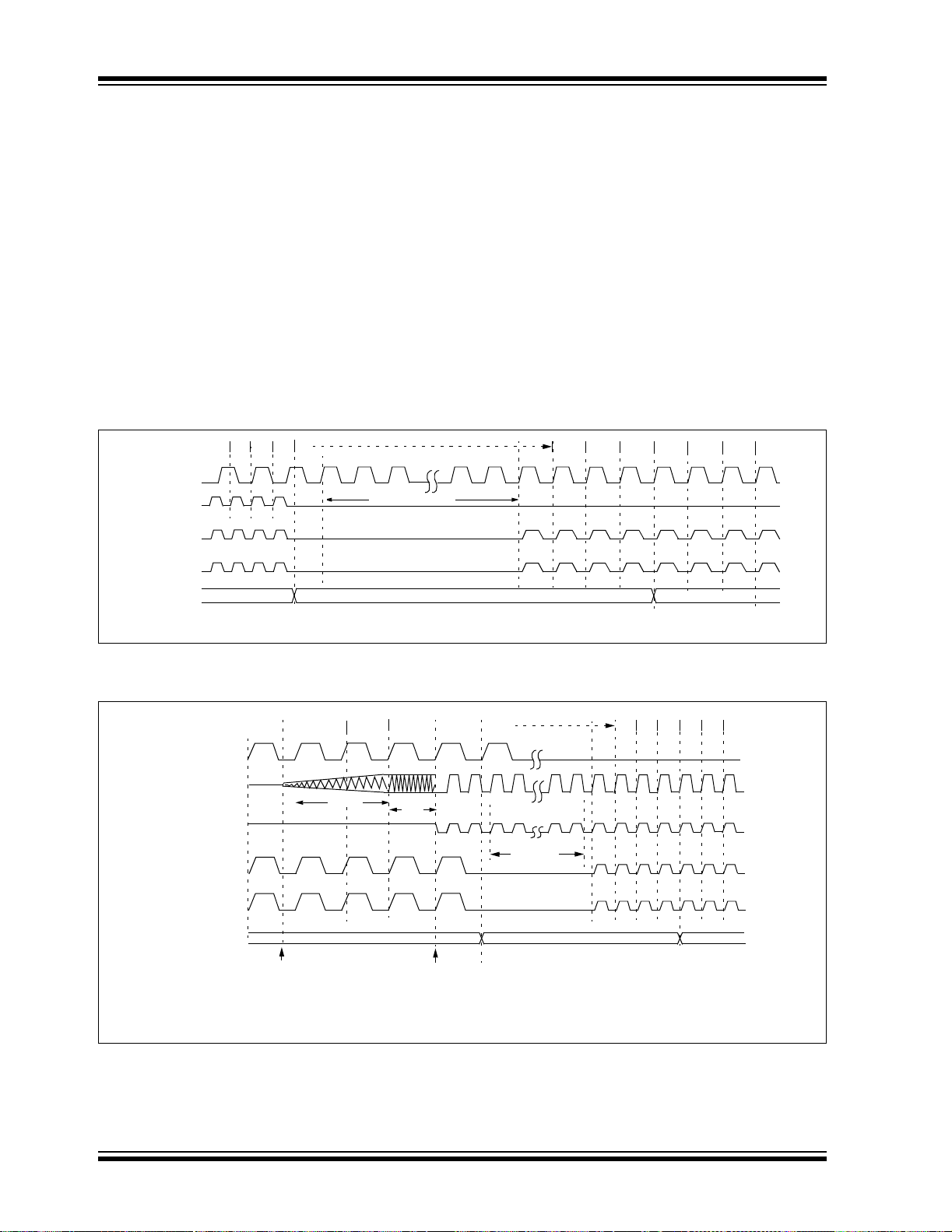
PIC18F2X1X/4X1X
If the IRCF bits and the INTSRC bit are all clear, the
INTOSC output is not enabled and the IOFS bit will
remain clear; there will be no indication of the current
clock source. The INTRC source is providing the
device clocks.
If the IRCF bits are changed from all clear (thus,
enabling the INTOSC output) or if INTSRC is set, the
IOFS bit becomes set after the INTOSC output
becomes stable. Clocks to the device continue while
the INTOSC source stabilizes after an interval of
IOBST.
T
On transitions from RC_RUN mode to PRI_RUN mode,
the device continues to be clocked from the INTOSC
multiplexer whil e the prim ary clock is st arted. W hen the
primary clock becomes ready, a clock switch to the
primary clock occurs (see Figure 3-4). When the clock
switch is complete, the IOFS bit is cleared, the OSTS
bit is set and the primary clock is providing the device
clock. The IDLEN and SCS bits are not af fe cte d by the
switch. The INTRC source will continue to run if either
the WDT or the Fail-Safe Clock Monitor is enabled.
If the IRCF bits w ere prev io us ly at a no n-z ero val ue, or
if INTSRC was set before setting SCS1 and the
INTOSC source was already stable, the IOFS bi t will
remain set.
FIGURE 3-3: TRANSITION TIMING TO RC_RUN MODE
Q4Q3Q2
Q1
INTRC
OSC1
CPU
Clock
Peripheral
Clock
Program
Counter
Note 1: Clock transition typically occurs within 2-4 TOSC.
Q1
123 n-1n
Clock Transition
(1)
PC + 2PC
Q4Q3Q2 Q1 Q3Q2
PC + 4
FIGURE 3-4: TRANSITION TIMING FROM RC_RUN MODE TO PRI_RUN MODE
Q2
INTOSC
Multiplexer
OSC1
PLL Clock
Output
CPU Clock
Peripheral
Clock
Program
Counter
Q1
TOST
SCS1:SCS0 bits changed
Q1
Q3
Q2
(1)
PC
TPLL
OSTS bit set
Q4
(1)
12 n-1n
(2)
Clock
Transition
PC + 2
Note 1: TOST = 1024 TOSC; TPLL = 2 ms (approx). These intervals are not shown to scale.
2: C lock transition typically occurs within 2-4 T
OSC.
Q3 Q4
Q1
PC + 4
Q2
Q3
DS39636A-page 36 2004 Microchip Technology Inc.

PIC18F2X1X/4X1X
3.3 Sleep Mode
The Power Managed Sleep mode in the PIC18F2X1X/
4X1X devices is identical to the legacy Sleep mode
offered in all other PICmicro devices. It is entered by
clearing the IDLEN bit (the default state on device
Reset) and executing the SLEEP instruction. Th is shut s
down the selected oscillator (Figure 3-5). All clock
source status bits are cleared.
Entering the Sleep m ode from any other mo de does not
require a clock switch. This is because no clocks are
needed once the controller has entered Sleep. If the
WDT is selected, the INTRC source will continue to
operate. If the Timer1 oscillator is enabled, it will also
continue to run.
When a wake ev ent occurs i n Sleep mo de (by int errupt,
Reset or WDT time-out), the device wil l not be clocke d
until the clock source selected by the SCS1:SCS0 bits
becomes ready (see Figure 3-6), or it will be clocked
from the internal oscillator block if either the TwoSpeed Start-up or the Fail-Safe Clock Monitor are
enabled (s ee Section 22.0 “Special Features of the
CPU”). In either case, the OSTS b it is set when t he primary clock is providing the device clocks. The IDLEN
and SCS bits are not affected by the wake-up.
3.4 Idle Modes
The Idle modes allow the controller’s CPU to be
selectively shut down while the peripherals continue to
operate. Selecting a particular Idle mode allows users
to further manage power consumption.
If the IDLEN bit i s set to a ‘1’ when a SLEEP inst ruction is
executed, the periph erals will be cl ocked fro m the cloc k
source selected us ing the SCS1:SCS 0 bits; howev er , the
CPU will not be clocked. The clock source status bits are
not affected. Setting IDLEN and executing a SLEEP
instruction pr ovides a quick method of switchi ng from a
given Run mo de to its correspondi ng Id le m od e.
If the WDT is selected, the INTRC source will continue
to operate. If the T imer1 oscill ator is enable d, it will also
continue to run.
Since the CPU is not executing instructions, the only
exits from any of the Idle modes are by interrupt, WDT
time-out or a Reset. When a wak e even t occur s, CPU
execution is delayed by an interval of T
(parameter 38, Table 25-10) while it becomes ready to
execute code. When the CPU begins executing code,
it resumes with the same clock source for the current
Idle mode. For example, when waking from RC_IDLE
mode, the internal oscillator block will clock the CPU
and peripherals (in other words, RC_RUN mode). The
IDLEN and SCS bits are not affected by the wake-up.
While in any Idle mode or the Sleep mode, a WD T time-
out will result in a WDT wake-up to the Run mode
currently specified by the SCS1:SCS0 bits.
CSD
FIGURE 3-5: TRANSITION TIMING FOR ENTRY TO SLEEP MODE
Q4Q3Q2
Q1Q1
OSC1
CPU
Clock
Peripheral
Clock
Sleep
Program
Counter
PC + 2PC
FIGURE 3-6: TRANSITION TIMING FOR WAKE FROM SLEEP (HSPLL)
Q1 Q2 Q3 Q4 Q1 Q2
OSC1
(1)
PLL Clock
Output
CPU Clock
Peripheral
Clock
Program
Counter
Wake Event
OST = 1024 TOSC; TPLL = 2 ms (approx). These intervals are not shown to scale.
Note 1: T
TOST
(1)
TPLL
PC
OSTS bit set
Q3 Q4 Q1 Q2
PC + 2
Q3 Q4
PC + 4
Q1 Q2 Q3 Q4
PC + 6
2004 Microchip Technology Inc. DS39636A-page 37

PIC18F2X1X/4X1X
3.4.1 PRI_IDLE MODE
This mode is uni que among the thre e low-power Idle
modes, in that it does not disable the primary device
clock. For timing sensitive applications, this allows for
the fastest resump tion of devic e operation with its more
accurate pri mary clock source, si nce the cl ock source
does not have to “warm up” or transition from another
oscillator.
PRI_IDLE mode is entered from PRI_RUN mode by
setting the IDLEN bit and executing a SLEEP instruction. If the device is in another Run mode, set IDLEN
first, then clear the SCS bits and execute SLEEP.
Although the CPU is disab led, th e peri pherals c ontinu e
to be clocked from the primary clock source specified
by the FOSC3:FOSC0 config uration bit s. The OSTS bit
remains set (see Figure3-7).
When a wake event occurs, the CPU is clocked from the
primary clock source. A delay of interval T
required between the wake event and when code
execution starts. This is required to allo w the CPU to
become ready to execute instructions. A fter the wakeup, the OSTS bit remains set. The IDLEN and SCS bits
are not affected by the wake-up (see Figure 3-8).
CSD is
3.4.2 SEC_IDLE MODE
In SEC_IDLE mode, the CPU is disabled but the
peripherals continue to be clocked from the Timer1
oscillator. This mode is entered from SEC_RUN by
setting the IDLEN bit and executing a SLEEP
instructio n. If the devic e is in another Run mode, set
IDLEN first, then set SCS1:SCS0 to ‘01’ and ex ecute
SLEEP. When the clock source is switched to the
Timer1 oscillator, the primary oscillator is shut down,
the OSTS bit is cleared and the T1RUN bit is set.
When a wake event occ urs, the pe ripherals continue to
be clocked from the Timer1 oscillator. After an interval
CSD following the wake event, the CPU begi ns ex e-
of T
cuting code being cloc ked by the T im er1 oscil lator . Th e
IDLEN and SCS bits are not affected by the wake-up;
the Timer1 oscillator continues to run (see Figure 3-8).
Note: The Timer1 oscillator should already be
running prior to entering SEC_IDLE mod e.
If the T1OSCEN bit is not set when the
SLEEP instruction is executed, the SLEEP
instruction will be ignored and entry to
SEC_IDLE mode will not occur. If the
Timer1 oscillator is enabled but not yet
running, peripheral clocks will be delayed
until the oscillator has started. In such
situations, initial oscillator operation is far
from stable and unpredictable operation
may result.
FIGURE 3-7: TRANSITION TIMING FOR ENTRY TO IDLE MODE
Q1
Q4
OSC1
CPU Clock
Peripheral
Clock
Program
Counter
Q1
Q2
Q3
PC PC + 2
FIGURE 3-8: TRANSITION TIMING FOR WAKE FROM IDLE TO RUN MODE
OSC1
CPU Clock
Peripheral
Clock
Program
Counter
Q1 Q3 Q4
TCSD
PC
Q2
Wake Event
DS39636A-page 38 2004 Microchip Technology Inc.

PIC18F2X1X/4X1X
3.4.3 RC_IDLE MODE
In RC_IDLE mode, t he C PU is d isabled but the peripherals continue to b e c loc ke d fro m t he internal oscillator
block using the INTOSC multiplexer. This mode allows
for controllable power cons ervation during Idl e periods .
From RC_RUN, this mode is entered by setting the
IDLEN bit and executing a SLEEP instruction. If the
device is in a nother Run mode, first s et IDLEN, th en set
the SCS1 bit and execute SLEEP. Although its value is
ignored, it is reco mmended that SCS0 also be cle ared;
this is to maintain software compatibility with future
devices. The INTOSC multiplexer may be used to
select a higher clock frequency by modifying the IRCF
bits before exec uti ng th e SLEEP instruction. When the
clock source is switched to the IN TOSC mult iplexer , the
primary oscillator is shut down and the OSTS bit is
cleared.
If the IRCF bits are set to any non-zero value, or the
INTSRC bit is set, the INTOSC output is enabled. The
IOFS bit becomes set, after the INTOSC output
becomes stable, after an interval of T
(parameter 39, Table 25-10). Clocks to the peripherals
continue while the INTOSC source stabilizes. If the
IRCF bits were previously at a non-zero value, or
INTSRC was set before the SLEEP instr uction was ex ecuted and the INTOSC source was already stable, the
IOFS bit will remain set. If the IRCF bits and INTSRC
are all clear , the INT OSC output will n ot be enabled, the
IOFS bit will remain c lear and there will be no ind ication
of the current clock source .
When a wake event occ urs, the pe ripherals co ntinue to
be clocked from the INTOSC multiplexer. After a delay
CSD following the wake event, the CPU begins
of T
executing code being clocked by the INTOSC multiplexer . The IDLEN and SCS bit s are not affect ed by the
wake-up. The INTRC source will continue to run if
either the WDT or the Fail-Safe Clock Monitor is
enabled.
IOBST
On all exits from Idl e or Sleep modes by interrupt, code
execution branches to the interrupt vector if the GIE/
GIEH bit (INTCON<7>) is set. Otherwise, code execu-
tion continues or resumes without branching (see
Section 8.0 “Interrupts”).
A fixed delay of interval T
is required when leaving Sleep and Idle modes. This
delay is required for the CPU to prepar e for execution.
Instructio n execution r esumes on th e first clock c ycle
following this delay.
CSD following th e wak e ev en t
3.5.2 EXIT BY WDT TIME-OUT
A WDT time-out will cause different actions depending
on which power managed mode the device is in when
the time-out occurs.
If the device i s not exec uti ng code (al l Idle mode s and
Sleep mode), the time-out will res ul t in a n ex it fro m the
power managed mode (see Sec tion 3.2 “Run Modes”
and Section 3.3 “Sleep Mode”). If the device is
executing code (a ll b11.3 tl1rr(-1.213t)-1(e6(i)-14.x(i)-14.x3r)-9.6 TD0.3725 T7p0.0867 -3.4(t)-mh7 (aTT
3.5 Exiting Idle and Sleep Modes
An exit from Sleep mode or any of the Idle modes is
triggered b y an interrupt , a Reset or a WDT time-out.
This section discusses the triggers that cause exits
from power managed modes. The clocking subsystem
actions are discussed in each of the power managed
modes (see Section 3.2 “Run Modes”, Section 3.3
“Sleep Mode” and Section 3.4 “Idle Modes”).
3.5.1 EXIT BY INTERRUPT
Any of the available interrupt sources can cause the
device to exit from an Idle mode or the Sleep mode to
a Run mode. To enable this functionality, an interrupt
source must be enab led by s etti ng i t s en able bit in one
of the INTCON or PIE registers. The exit sequence is
initiated when the c orresponding interrupt flag bit is set.
2004 Microchip Technology Inc. DS39636A-page 39

PIC18F2X1X/4X1X
3.5.4 EXIT WITHOUT AN OSCILLATOR START-UP DELAY
Certain exits from power managed modes do not
invoke the OST at all. There are two cases:
• PRI_IDLE mode, where the primary clock source
is not stopped; and
• the primary clock source is not any of the LP, XT,
HS or HSPLL modes.
In these instances, the primary clock source either
does not require an oscillator start-up delay since it is
already running (PRI_IDLE), or normally does not
require an oscillator start-up delay (RC, EC and INTIO
Oscillator modes). However, a fixed delay of interval
CSD following the wake event is still required when
T
leaving Sleep and Idle modes to allow the CPU to
prepare for execution. Instruction execution resumes
on the first clock cycle following this delay.
TABLE 3-2: EXIT DELAY ON WAKE-UP BY RESET FROM SLEEP MODE OR ANY IDLE MODE
(BY CLOCK SOURCES)
Clock Source
before Wake-up
Primary Device Clo ck
(PRI_IDLE mode)
T1OSC or INTRC
INTOSC
None
(Sleep mode)
Note 1: In this instance, refers specifically to the 31 kHz INTRC clock source.
2: TCSD (parameter 38) is a requir ed delay w hen wa king from Sl eep an d all Idle modes and runs conc urr ently
with any other required delays (see Section 3.4 “Idle Modes”). On Reset, INTOSC defaults to 1 MHz.
3: Includes both the INTOSC 8 MHz source and postscaler derived frequencies.
4: T
OST is the Oscillator Start-up Timer (parameter 32). t
also designated as T
5: Execution continues during T
(1)
(3)
PLL.
Clock Source
after Wake-up
Exit Delay
LP, XT, HS
HSPLL
(2)
T
EC, RC
(1)
INTRC
INTOSC
(3)
LP, XT, HS TOST
HSPLL T
EC, RC TCSD
INTOSC
(2)
LP, XT, HS TOST
HSPLL T
EC, RC TCSD
INTOSC
(2)
LP, XT, HS T
HSPLL T
EC, RC TCSD
INTOSC
IOBST (parameter 39), the INTOSC stabilization period.
(2)
is the PLL Lock-out Timer (p aram eter F12); it is
rc
CSD
(4)
(2)
(5)
(2)
rc
(5)
rc
(4)
(4)
OST + t
TIOBST
OST + t
None IOFS
(4)
OST
(2)
rc
(5)
(4)
OST + t
TIOBST
Clock Ready Status
bit (OSCCON)
OSTS
—
IOFS
OSTS
IOFS
OSTS
OSTS
IOFS
DS39636A-page 40 2004 Microchip Technology Inc.
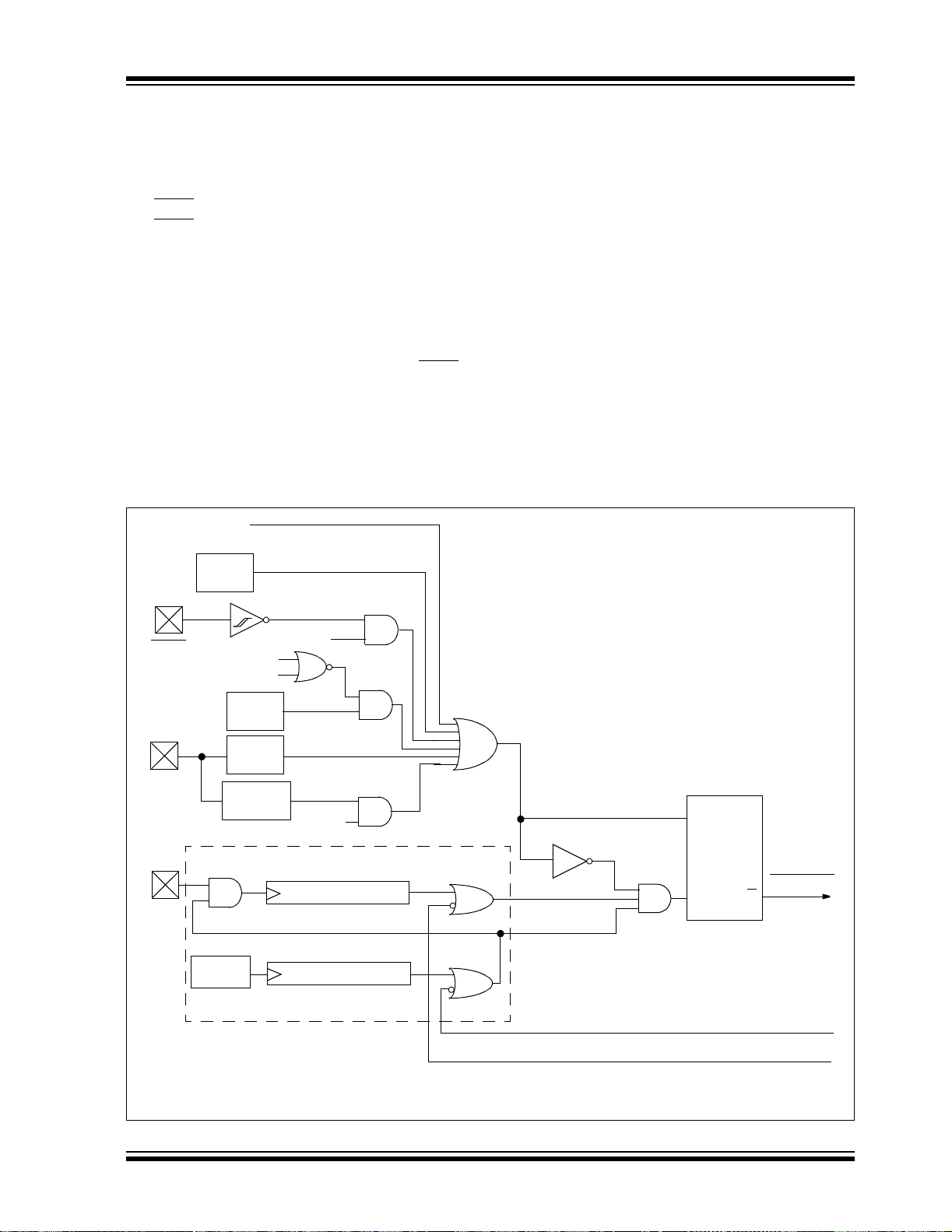
PIC18F2X1X/4X1X
4.0 RESET
A simplified block di agram of the On-Chip Reset Circu it
is shown in Figure 4-1.
The PIC18F2X1X/4X1X devices differentiate between
various kinds of Reset:
a) Power-on Reset (POR)
b) MCLR
Reset during normal operation
c) MCLR Reset during power managed modes
d) Watchdog Timer (WDT) Reset (during
execution)
e) Programmable Brown-out Reset (BOR)
f) RESET Instruction
g) Stack Full Reset
h) Stack Underflow Reset
This section discusses Resets generated by MCLR
POR and BOR and covers the ope rati on o f the various
start-up timers. Stack Reset events are covered in
Section 5.1.2.4 “Stack Full and Underflow Resets”.
WDT Resets are co v ere d i n Section 22.2 “Watchdog
,
4.1 RCON Register
Device Reset events are tracked through the RCON
register (Register 4-1). The lower five bits of the
register indicate that a specific Reset event has
occurred. In most cases, th ese bit s can on ly be cl eared
by the event and must be set by the application after
the event. The state of these flag bits, taken together,
can be read to indicate the type of Reset that just
occurred. This is described in more detail in
Section 4.6 “Reset State of Registers”.
The RCON register also has control bits for setting
interrupt priority (IPEN) and software control of the
BOR (SBOREN). Interrupt priority is discussed in
Section 8.0 “Interrupts”. BOR is covered in
Section 4.4 “Brown-out Reset (BOR)”.
Timer (WDT)”.
FIGURE 4-1: SIMPLIFIED BLOCK DIAGRAM OF ON-CHIP RESET CIRCUIT
RESET
Instruction
Stack
Pointer
Stack Full/Underflow Reset
MCLR
VDD
OSC1
( )_IDLE
Sleep
WDT
Time-out
V
DD Rise
Detect
Brown-out
Reset
OST/PWRT
32 µs
(1)
INTRC
External Reset
MCLRE
POR Pulse
BOREN
OST
PWRT
1024 Cycles
10-bit Ripple Counter
65.5 ms
11-bit Ripple Counter
S
Chip_Reset
R
Q
Enable PWRT
Enable OST
(2)
Note 1: This is the INTRC source from the internal oscillator block and is separate from the RC oscillator of the CLKI pin.
2: See Table 4-2 for time-out situations.
2004 Microchip Technology Inc. Preliminary DS39636A-page 41

PIC18F2X1X/4X1X
REGISTER 4-1: RCON: RESET CONTROL REGISTER
R/W-0 R/W-1
IPEN SBOREN
bit 7 bit 0
bit 7 IPEN: Interrupt Priority Enable bit
1 = Enable priority levels on interrupts
0 = Disable priority levels on interrupts (PIC16CXXX Compatibility mode)
bit 6 SBOREN: BOR Software Enable bit
If BOREN1:BOREN0 = 01:
1 = BOR is enabled
0 = BOR is disabled
If BOREN1:BOREN0 =
Bit is disabled and read as ‘0’.
bit 5 Unimplemented: Read as ‘0’
bit 4 RI: RESET Instruction Flag bit
1 = The RESET instruction was not executed (set by firmware only)
0 = The RESET instruction was executed causing a device Reset (must be set in software after
a Brown-out Reset occur s)
bit 3 TO: Watchdog Time-out Flag bit
1 = Set by power-up, CLRWDT instruction or SLEEP instruction
0 = A WDT time-out occurred
bit 2 PD
bit 1 POR
bit 0 BOR
: Power-down Detection Flag bit
1 = Set by power-up or by the CLRWDT instruction
0 = Set by execution of th e SLEEP instruction
: Power-on Reset Status bit
1 = A Power-on Reset has not occurred (set by firmware only)
0 = A Power-on Reset occurred (must be set in software after a Power-on Reset occurs)
: Brown-out Reset Status bit
1 = A Brown-out Reset has not occurred (set by firmware only)
0 = A Brown-out Reset occurred (must be set in software after a Brown-out Reset occurs)
(1)
00, 10 or 11:
U-0 R/W-1 R-1 R-1 R/W-0
—RITO PD POR BOR
(1)
(2)
(2)
R/W-0
Note 1: The SBOREN bit is only available when the BOREN1:BOREN0 configuration
bits = 01; otherwise, it is disabled and reads as ‘0’. See Section 4.4 “Brown-out
Reset (BOR)”.
2: The actual Reset val ue o f POR
notes following this register and Section 4.6 “Reset State of Registers” for
additional information.
Legend:
R = Readable bit W = Writable bit U = Unimplemented bit, read as ‘0’
-n = Value at POR ‘1’ = Bit is set ‘0’ = Bit is cleared x = Bit is unknown
Note 1: It is recommended that the POR bit be set after a Power-on Reset has been
detected so that subsequent Power-on Resets may be detected.
2: Brown-out Reset is said to have occurred when BOR
that POR
DS39636A-page 42 Preliminary 2004 Microchip Technology Inc.
was set to ‘1’ by software immediately after POR).
is determined by the t ype of device Reset. See the
is ‘0’ and POR is ‘1’ (assumin g

PIC18F2X1X/4X1X
4.2 Master Clear (MCLR)
The MCLR pin provides a method for triggering an
external Reset of the device. A Reset is generated by
holding the pin low. These devi ces have a noise fi lter in
the MCLR
Reset path which detects and ignores small
pulses.
The MCLR
pin is not drive n low by any inter nal Reset s,
including the WDT.
In PIC18F2X1X/4X1X devi ces , th e M CLR
input can be
disabled with the MCLRE configuration bit. When
MCLR is disabled, the pin becom es a dig ita l input. See
Section 9.5 “PORTE, TRISE and LATE Registers”
for more information.
4.3 Power-on Reset (POR)
A Power-on Reset pulse is generated on-chip
whenever V
allows the device to start in the initialized state when
VDD is adequate for operation.
To take advantage of the POR circuitry, tie the MCLR
pin throug h a resis tor (1 kΩ to 10 kΩ) to VDD. T his w ill
eliminate external RC components usually needed to
create a Power-on Re set delay. A minimum rise rate for
DD is specified (parameter D004). For a slow rise
V
time, see Figure 4-2.
When the device st arts normal operation (i.e ., ex its the
Reset condition), device operating parameters (voltage, frequency, temperature, etc.) must be met to
ensure operation. If these conditions are not met, the
device must be held in Reset until the operating
conditions are met.
POR events are captured by the POR
The state of the bit is set to ‘0’ whe never a POR occurs;
it does not change for any other Reset event. POR is
not reset to ‘1’ by any hardware event. To capture
multiple events, the user manually resets the bit to ‘1’
in software following any POR.
DD rises above a certain threshold. This
bit (RCON<1>).
FIGURE 4-2: EXTERNAL POWER-ON
RESET CIRCUIT (FOR
SLOW V
DD
VDD
Note 1: External Power-on Reset circuit is required
V
D
R
C
only if the V
The diode D helps discharge the capacitor
quickly when V
2: R < 40 kΩ is recommended to make sure that
the voltage drop across R does not violate
the device’s electrical specification.
3: R1 ≥ 1 kΩ will limit any current flowing into
MCLR
of MCLR
Electrostatic Discharge (ESD) or Electrical
Overstress (EOS).
DD power-up slope is too slow.
from external capacitor C, in the event
/VPP pin breakdown, due to
DD POWER-UP)
R1
MCLR
PIC18FXXXX
DD powers down.
2004 Microchip Technology Inc. Preliminary DS39636A-page 43

PIC18F2X1X/4X1X
4.4 Brown-out Reset (BOR)
PIC18F2X1X/4X1X devices implement a BOR circuit
that provides the user with a number of configuration
and power-saving options. The BOR is controlled by
the BORV1:BOR V0 and BOREN1:BO REN0 conf igur ation bits. There are a total of four BOR configurations
which are summarized in Table 4-1.
The BOR threshold is set by t he BOR V1:BOR V0 bit s. If
BOR is enabled (any values of BOREN1:BOREN0,
except ‘00’), any drop of V
D005) for greater than T
the device. A Reset may or may not occur if V
below V
Brown-out Reset until V
If the Power-up T imer is enabl ed, it will be inv oked after
VDD rises above VBOR; it then will keep the chip in
Reset for an additional time delay, T
(parameter 33). If VDD drops below VBOR while the
Power-up Timer is running, the chip will go back into a
Brown-out Reset and the Power-up Timer will be
initialized. Once V
Timer will execute the additional time delay.
BOR and the Power-on Timer (PWRT) are
independently configured. Enabling BOR Reset does
not automatically enable the PWRT.
BOR for less than TBOR. The chip will remain in
DD rises above VBOR, the Power-up
4.4.1 SOFTWARE ENABLED BOR
When BOREN1:BOREN0 = 01, the BOR can be
enabled or disabled by the user in software. This is
done with the control bit, SBOREN (RCON<6>).
Setting SBOREN enables the BOR to function as
previously described. Clearing SBOREN disables the
BOR entirely. The SBOREN bit operates only in this
mode; otherwise it is read as ‘0’.
DD below VBOR (parameter
BOR (parameter 35 ) will reset
DD falls
DD rises above VBOR.
PWRT
Placing the BOR under software control gives the user
the additional flexibility of tailoring the application to its
environment withou t ha vi ng to reprogram the device to
change BOR configuration. It also allows the user to
tailor device power consumption in software by eliminating the incremental current that the BOR consumes.
While the BOR current is typically very small, it may
have some impact in low-power applications.
Note: Even when BOR is under s oftware contro l,
the BOR Reset voltage level is still set by
the BORV1:BORV0 configuration bits. It
cannot be changed in software.
4.4.2 DETECTING BOR
When BOR is enab led, the BO R bit always resets to ‘0’
on any BOR or P OR event. This makes it diff icult to
determine if a BOR event has occurre d jus t by rea ding
the state of BOR
simultaneously check the state of both POR
This assumes th at the POR
immediately after any POR event. If BOR
POR
is ‘1’, it can be reliably assum ed that a BOR event
has occurred.
alone. A more reliable method is to
and BOR.
bit is reset to ‘1’ in softwa re
is ‘0’ while
4.4.3 DISABLING BOR IN SLEEP MODE
When BOREN1:BOREN0 = 10, the BOR remains
under hardware control and operates as previously
described. Whenever the device enters Sleep mode,
however , the BOR is au tom ati ca lly dis abl ed . When the
device returns to any other operating mode, BOR is
automatically re-enabled.
This mode allows for applications to recover from
brown-out situations, while actively executing code,
when the device requires BOR protection the most. At
the same time, it save s additional po wer in Sleep mod e
by eliminating the small incremental BOR current.
TABLE 4-1: BOR CONFIGURATIONS
BOR Configuration Status of
BOREN1 BOREN0
00Unavailable BOR disabled; must be enabled by reprogramming the configuration bits.
01Available BOR enabled in software; operation controlled by SBOREN.
10Unavailable BOR enabled in hardware in Run and Idle modes, disabled during
11Unavailable BOR enabled in hardware; must be disabled by reprogramming the
DS39636A-page 44 Preliminary 2004 Microchip Technology Inc.
SBOREN
(RCON<6>)
Sleep mode.
configuration bits.
BOR Operation

PIC18F2X1X/4X1X
4.5 Device Reset Timers
PIC18F2X1X/4X1X devices inc orporate three sep arate
on-chip timers that help regulate the Power-on Reset
process. Their main function is to ensure that the
device clock is stable before code is executed. These
timers are:
• Power-up Timer (PWRT)
• Oscillator Start-up Timer (OST)
• PLL Lock Time-out
4.5.1 POWER-UP TIMER (PWRT)
The Power-up Timer (PWRT) of PIC18F2X1X/4X1X
devices is an 11-bit counter which uses the INTRC
source as t he clock i nput. Thi s yields a n approxim a(t)-10.72 asse-15.58r.T10.7( T) e-T
2004 Microchip Technology Inc. Preliminary DS39636A-page 45

PIC18F2X1X/4X1X
FIGURE 4-3: TIME-OUT SEQUENCE ON POWER-UP (MCLR TIED TO VDD, VDD RISE < TPWRT)
VDD
MCLR
INTERNAL POR
TPWRT
PWRT TIME-OUT
OST TIME-OUT
INTERNAL RESET
TOST
FIGURE 4-4: TIME-OUT SEQUENCE ON POWER-UP (MCLR
VDD
MCLR
INTERNAL POR
PWRT TI ME-OUT
OST TIME-OUT
INTERNAL RESET
TPWRT
NOT TIED TO VDD): CASE 1
TOST
FIGURE 4-5: TIME-OUT SEQUENCE ON POWER-UP (MCLR
VDD
MCLR
INTERNAL POR
TPWRT
PWRT TIME-OUT
OST TIME-OUT
INTERNAL RESET
DS39636A-page 46 Preliminary 2004 Microchip Technology Inc.
NOT TIED TO VDD): CASE 2
TOST

PIC18F2X1X/4X1X
FIGURE 4-6: SLOW RISE TIME (MCLR TIED TO VDD, VDD RISE > TPWRT)
5V
VDD
MCLR
INTERNAL POR
0V
PWRT
T
PWRT TIME-OUT
OST TIME-OUT
INTERNAL RESET
TOST
FIGURE 4-7: TIME-OUT SEQUENCE ON POR W/PLL ENABLED (MCLR TIED TO VDD)
VDD
MCLR
INTERNAL POR
TPWRT
PWRT TIME-OUT
OST TIME-OUT
PLL TIME-OUT
TOST
TPLL
INTERNAL RESET
Note: TOST = 1024 clock cycles.
T
PLL ≈ 2 ms max. First three stages of the PWRT timer.
2004 Microchip Technology Inc. Preliminary DS39636A-page 47

PIC18F2X1X/4X1X
4.6 Reset State of Registers
Most registers are unaffected by a Reset. Their status
is unknown on POR and unchanged by all other
Table 4-4 describes the Reset states for all of the
Special Function Registers. These are categorized by
Power-on and Brown-out Resets, Master Clear and
WDT Resets and WDT wake-ups.
Resets. The other registers are forced to a “Reset
state” depending on the type of Reset that occurred.
Most registers are not affected by a WDT wake-up,
since this is viewed as the resumption of normal operation. Status bits from the RCON register, RI
POR
and BOR, are set or cleare d dif ferently i n differe nt
, TO, PD,
Reset situations, as indicated in Table 4-3. These bits
are used in software to determine the nature of the
Reset.
TABLE 4-3: STATUS BITS, THEIR SIGNIFICANCE AND THE INITIALIZATION CONDITION
FOR RCON REGISTER
Condition
Program
Counter
SBOREN RI TO PD POR BOR STKFUL STKUNF
Power-on Reset 0000h 1 11100 0 0
RESET Instruction 0000h u
Brown-out Reset 0000h u
during Power Managed
MCLR
0000h u
(2)
(2)
(2)
Run Modes
MCLR during Power Managed
0000h u
(2)
Idle Modes and Sleep Mode
WDT Time-ou t during Full Power
0000h u
(2)
or Power Managed Run Mode
MCLR during Full Power
0000h u
(2)
Execution
Stack Full Reset (STVREN = 1) 0000h u
Stack Underflow Reset
0000h u
(2)
(2)
(STVREN = 1)
Stack Underflow Error (not an
0000h u
(2)
actual Reset, STVREN = 0)
WDT Time-out during Power
PC + 2 u
(2)
Managed Idle or Sleep Modes
Interrupt Exit from Power
PC + 2
(1)
(2)
u
Managed Modes
Legend: u = unchanged
Note 1: When the wake-up is due to an interrupt and the GIEH or GIEL bits are set, the PC is loaded with the
interrupt vector (008h or 0018h).
2: Reset state is ‘1’ for POR and unchanged for all other Resets when software BOR is enabled
(BOREN1:BOREN0 configuration bits = 01 and SBOREN = 1). Otherwise, the Re set state is ‘0’.
RCON Register STKPTR Register
0uuuu u u
111u0 u u
u1uuu u u
u10uu u u
u0uuu u u
uuuuu u u
uuuuu 1 u
uuuuu u 1
uuuuu u 1
u00uu u u
uu0uu u u
DS39636A-page 48 Preliminary 2004 Microchip Technology Inc.

PIC18F2X1X/4X1X
TABLE 4-4: INITIALIZATION CONDITIONS FOR ALL REGISTERS
Resets,
MCLR
Register Applicable Devices
Power-on Reset,
Brown-out
Reset
WDT Reset,
RESET
Instruction,
Stack Resets
TOSU 2410 2510 2515 2610 4410 4510 4515 4610 ---0 0000 ---0 0000 ---0 uuuu
TOSH 2410 2510 2515 2610 4410 4510 4515 4610 0000 0000 0000 0000 uuuu uuuu
TOSL 2410 2510 2515 2610 4410 4510 4515 4610 0000 0000 0000 0000 uuuu uuuu
STKPTR 2410 2510 2515 2610 4410 4510 4515 4610 00-0 0000 uu-0 0000 uu-u uuuu
PCLATU 2410 2510 2515 2610 4410 4510 4515 4610 ---0 0000 ---0 0000 ---u uuuu
PCLATH 2410 2510 2515 2610 4410 4510 4515 4610 0000 0000 0000 0000 uuuu uuuu
PCL 2410 2510 2515 2610 4410 4510 4515 4610 0000 0000 0000 0000 PC + 2
TBLPTRU 2410 2510 2515 2610 4410 4510 4515 4610 --00 0000 --00 0000 --uu uuuu
TBLPTRH 2410 2510 2515 2610 4410 4510 4515 4610 0000 0000 0000 0000 uuuu uuuu
TBLPTRL 2410 2510 2515 2610 4410 4510 4515 4610 0000 0000 0000 0000 uuuu uuuu
TABLAT 2410 2510 2515 2610 4410 4510 4515 4610 0000 0000 0000 0000 uuuu uuuu
PRODH 2410 2510 2515 2610 4410 4510 4515 4610 xxxx xxxx uuuu uuuu uuuu uuuu
PRODL 2410 2510 2515 2610 4410 4510 4515 4610 xxxx xxxx uuuu uuuu uuuu uuuu
INTCON 2410 2510 2515 2610 4410 4510 4515 4610 0000 000x 0000 000u uuuu uuuu
INTCON2 2410 2510 2515 2610 4410 4510 4515 4610 1111 -1-1 1111 -1-1 uuuu -u-u
INTCON3 2410 2510 2515 2610 4410 4510 4515 4610 11-0 0-00 11-0 0-00 uu-u u-uu
INDF0 2410 2510 2515 2610 4410 4510 4515 4610 N/ A N/A N/A
POSTINC0 2410 2510 2515 2610 4410 4510 4515 4610 N/A N/A N/A
POSTDEC0 2410 2510 2515 2610 4410 4510 4515 4610 N/A N/A N/A
PREINC0 2410 2510 2515 2610 4410 4510 4515 4610 N/A N/A N/A
PLUSW0 2410 2510 2515 2610 4410 4510 4515 4610 N/ A N/A N/A
FSR0H 2410 2510 2515 2610 4410 4510 4515 4610 ---- 0000 ---- 0000 ---- uuuu
FSR0L 2410 2510 2515 2610 4410 4510 4515 4610 xxxx xxxx uuuu uuuu uuuu uuuu
WREG 2410 2510 2515 2610 4410 4510 4515 4610 xxxx xxxx uuuu uuuu uuuu uuuu
INDF1 2410 2510 2515 2610 4410 4510 4515 4610 N/ A N/A N/A
POSTINC1 2410 2510 2515 2610 4410 4510 4515 4610 N/A N/A N/A
POSTDEC1 2410 2510 2515 2610 4410 4510 4515 4610 N/A N/A N/A
PREINC1 2410 2510 2515 2610 4410 4510 4515 4610 N/A N/A N/A
PLUSW1 2410 2510 2515 2610 4410 4510 4515 4610 N/ A N/A N/A
Legend: u = unchanged, x = unknown, - = unimplemented bit, read as ‘0’, q = value depends on condition.
Shaded cells indicate conditions do not apply for the designated device.
Note 1: One or more bits in the INTCONx or PIRx registers will be affected (to cause wake-up).
2: When the wake-up is due to an interrupt and the GIEL or GIEH bit is set, the PC is loaded with the interrupt vector
(0008h or 0018h).
3: When the wake-up is due to an interrupt and the GIEL or GIEH bit is set, the TOSU, TOSH and TOSL are updated with
the current value of the PC. The STKPTR is modified to point to the next location in the hardware stack.
4: See Table 4-3 for Reset value for specific condition.
5: Bits 6 and 7 of PORTA, LAT A and TRISA are enabled, depending on the oscillator mode selected. When not enabled as
PORTA pins, they are disabled and read ‘0’.
Wake-up via
WDT
or Interrupt
(3)
(3)
(3)
(3)
(2)
(1)
(1)
(1)
2004 Microchip Technology Inc. Preliminary DS39636A-page 49

PIC18F2X1X/4X1X
TABLE 4-4: INITIALIZATION CONDITIONS FOR ALL REGISTERS (CONTINUED)
MCLR
Register Applicable Devices
FSR1H 2410 2510 2515 2610 4410 4510 4515 4610 ---- 0000 ---- 0000 ---- uuuu
FSR1L 2410 2510 2515 2610 4410 4510 4515 4610 xxxx xxxx uuuu uuuu uuuu uuuu
BSR 2410 2510 2515 2610 4410 4510 4515 4610 ---- 0000 ---- 0000 ---- uuuu
INDF2 2410 2510 2515 2610 4410 4510 4515 4610 N/ A N/A N/A
POSTINC2 2410 2510 2515 2610 4410 4510 4515 4610 N/A N/A N/A
POSTDEC2 2410 2510 2515 2610 4410 4510 4515 4610 N/A N/A N/A
PREINC2 2410 2510 2515 2610 4410 4510 4515 4610 N/A N/A N/A
PLUSW2 2410 2510 2515 2610 4410 4510 4515 4610 N/ A N/A N/A
FSR2H 2410 2510 2515 2610 4410 4510 4515 4610 ---- 0000 ---- 0000 ---- uuuu
FSR2L 2410 2510 2515 2610 4410 4510 4515 4610 xxxx xxxx uuuu uuuu uuuu uuuu
STATUS 2410 2510 2515 2610 4410 4510 4515 4610 ---x xxxx ---u uuuu ---u uuuu
TMR0H 2410 2510 2515 2610 4410 4510 4515 4610 0000 0000 0000 0000 uuuu uuuu
TMR0L 2410 2510 2515 2610 4410 4510 4515 4610 xxxx xxxx uuuu uuuu uuuu uuuu
T0CON 2410 2510 2515 2610 4410 4510 4515 4610 1111 1111 1111 1111 uuuu uuuu
OSCCON 2410 2510 2515 2610 4410 4510 4515 4610 0100 q000 0100 q000 uuuu uuqu
HLVDCON 2410 2510 2515 2610 4410 4510 4515 4610 0-00 0101 0-00 0101 u-uu uuuu
WDTCON 2410 2510 2515 2610 4410 4510 4515 4610 ---- ---0 ---- ---0 ---- ---u
(4)
RCON
TMR1H 2410 2510 2515 2610 4410 4510 4515 4610 xxxx xxxx uuuu uuuu uuuu uuuu
TMR1L 2410 2510 2515 2610 4410 4510 4515 4610 xxxx xxxx uuuu uuuu uuuu uuuu
T1CON 2410 2510 2515 2610 4410 4510 4515 4610 0000 0000 u0uu uuuu uuuu uuuu
TMR2 2410 2510 2515 2 610 4410 4510 4515 4610 0000 0000 0000 0000 uuuu uuuu
PR2 2410 2510 2515 2610 4410 4510 4515 4610 1111 1111 1111 1111 1111 1111
T2CON 2410 2510 2515 2610 4410 4510 4515 4610 -000 0000 -000 0000 -uuu uuuu
SSPBUF 2410 2510 2515 2610 4410 4510 4515 4610 xxxx xxxx uuuu uuuu uuuu uuuu
SSPADD 2410 2510 2515 2610 4410 4510 4515 4610 0000 0000 0000 0000 uuuu uuuu
SSPSTAT 2410 2510 2515 2610 4410 4510 4515 4610 0000 0000 0000 0000 uuuu uuuu
SSPCON1 2410 2510 2515 2610 4410 4510 4515 4610 0000 0000 0000 0000 uuuu uuuu
SSPCON2 2410 2510 2515 2610 4410 4510 4515 4610 0000 0000 0000 0000 uuuu uuuu
Legend: u = unchanged, x = unknown, - = unimplemented bit, read as ‘0’, q = value depends on condition.
Note 1: One or more bits in the INTCONx or PIRx registers will be affected (to cause wake-up).
2: When the wake-up is due to an interrupt and the GIEL or GIEH bit is set, the PC is loaded with the interrupt vector
3: When the wake-up is due to an interrupt and the GIEL or GIEH bit is set, the TOSU, TOSH and TOSL are updated with
4: See Table 4-3 for Reset value for specific condition.
5: Bits 6 and 7 of PORTA, LAT A and TRISA are enabled, depending on the oscillator mode selected. When not enabled as
2410 2510 2515 2610 4410 4510 4515 4610 0q-1 11q0 0q-q qquu uq-u qquu
Shaded cells indicate conditions do not apply for the designated device.
(0008h or 0018h).
the current value of the PC. The STKPTR is modified to point to the next location in the hardware stack.
PORTA pins, they are disabled and read ‘0’.
Power-on Reset,
Brown-out
Reset
Resets,
WDT Reset,
RESET
Instruction,
Stack Resets
Wake-up via
WDT
or Interrupt
DS39636A-page 50 Preliminary 2004 Microchip Technology Inc.

PIC18F2X1X/4X1X
TABLE 4-4: INITIALIZATION CONDITIONS FOR ALL REGISTERS (CONTINUED)
MCLR
Register Applicable Devices
ADRESH 2410 2510 2515 2610 4410 4510 4515 4610 xxxx xxxx uuuu uuuu uuuu uuuu
ADRESL 2410 2510 2515 2610 4410 4510 4515 4610 xxxx xxxx uuuu uuuu uuuu uuuu
ADCON0 2410 2510 2515 2610 4410 4510 4515 4610 --00 0000 --00 0000 --uu uuuu
ADCON1 2410 2510 2515 2610 4410 4510 4515 4610 --00 0qqq --00 0qqq --uu uuuu
ADCON2 2410 2510 2515 2610 4410 4510 4515 4610 0-00 0000 0-00 0000 u-uu uuuu
CCPR1H 2410 2510 2515 2610 4410 4510 4515 4610 xxxx xxxx uuuu uuuu uuuu uuuu
CCPR1L 2410 2510 2515 2610 4410 4510 4515 4610 xxxx xxxx uuuu uuuu uuuu uuuu
CCP1CON
CCPR2H 2410 2510 2515 2610 4410 4510 4515 4610 xxxx xxxx uuuu uuuu uuuu uuuu
CCPR2L 2410 2510 2515 2610 4410 4510 4515 4610 xxxx xxxx uuuu uuuu uuuu uuuu
CCP2CON 2410 2510 2515 2610 4410 4510 4515 4610 --00 0000 --00 0000 --uu uuuu
BAUDCON 2410 2510 2515 2610 4410 4510 4515 4610 01-0 0-00 01-0 0-00 --uu uuuu
PWM1CON 2410 2510 2515 2610 4410 4510 4515 4610 0000 0000 0000 0000 uuuu uuuu
ECCP1AS
CVRCON 2410 2510 2515 2610 4410 4510 4515 4610 0000 0000 0000 0000 uuuu uuuu
CMCON 2410 2510 2515 2610 4410 4510 4515 4610 0000 0111 0000 0111 uuuu uuuu
TMR3H 2410 2510 2515 2610 4410 4510 4515 4610 xxxx xxxx uuuu uuuu uuuu uuuu
TMR3L 2410 2510 2515 2610 4410 4510 4515 4610 xxxx xxxx uuuu uuuu uuuu uuuu
T3CON 2410 2510 2515 2610 4410 4510 4515 4610 0000 0000 uuuu uuuu uuuu uuuu
SPBRGH 2410 2510 2515 2610 4410 4510 4515 4610 0000 0000 0000 0000 uuuu uuuu
SPBRG 2410 2510 2515 2610 4410 4510 4515 4610 0000 0000 0000 0000 uuuu uuuu
RCREG 2410 2510 2515 2610 4410 4510 4515 4610 0000 0000 0000 0000 uuuu uuuu
TXREG 2410 2510 2515 2610 4410 4510 4515 4610 0000 0000 0000 0000 uuuu uuuu
TXSTA 2410 2510 2515 2610 4410 4510 4515 4610 0000 0010 0000 0010 uuuu uuuu
RCSTA 2410 2510 2515 2610 4410 4510 4515 4610 0000 000x 0000 000x uuuu uuuu
Legend: u = unchanged, x = unknown, - = unimplemented bit, read as ‘0’, q = value depends on condition.
Note 1: One or more bits in the INTCONx or PIRx registers will be affected (to cause wake-up).
2410 2510 2515 2610 4410 4510 4515 4610 0000 0000 0000 0000 uuuu uuuu
2410 2510 2515 2610
2410 2510 2515 2610 4410 4510 4515 4610 0000 0000 0000 0000 uuuu uuuu
2410 2510 2515 2610
Shaded cells indicate conditions do not apply for the designated device.
2: When the wake-up is due to an interrupt and the GIEL or GIEH bit is set, the PC is loaded with the interrupt vector
(0008h or 0018h).
3: When the wake-up is due to an interrupt and the GIEL or GIEH bit is set, the TOSU, TOSH and TOSL are updated with
the current value of the PC. The STKPTR is modified to point to the next location in the hardware stack.
4: See Table 4-3 for Reset value for specific condition.
5: Bits 6 and 7 of PORTA, LAT A and TRISA are enabled, depending on the oscillator mode selected. When not enabled as
PORTA pins, they are disabled and read ‘0’.
4410 4510 4515 4610 --00 0000 --00 0000 --uu uuuu
4410 4510 4515 4610 0000 00-- 0000 00-- uuuu uu--
Power-on Reset,
Brown-out
Reset
Resets,
WDT Reset,
RESET
Instruction,
Stack Resets
Wake-up via
WDT
or Interrupt
2004 Microchip Technology Inc. Preliminary DS39636A-page 51

PIC18F2X1X/4X1X
TABLE 4-4: INITIALIZATION CONDITIONS FOR ALL REGISTERS (CONTINUED)
MCLR
Register Applicable Devices
Brown-out
Reset
IPR2 2410 2510 2515 2610 4410 4510 4515 4610 11-- 1111 11-- 1111 uu-- uuuu
PIR2 2410 2510 2515 2610 4410 4510 4515 4610 00-- 0000 00-- 0000 uu-- uuuu
PIE2 2410 2510 2515 2610 4410 4510 4515 4610 00-- 0000 00-- 0000 uu-- uuuu
Power-on Reset,
IPR1
PIR1
2410 2510 2515 2610 4410 4510 4515 4610 1111 1111 1111 1111 uuuu uuuu
2410 2510 2515 2610
4410 4510 4515 4610 -111 1111 -111 1111 -uuu uuuu
2410 2510 2515 2610 4410 4510 4515 4610 0000 0000 0000 0000 uuuu uuuu
2410 2510 2515 2610 4410 4510 4515 4610 -000 0000 -000 0000 -uuu uuuu
PIE1 2410 2510 2515 2610 4410 4510 4515 4610 0000 0000 0000 0000 uuuu uuuu
2410 2510 2515 2610
4410 4510 4515 4610 -000 0000 -000 0000 -uuu uuuu
OSCTUNE 2410 2510 2515 2610 4410 4510 4515 4610 00-0 0000 00-0 0000 uu-u uuuu
TRISE
TRISD
2410 2510 2515 2610 4410 4510 4515 4610 0000 -111 0000 -111 uuuu -uuu
2410 2510 2515 2610 4410 4510 4515 4610 1111 1111 1111 1111 uuuu uuuu
TRISC 2410 2510 2515 2610 4410 4510 4515 4610 1111 1111 1111 1111 uuuu uuuu
TRISB 2410 2510 2515 2610 4410 4510 4515 4610 1111 1111 1111 1111 uuuu uuuu
TRISA
(5)
2410 2510 2515 2610 4410 4510 4515 4610 1111 1111
(5)
LATE 2410 2510 2515 2610 4410 4510 4515 4610 ---- -xxx ---- -uuu ---- -uuu
LATD
2410 2510 2515 2610 4410 4510 4515 4610 xxxx xxxx uuuu uuuu uuuu uuuu
LATC 2410 2510 2515 2610 4410 4510 4515 4610 xxxx xxxx uuuu uuuu uuuu uuuu
LATB 2410 2510 2515 2610 4410 4510 4515 4610 xxxx xxxx uuuu uuuu uuuu uuuu
LATA
(5)
2410 2510 2515 2610 4410 4510 4515 4610 xxxx xxxx
(5)
PORTE 2410 2510 2515 2610 4410 4510 4515 4610 ---- x000 ---- x000 ---- uuuu
PORTD
2410 2510 2515 2610 4410 4510 4515 4610 xxxx xxxx uuuu uuuu uuuu uuuu
PORTC 2410 2510 2515 2610 4410 4510 4515 4610 xxxx xxxx uuuu uuuu uuuu uuuu
PORTB 2410 2510 2515 2610 4410 4510 4515 4610 xxxx xxxx uuuu uuuu uuuu uuuu
PORTA
(5)
2410 2510 2515 2610 4410 4510 4515 4610 xx0x 0000
(5)
Legend: u = unchanged, x = unknown, - = unimplemented bit, read as ‘0’, q = value depends on condition.
Shaded cells indicate conditions do not apply for the designated device.
Note 1: One or more bits in the INTCONx or PIRx registers will be affected (to cause wake-up).
2: When the wake-up is due to an interrupt and the GIEL or GIEH bit is set, the PC is loaded with the interrupt vector
(0008h or 0018h).
3: When the wake-up is due to an interrupt and the GIEL or GIEH bit is set, the TOSU, TOSH and TOSL are updated with
the current value of the PC. The STKPTR is modified to point to the next location in the hardware stack.
4: See Table 4-3 for Reset value for specific condition.
5: Bits 6 and 7 of PORTA, LAT A and TRISA are enabled, depending on the oscillator mode selected. When not enabled as
PORTA pins, they are disabled and read ‘0’.
Resets,
WDT Reset,
RESET
Instruction,
Stack Resets
1111 1111
uuuu uuuu
uu0u 0000
(5)
(5)
(5)
Wake-up via
WDT
or Interrupt
uuuu uuuu
uuuu uuuu
uuuu uuuu
(1)
(1)
(1)
(5)
(5)
(5)
DS39636A-page 52 Preliminary 2004 Microchip Technology Inc.
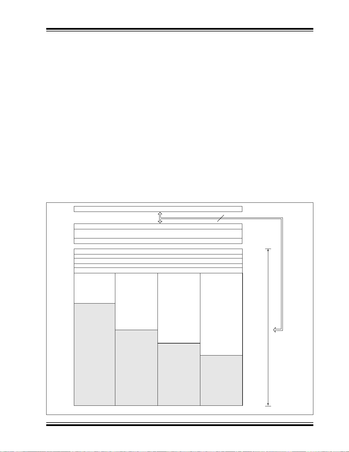
PIC18F2X1X/4X1X
5.0 MEMORY ORGANIZATION
There are two types of memory in PIC18F2X1X/4X1X
microcontroller devices:
• Program Memory
• Data RAM
As Harvard architecture dev ices, the dat a and progra m
memories use separate busses; this allows for
concurrent access of the two memory spaces.
Additional detailed information on the operation of the
Flash program memory is provided in Section 6.0
“Flash Program Memory”.
5.1 Program Memory Organization
PIC18 microcontrollers implement a 21-bit program
counter, which is capable of addressing a 2-Mbyte
program memory sp ace. Accessi ng a loca tion betwee n
the upper boundary of the physically implemented
memory and the 2-Mbyte address will return all ‘0’s (a
NOP instruction).
The PIC18F2410/4410 and PIC18F2510 each have
16 Kbytes of Flash memory and can store up to 8,192
single-word instructions. The PIC18F2510/4510 each
have 32 Kbytes of Flash memory and can store up to
16,384 single-word instructions. The PIC18F2515/4515
each have 48 Kbytes of Flash memory and can store up
to 24,576 single-word instructions. The PIC18F2610/
4610 each have 64 Kbytes of Flash memory and can
store up to 32,768 single-word instructions.
PIC18 devices have two interrupt vectors. The Reset
vector address is at 0000h and the interrupt vector
addresses are at 0008h and 0018h.
The program memory map for PIC18F2X1X/4X1X
devices is shown in Figure 5-1.
FIGURE 5-1: PROGRAM MEMORY MAP AND STACK FOR
PIC18F2X1X/4X1X DEVICES
On-Chip
Program Memory
(16 Kbytes)
03FFFh
04000h
Read ‘0’
PC<20:0>
CALL,RCALL,RETURN
RETFIE,RETLW
Stack Level 1
Stack Level 31
Reset Vector
High Priority Interrupt Vector
Low Priority Interrupt Vector
On-Chip
Program Memory
(32 Kbytes) (48 Kbytes)
07FFFh
08000h
Read ‘0’
•
•
•
On-Chip
Program Memory
0BFFFh
0C000h
Read ‘0’
21
On-Chip
Program Memory
(64 Kbytes)
0FFFFh
10000h
Read ‘0’
00000h
00008h
00018h
User Memory Space
1FFFFFh
PIC18F2410/4410
2004 Microchip Technology Inc. Preliminary DS39636A-page 53
PIC18F2510/4510
PIC18F2515/4515
PIC18F2610/4610
200000h

PIC18F2X1X/4X1X
5.1.1 PROGRAM COUNTER
The Program Counter (PC) specifies the address of the
instruction to fetch for execu tion. The PC is 21 bits wide
and is contained in three separate 8-bit registers. The
low byte, known as the PCL register, is both readable
and writable. The high byt e, or PCH re gister, contains
the PC<15:8> bits; i t is not directly re adable or writ able.
Updates to the PCH register are perfo rmed through the
PCLATH register. The upper byte is called PCU. This
register contains the PC<20:16> bits; it is also not
directly readable or writable. Updates to the PCU
register are performed through the PCLATU register.
The contents of PCLATH and PCLATU are transferred
to the program counter by any operation that writes
PCL. Similarly, the upper two bytes of the program
counter are transferred to P CLATH and PCLATU by an
operation that reads PCL. This is useful for computed
offsets to the PC (see Section 5.1.4.1 “Computed
GOTO”).
The PC addresses bytes in the program memory. To
prevent the PC from becoming misaligned with word
instructions, the Least Significant bit of PCL is fixed to
a value of ‘0’. The PC increments by 2 to address
sequential instructions in the program memory.
The CALL, RCALL, GOTO and program branch
instructions write to the program counter directly. For
these instructions, the contents of PCLATH and
PCLATU are not transferred to the program counter.
5.1.2 RETURN ADDRESS STACK
The return address s tack allows any combination of up
to 31 program calls and interrupts to occur. The PC is
pushed onto th e stac k when a CALL or RCALL instruction is executed or an interrupt is Acknowledged. The
PC value is pulled of f the stack o n a RETURN, RETLW or
a RETFIE ins truction. PCLATU and PCLATH are not
affected by any of the RETURN or CALL instructions.
The stack operates as a 31-word by 21-bit RAM and a
5-bit Stack Pointer, STKPTR. The stack space is not
part of either program or da ta sp ace. The Stack Pointer
is readable and writable and the address on the top of
the stack is readable and writable through the top-ofstack Special File Registers. Data can also be pushed
to, or popped from the stack, using these registers.
A CALL type instru ctio n caus es a pus h ont o the stac k;
the Stack Pointer is first incremented and the location
pointed to by the Stack Pointer is written with the
contents of the PC (already pointing to the instruction
following the CALL). A RETURN ty pe ins truc ti on c au se s
a pop from the stack; the contents of the location
pointed to by the STKPTR are transferred to the PC
and then the Stack Pointer is decremented.
The Stack Pointer is initialized to ‘00000’ after all
Resets. There is no RAM associated with the location
corresponding to a Stack Pointer value of ‘00000’; this
is only a Reset value. Status bit s in dic ate if the stack is
full or has overflowed or has underflowed.
5.1.2.1 Top-of-Stack Access
Only the top of the return address stack (TOS) is
readable and writable. A set of three registers,
TOSU:TOSH:TOSL, hold th e contents of the stack location pointed to by the STKPTR register (Figure 5-2). This
allows users to implement a software stack if necessary.
After a CALL, RCALL or interrupt, the software can read
the pushed value by reading the TOSU:TOSH:TOSL
registers. These values can be placed on a use r defined
software stack. At return time, the software can return
these values to TOSU:TOSH:TOSL and do a return.
The user must disable the global interrupt enable bits
while accessing the stack to prevent inadvertent stack
corruption.
FIGURE 5-2: RETURN ADDRESS STACK AND ASSOCIATED REGISTERS
Return Address Stack <20:0>
11111
T op -of-Stack Registers Stack Pointer
TOSLTOSHTOSU
34h1Ah00h
Top-of-Stack
DS39636A-page 54 Preliminary 2004 Microchip Technology Inc.
001A34h
000D58h
11110
11101
STKPTR<4:0>
00010
00011
00010
00001
00000

PIC18F2X1X/4X1X
5.1.2.2 Return Stack Pointer (STKPTR)
The STKPTR register (Reg ister 5-1) contains the Stack
Pointer value, the STKFUL (Stack Full) status bit and
the STKUNF (Stack Underflow) status bits. The value
of the Stack Pointer can be 0 through 31. The Stack
Pointer increments before values are pushed onto the
stack and decrements after values are popped off the
stack. On Reset, the Stack Pointer value will be zero.
The user may read and write the Stack Pointer value.
This feature can be used by a Real-Time Operating
System (RTOS) for return stack maintenance.
After the PC is pus hed o nto the st ack 31 times (wi thout
popping any values off the stack), the STKFUL bit is
set. The STKFUL bit is cleared by software or by a
POR.
The action that takes place when the stack becomes
full depends on the state of the STVREN (Stack Overflow Reset Enable) configuration bit. (Refer to
Section 22.1 “Configuration Bits” for a de scription of
the device configuration bits.) If STVREN is set
(default), the 31st push will push the (PC + 2) value
onto the stack, set the STKFUL bit and reset the
device. The STKFUL bit will remain set and the Stack
Pointer will be set to zero.
If STVREN is cleared, the STKFUL bi t will be set on the
31st push and the Stack Pointer will increment to 31.
Any additional pushes will not overwrite the 31st push
and STKPTR will remain at 31.
When the stack has been popped enough times to
unload the stac k, the next pop will ret urn a value of zero
to the PC and sets the STKUNF bit, while the Stack
Pointer remains at zero. The STKUNF bit will remain
set until cleared by software or until a POR occurs.
Note: Returning a value of zero to the PC on an
underflow has the effect of vectoring the
program to the Reset vector, where the
stack conditions can be verified and
appropriate actions can be taken. This is
not the same as a Reset, as the contents
of the SFRs are not affected.
5.1.2.3 PUSH and POP Instruction s
Since the Top-of-Stack is readable and writable, the
ability to push value s on to the st ac k an d pul l va lues off
the stack without disturbing normal program execution
is a desirable feature. The PIC18 instruction set
includes two instructions, PUSH and POP, that permit
the TOS to be manipulated under software control.
TOSU, TOSH and T OS L can be m odifie d to plac e dat a
or a return address on the stack.
The PUSH instruction places the current PC value onto
the stack. This increments the Stack Pointer and loads
the current PC value onto the stack.
The POP instruction discards the current TOS by decrementing the Stack Pointer. The previous value pushed
onto the stack then becomes the TOS value.
REGISTER 5-1: STKPTR: STACK POINTER REGISTER
R/C-0 R/C-0 U-0 R/W-0 R/W-0 R/W-0 R/W-0 R/W-0
STKFUL
bit 7 bit 0
bit 7 STKFUL: Stack Full Flag bit
1 = Stack became full or overflowed
0 = Stack has not become full or overflowed
bit 6 STKUNF: Stack Underflow Flag bit
1 = Stack underflow occurred
0 = Stack underflow did not occur
bit 5 Unimplemented: Read as ‘0’
bit 4-0 SP4:SP0: Stack Pointer Location bits
Legend:
R = Readable bit W = Writable bit U = Unimplemented C = Clearable only bit
-n = Value at POR ‘1’ = Bit is set ‘0’ = Bit is cleared x = Bit is unknown
(1)
STKUNF
Note 1: Bit 7 and bit 6 are cleared by user software or by a POR.
(1)
— SP4 SP3 SP2 SP1 SP0
(1)
(1)
2004 Microchip Technology Inc. Preliminary DS39636A-page 55

PIC18F2X1X/4X1X
5.1.2.4 Stack Full and Underflow Resets
Device Resets on stack overflow and stack underflow
conditions are enabled by setting the STVREN bit in
Configuration Regist er 4L. When STVREN is set, a full
or underflow will set the appropriate STKFUL or
STKUNF bit and then cause a device Reset. When
STVREN is cleared, a full or underflow condi tion will set
the appropriate STKFUL or STKUNF bit but not cause
a device Reset. The STKFUL or STKUNF bits are
cleared by the user software or a Power-on Reset.
5.1.3 FAST REGISTER STACK
DS39636A-page 56 Preliminary 2004 Microchip Technology Inc.

PIC18F2X1X/4X1X
5.2 PIC18 Instruction Cycle
5.2.1 CLOCKING SCHEME
The microcontroller clock input, whether from an
internal or external source, is internally divided by four
to generate four non-overlapping quadrature clocks
(Q1, Q2, Q3 and Q 4). Internall y, the program cou nter is
incremented on every Q1; the instruction is fetched
from the program memory and latched into the instruction register during Q4. The ins truc tion is decoded and
executed during the following Q1 through Q4. The
clocks and instruction execution flow are shown in
Figure 5-3.
FIGURE 5-3: CLOCK/ INSTRUCTION CYCLE
OSC1
Q1
Q2
Q3
Q4
PC
OSC2/CLKO
(RC mode)
Q2 Q3 Q4
Q1
PC PC + 2 PC + 4
Execute INST (PC – 2)
Fetch INST (PC)
Q2 Q3 Q4
Q1
Execute INST (PC)
Fetch INST (PC + 2)
5.2.2 INSTRUCTION FLOW/PIPELINING
An “Instruction Cycle” consists of four Q cycles: Q1
through Q4. The instruction fetch and execute are
pipelined in such a manner that a fetch takes one
instruction cycle, while the decode and execute take
another instruction cycle. However, due to the pipelining, each instruction effectively executes in one
cycle. If a n instruc tion caus es the pro gram coun ter to
change (e.g., GOTO), then two cycles are required to
complete the instruction (Example 5-3).
A fetch cycle begins with the Program Counter (PC)
incrementing in Q1.
In the execution cy cle, the fetch ed instruction i s latched
into the Instruction Register (IR) in cycle Q1. This
instruction is then decoded and executed during the
Q2, Q3 and Q4 cycle s. D ata memory is re ad dur ing Q 2
(operand read) and written during Q4 (destination
write).
Q2 Q3 Q4
Q1
Internal
Phase
Clock
Execute INST (PC + 2)
Fetch INST (PC + 4)
EXAMPLE 5-3: INSTRUCTION PIPELINE FLOW
TCY0TCY1TCY2TCY3TCY4TCY5
1. MOVLW 55h
2. MOVWF PORTB
3. BRA SUB_1
4. BSF PORTA, BIT3 (Forced NOP)
5. Instruction @ address SUB_1
All instructions are single cycle, except for any program branche s. These take tw o cycles since the fetch instruction
is “flushed” from the pipeline while the new instruction is being fetched and then executed.
2004 Microchip Technology Inc. Preliminary DS39636A-page 57
Fetch 1 Execute 1
Fetch 2 Execute 2
Fetch 3 Execute 3
Fetch 4 Flush (NOP)
Fetch SUB_1 Execute SUB_1

PIC18F2X1X/4X1X
5.2.3 INSTRUCTIONS IN PROGRAM MEMORY
The program memory is addressed in bytes. Instructions are stored as two bytes or four bytes in program
memory. The Least Significant Byte of an instruction
word is always stored in a program memory location
with an even address (LSb = 0). To maintain alignment
with instruction bo undaries , the PC incr ements in step s
of 2 and the LSb wi ll always read ‘0’ (see Section 5.1.1
“Program Counter”).
Figure 5-4 shows an exam ple of h ow in st ruc tion w ord s
are stored in the program memory.
The CALL and GOTO instructions have the absolute
program memory address embedded into the instruc-
tion. Since instructions are always stored on word
boundaries, the data contained in the instruction is a
word address. The word address is written to PC<20:1>,
which accesses the desired byte address in program
memory. Instruction #2 in Figure 5-4 shows how the
instruction GOTO 0006h is encoded in the program
memory. Program branch instructions, which encode a
relative address offset, operate in the same ma nner. The
offset value stored in a br anch instruction represent s the
number of single-word instructions that the PC will be
offset by. Section 23.0 “Instruction Set Summary”
provides further details of the instruction set.
FIGURE 5-4: INSTRUCTIONS IN PROGRAM MEMORY
LSB = 1 LSB = 0 ↓
0Fh 55h 000008h
EFh 03h 00000Ah
F0h 00h 00000Ch
C1h 23h 00000Eh
F4h 56h 000010h
Instruction 1:
Instruction 2:
Instruction 3:
Program Memory
Byte Locations
MOVLW 055h
GOTO 0006h
MOVFF 123h, 456h
→
Word Address
000000h
000002h
000004h
000006h
000012h
000014h
5.2.4 TWO-WORD INSTRUCTIONS
The standard PIC18 instruction set has four two-word
instructions: CALL, MOVFF, GOTO and LSFR. In all
cases, the second word of the in struc tion s always has
‘1111’ as its four M ost Si gnifican t bit s; the other 12 bit s
are literal data, usually a data memory address.
The use of ‘1111’ in the 4 MSbs of an instruction specifies a special form of NOP. If the instruction is executed
in proper sequence – immediately after the first wor d –
the data in the s econd word is ac cessed an d used by
some reason and the se cond word is ex ecuted by itsel f,
a NOP is executed instead. This is necessary for cases
when the two-word instruction is preceded by a conditional instruction that changes the PC. Example 5-4
shows how this works.
Note: See Section 5.6 “PIC18 Instruction
Execution and the Extended Instruction Set” for information on two-word
instructions in the extended instruction
set.
the instruction se quence. If the first word is skipped for
EXAMPLE 5-4: TWO-WORD INSTRUCTIONS
CASE 1:
Object Code Source Code
0110 0110 0000 0000 TSTFSZ REG1 ; is RAM location 0?
1100 0001 0010 0011 MOVFF REG1, REG2 ; No, skip this word
1111 0100 0101 0110 ; Execute this word as a NOP
0010 0100 0000 0000 ADDWF REG3 ; continue code
CASE 2:
Object Code Source Code
0110 0110 0000 0000 TSTFSZ REG1 ; is RAM location 0?
1100 0001 0010 0011 MOVFF REG1, REG2 ; Yes, execute this word
1111 0100 0101 0110 ; 2nd word of instruction
0010 0100 0000 0000 ADDWF REG3 ; continue code
DS39636A-page 58 Preliminary 2004 Microchip Technology Inc.

PIC18F2X1X/4X1X
5.3 Data Memory Organization
Note: The operation of some aspects of data
memory are changed when the PIC18
extended instruction set is enabled. See
Section 5.5 “Data Memory and the
Extended Instruction Set” for more
information.
The data memory in PIC18 devices is implemented as
static RAM. Figures 5-5, 5-6 and 5-7 show the data
memory organization for the PIC18F2X1X/4X1X
devices.
The data memory contains Special Function Registers
(SFRs) and General Purpose Registers (GPRs). The
SFRs are used for control and status of the controller
and peripheral functio ns, while GPRs are us ed for data
storage and scratchpad operations in the user’s
application. Any re ad of an unimpl emented location will
read as ‘0’s.
The instruction set and architecture allow operations
across all banks. The entire data memory may be
accessed by Direct, Indirect or Indexed Addressing
modes. Addressing modes are discussed later in this
subsection.
To ensure that commonly used registers (SFRs and
select GPRs) c an b e ac cess ed i n a si ngle cycle, PI C18
devices impl em ent an Ac ce ss Ba nk . Th is i s a 256-byte
memory space that pr ovid es fa st acces s to SFRs a nd
the lower portion of GPR Bank 0 without using the
BSR. Section 5.3.2 “Access Bank” provides a
detailed description of the Access RAM.
5.3.1 BANK SELECT REGISTER (BSR)
Large areas of data memory require an efficient
addressing scheme to make rapid access to any
address possible. Ideally, this means that an entire
address does not need to be provided for each read or
write operation. For PIC18 devices, this is accomplished with a RAM banking scheme. This divides the
memory space into 16 contiguous banks of 256 bytes.
Depending on the instruction, each location can be
addressed directly by its full 12-bit address, or an 8-bit
low-order address and a 4-bit bank pointer.
Most instruct ions in th e PIC18 in struct ion set ma ke use
of the bank poin ter, known as the Bank Select Reg ister
(BSR). This SFR holds the 4 Most Significant bits of a
location’s address; the instruction itself includes the
8 Least Significant bits. Only the four lower bits of the
BSR are implemented (BSR3:BSR0). The upper four
bits are unused; the y will always read ‘ 0’ and cannot be
written to. The BSR can be l oaded direc tly by using the
MOVLB instruction.
The value of the BSR indicates the bank in data
memory; the 8 bits in the instruction show the location
in the bank and can be thought of as an offset from the
bank’s lower boundary. The relationship between the
BSR’s value and the bank division in data memory is
shown in Figure 5-8.
Since up to 16 regis ters m ay share the s ame l ow-order
address, the user must alway s be careful to ensure that
the proper bank is selected before performing a data
read or write. For example, writing what should be
program data to an 8-bit addre ss of F9 h, while the BSR
is 0Fh, will end up resetting the program counter.
While any bank can be s el ec ted, only those banks that
are actually implemented can be read or written to.
Writes to unimplemented banks are ignored, while
reads from unimplemented banks will return ‘0’s. Even
so, the Status register will still be affected as if the
operation was successful. The data memory map in
Figure 5-5 indicates which banks are implemented.
In the core PIC18 instruction set, only the MOVFF
instruction fully specifies the 12-bit address of the
source and target registers. This i nstruction ig nores the
BSR completely when it ex ecutes. All o ther instruction s
include only the low-order address as an operand and
must use either the BSR or the Access Bank to locate
their target registers.
2004 Microchip Technology Inc. Preliminary DS39636A-page 59
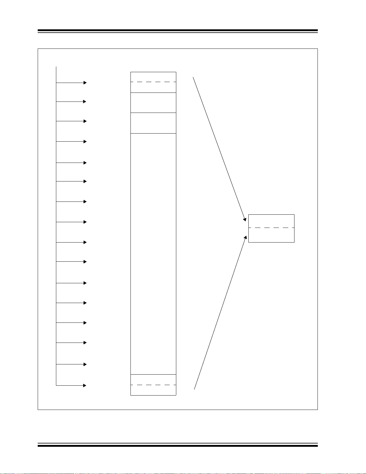
PIC18F2X1X/4X1X
FIGURE 5-5: DATA MEMORY MAP FOR PIC18F2410/4410 DEVICES
BSR<3:0>
= 0000
= 0001
= 0010
= 0011
= 0100
= 0101
= 0110
= 0111
= 1000
= 1001
= 1010
= 1011
= 1100
= 1101
= 1110
= 1111
Bank 0
Bank 1
Bank 2
Bank 3
Bank 4
Bank 5
Bank 6
Bank 7
Bank 8
Bank 9
Bank 10
Bank 11
Bank 12
Bank 13
Bank 14
Bank 15
Data Memory Map
00h
FFh
00h
FFh
00h
FFh
00h
FFh
00h
FFh
00h
FFh
00h
FFh
00h
FFh
00h
FFh
00h
FFh
00h
FFh
00h
FFh
00h
FFh
00h
FFh
00h
FFh
00h
FFh
Access RAM
Unused
Read 00h
Unused
GPR
GPR
GPR
SFR
000h
07Fh
080h
0FFh
100h
1FFh
200h
2FFh
300h
3FFh
400h
4FFh
500h
5FFh
600h
6FFh
700h
7FFh
800h
8FFh
900h
9FFh
A00h
AFFh
B00h
BFFh
C00h
CFFh
D00h
DFFh
E00h
EFFh
F00h
F7Fh
F80h
FFFh
When ‘a’ = 0:
The BSR is ignored an d the
Access Bank is used.
The first 128 bytes are
general purpose RAM
(from Bank 0).
The second 128 bytes are
Special Function Registers
(from Bank 15).
When ‘a’ = 1:
The BSR specifies the Ban k
used by the instruction.
Access Bank
Access RAM Low
Access RAM High
(SFRs)
00h
7Fh
80h
FFh
DS39636A-page 60 Preliminary 2004 Microchip Technology Inc.

PIC18F2X1X/4X1X
FIGURE 5-6: DATA MEMORY MAP FOR PIC18F2510/4510 DEVICES
BSR<3:0>
= 0000
= 0001
= 0010
= 0011
= 0100
= 0101
= 0110
= 0111
= 1000
= 1001
= 1010
= 1011
= 1100
= 1101
= 1110
= 1111
Bank 0
Bank 1
Bank 2
Bank 3
Bank 4
Bank 5
Bank 6
Bank 7
Bank 8
Bank 9
Bank 10
Bank 11
Bank 12
Bank 13
Bank 14
Bank 15
Data Memory Map
00h
FFh
00h
FFh
00h
FFh
00h
FFh
00h
FFh
00h
FFh
00h
FFh
00h
FFh
00h
FFh
00h
FFh
00h
Access RAM
Unused
Read 00h
FFh
00h
FFh
00h
FFh
00h
FFh
00h
FFh
00h
FFh
Unused
GPR
GPR
GPR
GPR
GPR
GPR
SFR
000h
07Fh
080h
0FFh
100h
1FFh
200h
2FFh
300h
3FFh
400h
4FFh
500h
5FFh
600h
6FFh
700h
7FFh
800h
8FFh
900h
9FFh
A00h
AFFh
B00h
BFFh
C00h
CFFh
D00h
DFFh
E00h
EFFh
F00h
F7Fh
F80h
FFFh
When ‘a’ = 0:
The BSR is ignored an d the
Access Bank is used.
The first 128 bytes are
general purpose RAM
(from Bank 0).
The second 128 bytes are
Special Function Registers
(from Bank 15).
When ‘a’ = 1:
The BSR specifies the Ban k
used by the instruction.
Access Bank
Access RAM Low
Access RAM High
(SFRs)
00h
7Fh
80h
FFh
2004 Microchip Technology Inc. Preliminary DS39636A-page 61

PIC18F2X1X/4X1X
FIGURE 5-7: DATA MEMORY MAP FOR PIC18F2515/2610/4515/4610 DEVICES
BSR<3:0>
= 0000
= 0001
= 0010
= 0011
= 0100
= 0101
= 0110
= 0111
= 1000
= 1001
= 1010
= 1011
= 1100
= 1101
= 1110
= 1111
Bank 0
Bank 1
Bank 2
Bank 3
Bank 4
Bank 5
Bank 6
Bank 7
Bank 8
Bank 9
Bank 10
Bank 11
Bank 12
Bank 13
Bank 14
Bank 15
Data Memory Map
00h
FFh
00h
FFh
00h
FFh
00h
FFh
00h
FFh
00h
FFh
00h
FFh
00h
FFh
00h
FFh
00h
FFh
00h
FFh
00h
FFh
00h
FFh
00h
FFh
00h
FFh
00h
FFh
Access RAM
GPR
GPR
GPR
GPR
GPR
GPR
GPR
GPR
GPR
GPR
GPR
GPR
GPR
GPR
GPR
GPR
SFR
000h
07Fh
080h
0FFh
100h
1FFh
200h
2FFh
300h
3FFh
400h
4FFh
500h
5FFh
600h
6FFh
700h
7FFh
800h
8FFh
900h
9FFh
A00h
AFFh
B00h
BFFh
C00h
CFFh
D00h
DFFh
E00h
EFFh
F00h
F7Fh
F80h
FFFh
When a = 0:
The BSR is ignor ed and the
Access Bank is used.
The first 128 bytes are
general purpose RAM
(from Bank 0).
The second 128 bytes are
Special Function Registers
(from Bank 15).
When a = 1:
The BSR specifie s th e Ba nk
used by the instruction.
Access Bank
Access RAM Low
Access RAM High
(SFRs)
00h
7Fh
80h
FFh
DS39636A-page 62 Preliminary 2004 Microchip Technology Inc.

PIC18F2X1X/4X1X
FIGURE 5-8: USE OF THE BANK SELECT REGISTER (DIRECT ADDRESSING)
Memory
7
0000
Bank Select
(2)
(1)
BSR
0011
0
000h
100h
200h
300h
Data
Bank 0
Bank 1
Bank 2
Bank 3
through
Bank 13
00h
FFh
00h
FFh
00h
FFh
00h
7
From Opcode
111 11 111
(2)
0
E00h
F00h
FFFh
Note 1: The Access RAM bit of the instruction can be used to force an override of the selected bank (BSR<3:0>) to
the registers of the Access Bank.
2: The MOVFF instruction embeds the entire 12-bit address in the instruction.
Bank 14
Bank 15
5.3.2 ACCESS BANK
While the use of the BSR with an embedded 8-bit
address allows users to address the entire range of
data memory, it also means th at the user must a lways
ensure that the correct bank is selected. Otherwise,
data may be read from or written to the wrong location.
This can be disastrous if a GPR is the intended target
of an operation, but an SFR is written to instead.
Verifying and/or changing the BSR for each read or
write to data memory can become very inefficient.
T o stre amline acces s for the most commonl y used data
memory locations, the data memory is configured with
an Access Bank, which allows users to access a
mapped block of memory without specifying a BSR.
The Access Bank consists of the first 128 bytes of
memory (00h-7Fh) in Bank 0 and the last 128 bytes of
memory (80h-FFh) in Block 15 . The lower half is known
as the “Access RAM” and is composed of GPRs. This
upper half is also where the device’s SFRs are
mapped. These two areas are mapped contiguously in
the Access Bank and can be addressed in a linear
fashion by an 8-bit address (Figure 5-5).
The Access Bank is used by core PIC18 instructions
that include the Access RAM bit (the ‘a’ parameter in
FFh
00h
FFh
00h
FFh
Using this “forced” addressing allows the instruction to
operate on a data address in a single cycle, without
updating the BSR first. For 8-bit addresses of 80h and
above, this means th at use rs can ev aluate an d operate
on SFRs more efficiently. The Access RAM below 80h
is a good place for da ta values that the user might need
to access rapidly, such as immediate computational
results or common program variables. Access RAM
also allows for faster and more code efficient context
saving and switching of variables.
The mapping of the Access Bank is slightly different
when the extended instruction set is enabled (XINST
configuration bit = 1). This is discussed in more detail
in Section 5.5.3 “Mapping the Access Bank in
Indexed Literal Offset Addressing Mode”.
5.3.3 GENERAL PURPOSE REGISTER FILE
PIC18 devices may have banked memory in the GPR
area. This is data RAM, which is available for use by all
instructions. GPRs start at the bottom of Bank 0
(address 000h) and grow upwards towards the bottom of
the SFR area. GPRs are not initialized by a Power-on
Reset and are unchanged on all other Resets.
the instruction). When ‘a’ is equal to ‘1’, the inst ru ct i on
uses the BSR and the 8-bit address included in the
opcode for the data memory address. When ‘a’ is ‘0’,
however, the instruction is forced to use the Access
Bank address map; the current value of the BSR is
ignored entirely.
2004 Microchip Technology Inc. Preliminary DS39636A-page 63

PIC18F2X1X/4X1X
5.3.4 SPECIAL FUNCTION REGISTERS
The Special Function Registers (SFRs) are registers
used by the CPU and p eripheral modul es for controllin g
the desired operation of the device. These reg isters are
implemented as static RAM. SFRs start at the top of
data memory (FF Fh) and extend downw ard to oc cupy
the top half of Bank 15 (F80h to FFFh). A list of these
registers is given in Table 5-1 and Table 5-2.
The SFRs can be classified into two sets: those associated with the “ core” de vice functi onali ty (ALU, R eset s
and interrupts) a nd those relate d to the periphe ral functions. The reset a nd in terrupt reg isters ar e d escribed in
their respective c hap ters , wh ile the ALU’s S tatus register is described later in this s ection. Register s related to
the operation of a peripheral feature are described in
the chapter for that peripheral.
The SFRs are typically distributed among the
peripherals whose fun cti ons th ey c ontr ol. U nus ed SFR
locations are unimplemented and read as ‘0’s.
TABLE 5-1: SPECIAL FUNCTION REGISTER MAP FOR PIC18F2X1X/4X1X DEVICES
Address Name Address Name Address Name Address Name
FFFh TOSU FDFh INDF2
FFEh TOSH FDEh POSTINC2
FFDh TOSL FDDh POSTDEC2
FFCh STKPTR FDCh PREINC2
FFBh PCLATU FDBh PLUSW2
FFAh PCLATH FDAh FSR2H FBAh CCP2CON F9Ah —
FF9h PCL FD9h FSR2L FB9h —
FF8h TBLPTRU FD8h STATUS FB8h BAUDCON F98h —
FF7h TBLPTRH FD7h TMR0H FB7h PWM1CON
FF6h TBLPTRL FD6h TMR0L FB6h ECCP1AS
FF5h TABLAT FD5h T0CON FB5h CVRCON F95h TRISD
FF4h PRODH FD4h —
FF3h PRODL FD3h OSCCON FB3h TMR3H F93h TRISB
FF2h INTCON FD2h HLVDCON FB2h TMR3L F92h TRISA
FF1h INTCON2 FD1h WDTCON FB1h T3CON F91h
FF0h INTCON3 FD0h RCON FB0h SPBRGH F90h —
FEFh INDF0
FEEh POSTINC0
FEDh POSTDEC0
FECh PREINC0
FEBh PLUSW0
(1)
FCFh TMR1H FAFh SPBRG F8Fh —
(1)
(1)
(1)
(1)
FCEh TMR1L FAEh RCREG F8Eh —
FCDh T1CON FADh TXREG F8Dh LATE
FCCh TMR2 FACh TXSTA F8Ch LATD
FCBh PR2 FABh RCSTA F8Bh LATC
FEAh FSR0H FCAh T2CON FAAh
FE9h FSR0L FC9h SSPBUF FA9h —
FE8h WREG FC8h SSPADD FA8h —
FE7h INDF1
FE6h POSTINC1
FE5h POSTDEC1
FE4h PREINC1
FE3h PLUSW1
(1)
(1)
(1)
(1)
(1)
FC7h SSPSTAT FA7h —
FC6h SSPCON1 FA6h —
FC5h SSPCON2 FA5h —
FC4h ADRESH FA4h —
FC3h ADRESL FA3h —
FE2h FSR1H FC2h ADCON0 FA2h IPR2 F82h PORTC
FE1h FSR1L FC1h ADCON1 FA1h PIR2 F81h PORTB
FE0h BSR FC0h ADCON2 FA0h PIE2 F80h PORTA
(1)
FBFh CCPR1H F9Fh IPR1
(1)
(1)
(1)
(1)
(2)
FBEh CCPR1L F9Eh PIR1
FBDh CCP1CON F9Dh PIE1
FBCh CCPR2H F9Ch —
FBBh CCPR2L F9Bh OSCTUNE
(2)
(3)
(3)
F99h —
F97h —
F96h TRISE
FB4h CMCON F94h TRISC
(2)
—
(2)
(2)
(2)
(2)
(2)
(2)
(2)
F8Ah LATB
F89h LATA
F88h —
F87h —
F86h —
F85h —
F84h PORTE
F83h PORTD
—
(2)
(2)
(2)
(2)
(2)
(2)
(2)
(2)
(2)
(2)
(2)
(2)
(2)
(3)
(3)
(3)
(3)
(3)
(3)
Note 1: This is not a physical register.
2: Unimplemented registers are read as ‘0’.
3: This register is not available on 28-pin devices.
DS39636A-page 64 Preliminary 2004 Microchip Technology Inc.

PIC18F2X1X/4X1X
TABLE 5-2: REGISTER FILE SUMMARY (PIC18F2X1X/4X1X)
File Name Bit 7 Bit 6 Bit 5 Bit 4 Bit 3 Bit 2 Bit 1 Bit 0
TOSU
TOSH Top-of-Stack High Byte (TOS<15:8>) 0000 0000 49, 54
TOSL Top-of-Stack Low Byte (TOS<7:0>) 0000 0000 49, 54
STKPTR STKFUL
PCLATU
PCLATH Holding Register for PC<15:8> 0000 0000 49, 54
PCL PC Low Byte (PC<7:0>) 0000 0000 49, 54
TBLPTRU
TBLPTRH Program Memory Table Pointer High Byte (TBLPTR<15:8>) 0000 0000 49, 77
TBLPTRL Program Memory Table Pointer Low Byte (TBLPTR<7:0>) 0000 0000 49, 77
TABLAT Program Memory Table Latch 0000 0000 49, 77
PRODH Product Register High Byte xxxx xxxx 49, 79
PRODL Product Register Low Byte xxxx xxxx 49, 79
INTCON GIE/GIEH PEIE/GIEL TMR0IE INT0IE RBIE TMR0IF INT0IF RBIF 0000 000x 49, 83
INTCON2 RBPU
INTCON3 INT2IP INT1IP
INDF0 Uses contents of FSR0 to address data memory – value of FSR0 not changed (not a physical register) N/A 49, 70
POSTINC0 Uses contents of FSR0 to addres s data memory – value of FSR0 post-incremented (not a physical register) N/A 49, 70
POSTDEC0 Uses contents of FSR0 to address data memory – value of FSR0 post-decremented (not a physical register) N/A 49, 70
PREINC0 Uses contents of FSR0 to address data memory – value of FSR0 pre-incremented (not a physical register) N/A 49, 70
PLUSW0 Uses contents of FSR0 to address data memory – value of FSR0 pre-incremented (not a physical register) –
FSR0H
FSR0L Indirect Data Memory Address Pointer 0 Low Byte xxxx xxxx 49, 70
WREG Working Register xxxx xxxx 49
INDF1 Uses contents of FSR1 to address data memory – value of FSR1 not changed (not a physical register) N/A 49, 70
POSTINC1 Uses contents of FSR1 to addres s data memory – value of FSR1 post-incremented (not a physical register) N/A 49, 70
POSTDEC1 Uses contents of FSR1 to address data memory – value of FSR1 post-decremented (not a physical register) N/A 49, 70
PREINC1 Uses contents of FSR1 to address data memory – value of FSR1 pre-incremented (not a physical register) N/A 49, 70
PLUSW1 Uses contents of FSR1 to address data memory – value of FSR1 pre-incremented (not a physical register) –
FSR1H
FSR1L Indirect Data Memory Address Pointer 1 Low Byte xxxx xxxx 50, 70
BSR
INDF2 Uses contents of FSR2 to address data memory – value of FSR2 not changed (not a physical register) N/A 50, 70
POSTINC2 Uses contents of FSR2 to addres s data memory – value of FSR2 post-incremented (not a physical register) N/A 50, 70
POSTDEC2 Uses contents of FSR2 to address data memory – value of FSR2 post-decremented (not a physical register) N/A 50, 70
PREINC2 Uses contents of FSR2 to address data memory – value of FSR2 pre-incremented (not a physical register) N/A 50, 70
PLUSW2 Uses contents of FSR2 to address data memory – value of FSR2 pre-incremented (not a physical register) –
FSR2H
FSR2L Indirect Data Memory Address Pointer 2 Low Byte xxxx xxxx 50, 70
STATUS
Legend: x = unknown , u = unchanged, — = unimplemented, q = value depends on condition
Note 1: The SBOREN bit is only available when the BOREN1:BOREN0 configuration bits = 01; otherwise, it is disabled and reads as ‘0’. See
2: These registers and/or bits are not implemen ted on 28-pin devices and are read as
3: The PLLEN bit is only available in specific oscillator configuration; otherwise it is disabled and reads as
4: The RE3 bit is only available when Master Clear Reset is disabled (MCLRE configuration bit = 0). Otherwise, RE3 reads as
5: RA6/RA7 and their associated latch and direction bits are individually configured as port pins based on various primary oscillator modes.
6: Bit 7 and bit 6 are cleared by user software or by a POR.
— — — Top-of-Stack Upper Byte (TOS<20:16>) ---0 0000 49, 54
(6)
— — — Holding Regi st er for PC<20:16> ---0 0000 49, 54
— — bit 21 Program Memory Table Pointer Upper Byte (TBLPTR<20:16>) --00 0000 49, 77
value of FSR0 offset by W
— — — — Indirect Data Memory Address Pointer 0 High ---- 0000 49, 70
value of FSR1 offset by W
— — — — Indirect Data Memory Address Pointer 1 High ---- 0000 50, 70
— — — — Bank Select Register ---- 0000 50, 59
value of FSR2 offset by W
— — — — Indirect Data Memory Address Pointer 2 High ---- 0000 50, 70
— — —NOVZDCC---x xxxx 50, 68
Section 4.4 “Brown-out Reset (BOR)”.
(6)
STKUNF
INTEDG0 INTEDG1 INTEDG2 —TMR0IP—RBIP1111 -1-1 49, 84
— SP4 SP3 SP2 SP1 SP0 00-0 0000 49, 55
—INT2IEINT1IE— INT2IF INT1IF 11-0 0-00 49, 85
‘0’. Reset values are shown for 40/44-pin devices;
individual unimplemented bits should be interpreted as ‘-’.
INTOSC Modes”.
read-only.
When disabled, these bits read as ‘0’.
‘0’. See Section 2.6.4 “PLL in
Value on
POR, BOR
N/A 49, 70
N/A 49, 70
N/A 50, 70
Details
on page:
‘0’. This bit is
2004 Microchip Technology Inc. Preliminary DS39636A-page 65

PIC18F2X1X/4X1X
TABLE 5-2: REGISTER FILE SUMMARY (PIC18F2X1X/4X1X) (CONTINUED)
File Name Bit 7 Bit 6 Bit 5 Bit 4 Bit 3 Bit 2 Bit 1 Bit 0
TMR0H Timer0 Register High Byte 0000 0000 50, 115
TMR0L Timer0 Register Low Byte xxxx xxxx 50, 115
T0CON TMR0ON T08BIT T0CS T0SE PSA T0PS2 T0PS1 T0PS0 1111 1111 50, 113
OSCCON IDLEN IRCF2 IRCF1 IRCF0 OSTS IOFS SCS1 SCS0 0100 q000 30, 50
HLVDCON VDIRMAG
WDTCON
RCON IPEN SBOREN
TMR1H Timer1 Register High Byte xxxx xxxx 50, 121
TMR1L Timer1 Register Low Bytes xxxx xxxx 50, 121
T1CON R D16 T1RUN T1CKPS1 T1CKPS0 T1OSCEN T1SYNC
TMR2 Timer2 Register 0000 0000 50, 124
PR2 Timer2 Period Register 1111 1111 50, 124
T2CON
SSPBUF SSP Receive Buffer/Transmit Regis ter xxxx xxxx 50, 159,
SSPADD SSP Address Register in I
SSPSTAT SMP CKE D/A
SSPCON1 WCOL SSPOV SSPEN CKP SSPM3 SSPM2 SSPM1 SSPM0 0000 0000 50, 153,
SSPCON2 GCEN ACKSTAT ACKDT ACKEN RCEN PEN RSEN SEN 0000 0000 50, 163
ADRESH A/D Result Register High Byte xxxx xxxx 51, 220
ADRESL A/D Result Register Low Byte xxxx xxxx 51, 220
ADCON0
ADCON1
ADCON2 ADFM
CCPR1H Captur e/C o mpar e/P WM R egis t er 1 High Byte xxxx xxxx 51, 130
CCPR1L Capture/Compare/PWM Register 1 Low Byte xxxx xxxx 51, 130
CCP1CON P1M1
CCPR2H Captur e/C o mpar e/P WM R egis t er 2 High Byte xxxx xxxx 51, 130
CCPR2L Capture/Compare/PWM Register 2 Low Byte xxxx xxxx 51, 130
CCP2CON
BAUDCON ABDOVF RCIDL
PWM1CON PRSEN PDC6
ECCP1AS ECCPASE ECCPAS2 ECCPAS1 ECCPAS0 PSSAC1 PSSAC0 PSSBD1
CVRCON CVREN CVROE CVRR CVRSS CVR3 CVR2 CVR1 CVR0 0000 0000 51, 227
CMCON C2OUT C1OUT C2INV C1INV CIS CM2 CM1 CM0 0000 0111 51, 221
TMR3H Timer3 Register High Byte xxxx xxxx 51, 127
TMR3L Timer3 Register Low Byte xxxx xxxx 51, 127
T3CON RD16 T3CCP2 T3CKPS1 T3CKPS0 T3CCP1 T3SYNC
Legend: x = unknown , u = unchanged, — = unimplemented, q = value depends on condition
Note 1: The SBOREN bit is only available when the BOREN1:BOREN0 configuration bits = 01; otherwise, it is disabled and reads as ‘0’. See
2: These registers and/or bits are not implemen ted on 28-pin devices and are read as
3: The PLLEN bit is only available in specific oscillator configuration; otherwise it is disabled and reads as
4: The RE3 bit is only available when Master Clear Reset is disabled (MCLRE configuration bit = 0). Otherwise, RE3 reads as
5: RA6/RA7 and their associated latch and direction bits are individually configured as port pins based on various primary oscillator modes.
6: Bit 7 and bit 6 are cleared by user software or by a POR.
— — — — — — —SWDTEN--- ---0 50, 247
— T2OUTPS3 T2OUTPS2 T2OUTPS1 T2OUTPS0 TMR2ON T2CKPS1 T2CKPS0 -000 0000 50, 123
— — CHS3 CHS2 CHS1 CHS0 GO/DONE ADON --00 0000 51, 211
— — VCFG1 VCFG0 PCFG3 PCFG2 PCFG1 PCFG0 --00 0qqq 51, 212
(2)
— — DC2B1 DC2B0 CCP2M3 CCP2M2 CCP2M1 CCP2M0 --00 0000 51, 129
Section 4.4 “Brown-out Reset (BOR)”.
individual unimplemented bits should be interpreted as ‘-’.
INTOSC Modes”.
read-only.
When disabled, these bits read as ‘0’.
— IRVST HLVDEN HLVDL3 HLVDL2 HLVDL1 HLVDL0 0-00 0101 50, 231
(1)
—RITO PD POR BOR 0q-1 11q0 42, 48, 92
TMR1CS T MR1ON 0000 0000 50, 117
2
C Slave Mode. SSP Baud Rate Reload Register in I2C Master Mode. 0000 0000 50, 160
PSR/WUA BF 0000 0000 50, 152,
— ACQT2 ACQT 1 ACQT0 ADCS2 ADCS1 ADCS0 0-00 0000 51, 213
P1M0
(2)
DC1B1 DC1B0 CCP1M3 CCP1M2 CCP1M1 CCP1M0 0000 0000 51, 129,
(2)
— SCKP BRG16 — WUE ABDEN 01-0 0-00 51, 194
PDC5
(2)
PDC4
(2)
PDC3
(2)
PDC2
(2)
(2)
PDC1
TMR3CS T MR3ON 0000 0000 51, 125
(2)
PDC0
PSSBD0
‘0’. Reset values are shown for 40/44-pin devices;
‘0’. See Section 2.6.4 “PLL in
Value on
POR, BOR
(2)
0000 0000 51, 146
(2)
0000 0000 51, 147
Details
on page:
160
161
162
137
‘0’. This bit is
DS39636A-page 66 Preliminary 2004 Microchip Technology Inc.

PIC18F2X1X/4X1X
TABLE 5-2: REGISTER FILE SUMMARY (PIC18F2X1X/4X1X) (CONTINUED)
File Name Bit 7 Bit 6 Bit 5 Bit 4 Bit 3 Bit 2 Bit 1 Bit 0
Value on
POR, BOR
SPBRGH EUSART Baud Rate Generator Register High Byte 0000 0000 51, 195
SPBRG EUSART Baud Rate Generator Register Low Byte 0000 0000 51, 195
RCREG EUSART Receive Register 0000 0000 51, 202
TXREG EUSART Transmit Register 0000 0000 51, 200
TXSTA CSRC TX9 TXEN SYNC SENDB BRGH TRMT TX9D 0000 0010 51, 192
RCSTA SPEN RX9 SREN CREN ADDEN FERR OERR RX9D 0000 000x 51, 193
IPR2 OSCFIP CMIP
PIR2 OSCFIF CMIF
PIE2 OSCFIE CMIE
IPR1 PSPIP
PIR1 PSPIF
PIE1 PSPIE
(2)
ADIP RCIP TXIP SSPIP CCP1IP TMR2IP TMR1IP 1111 1111 52, 90
(2)
ADIF RCIF TXIF SSPIF CCP1IF TMR2IF TMR1IF 0000 0000 52, 86
(2)
ADIE RCIE TXIE SSPIE CCP1IE TMR2IE TMR1IE 0000 0000 52, 88
OSCTUNE INTSRC PLLEN
(2)
TRISE
TRISD
(2)
IBF OBF IBOV PSPMODE — TRISE2 TRISE1 TRISE0 0000 -111 52, 108
PORTD Data Direction Control Register 1111 1111 52, 104
(3)
— — BCLIP HLVDIP TMR3IP CCP2IP 11-- 1111 52, 91
— — BCLIF HLVDIF TMR3IF CCP2IF 00-- 0000 52, 87
— — BCLIE HLVDIE TMR3IE CCP2IE 00-- 0000 52, 89
— TUN4 TUN3 TUN2 TUN 1 TUN0 0q-0 0000 27, 52
TRISC PORTC Data Direction Control Register 1111 1111 52, 101
TRISB PORTB Data Direction Control Register 1111 1111 52, 98
TRISA TRISA7
(2)
LATE
— — — — — PORTE Data Latch Register
(5)
TRISA6
(5)
Data Direction Control Register for PORTA 1111 1111 52, 95
---- -xxx 52, 107
(Read and Write to Data Latch)
(2)
LATD
PORTD Data Latch Register (Read and Write to Data Latch) xxxx xxxx 52, 104
LATC PORTC Data Latch Register (Read and Write to Data Latch) xxxx xxxx 52, 101
LATB PORTB Data Latch Register (Read and Write to Data Latch) xxxx xxxx 52, 98
LATA LATA7
PORTE
PORTD
(2)
— — — —RE3
RD7 RD6 RD5 RD4 RD3 RD2 RD1 RD0 xxxx xxxx 52, 104
(6)
LATA6
(6)
PORTA Data Latch Register (Read and Write to Data Latch) xxxx xxxx 52, 95
(4)
RE2
(2)
RE1
(2)
RE0
(2)
---- xxxx 52, 107
PORTC RC7 RC6 RC5 RC4 RC3 RC2 RC1 RC0 xxxx xxxx 52, 101
PORTB RB7 RB6 RB5 RB4 RB3 RB2 RB1 RB0 xxxx xxxx 52, 98
PORTA RA7
(5)
RA6
(5)
RA5 RA4 RA3 RA2 RA1 RA0 xx0x 0000 52, 95
Legend: x = unknown , u = unchanged, — = unimplemented,
Details
on page:
2004 Microchip Technology Inc. Preliminary DS39636A-page 67
PIC18F2X1X/4X1X
5.3.5 STATUS REGISTER
The St atus register , s hown in Register5-2, contains the
arithmetic status of the ALU. As with any other SFR, it
can be the operand for any instruction.
If the St atus regis ter is the dest ination for an instructio n
that affect s the Z, DC, C, OV or N bit s, the re sults of the
instruction are not written; instead, the status is
updated according to t he i nstruc tion pe rformed . Therefore, the result of an instru cti on w i th the Status register
as its destinatio n may be dif ferent than intended . As an
example, CLRF STATUS will set the Z bit and leave the
remaining status bits unchanged (‘000u u1uu’).
REGISTER 5-2: STATUS REGISTER
U-0 U-0 U-0 R/W-x R/W-x R/W-x R/W-x R/W-x
— — —NOVZDCC
bit 7 bit 0
bit 7-5 Unimplemented: Read as ‘0’
bit 4 N: Negative bit
This bit is used for signed arithmetic (2’s complement). It indicates whether the result was
negative (ALU MSB = 1).
1 = Result was negative
0 = Result was positive
bit 3 OV: Overflow bit
This bit is used for signed arithmetic (2’s complement). It indicates an overflow of the 7-bit
magnitude which causes the sign bit (bit 7 of the result) to change state.
1 = Overflow occurred for signed arithmetic (in this arithmetic operation)
0 = No overflow occurred
bit 2 Z: Zero bit
1 = The result of an arithmetic or logic operation is zero
0 = The result of an arithmetic or logic operation is not zero
bit 1 DC: Digit carry/bor row
For ADDWF, ADDLW, SUBLW and SUBWF instructions:
1 = A carry-out from the 4th low-order bit of the result occurred
0 = No carry-out from the 4th low-order bit of the result
Note: For borrow,
2’s complement of the second operand. For rotate (RRF, RLF) instructions, this bit
is loaded with either bit 4 or bit 3 of the source register.
bit 0 C: Carry/borrow bit
For ADDWF, ADDLW, SUBLW and SUBWF instructions:
1 = A carry-out from the Most Significant bit of the result occurred
0 = No carry-out from the Most Significant bit of the result occurred
Note: For borrow,
2’s complement of the second operand. For rotate (RRF, RLF) instructions, this bit
is loaded with either the high or low-order bit of the source register.
bit
the polarity is reversed. A subtraction is executed by adding the
the polarity is reversed. A subtraction is executed by adding the
It is recommended that only BCF, BSF, SWAPF, MOVFF
and MOVWF instructions are used to alter the Status
register , b ecaus e thes e ins tructi ons d o not af fect t he Z,
C, DC, OV or N bits in the Status register.
For other instructions that do not affect status bits, see
the instruction set summaries in Table 23-2 and
Table 23-3.
Note: The C and DC bits operate as the borrow
and digit borrow bits, respectively, in
subtraction.
Legend:
R = Readable bit W = Writable bit U = Unimplemented bit, read as ‘0’
-n = Value at POR ‘1’ = Bit is set ‘0’ = Bit is cleared x = Bit is unknown
DS39636A-page 68 Preliminary 2004 Microchip Technology Inc.

PIC18F2X1X/4X1X
5.4 Data Addressing Modes
Note: The execution of some instructions in the
core PIC18 instruction set are changed
when the PIC18 extended instruction set is
enabled. See Section 5.5 “Data Memory
and the Extended Instruction Set” for
more information.
The data memory space can be addr essed in se veral
ways. For most instructions, the addressing mode is
fixed. Other instructions may use up to three modes,
depending on whic h operands are used and whe ther or
not the extended instruction set is enabled.
The addressing modes are:
• Inherent
• Literal
•Direct
•Indirect
An additional addressing mode, Indexed Literal Offset,
is available when the extended instruction set is
enabled (XINST configuration bit = 1). Its operation is
discussed in greater detail in Section 5.5.1 “Indexed
Addressing with Literal Offset”.
5.4.1 INHERENT AND LITERAL ADDRESSING
Many PIC18 control instructions do not need any
argument at all; they either perform an operation that
globally affects the device or they operate implicitly on
one register. This addressing mode is known as
Inherent Addressing. Exa mp les includ e SLEEP, RESET
and DAW.
Other instructions work in a similar way but require an
additional explicit argument in the opcode. This is
known as Literal Addressing mode because they
require some literal value as an argument. Examples
include ADDLW and MOVLW which, respectively, add or
move a literal value to the W register. Other examples
include CALL and GOTO, which include a 20-bit
program memory address.
5.4.2 DIRECT ADDRESSING
Direct addressing specifies all or part of the source
and/or destination address of the operation within the
opcode itself. The options are specified by the
arguments accompanying the instruction.
In the core PIC18 inst ruct ion se t, bit-ori ented and by teoriented instructions use some version of direct
addressing by default. All of these instructions include
some 8-bit literal address as their Least Significant
Byte. This address spec ifies either a re gister address in
one of the banks of d ata RAM ( Section 5.3.3 “General
Purpose Register File”) or a location in the Access
Bank (Section 5.3.2 “Access Bank”) as the data
source for the instruction.
The Access RAM bit ‘a’ determines how the addre ss i s
interpreted. When ‘a’ is ‘1’, the contents of the BSR
(Section 5.3.1 “Bank Select Register (BSR)”) are
used with the address t o determin e the comple te 12-bit
address of the reg ister. When ‘a’ is ‘0’, the address is
interpreted as being a register in the Access Bank.
Addressing that uses the Access RAM is sometimes
also known as Direct Forced Addressing mode.
A few instructions, such as MOVFF, include the entire
12-bit address (either source or destination) in their
opcodes. In these cases, the BSR is ignored entirely.
The destination of the operati on’s results is determined
by the destination bit ‘d ’. Wh en ‘d’ is ‘1’, the results are
stored back in t he s o ur c e re g is ter, over wr iti n g i ts or i gi nal contents. When ‘d’ is ‘0’, the results are stored in
the W register. Instructions without the ‘d’ argument
have a destin ation tha t is i mplicit in the inst ruction; their
destination is either the target register being operated
on or the W register.
5.4.3 INDIRECT ADDRESSING
Indirect addressi ng allows the user to acces s a locatio n
in data memory without giving a fixed address in the
instruction. This is done by using File Select Registers
(FSRs) as pointers to the location s to be read or written
to. Since the FSRs are themselves located in RAM as
Special File Reg isters , they can also be directl y mani pulated under program control. This makes FSRs very
useful in imp lem ent ing data str uct ures , s uch as tabl es
and arrays in data memory.
The registers for indirect addressing are also
implemented with Indirect File Operands (INDFs) that
permit automatic mani pulati on of the poi nter val ue wi th
auto-incrementing, auto-decrementing or offsetting
with another va lue . Th is al lo ws f or e fficient code, usin g
loops, such as the example of clearing an entire RAM
bank in Example 5-5.
EXAMPLE 5-5: HOW TO CLEAR RAM
(BANK 1) USING
INDIRECT ADDRESSING
LFSR FSR0, 100h ;
NEXT CLRF POSTINC0 ; Clear INDF
; register then
; inc pointer
BTFSS FSR0H, 1 ; All done with
; Bank1?
BRA NEXT ; NO, clear next
CONTINUE ; YES, continue
2004 Microchip Technology Inc. Preliminary DS39636A-page 69

PIC18F2X1X/4X1X
5.4.3.1 FSR Registers and the INDF
Operand
At the core of indirect addressing are three sets of
registers: FSR0, FSR1 and FSR2. Each represents a
pair of 8-bit registers, FSRnH and FSRnL. The four
upper bits of the FSRnH register are not used so each
FSR pair holds a 12-bi t va lue. T his repre sen ts a value
that can address the entire range of the data memory
in a linear fashion. The FSR register pairs, then, serve
as pointers to data memory locations.
Indirect addressing is accomplished with a set of
Indirect File Operands, INDF0 through INDF2. These
can be thought of as “virtual” registers: they are
mapped in the SFR space but are not physically implemented. Reading or writin g to a particular INDF reg ister
actually accesses its corresponding FSR register pair.
A read from INDF1, for example, reads the data at the
address indi cated by FSR 1H:FSR1L. Instructi ons that
use the IND F registers as operands actual ly use the
contents of th eir co rrespon ding FS R as a poin ter to th e
instruction’s target. The INDF operand is just a
convenient way of using the pointer.
Because indirec t addre ssing us es a full 1 2-bit a ddress ,
data RAM banking is not necessary. Thus, the current
contents of the BSR and the Access RAM bit have no
effect on determining the target address.
5.4.3.2 FSR Registers and POSTI NC,
POSTDEC, PREINC and PLUSW
In addition to the IND F operand, eac h FSR register pair
also has four additional indirect operands. Like INDF,
these are “virtual” registers that cannot be indirectly
read or written to. Accessing these registers actually
accesses the associated FSR register pair, but also
performs a specifi c action on it s stored v alue. They ar e:
• POSTDEC: accesses the FSR value, then
automatically decrements it by 1 afterwards
• POSTINC: accesses the FSR valu e, then
automatically increments it by 1 afterwards
• PREINC: increments the FSR value by 1, then
uses it in the operation
• PLUSW: adds the signed value of the W register
(range of -127 to 128) t o that of th e FSR and uses
the new value in the operation.
In this context, accessing an INDF register uses the
value in the FSR registers with out changing the m. Similarly , acces sing a PLUSW register giv es the FSR v alue
offset by that in the W registe r; neit her value is ac tuall y
changed in the operation. Accessing the other virtual
registers changes the value of the FSR registers.
Operations on the FSRs with POSTDEC, POSTINC
and PREINC affect the entire register pair; that is, rollovers of the FSRnL register from FFh to 00h ca rry over
to the FSRnH register. On the other hand, results of
these operations do not change the value of any flags
in the Status register (e.g., Z, N, OV, etc.).
FIGURE 5-9: INDIRECT ADDRESSING
Using an instruction with one of the
indirect addressing registers as the
operand....
...uses the 12-bit address stored in
the FSR pair associated with that
register....
xxxx111 0 11001 100
...to determine the data memory
location to be used in that operation.
In this case, the FSR1 pair contains
ECCh. This means the contents of
location ECCh will be added to that
of the W register and stored back in
ECCh.
ADDWF, INDF1, 1
FSR1H:FSR1L
000h
Bank 0
100h
200h
300h
07
7
0
E00h
F00h
FFFh
Bank 1
Bank 2
Bank 3
through
Bank 13
Bank 14
Bank 15
Data Memory
DS39636A-page 70 Preliminary 2004 Microchip Technology Inc.

PIC18F2X1X/4X1X
The PLUSW register can be used to implement a form
of indexed addressing in t he data memory space. By
manipulating the value in the W register, users can
reach addresses that are fixed offsets from pointer
addresses. In some applications, this can be used to
implement some powerful program control structure,
such as softw are stacks, insi de of data memory.
5.4.3.3 Operations by FSRs on FSRs
Indirect addressing operations that target other FSRs
or virtual registers represent special cases. For example, using an FSR to point to on e of the virtual regis ters
will not result in successful operations. As a specific
case, assume that FSR0H:FSR0L contains FE7h, the
address of INDF1. Attempts to read the value of the
INDF1 using INDF0 as an operand will return 00h.
Attempts to write to INDF1 using I NDF0 as the operan d
will result in a NOP.
On the other ha nd, u sing the v irtual reg isters to w rite to
an FSR pair may n ot oc cur as plan ned. I n t hese cases ,
the value will be written to the FSR p air bu t withou t any
incrementing or decrementing. Thus, writing to INDF2
or POSTDEC2 will write the same value to the
FSR2H:FSR2L.
Since the FSRs are physical registers mapped in the
SFR space, they can be manipulated through all direct
operations. Users should proceed cautiously when
working on these registers, particularly if their code
uses indirect addressing.
Similarly, operations by indirect addressing are generally permitted on all other SFRs. U sers shoul d exercise
the appropriate caution that they do not inadvertently
change settings that might affect the operation of the
device.
5.5 Data Memory and the Extended Instruction Set
Enabling the PIC18 extended instruction set (XINST
configuration bit = 1) significantly changes certain
aspects of data memory and its addressing. Specifically, the use of the Access Bank for many of the core
PIC18 instructions is different; this is due to the
introduction of a new addressing mode for the data
memory space.
What does not change is just as im po rtant. The size of
the data memory space is unchanged, as well as its
linear addressing. The SFR map remains the same.
Core PIC18 instructions can still operate in both Direct
and Indirect Addressing mode; inherent and literal
instructions do not change at all. Indirect addressing
with FSR0 and FSR1 also remain unchanged.
5.5.1 INDEXED ADDRESSING WITH LITERAL OFFSET
Enabling the PIC18 extended instruction set changes
the behavior of indirect addressing using the FSR2
register pair within access RAM. Under the proper
conditions, instruc tions that us e the Access Ban k – that
is, most bit-oriented and byte-oriented instructions –
can invoke a form of indexed addressing using an
offset specified in the in structi on. Thi s spe cial addr ess ing mode is known as Indexed Addressing with Literal
Offset, or Indexed Literal Offset mode.
When using the extended instruction set, this
addressing mode requires the following:
• The use of the Access Bank is forced (‘a’ = 0);
and
• The file addres s arg um ent is less than or equa l to
5Fh.
Under these conditions, the file address of the instruction is not interpreted as the lower byte of an address
(used with the BSR in direct addre ssing), or as an 8-bit
address in the Access Bank. Instead, the value is
interpreted as an offset value to an address pointer,
specified by FSR2. The offset and the contents of
FSR2 are added to obtain the target address of the
operation.
5.5.2 INSTRUCTIONS AFFECTED BY INDEXED LITERAL OFFSET MODE
Any of the core PIC18 instructions that can use direct
addressing are potentially affected by the Indexed Literal
Offset Addressing mode. This includes all byte-oriented
and bit-oriented instructions, or almost one-half of the
standard PIC18 instruction set. Instructions that only use
Inherent or Literal Addressing modes are unaffected.
Additionally, byte-oriented and bit-oriented instructions
are not affected if they do not use the Access Bank
(Access RAM bit is ‘1’), or include a fi le ad dres s of 60 h
or above. Instructions meeting these criteria will
continue to execute as before. A comparison of the
different possible addressing modes when the
extended instruction set is enabled is shown in
Figure 5-10.
Those who desire to use bit-oriented or byte-oriented
instructions in the Indexed Literal Offset mode should
note the changes to assembler syntax for this mode.
This is described in more detail in Section 23.2.1
“Extended Instruction Syntax”.
2004 Microchip Technology Inc. Preliminary DS39636A-page 71
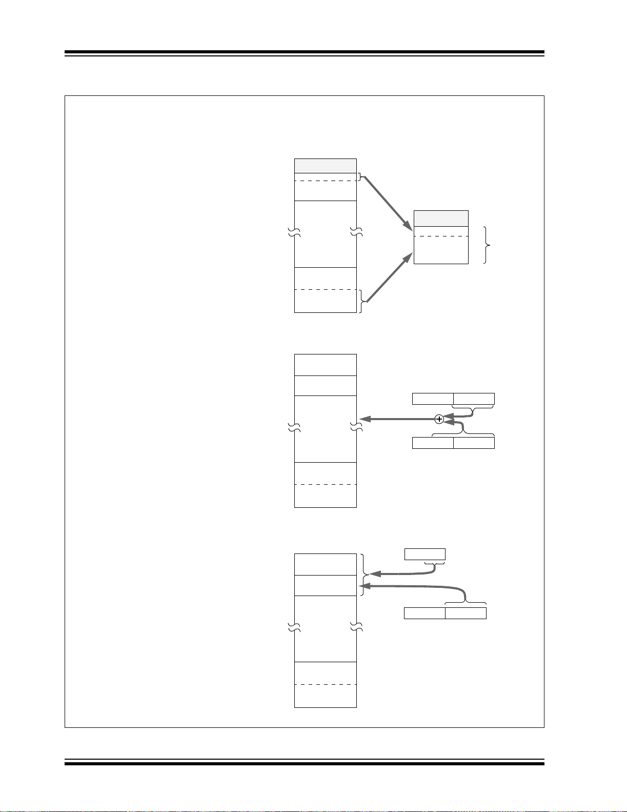
PIC18F2X1X/4X1X
FIGURE 5-10: COMPARING ADDRESSING OPTIONS FOR BIT-ORIENTED AND
BYTE-ORIENTED INSTRUCTIONS (EXTENDED INSTRUCTION SET ENABLED)
EXAMPLE INSTRUCTION: ADDWF, f, d, a (Opcode: 0010 01da ffff ffff)
When ‘a’ = 0 and f ≥ 60h:
The instruction executes in
Direct Forced mode. ‘f’ is interpreted as a location in the
Access RAM between 060h
and 0FFh. This is the sam e as
locations 060h to 07Fh
(Bank 0) and F80h to FFFh
(Bank 15) of data memory.
Locations below 60h are not
available in this addressing
mode.
When ‘a’ = 0 and f ≤ 5Fh:
The instruction executes in
Indexed Literal Offset mode. ‘f’
is interpreted as an offset to the
address value in FSR2. The
two are added together to
obtain the address of the target
register for the instruction. The
address can be anywhere in
the data memory space.
Note that in this mode, the
correct syntax is now:
ADDWF [k], d
where ‘k’ is the same as ‘f’.
000h
060h
080h
100h
F00h
F80h
FFFh
000h
080h
100h
F00h
F80h
FFFh
Bank 0
Bank 1
through
Bank 14
Bank 15
SFRs
Data Memory
Bank 0
Bank 1
through
Bank 14
Bank 15
SFRs
Data Memory
00h
60h
80h
Access RAM
FSR2H FSR2L
FFh
ffffffff001001da
Valid range
for ‘f’
BSR
00000000
ffffffff001001da
When ‘a’ = 1 (all values of f):
The instruction executes in
Direct mode (also known as
Direct Long mode). ‘f’ is interpreted as a location in one of
the 16 banks of the data
memory space. The bank is
designated by the Bank Sel ect
000h
080h
100h
Bank 0
Bank 1
through
Bank 14
Register (BSR). The address
can be in any implemented
bank in the data memory
space.
DS39636A-page 72 Preliminary 2004 Microchip Technology Inc.
F00h
F80h
FFFh
Bank 15
SFRs
Data Memory

PIC18F2X1X/4X1X
5.5.3 MAPPI NG THE ACCESS BANK IN INDEXED LITERAL OFFSET ADDRESSING MODE
The use of Indexed Literal Offset Addressing mode
effectively changes how the first 96 locations of access
RAM (00h to 5Fh) are m ap ped . R at her tha n c on t ai nin g
just the contents of the bottom half of Bank 0, this mode
maps the contents from Bank 0 and a user defined
“window” that can be located anywhere in the data
memory space. The value of FSR2 establishes the
lower boundary of the addresses mapped into the
window, while the upper boundary is defined by FSR2
Remapping of the Access Bank applies only to operations using the Indexed Literal Offset Addressing
mode. Operations that us e the BSR (Access RAM bit is
‘1’) will continue to use direct addressing as before.
5.6 PIC18 Instruction Execution and the Extended Instruction Set
Enabling the extended instruction set adds eight
additional commands to the existing PIC18 instruction
set. These instructions are executed as described in
Section 23.2 “Extended Instruction Set”.
plus 95 (5Fh). Addresses in the Access RAM above
5Fh are mapped as previously described (see
Section 5.3.2 “Access Bank”). An example of Access
Bank remapping in this addressing mode is shown in
Figure 5-11.
FIGURE 5-11: REMAPPING THE ACCESS BANK WITH INDEXED LITERAL OFFSET
ADDRESSING
Example Situation:
ADDWF f, d, a
FSR2H:FSR2L = 120h
Locations in the region
from the FSR2 pointer
(120h) to the pointer plus
05Fh (17Fh) are mapped
to the bottom of the
Access RAM (000h-05Fh).
Locations in Bank 0 from
060h to 07Fh are mapped,
as usual, to the middle of
the Access Bank.
Special File Registers at
F80h through FFFh are
mapped to 80h through
FFh, as usual.
Bank 0 addresses below
5Fh can still be addressed
by using the BSR.
000h
05Fh
07Fh
100h
120h
17Fh
200h
F00h
F80h
FFFh
Bank 0
Bank 0
Bank 1
Window
Bank 1
Bank 2
through
Bank 14
Bank 15
SFRs
Data Memory
Bank 1 “Window”
Bank 0
SFRs
Access Bank
00h
5Fh
7Fh
80h
FFh
2004 Microchip Technology Inc. Preliminary DS39636A-page 73

PIC18F2X1X/4X1X
NOTES:
DS39636A-page 74 Preliminary 2004 Microchip Technology Inc.

PIC18F2X1X/4X1X
6.0 FLASH PROGRAM MEMORY
In PIC18F2X1X/4X1X devices , the program me mory i s
implemented as read-o nly Flas h memory. It is read able
over the entire VDD range during normal operation. A
read from program memory is exec uted on one byte at
a time.
6.1 Table Reads
For PIC18 devices, there are two operations that allow
the processor to move bytes between the program
memory space and the data RAM: table read (TBLRD)
and table write (TBLWT).
Table read operations retrieve data from program
memory and place it into the data RAM space.
Figure 6-1 shows the operation of a table read with
program memory and dat a RAM.
The program memory space is 16 bits wide, while the
data RAM space is 8 bits wide. Table reads and table
writes move data between these two memory spaces
through an 8-bit register, TABLAT.
FIGURE 6-1: TABLE READ OPERATION
Table reads work with byte entities. A table block
containing data, rather than program instructions, is not
required to be word-aligned. Therefore, a table block can
start and end at any byte address.
Because the program memory cannot be written to or
erased under normal operation, the TBLWT operation is
not discussed here.
Note 1: Although it cannot be used in
PIC18F2X1X/4X1X devices in normal
operation, the TBLWT instruction is still
implemented in the instruction set.
Executing the instruction takes two
instruction cycles, but effectively results
in a NOP.
2: The TBLWT instruction is available only in
programming modes and is used during
In-Circuit Serial Programming™ (ICSP™).
Instruction: TBLRD*
Table Pointer
TBLPTRU
Note 1: Table Pointer register points to a byte in program memory.
TBLPTRH TBLPTRL
(1)
Program Memory
(TBLPTR)
Program Memory
Table Latch (8-bit)
TABLAT
2004 Microchip Technology Inc. Preliminary DS39636A-page 75

PIC18F2X1X/4X1X
6.2 Control Registers
Two control registers are used in conjunction with the
TBLRD instruction: the TABLAT register and the
TBLPTR register set.
6.2.1 TABLAT – TABLE LATCH REGISTER
The Table Latch (TABLAT) is an 8-bit register mapped
into the SFR space. The Table Latch register is used to
hold 8-bit data during data transfers between program
memory and data RAM.
6.2.2 TBLPTR – TABLE POINTER REGISTER
The Table Pointer regi st er (TBL PTR) addresses a byte
within the program memory. It is comprised of three
SFR registers: Table Pointer Upper Byte, T a ble Poin ter
High Byte and Table Pointer Low Byte
(TBLPTRU:TBLPTRH:TBLPTRL). Only the lower six
bits of TBLPTRU are used with TBLPTRH and
TBLPTRL, to form a 22-bit wide pointer.
The contents of TBLP TR indic ate a locat ion in progra m
memory space. The low-order 21 bits allow the device
to address the full 2 Mbyte s of program memory sp ace.
The 22nd bit allows access to the configuration space,
including the device ID, user ID locations and the
configuration bit s.
The TBLPTR register set is updated when executing a
TBLRD in one of four ways, based on the instruction’s
arguments. These are detailed in Table 6-1. These
operations on the TBLPTR only affect the low-order
21 bits.
When a TBLRD is executed, all 22 bits of the TBLPTR
determine which byte is read from program memory
into T AB LAT.
TABLE 6-1: TABLE POINTER
OPERATIONS WITH TBLRD
INSTRUCTIONS
Example Operation on Table Pointer
TBLRD* TBLPTR is not modified
TBLRD*+ TBLPTR is incremented after the read
TBLRD*- TBLPTR is decremented after the read
TBLRD+* TBLPTR is increm ent ed be fore th e read
6.3 Reading the Flash Program Memory
The TBLRD instruction is used to retrieve data from
program memory and place it into data RAM. Table
reads from program memory are performed one byte at
a time.
TBLPTR points to a byte address in program space.
Executing TBLRD places the byte pointed to into
TABLAT. In addition, TBLPTR can be modified
automatically for the next table read operation.
The internal program memory is typically organize d by
words. The Least Significant b it of th e address selects
between the high and low bytes of the word. Figure 6-2
shows the interface between the internal program
memory and the TABLA T.
A typical method for reading data from program memory
is shown in Example 6-1.
FIGURE 6-2: READS FROM FLASH PROGRAM MEMORY
Program Memory
(Even Byte Address)
Instruction Register
(IR)
DS39636A-page 76 Preliminary 2004 Microchip Technology Inc.
FETCH
(Odd Byte Address)
TBLPTR = xxxxx1
TBLRD
TBLPTR = xxxxx0
TABLAT
Read Register
PIC18F2X1X/4X1X
EXAMPLE 6-1: READING A FLASH PROGRAM MEMORY WORD
MOVLW CODE_ADDR_UPPER ; Load TBLPTR with the base
MOVWF TBLPTRU ; address of the word
MOVLW CODE_ADDR_HIGH
MOVWF TBLPTRH
MOVLW CODE_ADDR_LOW
MOVWF TBLPTRL
READ_WORD
TBLRD*+ ; read into TABLAT and increment
MOVF TABLAT, W ; get data
MOVWF WORD_EVEN
TBLRD*+ ; read into TABLAT and increment
MOVF TABLAT, W ; get data
MOVF WORD_ODD
TABLE 6-2: REGISTERS ASSOCIATED WITH READING PROGRAM FLASH MEMORY
Name Bit 7 Bit 6 Bit 5 Bit 4 Bit 3 Bit 2 Bit 1 Bit 0
TBLPTRU — — bit 21 Program Memory Table Pointer Upper Byte
(TBLPTR<20:16>)
TBPLTRH Program Memory Table Pointer High Byte (TBLPTR<15:8>) 49
TBLPTRL Program Memory Table Pointer Low Byte (TBLPTR<7:0>) 49
TABLAT Program Memory Table Latch 49
Legend: — = unimplemented, read as ‘0’. Shaded cells are not used during Flash access.
Reset
Values on
Page
49
2004 Microchip Technology Inc. Preliminary DS39636A-page 77

PIC18F2X1X/4X1X
NOTES:
DS39636A-page 78 Preliminary 2004 Microchip Technology Inc.

PIC18F2X1X/4X1X
7.0 8 x 8 HARDWARE MULTIPLIER
7.1 Introduction
All PIC18 devices include an 8 x 8 hardware multiplier
as part of the ALU. The multiplier pe rforms an unsigned
operation and yields a 16-bit result that is stored in the
product register pair, PRODH:PRODL. The multiplier’s
operation does not affect any flags in the Status
register.
Making multiplication a hardware operation allows it to
be completed in a s ingle instruction cycle. This has the
advantages of higher computational throughput and
reduced code size for multiplication algorithms and
allows the PIC18 devices to be used in many applications previously reserved for digital signal processors.
A comparison of various hardware and software
multiply operations, along with the savings in memory
and execution time, is shown in Table 7-1.
7.2 Operation
Example 7-1 shows the instruction sequence for an 8 x 8
unsigned multiplication. Only one instruction is required
when one of the arguments is already loaded in the
WREG register.
Example 7-2 shows the s equence to d o an 8 x 8 si gned
multiplication. To account for the sign bits of the arguments, each argument’s Most Significant bit (MSb) is
tested and the appropriate subtractions are done.
EXAMPLE 7-1: 8 x 8 UNSIGNED
MULTIPLY ROUTINE
MOVF ARG1, W ;
MULWF ARG2 ; ARG1 * ARG2 ->
; PRODH:PRODL
EXAMPLE 7-2: 8 x 8 SIGNED MULTIPLY
ROUTINE
MOVF ARG1, W
MULWF ARG2 ; ARG1 * ARG2 ->
; PRODH:PRODL
BTFSC ARG2, SB ; Test Sign Bit
SUBWF PRODH, F ; PRODH = PRODH
; - ARG1
MOVF ARG2, W
BTFSC ARG1, SB ; Test Sign Bit
SUBWF PRODH, F ; PRODH = PRODH
; - ARG2
TABLE 7-1: PERFORMANCE COMPARISON FOR VARIOUS MULTIPLY OPERATIONS
Routine Multiply Method
8 x 8 unsigned
8 x 8 signed
16 x 16 unsigned
16 x 16 signed
Without hardware multiply 13 69 6.9 µs27.6 µs69 µs
Hardware multiply 1 1 100 ns 400 ns 1 µs
Without hardware multiply 33 91 9.1 µs36.4 µs91 µs
Hardware multiply 6 6 600 ns 2.4 µs6 µs
Without hardware multiply 21 242 24.2 µs96.8 µs 242 µs
Hardware multiply 28 28 2.8 µs 11.2 µs28 µs
Without hardware multiply 52 254 25.4 µs 102.6 µs 254 µs
Hardware multiply 35 40 4.0 µs16.0 µs40 µs
Program
Memory
(Words)
Cycles
(Max)
@ 40 MHz @ 10 MHz @ 4 MHz
Time
2004 Microchip Technology Inc. Preliminary DS39636A-page 79

PIC18F2X1X/4X1X
Example 7-3 shows the sequence to do a 16 x 16
unsigned multiplication. Equation 7-1 shows the
algorithm that is used . The 32-bit re sult is st ored in four
registers (RES3:RES0).
EQUATION 7-1: 16 x 16 UNSIGNED
DS39636A-page 80 Preliminary 2004 Microchip Technology Inc.

PIC18F2X1X/4X1X
8.0 INTERRUPTS
The PIC18F2X1X/4X1X devic es have multiple in terrupt
sources and an interrupt priority feature that allows
most interrupt sources to be assigned a high priority
level or a low priority level. The high priority interrupt
vector is at 0008h and the lo w priority interrup t vector is
at 0018h. High priority interrupt event s will int errupt any
low priority interrupts that may be in progress.
There are ten registers which are used to control
interrupt operation. These registers are:
• RCON
•INTCON
• INTCON2
• INTCON3
• PIR1, PIR2
• PIE1, PIE2
• IPR1, IPR2
It is recommended that the Microchip header files
supplied with MPLAB
names in these registers. This allows the assembler/
compiler to automatical ly ta ke care of the pla ceme nt of
these bits within the specified register.
In genera l, int errupt sour ces h ave th ree bits to cont rol
their operation. They are:
• Flag bit to indicate that an interrupt event
occurred
• Enable bit that allows program execution to
branch to the interrupt vector address when the
flag bit is set
• Priority bit to select high priority or low priority
The interrupt priority feature is enabled by setting the
IPEN bit (RCON<7>). When interrupt priority is
enabled, there are two bits which enable interrupts
globally . Setti ng the GIEH bit (INTC ON<7>) enable s all
interrupts that have the priority bit set (high priority).
Setting the GIEL bit (INTCON<6>) enables all
interrupts that have the prio rity bit cleared ( low priority ).
When the interrupt flag, enable bit and appropriate
global interrupt enable bit are set, the interrupt wi ll vector immediately to addres s 000 8h or 0018h, depen ding
on the priority bit setting. Individual interrupts can be
disabled through their corresponding enable bits.
®
IDE be used for the symb olic bit
When the IPEN bit is cleared (default state), the
interrupt priority feature is disabled and interrupts are
compatible with PICmicro
Compatibilit y mode, the in terrupt prior ity bits for each
source have no effect. INTCON<6> is the PEIE bit,
which enables/disab les all periph eral interrupt s ources.
INTCON<7> is the GIE bit, which enables/disables all
interrupt sources. All interrupts branch to address
0008h in Compatibility mode.
When an interrupt is responded to, the global interrupt
enable bit is cleared to disable further interrupts. If the
IPEN bit is cleared, this is the GIE bit. If interru pt priority
levels are used, this wi ll be either the GIEH or G IEL bit.
High priority interrupt sources can interrupt a low
priority interrupt. Low priority interrupts are not
processed while high priority interrupts are in progress.
The return address is pushed onto the stack and the
PC is loaded with the interrupt vector address (0008h
or 0018h). Once in the Interrupt Service Routine, the
source(s) of the interrupt can be determined by polling
the interrupt flag bits. The interrupt flag bits must be
cleared in software before re-enabling interrupts to
avoid recursive interrupts.
The “return from interrupt” instruction, RETFIE, exits
the interrupt routine and set s the GIE bit (GIEH or GI EL
if priority levels are used), which re-enables interrupts.
For external interrupt events, such as the INT pins or
the PORTB input chang e interrupt, the i nterrupt latenc y
will be three to four instruction cycles. The exact
latency is the same for one or two-cycle instructions.
Individual interrupt flag bits are set, regardless of the
status of their corresponding enable bit or the GIE bit.
Note: Do not use the MOVFF instruction to modify
any of the interrupt control registers while
any interrupt is enabled. Doing so may
cause erratic microcontroller behavior.
®
mid-range devices. In
2004 Microchip Technology Inc. Preliminary DS39636A-page 81

PIC18F2X1X/4X1X
FIGURE 8-1: PIC18 INTERRUPT LOGIC
SSPIF
SSPIE
SSPIP
ADIF
ADIE
ADIP
RCIF
RCIE
RCIP
Additional Peripheral Interrupts
High Priority Interrupt Generation
Low Priority Interrupt Generation
SSPIF
SSPIE
SSPIP
ADIF
ADIE
ADIP
RCIF
RCIE
RCIP
Additional Peripheral Interrupts
IPEN
TMR0IF
TMR0IE
TMR0IP
RBIF
RBIE
RBIP
INT1IF
INT1IE
INT1IP
INT2IF
INT2IE
INT2IP
TMR0IF
TMR0IE
TMR0IP
INT0IE
INT1IE
INT1IP
INT2IE
INT2IP
IPEN
GIEL/PEIE
RBIF
RBIE
RBIP
INT0IF
INT1IF
INT2IF
IPEN
GIEH/GIE
GIEL/PEIE
Wake-up if in
Idle or Sleep modes
Interrupt to CPU
Vector to Location
0008h
GIEH/GIE
Interrupt to CPU
Vector to Location
0018h
DS39636A-page 82 Preliminary 2004 Microchip Technology Inc.

PIC18F2X1X/4X1X
8.1 INTCON Registers
The INTCON registers are readable and writable
registers, which contain various enable, priority and
flag bits.
REGISTER 8-1: INTCON REGISTER
R/W-0 R/W-0 R/W-0 R/W-0 R/W-0 R/W-0 R/W-0 R/W-x
GIE/GIEH PEIE/GIEL TMR0IE INT0IE RBIE TMR0IF INT0IF RBIF
bit 7 bit 0
bit 7 GIE/GIEH: Global Interrupt Enable bit
When IPEN =
1 = Enables all unmasked interrupts
0 = Disables all interr upts
When IPEN =
1 = Enables all high priority interrupts
0 = Disables all interrupts
bit 6 PEIE/GIEL: Peripheral Interrupt Enable bit
When IPEN =
1 = Enables all unmasked peripheral interrupts
0 = Disables all peripheral interr upts
When IPEN =
1 = Enables all low priority peripheral interrupts
0 = Disables all low priority peripheral interrupts
bit 5 TMR0IE: TMR0 Overflow Interrupt Enable bit
1 = Enables the TMR0 overflow interrupt
0 = Disables the TMR0 overflow interrupt
bit 4 INT0IE: INT0 External Interrupt Enable bit
1 = Enables the INT0 external interrupt
0 = Disables the INT0 external interrupt
bit 3 RBIE: RB Port Change Interrupt Enable bit
1 = Enables the RB port change interrupt
0 = Disables the RB port change inte rrupt
bit 2 TMR0IF: TMR0 Overflow Interrupt Flag bit
1 = TMR0 register has ov erflowed (must be clear ed in software)
0 = TMR0 register did not overflow
bit 1 INT0IF: INT0 External Interrupt Flag bit
1 = The INT0 external interrupt occurred (must be cleared in software)
0 = The INT0 external interrupt did not occur
bit 0 RBIF: RB Port Change Interrupt Flag bit
1 = At least one of the RB7:RB4 pins changed state (must be cleared in software)
0 = None of the RB7:RB4 pins have changed state
Note: A mismatch condition will continue to set this bit. Reading PORTB will end the
0:
1:
0:
1:
mismatch condition and allow the bit to be cleared.
Note: Interrupt flag bits are s et when an i nterr upt
condition occurs regardless of the state of
its corresponding enable bit or the global
interrupt enable bit. User software should
ensure the appropriate interrupt flag bits
are clear prior to enabling an interrupt.
This feature allows for software polling.
Legend:
R = Readable bit W = Writable bit U = Unimplemented bit, read as ‘0’
-n = Value at POR ‘ 1’ = Bit is set ‘0’ = Bit is cleared x = Bit is unknown
2004 Microchip Technology Inc. Preliminary DS39636A-page 83

PIC18F2X1X/4X1X
REGISTER 8-2: INTCON2 REGISTER
R/W-1 R/W-1 R/W-1 R/W-1 U-0 R/W-1 U-0 R/W-1
RBPU
bit 7 bit 0
INTEDG0 INTEDG1 INTEDG2 —TMR0IP—RBIP
bit 7 RBPU
bit 6 INTEDG0: External Interrupt 0 Edge Select bit
bit 5 INTEDG1: External Interrupt 1 Edge Select bit
bit 4 INTEDG2: External Interrupt 2 Edge Select bit
bit 3 Unimplemented: Read as ‘0’
bit 2 TMR0IP: TMR0 Overflow Interrupt Priority bit
bit 1 Unimplemented: Read as ‘0’
bit 0 RBIP: RB Port Change Interrupt Priority bit
: PORTB Pull-up Enable bit
1 = All PORTB pull-ups are disabled
0 = PORTB pull-ups are enabled by individual port latch values
1 = Interrupt on rising edge
0 = Interrupt on falling edge
1 = Interrupt on rising edge
0 = Interrupt on falling edge
1 = Interrupt on rising edge
0 = Interrupt on falling edge
1 = High priority
0 = Low priority
1 = High priority
0 = Low priority
Legend:
R = Readable bit W = Writable bit U = Unimplemented bit, read as ‘0’
-n = Value at POR ‘1’ = Bit is set ‘0’ = Bit is cleared x = Bit is unknown
Note: Inter ru pt f l ag bi ts a r e s et w h en an i nt e rr up t co ndi t io n o cc urs r eg a rdl es s o f th e state
of its corresponding enable bit or the global interrupt enable bit. User software
should ensure the appropriate interrupt flag bits are clear prior to enabling an
interrupt. This feature allows for software polling.
DS39636A-page 84 Preliminary 2004 Microchip Technology Inc.

REGISTER 8-3: INTCON3 REGISTER
R/W-1 R/W-1 U-0 R/W-0 R/W-0 U-0 R/W-0 R/W-0
INT2IP INT1IP
bit 7 bit 0
bit 7 INT2IP: INT2 External Interrupt Priority bit
1 = High priority
0 = Low priority
bit 6 INT1IP: INT1 External Interrupt Priority bit
1 = High priority
0 = Low priority
bit 5 Unimplemented: Read as ‘0’
bit 4 INT2IE: INT2 External Interrupt Enable bit
1 = Enables the INT2 external interrupt
0 = Disables the INT2 external interrupt
bit 3 INT1IE: INT1 External Interrupt Enable bit
1 = Enables the INT1 external interrupt
0 = Disables the INT1 external interrupt
bit 2 Unimplemented: Read as ‘0’
bit 1 INT2IF: INT2 External Interrupt Flag bit
1 = The INT2 external interrupt occurred (must be cleared in software)
0 = The INT2 external interrupt did not occur
bit 0 INT1IF: INT1 External Interrupt Flag bit
1 = The INT1 external interrupt occurred (must be cleared in software)
0 = The INT1 external interrupt did not occur
—INT2IEINT1IE— INT2IF INT1IF
PIC18F2X1X/4X1X
Legend:
R = Readable bit W = Writable bit U = Unimplemented bit, read as ‘0’
-n = Value at POR ‘1’ = Bit is set ‘0’ = Bit is cleared x = Bit is unknown
Note: Interrupt flag bits are set when an interr upt c ond iti on oc curs , rega rdle ss of the st a te
of its corresponding enable bit or the global interrupt enable bit. User software
should ensure the appropriate interrupt flag bits are clear prior to enabling an
interrupt. This feature allows for software polling.
2004 Microchip Technology Inc. Preliminary DS39636A-page 85

PIC18F2X1X/4X1X
8.2 PIR Registers
The PIR registers conta in the ind ividu al flag bi ts fo r the
peripheral interrupts. Due to the number of peripheral
interrupt sources, there are two Peripheral Interrupt
Request (Flag) registers (PIR1 and PIR2).
Note 1: Interrupt flag bits are set when an interrupt
condition occurs rega rdless of the st ate of
its corresponding enable bit or the Global
Interrupt Enable bit, GIE (INTCON<7>).
2: User software sh ould ensure the ap propri-
ate interrupt flag bits are cleared prior to
enabling an interrupt and after servicing
that interrupt.
REGISTER 8-4: PIR1: PERIPHERAL INTERRUPT REQUEST (FLAG) REGISTER 1
R/W-0 R/W-0 R-0 R-0 R/W-0 R/W-0 R/W-0 R/W-0
(1)
PSPIF
bit 7 bit 0
bit 7 PSPIF: Parallel Slave Port Read/Write Interrupt Flag bit
1 = A read or a write operation has taken place (must be cleared in software)
0 = No read or write has occurred
Note 1: This bit is unimplemented on 28-pin devices and is read as ‘0’.
bit 6 ADIF: A/D Converter Interrupt Flag bit
1 = An A/D conversion completed (must be cleared in software)
0 = The A/D conversion is not complete
bit 5 RCIF: EUSART Receive Interrupt Flag bit
1 = The EUSART receive buffer, RCREG, is full (cleared when RCREG is read)
0 = The EUSART receive buffer is empty
bit 4 TXIF: EUSART Transmit Interrupt Flag bit
1 = The EUSART transmit buffer, TXREG, is empty (cleared when TXREG is written)
0 = The EUSART transmit buffer is full
bit 3 SSPIF: Master Synchronous Serial Port Interrupt Flag bit
1 = The transmission/reception is complete (must be cleared in software)
0 = Waiting to transmit/receive
bit 2 CCP1IF: CCP1 Interrupt Flag bit
Capture mode:
1 = A TMR1 register capture occurred (must be cleared in softwar e)
0 = No TMR1 register capture occurred
Compare mode:
1 = A TMR1 register compare match occurred (must be cleared in software)
0 = No TMR1 register compare match occurred
PWM mode:
Unused in this mode.
bit 1 TMR2IF: TMR2 to PR2 Match Interrupt Flag bit
1 = TMR2 to PR2 match occurred (must be cleared in software)
0 = No TMR2 to PR2 match occurred
bit 0 TMR1IF: TMR1 Overflow Interrupt Flag bit
1 = TMR1 register overflowed (must be cleared in software)
0 = TMR1 register did not overflow
ADIF RCIF TXIF SSPIF CCP1IF TMR2IF TMR1IF
(1)
Legend:
R = Readable bit W = Writable bit U = Unimplemented bit, read as ‘0’
-n = Value at POR ‘1’ = Bit is set ‘0’ = Bit is cleared x = Bit is unknown
DS39636A-page 86 Preliminary 2004 Microchip Technology Inc.

PIC18F2X1X/4X1X
REGISTER 8-5: PIR2: PERIPHERAL INTERRUPT REQUEST (FLAG) REGISTER 2
R/W-0 R/W-0 U-0 U-0 R/W-0 R/W-0 R/W-0 R/W-0
OSCFIF CMIF — — BCLIF HLVDIF TMR3IF CCP2IF
bit 7 bit 0
bit 7 OSCFIF: Oscillator Fail Interrupt Flag bit
1 = Device oscillator failed, clock input has changed to INTOSC (must be cleared in software)
0 = Device clock operating
bit 6 CMIF: Comparator Interrupt Flag bit
1 = Comparator input has changed (must be cleared in software)
0 = Comparator input has not changed
bit 5-4 Unimplemented: Read as ‘0’
bit 3 BCLIF: Bus Collision Interrupt Flag bit
1 = A bus collision occurred (must be cleared in software)
0 = No bus collision occurred
bit 2 HLVDIF: High/Low-Voltage Detect Interrupt Flag bit
1 = A low-voltage condition occurred (must be cleared in software)
0 = The device voltage is above the High/Low-Voltage Detect trip point
bit 1 TMR3IF: TMR3 Overflow Interrupt Flag bit
1 = TMR3 register overflowed (must be cleared in software)
0 = TMR3 register did not overflow
bit 0 CCP2IF: CCPx Interrupt Flag bit
Capture mode:
1 = A TMR1 register capture occurred (must be cleared in software)
0 = No TMR1 register capture occurred
Compare mode:
1 = A TMR1 register compare match occurred (must be cleared in software)
0 = No TMR1 register compare match occurred
PWM mode:
Unused in this mode.
Legend:
R = Readable bit W = Writable bit U = Unimplemented bit, read as ‘0’
-n = Value at POR ‘1’ = Bit is set ‘0’ = Bit is cleared x = Bit is unknown
2004 Microchip Technology Inc. Preliminary DS39636A-page 87

PIC18F2X1X/4X1X
8.3 PIE Registers
The PIE registers contain the individual enable bits for
the peripheral interrupts. Due to the number of peripheral interrupt sources, there are two Peripheral Interrupt
Enable registers (PIE1 and PIE2). When IPEN = 0, the
PEIE bit must be set to enable any of these peripheral
interrupts.
REGISTER 8-6: PIE1: PERIPHERAL INTERRUPT ENABLE REGISTER 1
R/W-0 R/W-0 R/W-0 R/W-0 R/W-0 R/W-0 R/W-0 R/W-0
(1)
PSPIE
bit 7 bit 0
bit 7 PSPIE: Parallel Slave Port Read/ W ri te Interru pt Enab le bit
1 = Enables the PSP read/write interrupt
0 = Disables the PSP read/write interrupt
Note 1: This bit is unimplemented on 28-pin devices and is read as ‘0’.
bit 6 ADIE: A/D Converter Interrupt Enable bit
1 = Enables the A/D interrupt
0 = Disables the A/D interrupt
bit 5 RCIE: EUSART Receive Interrupt Enable bit
1 = Enables the EUSART receive interrupt
0 = Disables the EUSART receive interrupt
bit 4 TXIE: EUSART Transmit Interrupt Enable bit
1 = Enables the EUSART transmit interrupt
0 = Disables the EUSART transmit interrupt
bit 3 SSPIE: Master Synchronous Serial Port Interrupt Enable bit
1 = Enables the MSSP interrupt
0 = Disables the MSSP interrupt
bit 2 CCP1IE: CCP1 Interrupt Enable bit
1 = Enables the CCP1 interrupt
0 = Disables the CCP1 interrupt
bit 1 TMR2IE: TMR2 to PR2 Match Interrupt Enable bit
1 = Enables the TMR2 to PR2 match interrupt
0 = Disables the TMR2 to PR2 match interrupt
bit 0 TMR1IE: TMR1 Overflow Interrupt Enable bit
1 = Enables the TMR1 overflow interrupt
0 = Disables the TMR1 overflow interrupt
ADIE RCIE TXIE SSPIE CCP1IE TMR2IE TMR1IE
(1)
Legend:
R = Readable bit W = Writable bit U = Unimplemented bit, read as ‘0’
-n = Value at POR ‘1’ = Bit is set ‘0’ = Bit is cleared x = Bit is unknown
DS39636A-page 88 Preliminary 2004 Microchip Technology Inc.

PIC18F2X1X/4X1X
REGISTER 8-7: PIE2: PERIPHERAL INTERRUPT ENABLE REGISTER 2
R/W-0 R/W-0 U-0 U-0 R/W-0 R/W-0 R/W-0 R/W-0
OSCFIE CMIE — — BCLIE HLVDIE TMR3IE CCP2IE
bit 7 bit 0
bit 7 OSCFIE: Oscillator Fail Interrupt Enable bit
1 = Enabled
0 =Disabled
bit 6 CMIE: Comparator Interrupt Enable bit
1 = Enabled
0 =Disabled
bit 5-4 Unimplemented: Read as ‘0’
bit 3 BCLIE: Bus Collision Interrupt Enable bit
1 = Enabled
0 =Disabled
bit 2 HLVDIE: High/Low-Voltage Detect Interrupt Enable bit
1 = Enabled
0 =Disabled
bit 1 TMR3IE: TMR3 Overflow Interrupt Enable bit
1 = Enabled
0 =Disabled
bit 0 CCP2IE: CCP2 Interrupt Enable bit
1 = Enabled
0 =Disabled
Legend:
R = Readable bit W = Writable bit U = Unimplemented bit, read as ‘0’
-n = Value at POR ‘1’ = Bit is set ‘0’ = Bit is cleared x = Bit is unknown
2004 Microchip Technology Inc. Preliminary DS39636A-page 89

PIC18F2X1X/4X1X
8.4 IPR Registers
The IPR registers contain the individual priority bits for
the peripheral interrupts. Due to the number of peripheral interrupt sources, there are two Peripheral Interrupt
Priority registers (IPR1 and IPR2). Using the priority bits
requires that the Interrupt Priority Enable (IPEN) bit be
set.
REGISTER 8-8: IPR1: PERIPHERAL INTERRUPT PRIORITY REGISTER 1
R/W-1 R/W-1 R/W-1 R/W-1 R/W-1 R/W-1 R/W-1 R/W-1
(1)
PSPIP
bit 7 bit 0
bit 7 PSPIP: Parallel Slave Port Read/Write Interrupt Priority bit
1 =High priority
0 = Low priority
Note 1: This bit is unimplemented on 28-pin devices and is read as ‘0’.
bit 6 ADIP: A/D Converter Interrupt Priority bit
1 =High priority
0 = Low priority
bit 5 RCIP: EUSART Receive Interrupt Priority bit
1 =High priority
0 = Low priority
bit 4 TXIP: EUSART Transmit Interrupt Priority bit
1 =High priority
0 = Low priority
bit 3 SSPIP: Master Synchronous Serial Port Interrupt Priority bit
1 =High priority
0 = Low priority
bit 2 CCP1IP: CCP1 Interrupt Priority bit
1 =High priority
0 = Low priority
bit 1 TMR2IP: TMR2 to PR2 Match Interrupt Priority bit
1 =High priority
0 = Low priority
bit 0 TMR1IP: TMR1 Overflow Interrupt Priority bit
1 =High priority
0 = Low priority
ADIP RCIP TXIP SSPIP CCP1IP TMR2IP TMR1IP
(1)
Legend:
R = Readable bit W = Writable bit U = Unimplemented bit, read as ‘0’
-n = Value at POR ‘1’ = Bit is set ‘0’ = Bit is cleared x = Bit is unknown
DS39636A-page 90 Preliminary 2004 Microchip Technology Inc.

PIC18F2X1X/4X1X
REGISTER 8-9: IPR2: PERIPHERAL INTERRUPT PRIORITY REGISTER 2
R/W-1 R/W-1 U-0 U-0 R/W-1 R/W-1 R/W-1 R/W-1
OSCFIP CMIP — — BCLIP HLVDIP TMR3IP CCP2IP
bit 7 bit 0
bit 7 OSCFIP: Oscillator Fail Interrupt Priority bit
1 =High priority
0 = Low priority
bit 6 CMIP: Comparator Interrupt Priority bit
1 =High priority
0 = Low priority
bit 5-4 Unimplemented: Read as ‘0’
bit 3 BCLIP: Bus Collision Interrupt Priority bit
1 =High priority
0 = Low priority
bit 2 HLVDIP: High/Low-Voltage Detect Interrupt Priority bit
1 =High priority
0 = Low priority
bit 1 TMR3IP: TMR3 Overflow Interrupt Priority bit
1 =High priority
0 = Low priority
bit 0 CCP2IP: CCP2 Interrupt Priority bit
1 =High priority
0 = Low priority
Legend:
R = Readable bit W = Writable bit U = Unimplemented bit, read as ‘0’
-n = Value at POR ‘1’ = Bit is set ‘0’ = Bit is cleared x = Bit is unknown
2004 Microchip Technology Inc. Preliminary DS39636A-page 91

PIC18F2X1X/4X1X
8.5 RCON Register
The RCON register co ntains flag bit s which a re used to
determine the cause of the last R eset or wa ke -up from
Idle or Sleep modes. R CO N als o co ntains the IPEN bit
which enables interrupt priorities.
REGISTER 8-10: RCON REGISTER
R/W-0 R/W-1
IPEN SBOREN
bit 7 bit 0
bit 7 IPEN: Interrupt Priority Enable bit
1 = Enable priority levels on interrupts
0 = Disable priority levels on interrupts (PIC16XXX Compatibility mode)
bit 6 SBOREN: Software BOR Enable bit
For details of bit operation, see Register4-1.
Note 1: Actual Reset values are determined by device configuration and the nature of the
bit 5 Unimplemented: Read as ‘0’
bit 4 RI
bit 3 TO: Watchdog Time-out Flag bit
bit 2 PD: Power-down Detection Flag bit
bit 1 POR: Power-on Reset Status bit
bit 0 BOR: Brown-out Reset Status bit
: RESET Instruction Flag bit
For details of bit operation, see Register 4-1.
For details of bit operation, see Register 4-1.
For details of bit operation, see Register 4-1.
For details of bit operation, see Register 4-1.
For details of bit operation, see Register 4-1.
(1)
device Reset. See Register 4-1 for additional information.
U-0 R/W-1 R-1 R-1 R/W-0
—RITO PD POR BOR
The operation of the SBOREN bit and the Reset flag
bits is discussed in more detail in Section 4.1 “RCON
Register”.
(1)
(1)
R/W-0
Legend:
R = Readable bit W = Writable bit U = Unimplemented bit, read as ‘0’
-n = Value at POR ‘1’ = Bit is set ‘0’ = Bit is cleared x = Bit is unknown
DS39636A-page 92 Preliminary 2004 Microchip Technology Inc.

PIC18F2X1X/4X1X
8.6 INTn Pin Interrupts
External interrupts on the RB0/INT0, RB1/INT1 and
RB2/INT2 pins are edge-trig gered. If the correspon ding
INTEDGx bit in the INTCON2 register is set (= 1), the
interrupt is triggered by a rising edge; if the bit is clear,
the trigger is on the falling edge. When a valid edge
appears on the RBx/INTx pin, the corresponding flag
bit INTxF is set. This interrup t can be disabled by cle aring the corresponding ena ble bi t INTx E. Fla g bi t IN Tx F
must be cleared in software in the Interrupt Service
Routine before re-enabling the interrupt.
All external interrupt s (INT0, INT1 an d INT2) can wakeup the processor from Idle or Sleep modes if bit INTxE
was set prior to going into those modes. If the Global
Interrupt Enable bit, GIE, is set, the processor will
branch to the interrupt vector following wake-up.
Interrupt priority for INT1 and INT2 is determ ined by the
value contained in the interrupt priority bits, INT1IP
(INTCON3<6>) and INT2IP (INTCON3<7>). There is
no priority bit associated with INT0. It is always a high
priority interrupt source.
8.7 TMR0 Interrupt
In 8-bit mod e (whic h is the de faul t), an ov erfl ow in the
TMR0 register (FFh → 00h) will set flag bit TMR0IF. In
16-bit mode, an overflow in the TMR0H:TMR0L register pair (FFFFh → 0000h) will set TMR0 IF . The interrupt
can be enabled/disabled by setting/clearing enable bit,
TMR0IE (INTCON<5>). Interrupt priority for Timer0 is
determined by the value contained in the interrupt
priority bit, TMR0IP (INTCON2<2>). See Section10.0
“Timer0 Module” for further details on the Timer0
module.
8.8 PORTB Interrupt-on-Change
An input change on PORTB<7:4> sets flag bit, RBIF
(INTCON<0>). The interrupt can be enabled/disabled
by setting/clearing enable bit, RBIE (INTCON<3>).
Interrupt priority for PORTB interrupt-on-change is
determined by the value contained in the interrupt
priority bit, RBIP (INTCON2<0>).
8.9 Context Saving During Interrupts
During interrupts, the return PC address is saved on
the stack. Additionally, the WREG, Status and BSR
registers ar e saved on the fas t return stack. If a f ast
return from interrupt is not used (see Section 5.3
“Data Memory Organization”), the user may need to
save the WREG, Status and BSR registers on entry to
the Interrupt Servic e Ro uti ne. D epe nd ing on th e u se r’s
application, othe r regist ers ma y a lso ne ed to be save d.
Example 8-1 saves and restores the WREG, Status
and BSR registers during an In terrupt Serv ice Rou tine.
EXAMPLE 8-1: SAVING STATUS, WREG AND BSR REGISTERS IN RAM
MOVWF W_TEMP ; W_TEMP is in virtual bank
MOVFF STATUS, STATUS_TEMP ; STATUS_TEMP located anywhere
MOVFF BSR, BSR_TEMP ; BSR_TMEP located anywhere
;
; USER ISR CODE
;
MOVFF BSR_TEMP, BSR ; Restore BSR
MOVF W_TEMP, W ; Restore WREG
MOVFF STATUS_TEMP, STATUS ; Restore STATUS
2004 Microchip Technology Inc. Preliminary DS39636A-page 93

PIC18F2X1X/4X1X
NOTES:
DS39636A-page 94 Preliminary 2004 Microchip Technology Inc.

PIC18F2X1X/4X1X
9.0 I/O PORTS
Depending on the device selected and features
enabled, there are up to five ports available. Some pins
of the I/O ports are multiplexed with an alternate
function from the peripheral features on the device. In
general, when a periphe ral is ena bled, that pi n may not
be used as a general purpose I/O pin.
Each port has three registers for its operation. These
registers are:
• TRIS register (data direction register)
• PORT register (rea ds the level s on the pins of the
device)
• LAT register (output latch)
The Data Latch (LAT register) is useful for read-modifywrite operations on the value that the I/O pins are
driving.
A simplified model of a generic I/O port, without the
interfaces to other peripherals, is shown in Figure 9-1.
FIGURE 9-1: GENERIC I/O PORT
OPERATION
RD LAT
Data
Bus
WR LAT
or
Port
WR TRIS
RD TRIS
RD Port
Note 1: I/O pins have diode protection to V
9.1 PORTA, TRISA and LATA Registers
PORTA is a 8-bit wide, bidirectional port. The corresponding data direction register is TRISA. Setting a
TRISA bit (= 1) will make the correspondi ng PORT A pin
an input (i.e., put the corresponding output driver in a
high-impedance mode). Clearing a TRISA bit (= 0) will
make the correspondin g POR TA pin an output (i.e., put
the contents of the output latch on the selected pin).
CK
Data Latch
QD
CK
TRIS Latch
QD
QD
EN
EN
DD and VSS.
I/O pin
Input
Buffer
(1)
Reading the PORTA register reads the status of the
pins, whereas writing to it will write to the port latch.
The Data Latch (LA TA) register is also memory mapped.
Read-modify-write operations on the LA TA register read
and write the latched output value for PORTA.
The RA4 pin is multiplexed with the Timer0 module
clock input and one of the comparator outputs to
become the RA4/T0CKI/C1OUT pin. Pins RA6 and
RA7 are multiplexed with the main oscillator pins; they
are enabled as oscillator or I/O pins by the selection of
the main oscillator in the configuration register (see
Section 22.1 “Configuration Bits” for details). When
they are not used as port pins, RA6 and RA7 and their
associated TRIS and LAT bits are read as ‘0’.
The other PORTA pins are multiplexed with analog
inputs, the analog V
REF+ and VREF- inputs and the com-
parator voltage reference out put . T he op erati on o f pi ns
RA3:RA0 and RA5 as A/D converter inputs is sel ected
by clearing or setting the cont rol bits in the ADCON1
register (A/D Control Register 1).
Pins RA0 through RA5 may also be used as comparator
inputs or outputs by setting the appropriate bits in the
CMCON re gist er . To use RA3:RA0 as digital inputs , it is
also necessary to turn off the comparators.
Note: On a Power-on Reset, RA5 and RA3:RA0
are configured as analog inputs and read
as ‘0’. RA4 is configured as a digital input.
The RA4/T0 CK I /C 1O U T pi n is a S c hm it t Trigg e r inp ut .
All other PORTA pins have TTL input levels and full
CMOS output drivers.
The TRISA register co ntrols the di rection of the PO RTA
pins, even when they a re being used as analog input s .
The user must ensure the bit s in the TRISA registe r are
maintained set when using them as analog inputs.
EXAMPLE 9-1: INITIALIZING PORTA
CLRF PORTA ; Initialize PORTA by
CLRF LATA ; Alternate method
MOVLW 07h ; Configure A/D
MOVWF ADCON1 ; for digital inputs
MOVWF 07h ; Configure comparators
MOVWF CMCON ; for digital input
MOVLW 0CFh ; Value used to
MOVWF TRISA ; Set RA<3:0> as inputs
; clearing output
; data latches
; to clear output
; data latches
; initialize data
; direction
; RA<5:4> as outputs
2004 Microchip Technology Inc. Preliminary DS39636A-page 95

PIC18F2X1X/4X1X
TABLE 9-1: PORTA I/O SUMMARY
Pin Function
RA0/AN0 RA0 0 O DIG LATA<0> data output; not affected by analog input.
AN0 1 I ANA A/D input channel 0 and Comparator C1- input. Default input
RA1/AN1 RA1 0 O DIG LATA<1> data output; not affected by analog input.
AN1 1 I ANA A/D input channel 1 and comparator C2- input. Default input
RA2/AN2/
REF-/CVREF
V
RA3/AN3/V
RA4/T0CKI/C1OUT RA4 0 O DIG LAT A<4> dat a output.
RA5/AN4/SS
HLVDIN/C2OUT
OSC2/CLKO/RA6 R A6 0 O DIG LATA<6> data out put. Enabled in RCIO, INTIO2 and ECIO modes only .
OSC1/CLKI/RA7 RA7 0 O DIG LATA<7> data output. Disabled in external oscillator modes.
Legend: DIG = Digital level output; TTL = TTL input buffer; ST = Schmitt Trigger input buffer; ANA = Analog level input/output;
REF+RA30 O DIG LATA<3> data output; not affected by analog input.
/
x = Don’t care (TRIS bit does not affect port direction or is overridden for this option).
RA2 0 O DIG LATA<2> data output; not affected by analog input. Disabled when
AN2 1 I ANA A/D input channel 2 and comparator C2+ input. Default input
REF- 1 I ANA A/D and comparator voltage reference low input.
V
CV
REF x O ANA Comparator voltage reference output. Enabling this feature disables
AN3 1 I ANA A/D input channel 3 and comparator C1+ input. Default input
REF+ 1 I ANA A/D and comparator voltage reference high input.
V
T0CKI 1 I ST Timer0 clock input.
C1OUT 0 O DIG Comparator 1 output; takes priority over port data.
RA5 0 O DIG LATA <5> data output; not affected by analog input.
AN4 1 I ANA A/D input channel 4. Default configuration on POR.
SS
HLVDIN 1 I ANA High/Low-Voltage Detect external trip point input.
C2OUT 0 O DIG Comparator 2 output; takes priority over port data.
OSC2 x O ANA Main oscillator feedback output connection (XT, HS and LP modes).
CLKO x O DIG System cycle clock output (F
OSC1 x I ANA Main oscillator input connection.
CLKI x I ANA Main clock input connection.
TRIS
Setting
1 I TTL PORTA<0> data input; disabled when analog input enabled.
1 I TTL PORTA<1> data input; disabled when analog input enabled.
1 I TTL PORTA<2> data input. Disabled when analog functions enabled;
1 I TTL PORTA<3> data input; disabled when analog input enabled.
1 I ST PORTA<4> data input; default configuration on POR.
1 I TTL PORTA<5> data input; disabled when analog input enabled.
1 I TTL Slave select input for SSP (MSSP module).
1 I TTL PORTA<6> data input. Enabled in RCIO, INTIO2 and ECIO modes only.
1 I TTL PORTA<7> data input. Disabled in external oscillator modes.
I/O
I/O
Type
configuration on POR; does not affect digital output.
configuration on POR; does not affect digital output.
CV
REF output enabled.
disabled when CV
configuration on POR; not affected by analog output.
digital I/O.
configuration on POR.
modes.
REF output enabled.
Description
OSC/4) in RC, INTIO1 and EC Oscillator
DS39636A-page 96 Preliminary 2004 Microchip Technology Inc.

PIC18F2X1X/4X1X
TABLE 9-2: SUMMARY OF REGISTERS ASSOCIATED WITH PORTA
Reset
Name Bit 7 Bit 6 Bit 5 Bit 4 Bit 3 Bit 2 Bit 1 Bit 0
PORTA RA7
LATA LATA7
TRISA TRISA7
ADCON1 — — VCFG1 VCFG0 PCFG3 PCFG2 PCFG1 PCFG0 51
CMCON
CVRCON CVREN CVROE CVRR CVRSS CVR3 CVR2 CVR1 CVR0 51
Legend: — = unimplemented, read as ‘0’. Shaded cells are not used by PORTA.
Note 1: RA7:RA6 and their associated latch and data direction bits are enabled as I/O pins based on oscillator
configuration; otherwise, they are read as ‘0’.
(1)
(1)
(1)
C2OUT C1OUT C2INV C1INV CIS CM2 CM1 CM0 51
RA6
LATA6
TRISA6
(1)
RA5 RA4 RA3 RA2 RA1 RA0 52
(1)
PORTA Data Latch Register (Read and Write to Data Latch) 52
(1)
PORTA Data Direction Control Register 52
Values
on page
2004 Microchip Technology Inc. Preliminary DS39636A-page 97

PIC18F2X1X/4X1X
9.2 PORTB, TRISB and LATB Registers
PORTB is an 8-bit wide, bidirectional port. The
corresponding data direction register is TRISB. Se ttin g
a TRISB bit (= 1) will make the corresponding PORTB
pin an input (i.e., put the corresponding output driver in
a high-imped ance mode). Cl earing a TRISB bit (= 0)
will make the c orrespond ing POR TB pi n an out put (i.e.,
put the contents of the outpu t latch on the selected pi n).
The Data Latch register (LATB) is also memory
mapped. Read-modify-write operations on the LATB
register read and write the latched output value for
PORTB.
EXAMPLE 9-2: INITIALIZING PORTB
CLRF PORTB ; Initialize PORTB by
; clearing output
; data latches
CLRF LATB ; Alternate method
; to clear output
; data latches
MOVLW 0Fh ; Set RB<4:0> as
MOVWF ADCON1 ; digital I/O pins
; (required if config bit
; PBADEN is set)
MOVLW 0CFh ; Value used to
; initialize data
; direction
MOVWF TRISB ; Set RB<3:0> as inputs
; RB<5:4> as outputs
; RB<7:6> as inputs
Four of the PORTB pins (RB7:RB4) have an interrupton-change feature. Only pins configured as inputs can
cause this interrupt to occur (i.e., any RB7:RB4 pin
configured as an output is excluded from the interrupton-change comparison). The input pins (of RB7:RB4)
are compared with the old value latched on the last
read of PORTB. The “mismatch” outputs of RB7:RB4
are ORed together to generate the RB Port Change
Interrupt with Flag bit, RBIF (INTCON<0>).
This interrupt can wake the device from the Sleep
mode, or any of the Idle modes. The user, in the
Interrupt Service Routine, can clear the interrupt in the
following manner:
a) Any read or write of PORTB (except with the
MOVFF (ANY), PORTB instructi on).
b) Clear flag bit RBIF.
A mismatch c ond it i on wi ll cont i n ue to s et f lag bi t RB IF.
Reading PORTB will end the mismatch condition and
allow flag bit RBIF to be cleared.
The interrupt-on-change feature is recommended for
wake-up on key depression operation and operations
where PORTB is only used for the interrupt-on-change
feature. Polling of PORTB is not recommended while
using the interrupt-on-change feature.
RB3 can be configured by the configuration bit
CCP2MX as the alternate peripheral pin for the CCP2
module (CCP2MX = 0).
Each of the PORTB pi ns has a w eak i nternal pul l-up. A
single cont rol bit can turn on a ll the pull-ups. This is
performed by clearing bit, RBPU
(INTCON2<7>). The
weak pull-up is automatically turned off when the port
pin is configured as an output. The pull-ups are
disabled on a Power-on Reset.
Note: On a Power-on Reset, RB4:RB0 are
configured as analo g inputs by default and
read as ‘0’; RB7:RB5 are configured as
digital inputs.
By programming the configuration bit,
PBADEN, RB4:RB0 will alternatively be
configured as digital inputs on POR.
DS39636A-page 98 Preliminary 2004 Microchip Technology Inc.
 Loading...