


PIC18F2585/2680/4585/4680
Data Sheet
28/40/44-Pin
Enhanced Flash Microcontrollers
with ECAN™ Technology, 10-Bit A/D
and nanoWatt Technology
© 2007 Microchip Technology Inc. Preliminary DS39625C

Note the following details of the code protection feature on Microchip devices:
• Microchip products meet the specification contained in their particular Microchip Data Sheet.
• Microchip believes that its family of products is one of the most secure families of its kind on the market today, when used in the
intended manner and under normal conditions.
• There are dishonest and possibly illegal methods used to breach the code protection feature. All of these methods, to our
knowledge, require using the Microchip products in a manner outside the operating specifications contained in Microchip’s Data
Sheets. Most likely, the person doing so is engaged in theft of intellectual property.
• Microchip is willing to work with the customer who is concerned about the integrity of their code.
• Neither Microchip nor any other semiconductor manufacturer can guarantee the security of their code. Code protection does not
mean that we are guaranteeing the product as “unbreakable.”
Code protection is constantly evolving. We at Microchip are committed to continuously improving the code protection features of our
products. Attempts to break Microchip’s code protection feature may be a violation of the Digital Millennium Copyright Act. If such acts
allow unauthorized access to your software or other copyrighted work, you may have a right to sue for relief under that Act.
Information contained in this publication regarding device
applications and the like is provided only for your convenience
and may be superseded by updates. It is your responsibility to
ensure that your application meets with your specifications.
MICROCHIP MAKES NO REPRESENTATIONS OR
WARRANTIES OF ANY KIND WHETHER EXPRESS OR
IMPLIED, WRITTEN OR ORAL, STATUTORY OR
OTHERWISE, RELATED TO THE INFORMATION,
INCLUDING BUT NOT LIMITED TO ITS CONDITION,
QUALITY, PERFORMANCE, MERCHANTABILITY OR
FITNESS FOR PURPOSE. Microchip disclaims all liability
arising from this information and its use. Use of Microchip
devices in life support and/or safety applications is entirely at
the buyer’s risk, and the buyer agrees to defend, indemnify and
hold harmless Microchip from any and all damages, claims,
suits, or expenses resulting from such use. No licenses are
conveyed, implicitly or otherwise, under any Microchip
intellectual property rights.
Trademarks
The Microchip name and logo, the Microchip logo, Accuron,
dsPIC, K
EELOQ, KEELOQ logo, microID, MPLAB, PIC,
PICmicro, PICSTART, PRO MATE, PowerSmart, rfPIC, and
SmartShunt are registered trademarks of Microchip
Technology Incorporated in the U.S.A. and other countries.
AmpLab, FilterLab, Linear Active Thermistor, Migratable
Memory, MXDEV, MXLAB, PS logo, SEEVAL, SmartSensor
and The Embedded Control Solutions Company are
registered trademarks of Microchip Technology Incorporated
in the U.S.A.
Analog-for-the-Digital Age, Application Maestro, CodeGuard,
dsPICDEM, dsPICDEM.net, dsPICworks, ECAN,
ECONOMONITOR, FanSense, FlexROM, fuzzyLAB,
In-Circuit Serial Programming, ICSP, ICEPIC, Mindi, MiWi,
MPASM, MPLAB Certified logo, MPLIB, MPLINK, PICkit,
PICDEM, PICDEM.net, PICLAB, PICtail, PowerCal,
PowerInfo, PowerMate, PowerTool, REAL ICE, rfLAB,
rfPICDEM, Select Mode, Smart Serial, SmartTel, Total
Endurance, UNI/O, WiperLock and ZENA are trademarks of
Microchip Technology Incorporated in the U.S.A. and other
countries.
SQTP is a service mark of Microchip Technology Incorporated
in the U.S.A.
All other trademarks mentioned herein are property of their
respective companies.
© 2007, Microchip Technology Incorporated, Printed in the
U.S.A., All Rights Reserved.
Printed on recycled paper.
Microchip received ISO/TS-16949:2002 certification for its worldwide
headquarters, design and wafer fabrication facilities in Chandler and
Tempe, Arizona, Gresham, Oregon and Mountain View, California. The
Company’s quality system processes and procedures are for its PIC
MCUs and dsPIC® DSCs, KEEL
EEPROMs, microperipherals, nonvolatile memory and analog
products. In addition, Microchip’s quality system for the design and
manufacture of development systems is ISO 9001:2000 certified.
®
OQ
code hopping devices, Serial
DS39625C-page ii Preliminary © 2007 Microchip Technology Inc.
®

PIC18F2585/2680/4585/4680
28/40/44-Pin Enhanced Flash Microcontrollers with
ECAN™ Technology, 10-Bit A/D and nanoWatt Technology
Power Managed Modes:
• Run: CPU on, peripherals on
• Idle: CPU off, peripherals on
• Sleep: CPU off, peripherals off
• Idle mode currents down to 5.8 μA typical
• Sleep mode currents down to 0.1 μA typical
• Timer1 Oscillator: 1.1 μA, 32 kHz, 2V
• Watchdog Timer: 2.1 μA
• Two-Speed Oscillator Start-up
Flexible Oscillator Structure:
• Four Crystal modes, up to 40 MHz
• 4x Phase Lock Loop (PLL) – available for crystal
and internal oscillators
• Two External RC modes, up to 4 MHz
• Two External Clock modes, up to 40 MHz
• Internal oscillator block:
- 8 user selectable frequencies, from 31 kHz to 8 MHz
- Provides a complete range of clock speeds,
from 31 kHz to 32 MHz when used with PLL
- User tunable to compensate for frequency drift
• Secondary oscillator using Timer1 @ 32 kHz
• Fail-Safe Clock Monitor
- Allows for safe shutdown if peripheral clock stops
Special Microcontroller Features:
• C compiler optimized architecture with optional
extended instruction set
• 100,000 erase/write cycle Enhanced Flash
program memory typical
• 1,000,000 erase/write cycle Data EEPROM
memory typical
• Flash/Data EEPROM Retention: > 40 years
• Self-programmable under software control
• Priority levels for interrupts
• 8 x 8 Single Cycle Hardware Multiplier
• Extended Watchdog Timer (WDT):
- Programmable period from 41 ms to 131s
• Single-Supply 5V In-Circuit Serial
Programming™ (ICSP™) via two pins
• In-Circuit Debug (ICD) via two pins
• Wide operating voltage range: 2.0V to 5.5V
Peripheral Highlights:
• High current sink/source 25 mA/25 mA
• Three external interrupts
• One Capture/Compare/PWM (CCP1) module
• Enhanced Capture/Compare/PWM (ECCP1) module
(40/44-pin devices only):
- One, two or four PWM outputs
- Selectable polarity
- Programmable dead time
- Auto-Shutdown and Auto-Restart
• Master Synchronous Serial Port (MSSP) module
supporting 3-wire SPI (all 4 modes) and I
Master and Slave modes
• Enhanced Addressable USART module:
- Supports RS-485, RS-232 and LIN 1.3
- RS-232 operation using internal oscillator
block (no external crystal required)
- Auto-Wake-up on Start bit
- Auto-Baud Detect
• 10-bit, up to 11-channel Analog-to-Digital
Converter module (A/D), up to 100 Ksps
- Auto-acquisition capability
- Conversion available during Sleep
• Dual analog comparators with input multiplexing
2
C™
ECAN Module Features:
• Message bit rates up to 1 Mbps
• Conforms to CAN 2.0B ACTIVE Specification
• Fully backward compatible with PIC18XXX8 CAN
modules
• Three modes of operation:
- Legacy, Enhanced Legacy, FIFO
• Three dedicated transmit buffers with prioritization
• Two dedicated receive buffers
• Six programmable receive/transmit buffers
• Three full 29-bit acceptance masks
• 16 full 29-bit acceptance filters w/ dynamic association
• DeviceNet™ data byte filter support
• Automatic remote frame handling
• Advanced error management features
Program Memory Data Memory
Device
PIC18F2585 48K 24576 3328 1024 28 8 1/0 Y Y 1 0 1/3
PIC18F2680 64K 32768 3328 1024 28 8 1/0 Y Y 1 0 1/3
PIC18F4585 48K 24576 3328 1024 44 11 1/1 Y Y 1 2 1/3
PIC18F4680 64K 32768 3328 1024 40/44 11 1/1 Y Y 1 2 1/3
© 2007 Microchip Technology Inc. Preliminary DS39625C-page 1
Flash
(bytes)
# Single-Word
Instructions
SRAM
(bytes)
EEPROM
(bytes)
I/O
10-Bit
A/D (ch)
CCP1/
ECCP1
(PWM)
SPI
MSSP
Master
I
2
C™
Comp.
EUSART
Timers
8/16-bit
PIC18F2585/2680/4585/4680
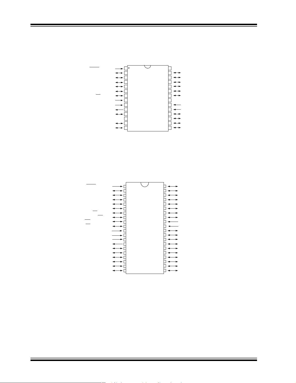
Pin Diagrams
40-Pin PDIP
MCLR/VPP/RE3
RA0/AN0
RA1/AN1
RA2/AN2/V
RA3/AN3/V
RA4/T0CKI
RA5/AN4/SS
RC0/T1OSO/T13CKI
RA0/AN0/CV
RA3/AN3/V
RA5/AN4/SS
RE1/WR
RE2/CS
OSC1/CLKI/RA7
OSC2/CLKO/RA6
RC0/T1OSO/T13CKI
RD0/PSP0/C1IN+
RD1/PSP1/C1IN-
/HLVDIN
OSC1/CLKI/RA7
OSC2/CLKO/RA6
RC1/T1OSI
RC2/CCP1
RC3/SCK/SCL
MCLR/VPP/RE3
RA1/AN1
RA2/AN2/V
RC3/SCK/SCL
REF+
RA4/T0CKI
/HLVDIN
RE0/RD
/AN5
/AN6/C1OUT
/AN7/C2OUT
RC1/T1OSI
RC2/CCP1
REF+
REF
REF-
V
DD
VSS
REF-
V
1
2
3
4
5
6
7
SS
8
9
10
11
12
13
14
1
2
3
4
5
6
7
8
9
10
11
12
13
14
15
16
17
18
19
20
PIC18F4585
PIC18F2585
PIC18F4680
28
27
26
25
24
23
22
21
20
19
18
17
16
15
40
39
38
37
36
35
34
33
32
31
30
29
28
27
26
25
24
23
22
21
RB7/KBI3/PGD
RB6/KBI2/PGC
RB5/KBI1/PGM
RB4/KBI0/AN9
RB3/CANRX
RB2/INT2/CANTX
RB1/INT1/AN8
RB0/INT0/AN10
V
DD
VSS
RC7/RX/DT
RC6/TX/CK
RC5/SDO
RC4/SDI/SDA
RB7/KBI3/PGD
RB6/KBI2/PGC
RB5/KBI1/PGM
RB4/KBI0/AN9
RB3/CANRX
RB2/INT2/CANTX
RB1/INT1/AN8
RB0/INT0/FLT0/AN10
V
DD
VSS
RD7/PSP7/P1D
RD6/PSP6/P1C
RD5/PSP5/P1B
RD4/PSP4/ECCP1/P1A
RC7/RX/DT
RC6/TX/CK
RC5/SDO
RC4/SDI/SDA
RD3/PSP3/C2INRD2/PSP2/C2IN+
DS39625C-page 2 Preliminary © 2007 Microchip Technology Inc.
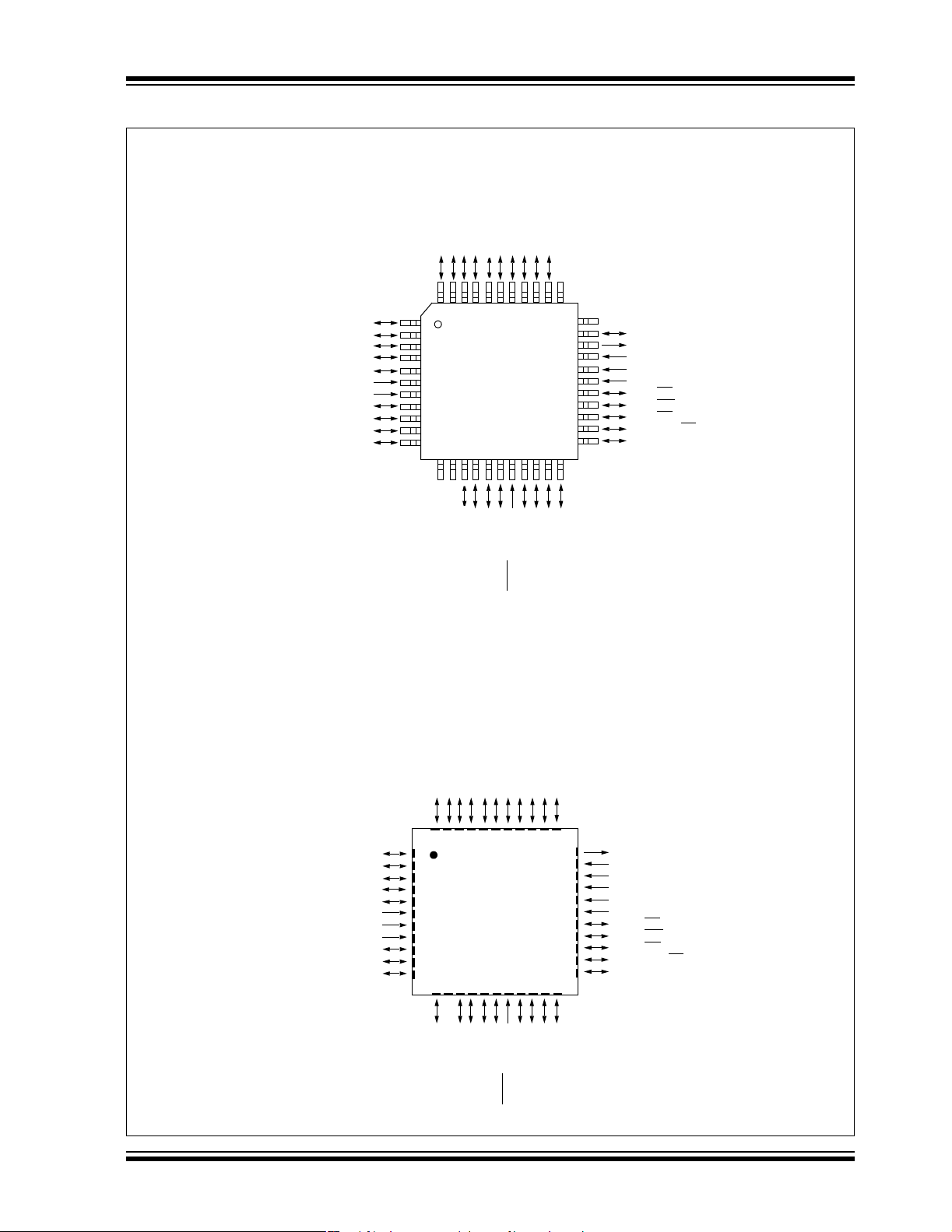
Pin Diagrams (Continued)
44-Pin TQFP
RD4/PSP4/ECCP1/P1A
RB0/INT0/FLT0/AN10
RC7/RX/DT
RD5/PSP5/P1B
RD6/PSP6/P1C
RD7/PSP7/P1D
RB1/INT1/AN8
RB2/INT2/CANTX
RB3/CANRX
V
SS
VDD
PIC18F2585/2680/4585/4680
RC6/TX/CK
RC5/SDO
RC4/SDI/SDA
RD3/PSP3/C2IN-
RD2/PSP2/C2IN+
RD1/PSP1/C1IN-
RD0/PSP0/C1IN+
RC3/SCK/SCL
RC2/CCP1
RC1/T1OSI
NC
363435
1819202122
16
17
37
38
33
32
31
30
29
28
27
26
25
24
23
NC
RC0/T1OSO/T13CKI
OSC2/CLKO/RA6
OSC1/CLKI/RA7
SS
V
VDD
RE2/CS/AN7/C2OUT
RE1/WR
/AN6/C1OUT
RE0/RD
/AN5
RA5/AN4/SS
RA4/T0CKI
/HLVDIN
1
2
3
4
5
6
7
8
9
10
11
44
121314
414039
42
43
PIC18F4585
PIC18F4680
15
44-Pin QFN
RD4/PSP4/ECCP1/P1A
RB0/INT0/FLT0/AN10
RC7/RX/DT
RD5/PSP5/P1B
RD6/PSP6/P1C
RD7/PSP7/P1D
RB1/INT1/AN8
RB2/INT2/CANTX
V
AVDD
VDD
NC
NC
RB4/KBI0/AN9
RB5/KBI1/PGM
RC6/TX/CK
RC5/SDO
RC4/SDI/SDA
RD3/PSP3/C2IN-
4443424140
1
2
3
4
5
SS
6
7
8
9
10
11
121314
PIC18F4585
PIC18F4680
15
RB7/KBI3/PGD
RB6/KBI2/PGC
RD2/PSP2/C2IN+
RD1/PSP1/C1IN-
RD0/PSP0/C1IN+
38
39
1819202122
16
17
MCLR/VPP/RE3
REF
RA0/AN0/CV
RC3/SCK/SCL
37
REF-
RA1/AN1
RA2/AN2/V
RC2/CCP1
RC1/T1OSI
363435
33
32
31
30
29
28
27
26
25
24
23
RA3/AN3/VREF+
RC0/T1OSO/T13CKI
OSC2/CLKO/RA6
OSC1/CLKI/RA7
SS
V
AVSS
VDD
AVDD
RE2/CS/AN7/C2OUT
RE1/WR
/AN6/C1OUT
RE0/RD
/AN5
RA5/AN4/SS
RA4/T0CKI
/HLVDIN
NC
RB3/CANRX
RB4/KBI0/AN9
RB5/KBI1/PGM
RB6/KBI2/PGC
RB7/KBI3/PGD
REF
REF-
RA1/AN1
RA2/AN2/V
MCLR/VPP/RE3
RA0/AN0/CV
RA3/AN3/VREF+
© 2007 Microchip Technology Inc. Preliminary DS39625C-page 3

PIC18F2585/2680/4585/4680
Table of Contents
1.0 Device Overview.......................................................................................................................................................................... 7
2.0 Oscillator Configurations............................................................................................................................................................23
3.0 Power Managed Modes .............................................................................................................................................................33
4.0 Reset.......................................................................................................................................................................................... 41
5.0 Memory Organization................................................................................................................................................................. 61
6.0 Flash Program Memory.............................................................................................................................................................. 95
7.0 Data EEPROM Memory........................................................................................................................................................... 105
8.0 8 x 8 Hardware Multiplier..........................................................................................................................................................111
9.0 Interrupts.................................................................................................................................................................................. 113
10.0 I/O Ports................................................................................................................................................................................... 129
11.0 Timer0 Module ......................................................................................................................................................................... 147
12.0 Timer1 Module ......................................................................................................................................................................... 151
13.0 Timer2 Module ......................................................................................................................................................................... 157
14.0 Timer3 Module ......................................................................................................................................................................... 159
15.0 Capture/Compare/PWM (CCP1) Modules ...............................................................................................................................163
16.0 Enhanced Capture/Compare/PWM (ECCP1) Module.............................................................................................................. 173
17.0 Master Synchronous Serial Port (MSSP) Module ....................................................................................................................187
18.0 Enhanced Universal Synchronous Receiver Transmitter (EUSART)....................................................................................... 227
19.0 10-Bit Analog-to-Digital Converter (A/D) Module .....................................................................................................................247
20.0 Comparator Module..................................................................................................................................................................257
21.0 Comparator Voltage Reference Module...................................................................................................................................263
22.0 High/Low-Voltage Detect (HLVD)............................................................................................................................................. 267
23.0 ECAN™ Technology ................................................................................................................................................................ 273
24.0 Special Features of the CPU.................................................................................................................................................... 343
25.0 Instruction Set Summary..........................................................................................................................................................361
26.0 Development Support............................................................................................................................................................... 411
27.0 Electrical Characteristics..........................................................................................................................................................415
28.0 DC and AC Characteristics Graphs and Tables.......................................................................................................................451
29.0 Packaging Information.............................................................................................................................................................. 453
Appendix A: Revision History............................................................................................................................................................. 461
Appendix B: Device Differences......................................................................................................................................................... 461
Appendix C: Conversion Considerations ........................................................................................................................................... 462
Appendix D: Migration From Baseline to Enhanced Devices............................................................................................................. 462
Appendix E: Migration from Mid-Range to Enhanced Devices .......................................................................................................... 463
Appendix F: Migration from High-End to Enhanced Devices............................................................................................................. 463
Index ..................................................................................................................................................................................................465
The Microchip Web Site..................................................................................................................................................................... 477
Customer Change Notification Service ..............................................................................................................................................477
Customer Support..............................................................................................................................................................................477
Reader Response.............................................................................................................................................................................. 478
PIC18F2585/2680/4585/4680 Product Identification System ............................................................................................................ 479
DS39625C-page 4 Preliminary © 2007 Microchip Technology Inc.

PIC18F2585/2680/4585/4680
TO OUR VALUED CUSTOMERS
It is our intention to provide our valued customers with the best documentation possible to ensure successful use of your Microchip
products. To this end, we will continue to improve our publications to better suit your needs. Our publications will be refined and
enhanced as new volumes and updates are introduced.
If you have any questions or comments regarding this publication, please contact the Marketing Communications Department via
E-mail at docerrors@microchip.com or fax the Reader Response Form in the back of this data sheet to (480) 792-4150. We
welcome your feedback.
Most Current Data Sheet
To obtain the most up-to-date version of this data sheet, please register at our Worldwide Web site at:
http://www.microchip.com
You can determine the version of a data sheet by examining its literature number found on the bottom outside corner of any page.
The last character of the literature number is the version number, (e.g., DS30000A is version A of document DS30000).
Errata
An errata sheet, describing minor operational differences from the data sheet and recommended workarounds, may exist for current
devices. As device/documentation issues become known to us, we will publish an errata sheet. The errata will specify the revision
of silicon and revision of document to which it applies.
To determine if an errata sheet exists for a particular device, please check with one of the following:
• Microchip’s Worldwide Web site; http://www.microchip.com
• Your local Microchip sales office (see last page)
When contacting a sales office, please specify which device, revision of silicon and data sheet (include literature number) you are
using.
Customer Notification System
Register on our web site at www.microchip.com to receive the most current information on all of our products.
© 2007 Microchip Technology Inc. Preliminary DS39625C-page 5

PIC18F2585/2680/4585/4680
NOTES:
DS39625C-page 6 Preliminary © 2007 Microchip Technology Inc.

PIC18F2585/2680/4585/4680
1.0 DEVICE OVERVIEW
This document contains device specific information for
the following devices:
• PIC18F2585
• PIC18F2680
• PIC18F4585
• PIC18F4680
This family of devices offers the advantages of all PIC18
microcontrollers – namely, high computational
performance at an economical price – with the addition
of high-endurance, Enhanced Flash program memory.
In addition to these features, the
PIC18F2585/2680/4585/4680 family introduces design
enhancements that make these microcontrollers a
logical choice for many high-performance, power
sensitive applications.
1.1 New Core Features
1.1.1 nanoWatt TECHNOLOGY
All of the devices in the PIC18F2585/2680/4585/4680
family incorporate a range of features that can significantly reduce power consumption during operation.
Key items include:
• Alternate Run Modes: By clocking the controller
from the Timer1 source or the internal oscillator
block, power consumption during code execution
can be reduced by as much as 90%.
• Multiple Idle Modes: The controller can also run
with its CPU core disabled but the peripherals still
active. In these states, power consumption can be
reduced even further, to as little as 4% of normal
operation requirements.
• On-the-fly Mode Switching: The power
managed modes are invoked by user code during
operation, allowing the user to incorporate
power-saving ideas into their application’s
software design.
• Lower Consumption in Key Modules: The
power requirements for both Timer1 and the
Watchdog Timer have been reduced by up to
80%, with typical values of 1.1 and 2.1 μA,
respectively.
• Extended Instruction Set: In addition to the
standard 75 instructions of the PIC18 instruction
set, PIC18F2585/2680/4585/4680 devices also
provide an optional extension to the core CPU
functionality. The added features include eight
additional instructions that augment indirect and
indexed addressing operations and the
implementation of Indexed Literal Offset
Addressing mode for many of the standard PIC18
instructions.
1.1.2 MULTIPLE OSCILLATOR OPTIONS AND FEATURES
All of the devices in the PIC18F2585/2680/4585/4680
family offer ten different oscillator options, allowing
users a wide range of choices in developing application
hardware. These include:
• Four Crystal modes, using crystals or ceramic
resonators
• Two External Clock modes, offering the option of
using two pins (oscillator input and a divide-by-4
clock output) or one pin (oscillator input, with the
second pin reassigned as general I/O)
• Two External RC Oscillator modes with the same
pin options as the External Clock modes
• An internal oscillator block which provides an
8 MHz clock (±2% accuracy) and an INTRC
source (approximately 31 kHz, stable over
temperature and V
6 user selectable clock frequencies, between
125 kHz to 4 MHz, for a total of 8 clock
frequencies. This option frees the two oscillator
pins for use as additional general purpose I/O.
• A Phase Lock Loop (PLL) frequency multiplier,
available to both the high-speed crystal and
internal oscillator modes, which allows clock
speeds of up to 40 MHz. Used with the internal
oscillator, the PLL gives users a complete
selection of clock speeds, from 31 kHz to
32 MHz – all without using an external crystal or
clock circuit.
Besides its availability as a clock source, the internal
oscillator block provides a stable reference source that
gives the family additional features for robust
operation:
• Fail-Safe Clock Monitor: This option constantly
monitors the main clock source against a reference signal provided by the internal oscillator. If a
clock failure occurs, the controller is switched to
the internal oscillator block, allowing for continued
low-speed operation or a safe application
shutdown.
• Two-Speed Start-up: This option allows the
internal oscillator to serve as the clock source
from Power-on Reset, or wake-up from Sleep
mode, until the primary clock source is available.
DD), as well as a range of
© 2007 Microchip Technology Inc. Preliminary DS39625C-page 7

PIC18F2585/2680/4585/4680
1.2 Other Special Features
• Memory Endurance: The Enhanced Flash cells
for both program memory and data EEPROM are
rated to last for many thousands of erase/write
cycles – up to 100,000 for program memory and
1,000,000 for EEPROM. Data retention without
refresh is conservatively estimated to be greater
than 40 years.
• Self-programmability: These devices can write
to their own program memory spaces under internal software control. By using a bootloader routine located in the protected Boot Block at the top
of program memory, it becomes possible to create
an application that can update itself in the field.
• Extended Instruction Set: The
PIC18F2585/2680/4585/4680 family introduces
an optional extension to the PIC18 instruction set,
which adds 8 new instructions and an Indexed
Addressing mode. This extension, enabled as a
device configuration option, has been specifically
designed to optimize re-entrant application code
originally developed in high-level languages, such
as C.
• Enhanced CCP1 module: In PWM mode, this
module provides 1, 2 or 4 modulated outputs for
controlling half-bridge and full-bridge drivers.
Other features include Auto-Shutdown, for
disabling PWM outputs on interrupt or other select
conditions and Auto-Restart, to reactivate outputs
once the condition has cleared.
• Enhanced Addressable USART: This serial
communication module is capable of standard
RS-232 operation and provides support for the LIN
bus protocol. Other enhancements include
automatic baud rate detection and a 16-bit Baud
Rate Generator for improved resolution. When the
microcontroller is using the internal oscillator
block, the EUSART provides stable operation for
applications that talk to the outside world without
using an external crystal (or its accompanying
power requirement).
• 10-bit A/D Converter: This module incorporates
programmable acquisition time, allowing for a
channel to be selected and a conversion to be
initiated without waiting for a sampling period and
thus, reduce code overhead.
• Extended Watchdog Timer (WDT): This
enhanced version incorporates a 16-bit prescaler,
allowing a time-out range from 4 ms to over
131 seconds, that is stable across operating
voltage and temperature.
1.3 Details on Individual Family Members
Devices in the PIC18F2585/2680/4585/4680 family are
available in 28-pin (PIC18F2X8X) and 40/44-pin
(PIC18F4X8X) packages. Block diagrams for the two
groups are shown in Figure 1-1 and Figure 1-2.
The devices are differentiated from each other in six
ways:
1. Flash program memory (48 Kbytes for
PIC18FX585 devices, 64 Kbytes for
PIC18FX680).
2. A/D channels (8 for PIC18F2X8X devices, 11 for
PIC18F4X8X devices).
3. I/O ports (3 bidirectional ports and 1 input only
port on PIC18F2X8X devices, 5 bidirectional
ports on PIC18F4X8X devices).
4. CCP1 and Enhanced CCP1 implementation
(PIC18F2X8X devices have 1 standard CCP1
module, PIC18F4X8X devices have one
standard CCP1 module and one ECCP1
module).
5. Parallel Slave Port (present only on
PIC18F4X8X devices).
6. PIC18F4X8X devices provide two comparators.
All other features for devices in this family are identical.
These are summarized in Table 1-1.
The pinouts for all devices are listed in Table 1-2 and
Table 1-3.
Like all Microchip PIC18 devices, members of the
PIC18F2585/2680/4585/4680 family are available as
both standard and low-voltage devices. Standard
devices with Enhanced Flash memory, designated with
an “F” in the part number (such as PIC18F2585),
accommodate an operating V
Low-voltage parts, designated by “LF” (such as
PIC18LF2585), function over an extended V
of 2.0V to 5.5V.
DD range of 4.2V to 5.5V.
DD range
DS39625C-page 8 Preliminary © 2007 Microchip Technology Inc.

PIC18F2585/2680/4585/4680
TABLE 1-1: DEVICE FEATURES
Features PIC18F2585 PIC18F2680 PIC18F4585 PIC18F4680
Operating Frequency DC – 40 MHz DC – 40 MHz DC – 40 MHz DC – 40 MHz
Program Memory (Bytes) 49152 65536 49152 65536
Program Memory (Instructions) 24576 32768 24576 32768
Data Memory (Bytes) 3328 3328 3328 3328
Data EEPROM Memory (Bytes) 1024 1024 1024 1024
Interrupt Sources 19 19 20 20
I/O Ports Ports A, B, C, (E) Ports A, B, C, (E) Ports A, B, C, D, E Ports A, B, C, D, E
Timers 4 4 4 4
Capture/Compare/PWM Modules 1 1 1 1
Enhanced Capture/
Compare/PWM Modules
ECAN Module 1 1 1 1
Serial Communications MSSP,
Enhanced USART
Parallel Communications (PSP) No No Yes Yes
10-bit Analog-to-Digital Module 8 Input Channels 8 Input Channels 11 Input Channels 11 Input Channels
Comparators 0 0 2 2
Resets (and Delays) POR, BOR,
RESET Instruction,
MCLR
Programmable High/Low-Voltage
Detect
Programmable Brown-out Reset Yes Yes Yes Yes
Instruction Set 75 Instructions;
83 with Extended
Packages 28-pin PDIP
0011
MSSP,
Enhanced USART
POR, BOR,
RESET Instruction,
Stack Full,
Stack Underflow
(PWRT, OST),
(optional),
WDT
Yes Ye s Yes Yes
Instruction Set
enabled
28-pin SOIC
Stack Full,
Stack Underflow
(PWRT, OST),
(optional),
MCLR
WDT
75 Instructions;
83 with Extended
Instruction Set
enabled
28-pin PDIP
28-pin SOIC
MSSP,
Enhanced USART
POR, BOR,
RESET Instruction,
Stack Full,
Stack Underflow
(PWRT, OST),
(optional),
MCLR
WDT
75 Instructions;
83 with Extended
Instruction Set
enabled
40-pin PDIP
44-pin QFN
44-pin TQFP
MSSP,
Enhanced USART
POR, BOR,
RESET Instruction,
Stack Full,
Stack Underflow
(PWRT, OST),
(optional),
MCLR
WDT
75 Instructions;
83 with Extended
Instruction Set
enabled
40-pin PDIP
44-pin QFN
44-pin TQFP
© 2007 Microchip Technology Inc. Preliminary DS39625C-page 9
PIC18F2585/2680/4585/4680
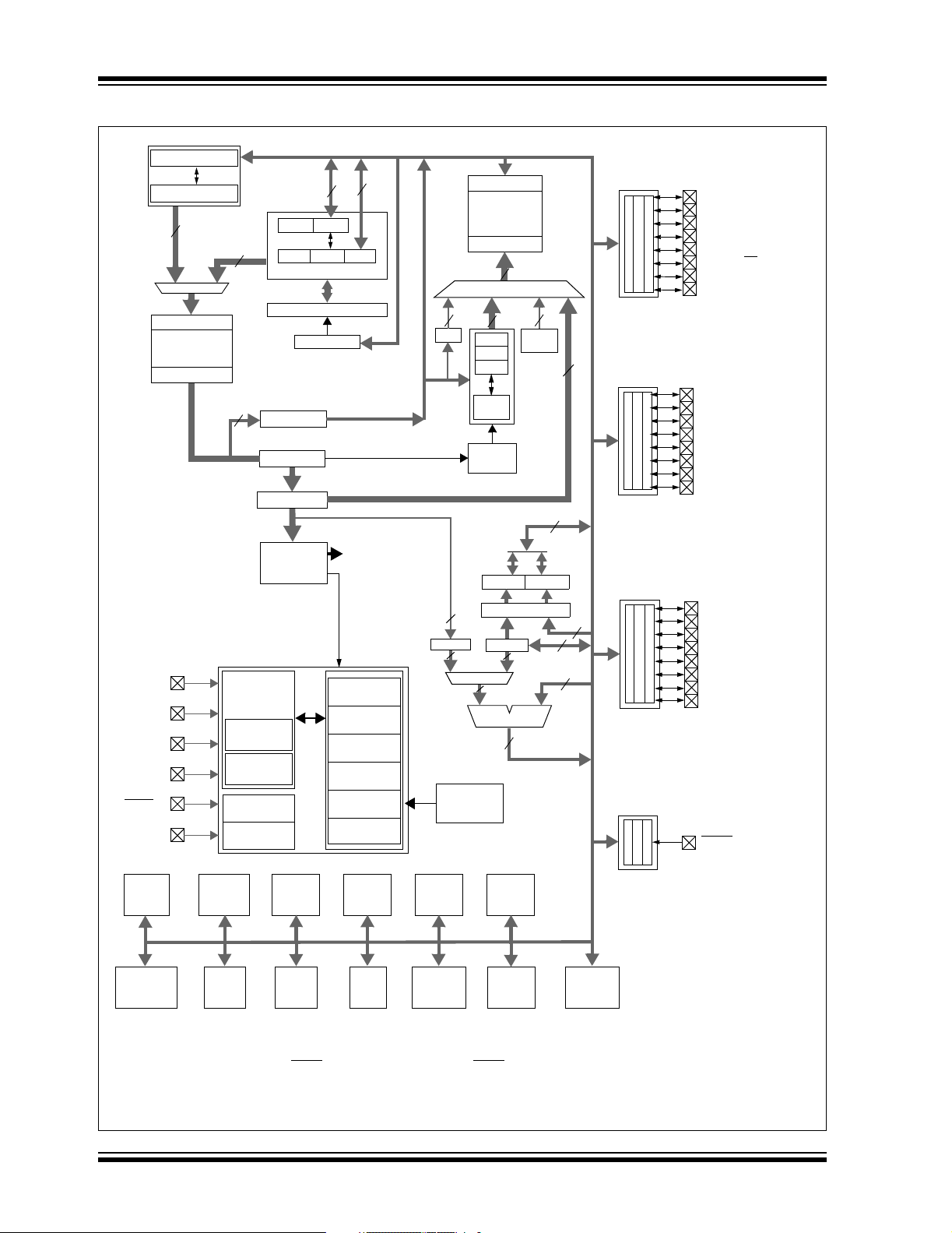
FIGURE 1-1: PIC18F2585/2680 (28-PIN) BLOCK DIAGRAM
Table Pointer<21>
inc/dec logic
21
Address Latch
Program Memory
(48/64 Kbytes)
Data Latch
Instruction Bus <16>
(2)
OSC1
(2)
OSC2
T1OSI
T1OSO
(1)
MCLR
VDD,
SS
V
20
8
Table Latch
ROM Latch
Instruction
Decode &
Control
Internal
Oscillator
Block
INTRC
Oscillator
8 MHz
Oscillator
Single-Supply
Programming
In-Circuit
Debugger
8
PCLATH
PCLATU
PCH PCL
PCU
Program Counter
31 Level Stack
STKPTR
IR
State Machine
Control Signals
Power-up
Oscillator
Start-up Timer
Power-on
Watchdog
Brown-out
Fail-Safe
Clock Monitor
Data Bus<8>
8
Timer
Reset
Timer
Reset
Data Latch
Data Memory
(3.9 Kbytes)
Address Latch
12
Data Address<12>
44
12
FSR0
FSR1
FSR2
logic
8 x 8 Multiply
W
8
ALU<8>
Access
Bank
PRODLPRODH
8
8
12
8
8
8
8
BSR
3
BITOP
8
Band Gap
Reference
inc/dec
Address
Decode
PORTA
PORTB
PORTC
PORTE
RA0/AN0
RA1/AN1
RA2/AN2/VREFRA3/AN3/VREF+
RA4/T0CKI
RA5/AN4/SS
OSC2/CLKO/RA6
OSC1/CLKI/RA7
RB0/INT0/AN10
RB1/INT1/AN8
RB2/INT2/CANTX
RB3/CANRX
RB4/KBI0/AN9
RB5/KBI1/PGM
RB6/KBI2/PGC
RB7/KBI3/PGD
RC0/T1OSO/T13CKI
RC1/T1OSI
RC2/CCP1
RC3/SCK/SCL
RC4/SDI/SDA
RC5/SDO
RC6/TX/CK
RC7/RX/DT
MCLR/VPP/RE3
/HLVDIN
(1)
BOR
HLVD
Note 1: RE3 is multiplexed with MCLR and is only available when the MCLR Resets are disabled.
2: OSC1/CLKI and OSC2/CLKO are only available in select oscillator modes and when these pins are not being used as digital I/O.
Data
EEPROM
CCP1
Refer to Section 2.0 “Oscillator Configurations” for additional information.
ECCP1
MSSP
Timer2Timer1 Timer3Timer0
EUSARTComparator
ADC
10-bit
ECAN
DS39625C-page 10 Preliminary © 2007 Microchip Technology Inc.
PIC18F2585/2680/4585/4680
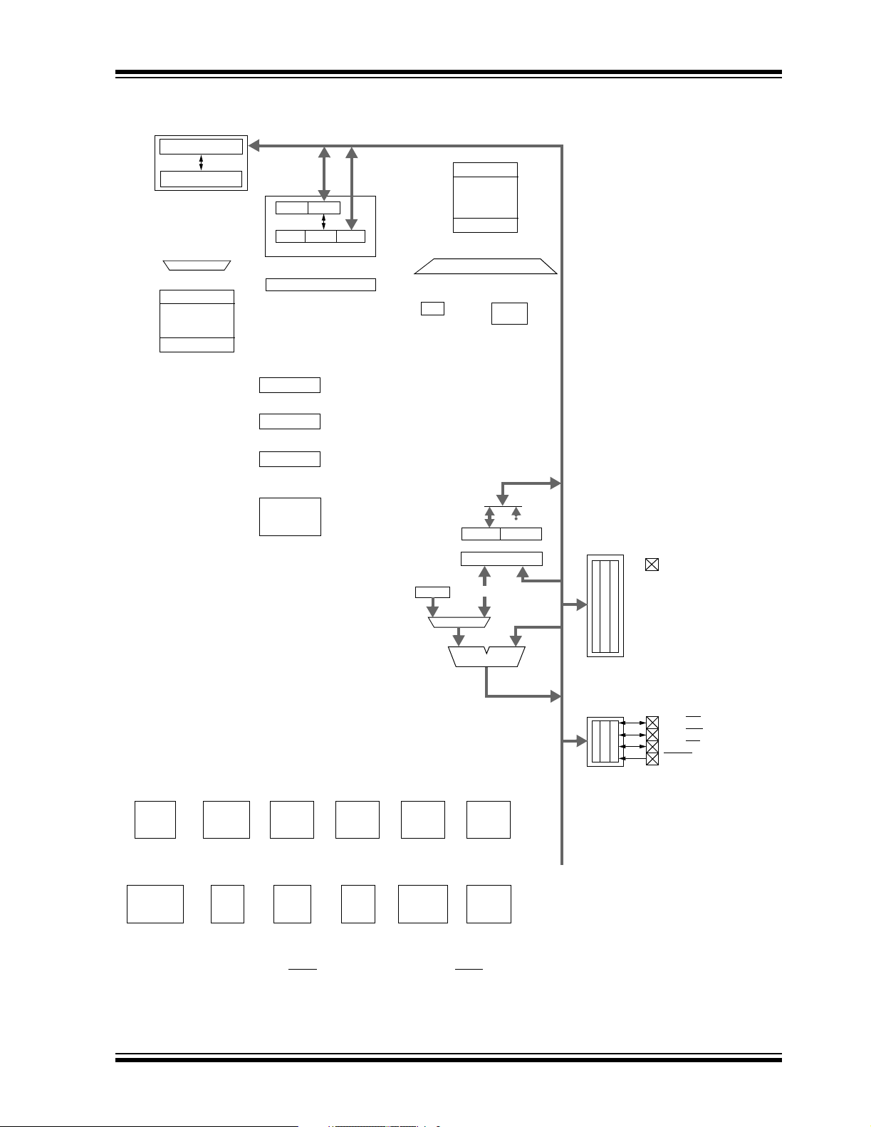
FIGURE 1-2: PIC18F4585/4680 (40/44-PIN) BLOCK DIAGRAM
Table Pointer<21>
inc/dec logic
21
Address Latch
Program Memory
(48/64 Kbytes)
Data Latch
20
8
PCLATH
PCLATU
PCH PCL
PCU
Program Counter
31 Level Stack
Table Latch
ROM Latch
IR
Instruction
Decode &
Control
Data Bus<8>
8
8
Data Latch
Data Memory
(3.9 Kbytes)
Address Latch
12
Data Address<12>
44
BSR
BITOP
3
8
Access
12
PRODLPRODH
8 x 8 Multiply
8
PORTD
8
RD0/PSP0
/C1IN+
8
ALU<8>
8
PORTE
BOR
HLVD
Note 1: RE3 is multiplexed with MCLR
2: OSC1/CLKI and OSC2/CLKO are only available in select oscillator modes and when these pins are not being used as digital I/O.
Data
EEPROM
CCP1
Refer to Section 2.0 “Oscillator Configurations” for additional information.
ECCP1
MSSP
and is only available when the MCLR Resets are disabled.
Timer2Timer1 Timer3Timer0
EUSARTComparator
ADC
10-bit
RE0/RD/AN5
RE1/WR/AN6/C1OUT
RE2/CS/AN7/C2OUT
MCLR/VPP/RE3
(1)
© 2007 Microchip Technology Inc. Preliminary DS39625C-page 11

PIC18F2585/2680/4585/4680
TABLE 1-2: PIC18F2585/2680 PINOUT I/O DESCRIPTIONS
Pin
Pin Name
MCLR
/VPP/RE3
MCLR
VPP
RE3
OSC1/CLKI/RA7
OSC1
CLKI
RA7
OSC2/CLKO/RA6
OSC2
CLKO
RA6
Legend: TTL = TTL compatible input CMOS = CMOS compatible input or output
ST = Schmitt Trigger input with CMOS levels I = Input
O = Output P = Power
Number
PDIP,
SOIC
10
Pin
Buffer
Type
1
9
P
I/O
O
O
I/O
Type
Master Clear (input) or programming voltage (input).
I
ST
I
ST
I
ST
I
CMOS
TTL
—
—
TTL
Master Clear (Reset) input. This pin is an active-low
Reset to the device.
Programming voltage input.
Digital input.
Oscillator crystal or external clock input.
Oscillator crystal input or external clock source input.
ST buffer when configured in RC mode; CMOS otherwise.
External clock source input. Always associated with pin
function OSC1. (See related OSC1/CLKI, OSC2/CLKO pins.)
General purpose I/O pin.
Oscillator crystal or clock output.
Oscillator crystal output. Connects to crystal or resonator in
Crystal Oscillator mode.
In RC mode, OSC2 pin outputs CLKO which has 1/4 the
frequency of OSC1 and denotes the instruction cycle rate.
General purpose I/O pin.
Description
DS39625C-page 12 Preliminary © 2007 Microchip Technology Inc.

PIC18F2585/2680/4585/4680
TABLE 1-2: PIC18F2585/2680 PINOUT I/O DESCRIPTIONS (CONTINUED)
Pin
Pin Name
RA0/AN0
RA0
AN0
RA1/AN1
RA1
AN1
RA2/AN2/V
RA3/AN3/V
RA4/T0CKI
RA5/AN4/SS
RA6 See the OSC2/CLKO/RA6 pin.
RA7 See the OSC1/CLKI/RA7 pin.
Legend: TTL = TTL compatible input CMOS = CMOS compatible input or output
REF-
RA2
AN2
REF-
V
REF+
RA3
AN3
REF+
V
RA4
T0CKI
/HLVDIN
RA5
AN4
SS
HLVDIN
ST = Schmitt Trigger input with CMOS levels I = Input
O = Output P = Power
Number
PDIP,
SOIC
2
3
4
5
6
7
Pin
Buffer
Typ e
Type
I/OITTL
Analog
I/OITTL
Analog
I/O
I/O
I/OITTL
I/O
TTL
I
Analog
I
Analog
TTL
I
Analog
I
Analog
TTL
I
Analog
I
TTL
I
Analog
PORTA is a bidirectional I/O port.
Digital I/O.
Analog input 0.
Digital I/O.
Analog input 1.
Digital I/O.
Analog input 2.
A/D reference voltage (low) input.
Digital I/O.
Analog input 3.
A/D reference voltage (high) input.
Digital I/O.
ST
Timer0 external clock input.
Digital I/O.
Analog input 4.
SPI slave select input.
High/Low-Voltage Detect input.
Description
© 2007 Microchip Technology Inc. Preliminary DS39625C-page 13

PIC18F2585/2680/4585/4680
TABLE 1-2: PIC18F2585/2680 PINOUT I/O DESCRIPTIONS (CONTINUED)
Pin
Pin Name
RB0/INT0/AN10
RB0
INT0
AN10
RB1/INT1/AN8
RB1
INT1
AN8
RB2/INT2/CANTX
RB2
INT2
CANTX
RB3/CANRX
RB3
CANRX
RB4/KBI0/AN9
RB4
KBI0
AN9
RB5/KBI1/PGM
RB5
KBI1
PGM
RB6/KBI2/PGC
RB6
KBI2
PGC
RB7/KBI3/PGD
RB7
KBI3
PGD
Legend: TTL = TTL compatible input CMOS = CMOS compatible input or output
ST = Schmitt Trigger input with CMOS levels I = Input
O = Output P = Power
Number
PDIP,
SOIC
21
22
23
24
25
26
27
28
Pin
Buffer
Type
Type
I/O
I/O
I/O
I/OITTL
I/O
I/O
I/O
I/O
I/O
I/O
I/O
TTL
I
I
Analog
TTL
I
I
Analog
TTL
I
O
TTL
TTL
TTL
I
TTL
I
Analog
TTL
I
TTL
TTL
I
TTL
TTL
I
TTL
Description
PORTB is a bidirectional I/O port. PORTB can be software
programmed for internal weak pull-ups on all inputs.
Digital I/O.
ST
ST
ST
ST
ST
ST
External interrupt 0.
Analog input 10.
Digital I/O.
External interrupt 1.
Analog input 8.
Digital I/O.
External interrupt 2.
CAN bus TX.
Digital I/O.
CAN bus RX.
Digital I/O.
Interrupt-on-change pin.
Analog input 9.
Digital I/O.
Interrupt-on-change pin.
Low-Voltage ICSP™ Programming enable pin.
Digital I/O.
Interrupt-on-change pin.
In-Circuit Debugger and ICSP programming clock pin.
Digital I/O.
Interrupt-on-change pin.
In-Circuit Debugger and ICSP programming data pin.
DS39625C-page 14 Preliminary © 2007 Microchip Technology Inc.
PIC18F2585/2680/4585/4680
TABLE 1-2: PIC18F2585/2680 PINOUT I/O DESCRIPTIONS (CONTINUED)
Pin
Pin Name
RC0/T1OSO/T13CKI
RC0
T1OSO
T13CKI
RC1/T1OSI
RC1
T1OSI
RC2/CCP1
RC2
CCP1
RC3/SCK/SCL
RC3
SCK
SCL
RC4/SDI/SDA
RC4
SDI
SDA
RC5/SDO
RC5
SDO
RC6/TX/CK
RC6
TX
CK
RC7/RX/DT
RC7
RX
DT
RE3 — — — See MCLR
VSS 8, 19 P — Ground reference for logic and I/O pins.
DD 20 P — Positive supply for logic and I/O pins.
V
Legend: TTL = TTL compatible input CMOS = CMOS compatible input or output
ST = Schmitt Trigger input with CMOS levels I = Input
O = Output P = Power
Number
PDIP,
SOIC
11
12
13
14
15
16
17
18
Pin
Buffer
Typ e
I/O
O
I
I/O
ISTCMOS
I/O
I/O
I/O
I/O
I/O
I/O
I
I/O
I/O
O
I/O
O
I/O
I/O
I
I/O
Type
ST
—
ST
ST
ST
ST
ST
ST
ST
ST
ST
ST
—
ST
—
ST
ST
ST
ST
Description
PORTC is a bidirectional I/O port.
Digital I/O.
Timer1 oscillator output.
Timer1/Timer3 external clock input.
Digital I/O.
Timer1 oscillator input.
Digital I/O.
Capture1 input/Compare1 output/PWM1 output.
Digital I/O.
Synchronous serial clock input/output for SPI mode.
Synchronous serial clock input/output for I
Digital I/O.
SPI data in.
2
C data I/O.
I
Digital I/O.
SPI data out.
Digital I/O.
EUSART asynchronous transmit.
EUSART synchronous clock (see related RX/DT).
Digital I/O.
EUSART asynchronous receive.
EUSART synchronous data (see related TX/CK).
/VPP/RE3 pin.
2
C™ mode.
© 2007 Microchip Technology Inc. Preliminary DS39625C-page 15

PIC18F2585/2680/4585/4680
TABLE 1-3: PIC18F4585/4680 PINOUT I/O DESCRIPTIONS
Pin Name
/VPP/RE3
MCLR
MCLR
VPP
RE3
OSC1/CLKI/RA7
OSC1
CLKI
RA7
OSC2/CLKO/RA6
OSC2
CLKO
RA6
Legend: TTL = TTL compatible input CMOS = CMOS compatible input or output
ST = Schmitt Trigger input with CMOS levels I = Input
O = Output P = Power
Pin Number
PDIP QFN TQFP
11818
13 32 30
14 33 31
Pin
Typ e
I
P
I
I
I
I/O
O
O
I/O
Buffer
Type
ST
ST
ST
CMOS
TTL
—
—
TTL
Description
Master Clear (input) or programming voltage (input).
Master Clear (Reset) input. This pin is an
active-low Reset to the device.
Programming voltage input.
Digital input.
Oscillator crystal or external clock input.
Oscillator crystal input or external clock source input.
ST buffer when configured in RC mode;
CMOS otherwise.
External clock source input. Always associated with
pin function OSC1. (See related OSC1/CLKI,
OSC2/CLKO pins.)
General purpose I/O pin.
Oscillator crystal or clock output.
Oscillator crystal output. Connects to crystal or
resonator in Crystal Oscillator mode.
In RC mode, OSC2 pin outputs CLKO which has 1/4
the frequency of OSC1 and denotes the instruction
cycle rate.
General purpose I/O pin.
DS39625C-page 16 Preliminary © 2007 Microchip Technology Inc.

PIC18F2585/2680/4585/4680
TABLE 1-3: PIC18F4585/4680 PINOUT I/O DESCRIPTIONS (CONTINUED)
Pin Name
RA0/AN0/CVREF
RA0
AN0
CVREF
RA1/AN1
RA1
AN1
RA2/AN2/V
RA3/AN3/V
RA4/T0CKI
RA5/AN4/SS
RA6 See the OSC2/CLKO/RA6 pin.
RA7 See the OSC1/CLKI/RA7 pin.
Legend: TTL = TTL compatible input CMOS = CMOS compatible input or output
REF-
RA2
AN2
REF-
V
REF+
RA3
AN3
REF+
V
RA4
T0CKI
/HLVDIN
RA5
AN4
SS
HLVDIN
ST = Schmitt Trigger input with CMOS levels I = Input
O = Output P = Power
Pin Number
PDIP QFN TQFP
21919
32020
42121
52222
62323
72424
Pin
Buffer
Typ e
Type
I/O
I
Analog
O
Analog
I/OITTL
Analog
I/O
I
Analog
I
Analog
I/O
I
Analog
I
Analog
I/OITTL
I/O
I
Analog
I
I
Analog
PORTA is a bidirectional I/O port.
TTL
TTL
TTL
ST
TTL
TTL
Digital I/O.
Analog input 0.
Analog comparator reference output.
Digital I/O.
Analog input 1.
Digital I/O.
Analog input 2.
A/D reference voltage (low) input.
Digital I/O.
Analog input 3.
A/D reference voltage (high) input.
Digital I/O.
Timer0 external clock input.
Digital I/O.
Analog input 4.
SPI slave select input.
High/Low-Voltage Detect input.
Description
© 2007 Microchip Technology Inc. Preliminary DS39625C-page 17

PIC18F2585/2680/4585/4680
TABLE 1-3: PIC18F4585/4680 PINOUT I/O DESCRIPTIONS (CONTINUED)
Pin Name
RB0/INT0/FLT0/AN10
RB0
INT0
FLT0
AN10
RB1/INT1/AN8
RB1
INT1
AN8
RB2/INT2/CANTX
RB2
INT2
CANTX
RB3/CANRX
RB3
CANRX
RB4/KBI0/AN9
RB4
KBI0
AN9
RB5/KBI1/PGM
RB5
KBI1
PGM
RB6/KBI2/PGC
RB6
KBI2
PGC
RB7/KBI3/PGD
RB7
KBI3
PGD
Legend: TTL = TTL compatible input CMOS = CMOS compatible input or output
ST = Schmitt Trigger input with CMOS levels I = Input
O = Output P = Power
Pin Number
PDIP QFN TQFP
33 9 8
34 10 9
35 11 10
36 12 11
37 14 14
38 15 15
39 16 16
40 17 17
Pin
Buffer
Typ e
Type
I/O
I
I
I
Analog
I/O
I
I
Analog
I/O
I
O
I/OITTL
I/O
I
I
Analog
I/O
I
I/O
I/O
I
I/O
I/O
I
I/O
Description
PORTB is a bidirectional I/O port. PORTB can be
software programmed for internal weak pull-ups on all
inputs.
TTL
ST
ST
TTL
ST
TTL
ST
TTL
TTL
TTL
TTL
TTL
TTL
ST
TTL
TTL
ST
TTL
TTL
ST
Digital I/O.
External interrupt 0.
Enhanced PWM Fault input (ECCP1 module).
Analog input 10.
Digital I/O.
External interrupt 1.
Analog input 8.
Digital I/O.
External interrupt 2.
CAN bus TX.
Digital I/O.
CAN bus RX.
Digital I/O.
Interrupt-on-change pin.
Analog input 9.
Digital I/O.
Interrupt-on-change pin.
Low-Voltage ICSP™ Programming enable pin.
Digital I/O.
Interrupt-on-change pin.
In-Circuit Debugger and ICSP programming
clock pin.
Digital I/O.
Interrupt-on-change pin.
In-Circuit Debugger and ICSP programming
data pin.
DS39625C-page 18 Preliminary © 2007 Microchip Technology Inc.

PIC18F2585/2680/4585/4680
TABLE 1-3: PIC18F4585/4680 PINOUT I/O DESCRIPTIONS (CONTINUED)
Pin Name
RC0/T1OSO/T13CKI
RC0
T1OSO
T13CKI
RC1/T1OSI
RC1
T1OSI
RC2/CCP1
RC2
CCP1
RC3/SCK/SCL
RC3
SCK
SCL
RC4/SDI/SDA
RC4
SDI
SDA
RC5/SDO
RC5
SDO
RC6/TX/CK
RC6
TX
CK
RC7/RX/DT
RC7
RX
DT
Legend: TTL = TTL compatible input CMOS = CMOS compatible input or output
ST = Schmitt Trigger input with CMOS levels I = Input
O = Output P = Power
Pin Number
PDIP QFN TQFP
15 34 32
16 35 35
17 36 36
18 37 37
23 42 42
24 43 43
25 44 44
26 1 1
Pin
Buffer
Typ e
I/O
O
I
I/OIST
CMOS
I/O
I/OSTST
I/O
I/O
I/O
I/O
I
I/O
I/OOST
I/O
O
I/O
I/O
I
I/O
Type
ST
—
ST
ST
ST
ST
ST
ST
ST
—
ST
—
ST
ST
ST
ST
Description
PORTC is a bidirectional I/O port.
Digital I/O.
Timer1 oscillator output.
Timer1/Timer3 external clock input.
Digital I/O.
Timer1 oscillator input.
Digital I/O.
Capture1 input/Compare1 output/PWM1 output.
Digital I/O.
Synchronous serial clock input/output for
SPI mode.
Synchronous serial clock input/output for
2
C™ mode.
I
Digital I/O.
SPI data in.
2
C data I/O.
I
Digital I/O.
SPI data out.
Digital I/O.
EUSART asynchronous transmit.
EUSART synchronous clock (see related RX/DT).
Digital I/O.
EUSART asynchronous receive.
EUSART synchronous data (see related TX/CK).
© 2007 Microchip Technology Inc. Preliminary DS39625C-page 19

PIC18F2585/2680/4585/4680
TABLE 1-3: PIC18F4585/4680 PINOUT I/O DESCRIPTIONS (CONTINUED)
Pin Name
RD0/PSP0/C1IN+
RD0
PSP0
C1IN+
RD1/PSP1/C1IN-
RD1
PSP1
C1IN-
RD2/PSP2/C2IN+
RD2
PSP2
C2IN+
RD3/PSP3/C2IN-
RD3
PSP3
C2IN-
RD4/PSP4/ECCP1/
P1A
RD4
PSP4
ECCP1
P1A
RD5/PSP5/P1B
RD5
PSP5
P1B
RD6/PSP6/P1C
RD6
PSP6
P1C
RD7/PSP7/P1D
RD7
PSP7
P1D
Legend: TTL = TTL compatible input CMOS = CMOS compatible input or output
ST = Schmitt Trigger input with CMOS levels I = Input
O = Output P = Power
Pin Number
PDIP QFN TQFP
19 38 38
20 39 39
21 40 40
22 41 41
27 2 2
28 3 3
29 4 4
30 5 5
Pin
Typ e
I/O
I/O
I
I/O
I/O
I
I/O
I/O
I
I/O
I/O
I
I/O
I/O
I/O
O
I/O
I/O
O
I/O
I/O
O
I/O
I/O
O
Buffer
Type
ST
TTL
Analog
ST
TTL
Analog
ST
TTL
Analog
ST
TTL
Analog
ST
TTL
ST
TTL
ST
TTL
TTL
ST
TTL
TTL
ST
TTL
TTL
Description
PORTD is a bidirectional I/O port or a Parallel Slave
Port (PSP) for interfacing to a microprocessor port.
These pins have TTL input buffers when PSP module
is enabled.
Digital I/O.
Parallel Slave Port data.
Comparator 1 input (+).
Digital I/O.
Parallel Slave Port data.
Comparator 1 input (-)
Digital I/O.
Parallel Slave Port data.
Comparator 2 input (+).
Digital I/O.
Parallel Slave Port data.
Comparator 2 input (-).
Digital I/O.
Parallel Slave Port data.
Capture2 input/Compare2 output/PWM2 output.
ECCP1 PWM output A.
Digital I/O.
Parallel Slave Port data.
ECCP1 PWM output B.
Digital I/O.
Parallel Slave Port data.
ECCP1 PWM output C.
Digital I/O.
Parallel Slave Port data.
ECCP1 PWM output D.
DS39625C-page 20 Preliminary © 2007 Microchip Technology Inc.
PIC18F2585/2680/4585/4680
TABLE 1-3: PIC18F4585/4680 PINOUT I/O DESCRIPTIONS (CONTINUED)
Pin Name
RE0/RD
RE1/WR
RE2/CS
RE3 — — — — — See MCLR
V
V
NC — 13 12, 13,
Legend: TTL = TTL compatible input CMOS = CMOS compatible input or output
/AN5
RE0
RD
AN5
/AN6/C1OUT
RE1
WR
AN6
C1OUT
/AN7/C2OUT
RE2
CS
AN7
C2OUT
SS 12,
DD 11, 32 7, 8,
ST = Schmitt Trigger input with CMOS levels I = Input
O = Output P = Power
Pin Number
PDIP QFN TQFP
82525
92626
10 27 27
6, 30, 316, 29 P — Ground reference for logic and I/O pins.
31
7, 28 P — Positive supply for logic and I/O pins.
28, 29
33, 34
Pin
Buffer
Typ e
Type
PORTE is a bidirectional I/O port.
I/O
I/O
I/O
ST
I
TTL
I
Analog
ST
TTL
I
Analog
I
TTL
O
ST
I
TTL
I
Analog
O
TTL
— — No connect.
Digital I/O.
Read control for Parallel Slave Port (see also WR
and CS
Analog input 5.
Digital I/O.
Write control for Parallel Slave Port (see CS
and RD
Analog input 6.
Comparator 1 output.
Digital I/O.
Chip select control for Parallel Slave Port (see
related RD
Analog input 7.
Comparator 2 output.
Description
pins).
pins).
and WR).
/VPP/RE3 pin.
© 2007 Microchip Technology Inc. Preliminary DS39625C-page 21

PIC18F2585/2680/4585/4680
NOTES:
DS39625C-page 22 Preliminary © 2007 Microchip Technology Inc.
PIC18F2585/2680/4585/4680
2.0 OSCILLATOR CONFIGURATIONS
2.1 Oscillator Types
PIC18F2585/2680/4585/4680 devices can be operated
in ten different oscillator modes. The user can program
the Configuration bits, FOSC3:FOSC0, in Configuration
Register 1H to select one of these ten modes:
1. LP Low-Power Crystal
2. XT Crystal/Resonator
3. HS High-Speed Crystal/Resonator
4. HSPLL High-Speed Crystal/Resonator
with PLL enabled
5. RC External Resistor/Capacitor with
F
OSC/4 output on RA6
6. RCIO External Resistor/Capacitor with I/O
on RA6
7. INTIO1 Internal Oscillator with F
on RA6 and I/O on RA7
8. INTIO2 Internal Oscillator with I/O on RA6
and RA7
9. EC External Clock with F
10. ECIO External Clock with I/O on RA6
2.2 Crystal Oscillator/Ceramic Resonators
In XT, LP, HS or HSPLL Oscillator modes, a crystal or
ceramic resonator is connected to the OSC1 and
OSC2 pins to establish oscillation. Figure 2-1 shows
the pin connections.
The oscillator design requires the use of a parallel cut
crystal.
Note: Use of a series cut crystal may give a
frequency out of the crystal manufacturer’s
specifications.
OSC/4 output
OSC/4 output
FIGURE 2-1: CRYSTAL/CERAMIC
RESONATOR OPERATION
(XT, LP, HS OR HSPLL
CONFIGURATION)
(1)
C1
(1)
C2
Note 1: See Table 2-1 and Table 2-2 for initial values of
2: A series resistor (R
3: R
OSC1
XTAL
OSC2
C1 and C2.
strip cut crystals.
F varies with the oscillator mode chosen.
(3)
RF
Sleep
PIC18FXXXX
S) may be required for AT
To
Logic
TABLE 2-1: CAPACITOR SELECTION FOR
CERAMIC RESONATORS
Typical Capacitor Values Used:
Mode Freq OSC1 OSC2
XT 455 kHz
2.0 MHz
4.0 MHz
HS 8.0 MHz
16.0 MHz
Capacitor values are for design guidance only.
These capacitors were tested with the resonators
listed below for basic start-up and operation. These
values are not optimized.
Different capacitor values may be required to produce
acceptable oscillator operation. The user should test
the performance of the oscillator over the expected
DD and temperature range for the application.
V
See the notes on page 24 for additional information.
Resonators Used:
56 pF
47 pF
33 pF
27 pF
22 pF
56 pF
47 pF
33 pF
27 pF
22 pF
455 kHz 4.0 MHz
2.0 MHz 8.0 MHz
16.0 MHz
Note: When using resonators with frequencies
above 3.5 MHz, the use of HS mode,
rather than XT mode, is recommended.
HS mode may be used at any V
DD for
which the controller is rated. If HS is
selected, it is possible that the gain of the
oscillator will overdrive the resonator.
Therefore, a series resistor should be
placed between the OSC2 pin and the
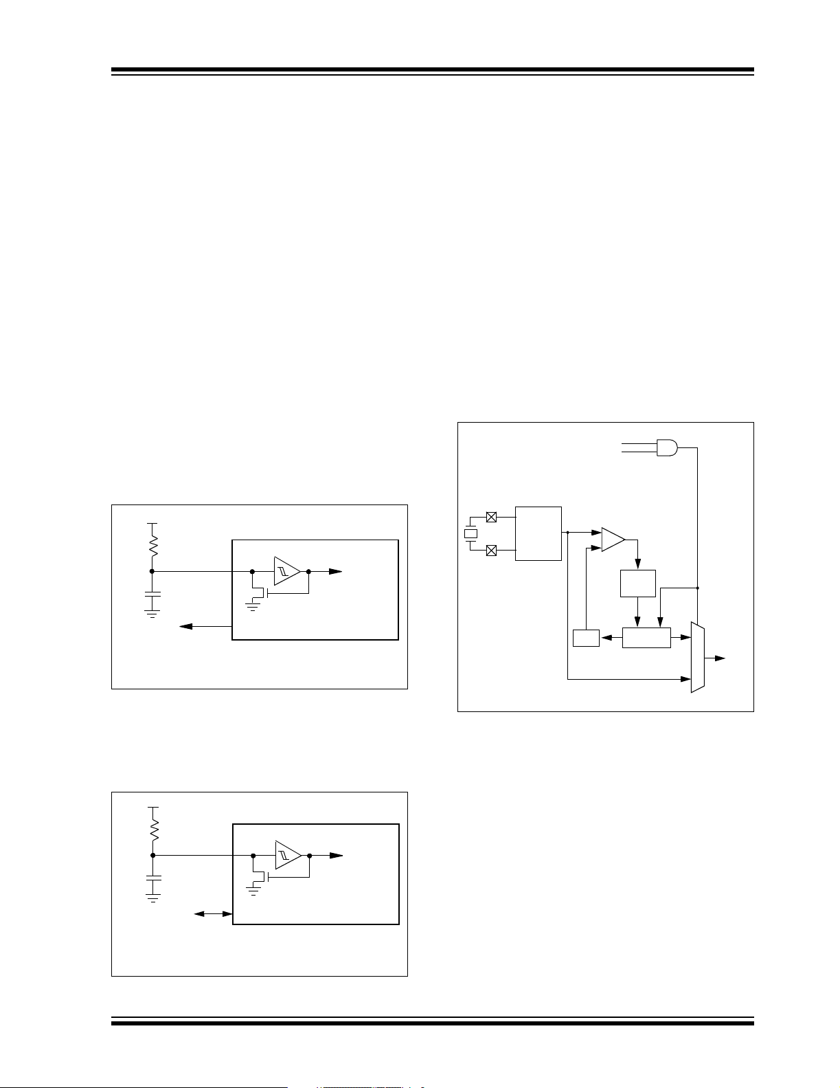
resonator. As a good starting point, the
recommended value of R
© 2007 Microchip Technology Inc. Preliminary DS39625C-page 23
S is 330Ω.
PIC18F2585/2680/4585/4680
TABLE 2-2: CAPACITOR SELECTION FOR
CRYSTAL OSCILLATOR
Osc Type
LP 32 kHz 33 pF 33 pF
XT 1 MHz 33 pF 33 pF
HS 4 MHz 27 pF 27 pF
Capacitor values are for design guidance only.
These capacitors were tested with the crystals listed
below for basic start-up and operation. These values
are not optimized.
Different capacitor values may be required to produce
acceptable oscillator operation. The user should test
the performance of the oscillator over the expected
DD and temperature range for the application.
V
See the notes following this table for additional
information.
Note 1: Higher capacitance increases the stability
Crystal
Freq
200 kHz 15 pF 15 pF
4 MHz 27 pF 27 pF
8 MHz 22 pF 22 pF
20 MHz 15 pF 15 pF
Crystals Used:
32 kHz 4 MHz
200 kHz 8 MHz
1 MHz 20 MHz
of the oscillator but also increases the
start-up time.
2: When operating below 3V V
using certain ceramic resonators at any
voltage, it may be necessary to use the
HS mode or switch to a crystal oscillator.
3: Since each resonator/crystal has its own
characteristics, the user should consult
the resonator/crystal manufacturer for
appropriate values of external
components.
4: Rs may be required to avoid overdriving
crystals with low drive level specification.
5: Always verify oscillator performance over
DD and temperature range that is
the V
expected for the application.
Typical Capacitor Values
Tested:
C1 C2
DD, or when
An external clock source may also be connected to the
OSC1 pin in the HS mode, as shown in Figure 2-2.
FIGURE 2-2: EXTERNAL CLOCK
INPUT OPERATION
(HS OSCILLATOR
CONFIGURATION)
Clock from
Ext. System
Open
OSC1
OSC2
PIC18FXXXX
(HS Mode)
2.3 External Clock Input
The EC and ECIO Oscillator modes require an external
clock source to be connected to the OSC1 pin. There is
no oscillator start-up time required after a Power-on
Reset or after an exit from Sleep mode.
In the EC Oscillator mode, the oscillator frequency
divided by 4 is available on the OSC2 pin. This signal
may be used for test purposes or to synchronize other
logic. Figure 2-3 shows the pin connections for the EC
Oscillator mode.
FIGURE 2-3: EXTERNAL CLOCK
INPUT OPERATION
(EC CONFIGURATION)
Clock from
Ext. System
F
OSC/4
The ECIO Oscillator mode functions like the EC mode,
except that the OSC2 pin becomes an additional
general purpose I/O pin. The I/O pin becomes bit 6 of
PORTA (RA6). Figure 2-4 shows the pin connections
for the ECIO Oscillator mode.
FIGURE 2-4: EXTERNAL CLOCK
Clock from
Ext. System
RA6
OSC1/CLKI
PIC18FXXXX
OSC2/CLKO
INPUT OPERATION
(ECIO CONFIGURATION)
OSC1/CLKI
PIC18FXXXX
I/O (OSC2)
DS39625C-page 24 Preliminary © 2007 Microchip Technology Inc.
PIC18F2585/2680/4585/4680
2.4 RC Oscillator
For timing insensitive applications, the “RC” and
“RCIO” device options offer additional cost savings.
The actual oscillator frequency is a function of several
factors:
• supply voltage
• values of the external resistor (R
capacitor (C
EXT)
• operating temperature
Given the same device, operating voltage and temperature and component values, there will also be unit-to-unit
frequency variations. These are due to factors such as:
• normal manufacturing variation
• difference in lead frame capacitance between
package types (especially for low C
• variations within the tolerance of limits of R
EXT
and C
In the RC Oscillator mode, the oscillator frequency
divided by 4 is available on the OSC2 pin. This signal
may be used for test purposes or to synchronize other
logic. Figure 2-5 shows how the R/C combination is
connected.
FIGURE 2-5: RC OSCILLATOR MODE
VDD
REXT
OSC1
CEXT
VSS
F
Recommended values: 3 kΩ ≤ REXT ≤ 100 kΩ
OSC/4
OSC2/CLKO
EXT > 20 pF
C
EXT) and
EXT values)
EXT
Internal
Clock
PIC18FXXXX
2.5 PLL Frequency Multiplier
A Phase Locked Loop (PLL) circuit is provided as an
option for users who wish to use a lower frequency
oscillator circuit or to clock the device up to its highest
rated frequency from a crystal oscillator. This may be
useful for customers who are concerned with EMI due
to high-frequency crystals or users who require higher
clock speeds from an internal oscillator.
2.5.1 HSPLL OSCILLATOR MODE
The HSPLL mode makes use of the HS mode oscillator
for frequencies up to 10 MHz. A PLL then multiplies the
oscillator output frequency by 4 to produce an internal
clock frequency up to 40 MHz.
The PLL is only available to the crystal oscillator when
the FOSC3:FOSC0 Configuration bits are programmed
for HSPLL mode (= 0110).
FIGURE 2-7: PLL BLOCK DIAGRAM
(HS MODE)
HS Osc Enable
PLL Enable
(from Configuration Register 1H)
OSC2
OSC1
HS Mode
Crystal
Osc
IN
F
FOUT
÷4
Phase
Comparator
Loop
Filter
VCO
SYSCLK
MUX
The RCIO Oscillator mode (Figure 2-6) functions like
the RC mode, except that the OSC2 pin becomes an
additional general purpose I/O pin. The I/O pin
becomes bit 6 of PORTA (RA6).
2.5.2 PLL AND INTOSC
The PLL is also available to the internal oscillator block
in selected oscillator modes. In this configuration, the
FIGURE 2-6: RCIO OSCILLATOR MODE
VDD
PLL is enabled in software and generates a clock
output of up to 32MHz. The operation of INTOSC with
the PLL is described in Section 2.6.4 “PLL in INTOSC
REXT
OSC1
CEXT
VSS
RA6
Recommended values: 3 kΩ ≤ REXT ≤ 100 kΩ
© 2007 Microchip Technology Inc. Preliminary DS39625C-page 25
I/O (OSC2)
C
EXT > 20 pF
Internal
Clock
PIC18FXXXX
Modes”.

PIC18F2585/2680/4585/4680
2.6 Internal Oscillator Block
The PIC18F2585/2680/4585/4680 devices include an
internal oscillator block which generates two different
clock signals; either can be used as the microcontroller’s
clock source. This may eliminate the need for external
oscillator circuits on the OSC1 and/or OSC2 pins.
The main output (INTOSC) is an 8MHz clock source,
which can be used to directly drive the device clock. It
also drives a postscaler, which can provide a range of
clock frequencies from 31 kHz to 4 MHz. The INTOSC
output is enabled when a clock frequency from 125 kHz
to 8 MHz is selected.
The other clock source is the internal RC oscillator
(INTRC), which provides a nominal 31 kHz output.
INTRC is enabled if it is selected as the device clock
source; it is also enabled automatically when any of the
following are enabled:
• Power-up Timer
• Fail-Safe Clock Monitor
• Watchdog Timer
• Two-Speed Start-up
These features are discussed in greater detail in
Section 24.0 “Special Features of the CPU”.
The clock source frequency (INTOSC direct, INTRC
direct or INTOSC postscaler) is selected by configuring
the IRCF bits of the OSCCON register (Register 2-2).
2.6 enH918.5(t-unfg2sTD0.1710.7sh4o]TJ0 -2cc647.2.o(10.7sh4g)13.37ccl)12.4 81 Te.9(e)-1(2)-12u9
DS39625C-page 26 Preliminary © 2007 Microchip Technology Inc.

PIC18F2585/2680/4585/4680
REGISTER 2-1: OSCTUNE: OSCILLATOR TUNING REGISTER
R/W-0 R/W-0
INTSRC PLLEN
bit 7 bit 0
bit 7 INTSRC: Internal Oscillator Low-Frequency Source Select bit
1 = 31.25 kHz device clock derived from 8 MHz INTOSC source (divide-by-256 enabled)
0 = 31 kHz device clock derived directly from INTRC internal oscillator
bit 6 PLLEN: Frequency Multiplier PLL for INTOSC Enable bit
1 = PLL enabled for INTOSC (4 MHz and 8 MHz only)
0 = PLL disabled
Note 1: Available only in certain oscillator configurations; otherwise, this bit is unavailable
bit 5 Unimplemented: Read as ‘0’
bit 4-0 TUN4:TUN0: Frequency Tuning bits
01111 = Maximum frequency
• •
• •
00001
00000 = Center frequency. Oscillator module is running at the calibrated frequency.
11111
• •
• •
10000 = Minimum frequency
(1)
(1)
and reads as ‘0’. See text for details.
U-0 R/W-0 R/W-0 R/W-0 R/W-0 R/W-0
— TUN4 TUN3 TUN2 TUN1 TUN0
(1)
Legend:
R = Readable bit W = Writable bit U = Unimplemented bit, read as ‘0’
-n = Value at POR ‘1’ = Bit is set ‘0’ = Bit is cleared x = Bit is unknown
2.6.5.1 Compensating with the EUSART
An adjustment may be required when the EUSART
begins to generate framing errors or receives data with
errors while in Asynchronous mode. Framing errors
indicate that the device clock frequency is too high. To
adjust for this, decrement the value in OSCTUNE to
reduce the clock frequency. On the other hand, errors
in data may suggest that the clock speed is too low. To
compensate, increment OSCTUNE to increase the
clock frequency.
2.6.5.2 Compensating with the Timers
This technique compares device clock speed to some
reference clock. Two timers may be used; one timer is
clocked by the peripheral clock, while the other is
clocked by a fixed reference source, such as the
Timer1 oscillator.
Both timers are cleared, but the timer clocked by the
reference generates interrupts. When an interrupt
occurs, the internally clocked timer is read and both
timers are cleared. If the internally clocked timer value
is greater than expected, then the internal oscillator
block is running too fast. To adjust for this, decrement
the OSCTUNE register.
2.6.5.3 Compensating with the CCP1
Module in Capture Mode
The CCP1 module can use free running Timer1 (or
Timer3), clocked by the internal oscillator block and an
external event with a known period (i.e., AC power
frequency). The time of the first event is captured in the
CCPRxH:CCPRxL registers and is recorded for use
later. When the second event causes a capture, the
time of the first event is subtracted from the time of the
second event. Since the period of the external event is
known, the time difference between events can be
calculated.
If the measured time is much greater than the
calculated time, the internal oscillator block is running
too fast. To compensate, decrement the OSCTUNE
register. If the measured time is much less than the
calculated time, the internal oscillator block is running
too slow. To compensate, increment the OSCTUNE
register.
© 2007 Microchip Technology Inc. Preliminary DS39625C-page 27
PIC18F2585/2680/4585/4680
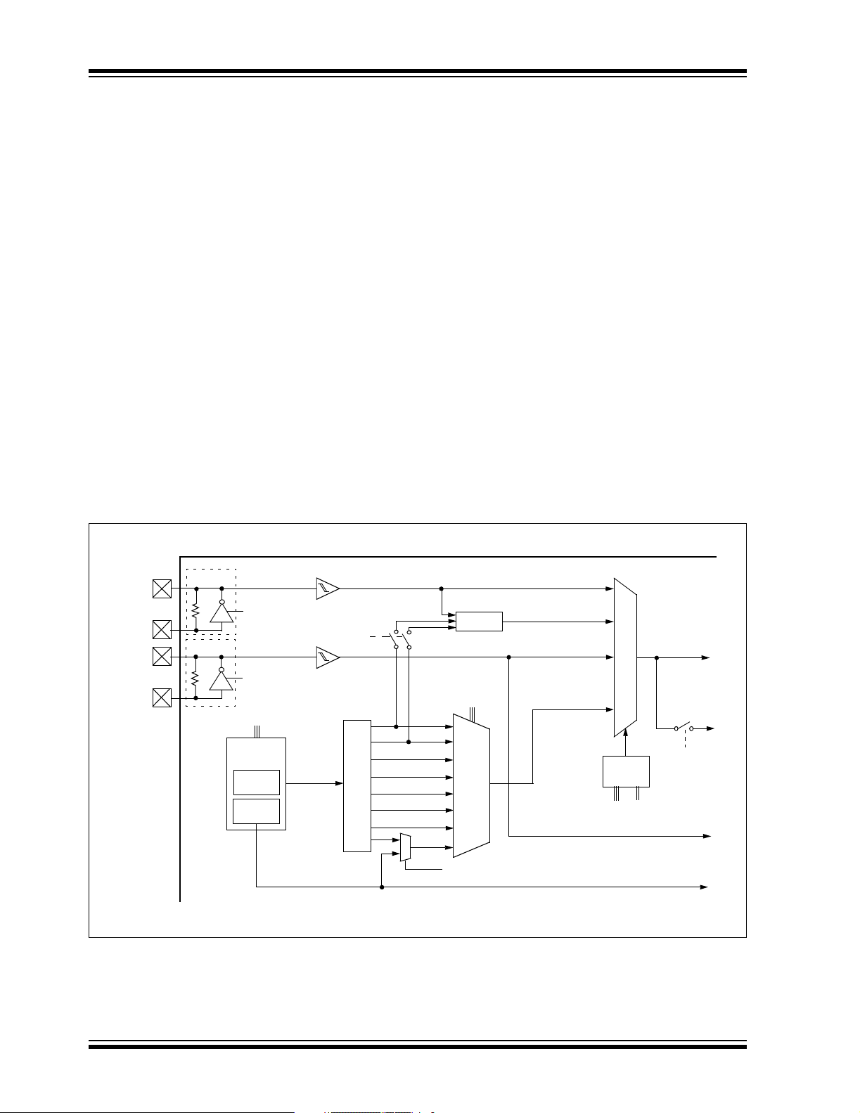
2.7 Clock Sources and Oscillator Switching
Like previous PIC18 devices, the PIC2585/2680/
4585/4680 family includes a feature that allows the
device clock source to be switched from the main
oscillator to an alternate low-frequency clock source.
PIC18F2585/2680/4585/4680 devices offer two alternate clock sources. When an alternate clock source is
enabled, the various power managed operating modes
are available.
Essentially, there are three clock sources for these
devices:
• Primary oscillators
• Secondary oscillators
• Internal oscillator block
The primary oscillators include the External Crystal
and Resonator modes, the External RC modes, the
External Clock modes and the internal oscillator block.
The particular mode is defined by the FOSC3:FOSC0
Configuration bits. The details of these modes are
covered earlier in this chapter.
The secondary oscillators are those external sources
not connected to the OSC1 or OSC2 pins. These
sources may continue to operate even after the
controller is placed in a power managed mode.
PIC18F2585/2680/4585/4680 devices offer the Timer1
oscillator as a secondary oscillator. This oscillator, in all
power managed modes, is often the time base for
functions such as a real-time clock.
Most often, a 32.768kHz watch crystal is connected
between the RC0/T1OSO/T13CKI and RC1/T1OSI
pins. Like the LP mode oscillator circuit, loading
capacitors are also connected from each pin to ground.
The Timer1 oscillator is discussed in greater detail in
Section 12.3 “Timer1 Oscillator”.
In addition to being a primary clock source, the internal
oscillator block is available as a power managed
mode clock source. The INTRC source is also used as
the clock source for several special features, such as
the WDT and Fail-Safe Clock Monitor.
The clock sources for the PIC18F2585/2680/4585/4680
devices are shown in Figure 2-8. See Section 24.0
“Special Features of the CPU” for Configuration
register details.
FIGURE 2-8: PIC18F2585/2680/4585/4680 CLOCK DIAGRAM
PIC18FX585/X680
8 MHz
4 MHz
2 MHz
1 MHz
500 kHz
Postscaler
250 kHz
125 kHz
1
0
31 kHz
4 x PLL
OSCCON<6:4>
111
110
101
100
MUX
011
010
001
000
OSCTUNE<7>
HSPLL, INTOSC/PLL
OSC2
OSC1
T1OSO
T1OSI
Primary Oscillator
Sleep
Secondary Oscillator
T1OSCEN
Enable
Oscillator
OSCCON<6:4>
Internal
Oscillator
Block
8 MHz
Source
INTRC
Source
31 kHz (INTRC)
OSCTUNE<6>
8 MHz
(INTOSC)
LP, XT, HS, RC, EC
T1OSC
Internal Oscillator
FOSC3:FOSC0
Peripherals
MUX
CPU
Clock
Control
Clock Source Option
for other Modules
WDT, PWRT, FSCM
and Two-Speed Startup
IDLEN
OSCCON<1:0>
DS39625C-page 28 Preliminary © 2007 Microchip Technology Inc.

PIC18F2585/2680/4585/4680
2.7.1 OSCILLATOR CONTROL REGISTER
The OSCCON register (Register 2-2) controls several
aspects of the device clock’s operation, both in full
power operation and in power managed modes.
The System Clock Select bits, SCS1:SCS0, select the
clock source. The available clock sources are the
primary clock (defined by the FOSC3:FOSC0 Configuration bits), the secondary clock (Timer1 oscillator) and
the internal oscillator block. The clock source changes
immediately after one or more of the bits is written to,
following a brief clock transition interval. The SCS bits
are cleared on all forms of Reset.
The Internal Oscillator Frequency Select bits,
IRCF2:IRCF0, select the frequency output of the
internal oscillator block to drive the device clock. The
choices are the INTRC source, the INTOSC source
(8 MHz) or one of the frequencies derived from the
INTOSC postscaler (31kHz to 4 MHz). If the internal
oscillator block is supplying the device clock, changing
the states of these bits will have an immediate change
on the internal oscillator’s output. On device Resets,
the default output frequency of the internal oscillator
block is set at 1 MHz.
When an output frequency of 31 kHz is selected
(IRCF2:IRCF0 = 000), users may choose which
internal oscillator acts as the source. This is done with
the INTSRC bit in the OSCTUNE register
(OSCTUNE<7>). Setting this bit selects INTOSC as a
31.25 kHz clock source by enabling the divide-by-256
output of the INTOSC postscaler. Clearing INTSRC
selects INTRC (nominally 31 kHz) as the clock source.
This option allows users to select the tunable and more
precise INTOSC as a clock source, while maintaining
power savings with a very low clock speed. Regardless
of the setting of INTSRC, INTRC always remains the
clock source for features such as the Watchdog Timer
and the Fail-Safe Clock Monitor.
The OSTS, IOFS and T1RUN bits indicate which clock
source is currently providing the device clock. The
OSTS bit indicates that the Oscillator Start-up Timer
has timed out and the primary clock is providing the
device clock in primary clock modes. The IOFS bit
indicates when the internal oscillator block has
stabilized and is providing the device clock in RC Clock
modes. The T1RUN bit (T1CON<6>) indicates when
the Timer1 oscillator is providing the device clock in
secondary clock modes. In power managed modes,
only one of these three bits will be set at any time. If
none of these bits are set, the INTRC is providing the
clock or the internal oscillator block has just started and
is not yet stable.
The IDLEN bit determines if the device goes into Sleep
mode or one of the Idle modes when the SLEEP
instruction is executed.
The use of the flag and control bits in the OSCCON
register is discussed in more detail in Section 3.0
“Power Managed Modes”.
Note 1: The Timer1 oscillator must be enabled to
select the secondary clock source. The
Timer1 oscillator is enabled by setting the
T1OSCEN bit in the Timer1 Control register (T1CON<3>). If the Timer1 oscillator is
not enabled, then any attempt to select a
secondary clock source when executing a
SLEEP instruction will be ignored.
2: It is recommended that the Timer1
oscillator be operating and stable before
executing the SLEEP instruction, or a very
long delay may occur while the Timer1
oscillator starts.
2.7.2 OSCILLATOR TRANSITIONS
PIC18F2585/2680/4585/4680 devices contain circuitry
to prevent clock “glitches” when switching between
clock sources. A short pause in the device clock occurs
during the clock switch. The length of this pause is the
sum of two cycles of the old clock source and three to
four cycles of the new clock source. This formula
assumes that the new clock source is stable.
Clock transitions are discussed in greater detail in
Section 3.1.2 “Entering Power Managed Modes”.
© 2007 Microchip Technology Inc. Preliminary DS39625C-page 29

PIC18F2585/2680/4585/4680
REGISTER 2-2: OSCCON: OSCILLATOR CONTROL REGISTER
R/W-0 R/W-1 R/W-0 R/W-0 R
IDLEN IRCF2 IRCF1 IRCF0 OSTS IOFS SCS1 SCS0
bit 7 bit 0
bit 7 IDLEN: Idle Enable bit
1 = Device enters Idle mode on SLEEP instruction
0 = Device enters Sleep mode on SLEEP instruction
bit 6-4 IRCF2:IRCF0: Internal Oscillator Frequency Select bits
(1)
R-0 R/W-0 R/W-0
DS39625C-page 30 Preliminary © 2007 Microchip Technology Inc.

PIC18F2585/2680/4585/4680
2.8 Effects of Power Managed Modes on the Various Clock Sources
When PRI_IDLE mode is selected, the designated
primary oscillator continues to run without interruption.
For all other power managed modes, the oscillator
using the OSC1 pin is disabled. The OSC1 pin (and
OSC2 pin, if used by the oscillator) will stop oscillating.
In secondary clock modes (SEC_RUN and
SEC_IDLE), the Timer1 oscillator is operating and
providing the device clock. The Timer1 oscillator may
also run in all power managed modes if required to
clock Timer1 or Timer3.
In internal oscillator modes (RC_RUN and RC_IDLE),
the internal oscillator block provides the device clock
source. The 31 kHz INTRC output can be used directly
to provide the clock and may be enabled to support
various special features, regardless of the power
managed mode (see Section 24.2 “Watchdog Timer
(WDT)”, Section 24.3 “Two-Speed Start-up” and
Section 24.4 “Fail-Safe Clock Monitor” for more
information on WDT, Two-Speed Start-up and Fail-Safe
Clock Monitor). The INTOSC output at 8 MHz may be
used directly to clock the device or may be divided
down by the postscaler. The INTOSC output is disabled
if the clock is provided directly from the INTRC output.
If the Sleep mode is selected, all clock sources are
stopped. Since all the transistor switching currents
have been stopped, Sleep mode achieves the lowest
current consumption of the device (only leakage
currents).
Enabling any on-chip feature that will operate during
Sleep will increase the current consumed during Sleep.
The INTRC is required to support WDT operation. The
Timer1 oscillator may be operating to support a
real-time clock. Other features may be operating that
do not require a device clock source (i.e., SSP slave,
PSP, INTn pins and others). Peripherals that may add
significant current consumption are listed in
Section 27.2 “DC Characteristics: Power Down and
Supply Current”.
2.9 Power-up Delays
Power-up delays are controlled by two timers, so that
no external Reset circuitry is required for most applications. The delays ensure that the device is kept in
Reset until the device power supply is stable under normal circumstances and the primary clock is operating
and stable. For additional information on power-up
delays, see Section 4.5 “Device Reset Timers”.
The first timer is the Power-up Timer (PWRT), which
provides a fixed delay on power-up (parameter 33,
Table 27-10). It is enabled by clearing (= 0) the
PWRTEN
The second timer is the Oscillator Start-up Timer
(OST), intended to keep the chip in Reset until the
crystal oscillator is stable (LP, XT and HS modes). The
OST does this by counting 1024 oscillator cycles
before allowing the oscillator to clock the device.
When the HSPLL Oscillator mode is selected, the
device is kept in Reset for an additional 2 ms, following
the HS mode OST delay, so the PLL can lock to the
incoming clock frequency.
There is a delay of interval T
Table 27-10), following POR, while the controller
becomes ready to execute instructions. This delay runs
concurrently with any other delays. This may be the
only delay that occurs when any of the EC, RC or INTIO
modes are used as the primary clock source.
Configuration bit.
CSD (parameter 38,
TABLE 2-3: OSC1 AND OSC2 PIN STATES IN SLEEP MODE
OSC Mode OSC1 Pin OSC2 Pin
RC, INTIO1 Floating, external resistor should pull high At logic low (clock/4 output)
RCIO, INTIO2 Floating, external resistor should pull high Configured as PORTA, bit 6
ECIO Floating, pulled by external clock Configured as PORTA, bit 6
EC Floating, pulled by external clock At logic low (clock/4 output)
LP, XT and HS Feedback inverter disabled at quiescent
voltage level
Note: See Table 4-2 in Section 4.0 “Reset” for time-outs due to Sleep and MCLR
© 2007 Microchip Technology Inc. Preliminary DS39625C-page 31
Feedback inverter disabled at quiescent
voltage level
Reset.

PIC18F2585/2680/4585/4680
NOTES:
DS39625C-page 32 Preliminary © 2007 Microchip Technology Inc.

PIC18F2585/2680/4585/4680
3.0 POWER MANAGED MODES
PIC18F2585/2680/4585/4680 devices offer a total of
seven operating modes for more efficient power
management. These modes provide a variety of
options for selective power conservation in applications
where resources may be limited (i.e., battery-powered
devices).
There are three categories of power managed modes:
• Run modes
• Idle modes
• Sleep mode
These categories define which portions of the device
are clocked and sometimes, what speed. The Run and
Idle modes may use any of the three available clock
sources (primary, secondary or internal oscillator
block); the Sleep mode does not use a clock source.
The power managed modes include several power
saving features offered on previous PIC
is the clock switching feature, offered in other PIC18
devices, allowing the controller to use the Timer1
oscillator in place of the primary oscillator. Also
included is the Sleep mode, offered by all PIC devices,
where all device clocks are stopped.
3.1 Selecting Power Managed Modes
Selecting a power managed mode requires two
decisions: if the CPU is to be clocked or not and the
selection of a clock source. The IDLEN bit
(OSCCON<7>) controls CPU clocking, while the
SCS1:SCS0 bits (OSCCON<1:0>) select the clock
source. The individual modes, bit settings, clock sources
and affected modules are summarized in Table 3-1.
®
devices. One
3.1.1 CLOCK SOURCES
The SCS1:SCS0 bits allow the selection of one of three
clock sources for power managed modes. They are:
• the primary clock, as defined by the
FOSC3:FOSC0 Configuration bits
• the secondary clock (the Timer1 oscillator)
• the internal oscillator block (for RC modes)
3.1.2 ENTERING POWER MANAGED
MODES
Switching from one power managed mode to another
begins by loading the OSCCON register. The
SCS1:SCS0 bits select the clock source and determine
which Run or Idle mode is to be used. Changing these
bits causes an immediate switch to the new clock
source, assuming that it is running. The switch may
also be subject to clock transition delays. These are
discussed in Section 3.1.3 “Clock Transitions And
Status Indicators” and subsequent sections.
Entry to the Power Managed Idle or Sleep modes is
triggered by the execution of a SLEEP instruction. The
actual mode that results depends on the status of the
IDLEN bit.
Depending on the current mode and the mode being
switched to, a change to a power managed mode does
not always require setting all of these bits. Many
transitions may be done by changing the oscillator
select bits, or changing the IDLEN bit, prior to issuing a
SLEEP instruction. If the IDLEN bit is already
configured correctly, it may only be necessary to
perform a SLEEP instruction to switch to the desired
mode.
TABLE 3-1: POWER MANAGED MODES
Mode
IDLEN<7>
Sleep 0 N/A Off Off None – All clocks are disabled
PRI_RUN N/A 00 Clocked Clocked Primary – LP, XT, HS, HSPLL, RC, EC, INTRC
SEC_RUN N/A 01 Clocked Clocked Secondary – Timer1 Oscillator
RC_RUN N/A 1x Clocked Clocked Internal Oscillator Block
PRI_IDLE 100Off Clocked Primary – LP, XT, HS, HSPLL, RC, EC
SEC_IDLE 101Off Clocked Secondary – Timer1 Oscillator
RC_IDLE 11xOff Clocked Internal Oscillator Block
Note 1: IDLEN reflects its value when the SLEEP instruction is executed.
2: Includes INTOSC and INTOSC postscaler, as well as the INTRC source.
© 2007 Microchip Technology Inc. Preliminary DS39625C-page 33
OSCCON Bits Module Clocking
(1)
SCS1:SCS0<1:0> CPU Peripherals
Available Clock and Oscillator Source
(2)
This is the normal full power execution mode.
(2)
(2)
:

PIC18F2585/2680/4585/4680
3.1.3 CLOCK TRANSITIONS AND STATUS INDICATORS
The length of the transition between clock sources is
the sum of two cycles of the old clock source and three
to four cycles of the new clock source. This formula
assumes that the new clock source is stable.
Three bits indicate the current clock source and its
status. They are:
• OSTS (OSCCON<3>)
• IOFS (OSCCON<2>)
• T1RUN (T1CON<6>)
In general, only one of these bits will be set while in a
given power managed mode. When the OSTS bit is
set, the primary clock is providing the device clock.
When the IOFS bit is set, the INTOSC output is providing a stable 8MHz clock source to a divider that
actually drives the device clock. When the T1RUN bit is
set, the Timer1 oscillator is providing the clock. If none
of these bits are set, then either the INTRC clock
source is clocking the device, or the INTOSC source is
not yet stable.
If the internal oscillator block is configured as the
primary clock source by the FOSC3:FOSC0 Configuration bits, then both the OSTS and IOFS bits may be set
when in PRI_RUN or PRI_IDLE modes. This indicates
that the primary clock (INTOSC output) is generating a
stable 8 MHz output. Entering another RC power
managed mode at the same frequency would clear the
OSTS bit.
Note 1: Caution should be used when modifying a
single IRCF bit. If V
possible to select a higher clock speed
than is supported by the low VDD.
Improper device operation may result if
the VDD/FOSC specifications are violated.
2: Executing a SLEEP instruction does not
necessarily place the device into Sleep
mode. It acts as the trigger to place the
controller into either the Sleep mode or
one of the Idle modes, depending on the
setting of the IDLEN bit.
DD is less than 3V, it is
3.1.4 MULTIPLE SLEEP COMMANDS
The power managed mode that is invoked with the
SLEEP instruction is determined by the setting of the
IDLEN bit at the time the instruction is executed. If
another SLEEP instruction is executed, the device will
enter the power managed mode specified by IDLEN at
that time. If IDLEN has changed, the device will enter
the new power managed mode specified by the new
setting.
3.2 Run Modes
In the Run modes, clocks to both the core and
peripherals are active. The difference between these
modes is the clock source.
3.2.1 PRI_RUN MODE
The PRI_RUN mode is the normal, full power execution
mode of the microcontroller. This is also the default
mode upon a device Reset, unless Two-Speed Start-up
is enabled (see Section 24.3 “Two-Speed Start-up”
for details). In this mode, the OSTS bit is set. The IOFS
bit may be set if the internal oscillator block is the
primary clock source (see Section 2.7.1 “Oscillator
Control Register”).
3.2.2 SEC_RUN MODE
The SEC_RUN mode is the compatible mode to the
“clock switching” feature offered in other PIC18
devices. In this mode, the CPU and peripherals are
clocked from the Timer1 oscillator. This gives users the
option of lower power consumption while still using a
high accuracy clock source.
SEC_RUN mode is entered by setting the SCS1:SCS0
bits to ‘01’. The device clock source is switched to the
Timer1 oscillator (see Figure 3-1), the primary oscillator is shut down, the T1RUN bit (T1CON<6>) is set and
the OSTS bit is cleared.
Note: The Timer1 oscillator should already be
running prior to entering SEC_RUN mode.
If the T1OSCEN bit is not set when the
SCS1:SCS0 bits are set to ‘01’, entry to
SEC_RUN mode will not occur. If the
Timer1 oscillator is enabled but not yet
running, device clocks will be delayed until
the oscillator has started. In such situations, initial oscillator operation is far from
stable and unpredictable operation may
result.
On transitions from SEC_RUN mode to PRI_RUN, the
peripherals and CPU continue to be clocked from the
Timer1 oscillator while the primary clock is started.
When the primary clock becomes ready, a clock switch
back to the primary clock occurs (see Figure 3-2).
When the clock switch is complete, the T1RUN bit is
cleared, the OSTS bit is set and the primary clock is
providing the clock. The IDLEN and SCS bits are not
affected by the wake-up; the Timer1 oscillator
continues to run.
DS39625C-page 34 Preliminary © 2007 Microchip Technology Inc.

PIC18F2585/2680/4585/4680
FIGURE 3-1: TRANSITION TIMING FOR ENTRY TO SEC_RUN MODE
FIGURE 3-2: TRANSITION TIMING FROM SEC_RUN MODE TO PRI_RUN MODE (HSPLL)
3.2.3 RC_RUN MODE
In RC_RUN mode, the CPU and peripherals are
clocked from the internal oscillator block using the
INTOSC multiplexer; the primary clock is shut down.
When using the INTRC source, this mode provides the
best power conservation of all the Run modes, while
still executing code. It works well for user applications
which are not highly timing sensitive or do not require
high-speed clocks at all times.
If the primary clock source is the internal oscillator
block (either INTRC or INTOSC), there are no distinguishable differences between PRI_RUN and
RC_RUN modes during execution. However, a clock
switch delay will occur during entry to and exit from
RC_RUN mode. Therefore, if the primary clock source
is the internal oscillator block, the use of RC_RUN
mode is not recommended.
© 2007 Microchip Technology Inc. Preliminary DS39625C-page 35
This mode is entered by setting SCS1 to ‘1’. Although
it is ignored, it is recommended that SCS0 also be
cleared; this is to maintain software compatibility with
future devices. When the clock source is switched to
the INTOSC multiplexer (see Figure3-3), the primary
oscillator is shut down and the OSTS bit is cleared. The
IRCF bits may be modified at any time to immediately

PIC18F2585/2680/4585/4680
If the IRCF bits and the INTSRC bit are all clear, the
INTOSC output is not enabled and the IOFS bit will
remain clear; there will be no indication of the current
clock source. The INTRC source is providing the
device clocks.
If the IRCF bits are changed from all clear (thus,
enabling the INTOSC output) or if INTSRC is set, the
IOFS bit becomes set after the INTOSC output
becomes stable. Clocks to the device continue while
the INTOSC source stabilizes after an interval of
IOBST.
T
On transitions from RC_RUN mode to PRI_RUN mode,
the device continues to be clocked from the INTOSC
multiplexer while the primary clock is started. When the
primary clock becomes ready, a clock switch to the
primary clock occurs (see Figure 3-4). When the clock
switch is complete, the IOFS bit is cleared, the OSTS
bit is set and the primary clock is providing the device
clock. The IDLEN and SCS bits are not affected by the
switch. The INTRC source will continue to run if either
the WDT or the Fail-Safe Clock Monitor is enabled.
If the IRCF bits were previously at a non-zero value or
if INTSRC was set before setting SCS1 and the
INTOSC source was already stable, the IOFS bit will
remain set.
FIGURE 3-3: TRANSITION TIMING TO RC_RUN MODE
Q4Q3Q2
Q1
123 n-1n
Clock Transition
PC + 2PC
INTRC
OSC1
CPU
Clock
Peripheral
Clock
Program
Counter
Q1
Q4Q3Q2 Q1 Q3Q2
PC + 4
FIGURE 3-4: TRANSITION TIMING FROM RC_RUN MODE TO PRI_RUN MODE
Q3 Q4
Q1
Q1
INTOSC
Multiplexer
OSC1
PLL Clock
Output
CPU Clock
Peripheral
Clock
Program
Counter
SCS1:SCS0 bits changed
Note 1: TOST = 1024 TOSC; TPLL = 2 ms (approx). These intervals are not shown to scale.
TOST
(1)
PC
Q2
Q3
TPLL
OSTS bit set
Q4
(1)
12 n-1n
Clock
Transition
PC + 2
Q2
Q1
PC + 4
Q2
Q3
DS39625C-page 36 Preliminary © 2007 Microchip Technology Inc.

PIC18F2585/2680/4585/4680
3.3 Sleep Mode
The Power Managed Sleep mode in the
PIC18F2585/2680/4585/4680 devices is identical to
the legacy Sleep mode offered in all other PIC devices.
It is entered by clearing the IDLEN bit (the default state
on device Reset) and executing the SLEEP instruction.
This shuts down the selected oscillator (Figure 3-5). All
clock source status bits are cleared.
Entering the Sleep mode from any other mode does not
require a clock switch. This is because no clocks are
needed once the controller has entered Sleep. If the
WDT is selected, the INTRC source will continue to
operate. If the Timer1 oscillator is enabled, it will also
continue to run.
When a wake event occurs in Sleep mode (by interrupt,
Reset or WDT time-out), the device will not be clocked
until the clock source selected by the SCS1:SCS0 bits
becomes ready (see Figure 3-6), or it will be clocked
from the internal oscillator block if either the
Two-Speed Start-up or the Fail-Safe Clock Monitor are
enabled (see Section 24.0 “Special Features of the
CPU”). In either case, the OSTS bit is set when the
primary clock is providing the device clocks. The
IDLEN and SCS bits are not affected by the wake-up.
3.4 Idle Modes
The Idle modes allow the controller’s CPU to be
selectively shut down while the peripherals continue to
operate. Selecting a particular Idle mode allows users
to further manage power consumption.
If the IDLEN bit is set to a ‘1’ when a SLEEP instruction is
executed, the peripherals will be clocked from the clock
source selected using the SCS1:SCS0 bits; however, the
CPU will not be clocked. The clock source status bits are
not affected. Setting IDLEN and executing a SLEEP
instruction provides a quick method of switching from a
given Run mode to its corresponding Idle mode.
If the WDT is selected, the INTRC source will continue
to operate. If the Timer1 oscillator is enabled, it will also
continue to run.
Since the CPU is not executing instructions, the only
exits from any of the Idle modes are by interrupt, WDT
time-out or a Reset. When a wake event occurs, CPU
execution is delayed by an interval of T
(parameter 38, Table 27-10) while it becomes ready to
execute code. When the CPU begins executing code,
it resumes with the same clock source for the current
Idle mode. For example, when waking from RC_IDLE
mode, the internal oscillator block will clock the CPU
and peripherals (in other words, RC_RUN mode). The
IDLEN and SCS bits are not affected by the wake-up.
While in any Idle mode or the Sleep mode, a WDT
time-out will result in a WDT wake-up to the Run mode
currently specified by the SCS1:SCS0 bits.
CSD
FIGURE 3-5: TRANSITION TIMING FOR ENTRY TO SLEEP MODE
Q4Q3Q2
Q1Q1
OSC1
CPU
Clock
Peripheral
Clock
Sleep
Program
Counter
PC + 2PC
FIGURE 3-6: TRANSITION TIMING FOR WAKE FROM SLEEP (HSPLL)
OSC1
PLL Clock
Output
CPU Clock
Peripheral
Clock
Program
Counter
Note1: T
Q1 Q2 Q3 Q4 Q1 Q2
(1)
TOST
Wake Event
OST = 1024 TOSC; TPLL = 2 ms (approx). These intervals are not shown to scale.
(1)
TPLL
PC
OSTS bit set
Q3 Q4 Q1 Q2
PC + 2
Q3 Q4
PC + 4
Q1 Q2 Q3 Q4
PC + 6
© 2007 Microchip Technology Inc. Preliminary DS39625C-page 37

PIC18F2585/2680/4585/4680
3.4.1 PRI_IDLE MODE
This mode is unique among the three Low-Power Idle
modes, in that it does not disable the primary device
clock. For timing sensitive applications, this allows for
the fastest resumption of device operation with its more
accurate primary clock source, since the clock source
does not have to “warm up” or transition from another
oscillator.
PRI_IDLE mode is entered from PRI_RUN mode by
setting the IDLEN bit and executing a SLEEP instruction. If the device is in another Run mode, set IDLEN
first, then clear the SCS bits and execute SLEEP.
Although the CPU is disabled, the peripherals continue
to be clocked from the primary clock source specified
by the FOSC3:FOSC0 Configuration bits. The OSTS
bit remains set (see Figure3-7).
When a wake event occurs, the CPU is clocked from the
primary clock source. A delay of interval T
required between the wake event and when code
execution starts. This is required to allow the CPU to
become ready to execute instructions. After the
wake-up, the OSTS bit remains set. The IDLEN and
SCS bits are not affected by the wake-up (see
Figure 3-8).
CSD is
3.4.2 SEC_IDLE MODE
In SEC_IDLE mode, the CPU is disabled but the
peripherals continue to be clocked from the Timer1
oscillator. This mode is entered from SEC_RUN by setting the IDLEN bit and executing a SLEEP instruction. If
the device is in another Run mode, set the IDLEN bit
first, then set the SCS1:SCS0 bits to ‘01’ and execute
SLEEP. When the clock source is switched to the
Timer1 oscillator, the primary oscillator is shut down,
the OSTS bit is cleared and the T1RUN bit is set.
When a wake event occurs, the peripherals continue to
be clocked from the Timer1 oscillator. After an interval of
CSD following the wake event, the CPU begins
T
executing code being clocked by the Timer1 oscillator.
The IDLEN and SCS bits are not affected by the
wake-up; the Timer1 oscillator continues to run (see
Figure 3-8).
Note: The Timer1 oscillator should already be
running prior to entering SEC_IDLE mode.
If the T1OSCEN bit is not set when the
SLEEP instruction is executed, the SLEEP
instruction will be ignored and entry to
SEC_IDLE mode will not occur. If the
Timer1 oscillator is enabled but not yet running, peripheral clocks will be delayed until
the oscillator has started. In such situations,
initial oscillator operation is far from stable
and unpredictable operation may result.
FIGURE 3-7: TRANSITION TIMING FOR ENTRY TO IDLE MODE
Q1
OSC1
CPU Clock
Peripheral
Clock
Program
Counter
Q1
Q2
Q3
PC PC + 2
Q4
FIGURE 3-8: TRANSITION TIMING FOR WAKE FROM IDLE TO RUN MODE
OSC1
CPU Clock
Peripheral
Clock
Program
Counter
Q1 Q3 Q4
TCSD
PC
Q2
Wake Event
DS39625C-page 38 Preliminary © 2007 Microchip Technology Inc.

PIC18F2585/2680/4585/4680
3.4.3 RC_IDLE MODE
In RC_IDLE mode, the CPU is disabled but the peripherals continue to be clocked from the internal oscillator
block using the INTOSC multiplexer. This mode allows
for controllable power conservation during Idle periods.
From RC_RUN, this mode is entered by setting the
IDLEN bit and executing a SLEEP instruction. If the
device is in another Run mode, first set IDLEN, then set
the SCS1 bit and execute SLEEP. Although its value is
ignored, it is recommended that SCS0 also be cleared;
this is to maintain software compatibility with future
devices. The INTOSC multiplexer may be used to
select a higher clock frequency, by modifying the IRCF
bits, before executing the SLEEP instruction. When the
clock source is switched to the INTOSC multiplexer, the
primary oscillator is shut down and the OSTS bit is
cleared.
If the IRCF bits are set to any non-zero value or the
INTSRC bit is set, the INTOSC output is enabled. The
IOFS bit becomes set, after the INTOSC output
becomes stable, after an interval of T
(parameter 39, Table 27-10). Clocks to the peripherals
continue while the INTOSC source stabilizes. If the
IRCF bits were previously at a non-zero value, or
INTSRC was set before the SLEEP instruction was
executed and the INTOSC source was already stable,
the IOFS bit will remain set. If the IRCF bits and
INTSRC are all clear, the INTOSC output will not be
enabled, the IOFS bit will remain clear and there will be
no indication of the current clock source.
When a wake event occurs, the peripherals continue to
be clocked from the INTOSC multiplexer. After a delay
CSD following the wake event, the CPU begins
of T
executing code being clocked by the INTOSC multiplexer. The IDLEN and SCS bits are not affected by the
wake-up. The INTRC source will continue to run if
either the WDT or the Fail-Safe Clock Monitor is
enabled.
IOBST
3.5 Exiting Idle and Sleep Modes
An exit from Sleep mode or any of the Idle modes is
triggered by an interrupt, a Reset or a WDT time-out.
This section discusses the triggers that cause exits
from power managed modes. The clocking subsystem
actions are discussed in each of the power managed
modes (see Section 3.2 “Run Modes”, Section 3.3
“Sleep Mode” and Section 3.4 “Idle Modes”).
3.5.1 EXIT BY INTERRUPT
Any of the available interrupt sources can cause the
device to exit from an Idle mode or the Sleep mode to
a Run mode. To enable this functionality, an interrupt
source must be enabled by setting its enable bit in one
of the INTCON or PIE registers. The exit sequence is
initiated when the corresponding interrupt flag bit is set.
On all exits from Idle or Sleep modes by interrupt, code
execution branches to the interrupt vector if the
GIE/GIEH bit (INTCON<7>) is set. Otherwise, code
execution continues or resumes without branching
(see Section 9.0 “Interrupts”).
A fixed delay of interval T
is required when leaving Sleep and Idle modes. This
delay is required for the CPU to prepare for execution.
Instruction execution resumes on the first clock cycle
following this delay.
CSD following the wake event
3.5.2 EXIT BY WDT TIME-OUT
A WDT time-out will cause different actions depending
on which power managed mode the device is in when
the time-out occurs.
If the device is not executing code (all Idle modes and
Sleep mode), the time-out will result in an exit from the
power managed mode (see Section 3.2 “Run Modes”
and Section 3.3 “Sleep Mode”). If the device is
executing code (all Run modes), the time-out will result
in a WDT Reset (see Section 24.2 “Watchdog Timer
(WDT)”).
The WDT timer and postscaler are cleared by executing a SLEEP or CLRWDT instruction, the loss of a
currently selected clock source (if the Fail-Safe Clock
Monitor is enabled) and modifying the IRCF bits in the
OSCCON register if the internal oscillator block is the
device clock source.
3.5.3 EXIT BY RESET
Normally, the device is held in Reset by the Oscillator
Start-up Timer (OST) until the primary clock becomes
ready. At that time, the OSTS bit is set and the device
begins executing code. If the internal oscillator block is
the new clock source, the IOFS bit is set instead.
The exit delay time from Reset to the start of code
execution depends on both the clock sources before
and after the wake-up and the type of oscillator if the
new clock source is the primary clock. Exit delays are
summarized in Table 3-2.
Code execution can begin before the primary clock
becomes ready. If either the Two-Speed Start-up (see
Section 24.3 “Two-Speed Start-up”) or Fail-Safe
Clock Monitor (see Section 24.4 “Fail-Safe Clock
Monitor”) is enabled, the device may begin execution
as soon as the Reset source has cleared. Execution is
clocked by the INTOSC multiplexer driven by the
internal oscillator block. Execution is clocked by the
internal oscillator block until either the primary clock
becomes ready or a power managed mode is entered
before the primary clock becomes ready; the primary
clock is then shut down.
© 2007 Microchip Technology Inc. Preliminary DS39625C-page 39

PIC18F2585/2680/4585/4680
3.5.4 EXIT WITHOUT AN OSCILLATOR START-UP DELAY
Certain exits from power managed modes do not
invoke the OST at all. There are two cases:
• PRI_IDLE mode where the primary clock source
is not stopped; and
• the primary clock source is not any of the LP, XT,
HS or HSPLL modes.
In these instances, the primary clock source either
does not require an oscillator start-up delay, since it is
already running (PRI_IDLE), or normally does not
require an oscillator start-up delay (RC, EC and INTIO
Oscillator modes). However, a fixed delay of interval
CSD following the wake event is still required when
T
leaving Sleep and Idle modes to allow the CPU to prepare for execution. Instruction execution resumes on
the first clock cycle following this delay.
TABLE 3-2: EXIT DELAY ON WAKE-UP BY RESET FROM SLEEP MODE OR ANY IDLE MODE
(BY CLOCK SOURCES)
Clock Source
Before Wake-up
Primary Device Clock
(PRI_IDLE mode)
T1OSC or INTRC
INTOSC
None
(Sleep mode)
Note 1: In this instance, refers specifically to the 31 kHz INTRC clock source.
2: TCSD (parameter 38) is a required delay when waking from Sleep and all Idle modes and runs concurrently
with any other required delays (see Section 3.4 “Idle Modes”).
3: Includes both the INTOSC 8 MHz source and postscaler derived frequencies.
4: T
OST is the Oscillator Start-up Timer (parameter 32). t
also designated as T
5: Execution continues during T
(1)
(3)
PLL.
Clock Source
After Wake-up
Exit Delay
LP, XT, HS
(2)
EC, RC
(1)
INTRC
INTOSC
(3)
LP, XT, HS TOST
EC, RC
(1)
INTRC
INTOSC
(2)
LP, XT, HS TOST
EC, RC
(1)
INTRC
INTOSC
(2)
LP, XT, HS T
EC, RC
(1)
INTRC
INTOSC
IOBST (parameter 39), the INTOSC stabilization period.
(2)
is the PLL Lock-out Timer (parameter F12); it is
rc
CSD
T
(4)
(4)
rc
(2)
T
CSD
(5)
TIOBST
(5)
(4)
rc
(2)
T
CSD
None IOFS
(4)
OST
(4)
rc
(2)
CSD
T
(5)
TIOBST
Clock Ready Status
Bit (OSCCON)
OSTSHSPLL
—
IOFS
OSTSHSPLL TOST + t
—
IOFS
OSTSHSPLL TOST + t
—
OSTSHSPLL TOST + t
—
IOFS
DS39625C-page 40 Preliminary © 2007 Microchip Technology Inc.

PIC18F2585/2680/4585/4680
4.0 RESET
A simplified block diagram of the On-Chip Reset Circuit
is shown in Figure 4-1.
The PIC18F2585/2680/4585/4680 devices differentiate
between various kinds of Reset:
a) Power-on Reset (POR)
b) MCLR
Reset during normal operation
c) MCLR Reset during power managed modes
d) Watchdog Timer (WDT) Reset (during
execution)
e) Programmable Brown-out Reset (BOR)
f) RESET Instruction
g) Stack Full Reset
h) Stack Underflow Reset
This section discusses Resets generated by MCLR
POR and BOR and covers the operation of the various
start-up timers. Stack Reset events are covered in
Section 5.1.2.4 “Stack Full and Underflow Resets”.
WDT Resets are covered in Section 24.2 “Watchdog
,
4.1 RCON Register
Device Reset events are tracked through the RCON
register (Register 4-1). The lower five bits of the
register indicate that a specific Reset event has
occurred. In most cases, these bits can only be cleared
by the event and must be set by the application after
the event. The state of these flag bits, taken together,
can be read to indicate the type of Reset that just
occurred. This is described in more detail in
Section 4.6 “Reset State of Registers”.
The RCON register also has control bits for setting
interrupt priority (IPEN) and software control of the
BOR (SBOREN). Interrupt priority is discussed in
Section 9.0 “Interrupts”. BOR is covered in
Section 4.4 “Brown-out Reset (BOR)”.
Timer (WDT)”.
FIGURE 4-1: SIMPLIFIED BLOCK DIAGRAM OF ON-CHIP RESET CIRCUIT
RESET
Instruction
Stack
Pointer
Stack Full/Underflow Reset
MCLR
VDD
OSC1
( )_IDLE
Sleep
WDT
Time-out
DD Rise
V
Detect
Brown-out
Reset
OST/PWRT
32 μs
(1)
INTRC
External Reset
MCLRE
POR Pulse
BOREN
OST
PWRT
1024 Cycles
10-bit Ripple Counter
65.5 ms
11-bit Ripple Counter
S
Chip_Reset
R
Q
Enable PWRT
Enable OST
(2)
Note 1: This is the INTRC source from the internal oscillator block and is separate from the RC oscillator of the CLKI pin.
2: See Table 4-2 for time-out situations.
© 2007 Microchip Technology Inc. Preliminary DS39625C-page 41

PIC18F2585/2680/4585/4680
REGISTER 4-1: RCON: RESET CONTROL REGISTER
R/W-0 R/W-1
IPEN SBOREN
bit 7 bit 0
bit 7 IPEN: Interrupt Priority Enable bit
1 = Enable priority levels on interrupts
0 = Disable priority levels on interrupts (16CXXX Compatibility mode)
bit 6 SBOREN: BOR Software Enable bit
If BOREN1:BOREN0 = 01:
1 = BOR is enabled
0 = BOR is disabled
If BOREN1:BOREN0 =
Bit is disabled and read as ‘0’.
bit 5 Unimplemented: Read as ‘0’
bit 4 RI: RESET Instruction Flag bit
1 = The RESET instruction was not executed (set by firmware only)
0 = The RESET instruction was executed causing a device Reset (must be set in software after
a Brown-out Reset occurs)
bit 3 TO: Watchdog Time-out Flag bit
1 = Set by power-up, CLRWDT instruction or SLEEP instruction
0 = A WDT time-out occurred
bit 2 PD
bit 1 POR
bit 0 BOR
: Power-down Detection Flag bit
1 = Set by power-up or by the CLRWDT instruction
0 = Set by execution of the SLEEP instruction
: Power-on Reset Status bit
1 = A Power-on Reset has not occurred (set by firmware only)
0 = A Power-on Reset occurred (must be set in software after a Power-on Reset occurs)
: Brown-out Reset Status bit
1 = A Brown-out Reset has not occurred (set by firmware only)
0 = A Brown-out Reset occurred (must be set in software after a Brown-out Reset occurs)
Note 1: If SBOREN is enabled, its Reset state is ‘1’; otherwise, it is ‘0’.
2: The actual Reset value of POR
(1)
notes following this register and Section 4.6 “Reset State of Registers” for
additional information.
U-0 R/W-1 R-1 R-1 R/W-0
—RITO PD POR BOR
(1)
00, 10 or 11:
(2)
is determined by the type of device Reset. See the
(2)
R/W-0
Legend:
R = Readable bit W = Writable bit U = Unimplemented bit, read as ‘0’
-n = Value at POR ‘1’ = Bit is set ‘0’ = Bit is cleared x = Bit is unknown
Note 1: It is recommended that the POR bit be set after a Power-on Reset has been
detected so that subsequent Power-on Resets may be detected.
2: Brown-out Reset is said to have occurred when BOR
that POR
DS39625C-page 42 Preliminary © 2007 Microchip Technology Inc.
was set to ‘1’ by software immediately after POR).
is ‘0’ and POR is ‘1’ (assuming

PIC18F2585/2680/4585/4680
4.2 Master Clear Reset (MCLR)
The MCLR pin provides a method for triggering an
external Reset of the device. A Reset is generated by
holding the pin low. These devices have a noise filter in
the MCLR
pulses.
The MCLR
including the WDT.
In PIC18F2585/2680/4585/4680 devices, the MCLR
input can be disabled with the MCLRE Configuration
bit. When MCLR
input. See Section 10.5 “PORTE, TRISE and LATE
Registers” for more information.
4.3 Power-on Reset (POR)
A Power-on Reset pulse is generated on-chip
Reset path which detects and ignores small
pin is not driven low by any internal Resets,
is disabled, the pin becomes a digital
© 2007 Microchip Technology Inc. Preliminary DS39625C-page 43

PIC18F2585/2680/4585/4680
4.4 Brown-out Reset (BOR)
PIC18F2585/2680/4585/4680 devices implement a BOR
circuit that provides the user with a number of configuration and power-saving options. The BOR is controlled by
the BORV1:BORV0 and BOREN1:BOREN0 Configuration bits. There are a total of four BOR configurations
which are summarized in Table 4-1.
The BOR threshold is set by the BORV1:BORV0 bits. If
BOR is enabled (any values of BOREN1:BOREN0,
except ‘00’), any drop of V
D005) for greater than T
the device. A Reset may or may not occur if V
below V
Brown-out Reset until V
If the Power-up Timer is enabled, it will be invoked after
V
Reset for an additional time delay, T
(parameter 33). If VDD drops below VBOR while the
Power-up Timer is running, the chip will go back into a
Brown-out Reset and the Power-up Timer will be
initialized. Once V
Timer will execute the additional time delay.
BOR and the Power-on Timer (PWRT) are
independently configured. Enabling BOR Reset does
not automatically enable the PWRT.
BOR for less than TBOR. The chip will remain in
DD rises above VBOR; it then will keep the chip in
DD rises above VBOR, the Power-up
4.4.1 SOFTWARE ENABLED BOR
When BOREN1:BOREN0 = 01, the BOR can be
enabled or disabled by the user in software. This is
done with the control bit, SBOREN (RCON<6>).
Setting SBOREN enables the BOR to function as
previously described. Clearing SBOREN disables the
BOR entirely. The SBOREN bit operates only in this
mode; otherwise it is read as ‘0’.
DD below VBOR (parameter
BOR (parameter 35) will reset
DD falls
DD rises above VBOR.
PWRT
Placing the BOR under software control gives the user
the additional flexibility of tailoring the application to its
environment without having to reprogram the device to
change BOR configuration. It also allows the user to
tailor device power consumption in software by eliminating the incremental current that the BOR consumes.
While the BOR current is typically very small, it may
have some impact in low-power applications.
Note: Even when BOR is under software control,
the BOR Reset voltage level is still set by
the BORV1:BORV0 Configuration bits. It
cannot be changed in software.
4.4.2 DETECTING BOR
When BOR is enabled, the BOR bit always resets to ‘0’
on any BOR or POR event. This makes it difficult to
determine if a BOR event has occurred just by reading
the state of BOR
simultaneously check the state of both POR
This assumes that the POR
immediately after any POR event. IF BOR
POR
is ‘1’, it can be reliably assumed that a BOR event
has occurred.
alone. A more reliable method is to
and BOR.
bit is reset to ‘1’ in software
is ‘0’ while
4.4.3 DISABLING BOR IN SLEEP MODE
When BOREN1:BOREN0 = 10, the BOR remains
under hardware control and operates as previously
described. Whenever the device enters Sleep mode,
however, the BOR is automatically disabled. When the
device returns to any other operating mode, BOR is
automatically re-enabled.
This mode allows for applications to recover from
brown-out situations, while actively executing code,
when the device requires BOR protection the most. At
the same time, it saves additional power in Sleep mode
by eliminating the small incremental BOR current.
TABLE 4-1: BOR CONFIGURATIONS
BOR Configuration Status of
BOREN1 BOREN0
00Unavailable BOR disabled; must be enabled by reprogramming the Configuration bits.
01Available BOR enabled in software; operation controlled by SBOREN.
10Unavailable BOR enabled in hardware in Run and Idle modes, disabled during Sleep
11Unavailable BOR enabled in hardware; must be disabled by reprogramming the
DS39625C-page 44 Preliminary © 2007 Microchip Technology Inc.
SBOREN
(RCON<6>)
mode.
Configuration bits.
BOR Operation

PIC18F2585/2680/4585/4680
4.5 Device Reset Timers
PIC18F2585/2680/4585/4680 devices incorporate
three separate on-chip timers that help regulate the
Power-on Reset process. Their main function is to
ensure that the device clock is stable before code is
executed. These timers are:
• Power-up Timer (PWRT)
• Oscillator Start-up Timer (OST)
• PLL Lock Time-out
4.5.1 POWER-UP TIMER (PWRT)
The Power-up Timer (PWRT) of PIC18F2585/2680/
4585/4680 devices is an 11-bit counter which uses the
INTRC source as the clock input. This yields an
approximate time interval of 2048 x 32 μs=65.6ms.
While the PWRT is counting, the device is held in
Reset.
The power-up time delay depends on the INTRC clock
and will vary from chip to chip due to temperature and
process variation. See DC parameter 33 for details.
The PWRT is enabled by clearing the PWRTEN
Configuration bit.
4.5.2 OSCILLATOR START-UP TIMER (OST)
The Oscillator Start-up Timer (OST) provides a 1024
oscillator cycle (from OSC1 input) delay after the
PWRT delay is over (parameter 33). This ensures that
the crystal oscillator or resonator has started and
stabilized.
The OST time-out is invoked only for XT, LP, HS and
HSPLL modes and only on Power-on Reset or on exit
from most power managed modes.
4.5.3 PLL LOCK TIME-OUT
With the PLL enabled in its PLL mode, the time-out
sequence following a Power-on Reset is slightly
different from other oscillator modes. A separate timer
is used to provide a fixed time-out that is sufficient for
the PLL to lock to the main oscillator frequency. This
PLL lock time-out (T
the oscillator start-up time-out.
PLL) is typically 2 ms and follows
4.5.4 TIME-OUT SEQUENCE
On power-up, the time-out sequence is as follows:
1. After the POR pulse has cleared, PWRT
time-out is invoked (if enabled).
2. Then, the OST is activated.
The total time-out will vary based on oscillator configuration and the status of the PWRT. Figure 4-3,
Figure 4-4, Figure 4-5, Figure 4-6 and Figure4-7 all
depict time-out sequences on power-up, with the
Power-up Timer enabled and the device operating in
HS Oscillator mode. Figures 4-3 through 4-6 also apply
to devices operating in XT or LP modes. For devices in
RC mode and with the PWRT disabled, on the other
hand, there will be no time-out at all.
Since the time-outs occur from the POR pulse, if MCLR
is kept low long enough, all time-outs will expire.
Bringing MCLR
(Figure 4-5). This is useful for testing purposes or to
synchronize more than one PIC18FXXXX device
operating in parallel.
high will begin execution immediately
TABLE 4-2: TIME-OUT IN VARIOUS SITUATIONS
Oscillator
Configuration
HSPLL 66 ms
HS, XT, LP 66 ms
EC, ECIO 66 ms
RC, RCIO 66 ms
INTIO1, INTIO2 66 ms
Note 1: 66 ms (65.5 ms) is the nominal Power-up Timer (PWRT) delay.
2: 2 ms is the nominal time required for the PLL to lock.
© 2007 Microchip Technology Inc. Preliminary DS39625C-page 45
PWRTEN = 0 PWRTEN = 1
(1)
+ 1024 TOSC + 2 ms
Power-up
(1)
+ 1024 TOSC 1024 TOSC 1024 TOSC
(1)
(1)
(1)
(2)
and Brown-out
(2)
1024 TOSC + 2 ms
——
——
——
(2)
Exit from
Power Managed Mode
1024 TOSC + 2 ms
(2)
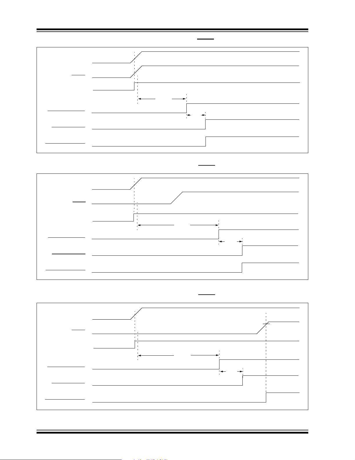
PIC18F2585/2680/4585/4680
FIGURE 4-3: TIME-OUT SEQUENCE ON POWER-UP (MCLR TIED TO VDD, VDD RISE < TPWRT)
VDD
MCLR
INTERNAL POR
TPWRT
PWRT TIME-OUT
OST TIME-OUT
INTERNAL RESET
TOST
FIGURE 4-4: TIME-OUT SEQUENCE ON POWER-UP (MCLR
VDD
MCLR
INTERNAL POR
PWRT TIME-OUT
OST TIME-OUT
INTERNAL RESET
TPWRT
NOT TIED TO VDD): CASE 1
TOST
FIGURE 4-5: TIME-OUT SEQUENCE ON POWER-UP (MCLR
VDD
MCLR
INTERNAL POR
TPWRT
PWRT TIME-OUT
OST TIME-OUT
INTERNAL RESET
DS39625C-page 46 Preliminary © 2007 Microchip Technology Inc.
NOT TIED TO VDD): CASE 2
TOST

PIC18F2585/2680/4585/4680
FIGURE 4-6: SLOW RISE TIME (MCLR TIED TO VDD, VDD RISE > TPWRT)
5V
VDD
MCLR
INTERNAL POR
0V
PWRT
T
1V
PWRT TIME-OUT
OST TIME-OUT
INTERNAL RESET
TOST
FIGURE 4-7: TIME-OUT SEQUENCE ON POR W/PLL ENABLED (MCLR
VDD
MCLR
INTERNAL POR
TPWRT
PWRT TIME-OUT
OST TIME-OUT
PLL TIME-OUT
TOST
TPLL
TIED TO VDD)
INTERNAL RESET
Note: TOST = 1024 clock cycles.
T
PLL ≈ 2 ms max. First three stages of the PWRT timer.
© 2007 Microchip Technology Inc. Preliminary DS39625C-page 47

PIC18F2585/2680/4585/4680
4.6 Reset State of Registers
Most registers are unaffected by a Reset. Their status
is unknown on POR and unchanged by all other
Table 4-4 describes the Reset states for all of the
Special Function Registers. These are categorized by
Power-on and Brown-out Resets, Master Clear and
WDT Resets and WDT wake-ups.
Resets. The other registers are forced to a “Reset
state” depending on the type of Reset that occurred.
Most registers are not affected by a WDT wake-up,
since this is viewed as the resumption of normal
operation. Status bits from the RCON register, RI
PD
, POR and BOR, are set or cleared differently in
, TO,
different Reset situations, as indicated in Table 4-3.
These bits are used in software to determine the nature
of the Reset.
TABLE 4-3: STATUS BITS, THEIR SIGNIFICANCE AND THE INITIALIZATION CONDITION FOR
RCON REGISTER
Condition
Program
Counter
SBOREN RI
Power-on Reset 0000h 1 11100 0 0
RESET Instruction 0000h u
Brown-out 0000h u
during Power Managed
MCLR
0000h u
(2)
(2)
(2)
Run modes
MCLR
during Power Managed
0000h u
(2)
Idle modes and Sleep mode
WDT Time-out during Full Power
0000h u
(2)
or Power Managed Run modes
MCLR
during Full Power
0000h u
(2)
Execution
Stack Full Reset (STVREN = 1) 0000h u
Stack Underflow Reset
0000h u
(2)
(2)
(STVREN = 1)
Stack Underflow Error (not an
0000h u
(2)
actual Reset, STVREN = 0)
WDT Time-out during Power
PC + 2 u
(2)
Managed Idle or Sleep modes
Interrupt Exit from Power
PC + 2
(1)
(2)
u
Managed modes
Legend: u = unchanged
Note 1: When the wake-up is due to an interrupt and the GIEH or GIEL bits are set, the PC is loaded with the
interrupt vector (008h or 0018h).
2: Reset state is ‘1’ for POR and unchanged for all other Resets when software BOR is enabled
(BOREN1:BOREN0 Configuration bits = 01 and SBOREN = 1); otherwise, the Reset state is ‘0’.
RCON Register STKPTR Register
TO PD POR BOR STKFUL STKUNF
0uuuu u u
111u0 u u
u1uuu u u
u10uu u u
u0uuu u u
uuuuu u u
uuuuu 1 u
uuuuu u 1
uuuuu u 1
u00uu u u
uu0uu u u
DS39625C-page 48 Preliminary © 2007 Microchip Technology Inc.

PIC18F2585/2680/4585/4680
TABLE 4-4: INITIALIZATION CONDITIONS FOR ALL REGISTERS
Resets,
MCLR
Register Applicable Devices
Power-on Reset,
Brown-out Reset
TOSU 2585 2680 4585 4680 ---0 0000 ---0 0000 ---0 uuuu
TOSH 2585 2680 4585 4680 0000 0000 0000 0000 uuuu uuuu
TOSL 2585 2680 4585 4680 0000 0000 0000 0000 uuuu uuuu
STKPTR 2585 2680 4585 4680 00-0 0000 uu-0 0000 uu-u uuuu
PCLATU 2585 2680 4585 4680 ---0 0000 ---0 0000 ---u uuuu
PCLATH 2585 2680 4585 4680 0000 0000 0000 0000 uuuu uuuu
PCL 2585 2680 4585 4680 0000 0000 0000 0000 PC + 2
TBLPTRU 2585 2680 4585 4680 --00 0000 --00 0000 --uu uuuu
TBLPTRH 2585 2680 4585 4680 0000 0000 0000 0000 uuuu uuuu
TBLPTRL 2585 2680 4585 4680 0000 0000 0000 0000 uuuu uuuu
TABLAT 2585 2680 4585 4680 0000 0000 0000 0000 uuuu uuuu
PRODH 2585 2680 4585 4680 xxxx xxxx uuuu uuuu uuuu uuuu
PRODL 2585 2680 4585 4680 xxxx xxxx uuuu uuuu uuuu uuuu
INTCON 2585 2680 4585 4680 0000 000x 0000 000u uuuu uuuu
INTCON2 2585 2680 4585 4680 1111 -1-1 1111 -1-1 uuuu -u-u
INTCON3 2585 2680 4585 4680 11-0 0-00 11-0 0-00 uu-u u-uu
INDF0 2585 2680 4585 4680 N/A N/A N/A
POSTINC0 2585 2680 4585 4680 N/A N/A N/A
POSTDEC0 2585 2680 4585 4680 N/A N/A N/A
PREINC0 2585 2680 4585 4680 N/A N/A N/A
PLUSW0 2585 2680 4585 4680 N/A N/A N/A
FSR0H 2585 2680 4585 4680 ---- 0000 ---- 0000 ---- uuuu
FSR0L 2585 2680 4585 4680 xxxx xxxx uuuu uuuu uuuu uuuu
WREG 2585 2680 4585 4680 xxxx xxxx uuuu uuuu uuuu uuuu
INDF1 2585 2680 4585 4680 N/A N/A N/A
POSTINC1 2585 2680 4585 4680 N/A N/A N/A
POSTDEC1 2585 2680 4585 4680 N/A N/A N/A
PREINC1 2585 2680 4585 4680 N/A N/A N/A
PLUSW1 2585 2680 4585 4680 N/A N/A N/A
FSR1H 2585 2680 4585 4680 ---- 0000 ---- 0000 ---- uuuu
FSR1L 2585 2680 4585 4680 xxxx xxxx uuuu uuuu uuuu uuuu
Legend: u = unchanged, x = unknown, - = unimplemented bit, read as ‘0’, q = value depends on condition.
Shaded cells indicate conditions do not apply for the designated device.
Note 1: One or more bits in the INTCONx or PIRx registers will be affected (to cause wake-up).
2: When the wake-up is due to an interrupt and the GIEL or GIEH bit is set, the PC is loaded with the interrupt
vector (0008h or 0018h).
3: When the wake-up is due to an interrupt and the GIEL or GIEH bit is set, the TOSU, TOSH and TOSL are
updated with the current value of the PC. The STKPTR is modified to point to the next location in the
hardware stack.
4: See Table 4-3 for Reset value for specific condition.
5: Bits 6 and 7 of PORTA, LATA and TRISA are enabled, depending on the oscillator mode selected. When
not enabled as PORTA pins, they are disabled and read ‘0’.
6: This register reads all ‘0’s until the ECAN™ technology is set up in Mode 1 or Mode 2.
WDT Reset,
RESET Instruction,
Stack Resets
Wake-up via WDT
or Interrupt
(3)
(3)
(3)
(3)
(2)
(1)
(1)
(1)
© 2007 Microchip Technology Inc. Preliminary DS39625C-page 49

PIC18F2585/2680/4585/4680
TABLE 4-4: INITIALIZATION CONDITIONS FOR ALL REGISTERS (CONTINUED)
Resets,
MCLR
Register Applicable Devices
BSR 2585 2680 4585 4680 ---- 0000 ---- 0000 ---- uuuu
INDF2 2585 2680 4585 4680 N/A N/A N/A
POSTINC2 2585 2680 4585 4680 N/A N/A N/A
POSTDEC2 2585 2680 4585 4680 N/A N/A N/A
PREINC2 2585 2680 4585 4680 N/A N/A N/A
PLUSW2 2585 2680 4585 4680 N/A N/A N/A
FSR2H 2585 2680 4585 4680 ---- 0000 ---- 0000 ---- uuuu
FSR2L 2585 2680 4585 4680 xxxx xxxx uuuu uuuu uuuu uuuu
STATUS 2585 2680 4585 4680 ---x xxxx ---u uuuu ---u uuuu
TMR0H 2585 2680 4585 4680 0000 0000 0000 0000 uuuu uuuu
TMR0L 2585 2680 4585 4680 xxxx xxxx uuuu uuuu uuuu uuuu
T0CON 2585 2680 4585 4680 1111 1111 1111 1111 uuuu uuuu
OSCCON 2585 2680 4585 4680 0100 q000 0100 00q0 uuuu uuqu
HLVDCON 2585 2680 4585 4680 0-00 0101 0-00 0101 0-uu uuuu
WDTCON 2585 2680 4585 4680 ---- ---0 ---- ---0 ---- ---u
(4)
RCON
TMR1H 2585 2680 4585 4680 xxxx xxxx uuuu uuuu uuuu uuuu
TMR1L 2585 2680 4585 4680 xxxx xxxx uuuu uuuu uuuu uuuu
T1CON 2585 2680 4585 4680 0000 0000 u0uu uuuu uuuu uuuu
TMR2 2585 2680 4585 4680 0000 0000 0000 0000 uuuu uuuu
PR2 2585 2680 4585 4680 1111 1111 1111 1111 1111 1111
T2CON 2585 2680 4585 4680 -000 0000 -000 0000 -uuu uuuu
SSPBUF 2585 2680 4585 4680 xxxx xxxx uuuu uuuu uuuu uuuu
SSPADD 2585 2680 4585 4680 0000 0000 0000 0000 uuuu uuuu
SSPSTAT 2585 2680 4585 4680 0000 0000 0000 0000 uuuu uuuu
SSPCON1 2585 2680 4585 4680 0000 0000 0000 0000 uuuu uuuu
SSPCON2 2585 2680 4585 4680 0000 0000 0000 0000 uuuu uuuu
ADRESH 2585 2680 4585 4680 xxxx xxxx uuuu uuuu uuuu uuuu
ADRESL 2585 2680 4585 4680 xxxx xxxx uuuu uuuu uuuu uuuu
ADCON0 2585 2680 4585 4680 --00 0000 --00 0000 --uu uuuu
ADCON1 2585 2680 4585 4680 --00 0qqq --00 0qqq --uu uuuu
ADCON2 2585
Legend: u = unchanged, x = unknown, - = unimplemented bit, read as ‘0’, q = value depends on condition.
Note 1: One or more bits in the INTCONx or PIRx registers will be affected (to cause wake-up).
2: When the wake-up is due to an interrupt and the GIEL or GIEH bit is set, the PC is loaded with the interrupt
3: When the wake-up is due to an interrupt and the GIEL or GIEH bit is set, the TOSU, TOSH and TOSL are
4: See Table 4-3 for Reset value for specific condition.
5: Bits 6 and 7 of PORTA, LATA and TRISA are enabled, depending on the oscillator mode selected. When
6: This register reads all ‘0’s until the ECAN™ technology is set up in Mode 1 or Mode 2.
2585 2680 4585 4680 0q-1 11q0 0q-q qquu uq-u qquu
2680 4585 4680 0-00 0000 0-00 0000 u-uu uuuu
Shaded cells indicate conditions do not apply for the designated device.
vector (0008h or 0018h).
updated with the current value of the PC. The STKPTR is modified to point to the next location in the
hardware stack.
not enabled as PORTA pins, they are disabled and read ‘0’.
Power-on Reset,
Brown-out Reset
WDT Reset,
RESET Instruction,
Stack Resets
Wake-up via WDT
or Interrupt
DS39625C-page 50 Preliminary © 2007 Microchip Technology Inc.

PIC18F2585/2680/4585/4680
TABLE 4-4: INITIALIZATION CONDITIONS FOR ALL REGISTERS (CONTINUED)
Resets,
MCLR
Register Applicable Devices
CCPR1H 2585 2680 4585 4680 xxxx xxxx uuuu uuuu uuuu uuuu
CCPR1L 2585 2680 4585 4680 xxxx xxxx uuuu uuuu uuuu uuuu
CCP1CON 2585 2680 4585 4680 --00 0000 --00 0000 --uu uuuu
ECCPR1H
ECCPR1L 2585 2680 4585 4680 xxxx xxxx uuuu uuuu uuuu uuuu
ECCP1CON 2585 2680 4585 4680 0000 0000 0000 0000 uuuu uuuu
BAUDCON 2585 2680 4585 4680 01-0 0-00 01-0 0-00 --uu uuuu
ECCP1DEL
ECCP1AS 2585 2680 4585 4680 0000 0000 0000 0000 uuuu uuuu
CVRCON
CMCON
TMR3H 2585 2680 4585 4680 xxxx xxxx uuuu uuuu uuuu uuuu
TMR3L 2585 2680 4585 4680 xxxx xxxx uuuu uuuu uuuu uuuu
T3CON 2585 2680 4585 4680 0000 0000 uuuu uuuu uuuu uuuu
SPBRGH 2585 2680 4585 4680 0000 0000 0000 0000 uuuu uuuu
SPBRG 2585 2680 4585 4680 0000 0000 0000 0000 uuuu uuuu
RCREG 2585 2680 4585 4680 0000 0000 0000 0000 uuuu uuuu
TXREG 2585 2680 4585 4680 0000 0000 0000 0000 uuuu uuuu
TXSTA 2585 2680 4585 4680 0000 0010 0000 0010 uuuu uuuu
RCSTA 2585 2680 4585 4680 0000 000x 0000 000x uuuu uuuu
EEADRH 2585 2680 4585 4680 ---- --00 ---- --00 ---- --uu
EEADR 2585 2680 4585 4680 0000 0000 0000 0000 uuuu uuuu
EEDATA 2585 2680 4585 4680 0000 0000 0000 0000 uuuu uuuu
EECON2 2585 2680 4585 4680 0000 0000 0000 0000 0000 0000
EECON1 2585 2680 4585 4680 xx-0 x000 uu-0 u000 uu-0 u000
IPR3 2585 2680 4585 4680 1111 1111 1111 1111 uuuu uuuu
PIR3 2585 2680 4585 4680 0000 0000 0000 0000 uuuu uuuu
PIE3 2585 2680 4585 4680 0000 0000 0000 0000 uuuu uuuu
IPR2
PIR2
Legend: u = unchanged, x = unknown, - = unimplemented bit, read as ‘0’, q = value depends on condition.
Note 1: One or more bits in the INTCONx or PIRx registers will be affected (to cause wake-up).
2: When the wake-up is due to an interrupt and the GIEL or GIEH bit is set, the PC is loaded with the interrupt
3: When the wake-up is due to an interrupt and the GIEL or GIEH bit is set, the TOSU, TOSH and TOSL are
4: See Table 4-3 for Reset value for specific condition.
5: Bits 6 and 7 of PORTA, LATA and TRISA are enabled, depending on the oscillator mode selected. When
6: This register reads all ‘0’s until the ECAN™ technology is set up in Mode 1 or Mode 2.
2585 2680 4585 4680 xxxx xxxx uuuu uuuu uuuu uuuu
2585 2680 4585 4680 0000 0000 0000 0000 uuuu uuuu
2585 2680 4585 4680 0000 0000 0000 0000 uuuu uuuu
2585 2680 4585 4680 0000 0111 0000 0111 uuuu uuuu
2585 2680 4585 4680 11-1 1111 11-1 1111 uu-u uuuu
2585 2680
2585 2680 4585 4680 00-0 0000 00-0 0000 uu-u uuuu
2585 2680 4585 4680 0--0 000- 0--0 000- u--u uuu-
Shaded cells indicate conditions do not apply for the designated device.
vector (0008h or 0018h).
updated with the current value of the PC. The STKPTR is modified to point to the next location in the
hardware stack.
not enabled as PORTA pins, they are disabled and read ‘0’.
4585 4680 1--1 111- 1--1 111- u--u uuu-
Power-on Reset,
Brown-out Reset
WDT Reset,
RESET Instruction,
Stack Resets
Wake-up via WDT
or Interrupt
(1)
(1)
© 2007 Microchip Technology Inc. Preliminary DS39625C-page 51

PIC18F2585/2680/4585/4680
TABLE 4-4: INITIALIZATION CONDITIONS FOR ALL REGISTERS (CONTINUED)
Resets,
MCLR
Register Applicable Devices
Power-on Reset,
Brown-out Reset
PIE2 2585 2680 4585 4680 00-0 0000 00-0 0000 uu-u uuuu
2585 2680 4585 4680 0--0 000- 0--0 000- u--u uuu-
IPR1 2585 2680 4585 4680 1111 1111 1111 1111 uuuu uuuu
2585 2680
4585 4680 -111 1111 -111 1111 -uuu uuuu
PIR1 2585 2680 4585 4680 0000 0000 0000 0000 uuuu uuuu
2585 2680 4585 4680 -000 0000 -000 0000 -uuu uuuu
PIE1
2585 2680 4585 4680 0000 0000 0000 0000 uuuu uuuu
2585 2680 4585 4680 -000 0000 -000 0000 -uuu uuuu
OSCTUNE 2585 2680 4585 4680 --00 0000 --00 0000 --uu uuuu
TRISE
TRISD
2585 2680 4585 4680 0000 -111 0000 -111 uuuu -uuu
2585 2680 4585 4680 1111 1111 1111 1111 uuuu uuuu
TRISC 2585 2680 4585 4680 1111 1111 1111 1111 uuuu uuuu
TRISB 2585 2680 4585 4680 1111 1111 1111 1111 uuuu uuuu
TRISA
(5)
2585 2680 4585 4680 1111 1111
(5)
LATE 2585 2680 4585 4680 ---- -xxx ---- -uuu ---- -uuu
LATD
2585 2680 4585 4680 xxxx xxxx uuuu uuuu uuuu uuuu
LATC 2585 2680 4585 4680 xxxx xxxx uuuu uuuu uuuu uuuu
LATB 2585 2680 4585 4680 xxxx xxxx uuuu uuuu uuuu uuuu
LATA
(5)
2585 2680 4585 4680 xxxx xxxx
(5)
PORTE 2585 2680 4585 4680 ---- x000 ---- x000 ---- uuuu
PORTD 2585 2680 4585 4680 xxxx xxxx uuuu uuuu uuuu uuuu
PORTC 2585 2680 4585 4680 xxxx xxxx uuuu uuuu uuuu uuuu
PORTB 2585 2680 4585 4680 xxxx xxxx uuuu uuuu uuuu uuuu
PORTA
(5)
2585 2680 4585 4680 xx0x 0000
(5)
ECANCON 2585 2680 4585 4680 0001 0000 0001 0000 uuuu uuuu
TXERRCNT 2585 2680 4585 4680 0000 0000 0000 0000 uuuu uuuu
RXERRCNT 2585 2680 4585 4680 0000 0000 0000 0000 uuuu uuuu
COMSTAT 2585 2680 4585 4680 0000 0000 0000 0000 uuuu uuuu
CIOCON 2585 2680 4585 4680 --00 ---- --00 ---- --uu ----
BRGCON3 2585 2680 4585 4680 00-- -000 00-- -000 uu-- -uuu
BRGCON2 2585 2680 4585 4680 0000 0000 0000 0000 uuuu uuuu
BRGCON1 2585 2680 4585 4680 0000 0000 0000 0000 uuuu uuuu
Legend: u = unchanged, x = unknown, - = unimplemented bit, read as ‘0’, q = value depends on condition.
Shaded cells indicate conditions do not apply for the designated device.
Note 1: One or more bits in the INTCONx or PIRx registers will be affected (to cause wake-up).
2: When the wake-up is due to an interrupt and the GIEL or GIEH bit is set, the PC is loaded with the interrupt
vector (0008h or 0018h).
3: When the wake-up is due to an interrupt and the GIEL or GIEH bit is set, the TOSU, TOSH and TOSL are
updated with the current value of the PC. The STKPTR is modified to point to the next location in the
hardware stack.
4: See Table 4-3 for Reset value for specific condition.
5: Bits 6 and 7 of PORTA, LATA and TRISA are enabled, depending on the oscillator mode selected. When
not enabled as PORTA pins, they are disabled and read ‘0’.
6: This register reads all ‘0’s until the ECAN™ technology is set up in Mode 1 or Mode 2.
WDT Reset,
RESET Instruction,
Stack Resets
1111 1111
uuuu uuuu
uu0u 0000
(5)
(5)
(5)
Wake-up via WDT
or Interrupt
uuuu uuuu
uuuu uuuu
uuuu uuuu
(1)
(5)
(5)
(5)
DS39625C-page 52 Preliminary © 2007 Microchip Technology Inc.

PIC18F2585/2680/4585/4680
TABLE 4-4: INITIALIZATION CONDITIONS FOR ALL REGISTERS (CONTINUED)
Resets,
MCLR
Register Applicable Devices
CANCON 2585 2680 4585 4680 1000 000- 1000 000- uuuu uuu-
CANSTAT 2585 2680 4585 4680 100- 000- 100- 000- uuu- uuu-
RXB0D7 2585 2680 4585 4680 xxxx xxxx uuuu uuuu uuuu uuuu
RXB0D6 2585 2680 4585 4680 xxxx xxxx uuuu uuuu uuuu uuuu
RXB0D5 2585 2680 4585 4680 xxxx xxxx uuuu uuuu uuuu uuuu
RXB0D4 2585 2680 4585 4680 xxxx xxxx uuuu uuuu uuuu uuuu
RXB0D3 2585 2680 4585 4680 xxxx xxxx uuuu uuuu uuuu uuuu
RXB0D2 2585 2680 4585 4680 xxxx xxxx uuuu uuuu uuuu uuuu
RXB0D1 2585 2680 4585 4680 xxxx xxxx uuuu uuuu uuuu uuuu
RXB0D0 2585 2680 4585 4680 xxxx xxxx uuuu uuuu uuuu uuuu
RXB0DLC 2585 2680 4585 4680 -xxx xxxx -uuu uuuu -uuu uuuu
RXB0EIDL 2585 2680 4585 4680 xxxx xxxx uuuu uuuu uuuu uuuu
RXB0EIDH 2585 2680 4585 4680 xxxx xxxx uuuu uuuu uuuu uuuu
RXB0SIDL 2585 2680 4585 4680 xxxx x-xx uuuu u-uu uuuu u-uu
RXB0SIDH 2585 2680 4585 4680 xxxx xxxx uuuu uuuu uuuu uuuu
RXB0CON 2585 2680 4585 4680 000- 0000 000- 0000 uuu- uuuu
RXB1D7 2585 2680 4585 4680 xxxx xxxx uuuu uuuu uuuu uuuu
RXB1D6 2585 2680 4585 4680 xxxx xxxx uuuu uuuu uuuu uuuu
RXB1D5 2585 2680 4585 4680 xxxx xxxx uuuu uuuu uuuu uuuu
RXB1D4 2585 2680 4585 4680 xxxx xxxx uuuu uuuu uuuu uuuu
RXB1D3 2585 2680 4585 4680 xxxx xxxx uuuu uuuu uuuu uuuu
RXB1D2 2585 2680 4585 4680 xxxx xxxx uuuu uuuu uuuu uuuu
RXB1D1 2585 2680 4585 4680 xxxx xxxx uuuu uuuu uuuu uuuu
RXB1D0 2585 2680 4585 4680 xxxx xxxx uuuu uuuu uuuu uuuu
RXB1DLC 2585 2680 4585 4680 -xxx xxxx -uuu uuuu -uuu uuuu
RXB1EIDL 2585 2680 4585 4680 xxxx xxxx uuuu uuuu uuuu uuuu
RXB1EIDH 2585 2680 4585 4680 xxxx xxxx uuuu uuuu uuuu uuuu
RXB1SIDL 2585 2680 4585 4680 xxxx x-xx uuuu u-uu uuuu u-uu
RXB1SIDH 2585 2680 4585 4680 xxxx xxxx uuuu uuuu uuuu uuuu
RXB1CON 2585 2680 4585 4680 000- 0000 000- 0000 uuu- uuuu
TXB0D7 2585 2680 4585 4680 xxxx xxxx uuuu uuuu uuuu uuuu
TXB0D6 2585 2680 4585 4680 xxxx xxxx uuuu uuuu uuuu uuuu
Legend: u = unchanged, x = unknown, - = unimplemented bit, read as ‘0’, q = value depends on condition.
Shaded cells indicate conditions do not apply for the designated device.
Note 1: One or more bits in the INTCONx or PIRx registers will be affected (to cause wake-up).
2: When the wake-up is due to an interrupt and the GIEL or GIEH bit is set, the PC is loaded with the interrupt
vector (0008h or 0018h).
3: When the wake-up is due to an interrupt and the GIEL or GIEH bit is set, the TOSU, TOSH and TOSL are
updated with the current value of the PC. The STKPTR is modified to point to the next location in the
hardware stack.
4: See Table 4-3 for Reset value for specific condition.
5: Bits 6 and 7 of PORTA, LATA and TRISA are enabled, depending on the oscillator mode selected. When
not enabled as PORTA pins, they are disabled and read ‘0’.
6: This register reads all ‘0’s until the ECAN™ technology is set up in Mode 1 or Mode 2.
Power-on Reset,
Brown-out Reset
WDT Reset,
RESET Instruction,
Stack Resets
Wake-up via WDT
or Interrupt
© 2007 Microchip Technology Inc. Preliminary DS39625C-page 53

PIC18F2585/2680/4585/4680
TABLE 4-4: INITIALIZATION CONDITIONS FOR ALL REGISTERS (CONTINUED)
Resets,
MCLR
Register Applicable Devices
TXB0D5 2585 2680 4585 4680 xxxx xxxx uuuu uuuu uuuu uuuu
TXB0D4 2585 2680 4585 4680 xxxx xxxx uuuu uuuu uuuu uuuu
TXB0D3 2585 2680 4585 4680 xxxx xxxx uuuu uuuu uuuu uuuu
TXB0D2 2585 2680 4585 4680 xxxx xxxx uuuu uuuu uuuu uuuu
TXB0D1 2585 2680 4585 4680 xxxx xxxx uuuu uuuu uuuu uuuu
TXB0D0 2585 2680 4585 4680 xxxx xxxx uuuu uuuu uuuu uuuu
TXB0DLC 2585 2680 4585 4680 -x-- xxxx -u-- uuuu -u-- uuuu
TXB0EIDL 2585 2680 4585 4680 xxxx xxxx uuuu uuuu uuuu uuuu
TXB0EIDH 2585 2680 4585 4680 xxxx xxxx uuuu uuuu -uuu uuuu
TXB0SIDL 2585 2680 4585 4680 xxx- x-xx uuu- u-uu uuu- u-uu
TXB0SIDH 2585 2680 4585 4680 xxxx xxxx uuuu uuuu uuuu uuuu
TXB0CON 2585 2680 4585 4680 0000 0-00 0000 0-00 uuuu u-uu
TXB1D7 2585 2680 4585 4680 xxxx xxxx uuuu uuuu uuuu uuuu
TXB1D6 2585 2680 4585 4680 xxxx xxxx uuuu uuuu uuuu uuuu
TXB1D5 2585 2680 4585 4680 xxxx xxxx uuuu uuuu uuuu uuuu
TXB1D4 2585 2680 4585 4680 xxxx xxxx uuuu uuuu uuuu uuuu
TXB1D3 2585 2680 4585 4680 xxxx xxxx uuuu uuuu uuuu uuuu
TXB1D2 2585 2680 4585 4680 xxxx xxxx uuuu uuuu uuuu uuuu
TXB1D1 2585 2680 4585 4680 xxxx xxxx uuuu uuuu uuuu uuuu
TXB1D0 2585 2680 4585 4680 xxxx xxxx uuuu uuuu uuuu uuuu
TXB1DLC 2585 2680 4585 4680 -x-- xxxx -u-- uuuu -u-- uuuu
TXB1EIDL 2585 2680 4585 4680 xxxx xxxx uuuu uuuu uuuu uuuu
TXB1EIDH 2585 2680 4585 4680 xxxx xxxx uuuu uuuu uuuu uuuu
TXB1SIDL 2585 2680 4585 4680 xxx- x-xx uuu- u-uu uuu- uu-u
TXB1SIDH 2585 2680 4585 4680 xxxx xxxx uuuu uuuu -uuu uuuu
TXB1CON 2585 2680 4585 4680 0000 0-00 0000 0-00 uuuu u-uu
TXB2D7 2585 2680 4585 4680 xxxx xxxx uuuu uuuu 0uuu uuuu
TXB2D6 2585 2680 4585 4680 xxxx xxxx uuuu uuuu 0uuu uuuu
TXB2D5 2585 2680 4585 4680 xxxx xxxx uuuu uuuu 0uuu uuuu
TXB2D4 2585 2680 4585 4680 xxxx xxxx uuuu uuuu 0uuu uuuu
TXB2D3 2585 2680 4585 4680 xxxx xxxx uuuu uuuu 0uuu uuuu
TXB2D2 2585 2680 4585 4680 xxxx xxxx uuuu uuuu 0uuu uuuu
Legend: u = unchanged, x = unknown, - = unimplemented bit, read as ‘0’, q = value depends on condition.
Shaded cells indicate conditions do not apply for the designated device.
Note 1: One or more bits in the INTCONx or PIRx registers will be affected (to cause wake-up).
2: When the wake-up is due to an interrupt and the GIEL or GIEH bit is set, the PC is loaded with the interrupt
vector (0008h or 0018h).
3: When the wake-up is due to an interrupt and the GIEL or GIEH bit is set, the TOSU, TOSH and TOSL are
updated with the current value of the PC. The STKPTR is modified to point to the next location in the
hardware stack.
4: See Table 4-3 for Reset value for specific condition.
5: Bits 6 and 7 of PORTA, LATA and TRISA are enabled, depending on the oscillator mode selected. When
not enabled as PORTA pins, they are disabled and read ‘0’.
6: This register reads all ‘0’s until the ECAN™ technology is set up in Mode 1 or Mode 2.
Power-on Reset,
Brown-out Reset
WDT Reset,
RESET Instruction,
Stack Resets
Wake-up via WDT
or Interrupt
DS39625C-page 54 Preliminary © 2007 Microchip Technology Inc.

PIC18F2585/2680/4585/4680
TABLE 4-4: INITIALIZATION CONDITIONS FOR ALL REGISTERS (CONTINUED)
Resets,
MCLR
Register Applicable Devices
TXB2D1 2585 2680 4585 4680 xxxx xxxx uuuu uuuu 0uuu uuuu
TXB2D0 2585 2680 4585 4680 xxxx xxxx uuuu uuuu 0uuu uuuu
TXB2DLC 2585 2680 4585 4680 -x-- xxxx -u-- uuuu -u-- uuuu
TXB2EIDL 2585 2680 4585 4680 xxxx xxxx uuuu uuuu uuuu uuuu
TXB2EIDH 2585 2680 4585 4680 xxxx xxxx uuuu uuuu uuuu uuuu
TXB2SIDL 2585 2680 4585 4680 xxxx x-xx uuuu u-uu -uuu uuuu
TXB2SIDH 2585 2680 4585 4680 xxx- x-xx uuu- u-uu uuu- u-uu
TXB2CON 2585 2680 4585 4680 0000 0-00 0000 0-00 uuuu u-uu
RXM1EIDL 2585 2680 4585 4680 xxxx xxxx uuuu uuuu uuuu uuuu
RXM1EIDH 2585 2680 4585 4680 xxxx xxxx uuuu uuuu uuuu uuuu
RXM1SIDL 2585 2680 4585 4680 xxx- x-xx uuu- u-uu uuu- u-uu
RXM1SIDH 2585 2680 4585 4680 xxxx xxxx uuuu uuuu uuuu uuuu
RXM0EIDL 2585 2680 4585 4680 xxxx xxxx uuuu uuuu uuuu uuuu
RXM0EIDH 2585 2680 4585 4680 xxxx xxxx uuuu uuuu uuuu uuuu
RXM0SIDL 2585 2680 4585 4680 xxx- x-xx uuu- u-uu uuu- u-uu
RXM0SIDH 2585 2680 4585 4680 xxxx xxxx uuuu uuuu uuuu uuuu
RXF5EIDL 2585 2680 4585 4680 xxxx xxxx uuuu uuuu uuuu uuuu
RXF5EIDH 2585 2680 4585 4680 xxxx xxxx uuuu uuuu uuuu uuuu
RXF5SIDL 2585 2680 4585 4680 xxx- x-xx uuu- u-uu uuu- u-uu
RXF5SIDH 2585 2680 4585 4680 xxxx xxxx uuuu uuuu uuuu uuuu
RXF4EIDL 2585 2680 4585 4680 xxxx xxxx uuuu uuuu uuuu uuuu
RXF4EIDH 2585 2680 4585 4680 xxxx xxxx uuuu uuuu uuuu uuuu
RXF4SIDL 2585 2680 4585 4680 xxx- x-xx uuu- u-uu uuu- u-uu
RXF4SIDH 2585 2680 4585 4680 xxxx xxxx uuuu uuuu uuuu uuuu
RXF3EIDL 2585 2680 4585 4680 xxxx xxxx uuuu uuuu uuuu uuuu
RXF3EIDH 2585 2680 4585 4680 xxxx xxxx uuuu uuuu uuuu uuuu
RXF3SIDL 2585 2680 4585 4680 xxx- x-xx uuu- u-uu uuu- u-uu
RXF3SIDH 2585 2680 4585 4680 xxxx xxxx uuuu uuuu uuuu uuuu
RXF2EIDL 2585 2680 4585 4680 xxxx xxxx uuuu uuuu uuuu uuuu
RXF2EIDH 2585 2680 4585 4680 xxxx xxxx uuuu uuuu uuuu uuuu
RXF2SIDL 2585 2680 4585 4680 xxx- x-xx uuu- u-uu uuu- u-uu
RXF2SIDH 2585 2680 4585 4680 xxxx xxxx uuuu uuuu uuuu uuuu
Legend: u = unchanged, x = unknown, - = unimplemented bit, read as ‘0’, q = value depends on condition.
Shaded cells indicate conditions do not apply for the designated device.
Note 1: One or more bits in the INTCONx or PIRx registers will be affected (to cause wake-up).
2: When the wake-up is due to an interrupt and the GIEL or GIEH bit is set, the PC is loaded with the interrupt
vector (0008h or 0018h).
3: When the wake-up is due to an interrupt and the GIEL or GIEH bit is set, the TOSU, TOSH and TOSL are
updated with the current value of the PC. The STKPTR is modified to point to the next location in the
hardware stack.
4: See Table 4-3 for Reset value for specific condition.
5: Bits 6 and 7 of PORTA, LATA and TRISA are enabled, depending on the oscillator mode selected. When
not enabled as PORTA pins, they are disabled and read ‘0’.
6: This register reads all ‘0’s until the ECAN™ technology is set up in Mode 1 or Mode 2.
Power-on Reset,
Brown-out Reset
WDT Reset,
RESET Instruction,
Stack Resets
Wake-up via WDT
or Interrupt
© 2007 Microchip Technology Inc. Preliminary DS39625C-page 55

PIC18F2585/2680/4585/4680
TABLE 4-4: INITIALIZATION CONDITIONS FOR ALL REGISTERS (CONTINUED)
Resets,
MCLR
Register Applicable Devices
Power-on Reset,
Brown-out Reset
RXF1EIDL 2585 2680 4585 4680 xxxx xxxx uuuu uuuu uuuu uuuu
RXF1EIDH 2585 2680 4585 4680 xxxx xxxx uuuu uuuu uuuu uuuu
RXF1SIDL 2585 2680 4585 4680 xxx- x-xx uuu- u-uu uuu- u-uu
RXF1SIDH 2585 2680 4585 4680 xxxx xxxx uuuu uuuu uuuu uuuu
RXF0EIDL 2585 2680 4585 4680 xxxx xxxx uuuu uuuu uuuu uuuu
RXF0EIDH 2585 2680 4585 4680 xxxx xxxx uuuu uuuu uuuu uuuu
RXF0SIDL 2585 2680 4585 4680 xxx- x-xx uuu- u-uu uuu- u-uu
RXF0SIDH 2585 2680 4585 4680 xxxx xxxx uuuu uuuu uuuu uuuu
(6)
B5D7
(6)
B5D6
(6)
B5D5
(6)
B5D4
(6)
B5D3
(6)
B5D2
(6)
B5D1
(6)
B5D0
B5DLC
B5EIDL
B5EIDH
B5SIDL
B5SIDH
B5CON
(6)
B4D7
(6)
B4D6
(6)
B4D5
(6)
B4D4
(6)
B4D3
(6)
B4D2
(6)
B4D1
(6)
B4D0
B4DLC
B4EIDL
(6)
(6)
(6)
(6)
(6)
(6)
(6)
(6)
2585 2680 4585 4680 xxxx xxxx uuuu uuuu uuuu uuuu
2585 2680 4585 4680 xxxx xxxx uuuu uuuu uuuu uuuu
2585 2680 4585 4680 xxxx xxxx uuuu uuuu uuuu uuuu
2585 2680 4585 4680 xxxx xxxx uuuu uuuu uuuu uuuu
2585 2680 4585 4680 xxxx xxxx uuuu uuuu uuuu uuuu
2585 2680 4585 4680 xxxx xxxx uuuu uuuu uuuu uuuu
2585 2680 4585 4680 xxxx xxxx uuuu uuuu uuuu uuuu
2585 2680 4585 4680 xxxx xxxx uuuu uuuu uuuu uuuu
2585 2680 4585 4680 -xxx xxxx -uuu uuuu -uuu uuuu
2585 2680 4585 4680 xxxx xxxx uuuu uuuu uuuu uuuu
2585 2680 4585 4680 xxxx xxxx uuuu uuuu uuuu uuuu
2585 2680 4585 4680 xxxx x-xx uuuu u-uu uuuu u-uu
2585 2680 4585 4680 xxxx x-xx uuuu u-uu uuuu u-uu
2585 2680 4585 4680 0000 0000 0000 0000 uuuu uuuu
2585 2680 4585 4680 xxxx xxxx uuuu uuuu uuuu uuuu
2585 2680 4585 4680 xxxx xxxx uuuu uuuu uuuu uuuu
2585 2680 4585 4680 xxxx xxxx uuuu uuuu uuuu uuuu
2585 2680 4585 4680 xxxx xxxx uuuu uuuu uuuu uuuu
2585 2680 4585 4680 xxxx xxxx uuuu uuuu uuuu uuuu
2585 2680 4585 4680 xxxx xxxx uuuu uuuu uuuu uuuu
2585 2680 4585 4680 xxxx xxxx uuuu uuuu uuuu uuuu
2585 2680 4585 4680 xxxx xxxx uuuu uuuu uuuu uuuu
2585 2680 4585 4680 -xxx xxxx -uuu uuuu -uuu uuuu
2585 2680 4585 4680 xxxx xxxx uuuu uuuu uuuu uuuu
Legend: u = unchanged, x = unknown, - = unimplemented bit, read as ‘0’, q = value depends on condition.
Shaded cells indicate conditions do not apply for the designated device.
Note 1: One or more bits in the INTCONx or PIRx registers will be affected (to cause wake-up).
2: When the wake-up is due to an interrupt and the GIEL or GIEH bit is set, the PC is loaded with the interrupt
vector (0008h or 0018h).
3: When the wake-up is due to an interrupt and the GIEL or GIEH bit is set, the TOSU, TOSH and TOSL are
updated with the current value of the PC. The STKPTR is modified to point to the next location in the
hardware stack.
4: See Table 4-3 for Reset value for specific condition.
5: Bits 6 and 7 of PORTA, LATA and TRISA are enabled, depending on the oscillator mode selected. When
not enabled as PORTA pins, they are disabled and read ‘0’.
6: This register reads all ‘0’s until the ECAN™ technology is set up in Mode 1 or Mode 2.
WDT Reset,
RESET Instruction,
Stack Resets
Wake-up via WDT
or Interrupt
DS39625C-page 56 Preliminary © 2007 Microchip Technology Inc.

PIC18F2585/2680/4585/4680
TABLE 4-4: INITIALIZATION CONDITIONS FOR ALL REGISTERS (CONTINUED)
Resets,
MCLR
Register Applicable Devices
(6)
(6)
(6)
(6)
(6)
(6)
(6)
(6)
(6)
(6)
(6)
(6)
(6)
(6)
(6)
(6)
(6)
(6)
(6)
(6)
(6)
(6)
(6)
(6)
(6)
(6)
(6)
(6)
(6)
(6)
(6)
2585 2680 4585 4680 xxxx xxxx uuuu uuuu uuuu uuuu
2585 2680 4585 4680 xxxx x-xx uuuu u-uu uuuu u-uu
2585 2680 4585 4680 xxxx xxxx uuuu uuuu uuuu uuuu
2585 2680 4585 4680 0000 0000 0000 0000 uuuu uuuu
2585 2680 4585 4680 xxxx xxxx uuuu uuuu uuuu uuuu
2585 2680 4585 4680 xxxx xxxx uuuu uuuu uuuu uuuu
2585 2680 4585 4680 xxxx xxxx uuuu uuuu uuuu uuuu
2585 2680 4585 4680 xxxx xxxx uuuu uuuu uuuu uuuu
2585 2680 4585 4680 xxxx xxxx uuuu uuuu uuuu uuuu
2585 2680 4585 4680 xxxx xxxx uuuu uuuu uuuu uuuu
2585 2680 4585 4680 xxxx xxxx uuuu uuuu uuuu uuuu
2585 2680 4585 4680 xxxx xxxx uuuu uuuu uuuu uuuu
2585 2680 4585 4680 -xxx xxxx -uuu uuuu -uuu uuuu
2585 2680 4585 4680 xxxx xxxx uuuu uuuu uuuu uuuu
2585 2680 4585 4680 xxxx xxxx uuuu uuuu uuuu uuuu
2585 2680 4585 4680 xxxx x-xx uuuu u-uu uuuu u-uu
2585 2680 4585 4680 xxxx xxxx uuuu uuuu uuuu uuuu
B4EIDH
B4SIDL
B4SIDH
B4CON
B3D7
B3D6
B3D5
B3D4
B3D3
B3D2
B3D1
B3D0
B3DLC
B3EIDL
B3EIDH
B3SIDL
B3SIDH
B3CON
B2D7
B2D6
B2D5
B2D4
B2D3
B2D2
B2D1
B2D0
B2DLC
B2EIDL
B2EIDH
B2SIDL
B2SIDH
Power-on Reset,
Brown-out Reset
Legend: u = unchanged, x = unknown, - = unimplemented bit, read as ‘0’, q = value depends on condition.
Shaded cells indicate conditions do not apply for the designated device.
Note 1: One or more bits in the INTCONx or PIRx registers will be affected (to cause wake-up).
2: When the wake-up is due to an interrupt and the GIEL or GIEH bit is set, the PC is loaded with the interrupt
vector (0008h or 0018h).
3: When the wake-up is due to an interrupt and the GIEL or GIEH bit is set, the TOSU, TOSH and TOSL are
updated with the current value of the PC. The STKPTR is modified to point to the next location in the
hardware stack.
4: See Table 4-3 for Reset value for specific condition.
5: Bits 6 and 7 of PORTA, LATA and TRISA are enabled, depending on the oscillator mode selected. When
not enabled as PORTA pins, they are disabled and read ‘0’.
6: This register reads all ‘0’s until the ECAN™ technology is set up in Mode 1 or Mode 2.
WDT Reset,
RESET Instruction,
Stack Resets
Wake-up via WDT
or Interrupt
© 2007 Microchip Technology Inc. Preliminary DS39625C-page 57

PIC18F2585/2680/4585/4680
TABLE 4-4: INITIALIZATION CONDITIONS FOR ALL REGISTERS (CONTINUED)
Resets,
MCLR
Register Applicable Devices
(6)
(6)
(6)
(6)
(6)
(6)
(6)
(6)
(6)
(6)
(6)
(6)
(6)
(6)
(6)
(6)
(6)
(6)
(6)
(6)
(6)
(6)
(6)
(6)
(6)
(6)
(6)
(6)
(6)
(6)
(6)
2585 2680 4585 4680 0000 0000 0000 0000 uuuu uuuu
2585 2680 4585 4680 xxxx xxxx uuuu uuuu uuuu uuuu
2585 2680 4585 4680 xxxx xxxx uuuu uuuu uuuu uuuu
2585 2680 4585 4680 xxxx xxxx uuuu uuuu uuuu uuuu
2585 2680 4585 4680 xxxx xxxx uuuu uuuu uuuu uuuu
2585 2680 4585 4680 xxxx xxxx uuuu uuuu uuuu uuuu
2585 2680 4585 4680 xxxx xxxx uuuu uuuu uuuu uuuu
2585 2680 4585 4680 xxxx xxxx uuuu uuuu uuuu uuuu
2585 2680 4585 4680 xxxx xxxx uuuu uuuu uuuu uuuu
2585 2680 4585 4680 -xxx xxxx -uuu uuuu -uuu uuuu
2585 2680 4585 4680 xxxx xxxx uuuu uuuu uuuu uuuu
2585 2680 4585 4680 xxxx xxxx uuuu uuuu uuuu uuuu
2585 2680 4585 4680 xxxx x-xx uuuu u-uu uuuu u-uu
2585 2680 4585 4680 xxxx xxxx uuuu uuuu uuuu uuuu
2585 2680 4585 4680 0000 0000 0000 0000 uuuu uuuu
2585 2680 4585 4680 ---0 00-- ---u uu-- ---u uu--
2585 2680 4585 4680 0000 0000 0000 0000 uuuu uuuu
B2CON
B1D7
B1D6
B1D5
B1D4
B1D3
B1D2
B1D1
B1D0
B1DLC
B1EIDL
B1EIDH
B1SIDL
B1SIDH
B1CON
B0D7
B0D6
B0D5
B0D4
B0D3
B0D2
B0D1
B0D0
B0DLC
B0EIDL
B0EIDH
B0SIDL
B0SIDH
B0CON
TXBIE
BIE0
Power-on Reset,
Brown-out Reset
Legend: u = unchanged, x = unknown, - = unimplemented bit, read as ‘0’, q = value depends on condition.
Shaded cells indicate conditions do not apply for the designated device.
Note 1: One or more bits in the INTCONx or PIRx registers will be affected (to cause wake-up).
2: When the wake-up is due to an interrupt and the GIEL or GIEH bit is set, the PC is loaded with the interrupt
vector (0008h or 0018h).
3: When the wake-up is due to an interrupt and the GIEL or GIEH bit is set, the TOSU, TOSH and TOSL are
updated with the current value of the PC. The STKPTR is modified to point to the next location in the
hardware stack.
4: See Table 4-3 for Reset value for specific condition.
5: Bits 6 and 7 of PORTA, LATA and TRISA are enabled, depending on the oscillator mode selected. When
not enabled as PORTA pins, they are disabled and read ‘0’.
6: This register reads all ‘0’s until the ECAN™ technology is set up in Mode 1 or Mode 2.
WDT Reset,
RESET Instruction,
Stack Resets
Wake-up via WDT
or Interrupt
DS39625C-page 58 Preliminary © 2007 Microchip Technology Inc.

PIC18F2585/2680/4585/4680
TABLE 4-4: INITIALIZATION CONDITIONS FOR ALL REGISTERS (CONTINUED)
Resets,
MCLR
Register Applicable Devices
(6)
BSEL0
(6)
MSEL3
(6)
MSEL2
(6)
MSEL1
(6)
MSEL0
(6)
SDFLC
RXFCON1
RXFCON0
RXFBCON7
RXFBCON6
RXFBCON5
RXFBCON4
RXFBCON3
RXFBCON2
RXFBCON1
RXFBCON0
RXF15EIDL
RXF15EIDH
RXF15SIDL
RXF15SIDH
RXF14EIDL
RXF14EIDH
RXF14SIDL
RXF14SIDH
RXF13EIDL
RXF13EIDH
RXF13SIDL
RXF13SIDH
RXF12EIDL
RXF12EIDH
RXF12SIDL
2585 2680 4585 4680 0000 00-- 0000 00-- uuuu uu--
2585 2680 4585 4680 0000 0000 0000 0000 uuuu uuuu
2585 2680 4585 4680 0000 0000 0000 0000 uuuu uuuu
2585 2680 4585 4680 0000 0101 0000 0101 uuuu uuuu
2585 2680 4585 4680 0101 0000 0101 0000 uuuu uuuu
2585 2680 4585 4680 ---0 0000 ---0 0000 -u-- uuuu
(6)
2585 2680 4585 4680 0000 0000 0000 0000 uuuu uuuu
(6)
2585 2680 4585 4680 0000 0000 0000 0000 uuuu uuuu
(6)
2585 2680 4585 4680 0000 0000 0000 0000 uuuu uuuu
(6)
2585 2680 4585 4680 0000 0000 0000 0000 uuuu uuuu
(6)
2585 2680 4585 4680 0000 0000 0000 0000 uuuu uuuu
(6)
2585 2680 4585 4680 0000 0000 0000 0000 uuuu uuuu
(6)
2585 2680 4585 4680 0000 0000 0000 0000 uuuu uuuu
(6)
2585 2680 4585 4680 0001 0001 0001 0001 uuuu uuuu
(6)
2585 2680 4585 4680 0001 0001 0001 0001 uuuu uuuu
(6)
2585 2680 4585 4680 0000 0000 0000 0000 uuuu uuuu
(6)
2585 2680 4585 4680 xxxx xxxx uuuu uuuu uuuu uuuu
(6)
2585 2680 4585 4680 xxxx xxxx uuuu uuuu uuuu uuuu
(6)
2585 2680 4585 4680 xxx- x-xx uuu- u-uu uuu- u-uu
(6)
2585 2680 4585 4680 xxxx xxxx uuuu uuuu uuuu uuuu
(6)
2585 2680 4585 4680 xxxx xxxx uuuu uuuu uuuu uuuu
(6)
2585 2680 4585 4680 xxxx xxxx uuuu uuuu uuuu uuuu
(6)
2585 2680 4585 4680 xxx- x-xx uuu- u-uu uuu- u-uu
(6)
2585 2680 4585 4680 xxxx xxxx uuuu uuuu uuuu uuuu
(6)
2585 2680 4585 4680 xxxx xxxx uuuu uuuu uuuu uuuu
(6)
2585 2680 4585 4680 xxxx xxxx uuuu uuuu uuuu uuuu
(6)
2585 2680 4585 4680 xxx- x-xx uuu- u-uu uuu- u-uu
(6)
2585 2680 4585 4680 xxxx xxxx uuuu uuuu uuuu uuuu
(6)
2585 2680 4585 4680 xxxx xxxx uuuu uuuu uuuu uuuu
(6)
2585 2680 4585 4680 xxxx xxxx uuuu uuuu uuuu uuuu
(6)
2585 2680 4585 4680 xxx- x-xx uuu- u-uu uuu- u-uu
Power-on Reset,
Brown-out Reset
Legend: u = unchanged, x = unknown, - = unimplemented bit, read as ‘0’, q = value depends on condition.
Shaded cells indicate conditions do not apply for the designated device.
Note 1: One or more bits in the INTCONx or PIRx registers will be affected (to cause wake-up).
2: When the wake-up is due to an interrupt and the GIEL or GIEH bit is set, the PC is loaded with the interrupt
vector (0008h or 0018h).
3: When the wake-up is due to an interrupt and the GIEL or GIEH bit is set, the TOSU, TOSH and TOSL are
updated with the current value of the PC. The STKPTR is modified to point to the next location in the
hardware stack.
4: See Table 4-3 for Reset value for specific condition.
5: Bits 6 and 7 of PORTA, LATA and TRISA are enabled, depending on the oscillator mode selected. When
not enabled as PORTA pins, they are disabled and read ‘0’.
6: This register reads all ‘0’s until the ECAN™ technology is set up in Mode 1 or Mode 2.
WDT Reset,
RESET Instruction,
Stack Resets
Wake-up via WDT
or Interrupt
© 2007 Microchip Technology Inc. Preliminary DS39625C-page 59

PIC18F2585/2680/4585/4680
TABLE 4-4: INITIALIZATION CONDITIONS FOR ALL REGISTERS (CONTINUED)
Resets,
MCLR
Register Applicable Devices
RXF12SIDH
RXF11EIDL
RXF11EIDH
RXF11SIDL
RXF11SIDH
RXF10EIDL
RXF10EIDH
RXF10SIDL
RXF10SIDH
RXF9EIDL
RXF9EIDH
RXF9SIDL
RXF9SIDH
RXF8EIDL
RXF8EIDH
RXF8SIDL
RXF8SIDH
RXF7EIDL
RXF7EIDH
RXF7SIDL
RXF7SIDH
RXF6EIDL
RXF6EIDH
RXF6SIDL
RXF6SIDH
(6)
2585 2680 4585 4680 xxxx xxxx uuuu uuuu uuuu uuuu
(6)
2585 2680 4585 4680 xxxx xxxx uuuu uuuu uuuu uuuu
(6)
2585 2680 4585 4680 xxxx xxxx uuuu uuuu uuuu uuuu
(6)
2585 2680 4585 4680 xxx- x-xx uuu- u-uu uuu- u-uu
(6)
2585 2680 4585 4680 xxxx xxxx uuuu uuuu uuuu uuuu
(6)
2585 2680 4585 4680 xxxx xxxx uuuu uuuu -uuu uuuu
(6)
2585 2680 4585 4680 xxxx xxxx uuuu uuuu -uuu uuuu
(6)
2585 2680 4585 4680 xxx- x-xx uuu- u-uu -uuu uuuu
(6)
2585 2680 4585 4680 xxxx xxxx uuuu uuuu -uuu uuuu
(6)
2585 2680 4585 4680 xxxx xxxx uuuu uuuu -uuu uuuu
(6)
2585 2680 4585 4680 xxxx xxxx uuuu uuuu -uuu uuuu
(6)
2585 2680 4585 4680 xxx- x-xx uuu- u-uu -uuu uuuu
(6)
2585 2680 4585 4680 xxxx xxxx uuuu uuuu -uuu uuuu
(6)
2585 2680 4585 4680 xxxx xxxx uuuu uuuu -uuu uuuu
(6)
2585 2680 4585 4680 xxxx xxxx uuuu uuuu -uuu uuuu
(6)
2585 2680 4585 4680 xxx- x-xx uuu- u-uu -uuu uuuu
(6)
2585 2680 4585 4680 xxxx xxxx uuuu uuuu -uuu uuuu
(6)
2585 2680 4585 4680 xxxx xxxx uuuu uuuu -uuu uuuu
(6)
2585 2680 4585 4680 xxxx xxxx uuuu uuuu -uuu uuuu
(6)
2585 2680 4585 4680 xxx- x-xx uuu- u-uu -uuu uuuu
(6)
2585 2680 4585 4680 xxxx xxxx uuuu uuuu -uuu uuuu
(6)
2585 2680 4585 4680 xxxx xxxx uuuu uuuu -uuu uuuu
(6)
2585 2680 4585 4680 xxxx xxxx uuuu uuuu -uuu uuuu
(6)
2585 2680 4585 4680 xxx- x-xx uuu- u-uu -uuu uuuu
(6)
2585 2680 4585 4680 xxxx xxxx uuuu uuuu -uuu uuuu
Power-on Reset,
Brown-out Reset
Legend: u = unchanged, x = unknown, - = unimplemented bit, read as ‘0’, q = value depends on condition.
Shaded cells indicate conditions do not apply for the designated device.
Note 1: One or more bits in the INTCONx or PIRx registers will be affected (to cause wake-up).
2: When the wake-up is due to an interrupt and the GIEL or GIEH bit is set, the PC is loaded with the interrupt
vector (0008h or 0018h).
3: When the wake-up is due to an interrupt and the GIEL or GIEH bit is set, the TOSU, TOSH and TOSL are
updated with the current value of the PC. The STKPTR is modified to point to the next location in the
hardware stack.
4: See Table 4-3 for Reset value for specific condition.
5: Bits 6 and 7 of PORTA, LATA and TRISA are enabled, depending on the oscillator mode selected. When
not enabled as PORTA pins, they are disabled and read ‘0’.
6: This register reads all ‘0’s until the ECAN™ technology is set up in Mode 1 or Mode 2.
WDT Reset,
RESET Instruction,
Stack Resets
Wake-up via WDT
or Interrupt
DS39625C-page 60 Preliminary © 2007 Microchip Technology Inc.
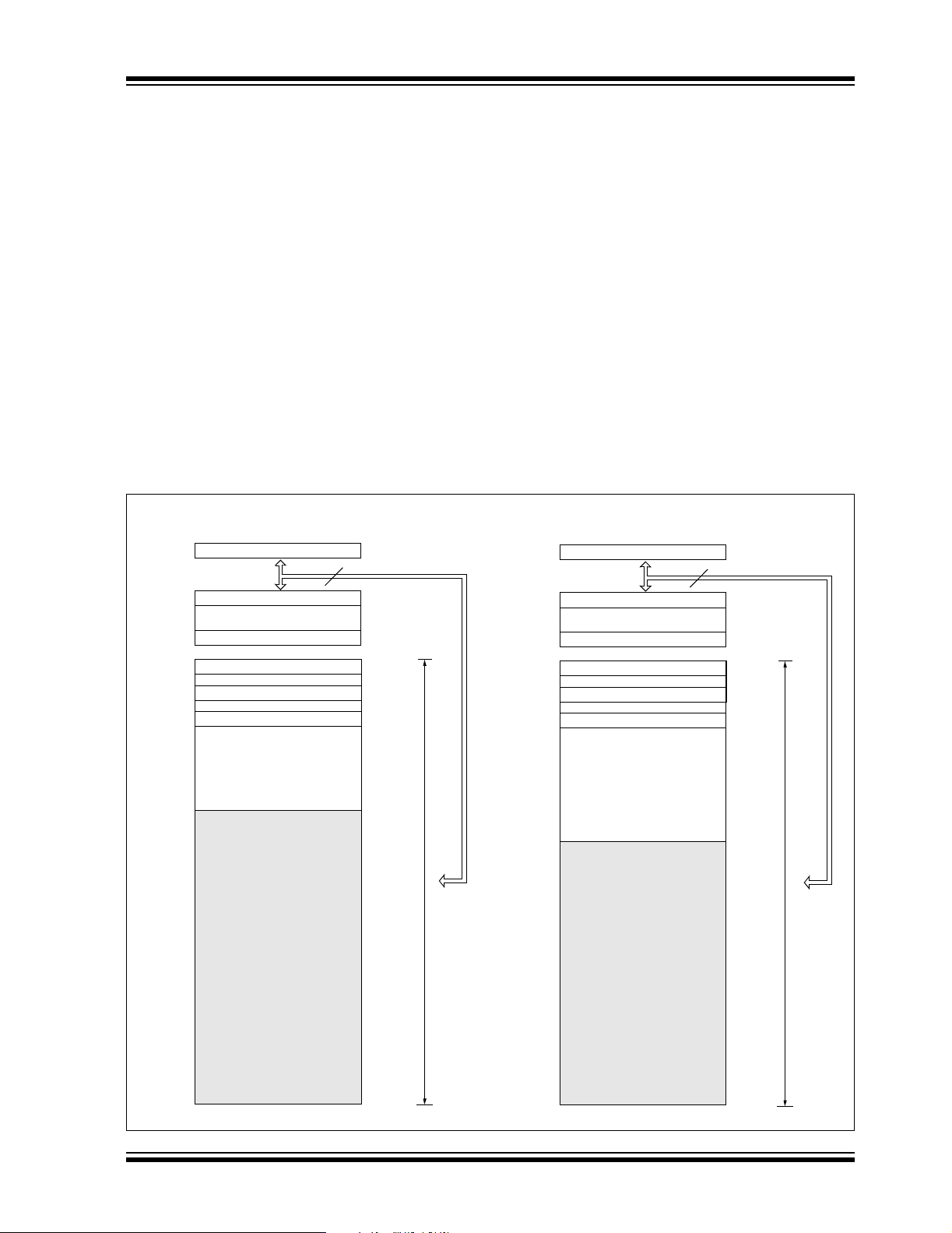
PIC18F2585/2680/4585/4680
5.0 MEMORY ORGANIZATION
There are three types of memory in PIC18 Enhanced
microcontroller devices:
• Program Memory
• Data RAM
• Data EEPROM
As Harvard architecture devices, the data and program
memories use separate busses; this allows for concurrent access of the two memory spaces. The data
EEPROM, for practical purposes, can be regarded as
a peripheral device, since it is addressed and accessed
through a set of control registers.
Additional detailed information on the operation of the
Flash program memory is provided in Section 6.0
“Flash Program Memory”. Data EEPROM is
discussed separately in Section 7.0 “Data EEPROM
Memory”.
5.1 Program Memory Organization
PIC18 microcontrollers implement a 21-bit program
counter, which is capable of addressing a 2-Mbyte
program memory space. Accessing a location between
the upper boundary of the physically implemented
memory and the 2-Mbyte address will return all ‘0’s (a
NOP instruction).
The PIC18F2585 and PIC18F4585 each have
48 Kbytes of Flash memory and can store up to 24,576
single-word instructions. The PIC18F2680 and
PIC18F4680 each have 64Kbytes of Flash memory
and can store up to 32,768 single-word instructions.
PIC18 devices have two interrupt vectors. The Reset
vector address is at 0000h and the interrupt vector
addresses are at 0008h and 0018h.
The program memory maps for PIC18FX585 and
PIC18FX680 devices are shown in Figure 5-1.
FIGURE 5-1: PROGRAM MEMORY MAP AND STACK FOR
PIC18F2585/2680/4585/4680 DEVICES
PIC18X585
PC<20:0>
CALL,RCALL,RETURN
RETFIE,RETLW
Stack Level 1
Stack Level 31
Reset Vector
High Priority Interrupt Vector
Low Priority Interrupt Vector
21
•
•
•
0000h
0008h
0018h
CALL,RCALL,RETURN
RETFIE,RETLW
High Priority Interrupt Vector
Low Priority Interrupt Vector
PIC18FX680
PC<20:0>
Stack Level 1
•
•
•
Stack Level 31
Reset Vector
21
0000h
0008h
0018h
On-Chip
Program Memory
BFFFh
C000h
Read ‘0’
1FFFFFh
200000h
© 2007 Microchip Technology Inc. Preliminary DS39625C-page 61
User Memory Space
On-Chip
Program Memory
Read ‘0’
FFFFh
10000h
User Memory Space
1FFFFFh
200000h

PIC18F2585/2680/4585/4680
5.1.1 PROGRAM COUNTER
The Program Counter (PC) specifies the address of the
instruction to fetch for execution. The PC is 21 bits wide
and is contained in three separate 8-bit registers. The
low byte, known as the PCL register, is both readable
and writable. The high byte, or PCH register, contains
the PC<15:8> bits; it is not directly readable or writable.
Updates to the PCH register are performed through the
PCLATH register. The upper byte is called PCU. This
register contains the PC<20:16> bits; it is also not
directly readable or writable. Updates to the PCU
register are performed through the PCLATU register.
The contents of PCLATH and PCLATU are transferred
to the program counter by any operation that writes
PCL. Similarly, the upper two bytes of the program
counter are transferred to PCLATH and PCLATU by an
operation that reads PCL. This is useful for computed
offsets to the PC (see Section 5.1.4.1 “Computed
GOTO”).
The PC addresses bytes in the program memory. To
prevent the PC from becoming misaligned with word
instructions, the Least Significant bit of PCL is fixed to
a value of ‘0’. The PC increments by 2 to address
sequential instructions in the program memory.
The CALL, RCALL and GOTO program branch
instructions write to the program counter directly. For
these instructions, the contents of PCLATH and
PCLATU are not transferred to the program counter.
5.1.2 RETURN ADDRESS STACK
The return address stack allows any combination of up
to 31 program calls and interrupts to occur. The PC is
pushed onto the stack when a CALL or RCALL instruction is executed or an interrupt is Acknowledged. The
PC value is pulled off the stack on a RETURN, RETLW
or a RETFIE instruction. PCLATU and PCLATH are not
affected by any of the RETURN or CALL instructions.
The stack operates as a 31-word by 21-bit RAM and a
5-bit Stack Pointer, STKPTR. The stack space is not
part of either program or data space. The Stack Pointer
is readable and writable and the address on the top of
the stack is readable and writable through the
top-of-stack Special File Registers. Data can also be
pushed to, or popped from the stack, using these
registers.
A CALL type instruction causes a push onto the stack;
the Stack Pointer is first incremented and the location
pointed to by the Stack Pointer is written with the
contents of the PC (already pointing to the instruction
following the CALL). A RETURN type instruction causes
a pop from the stack; the contents of the location
pointed to by the STKPTR are transferred to the PC
and then the Stack Pointer is decremented.
The Stack Pointer is initialized to ‘00000’ after all
Resets. There is no RAM associated with the location
corresponding to a Stack Pointer value of ‘00000’; this
is only a Reset value. Status bits indicate if the stack is
full or has overflowed or has underflowed.
5.1.2.1 Top-of-Stack Access
Only the top of the return address stack (TOS) is
readable and writable. A set of three registers,
TOSU:TOSH:TOSL, hold the contents of the stack location pointed to by the STKPTR register (Figure 5-2). This
allows users to implement a software stack if necessary.
After a CALL, RCALL or interrupt, the software can read
the pushed value by reading the TOSU:TOSH:TOSL
registers. These values can be placed on a user defined
software stack. At return time, the software can return
these values to TOSU:TOSH:TOSL and do a return.
The user must disable the global interrupt enable bits
while accessing the stack to prevent inadvertent stack
corruption.
FIGURE 5-2: RETURN ADDRESS STACK AND ASSOCIATED REGISTERS
Return Address Stack <20:0>
11111
Top-of-Stack Registers Stack Pointer
TOSLTOSHTOSU
34h1Ah00h
To p- o f -S ta ck
DS39625C-page 62 Preliminary © 2007 Microchip Technology Inc.
001A34h
000D58h
11110
11101
STKPTR<4:0>
00010
00011
00010
00001
00000

PIC18F2585/2680/4585/4680
5.1.2.2 Return Stack Pointer (STKPTR)
The STKPTR register (Register 5-1) contains the Stack
Pointer value, the STKFUL (Stack Full) status bit and
the STKUNF (Stack Underflow) status bits. The value
of the Stack Pointer can be 0 through 31. The Stack
Pointer increments before values are pushed onto the
stack and decrements after values are popped off the
stack. On Reset, the Stack Pointer value will be zero.
The user may read and write the Stack Pointer value.
This feature can be used by a Real-Time Operating
System (RTOS) for return stack maintenance.
After the PC is pushed onto the stack 31 times (without
popping any values off the stack), the STKFUL bit is
set. The STKFUL bit is cleared by software or by a
POR.
The action that takes place when the stack becomes
full depends on the state of the STVREN (Stack Overflow Reset Enable) Configuration bit. (Refer to
Section 24.1 “Configuration Bits” for a description of
the device Configuration bits.) If STVREN is set
(default), the 31st push will push the (PC + 2) value
onto the stack, set the STKFUL bit and reset the
device. The STKFUL bit will remain set and the Stack
Pointer will be set to zero.
If STVREN is cleared, the STKFUL bit will be set on the
31st push and the Stack Pointer will increment to 31.
Any additional pushes will not overwrite the 31st push
and STKPTR will remain at 31.
When the stack has been popped enough times to
unload the stack, the next pop will return a value of zero
to the PC and sets the STKUNF bit, while the Stack
Pointer remains at zero. The STKUNF bit will remain
set until cleared by software or until a POR occurs.
Note: Returning a value of zero to the PC on an
underflow has the effect of vectoring the
program to the Reset vector, where the
stack conditions can be verified and
appropriate actions can be taken. This is
not the same as a Reset, as the contents
of the SFRs are not affected.
5.1.2.3 PUSH and POP Instructions
Since the Top-of-Stack is readable and writable, the
ability to push values onto the stack and pull values off
the stack without disturbing normal program execution
is a desirable feature. The PIC18 instruction set
includes two instructions, PUSH and POP, that permit
the TOS to be manipulated under software control.
TOSU, TOSH and TOSL can be modified to place data
or a return address on the stack.
The PUSH instruction places the current PC value onto
the stack. This increments the Stack Pointer and loads
the current PC value onto the stack.
The POP instruction discards the current TOS by decrementing the Stack Pointer. The previous value pushed
onto the stack then becomes the TOS value.
REGISTER 5-1: STKPTR: STACK POINTER REGISTER
R/C-0 R/C-0 U-0 R/W-0 R/W-0 R/W-0 R/W-0 R/W-0
STKFUL
bit 7 bit 0
bit 7 STKFUL: Stack Full Flag bit
1 = Stack became full or overflowed
0 = Stack has not become full or overflowed
bit 6 STKUNF: Stack Underflow Flag bit
1 = Stack underflow occurred
0 = Stack underflow did not occur
bit 5 Unimplemented: Read as ‘0’
bit 4-0 SP4:SP0: Stack Pointer Location bits
Legend:
R = Readable bit W = Writable bit U = Unimplemented C = Clearable only bit
-n = Value at POR ‘1’ = Bit is set ‘0’ = Bit is cleared x = Bit is unknown
(1)
STKUNF
Note 1: Bit 7 and bit 6 are cleared by user software or by a POR.
(1)
— SP4 SP3 SP2 SP1 SP0
(1)
(1)
© 2007 Microchip Technology Inc. Preliminary DS39625C-page 63

PIC18F2585/2680/4585/4680
5.1.2.4 Stack Full and Underflow Resets
Device Resets on stack overflow and stack underflow
conditions are enabled by setting the STVREN bit in
Configuration Register 4L. When STVREN is set, a full
or underflow will set the appropriate STKFUL or
STKUNF bit and then cause a device Reset. When
STVREN is cleared, a full or underflow condition will set
the appropriate STKFUL or STKUNF bit, but not cause
a device Reset. The STKFUL or STKUNF bits are
cleared by the user software or a Power-on Reset.
5.1.3 FAST REGISTER STACK
A fast register stack is provided for the STATUS,
WREG and BSR registers, to provide a “fast return”
option for interrupts. Each stack is only one level deep
and is neither readable nor writable. It is loaded with the
current value of the corresponding register when the
processor vectors for an interrupt. All interrupt sources
will push values into the stack registers. The values in
the registers are then loaded back into their associated
registers, if the RETFIE, FAST instruction is used to
return from the interrupt.
If both low and high priority interrupts are enabled, the
stack registers cannot be used reliably to return from
low priority interrupts. If a high priority interrupt occurs
while servicing a low priority interrupt, the stack register
values stored by the low priority interrupt will be
overwritten. In these cases, users must save the key
registers in software during a low priority interrupt.
If interrupt priority is not used, all interrupts may use the
fast register stack for returns from interrupt. If no interrupts are used, the fast register stack can be used to
restore the STATUS, WREG and BSR registers at the
end of a subroutine call. To use the fast register stack
for a subroutine call, a CALL label, FAST instruction
must be executed to save the STATUS, WREG and
BSR registers to the fast register stack. A
RETURN, FAST instruction is then executed to restore
these registers from the fast register stack.
Example 5-1 shows a source code example that uses
the fast register stack during a subroutine call and
return.
EXAMPLE 5-1: FAST REGISTER STACK
CODE EXAMPLE
CALL SUB1, FAST ;STATUS, WREG, BSR
;SAVED IN FAST REGISTER
;STACK
•
•
SUB1 •
•
RETURN, FAST ;RESTORE VALUES SAVED
;IN FAST REGISTER STACK
5.1.4 LOOK-UP TABLES IN PROGRAM MEMORY
There may be programming situations that require the
creation of data structures, or look-up tables, in
program memory. For PIC18 devices, look-up tables
can be implemented in two ways:
• Computed GOTO
• Table Reads
5.1.4.1 Computed GOTO
A computed GOTO is accomplished by adding an offset
to the program counter. An example is shown in
Example 5-2.
A look-up table can be formed with an ADDWF PCL
instruction and a group of RETLW nn instructions. The
W register is loaded with an offset into the table before
executing a CALL to that table. The first instruction of
the called routine is the ADDWF PCL instruction. The
next instruction executed will be one of the RETLW nn
instructions, that returns the value ‘nn’ to the calling
function.
The offset value (in WREG) specifies the number of
bytes that the program counter should advance and
should be multiples of 2 (LSb = 0).
In this method, only one data byte may be stored in
each instruction location and room on the return
address stack is required.
EXAMPLE 5-2: COMPUTED GOTO USING
AN OFFSET VALUE
MOVF OFFSET, W
CALL TABLE
ORG nn00h
TABLE ADDWF PCL
RETLW nnh
RETLW nnh
RETLW nnh
.
.
.
5.1.4.2 Table Reads and Table Writes
A better method of storing data in program memory
allows two bytes of data to be stored in each instruction
location.
Look-up table data may be stored two bytes per
program word by using table reads and writes. The
Table Pointer (TBLPTR) register specifies the byte
address and the Table Latch (TABLAT) register
contains the data that is read from or written to program
memory. Data is transferred to or from program
memory one byte at a time.
Table read and table write operations are discussed
further in Section 6.1 “Table Reads and Table
Writes”.
DS39625C-page 64 Preliminary © 2007 Microchip Technology Inc.

PIC18F2585/2680/4585/4680
5.2 PIC18 Instruction Cycle
5.2.1 CLOCKING SCHEME
The microcontroller clock input, whether from an internal or external source, is internally divided by four to
generate four non-overlapping quadrature clocks (Q1,
Q2, Q3 and Q4). Internally, the Program Counter (PC)
is incremented on every Q1; the instruction is fetched
from the program memory and latched into the Instruction Register (IR) during Q4. The instruction is decoded
and executed during the following Q1 through Q4. The
clocks and instruction execution flow are shown in
Figure 5-3.
FIGURE 5-3: CLOCK/INSTRUCTION CYCLE
OSC1
Q1
Q2
Q3
Q4
PC
OSC2/CLKO
(RC mode)
Q2 Q3 Q4
Q1
PC PC + 2 PC + 4
Execute INST (PC – 2)
Fetch INST (PC)
Q2 Q3 Q4
Q1
Execute INST (PC)
Fetch INST (PC + 2)
5.2.2 INSTRUCTION FLOW/PIPELINING
An “Instruction Cycle” consists of four Q cycles: Q1
through Q4. The instruction fetch and execute are pipelined in such a manner that a fetch takes one instruction
cycle, while the decode and execute take another
instruction cycle. However, due to the pipelining, each
instruction effectively executes in one cycle. If an
instruction causes the program counter to change (e.g.,
GOTO), then two cycles are required to complete the
instruction (Example 5-3).
A fetch cycle begins with the program counter
incrementing in Q1.
In the execution cycle, the fetched instruction is latched
into the Instruction Register (IR) in cycle Q1. This
instruction is then decoded and executed during the
Q2, Q3 and Q4 cycles. Data memory is read during Q2
(operand read) and written during Q4 (destination
write).
Q2 Q3 Q4
Q1
Internal
Phase
Clock
Execute INST (PC + 2)
Fetch INST (PC + 4)
EXAMPLE 5-3: INSTRUCTION PIPELINE FLOW
TCY0TCY1TCY2TCY3TCY4TCY5
1. MOVLW 55h
2. MOVWF PORTB
3. BRA SUB_1
4. BSF PORTA, BIT3 (Forced NOP)
5. Instruction @ address SUB_1
Note: All instructions are single cycle, except for any program branches. These take two cycles since the
fetch instruction is “flushed” from the pipeline while the new instruction is being fetched and then
executed.
© 2007 Microchip Technology Inc. Preliminary DS39625C-page 65
Fetch 1 Execute 1
Fetch 2 Execute 2
Fetch 3 Execute 3
Fetch 4 Flush (NOP)
Fetch SUB_1 Execute SUB_1

PIC18F2585/2680/4585/4680
5.2.3 INSTRUCTIONS IN PROGRAM MEMORY
The program memory is addressed in bytes. Instructions are stored as two bytes or four bytes in program
memory. The Least Significant Byte of an instruction
word is always stored in a program memory location
with an even address (LSB = 0). To maintain alignment
with instruction boundaries, the PC increments in steps
of 2 and the LSB will always read ‘0’ (see Section 5.1.1
“Program Counter”).
Figure 5-4 shows an example of how instruction words
are stored in the program memory.
The CALL and GOTO instructions have the absolute
program memory address embedded into the instruc-
tion. Since instructions are always stored on word
boundaries, the data contained in the instruction is a
word address. The word address is written to PC<20:1>,
which accesses the desired byte address in program
memory. Instruction #2 in Figure 5-4 shows how the
instruction GOTO 0006h is encoded in the program
memory. Program branch instructions, which encode a
relative address offset, operate in the same manner. The
offset value stored in a branch instruction represents the
number of single-word instructions that the PC will be
offset by. Section 25.0 “Instruction Set Summary”
provides further details of the instruction set.
FIGURE 5-4: INSTRUCTIONS IN PROGRAM MEMORY
LSB = 1 LSB = 0 ↓
0Fh 55h 000008h
EFh 03h 00000Ah
F0h 00h 00000Ch
C1h 23h 00000Eh
F4h 56h 000010h
Instruction 1:
Instruction 2:
Instruction 3:
Program Memory
Byte Locations
MOVLW 055h
GOTO 0006h
MOVFF 123h, 456h
→
Word Address
000000h
000002h
000004h
000006h
000012h
000014h
5.2.4 TWO-WORD INSTRUCTIONS
The standard PIC18 instruction set has four two-word
instructions: CALL, MOVFF, GOTO and LSFR. In all
cases, the second word of the instructions always has
‘1111’ as its four Most Significant bits; the other 12 bits
are literal data, usually a data memory address.
The use of ‘1111’ in the 4 MSbs of an instruction
specifies a special form of NOP. If the instruction is
executed in proper sequence – immediately after the
first word – the data in the second word is accessed
and used by the instruction sequence. If the first word
is skipped for some reason and the second word is
executed by itself, a NOP is executed instead. This is
necessary for cases when the two-word instruction is
preceded by a conditional instruction that changes the
PC. Example 5-4 shows how this works.
Note: See Section 5.5 “Program Memory and
the Extended Instruction Set” for
information on two-word instructions in the
extended instruction set.
EXAMPLE 5-4: TWO-WORD INSTRUCTIONS
CASE 1:
Object Code Source Code
0110 0110 0000 0000 TSTFSZ REG1 ; is RAM location 0?
1100 0001 0010 0011 MOVFF REG1, REG2 ; No, skip this word
1111 0100 0101 0110 ; Execute this word as a NOP
0010 0100 0000 0000 ADDWF REG3 ; continue code
CASE 2:
Object Code Source Code
0110 0110 0000 0000 TSTFSZ REG1 ; is RAM location 0?
1100 0001 0010 0011 MOVFF REG1, REG2 ; Yes, execute this word
1111 0100 0101 0110 ; 2nd word of instruction
0010 0100 0000 0000 ADDWF REG3 ; continue code
DS39625C-page 66 Preliminary © 2007 Microchip Technology Inc.

PIC18F2585/2680/4585/4680
5.3 Data Memory Organization
Note: The operation of some aspects of data
memory are changed when the PIC18
extended instruction set is enabled. See
Section 5.6 “Data Memory and the
Extended Instruction Set” for more
information.
The data memory in PIC18 devices is implemented as
static RAM. Each register in the data memory has a
12-bit address, allowing up to 4096 bytes of data
memory. The memory space is divided into as many as
16 banks that contain 256 bytes each;
PIC18F2585/2680/4585/4680 devices implement all
16 banks. Figure 5-5 shows the data memory
organization for the PIC18F2585/2680/4585/4680
devices.
The data memory contains Special Function Registers
(SFRs) and General Purpose Registers (GPRs). The
SFRs are used for control and status of the controller
and peripheral functions, while GPRs are used for data
storage and scratchpad operations in the user’s
application. Any read of an unimplemented location will
read as ‘0’s.
The instruction set and architecture allow operations
across all banks. The entire data memory may be
accessed by Direct, Indirect or Indexed Addressing
modes. Addressing modes are discussed later in this
subsection.
To ensure that commonly used registers (SFRs and
select GPRs) can be accessed in a single cycle, PIC18
devices implement an Access Bank. This is a 256-byte
memory space that provides fast access to SFRs and
the lower portion of GPR Bank 0 without using the
BSR. Section 5.3.2 “Access Bank” provides a
detailed description of the Access RAM.
5.3.1 BANK SELECT REGISTER (BSR)
Large areas of data memory require an efficient
addressing scheme to make rapid access to any
address possible. Ideally, this means that an entire
address does not need to be provided for each read or
write operation. For PIC18 devices, this is accomplished with a RAM banking scheme. This divides the
memory space into 16 contiguous banks of 256 bytes.
Depending on the instruction, each location can be
addressed directly by its full 12-bit address, or an 8-bit
low-order address and a 4-bit bank pointer.
Most instructions in the PIC18 instruction set make use
of the bank pointer, known as the Bank Select Register
(BSR). This SFR holds the 4 Most Significant bits of a
location’s address; the instruction itself includes the
8 Least Significant bits. Only the four lower bits of the
BSR are implemented (BSR3:BSR0). The upper four
bits are unused; they will always read ‘0’ and cannot be
written to. The BSR can be loaded directly by using the
MOVLB instruction.
The value of the BSR indicates the bank in data memory; the 8 bits in the instruction show the location in the
bank and can be thought of as an offset from the bank’s
lower boundary. The relationship between the BSR’s
value and the bank division in data memory is shown in
Figure 5-6.
Since up to 16 registers may share the same low-order
address, the user must always be careful to ensure that
the proper bank is selected before performing a data
read or write. For example, writing what should be
program data to an 8-bit address of F9h while the BSR
is 0Fh, will end up resetting the program counter.
While any bank can be selected, only those banks that
are actually implemented can be read or written to.
Writes to unimplemented banks are ignored, while
reads from unimplemented banks will return ‘0’s. Even
so, the STATUS register will still be affected as if the
operation was successful. The data memory map in
Figure 5-5 indicates which banks are implemented.
In the core PIC18 instruction set, only the MOVFF
instruction fully specifies the 12-bit address of the
source and target registers. This instruction ignores the
BSR completely when it executes. All other instructions
include only the low-order address as an operand and
must use either the BSR or the Access Bank to locate
their target registers.
© 2007 Microchip Technology Inc. Preliminary DS39625C-page 67

PIC18F2585/2680/4585/4680
FIGURE 5-5: DATA MEMORY MAP FOR PIC18F2585/2680/4585/4680 DEVICES
BSR<3:0>
= 0000
= 0001
= 0010
= 0011
= 0100
= 0101
= 0110
= 0111
= 1000
= 1001
= 1010
= 1011
= 1100
= 1101
= 1110
= 1111
Bank 0
Bank 1
Bank 2
Bank 3
Bank 4
Bank 5
Bank 6
Bank 7
Bank 8
Bank 9
Bank 10
Bank 11
Bank 12
Bank 13
Bank 14
Bank 15
Data Memory Map
00h
FFh
00h
FFh
00h
FFh
00h
FFh
00h
FFh
00h
FFh
00h
FFh
00h
FFh
00h
FFh
00h
FFh
00h
FFh
00h
FFh
00h
FFh
00h
FFh
00h
FFh
00h
FFh
Access RAM
CAN SFRs
CAN SFRs
CAN SFRs
GPR
GPR
GPR
GPR
GPR
GPR
GPR
GPR
GPR
GPR
GPR
GPR
GPR
SFR
000h
05Fh
060h
0FFh
100h
1FFh
200h
2FFh
300h
3FFh
400h
4FFh
500h
5FFh
600h
6FFh
700h
7FFh
800h
8FFh
900h
9FFh
A00h
AFFh
B00h
BFFh
C00h
CFFh
D00h
DFFh
E00h
EFFh
F00h
F5Fh
F60h
FFFh
When a = 0:
The BSR is ignored and the
Access Bank is used.
The first 128 bytes are
general purpose RAM
(from Bank 0).
The second 128 bytes are
Special Function Registers
(from Bank 15).
When a = 1:
The BSR specifies the Bank
used by the instruction.
Access Bank
Access RAM Low
Access RAM High
(SFRs)
00h
5Fh
60h
FFh
DS39625C-page 68 Preliminary © 2007 Microchip Technology Inc.

PIC18F2585/2680/4585/4680
FIGURE 5-6: USE OF THE BANK SELECT REGISTER (DIRECT ADDRESSING)
Memory
7
BSR
0000
Bank Select
(2)
(1)
0
0011
000h
100h
200h
300h
Data
Bank 0
Bank 1
Bank 2
Bank 3
through
Bank 13
00h
FFh
00h
FFh
00h
FFh
00h
7
From Opcode
11111111
(2)
0
E00h
F00h
FFFh
Note 1: The Access RAM bit of the instruction can be used to force an override of the selected bank (BSR<3:0>) to
the registers of the Access Bank.
2: The MOVFF instruction embeds the entire 12-bit address in the instruction.
Bank 14
Bank 15
5.3.2 ACCESS BANK
While the use of the BSR with an embedded 8-bit
address allows users to address the entire range of
data memory, it also means that the user must always
ensure that the correct bank is selected. Otherwise,
data may be read from or written to the wrong location.
This can be disastrous if a GPR is the intended target
of an operation, but an SFR is written to instead.
Verifying and/or changing the BSR for each read or
write to data memory can become very inefficient.
To streamline access for the most commonly used data
memory locations, the data memory is configured with
an Access Bank, which allows users to access a
mapped block of memory without specifying a BSR.
The Access Bank consists of the first 128 bytes of
memory (00h-7Fh) in Bank 0 and the last 128 bytes of
memory (80h-FFh) in Block 15. The lower half is known
as the “Access RAM” and is composed of GPRs. The
FFh
00h
FFh
00h
FFh
however, the instruction is forced to use the Access
Bank address map; the current value of the BSR is
ignored entirely.
Using this “forced” addressing allows the instruction to
operate on a data address in a single cycle, without
updating the BSR first. For 8-bit addresses of 80h and
above, this means that users can evaluate and operate
on SFRs more efficiently. The Access RAM below 80h
is a good place for data values that the user might need
to access rapidly, such as immediate computational
results or common program variables. Access RAM
also allows for faster and more code efficient context
saving and switching of variables.
The mapping of the Access Bank is slightly different
when the extended instruction set is enabled (XINST
Configuration bit = 1). This is discussed in more detail
in Section 5.6.3 “Mapping the Access Bank in
Indexed Literal Offset Mode”.
upper half is also where the device’s SFRs are
mapped. These two areas are mapped contiguously in
the Access Bank and can be addressed in a linear
fashion by an 8-bit address (Figure 5-5).
The Access Bank is used by core PIC18 instructions
that include the Access RAM bit (the ‘a’ parameter in
the instruction). When ‘a’ is equal to ‘1’, the instruction
uses the BSR and the 8-bit address included in the
opcode for the data memory address. When ‘a’ is ‘0’
5.3.3 GENERAL PURPOSE REGISTER FILE
PIC18 devices may have banked memory in the GPR
area. This is data RAM, which is available for use by all
instructions. GPRs start at the bottom of Bank 0
(address 000h) and grow upwards towards the bottom
of the SFR area. GPRs are not initialized by a
Power-on Reset and are unchanged on all other
Resets.
© 2007 Microchip Technology Inc. Preliminary DS39625C-page 69

PIC18F2585/2680/4585/4680
5.3.4 SPECIAL FUNCTION REGISTERS
The Special Function Registers (SFRs) are registers
used by the CPU and peripheral modules for controlling
the desired operation of the device. These registers are
implemented as static RAM. SFRs start at the top of
data memory (FFFh) and extend downward to occupy
the top half of Bank 15 (F80h to FFFh). A list of these
registers is given in Table 5-1 and Table 5-2.
The SFRs can be classified into two sets: those
peripheral functions. The reset and interrupt registers
are described in their respective chapters, while the
ALU’s STATUS register is described later in this
section. Registers related to the operation of a
peripheral feature are described in the chapter for that
peripheral.
The SFRs are typically distributed among the
peripherals whose functions they control. Unused SFR
locations are unimplemented and read as ‘0’s.
associated with the “core” device functionality (ALU,
Resets and interrupts) and those related to the
TABLE 5-1: SPECIAL FUNCTION REGISTER MAP FOR
PIC18F2585/2680/4585/4680 DEVICES
Address Name Address Name Address Name Address Name
FFFh TOSU FDFh INDF2
FFEh TOSH FDEh POSTINC2
FFDh TOSL FDDh POSTDEC2
FFCh STKPTR FDCh PREINC2
FFBh PCLATU FDBh PLUSW2
FFAh PCLATH FDAh FSR2H FBAh ECCP1CON
FF9h PCL FD9h FSR2L FB9h
FF8h TBLPTRU FD8h STATUS FB8h BAUDCON F98h
FF7h TBLPTRH FD7h TMR0H FB7h ECCP1DEL F97h
FF6h TBLPTRL FD6h TMR0L FB6h ECCP1AS
FF5h TABLAT FD5h T0CON FB5h CVRCON
FF4h PRODH FD4h — FB4h CMCON F94h TRISC
FF3h PRODL FD3h OSCCON FB3h TMR3H F93h TRISB
FF2h INTCON FD2h HLVDCON FB2h TMR3L F92h TRISA
FF1h INTCON2 FD1h WDTCON FB1h T3CON F91h
FF0h INTCON3 FD0h RCON FB0h SPBRGH F90h
FEFh INDF0
FEEh POSTINC0
FEDh POSTDEC0
FECh PREINC0
FEBh PLUSW0
(3)
(3)
(3)
(3)
(3)
FCFh TMR1H FAFh SPBRG F8Fh —
FCEh TMR1L FAEh RCREG F8Eh —
FCDh T1CON FADh TXREG F8Dh LATE
FCCh TMR2 FACh TXSTA F8Ch LATD
FCBh PR2 FABh RCSTA F8Bh LATC
FEAh FSR0H FCAh T2CON FAAh EEADRH F8Ah LATB
FE9h FSR0L FC9h SSPBUF FA9h EEADR F89h LATA
FE8h WREG FC8h SSPADD FA8h EEDATA F88h
FE7h INDF1
(3)
FE6h POSTINC1
FE5h POSTDEC1
FE4h PREINC1
FE3h PLUSW1
(3)
(3)
(3)
(3)
FC7h SSPSTAT FA7h EECON2
FC6h SSPCON1 FA6h EECON1 F86h —
FC5h SSPCON2 FA5h IPR3 F85h —
FC4h ADRESH FA4h PIR3 F84h PORTE
FC3h ADRESL FA3h PIE3 F83h PORTD
FE2h FSR1H FC2h ADCON0 FA2h IPR2 F82h PORTC
FE1h FSR1L FC1h ADCON1 FA1h PIR2 F81h PORTB
FE0h BSR FC0h ADCON2 FA0h PIE2 F80h PORTA
(3)
(3)
(3)
(3)
(3)
FBFh CCPR1H F9Fh IPR1
FBEh CCPR1L F9Eh PIR1
FBDh CCP1CON F9Dh PIE1
FBCh ECCPR1H
FBBh ECCPR1L
(1)
(1)
(1)
F9Ch —
F9Bh OSCTUNE
F9Ah —
— F99h —
(1)
(1)
(3)
F96h TRISE
F95h TRISD
F87h —
—
—
(1)
(1)
—
—
(1)
(1)
—
(1)
(1)
Note 1: Registers available only on PIC18F4X8X devices; otherwise, the registers read as ‘0’.
2: When any TX_ENn bit in RX_TX_SELn is set, then the corresponding bit in this register has transmit properties.
3: This is not a physical register.
DS39625C-page 70 Preliminary © 2007 Microchip Technology Inc.

PIC18F2585/2680/4585/4680
TABLE 5-1: SPECIAL FUNCTION REGISTER MAP FOR
PIC18F2585/2680/4585/4680 DEVICES (CONTINUED)
Address Name Address Name Address Name Address Name
F7Fh
F7Eh
F7Dh
F7Ch
F7Bh
F7Ah
F79h
F78h
F77h ECANCON F57h RXB1D1 F37h TXB1D1 F17h RXF5EIDL
F76h TXERRCNT F56h RXB1D0 F36h TXB1D0 F16h RXF5EIDH
F75h RXERRCNT F55h RXB1DLC F35h TXB1DLC F15h RXF5SIDL
F74h COMSTAT F54h RXB1EIDL F34h TXB1EIDL F14h RXF5SIDH
F73h CIOCON F53h RXB1EIDH F33h TXB1EIDH F13h RXF4EIDL
F72h BRGCON3 F52h RXB1SIDL F32h TXB1SIDL F12h RXF4EIDH
F71h BRGCON2 F51h RXB1SIDH F31h TXB1SIDH F11h RXF4SIDL
F70h BRGCON1 F50h RXB1CON F30h TXB1CON F10h RXF4SIDH
F6Fh CANCON F4Fh CANCON_RO1 F2Fh CANCON_RO3 F0Fh RXF3EIDL
F6Eh CANSTAT F4Eh CANSTAT_RO1 F2Eh CANSTAT_RO3 F0Eh RXF3EIDH
F6Dh RXB0D7 F4DH TXB0D7 F2Dh TXB2D7 F0Dh RXF3SIDL
F6Ch RXB0D6 F4Ch TXB0D6 F2Ch TXB2D6 F0Ch RXF3SIDH
F6Bh RXB0D5 F4Bh TXB0D5 F2Bh TXB2D5 F0Bh RXF2EIDL
F6Ah RXB0D4 F4Ah TXB0D4 F2Ah TXB2D4 F0Ah RXF2EIDH
F69h RXB0D3 F49h TXB0D3 F29h TXB2D3 F09h RXF2SIDL
F68h RXB0D2 F48h TXB0D2 F28h TXB2D2 F08h RXF2SIDH
F67h RXB0D1 F47h TXB0D1 F27h TXB2D1 F07h RXF1EIDL
F66h RXB0D0 F46h TXB0D0 F26h TXB2D0 F06h RXF1EIDH
F65h RXB0DLC F45h TXB0DLC F25h TXB2DLC F05h RXF1SIDL
F64h RXB0EIDL F44h TXB0EIDL F24h TXB2EIDL F04h RXF1SIDH
F63h RXB0EIDH F43h TXB0EIDH F23h TXB2EIDH F03h RXF0EIDL
F62h RXB0SIDL F42h TXB0SIDL F22h TXB2SIDL F02h RXF0EIDH
F61h RXB0SIDH F41h TXB0SIDH F21h TXB2SIDH F01h RXF0SIDL
F60h RXB0CON F40h TXB0CON F20h TXB2CON F00h RXF0SIDH
— F5Fh CANCON_RO0 F3Fh CANCON_RO2 F1Fh RXM1EIDL
— F5Eh CANSTAT_RO0 F3Eh CANSTAT_RO2 F1Eh RXM1EIDH
— F5Dh RXB1D7 F3Dh TXB1D7 F1Dh RXM1SIDL
— F5Ch RXB1D6 F3Ch TXB1D6 F1Ch RXM1SIDH
— F5Bh RXB1D5 F3Bh TXB1D5 F1Bh RXM0EIDL
— F5Ah RXB1D4 F3Ah TXB1D4 F1Ah RXM0EIDH
— F59h RXB1D3 F39h TXB1D3 F19h RXM0SIDL
— F58h RXB1D2 F38h TXB1D2 F18h RXM0SIDH
Note 1: Registers available only on PIC18F4X8X devices; otherwise, the registers read as ‘0’.
2: When any TX_ENn bit in RX_TX_SELn is set, then the corresponding bit in this register has transmit properties.
3: This is not a physical register.
© 2007 Microchip Technology Inc. Preliminary DS39625C-page 71

PIC18F2585/2680/4585/4680
Address Name Address Name Address Name Address Name
EFFh
EFEh
EFDh
EFCh
EFBh
EFAh
EF9h
EF8h
EF7h
EF6h
EF5h
EF4h
EF3h
EF2h
EF1h
EF0h
EEFh
EEEh
—EDFh—EBFh—E9Fh—
—EDEh—EBEh—E9Eh—
—EDDh—EBDh—E9Dh—
—EDCh—EBCh—E9Ch—
—EDBh—EBBh—E9Bh—
—EDAh—EBAh—E9Ah—
—ED9h—EB9h— E99h —
—ED8h—EB8h— E98h —
—ED7h—EB7h— E97h —
—ED6h—EB6h— E96h —
—ED5h—EB5h— E95h —
—ED4h—EB4h— E94h —
—ED3h—EB3h— E93h —
—ED2h—EB2h— E92h —
—ED1h—EB1h— E91h —
—ED0h—EB0h— E90h —
—ECFh—EAFh—E8Fh—
—ECEh—EAEh
DS39625C-page 72 Preliminary © 2007 Microchip Technology Inc.

PIC18F2585/2680/4585/4680
TABLE 5-1: SPECIAL FUNCTION REGISTER MAP FOR
PIC18F2585/2680/4585/4680 DEVICES (CONTINUED)
Address Name Address Name Address Name Address Name
E7Fh CANCON_RO4 E6Fh CANCON_RO5 E5Fh CANCON_RO6 E4Fh CANCON_RO7
E7Eh CANSTAT_RO4 E6Eh CANSTAT_RO5 E5Eh CANSTAT_RO6 E4Eh CANSTAT_RO7
E7Dh B5D7
E7Ch B5D6
E7Bh B5D5
E7Ah B5D4
E79h B5D3
E78h B5D2
E77h B5D1
E76h B5D0
E75h B5DLC
E74h B5EIDL
E73h B5EIDH
E72h B5SIDL
E71h B5SIDH
E70h B5CON
E3Fh CANCON_RO8 E2Fh CANCON_RO9 E1Fh —E0Fh—
E3Eh CANSTAT_RO8 E2Eh CANSTAT_RO9 E1Eh
E3Dh B1D7
E3Ch B1D6
E3Bh B1D5
E3Ah B1D4
E39h B1D3
E38h B1D2
E37h B1D1
E36h B1D0
E35h B1DLC
E34h B1EIDL
E33h B1EIDH
E32h B1SIDL
E31h B1SIDH
E30h B1CON
(2)
E6Dh B4D7
(2)
E6Ch B4D6
(2)
E6Bh B4D5
(2)
E6Ah B4D4
(2)
E69h B4D3
(2)
E68h B4D2
(2)
E67h B4D1
(2)
E66h B4D0
(2)
E65h B4DLC
(2)
E64h B4EIDL
(2)
E63h B4EIDH
(2)
E62h B4SIDL
(2)
E61h B4SIDH
(2)
E60h B4CON
(2)
(2)
(2)
(2)
(2)
(2)
(2)
(2)
(2)
(2)
(2)
(2)
(2)
(2)
E2Dh B0D7
E2Ch B0D6
E2Bh B0D5
E2Ah B0D4
E29h B0D3
E28h B0D2
E27h B0D1
E26h B0D0
E25h B0DLC
E24h B0EIDL
E23h B0EIDH
E22h B0SIDL
E21h B0SIDH
E20h B0CON
(2)
(2)
(2)
(2)
(2)
(2)
(2)
(2)
(2)
(2)
(2)
(2)
(2)
(2)
E5Dh B3D7
E5Ch B3D6
E5Bh B3D5
E5Ah B3D4
E59h B3D3
E58h B3D2
E57h B3D1
E56h B3D0
E55h B3DLC
E54h B3EIDL
E53h B3EIDH
E52h B3SIDL
E51h B3SIDH
E50h B3CON
(2)
(2)
(2)
(2)
(2)
(2)
(2)
(2)
(2)
(2)
(2)
(2)
(2)
(2)
E4Dh B2D7
E4Ch B2D6
E4Bh B2D5
E4Ah B2D4
E49h B2D3
E48h B2D2
E47h B2D1
E46h B2D0
E45h B2DLC
E44h B2EIDL
E43h B2EIDH
E42h B2SIDL
E41h B2SIDH
E40h B2CON
—E0Eh—
(2)
(2)
(2)
(2)
(2)
(2)
(2)
(2)
(2)
(2)
(2)
(2)
(2)
(2)
E1Dh —E0Dh—
E1Ch —E0Ch—
E1Bh —E0Bh—
E1Ah —E0Ah—
E19h — E09h —
E18h — E08h —
E17h — E07h —
E16h — E06h —
E15h — E05h —
E14h — E04h —
E13h — E03h —
E12h — E02h —
E11h — E01h —
E10h — E00h —
(2)
(2)
(2)
(2)
(2)
(2)
(2)
(2)
(2)
(2)
(2)
(2)
(2)
(2)
Note 1: Registers available only on PIC18F4X8X devices; otherwise, the registers read as ‘0’.
2: When any TX_ENn bit in RX_TX_SELn is set, then the corresponding bit in this register has transmit properties.
3: This is not a physical register.
© 2007 Microchip Technology Inc. Preliminary DS39625C-page 73

PIC18F2585/2680/4585/4680
TABLE 5-1: SPECIAL FUNCTION REGISTER MAP FOR
PIC18F2585/2680/4585/4680 DEVICES (CONTINUED)
Address Name Address Name Address Name Address Name
DFFh
DFEh
DFDh
DFCh TXBIE DDCh
DFBh
DFAh BIE0 DDAh
DF9h
DF8h BSEL0 DD8h SDFLC DB8h
DF7h
DF6h
DF5h
DF4h
DF3h MSEL3 DD3h
DF2h MSEL2 DD2h
DF1h MSEL1 DD1h
DF0h MSEL0 DD0h
DEFh
DEEh
DEDh
DECh
DEBh
DEAh
DE9h
DE8h
DE7h RXFBCON7 DC7h
DE6h RXFBCON6 DC6h
DE5h RXFBCON5 DC5h
DE4h RXFBCON4 DC4h
DE3h RXFBCON3 DC3h
DE2h RXFBCON2 DC2h
DE1h RXFBCON1 DC1h
DE0h RXFBCON0 DC0h
— DDFh —DBFh—D9Fh—
— DDEh —DBEh—D9Eh—
—DDDh—DBDh—D9Dh—
—DBCh—D9Ch—
— DDBh —DBBh—D9Bh—
—DBAh—D9Ah—
—DD9h—DB9h— D99h —
— D98h —
—DD7h—DB7h— D97h —
—DD6h—DB6h— D96h —
— DD5h RXFCON1 DB5h — D95h —
— DD4h RXFCON0 DB4h — D94h —
—DB3h— D93h RXF15EIDL
—DB2h— D92h RXF15EIDH
—DB1h— D91h RXF15SIDL
—DB0h— D90h RXF15SIDH
— DCFh —DAFh—D8Fh—
— DCEh —DAEh—D8Eh—
—DCDh—DADh—D8Dh—
—DCCh—DACh—D8Ch—
— DCBh —DABh—D8BhRXF14EIDL
— DCAh —DAAh— D8Ah RXF14EIDH
—DC9h—DA9h— D89h RXF14SIDL
—DC8h—DA8h— D88h RXF14SIDH
—DA7h— D87h RXF13EIDL
—DA6h— D86h RXF13EIDH
—DA5h— D85h RXF13SIDL
—DA4h— D84h RXF13SIDH
—DA3h— D83h RXF12EIDL
—DA2h— D82h RXF12EIDH
—DA1h— D81h RXF12SIDL
—DA0h— D80h RXF12SIDH
Note 1: Registers available only on PIC18F4X8X devices; otherwise, the registers read as ‘0’.
2: When any TX_ENn bit in RX_TX_SELn is set, then the corresponding bit in this register has transmit properties.
3: This is not a physical register.
DS39625C-page 74 Preliminary © 2007 Microchip Technology Inc.

PIC18F2585/2680/4585/4680
TABLE 5-1: SPECIAL FUNCTION REGISTER MAP FOR
PIC18F2585/2680/4585/4680 DEVICES (CONTINUED)
Address Name
D7Fh
D7Eh
D7Dh
D7Ch
D7Bh RXF11EIDL
D7Ah RXF11EIDH
D79h RXF11SIDL
D78h RXF11SIDH
D77h RXF10EIDL
D76h RXF10EIDH
D75h RXF10SIDL
D74h RXF10SIDH
D73h RXF9EIDL
D72h RXF9EIDH
D71h RXF9SIDL
D70h RXF9SIDH
D6Fh
D6Eh
D6Dh
D6Ch
D6Bh RXF8EIDL
D6Ah RXF8EIDH
D69h RXF8SIDL
D68h RXF8SIDH
D67h RXF7EIDL
D66h RXF7EIDH
D65h RXF7SIDL
D64h RXF7SIDH
D63h RXF6EIDL
D62h RXF6EIDH
D61h RXF6SIDL
D60h RXF6SIDH
—
—
—
—
—
—
—
—
Note 1: Registers available only on PIC18F4X8X devices; otherwise, the registers read as ‘0’.
2: When any TX_ENn bit in RX_TX_SELn is set, then the corresponding bit in this register has transmit properties.
3: This is not a physical register.
© 2007 Microchip Technology Inc. Preliminary DS39625C-page 75

PIC18F2585/2680/4585/4680
TABLE 5-2: REGISTER FILE SUMMARY (PIC18F2585/2680/4585/4680)
File Name Bit 7 Bit 6 Bit 5 Bit 4 Bit 3 Bit 2 Bit 1 Bit 0
TOSU
TOSH Top-of-Stack High Byte (TOS<15:8>) 0000 0000 49, 62
TOSL Top-of-Stack Low Byte (TOS<7:0>) 0000 0000 49, 62
STKPTR STKFUL STKUNF
PCLATU
PCLATH Holding Register for PC<15:8> 0000 0000 49, 62
PCL PC Low Byte (PC<7:0>) 0000 0000 49, 62
TBLPTRU
TBLPTRH Program Memory Table Pointer High Byte (TBLPTR<15:8>) 0000 0000 49, 103
TBLPTRL Program Memory Table Pointer Low Byte (TBLPTR<7:0>) 0000 0000 49, 103
TABLAT Program Memory Table Latch 0000 0000 49, 103
PRODH Product Register High Byte xxxx xxxx 49, 111
PRODL Product Register Low Byte xxxx xxxx 49, 111
INTCON GIE/GIEH PEIE/GIEL TMR0IE INT0IE RBIE TMR0IF INT0IF RBIF 0000 000x 49, 115
INTCON2 RBPU
INTCON3 INT2IP INT1IP
INDF0 Uses contents of FSR0 to address data memory – value of FSR0 not changed (not a physical register) N/A 49, 89
POSTINC0 Uses contents of FSR0 to address data memory – value of FSR0 post-incremented (not a physical register) N/A 49, 90
POSTDEC0 Uses contents of FSR0 to address data memory – value of FSR0 post-decremented (not a physical register) N/A 49, 90
PREINC0 Uses contents of FSR0 to address data memory – value of FSR0 pre-incremented (not a physical register) N/A 49, 90
PLUSW0 Uses contents of FSR0 to address data memory – value of FSR0 pre-incremented (not a physical register),
FSR0H
FSR0L Indirect Data Memory Address Pointer 0 Low Byte xxxx xxxx 49, 89
WREG Working Register xxxx xxxx 49
INDF1 Uses contents of FSR1 to address data memory – value of FSR1 not changed (not a physical register) N/A 49, 89
POSTINC1 Uses contents of FSR1 to address data memory – value of FSR1 post-incremented (not a physical register) N/A 49, 90
POSTDEC1 Uses contents of FSR1 to address data memory – value of FSR1 post-decremented (not a physical register) N/A 49, 90
PREINC1 Uses contents of FSR1 to address data memory – value of FSR1 pre-incremented (not a physical register) N/A 49, 90
PLUSW1 Uses contents of FSR1 to address data memory – value of FSR1 pre-incremented (not a physical register),
FSR1H
FSR1L Indirect Data Memory Address Pointer 1 Low Byte xxxx xxxx 49, 89
BSR
INDF2 Uses contents of FSR2 to address data memory – value of FSR2 not changed (not a physical register) N/A 50, 89
POSTINC2 Uses contents of FSR2 to address data memory – value of FSR2 post-incremented (not a physical register) N/A 50, 90
POSTDEC2 Uses contents of FSR2 to address data memory – value of FSR2 post-decremented (not a physical register) N/A 50, 90
PREINC2 Uses contents of FSR2 to address data memory – value of FSR2 pre-incremented (not a physical register) N/A 50, 90
PLUSW2 Uses contents of FSR2 to address data memory – value of FSR2 pre-incremented (not a physical register),
FSR2H
FSR2L Indirect Data Memory Address Pointer 2 Low Byte xxxx xxxx 50, 89
Legend: x = unknown, u = unchanged, - = unimplemented, q = value depends on condition
Note 1: Bit 21 of the PC is only available in Test mode and Serial Programming modes.
2: The SBOREN bit is only available when CONFIG2L<1:0> = 01; otherwise, it is disabled and reads as ‘0’. See Section 4.4 “Brown-out Reset
(BOR)”.
3: These registers and/or bits are not implemented on PIC18F2X8X devices and are read as ‘0’. Reset values are shown for PIC18F4X8X
devices; individual unimplemented bits should be interpreted as ‘—’.
4: The PLLEN bit is only available in specific oscillator configuration; otherwise, it is disabled and reads as ‘0’. See Section 2.6.4 “PLL in
INTOSC Modes”.
5: The RE3 bit is only available when Master Clear Reset is disabled (CONFIG3H<7> = 0); otherwise, RE3 reads as ‘0’. This bit is read-only.
6: RA6/RA7 and their associated latch and direction bits are individually configured as port pins based on various primary oscillator modes.
When disabled, these bits read as ‘0’.
7: CAN bits have multiple functions depending on the selected mode of the CAN module.
8: This register reads all ‘0’s until the ECAN™ technology is set up in Mode 1 or Mode 2.
9: These registers are available on PIC18F4X8X devices only.
— — — Top-of-Stack Upper Byte (TOS<20:16>) ---0 0000 49, 62
— Return Stack Pointer 00-0 0000 49, 63
— —bit 21
— — bit 21 Program Memory Table Pointer Upper Byte (TBLPTR<20:16>) --00 0000 49, 103
INTEDG0 INTEDG1 INTEDG2 —TMR0IP—RBIP1111 -1-1 49, 116
value of FSR0 offset by W
— — — — Indirect Data Memory Address Pointer 0 High ---- xxxx 49, 89
value of FSR1 offset by W
— — — — Indirect Data Memory Address Pointer 1 High ---- xxxx 49, 89
— — — — Bank Select Register ---- 0000 50, 67
value of FSR2 offset by W
— — — — Indirect Data Memory Address Pointer 2 High ---- xxxx 50, 89
(1)
Holding Register for PC<20:16> ---0 0000 49, 62
— INT2IE INT1IE — INT2IF INT1IF 11-0 0-00 49, 117
Val ue on
POR, BOR
N/A 49, 90
N/A 49, 90
N/A 50, 90
Details
on page:
DS39625C-page 76 Preliminary © 2007 Microchip Technology Inc.
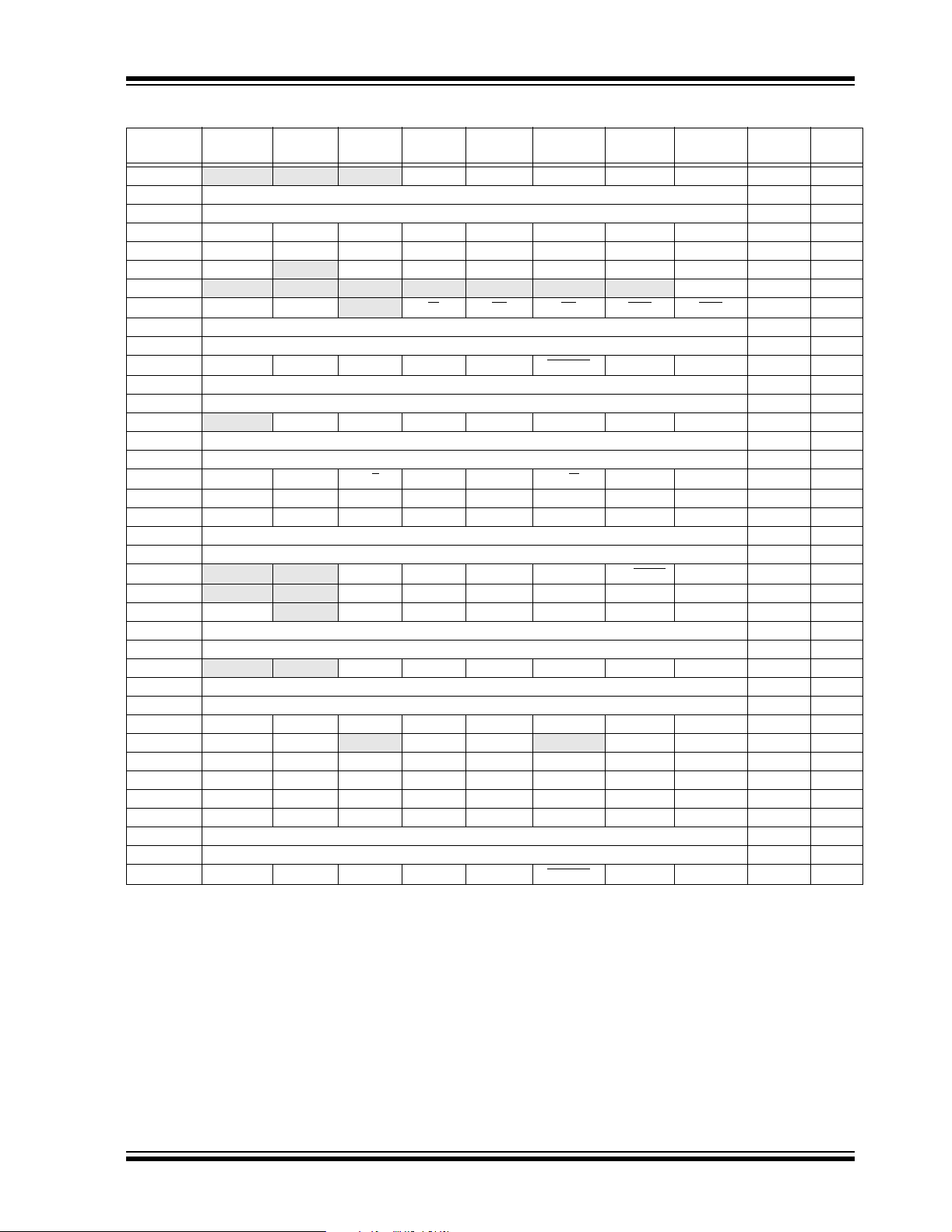
PIC18F2585/2680/4585/4680
TABLE 5-2: REGISTER FILE SUMMARY (PIC18F2585/2680/4585/4680) (CONTINUED)
File Name Bit 7 Bit 6 Bit 5 Bit 4 Bit 3 Bit 2 Bit 1 Bit 0
Val ue on
POR, BOR
STATUS — — —NOV Z DC C---x xxxx 50, 87
TMR0H Timer0 Register High Byte 0000 0000 50, 149
TMR0L Timer0 Register Low Byte xxxx xxxx 50, 149
T0CON TMR0ON T08BIT T0CS T0SE PSA T0PS2 T0PS1 T0PS0 1111 1111 50, 149
OSCCON IDLEN IRCF2 IRCF1 IRCF0 OSTS IOFS SCS1 SCS0 0000 q000 30, 50
HLVDCON VDIRMAG
WDTCON
— — — — — — —SWDTEN--- ---0 50, 353
RCON IPEN SBOREN
— IRVST HLVDEN HLVDL3 HLVDL2 HLVDL1 HLVDL0 0-00 0101 50, 267
(2)
—RITO PD POR BOR 0q-1 11q0 50, 127
TMR1H Timer1 Register High Byte xxxx xxxx 50, 155
TMR1L Timer1 Register Low Byte 0000 0000 50, 155
T1CON RD16 T1RUN T1CKPS1 T1CKPS0 T1OSCEN T1SYNC
TMR1CS TMR1ON 0000 0000 50, 151
TMR2 Timer2 Register 1111 1111 50, 158
PR2 Timer2 Period Register -000 0000 50, 155
T2CON
— T2OUTPS3 T2OUTPS2 T2OUTPS1 T2OUTPS0 TMR2ON T2CKPS1 T2CKPS0 -000 0000 50, 157
SSPBUF SSP Receive Buffer/Transmit Register xxxx xxxx 50, 195
SSPADD SSP Address Register in I
SSPSTAT SMP CKE D/A
2
C Slave mode. SSP Baud Rate Reload Register in I2C Master mode. 0000 0000 50, 195
PSR/WUA BF 0000 0000 50, 197
SSPCON1 WCOL SSPOV SSPEN CKP SSPM3 SSPM2 SSPM1 SSPM0 0000 0000 50, 198
SSPCON2 GCEN ACKSTAT ACKDT ACKEN RCEN PEN RSEN SEN 0000 0000 50, 199
ADRESH A/D Result Register High Byte xxxx xxxx 50, 256
ADRESL A/D Result Register Low Byte xxxx xxxx 50, 256
ADCON0
ADCON1
ADCON2 ADFM
— — CHS3 CHS2 CHS1 CHS0 GO/DONE ADON --00 0000 50, 247
— — VCFG1 VCFG0 PCFG3 PCFG2 PCFG1 PCFG0 --00 0qqq 50, 248
— ACQT2 ACQT1 ACQT0 ADCS2 ADCS1 ADCS0 0-00 0000 50, 249
CCPR1H Capture/Compare/PWM Register 1 High Byte xxxx xxxx 51, 168
CCPR1L Capture/Compare/PWM Register 1 Low Byte xxxx xxxx 51, 168
CCP1CON
ECCPR1H
ECCPR1L
(9)
(9)
ECCP1CON
BAUDCON ABDOVF RCIDL
ECCP1DEL
ECCP1AS
CVRCON
CMCON
(9)
(9)
(9)
— — DC1B1 DC1B0 CCP1M3 CCP1M2 CCP1M1 CCP1M0 --xx xxxx 51, 163
Enhanced Capture/Compare/PWM Register 1 High Byte xxxx xxxx 51, 167
Enhanced Capture/Compare/PWM Register 1 Low Byte xxxx xxxx 51, 167
(9)
EPWM1M1 EPWM1M0 EDC1B1 EDC1B0 ECCP1M3 ECCP1M2 ECCP1M1 ECCP1M0 0000 0000 51, 168
— SCKP BRG16 — WUE ABDEN 01-0 0000 51, 230
(9)
PRSEN PDC6
ECCPASE ECCPAS2 ECCPAS1 ECCPAS0 PSSAC1 PSSAC0 PSSBD1
(3)
PDC5
(3)
PDC4
(3)
PDC3
(3)
PDC2
(3)
PDC1
(3)
(3)
PDC0
PSSBD0
(3)
0000 0000 51, 182
(3)
0000 0000 51, 183
CVREN CVROE CVRR CVRSS CVR3 CVR2 CVR1 CVR0 0000 0000 51, 263
C2OUT C1OUT C2INV C1INV CIS CM2 CM1 CM0 0000 0000 51, 257
TMR3H Timer3 Register High Byte xxxx xxxx 51, 161
TMR3L Timer3 Register Low Byte xxxx xxxx 51, 161
T3CON RD16 T3ECCP1
(9)
T3CKPS1 T3CKPS0 T3CCP1
(9)
T3SYNC TMR3CS TMR3ON 0000 0000 51, 161
Legend: x = unknown, u = unchanged, - = unimplemented, q = value depends on condition
Note 1: Bit 21 of the PC is only available in Test mode and Serial Programming modes.
2: The SBOREN bit is only available when CONFIG2L<1:0> = 01; otherwise, it is disabled and reads as ‘0’. See Section 4.4 “Brown-out Reset
(BOR)”.
3: These registers and/or bits are not implemented on PIC18F2X8X devices and are read as ‘0’. Reset values are shown for PIC18F4X8X
devices; individual unimplemented bits should be interpreted as ‘—’.
4: The PLLEN bit is only available in specific oscillator configuration; otherwise, it is disabled and reads as ‘0’. See Section 2.6.4 “PLL in
INTOSC Modes”.
5: The RE3 bit is only available when Master Clear Reset is disabled (CONFIG3H<7> = 0); otherwise, RE3 reads as ‘0’. This bit is read-only.
6: RA6/RA7 and their associated latch and direction bits are individually configured as port pins based on various primary oscillator modes.
When disabled, these bits read as ‘0’.
7: CAN bits have multiple functions depending on the selected mode of the CAN module.
8: This register reads all ‘0’s until the ECAN™ technology is set up in Mode 1 or Mode 2.
9: These registers are available on PIC18F4X8X devices only.
Details
on page:
© 2007 Microchip Technology Inc. Preliminary DS39625C-page 77

PIC18F2585/2680/4585/4680
TABLE 5-2: REGISTER FILE SUMMARY (PIC18F2585/2680/4585/4680) (CONTINUED)
File Name Bit 7 Bit 6 Bit 5 Bit 4 Bit 3 Bit 2 Bit 1 Bit 0
Val ue on
POR, BOR
SPBRGH EUSART Baud Rate Generator High Byte 0000 0000 51, 231
SPBRG EUSART Baud Rate Generator 0000 0000 51, 231
RCREG EUSART Receive Register 0000 0000 51, 238
TXREG EUSART Transmit Register 0000 0000 51, 236
TXSTA CSRC TX9 TXEN SYNC SENDB BRGH TRMT TX9D 0000 0010 51, 237
RCSTA SPEN RX9 SREN CREN ADDEN FERR OERR RX9D 0000 000x 51, 237
EEADRH
— — — — — — EEPROM Addr Register High ---- --00 51, 108
EEADR EEPROM Address Register 0000 0000 51, 105
EEDATA EEPROM Data Register 0000 0000 51, 105
EECON2 EEPROM Control Register 2 (not a physical register) 0000 0000 51, 105
EECON1 EEPGD CFGS
IPR3
IRXIP WAKIP ERRIP TXB2IP TXB1IP TXB0IP RXB1IP RXB0IP 1111 1111 51, 126
— FREE WRERR WREN WR RD xx-0 x000 51, 105
Mode 0
IPR3
Mode 1, 2
PIR3
Mode 0
PIR3
Mode 1, 2
PIE3
IRXIP WAKIP ERRIP TXBnIP
TXB1IP
(8)
IRXIF WAKIF ERRIF TXB2IF TXB1IF TXB0IF RXB1IF RXB0IF 0000 0000 51, 120
IRXIF WAKIF ERRIF TXBnIF
TXB1IF
(8)
IRXIE WAKIE ERRIE TXB2IE TXB1IE TXB0IE RXB1IE RXB0IE 0000 0000 51, 123
TXB0IP
TXB0IF
(8)
RXBnIP FIFOWMIP 1111 1111 51, 126
(8)
RXBnIF FIFOWMIF 0000 0000 51, 120
Mode 0
PIE3
Mode 1, 2
IRXIE WAKIE ERRIE TXBnIE
IPR2 OSCFIP CMIP
PIR2 OSCFIF CMIF
PIE2 OSCFIE CMIE
IPR1 PSPIP
PIR1 PSPIF
PIE1 PSPIE
(3)
ADIP RCIP TXIP SSPIP CCP1IP TMR2IP TMR1IP 1111 1111 52, 124
(3)
ADIF RCIF TXIF SSPIF CCP1IF TMR2IF TMR1IF 0000 0000 52, 118
(3)
ADIE RCIE TXIE SSPIE CCP1IE TMR2IE TMR1IE 0000 0000 52, 121
OSCTUNE INTSRC PLLEN
(3)
TRISE
TRISD
(3)
IBF OBF IBOV PSPMODE — TRISE2 TRISE1 TRISE0 0000 -111 52, 141
Data Direction Control Register for PORTD 1111 1111 52, 138
(8)
TXB1IE
(9)
(9)
(9)
(4)
— EEIP BCLIP HLVDIP TMR3IP ECCP1IP
— EEIF BCLIF HLVDIF TMR3IF ECCP1IF
— EEIE BCLIE HLVDIE TMR3IE ECCP1IE
— TUN4 TUN3 TUN2 TUN1 TUN0 0q-0 0000 27, 52
TXB0IE
(8)
RXBnIE FIFOMWIE 0000 0000 51, 123
(9)
11-1 1111 51, 125
(9)
00-0 0000 51, 119
(9)
00-0 0000 52, 122
TRISC Data Direction Control Register for PORTC 1111 1111 52, 135
TRISB Data Direction Control Register for PORTB 1111 1111 52, 132
TRISA TRISA7
(3)
LATE
LATD
(3)
— — — — — LAT E2 LATE 1 LATE0 ---- -xxx 52, 141
Read PORTD Data Latch, Write PORTD Data Latch xxxx xxxx 52, 138
(6)
TRISA6
(6)
Data Direction Control Register for PORTA 1111 1111 52, 129
LATC Read PORTC Data Latch, Write PORTC Data Latch xxxx xxxx 52, 135
LATB Read PORTB Data Latch, Write PORTB Data Latch xxxx xxxx 52, 132
LATA LATA7
(6)
LATA6
(6)
Read PORTA Data Latch, Write PORTA Data Latch xxxx xxxx 52, 129
Legend: x = unknown, u = unchanged, - = unimplemented, q = value depends on condition
Note 1: Bit 21 of the PC is only available in Test mode and Serial Programming modes.
2: The SBOREN bit is only available when CONFIG2L<1:0> = 01; otherwise, it is disabled and reads as ‘0’. See Section 4.4 “Brown-out Reset
(BOR)”.
3: These registers and/or bits are not implemented on PIC18F2X8X devices and are read as ‘0’. Reset values are shown for PIC18F4X8X
devices; individual unimplemented bits should be interpreted as ‘—’.
4: The PLLEN bit is only available in specific oscillator configuration; otherwise, it is disabled and reads as ‘0’. See Section 2.6.4 “PLL in
INTOSC Modes”.
5: The RE3 bit is only available when Master Clear Reset is disabled (CONFIG3H<7> = 0); otherwise, RE3 reads as ‘0’. This bit is read-only.
6: RA6/RA7 and their associated latch and direction bits are individually configured as port pins based on various primary oscillator modes.
When disabled, these bits read as ‘0’.
7: CAN bits have multiple functions depending on the selected mode of the CAN module.
8: This register reads all ‘0’s until the ECAN™ technology is set up in Mode 1 or Mode 2.
9: These registers are available on PIC18F4X8X devices only.
Details
on page:
DS39625C-page 78 Preliminary © 2007 Microchip Technology Inc.

PIC18F2585/2680/4585/4680
PORTE
PORTD
(3)
(3)
— — — —RE3
Read PORTD pins, Write PORTD Data Latch xxxx xxxx 52, 138
(5)
RE2
(3)
RE1
(3)
RE0
(3)
---- xxxx 52, 145
PORTC Read PORTC pins, Write PORTC Data Latch xxxx xxxx 52, 135
PORTB Read PORTB pins, Write PORTB Data Latch xxxx xxxx 52, 132
PORTA RA7
(6)
RA6
(6)
Read PORTA pins, Write PORTA Data Latch xx00 0000 52, 129
ECANCON MDSEL1 MDSEL0 FIFOWM EWIN4 EWIN3 EWIN2 EWIN1 EWIN0 0001 000 52, 280
TXERRCNT TEC7 TEC6 TEC5 TEC4 TEC3 TEC2 TEC1 TEC0 0000 0000 52, 285
RXERRCNT REC7 REC6 REC5 REC4 REC3 REC2 REC1 REC0 0000 0000 52, 293
COMSTAT
RXB0OVFL RXB1OVFL TXBO TXBP RXBP TXWARN RXWARN EWARN 0000 0000 52, 281
Mode 0
COMSTAT
Mode 1
COMSTAT
— RXBnOVFL TXBO TXBP RXBP TXWARN RXWARN EWARN -000 0000 52, 281
FIFOEMPTY
RXBnOVFL TXBO TXBP RXBP TXWARN RXWARN EWARN 0000 0000 52, 281
Mode 2
CIOCON
BRGCON3 WAKDIS WAKFIL
— — ENDRHI CANCAP — — — — --00 ---- 52, 314
— — — SEG2PH2 SEG2PH1 SEG2PH0 00-- -000 52, 313
BRGCON2 SEG2PHTS SAM SEG1PH2 SEG1PH1 SEG1PH0 PRSEG2 PRSEG1 PRSEG0 0000 0000 52, 312
BRGCON1 SJW1 SJW0 BRP5 BRP4 BRP3 BRP2 BRP1 BRP0 0000 0000 52, 311
CANCON
Mode 0
CANCON
REQOP2 REQOP1 REQOP0 ABAT WIN2
REQOP2 REQOP1 REQOP0 ABAT
—
(7)
(7)
WIN1
—
(7)
(7)
WIN0
—
(7)
(7)
(7)
—
—
1000 000- 53, 276
(7)
1000 ---- 53, 276
Mode 1
CANCON
REQOP2 REQOP1 REQOP0 ABAT FP3
(7)
FP2
(7)
FP1
(7)
FP0
(7)
1000 0000 53, 276
Mode 2
CANSTAT
Mode 0
CANSTAT
OPMODE2 OPMODE1 OPMODE0
(7)
—
OPMODE2 OPMODE1 OPMODE0 EICODE4
(7)
ICODE3
EICODE3
(7)
(7)
ICODE2
EICODE2
(7)
(7)
ICODE1
EICODE1
(7)
(7)
(7)
—
EICODE0
000- 0000 53, 277
(7)
0000 0000 53, 277
Modes 1, 2
RXB0D7 RXB0D77 RXB0D76 RXB0D75 RXB0D74 RXB0D73 RXB0D72 RXB0D71 RXB0D70 xxxx xxxx 53, 292
RXB0D6 RXB0D67 RXB0D66 RXB0D65 RXB0D64 RXB0D63 RXB0D62 RXB0D61 RXB0D60 xxxx xxxx 53, 292
RXB0D5 RXB0D57 RXB0D56 RXB0D55 RXB0D54 RXB0D53 RXB0D52 RXB0D51 RXB0D50 xxxx xxxx 53, 292
RXB0D4 RXB0D47 RXB0D46 RXB0D45 RXB0D44 RXB0D43 RXB0D42 RXB0D41 RXB0D40 xxxx xxxx 53, 292
RXB0D3 RXB0D37 RXB0D36 RXB0D35 RXB0D34 RXB0D33 RXB0D32 RXB0D31 RXB0D30 xxxx xxxx 53, 292
RXB0D2 RXB0D27 RXB0D26 RXB0D25 RXB0D24 RXB0D23 RXB0D22 RXB0D21 RXB0D20 xxxx xxxx 53, 292
RXB0D1 RXB0D17 RXB0D16 RXB0D15 RXB0D14 RXB0D13 RXB0D12 RXB0D11 RXB0D10 xxxx xxxx 53, 292
RXB0D0 RXB0D07 RXB0D06 RXB0D05 RXB0D04 RXB0D03 RXB0D02 RXB0D01 RXB0D00 xxxx xxxx 53, 292
RXB0DLC
— RXRTR RB1 RB0 DLC3 DLC2 DLC1 DLC0 -xxx xxxx 53, 292
RXB0EIDL EID7 EID6 EID5 EID4 EID3 EID2 EID1 EID0 xxxx xxxx 53, 291
RXB0EIDH EID15 EID14 EID13 EID12 EID11 EID10 EID9 EID8 xxxx xxxx 53, 291
RXB0SIDL SID2 SID1 SID0 SRR EXID
—EID17EID16xxxx x-xx 53, 291
RXB0SIDH SID10 SID9 SID8 SID7 SID6 SID5 SID4 SID3 xxxx xxxx 53, 290
RXB0xx xxx0c[(5 TwE)-9.2(np33.2(DH)050, 6,B8)241 w[(5)-16.4(3)0.9(, 291)]TJ-63.6034 -1.7241 TD0.00E5Tc0.0185 Tw[(5)-16.4(3)0.9(, 290)]TJ-63.6034 -16C68-N2(D369D)1.(np33.22.8(S)12.10.00xx)5789CI55 III3, 292XB0t .9.0185 T4859 9C0
© 2007 Microchip Technology Inc. Preliminary DS39625C-page 79

PIC18F2585/2680/4585/4680
TABLE 5-2: REGISTER FILE SUMMARY (PIC18F2585/2680/4585/4680) (CONTINUED)
File Name Bit 7 Bit 6 Bit 5 Bit 4 Bit 3 Bit 2 Bit 1 Bit 0
RXB1D7 RXB1D77 RXB1D76 RXB1D75 RXB1D74 RXB1D73 RXB1D72 RXB1D71 RXB1D70 xxxx xxxx 53, 292
RXB1D6 RXB1D67 RXB1D66 RXB1D65 RXB1D64 RXB1D63 RXB1D62 RXB1D61 RXB1D60 xxxx xxxx 53, 292
RXB1D5 RXB1D57 RXB1D56 RXB1D55 RXB1D54 RXB1D53 RXB1D52 RXB1D51 RXB1D50 xxxx xxxx 53, 292
RXB1D4 RXB1D47 RXB1D46 RXB1D45 RXB1D44 RXB1D43 RXB1D42 RXB1D41 RXB1D40 xxxx xxxx 53, 292
RXB1D3 RXB1D37 RXB1D36 RXB1D35 RXB1D34 RXB1D33 RXB1D32 RXB1D31 RXB1D30 xxxx xxxx 53, 292
RXB1D2 RXB1D27 RXB1D26 RXB1D25 RXB1D24 RXB1D23 RXB1D22 RXB1D21 RXB1D20 xxxx xxxx 53, 292
RXB1D1 RXB1D17 RXB1D16 RXB1D15 RXB1D14 RXB1D13 RXB1D12 RXB1D11 RXB1D10 xxxx xxxx 53, 292
RXB1D0 RXB1D07 RXB1D06 RXB1D05 RXB1D04 RXB1D03 RXB1D02 RXB1D01 RXB1D00 xxxx xxxx 53, 292
RXB1DLC
RXB1EIDL EID7 EID6 EID5 EID4 EID3 EID2 EID1 EID0 xxxx xxxx 53, 291
RXB1EIDH EID15 EID14 EID13 EID12 EID11 EID10 EID9 EID8 xxxx xxxx 53, 291
RXB1SIDL SID2 SID1 SID0 SRR EXID
RXB1SIDH SID10 SID9 SID8 SID7 SID6 SID5 SID4 SID3 xxxx xxxx 53, 290
RXB1CON
Mode 0
RXB1CON
Mode 1, 2
TXB0D7 TXB0D77 TXB0D76 TXB0D75 TXB0D74 TXB0D73 TXB0D72 TXB0D71 TXB0D70 xxxx xxxx 53, 284
TXB0D6 TXB0D67 TXB0D66 TXB0D65 TXB0D64 TXB0D63 TXB0D62 TXB0D61 TXB0D60 xxxx xxxx 53, 284
TXB0D5 TXB0D57 TXB0D56 TXB0D55 TXB0D54 TXB0D53 TXB0D52 TXB0D51 TXB0D50 xxxx xxxx 54, 284
TXB0D4 TXB0D47 TXB0D46 TXB0D45 TXB0D44 TXB0D43 TXB0D42 TXB0D41 TXB0D40 xxxx xxxx 54, 284
TXB0D3 TXB0D37 TXB0D36 TXB0D35 TXB0D34 TXB0D33 TXB0D32 TXB0D31 TXB0D30 xxxx xxxx 54, 284
TXB0D2 TXB0D27 TXB0D26 TXB0D25 TXB0D24 TXB0D23 TXB0D22 TXB0D21 TXB0D20 xxxx xxxx 54, 284
TXB0D1 TXB0D17 TXB0D16 TXB0D15 TXB0D14 TXB0D13 TXB0D12 TXB0D11 TXB0D10 xxxx xxxx 54, 284
TXB0D0 TXB0D07 TXB0D06 TXB0D05 TXB0D04 TXB0D03 TXB0D02 TXB0D01 TXB0D00 xxxx xxxx 54, 284
TXB0DLC
TXB0EIDL EID7 EID6 EID5 EID4 EID3 EID2 EID1 EID0 xxxx xxxx 54, 284
TXB0EIDH EID15 EID14 EID13 EID12 EID11 EID10 EID9 EID8 xxxx xxxx 54, 283
TXB0SIDL SID2 SID1 SID0
TXB0SIDH SID10 SID9 SID8 SID7 SID6 SID5 SID4 SID3 xxxx xxxx 54, 283
TXB0CON TXBIF TXABT TXLARB TXERR TXREQ
TXB1D7 TXB1D77 TXB1D76 TXB1D75 TXB1D74 TXB1D73 TXB1D72 TXB1D71 TXB1D70 xxxx xxxx 54, 284
TXB1D6 TXB1D67 TXB1D66 TXB1D65 TXB1D64 TXB1D63 TXB1D62 TXB1D61 TXB1D60 xxxx xxxx 54, 284
TXB1D5 TXB1D57 TXB1D56 TXB1D55 TXB1D54 TXB1D53 TXB1D52 TXB1D51 TXB1D50 xxxx xxxx 54, 284
TXB1D4 TXB1D47 TXB1D46 TXB1D45 TXB1D44 TXB1D43 TXB1D42 TXB1D41 TXB1D40 xxxx xxxx 54, 284
TXB1D3 TXB1D37 TXB1D36 TXB1D35 TXB1D34 TXB1D33 TXB1D32 TXB1D31 TXB1D30 xxxx xxxx 54, 284
TXB1D2 TXB1D27 TXB1D26 TXB1D25 TXB1D24 TXB1D23 TXB1D22 TXB1D21 TXB1D20 xxxx xxxx 54, 284
TXB1D1 TXB1D17 TXB1D16 TXB1D15 TXB1D14 TXB1D13 TXB1D12 TXB1D11 TXB1D10 xxxx xxxx 54, 284
TXB1D0 TXB1D07 TXB1D06 TXB1D05 TXB1D04 TXB1D03 TXB1D02 TXB1D01 TXB1D00 xxxx xxxx 54, 284
TXB1DLC
TXB1EIDL EID7 EID6 EID5 EID4 EID3 EID2 EID1 EID0 xxxx xxxx 54, 284
TXB1EIDH EID15 EID14 EID13 EID12 EID11 EID10 EID9 EID8 xxxx xxxx 54, 283
— RXRTR RB1 RB0 DLC3 DLC2 DLC1 DLC0 -xxx xxxx 53, 292
—EID17EID16xxxx xxxx 53, 291
RXFUL RXM1 RXM0
RXFUL RXM1 RTRRO FILHIT4 FILHIT3 FILHIT2 FILHIT1 FILHIT0 0000 0000 53, 287
—TXRTR— — DLC3 DLC2 DLC1 DLC0 -x-- xxxx 54, 285
—TXRTR— — DLC3 DLC2 DLC1 DLC0 -x-- xxxx 54, 285
(7)
(7)
—
RXRTRRO
— EXIDE —EID17EID16xxx- x-xx 54, 283
(7)
(7)
FILHIT2
— TXPRI1 TXPRI0 0000 0-00 54, 282
FILHIT1
(7)
FILHIT0
Var(C)2i60.2(NUE)-8.8(D))]TJ6.96 0t3(1)-23R11.4(85/)s-5.4( (3I73.8(9c611.4(8)62.9991 713.360454 Tw.4(8)62.8B)6.4(D-17.3(t0 713.3609 0 0xxxx)1IxxxxTm0 gTw[(Va)-59.3(r(C)2)-4.3(i60.2(NUE)-8.8(D))]TJ7.3)-4.3(i60.2(N,)1I7—12 45.24 U 973)-4.3.3)-4.NUE)‘g 3(i61A)-14(BL)-4.608 T14 1it -1T1 19 19 19 19 19i61ABL4 1it -1T1 19 19 1991 69419(T)12.2(XB1)9(D2)-8.3(1)-2263 160488 80) (C25 1180g0 Tc(—)TjET0.902 g239.999 212 41.16 12 refBT6.96 0 0 6.96 257.034 160488 —80)I25 1—
(7)
000- 0000 53, 287
DS39625C-page 80 Preliminary © 2007 Microchip Technology Inc.

PIC18F2585/2680/4585/4680
TABLE 5-2: REGISTER FILE SUMMARY (PIC18F2585/2680/4585/4680) (CONTINUED)
File Name Bit 7 Bit 6 Bit 5 Bit 4 Bit 3 Bit 2 Bit 1 Bit 0
TXB1SIDL SID2 SID1 SID0 — EXIDE —EID17EID16xxx- x-xx 54, 283
TXB1SIDH SID10 SID9 SID8 SID7 SID6 SID5 SID4 SID3 xxxx xxxx 54, 283
TXB1CON TXBIF TXABT TXLARB TXERR TXREQ
TXB2D7 TXB2D77 TXB2D76 TXB2D75 TXB2D74 TXB2D73 TXB2D72 TXB2D71 TXB2D70 xxxx xxxx 54, 284
TXB2D6 TXB2D67 TXB2D66 TXB2D65 TXB2D64 TXB2D63 TXB2D62 TXB2D61 TXB2D60 xxxx xxxx 54, 284
TXB2D5 TXB2D57 TXB2D56 TXB2D55 TXB2D54 TXB2D53 TXB2D52 TXB2D51 TXB2D50 xxxx xxxx 54, 284
TXB2D4 TXB2D47 TXB2D46 TXB2D45 TXB2D44 TXB2D43 TXB2D42 TXB2D41 TXB2D40 xxxx xxxx 54, 284
TXB2D3 TXB2D37 TXB2D36 TXB2D35 TXB2D34 TXB2D33 TXB2D32 TXB2D31 TXB2D30 xxxx xxxx 54, 284
TXB2D2 TXB2D27 TXB2D26 TXB2D25 TXB2D24 TXB2D23 TXB2D22 TXB2D21 TXB2D20 xxxx xxxx 54, 284
TXB2D1 TXB2D17 TXB2D16 TXB2D15 TXB2D14 TXB2D13 TXB2D12 TXB2D11 TXB2D10 xxxx xxxx 55, 284
TXB2D0 TXB2D07 TXB2D06 TXB2D05 TXB2D04 TXB2D03 TXB2D02 TXB2D01 TXB2D00 xxxx xxxx 55, 284
TXB2DLC
TXB2EIDL EID7 EID6 EID5 EID4 EID3 EID2 EID1 EID0 xxxx xxxx 55, 284
TXB2EIDH EID15 EID14 EID13 EID12 EID11 EID10 EID9 EID8 xxxx xxxx 55, 283
TXB2SIDL SID2 SID1 SID0
TXB2SIDH SID10 SID9 SID8 SID7 SID6 SID5 SID4 SID3 xxx- x-xx 55, 283
TXB2CON TXBIF TXABT TXLARB TXERR TXREQ
RXM1EIDL EID7 EID6 EID5 EID4 EID3 EID2 EID1 EID0 xxxx xxxx 55, 304
RXM1EIDH EID15 EID14 EID13 EID12 EID11 EID10 EID9 EID8 xxxx xxxx 55, 304
RXM1SIDL SID2 SID1 SID0
RXM1SIDH SID10 SID9 SID8 SID7 SID6 SID5 SID4 SID3 xxxx xxxx 55, 304
RXM0EIDL EID7 EID6 EID5 EID4 EID3 EID2 EID1 EID0 xxxx xxxx 55, 304
RXM0EIDH EID15 EID14 EID13 EID12 EID11 EID10 EID9 EID8 xxxx xxxx 55, 304
RXM0SIDL SID2 SID1 SID0
RXM0SIDH SID10 SID9 SID8 SID7 SID6 SID5 SID4 SID3 xxxx xxxx 55, 303
RXF5EIDL EID7 EID6 EID5 EID4 EID3 EID2 EID1 EID0 xxxx xxxx 55, 303
RXF5EIDH EID15 EID14 EID13 EID12 EID11 EID10 EID9 EID8 xxxx xxxx 55, 303
RXF5SIDL SID2 SID1 SID0
RXF5SIDH SID10 SID9 SID8 SID7 SID6 SID5 SID4 SID3 xxxx xxxx 55, 302
RXF4EIDL EID7 EID6 EID5 EID4 EID3 EID2 EID1 EID0 xxxx xxxx 55, 303
RXF4EIDH EID15 EID14 EID13 EID12 EID11 EID10 EID9 EID8 xxxx xxxx 55, 303
RXF4SIDL SID2 SID1 SID0
RXF4SIDH SID10 SID9 SID8 SID7 SID6 SID5 SID4 SID3 xxxx xxxx 55, 302
RXF3EIDL EID7 EID6 EID5 EID4 EID3 EID2 EID1 EID0 xxxx xxxx 55, 303
RXF3EIDH EID15 EID14 EID13 EID12 EID11 EID10 EID9 EID8 xxxx xxxx 55, 303
RXF3SIDL SID2 SID1 SID0
RXF3SIDH SID10 SID9 SID8 SID7 SID6 SID5 SID4 SID3 xxxx xxxx 55, 302
RXF2EIDL EID7 EID6 EID5 EID4 EID3 EID2 EID1 EID0 xxxx xxxx 55, 303
RXF2EIDH EID15 EID14 EID13 EID12 EID11 EID10 EID9 EID8 xxxx xxxx 55, 303
RXF2SIDL SID2 SID1 SID0
RXF2SIDH SID10 SID9 SID8 SID7 SID6 SID5 SID4 SID3 xxxx xxxx 55, 302
Legend: x = unknown, u = unchanged, - = unimplemented, q = value depends on condition
Note 1: Bit 21 of the PC is only available in Test mode and Serial Programming modes.
2: The SBOREN bit is only available when CONFIG2L<1:0> = 01; otherwise, it is disabled and reads as ‘0’. See Section 4.4 “Brown-out Reset
(BOR)”.
3: These registers and/or bits are not implemented on PIC18F2X8X devices and are read as ‘0’. Reset values are shown for PIC18F4X8X
devices; individual unimplemented bits should be interpreted as ‘—’.
4: The PLLEN bit is only available in specific oscillator configuration; otherwise, it is disabled and reads as ‘0’. See Section 2.6.4 “PLL in
INTOSC Modes”.
5: The RE3 bit is only available when Master Clear Reset is disabled (CONFIG3H<7> = 0); otherwise, RE3 reads as ‘0’. This bit is read-only.
6: RA6/RA7 and their associated latch and direction bits are individually configured as port pins based on various primary oscillator modes.
When disabled, these bits read as ‘0’.
7: CAN bits have multiple functions depending on the selected mode of the CAN module.
8: This register reads all ‘0’s until the ECAN™ technology is set up in Mode 1 or Mode 2.
9: These registers are available on PIC18F4X8X devices only.
—TXRTR— — DLC3 DLC2 DLC1 DLC0 -x-- xxxx 55, 285
— EXIDE —EID17EID16xxxx x-xx 55, 283
— EXIDEN —EID17EID16xxx- x-xx 55, 304
— EXIDEN —EID17EID16xxx- x-xx 55, 304
— EXIDEN —EID17EID16xxx- x-xx 55, 302
— EXIDEN —EID17EID16xxx- x-xx 55, 302
— EXIDEN —EID17EID16xxx- x-xx 55, 302
— EXIDEN —EID17EID16xxx- x-xx 55, 302
— TXPRI1 TXPRI0 0000 0-00 54, 282
— TXPRI1 TXPRI0 0000 0-00 55, 282
Val ue on
POR, BOR
Details
on page:
© 2007 Microchip Technology Inc. Preliminary DS39625C-page 81

PIC18F2585/2680/4585/4680
TABLE 5-2: REGISTER FILE SUMMARY (PIC18F2585/2680/4585/4680) (CONTINUED)
File Name Bit 7 Bit 6 Bit 5 Bit 4 Bit 3 Bit 2 Bit 1 Bit 0
Val ue on
POR, BOR
RXF1EIDL EID7 EID6 EID5 EID4 EID3 EID2 EID1 EID0 xxxx xxxx 56, 303
RXF1EIDH EID15 EID14 EID13 EID12 EID11 EID10 EID9 EID8 xxxx xxxx 56, 303
RXF1SIDL SID2 SID1 SID0
— EXIDEN —EID17EID16xxx- x-xx 56, 302
RXF1SIDH SID10 SID9 SID8 SID7 SID6 SID5 SID4 SID3 xxxx xxxx 56, 302
RXF0EIDL EID7 EID6 EID5 EID4 EID3 EID2 EID1 EID0 xxxx xxxx 56, 303
RXF0EIDH EID15 EID14 EID13 EID12 EID11 EID10 EID9 EID8 xxxx xxxx 56, 303
RXF0SIDL SID2 SID1 SID0
— EXIDEN —EID17EID16xxx- x-xx 56, 302
RXF0SIDH SID10 SID9 SID8 SID7 SID6 SID5 SID4 SID3 xxxx xxxx 56, 302
(8)
B5D7
B5D77 B5D76 B5D75 B5D74 B5D73 B5D72 B5D71 B5D70 xxxx xxxx 56, 299
(8)
B5D6
B5D67 B5D66 B5D65 B5D64 B5D63 B5D62 B5D61 B5D60 xxxx xxxx 56, 299
(8)
B5D5
B5D57 B5D56 B5D55 B5D54 B5D53 B5D52 B5D51 B5D50 xxxx xxxx 56, 299
(8)
B5D4
B5D47 B5D46 B5D45 B5D44 B5D43 B5D42 B5D41 B5D40 xxxx xxxx 56, 299
(8)
B5D3
B5D37 B5D36 B5D35 B5D34 B5D33 B5D32 B5D31 B5D30 xxxx xxxx 56, 299
(8)
B5D2
B5D27 B5D26 B5D25 B5D24 B5D23 B5D22 B5D21 B5D20 xxxx xxxx 56, 299
(8)
B5D1
B5D17 B5D16 B5D15 B5D14 B5D13 B5D12 B5D11 B5D10 xxxx xxxx 56, 299
(8)
B5D0
B5D07 B5D06 B5D05 B5D04 B5D03 B5D02 B5D01 B5D00 xxxx xxxx 56, 299
(8)
B5DLC
— RXRTR RB1 RB0 DLC3 DLC2 DLC1 DLC0 -xxx xxxx 56, 300
Receive mode
(8)
B5DLC
—TXRTR— — DLC3 DLC2 DLC1 DLC0 -x-- xxxx 56, 301
Transmit mode
(8)
B5EIDL
B5EIDH
B5SIDL
Receive mode
B5SIDL
EID7 EID6 EID5 EID4 EID3 EID2 EID1 EID0 xxxx xxxx 56, 299
(8)
EID15 EID14 EID13 EID12 EID11 EID10 EID9 EID8 xxxx xxxx 56, 298
(8)
(8)
SID2 SID1 SID0 SRR EXID —EID17EID16xxxx x-xx 56, 297
SID2 SID1 SID0 — EXIDE —EID17EID16xxx- x-xx 56, 297
Transmit mode
(8)
B5SIDH
B5CON
SID10 SID9 SID8 SID7 SID6 SID5 SID4 SID3 xxxx x-xx 56, 296
(8)
RXFUL RXM1 RXRTRRO FILHIT4 FILHIT3 FILHIT2 FILHIT1 FILHIT0 0000 0000 56, 294
Receive mode
(8)
B5CON
Transmit mode
(8)
B4D77 B4D76 B4D75 B4D74 B4D73 B4D72 B4D71 B4D70 xxxx xxxx 56, 299
B4D7
(8)
B4D6
B4D67 B4D66 B4D65 B4D64 B4D63 B4D62 B4D61 B4D60 xxxx xxxx 56, 299
(8)
B4D5
B4D57 B4D56 B4D55 B4D54 B4D53 B4D52 B4D51 B4D50 xxxx xxxx 56, 299
(8)
B4D4
B4D47 B4D46 B4D45 B4D44 B4D43 B4D42 B4D41 B4D40 xxxx xxxx 56, 299
(8)
B4D3
B4D37 B4D36 B4D35 B4D34 B4D33 B4D32 B4D31 B4D30 xxxx xxxx 56, 299
(8)
B4D2
B4D27 B4D26 B4D25 B4D24 B4D23 B4D22 B4D21 B4D20 xxxx xxxx 56, 299
(8)
B4D1
B4D17 B4D16 B4D15 B4D14 B4D13 B4D12 B4D11 B4D10 xxxx xxxx 56, 299
(8)
B4D0
B4D07 B4D06 B4D05 B4D04 B4D03 B4D02 B4D01 B4D00 xxxx xxxx 56, 299
(8)
B4DLC
TXBIF TXABT TXLARB TXERR TXREQ RTREN TXPRI1 TXPRI0 0000 0000 56, 295
— RXRTR RB1 RB0 DLC3 DLC2 DLC1 DLC0 -xxx xxxx 56, 300
Receive mode
(8)
B4DLC
—TXRTR— — DLC3 DLC2 DLC1 DLC0 -x-- xxxx 56, 301
Transmit mode
Legend: x = unknown, u = unchanged, - = unimplemented, q = value depends on condition
Note 1: Bit 21 of the PC is only available in Test mode and Serial Programming modes.
2: The SBOREN bit is only available when CONFIG2L<1:0> = 01; otherwise, it is disabled and reads as ‘0’. See Section 4.4 “Brown-out Reset
(BOR)”.
3: These registers and/or bits are not implemented on PIC18F2X8X devices and are read as ‘0’. Reset values are shown for PIC18F4X8X
devices; individual unimplemented bits should be interpreted as ‘—’.
4: The PLLEN bit is only available in specific oscillator configuration; otherwise, it is disabled and reads as ‘0’. See Section 2.6.4 “PLL in
INTOSC Modes”.
5: The RE3 bit is only available when Master Clear Reset is disabled (CONFIG3H<7> = 0); otherwise, RE3 reads as ‘0’. This bit is read-only.
6: RA6/RA7 and their associated latch and direction bits are individually configured as port pins based on various primary oscillator modes.
When disabled, these bits read as ‘0’.
7: CAN bits have multiple functions depending on the selected mode of the CAN module.
8: This register reads all ‘0’s until the ECAN™ technology is set up in Mode 1 or Mode 2.
9: These registers are available on PIC18F4X8X devices only.
Details
on page:
DS39625C-page 82 Preliminary © 2007 Microchip Technology Inc.

PIC18F2585/2680/4585/4680
TABLE 5-2: REGISTER FILE SUMMARY (PIC18F2585/2680/4585/4680) (CONTINUED)
File Name Bit 7 Bit 6 Bit 5 Bit 4 Bit 3 Bit 2 Bit 1 Bit 0
(8)
B4EIDL
B4EIDH
B4SIDL
EID7 EID6 EID5 EID4 EID3 EID2 EID1 EID0 xxxx xxxx 56, 299
(8)
EID15 EID14 EID13 EID12 EID11 EID10 EID9 EID8 xxxx xxxx 57, 298
(8)
SID2 SID1 SID0 SRR EXID —EID17EID16xxxx x-xx 56, 297
Receive mode
(8)
B4SIDL
Transmit mode
(8)
B4SIDH
B4CON
SID10 SID9 SID8 SID7 SID6 SID5 SID4 SID3 xxxx xxxx 57, 296
(8)
SID2 SID1 SID0 — EXIDE —EID17EID16xxx- x-xx 56, 297
RXFUL RXM1 RXRTRRO FILHIT4 FILHIT3 FILHIT2 FILHIT1 FILHIT0 0000 0000 57, 294
Receive mode
(8)
B4CON
TXBIF TXABT TXLARB TXERR TXREQ RTREN TXPRI1 TXPRI0 0000 0000 57, 295
Transmit mode
(8)
B3D7
B3D77 B3D76 B3D75 B3D74 B3D73 B3D72 B3D71 B3D70 xxxx xxxx 57, 299
(8)
B3D6
B3D67 B3D66 B3D65 B3D64 B3D63 B3D62 B3D61 B3D60 xxxx xxxx 57, 299
(8)
B3D5
B3D57 B3D56 B3D55 B3D54 B3D53 B3D52 B3D51 B3D50 xxxx xxxx 57, 299
(8)
B3D4
B3D47 B3D46 B3D45 B3D44 B3D43 B3D42 B3D41 B3D40 xxxx xxxx 57, 299
(8)
B3D3
B3D37 B3D36 B3D35 B3D34 B3D33 B3D32 B3D31 B3D30 xxxx xxxx 57, 299
(8)
B3D2
B3D27 B3D26 B3D25 B3D24 B3D23 B3D22 B3D21 B3D20 xxxx xxxx 57, 299
(8)
B3D1
B3D17 B3D16 B3D15 B3D14 B3D13 B3D12 B3D11 B3D10 xxxx xxxx 57, 299
(8)
B3D0
B3DLC
(8)
B3D07 B3D06 B3D05 B3D04 B3D03 B3D02 B3D01 B3D00 xxxx xxxx 57, 299
— RXRTR RB1 RB0 DLC3 DLC2 DLC1 DLC0 -xxx xxxx 56, 300
Receive mode
(8)
B3DLC
Transmit
—TXRTR— — DLC3 DLC2 DLC1 DLC0 -x-- xxxx 56, 301
mode
(8)
B3EIDL
B3EIDH
B3SIDL
EID7 EID6 EID5 EID4 EID3 EID2 EID1 EID0 xxxx xxxx 57, 299
(8)
EID15 EID14 EID13 EID12 EID11 EID10 EID9 EID8 xxxx xxxx 57, 298
(8)
SID2 SID1 SID0 SRR EXID —EID17EID16xxxx x-xx 56, 297
Receive mode
(8)
B3SIDL
Transmit mode
(8)
B3SIDH
B3CON
SID10 SID9 SID8 SID7 SID6 SID5 SID4 SID3 xxxx xxxx 57, 296
(8)
SID2 SID1 SID0 — EXIDE —EID17EID16xxx- x-xx 56, 297
RXFUL RXM1 RXRTRRO FILHIT4 FILHIT3 FILHIT2 FILHIT1 FILHIT0 0000 0000 57, 294
Receive mode
(8)
B3CON
TXBIF TXABT TXLARB TXERR TXREQ RTREN TXPRI1 TXPRI0 0000 0000 57, 295
Transmit mode
(8)
B2D7
B2D77 B2D76 B2D75 B2D74 B2D73 B2D72 B2D71 B2D70 xxxx xxxx 57, 299
(8)
B2D6
B2D67 B2D66 B2D65 B2D64 B2D63 B2D62 B2D61 B2D60 xxxx xxxx 57, 299
(8)
B2D5
B2D57 B2D56 B2D55 B2D54 B2D53 B2D52 B2D51 B2D50 xxxx xxxx 57, 299
(8)
B2D4
B2D47 B2D46 B2D45 B2D44 B2D43 B2D42 B2D41 B2D40 xxxx xxxx 57, 299
(8)
B2D3
B2D37 B2D36 B2D35 B2D34 B2D33 B2D32 B2D31 B2D30 xxxx xxxx 57, 299
(8)
B2D2
B2D27 B2D26 B2D25 B2D24 B2D23 B2D22 B2D21 B2D20 xxxx xxxx 57, 299
(8)
B2D1
B2D17 B2D16 B2D15 B2D14 B2D13 B2D12 B2D11 B2D10 xxxx xxxx 57, 299
(8)
B2D0
B2D07 B2D06 B2D05 B2D04 B2D03 B2D02 B2D01 B2D00 xxxx xxxx 57, 299
Legend: x = unknown, u = unchanged, - = unimplemented, q = value depends on condition
Note 1: Bit 21 of the PC is only available in Test mode and Serial Programming modes.
2: The SBOREN bit is only available when CONFIG2L<1:0> = 01; otherwise, it is disabled and reads as ‘0’. See Section 4.4 “Brown-out Reset
(BOR)”.
3: These registers and/or bits are not implemented on PIC18F2X8X devices and are read as ‘0’. Reset values are shown for PIC18F4X8X
devices; individual unimplemented bits should be interpreted as ‘—’.
4: The PLLEN bit is only available in specific oscillator configuration; otherwise, it is disabled and reads as ‘0’. See Section 2.6.4 “PLL in
INTOSC Modes”.
5: The RE3 bit is only available when Master Clear Reset is disabled (CONFIG3H<7> = 0); otherwise, RE3 reads as ‘0’. This bit is read-only.
6: RA6/RA7 and their associated latch and direction bits are individually configured as port pins based on various primary oscillator modes.
When disabled, these bits read as ‘0’.
7: CAN bits have multiple functions depending on the selected mode of the CAN module.
8: This register reads all ‘0’s until the ECAN™ technology is set up in Mode 1 or Mode 2.
9: These registers are available on PIC18F4X8X devices only.
Val ue on
POR, BOR
Details
on page:
© 2007 Microchip Technology Inc. Preliminary DS39625C-page 83

PIC18F2585/2680/4585/4680
TABLE 5-2: REGISTER FILE SUMMARY (PIC18F2585/2680/4585/4680) (CONTINUED)
File Name Bit 7 Bit 6 Bit 5 Bit 4 Bit 3 Bit 2 Bit 1 Bit 0
(8)
B2DLC
— RXRTR RB1 RB0 DLC3 DLC2 DLC1 DLC0 -xxx xxxx 56, 300
Receive mode
(8)
B2DLC
Transmit mode
(8)
B2EIDL
B2EIDH
B2SIDL
EID7 EID6 EID5 EID4 EID3 EID2 EID1 EID0 xxxx xxxx 57, 299
(8)
EID15 EID14 EID13 EID12 EID11 EID10 EID9 EID8 xxxx xxxx 57, 298
(8)
—TXRTR— — DLC3 DLC2 DLC1 DLC0 -x-- xxxx 56, 301
SID2 SID1 SID0 SRR EXID —EID17EID16xxxx x-xx 56, 297
Receive mode
(8)
B2SIDL
SID2 SID1 SID0 — EXIDE —EID17EID16xxx- x-xx 56, 297
Transmit mode
(8)
B2SIDH
B2CON
Receive mode
B2CON
Transmit mode
B1D7
B1D6
B1D5
B1D4
B1D3
B1D2
B1D1
B1D0
B1DLC
SID10 SID9 SID8 SID7 SID6 SID5 SID4 SID3 xxxx xxxx 57, 296
(8)
RXFUL RXM1 RXRTRRO FILHIT4 FILHIT3 FILHIT2 FILHIT1 FILHIT0 0000 0000 58, 294
(8)
(8)
B1D77 B1D76 B1D75 B1D74 B1D73 B1D72 B1D71 B1D70 xxxx xxxx 58, 299
(8)
B1D67 B1D66 B1D65 B1D64 B1D63 B1D62 B1D61 B1D60 xxxx xxxx 58, 299
(8)
B1D57 B1D56 B1D55 B1D54 B1D53 B1D52 B1D51 B1D50 xxxx xxxx 58, 299
(8)
B1D47 B1D46 B1D45 B1D44 B1D43 B1D42 B1D41 B1D40 xxxx xxxx 58, 299
(8)
B1D37 B1D36 B1D35 B1D34 B1D33 B1D32 B1D31 B1D30 xxxx xxxx 58, 299
(8)
B1D27 B1D26 B1D25 B1D24 B1D23 B1D22 B1D21 B1D20 xxxx xxxx 58, 299
(8)
B1D17 B1D16 B1D15 B1D14 B1D13 B1D12 B1D11 B1D10 xxxx xxxx 58, 299
(8)
B1D07 B1D06 B1D05 B1D04 B1D03 B1D02 B1D01 B1D00 xxxx xxxx 58, 299
(8)
TXBIF RXM1 TXLARB TXERR TXREQ RTREN TXPRI1 TXPRI0 0000 0000 58, 295
— RXRTR RB1 RB0 DLC3 DLC2 DLC1 DLC0 -xxx xxxx 56, 300
Receive mode
(8)
B1DLC
—TXRTR— — DLC3 DLC2 DLC1 DLC0 -x-- xxxx 56, 301
Transmit mode
(8)
B1EIDL
EID7 EID6 EID5 EID4 EID3 EID2 EID1 EID0 xxxx xxxx 58, 299
(8)
B1EIDH
B1SIDL
Receive mode
B1SIDL
EID15 EID14 EID13 EID12 EID11 EID10 EID9 EID8 xxxx xxxx 58, 298
(8)
(8)
SID2 SID1 SID0 SRR EXID —EID17EID16xxxx x-xx 56, 297
SID2 SID1 SID0 — EXIDE —EID17EID16xxx- x-xx 56, 297
Transmit mode
(8)
B1SIDH
B1CON
SID10 SID9 SID8 SID7 SID6 SID5 SID4 SID3 xxxx xxxx 58, 296
(8)
RXFUL RXM1 RXRTRRO FILHIT4 FILHIT3 FILHIT2 FILHIT1 FILHIT0 0000 0000 58, 295
Receive mode
(8)
B1CON
Transmit mode
(8)
B0D77 B0D76 B0D75 B0D74 B0D73 B0D72 B0D71 B0D70 xxxx xxxx 58, 299
B0D7
(8)
B0D6
B0D67 B0D66 B0D65 B0D64 B0D63 B0D62 B0D61 B0D60 xxxx xxxx 58, 299
(8)
B0D5
B0D57 B0D56 B0D55 B0D54 B0D53 B0D52 B0D51 B0D50 xxxx xxxx 58, 299
(8)
B0D4
B0D47 B0D46 B0D45 B0D44 B0D43 B0D42 B0D41 B0D40 xxxx xxxx 58, 299
(8)
B0D3
B0D37 B0D36 B0D35 B0D34 B0D33 B0D32 B0D31 B0D30 xxxx xxxx 58, 299
(8)
B0D2
B0D27 B0D26 B0D25 B0D24 B0D23 B0D22 B0D21 B0D20 xxxx xxxx 58, 299
(8)
B0D1
B0D17 B0D16 B0D15 B0D14 B0D13 B0D12 B0D11 B0D10 xxxx xxxx 58, 299
(8)
B0D0
B0D07 B0D06 B0D05 B0D04 B0D03 B0D02 B0D01 B0D00 xxxx xxxx 58, 299
TXBIF TXABT TXLARB TXERR TXREQ RTREN TXPRI1 TXPRI0 0000 0000 58, 295
Legend: x = unknown, u = unchanged, - = unimplemented, q = value depends on condition
Note 1: Bit 21 of the PC is only available in Test mode and Serial Programming modes.
2: The SBOREN bit is only available when CONFIG2L<1:0> = 01; otherwise, it is disabled and reads as ‘0’. See Section 4.4 “Brown-out Reset
(BOR)”.
3: These registers and/or bits are not implemented on PIC18F2X8X devices and are read as ‘0’. Reset values are shown for PIC18F4X8X
devices; individual unimplemented bits should be interpreted as ‘—’.
4: The PLLEN bit is only available in specific oscillator configuration; otherwise, it is disabled and reads as ‘0’. See Section 2.6.4 “PLL in
INTOSC Modes”.
5: The RE3 bit is only available when Master Clear Reset is disabled (CONFIG3H<7> = 0); otherwise, RE3 reads as ‘0’. This bit is read-only.
6: RA6/RA7 and their associated latch and direction bits are individually configured as port pins based on various primary oscillator modes.
When disabled, these bits read as ‘0’.
7: CAN bits have multiple functions depending on the selected mode of the CAN module.
8: This register reads all ‘0’s until the ECAN™ technology is set up in Mode 1 or Mode 2.
9: These registers are available on PIC18F4X8X devices only.
Val ue on
POR, BOR
Details
on page:
DS39625C-page 84 Preliminary © 2007 Microchip Technology Inc.

PIC18F2585/2680/4585/4680
TABLE 5-2: REGISTER FILE SUMMARY (PIC18F2585/2680/4585/4680) (CONTINUED)
File Name Bit 7 Bit 6 Bit 5 Bit 4 Bit 3 Bit 2 Bit 1 Bit 0
(8)
B0DLC
Receive mode
(8)
B0DLC
Transmit mode
(8)
EID7 EID6 EID5 EID4 EID3 EID2 EID1 EID0 xxxx xxxx 58, 299
B0EIDL
(8)
B0EIDH
B0SIDL
Receive mode
B0SIDL
Transmit mode
B0SIDH
B0CON
Receive mode
B0CON
Transmit mode
TXBIE
BIE0 B5IE B4IE B3IE B2IE B1IE B0IE RXB1IE RXB0IE 0000 0000 58, 318
BSEL0 B5TXEN B4TXEN B3TXEN B2TXEN B1TXEN B0TXEN
MSEL3 FIL15_1 FIL15_0 FIL14_1 FIL14_0 FIL13_1 FIL13_0 FIL12_1 FIL12_0 0000 0000 59, 310
MSEL2 FIL11_1 FIL11_0 FIL10_1 FIL10_0 FIL9_1 FIL9_0 FIL8_1 FIL8_0 0000 0000 59, 309
MSEL1 FIL7_1 FIL7_0 FIL6_1 FIL6_0 FIL5_1 FIL5_0 FIL4_1 FIL4_0 0000 0101 59, 308
MSEL0 FIL3_1 FIL3_0 FIL2_1 FIL2_0 FIL1_1 FIL1_0 FIL0_1 FIL0_0 0101 0000 59, 307
RXFBCON7 F15BP_3 F15BP_2 F15BP_1 F15BP_0 F14BP_3 F14BP_2 F14BP_1 F14BP_0 0000 0000 59, 305
RXFBCON6 F13BP_3 F13BP_2 F13BP_1 F13BP_0 F12BP_3 F12BP_2 F12BP_1 F12BP_0 0000 0000 59, 305
RXFBCON5 F11BP_3 F11BP_2 F11BP_1 F11BP_0 F10BP_3 F10BP_2 F10BP_1 F10BP_0 0000 0000 59, 305
RXFBCON4 F9BP_3 F9BP_2 F9BP_1 F9BP_0 F8BP_3 F8BP_2 F8BP_1 F8BP_0 0000 0000 59, 305
RXFBCON3 F7BP_3 F7BP_2 F7BP_1 F7BP_0 F6BP_3 F6BP_2 F6BP_1 F6BP_0 0000 0000 59, 305
RXFBCON2 F5BP_3 F5BP_2 F5BP_1 F5BP_0 F4BP_3 F4BP_2 F4BP_1 F4BP_0 0001 0001 59, 305
RXFBCON1 F3BP_3 F3BP_2 F3BP_1 F3BP_0 F2BP_3 F2BP_2 F2BP_1 F2BP_0 0001 0001 59, 305
RXFBCON0 F1BP_3 F1BP_2 F1BP_1 F1BP_0 F0BP_3 F0BP_2 F0BP_1 F0BP_0 0000 0000 59, 305
SDFLC
RXFCON1 RXF15EN RXF14EN RXF13EN RXF12EN RXF11EN RXF10EN RXF9EN RXF8EN 0000 0000 59, 306
RXFCON0 RXF7EN RXF6EN RXF5EN RXF4EN RXF3EN RXF2EN RXF1EN RXF0EN 0000 0000 59, 305
RXF15EIDL EID7 EID6 EID5 EID4 EID3 EID2 EID1 EID0 xxxx xxxx 59, 303
RXF15EIDH EID15 EID14 EID13 EID12 EID11 EID10 EID9 EID8 xxxx xxxx 59, 303
RXF15SIDL SID2 SID1 SID0
RXF15SIDH SID10 SID9 SID8 SID7 SID6 SID5 SID4 SID3 xxxx xxxx 59, 303
RXF14EIDL EID7 EID6 EID5 EID4 EID3 EID2 EID1 EID0 xxxx xxxx 59, 303
RXF14EIDH EID15 EID14 EID13 EID12 EID11 EID10 EID9 EID8 xxxx xxxx 59, 303
RXF14SIDL SID2 SID1 SID0
RXF14SIDH SID10 SID9 SID8 SID7 SID6 SID5 SID4 SID3 xxxx xxxx 59, 303
RXF13EIDL EID7 EID6 EID5 EID4 EID3 EID2 EID1 EID0 xxxx xxxx 59, 303
RXF13EIDH EID15 EID14 EID13 EID12 EID11 EID10 EID9 EID8 xxxx xxxx 59, 303
Legend: x = unknown, u = unchanged, - = unimplemented, q = value depends on condition
Note 1: Bit 21 of the PC is only available in Test mode and Serial Programming modes.
EID15 EID14 EID13 EID12 EID11 EID10 EID9 EID8 xxxx xxxx 58, 298
(8)
(8)
(8)
SID10 SID9 SID8 SID7 SID6 SID5 SID4 SID3 xxxx xxxx 58, 296
(8)
(8)
2: The SBOREN bit is only available when CONFIG2L<1:0> = 01; otherwise, it is disabled and reads as ‘0’. See Section 4.4 “Brown-out Reset
(BOR)”.
3: These registers and/or bits are not implemented on PIC18F2X8X devices and are read as ‘0’. Reset values are shown for PIC18F4X8X
devices; individual unimplemented bits should be interpreted as ‘—’.
4: The PLLEN bit is only available in specific oscillator configuration; otherwise, it is disabled and reads as ‘0’. See Section 2.6.4 “PLL in
INTOSC Modes”.
5: The RE3 bit is only available when Master Clear Reset is disabled (CONFIG3H<7> = 0); otherwise, RE3 reads as ‘0’. This bit is read-only.
6: RA6/RA7 and their associated latch and direction bits are individually configured as port pins based on various primary oscillator modes.
When disabled, these bits read as ‘0’.
7: CAN bits have multiple functions depending on the selected mode of the CAN module.
8: This register reads all ‘0’s until the ECAN™ technology is set up in Mode 1 or Mode 2.
9: These registers are available on PIC18F4X8X devices only.
— RXRTR RB1 RB0 DLC3 DLC2 DLC1 DLC0 -xxx xxxx 56, 300
—TXRTR— — DLC3 DLC2 DLC1 DLC0 -x-- xxxx 56, 301
SID2 SID1 SID0 SRR EXID —EID17EID16xxxx x-xx 56, 297
SID2 SID1 SID0 — EXIDE —EID17EID16xxx- x-xx 56, 297
RXFUL RXM1 RXRTRRO FILHIT4 FILHIT3 FILHIT2 FILHIT1 FILHIT0 0000 0000 58, 295
TXBIF TXABT TXLARB TXERR TXREQ RTREN TXPRI1 TXPRI0 0000 0000 58, 295
— — — TXB2IE TXB1IE TXB0IE — — ---0 00-- 58, 318
— — 0000 00-- 59, 301
— — — FLC4 FLC3 FLC2 FLC1 FLC0 ---0 0000 59, 305
— EXIDEN —EID17EID16xxx- x-xx 59, 304
— EXIDEN —EID17EID16xxx- x-xx 59, 304
Val ue on
POR, BOR
Details
on page:
© 2007 Microchip Technology Inc. Preliminary DS39625C-page 85

PIC18F2585/2680/4585/4680
TABLE 5-2: REGISTER FILE SUMMARY (PIC18F2585/2680/4585/4680) (CONTINUED)
File Name Bit 7 Bit 6 Bit 5 Bit 4 Bit 3 Bit 2 Bit 1 Bit 0
RXF13SIDL SID2 SID1 SID0 — EXIDEN —EID17EID16xxx- x-xx 59, 304
RXF13SIDH SID10 SID9 SID8 SID7 SID6 SID5 SID4 SID3 xxxx xxxx 59, 303
RXF12EIDL EID7 EID6 EID5 EID4 EID3 EID2 EID1 EID0 xxxx xxxx 59, 303
RXF12EIDH EID15 EID14 EID13 EID12 EID11 EID10 EID9 EID8 xxxx xxxx 59, 303
RXF12SIDL SID2 SID1 SID0
RXF12SIDH SID10 SID9 SID8 SID7 SID6 SID5 SID4 SID3 xxxx xxxx 60, 303
RXF11EIDL EID7 EID6 EID5 EID4 EID3 EID2 EID1 EID0 xxxx xxxx 60, 303
RXF11EIDH EID15 EID14 EID13 EID12 EID11 EID10 EID9 EID8 xxxx xxxx 60, 303
RXF11SIDL SID2 SID1 SID0
RXF11SIDH SID10 SID9 SID8 SID7 SID6 SID5 SID4 SID3 xxxx xxxx 60, 303
RXF10EIDL EID7 EID6 EID5 EID4 EID3 EID2 EID1 EID0 xxxx xxxx 60, 303
RXF10EIDH EID15 EID14 EID13 EID12 EID11 EID10 EID9 EID8 xxxx xxxx 60, 303
RXF10SIDL SID2 SID1 SID0
RXF10SIDH SID10 SID9 SID8 SID7 SID6 SID5 SID4 SID3 xxxx xxxx 60, 303
RXF9EIDL EID7 EID6 EID5 EID4 EID3 EID2 EID1 EID0 xxxx xxxx 60, 303
RXF9EIDH EID15 EID14 EID13 EID12 EID11 EID10 EID9 EID8 xxxx xxxx 60, 303
RXF9SIDL SID2 SID1 SID0
RXF9SIDH SID10 SID9 SID8 SID7 SID6 SID5 SID4 SID3 xxxx xxxx 60, 303
RXF8EIDL EID7 EID6 EID5 EID4 EID3 EID2 EID1 EID0 xxxx xxxx 60, 303
RXF8EIDH EID15 EID14 EID13 EID12 EID11 EID10 EID9 EID8 xxxx xxxx 60, 303
RXF8SIDL SID2 SID1 SID0
RXF8SIDH SID10 SID9 SID8 SID7 SID6 SID5 SID4 SID3 xxxx xxxx 60, 303
RXF7EIDL EID7 EID6 EID5 EID4 EID3 EID2 EID1 EID0 xxxx xxxx 60, 303
RXF7EIDH EID15 EID14 EID13 EID12 EID11 EID10 EID9 EID8 xxxx xxxx 60, 303
RXF7SIDL SID2 SID1 SID0
RXF7SIDH SID10 SID9 SID8 SID7 SID6 SID5 SID4 SID3 xxxx xxxx 60, 303
RXF6EIDL EID7 EID6 EID5 EID4 EID3 EID2 EID1 EID0 xxxx xxxx 60, 303
RXF6EIDH EID15 EID14 EID13 EID12 EID11 EID10 EID9 EID8 xxxx xxxx 60, 303
RXF6SIDL SID2 SID1 SID0
RXF6SIDH SID10 SID9 SID8 SID7 SID6 SID5 SID4 SID3 xxxx xxxx 60, 303
Legend: x = unknown, u = unchanged, - = unimplemented, q = value depends on condition
Note 1: Bit 21 of the PC is only available in Test mode and Serial Programming modes.
2: The SBOREN bit is only available when CONFIG2L<1:0> = 01; otherwise, it is disabled and reads as ‘0’. See Section 4.4 “Brown-out Reset
(BOR)”.
3: These registers and/or bits are not implemented on PIC18F2X8X devices and are read as ‘0’. Reset values are shown for PIC18F4X8X
devices; individual unimplemented bits should be interpreted as ‘—’.
4: The PLLEN bit is only available in specific oscillator configuration; otherwise, it is disabled and reads as ‘0’. See Section 2.6.4 “PLL in
INTOSC Modes”.
5: The RE3 bit is only available when Master Clear Reset is disabled (CONFIG3H<7> = 0); otherwise, RE3 reads as ‘0’. This bit is read-only.
6: RA6/RA7 and their associated latch and direction bits are individually configured as port pins based on various primary oscillator modes.
When disabled, these bits read as ‘0’.
7: CAN bits have multiple functions depending on the selected mode of the CAN module.
8: This register reads all ‘0’s until the ECAN™ technology is set up in Mode 1 or Mode 2.
9: These registers are available on PIC18F4X8X devices only.
— EXIDEN —EID17EID16xxx- x-xx 59, 304
— EXIDEN —EID17EID16xxx- x-xx 60, 304
— EXIDEN —EID17EID16xxx- x-xx 60, 304
— EXIDEN —EID17EID16xxx- x-xx 60, 304
— EXIDEN —EID17EID16xxx- x-xx 60, 304
— EXIDEN —EID17EID16xxx- x-xx 60, 304
— EXIDEN —EID17EID16xxx- x-xx 60, 304
Val ue on
POR, BOR
Details
on page:
DS39625C-page 86 Preliminary © 2007 Microchip Technology Inc.
PIC18F2585/2680/4585/4680
5.3.5 STATUS REGISTER
The STATUS register, shown in Register 5-2, contains
the arithmetic status of the ALU. As with any other SFR,
it can be the operand for any instruction.
If the STATUS register is the destination for an instruction that affects the Z, DC, C, OV or N bits, the results
of the instruction are not written; instead, the status is
updated according to the instruction performed. Therefore, the result of an instruction with the STATUS
register as its destination may be different than
intended. As an example, CLRF STATUS will set the Z
bit and leave the remaining Status bits unchanged
(‘000u u1uu’).
REGISTER 5-2: STATUS REGISTER
U-0 U-0 U-0 R/W-x R/W-x R/W-x R/W-x R/W-x
— — —NOVZDCC
bit 7 bit 0
bit 7-5 Unimplemented: Read as ‘0’
bit 4 N: Negative bit
This bit is used for signed arithmetic (2’s complement). It indicates whether the result was
negative (ALU MSB = 1).
1 = Result was negative
0 = Result was positive
bit 3 OV: Overflow bit
This bit is used for signed arithmetic (2’s complement). It indicates an overflow of the 7-bit
magnitude which causes the sign bit (bit 7) to change state.
1 = Overflow occurred for signed arithmetic (in this arithmetic operation)
0 = No overflow occurred
bit 2 Z: Zero bit
1 = The result of an arithmetic or logic operation is zero
0 = The result of an arithmetic or logic operation is not zero
bit 1 DC: Digit carry/borrow
For ADDWF, ADDLW, SUBLW and SUBWF instructions:
1 = A carry-out from the 4th low-order bit of the result occurred
0 = No carry-out from the 4th low-order bit of the result
Note: For borrow,
complement of the second operand. For rotate (RRF, RLF) instructions, this bit is
loaded with either the bit 4 or bit 3 of the source register.
bit 0 C: Carry/borrow
For ADDWF, ADDLW, SUBLW and SUBWF instructions:
1 = A carry-out from the Most Significant bit of the result occurred
0 = No carry-out from the Most Significant bit of the result occurred
Note: For borrow,
complement of the second operand. For rotate (RRF, RLF) instructions, this bit is
loaded with either the high or low-order bit of the source register.
bit
the polarity is reversed. A subtraction is executed by adding the two’s
bit
the polarity is reversed. A subtraction is executed by adding the two’s
It is recommended that only BCF, BSF, SWAPF, MOVFF
and MOVWF instructions are used to alter the STATUS
register, because these instructions do not affect the Z,
C, DC, OV or N bits in the STATUS register.
For other instructions that do not affect Status bits, see
the instruction set summaries in Table 25-2 and
Table 25-3.
Note: The C and DC bits operate as the borrow
and digit borrow bits respectively in
subtraction.
Legend:
R = Readable bit W = Writable bit U = Unimplemented bit, read as ‘0’
-n = Value at POR ‘1’ = Bit is set ‘0’ = Bit is cleared x = Bit is unknown
© 2007 Microchip Technology Inc. Preliminary DS39625C-page 87

PIC18F2585/2680/4585/4680
5.4 Data Addressing Modes
Note: The execution of some instructions in the
core PIC18 instruction set are changed
when the PIC18 extended instruction
set is enabled. See Section 5.6 “Data
Memory and the Extended Instruction
Set” for more information.
While the program memory can be addressed in only
one way – through the program counter – information
in the data memory space can be addressed in several
ways. For most instructions, the addressing mode is
fixed. Other instructions may use up to three modes,
depending on which operands are used and whether or
not the extended instruction set is enabled.
The addressing modes are:
• Inherent
• Literal
•Direct
•Indirect
An additional addressing mode, Indexed Literal Offset,
is available when the extended instruction set is
enabled (XINST Configuration bit = 1). Its operation is
discussed in greater detail in Section 5.6.1 “Indexed
Addressing with Literal Offset”.
5.4.1 INHERENT AND LITERAL ADDRESSING
Many PIC18 control instructions do not need any
argument at all; they either perform an operation that
globally affects the device or they operate implicitly on
one register. This addressing mode is known as
Inherent Addressing. Examples include SLEEP, RESET
and DAW.
Other instructions work in a similar way but require an
additional explicit argument in the opcode. This is
known as Literal Addressing mode because they
require some literal value as an argument. Examples
include ADDLW and MOVLW which, respectively, add or
move a literal value to the W register. Other examples
include CALL and GOTO, which include a 20-bit
program memory address.
5.4.2 DIRECT ADDRESSING
Direct addressing specifies all or part of the source
and/or destination address of the operation within the
opcode itself. The options are specified by the
arguments accompanying the instruction.
In the core PIC18 instruction set, bit-oriented and
byte-oriented instructions use some version of direct
addressing by default. All of these instructions include
some 8-bit literal address as their Least Significant
Byte. This address specifies either a register address in
one of the banks of data RAM (Section 5.3.3 “General
Purpose Register File”) or a location in the Access
Bank (Section 5.3.2 “Access Bank”) as the data
source for the instruction.
The Access RAM bit ‘a’ determines how the address is
interpreted. When ‘a’ is ‘1’, the contents of the BSR
(Section 5.3.1 “Bank Select Register (BSR)”) are
used with the address to determine the complete 12-bit
address of the register. When ‘a’ is ‘0’, the address is
interpreted as being a register in the Access Bank.
Addressing that uses the Access RAM is sometimes
also known as Direct Forced Addressing mode.
A few instructions, such as MOVFF, include the entire
12-bit address (either source or destination) in their
opcodes. In those cases, the BSR is ignored entirely.
The destination of the operation’s results is determined
by the destination bit ‘d’. When ‘d’ is ‘1’, the results are
stored back in the source register, overwriting its original contents. When ‘d’ is ‘0’, the results are stored in
the W register. Instructions without the ‘d’ argument
have a destination that is implicit in the instruction; their
destination is either the target register being operated
on or the W register.
5.4.3 INDIRECT ADDRESSING
Indirect addressing allows the user to access a location
in data memory without giving a fixed address in the
instruction. This is done by using File Select Registers
(FSRs) as pointers to the locations to be read or written
to. Since the FSRs are themselves located in RAM as
Special File Registers, they can also be directly manipulated under program control. This makes FSRs very
useful in implementing data structures, such as tables
and arrays in data memory.
The registers for indirect addressing are also implemented with Indirect File Operands (INDFs) that permit
automatic manipulation of the pointer value with
auto-incrementing, auto-decrementing or offsetting
with another value. This allows for efficient code, using
loops, such as the example of clearing an entire RAM
bank in Example 5-5.
EXAMPLE 5-5: HOW TO CLEAR RAM
(BANK 1) USING
INDIRECT ADDRESSING
LFSR FSR0, 100h ;
NEXT CLRF POSTINC0 ; Clear INDF
; register then
; inc pointer
BTFSS FSR0H, 1 ; All done with
; Bank1?
BRA NEXT ; NO, clear next
CONTINUE ; YES, continue
DS39625C-page 88 Preliminary © 2007 Microchip Technology Inc.

PIC18F2585/2680/4585/4680
5.4.3.1 FSR Registers and the
INDF Operand
At the core of indirect addressing are three sets of
registers: FSR0, FSR1 and FSR2. Each represents a
pair of 8-bit registers, FSRnH and FSRnL. The four
upper bits of the FSRnH register are not used, so each
FSR pair holds a 12-bit value. This represents a value
that can address the entire range of the data memory
in a linear fashion. The FSR register pairs, then, serve
as pointers to data memory locations.
Indirect addressing is accomplished with a set of
Indirect File Operands, INDF0 through INDF2. These
can be thought of as “virtual” registers: they are
FIGURE 5-7: INDIRECT ADDRESSING
Using an instruction with one of the
indirect addressing registers as the
operand....
...uses the 12-bit address stored in
the FSR pair associated with that
register....
xxxx1110 11001100
ADDWF, INDF1, 1
mapped in the SFR space, but are not physically
implemented. Reading or writing to a particular INDF
register actually accesses its corresponding FSR
register pair. A read from INDF1, for example, reads
the data at the address indicated by FSR1H:FSR1L.
Instructions that use the INDF registers as operands
actually use the contents of their corresponding FSR as
a pointer to the instruction’s target. The INDF operand
is just a convenient way of using the pointer.
Because indirect addressing uses a full 12-bit address,
data RAM banking is not necessary. Thus, the current
contents of the BSR and the Access RAM bit have no
effect on determining the target address.
FSR1H:FSR1L
07
7
000h
Bank 0
100h
200h
300h
0
Bank 1
Bank 2
Bank 3
through
Bank 13
...to determine the data memory
location to be used in that operation.
In this case, the FSR1 pair contains
ECCh. This means the contents of
location ECCh will be added to that
of the W register and stored back in
ECCh.
E00h
F00h
FFFh
Bank 14
Bank 14
Bank 15
Data Memory
© 2007 Microchip Technology Inc. Preliminary DS39625C-page 89

PIC18F2585/2680/4585/4680
5.4.3.2 FSR Registers and POSTINC,
POSTDEC, PREINC and PLUSW
In addition to the INDF operand, each FSR register pair
also has four additional indirect operands. Like INDF,
these are “virtual” registers that cannot be indirectly
read or written to. Accessing these registers actually
accesses the associated FSR register pair, but also
performs a specific action on its stored value. They are:
• POSTDEC: accesses the FSR value, then
automatically decrements it by 1 afterwards
• POSTINC: accesses the FSR value, then
automatically increments it by 1 afterwards
• PREINC: increments the FSR value by 1, then
uses it in the operation
• PLUSW: adds the signed value of the W register
(range of -127 to 128) to that of the FSR and uses
the new value in the operation.
In this context, accessing an INDF register uses the
value in the FSR registers without changing them.
Similarly, accessing a PLUSW register gives the FSR
value offset by that in the W register; neither value is
actually changed in the operation. Accessing the other
virtual registers changes the value of the FSR
registers.
Operations on the FSRs with POSTDEC, POSTINC
and PREINC affect the entire register pair; that is,
rollovers of the FSRnL register from FFh to 00h carry
over to the FSRnH register. On the other hand, results
of these operations do not change the value of any
flags in the STATUS register (e.g., Z, N, OV, etc.).
The PLUSW register can be used to implement a form
of indexed addressing in the data memory space. By
manipulating the value in the W register, users can
reach addresses that are fixed offsets from pointer
addresses. In some applications, this can be used to
implement some powerful program control structure,
such as software stacks, inside of data memory.
5.4.3.3 Operations by FSRs on FSRs
Indirect addressing operations that target other FSRs
or virtual registers represent special cases. For example, using an FSR to point to one of the virtual registers
will not result in successful operations. As a specific
case, assume that FSR0H:FSR0L contains FE7h, the
address of INDF1. Attempts to read the value of the
INDF1 using INDF0 as an operand will return 00h.
Attempts to write to INDF1 using INDF0 as the operand
will result in a NOP.
On the other hand, using the virtual registers to write to
an FSR pair may not occur as planned. In these cases,
the value will be written to the FSR pair but without any
incrementing or decrementing. Thus, writing to INDF2
or POSTDEC2 will write the same value to the
FSR2H:FSR2L.
Since the FSRs are physical registers mapped in the
SFR space, they can be manipulated through all direct
operations. Users should proceed cautiously when
working on these registers, particularly if their code
uses indirect addressing.
Similarly, operations by indirect addressing are generally permitted on all other SFRs. Users should exercise
the appropriate caution that they do not inadvertently
change settings that might affect the operation of the
device.
DS39625C-page 90 Preliminary © 2007 Microchip Technology Inc.

PIC18F2585/2680/4585/4680
5.5 Program Memory and the Extended Instruction Set
The operation of program memory is unaffected by the
use of the extended instruction set.
Enabling the extended instruction set adds eight
additional two-word commands to the existing
PIC18 instruction set: ADDFSR, ADDULNK, CALLW,
MOVSF, MOVSS, PUSHL, SUBFSR and SUBULNK. These
instructions are executed as described in
Section 5.2.4 “Two-Word Instructions”.
5.6 Data Memory and the Extended Instruction Set
Enabling the PIC18 extended instruction set (XINST
Configuration bit = 1) significantly changes certain
aspects of data memory and its addressing. Specifically, the use of the Access Bank for many of the core
PIC18 instructions is different; this is due to the introduction of a new addressing mode for the data memory
space. This mode also alters the behavior of indirect
addressing using FSR2 and its associated operands.
What does not change is just as important. The size of
the data memory space is unchanged, as well as its
linear addressing. The SFR map remains the same.
Core PIC18 instructions can still operate in both Direct
and Indirect Addressing mode; inherent and literal
instructions do not change at all. Indirect addressing
with FSR0 and FSR1 also remains unchanged.
5.6.1 INDEXED ADDRESSING WITH
LITERAL OFFSET
Enabling the PIC18 extended instruction set changes
the behavior of indirect addressing using the FSR2
register pair and its associated file operands. Under the
proper conditions, instructions that use the Access
Bank – that is, most bit-oriented and byte-oriented –
instructions – can invoke a form of indexed addressing
using an offset specified in the instruction. This special
addressing mode is known as Indexed Addressing with
Literal Offset or Indexed Literal Offset mode.
When using the extended instruction set, this
addressing mode requires the following:
• The use of the Access Bank is forced (‘a’ = 0);
and
• The file address argument is less than or equal to
5Fh.
Under these conditions, the file address of the instruction is not interpreted as the lower byte of an address
(used with the BSR in direct addressing), or as an 8-bit
address in the Access Bank. Instead, the value is
interpreted as an offset value to an address pointer,
specified by FSR2. The offset and the contents of
FSR2 are added to obtain the target address of the
operation.
5.6.2 INSTRUCTIONS AFFECTED BY
INDEXED LITERAL OFFSET MODE
Any of the core PIC18 instructions that can use direct
addressing are potentially affected by the Indexed
Literal Offset Addressing mode. This includes all
byte-oriented and bit-oriented instructions, or almost
one-half of the standard PIC18 instruction set. Instructions that only use Inherent or Literal Addressing
modes are unaffected.
Additionally, byte-oriented and bit-oriented instructions
are not affected if they use the Access Bank (Access
RAM bit is ‘1’), or include a file address of 60h or above.
Instructions meeting these criteria will continue to
execute as before. A comparison of the different possible addressing modes when the extended instruction
set is enabled in shown in Figure 5-8.
Those who desire to use byte-oriented or bit-oriented
instructions in the Indexed Literal Offset mode should
note the changes to assembler syntax for this mode.
This is described in more detail in Section 25.2.1
“Extended Instruction Syntax”.
© 2007 Microchip Technology Inc. Preliminary DS39625C-page 91

PIC18F2585/2680/4585/4680
FIGURE 5-8: COMPARING ADDRESSING OPTIONS FOR BIT-ORIENTED AND
BYTE-ORIENTED INSTRUCTIONS (EXTENDED INSTRUCTION SET ENABLED)
EXAMPLE INSTRUCTION: ADDWF, f, d, a (Opcode: 0010 01da ffff ffff)
When a = 0 and f ≥ 60h:
The instruction executes in
Direct Forced mode. ‘f’ is
interpreted as a location in the
Access RAM between 060h
and 0FFh. This is the same as
the SFRs, or locations F60h to
0FFh (Bank 15) of data
memory.
Locations below 60h are not
available in this addressing
mode.
When a = 0 and f ≤ 5Fh:
The instruction executes in
Indexed Literal Offset mode. ‘f’
is interpreted as an offset to the
address value in FSR2. The
two are added together to
obtain the address of the target
register for the instruction. The
address can be anywhere in
the data memory space.
Note that in this mode, the
correct syntax is now:
ADDWF [k], d
where ‘k’ is the same as ‘f’.
000h
060h
080h
100h
F00h
F60h
FFFh
000h
080h
100h
F00h
F60h
FFFh
Bank 0
Bank 1
through
Bank 14
Bank 15
SFRs
Data Memory
Bank 0
Bank 1
through
Bank 14
Bank 15
SFRs
Data Memory
00h
60h
Access RAM
FSR2H FSR2L
FFh
ffffffff001001da
Valid range
for ‘f’
BSR
00000000
ffffffff001001da
When a = 1 (all values of f):
The instruction executes in
Direct mode (also known as
Direct Long mode). ‘f’ is
interpreted as a location in
one of the 16 banks of the data
memory space. The bank is
designated by the Bank Select
000h
080h
100h
Bank 0
Bank 1
through
Bank 14
Register (BSR). The address
can be in any implemented
bank in the data memory
space.
DS39625C-page 92 Preliminary © 2007 Microchip Technology Inc.
F00h
F60h
FFFh
Bank 15
SFRs
Data Memory

PIC18F2585/2680/4585/4680
5.6.3 MAPPING THE ACCESS BANK IN INDEXED LITERAL OFFSET MODE
The use of Indexed Literal Offset Addressing mode
effectively changes how the lower half of Access RAM
(00h to 7Fh) is mapped. Rather than containing just the
contents of the bottom half of Bank 0, this mode maps
the contents from Bank 0 and a user defined “window”
that can be located anywhere in the data memory
space. The value of FSR2 establishes the lower boundary of the addresses mapped into the window, while the
upper boundary is defined by FSR2 plus 95 (5Fh).
Addresses in the Access RAM above 5Fh are mapped
as previously described (see Section 5.3.2 “Access
Bank”). An example of Access Bank remapping in this
addressing mode is shown in Figure 5-9.
FIGURE 5-9: REMAPPING THE ACCESS BANK WITH INDEXED LITERAL
OFFSET ADDRESSING
Remapping of the Access Bank applies
tions using the Indexed Literal Offset mode. Operations
that use the BSR (Access RAM bit is ‘1’) will continue
to use direct addressing as before. Any indirect or
indexed operation that explicitly uses any of the indirect
file operands (including FSR2) will continue to operate
as standard indirect addressing. Any instruction that
uses the Access Bank, but includes a register address
of greater than 05Fh, will use direct addressing and the
normal Access Bank map.
5.6.4 BSR IN INDEXED LITERAL OFFSET MODE
Although the Access Bank is remapped when the
extended instruction set is enabled, the operation of the
BSR remains unchanged. Direct addressing using the
BSR to select the data memory bank operates in the
same manner as previously described.
only
to opera-
Example Situation:
ADDWF f, d, a
FSR2H:FSR2L = 120h
Locations in the region
from the FSR2 pointer
(120h) to the pointer plus
05Fh (17Fh) are mapped
to the bottom of the
Access RAM (000h-05Fh).
Special File Registers at
F60h through FFFh are
mapped to 60h through
FFh, as usual.
Bank 0 addresses below
5Fh are not available in
this mode. They can still
be addressed by using the
BSR.
000h
100h
120h
17Fh
200h
F00h
F60h
FFFh
Bank 0
Window
Bank 1
Bank 2
through
Bank 14
Bank 15
SFRs
Data Memory
00h
Bank 1 “Window”
5Fh
60h
SFRs
FFh
Access Bank
© 2007 Microchip Technology Inc. Preliminary DS39625C-page 93

PIC18F2585/2680/4585/4680
NOTES:
DS39625C-page 94 Preliminary © 2007 Microchip Technology Inc.

PIC18F2585/2680/4585/4680
6.0 FLASH PROGRAM MEMORY
The Flash program memory is readable, writable and
erasable during normal operation over the entire V
range.
A read from program memory is executed on one byte
at a time. A write to program memory is executed on
blocks of 64 bytes at a time. Program memory is
erased in blocks of 64 bytes at a time. A bulk erase
operation may not be issued from user code.
Writing or erasing program memory will cease
instruction fetches until the operation is complete. The
program memory cannot be accessed during the write
or erase, therefore, code cannot execute. An internal
programming timer terminates program memory writes
and erases.
A value written to program memory does not need to be
a valid instruction. Executing a program memory
location that forms an invalid instruction results in a
NOP.
DD
6.1 Table Reads and Table Writes
In order to read and write program memory, there are
two operations that allow the processor to move bytes
between the program memory space and the data RAM:
• Table Read (TBLRD)
• Table Write (TBLWT)
The program memory space is 16 bits wide, while the
data RAM space is 8 bits wide. Table reads and table
writes move data between these two memory spaces
through an 8-bit register (TABLAT).
Table read operations retrieve data from program
memory and place it into the data RAM space.
Figure 6-1 shows the operation of a table read with
program memory and data RAM.
Table write operations store data from the data memory
space into holding registers in program memory. The
procedure to write the contents of the holding registers
into program memory is detailed in Section 6.5 “Writing
to Flash Program Memory”. Figure6-2 shows the
operation of a table write with program memory and data
RAM.
Table operations work with byte entities. A table block
containing data, rather than program instructions, is not
required to be word aligned. Therefore, a table block can
start and end at any byte address. If a table write is being
used to write executable code into program memory,
program instructions will need to be word aligned.
FIGURE 6-1: TABLE READ OPERATION
Table Pointer
TBLPTRU
Note 1: Table Pointer register points to a byte in program memory.
TBLPTRH TBLPTRL
(1)
Program Memory
(TBLPTR)
Instruction: TBLRD*
Program Memory
Table Latch (8-bit)
TAB LAT
© 2007 Microchip Technology Inc. Preliminary DS39625C-page 95

PIC18F2585/2680/4585/4680
FIGURE 6-2: TABLE WRITE OPERATION
Instruction: TBLWT*
Program Memory
Table Pointer
TBLPTRU
Note 1: Table Pointer actually points to one of 64 holding registers, the address of which is determined by
TBLPTRH TBLPTRL
TBLPTRL<5:0>. The process for physically writing data to the program memory array is discussed in
Section 6.5 “Writing to Flash Program Memory”.
(1)
Program Memory
(TBLPTR)
Holding Registers
Table Latch (8-bit)
TAB LAT
6.2 Control Registers
Several control registers are used in conjunction with
the TBLRD and TBLWT instructions. These include the:
• EECON1 register
• EECON2 register
• TABLAT register
• TBLPTR registers
6.2.1 EECON1 AND EECON2 REGISTERS
The EECON1 register (Register 6-1) is the control
register for memory accesses. The EECON2 register is
not a physical register; it is used exclusively in the
memory write and erase sequences. Reading
EECON2 will read all ‘0’s.
The EEPGD control bit determines if the access will be
a program or data EEPROM memory access. When
clear, any subsequent operations will operate on the
data EEPROM memory. When set, any subsequent
operations will operate on the program memory.
The CFGS control bit determines if the access will be
to the Configuration/Calibration registers or to program
memory/data EEPROM memory. When set,
subsequent operations will operate on Configuration
registers regardless of EEPGD (see Section 24.0
“Special Features of the CPU”). When clear, memory
selection access is determined by EEPGD.
The FREE bit, when set, will allow a program memory
erase operation. When FREE is set, the erase operation is initiated on the next WR command. When FREE
is clear, only writes are enabled.
The WREN bit, when set, will allow a write operation.
On power-up, the WREN bit is clear. The WRERR bit is
set in hardware when the WREN bit is set and cleared
when the internal programming timer expires and the
write operation is complete.
Note: During normal operation, the WRERR is
read as ‘1’. This can indicate that a write
operation was prematurely terminated by
a Reset, or a write operation was
attempted improperly.
The WR control bit initiates write operations. The bit
cannot be cleared, only set, in software; it is cleared in
hardware at the completion of the write operation.
Note: The EEIF Interrupt flag bit (PIR2<4>) is set
when the write is complete. It must be
cleared in software.
DS39625C-page 96 Preliminary © 2007 Microchip Technology Inc.

PIC18F2585/2680/4585/4680
REGISTER 6-1: EECON1: DATA EEPROM CONTROL REGISTER 1
R/W-x R/W-x U-0 R/W-0 R/W-x R/W-0 R/S-0 R/S-0
EEPGD CFGS — FREE WRERR WREN WR RD
bit 7 bit 0
bit 7 EEPGD: Flash Program or Data EEPROM Memory Select bit
1 = Access Flash program memory
0 = Access data EEPROM memory
bit 6 CFGS: Flash Program/Data EEPROM or Configuration Select bit
1 = Access Configuration registers
0 = Access Flash program or data EEPROM memory
bit 5 Unimplemented: Read as ‘0’
bit 4 FREE: Flash Row Erase Enable bit
1 = Erase the program memory row addressed by TBLPTR on the next WR command (cleared
by completion of erase operation)
0 = Perform write only
bit 3 WRERR: Flash Program/Data EEPROM Error Flag bit
1 = A write operation is prematurely terminated (any Reset during self-timed programming in
normal operation or an improper write attempt)
0 = The write operation completed
Note: When a WRERR occurs, the EEPGD and CFGS bits are not cleared.
This allows tracing of the error condition.
bit 2 WREN: Flash Program/Data EEPROM Write Enable bit
1 = Allows write cycles to Flash program/data EEPROM
0 = Inhibits write cycles to Flash program/data EEPROM
bit 1 WR: Write Control bit
1 = Initiates a data EEPROM erase/write cycle or a program memory erase cycle or write cycle
(The operation is self-timed and the bit is cleared by hardware once write is complete.
The WR bit can only be set (not cleared) in software.)
0 = Write cycle to the EEPROM is complete
bit 0 RD: Read Control bit
1 = Initiates an EEPROM read (Read takes one cycle. RD is cleared in hardware. The RD bit can
only be set (not cleared) in software. RD bit cannot be set when EEPGD = 1 or CFGS = 1.)
0 = Does not initiate an EEPROM read
Legend:
R = Readable bit W = Writable bit U = Unimplemented bit, read as ‘0’
-n = Value at POR ‘1’ = Bit is set ‘0’ = Bit is cleared x = Bit is unknown
© 2007 Microchip Technology Inc. Preliminary DS39625C-page 97

PIC18F2585/2680/4585/4680
6.2.2 TABLAT – TABLE LATCH REGISTER
The Table Latch (TABLAT) is an 8-bit register mapped
into the SFR space. The Table Latch register is used to
hold 8-bit data during data transfers between program
memory and data RAM.
6.2.3 TBLPTR – TABLE POINTER REGISTER
The Table Pointer (TBLPTR) register addresses a byte
within the program memory. The TBLPTR is comprised
of three SFR registers: Table Pointer Upper Byte, Table
Pointer High Byte and Table Pointer Low Byte
(TBLPTRU:TBLPTRH:TBLPTRL). These three registers join to form a 22-bit wide pointer. The low-order
21 bits allow the device to address up to 2 Mbytes of
program memory space. The 22nd bit allows access to
the device ID, the user ID and the Configuration bits.
The Table Pointer, TBLPTR, is used by the TBLRD and
TBLWT instructions. These instructions can update the
TBLPTR in one of four ways based on the table operation. These operations are shown in Table 6-1. These
operations on the TBLPTR only affect the low-order
21 bits.
6.2.4 TABLE POINTER BOUNDARIES
TBLPTR is used in reads, writes and erases of the
Flash program memory.
When a TBLRD is executed, all 22 bits of the TBLPTR
determine which byte is read from program memory
into TABLAT.
When a TBLWT is executed, the six LSbs of the Table
Pointer register (TBLPTR<5:0>) determine which of the
64 program memory holding registers is written to.
When the timed write to program memory begins (via
the WR bit), the 16 MSbs of the TBLPTR
(TBLPTR<21:6>) determine which program memory
block of 64 bytes is written to. For more detail, see
Section 6.5 “Writing to Flash Program Memory”.
When an erase of program memory is executed, the
16 MSbs of the Table Pointer register (TBLPTR<21:6>)
point to the 64-byte block that will be erased. The Least
Significant bits (TBLPTR<5:0>) are ignored.
Figure 6-3 describes the relevant boundaries of
TBLPTR based on Flash program memory operations.
TABLE 6-1: TABLE POINTER OPERATIONS WITH TBLRD AND TBLWT INSTRUCTIONS
Example Operation on Table Pointer
TBLRD*
TBLWT*
TBLRD*+
TBLWT*+
TBLRD*TBLWT*-
TBLRD+*
TBLWT+*
TBLPTR is incremented after the read/write
TBLPTR is decremented after the read/write
TBLPTR is incremented before the read/write
TBLPTR is not modified
FIGURE 6-3: TABLE POINTER BOUNDARIES BASED ON OPERATION
21 16 15 87 0
TBLPTRU
TABLE ERASE/WRITE TABLE WRITE
TBLPTRH
TABLE READ – TBLPTR<21:0>
TBLPTRL
TBLPTR<5:0>TBLPTR<21:6>
DS39625C-page 98 Preliminary © 2007 Microchip Technology Inc.
 Loading...