

Page 1

PIC18F2458/2553/4458/4553
Data Sheet
28/40/44-Pin High-Performance,
Enhanced Flash, USB Microcontrollers
with 12-Bit A/D and nanoWatt Technology
© 2007 Microchip Technology Inc. Preliminary DS39887B
Page 2

Note the following details of the code protection feature on Microchip devices:
• Microchip products meet the specification contained in their particular Microchip Data Sheet.
• Microchip believes that its family of products is one of the most secure families of its kind on the market today, when used in the
intended manner and under normal conditions.
• There are dishonest and possibly illegal methods used to breach the code protection feature. All of these methods, to our
knowledge, require using the Microchip products in a manner outside the operating specifications contained in Microchip’s Data
Sheets. Most likely, the person doing so is engaged in theft of intellectual property.
• Microchip is willing to work with the customer who is concerned about the integrity of their code.
• Neither Microchip nor any other semiconductor manufacturer can guarantee the security of their code. Code protection does not
mean that we are guaranteeing the product as “unbreakable.”
Code protection is constantly evolving. We at Microchip are committed to continuously improving the code protection features of our
products. Attempts to break Microchip’s code protection feature may be a violation of the Digital Millennium Copyright Act. If such acts
allow unauthorized access to your software or other copyrighted work, you may have a right to sue for relief under that Act.
Information contained in this publication regarding device
applications and the like is provided only for your convenience
and may be superseded by updates. It is your responsibility to
ensure that your application meets with your specifications.
MICROCHIP MAKES NO REPRESENTATIONS OR
WARRANTIES OF ANY KIND WHETHER EXPRESS OR
IMPLIED, WRITTEN OR ORAL, STATUTORY OR
OTHERWISE, RELATED TO THE INFORMATION,
INCLUDING BUT NOT LIMITED TO ITS CONDITION,
QUALITY, PERFORMANCE, MERCHANTABILITY OR
FITNESS FOR PURPOSE. Microchip disclaims all liability
arising from this information and its use. Use of Microchip
devices in life support and/or safety applications is entirely at
the buyer’s risk, and the buyer agrees to defend, indemnify and
hold harmless Microchip from any and all damages, claims,
suits, or expenses resulting from such use. No licenses are
conveyed, implicitly or otherwise, under any Microchip
intellectual property rights.
Trademarks
The Microchip name and logo, the Microchip logo, Accuron,
dsPIC, K
EELOQ, KEELOQ logo, microID, MPLAB, PIC,
PICmicro, PICSTART, PRO MATE, rfPIC and SmartShunt are
registered trademarks of Microchip Technology Incorporated
in the U.S.A. and other countries.
AmpLab, FilterLab, Linear Active Thermistor, Migratable
Memory, MXDEV, MXLAB, SEEVAL, SmartSensor and The
Embedded Control Solutions Company are registered
trademarks of Microchip Technology Incorporated in the
U.S.A.
Analog-for-the-Digital Age, Application Maestro, CodeGuard,
dsPICDEM, dsPICDEM.net, dsPICworks, ECAN,
ECONOMONITOR, FanSense, FlexROM, fuzzyLAB,
In-Circuit Serial Programming, ICSP, ICEPIC, Mindi, MiWi,
MPASM, MPLAB Certified logo, MPLIB, MPLINK, PICkit,
PICDEM, PICDEM.net, PICLAB, PICtail, PowerCal,
PowerInfo, PowerMate, PowerTool, REAL ICE, rfLAB, Select
Mode, Smart Serial, SmartTel, Total Endurance, UNI/O,
WiperLock and ZENA are trademarks of Microchip
Technology Incorporated in the U.S.A. and other countries.
SQTP is a service mark of Microchip Technology Incorporated
in the U.S.A.
All other trademarks mentioned herein are property of their
respective companies.
© 2007, Microchip Technology Incorporated, Printed in the
U.S.A., All Rights Reserved.
Printed on recycled paper.
Microchip received ISO/TS-16949:2002 certification for its worldwide
headquarters, design and wafer fabrication facilities in Chandler and
Tempe, Arizona; Gresham, Oregon and design centers in California
and India. The Company’s quality system processes and procedures
are for its PIC
devices, Serial EEPROMs, microperipherals, nonvolatile memory and
analog products. In addition, Microchip’s quality system for the design
and manufacture of development systems is ISO 9001:2000 certified.
®
MCUs and dsPIC® DSCs, KEELOQ
®
code hopping
DS39887B-page ii Preliminary © 2007 Microchip Technology Inc.
Page 3
PIC18F2458/2553/4458/4553
28/40/44-Pin High-Performance, Enhanced Flash, USB
Microcontrollers with 12-Bit A/D and nanoWatt Technology
Universal Serial Bus Features:
• USB V2.0 Compliant
• Low Speed (1.5 Mb/s) and Full Speed (12 Mb/s)
• Supports Control, Interrupt, Isochronous and Bulk
Transfers
• Supports up to 32 Endpoints (16 bidirectional)
• 1-Kbyte Dual Access RAM for USB
• On-Chip USB Transceiver with On-Chip Voltage
Regulator
• Interface for Off-Chip USB Transceiver
• Streaming Parallel Port (SPP) for USB Streaming
Transfers (40/44-pin devices only)
Power-Managed Modes:
• Run: CPU On, Peripherals On
• Idle: CPU Off, Peripherals On
• Sleep: CPU Off, Peripherals Off
• Idle mode Currents Down to 5.8 μA Typical
• Sleep mode Currents Down to 0.1 μA Typical
• Timer1 Oscillator: 1.1 μA Typical, 32 kHz, 2V
• Watchdog Timer: 2.1 μA Typical
• Two-Speed Oscillator Start-up
Special Microcontroller Features:
• C Compiler Optimized Architecture with Optional
Extended Instruction Set
• 100,000 Erase/Write Cycle Enhanced Flash
Program Memory Typical
• 1,000,000 Erase/Write Cycle Data EEPROM
Memory Typical
• Flash/Data EEPROM Retention: > 40 Years
• Self-Programmable under Software Control
• Priority Levels for Interrupts
• 8 x 8 Single-Cycle Hardware Multiplier
• Extended Watchdog Timer (WDT):
- Programmable period from 41 ms to 131s
• Programmable Code Protection
• Single-Supply 5V In-Circuit Serial
Programming™ (ICSP™) via Two Pins
• In-Circuit Debug (ICD) via Two Pins
• Optional Dedicated ICD/ICSP Port (44-pin TQFP
package only)
• Wide Operating Voltage Range (2.0V to 5.5V)
Program Memory Data Memory
Device
PIC18F2458 24K 12288
PIC18F2553 32K 16384
PIC18F4458 24K 12288
PIC18F4553 32K 16384
Flash
(bytes)
# Single-Word
Instructions
SRAM
(bytes)
EEPROM
(bytes)
2048 256
Flexible Oscillator Structure:
• Four Crystal modes, Including High-Precision PLL
for USB
• Two External Clock modes, up to 48 MHz
• Internal Oscillator Block:
- 8 user-selectable frequencies, from 31 kHz
to 8 MHz
- User-tunable to compensate for frequency drift
• Secondary Oscillator using Timer1 @ 32 kHz
• Dual Oscillator Options allow Microcontroller and
USB module to Run at Different Clock Speeds
• Fail-Safe Clock Monitor:
- Allows for safe shutdown if any clock stops
Peripheral Highlights:
• High-Current Sink/Source: 25 mA/25 mA
• Three External Interrupts
• Four Timer modules (Timer0 to Timer3)
• Up to 2 Capture/Compare/PWM (CCP) modules:
- Capture is 16-bit, max. resolution 5.2 ns (T
- Compare is 16-bit, max. resolution 83.3 ns (T
- PWM output: PWM resolution is 1 to 10-bits
• Enhanced Capture/Compare/PWM (ECCP) module:
- Multiple output modes
- Selectable polarity
- Programmable dead time
- Auto-shutdown and auto-restart
• Enhanced USART module:
- LIN bus support
• Master Synchronous Serial Port (MSSP) module
supporting 3-wire SPI (all 4 modes) and I
Master and Slave modes
• 12-Bit, up to 13-Channel Analog-to-Digital Converter
module (A/D) with Programmable Acquisition Time
• Dual Analog Comparators with Input Multiplexing
Note: This document is supplemented by
the “PIC18F2455/2550/4455/4550 Data
Sheet” (DS39632). See Section 1.0
“Device Overview”.
12-Bit
I/O
A/D (ch)
24 10 2/0 No
35 13 1/1 Yes
CCP/ECCP
(PWM)
SPP
CY/16)
CY)
2
C™
MSSP
Master
SPI
2
C™
I
YY121/3
EUSART
Comp.
Timers
8/16-Bit
© 2007 Microchip Technology Inc. Preliminary DS39887B-page 1
Page 4
PIC18F2458/2553/4458/4553
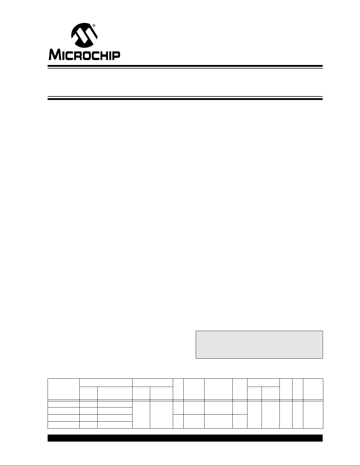
Pin Diagrams
28-Pin SPDIP, SOIC
RA5/AN4/SS
40-Pin PDIP
MCLR/VPP/RE3
RA0/AN0
RA2/AN2/V
RA4/T0CKI/C1OUT/RCV
RC0/T1OSO/T13CKI
RC1/T1OSI/CCP2
RA1/AN1
REF-/CVREF
RA3/AN3/VREF+
/HLVDIN/C2OUT
OSC1/CLKI
OSC2/CLKO/RA6
(1)
/UOE
RC2/CCP1
V
V
USB
1
2
3
4
5
6
7
SS
8
9
10
11
12
13
14
PIC18F2458
28
27
26
25
24
23
22
21
20
PIC18F2553
19
18
17
16
15
RB7/KBI3/PGD
RB6/KBI2/PGC
RB5/KBI1/PGM
RB4/AN11/KBI0
RB3/AN9/CCP2
RB2/AN8/INT2/VMO
RB1/AN10/INT1/SCK/SCL
RB0/AN12/INT0/FLT0/SDI/SDA
V
DD
VSS
RC7/RX/DT/SDO
RC6/TX/CK
RC5/D+/VP
RC4/D-/VM
(1)
/VPO
MCLR/VPP/RE3
RA0/AN0
RA2/AN2/V
RA4/T0CKI/C1OUT/RCV
RA5/AN4/SS
RC0/T1OSO/T13CKI
RC1/T1OSI/CCP2
Note 1: RB3 is the alternate pin for CCP2 multiplexing.
RA1/AN1
REF-/CVREF
RA3/AN3/VREF+
/HLVDIN/C2OUT
RE0/AN5/CK1SPP
RE1/AN6/CK2SPP
RE2/AN7/OESPP
OSC2/CLKO/RA6
RC2/CCP1/P1A
V
VSS
OSC1/CLKI
(1)
/UOE
V
USB
RD0/SPP0
RD1/SPP1
DD
1
2
3
4
5
6
7
8
9
10
11
12
13
14
15
16
17
18
19
20
PIC18F4458
PIC18F4553
40
39
38
37
36
35
34
33
32
31
30
29
28
27
26
25
24
23
22
21
RB7/KBI3/PGD
RB6/KBI2/PGC
RB5/KBI1/PGM
RB4/AN11/KBI0/CSSPP
RB3/AN9/CCP2
RB2/AN8/INT2/VMO
RB1/AN10/INT1/SCK/SCL
RB0/AN12/INT0/FLT0/SDI/SDA
V
DD
VSS
RD7/SPP7/P1D
RD6/SPP6/P1C
RD5/SPP5/P1B
RD4/SPP4
RC7/RX/DT/SDO
RC6/TX/CK
RC5/D+/VP
RC4/D-/VM
RD3/SPP3
RD2/SPP2
(1)
/VPO
DS39887B-page 2 Preliminary © 2007 Microchip Technology Inc.
Page 5
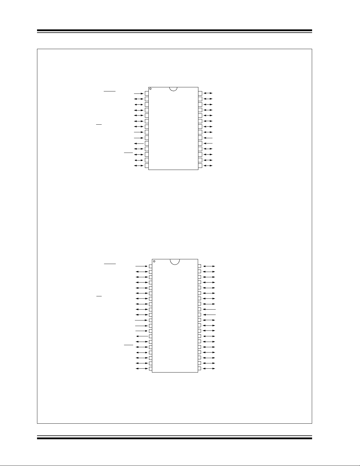
Pin Diagrams (Continued)
44-Pin TQFP
PIC18F2458/2553/4458/4553
/UOE
(1)
(2)
RC7/RX/DT/SDO
RD5/SPP5/P1B
RD6/SPP6/P1C
RD7/SPP7/P1D
RB0/AN12/INT0/FLT0/SDI/SDA
RB1/AN10/INT1/SCK/SCL
RB2/AN8/INT2/VMO
RB3/AN9/CCP2
44-Pin QFN
RD4/SPP4
V
VDD
(1)
/VPO
RC6/TX/CK
RC5/D+/VP
RC4/D-/VM
RD3/SPP3
4443424140
1
2
3
4
5
PIC18F4458
SS
6
7
8
9
10
11
121314
(2)
(2)
/ICPGC
(2)
(2)
NC/ICCK
PIC18F4553
15
/ICPGD
RB5/KBI1/PGM
NC/ICDT
RB4/AN11/KBI0/CSSPP
RD2/SPP2
RD1/SPP1
39
16
17
RB7/KBI3/PGD
RB6/KBI2/PGC
USB
RD0/SPP0
V
RC2/CCP1/P1A
RC1/T1OSI/CCP2
363435
37
38
1819202122
RA1/AN1
RA0/AN0
/VPP/RE3
REF-/CVREF
MCLR
RA2/AN2/V
NC/ICPORTS
(2)
33
32
31
30
29
28
27
26
25
24
23
RA3/AN3/VREF+
NC/ICRST
RC0/T1OSO/T13CKI
OSC2/CLKO/RA6
OSC1/CLKI
V
SS
VDD
RE2/AN7/OESPP
RE1/AN6/CK2SPP
RE0/AN5/CK1SPP
RA5/AN4/SS
RA4/T0CKI/C1OUT/RCV
/UOE
(1)
(2)
/ICVPP
/HLVDIN/C2OUT
15
RD2/SPP2
16
RB6/KBI2/PGC
USB
RD1/SPP1
RD0/SPP0
V
39
37
38
1819202122
17
RA0/AN0
/VPP/RE3
RB7/KBI3/PGD
MCLR
RC2/CCP1/P1A
363435
RA1/AN1
RC1/T1OSI/CCP2
REF-/CVREF
RA2/AN2/V
RC0/T1OSO/T13CKI
33
32
31
30
29
28
27
26
25
24
23
REF+
RA3/AN3/V
OSC2/CLKO/RA6
OSC1/CLKI
SS
V
VSS
VDD
VDD
RE2/AN7/OESPP
RE1/AN6/CK2SPP
RE0/AN5/CK1SPP
RA5/AN4/SS
RA4/T0CKI/C1OUT/RCV
RC6/TX/CK
RC5/D+/VP
RC4/D-/VM
RD3/SPP3
RC7/RX/DT/SDO
RD4/SPP4
RD5/SPP5/P1B
RD6/SPP6/P1C
RD7/SPP7/P1D
RB0/AN12/INT0/FLT0/SDI/SDA
RB1/AN10/INT1/SCK/SCL
RB2/AN8/INT2/VMO
Note 1: RB3 is the alternate pin for CCP2 multiplexing.
2: Special ICPORT features are available only in 44-pin TQFP packages. See Section 25.9 “Special ICPORT Features” in
the “PIC18F2455/2550/4455/4550 Data Sheet”’.
V
VDD
VDD
SS
4443424140
1
2
3
4
5
6
7
8
9
10
11
(1)
PIC18F4458
PIC18F4553
121314
NC
/VPO
RB5/KBI1/PGM
RB3/AN9/CCP2
RB4/AN11/KBI0/CSSPP
/HLVDIN/C2OUT
© 2007 Microchip Technology Inc. Preliminary DS39887B-page 3
Page 6

PIC18F2458/2553/4458/4553
Table of Contents
1.0 Device Overview .......................................................................................................................................................................... 5
2.0 12-Bit Analog-to-Digital Converter (A/D) Module ....................................................................................................................... 19
3.0 Special Features of the CPU...................................................................................................................................................... 29
4.0 Electrical Characteristics ............................................................................................................................................................ 31
5.0 Packaging Information................................................................................................................................................................ 35
Appendix A: Revision History............................................................................................................................................................... 37
Appendix B: Device Differences........................................................................................................................................................... 37
Appendix C: Migration From Mid-Range to Enhanced Devices........................................................................................................... 38
Appendix D: Migration From High-End to Enhanced Devices ............................................................................................................. 38
Index .................................................................................................................................................................................................... 39
The Microchip Web Site....................................................................................................................................................................... 41
Customer Change Notification Service ................................................................................................................................................ 41
Customer Support ................................................................................................................................................................................ 41
Reader Response ................................................................................................................................................................................ 42
Product Identification System............................................................................................................................................................... 43
TO OUR VALUED CUSTOMERS
It is our intention to provide our valued customers with the best documentation possible to ensure successful use of your Microchip
products. To this end, we will continue to improve our publications to better suit your needs. Our publications will be refined and
enhanced as new volumes and updates are introduced.
If you have any questions or comments regarding this publication, please contact the Marketing Communications Department via
E-mail at docerrors@microchip.com or fax the Reader Response Form in the back of this data sheet to (480) 792-4150. We
welcome your feedback.
Most Current Data Sheet
To obtain the most up-to-date version of this data sheet, please register at our Worldwide Web site at:
http://www.microchip.com
You can determine the version of a data sheet by examining its literature number found on the bottom outside corner of any page.
The last character of the literature number is the version number, (e.g., DS30000A is version A of document DS30000).
Errata
An errata sheet, describing minor operational differences from the data sheet and recommended workarounds, may exist for current
devices. As device/documentation issues become known to us, we will publish an errata sheet. The errata will specify the revision
of silicon and revision of document to which it applies.
To determine if an errata sheet exists for a particular device, please check with one of the following:
• Microchip’s Worldwide Web site; http://www.microchip.com
• Your local Microchip sales office (see last page)
When contacting a sales office, please specify which device, revision of silicon and data sheet (include literature number) you are
using.
Customer Notification System
Register on our web site at www.microchip.com to receive the most current information on all of our products.
DS39887B-page 4 Preliminary © 2007 Microchip Technology Inc.
Page 7

PIC18F2458/2553/4458/4553
1.0 DEVICE OVERVIEW
This document contains device-specific information for
the following devices:
• PIC18F2458 • PIC18F4458
• PIC18F2553 • PIC18F4553
Note: This data sheet documents only the
devices’ features and specifications that are
in addition to the features and specifications of the PIC18F2455/2550/4455/4550
devices. For information on the features
and specifications shared by
the PIC18F2458/2553/4458/4553 and
PIC18F2455/2550/4455/4550 devices,
see the “PIC18F2455/2550/4455/4550
Data Sheet” (DS39632).
The PIC18F4553 family of devices offers the advantages of all PIC18 microcontrollers – namely, high
computational performance at an economical price –
with the addition of high-endurance, Enhanced Flash
program memory. In addition to these features, the
PIC18F4553 family introduces design enhancements
that make these microcontrollers a logical choice for
many high-performance, power sensitive applications.
1.1 Special Features
• 12-Bit A/D Converter: The PIC18F4553 family
implements a 12-bit A/D Converter. The A/D
Converter incorporates programmable acquisition time. This allows for a channel to be selected
and a conversion to be initiated, without waiting
for a sampling period and thus, reducing code
overhead.
1.2 Details on Individual Family Members
The PIC18F2458/2553/4458/4553 devices are
available in 28-pin and 40/44-pin packages. Block
diagrams for the two groups are shown in Figure 1-1
and Figure 1-2.
The devices are differentiated from each other in the
following ways:
1. Flash program memory (24 Kbytes for
PIC18FX458 devices, 32 Kbytes for
PIC18FX553).
2. A/D channels (10 for 28-pin devices, 13 for
40-pin and 44-pin devices).
3. I/O ports (3 bidirectional ports and 1 input only
port on 28-pin devices, 5 bidirectional ports on
40-pin and 44-pin devices).
4. CCP and Enhanced CCP implementation
(28-pin devices have two standard CCP
modules, 40-pin and 44-pin devices have one
standard CCP module and one ECCP module).
5. Streaming Parallel Port (present only on
40/44-pin devices).
All other features for devices in this family are identical.
These are summarized in Table 1-1.
The pinouts for all devices are listed in Table 1-2 and
Table 1-3.
Members of the PIC18F4553 family are available as
both standard and low-voltage devices. Standard
devices with Enhanced Flash memory, designated with
an “F” in the part number (such as PIC18F2458),
accommodate an operating V
Low-voltage parts, designated by “LF” (such as
PIC18LF2458), function over an extended VDD range
of 2.0V to 5.5V.
DD range of 4.2V to 5.5V.
© 2007 Microchip Technology Inc. Preliminary DS39887B-page 5
Page 8
PIC18F2458/2553/4458/4553
TABLE 1-1: DEVICE FEATURES
Features PIC18F2458 PIC18F2553 PIC18F4458 PIC18F4553
Operating Frequency DC – 48 MHz DC – 48 MHz DC – 48 MHz DC – 48 MHz
Program Memory (Bytes) 24576 32768 24576 32768
Program Memory
(Instructions)
Data Memory (Bytes) 2048 2048 2048 2048
Data EEPROM Memory
(Bytes)
Interrupt Sources 19 19 20 20
I/O Ports Ports A, B, C, (E) Ports A, B, C, (E) Ports A, B, C, D, E Ports A, B, C, D, E
Timers 4 4 4 4
Capture/Compare/PWM
Modules
Enhanced Capture/
Compare/PWM Modules
Serial Communications MSSP,
Universal Serial Bus (USB)
Module
Streaming Parallel Port (SPP) No No Yes Yes
12-Bit Analog-to-Digital
Converter Module
Comparators 2 2 2 2
Resets (and Delays) POR, BOR, WDT,
Programmable High/
Low-Voltage Detect
Programmable Brown-out
Reset
Instruction Set 75 Instructions;
Packages 28-Pin SPDIP
Corresponding Devices with
10-Bit A/D
12288 16384 12288 16384
256 256 256 256
2 2 1 1
0 0 1 1
MSSP,
Enhanced USART
1 1 1 1
10 Input Channels 10 Input Channels 13 Input Channels 13 Input Channels
RESET Instruction,
Stack Full, Stack
Underflow, MCLR
(optional),
(PWRT, OST)
Yes Ye s Yes Ye s
Yes Ye s Ye s Yes
83 with Extended
Instruction Set
Enabled
28-Pin SOIC
PIC18F2455 PIC18F2550 PIC18F4455 PIC18F4550
Enhanced USART
POR, BOR, WDT,
RESET Instruction,
Stack Full, Stack
Underflow, MCLR
(optional),
(PWRT, OST)
75 Instructions;
83 with Extended
Instruction Set
Enabled
28-Pin SPDIP
28-Pin SOIC
MSSP,
Enhanced USART
POR, BOR, WDT,
RESET Instruction,
Stack Full, Stack
Underflow, MCLR
(optional),
(PWRT, OST)
75 Instructions;
83 with Extended
Instruction Set
Enabled
40-Pin PDIP
44-Pin QFN
44-Pin TQFP
MSSP,
Enhanced USART
POR, BOR, WDT,
RESET Instruction,
Stack Ful l, Stack
Underflow, MCLR
(optional),
(PWRT, OST)
75 Instructions;
83 with Extended
Instruction Set
Enabled
40-Pin PDIP
44-Pin QFN
44-Pin TQFP
DS39887B-page 6 Preliminary © 2007 Microchip Technology Inc.
Page 9
PIC18F2458/2553/4458/4553
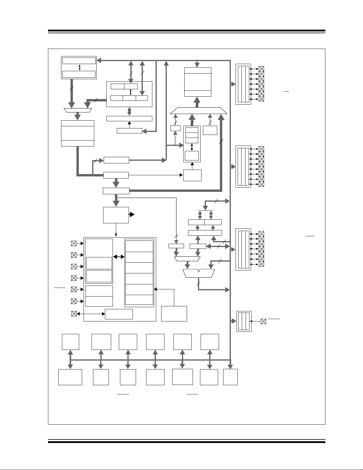
FIGURE 1-1: PIC18F2458/2553 (28-PIN) BLOCK DIAGRAM
Table Pointer<21>
inc/dec logic
21
Address Latch
Program Memory
(24/32 Kbytes)
Data Latch
Instruction Bus <16>
(2)
OSC1
(2)
OSC2
T1OSI
T1OSO
(1)
MCLR
VDD,
SS
V
USB
V
20
8
Tabl e L a t c h
Instruction
Internal
Oscillator
Block
INTRC
Oscillator
8 MHz
Oscillator
Single-Supply
Programming
In-Circuit
Debugger
PCLATH
PCLATU
PCH PCL
PCU
Program Counter
31 Level Stack
STKPTR
ROM Latch
IR
Decode &
Control
Start-up Timer
Clock Monitor
USB Voltage
Regulator
Data Bus<8>
8
8
State Machine
Control Signals
Power-up
Timer
Oscillator
Power-on
Reset
Watchdog
Timer
Brown-out
Reset
Fail-Safe
Data Latch
Data Memory
(2 Kbytes)
Address Latch
12
Data Address<12>
44
12
FSR0
FSR1
FSR2
inc/dec
logic
Decode
8 x 8 Multiply
W
8
ALU<8>
Access
Bank
PRODLPRODH
8
8
12
8
BSR
Address
3
BITOP
8
Band Gap
Reference
PORTA
RA0/AN0
RA1/AN1
RA2/AN2/VREF-/CVREF
RA3/AN3/VREF+
RA4/T0CKI/C1OUT/RCV
RA5/AN4/SS/HLVDIN/C2OUT
OSC2/CLKO/RA6
PORTB
RB0/AN12/INT0/FLT0/SDI/SDA
RB1/AN10/INT1/SCK/SCL
RB2/AN8/INT2/VMO
RB3/AN9/CCP2
RB4/AN11/KBI0
RB5/KBI1/PGM
RB6/KBI2/PGC
RB7/KBI3/PGD
PORTC
8
8
8
PORTE
RC0/T1OSO/T13CKI
RC1/T1OSI/CCP2
RC2/CCP1
RC4/D-/VM
RC5/D+/VP
RC6/TX/CK
RC7/RX/DT/SDO
MCLR/VPP/RE3
(3)
/VPO
(3)
(1)
/UOE
BOR
HLVD
Comparator
Note 1: RE3 is multiplexed with MCLR and is only available when the MCLR Resets are disabled.
2: OSC1/CLKI and OSC2/CLKO are only available in select oscillator modes and when these pins are not being used as digital I/O.
3: RB3 is the alternate pin for CCP2 multiplexing.
Data
EEPROM
CCP1
CCP2
MSSP
Timer2Timer1 Timer3Timer0
EUSART
ADC
12-Bit
USB
© 2007 Microchip Technology Inc. Preliminary DS39887B-page 7
Page 10
PIC18F2458/2553/4458/4553
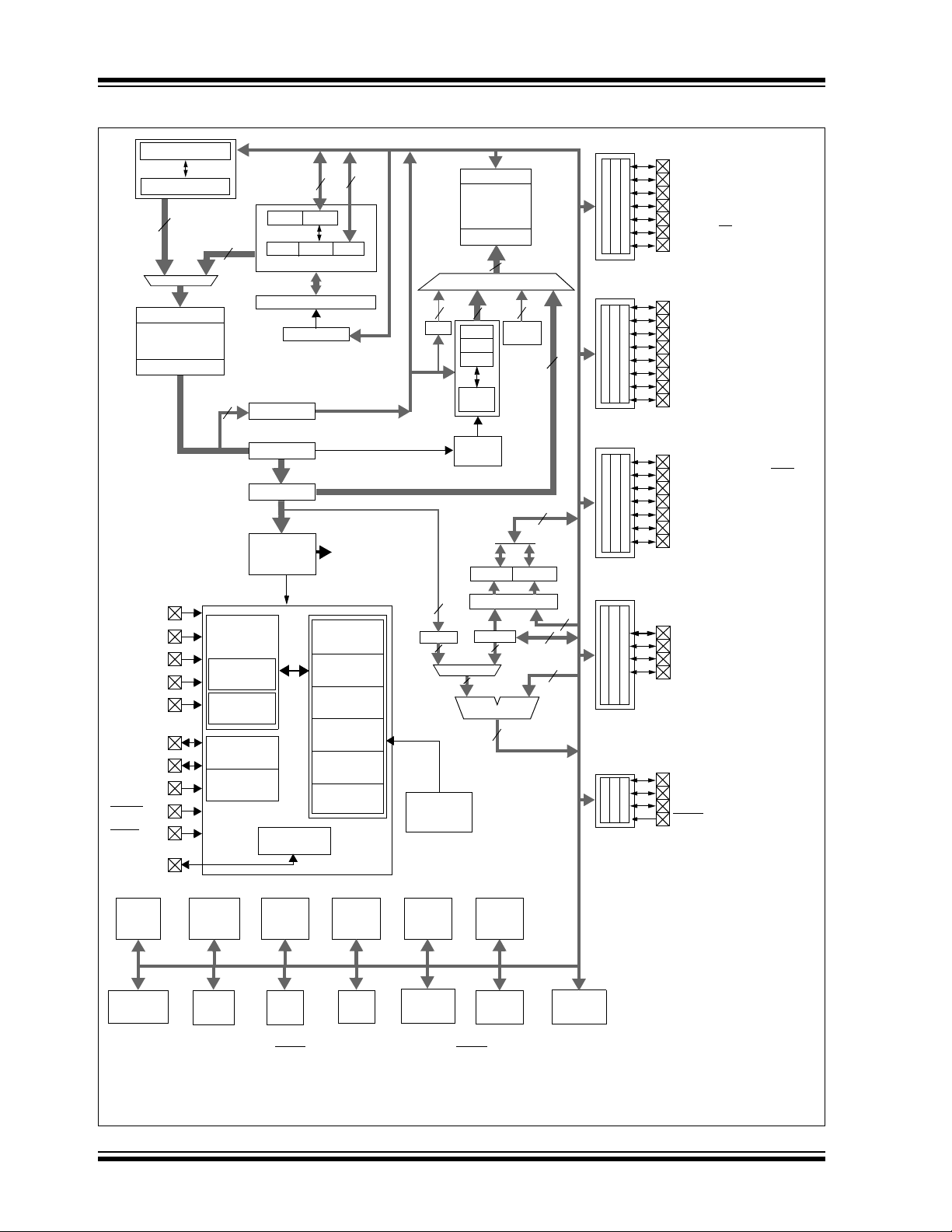
FIGURE 1-2: PIC18F4458/4553(40/44-PIN) BLOCK DIAGRAM
Table Pointer<21>
inc/dec logic
21
Address Latch
Program Memory
(24/32 Kbytes)
Data Latch
20
8
PCLATH
PCLATU
PCU
Program Counter
31 Level Stack
STKPTR
Table Latch
Data Bus<8>
8
PCH PCL
8
Data Latch
Data Memory
(2 Kbytes)
Address Latch
12
Data Address<12>
12
44
BSR
FSR0
FSR1
FSR2
inc/dec
logic
Access
Bank
12
PORTA
PORTB
RA0/AN0
RA1/AN1
RA2/AN2/VREF-/CVREF
RA3/AN3/VREF+
RA4/T0CKI/C1OUT/RCV
RA5/AN4/SS/HLVDIN/C2OUT
OSC2/CLKO/RA6
RB0/AN12/INT0/FLT0/SDI/SDA
RB1/AN10/INT1/SCK/SCL
RB2/AN8/INT2/VMO
RB3/AN9/CCP2
(4)
/VPO
RB4/AN11/KBI0/CSSPP
RB5/KBI1/PGM
RB6/KBI2/PGC
RB7/KBI3/PGD
Instruction Bus <16>
VDD, VSS
(2)
OSC1
(2)
OSC2
T1OSI
T1OSO
(3)
ICPGC
(3)
ICPGD
(3)
ICPORTS
(3)
ICRST
(1)
MCLR
V
USB
ROM Latch
IR
Instruction
Decode &
Internal
Oscillator
Block
INTRC
Oscillator
8 MHz
Oscillator
Single-Supply
Programming
In-Circuit
Debugger
Control
USB Voltage
Regulator
State Machine
Control Signals
Power-up
Timer
Oscillator
Start-up Timer
Power-on
Reset
Watchdog
Timer
Brown-out
Reset
Fail-Safe
Clock Monitor
3
BITOP
8
Band Gap
Reference
Address
Decode
8 x 8 Multiply
8
ALU<8>
PORTC
RC0/T1OSO/T13CKI
RC1/T1OSI/CCP2
(4)
/UOE
RC2/CCP1/P1A
RC4/D-/VM
RC5/D+/VP
8
RC6/TX/CK
RC7/RX/DT/SDO
PRODLPRODH
PORTD
8
W
8
8
RD0/SPP0:RD4/SPP4
RD5/SPP5/P1B
RD6/SPP6/P1C
RD7/SPP7/P1D
8
8
PORTE
RE0/AN5/CK1SPP
RE1/AN6/CK2SPP
RE2/AN7/OESPP
MCLR/VPP/RE3
(1)
BOR
HLVD
Comparator
Note 1: RE3 is multiplexed with MCLR
Data
EEPROM
ECCP1
Timer2Timer1 Timer3Timer0
CCP2
MSSP
EUSART
ADC
12-Bit
and is only available when the MCLR Resets are disabled.
USB
2: OSC1/CLKI and OSC2/CLKO are only available in select oscillator modes and when these pins are not being used as digital I/O.
3: These pins are only available on 44-pin TQFP packages under certain conditions.
4: RB3 is the alternate pin for CCP2 multiplexing.
DS39887B-page 8 Preliminary © 2007 Microchip Technology Inc.
Page 11
PIC18F2458/2553/4458/4553
TABLE 1-2: PIC18F2458/2553 PINOUT I/O DESCRIPTIONS
Pin
Pin Name
M
CLR/VPP/RE3
MCLR
VPP
RE3
OSC1/CLKI
OSC1
CLKI
OSC2/CLKO/RA6
OSC2
CLKO
RA6
Legend: TTL = TTL compatible input CMOS = CMOS compatible input or output
ST = Schmitt Trigger input with CMOS levels I = Input
O = Output P = Power
Note 1: Alternate assignment for CCP2 when CCP2MX Configuration bit is cleared.
2: Default assignment for CCP2 when CCP2MX Configuration bit is set.
Number
SPDIP,
SOIC
10
Pin
Buffer
Type
1
9
Type
I
ST
P
I
ST
IIAnalog
Analog
O
O
I/O
—
—
TTL
Master Clear (input) or programming voltage (input).
Master Clear (Reset) input. This pin is an active-low
Reset to the device.
Programming voltage input.
Digital input.
Oscillator crystal or external clock input.
Oscillator crystal input or external clock source input.
External clock source input. Always associated with pin
function OSC1. (See OSC2/CLKO pin.)
Oscillator crystal or clock output.
Oscillator crystal output. Connects to crystal or resonator in
Crystal Oscillator mode.
In select modes, OSC2 pin outputs CLKO which has 1/4 the
frequency of OSC1 and denotes the instruction cycle rate.
General purpose I/O pin.
Description
© 2007 Microchip Technology Inc. Preliminary DS39887B-page 9
Page 12
PIC18F2458/2553/4458/4553
TABLE 1-2: PIC18F2458/2553 PINOUT I/O DESCRIPTIONS (CONTINUED)
Pin
Pin Name
RA0/AN0
RA0
AN0
RA1/AN1
RA1
AN1
RA2/AN2/VREF-/CVREF
RA2
AN2
VREF-
REF
CV
RA3/AN3/V
RA3
AN3
V
RA4/T0CKI/C1OUT/RCV
RA4
T0CKI
C1OUT
RCV
RA5/AN4/SS
HLVDIN/C2OUT
RA5
AN4
SS
HLVDIN
C2OUT
RA6 — — — See the OSC2/CLKO/RA6 pin.
Legend: TTL = TTL compatible input CMOS = CMOS compatible input or output
Note 1: Alternate assignment for CCP2 when CCP2MX Configuration bit is cleared.
REF+
REF+
/
ST = Schmitt Trigger input with CMOS levels I = Input
O = Output P = Power
2: Default assignment for CCP2 when CCP2MX Configuration bit is set.
Number
SPDIP,
SOIC
Pin
Buffer
Type
2
3
4
5
6
7
Type
I/OITTL
Analog
I/OITTL
Analog
I/O
I/O
I/O
I/O
TTL
I
Analog
I
Analog
O
Analog
TTL
I
Analog
I
Analog
ST
I
ST
O
I
I
I
I
O
—
TTL
TTL
Analog
TTL
Analog
—
PORTA is a bidirectional I/O port.
Digital I/O.
Analog input 0.
Digital I/O.
Analog input 1.
Digital I/O.
Analog input 2.
A/D reference voltage (low) input.
Analog comparator reference output.
Digital I/O.
Analog input 3.
A/D reference voltage (high) input.
Digital I/O.
Timer0 external clock input.
Comparator 1 output.
External USB transceiver RCV input.
Digital I/O.
Analog input 4.
SPI slave select input.
High/Low-Voltage Detect input.
Comparator 2 output.
Description
DS39887B-page 10 Preliminary © 2007 Microchip Technology Inc.
Page 13
PIC18F2458/2553/4458/4553
TABLE 1-2: PIC18F2458/2553 PINOUT I/O DESCRIPTIONS (CONTINUED)
Pin
Pin Name
RB0/AN12/INT0/FLT0/
SDI/SDA
RB0
AN12
INT0
FLT0
SDI
SDA
RB1/AN10/INT1/SCK/
SCL
RB1
AN10
INT1
SCK
SCL
RB2/AN8/INT2/VMO
RB2
AN8
INT2
VMO
RB3/AN9/CCP2/VPO
RB3
AN9
(1)
CCP2
VPO
RB4/AN11/KBI0
RB4
AN11
KBI0
RB5/KBI1/PGM
RB5
KBI1
PGM
RB6/KBI2/PGC
RB6
KBI2
PGC
RB7/KBI3/PGD
RB7
KBI3
PGD
Legend: TTL = TTL compatible input CMOS = CMOS compatible input or output
ST = Schmitt Trigger input with CMOS levels I = Input
O = Output P = Power
Note 1: Alternate assignment for CCP2 when CCP2MX Configuration bit is cleared.
2: Default assignment for CCP2 when CCP2MX Configuration bit is set.
Number
SPDIP,
SOIC
21
22
23
24
25
26
27
28
Pin
Type
I/O
I
I
I
I
I/O
I/O
I
I
I/O
I/O
I/O
I
I
O
I/O
I
I/O
O
I/O
I
I
I/O
I
I/O
I/O
I
I/O
I/O
I
I/O
Buffer
Type
TTL
Analog
ST
ST
ST
ST
TTL
Analog
ST
ST
ST
TTL
Analog
ST
—
TTL
Analog
ST
—
TTL
Analog
TTL
TTL
TTL
ST
TTL
TTL
ST
TTL
TTL
ST
Description
PORTB is a bidirectional I/O port. PORTB can be software
programmed for internal weak pull-ups on all inputs.
Digital I/O.
Analog input 12.
External interrupt 0.
PWM Fault input (CCP1 module).
SPI data in.
2
C™ data I/O.
I
Digital I/O.
Analog input 10.
External interrupt 1.
Synchronous serial clock input/output for SPI mode.
Synchronous serial clock input/output for I
Digital I/O.
Analog input 8.
External interrupt 2.
External USB transceiver VMO output.
Digital I/O.
Analog input 9.
Capture 2 input/Compare 2 output/PWM 2 output.
External USB transceiver VPO output.
Digital I/O.
Analog input 11.
Interrupt-on-change pin.
Digital I/O.
Interrupt-on-change pin.
Low-Voltage ICSP™ Programming enable pin.
Digital I/O.
Interrupt-on-change pin.
In-Circuit Debugger and ICSP programming clock pin.
Digital I/O.
Interrupt-on-change pin.
In-Circuit Debugger and ICSP programming data pin.
2
C mode.
© 2007 Microchip Technology Inc. Preliminary DS39887B-page 11
Page 14
PIC18F2458/2553/4458/4553
TABLE 1-2: PIC18F2458/2553 PINOUT I/O DESCRIPTIONS (CONTINUED)
Pin
Pin Name
RC0/T1OSO/T13CKI
RC0
T1OSO
T13CKI
RC1/T1OSI/CCP2/UOE
RC1
T1OSI
(2)
CCP2
UOE
RC2/CCP1
RC2
CCP1
RC4/D-/VM
RC4
DVM
RC5/D+/VP
RC5
D+
VP
RC6/TX/CK
RC6
TX
CK
RC7/RX/DT/SDO
RC7
RX
DT
SDO
RE3 — — — See MCLR
V
USB 14
V
SS 8, 19 P — Ground reference for logic and I/O pins.
V
DD 20 P — Positive supply for logic and I/O pins.
Legend: TTL = TTL compatible input CMOS = CMOS compatible input or output
ST = Schmitt Trigger input with CMOS levels I = Input
O = Output P = Power
Note 1: Alternate assignment for CCP2 when CCP2MX Configuration bit is cleared.
2: Default assignment for CCP2 when CCP2MX Configuration bit is set.
Number
SPDIP,
SOIC
11
12
13
15
16
17
18
Pin
Type
I/O
O
I
I/O
I
I/O
—
I/O
I/O
I
I/O
I
I
I/O
O
I/O
O
I/O
I/O
I
I/O
O
O
P
Buffer
Type
ST
—
ST
ST
CMOS
ST
—
ST
ST
TTL
—
TTL
TTL
—
TTL
ST
—
ST
ST
ST
ST
—
—
—
Description
PORTC is a bidirectional I/O port.
Digital I/O.
Timer1 oscillator output.
Timer1/Timer3 external clock input.
Digital I/O.
Timer1 oscillator input.
Capture 2 input/Compare 2 output/PWM2 output.
External USB transceiver OE
Digital I/O.
Capture 1 input/Compare 1 output/PWM1 output.
Digital input.
USB differential minus line (input/output).
External USB transceiver VM input.
Digital input.
USB differential plus line (input/output).
External USB transceiver VP input.
Digital I/O.
EUSART asynchronous transmit.
EUSART synchronous clock (see RX/DT).
Digital I/O.
EUSART asynchronous receive.
EUSART synchronous data (see TX/CK).
SPI data out.
/VPP/RE3 pin.
Internal USB transceiver power supply.
When the internal USB regulator is enabled, V
regulator output.
When the internal USB regulator is disabled, V
power input for the USB transceiver.
output.
USB is the
USB is the
DS39887B-page 12 Preliminary © 2007 Microchip Technology Inc.
Page 15

PIC18F2458/2553/4458/4553
TABLE 1-3: PIC18F4458/4553 PINOUT I/O DESCRIPTIONS
Pin Name
Pin Number
PDIP QFN TQFP
Pin
Type
Buffer
Type
Description
/VPP/RE3
MCLR
MCLR
VPP
RE3
OSC1/CLKI
OSC1
CLKI
OSC2/CLKO/RA6
OSC2
CLKO
RA6
Legend: TTL = TTL compatible input CMOS = CMOS compatible input or output
ST = Schmitt Trigger input with CMOS levels I = Input
O = Output P = Power
Note 1: Alternate assignment for CCP2 when CCP2MX Configuration bit is cleared.
2: Default assignment for CCP2 when CCP2MX Configuration bit is set.
3: These pins are No Connect unless the ICPRT Configuration bit is set. For NC/ICPORTS, the pin is No
Connect unless ICPRT is set and the DEBUG
11818
13 32 30
14 33 31
I
ST
P
I
ST
IIAnalog
Analog
O
—
O
—
I/O
TTL
Configuration bit is cleared.
Master Clear (input) or programming voltage (input).
Master Clear (Reset) input. This pin is an active-low
Reset to the device.
Programming voltage input.
Digital input.
Oscillator crystal or external clock input.
Oscillator crystal input or external clock source input.
External clock source input. Always associated with
pin function OSC1. (See OSC2/CLKO pin.)
Oscillator crystal or clock output.
Oscillator crystal output. Connects to crystal or
resonator in Crystal Oscillator mode.
In RC mode, OSC2 pin outputs CLKO which has 1/4
the frequency of OSC1 and denotes the instruction
cycle rate.
General purpose I/O pin.
© 2007 Microchip Technology Inc. Preliminary DS39887B-page 13
Page 16

PIC18F2458/2553/4458/4553
TABLE 1-3: PIC18F4458/4553 PINOUT I/O DESCRIPTIONS (CONTINUED)
Pin Name
RA0/AN0
RA0
AN0
RA1/AN1
RA1
AN1
RA2/AN2/VREF-/
CV
REF
RA2
AN2
REF-
V
REF
CV
RA3/AN3/V
RA3
AN3
V
RA4/T0CKI/C1OUT/
RCV
RA4
T0CKI
C1OUT
RCV
RA5/AN4/SS
HLVDIN/C2OUT
RA5
AN4
SS
HLVDIN
C2OUT
RA6 — — — — — See the OSC2/CLKO/RA6 pin.
Legend: TTL = TTL compatible input CMOS = CMOS compatible input or output
Note 1: Alternate assignment for CCP2 when CCP2MX Configuration bit is cleared.
REF+
REF+
/
ST = Schmitt Trigger input with CMOS levels I = Input
O = Output P = Power
2: Default assignment for CCP2 when CCP2MX Configuration bit is set.
3: These pins are No Connect unless the ICPRT Configuration bit is set. For NC/ICPORTS, the pin is No
Connect unless ICPRT is set and the DEBUG
Pin Number
PDIP QFN TQFP
21919
32020
42121
52222
62323
72424
Pin
Buffer
Type
Type
I/OITTL
Analog
I/OITTL
Analog
I/O
I
Analog
I
Analog
O
Analog
I/O
I
Analog
I
Analog
I/O
I
O
I
I/O
I
Analog
I
I
Analog
O
PORTA is a bidirectional I/O port.
Digital I/O.
Analog input 0.
Digital I/O.
Analog input 1.
TTL
TTL
ST
ST
—
TTL
TTL
TTL
—
Configuration bit is cleared.
Digital I/O.
Analog input 2.
A/D reference voltage (low) input.
Analog comparator reference output.
Digital I/O.
Analog input 3.
A/D reference voltage (high) input.
Digital I/O.
Timer0 external clock input.
Comparator 1 output.
External USB transceiver RCV input.
Digital I/O.
Analog input 4.
SPI slave select input.
High/Low-Voltage Detect input.
Comparator 2 output.
Description
DS39887B-page 14 Preliminary © 2007 Microchip Technology Inc.
Page 17

PIC18F2458/2553/4458/4553
TABLE 1-3: PIC18F4458/4553 PINOUT I/O DESCRIPTIONS (CONTINUED)
Pin Name
RB0/AN12/INT0/
FLT0/SDI/SDA
RB0
AN12
INT0
FLT0
SDI
SDA
RB1/AN10/INT1/SCK/
SCL
RB1
AN10
INT1
SCK
SCL
RB2/AN8/INT2/VMO
RB2
AN8
INT2
VMO
RB3/AN9/CCP2/VPO
RB3
AN9
(1)
CCP2
VPO
RB4/AN11/KBI0/CSSPP
RB4
AN11
KBI0
CSSPP
RB5/KBI1/PGM
RB5
KBI1
PGM
RB6/KBI2/PGC
RB6
KBI2
PGC
RB7/KBI3/PGD
RB7
KBI3
PGD
Legend: TTL = TTL compatible input CMOS = CMOS compatible input or output
ST = Schmitt Trigger input with CMOS levels I = Input
O = Output P = Power
Note 1: Alternate assignment for CCP2 when CCP2MX Configuration bit is cleared.
2: Default assignment for CCP2 when CCP2MX Configuration bit is set.
3: These pins are No Connect unless the ICPRT Configuration bit is set. For NC/ICPORTS, the pin is No
Connect unless ICPRT is set and the DEBUG
Pin Number
PDIP QFN TQFP
33 9 8
34 10 9
35 11 10
36 12 11
37 14 14
38 15 15
39 16 16
40 17 17
Pin
Type
I/O
I
I
I
I
I/O
I/O
I
I
I/O
I/O
I/O
I
I
O
I/O
I
I/O
O
I/O
I
I
O
I/O
I
I/O
I/O
I
I/O
I/O
I
I/O
Buffer
Type
PORTB is a bidirectional I/O port. PORTB can be software programmed for internal weak pull-ups on all inputs.
TTL
Analog
ST
ST
ST
ST
TTL
Analog
ST
ST
ST
TTL
Analog
ST
—
TTL
Analog
ST
—
TTL
Analog
TTL
—
TTL
TTL
ST
TTL
TTL
ST
TTL
TTL
ST
Configuration bit is cleared.
Digital I/O.
Analog input 12.
External interrupt 0.
Enhanced PWM Fault input (ECCP1 module).
SPI data in.
2
C™ data I/O.
I
Digital I/O.
Analog input 10.
External interrupt 1.
Synchronous serial clock input/output for SPI mode.
Synchronous serial clock input/output for I
Digital I/O.
Analog input 8.
External interrupt 2.
External USB transceiver VMO output.
Digital I/O.
Analog input 9.
Capture 2 input/Compare 2 output/PWM 2 output.
External USB transceiver VPO output.
Digital I/O.
Analog input 11.
Interrupt-on-change pin.
SPP chip select control output.
Digital I/O.
Interrupt-on-change pin.
Low-Voltage ICSP™ Programming enable pin.
Digital I/O.
Interrupt-on-change pin.
In-Circuit Debugger and ICSP programming clock pin.
Digital I/O.
Interrupt-on-change pin.
In-Circuit Debugger and ICSP programming data pin.
Description
2
C mode.
© 2007 Microchip Technology Inc. Preliminary DS39887B-page 15
Page 18

PIC18F2458/2553/4458/4553
TABLE 1-3: PIC18F4458/4553 PINOUT I/O DESCRIPTIONS (CONTINUED)
Pin Name
RC0/T1OSO/T13CKI
RC0
T1OSO
T13CKI
RC1/T1OSI/CCP2/
UOE
RC1
T1OSI
(2)
CCP2
UOE
RC2/CCP1/P1A
RC2
CCP1
P1A
RC4/D-/VM
RC4
DVM
RC5/D+/VP
RC5
D+
VP
RC6/TX/CK
RC6
TX
CK
RC7/RX/DT/SDO
RC7
RX
DT
SDO
Legend: TTL = TTL compatible input CMOS = CMOS compatible input or output
ST = Schmitt Trigger input with CMOS levels I = Input
O = Output P = Power
Note 1: Alternate assignment for CCP2 when CCP2MX Configuration bit is cleared.
2: Default assignment for CCP2 when CCP2MX Configuration bit is set.
3: These pins are No Connect unless the ICPRT Configuration bit is set. For NC/ICPORTS, the pin is No
Connect unless ICPRT is set and the DEBUG
Pin Number
PDIP QFN TQFP
15 34 32
16 35 35
17 36 36
23 42 42
24 43 43
25 44 44
26 1 1
Pin
Type
I/O
O
I
I/O
I
I/O
O
I/O
I/O
O
I
I/O
I
I
I/O
I
I/O
O
I/O
I/O
I
I/O
O
Buffer
Type
PORTC is a bidirectional I/O port.
ST
—
ST
ST
CMOS
ST
—
ST
ST
TTL
TTL
—
TTL
TTL
—
TTL
ST
—
ST
ST
ST
ST
—
Configuration bit is cleared.
Digital I/O.
Timer1 oscillator output.
Timer1/Timer3 external clock input.
Digital I/O.
Timer1 oscillator input.
Capture 2 input/Compare 2 output/PWM2 output.
External USB transceiver OE output.
Digital I/O.
Capture 1 input/Compare 1 output/PWM1 output.
Enhanced CCP1 PWM output, channel A.
Digital input.
USB differential minus line (input/output).
External USB transceiver VM input.
Digital input.
USB differential plus line (input/output).
External USB transceiver VP input.
Digital I/O.
EUSART asynchronous transmit.
EUSART synchronous clock (see RX/DT).
Digital I/O.
EUSART asynchronous receive.
EUSART synchronous data (see TX/CK).
SPI data out.
Description
DS39887B-page 16 Preliminary © 2007 Microchip Technology Inc.
Page 19

PIC18F2458/2553/4458/4553
TABLE 1-3: PIC18F4458/4553 PINOUT I/O DESCRIPTIONS (CONTINUED)
Pin Name
RD0/SPP0
RD0
SPP0
RD1/SPP1
RD1
SPP1
RD2/SPP2
RD2
SPP2
RD3/SPP3
RD3
SPP3
RD4/SPP4
RD4
SPP4
RD5/SPP5/P1B
RD5
SPP5
P1B
RD6/SPP6/P1C
RD6
SPP6
P1C
RD7/SPP7/P1D
RD7
SPP7
P1D
Legend: TTL = TTL compatible input CMOS = CMOS compatible input or output
ST = Schmitt Trigger input with CMOS levels I = Input
O = Output P = Power
Note 1: Alternate assignment for CCP2 when CCP2MX Configuration bit is cleared.
2: Default assignment for CCP2 when CCP2MX Configuration bit is set.
3: These pins are No Connect unless the ICPRT Configuration bit is set. For NC/ICPORTS, the pin is No
Connect unless ICPRT is set and the DEBUG
Pin Number
PDIP QFN TQFP
19 38 38
20 39 39
21 40 40
22 41 41
27 2 2
28 3 3
29 4 4
30 5 5
Pin
Buffer
Type
Type
I/O
I/OSTTTL
I/O
I/OSTTTL
I/O
I/OSTTTL
I/O
I/OSTTTL
I/O
I/OSTTTL
I/O
I/O
O
I/O
I/O
O
I/O
I/O
O
Description
PORTD is a bidirectional I/O port or a Streaming
Parallel Port (SPP). PORTD can be software
programmed for internal weak pull-ups on all inputs.
These pins have TTL input buffers when the SPP
module is enabled.
Digital I/O.
Streaming Parallel Port data.
Digital I/O.
Streaming Parallel Port data.
Digital I/O.
Streaming Parallel Port data.
Digital I/O.
Streaming Parallel Port data.
Digital I/O.
Streaming Parallel Port data.
ST
TTL
—
ST
TTL
—
ST
TTL
—
Configuration bit is cleared.
Digital I/O.
Streaming Parallel Port data.
ECCP1 PWM output, channel B.
Digital I/O.
Streaming Parallel Port data.
ECCP1 PWM output, channel C.
Digital I/O.
Streaming Parallel Port data.
ECCP1 PWM output, channel D.
© 2007 Microchip Technology Inc. Preliminary DS39887B-page 17
Page 20

PIC18F2458/2553/4458/4553
TABLE 1-3: PIC18F4458/4553 PINOUT I/O DESCRIPTIONS (CONTINUED)
Pin Name
Pin Number
PDIP QFN TQFP
RE0/AN5/CK1SPP
82525
RE0
AN5
CK1SPP
RE1/AN6/CK2SPP
92626
RE1
AN6
CK2SPP
RE2/AN7/OESPP
10 27 27
RE2
AN7
OESPP
RE3 — — — — — See MCLR
VSS 12, 316, 30, 316, 29 P — Ground reference for logic and I/O pins.
V
DD 11, 32 7, 8,
7, 28 P — Positive supply for logic and I/O pins.
28, 29
V
USB 18 37 37
NC/ICCK/ICPGC
(3)
——12
ICCK
ICPGC
NC/ICDT/ICPGD
(3)
——13
ICDT
ICPGD
NC/ICRST
/ICVPP
——33
(3)
ICRST
ICVPP
NC/ICPORTS
(3)
— — 34 P — No Connect or 28-pin device emulation.
ICPORTS
NC — 13 — — — No Connect.
Legend: TTL = TTL compatible input CMOS = CMOS compatible input or output
ST = Schmitt Trigger input with CMOS levels I = Input
O = Output P = Power
Note 1: Alternate assignment for CCP2 when CCP2MX Configuration bit is cleared.
2: Default assignment for CCP2 when CCP2MX Configuration bit is set.
3: These pins are No Connect unless the ICPRT Configuration bit is set. For NC/ICPORTS, the pin is No
Connect unless ICPRT is set and the DEBUG
Pin
Buffer
Type
I/O
I
Analog
O
I/O
I
Analog
O
I/O
I
Analog
O
O
P
I/O
I/OSTST
I/O
I/OSTST
I
P
Type
Description
PORTE is a bidirectional I/O port.
ST
Digital I/O.
Analog input 5.
—
ST
SPP clock 1 output.
Digital I/O.
Analog input 6.
—
ST
SPP clock 2 output.
Digital I/O.
Analog input 7.
—
SPP output enable output.
/VPP/RE3 pin.
Internal USB transceiver power supply.
—
When the internal USB regulator is enabled, V
the regulator output.
—
When the internal USB regulator is disabled, VUSB
is the power input for the USB transceiver.
No Connect or dedicated ICD/ICSP™ port clock.
In-Circuit Debugger clock.
ICSP programming clock.
No Connect or dedicated ICD/ICSP port clock.
In-Circuit Debugger data.
ICSP programming data.
No Connect or dedicated ICD/ICSP port Reset.
—
—
Master Clear (Reset) input.
Programming voltage input.
Enable 28-pin device emulation when connected
to V
SS.
Configuration bit is cleared.
USB is
DS39887B-page 18 Preliminary © 2007 Microchip Technology Inc.
Page 21

PIC18F2458/2553/4458/4553
2.0 12-BIT ANALOG-TO-DIGITAL CONVERTER (A/D) MODULE
The Analog-to-Digital (A/D) Converter module has
10 inputs for the 28-pin devices and 13 for the 40-pin
and 44-pin devices. This module allows conversion of an
analog input signal to a corresponding 12-bit digital
number.
The module has five registers:
• A/D Result High Register (ADRESH)
• A/D Result Low Register (ADRESL)
• A/D Control Register 0 (ADCON0)
• A/D Control Register 1 (ADCON1)
• A/D Control Register 2 (ADCON2)
The ADCON0 register, shown in Register 2-1, controls
the operation of the A/D module. The ADCON1
register, shown in Register 2-2, configures the
functions of the port pins. The ADCON2 register,
shown in Register 2-3, configures the A/D clock
source, programmed acquisition time and justification.
REGISTER 2-1: ADCON0: A/D CONTROL REGISTER 0
U-0 U-0 R/W-0 R/W-0 R/W-0 R/W-0 R/W-0 R/W-0
— — CHS3 CHS2 CHS1 CHS0 GO/DONE ADON
bit 7 bit 0
Legend:
R = Readable bit W = Writable bit U = Unimplemented bit, read as ‘0’
-n = Value at POR ‘1’ = Bit is set ‘0’ = Bit is cleared x = Bit is unknown
bit 7-6 Unimplemented: Read as ‘0’
bit 5-2 CHS3:CHS0: Analog Channel Select bits
0000 = Channel 0 (AN0)
0001 = Channel 1 (AN1)
0010 = Channel 2 (AN2)
0011 = Channel 3 (AN3)
0100 = Channel 4 (AN4)
0101 = Channel 5 (AN5)
0110 = Channel 6 (AN6)
0111 = Channel 7 (AN7)
1000 = Channel 8 (AN8)
1001 = Channel 9 (AN9)
1010 = Channel 10 (AN10)
1011 = Channel 11 (AN11)
1100 = Channel 12 (AN12
1101 = Unimplemented
1110 = Unimplemented
1111 = Unimplemented
bit 1 GO/DONE
When ADON =
1 = A/D conversion in progress
0 = A/D Idle
bit 0 ADON: A/D On bit
1 = A/D Converter module is enabled
0 = A/D Converter module is disabled
: A/D Conversion Status bit
1:
(2)
(2)
(2)
(1,2)
(1,2)
(1,2)
Note 1: These channels are not implemented on 28-pin devices.
2: Performing a conversion on unimplemented channels will return a floating input measurement.
© 2007 Microchip Technology Inc. Preliminary DS39887B-page 19
Page 22

PIC18F2458/2553/4458/4553
REGISTER 2-2: ADCON1: A/D CONTROL REGISTER 1
U-0 U-0 R/W-0 R/W-0 R/W-0 R/W
(1)
— — VCFG1 VCFG0 PCFG3 PCFG2 PCFG1 PCFG0
bit 7 bit 0
Legend:
R = Readable bit W = Writable bit U = Unimplemented bit, read as ‘0’
-n = Value at POR ‘1’ = Bit is set ‘0’ = Bit is cleared x = Bit is unknown
bit 7-6 Unimplemented: Read as ‘0’
bit 5 VCFG1: Voltage Reference Configuration bit (V
1 = V
REF- (AN2)
0 = V
SS
REF- source)
bit 4 VCFG0: Voltage Reference Configuration bit (VREF+ source)
REF+ (AN3)
1 = V
DD
0 = V
bit 3-0 PCFG3:PCFG0: A/D Port Configuration Control bits:
(2)
(2)
AN6
(2)
AN5
AN4
AN3
PCFG3:
PCFG0
(1)
0000
AN12
AN11
AN10
AN9
AN8
AN7
A A AAAAAAAAAAA
0001 AA A AAAAAAAAAA
0010 AA A AAAAAAAAAA
0011 DA AAAAAAAAAAA
0100 DDAAAAAAAAAAA
0101 DDDAAAAAAAAAA
0110 DDDDAAAAAAAAA
(1)
0111
DDDDDAAAAAAAA
1000 DDDDDDAAAAAAA
1001 DDDDDDDAAAAAA
1010 D D DDDDDDAAAAA
1011 D D DDDDDDDAAAA
1100 D D DDDDDDDDAAA
1101 D D DDDDDDDDDAA
1110 D D DDDDDDDDDDA
1111 D D DDDDDDDDDDD
A = Analog input D = Digital I/O
R/W
(1)
AN2
AN1
R/W
AN0
(1)
Note 1: The Reset value of the PCFG bits depends on the value of the PBADEN Configuration bit. When
PBADEN = 1, PCFG<3:0> = 0000; when PBADEN = 0, PCFG<3:0> = 0111.
2: AN5 through AN7 are available only on 40-pin and 44-pin devices.
DS39887B-page 20 Preliminary © 2007 Microchip Technology Inc.
Page 23

PIC18F2458/2553/4458/4553
REGISTER 2-3: ADCON2: A/D CONTROL REGISTER 2
R/W-0 U-0 R/W-0 R/W-0 R/W-0 R/W-0 R/W-0 R/W-0
ADFM — ACQT2 ACQT1 ACQT0 ADCS2 ADCS1 ADCS0
bit 7 bit 0
Legend:
R = Readable bit W = Writable bit U = Unimplemented bit, read as ‘0’
-n = Value at POR ‘1’ = Bit is set ‘0’ = Bit is cleared x = Bit is unknown
bit 7 ADFM: A/D Result Format Select bit
1 = Right justified
0 = Left justified
bit 6 Unimplemented: Read as ‘0’
bit 5-3 ACQT2:ACQT0: A/D Acquisition Time Select bits
111 = 20 T
110 = 16 TAD
101 = 12 TAD
100 = 8 TAD
011 = 6 TAD
010 = 4 TAD
001 = 2 TAD
000 = 0 TAD
bit 2-0 ADCS2:ADCS0: A/D Conversion Clock Select bits
111 = FRC (clock derived from A/D RC oscillator)
110 = F
101 = F
100 = F
011 = F
010 = F
001 = F
000 = F
AD
(1)
OSC/64
OSC/16
OSC/4
RC (clock derived from A/D RC oscillator)
OSC/32
OSC/8
OSC/2
(1)
(1)
Note 1: If the A/D F
RC clock source is selected, a delay of one TCY (instruction cycle) is added before the A/D
clock starts. This allows the SLEEP instruction to be executed before starting a conversion.
© 2007 Microchip Technology Inc. Preliminary DS39887B-page 21
Page 24

PIC18F2458/2553/4458/4553
The analog reference voltage is software selectable to
either the device’s positive and negative supply voltage
(VDD and VSS), or the voltage level on the RA3/AN3/
REF+ and RA2/AN2/VREF-/CVREF pins.
V
The A/D Converter has a unique feature of being able
to operate while the device is in Sleep mode. To operate in Sleep, the A/D conversion clock must be derived
from the A/D’s internal RC oscillator.
The output of the sample and hold is the input into the
Converter, which generates the result via successive
approximation.
FIGURE 2-1: A/D BLOCK DIAGRAM
V
AIN
12-Bit
A/D
Converter
Reference
Voltage
(Input Voltage)
VCFG1:VCFG0
VREF+
VREF-
A device Reset forces all registers to their Reset state.
This forces the A/D module to be turned off and any
conversion in progress is aborted.
Each port pin associated with the A/D Converter can be
configured as an analog input or as a digital I/O. The
ADRESH and ADRESL registers contain the result of
the A/D conversion. When the A/D conversion is complete, the result is loaded into the ADRESH:ADRESL
register pair, the GO/DONE
bit (ADCON0 register) is
cleared and the A/D Interrupt Flag bit, ADIF, is set. The
block diagram of the A/D module is shown in Figure 2-1.
CHS3:CHS0
1100
1011
1010
1001
1000
0111
AN12
AN11
AN10
AN9
AN8
AN7
0110
AN6
0101
AN5
X0
X1
0100
0011
0010
0001
DD
V
0000
AN4
AN3
AN2
AN1
AN0
1X
0X
(1)
(1)
(1)
VSS
Note 1: Channels AN5 through AN7 are not available on 28-pin devices.
DS39887B-page 22 Preliminary © 2007 Microchip Technology Inc.
Page 25

PIC18F2458/2553/4458/4553
The value in the ADRESH:ADRESL registers is
unknown following Power-on and Brown-out Resets,
and is not affected by any other Reset.
After the A/D module has been configured as desired,
the selected channel must be acquired before the
conversion is started. The analog input channels must
have their corresponding TRIS bits selected as an
input. To determine acquisition time, see Section 2.1
“A/D Acquisition Requirements”. After this acquisition time has elapsed, the A/D conversion can be
started. An acquisition time can be programmed to
occur between setting the GO/DONE
bit and the actual
start of the conversion.
The following steps should be followed to perform an A/D
conversion:
1. Configure the A/D module:
• Configure analog pins, voltage reference and
digital I/O (ADCON1)
• Select A/D input channel (ADCON0)
• Select A/D acquisition time (ADCON2)
• Select A/D conversion clock (ADCON2)
• Turn on A/D module (ADCON0)
2. Configure A/D interrupt (if desired):
• Clear ADIF bit
• Set ADIE bit
• Set GIE bit
3. Wait the required acquisition time (if required).
4. Start conversion:
• Set GO/DONE
bit (ADCON0 register)
5. Wait for A/D conversion to complete, by either:
• Polling for the GO/DONE
bit to be cleared
OR
• Waiting for the A/D interrupt
6. Read A/D Result registers (ADRESH:ADRESL);
clear bit ADIF, if required.
7. For next conversion, go to step 1 or step 2, as
required. The A/D conversion time per bit is
defined as T
AD. A minimum wait of 2 TAD is
required before the next acquisition starts.
FIGURE 2-2: A/D TRANSFER FUNCTION
FFFh
FFEh
003h
002h
Digital Code Output
001h
000h
1 LSB
0.5 LSB
1.5 LSB
Analog Input Voltage
3 LSB
2 LSB
2.5 LSB
4095 LSB
4094 LSB
4094.5 LSB
4095.5 LSB
FIGURE 2-3: ANALOG INPUT MODEL
VDD
T = 0.6V
ANx
Rs
VAIN
Legend: CPIN
VT
ILEAKAGE
RIC
SS
C
HOLD
CPIN
5 pF
= Input Capacitance
= Threshold Voltage
= Leakage Current at the pin due to
various junctions
= Interconnect Resistance
= Sampling Switch
= Sample/Hold Capacitance (from DAC)
= Sampling Switch ResistanceRSS
V
V
T = 0.6V
RIC ≤ 1k
I
LEAKAGE
±100 nA
Sampling
Switch
SS
6V
5V
4V
VDD
3V
2V
R
SS
Sampling Switch
CHOLD = 25 pF
V
SS
1234
(kΩ)
© 2007 Microchip Technology Inc. Preliminary DS39887B-page 23
Page 26

PIC18F2458/2553/4458/4553
2.1 A/D Acquisition Requirements
For the A/D Converter to meet its specified accuracy,
the charge holding capacitor (C
to fully charge to the input channel voltage level. The
analog input model is shown in Figure 2-3. The source
impedance (R
S) and the internal sampling switch (RSS)
impedance directly affect the time required to charge
the capacitor CHOLD. The sampling switch (RSS)
impedance varies over the device voltage (V
source impedance affects the offset voltage at the analog input (due to pin leakage current). The maximum
recommended impedance for analog sources is
2.5 kΩ. After the analog input channel is selected
(changed), the channel must be sampled for at least
HOLD) must be allowed
DD). The
To calculate the minimum acquisition time, Equation 2-1
may be used. This equation assumes that 1/2 LSb error
is used (4096 steps for the 12-bit A/D). The 1/2 LSb error
is the maximum error allowed for the A/D to meet its
specified resolution.
Example 2-3 shows the calculation of the minimum
required acquisition time, T
based on the following application system
assumptions:
HOLD = 25 pF
C
Rs = 2.5 kΩ
Conversion Error ≤ 1/2 LSb
DD =3V → Rss = 4 kΩ
V
Temperature = 85°C (system max.)
the minimum acquisition time before starting a
conversion.
Note: When the conversion is started, the
holding capacitor is disconnected from the
input pin.
EQUATION 2-1: ACQUISITION TIME
TACQ = Amplifier Settling Time + Holding Capacitor Charging Time + Temperature Coefficient
AMP + TC + TCOFF
=T
ACQ. This calculation is
EQUATION 2-2: A/D MINIMUM CHARGING TIME
VHOLD = (VREF – (VREF/4096)) • (1 – e
or
TC = -(CHOLD)(RIC + RSS + RS) ln(1/4096)
(-TC/CHOLD(RIC + RSS + RS))
)
EQUATION 2-3: CALCULATING THE MINIMUM REQUIRED ACQUISITION TIME
TACQ =TAMP + TC + TCOFF
TAMP =0.2 µs
COFF = (Temp – 25°C)(0.02 µs/°C)
T
(85°C – 25°C)(0.02 µs/°C)
1.2 µs
Temperature coefficient is only required for temperatures > 25°C. Below 25°C, T
C = -(CHOLD)(RIC + RSS + RS) ln(1/4096) µs
T
-(25 pF) (1 kΩ + 4 kΩ + 2.5 kΩ) ln(0.0002441) µs
1.56 µs
ACQ = 0.2 µs + 1.56 μs + 1.2 µs
T
2.96 µs
COFF = 0 µs.
DS39887B-page 24 Preliminary © 2007 Microchip Technology Inc.
Page 27

PIC18F2458/2553/4458/4553
2.2 Selecting and Configuring Acquisition Time
The ADCON2 register allows the user to select an
acquisition time that occurs each time the GO/DONE
bit is set. It also gives users the option to use an
automatically determined acquisition time.
Acquisition time may be set with the ACQT2:ACQT0
bits (ADCON2<5:3>), which provides a range of 2 to
AD. When the GO/DONE bit is set, the A/D module
20 T
continues to sample the input for the selected acquisition time, then automatically begins a conversion.
Since the acquisition time is programmed, there may
be no need to wait for an acquisition time between
selecting a channel and setting the GO/DONE
Manual acquisition is selected when
ACQT2:ACQT0 = 000. When the GO/DONE
sampling is stopped and a conversion begins. The user
is responsible for ensuring the required acquisition time
has passed between selecting the desired input
channel and setting the GO/DONE
bit. This option is
also the default Reset state of the ACQT2:ACQT0 bits
and is compatible with devices that do not offer
programmable acquisition times.
In either case, when the conversion is completed, the
GO/DONE
bit is cleared, the ADIF flag is set and the
A/D begins sampling the currently selected channel
again. If an acquisition time is programmed, there is
nothing to indicate if the acquisition time has ended or
if the conversion has begun.
bit.
bit is set,
2.3 Selecting the A/D Conversion Clock
The A/D conversion time per bit is defined as TAD. The
A/D conversion requires 13 T
The source of the A/D conversion clock is software
selectable. There are seven possible options for T
OSC
•2 T
•4 TOSC
•8 TOSC
•16 TOSC
•32 TOSC
•64 TOSC
• Internal RC Oscillator
For correct A/D conversions, the A/D conversion clock
AD) must be as short as possible, but greater than the
(T
minimum T
AD (see parameter 130 for more
information).
Table 2-1 shows the resultant T
the device operating frequencies and the A/D clock
source selected.
AD per 12-bit conversion.
AD:
AD times derived from
TABLE 2-1: TAD vs. DEVICE OPERATING FREQUENCIES
A/D Clock Source (TAD)
Operation ADCS2:ADCS0 Maximum F
2 TOSC 000 2.50 MHz
4 TOSC 100 5.00 MHz
OSC 001 10.00 MHz
8 T
16 TOSC 101 20.00 MHz
32 T
OSC 010 40.00 MHz
OSC 110 48.00 MHz
64 T
(1)
RC
x11 1.00 MHz
Note 1: The RC source has a typical TAD time of 2.5 μs.
2: For device frequencies above 1 MHz, the device must be in Sleep for the entire conversion or a F
divider should be used instead; otherwise, the A/D accuracy specification may not be met.
Assumes T
AD Min. = 0.8 μs
OSC
(2)
OSC
© 2007 Microchip Technology Inc. Preliminary DS39887B-page 25
Page 28

PIC18F2458/2553/4458/4553
2.4 Operation in Power-Managed Modes
The selection of the automatic acquisition time and A/D
conversion clock is determined in part by the clock
source and frequency while in a power-managed mode.
If the A/D is expected to operate while the device is in
a power-managed mode, the ADCS2:ADCS0 bits in
ADCON2 should be updated in accordance with the
clock source to be used. The ACQT2:ACQT0 bits do
not need to be adjusted as the ADCS2:ADCS0 bits
adjust the T
entering the mode, an A/D acquisition or conversion
may be started. Once started, the device should
continue to be clocked by the same clock source until
the conversion has been completed.
If desired, the device may be placed into the
corresponding Idle mode during the conversion. If the
device clock frequency is less than 1 MHz, the A/D RC
clock source should be selected.
Operation in Sleep mode requires the A/D F
be selected. If bits ACQT2:ACQT0 are set to ‘000’ and
a conversion is started, the conversion will be delayed
one instruction cycle to allow execution of the SLEEP
instruction and entry to Sleep mode. The IDLEN bit
(OSCCON<7>) must have already been cleared prior
to starting the conversion.
AD time for the new clock speed. After
RC clock to
2.5 Configuring Analog Port Pins
The ADCON1, TRISA, TRISB and TRISE registers all
configure the A/D port pins. The port pins needed as
analog inputs must have their corresponding TRIS bits
set (input). If the TRIS bit is cleared (output), the digital
output level (V
The A/D operation is independent of the state of the
CHS3:CHS0 bits and the TRIS bits.
Note 1: When reading the PORT register, all pins
OH or VOL) will be converted.
configured as analog input channels will
read as cleared (a low level). Analog conversion on pins configured as digital pins
can be performed. The voltage on the pin
will be accurately converted.
2: Analog levels on any pin defined as a dig-
ital input may cause the digital input buffer
to consume current out of the device’s
specification limits.
3: The PBADEN bit in Configuration
Register 3H configures PORTB pins to
reset as analog or digital pins by controlling how the PCFG3:PCFG0 bits in
ADCON1 are reset.
DS39887B-page 26 Preliminary © 2007 Microchip Technology Inc.
Page 29

PIC18F2458/2553/4458/4553
2.6 A/D Conversions
Figure 2-4 shows the operation of the A/D Converter
after the GO/DONE
ACQT2:ACQT0 bits are cleared. A conversion is
started after the following instruction to allow entry into
Sleep mode before the conversion begins.
Figure 2-5 shows the operation of the A/D Converter
after the GO/DONE
ACQT2:ACQT0 bits are set to ‘010’, and selecting a
4TAD acquisition time before the conversion starts.
Clearing the GO/DONE
the current conversion. The A/D Result register pair will
NOT be updated with the partially completed A/D
conversion sample. This means the ADRESH:ADRESL
registers will continue to contain the value of the last
completed conversion (or the last value written to the
ADRESH:ADRESL registers).
bit has been set and the
bit has been set and the
bit during a conversion will abort
After the A/D conversion is completed or aborted, a
CY wait is required before the next acquisition can
2T
be started. After this wait, acquisition on the selected
channel is automatically started.
Note: The GO/DONE bit should NOT be set in
the same instruction that turns on the A/D.
Code should wait at least 2 μs after
enabling the A/D before beginning an
acquisition and conversion cycle.
2.7 Discharge
The discharge phase is used to initialize the value of
the holding capacitor. The array is discharged before
every sample. This feature helps to optimize the unity
gain amplifier, as the circuit always needs to charge the
capacitor array, rather than charge/discharge based on
previous measure values.
FIGURE 2-4: A/D CONVERSION TAD CYCLES (ACQT<2:0> = 000, TACQ = 0)
TAD1 TAD2 TAD3 TAD4 TAD5 TAD6 TAD7 TAD8 TAD11
b11
b10
b9
b8
b7
b6
b5
TAD9 TAD10TCY – TAD
b2
b3
b4
TAD13TAD12
b0b1
TAD1
Conversion starts
Holding capacitor is disconnected from analog input (typically 100 ns)
Set GO/DONE bit
On the following cycle:
ADRESH:ADRESL are loaded, GO/DONE bit is cleared,
ADIF bit is set, holding capacitor is connected to analog input.
FIGURE 2-5: A/D CONVERSION T
T
ACQT Cycles
2
1
Automatic
Acquisition
Time
Set GO/DONE bit
(Holding capacitor continues
acquiring input)
4
3
2
1
Conversion starts
(Holding capacitor is disconnected)
AD CYCLES (ACQT<2:0> = 010, TACQ = 4 TAD)
TAD Cycles
6 7
b9
5
b8
b7 b6
3 4
b10
On the following cycle:
ADRESH:ADRESL are loaded, GO/DONE bit is cleared,
ADIF bit is set, holding capacitor is connected to analog input.
8 13
b5
9
b4
10
b3
11
b2
12
b1
Discharge
(typically 200 ns)
TAD1
b0b11
Discharge
(typically
200 ns)
© 2007 Microchip Technology Inc. Preliminary DS39887B-page 27
Page 30

PIC18F2458/2553/4458/4553
2.8 Use of the CCP2 Trigger
An A/D conversion can be started by the Special Event
Trigger of the CCP2 module. This requires that the
CCP2M3:CCP2M0 bits (CCP2CON<3:0>) be programmed as ‘1011’ and that the A/D module is enabled
(ADON bit is set). When the trigger occurs, the GO/
bit will be set, starting the A/D acquisition and
DONE
conversion, and the Timer1 (or Timer3) counter will be
reset to zero. Timer1 (or Timer3) is reset to automatically
repeat the A/D acquisition period with minimal software
the desired location). The appropriate analog input
channel must be selected and the minimum acquisition
period is either timed by the user, or an appropriate T
time selected before the Special Event Trigger sets the
GO/DONE
bit (starts a conversion).
If the A/D module is not enabled (ADON is cleared), the
Special Event Trigger will be ignored by the A/D
module, but will still reset the Timer1 (or Timer3)
counter.
overhead (firmware must move ADRESH:ADRESL to
TABLE 2-2: REGISTERS ASSOCIATED WITH A/D OPERATION
Reset
Name Bit 7 Bit 6 Bit 5 Bit 4 Bit 3 Bit 2 Bit 1 Bit 0
INTCON GIE/GIEH PEIE/GIEL TMR0IE INT0IE RBIE TMR0IF INT0IF RBIF
(1)
PIR1
SPPIF
PIE1 SPPIE
IPR1 SPPIP
PIR2
OSCFIF CMIF USBIF EEIF BCLIF HLVDIF TMR3IF CCP2IF
ADIF RCIF TXIF SSPIF CCP1IF TMR2IF TMR1IF
(1)
ADIE RCIE TXIE SSPIE CCP1IE TMR2IE TMR1IE
(1)
ADIP RCIP TXIP SSPIP CCP1IP TMR2IP TMR1IP
PIE2 OSCFIE CMIE USBIE EEIE BCLIE HLVDIE TMR3IE CCP2IE
IPR2 OSCFIP CMIP USBIP EEIP BCLIP HLVDIP TMR3IP CCP2IP
ADRESH A/D Result Register High Byte
ADRESL A/D Result Register Low Byte
ADCON0
— — CHS3 CHS2 CHS1 CHS0 GO/DONE ADON 19
ADCON1 — — VCFG1 VCFG0 PCFG3 PCFG2 PCFG1 PCFG0 20
ADCON2 ADFM
PORTA —RA6
TRISA — TRISA6
— ACQT2 ACQT1 ACQT0 ADCS2 ADCS1 ADCS0 21
(2)
RA5 RA4 RA3 RA2 RA1 RA0
(2)
PORTA Data Direction Control Register
PORTB RB7 RB6 RB5 RB4 RB3 RB2 RB1 RB0
TRISB PORTB Data Direction Control Register
LATB PORTB Data Latch Register (Read and Write to Data Latch)
PORTE
TRISE
(1)
LATE
(1)
RDPU — — —RE3
(1)
— — — — — TRISE2 TRISE1 TRISE0
— — — — — PORTE Data Latch Register
(3)
RE2
(1)
RE1
(1)
RE0
Legend: — = unimplemented, read as ‘0’. Shaded cells are not used for A/D conversion.
Note 1: These registers and/or bits are not implemented on 28-pin devices and are read as ‘0’.
2: RA6 and its associated latch and data direction bits are enabled as I/O pins based on oscillator configuration;
otherwise, they are read as ‘0’.
3: RE3 port bit is available only as an input pin when the MCLRE Configuration bit is ‘0’.
4: For these Reset values, see the “PIC18F2455/2550/4455/4550 Data Sheet”.
Values
on Page:
(1) (4)
(4)
(4)
(4)
(4)
(4)
(4)
(4)
(4)
(4)
(4)
(4)
(4)
(4)
(4)
(4)
(4)
ACQ
DS39887B-page 28 Preliminary © 2007 Microchip Technology Inc.
Page 31

PIC18F2458/2553/4458/4553
3.0 SPECIAL FEATURES OF THE CPU
Note: For additional details on the Con-
figuration bits, refer to the
“PIC18F2455/2550/4455/4550 Data Sheet”,
Section 25.1 “Configuration Bits”. Device
ID information presented in this section is for
PIC18F2458/2553/4458/4553 only.
PIC18F2458/2553/4458/4553 devices include several
features intended to maximize reliability and minimize
cost through elimination of external components.
These include:
• Device ID Registers
3.1 Device ID Registers
The Device ID registers are “read-only” registers.
They identify the device type and revision to device
programmers, and can be read by firmware using
table reads.
TABLE 3-1: DEVICE IDs
File Name Bit 7 Bit 6 Bit 5 Bit 4 Bit 3 Bit 2 Bit 1 Bit 0
3FFFFEh DEVID1 DEV2 DEV1 DEV0 REV4 REV3 REV2 REV1 REV0 xxxx xxxx
3FFFFFh DEVID2 DEV10 DEV9 DEV8 DEV7 DEV6 DEV5 DEV4 DEV3 xxxx xxxx
Legend: x = unknown, u = unchanged
Note 1: See Register 3-1 and Register 3-2 for DEVID values. DEVID registers are read-only and cannot be programmed by the
user.
Default/
Unprogrammed
Value
(1)
(1)
© 2007 Microchip Technology Inc. Preliminary DS39887B-page 29
Page 32

PIC18F2458/2553/4458/4553
REGISTER 3-1: DEVID1: DEVICE ID REGISTER 1 FOR PIC18F2458/2553/4458/4553 DEVICES
RRRRRRRR
DEV2 DEV1 DEV0 REV4 REV3 REV2 REV1 REV0
bit 7 bit 0
Legend:
R = Read-only bit P = Programmable bit U = Unimplemented bit, read as ‘0’
-n = Value when device is unprogrammed u = Unchanged from programmed state
bit 7-5 DEV2:DEV0: Device ID bits
See Register 3-2 for a complete listing.
bit 4-0 REV3:REV0: Revision ID bits
These bits are used to indicate the device revision.
REGISTER 3-2: DEVID2: DEVICE ID REGISTER 2 FOR PIC18F2458/2553/4458/4553 DEVICES
RRRRRRRR
DEV10 DEV9 DEV8 DEV7 DEV6 DEV5 DEV4 DEV3
bit 7 bit 0
Legend:
R = Read-only bit P = Programmable bit U = Unimplemented bit, read as ‘0’
-n = Value when device is unprogrammed u = Unchanged from programmed state
bit 7-0 DEV10:DEV3: Device ID bits
DEV10:DEV3
(DEVID2<7:0>)
0010 1010 011 PIC18F2458
0010 1010 010 PIC18F2553
0010 1010 001 PIC18F4458
0010 1010 000 PIC18F4553
DEV2:DEV0
(DEVID1<7:5>)
Device
DS39887B-page 30 Preliminary © 2007 Microchip Technology Inc.
Page 33

PIC18F2458/2553/4458/4553
4.0 ELECTRICAL CHARACTERISTICS
Absolute Maximum Ratings
Ambient temperature under bias.............................................................................................................-40°C to +125°C
Storage temperature .............................................................................................................................. -65°C to +150°C
Voltage on any pin with respect to V
Voltage on V
Voltage on MCLR
Total power dissipation (Note 1) ...............................................................................................................................1.0W
Maximum current out of V
Maximum current into V
Input clamp current, I
Output clamp current, I
Maximum output current sunk by any I/O pin..........................................................................................................25 mA
Maximum output current sourced by any I/O pin ....................................................................................................25 mA
Maximum current sunk by all ports .......................................................................................................................200 mA
Maximum current sourced by all ports ..................................................................................................................200 mA
Note 1: Power dissipation is calculated as follows:
DD with respect to VSS ......................................................................................................... -0.3V to +7.5V
with respect to VSS (Note 2)......................................................................................... 0V to +13.25V
SS pin ...........................................................................................................................300 mA
DD pin ..............................................................................................................................250 mA
IK (VI < 0 or VI > VDD)......................................................................................................................±20 mA
OK (VO < 0 or VO > VDD) ..............................................................................................................±20 mA
Pdis = V
2: Voltage spikes below V
latch-up. Thus, a series resistor of 50-100Ω should be used when applying a “low” level to the MCLR
RE3 pin, rather than pulling this pin directly to V
DD x {IDD – ∑ IOH} + ∑ {(VDD – VOH) x IOH} + ∑(VOL x IOL)
(†)
SS (except VDD and MCLR) ................................................... -0.3V to (VDD + 0.3V)
SS at the MCLR/VPP/RE3 pin, inducing currents greater than 80 mA, may cause
/VPP/
SS.
† NOTICE: Stresses above those listed under “Absolute Maximum Ratings” may cause permanent damage to the
device. This is a stress rating only and functional operation of the device at those or any other conditions above those
indicated in the operation listings of this specification is not implied. Exposure to maximum rating conditions for
extended periods may affect device reliability.
© 2007 Microchip Technology Inc. Preliminary DS39887B-page 31
Page 34

PIC18F2458/2553/4458/4553
FIGURE 4-1: PIC18F2458/2553/4458/4553 VOLTAGE-FREQUENCY GRAPH (INDUSTRIAL)
6.0V
5.5V
5.0V
4.5V
4.0V
3.5V
Volta ge
3.0V
2.5V
2.0V
PIC18F2458/2553/4458/4553
4.2V
48 MHz
Frequency
FIGURE 4-2: PIC18LF2458/2553/4458/4553 VOLTAGE-FREQUENCY GRAPH (INDUSTRIAL)
6.0V
5.5V
Voltage
5.0V
4.5V
4.0V
3.5V
3.0V
2.5V
2.0V
4 MHz
PIC18LF2458/2553/4458/4553
40 MHz
Frequency
For 2.0V ≤ VDD < 4.2V: FMAX = (16.36 MHz/V) (VDDAPPMIN – 2.0V) + 4 MHz
For 4.2V ≤ VDD: FMAX = 48 MHz
Note: V
DDAPPMIN is the minimum voltage of the PIC
®
device in the application.
4.2V
48 MHz
DS39887B-page 32 Preliminary © 2007 Microchip Technology Inc.
Page 35

PIC18F2458/2553/4458/4553
TABLE 4-1: A/D CONVERTER CHARACTERISTICS: PIC18F2458/2553/4458/4553 (INDUSTRIAL)
PIC18LF2458/2553/4458/4553 (INDUSTRIAL)
Param
A01 N
A03 E
A04 E
A06 E
A07 E
A10 — Monotonicity Guaranteed
A20 ΔVREF Reference Voltage Range
A21 V
A22 V
A25 V
A30 Z
A50 I
Note 1: The A/D conversion result never decreases with an increase in the input voltage and has no missing codes.
Sym Characteristic Min Typ Max Units Conditions
No.
R Resolution — — 12 bit ΔVREF ≥ 3.0V
IL Integral Linearity Error — ±1 ±2.0 LSB VDD = 3.0V ΔVREF ≥ 3.0V
——±2.0LSBV
DL Differential Linearity Error — ±1 +1.5/-1.0 LSB VDD = 3.0V ΔVREF ≥ 3.0V
——+1.5/-1.0LSBV
OFF Offset Error — ±1 ±5 LSB VDD = 3.0V ΔVREF ≥ 3.0V
——±3LSBV
GN Gain Error — ±1 ±1.25 LSB VDD = 3.0V ΔVREF ≥ 3.0V
——±2.00LSBV
(1)
REFH – VREFL)
3—V
(V
REFH Reference Voltage High VSS + 3.0V — VDD + 0.3V V For 12-bit resolution
REFL Reference Voltage Low VSS – 0.3V — VDD – 3.0V V For 12-bit resolution
AIN Analog Input Voltage VREFL —VREFH V
AIN Recommended
——2.5kΩ
DD – VSS V For 12-bit resolution
DD = 5.0V
DD = 5.0V
DD = 5.0V
DD = 5.0V
—VSS ≤ VAIN ≤ VREF
Impedance of Analog
Voltage Source
REF VREF Input Current
(2)
—
—
—
—
5
150
μA
μA
During VAIN acquisition.
During A/D conversion
cycle.
2: V
REFH current is from the RA3/AN3/VREF+ pin or VDD, whichever is selected as the VREFH source.
REFL current is from the RA2/AN2/VREF-/CVREF pin or VSS, whichever is selected as the VREFL source.
V
© 2007 Microchip Technology Inc. Preliminary DS39887B-page 33
Page 36

PIC18F2458/2553/4458/4553
FIGURE 4-3: A/D CONVERSION TIMING
BSF ADCON0, GO
A/D CLK
A/D DATA
Q4
(Note 2)
(1)
132
11 1 0 9 3 2 1
. . .
131
130
. . .
0
ADRES
ADIF
GO
SAMPLE
Note 1: If the A/D clock source is selected as RC, a time of T
This allows the SLEEP instruction to be executed.
2: This is a minimal RC delay (typically 100 ns), which also disconnects the holding capacitor from the analog input.
OLD_DATA
SAMPLING STOPPED
CY is added before the A/D clock starts.
NEW_DATA
TCY
DONE
TABLE 4-2: A/D CONVERSION REQUIREMENTS
Param
130 T
131 TCNV Conversion Time
132 TACQ Acquisition Time
135 T
137 T
Note 1: The time of the A/D clock period is dependent on the device frequency and the TAD clock divider.
Symbol Characteristic Min Max Units Conditions
No.
AD A/D Clock Period PIC18FXXXX 0.8 12.5
PIC18LFXXXX 1.4 25.0
(1)
μsTOSC based, VREF ≥ 3.0V
(1)
μsVDD = 3.0V;
OSC based, VREF full range
T
PIC18FXXXX — 1 μs A/D RC mode
PIC18LFXXXX — 3 μsV
(not including acquisition time)
(3)
SWC Switching Time from Convert → Sample — (Note 4)
DIS Discharge Time 0.2 — μs
(2)
13 14 TAD
1.4 — μs
DD = 3.0V; A/D RC mode
2: ADRES registers may be read on the following TCY cycle.
3: The time for the holding capacitor to acquire the “New” input voltage when the voltage changes full scale
after the conversion (V
DD to VSS or VSS to VDD). The source impedance (RS) on the input channels is 50Ω.
4: On the following cycle of the device clock.
DS39887B-page 34 Preliminary © 2007 Microchip Technology Inc.
Page 37

PIC18F2458/2553/4458/4553
5.0 PACKAGING INFORMATION
For packaging information, see the “PIC18F2455/
2550/4455/4550 Data Sheet” (DS39632).
© 2007 Microchip Technology Inc. Preliminary DS39887B-page 35
Page 38

PIC18F2458/2553/4458/4553
NOTES:
DS39887B-page 36 Preliminary © 2007 Microchip Technology Inc.
Page 39

PIC18F2458/2553/4458/4553
APPENDIX A: REVISION HISTORY
APPENDIX B: DEVICE
DIFFERENCES
Revision A (May 2007)
Original data sheet for the PIC18F2458/2553/4458/
4553 devices.
Revision B (June 2007)
Changes to Figure 4-2: PIC18LF2458/2553/4458/4553
Voltage-Frequency Graph (Industrial).
TABLE B-1: DEVICE DIFFERENCES
Features PIC18F2458 PIC18F2553 PIC18F4458 PIC18F4553
Program Memory (Bytes) 24576 32768 24576 32768
Program Memory (Instructions) 12288 16384 12288 16384
Interrupt Sources 19 19 20 20
I/O Ports Ports A, B, C, (E) Ports A, B, C, (E) Ports A, B, C, D, E Ports A, B, C, D, E
Capture/Compare/PWM Modules 2 2 1 1
Enhanced Capture/Compare/
PWM Modules
Parallel Communications (SPP) No No Yes Yes
12-Bit Analog-to-Digital Module 10 Input Channels 10 Input Channels 13 Input Channels 13 Input Channels
Packages 28-Pin SPDIP
0011
28-Pin SOIC
The differences between the devices listed in this data
sheet are shown in Table B-1.
28-Pin SPDIP
28-Pin SOIC
40-Pin PDIP
44-Pin TQFP
44-Pin QFN
40-Pin PDIP
44-Pin TQFP
44-Pin QFN
© 2007 Microchip Technology Inc. Preliminary DS39887B-page 37
Page 40

PIC18F2458/2553/4458/4553
APPENDIX C: MIGRATION FROM
MID-RANGE TO
ENHANCED DEVICES
A detailed discussion of the differences between the
mid-range MCU devices (i.e., PIC16CXXX) and the
enhanced devices (i.e., PIC18FXXX) is provided in
AN716, “Migrating Designs from PIC16C74A/74B to
PIC18C442”. The changes discussed, while device
specific, are generally applicable to all mid-range to
enhanced device migrations.
This Application Note is available as Literature Number
DS00716.
APPENDIX D: MIGRATION FROM
HIGH-END TO
ENHANCED DEVICES
A detailed discussion of the migration pathway and
differences between the high-end MCU devices (i.e.,
PIC17CXXX) and the enhanced devices (i.e.,
PIC18FXXX) is provided in AN726, “PIC17CXXX to
PIC18CXXX Migration”.
This Application Note is available as Literature Number
DS00726.
DS39887B-page 38 Preliminary © 2007 Microchip Technology Inc.
Page 41

INDEX
PIC18F2458/2553/4458/4553
A
A/D .....................................................................................19
A/D Converter Interrupt, Configuring ......................... 23
Acquisition Requirements ..........................................24
ADCON0 Register ...................................................... 19
ADCON1 Register ...................................................... 19
ADCON2 Register ...................................................... 19
ADRESH Register ................................................ 19, 22
ADRESL Register ......................................................19
Analog Port Pins, Configuring ....................................26
Associated Registers ................................................. 28
Calculating the Minimum Required
Acquisition Time ................................................ 24
Configuring the Module .............................................. 23
Conversion Clock (T
Conversion Status (GO/DONE
Conversions ............................................................... 27
Converter Characteristics .......................................... 33
Discharge ................................................................... 27
Operation in Power-Managed Modes ........................26
Selecting and Configuring Acquisition Time .............. 25
Special Event Trigger (CCP) ......................................28
Use of the CCP2 Trigger ............................................28
Absolute Maximum Ratings ............................................... 31
ADCON0 Register ..............................................................19
GO/DONE
ADCON1 Register ..............................................................19
ADCON2 Register ..............................................................19
ADRESH Register ..............................................................19
ADRESL Register ........................................................19, 22
Analog-to-Digital Converter. See A/D.
Bit ............................................................. 22
AD) .............................................25
Bit) ............................ 22
B
Block Diagrams
A/D ............................................................................. 22
Analog Input Model .................................................... 23
PIC18F2458/2553 ........................................................ 7
PIC18F4458/4553 ........................................................ 8
C
Compare (CCP Module)
Special Event Trigger .................................................28
Configuration Bits ............................................................... 29
Customer Change Notification Service .............................. 41
Customer Notification Service ............................................41
Customer Support .............................................................. 41
D
Device Differences ............................................................. 37
Device ID Registers ........................................................... 29
Device Overview .................................................................. 5
Other Special Features ................................................ 5
E
Electrical Characteristics ....................................................31
Equations
A/D Acquisition Time .................................................. 24
A/D Minimum Charging Time ..................................... 24
Errata ...................................................................................4
I
Internet Address ................................................................. 41
Interrupt Sources
A/D Conversion Complete .........................................23
M
Microchip Internet Web Site ............................................... 41
Migration from High-End to
Enhanced Devices ..................................................... 38
Migration from Mid-Range to
Enhanced Devices ..................................................... 38
P
Packaging Information ....................................................... 35
Pin Functions
Pinout I/O Descriptions
Power-Managed Modes
/VPP/RE3 ........................................................... 9
MCLR
MCLR
/VPP/RE3 ......................................................... 13
NC/ICCK/ICPGC ....................................................... 18
NC/ICDT/ICPGD ........................................................ 18
NC/ICPORTS ............................................................ 18
NC/ICRST
OSC1/CLKI ............................................................ 9, 13
OSC2/CLKO/RA6 .................................................. 9, 13
RA0/AN0 .............................................................. 10, 14
RA1/AN1 .............................................................. 10, 14
RA2/AN2/V
RA3/AN3/V
RA4/T0CKI/C1OUT/RCV ..................................... 10, 14
RA5/AN4/SS
RB0/AN12/INT0/FLT0/SDI/SDA .......................... 11, 15
RB1/AN10/INT1/SCK/SCL .................................. 11, 15
RB2/AN8/INT2/VMO ............................................ 11, 15
RB3/AN9/CCP2/VPO .......................................... 11, 15
RB4/AN11/KBI0 ......................................................... 11
RB4/AN11/KBI0/CSSPP ............................................ 15
RB5/KBI1/PGM .................................................... 11, 15
RB6/KBI2/PGC .................................................... 11, 15
RB7/KBI3/PGD .................................................... 11, 15
RC0/T1OSO/T13CKI ........................................... 12, 16
RC1/T1OSI/CCP2/UOE
RC2/CCP1 ................................................................. 12
RC2/CCP1/P1A ......................................................... 16
RC4/D-/VM .......................................................... 12, 16
RC5/D+/VP .......................................................... 12, 16
RC6/TX/CK .......................................................... 12, 16
RC7/RX/DT/SDO ................................................. 12, 16
RD0/SPP0 ................................................................. 17
RD1/SPP1 ................................................................. 17
RD2/SPP2 ................................................................. 17
RD3/SPP3 ................................................................. 17
RD4/SPP4 ................................................................. 17
RD5/SPP5/P1B ......................................................... 17
RD6/SPP6/P1C ......................................................... 17
RD7/SPP7/P1D ......................................................... 17
RE0/AN5/CK1SPP .................................................... 18
RE1/AN6/CK2SPP .................................................... 18
RE2/AN7/OESPP ...................................................... 18
DD ...................................................................... 12, 18
V
SS ...................................................................... 12, 18
V
USB .................................................................... 12, 18
V
PIC18F2458/2553 ....................................................... 9
PIC18F4458/4553 ..................................................... 13
and A/D Operation ..................................................... 26
/ICVPP ....................................................... 18
REF-/CVREF ....................................... 10, 14
REF+ .................................................. 10, 14
/HLVDIN/C2OUT ............................ 10, 14
....................................... 12, 16
© 2007 Microchip Technology Inc. Preliminary DS39887B-page 39
Page 42

PIC18F2458/2553/4458/4553
R
Reader Response .............................................................. 42
Registers
ADCON0 (A/D Control 0) ........................................... 19
ADCON1 (A/D Control 1) ........................................... 20
ADCON2 (A/D Control 2) ........................................... 21
DEVID1 (Device ID 1) ................................................30
DEVID2 (Device ID 2) ................................................30
Revision History .................................................................37
S
Special Features of the CPU ..............................................29
T
Timing Diagrams
A/D Conversion .......................................................... 34
Timing Diagrams and Specifications
A/D Conversion Requirements .................................. 34
W
WWW Address .................................................................. 41
WWW, On-Line Support ...................................................... 4
DS39887B-page 40 Preliminary © 2007 Microchip Technology Inc.
Page 43

PIC18F2458/2553/4458/4553
THE MICROCHIP WEB SITE
Microchip provides online support via our WWW site at
www.microchip.com. This web site is used as a means
to make files and information easily available to
customers. Accessible by using your favorite Internet
browser, the web site contains the following
information:
• Product Support – Data sheets and errata,
application notes and sample programs, design
resources, user’s guides and hardware support
documents, latest software releases and archived
software
• General Technical Support – Frequently Asked
Questions (FAQ), technical support requests,
online discussion groups, Microchip consultant
program member listing
• Business of Microchip – Product selector and
ordering guides, latest Microchip press releases,
listing of seminars and events, listings of
Microchip sales offices, distributors and factory
representatives
CUSTOMER CHANGE NOTIFICATION SERVICE
CUSTOMER SUPPORT
Users of Microchip products can receive assistance
through several channels:
• Distributor or Representative
• Local Sales Office
• Field Application Engineer (FAE)
• Technical Support
• Development Systems Information Line
Customers should contact their distributor,
representative or field application engineer (FAE) for
support. Local sales offices are also available to help
customers. A listing of sales offices and locations is
included in the back of this document.
Technical support is available through the web site
at: http://support.microchip.com
Microchip’s customer notification service helps keep
customers current on Microchip products. Subscribers
will receive e-mail notification whenever there are
changes, updates, revisions or errata related to a
specified product family or development tool of interest.
To register, access the Microchip web site at
www.microchip.com, click on Customer Change
Notification and follow the registration instructions.
© 2007 Microchip Technology Inc. Preliminary DS39887B-page 41
Page 44

PIC18F2458/2553/4458/4553
READER RESPONSE
It is our intention to provide you with the best documentation possible to ensure successful use of your Microchip product. If you wish to provide your comments on organization, clarity, subject matter, and ways in which our documentation
can better serve you, please FAX your comments to the Technical Publications Manager at (480) 792-4150.
Please list the following information, and use this outline to provide us with your comments about this document.
To :
RE: Reader Response
From:
Application (optional):
Would you like a reply? Y N
Device: Literature Number:
Questions:
1. What are the best features of this document?
2. How does this document meet your hardware and software development needs?
3. Do you find the organization of this document easy to follow? If not, why?
Technical Publications Manager
Name
Company
Address
City / State / ZIP / Country
Telephone: (_______) _________ - _________
Total Pages Sent ________
FAX: (______) _________ - _________
DS39887BPIC18F2458/2553/4458/4553
4. What additions to the document do you think would enhance the structure and subject?
5. What deletions from the document could be made without affecting the overall usefulness?
6. Is there any incorrect or misleading information (what and where)?
7. How would you improve this document?
DS39887B-page 42 Preliminary © 2007 Microchip Technology Inc.
Page 45

PIC18F2458/2553/4458/4553
PRODUCT IDENTIFICATION SYSTEM
To order or obtain information, e.g., on pricing or delivery, refer to the factory or the listed sales office.
PART NO. X /XX XXX
Device
Range
Device PIC18F2458/2553
PIC18F2458/2553T
V
DD range 4.2V to 5.5V
PIC18LF2458/2553
PIC18LF2458/2553T
V
DD range 2.0V to 5.5V
(1)
, PIC18F4458/4553
(2)
, PIC18F4458/4553T
(1)
, PIC18LF4458/4553
(2)
, PIC18LF4458/4553T
PatternPackageTemperature
(1)
,
(2)
;
(1)
,
(2)
;
Examples:
a) PIC18LF4553-I/P 301 = Industrial temp., PDIP
package, Extended VDD limits, QTP pattern
#301.
b) PIC18LF2458-I/SO = Industrial temp., SOIC
package, Extended V
c) PIC18F4458-I/P = Industrial temp., PDIP
package, normal V
DD limits.
DD limits.
Temperature Range I = -40°C to +85°C (Industrial)
Package PT = TQFP (Thin Quad Flatpack)
Pattern QTP, SQTP, Code or Special Requirements
E= -40°C to +125°C (Extended)
SO = SOIC
SP = Skinny PDIP
P=PDIP
ML = QFN
(blank otherwise)
Note 1: F = Standard Voltage Range
LF = Wide Voltage Range
2: T = In tape and reel TQFP
packages only.
© 2007 Microchip Technology Inc. Preliminary DS39887B-page 43
Page 46

WORLDWIDE SALES AND SERVICE
AMERICAS
Corporate Office
2355 West Chandler Blvd.
Chandler, AZ 85224-6199
Tel: 480-792-7200
Fax: 480-792-7277
Technical Support:
http://support.microchip.com
Web Address:
www.microchip.com
Atlanta
Duluth, GA
Tel: 678-957-9614
Fax: 678-957-1455
Boston
Westborough, MA
Tel: 774-760-0087
Fax: 774-760-0088
Chicago
Itasca, IL
Tel: 630-285-0071
Fax: 630-285-0075
Dallas
Addison, TX
Tel: 972-818-7423
Fax: 972-818-2924
Detroit
Farmington Hills, MI
Tel: 248-538-2250
Fax: 248-538-2260
Kokomo
Kokomo, IN
Tel: 765-864-8360
Fax: 765-864-8387
Los Angeles
Mission Viejo, CA
Tel: 949-462-9523
Fax: 949-462-9608
Santa Clara
Santa Clara, CA
Tel: 408-961-6444
Fax: 408-961-6445
Toronto
Mississauga, Ontario,
Canada
Tel: 905-673-0699
Fax: 905-673-6509
ASIA/PACIFIC
Asia Pacific Office
Suites 3707-14, 37th Floor
Tower 6, The Gateway
Harbour City, Kowloon
Hong Kong
Tel: 852-2401-1200
Fax: 852-2401-3431
Australia - Sydney
Tel: 61-2-9868-6733
Fax: 61-2-9868-6755
China - Beijing
Tel: 86-10-8528-2100
Fax: 86-10-8528-2104
China - Chengdu
Tel: 86-28-8665-5511
Fax: 86-28-8665-7889
China - Fuzhou
Tel: 86-591-8750-3506
Fax: 86-591-8750-3521
China - Hong Kong SAR
Tel: 852-2401-1200
Fax: 852-2401-3431
China - Qingdao
Tel: 86-532-8502-7355
Fax: 86-532-8502-7205
China - Shanghai
Tel: 86-21-5407-5533
Fax: 86-21-5407-5066
China - Shenyang
Tel: 86-24-2334-2829
Fax: 86-24-2334-2393
China - Shenzhen
Tel: 86-755-8203-2660
Fax: 86-755-8203-1760
China - Shunde
Tel: 86-757-2839-5507
Fax: 86-757-2839-5571
China - Wuhan
Tel: 86-27-5980-5300
Fax: 86-27-5980-5118
China - Xian
Tel: 86-29-8833-7252
Fax: 86-29-8833-7256
ASIA/PACIFIC
India - Bangalore
Tel: 91-80-4182-8400
Fax: 91-80-4182-8422
India - New Delhi
Tel: 91-11-4160-8631
Fax: 91-11-4160-8632
India - Pune
Tel: 91-20-2566-1512
Fax: 91-20-2566-1513
Japan - Yokohama
Tel: 81-45-471- 6166
Fax: 81-45-471-6122
Korea - Daegu
Tel: 82-53-744-4301
Fax: 82-53-744-4302
Korea - Seoul
Tel: 82-2-554-7200
Fax: 82-2-558-5932 or
82-2-558-5934
Malaysia - Penang
Tel: 60-4-646-8870
Fax: 60-4-646-5086
Philippines - Manila
Tel: 63-2-634-9065
Fax: 63-2-634-9069
Singapore
Tel: 65-6334-8870
Fax: 65-6334-8850
Taiwan - Hsin Chu
Tel: 886-3-572-9526
Fax: 886-3-572-6459
Taiwan - Kaohsiung
Tel: 886-7-536-4818
Fax: 886-7-536-4803
Taiwan - Taipei
Tel: 886-2-2500-6610
Fax: 886-2-2508-0102
Thailand - Bangkok
Tel: 66-2-694-1351
Fax: 66-2-694-1350
EUROPE
Austria - Wels
Tel: 43-7242-2244-39
Fax: 43-7242-2244-393
Denmark - Copenhagen
Tel: 45-4450-2828
Fax: 45-4485-2829
France - Paris
Tel: 33-1-69-53-63-20
Fax: 33-1-69-30-90-79
Germany - Munich
Tel: 49-89-627-144-0
Fax: 49-89-627-144-44
Italy - Milan
Tel: 39-0331-742611
Fax: 39-0331-466781
Netherlands - Drunen
Tel: 31-416-690399
Fax: 31-416-690340
Spain - Madrid
Tel: 34-91-708-08-90
Fax: 34-91-708-08-91
UK - Wokingham
Tel: 44-118-921-5869
Fax: 44-118-921-5820
06/25/07
DS39887B-page 44 Preliminary © 2007 Microchip Technology Inc.
 Loading...