


PIC18F2450/4450
Data Sheet
28/40/44-Pin High-Performance,
12 MIPS, Enhanced Flash,
USB Microcontrollers
with nanoWatt Technology
© 2007 Microchip Technology Inc. Preliminary DS39760C

Note the following details of the code protection feature on Microchip devices:
• Microchip products meet the specification contained in their particular Microchip Data Sheet.
• Microchip believes that its family of products is one of the most secure families of its kind on the market today, when used in the
intended manner and under normal conditions.
• There are dishonest and possibly illegal methods used to breach the code protection feature. All of these methods, to our
knowledge, require using the Microchip products in a manner outside the operating specifications contained in Microchip’s Data
Sheets. Most likely, the person doing so is engaged in theft of intellectual property.
• Microchip is willing to work with the customer who is concerned about the integrity of their code.
• Neither Microchip nor any other semiconductor manufacturer can guarantee the security of their code. Code protection does not
mean that we are guaranteeing the product as “unbreakable.”
Code protection is constantly evolving. We at Microchip are committed to continuously improving the code protection features of our
products. Attempts to break Microchip’s code protection feature may be a violation of the Digital Millennium Copyright Act. If such acts
allow unauthorized access to your software or other copyrighted work, you may have a right to sue for relief under that Act.
Information contained in this publication regarding device
applications and the like is provided only for your convenience
and may be superseded by updates. It is your responsibility to
ensure that your application meets with your specifications.
MICROCHIP MAKES NO REPRESENTATIONS OR
WARRANTIES OF ANY KIND WHETHER EXPRESS OR
IMPLIED, WRITTEN OR ORAL, STATUTORY OR
OTHERWISE, RELATED TO THE INFORMATION,
INCLUDING BUT NOT LIMITED TO ITS CONDITION,
QUALITY, PERFORMANCE, MERCHANTABILITY OR
FITNESS FOR PURPOSE. Microchip disclaims all liability
arising from this information and its use. Use of Microchip
devices in life support and/or safety applications is entirely at
the buyer’s risk, and the buyer agrees to defend, indemnify and
hold harmless Microchip from any and all damages, claims,
suits, or expenses resulting from such use. No licenses are
conveyed, implicitly or otherwise, under any Microchip
intellectual property rights.
Trademarks
The Microchip name and logo, the Microchip logo, Accuron,
dsPIC, K
EELOQ, KEELOQ logo, microID, MPLAB, PIC,
PICmicro, PICSTART, PRO MATE, rfPIC and SmartShunt are
registered trademarks of Microchip Technology Incorporated
in the U.S.A. and other countries.
AmpLab, FilterLab, Linear Active Thermistor, Migratable
Memory, MXDEV, MXLAB, SEEVAL, SmartSensor and The
Embedded Control Solutions Company are registered
trademarks of Microchip Technology Incorporated in the
U.S.A.
Analog-for-the-Digital Age, Application Maestro, CodeGuard,
dsPICDEM, dsPICDEM.net, dsPICworks, dsSPEAK, ECAN,
ECONOMONITOR, FanSense, FlexROM, fuzzyLAB,
In-Circuit Serial Programming, ICSP, ICEPIC, Mindi, MiWi,
MPASM, MPLAB Certified logo, MPLIB, MPLINK, PICkit,
PICDEM, PICDEM.net, PICLAB, PICtail, PowerCal,
PowerInfo, PowerMate, PowerTool, REAL ICE, rfLAB, Select
Mode, Smart Serial, SmartTel, Total Endurance, UNI/O,
WiperLock and ZENA are trademarks of Microchip
Technology Incorporated in the U.S.A. and other countries.
SQTP is a service mark of Microchip Technology Incorporated
in the U.S.A.
All other trademarks mentioned herein are property of their
respective companies.
© 2007, Microchip Technology Incorporated, Printed in the
U.S.A., All Rights Reserved.
Printed on recycled paper.
Microchip received ISO/TS-16949:2002 certification for its worldwide
headquarters, design and wafer fabrication facilities in Chandler and
Tempe, Arizona; Gresham, Oregon and design centers in California
and India. The Company’s quality system processes and procedures
are for its PIC
devices, Serial EEPROMs, microperipherals, nonvolatile memory and
analog products. In addition, Microchip’s quality system for the design
and manufacture of development systems is ISO 9001:2000 certified.
®
MCUs and dsPIC® DSCs, KEELOQ
®
code hopping
DS39760C-page ii Preliminary © 2007 Microchip Technology Inc.

PIC18F2450/4450
28/40/44-Pin High-Performance, 12 MIPS, Enhanced Flash,
USB Microcontrollers with nanoWatt Technology
Universal Serial Bus Features:
• USB V2.0 Compliant
• Low Speed (1.5 Mb/s) and Full Speed (12 Mb/s)
• Supports Control, Interrupt, Isochronous and
Bulk Transfers
• Supports up to 32 Endpoints (16 bidirectional)
• 256-Byte Dual Access RAM for USB
• On-Chip USB Transceiver with On-Chip Voltage
Regulator
• Interface for Off-Chip USB Transceiver
Power-Managed Modes:
• Run: CPU on, Peripherals on
• Idle: CPU off, Peripherals on
• Sleep: CPU off, Peripherals off
• Idle mode Currents Down to 5.8 μA Typical
• Sleep mode Currents Down to 0.1 μA Typical
• Timer1 Oscillator: 1.8 μA Typical, 32 kHz, 2V
• Watchdog Timer: 2.1 μA Typical
• Two-Speed Oscillator Start-up
Flexible Oscillator Structure:
• Four Crystal modes, including High-Precision PLL
for USB
• Two External Clock modes, up to 48 MHz
• Internal 31 kHz Oscillator
• Secondary Oscillator using Timer1 @ 32 kHz
• Dual Oscillator Options allow Microcontroller and
USB module to run at Different Clock Speeds
• Fail-Safe Clock Monitor:
- Allows for safe shutdown if any clock stops
Peripheral Highlights:
• High-Current Sink/Source: 25 mA/25 mA
• Three External Interrupts
• Three Timer modules (Timer0 to Timer2)
• Capture/Compare/PWM (CCP) module:
- Capture is 16-bit, max. resolution 5.2 ns
- Compare is 16-bit, max. resolution 83.3 ns
- PWM output: PWM resolution is 1 to 10-bit
• Enhanced USART module:
- LIN bus support
• 10-Bit, Up to 13-Channel Analog-to-Digital Converter
module (A/D):
- Up to 100 ksps sampling rate
- Programmable acquisition time
Special Microcontroller Features:
• C Compiler Optimized Architecture with Optional
Extended Instruction Set
• Flash Memory Retention: > 40 Years
• Self-Programmable under Software Control
• Priority Levels for Interrupts
• 8 x 8 Single-Cycle Hardware Multiplier
• Extended Watchdog Timer (WDT):
- Programmable period from 4 ms to 131s
• Programmable Code Protection
• Single-Supply In-Circuit Serial Programming™
(ICSP™) via Two Pins
• In-Circuit Debug (ICD) via Two Pins
• Optional Dedicated ICD/ICSP Port
(44-pin TQFP devices only)
• Wide Operating Voltage Range (2.0V to 5.5V)
Program Memory Data
Device
PIC18F2450 16K 8192 768* 23 10 1 1 1/2
PIC18F4450 16K 8192 768* 34 13 1 1 1/2
* Includes 256 bytes of dual access RAM used by USB module and shared with data memory.
© 2007 Microchip Technology Inc. Preliminary DS39760C-page 1
Flash
(bytes)
# Single-Word
Instructions
Memory
SRAM
(bytes)
I/O
10-Bit A/D
(ch)
CCP EUSART
Timers
8/16-Bit
PIC18F2450/4450
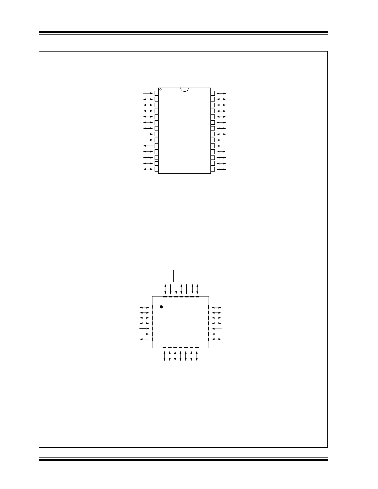
Pin Diagrams
28-Pin SPDIP, SOIC
28-Pin QFN
MCLR/VPP/RE3
RA0/AN0
RA1/AN1
RA2/AN2/V
RA3/AN3/V
RA4/T0CKI/RCV
RA5/AN4/HLVDIN
OSC2/CLKO/RA6
RC0/T1OSO/T1CKI
RC1/T1OSI/UOE
REF-
REF+
V
OSC1/CLKI
RC2/CCP1
USB
V
1
2
3
4
5
6
7
SS
8
9
10
11
12
13
14
PIC18F2450
/VPP/RE3
28
27
26
25
24
23
22
21
20
19
18
17
16
15
RB7/KBI3/PGD
RB6/KBI2/PGC
RB5/KBI1/PGM
RB4/AN11/KBI0
RB3/AN9/VPO
RB2/AN8/INT2/VMO
RB1/AN10/INT1
RB0/AN12/INT0
V
DD
VSS
RC7/RX/DT
RC6/TX/CK
RC5/D+/VP
RC4/D-/VM
RA2/AN2/VREF-
RA3/AN3/V
RA4/T0CKI/RCV
RA5/AN4/HLVDIN
OSC2/CLKO/RA6
REF+
V
OSC1/CLKI
SS
Note: Pinouts are subject to change.
RA0/AN0
RA1/AN1
1
2
3
PIC18F2450
4
5
6
7
10 11
8
9
RC1/T1OSI/UOE
RC0/T1OSO/T1CKI
MCLR
RB7/KBI3/PGD
12 13 14
USB
V
RC2/CCP1
RB6/KBI2/PGC
RC4/D-/VM
RB5/KBI1/PGM
RB4/AN11/KBI0
22
232425262728
RC5/D+/VP
21
20
19
18
17
16
15
RC6/TX/CK
RB3/AN9/VPO
RB2/AN8/INT2/VMO
RB1/AN10/INT1
RB0/AN12/INT0
V
DD
VSS
RC7/RX/DT
DS39760C-page 2 Preliminary © 2007 Microchip Technology Inc.
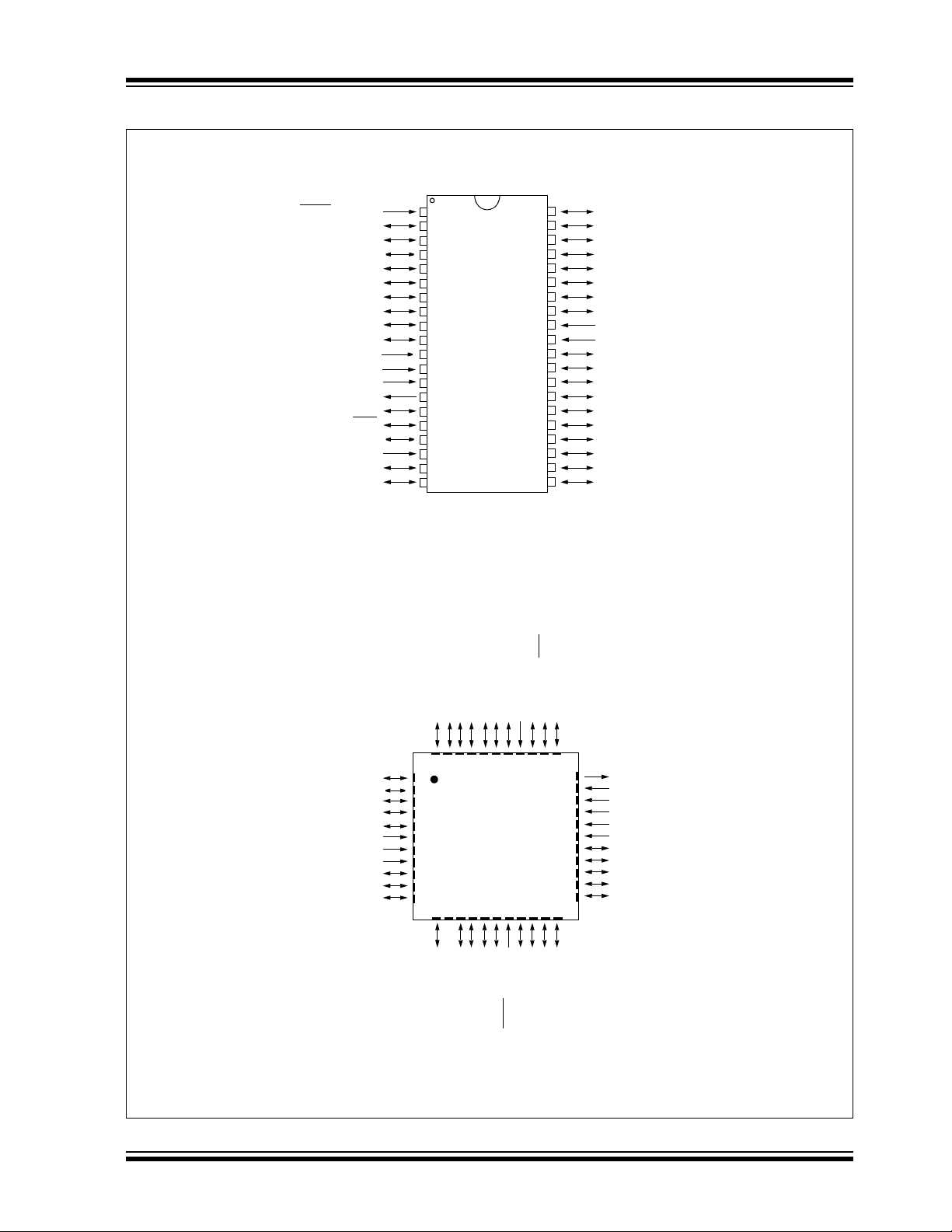
Pin Diagrams (Continued)
40-Pin PDIP
PIC18F2450/4450
44-Pin QFN
MCLR/VPP/RE3
RA0/AN0
RA1/AN1
RA2/AN2/V
RA3/AN3/V
RA4/T0CKI/RCV
RA5/AN4/HLVDIN
OSC2/CLKO/RA6
RC0/T1OSO/T1CKI
RC1/T1OSI/UOE
REF-
REF+
RE0/AN5
RE1/AN6
RE2/AN7
V
VSS
OSC1/CLKI
RC2/CCP1
V
USB
RD0
RD1
DD
1
2
3
4
5
6
7
8
9
10
11
12
13
14
15
16
17
18
19
20
PIC18F4450
40
39
38
37
36
35
34
33
32
31
30
29
28
27
26
25
24
23
22
21
RB7/KBI3/PGD
RB6/KBI2/PGC
RB5/KBI1/PGM
RB4/AN11/KBI0
RB3/AN9/VPO
RB2/AN8/INT2/VMO
RB1/AN10/INT1
RB0/AN12/INT0
V
DD
VSS
RD7
RD6
RD5
RD4
RC7/RX/DT
RC6/TX/CK
RC5/D+/VP
RC4/D-/VM
RD3
RD2
RC7/RX/DT
RD4
RD5
RD6
RD7
SS
V
AVDD
RB0/AN12/INT0
RB1/AN10/INT1
RB2/AN8/INT2/VMO
VDD
Note: Pinouts are subject to change.
1
2
3
4
5
6
7
8
9
10
11
RC6/TX/CK
44
121314
RB3/AN9/VPO
RC5/D+/VP
RC4/D-/VM
RD3
RD2
RD1
RD0
414039
42
43
38
PIC18F4450
1819202122
15
16
17
NC
/VPP/RE3
RB7/KBI3/PGD
RB6/KBI2/PGC
RB5/KBI1/PGM
RB4/AN11/KBI0
MCLR
USB
V
37
RA0/AN0
RC2/CCP1
RC1/T1OSI/UOE
363435
REF-
RA1/AN1
RA2/AN2/V
RC0/T1OSO/T1CKI
33
32
31
30
29
28
27
26
25
24
23
REF+
RA3/AN3/V
OSC2/CLKO/RA6
OSC1/CLKI
V
SS
AV SS
VDD
AV DD
RE2/AN7
RE1/AN6
RE0/AN5
RA5/AN4/HLVDIN
RA4/T0CKI/RCV
© 2007 Microchip Technology Inc. Preliminary DS39760C-page 3
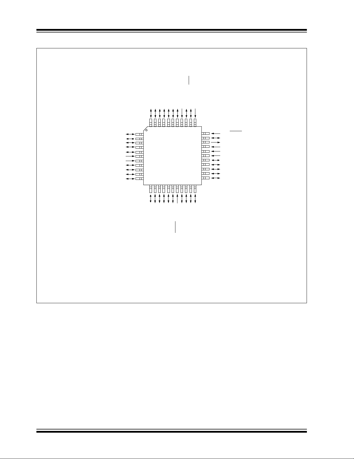
PIC18F2450/4450
Pin Diagrams (Continued)
44-Pin TQFP
RC7/RX/DT
RD4
RD5
RD6
RD7
VSS
RB0/AN12/INT0
RB1/AN10/INT1
RB2/AN8/INT2/VMO
RB3/AN9/VPO
VDD
1
2
3
4
5
6
7
8
9
10
11
RC6/TX/CK
44
121314
RD0
RD1
RD2
RD3
RC4/D-/VM
RC5/D+/VP
414039
42
43
38
PIC18F4450
1819202122
15
16
17
USB
V
37
RC1/T1OSI/UOE
RC2/CCP1
363435
NC/ICPORTS*
33
32
31
30
29
28
27
26
25
24
23
NC/ICRST*/ICVPP*
RC0/T1OSO/T1CKI
OSC2/CLKO/RA6
OSC1/CLKI
V
SS
VDD
RE2/AN7
RE1/AN6
RE0/AN5
RA5/AN4/HLVDIN
RA4/T0CKI/RCV
/VPP/RE3
RB6/KBI2/PGC
RB7/KBI3/PGD
RB5/KBI1/PGM
RB4/AN11/KBI0
NC/ICDT*/ICPGD*
NC/ICCK*/ICPGC*
MCLR
Note: Pinouts are subject to change.
* Assignment of this feature is dependent on device configuration.
RA0/AN0
RA1/AN1
REF-
RA2/AN2/V
RA3/AN3/VREF+
DS39760C-page 4 Preliminary © 2007 Microchip Technology Inc.

PIC18F2450/4450
Table of Contents
1.0 Device Overview .......................................................................................................................................................................... 7
2.0 Oscillator Configurations ............................................................................................................................................................ 23
3.0 Power-Managed Modes ............................................................................................................................................................. 33
4.0 Reset.......................................................................................................................................................................................... 41
5.0 Memory Organization ................................................................................................................................................................. 53
6.0 Flash Program Memory.............................................................................................................................................................. 73
7.0 8 x 8 Hardware Multiplier............................................................................................................................................................ 83
8.0 Interrupts.................................................................................................................................................................................... 85
9.0 I/O Ports ..................................................................................................................................................................................... 99
10.0 Timer0 Module ......................................................................................................................................................................... 111
11.0 Timer1 Module ......................................................................................................................................................................... 115
12.0 Timer2 Module ......................................................................................................................................................................... 121
13.0 Capture/Compare/PWM (CCP) Module ................................................................................................................................... 123
14.0 Universal Serial Bus (USB) ...................................................................................................................................................... 129
15.0 Enhanced Universal Synchronous Receiver Transmitter (EUSART) ....................................................................................... 153
16.0 10-Bit Analog-to-Digital Converter (A/D) Module ..................................................................................................................... 175
17.0 High/Low-Voltage Detect (HLVD)............................................................................................................................................. 185
18.0 Special Features of the CPU.................................................................................................................................................... 191
19.0 Instruction Set Summary.......................................................................................................................................................... 213
20.0 Development Support............................................................................................................................................................... 263
21.0 Electrical Characteristics.......................................................................................................................................................... 267
22.0 DC and AC Characteristics Graphs and Tables....................................................................................................................... 295
23.0 Packaging Information.............................................................................................................................................................. 297
Appendix A: Revision History............................................................................................................................................................. 305
Appendix B: Device Differences ........................................................................................................................................................ 305
Appendix C: Conversion Considerations ........................................................................................................................................... 306
Appendix D: Migration From Baseline to Enhanced Devices ............................................................................................................ 306
Appendix E: Migration From Mid-Range to Enhanced Devices ......................................................................................................... 307
Appendix F: Migration From High-End to Enhanced Devices............................................................................................................ 307
Index ................................................................................................................................................................................................. 309
The Microchip Web Site..................................................................................................................................................................... 317
Customer Change Notification Service .............................................................................................................................................. 317
Customer Support .............................................................................................................................................................................. 317
Reader Response .............................................................................................................................................................................. 318
PIC18F2450/4450 Product Identification System .............................................................................................................................. 319
© 2007 Microchip Technology Inc. Preliminary DS39760C-page 5

PIC18F2450/4450
TO OUR VALUED CUSTOMERS
It is our intention to provide our valued customers with the best documentation possible to ensure successful use of your Microchip
products. To this end, we will continue to improve our publications to better suit your needs. Our publications will be refined and
enhanced as new volumes and updates are introduced.
If you have any questions or comments regarding this publication, please contact the Marketing Communications Department via
E-mail at docerrors@microchip.com or fax the Reader Response Form in the back of this data sheet to (480) 792-4150. We
welcome your feedback.
Most Current Data Sheet
To obtain the most up-to-date version of this data sheet, please register at our Worldwide Web site at:
http://www.microchip.com
You can determine the version of a data sheet by examining its literature number found on the bottom outside corner of any page.
The last character of the literature number is the version number, (e.g., DS30000A is version A of document DS30000).
Errata
An errata sheet, describing minor operational differences from the data sheet and recommended workarounds, may exist for current
devices. As device/documentation issues become known to us, we will publish an errata sheet. The errata will specify the revision
of silicon and revision of document to which it applies.
To determine if an errata sheet exists for a particular device, please check with one of the following:
• Microchip’s Worldwide Web site; http://www.microchip.com
• Your local Microchip sales office (see last page)
When contacting a sales office, please specify which device, revision of silicon and data sheet (include literature number) you are
using.
Customer Notification System
Register on our web site at www.microchip.com to receive the most current information on all of our products.
DS39760C-page 6 Preliminary © 2007 Microchip Technology Inc.

PIC18F2450/4450
1.0 DEVICE OVERVIEW
This document contains device-specific information for
the following devices:
• PIC18F2450 • PIC18F4450
This family of devices offers the advantages of all
PIC18 microcontrollers – namely, high computational
performance at an economical price – with the addition of high-endurance, Enhanced Flash program
memory. In addition to these features, the
PIC18F2450/4450 family introduces design enhancements that make these microcontrollers a logical
choice for many high-performance, power sensitive
applications.
1.1 New Core Features
1.1.1 nanoWatt TECHNOLOGY
All of the devices in the PIC18F2450/4450 family
incorporate a range of features that can significantly
reduce power consumption during operation. Key
items include:
• Alternate Run Modes: By clocking the controller
from the Timer1 source or the internal RC
oscillator, power consumption during code
execution can be reduced by as much as 90%.
• Multiple Idle Modes: The controller can also run
with its CPU core disabled but the peripherals still
active. In these states, power consumption can be
reduced even further, to as little as 4% of normal
operation requirements.
• On-the-Fly Mode Switching: The power-
managed modes are invoked by user code during
operation, allowing the user to incorporate
power-saving ideas into their application’s
software design.
• Low Consumption in Key Modules: The
power requirements for both Timer1 and the
Watchdog Timer are minimized. See
Section 21.0 “Electrical Characteristics” for
values.
1.1.3 MULTIPLE OSCILLATOR OPTIONS
AND FEATURES
All of the devices in the PIC18F2450/4450 family offer
twelve different oscillator options, allowing users a wide
range of choices in developing application hardware.
These include:
• Four Crystal modes using crystals or ceramic
resonators.
• Four External Clock modes, offering the option of
using two pins (oscillator input and a divide-by-4
clock output) or one pin (oscillator input, with the
second pin reassigned as general I/O).
• An INTRC source (approximately 31 kHz, stable
over temperature and V
oscillator pin for use as an additional general
purpose I/O.
• A Phase Lock Loop (PLL) frequency multiplier,
available to both the High-Speed Crystal and
External Oscillator modes, which allows a wide
range of clock speeds from 4 MHz to 48 MHz.
• Asynchronous dual clock operation, allowing the
USB module to run from a high-frequency
oscillator while the rest of the microcontroller is
clocked from an internal low-power oscillator.
The internal oscillator provides a stable reference
source that gives the family additional features for
robust operation:
• Fail-Safe Clock Monitor: This option constantly
monitors the main clock source against a
reference signal provided by the internal
oscillator. If a clock failure occurs, the controller is
switched to the internal oscillator, allowing for
continued low-speed operation or a safe
application shutdown.
• Two-Speed Start-up: This option allows the
internal oscillator to serve as the clock source
from Power-on Reset, or wake-up from Sleep
mode, until the primary clock source is available.
DD). This option frees an
1.1.2 UNIVERSAL SERIAL BUS (USB)
Devices in the PIC18F2450/4450 family incorporate a
fully featured Universal Serial Bus communications
module that is compliant with the USB Specification
Revision 2.0. The module supports both low-speed and
full-speed communication for all supported data
transfer types. It also incorporates its own on-chip
transceiver and 3.3V regulator and supports the use of
external transceivers and voltage regulators.
© 2007 Microchip Technology Inc. Preliminary DS39760C-page 7

PIC18F2450/4450
1.2 Other Special Features
• Memory Endurance: The Enhanced Flash cells
for program memory are rated to last for many
thousands of erase/write cycles – up to 100,000.
• Self-Programmability: These devices can write
to their own program memory spaces under
internal software control. By using a bootloader
routine, located in the protected Boot Block at the
top of program memory, it becomes possible to
create an application that can update itself in the
field.
• Extended Instruction Set: The PIC18F2450/
4450 family introduces an optional extension to
the PIC18 instruction set, which adds 8 new
instructions and an Indexed Literal Offset
Addressing mode. This extension, enabled as a
device configuration option, has been specifically
designed to optimize re-entrant application code
originally developed in high-level languages such
as C.
• Enhanced Addressable USART: This serial
communication module is capable of standard
RS-232 operation and provides support for the LIN
bus protocol. Other enhancements include
Automatic Baud Rate Detection and a 16-bit Baud
Rate Generator for improved resolution.
• 10-Bit A/D Converter: This module incorporates
programmable acquisition time, allowing for a
channel to be selected and a conversion to be
initiated, without waiting for a sampling period and
thus, reducing code overhead.
• Dedicated ICD/ICSP Port: These devices
introduce the use of debugger and programming
pins that are not multiplexed with other microcontroller features. Offered as an option in select
packages, this feature allows users to develop I/O
intensive applications while retaining the ability to
program and debug in the circuit.
1.3 Details on Individual Family Members
Devices in the PIC18F2450/4450 family are available
in 28-pin and 40/44-pin packages. Block diagrams for
the two groups are shown in Figure 1-1 and Figure 1-2.
The devices are differentiated from each other in the
following two ways:
1. A/D channels (10 for 28-pin devices, 13 for
40/44-pin devices).
2. I/O ports (3 bidirectional ports and 1 input only
port on 28-pin devices, 5 bidirectional ports on
40/44-pin devices).
All other features for devices in this family are identical.
These are summarized in Table 1-1.
The pinouts for all devices are listed in Table 1-2 and
Table 1-3.
Like all Microchip PIC18 devices, members of the
PIC18F2450/4450 family are available as both standard
and low-voltage devices. Standard devices with
Enhanced Flash memory, designated with an “F” in the
part number (such as PIC18F2450), accommodate an
operating V
designated by “LF” (such as PIC18LF2450), function
over an extended VDD range of 2.0V to 5.5V.
DD range of 4.2V to 5.5V. Low-voltage parts,
DS39760C-page 8 Preliminary © 2007 Microchip Technology Inc.

PIC18F2450/4450
TABLE 1-1: DEVICE FEATURES
Features PIC18F2450 PIC18F4450
Operating Frequency DC – 48 MHz DC – 48 MHz
Program Memory (Bytes) 16384 16384
Program Memory (Instructions) 8192 8192
Data Memory (Bytes) 768 768
Interrupt Sources 13 13
I/O Ports Ports A, B, C, (E) Ports A, B, C, D, E
Timers 3 3
Capture/Compare/PWM Modules 1 1
Enhanced USART 1 1
Universal Serial Bus (USB) Module 1 1
10-Bit Analog-to-Digital Module 10 Input Channels 13 Input Channels
Resets (and Delays) POR, BOR,
RESET Instruction,
Stack Ful l,
Stack Underflow (PWRT, OST),
(optional),
MCLR
WDT
Programmable Low-Voltage Detect Yes Yes
Programmable Brown-out Reset Yes Yes
Instruction Set 75 Instructions;
83 with Extended Instruction Set
enabled
Packages 28-Pin SPDIP
28-Pin SOIC
28-Pin QFN
Stack Underflow (PWRT, OST),
83 with Extended Instruction Set
POR, BOR,
RESET Instruction,
Stack Full,
MCLR (optional),
WDT
75 Instructions;
enabled
40-Pin PDIP
44-Pin QFN
44-Pin TQFP
© 2007 Microchip Technology Inc. Preliminary DS39760C-page 9
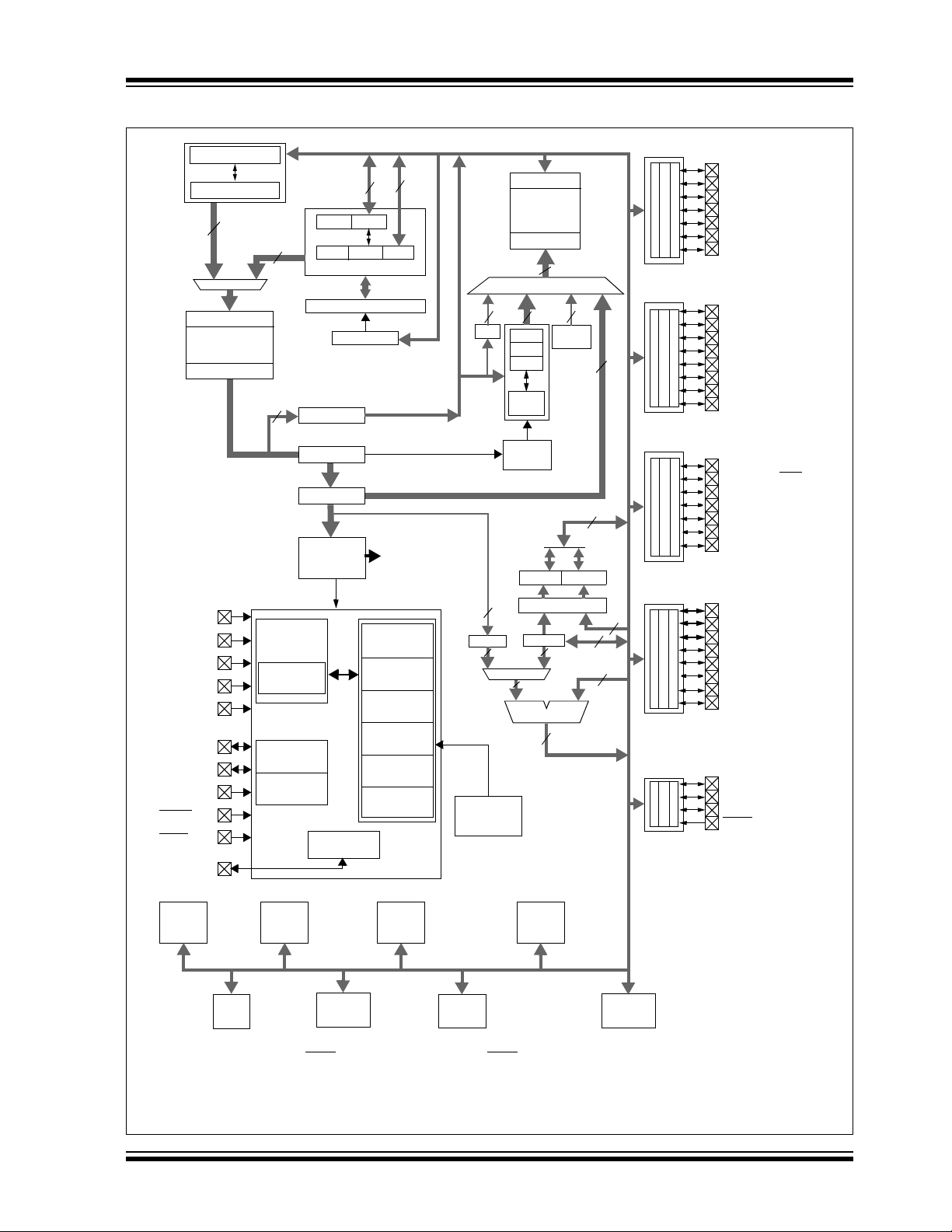
PIC18F2450/4450
FIGURE 1-1: PIC18F2450 (28-PIN) BLOCK DIAGRAM
Table Pointer<21>
inc/dec logic
21
Address Latch
Program Memory
(24/32 Kbytes)
Data Latch
Instruction Bus <16>
(2)
OSC1
(2)
OSC2
T1OSI
T1OSO
(1)
MCLR
VDD,
SS
V
USB
V
20
8
Table Latch
ROM Latch
Instruction
Internal
Oscillator
Block
INTRC
Oscillator
Single-Supply
Programming
In-Circuit
Debugger
PCLATH
PCLATU
PCH PCL
PCU
Program Counter
31 Level Stack
STKPTR
IR
Decode &
Control
Start-up Timer
Clock Monitor
USB Voltage
Regulator
Data Bus<8>
8
8
State Machine
Control Signals
Power-up
Timer
Oscillator
Power-on
Reset
Watchdog
Timer
Brown-out
Reset
Fail-Safe
Data Latch
Data Memory
(2 Kbytes)
Address Latch
12
Data Address<12>
44
12
FSR0
FSR1
FSR2
logic
8 x 8 Multiply
W
8
ALU<8>
Access
Bank
PRODLPRODH
8
8
12
8
BSR
3
BITOP
Band Gap
Reference
8
inc/dec
Address
Decode
PORTA
RA0/AN0
RA1/AN1
RA2/AN2/VREFRA3/AN3/VREF+
RA4/T0CKI/RCV
RA5/AN4/HLVDIN
OSC2/CLKO/RA6
PORTB
RB0/AN12/INT0
RB1/AN10/INT1
RB2/AN8/INT2/VMO
RB3/AN9/VPO
RB4/AN11/KBI0
RB5/KBI1/PGM
RB6/KBI2/PGC
RB7/KBI3/PGD
PORTC
8
8
8
PORTE
RC0/T1OSO/T1CKI
RC1/T1OSI/UOE
RC2/CCP1
RC4/D-/VM
RC5/D+/VP
RC6/TX/CK
RC7/RX/DT
MCLR/VPP/RE3
(1)
BOR
HLVD
CCP1
Note 1: RE3 is multiplexed with MCLR and is only available when the MCLR Resets are disabled.
2: OSC1/CLKI and OSC2/CLKO are only available in select oscillator modes and when these pins are not being used as digital I/O. Refer
to Section 2.0 “Oscillator Configurations” for additional information.
EUSART
Timer2Timer1Timer0
ADC
10-Bit
USB
DS39760C-page 10 Preliminary © 2007 Microchip Technology Inc.
PIC18F2450/4450
FIGURE 1-2: PIC18F4450 (40/44-PIN) BLOCK DIAGRAM
Table Pointer<21>
inc/dec logic
21
Address Latch
Program Memory
(24/32 Kbytes)
Data Latch
20
8
PCLATH
PCLATU
PCU
Program Counter
31 Level Stack
STKPTR
Table Latch
Data Bus<8>
8
PCH PCL
8
Data Latch
Data Memory
(2 Kbytes)
Address Latch
12
Data Address<12>
BSR
FSR0
FSR1
Access
Bank
12
44
FSR2
inc/dec
logic
PORTA
RA0/AN0
RA1/AN1
RA2/AN2/VREFRA3/AN3/VREF+
RA4/T0CKI/RCV
RA5/AN4/HLVDIN
OSC2/CLKO/RA6
PORTB
RB0/AN12/INT0
RB1/AN10/INT1
RB2/AN8/INT2/VMO
RB3/AN9/VPO
12
RB4/AN11/KBI0
RB5/KBI1/PGM
RB6/KBI2/PGC
RB7/KBI3/PGD
Instruction Bus <16>
VDD,
VSS
(2)
OSC1
(2)
OSC2
T1OSI
T1OSO
(3)
ICPGC
(3)
ICPGD
(3)
ICPORTS
(3)
ICRST
(1)
MCLR
USB
V
ROM Latch
IR
Instruction
Decode &
Internal
Oscillator
Block
INTRC
Oscillator
Single-Supply
Programming
In-Circuit
Debugger
Control
Start-up Timer
USB Voltage
Regulator
State Machine
Control Signals
Power-up
Timer
Oscillator
Power-on
Reset
Watchdog
Timer
Brown-out
Reset
Fail-Safe
Clock Monitor
3
BITOP
8
Band Gap
Reference
Address
Decode
8 x 8 Multiply
8
ALU<8>
PORTC
RC0/T1OSO/T1CKI
RC1/T1OSI/UOE
RC2/CCP1
RC4/D-/VM
RC5/D+/VP
8
RC6/TX/CK
RC7/RX/DT
PRODLPRODH
PORTD
8
W
8
8
8
RD0
RD1
RD2
RD3
RD4
RD5
RD6
RD7
8
PORTE
RE0/AN5
RE1/AN6
RE2/AN7
MCLR/VPP/RE3
(1)
BOR
HLVD
CCP1
Note 1: RE3 is multiplexed with MCLR
EUSART
ADC
10-Bit
and is only available when the MCLR Resets are disabled.
Timer2Timer1Timer0
USB
2: OSC1/CLKI and OSC2/CLKO are only available in select oscillator modes and when these pins are not being used as digital I/O. Refer
to Section 2.0 “Oscillator Configurations” for additional information.
3: These pins are only available on 44-pin TQFP under certain conditions. Refer to Section 18.9 “Special ICPORT Features (Designated
Packages Only)” for additional information.
© 2007 Microchip Technology Inc. Preliminary DS39760C-page 11
PIC18F2450/4450
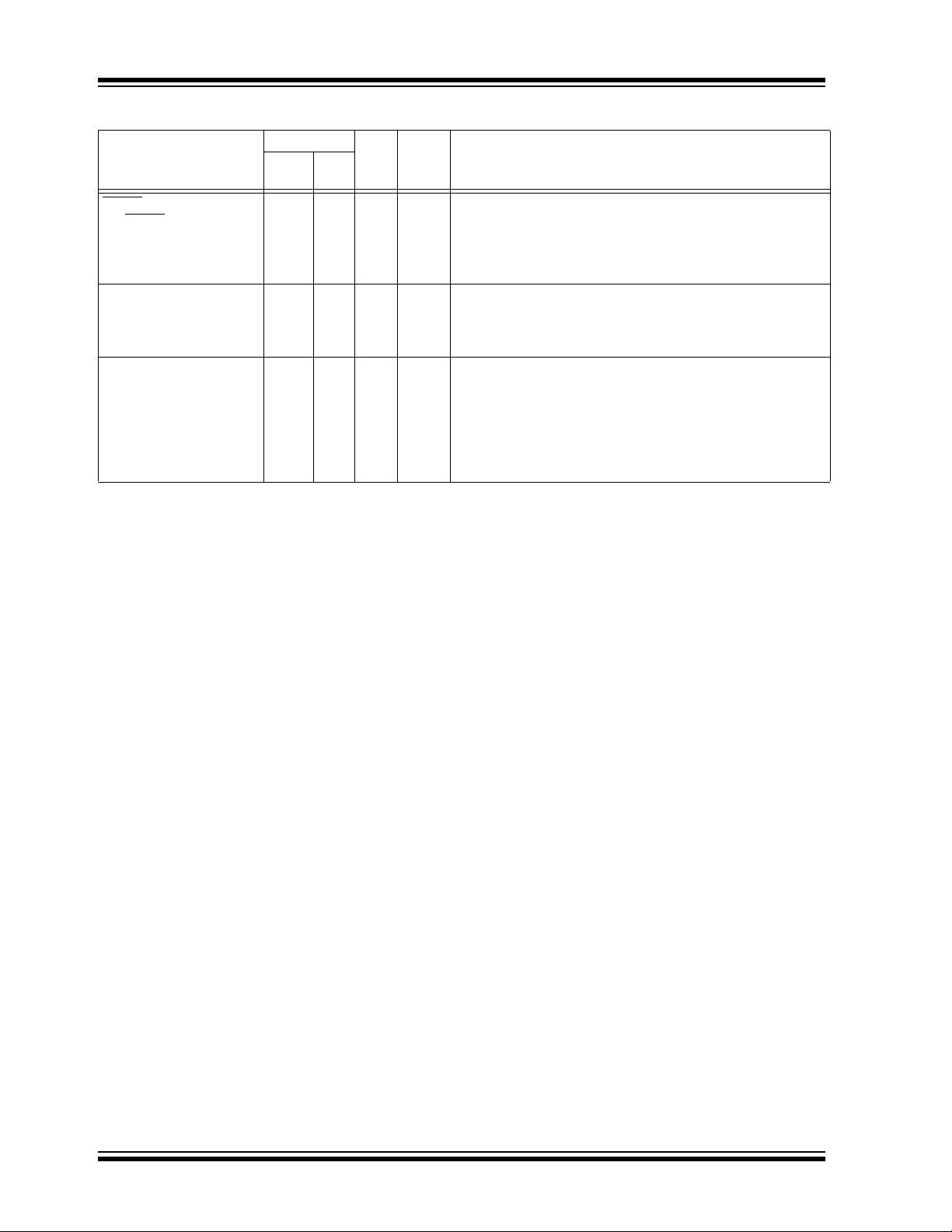
TABLE 1-2: PIC18F2450 PINOUT I/O DESCRIPTIONS
Pin Number
Pin Name
/VPP/RE3
MCLR
MCLR
VPP
RE3
OSC1/CLKI
OSC1
CLKI
OSC2/CLKO/RA6
OSC2
CLKO
RA6
Legend: TTL = TTL compatible input CMOS = CMOS compatible input or output
ST = Schmitt Trigger input with CMOS levels I = Input
O = Output P = Power
SPDIP,
SOIC
126
96
10 7
QFN
Pin
Buffer
Typ e
I
P
I
IIAnalog
Analog
O
O
I/O
Type
ST
ST
—
—
TTL
Description
Master Clear (input) or programming voltage (input).
Master Clear (Reset) input. This pin is an active-low
Reset to the device.
Programming voltage input.
Digital input.
Oscillator crystal or external clock input.
Oscillator crystal input or external clock source input.
External clock source input. Always associated with pin
function OSC1. (See OSC2/CLKO pin.)
Oscillator crystal or clock output.
Oscillator crystal output. Connects to crystal or resonator
in Crystal Oscillator mode.
In select modes, OSC2 pin outputs CLKO which has
1/4 the frequency of OSC1 and denotes the instruction
cycle rate.
General purpose I/O pin.
DS39760C-page 12 Preliminary © 2007 Microchip Technology Inc.

PIC18F2450/4450
TABLE 1-2: PIC18F2450 PINOUT I/O DESCRIPTIONS (CONTINUED)
Pin Number
Pin Name
RA0/AN0
RA0
AN0
RA1/AN1
RA1
AN1
RA2/AN2/VREF-
RA2
AN2
REF-
V
RA3/AN3/V
RA3
AN3
V
RA4/T0CKI/RCV
RA4
T0CKI
RCV
RA5/AN4/HLVDIN
RA5
AN4
HLVDIN
RA6 — — — — See the OSC2/CLKO/RA6 pin.
Legend: TTL = TTL compatible input CMOS = CMOS compatible input or output
REF+
REF+
ST = Schmitt Trigger input with CMOS levels I = Input
O = Output P = Power
SPDIP,
SOIC
QFN
227
328
41
52
63
74
Pin
Buffer
Typ e
Type
I/OITTL
Analog
I/OITTL
Analog
I/O
TTL
I
Analog
I
Analog
I/O
TTL
I
Analog
I
Analog
I/O
I
I
TTL
I/O
TTL
I
Analog
I
Analog
PORTA is a bidirectional I/O port.
Digital I/O.
Analog input 0.
Digital I/O.
Analog input 1.
Digital I/O.
Analog input 2.
A/D reference voltage (low) input.
Digital I/O.
Analog input 3.
A/D reference voltage (high) input.
ST
ST
Digital I/O.
Timer0 external clock input.
External USB transceiver RCV input.
Digital I/O.
Analog input 4.
High/Low-Voltage Detect input.
Description
© 2007 Microchip Technology Inc. Preliminary DS39760C-page 13

PIC18F2450/4450
TABLE 1-2: PIC18F2450 PINOUT I/O DESCRIPTIONS (CONTINUED)
Pin Number
Pin Name
RB0/AN12/INT0
RB0
AN12
INT0
RB1/AN10/INT1
RB1
AN10
INT1
RB2/AN8/INT2/VMO
RB2
AN8
INT2
VMO
RB3/AN9/VPO
RB3
AN9
VPO
RB4/AN11/KBI0
RB4
AN11
KBI0
RB5/KBI1/PGM
RB5
KBI1
PGM
RB6/KBI2/PGC
RB6
KBI2
PGC
RB7/KBI3/PGD
RB7
KBI3
PGD
Legend: TTL = TTL compatible input CMOS = CMOS compatible input or output
ST = Schmitt Trigger input with CMOS levels I = Input
O = Output P = Power
SPDIP,
SOIC
21 18
22 19
23 20
24 21
25 22
26 23
27 24
28 25
QFN
Pin
Typ e
I/O
I
I
I/O
I
I
I/O
I
I
O
I/O
I
O
I/O
I
I
I/O
I
I/O
I/O
I
I/O
I/O
I
I/O
Buffer
Type
TTL
Analog
ST
TTL
Analog
ST
TTL
Analog
ST
—
TTL
Analog
—
TTL
Analog
TTL
TTL
TTL
ST
TTL
TTL
ST
TTL
TTL
ST
Description
PORTB is a bidirectional I/O port. PORTB can be software
programmed for internal weak pull-ups on all inputs.
Digital I/O.
Analog input 12.
External interrupt 0.
Digital I/O.
Analog input 10.
External interrupt 1.
Digital I/O.
Analog input 8.
External interrupt 2.
External USB transceiver VMO output.
Digital I/O.
Analog input 9.
External USB transceiver VPO output.
Digital I/O.
Analog input 11.
Interrupt-on-change pin.
Digital I/O.
Interrupt-on-change pin.
Low-Voltage ICSP™ Programming enable pin.
Digital I/O.
Interrupt-on-change pin.
In-Circuit Debugger and ICSP programming clock pin.
Digital I/O.
Interrupt-on-change pin.
In-Circuit Debugger and ICSP programming data pin.
DS39760C-page 14 Preliminary © 2007 Microchip Technology Inc.

PIC18F2450/4450
TABLE 1-2: PIC18F2450 PINOUT I/O DESCRIPTIONS (CONTINUED)
Pin Number
Pin Name
RC0/T1OSO/T1CKI
RC0
T1OSO
T1CKI
RC1/T1OSI/UOE
RC1
T1OSI
UOE
RC2/CCP1
RC2
CCP1
RC4/D-/VM
RC4
DVM
RC5/D+/VP
RC5
D+
VP
RC6/TX/CK
RC6
TX
CK
RC7/RX/DT
RC7
RX
DT
RE3 — — — — See MCLR
VUSB 14 11 O — Internal USB 3.3V voltage regulator.
VSS 8, 19 5, 16 P — Ground reference for logic and I/O pins.
DD 20 17 P — Positive supply for logic and I/O pins.
V
Legend: TTL = TTL compatible input CMOS = CMOS compatible input or output
ST = Schmitt Trigger input with CMOS levels I = Input
O = Output P = Power
SPDIP,
SOIC
11 8
12 9
13 10
15 12
16 13
17 14
18 15
QFN
Pin
Buffer
Typ e
I/O
O
I
I/O
I
CMOS
—
I/O
I/OSTST
I
I/O
I
I
I/O
O
I/O
O
I/O
I/O
I
I/O
Type
ST
—
ST
ST
—
TTL
—
TTL
TTL
—
TTL
ST
—
ST
ST
ST
ST
Description
PORTC is a bidirectional I/O port.
Digital I/O.
Timer1 oscillator output.
Timer1external clock input.
Digital I/O.
Timer1 oscillator input.
External USB transceiver OE
Digital I/O.
Capture 1 input/Compare 1 output/PWM 1 output.
Digital input.
USB differential minus line (input/output).
External USB transceiver VM input.
Digital input.
USB differential plus line (input/output).
External USB transceiver VP input.
Digital I/O.
EUSART asynchronous transmit.
EUSART synchronous clock (see RX/DT).
Digital I/O.
EUSART asynchronous receive.
EUSART synchronous data (see TX/CK).
/VPP/RE3 pin.
output.
© 2007 Microchip Technology Inc. Preliminary DS39760C-page 15

PIC18F2450/4450
TABLE 1-3: PIC18F4450 PINOUT I/O DESCRIPTIONS
Pin Name
/VPP/RE3
MCLR
MCLR
VPP
RE3
OSC1/CLKI
OSC1
CLKI
OSC2/CLKO/RA6
OSC2
CLKO
RA6
Legend: TTL = TTL compatible input CMOS = CMOS compatible input or output
ST = Schmitt Trigger input with CMOS levels I = Input
O = Output P = Power
Note 1: These pins are No Connect unless the ICPRT Configuration bit is set. For NC/ICPORTS, the pin is No
Connect unless ICPRT is set and the DEBUG
Pin Number
PDIP QFN TQFP
11818
13 32 30
14 33 31
Pin
Buffer
Typ e
I
P
I
IIAnalog
Analog
O
O
I/O
Type
Master Clear (input) or programming voltage (input).
ST
ST
—
—
TTL
Configuration bit is cleared.
Master Clear (Reset) input. This pin is an
active-low Reset to the device.
Programming voltage input.
Digital input.
Oscillator crystal or external clock input.
Oscillator crystal input or external clock source input.
External clock source input. Always associated with
pin function OSC1. (See OSC2/CLKO pin.)
Oscillator crystal or clock output.
Oscillator crystal output. Connects to crystal or
resonator in Crystal Oscillator mode.
In select modes, OSC2 pin outputs CLKO which has
1/4 the frequency of OSC1 and denotes the instruction
cycle rate.
General purpose I/O pin.
Description
DS39760C-page 16 Preliminary © 2007 Microchip Technology Inc.

PIC18F2450/4450
TABLE 1-3: PIC18F4450 PINOUT I/O DESCRIPTIONS (CONTINUED)
Pin Name
RA0/AN0
RA0
AN0
RA1/AN1
RA1
AN1
RA2/AN2/VREF-
RA2
AN2
REF-
V
RA3/AN3/VREF+
RA3
AN3
REF+
V
RA4/T0CKI/RCV
RA4
T0CKI
RCV
RA5/AN4/HLVDIN
RA5
AN4
HLVDIN
RA6 — — — — — See the OSC2/CLKO/RA6 pin.
Legend: TTL = TTL compatible input CMOS = CMOS compatible input or output
ST = Schmitt Trigger input with CMOS levels I = Input
O = Output P = Power
Note 1: These pins are No Connect unless the ICPRT Configuration bit is set. For NC/ICPORTS, the pin is No
Connect unless ICPRT is set and the DEBUG
Pin Number
PDIP QFN TQFP
21919
32020
42121
52222
62323
72424
Pin
Buffer
Typ e
Type
I/OITTL
Analog
I/OITTL
Analog
I/O
I
Analog
I
Analog
I/O
I
Analog
I
Analog
I/O
I
I
I/O
I
Analog
I
Analog
PORTA is a bidirectional I/O port.
Digital I/O.
Analog input 0.
Digital I/O.
Analog input 1.
TTL
TTL
ST
ST
TTL
TTL
Configuration bit is cleared.
Digital I/O.
Analog input 2.
A/D reference voltage (low) input.
Digital I/O.
Analog input 3.
A/D reference voltage (high) input.
Digital I/O.
Timer0 external clock input.
External USB transceiver RCV input.
Digital I/O.
Analog input 4.
High/Low-Voltage Detect input.
Description
© 2007 Microchip Technology Inc. Preliminary DS39760C-page 17

PIC18F2450/4450
TABLE 1-3: PIC18F4450 PINOUT I/O DESCRIPTIONS (CONTINUED)
Pin Name
RB0/AN12/INT0
RB0
AN12
INT0
RB1/AN10/INT1
RB1
AN10
INT1
RB2/AN8/INT2/VMO
RB2
AN8
INT2
VMO
RB3/AN9/VPO
RB3
AN9
VPO
RB4/AN11/KBI0
RB4
AN11
KBI0
RB5/KBI1/PGM
RB5
KBI1
PGM
RB6/KBI2/PGC
RB6
KBI2
PGC
RB7/KBI3/PGD
RB7
KBI3
PGD
Legend: TTL = TTL compatible input CMOS = CMOS compatible input or output
ST = Schmitt Trigger input with CMOS levels I = Input
O = Output P = Power
Note 1: These pins are No Connect unless the ICPRT Configuration bit is set. For NC/ICPORTS, the pin is No
Connect unless ICPRT is set and the DEBUG
Pin Number
PDIP QFN TQFP
33 9 8
34 10 9
35 11 10
36 12 11
37 14 14
38 15 15
39 16 16
40 17 17
Pin
Typ e
I/O
I
I
I/O
I
I
I/O
I
I
O
I/O
I
O
I/O
I
I
I/O
I
I/O
I/O
I
I/O
I/O
I
I/O
Buffer
Type
PORTB is a bidirectional I/O port. PORTB can be
software programmed for internal weak pull-ups on all
inputs.
TTL
Analog
ST
TTL
Analog
ST
TTL
Analog
ST
—
TTL
Analog
—
TTL
Analog
TTL
TTL
TTL
ST
TTL
TTL
ST
TTL
TTL
ST
Configuration bit is cleared.
Digital I/O.
Analog input 12.
External interrupt 0.
Digital I/O.
Analog input 10.
External interrupt 1.
Digital I/O.
Analog input 8.
External interrupt 2.
External USB transceiver VMO output.
Digital I/O.
Analog input 9.
External USB transceiver VPO output.
Digital I/O.
Analog input 11.
Interrupt-on-change pin.
Digital I/O.
Interrupt-on-change pin.
Low-Voltage ICSP™ Programming enable pin.
Digital I/O.
Interrupt-on-change pin.
In-Circuit Debugger and ICSP programming clock pin.
Digital I/O.
Interrupt-on-change pin.
In-Circuit Debugger and ICSP programming data pin.
Description
DS39760C-page 18 Preliminary © 2007 Microchip Technology Inc.

PIC18F2450/4450
TABLE 1-3: PIC18F4450 PINOUT I/O DESCRIPTIONS (CONTINUED)
Pin Name
RC0/T1OSO/T1CKI
RC0
T1OSO
T1CKI
RC1/T1OSI/UOE
RC1
T1OSI
UOE
RC2/CCP1
RC2
CCP1
RC4/D-/VM
RC4
DVM
RC5/D+/VP
RC5
D+
VP
RC6/TX/CK
RC6
TX
CK
RC7/RX/DT
RC7
RX
DT
Legend: TTL = TTL compatible input CMOS = CMOS compatible input or output
ST = Schmitt Trigger input with CMOS levels I = Input
O = Output P = Power
Note 1: These pins are No Connect unless the ICPRT Configuration bit is set. For NC/ICPORTS, the pin is No
Connect unless ICPRT is set and the DEBUG
Pin Number
PDIP QFN TQFP
15 34 32
16 35 35
17 36 36
23 42 42
24 43 43
25 44 44
26 1 1
Pin
Buffer
Typ e
I/O
O
I
I/O
I
CMOS
O
I/O
I/OSTST
I
I/O
I
I
I/O
I
I/O
O
I/O
I/O
I
I/O
Type
PORTC is a bidirectional I/O port.
ST
—
ST
ST
—
TTL
—
TTL
TTL
—
TTL
ST
—
ST
ST
ST
ST
Configuration bit is cleared.
Digital I/O.
Timer1 oscillator output.
Timer1 external clock input.
Digital I/O.
Timer1 oscillator input.
External USB transceiver OE
Digital I/O.
Capture 1 input/Compare 1 output/PWM 1 output.
Digital input.
USB differential minus line (input/output).
External USB transceiver VM input.
Digital input.
USB differential plus line (input/output).
External USB transceiver VP input.
Digital I/O.
EUSART asynchronous transmit.
EUSART synchronous clock (see RX/DT).
Digital I/O.
EUSART asynchronous receive.
EUSART synchronous data (see TX/CK).
Description
output.
© 2007 Microchip Technology Inc. Preliminary DS39760C-page 19

PIC18F2450/4450
TABLE 1-3: PIC18F4450 PINOUT I/O DESCRIPTIONS (CONTINUED)
Pin Name
RD0 19 38 38 I/O ST Digital I/O.
RD1 20 39 39 I/O ST Digital I/O.
RD2 21 40 40 I/O ST Digital I/O.
RD3 22 41 41 I/O ST Digital I/O.
RD4 27 2 2 I/O ST Digital I/O.
RD5 28 3 3 I/O ST Digital I/O.
RD6 29 4 4 I/O ST Digital I/O.
RD7 30 5 5 I/O ST Digital I/O.
Legend: TTL = TTL compatible input CMOS = CMOS compatible input or output
ST = Schmitt Trigger input with CMOS levels I = Input
O = Output P = Power
Note 1: These pins are No Connect unless the ICPRT Configuration bit is set. For NC/ICPORTS, the pin is No
Connect unless ICPRT is set and the DEBUG
Pin Number
PDIP QFN TQFP
Pin
Typ e
Buffer
Type
PORTD is a bidirectional I/O port.
Configuration bit is cleared.
Description
DS39760C-page 20 Preliminary © 2007 Microchip Technology Inc.
PIC18F2450/4450
TABLE 1-3: PIC18F4450 PINOUT I/O DESCRIPTIONS (CONTINUED)
Pin Name
RE0/AN5
RE0
AN5
RE1/AN6
RE1
AN6
RE2/AN7
RE2
AN7
RE3 — — — — — See MCLR
VSS 12, 31 6, 30, 316, 29 P — Ground reference for logic and I/O pins.
V
DD 11, 32 7, 8,
USB 18 37 37 O — Internal USB 3.3V voltage regulator output.
V
NC/ICCK/ICPGC
ICCK
ICPGC
NC/ICDT/ICPGD
ICDT
ICPGD
NC/ICRST
ICRST
ICVPP
NC/ICPORTS
ICPORTS
NC — 13 — — — No Connect.
Legend: TTL = TTL compatible input CMOS = CMOS compatible input or output
Note 1: These pins are No Connect unless the ICPRT Configuration bit is set. For NC/ICPORTS, the pin is No
(1)
(1)
(1)
/ICVPP
(1)
ST = Schmitt Trigger input with CMOS levels I = Input
O = Output P = Power
Connect unless ICPRT is set and the DEBUG
Pin Number
PDIP QFN TQFP
82525
92626
10 27 27
7, 28 P — Positive supply for logic and I/O pins.
28, 29
——12
——13
——33
— — 34 P — No Connect or 28-pin device emulation.
Pin
Buffer
Typ e
I/OIST
Analog
I/OIST
Analog
I/OIST
Analog
I/O
I/OSTST
I/O
I/OSTST
I
P
Type
PORTE is a bidirectional I/O port.
Digital I/O.
Analog input 5.
Digital I/O.
Analog input 6.
Digital I/O.
Analog input 7.
/VPP/RE3 pin.
No Connect or dedicated ICD/ICSP™ port clock.
In-Circuit Debugger clock.
ICSP programming clock.
No Connect or dedicated ICD/ICSP port clock.
In-Circuit Debugger data.
ICSP programming data.
No Connect or dedicated ICD/ICSP port Reset.
—
—
Configuration bit is cleared.
Master Clear (Reset) input.
Programming voltage input.
Enable 28-pin device emulation when connected
SS.
to V
Description
© 2007 Microchip Technology Inc. Preliminary DS39760C-page 21

PIC18F2450/4450
NOTES:
DS39760C-page 22 Preliminary © 2007 Microchip Technology Inc.

PIC18F2450/4450
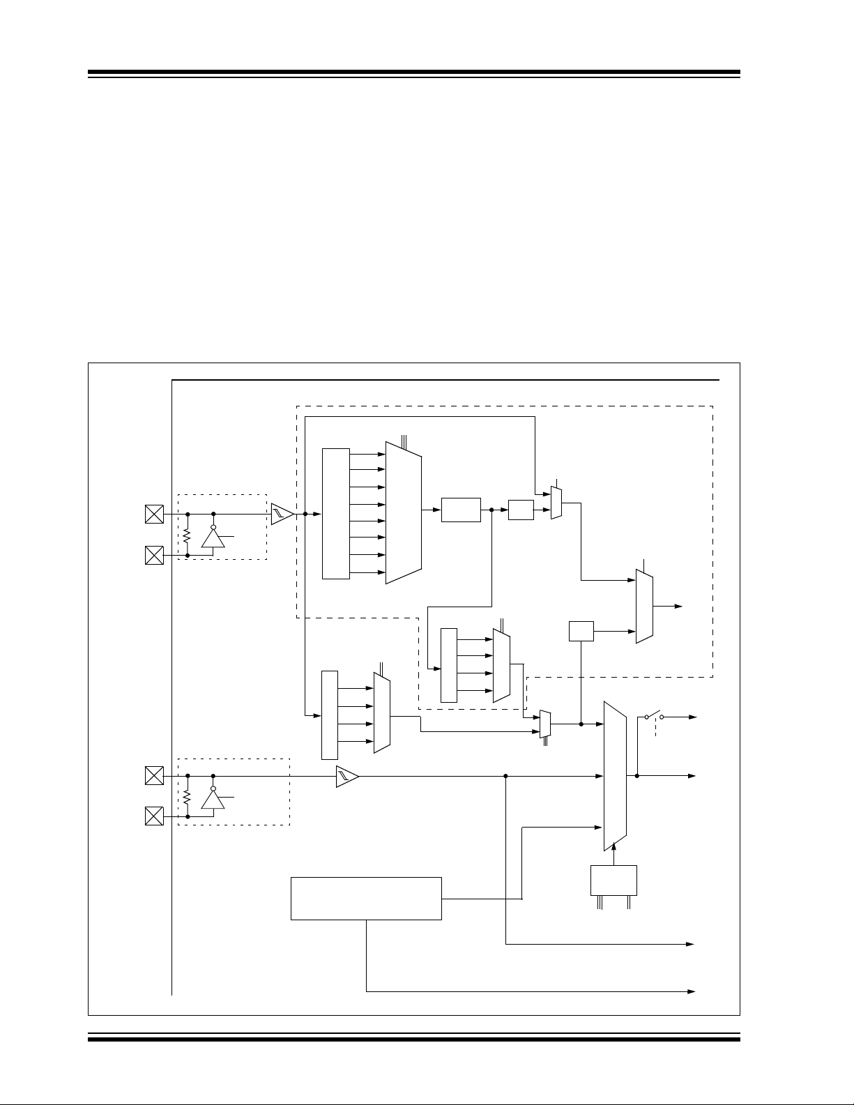
2.0 OSCILLATOR CONFIGURATIONS
2.1 Overview
Devices in the PIC18F2450/4450 family incorporate a
different oscillator and microcontroller clock system
than the non-USB PIC18F devices. The addition of the
USB module, with its unique requirements for a stable
clock source, make it necessary to provide a separate
clock source that is compliant with both USB low-speed
and full-speed specifications.
To accommodate these requirements, PIC18F2450/
4450 devices include a new clock branch to provide a
48 MHz clock for full-speed USB operation. Since it is
driven from the primary clock source, an additional
system of prescalers and postscalers has been added
to accommodate a wide range of oscillator frequencies.
An overview of the oscillator structure is shown in
Figure 2-1.
Other oscillator features used in PIC18 enhanced
microcontrollers, such as the internal RC oscillator and
clock switching, remain the same. They are discussed
later in this chapter.
2.1.1 OSCILLATOR CONTROL
The operation of the oscillator in PIC18F2450/4450
devices is controlled through two Configuration registers
and two control registers. Configuration registers,
CONFIG1L and CONFIG1H, select the oscillator mode
and USB prescaler/postscaler options. As Configuration
bits, these are set when the device is programmed and
left in that configuration until the device is
reprogrammed.
The OSCCON register (Register 2-1) selects the Active
Clock mode; it is primarily used in controlling clock
switching in power-managed modes. Its use is
discussed in Section 2.4.1 “Oscillator Control
Register”.
2.2 Oscillator Types
PIC18F2450/4450 devices can be operated in twelve
distinct oscillator modes. In contrast with the non-USB
PIC18 enhanced microcontrollers, four of these modes
involve the use of two oscillator types at once. Users
can program the FOSC3:FOSC0 Configuration bits to
select one of these modes:
1. XT Crystal/Resonator
2. XTPLL Crystal/Resonator with PLL enabled
3. HS High-Speed Crystal/Resonator
4. HSPLL High-Speed Crystal/Resonator
with PLL enabled
5. EC External Clock with F
6. ECIO External Clock with I/O on RA6
7. ECPLL External Clock with PLL enabled
and F
OSC/4 output on RA6
8. ECPIO External Clock with PLL enabled,
I/O on RA6
9. INTHS Internal Oscillator used as
microcontroller clock source, HS
Oscillator used as USB clock source
10. INTXT Internal Oscillator used as
microcontroller clock source, XT
Oscillator used as USB clock source
11. INTIO Internal Oscillator used as
microcontroller clock source, EC
Oscillator used as USB clock source,
digital I/O on RA6
12. INTCKO Internal Oscillator used as
microcontroller clock source, EC
Oscillator used as USB clock source,
FOSC/4 output on RA6
OSC/4 output
© 2007 Microchip Technology Inc. Preliminary DS39760C-page 23
PIC18F2450/4450
2.2.1 OSCILLATOR MODES AND USB OPERATION
Because of the unique requirements of the USB
module, a different approach to clock operation is
necessary. In previous PIC
and peripheral clocks were driven by a single oscillator
source; the usual sources were primary, secondary or
the internal oscillator. With PIC18F2450/4450 devices,
the primary oscillator becomes part of the USB module
and cannot be associated to any other clock source.
®
microcontrollers, all core
Because of the timing requirements imposed by USB,
an internal clock of either 6 MHz or 48 MHz is required
while the USB module is enabled. Fortunately, the
microcontroller and other peripherals are not required
to run at this clock speed when using the primary
oscillator. There are numerous options to achieve the
USB module clock requirement and still provide flexibility for clocking the rest of the device from the primary
oscillator source. These are detailed in Section 2.3
“Oscillator Settings for USB”.
Thus, the USB module must be clocked from the
primary clock source; however, the microcontroller
core and other peripherals can be separately clocked
from the secondary or internal oscillators as before.
FIGURE 2-1: PIC18F2450/4450 CLOCK DIAGRAM
PIC18F2450/4450
PLLDIV<2:0>
÷ 12
111
÷ 10
110
÷ 6
101
OSC2
OSC1
T1OSO
T1OSI
Primary Oscillator
Sleep
XT, HS, EC, ECIO
Secondary Oscillator
T1OSCEN
Enable
Oscillator
÷ 5
÷ 4
÷ 3
PLL Prescaler
÷ 2
÷ 1
CPUDIV<1:0>
÷ 4
÷ 3
÷ 2
÷ 1
Oscillator Postscaler
11
10
01
00
100
011
010
001
000
MUX
HSPLL, ECPLL,
XTPLL, ECPIO
(4 MHz Input Only)
OSCCON<6:4>
96 MHz
PLL
PLL Postscaler
CPUDIV<1:0>
÷ 6
11
÷ 4
10
÷ 3
01
÷ 2
00
FOSC3:FOSC0
USBDIV
0
÷ 2
1
1
0
Primary
Clock
T1OSC
Internal Oscillator
USB Clock Source
FSEN
1
Peripheral
÷ 4
0
IDLEN
Peripherals
MUX
USB
CPU
Clock
Internal RC Oscillator
31.25
kHz
FOSC3:FOSC0
Control
OSCCON<1:0>
Clock Source Option
for other Modules
WDT, PWRT, FSCM
and Two-Speed Start-up
DS39760C-page 24 Preliminary © 2007 Microchip Technology Inc.
PIC18F2450/4450
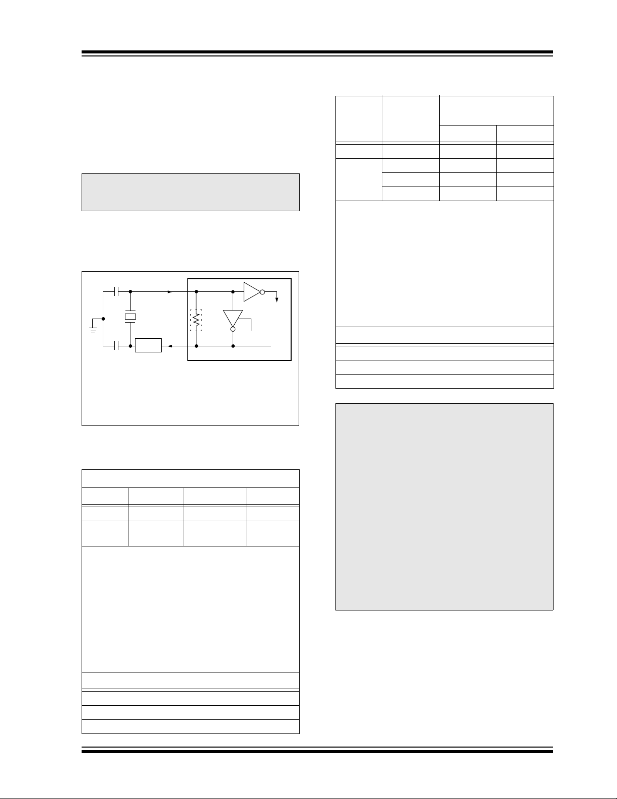
2.2.2 CRYSTAL OSCILLATOR/CERAMIC RESONATORS
In HS, HSPLL, XT and XTPLL Oscillator modes, a
crystal or ceramic resonator is connected to the OSC1
and OSC2 pins to establish oscillation. Figure 2-2
shows the pin connections.
The oscillator design requires the use of a parallel cut
crystal.
Note: Use of a series cut crystal may give a fre-
quency out of the crystal manufacturer’s
specifications.
FIGURE 2-2: CRYSTAL/CERAMIC
RESONATOR OPERATION
(XT, HS OR HSPLL
CONFIGURATION)
(1)
C1
(1)
C2
Note 1: See Table 2-1 and Table 2-2 for initial values of
C1 and C2.
2: A series resistor (R
strip cut crystals.
3: R
OSC1
To
Internal
XTAL
(2)
RS
OSC2
F varies with the oscillator mode chosen.
(3)
RF
PIC18FXXXX
S) may be required for AT
Logic
Sleep
TABLE 2-1: CAPACITOR SELECTION FOR
CERAMIC RESONATORS
Typical Capacitor Values Used:
Mode Freq OSC1 OSC2
XT 4.0 MHz 33 pF 33 pF
HS 8.0 MHz
16.0 MHz
Capacitor values are for design guidance only.
These capacitors were tested with the resonators
listed below for basic start-up and operation. These
values are not optimized.
Different capacitor values may be required to produce
acceptable oscillator operation. The user should test
the performance of the oscillator over the expected
DD and temperature range for the application.
V
See the notes following Table 2-2 for additional
information.
Resonators Used:
16.0 MHz
4.0 MHz
8.0 MHz
27 pF
22 pF
27 pF
22 pF
TABLE 2-2: CAPACITOR SELECTION FOR
CRYSTAL OSCILLATOR
Osc Type
Crystal
Freq
XT 4 MHz 27 pF 27 pF
HS 4 MHz 27 pF 27 pF
8 MHz 22 pF 22 pF
20 MHz 15 pF 15 pF
Capacitor values are for design guidance only.
These capacitors were tested with the crystals listed
below for basic start-up and operation. These values
are not optimized.
Different capacitor values may be required to produce
acceptable oscillator operation. The user should test
the performance of the oscillator over the expected
DD and temperature range for the application.
V
See the notes following this table for additional
information.
Crystals Used:
Note 1: Higher capacitance increases the stability
of oscillator but also increases the start-up
time.
2: When operating below 3V V
using certain ceramic resonators at any
voltage, it may be necessary to use the
HS mode or switch to a crystal oscillator.
3: Since each resonator/crystal has its own
characteristics, the user should consult
the resonator/crystal manufacturer for
appropriate values of external
components.
4: Rs may be required to avoid overdriving
crystals with low drive level specification.
5: Always verify oscillator performance over
DD and temperature range that is
the V
expected for the application.
An internal postscaler allows users to select a clock
frequency other than that of the crystal or resonator.
Frequency division is determined by the CPUDIV
Configuration bits. Users may select a clock frequency
of the oscillator frequency, or 1/2, 1/3 or 1/4 of the
frequency.
An external clock may also be used when the microcontroller is in HS Oscillator mode. In this case, the
OSC2/CLKO pin is left open (Figure 2-3).
Typical Capacitor Values
Test ed:
C1 C2
4 MHz
8 MHz
20 MHz
DD, or when
© 2007 Microchip Technology Inc. Preliminary DS39760C-page 25

PIC18F2450/4450
FIGURE 2-3: EXTERNAL CLOCK INPUT
OPERATION (HS OSC
CONFIGURATION)
Clock from
Ext. System
Open
OSC1
OSC2
PIC18FXXXX
(HS Mode)
2.2.3 EXTERNAL CLOCK INPUT
The EC, ECIO, ECPLL and ECPIO Oscillator modes
require an external clock source to be connected to the
OSC1 pin. There is no oscillator start-up time required
after a Power-on Reset or after an exit from Sleep
mode.
In the EC and ECPLL Oscillator modes, the oscillator
frequency divided by 4 is available on the OSC2 pin.
This signal may be used for test purposes or to
synchronize other logic. Figure 2-4 shows the pin
connections for the EC Oscillator mode.
FIGURE 2-4: EXTERNAL CLOCK
INPUT OPERATION
(EC AND ECPLL
CONFIGURATION)
2.2.4 PLL FREQUENCY MULTIPLIER
PIC18F2450/4450 devices include a Phase Locked
Loop (PLL) circuit. This is provided specifically for USB
applications with lower speed oscillators and can also
be used as a microcontroller clock source.
The PLL is enabled in HSPLL, XTPLL, ECPLL and
ECPIO Oscillator modes. It is designed to produce a
fixed 96 MHz reference clock from a fixed 4 MHz input.
The output can then be divided and used for both the
USB and the microcontroller core clock. Because the
PLL has a fixed frequency input and output, there are
eight prescaling options to match the oscillator input
frequency to the PLL.
There is also a separate postscaler option for deriving
the microcontroller clock from the PLL. This allows the
USB peripheral and microcontroller to use the same
oscillator input and still operate at different clock
speeds. In contrast to the postscaler for XT, HS and EC
modes, the available options are 1/2, 1/3, 1/4 and 1/6
of the PLL output.
The HSPLL, ECPLL and ECPIO modes make use of
the HS mode oscillator for frequencies up to 48 MHz.
The prescaler divides the oscillator input by up to 12 to
produce the 4 MHz drive for the PLL. The XTPLL mode
can only use an input frequency of 4 MHz which drives
the PLL directly.
Clock from
Ext. System
OSC/4
F
OSC1/CLKI
PIC18FXXXX
OSC2/CLKO
The ECIO and ECPIO Oscillator modes function like the
EC and ECPLL modes, except that the OSC2 pin
becomes an additional general purpose I/O pin. The I/O
pin becomes bit 6 of PORTA (RA6). Figure 2-5 shows
the pin connections for the ECIO Oscillator mode.
FIGURE 2-5: EXTERNAL CLOCK
INPUT OPERATION
(ECIO AND ECPIO
CONFIGURATION)
Clock from
Ext. System
RA6
The internal postscaler for reducing clock frequency in
XT and HS modes is also available in EC and ECIO
modes.
OSC1/CLKI
PIC18FXXXX
I/O (OSC2)
FIGURE 2-6: PLL BLOCK DIAGRAM
(HS MODE)
HS/EC/ECIO/XT Oscillator Enable
(from CONFIG1H Register)
OSC2
Oscillator
OSC1
and
Prescaler
PLL Enable
Phase
Comparator
IN
F
FOUT
÷24
Loop
Filter
VCO
SYSCLK
MUX
DS39760C-page 26 Preliminary © 2007 Microchip Technology Inc.

PIC18F2450/4450
2.2.5 INTERNAL OSCILLATOR
The PIC18F2450/4450 devices include an internal RC
oscillator (INTRC) which provides a nominal 31 kHz output. INTRC is enabled if it is selected as the device clock
source; it is also enabled automatically when any of the
following are enabled:
• Power-up Timer
• Fail-Safe Clock Monitor
• Watchdog Timer
• Two-Speed Start-up
These features are discussed in greater detail in
Section 18.0 “Special Features of the CPU”.
2.2.5.1 Internal Oscillator Modes
When the internal oscillator is used as the microcontroller clock source, one of the other oscillator
modes (External Clock or External Crystal/Resonator)
must be used as the USB clock source. The choice of
USB clock source is determined by the particular
internal oscillator mode.
There are four distinct modes available:
1. INTHS mode: The USB clock is provided by the
oscillator in HS mode.
2. INTXT mode: The USB clock is provided by the
oscillator in XT mode.
3. INTCKO mode: The USB clock is provided by an
external clock input on OSC1/CLKI; the OSC2/
CLKO pin outputs F
4. INTIO mode: The USB clock is provided by an
external clock input on OSC1/CLKI; the OSC2/
CLKO pin functions as a digital I/O (RA6).
Of these four modes, only INTIO mode frees up an
additional pin (OSC2/CLKO/RA6) for port I/O use.
OSC/4.
2.3 Oscillator Settings for USB
When the PIC18F2450/4450 is used for USB
connectivity, it must have either a 6 MHz or 48 MHz
clock for USB operation, depending on whether LowSpeed or Full-Speed mode is being used. This may
require some forethought in selecting an oscillator
frequency and programming the device.
The full range of possible oscillator configurations
compatible with USB operation is shown in Table 2-3.
2.3.1 LOW-SPEED OPERATION
The USB clock for Low-Speed mode is derived from
the primary oscillator chain and not directly from the
PLL. It is divided by 4 to produce the actual 6 MHz
clock. Because of this, the microcontroller can only use
a clock frequency of 24 MHz when the USB module is
active and the controller clock source is one of the
primary oscillator modes (XT, HS or EC, with or without
the PLL).
This restriction does not apply if the microcontroller
clock source is the secondary oscillator or internal
oscillator.
2.3.2 RUNNING DIFFERENT USB AND MICROCONTROLLER CLOCKS
The USB module, in either mode, can run
asynchronously with respect to the microcontroller core
and other peripherals. This means that applications can
use the primary oscillator for the USB clock while the
microcontroller runs from a separate clock source at a
lower speed. If it is necessary to run the entire application
from only one clock source, full-speed operation provides
a greater selection of microcontroller clock frequencies.
© 2007 Microchip Technology Inc. Preliminary DS39760C-page 27

PIC18F2450/4450
TABLE 2-3: OSCILLATOR CONFIGURATION OPTIONS FOR USB OPERATION
Input Oscillator
Frequency
48 MHz N/A
48 MHz ÷12 (111)
40 MHz ÷10 (110)
24 MHz ÷6 (101)
20 MHz ÷5 (100)
16 MHz ÷4 (011)
Legend: All clock frequencies, except 24 MHz, are exclusively associated with full-speed USB operation (USB clock of 48 MHz).
Bold is used to highlight clock selections that are compatible with low-speed USB operation (system clock of 24 MHz,
USB clock of 6 MHz).
Note 1: Only valid when the USBDIV Configuration bit is cleared.
PLL Division
(PLLDIV2:PLLDIV0)
(1)
Clock Mode
(FOSC3:FOSC0)
EC, ECIO
EC, ECIO
ECPLL, ECPIO
EC, ECIO
ECPLL, ECPIO
HS, EC, ECIO
HSPLL, ECPLL, ECPIO
HS, EC, ECIO
HSPLL, ECPLL, ECPIO
HS, EC, ECIO
HSPLL, ECPLL, ECPIO
MCU Clock Division
(CPUDIV1:CPUDIV0)
None (00)48MHz
÷2 (01) 24 MHz
÷3 (10)16MHz
÷4 (11)12MHz
None (00)48MHz
÷2 (01) 24 MHz
÷3 (10)16MHz
÷4 (11)12MHz
÷2 (00)48MHz
÷3 (01)32MHz
÷4 (10) 24 MHz
÷6 (11)16MHz
None (00)40MHz
÷2 (01)20MHz
÷3 (10) 13.33 MHz
÷4 (11)10MHz
÷2 (00)48MHz
÷3 (01)32MHz
÷4 (10) 24 MHz
÷6 (11)16MHz
None (00) 24 MHz
÷2 (01)12MHz
÷3 (10)8MHz
÷4 (11)6MHz
÷2 (00)48MHz
÷3 (01)32MHz
÷4 (10) 24 MHz
÷6 (11)16MHz
None (00)20MHz
÷2 (01)10MHz
÷3 (10)6.67MHz
÷4 (11)5MHz
÷2 (00)48MHz
÷3 (01)32MHz
÷4 (10) 24 MHz
÷6 (11)16MHz
None (00)16MHz
÷2 (01)8MHz
÷3 (10)5.33MHz
÷4 (11)4MHz
÷2 (00)48MHz
3 (01)32MHz
÷
÷4 (10) 24 MHz
÷6 (11)16MHz
Microcontroller
Clock Frequency
DS39760C-page 28 Preliminary © 2007 Microchip Technology Inc.

PIC18F2450/4450
TABLE 2-3: OSCILLATOR CONFIGURATION OPTIONS FOR USB OPERATION (CONTINUED)
Input Oscillator
Frequency
12 MHz ÷3 (010)
8MHz ÷2 (001)
4MHz ÷1 (000)
Legend: All clock frequencies, except 24 MHz, are exclusively associated with full-speed USB operation (USB clock of 48 MHz).
Bold is used to highlight clock selections that are compatible with low-speed USB operation (system clock of 24 MHz,
USB clock of 6 MHz).
Note 1: Only valid when the USBDIV Configuration bit is cleared.
PLL Division
(PLLDIV2:PLLDIV0)
Clock Mode
(FOSC3:FOSC0)
HS, EC, ECIO
HSPLL, ECPLL, ECPIO
HS, EC, ECIO
HSPLL, ECPLL, ECPIO
XT, HS, EC, ECIO
HSPLL, ECPLL, XTPLL,
ECPIO
MCU Clock Division
(CPUDIV1:CPUDIV0)
None (00)12MHz
÷2 (01)6MHz
÷3 (10)4MHz
÷4 (11)3MHz
÷2 (00)48MHz
÷3 (01)32MHz
÷4 (10) 24 MHz
÷6 (11)16MHz
None (00)8MHz
÷2 (01)4MHz
÷3 (10)2.67MHz
÷4 (11)2MHz
÷2 (00)48MHz
÷3 (01)32MHz
÷4 (10) 24 MHz
÷6 (11)16MHz
None (00)4MHz
÷2 (01)2MHz
÷3 (10)1.33MHz
÷4 (11)1MHz
÷2 (00)48MHz
÷3 (01)32MHz
÷4 (10) 24 MHz
÷6 (11)16MHz
Microcontroller
Clock Frequency
© 2007 Microchip Technology Inc. Preliminary DS39760C-page 29

PIC18F2450/4450
2.4 Clock Sources and Oscillator Switching
Like previous PIC18 enhanced devices, the
PIC18F2450/4450 family includes a feature that allows
the device clock source to be switched from the main
oscillator to an alternate, low-frequency clock source.
PIC18F2450/4450 devices offer two alternate clock
sources. When an alternate clock source is enabled,
the various power-managed operating modes are
available.
Essentially, there are three clock sources for these
devices:
• Primary oscillators
• Secondary oscillators
• Internal oscillator
The primary oscillators include the External Crystal
and Resonator modes, the External Clock modes and
the internal oscillator. The particular mode is defined by
the FOSC3:FOSC0 Configuration bits. The details of
these modes are covered earlier in this chapter.
The secondary oscillators are those external sources
not connected to the OSC1 or OSC2 pins. These
sources may continue to operate even after the
controller is placed in a power-managed mode.
PIC18F2450/4450 devices offer the Timer1 oscillator
as a secondary oscillator. This oscillator, in all powermanaged modes, is often the time base for functions
such as a Real-Time Clock (RTC). Most often, a
32.768 kHz watch crystal is connected between the
RC0/T1OSO/T1CKI and RC1/T1OSI/UOE
the XT and HS Oscillator mode circuits, loading
capacitors are also connected from each pin to ground.
The Timer1 oscillator is discussed in greater detail in
Section 11.3 “Timer1 Oscillator”.
In addition to being a primary clock source, the internal
oscillator is available as a power-managed mode
clock source. The INTRC source is also used as the
clock source for several special features, such as the
WDT and Fail-Safe Clock Monitor.
2.4.1 OSCILLATOR CONTROL REGISTER
The OSCCON register (Register 2-1) controls several
aspects of the device clock’s operation, both in full-power
operation and in power-managed modes.
The System Clock Select bits, SCS1:SCS0, select the
clock source. The available clock sources are the primary
clock (defined by the FOSC3:FOSC0 Configuration bits),
the secondary clock (Timer1 oscillator) and the internal
oscillator. The clock source changes immediately, after
one or more of the bits is written to, following a brief clock
transition interval. The SCS bits are cleared on all forms
of Reset.
pins. Like
INTRC always remains the clock source for features
such as the Watchdog Timer and the Fail-Safe Clock
Monitor.
The OSTS and T1RUN bits indicate which clock source
is currently providing the device clock. The OSTS bit
indicates that the Oscillator Start-up Timer (OST) has
timed out and the primary clock is providing the device
clock in primary clock modes. The T1RUN bit
(T1CON<6>) indicates when the Timer1 oscillator is
providing the device clock in secondary clock modes. In
power-managed modes, only one of these three bits will
be set at any time. If none of these bits are set, the
INTRC is providing the clock or the internal oscillator has
just started and is not yet stable.
The IDLEN bit determines if the device goes into Sleep
mode, or one of the Idle modes, when the SLEEP
instruction is executed.
The use of the flag and control bits in the OSCCON
register is discussed in more detail in Section 3.0
“Power-Managed Modes”.
Note 1: The Timer1 oscillator must be enabled to
select the secondary clock source. The
Timer1 oscillator is enabled by setting the
T1OSCEN bit in the Timer1 Control register (T1CON<3>). If the Timer1 oscillator is
not enabled, then any attempt to select a
secondary clock source will be ignored.
2: It is recommended that the Timer1
oscillator be operating and stable prior to
switching to it as the clock source; otherwise, a very long delay may occur while
the Timer1 oscillator starts.
2.4.2 OSCILLATOR TRANSITIONS
PIC18F2450/4450 devices contain circuitry to prevent
clock “glitches” when switching between clock sources.
A short pause in the device clock occurs during the
clock switch. The length of this pause is the sum of two
cycles of the old clock source and three to four cycles
of the new clock source. This formula assumes that the
new clock source is stable.
Clock transitions are discussed in greater detail in
Section 3.1.2 “Entering Power-Managed Modes”.
DS39760C-page 30 Preliminary © 2007 Microchip Technology Inc.

PIC18F2450/4450
REGISTER 2-1: OSCCON: OSCILLATOR CONTROL REGISTER
(1)
(1)
U-0 R/W-0 R/W-0
R/W-0 U-0 U-0 U-0 R
IDLEN — — —OSTS —SCS1SCS0
bit 7 bit 0
Legend:
R = Readable bit W = Writable bit U = Unimplemented bit, read as ‘0’
-n = Value at POR ‘1’ = Bit is set ‘0’ = Bit is cleared x = Bit is unknown
bit 7 IDLEN: Idle Enable bit
1 = Device enters Idle mode on SLEEP instruction
0 = Device enters Sleep mode on SLEEP instruction
bit 6-4 Unimplemented: Read as ‘0’
bit 3 OSTS: Oscillator Start-up Time-out Status bit
1 = Oscillator Start-up Timer time-out has expired; primary oscillator is running
0 = Oscillator Start-up Timer time-out is running; primary oscillator is not ready
bit 2 Unimplemented: Read as ‘0’
bit 1-0 SCS1:SCS0: System Clock Select bits
1x = Internal oscillator
01 = Timer1 oscillator
00 = Primary oscillator
Note 1: Depends on the state of the IESO Configuration bit.
© 2007 Microchip Technology Inc. Preliminary DS39760C-page 31

PIC18F2450/4450
2.5 Effects of Power-Managed Modes on the Various Clock Sources
When PRI_IDLE mode is selected, the designated
primary oscillator continues to run without interruption.
For all other power-managed modes, the oscillator
using the OSC1 pin is disabled. Unless the USB
module is enabled, the OSC1 pin (and OSC2 pin if
used by the oscillator) will stop oscillating.
In secondary clock modes (SEC_RUN and
SEC_IDLE), the Timer1 oscillator is operating and
providing the device clock. The Timer1 oscillator may
also run in all power-managed modes if required to
clock Timer1.
In internal oscillator modes (RC_RUN and RC_IDLE),
the internal oscillator provides the device clock source.
The 31 kHz INTRC output can be used directly to
provide the clock and may be enabled to support various
special features regardless of the power-managed
mode (see Section 18.2 “Watchdog Timer (WDT)”,
Section 18.3 “Two-Speed Start-up” and Section 18.4
“Fail-Safe Clock Monitor” for more information on
WDT, Fail-Safe Clock Monitor and Two-Speed Start-up).
Regardless of the Run or Idle mode selected, the USB
clock source will continue to operate. If the device is
operating from a crystal or resonator-based oscillator,
that oscillator will continue to clock the USB module.
The core and all other modules will switch to the new
clock source.
If the Sleep mode is selected, all clock sources are
stopped. Since all the transistor switching currents
have been stopped, Sleep mode achieves the lowest
current consumption of the device (only leakage
currents).
Sleep mode should never be invoked while the USB
module is operating and connected. The only exception
is when the device has been issued a “Suspend” command over the USB. Once the module has suspended
operation and shifted to a low-power state, the
microcontroller may be safely put into Sleep mode.
Enabling any on-chip feature that will operate during
Sleep will increase the current consumed during Sleep.
The INTRC is required to support WDT operation. The
Timer1 oscillator may be operating to support a RealTime Clock. Other features may be operating that do
not require a device clock source (i.e., PSP, INTx pins
and others). Peripherals that may add significant
current consumption are listed in Section 21.2 “DC
Characteristics: Power-Down and Supply Current”.
2.6 Power-up Delays
Power-up delays are controlled by two timers, so that no
external Reset circuitry is required for most applications.
The delays ensure that the device is kept in Reset until
the device power supply is stable under normal circumstances and the primary clock is operating and stable.
For additional information on power-up delays, see
Section 4.5 “Device Reset Timers”.
The first timer is the Power-up Timer (PWRT), which
provides a fixed delay on power-up (parameter 33,
Table 21-10). It is enabled by clearing (= 0) the
PWRTEN
The second timer is the Oscillator Start-up Timer
(OST), intended to keep the chip in Reset until the
crystal oscillator is stable (XT and HS modes). The
OST does this by counting 1024 oscillator cycles
before allowing the oscillator to clock the device.
When the HSPLL Oscillator mode is selected, the
device is kept in Reset for an additional 2 ms following
the HS mode OST delay, so the PLL can lock to the
incoming clock frequency.
There is a delay of interval, T
Table 21-10), following POR, while the controller
becomes ready to execute instructions. This delay runs
concurrently with any other delays. This may be the
only delay that occurs when any of the EC or internal
oscillator modes are used as the primary clock source.
Configuration bit.
CSD (parameter 38,
TABLE 2-4: OSC1 AND OSC2 PIN STATES IN SLEEP MODE
Oscillator Mode OSC1 Pin OSC2 Pin
INTCKO Floating, pulled by external clock At logic low (clock/4 output)
INTIO Floating, pulled by external clock Configured as PORTA, bit 6
ECIO, ECPIO Floating, pulled by external clock Configured as PORTA, bit 6
EC Floating, pulled by external clock At logic low (clock/4 output)
XT and HS Feedback inverter disabled at quiescent
voltage level
Note: See Table 4-2 in Section 4.0 “Reset” for time-outs due to Sleep and MCLR
DS39760C-page 32 Preliminary © 2007 Microchip Technology Inc.
Feedback inverter disabled at quiescent
voltage level
Reset.

PIC18F2450/4450
3.0 POWER-MANAGED MODES
PIC18F2450/4450 devices offer a total of seven
operating modes for more efficient power
management. These modes provide a variety of
options for selective power conservation in applications
where resources may be limited (i.e., battery-powered
devices).
There are three categories of power-managed modes:
• Run modes
• Idle modes
• Sleep mode
These categories define which portions of the device
are clocked and sometimes, what speed. The Run and
Idle modes may use any of the three available clock
sources (primary, secondary or internal oscillator); the
Sleep mode does not use a clock source.
The power-managed modes include several powersaving features offered on previous PIC
microcontrollers. One is the clock switching feature,
offered in other PIC18 devices, allowing the controller
to use the Timer1 oscillator in place of the primary
oscillator. Also included is the Sleep mode, offered by
all PIC microcontrollers, where all device clocks are
stopped.
3.1 Selecting Power-Managed Modes
Selecting a power-managed mode requires two
decisions: if the CPU is to be clocked or not and the
selection of a clock source. The IDLEN bit
(OSCCON<7>) controls CPU clocking, while the
SCS1:SCS0 bits (OSCCON<1:0>) select the clock
source. The individual modes, bit settings, clock sources
and affected modules are summarized in Table 3-1.
3.1.1 CLOCK SOURCES
The SCS1:SCS0 bits allow the selection of one of three
clock sources for power-managed modes. They are:
• The primary clock, as defined by the
FOSC3:FOSC0 Configuration bits
• The secondary clock (the Timer1 oscillator)
• The internal oscillator (for RC modes)
3.1.2 ENTERING POWER-MANAGED
MODES
Switching from one power-managed mode to another
begins by loading the OSCCON register. The
SCS1:SCS0 bits select the clock source and determine
which Run or Idle mode is to be used. Changing these
bits causes an immediate switch to the new clock
source, assuming that it is running. The switch may
also be subject to clock transition delays. These are
®
discussed in Section 3.1.3 “Clock Transitions and
Status Indicators” and subsequent sections.
Entry to the power-managed Idle or Sleep modes is
triggered by the execution of a SLEEP instruction. The
actual mode that results depends on the status of the
IDLEN bit.
Depending on the current mode and the mode being
switched to, a change to a power-managed mode does
not always require setting all of these bits. Many
transitions may be done by changing the oscillator
select bits, or changing the IDLEN bit, prior to issuing a
SLEEP instruction. If the IDLEN bit is already
configured correctly, it may only be necessary to
perform a SLEEP instruction to switch to the desired
mode.
TABLE 3-1: POWER-MANAGED MODES
Mode
Sleep 0 N/A Off Off None – all clocks are disabled
PRI_RUN N/A 00 Clocked Clocked Primary – all oscillator modes.
SEC_RUN N/A 01 Clocked Clocked Secondary – Timer1 oscillator
RC_RUN N/A 1x Clocked Clocked Internal oscillator
PRI_IDLE 100Off Clocked Primary – all oscillator modes
SEC_IDLE 101Off Clocked Secondary – Timer1 oscillator
RC_IDLE 11xOff Clocked Internal oscillator
Note 1: IDLEN reflects its value when the SLEEP instruction is executed.
2: Clock is INTRC source.
© 2007 Microchip Technology Inc. Preliminary DS39760C-page 33
OSCCON Bits Module Clocking
(1)
IDLEN
SCS1:SCS0 CPU Peripherals
Available Clock and Oscillator Source
This is the normal full-power execution mode.
(2)
(2)

PIC18F2450/4450
3.1.3 CLOCK TRANSITIONS AND STATUS INDICATORS
The length of the transition between clock sources is
the sum of two cycles of the old clock source and three
to four cycles of the new clock source. This formula
assumes that the new clock source is stable.
Two bits indicate the current clock source and its
status. They are:
• OSTS (OSCCON<3>)
• T1RUN (T1CON<6>)
In general, only one of these bits will be set while in a
given power-managed mode. When the OSTS bit is
set, the primary clock is providing the device clock.
When the T1RUN bit is set, the Timer1 oscillator is
providing the clock.
Note: Executing a SLEEP instruction does not
necessarily place the device into Sleep
mode. It acts as the trigger to place the
controller into either the Sleep mode, or
one of the Idle modes, depending on the
setting of the IDLEN bit.
3.1.4 MULTIPLE SLEEP COMMANDS
The power-managed mode that is invoked with the
SLEEP instruction is determined by the setting of the
IDLEN bit at the time the instruction is executed. If
another SLEEP instruction is executed, the device will
enter the power-managed mode specified by IDLEN at
that time. If IDLEN has changed, the device will enter
the new power-managed mode specified by the new
setting.
3.2.1 PRI_RUN MODE
The PRI_RUN mode is the normal, full-power execution mode of the microcontroller. This is also the default
mode upon a device Reset unless Two-Speed Start-up
is enabled (see Section 18.3 “Two-Speed Start-up”
for details). In this mode, the OSTS bit is set.
3.2.2 SEC_RUN MODE
The SEC_RUN mode is the compatible mode to the
“clock switching” feature offered in other PIC18
devices. In this mode, the CPU and peripherals are
clocked from the Timer1 oscillator. This gives users the
option of lower power consumption while still using a
high accuracy clock source.
SEC_RUN mode is entered by setting the SCS1:SCS0
bits to ‘01’. The device clock source is switched to the
Timer1 oscillator (see Figure 3-1), the primary
oscillator is shut down, the T1RUN bit (T1CON<6>) is
set and the OSTS bit is cleared.
Note: The Timer1 oscillator should already be
running prior to entering SEC_RUN mode.
If the T1OSCEN bit is not set when the
SCS1:SCS0 bits are set to ‘01’, entry to
SEC_RUN mode will not occur. If the
Timer1 oscillator is enabled but not yet
running, device clocks will be delayed until
the oscillator has started. In such
situations, initial oscillator operation is far
from stable and unpredictable operation
may result.
3.2 Run Modes
In the Run modes, clocks to both the core and
peripherals are active. The difference between these
modes is the clock source.
DS39760C-page 34 Preliminary © 2007 Microchip Technology Inc.

PIC18F2450/4450
On transitions from SEC_RUN mode to PRI_RUN
mode, the peripherals and CPU continue to be clocked
from the Timer1 oscillator while the primary clock is
started. When the primary clock becomes ready, a
clock switch back to the primary clock occurs (see
Figure 3-2). When the clock switch is complete, the
T1RUN bit is cleared, the OSTS bit is set and the
primary clock is providing the clock. The IDLEN and
SCS bits are not affected by the wake-up; the Timer1
oscillator continues to run.
FIGURE 3-1: TRANSITION TIMING FOR ENTRY TO SEC_RUN MODE
Q4Q3Q2
Q1
T1OSI
OSC1
CPU
Clock
Peripheral
Clock
Program
Counter
Note 1: Clock transition typically occurs within 2-4 T
Q1
123
Clock Transition
OSC.
Q4Q3Q2 Q1 Q3Q2
n-1
n
(1)
PC + 2PC
PC + 4
FIGURE 3-2: TRANSITION TIMING FROM SEC_RUN MODE TO PRI_RUN MODE (HSPLL)
T1OSI
OSC1
PLL Clock
Output
CPU Clock
Q1 Q3 Q4
(1)
TOST
Q3 Q4 Q1
Q2 Q2 Q3
(1)
TPLL
12 n-1n
(2)
Clock
Transition
Q1
Q2
Peripheral
Clock
Program
Counter
SCS1:SCS0 bits Changed
Note 1: TOST = 1024 TOSC; TPLL = 2 ms (approx). These intervals are not shown to scale.
2: Clock transition typically occurs within 2-4 T
PC
OSTS bit Set
OSC.
PC + 2
PC + 4
© 2007 Microchip Technology Inc. Preliminary DS39760C-page 35

PIC18F2450/4450
3.2.3 RC_RUN MODE
In RC_RUN mode, the CPU and peripherals are
clocked from the internal oscillator; the primary clock is
shut down. When using the INTRC source, this mode
provides the best power conservation of all the Run
modes while still executing code. It works well for user
applications which are not highly timing sensitive or do
not require high-speed clocks at all times.
If the primary clock source is the internal oscillator
(INTRC), there are no distinguishable differences
between the PRI_RUN and RC_RUN modes during
execution. However, a clock switch delay will occur during entry to and exit from RC_RUN mode. Therefore, if
the primary clock source is the internal oscillator, the
use of RC_RUN mode is not recommended.
This mode is entered by setting SCS1 to ‘1’. Although
it is ignored, it is recommended that SCS0 also be
cleared; this is to maintain software compatibility with
future devices. When the clock source is switched to
the INTRC (see Figure 3-3), the primary oscillator is
shut down and the OSTS bit is cleared.
On transitions from RC_RUN mode to PRI_RUN mode,
the device continues to be clocked from the INTRC
while the primary clock is started. When the primary
clock becomes ready, a clock switch to the primary
clock occurs (see Figure 3-4). When the clock switch is
complete, the OSTS bit is set and the primary clock is
providing the device clock. The IDLEN and SCS bits
are not affected by the switch. The INTRC source will
continue to run if either the WDT or the Fail-Safe Clock
Monitor is enabled.
FIGURE 3-3: TRANSITION TIMING TO RC_RUN MODE
Q4Q3Q2
Q1
123 n-1n
Clock Transition
PC + 2PC
(1)
INTRC
OSC1
CPU
Clock
Peripheral
Clock
Program
Counter
Q1
Q4Q3Q2 Q1 Q3Q2
PC + 4
Note 1: Clock transition typically occurs within 2-4 T
OSC.
FIGURE 3-4: TRANSITION TIMING FROM RC_RUN MODE TO PRI_RUN MODE
Q1
INTRC
OSC1
PLL Clock
Output
CPU Clock
Peripheral
Clock
Program
Counter
SCS1:SCS0 bits Changed
Note 1: TOST = 1024 TOSC; TPLL = 2 ms (approx). These intervals are not shown to scale.
2: Clock transition typically occurs within 2-4 T
TOST
Q2
(1)
PC
Q3
(1)
TPLL
OSTS bit Set
OSC.
12 n-1n
(2)
Clock
Transition
PC + 2
Q1
Q4
Q2
Q3 Q4
Q1
PC + 4
Q2
Q3
DS39760C-page 36 Preliminary © 2007 Microchip Technology Inc.

PIC18F2450/4450
3.3 Sleep Mode
The power-managed Sleep mode in the PIC18F2450/
4450 devices is identical to the legacy Sleep mode
offered in all other PIC microcontrollers. It is entered by
clearing the IDLEN bit (the default state on device
Reset) and executing the SLEEP instruction. This shuts
down the selected oscillator (Figure 3-5). All clock
source status bits are cleared.
Entering the Sleep mode from any other mode does not
require a clock switch. This is because no clocks are
needed once the controller has entered Sleep. If the
WDT is selected, the INTRC source will continue to
operate. If the Timer1 oscillator is enabled, it will also
continue to run.
When a wake event occurs in Sleep mode (by interrupt,
Reset or WDT time-out), the device will not be clocked
until the clock source selected by the SCS1:SCS0 bits
becomes ready (see Figure 3-6), or it will be clocked
from the internal oscillator if either the Two-Speed
Start-up or the Fail-Safe Clock Monitor are enabled
(see Section 18.0 “Special Features of the CPU”). In
either case, the OSTS bit is set when the primary clock
is providing the device clocks. The IDLEN and SCS bits
are not affected by the wake-up.
3.4 Idle Modes
The Idle modes allow the controller’s CPU to be
selectively shut down while the peripherals continue to
operate. Selecting a particular Idle mode allows users
to further manage power consumption.
If the IDLEN bit is set to ‘1’ when a SLEEP instruction is
executed, the peripherals will be clocked from the clock
source selected using the SCS1:SCS0 bits; however, the
CPU will not be clocked. The clock source status bits are
not affected. Setting IDLEN and executing a SLEEP
instruction provides a quick method of switching from a
given Run mode to its corresponding Idle mode.
If the WDT is selected, the INTRC source will continue
to operate. If the Timer1 oscillator is enabled, it will also
continue to run.
Since the CPU is not executing instructions, the only
exits from any of the Idle modes are by interrupt, WDT
time-out or a Reset. When a wake event occurs, CPU
execution is delayed by an interval of T
(parameter 38, Table 21-10) while it becomes ready to
execute code. When the CPU begins executing code,
it resumes with the same clock source for the current
Idle mode. For example, when waking from RC_IDLE
mode, the internal oscillator will clock the CPU and
peripherals (in other words, RC_RUN mode). The
IDLEN and SCS bits are not affected by the wake-up.
While in any Idle mode or Sleep mode, a WDT time-out
will result in a WDT wake-up to the Run mode currently
specified by the SCS1:SCS0 bits.
CSD
FIGURE 3-5: TRANSITION TIMING FOR ENTRY TO SLEEP MODE
Q4Q3Q2
Q1Q1
OSC1
CPU
Clock
Peripheral
Clock
Sleep
Program
Counter
PC + 2PC
FIGURE 3-6: TRANSITION TIMING FOR WAKE FROM SLEEP (HSPLL)
OSC1
PLL Clock
Output
CPU Clock
Peripheral
Clock
Program
Counter
Note1: T
Q1 Q2 Q3 Q4 Q1 Q2
(1)
TOST
Wake Event
OST = 1024 TOSC; TPLL = 2 ms (approx). These intervals are not shown to scale.
(1)
TPLL
PC
OSTS bit Set
Q3 Q4 Q1 Q2
PC + 2
Q3 Q4
PC + 4
Q1 Q2 Q3 Q4
PC + 6
© 2007 Microchip Technology Inc. Preliminary DS39760C-page 37
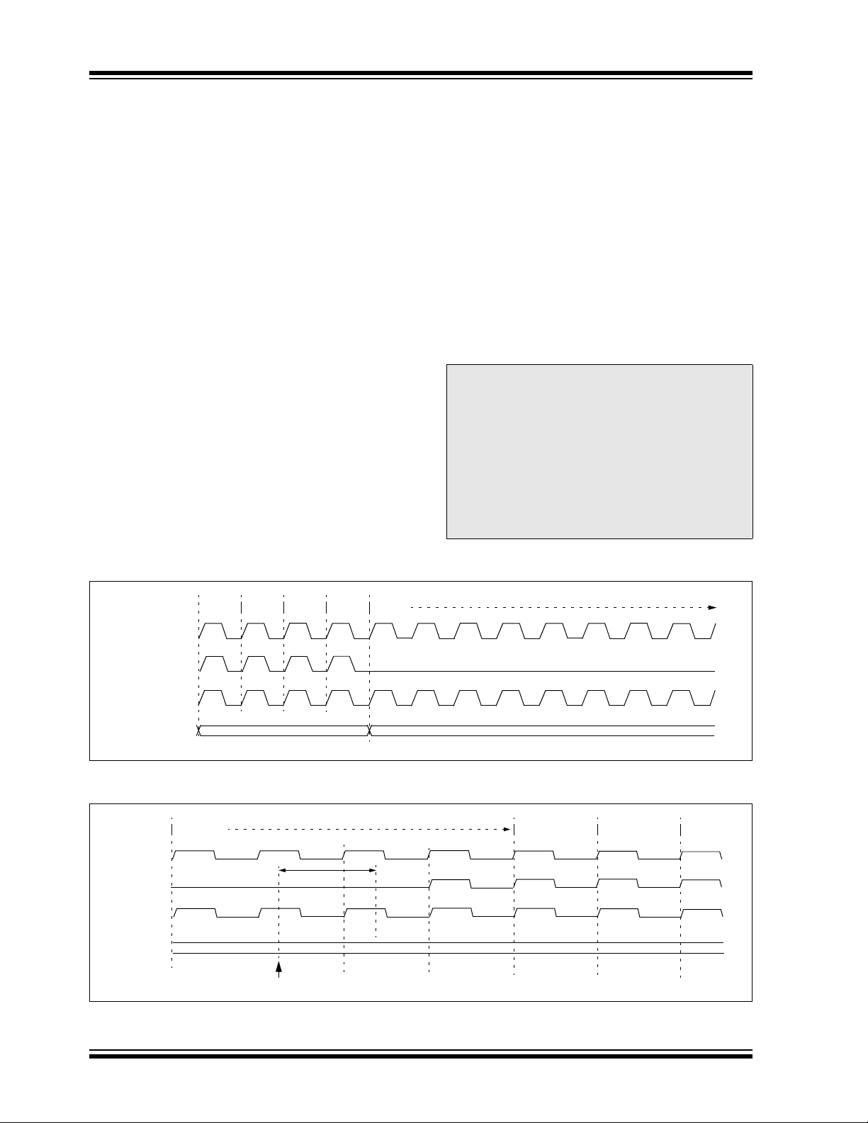
PIC18F2450/4450
3.4.1 PRI_IDLE MODE
This mode is unique among the three low-power Idle
modes in that it does not disable the primary device
clock. For timing sensitive applications, this allows for
the fastest resumption of device operation, with its
more accurate primary clock source, since the clock
source does not have to “warm up” or transition from
another oscillator.
PRI_IDLE mode is entered from PRI_RUN mode by
setting the IDLEN bit and executing a SLEEP
instruction. If the device is in another Run mode, set
IDLEN first, then clear the SCS bits and execute
SLEEP. Although the CPU is disabled, the peripherals
continue to be clocked from the primary clock source
specified by the FOSC3:FOSC0 Configuration bits.
The OSTS bit remains set (see Figure 3-7).
When a wake event occurs, the CPU is clocked from the
primary clock source. A delay of interval T
required between the wake event and when code
execution starts. This is required to allow the CPU to
become ready to execute instructions. After the wakeup, the OSTS bit remains set. The IDLEN and SCS bits
are not affected by the wake-up (see Figure 3-8).
CSD is
3.4.2 SEC_IDLE MODE
In SEC_IDLE mode, the CPU is disabled but the
peripherals continue to be clocked from the Timer1
oscillator. This mode is entered from SEC_RUN by
setting the IDLEN bit and executing a SLEEP
instruction. If the device is in another Run mode, set
IDLEN first, then set SCS1:SCS0 to ‘01’ and execute
SLEEP. When the clock source is switched to the
Timer1 oscillator, the primary oscillator is shut down,
the OSTS bit is cleared and the T1RUN bit is set.
When a wake event occurs, the peripherals continue to
be clocked from the Timer1 oscillator. After an interval of
CSD following the wake event, the CPU begins execut-
T
ing code being clocked by the Timer1 oscillator. The
IDLEN and SCS bits are not affected by the wake-up;
the Timer1 oscillator continues to run (see Figure 3-8).
Note: The Timer1 oscillator should already be
running prior to entering SEC_IDLE mode.
If the T1OSCEN bit is not set when the
SLEEP instruction is executed, the SLEEP
instruction will be ignored and entry to
SEC_IDLE mode will not occur. If the
Timer1 oscillator is enabled but not yet running, peripheral clocks will be delayed until
the oscillator has started. In such situations,
initial oscillator operation is far from stable
and unpredictable operation may result.
FIGURE 3-7: TRANSITION TIMING FOR ENTRY TO IDLE MODE
Q1
OSC1
CPU Clock
Peripheral
Clock
Program
Counter
Q1
Q4
Q2
Q3
PC PC + 2
FIGURE 3-8: TRANSITION TIMING FOR WAKE FROM IDLE TO RUN MODE
OSC1
CPU Clock
Peripheral
Clock
Program
Counter
Q1 Q3 Q4
TCSD
PC
Q2
Wake Even t
DS39760C-page 38 Preliminary © 2007 Microchip Technology Inc.

PIC18F2450/4450
3.4.3 RC_IDLE MODE
In RC_IDLE mode, the CPU is disabled but the peripherals continue to be clocked from the internal oscillator,
INTRC. This mode allows for controllable power
conservation during Idle periods.
From RC_RUN, this mode is entered by setting the
IDLEN bit and executing a SLEEP instruction. If the
device is in another Run mode, first set IDLEN, then set
the SCS1 bit and execute SLEEP. Although its value is
ignored, it is recommended that SCS0 also be cleared;
this is to maintain software compatibility with future
devices. When the clock source is switched to the
INTRC, the primary oscillator is shut down and the
OSTS bit is cleared.
When a wake event occurs, the peripherals continue to
be clocked from the INTRC. After a delay of T
following the wake event, the CPU begins executing
code being clocked by the INTRC. The IDLEN and SCS
bits are not affected by the wake-up. The INTRC source
will continue to run if either the WDT or the Fail-Safe
Clock Monitor is enabled.
CSD
3.5 Exiting Idle and Sleep Modes
An exit from Sleep mode or any of the Idle modes is
triggered by an interrupt, a Reset or a WDT time-out.
This section discusses the triggers that cause exits
from power-managed modes. The clocking subsystem
actions are discussed in each of the power-managed
modes (see Section 3.2 “Run Modes”, Section 3.3
“Sleep Mode” and Section 3.4 “Idle Modes”).
3.5.1 EXIT BY INTERRUPT
Any of the available interrupt sources can cause the
device to exit from an Idle mode, or the Sleep mode, to
a Run mode. To enable this functionality, an interrupt
source must be enabled by setting its enable bit in one
of the INTCON or PIE registers. The exit sequence is
initiated when the corresponding interrupt flag bit is set.
On all exits from Idle or Sleep modes by interrupt, code
execution branches to the interrupt vector if the GIE/
GIEH bit (INTCON<7>) is set. Otherwise, code execution
continues or resumes without branching (see
Section 8.0 “Interrupts”).
A fixed delay of interval, T
event, is required when leaving Sleep and Idle modes.
This delay is required for the CPU to prepare for execution. Instruction execution resumes on the first clock
cycle following this delay.
CSD, following the wake
3.5.2 EXIT BY WDT TIME-OUT
A WDT time-out will cause different actions depending
on which power-managed mode the device is in when
the time-out occurs.
If the device is not executing code (all Idle modes and
Sleep mode), the time-out will result in an exit from the
power-managed mode (see Section 3.2 “Run
Modes” and Section 3.3 “Sleep Mode”). If the device
is executing code (all Run modes), the time-out will
result in a WDT Reset (see Section 18.2 “Watchdog
Timer (WDT)”).
3.5.3 EXIT BY RESET
Normally, the device is held in Reset by the Oscillator
Start-up Timer (OST) until the primary clock becomes
ready. At that time, the OSTS bit is set and the device
begins executing code.
The exit delay time from Reset to the start of code
execution depends on both the clock sources before
and after the wake-up and the type of oscillator if the
new clock source is the primary clock. Exit delays are
summarized in Table 3-2.
Code execution can begin before the primary clock
becomes ready. If either the Two-Speed Start-up (see
Section 18.3 “Two-Speed Start-up”) or Fail-Safe
Clock Monitor (see Section 18.4 “Fail-Safe Clock
Monitor”) is enabled, the device may begin execution
as soon as the Reset source has cleared. Execution is
clocked by the INTRC driven by the internal oscillator.
Execution is clocked by the internal oscillator until
either the primary clock becomes ready or a powermanaged mode is entered before the primary clock
becomes ready; the primary clock is then shut down.
© 2007 Microchip Technology Inc. Preliminary DS39760C-page 39

PIC18F2450/4450
3.5.4 EXIT WITHOUT AN OSCILLATOR START-UP DE LAY
Certain exits from power-managed modes do not
invoke the OST at all. There are two cases:
• PRI_IDLE mode, where the primary clock source
is not stopped; and
• The primary clock source is not any of the XT or
HS modes
In these instances, the primary clock source either
does not require an oscillator start-up delay, since it is
already running (PRI_IDLE), or normally does not
require an oscillator start-up delay (EC and any internal
oscillator modes). However, a fixed delay of interval
CSD following the wake event is still required when
T
leaving Sleep and Idle modes to allow the CPU to
prepare for execution. Instruction execution resumes
on the first clock cycle following this delay.
TABLE 3-2: EXIT DELAY ON WAKE-UP BY RESET FROM SLEEP MODE OR ANY IDLE MODE
(BY CLOCK SOURCES)
Microcontroller Clock Source
Before Wake-up After Wake-up
Primary Device Clock
(PRI_IDLE mode)
T1OSC or INTRC
INTRC
None
(Sleep mode)
Note 1: In this instance, refers specifically to the 31 kHz INTRC clock source.
CSD (parameter 38, Table 21-10) is a required delay when waking from Sleep and all Idle modes and runs
2: T
concurrently with any other required delays (see Section 3.4 “Idle Modes”).
OST is the Oscillator Start-up Timer period (parameter 32, Table 21-10). t
3: T
(parameter F12, Table 21-7); it is also designated as T
4: Execution continues during TIOBST (parameter 39, Table 21-10), the INTRC stabilization period.
(1)
(1)
XT, HS
XTPLL, HSPLL
EC
(1)
INTRC
XT, HS TOST
XTPLL, HSPLL T
EC TCSD
(1)
INTRC
XT, HS TOST
XTPLL, HSPLL T
EC TCSD
(1)
INTRC
XT, HS T
XTPLL, HSPLL T
EC TCSD
(1)
INTRC
PLL.
Exit Delay
Clock Ready Status
Bit (OSCCON)
None OSTS
(3)
(2)
(3)
(2)
rc
rc
(3)
(4)
(3)
OST + t
TIOBST
OST + t
None
(3)
OST
OST + t
TIOBST
(3)
rc
(2)
(4)
is the PLL lock time-out
rc
OSTS
OSTS
OSTS
DS39760C-page 40 Preliminary © 2007 Microchip Technology Inc.

PIC18F2450/4450
4.0 RESET
A simplified block diagram of the on-chip Reset circuit
is shown in Figure 4-1.
The PIC18F2450/4450 devices differentiate between
various kinds of Reset:
a) Power-on Reset (POR)
b) MCLR
Reset during normal operation
c) MCLR Reset during power-managed modes
d) Watchdog Timer (WDT) Reset (during
execution)
e) Programmable Brown-out Reset (BOR)
f) RESET Instruction
g) Stack Full Reset
h) Stack Underflow Reset
This section discusses Resets generated by MCLR
POR and BOR, and covers the operation of the various
start-up timers. Stack Reset events are covered in
Section 5.1.2.4 “Stack Full and Underflow Resets”.
WDT Resets are covered in Section 18.2 “Watchdog
,
4.1 RCON Register
Device Reset events are tracked through the RCON
register (Register 4-1). The lower five bits of the
register indicate that a specific Reset event has
occurred. In most cases, these bits can only be cleared
by the event and must be set by the application after
the event. The state of these flag bits, taken together,
can be read to indicate the type of Reset that just
occurred. This is described in more detail in
Section 4.6 “Reset State of Registers”.
The RCON register also has control bits for setting
interrupt priority (IPEN) and software control of the
BOR (SBOREN). Interrupt priority is discussed in
Section 8.0 “Interrupts”. BOR is covered in
Section 4.4 “Brown-out Reset (BOR)”.
Timer (WDT)”.
FIGURE 4-1: SIMPLIFIED BLOCK DIAGRAM OF ON-CHIP RESET CIRCUIT
RESET Instruction
Stac k
Pointer
Stack Full/Underflow Reset
MCLR
VDD
OSC1
( )_IDLE
Sleep
WDT
Time-out
DD Rise
V
Detect
Brown-out
Reset
OST/PWRT
32 μs
(1)
INTRC
External Reset
MCLRE
POR Pulse
BOREN
OST
PWRT
1024 Cycles
10-Bit Ripple Counter
65.5 ms
11-Bit Ripple Counter
S
Chip_Reset
R
Q
Enable PWRT
Enable OST
(2)
Note 1: This is the INTRC source from the internal oscillator and is separate from the RC oscillator of the CLKI pin.
2: See Table 4-2 for time-out situations.
© 2007 Microchip Technology Inc. Preliminary DS39760C-page 41

PIC18F2450/4450
REGISTER 4-1: RCON: RESET CONTROL REGISTER
R/W-0 R/W-1
IPEN SBOREN
bit 7 bit 0
Legend:
R = Readable bit W = Writable bit U = Unimplemented bit, read as ‘0’
-n = Value at POR ‘1’ = Bit is set ‘0’ = Bit is cleared x = Bit is unknown
bit 7 IPEN: Interrupt Priority Enable bit
1 = Enable priority levels on interrupts
0 = Disable priority levels on interrupts (PIC16CXXX Compatibility mode)
bit 6 SBOREN: BOR Software Enable bit
If BOREN1:BOREN0 =
1 = BOR is enabled
0 = BOR is disabled
If BOREN1:BOREN0 =
Bit is disabled and read as ‘0’.
bit 5 Unimplemented: Read as ‘0’
bit 4 RI
1 = The RESET instruction was not executed (set by firmware only)
0 = The RESET instruction was executed causing a device Reset (must be set in software after a
bit 3 TO
1 = Set by power-up, CLRWDT instruction or SLEEP instruction
0 = A WDT time-out occurred
bit 2 PD
1 = Set by power-up or by the CLRWDT instruction
0 = Set by execution of the SLEEP instruction
bit 1 POR
1 = A Power-on Reset has not occurred (set by firmware only)
0 = A Power-on Reset occurred (must be set in software after a Power-on Reset occurs)
bit 0 BOR
1 = A Brown-out Reset has not occurred (set by firmware only)
0 = A Brown-out Reset occurred (must be set in software after a Brown-out Reset occurs)
(1)
: RESET Instruction Flag bit
Brown-out Reset occurs)
: Watchdog Time-out Flag bit
: Power-Down Detection Flag bit
: Power-on Reset Status bit
: Brown-out Reset Status bit
U-0 R/W-1 R-1 R-1 R/W-0
—RITO PD POR BOR
01:
00, 10 or 11:
(2)
(1)
(2)
R/W-0
Note 1: If SBOREN is enabled, its Reset state is ‘1’; otherwise, it is ‘0’.
2: The actual Reset value of POR
register and Section 4.6 “Reset State of Registers” for additional information.
Note 1: It is recommended that the POR bit be set after a Power-on Reset has been detected so that subsequent
Power-on Resets may be detected.
2: Brown-out Reset is said to have occurred when BOR is ‘0’ and POR is ‘1’ (assuming that POR was set to
‘1’ by software immediately after a Power-on Rest).
DS39760C-page 42 Preliminary © 2007 Microchip Technology Inc.
is determined by the type of device Reset. See the notes following this

PIC18F2450/4450
4.2 Master Clear Reset (MCLR)
The MCLR pin provides a method for triggering an
external Reset of the device. A Reset is generated by
holding the pin low. These devices have a noise filter in
the MCLR
Reset path which detects and ignores small
pulses.
The MCLR
pin is not driven low by any internal Resets,
including the WDT.
In PIC18F2450/4450 devices, the MCLR
input can be
disabled with the MCLRE Configuration bit. When
MCLR is disabled, the pin becomes a digital input. See
Section 9.5 “PORTE, TRISE and LATE Registers”
for more information.
4.3 Power-on Reset (POR)
A Power-on Reset pulse is generated on-chip
whenever V
allows the device to start in the initialized state when
VDD is adequate for operation.
To take advantage of the POR circuitry, tie the MCLR
through a resistor (1 kΩ to 10 kΩ) to V
eliminate external RC components usually needed to
create a Power-on Reset delay. A minimum rise rate for
DD is specified (parameter D004, Section269 “DC
V
Characteristics”). For a slow rise time, see Figure 4-2.
When the device starts normal operation (i.e., exits the
Reset condition), device operating parameters (voltage, frequency, temperature, etc.) must be met to
ensure operation. If these conditions are not met, the
device must be held in Reset until the operating
conditions are met.
POR events are captured by the POR
The state of the bit is set to ‘0’ whenever a Power-on
Reset occurs; it does not change for any other Reset
event. POR
To capture multiple events, the user manually resets
the bit to ‘1’ in software following any Power-on Reset.
DD rises above a certain threshold. This
pin
DD. This will
bit (RCON<1>).
is not reset to ‘1’ by any hardware event.
FIGURE 4-2: EXTERNAL POWER-ON
RESET CIRCUIT (FOR
SLOW V
DD
VDD
Note 1: External Power-on Reset circuit is required
V
D
R
C
only if the V
The diode D helps discharge the capacitor
quickly when V
2: R < 40 kΩ is recommended to make sure that
the voltage drop across R does not violate
the device’s electrical specification.
3: R1 ≥ 1 kΩ will limit any current flowing into
MCLR
of MCLR
static Discharge (ESD) or Electrical
Overstress (EOS).
DD power-up slope is too slow.
from external capacitor C, in the event
/VPP pin breakdown, due to Electro-
DD POW E R-U P)
R1
MCLR
PIC18FXXXX
DD powers down.
© 2007 Microchip Technology Inc. Preliminary DS39760C-page 43

PIC18F2450/4450
4.4 Brown-out Reset (BOR)
PIC18F2450/4450 devices implement a BOR circuit
that provides the user with a number of configuration
and power-saving options. The BOR is controlled by
the BORV1:BORV0 and BOREN1:BOREN0
Configuration bits. There are a total of four BOR
configurations which are summarized in Table 4-1.
The BOR threshold is set by the BORV1:BORV0 bits. If
BOR is enabled (any values of BOREN1:BOREN0
except ‘00’), any drop of V
D005, Section 269 “DC Characteristics: Supply
Volta ge”) for greater than TBOR (parameter 35,
Table 21-10) will reset the device. A Reset may or may
not occur if V
The chip will remain in Brown-out Reset until V
above V
If the Power-up Timer is enabled, it will be invoked after
DD rises above VBOR; it then will keep the chip in
V
Reset for an additional time delay, T
(parameter 33, Table 21-10). If VDD drops below VBOR
while the Power-up Timer is running, the chip will go
back into a Brown-out Reset and the Power-up Timer
will be initialized. Once VDD rises above VBOR, the
Power-up Timer will execute the additional time delay.
BOR and the Power-on Timer (PWRT) are
independently configured. Enabling BOR Reset does
not automatically enable the PWRT.
DD falls below VBOR for less than TBOR.
BOR.
4.4.1 SOFTWARE ENABLED BOR
When BOREN1:BOREN0 = 01, the BOR can be
enabled or disabled by the user in software. This is
done with the control bit, SBOREN (RCON<6>).
Setting SBOREN enables the BOR to function as
previously described. Clearing SBOREN disables the
BOR entirely. The SBOREN bit operates only in this
mode; otherwise, it is read as ‘0’.
DD below VBOR (parameter
DD rises
PWRT
Placing the BOR under software control gives the user
the additional flexibility of tailoring the application to its
environment without having to reprogram the device to
change BOR configuration. It also allows the user to
tailor device power consumption in software by eliminating the incremental current that the BOR consumes.
While the BOR current is typically very small, it may have
some impact in low-power applications.
Note: Even when BOR is under software control,
the BOR Reset voltage level is still set by
the BORV1:BORV0 Configuration bits. It
cannot be changed in software.
4.4.2 DETECTING BOR
When Brown-out Reset is enabled, the BOR bit always
resets to ‘0’ on any Brown-out Reset or Power-on
Reset event. This makes it difficult to determine if a
Brown-out Reset event has occurred just by reading
the state of BOR alone. A more reliable method is to
simultaneously check the state of both POR
This assumes that the POR
immediately after any Power-on Reset event. IF BOR
is ‘0’ while POR is ‘1’, it can be reliably assumed that a
Brown-out Reset event has occurred.
bit is reset to ‘1’ in software
and BOR.
4.4.3 DISABLING BOR IN SLEEP MODE
When BOREN1:BOREN0 = 10, the BOR remains
under hardware control and operates as previously
described. Whenever the device enters Sleep mode,
however, the BOR is automatically disabled. When the
device returns to any other operating mode, BOR is
automatically re-enabled.
This mode allows for applications to recover from
brown-out situations, while actively executing code,
when the device requires BOR protection the most. At
the same time, it saves additional power in Sleep mode
by eliminating the small incremental BOR current.
TABLE 4-1: BOR CONFIGURATIONS
BOR Configuration Status of
BOREN1 BOREN0
00Unavailable BOR disabled; must be enabled by reprogramming the Configuration bits.
01Available BOR enabled in software; operation controlled by SBOREN.
10Unavailable BOR enabled in hardware in Run and Idle modes, disabled during
11Unavailable BOR enabled in hardware; must be disabled by reprogramming the
DS39760C-page 44 Preliminary © 2007 Microchip Technology Inc.
SBOREN
(RCON<6>)
Sleep mode.
Configuration bits.
BOR Operation

PIC18F2450/4450
4.5 Device Reset Timers
PIC18F2450/4450 devices incorporate three separate
on-chip timers that help regulate the Power-on Reset
process. Their main function is to ensure that the
device clock is stable before code is executed. These
timers are:
• Power-up Timer (PWRT)
• Oscillator Start-up Timer (OST)
• PLL Lock Time-out
4.5.1 POWER-UP TIMER (PWRT)
The Power-up Timer (PWRT) of the PIC18F2450/4450
devices is an 11-bit counter which uses the INTRC
source as the clock input. This yields an approximate
time interval of 2048 x 32 μs = 65.6 ms. While the
PWRT is counting, the device is held in Reset.
The power-up time delay depends on the INTRC clock
and will vary from chip to chip due to temperature and
process variation. See DC parameter 33 (Table 21-10)
for details.
The PWRT is enabled by clearing the PWRTEN
Configuration bit.
4.5.2 OSCILLATOR START-UP
TIMER (OST)
The Oscillator Start-up Timer (OST) provides a
1024 oscillator cycle (from OSC1 input) delay after the
PWRT delay is over (parameter 33, Table 21-10). This
ensures that the crystal oscillator or resonator has
started and stabilized.
The OST time-out is invoked only for XT, HS and
HSPLL modes and only on Power-on Reset or on exit
from most power-managed modes.
4.5.3 PLL LOCK TIME-OUT
With the PLL enabled in its PLL mode, the time-out
sequence following a Power-on Reset is slightly different from other oscillator modes. A separate timer is
used to provide a fixed time-out that is sufficient for the
PLL to lock to the main oscillator frequency. This PLL
lock time-out (T
PLL) is typically 2 ms and follows the
oscillator start-up time-out.
4.5.4 TIME-OUT SEQUENCE
On power-up, the time-out sequence is as follows:
1. After the POR condition has cleared, PWRT
time-out is invoked (if enabled).
2. Then, the OST is activated.
The total time-out will vary based on oscillator configuration and the status of the PWRT. Figure 4-3,
Figure 4-4, Figure 4-5, Figure 4-6 and Figure 4-7 all
depict time-out sequences on power-up, with the
Power-up Timer enabled and the device operating in
HS Oscillator mode. Figure 4-3 through Figure 4-6 also
apply to devices operating in XT mode. For devices in
RC mode and with the PWRT disabled, on the other
hand, there will be no time-out at all.
Since the time-outs occur from the POR pulse, if MCLR
is kept low long enough, all time-outs will expire.
Bringing MCLR
(Figure 4-5). This is useful for testing purposes or to
synchronize more than one PIC18FXXXX device
operating in parallel.
high will begin execution immediately
TABLE 4-2: TIME-OUT IN VARIOUS SITUATIONS
(2)
(2)
and Brown-out
(2)
1024 TOSC + 2 ms
Exit from
Power-Managed Mode
(2)
1024 TOSC + 2 ms
(2)
——
2 ms
(2)
2 ms
(2)
——
Oscillator
Configuration
PWRTEN
HS, XT 66 ms
HSPLL, XTPLL 66 ms
(1)
+ 1024 TOSC + 2 ms
EC, ECIO 66 ms
ECPLL, ECPIO 66 ms
INTIO, INTCKO 66 ms
INTHS, INTXT 66 ms
Power-up
= 0 PWRTEN = 1
(1)
+ 1024 TOSC 1024 TOSC 1024 TOSC
(1)
(1)
+ 2 ms
(1)
(1)
+ 1024 TOSC 1024 TOSC 1024 TOSC
Note 1: 66 ms (65.5 ms) is the nominal Power-up Timer (PWRT) delay.
2: 2 ms is the nominal time required for the PLL to lock.
© 2007 Microchip Technology Inc. Preliminary DS39760C-page 45

PIC18F2450/4450
FIGURE 4-3: TIME-OUT SEQUENCE ON POWER-UP (MCLR TIED TO VDD, VDD RISE < TPWRT)
VDD
MCLR
INTERNAL POR
TPWRT
PWRT TIME-OUT
OST TIME-OUT
INTERNAL RESET
TOST
FIGURE 4-4: TIME-OUT SEQUENCE ON POWER-UP (MCLR
VDD
MCLR
INTERNAL POR
PWRT TIME-OUT
OST TIME-OUT
INTERNAL RESET
TPWRT
NOT TIED TO VDD): CASE 1
TOST
FIGURE 4-5: TIME-OUT SEQUENCE ON POWER-UP (MCLR
VDD
MCLR
INTERNAL POR
TPWRT
PWRT TIME-OUT
OST TIME-OUT
INTERNAL RESET
DS39760C-page 46 Preliminary © 2007 Microchip Technology Inc.
NOT TIED TO VDD): CASE 2
TOST

PIC18F2450/4450
FIGURE 4-6: SLOW RISE TIME (MCLR TIED TO VDD, VDD RISE > TPWRT)
5V
VDD
MCLR
INTERNAL POR
0V
T
PWRT
1V
PWRT TIME-OUT
OST TIME-OUT
INTERNAL RESET
TOST
FIGURE 4-7: TIME-OUT SEQUENCE ON POR w/PLL ENABLED (MCLR
VDD
MCLR
INTERNAL POR
TPWRT
PWRT TIME-OUT
OST TIME-OUT
PLL TIME-OUT
TOST
TPLL
TIED TO VDD)
INTERNAL RESET
Note: TOST = 1024 clock cycles.
© 2007 Microchip Technology Inc. Preliminary DS39760C-page 47
PLL ≈ 2 ms max. First three stages of the Power-up Timer.
T

PIC18F2450/4450
and BOR, are set or cleared differently in different
4.6 Reset State of Registers
Most registers are unaffected by a Reset. Their status
is unknown on POR and unchanged by all other
Resets. The other registers are forced to a “Reset
state” depending on the type of Reset that occurred.
Most registers are not affected by a WDT wake-up,
since this is viewed as the resumption of normal operation. Status bits from the RCON register, RI
TABLE 4-3: STATUS BITS, THEIR SIGNIFICANCE AND THE INITIALIZATION CONDITION
FOR RCON REGISTER
Condition
Power-on Reset 0000h 1 11100 0 0
RESET instruction 0000h u
Brown-out Reset 0000h u
Reset during power-managed
MCLR
Run modes
MCLR
Reset during power-managed
Idle modes and Sleep mode
WDT time-out during full-power or
power-managed Run modes
MCLR
Reset during full-power
execution
Stack Full Reset (STVREN = 1) 0000h u
Stack Underflow Reset
(STVREN = 1)
Stack Underflow Error (not an actual
Reset, STVREN = 0)
WDT time-out during power-managed
Idle or Sleep modes
Interrupt exit from
power-managed modes
Legend: u = unchanged
Note 1: When the wake-up is due to an interrupt and the GIEH or GIEL bit is set, the PC is loaded with the
interrupt vector (008h or 0018h).
2: Reset state is ‘1’ for POR and unchanged for all other Resets when software BOR is enabled
(BOREN1:BOREN0 Configuration bits = 01 and SBOREN = 1); otherwise, the Reset state is ‘0’.
, TO, PD,
Program
Counter
0000h u
0000h u
0000h u
0000h u
0000h u
0000h u
PC + 2 u
(1)
PC + 2
SBOREN RI
u
POR
Reset situations as indicated in Table 4-3. These bits
are used in software to determine the nature of the
Reset.
Table 4-4 describes the Reset states for all of the
Special Function Registers. These are categorized by
Power-on and Brown-out Resets, Master Clear and
WDT Resets and WDT wake-ups.
RCON Register STKPTR Register
TO PD POR BOR STKFUL STKUNF
(2)
(2)
(2)
(2)
(2)
(2)
(2)
(2)
(2)
(2)
(2)
0uuuu u u
111u0 u u
u1uuu u u
u10uu u u
u0uuu u u
uuuuu u u
uuuuu 1 u
uuuuu u 1
uuuuu u 1
u00uu u u
uu0uu u u
DS39760C-page 48 Preliminary © 2007 Microchip Technology Inc.

PIC18F2450/4450
TABLE 4-4: INITIALIZATION CONDITIONS FOR ALL REGISTERS
Resets,
MCLR
Register Applicable Devices
Power-on Reset,
Brown-out Reset
TOSU 2450 4450 ---0 0000 ---0 0000 ---0 uuuu
TOSH 2450 4450 0000 0000 0000 0000 uuuu uuuu
TOSL 2450 4450 0000 0000 0000 0000 uuuu uuuu
STKPTR 2450 4450 00-0 0000 uu-0 0000 uu-u uuuu
PCLATU 2450 4450 ---0 0000 ---0 0000 ---u uuuu
PCLATH 2450 4450 0000 0000 0000 0000 uuuu uuuu
PCL 2450 4450 0000 0000 0000 0000 PC + 2
TBLPTRU 2450 4450 --00 0000 --00 0000 --uu uuuu
TBLPTRH 2450 4450 0000 0000 0000 0000 uuuu uuuu
TBLPTRL 2450 4450 0000 0000 0000 0000 uuuu uuuu
TABLAT 2450 4450 0000 0000 0000 0000 uuuu uuuu
PRODH 2450 4450 xxxx xxxx uuuu uuuu uuuu uuuu
PRODL 2450 4450 xxxx xxxx uuuu uuuu uuuu uuuu
INTCON 2450 4450 0000 000x 0000 000u uuuu uuuu
INTCON2 2450 4450 1111 -1-1 1111 -1-1 uuuu -u-u
INTCON3 2450 4450 11-0 0-00 11-0 0-00 uu-u u-uu
INDF0 2450 4450 N/A N/A N/A
POSTINC0 2450 4450 N/A N/A N/A
POSTDEC0 2450 4450 N/A N/A N/A
PREINC0 2450 4450 N/A N/A N/A
PLUSW0 2450 4450 N/A N/A N/A
FSR0H 2450 4450 ---- 0000 ---- 0000 ---- uuuu
FSR0L 2450 4450 xxxx xxxx uuuu uuuu uuuu uuuu
WREG 2450 4450 xxxx xxxx uuuu uuuu uuuu uuuu
INDF1 2450 4450 N/A N/A N/A
POSTINC1 2450 4450 N/A N/A N/A
POSTDEC1 2450 4450 N/A N/A N/A
PREINC1 2450 4450 N/A N/A N/A
PLUSW1 2450 4450 N/A N/A N/A
FSR1H 2450 4450 ---- 0000 ---- 0000 ---- uuuu
FSR1L 2450 4450 xxxx xxxx uuuu uuuu uuuu uuuu
BSR 2450 4450 ---- 0000 ---- 0000 ---- uuuu
Legend: u = unchanged, x = unknown, - = unimplemented bit, read as ‘0’, q = value depends on condition.
Shaded cells indicate conditions do not apply for the designated device.
Note 1: When the wake-up is due to an interrupt and the GIEL or GIEH bit is set, the TOSU, TOSH and TOSL are
updated with the current value of the PC. The STKPTR is modified to point to the next location in the
hardware stack.
2: One or more bits in the INTCONx or PIRx registers will be affected (to cause wake-up).
3: When the wake-up is due to an interrupt and the GIEL or GIEH bit is set, the PC is loaded with the
interrupt vector (0008h or 0018h).
4: See Table 4-3 for Reset value for specific condition.
5: PORTA<6>, LATA<6> and TRISA<6> are enabled depending on the oscillator mode selected. When not
enabled as PORTA pins, they are disabled and read ‘0’.
WDT Reset,
RESET Instruction,
Stack Resets
Wake-up via WDT
or Interrupt
(1)
(1)
(1)
(1)
(3)
(2)
(2)
(2)
© 2007 Microchip Technology Inc. Preliminary DS39760C-page 49

PIC18F2450/4450
TABLE 4-4: INITIALIZATION CONDITIONS FOR ALL REGISTERS (CONTINUED)
Resets,
MCLR
Register Applicable Devices
INDF2 2450 4450 N/A N/A N/A
POSTINC2 2450 4450 N/A N/A N/A
POSTDEC2 2450 4450 N/A N/A N/A
PREINC2 2450 4450 N/A N/A N/A
PLUSW2 2450 4450 N/A N/A N/A
FSR2H 2450 4450 ---- 0000 ---- 0000 ---- uuuu
FSR2L 2450 4450 xxxx xxxx uuuu uuuu uuuu uuuu
STATUS 2450 4450 ---x xxxx ---u uuuu ---u uuuu
TMR0H 2450 4450 0000 0000 0000 0000 uuuu uuuu
TMR0L 2450 4450 xxxx xxxx uuuu uuuu uuuu uuuu
T0CON 2450 4450 1111 1111 1111 1111 uuuu uuuu
OSCCON 2450 4450 0--- q-00 0--- 0-q0 u--- u-qu
HLVDCON 2450 4450 0-00 0101 0-00 0101 u-uu uuuu
WDTCON 2450 4450 ---- ---0 ---- ---0 ---- ---u
(4)
RCON
TMR1H 2450 4450 xxxx xxxx uuuu uuuu uuuu uuuu
TMR1L 2450 4450 xxxx xxxx uuuu uuuu uuuu uuuu
T1CON 2450 4450 0000 0000 u0uu uuuu uuuu uuuu
TMR2 2450 4450 0000 0000 0000 0000 uuuu uuuu
PR2 2450 4450 1111 1111 1111 1111 1111 1111
T2CON 2450 4450 -000 0000 -000 0000 -uuu uuuu
ADRESH 2450 4450 xxxx xxxx uuuu uuuu uuuu uuuu
ADRESL 2450 4450 xxxx xxxx uuuu uuuu uuuu uuuu
ADCON0 2450 4450 --00 0000 --00 0000 --uu uuuu
ADCON1 2450 4450 --00 qqqq --00 qqqq --uu uuuu
ADCON2 2450 4450 0-00 0000 0-00 0000 u-uu uuuu
CCPR1H 2450 4450 xxxx xxxx uuuu uuuu uuuu uuuu
CCPR1L 2450 4450 xxxx xxxx uuuu uuuu uuuu uuuu
CCP1CON 2450 4450 --00 0000 --00 0000 --uu uuuu
BAUDCON 2450 4450 01-0 0-00 01-0 0-00 uu-u u-uu
SPBRG 2450 4450 0000 0000 0000 0000 uuuu uuuu
RCREG 2450 4450 0000 0000 0000 0000 uuuu uuuu
TXREG 2450 4450 0000 0000 0000 0000 uuuu uuuu
Legend: u = unchanged, x = unknown, - = unimplemented bit, read as ‘0’, q = value depends on condition.
Shaded cells indicate conditions do not apply for the designated device.
Note 1: When the wake-up is due to an interrupt and the GIEL or GIEH bit is set, the TOSU, TOSH and TOSL are
updated with the current value of the PC. The STKPTR is modified to point to the next location in the
hardware stack.
2: One or more bits in the INTCONx or PIRx registers will be affected (to cause wake-up).
3: When the wake-up is due to an interrupt and the GIEL or GIEH bit is set, the PC is loaded with the
interrupt vector (0008h or 0018h).
4: See Table 4-3 for Reset value for specific condition.
5: PORTA<6>, LATA<6> and TRISA<6> are enabled depending on the oscillator mode selected. When not
enabled as PORTA pins, they are disabled and read ‘0’.
2450 4450 0q-1 11q0 0q-q qquu uq-u qquu
Power-on Reset,
Brown-out Reset
WDT Reset,
RESET Instruction,
Stack Resets
Wake-up via WDT
or Interrupt
DS39760C-page 50 Preliminary © 2007 Microchip Technology Inc.

PIC18F2450/4450
TABLE 4-4: INITIALIZATION CONDITIONS FOR ALL REGISTERS (CONTINUED)
Resets,
MCLR
Register Applicable Devices
Power-on Reset,
Brown-out Reset
TXSTA 2450 4450 0000 0010 0000 0010 uuuu uuuu
RCSTA 2450 4450 0000 000x 0000 000x uuuu uuuu
EECON2 2450 4450 0000 0000 0000 0000 0000 0000
EECON1 2450 4450 -x-0 x00- -u-0 u00- -u-0 u00-
IPIR2 2450 4450 1-1- -1-- 1-1- -1-- u-u- -u--
PIR2 2450 4450 0-0- -0-- 0-0- -0-- u-u- -u--
PIE2 2450 4450 0-0- -0-- 0-0- -0-- u-u- -u--
IPR1 2450 4450 -111 -111 -111 -111 -uuu -uuu
PIR1
2450 4450 -000 -000 -000 -000 -uuu -uuu
PIE1 2450 4450 -000 -000 -000 -000 -uuu -uuu
TRISE 2450 4450 ---- -111 ---- -111 uuuu -uuu
TRISD
2450 4450 1111 1111 1111 1111 uuuu uuuu
TRISC 2450 4450 11-- -111 11-- -111 uu-- -uuu
TRISB 2450 4450 1111 1111 1111 1111 uuuu uuuu
TRISA
(5)
2450 4450 -111 1111
(5)
LATE 2450 4450 ---- -xxx ---- -uuu ---- -uuu
LATD 2450 4450 xxxx xxxx uuuu uuuu uuuu uuuu
LATC 2450 4450 xx-- -xxx uu-- -uuu uu-- -uuu
LATB 2450 4450 xxxx xxxx uuuu uuuu uuuu uuuu
LATA
(5)
2450 4450 -xxx xxxx
(5)
PORTE 2450 4450 ---- x000 ---- x000 ---- uuuu
PORTD 2450 4450 xxxx xxxx uuuu uuuu uuuu uuuu
PORTC 2450 4450 xxxx -xxx uuuu -uuu uuuu -uuu
PORTB 2450 4450 xxxx xxxx uuuu uuuu uuuu uuuu
PORTA
(5)
2450 4450 -x0x 0000
(5)
UEP15 2450 4450 ---0 0000 ---0 0000 ---u uuuu
UEP14 2450 4450 ---0 0000 ---0 0000 ---u uuuu
UEP13 2450 4450 ---0 0000 ---0 0000 ---u uuuu
UEP12 2450 4450 ---0 0000 ---0 0000 ---u uuuu
UEP11 2450 4450 ---0 0000 ---0 0000 ---u uuuu
UEP10 2450 4450 ---0 0000 ---0 0000 ---u uuuu
UEP9 2450 4450 ---0 0000 ---0 0000 ---u uuuu
Legend: u = unchanged, x = unknown, - = unimplemented bit, read as ‘0’, q = value depends on condition.
Shaded cells indicate conditions do not apply for the designated device.
Note 1: When the wake-up is due to an interrupt and the GIEL or GIEH bit is set, the TOSU, TOSH and TOSL are
updated with the current value of the PC. The STKPTR is modified to point to the next location in the
hardware stack.
2: One or more bits in the INTCONx or PIRx registers will be affected (to cause wake-up).
3: When the wake-up is due to an interrupt and the GIEL or GIEH bit is set, the PC is loaded with the
interrupt vector (0008h or 0018h).
4: See Table 4-3 for Reset value for specific condition.
5: PORTA<6>, LATA<6> and TRISA<6> are enabled depending on the oscillator mode selected. When not
enabled as PORTA pins, they are disabled and read ‘0’.
WDT Reset,
RESET Instruction,
Stack Resets
-111 1111
-uuu uuuu
-u0u 0000
(5)
(5)
(5)
Wake-up via WDT
or Interrupt
(2)
(2)
-uuu uuuu
-uuu uuuu
-uuu uuuu
(5)
(5)
(5)
© 2007 Microchip Technology Inc. Preliminary DS39760C-page 51

PIC18F2450/4450
TABLE 4-4: INITIALIZATION CONDITIONS FOR ALL REGISTERS (CONTINUED)
Resets,
MCLR
Register Applicable Devices
UEP8 2450 4450 ---0 0000 ---0 0000 ---u uuuu
UEP7 2450 4450 ---0 0000 ---0 0000 ---u uuuu
UEP6 2450 4450 ---0 0000 ---0 0000 ---u uuuu
UEP5 2450 4450 ---0 0000 ---0 0000 ---u uuuu
UEP4 2450 4450 ---0 0000 ---0 0000 ---u uuuu
UEP3 2450 4450 ---0 0000 ---0 0000 ---u uuuu
UEP2 2450 4450 ---0 0000 ---0 0000 ---u uuuu
UEP1 2450 4450 ---0 0000 ---0 0000 ---u uuuu
UEP0 2450 4450 ---0 0000 ---0 0000 ---u uuuu
UCFG 2450 4450 00-0 0000 00-0 0000 uu-u uuuu
UADDR 2450 4450 -000 0000 -000 0000 -uuu uuuu
UCON 2450 4450 -0x0 000- -0x0 000- -uuu uuu-
USTAT 2450 4450 -xxx xxx- -xxx xxx- -uuu uuu-
UEIE 2450 4450 0--0 0000 0--0 0000 u--u uuuu
UEIR 2450 4450 0--0 0000 0--0 0000 u--u uuuu
UIE 2450 4450 -000 0000 -000 0000 -uuu uuuu
UIR 2450 4450 -000 0000 -000 0000 -uuu uuuu
UFRMH 2450 4450 ---- -xxx ---- -xxx ---- -uuu
UFRML 2450 4450 xxxx xxxx xxxx xxxx uuuu uuuu
Legend: u = unchanged, x = unknown, - = unimplemented bit, read as ‘0’, q = value depends on condition.
Shaded cells indicate conditions do not apply for the designated device.
Note 1: When the wake-up is due to an interrupt and the GIEL or GIEH bit is set, the TOSU, TOSH and TOSL are
updated with the current value of the PC. The STKPTR is modified to point to the next location in the
hardware stack.
2: One or more bits in the INTCONx or PIRx registers will be affected (to cause wake-up).
3: When the wake-up is due to an interrupt and the GIEL or GIEH bit is set, the PC is loaded with the
interrupt vector (0008h or 0018h).
4: See Table 4-3 for Reset value for specific condition.
5: PORTA<6>, LATA<6> and TRISA<6> are enabled depending on the oscillator mode selected. When not
enabled as PORTA pins, they are disabled and read ‘0’.
Power-on Reset,
Brown-out Reset
WDT Reset,
RESET Instruction,
Stack Resets
Wake-up via WDT
or Interrupt
DS39760C-page 52 Preliminary © 2007 Microchip Technology Inc.
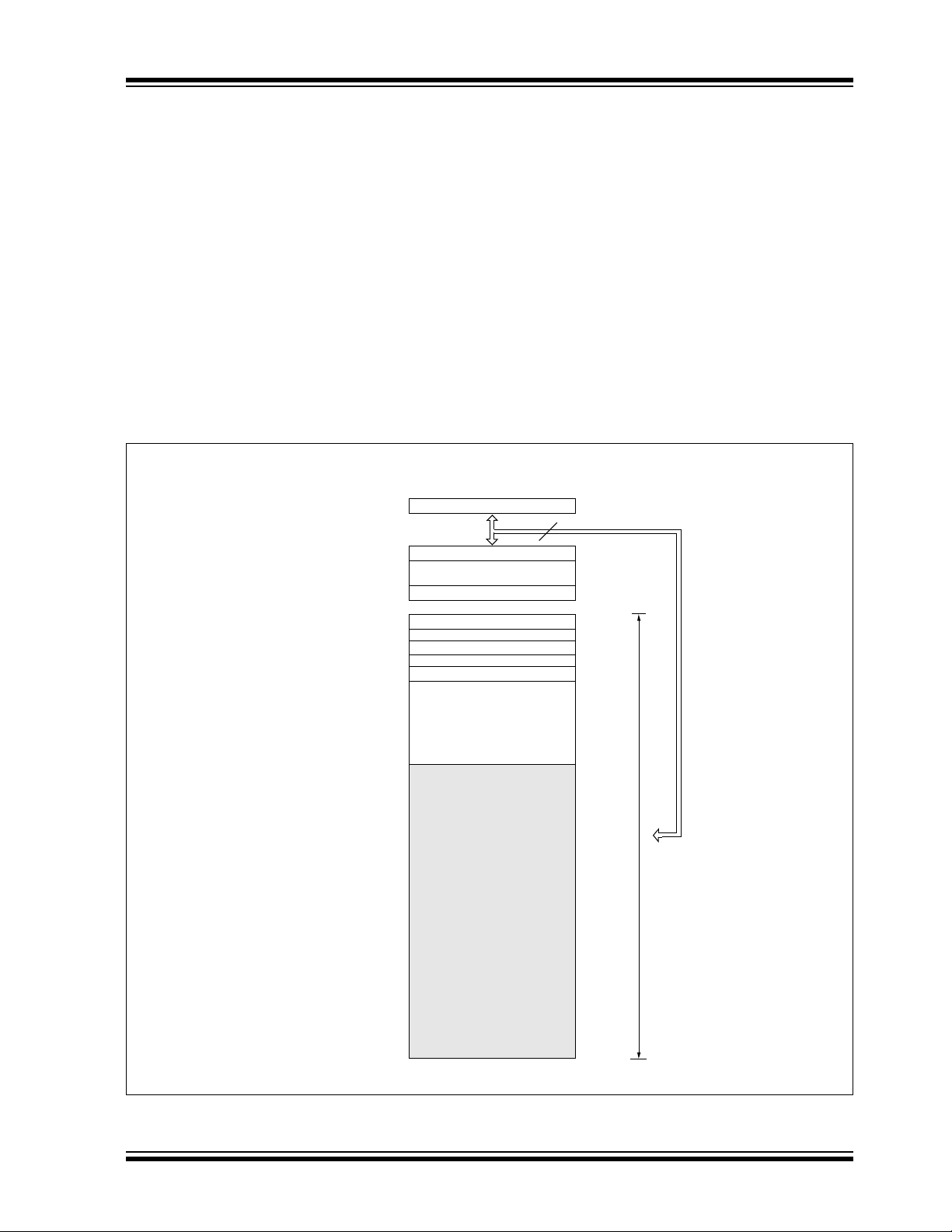
PIC18F2450/4450
5.0 MEMORY ORGANIZATION
There are two types of memory in PIC18F2450/4450
microcontroller devices:
• Program Memory
• Data RAM
As Harvard architecture devices, the data and program
memories use separate busses; this allows for
concurrent access of the two memory spaces.
Additional detailed information on the operation of the
Flash program memory is provided in Section 6.0
“Flash Program Memory”.
5.1 Program Memory Organization
PIC18 microcontrollers implement a 21-bit program
counter which is capable of addressing a 2-Mbyte
program memory space. Accessing a location between
the upper boundary of the physically implemented
memory and the 2-Mbyte address will return all ‘0’s (a
NOP instruction).
The PIC18F2450 and PIC18F4450 each have 16 Kbytes
of Flash memory and can store up to 8192 single-word
instructions.
PIC18 devices have two interrupt vectors. The Reset
vector address is at 0000h and the interrupt vector
addresses are at 0008h and 0018h.
The program memory maps for PIC18F2450 and
PIC18F4450 devices are shown in Figure 5-1.
FIGURE 5-1: PROGRAM MEMORY MAP AND STACK FOR PIC18F2450/4450 DEVICES
PIC18F2450/4450
CALL, RCALL, RETURN,
RETFIE, RETLW, CALLW,
ADDULNK, SUBULNK
PC<20:0>
Stack Level 1
Stack Level 31
21
•
•
•
Reset Vector
High-Priority Interrupt Vector
Low-Priority Interrupt Vector
On-Chip
Program Memory
Read ‘0’
0000h
0008h
0018h
3FFFh
4000h
User Memory Space
1FFFFFh
200000h
© 2007 Microchip Technology Inc. Preliminary DS39760C-page 53

PIC18F2450/4450
5.1.1 PROGRAM COUNTER
The Program Counter (PC) specifies the address of the
instruction to fetch for execution. The PC is 21 bits wide
and is contained in three separate 8-bit registers. The
low byte, known as the PCL register, is both readable
and writable. The high byte, or PCH register, contains
the PC<15:8> bits; it is not directly readable or writable.
Updates to the PCH register are performed through the
PCLATH register. The upper byte is called PCU. This
register contains the PC<20:16> bits; it is also not
directly readable or writable. Updates to the PCU
register are performed through the PCLATU register.
The contents of PCLATH and PCLATU are transferred
to the program counter by any operation that writes
PCL. Similarly, the upper two bytes of the program
counter are transferred to PCLATH and PCLATU by an
operation that reads PCL. This is useful for computed
offsets to the PC (see Section 5.1.4.1 “Computed
GOTO”).
The PC addresses bytes in the program memory. To
prevent the PC from becoming misaligned with word
instructions, the Least Significant bit of PCL is fixed to
a value of ‘0’. The PC increments by 2 to address
sequential instructions in the program memory.
The CALL, RCALL and GOTO program branch
instructions write to the program counter directly. For
these instructions, the contents of PCLATH and
PCLATU are not transferred to the program counter.
5.1.2 RETURN ADDRESS STACK
The return address stack allows any combination of up
to 31 program calls and interrupts to occur. The PC is
pushed onto the stack when a CALL or RCALL
instruction is executed or an interrupt is Acknowledged.
The PC value is pulled off the stack on a RETURN,
RETLW or a RETFIE instruction. PCLATU and PCLATH
are not affected by any of the RETURN or CALL
instructions.
The stack operates as a 31-word by 21-bit RAM and a
5-bit Stack Pointer, STKPTR. The stack space is not
part of either program or data space. The Stack Pointer
is readable and writable and the address on the top of
the stack is readable and writable through the Top-ofStack Special Function Registers. Data can also be
pushed to, or popped from the stack, using these
registers.
A CALL type instruction causes a push onto the stack.
The Stack Pointer is first incremented and the location
pointed to by the Stack Pointer is written with the
contents of the PC (already pointing to the instruction
following the CALL). A RETURN type instruction causes
a pop from the stack. The contents of the location
pointed to by the STKPTR are transferred to the PC
and then the Stack Pointer is decremented.
The Stack Pointer is initialized to ‘00000’ after all
Resets. There is no RAM associated with the location
corresponding to a Stack Pointer value of ‘00000’; this
is only a Reset value. Status bits indicate if the stack is
full, has overflowed or has underflowed.
5.1.2.1 Top-of-Stack Access
Only the top of the return address stack (TOS) is
readable and writable. A set of three registers,
TOSU:TOSH:TOSL, hold the contents of the stack location pointed to by the STKPTR register (Figure 5-2). This
allows users to implement a software stack if necessary.
After a CALL, RCALL or interrupt, the software can read
the pushed value by reading the TOSU:TOSH:TOSL
registers. These values can be placed on a user-defined
software stack. At return time, the software can return
these values to TOSU:TOSH:TOSL and do a return.
The user must disable the global interrupt enable bits
while accessing the stack to prevent inadvertent stack
corruption.
FIGURE 5-2: RETURN ADDRESS STACK AND ASSOCIATED REGISTERS
Return Address Stack<20:0>
11111
Top-of-Stack Registers Stack Pointer
TOSLTOSHTOSU
34h1Ah00h
To p- o f -S ta c k
DS39760C-page 54 Preliminary © 2007 Microchip Technology Inc.
001A34h
000D58h
11110
11101
STKPTR<4:0>
00010
00011
00010
00001
00000

PIC18F2450/4450
5.1.2.2 Return Stack Pointer (STKPTR)
The STKPTR register (Register 5-1) contains the Stack
Pointer value, the STKFUL (Stack Full) status bit and
the STKUNF (Stack Underflow) status bit. The value of
the Stack Pointer can be 0 through 31. The Stack
Pointer increments before values are pushed onto the
stack and decrements after values are popped off the
stack. On Reset, the Stack Pointer value will be zero.
The user may read and write the Stack Pointer value.
This feature can be used by a Real-Time Operating
System (RTOS) for return stack maintenance.
After the PC is pushed onto the stack 31 times (without
popping any values off the stack), the STKFUL bit is
set. The STKFUL bit is cleared by software or by a
POR.
The action that takes place when the stack becomes
full depends on the state of the STVREN (Stack
Overflow Reset Enable) Configuration bit. (Refer to
Section 18.1 “Configuration Bits” for a description of
the device Configuration bits.) If STVREN is set
(default), the 31st push will push the (PC + 2) value
onto the stack, set the STKFUL bit and reset the
device. The STKFUL bit will remain set and the Stack
Pointer will be set to zero.
If STVREN is cleared, the STKFUL bit will be set on the
31st push and the Stack Pointer will increment to 31.
Any additional pushes will not overwrite the 31st push
and the STKPTR will remain at 31.
When the stack has been popped enough times to
unload the stack, the next pop will return a value of zero
to the PC and sets the STKUNF bit, while the Stack
Pointer remains at zero. The STKUNF bit will remain
set until cleared by software or until a POR occurs.
Note: Returning a value of zero to the PC on an
underflow has the effect of vectoring the
program to the Reset vector, where the
stack conditions can be verified and
appropriate actions can be taken. This is
not the same as a Reset, as the contents
of the SFRs are not affected.
5.1.2.3 PUSH and POP Instructions
Since the Top-of-Stack is readable and writable, the
ability to push values onto the stack and pull values off
the stack, without disturbing normal program execution, is a desirable feature. The PIC18 instruction set
includes two instructions, PUSH and POP, that permit
the TOS to be manipulated under software control.
TOSU, TOSH and TOSL can be modified to place data
or a return address on the stack.
The PUSH instruction places the current PC value onto
the stack. This increments the Stack Pointer and loads
the current PC value onto the stack.
The POP instruction discards the current TOS by
decrementing the Stack Pointer. The previous value
pushed onto the stack then becomes the TOS value.
REGISTER 5-1: STKPTR: STACK POINTER REGISTER
R/C-0 R/C-0 U-0 R/W-0 R/W-0 R/W-0 R/W-0 R/W-0
STKFUL
bit 7 bit 0
Legend: C = Clearable bit
R = Readable bit W = Writable bit U = Unimplemented bit, read as ‘0’
-n = Value at POR ‘1’ = Bit is set ‘0’ = Bit is cleared x = Bit is unknown
bit 7 STKFUL: Stack Full Flag bit
bit 6 STKUNF: Stack Underflow Flag bit
bit 5 Unimplemented: Read as ‘0’
bit 4-0 SP4:SP0: Stack Pointer Location bits
Note 1: Bit 7 and bit 6 are cleared by user software or by a POR.
(1)
STKUNF
1 = Stack became full or overflowed
0 = Stack has not become full or overflowed
1 = Stack underflow occurred
0 = Stack underflow did not occur
(1)
— SP4 SP3 SP2 SP1 SP0
(1)
(1)
© 2007 Microchip Technology Inc. Preliminary DS39760C-page 55

PIC18F2450/4450
5.1.2.4 Stack Full and Underflow Resets
Device Resets on stack overflow and stack underflow
conditions are enabled by setting the STVREN bit in
Configuration Register 4L. When STVREN is set, a full
or underflow condition will set the appropriate STKFUL
or STKUNF bit and then cause a device Reset. When
STVREN is cleared, a full or underflow condition will set
the appropriate STKFUL or STKUNF bit but not cause
a device Reset. The STKFUL or STKUNF bits are
cleared by user software or a Power-on Reset.
5.1.3 FAST REGISTER STACK
A Fast Register Stack is provided for the STATUS,
WREG and BSR registers to provide a “fast return”
option for interrupts. Each stack is only one level deep
and is neither readable nor writable. It is loaded with the
current value of the corresponding register when the
processor vectors for an interrupt. All interrupt sources
will push values into the stack registers. The values in
the registers are then loaded back into their associated
registers if the RETFIE, FAST instruction is used to
return from the interrupt.
If both low and high-priority interrupts are enabled, the
stack registers cannot be used reliably to return from
low-priority interrupts. If a high-priority interrupt occurs
while servicing a low-priority interrupt, the stack
register values stored by the low-priority interrupt will
be overwritten. In these cases, users must save the key
registers in software during a low-priority interrupt.
If interrupt priority is not used, all interrupts may use the
Fast Register Stack for returns from interrupt. If no
interrupts are used, the Fast Register Stack can be
used to restore the STATUS, WREG and BSR registers
at the end of a subroutine call. To use the Fast Register
Stack for a subroutine call, a CALL label, FAST
instruction must be executed to save the STATUS,
WREG and BSR registers to the Fast Register Stack. A
RETURN, FAST instruction is then executed to restore
these registers from the Fast Register Stack.
Example 5-1 shows a source code example that uses
the Fast Register Stack during a subroutine call and
return.
EXAMPLE 5-1: FAST REGISTER STACK
CODE EXAMPLE
CALL SUB1, FAST ;STATUS, WREG, BSR
;SAVED IN FAST REGISTER
;STACK
•
•
SUB1 •
•
RETURN, FAST ;RESTORE VALUES SAVED
;IN FAST REGISTER STACK
5.1.4 LOOK-UP TABLES IN PROGRAM MEMORY
There may be programming situations that require the
creation of data structures, or look-up tables, in
program memory. For PIC18 devices, look-up tables
can be implemented in two ways:
• Computed GOTO
• Table Reads
5.1.4.1 Computed GOTO
A computed GOTO is accomplished by adding an offset
to the program counter. An example is shown in
Example 5-2.
A look-up table can be formed with an ADDWF PCL
instruction and a group of RETLW nn instructions. The
W register is loaded with an offset into the table before
executing a call to that table. The first instruction of the
called routine is the ADDWF PCL instruction. The next
instruction executed will be one of the RETLW nn
instructions that returns the value ‘nn’ to the calling
function.
The offset value (in WREG) specifies the number of
bytes that the program counter should advance and
should be multiples of 2 (LSb = 0).
In this method, only one data byte may be stored in
each instruction location and room on the return
address stack is required.
EXAMPLE 5-2: COMPUTED GOTO USING
AN OFFSET VALUE
MOVF OFFSET, W
CALL TABLE
ORG nn00h
TABLE ADDWF PCL
RETLW nnh
RETLW nnh
RETLW nnh
.
.
.
5.1.4.2 Table Reads and Table Writes
A better method of storing data in program memory
allows two bytes of data to be stored in each instruction
location.
Look-up table data may be stored two bytes per
program word by using table reads and writes. The
Table Pointer (TBLPTR) register specifies the byte
address and the Table Latch (TABLAT) register
contains the data that is read from or written to program
memory. Data is transferred to or from program
memory one byte at a time.
Table read and table write operations are discussed
further in Section 6.1 “Table Reads and Table
Writes”.
DS39760C-page 56 Preliminary © 2007 Microchip Technology Inc.

PIC18F2450/4450
5.2 PIC18 Instruction Cycle
5.2.1 CLOCKING SCHEME
The microcontroller clock input, whether from an
internal or external source, is internally divided by four
to generate four non-overlapping quadrature clocks
(Q1, Q2, Q3 and Q4). Internally, the program counter is
incremented on every Q1; the instruction is fetched
from the program memory and latched into the Instruction Register (IR) during Q4. The instruction is decoded
and executed during the following Q1 through Q4. The
clocks and instruction execution flow are shown in
Figure 5-3.
FIGURE 5-3: CLOCK/ INSTRUCTION CYCLE
OSC1
Q1
Q2
Q3
Q4
PC
OSC2/CLKO
(RC mode)
Q2 Q3 Q4
Q1
PC PC + 2 PC + 4
Execute INST (PC – 2)
Fetch INST (PC)
Q2 Q3 Q4
Q1
Execute INST (PC)
Fetch INST (PC + 2)
5.2.2 INSTRUCTION FLOW/PIPELINING
An “Instruction Cycle” consists of four Q cycles: Q1
through Q4. The instruction fetch and execute are
pipelined in such a manner that a fetch takes one
instruction cycle, while the decode and execute takes
another instruction cycle. However, due to the
pipelining, each instruction effectively executes in one
cycle. If an instruction causes the program counter to
change (e.g., GOTO), then two cycles are required to
complete the instruction (Example 5-3).
A fetch cycle begins with the Program Counter (PC)
incrementing in Q1.
In the execution cycle, the fetched instruction is latched
into the Instruction Register (IR) in cycle Q1. This
instruction is then decoded and executed during the
Q2, Q3 and Q4 cycles. Data memory is read during Q2
(operand read) and written during Q4 (destination
write).
Q2 Q3 Q4
Q1
Internal
Phase
Clock
Execute INST (PC + 2)
Fetch INST (PC + 4)
EXAMPLE 5-3: INSTRUCTION PIPELINE FLOW
TCY0TCY1TCY2TCY3TCY4TCY5
1. MOVLW 55h
2. MOVWF PORTB
3. BRA SUB_1
4. BSF PORTA, BIT3 (Forced NOP)
5. Instruction @ address SUB_1
Note: All instructions are single cycle, except for any program branches. These take two cycles since the fetch
instruction is “flushed” from the pipeline while the new instruction is being fetched and then executed.
© 2007 Microchip Technology Inc. Preliminary DS39760C-page 57
Fetch 1 Execute 1
Fetch 2 Execute 2
Fetch 3 Execute 3
Fetch 4 Flush (NOP)
Fetch SUB_1 Execute SUB_1

PIC18F2450/4450
5.2.3 INSTRUCTIONS IN PROGRAM MEMORY
The program memory is addressed in bytes.
Instructions are stored as two bytes or four bytes in
program memory. The Least Significant Byte of an
instruction word is always stored in a program memory
location with an even address (LSb = 0). To maintain
alignment with instruction boundaries, the PC
increments in steps of 2 and the LSb will always read
‘0’ (see Section 5.1.1 “Program Counter”).
Figure 5-4 shows an example of how instruction words
are stored in the program memory.
The CALL and GOTO instructions have the absolute
program memory address embedded into the
instruction. Since instructions are always stored on word
boundaries, the data contained in the instruction is a
word address. The word address is written to PC<20:1>,
which accesses the desired byte address in program
memory. Instruction #2 in Figure 5-4 shows how the
instruction, GOTO 0006h, is encoded in the program
memory. Program branch instructions, which encode a
relative address offset, operate in the same manner. The
offset value stored in a branch instruction represents the
number of single-word instructions that the PC will be
offset by. Section 19.0 “Instruction Set Summary”
provides further details of the instruction set.
FIGURE 5-4: INSTRUCTIONS IN PROGRAM MEMORY
LSB = 1 LSB = 0 ↓
F0h 00h 00000Ch
F4h 56h 000010h
Instruction 1:
Instruction 2:
Instruction 3:
Program Memory
Byte Locations
MOVLW 055h 0Fh 55h 000008h
GOTO 0006h EFh 03h 00000Ah
MOVFF 123h, 456h C1h 23h 00000Eh
→
Word Address
000000h
000002h
000004h
000006h
000012h
000014h
5.2.4 TWO-WORD INSTRUCTIONS
The standard PIC18 instruction set has four two-word
instructions: CALL, MOVFF, GOTO and LSFR. In all
cases, the second word of the instructions always has
‘1111’ as its four Most Significant bits; the other 12 bits
are literal data, usually a data memory address.
The use of ‘1111’ in the 4 MSbs of an instruction
specifies a special form of NOP. If the instruction is
executed in proper sequence, immediately after the
first word, the data in the second word is accessed and
used by the instruction sequence. If the first word is
skipped for some reason and the second word is
executed by itself, a NOP is executed instead. This is
necessary for cases when the two-word instruction is
preceded by a conditional instruction that changes the
PC. Example 5-4 shows how this works.
Note: See Section 5.5 “Program Memory and
the Extended Instruction Set” for
information on two-word instruction in the
extended instruction set.
EXAMPLE 5-4: TWO-WORD INSTRUCTIONS
CASE 1:
Object Code Source Code
0110 0110 0000 0000 TSTFSZ REG1 ; is RAM location 0?
1100 0001 0010 0011 MOVFF REG1, REG2 ; No, skip this word
1111 0100 0101 0110 ; Execute this word as a NOP
0010 0100 0000 0000 ADDWF REG3 ; continue code
CASE 2:
Object Code Source Code
0110 0110 0000 0000 TSTFSZ REG1 ; is RAM location 0?
1100 0001 0010 0011 MOVFF REG1, REG2 ; Yes, execute this word
1111 0100 0101 0110 ; 2nd word of instruction
0010 0100 0000 0000 ADDWF REG3 ; continue code
DS39760C-page 58 Preliminary © 2007 Microchip Technology Inc.

PIC18F2450/4450
5.3 Data Memory Organization
Note: The operation of some aspects of data
memory are changed when the PIC18
extended instruction set is enabled. See
Section 5.6 “Data Memory and the
Extended Instruction Set” for more
information.
The data memory in PIC18 devices is implemented as
static RAM. Each register in the data memory has a
12-bit address, allowing up to 4096 bytes of data
memory. The memory space is divided into as many as
16 banks that contain 256 bytes each. PIC18F2450/
4450 devices implement three complete banks, for a
total of 768 bytes. Figure 5-5 shows the data memory
organization for the devices.
The data memory contains Special Function Registers
(SFRs) and General Purpose Registers (GPRs). The
SFRs are used for control and status of the controller
and peripheral functions, while GPRs are used for data
storage and scratchpad operations in the user’s
application. Any read of an unimplemented location will
read as ‘0’s.
The instruction set and architecture allow operations
across all banks. The entire data memory may be
accessed by Direct, Indirect or Indexed Addressing
modes. Addressing modes are discussed later in this
subsection.
To ensure that commonly used registers (SFRs and
select GPRs) can be accessed in a single cycle, PIC18
devices implement an Access Bank. This is a 256-byte
memory space that provides fast access to SFRs and
the lower portion of GPR Bank 0 without using the
BSR. Section 5.3.3 “Access Bank” provides a
detailed description of the Access RAM.
5.3.1 USB RAM
Bank 4 of the data memory is actually mapped to
special dual port RAM. When the USB module is
disabled, the GPRs in these banks are used like any
other GPR in the data memory space.
When the USB module is enabled, the memory in this
bank is allocated as buffer RAM for USB operation.
This area is shared between the microcontroller core
and the USB Serial Interface Engine (SIE) and is used
to transfer data directly between the two.
It is theoretically possible to use this area of USB RAM
that is not allocated as USB buffers for normal scratchpad memory or other variable storage. In practice, the
dynamic nature of buffer allocation makes this risky at
best. Bank 4 is also used for USB buffer management
when the module is enabled and should not be used for
any other purposes during that time.
Additional information on USB RAM and buffer
operation is provided in Section 14.0 “Universal
Serial Bus (USB)”.
5.3.2 BANK SELECT REGISTER (BSR)
Large areas of data memory require an efficient
addressing scheme to make rapid access to any
address possible. Ideally, this means that an entire
address does not need to be provided for each read or
write operation. For PIC18 devices, this is
accomplished with a RAM banking scheme. This
divides the memory space into 16 contiguous banks of
256 bytes. Depending on the instruction, each location
can be addressed directly by its full 12-bit address, or
an 8-bit low-order address and a 4-bit Bank Pointer.
Most instructions in the PIC18 instruction set make use
of the Bank Pointer, known as the Bank Select Register
(BSR). This SFR holds the 4 Most Significant bits of a
location’s address; the instruction itself includes the
8 Least Significant bits. Only the four lower bits of the
BSR are implemented (BSR3:BSR0). The upper four
bits are unused; they will always read ‘0’ and cannot be
written to. The BSR can be loaded directly by using the
MOVLB instruction.
The value of the BSR indicates the bank in data
memory. The eight bits in the instruction show the location in the bank and can be thought of as an offset from
the bank’s lower boundary. The relationship between
the BSR’s value and the bank division in data memory
is shown in Figure 5-6.
Since up to 16 registers may share the same low-order
address, the user must always be careful to ensure that
the proper bank is selected before performing a data
read or write. For example, writing what should be
program data to an 8-bit address of F9h, while the BSR
is 0Fh, will end up resetting the program counter.
While any bank can be selected, only those banks that
are actually implemented can be read or written to.
Writes to unimplemented banks are ignored, while
reads from unimplemented banks will return ‘0’s. Even
so, the STATUS register will still be affected as if the
operation was successful. The data memory map in
Figure 5-6 indicates which banks are implemented.
In the core PIC18 instruction set, only the MOVFF
instruction fully specifies the 12-bit address of the
source and target registers. This instruction ignores the
BSR completely when it executes. All other instructions
include only the low-order address as an operand and
must use either the BSR or the Access Bank to locate
their target registers.
© 2007 Microchip Technology Inc. Preliminary DS39760C-page 59
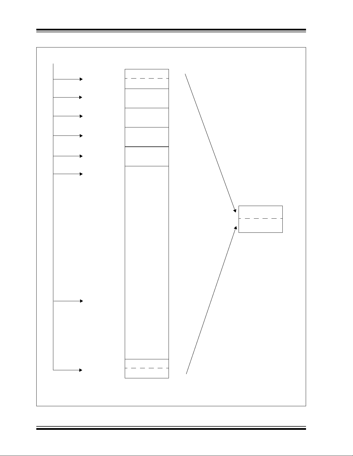
PIC18F2450/4450
FIGURE 5-5: DATA MEMORY MAP FOR PIC18F2450/4450 DEVICES
BSR<3:0>
= 0000
= 0001
= 0010
= 0011
= 0100
= 0101
Bank 0
Bank 1
Bank 2
Bank 3
Bank 4
Bank 5
to
Data Memory Map
00h
FFh
00h
FFh
00h
FFh
00h
FFh
00h
FFh
00h
Access RAM
GPR
GPR
Unused
Read as 00h
Unused
Read as 00h
GPR
(1)
000h
05Fh
060h
0FFh
100h
1FFh
200h
2FFh
300h
3FFh
400h
4FFh
800h
When a = 0:
The BSR is ignored and the
Access Bank is used.
The first 96 bytes are
general purpose RAM
(from Bank 0).
The remaining 160 bytes are
Special Function Registers
(from Bank 15).
When a = 1:
The BSR specifies the bank
used by the instruction.
Access Bank
Access RAM Low
Access RAM High
(SFRs)
00h
5Fh
60h
FFh
Unused
Read as 00h
= 1110
= 1111
Note 1: This bank also serve as RAM buffer for USB operation. See Section 5.3.1 “USB RAM” for more
information.
Bank 14
Bank 15
FFh
00h
FFh
Unused
SFR
EFFh
F00h
F5Fh
F60h
FFFh
DS39760C-page 60 Preliminary © 2007 Microchip Technology Inc.
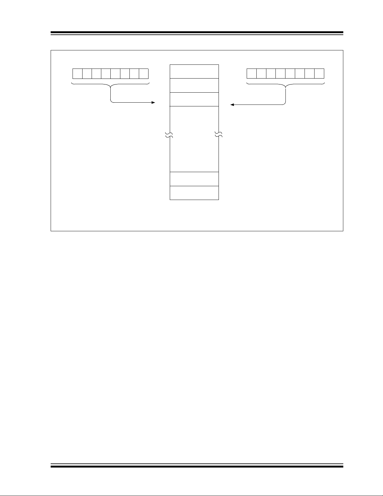
PIC18F2450/4450
FIGURE 5-6: USE OF THE BANK SELECT REGISTER (DIRECT ADDRESSING)
(1)
7
0000
Bank Select
Note 1: The Access RAM bit of the instruction can be used to force an override of the selected bank (BSR<3:0>) to
2: The MOVFF instruction embeds the entire 12-bit address in the instruction.
BSR
0
0011
(2)
FFFh
the registers of the Access Bank.
000h
100h
200h
300h
E00h
F00h
Data Memory
Bank 0
Bank 1
Bank 2
Bank 3
through
Bank 13
Bank 14
Bank 15
00h
FFh
00h
FFh
00h
FFh
00h
FFh
00h
FFh
00h
FFh
7
From Opcode
11111111
(2)
0
5.3.3 ACCESS BANK
While the use of the BSR, with an embedded 8-bit
address, allows users to address the entire range of
data memory, it also means that the user must always
ensure that the correct bank is selected. Otherwise,
data may be read from or written to the wrong location.
This can be disastrous if a GPR is the intended target
of an operation but an SFR is written to instead.
Verifying and/or changing the BSR for each read or
write to data memory can become very inefficient.
To streamline access for the most commonly used data
memory locations, the data memory is configured with
an Access Bank, which allows users to access a
mapped block of memory without specifying a BSR.
The Access Bank consists of the first 96 bytes of
memory (00h-5Fh) in Bank 0 and the last 160 bytes of
memory (60h-FFh) in Block 15. The lower half is known
as the “Access RAM” and is composed of GPRs. The
upper half is where the device’s SFRs are mapped.
These two areas are mapped contiguously in the
Access Bank and can be addressed in a linear fashion
by an 8-bit address (Figure 5-5).
The Access Bank is used by core PIC18 instructions
that include the Access RAM bit (the ‘a’ parameter in
the instruction). When ‘a’ is equal to ‘1’, the instruction
uses the BSR and the 8-bit address included in the
opcode for the data memory address. When ‘a’ is ‘0’,
however, the instruction is forced to use the Access
Bank address map; the current value of the BSR is
ignored entirely.
Using this “forced” addressing allows the instruction to
operate on a data address in a single cycle without
updating the BSR first. For 8-bit addresses of 60h and
above, this means that users can evaluate and operate
on SFRs more efficiently. The Access RAM below 60h
is a good place for data values that the user might need
to access rapidly, such as immediate computational
results or common program variables. Access RAM
also allows for faster and more code efficient context
saving and switching of variables.
The mapping of the Access Bank is slightly different
when the extended instruction set is enabled (XINST
Configuration bit = 1). This is discussed in more detail
in Section 5.6.3 “Mapping the Access Bank in
Indexed Literal Offset Mode”.
5.3.4 GENERAL PURPOSE REGISTER FILE
PIC18 devices may have banked memory in the GPR
area. This is data RAM which is available for use by all
instructions. GPRs start at the bottom of Bank 0
(address 000h) and grow upwards towards the bottom of
the SFR area. GPRs are not initialized by a Power-on
Reset and are unchanged on all other Resets.
© 2007 Microchip Technology Inc. Preliminary DS39760C-page 61

PIC18F2450/4450
5.3.5 SPECIAL FUNCTION REGISTERS
The Special Function Registers (SFRs) are registers
used by the CPU and peripheral modules for controlling
the desired operation of the device. These registers are
implemented as static RAM in the data memory space.
SFRs start at the top of data memory and extend
downward to occupy the top segment of Bank 15, from
F60h to FFFh. A list of these registers is given in
Table 5-1 and Table 5-2.
peripheral functions. The Reset and interrupt registers
are described in their respective chapters, while the
ALU’s STATUS register is described later in this
section. Registers related to the operation of a
peripheral feature are described in the chapter for that
peripheral.
The SFRs are typically distributed among the
peripherals whose functions they control. Unused SFR
locations are unimplemented and read as ‘0’s.
The SFRs can be classified into two sets: those
associated with the “core” device functionality (ALU,
Resets and interrupts) and those related to the
TABLE 5-1: SPECIAL FUNCTION REGISTER MAP FOR PIC18F2450/4450 DEVICES
Address Name Address Name Address Name Address Name Address Name
FFFh TOSU FDFh INDF2
FFEh TOSH FDEh POSTINC2
FFDh TOSL FDDh POSTDEC2
FFCh STKPTR FDCh PREINC2
FFBh PCLATU FDBh PLUSW2
FFAh PCLATH FDAh FSR2H FBAh
FF9h PCL FD9h FSR2L FB9h
FF8h TBLPTRU FD8h STATUS FB8h BAUDCON F98h
FF7h TBLPTRH FD7h TMR0H FB7h
FF6h TBLPTRL FD6h TMR0L FB6h
FF5h TABLAT FD5h T0CON FB5h
FF4h PRODH FD4h
FF3h PRODL FD3h OSCCON FB3h
FF2h INTCON FD2h HLVDCON FB2h
FF1h INTCON2 FD1h WDTCON FB1h
FF0h INTCON3 FD0h RCON FB0h SPBRGH F90h
FEFh INDF0
(1)
FEEh POSTINC0
FEDh POSTDEC0
FECh PREINC0
FEBh PLUSW0
(1)
(1)
FCFh TMR1H FAFh SPBRG F8Fh —
(1)
FCEh TMR1L FAEh RCREG F8Eh —
(1)
FCDh T1CON FADh TXREG F8Dh LATE
FCCh TMR2 FACh TXSTA F8Ch LATD
FCBh PR2 FABh RCSTA F8Bh LATC F6Bh UEIE
FEAh FSR0H FCAh T2CON FAAh
FE9h FSR0L FC9h
FE8h WREG FC8h
FE7h INDF1
FE6h POSTINC1
FE5h POSTDEC1
FE4h PREINC1
FE3h PLUSW1
(1)
(1)
(1)
FC7h —
(1)
FC6h —
(1)
FC5h —
FC4h ADRESH FA4h —
FC3h ADRESL FA3h —
FE2h FSR1H FC2h ADCON0 FA2h IPR2 F82h PORTC F62h —
FE1h FSR1L FC1h ADCON1 FA1h PIR2 F81h PORTB F61h —
FE0h BSR FC0h ADCON2 FA0h PIE2 F80h PORTA F60h —
(1)
(1)
(1)
(2)
—
(2)
—
(2)
—
(2)
(2)
(2)
FBFh CCPR1H F9Fh IPR1 F7Fh UEP15
(1)
FBEh CCPR1L F9Eh PIR1 F7Eh UEP14
(1)
FBDh CCP1CON F9Dh PIE1 F7Dh UEP13
FBCh —
FBBh —
FB4h —
FA9 h —
FA8 h —
FA7 h EEC ON2
FA6h EECON1 F86h —
FA5 h —
(2)
(2)
(2)
—
(2)
—
(2)
—
(2)
—
(2)
—
(2)
(2)
—
(2)
—
(2)
—
(2)
—
(2)
(2)
(1)
(2)
(2)
(2)
F9Ch —
F9Bh —
F9Ah —
F99h —
F97h —
F96h TRISE
F95h TRISD
F94h TRISC F74h UEP4
F93h TRISB F73h UEP3
F92h TRISA F72h UEP2
F91h —
F8Ah LATB F6Ah UEIR
F89h LATA F69h UIE
F88h —
F87h —
F85h —
F84h PORTE F64h —
F83h PORTD
(2)
(2)
(2)
(2)
(2)
—
(2)
(3)
(3)
(2)
(2)
—
(2)
(2)
(3)
(3)
(2)
(2)
(2)
(2)
(3)
F7Ch UEP12
F7Bh UEP11
F7Ah UEP10
F79h UEP9
F78h UEP8
F77h UEP7
F76h UEP6
F75h UEP5
F71h UEP1
F70h UEP0
F6Fh UCFG
F6Eh UADDR
F6Dh UCON
F6Ch USTAT
F68h UIR
F67h UFRMH
F66h UFRML
F65h —
F63h —
(2)
(2)
(2)
(2)
(2)
(2)
Note 1: Not a physical register.
2: Unimplemented registers are read as ‘0’.
3: These registers are implemented only on 40/44-pin devices.
DS39760C-page 62 Preliminary © 2007 Microchip Technology Inc.

PIC18F2450/4450
TABLE 5-2: REGISTER FILE SUMMARY (PIC18F2450/4450)
File Name Bit 7 Bit 6 Bit 5 Bit 4 Bit 3 Bit 2 Bit 1 Bit 0
TOSU
TOSH Top-of-Stack High Byte (TOS<15:8>) 0000 0000 49, 54
TOSL Top-of-Stack Low Byte (TOS<7:0>) 0000 0000 49, 54
STKPTR STKFUL STKUNF
PCLATU
PCLATH Holding Register for PC<15:8> 0000 0000 49, 54
PCL PC Low Byte (PC<7:0>) 0000 0000 49, 54
TBLPTRU
TBLPTRH Program Memory Table Pointer High Byte (TBLPTR<15:8>) 0000 0000 49, 76
TBLPTRL Program Memory Table Pointer Low Byte (TBLPTR<7:0>) 0000 0000 49, 76
TABLAT Program Memory Table Latch 0000 0000 49, 76
PRODH Product Register High Byte xxxx xxxx 49, 83
PRODL Product Register Low Byte xxxx xxxx 49, 83
INTCON GIE/GIEH PEIE/GIEL TMR0IE INT0IE RBIE TMR0IF INT0IF RBIF 0000 000x 49, 87
INTCON2 RBPU
INTCON3 INT2IP INT1IP
INDF0 Uses contents of FSR0 to address data memory – value of FSR0 not changed (not a physical register) N/A 49, 68
POSTINC0 Uses contents of FSR0 to address data memory – value of FSR0 post-incremented (not a physical register) N/A 49, 69
POSTDEC0 Uses contents of FSR0 to address data memory – value of FSR0 post-decremented (not a physical register) N/A 49, 69
PREINC0 Uses contents of FSR0 to address data memory – value of FSR0 pre-incremented (not a physical register) N/A 49, 69
PLUSW0 Uses contents of FSR0 to address data memory – value of FSR0 pre-incremented (not a physical register) –
FSR0H
FSR0L Indirect Data Memory Address Pointer 0 Low Byte xxxx xxxx 49, 68
WREG Working Register xxxx xxxx 49,
INDF1 Uses contents of FSR1 to address data memory – value of FSR1 not changed (not a physical register) N/A 49, 68
POSTINC1 Uses contents of FSR1 to address data memory – value of FSR1 post-incremented (not a physical register) N/A 49, 69
POSTDEC1 Uses contents of FSR1 to address data memory – value of FSR1 post-decremented (not a physical register) N/A 49, 69
PREINC1 Uses contents of FSR1 to address data memory – value of FSR1 pre-incremented (not a physical register) N/A 49, 69
PLUSW1 Uses contents of FSR1 to address data memory – value of FSR1 pre-incremented (not a physical register) –
FSR1H
FSR1L Indirect Data Memory Address Pointer 1 Low Byte xxxx xxxx 49, 68
BSR
INDF2 Uses contents of FSR2 to address data memory – value of FSR2 not changed (not a physical register) N/A 50, 68
POSTINC2 Uses contents of FSR2 to address data memory – value of FSR2 post-incremented (not a physical register) N/A 50, 69
POSTDEC2 Uses contents of FSR2 to address data memory – value of FSR2 post-decremented (not a physical register) N/A 50, 69
PREINC2 Uses contents of FSR2 to address data memory – value of FSR2 pre-incremented (not a physical register) N/A 50, 69
PLUSW2 Uses contents of FSR2 to address data memory – value of FSR2 pre-incremented (not a physical register) –
FSR2H
FSR2L Indirect Data Memory Address Pointer 2 Low Byte xxxx xxxx 50, 68
STATUS
TMR0H Timer0 Register High Byte 0000 0000 50, 113
TMR0L Timer0 Register Low Byte xxxx xxxx 50, 113
T0CON TMR0ON T08BIT T0CS T0SE PSA T0PS2 T0PS1 T0PS0 1111 1111 50 , 111
Legend: x = unknown, u = unchanged, - = unimplemented, q = value depends on condition. Shaded cells are unimplemented, read as ‘0’.
Note 1: Bit 21 of the TBLPTRU allows access to the device Configuration bits.
2: The SBOREN bit is only available when BOREN<1:0> = 01; otherwise, the bit reads as ‘0’.
3: These registers and/or bits are not implemented on 28-pin devices and are read as ‘0’. Reset values are shown for 40/44-pin devices;
4: RA6 is configured as a port pin based on various primary oscillator modes. When the port pin is disabled, all of the associated bits read ‘0’.
5: RE3 is only available as a port pin when the MCLRE Configuration bit is clear; otherwise, the bit reads as ‘0’.
6: RC5 and RC4 are only available as port pins when the USB module is disabled (UCON<3> = 0).
— — — Top-of-Stack Upper Byte (TOS<20:16>) ---0 0000 49, 54
— SP4 SP3 SP2 SP1 SP0 00-0 0000 49, 55
— — — Holding Register for PC<20:16> ---0 0000 49, 54
— —bit 21
INTEDG0 INTEDG1 INTEDG2 —TMR0IP—RBIP1111 -1-1 49, 88
value of FSR0 offset by W
— — — — Indirect Data Memory Address Pointer 0 High Byte ---- 0000 49, 68
value of FSR1 offset by W
— — — — Indirect Data Memory Address Pointer 1 High Byte ---- 0000 49, 68
— — — — Bank Select Register ---- 0000 49, 59
value of FSR2 offset by W
— — — — Indirect Data Memory Address Pointer 2 High Byte ---- 0000 50, 68
— — —NOVZDCC---x xxxx 50, 66
individual unimplemented bits should be interpreted as ‘-’.
(1)
Program Memory Table Pointer Upper Byte (TBLPTR<20:16>) --00 0000 49, 76
— INT2IE INT1IE —INT2IFINT1IF11-0 0-00 49, 89
Valu e o n
POR, BOR
N/A 49, 69
N/A 49, 69
N/A 50, 69
Details
on Page:
© 2007 Microchip Technology Inc. Preliminary DS39760C-page 63

PIC18F2450/4450
TABLE 5-2: REGISTER FILE SUMMARY (PIC18F2450/4450) (CONTINUED)
File Name Bit 7 Bit 6 Bit 5 Bit 4 Bit 3 Bit 2 Bit 1 Bit 0
OSCCON IDLEN — — —OSTS— SCS1 SCS0 0--- q-00 50, 31
HLVDCON VDIRMAG
WDTCON
RCON IPEN SBOREN
TMR1H Timer1 Register High Byte xxxx xxxx 50, 120
TMR1L Timer1 Register Low Byte xxxx xxxx 50, 120
T1CON RD16 T1RUN T1CKPS1 T1CKPS0 T1OSCEN T1SYNC
TMR2 Timer2 Register 0000 0000 50, 122
PR2 Timer2 Period Register 1111 1111 50, 122
T2CON
ADRESH A/D Result Register High Byte xxxx xxxx 50, 184
ADRESL A/D Result Register Low Byte xxxx xxxx 50, 184
ADCON0 — — CHS3 CHS2 CHS1 CHS0 GO/DONE ADON --00 0000 50, 175
ADCON1
ADCON2 ADFM
CCPR1H Capture/Compare/PWM Register 1 High Byte xxxx xxxx 50, 124
CCPR1L Capture/Compare/PWM Register 1 Low Byte xxxx xxxx 50, 124
CCP1CON
BAUDCON ABDOVF RCIDL
SPBRGH EUSART Baud Rate Generator Register High Byte 0000 0000 50, 157
SPBRG EUSART Baud Rate Generator Register Low Byte 0000 0000 50, 157
RCREG EUSART Receive Register 0000 0000 50, 165
TXREG EUSART Transmit Register 0000 0000 50, 163
TXSTA CSRC TX9 TXEN SYNC SENDB BRGH TRMT TX9D 0000 0010 51, 154
RCSTA SPEN RX9 SREN CREN ADDEN FERR OERR RX9D 0000 000x 51, 155
EECON2 Data Memory Control Register 2 (not a physical register) 0000 0000 51, 74
EECON1
IPR2 OSCFIP
PIR2 OSCFIF
PIE2 OSCFIE
IPR1
PIR1
PIE1
(3)
TRISE
(3)
TRISD
TRISC TRISC7 TRISC6
TRISB TRISB7 TRISB6 TRISB5 TRISB4 TRISB3 TRISB2 TRISB1 TRISB0 1111 1111 51, 103
TRISA
(3)
LATE
(3)
LATD
LATC LATC7 LATC6
LATB LATB7 LATB6 LATB5 LATB4 LATB3 LATB2 LATB1 LATB0 xxxx xxxx 51, 103
LATA
PORTE
(3)
PORTD
Legend: x = unknown, u = unchanged, - = unimplemented, q = value depends on condition. Shaded cells are unimplemented, read as ‘0’.
Note 1: Bit 21 of the TBLPTRU allows access to the device Configuration bits.
2: The SBOREN bit is only available when BOREN<1:0> = 01; otherwise, the bit reads as ‘0’.
3: These registers and/or bits are not implemented on 28-pin devices and are read as ‘0’. Reset values are shown for 40/44-pin devices;
4: RA6 is configured as a port pin based on various primary oscillator modes. When the port pin is disabled, all of the associated bits read ‘0’.
5: RE3 is only available as a port pin when the MCLRE Configuration bit is clear; otherwise, the bit reads as ‘0’.
6: RC5 and RC4 are only available as port pins when the USB module is disabled (UCON<3> = 0).
— — — — — — —SWDTEN--- ---0 50, 204
— T2OUTPS3 T2OUTPS2 T2OUTPS1 T2OUTPS0 TMR2ON T2CKPS1 T2CKPS0 -000 0000 50, 121
— — VCFG1 VCFG0 PCFG3 PCFG2 PCFG1 PCFG0 --00 qqqq 50, 176
— — DC1B1 DC1B0 CCP1M3 CCP1M2 CCP1M1 CCP1M0 --00 0000 50, 123,
—CFGS— FREE WRERR WREN WR — -x-0 x00- 51, 75
— ADIP RCIP TXIP — CCP1IP TMR2IP TMR1IP -111 -111 51, 94
— ADIF RCIF TXIF — CCP1IF TMR2IF TMR1IF -000 -000 51, 90
— ADIE RCIE TXIE — CCP1IE TMR2IE TMR1IE -000 -000 51, 92
— — — — — TRISE2 TRISE1 TRISE0 ---- -111 51, 110
TRISD7 TRISD6 TRISD5 TRISD4 TRISD3 TRISD2 TRISD1 TRISD0 1111 1111 51, 108
— TRISA6
— — — — — LATE2 LATE1 LATE0 ---- -xxx 51, 110
LATD7LATD6LATD5LATD4LATD3LATD2LATD1LATD0xxxx xxxx 51, 108
—LATA6
— — — —RE3
RD7 RD6 RD5 RD4 RD3 RD2 RD1 RD0 xxxx xxxx 51, 108
individual unimplemented bits should be interpreted as ‘-’.
— IRVST HLVDEN HLVDL3 HLVDL2 HLVDL1 HLVDL0 0-00 0101 50, 185
(2)
—RITO PD POR BOR 0q-1 11q0 50, 42
TMR1CS TMR1ON 0000 0000 50, 115
— ACQT2 ACQT1 ACQT0 ADCS2 ADCS1 ADCS0 0-00 0000 50, 177
— SCKP BRG16 — WUE ABDEN 01-0 0-00 51, 156,
— USBIP — —HLVDIP— — 1-1- -1-- 51, 95
—USBIF— —HLVDIF— — 0-0- -0-- 51, 91
— USBIE — —HLVDIE— — 0-0- -0-- 51, 93
— — — TRISC2 TRISC1 TRISC0 11-- -111 51, 106
(4)
TRISA5 TRISA4 TRISA3 TRISA2 TRISA1 TRISA0 -111 1111 51, 100
— — — LATC2 LATC1 LATC0 xx-- -xxx 51, 106
(4)
LATA5 LATA4 LATA3 LATA2 LATA1 LATA0 -xxx xxxx 51, 100
(5)
RE2
(3)
RE1
(3)
RE0
Value on
POR, BOR
(3)
---- x000 51, 109
Details
on Page:
DS39760C-page 64 Preliminary © 2007 Microchip Technology Inc.

PIC18F2450/4450
TABLE 5-2: REGISTER FILE SUMMARY (PIC18F2450/4450) (CONTINUED)
File Name Bit 7 Bit 6 Bit 5 Bit 4 Bit 3 Bit 2 Bit 1 Bit 0
PORTC RC7 RC6 RC5
PORTB RB7 RB6 RB5 RB4 RB3 RB2 RB1 RB0 xxxx xxxx 51, 100
PORTA
UEP15
UEP14
UEP13
UEP12
UEP11
UEP10
UEP9
UEP8
UEP7
UEP6
UEP5
UEP4
UEP3
UEP2
UEP1
UEP0
UCFG UTEYE UOEMON
UADDR
UCON
USTAT
UEIE BTSEE
UEIR BTSEF
UIE
UIR
UFRMH
UFRML FRM7 FRM6 FRM5 FRM4 FRM3 FRM2 FRM1 FRM0 xxxx xxxx 52, 136
Legend: x = unknown, u = unchanged, - = unimplemented, q = value depends on condition. Shaded cells are unimplemented, read as ‘0’.
Note 1: Bit 21 of the TBLPTRU allows access to the device Configuration bits.
2: The SBOREN bit is only available when BOREN<1:0> = 01; otherwise, the bit reads as ‘0’.
3: These registers and/or bits are not implemented on 28-pin devices and are read as ‘0’. Reset values are shown for 40/44-pin devices;
4: RA6 is configured as a port pin based on various primary oscillator modes. When the port pin is disabled, all of the associated bits read ‘0’.
5: RE3 is only available as a port pin when the MCLRE Configuration bit is clear; otherwise, the bit reads as ‘0’.
6: RC5 and RC4 are only available as port pins when the USB module is disabled (UCON<3> = 0).
—RA6
— — — EPHSHK EPCONDIS EPOUTEN EPINEN EPSTALL ---0 0000 51, 135
— — — EPHSHK EPCONDIS EPOUTEN EPINEN EPSTALL ---0 0000 51, 135
— — — EPHSHK EPCONDIS EPOUTEN EPINEN EPSTALL ---0 0000 51, 135
— — — EPHSHK EPCONDIS EPOUTEN EPINEN EPSTALL ---0 0000 51, 135
— — — EPHSHK EPCONDIS EPOUTEN EPINEN EPSTALL ---0 0000 51, 135
— — — EPHSHK EPCONDIS EPOUTEN EPINEN EPSTALL ---0 0000 51, 135
— — — EPHSHK EPCONDIS EPOUTEN EPINEN EPSTALL ---0 0000 51, 135
— — — EPHSHK EPCONDIS EPOUTEN EPINEN EPSTALL ---0 0000 52, 135
— — — EPHSHK EPCONDIS EPOUTEN EPINEN EPSTALL ---0 0000 52, 135
— — — EPHSHK EPCONDIS EPOUTEN EPINEN EPSTALL ---0 0000 52, 135
— — — EPHSHK EPCONDIS EPOUTEN EPINEN EPSTALL ---0 0000 52, 135
— — — EPHSHK EPCONDIS EPOUTEN EPINEN EPSTALL ---0 0000 52, 135
— — — EPHSHK EPCONDIS EPOUTEN EPINEN EPSTALL ---0 0000 52, 135
— — — EPHSHK EPCONDIS EPOUTEN EPINEN EPSTALL ---0 0000 52, 135
— — — EPHSHK EPCONDIS EPOUTEN EPINEN EPSTALL ---0 0000 52, 135
— — — EPHSHK EPCONDIS EPOUTEN EPINEN EPSTALL ---0 0000 52, 135
— ADDR6 ADDR5 ADDR4 ADDR3 ADDR2 ADDR1 ADDR0 -000 0000 52, 136
— PPBRST SE0 PKTDIS USBEN RESUME SUSPND — -0x0 000- 52, 130
— ENDP3 ENDP2 ENDP1 ENDP0 DIR PPBI — -xxx xxx- 52, 134
— SOFIE STALLIE IDLEIE TRNIE ACTVIE UERRIE URSTIE -000 0000 52, 146
— SOFIF STALLIF IDLEIF TRNIF ACTVIF UERRIF URSTIF -000 0000 52, 144
— — — — — FRM10 FRM9 FRM8 ---- -xxx 52, 136
individual unimplemented bits should be interpreted as ‘-’.
(4)
— — BTOEE DFN8EE CRC16EE CRC5EE PIDEE 0--0 0000 52, 148
— — BTOEF DFN8EF CRC16EF CRC5EF PIDEF 0--0 0000 52, 147
(6)
RA5 RA4 RA3 RA2 RA1 RA0 -x0x 0000 51, 100
— UPUEN UTRDIS FSEN PPB1 PPB0 00-0 0000 52, 132
RC4
(6)
— RC2 RC1 RC0 xxxx -xxx 51, 106
Valu e o n
POR, BOR
Details
on Page:
© 2007 Microchip Technology Inc. Preliminary DS39760C-page 65

PIC18F2450/4450
5.3.6 STATUS REGISTER
The STATUS register, shown in Register 5-2, contains
the arithmetic status of the ALU. As with any other SFR,
it can be the operand for any instruction.
If the STATUS register is the destination for an instruction
that affects the Z, DC, C, OV or N bits, the results of the
instruction are not written; instead, the STATUS register
is updated according to the instruction performed.
Therefore, the result of an instruction with the STATUS
register as its destination may be different than intended.
As an example, CLRF STATUS will set the Z bit and leave
the remaining Status bits unchanged (‘000u u1uu’).
It is recommended that only BCF, BSF, SWAPF, MOVFF
and MOVWF instructions are used to alter the STATUS
register because these instructions do not affect the Z,
C, DC, OV or N bits in the STATUS register.
For other instructions that do not affect Status bits, see
the instruction set summaries in Table 19-2 and
Table 19-3.
Note: The C and DC bits operate as the Borrow
and Digit Borrow bits, respectively, in
subtraction.
REGISTER 5-2: STATUS REGISTER
U-0 U-0 U-0 R/W-x R/W-x R/W-x R/W-x R/W-x
— — —NOVZDC
bit 7 bit 0
Legend:
R = Readable bit W = Writable bit U = Unimplemented bit, read as ‘0’
-n = Value at POR ‘1’ = Bit is set ‘0’ = Bit is cleared x = Bit is unknown
(1)
(2)
C
bit 7-5 Unimplemented: Read as ‘0’
bit 4 N: Negative bit
This bit is used for signed arithmetic (2’s complement). It indicates whether the result was
negative (ALU MSB = 1).
1 = Result was negative
0 = Result was positive
bit 3 OV: Overflow bit
This bit is used for signed arithmetic (2’s complement). It indicates an overflow of the 7-bit
magnitude which causes the sign bit (bit 7 of the result) to change state.
1 = Overflow occurred for signed arithmetic (in this arithmetic operation)
0 = No overflow occurred
bit 2 Z: Zero bit
1 = The result of an arithmetic or logic operation is zero
0 = The result of an arithmetic or logic operation is not zero
(1)
bit
(2)
bit
bit 1 DC: Digit Carry/Borrow
For ADDWF, ADDLW, SUBLW and SUBWF instructions:
1 = A carry-out from the 4th low-order bit of the result occurred
0 = No carry-out from the 4th low-order bit of the result
bit 0 C: Carry/Borrow
For ADDWF, ADDLW, SUBLW and SUBWF instructions:
1 = A carry-out from the Most Significant bit of the result occurred
0 = No carry-out from the Most Significant bit of the result occurred
Note 1: For borrow
operand. For rotate (RRF, RLF) instructions, this bit is loaded with either bit 4 or bit 3 of the source register.
2: For borrow
operand. For rotate (RRF, RLF) instructions, this bit is loaded with either the high or low-order bit of the
source register.
, the polarity is reversed. A subtraction is executed by adding the 2’s complement of the second
, the polarity is reversed. A subtraction is executed by adding the 2’s complement of the second
DS39760C-page 66 Preliminary © 2007 Microchip Technology Inc.

PIC18F2450/4450
5.4 Data Addressing Modes
Note: The execution of some instructions in the
core PIC18 instruction set are changed
when the PIC18 extended instruction
set is enabled. See Section 5.6 “Data
Memory and the Extended Instruction
Set” for more information.
While the program memory can be addressed in only
one way – through the program counter – information
in the data memory space can be addressed in several
ways. For most instructions, the addressing mode is
fixed. Other instructions may use up to three modes,
depending on which operands are used and whether or
not the extended instruction set is enabled.
The addressing modes are:
• Inherent
• Literal
•Direct
•Indirect
An additional addressing mode, Indexed Literal Offset,
is available when the extended instruction set is
enabled (XINST Configuration bit = 1). Its operation is
discussed in greater detail in Section 5.6.1 “Indexed
Addressing with Literal Offset”.
5.4.1 INHERENT AND LITERAL ADDRESSING
Many PIC18 control instructions do not need any
argument at all; they either perform an operation that
globally affects the device or they operate implicitly on
one register. This addressing mode is known as
Inherent Addressing. Examples include SLEEP, RESET
and DAW.
Other instructions work in a similar way but require an
additional explicit argument in the opcode. This is
known as Literal Addressing mode because they
require some literal value as an argument. Examples
include ADDLW and MOVLW, which respectively, add or
move a literal value to the W register. Other examples
include CALL and GOTO, which include a 20-bit
program memory address.
5.4.2 DIRECT ADDRESSING
Direct Addressing mode specifies all or part of the
source and/or destination address of the operation
within the opcode itself. The options are specified by
the arguments accompanying the instruction.
In the core PIC18 instruction set, bit-oriented and byteoriented instructions use some version of Direct
Addressing by default. All of these instructions include
some 8-bit literal address as their Least Significant
Byte. This address specifies either a register address in
one of the banks of data RAM (Section 5.3.4 “General
Purpose Register File”) or a location in the Access
Bank (Section 5.3.3 “Access Bank”) as the data
source for the instruction.
The Access RAM bit ‘a’ determines how the address is
interpreted. When ‘a’ is ‘1’, the contents of the BSR
(Section 5.3.2 “Bank Select Register (BSR)”) are
used with the address to determine the complete 12-bit
address of the register. When ‘a’ is ‘0’, the address is
interpreted as being a register in the Access Bank.
Addressing that uses the Access RAM is sometimes
also known as Direct Forced Addressing mode.
A few instructions, such as MOVFF, include the entire
12-bit address (either source or destination) in their
opcodes. In these cases, the BSR is ignored entirely.
The destination of the operation’s results is determined
by the destination bit ‘d’. When ‘d’ is ‘1’, the results are
stored back in the source register, overwriting its original contents. When ‘d’ is ‘0’, the results are stored in
the W register. Instructions without the ‘d’ argument
have a destination that is implicit in the instruction; their
destination is either the target register being operated
on or the W register.
5.4.3 INDIRECT ADDRESSING
Indirect Addressing allows the user to access a location
in data memory without giving a fixed address in the
instruction. This is done by using File Select Registers
(FSRs) as pointers to the locations to be read or written
to. Since the FSRs are themselves located in RAM as
Special Function Registers, they can also be directly
manipulated under program control. This makes FSRs
very useful in implementing data structures, such as
tables and arrays in data memory.
The registers for Indirect Addressing are also
implemented with Indirect File Operands (INDFs) that
permit automatic manipulation of the pointer value with
auto-incrementing, auto-decrementing or offsetting
with another value. This allows for efficient code, using
loops, such as the example of clearing an entire RAM
bank in Example 5-5.
EXAMPLE 5-5: HOW TO CLEAR RAM
(BANK 1) USING
INDIRECT ADDRESSING
LFSR FSR0, 100h ;
NEXT CLRF POSTINC0 ; Clear INDF
; register then
; inc pointer
BTFSS FSR0H, 1 ; All done with
; Bank1?
BRA NEXT ; NO, clear next
CONTINUE ; YES, continue
© 2007 Microchip Technology Inc. Preliminary DS39760C-page 67

PIC18F2450/4450
5.4.3.1 FSR Registers and the
INDF Operand
At the core of Indirect Addressing are three sets of
registers: FSR0, FSR1 and FSR2. Each represents a
pair of 8-bit registers: FSRnH and FSRnL. The four
upper bits of the FSRnH register are not used, so each
FSR pair holds a 12-bit value. This represents a value
that can address the entire range of the data memory
in a linear fashion. The FSR register pairs, then, serve
as pointers to data memory locations.
Indirect Addressing is accomplished with a set of
Indirect File Operands, INDF0 through INDF2. These
can be thought of as “virtual” registers; they are
FIGURE 5-7: INDIRECT ADDRESSING
Using an instruction with one of the
indirect addressing registers as the
operand....
...uses the 12-bit address stored in
the FSR pair associated with that
register....
xxxx 1110 11001100
ADDWF, INDF1, 1
mapped in the SFR space but are not physically
implemented. Reading or writing to a particular INDF
register actually accesses its corresponding FSR
register pair. A read from INDF1, for example, reads
the data at the address indicated by FSR1H:FSR1L.
Instructions that use the INDF registers as operands
actually use the contents of their corresponding FSR as
a pointer to the instruction’s target. The INDF operand
is just a convenient way of using the pointer.
Because Indirect Addressing uses a full 12-bit address,
data RAM banking is not necessary. Thus, the current
contents of the BSR and the Access RAM bit have no
effect on determining the target address.
FSR1H:FSR1L
07
7
000h
Bank 0
100h
Bank 1
200h
Bank 2
300h
0
Bank 3
through
Bank 13
...to determine the data memory
location to be used in that operation.
In this case, the FSR1 pair contains
ECCh. This means the contents of
location ECCh will be added to that
of the W register and stored back in
ECCh.
E00h
F00h
FFFh
Bank 14
Bank 14
Bank 15
Data Memory
DS39760C-page 68 Preliminary © 2007 Microchip Technology Inc.

PIC18F2450/4450
5.4.3.2 FSR Registers and POSTINC,
POSTDEC, PREINC and PLUSW
In addition to the INDF operand, each FSR register pair
also has four additional indirect operands. Like INDF,
these are “virtual” registers that cannot be indirectly
read or written to. Accessing these registers actually
accesses the associated FSR register pair, but also
performs a specific action on it stored value. They are:
• POSTDEC: accesses the FSR value, then
automatically decrements it by ‘1’ afterwards
• POSTINC: accesses the FSR value, then
automatically increments it by ‘1’ afterwards
• PREINC: increments the FSR value by ‘1’, then
uses it in the operation
• PLUSW: adds the signed value of the W register
(range of -127 to 128) to that of the FSR and uses
the new value in the operation.
In this context, accessing an INDF register uses the
value in the FSR registers without changing them.
Similarly, accessing a PLUSW register gives the FSR
value offset by that in the W register; neither value is
actually changed in the operation. Accessing the other
virtual registers changes the value of the FSR
registers.
Operations on the FSRs with POSTDEC, POSTINC
and PREINC affect the entire register pair; that is,
rollovers of the FSRnL register from FFh to 00h carry
over to the FSRnH register. On the other hand, results
of these operations do not change the value of any
flags in the STATUS register (e.g., Z, N, OV, etc.).
The PLUSW register can be used to implement a form
of Indexed Addressing in the data memory space. By
manipulating the value in the W register, users can
reach addresses that are fixed offsets from pointer
addresses. In some applications, this can be used to
implement some powerful program control structure,
such as software stacks, inside of data memory.
5.4.3.3 Operations by FSRs on FSRs
Indirect Addressing operations that target other FSRs
or virtual registers represent special cases. For
example, using an FSR to point to one of the virtual
registers will not result in successful operations. As a
specific case, assume that FSR0H:FSR0L contains
FE7h, the address of INDF1. Attempts to read the
value of INDF1, using INDF0 as an operand, will return
00h. Attempts to write to INDF1, using INDF0 as the
operand, will result in a NOP.
On the other hand, using the virtual registers to write to
an FSR pair may not occur as planned. In these cases,
the value will be written to the FSR pair but without any
incrementing or decrementing. Thus, writing to INDF2
or POSTDEC2 will write the same value to the
FSR2H:FSR2L.
Since the FSRs are physical registers mapped in the
SFR space, they can be manipulated through all direct
operations. Users should proceed cautiously when
working on these registers, particularly if their code
uses Indirect Addressing.
Similarly, operations by Indirect Addressing are
generally permitted on all other SFRs. Users should
exercise the appropriate caution that they do not
inadvertently change settings that might affect the
operation of the device.
© 2007 Microchip Technology Inc. Preliminary DS39760C-page 69

PIC18F2450/4450
5.5 Program Memory and the Extended Instruction Set
The operation of program memory is unaffected by the
use of the extended instruction set.
Enabling the extended instruction set adds eight
additional two-word commands to the existing
PIC18 instruction set: ADDFSR, ADDULNK, CALLW,
MOVSF, MOVSS, PUSHL, SUBFSR and SUBULNK. These
instructions are executed as described in
Section 5.2.4 “Two-Word Instructions”.
5.6 Data Memory and the Extended Instruction Set
Enabling the PIC18 extended instruction set (XINST
Configuration bit = 1) significantly changes certain
aspects of data memory and its addressing.
Specifically, the use of the Access Bank for many of the
core PIC18 instructions is different. This is due to the
introduction of a new addressing mode for the data
memory space. This mode also alters the behavior of
Indirect Addressing using FSR2 and its associated
operands.
What does not change is just as important. The size of
the data memory space is unchanged, as well as its
linear addressing. The SFR map remains the same.
Core PIC18 instructions can still operate in both Direct
and Indirect Addressing mode; inherent and literal
instructions do not change at all. Indirect Addressing
with FSR0 and FSR1 also remains unchanged.
5.6.1 INDEXED ADDRESSING WITH
LITERAL OFFSET
Enabling the PIC18 extended instruction set changes
the behavior of Indirect Addressing using the FSR2
register pair and its associated file operands. Under the
proper conditions, instructions that use the Access
Bank – that is, most bit-oriented and byte-oriented
instructions – can invoke a form of Indexed Addressing
using an offset specified in the instruction. This special
addressing mode is known as Indexed Addressing with
Literal Offset or Indexed Literal Offset mode.
When using the extended instruction set, this
addressing mode requires the following:
• The use of the Access Bank is forced (‘a’ = 0);
and
• The file address argument is less than or equal
to 5Fh.
Under these conditions, the file address of the
instruction is not interpreted as the lower byte of an
address (used with the BSR in Direct Addressing), or
as an 8-bit address in the Access Bank. Instead, the
value is interpreted as an offset value to an Address
Pointer specified by FSR2. The offset and the contents
of FSR2 are added to obtain the target address of the
operation.
5.6.2 INSTRUCTIONS AFFECTED BY
INDEXED LITERAL OFFSET MODE
Any of the core PIC18 instructions that can use Direct
Addressing are potentially affected by the Indexed
Literal Offset Addressing mode. This includes all byte-
oriented and bit-oriented instructions, or almost one-half
of the standard PIC18 instruction set. Instructions that
only use Inherent or Literal Addressing modes are
unaffected.
Additionally, byte-oriented and bit-oriented instructions
are not affected if they use the Access Bank (Access
RAM bit is ‘1’) or include a file address of 60h or above.
Instructions meeting these criteria will continue to
execute as before. A comparison of the different
possible addressing modes when the extended
instruction set is enabled in shown in Figure 5-8.
Those who desire to use byte-oriented or bit-oriented
instructions in the Indexed Literal Offset mode should
note the changes to assembler syntax for this mode.
This is described in more detail in Section 19.2.1
“Extended Instruction Syntax”.
DS39760C-page 70 Preliminary © 2007 Microchip Technology Inc.

PIC18F2450/4450
FIGURE 5-8: COMPARING ADDRESSING OPTIONS FOR BIT-ORIENTED AND
BYTE-ORIENTED INSTRUCTIONS (EXTENDED INSTRUCTION SET ENABLED)
EXAMPLE INSTRUCTION: ADDWF, f, d, a (Opcode: 0010 01da ffff ffff)
When a = 0 and f ≥ 60h:
The instruction executes in
Direct Forced mode. ‘f’ is interpreted as a location in the
Access RAM between 060h
and 0FFh. This is the same as
the SFRs or locations F60h to
0FFh (Bank 15) of data
memory.
Locations below 60h are not
available in this addressing
mode.
When a = 0 and f ≤ 5Fh:
The instruction executes in
Indexed Literal Offset mode. ‘f’
is interpreted as an offset to the
address value in FSR2. The
two are added together to
obtain the address of the target
register for the instruction. The
address can be anywhere in
the data memory space.
Note that in this mode, the
correct syntax is now:
ADDWF [k], d
where ‘k’ is the same as ‘f’.
000h
060h
080h
100h
F00h
F60h
FFFh
000h
080h
100h
F00h
F60h
FFFh
Bank 0
Bank 1
through
Bank 14
Bank 15
SFRs
Data Memory
Bank 0
Bank 1
through
Bank 14
Bank 15
SFRs
Data Memory
00h
60h
Access RAM
FSR2H FSR2L
FFh
ffffffff001001da
Valid range
for ‘f’
BSR
00000000
ffffffff001001da
When a = 1 (all values of f):
The instruction executes in
Direct mode (also known as
Direct Long mode). ‘f’ is interpreted as a location in one of
the 16 banks of the data
memory space. The bank is
designated by the Bank Select
000h
080h
100h
Bank 0
Bank 1
through
Bank 14
Register (BSR). The address
can be in any implemented
bank in the data memory
space.
© 2007 Microchip Technology Inc. Preliminary DS39760C-page 71
F00h
F60h
FFFh
Bank 15
SFRs
Data Memory
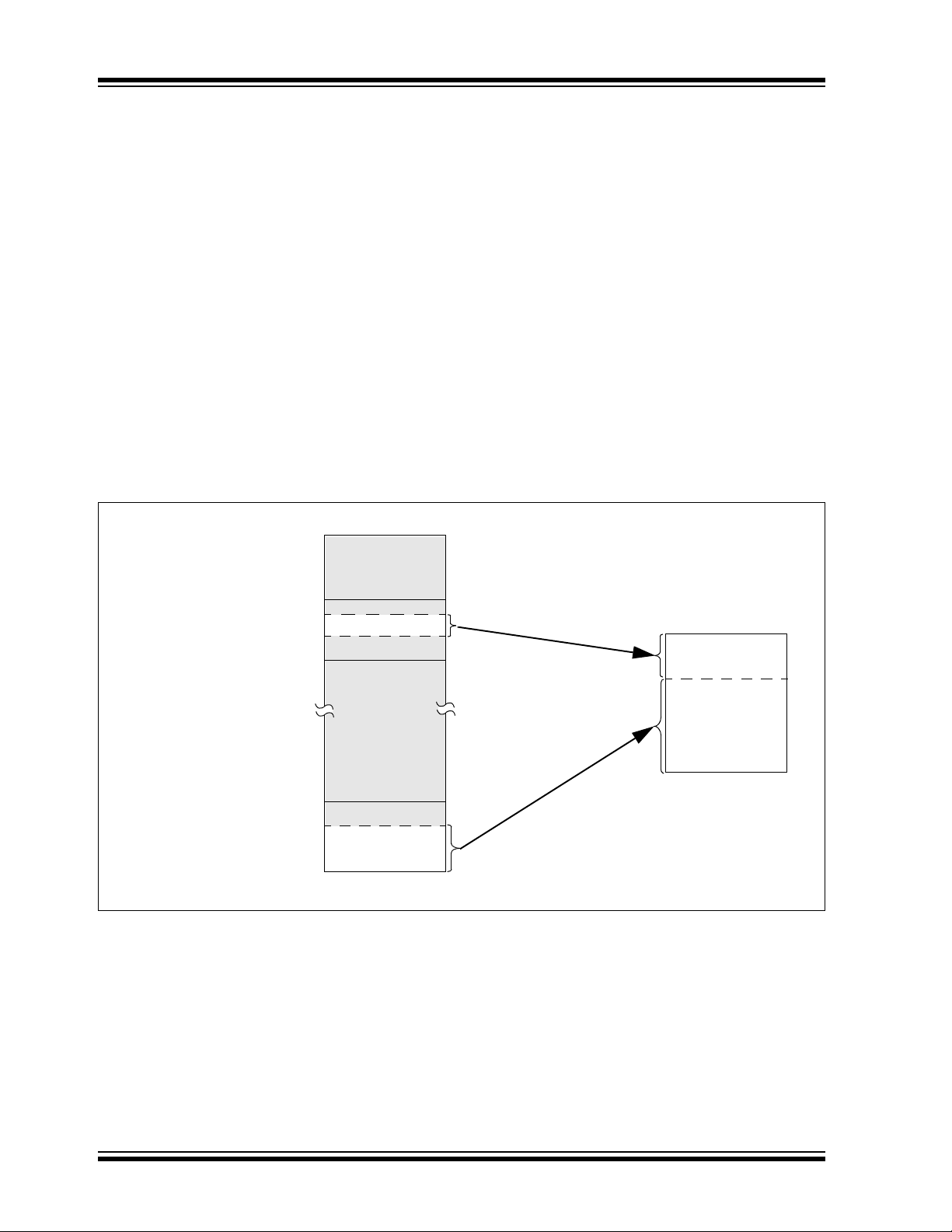
PIC18F2450/4450
5.6.3 MAPPING THE ACCESS BANK IN INDEXED LITERAL OFFSET MODE
The use of Indexed Literal Offset Addressing mode
effectively changes how the lower portion of Access
RAM (00h to 5Fh) is mapped. Rather than containing
just the contents of the bottom half of Bank 0, this mode
maps the contents from Bank 0 and a user-defined
“window” that can be located anywhere in the data
memory space. The value of FSR2 establishes the
lower boundary of the addresses mapped into the
window, while the upper boundary is defined by FSR2
plus 95 (5Fh). Addresses in the Access RAM above
5Fh are mapped as previously described (see
Section 5.3.3 “Access Bank”). An example of Access
Bank remapping in this addressing mode is shown in
Figure 5-9.
Remapping of the Access Bank applies only to
operations using the Indexed Literal Offset mode.
Operations that use the BSR (Access RAM bit is ‘1’) will
continue to use Direct Addressing as before. Any
indirect or indexed operation that explicitly uses any of
the indirect file operands (including FSR2) will continue
to operate as standard Indirect Addressing. Any
instruction that uses the Access Bank, but includes a
register address of greater than 05Fh, will use Direct
Addressing and the normal Access Bank map.
5.6.4 BSR IN INDEXED LITERAL OFFSET MODE
Although the Access Bank is remapped when the
extended instruction set is enabled, the operation of the
BSR remains unchanged. Direct Addressing, using the
BSR to select the data memory bank, operates in the
same manner as previously described.
FIGURE 5-9: REMAPPING THE ACCESS BANK WITH INDEXED LITERAL
OFFSET ADDRESSING
Example Situation:
ADDWF f, d, a
FSR2H:FSR2L = 120h
Locations in the region
from the FSR2 Pointer
(120h) to the pointer plus
05Fh (17Fh) are mapped
to the bottom of the
Access RAM (000h-05Fh).
Special Function Registers at F60h through FFFh
are mapped to 60h
through FFh as usual.
Bank 0 addresses below
5Fh are not available in
this mode. They can still
be addressed by using the
BSR.
000h
100h
120h
17Fh
200h
F00h
F60h
FFFh
Bank 0
Window
Bank 1
Bank 2
through
Bank 14
Bank 15
SFRs
Data Memory
00h
Bank 1 “Window”
5Fh
60h
SFRs
FFh
Access Bank
DS39760C-page 72 Preliminary © 2007 Microchip Technology Inc.
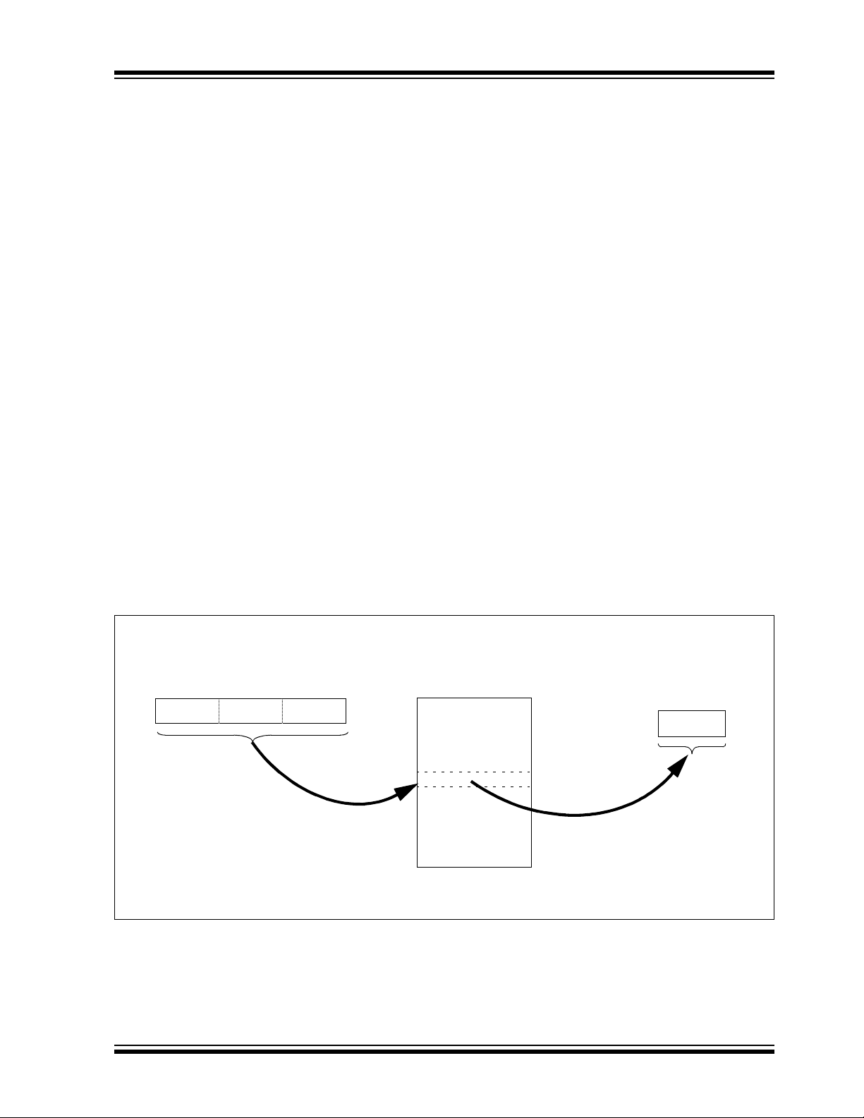
PIC18F2450/4450
6.0 FLASH PROGRAM MEMORY
The Flash program memory is readable, writable and
erasable, during normal operation over the entire V
range.
A read from program memory is executed on one byte
at a time. A write to program memory is executed on
blocks of 16 bytes at a time. Program memory is
erased in blocks of 64 bytes at a time. A Bulk Erase
operation may not be issued from user code.
Writing or erasing program memory will cease
instruction fetches until the operation is complete. The
program memory cannot be accessed during the write
or erase, therefore, code cannot execute. An internal
programming timer terminates program memory writes
and erases.
A value written to program memory does not need to be
a valid instruction. Executing a program memory
location that forms an invalid instruction results in a
NOP.
DD
6.1 Table Reads and Table Writes
In order to read and write program memory, there are
two operations that allow the processor to move bytes
between the program memory space and the data RAM:
• Table Read (TBLRD)
• Table Write (TBLWT)
The program memory space is 16 bits wide, while the
data RAM space is 8 bits wide. Table reads and table
writes move data between these two memory spaces
through an 8-bit register (TABLAT).
Table read operations retrieve data from program
memory and place it into the data RAM space.
Figure 6-1 shows the operation of a table read with
program memory and data RAM.
Table write operations store data from the data memory
space into holding registers in program memory. The
procedure to write the contents of the holding registers
into program memory is detailed in Section 6.5 “Writing
to Flash Program Memory”. Figure 6-2 shows the
operation of a table write with program memory and data
RAM.
Table operations work with byte entities. A table block
containing data, rather than program instructions, is not
required to be word-aligned. Therefore, a table block can
start and end at any byte address. If a table write is being
used to write executable code into program memory,
program instructions will need to be word-aligned.
FIGURE 6-1: TABLE READ OPERATION
Table Pointer
TBLPTRU
Note 1: Table Pointer register points to a byte in program memory.
TBLPTRH TBLPTRL
(1)
Program Memory
(TBLPTR)
Instruction: TBLRD*
Program Memory
Table Latch (8-bit)
TAB LAT
© 2007 Microchip Technology Inc. Preliminary DS39760C-page 73

PIC18F2450/4450
FIGURE 6-2: TABLE WRITE OPERATION
Instruction: TBLWT*
Program Memory
Holding Registers
TBLPTRU
Table Pointer
TBLPTRH TBLPTRL
(1)
Program Memory
(TBLPTR)
Table Latch (8-bit)
TAB LAT
Note 1: Table Pointer actually points to one of 16 holding registers, the address of which is determined by
TBLPTRL<3:0>. The process for physically writing data to the program memory array is discussed
in Section 6.5 “Writing to Flash Program Memory”.
6.2 Control Registers
Several control registers are used in conjunction with
the TBLRD and TBLWT instructions. These include the:
• EECON1 register
• EECON2 register
• TABLAT register
• TBLPTR registers
6.2.1 EECON1 AND EECON2 REGISTERS
The EECON1 register (Register 6-1) is the control
register for memory accesses. The EECON2 register is
not a physical register; it is used exclusively in the
memory write and erase sequences. Reading
EECON2 will read all ‘0’s.
The CFGS control bit determines if the access will be
to the Configuration/Calibration registers or to program
memory.
The FREE bit, when set, will allow a program memory
erase operation. When FREE is set, the erase
operation is initiated on the next WR command. When
FREE is clear, only writes are enabled.
The WREN bit, when set, will allow a write operation.
On power-up, the WREN bit is clear. The WRERR bit is
set in hardware when the WREN bit is set and cleared
when the internal programming timer expires and the
write operation is complete.
Note: During normal operation, the WRERR is
read as ‘1’. This can indicate that a write
operation was prematurely terminated by
a Reset or a write operation was
attempted improperly.
The WR control bit initiates write operations. The bit
cannot be cleared, only set, in software; it is cleared in
hardware at the completion of the write operation.
DS39760C-page 74 Preliminary © 2007 Microchip Technology Inc.

PIC18F2450/4450
REGISTER 6-1: EECON1: MEMORY CONTROL REGISTER 1
U-0 R/W-x U-0 R/W-0 R/W-x R/W-0 R/S-0 U-0
—CFGS— FREE WRERR
bit 7 bit 0
Legend: S = Settable bit
R = Readable bit W = Writable bit U = Unimplemented bit, read as ‘0’
-n = Value at POR ‘1’ = Bit is set ‘0’ = Bit is cleared x = Bit is unknown
bit 7 Unimplemented: Read as ‘0’
bit 6 CFGS: Flash Program or Configuration Select bit
1 = Access Configuration registers
0 = Access Flash program
bit 5 Unimplemented: Read as ‘0’
bit 4 FREE: Flash Row Erase Enable bit
1 = Erase the program memory row addressed by TBLPTR on the next WR command
(cleared by completion of erase operation)
0 = Perform write-only
bit 3 WRERR: Flash Program Error Flag bit
1 = A write operation is prematurely terminated (any Reset during self-timed programming in normal
operation or an improper write attempt)
0 = The write operation completed
bit 2 WREN: Flash Program Write Enable bit
1 = Allows write cycles to Flash program
0 = Inhibits write cycles to Flash program
bit 1 WR: Write Control bit
1 = Initiates a program memory erase cycle or write cycle
(The operation is self-timed and the bit is cleared by hardware once write is complete.
The WR bit can only be set (not cleared) in software.)
0 = Write cycle complete
bit 0 Unimplemented: Read as ‘0’
(1)
(1)
WREN WR —
Note 1: When a WRERR occurs, the CFGS bit is not cleared. This allows tracing of the error condition.
© 2007 Microchip Technology Inc. Preliminary DS39760C-page 75
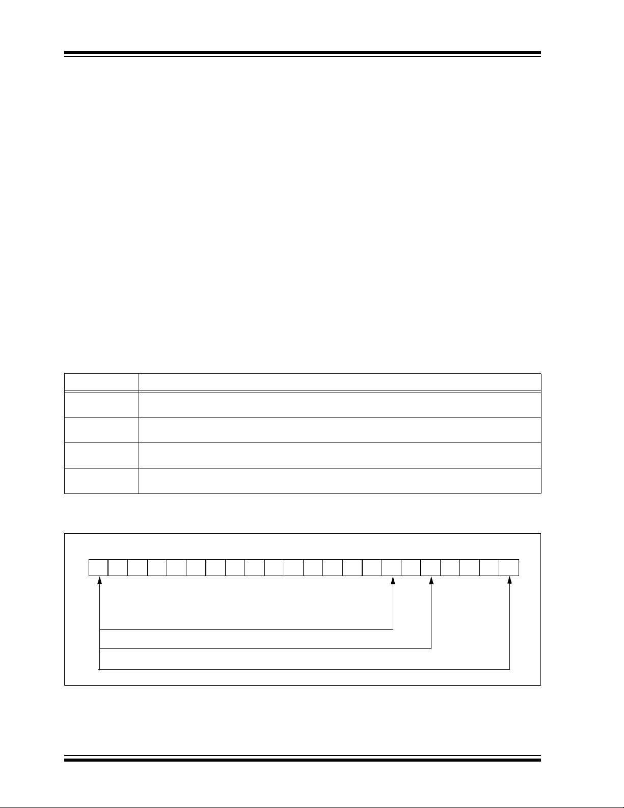
PIC18F2450/4450
6.2.2 TABLE LATCH REGISTER (TABLAT)
The Table Latch (TABLAT) is an 8-bit register mapped
into the SFR space. The Table Latch register is used to
hold 8-bit data during data transfers between program
memory and data RAM.
6.2.3 TABLE POINTER REGISTER (TBLPTR)
The Table Pointer (TBLPTR) register addresses a byte
within the program memory. The TBLPTR is comprised
of three SFR registers: Table Pointer Upper Byte, Table
Pointer High Byte and Table Pointer Low Byte
(TBLPTRU:TBLPTRH:TBLPTRL). These three registers
join to form a 22-bit wide pointer. The low-order 21 bits
allow the device to address up to 2 Mbytes of program
memory space. The 22nd bit allows access to the device
ID, the user ID and the Configuration bits.
The Table Pointer, TBLPTR, is used by the TBLRD and
TBLWT instructions. These instructions can update the
TBLPTR in one of four ways based on the table operation. These operations are shown in Table 6-1. These
operations on the TBLPTR only affect the low-order
21 bits.
6.2.4 TABLE POINTER BOUNDARIES
TBLPTR is used in reads, writes and erases of the
Flash program memory.
When a TBLRD is executed, all 22 bits of the TBLPTR
determine which byte is read from program memory
into TABLAT.
When a TBLWT is executed, the four LSbs of the Table
Pointer register (TBLPTR<3:0>) determine which of the
16 program memory holding registers is written to.
When the timed write to program memory begins (via
the WR bit), the 16 MSbs of the TBLPTR
(TBLPTR<21:4>) determine which program memory
block of 16 bytes is written to. For more detail, see
Section 6.5 “Writing to Flash Program Memory”.
When an erase of program memory is executed, the
16 MSbs of the Table Pointer register (TBLPTR<21:6>)
point to the 64-byte block that will be erased. The Least
Significant bits (TBLPTR<5:0>) are ignored.
Figure 6-3 describes the relevant boundaries of the
TBLPTR based on Flash program memory operations.
TABLE 6-1: TABLE POINTER OPERATIONS WITH TBLRD AND TBLWT INSTRUCTIONS
Example Operation on Table Pointer
TBLRD*
TBLWT*
TBLRD*+
TBLWT*+
TBLRD*TBLWT*-
TBLRD+*
TBLWT+*
TBLPTR is incremented after the read/write
TBLPTR is decremented after the read/write
TBLPTR is incremented before the read/write
TBLPTR is not modified
FIGURE 6-3: TABLE POINTER BOUNDARIES BASED ON OPERATION
21 16 15 87 0
DS39760C-page 76 Preliminary © 2007 Microchip Technology Inc.
TBLPTRU
TABLE ERASE
TBLPTR<21:6>
TABLE WRITE – TBLPTR<21:4>
TABLE READ – TBLPTR<21:0>
TBLPTRLTBLPTRH
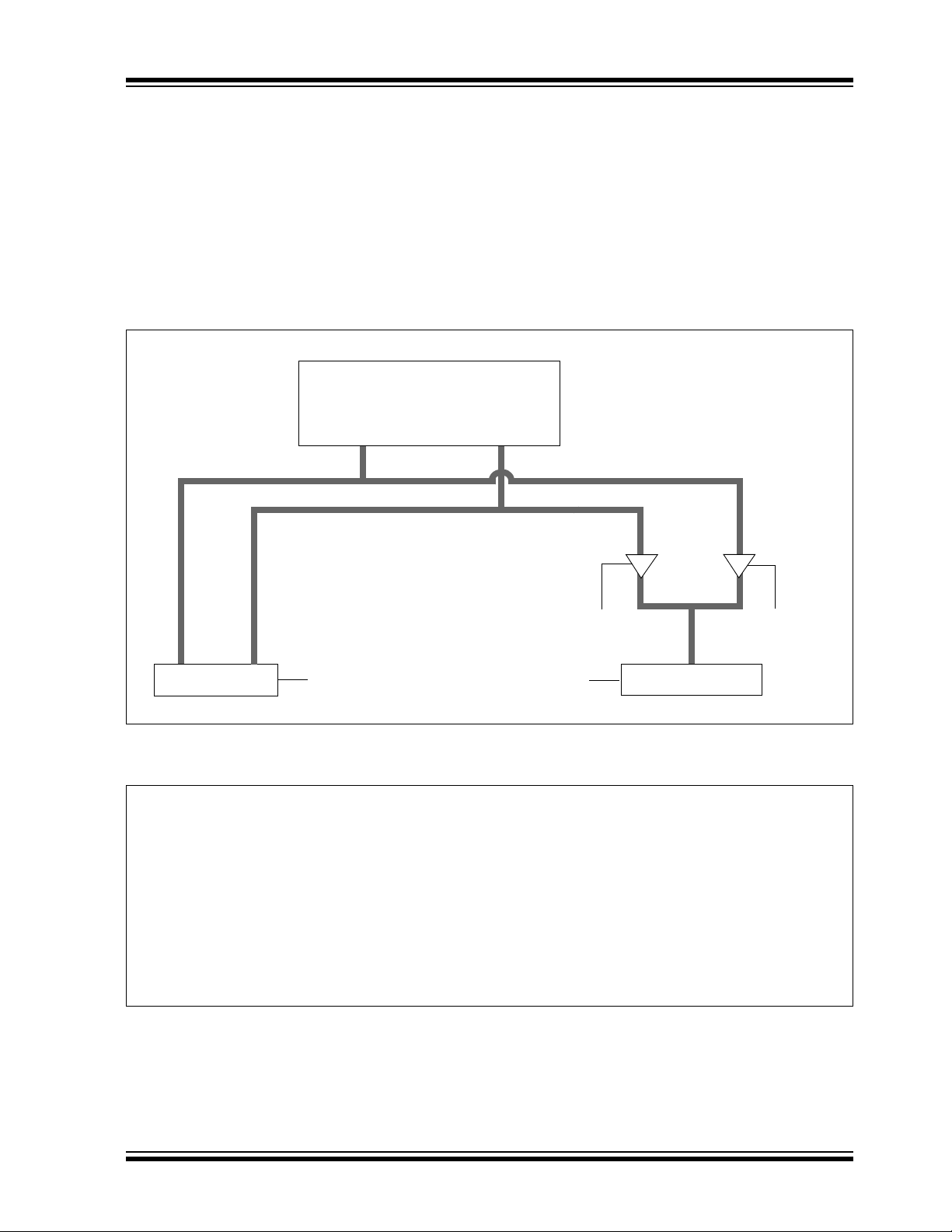
PIC18F2450/4450
6.3 Reading the Flash Program Memory
The TBLRD instruction is used to retrieve data from
program memory and places it into data RAM. Table
reads from program memory are performed one byte at
a time.
TBLPTR points to a byte address in program space.
Executing TBLRD places the byte pointed to into
TABLAT. In addition, TBLPTR can be modified
automatically for the next table read operation.
The internal program memory is typically organized by
words. The Least Significant bit of the address selects
between the high and low bytes of the word. Figure 6-4
shows the interface between the internal program
memory and the TABLAT.
FIGURE 6-4: READS FROM FLASH PROGRAM MEMORY
Program Memory
(Even Byte Address)
(Odd Byte Address)
TBLPTR = xxxxx1
Instruction Register
(IR)
FETCH
TBLRD
EXAMPLE 6-1: READING A FLASH PROGRAM MEMORY WORD
MOVLW CODE_ADDR_UPPER ; Load TBLPTR with the base
MOVWF TBLPTRU ; address of the word
MOVLW CODE_ADDR_HIGH
MOVWF TBLPTRH
MOVLW CODE_ADDR_LOW
READ_WORD
MOVWF TBLPTRL
TBLRD*+ ; read into TABLAT and increment
MOVF TABLAT, W ; get data
MOVWF WORD_EVEN
TBLRD*+ ; read into TABLAT and increment
MOVF TABLAT, W ; get data
MOVF WORD_ODD
TBLPTR = xxxxx0
TAB LAT
Read Register
© 2007 Microchip Technology Inc. Preliminary DS39760C-page 77

PIC18F2450/4450
6.4 Erasing Flash Program Memory
The minimum erase block is 32 words or 64 bytes. Only
through the use of an external programmer, or through
ICSP control, can larger blocks of program memory be
Bulk Erased. Word Erase in the Flash array is not
supported.
When initiating an erase sequence from the
microcontroller itself, a block of 64 bytes of program
memory is erased. The Most Significant 16 bits of the
TBLPTR<21:6> point to the block being erased.
TBLPTR<5:0> are ignored.
The EECON1 register commands the erase operation.
The WREN bit must be set to enable write operations.
The FREE bit is set to select an erase operation.
For protection, the write initiate sequence for EECON2
must be used.
A long write is necessary for erasing the internal Flash.
Instruction execution is halted while in a long write
cycle. The long write will be terminated by the internal
6.4.1 FLASH PROGRAM MEMORY ERASE SEQUENCE
The sequence of events for erasing a block of internal
program memory is:
1. Load Table Pointer register with address of row
being erased.
2. Set the EECON1 register for the erase operation:
• clear the CFGS bit to access program memory;
• set WREN bit to enable writes;
• set FREE bit to enable the erase.
3. Disable interrupts.
4. Write 55h to EECON2.
5. Write 0AAh to EECON2.
6. Set the WR bit. This will begin the Row Erase
cycle.
7. The CPU will stall for duration of the erase
(about 2 ms using internal timer).
8. Re-enable interrupts.
programming timer.
EXAMPLE 6-2: ERASING A FLASH PROGRAM MEMORY ROW
MOVLW CODE_ADDR_UPPER ; load TBLPTR with the base
MOVWF TBLPTRU ; address of the memory block
MOVLW CODE_ADDR_HIGH
MOVWF TBLPTRH
MOVLW CODE_ADDR_LOW
ERASE_ROW
Required MOVLW 55h
Sequence MOVWF EECON2 ; write 55h
MOVWF TBLPTRL
BCF EECON1, CFGS ; access Flash program memory
BSF EECON1, WREN ; enable write to memory
BSF EECON1, FREE ; enable Row Erase operation
BCF INTCON, GIE ; disable interrupts
MOVLW 0AAh
MOVWF EECON2 ; write 0AAh
BSF EECON1, WR ; start erase (CPU stall)
BSF INTCON, GIE ; re-enable interrupts
DS39760C-page 78 Preliminary © 2007 Microchip Technology Inc.

PIC18F2450/4450
6.5 Writing to Flash Program Memory
The minimum programming block is 8 words or
16 bytes. Word or byte programming is not supported.
Table writes are used internally to load the holding
registers needed to program the Flash memory. There
are 16 holding registers used by the table writes for
programming.
Since the Table Latch (TABLAT) is only a single byte, the
TBLWT instruction may need to be executed 16 times for
each programming operation. All of the table write operations will essentially be short writes because only the
holding registers are written. At the end of updating the
16 holding registers, the EECON1 register must be
written to in order to start the programming operation
with a long write.
The long write is necessary for programming the
internal Flash. Instruction execution is halted while in a
long write cycle. The long write will be terminated by
the internal programming timer.
The write/erase voltages are generated by an on-chip
charge pump, rated to operate over the voltage range
of the device.
Note: The default value of the holding registers on
device Resets and after write operations is
FFh. A write of FFh to a holding register
does not modify that byte. This means that
individual bytes of program memory may be
modified, provided that the change does not
attempt to change any bit from a ‘0’ to a ‘1’.
When modifying individual bytes, it is not
necessary to load all 16 holding registers
before executing a write operation.
FIGURE 6-5: TABLE WRITES TO FLASH PROGRAM MEMORY
TAB LAT
Write Register
8
8 8 8
Holding Register Holding Register Holding Register Holding Register
6.5.1 FLASH PROGRAM MEMORY WRITE SEQUENCE
The sequence of events for programming an internal
program memory location should be:
1. Read 64 bytes into RAM.
2. Update data values in RAM as necessary.
3. Load Table Pointer register with address being
erased.
4. Execute the Row Erase procedure.
5. Load Table Pointer register with address of first
byte being written.
6. Write 16 bytes into the holding registers with
auto-increment.
7. Set the EECON1 register for the write operation:
• clear the CFGS bit to access program memory;
• set WREN to enable byte writes.
8. Disable interrupts.
9. Write 55h to EECON2.
TBLPTR = xxxxxFTBLPTR = xxxxx1TBLPTR = xxxxx0 TBLPTR = xxxxx2
Program Memory
10. Write 0AAh to EECON2.
11. Set the WR bit. This will begin the write cycle.
12. The CPU will stall for duration of the write (about
2 ms using internal timer).
13. Re-enable interrupts.
14. Repeat steps 6 through 14 once more to write
64 bytes.
15. Verify the memory (table read).
This procedure will require about 8 ms to update one
row of 64 bytes of memory. An example of the required
code is given in Example 6-3.
Note: Before setting the WR bit, the Table
Pointer address needs to be within the
intended address range of the 16 bytes in
the holding register.
© 2007 Microchip Technology Inc. Preliminary DS39760C-page 79

PIC18F2450/4450
EXAMPLE 6-3: WRITING TO FLASH PROGRAM MEMORY
MOVLW D'64’ ; number of bytes in erase block
MOVWF COUNTER
MOVLW BUFFER_ADDR_HIGH ; point to buffer
MOVWF FSR0H
MOVLW BUFFER_ADDR_LOW
MOVWF FSR0L
MOVLW CODE_ADDR_UPPER ; Load TBLPTR with the base
MOVWF TBLPTRU ; address of the memory block
MOVLW CODE_ADDR_HIGH
MOVWF TBLPTRH
MOVLW CODE_ADDR_LOW
READ_BLOCK
MODIFY_WORD
ERASE_BLOCK
MOVWF TBLPTRL
TBLRD*+ ; read into TABLAT, and inc
MOVF TABLAT, W ; get data
MOVWF POSTINC0 ; store data
DECFSZ COUNTER ; done?
BRA READ_BLOCK ; repeat
MOVLW DATA_ADDR_HIGH ; point to buffer
MOVWF FSR0H
MOVLW DATA_ADDR_LOW
MOVWF FSR0L
MOVLW NEW_DATA_LOW ; update buffer word
MOVWF POSTINC0
MOVLW NEW_DATA_HIGH
MOVWF INDF0
MOVLW CODE_ADDR_UPPER ; load TBLPTR with the base
MOVWF TBLPTRU ; address of the memory block
MOVLW CODE_ADDR_HIGH
MOVWF TBLPTRH
MOVLW CODE_ADDR_LOW
MOVWF TBLPTRL
BCF EECON1, CFGS ; access Flash program memory
BSF EECON1, WREN ; enable write to memory
BSF EECON1, FREE ; enable Row Erase operation
BCF INTCON, GIE ; disable interrupts
MOVLW 55h
Required MOVWF EECON2 ; write 55h
Sequence MOVLW 0AAh
WRITE_BUFFER_BACK
WRITE_BYTE_TO_HREGS
DS39760C-page 80 Preliminary © 2007 Microchip Technology Inc.
MOVWF EECON2 ; write 0AAh
BSF EECON1, WR ; start erase (CPU stall)
BSF INTCON, GIE ; re-enable interrupts
TBLRD*- ; dummy read decrement
MOVLW BUFFER_ADDR_HIGH ; point to buffer
MOVWF FSR0H
MOVLW BUFFER_ADDR_LOW
MOVWF FSR0L
MOVLW D’4’
MOVWF COUNTER1
MOVLW D’16’ ; number of bytes in holding register
MOVWF COUNTER
MOVF POSTINC0, W ; get low byte of buffer data
MOVWF TABLAT ; present data to table latch
TBLWT+* ; write data, perform a short write
; to internal TBLWT holding register.
DECFSZ COUNTER ; loop until buffers are full
BRA WRITE_WORD_TO_HREGS

PIC18F2450/4450
EXAMPLE 6-3: WRITING TO FLASH PROGRAM MEMORY (CONTINUED)
PROGRAM_MEMORY
BCF EECON1, CFGS ; access Flash program memory
BSF EECON1, WREN ; enable write to memory
BCF INTCON, GIE ; disable interrupts
Required MOVWF EECON2 ; write 55h
Sequence MOVLW 0AAh
MOVLW 55h
MOVWF EECON2 ; write 0AAh
BSF EECON1, WR ; start program (CPU stall)
DECFSZ COUNTER1
BRA WRITE_BUFFER_BACK
BSF INTCON, GIE ; re-enable interrupts
BCF EECON1, WREN ; disable write to memory
6.5.2 WRITE VERIFY
Depending on the application, good programming
practice may dictate that the value written to the
memory should be verified against the original value.
This should be used in applications where excessive
writes can stress bits near the specification limit.
6.5.3 UNEXPECTED TERMINATION OF WRITE OPERATION
If a write is terminated by an unplanned event, such as
loss of power or an unexpected Reset, the memory
location just programmed should be verified and
reprogrammed if needed. If the write operation is
interrupted by a MCLR
during normal operation, the user can check the
WRERR bit and rewrite the location(s) as needed.
Reset or a WDT time-out Reset
6.5.4 PROTECTION AGAINST SPURIOUS WRITES
To protect against spurious writes to Flash program
memory, the write initiate sequence must also be
followed. See Section 18.0 “Special Features of the
CPU” for more detail.
6.6 Flash Program Operation During
Code Protection
See Section 18.5 “Program Verification and Code
Protection” for details on code protection of Flash
program memory.
TABLE 6-2: REGISTERS ASSOCIATED WITH PROGRAM FLASH MEMORY
Reset
Name Bit 7 Bit 6 Bit 5 Bit 4 Bit 3 Bit 2 Bit 1 Bit 0
TBLPTRU
TBPLTRH Program Memory Table Pointer High Byte (TBLPTR<15:8>) 49
TBLPTRL Program Memory Table Pointer Low Byte (TBLPTR<7:0>) 49
TABLAT Program Memory Table Latch 49
INTCON GIE/GIEH PEIE/GIEL
EECON2 Control Register 2 (not a physical register) 51
EECON1
IPR2 OSCFIP
PIR2 OSCFIF
PIE2 OSCFIE
Legend: — = unimplemented, read as ‘0’. Shaded cells are not used during Flash access.
— — bit 21 Program Memory Table Pointer Upper Byte (TBLPTR<20:16>) 49
TMR0IE INT0IE RBIE TMR0IF INT0IF RBIF 49
—CFGS— FREE WRERR WREN WR —51
— USBIP — — HLVDIP — —51
— USBIF — — HLVDIF — —51
— USBIE — — HLVDIE — —51
Val ues
on Page:
© 2007 Microchip Technology Inc. Preliminary DS39760C-page 81

PIC18F2450/4450
NOTES:
DS39760C-page 82 Preliminary © 2007 Microchip Technology Inc.

PIC18F2450/4450
7.0 8 x 8 HARDWARE MULTIPLIER
7.1 Introduction
All PIC18 devices include an 8 x 8 hardware multiplier
as part of the ALU. The multiplier performs an unsigned
operation and yields a 16-bit result that is stored in the
product register pair, PRODH:PRODL. The multiplier’s
operation does not affect any flags in the STATUS
register.
Making multiplication a hardware operation allows it to
be completed in a single instruction cycle. This has the
advantages of higher computational throughput and
reduced code size for multiplication algorithms and
allows the PIC18 devices to be used in many applications previously reserved for digital signal processors.
A comparison of various hardware and software
multiply operations, along with the savings in memory
and execution time, is shown in Table 7-1.
7.2 Operation
Example 7-1 shows the instruction sequence for an
8 x 8 unsigned multiplication. Only one instruction is
required when one of the arguments is already loaded
in the WREG register.
Example 7-2 shows the sequence to do an 8 x 8 signed
multiplication. To account for the sign bits of the
arguments, each argument’s Most Significant bit (MSb)
is tested and the appropriate subtractions are done.
EXAMPLE 7-1: 8 x 8 UNSIGNED
MULTIPLY ROUTINE
MOVF ARG1, W ;
MULWF ARG2 ; ARG1 * ARG2 ->
; PRODH:PRODL
EXAMPLE 7-2: 8 x 8 SIGNED MULTIPLY
ROUTINE
MOVF ARG1, W
MULWF ARG2 ; ARG1 * ARG2 ->
; PRODH:PRODL
BTFSC ARG2, SB ; Test Sign Bit
SUBWF PRODH, F ; PRODH = PRODH
; - ARG1
MOVF ARG2, W
BTFSC ARG1, SB ; Test Sign Bit
SUBWF PRODH, F ; PRODH = PRODH
; - ARG2
TABLE 7-1: PERFORMANCE COMPARISON FOR VARIOUS MULTIPLY OPERATIONS
Routine Multiply Method
8 x 8 unsigned
8 x 8 signed
16 x 16 unsigned
16 x 16 signed
Without hardware multiply 13 69 6.9 μs27.6 μs69 μs
Hardware multiply 1 1 100 ns 400 ns 1 μs
Without hardware multiply 33 91 9.1 μs36.4 μs91 μs
Hardware multiply 6 6 600 ns 2.4 μs6 μs
Without hardware multiply 21 242 24.2 μs96.8 μs242 μs
Hardware multiply 28 28 2.8 μs 11.2 μs28 μs
Without hardware multiply 52 254 25.4 μs 102.6 μs254 μs
Hardware multiply 35 40 4.0 μs16.0 μs40 μs
Program
Memory
(Words)
Cycles
(Max)
@ 40 MHz @ 10 MHz @ 4 MHz
Time
© 2007 Microchip Technology Inc. Preliminary DS39760C-page 83

PIC18F2450/4450
Example 7-3 shows the sequence to do a 16 x 16
unsigned multiplication. Equation 7-1 shows the
algorithm that is used. The 32-bit result is stored in four
registers (RES3:RES0).
EQUATION 7-1: 16 x 16 UNSIGNED
MULTIPLICATION
ALGORITHM
RES3:RES0 = ARG1H:ARG1L • ARG2H:ARG2L
= (ARG1H • ARG2H • 2
(ARG1H • ARG2L • 2
(ARG1L • ARG2H • 2
(ARG1L • ARG2L)
16
) +
8
) +
8
) +
EXAMPLE 7-3: 16 x 16 UNSIGNED
MULTIPLY ROUTINE
MOVF ARG1L, W
MULWF ARG2L ; ARG1L * ARG2L->
MOVFF PRODH, RES1 ;
MOVFF PRODL, RES0 ;
;
MOVF ARG1H, W
MULWF ARG2H ; ARG1H * ARG2H->
MOVFF PRODH, RES3 ;
MOVFF PRODL, RES2 ;
;
MOVF ARG1L, W
MULWF ARG2H ; ARG1L * ARG2H->
MOVF PRODL, W ;
ADDWF RES1, F ; Add cross
MOVF PRODH, W ; products
ADDWFC RES2, F ;
CLRF WREG ;
ADDWFC RES3, F ;
;
MOVF ARG1H, W ;
MULWF ARG2L ; ARG1H * ARG2L->
MOVF PRODL, W ;
ADDWF RES1, F ; Add cross
MOVF PRODH, W ; products
ADDWFC RES2, F ;
CLRF WREG ;
ADDWFC RES3, F ;
Example 7-4 shows the sequence to do a 16 x 16
signed multiply. Equation 7-2 shows the algorithm
used. The 32-bit result is stored in four registers
(RES3:RES0). To account for the sign bits of the
arguments, the MSb for each argument pair is tested
and the appropriate subtractions are done.
; PRODH:PRODL
; PRODH:PRODL
; PRODH:PRODL
; PRODH:PRODL
EQUATION 7-2: 16 x 16 SIGNED
MULTIPLICATION
ALGORITHM
RES3:RES0= ARG1H:ARG1L • ARG2H:ARG2L
= (ARG1H • ARG2H • 2
(ARG1H • ARG2L • 2
(ARG1L • ARG2H • 2
(ARG1L • ARG2L) +
(-1 • ARG2H<7> • ARG1H:ARG1L • 2
(-1 • ARG1H<7> • ARG2H:ARG2L • 2
16
) +
8
) +
8
) +
EXAMPLE 7-4: 16 x 16 SIGNED
MULTIPLY ROUTINE
MOVF ARG1L, W
MULWF ARG2L ; ARG1L * ARG2L ->
MOVFF PRODH, RES1 ;
MOVFF PRODL, RES0 ;
;
MOVF ARG1H, W
MULWF ARG2H ; ARG1H * ARG2H ->
MOVFF PRODH, RES3 ;
MOVFF PRODL, RES2 ;
;
MOVF ARG1L,W
MULWF ARG2H ; ARG1L * ARG2H ->
MOVF PRODL, W ;
ADDWF RES1, F ; Add cross
MOVF PRODH, W ; products
ADDWFC RES2, F ;
CLRF WREG ;
ADDWFC RES3, F ;
;
MOVF ARG1H, W ;
MULWF ARG2L ; ARG1H * ARG2L ->
MOVF PRODL, W ;
ADDWF RES1, F ; Add cross
MOVF PRODH, W ; products
ADDWFC RES2, F ;
CLRF WREG ;
ADDWFC RES3, F ;
;
BTFSS ARG2H, 7 ; ARG2H:ARG2L neg?
BRA SIGN_ARG1 ; no, check ARG1
MOVF ARG1L, W ;
SUBWF RES2 ;
MOVF ARG1H, W ;
SUBWFB RES3
;
SIGN_ARG1
BTFSS ARG1H, 7 ; ARG1H:ARG1L neg?
BRA CONT_CODE ; no, done
MOVF ARG2L, W ;
SUBWF RES2 ;
MOVF ARG2H, W ;
SUBWFB RES3
;
CONT_CODE
:
; PRODH:PRODL
; PRODH:PRODL
; PRODH:PRODL
; PRODH:PRODL
16
) +
16
)
DS39760C-page 84 Preliminary © 2007 Microchip Technology Inc.

PIC18F2450/4450
8.0 INTERRUPTS
The PIC18F2450/4450 devices have multiple interrupt
sources and an interrupt priority feature that allows
each interrupt source to be assigned a high-priority
level or a low-priority level. The high-priority interrupt
vector is at 000008h and the low-priority interrupt vector is at 000018h. High-priority interrupt events will
interrupt any low-priority interrupts that may be in
progress.
There are ten registers which are used to control
interrupt operation. These registers are:
• RCON
•INTCON
• INTCON2
• INTCON3
• PIR1, PIR2
• PIE1, PIE2
• IPR1, IPR2
It is recommended that the Microchip header files
supplied with MPLAB
names in these registers. This allows the assembler/
compiler to automatically take care of the placement of
these bits within the specified register.
Each interrupt source has three bits to control its
operation. The functions of these bits are:
• Flag bit to indicate that an interrupt event
occurred
• Enable bit that allows program execution to
branch to the interrupt vector address when the
flag bit is set
• Priority bit to select high priority or low priority
The interrupt priority feature is enabled by setting the
IPEN bit (RCON<7>). When interrupt priority is
enabled, there are two bits which enable interrupts
globally. Setting the GIEH bit (INTCON<7>) enables all
interrupts that have the priority bit set (high priority).
Setting the GIEL bit (INTCON<6>) enables all
interrupts that have the priority bit cleared (low priority).
When the interrupt flag, enable bit and appropriate
global interrupt enable bit are set, the interrupt will
vector immediately to address 000008h or 000018h,
depending on the priority bit setting. Individual interrupts can be disabled through their corresponding
enable bits.
When the IPEN bit is cleared (default state), the
interrupt priority feature is disabled and interrupts are
compatible with PIC
Compatibility mode, the interrupt priority bits for each
source have no effect. INTCON<6> is the PEIE bit
which enables/disables all peripheral interrupt sources.
INTCON<7> is the GIE bit which enables/disables all
interrupt sources. All interrupts branch to address
000008h in Compatibility mode.
®
IDE be used for the symbolic bit
®
mid-range microcontrollers. In
When an interrupt is responded to, the global interrupt
enable bit is cleared to disable further interrupts. If the
IPEN bit is cleared, this is the GIE bit. If interrupt priority
levels are used, this will be either the GIEH or GIEL bit.
High-priority interrupt sources can interrupt a lowpriority interrupt. Low-priority interrupts are not
processed while high-priority interrupts are in progress.
The return address is pushed onto the stack and the PC
is loaded with the interrupt vector address (000008h or
000018h). Once in the Interrupt Service Routine, the
source(s) of the interrupt can be determined by polling
the interrupt flag bits. The interrupt flag bits must be
cleared in software before re-enabling interrupts to avoid
recursive interrupts.
The “return from interrupt” instruction, RETFIE, exits
the interrupt routine and sets the GIE bit (GIEH or GIEL
if priority levels are used) which re-enables interrupts.
For external interrupt events, such as the INTx pins or
the PORTB input change interrupt, the interrupt latency
will be three to four instruction cycles. The exact
latency is the same for one or two-cycle instructions.
Individual interrupt flag bits are set regardless of the
status of their corresponding enable bit or the GIE bit.
Note: Do not use the MOVFF instruction to modify
any of the interrupt control registers while
any interrupt is enabled. Doing so may
cause erratic microcontroller behavior.
8.1 USB Interrupts
Unlike other peripherals, the USB module is capable of
generating a wide range of interrupts for many types of
events. These include several types of normal communication and status events and several module level
error events.
To handle these events, the USB module is equipped
with its own interrupt logic. The logic functions in a
manner similar to the microcontroller level interrupt
funnel, with each interrupt source having separate flag
and enable bits. All events are funneled to a single
device level interrupt, USBIF (PIR2<5>). Unlike the
device level interrupt logic, the individual USB interrupt
events cannot be individually assigned their own priority. This is determined at the device level interrupt
funnel for all USB events by the USBIP bit.
For additional details on USB interrupt logic, refer to
Section 14.5 “USB Interrupts”.
© 2007 Microchip Technology Inc. Preliminary DS39760C-page 85

PIC18F2450/4450
FIGURE 8-1: INTERRUPT LOGIC
Peripheral Interrupt Flag bit
Peripheral Interrupt Enable bit
Peripheral Interrupt Priority bit
From USB
Interrupt Logic
High-Priority Interrupt Generation
Low-Priority Interrupt Generation
Peripheral Interrupt Flag bit
Peripheral Interrupt Enable bit
Peripheral Interrupt Priority bit
TMR1IF
TMR1IE
TMR1IP
From USB
Interrupt Logic
USBIF
USBIE
USBIP
TMR1IF
TMR1IE
TMR1IP
USBIF
USBIE
USBIP
Additional Peripheral Interrupts
Additional Peripheral Interrupts
IPEN
TMR0IF
TMR0IE
TMR0IP
RBIF
RBIE
RBIP
INT1IF
INT1IE
INT1IP
INT2IF
INT2IE
INT2IP
TMR0IF
TMR0IE
TMR0IP
INT0IF
INT0IE
INT1IF
INT1IE
INT1IP
INT2IF
INT2IE
INT2IP
IPEN
PEIE/GIEL
RBIF
RBIE
RBIP
IPEN
Wake-up if in Sleep Mode
PEIE/GIEL
GIE/GIEH
Interrupt to CPU
Vector to Location
0008h
GIE/GIEH
Interrupt to CPU
Vector to Location
0018h
DS39760C-page 86 Preliminary © 2007 Microchip Technology Inc.

PIC18F2450/4450
8.2 INTCON Registers
The INTCON registers are readable and writable
registers which contain various enable, priority and flag
bits.
Note: Interrupt flag bits are set when an interrupt
condition occurs regardless of the state of
its corresponding enable bit or the global
interrupt enable bit. User software should
ensure the appropriate interrupt flag bits
are clear prior to enabling an interrupt.
This feature allows for software polling.
REGISTER 8-1: INTCON: INTERRUPT CONTROL REGISTER
R/W-0 R/W-0 R/W-0 R/W-0 R/W-0 R/W-0 R/W-0 R/W-x
GIE/GIEH PEIE/GIEL TMR0IE INT0IE RBIE TMR0IF INT0IF RBIF
bit 7 bit 0
Legend:
R = Readable bit W = Writable bit U = Unimplemented bit, read as ‘0’
-n = Value at POR ‘1’ = Bit is set ‘0’ = Bit is cleared x = Bit is unknown
bit 7 GIE/GIEH: Global Interrupt Enable bit
When IPEN =
1 = Enables all unmasked interrupts
0 = Disables all interrupts
When IPEN =
1 = Enables all high-priority interrupts
0 = Disables all interrupts
bit 6 PEIE/GIEL: Peripheral Interrupt Enable bit
When IPEN =
1 = Enables all unmasked peripheral interrupts
0 = Disables all peripheral interrupts
When IPEN =
1 = Enables all low-priority peripheral interrupts
0 = Disables all low-priority peripheral interrupts
bit 5 TMR0IE: TMR0 Overflow Interrupt Enable bit
1 = Enables the TMR0 overflow interrupt
0 = Disables the TMR0 overflow interrupt
bit 4 INT0IE: INT0 External Interrupt Enable bit
1 = Enables the INT0 external interrupt
0 = Disables the INT0 external interrupt
bit 3 RBIE: RB Port Change Interrupt Enable bit
1 = Enables the RB port change interrupt
0 = Disables the RB port change interrupt
bit 2 TMR0IF: TMR0 Overflow Interrupt Flag bit
1 = TMR0 register has overflowed (must be cleared in software)
0 = TMR0 register did not overflow
bit 1 INT0IF: INT0 External Interrupt Flag bit
1 = The INT0 external interrupt occurred (must be cleared in software)
0 = The INT0 external interrupt did not occur
bit 0 RBIF: RB Port Change Interrupt Flag bit
1 = At least one of the RB7:RB4 pins changed state (must be cleared in software)
0 = None of the RB7:RB4 pins have changed state
0:
1:
0:
1:
(1)
(1)
Note 1: A mismatch condition will continue to set this bit. Reading PORTB will end the mismatch condition and
allow the bit to be cleared.
© 2007 Microchip Technology Inc. Preliminary DS39760C-page 87

PIC18F2450/4450
REGISTER 8-2: INTCON2: INTERRUPT CONTROL REGISTER 2
R/W-1 R/W-1 R/W-1 R/W-1 U-0 R/W-1 U-0 R/W-1
RBPU
bit 7 bit 0
Legend:
R = Readable bit W = Writable bit U = Unimplemented bit, read as ‘0’
-n = Value at POR ‘1’ = Bit is set ‘0’ = Bit is cleared x = Bit is unknown
INTEDG0 INTEDG1 INTEDG2
—
TMR0IP
—
RBIP
bit 7 RBPU
bit 6 INTEDG0: External Interrupt 0 Edge Select bit
bit 5 INTEDG1: External Interrupt 1 Edge Select bit
bit 4 INTEDG2: External Interrupt 2 Edge Select bit
bit 3 Unimplemented: Read as ‘0’
bit 2 TMR0IP: TMR0 Overflow Interrupt Priority bit
bit 1 Unimplemented: Read as ‘0’
bit 0 RBIP: RB Port Change Interrupt Priority bit
Note: Interrupt flag bits are set when an interrupt condition occurs regardless of the state of its corresponding
enable bit or the global interrupt enable bit. User software should ensure the appropriate interrupt flag bits
are clear prior to enabling an interrupt. This feature allows for software polling.
: PORTB Pull-up Enable bit
1 = All PORTB pull-ups are disabled
0 = PORTB pull-ups are enabled by individual port latch values
1 = Interrupt on rising edge
0 = Interrupt on falling edge
1 = Interrupt on rising edge
0 = Interrupt on falling edge
1 = Interrupt on rising edge
0 = Interrupt on falling edge
1 = High priority
0 = Low priority
1 = High priority
0 = Low priority
DS39760C-page 88 Preliminary © 2007 Microchip Technology Inc.

PIC18F2450/4450
REGISTER 8-3: INTCON3: INTERRUPT CONTROL REGISTER 3
R/W-1 R/W-1 U-0 R/W-0 R/W-0 U-0 R/W-0 R/W-0
INT2IP INT1IP — INT2IE INT1IE — INT2IF INT1IF
bit 7 bit 0
Legend:
R = Readable bit W = Writable bit U = Unimplemented bit, read as ‘0’
-n = Value at POR ‘1’ = Bit is set ‘0’ = Bit is cleared x = Bit is unknown
bit 7 INT2IP: INT2 External Interrupt Priority bit
1 = High priority
0 = Low priority
bit 6 INT1IP: INT1 External Interrupt Priority bit
1 = High priority
0 = Low priority
bit 5 Unimplemented: Read as ‘0’
bit 4 INT2IE: INT2 External Interrupt Enable bit
1 = Enables the INT2 external interrupt
0 = Disables the INT2 external interrupt
bit 3 INT1IE: INT1 External Interrupt Enable bit
1 = Enables the INT1 external interrupt
0 = Disables the INT1 external interrupt
bit 2 Unimplemented: Read as ‘0’
bit 1 INT2IF: INT2 External Interrupt Flag bit
1 = The INT2 external interrupt occurred (must be cleared in software)
0 = The INT2 external interrupt did not occur
bit 0 INT1IF: INT1 External Interrupt Flag bit
1 = The INT1 external interrupt occurred (must be cleared in software)
0 = The INT1 external interrupt did not occur
Note: Interrupt flag bits are set when an interrupt condition occurs regardless of the state of its corresponding
enable bit or the global interrupt enable bit. User software should ensure the appropriate interrupt flag bits
are clear prior to enabling an interrupt. This feature allows for software polling.
© 2007 Microchip Technology Inc. Preliminary DS39760C-page 89

PIC18F2450/4450
8.3 PIR Registers
The PIR registers contain the individual flag bits for the
peripheral interrupts. Due to the number of peripheral
interrupt sources, there are two Peripheral Interrupt
Request (Flag) registers (PIR1 and PIR2).
Note 1: Interrupt flag bits are set when an interrupt
condition occurs regardless of the state of
its corresponding enable bit or the Global
Interrupt Enable bit, GIE (INTCON<7>).
2: User software should ensure the
appropriate interrupt flag bits are cleared
prior to enabling an interrupt and after
servicing that interrupt.
REGISTER 8-4: PIR1: PERIPHERAL INTERRUPT REQUEST (FLAG) REGISTER 1
U-0 R/W-0 R-0 R-0 U-0 R/W-0 R/W-0 R/W-0
— ADIF RCIF TXIF — CCP1IF TMR2IF TMR1IF
bit 7 bit 0
Legend:
R = Readable bit W = Writable bit U = Unimplemented bit, read as ‘0’
-n = Value at POR ‘1’ = Bit is set ‘0’ = Bit is cleared x = Bit is unknown
bit 7 Unimplemented: Read as ‘0’
bit 6 ADIF: A/D Converter Interrupt Flag bit
1 = An A/D conversion completed (must be cleared in software)
0 = The A/D conversion is not complete
bit 5 RCIF: EUSART Receive Interrupt Flag bit
1 = The EUSART receive buffer, RCREG, is full (cleared when RCREG is read)
0 = The EUSART receive buffer is empty
bit 4 TXIF: EUSART Transmit Interrupt Flag bit
1 = The EUSART transmit buffer, TXREG, is empty (cleared when TXREG is written)
0 = The EUSART transmit buffer is full
bit 3 Unimplemented: Read as ‘0’
bit 2 CCP1IF: CCP1 Interrupt Flag bit
Capture mode:
1 = A TMR1 register capture occurred (must be cleared in software)
0 = No TMR1 register capture occurred
Compare mode:
1 = A TMR1 register compare match occurred (must be cleared in software)
0 = No TMR1 register compare match occurred
PWM mode:
Unused in this mode.
bit 1 TMR2IF: TMR2 to PR2 Match Interrupt Flag bit
1 = TMR2 to PR2 match occurred (must be cleared in software)
0 = No TMR2 to PR2 match occurred
bit 0 TMR1IF: TMR1 Overflow Interrupt Flag bit
1 = TMR1 register overflowed (must be cleared in software)
0 = TMR1 register did not overflow
DS39760C-page 90 Preliminary © 2007 Microchip Technology Inc.

PIC18F2450/4450
REGISTER 8-5: PIR2: PERIPHERAL INTERRUPT REQUEST (FLAG) REGISTER 2
R/W-0 U-0 R/W-0 U-0 U-0 R/W-0 U-0 U-0
OSCFIF — USBIF — —HLVDIF — —
bit 7 bit 0
Legend:
R = Readable bit W = Writable bit U = Unimplemented bit, read as ‘0’
-n = Value at POR ‘1’ = Bit is set ‘0’ = Bit is cleared x = Bit is unknown
bit 7 OSCFIF: Oscillator Fail Interrupt Flag bit
1 = System oscillator failed, clock input has changed to INTRC (must be cleared in software)
0 = System clock operating
bit 6 Unimplemented: Read as ‘0’
bit 5 USBIF: USB Interrupt Flag bit
1 = USB has requested an interrupt (must be cleared in software)
0 = No USB interrupt request
bit 4-3 Unimplemented: Read as ‘0’
bit 2 HLVDIF: High/Low-Voltage Detect Interrupt Flag bit
1 = A high/low-voltage condition occurred
0 = No high/low-voltage event has occurred
bit 1-0 Unimplemented: Read as ‘0’
© 2007 Microchip Technology Inc. Preliminary DS39760C-page 91
PIC18F2450/4450
8.4 PIE Registers
The PIE registers contain the individual enable bits for
the peripheral interrupts. Due to the number of
peripheral interrupt sources, there are two Peripheral
Interrupt Enable registers (PIE1 and PIE2). When
IPEN = 0, the PEIE bit must be set to enable any of
these peripheral interrupts.
REGISTER 8-6: PIE1: PERIPHERAL INTERRUPT ENABLE REGISTER 1
U-0 R/W-0 R/W-0 R/W-0 U-0 R/W-0 R/W-0 R/W-0
— ADIE RCIE TXIE — CCP1IE TMR2IE TMR1IE
bit 7 bit 0
Legend:
R = Readable bit W = Writable bit U = Unimplemented bit, read as ‘0’
-n = Value at POR ‘1’ = Bit is set ‘0’ = Bit is cleared x = Bit is unknown
bit 7 Unimplemented: Read as ‘0’
bit 6 ADIE: A/D Converter Interrupt Enable bit
1 = Enables the A/D interrupt
0 = Disables the A/D interrupt
bit 5 RCIE: EUSART Receive Interrupt Enable bit
1 = Enables the EUSART receive interrupt
0 = Disables the EUSART receive interrupt
bit 4 TXIE: EUSART Transmit Interrupt Enable bit
1 = Enables the EUSART transmit interrupt
0 = Disables the EUSART transmit interrupt
bit 3 Unimplemented: Read as ‘0’
bit 2 CCP1IE: CCP1 Interrupt Enable bit
1 = Enables the CCP1 interrupt
0 = Disables the CCP1 interrupt
bit 1 TMR2IE: TMR2 to PR2 Match Interrupt Enable bit
1 = Enables the TMR2 to PR2 match interrupt
0 = Disables the TMR2 to PR2 match interrupt
bit 0 TMR1IE: TMR1 Overflow Interrupt Enable bit
1 = Enables the TMR1 overflow interrupt
0 = Disables the TMR1 overflow interrupt
DS39760C-page 92 Preliminary © 2007 Microchip Technology Inc.

PIC18F2450/4450
REGISTER 8-7: PIE2: PERIPHERAL INTERRUPT ENABLE REGISTER 2
R/W-0 U-0 R/W-0 U-0 U-0 R/W-0 U-0 U-0
OSCFIE — USBIE — —HLVDIE — —
bit 7 bit 0
Legend:
R = Readable bit W = Writable bit U = Unimplemented bit, read as ‘0’
-n = Value at POR ‘1’ = Bit is set ‘0’ = Bit is cleared x = Bit is unknown
bit 7 OSCFIE: Oscillator Fail Interrupt Enable bit
1 = Enabled
0 =Disabled
bit 6 Unimplemented: Read as ‘0’
bit 5 USBIE: USB Interrupt Enable bit
1 = Enabled
0 =Disabled
bit 4-3 Unimplemented: Read as ‘0’
bit 2 HLVDIE: High/Low-Voltage Detect Interrupt Enable bit
1 = Enabled
0 =Disabled
bit 1-0 Unimplemented: Read as ‘0’
© 2007 Microchip Technology Inc. Preliminary DS39760C-page 93

PIC18F2450/4450
8.5 IPR Registers
The IPR registers contain the individual priority bits for
the peripheral interrupts. Due to the number of
peripheral interrupt sources, there are two Peripheral
Interrupt Priority registers (IPR1 and IPR2). Using the
priority bits requires that the Interrupt Priority Enable
(IPEN) bit be set.
REGISTER 8-8: IPR1: PERIPHERAL INTERRUPT PRIORITY REGISTER 1
U-0 R/W-1 R/W-1 R/W-1 U-0 R/W-1 R/W-1 R/W-1
— ADIP RCIP TXIP — CCP1IP TMR2IP TMR1IP
bit 7 bit 0
Legend:
R = Readable bit W = Writable bit U = Unimplemented bit, read as ‘0’
-n = Value at POR ‘1’ = Bit is set ‘0’ = Bit is cleared x = Bit is unknown
bit 7 Unimplemented: Read as ‘0’
bit 6 ADIP: A/D Converter Interrupt Priority bit
1 = High priority
0 = Low priority
bit 5 RCIP: EUSART Receive Interrupt Priority bit
1 = High priority
0 = Low priority
bit 4 TXIP: EUSART Transmit Interrupt Priority bit
1 = High priority
0 = Low priority
bit 3 Unimplemented: Read as ‘0’
bit 2 CCP1IP: CCP1 Interrupt Priority bit
1 = High priority
0 = Low priority
bit 1 TMR2IP: TMR2 to PR2 Match Interrupt Priority bit
1 = High priority
0 = Low priority
bit 0 TMR1IP: TMR1 Overflow Interrupt Priority bit
1 = High priority
0 = Low priority
DS39760C-page 94 Preliminary © 2007 Microchip Technology Inc.

PIC18F2450/4450
REGISTER 8-9: IPR2: PERIPHERAL INTERRUPT PRIORITY REGISTER 2
R/W-1 U-0 R/W-1 U-0 U-0 R/W-1 U-0 U-0
OSCFIP — USBIP — —HLVDIP — —
bit 7 bit 0
Legend:
R = Readable bit W = Writable bit U = Unimplemented bit, read as ‘0’
-n = Value at POR ‘1’ = Bit is set ‘0’ = Bit is cleared x = Bit is unknown
bit 7 OSCFIP: Oscillator Fail Interrupt Priority bit
1 = High priority
0 = Low priority
bit 6 Unimplemented: Read as ‘0’
bit 5 USBIP: USB Interrupt Priority bit
1 = High priority
0 = Low priority
bit 4-3 Unimplemented: Read as ‘0’
bit 2 HLVDIP: High/Low-Voltage Detect Interrupt Priority bit
1 = High priority
0 = Low priority
bit 1-0 Unimplemented: Read as ‘0’
© 2007 Microchip Technology Inc. Preliminary DS39760C-page 95

PIC18F2450/4450
8.6 RCON Register
The RCON register contains flag bits which are used to
determine the cause of the last Reset or wake-up from
Idle or Sleep modes. RCON also contains the IPEN bit
which enables interrupt priorities.
REGISTER 8-10: RCON: RESET CONTROL REGISTER
R/W-0 R/W-1
IPEN SBOREN
bit 7 bit 0
Legend:
R = Readable bit W = Writable bit U = Unimplemented bit, read as ‘0’
-n = Value at POR ‘1’ = Bit is set ‘0’ = Bit is cleared x = Bit is unknown
bit 7 IPEN: Interrupt Priority Enable bit
1 = Enable priority levels on interrupts
0 = Disable priority levels on interrupts (PIC16CXXX Compatibility mode)
bit 6 SBOREN: BOR Software Enable bit
For details of bit operation, see Register 4-1.
bit 5 Unimplemented: Read as ‘0’
bit 4 RI: RESET Instruction Flag bit
For details of bit operation, see Register 4-1.
bit 3 TO: Watchdog Time-out Flag bit
For details of bit operation, see Register 4-1.
bit 2 PD: Power-Down Detection Flag bit
For details of bit operation, see Register 4-1.
bit 1 POR: Power-on Reset Status bit
For details of bit operation, see Register 4-1.
bit 0 BOR: Brown-out Reset Status bit
For details of bit operation, see Register 4-1.
(1)
U-0 R/W-1 R-1 R-1 R/W-0
—RITO PD POR BOR
(1)
(2)
(2)
R/W-0
Note 1: If SBOREN is enabled, its Reset state is ‘1’; otherwise, it is ‘0’. See Register 4-1 for additional information.
2: The actual Reset value of POR
information.
DS39760C-page 96 Preliminary © 2007 Microchip Technology Inc.
is determined by the type of device Reset. See Register 4-1 for additional

PIC18F2450/4450
8.7 INTx Pin Interrupts
External interrupts on the RB0/AN12/INT0, RB1/AN10/
INT1and RB2/AN8/INT2/VMO pins are edge-triggered.
If the corresponding INTEDGx bit in the INTCON2
register is set (= 1), the interrupt is triggered by a rising
edge; if the bit is clear, the trigger is on the falling edge.
When a valid edge appears on the RBx/INTx pin, the
corresponding flag bit, INTxIF, is set. This interrupt can
be disabled by clearing the corresponding enable bit,
INTxIE. Flag bit, INTxIF, must be cleared in software in
the Interrupt Service Routine before re-enabling the
interrupt.
All external interrupts (INT0, INT1 and INT2) can wakeup the processor from the power-managed modes if bit,
INTxIE, was set prior to going into the power-managed
modes. If the Global Interrupt Enable bit, GIE, is set, the
processor will branch to the interrupt vector following
wake-up.
Interrupt priority for INT1 and INT2 is determined by
the value contained in the interrupt priority bits,
INT1IP (INTCON3<6>) and INT2IP (INTCON3<7>).
There is no priority bit associated with INT0. It is
always a high-priority interrupt source.
8.8 TMR0 Interrupt
In 8-bit mode (which is the default), an overflow in the
TMR0 register (FFh → 00h) will set flag bit, TMR0IF. In
16-bit mode, an overflow in the TMR0H:TMR0L
register pair (FFFFh → 0000h) will set TMR0IF. The
interrupt can be enabled/disabled by setting/clearing
enable bit, TMR0IE (INTCON<5>). Interrupt priority for
Timer0 is determined by the value contained in the
interrupt priority bit, TMR0IP (INTCON2<2>). See
Section 12.0 “Timer2 Module” for further details on
the Timer0 module.
8.9 PORTB Interrupt-on-Change
An input change on PORTB<7:4> sets flag bit, RBIF
(INTCON<0>). The interrupt can be enabled/disabled
by setting/clearing enable bit, RBIE (INTCON<3>).
Interrupt priority for PORTB interrupt-on-change is
determined by the value contained in the interrupt
priority bit, RBIP (INTCON2<0>).
8.10 Context Saving During Interrupts
During interrupts, the return PC address is saved on
the stack. Additionally, the WREG, STATUS and BSR
registers are saved on the Fast Return Stack. If a fast
return from interrupt is not used (see Section 5.3
“Data Memory Organization”), the user may need to
save the WREG, STATUS and BSR registers on entry
to the Interrupt Service Routine. Depending on the
user’s application, other registers may also need to be
saved. Example 8-1 saves and restores the WREG,
STATUS and BSR registers during an Interrupt Service
Routine.
EXAMPLE 8-1: SAVING STATUS, WREG AND BSR REGISTERS IN RAM
MOVWF W_TEMP ; W_TEMP is in virtual bank
MOVFF STATUS, STATUS_TEMP ; STATUS_TEMP located anywhere
MOVFF BSR, BSR_TEMP ; BSR_TMEP located anywhere
;
; USER ISR CODE
;
MOVFF BSR_TEMP, BSR ; Restore BSR
MOVF W_TEMP, W ; Restore WREG
MOVFF STATUS_TEMP, STATUS ; Restore STATUS
© 2007 Microchip Technology Inc. Preliminary DS39760C-page 97

PIC18F2450/4450
NOTES:
DS39760C-page 98 Preliminary © 2007 Microchip Technology Inc.
 Loading...