


PIC18F2331/2431/4331/4431
Data Sheet
28/40/44-Pin Enhanced
Flash Microcontrollers
with nanoWatt Technology,
High Performance PWM and A/D
2003 Microchip Technology Inc. Preliminary DS39616B

Note the following details of the code protection feature on Microchip devices:
• Microchip products meet the specification contained in their particular Microchip Data Sheet.
• Microchip believes that its family of products is one of the most secure families of its kind on the market today, when used in the
intended manner and under normal conditions.
• There are dishonest and possibly illegal methods used to breach the code protection feature. All of these methods, to our
knowledge, require using the Microchip products in a manner outside the operating specifications contained in Microchip's Data
Sheets. Most likely, the person doing so is engaged in theft of intellectual property.
• Microchip is willing to work with the customer who is concerned about the integrity of their code.
• Neither Microchip nor any other semiconductor manufacturer can guarantee the security of their code. Code protection does not
mean that we are guaranteeing the product as “unbreakable.”
Code protection is constantly evolving. We at Microchip are committed to continuously impro ving the cod e protection features of our
products. Attempts to break microchip’s code protection feature may be a violation of the Digital Millennium Copyright Act. If such acts
allow unauthorized access to your software or other copyrighted work, you may have a right to sue for relief under that Act.
Information contained in this publication regarding device
applications and the like is intended through suggestion only
and may be superseded by updates. It is your responsibility to
ensure that your application meets with your specifications.
No representation or warranty is given and no liability is
assumed by Microchip Technology Incorporated with respect
to the accuracy or use of such information, or infringement of
patents or other intellectual property rights arising from such
use or otherwise. Use of Microchip’s products as critical
components in life support systems is not authorized except
with express written approval by Microchip. No licenses are
conveyed, implicitly or otherwise, under any intellectual
property rights.
Trademarks
The Microchip name and logo, the Microchip logo, Accuron,
dsPIC, K
EELOQ, MPLAB, PIC, PICmic ro, PI C START,
PRO MATE and PowerSmart are registered trademarks of
Microchip Technology Incorporated in the U.S.A. and other
countries.
AmpLab, FilterLab, microID, MXDEV, MXLAB, PICMASTE R ,
SEEVAL, SmartShunt and The Embedded Control Solutions
Company are registered trademarks of Microchip Technology
Incorporated in the U.S.A.
Application Maestro, dsPICDEM, dsPICDEM.net,
dsPICworks, ECAN, ECONOMONITOR, FanSense,
FlexROM, fuzzyLAB, In-Circuit Serial Programming, ICSP,
ICEPIC, microPort, Migratable Memory, MPASM, MPLIB,
MPLINK, MPSIM, PICkit, PICDEM, PICDEM.net, PICtail,
PowerCal, PowerInfo, PowerMate, PowerTool, rfLAB, rfPIC,
Select Mode, SmartSensor, SmartTel and Total Endurance
are trademarks of Microchip Technology Incorporated in the
U.S.A. and other countries.
Serialized Quick Turn Programming (SQTP) is a service mark
of Microchip Technology Incorporated in the U.S.A.
All other trademarks mentioned herein are property of their
respective companies.
© 2003, Microchip Technology Incorporated, Printed in the
U.S.A., All Rights Reserved.
Printed on recycled paper.
Microchip re cei v ed I S O/T S - 16 949 : 20 02 qu ality system c er ti f ic at io n f or
its worldwide headquarters, design and wafer fabrication facilities in
Chandler and Tempe, Arizona and Mountain View, California in October
2003 . The Company’s quality system processes and procedures are
for its PICmicro
EEPROMs, microperipherals, non-volatile memory and analog
products. In addition, Microchip’s quality system for the design and
manufacture of development systems is ISO 9001:2000 certified.
®
8-bit MCUs, KEELOQ
®
code hopping devices, Serial
DS39616B-page ii Preliminary 2003 Microchip Technology Inc.

PIC18F2331/2431/4331/4431
28/40/44-Pin Enhanced Flash Microcontrollers with
nanoWatt Technology, High Performance PWM and A/D
14-bit Power Control PWM Module:
• Up to 4 channels with complementary outputs
• Edge- or center-aligned operation
• Flexible dead-band generator
• Hardware fault protection inputs
• Simultaneous update of duty cycle and period:
- Flexible special event trigger output
Motion Feedback Module:
• Three independent input capture channels:
- Flexible operating modes for period and pulse
width measuremen t
- Special Hall Sens or interface module
- Special event trigger output to other modules
• Quadrature Encoder Interface:
- 2 phase inputs and one index input from encoder
- High and low position tracking with directi on
status and change of direction interrupt
- Velocity measurement
High-Speed, 200 Ksps 10-bit A/D Converter:
• Up to 9 channels
• Simultaneous two-channel sampling
• Sequential sampling: 1, 2 or 4 selected channels
• Auto-conversion capability
• 4-word FIFO with selectable interrupt frequency
• Selectable extern al con ve rsi on trig gers
• Programmable acquisition time
Flexible Oscillator Struc ture:
• Four crystal modes up to 40 MHz
• Two external clock modes up to 40 MHz
• Internal oscillator block:
- 8 user selectable frequencies: 31 kHz to 8MHz
- OSCTUNE can compensate for frequency drift
• Secondary oscillator using Timer1 @ 32 kHz
• Fail-Safe Clock Monitor:
- Allows for safe shutdown of device if clock fails
Power-Managed Modes:
• Run CPU on, peripherals on
• Idle CPU off, peripherals on
• Sleep CPU off, peripherals off
• Idle mode currents down to 5.8 µA typical
• Sleep current down to 0.1 µA typical
• Timer1 oscillator, 1.8 µA typical, 32 kHz, 2V
• Watchdog Timer (WDT), 2.1 µA typical
• Two-Speed oscillator start-up
Peripheral Highlight s:
• High current sink/source 25 mA/25 mA
• Three external interrupts
• Two Capture/Compare/PWM (CCP) modules:
- Capture is 16-bit, max. resoluti on 6.25ns (T
- Compare is 16-bit, max. resolution 100 ns (T
- PWM output: PWM resolution is 1 to 10 bits
• Enhanced USART module:
- Supports RS-485, RS-232 and LIN 1.2
- Auto-Wake-up on Start bit
- Auto-Baud detect
• RS-232 operation using internal oscillator block
(no external crystal required)
CY/16)
Special Microcontroller Features:
• 100,000 erase/write cycle enhanced Flash
program memory typical
• 1,000,000 erase/write cycle data EEPROM
memory typical
• Flash/data EEPROM retention: 100 years
• Self-programmable under software control
• Priority levels for interrupts
• 8 X 8 Single-cycle Hardware Multiplier
• Extended Watchdog Timer (WDT):
- Programmable period from 41 ms to 131s
• Single-supply In-Circuit Serial Programming™
(ICSP™) via two pins
• In-Circuit Debug (ICD) via two pins
- Drives PWM outputs safely when debugging
CY)
Program Memo ry Data Memory
Device
PIC18F2331 8192 4096 768 256 24 5 2 Y Y Y Y 6 1/3
PIC18F2431 16384 8192 768 256 24 5 2 Y Y Y Y 6 1/3
PIC18F4331 8192 4096 768 256 36 9 2 Y Y Y Y 8 1/3
PIC18F4431 16384 8192 768 256 36 9 2 Y Y Y Y 8 1/3
2003 Microchip Technology Inc. Preliminary DS39616B-page 1
Flash
(bytes)
# Single- Word
Instructions
SRAM
(bytes)
EEPROM
(bytes)
I/O
10-bit
A/D
(ch)
CCP
SPI
SSP
Slave
2
I
C™
EUSART
14-bit
Timers
PWM
8/16-bit
(ch)
Encoder
Quadrature

PIC18F2331/2431/4331/4431
Pin Diagrams
28-Pin SDIP , SOIC
MCLR/VPP/RE3
RA0/AN0
RA1/AN1
RA2/AN2/V
RA3/AN3/V
REF-/CAP1/INDX
REF+/CAP2/QEA
RA4/AN4/CAP3/QEB
DD
AV
AVSS
OSC1/CLKI/RA7
OSC2/CLKO/RA6
RC0/T1OSO/T1CKI
RC1/T1OSI/CCP2/FLTA
RC2/CCP1/FLTB
RC3/T0CKI/T5CKI/INT0
Note 1: Low-voltage programming must be enabled.
40-Pin PDIP
• 1
2
3
4
5
6
7
8
9
10
11
12
13
14
PIC18F2331/2431
28
27
26
25
24
23
22
21
20
19
18
17
16
15
RB7/KBI3/PGD
RB6/KBI2/PGC
RB5/KBI1/PWM4/PGM
RB4/KBI0/PWM5
RB3/PWM3
RB2/PWM2
RB1/PWM1
RB0/PWM0
DD
V
VSS
RC7/RX/DT/SDO
RC6/TX/CK/SS
RC5/INT2/SCK/SCL
RC4/INT1/SDI/SDA
(1)
MCLR/VPP/RE3
RA2/AN2/V
RA3/AN3/V
REF-/CAP1/INDX
REF+/CAP2/QEA
RA4/AN4/CAP3/QEB
RA5/AN5/LVDIN
OSC1/CLKI/RA7
OSC2/CLKO/RA6
RC0/T1OSO/T1CKI
RC1/T1OSI/CCP2/FLTA
RC2/CCP1/FLTB
RC3/T0CKI
(1)
/T5CKI
RD0/T0CKI/T5CKI
RA0/AN0
RA1/AN1
RE0/AN6
RE1/AN7
RE2/AN8
DD
AV
AVSS
(1)
/INT0
RD1/SDO
1
2
3
4
5
6
7
8
9
10
11
12
13
14
15
16
17
18
19
20
40
39
38
37
36
35
34
33
32
31
30
PIC18F4331/4431
29
28
27
26
25
24
23
22
21
RB7/KBI3/PGD
RB6/KBI2/PGC
RB5/KBI1/PWM4/PGM
RB4/KBI0/PWM5
RB3/PWM3
RB2/PWM2
RB1/PWM1
RB0/PWM0
DD
V
VSS
RD7/PWM7
RD6/PWM6
RD5/PWM4
RD4/FLTA
RC7/RX/DT/SDO
RC6/TX/CK/SS
RC5/INT2/SCK
RC4/INT1/SDI
(4)
(3)
(1)
(1)
/SCL
(1)
/SDA
RD3/SCK/SCL
RD2/SDI/SDA
(2)
(1)
(1)
Note 1: RC3 is the alternate pin for T0CKI/T5CKI; RC4 is the alternate pin for SDI/SDA; RC5 is the alternate pin
for SCK/SCL.
2: Low-voltage programming must be enabled.
3: RD4 is the alternate pin for FLTA
.
4: RD5 is the alternate pin for PWM4.
DS39616B-page 2 Preliminary 2003 Microchip Technology Inc.
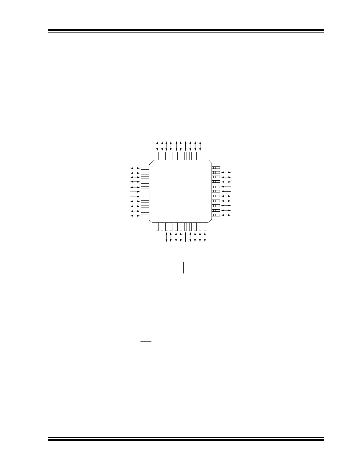
Pin Diagrams (Continued)
44-Pin TQFP
PIC18F2331/2431/4331/4431
RC7/RX/DT/SDO
RD4/FLTA
RD5/PWM4
RD6/PWM6
RD7/PWM7
RB0/PWM0
RB1/PWM1
RB2/PWM2
RB3/PWM3
V
VDD
RD2/SDI/SDA
RD1/SDO
RD0/T0CKI/T5CKI
38
39
1819202122
16
17
/VPP/RE3
/INT0
(1)
/T5CKI
(1)
RC3/T0CKI
37
RA0/AN0
RC2/CCP1/FLTB
363435
RA1/AN1
RC1/T1OSI/CCP2/FLTA
NC
33
32
31
30
29
28
27
26
25
24
23
NC
RC0/T1OSO/T1CKI
OSC2/CLKO/RA6
OSC1/CLKI/RA7
SS
AV
AVDD
RE2/AN8
RE1/AN7
RE0/AN6
RA5/AN5/LVDIN
RA4/AN4/CAP3/QEB
(1)
(1)
/SCL
/SDA
(1)
(1)
RC6/TX/CK/SS
RC5/INT2/SCK
RC4/INT1/SDI
RD3/SCK/SCL
(1)
(3)
(4)
SS
4443424140
1
2
3
4
PIC18F4331
5
6
PIC18F4431
7
8
9
10
11
121314
NC
NC
15
(2)
RB7/KBI3/PGD
RB6/KBI2/PGC
MCLR
RB4/KBI0/PWM5
RB5/KBI1/PWM4/PGM
REF-/CAP1/INDX
RA3/AN3/VREF+/CAP2/QEA
RA2/AN2/V
Note 1: RC3 is the alternate pin for T0CKI/T5CKI; RC4 is the alternate pin for SDI/SDA; RC5 is the alternate pin
for SCK/SCL.
2: Low-voltage programming must be enabled.
3: RD4 is the alternate pin for FLTA
.
4: RD5 is the alternate pin for PWM4.
2003 Microchip Technology Inc. Preliminary DS39616B-page 3

PIC18F2331/2431/4331/4431
Pin Diagrams (Continued)
44-Pin QFN
RC7/RX/DT/SDO
RD4/FLTA
RD5/PWM4
RD6/PWM6
RD7/PWM7
AVDD
RB0/PWM0
RB1/PWM1
RB2/PWM2
V
VDD
(1)
(1)
/SCL
/SDA
(1)
(1)
RC6/TX/CK/SS
RC5/INT2/SCK
RC4/INT1/SDI
RD3/SCK/SCL
(1)
(3)
(4)
SS
4443424140
1
2
3
4
PIC18F4331
5
6
PIC18F4431
7
8
9
10
11
121314
NC
RB3/PWM3
15
(2)
RB4/KBI0/PWM5
(1)
(1)
RD2/SDI/SDA
RD1/SDO
RD0/T0CKI/T5CKI
38
39
1819202122
16
17
/VPP/RE3
RB7/KBI3/PGD
RB6/KBI2/PGC
MCLR
/INT0
/T5CKI
RC3/T0CKI
37
RA0/AN0
RC2/CCP1/FLTB
363435
RA1/AN1
RC1/T1OSI/CCP2/FLTA
REF-/CAP1/INDX
RC0/T1OSO/T1CKI
33
32
31
30
29
28
27
26
25
24
23
OSC2/CLKO/RA6
OSC1/CLKI/RA7
SS
V
AVSS
AVDD
VDD
RE2/AN8
RE1/AN7
RE0/AN6
RA5/AN5/LVDIN
RA4/AN4/CAP3/QEB
RB5/KBI1/PWM4/PGM
RA3/AN3/VREF+/CAP2/QEA
RA2/AN2/V
Note 1: RC3 is the alternate pin for T0CKI/T5CKI; RC4 is the alternate pin for SDI/SDA; RC5 is the alternate pin
for SCK/SCL.
2: Low-voltage programming must be enabled.
3: RD4 is the alternate pin for FLTA
.
4: RD5 is the alternate pin for PWM4.
DS39616B-page 4 Preliminary 2003 Microchip Technology Inc.

PIC18F2331/2431/4331/4431
Table of Contents
1.0 Device Overview ..........................................................................................................................................................................7
2.0 Oscillator Configurations............................................................................................................................................................ 21
3.0 Power-Managed Modes........................................ .. .... .. .. ....... .... .. .. .... .. ....... .. .... .. .... .. ....... .. .... .................................................... 31
4.0 Reset.......................................................................................................................................................................................... 45
5.0 Memory Organization................................................................................................................................................................. 57
6.0 Flash Prog ram Memory.............................. .......................... ......................... ............ ................................................................. 75
7.0 Data EEPROM Mem o ry...................................... ......................... ......................... ..................................................................... 85
8.0 8 X 8 Hardware Multiplie r................. ............................................................................ ..............................................................89
9.0 Interrupts....................................................................................................................................................................................91
10.0 I/O Ports.................... ............ ............. ......................... ............. ......................... ....................................................................... 107
11.0 Timer0 Module .........................................................................................................................................................................133
12.0 Timer1 Module .........................................................................................................................................................................137
13.0 Timer2 Module .........................................................................................................................................................................143
14.0 Timer5 Module .........................................................................................................................................................................145
15.0 Capture/Compare/PWM (CCP) Modules ................................................................................................................................. 151
16.0 Motion Feedback Module........................................ .. .... .. ....... .. .... .. .... .. ....... .. .... .. .... .. ....... .. ......................................................159
17.0 Power Control PWM Module ................................................................ ....... .. .... .. .... ....... .... .. ....................................................181
18.0 Synchronous Serial Port (SSP) Module ...................................................................................................................................211
19.0 Enhanced Universal Synchronous Asynchronous Receiver Transmitter (EUSART)............................................................... 221
20.0 10-bit High-Speed Analog-to-Digital Converter (A/D) Module.................................................................................................. 243
21.0 Low-Voltage Detect.................................................................................................................................................................. 261
22.0 Special Features of the CPU............................................................ ........................................................................................ 267
23.0 Instruction Set Summary.......................................................................................................................................................... 287
24.0 Development Support............................................................................................................................................................... 331
25.0 Electrical Characteristics.......................................................................................................................................................... 337
26.0 Preliminary DC and AC Characteristics Graphs and Tables.................................................................................................... 371
27.0 Packaging Information.............. ......................... ............ .......................... ......................... ........................................................ 373
Appendix A: Revision History.............................................................................................................................................................379
Appendix B: Device Differences ........................................................................................................................................................379
Appendix C: Conversion Considerations ...........................................................................................................................................380
Appendix D: Migration from Baseline to Enhanced Devices.............................................................................................................. 380
Appendix E: Migration from Mid-range to Enhanced Devices ...........................................................................................................381
Appendix F: Migration from High-end to Enhanced Devices ............................................................................................................. 381
INDEX................................................................................................................................................................................................ 383
On-Line Support................................................................................................................................................................................. 391
Systems Information and Upgrade Hot Line......................................................................................................................................391
Reader Response. .............................................................................................................................................................................392
PIC18F2331/2431/4331/4431 Product Identification System ............................................................................................................ 393
2003 Microchip Technology Inc. Preliminary DS39616B-page 5

PIC18F2331/2431/4331/4431
TO OUR VALUED CUSTOMERS
It is our intention to provide our valued customers with the best documentation possible to ensure successful use of your Microchip
products. To this end, we will continue to improve our publications to better suit your needs. Our publications will be refined and
enhanced as new volumes and updates are introduced.
If you have any questions or c omm ents regarding t his publication, p lease c ontact the M arket ing Co mmunications Department via
E-mail at docerrors@mail.microchip.com or fax the Reader Response Form in the back of this data sheet to (480) 792-4150.
We welcome your feedback.
Most Current Data Sheet
To obtain the most up-to-date version of this data sheet, please register at our Worldwide Web site at:
http://www.microchip.com
You can determine the version of a data sheet by examining its literature number found on the bottom outside corner of any page.
The last character of the literature number is the version number, (e.g., DS30000A is version A of document DS30000).
Errata
An errata sheet, describing minor operational differences from the data sheet and recommended workarounds, may exist for current
devices. As device/documentation issues become known to us, we will publish an errata sheet. The errata will specify the revision
of silicon and revision of document to which it applies.
To determine if an errata sheet exists for a particular device, please check with one of the following:
• Microchip’s Worldwide Web site; http://www.microchip.com
• Your local Microchip sales office (see last page)
• The Microchip Corporate Literature Center; U.S. FAX: (480) 792-7277
When contacting a sales office or the literature center, please specify which device, revision of silicon and data sheet (include
literature number) you are using.
Customer Notification System
Register on our Web site at www.microchip.com/cn to receive the most current information on all of our products.
DS39616B-page 6 Preliminary 2003 Microchip Technology Inc.

PIC18F2331/2431/4331/4431
1.0 DEVICE OVERVIEW
This documen t conta i ns dev ic e spec if i c in for m at i on fo r
the following devices:
• PIC18F2331 • PIC18F4331
• PIC18F2431 • PIC18F4431
This family offers the advantages of all PIC18 microcontrollers – namely, high computational performance
at an economical pr ice, with the addi tion of h igh end urance enhanced Flash program memory and a highspeed 10-bit A/D converter. On top of these features,
the PIC18F2331/2431/4331/4431 family introduces
design enhancements that make these microcontrollers a logical choic e for m any hi gh perfo rmanc e, power
control and motor control applications. These special
peripherals include:
• 14-bit resolution Power Control PWM Module
(PCPWM) with programmable dead time insertion
• Motion Feedback Module (MFM), including a
3-channel Input Capture (IC) Module and
Quadrature Encoder Interface (QEI)
• High-speed 10-bit A/D Converter (HSADC)
The PCPWM can generate up to eight complementary
PWM outputs w ith dead-band time inse rtion. Overd rive
current is detected by off-chip analog comparators or
the digital fault inputs (FLTA
The MFM Quadrature Encoder Interface provides
precise rotor position feedback and/or velocity
measurement. The MFM 3 X input capture or external
interrupts can be used to detect the rotor state for
electrically commutated motor applications using Hall
Sensor feedback, such as BLDC motor drives.
PIC18F2331/2431/4331/4431 devices also feature
Flash program memory and an internal RC oscillator
with built-in LP modes.
1.1 New Core Features
1.1.1 nanoWatt TECHNOLOGY
All of the devices in the PIC18F2331/2431/4331/4431
family incorporate a range of features that can significantly reduce power consumption during operation.
Key items include:
• Alternate Run Modes: By clocking the controller
from the Timer1 source or the internal oscillator
block, power consumption during code execution
can be reduced by as much as 90%.
• Multiple Idle Modes: The controller can also run
with its CPU core disabled, bu t the peripheral s are
still active. In these states, power consumption
can be reduced even further, to as little as 4% of
normal operation requiremen t s.
, FLTB).
• On-the-fly Mode Switching: The power-managed modes are invoked by user code during
operation, allowing the user to incorporate power
saving ideas into their application’s software
design.
• Lower Consumption in Key Modules: The
power requirements for both Timer1 and the
Watchdog Timer have been reduced by up to
80%, with typical values of 1.1 and 2.1 µA,
respectively.
1.1.2 MULTIPLE OSCILLATOR OPTIONS
AND FEATURES
All of the devices in the PIC18F2331/2431/4331/4431
family offer nine different oscillator options, allowing
users a wide range o f choices i n develo ping applica tion
hardware. These include:
• Four crystal modes, using crystals or ceramic
resonators.
• Two external clock modes, offering the option of
using two pins (oscillator input and a divide-by-4
clock output) or one pin (oscillator input, with the
second pin reassigned as general I/O).
• Two external RC oscillator modes, with the same
pin options as the external clock modes.
• An internal oscillator block , which provides an
8 MHz clock and an INTRC source (approximately 31 kHz, stable over temperature and V
as well as a range of 6 user-selectable clock frequencies (from 125 kHz to 4 MHz) for a total of 8
clock frequencies.
Besides its ava ilability as a cloc k source, the intern al
oscillator block pro vid es a s t ab le re fere nce source that
gives the family additional features for robust
operation:
• Fail-Safe Clock Monitor: This option constantly
monitors the main clock source against a
reference signal provided by the internal
oscillator. If a clock failure occ urs, the con troller i s
switched to the internal oscillator block, allowing
for continued low speed operation or a safe
application shutdown.
• Two-Speed Start-up: This optio n allows the
internal oscillator to serve as the clock source
from Power-on Reset or wake-up from Sleep
mode, until the primary clock source is available.
This allows for code execution during what would
otherwise be the clock start-up interval, and can
even allow an application to perform routine
background activities and return to Sleep without
returning to full power operation.
DD),
2003 Microchip Technology Inc. Preliminary DS39616B-page 7

PIC18F2331/2431/4331/4431
1.2 Other Special Features
• Memory Endurance: The enhanced Flash cells
for both program memory and data EEPROM are
rated to last for many thousands of erase/write
cycles – up to 100,000 for program memory and
1,000,000 for EEPROM. Data retention without
refresh is conservatively estimated to be greater
than 100 years.
• Self-programmability: These devices can write
to their own program memory spaces under internal software control. By us ing a bootloader routi ne
located in the protected Boot Block at the top of
program memory, it becomes possible to create
an application that can update itself in the field.
• Power Control PWM Module: In PWM mode,
this module provides 1, 2 or 4 modulated outputs
for controlling half-bridge and full-bridge drivers.
Other features include Auto- Shutdown on fault
detection and Auto-Restart to reactivate outputs
once the condition has cleared.
• Enhanced USART: This serial communication
module is capable of standard RS-232 operation
using the internal oscillator block, removing the
need for an external crystal (and its accompanying power requirement) in applications that talk to
the outside worl d. This modul e al so incl udes au tobaud detect and LIN capability.
• High-speed 10-bit A/D Converter: This module
incorporates Programmable Acquisition Time,
allowing for a channel to be selected and a
conversion to be initiated without waiting for a
sampling period and thus, reducing code
overhead.
• Motion Feedback Module (MFM): This mod ule
features a Quadrature Encoder Interface (QEI)
and an Input Capture (IC) module. The QEI
accepts two phase inputs (QEA, QEB) and one
index input (INDX) from an incremental encoder.
The QEI supports high and low precision position
tracking, direction status and change of direction
interrupt, and velocity measurement. The input
capture features 3 channels of independent input
capture with Timer5 as the time base, a special
event trigger to other modules, and an adjustable
noise filter on each IC input.
• Extended Watchdog Timer (WDT): This
enhanced version in corpora tes a 16 -bit pre scale r,
allowing a time-out range from 4 ms to over 2
minutes, that is stable across ope rati ng vol tage
and temperature.
DS39616B-page 8 Preliminary 2003 Microchip Technology Inc.

PIC18F2331/2431/4331/4431
1.3 Details on Individual Family Members
Devices in the PIC18F 2331/2431/43 31/4431 famil y are
available in 28-pin (PIC18F2X31) and 40/44-pin
(PIC18F4X31) packages. The block diagram for the
two groups is shown in Figure 1-1.
The devices are differentiated from each other in three
ways:
1. Flash program memory (8 Kbytes for
PIC18F2X31 devices, 16 Kbytes for
PIC18F4X31).
2. A/D channels (5 for PIC18F2X31 devices, 9 for
PIC18F4X31 devices).
3. I/O ports (3 bidirectional ports on PIC18F2X31
devices, 5 bidirectional ports on PIC18F4X31
devices).
All other features fo r device s in this family are identi cal.
These are summarized in Table1-1.
The pinouts for all devices are listed in Table 1-2 and
Table 1-3.
TABLE 1-1: DEVICE FEATURES
Features PIC18F2331 PIC18F2431 PIC18F4331 PIC18F4431
Operating Frequency
Program Memory (Bytes) 8192 16384 8192 16384
Program Memory (Instruction s) 4096 8192 4096 8192
Data Memory (Bytes) 768 768 768 768
Data EEPROM Memory (Bytes) 256 256 256 256
Interrupt Sources 22 22 34 34
I/O Ports Ports A, B, C Ports A, B, C Ports A, B, C, D, E Ports A, B, C, D, E
Timers 4 4 4 4
Capture/Compare/PWM modules 2 2 2 2
14-bit Power Control PWM (6 Channels) (6 Channels) (8 Channels) (8 Channels)
Motion Feedback module
(Input Capture/Quad rature Encoder
Interface)
Serial Communications SSP,
10-bit High-Speed
Analog-to-Digital Converter module
Resets (and Delays) POR, BOR,
Programmable Low-voltag e Det ect Y e s Yes Yes Yes
Programmable Brown-out Reset Yes Yes Yes Yes
Instruction Set 75 Instructions 75 Instructions 75 Instructions 75 Instructions
Packages
DC – 40 MHz DC – 40 MHz DC – 40 MHz DC – 40 MHz
1 QEI
or
3x IC
Enhanced USART
5 Input Channels 5 Input Channels 9 Input Channels 9 Input Channels
RESET Instruction,
Stack Full,
Stack Underflow
(PWRT, OST),
(optional),
MCLR
WDT
28-pin SDIP
28-pin SOIC
1 QEI
or
3x IC
SSP,
Enhanced USART
POR, BOR,
RESET Instruction,
Stack Full,
Stac k U nde rflo w
(PWRT, OST),
(optional),
MCLR
WDT
28-pin SDIP
28-pin SOIC
1 QEI
or
3x IC
SSP,
Enhanced USART
POR, BOR,
RESET Instruction,
Stack Full,
Stack Underflow
(PWRT, OST),
(optional),
MCLR
WDT
40-pin DIP
44-pin TQFP
44-pin QFN
1 QEI
or
3x IC
SSP,
Enhanced USART
POR, BOR,
RESET Instruction,
Stack Full,
Stack Underflow
(PWRT, OST),
(optional),
MCLR
WDT
40-pin DIP
44-pin TQFP
44-pin QFN
2003 Microchip Technology Inc. Preliminary DS39616B-page 9

PIC18F2331/2431/4331/4431
FIGURE 1-1: PIC18F2331/2431 BLOCK DIAGRAM
Data Bus<8>
21
Address Latch
Program Memory
Data Latch
16
OSC2/CLKO
OSC1/CLKI
T1OSI
T1OSO
/VPP
MCLR
VDD, VSS
21
Table Pointer<21>
21
inc/dec logic
20
TABLELATCH
8
Instruction
Decode &
Control
Timing
Generation
4X PLL
Precision
Band Gap
Reference
PCLATH
PCLATU
PCH PCL
PCU
Program Counter
31 Level Stack
ROMLATCH
IR
Power-up
Timer
Oscillator
Start-up Timer
Power-on
Reset
Watchdog
Timer
Brown-out
Reset
Power
Managed
Mode Logic
INTRC
OSC
8
8
Decode
BITOP
4
BSR
3
8
Data Latch
Data RAM
(768 bytes)
Address Latch
12
Address<12>
12 4
Bank0, F
FSR0
FSR1
FSR2
inc/dec
logic
PRODLPRODH
8 x 8 Multiply
W
8
8
ALU<8>
8
PORTA
RA0/AN0
RA1/AN1
RA2/AN2/VREF-/CAP1/INDX
RA3/AN3/VREF+/CAP2/QEA
RA4/AN4/CAP3/QEB
OSC2/CLKO/RA6
OSC1/CLKI/RA7
PORTB
12
PORTC
8
8
8
PORTE
RB0/PWM0
RB1/PWM1
RB2/PWM2
RB3/PWM3
RB4/KBI0/PWM5
RB5/KBI1/PWM4/PGM
RB6/KBI2/PGC
RB7/KBI3/PGD
RC0/T1OSO/T1CKI
RC1/T1OSI/CCP2/FLTA
RC2/CCP1/FLTB
RC3/T0CKI/T5CKI/INT0
RC4/INT1/SDI/SDA
RC5/INT2/SCK/SCL
RC6/TX/CK/SS
RC7/RX/DT/SDO
MCLR/VPP/RE3
(1, 2)
Timer0 Timer1 Timer2
Data EE
CCP1
CCP2
Synchronous
Serial Port
Timer5
EUSART
HS 10-bit
ADC
PCPWM
AVDD, AVSS
MFM
Note 1: RE3 input pin is only enabled when MCLRE fuse is programmed to ‘0’.
2: RE3 is available only when MCLR is disabled.
DS39616B-page 10 Preliminary 2003 Microchip Technology Inc.

PIC18F2331/2431/4331/4431
FIGURE 1-2: PIC18F4331/4431 BLOCK DIAGRAM
Data Bus<8>
21
Address Latch
Program Memory
Data Latch
16
OSC2/CLKO
OSC1/CLKI
T1OSI
T1OSO
/VPP
MCLR
VDD, VSS
21
Table Pointer<21>
21
inc/dec logic
20
TABLELAT CH
8
Instruction
Decode &
Control
Timing
Generation
4X PLL
Precision
Band Gap
Reference
PCLATH
PCLATU
PCH PCL
PCU
Program Counter
31 Level Stack
ROMLATCH
IR
Power-up
Timer
Oscillator
Start-up Timer
Power-on
Reset
Watchdog
Timer
Brown-out
Reset
Power
Managed
Mode Logic
INTRC
OSC
8
8
Decode
BITOP
4
BSR
3
8
Data Latch
Data RAM
(768 bytes)
Address Latch
Address<12>
12 4
FSR0
FSR1
FSR2
inc/dec
logic
8 x 8 Multiply
W
8
8
ALU<8>
12
Bank0, F
PRODLPRODH
8
PORTA
PORTB
12
PORTC
8
8
PORTD
8
PORTE
RA0/AN0
RA1/AN1
RA2/AN2/VREF-/CAP1/INDX
RA3/AN3/VREF+/CAP2/QEA
RA4/AN4/CAP3/QEB
RA5/AN5/LVDIN
OSC2/CLKO/RA6
OSC1/CLKI/RA7
RB0/PWM0
RB1/PWM1
RB2/PWM2
RB3/PWM3
RB4/KBI0/PWM5
RB5/KBI1/PWM4/PGM
RB6/KBI2/PGC
RB7/KBI3/PGD
RC0/T1OSO/T1CKI
RC1/T1OSI/CCP2/FLTA
RC2/CCP1/FLTB
RC3/T0CKI/T5CKI/INT0
RC4/INT1/SDI/SDA
RC5/INT2/SCK/SCL
RC6/TX/CK/SS
RC7/RX/DT/SDO*
RD0/IT0CKI/T5CKI
RD1/SDO
RD2/SDI/SDA
RD3/SCK/SCL
RD4/FLTA
RD5/PWM4
RD6/PWM6
RD7/PWM7
RE0/AN6
RE1/AN7
RE2/AN8
MCLR/VPP/RE3
(2)
(4)
(2)
(3)
(3)
(3)
(4)
(1)
Timer0 Timer1 Timer2
Data EE
CCP1
CCP2
Synchronous
Serial Port
Timer5
EUSART
HS 10-bit
ADC
PCPWM
AVDD, AVSS
MFM
Note 1: RE3 is available only when MCLR is disabled.
2: RD4 is the alternate pin for FLTA.
3: RC3, RC4 and RC5 are alternate pins for T0CKI/T5CKI, SDI/SDA, SCK/SCL
respectively.
4: RD5 is the alternate pin for PWM4.
2003 Microchip Technology Inc. Preliminary DS39616B-page 11

PIC18F2331/2431/4331/4431
TABLE 1-2: PIC18F2331/2431 PINOUT I/O DESCRIPTIONS
Pin Name
Pin
Number
DIP SOIC
Pin
Type
Buffer
Type
Description
/VPP/RE3
MCLR
MCLR
VPP
RE3
OSC1/CLKI/RA7
OSC1
CLKI
RA7
OSC2/CLKO/RA6
OSC2
CLKO
RA6
RA0/AN0
RA0
AN0
RA1/AN1
RA1
AN1
RA2/AN2/V
RA2
AN2
V
CAP1
INDX
RA3/AN3/V
RA3
AN3
V
CAP2
QEA
RA4/AN4/CAP3/QEB
RA4
AN4
CAP3
QEB
Legend: TTL = TTL compatible input CMOS = CMOS compatible input or output
REF-/CAP1/INDX
REF-
REF+/CAP2/QEA
REF+
ST = Schmitt Trigger input with CMOS levels I = Input
O = Output P = Power
OD = Open-Drain (no diode to V
11
99
10 10
22
33
44
55
66
I
ST
P
I
ST
I
ST
I
CMOS
I/O
TTL
O
—
O
—
I/O
TTL
I/OITTL
Analog
I/OITTL
Analog
I/O
TTL
I
Analog
I
Analog
I
ST
I
ST
I/O
TTL
I
Analog
I
Analog
I
ST
I
ST
I/O
TTL
I
Analog
I
ST
I
ST
DD)
Master Clear (input) or programming voltage (input).
Master Clear (Reset) input. This pin is an active-low
Reset to the device.
High-voltage ICSP programming enable pin.
Digital input. Available only when MCLR
Oscillator crystal or external clock input.
Oscillator crystal input or external clock source input.
ST buffer when configured in RC mode, CMOS otherwise.
External clock source input. Always associated with pin
function OSC1. (See related OSC1/CLKI, OSC2/CLKO
pins.)
General purpose I/O pin.
Oscillator crystal or clock output.
Oscillator crystal output. Connects to crystal or resonator
in Crystal Oscillator mode.
In RC mode, OSC2 pin outputs CLKO, which has 1/4 the
frequency of OSC1 and de notes the in struc tion cycl e rate.
General purpose I/O pin.
PORTA is a bidirectional I/O port.
Digital I/O.
Analog input 0.
Digital I/O.
Analog input 1.
Digital I/O.
Analog input 2.
A/D Reference Voltage (Low) input.
Input capture pin 1.
Quadrature Encoder Interface index input pin.
Digital I/O.
Analog input 3.
A/D Reference Voltage (High) input.
Input capture pin 2.
Quadrature Encoder Interface channel A input pin.
Digital I/O.
Analog input 4.
Input capture pin 3.
Quadrature Encoder Interface channel B input pin.
is disabled.
DS39616B-page 12 Preliminary 2003 Microchip Technology Inc.

PIC18F2331/2431/4331/4431
T ABLE 1-2: PIC18F2331/2431 PINOUT I/O DESCRIPTIONS (CONTINUED)
Pin
Pin Name
RB0/PWM0
RB0
PWM0
RB1/PWM1
RB1
PWM1
RB2/PWM2
RB2
PWM2
RB3/PWM3
RB3
PWM3
RB4/KBI0/PWM5
RB4
KBI0
PWM5
RB5/KBI1/PWM4/PGM
RB5
KBI1
PWM4
PGM
RB6/KBI2/PGC
RB6
KBI2
PGC
RB7/KBI3/PGD
RB7
KBI3
PGD
Legend: TTL = TTL compatible input CMOS = CMOS compatible input or output
ST = Schmitt Trigger input with CMOS levels I = Input
O = Output P = Power
OD = Open-Drain (no diode to V
Number
DIP SOIC
21 21
22 22
23 23
24 24
25 25
26 26
27 27
28 28
Pin
Buffer
Type
Type
I/OOTTL
I/OOTTL
I/OOTTL
I/OOTTL
I/O
I
O
I/O
I
O
I/O
I/O
I
I/O
I/O
I
I/O
DD)
Description
PORTB is a bidirectional I/O port. PORTB can be software
programmed for internal weak pull-ups on all in puts.
Digital I/O.
TTL
TTL
TTL
TTL
TTL
TTL
TTL
TTL
TTL
TTL
ST
TTL
TTL
ST
TTL
TTL
ST
PWM output 0.
Digital I/O.
PWM output 1.
Digital I/O.
PWM output 2.
Digital I/O.
PWM output 3.
Digital I/O.
Interrupt-on-change pin.
PWM output 5.
Digital I/O.
Interrupt-on-change pin.
PWM output 4.
Low-voltage ICSP programming entry pin.
Digital I/O.
Interrupt-on-change pin.
In-Circuit Debugger and ICSP programming clock pin.
Digital I/O.
Interrupt-on-change pin.
In-Circuit Debugger and ICSP programming data pin.
2003 Microchip Technology Inc. Preliminary DS39616B-page 13
PIC18F2331/2431/4331/4431
TABLE 1-2: PIC18F2331/2431 PINOUT I/O DESCRIPTIONS (CONTINUED)
Pin
Pin Name
RC0/T1OSO/T1CKI
RC0
T1OSO
T1CKI
RC1/T1OSI/CCP2/FLTA
RC1
T1OSI
CCP2
FLTA
RC2/CCP1/FLTB
RC2
CCP1
FLTB
RC3/T0CKI/T5CKI/INT0
RC3
T0CKI
T5CKI
INT0
RC4/INT1/SDI/SDA
RC4
INT1
SDI
SDA
RC5/INT2/SCK/SCL
RC5
INT2
SCK
SCL
RC6/TX/CK/SS
RC6
TX
CK
SS
RC7/RX/DT/SDO
RC7
RX
DT
SDO
SS 8, 19 8, 19 P — Ground reference for logic and I/O pins.
V
VDD 7, 20 7, 20 P — Positive supply for logic and I/O pins.
Legend: TTL = TTL compatible input CMOS = CMOS compatible input or output
ST = Schmitt Trigger input with CMOS levels I = Input
O = Output P = Power
OD = Open-Drain (no diode to V
Number
DIP SOIC
11 11
12 12
13 13
14 14
15 15
16 16
17 17
18 18
Pin
Type
I/O
O
I
I/O
I
I/O
I
I/O
I/O
I
I/O
I
I
I
I/O
I
I
I/O
I/O
I
I/O
I/O
I/O
O
I/O
I
I/O
I
I/O
O
DD)
Buffer
Type
ST
—
ST
ST
CMOS
ST
ST
ST
ST
ST
ST
ST
ST
ST
ST
ST
ST
ST
ST
ST
ST
ST
ST
—
ST
TTL
ST
ST
ST
—
Description
PORTC is a bidirectional I/O port.
Digital I/O.
Timer1 oscillator output.
Timer1 external clock input.
Digital I/O.
Timer1 oscillator input.
Capture2 input, Compare2 output, PWM2 output.
Fault interrupt input pin.
Digital I/O.
Capture1 input/Compare1 output/PWM1 output.
Fault interrupt input pin,.
Digital I/O.
Timer0 alternate clock input.
Timer5 alternate clock input.
External interrupt 0.
Digital I/O.
External interrupt 1.
SPI™ data in.
2
C™ data I/O.
I
Digital I/O.
External interrupt 2.
Synchronous serial clock input/output for SPI mode.
Synchronous serial clock input/output for I
Digital I/O.
USART Asynchronous Transmit.
USART Synchronous Clock (see related RX/DT).
SPI Slave Select input.
Digital I/O.
USART Asynchronous Receive.
USART Synchronous Data (see related TX/CK).
SPI data out.
2
C mode.
DS39616B-page 14 Preliminary 2003 Microchip Technology Inc.

PIC18F2331/2431/4331/4431
T ABLE 1-3: PIC18F4331/4431 PINOUT I/O DESCRIPTIONS
Pin Name
MCLR
/VPP/RE3
MCLR
VPP
RE3
OSC1/CLKI/RA7
OSC1
CLKI
RA7
OSC2/CLKO/RA6
OSC2
CLKO
RA6
RA0/AN0
RA0
AN0
RA1/AN1
RA1
AN1
RA2/AN2/V
INDX
RA2
AN2
V
CAP1
INDX
RA3/AN3/V
CAP2/QEA
RA3
AN3
V
CAP2
QEA
RA4/AN4/CAP3/QEB
RA4
AN4
CAP3
QEB
RA5/AN5/LVDIN
RA5
AN5
LVDIN
Legend: TTL = TTL compatible input CMOS = CMOS compatible input or output
REF-/CAP1/
REF-
REF+/
REF+
ST = Schmitt Trigger input with CMOS levels I = Input
O = Output P = Power
OD = Open-Drain (no diode to V
Pin Number
DIP TQFP QFN
11818
13 30 32
14 31 33
21919
32020
42121
52222
62323
72424
Pin
Buffer
Type
Type
I
P
I
I
CMOS
I
I/O
O
O
I/O
I/OITTL
Analog
I/OITTL
Analog
I/O
Analog
I
Analog
I
I
I
I/O
Analog
I
Analog
I
I
I
I/O
I
Analog
I
I
I/O
I
Analog
I
Analog
DD)
Description
Master Clear (input) or programming voltage (input).
ST
ST
ST
TTL
—
—
TTL
TTL
ST
ST
TTL
ST
ST
TTL
ST
ST
TTL
Master Clear (Reset) input. This pin is an active-low.
Reset to the device.
Programming voltage inpu t.
Digital input. Available only when MCLR
Oscillator crystal or external clock input.
Oscillator crystal input or external clock source input.
ST buffer when configured in RC mode, CMOS otherwise.
External clock source input. Always associated with pin
function OSC1. (See related OSC1/CLKI, OSC2/CLKO pins.)
General purpose I/O pin.
Oscillator crystal or clock output.
Oscillator crystal output. Connects to crystal or resonator
in Crystal Oscillator mode.
In RC mode, OSC2 pin outputs CLKO, which has 1/4 the
frequency of OSC1 and denotes the instruction cycle rate.
General purpose I/O pin.
PORTA is a bidirectional I/O port.
Digital I/O.
Analog input 0.
Digital I/O.
Analog input 1.
Digital I/O.
Analog input 2.
A/D Reference Voltage (Low) input.
Input capture pin 1.
Quadrature Encoder Interface index input pin.
Digital I/O.
Analog input 3.
A/D Reference Voltage (High) input.
Input capture pin 2.
Quadrature Encoder Interface channel A input pin.
Digital I/O.
Analog input 4.
Input capture pin 3.
Quadrature Encoder Interface channel B input pin.
Digital I/O.
Analog input 5.
Low-voltage Detect input.
is disabled.
2003 Microchip Technology Inc. Preliminary DS39616B-page 15

PIC18F2331/2431/4331/4431
TABLE 1-3: PIC18F4331/4431 PINOUT I/O DESCRIPTIONS (CONTINUED)
Pin Name
RB0/PWM0
RB0
PWM0
RB1/PWM1
RB1
PWM1
RB2/PWM2
RB2
PWM2
RB3/PWM3
RB3
PWM3
RB4/KBI0/PWM5
RB4
KBI0
PWM5
RB5/KBI1/PWM4/
PGM
RB5
KBI1
PWM4
PGM
RB6/KBI2/PGC
RB6
KBI2
PGC
RB7/KBI3/PGD
RB7
KBI3
PGD
Legend: TTL = TTL compatible input CMOS = CMOS compatible input or output
ST = Schmitt Trigger input with CMOS levels I = Input
O = Output P = Power
OD = Open-Drain (no diode to V
Pin Number
DIP TQFP QFN
33 8 9
34 9 10
35 10 11
36 11 12
37 14 14
38 15 15
39 16 16
40 17 17
Pin
Buffer
Type
Type
I/OOTTL
I/OOTTL
I/OOTTL
I/OOTTL
I/O
I
O
I/O
I
O
I/O
I/O
I
I/O
I/O
I
I/O
DD)
Description
PORTB is a bidirectional I/O port. PORTB can be software
programmed for internal weak pull-ups on all inputs.
Digital I/O.
TTL
TTL
TTL
TTL
TTL
TTL
TTL
TTL
TTL
TTL
ST
TTL
TTL
ST
TTL
TTL
ST
PWM output 0.
Digital I/O.
PWM output 1.
Digital I/O.
PWM output 2.
Digital I/O.
PWM output 3.
Digital I/O.
Interrupt-on-change pin.
PWM output 5.
Digital I/O.
Interrupt-on-change pin.
PWM output 4.
Low-voltage ICSP programming entry pin.
Digital I/O.
Interrupt-on-change pin.
In-Circuit Debugger and ICSP programming clock pin.
Digital I/O.
Interrupt-on-change pin.
In-Circuit Debugger and ICSP programming data pin.
DS39616B-page 16 Preliminary 2003 Microchip Technology Inc.

PIC18F2331/2431/4331/4431
T ABLE 1-3: PIC18F4331/4431 PINOUT I/O DESCRIPTIONS (CONTINUED)
Pin Name
RC0/T1OSO/T1CKI
RC0
T1OSO
T1CKI
RC1/T1OSI/CCP2/
FLTA
RC1
T1OSI
CCP2
FLTA
RC2/CCP1/FLTB
RC2
CCP1
FLTB
RC3/T0CKI/T5CKI/
INT0
RC3
T0CKI
T5CKI
INT0
RC4/INT1/SDI/SDA
RC4
INT1
SDI
SDA
RC5/INT2/SCK/SCL
RC5
INT2
SCK
SCL
RC6/TX/CK/SS
RC6
TX
CK
SS
RC7/RX/DT/SDO
RC7
RX
DT
SDO
Legend: TTL = TTL compatible input CMOS = CMOS compatible input or output
ST = Schmitt Trigger input with CMOS levels I = Input
O = Output P = Power
OD = Open-Drain (no diode to V
Pin Number
DIP TQFP QFN
15 32 34
16 35 35
17 36 36
18 37 37
23 42 42
24 43 43
25 44 44
26 1 1
Pin
Type
I/O
O
I
I/O
I
I/O
I
I/O
I/O
I
I/O
I
I
I
I/O
I
I
I/O
I/O
I
I/O
I/O
I/O
O
I/O
I
I/O
I
I/O
O
DD)
Buffer
Type
ST
—
ST
ST
CMOS
ST
ST
ST
ST
ST
ST
ST
ST
ST
ST
ST
ST
ST
ST
ST
ST
ST
ST
—
ST
ST
ST
ST
ST
—
Description
PORTC is a bidirectional I/O port.
Digital I/O.
Timer1 oscillator output.
Timer1 external clock input.
Digital I/O.
Timer1 oscillator input.
Capture2 input, Compare2 output, PWM2 output.
Fault interrupt input pin.
Digital I/O.
Capture1 input/Compare1 output/PWM1 output.
Fault interrupt input pin.
Digital I/O.
Timer0 alternate clock input.
Timer5 alternate clock input.
External interrupt 0.
Digital I/O.
External interrupt 1.
SPI Data in.
2
C Data I/O.
I
Digital I/O.
External interrupt 2.
Synchronous serial clock input/output for SPI mode.
Synchron ous serial clock input/o utput for I
Digital I/O.
USART Asynchronous Transmit.
USART Synchronous Clock (see related RX/DT).
SPI Slave Select input.
Digital I/O.
USART Asynchronous Receive.
USART Synchronous Data (see related TX/CK).
SPI Data out.
2
C mode.
2003 Microchip Technology Inc. Preliminary DS39616B-page 17

PIC18F2331/2431/4331/4431
TABLE 1-3: PIC18F4331/4431 PINOUT I/O DESCRIPTIONS (CONTINUED)
Pin Name
RD0/T0CKI/T5CKI
RD0
T0CKI
T5CKI
RD1/SDO
RD1
SDO
RD2/SDI/SDA
RD2
SDI
SDA
RD3/SCK/SCL
RD3
SCK
SCL
RD4/FLTA
RD4
FLTA
RD5/PWM4
RD5
PWM4
RD6/PWM6
RD6
PWM6
RD7/PWM7
RD7
PWM7
Legend: TTL = TTL compatible input CMOS = CMOS compatible input or output
ST = Schmitt Trigger input with CMOS levels I = Input
O = Output P = Power
OD = Open-Drain (no diode to V
Pin Number
DIP TQFP QFN
19 38 38
20 39 39
21 40 40
22 41 41
27 2 2
28 3 3
29 4 4
30 5 5
Pin
Buffer
Type
I/O
I
I
I/OOST
I/O
I
I/O
I/O
I/O
I/O
I/OIST
I/OOST
I/OOST
I/OOST
DD)
Type
PORTD is a bidirectional I/O port, or a Parallel Slave Port
(PSP) for interfacing to a microprocessor port. These pins
have TTL input buffers when PSP module is enabled.
ST
ST
ST
—
ST
ST
ST
ST
ST
ST
ST
TTL
TTL
TTL
Digital I/O.
Timer0 external clock input.
Timer5 input clock.
Digital I/O.
SPI Data out.
Digital I/O.
SPI Data in.
2
C Data I/O.
I
Digital I/O.
Synchronous serial clock input/output for SPI mode.
Synchronous serial clock input/output for I
Digital I/O.
Fault interrupt input pin.
Digital I/O.
PWM output 4.
Digital I/O.
PWM output 6.
Digital I/O.
PWM output 7.
Description
2
C mode.
DS39616B-page 18 Preliminary 2003 Microchip Technology Inc.

PIC18F2331/2431/4331/4431
T ABLE 1-3: PIC18F4331/4431 PINOUT I/O DESCRIPTIONS (CONTINUED)
Pin Name
RE0/AN6
RE0
AN6
RE1/AN7
RE1
AN7
RE2/AN8
RE2
AN8
SS 12,
V
VDD 11, 32 7, 28 7, 8,
NC — 12,
Legend: TTL = TTL compatible input CMOS = CMOS compatible input or output
ST = Schmitt Trigger input with CMOS levels I = Input
O = Output P = Power
OD = Open-Drain (no diode to V
Pin Number
DIP TQFP QFN
82525
92626
10 27 27
6, 29 6, 30, 31P — Ground reference for logic and I/O pins.
31
13,
33, 34
Pin
Buffer
Type
Type
PORTE is a bidirectional I/O port.
I/OIST
Analog
I/OIST
Analog
I/OIST
Analog
P — Positive supply for logic and I/O pins.
28,
29
13 NC NC No connect
DD)
Digital I/O.
Analog input 6.
Digital I/O.
Analog input 7.
Digital I/O.
Analog input 8.
Description
2003 Microchip Technology Inc. Preliminary DS39616B-page 19

PIC18F2331/2431/4331/4431
NOTES:
DS39616B-page 20 Preliminary 2003 Microchip Technology Inc.

PIC18F2331/2431/4331/4431
2.0 OSCILLATOR CONFIGURATIONS
2.1 Oscillator Types
The PIC18F2331/2431/4331/4431 devices can be
operated in 10 di fferent oscillator modes. The u ser ca n
program the configuratio n bit s FOSC3:FOSC0 in Confi guration register 1H to select one of these 10 modes:
1. LP Low-power Crystal
2. XT Crystal/Resonator
3. HS High-speed Crystal/Resonator
4. HSPLL High-speed Crystal/Resonator
with PLL enabled
5. RC External Resistor/Capacitor with
F
OSC/4 output on RA6
6. RCIO External Resist or/Capacitor with
I/O on RA6
7. INTIO1 Internal Oscillator with F
output on RA6 and I/O on RA7
8. INTIO2 Intern al Osc illat or with I/O on RA6
and RA7
9. EC External Clock with F
10. ECIO External Clock with I/O on RA6
2.2 Crystal Oscillator/Ceramic Resonators
In XT, LP, HS or HSPLL oscillator modes, a crystal or
ceramic resonator is connected to the OSC1 and
OSC2 pins to establish oscillation. Figure 2-1 shows
the pin connections.
The oscillator design requires the use of a parallel cut
crystal.
Note: Use of a series cut crystal may give a
frequency out of the crystal
manufacturers’ specifications.
OSC/4
OSC/4 output
FIGURE 2-1: CRYSTAL/CERAMIC
RESONATOR OPERATION
(XT, LP, HS OR HSPLL
CONFIGURATION)
(1)
C1
(1)
C2
Note 1: See T able 2-1 and T able 2-2 for initial values of
2: A series res istor (R
3: R
OSC1
XTAL
(2)
RS
OSC2
C1 and C2.
strip cut crystals.
F varies with the oscillator mode chosen.
(3)
RF
Sleep
PIC18FXXXX
S) may be required for AT
To
Internal
Logic
T ABLE 2-1: CAPACITOR SELECTION FOR
CERAMIC RESONATORS
Typical Capacitor Values Used:
Mode Freq OSC1 OSC2
XT 455 kHz
2.0 MHz
4.0 MHz
HS 8.0 MHz
16.0 MHz
Capacitor values are for design guidance only.
These capacitors were tested with the resonators
listed below for basic start-up and operation. These
values are not optimized.
Different cap acitor values may be required to prod uce
acceptable oscillator operation. The user should test
the performance of the oscillator over the expected
DD and temperature range for the application.
V
See the notes on page 22 for additional information.
Resonators Used:
455 kHz 4.0 MHz
2.0 MHz 8.0 MHz
16.0 MHz
56 pF
47 pF
33 pF
27 pF
22 pF
56 pF
47 pF
33 pF
27 pF
22 pF
2003 Microchip Technology Inc. Preliminary DS39616B-page 21
PIC18F2331/2431/4331/4431
TABLE 2-2: CAPACITOR SELECTION FOR
CRYSTAL OSCILLATOR
Osc T y pe
Crystal
Freq
LP 32 kHz 33 pF 33 pF
200 kHz 15 pF 15 pF
XT 1 MHz 33 pF 33 pF
4 MHz 27 pF 27 pF
HS 4 MH z 27 pF 27 pF
8 MHz 22 pF 22 pF
20 MHz 15 pF 15 pF
Capacitor values are for design guidance only.
These capacitors were tested with the crystals listed
below for basic start-up and op erat ion . These values
are not optimized.
Different capa citor values may be required to produc e
acceptable oscillator operation. The user should test
the performance of the oscillator over the expected
DD and temperature range for the application.
V
See the notes following this table for additional
information.
Crystals Used:
32 kHz 4 MHz
200 kHz 8 MHz
1 MHz 20 MHz
Note 1: Higher capacit ance increa ses the st ability
of oscillator, but also increases the startup time.
2: When operating below 3V V
using certain ceramic resonators at any
voltage, it may be necessary to use the
HS mode or switch to a crystal oscillator.
3: Since each resonator/crystal has its own
characteristics, the user should consult
the resonator/crystal manufacturer for
appropriate values of external
components.
4: Rs may be requ ired to avoi d overdrivi ng
crystals with low driv e lev e l spe ci fic ati on.
5: Always verify oscilla tor pe rform an ce ov er
DD and temperature range that is
the V
expected for the application.
T ypical Cap acitor V alues
Tested:
C1 C2
DD, or when
An external clock source may also be connected to the
OSC1 pin in the HS mode, as shown in Figure 2-2.
FIGURE 2-2: EXTERNAL CLOCK INPUT
OPERATION (HS OSC
CONFIGURATION)
Clock from
Ext. System
Open
OSC1
OSC2
PIC18FXXXX
(HS Mode)
2.3 HSPLL
A Phase Locked Loop (PLL) circuit is provided as an
option for users who wish to use a lower frequency
crystal oscillator circuit, or to clock the device up to its
highest rated frequency from a crystal oscillator. This
may be useful for customers who are concerned with
EMI due to high-frequency crystals.
The HSPLL mode make s use of the HS mode osc illator
for frequencies up t o 10 MHz. A PLL then multipl ies the
oscillator output frequency by 4 to produce an internal
clock frequency up to 40 MHz.
The PLL is enabled only when the oscillator configuration bits are programmed for HSPLL mode. If
programmed for any other mode, the PLL is not
enabled.
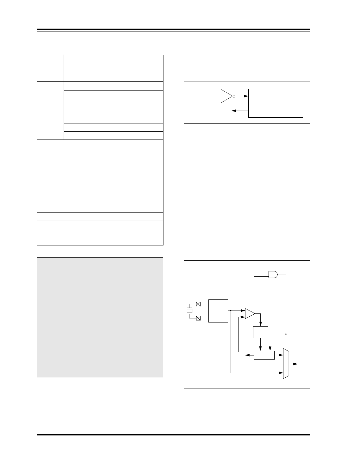
FIGURE 2-3: PLL BLOCK DIAGRAM
HS Osc Enable
PLL Enable
(from Configuration Register 1H)
OSC2
OSC1
HS Mode
Crystal
Osc
F
IN
FOUT
÷4
Phase
Comparator
Loop
Filter
VCO
SYSCLK
MUX
DS39616B-page 22 Preliminary 2003 Microchip Technology Inc.

PIC18F2331/2431/4331/4431
2.4 External Clock Input
The EC and ECIO os c ill ato r m ode s require an external
clock source to be conn ected to the OSC1 pi n. There is
no oscillator start-up time required after a Power-on
Reset or after an exit from Sleep mode.
In the EC Oscillator mode, the oscillator frequency
divided by 4 is available on the OSC2 pin. This signal
may be used f or t e st pu r pos es or t o sy nc hr o n iz e ot he r
logic. Figure 2-4 shows the pin connections for the EC
Oscillator mode.
FIGURE 2-4: EXTER NAL CLOCK INPUT
OPERATION
(EC CONFIGURATION)
Clock from
Ext. System
OSC/4
F
The ECIO Oscillator mode func ti ons li ke t he EC m od e,
except that the OSC2 pin becomes an additional
general purpose I/O pin. The I/O pin becomes bit 6 of
PORTA (RA6). Figure 2-5 shows the pin connections
for the ECIO Oscillator mode.
FIGURE 2-5: EXTER NAL CLOCK INPUT
Clock from
Ext. System
RA6
OSC1/CLKI
PIC18FXXXX
OSC2/CLKO
OPERATION
(ECIO CONFIGURATION)
OSC1/CLKI
PIC18FXXXX
I/O (OSC2)
2.5 RC Oscillator
For timing insensitive applications, the “RC” and
“RCIO” device options offer additional cost savings.
The RC oscillator frequency is a function of the supply
voltage, the resistor (R
values and the operating temperature. In addition to
this, the oscillator frequency will vary from unit to unit
due to normal manufacturing variation. Furthermore,
the difference in lead frame capacitance between
package type s wi ll also affect the os cillation frequenc y,
especially for low C
take into account variation due to tolerance of external
R and C components used. Figure 2-6 shows how the
R/C combination is connected.
In the RC Oscillator mode, the oscillator frequency
divided by 4 is available on the OSC2 pin. This signal
may be used f or t e st pu r pos es or t o sy nc hr o n iz e ot he r
logic.
FIGURE 2-6: RC OSCILLATOR MODE
VDD
REXT
CEXT
VSS
F
OSC/4
Recommended values: 3 kΩ ≤ REXT ≤ 100 kΩ
The RCIO Oscillator mode (Figure 2-7) functions like
the RC mode, except that the OSC2 pin becomes an
additional general purpose I/O pin. The I/O pin
becomes bit 6 of PORTA (RA6).
EXT) and capacitor (CEXT)
EXT values. Th e user also needs to
OSC1
Internal
Clock
PIC18FXXXX
OSC2/CLKO
EXT > 20 pF
C
FIGURE 2-7: RCIO OSCILLATOR MODE
VDD
REXT
OSC1
CEXT
VSS
RA6
Recommended values: 3 kΩ ≤ REXT ≤ 100 kΩ
2003 Microchip Technology Inc. Preliminary DS39616B-page 23
I/O (OSC2)
C
EXT > 20 pF
Internal
Clock
PIC18FXXXX

PIC18F2331/2431/4331/4431
2.6 Internal Oscillator Block
The PIC18F2331/2431/4331/4431 devices include an
internal oscillator block, which generates two different
clock signals; ei ther can be used a s t he s y ste m’s clock
source. This can eliminate the need for external
oscillator circuits on the OSC1 and/or OSC2 pins.
The main output (INTOSC) is an 8 MHz clock source,
which can be used to directly drive the system clock. It
also drives a postscaler, which can provide a range of
clock frequencies from 125 kHz to 4 MHz. The
INTOSC output is enabled when a system clock
frequency from 125 kHz to 8 MHz is selected.
The other clock source is the internal RC oscillator
(INTRC), which provides a 31kHz output. The INTRC
oscillator is enabled by selecting the internal oscillator
block as the system clock source, or when any of the
following are enabled:
• Power-up Timer
• Fail-Safe Clock Monitor
• Watchdog Timer
• Two-Spe ed Start-up
These features are discussed in greater detail in
Section 2 2.0 “Special Features of the CPU”.
The clock source frequency (INTOSC direct, INTRC
direct or INTOSC postscaler) is selected by configuring
the IRCF bits of the OSCCON register (Register 2-2).
2.6.2 INTRC OUTPUT FREQUENCY
The internal oscillator block is calibrated at the factory
to produce an INTOSC output frequency of 8.0 MHz.
This changes the frequency of the INTRC source from
its nominal 31.25 kHz. Peripherals and features that
depend on the INTRC source will be affected by this
shift in frequency.
2.6.3 OSCTUNE REGISTER
The internal oscillator’s output has been calibrated at
the factory, but can be adjusted in the user's application. Thi s is do ne by writi ng to the OS CTUNE regi ster
(Register 2-1). The tuning sensitivity is constant
throughout the tuning range.
When the OSCTUNE regis ter is mo di fied , the IN T O SC
and INTRC frequencies will begin shifting to the new
frequency. The INTRC clock will reach the new frequency within 8clock cycles (approximately
8*32µs = 256 µs). The INTOSC clock will stabilize
within 1 ms. Code execution continues during th is shi ft.
There is no indicati on that th e shift ha s occurre d. Operation of features that depend on the INTRC clock
source frequency, such as the WDT, Fail-Safe Clock
Monitor and peripherals, will also be affected by the
change in frequency.
2.6.1 INTIO MODES
Using the internal oscillator as the clock source can
eliminate the need for up t o two extern al oscilla tor pins,
which can then be used for digital I/O. Two distinct
configurations are available:
• In INTIO1 mode, the OSC2 pin outputs F
while OSC1 functions as RA 7 fo r dig it a l in put a nd
output.
• In INTIO2 mode, OSC1 functions as RA7 and
OSC2 functions as RA6, both for digital input and
output.
OSC/4,
DS39616B-page 24 Preliminary 2003 Microchip Technology Inc.

PIC18F2331/2431/4331/4431
REGISTER 2-1: OSCTUNE: OSCILLATOR TUNING REGISTER
U-0 U-0 R/W-0 R/W-0 R/W-0 R/W-0 R/W-0 R/W-0
— — TUN5 TUN4 TUN3 TUN2 TUN1 TUN0
bit 7 bit 0
bit 7, 6 Unimplemented: Read as ‘0’
bit 5-0 TUN<5:0>: Frequency Tuning bits
011111 = Maximum frequency
• •
• •
000001
000000 = Center frequency. Oscillator module is running at the calibrated frequency.
111111
• •
• •
100000 = Minimum frequency
Legend:
R = Readable bit W = Writable bit U = Unimplemented bit, read as ‘0’
-n = Value at POR ‘1’ = Bit is set ‘0’ = Bit is cleared x = Bit is unknown
2003 Microchip Technology Inc. Preliminary DS39616B-page 25

PIC18F2331/2431/4331/4431
2.7 Clock Sources and Oscillator
Switching
Like previous PIC18 devices, the PIC18F2331/2431/
4331/4431 devices include a feature that allows the
system clock source to be switched from the main
oscillator t o an alternate lo w frequency clock s ource.
PIC18F2331/2431/4331/4431 devices offer two alternate clock sources. When enabled, these give additional options for switching to the various powermanaged operating modes.
Essentially, there are three clock sources for these
devices:
• Primary oscillators
• Secondary oscillators
• Internal oscillator block
The primary oscillators include the external crystal
and resonator modes, the external RC modes, the
external clock modes and the internal oscillator block.
The particular mod e is defined on POR by the content s
of Configuration Register 1H. The details of these
modes are covered earlier in this chapter.
The s econdary oscillat ors are those external sources
not connected to the OSC1 or OSC2 pins. These
sources may continue to operate even after the
controller is placed in a power-managed mode.
PIC18F2331/2431/4331/4431 devices offer only the
Timer1 oscillator as a secondary oscillator. This
oscillator, in all power-managed modes, is often the
time base for functions such as a real-time clock.
Most often, a 32.768 kHz watch crystal is connected
between the RC0/T1OSO and RC1/T1OSI pins. Like
the LP mode oscillator circuit, loading capacitors are
also connected from each pin to ground.
The Timer1 oscillator is discussed in greater detail in
Section 1 2.2 “Timer1 Oscillator”.
In addition to being a p rimary clock source, the internal
oscillator block is available as a power-managed
mode clock source. The INTRC source is a lso us ed as
the clock source for several special features, such as
the WDT and Fail-Safe Clock Monitor.
The clock sources for the PIC18F2331/2431/4331/
4431 devices are shown in Figure 2-8. See
Section 12.0 “Timer1 Module” for further details of
the Timer1 oscillator. See Section 22.1 “Configura-
tion Bits” for Configurati on register details.
2.7.1 OSCILLATOR CONTROL REGISTER
The OSCCON register (Register 2-2) controls several
aspects of the system clock’s operation, both in full
power operation and in power-managed modes.
The System Clock Select bits, SCS1:SCS0, select the
clock source that is used when the device is operating
in power-managed mod es. The availab le clock sources
are the primary clock (defined in Configuration register
1H), the secondary clock (Timer1 oscillator) and the
internal oscillator block. The clock selection has no
effect until a SLEEP instruction is executed and the
device enters a power-managed mode of operation.
The SCS bits are cleared on all forms of Reset.
The Internal Oscill ator Select bit s, IRCF2:IRCF0, select
the frequency output of the interna l oscill ator block th at
is used to dr ive t he sys tem clo ck. Th e choi ces are t he
INTRC source, the INTOSC source (8 MHz) or one of
the six frequencies derived from the INTOSC
postscaler (125kHz to 4 MHz). If the internal oscillator
block is supplying the system clock, changing the
states of thes e bits w ill ha ve an immedi ate cha nge on
the internal oscillator’s output.
The OSTS, IOFS and T1RUN bits ind icate wh ich cl oc k
source is currently providing the system clock. The
OSTS indicates that the Oscillator Start-up Timer has
timed out, and the p rimary clock i s providing the s ystem
clock in pri mary clock mode s. The IOFS b it indicates
when the internal oscillator block has stabilized, and is
providing the system clock in RC clock modes. The
T1RUN bit (T1CON<6>) indicates when the Timer1
oscillator is providing the system clock in secondary
clock modes. In power-managed modes, only one of
these three bits will be se t at any time. If none of these
bits are set, the INTRC is providi ng the syste m clock, or
the internal oscillator block has just started and is not
yet stable.
The IDLEN bit controls the selective shut down of the
controller’s CPU in power-man aged modes. Th e use of
these bits is discussed in more detail in Section 3.0
“Power-Managed Modes”
Note 1: The Timer1 oscillator must be enabled to
select the secondary clock source. The
Timer1 osc illator is enabled by s etting the
T1OSCEN bit in th e T imer1 C ontrol re gister (T1CON<3>). If the Timer1 oscillator
is not enabled, then any at tem pt to se lec t
a secondary clock source when executing a SLEEP instruction will be ignored.
2: It is recommended that the Timer1 oscil-
lator be operating and stable before executing the SLEEP instruction, or a very
long delay may occur while the Timer1
oscillator starts.
DS39616B-page 26 Preliminary 2003 Microchip Technology Inc.
PIC18F2331/2431/4331/4431
FIGURE 2-8: PIC18F2331/2431/4331/4431 CLOCK DIAGRAM
OSC2
OSC1
T1OSO
T1OSI
Primary Oscillator
Sleep
Secondary Oscillator
T1OSCEN
Enable
Oscillator
OSCCON<6:4>
Internal
Oscillator
Block
INTRC
Source
PIC18F2331/2431/4331/4431
8 MHz
4 MHz
2 MHz
1 MHz
8 MHz
(INTOSC)
Postscaler
500 kHz
250 kHz
125 kHz
31 kHz
4 x PLL
OSCCON<6:4>
111
110
101
100
MUX
011
010
001
000
C4NFIG1H <3:0>
HSPLL
LP, XT, HS, RC, EC
T1OSC
Clock Source Option
for Other Modules
Internal Oscillator
Clock
Control
MUX
OSCCON<1:0>
Peripherals
CPU
IDLEN
WDT, FSCM
2003 Microchip Technology Inc. Preliminary DS39616B-page 27

PIC18F2331/2431/4331/4431
REGISTER 2-2: OSCCON REGISTER
R/W-0 R/W-0 R/W-0 R/W-0 R
IDLEN IRCF2 IRCF1 IRCF0 OSTS IOFS SCS1 SCS0
bit 7 bit 0
bit 7 IDLEN: Idle Enable bit
1 = Idle mode enabled; CPU core is not clocked in power-managed modes
0 = Run mode enabled; CPU core is clocked in power-managed modes
bit 6-4 IRCF2:IRCF0: Internal Oscillator Frequency Select bits
111 = 8 M Hz (8 MHz source drives clock directly)
110 = 4 MHz
101 = 2 MHz
100 = 1 MHz
011 = 500 k Hz
010 = 250 k Hz
001 = 125 k Hz
000 = 31 kHz (INTRC source drives clock directly)
bit 3 OSTS: Oscillator Start-up Time-out Status bit
1 = Oscillator start-up time-out timer has expired; primary oscillator is running
0 = Oscillator start-up time-out timer is running; primary oscillator is not ready
bit 2 IOFS: INTOSC Frequency Stable bit
1 = INTOSC frequency is stable
0 = INTOSC frequency is not stable
bit 1-0 SCS1:SCS0: System Clock Select bits
1x = Internal oscillator block (RC modes)
01 = Timer1 oscillator (Secondary modes)
00 = Primary oscillator (Sleep and PRI_IDLE modes)
Note 1: Depends on state of the IESO bit in Configuration Register 1H.
(1)
R-0 R/W-0 R/W-0
Legend:
R = Readable bit W = Writable bit U = Unimplemented bit, read as ‘0’
- n = Value at POR ‘1’ = Bit is set ‘0’ = Bit is cleared x = Bit is unknown
2.7.2 OSCILLATOR TRANSITIONS
The PIC18F2331/2431/4331/4431 devices contain
circuitry to prevent clocking “glitches” when switching
between clock sources. A short pause in the system
clock occurs during the clock switc h. Th e leng th of thi s
pause is between 8 and 9 clock periods of the new
clock source. This ensures that the new clock source is
stable and that its pulse width will not be less than the
shortest pulse width of the two clock sources.
Clock transitions are discussed in greater detail in
Section 3 .1.2 “Entering Power-Managed Modes”.
DS39616B-page 28 Preliminary 2003 Microchip Technology Inc.

PIC18F2331/2431/4331/4431
2.8 Effects of Power-Managed Modes on the Various Clock Sources
When the device executes a SLEEP instruction, the
system is switched to one of the power-managed
modes, depending on the state of the IDLEN and
SCS1:SCS0 bits of the OSCCON register. See
Section 3.0 “Power-Managed Modes” for details.
When PRI_IDLE mode is selected, the designated
primary oscillator continues to run without interruption.
For all other power-managed modes, the oscillator
using the OSC1 pin is disabled. The OSC1 pin (and
OSC2 pin, if used by the o scillat or) will sto p oscillat ing.
In secondary clock modes (SEC_RUN and
SEC_IDLE), the Timer1 oscillator is operating and
providing the system clock. The Timer1 oscillator may
also run in all power-managed modes if required to
clock Timer1.
In internal oscillator modes (RC_RUN and RC_IDLE),
the internal oscillator block provides the system clock
source. The INTRC output can be used directly to
provide the system clock, and may be enabled to
support various special features, regardless of the
power-managed mode (see Sections 22.2 through
22.4). The INTOSC output at 8 MHz may be used
directly to clock the system, or may be divided down
first. The INTOSC out put is disabled if the sy stem clock
is provided directly from the INTRC output.
If the Sleep mode is selected, all clock sources are
stopped. Since all the transistor switching currents
have been stopped, Sleep mode achieves the lowest
current consumption of the device (only leakage
currents).
Enabling any on-chip feature that will operate during
Sleep will increas e the current cons umed during S leep.
The INTRC is required to support WDT operation. The
Timer1 oscillator may be operating to support a realtime clock. Other features m ay be op erating th at do not
require a system clock source (i.e., SSP slave, PSP,
INTn pins, A/D conversions and others).
2.9 Power-up Delays
Power-up delays are controlled by two timers, so that
no external Reset circuitry is required for most
applications. The delays ensure that the device is kept
in Reset until the device power supply is stable under
normal circumstances, and the primary clock is
operating and stable. For additional information on
power-up delays, see Sections 4.1 through 4.5.
The first timer is the Power-up Timer (PWRT), which
provides a fixed delay on power-up (parameter 33,
Table 25-8), if enabled, in Configuration register 2L.
The second timer is the Oscillator Start-up Timer
(OST), intended to keep the chip in Rese t until the crystal oscillator is stable (LP, XT and HS modes). The OST
does this by counting 1024 oscillator cycles before
allowing the oscillator to clock the device.
When the HSPLL Oscillator mode is selected, the
device is kept in Res et for an add iti onal 2ms, following
the HS mode OST delay, so the PLL can lock to the
incoming clock frequ enc y.
There is a delay of 5 to 10 µs following POR, while the
controller becomes ready to execute instructions. This
delay runs concurrently with any other delays. This
may be the only del ay that occurs when any o f the EC ,
RC or INTIO modes are used as the primary clock
source.
TABLE 2-3: OSC1 AND OSC2 PIN STATES IN SLEEP MODE
OSC Mode OSC1 Pin OSC2 Pin
RC, INTIO1 Floating, external resistor
should pull high
RCIO, INTIO2 Floating, external resistor
should pull high
ECIO Floating, pulled by external clock Configured as PORTA, bit 6
EC Floating, pulled by external clock At logic low (clock/4 output)
LP, XT, and HS Feedback inverter disabled , at
quiescent voltage level
Note: See Table 4-1 in the Section 4.0 “Reset”, for time-outs due to Sleep and MCLR
2003 Microchip Technology Inc. Preliminary DS39616B-page 29
At logic low (clock/4 output)
Configured as PORTA, bit 6
Feedback inverter disabled, at
quiescent voltage level
Reset.

PIC18F2331/2431/4331/4431
NOTES:
DS39616B-page 30 Preliminary 2003 Microchip Technology Inc.

PIC18F2331/2431/4331/4431
3.0 POWER-MANAGED MODES
The PIC18F2331/2431/4331/4431 devices offer a total
of six operating modes for more efficient power
management (see Table 3-1). These operating modes
provide a variety of options for selective power
conservation in applications where resources may be
limited (i.e., battery-powered devices).
There are three categories of power-managed modes:
• Sleep mode
• Idle modes
• Run modes
These categories define which portions of the device
are clocked and sometimes, what speed. The run and
idle modes may use any of the three available clock
sources (Primary, Secondary or INTOSC multiplexer);
the Sleep mode does not use a clock source.
The clock switching feature offered in other PIC18
devices (i.e., using the Timer1 oscillator in place of the
primary oscillator), and the Sleep mode offered by all
PICmicro
stopped) are both offered in the PIC18F2331/2431/
4331/4431 devices (SEC_RUN and Sleep modes,
respectively). However, additional power-managed
modes are available that al low the user gre ater flex ibility in determining what portions of the device are operating. The power-managed modes are event driven;
that is, some sp ecific event m ust occur for the device to
enter or (more particularl y) exit these operating mo des.
For PIC18F2331/2431/4331/4431 devices, the powermanaged modes are invoked by using the existing
SLEEP instruction. All modes exit to PRI_RUN mode
when triggered by an interrupt, a Reset or a WD T timeout (PRI_RUN mode is the normal full power execution
mode; the CPU and peri phe ral s are cl oc ked by the p rimary oscillator source). In addition, power-managed
run modes may also exit to Sleep mode or their
corresponding idle mode.
®
devices (where all system clocks are
3.1 Selecting Power-Managed Modes
Selecting a power-managed mode requires deciding if
the CPU is to be clocked or not, and selecting a clock
source. The IDLEN bit controls CPU clocking, while the
SC1:SCS0 bits select a clock source. The individual
modes, bit settings, clock sources and affected
modules are summarized in Table 3-1.
3.1.1 CLOCK SOURCES
The clock source is selected by setting the SCS bits of
the OSCCON register. Three clock sources are available for use in powe r-managed idl e modes: the primary
clock (as configured in Configuration Register 1H), the
secondary clock (Timer1 oscillator), and the internal
oscillator block. The secondary and internal oscillator
block sources are available for the power-managed
modes (PRI_RUN mode is the normal full power execution mode; the CPU and peripherals are clocked by
the primary oscillator source).
TABLE 3-1: POWER-MANAGED MODES
OSCCON bits Module Clocking
Mode
Sleep
PRI_RUN
SEC_RUN 001Clocked Clocked Secondary – Timer1 Oscillator
RC_RUN 01xClocked Clocked Internal Oscillator Block
PRI_IDLE 100 Off Clocked Primary – LP, XT, HS, HSPLL, RC, EC
SEC_IDLE 101 Off Clocked Secondary – Timer1 Oscillator
RC_IDLE 11x Off Clocked Internal Oscillator Block
Note 1: Includes INTOSC and INTOSC postscaler, as well as the INTRC source.
2003 Microchip Technology Inc. Preliminary DS39616B-page 31
IDLEN
<7>
SCS1:SCS0
<1:0>
000
000
CPU Peripherals
Off Off None – All clocks are disabled
Clocked Clocked Primary – L P, XT, HS, HSPLL, RC, EC, INTRC
Available Clock and Oscillator Source
(1)
This is the normal full power execution mod e.
(1)
(1)

PIC18F2331/2431/4331/4431
3.1.2 ENTERING POWER-MANAGED MODES
In general, entry, exit and switching between powermanaged clock sources requ ires clock s ource switching. In each case, the sequence of events is the same.
Any change in the power-managed mode begins with
loading the OSCCON register and executing a SLEEP
instruction. The SCS1:SCS0 bits select one of three
power-managed clock sources; the primary clock (as
defined in Configuration R egister 1H), the s econdary
clock (the Timer1 os cillator) and the inte rnal osci llator
block (used i n RC mode s). Mo dif ying the SCS bits wi ll
have no effec t until a SLEEP instruction is executed.
Entry to the power-managed mode is triggered by the
execution of a SLEEP instruction.
Figure 3-5 shows how the system is clocked while
switching from the primary clock to the Timer1 oscillator. When the SLEEP instruction is executed, clocks to
the device are stopped at the beginning of the next
instruction cycle. Eight clock cycles from the new clock
source are counted to synchronize with the new clock
source. After eight clock pulses from the new clock
source are counted, clocks from the new clock source
resume clocking the system. The actual length of the
pause is betwe en eight a nd nine cl ock periods from the
new clock source. This ensures that the new clock
source is stab le a nd th at its pulse wid th wil l not be less
than the shortest pulse width of the two clock sources.
Three bits in dicat e the current cloc k so urce: OSTS an d
IOFS in the OSCCON register, and T1RUN in the
T1CON register. Only one o f these bit s will be se t while
in a power-managed m ode other than PRI_ RUN. When
the OSTS bit is set, the primary clock is providing the
system clock. When the IOFS bit is set, the INTOSC
output is providing a stable 8MHz clock source and is
providing the sy stem cl ock. When the T1R UN bit is set,
the Timer1 oscillator is providing the system clock. If
none of these bits are set, then either the INTRC clock
source is clo cking the syst em, or th e INTO SC sour ce is
not yet stable.
If the internal oscillator block is configured as the primary clock source in Configuration Register 1H, then
both the OSTS and IOFS bits may be set when in
PRI_RUN or PRI_IDLE modes. This indicates that the
primary clock (INTOSC output) is generating a stable
8 MHz output. Entering an RC power-managed mode
(same frequency) would clear the OSTS bit.
Note 1: Caution should be used when modi fying a
single IRCF bit. If V
possible to select a higher clock speed
than is supported by the low VDD.
Improper device operation may result if
the VDD/FOSC specifications are violated.
2: Executing a SLEEP instruction does not
necessarily place the device into Sleep
mode; executing a SLEEP instruction is
simply a trigger to place th e controller in to
a power-managed mode selected by the
OSCCON register, one of which is Sleep
mode.
DD is less than 3V, it is
3.1.3 MULTIPLE SLEEP COMMANDS
The power-managed mode that is invoked with the
SLEEP instruction is determined by the settings of the
IDLEN and SCS bits at the time the instruction is executed. If another SLEEP instruction is executed, the
device will enter the power-managed mode specified
by these same bits at that time. If the bits have
changed, the dev ice will e nter the ne w power-man aged
mode specified by the new bit settings.
3.1.4 COMPARISONS BETWEEN RUN AND IDLE MODES
Clock source selection for the run modes is identical to
the corresponding idle modes. When a SLEEP instruction is executed, the SCS bits in the OSCCON register
are used to switch to a different clock source. As a
result, if there is a ch ange of clock sour ce at th e ti me a
SLEEP instruction is ex ecuted, a clock swi tch will occur .
In idle modes, the CPU is not clocked and is not running. In run modes, the CPU is clocked and executing
code. This difference modifies the operation of the
WDT when it times out. In idl e m ode s, a WD T time-o ut
results in a wake from power-managed modes. In run
modes, a WDT time-out results in a WDT Reset (see
Table 3-2).
During a wake-up from an id le mode, the CPU starts
executing code by entering the corresponding run
mode, until the primary clock becomes ready. When the
primary clock becomes ready, the clock source is automatically switched to the primary clock. The IDLEN and
SCS bits are unchanged during and after the wake-up.
Figure 3-2 shows how the system is clocked during the
clock source switch. The example assumes the device
was in SEC_IDLE or SEC_RUN mode when a wake is
triggered (the primary clock was configured in HSPLL
mode).
DS39616B-page 32 Preliminary 2003 Microchip Technology Inc.

PIC18F2331/2431/4331/4431
TABLE 3-2: COMPARISON BETWEEN POWER-MANAGED MODES
Power
Managed
Mode
Sleep Not clocked (not running) Wake-up Not clocked None or INTOSC multiplexer
Any idle mode Not clocked (not running) Wake-up Primary, Secondary or
Any run mode Secondary, or INTOSC
CPU is clocked by ...
multiplexer
3.2 Sleep Mode
The power-managed Sleep mode in the PIC18F2331/
2431/4331 /4431 devices is identical to that offer ed in
all other PICmicro
the IDLEN and SCS1:SCS0 bits (this is the Reset
state), and executing the SLEEP instruction. This shuts
down the primary os cillator and the OS TS bit is cl eared
(see Figure 3-1).
When a wake ev ent occurs i n Sleep mo de (by int errupt,
Reset, or WDT time-o ut), the system will n ot be clocked
until the primary clock source becomes ready (see
Figure 3-2), or it will be clocked from the internal oscillator block if either the Two-Speed Start-up or the FailSafe Clock Monitor are enabled (see Section 22.0
“Special Features of the CPU”). In either case, the
OSTS bit is set when the primary clock provides the
system clocks. The IDLEN and SCS bits are not
affected by the wake-u p.
®
controllers. It is entered by clearin g
WDT time-out
causes a ...
Reset Secondary or INTOSC
Peripherals are
clocked by ...
INTOSC multiplexer
multiplexer
3.3 Idle Modes
The IDLEN bit allows the controller’s CPU to be selectively shut down whi le the peri pherals c ontinue to operate. Clearing IDLEN allows the CPU to be clocked.
Setting IDLEN disables clocks to the CPU, effectively
stopping program execution (see Register 2-2). The
peripherals continue to be clocked regardless of the
setting of the IDLEN bit.
There is one exception to ho w the IDLEN bit functions.
When all the low-power OSCCON bits are cleared
(IDLEN:SCS1:SCS0 = 000), the device enters Sleep
mode upon the execu tion of the SLEEP instruction. This
is both the Reset state of the OSCCON register and the
setting that selects Sleep mode. This maintains compatibility with other PICmicro devices that do not offer
power-managed modes.
If the Idle Enable bit, IDLEN (OSCCON<7>), is set to a
‘1’ when a SLEEP instruction is executed, the
peripherals will be clocked from the clock source
selected using the SCS1 :SCS0 bits ; however, the CPU
will not be clocked. Since the CPU is not executing
instructions, the only exits from any of the idle modes
are by interrupt, WDT time-out or a Reset.
When a wake event occurs, CPU execution is delayed
approximately 10µs while it becomes ready to exe cute
code. When the CPU begins executing code, it is
clocked by th e same clock s ource as was selected in
the power-managed mode (i.e., when waking from
RC_IDLE mode, the internal oscillator block will clock
the CPU and peripherals unti l the primar y clock so urce
becomes ready – this is essentially RC_RUN mode).
This continues until the primary clock source becomes
ready. When the primary clock becomes ready, the
OSTS bit is set, and the system clock source is
switched to the primary clock (see Figure 3-4). The
IDLEN and SCS bits are not affected by the wake-up.
While in any idle mode or the Sleep mode, a WDT timeout will result in a WDT wa ke-up to full pow er operation.
Clock during wake-up
(while primary becomes
ready)
if Two-Speed Start-up or
Fail-Safe Clock Monitor are
enabled.
Unchanged from Idle mode
(CPU operates as in
corresponding Run mode).
Unchanged from Run mode.
2003 Microchip Technology Inc. Preliminary DS39616B-page 33

PIC18F2331/2431/4331/4431
FIGURE 3-1: TIMING TRANSITION FOR ENTRY TO SLEEP MODE
Q4Q3Q2
Q1Q1
OSC1
CPU
Clock
Peripheral
Clock
Sleep
Program
Counter
FIGURE 3-2: TRANSITION TIMING FOR WAKE FROM SLEEP (HSPLL)
PC + 2PC
Q3 Q4 Q1 Q2
PC + 4
PC + 6
OSC1
PLL Clock
Output
CPU Clock
Peripheral
Clock
Program
Counter
PC
Wake Event
TOST
Q1 Q2 Q3 Q4 Q1 Q2
(1)
(1)
TPLL
OSTS bit Se t
PC + 2
Note 1: TOST = 1024 TOSC; TPLL = 2 ms (approx). These intervals are not shown to scale.
Q3 Q4
Q1 Q2 Q3 Q4
PC + 8
DS39616B-page 34 Preliminary 2003 Microchip Technology Inc.

PIC18F2331/2431/4331/4431
3.3.1 PRI_IDLE MODE
This mode is unique among the three low-power idle
modes, in that it does not disable the primary system
clock. For timing sensitive applications, this allows for
the fastest resump tion of devic e operation with its more
accurate pri mary clock source, si nce the cl ock source
does not have to “warm up” or transition from another
When a wake event occurs, the CPU is clocked from the
primary clock source. A delay of approximately 10 µs is
required between the w ake event and when cod e execution starts. This is required to allow the CPU to
become ready to execut e instructions. Aft er the wakeup, the OSTS bit remains set. The IDLEN and SCS bits
are not affected by the wake-up (see Figure 3-4).
oscillator.
PRI_IDLE mode is entered by setting the IDLEN bit,
clearing the SCS bits, and executing a SLEEP instruction. Although the CPU is disabled, the peripherals
continue to be clocked from the primary clock source
specified in Configuration Register 1H. The OSTS bit
remains set in PRI_IDLE mode (see Figure 3-3).
FIGURE 3-3: TRANSITION TIMING TO PRI_IDLE MODE
Q1
Q4
OSC1
CPU Clock
Peripheral
Clock
Program
Counter
Q1
Q2
Q3
PC PC + 2
FIGURE 3-4: TRANSITION TIMING FOR WAKE FROM PRI_IDLE MODE
OSC1
CPU Clock
Peripheral
Clock
Program
Counter
Q1 Q3 Q4
CPU Start-up Delay
PC
Wake Event
Q2
PC + 2
2003 Microchip Technology Inc. Preliminary DS39616B-page 35

PIC18F2331/2431/4331/4431
3.3.2 SEC_IDLE MODE
In SEC_IDLE mode, the CPU is disabled, but the
peripherals continue to be clocked from the Timer1
oscillator. This mode is entered by setting the Idle bit,
modifying to SCS1:SCS0 = 01, and executing a SLEEP
instruction. When the clock source is switched (see
Figure 3-5) to the T imer1 oscillator, the prim ary o sc ill ator is shut down, the OSTS bit is cleared and the
T1RUN bit is set.
Note: The Timer1 oscillator should already be
running prior to entering SEC_IDLE mod e.
When a wake event occurs, the peripherals continue to
be clocked from the Timer1 oscillator. After a 10 µs
delay following the wake event, the CPU begins executing code, being clocked by the Timer1 oscillator. The
microcontroller operates in SE C_RUN mode until the
primary clock becomes ready. When the primary clock
becomes ready, a clock switch back to the primary clock
occurs (see Figure 3-6). When the clock switch is complete, the T1RUN bit is cleared , the OSTS bit is set and
the primary clock is providing the system clock. The
IDLEN and SCS bits are not affected by the wa ke-up;
the Timer1 oscillator continues to run.
If the T1OSCEN bit is not set when the
SLEEP instruction is executed, a forced
NOP will be executed instead and entry to
SEC_IDLE mode will not occur. If the
Timer1 oscillator is enabled, but not yet
running, peripheral clocks will be delayed
until the os cill at or ha s start ed; in su ch si tuations, initial oscillator operation is far
from stable and unpredictable operation
may result.
FIGURE 3-5: TIMING TRANSITION FOR ENTRY TO SEC_IDLE MODE
Q4Q3Q2
Q1
Q1
T1OSI
OSC1
CPU
Clock
Peripheral
Clock
Program
Counter
12345678
Clock Transition
PC + 2PC
FIGURE 3-6: TIMING TRANSITION FOR WAKE FROM SEC_RUN MODE (HSPLL)
Q2
Q3 Q4
T1OSI
OSC1
PLL Clock
Output
CPU Clock
Peripheral
Clock
Program
Counter
Q1
PC PC + 2
TOST
Q2
(1)
Q3
TPLL
Q1
Q4
(1)
12345678
Clock Transition
PC + 4
Q1
PC + 6
Q2
Q3
Wake from Interrupt Event
Note 1: TOST = 1024 TOSC; TPLL = 2 ms (approx). These intervals are not shown to scale.
DS39616B-page 36 Preliminary 2003 Microchip Technology Inc.
OSTS bit Set
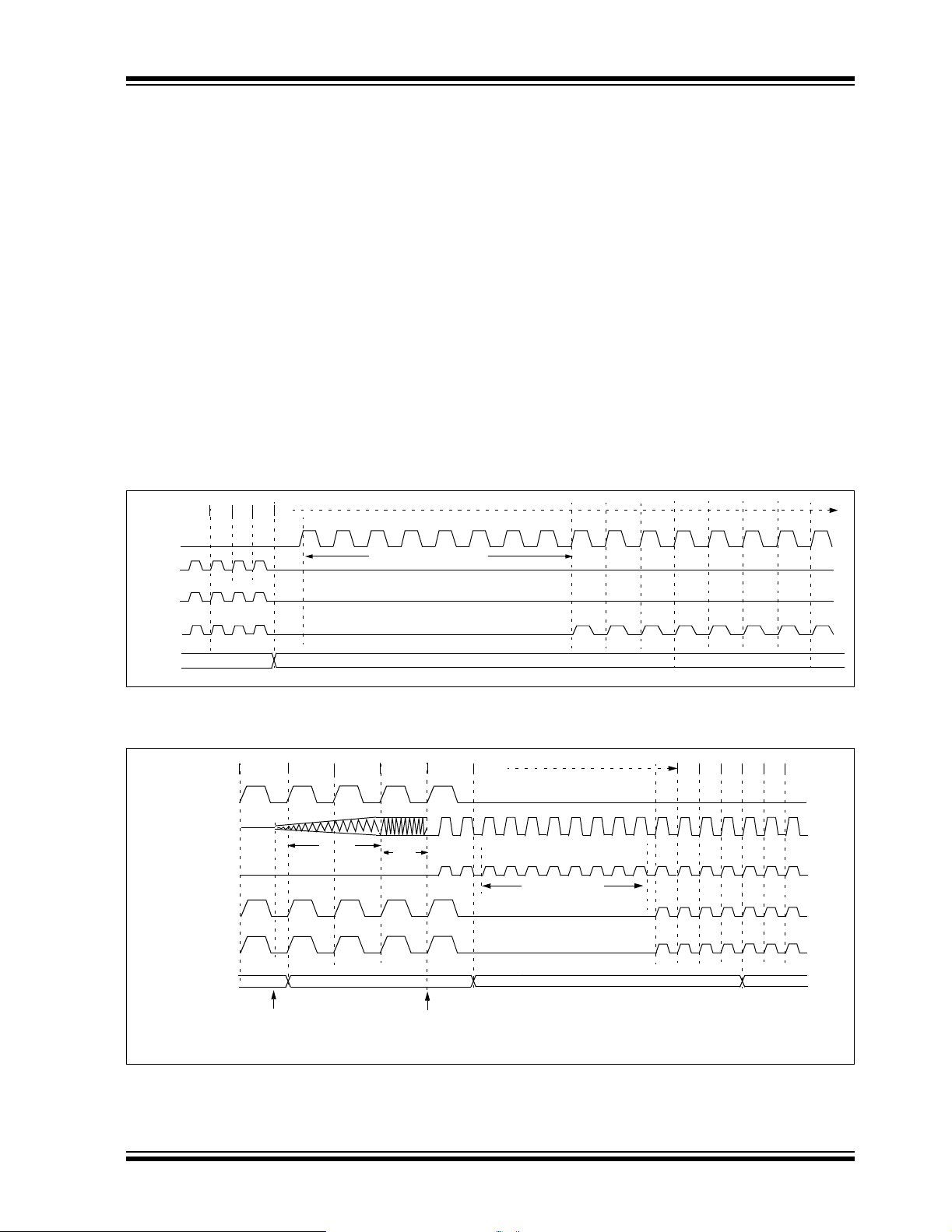
PIC18F2331/2431/4331/4431
3.3.3 RC_IDLE MODE
In RC_IDLE mode, the CPU is di sabled, but the peripherals continue to b e c loc ke d fro m t he internal oscilla tor
block using the INTOSC multiplexer. This mode allows
for controllable power cons ervation during Idl e periods .
This mode is entered by setting the IDLEN bit, setting
SCS1 (SCS0 is ignored), and executing a SLEEP
instruction. The INTOSC multiplexer may be used to
select a higher clock frequency by modifying the IRCF
bits before exec uti ng th e SLEEP instruction. When the
clock source is switched to the INTOSC multiplexer
(see Figure 3-7), the primary oscillator is shut down,
and the OSTS bit is cleared.
If the IRCF bits are set to a non-zero value (thus
enabling the INTOSC output), the IOFS bit becomes
set after the INTOSC output becomes stable, in about
1 ms. Clocks to the peripherals continue while the
INTOSC source stabilizes. If the IRCF bits were previ-
was executed, and the INTOSC source was already
stable, the IOFS bit will remain set. If the IRCF bits are
all clear, the INTOSC output is not enabled and the
IOFS bit will remain clear; there will be no indication of
the current cl ock source.
When a wake event occ urs, the pe ripherals continue to
be clocked from the INTOSC multi ple xe r. After a 10µs
delay following the wake event, the CPU begins exe-
cuting code, being clo cked by the IN T OSC multi plexe r.
The microcontroller operates in RC_RUN mode until
the primary clock becomes ready. When the primary
clock becomes ready, a clock switch back to the pri-
mary clock occurs (see Figure 3-8). When the clock
switch is complete, the IOFS bit is cleared, the OSTS
bit is set, and th e p rim ary c loc k is pro vid in g th e s ys tem
clock. The IDLEN and SCS bits are not af fe cte d by the
wake-up. The INTRC source will continue to run if
either the WDT or the Fail-Safe Clock Monitor is
enabled.
ously at a non-zero value before the SLEEP instruction
FIGURE 3-7: TIMING TRANSITION TO RC_IDLE MODE
Q4Q3Q2
Q1
INTRC
OSC1
Q1
12345678
Clock Transition
CPU
Clock
Peripheral
Clock
Program
Counter
PC + 2PC
FIGURE 3-8: TIMING TRANSITION FOR W AKE FROM RC_RUN MODE (RC_RUN TO PRI_RUN)
Q3 Q4
Q1
Q2
Q3
(1)
TPLL
OSTS bit Set
12345678
Clock Transition
PC + 4
Q4
INTOSC
Multiplexer
OSC1
PLL Clock
Output
CPU Clock
Peripheral
Clock
Program
Counter
Note 1: TOST = 1024 TOSC; TPLL = 2 ms (approx). These intervals are not shown to scale.
PC PC + 2
Wake from Interrupt Event
Q1
TOST
(1)
Q1
Q4
Q2
Q2
PC + 6
Q3
2003 Microchip Technology Inc. Preliminary DS39616B-page 37

PIC18F2331/2431/4331/4431
3.4 Run Modes
If the IDLEN bit is clear when a SLEEP instruction is
executed, the CPU and peripherals are both clocked
from the source selected using the SCS1:SCS0 bits.
While these operating mo des may not aff ord the power
conservation of Idle or Sleep modes, they do allow the
device to continue executing instructions by using a
lower frequency clock source. RC_RUN mode also
offers the possibility of executing code at a frequency
greater than the primary clock.
Wake-up from a power-managed run mode ca n be triggered by an interrupt, or any Reset, to return to full
power operation. As the CPU is executing code in run
modes, several additional exits from run modes are
possible. They inclu de exit to Sleep m ode, exit to a correspondin g idle mod e, and ex it by exec uting a RESET
instruction. While the device is in any of the powermanaged run modes, a WDT time-out will result in a
WDT Reset.
3.4.1 PRI_RUN MODE
The PRI_RUN mode is the normal full power execution
mode. If the SLEEP instruction is never executed, the
microcontroller opera tes in this m ode (a SLEEP instruction is executed to enter all other power-managed
modes). All other power-managed modes exit to
PRI_RUN mode when an interrupt or WDT time-out
occur.
There is no entry to PRI_RUN mode. The OSTS bit is
set. The IOFS bit may be set if the internal oscillator
block is the primary clock source (see Section2.7.1
“Oscillator Control Register”).
3.4.2 SEC_RUN MODE
The SEC_RUN mode is the compatible mode to the
“clock switching” feature offered in other PIC18
devices. In this mode, the CPU and peripherals are
clocked from the T imer1 osci llator. This gives users the
option of lower power c onsumption w hile still using a
high accuracy clock source.
SEC_RUN mode is entered by clearing the IDLEN bit,
setting SCS1:SCS0 = 01, and executing a SLEEP
instruction. The system clo ck source is switched to the
Timer1 oscillator (see Figure 3-9), the primary oscillator is shut down, the T1RUN bit (T1CON<6>) is set and
the OSTS bit is cleared.
Note: The Timer1 oscillator should already be
running prior to entering SEC_RU N mode.
If the T1OSCEN bit is not set when the
SLEEP instruction is executed, a forced
NOP will be executed instead and entry to
SEC_IDLE mode will not occur. If the
Timer1 oscillator is enabled, but not yet
running, system clocks will be delayed
until the oscillator has started. In such
situations, initial oscillator operation is far
from stable and unpredictable operation
may result.
When a wake event occurs, the periphe rals and CPU
continue to be clocked from t he Timer1 oscillator w hile
the primary clock is started. When the primary clock
becomes ready, a clock switch back to the primary clock
occurs (see Figure 3-6). When the clock switch is complete, the T1RUN bit is cleared, the OSTS bit is set, and
the primary clock is providing the system clock. The
IDLEN and SCS bits are not affected by the wa ke-up;
the Timer1 oscillator continues to run.
Firmware can force an exit from SE C_RUN mode. By
clearing the T1OSC EN bit (T1CON<3>), an exit from
SEC_RUN back to normal full po wer operation is triggered. The Timer1 oscillator will continue to run and
provide the system clock even though the T1OSCEN bit
is cleared. The prim ary clock is started. When the primary clock becomes ready, a clock switch back to the
primary clock occurs (see Figure 3-6). When the clock
switch is complete, the Timer1 oscillator is disabled, the
T1RUN bit is cleared, t he OSTS bit is set and the primary clock provides the system clock. The IDLEN and
SCS bits are not affected by the wake-up.
FIGURE 3-9: TIMING TRANSITION FOR ENTRY TO SEC_RUN MODE
Q4Q3Q2
Q1
T1OSI
OSC1
CPU
Clock
Peripheral
Clock
Program
Counter
DS39616B-page 38 Preliminary 2003 Microchip Technology Inc.
Q1
12345678
Clock Transition
PC + 2PC
Q2
Q4Q3
Q1
Q2
Q3
PC + 2

PIC18F2331/2431/4331/4431
3.4.3 RC_RUN MODE
In RC_RUN mode, the CPU and peripherals are
clocked from the internal oscillator block using the
INTOSC multiplexer, and the primary clock is shut
down. When using the INTRC source, this mode provides the best power con servation of al l the run modes,
while still executing code. This mode works well for
user applicatio ns th at are not highly tim ing s ensit ive, or
do not require high-speed clocks at all times.
If the primary clock source is the internal oscillator
block (either of the INTIO1 or INTIO2 os cillator s), there
are no distinguishable differences between PRI_RUN
and RC_RUN modes during execution. However, a
clock switch delay will occur during entry to, and exit
from, RC_RUN mode. Therefore, if the primary clock
source is the internal oscillator block, the use of
RC_RUN mode is not recommended.
This mode is ente red by c lea rin g th e IDLEN b it, se ttin g
SCS1 (SCS0 is ignored) and executing a SLEEP
instruction. The IRCF bits may select the clock
frequency before the SLEEP instruction is executed.
When the clock source is switched to the INTOSC
multiplexer (see Figure 3-10), the primary oscillator is
shut down and the OSTS bit is cleared.
The IRCF bits may be modified at any time to immediately change the system clock speed. Executing a
SLEEP instruction is not required to select a new clock
frequency from the INTOSC multiplexer.
Note: Caution should be used when m odi fy ing a
single IRCF bit. If V
DD is less than 3V, it is
possible to select a higher clock speed
than is supported by the low VDD.
Improper device operation may result if
the VDD/FOSC specifications are violated.
If the IRCF bits are all clear, the INTOSC output is not
enabled, and the IOFS bit will remain clear; there will
be no indication of the current clock s ource. The INTRC
source is providing the system clocks.
If the IRCF bits are changed from all clear (thus
enabling the INTOSC output), the IOFS bit becomes
set after the INTOSC out put becom es stab le. Clocks to
the system continue while the INTOSC source
stabilizes in approximately 1ms.
If the IRCF bits were previously at a non-zero value
before the SLEEP instruction was executed, and the
INTOSC source was already stable, the IOFS bit will
remain set.
When a wake event occurs , the system conti nues to be
clocked from the IN TO SC multiple xer while the primar y
clock is started. When the primary clock becomes
ready, a clock switch to the primary clock occurs (see
Figure 3-8). When the clock switch is complete, the
IOFS bit is cleared, the O STS bit is se t and the prim ary
clock provides the system clock. The IDLEN and SCS
bits are not affected by the wake-up. The INTRC
source will continue to run if either the WDT or the
Fail-Safe Clock Monitor is enab led .
FIGURE 3-10: TIMING TRANSITION TO RC_RUN MODE
Q3Q2Q1
Q4
12345678
Clock Transition
PC + 2PC
INTRC
OSC1
CPU
Clock
Peripheral
Clock
Program
Counter
Q4
Q3Q2Q1 Q4 Q2Q1 Q3
PC + 4
2003 Microchip Technology Inc. Preliminary DS39616B-page 39

PIC18F2331/2431/4331/4431
3.4.4 EXIT TO IDLE MODE
An exit from a power-managed run mode to its corresponding idle mode is executed by setting the IDLEN
bit and executing a SLEEP instruction. The CPU is
halted at the beginning of the instruction following the
SLEEP instruction. There are no changes to any of the
clock source status bits (OSTS, IOFS, or T1RUN).
While the CPU is halte d, the periphe rals c ontin ue to b e
clocked from the previously selected clock source.
3.4.5 EXIT TO SLEEP MODE
An exit from a power-managed run mode to Sleep
mode is executed by clearing the IDLEN and
SCS1:SCS0 bits and executing a SLEEP instruction.
The code is no diff erent than the me thod used to invoke
Sleep mode from the normal operating (full power)
mode.
The primary clock and internal oscillator block are disabled. The INTRC will continue to operate if the WDT
is enabled. The Timer1 oscillator will continue to run, if
enabled, in the T1C ON regis ter. All clock sourc e st atus
bits are cleared (OSTS, IOFS and T1RUN).
3.5 Wake From Power-Managed Modes
An exit from any of the power-managed modes is triggered by an interrupt, a Reset or a WDT time-out. This
section discusses the triggers that cause exits from
power-managed modes. The clocking subsystem
actions are discussed in each of the power-managed
modes (see Sections 3.2 through 3.4).
Note: If application code is timing sensitive, it
should wait for the OSTS bi t to become set
before continuing. Use the interval during
the Low-power exit sequence (before
OSTS is set) to perform timing insensitive
“housekeeping” tasks.
Device behavior during Low-power mode exits is
summarized in Table 3-3.
3.5.1 EXIT BY INTERRUPT
Any of the available interrupt sources can cause the
device to exit a power-managed mode and resume full
power operation. To enable this functionality, an interrupt source must be e nab le d by s etti ng its enable bit i n
one of the INTCON or PIE register s. The exit sequenc e
is initiated when the corresponding interrupt flag bit is
set. On all exits from Low-power mode by interrupt,
code execution branches to the interrupt vector if the
GIE/GIEH bit (INTCON<7>) is set. Otherwise, code
execution continues or resumes without branching
(see Section 9.0 “Interrupts”).
DS39616B-page 40 Preliminary 2003 Microchip Technology Inc.

PIC18F2331/2431/4331/4431
TABLE 3-3: ACTIVITY AND EXIT DELAY ON WAKE FROM SLEEP MODE OR ANY IDLE MODE
(BY CLOCK SOURCES)
Clock in Power-
Managed Mode
Primary System
Clock
(PRI_IDLE mode)
T1OSC or
(1)
INTRC
INTOSC
(2)
Sleep mode
Note 1: In this instance, refers specifically to the INTRC clock source.
2: Includes both the INTOSC 8 MHz source and postscaler derived frequencies.
3: Two-Speed Start-up is covered in greater detail in Section 22.3 “Two-Speed Start-up”.
4: Execution continues during the INTOSC stabilization period.
5: Required delay when waking from Sleep and all idle modes. This delay runs concurrently with any other
required delays (see Section 3.3 “Idle Modes”).
Primary System
Clock
LP, XT, HS
HSPLL
EC, RC, INTRC
INTOSC
(1)
(2)
LP, XT, HS OST
HSPLL OST + 2 ms
EC, RC, INTRC
INTOSC
(1)
(2)
LP, XT, HS OST
HSPLL OST + 2 ms
EC, RC, INTRC
INTOSC
(1)
(2)
LP, XT, HS OST
HSPLL OST + 2 ms
EC, RC, INTRC
INTOSC
(1)
(2)
Power-
Managed
Mode Exit
Delay
5-10 µs
5-10 µs
1ms
5-10 µs
Clock Ready
Status bit
(OSCCON)
(5)
(5)
(4)
(5)
None IOFS
1ms
(5)
(4)
5-10 µs
OSTS
—
IOFS
OSTS
—
IOFS
OSTS
—
OSTS
—
IOFS
Activity During Wake from
Power-Managed Mode
Exit by Interrupt Exit by Reset
CPU and peripherals
clocked by primary
clock and executing
Not clocked, or
Two-Speed Start-up
(if enabled)
instructions.
CPU and peripherals
clocked by selected
power-managed mode
clock and executing
instructions until
primary clock source
becomes ready.
Not clocked or
Two-S pee d Start-up (if
enabled) until primary
clock source becomes
(3)
ready
.
(3)
.
2003 Microchip Technology Inc. Preliminary DS39616B-page 41

PIC18F2331/2431/4331/4431
3.5.2 EXIT BY RESET
Normally, the device is held in Reset by the Oscillator
Star t-up Timer (OST) until the primary clock (defi ned in
Configuration regist er 1H) become s ready . At that time,
the OSTS bit is set and the device begins executing
code.
Code execution can begin before the primary clock
becomes ready. If either the Two-Speed Start-up (see
Section 22.3 “Two-Speed Start-up”) or Fail-Safe
Clock Monitor (see Section 22.4 “Fail-Safe Clock
Monitor”) are enabled in Configuration Register 1H,
the device may begin execution as soon as the Reset
source has cleared. Execution is clocked by the
INTOSC multiplexer driven by the internal oscillator
block. Since the OSCCON register is cleared following
all Resets, the INTRC clock source is selected. A
higher speed clock may be selected by modifying the
IRCF bits in the OSCCON register. Execution is
clocked by the internal oscillator block until either the
primary clock becomes ready, or a power-managed
mode is entered before the primary clock becomes
ready; the primary clock is then shut down.
3.5.3 EXIT BY WDT TIME-OUT
A WDT time-out will cause different actions depending
on which power-managed mode the device is in when
the time-out occurs.
If the device is not executing code (all idle modes and
Sleep mode), the time-out will r esult in a wake from the
power-managed mode (see Section 3.2 “Sleep
Mode” through Section 3.4 “Run Modes”).
If the device is executing code (all run modes), the
time-out will result in a WDT Reset (see Section 22.2
“Watchdog Timer (WDT)”).
The WDT timer and postscaler are cleared by executing a SLEEP or CLRWDT instruction, the loss of a currently selected clock source (if the Fail-Safe Clock
Monitor is enabled), and mod ify in g the IRCF bit s in th e
OSCCON register if the internal oscillator block is the
system clock source.
3.5.4 EXIT WITHOUT AN OSCILLATOR
START-UP DELAY
Certain exits from power-managed modes do not
invoke the OST at all. These are:
• PRI_IDLE mode where the primary clock source
is not stopped; and
• the primary clock source is not any of LP, XT, HS
or HSPLL modes.
In these cases, the primary clock source either does
not require an oscillator start-up delay, since it is
already running (PRI_IDLE), or normally does not
require an oscillator s tart-u p delay (R C, EC, an d INTIO
oscillator modes).
However, a fixed del ay (a ppro xi ma tel y 10µs) following
the wake event is required when leavi ng Sleep and idle
modes. This delay is required for the CPU to prepare
for execution. Instruction ex ecution resumes on the first
clock cycle following this delay.
3.6 INTOSC Frequency Drift
The factory calibrates the internal oscillator block output (INTOSC) for 8 MHz. However, this frequency may
drift as VDD or temperature changes, which can affect
the controller operation in a variety of ways.
It is possible to adjust the INTOSC frequency by modifying the value in the OSCTUNE register. This has the
side effect that the INTRC clock source frequency is
also affected. However, the features that use the
INTRC source often do not require an exact frequency.
These features inc lude the Fail-Safe Clock Moni tor, the
Watchdog Timer and the RC_RUN/RC_IDLE modes
when the INTRC clock source is selected.
Being able to adjust the INTOSC requires knowing
when an adjustment is required, in which direction it
should be made, and in some cases, how large a
change is needed. Three examples follow, but other
techniques may be used.
DS39616B-page 42 Preliminary 2003 Microchip Technology Inc.

PIC18F2331/2431/4331/4431
3.6.1 EXAMPLE – USART
An adjustment may be indicated when the USART
begins to generate framing erro rs, or receives data with
errors while in Asynchronous mode. Framing errors
indicate that the system clock frequency is too high –
try decrementing the valu e in the OSCTUNE reg ister to
reduce the system clock frequency. Errors in data
may suggest that the system clock speed is too low –
increment OSCTUNE.
3.6.2 EXAMPLE – TIMERS
This technique compares system clock speed to some
reference clock. Two timers may be used; one timer is
clocked by the peripheral clock, while the other is
clocked by a fixed reference source, such as the
Timer1 oscillat or.
Both timers are cleared, but the timer clocked by the
reference generates interrupts. When an interrupt
occurs, the internally clocked timer is read and both
timers are cleared. If the internally clocked timer value
is greater than expected, then the internal oscillator
block is running too fast – decrement OSCTUNE.
3.6.3 EXAMPLE – CCP IN CAPTURE MODE
A CCP module can use free running T imer1, cl ocked by
the internal oscillator block and an external event with
a known period (i.e., AC power fre quenc y). The ti me of
the first event is captured in the CCPRxH:CCPRxL
registers and is recorded for use later. When the
second event causes a capture, the time of the first
event is subtracted from the time of the second event.
Since the period of the external event is known, the
time difference between events can be calculated.
If the measured time is much greater than the
calculated time, the inte rnal oscillator block is running
too fast – decreme nt OSCT UNE. I f the me asured time
is much less than the calculated time, the internal
oscillator block is running too slow – increment
OSCTUNE.
2003 Microchip Technology Inc. Preliminary DS39616B-page 43

PIC18F2331/2431/4331/4431
NOTES:
DS39616B-page 44 Preliminary 2003 Microchip Technology Inc.

PIC18F2331/2431/4331/4431
4.0 RESET
Most registers are not affected by a WDT wake-up,
since this is viewed as the resumption of normal
The PIC18F2331/2431/4331/4431 devices differentiate between various kinds of Reset:
a) Power-on Reset (POR)
b) MCLR
Reset during normal operation
c) MCLR Reset during Sleep
d) Watchdog Timer (WDT) Reset (during
execution)
e) Programmable Brown-out Reset (BOR)
f) RESET I nstruction
g) Stack Full Reset
h) Stack Underflow Reset
Most registers are unaffected by a Reset. Their status
is unknown on POR and unchanged by all other
Resets. The other registers are forced to a “Reset
state” depending on the type of Reset that occurred.
operation. Status bits from the RCON register, RI
, POR and BOR, are set or cleared differently in
PD
different Reset situations, as indicated in Table 4-2.
These bits are use d in software to d etermine the n ature
of the Reset. See Table 4-3 for a full description of the
Reset states of all registers.
A simplified block di agram of the On-Chip Reset Circu it
is shown in Figure 4- 1.
The enhanced MCU devices have a MCLR
in the MCLR
Reset path. The filter will detect and
ignore small pulses.
The MCLR
pin is not driven low by any internal Resets,
including the WDT.
The MCLR input pro vided by the MCLR p in ca n be dis -
abled with the MCL RE bit i n Configuration Registe r 3H
(CONFIG3H<7>). See Section 22.1 “Configuration
Bits” for more information.
FIGURE 4-1: SIMPLIFIED BLOCK DIAGRAM OF ON-CHIP RESET CIRCUIT
RESET
Instruction
Stack
Pointer
Stack Full/Underflow Reset
, TO,
noise filter
MCLR
VDD
OSC1
( )_IDLE
Sleep
WDT
Time-out
DD Rise
V
Detect
Brown-out
Reset
OST/PWRT
32 µs
(1)
INTRC
External Reset
MCLRE
POR Pulse
BOREN
OST
PWRT
1024 Cycles
10-bit Ripple Counter
65.5 ms
11-bit Ripple Counter
S
Chip_Reset
R
Q
Enable PWRT
Enable OST
(2)
Note 1: This is the INTRC source from the internal oscillator block, and is separate from the RC oscillator of the CLKI pin.
2: See Table 4-1 for time-out situations.
2003 Microchip Technology Inc. Preliminary DS39616B-page 45

PIC18F2331/2431/4331/4431
4.1 Power-on Reset (POR)
A Power-on Reset pulse is generated on-chip when
DD rise is detected. To take advantage of the POR cir-
V
cuitry, just tie the MCLR
10 kΩ) to V
DD. This will eliminate external RC compo-
pin through a resistor (1k to
nents usually needed to create a Power-on Reset
delay. A minimum rise rate for V
DD is specified
(parameter D004) . For a s low rise t ime, see F igure 4-2.
When the device st arts normal operati on (i.e ., ex its the
Reset condition), device operating parameters (voltage, frequency, temperature, etc.) must be met to
ensure operation. If these conditions are not met, the
device must be held in Reset until the operating
conditions are met.
FIGURE 4-2: EXTERN AL POWER-ON
RESET CIRCUIT (FOR
SLOW V
DD
VDD
Note 1: External Power-on Reset circuit is
V
D
R
C
required only if the V
is too slow . The diode D help s discharge
the capacitor quickly when V
down.
2: R < 40 kΩ is recommended to make
sure that the vol tage drop across R does
not violate the device ’s el ectrical specification.
3: R1 ≥ 1 kΩ will limit any current flowing
into MCLR
from external capacitor C, in
the event of MCLR
due to Elect ros tati c Disc har ge (E SD) o r
Electrical Overstress (EOS).
DD POWER-UP)
R1
MCLR
PIC18FXXXX
DD power-up slope
DD powers
/VPP pin break down ,
4.2 Power-up Timer (PWRT)
The Power-up Ti mer (PWRT) of the PIC18 F2331/2431/
4331/4431 device s is an 11-bit counte r, which use s the
INTRC source as the cl ock i nput. Th is yi elds a count of
2048 x 32 µs = 65.6 ms. While the PWRT is counting,
the device is held in Reset.
The power-up time delay depe nd s on the INTRC cl oc k
and will vary from chip-to-chip due to temperature and
process variation. See DC parameter #33 for details.
The PWRT is enabled by clearing configuration bit
PWRTEN
.
4.3 Oscillator Start-up Timer (OST)
The Oscillator Start-up Timer (OST) provides a 1024
oscillator cycle (from OSC1 input) delay after the
PWRT delay is over (para meter #33). Th is ensures th at
the crystal oscillator or resonator has started and
stabilized.
The OST time-out is invoked only for XT, LP, HS and
HSPLL modes, and only on Power-on Reset or on exit
from most power-managed modes.
4.4 PLL Lock Time-out
With the PLL enabled in its PLL mode, the time-out
sequence following a Power-on Reset is slightly different from other oscill ator modes. A p ortion of the Po werup Timer is used to provide a fixed time-out that is sufficient for the PLL to lock to the main oscillator frequency. This PLL lock time-out (T
PLL) is typically 2 ms
and follows the oscillator start-up time-out.
4.5 Brown-out Reset (BOR)
A configuration bit, BOREN, can disable (if clear/
programmed) or enable (if set) the Brown- out Reset circuitry. If V
greater than T
ation will reset the chip. A Reset may not occur if V
DD falls below VBOR (parameter D005) for
BOR (parameter #35), the brown-out sit u-
DD
falls below VBOR for less than TBOR. The chip will
remain in Brown-out Reset until V
DD rises above VBOR .
If the Power-up T imer is enable d, it will be invo ked after
DD rises above VBOR; it then will keep the chip in
V
Reset for an additional time delay T
#33). If V
DD drops below VBOR while the Power-up
PWRT (parameter
Timer is ru nni ng, the chip will go ba ck in to a Bro w n-o ut
Reset and the Power-up Timer will be initialized. Once
DD rises above VBOR, the Power-up Timer will execute
V
the additional time delay. Enabling BOR Res et does
not automatically enable the PWRT.
4.6 Time-out Sequence
On power-up, the time-out sequence is as follows:
First, after the POR pulse has cle are d, PWRT time-out
is invoked (if enab led). Then , the OST i s activated . The
total time-out wi ll var y base d o n oscill ator confi guratio n
and the status of the PWR T. For example, in RC mode
with the PWRT disabled , there will be no time-o ut at all.
Figures 4-3 through 4-7 depict time-out sequenc es on
power-up.
Since the time-outs occur from the POR pulse, if MC LR
is kept low long e nough, all ti me -out s will e xpire. Brin ging MCLR
(Figure 4 -5). This is useful for testing purposes or to
synchronize more than one PIC18FXXXX device
operating in parallel.
Table 4-2 shows the Reset condition s for some Special
Function registers, while Table 4-3 shows the Reset
conditions for all the registers.
high will begin execution immediately
DS39616B-page 46 Preliminary 2003 Microchip Technology Inc.

PIC18F2331/2431/4331/4431
TABLE 4-1: TIME-OUT IN VARIOUS SITUATIONS
Oscillator
Configuration
HSPLL 66 ms
PWRTEN = 0 PWRTEN = 1
(1)
+ 1024 TOSC + 2 ms
HS, XT, LP 66 ms
EC, ECIO 66 ms
RC, RCIO 66 ms
INTIO1, INTIO2 66 ms
Power-up
(1)
+ 1024 TOSC 1024 TOSC 1024 TOSC
(1)
(1)
(1)
Note 1: 66 ms (65.5 ms) is the nominal Power-up Timer (PWRT) delay.
2: 2 ms is the nominal time required for the 4x PLL to lock.
REGISTER 4-1: RCON REGISTER BITS AND POSITIONS
R/W-0 U-0 U-0 R/W-1 R-1 R-1 R/W-1 R/W-1
IPEN
bit 7 bit 0
Note: Refer to Section 5.14 “RCON Register” for bit definitions.
— —RITO PD POR BOR
(2)
and Brown-out
(2)
1024 TOSC + 2 ms
Exit from
Power-Managed Mode
(2)
1024 TOSC + 2 ms
(2)
——
——
——
TABLE 4-2: STATUS BITS, THEIR SIGNIFICANCE AND THE INITIALIZATION CONDITION FOR
RCON REGISTER
Condition
Program
Counter
Power-on Reset 0000h 0--1 1100 1 1 1 0 0 0 0
RESET Instruction 0000h 0--0 uuuu 0 u u u u u u
Brown-out 0000h 0--1 11u- 1 1 1 u 0 u u
during power-managed
MCLR
0000h 0--u 1uuu u 1 u u u u u
run modes
during power-managed
MCLR
0000h 0--u 10uu u 1 0 u u u u
idle modes and Sleep
WDT Time-out during full p ow er
0000h 0--u 0uuu u 0 u u u u u
or power-managed Run
MCLR during full power
execution
Stack Full Reset (STVREN = 1) 1u
0000h 0--u uuuu u u u u u
Stack Underflow Reset
(STVREN = 1)
Stack Underflow Error (not an
0000h u--u uuuu u u u u u u 1
actual Reset, STVREN = 0)
WDT Time-out during power-
PC + 2 u--u 00uu u 0 0 u u u u
managed Idle or Sleep
Interrupt Exit from power-man-
PC + 2
(1)
aged modes
Legend: u = unchanged, x = unknown, - = unimplemented bit, read as ‘0’.
Note 1: When the wake-up is due to an interrupt and the GIEH or GIEL bits are set, the PC is loaded with the
interrupt vector (0x00000 8h or 0x00 001 8h ).
RCON
Register
TO PD POR BOR STKFUL STKUNF
RI
uu
u1
u--u u0uu u u 0 u u u u
2003 Microchip Technology Inc. Preliminary DS39616B-page 47

PIC18F2331/2431/4331/4431
TABLE 4-3: INITIALIZATION CONDITIONS FOR ALL REGISTERS
MCLR
Resets
Register Applicable Devices
Power-on Reset,
Brown-out Reset
TOSU 2331 2431 4331 4431 ---0 0000 ---0 0000 ---0 uuuu
TOSH 2331 2431 4331 4431 0000 0000 0000 0000 uuuu uuuu
TOSL 2331 2431 4331 4431 0000 0000 0000 0000 uuuu uuuu
STKPTR 2331 2431 4331 4431 00-0 0000 uu-0 0000 uu-u uuuu
PCLATU 2331 2431 4331 4431 ---0 0000 ---0 0000 ---u uuuu
PCLATH 2331 2431 4331 4431 0000 0000 0000 0000 uuuu uuuu
PCL 2331 2431 4331 4431 0000 0000 0000 0000 PC + 2
TBLPTRU 2331 2431 4331 4431 --00 0000 --00 0000 --uu uuuu
TBLPTRH 2331 2431 4331 4431 0000 0000 0000 0000 uuuu uuuu
TBLPTRL 2331 2431 4331 4431 0000 0000 0000 0000 uuuu uuuu
TABLAT 2331 2431 4331 4431 0000 0000 0000 0000 uuuu uuuu
PRODH 2331 2431 4331 4431 xxxx xxxx uuuu uuuu uuuu uuuu
PRODL 2331 2431 4331 4431 xxxx xxxx uuuu uuuu uuuu uuuu
INTCON 2331 2431 4331 4431 0000 000x 0000 000u uuuu uuuu
INTCON2 2331 2431 4331 4431 1111 -1-1 1111 -1-1 uuuu -u-u
INTCON3 2331 2431 4331 4431 11-0 0-00 11-0 0-00 uu-u u-uu
INDF0 2331 2431 4331 4431 N/A N/A N/A
POSTINC0 2331 2431 4331 4431 N/A N/A N/A
POSTDEC0 2331 2431 4331 4431 N/A N/A N/A
PREINC0 2331 2431 4331 4431 N/A N/A N/A
PLUSW0 2331 2431 4331 4431 N/A N/A N/A
FSR0H 2331 2431 4331 4431 ---- xxxx ---- uuuu ---- uuuu
FSR0L 2331 2431 4331 4431 xxxx xxxx uuuu uuuu uuuu uuuu
WREG 2331 2431 4331 4431 xxxx xxxx uuuu uuuu uuuu uuuu
INDF1 2331 2431 4331 4431 N/A N/A N/A
POSTINC1 2331 2431 4331 4431 N/A N/A N/A
POSTDEC1 2331 2431 4331 4431 N/A N/A N/A
PREINC1 2331 2431 4331 4431 N/A N/A N/A
PLUSW1 2331 2431 4331 4431 N/A N/A N/A
Legend: u = unchanged, x = unknown, - = unimplemented bit, read as ‘0’, q = value depends on condition.
Shaded cells indicate condi tions do not apply for the designated devic e.
Note 1: One or more bits in the INTCONx or PIRx registers will be affected (to cause wake-up).
2: When the wake-up is due to an in terrupt and th e GIEL or GIE H bit is set, th e PC is loaded with the inte rrupt
vector (0008h or 0018h).
3: When the wake-up is due to an interrupt and the GI EL or GIEH bit is set, the TOSU, TO SH and T O SL are
updated with the current value of the PC. The STKPTR is modified to point to the next location in the
hardware stack.
4: See Table 4-2 for Reset value for specific condition.
5: Bits 6 and 7 of PORTA, LATA and TRISA are enabled, depending on the Oscillator mode selected. When
not enabled as PORTA pins, they are disabled and read ‘0’.
6: Bit 3 of PORTE and LATE are enabled if MCL R functional ity is d isabl ed. When not enabl ed as the PORT E
pin, they ar e disabled and read as ‘0’. The 28-pin devices have only RE3 on PORTE when MCLR
disabled.
WDT Reset
RESET Instruction
Stack Resets
Wake-up via WDT
or Interrupt
(3)
(3)
(3)
(3)
(2)
(1)
(1)
(1)
is
DS39616B-page 48 Preliminary 2003 Microchip Technology Inc.

PIC18F2331/2431/4331/4431
TABLE 4-3: INITIALIZATION CONDITIONS FOR ALL REGISTERS (CONTINUED)
MCLR
Resets
Register Applicable Devices
FSR1H 2331 2431 4331 4431 ---- xxxx ---- uuuu ---- uuuu
FSR1L 2331 2431 4331 4431 xxxx xxxx uuuu uuuu uuuu uuuu
BSR 2331 2431 4331 4431 ---- 0000 ---- 0000 ---- uuuu
INDF2 2331 2431 4331 4431 N/A N/A N/A
POSTINC2 2331 2431 4331 4431 N/A N/A N/A
POSTDEC2 2331 2431 4331 4431 N/A N/A N/A
PREINC2 2331 2431 4331 4431 N/A N/A N/A
PLUSW2 2331 2431 4331 4431 N/A N/A N/A
FSR2H 2331 2431 4331 4431 ---- xxxx ---- uuuu ---- uuuu
FSR2L 2331 2431 4331 4431 xxxx xxxx uuuu uuuu uuuu uuuu
STATUS 2331 2431 4331 4431 ---x xxxx ---u uuuu ---u uuuu
TMR0H 2331 2431 4331 4431 0000 0000 0000 0000 uuuu uuuu
TMR0L 2331 2431 4331 4431 xxxx xxxx uuuu uuuu uuuu uuuu
T0CON 2331 2431 4331 4431 11-- 1111 11-- 1111 uu-- uuuu
OSCCON 2331 2431 4331 4431 0000 0000 0000 0000 uuuu uuuu
LVDCON 2331 2431 4331 4431 --00 0101 --00 0101 --uu uuuu
WDTCON 2331 2431 4331 4431 ---- ---0 ---- ---0 ---- ---u
(4)
RCON
TMR1H 2331 2431 4331 4431 xxxx xxxx uuuu uuuu uuuu uuuu
TMR1L 2331 2431 4331 4431 xxxx xxxx uuuu uuuu uuuu uuuu
T1CON 2331 2431 4331 4431 0000 0000 u0uu uuuu uuuu uuuu
TMR2 2331 2431 4331 4431 0000 0000 0000 0000 uuuu uuuu
PR2 2331 2431 4331 4431 1111 1111 1111 1111 1111 1111
T2CON 2331 2431 4331 4431 -000 0000 -000 0000 -uuu uuuu
SSPBUF 2331 2431 4331 4431 xxxx xxxx uuuu uuuu uuuu uuuu
SSPADD 2331 2431 4331 4431 0000 0000 0000 0000 uuuu uuuu
SSPSTAT 2331 2431 4331 4431 0000 0000 0000 0000 uuuu uuuu
SSPCON 2331 2431 4331 4431 0000 0000 0000 0000 uuuu uuuu
Legend: u = unchanged, x = unknown, - = unimplemented bit, read as ‘0’, q = value depends on condition.
Note 1: One or more bits in the INTCONx or PIRx registers will be affected (to cause wake-up).
2: When the wake-up is due to an in terrupt and th e GIEL or GIE H bit is set, th e PC is loaded with the inte rrupt
3: When the wake-up is due to an interrupt and the GI EL or GIEH bit is set, the TOSU, TO SH and T O SL are
4: See Table 4-2 for Reset value for specific condition.
5: Bits 6 and 7 of PORTA, LATA and TRISA are enabled, depending on the Oscillator mode selected. When
6: Bit 3 of PORTE and LATE are enabled if MCL R
2331 2431 4331 4431 0--1 11q0 0--q qquu u--u qquu
Shaded cells indicate condi tions do not apply for the designated devic e.
vector (0008h or 0018h).
updated with the current value of the PC. The STKPTR is modified to point to the next location in the
hardware stack.
not enabled as PORTA pins, they are disabled and read ‘0’.
pin, they are disabled and read as ‘0’. The 28-pin devices have only RE3 on PORTE when MCLR
disabled.
Power-on Reset,
Brown-out Reset
functionality is disabl ed. When not enabl ed as the PORT E
WDT Reset
RESET Instruction
Stack Resets
Wake-up via WDT
or Interrupt
is
2003 Microchip Technology Inc. Preliminary DS39616B-page 49

PIC18F2331/2431/4331/4431
TABLE 4-3: INITIALIZATION CONDITIONS FOR ALL REGISTERS (CONTINUED)
MCLR
Resets
Register Applicable Devices
ADRESH 2331 2431 4331 4431 xxxx xxxx uuuu uuuu uuuu uuuu
ADRESL 2331 2431 4331 4431 xxxx xxxx uuuu uuuu uuuu uuuu
ADCON0 2331 2431 4331 4431 --00 0000 --00 0000 --uu uuuu
ADCON1 2331 2431 4331 4431 00-0 1000 00-- 1000 uu-u uuuu
ADCON2 2331
CCPR1H 2331 2431 4331 4431 xxxx xxxx uuuu uuuu uuuu uuuu
CCPR1L 2331 2431 4331 4431 xxxx xxxx uuuu uuuu uuuu uuuu
CCP1CON 2331 2431
CCPR2H 2331 2431 4331 4431 xxxx xxxx uuuu uuuu uuuu uuuu
CCPR2L 2331 2431 4331 4431 xxxx xxxx uuuu uuuu uuuu uuuu
CCP2CON 2331 2431 4331 4431 --00 0000 --00 0000 --uu uuuu
ANSEL0 2331
ANSEL1 2331
T5CON 2331 2431 4331 4431 0000 0000 0000 0000 uuuu uuuu
QEICON 2331 2431 4331 4431 0000 0000 0000 0000 uuuu uuuu
SPBRGH 2331 2431 4331 4431 0000 0000 0000 0000 uuuu uuuu
SPBRG 2331 2431 4331 4431 0000 0000 0000 0000 uuuu uuuu
RCREG 2331 2431 4331 4431 0000 0000 0000 0000 uuuu uuuu
TXREG 2331 2431 4331 4431 0000 0000 0000 0000 uuuu uuuu
TXSTA 2331 2431 4331 4431 0000 -010 0000 -010 uuuu -uuu
RCSTA 2331 2431 4331 4431 0000 000x 0000 000x uuuu uuuu
BAUDCTL 2331 2431 4331 4431 -1-1 0-00 -1-1 0-00 -u-u u-uu
EEADR 2331 2431 4331 4431 0000 0000 0000 0000 uuuu uuuu
EEDATA 2331 2431 4331 4431 0000 0000 0000 0000 uuuu uuuu
EECON1 2331 2431 4331 4431 xx-0 x000 uu-0 u000 uu-0 u000
EECON2 2331 2431 4331 4431 0000 0000 0000 0000 0000 0000
IPR3 2331 2431 4331 4431 ---1 1111 ---1 1111 ---u uuuu
PIE3 2331 2431 4331 4431 ---0 0000 ---0 0000 ---u uuuu
PIR3 2331 2431 4331 4431 ---0 0000 ---0 0000 ---u uuuu
Legend: u = unchanged, x = unknown, - = unimplemented bit, read as ‘0’, q = value depends on condition.
Shaded cells indicate condi tions do not apply for the designated devic e.
Note 1: One or more bits in the INTCONx or PIRx registers will be affected (to cause wake-up).
2: When the wake-up is due to an in terrupt and th e GIEL or GIE H bit is set, th e PC is loaded with the inte rrupt
vector (0008h or 0018h).
3: When the wake-up is due to an interrupt and the GI EL or GIEH bit is set, the TOSU, TO SH and T O SL are
updated with the current value of the PC. The STKPTR is modified to point to the next location in the
hardware stack.
4: See Table 4-2 for Reset value for specific condition.
5: Bits 6 and 7 of PORTA, LATA and TRISA are enabled, depending on the Oscillator mode selected. When
not enabled as PORTA pins, they are disabled and read ‘0’.
6: Bit 3 of PORTE and LATE are enabled if MCL R
pin, they ar e disabled and read as ‘0’. The 28-pin devices have only RE3 on PORTE when MCLR
disabled.
2431 4331 4431 0000 0000 0000 0000 uuuu uuuu
4331 4431 --00 0000 --00 0000 --uu uuuu
2431 4331 4431 1111 1111 1111 1111 uuuu uuuu
2431 4331 4431 ---- ---0 ---- ---0 ---- ---u
Power-on Reset,
Brown-out Reset
functionality is disabl ed. When not enabl ed as the PORT E
WDT Reset
RESET Instruction
Stack Resets
Wake-up via WDT
or Interrupt
is
DS39616B-page 50 Preliminary 2003 Microchip Technology Inc.

PIC18F2331/2431/4331/4431
TABLE 4-3: INITIALIZATION CONDITIONS FOR ALL REGISTERS (CONTINUED)
MCLR Resets
Register Applicable Devices
Power-on Reset,
Brown-out Reset
IPR2 2331 2431 4331 4431 1--1 -1-1 1--1 -1-1 u--u -u-u
PIR2 2331 2431 4331 4431 0--0 -0-0 0--0 -0-0 u--u -u-u
PIE2 2331 2431 4331 4431 0--0 -0-0 0--0 -0-0 u--u -u-u
IPR1
PIR1
PIE1
2331 2431 4331 4431 1111 1111 1111 1111 uuuu uuuu
2331 2431 4331 4431 -111 1111 -111 1111 -uuu uuuu
2331 2431 4331 4431 -000 0000 -000 0000 -uuu uuuu
2331 2431 4331 4431 -000 0000 -000 0000 -uuu uuuu
2331 2431 4331 4431 0000 0000 0000 0000 uuuu uuuu
2331 2431 4331 4431 -000 0000 -000 0000 -uuu uuuu
OSCTUNE 2331 2431 4331 4431 --00 0000 --00 0000 --uu uuuu
ADCON3 2331
2431 4331 4431 00-0 0000 00-0 0000 uu-u uuuu
ADCHS 2331 2431 4331 4431 0000 0000 0000 0000 uuuu uuuu
(6)
TRISE
TRISD
2331 2431 4331 4431 ---- -111 ---- -111 ---- -uuu
2331 2431 4331 4431 1111 1111 1111 1111 uuuu uuuu
TRISC 2331 2431 4331 4431 1111 1111 1111 1111 uuuu uuuu
TRISB 2331 2431 4331 4431 1111 1111 1111 1111 uuuu uuuu
TRISA
(5)
2331 2431 4331 4431 1111 1111
(5)
PR5H 2331 2431 4331 4431 1111 1111 1111 1111 uuuu uuuu
PR5L 2331 2431 4331 4431 1111 1111 1111 1111 uuuu uuuu
LATE
(6)
2331 2431 4331 4431 ---- -xxx ---- -uuu ---- -uuu
LATD 2331 2431 4331 4431 xxxx xxxx uuuu uuuu uuuu uuuu
LATC 2331 2431 4331 4431 xxxx xxxx uuuu uuuu uuuu uuuu
LATB 2331 2431 4331 4431 xxxx xxxx uuuu uuuu uuuu uuuu
LATA
(5)
2331 2431 4331 4431 xxxx xxxx
(5)
TMR5H 2331 2431 4331 4431 xxxx xxxx uuuu uuuu uuuu uuuu
TMR5L 2331 2431 4331 4431 xxxx xxxx uuuu uuuu uuuu uuuu
(6)
PORTE
PORTD
2331 2431 4331 4431 ---- xxxx ---- xxxx ---- uuuu
2331 2431 4331 4431 xxxx xxxx uuuu uuuu uuuu uuuu
PORTC 2331 2431 4331 4431 xxxx xxxx uuuu uuuu uuuu uuuu
PORTB 2331 2431 4331 4431 xxxx xxxx uuuu uuuu uuuu uuuu
PORTA
(5)
2331 2431 4331 4431 xx0x 0000
(5)
Legend: u = unchanged, x = unknown, - = unimplemented bit, read as ‘0’, q = value depends on condition.
Shaded cells indicate condi tions do not apply for the designated devic e.
Note 1: One or more bits in the INTCONx or PIRx registers will be affected (to cause wake-up).
2: When the wake-up is due to an in terrupt and th e GIEL or GIE H bit is set, th e PC is loaded with the inte rrupt
vector (0008h or 0018h).
3: When the wake-up is due to an interrupt and the GI EL or GIEH bit is set, the TOSU, TO SH and T O SL are
updated with the current value of the PC. The STKPTR is modified to point to the next location in the
hardware stack.
4: See Table 4-2 for Reset value for specific condition.
5: Bits 6 and 7 of PORTA, LATA and TRISA are enabled, depending on the Oscillator mode selected. When
not enabled as PORTA pins, they are disabled and read ‘0’.
6: Bit 3 of PORTE and LATE are enabled if MCL R
functionality is disabl ed. When not enabl ed as the PORT E
pin, they are disabled and read as ‘0’. The 28-pin devices have only RE3 on PORTE when MCLR
disabled.
WDT Reset
RESET Instruction
Stack Resets
1111 1111
uuuu uuuu
uu0u 0000
(5)
(5)
(5)
Wake-up via WDT
or Interrupt
uuuu uuuu
uuuu uuuu
uuuu uuuu
(1)
(1)
(5)
(5)
(5)
is
2003 Microchip Technology Inc. Preliminary DS39616B-page 51

PIC18F2331/2431/4331/4431
TABLE 4-3: INITIALIZATION CONDITIONS FOR ALL REGISTERS (CONTINUED)
MCLR
Resets
Register Applicable Devices
PTCON0 2331 2431 4331 4431
PTCON1 2331 2431 4331 4431 00-- ---- 00-- ---- uu-- ----
PTMRL 2331 2431 4331 4431 0000 0000 0000 0000 uuuu uuuu
PTMRH 2331 2431 4331 4431 ---- 0000 ---- 0000 ---- uuuu
PTPERL 2331 2431 4331 4431 1111 1111 1111 1111 uuuu uuuu
PTPERH 2331 2431 4331 4431 ---- 1111 ---- 1111 ---- uuuu
PDC0L 2331 2431 4331 4431 --00 0000 --00 0000 --uu uuuu
PDC0H 2331 2431 4331 4431 0000 0000 0000 0000 uuuu uuuu
PDC1L 2331 2431 4331 4431 0000 0000 0000 0000 uuuu uuuu
PDC1H 2331 2431 4331 4431 --00 0000 --00 0000 --uu uuuu
PDC2L 2331 2431 4331 4431 0000 0000 0000 0000 uuuu uuuu
PDC2H 2331 2431 4331 4431 --00 0000 --00 0000 --uu uuuu
PDC3L 2331 2431 4331 4431 0000 0000 0000 0000 uuuu uuuu
PDC3H 2331 2431 4331 4431 --00 0000 --00 0000 --uu uuuu
SEVTCMPL 2331 2431 4331 4431 0000 0000 0000 0000 uuuu uuuu
SEVTCMPH 2331 2431 4331 4431 ---- 0000 ---- 0000 ---- uuuu
PWMCON0 2331 2431 4331 4431 -101 0000 -101 0000 -uuu uuuu
PWMCON1 2331 2431 4331 4431 0000 0-00 0000 0-00 uuuu u-uu
DTCON 2331 2431 4331 4431 0000 0000 0000 0000 uuuu uuuu
FLTCONFIG 2331 2431 4331 4431 -000 0000 -000 0000 -uuu uuuu
OVDCOND 2331 2431 4331 4431 1111 1111 1111 1111 uuuu uuuu
OVDCONS 2331 2431 4331 4431 0000 0000 0000 0000 uuuu uuuu
CAP1BUFH/
VELRH
CAP1BUFL/
VELRL
CAP2BUFH/
POSCNTH
CAP2BUFL/
POSCNTL
Legend: u = unchanged, x = unknown, - = unimplemented bit, read as ‘0’, q = value depends on condition.
Note 1: One or more bits in the INTCONx or PIRx registers will be affected (to cause wake-up).
2: When the wake-up is due to an in terrupt and th e GIEL or GIE H bit is set, th e PC is loaded with the inte rrupt
3: When the wake-up is due to an interrupt and the GI EL or GIEH bit is set, the TOSU, TO SH and T O SL are
4: See Table 4-2 for Reset value for specific condition.
5: Bits 6 and 7 of PORTA, LATA and TRISA are enabled, depending on the Oscillator mode selected. When
6: Bit 3 of PORTE and LATE are enabled if MCL R
2331 2431 4331 4431
2331 2431 4331 4431
2331 2431 4331 4431
2331 2431 4331 4431
Shaded cells indicate condi tions do not apply for the designated devic e.
vector (0008h or 0018h).
updated with the current value of the PC. The STKPTR is modified to point to the next location in the
hardware stack.
not enabled as PORTA pins, they are disabled and read ‘0’.
pin, they ar e disabled and read as ‘0’. The 28-pin devices have only RE3 on PORTE when MCLR
disabled.
Power-on Reset,
Brown-out Reset
0000 0000 uuuu uuuu
xxxx xxxx uuuu uuuu
xxxx xxxx uuuu uuuu
xxxx xxxx uuuu uuuu
xxxx xxxx uuuu uuuu
functionality is disabl ed. When not enabl ed as the PORT E
WDT Reset
RESET Instruction
Stack Resets
Wake-up via WDT
or Interrupt
uuuu uuuu
uuuu uuuu
uuuu uuuu
uuuu uuuu
uuuu uuuu
is
DS39616B-page 52 Preliminary 2003 Microchip Technology Inc.

PIC18F2331/2431/4331/4431
TABLE 4-3: INITIALIZATION CONDITIONS FOR ALL REGISTERS (CONTINUED)
MCLR
Resets
Register Applicable Devices
CAP3BUFH/
MAXCNTH
CAP3BUFL/
MAXCNTL
CAP1CON 2331 2431 4331 4431 -0-- 0000 -0-- 0000 -u-- uuuu
CAP2CON 2331 2431 4331 4431 -0-- 0000 -0-- 0000 -u-- uuuu
CAP3CON 2331 2431 4331 4431 -0-- 0000 -0-- 0000 -u-- uuuu
DFLTCON 2331 2431 4331 4431 -000 0000 -000 0000 -uuu uuuu
Legend: u = unchanged, x = unknown, - = unimplemented bit, read as ‘0’, q = value depends on condition.
Note 1: One or more bits in the INTCONx or PIRx registers will be affected (to cause wake-up).
2: When the wake-up is due to an in terrupt and th e GIEL or GIE H bit is set, th e PC is loaded with the inte rrupt
3: When the wake-up is due to an interrupt and the GI EL or GIEH bit is set, the TOSU, TO SH and T O SL are
4: See Table 4-2 for Reset value for specific condition.
5: Bits 6 and 7 of PORTA, LATA and TRISA are enabled, depending on the Oscillator mode selected. When
6: Bit 3 of PORTE and LATE are enabled if MCL R functional ity is d isabl ed. When not enabl ed as the PORT E
2331 2431 4331 4431
2331 2431 4331 4431
Shaded cells indicate condi tions do not apply for the designated devic e.
vector (0008h or 0018h).
updated with the current value of the PC. The STKPTR is modified to point to the next location in the
hardware stack.
not enabled as PORTA pins, they are disabled and read ‘0’.
pin, they are disabled and read as ‘0’. The 28-pin devices have only RE3 on PORTE when MCLR
disabled.
Power-on Reset,
Brown-out Reset
xxxx xxxx uuuu uuuu
xxxx xxxx uuuu uuuu
WDT Reset
RESET Instruction
Stack Resets
Wake-up via WDT
or Interrupt
uuuu uuuu
uuuu uuuu
is
2003 Microchip Technology Inc. Preliminary DS39616B-page 53

PIC18F2331/2431/4331/4431
FIGURE 4-3: TIME-OUT SEQUENCE ON POWER-UP (MCLR TIED TO VDD, VDD RISE < TPWRT)
VDD
MCLR
INTERNAL POR
TPWRT
PWRT TIME-OUT
OST TIME-OUT
INTERNAL RESET
TOST
FIGURE 4-4: TIME-OUT SEQUENCE ON POWER-UP (MCLR
VDD
MCLR
INTERNAL POR
PWRT TIME-OUT
OST TIME-OUT
INTERNAL RESET
TPWRT
NOT TIED TO VDD): CASE 1
TOST
FIGURE 4-5: TIME-OUT SEQUENCE ON POWER-UP (MCLR
VDD
MCLR
INTERNAL POR
TPWRT
PWRT TIME-OUT
OST TIME-OUT
INTERNAL RESET
DS39616B-page 54 Preliminary 2003 Microchip Technology Inc.
NOT TIED TO VDD): CASE 2
TOST
PIC18F2331/2431/4331/4431
FIGURE 4-6: SLOW RISE TIME (MCLR TIED TO VDD, VDD RISE > TPWRT)
5V
VDD
MCLR
INTERNAL POR
0V
PWRT
T
1V
PWRT TIME-OUT
OST TIME-OUT
INTERNAL RES ET
TOST
FIGURE 4-7: TIME-OUT SEQUENCE ON POR W/ PLL ENABLED (MCLR TIED TO VDD)
VDD
MCLR
INTERNAL POR
TPWRT
PWRT TIME-OUT
OST TIME-OUT
PLL TIME-OUT
TOST
TPLL
INTERNAL RESET
Note: TOST = 1024 clock cycles.
T
PLL ≈ 2 ms max. First three stages of the PWRT timer.
2003 Microchip Technology Inc. Preliminary DS39616B-page 55

PIC18F2331/2431/4331/4431
NOTES:
DS39616B-page 56 Preliminary 2003 Microchip Technology Inc.

PIC18F2331/2431/4331/4431
5.0 MEMORY ORGANIZATION
There are three memory types in enhanced MCU
devices. These memory types ar e:
• Program Memory
• Data RAM
• Data EEPROM
Data and program memory use separate busses,
which allows for concurrent access of these types.
Additional det ailed infor mation for F lash program mem-
ory and data EEPROM is provided in Section 6.0
“Flash Program Memory” and Section 7.0 “Data
EEPROM Memory”, respectively.
FIGURE 5-1: PROGRAM MEMORY MAP
AND STACK FOR
PIC18F2331/4331
PC<20:0>
CALL,RCALL,RETURN
RETFIE,RETLW
Stack Level 1
Stack Level 31
Reset Vector LSb
High Priority Interrupt Vector LSb
Low Priority Interrupt Vector LSb
On-Chip Flash
Program Memory
21
•
•
•
000000h
000008h
000018h
001FFFh
002000h
5.1 Program Memory Organization
A 21-bit progra m count er is capab le of addr essin g the
2-Mbyte program m emo ry space. Accessing a l oca tion
between the physically implemented memory and the
2-Mbyte address will cause a read of all ‘0’s (a NOP
instruction).
The PIC18F2331 and PIC18F4331 each have
8 Kbytes of Flash memory and can store up to 4,096
single-word instructions.
The PIC18F2431 and PIC18F4431 each have
16 Kbytes of Flash memory and can store up to 8,192
single-word instructions.
The Reset vector address is at 000000h and the
interrupt vector addresses are at 000008h and
000018h.
The Program Memory Maps for PIC18F2X31 and
PIC18F4X31 devices are shown in Figure5-1 and
Figure 5-2, respectively.
FIGURE 5-2: PROGRAM MEMORY MAP
AND STACK FOR
PIC18F2431/4431
PC<20:0>
CALL,RCALL,RETURN
RETFIE,RETLW
Stack Level 1
Stack Level 31
Reset Vector LSb
High Priority Interrupt Vector LSb
Low Priority Interrupt Vector LSb
On-Chip Flash
Program Memory
21
•
•
•
000000h
000008h
000018h
Space
User Memory
Unused -
Read ‘0’s
Space
User Memory
1FFFFFh
2003 Microchip Technology Inc. Preliminary DS39616B-page 57
Unused Read ‘0’s
003FFFh
004000h
1FFFFFh

PIC18F2331/2431/4331/4431
5.2 Return Address Stack
The return address s tack allows any co mbination of up
to 31 program calls and interrupts to occur. The PC
(Program Counter) is pushed onto the stack when a
CALL or RCALL instruction is executed, or an interrupt
is acknowledged. The PC value is pulled off the stack
on a RETURN, RETLW or a RETFIE instruction.
PCLATU and PCLATH are not affected by any of the
RETURN or CALL instructions.
The stack operates as a 31-word by 21-bit RAM and a
5-bit stack pointer, with the stack pointer initialized to
00000b after all Resets. There is no RAM associated
with stack pointer 00000b. This is only a Reset value.
During a CALL type instruc tion, causing a pu sh onto the
stack, the stack pointer is first incremented and the
RAM location pointed to by the stack pointer is written
with the contents of the PC (already pointing to the
instruction following the call). During a RETURN type
instruction, causing a pop from the stack, the contents
of the RAM location pointed to by the STKPTR are
transferred to the PC and then the stack pointer is
decremented.
The stack space is not part of either program or data
space. The stac k p oi n ter i s r e adab l e a n d wr i tab le, a nd
the address on the top of the stac k is readab le and writable through the top-of-stack Special File registers.
Data can also be pushed to, or popped from, the stack
using the top-of-stack SFRs. Status bits indicate if the
stack is full, has overflowed or underflowed.
5.2.1 TOP-OF-STACK ACCESS
The top of the stack is readable and writable. Three
register locations, TOSU, TOSH and TOSL hold the
contents of the stack location pointed to by the
STKPTR register (Figure 5-3). This allows users to
implement a software stack if nece ssary . Afte r a CALL,
RCALL or interrupt, the software can read the pushed
value by reading the TOSU, TO SH and TOSL regis ters.
These values can b e placed on a use r-defined softwar e
stack. At return time, the software can replace the
TOSU, TOSH and TOSL and do a return.
The user must disable the global interrupt enable bits
while accessing the stack to prevent inadvertent stack
corruption.
5.2.2 RETURN STACK POINTER (STKPTR)
The STKPTR register (Re giste r 5-1) contains the stack
pointer value, the STKFUL (stack full) status bit, and
the STKUNF (stack u nderflow) statu s bits. Th e value of
the stack pointe r can be 0 throug h 31. The st ack pointer
increments before values are pushed onto the stack
and decrements after values are popped off the stack.
At Reset, the stac k poi nter value will be z ero. The us er
may read and write the s tack pointer value. This featu re
can be used by a Real-Time Operating System for
return stack maintenance.
After the PC is pus hed on to the st ack 31 tim es (wi thout
popping any values off the stack), the STKFUL bit is
set. The STKFUL bit is cleared by software or by a
POR.
The action that takes place when the stack becomes
full depends on the state of the STVREN (Stack Overflow Reset Enable) configuration bit. (Refer to
Section 22.1 “Configuration Bits” for a de scription of
the device configuration bits.) If STVREN is set
(default), the 31st push will push the (PC + 2) value
onto the stack, set the STKFUL bit, and reset the
device. The STKFUL bit will remain set and the stack
pointer will be set to zero.
If STVREN is cleared, the STKFUL bit will be set on the
31st push and the stack pointer will increment to 31.
Any additional pushes will not overwrite the 31st push,
and STKPTR will remain at 31.
When the stack has been popped enough times to
unload the stac k, the next pop will ret urn a value of zero
to the PC and set the STKUNF bit, while the stack
pointer remains at zero. The STKUNF bit will remain
set until cleared by software or a POR occurs.
Note: Returning a value of zero to the PC on an
underflow has the effect of vectoring the
program to the Reset vector, where the
stack conditions can be verified and
appropriate actions can be taken. This is
not the same as a Reset, as the contents
of the SFRs are not affected.
FIGURE 5-3: RETURN ADDRESS STACK AND ASSOCIATED REGISTERS
Return Address S t ac k
11111
11110
TOSLTOSHTOSU
34h1Ah00h
Top-of-Stack
DS39616B-page 58 Preliminary 2003 Microchip Technology Inc.
001A34h
000D58h
11101
00011
00010
00001
00000
STKPTR<4:0>
00010

PIC18F2331/2431/4331/4431
REGISTER 5-1: STKPTR REGISTER
R/C-0 R/C-0 U-0 R/W-0 R/W-0 R/W-0 R/W-0 R/W-0
STKFUL STKUNF
bit 7 bit 0
— SP4 SP3 SP2 SP1 SP0
(1)
bit 7
(1)
bit 6
bit 5 Unimplemented: Read as ‘0’
bit 4-0 SP4:SP0: Stack Pointer Location bits
STKFUL: Stack Full Flag bit
1 = Stack became full or overflowed
0 = Stack has not become full or overflowed
STKUNF: Stack Underflow Flag bit
1 = Stack underflow occurred
0 = Stack underflow did not occur
Note 1: Bit 7 and bit 6 are cleared by user software or by a POR.
Legend:
R = Readable bit W = Writable bit U = Unimplemented C = Clearable only bit
- n = Value at POR ‘1’ = Bit is set ‘0’ = Bit is clea red x = Bit is unknown
5.2.3 PUSH AND POP INSTRUCTIONS
Since the Top-of-Stack (TOS) is rea dab le a nd w ritable,
the ability to push valu es onto the stack and pull va lues
off the stack without disturbing normal program execution is a desirable opt ion. To push the current PC value
onto the stack, a PUSH instruction can be executed.
This will i ncrem ent th e stack point er and load the cu rrent PC value onto the stack. TOSU, TOSH and TOSL
can then be modified to place data or a return address
on the stack.
The ability to pull the TOS value off of the stack and
replace it with the value that was previously pushed
onto the stack, without disturbing normal execution, is
achieved by using the POP inst ruction. T he POP instru ction discards the current TOS by decrementing the
stack pointer. The previous value pushed onto the
stack then becomes the TOS value.
5.2.4 STACK FULL/UNDERFLOW RESETS
These Resets are enabled by programming the
STVREN bit in Configuration Register 4L. When the
STVREN bit is cleared, a full or underf low conditi on will
set the appr opriate STKFUL or STK UNF bit, but not
cause a device Reset. When the STVREN bit is set, a
full or underflow will set the appropriate STKFUL or
STKUNF bit and then cause a device Reset. The
STKFUL or STKUNF bits are cleared by the user
software or a POR Reset.
2003 Microchip Technology Inc. Preliminary DS39616B-page 59

PIC18F2331/2431/4331/4431
5.3 Fast Register Stack
A “fast return” option is available for interrupts. A fast
register stack is provided for the Status, WREG and
BSR registers and are only one in depth. The stack is
not readable or writable and is loaded with the current
value of the correspo nding regi ster when the pro cessor
vectors for an interrupt. The values in the registers are
then loaded back into the working registers, if the
RETFIE, FAST instruction is used to return from the
interrupt.
All interrupt sources w ill push va lues into the stack registers. If both low and high priority interrupts are
enabled, the stack registers cannot be used reliably to
return from low priority interrupt s. If a high pri ority interrupt occurs while servicing a low priority interrupt, the
stack register v al ues s tor ed by the l ow p riori ty in terru pt
will be overwritten. Users must save the key registers
in software during a low priority interrupt.
If interrupt priority is not used, all interrupts ma y use the
fast register stack for returns from interrupt.
If no interrupts are used, the fast register stack can be
used to restore the S tatus, WR EG and BSR registers at
the end of a subroutine call. To use the fast register
stack for a subroutine call, a CALL label, FAST
instruction must be executed to save the Status,
WREG and BSR registers to the fast register stack. A
RETURN, FAST instruction is then ex ec uted to re sto r e
these registers from the fast register stack.
Example 5-1 shows a source code example that uses
the fast register stack during a subroutine call and
return.
5.4 PCL, PCLATH and PCLATU
The program counter ( PC) spe ci fie s th e ad dre ss of th e
instruction to fetch for execution. The PC is 21-bits
wide. The low byte, known as the PCL register, is both
readable and writable. The high byte, or PCH register,
contains the PC<15 :8> bit s and is not direc tly read able
or writable. Updates to the PCH register may be performed through the PCLATH register. The upper byte i s
called PCU. This register contains the PC<20:16> bits
and is not directly readable or writable. Updates to the
PCU register may be performed through the PCLATU
register.
The contents of PCLATH and PCLATU will be transferred to the program counter by any operation that
writes PCL. Similarly, the upper two bytes of the program counter will be transferred to PCLATH and
PCLATU by an operation that reads PCL. This is useful
for computed offsets to the PC (see Section 5.8.1
“Computed GOTO”).
The PC addresses bytes in the program memory. To
prevent the PC from becoming misaligned with word
instructions, the LSB of PCL is fixed to a value of ‘0’.
The PC increments by 2 to address sequential
instructions in the program memo ry.
The CALL, RCALL, GOTO and program branch
instructions write to the program counter directly. For
these instructions, the contents of PCLATH and
PCLATU are not transferred to the program counter.
EXAMPLE 5-1: FAST REGISTER STACK
CODE EXAMPLE
CALL SUB1, FAST ;STATUS, WREG, BSR
•
•
SUB1 •
•
RETURN FAST ;RESTORE VALUES SAVED
;SAVED IN FAST REGISTER
;STACK
;IN FAST REGISTER STACK
DS39616B-page 60 Preliminary 2003 Microchip Technology Inc.

PIC18F2331/2431/4331/4431
5.5 Clocking Scheme/Instruction Cycle
The clock input (from OSC1) is internally divided by
four to generate four non-overlapping quadrature
clocks, namely Q1, Q2, Q3 and Q4. Internally, the program counter (PC) is incremented every Q1, the
instruction is fetched from the program memory and
latched into the Instruction register in Q4. The instruction is decoded and executed during the following Q1
through Q4. The clocks and instruction execution flow
are shown in Figure5-4.
FIGURE 5-4: CLOCK/INSTRUCTION CYCLE
Q2 Q3 Q4
OSC1
Q2
Q3
Q4
PC
OSC2/CLKO
(RC mode)
Q1
Q1
PC
Execute INST (PC-2)
Fetch INST (PC)
Q1
Execute INST (PC)
Fetch INST (PC+2)
5.6 Instruction Flow/Pipelining
An “Instruction Cycle” consists of four Q cycles (Q1,
Q2, Q3 and Q4). The instruc tio n fetch and execute ar e
pipelined such that fetch takes one instruction cycle,
while decode and execute takes another instruction
cycle. However, due to the pipelining, each instruction
effectively executes in one cycle. If an instruction
causes the program counter to change (e.g., GOTO),
then two cycles are req uired to c omplete the ins truction
(Example 5-2).
A fetch cycle begins with the program counter (PC)
incrementing in Q1.
In the execution cy cle, the fetch ed instruction i s latched
into the “Instruction register” (IR) in cycle Q1. This
instruction is then decoded and executed during the
Q2, Q3, and Q4 cycles. Dat a memory is read during Q2
(operand read) and written during Q4 (destination
write).
Q2 Q3 Q4
PC+2
Q2 Q3 Q4
Q1
PC+4
Execute INST (PC+2)
Fetch INST (PC+4)
Internal
Phase
Clock
EXAMPLE 5-2: INSTRUCTION PIPELINE FLOW
TCY0TCY1TCY2TCY3TCY4TCY5
1. MOVLW 55h
2. MOVWF PORTB
3. BRA SUB_1
4. BSF PORTA, BIT3 (Forced NOP)
5. Instruction @ address SUB_1
All instructions are single cycle, except for any program branche s. These take tw o cycles since the fetch instruction
is “flushed” from the pipeline, while the new instruction is being fetched and then executed.
2003 Microchip Technology Inc. Preliminary DS39616B-page 61
Fetch 1 Execute 1
Fetch 2 Execute 2
Fetch 3 Execute 3
Fetch 4 Flush (NOP)
Fetch SUB_1 Execute SUB_1

PIC18F2331/2431/4331/4431
5.7 Instructions in Program Memory
The program memory is addressed in bytes. Instructions are stored as two bytes or four bytes in program
memory. The Least Significant Byte of an instruction
word is always stored in a program memory location
with an even address (LSB = 0). Figure 5-5 shows an
example of how instructi on words are stored in the program memory. To maintain alignment with instruction
boundaries, the PC increments in steps of 2 and the
LSB will always read ‘0’ (see Section 5.4 “PCL,
PCLATH and PCLATU”).
The CALL and GOTO instruc tions have the absolute p ro-
gram memory address embedded into the instruction.
Since instructions are always stored on word boundaries, the data contained in the instruction is a word
address. The word address is written to PC<20:1>,
which accesses the desired byte address in program
memory. Instruction #2 in Figure 5-5 shows how the
instruction ‘GOTO 000006h’ is encoded in the program
memory. Program branch i nst ructions, which encode a
relative address offset, operate in the same manner.
The offset value stored in a branch instruction represents the number of single-word instructions that the
PC will be offset by. Section 23.0 “Instruction Set
Summary” provides further details of the instruction
set.
FIGURE 5-5: INS TRUCTIONS IN PROGRAM MEMORY
LSB = 1 LSB = 0 ↓
0Fh 55h 000008h
EFh 03h 00000Ah
F0h 00h 00000Ch
C1h 23h 00000Eh
F4h 56h 000010h
Instruction 1:
Instruction 2:
Instruction 3:
Program Memory
Byte Locations
MOVLW 055h
GOTO 000006h
MOVFF 123h, 456h
→
Word Address
000000h
000002h
000004h
000006h
000012h
000014h
5.7.1 TWO-WORD INSTRUCTIONS
PIC18F2331/2431/4331/4431 devices have four twoword instructions: MOVFF, CALL, GOTO and LFSR. The
second word of these instructions has the 4 MSBs set
to ‘1’s and is decoded as a NOP instruction. The lower
12 bits of the second word contain data to be used by
the instruction. If the first word of the instruction is
executed, the data in the second word is accessed. If
the second word of the instruction is executed by itself
(first word was skipped), it will execute as a NOP. This
action is necessary when the two-word instruction is
preceded by a conditional instruction that results in a
skip operat ion. A prog ram ex ample th at dem onstr ates
this concept is shown in Example 5-3. Refer to
Section 2 3.0 “Instruction Set Summary” for further
details of the instruction set.
EXAMPLE 5-3: TWO-WORD INSTRUCTIONS
CASE 1:
Object Code Source Code
0110 0110 0000 0000 TSTFSZ REG1 ; is RAM location 0?
1100 0001 0010 0011 MOVFF REG1, REG2 ; No, skip this word
1111 0100 0101 0110 ; Execute this word as a NOP
0010 0100 0000 0000 ADDWF REG3 ; continue code
CASE 2:
Object Code Source Code
0110 0110 0000 0000 TSTFSZ REG1 ; is RAM location 0?
1100 0001 0010 0011 MOVFF REG1, REG2 ; Yes, execute this word
1111 0100 0101 0110 ; 2nd word of instruction
0010 0100 0000 0000 ADDWF REG3 ; continue code
DS39616B-page 62 Preliminary 2003 Microchip Technology Inc.

PIC18F2331/2431/4331/4431
5.8 Look-up Tables
Look-up tables are implemented two ways:
• Computed GOTO
• Table Reads
5.8.1 COMPUTED GOTO
A computed GOTO is accomplish ed by adding an of fset
to the program counter. An example is shown in
Example 5 -4.
A look-up table can be formed with an ADDWF PCL
instruction and a group of RETLW 0xnn instructions.
WREG is loaded with an offset into the table before
executing a call to tha t t able. The first instru ction of the
called routine is the ADDWF PCL instruction. The next
instruction executed will be one of the RETLW 0xnn
instructions, which returns the valu e 0xnn to the cal ling
function.
The offset value (in WREG) specifies the number of
bytes that the program counter should advance, and
should be multiples of 2 (LSB = 0).
In this method, only one data byte may be stored in
each instruction location and room on the return
address stack is required.
EXAMPLE 5-4: COMPUTED GOTO USING
AN OFFSET VALUE
MOVFWOFFSET
CALLTABLE
ORG 0xnn00
TABLEADDWFPCL
RETLW0xnn
RETLW0xnn
RETLW0xnn
.
.
.
5.8.2 TABLE READS/TABLE WRITES
A better method of storing data in program memory
allows two bytes of dat a to be stored in each instruction
location.
Look-up table data may be stored two bytes per program word by using table reads and writes. The table
pointer (TBLPTR) specifies the byte address and the
table latch (TABLAT) contains the data that is read
from, or written to pro gram memory. Data is transferred
to/from program memory, one byte at a time.
The Table Read/Table Write operation is discussed
further in Section 6.1 “Table Reads and Table
Writes”.
5.9 Data Memory Organization
The data memory is im ple me nte d as st atic RAM. Each
register in the data memory has a 12-bit address,
allowing up to 4096 bytes of data memory. Figure 5-6
shows the data memory organization for the
PIC18F2331/2431/433 1/44 31 dev ic es .
The data memory map is divided into as many as 16
banks that contain 256 bytes each. The lower 4 bits of
the Bank Select Register (BSR<3:0>) select which
bank will be ac cessed. Th e upper 4 b its for t he BSR are
not implemented.
The data memory contains Special Function Registers
(SFR) and General Purpose Registers (GPR). The
SFRs are used for control and status of the controller
and peripheral functions, while GPRs are us ed for data
storage and scratch pad operations in the user’s
application. The SFRs start at the last loc ati on of Bank
15 (FFFh) and extend to F60h. Any remaining space
beyond the SFRs in the bank may be implemented as
GPRs. GPRs start at the first location of Bank 0 and
grow upwards. Any re ad of a n un im ple me nte d l oca tion
will read as ‘0’s.
The entire data memory may be accessed directly or
indirectly. Direct add ress in g m ay re qui re the use of the
BSR register. Indirect addressing requires the use of a
File Select Register (FSRn) and a corresponding
Indirect File Operand (INDFn). Each FSR holds a 12bit address value that can be used to access any
location in the Dat a Mem ory ma p without ban king. Se e
Section 5.12 “Indirect Addressing, INDF and FSR
Registers” for indirect addressing details.
The instruction set and architecture allow operations
across all banks. This ma y be accompli shed by indirec t
addressing or by the us e of th e MOVFF instruction. The
MOVFF instruction is a two-word/two-cycle instruction
that moves a value from one register to another.
To ensure that commonly used registers (SFRs and
select GPRs) can be accessed in a single cycle,
regardless of the current BSR values, an Access Bank
is implemented. A s egment of Bank 0 and a segme nt of
Bank 15 comprise the Access RAM. Section 5.10
“Access Bank” provides a detailed description of the
Access RAM.
5.9.1 GENERAL PURPOSE REGISTER FILE
Enhanced MCU devices may have banked memory in
the GPR area. GPRs are not initialized by a Power-on
Reset and are unchanged on all other Resets.
Data RAM is available for use as GPR registers by all
instructions. The second half of Bank 15 (F60h to
FFFh) contains SFRs. All other banks of data memory
contain GPRs, starting with Bank 0.
2003 Microchip Technology Inc. Preliminary DS39616B-page 63

PIC18F2331/2431/4331/4431
FIGURE 5-6: DATA MEMORY MAP FOR PIC18F2331/2431/4331/4431 DEVICES
BSR<3:0>
= 0000
= 0001
= 0010
= 0011
= 1110
Bank 0
Bank 1
Bank 2
Bank 3
to
Bank 14
Data Memory Map
00h
Access RAM
FFh
00h
FFh
00h
FFh
00h
GPR
GPR
GPR
Unused
Read ‘00h’
000h
05Fh
060h
0FFh
100h
1FFh
200h
2FFh
300h
Access Bank
Access RAM Low
Access RAM High
(SFRs)
00h
5Fh
60h
FFh
= 1111
Bank 15
00h
FFh
Unused
SFR
EFFh
F00h
F5Fh
F60h
FFFh
When a = 0:
The BSR is ignored and the
Access Bank is used.
The first 96 bytes are
General Purpose RAM
(from Bank 0).
The second 160 bytes are
Special Function Registers
(from Bank 15).
When a = 1:
The BSR specifies the bank
used by the instruction .
DS39616B-page 64 Preliminary 2003 Microchip Technology Inc.

PIC18F2331/2431/4331/4431
5.9.2 SPECIAL FUNCTION REGISTERS
The Special Function Registers (SFRs) are registers
used by the CPU and Peripheral Modules for controlling the desired operation of the device. These registers are implemented as static RAM. A list of these
registers is given in Table5-1 and Table 5-2.
The SFRs can be classified into two sets; those asso-
“core” are described i n this section, whil e tho se rel ate d
to the operation of the peripheral features are
described in the section of that periphe ral feature.
The SFRs are typically distributed among the
peripherals whose functions they control.
The unused SFR locations will be unimplemented and
read as ‘0’s.
ciated with the “core” function and those related to the
peripheral functions. Those registers related to the
TABLE 5-1: SPECIAL FUNCTION REGISTER MAP FOR PIC18F2331/2431/4331/4431 DEVICES
Address Name Address Name Address Name Address N ame Address Name
FFFh TOSU FDFh INDF2 FBFh CCPR1H F9Fh IPR1 F7Fh PTCON0
FFEh TOSH FDEh POSTINC2 FBEh CCPR1L F9Eh PIR1 F7Eh PTCON1
FFDh TOSL FDDh POSTDEC2 FBDh CCP1CON F9Dh PIE1 F7Dh PTMRL
FFCh STKPTR FDCh PREINC2 FBCh CCPR2H F9Ch
FFBh PCLATU FDBh PLUSW2 FBBh CCPR2L F9Bh OSCTUNE F7Bh PTPERL
FFAh PCLATH FDAh FSR2H FBAh CCP2CON F9Ah ADCON3 F7Ah PTPERH
FF9h PCL FD9h FSR2L FB9h ANSEL1 F99h ADCHS F79h PDC0L
FF8h TBLPTRU FD8h STATUS FB8h ANSEL0 F98h
FF7h TBLPTRH FD7h TMR0H FB7h T5CON F97h
FF6h TBLPTRL FD6h TMR0L FB6h QEICON F96 h TRISE F76h PDC1H
FF5h TABLAT FD5h T0CON FB5h
FF4h PRODH FD4h
FF3h PRODL FD3h OSCCON FB3h
FF2h INTCON FD2h LVDCON FB2h
FF1h INTCON2 FD1h WDTCON FB1h
FF0h INTCON3 FD0h RCON FB0h SPBRGH F90h PR5L F70h SEVTCMPH
FEFh INDF0 FCFh TMR1H FAFh SPBRG F8Fh
FEEh POSTINC0 FCEh TMR1L FAEh RCREG F8Eh
FEDh POSTDEC0 FCDh T1CON FADh TXREG F8Dh LATE F6Dh DTCON
FECh PREINC0 FCCh TMR2 FACh TXSTA F8Ch LATD F6Ch FLTCONFIG
FEBh PLUSW0 FCBh PR2 FABh RCSTA F8Bh LATC F6Bh OVDCOND
FEAh FSR0H FCAh T2CON FAAh BAUDCTL F8Ah LATB F6Ah OVDCONS
FE9h FSR0L FC9h SSPBUF FA9h EEADR F89h LATA F69h CAP1BUFH
FE8h WREG FC8h SSPADD FA8h EEDATA F88h TMR5H F68h CAP1BUFL
FE7h INDF1 FC7h SSPST A T FA7h EECON2 F87h TMR5L F67h CAP2BUFH
FE6h POSTINC1 FC6h SSPCON FA6h EECON1 F86h
FE5h POSTDEC1 FC5h
FE4h PREINC1 FC4h ADRESH FA4h PIR3 F84h PORTE F64h CAP3 BUFL
FE3h PLUSW1 FC3h ADRESL FA3h PIE3 F83h PORTD F63h CAP1CON
FE2h FSR1H FC2h ADCON0 FA2h IPR2 F82h PORTC F62h CAP2CON
FE1h FSR1L FC1h ADCON1 FA1h PIR2 F81h PORTB F61h CAP3CON
FE0h BSR FC0h ADCON2 FA0h PIE2 F80h PORTA F60h DFLTCON
—
—
FB4h
FA5h IPR3 F85h
—
—
—
—
—
F95h TRISD F75h PDC2L
F94h TRISC F74h
F93h TRISB F73h
F92h TRISA F72h
F91h PR5H F71h
—
—
—
—
—
—
—
F7Ch
F78h
F77h
F6Fh
F6Eh
F66h
F65h
PTMRH
PDC0H
PDC1L
PDC2H
PDC3L
PDC3H
SEVTCMPL
PWMCON0
PWMCON1
CAP2BUFL
CAP3BUFH
2003 Microchip Technology Inc. Preliminary DS39616B-page 65

PIC18F2331/2431/4331/4431
TABLE 5-2: REGISTER FILE SUMMARY (PIC18F2331/2431/4331/4431)
File Name Bit 7 Bit 6 Bit 5 Bit 4 Bit 3 Bit 2 Bit 1 Bit 0
TOSU
TOSH Top-of-Stack High B yte (TOS< 15:8>) 0000 0000 48, 58
TOSL Top-of-Stack Low Byte (TOS<7:0>) 0000 0000 48, 58
STKPTR STKFUL STKUNF
PCLATU
PCLATH Holding register for PC<15:8> 0000 0000 48, 60
PCL PC Low Byte (PC<7:0>) 0000 0000 48, 60
TBLPTRU
TBLPTRH Program Memory Table Pointer High B yte (TBLPTR<15:8>) 0000 0000 48, 78
TBLPTRL Program Memory Table Pointer Low Byte (TBLPTR<7:0>) 0000 0000 48, 78
TABLAT Progr am Memory Table Latch 0000 0000 48, 78
PRODH Product register High Byte xxxx xxxx 48, 89
PRODL Product register Low Byte xxxx xxxx 48, 89
INTCON GIE/GIEH PEIE/GIEL TMR0IE INT0IE RBIE TMR0IF INT0F RBIF 0000 000x 48, 93
INTCON2 RBPU
INTCON3 INT2P INT1P
INDF0 Uses contents of FSR0 to address data memory – value of FSR0 not changed (not a physical register) N/A 48, 71
POSTINC0 Uses contents of FSR0 to address data memory – value of FSR0 post-incremented (not a physical register) N/A 48, 71
POSTDEC0 Uses contents of FSR0 to address data memory – value of FSR0 post-decremented (not a physical register) N/A 48, 71
PREINC0 Uses contents of FSR0 to address data memory – value of FSR0 pre-incremented (not a physical register) N/A 48, 71
PLUSW0 Uses contents of FSR0 to address data memory – value of FSR0 offset by W (not a physical register) N/A 48, 71
FSR0H
FSR0L Indirect Data Memory Address Pointer 0 Low Byte xxxx xxxx 48, 71
WREG Working register xxxx xxxx 48
INDF1 Uses contents of FSR1 to address data memory – value of FSR1 not changed (not a physical register) N/A 48, 71
POSTINC1 Uses contents of FSR1 to address data memory – value of FSR1 post-incremented (not a physical register) N/A 48, 71
POSTDEC1 Uses contents of FSR1 to address data memory – value of FSR1 post-decremented (not a physical register) N/A 48, 71
PREINC1 Uses contents of FSR1 to address data memory – value of FSR1 pre-incremented (not a physical register) N/A 48, 71
PLUSW1 Uses contents of FSR1 to address data memory – value of FSR1 offset by W (not a physical register) N/A 48, 71
FSR1H
FSR1L Indirect Data Memory Address Pointer 1 Low Byte xxxx xxxx 49, 71
BSR
INDF2 Uses contents of FSR2 to address data memory – value of FSR2 not changed (not a physical register) N/A 49, 71
POSTINC2 Uses contents of FSR2 to address data memory – value of FSR2 post-incremented (not a physical register) N/A 49, 71
POSTDEC2 Uses contents of FSR2 to address data memory – value of FSR2 post-decremented (not a physical register) N/A 49, 71
PREINC2 Uses contents of FSR2 to address data memory – value of FSR2 pre-incremented (not a physical register) N/A 49, 71
PLUSW2 Uses contents of FSR2 to address data memory – value of FSR2 offset by W (not a physical register) N/A 49, 71
FSR2H
FSR2L Indirect Data Memory Address Pointer 2 Low Byte xxxx xxxx 49, 71
STATUS
TMR0H Timer0 register High Byte 0000 0000 49, 135
TMR0L Timer0 register Low Byte xxxx xxxx 49, 135
T0CON TMR0ON T016BIT
Legend:
Note 1: RA6 and associated bits are configured as port pins in RCIO, ECIO and INTIO2 (with port function on RA6) Oscillator mode only, and read
2: RA7 and associated bits are configured as port pins in INTIO2 Oscillator mode only and read ‘0’ in all other modes.
3: Bit 21 of the PC is only available in Test mode and serial programming modes.
4: If PBADEN = 0, PORTB<4:0> are configured as digital input and read unknown, and if PBADEN = 1, PORTB<4:0> are configured as
5: These registers and/or bits are not implemented on the PIC18F2X31 devices, and read as ‘0’.
6: The RE3 port bit is only available when MCLRE fuse (CONFIG3H<7>) is programmed to ‘0’. Otherwise, RE3 reads ‘0’. This bit is read-only.
— — — Top-of-Stack Upper Byte (TOS<20 :16>) ---0 0000 48, 58
— Return Stack Pointer 00-0 0000 48, 59
— —bit 21
— —bit 21
INTEDG0 INTEDG1 INTEDG2 —TMR0IP—RBIP1111 -1-1 48, 94
— — — — Indirect Data Memory Address Pointer 0 High ---- 0000 48, 71
— — — — Indirect Data Memory Address Pointer 1 High ---- 0000 49, 71
— — — — Bank Select Register ---- 0000 49, 70
— — — — Indirect Data Memory Address Pointer 2 High ---- 0000 49, 71
— — —NOVZDCC---x xxxx 49, 73
(3)
Holding register for PC<20:16> ---0 0000 48, 60
(3)
Program Memory Table Pointer Upper Byte (TBLPTR<20:16>) --00 0000 48, 78
—INT2IEINT1IE— INT2IF INT1IF 11-0 0-00 48, 95
— — T0PS3 T0PS2 T0PS1 T0PS0 11-- 1111 49, 133
x = unknown, u = unchanged, – = unimplemented, q = value depends on condition
‘0’ in all other oscillator modes.
analog input and read ‘0’ following a Reset.
Value on
POR, BOR
Details on
page:
DS39616B-page 66 Preliminary 2003 Microchip Technology Inc.

PIC18F2331/2431/4331/4431
T ABLE 5-2: REGISTER FILE SUMMARY (PIC18F2331/2431/4331/4431) (CONTINUED)
File Name Bit 7 Bit 6 Bit 5 Bit 4 Bit 3 Bit 2 Bit 1 Bit 0
OSCCON IDLEN IRCF2 IRCF1 IRCF0 OSTS IOFS SCS1 SCS0 0000 q000 28, 49
LVDCON
WDTCON WDTW
RCON IPEN — —RITO PD POR BOR 0--1 11qq 47, 74, 10 5
TMR1H Timer1 register High Byte xxxx xxxx 49, 141
TMR1L Timer1 register Low Byte xxxx xxxx 49, 141
T1CON RD16 T1RUN T1CKPS1 T1CKPS0 T1OSCEN T1SYNC
TMR2 T imer2 register 0000 0000 49, 143
PR2 Timer2 Period register 1111 1111 49, 143
T2CON
SSPBUF SSP Receive Buffer/Transmit register xxxx xxxx 49, 220
SSPADD SSP Address register in I
SSPSTAT SMP CKE D/A
SSPCON WCOL SSPOV SSPEN CKP SSPM3 SSPM2 SSPM1 SSPM0 0000 0000 49, 213
ADRESH A/D Result register High Byte xxxx xxxx 50, 259
ADRESL A/D Result register Low Byte xxxx xxxx 50, 259
ADCON0
ADCON1 VCFG1 VCFG0 — FIFOEN BFEMT FFOVFL ADPNT1 ADPNT0 00-0 1000
ADCON2 ADFM ACQT3 ACQT2 ACQT1 ACQT0 ADCS2 ADCS1 ADCS0 0000 0000
ADCON3 ADRS1 ADRS0
ADCSH GDSEL1 GDSEL0 GBSEL1 GBSEL0 GCSEL1 GCSEL0 GASEL1 GASEL0 0000 0000 51, 248
CCPR1H Capture/Compare/PWM register1 High Byte xxxx xxxx 50, 152
CCPR1L Capture/Compare/PWM register1 Low Byte xxxx xxxx 50, 152
CCP1CON
CCPR2H Capture/Compare/PWM register2 High Byte xxxx xxxx 50, 152
CCPR2L Capture/Compare/PWM register2 Low Byte xxxx xxxx 50, 152
CCP2CON
ANSEL1 — — — — — — —ANS8---- ---1
ANSEL0 ANS7
T5CON
QEICON VELM ERROR UP/DOWN QEIM2 QEIM1 QEIM0 PDEC1 PDEC0 0000 0000
SPBRGH Baud Rate Generator register, High Byte
SPBRG USART Baud Rate Generator 0000 0000 50, 225
RCREG USART Receive register 0000 0000 50, 233,
TXREG USART Transmit register 0000 0000 50, 230,
TXSTA CSRC TX9 TXEN SYNC
RCSTA SPEN RX9 SREN CREN ADEN FERR OERR RX9D 0000 000x 50, 223
BAUDCTL
Legend:
Note 1: RA6 and associated bits are configured as port pins in RCIO, ECIO and INTIO2 (with port function on RA6) Oscillator mode only, and read
2: RA7 and associated bits are configured as port pins in INTIO2 Oscillator mode only and read ‘0’ in all other modes.
3: Bit 21 of the PC is only available in Test mode and serial programming modes.
4: If PBADEN = 0, PORTB<4:0> are configured as digital input and read unknown, and if PBADEN = 1, PORTB<4:0> are configured as
5: These registers and/or bits are not implemented on the PIC18F2X31 devices, and read as ‘0’.
6: The RE3 port bit is only available when MCLRE fuse (CONFIG3H<7>) is programmed to ‘0’. Otherwise, RE3 reads ‘0’. This bit is read-only.
— — IVRST LVDEN LVDL3 LVDL2 LVDL1 LVDL0 --00 0101 49, 263
— — — — — —
TMR1CS TMR1ON 0000 0000 49, 137
— TOUTPS3 TOUTPS2 TOUTPS1 TOUTPS0 TMR2ON T2CKPS1 T2CKPS0 -000 0000 49, 143
2
C Slave mode. SSP Baud Ra te Reload register in I2C Master mode. 0000 0000 49, 220
PSR/WUA BF 0000 0000 49, 212
— — ACONV ACSCH ACMOD1 ACMOD0 GO/DONE ADON --00 0000 50, 244
— SSRC4 SSRC3 SSRC2 SSRC1 SSRC0 00-0 0000 51. 247
— — DC1B1 DC1B0 CCP1M3 CCP1M2 CCP1M1 CCP1M0 0000 0000 50, 155,
— — DC2B1 DC2B0 CCP2M3 CCP2M2 CCP2M1 CCP2M0 --00 0000 50, 155
(6)
T5SEN
— RCIDL — SCKP BRG16 — WUE ABDEN -1-1 0-00 50, 224
ANS6
RESEN
(6)
(5)
(6)
ANS5
T5MOD T5PS1 T5PS0 T5SYNC TMR5CS TMR5ON 0100 0000
ANS4 ANS3 ANS2 ANS1 ANS0 1111 1111
— BRGH TRMT TX9D 0000 -010 50, 222
SWDTEN 0000 0000 49, 279
x = unknown, u = unchanged, – = unimplemented, q = value depends on condition
‘0’ in all other oscillator modes.
analog input and read ‘0’ following a Reset.
Value on
POR, BOR
0000 0000
Details on
page:
50, 245
50, 246
149
50, 249
50, 249
50, 145
50, 171
50, 225
232
232
2003 Microchip Technology Inc. Preliminary DS39616B-page 67

PIC18F2331/2431/4331/4431
TABLE 5-2: REGISTER FILE SUMMARY (PIC18F2331/2431/4331/4431) (CONTINUED)
File Name Bit 7 Bit 6 Bit 5 Bit 4 Bit 3 Bit 2 Bit 1 Bit 0
EEADR EEPROM Address register 0000 0000 50, 85
EEDATA EEPROM Data register 0000 0000 50, 88
EECON2 EEPROM Control register2 (not a physical register) 0000 0000 50, 76, 85
EECON1 EEPGD CFGS
IPR3
PIR3
PIE3
IPR2 OSFIP
PIR2 OSFIF
PIE2 OSFIE
IPR1
PIR1
PIE1
OSCTUNE
ADCON3 ADRS1 ADRS0 — SSRC4 SSRC3 SSRC2 SSRC1 SSRC0 00-0 0000
ADCHS GDSEL1 GDSEL0 GBSEL1 GBSEL0 GCSEL1 GCSEL0 GASEL1 GASEL0 0000 0000
(5)
TRISE
(5)
TRISD
TRISC Data Direction Control register for PORTC 1111 1111 51, 123
TRISB Data Direction Control register for PORTB 1111 1111 51, 117
TRISA TRISA7
PR5H Timer5 Period register High Byte 1111 1111 50
PR5L Timer5 Period register Low Byte 1111 1111 50
(5)
LATE
(5)
LATD
LATC Read/Write PORTC Data Latch xxxx xxxx 51, 123
LATB Read/Write PORTB Data Latch xxxx xxxx 51, 117
LATA LATA<7>
TMR5H Timer5 Timer register High Byte xxxx xxxx 146
TMR5L Timer5 Timer register Low Byte xxxx xxxx 146
PORTE
PORTD Read PORTD pins, Write PORTD Data Latch xxxx xxxx 51, 128
PORTC Read PORTC pins, Write PORTC Data Latch xxxx xxxx 51, 123
PORTB Read PORTB pins, Write PORTB Data Latch
PORTA RA7
PTCON0 PTOPS3 PTOPS2 PTOPS1 PTOPS0 PTCKPS1 PTCKPS0 PTMOD1 PTMOD0 0000 0000 52, 186
PTCON1 PTEN PTDIR
PTMRL PWM Time Base register (lower 8 bits). 0000 0000
PTMRH
Legend:
Note 1: RA6 and associated bits are configured as port pins in RCIO, ECIO and INTIO2 (with port function on RA6) Oscillator mode only, and read
2: RA7 and associated bits are configured as port pins in INTIO2 Oscillator mode only and read ‘0’ in all other modes.
3: Bit 21 of the PC is only available in Test mode and serial programming modes.
4: If PBADEN = 0, PORTB<4:0> are configured as digital input and read unknown, and if PBADEN = 1, PORTB<4:0> are configured as
5: These registers and/or bits are not implemented on the PIC18F2X31 devices, and read as ‘0’.
6: The RE3 port bit is only available when MCLRE fuse (CONFIG3H<7>) is programmed to ‘0’. Otherwise, RE3 reads ‘0’. This bit is read-only.
—
—
—
—
—
—
— — TUN5 TUN4 TUN3 TUN2 TUN1 TUN0 --00 0000 25, 51
— — — —
Data Direction Control register for PORTD 1111 1111 51, 128
— — — — — Read/Write PORTE Data Latch ---- -xxx 51, 132
Read/Write PORTD Data Latch xxxx xxxx 51, 128
— — — —RE3
(2)
— —
— —
— —
— —EEIP—LVDIP— CCP2IP 1--1 -1-1 51, 103
— — EEIF —LVDIF— CCP2IF 0--0 -0-0 51, 97
— —EEIE—LVDIE— CCP2IE 0--0 -0-0 51, 100
ADIP RCIP TXIP SSPIP CCP1IP TMR2IP TMR1IP -111 1111 51, 102
ADIF RCIF TXIF SSPIF CCP1IF TMR2IF TMR1IF -000 0000 51, 96
ADIE RCIE TXIE SSPIE CCP1IE TMR2IE TMR1IE -000 0000 51, 99
(2)
(2)
(1)
TRISA6
LATA<6>
(1)
RA6
UNUSED PWM Time Base register (Upper 4 bits) ---- 0000
x = unknown, u = unchanged, – = unimplemented, q = value depends on condition
‘0’ in all other oscillator modes.
analog input and read ‘0’ following a Reset.
— FREE WRERR WREN WR RD xx-0 x000 50, 77, 86
PTIP IC3DRIP IC2QEIP IC1IP TMR5IP
PTIF IC3DRIF IC2QEIF IC1IF TMR5IF
PTIE IC3DRIE IC2QEIE IC1IE TMR5IE
— Data Direction bits for PORTE
Data Direction Control register for PORTA 1111 1111 51, 111
(1)
Read/Write PORTA Data Latch xxxx xxxx 51, 111
(6)
Read PORTE pins,
Write PORTE Data Latch
(4)
Read PORT A pins, Write PORTA Data Latch xx0x 0000 51, 111
— — — — — — 00-- ----
(5)
(5)
Value on
POR, BOR
---1 1111
---0 0000
---0 0000
---- -111 51, 131
---- xxxx 51, 132
xxxx xxxx 51, 117
Details on
page:
50
50
50
50
50
52, 186
184
184
DS39616B-page 68 Preliminary 2003 Microchip Technology Inc.

PIC18F2331/2431/4331/4431
T ABLE 5-2: REGISTER FILE SUMMARY (PIC18F2331/2431/4331/4431) (CONTINUED)
File Name Bit 7 Bit 6 Bit 5 Bit 4 Bit 3 Bit 2 Bit 1 Bit 0
PTPERL PWM Time Base Period register (Lower 8 bits). 1111 1111
PTPERH UNUSED PWM Time Base Period register (Upper 4 bits) ---- 1111
PDC0L PWM Duty Cycle #0L register (Lower 8 bits) --00 0000
PDC0H
PDC1L PWM Duty Cycle #1L register (Lower 8 bits) 0000 0000
PDC1H
PDC2L PWM Duty Cycle #2L register (Lower 8 bits) 0000 0000
PDC2H
PDC3L PWM Duty Cycle #3L register (Lower 8 bits) 0000 0000
PDC3H
SEVTCMPL PWM Special Event Compare register (Lower 8 bits) 0000 0000
SEVTCMPH
PWMCON0
PWMCON1 SEVOPS3 SEVOPS2 SEVOPS1 SEVOPS0 SEVTDIR
DTCON DTPS1 DTPS0 DT5 DT4 DT3 DT2 DT1 DT0 0000 0000
FLTCONFIG
OVDCOND POVD7 POVD6 POVD5 POVD4 POVD3 P OVD2 POVD1 POVD0 1111 1111
OVDCONS POUT7 POUT6 POUT5 POUT4 POUT3 POUT2 POUT1 POUT0 0000 0000
CAP1BUFH/
VELRH
CAP1BUFL/
VELRL
CAP2BUFH/
POSCNTH
CAP2BUFL/
POSCNTL
CAP3BUFH/
MAXCNTH
CAP3BUFL/
MAXCNTL
CAP1CON
CAP2CON
CAP3CON — CAP3REN — — CAP3M3 CAP3M2 CAP3M1 CAP3M0 -0-0 0000
DFLTCON
Legend:
Note 1: RA6 and associated bits are configured as port pins in RCIO, ECIO and INTIO2 (with port function on RA6) Oscillator mode only, and read
2: RA7 and associated bits are configured as port pins in INTIO2 Oscillator mode only and read ‘0’ in all other modes.
3: Bit 21 of the PC is only available in Test mode and serial programming modes.
4: If PBADEN = 0, PORTB<4:0> are configured as digital input and read unknown, and if PBADEN = 1, PORTB<4:0> are configured as
5: These registers and/or bits are not implemented on the PIC18F2X31 devices, and read as ‘0’.
6: The RE3 port bit is only available when MCLRE fuse (CONFIG3H<7>) is programmed to ‘0’. Otherwise, RE3 reads ‘0’. This bit is read-only.
UNUSED PWM Duty Cycle #0H register (Upper 6 bits) 0000 0000
UNUSED PWM Duty Cycle #1H register (Upper 6 bits) --00 0000
UNUSED PWM Duty Cycle #2H register (Upper 6 bits) --00 0000
UNUSED PWM Duty Cycle #3H register (Upper 6 bits) --00 0000
UNUSED PWM Special Event Compare reg (Upper 4 bits) ---- 0000
— PWMEN2 PWMEN1 PWMEN0 PMOD3 PMOD2 PMOD1 PMOD0 -101 0000
— UDIS OSYNC 0000 0-00
— FLTBS FLTBMOD FLTBEN FLTCON FLTAS FLTAMOD FLTAEN -000 0000
Capture 1 register, High Byte/
Velocity register, High Byte
Capture 1 r egister Low Byte/
Velocity register, Low Byte
Capture 2 register, High Byte/
QEI Position Counter register, High Byte
Capture 2 Reg., Low Byte/
QEI Position Counter register, Low Byte
Capture 3 Reg., High Byte/
QEI Max. Count Limit register, High Byte
Capture 3 Reg., Low Byte/
QEI Max. Count Limit register, Low Byte
— CAP1REN — — CAP1M3 CAP1M2 CAP1M1 CAP1M0 -0-0 0000
— CAP2REN — — CAP2M3 CAP2M2 CAP2M1 CAP2M0 -0-0 0000
— FLT4EN FLT3EN FLT2EN FLT1EN FLTCK2 FLTCK1 FLTCK0 -000 0000
x = unknown, u = unchanged, – = unimplemented, q = value depends on condition
‘0’ in all other oscillator modes.
analog input and read ‘0’ following a Reset.
Value on
POR, BOR
xxxx xxxx 52,
xxxx xxxx 52
xxxx xxxx 52
xxxx xxxx 52
xxxx xxxx 53
xxxx xxxx 53
Details on
page:
184
184
184
184
184
184
184
184
184
184
N/A
N/A
52, 187
52, 188
52, 200
52, 208
52, 203
52, 204
53, 163
53, 163
53, 163
53, 178
2003 Microchip Technology Inc. Preliminary DS39616B-page 69

PIC18F2331/2431/4331/4431
5.10 Access Bank
The Access Bank is an architectural enhancement
which is very useful for C compiler code optimization.
The techniques used by the C compiler may also be
useful for programs written in assembly.
This data memory region can be used for:
• Intermediate computational values
• Local variables of subroutines
• Faster context saving/switching of variables
• Common variables
• Faster evaluation/control of SFRs (no banking)
The Access Bank is comprised of the last 128 bytes in
Bank 15 (SFRs) and the first 128 bytes in Bank 0.
These two sections will be referred to as Access RAM
High and Access RAM Low, respectively. Figure 5-6
indicates the Access RAM areas.
A bit in the instruction word spec ifie s if the opera tion is
to occur in the bank spec ifi ed by the BSR register or in
the Access Bank. This bit is denoted as the ‘a’ bit (for
access bit).
When forced in the Access Bank (a = 0), the last
address in Access RAM Low is followed by the first
address in Access RAM High. Access RAM High maps
the Special Function Registers, so these registers can
be accessed without any software overhead. This is
useful for testing st atus flags and m odifying control bit s.
5.1 1 Bank Select Register (BSR)
The need for a large general purpose memory space
dictates a RAM banking scheme. The data memory is
partitioned into as ma ny as six teen ban ks. When using
direct addressing, th e BSR should be confi gured for the
desired bank.
BSR<3:0> holds the upper 4 bits of the 12-bit RAM
address. The BSR<7:4> bits will always read ‘0’s, and
writes will have no effect (see Figure 5-7).
A MOVLB instruction has been provided in the
instruction set to assist in selecting banks.
If the currently selected bank is not implemented, any
read will return all ‘0’s and all writes are ignored. The
Stat us register bit s will be set/clea red as appropriate for
the instruction performed.
Each Bank extends up to FFh (256 bytes). All data
memory is implemented as static RAM.
A MOVFF instr uctio n igno res t he BSR, sinc e the 12-bit
addresses are embedded into the instruction word.
Section 5.12 “Indirect Addressing, INDF and FSR
Registers” provides a description of indirect address-
ing, which allows linear addressing of the entire RAM
space.
FIGURE 5-7: DIRECT ADDRESSING
Direct Addressing
BSR<7:4>
BSR<3:0> 7
0000
Bank Select
Note 1: For register file map detail, see Table5-1.
(2)
2: The access bit of the instruction can be used to force an override of the selected bank (BSR<3:0>) to the
registers of the Access Bank.
3: The MOVFF instruction embeds the entire 12-bit address in the instruction.
Location Select
From Opcode
Data
Memory
(3)
(1)
(3)
0
00h 01h 0Eh 0Fh
000h
0FFh
100h
1FFh
E00h
EFFh
Bank 0 Bank 1 Bank 14 Bank 15
F00h
FFFh
DS39616B-page 70 Preliminary 2003 Microchip Technology Inc.

PIC18F2331/2431/4331/4431
5.12 Indirect Addressing, INDF and FSR Registers
Indirect addressing is a mode of addressing dat a memory, where the data memory address in the instruction
is not fixed. An FSR regis ter i s u sed as a poi nte r to th e
data memory location that i s to be read or written. Since
this pointer is in RAM, the cont en t s c an be mo difi ed by
the program. This can be useful for data tables in the
data memory and for software stacks. Figure 5-8
shows how the fetched instruction is modified prior to
being executed.
Indirect addressing is possible by using one of the
INDF registers. Any ins tru cti on u si ng the IN DF reg ist er
actually accesses the register pointed to by the File
Select Register, FSR. Reading the INDF register itself,
indirectly (FSR = 0), will read 00h. Writing to the INDF
register indirectly, results in a no operation. The FSR
register contains a 12-bit address, which is shown in
Figure 5-9.
The INDFn register is not a physical register. Addressing INDFn actually addresses the register whose
address is contained in the FSRn register (FSRn is a
pointer). This is indirect addressing.
Example 5-5 shows a simple use of indirect add ressing
to clear the RAM in Bank 1 (locations 100h-1FFh) in a
minimum number of instructions.
EXAMPLE 5-5: HOW TO CLEAR RAM
(BANK 1) USING
INDIRECT ADDRESSING
LFSR FSR0, 0x100 ;
NEXT CLRF POSTINC0 ; Clear INDF
; register then
; inc pointer
BTFSS FSR0H, 1 ; All done with
; Bank1?
GOTO NEXT ; NO, clear next
CONTINUE ; YES, continue
There are three indirect addressing registers. To
address the entire data memory space (4096 bytes),
these registers are 12-bits wide. To store the 12 bits of
addressing information, two 8-bit registers are
required:
1. FSR0: composed of FSR0H:FSR0L
2. FSR1: composed of FSR1H:FSR1L
3. FSR2: composed of FSR2H:FSR2L
In addition, there are registers INDF0, INDF1 and
INDF2, which are not physically implemented. Reading
or writing to these registers activates indirect addressing, with the value in the corresponding FSR register
being the a ddress of the data. If an instruction writes a
value to INDF0, th e v al ue will be w ritten to the address
pointed to by FSR 0H:FSR0L. A read f rom INDF 1 reads
the data from the address pointed to by
FSR1H:FSR1L. INDFn can be used in code anywhere
an operand can be used.
If INDF0, INDF1 or INDF2 are read indirectly via a FSR ,
all ‘0’s are read (zero bit is set). Similarly, if INDF0,
INDF1 or INDF2 are written to indirectly, the operation
will be equivalent to a NOP instruction and the Status
bits are not affected.
5.12.1 INDIRECT ADDRESSING OPERATION
Each FSR register has an INDF register associated
with it, plus four addition al register addresses. Perform ing an operation using one of these five regis ters determines how the FSR will be modified during indirect
addressing.
When data access is performed using one of the five
INDFn locations, the address selected will configure
the FSRn register to:
• Do nothing to FSRn after an indirect access (no
change) – INDFn
• Auto-decrement FSRn after an indirect acce ss
(post-decrement) – POSTDECn
• Auto-increment FSRn after an indirect access
(post-increment) – POSTINCn
• Auto-i ncrement FSRn before an indir ect access
(pre-increment) – PREINCn
• Use the value in the WREG register as an offset
to FSRn. Do not mo dify the va lue of the WREG or
the FSRn register after an indirect access (no
change) – PLUSWn
When using the auto -increment or auto-decreme nt features, the effect o n the FSR is not refl ected in the S tatu s
register . For example , if the indirect address causes th e
FSR to equal ‘0’, the Z bit will not be set.
Auto-incrementing or a uto-decrem enting a F SR a ffe ct s
all 12 bits. That is, when FSRnL overflows from an
increment, FSRnH will be incremented automatically.
Adding these features allows the FSRn to be used as a
stack pointer, in addition to it s uses for t able operation s
in data memo ry.
Each FSR has an address associated with it that performs an indexed indirect access. When a data access
to this INDFn location (PLUSWn) occurs, the FSRn is
configured to add th e s ig ned v alu e in the WREG register and the value in FS R to f orm the add res s befo re a n
indirect access. The FSR value is not changed. The
WREG offset range is -128 to +127.
If an FSR register contains a value that poin ts to one of
the INDFn, an indirect read will read 00h (zero bit is
set), while an indirect write will be equivalent to a NOP
(Status bits are not affected).
If an indire ct addressing wr ite is performed when the
target address is an F SRnH or FSRnL registe r, th e data
is written to the FSR register, but no pre- or postincrement /decrement is performed.
2003 Microchip Technology Inc. Preliminary DS39616B-page 71

PIC18F2331/2431/4331/4431
FIGURE 5-8: INDIRECT ADDRESSING OPERATION
RAM
Instruction
Executed
Opcode Address
12
File Address = access of an indirect addressing register
0h
FFFh
BSR<3:0>
Instruction
Fetched
Opcode
12
4
8
File
FIGURE 5-9: INDIRECT ADDRESSING
Indirect Addressing
FSRnH:FSRnL
30
11 0
07
Location Select
Data
Memory
12
FSR
0000h
(1)
0FFFh
Note 1: For register file map detail, see Table5-1.
DS39616B-page 72 Preliminary 2003 Microchip Technology Inc.

PIC18F2331/2431/4331/4431
5.13 Status Register
The St atus register , sho wn in Register5-2, contains the
arithmetic status of the ALU. The Status register can be
the operand for any instruction, as with any other register. If the Status register is the destination for an
instruction that affects the Z, DC, C, OV or N bits, then
the write to these fiv e bits is d isabled. These bits are set
or cleared accordi ng to th e d ev ic e log ic . Th ere fore , th e
result of an instructi on with the Status regi ster as d estination may be different than intended.
REGISTER 5-2: STATUS REGISTER
U-0 U-0 U-0 R/W-x R/W-x R/W-x R/W-x R/W-x
— — —NOVZDCC
bit 7 bit 0
bit 7-5 Unimplemented: Read as ‘0’
bit 4 N: Negative bit
This bit is used for signed arithmetic (2’s complement). It indicates whether the result was
negative (ALU MSB = 1).
1 = Result was negative
0 = Result was positive
bit 3 OV: Overflow b it
This bit is used for signed arithmetic (2’s complement). It indicates an overflow of the
7-bit magnitude, which causes the sign bit (bit7) to change state.
1 = Overflow occurred for signed arithmetic (in this arithmetic operation)
0 = No overflow occurred
bit 2 Z: Zero bit
1 = The result of an arithmetic or logic operation is zero
0 = The result of an arithmetic or logic operation is not zero
bit 1 DC: Digit carry/borrow
For ADDWF, ADDLW, SUBLW and SUBWF instructions
1 = A carry-out from the 4th low order bit of the result occurred
0 = No carry-out from the 4th low order bit of the result
Note: For borrow,
2’s complement of the second operand. For rotate (RRF, RLF) instructions, this
bit is loaded with either the bit 4 or bit 3 of the source register.
bit 0 C: Carry/borrow bit
For ADDWF, ADDLW, SUBLW and SUBWF instructions
1 = A carry-out from the Most Significant bit of the result occurred
0 = No carry-out from the Most Significant bit of the result occurred
Note: For borrow,
2’s complement of the second operand. For rotate (RRF, RLF) instructions, this
bit is loaded with either the high- or low-order bit of the source register.
bit
the polarity is reversed. A subtraction is executed by adding the
the polarity is reversed. A subtraction is executed by adding the
For example, CLRF STATUS will clear the upper three
bits and set the Z bit. Thi s leav es the Status re gister a s
000u u1uu (where u = unchanged).
It is recommended, therefore, that only BCF, BSF,
SWAPF, MOVFF and MOVWF instructions are used to
alter the Status register, because these instructions do
not affect the Z, C, DC, OV or N bits in the Status register . For other instruct ions not af fecting any st atus bits ,
see Table23-2.
Note: The C and DC bits operate as a borrow
and digit borrow bit respectively, in subtraction.
Legend:
R = Readable bit W = Writable bit U = Unimplemented bit, read as ‘0’
- n = Value at POR ‘1’ = Bit is s et ‘0’ = Bit is cleared x = Bit is unknown
2003 Microchip Technology Inc. Preliminary DS39616B-page 73
PIC18F2331/2431/4331/4431
5.14 RCON Register
The Reset Control (RCON) register contains flag bits
that allow differentiation between the sources of a
device Reset. These flags include the TO
BOR
and RI bits. This re gister is reada ble and w ritabl e.
REGISTER 5-3: RCON REGISTER
R/W-0 U-0 U-0 R/W-1 R-1 R-1 R/W-0 R/W-0
IPEN
bit 7 bit 0
bit 7 IPEN: Interrupt Priority Enable bit
1 = Enable prio rity levels on interrupts
0 = Disable priority levels on interrupts (PIC16CXXX Compatibility mode)
bit 6-5 Unimplemented: Read as ‘0’
bit 4 RI
bit 3 TO
bit 2 PD
bit 1 POR
bit 0 BOR: Brown-out Reset Status bit
: RESET Instruction Flag bit
1 = The RESET instruction was not ex ecu ted (set by firmwa re only )
0 = The RESET instruction was executed causing a device Reset
(must be set in firmware after a Brown-out Reset occurs)
: Watchdog Time-out Flag bit
1 = Set by power-up, CLRWDT inst ruction, or SLEEP instruction
0 = A WDT time-out occurred
: Power-down Detection Flag bit
1 = Set by power-up or by the CLRWDT instruction
0 = Cleared by execution of the SLEEP instruction
: Power-on Reset Status bit
1 = A Power-on Reset has not occurred (set by firmware only)
0 = A Power-on Reset occurred
(must be set in firmware after a Power-on Reset occurs)
1 = A Brown-out Reset has not occurred (set by firmware only)
0 = A Brown-out Reset occurred
(must be set in firmware after a Brown-out Reset occurs)
, PD, POR,
— —RITO PD POR BOR
Note 1: If the BOREN configuration bit is set
(Brown-out Reset enabled), the BOR
is ‘1’ on a Power-on Reset. After a Bro wnout Reset has occurred, the BOR bit will
be cleared and mu st be set by firmware to
indicate the occurrence of the next
Brown-out Reset.
2: It is recommended that the PO R
after a Power-on Reset has been
detected, so that subsequent Power-on
Resets may be detected.
bit
bit be set
Legend:
R = Readable bit W = Writable bit U = Unimplemented bit, read as ‘0’
- n = Value at POR ‘1’ = Bit is set ‘0’ = Bit is cleared x = Bit is unknown
DS39616B-page 74 Preliminary 2003 Microchip Technology Inc.

PIC18F2331/2431/4331/4431
6.0 FLASH PROGRAM MEMORY
The Flash program memory is readable, writable and
erasable during normal operation over the entire V
range.
A read from program memory is executed on one byte
at a time. A write to program memory is executed on
blocks of 8 byt es at a time. Program mem ory is erased
in blocks of 64 bytes at a time. A bulk erase operation
may not be issued from user code.
While writing or erasing program memory, instruction
fetches cease until the operation is complete. The
program memory cannot be accessed during the write
or erase, therefore, code cannot execute. An internal
programming timer terminates program memory writes
and erases.
A value written to progra m memory does not nee d to be
a valid instruction. Executing a program memory
location that forms an invalid instruction results in a
NOP.
6.1 Table Reads and Table Writes
In order to read and write program memory, there are
two operati ons that all ow the pro cess o r to m ove by tes
between the program memory space and the data
RAM:
• Table Read (TBLRD)
• Table Write (TBLWT)
DD
The program memory space is 16-bits wide, while the
data RAM space is 8-bits wide. Table reads and table
writes move data between these two memory spaces
through an 8-bit register (TABLAT).
Table read operations retrieve data from program
memory and place it into TABLAT in the data RAM
space. Figure 6-1 shows the operation of a table read
with program memory and data RAM.
Table write operations store data from TABLAT in the
data memory space into holding registers in program
memory. The procedure to write the contents of the
holding registers into program memory is detailed in
Section 6.5 “Writing to Flash Program Memory”.
Figure 6-2 shows the operation of a table write with
program memory and data RAM.
Table operations work with byte entities. A table block
containing d ata, rather than prog ram instruct ions, is n ot
required to be word aligned. Therefore, a table block
can start and en d at any byte ad dress. If a table writ e is
being used to write executable code into program
memory, program instructions will need to be word
aligned, (TBLPTRL<0> = 0).
The EEPROM on-chip timer controls the write and
erase times. The write and erase voltages are generated by an on-chip charge pump rated to operate over
the voltage range of the device for byte or word
operations.
FIGURE 6-1: TABLE READ OPERATION
Table Pointer
TBLPTRU
Note 1: Table Pointer points to a byte in program memory.
TBLPTRH TBLPTRL
(1)
Program Memory
(TBLPTR)
Instruction: TBLRD*
Program Memory
Table Latch (8-bit)
TABLAT
2003 Microchip Technology Inc. Preliminary DS39616B-page 75

PIC18F2331/2431/4331/4431
FIGURE 6-2: TABLE WRITE OPERATION
Instruction: TBLWT*
Program Memory
Table Pointer
TBLPTRU
Note 1: Table Pointer actually points to one of eight holding registers, the address of which is determined by
TBLPTRH TBLPTRL
TBLPTRL<2:0>. The process for physically writing data to the Program Memory Array is discussed in
Section 6.5 “Writing to Flash Program Memory”.
(1)
Program Memory
(TBLPTR)
Holding Registers
Table Latch (8-bit)
TABLAT
6.2 Control Registers
Several control registers are used in conjunction with
the TBLRD and TBLWT instructions. These include the:
• EECON1 register
• EECON2 register
• TABLAT register
• TBLPTR registers
6.2.1 EECON1 AND EECON2 REGISTERS
EECON1 is the control register for memory accesses.
EECON2 is not a physical register. Reading EECON2
will read all ‘0’s. The EECON2 register is used
exclusively in the memory write and erase sequences.
Control bit EEPGD determines if the access will be to
program or data EEPROM memory. When clear, operations will access the data EEPROM memory. When
set, program memory is accessed.
Control bit CFGS determin es if the access will be to the
configuration registers or to program memory/data
EEPROM memory. When set, subsequent operations
access configuration registers. When CFGS is clear,
the EEPGD bit selects either program Flash or data
EEPROM memory.
The FREE bit controls program memory erase operations. When the FREE bit is set, the erase operation is
initiated on the next WR command. When FREE is
clear, only writes are enabled.
The WREN bit enables and disables erase and write
operations. When set, erase and write operations are
allowed. When clear, erase and write operations are
disabled – the WR bit can not be set while the W REN bit
is clear . Thi s process helps to preve nt accident al w rites
to memory due to errant (unexpected) code execution.
Firmware should keep the WREN bit clear at all times,
except when starting erase or write operations. Once
firmware has set the WR bit, the WREN bit may be
cleared. Clearing the WREN bit will not affect the
operation in progress.
The WRERR bit is set when a write operation is interrupted by a Reset. In these situations, the user can
check the WRERR bit and rewrite the location . It will be
necessary to reload the data and address registers
(EEDA T A and EEADR) as these registers hav e cleared
as a result of the Reset.
Control bits RD and WR start read and erase/write
operations, respectively. These bits are set by firmware, and cleared by hardware at the completion of the
operation.
The RD bit cannot be set when accessing program
memory (EEPGD = 1). Program memory is read using
table read instruc tions. See Section 6.3 “Reading the
Flash Program Memory” regarding table reads.
Note: Interrupt flag bit EEIF, in the PIR2 register,
is set when the write is complete. It must
be cleared in software.
DS39616B-page 76 Preliminary 2003 Microchip Technology Inc.

PIC18F2331/2431/4331/4431
REGISTER 6-1: EECON1 REGISTER
R/W-x R/W-x U-0 R/W-0 R/W-x R/W-0 R/S-0 R/S-0
EEPGD CFGS — FREE WRERR WREN WR RD
bit 7 bit 0
bit 7 EEPGD: Flash Program or Data EEPROM Memory Select bit
1 = Access pro gram Flash memory
0 = Access data EEPROM memory
bit 6 CFGS: Flash Program/Data EE or Configuration Select bit
1 = Access configuration registers
0 = Access program Flash or data EEPROM memory
bit 5 Unimplemented: Read as ‘0’
bit 4 FREE: Flash Row Erase Enable bit
1 = Erase the program memory row addressed by TBLPTR on the next WR command
(cleared by completion of erase operation – TBLPTR<5:0> are ignored)
0 = Perform write only
bit 3 WRERR: EEPROM Error Flag bit
1 = A write operation was prematurely terminated (any Reset during self-timed
programming)
0 = The write operation completed normally
Note: When a WRERR occurs, the EEPGD and CFGS bits are not cleared. This allows
tracing of the error condition.
bit 2 WREN: Write Enable bit
1 = Allows eras e or write cycles
0 = Inhibits erase or write cycles
bit 1 WR: Write Control bit
1 = Initiates a data EEPROM erase/write cycle or a program memory erase cycle or write
cycle.
(The operation is self-tim ed and the bit is cleared by hardw are once writ e is complete. The
WR bit can only be set (not cleared) in software.)
0 = Write cycle completed
bit 0 RD: Read Control bit
1 = Initiates a memory read
(Read takes one cyc le. RD is cleared in ha rdware. The RD bit can only be set (not cleare d)
in software. RD bit cannot be set when EEPGD = 1.)
0 = Read completed
Legend:
R = Readable bit S = Settable only U = Unimplemented bit, read as ‘0’
W = Writable bit - n = Value at POR ‘1’ = Bit is set ‘0’ = Bit is cleared
x = Bit is unknown
2003 Microchip Technology Inc. Preliminary DS39616B-page 77

PIC18F2331/2431/4331/4431
6.2.2 TABLAT – TABLE LATCH REGISTER
The Table Latch (TABLAT) is an 8-bit register mapped
into the SFR space. The Table Latch is used to hold
8-bit data during data transfers between program
memory and data RAM.
6.2.3 TBLPTR – TABLE POINTER REGISTER
The Table Pointer (TBLPTR) addresses a byte within
the program memory. The TBLPTR is comprised of
three SFR registers: Table Pointer Upper Byte, Table
Pointer High Byte and Table Pointer Low Byte
(TBLPTRU:TBLPTRH:TBLPTRL). These three registers join to form a 22-b it wi de poi nte r. The low order 21
bits allow the device to address up to 2 Mbytes of program memory space. Setting the 22nd bit allows
access to the Device ID, the User ID and the
Configuration bits.
The TBLPTR is used by the TBLRD and TBLWT ins tructions. These instructions can update the TBLPTR in
one of four ways based on the table operation. These
operations are shown in Table 6-1. These operations
on the TBLPTR only affect the low order 21 bits.
6.2.4 T ABLE POINTER BOUNDARIES
TBLPTR is used in reads, writes and erases of the
Flash program memory.
When a TBLRD is executed, all 22 bits of the Table
Pointer determine which byte is read from program or
configuration memory into TABLAT.
When a TBLWT is executed, th e three LSbs o f the Table
Pointer (TBLPTR<2:0>) determine which of the eight
program memory holding registers is written to. When
the timed write to pr ogram memor y (long write) begins ,
the 19 MSbs of the Table Pointer, TBLPTR
(TBLPTR<21:3>), will determine which program
memory block of 8 bytes is written to (TBLPTR<2:0>
are ignored). For more detail, see Section 6.5
“Writing to Flash Program Memory”.
When an erase of program memory is executed, the 16
MSbs of the Table Pointer (TBLPTR<21:6>) point to the
64-byte block that will be era sed. The Least Sign ificant
bits (TBLPTR<5:0>) are ignored.
Figure 6-3 describes the relevant boundaries of
TBLPTR based on Flash program memory operations.
TABLE 6-1: TABLE POINTER OPERATIONS WITH TBLRD AND TBLWT INSTRUCTIONS
Example Operation on Table Pointer
TBLRD*
TBLWT*
TBLRD*+
TBLWT*+
TBLRD*TBLWT*-
TBLRD+*
TBLWT+*
TBLPTR is incremented after the read/write
TBLPTR is decremented after the read/write
TBLPTR is incremented before the read /write
TBLPTR is not modified
FIGURE 6-3: TABLE POINTER BOUNDARIES BASED ON OPERAT ION
21 16 15 87 0
TBLPTRU
ERASE – TBLPTR<21:6>
LONG WRITE – TBLPTR<21:3>
TBLPTRLTBLPTRH
READ or WRITE – TBLPTR<21:0>
DS39616B-page 78 Preliminary 2003 Microchip Technology Inc.

PIC18F2331/2431/4331/4431
6.3 Reading the Flash Program Memory
The TBLRD instruction is used to retrieve data from
program memory and placed into data RAM. Table
The internal program memory is typically organize d by
words. The Least Significant b it of th e address selects
between the high and low bytes of the word. Figure 6-4
shows the interface between the internal program
memory and the TABLAT.
reads from program me mory are perform ed one byte at
a time.
TBLPTR points to a byte address in program space.
Executing a TBLRD instruction places the byte pointed
to into TABLAT. In addition, TBLPTR can be modified
automatically for the next table read operation.
FIGURE 6-4: READS FROM FLASH PROGRAM MEMORY
Program Memory
Odd (High) Byte
Even (Low) Byte
TBLPTR
LSB = 1
Instruction Register
(IR)
EXAMPLE 6-1: READING A FLASH PROGRAM MEMORY WORD
MOVLW CODE_ADDR_UPPER ; Load TBLPTR with the base
MOVWF TBLPTRU ; address of the word
MOVLW CODE_ADDR_HIGH
MOVWF TBLPTRH
MOVLW CODE_ADDR_LOW
MOVWF TBLPTRL
READ_WORD
TBLRD*+ ; read into TABLAT and increment TBLPTR
MOVFW TABLAT ; get data
MOVWF WORD_EVEN
TBLRD*+ ; read into TABLAT and increment TBLPTR
MOVFW TABLAT ; get data
MOVWF WORD_ODD
TBLPTR
LSB = 0
TABLAT
Read Register
2003 Microchip Technology Inc. Preliminary DS39616B-page 79

PIC18F2331/2431/4331/4431
6.4 Erasing Flash Program Memory
The minimum erase block size is 32 words or 64 bytes
under firmware control. Only through the use of an
external programmer, or through ICSP control can
larger blocks of program memory be bulk eras ed. Word
erase in Flash memory is not supported.
When initiating an erase sequence from the microcontroller itself, a blo ck of 64 bytes of program memo ry
is erased. The Most Significant 16 bits of the
TBLPTR<21:6> point to the block being erased.
TBLPTR<5:0> are ignored.
The EECON1 register comma nds the erase operation.
The EEPGD bit must be set to point to the Flash program memory. The CFGS bit must be clear to access
program Flash and data EEPROM memory. The
WREN bit must be set to enable write operations. The
FREE bit is set to select an erase operation. The WR
bit is set as part of the required instruction sequence
(as shown in Exampl e6-2), and starts the ac tua l e ras e
operation. It is not necessary to load the TABLAT
register with any data, as it is ignored.
For protection, the write initiate sequence using
EECON2 must be used.
A long write is nec essa ry for erasin g the i nternal Flash.
Instruction execution is halted while in a long write
cycle. The long write will be terminated by the internal
programming timer.
6.4.1 FLASH PROGRAM MEMORY ERASE SEQUENCE
The sequence of events for erasing a block of internal
program memory location is:
1. Load table pointer with address of row being
erased.
2. Set the EECON1 register for the erase
operation:
- set EEPGD bit to point to program
memory;
- clear the CFGS bit to access program
memory;
- set WREN bit to enable writes;
- set FREE bit to enable the erase.
3. Disable interrupts.
4. Write 55h to EECON2.
5. Write AAh to EECON2.
6. Set the WR bit. This will begin the row erase
cycle.
7. The CPU will stall for duration of the erase
(about 2 ms using internal timer).
8. Execute a NOP.
9. Re-enable interrupts.
EXAMPLE 6-2: ERASING A FLASH PROGRAM MEMORY ROW
MOVLW CODE_ADDR_UPPER ; load TBLPTR with the base
MOVWF TBLPTRU ; address of the memory block
MOVLW CODE_ADDR_HIGH
MOVWF TBLPTRH
MOVLW CODE_ADDR_LOW
MOVWF TBLPTRL
ERASE_ROW
Required MOVLW AAh
Sequence MOVWF EECON2 ; write AAH
BSF EECON1,EEPGD ; point to Flash program memory
BSF EECON1,WREN ; enable write to memory
BSF EECON1,FREE ; enable Row Erase operation
BCF INTCON,GIE ; disable interrupts
MOVLW 55h
MOVWF EECON2 ; write 55H
BSF EECON2,WR ; start erase (CPU stall)
NOP
BSF INTCON,GIE ; re-enable interrupts
DS39616B-page 80 Preliminary 2003 Microchip Technology Inc.

PIC18F2331/2431/4331/4431
6.5 Writing to Flash Program Memory
The programming block size is 4 words or 8 bytes.
Word or byte programming is not supported.
Table writes are used internally to load the holding
registers needed to program the Flash memory. There
are 8 holding registers used by the table writes for
programming.
Since the Table Latch (TABLAT) is only a single byte,
the TBLWT instruction has to be executed 8 times for
each programming operation. All of the table write
operations will essentially be short writes, b ecause only
the holding registers are w ritte n. At the end of upda ting
8 registers, the EECON1 register must be w ritten to, to
start the programming operation with a long write.
The long write is necessary for programming the
internal Flash. Instructio n execu tion is halted wh ile in a
long write cycle. The long write will be terminated by
the internal programming timer.
FIGURE 6-5: TABLE WRITES TO FLASH PROGRAM MEMORY
TABLAT
Write Register
8 8 8
TBLPTR = xxxxx2
Holding Register
TBLPTR = xxxxx0
Holding Register
8
TBLPTR = xxxxx1
Holding Register
TBLPTR = xxxxx7
Holding Register
Program Memory
6.5.1 FLASH PROGRAM MEMORY WRITE SEQUENCE
The sequence of events for programming an internal
program memory location should be:
1. Read 64 bytes into RAM.
2. Update data values in RAM as necessary.
3. Load Table Pointer with address being erased.
4. Do the row erase procedure (see Section 6.4.1
“Flash Program Memory Erase Sequence”).
5. Load Table Pointer with address of first byte
being written.
6. Write the first 8 bytes into the holding registers
with auto-increment.
7. Set the EECON1 register for the write operatio n:
- set EEPGD bit to point to program
memory;
- clear the CFGS bit to access program
memory;
- set WREN bit to enable byte writes.
8. Disable interrupts.
9. Write 55h to EECON2.
10. Write AAh to EECON2.
1 1. Set the WR bit. This will begin the write cycle.
12. The CPU will stall for d uration o f the w rite (abo ut
2 ms using internal timer).
13. Execute a NOP.
14. Re-enable interrupts.
15. Repeat steps 6-14 seven times, to write 64
bytes.
16. Verify the memory (table read).
This procedure will require about 18 ms to update one
row of 64 bytes of memory. An example of the required
code is given in Example 6-3.
2003 Microchip Technology Inc. Preliminary DS39616B-page 81

PIC18F2331/2431/4331/4431
EXAMPLE 6-3: WRITING TO FLASH PROGRAM MEMORY
MOVLW D'64 ; number of bytes in erase block
MOVWF COUNTER
MOVLW BUFFER_ADDR_HIGH ; point to buffer
MOVWF FSR0H
MOVLW BUFFER_ADDR_LOW
MOVWF FSR0L
MOVLW CODE_ADDR_UPPER ; Load TBLPTR with the base
MOVWF TBLPTRU ; address of the memory block
MOVLW CODE_ADDR_HIGH
MOVWF TBLPTRH
MOVLW CODE_ADDR_LOW ; 6 LSB = 0
MOVWF TBLPTRL
READ_BLOCK
MODIFY_WORD
ERASE_BLOCK
WRITE_BUFFER_BACK
PROGRAM_LOOP
WRITE_WORD_TO_HREGS
TBLRD*+ ; read into TABLAT, and inc
MOVFW TABLAT ; get data
MOVWF POSTINC0 ; store data and increment FSR0
DECFSZ COUNTER ; done?
GOTO READ_BLOCK ; repeat
MOVLW DATA_ADDR_HIGH ; point to buffer
MOVWF FSR0H
MOVLW DATA_ADDR_LOW
MOVWF FSR0L
MOVLW NEW_DATA_LOW ; update buffer word and increment FSR0
MOVWF POSTINC0
MOVLW NEW_DATA_HIGH ; update buffer word
MOVWF INDF0
MOVLW CODE_ADDR_UPPER ; load TBLPTR with the base
MOVWF TBLPTRU ; address of the memory block
MOVLW CODE_ADDR_HIGH
MOVWF TBLPTRH
MOVLW CODE_ADDR_LOW ; 6 LSB = 0
MOVWF TBLPTRL
BCF EECON1,CFGS ; point to PROG/EEPROM memory
BSF EECON1,EEPGD ; point to Flash program memory
BSF EECON1,WREN ; enable write to memory
BSF EECON1,FREE ; enable Row Erase operation
BCF INTCON,GIE ; disable interrupts
MOVLW 55h ; Required sequence
MOVWF EECON2 ; write 55H
MOVLW AAh
MOVWF EECON2 ; write AAH
BSF EECON1,WR ; start erase (CPU stall)
NOP
BSF INTCON,GIE ; re-enable interrupts
MOVLW 8 ; number of write buffer groups of 8 bytes
MOVWF COUNTER_HI
MOVLW BUFFER_ADDR_HIGH ; point to buffer
MOVWF FSR0H
MOVLW BUFFER_ADDR_LOW
MOVWF FSR0L
MOVLW 8 ; number of bytes in holding register
MOVWF COUNTER
MOVFW POSTINC0 ; get low byte of buffer data and increment FSR0
MOVWF TABLAT ; present data to table latch
TBLWT+* ; short write
; to internal TBLWT holding register, increment
; TBLPTR
DECFSZ COUNTER ; loop until buffers are full
GOTO WRITE_WORD_TO_HREGS
DS39616B-page 82 Preliminary 2003 Microchip Technology Inc.

PIC18F2331/2431/4331/4431
EXAMPLE 6-3: WRITING TO FLASH PROGRAM MEMORY (CONTINUED)
PROGRAM_MEMORY
BCF INTCON,GIE ; disable interrupts
MOVLW 55h ; required sequence
MOVWF EECON2 ; write 55H
MOVLW AAh
MOVWF EECON2 ; write AAH
BSF EECON1,WR ; start program (CPU stall)
NOP
BSF INTCON, GIE ; re-enable interrupts
DECFSZ COUNTER_HI ; loop until done
GOTO PROGRAM_LOOP
BCF EECON1, WREN ; disable write to memory
6.5.2 WRITE VERIFY
Depending on the application, good programming
practice may dictate that the value written to the
memory should be verified against the original value.
This should be used in applications where excessive
writes can stress bits near the specification limit.
6.6 Flash Program Operation During Code Protection
See Section 22.5 “Program Verification and Code
Protection” for details on c ode protectio n of Flash pro-
gram memory.
6.5.3 UNEXPECTED TERMINATION OF WRITE OPERATION
If a write is termin ate d b y a n u npl anned event, such a s
loss of power or an unexpected Reset, the memory
location just pr ogrammed shou ld be verifi ed and rep rogrammed if needed. The WRERR bit is set when a
write oper ation is interr upted by a MCLR
Reset, or a
WDT Time-o ut Reset duri ng normal operation. In these
situations, users can ch eck the WRERR bit and rewrite
the location.
TABLE 6-2: REGISTERS ASSOCIATED WITH PROGRAM FLASH MEMORY
Name Bit 7 Bit 6 Bit 5 Bit 4 Bit 3 Bit 2 Bit 1 Bit 0
TBLPTRU
TBPLTRH Program Memory Table Pointer High Byte (TBLPTR<15:8>) 0000 0000 0000 0000
TBLPTRL Program Memory Table Pointer High Byte (TBLPTR<7:0>) 0000 0000 0000 0000
TABLAT Program Memory Table Latch 0000 0000 0000 0000
INTCON GIE/GIEH PEIE/GIEL
EECON2 EEPROM Control Register2 (not a physical register) — —
EECON1 EEPGD CFGS — FREE WRERR WREN WR
IPR2 OSFIP
PIR2 OSFIF
PIE2 OSFIE
Legend: x = unknown, u = unchanged, r = reserved, - = unimplemented, read as ‘0’.
— — bit21 Program Memory Tabl e Pointer Upper Byte
(TBLPTR<20:16>)
TMR0IE INT0IE RBIE TMR0IF INTF RBIF 0000 000x 0000 000u
RD xx-0 x000 uu-0 u000
— —EEIP —LVDIP— CCP2IP 1--1 -1-1 1--1 -1-1
— —EEIF —LVDIF— CCP2IF 0--0 -0-0 0--0 -0-0
— —EEIE —LVDIE— CCP2IE 0--0 -0-0 0--0 -0-0
Shaded cells are not used during Flash/EEPROM access.
Value on:
POR, BOR
--00 0000 --00 0000
Val ue on
all other
Resets
2003 Microchip Technology Inc. Preliminary DS39616B-page 83

PIC18F2331/2431/4331/4431
NOTES:
DS39616B-page 84 Preliminary 2003 Microchip Technology Inc.

PIC18F2331/2431/4331/4431
7.0 DATA EEPROM MEMORY
The Data EEPROM is readable and writable during
normal operation over the entire V
memory is not directly mapped in the register file
space. Instead, it is indirectly addressed through the
Special Function Registers (SFR).
There are four SFRs used to read and write the
program and data EEPROM memory. These registers
are:
• EECON1
• EECON2
• EEDA TA
• EEADR
The EEPROM data memory allows byte read and write.
When interfacing to the data memory block, EEDATA
holds the 8-bit data for read/write and EEADR holds the
address of the EEPROM location being accessed.
These devices have 256 bytes of data EEPROM with
an address range from 00h to FFh.
The EEPROM data memory is rated for high erase/
write cycle endurance. A byte write automatically
erases the location and writes the new data (erasebefore-write). The writ e time is controlle d by an on- chip
timer. The write time will vary with voltage and temperature, as well as from chip-to-chip. Please refer to
parameter D122 (Table 25-1 in Section 25.0 “Electri-
cal Characteristics”) for exact limits.
7.1 EEADR
The address register can address 256 bytes of data
EEPROM.
DD range. Th e data
Control bit CFGS determines if the access will be to the
configuration registers or to program memory/data
EEPROM memory. When set, subsequent operations
access configuration registers. When CFGS is clear,
the EEPGD bit selects either program Flash or data
EEPROM memory.
The WREN bit enables and disables erase and write
operations. When set, erase and write operations are
allowed. When clear, erase and write operations are
disabled; the WR bit ca nno t be s et whi le t he WREN b it
is clear. This mechanism helps to prevent accidental
writes to memory due to errant (unexpected) code
execution.
Firmware should keep the WREN bit clear at all times,
except when starting erase or write operations. Once
firmware has set the WR bit, the WREN bit may be
cleared. Clearing the WREN bit will not affect the
operation in progress.
The WRERR bit is set when a write operation is
interrupted by a Reset. In these situati ons, the user can
check the WRERR bit and rewrite the location. It is
necessary to reload the data and address registers
(EEDATA and EEADR), as these registers have
cleared as a result of the Reset.
Control bits RD and WR start read and erase/write
operations, respectively. These bits are set by firmware, and cleared by hardware at the completion of the
operation.
The RD bit cannot be set when accessing program
memory (EEPGD = 1). Program memory is read using
table read instructions. See Section 6.1 “Table Reads
and Table Writes” regarding table reads.
7.2 EECON1 and EECON2 Registers
EECON1 is the control register for memory accesses.
EECON2 is not a physical register. Reading EECON2
will read all ‘0’s. The EECON2 register is used
exclusively in the memory write and erase sequences.
Control bit EEPGD determines if the access will be to
program or data EEPROM memory. When clear, operations will access the data EEPROM memory. When
set, program memory is accessed.
2003 Microchip Technology Inc. Preliminary DS39616B-page 85
Note: Interrupt flag bit, EEIF in the PIR2 r egister,
is set when write is complete. It must be
cleared in software.

PIC18F2331/2431/4331/4431
REGISTER 7-1: EECON1 REGISTER
R/W-x R/W-x U-0 R/W-0 R/W-x R/W-0 R/S-0 R/S-0
EEPGD CFGS — FREE WRERR WREN WR RD
bit 7 bit 0
bit 7 EEPGD: Flash Program or Data EEPROM Memory Select bit
1 = Access pro gram Flash memory
0 = Access data EEPROM memory
bit 6 CFGS: Flash Program/Data EE or Configuration Select bit
1 = Access configuration or calibration registers
0 = Access program Flash or data EEPROM memory
bit 5 Unimplemented: Read as ‘0’
bit 4 FREE: Flash Row Erase Enable bit
1 = Erase the program memory row addressed by TBLPTR on the next WR command
(cleared by completion of erase operation)
0 = Perform write only
bit 3 WRERR: EEPROM Error Flag bit
1 = A write operation was prematurely terminated
or WDT Reset during self-timed erase or program operation)
(MCLR
0 = The write operation completed normally
Note: When a WRERR occurs, the EEPGD or FREE bits are not c leared. This allows trac -
ing of the error condition.
bit 2 WREN: Erase/Write Enable bit
1 = Allows erase/write cycles
0 = Inhibits erase/write cycles
bit 1 WR: Write Control bit
1 = Initiates a data EEPROM erase/write cycle or a program memory erase cycle or write
cycle.
(The operation is self-tim ed and the bit is clea red by hardware on ce write is complete. The
WR bit can only be set (not cleared) in software.)
0 = Write cycle is completed
bit 0 RD: Read Control bit
1 = Initiates a memory read
(Read takes one cyc le. RD is cleared in ha rdware. The RD bit can only be set (not cleare d)
in software. RD bit cannot be set when EEPGD = 1.)
0 = Read completed
Legend:
R = Readable bit S = Settable only U = Unimplemented bit, read as ‘0’
W = Writable bit - n = Value at POR ‘1’ = Bit is set ‘0’ = Bit is cleared
x = Bit is unknown
DS39616B-page 86 Preliminary 2003 Microchip Technology Inc.

PIC18F2331/2431/4331/4431
7.3 Reading the Data EEPROM Memory
T o read a d ata memory loca tion, the user must write the
address to the EEADR register, clear the EEPGD control bit (EECON1<7>) and then set control bit RD
(EECON1<0>). The data is available for the very next
instruction cycle; therefore, the EEDATA register can
be read by the next instruction. EEDATA will hold this
value until another re ad operation, or until it is written to
by the user (during a write operation).
7.4 Writing to the Data EEPROM Memory
To write an EEPROM data location, the address must
first be written to the EEADR r egiste r and the da ta written to the EEDATA register. The sequence in
Example 7-2 must be followed to initiate the write cycle.
The write will not begin if this sequence is not exactly
followed (write 55h to E ECON2, write AAh to EECON2,
then set WR bit) for each byte. It is strongly recommended that interrupts be disabled during this
code segment.
Additionally, the WREN bit in EECON1 must be set to
enable writes. This mechanism prevents accidental
writes to data EEPROM due to unexpected code execution (i.e., runaway programs). The WREN bit should
be kept clear at all times, except when updating the
EEPROM. The WREN bit is not cleared by hardware.
After a write sequence has been initiated, EECON1,
EEADR and EEDATA cannot be modified. The WR bit
will be inhibited from being set unless the WREN bit is
set. The WREN bit must be set on a previous instruction. Both WR and WREN c an not be se t with th e s am e
instruction.
At the completion of the write cycle, the WR bit is
cleared in hardware and th e EEPROM inte rrup t flag bit
(EEIF) is set. The user may either enable this interrupt
or poll this bit. EEIF must be cleared by software.
7.5 Write Verify
Depending on the application, good programming
practice may dictate that the value written to the memory should be verified against the original value. This
should be used in applications where excessive writes
can stress bits near the specification limit.
7.6 Protection Against Spurious Write
There are conditions when the device may not want to
write to the data EEPROM memory. To protect against
spurious EEPROM writes, various mechanisms have
been built-i n. On power-up, the WR EN bit is cleared.
Also, the Power-up Timer (72 ms duration) prevents
EEPROM write.
The write initiate sequence and the WREN bi t tog eth er
help prevent an accidental write during brown-out,
power glitch, or software malfunction.
EXAMPLE 7-1: DATA EEPROM READ
MOVLW DATA_EE_ADDR ;
MOVWF EEADR ; Data Memory Address to read
BCF EECON1, EEPGD ; Point to DATA memory
BSF EECON1, RD ; EEPROM Read
MOVF EEDATA, W ; W = EEDATA
EXAMPLE 7-2: DATA EEPROM WRITE
MOVLW DATA_EE_ADDR ;
MOVWF EEADR ; Data Memory Address to write
MOVLW DATA_EE_DATA ;
MOVWF EEDATA ; Data Memory Value to write
BCF EECON1, EEPGD ; Point to DATA memory
BSF EECON1, WREN ; Enable writes
BCF INTCON, GIE ; Disable Interrupts
Required MOVWF EECON2 ; Write 55h
Sequence MOVLW AAh ;
MOVLW 55h ;
MOVWF EECON2 ; Write AAh
BSF EECON1, WR ; Set WR bit to begin write
BSF INTCON, GIE ; Enable Interrupts
SLEEP ; Wait for interrupt to signal write complete
BCF EECON1, WREN ; Disable writes
2003 Microchip Technology Inc. Preliminary DS39616B-page 87

PIC18F2331/2431/4331/4431
7.7 Operation During Code-Protect
Data EEPROM memory has its own code-protect bit s in
configuration words. External Read and Write operations are disabled if either of these mechanisms are
enabled.
The microcontroller i tself can both re ad and wr ite to the
internal data EEPROM, regardless of the state of the
code-protect configuration bit. Refer to Section 22.0
“Special Features of the CPU” for additional
information.
7.8 Using the Data EEPROM
The Data EEPROM is a high-endurance, byte
addressable array that has been optimized for the
storage of frequently changing information (e.g.,
program variables or other data that are updated
often). Frequently changing values will typically be
updated more often tha n s pec ifi ca tio n D 12 4 o r D 124 A.
If this is not the case, an array refresh must be
performed. For this reason, variables that change
infrequently (such as constants, IDs, calibration, etc.)
should be stored in Flash program memory.
A simple data EEPROM refresh routine is shown in
Example 7-3.
Note: If data EEPROM is only used to store con-
EXAMPLE 7-3: DATA EEPROM REFRESH ROUTINE
CLRF EEADR ; Start at address 0
BCF EECON1, CFGS ; Set for memory
BCF EECON1, EEPGD ; Set for Data EEPROM
BCF INTCON, GIE ; Disable interrupts
BSF EECON1, WREN ; Enable writes
LOOP ; Loop to refresh array
BSF EECON1, RD ; Read current address
MOVLW 55h ;
MOVWF EECON2 ; Write 55h
MOVLW AAh ;
MOVWF EECON2 ; Write AAh
BSF EECON1, WR ; Set WR bit to begin write
BTFSC EECON1, WR ; Wait for write to complete
BRA $-2
INCFSZ EEADR, F ; Increment address
BRA Loop ; Not zero, do it again
stants and/or data that changes rarely, an
array refresh is likely not required. See
specification D124 or D124A.
BCF EECON1, WREN ; Disable writes
BSF INTCON, GIE ; Enable interrupts
TABLE 7-1: REGISTERS ASSOCIATED WITH DATA EEPROM MEMORY
Name Bit 7 Bit 6 Bit 5 Bit 4 Bit 3 Bit 2 Bit 1 Bit 0
INTCON GIE/GIEH PEIE/GIEL
EEADR EEPROM Address Registe r 0000 0000 0000 0000
EEDATA EEPROM Data Register 0000 0000 0000 0000
EECON2 EEPROM Control Register2 (not a physical register) — —
EECON1 EEPGD CFGS — FREE WRERR WREN WR
IPR2 OSFIP
PIR2 OSFIF
PIE2 OSFIE
Legend: x = unknown, u = unchanged, r = reserved, - = unimplemented, read as ‘0’.
Shaded cells are not used during Flash/EEPROM access.
DS39616B-page 88 Preliminary 2003 Microchip Technology Inc.
— —EEIP—LVDIP— CCP 2IP 1--1 -1-1 1--1 -1-1
— —EEIF—LVDIF— CCP2IF 0--0 -0-0 0--0 -0-0
— —EEIE—LVDIE— CCP 2IE 0--0 -0-0 0--0 -0-0
TMR0IE INTE RBIE TMR0IF INTF RBIF 0000 000x 0000 000u
Value on:
POR, BOR
RD xx-0 x000 uu-0 u000
Value o n
all other
Resets

PIC18F2331/2431/4331/4431
8.0 8 X 8 HARDWARE MULTIPLIER
8.1 Introduction
An 8 x 8 hardware multiplier is included in the ALU of
the PIC18F2331/2431/4331/4431 devices. By making
the multiply a hardware operation, it completes in a
single instruction cycle. This is an unsigned multiply
that gives a 16-bit result. The result is stored into the
16-bit product register pair (PRODH:PRODL). The
multiplier does not affect any flags in the Status
register.
TABLE 8-1: PERFORMANCE COMPARISON
Program
Routine Multiply Method
8 x 8 unsigned
8 x 8 signed
16 x 16 unsigned
16 x 16 signed
Without hardware multiply 13 69 6.9 µs 27.6 µs 69 µs
Hardware multiply 1 1 100 ns 400 ns 1 µs
Without hardware multiply 33 91 9.1 µs 36.4 µs 91 µs
Hardware multiply 6 6 600 ns 2.4 µs6 µs
Without hardware multiply 21 242 24.2 µs 96.8 µs 242 µs
Hardware multiply 24 24 2.4 µs9.6 µs 24 µs
Without hardware multiply 52 254 25.4 µs102.6 µs 254 µs
Hardware multiply 36 36 3.6 µs 14.4 µs 36 µs
Memory
(Words)
Making the 8 x 8 multiplier execute in a single cycle
gives the following advantages:
• Higher computational throughput
• Reduces code size requirements for multiply
algorithms
The performance incre ase allows the device to be used
in applications previously reserved for Digital Signal
Processors.
Table 8-1 shows a performance compar ison between
enhanced devic es using the sin gle cycle hard ware multiply, and performing the same function without the
hardware multiply.
Cycles
(Max)
@ 40 MHz @ 10 MHz @ 4 MHz
Time
8.2 Operation
Example 8-1 shows the sequence to do an 8 x 8
unsigned multiply. Only one instruction is required
when one argument of the multiply is al rea dy lo aded in
the WREG register.
Example 8-2 shows the sequence to do an 8 x 8 signed
multiply. To account for the si gn bi ts of the ar gum ents,
each argumen t’s Most Signifi cant bit (MSb) is tested
and the appropriate subtractions are done.
EXAMPLE 8-1: 8 x 8 UNSIGNED
MULTIPLY ROUTINE
MOVF ARG1, W ;
MULWF ARG2 ; ARG1 * ARG2 ->
; PRODH:PRODL
EXAMPLE 8-2: 8 x 8 SIGNED MULTIPLY
ROUTINE
MOVF ARG1, W
MULWF ARG2 ; ARG1 * ARG2 ->
; PRODH:PRODL
BTFSC ARG2, SB ; Test Sign Bit
SUBWF PRODH, F ; PRODH = PRODH
; - ARG1
MOVF ARG2, W
BTFSC ARG1, SB ; Test Sign Bit
SUBWF PRODH, F ; PRODH = PRODH
; - ARG2
2003 Microchip Technology Inc. Preliminary DS39616B-page 89

PIC18F2331/2431/4331/4431
Example 8-3 shows the sequence to do a 16 x 16
unsigned multiply. Equation 8-1 shows the algorithm
that is used. The 32-bit re sult is st ored in four re gisters,
RES3:RES0.
EQUATION 8-1: 16 x 16 UNSIGNED
MULTIPLICATION
ALGORITHM
RES3:RES0 = ARG1H:ARG1L • ARG2H:ARG2L
= (ARG1H • ARG2H • 2
(ARG1H • ARG2L • 2
(ARG1L • ARG2H • 2
(ARG1L • ARG2L)
16
)+
8
)+
8
)+
EXAMPLE 8-3: 16 x 16 UNSIGNED
MULTIPLY ROUTINE
MOVFARG1L, W
MULWFARG2L ; ARG1L * ARG2L ->
MOVFFPRODH, RES1 ;
MOVFFPRODL, RES0 ;
;
MOVFARG1H, W
MULWFARG2H ; ARG1H * ARG2H ->
MOVFFPRODH, RES3 ;
MOVFFPRODL, RES2 ;
;
MOVFARG1L, W
MULWFARG2H ; ARG1L * ARG2H ->
MOVFPRODL, W ;
ADDWFRES1, F ; Add cross
MOVFPRODH, W ; products
ADDWFCRES2, F ;
CLRFWREG ;
ADDWFCRES3, F ;
;
MOVFARG1H, W ;
MULWFARG2L ; ARG1H * ARG2L ->
MOVFPRODL, W ;
ADDWFRES1, F ; Add cross
MOVFPRODH, W ; products
ADDWFCRES2, F ;
CLRFWREG ;
ADDWFCRES3, F ;
Example 8-4 shows the sequence to do a 16 x 16
signed multiply. Equation 8-2 shows the algorithm
used. The 32-bit result is stored in four registers,
RES3:RES0. To account for the sign bits of the arguments, each argu ment p air’s Most Signi ficant bit (M Sb)
is tested, and the appropriate subtractions are done.
; PRODH:PRODL
; PRODH:PRODL
; PRODH:PRODL
; PRODH:PRODL
EQUATION 8-2: 16 x 16 SIGNED
MULTIPLICATION
ALGORITHM
RES3:RES0
= ARG1H:ARG1L • ARG2H:ARG2L
= (ARG1H • ARG2H • 2
(ARG1H • ARG2L • 2
(ARG1L • ARG2H ² 2
16
)+
8
)+
8
)+
(ARG1L • ARG2L)+
(-1 • ARG2H<7> • ARG1H:ARG1L • 216)+
(-1 • ARG1H<7> • ARG2H:ARG2L • 2
EXAMPLE 8-4: 16 x 16 SIGNED
MULTIPLY ROUTIN E
MOVF ARG1L, W
MULWF ARG2L ; ARG1L * ARG2L ->
MOVFF PRODH, RES1 ;
MOVFF PRODL, RES0 ;
;
MOVF ARG1H, W
MULWF ARG2H ; ARG1H * ARG2H ->
MOVFF PRODH, RES3 ;
MOVFF PRODL, RES2 ;
;
MOVF ARG1L, W
MULWF ARG2H ; ARG1L * ARG2H ->
MOVF PRODL, W ;
ADDWF RES1, F ; Add cross
MOVF PRODH, W ; products
ADDWFC RES2, F ;
CLRF WREG ;
ADDWFC RES3, F ;
;
MOVF ARG1H, W ;
MULWF ARG2L ; ARG1H * ARG2L ->
MOVF PRODL, W ;
ADDWF RES1, F ; Add cross
MOVF PRODH, W ; products
ADDWFC RES2, F ;
CLRF WREG ;
ADDWFC RES3, F ;
;
BTFSS ARG2H, 7 ; ARG2H:ARG2L neg?
BRA SIGN_ARG1 ; no, check ARG1
MOVF ARG1L, W ;
SUBWF RES2 ;
MOVF ARG1H, W ;
SUBWFB RES3
;
SIGN_ARG1
BTFSS ARG1H, 7 ; ARG1H:ARG1L neg?
BRA CONT_CODE ; no, done
MOVF ARG2L, W ;
SUBWF RES2 ;
MOVF ARG2H, W ;
SUBWFB RES3
;
CONT_CODE
:
; PRODH:PRODL
; PRODH:PRODL
; PRODH:PRODL
; PRODH:PRODL
16
)
DS39616B-page 90 Preliminary 2003 Microchip Technology Inc.

PIC18F2331/2431/4331/4431
9.0 INTERRUPTS
The PIC18F2331/2431/4331/4431 devices have
multiple interrupt sources and an interrupt priority
feature that allows each interrupt so urce to be assigne d
a high priority level or a low priority level. The high
priority interrupt vector is at 000008h and the low
priority interrupt vector is at 000018h. High priority
interrupt events will interrupt any low priority interrupts
that may be in progress.
There are ten registers which are used to control
interrupt operation. These registers are:
• RCON
•INTCON
• INTCON2
• INTCON3
• PIR1, PIR2, PIR3
• PIE1, PIE2, PIE3
• IPR1, IPR2, IPR3
It is recommended that the Microchip header files sup-
plied with MPLAB
names in these registers. This allows the assembler/
compiler to automatical ly ta ke care of the pla ceme nt of
these bits within the specified register.
In general, each interrupt source has three bits to control its operation. The functions of these bits are:
• Flag bit to indicate that an interrupt event
occurred
• Enable bit that allows program execution to
branch to the interrupt vector address when the
flag bit is set
• Priority bit to select high priority or low priority
(most interrupt sources have priority bits)
The interrupt priority feature is enabled by setting the
IPEN bit (RCON<7>). When interrupt priority is
enabled, there are two bits which enable interrupts
globally . Setti ng the GIEH bit (INTC ON<7>) enable s all
interrupts that have the priority bit set (high priority).
Setting the GIEL bit (INTCON<6>) enables all
interrupts that have the prio rity bit cleared ( low priority ).
When the interrupt flag, enable bit and appropriate
global interrupt enable bit are set, the interrupt will
vector immediately to address 000008h or 000018h,
depending on the priority bit setting. Individual
interrupts can be disabled through their corresponding
enable bits.
®
IDE be used for the symbolic bit
When the IPEN bit is cleared (default state), the interrupt priority feature is disabled and interrupts are compatible with PICmicro
Compatibilit y mode, the in terrupt prior ity bits for each
source have no effect. INTCON<6> is the PEIE bit,
which enables/disab les all periph eral interrupt s ources.
INTCON<7> is the GIE bit, which enables/disables all
interrupt sources. All interrupts branch to address
000008h in Compatibility mode.
When an interrupt is responded to, the G lob al In terru pt
Enable bit is cleared to disable further interrupts. If the
IPEN bit is cleared, this is the GIE bit. If interru pt priority
levels are used, this wi ll be either the GIEH or G IEL bit.
High priority interrupt sources can interrupt a low
priority interrupt. Low priority interrupts are not
processed while high priority interrupts are in progress.
The return address is pushed onto the stack and the
PC is loaded with the interrupt vector address
(000008h or 000018h). Once in the interrupt service
routine, the source(s) of the interrupt can be
determined by polling the interrupt flag bits. The
interrupt flag bit s must be cleare d in softwar e before reenabling interrupts to avoid recursive interrupts.
The “return from interrupt” instruction, RETFIE, exits
the interrupt routine and set s the GIE bit (GIEH or GI EL
if priority levels are used), which re-enables interrupts.
For external interrupt events, such as the INT pins or
the PORTB input chang e interrupt, the i nterrupt latenc y
will be three to four instruction cycles. The exact
latency is the same for one or two-cycle instructions.
Individual interrupt flag bits are set, regardless of the
status of their corresponding enable bit or the GIE bit.
Note: Do not use the MOVFF instruction to modify
any of the interrupt control registers while
any interrupt is enabled. Doing so may
cause erratic microcontroller behavior.
®
mid-range devices. In
2003 Microchip Technology Inc. Preliminary DS39616B-page 91

PIC18F2331/2431/4331/4431
FIGURE 9-1: INTE RRUPT LOGIC
TMR0IF
TMR0IE
TMR0IP
RBIF
RBIE
RBIP
INT0IF
INT0IE
INT1IF
INT1IE
PSPIF
PSPIE
PSPIP
ADIF
ADIE
ADIP
RCIF
RCIE
RCIP
High Priority Interrupt Generation
Low Priority Interrupt Generation
PSPIF
PSPIE
PSPIP
ADIF
ADIE
ADIP
RCIF
RCIE
RCIP
Additional Peripheral Interrupts
Additional Peripheral Interrupts
TMR0IF
TMR0IE
TMR0IP
RBIF
RBIE
RBIP
INT0IF
INT0IE
INT1IF
INT1IE
INT1IP
INT2IF
INT2IE
INT2IP
IPE
INT1IP
INT2IF
INT2IE
INT2IP
IPEN
GIEL/PEIE
IPEN
Power-Managed mode
GIEH/GIE
GIEL\PEIE
Wake-up if in
Interrupt to CPU
Vector to Location
0008h
Interrupt to CPU
Vector to Location
0018h
DS39616B-page 92 Preliminary 2003 Microchip Technology Inc.

PIC18F2331/2431/4331/4431
9.1 INTCON Registers
The INTCON Registers are readable and writable
registers, which contain various enable, priority and
flag bits.
REGISTER 9-1: INTCON REGISTER
R/W-0 R/W-0 R/W-0 R/W-0 R/W-0 R/W-0 R/W-0 R/W-x
GIE/GIEH PEIE/GIEL TMR0IE INT0IE RBIE TMR0IF INT0IF RBIF
bit 7 bit 0
bit 7 GIE/GIEH: Global Inter rupt Enable bit
When IPEN =
1 = Enables all unmasked interrupts
0 = Disables all interrupts
When IPEN = 1:
1 = Enables all high priority interrupts
0 = Disables all high priority interrupts
bit 6 PEIE/GIEL: Peripheral Interrupt Enable bit
When IPEN =
1 = Enables all unmasked peripheral interrupts
0 = Disables all peripheral interrupts
When IPEN = 1:
1 = Enables all low priority peripheral interrupts
0 = Disables all low priority peripheral interrupts
bit 5 TMR0IE: TMR0 Overflow Interrupt Enable bit
1 = Enables the TMR0 overflow interrupt
0 = Disables the TMR0 overflow interrupt
bit 4 INT0IE: INT0 External Interrupt Enable bit
1 = Enables the INT0 external interrupt
0 = Disables the INT0 external interrupt
bit 3 RBIE: RB Port Change Interrupt Enable bit
1 = Enables the RB port change interrupt for RB7:RB4 pins
0 = Disables the RB port change interrupt for RB7:RB4 pins
bit 2 TMR0IF: TMR0 Overflow Interrupt Flag bit
1 = TMR0 register has overflowed (must be cleared in software)
0 = TMR0 register did not overflow
bit 1 INT0IF: INT0 External Interrupt Flag bit
1 = The INT0 external interrupt occurred (must be cleared in software)
0 = The INT0 external interrupt did not occur
bit 0 RBIF: RB Port Change Interrupt Flag bit
1 = At least one of the RB7:RB4 pins changed state (must be cleared in software)
0 = None of the RB7:RB4 pins have changed state
Note: A mismatch condition will continue to set this bit. Reading PORTB will end the
0:
0:
mismatch condition and allow the bit to be cleared.
Note: Interrupt flag bits are set when an inter rupt
condition occurs, rega rdless of the state of
its corresponding enable bit or the global
enable bit. User software should ensure
the appropriate interrupt flag bits are clear
prior to enabling an interrupt. This feature
allows for software polling.
Legend:
R = Readable bit W = Writable bit U = Unimplemented bit, read as ‘0’
2003 Microchip Technology Inc. Preliminary DS39616B-page 93
- n = Value at POR ‘1’ = Bit is set ‘0’ = Bit is cleared x = Bit is unknown

PIC18F2331/2431/4331/4431
REGISTER 9-2: INTCON2 REGISTER
R/W-1 R/W-1 R/W-1 R/W-1 U-0 R/W-1 U-0 R/W-1
RBPU
bit 7 bit 0
INTEDG0 INTEDG1 INTEDG2 —TMR0IP—RBIP
bit 7 RBPU
bit 6 INTEDG0: External Interrupt0 Edge Select bit
bit 5 INTEDG1: External Interrupt1 Edge Select bit
bit 4 INTEDG2: External Interrupt2 Edge Select bit
bit 3 Unimplemented: Read as ‘0’
bit 2 TMR0IP: TMR0 Overflow Interrupt Priority bit
bit 1 Unimplemented: Read as ‘0’
bit 0 RBIP: RB Port Change Interrupt Priority bit
: PORTB Pull-up Enable bit
1 = All PORTB pull-ups are disabled
0 = PORTB pull-ups are enabled by individual port latch values
1 = Interrupt on rising edge
0 = Interrupt on falling edge
1 = Interrupt on rising edge
0 = Interrupt on falling edge
1 = Interrupt on rising edge
0 = Interrupt on falling edge
1 = High priority
0 = Low priority
1 = High priority
0 = Low priority
Legend:
R = Readable bit W = Writable bit U = Unimplemented bit, read as ‘0’
- n = Value at POR ‘1’ = Bit is set ‘0’ = Bit is cleared x = Bit is unknown
Note: Interrupt flag bits are set when an interrupt cond iti on oc c urs , rega rdle ss of the st a te
of its correspo nding en abl e bit or the globa l ena ble bi t. U ser so ftware s hould ensu re
the appropriate interrup t flag bits are clear prior to enab ling an interrupt. T his featu re
allows for software polling.
DS39616B-page 94 Preliminary 2003 Microchip Technology Inc.

PIC18F2331/2431/4331/4431
REGISTER 9-3: INTCON3 REGISTER
R/W-1 R/W-1 U-0 R/W-0 R/W-0 U-0 R/W-0 R/W-0
INT2IP INT1IP
bit 7 bit 0
bit 7 INT2IP: INT2 External Interrupt Priority bit
1 = High priority
0 = Low priority
bit 6 INT1IP: INT1 External Interrupt Priority bit
1 = High priority
0 = Low priority
bit 5 Unimplemented: Read as ‘0’
bit 4 INT2IE: INT2 External Interrupt Enable bit
1 = Enables the INT2 external interrupt
0 = Disables the INT2 external interrupt
bit 3 INT1IE: INT1 External Interrupt Enable bit
1 = Enables the INT1 external interrupt
0 = Disables the INT1 external interrupt
bit 2 Unimplemented: Read as ‘0’
bit 1 INT2IF: INT2 External Interrupt Flag bit
1 = The INT2 external interrupt occurred (must be cleared in software)
0 = The INT2 external interrupt did not occur
bit 0 INT1IF: INT1 External Interrupt Flag bit
1 = The INT1 external interrupt occurred (must be cleared in software)
0 = The INT1 external interrupt did not occur
—INT2IEINT1IE— INT2IF INT1IF
Legend:
R = Readable bit W = Writable bit U = Unimplemented bit, read as ‘0’
- n = Value at POR ‘1’ = Bit is set ‘0’ = Bit is cleared x = Bit is unknown
Note: Interrupt flag bits are set when an interrupt c ond iti on oc curs , rega rdle ss of the st a te
of its correspo nding en abl e bit or the globa l ena ble bi t. U ser so ftware s hould ensu re
the appropriate interrup t flag bits are clear prior to enab ling an interrupt. T his featu re
allows for software polling.
2003 Microchip Technology Inc. Preliminary DS39616B-page 95

PIC18F2331/2431/4331/4431
9.2 PIR Registers
The PIR registers conta in the ind ividu al flag bi ts fo r the
peripheral interrupts. Due to the number of peripheral
interrupt sources, there are two Peripheral Interrupt
Flag Registers (PIR1, PIR2).
Note 1: Interrupt flag bits are set when an in terrupt
condition occurs, regardl ess of the state of
its corresponding enable bit or the global
enable bit, GIE (INTCON<7>).
2: User software should ensure the ap propri-
ate interrupt flag bits are cleared prior to
enabling an interrupt, and after servicing
that interrupt.
REGISTER 9-4: PIR1: PERIPHERAL INTERRUPT REQUEST (FLAG) REGISTER 1
U-0 R/W-0 R-0 R-0 R/W-0 R/W-0 R/W-0 R/W-0
— ADIF RCIF TXIF SSPIF CCP1IF TMR2IF TMR1IF
bit 7 bit 0
bit 7 Unimplemented: Read as ‘0’.
bit 6 ADIF: A/D Converter Interrupt Flag bit
1 = An A/D conversion completed (must be cleared in software)
0 = The A/D conversion is not complete
bit 5 RCIF: USART Receive Interrupt Flag bit
1 = The USART receive buffer, RCREG, is full (cleared when RCREG is read)
0 = The USART receive buffer is empty
bit 4 TXIF: USART Transmit Interrupt Flag bit
1 = The USART transmit buffer, TXREG, is empty (cleared when TXREG is written)
0 = The USART transmit buffer is full
bit 3 SSPIF: Synchronous Serial Port Interrupt Flag bit
1 = The transmission/reception is complete (must be cleared in software)
0 = Waiting to transmit/receive
bit 2 CCP1IF: CCP1 Interrupt Flag bit
Capture mode:
1 = A TMR1 register capture occurred (must be cleared in software)
0 = No TMR1 register capture occurred
Compare mode:
1 = A TMR1 register compare match occurred (must be cleared in software)
0 = No TMR1 register compare match occurred
PWM mode:
Unused in this mode
bit 1 TMR2IF: TMR2 to PR2 Match Interrupt Flag bit
1 = TMR2 to PR2 match occurred (must be cleared in software)
0 = No TMR2 to PR2 match occurred
bit 0 TMR1IF: TMR1 Overflow Interrupt Flag bit
1 = TMR1 register overflowed (must be cleared in software)
0 = TMR1 register did not overflow
Note 1: This bit is reserved on PIC18F2X31 devices; always maintain this bit clear.
Legend:
R = Readable bit W = Writable bit U = Unimplemented bit, read as ‘0’
- n = Value at POR ‘1’ = Bit is set ‘0’ = Bit is cleared x = Bit is unknown
DS39616B-page 96 Preliminary 2003 Microchip Technology Inc.

PIC18F2331/2431/4331/4431
REGISTER 9-5: PIR2: PERIPHERAL INTERRUPT REQUEST (FLAG) REGISTER 2
R/W-0 U-0 U-0 R/W-0 U-0 R/W-0 U-0 R/W-0
OSFIF — — EEIF —LVDIF— CCP2IF
bit 7 bit 0
bit 7 OSFIF: Oscillator Fail Interrupt Flag bit
1 = System Oscillator failed, cloc k input has c hanged to INT OSC (must be cleared in so ftware)
0 = System clock operating
bit 6-5 Unimplemented: Read as ‘0’
bit 4 EEIF: EEPROM or Flash Write Operation Interrupt Flag bit
1 = The write operation is complete (must be cleared in software)
0 = The write operation is not complete or has not been started
bit 3 Unimplemented: Read as ‘0’
bit 2 LVDIF: Low-Voltage Detect Interrupt Flag bit
1 = The supply voltage has fallen below the specified LVD voltage (must be cleared in
software)
0 = The supply voltage is greater than the specified LVD voltage
bit 1 Unimplemented: Read as ‘0’
bit 0 CCP2IF: CCP2 Interrupt Flag bit
Capture mode
1 = A TMR1 register captu re occurred (must be cleared in sof tware)
0 = No TMR1 register capture occurred
Compare mode:
1 = A TMR1 register compare match occurred (must be cleared in software)
0 = No TMR1 register compare match occurred
PWM mode:
Not used in PWM mode
:
Legend:
R = Readable bit W = Writable bit U = Unimplemented bit, read as ‘0’
- n = Value at POR ‘1’ = Bit is set ‘0’ = Bit is cleared x = Bit is unknown
2003 Microchip Technology Inc. Preliminary DS39616B-page 97

PIC18F2331/2431/4331/4431
REGISTER 9-6: PIR3: PERIPHERAL INTERRUPT FLAG REGISTER 3
U-0 U-0 U-0 R/W-0 R/W-0 R/W-0 R/W-0 R/W-0
— — — PTIF IC3DRIF IC2QEIF IC1IF TMR5IF
bit 7 bit 0
bit 7-5 Unimplemented: Read as ‘0’
bit 4 PTIF: PWM Time Base Interrupt bit
1 = PWM Time Base matched the value in PTPER register. Interrupt is issued according to the
postscaler settings. PTIF must be cleared in software.
0 = PWM Time Base has not matched the value in PTPER register.
bit 3 IC3DRIF: IC3 Interrupt Flag/Direction Change Interrupt Flag bit
IC3 Enabled (CAP3CON<3:0>)
1 = TMR5 value was captured by the active edge on CAP3 input (must be cleared in software).
0 = TMR5 capture has not occu rred.
QEI Enabled (QEIM<2:0>)
1 = Direction of rotation has changed (must be cleared in software).
0 = Direction of rotation has not changed.
bit 2 IC2QEIF: IC2 Interrupt Flag/QEI Interrupt Flag bit
IC2 Enabled (CAP2CON<3:0>)
1 = TMR5 value was captured by the active edge on CAP2 input (must be cleared in software).
0 = TMR5 capture has not occu rred.
QEI Enabled (QEIM<2:0>)
1 = The QEI position counter has reached the MAXCNT value or the index pulse, INDX, has
been detected. Depends on the QEI operating mode enabled. Must be cleared in software.
0 = The QEI position counter has not rea ched the MAXCNT va lue or the index puls e has not
been detected.
bit 1 IC1IF: IC1 Interrupt Flag bit
IC1 Enabled (CAP1CON<3:0>)
1 = TMR5 value was captured by the active edge on CAP1 input (must be cleared in software).
0 = TMR5 capture has not occu rred.
QEI Enabled (QEIM<2:0>) and Velocity Measurement mode enabled
(VELM = 0 in QEICON Register)
1 = Timer5 value was captured by the active velocity edge (based on PHA or PHB input).
CAP1REN bit must be set in CAP1CON register. IC1IF must be cleared in software.
0 = Timer5 value was not captured by the active velocity edge.
bit 0 TMR5IF: Timer5 Interrupt Flag bit
1 = Timer5 time base matched the PR5 value (must be cleared in software).
0 = Timer5 time base did not match the PR5 value.
Legend:
R = Readable bit W = Writable bit U = Unimplemented bit, read as ‘0’
-n = Value at POR ‘1’ = bit is set ‘0’ = bit is cleared x = bit is unknown
DS39616B-page 98 Preliminary 2003 Microchip Technology Inc.
 Loading...