

Page 1

PIC18F1220/1320
Data Sheet
18/20/28-Pin High-Performance,
Enhanced Flash Microcontrollers
with 10-bit A/D and nanoWatt Technology
2004 Microchip Technology Inc. DS39605C
Page 2

Note the following details of the code protection feature on Microchip devices:
• Microchip products meet the specification contained in their particular Microchip Data Sheet.
• Microchip believes that its family of products is one of the most secure families of its kind on the market today, when used in the
intended manner and under normal conditions.
• There are dishonest and possibly illegal methods used to breach the code protection feature. All of these methods, to our
knowledge, require using the Microchip products in a manner outside the operating specifications contained in Microchip’s Data
Sheets. Most likely, the person doing so is engaged in theft of intellectual property.
• Microchip is willing to work with the customer who is concerned about the integrity of their code.
• Neither Microchip nor any other semiconductor manufacturer can guarantee the security of their code. Code protection does not
mean that we are guaranteeing the product as “unbreakable.”
Code protection is constantly evolving. We at Microchip are committed to continuously improving the code protection features of our
products. Attempts to break Microchip’s code protection feature may be a violation of the Digit al Millennium Copyright Act. If suc h a c t s
allow unauthorized access to your software or other copyrighted work, you may have a right to sue for relief under that Act.
Information contained in this publication regarding device
applications and the like is intended through suggestion only
and may be superseded by updates. It is your responsibility to
ensure that your application meets with your specifications.
No representation or warranty is given and no liability is
assumed by Microchip Technology Incorporated with respect
to the accuracy or use of such information, or infringement of
patents or other intellectual property rights arising from such
use or otherwise. Use of Microchip’s products as critical
components in life support systems is not authorized except
with express written approval by Microchip. No licenses are
conveyed, implicitly or otherwise, under any intellectual
property rights.
Trademarks
The Microchip name and logo, the Microchip logo, Accuron,
dsPIC, K
EELOQ, microID, MPLAB, PIC, PICmicro, PICSTART,
PRO MATE, PowerSmart, rfPIC, and SmartShunt are
registered trademarks of Microchip Technology Incorporated
in the U.S.A. and other countries.
AmpLab, FilterLab, MXDEV, MXLAB, PICMASTER, SEEVAL,
SmartSensor and The Embedded Control Solutions Company
are registered trademarks of Microchip Technology
Incorporated in the U.S.A.
Analog-for-the-Digital Age, Application Maestro, dsPICDEM,
dsPICDEM.net, dsPICworks, ECAN, ECONOMONITOR,
FanSense, FlexROM, fuzzyLAB, In-Circuit Serial
Programming, ICSP, ICEPIC, Migratable Memory, MPASM,
MPLIB, MPLINK, MPSIM, PICkit, PICDEM, PICDEM.net,
PICLAB, PICtail, PowerCal, PowerInfo, PowerMate,
PowerTool, rfLAB, rfPICDEM, Select Mode, Smart Serial,
SmartTel and Total Endurance are trademarks of Microchip
Technology Incorporated in the U.S.A. and other countries.
SQTP is a service mark of Microchip Technology Incorporated
in the U.S.A.
All other trademarks mentioned herein are property of their
respective companies.
© 2004, Microchip Technology Incorporated, Printed in the
U.S.A., All Rights Reserved.
Printed on recycled paper.
Microchip received ISO/TS-16949:2002 quality system certification for
its worldwide headquarters, design and wafer fabrication facilities in
Chandler and Tempe, Arizona and Mountain View, California in
October 2003. The Company’s quality system processes and
procedures are for its PICmicro
devices, Serial EEPROMs, microperipherals, nonvolatile memory and
analog products. In addition, Microchip’s quality system for the design
and manufacture of development systems is ISO 9001:2000 certified.
®
8-bit MCUs, KEELOQ
®
code hopping
DS39605C-page ii 2004 Microchip Technology Inc.
Page 3

PIC18F1220/1320
18/20/28-Pin High-Performance, Enhanced Flash MCUs
with 10-bit A/D and nanoWatt Technology
Low-Power Features:
• Power Managed modes:
- Run: CP U on, peripherals on
- Idle: CPU off, peripherals on
- Sleep: CPU off, peripherals off
• Power Consumption modes:
- PRI_RUN: 150 µA, 1 MHz, 2V
- PRI_IDLE: 37 µA, 1 MHz, 2V
- SEC_RUN: 14 µA, 32 kHz, 2V
- SEC_IDLE: 5.8 µA, 32 kHz, 2V
- RC_RUN: 110 µA, 1 MHz, 2V
- RC_IDLE: 52 µA, 1 MHz, 2V
- Sleep: 0.1 µA, 1 MHz, 2V
• Timer1 Oscillator: 1.1 µA, 32 kHz, 2V
• Watchdog Timer: 2.1 µA
• Two-Speed Oscillator Start-up
Oscillators:
• Four Crystal modes:
- LP, XT, HS: up to 25 MHz
- HSPLL: 4-10 MHz (16-40 MHz internal)
• Two External RC modes, up to 4 MHz
• Two External Clock modes, up to 40MHz
• Internal oscillator block:
- 8 user-selectable frequencies: 31 kHz, 125 kHz,
250 kHz, 500 kHz, 1 MHz, 2 MHz, 4 MHz, 8 MH z
- 125 kHz to 8 MHz calibrated to 1%
- Two modes select one or two I/O pins
- OSCTUNE
• Secondary oscillator using Timer1 @ 32 kHz
• Fail-Safe Clock Monitor
- Allows for safe shutdown if peripheral clock stops
– Allows user to shift frequency
Peripheral Highlight s:
• High current sink/source 25 mA/25 mA
• Three external interrupts
• Enhanced Capture/Compare/PWM (ECCP) module:
- One, two or four PWM outputs
- Selectable polarity
- Programmable dead time
- Auto-Shutdown and Auto-Restart
- Capture is 16-bit, max resolution 6.25 ns (T
- Compare is 16-bit, max resolution 100 ns (T
• Compatible 10-bit, up to 13-chan nel Analog -toDigital Converter module (A/D) with programmable
acquisition time
• Enhanced USART module:
- Supports RS-485, RS-232 and LIN 1.2
- Auto-Wake-up on Start bit
- Auto-Baud Detect
CY/16)
CY)
Special Microcontroller Features:
• 100,000 erase/write cycl e Enhan ced Flas h
program memory typical
• 1,000,000 erase/write cycle Data EEPROM
memory typical
• Flash/Data EEPROM Retention: > 40 years
• Self-programmable under software control
• Priority levels for interrupts
• 8 x 8 Single-Cycle Hardware Multiplier
• Extended Watchdog Timer (WDT):
- Programmable period from 41 ms to 131s
- 2% stability over V
• Single-supply 5V In-Circuit Serial Programming™
(ICSP™) via two pins
• In-Circuit Debug (ICD) via two pins
• Wide operating voltage range: 2.0V to 5.5V
DD and Temperature
Program Memory Data Memory
Device
PIC18F1220 4K 2048 256 256 16 7 1 Y 1/3
PIC18F1320 8K 4096 256 256 16 7 1 Y 1/3
2004 Microchip Technology Inc. DS39605C-page 1
Flash
(bytes)
# Single-Word
Instructions
SRAM
(bytes)
EEPROM
(bytes)
I/O
10-bit
A/D (ch)
ECCP
(PWM)
EUSART
Timers
8/16-bit
Page 4
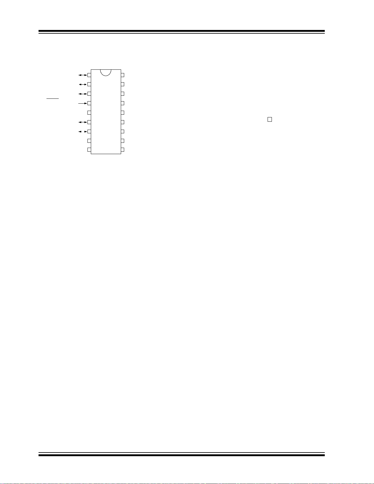
PIC18F1220/1320
Pin Diagrams
RA0/AN0
RA1/AN1/LVDIN
RA4/T0CKI
MCLR
/VPP/RA5
V
SS/AVSS
RA2/AN2/VREF-
RA3/AN3/V
RB0/AN4/INT0
REF+
RB1/AN5/TX/
1
2
3
4
5
6
7
8
9
18
17
16
15
14
13
12
11
10
RB3/CCP1/P1A
RB2/P1B/INT2
OSC1/CLKI/RA7
OSC2/CLKO/RA6
DD/AVDD
V
RB7/PGD/T1OSI/
RB6/PGC/T1OSO/
RB5/PGM/KBI1
RB4/AN6/RX/
DS39605C-page 2 2004 Microchip Technology Inc.
Page 5

PIC18F1220/1320
Table of Contents
1.0 Device Overview.......................................................................................................................................................................... 5
2.0 Oscillator Configurations............................................................................................................................................................ 11
3.0 Power Managed Modes ...................................... .. .. .... .. .. ..... .. .. .... .. .. .. .. ....... .. .. .. .. .. .. ....... .. .. .. ...................................................... 19
4.0 Reset..........................................................................................................................................................................................33
5.0 Memory Organization.................................................................................................................................................................41
6.0 Flash Program Memory............ ................ ................. ................. ................................................................................................57
7.0 Data EEPROM Memory.................................. ................................................ ........................................................................... 67
8.0 8 x 8 Hardware Multiplier............................................................................................................................................................ 71
9.0 Interrupts.................................................................................................................................................................................... 73
10.0 I/O Ports................................... .................................................................................................................................................. 87
11.0 Timer0 Module ...........................................................................................................................................................................99
12.0 Timer1 Module ......................................................................................................................................................................... 103
13.0 Timer2 Module ......................................................................................................................................................................... 109
14.0 Timer3 Module ......................................................................................................................................................................... 111
15.0 Enhanced Capture/Compare/PWM (ECCP) Module................................................................................................................ 115
16.0 Enhanced Addressable Universal Synchronous Asynchronous Receiver Transmitter (EUSART) .......................................... 131
17.0 10-Bit Analog-to-Digital Converter (A/D) Module .....................................................................................................................155
18.0 Low-Voltage Detect.................................................................................................................................................................. 165
19.0 Special Features of the CPU........................................... ................. ........................................................................................ 171
20.0 Instruction Set Summary.......................................................................................................................................................... 191
21.0 Development Support............................................................................................................................................................... 233
22.0 Electrical Characteristics.......................................................................................................................................................... 239
23.0 DC and AC Characteristics Graphs and Tables............................................................................. .......................................... 269
24.0 Packaging Information................................................. ................................................. ............................................................ 287
Appendix A: Revision History............................................................................................................................................................. 293
Appendix B: Device Differences ........................................................................................................................................................293
Appendix C: Conversion Considerations ...........................................................................................................................................294
Appendix D: Migration from Baseline to Enhanced Devices.............................................................................................................. 294
Appendix E: Migration from Mid-Range to Enhanced Devices.......................................................................................................... 295
Appendix F: Migration from High-End to Enhanced Devices............................................................................................................. 295
Index .................................................................................................................................................................................................. 297
On-Line Support.................................................................................................................................................................................305
Systems Information and Upgrade Hot Line...................................................................................................................................... 305
Reader Response.............................................................................................................................................................................. 306
PIC18F1220/1320 Product Identification System ............................................................................ .... .............................................. 307
2004 Microchip Technology Inc. DS39605C-page 3
Page 6

PIC18F1220/1320
TO OUR VALUED CUSTOMERS
It is our intention to provide our valued customers with the best documentation possible to ensure successful use of your Microchip
products. To this end, we will continue to improve our publications to better suit your needs. Our publications will be refined and
enhanced as new volumes and updates are introduced.
If you have any questions or c omm ents regarding t his publication, p lease c ontact the M arket ing Co mmunications Department via
E-mail at docerrors@mail.microchip.com or fax the Reader Response Form in the back of this data sheet to (480) 792-4150.
We welcome your feedback.
Most Current Data Sheet
To obtain the most up-to-date version of this data sheet, please register at our Worldwide Web site at:
http://www.microchip.com
You can determine the version of a data sheet by examining its literature number found on the bottom outside corner of any page.
The last character of the literature number is the version number, (e.g., DS30000A is version A of document DS30000).
Errata
An errata sheet, describing minor operational differences from the data sheet and recommended workarounds, may exist for current
devices. As device/documentation issues become known to us, we will publish an errata sheet. The errata will specify the revision
of silicon and revision of document to which it applies.
To determine if an errata sheet exists for a particular device, please check with one of the following:
• Microchip’s Worldwide Web site; http://www.microchip.com
• Your local Microchip sales office (see last page)
• The Microchip Corporate Literature Center; U.S. FAX: (480) 792-7277
When contacting a sales office or the literature center, please specify which device, revision of silicon and data sheet (include
literature number) you are using.
Customer Notification System
Register on our web site at www.microchip.com/cn to receive the most current information on all of our products.
DS39605C-page 4 2004 Microchip Technology Inc.
Page 7

PIC18F1220/1320
1.0 DEVICE OVERVIEW
This documen t conta i ns dev ic e spec if i c in for m at i on fo r
the following devices:
• PIC18F1220 • PIC18F1320
This family offers the advantages of all PIC18 microcontrollers – nam ely, high computationa l perfor manc e at an
economical pri ce – with the additio n of high enduran ce
Enhanced Flash program memory. On top of these features, the PIC18F1220/1320 family introduces design
enhancements that make these microcontrollers a logical
choice for many high-performance, power sensitive
applications.
1.1 New Core Features
1.1.1 nanoWatt TECHNOLOGY
All of the devices in the PIC18F1220/1320 family incorporate a range of features that can significantly reduce
power consumption during operation. Key items include:
• Alternate Run Modes: By clocking the controller
from the Timer1 source or the internal oscillator
block, power consumption during code execution
can be reduced by as much as 90%.
• Multiple Idle Modes: The controller can also run
with its CPU c ore disable d, but the pe ripherals are
still active. In these states, power consumption can
be reduced even further, to as little as 4% of normal
operation requirements.
• On-the-fly Mode Switching: The power managed
modes are invoked by user code during operation,
allowing the user to incorporate power-saving ideas
into their application’s software design.
• Lower Consumption in Key Modules: The power
requirements for both Timer1 and the Watchdog
Timer have been reduced by up to 80%, with typical
values of 1.1 and 2.1 µA, respectively.
1.1.2 MULTIPLE OSCILLATOR OPTIONS
AND FEATURES
All of the devices in the PIC18F1220/1320 family offer
nine different oscillator options, allowing users a wide
range of choices in developing application hardware.
These include:
• Four Crystal modes, using crystals or ceramic
resonators.
• Two External Clock modes, offering the option of
using two pins (oscillator input and a divide-by-4
clock output), or one pin (oscillator input, with the
second pin reassigned as general I/O).
• Two External RC Oscillator modes, with the same
pin options as the External Clock modes.
• An internal oscillator block, which provides an
8 MHz clock (±2% accuracy) and an INTRC source
(approximately 31kHz, stable over temperature and
V
DD), as well as a range of 6 user-selectable clock
frequencies (from 125 kHz to 4 MHz) for a total of
8 clock frequencies.
Besides its ava ilability as a cloc k source, the intern al
oscillator block pro vid es a s t ab le re fere nce source that
gives the family additional features for robust
operation:
• Fail-Safe Clock Monitor: This option constantly
monitors the main clock source against a reference
signal provided by the internal oscillator . If a clock failure occurs, the controller is switched to the internal
oscillator block, allowing for continued low-speed
operation, or a safe application shutdown.
• T wo-Spe ed Start-up: This option allows the internal
oscillator to serve as the cloc k source from Powe ron Reset, or wake-up from Sleep mode, until the
primary clock source is available. This allows for
code execution during what would otherwise be the
clock start-up interval and can even allow an application to perform routine background activities and
return to Sleep without returning to full power
operation.
1.2 Other Special Features
• Memory Endurance: The Enhanced Flash cells for
both program memory and data EEPROM are rated
to last for many thousands of erase/wri te cycles –
up to 100,000 for program memory and 1,000,000
for EEPROM. Data retention without refresh is
conservatively estimated to be greater than
40 years.
• Self-programmability: These devices can write to
their own program memory spaces under internal
software control. By using a bootloader routine
located in the protected Boot Block at the top of program memory, it becomes possible to create an
application that can update itself in the field.
• Enhanced CCP module: In PWM mode, this
module provides 1, 2 or 4 modulated outputs for
controlling half-bridge and full-bridge drivers. Other
features include auto-shutdown, for disabling PWM
outputs on interrupt or other select conditions and
auto-restart, to reactiv ate outpu t s onc e the condi tio n
has cleared.
• Enhanced USART: This serial communication
module features automatic wake-up on Start bit and
automatic baud rate d etecti on and supp ort s RS-23 2,
RS-485 and LIN 1.2 protocols, making it ideally
suited for use in Local Interconnect Network (LIN)
bus applications.
• 10-bit A/D Converter: This module incorporates
programmable acquisition time, allowing for a
channel to be selected and a conversion to be
initiated without waiting for a sampling period and
thus, reduce code overhead.
• Extended Watchdog Timer (WDT): This enhanced
version incorporates a 16-bit prescaler, allowing a
time-out range from 4 ms to over 2 minutes that is
stable across operating voltage and temperature.
2004 Microchip Technology Inc. DS39605C-page 5
Page 8

PIC18F1220/1320
1.3 Details on Individual Family Members
Devices in the PIC18F1220/1320 family are available
in 18-pin, 20-pin an d 28-pin pack ages. A block dia gram
for this device family is shown in Figure 1-1.
The devices are differentiated from each other only in
the amount of on-chip Flash program memory
(4 Kbytes for the PIC18F1220 device, 8 Kbytes for the
PIC18F1320 device). These and other features are
summarized in Table 1-1.
A block diagram of the PIC18F1220/1320 device
architecture is provided in Figure 1-1. The pinouts for
this device family are listed in Table 1-2.
TABLE 1-1: DEVICE FEATURES
Features PIC18F1220 PIC18F1320
Operating Frequency DC – 40 MHz DC – 40 MHz
Program Memory (Bytes) 4096 8192
Program Memory (Instruction s) 2048 4096
Data Memory (Bytes) 256 256
Data EEPROM Memory (Bytes) 256 256
Interrupt Sources 15 15
I/O Ports Ports A, B Ports A, B
Timers 4 4
Enhanced Capture/Compare/PWM Modules 1 1
Serial Communications Enhanced USART Enhanced USART
10-bit Analog-to-Digital Module 7 input channels 7 input channels
POR, BOR,
Resets (and Delays)
Programmable Low-Voltage Detect Yes Yes
Programmable Brown-out Reset Yes Yes
Instruction Set 75 Instructions 75 Instructions
Packages
RESET Instruction, Stack Full,
Stac k U nde rflo w (PWRT, OST),
(optional), WDT
MCLR
18-pin SDIP
18-pin SOIC
20-pin SSOP
28-pin QFN
RESET Instruction, Stack Full,
Stack Underflow (PWRT, OST),
POR, BOR,
MCLR (optional), WDT
18-pin SDIP
18-pin SOIC
20-pin SSOP
28-pin QFN
DS39605C-page 6 2004 Microchip Technology Inc.
Page 9
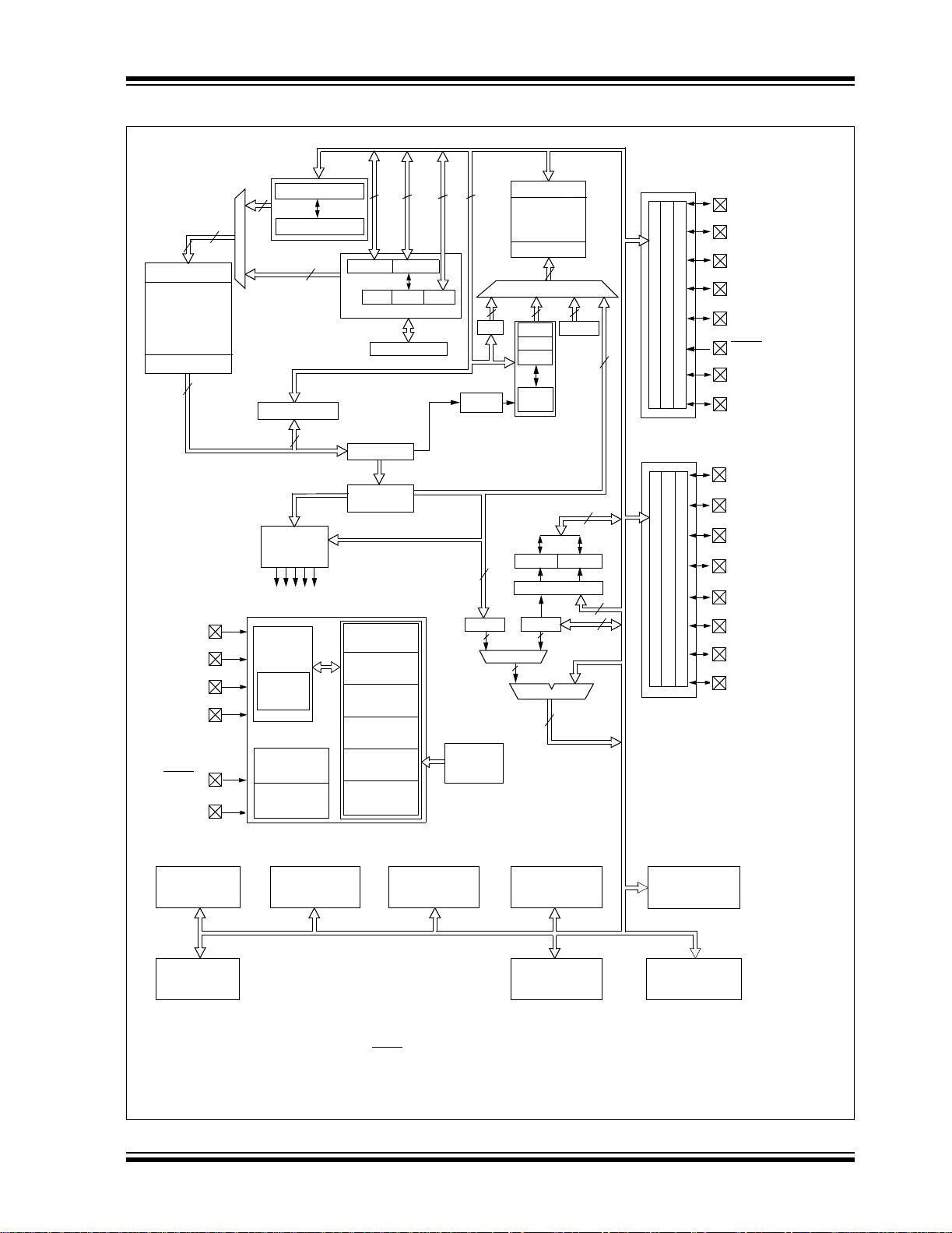
FIGURE 1-1: PIC18F1220/1320 BLOCK DIAGRAM
PIC18F1220/1320
Data Bus<8>
21
Address Latch
Program Memory
(4 Kbytes)
PIC18F1220
(8 Kbytes)
PIC18F1320
Data Latch
16
(2)
OSC1
(2)
OSC2
T1OSI
T1OSO
(1)
MCLR
DD, VSS
V
21
Table Pointer <2>
21
inc/dec logic
Table Latch
8
Instruction
Decode &
Control
Timing
Generation
INTRC
Oscillator
Low-Voltage
Programming
In-Circuit
Debugger
20
Start-up Timer
8
PCLATH
PCLATU
PCU
PCH PCL
Program Counter
31 Level Stack
ROM Latch
Instruction
Register
Power-up
Timer
Oscillator
Power-on
Reset
Watchdog
Timer
Brown-out
Reset
Fail-Safe
Clock Monitor
8
8
8
4
BSR
Decode
BIT OP
Precision
Voltage
Reference
Address Latch
Address<12>
12 4
FSR0
FSR1
FSR2
inc/dec
3
8
8
Data Latch
Data RAM
12
Bank0, F
logic
PRODLPRODH
8 x 8 Multiply
WREG
8
ALU<8>
8
PORTA
RA0/AN0
RA1/AN1/LVDIN
(2)
12
PORTB
8
8
8
RA2/AN2/VREF-
RA3/AN3/VREF+
RA4/T0CKI
(1)
/VPP/RA5
MCLR
OSC2/CLKO/RA6
OSC2/CLKI/RA7
RB0/AN4/INT0
RB1/AN5/TX/CK/INT1
RB2/P1B/INT2
RB3/CCP1/P1A
RB4/AN6/RX/DT/KBI0
RB5/PGM/KBI1
RB6/PGC/T1OSO/
T13CKI/P1C/KBI2
RB7/PGD/T1OSI/
P1D/KBI3
(2)
(2)
Timer0
Enhanced
CCP
Note 1: RA5 is available only when the MCLR
2: OSC1, OSC2, CLKI and CLKO are only available in select oscillator modes and when these pins are not being used as digital
I/O. Refer to Section 2.0 “Osc illa to r Configu ratio ns ” for additional information.
Timer1
Timer2
Reset is disabled.
Timer3
Enhanced
USART
A/D Converter
Data EEPROM
2004 Microchip Technology Inc. DS39605C-page 7
Page 10

PIC18F1220/1320
TABLE 1-2: PIC18F1220/1320 PINOUT I/O DESCRIPTIONS
Pin Name
Pin Number
PDIP/
SOIC
SSOP QFN
Pin
Type
Buffer
Type
Description
/VPP/RA5
MCLR
MCLR
VPP
RA5
OSC1/CLKI/RA7
OSC1
CLKI
RA7
OSC2/CLKO/RA6
OSC2
CLKO
RA6
RA0/AN0
RA0
AN0
RA1/AN1/LVDIN
RA1
AN1
LVDIN
RA2/AN2/V
RA3/AN3/VREF+
RA4/T0CKI
RA5 See the MCLR
RA6 See the OSC2/CLKO/RA6 pin.
RA7 See the OSC1/CLKI/RA7 pi n.
Legend: TTL = TTL compatible input CMOS = CMOS compatible input or output
REF-
RA2
AN2
V
REF-
RA3
AN3
V
REF+
RA4
T0CKI
ST = Schmitt Trigger input with CMOS levels I = Input
O=Output P =Power
OD = Op en- dr ai n ( no P di od e t o V
441
16 18 21
15 17 20
1126
2227
677
788
3328
I
ST
P
I/O
O
O
I/O
I/O
I/O
I/O
I/O
I/OIST/OD
DD)
—
I
ST
I
ST
I
CMOS
ST
—
—
ST
ISTAnalog
ST
I
Analog
I
Analog
ST
I
Analog
I
Analog
ST
I
Analog
I
Analog
ST
Master Clear (input) or programming voltage (input) .
Master Clear (Reset) input. This pin is an active-low
Reset to the device.
Programming voltage inpu t.
Digital input.
Oscillator crystal or extern al cl ock in put .
Oscillator crystal input or external clock source
input. ST buffer when configured i n R C m ode,
CMOS otherwise.
External clock source input. Always associated with
pin function OSC1. (See related OSC1/CLKI,
OSC2/CLKO pins.)
General purpose I/O pin.
Oscillator crystal or clock output.
Oscillator crystal output. C onnects to crystal or
resonator in Crystal Oscillator mode.
In RC, EC and INTRC modes, OSC2 pin outputs
CLKO, which has 1/4 the f re quency of OSC1 and
denotes instruction cy cl e r at e.
General purpose I/O pin.
PORTA is a bidirectional I/O port.
Digital I/O.
Analog input 0.
Digital I/O.
Analog input 1.
Low-Voltage Detect input.
Digital I/O.
Analog input 2.
A/D reference voltage (low) input.
Digital I/O.
Analog input 3.
A/D reference voltage (high) input.
Digital I/O. Open-drain when configured as output.
Timer0 external clock input.
/VPP/RA5 pin.
DS39605C-page 8 2004 Microchip Technology Inc.
Page 11

PIC18F1220/1320
T ABLE 1-2: PIC18F1220/1320 PINOUT I/O DESCRIPTIONS (CONTINUED)
Pin Number
Pin Name
RB0/AN4/INT0
RB0
AN4
INT0
RB1/AN5/TX/CK/INT1
RB1
AN5
TX
CK
INT1
RB2/P1B/INT2
RB2
P1B
INT2
RB3/CCP1/P1A
RB3
CCP1
P1A
RB4/AN6/RX/DT/KBI0
RB4
AN6
RX
DT
KBI0
RB5/PGM/KBI1
RB5
PGM
KBI1
RB6/PGC/T1OSO/
T13CKI/P1C/KBI2
RB6
PGC
T1OSO
T13CKI
P1C
KBI2
RB7/PGD/T1OSI/
P1D/KBI3
RB7
PGD
T1OSI
P1D
KBI3
V
SS 5 5, 6 3, 5 P — Ground reference for logic and I/O pins.
VDD 14 15, 16 17, 19 P — Positive supply for logic and I/O pins.
NC — — 18 — — No connect.
Legend: TTL = TTL compatible input CMOS = CMOS compatible input or output
ST = Schmitt Trigger input with CMOS levels I = Input
O=Output P =Power
OD = Op en- dr ai n ( no P di od e t o V
PDIP/
SSOP QFN
SOIC
899
91010
17 19 23
18 20 24
10 11 12
11 12 13
12 13 15
13 14 16
Pin
Type
I/O
I
I
I/O
I
O
I/O
I
I/O
O
I
I/O
I/O
O
I/O
I
I
I/O
I
I/O
I/O
I
I/O
I/O
O
I
O
I
I/O
I/O
I
O
I
DD)
Buffer
Type
TTL
Analog
ST
TTL
Analog
—
ST
ST
TTL
—
ST
TTL
ST
—
TTL
Analog
ST
ST
TTL
TTL
ST
TTL
TTL
ST
—
ST
—
TTL
TTL
ST
CMOS
—
TTL
Description
PORTB is a bidirectional I/O port. PORTB can be software
programmed for internal weak pull-ups on all inputs.
Digital I/O.
Analog input 4.
External interrupt 0.
Digital I/O.
Analog input 5.
EUSART asynchronous transmit.
EUSART synchronou s cl ock (see related RX/D T) .
External interrupt 1.
Digital I/O.
Enhanced CCP1/PW M ou tput .
External interrupt 2.
Digital I/O.
Capture 1 input/Compare 1 output/PWM 1 output.
Enhanced CCP1/PW M ou tput .
Digital I/O.
Analog input 6.
EUSART asynchronous rec eive.
EUSART synchronous da ta (see re l ated TX/CK).
Interrupt-on-chang e pi n.
Digital I/O.
Low-Voltage ICSP Programming enable pin.
Interrupt-on-chang e pi n.
Digital I/O.
In-Circuit Debugger and ICSP programming clock pin.
Timer1 oscillator output.
Timer1/Timer3 external clock output.
Enhanced CCP1/PW M ou tput .
Interrupt-on-chang e pi n.
Digital I/O.
In-Circuit Debugger and ICSP programming data pin.
Timer1 oscillator input.
Enhanced CCP1/PW M ou tput .
Interrupt-on-chang e pi n.
2004 Microchip Technology Inc. DS39605C-page 9
Page 12

PIC18F1220/1320
NOTES:
DS39605C-page 10 2004 Microchip Technology Inc.
Page 13
PIC18F1220/1320
2.0 OSCILLATOR CONFIGURATIONS
2.1 Oscillator Types
The PIC18F1220 and PIC18F1320 devices can be
operated in ten dif ferent osci llator modes . The user can
program the configuration bits, FOSC3:FOSC0, in
Configuration Register 1H to select one of these ten
modes:
1. LP Low-Power Crystal
2. XT Crystal/Resonator
3. HS High-Speed Crystal/Resonator
4. HSPLL High-Speed Crystal/Resonator
with PLL enabled
5. RC External Resistor/Capacitor with
OSC/4 output on RA6
F
6. RCIO Ex tern al R esi st or/C apacitor with
I/O on RA6
7. INTIO1 Internal Oscillator with F
output on RA6 and I/O on RA7
8. INTIO2 Internal Oscillator with I/O on RA6
and RA7
9. EC External Clock with F
10. ECIO External Clock with I/O on RA6
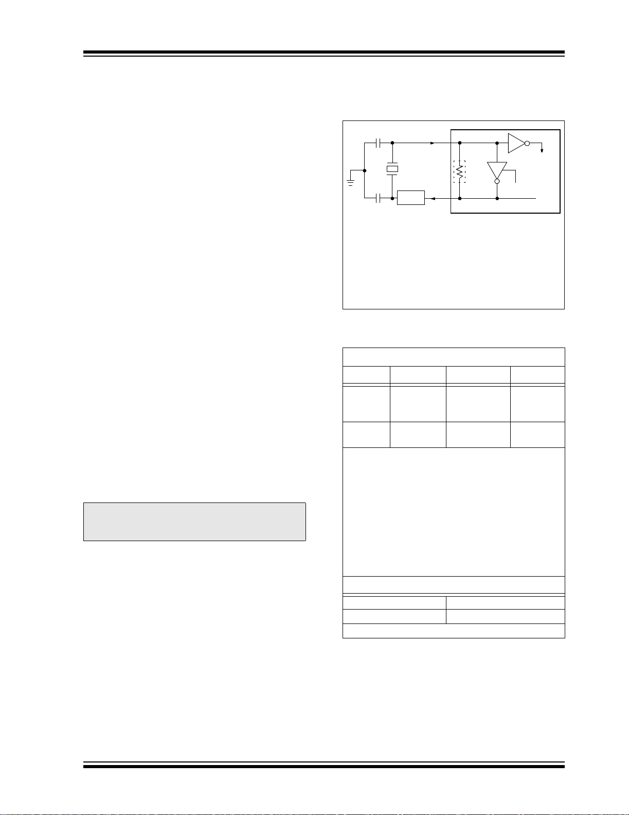
2.2 Crystal Oscillator/Ceramic Resonators
In XT, LP, HS or HSPLL Oscillator modes, a crystal or
ceramic resonator is connected to the OSC1 and
OSC2 pins to establish oscillation. Figure 2-1 shows
the pin connections.
The oscillator design requires the use of a parallel cut
crystal.
Note: Use of a series cut crystal may give a
frequency out of the crystal manufacturer’s
specifications.
OSC/4
OSC/4 output
FIGURE 2-1: CRYSTAL/CERAMIC
RESONATOR OPERATION
(XT, LP, HS OR HSPLL
CONFIGURATION)
(1)
C1
(1)
C2
Note 1: See Table 2-1 and Table 2-2 for initial
2: A series resistor (R
3: R
OSC1
To
Internal
XTAL
(2)
RS
OSC2
values of C1 and C2.
AT strip cut crystals.
F varies with the oscillator mode chosen.
(3)
RF
S) may be required for
Logic
Sleep
PIC18FXXXX
T ABLE 2-1: CAPACITOR SELECTION FOR
CERAMIC RESONATORS
Typical Capacitor Values Used:
Mode Freq OSC1 OSC2
XT 455 kHz
2.0 MHz
4.0 MHz
HS 8.0 MHz
16.0 MHz
Capacitor values are for design guidance only.
These capacitors were tested with the resonators
listed below for basic start-up and operation. These
values are not optimized.
Different cap acitor values may be required to prod uce
acceptable oscillator operation. The user should test
the performance of the oscillator over the expected
DD and temperature range for the application.
V
See the notes following Table 2-2 for additional
information.
Resonators Used:
455 kHz 4.0 MHz
2.0 MHz 8.0 MHz
16.0 MHz
56 pF
47 pF
33 pF
27 pF
22 pF
56 pF
47 pF
33 pF
27 pF
22 pF
2004 Microchip Technology Inc. DS39605C-page 11
Page 14

PIC18F1220/1320
TABLE 2-2: CAPACITOR SELECTION FOR
CRYSTAL OSCILLATOR
Osc T y pe
Crystal
Freq
LP 32 kHz 33 pF 33 pF
200 kHz 15 pF 15 pF
XT 1 MHz 33 pF 33 pF
4 MHz 27 pF 27 pF
HS 4 MHz 27 pF 27 pF
8 MHz 22 pF 22 pF
20 MHz 15 pF 15 pF
Capacitor values are for design guidance only.
These capacitors were tested with the crystals listed
below for basic start-up and operation . These values
are not optimized.
Different capa citor values may be required to produc e
acceptable oscillator operation. The user should test
the performance of the oscillator over the expected
DD and temperature range for the application.
V
See the notes following this table for additional
information.
Crystals Used:
32 kHz 4 MHz
200 kHz 8 MHz
1 MHz 20 MHz
Note 1: Higher capacitance increases the stability
of oscillator, but als o increases the start-up
time.
2: When operating below 3V V
using certain ceramic resonators at any
voltage, it may be necessary to use the
HS mode or switch to a crystal oscillator.
3: Since each resonator/crystal has its own
characteristics, the user should consult
the resonator/crystal manufacturer for
appropriate values of external
components.
S may be required to avoid overdriving
4: R
crystals with low driv e lev e l spe ci fic ati on.
5: Always veri fy os ci lla tor pe rform an ce ov er
DD and temperature range that is
the V
expected for the application.
T ypical Cap acitor V alues
Tested:
C1 C2
DD, or when
An external clock source may also be connected to the
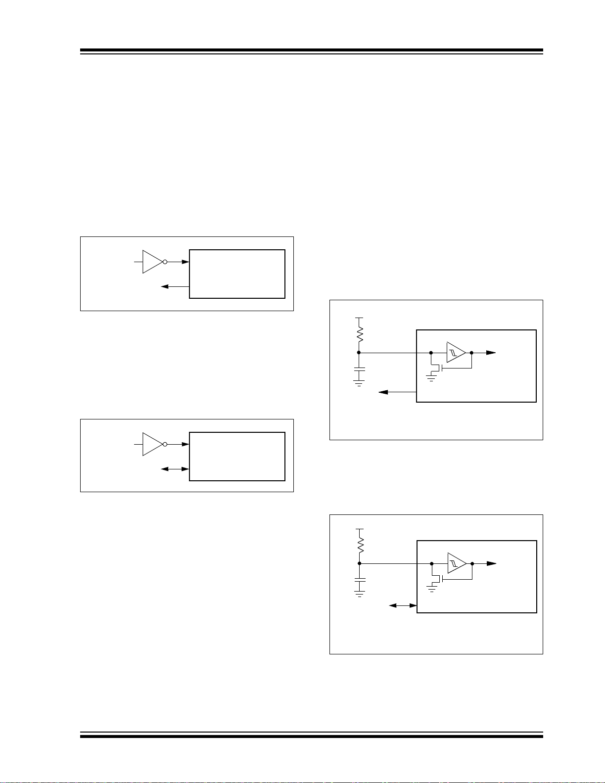
OSC1 pin in the HS mode, as shown in Figure 2-2.
FIGURE 2-2: EXTERNAL CLOCK INPUT
OPERATION (HS OSC
CONFIGURATION)
Clock from
Ext. System
Open
OSC1
OSC2
PIC18FXXXX
(HS Mode)
2.3 HSPLL
A Phase Locked Loop (PLL) circuit is provided as an
option for users who wish to use a lower frequency
crystal oscillator circuit, or to clock the device up to its
highest rated frequency from a crystal oscillator. This
may be useful for customers who are concerned with
EMI due to high-frequency crystals.
The HSPLL mode make s use of the HS mode osc illator
for frequencies up t o 10 MHz. A PLL then multipl ies the
oscillator output frequency by 4 to produce an internal
clock frequency up to 40 MHz.
The PLL is enabled only when the oscillator configuration bits are programmed for HSPLL mode. If
programmed for any other mode, the PLL is not
enabled.
FIGURE 2-3: PLL BLOCK DIAGRAM
HS Oscillator Enable
(from Configuration Register 1H)
OSC2
OSC1
Crystal
Osc
PLL Enable
F
IN
Comparator
FOUT
÷4
Phase
Loop
Filter
VCO
SYSCLK
MUX
DS39605C-page 12 2004 Microchip Technology Inc.
Page 15
PIC18F1220/1320
2.4 External Clock Input
The EC and ECIO Oscillator mode s require an externa l
clock source to be conn ected to the OSC1 pi n. There is
no oscillator start-up time required after a Power-on
Reset, or after an exit from Sleep mode.
In the EC Oscillator mode, the oscillator frequency
divided by 4 is available on the OSC2 pin. This signal
may be used for te st pu rpos es , o r to s yn chroni ze oth er
logic. Figure 2-4 shows the pin connections for the EC
Oscillator mode.
FIGURE 2-4: EXTER NAL CLOCK INPUT
OPERATION
(EC CONFIGURATION)
Clock from
Ext. System
OSC/4
F
The ECIO Oscillator mode func ti ons li ke t he EC m od e,
except that the OSC2 pin becomes an additional general purpose I/O pin. The I/O pin becomes bit 6 of
PORTA (RA6). Figure 2-5 shows the pin connections
for the ECIO Oscillator mode.
FIGURE 2-5: EXTER NAL CLOCK INPUT
Clock from
Ext. System
RA6
OSC1/CLKI
PIC18FXXXX
OSC2/CLKO
OPERATION
(ECIO CONFIGURATION)
OSC1/CLKI
PIC18FXXXX
I/O (OSC2)
2.5 RC Oscillator
For timing insensitive applications, the “RC” and
“RCIO” device options offer additional cost savings.
The RC oscillator frequency is a function of the supply
voltage, the resistor (R
ues and the operating temperature. In addition to this,
the oscillator frequency will vary from uni t to unit due to
normal manufacturing variation. Furthermore, the difference in lead frame capacitance between package
types will also affect the oscillation frequency, especially for low C
EXT values. The user also needs to take
into account variation, due to tolerance of external
R and C components used. Figure 2-6 shows how the
R/C combination is connected.
In the RC Oscillator mode, the oscillator frequency
divided by 4 is available on the OSC2 pin. This signal
may be used for te st purposes, or to synchronize other
logic.
FIGURE 2-6: RC OSCILLATOR MODE
VDD
REXT
CEXT
VSS
F
Recommended values: 3 kΩ ≤ REXT ≤ 100 kΩ
The RCIO Oscillator mode (Figure 2-7) functions like
the RC mode, except that the OSC2 pin becomes an
additional general purpose I/O pin. The I/O pin
becomes bit 6 of PORTA (RA6).
EXT) and capacitor (CEXT) val-
OSC1
OSC2/CLKO
OSC/4
EXT > 20 pF
C
Internal
Clock
PIC18FXXXX
FIGURE 2-7: RCIO OSCILLATOR MODE
VDD
REXT
OSC1
CEXT
VSS
RA6
Recommended values: 3 kΩ ≤ REXT ≤ 100 kΩ
2004 Microchip Technology Inc. DS39605C-page 13
I/O (OSC2)
EXT > 20 pF
C
Internal
Clock
PIC18FXXXX
Page 16

PIC18F1220/1320
2.6 Internal Oscillator Block
The PIC18F1220/1320 devices include an internal
oscillator block, which generates two different clock
signals; either can be used as the system’s clock
source. This can eliminate the need for external
oscillator circuits on the OSC1 and/or OSC 2 pins.
The main output (INTOSC) is an 8 MHz clock source,
which can be used to directly drive the system clock. It
also drives a postscaler, which can provide a range of
clock frequencies from 125 kHz to 4 MHz. The
INTOSC output is enabled when a system clock
frequency from 125 kHz to 8 MHz is selected.
The other clock source is the internal RC oscillator
(INTRC), which provides a 31kHz output. The INTRC
oscillator is enabled by selecting the internal oscillator
block as the system clock source, or when any of the
following are enabled:
• Power-up Timer
• Fail-Safe Clock Monitor
• Watchdog Timer
• Two-Spe ed Start-up
These features are discussed in greater detail in
Section 19.0 “Special Features of the CPU”.
The clock source frequency (INTOSC direct, INTRC
direct or INTOSC postscaler) is selected by configuring
the IRCF bits of the OSCCON register (Register2-2).
2.6.1 INTIO MODES
Using the internal oscillator as the clock source can
eliminate the need for up t o two extern al oscilla tor pins,
which can then be used for digital I/O. Two distinct
configurations are available:
• In INTIO1 mode, the OSC2 pin outputs F
while OSC1 functions as RA 7 fo r dig it a l in put a nd
output.
• In INTIO2 mode, OSC1 functions as RA7 and
OSC2 functions as RA6, both for digital input and
output.
OSC/4,
2.6.2 INTRC OUTPUT FREQUENCY
The internal oscillator block is calibrated at the factory
to produce an INTOSC output frequency of 8.0 MHz
(see Table 22-6). This changes the frequency of the
INTRC source from its nominal 31.25 kHz. Peripherals
and features that depend on the INTRC source will be
affected by this shift in frequency.
Once set during factory calibration, the INTRC
frequency will remain within ±2% as temperature and
DD change across their full specified operating
V
ranges.
2.6.3 OSCTUNE REGISTER
The internal oscillator’s output has been calibrated at
the factory, but can be adjusted in the user’s application. Thi s is do ne by writi ng to the OS CTUNE regi ster
(Register 2-1). The tuning sensitivity is constant
throughout the tuning range.
When the OSCTUNE regis ter is mo di fied , the IN T O SC
and INTRC frequencies will begin shifting to the new
frequency. The INTRC clock will reach the new
frequency within 8clock cycles (approximately
8*32µs = 256 µs). The INTOSC clock will stabilize
within 1 ms. Code execution continues during th is shift.
There is no indication that the shift has occurred.
Operation of features that depend on the INTRC clock
source frequency, such as the WDT, Fail-Safe Clock
Monitor and peripherals, will also be affected by the
change in frequency.
DS39605C-page 14 2004 Microchip Technology Inc.
Page 17

PIC18F1220/1320
REGISTER 2-1: OSCTUNE: OSCILLATOR T UNING REGISTER
U-0 U-0 R/W-0 R/W-0 R/W-0 R/W-0 R/W-0 R/W-0
— — TUN5 TUN4 TUN3 TUN2 TUN1 TUN0
bit 7 bit 0
bit 7-6 Unimplemented: Read as ‘0’
bit 5-0 TUN<5:0>: Frequency Tuning bits
011111 = Maximum frequency
• •
• •
000001
000000 = Center frequency. Oscillator module is running at the calibrated frequency.
111111
• •
• •
100000 = Minimum frequency
Legend:
R = Readable bit W = Writable bit U = Unimplemented bit, read as ‘0’
-n = Value at POR ‘1’ = Bit is set ‘0’ = Bit is cleared x = Bit is unknown
2.7 Clock Sources and Oscillator Switching
Like previous PIC18 devices, the PIC18F1220/1320
devices include a feature that allows the system clock
source to be switched from the main oscillator to an
alternate low-frequency clock source. PIC18F1220/
1320 devices offer two alternate clock sources. When
enabled, these give additional options for switching to
the various power managed operating modes.
Essentially, there are three clock sources for these
devices:
• Primary oscillators
• Secondary oscillators
• Internal oscillator block
The primary oscillators include the Ex ternal Crystal
and Resonator modes, the External RC modes, the
External Clock modes and the internal oscillator block.
The particular mod e is defined on POR by the content s
of Configuration Register 1H. The details of these
modes are covered earlier in this chapter.
The s econdary oscillat ors are those external sources
not connected to the OSC1 or OSC2 pins. These
sources may continue to operate even after the
controller is placed in a power managed mode.
PIC18F1220/1320 devices offer only the Timer1
oscillator as a secon dary oscilla tor . This osc illator , in all
power managed modes, is often the time base for
functions such as a real-time cloc k.
Most often, a 32.768 kHz watch crystal is connected
between the RB6/T1OSO and RB7/T1OSI pins. Like
the LP mode oscillator circuit, loading capacitors are
also connect ed from each pin to ground . These pins
are also used during ICSP operations.
The Timer1 oscillator is discussed in greater detail in
Section 12.2 “Timer1 Oscillator”.
In addition to being a prim ary clock source, the internal
oscillator block is available as a power managed
mode clock source. T he IN TR C s ource is also used as
the clock source for several special features, such as
the WDT and Fail-Safe Clock Monitor.
The clock sources for the PIC18F1220/1320 devices
are shown in Figure 2-8. See Section 12.0 “Timer1
Module” for further details of the Time r1 oscillator. See
Section 19.1 “Configuration Bits” for configuration
register details.
2004 Microchip Technology Inc. DS39605C-page 15
Page 18

PIC18F1220/1320
2.7.1 OSCILLATOR CONTROL REGISTER
The OSCCON register (Register 2-2) controls several
aspects of the system clock’s operation, both in full
power operation and in power managed modes.
The System Clock Select bits, SCS1:SCS0, select the
clock source that is used when the device is operating in
power managed modes. The available clock sources are
the primary clock (defined in Configuration Register 1H),
the secondary clock (Timer1 oscillator) and the internal
oscillator block. The clock selection has no effect until a
SLEEP instruction is executed and the device enters a
power managed mode of operation. The SCS bits are
cleared on all forms of Reset.
The Internal Oscill ator Select bit s, IRCF2:IRCF0, select
the frequency output o f the interna l oscill ator block th at
is used to dr ive t he sys tem clo ck. Th e ch oice s are the
INTRC source, the INTOSC source (8 MHz), or one of
the six frequencies derived from the INTOSC
postscaler (125kHz to 4 MHz). If the internal oscillator
block is supplying the system clock, changing the
states of these bits will have an immediate change on
the internal oscillator’s output.
The OSTS, IOFS and T1RUN bit s ind ic ate wh ich clock
source is currently providing the system clock. The
OSTS indicates that the Oscillator Start-up Timer has
timed out and the prima ry clock is pro viding the system
clock in Primary Clock modes. The IOFS bit indicates
when the internal oscillator block has stabilized and is
providing the system clock in RC Clock modes or
during Two-Speed Start-ups. The T1RUN bit
(T1CON<6>) indicates when the Timer1 oscillator is
providing the syste m cloc k in Seco ndary Clock modes .
In power managed modes, only one of these three bits
will be set at any time. If none of these bits are set, the
INTRC is providing the system clock, or the internal
oscillator block has just started and is not yet stable.
The IDLEN bit controls the selective shutdown of the
controller’s CPU in power managed modes. The uses
of these bits are discussed in more detail in
Section 3.0 “Power Managed Modes”.
Note 1: The Timer1 oscillator must be enabled to
select the secondary clock source. The
Timer1 osc illator is enabled by s etting the
T1OSCEN bit in th e T imer1 C ontrol re gister (T1CON<3>). If the Timer1 oscillator
is not enabled, then any at tem pt to se lec t
a secondary clock source when
executing a SLEEP instruction will be
ignored.
2: It is recommended that the Timer1 oscil-
lator be operating and stable before executing the SLEEP instruction or a very
long delay may occur while the Timer1
oscillator starts.
FIGURE 2-8: PIC18F1220/1320 CLOCK DIAGRAM
PIC18F1220/1320
OSCCON<6:4>
8
111
4 MHz
110
2 MHz
101
1 MHz
31 kHz
100
011
010
001
000
Postscaler
500 kHz
250 kHz
125 kHz
OSC2
OSC1
T1OSO
T1OSI
Primary Oscillator
Sleep
Secondary Oscillator
T1OSCEN
Enable
Oscillator
OSCCON<6:4>
Internal
Oscillator
Block
INTRC
Source
8 MHz
(INTOSC)
CONFIG1H<3:0>
4 x PLL
Clock Source Option
for Other Modules
MUX
HSPLL
LP, XT, HS, RC, EC
T1OSC
Internal Oscillator
Clock
Control
MUX
OSCCON<1:0>
Peripherals
CPU
IDLEN
WDT, FSCM
DS39605C-page 16 2004 Microchip Technology Inc.
Page 19

REGISTER 2-2: OSCCON REGISTER
R/W-0 R/W-0 R/W-0 R/W-0 R
IDLEN IRCF2 IRCF1 IRCF0 OSTS IOFS SCS1 SCS0
bit 7 bit 0
bit 7 IDLEN: Idle Enable bits
1 = Idle mode enabled; CPU core is not clocked in power managed modes
0 = Run mode enabled; CPU core is clocked in Run modes, but not Sleep mode
bit 6-4 IRCF2:IRCF0: Internal Oscillator Frequency Select bits
111 = 8 MHz (8 MHz source drives clock directly)
110 = 4 MHz
101 = 2 MHz
100 = 1 MHz
011 = 500 kHz
010 = 250 kHz
001 = 125 kHz
000 = 31 kHz (INTRC source drives clock directly)
bit 3 OSTS: Oscillator Start-up Time-out Status bit
1 = Oscillator Start-up Timer time-out has expired; primary oscillator is running
0 = Oscillator Start-up Timer time-out is running; primary oscillator is not ready
bit 2 IOFS: INTOSC Frequency Stable bit
1 = INTOSC frequency is stable
0 = INTOSC frequency is not stable
bit 1-0 SCS1:SCS0: System Clock Select b its
1x = Internal oscillator block (RC modes)
01 = Timer1 oscillator (Secondary modes)
00 = Primary oscillator (Sleep and PRI_IDLE modes)
Note 1: Depends on state of the IESO bit in Configuration Register 1H.
PIC18F1220/1320
(1)
R-0 R/W-0 R/W-0
Legend:
R = Readable bit W = Writable bit U = Unimplemented bit, read as ‘0’
-n = Value at POR ‘1’ = Bit is set ‘0’ = Bit is cleared x = Bit is unknown
2004 Microchip Technology Inc. DS39605C-page 17
Page 20

PIC18F1220/1320
2.7.2 OSCILLATOR TRANSITIONS
The PIC18F1220/1320 devices contain circuitry to
prevent clocking “glitches” when switching between
clock sources. A short pause in the system clock
occurs during the clo ck switch. Th e length of thi s pause
is between 8 and 9 clock periods of the new clock
source. This ensures that the new clock source is
stable and that its pulse width will not be less than the
shortest pulse width of the two clock sources.
Clock transitions are discussed in greater detail in
Section 3.1.2 “Entering Power Managed Modes”.
2.8 Effects of Power Managed Modes on the Various Clock Sources
When the device executes a SLEEP instruction, the
system is switched to one of the power managed
modes, depending on the state of the IDLEN and
SCS1:SCS0 bits of the OSCCON register. See
Section 3.0 “Power Managed Modes” for details.
When PRI_IDLE mode is selected, the designated primary oscillator continues to run without interruption.
For all other power managed modes, the oscillator
using the OSC1 pin is disabled. The OSC1 pin (and
OSC2 pin, if used by the o scillat or) will sto p oscillat ing.
In Secondary Clock modes (SEC_RUN and
SEC_IDLE), the Timer1 oscillator is operating and
providing the system clock. The Timer1 oscillator may
also run in all power managed modes if required to
clock Timer1 or Timer3.
In Internal Oscillator modes (RC_RUN and RC_IDLE),
the internal oscillator block provides the system clock
source. The INTRC output can be used directly to
provide the system clock and may be enabled to
support various special features, regardless of the
power managed mode (see Section 19.2 “Watchdog
Timer (WDT)” through Sec tion 19.4 “Fail-Safe Clock
Monitor”). The INTOSC output at 8 MHz may be used
directly to clock the system, or may be divided down
first. The INTOSC out put is disabled if the system clock
is provided directly from the INTRC output.
If the Sleep mode is selected, all clock sources are
stopped. Since all the transistor switching currents
have been stopped, Sleep mode achieves the lowest
current consumption of the device (only leakage
currents).
Enabling any on-chip feature that will operate during
Sleep will increase the current cons umed during Sleep.
The INTRC is required to support WDT operation. The
Timer1 oscillator may be operating to support a realtime clock. Ot her features may be operating that do n ot
require a system clock source (i.e., INTn pins, A/D
conversions and others).
2.9 Power-up Delays
Power-up delays are controlled by two timers, so that
no external Rese t circ ui try is re qui red for most applications. The delays ensure that the device is kept in
Reset until the device powe r supply i s stable under normal circumstan ces and the pri mary clock is ope rating
and stable. For additional information on power-up
delays, see Sections 4.1 through 4.5.
The first timer is the Power-up Timer (PWRT), which
provides a fixed delay on power-up (parameter 33,
Table 22-8) if enabled in Configuration Register 2L.
The second timer is the Oscillator Start-up Timer
(OST), intended to keep the chip in Reset until the
crystal oscillator is stable (LP, XT and HS modes). The
OST does this by counting 1024 oscillator cycles
before allowing the oscillator to clock the device.
When the HSPLL Oscillator mode is selected, the
device is kept in Reset for an additional 2 ms following
the HS mode OST delay, so the PLL can lock to the
incoming clock frequ enc y.
There is a delay of 5 to 10 µs following POR while the
controller becomes ready to execute instructions. This
delay runs concurrently with any other delays. This
may be the only del ay that occurs when any of the EC ,
RC or INTIO modes are used as the primary clock
source.
TABLE 2-3: OSC1 AND OSC2 PIN STATES IN SLEEP MODE
Oscillator Mode OSC1 Pin OSC2 Pin
RC, INTIO1 Floating, external resistor should pull high At logic low (clock/4 output)
RCIO, INTIO2 Floating, external resistor should pull high Configured as PORTA, bit 6
ECIO Floating, pulled by external clock Configured as PORTA, bit 6
EC Floating, pulled by external clock At logic low (clock/4 output)
LP, XT and HS Feedback inverter disabled at quiescent
voltage level
Note: See Table 4-1 in Section 4.0 “Reset” for time-outs due to Sleep and MCLR
DS39605C-page 18 2004 Microchip Technology Inc.
Feedback inverter disabled at quiescent
voltage level
Reset.
Page 21

PIC18F1220/1320
3.0 POWER MANAGED MODES
The PIC18F1220/1320 devic es o ffe r a tot al o f six operating modes for more efficient power management
(see Table 3-1). These provide a variety of options for
selective power conservation in applications where
resources may be limited (i.e., battery powered
devices).
There are three categories of power managed modes:
• Sleep mode
• Idle modes
• Run modes
These categories define which portions of the device
are clocked and some times , what sp eed. The R un and
Idle modes may use any of the three available clock
sources (primary, secondary or INTOSC multiplexer);
the Sleep mode does not use a clock source.
The clock switching feature offered in other PIC18
devices (i.e., using the Timer1 oscillator in place of the
primary oscillator) and the Sleep mode offered by all
PICmicro
stopped) are both offered in the PIC18F1220/1320
devices (SEC_RUN and Sleep modes, respectively).
However, additional power managed modes are available that allow the u ser greater flexibili ty in dete rmining
what portions of the device are operating. The power
managed modes are event driven; that is, some
specific event must occur for the device to enter or
(more particularly) exit these operating modes.
®
devices (where all system clocks are
For PIC18F1220/1320 devices, the power managed
modes are invoked by using the existing SLEEP
instruction. All modes exit to PRI_RUN mode when triggered by an interrupt, a Reset or a WDT time-out
(PRI_RUN mode is the normal full power execution
mode; the CPU and peri phe rals are cl ock ed by the p rimary oscillator source). In addition, power managed
Run modes may also exit to Sleep mode, or their
corresponding Idle mode.
3.1 Selecting Power Managed Modes
Selecting a power managed mode requires deciding if
the CPU is to be clocked or not and selecting a clock
source. The IDLEN bit controls CPU clocking, while the
SCS1:SCS0 bits select a clock source. The individual
modes, bit settings, clock sources and affected
modules are summarized in Table 3-1.
3.1.1 CLOCK SOURCES
The clock source is selected by setting the SCS bits of
the OSCCON register (Register 2-2). Three clock
sources are available for use in power managed Idle
modes: the primary clock (as confi gured in Configuration
Register 1H), the secondary clock (Timer1 oscillator)
and the internal oscillator block. The secondary and
internal oscillator block sources are available for the
power managed modes (PRI_RUN mode is the normal
full power execution mode; the CPU and peripherals are
clocked by the primary oscillator source).
TABLE 3-1: POWER MANAGED MODES
OSCCON Bits Module Clocking
Mode
Sleep 000 Off Off None – All clocks are disabled
PRI_RUN 000Clocked Clocked Primary – L P, XT, HS, HSPLL, RC, EC, INTRC
SEC_RUN 001Clocked Clocked Secondary – Timer1 Oscillator
RC_RUN 01xClocked Clocked Internal Oscillator Block
PRI_IDLE 100 Off Clocked Primary – LP, XT, HS, HSPLL, RC, EC
SEC_IDLE 101 Off Clocked Secondary – Timer1 Oscillator
RC_IDLE 11x Off Clocked Internal Oscillator Block
Note 1: Includes INTOSC and INTOSC postscaler, as well as the INTRC source.
IDLEN
<7>
SCS1:SCS0
<1:0>
CPU Peripherals
Available Clock and Oscillator Source
This is the normal full power execution mode.
(1)
(1)
(1)
2004 Microchip Technology Inc. DS39605C-page 19
Page 22

PIC18F1220/1320
3.1.2 ENTERING POWER MANAGED
MODES
In general, entry, exit and switching between power
managed clock sources requires clock source
switching. In each case, the sequence of events is the
same.
Any change in the power managed mode begins with
loading the OSCCON register and executing a SLEEP
instruction. The SCS1:SCS0 bits select one of three
power managed clock sources; the primary clock (as
defined in Configuration R egister 1H), the s econdary
clock (the Timer1 os cillator) and the inte rnal osci llator
block (used i n RC mode s). Mo dif ying the SCS bits wi ll
have no effec t until a SLEEP instruction is executed.
Entry to the power managed mode is triggered by the
execution of a SLEEP instruction.
Figure 3-5 shows how the system is clocked while
switching from the primary clock to the Timer1 oscillator. When the SLEEP instruction is executed, clocks to
the device are stopped at the beginning of the next
instruction cycle. Eight clock cycles from the new clock
source are counted to synchronize with the new clock
source. After eight clock pulses from the new clock
source are counted, clocks from the new clock source
resume clocking the system. The actual length of the
pause is betwe en eight and nine cl ock periods from the
new clock source. This ensures that the new clock
source is stab le a nd th at its pulse width will not be less
than the shortest pulse width of the two clock sources.
Three bits in dicat e the current cloc k so urce: OSTS an d
IOFS in the OSCCON register and T1RUN in the
T1CON register. Only one of these b its will be set whil e
in a power managed mode. When the OSTS bit is set,
the primary clock is providing the system clock. When
the IOFS bit is set, the INTOSC output is providing a
stable 8 MHz clock source and is providing the system
clock. When the T1RUN bit is set, the T i mer1 oscillator
is providing the system clock. If none of these bits are
set, then either the INTRC clock source is clocking the
system, or the INTOSC source is not yet stable.
If the internal oscillator block is configured as the primary clock source in Configuration Register 1H, then
both the OSTS and IOFS bits may be set when in
PRI_RUN or PRI_IDLE modes. This indicates that the
primary clock (INTOSC output) is generating a stable
8 MHz output. Entering an RC power managed mode
(same frequency) would clear the OSTS bit.
3.1.3 MULTIPLE SLEEP COMMANDS
The power managed mode that is invoked with the
SLEEP instruction is determined by the settings of the
IDLEN and SCS bits at the time the instruction is executed. If another SLEEP instruction is executed, the
device will enter the power managed mode specif ied by
these same bits at that time. If the bits have changed,
the device will enter the new power managed mode
specified by the new bit settings.
3.1.4 COMPARISONS BETWEEN RUN AND IDLE MODES
Clock source selection for the Run modes is identical to
the corresponding Idle modes. When a SLEEP instruction is executed, the SCS bits in the OSCCON register
are used to switch to a different clock source. As a
result, if there is a ch ange of clock source at th e ti me a
SLEEP instruction is ex ecuted, a clock swi tch will occur .
In Idle modes, the CPU is not clocked and is not running. In Run mode s, the CPU is clocked a nd ex ecu tin g
code. This difference modifies the operation oe.1TJ/F7-0.9(.4ng)13I1(on )1 t66
DS39605C-page 20 2004 Microchip Technology Inc.
Page 23

PIC18F1220/1320
TABLE 3-2: COMPARISON BETWEEN POWER MANAGED MODES
Power
Managed
Mode
Sleep Not clocked (not running) Wake-up Not clocked None or INTOSC multiplexer
Any Idle mode Not clocked (not running) Wake-up Primary, Secondary or
Any Run mode Primary or secondary
CPU is Clocked by ...
clocks or INTOSC
multiplexer
WDT Time-out
causes a .. .
Reset Primary or secondary
Peripherals are
Clocked by ...
INTOSC multiplexer
clocks or INTOSC
multiplexer
Clock during Wake-up
(while primary becomes
ready)
if Two-Speed Start-up or
Fail-Safe Clock Monitor are
enabled
Unchanged from Idle mode
(CPU operates as in
corresponding Run mode)
Unchanged from Run mode
3.2 Sleep Mode
The power managed Sleep mode in the PIC18F1220/
1320 devices is identical to that offered in all other
PICmicro microcontrollers. It is entered by clearing the
IDLEN and SCS1:SCS0 bits (this is the Reset state)
and executing the SLEEP instruction. This s huts down
the primary oscillator and the OSTS bit is cleared (see
Figure 3-1).
When a wake ev ent occurs i n Sleep mo de (by int errupt,
Reset or WDT time-out), the sy stem will no t be clocke d
until the primary clock source becomes ready (see
Figure 3-2), or it will be clocked from the internal
oscillator block if either the Two-Speed Start-up or the
Fail-Safe Clock Monitor are enabl ed (see Section 19.0
“Special Features of the CPU”). In either case, the
OSTS bit is set whe n t he primary clock is providin g the
system clocks. The IDLEN and SCS bits are not
affected by the wake-up.
3.3 Idle Modes
The IDLEN bi t allows the micr ocontrol ler’s C PU to be
selectively shut down while the peripherals continue to
operate. Clearing ID LEN allows t he CPU to be cl ocked.
Setting IDLEN disables clocks to the CPU, effectively
stopping program execution (see Register 2-2). The
peripherals continue to be clocked regardless of the
setting of the IDLEN bit.
There is one exception to how the IDLEN bit functions.
When all the low-power OSCCON bits are cleared
(IDLEN:SCS1:SCS0 = 000), the device enters Sleep
mode upon the exec ution of the SLEEP instruction. This
is both the Reset state of the OSCCON register and the
setting that selects Sleep mode. This maintains
compatibility with other PICmi cro devices that d o not
offer power managed modes.
If the Idle Enable bit, IDLEN (OSCCON<7>), is set to a
‘1’ when a SLEEP instruction is executed, the
peripherals will be clocked from the clock source
selected using the SCS1 :SCS0 bits ; however, the CPU
will not be clocked. Since the CPU is not executing
instructions, the only exits from any of the Idle modes
are by interrupt, WDT time-out or a Reset.
When a wake event occurs, CPU execution is delayed
approximately 10µs while it becomes ready to e xecute
code. When the CPU begins executing code, it is
clocked by th e same clock s ource as was selected in
the power managed mode (i.e., when waking from
RC_IDLE mode, the internal oscillator block will clock
the CPU and peripherals unti l the primar y clock so urce
becomes ready – this is essentially RC_RUN mode).
This continues until the primary clock source becomes
ready. When the primary clock becomes ready, the
OSTS bit is set and the system clock source is
switched to the primary clock (see Figure 3-4). The
IDLEN and SCS bits are not affected by the wake-up.
While in any Idle mode or the Sleep mode, a WDT
time-out will result in a WDT wake-up to full power
operation.
2004 Microchip Technology Inc. DS39605C-page 21
Page 24
PIC18F1220/1320
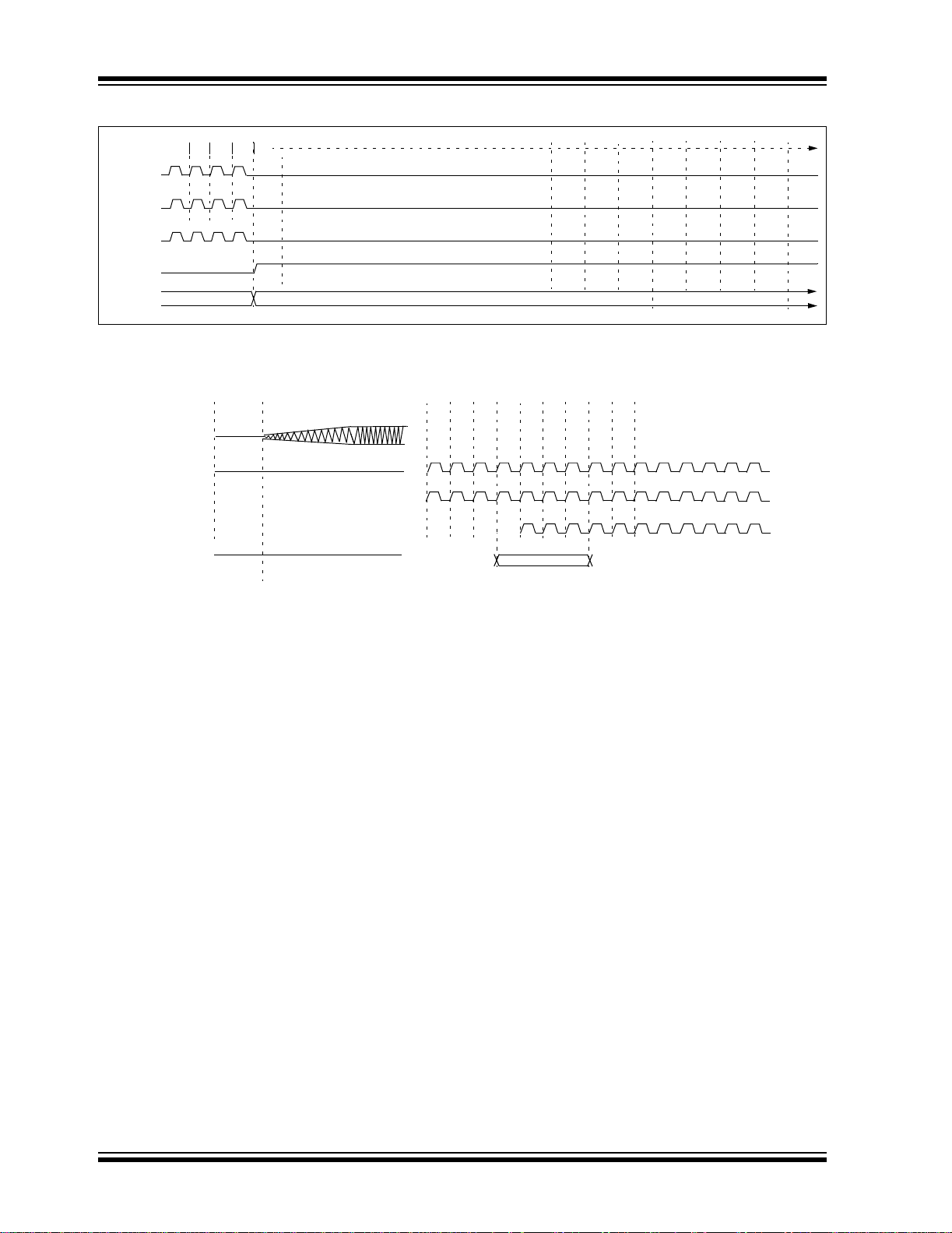
FIGURE 3-1: TIMING TRANSITION FOR ENTRY TO SLEEP MODE
Q4Q3Q2
Q1Q1
OSC1
CPU
Clock
Peripheral
Clock
Sleep
Program
Counter
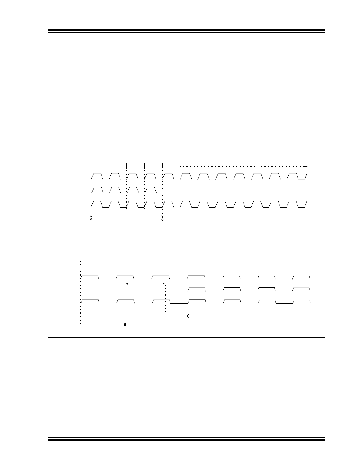
FIGURE 3-2: TRANSITION TIMING FOR WAKE FROM SLEEP (HSPLL)
PC + 2PC
OSC1
PLL Clock
Output
CPU Clock
Peripheral
Clock
Program
Counter
PC
Q1 Q2 Q3 Q4 Q1 Q2
Q3 Q4 Q1 Q2
Q3 Q4
DS39605C-page 22 2004 Microchip Technology Inc.
Page 25
PIC18F1220/1320
3.3.1 PRI_IDLE MODE
This mode is unique among the three Low-Power Idle
modes, in that it does not disable the primary system
clock. For timing sensitive applications, this allows for
the fastest resump tion of devic e operation with its more
accurate pri mary clock source, si nce the cl ock source
does not have to “warm up” or transition from another
When a wake event occurs, the CPU is clocked from
the primary clock source. A delay of approximately
10 µs is required between the wake event and code
execution starts. This is required to allow the CPU to
become read y to ex ecut e in stru cti ons. A ft er th e wake up, the OSTS bit remai ns set. Th e IDLEN an d SCS bit s
are not affected by the wake-up (see Figure3-4).
oscillator.
PRI_IDLE mode is entered by setting the IDLEN bit,
clearing the SCS bits and executing a SLEEP instruction. Although the CPU is disabled, the peripherals
continue to be clocked from the primary clock source
specified in Configuration Register 1H. The OSTS bit
remains set in PRI_IDLE mode (see Figure 3-3).
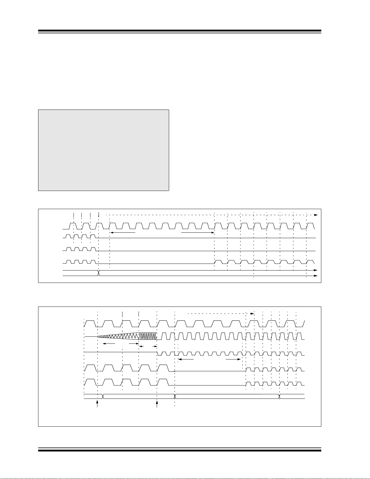
FIGURE 3-3: TRANSITION TIMING TO PRI_IDLE MODE
Q1
Q4
OSC1
CPU Clock
Peripheral
Clock
Program
Counter
Q1
Q2
Q3
PC PC + 2
FIGURE 3-4: TRANSITION TIMING FOR WAKE FROM PRI_IDLE MODE
OSC1
CPU Clock
Peripheral
Clock
Program
Counter
Q1 Q3 Q4
CPU Start-up Delay
PC
Wake Event
Q2
PC + 2
2004 Microchip Technology Inc. DS39605C-page 23
Page 26
PIC18F1220/1320
3.3.2 SEC_IDLE MODE
In SEC_IDLE mode, the CPU is disabled, but the
peripherals continue to be clocked from the Timer1
oscillator. This mode is entered by setting the Idle bit,
modifying bits, SCS1:SCS0 = 01 and executing a
SLEEP instruction. When the clock source is switched
(see Figure 3-5) to the Timer1 oscillator, the primary
oscillator is shut down, th e OSTS bit is cleared and the
T1RUN bit is set.
Note: The Timer1 oscillator should already be
running prior to entering SEC_IDLE mod e.
When a wake event occ urs, the pe ripherals continue to
be clocked from the Timer1 oscillator. After a 10 µs
delay following the wake event, the CPU begins executing code, be ing clocked b y the T imer1 oscillator. The
microcontroller operates in SEC_RUN mode until the
primary clock becomes ready. When the primary clock
becomes ready , a clock switchb ack to the prim ary clock
occurs (see Figure3-6). When the clock switch is c omplete, the T1RUN bit is cleared, the OSTS bit is set and
the primary clock is providing the system clock. The
IDLEN and SCS bits are not affected by the wake-up.
The Timer1 oscillator continues to run.
If the T1OSCEN bit is not set when the
SLEEP instruction is executed, the SLEEP
instruction will be ignored and entry to
SEC_IDLE mode will not occur. If the
Timer1 oscillator is enabled, but not yet
running, peripheral clocks will be delayed
until the os cill at or ha s start ed; in su ch si tuations, initial oscillator operation is far
from stable and unpredictable operation
may result.
FIGURE 3-5: TIMING TRANSITION FOR ENTRY TO SEC_IDLE MODE
Q4Q3Q2
Q1
Q1
T1OSI
OSC1
CPU
Clock
Peripheral
Clock
Program
Counter
12345678
Clock Transition
PC + 2PC
FIGURE 3-6: TIMING TRANSITION FOR WAKE FROM SEC_RUN MODE (HSPLL)
Q2
Q3 Q4
T1OSI
OSC1
PLL Clock
Output
CPU Clock
Peripheral
Clock
Program
Counter
Q1
PC PC + 2
TOST
Q2
(1)
Q3
TPLL
Q1
Q4
(1)
12345678
Clock Transition
PC + 4
Q1
Q2
PC + 6
Q3
Wake from Interrupt Event
Note 1: TOST = 1024 TOSC; TPLL = 2 ms (approx). These intervals are not shown to scale.
DS39605C-page 24 2004 Microchip Technology Inc.
OSTS bit Set
Page 27

PIC18F1220/1320
3.3.3 RC_IDLE MODE
In RC_IDLE mode, the CPU is di sabled, but the peripherals continue to b e c loc ke d fro m t he internal oscillator
block using the INTOSC multiplexer. This mode allows
for controllable power cons ervation during Idl e periods.
This mode is entered by setting the IDLEN bit, setting
SCS1 (SCS0 is ignored) and executing a SLEEP
instruction. The INTOSC multiplexer may be used to
select a higher clock frequency by modifying the IRCF
bits before exec uti ng th e SLEEP instruction. When the
clock source is switched to the INTOSC multiplexer
(see Figure 3-7), the primary oscillator is shut down
and the OSTS bit is cleared.
If the IRCF bits are set to a non-zero value (thus,
enabling the INTOSC output), the IOFS bit becomes
set after the INTOSC output becomes stable, in about
1 ms. Clocks to the peripherals continue while the
instruction was executed and the INTOSC source was
already stable, the IO FS bi t will rema in s et. If th e IRCF
bits are all clear, the INTOSC output is not enabled and
the IOFS bit will rem ain clear; there will be no ind ication
of the current clock source.
When a wake event occ urs, the pe ripherals continue to
be clocked from the INTOSC multi ple xe r. After a 10 µs
delay following the wake event, the CPU begins exe-
cuting code, being clo cked by the IN T OSC multi plexe r.
The microcontroller operates in RC_RUN mode until
the primary clock becomes ready. When the primary
clock becomes ready, a clock switchback to the primary
clock occurs (see Figu re 3-8). When the clock switch is
complete, the IOFS bit is cleared, the OSTS bit is set
and the primary clock is providing the system clock.
The IDLEN and SCS b it s a re not affected by the wake-
up. The INTRC source will continue to run if either the
WDT or the Fail-Safe Clock Monitor is enabled.
INTOSC source stabilizes. If the IRCF bits were
previously at a non-zero value before the SLEEP
FIGURE 3-7: TIMING TRANSITION TO RC_IDLE MODE
Q4Q3Q2
Q1
INTRC
OSC1
Q1
12345678
Clock Transition
CPU
Clock
Peripheral
Clock
Program
Counter
PC + 2PC
FIGURE 3-8: TIMING TRANSITION FOR W AKE FROM RC_RUN MODE (RC_RUN TO PRI_RUN)
Q3 Q4
Q1
Q4
INTOSC
Multiplexer
OSC1
PLL Clock
Output
CPU Clock
Peripheral
Clock
Program
Counter
Note 1: TOST = 1024 TOSC; TPLL = 2 ms (approx). These intervals are not shown to scale.
PC PC + 2
Wake from Interrupt Event
Q1
TOST
Q2
(1)
Q3
(1)
TPLL
OSTS bit Set
12345678
Clock Transition
PC + 4
Q1
Q4
Q2
Q2
PC + 6
Q3
2004 Microchip Technology Inc. DS39605C-page 25
Page 28
PIC18F1220/1320
3.4 Run Modes
If the IDLEN bit is clear when a SLEEP instruction is
executed, the CPU and peripherals are both clocked
from the source selected using the SCS1:SCS0 bits.
While these operating mo des may not aff ord the power
conservation of Idle or Sleep modes, they do allow the
device to continue executing instructions by using a
lower frequency clock source. RC_RUN mode also
offers the possibility of executing code at a frequency
greater than the primary clock.
Wake-up from a power managed Run mode can be
triggered by an interrupt, or any Reset, to return to full
power operation. As the CPU i s exec uti ng c od e in Run
modes, several additional exits from Run modes are
possible. They inclu de exit to Slee p mode, exit to a correspondin g Idle mode and exit by execut ing a RESET
instruction. While the device is in any of the power
managed Run modes, a WDT time-out will result in a
WDT Reset.
3.4.1 PRI_RUN MODE
The PRI_RUN mode is the normal full power execution
mode. If the SLEEP instruction is never executed, the
microcontroller opera tes in this m ode (a SLEEP instruction is executed to enter all other power managed
modes). All other power managed modes exit to
PRI_RUN mode when an interrupt or WDT time-out
occur.
There is no entry to PRI_RUN mode. The OSTS bit is
set. The IOFS bit may be set if the internal oscillator
block is the primary clock source (see Section 2.7.1
“Oscillator Control Register”).
3.4.2 SEC_RUN MODE
The SEC_RUN mode is the compatible mode to the
“clock switching” feature offered in other PIC18
devices. In this mode, the CPU and peripherals are
clocked from the T imer1 osci llator. This gives users the
option of lower power c onsumption w hile still using a
high accuracy clock source.
SEC_RUN mode is entered by clearing the IDLEN bit,
setting SCS1:SCS0 = 01 and executing a SLEEP
instruction. The system clock source is switched to the
Timer1 oscillator (see Figure 3-9), the primary oscillator is shut down, the T1RUN bit (T1CON<6>) is set and
the OSTS bit is cleared.
Note: The Timer1 oscillator should already be
running prior to entering SEC_RU N mode.
If the T1OSCEN bit is not set when the
SLEEP instruction is executed, the SLEEP
instruction will be ignored and entry to
SEC_RUN mode will not occur. If the
Timer1 oscillator is enabled, but not yet
running, system clocks will be delayed
until the oscillator has started; in such
situations, initial oscillator operation is far
from stable and unpredictable operation
may result.
When a wake event occurs, the peripherals and CPU
continue to be clocked from the Timer1 oscillator while
the primary clock is started. When the primary clock
becomes ready , a clock switchb ack to the prim ary clock
occurs (see Figure3-6). When the clock switch is c omplete, the T1RUN bit is cleared, the OSTS bit is set and
the primary clock is providing the system clock. The
IDLEN and SCS bits are not affected by the wake-up.
The Timer1 oscillator continues to run.
Firmware can force an exit from SEC_RUN mode. By
clearing th e T1OSCEN bit (T1CON<3>), an exit from
SEC_RUN back to normal full power operation is triggered. The Timer1 oscillator will continue to run and
provide the system clock, even though the T1OSCEN
bit is cleared. The primary clock is started. When the
primary clock becomes ready, a clock switchback to the
primary clock occurs (see Figure 3-6). When the clock
switch is compl ete, the T imer1 oscillat or is disabled , the
T1RUN bit is cleared, the OSTS bit is set and the primary clock is providing the system clock. The IDLEN
and SCS bits are not affected by the wake-up.
FIGURE 3-9: TIMING TRANSITION FOR ENTRY TO SEC_RUN MODE
Q4Q3Q2
Q1
T1OSI
OSC1
CPU
Clock
Peripheral
Clock
Program
Counter
DS39605C-page 26 2004 Microchip Technology Inc.
Q1
12345678
Clock Transition
PC + 2PC
Q2
Q4Q3
Q1
Q2
Q3
PC + 2
Page 29
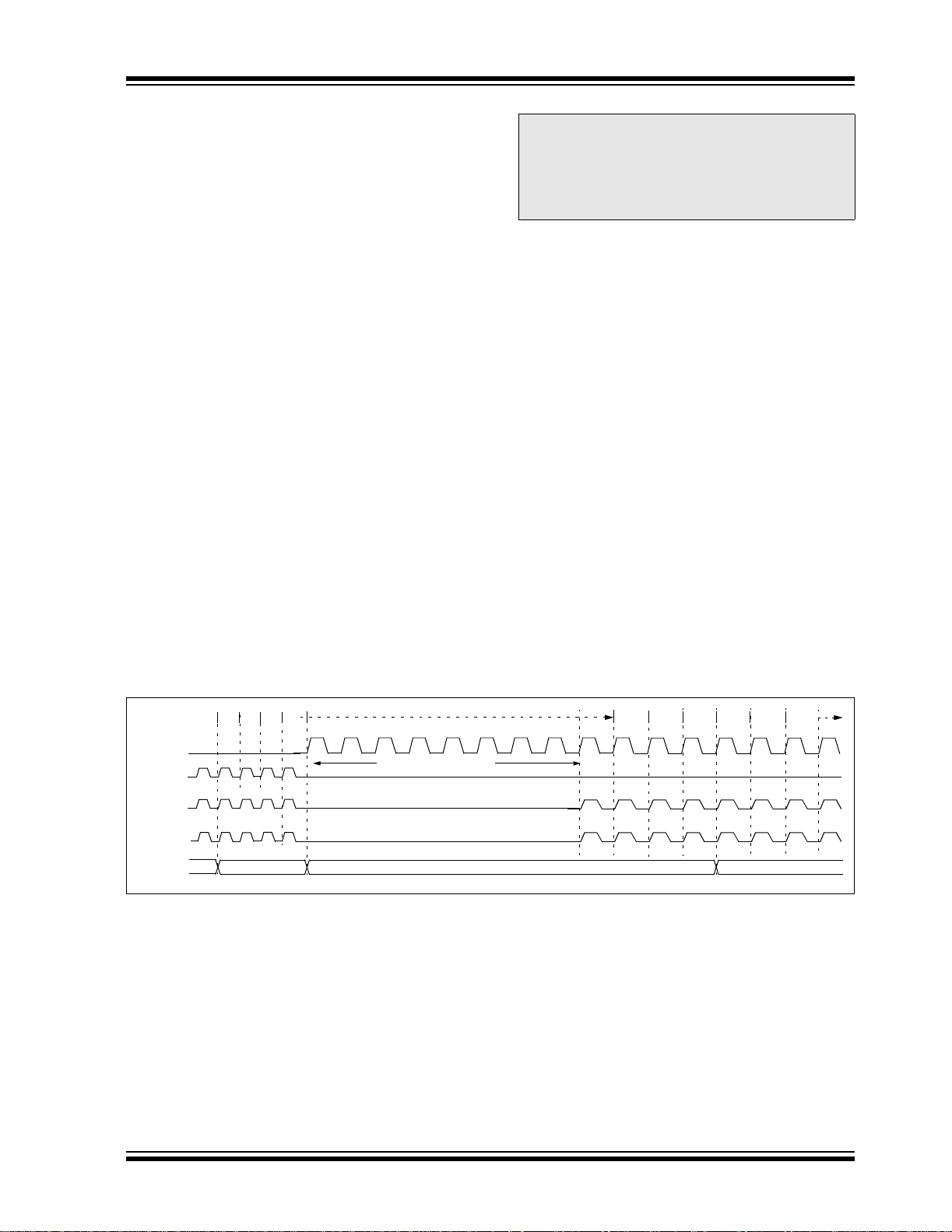
PIC18F1220/1320
3.4.3 RC_RUN MODE
In RC_RUN mode, the CPU and peripherals are
clocked from the internal oscillator block using the
INTOSC multiplexer and the primary clock is shut
down. When using the INTRC source, this mode provides the best power conservation of all the Run
modes, while still executing code. It works well for user
applications whic h are not h ighly tim ing sensiti ve, or do
not require high-speed clocks at all times.
If the primary clock source is the internal oscillator
block (either of the INTIO1 or INTIO2 os cillator s), there
are no distinguishable differences between PRI_RUN
and RC_RUN modes during execution. However, a
clock switch delay will occur during entry to and exit
from RC_RUN mode. Therefore, if the primary clock
source is the internal oscillator block, the use of
RC_RUN mode is not recommended.
This mode is ente red by c lea rin g th e IDLEN b it, se ttin g
SCS1 (SCS0 is ignored) and executing a SLEEP
instruction. The IRCF bits may select the clock
frequency before the SLEEP instruction is executed.
When the clock source is switched to the INTOSC
multiplexer (see Figure 3-10), the primary oscillator is
shut down and the OSTS bit is cleared.
The IRCF bits may be modified at any time to immediately change the system clock speed. Executing a
SLEEP instruction is not required to select a new clock
frequency from the INTOSC multiplexer.
Note: Caution should be used when modi fy ing a
single IRCF bit. If V
DD is less than 3V, it is
possible to select a higher clock speed
than is supported by the low VDD.
Improper device operation may result if
the VDD/FOSC specifications are violated.
If the IRCF bits are all clear, the INTOSC output is not
enabled and the IOFS bit wi ll remain clear; there will be
no indication of the current clock source. The INTRC
source is providing the system clocks.
If the IRCF bits are changed from all clear (thus,
enabling the INTOSC output), the IOFS bit becomes
set after the INTOSC out put becom es stab le. Clocks to
the system continue while the INTOSC source
stabilizes, in approximately 1ms.
If the IRCF bits were previously at a non-zero value
before the SLEEP instruction was executed and the
INTOSC source was already stable, the IOFS bit will
remain set.
When a wake event occurs , the system conti nues to be
clocked from the IN TO SC multiple xer while the primar y
clock is started. When the primary clock becomes
ready, a clock switch to the primary clock occurs (see
Figure 3-8). When the clock switch is complete, the
IOFS bit is cleared, the O STS bit is se t and the prim ary
clock is providing the system clock. The IDLEN and
SCS bits are not affected by the wake-up. The INTRC
source will continue to run if either the WDT or the
Fail-Safe Clock Monitor is enab led .
FIGURE 3-10: TIMING TRANSITION TO RC_RUN MODE
Q3Q2Q1
Q4
12345678
Clock Transition
PC + 2PC
INTRC
OSC1
CPU
Clock
Peripheral
Clock
Program
Counter
Q4
Q3Q2Q1 Q4 Q2Q1 Q3
PC + 4
2004 Microchip Technology Inc. DS39605C-page 27
Page 30

PIC18F1220/1320
3.4.4 EXIT TO IDLE MODE
An exit from a power managed Run mode to its
corresponding Idle mode is executed by setting the
IDLEN bit and executing a SLEEP instruction. The CPU
is halted at the beginning of the instruction follo wing the
SLEEP instruction. There are no changes to any of the
clock source status bits (OSTS, IOFS or T1RUN).
While the CPU is halte d, the periphe rals c ontin ue to b e
clocked from the previously selected clock source.
3.4.5 EXIT TO SLEEP MODE
An exit from a power managed Run mode to Sleep
mode is executed by clearing the IDLEN and
SCS1:SCS0 bits and executing a SLEEP instruction.
The code is no diff erent than the me thod used to invoke
Sleep mode from the normal operating (full power)
mode.
The primary clock and internal oscillator block are
disabled. The INTRC will continue to operate if the
WDT is enabled. The Timer1 oscillator will continue to
run, if enabled in the T1CON register (Register 12-1).
All clock source status bits are cleared (OSTS, IOFS
and T1RUN).
3.5 Wake from Power Managed Modes
An exit from any of the power managed modes is triggered by an interrupt, a Reset or a WDT time-out. This
section discusses the triggers that cause exits from
power managed modes. The clocking subsystem
actions are discussed in each of the power managed
modes (see Sections3.2 through 3.4).
Note: If application code is timing sensitive, it
should wait for the OSTS bi t to become set
before continuing. Use the interval during
the low-power exit sequence (before
OSTS is set) to perform timing insensitive
“housekeeping” tasks.
Device behavior during Low-Power mode exits is
summarized in Table 3-3.
3.5.1 EXIT BY INTERRUPT
Any of the available interrupt sources can cause the
device to exit a power managed mode and resume full
power operation. To enable this functionality, an interrupt source must be e nab le d by s etti ng its enable bit in
one of the INTCON or PIE register s. The exit sequenc e
is initiated when the corresponding interrupt flag bit is
set. On all exits from Low-Power mode by interrupt,
code execution branches to the interrupt vector if the
GIE/GIEH bit (INTCON<7>) is set. Otherwise, code
execution continues or resumes without branching
(see Section 9.0 “Interrupts”).
DS39605C-page 28 2004 Microchip Technology Inc.
Page 31

PIC18F1220/1320
TABLE 3-3: ACTIVITY AND EXIT DELAY ON WAKE FROM SLEEP MODE OR ANY IDLE MODE
(BY CLOCK SOURCES)
Clock in Power
Managed Mode
Primary System
Clock
(PRI_IDLE mode)
T1OSC or
(1)
INTRC
INTOSC
(2)
Sleep mode
Note 1: In this instance, refers specifically to the INTRC clock source.
2: Includes both the INTOSC 8 MHz source and postscaler derived frequencies.
3: Two-Speed Start-up is covered in greater detail in Section 19.3 “Two-Speed Start-up”.
4: Execution continues during the INTOSC stabilization period.
5: Required delay when waking from Sleep and all Idle modes. This delay runs concurrently with any other
required delays (see Section 3.3 “Idle Modes”).
Primary System
Clock
LP, XT, HS
HSPLL
EC, RC, INTRC
INTOSC
(1)
(2)
LP, XT, HS OST
HSPLL OST + 2 ms
EC, RC, INTRC
INTOSC
(1)
(2)
LP, XT, HS OST
HSPLL OST + 2 ms
EC, RC, INTRC
INTOSC
(1)
(2)
LP, XT, HS OST
HSPLL OST + 2 ms
EC, RC, INTRC
INTOSC
(1)
(2)
Power
Managed
Mode Exit
Delay
5-10 µs
5-10 µs
1ms
5-10 µs
Clock Ready
Status Bit
(OSCCON)
(5)
(5)
(4)
(5)
None IOFS
(5)
5-10 µs
(4)
1ms
OSTS
—
IOFS
OSTS
—
IOFS
OSTS
—
OSTS
—
IOFS
Activity during Wake-up from
Power Managed Mode
Exit by Interrupt Exit by Reset
CPU and peripherals
clocked by primary
clock and executing
Not clocked or
Two-Speed Start-up
(if enabled)
instructions.
CPU and peripherals
clocked by selected
power managed mo de
clock and executing
instructions until
primary clock source
becomes ready.
Not clocked or
Two-S pee d Start-up (if
enabled) until primary
clock source becomes
(3)
ready
.
(3)
.
2004 Microchip Technology Inc. DS39605C-page 29
Page 32

PIC18F1220/1320
3.5.2 EXIT BY RESET
Normally, the device is held in Reset by the Oscillator
Star t-up Timer (OST) until the primary clock (defi ned in
Configuration Register 1H) becomes ready. At that
time, the OSTS bit is set and the device begins
executing code.
Code execution can begin before the primary clock
becomes ready. If either the Two-Speed Start-up (see
Section 19.3 “Two-Speed Start-up”) or Fail-Safe
Clock Monitor (see Section 19.4 “Fail-Safe Clock
Monitor”) are enabled in Configuration Register 1H,
the device may begin execution as soon as the Reset
source has cleared. Execution is clocked by the
INTOSC multiplexer driven by the internal oscillator
block. Since the OSCCON register is cleared following
all Resets, the INTRC clock source is selected. A
higher speed clock may be selected by modifying the
IRCF bits in the OSCCON register. Execution is
clocked by the internal oscillator block until either the
primary clock becomes ready, or a power managed
mode is entered before the primary clock becomes
ready; the primary clock is then shut down.
3.5.3 EXIT BY WDT TIME-OUT
A WDT time-out will cause di ffe rent action s, dependin g
on which power managed mode the device is in when
the time-out occurs.
If the device is not executing code (all Idle modes and
Sleep mode), the time-out will result in a wake from the
power managed mode (see Sections 3.2 through 3.4).
If the device is executing code (all Run modes), the
time-out will result in a WDT Reset (see Section 1 9.2
“Watchdog Timer (WDT)”).
The WDT timer and postscaler are cleared by
executing a SLEEP or CLRWDT instruction, the loss of a
currently selected clock source (if the Fail-Safe Clock
Monitor is enabled) and modifying the IRCF bits in the
OSCCON register if the internal oscillator block is the
system clock source.
3.5.4 EXIT WITHOUT AN OSCILLATOR START-UP DELAY
Certain exits from power managed modes do not
invoke the OST at all. These are:
• PRI_IDLE mode, where the primary clock source
is not stopped; or
• the primary clock source is not any of LP, XT, HS
or HSPLL modes.
In these cases, the primary clock source either does
not require an oscillator start-up delay, since it is
already running (PRI_IDLE), or normally does not
require an oscillator start-up delay (RC, EC and INTIO
Oscillator modes).
However, a fixed delay (a ppro xi ma tel y 10 µs) following
the wake event is required w hen leaving Sleep an d Idle
modes. This delay is required for the CPU to prepare
for execution. Instruction ex ecution resumes on the first
clock cycle following this delay.
3.6 INTOSC Frequency Drift
The factory calibrates the internal oscillator block
output (INTOSC) for 8 MHz (see Table 22-6). However,
this frequency may drift as VDD or temperature
changes, which can affect the controller operation in a
variety of ways.
It is possible to adjust the INTOSC frequency by
modifying the value in the OSCTUNE register
(Register 2-1). This has the side effect that the INTRC
clock source frequency is also affected. However, the
features that use the INTRC source often do not require
an exact frequency . These features include the Fail-Safe
Clock Monitor, the Watchdog Timer and the RC_RUN/
RC_IDLE modes when the INTRC clock source is
selected.
Being able to adjust the INTOSC requires knowing
when an adjustment is required, in which direction it
should be made and in some cases, how large a
change is needed. Three examples follow but other
techniques may be used.
DS39605C-page 30 2004 Microchip Technology Inc.
Page 33

PIC18F1220/1320
3.6.1 EXAMPLE – EUSART
An adjustment may be indicated when the EUSART
begins to generate framing erro rs, or receives data with
errors while in Asynchronous mode. Framing errors
indicate that the system clock frequency is too high –
try decrementing the valu e in the OSCTUNE reg ister to
reduce the system clock frequency. Errors in data may
suggest that the system clock speed is too low –
increment OSCTUNE.
3.6.2 EXAMPLE – TIMERS
This technique compares system clock speed to some
reference clock. Two timers may be used; one timer is
clocked by the peripheral clock, while the other is
clocked by a fixed reference source, such as the
Timer1 oscillat or.
Both timers are cleared, but the timer clocked by the
reference generates interrupts. When an interrupt
occurs, the internally clocked timer is read and both
timers are cleared. If the internally clocked timer value
is greater than expected, then the internal oscillator
block is running too fast – decrement OSCTUNE.
3.6.3 EXAMPLE – CCP IN CAPTURE MODE
A CCP module can use free running Timer1 (or
Timer3), cl oc ked by the internal oscillator bl ock and an
external event with a known period (i.e., AC power
frequency). The time of the first event is capt ured in th e
CCPRxH:CCPRxL registers and is recorded for use
later. When the second event causes a capture, the
time of the first event is su btra cte d fro m the tim e of th e
second event. Since the period of the external event is
known, the time difference between events can be
calculated.
If the measured time is much greater than the
calculated time, the internal oscillator block is running
too fast – decrement OSCTUNE. If the measured time
is much less than the calculated time, the internal
oscillator block is running too slow – increment
OSCTUNE.
2004 Microchip Technology Inc. DS39605C-page 31
Page 34

PIC18F1220/1320
NOTES:
DS39605C-page 32 2004 Microchip Technology Inc.
Page 35

PIC18F1220/1320
4.0 RESET
Most registers are not affected by a WDT wake-up,
since this is viewed as the resumption of normal
The PIC18F1220/1320 devices differentiate between
various kinds of Reset:
a) Power-on Reset (POR)
b) MCLR
Reset during normal operation
c) MCLR Reset during Sleep
d) Watchdog Timer (WDT) Reset (during
execution)
e) Programmable Brown-out Reset (BOR)
f) RESET Instruction
g) Stack Full Reset
h) Stack Underflow Reset
Most registers are unaffected by a Reset. Their status
is unknown on POR and unchanged by all other
Resets. The other registers are forced to a “Reset
state”, depending on the type of Reset that occurred.
operation. Status bits from the RCON register
(Register 4-1), RI
, TO, PD, POR and BOR, are set or
cleared differently in different Reset situations, as
indicated in Table 4-2. These bits are used in software
to determine the nat ure of the R es et. See Table 4-3 for
a full description of the Reset states of all registers.
A simplified block di agram of the On-Chip Reset Circu it
is shown in Figure 4-1.
The Enhanced MCU devices have a MCLR
in the MCLR
Reset path. The filter will detect and
ignore small pulses.
The MCLR
pin is not driven low by any internal Resets,
including the WDT.
The MCLR input provided by the MCLR pin can be
disabled with the MCLRE bit in Configuration
Register 3H (CONFIG3H<7>).
FIGURE 4-1: SIMPLIFIED BLOCK DIAGRAM OF ON-CHIP RESET CIRCUIT
RESET
Instruction
Stack
Pointer
Stack Full/Underflow Reset
noise filter
External Reset
Sleep
WDT
DD Rise
Reset
OST
PWRT
MCLRE
POR Pulse
BOR
1024 Cycles
10-bit Ripple Counter
65.5 ms
11-bit Ripple Counter
MCLR
VDD
OSC1
Note 1: This is a separate oscillator from the RC oscillator of the CLKI pin.
( )_IDLE
Time-out
V
Detect
Brown-out
OST/PWRT
32 µs
(1)
INTRC
2: See Table 4-1 for time-out situations.
S
Chip_Reset
R
Q
Enable PWRT
Enable OST
(2)
2004 Microchip Technology Inc. DS39605C-page 33
Page 36

PIC18F1220/1320
4.1 Power-on Reset (POR)
A Power-on Reset pulse is generated on-chip when
DD rise is detected. To take advantage of the POR
V
circuitry, just tie the MCLR
10 kΩ) to V
DD. This will eliminate external RC compo-
pin through a resistor (1k to
nents usually needed to create a Power-on Reset
delay. A minimum rise rate for V
DD is specified
(parameter D004) . For a s low rise t ime, see F igure 4-2.
When the device st arts normal operation (i.e ., ex its the
Reset condition), device operating parameters (voltage, frequency, temperature, etc.) must be met to
ensure operation. If these conditions are not met, the
device must be held in Reset until the operating
conditions are met.
FIGURE 4-2: EXTERN AL POWER-ON
RESET CIRCUIT (FOR
SLOW V
DD
VDD
Note 1: External Power-on Rese t circuit is required
V
D
R
C
only if the V
The diode D helps discharge the capacitor
quickly when V
2: R < 40 kΩ is recommended to make sure that
the voltage drop across R does not violate
the device’s electrical specification.
3: R1 ≥ 1 kΩ will limit any current flowing into
MCLR
of MCLR/
static Discharge (ESD) or Electrical
Overstress (EOS).
DD power-up slope is too slow.
from external capacitor C, in the event
VPP pin breakdown due to Electro-
DD POWER-UP)
R1
MCLR
PIC18FXXXX
DD powers down.
4.2 Power-up Timer (PWRT)
The Power-up Timer (PWRT) of the PIC18F1220/1320 is
an 11-bit counte r, which uses the INTRC source as the
clock input. This yields a count of 2048 x 32 µs=65.6ms.
While the PWRT is counting, the device is held in Reset.
The power-up time delay will vary fr om chip-to-ch ip due
DD, temperature and process variation. See DC
to V
parameter 33 for details.
The PWRT is enabled by clearing configuration bit,
PWRTEN
.
4.3 Oscillator Start-up Timer (OST)
The Oscillator Start-up Timer (OST) provides a 1024
oscillator cycle (from OSC1 input) delay after the
PWRT delay is over (parameter 33). This ensures that
the crystal oscillator or resonator has started and
stabilized.
The OST time-out is invoked only for XT, LP, HS and
HSPLL modes and only on Power-on Reset, or on exit
from most low-power modes.
4.4 PLL Lock Time-out
With the PLL enabled in its PLL mode, the time-out
sequence following a Power-on Reset is slightly
different from other oscillator modes. A portion of the
Power-up Tim er is used to provi de a fixed time-ou t that
is sufficient f or the PLL to loc k to the main os cillator f requency. This PLL lock time-out (T
PLL) is typically 2 ms
and follows the Oscillator Start-up Time-out.
4.5 Brown-out Reset (BOR)
A configuration bit, BOR, can disable (if clear/
programmed), or enable (if set) the Brown-out Reset
circuitry. If V
greater than T
tion will reset the chip. A Reset may not occur if V
DD falls below VBOR (parameter D005) for
BOR (parameter 35), the b rown-out situ a-
DD
falls below VBOR for less than TBOR. The chip will
remain in Brown-out Reset until V
DD rises above VBOR .
If the Power-up T imer is enable d, it will be invo ked after
DD rises above VBOR; it then will keep the chip in
V
Reset for an additional time delay, T
PWRT
(parameter 33). If VDD drops below VBOR while the
Power-up Timer is running, the chip will go back into a
Brown-out Reset and the Power-up Timer will be init ialized. Once V
DD rises above VBOR, the Power-up Timer
will execute the additional time delay. Enabling BOR
Reset does not automatically enable the PWRT.
4.6 Time-out Sequence
On power-up, the time-out sequence is as follows:
First, after the POR pulse has cle are d, PWRT time-out
is invoked (if enab led). Then , the OST i s activated . The
total time-out wi ll var y base d o n oscill ator confi guratio n
and the status of the PWR T. For example, in RC mode
with the PWRT disabled , there will be no time-o ut at all.
Figure 4-3, Figure 4-4, Figure 4-5, Figure 4-6 and
Figure 4-7 depict time-out sequences on power-up.
Since the time-outs occur from the POR pulse, if M
is kept low long e nough, all ti me -out s will e xpire. Brin ging MCLR
high will begin execution immediately
(Figure 4-5). This is useful for testing purposes or to
synchronize more than one PIC18FXXXX device
operating in parallel.
Table 4-2 shows the Reset conditions for so me Specia l
Function Registers, while Table 4-3 shows the Reset
conditions for all the registers.
CLR
DS39605C-page 34 2004 Microchip Technology Inc.
Page 37

PIC18F1220/1320
TABLE 4-1: TIME-OUT IN VARIOUS SITUATIONS
Oscillator
Configuration
HSPLL 66 ms
PWRTEN = 0 PWRTEN = 1
(1)
+ 1024 TOSC + 2 ms
HS, XT, LP 66 ms
EC, ECIO 66 ms
RC, RCIO 66 ms
INTIO1, INTIO2 66 ms
Power-up
(1)
+ 1024 TOSC 1024 TOSC 1024 TOSC
(1)
(1)
(1)
Note 1: 66 ms (65.5 ms) is the nominal Power-up Timer (PWRT) delay.
2: 2 ms is the nominal time required for the 4x PLL to lock.
3: The program memory bias start-up time is always invoked on POR, wake-up from Sleep, or on any exit
from power managed mode that disables the CPU and instruction execution.
REGISTER 4-1: RCON REGISTER BITS AND POSITIONS
R/W-0 U-0 U-0 R/W-1 R/W-1 R/W-1 R/W-1 R/W-1
IPEN
bit 7 bit 0
Note: Refer to Section 5.14 “RCON Register” for bit definitions.
— —RITO PD POR BOR
(2)
and Brown-out
(2)
1024 TOSC + 2 ms
5-10 µs
5-10 µs
5-10 µs
(3)
(3)
(3)
(2)
Low-Power Mode
1024 TOSC + 2 ms
Exit from
5-10 µs
5-10 µs
5-10 µs
(3)
(3)
(3)
(2)
TABLE 4-2: STATUS BITS, THEIR SIGNIFICANCE AND THE INITIALIZATION CONDITION FOR
RCON REGISTER
Condition
Program
Counter
Power-on Reset 0000h 0--1 1100 1 1 1 0 0 0 0
RESET Instruction 0000h 0--0 uuuu 0 u u u u u u
Brown-out 0000h 0--1 11u- 1 1 1 u 0 u u
during Power Managed
MCLR
0000h 0--u 1uuu u 1 u u u u u
Run modes
MCLR during Power Managed
0000h 0--u 10uu u 1 0 u u u u
Idle modes and Sleep
WDT Time-out during Full
0000h 0--u 0uuu u 0 u u u u u
Power or Power Managed Run
during Full Power
MCLR
Execution
Stack Full Reset (STVR = 1) 1u
0000h 0--u uuuu u u u u u
Stack Underflow Reset
(STVR = 1)
Stack Underflow Error (not an
0000h u--u uuuu u u u u u u 1
actual Reset, STVR = 0)
WDT Time-out during Power
PC + 2 u--u 00uu u 0 0 u u u u
Managed Idle or Sleep
Interrupt Exit from Power
PC + 2 u--u u0uu u u 0 u u u u
Managed modes
Legend: u = unchanged, x = unknown, – = unimplemented bit, read as ‘0’
Note 1: When the wake-up is due to an interrupt and the GIEH or GIEL bits are set, the PC is loaded with the
interrupt vector (0x00000 8h or 0x00 001 8h ).
RCON
Register
TO PD POR BOR STKFUL STKUNF
RI
uu
u1
2004 Microchip Technology Inc. DS39605C-page 35
Page 38

PIC18F1220/1320
TABLE 4-3: INITIALIZATION CONDITIONS FOR ALL REGISTERS
Resets
MCLR
Register
Applicable
Devices
TOSU 1220 1320 ---0 0000 ---0 0000 ---0 uuuu
TOSH 1220 1320 0000 0000 0000 0000 uuuu uuuu
TOSL 1220 1320 0000 0000 0000 0000 uuuu uuuu
STKPTR 1220 1320 00-0 0000 00-0 0000 uu-u uuuu
PCLATU 1220 1320 ---0 0000 ---0 0000 ---u uuuu
PCLATH 1220 1320 0000 0000 0000 0000 uuuu uuuu
PCL 1220 1320 0000 0000 0000 0000 PC + 2
TBLPTRU 1220 1320 --00 0000 --00 0000 --uu uuuu
TBLPTRH 1220 1320 0000 0000 0000 0000 uuuu uuuu
TBLPTRL 1220 1320 0000 0000 0000 0000 uuuu uuuu
TABLAT 1220 1320 0000 0000 0000 0000 uuuu uuuu
PRODH 1220 1320 xxxx xxxx uuuu uuuu uuuu uuuu
PRODL 1220 1320 xxxx xxxx uuuu uuuu uuuu uuuu
INTCON 1220 1320 0000 000x 0000 000u uuuu uuuu
INTCON2 1220 1320 1111 -1-1 1111 -1-1 uuuu -u-u
INTCON3 1220 1320 11-0 0-00 11-0 0-00 uu-u u-uu
INDF0 1220 1320 N/A N/A N/A
POSTINC0 1220 1320 N/A N/A N/A
POSTDEC0 1220 1320 N/A N/A N/A
PREINC0 1220 1320 N/A N/A N/A
PLUSW0 1220 1320 N/A N/A N/A
FSR0H 1220 1320 ---- 0000 ---- 0000 ---- uuuu
FSR0L 1220 1320 xxxx xxxx uuuu uuuu uuuu uuuu
WREG 1220 1320 xxxx xxxx uuuu uuuu uuuu uuuu
INDF1 1220 1320 N/A N/A N/A
POSTINC1 1220 1320 N/A N/A N/A
POSTDEC1 1220 1320 N/A N/A N/A
PREINC1 1220 1320 N/A N/A N/A
PLUSW1 1220 1320 N/A N/A N/A
FSR1H 1220 1320 ---- 0000 ---- 0000 ---- uuuu
FSR1L 1220 1320 xxxx xxxx uuuu uuuu uuuu uuuu
Legend: u = unchanged, x = unknown, - = unimplemented bit, read as ‘0’, q = value depends on condition.
Shaded cells indicate condi tions do not apply for the designated device.
Note 1: One or more bits in the INTCONx or PIRx registers will be affected (to cause wake-up).
2: When the wake-up is due to an interrupt and the GIEL or GIEH bit is set, the PC is loaded with the
interrupt vector (0008h or 0018h).
3: When the wake-up is due to an interrupt a nd the G IEL or G IEH b it i s s et, the TOSU, TOSH and TO SL a re
updated with the current value of the PC. The STKPTR is modified to point to the next location in the
hardware stack.
4: See Table 4-2 for Reset value for specific condition.
5: Bits 6 and 7 of PORTA, LATA and TRISA are enabled, depending on the Oscillator mode selected. When
not enabled as PORTA pins, they are disabled and read ‘0’.
6: Bit 5 of PORTA is enabled if MCLR
Power-on Reset,
Brown-out Reset
is disabled.
WDT Reset
RESET Instruction
Stack Resets
Wake-up via WDT
or Interrupt
(3)
(3)
(3)
(3)
(2)
(1)
(1)
(1)
DS39605C-page 36 2004 Microchip Technology Inc.
Page 39

PIC18F1220/1320
TABLE 4-3: INITIALIZATION CONDITIONS FOR ALL REGISTERS (CONTINUED)
Resets
MCLR
Register
BSR 1220 1320 ---- 0000 ---- 0000 ---- uuuu
INDF2 1220 1320 N/A N/A N/A
POSTINC2 1220 1320 N/A N/A N/A
POSTDEC2 1220 1320 N/A N/A N/A
PREINC2 1220 1320 N/A N/A N/A
PLUSW2 1220 1320 N/A N/A N/A
FSR2H 1220 1320 ---- 0000 ---- 0000 ---- uuuu
FSR2L 1220 1320 xxxx xxxx uuuu uuuu uuuu uuuu
STATUS 1220 1320 ---x xxxx ---u uuuu ---u uuuu
TMR0H 1220 1320 0000 0000 0000 0000 uuuu uuuu
TMR0L 1220 1320 xxxx xxxx uuuu uuuu uuuu uuuu
T0CON 1220 1320 1111 1111 1111 1111 uuuu uuuu
OSCCON 1220 1320 0000 q000 0000 q000 uuuu qquu
LVDCON 1220 1320 --00 0101 --00 0101 --uu uuuu
WDTCON 1220 1320 ---- ---0 ---- ---0 ---- ---u
(4)
RCON
TMR1H 1220 1320 xxxx xxxx uuuu uuuu uuuu uuuu
TMR1L 1220 1320 xxxx xxxx uuuu uuuu uuuu uuuu
T1CON 1220 1320 0000 0000 u0uu uuuu uuuu uuuu
TMR2 1220 1320 0000 0000 0000 0000 uuuu uuuu
PR2 1220 1320 1111 1111 1111 1111 1111 1111
T2CON 1220 1320 -000 0000 -000 0000 -uuu uuuu
ADRESH 1220 1320 xxxx xxxx uuuu uuuu uuuu uuuu
ADRESL 1220 1320 xxxx xxxx uuuu uuuu uuuu uuuu
ADCON0 1220 1320 00-0 0000 00-0 0000 uu-u uuuu
ADCON1 1220 1320 -000 0000 -000 0000 -uuu uuuu
ADCON2 1220
CCPR1H 1220 1320 xxxx xxxx uuuu uuuu uuuu uuuu
CCPR1L 1220 1320 xxxx xxxx uuuu uuuu uuuu uuuu
CCP1CON
PWM1CON 1220 1320 0000 0000 0000 0000 uuuu uuuu
ECCPAS 1220 1320 0000 0000 0000 0000 uuuu uuuu
Legend: u = unchanged, x = unknown, - = unimplemented bit, read as ‘0’, q = value depends on condition.
Shaded cells indicate condi tions do not apply for the designated device.
Note 1: One or more bits in the INTCONx or PIRx registers will be affected (to cause wake-up).
2: When the wake-up is due to an interrupt and the GIEL or GIEH bit is set, the PC is loaded with the
interrupt vector (0008h or 0018h).
3: When the wake-up is due to an interrupt a nd the G IEL or G IEH b it i s s et, the TOSU, TOSH and TO SL a re
updated with the current value of the PC. The STKPTR is modified to point to the next location in the
hardware stack.
4: See Table 4-2 for Reset value for specific condition.
5: Bits 6 and 7 of PORTA, LATA and TRISA are enabled, depending on the Oscillator mode selected. When
not enabled as PORTA pins, they are disabled and read ‘0’.
6: Bit 5 of PORTA is enabled if MCLR
Applicable
Devices
1220 1320 0--1 11q0 0--q qquu u--u qquu
1320 0-00 0000 0-00 0000 u-uu uuuu
1220 1320 0000 0000 0000 0000 uuuu uuuu
Power-on Reset,
Brown-out Reset
is disabled.
WDT Reset
RESET Instruction
Stack Resets
Wake-up via WDT
or Interrupt
2004 Microchip Technology Inc. DS39605C-page 37
Page 40

PIC18F1220/1320
TABLE 4-3: INITIALIZATION CONDITIONS FOR ALL REGISTERS (CONTINUED)
Resets
MCLR
Register
Applicable
Devices
TMR3H 1220 1320 xxxx xxxx uuuu uuuu uuuu uuuu
TMR3L 1220 1320 xxxx xxxx uuuu uuuu uuuu uuuu
T3CON 1220 1320 0-00 0000 u-uu uuuu u-uu uuuu
SPBRGH 1220 1320 0000 0000 0000 0000 uuuu uuuu
SPBRG 1220 1320 0000 0000 0000 0000 uuuu uuuu
RCREG 1220 1320 0000 0000 0000 0000 uuuu uuuu
TXREG 1220 1320 0000 0000 0000 0000 uuuu uuuu
TXSTA 1220 1320 0000 0010 0000 0010 uuuu uuuu
RCSTA 1220 1320 0000 000x 0000 000x uuuu uuuu
BAUDCTL 1220 1320 -1-1 0-00 -1-1 0-00 -u-u u-uu
EEADR 1220 1320 0000 0000 0000 0000 uuuu uuuu
EEDATA 1220 1320 0000 0000 0000 0000 uuuu uuuu
EECON2 1220 1320 0000 0000 0000 0000 0000 0000
EECON1 1220 1320 xx-0 x000 uu-0 u000 uu-0 u000
IPR2 1220 1320 1--1 -11- 1--1 -11- u--u -uu-
PIR2 1220 1320 0--0 -00- 0--0 -00- u--u -uu-
PIE2 1220 1320 0--0 -00- 0--0 -00- u--u -uu-
IPR1 1220 1320 -111 -111 -111 -111 -uuu -uuu
PIR1 1220 1320 -000 -000 -000 -000 -uuu -uuu
PIE1 1220 1320 -000 -000 -000 -000 -uuu -uuu
OSCTUNE 1220 1320 --00 0000 --00 0000 --uu uuuu
TRISB 1220 1320 1111 1111 1111 1111 uuuu uuuu
TRISA
(5)
1220 1320 11-1 1111
LATB 1220 1320 xxxx xxxx uuuu uuuu uuuu uuuu
(5)
LATA
1220 1320 xx-x xxxx
PORTB 1220 1320 xxxx xxxx uuuu uuuu uuuu uuuu
PORT A
(5,6)
1220 1320 xx0x 0000
Legend: u = unchanged, x = unknown, - = unimplemented bit, read as ‘0’, q = value depends on condition.
Shaded cells indicate condi tions do not apply for the designated device.
Note 1: One or more bits in the INTCONx or PIRx registers will be affected (to cause wake-up).
2: When the wake-up is due to an interrupt and the GIEL or GIEH bit is set, the PC is loaded with the
interrupt vector (0008h or 0018h).
3: When the wake-up is due to an interrupt a nd the G IEL or G IEH b it i s s et, the TOSU, TOSH and TO SL a re
updated with the current value of the PC. The STKPTR is modified to point to the next location in the
hardware stack.
4: See Table 4-2 for Reset value for specific condition.
5: Bits 6 and 7 of PORTA, LATA and TRISA are enabled, depending on the Oscillator mode selected. When
not enabled as PORTA pins, they are disabled and read ‘0’.
6: Bit 5 of PORTA is enabled if MCLR
Power-on Reset,
Brown-out Reset
(5)
(5)
(5,6)
is disabled.
WDT Reset
RESET Instruction
Stack Resets
11-1 1111
uu-u uuuu
uu0u 0000
(5)
(5)
(5,6)
Wake-up via WDT
or Interrupt
uu-u uuuu
uu-u uuuu
uuuu uuuu
(1)
(1)
(5)
(5)
(5,6)
DS39605C-page 38 2004 Microchip Technology Inc.
Page 41

PIC18F1220/1320
FIGURE 4-3: TIME-OUT SEQUENCE ON POWER-UP (MCLR TIED TO VDD, VDD RISE < TPWRT)
VDD
MCLR
INTERNAL POR
TPWRT
PWRT TIME-OUT
OST TIME-OUT
INTERNAL RESET
TOST
FIGURE 4-4: TIME-OUT SEQUENCE ON POWER-UP (MCLR
VDD
MCLR
INTERNAL POR
PWRT TI ME-OUT
OST TIME-OUT
INTERNAL RESET
TPWRT
NOT TIED TO VDD): CASE 1
TOST
FIGURE 4-5: TIME-OUT SEQUENCE ON POWER-UP (MCLR
VDD
MCLR
INTERNAL POR
TPWRT
PWRT TIME-OUT
OST TIME-OUT
INTERNAL RESET
2004 Microchip Technology Inc. DS39605C-page 39
NOT TIED TO VDD): CASE 2
TOST
Page 42

PIC18F1220/1320
FIGURE 4-6: SLOW RISE TIME (MCLR TIED TO VDD, VDD RISE > TPWRT)
5V
VDD
MCLR
INTERNAL POR
0V
PWRT
T
1V
PWRT TIME-OUT
OST TIME-OUT
INTERNAL RES ET
TOST
FIGURE 4-7: TIME-OUT SEQUENCE ON POR W/PLL ENABLED (MCLR TIED TO VDD)
VDD
MCLR
INTERNAL POR
TPWRT
PWRT TIME-OUT
OST TIME-OUT
PLL TIME-OUT
TOST
TPLL
INTERNAL RESET
Note: TOST = 1024 clock cycles.
T
PLL ≈ 2 ms max. First three stages of the PWRT timer.
DS39605C-page 40 2004 Microchip Technology Inc.
Page 43

PIC18F1220/1320
5.0 MEMORY ORGANIZATION
There are three memory types in Enhanced MCU
devices. These memory types are :
• Program Memory
• Data RAM
• Data EEPROM
Data and program memory use separate busses,
which allows for concurrent access of these types.
Additional det ailed infor mation for F lash program mem-
ory and data EEPROM is provided in Section 6.0
“Flash Program Memory” and Section 7.0 “Data
EEPROM Memory”, respectively.
FIGURE 5-1: PROGRAM MEMORY MAP
AND STACK FOR
PIC18F1220
PC<20:0>
CALL,RCALL,RETURN
RETFIE,RETLW
Stack Level 1
Stack Level 31
Reset Vector
High Priority Interrupt Vector
Low Priority Interrupt Vector
21
•
•
•
0000h
0008h
0018h
5.1 Program Memory Organization
A 21-bit progra m count er is capab le of addr essin g the
2-Mbyte program m emo ry space. Accessing a loca tion
between the physically implemented memory and the
2-Mbyte address will cause a read of all ‘0’s (a NOP
instruction).
The PIC18F1220 has 4Kbytes of Flash memory and
can store up to 2,048 single-word instructions.
The PIC18F1320 has 8Kbytes of Flash memory and
can store up to 4,096 single-word instructions.
The Reset vector address is at 0000h and the interru pt
vector addresses are at 0008h and 0018h.
The program memory maps for the PIC18F1220 and
PIC18F1320 devices are shown in Figure 5-1 and
Figure 5-2, respectively.
FIGURE 5-2: PROGRAM MEMORY MAP
AND STACK FOR
PIC18F1320
PC<20:0>
CALL,RCALL,RETURN
RETFIE,RETLW
Stack Level 1
Stack Level 31
Reset Vector
High Priority Interrupt Vector
Low Priority Interrupt Vector
21
•
•
•
0000h
0008h
0018h
On-Chip
Program Memory
Read ‘0’
0FFFh
1000h
1FFFFFh
200000h
On-Chip
Program Memory
1FFFh
2000h
User Memory Space
Read ‘0’
1FFFFFh
200000h
User Memory Space
2004 Microchip Technology Inc. DS39605C-page 41
Page 44

PIC18F1220/1320
5.2 Return Address Stack
The return address s tack allows any combination of up
to 31 program calls and interrupts to occur. The PC
(Program Counter) is pushed onto the stack when a
CALL or RCALL instruction is executed, or an interrupt
is Acknowledged. The PC value is pulled off the stack
on a RETURN, RETLW or a RETFIE instruction. PCLATU
and PCLATH are not affected by any of the RETURN or
CALL instructions.
The stack operates as a 31-word by 21-bit RAM and a
5-bit stack pointer, with the Stack Pointer initialized to
B after all Resets. There is no RAM associated
00000
with St ac k Poin ter, 00000
During a CALL type instruc tion, causing a pu sh onto the
stack, the Stack Pointer is first incremented and the
RAM location pointed to by the Stack Pointer
(STKPTR) registe r is written with the contents o f the PC
(already pointing to th e instructio n following the CALL).
During a RETURN type instruction, causing a pop from
the stack, the contents of the RAM location pointed to
by the STKPTR are transferred to the PC and then the
Stack Pointer is decremented.
The stack space is not part of either program or data
space. The Stack Pointer is readable and writable and
the address on the top of the stack is readable and
writable through the top-of-stack Special File
Registers. Data can also be pushed to or popped from
the stack using the top-of-stack SFRs. Status bits
indicate if the stack is full, has overflowed or
underflowed.
5.2.1 TOP-OF-STACK ACCESS
The top of the stack is readable and writable. Three
register locations, TOSU, TOSH and TOSL, hold the
contents of the stack location pointed to by the
STKPTR register (Figure 5-3). This allows users to
implement a software st a ck if ne cess ary. After a CALL,
RCALL or interrupt, the software can read the pushed
value by reading the TOSU, TO SH and TOSL regis ters.
These values can b e placed on a user define d software
stack. At return time, the software can replace the
TOSU, TOSH and TOSL and do a return.
The user must disable the global interrupt enable bits
while accessing the stack to prevent inadvertent stack
corruption.
B. This is only a Re se t value.
5.2.2 RETURN STAC K POINTER (STKPTR)
The STKPTR register (Re giste r 5-1) contains the stack
pointer value, the STKFUL (Stack Full) status bit and
the STKUNF (Stack Underflow) status bits. The value
of the Stack Pointer can be 0 through 31. The Stack
Pointer increments before values are pushed onto the
stack and decrements after values are popped off the
stack. At Reset, the Stack Pointer value will be zero.
The user may read and write the Stack Pointer value.
This feature can be used by a Real-Time Operating
System for return stack maintenance.
After the PC is pus hed on to the st ack 31 tim es (wi thout
popping any values off the stack), the STKFUL bit is
set. The STKFUL bit is cleared by software or by a
POR.
The action that takes place when the stack becomes
full depends on the state of the STVR (Stack Overflow
Reset Enable) configurat ion bit. (Refer to Section 19.1
“Configuration Bits” for a description of the device
configuration bits.) If STVR is set (default), the 31st
push will push the ( PC + 2) valu e onto the st ack, se t the
STKFUL bit and reset the device. The STKFUL bit will
remain set and the Stack Pointer will be set to zero.
If STVR is cleared, the STKFUL bit will be set on the
31st push and the Stack Pointer will increment to 31.
Any additional pushes will not overwrite the 31st push
and STKPTR will remain at 31.
When the stack has been popped enough times to
unload the stac k, the next pop will ret urn a value of zero
to the PC and sets the STKUNF bit, while the Stack
Pointer remains at zero. The STKUNF bit will remain
set until cleared by software or a POR occurs.
Note: Returning a value of zero to the PC on an
underflow has the effect of vectoring the
program to the Reset vector, where the
stack conditions can be verified and
appropriate actions can be taken. This is
not the same as a Reset, as the contents
of the SFRs are not affected.
FIGURE 5-3: RETURN ADDRESS STACK AND ASSOCIATED REGISTERS
Return Address S t ac k
11111
11110
TOSLTOSHTOSU
34h1Ah00h
Top-of-Stack
DS39605C-page 42 2004 Microchip Technology Inc.
001A34h
000D58h
11101
00011
00010
00001
00000
STKPTR<4:0>
00010
Page 45

REGISTER 5-1: STKPTR REGISTER
R/C-0 R/C-0 U-0 R/W-0 R/W-0 R/W-0 R/W-0 R/W-0
STKFUL STKUNF
bit 7 bit 0
PIC18F1220/1320
— SP4 SP3 SP2 SP1 SP0
(1)
bit 7
(1)
bit 6
bit 5 Unimplemented: Read as ‘0’
bit 4-0 SP4:SP0: Stack Pointer Location bits
STKFUL: Stack Full Flag bit
1 = Stack became full or overflowed
0 = Stack has not become full or overflowed
STKUNF: Stack Underflow Flag bit
1 = Stack underflow occurred
0 = Stack underflow did not occur
Note 1: B it 7 and bit 6 are cleared by user software or by a P OR.
Legend:
R = Readable bit W = Writable bit U = Unimplemented C = Clearable only bit
-n = Value at POR ‘1’ = Bit is set ‘0’ = Bit is cleared x = Bit is unknown
5.2.3 PUSH AND POP INSTRUCTIONS
Since the Top-of-Stack (TOS) is rea dab le a nd w ritable,
the ability to push valu es onto the stack and pull va lues
off the sta ck, withou t disturbi ng normal program ex ecution, is a desirable optio n. To push the current PC value
onto the stack, a PUSH instruction can be executed.
This will increment the Stack Pointer and load the current PC value onto the stack. TOSU, TOSH and TOSL
can then be modified to place data or a return address
on the stack.
The ability to pull the TOS value off of the stack and
replace it with the value that was previously pushed
onto the stack, without disturbing normal execution, is
achieved by using the POP inst ruction. T he POP instru ction discards the current TOS by decrementing the
Stack Pointer. The previous value pushed onto the
stack then becomes the TOS value.
5.2.4 STACK FULL/UNDERFLOW RESETS
These Resets are enabled by programming the STVR
bit in Configuration Register 4L. When the STVR bit is
cleared, a full or unde rflo w co ndi tion will set the appropriate STKFUL or STKUNF bit, but not cause a device
Reset. When the STVR bit is set, a full or underflow
condition will set the appropriate STKFUL or STKUNF
bit and then cause a device Reset. The STKFUL or
STKUNF bits are cleared by the user software or a
Power-on Reset.
2004 Microchip Technology Inc. DS39605C-page 43
Page 46

PIC18F1220/1320
5.3 Fast Register Stack
A “fast return” option is available for interrupts. A fast
register stack is provided for the Status, WREG and
BSR registers and is only one in depth. The sta ck is not
readable or writable and is loaded with the current
value of the correspo nding regi ster when the pro cessor
vectors for an interrupt. The values in the registers are
then loaded back into the working registers, if the
RETFIE, FAST instruction is used to return from the
interrupt.
All interrupt sources will push values into the stack
registers. If both low and high priority interrupts are
enabled, the stack registers cannot be used reliably to
return from low priority interrupt s. If a high pri ority interrupt occurs while servicing a low priority interrupt, the
stack register v al ues s tor ed by the l ow p riori ty in terru pt
will be overwritten. Users must save the key registers
in software during a low priority interrupt.
If interrupt priority is not used, all interrupts ma y use the
fast register stack for returns from interrupt.
If no interrupts are used, the fast register stack can be
used to restore the S tatus, WR EG and BSR registers at
the end of a subroutine call. To use the fast register
stack for a subroutine call, a CALL LABEL, FAST
instruction must be executed to save the Status,
WREG and BSR registers to the fast register stack. A
RETURN, FAST instruction is then ex ec uted to re sto r e
these registers from the fast register stack.
Example 5-1 shows a source code example that uses
the fast register stack during a subroutine call and
return.
5.4 PCL, PCLATH and PCLATU
The Program Counter (PC) s pecifies the ad dress of the
instruction to fetch for execution. The PC is 21-bits
wide. The low byte, known as the PCL register, is both
readable and writable. The high byte, or PCH register,
contains the PC<15 :8> bit s and is not direc tly read able
or writable. Updates to the PCH register may be performed through the PCLATH register. The upper byte i s
called PCU. This register contains the PC<20:16> bits
and is not directly readable or writable. Updates to the
PCU register may be performed through the PCLATU
register.
The contents of PCLATH and PCLATU will be
transferred to the program counter by any operation
that writes PCL. Similarly, the upper two bytes of the
program counter will be transferred to PCLATH and
PCLATU by an operation that reads PCL. This is useful
for computed offsets to the PC (see Section 5.8.1
“Computed GOTO”).
The PC addresses bytes in the program memory. To
prevent the PC from becoming misaligned with word
instructions, the LSB of PCL is fixed to a value of ‘0’.
The PC increments by 2 to address sequential
instructions in the program memo ry.
The CALL, RCALL, GOTO and program branch instructions write to the program counter directly. For these
instructions, the contents of PCLATH and PCLATU are
not transferred to the program counter.
EXAMPLE 5-1: FAST REGISTER STACK
CODE EXAMPLE
CALL SUB1, FAST ;STATUS, WREG, BSR
•
•
SUB1 •
•
RETURN, FAST ;RESTORE VALUES SAVED
;SAVED IN FAST REGISTER
;STACK
;IN FAST REGISTER STACK
DS39605C-page 44 2004 Microchip Technology Inc.
Page 47

PIC18F1220/1320
5.5 Clocking Scheme/Instruction Cycle
The clock input (from OSC1) is internally divided by
four to generate four non-overlapping quadrature
clocks, namely Q1, Q2, Q3 and Q4. Internally, the
Program Cou nter (PC) is increme nted every Q1, the
instruction is fetched from the program memory and
latched into the instruction register in Q4. The instruction is decoded and executed during the following Q1
through Q4. The clocks and instruction execution flow
are shown in Figure5-4.
FIGURE 5-4: CLOCK/INSTRUCTION CYCLE
Q2 Q3 Q4
Q1
OSC1
Q1
Q2
Q3
Q4
PC
OSC2/CLKO
Q1
5.6 Instruction Flow/Pipelining
An “Instruction Cycle” consists of four Q cycles (Q1,
Q2, Q3 and Q4). The instruc tio n fetch and execute are
pipelined such that fetch takes one instruction cycle,
while decode and execute takes another instruction
cycle. However, due to the pipelining, each instruction
effectively executes in one cycle. If an instruction
causes the program counter to change (e.g., GOTO),
then two cycles are req uired to c omplete the ins truction
(Example 5-2).
A fetch cycle begins with the Program Counter (PC)
incrementing in Q1.
In the execution cy cle, the fetch ed instruction i s latched
into the “Instruction Register” (IR) in cycle Q1. This
instruction is then decoded and executed during the
Q2, Q3 and Q4 c ycles. Dat a m emory is read during Q2
(operand read) and written during Q4 (destination
write).
Q2 Q3 Q4
Q2 Q3 Q4
Q1
EXAMPLE 5-2: INSTRUCTION PIPELINE FLOW
2004 Microchip Technology Inc. DS39605C-page 45
Page 48

PIC18F1220/1320
5.7 Instructions in Program Memory
The program memory is addressed in bytes. Instructions are stored as two bytes or four bytes in program
memory. The Least Significant Byte of an instruction
word is always stored in a program memory location
with an even address (LSB= 0). Figure 5-5 shows an
example of how instructi on words are stored in the program memory. To maintain alignment with instruction
boundaries, the PC increments in steps of 2 and the
LSB will always read ‘0’ (see Section 5.4 “PCL,
PCLATH and PCLATU”).
The CALL and GOTO instructions have the absolute
program memory address embedded into the instruction. Since instructions are always stored on word
boundaries, the data contained in the instruction is a
word address. The word address is written to
PC<20:1>, which ac cesses the desired byte a ddress in
program memory. Instruction #2 in Figure 5-5 shows
how the instruction ‘GOTO 000006h’ is encoded in th e
program memory. Program branch instructions, which
encode a relative address offset, operate in the same
manner . The offset value stored in a br an ch ins truc tio n
represents the number of single-word instructions that
the PC will be of fse t by. Section 20.0 “Instruction Set
Summary” provides further details of the instruction
set.
FIGURE 5-5: INS TRUCTIONS IN PROGRAM MEMORY
LSB = 1 LSB = 0 ↓
0Fh 55h 000008h
EFh 03h 00000Ah
F0h 00h 00000Ch
C1h 23h 00000Eh
F4h 56h 000010h
Instruction 1:
Instruction 2:
Instruction 3:
Program Memory
Byte Locations
MOVLW 055h
GOTO 000006h
MOVFF 123h, 456h
→
Word Address
000000h
000002h
000004h
000006h
000012h
000014h
5.7.1 TWO-WORD INSTRUCTIONS
PIC18F1220/1320 devices have four two-word
instructions: MOVFF, CALL, GOTO and LFSR. The se cond
word of these instructions has the 4 MSBs set to ‘1’s and
is decoded as a NOP instruction. The lower 12 bit s of the
second word contain data to be used by the instruction.
If the first word of the instruction is executed, the data in
instruction is executed by itself (first word was skipped),
it will execute as a NOP. This action is necessary when
the two-word instruction is preceded by a conditional
instruction that results in a skip operation. A program
example that demonstrates this concept is shown in
Example 5-3. Refer to Section 20.0 “Instruction Set
Summary” for further details of the instruction set.
the second word is accessed. If the second word of the
EXAMPLE 5-3: TWO-WORD INSTRUCTIONS
CASE 1:
Object Code Source Code
0110 0110 0000 0000 TSTFSZ REG1 ; is RAM location 0?
1100 0001 0010 0011 MOVFF REG1, REG2 ; No, skip this word
1111 0100 0101 0110 ; Execute this word as a NOP
0010 0100 0000 0000 ADDWF REG3 ; continue code
CASE 2:
Object Code Source Code
0110 0110 0000 0000 TSTFSZ REG1 ; is RAM location 0?
1100 0001 0010 0011 MOVFF REG1, REG2 ; Yes, execute this word
1111 0100 0101 0110 ; 2nd word of instruction
0010 0100 0000 0000 ADDWF REG3 ; continue code
DS39605C-page 46 2004 Microchip Technology Inc.
Page 49

PIC18F1220/1320
5.8 Look-up Tables
Look-up tables are implemented two ways:
• Computed GOTO
• Table Reads
5.8.1 COMPUTED GOTO
A computed GOTO is accomplish ed by adding an offset
to the program counter (see Example 5-4).
A look-up table can be formed with an ADDWF PCL
instruction and a group of RETLW 0xnn instructions.
WREG is loaded with an offset into the table before
executing a call to tha t t able. The first instructi on of th e
called routine is the ADDWF PCL instruction. The next
instruction executed will be one of the RETLW 0xnn
instructions, that returns the value 0xnn to the calling
function.
The offset value (in WREG) specifies the number of
bytes that the program counter should advance and
should be multiples of 2 (LSB = 0).
In this method, only one data byte may be stored in
each instruction location and room on the return
address stack is required.
EXAMPLE 5-4: COMPUTED GOTO USING
AN OFFSET VALUE
MOVFW OFFSET
CALL TABLE
ORG 0xnn00
TABLE ADDWF PCL
RETLW 0xnn
RETLW 0xnn
RETLW 0xnn
.
.
.
5.8.2 TABLE READS/TABLE WRITES
A better method of storing data in program memory
allows two bytes of dat a to be stored in each instruction
location.
Look-up table data may be stored two bytes per program word by using table reads and writes. The Table
Pointer (TBLPTR) register specifies the byte address
and the Table Latch (TABLAT) register contains the
data that is read from or wr itten to progr am memory.
Data is transferred to/from program memory, one byte
at a time.
The table read/table write operation is discussed
further in Section 6.1 “Table Reads and Table
Writes”.
5.9 Data Memory Organization
The data memory is im ple me nte d as st atic RAM. Each
register in the data memory has a 12-bit address,
allowing up to 4096 bytes of data memory. Figure 5-6
shows the data memory organization for the
PIC18F1220/1320 devices.
The data memory map is divided into as many as
16 banks that cont ai n 2 56 byt es eac h. The lower 4 bits
of the Bank Select Register (BSR<3:0>) select which
bank will be ac cessed. Th e upper 4 b its for t he BSR are
not implemented.
The data memory contains Special Function Registers
(SFR) and General Purpose Registers (GPR). The
SFRs are used for control and status of the controller
and peripheral functions, while GPRs are us ed for data
storage and scratch pad operations in the user’s application. The SFRs start at the last location of Bank 15
(FFFh) and extend towa rds F80h. Any remain ing space
beyond the SFRs in the Bank may be implemented as
GPRs. GPRs start at the first location of Bank 0 and
grow upwards. Any re ad of a n un im ple me nte d l oca tion
will read as ‘0’s.
The entire data memory may be accessed directly or
indirectly. Direct addressin g m ay re qui re th e us e of the
BSR register. Indirect addressing requires the use of a
File Select Register (FSRn) and a corresponding Indirect File Operand (INDFn). Each FSR holds a 12-bit
address value that can be used to access any location
in the Data Memory map without banking. See
Section 5.12 “Indirect Addressing, INDF and FSR
Registers” for indirect addressing details.
The instruction set and architecture allow operations
across all banks. This ma y be accompli shed by indirec t
addressing or by the us e of th e MOVFF instruction. The
MOVFF instruction is a two-word/two-cycle instruction
that moves a value from one register to another.
To ensure that commonly used registers (SFRs and
select GPRs) can be accessed in a single cycle,
regardless of the current BSR values, an Access Bank
is implemented. A s egment of Bank 0 and a segme nt of
Bank 15 comprise the Access RAM. Section 5.10
“Access Bank” provides a detailed description of the
Access RAM.
5.9.1 GENERAL PURPOSE REGISTER FILE
Enhanced MCU devices may have banked memory in
the GPR area. GPRs are not initialized by a Power-on
Reset and are unchanged on all other Resets.
Data RAM is available for use as GPR registers by all
instructions. The second half of Bank 15 (F80h to
FFFh) contains SFRs. All other banks of data memory
contain GPRs, starting with Bank 0.
2004 Microchip Technology Inc. DS39605C-page 47
Page 50

PIC18F1220/1320
FIGURE 5-6: DATA MEMORY MAP FOR PIC18F1220/1320 DEVICES
BSR<3:0>
= 0000
= 0001
= 1110
Bank 0
Bank 1
to
Bank 14
Data Memory Map
00h
Access RAM
FFh
GPR
Unused
Read ‘00h’
000h
07Fh
080h
0FFh
Access Bank
Access RAM Low
Access RAM High
(SFRs)
00h
7Fh
80h
FFh
= 1111
Bank 15
00h
FFh
Unused
SFR
EFFh
F00h
F7Fh
F80h
FFFh
When a = 0,
The BSR is ignored and the
Access Bank is used.
The first 128 bytes are
General Purpose RAM
(from Bank 0).
The second 128 bytes are
Special Function Registers
(from Bank 15).
When a = 1,
The BSR specifie s th e Ba nk
used by the instruction.
DS39605C-page 48 2004 Microchip Technology Inc.
Page 51

PIC18F1220/1320
5.9.2 SPECIAL FUNCTION REGISTERS
The Special Function Registers (SFRs) are registers
used by the CPU and p eripheral modul es for controllin g
the desired operation of the device. These reg isters are
implemented as static RAM. A list of these registers is
given in Table 5-1 and Table 5-2.
The SFRs can be classified into two sets: those associated with the “core” function and those related to the
peripheral functions. Those registers related to the
“core” are described i n this section, while tho se rel ate d
to the operation of the peripheral features are
described in the section of that periphe ral feature.
The SFRs are typically distributed among the peripherals
whose functions they control.
The unused SFR locations will be unimplemented and
read as ‘0’s.
TABLE 5-1: SPECIAL FUNCTION REGISTER MAP FOR PIC18F1220/1320 DEVICES
Address Name Address Name Address Name Address Name
FFFh TOSU FDFh INDF2
FFEh TOSH FDEh POSTINC2
FFDh TOSL FDDh POSTDEC2
FFCh STKPTR FDCh PREINC2
FFBh PCLATU FDBh PLUSW2
FFAh PCLATH FDAh FSR2H FBAh — F9Ah —
FF9h PCL FD9h FSR2L FB9h — F99h —
FF8h TBLPTRU FD8h STATUS FB8h — F98h —
FF7h TBLPTRH FD7h TMR0H FB7h PWM1CON F97h —
FF6h TBLPTRL FD6h TMR0L FB6h ECCPAS F96h —
FF5h TABLAT FD5h T0CON FB5h — F95h —
FF4h PRODH FD4h — FB4h — F94h —
FF3h PRODL FD3h OSCCON FB3h TMR3H F93h TRISB
FF2h INTCON FD2h LVDCON FB2h TMR3L F92h TRISA
FF1h INTCON2 FD1h WDTCON FB1h T3CON F91h —
FF0h INTCON3 FD0h RCON FB0h SPBRGH F90h —
(2)
FEFh INDF0
FEEh POSTINC0
FEDh POSTDEC0
FECh PREINC0
FEBh PLUSW0
FCFh TMR1H FAFh SPBRG F8Fh —
(2)
FCEh TMR1L FAEh RCREG F8Eh —
(2)
FCDh T1CON FADh TXREG F8Dh —
(2)
FCCh TMR2 FACh TXSTA F8Ch —
(2)
FCBh PR2 FABh RCSTA F8Bh —
FEAh FSR0H FCAh T2CON FAAh BAUDCTL F8Ah LATB
FE9h FSR0L FC9h — FA9h EEADR F89h LATA
FE8h WREG FC8h — FA8h EEDATA F88h —
(2)
FE7h INDF1
FE6h POSTINC1
FE5h POSTDEC1
FE4h PREINC1
FE3h PLUSW1
FC7h — FA7h EECON2 F87h —
(2)
FC6h — FA6h EECON1 F86h —
(2)
FC5h — FA5h — F85h —
(2)
FC4h ADRESH FA4h — F84h —
(2)
FC3h ADRESL FA3h — F83h —
FE2h FSR1H FC2h ADCON0 FA2h IPR2 F82h —
FE1h FSR1L FC1h ADCON1 FA1h PIR2 F81h PORTB
FE0h BSR FC0h ADCON2 FA0h PIE2 F80h PORTA
(2)
FBFh CCPR1H F9Fh IPR1
(2)
FBEh CCPR1L F9Eh PIR1
(2)
FBDh CCP1CON F9Dh PIE1
(2)
FBCh — F9Ch —
(2)
FBBh — F9Bh OSCTUNE
Note 1: Unimplemented registers are read as ‘0’.
2: This is not a physical register.
2004 Microchip Technology Inc. DS39605C-page 49
Page 52

PIC18F1220/1320
TABLE 5-2: REGISTER FILE SUMMARY (PIC18F1220/1320)
File Name Bit 7 Bit 6 Bit 5 Bit 4 Bit 3 Bit 2 Bit 1 Bit 0
TOSU
TOSH Top-of-Stack High Byte (TOS<15:8>) 0000 0000 36, 42
TOSL Top-of-Stack Low Byte (TOS<7:0>) 0000 0000 36, 42
STKPTR STKFUL STKUNF
PCLATU
PCLATH Holding Register for PC<15:8> 0000 0000 36, 44
PCL PC Low Byte (PC<7:0>) 0000 0000 36, 44
TBLPTRU
TBLPTRH Program Memory Table Pointer High Byte (TBLPTR<15:8>) 0000 0000 36, 60
TBLPTRL Program Memory Table Pointer Low Byte (TBLPTR<7:0>) 0000 0000 36, 60
TABLAT Program Memory Table Latch 0000 0000 36, 60
PRODH Product Register High Byte xxxx xxxx 36, 71
PRODL Product Register Low Byte xxxx xxxx 36, 71
INTCON GIE/GIEH PEIE/GIEL TMR0IE INT0IE RBIE TMR0IF INT0IF RBIF 0000 000x 36, 75
INTCON2 RBPU
INTCON3 INT2IP INT1IP
INDF0 Uses contents of FSR0 to address data memory – value of FSR0 not changed (not a physical register) N/A 36, 53
POSTINC0 Uses contents of FSR0 to address data memory – value of FSR0 post-incremented (not a physical register) N/A 36, 53
POSTDEC0 Uses contents of FSR0 to address data memory– value of FSR0 post-decremented (not a physical register) N/A 36, 53
PREINC0 Uses contents of FSR0 to address data memory – value of FSR0 pre-incremented (not a physical register) N/A 36, 53
PLUSW0 Uses contents of FSR0 to address data memory – value of FSR0 offset by W (not a phys ical register) N/A 36, 53
FSR0H
FSR0L Indirect Data Memory Address Pointer 0 Low Byte xxxx xxxx 36, 53
WREG Working Register xxxx xxxx 36
INDF1 Uses contents of FSR1 to address data memory – value of FSR1 not changed (not a physical register) N/A 36, 53
POSTINC1 Uses contents of FSR1 to address data memory – value of FSR1 post-incremented (not a physical register) N/A 36, 53
POSTDEC1 Uses contents of FSR1 to address data memory – value of FSR1 post-decremented (not a physical register) N/A 36, 53
PREINC1 Uses contents of FSR1 to address data memory – value of FSR1 pre-incremented (not a physical register) N/A 36, 53
PLUSW1 Uses contents of FSR1 to address data memory – value of FSR1 offset by W (not a phys ical register) N/A 36, 53
FSR1H
FSR1L Indirect Data Memory Address Pointer 1 Low Byte xxxx xxxx 36, 53
BSR
INDF2 Uses contents of FSR2 to address data memory – value of FSR2 not changed (not a physical register) N/A 37, 53
POSTINC2 Uses contents of FSR2 to address data memory – value of FSR2 post-incremented (not a physical register) N/A 37, 53
POSTDEC2 Uses contents of FSR2 to address data memory – value of FSR2 post-decremented (not a physical register) N/A 37, 53
PREINC2 Uses contents of FSR2 to address data memory – value of FSR2 pre-incremented (not a physical register) N/A 37, 53
PLUSW2 Uses contents of FSR2 to address data memory – value of FSR2 offset by W (not a phys ical register) N/A 37, 53
FSR2H
FSR2L Indirect Data Memory Address Pointer 2 Low Byte xxxx xxxx 37, 53
STATUS
TMR0H Timer0 Register High Byte 0000 0000 37, 101
TMR0L Timer0 Register Low Byte xxxx xxxx 37, 101
T0CON TMR0ON T08BIT T0CS T0SE PSA T0PS2 T0PS1 T0PS0 1111 1111 37, 99
OSCCON IDLEN IRCF2 IRCF1 IRCF0 OSTS IOFS SCS1 SCS0 0000 q000 37, 17
LVDCON
WDTCON
RCON IPEN
Legend: x = unknown, u = unchanged, – = unimplemented, q = value depends on condition
Note 1: RA6 and associated bits are configured as port pins in RCIO, ECIO and INTIO2 (with port function on RA6) Oscillator mode only and read ‘0’
2: RA7 and associated bits are configured as port pins in INTIO2 Oscillator mode only and read ‘0’ in all other modes.
3: Bit 21 of the PC is only available in Test mode and Serial Programming modes.
4: The RA5 port bit is only available when MCLRE fuse (CONFIG3H<7>) is programmed to ‘0’. Otherwise, RA5 reads ‘0’. This bit is read-only.
— — — Top-of-Stack Upper Byte (TOS<20:16>) ---0 0000 36, 42
— Return Stack Pointer 00-0 0000 36, 43
— —bit 21
— — bit 21 Program Memory Table Pointer Upper Byte (TBLPTR<20:16>) --00 0000 36, 60
INTEDG0 INTEDG1 INTEDG2 —TMR0IP—RBIP1111 -1-1 36, 76
— — — — Indirect Data Memory Address Pointer 0 High ---- 0000 36, 53
— — — — Indirect Data Memory Address Pointer 1 High ---- 0000 36, 53
— — — — Bank Select Register ---- 0000 37, 52
— — — — Indirect Data Memory Address Pointer 2 High ---- 0000 37, 53
— — —NOVZDCC---x xxxx 37, 55
— — IVRST LVDEN LVDL3 LVDL2 LVDL1 LVDL0 --00 0101 37, 167
— — — — — — —SWDTEN--- ---0 37, 180
— —RITO PD POR BOR 0--1 11q0 35, 56, 84
in all other oscillator modes.
(3)
Holding Register for PC<20:16> ---0 0000 36, 44
—INT2IEINT1IE— INT2IF INT1IF 11-0 0-00 36, 77
Value on
POR, BOR
Details on
page:
DS39605C-page 50 2004 Microchip Technology Inc.
Page 53

PIC18F1220/1320
TABLE 5-2: REGISTER FILE SUMMARY (PIC18F1220/1320) (CONTINUED)
File Name Bit 7 Bit 6 Bit 5 Bit 4 Bit 3 Bit 2 Bit 1 Bit 0
TMR1H Timer1 Register High Byte xxxx xxxx 37, 108
TMR1L Timer1 Register Low Byte xxxx xxxx 37, 108
T1CON RD16 T1RUN T1CKPS1 T1CKPS0 T1OSCEN T1SYNC
TMR2 Timer2 Register 0000 0000 37, 109
PR2 Timer2 Period Register 1111 1111 37, 109
T2CON
ADRESH A/D Result Register High Byte xxxx xxxx 37, 164
ADRESL A/D Result Register Low Byte xxxx xxxx 37, 164
ADCON0 VCFG1 VCFG0
ADCON1
ADCON2 ADFM
CCPR1H Capture/Compare/PWM Register 1 High Byte xxxx xxxx 37. 116
CCPR1L Capture/Compare/PWM Register 1 Low Byte xxxx xxxx 37, 116
CCP1CON P1M1 P1M0 DC1B1 DC1B0 CCP1M3 CCP1M2 CCP1M1 CCP1M0 0000 0000 37, 115
PWM1CON PRSEN PDC6 PDC5 PDC4 PDC3 PDC2 PDC1 PDC0 0000 0000 37, 126
ECCPAS ECCPASE ECCPAS2 ECCPAS1 ECCPAS0 PSSAC1 PSSAC0 PSSBD1 PSSBD0 0000 0000 37, 127
TMR3H Timer3 Register High Byte xxxx xxxx 38, 113
TMR3L Timer3 Register Low Byte xxxx xxxx 38, 113
T3CON RD16
SPBRGH EUSART Baud Rate Generator High Byte 0000 0000 38
SPBRG EUSART Baud Rate Generator Low Byte 0000 0000 38, 135
RCREG EUSART Receive Register 0000 0000 38, 143,
TXREG EUSART Transmit Register 0000 0000 38, 140,
TXSTA CSRC TX9 TXEN SYNC SENDB BRGH TRMT TX9D 0000 0010 38, 132
RCSTA SPEN RX9 SREN CREN ADDEN FERR OERR RX9D 0000 000x 38, 133
BAUDCTL
EEADR EEPROM Address Register 0000 0000 38, 67
EEDATA EEPROM Data Register 0000 0000 38, 70
EECON2 EEPROM Control Register 2 (not a physical register) 0000 0000 38, 58, 67
EECON1 EEPGD CFGS
IPR2 OSCFIP
PIR2 OSCFIF
PIE2 OSCFIE
IPR1
PIR1
PIE1
OSCTUNE
TRISB Data Direction Control Register for PORTB 1111 1111 38, 98
TRISA TRISA7
LATB Read/Write PORTB Data Latch xxxx xxxx 38, 98
LATA LATA<7>
PORTB Read PORTB pins, Write PORTB Data Latch xxxx xxxx 38, 98
PORTA RA7
Legend: x = unknown, u = unchanged, – = unimplemented, q = value depends on condition
Note 1: RA6 and associated bits are configured as port pins in RCIO, ECIO and INTIO2 (with port function on RA6) Oscillator mode only and read ‘0’
2: RA7 and associated bits are configured as port pins in INTIO2 Oscillator mode only and read ‘0’ in all other modes.
3: Bit 21 of the PC is only available in Test mode and Serial Programming modes.
4: The RA5 port bit is only available when MCLRE fuse (CONFIG3H<7>) is programmed to ‘0’. Otherwise, RA5 reads ‘0’. This bit is read-only.
— TOUTPS3 TOUTPS2 TOUTPS1 TOUTPS0 TMR2ON T2CKPS1 T2CKPS0 -000 0000 37, 109
— CHS2 CHS1 CHS0 GO/DONE ADON 00-0 0000 37, 155
— PCFG6 PCFG5 PCFG4 PCFG3 PCFG2 PCFG1 PCFG0 -000 0000 37, 156
— ACQT2 ACQT1 ACQT0 ADCS2 ADCS1 ADCS0 0-00 0000 37, 157
— T3CKPS1 T3CKPS0 T3CCP1 T3SYNC TMR3CS TMR3ON 0-00 0000 38, 111
— RCIDL —SCKPBRG16— WUE ABDEN -1-1 0-00 38
— FREE WRERR WREN WR RD xx-0 x000 38, 59, 68
— —EEIP— LVDIP TMR3IP — 1--1 -11- 38, 83
— — EEIF —LVDIFTMR3IF— 0--0 -00- 38, 79
— —EEIE— LVDIE TMR3IE — 0--0 -00- 38, 81
— ADIP RCIP TXIP — CCP1IP TMR2IP TMR1IP -111 -111 38, 82
— ADIF RCIF TXIF — CCP1IF TMR2IF TMR1IF -000 -000 38, 78
— ADIE RCIE TXIE — CCP1IE TMR2IE TMR1IE -000 -000 38, 80
— — TUN5 TUN4 T UN3 TUN2 TUN1 TUN0 --00 0000 38, 15
(2)
(2)
(2)
in all other oscillator modes.
TRISA6
LATA<6>
RA6
(1)
— Data Direc tion C on trol R egist er for PORTA 11-1 1111 38, 89
(1)
— Read/Write PORTA D ata Latch xx-x xxxx 38, 89
(1)
RA5
(4)
Read PORT A pins, Write PORTA Data Latch xx0x 0000 38, 89
TMR1CS TMR1ON 0000 0000 37, 103
Value on
POR, BOR
Details on
page:
142
142
2004 Microchip Technology Inc. DS39605C-page 51
Page 54

PIC18F1220/1320
5.10 Access Bank
The Access Bank is an architectural enhancement
which is very useful for C compiler code optimization.
The techniques used by the C compiler may also be
useful for programs written in assembly.
This data memory region can be used for:
• Intermediate computational values
• Local variables of subroutines
• Faster context saving/switching of variables
• Common variables
• Faster evaluation/control of SFRs (no banking)
The Access Bank is comprised of the last 128 bytes in
Bank 15 (SFRs) and the first 128 bytes in Bank 0.
These two sections will be referred to as Access RAM
High and Access RAM Low, respectively. Figure 5-6
indicates the Access RAM areas.
A bit in the instruction word spec ifie s if the opera tion is
to occur in the bank spec ifi ed by the BSR register or in
the Access Bank. This bit is denoted as the ‘a’ bit (for
access bit).
When forced in the Access Bank (a = 0), the last
address in Access RAM Low is followed by the first
address in Access RAM High. Access RAM High maps
the Special Function Registers, so these registers can
be accessed without any software overhead. This is
useful for testing st atus flags and m odifying control bit s.
5.1 1 Bank Select Register (BSR)
The need for a large general purpose memory space
dictates a RAM banking scheme. The data memory is
partitioned into as ma ny as six teen ban ks. When using
direct addressing, th e BSR should be confi gured for the
desired bank.
BSR<3:0> holds the upper 4 bits of the 12-bit RAM
address. The BSR<7:4> bits will always read ‘0’s and
writes will have no effect (see Figure 5-7).
A MOVLB instruction has been provided in the instruction
set to assist in selecting banks.
If the currently selected bank is not implemented, any
read will return all ‘0’s and all writes are ignored. The
Stat us register bit s will be set/clea red as appropriate for
the instruction performed.
Each Bank extends up to FFh (256 bytes). All data
memory is implemented as static RAM.
A MOVFF instr uctio n igno res t he BSR, sinc e the 12-bit
addresses are embedded into the instruction word.
Section 5.12 “Indirect Addressing, INDF and FSR
Registers” provides a desctruc6oru3, INDFtIN1.21 12.2(58S(IN F)1c.5(5(d)b8e 1)12.6(t)]TJ-3.9867 -1.2133 TD0g42S21.6667 2( em)9.( are)12.8( em)9.8h s)9.( are)12.242 eeemn512.8( em) u:13.3(ef)8( em)9.8<3:0>
DS39605C-page 52 2004 Microchip Technology Inc.
Page 55

PIC18F1220/1320
5.12 Indirect Addressing, INDF and FSR Registers
Indirect addressing is a mode of addressing dat a memory, where the data memory address in the instruction
is not fixed. An FSR regis ter i s u sed as a poi nte r to th e
data memory location that i s to be read or written. Since
this pointer is in RAM, the cont en t s c an be mo difi ed by
the program. This can be useful for data tables in the
data memory and for software stacks. Figure 5-8
shows how the fetched instruction is modified prior to
being executed.
Indirect addressing is possible by using one of the
INDF registers. Any instruction, using the INDF register, ac tually ac cesses t he register po inted to by the Fil e
Select Register, FSR. Reading the INDF register itself,
indirectly (FSR = 0), will read 00h. Writing to the INDF
register indirectly, results in a no operation (NOP). The
FSR register cont ains a 12 -bit addres s, which is shown
in Figure 5-9.
The INDFn register is not a physical register. Addressing INDFn actually addresses the register whose
address is contained in the FSRn register (FSRn is a
pointer). This is indirect addressing.
Example 5-5 shows a simple use of indirect add ressing
to clear the RAM in Bank 1 (locations 100h-1FFh) in a
minimum number of instructions.
EXAMPLE 5-5: HOW TO CLEAR RAM
(BANK 1) USING
INDIRECT ADDRESSING
LFSR FSR0,0x100 ;
NEXT CLRF POSTINC0 ; Clear INDF
; register then
; inc pointer
BTFSS FSR0H, 1 ; All done with
; Bank1?
GOTO NEXT ; NO, clear next
CONTINUE ; YES, continue
There are three indirect addressing registers. To
address the entire data memory space (4096 bytes),
these registers are 12-bit wide. To store the 12 bits of
addressing information, two 8-bit registers are required:
1. FSR0: composed of FSR0H:FSR0L
2. FSR1: composed of FSR1H:FSR1L
3. FSR2: composed of FSR2H:FSR2L
In addition, there are registers INDF0, INDF1 and
INDF2, which are not physically implemented. Reading
or writing to these registers activates indirect addressing, with the value in the corresponding FSR register
being the a ddress of the data. If an instruction writes a
value to INDF0, th e v al ue will be w ritten to the address
pointed to by FSR 0H:FSR0L. A read f rom INDF 1 reads
the data from the address pointed to by
FSR1H:FSR1L. INDFn can be used in code anywhere
an operand can be used.
If INDF0, INDF1 or INDF2 are read indirectly via an
FSR, all ‘0’s are read (zero bit is set). Similarly, if
INDF0, INDF1 or INDF2 are written to indirectly, the
operation will be equivale nt to a NOP instruction and the
Status bits are not affected.
5.12.1 INDIRECT ADDRESSING OPERATION
Each FSR register has an INDF register associated with
it, plus four additional register addresses. Performing an
operation using one of these five registers determines
how the FSR will be modified during indirect addressing.
When data access is performed using one of the five
INDFn locations, the address selected will configure
the FSRn register to:
• Do nothing to FSRn after an indirect access (no
change) – INDFn
• Auto-decrement FSRn after an indirect access
(post-decrement) – POSTDECn
• Auto-increment FSRn after an indir ect access
(post-increment) – POSTINCn
• Auto-i ncrement FSRn before an indirect access
(pre-increment) – PREINCn
• Use the value in the WREG register as an offset
to FSRn. Do not mo dify the va lue of the WREG or
the FSRn register after an indirect access (no
change) – PLUSWn
When using the auto-increment or auto-decrement
features, the effect on the FSR is not reflected in the
Status register. For example, if the indirect address
causes the FSR to equal ‘0’, the Z bit will not be set.
Auto-incrementing or auto-decrementing an FSR affects
all 12 bits. That is, when FSRnL overflows from an
increment, FSRnH will be incremented automatically.
Adding these features allows the FSRn to be used as a
stack pointer, in addition to its use s for table ope rations
in data memo ry.
Each FSR has an address associated with it that
performs an indexed indirect access. When a data
access to this INDFn location (PLUSWn) occurs, the
FSRn is configured to add the signed value in the
WREG register and the value in FSR to form the
address before an indirect access. The FSR value is
not changed. The WR EG o ffset range is -128 t o +1 27 .
If an FSR register contains a value that poin ts to one of
the INDFn, an indirect read will read 00h (zero bit is
set), while an indirect write will be equivalent to a NOP
(Status bits are not affected).
If an indirect addressing write is performed when the target address is an FSRnH or FSRnL register, the data is
written to the F SR regist er , but no pre- or p ost-i ncrement/
decrement is performed.
2004 Microchip Technology Inc. DS39605C-page 53
Page 56

PIC18F1220/1320
FIGURE 5-8: INDIRECT ADDRESSING OPERATION
Instruction
Executed
Opcode Address
12
File Address = Access of an Indirect Addressing Register
BSR<3:0>
Instruction
Fetched
Opcode
12
4
8
File
FIGURE 5-9: INDIRECT ADDRESSING
Indirect Addressing
FSRnH:FSRnL
30
07
12
RAM
FSR
0h
FFFh
11 0
Location Select
0000h
Data
Memory
Note 1: For register file map detail, see Table 5-1.
(1)
0FFFh
DS39605C-page 54 2004 Microchip Technology Inc.
Page 57

PIC18F1220/1320
5.13 Status Register
The St atus register , sho wn in Register5-2, contains the
arithmetic status of the ALU. As with any other SFR, it
can be the operand for any instruction.
If the St atus regis ter is the dest ination for an instructio n
that affect s the Z, DC, C, OV or N bit s, the re sults of the
instruction are not written; instead, the status is
updated according to t he i nstruc tion pe rformed . Therefore, the result of an instru cti on w i th the Status register
as its destinatio n may be dif ferent than intended . As an
example, CLRF STATUS will set the Z bit and leave the
remaining Status bits unchanged (‘000u u1uu’).
REGISTER 5-2: STATUS REGISTER
U-0 U-0 U-0 R/W-x R/W-x R/W-x R/W-x R/W-x
— — —NOVZDCC
bit 7 bit 0
bit 7-5 Unimplemented: Read as ‘0’
bit 4 N: Negative bit
This bit is used for signed arithmetic (2’s complement). It indicates whether the result was
negative (ALU MSB = 1).
1 = Result was negative
0 = Result was positive
bit 3 OV: Overflow bit
This bit is used for signed arithmetic (2’s complement). It indicates an overflow of the
7-bit magnitude, which causes the sign bit (bit 7) to change state.
1 = Overflow occurred for signed arit hmetic (in this arithmetic operation)
0 = No overflow occurred
bit 2 Z: Zero bit
1 = The result of an arithmetic or logic operation is zero
0 = The result of an arithmetic or logic operation is not zero
bit 1 DC: Digit carry/bor row
For ADDWF, ADDLW, SUBLW and SUBWF instruction s:
1 = A carry-out from the 4th low-order bit of the result occurred
0 = No carry-out from the 4th low-order bit of the result
Note: For borrow,
2’s complement of the second operand. For rotate (RRF, RLF) instructions, this bit
is loaded with either the bit 4 or bit 3 of the source register.
bit 0 C: Carry/borrow bit
For ADDWF, ADDLW, SUBLW and SUBWF instructions:
1 = A carry-out from the Most Significant bit of the result occurred
0 = No carry-out from the Most Significant bit of the result occurred
Note: For borrow,
2’s complement of the second operand. For rotate (RRF, RLF) instructions, this bit
is loaded with either the high or low-order bit of the source register.
bit
the polarity is reversed. A subtraction is executed by adding the
the polarity is reversed. A subtraction is executed by adding the
It is recommended that only BCF, BSF, SWAPF, MOVFF
and MOVWF instructions are used to alter the S tatus reg-
ister , bec au se thes e in structions do not affect th e Z, C,
DC, OV or N bits in the Status register.
For other instructions that do not affect Status bit s, see
the instruction set summaries in Table 20-1.
Note: The C and DC bits operate as the borrow
and digit borrow bits, respectively, in
subtraction.
Legend:
R = Readable bit W = Writable bit U = Unimplemented bit, read as ‘0’
-n = Value at POR ‘1’ = Bit is set ‘0’ = Bit is cleared x = Bit is unknown
2004 Microchip Technology Inc. DS39605C-page 55
Page 58

PIC18F1220/1320
5.14 RCON Register
The Reset Control (RCON) register contains flag bits
that allow differentiation between the sources of a
device Reset. These flags include the TO
BOR
and RI bits. This re gister is reada ble and w ritabl e.
REGISTER 5-3: RCON REGISTER
R/W-0 U-0 U-0 R/W-1 R-1 R-1 R/W-0 R/W-0
IPEN
bit 7 bit 0
bit 7 IPEN: Interrupt Priority Enable bit
1 = Enable priority levels on interrupts
0 = Disable priority levels on interrupts (PIC16CXXX Compatibility mode)
bit 6-5 Unimplemented: Read as ‘0’
bit 4 RI
bit 3 TO
bit 2 PD
bit 1 POR
bit 0 BOR
: RESET Instruction Flag bit
1 = The RESET instruction was not executed (set by firmware only)
0 = The RESET instruction was executed causing a device Reset
(must be set in software after a Brown-out Reset occurs)
: Watchdog Time-out Flag bit
1 = S et by power -up, CLRWDT instruction or SLEEP instruction
0 = A WDT time-out occurred
: Power-down Detection Flag bit
1 = Set by power-up or by the CLRWDT instruction
0 = Cleared by execution of the SLEEP instruction
: Power-on Reset Status bit
1 = A Power-on Reset has not occurred (set by firmware only)
0 = A Power-on Reset occurred (must be set in software after a Power-on Reset occurs)
: Brown-out Reset Status bit
1 = A Brown-out Reset has not occurred (set by firmware only)
0 = A Brown-out Reset occurred (must be set in software after a Brown-out Reset occurs)
, PD, POR,
— —RITO PD POR BOR
Note 1: If the BOR configuration bit is set (Brown-
out Reset enabled), the BOR
a Power-on Reset. After a Brown-out
Reset has occurred, the BOR bit will be
cleared and must be set by firmware to
indicate the occurrence of the next
Brown-out Reset.
2: It is recommended th at the POR
after a Power-on Reset has been
detected, so that subsequent Power-on
Resets may be detected.
bit is ‘1’ on
bit be set
Legend:
R = Readable bit W = Writable bit U = Unimplemented bit, read as ‘0’
-n = Value at POR ‘1’ = Bit is set ‘0’ = Bit is cleared x = Bit is unknown
DS39605C-page 56 2004 Microchip Technology Inc.
Page 59

PIC18F1220/1320
6.0 FLASH PROGRAM MEMORY
The Flash program memory is readable, writable and
erasable during normal operation over the entire V
range.
A read from program memory is executed on one byte
at a time. A write to program memory is executed on
blocks of 8 byt es at a time. Program memory is erased
in blocks of 64 by tes at a time . A “Bulk Erase” oper ation
may not be issued from user code.
While writing or erasing program memory, instruction
fetches cease until the operation is complete. The
program memory cannot be accessed during the write
or erase, therefore, code cannot execute. An internal
programming timer terminates program memory writes
and erases.
A value written to progra m memory does not nee d to be
a valid instruction. Executing a program memory
location that forms an invalid instruction results in a
NOP.
6.1 Table Reads and Table Writes
In order to read and write program memory, there are
two operati ons that all ow the pro cess o r to m ove by tes
between the program memory space and the data
RAM:
• Table Read (TBLRD)
• Table Write (TBLWT)
DD
The program memory space is 16 bits wide, while the
data RAM space is 8 bits wide. Table reads and table
writes move data between these two memory spaces
through an 8-bit register (TABLAT).
Table read operations retrieve data from program
memory and place it into TABLAT in the data RAM
space. Figure 6-1 shows the operation of a table read
with program memory and data RAM.
Table write operations store data from TABLAT in the
data memory space into holding registers in program
memory. The procedure to write the contents of the
holding registers into program memory is detailed in
Section 6.5 “Writing to Flash Program Memory”.
Figure 6-2 shows the operation of a table write with
program memory and data RAM.
Table operations work with byte entities. A table block
containing d ata, rather than prog ram instruct ions, is n ot
required to be word aligned. Therefore, a table block
can start and en d at any byte ad dress. If a table wr ite is
being used to write executable code into program
memory, program instructions will need to be word
aligned (TBLPTRL<0> = 0).
The EEPROM on-chip timer controls the write and
erase times. The write and erase voltages are generated by an on-chip charge pump rated to operate over
the voltage range of the device for byte or word
operations.
FIGURE 6-1: TABLE READ OPERATION
Table Pointer
TBLPTRU
Note 1: Table Pointer points to a byte in program memory.
TBLPTRH TBLPTRL
(1)
Program Memory
(TBLPTR)
Instruction: TBLRD*
Program Memory
Table Latch (8-bit)
TABLAT
2004 Microchip Technology Inc. DS39605C-page 57
Page 60

PIC18F1220/1320
FIGURE 6-2: TABLE WRITE OPERATION
Instruction: TBLWT*
Program Memory
Holding Registers
TBLPTRU
Table Pointer
TBLPTRH TBLPTRL
(1)
Program Memory
(TBLPTR)
Table Latch (8-bit)
TABLAT
Note 1: T able Pointer actually points to one of eight holding registers, the address of which is determined by
TBLPTRL<2:0>. The process for physically writing data to the program memory array is discussed
in Section 6.5 “Writing to Flash Program Memory”.
6.2 Control Registers
Several control registers are used in conjunction with
the TBLRD and TBLWT instructions. These include the:
• EECON1 register
• EECON2 register
• TABLAT register
• TBLPTR registers
6.2.1 EECON1 AND EECON2 REGISTER S
EECON1 is the control register for memory accesses.
EECON2 is not a physical register. Reading EECON2
will read all ‘0’s. The EECON2 register is used
exclusively in the memory write and erase sequences.
Control bit, EEPGD, determines if the a cc ess wil l be to
program or data EEPROM memory. When clear,
operations will access the data EEPROM memory.
When set, pr ogram memory is accessed.
Control bit, CFGS, determines if the access will be to
the configuration reg isters, or to p rogram m emory/da ta
EEPROM memory. When set, subsequent operations
access configuration registers. When CFGS is clear,
the EEPGD bit selects either program Flash or data
EEPROM memory.
The FREE bit controls program memory erase operations. When the FREE bit is set, the erase operation is
initiated on the next WR command. When FREE is
clear, only writes are enabled.
The WREN bit enables and disables erase and write
operations. When set, erase and write operations are
allowed. When clear, erase and write operations are
disabled – the WR bit can not be set while the W REN bit
is clear . Thi s process helps to preve nt accident al w rites
to memory due to errant (unexpected) code execution.
Firmware should keep the WREN bit clear at all times,
except when starting erase or write operations. Once
firmware has set the WR bit, the WREN bit may be
cleared. Clearing the WREN bit will not affect the
operation in progress.
The WRERR bit is set when a write operation is
interrupted by a Reset. In these situati ons, the user can
check the WRERR bit and rewrite the location . It will be
necessary to reload the data and address registers
(EEDA T A and EEADR) as these registers hav e cleared
as a result of the Reset.
Control bits, RD and WR, start read and erase/write
operations, respec tively. These bits a re set by firmware
and cleared by hardware at the completion of the
operation.
The RD bit cannot be set when accessing program
memory (EEPGD = 1). Program memory is read using
table read instruc tions. See Section 6.3 “Reading the
Flash Program Memory” regarding table reads.
Note: Interrupt flag bit, EEIF in the PIR2 regi ster,
is set when the write is complete. It must
be cleared in software.
DS39605C-page 58 2004 Microchip Technology Inc.
Page 61

REGISTER 6-1: EECON1 REGISTER
R/W-x R/W-x U-0 R/W-0 R/W-x R/W-0 R/S-0 R/S-0
EEPGD CFGS — FREE WRERR WREN WR RD
bit 7 bit 0
bit 7 EEPGD: Flash Program or Data EEPROM Memory Select bit
1 = Access program Flash memory
0 = Access data EEPROM memory
bit 6 CFGS: Flash Program/Data EE or Configuration Select bit
1 = Access configuration registers
0 = Access program Flash or data EEPROM memory
bit 5 Unimplemented: Read as ‘0’
bit 4 FREE: Flash Row Erase Enable bit
1 = Erase the program memory row addressed by TBLPTR on the next WR command
(cleared by completion of erase operation – TBLPTR<5:0> are ignored)
0 = Perform write only
bit 3 WRERR: EEPROM Error Flag bit
1 = A write operation was prematurely terminated (any Reset during self-timed programming)
0 = The write operation completed normally
Note: When a WRERR occurs, the EEPGD and CFGS bits are not cleared. This allows
tracing of the error condition.
bit 2 WREN: Write Enable bit
1 = Allows erase or write cycles
0 = Inhibits erase or write cycles
bit 1 WR: Write Control bit
1 = Initiates a data EEPROM erase/write cycle or a program memory erase cycle or write cycle.
(The operation is self-tim ed and the bit is cleared by hardw are once writ e is complete. The
WR bit can only be set (not cleared) in software.)
0 = Write cycle completed
bit 0 RD: Read Control bit
1 = Initiates a memory read
(Read takes one cyc le. RD is cleared in ha rdware. The RD bit can only be set (not cleare d)
in software. RD bit cannot be set when EEPGD = 1.)
0 = Read completed
PIC18F1220/1320
Legend:
R = Readable bit S = Settable only U = Unimplemented bit, read as ‘0’
W = Writable bit -n = Value at POR ‘1’ = Bit is set ‘0’ = Bit is cleared
x = Bit is unknown
2004 Microchip Technology Inc. DS39605C-page 59
Page 62

PIC18F1220/1320
6.2.2 TABLAT – TABLE LATCH REGISTER
The Table Latch (TABLAT) is an 8-bit register mapped
into the SFR space. The t able latch is use d to hold 8-bit
data during data transfers between program memory
and data RAM.
6.2.3 TBLPTR – TABLE POINTER REGISTER
The Table Pointer (TBLPTR) addresses a byte within
the program memory. The TBLPTR is comprised of
three SFR registers: Table Pointer Upper Byte, Table
Pointer High Byte and Table Pointer Low Byte
(TBLPTRU:TBLPTRH:TBLPTRL). These three registers join to form a 22-bit wide po inter. The low -order
21 bits allow the device to address up to 2 Mbytes of
program memory space. Setting the 22nd bit allows
access to the device ID, the user ID and the
configuration bit s.
The Table Pointer (TBLPTR) register is used by the
TBLRD and TBLWT instructi ons . T hes e i ns truc tio ns ca n
update the TBLPTR in one of four ways based on the
table operation. These operations are shown in
T abl e 6-1. These operations on the TBLPTR only af fect
the low-order 21 bits.
6.2.4 TABLE POINTER BOUNDARIES
TBLPTR is used in reads, writes and erases of the
Flash program memory.
When a TBLRD is executed, all 22 bits of the Table
Pointer determine which byte is read from program or
configuration memory into TABLAT.
When a TBLWT is executed, the three LSbs of the Table
Pointer (TBLPTR<2:0>) determine which of the eight
program memory holding registers is written to. When
the timed write to program memory (long write) begins,
the 19 MSbs of the Table Pointer (TBLPTR<21:3>) will
determine which program memory block of 8 bytes is
written to (TBLPTR<2:0> are ignored). For more detail,
see Section 6.5 “Writing to Flash Program Memory”.
When an erase of program memory is executed, the
16 MSbs of the Table Pointer (TBLP TR<21 :6>) point to
the 64-byte block that will be erased. The Least
Significant bits (TBLPTR<5:0>) are ignored.
Figure 6-3 describes the relevant boundaries of
TBLPTR based on Flash program memory operations.
TABLE 6-1: TABLE POINTER OPERATIONS WITH TBLRD AND TBLWT INSTRUCTIONS
Example Operation on Table Pointer
TBLRD*
TBLWT*
TBLRD*+
TBLWT*+
TBLRD*TBLWT*-
TBLRD+*
TBLWT+*
TBLPTR is incremented after the read/write
TBLPTR is decremented after the read/write
TBLPTR is incremented before the read /write
TBLPTR is not modified
FIGURE 6-3: TABLE POINTER BOUNDARIES BASED ON OPERATION
21 16 15 87 0
DS39605C-page 60 2004 Microchip Technology Inc.
TBLPTRU
ERASE – TBLPTR<21:6>
TBLPTRH
LONG WRITE – TBLPTR<21:3>
READ or WRITE – TBLPTR<21:0>
TBLPTRL
Page 63

PIC18F1220/1320
6.3 Reading the Flash Program Memory
The TBLRD instruction is used to retrieve data from
program memory and place it into data RAM. Table
The internal program memory is typically organize d by
words. The Least Significant b it of th e address selects
between the high and low bytes of the word. Figure 6-4
shows the interface between the internal program
memory and the TABLAT.
reads from program memory are pe rformed one by te at
a time.
TBLPTR points to a byte address in program space.
Executing a TBLRD instruction places the byte pointed
to into TABLAT. In addition, TBLPTR can be modified
automatically for the next table read operation.
FIGURE 6-4: READS FROM FLASH PROGRAM MEMORY
Program Memory
Odd (High) Byte
Even (Low) Byte
TBLPTR
LSB = 1
Instruction Register
(IR)
EXAMPLE 6-1: READING A FLASH PROGRAM MEMORY WORD
MOVLW CODE_ADDR_UPPER ; Load TBLPTR with the base
MOVWF TBLPTRU ; address of the word
MOVLW CODE_ADDR_HIGH
MOVWF TBLPTRH
MOVLW CODE_ADDR_LOW
MOVWF TBLPTRL
READ_WORD
TBLRD*+ ; read into TABLAT and increment TBLPTR
MOVFW TABLAT ; get data
MOVWF WORD_EVEN
TBLRD*+ ; read into TABLAT and increment TBLPTR
MOVFW TABLAT ; get data
MOVWF WORD_ODD
TBLPTR
LSB = 0
TABLAT
Read Register
2004 Microchip Technology Inc. DS39605C-page 61
Page 64

PIC18F1220/1320
6.4 Erasing Flash Program Memory
The minimum erase block size is 32 words or 64 bytes
under firmware control. Only through the use of an
external programmer, or through ICSP control, can
larger blocks of program memory be bulk eras ed. Word
erase in Flash memory is not supported.
When initiating an erase sequence from the microcontroller itself, a blo ck of 64 bytes of program memo ry
is erased. The Most Significant 16 bits of the
TBLPTR<21:6> point to the block being erased.
TBLPTR<5:0> are ignored.
The EECON1 register comma nds the erase operation.
The EEPGD bit must be set to point to the Flash
program memory. The CFGS bit must be clear to
access program Flash and data EEPROM memory.
The WREN bit must be set to enable write operations.
The FREE bit is set to select an erase operation. The
WR bit is set as part of the required instruction
sequence (as shown in Example 6-2) and starts the
actual eras e operatio n. It is not ne cessary to lo ad the
TABLAT register with any data as it is ignored.
For protection, the write initiate sequence using
EECON2 must be used.
A long write is nec essa ry for erasin g the i nternal Flash.
Instruction execution is halted while in a long write
cycle. The long write will be terminated by the internal
programming timer.
6.4.1 FLASH PROGRAM MEMORY ERASE SEQUE NC E
The sequence of events for erasing a block of internal
program memory location is:
1. Load Table Pointer with address of row being
erased.
2. Set the EECON1 register for the erase operation:
• set EEPGD bit to point to program memory;
• clear the CFGS bit to access program
memory;
• set WREN bit to enable writes;
• set FREE bit to enable the erase.
DS39605C-page 62 2004 Microchip Technology Inc.
Page 65

PIC18F1220/1320
6.5 Writing to Flash Program Memory
The programming block size is 4 words or 8 bytes.
Word or byte programming is not supported.
Table writes are used internally to load the holding
registers needed to program the Flash memory. There
are 8 holding registers used by the table writes for
programming.
Since the Table Latch (TABLAT) is only a single byte,
the TBLWT instruction must be executed 8 times for
each programming operation. All of the table write
operations will essentially be short writes, b ecause only
the holding registers are w ritte n. At the end of upda ting
8 registers, the EECON1 register must be w ritten to, to
start the programming operation with a long write.
The long write is necessary for programming the
internal Flash. Instructio n execu tion is halted wh ile in a
long write cycle. The long write will be terminated by
the internal programming timer.
FIGURE 6-5: TABLE WRITES TO FLASH PROGRAM MEMORY
TABLAT
Write Register
8 8 8
TBLPTR = xxxxx2
Holding Register
TBLPTR = xxxxx0
Holding Register
8
TBLPTR = xxxxx1
Holding Register
TBLPTR = xxxxx7
Holding Register
Program Memory
6.5.1 FLASH PROGRAM MEMORY WRITE SEQUENCE
The sequence of events for programming an internal
program memory location should be:
1. Read 64 bytes into RAM.
2. Update data values in RAM as necessary.
3. Load Table Pointer with address being erased.
4. Do the row erase procedure (see Section 6.4.1
“Flash Program Memory Erase Sequence”).
5. Load Table Pointer with address of first byte
being written.
6. Write the first 8 bytes into the holding registers
with auto-increment.
7. Set the EECON1 register for the w rite operation:
• set EEPGD bit to point to program memory;
• clear the CFGS bit to access program
memory;
• set WREN bit to enable byte writes.
8. Disable interrupts.
9. Write 55h to EECON2.
10. Write AAh to EECON2.
1 1. Set the WR bit. This will begin the write cycle.
12. The CPU will stall for dura tion of t he write (about
2 ms using internal timer).
13. Exe cute a NOP.
14. Re-enable interrupts.
15. Repeat steps 6-14 seven times to write
64 bytes.
16. Verify the memory (table read).
This procedure will require about 18 ms to update one
row of 64 bytes of memory. An example of the required
code is given in Example 6-3.
2004 Microchip Technology Inc. DS39605C-page 63
Page 66

PIC18F1220/1320
EXAMPLE 6-3: WRITING TO FLASH PROGRAM MEMORY
MOVLW D'64 ; number of bytes in erase block
MOVWF COUNTER
MOVLW BUFFER_ADDR_HIGH ; point to buffer
MOVWF FSR0H
MOVLW BUFFER_ADDR_LOW
MOVWF FSR0L
MOVLW CODE_ADDR_UPPER ; Load TBLPTR with the base
MOVWF TBLPTRU ; address of the memory block
MOVLW CODE_ADDR_HIGH
MOVWF TBLPTRH
MOVLW CODE_ADDR_LOW ; 6 LSB = 0
READ_BLOCK
MODIFY_WORD
ERASE_BLOCK
WRITE_BUFFER_BACK
PROGRAM_LOOP
MOVWF TBLPTRL
TBLRD*+ ; read into TABLAT, and inc
MOVF TABLAT, W ; get data
MOVWF POSTINC0 ; store data and increment FSR0
DECFSZ COUNTER ; done?
GOTO READ_BLOCK ; repeat
MOVLW DATA_ADDR_HIGH ; point to buffer
MOVWF FSR0H
MOVLW DATA_ADDR_LOW
MOVWF FSR0L
MOVLW NEW_DATA_LOW ; update buffer word and increment FSR0
MOVWF POSTINC0
MOVLW NEW_DATA_HIGH ; update buffer word
MOVWF INDF0
MOVLW CODE_ADDR_UPPER ; load TBLPTR with the base
MOVWF TBLPTRU ; address of the memory block
MOVLW CODE_ADDR_HIGH
MOVWF TBLPTRH
MOVLW CODE_ADDR_LOW ; 6 LSB = 0
MOVWF TBLPTRL
BCF EECON1, CFGS ; point to PROG/EEPROM memory
BSF EECON1, EEPGD ; point to FLASH program memory
BSF EECON1, WREN ; enable write to memory
BSF EECON1, FREE ; enable Row Erase operation
BCF INTCON, GIE ; disable interrupts
MOVLW 55h ; Required sequence
MOVWF EECON2 ; write 55H
MOVLW AAh
MOVWF EECON2 ; write AAH
BSF EECON1, WR ; start erase (CPU stall)
NOP
BSF INTCON, GIE ; re-enable interrupts
MOVLW 8 ; number of write buffer groups of 8 bytes
MOVWF COUNTER_HI
MOVLW BUFFER_ADDR_HIGH ; point to buffer
MOVWF FSR0H
MOVLW BUFFER_ADDR_LOW
MOVWF FSR0L
MOVLW 8 ; number of bytes in holding register
MOVWF COUNTER
DS39605C-page 64 2004 Microchip Technology Inc.
Page 67

PIC18F1220/1320
EXAMPLE 6-3: WRITING TO FLASH PROGRAM MEMORY (CONTINUED)
WRITE_WORD_TO_HREGS
PROGRAM_MEMORY
MOVF POSTINC0, W ; get low byte of buffer data and increment FSR0
MOVWF TABLAT ; present data to table latch
TBLWT+* ; short write
; to internal TBLWT holding register, increment
TBLPTR
DECFSZ COUNTER ; loop until buffers are full
GOTO WRITE_WORD_TO_HREGS
BCF INTCON, GIE ; disable interrupts
MOVLW 55h ; required sequence
MOVWF EECON2 ; write 55H
MOVLW AAh
MOVWF EECON2 ; write AAH
BSF EECON1, WR ; start program (CPU stall)
NOP
BSF INTCON, GIE ; re-enable interrupts
DECFSZ COUNTER_HI ; loop until done
GOTO PROGRAM_LOOP
BCF EECON1, WREN ; disable write to memory
6.5.2 WRITE VERIFY
Depending on the application, good programming
practice may dictate that the value written to the memory should be verified against the original value. This
should be used in applications where excessive writes
6.6 Flash Program Operation During Code Protection
See Section 19.0 “Special Features of the CPU” for
details on code protection of Flash program memory.
can stress bits near the specification limit.
6.5.3 UNEXPECTED TERMINATION OF WRITE OPERATION
If a write is termin ate d b y a n u npl anned event, such as
loss of power or an unexpected Reset, the memory
location just pr ogrammed shou ld be verifi ed and rep rogrammed if needed. The WRERR bit is set when a
write oper ation is interr upted by a MCLR
Reset, or a
WDT Time-o ut Reset duri ng normal operation. In these
situations, users can ch eck the WRERR bit and rewrite
the location.
TABLE 6-2: REGISTERS ASSOCIATED WITH PROGRAM FLASH MEMORY
Name Bit 7 Bit 6 Bit 5 Bit 4 Bit 3 Bit 2 Bit 1 Bit 0
TBLPTRU
TBPLTRH Program Memory Table Pointer High Byte (TBLPTR<15:8>) 0000 0000 0000 0000
TBLPTRL Program Memory Table Pointer High Byte (TBLPTR<7:0>) 0000 0000 0000 0000
TABLAT Program Memory Table Latch 0000 0000 0000 0000
INTCON GIE/GIEH PEIE/GIEL
EECON2 EEPROM Control Register 2 (not a physical register)
EECON1 EEPGD CFGS — FREE WRERR WREN WR RD xx-0 x000 uu-0 u000
IPR2 OSCFIP
PIR2 OSCFIF
PIE2 OSCFIE
Legend: x = unknown, u = unchanged, – = unimplemented, read as ‘0’.
— — bit 21 Program Memory Table Poi nter U pper Byte (TBLP TR<20 :16>) --00 0000 --00 0000
TMR0IE INTE RBIE TMR0IF INTF RBIF 0000 000x 0000 000u
— —EEIP — LVDIP TMR3IP — 1--1 -11- 1--1 -11-
— —EEIF — LVDIF TMR3IF — 0--0 -00- 0--0 -00-
— —EEIE — LVDIE TMR3IE — 0--0 -00- 0--0 -00-
Shaded cells are not used during Flash/EEPROM access.
Value on:
POR, BOR
——
Value on
all other
Resets
2004 Microchip Technology Inc. DS39605C-page 65
Page 68

PIC18F1220/1320
NOTES:
DS39605C-page 66 2004 Microchip Technology Inc.
Page 69

PIC18F1220/1320
7.0 DATA EEPROM MEMORY
The data EEPROM is readable and writable during
normal operation over the entire V
memory is not directly mapped in the register file
space. Instead, it is indirectly addressed through the
Special Function Registers (SFR).
There are four SFRs used to read and write the
program and data EEPROM memory. These registers
are:
• EECON1
• EECON2
• EEDA TA
• EEADR
The EEPROM data memory allows byte read and write.
When interfacing to the data memory block, EEDATA
holds the 8-bit data for read/write and EEADR holds the
address of the EEPROM location being accessed.
These devices have 256 bytes of data EEPROM with
an address range from 00h to FFh.
The EEPROM data memory is rated for high erase/
write cycle endurance. A byte write automatically
erases the location and writes the new data (erasebefore-write). The writ e time is controlle d by an on- chip
timer. The write time will vary with voltage and
temperature, as well as from chip to chip. Please
refer to parameter D122 (Table 22-1 in Section 22.0
“Electrical Characteristics”) for exact limits.
7.1 EEADR
The address register can address 256 bytes of data
EEPROM.
7.2 EECON1 and EECON2 Registers
EECON1 is the control register for memory accesses.
EECON2 is not a physical register. Reading EECON2
will read all ‘0’s. The EECON2 register is used
exclusively in the memory write and erase sequences.
Control bit, EEPGD, determines if the a cc ess wil l be to
program or data EEPROM memory. When clear,
operations will access the data EEPROM memory.
When set, pr ogram memory is accessed.
DD range. Th e data
Control bit, CFGS, determines if the access will be to
the configuration registers or to program memory/data
EEPROM memory. When set, subsequent operations
access configuration registers. When CFGS is clear,
the EEPGD bit selects either program Flash or data
EEPROM memory.
The WREN bit enables and disables erase and write
operations. When set, erase and write operations are
allowed. When clear, erase and write operations are
disabled – the WR bit can not be set while the W REN bit
is clear. This mechanism helps to prevent accidental
writes to memory due to errant (unexpected) code
execution.
Firmware should keep the WREN bit clear at all times,
except when starting erase or write operations. Once
firmware has set the WR bit, the WREN bit may be
cleared. Clearing the WREN bit will not affect the
operation in progress.
The WRERR bit is set when a write operation is
interrupted by a Reset. In these situati ons, the user can
check the WRERR bit and rewrite the location. It is
necessary to reload the data and address registers
(EEDATA and EEADR), as these registers have
cleared as a result of the Reset.
Control bits, RD and WR, start read and erase/write
operations, respec tively . These bits a re set by firmwa re
and cleared by hardware at the completion of the
operation.
The RD bit cannot be set when accessing program
memory (EEPGD = 1). Program memory is read using
table read instructions. See Section 6.1 “Table Read s
and Table Writes” regarding table reads.
Note: Interrupt flag bit, EEIF in the PIR2 regi ster,
is set when write is complete. It must be
cleared in software.
2004 Microchip Technology Inc. DS39605C-page 67
Page 70

PIC18F1220/1320
REGISTER 7-1: EECON1 REGISTER
R/W-x R/W-x U-0 R/W-0 R/W-x R/W-0 R/S-0 R/S-0
EEPGD CFGS — FREE WRERR WREN WR RD
bit 7 bit 0
bit 7 EEPGD: Flash Program or Data EEPROM Memory Select bit
1 = Access program Flash memory
0 = Access data EEPROM memory
bit 6 CFGS: Flash Program/Data EEPROM or Configuration Select bit
1 = Access configuration or calibration registers
0 = Access program Flash or data EEPROM memory
bit 5 Unimplemented: Read as ‘0’
bit 4 FREE: Flash Row Erase Enable bit
1 = Erase the program memory row addressed by TBLPTR on the next WR command
(cleared by completion of erase operation)
0 = Perform write only
bit 3 WRERR: EEPROM Error Flag bit
1 = A write operation was prematurely terminated
or WDT Reset during self-timed erase or program operation)
(MCLR
0 = The write operation completed normally
Note: When a WRERR occurs, the EEPGD or FREE bits are not cleared. This allows
tracing of the error condition.
bit 2 WREN: Erase/Write Enable bit
1 = Allows erase/write cycles
0 = Inhibits erase/write cycles
bit 1 WR: Write Control bit
1 = Initiates a data EEPROM erase/write cycle, or a program memory erase cycl e, or write cycle.
(The operation is self-tim ed and the bit is clea red by hardware on ce write is complete. The
WR bit can only be set (not cleared) in software.)
0 = Write cycle is completed
bit 0 RD: Read Control bit
1 = Initiates a memory read
(Read takes one cyc le. RD is cleared in ha rdware. The RD bit can only be set (not cleare d)
in software. RD bit cannot be set when EEPGD = 1.)
0 = Read completed
Legend:
R = Readable bit S = Settable only U = Unimplemented bit, read as ‘0’
W = Writable bit -n = Value at POR ‘ 1’ = Bit is set ‘0’ = Bit is cleared
x = Bit is unknown
DS39605C-page 68 2004 Microchip Technology Inc.
Page 71

PIC18F1220/1320
7.3 Reading the Data EEPROM
Memory
T o read a d ata memory loca tion, the user must write the
address to the EEADR register, clear the EEPGD
control bit (EECON1<7>) and then set control bit, RD
(EECON1<0>). The data is available for the very next
instruction cycle; therefore, the EEDATA register can
be read by the next instruction. EEDATA will hold this
value until another re ad operation, or until it is written to
by the user (during a write operation).
7.4 Writing to the Data EEPROM
Memory
To write an EEPROM data location, the address must
first be written to the EEADR register and the data
written to the EEDATA register. The sequence in
Example 7-2 must be followed to initiate the write cycle.
The write will not begin if this sequence is not exactly
followed (write 55h to E ECON2, write AAh to EECON2,
then set WR bit) for each byte. It is strongly recommended that interrupts be disabled during this
code segment.
Additionally, the WREN bit in EECON1 must be set to
enable writes. This mechanism prevents accidental
writes to data EEPROM due to unexpected code execution (i.e., runaway programs). The WREN bit should
be kept clear at all times, except when updating the
EEPROM. The WREN bit is not cleared by hardware.
After a write sequence has been initiated, EECON1,
EEADR and EEDATA cannot be modified. The WR bit
will be inhibited from being set unless the WREN bit is
set. The WREN bit must be set on a previous instruction. Both WR and WREN c an not be se t with th e s am e
instruction.
At the completion of the write cycle, the WR bit is
cleared in hardware and the EEPROM Interrupt Flag b it
(EEIF) is set. The user may either enable this interrupt
or poll this bit. EEIF must be cleared by software.
7.5 Write Verify
Depending on the application, good programming
practice may dictate that the value written to the
memory should be verified against the original value.
This should be used in applications where excessive
writes can stress bits near the specification limit.
7.6 Protection Against Spurious Write
There are conditions when the device may not want to
write to the data EEPROM memory. To protect against
spurious EEPROM writes, various mechanisms have
been built-i n. On power-up, the WR EN bit is cleared.
Also, the Power-up Timer (72 ms duration) prevents
EEPROM write.
The write initiate sequence and the WREN bit togeth er
help prevent an accidental write during brown-out,
power glitch or software malfunction.
EXAMPLE 7-1: DATA EEPROM READ
MOVLW DATA_EE_ADDR ;
MOVWF EEADR ; Data Memory Address to read
BCF EECON1, EEPGD ; Point to DATA memory
BSF EECON1, RD ; EEPROM Read
MOVF EEDATA, W ; W = EEDATA
EXAMPLE 7-2: DATA EEPROM WRITE
MOVLW DATA_EE_ADDR ;
MOVWF EEADR ; Data Memory Address to write
MOVLW DATA_EE_DATA ;
MOVWF EEDATA ; Data Memory Value to write
BCF EECON1, EEPGD ; Point to DATA memory
BSF EECON1, WREN ; Enable writes
BCF INTCON, GIE ; Disable Interrupts
MOVLW 55h ;
Required MOVWF EECON2 ; Write 55h
Sequence MOVLW AAh ;
MOVWF EECON2 ; Write AAh
BSF EECON1, WR ; Set WR bit to begin write
BSF INTCON, GIE ; Enable Interrupts
SLEEP ; Wait for interrupt to signal write complete
BCF EECON1, WREN ; Disable writes
2004 Microchip Technology Inc. DS39605C-page 69
Page 72

PIC18F1220/1320
7.7 Operation During Code-Protect
Data EEPROM memory has its own code-protect bit s in
configuration words. External read and write
operations are disabled if either of these mechanisms
are enabled.
The microcontroller i tself can both re ad and wr ite to the
internal data EEPROM, regardless of the state of the
code-protect configuration bit. Refer to Section 19.0
“Special Features of the CPU” for additional
information.
7.8 Using the Data EEPROM
The data EEPROM is a high endurance, byte addressable array that has been optimized for the storage of frequently changing information (e.g., program variables or
other data that are updated often). Frequently changing
values will typically be updated more often than specification D124. If this is not the case, an array refresh must
be performed. For this reason, variables that change
infrequently (such as constants, IDs, calibration, etc.)
should be stored in Flash program memory.
A simple data EEPROM refresh routine is shown in
Example 7-3.
Note: If data EEPROM is only used to store
EXAMPLE 7-3: DATA EEPROM REFRESH ROUTINE
CLRF EEADR ; Start at address 0
BCF EECON1, CFGS ; Set for memory
BCF EECON1, EEPGD ; Set for Data EEPROM
BCF INTCON, GIE ; Disable interrupts
Loop ; Loop to refresh array
BSF EECON1, WREN ; Enable writes
BSF EECON1, RD ; Read current address
MOVLW 55h ;
MOVWF EECON2 ; Write 55h
MOVLW AAh ;
MOVWF EECON2 ; Write AAh
BSF EECON1, WR ; Set WR bit to begin write
BTFSC EECON1, WR ; Wait for write to complete
BRA $-2
INCFSZ EEADR, F ; Increment address
BRA Loop ; Not zero, do it again
constants and/or data that changes rarely,
an array refresh is likely not required. See
specification D124.
BCF EECON1, WREN ; Disable writes
BSF INTCON, GIE ; Enable interrupts
TABLE 7-1: REGISTERS ASSOCIATED WITH DATA EEPROM MEMORY
Name Bit 7 Bit 6 Bit 5 Bit 4 Bit 3 Bit 2 Bit 1 Bit 0
INTCON GIE/GIEH PEIE/GIEL
EEADR EEPROM Address Registe r 0000 0000 0000 0000
EEDATA EEPROM Data Register 0000 0000 0000 0000
EECON2 EEPROM Control Register 2 (not a physical register) — —
EECON1 EEPGD CFGS
IPR2 OSCFIP
PIR2 OSCFIF
PIE2 OSCFIE
Legend: x = unknown, u = unchanged, – = unimplemented, read as ‘0’. Shaded cells are not used during Flash/EEPROM access.
DS39605C-page 70 2004 Microchip Technology Inc.
— —EEIP— LVDIP TMR3IP — 1--1 -11- 1--1 -11-
— —EEIF— LVDIF TMR3IF — 0--0 -00- 0--0 -00-
— —EEIE— LVDIE TMR3IE — 0--0 -00- 0--0 -00-
TMR0IE INTE RBIE TMR0IF INTF RBIF 0000 000x 0000 000u
— FREE WRERR WREN WR RD xx-0 x000 uu-0 u000
Value on:
POR, BOR
Value on
all other
Resets
Page 73

PIC18F1220/1320
8.0 8 x 8 HARDWARE MULTIPLIER
8.1 Introduction
An 8 x 8 hardware multiplier is included in the ALU of
the PIC18F1220/1320 devices. By making the multiply
a hardware o perati on, i t compl etes in a sing le in struction cycle. This is an unsigned multiply that gives a
16-bit result. The result is stored into the 16-bit product
register pair (PR ODH:PRODL). The m ultip lier d oes not
affect any flags in the Status register.
TABLE 8-1: PERFORMANCE COMPARISON
Program
Routine Multiply Method
8 x 8 unsigned
8 x 8 signed
16 x 16 unsigned
16 x 16 signed
Without hardware multi ply 13 69 6.9 µs 27.6 µs69 µs
Hardware multiply 1 1 100 ns 400 ns 1 µs
Without hardware multi ply 33 91 9.1 µs 36.4 µs91 µs
Hardware multiply 6 6 600 ns 2.4 µs6 µs
Without hardware multiply 21 242 24.2 µs 96.8 µs 242 µs
Hardware multiply 28 28 2.8 µs11.2 µs28 µs
Without hardware multiply 52 254 25.4 µs 102.6 µs 254 µs
Hardware multiply 35 40 4 µs16 µs40 µs
Memory
(Words)
Making the 8 x 8 multiplier execute in a single cycle
gives the following advantages:
• Higher computational throughput
• Reduces code size requirements for multiply
algorithms
The performance incre ase allows the device to be used
in applications previously reserved for Digital Signal
Processors.
Table 8-1 sh ows a performance c omparison between
Enhanced devices using the single-cycle hardware
multiply and performing the same function without the
hardware multiply.
Cycles
(Max)
@ 40 MHz @ 10 MHz @ 4 MHz
Time
8.2 Operation
Example 8-1 shows the sequence to do an 8 x 8
unsigned multiply. Only one instruction is required
when one argument of the multiply is alrea dy lo ade d in
the WREG register.
Example 8-2 shows the sequence to do an 8 x 8 signed
multiply. To account for t he si gn bi ts of th e argu men ts,
each argumen t’s Most Sign ificant bit (MSb) is tested
and the appropriate subtractions are done.
EXAMPLE 8-1: 8 x 8 UNSIGNED
MULTIPLY ROUTINE
MOVF ARG1, W ;
MULWF ARG2 ; ARG1 * ARG2 ->
; PRODH:PRODL
EXAMPLE 8-2: 8 x 8 SIGNED MULTIPLY
ROUTINE
MOVF ARG1, W
MULWF ARG2 ; ARG1 * ARG2 ->
; PRODH:PRODL
BTFSC ARG2, SB ; Test Sign Bit
SUBWF PRODH, F ; PRODH = PRODH
; - ARG1
MOVF ARG2, W
BTFSC ARG1, SB ; Test Sign Bit
SUBWF PRODH, F ; PRODH = PRODH
; - ARG2
2004 Microchip Technology Inc. DS39605C-page 71
Page 74

PIC18F1220/1320
Example 8-3 shows the sequence to do a 16 x 16
unsigned multiply. Equation 8-1 shows the algorithm
that is used. The 32-bit re sult is st ored in four re gisters,
RES3:RES0.
EQUATION 8-1: 16 x 16 UNSIGNED
MULTIPLICATION
ALGORITHM
RES3:RES0
= ARG1H:ARG1L • ARG2H:ARG2L
= ( ARG1 H • ARG2H • 2
(ARG1H • ARG2L • 2
(ARG1L • ARG2H • 2
(ARG1L • ARG2L)
16
) +
8
) +
8
) +
EXAMPLE 8-3: 16 x 16 UNSIGNED
MULTIPLY ROUTINE
MOVF ARG1L, W
MULWF ARG2L ; ARG1L * ARG2L ->
MOVFF PRODH, RES1 ;
MOVFF PRODL, RES0 ;
;
MOVF ARG1H, W
MULWF ARG2H ; ARG1H * ARG2H ->
MOVFF PRODH, RES3 ;
MOVFF PRODL, RES2 ;
;
MOVF ARG1L, W
MULWF ARG2H ; ARG1L * ARG2H ->
MOVF PRODL, W ;
ADDWF RES1, F ; Add cross
MOVF PRODH, W ; products
ADDWFC RES2, F ;
CLRF WREG ;
ADDWFC RES3,F ;
;
MOVF ARG1H, W ;
MULWF ARG2L ; ARG1H * ARG2L ->
MOVF PRODL, W ;
ADDWF RES1, F ; Add cross
MOVF PRODH, W ; products
ADDWFC RES2, F ;
CLRF WREG ;
ADDWFC RES3, F ;
Example 8-4 shows the sequence to do a 16 x 16
signed multiply. Equation 8-2 shows the algorithm
used. The 32-bit result is stored in four registers,
RES3:RES0. To account for the sign bits of the arguments, each argum ent p ai rs’ M ost S ign ificant bit (MSb)
is tested and the appropriate subtractions are done.
; PRODH:PRODL
; PRODH:PRODL
; PRODH:PRODL
; PRODH:PRODL
EQUATION 8-2: 16 x 16 SIGNED
MULTIPLICATION
ALGORITHM
RES3:RES0
= ARG1H:ARG1L • ARG2H:ARG2L
= ( ARG1 H • ARG2H • 2
(ARG1H • ARG2L • 2
(ARG1L • ARG2H • 2
(ARG1L • ARG2L) +
(-1 • ARG2H<7> • ARG1H:ARG1L • 2
(-1 • ARG1H<7> • ARG2H:ARG2L • 2
16
) +
8
) +
8
) +
EXAMPLE 8-4: 16 x 16 SIGNED
MULTIPLY ROUTINE
MOVF ARG1L, W
MULWF ARG2L ; ARG1L * ARG2L ->
MOVFF PRODH, RES1 ;
MOVFF PRODL, RES0 ;
;
MOVF ARG1H, W
MULWF ARG2H ; ARG1H * ARG2H ->
MOVFF PRODH, RES3 ;
MOVFF PRODL, RES2 ;
;
MOVF ARG1L, W
MULWF ARG2H ; ARG1L * ARG2H ->
MOVF PRODL, W ;
ADDWF RES1, F ; Add cross
MOVF PRODH, W ; products
ADDWFC RES2, F ;
CLRF WREG ;
ADDWFC RES3, F ;
;
MOVF ARG1H, W ;
MULWF ARG2L ; ARG1H * ARG2L ->
MOVF PRODL, W ;
ADDWF RES1, F ; Add cross
MOVF PRODH, W ; products
ADDWFC RES2, F ;
CLRF WREG ;
ADDWFC RES3, F ;
;
BTFSS ARG2H, 7 ; ARG2H:ARG2L neg?
BRA SIGN_ARG1 ; no, check ARG1
MOVF ARG1L, W ;
SUBWF RES2 ;
MOVF ARG1H, W ;
SUBWFB RES3
;
SIGN_ARG1
BTFSS ARG1H, 7 ; ARG1H:ARG1L neg?
BRA CONT_CODE ; no, done
MOVF ARG2L, W ;
SUBWF RES2 ;
MOVF ARG2H, W ;
SUBWFB RES3
;
CONT_CODE
:
; PRODH:PRODL
; PRODH:PRODL
; PRODH:PRODL
; PRODH:PRODL
16
) +
16
)
DS39605C-page 72 2004 Microchip Technology Inc.
Page 75

PIC18F1220/1320
9.0 INTERRUPTS
The PIC18F1220/1320 devices have multiple interrupt
sources and an interrupt priority feature that allows
each interrupt source to be assigned a high priority
level or a low priority level. The high priority interrupt
vector is at 000008h and the low prio rity interrupt vector
is at 000018h. High priority interrupt events will
interrupt any low priority interrupts that may be in
progress.
There are ten registers which are used to control
interrupt operation. These registers are:
• RCON
•INTCON
• INTCON2
• INTCON3
• PIR1, PIR2
• PIE1, PIE2
• IPR1, IPR2
It is recommended that the Microchip header files
supplied with MPLAB
names in these registers. This allows the assembler/
compiler to automatical ly ta ke care of the pla ceme nt of
these bits within the specified register.
In general, each interrupt source has three bits to
control its operation. The functions of these bits are:
• Flag bit to indicate that an interrupt event
occurred
• Enable bit that allows program execution to
branch to the interrupt vector address when the
flag bit is set
• Priority bit to select high priority or low priority
(INT0 has no priority bit and is always high priorit y)
The interrupt priority feature is enabled by setting the
IPEN bit (RCON<7>). When interrupt priority is
enabled, there are two bits which enable interrupts
globally . Setti ng the GIEH bit (INTC ON<7>) enable s all
interrupts that have the priority bit set (high priority).
Setting the GIEL bit (INTCON<6>) enables all
interrupts that have the prio rity bit cleared ( low priority ).
When the interrupt flag, enable bit and appropriate
global interrupt enable bit are set, the interrupt will
vector immediately to address 000008h or 000018h,
depending on the priority bit setting. Individual
interrupts can be disabled through their corresponding
enable bits.
®
IDE be used for the symb olic bit
When the IPEN bit is cleared (default state), the
interrupt priority feature is disabled and interrupts are
compatible with PICmicro mid-range devices. In
Compatibilit y mode, the in terrupt prior ity bits for each
source have no effect. INTCON<6> is the PEIE bit,
which enables/disab les all periph eral interrupt s ources.
INTCON<7> is the GIE bit, which enables/disables all
interrupt sources. All interrupts branch to address
000008h in Compatibility mode.
When an interrupt is responded to, the global interrupt
enable bit is cleared to disable further interrupts. If the
IPEN bit is cleared, this is the GIE bit. If interru pt priority
levels are used, this wi ll be either the GIEH or G IEL bit.
High priority interrupt sources can interrupt a low
priority interrupt. Low priority interrupts are not
processed while high priority interrupts are in progress.
The return address is pushed onto the stack and the
PC is loaded with the interrupt vector address
(000008h or 000018h). Once in the Interrupt Service
Routine, the source(s) of the interrupt can be determined by polling the interrupt flag bits. The interrupt
flag bits must be cleared in s oftware be fore re-enab ling
interrupts to avoid recursive interrupts.
The “return from interrupt” instruction, RETFIE, exits
the interrupt routine and sets the GIE bit (GIEH or
GIEL, if priority levels are used), which re-enables
interrupts.
For external interrupt events, such as the INT pins or
the PORTB input chang e interrupt, the i nterrupt latenc y
will be three to four instruction cycles. The exact
latency is the same for one or two-cycle instructions.
Individual interrupt flag bits are set, regardless of the
status of their corresponding enable bit or the GIE bit.
Note: Do not use the MOVFF instruction to modify
any of the interrupt control registers while
any interrupt is enabled. Doing so may
cause erratic microcontroller behavior.
2004 Microchip Technology Inc. DS39605C-page 73
Page 76

PIC18F1220/1320
FIGURE 9-1: INTE RRUPT LOGIC
INT0IF
INT0IE
ADIF
ADIE
ADIP
RCIF
RCIE
RCIP
High Priority Interrupt Generation
Low Priority Interrupt Generation
INT0IF
INT0IE
ADIF
ADIE
ADIP
RCIF
RCIE
RCIP
Additional Peripheral Interrupts
Additional Peripheral Interrupts
IPEN
TMR0IF
TMR0IE
TMR0IP
RBIF
RBIE
RBIP
INT0IF
INT0IE
INT1IF
INT1IE
INT1IP
INT2IF
INT2IE
INT2IP
TMR0IF
TMR0IE
TMR0IP
INT0IF
INT0IE
INT1IF
INT1IE
INT1IP
INT2IF
INT2IE
INT2IP
IPEN
GIEL/PEIE
RBIF
RBIE
RBIP
IPEN
Wake-up if in Low-Power Mode
Interrupt to CPU
Vector to Location
0008h
GIEH/GIE
Interrupt to CPU
Vector to Location
0018h
GIEL\PEIE
GIE\GIEH
DS39605C-page 74 2004 Microchip Technology Inc.
Page 77

PIC18F1220/1320
9.1 INTCON Registers
The INTCON registers are readable and writable
registers, which contain various enable, priority and
flag bits.
REGISTER 9-1: INTCON REGISTER
R/W-0 R/W-0 R/W-0 R/W-0 R/W-0 R/W-0 R/W-0 R/W-x
GIE/GIEH PEIE/GIEL TMR0IE INT0IE RBIE TMR0IF INT0IF RBIF
bit 7 bit 0
bit 7 GIE/GIEH: Global Interrupt Enable bit
When IPEN =
1 = Enables all unmasked interrupts
0 = Disables all interr upts
When IPEN =
1 = Enables all high priority interrupts
0 = Disables all interrupts
bit 6 PEIE/GIEL: Peripheral Interrupt Enable bit
When IPEN =
1 = Enables all unmasked peripheral interrupts
0 = Disables all peripheral interr upts
When IPEN =
1 = Enables all low priority peripheral interrupts
0 = Disables all low priority peripheral interrupts
bit 5 TMR0IE: TMR0 Overflow Interrupt Enable bit
1 = Enables the TMR0 overflow interrupt
0 = Disables the TMR0 overflow interrupt
bit 4 INT0IE: INT0 External Interrupt Enable bit
1 = Enables the INT0 external interrupt
0 = Disables the INT0 external interrupt
bit 3 RBIE: RB Port Change Interrupt Enable bit
1 = Enables the RB port change interrupt
0 = Disables the RB port change inte rrupt
bit 2 TMR0IF: TMR0 Overflow Interrupt Flag bit
1 = TMR0 register has ov erflowed (must be clear ed in software)
0 = TMR0 register did not overflow
bit 1 INT0IF: INT0 External Interrupt Flag bit
1 = The INT0 external interrupt occurred (must be cleared in software)
0 = The INT0 external interrupt did not occur
bit 0 RBIF: RB Port Change Interrupt Flag bit
1 = At least one of the RB7:RB4 pins changed state (must be cleared in software)
0 = None of the RB7:RB4 pins have changed state
Note: A mismatch condition will continue to set this bit. Reading PORTB will end the
0:
1:
0:
1:
mismatch condition and allow the bit to be cleared.
Note: Interrupt flag bits are set when an i nter rupt
condition occurs, rega rdless of the state of
its corresponding enable bit or the global
interrupt enable bit. User software should
ensure the appropriate interrupt flag bits
are clear prior to enabling an interrupt.
This feature allows for software polling.
Legend:
R = Readable bit W = Writable bit U = Unimplemented bit, read as ‘0’
-n = Value at POR ‘1’ = Bit is set ‘0’ = Bit is cleared x = Bit is unknown
2004 Microchip Technology Inc. DS39605C-page 75
Page 78

PIC18F1220/1320
REGISTER 9-2: INTCON2 REGISTER
R/W-1 R/W-1 R/W-1 R/W-1 U-0 R/W-1 U-0 R/W-1
RBPU
bit 7 bit 0
INTEDG0 INTEDG1 INTEDG2 —TMR0IP—RBIP
bit 7 RBPU
bit 6 INTEDG0: External Interrupt 0 Edge Select bit
bit 5 INTEDG1: External Interrupt 1 Edge Select bit
bit 4 INTEDG2: External Interrupt 2 Edge Select bit
bit 3 Unimplemented: Read as ‘0’
bit 2 TMR0IP: TMR0 Overflow Interrupt Priority bit
bit 1 Unimplemented: Read as ‘0’
bit 0 RBIP: RB Port Change Interrupt Priority bit
: PORTB Pull-up Enable bit
1 = All PORTB pull-ups are disabled
0 = PORTB pull-ups are enabled by individual port latch values
1 = Interrupt on rising edge
0 = Interrupt on falling edge
1 = Interrupt on rising edge
0 = Interrupt on falling edge
1 = Interrupt on rising edge
0 = Interrupt on falling edge
1 = High priority
0 = Low priority
1 = High priority
0 = Low priority
Legend:
R = Readable bit W = Writable bit U = Unimplemented bit, read as ‘0’
-n = Value at POR ‘1’ = Bit is set ‘0’ = Bit is cleared x = Bit is unknown
Note: Interrupt flag bits are set when an interrupt conditi on oc c urs , rega rdle ss of the st a te
of its corresponding enable bit or the global interrupt enable bit. User software
should ensure the appropriate interrupt flag bits are clear prior to enabling an
interrupt. This feature allows for software polling.
DS39605C-page 76 2004 Microchip Technology Inc.
Page 79

REGISTER 9-3: INTCON3 REGISTER
R/W-1 R/W-1 U-0 R/W-0 R/W-0 U-0 R/W-0 R/W-0
INT2IP INT1IP
bit 7 bit 0
bit 7 INT2IP: INT2 External Interrupt Priority bit
1 = High priori ty
0 = Low priority
bit 6 INT1IP: INT1 External Interrupt Priority bit
1 = High priori ty
0 = Low priority
bit 5 Unimplemented: Read as ‘0’
bit 4 INT2IE: INT2 External Interrupt Enable bit
1 = Enables the INT2 external interrupt
0 = Disables the INT2 external interrupt
bit 3 INT1IE: INT1 External Interrupt Enable bit
1 = Enables the INT1 external interrupt
0 = Disables the INT1 external interrupt
bit 2 Unimplemented: Read as ‘0’
bit 1 INT2IF: INT2 External Interrupt Flag bit
1 = The INT2 external interrupt occurred (must be cleared in software)
0 = The INT2 external interrupt did not occur
bit 0 INT1IF: INT1 External Interrupt Flag bit
1 = The INT1 external interrupt occurred (must be cleared in software)
0 = The INT1 external interrupt did not occur
—INT2IEINT1IE— INT2IF INT1IF
PIC18F1220/1320
Legend:
R = Readable bit W = Writable bit U = Unimplemented bit, read as ‘0’
-n = Value at POR ‘1’ = Bit is set ‘0’ = Bit is cleared x = Bit is unknown
Note: Interrupt flag bits are set when an interrupt cond iti on oc curs , rega rdle ss of the st a te
of its corresponding enable bit or the global interrupt enable bit. User software
should ensure the appropriate interrupt flag bits are clear prior to enabling an
interrupt. This feature allows for software polling.
2004 Microchip Technology Inc. DS39605C-page 77
Page 80

PIC18F1220/1320
9.2 PIR Registers
The PIR registers conta in the ind ividu al flag bi ts fo r the
peripheral interrupts. Due to the number of peripheral
interrupt sources, there are two Peripheral Interrupt
Request (Flag) registers (PIR1, PIR2).
Note 1: Interrupt flag bits are set when an interrupt
condition occurs, regardl ess of the state of
its corresponding enable bit or the Global
Interrupt Enable bit, GIE (INTCON<7>).
2: User software should ensu re the appropri-
ate interrupt flag bits are cleared prior to
enabling an interrupt and after servicing
that interrupt.
REGISTER 9-4: PIR1: PERIPHERAL INTERRUPT REQUEST (FLAG) REGISTER 1
U-0 R/W-0 R-0 R-0 U-0 R/W-0 R/W-0 R/W-0
— ADIF RCIF TXIF — CCP1IF TMR2IF TMR1IF
bit 7 bit 0
bit 7 Unimplemented: Read as ‘0’
bit 6 ADIF: A/D Converter Interrupt Flag bit
1 = An A/D conversion completed (must be cleared in software)
0 = The A/D conversion is not complete
bit 5 RCIF: EUSART Receive Interrupt Flag bit
1 = The EUSART receive buffer, RCREG, is full (cleared when RCREG is read)
0 = The EUSART receive buffer is empty
bit 4 TXIF: EUSART Transmit Interrupt Flag bit
1 = The EUSART transmit buffer, TXREG, is empty (cleared when TXREG is written)
0 = The EUSART transmit buffer is full
bit 3 Unimplemented: Read as ‘0’
bit 2 CCP1IF: CCP1 Interrupt Flag bit
Capture mode:
1 = A TMR1 register capture occurred (mus t be cleared in software)
0 = No TMR1 register capture occurred
Compare mode:
1 = A TMR1 register compare match occurred (must be cleared in software)
0 = No TMR1 register compare match occurred
PWM mode:
Unused in this mode.
bit 1 TMR2IF: TMR2 to PR2 Match Interrupt Flag bit
1 = TMR2 to PR2 match occurred (must be cleared in software)
0 = No TMR2 to PR2 match occurred
bit 0 TMR1IF: TMR1 Overflow Interrupt Flag bit
1 = TMR1 register overflow ed (must be cleared in software)
0 = TMR1 register did not overflow
Legend:
R = Readable bit W = Writable bit U = Unimplemented bit, read as ‘0’
-n = Value at POR ‘1’ = Bit is set ‘0’ = Bit is cleared x = Bit is unknown
DS39605C-page 78 2004 Microchip Technology Inc.
Page 81

PIC18F1220/1320
REGISTER 9-5: PIR2: PERIPHERAL INTERRUPT REQUEST (FLAG) REGISTER 2
R/W-0 U-0 U-0 R/W-0 U-0 R/W-0 R/W-0 U-0
OSCFIF — — EEIF — LVDIF TMR3IF —
bit 7 bit 0
bit 7 OSCFIF: Oscillator Fail Interrupt Flag bit
1 = System oscill ator faile d, clock input has cha nged to IN TO SC (must be cl eared in softwar e)
0 = System clock operating
bit 6-5 Unimplemented: Read as ‘0’
bit 4 EEIF: Data EEPROM/Flash Write Operation Interrupt Flag bit
1 = The write operation is complete (must be cleared in software)
0 = The write operation is not complete or has not been started
bit 3 Unimplemented: Read as ‘0’
bit 2 LVDIF: Low-Voltage Detect Inter rupt Fla g bit
1 = A low-voltage condition occurred (must be cleared in software)
0 = The device voltage is above the Low-Voltage Detect trip point
bit 1 TMR3IF: TMR3 Overflow Interrupt Flag bit
1 = TMR3 register overflowed (must be cleared in software)
0 = TMR3 register did not overflow
bit 0 Unimplemented: Read as ‘0’
Legend:
R = Readable bit W = Writable bit U = Unimplemented bit, read as ‘0’
-n = Value at POR ‘1’ = Bit is set ‘0’ = Bit is cleared x = Bit is unknown
2004 Microchip Technology Inc. DS39605C-page 79
Page 82

PIC18F1220/1320
9.3 PIE Registers
The PIE registers contain the individual enable bits for
the peripheral interrupts. Due to the number of
peripheral interrupt sources, there are two Peripheral
Interrupt Enable registers (PIE1, PIE2). When
IPEN = 0, the PEIE bit must be set to enable any of
these peripheral interrupts.
REGISTER 9-6: PIE1: PERIPHERAL INTERRUPT ENABLE REGISTER 1
U-0 R/W-0 R/W-0 R/W-0 U-0 R/W-0 R/W-0 R/W-0
— ADIE RCIE TXIE — CCP1IE TMR2IE TMR1IE
bit 7 bit 0
bit 7 Unimplemented: Read as ‘0’
bit 6 ADIE: A/D Converter Interrupt Enable bit
1 = Enables the A/D interrupt
0 = Disables the A/D interrupt
bit 5 RCIE: EUSART Receive Interrupt Enable bit
1 = Enables the EUSART receive interrupt
0 = Disables the EUSART receive interrupt
bit 4 TXIE: EUSART Transmit Interrupt Enable bit
1 = Enables the EUSART transmit interrupt
0 = Disables the EUSART transmit interrupt
bit 3 Unimplemented: Read as ‘0’
bit 2 CCP1IE: CCP1 Interrupt Enable bit
1 = Enables the CCP1 interrupt
0 = Disables the CCP1 interrupt
bit 1 TMR2IE: TMR2 to PR2 Match Interrupt Enable bit
1 = Enables the TMR2 to PR2 match interrupt
0 = Disables the TMR2 to PR2 match interrupt
bit 0 TMR1IE: TMR1 Overflow Interrupt Enable bit
1 = Enables the TMR1 overflow interrupt
0 = Disables the TMR1 overflow interrupt
Legend:
R = Readable bit W = Writable bit U = Unimplemented bit, read as ‘0’
-n = Value at POR ‘1’ = Bit is set ‘0’ = Bit is cleared x = Bit is unknown
DS39605C-page 80 2004 Microchip Technology Inc.
Page 83

PIC18F1220/1320
REGISTER 9-7: PIE2: PERIPHERAL INTERRUPT ENABLE REGISTER 2
R/W-0 U-0 U-0 R/W-0 U-0 R/W-0 R/W-0 U-0
OSCFIE — — EEIE — LVDIE TMR3IE —
bit 7 bit 0
bit 7 OSCFIE: Oscillator Fail Interrupt Enable bit
1 = Enabled
0 =Disabled
bit 6-5 Unimplemented: Read as ‘0’
bit 4 EEIE: Data EEPROM/Flash Write Operation Interrupt Enable bit
1 = Enabled
0 =Disabled
bit 3 Unimplemented: Read as ‘0’
bit 2 LVDIE: Low-Voltage Detect Interrupt Enable bit
1 = Enabled
0 =Disabled
bit 1 TMR3IE: TMR3 Overflow Interrupt Enable bit
1 = Enabled
0 =Disabled
bit 0 Unimplemented: Read as ‘0’
Legend:
R = Readable bit W = Writable bit U = Unimplemented bit, read as ‘0’
-n = Value at POR ‘1’ = Bit is set ‘0’ = Bit is cleared x = Bit is unknown
2004 Microchip Technology Inc. DS39605C-page 81
Page 84

PIC18F1220/1320
9.4 IPR Registers
The IPR registers contain the individual priority bits for
the peripheral interrupts. Due to the number of
peripheral interrupt sources, there are two Peripheral
Interrupt Priority registers (IPR1, IPR2). Using the
priority bits requires that the Interrupt Priority Enable
(IPEN) bit be set.
REGISTER 9-8: IPR1: PERIPHERAL INTERRUPT PRIORITY REGISTER 1
U-0 R/W-1 R/W-1 R/W-1 U-0 R/W-1 R/W-1 R/W-1
— ADIP RCIP TXIP — CCP1IP TMR2IP TMR1IP
bit 7 bit 0
bit 7 Unimplemented: Read as ‘0’
bit 6 ADIP: A/D Converter Interrupt Priority bit
1 =High priority
0 = Low priority
bit 5 RCIP: EUSART Receive Interrupt Priority bit
1 =High priority
0 = Low priority
bit 4 TXIP: EUSART Transmit Interrupt Priority bit
1 =High priority
0 = Low priority
bit 3 Unimplemented: Read as ‘0’
bit 2 CCP1IP: CCP1 Interrupt Priority bit
1 =High priority
0 = Low priority
bit 1 TMR2IP: TMR2 to PR2 Match Interrupt Priority bit
1 =High priority
0 = Low priority
bit 0 TMR1IP: TMR1 Overflow Interrupt Priority bit
1 =High priority
0 = Low priority
Legend:
R = Readable bit W = Writable bit U = Unimplemented bit, read as ‘0’
-n = Value at POR ‘1’ = Bit is set ‘0’ = Bit is cleared x = Bit is unknown
DS39605C-page 82 2004 Microchip Technology Inc.
Page 85

PIC18F1220/1320
REGISTER 9-9: IPR2: PERIPHERAL INTERRUPT PRIORITY REGISTER 2
R/W-1 U-0 U-0 R/W-1 U-0 R/W-1 R/W-1 U-0
OSCFIP — — EEIP — LVDIP TMR3IP —
bit 7 bit 0
bit 7 OSCFIP: Oscillator Fail Interrupt Priority bit
1 =High priority
0 = Low priority
bit 6-5 Unimplemented: Read as ‘0’
bit 4 EEIP: Data EEPROM/Flash Write Operation Interrupt Priority bit
1 =High priority
0 = Low priority
bit 3 Unimplemented: Read as ‘0’
bit 2 LVDIP: Low-Voltage Detect Interrupt Priority bit
1 =High priority
0 = Low priority
bit 1 TMR3IP: TMR3 Overflow Interrupt Priority bit
1 =High priority
0 = Low priority
bit 0 Unimplemented: Read as ‘0’
Legend:
R = Readable bit W = Writable bit U = Unimplemented bit, read as ‘0’
-n = Value at POR ‘1’ = Bit is set ‘0’ = Bit is cleared x = Bit is unknown
2004 Microchip Technology Inc. DS39605C-page 83
Page 86

PIC18F1220/1320
9.5 RCON Register
The RCON register cont ains bit s used to determine the
cause of the last Reset or wake-up from a low-power
mode. RCON also contains the bit that enables
interrupt priorities (IPEN).
REGISTER 9-10: RCON REGISTER
R/W-0 U-0 U-0 R/W-1 R-1 R-1 R/W-0 R/W-0
IPEN
bit 7 bit 0
bit 7 IPEN: Interrupt Priority Enable bit
1 = Enable priority levels on interrupts
0 = Disable priority levels on interrupts (PIC16CXXX Compatibility mode)
bit 6-5 Unimplemented: Read as ‘0’
bit 4 RI
bit 3 TO: Watchdog Time-out Flag bit
bit 2 PD: Power-down Detection Flag bit
bit 1 POR: Power-on Reset Status bit
bit 0 BOR: Brown-out Reset Status bit
: RESET Instruction Flag bit
For details of bit operation, see Register5-3.
For details of bit operation, see Register5-3.
For details of bit operation, see Register5-3.
For details of bit operation, see Register5-3.
For details of bit operation, see Register5-3.
— —RITO PD POR BOR
Legend:
R = Readable bit W = Writable bit U = Unimplemented bit, read as ‘0’
-n = Value at POR ‘1’ = Bit is set ‘0’ = Bit is cleared x = Bit is unknown
DS39605C-page 84 2004 Microchip Technology Inc.
Page 87

PIC18F1220/1320
9.6 INTn Pin Interrupts
External interrupts on the RB0/INT0, RB1/INT1 and
RB2/INT2 pi ns are edge-trig gered: either ri sing if the
corresponding INTEDGx b it is set in the INTCON2 re gister , or falling if the INTEDGx bit is clear. When a valid
edge appears on the RBx/INTx pin, the corresponding
flag bit, INTxF, is set. This interrupt can be disabled by
clearing the corresponding enable bit, INTxE. Flag bit,
INTxF, must be cleared in software in the Interrupt
Service Routine before re-enabling the interrupt. All
external interrupts (INT0, INT1 and INT2) can wake-up
the proces sor fr om low- power mode s if bit INTx E was
set prior to going into low-power modes. If the Global
Interrupt Enable bit, GIE, is set, the processor will
branch to the interrupt vector following wake-up.
Interrupt priority for INT1 and INT2 is determ ined by the
value contained in the interrupt priority bits, INT1IP
(INTCON3<6>) and INT2IP (INTCON3<7>). There is
no priority bit associated with INT0. It is always a high
priority interrupt source.
9.7 TMR0 Interrupt
In 8-bit mode (which is the default), an overflow
(FFh → 00h) in the TMR0 register will set flag bit,
TMR0IF. In 16-bit mode, a n overflow (FFFFh → 0000h)
in the TMR0H:TMR0L registers will set flag bit,
TMR0IF. The interrupt can be enabled/disabled by
setting/clearing enable bit, TMR0IE (INTCON<5>).
Interrupt priority for Timer0 is determined by the value
contained in the interrupt priority bit, TMR0IP
(INTCON2<2>). See Section 11.0 “Timer0 Module”
for further details on the Timer0 module.
9.8 PORTB Interrupt-on-Change
An input change on PORTB<7:4> sets flag bit, RBIF
(INTCON<0>). The interrupt can be enabled/disabled
by setting/clearing enable bit, RBIE (INTCON<3>).
Interrupt priority for PORTB interrupt-on-change is
determined by the value contained in the interrupt
priority bit, RBIP (INTCON2<0>).
9.9 Context Saving During Interrupts
During interrupts, the return PC address is saved on the
stack. Additionally , the WREG, Status and BSR registers
are saved on the fast return stack. If a fast return from
interrupt is not used (see Section 5.3 “Fast Register
Stack”), the user may need to save the WREG, Status
and BSR registers on entry to the Interrupt Service
Routine. Depending on the user’s application, other
registers may also need to be saved. Example 9-1
saves and restores the WREG, Status and BSR
registers during an Interrupt Service Routine.
EXAMPLE 9-1: SAVING STATUS, WREG AND BSR REGISTERS IN RAM
MOVWF W_TEMP ; W_TEMP is in virtual bank
MOVFF STATUS, STATUS_TEMP ; STATUS_TEMP located anywhere
MOVFF BSR, BSR_TEMP ; BSR_TMEP located anywhere
;
; USER ISR CODE
;
MOVFF BSR_TEMP, BSR ; Restore BSR
MOVF W_TEMP, W ; Restore WREG
MOVFF STATUS_TEMP, STATUS ; Restore STATUS
2004 Microchip Technology Inc. DS39605C-page 85
Page 88

PIC18F1220/1320
NOTES:
DS39605C-page 86 2004 Microchip Technology Inc.
Page 89

PIC18F1220/1320
10.0 I/O PORTS
Depending on the device selected and features
enabled, there are up to five ports available. Some pins
of the I/O ports are multiplexed with an alternate
function from the peripheral features on the device. In
general, when a periphe ral is ena bled, that pi n may not
be used as a general purpose I/O pin.
Each port has three registers for its operation. These
registers are:
• TRIS register (data direction register)
• PORT register (reads the lev els on the pin s of the
device)
• LAT register (output latch)
The Data Latch (LATA) register is useful for readmodify-write operations on the value that the I/O pins
are driving.
A simplified model of a generic I/O port without the
interfaces to other peripherals is shown in Figure10-1.
FIGURE 10-1: GENERIC I/O PORT
OPERATION
RD LAT
Data
Bus
WR LAT
or Port
WR TRIS
RD TRIS
RD Port
CK
Data Latch
QD
CK
TRIS Latch
QD
QD
EN
EN
I/O pin
Input
Buffer
(1)
The Data Latch register (LATA) is also memory
mapped. Read-modify-write operations on the LATA
register read and write the latched output value for
PORTA.
The RA4 pin is multiplexed with the Timer0 module
clock input to become the RA4/T0CK I pin.
The sixth pin of PORTA (M
CLR/VPP/RA5) is a n input
only pin. Its operation is controlled by the MCLRE
configuration bit in Configuration Register 3H
(CONFIG3H<7>). When selected as a port pin
(MCLRE = 0), it functions as a digital input only pin; as
such, it does not hav e TRIS or L AT bits assoc iated with
its operation. Otherwise, it functions as the device’s
Master Clear input. In either configuration, RA5 also
functions as the programming voltage input during
programming.
Note: On a Power-on Reset, RA5 is enabled as a
digital input only if Master Clear functionality
is disabled.
Pins RA6 and RA7 are multiple xed with the ma in osci llator pins; they are enabled as oscillator or I/O pins by
the selection of the main oscillator in Configuration
Register 1H (see Section 19.1 “Configuration Bits”
for details). Whe n th ey are not used as po rt pins , RA6
and RA7 and their associated TRIS and LAT bits are
read as ‘0’.
The other PORTA pins are multiplexed with analog
inputs, the analog V
REF+ and VREF- input s and the LVD
input. The operation of pins R A3:RA0 as A/D convert er
inputs is selected by clearing/setting the control bits in
the ADCON1 register (A/D Control Register 1).
Note: On a Power-on Reset, RA3:RA0 are
configured as analog inputs and read as
‘0’. RA4 is always a digital pin.
The RA4/T0CKI pin is a Schmitt Trigger input and an
open-drain output. All other PORTA pins have TTL
input levels and full CMOS output drivers.
The TRISA register controls the direction of the RA
pins, even when they a re being used as analog input s .
The user must ensure the bit s in the TRISA registe r are
maintained set when using them as analog inputs.
Note 1: I/O pins have diode protection to V
10.1 PORTA, TRISA and LATA Registers
PORTA is an 8-bit wide, bidirectional port. The corresponding data direction register is TRISA. Setting a
TRISA bit (= 1) will make the correspondi ng PORT A pin
an input (i.e., put the corresponding output driver in a
high-impedance mode). Clearing a TRISA bit (= 0) will
make the correspondin g POR TA pin an output (i.e., put
the contents of the output latch on the selected pin).
Reading the PORTA register reads the status of the
DD and VSS.
EXAMPLE 10-1: INITIALIZING PORTA
CLRF PORTA ; Initialize PORTA by
; clearing output
; data latches
CLRF LATA ; Alternate method
; to clear output
; data latches
MOVLW 0x7F ; Configure A/D
MOVWF ADCON1 ; for digital inputs
MOVLW 0xD0 ; Value used to
; initialize data
; direction
MOVWF TRISA ; Set RA<3:0> as outputs
; RA<7:4> as inputs
pins, whereas writing to it will write to the port latch.
2004 Microchip Technology Inc. DS39605C-page 87
Page 90

PIC18F1220/1320
FIGURE 10-2: BLOCK DIAGRAM OF
RA3:RA0 PINS
RD LATA
Data
Bus
WR LATA
or
PORTA
WR TRISA
Analog
Input
Mode
RD TRISA
RD PORTA
To A/D Converter and LVD Modules
Note 1: I/O pins have protection diodes to VDD and VSS.
QD
Q
CK
Data Latch
QD
Q
CK
TRIS Latch
VDD
P
N
SS
V
QD
EN
I/O pin
Schmitt
Trigger
Input
Buffer
FIGURE 10-4: BLOCK DIAGRAM OF
RA4/T0CKI PIN
RD LATA
Data
Bus
WR LATA
or
PORTA
(1)
WR TRISA
RD TRISA
RD PORTA
TMR0 Clock Input
Note 1: I/O pins have protection diodes to V
QD
Q
CK
Data Latch
QD
Q
CK
TRIS Latch
N
V
SS
Schmitt
Trigger
Input
Buffer
QD
EN
EN
DD and VSS.
I/O pin
(1)
FIGURE 10-3: BLOCK DIAGRAM OF
OSC2/CLKO/RA6 PIN
RA6 Enable
Data
Bus
RD LATA
D
CK
Data Latch
D
CK
TRIS Latch
Q
Q
Q
Q
WR LATA
or
PORTA
WR
TRISA
RD
TRISA
ECIO or
RCIO
Enable
RD PORTA
Note 1: I/O pins have protection diodes to VDD and VSS.
VDD
P
N
SS
V
QD
EN
I/O pin
Schmitt
Trigger
Input
Buffer
FIGURE 10-5: BLOCK DIAGRAM OF
OSC1/CLKI/RA7 PIN
RA7 Enable
Data
Bus
RD LATA
D
CK
Data Latch
D
CK
Q
Q
Q
Q
WR LATA
or
PORTA
(1)
WR
TRISA
TRIS Latch
RD
TRISA
RA7
Enable
RD PORTA
Note 1: I/O pins have protection diodes to VDD and VSS .
To Oscillator
VDD
P
N
SS
V
QD
EN
I/O pin
Schmitt
Trigger
Input
Buffer
(1)
DS39605C-page 88 2004 Microchip Technology Inc.
Page 91

FIGURE 10-6: MCLR/VPP/RA5 PIN BLOCK DIAGRAM
MCLRE
Data Bus
RD TRISA
RD LATA
Latch
QD
EN
RD PORTA
High-Voltage Detect
Internal MCLR
Filter
PIC18F1220/1320
MCLR/VPP/RA5
Schmitt
Trigger
HV
Low-Level
Detect
MCLR
TABLE 10-1: PORTA FUNCTIONS
Name Bit# Buffer Function
RA0/AN0 bit 0 ST Input/output port pin or analog input.
RA1/AN1/LVDIN bit 1 ST Input/output port pin, analog input or Low-Voltage Detect input.
RA2/AN2/V
RA3/AN3/VREF+ bit 3 ST Input/output port pin, analog input or VREF+.
RA4/T0CKI bit 4 ST Input/output port pin or external clock input for Timer0.
MCLR
OSC2/CLKO/RA6 bit 6 ST OSC2, clock output or I/O pin.
OSC1/CLKI/RA7 bit 7 ST OSC1, clock input or I/O pin.
Legend: TTL = TTL input, ST = Schmitt Trigger input
TABLE 10-2: SUMMARY OF REGISTERS ASSOCIATED WITH PORTA
Name Bit 7 Bit 6 Bit 5 Bit 4 Bit 3 Bit 2 Bit 1 Bit 0
PORTA RA7
LATA LATA7
TRISA TRISA7
ADCON1 — PCFG6 PCFG5 PCFG4 PCFG3 PCFG2 PCFG1 PCFG0 -000 0000 -000 0000
Legend: x = unknown, u = unchanged, – = unimplemented locations read as ‘0’. Shaded cells are no t use d by P OR TA.
Note 1: R A7:RA6 and their associated latch and data direction bits are enabled as I/O pins based on oscillator
REF- bit 2 ST Input/output port pin, analog input or VREF-.
Output is open-drain type.
/VPP/RA5 bit 5 ST Master Clear input or programming volta ge i npu t (if M CL R is e nab led ) ; inp ut
only port pin or programming voltage input (if MCLR
is disabled).
Valu e on
all other
Resets
(1)
(1)
(1)
RA6
LATA6
TRISA6
(1)
(2)
RA5
(1)
— LATA Data Output Register xx-x xxxx uu-u uuuu
(1)
— PORTA Data Direction Register 11-1 1111 11-1 1111
configuration; otherwise, they are read as ‘0’.
2: RA5 is an input only if MCLR
is disabled.
Value on
POR, BOR
RA4 RA3 RA2 RA1 RA0 xx0x 0000 uu0u 0000
2004 Microchip Technology Inc. DS39605C-page 89
Page 92

PIC18F1220/1320
10.2 PORTB, TRISB and LATB Registers
PORTB is an 8-bit wide, bidirectional port. The corresponding data direction register is TRISB. Setting a
TRISB bit (= 1) will make the corresponding PORTB
pin an input (i.e., put the corresponding output driver in
a high-imped ance mode). Cl earing a TRISB bit (= 0)
will make the c orrespond ing POR TB pi n an out put (i.e.,
put the contents of the outpu t latch on the selected pi n).
The Data Latch register (LATB) is also memory
mapped. Read-modify-write operations on the LATB
register read and write the latched output value for
PORTB.
EXAMPLE 10-2: INITIALIZING PORTB
CLRF PORTB ; Initialize PORTB by
CLRF LATB ; Alternate method
MOVLW 0x70 ; Set RB0, RB1, RB4 as
MOVWF ADCON1 ; digital I/O pins
MOVLW 0xCF
MOVWF TRISB ; Set RB<3:0> as inputs
Pins RB0-RB2 are multiplexed with INT0-INT2; pins
RB0, RB1 and RB4 are multiplexed with A/D inputs;
pins RB1 and RB4 are multiplexed with EUSART; and
pins RB2, RB3, RB6 and RB7 are multiplexed with
ECCP.
Each of the PORTB pi ns has a w eak i nternal pul l-up. A
single cont rol bit can turn on a ll the pull-ups. This is
performed by clearing bit, RBPU
weak pull-up is automatically turned off when the port
pin is configured as an output. The pull-ups are
disabled on a Power-on Reset.
Note: On a Power-on Reset, RB4:RB0 are
configured as analo g inputs by default and
read as ‘0’; RB7:RB5 are configured as
digital inputs.
Four of the PORTB pins (RB7:RB4) have an interrupton-change feature. Only pins configured as inputs can
cause this interrupt to occur (i.e., any RB7:RB4 pin
configured as an output is excluded from the interrupton-change comparison). The input pins (of RB7:RB4)
are compared with the old value latched on the last
read of PORTB. The “mismatch” outputs of RB7:RB4
are OR’ed together to generate the RB Port Change
Interrupt with Flag bit, RBIF (INTCON<0>).
; clearing output
; data latches
; to clear output
; data latches
; Value used to
; initialize data
; direction
; RB<5:4> as outputs
; RB<7:6> as inputs
(INTCON2<7>). The
This interrupt can wake the device from Sleep. The
user, in the Interrupt Service Routine, can clear the
interrupt in the following manner:
a) Any read or write of PORTB (except with the
MOVFF instruction) . This will end the mismatch
condition.
b) Clear flag bit, RBIF.
A mismatch condition wil l contin ue to set flag bit , RBIF.
Reading PORTB will end the mismatch condition and
allow flag bit, RBIF, to be cleared.
The interrupt-on-change feature is recommended for
wake-up on key depression operation and operations
where PORTB is only used for the interrupt-on-change
feature. Polling of PORTB is not recommended while
using the interrupt-on-change feature.
FIGURE 10-7: BLOCK DIAGRAM OF
RB0/AN4/INT0 PIN
V
TTL
Input
Buffer
EN
DD
Weak
P
Pull-up
pin
I/O
(1)
(2)
RBPU
Analog Input Mode
Data Bus
WR LATB
or PORTB
WR TRISB
RD TRISB
RD LATB
RD PORTB
Schmitt Trigger
INTx
To A/D Converter
Note 1: I/O pins have diode protection to VDD and VSS.
Buffer
2: To enable weak pull-ups, set the appropriate TRIS
bit(s) and clear the RBPU
QD
CK
Data Latch
QD
CK
TRIS Latch
QD
EN
bit (INTCON2<7>).
DS39605C-page 90 2004 Microchip Technology Inc.
Page 93

PIC18F1220/1320
FIGURE 10-8: BLOCK DIAGRAM OF RB1/AN5/TX/CK/INT1 PIN
EUSART Enable
TX/CK Data
TX/CK TRIS
RBPU
Analog Input Mode
Data Bus
WR LATB
PORTB
WR TRISB
(2)
or
Data Latch
TRIS Latch
RD LATB
RD PORTB
CK
CK
RD TRISB
1
0
DD
V
Weak
P
Pull-up
QD
(1)
RB1 pin
QD
TTL
Input
Buffer
Q
D
EN
Schmitt
Trigger
Input
INT1/CK Input
Analog Input
Mode
To A/D Converter
Note 1: I/O pins have diode protection to VDD and VSS.
2: To enable weak pull-ups, set the appropriate TRIS bit(s) and clear the RBPU
Buffer
RD PORTB
bit (INTCON2<7>).
2004 Microchip Technology Inc. DS39605C-page 91
Page 94

PIC18F1220/1320
FIGURE 10-9: BLOCK DIAGRAM OF RB2/P1B/INT2 PIN
(2)
RBPU
P1B Enable
P1B Data
P1B/D Tri-State
Auto-Shutdown
1
0
V
P
DD
Weak
Pull-up
Data Bus
WR LATB or
PORTB
WR TRISB
INT2 Input
Note 1: I/O pins have diode protection to VDD and VSS.
2: To enable weak pull-ups, set the appropriate TRIS bit(s) and clear the RBPU
Data Latch
QD
CK
TRIS Latch
QD
CK
RD TRISB
RD LATB
RD PORTB
Schmitt
Trigger
TTL
Input
Buffer
D
Q
EN
RD PORTB
bit (INTCON2<7>).
RB2 pin
(1)
DS39605C-page 92 2004 Microchip Technology Inc.
Page 95

FIGURE 10-10: BLOCK DIAGRAM OF RB3/CCP1/P1A PIN
(3)
ECCP1
pin Output Enable
PIC18F1220/1320
(2)
RBPU
P1A/C Tri-State Auto-Shutdown
ECCP1/P1A Data Out
Data Bus
WR LATB or
PORTB
WR TRISB
RD PORTB
RD LATB
CK
Data Latch
CK
TRIS Latch
RD TRISB
VDD
Weak
P
Pull-up
DD
1
0
QD
Q
QD
Q
QD
EN
V
P
RB3 pin
N
VSS
TTL Input
Buffer
ECCP1 Input
Schmitt
Trigger
Note 1: I/O pins have diode protection to VDD and VSS.
2: To enable weak pull-ups, set the appropriate TRIS bit(s) and clear the RBPU
3: ECCP1 pin output enable active for any PWM mode and Compare mode, where CCP1M<3:0> = 1000 or 1001.
4: ECCP1 pin input enable active for Capture mode only.
bit (INTCON2<7>).
2004 Microchip Technology Inc. DS39605C-page 93
Page 96

PIC18F1220/1320
FIGURE 10-11: BLOCK DIAGRAM OF RB4/AN6/RX/DT/KBI0 PIN
EUSART Enabled
Analog Input Mode
DT TRIS
DT Data
Data Bus
WR LATB or
PORTB
WR TRISB
Set RBIF
From other
RB7:RB4 pins
RD LATB
QD
Q
CK
Data Latch
QD
Q
CK
TRIS Latch
RD TRISB
RD PORTB
RBPU
QD
RX/DT Input
(2)
EN
1
0
QD
RD PORTB
Schmitt
Trigger
EN
Q3
VDD
P
Weak
Pull-up
TTL
Input
Buffer
Q1
RB4 pin
Analog Input
To A/D Converter
Note 1: I/O pins have diode protection to V
2: To enable weak pull-ups, set the appropriate TRIS bit(s) and clear the RBPU
DD and VSS.
Mode
bit (INTCON2<7>).
DS39605C-page 94 2004 Microchip Technology Inc.
Page 97

FIGURE 10-12: BLOCK DIAGRAM OF RB5/PGM/KBI1 PIN
PIC18F1220/1320
(2)
RBPU
Data Bus
WR LATB
or
PORTB
WR TRISB
RD TRISB
RD LATB
RD PORTB
Set RBIF
From other
RB7:RB5 and
RB4 pins
RB7:RB5 in Serial Programming Mode
Data Latch
QD
CK
TRIS Latch
QD
CK
TTL
Input
Buffer
Latch
QD
EN
QD
EN
VDD
Weak
P
Pull-up
RD PORTB
I/O pin
Q1
Q3
ST
Buffer
(1)
Note 1: I/O pins have diode protection to V
2: To enable weak pull-ups, set the appr opriate TRIS bit(s) a nd clear the RBPU
(INTCON2<7>).
DD and VSS.
bit
2004 Microchip Technology Inc. DS39605C-page 95
Page 98

PIC18F1220/1320
FIGURE 10-13: BLOCK DIAGRAM OF RB6/PGC/T1OSO/T13CKI/P1C/KBI2 PIN
ECCP1 P1C/D Enable
RBPU
P1B/D Tri-State Auto-Shutdown
P1C Data
Data Bus
WR LATB or
PORTB
WR TRISB
T1OSCEN
Set RBIF
From other
RB7:RB4 pins
PGC
(2)
RD LATB
CK
Data Latch
CK
TRIS Latch
RD TRISB
RD PORTB
VDD
Weak
P
Pull-up
1
0
QD
Q
QD
Q
QD
EN
QD
EN
RD PORTB
Q3
TTL
Buffer
Schmitt
Trigger
Q1
RB6 pin
Timer1
Oscillator
From RB7 pin
T13CKI
Note 1: I/O pins have diode protec tion to VDD and VSS.
2: To enable weak pull-ups, set the appropriate TRIS bit(s) and clear the RBPU
bit (INTCON2<7>).
DS39605C-page 96 2004 Microchip Technology Inc.
Page 99

PIC18F1220/1320
FIGURE 10-14: BLOCK DIAGRAM OF RB7/PGD/T1OSI/P1D/KBI3 PIN
ECCP1 P1C/D Enable
(2)
RBPU
P1B/D Tri-State Auto-Shutdown
P1D Data
Data Bus
WR LATB or
PORTB
WR TRISB
T1OSCEN
Set RBIF
From other
RB7:RB4 pins
PGD
RD LATB
CK
Data Latch
CK
TRIS Latch
RD TRISB
RD PORTB
VDD
Weak
P
Pull-up
1
0
QD
Q
QD
Q
QD
EN
QD
EN
RD PORTB
Q3
TTL
Input
Buffer
Schmitt
Trigger
Q1
To RB6 pin
RB7 pin
Note 1: I/O pins have diode protection to V
2: To enable weak pull-ups, set the appropriate TRIS bit(s) and clear the RBPU
DD and VSS.
bit (INTCON2<7>).
2004 Microchip Technology Inc. DS39605C-page 97
Page 100

PIC18F1220/1320
TABLE 10-3: PORTB FUNCTIONS
Name Bit# Buffer Function
(1)
(1)
(1)
(1)
(1)
(1)
(1)
(1)
/ST
/ST
/ST
/ST
/ST
/ST
/ST
/ST
(2)
Input/output port pin, analog input or external interrupt
input 0.
(2)
Input/output port pin, analog input, Enhanced USART
Asynchronous Transmit, Addressable USART
Synchronous Clock or external interrupt input 1.
(2)
Input/output port pin or external interrupt input 2.
Internal software programmable weak pull-up.
(3)
Input/ou tput port pi n or Capture1 input/Compare1 output/
PWM output. Internal software programmable weak pull-up.
(4)
Input/output port pin (with interrupt-on-change), analog input,
Enhanced USART Asynchronous Receive or Addressable
USART Synchronous Data.
(5)
Input/output port pin (with interrupt-on-change).
Internal software programmable weak pull-up.
Low-Voltage ICSP enable pin.
(5,6)
Input/output port pin (with interrupt-on-change), Timer1/
Timer3 clock input or Timer1oscillator output.
Internal software programmable weak pull-up.
Serial programming clock.
(5)
Input/output port pin (with interrupt-on-change) or Timer1
oscillator input. Intern al soft ware program mable weak pull-up.
Serial programming data.
RB0/AN4/INT0 bit 0 TTL
RB1/AN5/TX/CK/INT1 bit 1 TTL
RB2/P1B/INT2 bit 2 TTL
RB3/CCP1/P1A bit 3 TTL
RB4/AN6/RX/DT/KBI0 bit 4 TTL
RB5/PGM/KBI1 bit 5 TTL
RB6/PGC/T1OSO/T13CKI/
bit 6 TTL
P1C/KBI2
RB7/PGD/T1OSI/P1D/KBI3 bit 7 TTL
Legend: TTL = TTL input, ST = Schmitt Trigger input
Note 1: This buffer is a TTL input when configured as a port input pin.
2: This buffer is a Schmitt Trigger input when configured as the external interrupt.
3: This buffer is a Schmitt Trigger input when configured as the CCP1 input.
4: This buffer is a Schmitt Trigger input when used as EUSART receive input.
5: This buffer is a Schmitt Trigger input when used in Serial Programming mode.
6: This buffer is a TTL input when used as the T13CKI input.
TABLE 10-4: SUMMARY OF REGISTERS ASSOCIATED WITH PORTB
Name Bit 7 Bit 6 Bit 5 Bit 4 Bit 3 Bit 2 Bit 1 Bit 0
PORTB RB7 RB6 RB5 RB4 RB3 RB2 RB1 RB0 xxxq qqqq uuuu uuuu
LATB LATB Data Output Register xxxx xxxx uuuu uuuu
TRISB PORTB Data Direction Register 1111 1111 1111 1111
INTCON
INTCON2 RBPU
INTCON3 INT2IP INT1IP
ADCON1
Legend: x = unknown, u = unchanged, q = value depends on condition. Shaded cells are not used by PORTB.
DS39605C-page 98 2004 Microchip Technology Inc.
GIE/GIEH PEIE/GIEL TMR0IE INT0IE RBIE TMR0IF INT0IF RBIF 0000 000x 0000 000u
INTEDG0 INTEDG1 INTEDG2 — TMR0IP —RBIP1111 -1-1 1111 -1-1
— INT2IE IN T1IE — INT2IF INT1IF 11-0 0-00 11-0 0-00
— PCFG6 P CFG5 PCFG4 PCFG3 PCFG2 PCFG1 PCFG0 -000 0000 -000 0000
Value on
POR, BOR
Value on
all other
Resets
 Loading...