


PIC18CXX8
High-Performance Microcontrollers with CAN Module
High Performance RISC CPU:
• C-compiler optimized architecture instruction set
• Linear program memory addressi ng to 32 Kbytes
• Linear data memory addressing to 4 Kbytes
Program Memory
On-Chip Off-Chip
Device
EPROM
(bytes)
PIC18C658 32 K 16384 N/A 1536
PIC18C858 32 K 16384 N/A 1536
• Up to 10 MIPS operation:
- DC - 40 MHz clock input
- 4 MHz - 10 MHz osc./clock input with PLL active
• 16-bit wide instructions, 8-bit wide data path
• Priority levels for interrupts
• 8 x 8 Single Cycle Hardware Multiplier
# Single
Word
Instructions
Maximum
Addressing
(bytes)
On-Chip
RAM
(bytes)
Peripheral Features:
• High current sink/source 25 mA/25 mA
• Up to 76 I/O with individual direction contro l
• Four ext ernal interrupt pins
•Timer0 module: 8-bit/16-bit timer/counter with
8-bit programmable prescaler
•Timer1 module: 16-bit timer/counter
•Timer2 module: 8-bit timer/counter with 8-bit
period register (time base for PWM)
•Timer3 module: 16-bit timer/counter
• Secondary oscillator clock option - Timer1/Timer3
• Two Capture/Compa re/PWM (CCP) modules
CCP pins can be configured as:
- Capture input: 16-bit, max resolution 6.25 ns
- Compare is 16-bit, max resolution 100 ns (T
- PWM output: PWM resolution is 1- to 10-bit.
Max. PWM freq. @:8-bit resolution = 156 kHz
10-bit resolution = 39kHz
• Master Synchronous Serial Port (MSSP) with two
modes of operation:
- 3-wire SPI™ (Supports all 4 SPI modes)
2
C™ Master and Slave mode
-I
• Addressable USART module: Supports Interrupt
on Address bit
CY)
Advanced Analog Features:
• 10-bit Analog-to-Digital Converter module (A/D)
with:
- Fast sampling rate
- Conversion available during SLEEP
- DNL = ±1 LSb, INL = ±1 LSb
- Up to 16 channels available
• Analog Comparator Module:
- 2 Comparators
- Programmable input and output multiplexing
• Comparator Voltage Reference Module
• Programmable Low Voltage Detection (LVD)
module
- Supports interrupt on low voltage detection
• Programmable Brown-out Reset (BOR)
CAN BUS Module Features:
• Message bit rates up to 1 Mbps
• Conforms to CAN 2.0B ACTIVE Spec with:
- 29-bit Identifier Fields
- 8 byte message length
• 3 Transmit Message Buffers with prioritization
• 2 Receive Message Buf fers
• 6 full 29-bit Acceptance Filters
• Prioritization of Acceptance Filters
• Multiple Receive Buffers for High Priority
Messages to prevent loss due to overflow
• Advanced Error Management Features
Special Microcontroller Features:
• Power-on Reset (POR), Power-up T imer (PWRT),
and Oscillator Start-up Timer (OST)
• Watchdog Timer (WDT) with its own on-chip RC
oscillator
• Programmable code protection
• Power saving SLEEP mode
• Selectable oscillator options, including:
- 4X Phase Lock Loop (of primary oscillator)
- Secondary Oscillator (32 kHz) clock input
• In-Circuit Serial Programming (ICSP™) via two pins
CMOS Technology:
• Low power, high speed EPROM technology
• Fully static design
• Wide operating voltage range (2.5V to 5.5V)
• Industrial and Extended temperature ranges
• Low power consumption
2000 Microchip Technology Inc. Advanced Information DS30475A-page 1

PIC18CXX8
Pin Diagrams
64-Pin TQFP
RE1/WR
RE0/RD
RG0/CANTX1
RG1/CANTX2
RG2/CANRX
RG3
/VPP
MCLR
RG4
V
SS
VDD
RF7
RF6/AN11
RF5/AN10/CV
RF2/AN7/C1OUT
REF
RF4/AN9
RF3/AN8
RE2/CS
RE3
RE4
RE5
RE6
RE7/CCP2
RD0/PSP0
VDDVSSRD1/PSP1
64 63 62 61 60 59 58 57 56 55 54 53 52 51 50 49
1
2
3
4
5
6
7
8
9
10
11
12
13
14
15
16
PIC18C658
RD2/PSP2
RD3/PSP3
RD4/PSP4
RD5/PSP5
RD6/PSP6
RD7/PSP7
48
47
46
45
44
43
42
41
40
39
38
37
36
35
34
33
RB0/INT0
RB1/INT1
RB2/INT2
RB3/INT3
RB4
RB5
RB6
SS
V
OSC2/CLKO/RA6
OSC1/CLKI
V
DD
RB7
RC5/SDO
RC4/SDI/SDA
RC3/SCK/SCL
RC2/CCP1
17 18 19 20 21 22 23 24 25 26 27 28 29 30 31 32
-
+
SS
DD
AV
RF0/AN5
RF1/AN6/C2OUT
AV
REF
REF
RA2/AN2/V
RA3/AN3/V
SS
DD
V
V
RA1/AN1
RA0/AN0
/AN4/LVDIN
RA5/SS
RA4/T0CKI
RC1/T1OSI
RC6/TX/CK
RC0/T1OSO/T13CKI
RC7/RX/DT
DS30475A-page 2 Advanced Information 2000 Microchip Technology Inc.

Pin Diagrams (Cont.’d)
68-Pin PLCC
PIC18CXX8
RE1/WR
RE0/RD
RG0/CANTX1
RG1/CANTX2
RG2/CANRX
RG3
MCLR
/VPP
RG4
NC
V
VDD
RF7
RF6/AN11
RF5/AN10/CV
RF2/AN7/C1OUT
REF
RF4/AN9
RF3/AN8
SS
RE2/CS
RE3
RE4
RE5
RE6
RE7/CCP2
9 8 7 6 5 4 3 2 1 6867666564636261
10
11
12
13
14
15
16
17
18
19
20
21
22
23
24
25
26
2728 29 30 31 32 33 34 35 36 37 38 39 40 41 42 43
DD
AV
RF0/AN5
RF1/AN6/C2OUT
PIC18C658
-
+
SS
REF
REF
AV
RA2/AN2/V
RA3/AN3/V
RD0/PSP0
VDDVSSRD1/PSP1
RA1/AN1
RA0/AN0
NC
NC
SS
V
DD
V
RD2/PSP2
RD3/PSP3
RA4/T0CKI
/AN4/LVDIN
RA5/SS
RD4/PSP4
RC1/T1OSI
RD5/PSP5
RD6/PSP6
RC6/TX/CK
RC0/T1OSO/T13CKI
RD7/PSP7
RC7/RX/DT
60
59
58
57
56
55
54
53
52
51
50
49
48
47
46
45
44
RB0/INT0
RB1/INT1
RB2/INT2
RB3/INT3
RB4
RB5
RB6
V
SS
NC
OSC2/CLKO/RA6
OSC1/CLKI
DD
V
RB7
RC5/SDO
RC4/SDI/SDA
RC3/SCK/SCL
RC2/CCP1
2000 Microchip Technology Inc. Advanced Information DS30475A-page 3

PIC18CXX8
Pin Diagrams (Cont.’d)
80-Pin TQFP
RH2
RH3
RE1/WR
RE0/RD
RG0/CANTX1
RG1/CANTX2
RG2/CANRX
RG3
MCLR
/VPP
RG4
V
VDD
RF7
RF6/AN11
RF5/AN10/CV
RF2/AN7/C1OUT
REF
RF4/AN9
RF3/AN8
RH7/AN15
RH6/AN14
SS
1
2
3
4
5
6
7
8
9
10
11
12
13
14
15
16
17
18
19
20
80
RH1
79
RH0
78
RE2/CS
RE3
77 76 75
RE4
RE5
RE6
RE7/CCP2
RD0/PSP0
VDDVSSRD1/PSP1
PIC18C858
RD2/PSP2
RD3/PSP3
RD4/PSP4
RD5/PSP5
RD6/PSP6
RD7/PSP7
RJ0
RJ1
68 67 66 6572 71 70 6974 73
64 63 62 61
60
59
58
57
56
55
54
53
52
51
50
49
48
47
46
45
44
43
42
41
RJ2
RJ3
RB0/INT0
RB1/INT1
RB2/INT2
RB3/INT3
RB4
RB5
RB6
SS
V
OSC2/CLKO/RA6
OSC1/CLKI
DD
V
RB7
RC5/SDO
RC4/SDI/SDA
RC3/SCK/SCL
RC2/CCP1
RK3
RK2
21 22 23 24 25 26 27 28 29 30 31 32
-
+
SS
DD
AV
RH5/AN13
RF0/AN5
RH4/AN12
RF1/AN6/C2OUT
AV
REF
REF
RA2/AN2/V
RA3/AN3/V
SS
V
RA1/AN1
RA0/AN0
33 34
DD
V
/AN4/LVDIN
RA5/SS
35 36
RA4/T0CKI
40
39
37
38
RK1
RK0
RC1/T1OSI
RC6/TX/CK
RC7/RX/DT
RC0/T1OSO/T13CKI
DS30475A-page 4 Advanced Information 2000 Microchip Technology Inc.

Pin Diagrams (Cont.’d)
84-Pin PLCC
RH1
PIC18CXX8
DDVSS
V
RE2/CS
RE3
RE4
RH0
RE5
RD0/PSP0
RE6
RE7/CCP2
NC
RD1/PSP1
RD2/PSP2
RD3/PSP3
RD4/PSP4
RD5/PSP5
RD6/PSP6
RD7/PSP7
RJ0
RJ1
RH2
RH3
RE1/WR
RE0/RD
RG0/CANTX1
RG1/CANTX2
RG2/CANRX
RG3
MCLR
/VPP
RG4
NC
V
VDD
RF7
RF6/AN11
RF5/AN10/CV
RF2/AN7/C1OUT
REF
RF4/AN9
RF3/AN8
RH7/AN15
RH6/AN14
SS
11
987654321
10
12
13
14
15
16
17
18
19
20
21
22
23
24
25
26
27
28
29
30
31
32
3435 36 37 38 39 40 41 42 43
33
SS
DD
AV
AV
RH4/AN12
RF0/AN5
RF1/AN6/C2OUT
RH5/AN13
PIC18C858
-
+
REF
REF
RA2/AN2/V
RA3/AN3/V
NC
RA1/AN1
RA0/AN0
83 82 81
84 75
44
45
SS
V
DD
V
/AN4/LVDIN
RA5/SS
80
797877
4948
4746
RA4/T0CKI
RC1/T1OSI
50
RC6/TX/CK
RC0/T1OSO/T13CKI
76
51
RK0
RC7/RX/DT
74
73
72
71
70
69
68
67
66
65
64
63
62
61
60
59
58
57
56
55
54
5352
RK1
RJ2
RJ3
RB0/INT0
RB1/INT1
RB2/INT2
RB3/INT3
RB4
RB5
RB6
V
SS
NC
OSC2/CLKO/RA6
OSC1/CLKI
DD
V
RB7
RC5/SDO
RC4/SDI/SDA
RC3/SCK/SCL
RC2/CCP1
RK3
RK2
2000 Microchip Technology Inc. Advanced Information DS30475A-page 5

PIC18CXX8
Table of Contents
1.0 Device Overview ..........................................................................................................................................................................9
2.0 Oscillator Configurations ............................................................................................................................................................21
3.0 Reset.......................................................................................................................................................................................... 29
4.0 Memory Organization .................................................................................................................................................................41
5.0 Table Reads/Table Writes.......................................................................................................................................................... 65
6.0 8 X 8 Hardware Multiplier................... ........................................................................................................................................71
7.0 Interrupts.................................................................................................................................................................................... 75
8.0 I/O Ports ........................................... ......................... ......................... ........................................................................................89
9.0 Parallel Slave Port.......................................................................... .......................................................................................... 109
10.0 Timer0 Module ......................................................................................................................................................................... 113
11.0 Timer1 Module ......................................................................................................................................................................... 117
12.0 Timer2 Module ......................................................................................................................................................................... 121
13.0 Timer3 Module ......................................................................................................................................................................... 123
14.0 Capture/Compare/PWM (CCP) Modules ................................................................................................................................. 127
15.0 Master Synchronous Serial Port (MSSP) Module .................................................................................................................... 135
16.0 Addressable Universal Synchronous Asynchronous Receiv er Transmitter (USA RT )..............................................................167
17.0 CAN Module.............................................................................................................................................................................183
18.0 10-bit Analog-to-Digital Converter (A/D) Module......................................................................................................................227
19.0 Comparator Module.............................................................................. .. .... ....... .... .. .... .... .........................................................237
20.0 Comparator Voltage Reference Module........... .. ....... .... .. .... .. .. ......... .. .... .. .. ......... .. .. .... .. .... ....... .. .............................................. 243
21.0 Low Voltage Detect .................................................................................................................................................................. 247
22.0 Special Features of the CPU......................................................................................... ...........................................................251
23.0 Instruction Set Summary.......................................................................................................................................................... 261
24.0 Development Support. .............................................................................................................................................................. 305
25.0 Electrical Characteristics..........................................................................................................................................................311
26.0 DC and AC Characteristics Graphs and Tables.......................................................................................................................341
27.0 Packaging Information........................................... ..................................... .............................................................................. 343
Appendix A: Data Sheet Revision History......................................................................................................................................349
Appendix B: Device Differences.....................................................................................................................................................349
Appendix C: Device Migrations ............................................... .... ......... .... .. .... .... ......... .. .... .... .........................................................350
Appendix D: Migrating from other PICmicro Devices................................... .... .. ......... .... .. .... ....... .... .... .. .. ......................................350
Appendix E: Development Tool Version Requirements.................................................................................................................351
Index ..................................................................................................................................................................................................353
On-Line Support.................................................................... .. .... .... .. ......... .. .... .... .. ......... ................................................................... 361
Reader Response.............................................................................................................................................................................. 362
PIC18CXX8 Product Identification System ........................................................................................................................................363
DS30475A-page 6 Advanced Information 2000 Microchip Technology Inc.

PIC18CXX8
TO OUR VALUED CUSTOMERS
It is our intention to provide our valued customers wit h the best docume ntation possible to ensure successf ul use of your Mic rochip products. To this end, we will continue to improve our publications to better suit your needs. Our publications will be refined
and enhanced as new volumes and updates are introduced.
If you have any questions or comments regarding this publication, please contact the Marketing Communications Department
via E-mail at docerrors@mail.m ic rochip.com or fax the Reader Response Form in the back of this data sheet to (480) 792-
4150. We welcome your feedback.
Most Current Data Sheet
To obtain the most up-to-date version of this data sheet, please register at our Worldwide Web site at:
http://www.microchip.com
You can determine the version of a data sheet by examining its literature number found on the bottom outside corner of any page.
The last character of the literature number is the version number, (e.g., DS30000A is version A of document DS30000).
Errata
An errata sheet, describing minor operational differences from the data sheet and recommended workarounds, may exist for current
devices. As device/documentation issues become known to us, we will publish an errata sheet. The errata will specify the revision
of silicon and revision of document to which it applies.
To determine if an errata sheet exists for a particular device, please check with one of the following:
• Microchip’s Worldwide Web site; http://www.microchip.com
• Your local Microchip sales office (see last page)
• The Microchip Corporate Literature Center; U.S. FAX: (480) 792-7277
When contacting a sales office or the literature center, please specify which device, revision of silicon and data sheet (include literature number) you are using.
Customer Notification System
Register on our web site at www.microchip.com/cn to receive the most current information on all of our products.
2000 Microchip Technology Inc. Advanced Information DS30475A-page 7

PIC18CXX8
NOTES:
DS30475A-page 8 Advanced Information 2000 Microchip Technology Inc.

PIC18CXX8
1.0 DEVICE OVERVIEW
This document contains device specific information for
the following three devices:
1. PIC18C658
2. PIC18C858
The PIC18C658 is ava ilable in 64- pin TQFP and 6 8-pin
PLCC packages. The PIC18C858 is available in 80-pin
TQFP and 84-pin PLCC packages.
An overview of features is shown in Table 1-1.
The following two figures are device block diagrams
sorted by pin count; 64/68-pin for Figure 1-1 and
80/84-pin for Figure 1-2. The 64/68-pin and 80/84-pin
pinouts are listed in Table 1-2.
TABLE 1-1: DEVICE FEATURES
Features PIC18C658 PIC18C858
Operating Frequency DC - 40 MHz DC - 40 MHz
Bytes 32 K 32 K
Program Memory Internal
Data Memory (Bytes) 1536 1536
Interrupt sources 21 21
I/O Ports Ports A – G Ports A – H, J, K
Timers 4 4
Capture/Compare/PWM modules 2 2
Serial Communications
Parallel Communications PSP PSP
10-bit Analog-to-Digital Module 12 input channels 16 input channels
Analog Comparators 2 2
RESETS (and Delays)
Programmable Low Voltage Detect Yes Yes
Programmable Brown-out Reset Yes Yes
CAN Module Y es Yes
In-Circuit Serial Programming (ICSP™)YesYes
Instruction Set 75 Instructions 75 Instructions
Packages
# of Single word
Instructions
16384 16384
MSSP, CAN
Addressable USART
POR, BOR,
RESET Instruction, Stack Ful l,
Stack Underflow
(PWRT, OST)
64-pin TQFP
68-pin CERQUAD
(Windowed)
68-pin PLCC
MSSP, CAN
Addressable USART
POR, BOR,
RESET Instruction, Stack Full,
Stack Underflow
(PWRT, OST)
80-pin TQFP
84-pin CERQUAD
(Windowed)
84-pin PLCC
2000 Microchip Technology Inc. Advanced Information DS30475A-page 9

PIC18CXX8
FIGURE 1-1: PIC18C658 BLOCK DIAGRAM
PORTA
PORTB
RA0/AN0
RA1/AN1
RA2/AN2/VREFRA3/AN3/VREF+
RA4/T0CKI
RA5/AN4/SS
RB0/INT0
RB7:RB4
/LV DIN
OSC2/CLKO
OSC1/CLKI
Instruction
Decode &
Control
Timing
Generation
Power-up
Timer
Oscillator
Start-up Timer
Power-on
Reset
Watchdog
Timer
Brown-out
Reset
MCLR
VDD, VSS
PORTC
RC0/T1OSO/T13CKI
RC1/T1OSI
RC2/CCP1
RC3/SCK/SCL
RC4/SDI/SDA
RC5/SDO
RC6/TX/CK
RC7/RX/DT
BOR
Comparator
Timer1
Timer2
Synchronous
Serial Port
USART
CAN Module
DS30475A-page 10 Advanced Information 2000 Microchip Technology Inc.

FIGURE 1-2: PIC18C858 BLOCK DIAGRAM
8
PCLATH
PCH PCL
Program Counter
31 Level Stack
4
BSR
Data Latch
Data RAM
( 1.5 K )
Address Latc h
12
Address<12>
12 4
Bank0, F
FSR0
FSR1
FSR2
PIC18CXX8
PORTA
RA0/AN0
RA1/AN1
RA2/AN2/VREFRA3/AN3/VREF+
RA4/T0CKI
RA5/AN4/SS
PORTB
RB0/INT0
RB1/INT1
RB7:RB4
/LV DIN
OSC2/CLKO
OSC1/CLKI
Instruction
Decode &
Control
Timing
Generation
Power-up
Timer
Oscillator
Start-up Timer
Power-on
Reset
Watchdog
Timer
Brown-out
Reset
MCLR
VDD, VSS
Decode
inc/dec
logic
PRODLPRODH
8 x 8 Multiply
WREG
PORTC
RC0/T1OSO/T13CKI
RC1/T1OSI
RC2/CCP1
RC3/SCK/SCL
RC4/SDI/SDA
RC5/SDO
RC6/TX/CK
RC7/RX/DT
BOR
Comparator
Timer1
Timer2
Synchronous
Serial Port
USART
10-bit
ADC
CAN Module
2000 Microchip Technology Inc. Advanced Information DS30475A-page 11

PIC18CXX8
TABLE 1-2: PINOUT I/O DESCRIPTIONS
Pin Number
Pin Name
MCLR
/VPP
MCLR
VPP
NC — 1, 18,
OSC1/CLKI
OSC1
CLKI
OSC2/CLKO/RA6
OSC2
CLKO
RA6
Legend: TTL = TTL com pat ibl e i nput CMOS = CMOS compatible input or output
ST = Schmitt Trigger input with CMOS levels Analog = Analog input
I = Input O = Output
P = Power OD = Open Drain (no P diode to VDD)
PIC18C658 PIC18C85 8
TQFP PLCC TQFP PLCC Description
716920
— 1, 22,
35, 52
39 50 49 62
40 51 50 63
43, 64
Pin
Type
I/O
Buffer
Type
I
P
——These pins should be left
IICMOS/ST
O
O
ST Master clear (RESET) input. This pin is
an active low RESET to th e device.
Programming voltage i nput
unconnected
Oscillator crystal input or external
clock source input. ST buffer when
configured in RC mode. O th er w i se
CMOS.
CMOS
—
—
TTL
External clock source input. Always
associated with pin function OSC1
(see OSC1/CLKI, OSC2/CLKO pins).
Oscillator crystal output.
Connects to crystal or resonator in
Crystal Oscillator mode.
In RC mode, OSC2 pin outputs CLKO,
which has 1/4 the freque ncy of OSC1
and denotes the instruct i on cycle rate
General purpose I/O pin
DS30475A-page 12 Advanced Information 2000 Microchip Technology Inc.

PIC18CXX8
TABLE 1-2: PINOUT I/O DESCRIPTIONS (CONTINUED)
Pin Number
Pin Name
RA0/AN0
RA0
AN0
RA1/AN1
RA1
AN1
RA2/AN2/V
RA3/AN3/V
RA4/T0CKI
RA5/AN4/SS
RA6 See the OSC2/CLKO/RA6 pin
Legend: TTL = TTL com pat ibl e i nput CMOS = CMOS compatible input or output
REF-
RA2
AN2
V
REF-
REF+
RA3
AN3
REF+
V
RA4
T0CKI
/LVDIN
RA5
AN4
SS
LVDIN
ST = Schmitt Trigger input with CMOS levels Analog = Analog input
I = Input O = Output
P = Power OD = Open Drain (no P diode to V
PIC18C658 PIC18C85 8
TQFP PLCC TQFP PLCC Description
24 34 30 42
23 33 29 41
22 32 28 40
21 31 27 39
28 39 34 47
27 38 33 46
Pin
Type
I/O
I/O
I/O
I/O
I/O
I/O
Buffer
Type
PORTA is a bi-directional I/O port
TTL
I
Analog
TTL
I
Analog
TTL
I
Analog
I
Analog
TTL
I
Analog
I
Analog
ST/OD
I
I
I
I
ST
TTL
Analog
ST
Analog
Digital I/O
Analog input 0
Digital I/O
Analog input 1
Digital I/O
Analog input 2
A/D reference voltage (L ow) in put
Digital I/O
Analog input 3
A/D reference voltage (High) input
Digital I/O – Open drain when
configured as output
Timer0 external clock input
Digital I/O
Analog input 4
SPI slave select input
Low voltage detect input
DD)
2000 Microchip Technology Inc. Advanced Information DS30475A-page 13

PIC18CXX8
TABLE 1-2: PINOUT I/O DESCRIPTIONS (CONTINUED)
Pin Number
Pin Name
RB0/INT0
RB0
INT0
RB1/INT1
RB1
INT1
RB2/INT2
RB2
INT2
RB3/INT3
RB3
INT3
RB4 44 56 54 68 I/O TTL Digital I/O
RB5 43 55 53 67 I/O TTL Digital I/O
RB6 42 54 52 66 I/O
RB7 37 48 47 60 I/O
Legend: TTL = TTL com pat ibl e i nput CMOS = CMOS compatible input or output
ST = Schmitt Trigger input with CMOS levels Analog = Analog input
I = Input O = Output
P = Power OD = Open Drain (no P diode to V
PIC18C658 PIC18C85 8
TQFP PLCC TQFP PLCC Description
48 60 58 72
47 59 57 71
46 58 56 70
45 57 55 69
Pin
Type
I/O
I/O
I/O
I/O
I/O
I/O
Buffer
Type
PORTB is a bi-directional I/O p ort.
PORTB can be software
programmed for internal weak pull-ups on
all inputs.
TTL
I
I
I
I
ST
TTL
ST
TTL
ST
TTL
ST
TTL
ST
TTL
ST
Digital I/O
External interrupt 0
Digital I/O
External interrupt 1
Digital I/O
External interrupt 2
Digital I/O
External interrupt 3
Interrupt on change pin
Interrupt-on-chang e pi n
Digital I/O
Interrupt-on-chang e pi n
ICSP programming clock
Digital I/O
Interrupt-on-chang e pi n
ICSP programming data
DD)
DS30475A-page 14 Advanced Information 2000 Microchip Technology Inc.

PIC18CXX8
TABLE 1-2: PINOUT I/O DESCRIPTIONS (CONTINUED)
Pin Number
Pin Name
RC0/T1OSO/T13CKI
RC0
T1OSO
T13CKI
RC1/T1OSI
RC1
T1OSI
RC2/CCP1
RC2
CCP1
RC3/SCK/SCL
RC3
SCK
SCL
RC4/SDI/SDA
RC4
SDI
SDA
RC5/SDO
RC5
SDO
RC6/TX/CK
RC6
TX
CK
RC7/RX/DT
RC7
RX
DT
Legend: TTL = TTL com pat ibl e i nput CMOS = CMOS compatible input or output
ST = Schmitt Trigger input with CMOS levels Analog = Analog input
I = Input O = Output
P = Power OD = Open Drain (no P diode to V
PIC18C658 PIC18C85 8
TQFP PLCC TQFP PLCC Description
30 41 36 49
29 40 35 48
33 44 43 56
34 45 44 57
35 46 45 58
36 47 46 59
31 42 37 50
32 43 38 51
Pin
Type
I/O
I/O
I/O
I/O
I/O
I/O
I/O
I/O
I/O
I/O
I/O
I/O
I/O
I/O
Buffer
Type
PORTC is a bi-directional I/O port
ST
O
I
I
I
O
O
I
—
ST
ST
CMOS
ST
ST
ST
ST
ST
ST
ST
ST
ST
—
ST
—
ST
ST
ST
ST
Digital I/O
Timer1 oscillator output
Timer1/Timer3 external clock input
Digital I/O
Timer1 oscilla to r i npu t
Digital I/O
Capture1 input/Com pare1
output/PWM1 output
Digital I/O
Synchronous serial clock
input/output for SPI mode
Synchronous serial clock
input/output for I
Digital I/O
SPI data in
2
I
C data I/O
Digital I/O
SPI data out
Digital I/O
USART asynchronous transmit
USART synchronous clock
(See RX/DT)
Digital I/O
USART asynchronous receive
USART synchronous data
(See TX/CK)
2
C mode
DD)
2000 Microchip Technology Inc. Advanced Information DS30475A-page 15

PIC18CXX8
TABLE 1-2: PINOUT I/O DESCRIPTIONS (CONTINUED)
Pin Number
Pin Name
RD0/PSP0
RD0
PSP0
RD1/PSP1
RD1
PSP1
RD2/PSP2
RD2
PSP2
RD3/PSP3
RD3
PSP3
RD4/PSP4
RD4
PSP4
RD5/PSP5
RD5
PSP5
RD6/PSP6
RD6
PSP6
RD7/PSP7
RD7
PSP7
Legend: TTL = TTL com pat ibl e i nput CMOS = CMOS compatible input or output
ST = Schmitt Trigger input with CMOS levels Analog = Analog input
I = Input O = Output
P = Power OD = Open Drain (no P diode to V
PIC18C658 PIC18C85 8
TQFP PLCC TQFP PLCC Description
583723
55 67 69 83
54 66 68 82
53 65 67 81
52 64 66 80
51 63 65 79
50 62 64 78
49 61 63 77
Pin
Type
I/O
I/O
I/O
I/O
I/O
I/O
I/O
I/O
I/O
I/O
I/O
I/O
I/O
I/O
I/O
I/O
Buffer
Type
ST
TTL
ST
TTL
ST
TTL
ST
TTL
ST
TTL
ST
TTL
ST
TTL
ST
TTL
PORTD is a bi-directional I/O port. These
pins have TTL input buffers when external
memory is enabled.
Digital I/O
Parallel slave port data
Digital I/O
Parallel slave port data
Digital I/O
Parallel slave port data
Digital I/O
Parallel slave port data
Digital I/O
Parallel slave port data
Digital I/O
Parallel slave port data
Digital I/O
Parallel slave port data
Digital I/O
Parallel slave port data
DD)
DS30475A-page 16 Advanced Information 2000 Microchip Technology Inc.

PIC18CXX8
TABLE 1-2: PINOUT I/O DESCRIPTIONS (CONTINUED)
Pin Number
Pin Name
RE0/RD
RE0
R
D
RE1/WR
RE1
W
R
RE2/CS
RE2
S
C
RE3 63 8 77 8 I/O ST Digital I/O
RE4 62 7 76 7 I/O ST Digital I/O
RE5 61 6 75 6 I/O ST Digital I/O
RE6 60 5 74 5 I/O ST Digital I/O
RE7/CCP2
RE7
CCP2
Legend: TTL = TTL com pat ibl e i nput CMOS = CMOS compatible input or output
ST = Schmitt Trigger input with CMOS levels Analog = Analog input
I = Input O = Output
P = Power OD = Open Drain (no P diode to V
PIC18C658 PIC18C85 8
TQFP PLCC TQFP PLCC Description
211415
110314
649789
594734
Pin
Type
I/O
I/O
I/O
I/O
I/O
Buffer
Type
PORTE is a bi-directional I/O p ort
ST
I
I
I
TTL
ST
TTL
ST
TTL
ST
ST
Digital I/O
Read control for parall el sl ave port
(See WR
Digital I/O
Write co nt rol for parallel slave port
(See CS
Digital I/O
Chip select control for parallel slave
port (See RD
Digital I/O
Capture2 input, Comp ar e2 output,
PWM2 output
and CS pins)
and RD pins)
and WR)
DD)
2000 Microchip Technology Inc. Advanced Information DS30475A-page 17

PIC18CXX8
TABLE 1-2: PINOUT I/O DESCRIPTIONS (CONTINUED)
Pin Number
Pin Name
RF0/AN5
RF0
AN5
RF1/AN6/C2OUT
RF1
AN6
C2OUT
RF2/AN7/C1OUT
RF2
AN7
C1OUT
RF3/AN8
RF1
AN8
RF4/AN9
RF1
AN9
RF5/AN10/CV
RF1
AN10
CVREF
RF6/AN11
RF6
AN11
RF7 11 21 13 25 I/O ST Digital I/O
Legend: TTL = TTL com pat ibl e i nput CMOS = CMOS compatible input or output
REF
ST = Schmitt Trigger input with CMOS levels Analog = Analog input
I = Input O = Output
P = Power OD = Open Drain (no P diode to V
PIC18C658 PIC18C85 8
TQFP PLCC TQFP PLCC Description
18 28 24 36
17 27 23 35
16 26 18 30
15 25 17 29
14 24 16 28
13 23 15 27
12 22 14 26
Pin
Type
I/O
I/O
I/O
I/O
I/O
I/O
I/O
Buffer
Type
PORTF is a bi-directional I/O port
ST
I
Analog
ST
I
Analog
O
I
O
I
I
I
O
I
ST
ST
Analog
ST
ST
Analog
ST
Analog
ST
Analog
Analog
ST
Analog
Digital I/O
Analog input 5
Digital I/O
Analog input 6
Comparator 2 output
Digital I/O
Analog input 7
Comparator 1 output
Digital I/O
Analog input 8
Digital I/O
Analog input 9
Digital I/O
Analog input 10
Comparator V
Digital I/O
Analog input 11
REF output
DD)
DS30475A-page 18 Advanced Information 2000 Microchip Technology Inc.

PIC18CXX8
TABLE 1-2: PINOUT I/O DESCRIPTIONS (CONTINUED)
Pin Number
Pin Name
RG0/CANTX1
RG0
CANTX1
RG1/CANTX2
RG1
CANTX2
RG2/CANRX
RG2
CANRX
RG3 6 15 8 19 I/O ST Digital I/O
RG4 8 17 10 21 I/O ST Digital I/O
RH0 ——79 10 I/O ST Digital I/O
RH1 ——80 11 I/O ST Digital I/O
RH2 —— 1 12 I/O ST Digital I/O
RH3 —— 2 13 I/O ST Digital I/O
RH4/AN12
RH4
AN12
RH5/AN13
RH5
AN13
RH6/AN14
RH6
AN14
RH7/AN15
RH7
AN15
Legend: TTL = TTL com pat ibl e i nput CMOS = CMOS compatible input or output
ST = Schmitt Trigger input with CMOS levels Analog = Analog input
I = Input O = Output
P = Power OD = Open Drain (no P diode to V
PIC18C658 PIC18C85 8
TQFP PLCC TQFP PLCC Description
312516
413617
514718
——22 34
——21 33
——20 32
——19 31
Pin
Type
I/O
I/O
I/O
I/O
I/O
I/O
I/O
Buffer
Type
OSTCAN Bus
OSTCAN Bus
ISTCAN Bus
ST
I
Analog
ST
I
Analog
ST
I
Analog
ST
I
Analog
PORTG is a bi-directional I/O port
Digital I/O
CAN bus output
Digital I/O
Complimentary CAN bus output
or CAN bus bit time cloc k
Digital I/O
CAN bus input
PORTH is a bi-directional I/O port.
Digital I/O
Analog input 12
Digital I/O
Analog input 13
Digital I/O
Analog input 14
Digital I/O
Analog input 15
DD)
2000 Microchip Technology Inc. Advanced Information DS30475A-page 19

PIC18CXX8
TABLE 1-2: PINOUT I/O DESCRIPTIONS (CONTINUED)
Pin Number
Pin Name
RJ0
RJ0
RJ0
RJ1
RJ1
RJ1
RJ2
RJ2
RJ2
RJ3
RJ3
RJ3
RK0 ——39 52 I/O ST Digital I/O
RK1 ——40 53 I/O ST Digital I/O
RK2 ——41 54 I/O ST Digital I/O
RK3 ——42 55 I/O ST Digital I/O
V
SS 9, 25,
DD 10, 26,
V
VSS 20 30 26 38 P — Gro und reference for analog mod ul es
A
AVDD 19 29 25 37 P — Positive supply for analog modules
Legend: TTL = TTL com pat ibl e i nput CMOS = CMOS compatible input or output
ST = Schmitt Trigger input with CMOS levels Analog = Analog input
I = Input O = Output
P = Power OD = Open Drain (no P diode to V
PIC18C658 PIC18C85 8
TQFP PLCC TQFP PLCC Description
—
—
—
—
—
—
—
—
41, 56
38, 57
—
—
—
—
—
—
—
—
19, 36,
53, 68
2, 20,
37, 49
62
—
61
—
60
—
59
—
11, 31,
51, 70
12, 32,
48, 71
23, 44,
65, 84
2, 24,
45, 61
Pin
Type
76
—
I/O ST Digital I/O
75
—
I/O ST Digital I/O
74
—
I/O ST Digital I/O
73
—
I/O ST Digital I/O
Buffer
Type
PORTJ is a bi-directional I/O port
PORTK is a bi-directional I/O p ort
P — Ground re fe re nce for logic and I/O pins
P — Positive supply for logic and I/O pins
DD)
DS30475A-page 20 Advanced Information 2000 Microchip Technology Inc.

PIC18CXX8
2.0 OSCILLATOR CONFIGURATIONS
2.1 Oscillator Types
The PIC18CXX8 can be operated in one of eight oscillator modes, programmable by three configuration bits
(FOSC2, FOSC1, and FOSC0).
1. LP Low Power Crystal
2. XT Crystal/Resonator
3. HS High Speed Crystal/Resonator
4. HS4 High Speed Crystal/Resonator with
PLL enabled
5. RC External Resistor/Capac ito r
6. R CIO External Resisto r/Capac itor wi th I/O
pin enabled
7. EC External Clock
8. ECIO External Clock with I/O pin enabled
2.2 Crystal Oscillator/Ceramic
Resonators
In XT, LP, HS or HS4 (PLL) oscillator modes, a crystal
or ceramic resonator is connected to the OSC1 and
OSC2 pins to establish oscillation. Figure2-1 shows
the pin connections . An external cloc k source may also
be connected to the OSC1 pin, as shown in Figure 2-3
and Figure 2-4.
The PIC18CXX8 oscillat or desi gn requ ires th e use o f a
parallel cut crystal.
Note: Use of a series cut crystal may give a fre-
quency out of the crystal manufacturer’s
specifications.
FIGURE 2-1: CRYSTAL/CERAMIC
RESONATOR OPERATION
(HS, XT OR LP
OSC CONFIGURATION)
(1)
C1
(1)
C2
Note 1: See Table 2-1 and Table 2-2 for recom-
2: A series resisto r (RS) may be required
3: R
OSC1
XTAL
(2)
RS
OSC2
mended values of C1 and C2.
for AT strip cut crystals.
F varies with the crystal chosen.
RF
(3)
SLEEP
PIC18CXX8
To
internal
logic
2000 Microchip Technology Inc. Advanced Information DS30475A-page 21

PIC18CXX8
TABLE 2-1: CERAMIC RESONATORS
Ranges Tested:
Mode Freq OSC1 OSC2
XT 455 kHz
2.0 MHz
4.0 MHz
HS 8.0 MHz
16.0 MHz
20.0 MHz
25.0 MHz
HS+PLL 4.0 MHz
8.0 MHz
10.0 MHz
These values are for design guidance only. See
notes on this page.
68 - 100 pF
15 - 68 pF
15 - 68 pF
10 - 68 pF
10 - 22 pF
TBD
TBD
TBD
10 - 68 pF
TBD
68 - 100 pF
15 - 68 pF
15 - 68 pF
10 - 68 pF
10 - 22 pF
TBD
TBD
TBD
10 - 68 pF
TBD
Resonators Used:
455 kHz Panasonic EFO-A455K04B ± 0.3%
2.0 MHz Murata Erie CSA2.00MG
4.0 MHz Murata Erie CSA4.00MG
8.0 MHz Murata Erie CSA8.00MT
16.0 MHz Murata Erie CSA16.00MX
All resonators used did not have built-in capacitors.
± 0.5%
± 0.5%
± 0.5%
± 0.5%
TABLE 2-2: CAPACITOR SELECTION FOR
Osc Type
CRYSTAL OSCILLATOR
Crystal
Freq
DS30475A-page 22 Advanced Information 2000 Microchip Technology Inc.

PIC18CXX8
2.3 RC Oscillator
For timing insensitive applications, the “RC” and
"RCIO" device options offer additional cost savings.
The RC oscillator frequency is a function of the supply
voltage, the resistor (R
EXT) and capacitor (CEXT) v al-
ues and the operating temperature. In addition to this,
the oscillator frequency will vary from unit to unit due
to normal process parameter variation. Furthermore,
the difference in lead frame capacitance between
package types will also affect the oscillation frequency ,
especially for low C
EXT values. The user also needs to
take into account variation due to tolerance of external
R and C components used. Figure 2-2 shows how the
R/C combination is connected.
In the RC oscillator mode, the oscillator frequency
divided by 4 is available on the OSC2 pin. This signal
may be used f or t e st pu r pos es or t o sy nc hr o n iz e ot he r
logic.
FIGURE 2-2: RC OSCILLATOR MODE
VDD
REXT
OSC1
CEXT
VSS
F
OSC/4
or I/O
Recommended values: 3 kΩ ≤ REXT ≤ 100 kΩ
OSC2/CLKO/RA6
CEXT > 20pF
Internal
clock
PIC18CXX8
2.4 External Clock Input
The EC and ECIO os c ill ato r m ode s req uire a n e xt erna l
clock source to be connected to the OSC1 pin. The
feedback device between OSC1 and OSC2 is turned
off in these mode s to save c urrent. The re is no os cill ator start-up time required after a Power-on Reset or
after a recovery from SLEEP mode.
In the EC oscillator mode, the oscillator frequency
divided by 4 is available on the OSC2 pin. This signal
may be used f or t e st pu r pos es or t o sy nc hr o n iz e ot he r
logic. Figure 2-3 shows the pin connecti ons for the EC
oscillator mode.
FIGURE 2-3: EXTERNAL CLOCK INPUT
OPERATION
(EC OSC CONFIGURATION)
Clock from
ext. system
F
OSC/4
The ECIO oscillator mode functions like the EC mode,
except that the OSC2 pin becomes an additional general purpose I/O pin. The I/O pin becomes bit 6 of
PORTA (RA6). Figure 2-4 shows the pin connections
for the ECIO oscillator mode.
OSC1
PIC18CXX8
OSC2
FIGURE 2-4: EXTERNAL CLOCK INPUT
OPERATION
(ECIO CONFIGURATION)
The RCIO oscillator mode functions like the RC mode,
except that the OSC2 pin becomes an additional general purpose I/O pin. The I/O pin becomes bit 6 of
PORTA (RA6).
Clock from
ext. system
RA6
OSC1
PIC18CXX8
I/O (OSC2)
2000 Microchip Technology Inc. Advanced Information DS30475A-page 23

PIC18CXX8
2.5 HS4 (PLL)
A Phase Locked Loop circuit is provided as a programmable option for users that want to multiply the
frequency of the i nc om ing c rys tal o sc ill ato r s ig nal b y 4.
For an input clock frequency of 10 MHz, the internal
clock frequency will be multiplied to 40 MHz. This is
useful for customers who are concerned with EMI due
to high frequency crystals.
FIGURE 2-5: PLL BLOCK DIAGRAM
OSC2
Crystal
Osc
Phase
Comparator
IN
F
FOUT
The PLL can only be enabled when the oscillator configuration bits are programmed for HS mode. If they
are programmed for any other mode, the PLL is not
enabled and the system clock will come directly from
OSC1.
The PLL is one of the modes of the FOSC2:FOSC0
configuration bits . Th e o sc ill ato r mode is specified during device programming.
A PLL lock timer is used to ensure that the PLL has
locked before device execution starts. The PLL lock
timer has a time-out referred to as T
FOSC2:FOSC0 = ‘110’
Loop
Filter
PLL.
VCO
SYSCLK
OSC1
Divide by 4
MUX
DS30475A-page 24 Advanced Information 2000 Microchip Technology Inc.

PIC18CXX8
2.6 Oscillator Switching Feature
The PIC18CXX8 devices include a feature that allows
the system clock source to be switched from the main
oscillator t o an alternate lo w frequency clock s ource.
For the PIC18CXX8 devices, this alternate clock
source is the Timer1 oscillator. If a l ow freque ncy c rystal (32 kHz, for example) has been attached to the
Timer1 oscillator pins and the Timer1 oscillator has
been enabled, the device can switch to a low power
execution mode. Figure 2-6 shows a block diagram of
the system clock so urc es. The clock switching feature
is enabled by programming the Oscillator Switching
Enable (OSCSEN
CONFIG1H to a ’0’. Clock switching is disabled in an
erased device. See Section 9 for further details of the
Timer1 oscillator. See Section 22.0 for Configuration
Register details.
) bit in Configuration register
FIGURE 2-6: DEVICE CLOCK SOURCES
2.6.1 SYSTEM CLOCK SWITCH BIT
The system clock source switching is performed under
software control. The system clock switch bit, SCS
(OSCCON register), controls the clock switching. When
the SCS bit is ’0’, the system clock source comes from
the main oscillator selected by the FOSC2:FOSC0 configuration bits. When the SCS bit is set, the system clock
source will come from the T imer1 oscilla tor . The SCS bit
is cleared on all forms of RESET.
Note: The Timer 1 oscillator mu st be enabl ed to
switch the system clock source. The
Timer1 oscillator is enabled by setting the
T1OSCEN bit in the T imer1 cont rol register
(T1CON). If the Timer1 oscillator is not
enabled, any write to the SCS bit will be
ignored (SCS bit forced cleared) and the
main oscillator will continue to be the system clock source.
REGISTER 2-1: OSCCON REGISTER
U-0 U-0 U-0 U-0 U-0 U-0 U-0 R/W-1
— — — — — — — SCS
bit 7 bit 0
bit 7-1 Unimplemented: Read a s '0'
bit 0 SCS: System Clock Switch bit
OSCSEN configuration bit = ’0’ and T1OSCEN bit is set:
when
1 = Switch to Timer1 Oscillator/Clock pin
0 = Use primary Oscillator/Clock input pin
OSCSEN is clear or T1OSCEN is clear:
when
2000 Microchip Technology Inc. Advanced Information DS30475A-page 25

PIC18CXX8
2.6.2 OSCILLATOR TRANSITIONS
The PIC18CXX8 devices contain circuitry to prevent
"glitches" when switching between oscillator sources.
Essentially, the circuitry waits for eight rising edges of
the clock source that the processor is switching to.
This ensures that the new clock source is stable and
that its pulse width will not be less than the shortest
pulse width of the two clock sources.
A timing diagram indicating the transition from the
main oscillator to the Timer1 oscillator is shown in
The sequence of events that takes place when switching from the Timer1 oscillator to the main oscillator will
depend on the mode of the main oscillator. In addition
to eight clock cycles of the main oscillator, additional
delays may take place.
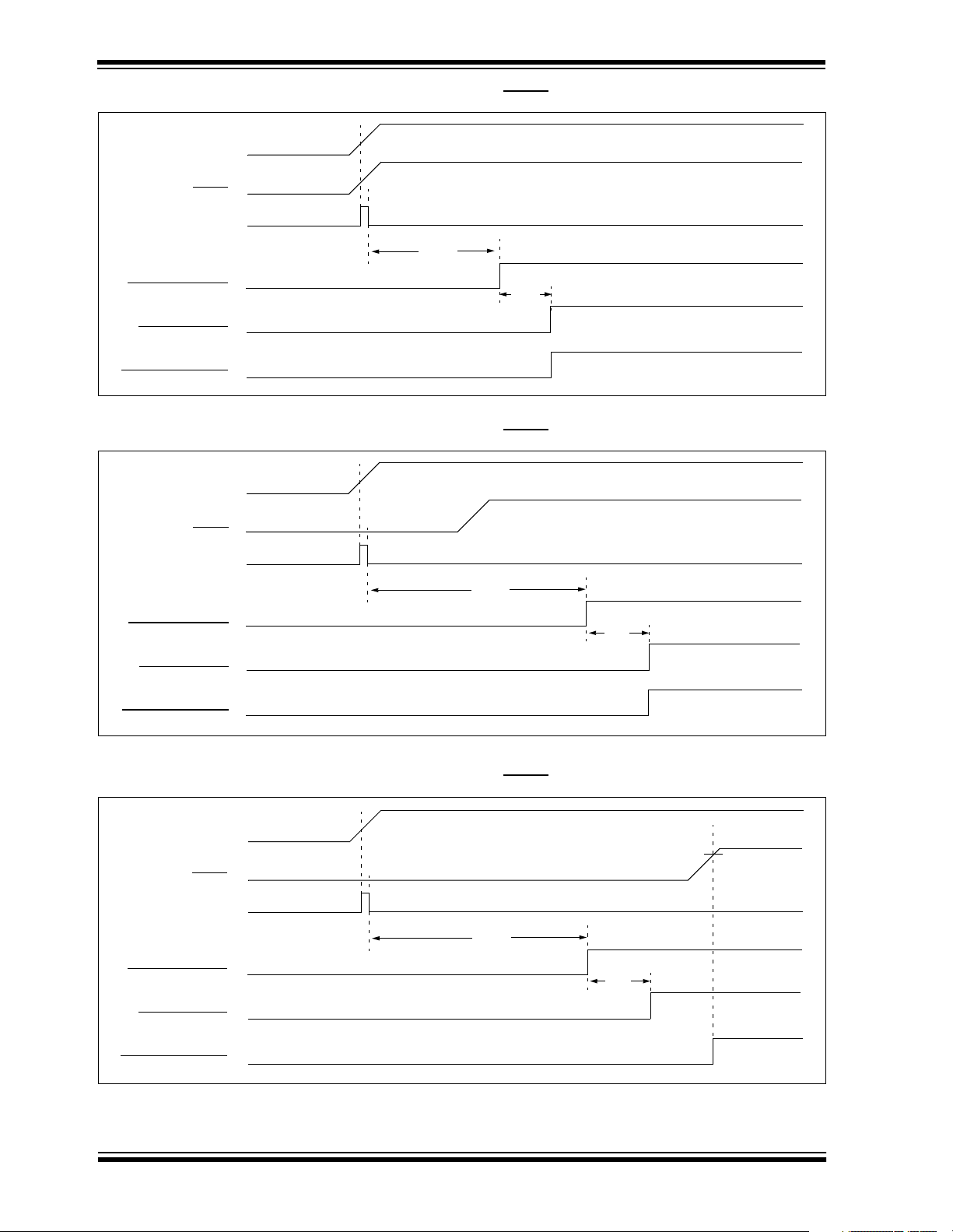
If the main oscillator is configured for an external crystal (HS, XT, LP), the transition will take place after an
oscillator start-up time (T
OST) has occurred. A timing
diagram indicating the transition from the Timer1 oscillator to the main oscillator for HS, XT and LP modes is
shown in Figure 2-8.
Figure 2-7. The Timer1 oscillator is assumed to be
running all the time. After the SCS bit is set, the processor is frozen at the next occurring Q1 cycle. After
eight synchronization cycles are counted from the
Timer1 oscillator, operation resumes. No additional
delays are required after the synchronization cycles.
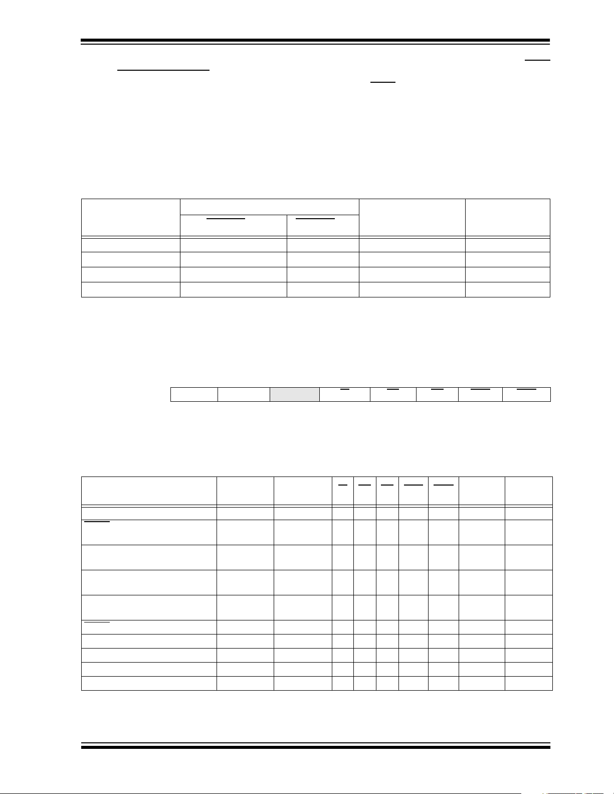
FIGURE 2-7: TIMING DIAGRAM FOR TRANSITION FROM OSC1 TO TIMER1 OSCILLATOR
Q1
T1OSI
OSC1
Internal
System
Clock
SCS
(OSCCON<0>)
Program
Counter
TOSC
Q1
TDLY
TT1P
21 345678
Tscs
PC + 2PC
Q3Q2Q1Q4Q3Q2
Q4 Q1
Q2 Q3 Q4 Q1
PC + 4
Note 1: Delay on internal system clock is eight oscillator cycles for synchronization.
FIGURE 2-8: TIMING DIAGRAM FOR TRANSITION BETWEEN TIMER1 AND OSC1 (HS,XT,LP)
Q3 Q4
T1OSI
OSC1
OSC2
Internal System
Clock
SCS
(OSCCON<0>)
Program Counter
Note 1: TOST = 1024TOSC (drawing not to scale).
PC PC + 2
Q1
TOST
TOSC
TT1P
12345678
TSCS
Q1 Q2 Q3 Q4 Q1 Q2
Q3
PC + 4
DS30475A-page 26 Advanced Information 2000 Microchip Technology Inc.

PIC18CXX8
If the main oscill ator is confi gured for HS4 (PLL) m ode,
an oscillator start-up tim e (T
time-out (T
PLL) will occur. The PLL time-out is typicall y
OST) plus an additional PLL
2 ms and allows the PLL to lock to the main oscillator
frequency. A timing diagram indicating the transition
from the Timer1 oscilla tor to the main os cillator f or HS4
mode is shown in Figure 2-9.
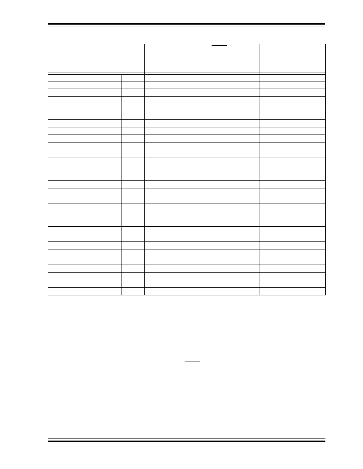
If the main oscillato r is co nfigure d in th e RC, R CIO, EC
or ECIO modes, t here i s no os ci lla tor st art-u p time-out.
Operation will resume after eight cycles of the main
oscillator have been counted. A t iming diagram ind icating the transition from the Timer1 oscillator to the main
oscillator for RC, RCIO, EC and ECIO modes is shown
in Figure 2-10.
FIGURE 2-9: TIMING FOR TRANSITION BETWEEN TIMER1 AND OSC1 (HS WITH PLL)
Q4 Q1
T1OSI
OSC1
TOST
Internal System
Clock
(OSCCON<0>)
Program Counter
Note 1: TOST = 1024TOSC (drawing not to scale).
SCS
PC PC + 2
Q1 Q2 Q3 Q4 Q1 Q2
FIGURE 2-10: TIMING FOR TRANSITION BETWEEN TIMER1 AND OSC1 (RC, EC)
2000 Microchip Technology Inc. Advanced Information DS30475A-page 27

PIC18CXX8
2.7 Effects of SLEEP Mode on the
On-chip Oscillator
When the device executes a SLEEP instruction, the
on-chip clocks and oscillator are turned off and the
device is held at the beginning of an instruction cycle
(Q1 state). With th e o scill ato r off, the OSC1 and OSC2
signals will stop oscillating. Since all the transistor
switching currents have been removed, SLEEP mode
achieves the lowest current consumption of the device
(only leakage currents). Enabling any on-chi p feature
that will operate duri ng SLEEP will i ncrease th e current
consumed during SLEEP. The user can wake from
SLEEP through external RESET, Watchdog Timer
Reset or through an interrupt.
2.8 Power-up Delays
Power up del ays are contr olled by t wo timers, so that
no external RESET circuitry is required for most applications. The delays ensure that the device is kept in
RESET until the device powe r supply and clock ar e stable. For additional information on RESET operation,
see Section 3.0 RESET .
The first timer is the Power-up Timer (PWRT), which
optionally provides a fixed delay of T
#33) on power-up only (POR and BOR). The second
timer is the Osci llator Start-up T ime r (OST), intended to
keep the chip in RESET until the crystal oscillator is
stable.
With the PLL enabled (HS4 oscillator mode), the
time-out sequenc e following a Power-on Reset is diff erent from other oscil lator modes. The time-out se quence
is as follows: th e PWRT time-ou t is invoked a fter a POR
time delay has expired, then the Oscillator Start-up
Timer (OST) is invoked. However, this is still not a sufficient amount of time to allow the PLL to lock at high
frequencies. The PWRT timer is used to provide an
additional time -out. Th is ti me is called T
#7) to allow the PLL ample time to lo ck to the incom ing
clock frequency.
PWRT (parameter
PLL (parameter
TABLE 2-3: OSC1 AND OSC2 PIN STATES IN SLEEP MODE
OSC Mode OSC1 Pin OSC2 Pin
RC Floating, external resistor should pull high At logic low
RCIO Floating, external resistor should pull high Configured as PORTA, bit 6
ECIO Floating Configured as PORTA, bit 6
EC Floating At logic low
LP, XT, and HS Feedback inverter disabled, at quiescent
voltage level
Note: See Table 3-1 in Section 3.0 RESET, for time-outs due to SLEEP and MCLR
Feedback inverter disabled, at quiescent
voltage level
Reset.
DS30475A-page 28 Advanced Information 2000 Microchip Technology Inc.

PIC18CXX8
3.0 RESET
The PIC18CXX8 differentiates between various kinds
of RESET:
a) Power-on Reset (POR)
b) MCLR
c) MCLR
d) Watchdog Timer (WDT) Reset (during normal
e) Programmable Brown-out Reset (PBOR)
f) RESET Instruction
g) Stack Ful l Reset
h) Stack Underflow Reset
Most registers are unaff ected by a RESET. Their status
is unknown on POR and unchanged by all other
RESETs. The other registers are forced to a “RESET”
Reset during normal operation
Reset during SLEEP
operation)
state on Power-on Reset, MCLR
Brown-out Reset, MCLR
Reset during SLEEP and by
the RESET instruction.
Most registers are not affected by a WDT wake-up,
since this is viewed as the resumption of normal operation. Status bits from the RCON register, RI
and BOR are set or cleared differently in different
POR
RESET situations, as indicated i n Table 3-2. These bits
are used in software to determine the nature of the
RESET. See Table 3-3 for a full description of the
RESET states of all registers.
A simplified block diagram of the on-chip RESET circuit
is shown in Figure 3-1.
The Enhanced MCU devices have a MCLR
in the MCLR
Reset path. The filter will detect and
ignore small pulses.
A WDT Reset does not drive MCLR
FIGURE 3-1: SIMPLIFIED BLOCK DIAGRAM OF ON-CHIP RESET CIRCUIT
RESET
Instruction
Stack
Pointer
Stack Full/Underflow Reset
External Reset
, WDT Reset,
, TO, PD,
noise filter
pin low.
MCLR
WDT
Module
DD Rise
V
Detect
VDD
Brown-out
Reset
OST/PWRT
OST
OSC1
On-chip
RC OSC
Note 1: This is a separate oscillator from the RC oscillator of the CLKI pin.
2: See Table 3-1 for time-out situations.
(1)
SLEEP
WDT
Time-out
Reset
Power-on Reset
BOREN
10-bit Ripple Counter
PWRT
10-bit Ripple Counter
Enable PWRT
Enable OST
(2)
S
Chip_Reset
R
Q
2000 Microchip Technology Inc. Advanced Information DS30475A-page 29

PIC18CXX8
3.1 Power-on Reset (POR)
A Power-on Reset pulse is generated on-chip when a
V
DD rise is detected. To take advan tage of th e POR cir-
cuitry, connect the MCLR
resistor) to V
DD. This will eliminate ext ernal RC compo-
pin directly (or through a
nents usually needed to create a Power-on Reset
delay . A minimum ris e rate for VDD is specified (parameter D004). For a slow rise time, see Figure 3-2.
When the device starts normal operation (exits the
RESET condition), device operating parameters (voltage, frequency, temperature,...) must be m et to en su re
operation. If these cond itions are not met, the d evice
must be held in RESET until the operating conditions
are met. Brown-out Reset may be used to meet the
voltage start-up condition.
FIGURE 3-2: EXTERNAL POWER-ON
RESET CIRCUIT (FOR SLOW
DD POWER-UP)
V
DD
V
D
R
R1
MCLR
C
Note 1: External Power-on Reset circuit is required
only if the V
DD power-up slope is too slow.
The diode D hel ps d isch arge th e ca pacito r
quickly when V
DD powers down.
2: R < 40 kΩ is recommended to make sure
that the voltage drop across R does not
violate the device’s electrical specification.
3: R1 = 100Ω to 1 kΩ will limit any current
flowing into MCLR
C in the even t of MCLR/
down due to Electrostatic Discharge
(ESD) or Electrical Overstress (EOS).
PIC18CXX8
from external capacitor
VPP pin break-
3.2 Power-up Timer (PWRT)
The Power-up Timer provides a fixed nominal time-out
(parameter #33), only on power-up from the POR. The
Power-up Timer operates on an internal RC oscillator.
The chip is kept in RESET as long as the PWRT is
active. The PWRT ’s time delay allows V
acceptable level. A configuration bit (PWRTEN
DD to rise to an
in
CONFIG2L register) is provided to enable/disable the
PWRT.
The power-up time dela y will vary f rom chip to c hip due
DD, temperature and process variation. See DC
to V
parameter #33 for details.
3.3 Oscillator Start-up Timer (OST)
The Oscillator Start-up Timer (OST) provides 1024
oscillator cycle (from OSC1 input) delay after the
PWRT delay is over (parameter #32). This ensures that
the crystal oscilla tor or res onator has started an d stabilized.
The OST time-out is invoked only for XT, LP, HS and
HS4 modes and only on Power-on Reset or wake-up
from SLEEP.
3.4 PLL Lock Time-out
With the PLL enabled, the time-ou t sequen ce foll owin g
a Power-on Reset is different from other oscillator
modes. A portion of the Pow er-up T imer is used to provide a fixed time-out th at is suff icient for the PLL to lock
to the main oscillato r frequency. This PLL lock time-out
PLL) is typically 2 ms and follows the oscillator
(T
start-up time-out (OST).
3.5 Brown-out Reset (BOR)
A configuration bit, BOREN, can disable (if
clear/programmed) or enable (if set) the Brown-out
Reset circuitry. If VDD falls below parameter D005 for
greater than parameter #35, the brown-out situation
resets the chip. A RESET may not occur if VDD falls
below parameter D005 for less than parameter #35.
The chip will remain in Bro wn-out Re set unt il V
above BV
DD. The Power-up T im er w ill th en be invoked
and will keep the chip in RESET an additional time
delay (parameter #33). If V
DD drops below BVDD while
the Power-up Timer is running, the chip will go back
into a Brown-out Reset and the Power-up Timer will be
initialized . Once V
DD rises above BVDD, the Power-up
Timer will execute the additional time delay.
DD rises
DS30475A-page 30 Advanced Information 2000 Microchip Technology Inc.
PIC18CXX8
3.6 Time-out Sequence
On power-up, the time-out sequence is as follows:
First, PWRT time-out is invoked after the POR time
delay has expired, then OST is activated. The total
time-out will vary based on oscillator configuration and
the status of the PWRT. For example, in RC mode with
the PWRT disabled, there will be no time-out at all.
Figure 3-3, Figure 3-4, Figure 3-5, Figure 3-6 and
Figure 3-7 depict time-out sequences on power-up.
Since the time-outs oc cur from the POR pulse, if MCLR
is kept low long enough, the time-outs will expire.
Bringing MCLR
(Figure 3-5). This is useful for testing purposes or to
synchronize more th an one PIC18C XX8 device opera ting in para llel.
Table 3-2 shows the RESET conditions for some Special Function Registers, while Table 3-3 shows the
RESET conditions for all registers.
high will begin execution immediately
TABLE 3-1: TIME-OUT IN VARIOUS SITUATIONS
Oscillator
Configuration
HS with PLL enabled
HS, XT, LP 72 ms + 1024Tosc 1024Tosc 72 ms + 1024Tosc 1024Tosc
EC 72 ms — 72 ms —
External RC 72 ms — 72 ms —
Note 1: 2 ms = Nominal time required for the 4X PLL to lock.
2: 72 ms is the nominal power-up timer delay.
(1)
PWRTE
72 ms + 1024Tosc + 2 ms 1024Tosc + 2 ms 72 ms + 1024Tosc + 2 ms 1 02 4Tosc + 2 ms
Power-up
N = 0 PWRTEN = 1
(2)
Brown-out
(2)
Wake-up from
SLEEP or
Oscillator Switch
REGISTER 3-1: RCON REGISTER BITS AND POSITIONS
R/W-0 R/W-0 U-0 R/W-1 R/W-1 R/W-1 R/W-1 R/W-1
IPEN LWRT
bit 7 bit 0
— RI TO PD POR BOR
TABLE 3-2: STATUS BITS, THEIR SIGNIFICANCE AND THE INITIALIZATION CONDITION FOR
RCON REGISTER
Condition
Power-on Reset 0000h 00-1 1100 1 1 1 0 0 u u
Reset during normal
MCLR
operation
Software Reset during normal
operation
Stack Full Reset during normal
operation
Stack Underflow Reset during
normal operation
MCLR
Reset during SLEEP 0000h 00-u 10uu u 1 0 u u u u
WDT Reset 0000h 0u-u 01uu u 0 1 u u u u
WDT Wake-up PC + 2 uu-u 00uu u 0 0 u u u u
Brown-out Reset 0000h 0u-1 11u0 1 1 1 u 0 u u
Interrupt wake-up from SLEEP PC + 2
Legend: u = unchanged, x = unknown,- = unimplemented bit, read as '0'
Note 1: When the wake-up is due to an interrupt and the GIEH or GIEL bits are set, the PC is loaded with the
interrupt vector (0x000008h or 0x000018h).
Program
Counter
0000h 00-u uuuu u u u u u u u
0000h 0u-0 uuuu 0 u u u u u u
0000h 0u-u uu11 u u u 1 1 u 1
0000h 0u-u uu11 u u u 1 1 1 u
(1)
RCON
Register
uu-u 00uu u 0 0 u u u u
TO PD POR BOR STKFUL STKUNF
RI
2000 Microchip Technology Inc. Advanced Information DS30475A-page 31
PIC18CXX8
FIGURE 3-3: TIME-OUT SEQUENCE ON POWER-UP (MCLR TIED TO VDD)
VDD
MCLR
INTERNAL POR
TPWRT
PWRT TIME-OUT
OST TIME-OUT
INTERNAL RESET
TOST
FIGURE 3-4: TIME-OUT SEQUENCE ON POWER-UP (MCLR
VDD
MCLR
INTERNAL POR
TPWRT
PWRT TI ME-OUT
OST TIME-OUT
INTERNAL RESET
NOT TIED TO VDD): CASE 1
TOST
FIGURE 3-5: TIME-OUT SEQUENCE ON POWER-UP (MCLR
VDD
MCLR
INTERNAL POR
TPWRT
PWRT TIME-OUT
OST TIME-OUT
INTERNAL RESET
DS30475A-page 32 Advanced Information 2000 Microchip Technology Inc.
NOT TIED TO VDD): CASE 2
TOST
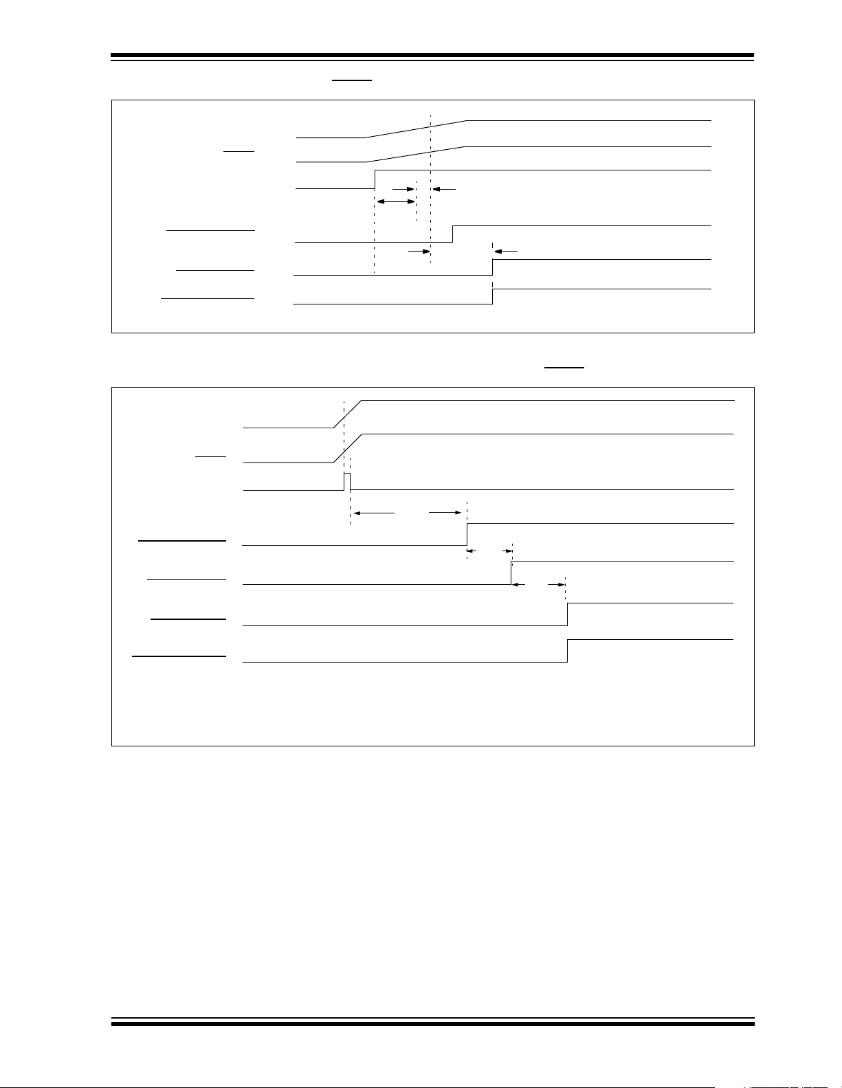
FIGURE 3-6: SLOW RISE TIME (MCLR TIED TO VDD)
VDD
MCLR
0V
1V
PIC18CXX8
5V
INTERNAL POR
PWRT TIME-OUT
OST TIME-OUT
INTERNAL RES ET
T
PWRT
TDEADTIME
TOST
FIGURE 3-7: TIME-OUT SEQUENCE ON POR W/ PLL ENABLED (MCLR
VDD
MCLR
IINTERNAL POR
TPWRT
PWRT TIME-OUT
TOST
TIED TO VDD)
OST TIME-OUT
PLL TIME-OUT
INTERNAL RESET
TOST = 1024 clock cycles.
PLL ≈ 2 ms max. First three stages of the PWRT timer.
T
TPLL
2000 Microchip Technology Inc. Advanced Information DS30475A-page 33

PIC18CXX8
TABLE 3-3: INITIALIZATION CONDITIONS FOR ALL REGISTERS
Reset
MCLR
Register
Applicable
Devices
TOSU 658 858 ---0 0000 ---0 0000 ---0 uuuu
TOSH 658 858 0000 0000 0000 0000 uuuu uuuu
TOSL 658 858 0000 0000 0000 0000 uuuu uuuu
STKPTR 658 858 00-0 0000 00-0 0000 uu-u uuuu
PCLATU 658 858 ---0 0000 ---0 0000 ---u uuuu
PCLATH 658 858 0000 0000 0000 0000 uuuu uuuu
PCL 658 858 0000 0000 0000 0000 PC + 2
TBLPTRU 658 858 --00 0000 --00 0000 --uu uuuu
TBLPTRH 658 858 0000 0000 0000 0000 uuuu uuuu
TBLPTRL 658 858 0000 0000 0000 0000 uuuu uuuu
TABLAT 658 858 0000 0000 0000 0000 uuuu uuuu
PRODH 658 858 xxxx xxxx uuuu uuuu uuuu uuuu
PRODL 658 858 xxxx xxxx uuuu uuuu uuuu uuuu
INTCON 658 858 0000 000x 0000 000u uuuu uuuu
INTCON2 658 858 1111 1111 1111 1111 uuuu uuuu
INTCON3 658 858 1100 0000 1100 0000 uuuu uuuu
INDF0 658 858 N/A N/A N/A
POSTINC0 658 858 N/A N/A N/A
POSTDEC0 658 858 N/A N/A N/A
PREINC0 658 858 N/A N/A N/A
PLUSW0 658 858 N/A N/A N/A
FSR0H 658 858 ---- 0000 ---- 0000 ---- uuuu
FSR0L 658 858 xxxx xxxx uuuu uuuu uuuu uuuu
WREG 658 858 xxxx xxxx uuuu uuuu uuuu uuuu
INDF1 658 858 N/A N/A N/A
POSTINC1 658 858 N/A N/A N/A
POSTDEC1 658 858 N/A N/A N/A
PREINC1 658 858 N/A N/A N/A
PLUSW1 658 858 N/A N/A N/A
Legend: u = unchanged, x = unknown, - = unimplemented bit, read as ’0’, q = value depends on condition
Note 1: One or more bits in the INTCONx or PIRx registers will be affected (to cause wake-up).
2: When the wake-up is due to an inte rrup t and th e GIEL or GIEH bit is set, the PC is loaded with the interrupt
vector (0008h or 0018h).
3: When the wake-up is due to an interrupt and the GIEL or GIEH bit is set, the TOSU, TOSH and TOSL are
updated with the current value of the PC. The STKPTR is modified to point to the next location in the hardware
stack.
4: See Table 3-2 for RESET value for specific condition.
5: Bit 6 of PORTA, LATA, and TRISA are enabled in ECIO and RCIO oscillator modes only. In all other
oscillator modes, they are disabled and read ’0’.
6: The long write enable is only reset on a POR or MCLR
7: Available on PIC18C858 only.
Power-on Reset,
Brown-out Reset
WDT Reset
RESET Instruction
Stack Resets
.
Wake-up via WDT
or Interrupt
(3)
(3)
(3)
(3)
(2)
(1)
(1)
(1)
DS30475A-page 34 Advanced Information 2000 Microchip Technology Inc.
PIC18CXX8
TABLE 3-3: INITIALIZATION CONDITIONS FOR ALL REGISTERS (CONTINUED)
Reset
MCLR
Register
FSR1H 658 858 ---- 0000 ---- 0000 ---- uuuu
FSR1L 658 858 xxxx xxxx uuuu uuuu uuuu uuuu
BSR 658 858 ---- 0000 ---- 0000 ---- uuuu
INDF2 658 858 N/A N/A N/A
POSTINC2 658 858 N/A N/A N/A
POSTDEC2 658 858 N/A N/A N/A
PREINC2 658 858 N/A N/A N/A
PLUSW2 658 858 N/A N/A N/A
FSR2H 658 858 ---- 0000 ---- 0000 ---- uuuu
FSR2L 658 858 xxxx xxxx uuuu uuuu uuuu uuuu
STATUS 658 858 ---x xxxx ---u uuuu ---u uuuu
TMR0H 658 858 xxxx xxxx uuuu uuuu uuuu uuuu
TMR0L 658 858 xxxx xxxx uuuu uuuu uuuu uuuu
T0CON 658 858 1111 1111 1111 1111 uuuu uuuu
OSCCON 658 858 ---- ---0 ---- ---0 ---- ---u
LVDCON 658 858 --00 0101 --00 0101 --uu uuuu
WDTCON 658 858 ---- ---0 ---- ---0 ---- ---u
(4, 6)
RCON
TMR1H 658 858 xxxx xxxx uuuu uuuu uuuu uuuu
TMR1L 658 858 xxxx xxxx uuuu uuuu uuuu uuuu
T1CON 658 858 0-00 0000 u-uu uuuu u-uu uuuu
TMR2 658 858 xxxx xxxx uuuu uuuu uuuu uuuu
PR2 658 858 1111 1111 1111 1111 1111 1111
T2CON 658 858 -000 0000 -000 0000 -uuu uuuu
SSPBUF 658 858 xxxx xxxx uuuu uuuu uuuu uuuu
SSPADD 658 858 0000 0000 0000 0000 uuuu uuuu
SSPSTAT 658 858 0000 0000 0000 0000 uuuu uuuu
SSPCON1 658 858 0000 0000 0000 0000 uuuu uuuu
SSPCON2 658 858 0000 0000 0000 0000 uuuu uuuu
Legend: u = unchanged, x = unknown, - = unimplemented bit, read as ’0’, q = value depends on condition
Note 1: One or more bits in the INTCONx or PIRx registers will be affected (to cause wake-up).
2: When the wake-up is due to an inte rrup t and th e GIEL or GIEH bit is set, the PC is loaded with the interrupt
vector (0008h or 0018h).
3: When the wake-up is due to an interrupt and the GIEL or GIEH bit is set, the TOSU, TOSH and TOSL are
updated with the current value of the PC. The STKPTR is modified to point to the next location in the hardware
stack.
4: See Table 3-2 for RESET value for specific condition.
5: Bit 6 of PORTA, LATA, and TRISA are enabled in ECIO and RCIO oscillator modes only. In all other
oscillator modes, they are disabled and read ’0’.
6: The long write enable is only reset on a POR or MCLR
7: Available on PIC18C858 only.
Applicable
Devices
658 858 00-1 11q0 00-1 qquu uu-u qquu
Power-on Reset,
Brown-out Reset
WDT Reset
RESET Instruction
Stack Resets
.
Wake-up via WDT
or Interrupt
2000 Microchip Technology Inc. Advanced Information DS30475A-page 35

PIC18CXX8
TABLE 3-3: INITIALIZATION CONDITIONS FOR ALL REGISTERS (CONTINUED)
MCLR Reset
Register
ADRESH 658 858 xxxx xxxx uuuu uuuu uuuu uuuu
ADRESL 658 858 xxxx xxxx uuuu uuuu uuuu uuuu
ADCON0 658 858 --00 0000 --00 0000 --uu uuuu
ADCON1 658 858 --00 0000 --00 0000 --uu uuuu
ADCON2 658 858 0--- -000 0--- -000 u--- -uuu
CCPR1H 658 858 xxxx xxxx uuuu uuuu uuuu uuuu
CCPR1L 658 858 xxxx xxxx uuuu uuuu uuuu uuuu
CCP1CON 658 858 --00 0000 --00 0000 --uu uuuu
CCPR2H 658 858 xxxx xxxx uuuu uuuu uuuu uuuu
CCPR2L 658 858 xxxx xxxx uuuu uuuu uuuu uuuu
CCP2CON 658 858 --00 0000 --00 0000 --uu uuuu
CVRCON 658 858 0000 0000 0000 0000 uuuu uuuu
CMCON 658 858 0000 0000 0000 0000 uuuu uuuu
TMR3H 658 858 xxxx xxxx uuuu uuuu uuuu uuuu
TMR3L 658 858 xxxx xxxx uuuu uuuu uuuu uuuu
T3CON 658 858 0000 0000 uuuu uuuu uuuu uuuu
PSPCON 658 858 0000 ---- 0000 ---- uuuu ----
SPBRG 658 858 xxxx xxxx uuuu uuuu uuuu uuuu
RCREG 658 858 xxxx xxxx uuuu uuuu uuuu uuuu
TXREG 658 858 xxxx xxxx uuuu uuuu uuuu uuuu
TXSTA 658 858 0000 -01x 0000 -01u uuuu -uuu
RCSTA 658 858 0000 000x 0000 000u uuuu uuuu
IPR3 658 858 1111 1111 1111 1111 uuuu uuuu
PIR3 658 858 0000 0000 0000 0000 uuuu uuuu
PIE3 658 858 0000 0000 0000 0000 uuuu uuuu
IPR2 658 858 -1-- 1111 -1-- 1111 -u-- uuuu
PIR2 658 858 -0-- 0000 -0-- 0000 -u-- uuuu
PIE2 658 858 -0-- 0000 -0-- 0000 -u-- uuuu
IPR1 658 858 1111 1111 1111 1111 uuuu uuuu
PIR1 658 858 0000 0000 0000 0000 uuuu uuuu
PIE1 658 858 0000 0000 0000 0000 uuuu uuuu
Legend: u = unchanged, x = unknown, - = unimplemented bit, read as ’0’, q = value depends on condition
Note 1: One or more bits in the INTCONx or PIRx registers will be affected (to cause wake-up).
2: When the wake-up is due to an inte rrup t and th e GIEL or GIEH bit is set, the PC is loaded with the interrupt
vector (0008h or 0018h).
3: When the wake-up is due to an interrupt and the GIEL or GIEH bit is set, the TOSU, TOSH and TOSL are
updated with the current value of the PC. The STKPTR is modified to point to the next location in the hardware
stack.
4: See Table 3-2 for RESET value for specific condition.
5: Bit 6 of PORTA, LATA, and TRISA are enabled in ECIO and RCIO oscillator modes only. In all other
oscillator modes, they are disabled and read ’0’.
6: The long write enable is only reset on a POR or MCLR
7: Available on PIC18C858 only.
Applicable
Devices
658 858 -111 1111 -111 1111 -uuu uuuu
658 858 -000 0000 -000 0000 -uuu uuuu
658 858 -000 0000 -000 0000 -uuu uuuu
Power-on Reset,
Brown-out Reset
WDT Reset
RESET Instruction
Stack Resets
.
Wake-up via WDT
or Interrupt
(1)
(1)
(1)
DS30475A-page 36 Advanced Information 2000 Microchip Technology Inc.

PIC18CXX8
TABLE 3-3: INITIALIZATION CONDITIONS FOR ALL REGISTERS (CONTINUED)
Reset
MCLR
WDT Reset
RESET Instruction
Stack Resets
-111 1111
-uuu uuuu
-u0u 0000
.
(5)
(5)
(5)
Wake-up via WDT
or Interrupt
-uuu uuuu
-uuu uuuu
-uuu uuuu
(5)
(5)
(5)
TRISJ
TRISH
Register
(7)
(7)
Applicable
Devices
-8581111 1111 1111 1111 uuuu uuuu
-8581111 1111 1111 1111 uuuu uuuu
Power-on Reset,
Brown-out Reset
TRISG 658 858 ---1 1111 ---1 1111 ---u uuuu
TRISF 658 858 1111 1111 1111 1111 uuuu uuuu
TRISE 658 858 1111 1111 1111 1111 uuuu uuuu
TRISD 658 858 1111 1111 1111 1111 uuuu uuuu
TRISC 658 858 1111 1111 1111 1111 uuuu uuuu
TRISB 658 858 1111 1111 1111 1111 uuuu uuuu
TRISA
LATJ
LATH
(7)
(7)
(5)
658 858 -111 1111
-858xxxx xxxx uuuu uuuu uuuu uuuu
-858xxxx xxxx uuuu uuuu uuuu uuuu
(5)
LATG 658 858 ---x xxxx ---u uuuu ---u uuuu
LATF 658 858 xxxx xxxx uuuu uuuu uuuu uuuu
LATE 658 858 xxxx xxxx uuuu uuuu uuuu uuuu
LATD 658 858 xxxx xxxx uuuu uuuu uuuu uuuu
LATC 658 858 xxxx xxxx uuuu uuuu uuuu uuuu
LATB 658 858 xxxx xxxx uuuu uuuu uuuu uuuu
(5)
LATA
PORTJ
PORTH
(7)
(7)
658 858 -xxx xxxx
-858xxxx xxxx uuuu uuuu uuuu uuuu
-8580000 xxxx 0000 uuuu uuuu uuuu
(5)
PORTG 658 858 ---x xxxx ---u uuuu ---u uuuu
PORTF 658 858 x000 0000 u000 0000 uuuu uuuu
PORTE 658 858 --00 xxxx uuuu u000 uuuu uuuu
PORTD 658 858 xxxx xxxx uuuu uuuu uuuu uuuu
PORTC 658 858 xxxx xxxx uuuu uuuu uuuu uuuu
PORTB 658 858 xxxx xxxx uuuu uuuu uuuu uuuu
PORTA
(5)
658 858 -x0x 0000
(5)
TRISK 658 858 1111 1111 1111 1111 uuuu uuuu
LATK 658 858 xxxx xxxx uuuu uuuu uuuu uuuu
PORTK 658 858 xxxx xxxx uuuu uuuu uuuu uuuu
TXERRCNT 658 858 0000 0000 0000 0000 uuuu uuuu
RXERRCNT 658 858 0000 0000 0000 0000 uuuu uuuu
COMSTAT 658 858 0000 0000 0000 0000 uuuu uuuu
CIOCON 658 858 1000 ---- 1000 ---- uuuu ----
BRGCON3 658 858 -0-- -000 -0-- -000 -u-- -uuu
BRGCON2 658 858 0000 0000 0000 0000 uuuu uuuu
BRGCON1 658 858 0000 0000 0000 0000 uuuu uuuu
Legend: u = unchanged, x = unknown, - = unimplemented bit, read as ’0’, q = value depends on condition
Note 1: One or more bits in the INTCONx or PIRx registers will be affected (to cause wake-up).
2: When the wake-up is due to an inte rrup t and th e GIEL or GIEH bit is set, the PC is loaded with the interrupt
vector (0008h or 0018h).
3: When the wake-up is due to an interrupt and the GIEL or GIEH bit is set, the TOSU, TOSH and TOSL are
updated with the current value of the PC. The STKPTR is modified to point to the next location in the hardware
stack.
4: See Table 3-2 for RESET value for specific condition.
5: Bit 6 of PORTA, LATA, and TRISA are enabled in ECIO and RCIO oscillator modes only. In all other
oscillator modes, they are disabled and read ’0’.
6: The long write enable is only reset on a POR or MCLR
7: Available on PIC18C858 only.
2000 Microchip Technology Inc. Advanced Information DS30475A-page 37

PIC18CXX8
TABLE 3-3: INITIALIZATION CONDITIONS FOR ALL REGISTERS (CONTINUED)
Reset
MCLR
Register
CANCON 658 858 xxxx xxx- uuuu uuu- uuuu uuu-
CANSTAT 658 858 xxx- xxx- uuu- uuu- uuu- uuu-
RXB0D7 658 858 xxxx xxxx uuuu uuuu uuuu uuuu
RXB0D6 658 858 xxxx xxxx uuuu uuuu uuuu uuuu
RXB0D5 658 858 xxxx xxxx uuuu uuuu uuuu uuuu
RXB0D4 658 858 xxxx xxxx uuuu uuuu uuuu uuuu
RXB0D3 658 858 xxxx xxxx uuuu uuuu uuuu uuuu
RXB0D2 658 858 xxxx xxxx uuuu uuuu uuuu uuuu
RXB0D1 658 858 xxxx xxxx uuuu uuuu uuuu uuuu
RXB0D0 658 858 xxxx xxxx uuuu uuuu uuuu uuuu
RXB0DLC 658 858 0xxx xxxx 0uuu uuuu uuuu uuuu
RXB0EIDL 658 858 xxxx xxxx uuuu uuuu uuuu uuuu
RXB0EIDH 658 858 xxxx xxxx uuuu uuuu uuuu uuuu
RXB0SIDL 658 858 xxxx x-xx uuuu u-uu uuuu u-uu
RXB0SIDH 658 858 xxxx xxxx uuuu uuuu uuuu uuuu
RXB0CON 658 858 000- 0000 000- 0000 uuu- uuuu
RXB1D7 658 858 xxxx xxxx uuuu uuuu uuuu uuuu
RXB1D6 658 858 xxxx xxxx uuuu uuuu uuuu uuuu
RXB1D5 658 858 xxxx xxxx uuuu uuuu uuuu uuuu
RXB1D4 658 858 xxxx xxxx uuuu uuuu uuuu uuuu
RXB1D3 658 858 xxxx xxxx uuuu uuuu uuuu uuuu
RXB1D2 658 858 xxxx xxxx uuuu uuuu uuuu uuuu
RXB1D1 658 858 xxxx xxxx uuuu uuuu uuuu uuuu
RXB1D0 658 858 xxxx xxxx uuuu uuuu uuuu uuuu
RXB1DLC 658 858 0xxx xxxx 0uuu uuuu uuuu uuuu
RXB1EIDL 658 858 xxxx xxxx uuuu uuuu uuuu uuuu
RXB1EIDH 658 858 xxxx xxxx uuuu uuuu uuuu uuuu
RXB1SIDL 658 858 xxxx x0xx uuuu u0uu uuuu uuuu
RXB1SIDH 658 858 xxxx xxxx uuuu uuuu uuuu uuuu
RXB1CON 658 858 0000 0000 0000 0000 uuuu uuuu
TXB0D7 658 858 xxxx xxxx uuuu uuuu uuuu uuuu
TXB0D6 658 858 xxxx xxxx uuuu uuuu uuuu uuuu
TXB0D5 658 858 xxxx xxxx uuuu uuuu uuuu uuuu
TXB0D4 658 858 xxxx xxxx uuuu uuuu uuuu uuuu
TXB0D3 658 858 xxxx xxxx uuuu uuuu uuuu uuuu
TXB0D2 658 858 xxxx xxxx uuuu uuuu uuuu uuuu
TXB0D1 658 858 xxxx xxxx uuuu uuuu uuuu uuuu
Legend: u = unchanged, x = unknown, - = unimplemented bit, read as ’0’, q = value depends on condition
Note 1: One or more bits in the INTCONx or PIRx registers will be affected (to cause wake-up).
2: When the wake-up is due to an inte rrup t and th e GIEL or GIEH bit is set, the PC is loaded with the interrupt
vector (0008h or 0018h).
3: When the wake-up is due to an interrupt and the GIEL or GIEH bit is set, the TOSU, TOSH and TOSL are
updated with the current value of the PC. The STKPTR is modified to point to the next location in the hardware
stack.
4: See Table 3-2 for RESET value for specific condition.
5: Bit 6 of PORTA, LATA, and TRISA are enabled in ECIO and RCIO oscillator modes only. In all other
oscillator modes, they are disabled and read ’0’.
6: The long write enable is only reset on a POR or MCLR
7: Available on PIC18C858 only.
Applicable
Devices
Power-on Reset,
Brown-out Reset
WDT Reset
RESET Instruction
Stack Resets
.
Wake-up via WDT
or Interrupt
DS30475A-page 38 Advanced Information 2000 Microchip Technology Inc.
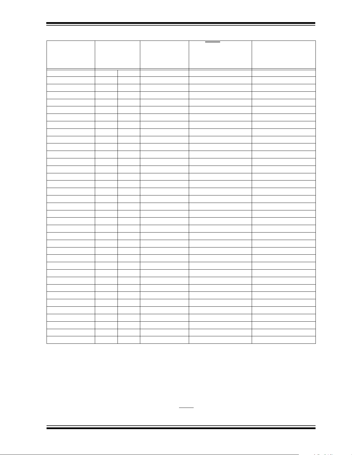
PIC18CXX8
TABLE 3-3: INITIALIZATION CONDITIONS FOR ALL REGISTERS (CONTINUED)
Reset
MCLR
Register
TXB0D0 658 858 xxxx xxxx uuuu uuuu uuuu uuuu
TXB0DLC 658 858 0x00 xxxx 0u00 uuuu uuuu uuuu
TXB0EIDL 658 858 xxxx xxxx uuuu uuuu uuuu uuuu
TXB0EIDH 658 858 xxxx xxxx uuuu uuuu uuuu uuuu
TXB0SIDL 658 858 xxx0 x0xx uuu0 u0uu uuuu uuuu
TXB0SIDH 658 858 xxxx xxxx uuuu uuuu uuuu uuuu
TXB0CON 658 858 0000 0000 0000 0000 uuuu uuuu
TXB1D7 658 858 xxxx xxxx uuuu uuuu uuuu uuuu
TXB1D6 658 858 xxxx xxxx uuuu uuuu uuuu uuuu
TXB1D5 658 858 xxxx xxxx uuuu uuuu uuuu uuuu
TXB1D4 658 858 xxxx xxxx uuuu uuuu uuuu uuuu
TXB1D3 658 858 xxxx xxxx uuuu uuuu uuuu uuuu
TXB1D2 658 858 xxxx xxxx uuuu uuuu uuuu uuuu
TXB1D1 658 858 xxxx xxxx uuuu uuuu uuuu uuuu
TXB1D0 658 858 xxxx xxxx uuuu uuuu uuuu uuuu
TXB1DLC 658 858 0x00 xxxx 0u00 uuuu uuuu uuuu
TXB1EIDL 658 858 xxxx xxxx uuuu uuuu uuuu uuuu
TXB1EIDH 658 858 xxxx xxxx uuuu uuuu uuuu uuuu
TXB1SIDL 658 858 xxx0 x0xx uuu0 u0uu uuuu uuuu
TXB1SIDH 658 858 xxxx xxxx uuuu uuuu uuuu uuuu
TXB1CON 658 858 0000 0000 0000 0000 uuuu uuuu
TXB2D7 658 858 xxxx xxxx uuuu uuuu uuuu uuuu
TXB2D6 658 858 xxxx xxxx uuuu uuuu uuuu uuuu
TXB2D5 658 858 xxxx xxxx uuuu uuuu uuuu uuuu
TXB2D4 658 858 xxxx xxxx uuuu uuuu uuuu uuuu
TXB2D3 658 858 xxxx xxxx uuuu uuuu uuuu uuuu
TXB2D2 658 858 xxxx xxxx uuuu uuuu uuuu uuuu
TXB2D1 658 858 xxxx xxxx uuuu uuuu uuuu uuuu
TXB2D0 658 858 xxxx xxxx uuuu uuuu uuuu uuuu
TXB2DLC 658 858 0x00 xxxx 0u00 uuuu uuuu uuuu
TXB2EIDL 658 858 xxxx xxxx uuuu uuuu uuuu uuuu
TXB2EIDH 658 858 xxxx xxxx uuuu uuuu uuuu uuuu
TXB2SIDL 658 858 xxx0 x0xx uuu0 u0uu uuuu uuuu
TXB2SIDH 658 858 xxxx xxxx uuuu uuuu uuuu uuuu
TXB2CON 658 858 0000 0000 0000 0000 uuuu uuuu
RXM1EIDL 658 858 xxxx xxxx uuuu uuuu uuuu uuuu
RXM1EIDH 658 858 xxxx xxxx uuuu uuuu uuuu uuuu
Legend: u = unchanged, x = unknown, - = unimplemented bit, read as ’0’, q = value depends on condition
Note 1: One or more bits in the INTCONx or PIRx registers will be affected (to cause wake-up).
2: When the wake-up is due to an inte rrup t and th e GIEL or GIEH bit is set, the PC is loaded with the interrupt
vector (0008h or 0018h).
3: When the wake-up is due to an interrupt and the GIEL or GIEH bit is set, the TOSU, TOSH and TOSL are
updated with the current value of the PC. The STKPTR is modified to point to the next location in the hardware
stack.
4: See Table 3-2 for RESET value for specific condition.
5: Bit 6 of PORTA, LATA, and TRISA are enabled in ECIO and RCIO oscillator modes only. In all other
oscillator modes, they are disabled and read ’0’.
6: The long write enable is only reset on a POR or MCLR
7: Available on PIC18C858 only.
Applicable
Devices
Power-on Reset,
Brown-out Reset
WDT Reset
RESET Instruction
Stack Resets
.
Wake-up via WDT
or Interrupt
2000 Microchip Technology Inc. Advanced Information DS30475A-page 39

PIC18CXX8
TABLE 3-3: INITIALIZATION CONDITIONS FOR ALL REGISTERS (CONTINUED)
MCLR Reset
Register
RXM1SIDL 658 858 xxx- --xx uuu- --uu uuu- --uu
RXM1SIDH 658 858 xxxx xxxx uuuu uuuu uuuu uuuu
RXM0EIDL 658 858 xxxx xxxx uuuu uuuu uuuu uuuu
RXM0EIDH 658 858 xxxx xxxx uuuu uuuu uuuu uuuu
RXM0SIDL 658 858 xxx- --xx uuu- --uu uuu- --uu
RXM0SIDH 658 858 xxxx xxxx uuuu uuuu uuuu uuuu
RXF5EIDL 658 858 xxxx xxxx uuuu uuuu uuuu uuuu
RXF5EIDH 658 858 xxxx xxxx uuuu uuuu uuuu uuuu
RXF5SIDL 658 858 xxx- x-xx uuu- u-uu uuu- u-uu
RXF5SIDH 658 858 xxxx xxxx uuuu uuuu uuuu uuuu
RXF4EIDL 658 858 xxxx xxxx uuuu uuuu uuuu uuuu
RXF4EIDH 658 858 xxxx xxxx uuuu uuuu uuuu uuuu
RXF4SIDL 658 858 xxx- x-xx uuu- u-uu uuu- u-uu
RXF4SIDH 658 858 xxxx xxxx uuuu uuuu uuuu uuuu
RXF3EIDL 658 858 xxxx xxxx uuuu uuuu uuuu uuuu
RXF3EIDH 658 858 xxxx xxxx uuuu uuuu uuuu uuuu
RXF3SIDL 658 858 xxx- x-xx uuu- u-uu uuu- u-uu
RXF3SIDH 658 858 xxxx xxxx uuuu uuuu uuuu uuuu
RXF2EIDL 658 858 xxxx xxxx uuuu uuuu uuuu uuuu
RXF2EIDH 658 858 xxxx xxxx uuuu uuuu uuuu uuuu
RXF2SIDL 658 858 xxx- x-xx uuu- u-uu uuu- u-uu
RXF2SIDH 658 858 xxxx xxxx uuuu uuuu uuuu uuuu
RXF1EIDL 658 858 xxxx xxxx uuuu uuuu uuuu uuuu
RXF1EIDH 658 858 xxxx xxxx uuuu uuuu uuuu uuuu
RXF1SIDL 658 858 xxx- x-xx uuu- u-uu uuu- u-uu
RXF1SIDH 658 858 xxxx xxxx uuuu uuuu uuuu uuuu
RXF0EIDL 658 858 xxxx xxxx uuuu uuuu uuuu uuuu
RXF0EIDH 658 858 xxxx xxxx uuuu uuuu uuuu uuuu
RXF0SIDL 658 858 xxx- x-xx uuu- u-uu uuu- u-uu
RXF0SIDH 658 858 xxxx xxxx uuuu uuuu uuuu uuuu
Legend: u = unchanged, x = unknown, - = unimplemented bit, read as ’0’, q = value depends on condition
Note 1: One or more bits in the INTCONx or PIRx registers will be affected (to cause wake-up).
2: When the wake-up is due to an inte rrup t and th e GIEL or GIEH bit is set, the PC is loaded with the interrupt
vector (0008h or 0018h).
3: When the wake-up is due to an interrupt and the GIEL or GIEH bit is set, the TOSU, TOSH and TOSL are
updated with the current value of the PC. The STKPTR is modified to point to the next location in the hardware
stack.
4: See Table 3-2 for RESET value for specific condition.
5: Bit 6 of PORTA, LATA, and TRISA are enabled in ECIO and RCIO oscillator modes only. In all other
oscillator modes, they are disabled and read ’0’.
6: The long write enable is only reset on a POR or MCLR
7: Available on PIC18C858 only.
Applicable
Devices
Power-on Reset,
Brown-out Reset
WDT Reset
RESET Instruction
Stack Resets
.
Wake-up via WDT
or Interrupt
DS30475A-page 40 Advanced Information 2000 Microchip Technology Inc.
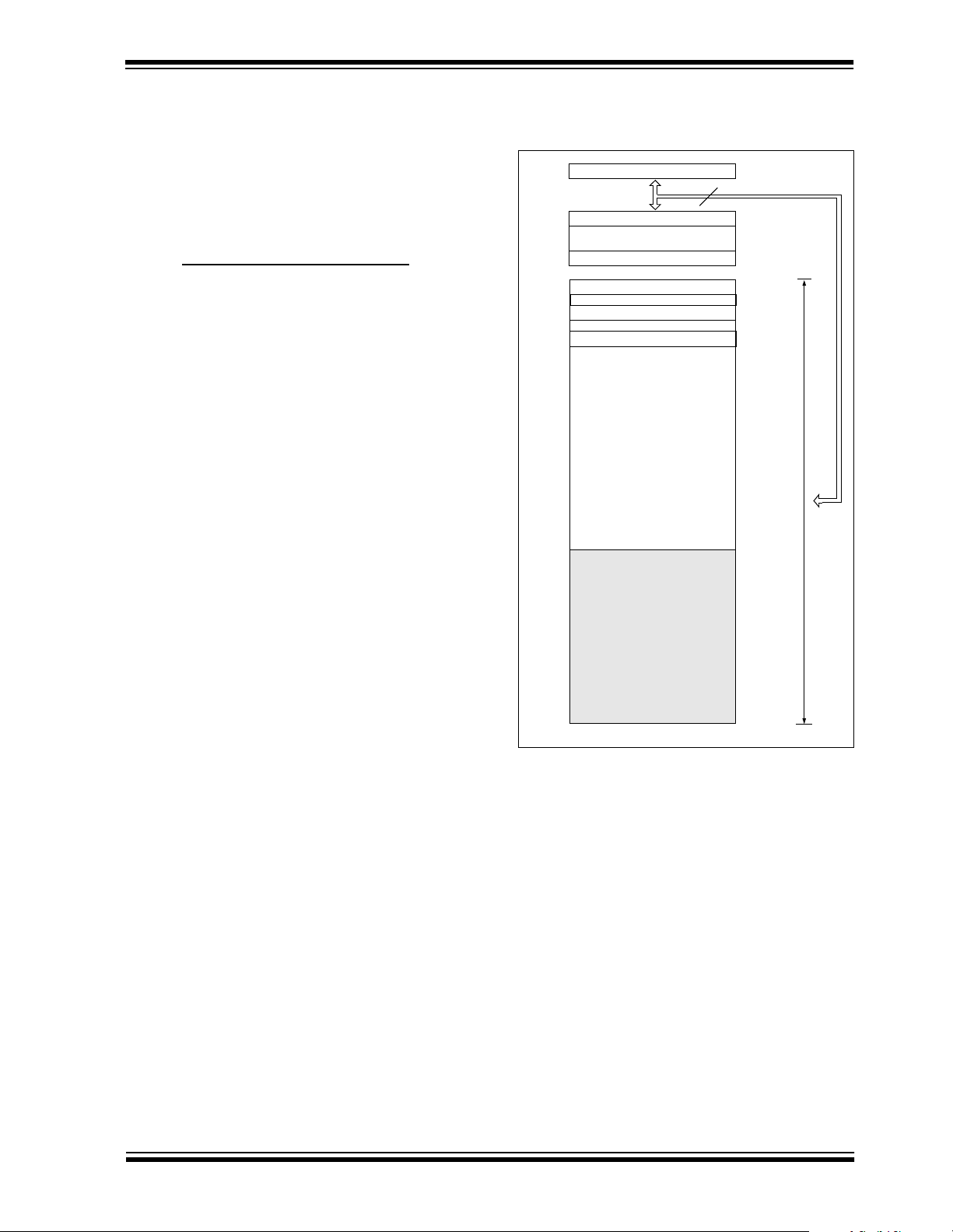
PIC18CXX8
4.0 MEMORY ORGANIZATION
There are two memory blocks in Enhanced MCU
devices. These memory blocks are:
• Program Memory
• Data Memory
Each block has its own bus so that concurrent access
can occur.
4.1 Program Memory Organization
The PIC18CXX8 devices have a 21-bit program
counter that is capable of addressing the 2 Mbyte
program memory space.
The reset vector address is at 0000h and the interrupt
vector addresses are at 0008h and 0018h. Figure 4-1
shows the diag ram for program memory map and stack
for the PIC18C658 and PIC18C858.
4.1.1 INTERNAL PROGRAM MEMORY
OPERATION
All devices have 32 Kbytes of internal EPROM program
memory. This means that the PIC18CXX 8 de vi ces ca n
store up to 16 K of si ngle wo rd ins tructi ons. Ac cessi ng
a location between the physically implemented memory and the 2 Mbyt e addre ss will c ause a rea d of all '0' s
(a NOP instruction) .
FIGURE 4-1: PROGRAM MEMORY MAP
AND STACK FOR
PIC18C658/858
PC<20:0>
Stack Level 1
Stack Level 31
RESET Vector
High Priority Interrupt Vector
Low Priori ty Interrupt Vector
On-chip
Program Memory
21
•
•
•
0000h
0008h
0018h
7FFFh
8000h
User Memory Space
Read ’1’
1FFFFFh
2000 Microchip Technology Inc. Advanced Information DS30475A-page 41

PIC18CXX8
4.2 Return Address Stack
The return address stack allows any combination of up
to 31 program calls and interrupts to occur. The PC
(Program Counter) is pu shed onto the stack when a
PUSH, CALL or RCALL instruction is executed, or an
interrupt is acknowledged. The PC value is pulled off
the stack on a RETURN, RETLW or a RETFIE instruc-
tion. PCLATU and PCLATH are not affected by any of
the return instructions.
The stack operates as a 31 word by 21-bit stack memory and a 5-bit stack pointer, with the stack pointer initialized to 00000b after all RESETs. There is no RAM
associated with stack pointer 00000b. This is only a
RESET value. During a CALL type instruction caus ing
a push onto the stack, the stack pointer is first incremented and the RAM location pointed to by the stack
pointer is written with the contents of the PC. During a
RETURN type instruction causing a pop from the stack,
the contents of the RAM location indicated by the
STKPTR is transferred to the PC and then the stack
pointer is decremented.
The stack space is not part of either program or data
space. The stack pointer is readable and writable, and
the data on the top of the s tack is readab le and writabl e
through SFR registers. Status bits indicate if the stack
pointer is at or beyond the 31 levels provided.
4.2.1 TOP-OF-STACK ACCESS
The top of the stack is readable and writable. Three
register locations, TOSU, TOSH and TOSL allow
access to the contents of the stack lo cation indi cated
by the STKPTR register. This allows users to implement a software stack if necessary. After a CALL,
RCALL or interrupt, the software can read the pushed
value by reading the TOSU, TO SH and TOSL regis ters.
These values can b e placed on a user define d software
stack. At return time, the software can replace the
TOSU, TOSH and TOSL and do a return.
The user should disable the global interru pt enable bit s
during this time to prevent inadvertent stack operations.
4.2.2 RETURN STACK POINTER (STKPTR)
The STKPTR register c onta in s th e st ack po inter value,
the STKFUL (stack full) status bit, and the STKUNF
(stack underflow) status bits. Register 4-1 shows the
STKPTR register . The value of the stack point er can be
0 through 31. The stack pointer increments when values are pushed onto the stack and decrements when
values are popped off the stack. At RESET, the stack
pointer value will be 0. The user may read and write the
stack pointer value. T his feature can be u sed by a Rea l
Time Operating Sy stem for return stack maintenance.
After the PC is pushed onto the stack 31 times (witho ut
popping any values off the stack), the STKFUL bit is
set. The STKFUL bit can on ly be cleared in so ftware or
by a POR.
The action that takes place when the stack becomes
full depends on the state of the STVREN (stack overflow RESET enable) configuration bit. Refer to Section
18 for a description of the device configuration bits. If
STVREN is set (default) the 31st push will push the
(PC + 2) value onto the stack, set the STKFUL bit, an d
reset the device. The STKFUL bit will remain set and
the stack pointer will be set to 0.
If STVREN is cleared, the STKFUL bit will be set on the
31st push and the stack pointer will increment to 31.
The 32nd push will overwrite th e 31st push (and so on),
while STKPTR remains at 31.
When the stack has been popped enough times to
unload the stack, t he next pop will retu rn a value of zero
to the PC and sets the STKUNF bit, while the stack
pointer remains at 0. The STKUNF bit will remain set
until cleared in software or a POR occurs.
Note: Returning a value of zero to the PC on an
underflow has the effect of vectoring the
program to the RESET vector, where the
stack condition s can be ve rified and app ropriate actions can be taken.
DS30475A-page 42 Advanced Information 2000 Microchip Technology Inc.
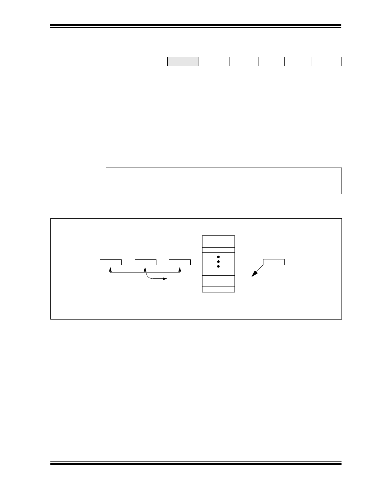
REGISTER 4-1: STKPTR - STACK POINTER REGISTER
R/C-0 R/C-0 U-0 R/W-0 R/W-0 R/W-0 R/W-0 R/W-0
STKFUL STKUNF — SP4 SP3 SP2 SP1 SP0
bit 7 bit 0
bit 7 STKFUL: Stack Full Flag bit
1 = Stack became full or overflowed
0 = Stack has not become full or overflowed
bit 6 STKUNF: Stack Underflow Flag bit
1 = Stack underflow occurred
0 = Stack underflow did not occur
bit 5 Unimplemented: Read as '0'
bit 4-0 SP4:SP0: Stack Pointer Location bits
Note: Bit 7 and bit 6 can only be cleared in user software or by a POR.
Legend
= Readable bit W = Writable bit U = Unimplemented bit, read as ‘0’
R
- n = Value at POR ’1’ = Bit is set ’0’ = Bit is cleared C = Clearable bit
PIC18CXX8
FIGURE 4-2: RETURN ADDRESS STACK AND ASSOCIATED REGISTERS
Return Address Stack
11111
11110
TOSLTOSHTOSU
0x340x1A0x00
Top-of-Stack
Note 1: No RAM associated with this address; always maintained ‘0’s.
0x001A34
0x000D58
0x000000
11101
00011
00010
00001
00000
STKPTR<4:0>
00010
(1)
2000 Microchip Technology Inc. Advanced Information DS30475A-page 43

PIC18CXX8
4.2.3 PUSH AND POP INSTRUCTIONS
Since the Top-of-Stack (TOS) is readable and writ able,
the ability to push values on to the stac k and pull values
off the stack without disturbing normal program execution is a desirable opt ion. To push the curren t PC value
onto the stack, a PUSH instruction can be executed.
This will increment the stack pointer and load the current PC value onto the stack. TOSU, TOSH and TOSL
can then be modified to place a return address on the
stack.
The POP instruction discards the current TOS by decrementing the stack pointer. The previous value pushed
onto the stack then becomes the TOS value.
4.2.4 STACK FULL/UNDERFLOW RESETS
These RESETs are enabled by programming the
STVREN configuration bit. When the STVREN bit is
disabled, a full or underf low condition will set the appropriate STKFUL or STKUNF bit, but not cause a device
RESET. When the STVREN bit is enabled, a full or
underflow will set the appro priate STKF UL or STKUNF
bit and then cause a device RESET. The STKFUL or
STKUNF bits are only cleared by the user software or
a POR.
4.3 Fast Register Stack
A “fast return” option is available for interrupts and
calls. A fast register stack is provided for the STATUS,
WREG and BSR registers and is only one layer in
depth. The stack is not readable or writable and is
loaded with the curre nt value o f the co rrespon ding re gister when the processor vectors for an interrupt. The
values in the fast register stack are then loaded back
into the working registers if the fast return instruction is used to return from the interrupt.
A low or high priority interrupt source will push values
into the stack registers. If both low and high priority
interrupts are enabled, the stack registers cannot be
used reliably for low priority interrupts. If a high priority
interrupt occurs while servicing a low priority interrupt,
the stack register values sto red by the low priority interrupt will be overwritten.
If high priority interrupts are not disabled during low priority interrupts, users must save the key registers in
software during a low priority interrupt.
If no interrupts are used, the fast register stack can be
used to restore the STATU S, WREG and BSR registers
at the end of a subroutine call. To use the fast register
stack for a subroutine call, a fast call instruction
must be executed.
Example 4-1 sho ws a source code exam ple that uses
the fast register stack.
EXAMPLE 4-1: FAST REGISTER STACK
CODE EXAMPLE
CALL SUB1, FAST ;STATUS, WREG, BSR
;SAVED IN FAST REGISTER
•
•
SUB1 •
•
•
RETURN FAST ;RESTORE VALUES SAVED
;STACK
;IN FAST REGISTER STACK
DS30475A-page 44 Advanced Information 2000 Microchip Technology Inc.

PIC18CXX8
4.4 PCL, PCLATH and PCLATU
The program counter (PC) specifies the address of the
instruction to fetch for execution. The PC is 21-bits
wide. The low byte is called the PCL register. This register is readable and writable. The high byte is called
the PCH register. This register contains the PC<15:8>
bits and is not directly readable or writable. Updates to
the PCH register may be performed through the
PCLATH register. The upper byte is called PCU. This
register contains the PC<20 :16> bi ts and i s not d irectl y
readable or writable. Updates to the PCU register may
be performed through the PCLATU register.
The PC addresses bytes in the program memory. To
prevent the PC from becoming misaligned with word
instructions, the LSb of PCL is fixed to a value of ’0’.
The PC increments by 2 to address sequential instructions in the program memory.
The CALL, RCALL, GOTO and program branch
instructions write to the program counter directly. For
these instructions, the contents of PCLATH and
PCLATU are not transferred to the program counter.
FIGURE 4-3: CLOCK/INSTRUCTION CYCLE
Q2 Q3 Q4
OSC1
Q1
Q2
Q3
Q4
PC
OSC2/CLKOUT
(RC mode)
Q1
PC
Fetch INST (PC)
Execute INST (PC-2) Fetch INS T (PC +2)
Q1
Execute INST (PC) Fetch INST (PC+4)
The contents of PCLATH and PCLATU will be transferred to the program counter by an operation that
writes PCL. Similarly, the upper two bytes of the program counter will be transferred to PCLATH and
PCLATU by an operation that reads PCL. This is useful
for computed offsets to the PC (See Section 4.8.1).
4.5 Clocking Scheme/Instruction Cycle
The clock input (from OSC1) is internally divided by
four to generate four non-overlapping quadrature
clocks, namely Q1, Q2, Q3 and Q4. Internally, the program counter (PC) is incremented every Q1, the
instruction is fetched from the program memory and
latched into the instruction register in Q4. The instruction is decoded and executed during the following Q1
through Q4. The clocks and instruction execution flow
are shown in Figure 4-3.
Q2 Q3 Q4
PC+2 PC+4
Q2 Q3 Q4
Q1
Execute INST (PC+2)
Internal
phase
clock
2000 Microchip Technology Inc. Advanced Information DS30475A-page 45

PIC18CXX8
4.6 Instruction Flow/Pipelining
An “Instruction Cycle” consists of four Q cycles (Q1,
Q2, Q3 and Q4). The instruc ti on fe tch and execute are
pipelined such that fetch takes one instruction cycle
while decode and execute takes another instruction
cycle. However, due to the pipelining, each instruction
effectively executes in one cycle. If an instruction
causes the program counter to change (e.g., GOTO),
two cycles are required to complete the instruction
(Example 4-2).
A fetch cycle begins with the program counter (PC)
incrementing in Q1.
In the execution cy cle, the fetc hed instructi on is latche d
into the “Instruction Register” (IR) in cycle Q1. This
instruction is then decoded and executed during the
Q2, Q3, and Q4 cycles. Data memory is read during Q2
(operand read) and written during Q4 (destination
write).
EXAMPLE 4-2: INSTRUCTION PIPELINE FLOW
TCY0TCY1TCY2TCY3TCY4TCY5
1. MOVLW 55h
2. MOVWF PORTB
3. BRA SUB_1
4. BSF PORTA, BIT3 (Forced NOP)
5. Instruction @ address SUB_1
Fetch 1 Execute 1
Fetch 2 Execute 2
Fetch 3 Execute 3
4.7 Instructions in Program Memory
The program memory is addressed in bytes. Instructions are stored as two bytes or four bytes in program
memory. The Least Significant Byte of an instruction
word is always stored in a program memory location
with an even address (LSB = ’0’). Figure 4-1 shows an
example of how instruct ion words are stored in the p rogram memory. To maintain alignment with instruction
boundaries, the PC increments in steps of 2 and the
LSB will always read ’0’ (See Section 4.4).
The CALL and GOTO instructions have an absolute program memory address embedded into the instruction.
Since instructions are always stored on word boundaries, the data contained in the instruction is a word
address. The word address is written to PC<20:1>,
which accesses the desired byte address in program
memory. Instruction #2 in Figure 4-1 shows how the
instruction “GOTO 000006h” is encoded in the program
memory . Program branch instructions that encode a relative address offset operate in the same manner. The
offset value stored in a b ranch instruction represents the
number of single word instructions by which the PC will
be offset. Section 23.0 provides further details of the
instruction set.
Fetch 4 Flush
Fetch SUB_1 Execute SUB_1
All instructions are single cycle, except for any program branches. These take two cycles since the fetch
instruction is “flushed” from the pipeline while the new instruction is being fetched and then executed.
TABLE 4-1: INSTRUCTIONS IN PROGRAM MEMORY
Instruction Opcode Memory Address
— 000007h
MOVLW 055h 0E55h 55h 000008h
0Eh 000009h
GOTO 000006h EF03h, F000h 03h 00000Ah
EFh 00000Bh
00h 00000Ch
F0h 00000Dh
MOVFF 123h, 456h C123h, F456h 23h 00000Eh
C1h 00000Fh
56h 000010h
F4h 000011h
— 000012h
DS30475A-page 46 Advanced Information 2000 Microchip Technology Inc.

PIC18CXX8
4.7.1 TWO WORD INSTRUCTIONS
The PIC18CXX8 devi ces h ave 4 two word ins tructi ons:
MOVFF, CALL, GOTO and LFSR. The second w ord of
these instructions has the 4 MSB’s set to 1’s and is a
special kind of NOP instruction. The lower 12 bits of the
second word contain da ta to be used by the ins truction.
If the first word of the instruction is executed, the data
in the second word is accessed. If the second word of
the instruction is executed by itself (first word was
skipped), it will execute as a NOP. This action is neces-
sary when the two word instruction is preceded by a
conditional instruct ion that changes the PC. A program
example that demonstrates this concept is shown in
Example 4-3. Refer to Section 19.0 for further de tails of
the instruction set.
4.8 Lookup Tables
Lookup tables are implemented two ways. These are:
• Computed GOTO
• Table Reads
4.8.1 COMPUTED GOTO
A computed GOTO is accomplished by adding an offset
to the program counter (ADDWF PCL).
A lookup table can be formed with an ADDWF PCL
instruction and a group of RETLW 0xnn instructions.
WREG is loaded with an offset into the table befor e executing a call to that table. The first instruction of the called
routine is the ADDWF PCL instruction. The next instruction executed will be one of the RETLW 0xnn instructions that returns the value 0xnn to the calling fun ction .
The offset v alue (val ue in WR EG) speci fies the number
of bytes that the program counter should advance.
In this method, only one data byte may be stored in
each instruction location and room on the return
address stack is required.
Warning: The LSb of PCL is fixed to a value of ‘0’.
Hence, computed GOTO to an odd
address is not possible.
4.8.2 TABLE READS/TABLE WRITES
A better method of storing data in program memory
allows 2 byte s of data to be stored in each inst ruction
location.
Lookup table data may be stored as 2 bytes per program word by using table reads and writes. The table
pointer (TBLPTR) specifies the byte address and the
table latch (TABLAT) contains the data that is read
from, or written to, program memory. Data is transferred to/from program memory one byte at a time.
A description of the Table Read/Table Write operation
is shown in Section 5.0.
EXAMPLE 4-3: TWO WORD INSTRUCTIONS
CASE 1:
Object Code Source Code
0110 0110 0000 0000 TSTFSZ REG1 ; is RAM location 0?
1100 0001 0010 0011 MOVFF REG1, REG2 ; No, execute 2-word instruction
1111 0100 0101 0110 ; 2nd operand holds address of REG2
0010 0100 0000 0000 ADDWF REG3 ; continue code
CASE 2:
Object Code Source Code
0110 0110 0000 0000 TSTFSZ REG1 ; is RAM location 0?
1100 0001 0010 0011 MOVFF REG1, REG2 ; Yes
1111 0100 0101 0110 ; 2nd operand becomes NOP
0010 0100 0000 0000 ADDWF REG3 ; continue code
2000 Microchip Technology Inc. Advanced Information DS30475A-page 47

PIC18CXX8
4.9 Data Memory Organization
The data memory is impl eme nted as static RAM. Each
register in the data memory has a 12-bit address,
allowing up to 4096 bytes of data memory. Figure 4-4
shows the data memory organization for the
PIC18CXX8 devices.
The data memory map is divided into as many as 16
banks that contain 256 bytes each. The lower 4 bits of
the Bank Select Register (BSR<3:0>) select which
bank will be accessed. The upper 4 bits for the BSR are
not implemented.
The data memory contains Special Function Registers
(SFR) and General Purpose Registers (GPR). The
SFR’s are used for control and status of the controller
and peripheral fu nctions, whi le GPR’s are used for data
storage and scratch pad operations in the user’s application. The SFR’s start at the last location of Bank 15
(0xFFF) and grow downwards. GPR’s start at the first
location of Bank 0 and grow up wards. Any read of an
unimplemented location will read as ’0’s.
The entire data memory may be accessed directly or
indirectly. Direct addressing may require the use of th e
BSR register. Indirect addressing requires the use of
the File Select Register (FSR). Each FSR holds a
12-bit address value that can be used to access any
location in the Data Memory map without banking.
The instruction set and architecture allow operations
across all banks. This m ay be accompli shed by indirec t
addressing or by the use of th e MOVFF instruction. The
MOVFF instruction is a two word/two cycl e instruction
that moves a value from one register to another.
To ensure that commonly used registers (SFR’s and
select GPR’s) can be accessed in a single cycle,
regardless of the current BSR values, an Access Bank
is implemented. A s egment of Ban k 0 and a segm ent of
Bank 15 comprise the Access RAM. Section 4.10 provides a detailed description of the Access RAM.
4.9.1 GENERAL PURPOSE REGISTER FILE
The register file can b e access ed eithe r dire ctly o r indi-
rectly. Indirect addressing operates through the File
Select Registers (FSR). The operation of indirect
addressing is shown in Section 4.12.
Enhanced MCU devices may have banked memory in
the GPR area. GPR’s are not initialized by a Power-on
Reset and are unchanged on all other RESETS.
Data RAM is available for use as GPR registers by all
instructions. Bank 15 (0xF00 to 0xFFF) contains
SFR’s. All other banks of data memory contain GPR
registers starting with bank 0.
4.9.2 SPECIAL FUNCTION REGISTERS
The Special Function Registers (SFR’s) are registers
used by the CPU and Peripheral Modules for controlling the desired operation of the device. These registers are implemented as static RAM. A list of these
registers is given in Table 4-2.
The SFR’s can be classified into two sets: those associated with the “core” function and those related to the
peripheral functions. Those registers related to the
“core” are described in this s ec tio n, w hil e tho se rel ate d
to the operation of the peripheral features are
described in the section of that periphe ral feature.
The SFR’s are typically di stributed among the per ipherals whose functions they control.
The unused SFR locations will be unimplemented and
read as '0's. See Table 4-2 for addresses for the SFR’s.
DS30475A-page 48 Advanced Information 2000 Microchip Technology Inc.

FIGURE 4-4: DATA MEMORY MAP FOR PIC18C658/858
PIC18CXX8
BSR<3:0>
= 0000b
= 0001b
= 0010b
= 0011b
= 0100b
= 0101b
= 0110b
= 1110b
= 1111b
Bank 0
Bank 1
Bank 2
Bank 3
Bank 4
Bank 5
Bank 6
to
Bank 14
Bank 15
Data Memory Map
00h
Access GPR’s
FFh
00h
FFh
00h
FFh
00h
FFh
00h
FFh
00h
FFh
GPR’s
GPR’s
GPR’s
GPR’s
GPR’s
GPR’s
Unused
Read ’00h’
SFR’s
Access SFR’s
000h
05Fh
060h
0FFh
100h
1FFh
200h
2FFh
300h
3FFh
400h
4FFh
500h
5FFh
600h
EFFh
F00h
F5Fh
F60h
FFFh
Access Bank
Access Bank low
(GPR’s)
Access Bank high
(SFR’s)
When a = 0,
the BSR is ignored and the
Access Bank is used.
The first 96 bytes are General Purpose RAM (from
Bank 0).
The next 160 bytes are
Special Function R egisters
(from Bank 15).
00h
5Fh
60h
FFh
When a = 1,
the BSR is used to specify
the RAM location that the
instruction uses.
2000 Microchip Technology Inc. Advanced Information DS30475A-page 49

PIC18CXX8
TABLE 4-2: SPECIAL FUNCTION REGISTER MAP
Address Name Address Name Address Name Address Name
(2)
FFFh TOSU FDFh INDF2
FFEh TOSH FDEh POSTINC2
FFDh TOSL FDDh POSTDEC2
FFCh STKPTR FDCh PREINC2
FFBh PCLATU FDBh PLUSW2
FFAh PCLATH FDAh FSR2H FBAh CCP2CON F9Ah TRISJ
FF9h PCL FD9h FSR2L FB9h — F99h TRISH
FF8h TBLPTRU FD8h STA TUS FB8h — F98h TRISG
FF7h TBLPTRH FD7h TMR0H FB7h — F97h TRISF
FF6h TBLPTRL FD6h TMR0L FB6h — F96h TRISE
FF5h TABLAT FD5h T0CON FB5h CVRCON F95h TRISD
FF4h PRODH FD4h — FB4h CMCON F94h TRISC
FF3h PRODL FD3h OSCCON FB3h TMR3H F93h TRISB
FF2h INTCON FD2h LVDCON FB2h TMR3L F92h TRISA
FF1h INTCON2 FD1h WDTCON FB1h T3CON F91h LATJ
FF0h INTCON3 FD0h RCON FB0h PSPCON F90h LATH
FEFh INDF0
FEEh POSTINC0
FEDh POSTDEC0
FECh PREINC0
FEBh PLUSW0
(2)
FCFh TMR1H FAFh SPBRG F8Fh LATG
(2)
FCEh TMR1L FAEh RCREG F8Eh LATF
(2)
FCDh T1CON FADh TXREG F8Dh LATE
(2)
FCCh TMR2 FACh TXSTA F8Ch LATD
(2)
FCBh PR2 FABh RCSTA F8Bh LATC
FEAh FSR0H FCAh T2CON FAAh — F8Ah LATB
FE9h FSR0L FC9h SSPBUF FA9h — F89h LATA
FE8h WREG FC8h SSPADD FA8h — F88h PORTJ
FE7h INDF1
FE6h POSTINC1
FE5h POSTDEC1
FE4h PREINC1
FE3h PLUSW1
(2)
(2)
FC6h SSPCON1 FA6h — F86h PORTG
(2)
FC5h SSPCON2 FA5h IPR3 F85h PORTF
(2)
FC4h ADRESH FA4h PIR3 F84h PORTE
(2)
FC3h ADRESL FA3h PIE3 F83h PORTD
FC7h SSPSTAT FA7h — F87h PORTH
FE2h FSR1H FC2h ADCON0 FA2h IPR2 F82h PORTC
FE1h FSR1L FC1h ADCON1 FA1h PIR2 F81h PORTB
FE0h BSR FC0h ADCON2 FA0h PIE2 F80h PORTA
FBFh CCPR1H F9Fh IPR1
(2)
FBEh CCPR1L F9Eh PIR1
(2)
FBDh CCP1CON F9Dh PIE1
(2)
FBCh CCPR2H F9Ch —
(2)
FBBh CCPR2L F9Bh —
(5)
(5)
(5)
(5)
(5)
(5)
Note 1: Unimplemented registers are read as ’0’.
2: This is not a physical register.
3: Contents of register is dependent on WIN2:WIN0 bits in CANCON register.
4: CANSTAT regi ste r is repeated in these locations t o si mplify application firmware. Uniqu e nam es are given
for each instance of the CANSTAT register due to the Microchip Header file requirement.
5: Available on PIC18C858 only.
DS30475A-page 50 Advanced Information 2000 Microchip Technology Inc.

PIC18CXX8
Address Name Address Name Address Name Address Name
F7Fh
F7Eh
F7Dh
F7Ch
F7Bh
F7Ah
F79h
F78h
F77h
F76h
F75h
F74h
F73h
F72h
F71h
F70h
F6Fh
F6Eh
F6Dh
F6Ch
F6Bh
F6Ah
F69h
F68h
F67h
F66h
F65h
F64h
F63h
F62h
F61h
F60h
(5)
TRISK
(5)
LATK
PORTK
(5)
—
—
—
—
—
—
TXERRCNT
RXERRCNT
COMSTAT
CIOCON
BRGCON3
BRGCON2
BRGCON1
CANCON
CANSTAT
RXB0D7
RXB0D6
RXB0D5
RXB0D4
RXB0D3
RXB0D2
RXB0D1
RXB0D0
RXB0DLC
(3)
(3)
(3)
(3)
(3)
(3)
(3)
(3)
(3)
RXB0EIDL
RXB0EIDH
RXB0SIDL
RXB0SIDH
RXB0CON
(3)
(3)
(3)
(3)
(3)
F5Fh
F5Eh
CANSTATRO0
F5Dh
RXB1D7
F5Ch
RXB1D6
F5Bh
RXB1D5
F5Ah
RXB1D4
F59h
RXB1D3
F58h
RXB1D2
F57h
RXB1D1
F56h
RXB1D0
F55h
RXB1DLC
F54h
RXB1EIDL
F53h
RXB1EIDH
F52h
RXB1SIDL
F51h
RXB1SIDH
F50h
RXB1CON
F4Fh
F4Eh
CANSTATRO1
F4Dh
TXB0D7
F4Ch
TXB0D6
F4Bh
TXB0D5
F4Ah
TXB0D4
F49h
TXB0D3
F48h
TXB0D2
F47h
TXB0D1
F46h
TXB0D0
F45h
F44h
F43h
F42h
F41h
F40h
TXB0DLC
TXB0EIDL
TXB0EIDH
TXB0SIDL
TXB0SIDH
TXB0CON
—
—
(4)
(4)
F3Fh
F3Eh
F3Dh
F3Ch
F3Bh
F3Ah
F39h
F38h
F37h
F36h
F35h
F34h
F33h
F32h
F31h
F30h
F2Fh
F2Eh
F2Dh
F2Ch
F2Bh
F2Ah
F29h
F28h
F27h
F26h
F25h
F24h
F23h
F22h
F21h
F20h
—
CANSTATRO2
TXB1D7
TXB1D6
TXB1D5
TXB1D4
TXB1D3
TXB1D2
TXB1D1
TXB1D0
TXB1DLC
TXB1EIDL
TXB1EIDH
TXB1SIDL
TXB1SIDH
TXB1CON
—
CANSTATRO3
TXB2D7
TXB2D6
TXB2D5
TXB2D4
TXB2D3
TXB2D2
TXB2D1
TXB2D0
TXB2DLC
TXB2EIDL
TXB2EIDH
TXB2SIDL
TXB2SIDH
TXB2CON
(4)
(4)
F1Fh
RXM1EID0
F1Eh
F1Dh
F1Ch
F1Bh
F1Ah
F19h
F18h
F17h
F16h
F15h
F14h
F13h
F12h
F11h
F10h
F0Fh
F0Eh
F0Dh
F0Ch
F0Bh
F0Ah
F09h
F08h
F07h
F06h
F05h
F04h
F03h
F02h
F01h
F00h
RXM1EID8
RXM1SIDL
RXM1SIDH
RXM0EID0
RXM0EID8
RXM0SIDL
RXM0SIDH
RXF5EID0
RXF5EID8
RXF5SIDL
RXF5SIDH
RXF4EID0
RXF4EID8
RXF4SIDL
RXF4SIDH
RXF3EID0
RXF3EID8
RXF3SIDL
RXF3SIDH
RXF2EID0
RXF2EID8
RXF2SIDL
RXF2SIDH
RXF1EID0
RXF1EID8
RXF1SIDL
RXF1SIDH
RXF0EIDL
RXF0EIDH
RXF0SIDL
RXF0SIDH
Note: Shaded registers are available in Bank 15, while the rest are in Access Bank low.
Note 1: Unimplemented registers are read as ’0’.
2: This is not a physical register.
3: Contents of register is dependent on WIN2:WIN0 bits in CANCON register.
4: CANSTAT registe r is repea ted in the se loc ations to simp lify app licat ion firm ware. Un ique nam es are g iven
for each instance of the CANSTAT register due to the Microchip Header file requirement.
5: Available on PIC18C858 only.
2000 Microchip Technology Inc. Advanced Information DS30475A-page 51
PIC18CXX8
TABLE 4-3: REGISTER FILE SUMMARY
Filename Bit 7 Bit 6 Bit 5 Bit 4 Bit 3 Bit 2 Bit 1 Bit 0
TOSU
TOSH Top-of-Stack High Byte (TOS<15:8>) 0000 0000 0000 0000
TOSL Top-of-Stack Low Byte (TOS<7:0>) 0000 0000 0000 0000
STKPTR STKFUL STKUNF
PCLATU
PCLATH Holding Register for PC<15:8> 0000 0000 0000 0000
PCL PC Low Byte (PC<7:0>) 0000 0000 0000 0000
TBLPTRU
TBLPTRH Program Memory Table Pointer High Byte (TBLPTR<15:8>) 0000 0000 0000 0000
TBLPTRL Program Memory Table Pointer Low Byte (TBLPTR<7:0>) 0000 0000 0000 0000
TABLAT Program Memory Table Latch 0000 0000 0000 0000
PRODH Product Register High Byte xxxx xxxx uuuu uuuu
PRODL Product Register Low Byte xxxx xxxx uuuu uuuu
INTCON GIE/GIEH PEIE/GIEL TMR0IE INT0IE RBIE TMR0IF INT0IF RBIF 0000 000x 0000 000u
INTCON2 RBPU
INTCON3 INT2IP INT1IP INT3IE INT2IE INT1IE INT3IF INT2IF INT1IF 1100 0000 1100 0000
INDF0 Uses contents of FSR0 to address data memory - value of FSR0 not changed (not a physical register) n/a n/a
POSTINC0 Uses contents of FSR0 to address data memory - value of FSR0 post-incremented (not a physical register) n/a n/a
POSTDEC0 Uses contents of FSR0 to address data memory - value of FSR0 post-decremented (not a physical register) n/a n/a
PREINC0 Uses contents of FSR0 to address data memory - value of FSR0 pre-incremented (not a physical register) n/a n/a
PLUSW0 Uses contents of FSR0 to address data memory - value of FSR0 pre-incremented (not a physical register) - value
FSR0H
FSR0L Indirect Data Memory Address Pointer 0 Low Byte xxxx xxxx uuuu uuuu
WREG Working Register xxxx xxxx uuuu uuuu
INDF1 Uses contents of FSR1 to address data memory - value of FSR1 not changed (not a physical register) n/a n/a
POSTINC1 Uses contents of FSR1 to address data memory - value of FSR1 post-incremented (not a physical register) n/a n/a
POSTDEC1 Uses contents of FSR1 to address data memory - value of FSR1 post-decremented (not a physical register) n/a n/a
PREINC1 Uses contents of FSR1 to address data memory - value of FSR1 pre-incremented (not a physical register) n/a n/a
PLUSW1 Uses contents of FSR1 to address data memory - value of FSR1 pre-incremented (not a physical register) - value
FSR1H
FSR1L Indirect Data Memory Address Pointer 1 Low Byte xxxx xxxx uuuu uuuu
BSR
Legend: x = unknown, u = unchanged, - = unimplemented, q = value depends on condition
Note 1: Bit 6 of PORTA, L ATA and TRISA are enabled in ECIO and RCIO oscillator modes only. In all other oscillator modes, they are disabled and read ‘0’.
2: Bit 21 of the TBLPTRU allows access to the device configuration bits.
3: Other (non-power-up) RESETs include external RESET through MCLR
4: These registers are reserved on PIC18C658.
— — —
—
— —
— —
INTEDG0 INTEDG1 INTEDG2 INTEDG3 TMR0IP INT3IP RBIP 1111 1111 1111 1111
of FSR0 offset by WREG
bit 21
bit 21
— — — —
of FSR1 offset by WREG
— — — —
— — — —
Top-of-Stack upper Byte (TOS<20:16>) ---0 0000 ---0 0000
Return Stack Pointer 00-0 0000 00-0 0000
(3)
Holding Register for PC<20: 16> --00 0000 --00 0000
(2)
Program Memory Table Pointer Upper Byte (TBLPTR<20:16>) ---0 0000 ---0 0000
Indirect Data Memory Address Pointer 0 High ---- 0000 ---- 0000
Indirect Data Memory Address Pointer 1 High ---- 0000 ---- 0000
Bank Select Register ---- 0000 ---- 0000
and Watchdog Timer Reset.
Value on
POR,
BOR
n/a n/a
n/a n/a
Value on
all other
RESETS
(3)
DS30475A-page 52 Advanced Information 2000 Microchip Technology Inc.

PIC18CXX8
Filename Bit 7 Bit 6 Bit 5 Bit 4 Bit 3 Bit 2 Bit 1 Bit 0
INDF2 Uses contents of FSR2 to address data memory - value of FSR2 not changed (not a physical register) n/a n/a
POSTINC2 Uses contents of FSR2 to address data memory - value of FSR2 post-incremented (not a physical register) n/a n/a
POSTDEC2 Uses contents of FSR2 to address data memory - value of FSR2 post-decremented (not a physical register) n/a n/a
PREINC2 Uses contents of FSR2 to address data memory - value of FSR2 pre-incremented (not a physical register) n/a n/a
PLUSW2 Uses contents of FSR2 to address data memory - value of FSR2 pre-incremented (not a physical register) - value
FSR2H
FSR2L Indirect Data Memory Address Pointer 2 Low Byte xxxx xxxx uuuu uuuu
STATUS
TMR0H Timer0 register high byte 0000 0000 0000 0000
TMR0L Timer0 register low byte xxxx xxxx uuuu uuuu
T0CON TMR0ON T08BIT T0CS T0SE T0PS3 T0PS2 T 0PS1 T0PS0 1111 1111 1111 1111
OSCCON
LVDCON
WDTCON
RCON IPEN LWRT
TMR1H Timer1 Register High Byte xxxx xxxx uuuu uuuu
TMR1L Timer1 Register Low Byte xxxx xxxx uuuu uuuu
T1CON RD16
TMR2 Timer2 Register 0000 0000 0000 0000
PR2 Timer2 Period Register 1111 1111 1111 1111
T2CON
SSPBUF SSP Receive Buffer/Transmit Register xxxx xxxx uuuu uuuu
SSPADD SSP Address Register in I
SSPSTAT SMP CKE D/A
SSPCON1 WCOL SSPOV SSPEN CKP SSPM3 SSPM2 SSPM1 SSPM0 0000 0000 0000 0000
SSPCON2 GCEN ACKSTAT ACKDT ACKEN RCEN PEN RSEN SEN 0000 0000 0000 0000
ADRESH A/D Result Register High Byte xxxx xxxx uuuu uuuu
ADRESL A/D Result Register Low Byte xxxx xxxx uuuu uuuu
ADCON0
ADCON1
ADCON2 ADFM
Legend: x = unknown, u = unchanged, - = unimplemented, q = value depends on condition
Note 1: Bit 6 of PORTA, L ATA and TRISA are enabled in ECIO and RCIO oscillator modes only. In all other oscillator modes, they are disabled and read ‘0’.
of FSR2 offset by WREG
— — — —
— — —
Indirect Data Memory Address Pointer 2 High ---- 0000 ---- 0000
NOVZ DCC---x xxxx ---u uuuu
— — — — — — —
— —
IRVST LVDEN LVDL3 LVDL2 LVDL1 LVDL0 --00 0101 --00 0101
— — — — — — —
RI TO PD POR BOR 00-1 11qq 00-q qquu
PSR/WUA BF 0000 0000 0000 0000
—
—
TOUTPS3 TOUTPS2 TOUTPS1 TOUTPS0 TMR2ON T2CKPS1 T2CKPS0 -000 0000 -000 0000
— —
— —
—
T1CKPS1 T1CKPS0 T1OSCEN T1SYNC TMR1CS TMR1ON 0-00 0000 u-uu uuuu
2
C Slave mode. SSP Baud Rate Reload Register in I2C Master mode. 0000 0000 0000 0000
CHS3 CHS2 CHS1 CHS0 GO/DONE ADON --00 0000 --00 0000
VCFG1 VCFG0 PCFG3 PCFG2 PCFG1 PCFG0 -000 0000 -000 0000
— — — —
2: Bit 21 of the TBLPTRU allows access to the device configuration bits.
3: Other (non-power-up) RESETs include external RESET through MCLR
4: These registers are reserved on PIC18C658.
SCS ---- ---0 ---- ---0
SWDTEN
ADCS2 ADCS1 ADCS0 0--- -000 0--- -000
and Watchdog Timer Reset.
Value on
POR,
BOR
n/a n/a
---- ---0 ---- ---0
Value on
all other
RESETS
(3)
2000 Microchip Technology Inc. Advanced Information DS30475A-page 53

PIC18CXX8
Filename Bit 7 Bit 6 Bit 5 Bit 4 Bit 3 Bit 2 Bit 1 Bit 0
CCPR1H Capture/Compare/PWM Register 1 High Byte xxxx xxxx uuuu uuuu
CCPR1L Capture/Compare/PWM Register 1 Low Byte xxxx xxxx uuuu uuuu
CCP1CON
CCPR2H Capture/Compare/PWM Register 2 High Byte xxxx xxxx uuuu uuuu
CCPR2L Capture/Compare/PWM Register 2 Low Byte xxxx xxxx uuuu uuuu
CCP2CON
VRCON VREN VROEN VRR VRSS VR3 VR2 VR1 VR0 0000 0000 0000 0000
CMCON C2OUT C1OUT C2INV C1INV CIS CM2 CM1 CM0 0000 0000 0000 0000
TMR3H Timer3 Register High Byte xxxx xxxx uuuu uuuu
TMR3L Timer3 Register Low Byte xxxx xxxx uuuu uuuu
T3CON RD16 T3CCP2 T3CKPS1 T3CKPS0 T3CCP1 T3SYNC
PSPCON IBF OBF IBOV PSPMODE
SPBRG USART Baud Rate Generator 0000 0000 0000 0000
RCREG USART Receive Register 0000 0000 0000 0000
TXREG USART Transmit Register 0000 0000 0000 0000
TXSTA CSRC TX9 TXEN SYNC
RCSTA SPEN RX9 SREN CREN ADEN FERR OERR RX9D 0000 000x 0000 000x
IPR3 IRXIP WAKIP ERRIP TXB2IP TXB1IP TXB0IP RXB1IP RXB0IP 1111 1111 1111 1111
PIR3 IRXIF WAKIF ERRIF TXB2IF TXB1IF TXB0IF RXB1IF RXB0IF 0000 0000 0000 0000
PIE3 IRXIE WAKIE ERRIE TXB2IE TXB1IE TXB0IE RXB1IE RXB0IE 0000 0000 0000 0000
IPR2
PIR2
PIE2
IPR1 PSPIP ADIP RCIP TXIP SSPIP CCP1IP TMR2IP TMR1IP 1111 1111 1111 1111
PIR1 PSPIF ADIF RCIF TXIF SSPIF CCP1IF TMR2IF TMR1IF 0000 0000 0000 0000
PIE1 PSPIE ADIE RCIE TXIE SSPIE CCP1IE TMR2IE TMR1IE 0000 0000 0000 0000
(4)
TRISJ
(4)
TRISH
TRISG
TRISF Data Direction Control Register for PORTF 1111 1111 1111 1111
TRISE Data Direction Control Register for PORTE 1111 1111 1111 1111
TRISD Data Direction Control Register for PORTD 1111 1111 1111 1111
TRISC Data Direction Control Register for PORTC 1111 1111 1111 1111
TRISB Data Direction Control Register for PORTB 1111 1111 1111 1111
TRISA
Legend: x = unknown, u = unchanged, - = unimplemented, q = value depends on condition
Note 1: Bit 6 of PORTA, L ATA and TRISA are enabled in ECIO and RCIO oscillator modes only. In all other oscillator modes, they are disabled and read ‘0’.
2: Bit 21 of the TBLPTRU allows access to the device configuration bits.
3: Other (non-power-up) RESETs include external RESET through MCLR
4: These registers are reserved on PIC18C658.
— —
— —
—
—
—
Data Direction Control Register for PORTJ 1111 1111 1111 1111
Data Direction Control Register for PORTH 1111 1111 1111 1111
CMIP
CMIF
CMIE
— — —
(1)
—
Bit 6
DC1B1 DC1B0 CCPM3 CCP1M2 CCP1M1 CCP1M0 --00 0000 --00 0000
DC2B1 DC2 B0 CCPM3 CCP2M2 CCP2M1 CCP2M0 0000 0000 0000 0000
TMR3CS TMR3ON 0000 0000 uuuu uuuu
————
—
— —
— —
— —
Data Direction Control Register for PORTG ---1 1111 ---1 1111
Data Direction Control Register for PORTA --11 1111 --11 1111
BCLIP LVDIP TMR3IP CCP2IP -1-- 1111 -1-- 1111
BCLIF LVDIF TMR3IF CCP2IF -0-- 0000 -0-- 0000
BCLIE LVDIE TMR3IE CCP2IE -0-- 0000 -0-- 0000
BRGH TRMT TX9D 0000 -010 0000 -010
and Watchdog Timer Reset.
Value on
POR,
BOR
0000 ---- 0000 ----
Value on
all other
RESETS
(3)
DS30475A-page 54 Advanced Information 2000 Microchip Technology Inc.

PIC18CXX8
(4)
LATJ
LATH
LATG
LATF Read PORTF Data Latch, Write PORTF Data Latch xxxx xxxx uuuu uuuu
LATE Read PORTE Data Latch, Write PORTE Data Latch xxxx xxxx uuuu uuuu
LATD Read PORTD Data Latch, Write PORTD Data Latch xxxx xxxx uuuu uuuu
LATC Read PORTC Data Latch, Write PORTC Data Latch xxxx xxxx uuuu uuuu
LATB Read PORTB Data Latch, Write PORTB Data Latch xxxx xxxx uuuu uuuu
LATA
PORTJ
PORTH
PORTG
PORTF Read PORTF pins, Write PORTF Data Latch 0000 0000 0000 0000
PORTE Read PORTE pins, Write PORTE Data Latch xxxx xxxx uuuu uuuu
PORTD Read PORTD pins, Write PORTD Data Latch xxxx xxxx uuuu uuuu
PORTC Read PORTC pins, Write PORTC Data Latch xxxx xxxx uuuu uuuu
PORTB Read PORTB pins, Write PORTB Data Latch xxxx xxxx uuuu uuuu
PORTA
TRISK
LATK
PORTK
Read PORTJ Data Latch, Write PORTJ Data Latch xxxx xxxx uuuu uuuu
(4)
Read PORTH Data Latch, Write PORTH Data Latch xxxx xxxx uuuu uuuu
— — —
(1)
—
(4)
Read PORTJ pins, Write PORTJ Data Latch xxxx xxxx uuuu uuuu
(4)
Read PORTH pins, Write PORTH Data Latch xxxx xxxx uuuu uuuu
Bit 6
Read PORTA Data Latch, Write PORTA Data Latch --xx xxxx --uu uuuu
— — —
(1)
— Bit 6
(4)
Data Direction Control Register for PORTK 1111 1111 1111 1111
(4)
Read PORTK Data Latch, Write PORTK Data Latch xxxx xxxx uuuu uuuu
(4)
Read PORTK pins, Write PORTK Data Latch xxxx xxxx uuuu uuuu
Read PORTA pins, Write PORTA Data Latch --0x 0000 --0u 0000
Read PORTG Data Latch, Write PORTG Data Latch ---x xxxx ---u uuuu
Read PORTG pins, Write PORTG Data Latch ---x xxxx uuuu uuuu
2000 Microchip Technology Inc. Advanced Information DS30475A-page 55

PIC18CXX8
Filename Bit 7 Bit 6 Bit 5 Bit 4 Bit 3 Bit 2 Bit 1 Bit 0
RXB0D7
RXB0D6
RXB0D5
RXB0D4
RXB0D3
RXB0D2
RXB0D1
RXB0D0
RXB0DLC
RXB0EIDL
RXB0EIDH EID15 EID14 EID13 EID12 EID11 EID10 EID9 EID8 xxxx xxxx uuuu uuuu
RXB0SIDL SID2 SID1 SID0 SRR EXID
RXB0SIDH SID10 SID9 SID8 SID7 SID6 SID5 SID4 SID3 xxxx xxxx uuuu uuuu
RXB0CON RXFUL RXM1 RXM0
CANSTAT OPMODE2 OPMODE1 OPMODE0
RXB1D7
RXB1D6
RXB1D5
RXB1D4
RXB1D3
RXB1D2
RXB1D1
RXB1D0
RXB1DLC
RXB1EIDL EID7 EID6 EID5 EID4 EID3 EID2 EID1 EID0 xxxx xxxx uuuu uuuu
RXB1EIDH EID15 EID14 EID13 EID12 EID11 EID10 EID9 EID8 xxxx xxxx uuuu uuuu
RXB1SIDL SID2 SID1 SID0 SRR EXID
RXB1SIDH SID10 SID9 SID8 SID7 SID6 SID5 SID4 SID3 xxxx xxxx uuuu uuuu
RXB1CON RXFUL RXM1 RXM0
CANSTAT OPMODE2 OPMODE1 OPMODE0
Legend: x = unknown, u = unchanged, - = unimplemented, q = value depends on condition
Note 1: Bit 6 of PORTA, L ATA and TRISA are enabled in ECIO and RCIO oscillator modes only. In all other oscillator modes, they are disabled and read ‘0’.
RXB0D77 RXB0D76 RXB0D75 RXB0D74 RXB0D73 RXB0D72 RXB0D71 RXB0D70
RXB0D67 RXB0D66 RXB0D65 RXB0D64 RXB0D63 RXB0D62 RXB0D61 RXB0D60
RXB0D57 RXB0D56 RXB0D55 RXB0D54 RXB0D53 RXB0D52 RXB0D51 RXB0D50
RXB0D47 RXB0D46 RXB0D45 RXB0D44 RXB0D43 RXB0D42 RXB0D41 RXB0D40
RXB0D37 RXB0D36 RXB0D35 RXB0D34 RXB0D33 RXB0D32 RXB0D31 RXB0D30
RXB0D27 RXB0D26 RXB0D25 RXB0D24 RXB0D23 RXB0D22 RXB0D21 RXB0D20
RXB0D17 RXB0D16 RXB0D15 RXB0D14 RXB0D13 RXB0D12 RXB0D11 RXB0D10
RXB0D07 RXB0D06 RXB0D05 RXB0D04 RXB0D03 RXB0D02 RXB0D0? RXB0D00
—
EID7 EID6 EID5 EID4 EID3 EID2 EID1 EID0
RXB1D77 RXB1D76 RXB1D75 RXB1D74 RXB1D73 RXB1D72 RXB1D71 RXB1D70
RXB1D67 RXB1D66 RXB1D65 RXB1D64 RXB1D63 RXB1D62 RXB1D61 RXB1D60
RXB1D57 RXB1D56 RXB1D55 RXB1D54 RXB1D53 RXB1D52 RXB1D51 RXB1D50
RXB1D47 RXB1D46 RXB1D45 RXB1D44 RXB1D43 RXB1D42 RXB1D41 RXB1D40
RXB1D37 RXB1D36 RXB1D35 RXB1D34 RXB1D33 RXB1D32 RXB1D31 RXB1D30
RXB1D27 RXB1D26 RXB1D25 RXB1D24 RXB1D23 RXB1D22 RXB1D21 RXB1D20
RXB1D17 RXB1D16 RXB1D15 RXB1D14 RXB1D13 RXB1D12 RXB1D11 RXB1D10
RXB1D07 RXB1D06 RXB1D05 RXB1D04 RXB1D03 RXB1D02 RXB1D01 RXB1D00
—
2: Bit 21 of the TBLPTRU allows access to the device configuration bits.
3: Other (non-power-up) RESETs include external RESET through MCLR
4: These registers are reserved on PIC18C658.
RXRTR RESB1 RESB0 DLC3 DLC2 DLC1 DLC0 0xxx xxxx 0uuu uuuu
—
—
—
RXRTR RESB1 RESB0 DLC3 DLC2 DLC1 DLC0 0xxx xxxx 0uuu uuuu
RXRTRRO RXB0DBEN JTOFF FILHIT0 000- 0000 000- 0000
ICODE2 ICODE1 ICODE0
—
—
—
RXRTRRO FILHIT2 FILHIT1 FILHIT0 0000 0000 0000 0000
ICODE2 ICODE1 ICODE0
and Watchdog Timer Reset.
EID17 EID16 xxxx x-xx uuuu u-uu
EID17 EID16 xxxx x0xx uuuu u0uu
—
—
Value on
POR,
BOR
xxxx xxxx uuuu uuuu
xxxx xxxx uuuu uuuu
xxxx xxxx uuuu uuuu
xxxx xxxx uuuu uuuu
xxxx xxxx uuuu uuuu
xxxx xxxx uuuu uuuu
xxxx xxxx uuuu uuuu
xxxx xxxx uuuu uuuu
xxxx xxxx uuuu uuuu
xxx- xxx- uuu- uuu-
xxxx xxxx uuuu uuuu
xxxx xxxx uuuu uuuu
xxxx xxxx uuuu uuuu
xxxx xxxx uuuu uuuu
xxxx xxxx uuuu uuuu
xxxx xxxx uuuu uuuu
xxxx xxxx uuuu uuuu
xxxx xxxx uuuu uuuu
xxx- xxx- uuu- uuu-
Value on
all other
RESETS
(3)
DS30475A-page 56 Advanced Information 2000 Microchip Technology Inc.

PIC18CXX8
Filename Bit 7 Bit 6 Bit 5 Bit 4 Bit 3 Bit 2 Bit 1 Bit 0
TXB0D7
TXB0D6
TXB0D5
TXB0D4
TXB0D3
TXB0D2
TXB0D1
TXB0D0
TXB0DLC
TXB0EIDL
TXB0EIDH
TXB0SIDL
TXB0SIDH
TXB0CON
CANSTAT OPMODE2 OPMODE1 OPMODE0
TXB1D7
TXB1D6
TXB1D5
TXB1D4
TXB1D3
TXB1D2
TXB1D1
TXB1D0
TXB1DLC
TXB1EIDL
TXB1EIDH
TXB1SIDL
TXB1SIDH
TXB1CON
CANSTAT OPMODE2 OPMODE1 OPMODE0
Legend: x = unknown, u = unchanged, - = unimplemented, q = value depends on condition
Note 1: Bit 6 of PORTA, L ATA and TRISA are enabled in ECIO and RCIO oscillator modes only. In all other oscillator modes, they are disabled and read ‘0’.
TXB0D77 TXB0D76 TXB0D75 TXB0D74 TXB0D73 TXB0D72 TXB0D71 TXB0D70
TXB0D67 TXB0D66 TXB0D65 TXB0D64 TXB0D63 TXB0D62 TXB0D61 TXB0D60
TXB0D57 TXB0D56 TXB0D55 TXB0D54 TXB0D53 TXB0D52 TXB0D51 TXB0D50
TXB0D47 TXB0D46 TXB0D45 TXB0D44 TXB0D43 TXB0D42 TXB0D41 TXB0D40
TXB0D37 TXB0D36 TXB0D35 TXB0D34 TXB0D33 TXB0D32 TXB0D31 TXB0D30
TXB0D27 TXB0D26 TXB0D25 TXB0D24 TXB0D23 TXB0D22 TXB0D21 TXB0D20
TXB0D17 TXB0D16 TXB0D15 TXB0D14 TXB0D13 TXB0D12 TXB0D11 TXB0D10
TXB0D07 TXB0D06 TXB0D05 TXB0D04 TXB0D03 TXB0D02 TXB0D01 TXB0D00
—
EID7 EID6 EID5 EID4 EID3 EID2 EID1 EID0
EID15 EID14 EID13 EID12 EID11 EID10 EID9 EID8
SID2 SID1 SID0
SID10 SID9 SID8 SID7 SID6 SID5 SID4 SID3
—
TXRTR
— —
—
TXABT TXLARB TXERR TXREQ
—
TXB1D77 TXB1D76 TXB1D75 TXB1D74 TXB1D73 TXB1D72 TXB1D71 TXB1D70
TXB1D67 TXB1D66 TXB1D65 TXB1D64 TXB1D63 TXB1D62 TXB1D61 TXB1D60
TXB1D57 TXB1D56 TXB1D55 TXB1D54 TXB1D53 TXB1D52 TXB1D51 TXB1D50
TXB1D47 TXB1D46 TXB1D45 TXB1D44 TXB1D43 TXB1D42 TXB1D41 TXB1D40
TXB1D37 TXB1D36 TXB1D35 TXB1D34 TXB1D33 TXB1D32 TXB1D31 TXB1D30
TXB1D27 TXB1D26 TXB1D25 TXB1D24 TXB1D23 TXB1D22 TXB1D21 TXB1D20
TXB1D17 TXB1D16 TXB1D15 TXB1D14 TXB1D13 TXB1D12 TXB1D11 TXB1D10
TXB1D07 TXB1D06 TXB1D05 TXB1D04 TXB1D03 TXB1D02 TXB1D01 TXB1D00
—
EID7 EID6 EID5 EID4 EID3 EID2 EID1 EID0
EID15 EID14 EID13 EID12 EID11 EID10 EID9 EID8
SID2 SID1 SID0
SID10 SID9 SID8 SID7 SID6 SID5 SID4 SID3
—
TXRTR
— —
—
TXABT TXLARB TXERR TXREQ
—
2: Bit 21 of the TBLPTRU allows access to the device configuration bits.
3: Other (non-power-up) RESETs include external RESET through MCLR
4: These registers are reserved on PIC18C658.
DLC3 DLC2 DLC1 DLC0
EXIDEN
—
—
ICODE2 ICODE1 ICODE0
DLC3 DLC2 DLC1 DLC0
EXIDE
—
—
ICODE2 ICODE1 ICODE0
and Watchdog Timer Reset.
EID17 EID16
TXPRI1 TXPRI0
EID17 EID16
TXPRI1 TXPRI0
—
—
Value on
POR,
BOR
xxxx xxxx uuuu uuuu
xxxx xxxx uuuu uuuu
xxxx xxxx uuuu uuuu
xxxx xxxx uuuu uuuu
xxxx xxxx uuuu uuuu
xxxx xxxx uuuu uuuu
xxxx xxxx uuuu uuuu
xxxx xxxx uuuu uuuu
0x00 xxxx 0u00 uuuu
xxxx xxxx uuuu uuuu
xxxx xxxx uuuu uuuu
xxx0 x0xx uuu0 u0uu
xxxx xxxx uuuu uuuu
0000 0000 0000 0000
xxx- xxx- uuu- uuu-
xxxx xxxx uuuu uuuu
xxxx xxxx uuuu uuuu
xxxx xxxx uuuu uuuu
xxxx xxxx uuuu uuuu
xxxx xxxx uuuu uuuu
xxxx xxxx uuuu uuuu
xxxx xxxx uuuu uuuu
xxxx xxxx uuuu uuuu
0x00 xxxx 0u00 uuuu
xxxx xxxx uuuu uuuu
xxxx xxxx uuuu uuuu
xxx0 x0xx uuu0 u0uu
xxxx xxxx uuuu uuuu
0000 0000 0000 0000
xxx- xxx- uuu- uuu-
Value on
all other
RESETS
(3)
2000 Microchip Technology Inc. Advanced Information DS30475A-page 57
PIC18CXX8
Filename Bit 7 Bit 6 Bit 5 Bit 4 Bit 3 Bit 2 Bit 1 Bit 0
TXB2D7
TXB2D6
TXB2D5
TXB2D4
TXB2D3
TXB2D2
TXB2D1
TXB2D0
TXB2DLC
TXB2EIDL
TXB2EIDH
TXB2SIDL
TXB2SIDH
TXB2CON
RXM1EIDL
RXM1EIDH
RXM1SIDL
RXM1SIDH
RXM0EIDL
RXM0EIDH
RXM0SIDL
RXM0SIDH
RXF5EID0
RXF5EID8
RXF5SIDL
RXF5SIDH
RXF4EID0
RXF4EID8
RXF4SIDL
RXF4SIDH
RXF3EID0
RXF3EID8
RXF3SIDL
RXF3SIDH
Legend: x = unknown, u = unchanged, - = unimplemented, q = value depends on condition
Note 1: Bit 6 of PORTA, L ATA and TRISA are enabled in ECIO and RCIO oscillator modes only. In all other oscillator modes, they are disabled and read ‘0’.
TXB2D77 TXB2D76 TXB2D75 TXB2D74 T XB2D73 TXB2D72 TXB2D71 TXB2D70
TXB2D67 TXB2D66 TXB2D65 TXB2D64 T XB2D63 TXB2D62 TXB2D61 TXB2D60
TXB2D57 TXB2D56 TXB2D55 TXB2D54 T XB2D53 TXB2D52 TXB2D51 TXB2D50
TXB2D47 TXB2D46 TXB2D45 TXB2D44 T XB2D43 TXB2D42 TXB2D41 TXB2D40
TXB2D37 TXB2D36 TXB2D35 TXB2D34 T XB2D33 TXB2D32 TXB2D31 TXB2D30
TXB2D27 TXB2D26 TXB2D25 TXB2D24 T XB2D23 TXB2D22 TXB2D21 TXB2D20
TXB2D17 TXB2D16 TXB2D15 TXB2D14 TXB2D13 TXB2D12 TXB2D11 TXB2D10
TXB2D07 TXB2D06 TXB2D05 TXB2D04 T XB2D03 TXB2D02 TXB2D01 TXB2D00
—
EID7 EID6 EID5 EID4 EID3 EID2 EID1 EID0
EID15 EID14 EID13 EID12 EID11 EID10 EID9 EID8
SID2 SID1 SID0
SID10 SID9 SID8 SID7 SID6 SID5 SID4 SID3
—
EID7 EID6 EID5 EID4 EID3 EID2 EID1 EID0
EID15 EID14 EID13 EID12 EID11 EID10 EID9 EID8
SID2 SID1 SID0
SID10 SID9 SID8 SID7 SID6 SID5 SID4 SID3
EID7 EID6 EID5 EID4 EID3 EID2 EID1 EID0
EID15 EID14 EID13 EID12 EID11 EID10 EID9 EID8
SID2 SID1 SID0
SID10 SID9 SID8 SID7 SID6 SID5 SID4 SID3
EID7 EID6 EID5 EID4 EID3 EID2 EID1 EID0
EID15 EID14 EID13 EID12 EID11 EID10 EID9 EID8
SID2 SID1 SID0
SID10 SID9 SID8 SID7 SID6 SID5 SID4 SID3
EID7 EID6 EID5 EID4 EID3 EID2 EID1 EID0
EID15 EID14 EID13 EID12 EID11 EID10 EID9 EID8
SID2 SID1 SID0
SID10 SID9 SID8 SID7 SID6 SID5 SID4 SID3
EID7 EID6 EID5 EID4 EID3 EID2 EID1 EID0
EID15 EID14 EID13 EID12 EID11 EID10 EID9 EID8
SID2 SID1 SID0
SID10 SID9 SID8 SID7 SID6 SID5 SID4 SID3
2: Bit 21 of the TBLPTRU allows access to the device configuration bits.
3: Other (non-power-up) RESETs include external RESET through MCLR
4: These registers are reserved on PIC18C658.
TXRTR
— —
—
TXABT TXLARB TXERR TXREQ
— — —
— — —
—
—
—
DLC3 DLC2 DLC1 DLC0
EXIDEN
—
—
EXIDEN
EXIDEN
EXIDEN
—
—
—
and Watchdog Timer Reset.
EID17 EID16
TXPRI1 TXPRI0
EID17 EID16
EID17 EID16
EID17 EID16
EID17 EID16
EID17 EID16
Value on
POR,
BOR
xxxx xxxx uuuu uuuu
xxxx xxxx uuuu uuuu
xxxx xxxx uuuu uuuu
xxxx xxxx uuuu uuuu
xxxx xxxx uuuu uuuu
xxxx xxxx uuuu uuuu
xxxx xxxx uuuu uuuu
xxxx xxxx uuuu uuuu
0x00 xxxx 0u00 uuuu
xxxx xxxx uuuu uuuu
xxxx xxxx uuuu uuuu
xxx0 x0xx uuu0 u0uu
xxxx xxxx uuuu uuuu
0000 0000 0000 0000
xxxx xxxx uuuu uuuu
xxxx xxxx uuuu uuuu
xxx- --xx uuu- --uu
xxxx xxxx uuuu uuuu
xxxx xxxx uuuu uuuu
xxxx xxxx uuuu uuuu
xxx- --xx uuu- --uu
xxxx xxxx uuuu uuuu
xxxx xxxx uuuu uuuu
xxxx xxxx uuuu uuuu
xxx- x-xx uuu- u-uu
xxxx xxxx uuuu uuuu
xxxx xxxx uuuu uuuu
xxxx xxxx uuuu uuuu
xxx- x-xx uuu- u-uu
xxxx xxxx uuuu uuuu
xxxx xxxx uuuu uuuu
xxxx xxxx uuuu uuuu
xxx- x-xx uuu- u-uu
xxxx xxxx uuuu uuuu
Value on
all other
RESETS
(3)
DS30475A-page 58 Advanced Information 2000 Microchip Technology Inc.

PIC18CXX8
Filename Bit 7 Bit 6 Bit 5 Bit 4 Bit 3 Bit 2 Bit 1 Bit 0
RXF2EID0
RXF2EID8
RXF2SIDL
RXF2SIDH
RXF1EIDL
RXF1EIDH
RXF1SIDL
RXF1SIDH
RXF0EIDL
RXF0EIDH
RXF0SIDL
RXF0SIDH
Legend: x = unknown, u = unchanged, - = unimplemented, q = value depends on condition
Note 1: Bit 6 of PORTA, L ATA and TRISA are enabled in ECIO and RCIO oscillator modes only. In all other oscillator modes, they are disabled and read ‘0’.
2: Bit 21 of the TBLPTRU allows access to the device configuration bits.
3: Other (non-power-up) RESETs include external RESET through MCLR
4: These registers are reserved on PIC18C658.
EID7 EID6 EID5 EID4 EID3 EID2 EID1 EID0
EID15 EID14 EID13 EID12 EID11 EID10 EID9 EID8
SID2 SID1 SID0
SID10 SID9 SID8 SID7 SID6 SID5 SID4 SID3
EID7 EID6 EID5 EID4 EID3 EID2 EID1 EID0
EID15 EID14 EID13 EID12 EID11 EID10 EID9 EID8
SID2 SID1 SID0
SID10 SID9 SID8 SID7 SID6 SID5 SID4 SID3
EID7 EID6 EID5 EID4 EID3 EID2 EID1 EID0
EID15 EID14 EID13 EID12 EID11 EID10 EID9 EID8
SID2 SID1 SID0
SID10 SID9 SID8 SID7 SID6 SID5 SID4 SID3
—
—
—
EXIDEN
EXIDEN
EXIDEN
—
—
—
and Watchdog Timer Reset.
EID17 EID16
EID17 EID16
EID17 EID16
Value on
POR,
BOR
xxxx xxxx uuuu uuuu
xxxx xxxx uuuu uuuu
xxx- x-xx uuu- u-uu
xxxx xxxx uuuu uuuu
xxxx xxxx uuuu uuuu
xxxx xxxx uuuu uuuu
xxx- x-xx uuu- u-uu
xxxx xxxx uuuu uuuu
xxxx xxxx uuuu uuuu
xxxx xxxx uuuu uuuu
xxx- x-xx uuu- u-uu
xxxx xxxx uuuu uuuu
Value on
all other
RESETS
(3)
2000 Microchip Technology Inc. Advanced Information DS30475A-page 59

PIC18CXX8
4.10 Access Ban k
The Access Bank is an arch itectural e nhanc ement th at
is very useful for C compiler code optimization. The
techniques used by the C compiler are also be useful
for programs written in assembly.
This data memory region can be used for:
• Intermediate computational values
• Local variables of subroutines
• Faster context saving/switching of variables
• Common variables
• Faster evaluation/control of SFR’s (no banking)
The Access Bank is comprised of the upper 160 bytes
in Bank 15 ( SFR’s) and the lower 96 bytes in Bank 0.
These two sections will be referred to as Access Bank
High and Access Bank Low, respectively. Figure 4-4
indicates the Access Bank areas.
A bit in the instruction word spec ifie s if the opera tion is
to occur in the bank s pecified by t he BSR register, or in
the Access Bank.
When forced in the Access Bank (a = ’0’), the last
address in Access Bank Low is followed by the first
address in Access Bank High. Access Bank High maps
most of the Special Function Registers so that these
registers can be accessed without any software overhead.
4.11 Bank Select Register (BSR)
The need for a large general purpose memory space
dictates a RAM banking scheme. The data memory is
partitioned into sixteen banks. When using direct
addressing, the BSR should be configured for the
desired bank.
BSR<3:0> holds the upper 4 bits of the 12-bit RAM
address. The BSR<7:4> bits will always read ’0’s, and
writes will have no effect.
A MOVLB instruction has been provided in the instruction set to assist in selecting banks.
If the currently selected bank is not implemented, any
read will return all '0's and all writes are ignored. The
ST ATUS register bits will be set/cleared as approp riate
for the instruction p erformed.
Each Bank extends up to FFh (256 bytes). All data
memory is implemented as static RAM.
A MOVFF instr uctio n igno res t he BSR, sinc e the 12-bit
addresses are embedded into the instruction word.
Section 4.12 provides a description of ind irect addr essing, which allows linear addressing of the entire RAM
space.
FIGURE 4-5: DIRECT ADDRESSING
Direct Addressing
BSR<3:0> 7
bank select
(2)
location select
Note 1: For register file map detail, see Table 4-2.
2: The access bit of the instruction can be used to force an override of the selected bank
(BSR<3:0>) to the registers of the Access Bank.
3: The MOVFF instruction embeds the entire 12-bit address in the instruction.
from opcode
Data
Memory
(3)
(1)
(3)
0
00h 01h 0Eh 0Fh
000h
0FFh
100h
1FFh
E00h
EFFh
Bank 0 Bank 1 Bank 14 Bank 15
F00h
FFFh
DS30475A-page 60 Advanced Information 2000 Microchip Technology Inc.

PIC18CXX8
4.12 Indirect Addressing, INDF and FSR
Registers
Indirect addressin g is a mode of addr essing data mem ory, where the data memory address in the instruction
is not fixed. A SFR register is used as a pointer to the
data memory location that is to be read or written.
Since this pointer is in RAM, the contents can be modified by the program. This ca n be use ful for data tables
in the data memory and for sof tware sta cks. Figu re 4-6
shows the operation of indirect addressing. This shows
the moving of the value to the data memory address
specified b y the value of the FSR register.
Indirect addressing is possible by using one of the
INDF registers. Any ins tru cti on u si ng the IN DF reg ist er
actually accesses the register indicated by the File
Select Register, FSR. Reading the INDF register itself
indirectly (FSR = ’0’) will read 00h. Writing to the INDF
register indirectly results in a no-operation. The FSR
register contains a 12-bit address, which is shown in
Figure 4-6.
The INDFn (0 ≤ n ≤ 2) register is not a physical registe r .
Addressing INDFn actually addresses the register
whose address is contained in the FSRn register
(FSRn is a pointer). This is indirect addressing.
Example 4-4 shows a simple use of in direct addres sing
to clear the RAM in Bank 1 (locations 100h-1FFh) in a
minimum number of instructions.
EXAMPLE 4-4: HOW TO CLEAR RAM
(BANK 1) USING INDIRECT
ADDRESSING
LFSR FSR0, 0x100 ;
NEXT CLRF POSTINC0 ; Clear INDF
; register
; & inc pointer
BTFSS FSR0H, 1 ; All done
; w/ Bank1?
GOTO NEXT ; NO, clear next
CONTINUE ;
: ; YES, continue
There are three indirect addressing registers. To
address the entire data memory space (4096 bytes),
these registers are 12-bit wide. To store the 12-bits of
addressing information, two 8-bit registers are
required. These indirect addres si ng regi ste r s are:
1. FSR0: composed of FSR0H:FSR0L
2. FSR1: composed of FSR1H:FSR1L
3. FSR2: composed of FSR2H:FSR2L
In addition, there are registers INDF0, INDF1 and
INDF2, which are not physically implemented. Reading
or writing to these registers activates indirect addressing, with the value in the corresponding FSR register
being the address of the data.
If an instruction writes a value to INDF0, the value will
be written to the address indicated by FSR0H:FSR0L.
A read from INDF1 reads the data from the address
indicated by FSR1H:FSR1L. INDFn can be used in
code anywhere an operand can be used.
If INDF0, INDF1 or INDF2 are read indirectly via an
FSR, all ’0’s are read (zero bit is set). Similarly, if
INDF0, INDF1 or INDF2 are written to indirectly, the
operation will be equivale nt to a NOP instruction and the
ST ATUS bits are not affected.
4.12.1 INDIRECT ADDRESSING OPERATION
Each FSR register has an INDF register associated with
it, plus four additional register addresses. Performing an
operation on one of these five registers determines how
the FSR will be modified during indirect addressing.
When data access is done to one of the five INDFn
locations, the address selected will configure the FSRn
register to:
• Do nothing to FSRn after an indirect access (no
change) - INDFn
• Auto-decrement FSRn after an indirect access
(post-decrement) - POSTDECn
• Auto-increment FSRn after an indirect access
(post-increment) - POSTINCn
• Auto-increment FSRn before an indirect access
(pre-increment) - PREINCn
• Use the value in the WREG register as an offset
to FSRn. Do not mo dify the va lue of the WREG or
the FSRn register after an indirect access (no
change) - PLUSWn
When using the auto-increment or auto-decrement
features, the e ffect on t he FSR i s not r eflecte d in th e
STATUS register. For example, if the indirect address
causes the FSR to equal '0', the Z bit will not be set.
Incrementing or decrementing an FSR affects all 12
bits. That is, when FSRnL overflows from an increment,
FSRnH will be incremented automatically.
Adding these features allows the FSRn to be used as a
software stack pointer in addition to its uses for table
operations in data memory.
Each FSR has an address associated with it that performs an indexed indirect access. When a data access
to this INDFn location (PLUSWn) occurs, the FSRn is
configured to add the 2’s complement value in the
WREG register and the value in FSR to form the
address before an indirect access. The FSR value is
not changed.
If an FSR register con tains a value t hat indicate s one of
the INDFn, an indirect read will read 00h (zero bit is
set), while an indirect write will be equivalent to a NOP
(ST ATUS bits are not affected).
If an indirect addressing operation is done where the
target address is an FSRnH or FSRnL register, the
write operation will dominate over the pre- or
post-increment/decrement functions.
2000 Microchip Technology Inc. Advanced Information DS30475A-page 61
PIC18CXX8
FIGURE 4-6: INDIRECT ADDRESSING
Indirect Addressing
FSR register
11 8 7
FSRnH FSRnL
location select
0
0000h
Data
Memory
Note 1: For register file map detail, see Table 4-2.
(1)
0FFFh
DS30475A-page 62 Advanced Information 2000 Microchip Technology Inc.

PIC18CXX8
4.13 STATUS Register
The STATUS register, shown in Register 4-2, contains
the arithmetic status of the ALU. The STATUS register
can be the destination for any instruction, as with any
other register. If the STATUS register is the destination
for an instruction t hat affec ts the Z, DC, C , OV or N bits,
then the write to these five bits is disabled. These bits
are set or cleare d a cc ord ing to th e d ev ice l ogi c. Therefore, the result of a n ins tructi on with the STATUS re gister as destination may be different than intended.
REGISTER 4-2: STATUS REGISTER
U-0 U-0 U-0 R/W-x R/W-x R/W-x R/W-x R/W-x
— — — NOVZDCC
bit 7 bit 0
bit 7-5 Unimplemented: Read as '0'
bit 4 N: Negative bit
This bit is used for signed arithmetic (2 ’s comp lement). It indicates w hether the result of the ALU
operation was negative, (ALU MSb = 1)
1 = Result was negative
0 = Result was positive
bit 3 OV: Overflow bit
This bit is used for signed a rithmetic (2’s complement). It indicates an overflow of the 7-bit magnitude, which causes the sign bit (bit 7) to change state.
1 = Overflow occurred for signed arithmetic (in this arithmet ic operation)
0 = No overflow occurred
bit 2 Z: Zero bit
1 = The result of an arithmetic or logic operation is zero
0 = The result of an arithmetic or logic operation is not zero
bit 1 DC: Digit carry/borrow
For ADDWF, ADDLW, SUBLW, and SUBWF instructions
1 = A carry-out from the 4th low order bit of the result occurred
0 = No carry-out from the 4th low order bit of the result
Note: For borrow,
complement of the second operand. For rotate (RRCF, RRNCF, RLCF, and
RLNCF) instructions, this bit is loaded with either the bit 4 or bit 3 of the source
register.
bit 0 C: Carry/borrow
For ADDWF, ADDLW, SUBLW, and SUBWF instructions
1 = A carry-out from the most significant bit of the result occurred
0 = No carry-out from the most significant bit of the result occurred
Note: For borrow,
complement of the second operand. For rotate (RRF, RLF) instructions, this bit is
loaded with either the high or low order bit of the source register.
bit
the polarity is reversed. A subtraction is executed by adding the tw o’s
bit
the polarity is reversed. A subtraction is executed by adding the tw o’s
For example, CLRF STATUS will clear the upper three
bits and set the Z bit. This leaves the STATUS register
as 000u u1uu (where u = unchanged).
It is recommended, therefore, that only BCF, BSF,
SWAPF, MOVFF and MOVWF instructions are used to
alter the STATUS register, because these instructions do not affect the Z, C, DC, OV o r N bits from the
STATUS register. For other instructions which do not
affect the status bits, see Table 23-2.
Note: The C and DC bits operate as a borrow and
digit borrow
bit respectively, in subtraction.
Legend:
R = Readable bit W = Writable bit U = Unimplemented bit, r ead as ‘0’
- n = Value at POR ’1’ = Bit is set ’0’ = Bit is cleared x = Bit is unknown
2000 Microchip Technology Inc. Advanced Information DS30475A-page 63
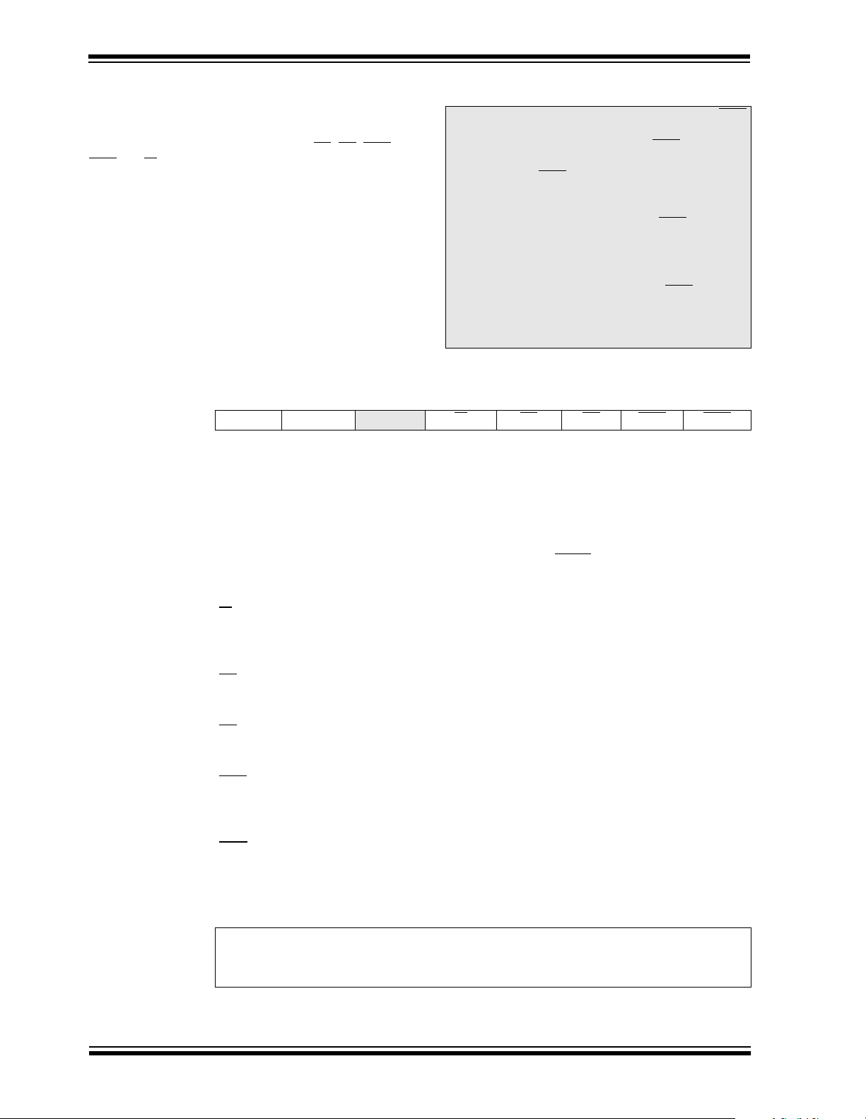
PIC18CXX8
4.13.1 RCON REGISTER
The Reset Control (RCON) regi ster contains flag bits
that allow differentiation between the sources of a
device RESET. These flags include the TO
BOR
and RI bits. This regis ter is rea dable and writabl e.
, PD, POR,
REGISTER 4-3: RCON REGISTER
R/W-0 R/W-0 U-0 R/W-1 R/W-1 R/W-1 R/W-0 R/W-0
IPEN LWRT
bit 7 bit 0
bit 7 IPEN: Interrupt Priority Enable bit
1 = Enable priority levels on interrupts
0 = Disable priority levels on interrupts (16CXXX compatibility mode)
bit 6 LWRT: Long Write Enable bit
1 = Enable TBLWT to internal program memory
Once this bit is set, it can only be cleared by a POR or MCLR
0 = Disable TBLWT to internal program memory; TBLWT only to external program memory
bit 5 Unimplemented: Read as '0'
bit 4 RI
bit 3 TO
bit 2 PD
bit 1 POR
bit 0 BOR
: RESET Instruction Flag bit
1 = The RESET instruction was not executed
0 = The RESET instruction was executed causing a device RESET
(must be set in software after a Brown-out Reset occurs)
: Watchdog Time-out Flag bit
1 = After power-up, CLRWDT instru ction, or SLEEP instruction
0 = A WDT time-out occurred
: Power-down Detection Flag bit
1 = After power-up or by the CLRWDT instruction
0 = B y execution of the SLEEP instruction
: Power-on Reset Status bit
1 = A Power-on Reset has not occurred
0 = A Power-on Reset occurred
(must be set in software after a Power-on Reset occurs)
: Brown-out Reset Status bit
1 = A Brown-out Reset has not occurred
0 = A Brown-out Reset occurred
(must be set in software after a Brown-out Reset occurs)
— RI TO PD POR BOR
Note 1: If the BOREN configuration bit is set, BOR
is ’1’ on Power-on Reset. If the BOREN
configuration bit is c lear, BOR
on Power-on Reset.
The BOR
not necessarily predictable if the
brown-out circuit is disabled (the BOREN
configuration bit is clear). BOR
be set by the user and ch ecke d on su bsequent RESETs to see if it is clear, indicating a brown-out has occurred.
2: It is recommended that the POR
after a Power-on Reset has been
detected, so that subsequent Power-on
Resets may be detected.
status bit is a “don't care” and is
Reset
is unknown
must then
bit be set
Legend:
R = Readable bit W = Writable bit U = Unimplemented bit, read as ‘0’
- n = Value at POR ’1’ = Bit is set ’0’ = Bit is cleared x = Bit is unknown
DS30475A-page 64 Advanced Information 2000 Microchip Technology Inc.

PIC18CXX8
5.0 TABLE READS/TABLE WRITES
All PICmicro® devices have two memory spaces: the
program memory space and the data memory space.
Table Reads and Table Writes have been provided to
move data between these two memory spa ces through
an 8-bit register (TABLAT).
The operations that allow the processor to move data
between the data and program memory spaces are:
• Table Read (TBLRD)
• Table Write (TBLWT)
FIGURE 5-1: TABLE READ OPERATION
TABLE POINTER
TBLPTRH TBLPTRL
(1)
PROGRAM MEMORY
Table Read operations retrieve data from program
memory and place it into the data memory space.
Figure 5-1 shows the operation of a Table Read with
program and data memory.
Table Write operations store data from the data memory space into program memory. Figure 5-2 shows the
operation of a Table Write with program and data
memory.
Table operations work with byte entities. A table block
containing data is n ot requi red to b e word align ed, so a
table block can start and end at any byte address. If a
table write is being used to write an executable program to program memory, program instructions will
need to be word aligned.
TABLE LATCH (8-bit)
TABLAT
FIGURE 5-2: TABLE WRITE OPERATION
2000 Microchip Technology Inc. Advanced Information DS30475A-page 65
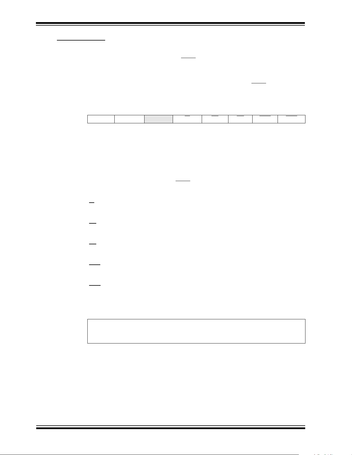
PIC18CXX8
5.1 Control Registers
Several control registers are used in conjunction with
the TBLRD and TBLWT instructions. These include:
• RCON register
• TABLAT register
• TBLPTR registers
5.1.1 RCON REGISTER
The L WRT bit specifi es the opera tion of Table Writes to
internal memory when the V
pin. When the LWRT bit is set, the controller
MCLR
continues to execute user code, but long table writes
are allowed (for programming internal program memory) from user mo de. The LWRT bit can be cl eared only
by performing either a POR or MCLR
REGISTER 5-1: RCON REGISTER (ADDRESS: 0xFD0h)
R/W-0 R/W-0 U-0 R/W-1 R/W-1 R/W-1 R/W-0 R/W-0
IPEN LWRT
bit 7 bit 0
bit 7 IPEN: Interrupt Priority Enable
1 = Enable priority levels on interrupts
0 = Disable priority levels on interrupts (16CXXX compatibility mode)
bit 6 LWRT: Long Write Enable
1 = Enable TBLWT to internal program memory
0 = Disable TBLWT to internal program memory.
Note 1: Only cleared on a POR or MCLR reset.
This bit has no effect on TBLWTs to external program memory.
bit 5 Unimplemented: Read as '0'
bit 4 RI
bit 3 TO: Time-out bit
bit 2 PD: Power-down bit
bit 1 POR: Power-on Reset Status bit
bit 0 BOR: Brown-out Reset Status bit
: RESET Instruction Flag bit
1 = No RESET instruction occurred
0 = A RESET instruction occurred
1 = After power-up, CLRWDT instruction, or SLEEP instruction
0 = A WDT time-out occurred
1 = After power-up or by t he CLRWDT instruction
0 = By execution of the SLEEP instruction
1 = No Power-on Reset occurred
0 = A Power-on Reset occurred (must be set in software after a Power-on Reset occurs)
1 = No Brown-out Reset nor POR Reset occurred
0 = A Brown-out Reset or POR Reset occurred
(must be set in software after a Brown-out Reset occurs)
— RI TO PD POR BOR
PP voltage is applied to th e
Reset.
Legend:
R = Readable bit W = Writable bit U = Unimplemented bit, read as ‘0’
- n = Value at POR ’1’ = Bit is set ’0’ = Bit is cleared x = Bit is unknown
DS30475A-page 66 Advanced Information 2000 Microchip Technology Inc.

PIC18CXX8
5.1.2 TABLAT - TABLE LATCH REGISTER
The T a ble Latch (TABLAT) is an 8-bi t register mapped
into the SFR space. The Table Latch is used to hold
8-bit data during data transfers between program
memory and data memory.
5.1.3 TBLPTR - TABLE POINTER REGISTER
The Table Pointer (TBLPTR) addresses a byte within
the program memory. The TBLPTR is comprised of
three SFR registers (Table Pointer Upper byte, High
byte and Low byte). These three registers
(TBLPTRU:TBLPTRH:TBLPTRL) join to form a 22-bit
wide pointer. The low order 21-bits allow the device to
address up to 2 Mbytes o f program memory spac e. The
22nd bit allows read only access to the Device ID, the
User ID and the Configuration bits.
The table pointer TBLPTR is used by t he TBLRD and
TBLWT instructions. These instructions can update the
TBLPTR in one of four ways based on the t a ble operation. These operations are shown in Table5-1.
These operations o n the TBL PTR only affect the l ow
order 21-bits.
TABLE 5-1: TABLE POINTER OPERATIONS WITH TBLRD AND TBLWT INSTRUCTIONS
Example Operation on Table Pointer
TBLRD*
TBLWT*
TBLRD*+
TBLWT*+
TBLRD*TBLWT*-
TBLRD+*
TBLWT+*
TBLPTR is not modified
TBLPTR is incremented after the read/write
TBLPTR is decremented after the read/write
TBLPTR is incremented before the read/write
2000 Microchip Technology Inc. Advanced Information DS30475A-page 67

PIC18CXX8
5.2 Program Memory Read/Writes
5.2.1 TABLE READ OVERVIEW (TBLRD)
The TBLRD in structions are used to read data from pr o-
gram memory to data memory.
TBLPTR points to a byte address in program space.
Executing TBLRD places the byte pointed to into
TABLAT. In addition, TBLPTR can be modified automatically for the next Table Read operation.
Table Reads from program memory are perform ed on e
byte at a time. The instruction will load T ABLAT with the
one byte from program memory poi nted to by TBLPTR .
5.2.2 PROGRAM MEMORY WRITE BLOCK SIZE
The program memory of PIC18CXX8 devices is written
in blocks. For PIC18CXX8 devices , the write block size
is 2 bytes. Consequently, Table Write operations to
program memory are performed in pairs, one byte at a
time.
When a Table Write occurs to an even program memory address (TBLP TR<0> = 0), the co ntents of TABLAT
are transferred to an internal holding register. This is
performed as a short write and the program memory
block is not actually programmed at this time. The
holding register is not accessible by the user.
When a Table Write occurs to a n odd p rogram memor y
address (TBLPTR <0> = 1), a long wri te is s tarted. During the long write, the contents of TABLAT are written
to the high byte of t he progr am m emory blo ck and t he
contents of the holding register are transferred to the
low byte of the program memory block.
Figure 5-3 shows the holding register and the program
memory write blocks.
If a single byte is to be programmed, the low (even)
byte of the destination program word should be read
using TBLRD*, modified or changed, if required, and
written back to the same address using TBLWT*+. The
high (odd) byte should be read using TBLRD*, modified
or changed if required, and written back to the same
address using TBLWT. The write to an odd address will
cause a long write to begin. This process ensures that
existing data in either byte will not be changed unless
desired.
FIGURE 5-3: HOLDING REGISTER AND THE WRITE
Program Memory Holding Register Instruction Execution
; TABLPTR points to address n
MOVLW DataLow ; Load low data
MSB LSB MOVWF TABLAT ; byte to TABLAT
DataLow TBLWT*+ ; Write it to LSB
; of Holding register
MOVLW DataHigh ; Load high data
n - 1 MSB LSB MOVWF TABLAT ; byte to TABLAT
n DataLow DataHigh DataLow TBLWT* ; Write it to MSB
n + 1 DataHigh ; of Holding
n + 2 ; register and
; begin long
; write
EXAMPLE 5-1: TABLE READ CODE EXAMPLE
; Read a byte from location 0x0020
CLRF TBLPTRU ; Load upper 5 bits of
; 0x0020
CLRF TBLPTRH ; Load higher 8 bits of
; 0x0020
MOVLW 0x20 ; Load 0x20 into
MOVWF TBLPTRL ; TBLPTRL
MOVWF TBLRD* ; Data is in TABLAT
DS30475A-page 68 Advanced Information 2000 Microchip Technology Inc.

PIC18CXX8
5.2.2.1 Long Write Operation
The long write is what actually programs words of data
into the internal me mory. When a TBLWT to the MSB of
the write block occurs, instruction execution is halted.
During this time, programming voltage and the data
stored in internal latche s is applied to program memory .
For a long write to occur:
1. MCLR
2. LWRT bit must be set
3. TBLWT to the address of the MSB of the write
If the LWRT bit is clear , a short write will oc cur an d program memory will not be changed. If the TBLWT is not
to the MSB of th e write block, t hen the program ming
phase is not initiated.
Setting the LWRT bit enables long writes when the
MCLR
is set, it can be cleared only by performing a POR or
MCLR Reset.
To ensure that the memory location has been well programmed, a minimum programming time is required.
The long write can be terminated after the programming time has expired by a RESET or an interrupt.
Having only one int errupt source en able d to ter minat e
the long write, ensures that no unintended interrupts
will prematurely terminate the long write.
/VPP pin must be at the programming
voltage
block
pin is taken to VPP voltage. Once the LWRT bit
5.2.2.2 Sequence of Events
The sequence of events for programming an internal
program memory location should be:
1. Enable the interrupt that terminates the long
write. Disable all other interrupts.
2. Clear the source interrupt flag.
3. If Interrupt Service Routine execution is desired
when the device wakes, enable global
interrupts.
4. Set LWRT bit in the RCON register.
5. Raise MCLR
voltage, V
6. Clear the WDT (if enabled).
7. Set the interrupt source to interrupt at the
required time.
8. Execute the Table Write for the lower (even)
byte. This will be a short write.
9. Execute the T able Wr ite for the upper (odd) b yte.
This will be a lo ng write. The con troller will HA L T
while programming. The interrupt wakes the
controller.
10. If GIE was set, service the interrupt request.
11. Go to 7 if more bytes to be programmed.
12. Lower MCLR
13. Verify the memory locati on (table read).
14. Reset the device.
/VPP pin to the programming
PP.
/VPP pin to VDD.
2000 Microchip Technology Inc. Advanced Information DS30475A-page 69

PIC18CXX8
5.2.3 LONG WRITE INTERRUPTS
The long write must be terminated by a RESET or any
interrupt.
The interrupt source must have its interrupt enable bit
set. When the source sets its interrupt flag, programming will terminate. This will occur regardless of the
settings of interrupt priori ty bits, the GIE/GIEH bit o r the
PIE/GIEL bit.
Depending on the states of interrupt priority bits, the
GIE/GIEH bit or the PIE/GIEL bit, program execution
can either be vectored to the high or low priority Interrupt Service Routine (ISR), or continue execution from
where programming commenced.
In either case, the interrupt flag will not be cleared
when programming is terminated and will need to be
cleared by the software.
5.3 Unexpected Termination of Write
Operations
If a write is terminated by an unplanned event such as
loss of power, an unexpected RESET, or an interrupt
that was not disabled, the memory location just programmed should be verified and reprogrammed if
needed.
TABLE 5-2: SLEEP MODE, INTERRUPT ENABLE BITS AND INTERRUPT RESULTS
GIE/
GIEH
XX X 0
X X X 1 0 Long write continues, will wake when
0
(default)0(default)
0
(default)
10
0
(default)
10
PIE/
GIEL
11
(default)
10
(default)1high priority
Priority
X 1 1 Terminates long write, executes next instruction.
high priority
(default)
0
low
low
(default)
Interrupt
Enable
(default)
1 1 Terminates long write, executes next instruction.
1 1 Terminates long write, executes next instruction.
1 1 Terminates long write, branches to low priority
1 1 Terminates long write, branches to high priority
Interrupt
Flag
X Long write continues even if interrupt flag
becomes set during SLEEP.
the interrupt flag is set.
Interrupt flag not cleared.
Interrupt flag not cleared.
Interrupt flag not cleared.
interrupt vector.
Interrupt flag can be cleared by ISR.
interrupt vector.
Interrupt flag can be cleared by ISR.
Action
DS30475A-page 70 Advanced Information 2000 Microchip Technology Inc.

PIC18CXX8
6.0 8 X 8 HARDWARE MULTIPLIER
An 8 x 8 hardware multiplier is included in the ALU of
the PIC18CXX8 devices. By making the multiply a
hardware operatio n, i t co mp letes in a single instruction
cycle. This is an unsign ed multiply that gives a 16-bit
result. The result is store d into th e 16-bit produ ct regi ster pair (PRODH:PRODL). The multiplier does not
affect any flags in the STATUS register.
Making the 8 x 8 multiplier execute in a single cycle
gives the following advantages:
• Higher computational throughput
• Reduces code size requirements for multiply algo-
rithms
The performance incre ase allows the device to be used
in applications previously reserved for Digital Signal
Processors.
Table 6-1 shows a performance comparison between
enhanced devic es using the sin gle cycle hard ware multiply, and performing the same function without the
hardware multiply.
TABLE 6-1: PERFORMANCE COMPARISON
Program
Routine Multiply Method
8 x 8 unsigned Without hardware multiply 13 69 6.9 µs27.6 µs69 µs
Hardware multiply 1 1 100 ns 400 ns 1 µs
8 x 8 signed Without hardware multiply 33 91 9.1 µs36.4 µs91 µs
Hardware multiply 6 6 600 ns 2.4 µs 6 µs
16 x 16 unsigned Without hardware multiply 21 242 24.2 µs96.8 µs 242 µs
Hardware multiply 24 24 2.4 µs 9.6 µs 24 µs
16 x 16 signed Without hardware multiply 52 254 25.4 µs102.6 µs 254 µs
Hardware multiply 36 36 3.6 µs 14.4 µs 36 µs
Memory
(Words)
Cycles
(Max)
Time
@ 40 MHz @ 10 MHz @ 4 MHz
2000 Microchip Technology Inc. Advanced Information DS30475A-page 71

PIC18CXX8
6.1 Operation
Example 6-1 shows the sequence to perform an 8 x 8
unsigned multiply. Only one instruction is required
when one argumen t of the multiply is already loaded in
the WREG register.
Example 6-2 shows the sequence to do an 8 x 8 signed
multiply. To account for the sign bits of the arguments,
each argument’s most significant bit (MSb) is tested
and the appropriate subtractions are done.
EXAMPLE 6-1: 8 x 8 UNSIGNED MULTIPLY
ROUTINE
MOVFF ARG1, WREG ;
MULWF ARG2 ; ARG1 * ARG2 ->
; PRODH:PRODL
EXAMPLE 6-2: 8 x 8 SIGNED MULTIPLY
ROUTINE
MOVFF ARG1, WREG
MULWF ARG2 ; ARG1 * ARG2 ->
; PRODH:PRODL
BTFSC ARG2, SB ; Test Sign Bit
SUBWF PRODH, F ; PRODH = PRODH
; - ARG1
MOVFF ARG2, WREG
BTFSC ARG1, SB ; Test Sign Bit
SUBWF PRODH, F ; PRODH = PRODH
; - ARG2
Example 6-3 shows the sequence to perform a 16 x 16
unsigned multiply. Equation 6-1 shows the algorithm
that is used. The 32-bit result is stored in 4 registers
RES3:RES0.
EQUATION 6-1: 16 x 16 UNSIGNED
MULTIPLICATION
ALGORITHM
RES3:RES0 = ARG1H:ARG1L • ARG2H:ARG2L
= (ARG1H
(ARG1H
(ARG1L
(ARG1L
• ARG2H • 2
• ARG2L • 2
• ARG2H • 2
• ARG2L)
16
)+
8
)+
8
)+
EXAMPLE 6-3: 16 x 16 UNSIGNED
MULTIPLY ROUTINE
MOVFF ARG1L, WREG
MULWF ARG2L ; ARG1L * ARG2L ->
; PRODH:PRODL
MOVFF PRODH, RES1 ;
MOVFF PRODL, RES0 ;
;
MOVFF ARG1H, WREG
MULWF ARG2H ; ARG1H * ARG2H ->
; PRODH:PRODL
MOVFF PRODH, RES3 ;
MOVFF PRODL, RES2 ;
;
MOVFF ARG1L, WREG
MULWF ARG2H ; ARG1L * ARG2H ->
; PRODH:PRODL
MOVF PRODL, W ;
ADDWF RES1, F ; Add cross
MOVF PRODH, W ; products
ADDWFC RES2, F ;
CLRF WREG ;
ADDWFC RES3, F ;
;
MOVFF ARG1H, WREG ;
MULWF ARG2L ; ARG1H * ARG2L ->
; PRODH:PRODL
MOVF PRODL, W ;
ADDWF RES1, F ; Add cross
MOVF PRODH, W ; products
ADDWFC RES2, F ;
CLRF WREG ;
ADDWFC RES3, F ;
DS30475A-page 72 Advanced Information 2000 Microchip Technology Inc.

PIC18CXX8
Example 6-4 shows the sequence to perform an 16 x
16 signed multiply. Equation 6-2 shows the algorithm
used. The 32-bit result is stored in four registers
RES3:RES0. To account for the sign bits of the arguments, each argument pairs most significant bit (MSb)
is tested and the appropriate subtractions are done.
EQUATION 6-2: 16 x 16 SIGNED
MULTIPLICATION
ALGORITHM
RES3:RES0
= ARG1H:ARG1L
= (ARG1H
(ARG1H
(ARG1L
(ARG1L
• ARG2H<7> • ARG1H:ARG1L • 2
(-1
(-1
• ARG1H<7> • ARG2H:ARG2L • 2
• ARG2H:ARG2L
• ARG2H • 2
• ARG2L • 2
• ARG2H • 2
• ARG2L) +
16
)+
8
)+
8
)+
16
)+
16
)
EXAMPLE 6-4: 16 x 16 SIGNED MULTIPLY
ROUTINE
MOVFF ARG1L, WREG
MULWF ARG2L ; ARG1L * ARG2L ->
; PRODH:PRODL
MOVFF PRODH, RES1 ;
MOVFF PRODL, RES0 ;
;
MOVFF ARG1H, WREG
MULWF ARG2H ; ARG1H * ARG2H ->
; PRODH:PRODL
MOVFF PRODH, RES3 ;
MOVFF PRODL, RES2 ;
;
MOVFF ARG1L, WREG
MULWF ARG2H ; ARG1L * ARG2H ->
; PRODH:PRODL
MOVF PRODL, W ;
ADDWF RES1, F ; Add cross
MOVF PRODH, W ; products
ADDWFC RES2, F ;
CLRF WREG ;
ADDWFC RES3, F ;
;
MOVFF ARG1H, WREG ;
MULWF ARG2L ; ARG1H * ARG2L ->
; PRODH:PRODL
MOVF PRODL, W ;
ADDWF RES1, F ; Add cross
MOVF PRODH, W ; products
ADDWFC RES2, F ;
CLRF WREG ;
ADDWFC RES3, F ;
;
BTFSS ARG2H, 7 ; ARG2H:ARG2L neg?
GOTO SIGN_ARG1 ; no, check ARG1
MOVFF ARG1L, WREG ;
SUBWF RES2 ;
MOVFF ARG1H, WREG ;
SUBWFB RES3
;
SIGN_ARG1
BTFSS ARG1H, 7 ; ARG1H:ARG1L neg?
GOTO CONT_CODE ; no, done
MOVFF ARG2L, WREG ;
SUBWF RES2 ;
MOVFF ARG2H, WREG ;
SUBWFB RES3
;
CONT_CODE
:
2000 Microchip Technology Inc. Advanced Information DS30475A-page 73

PIC18CXX8
NOTES:
DS30475A-page 74 Advanced Information 2000 Microchip Technology Inc.

PIC18CXX8
7.0 INTERRUPTS
The PIC18CXX8 devices have multiple interrupt
sources and an interrupt priority feature that allows
each interrupt source to be assigned a high priority
level or a low priority level. The high priority interrupt
vector is at 000008h and the low prio rity interrupt vector
is at 000018h. High priority interrupt events will override any low priority interrupts that may be in progress.
There are 13 registers that are use d to c ontrol interru pt
operation. These registers are:
• RCON
• INTCON
• INTCON2
• INTCON3
• PIR1, PIR2, PIR3
• PIE1, PIE2, PIE3
• IPR1, IPR2, IPR3
It is recommended that the Microchip header files supplied with MPLAB be used for the symbolic bit names
in these registers. This allows the assembler/compiler
to automatically take care of the placement of these
bits within the specified regis te r.
Each interrupt source has three bits to control its operation. The functions of these bits are:
• Flag bit to indicate that an interrupt event
occurred
• Enable bit that allows program execution to
branch to the interrupt vector address when
the flag bit is set
• Priority bit to select hi gh p rio rity or l ow pri orit y
The interrupt priority feature is enabled by setting the
IPEN bit (RCON register). When interrupt priority is
enabled, there are two bits that enable interrupts globally. Setting the GI EH bit (IN TCON regi ster) enab les
all interrupts that have the priority bit set. Setting the
GIEL bit (INTCON register) enables all interrupts that
have the pr iority bit cleared. When the interrup t flag,
enable bit and appropriate global interrupt enable bit
are set, the interrupt will v ector im media tely to add ress
000008h or 000018h, depending on the priority level.
Individual interrupts can be disabled through their corresponding enable bits.
When the IPEN bit is cleared (default state), the interrupt priority feature is disabled and interrupts are compatible with PICmicro
Compatibility mode, the interrupt priority bits for each
source have no effe ct. T he PEIE b it (IN TCO N regi st er)
enables/disables all peripheral interrupt sources. The
GIE bit (INTCON register) enab les/disables all in terrupt
sources. All interrupts branch to address 000008h in
Compatibility mo de.
When an interrupt is responded to, the Global Interrupt
Enable bit is cleared to d isable furth er interru pts. If the
IPEN bit is cleared, this is the GIE bit. If in terrupt pri ority levels are used, this will be eith er the GIEH or GIEL
bit. High priority interrupt sources can interrupt a low
priority interrupt.
The return address is pushed onto the stack and the
PC is loaded with the interrupt vector address
(000008h or 000018h). Once in the interrupt service
routine, the source(s) of the interrupt can be determined by polling the interrupt flag bits. The interrupt
flag bits must be cl eared in so ftware be fore re-enab ling
interrupts to avoid recursive interrupts.
The "return from interrupt" instruction, RETFIE, exits
the interrupt routine and set s the GIE bit (GIEH or GI EL
if priority levels are used), which re-enables interrupts.
For external interrupt events, such as the INT pins or
the PORTB input chang e interrupt, the i nterrupt latenc y
will be three to four instruction cycles. The exact
latency is the same for one or two cycle instructions.
Individual interrupt flag bits are set, regardless of the
status of their corresponding enable bit or the GIE bit.
®
mid-range devices. In
2000 Microchip Technology Inc. Advanced Information DS30475A-page 75

PIC18CXX8
FIGURE 7-1: INTERRUPT LOGIC
Peripheral Interrupt Flag bit
Peripheral Interrupt Enable bit
Peripheral Interrupt Priority bit
TMR1IF
TMR1IE
TMR1IP
XXXXIF
XXXXIE
XXXXIP
Additional Peripheral Interrupts
High Priority Interrupt Generation
Low Priority Interrupt Generation
IPEN
TMR0IF
TMR0IE
TMR0IP
INT0IF
INT0IE
INT1IF
INT1IE
INT1IP
INT2IF
INT2IE
INT2IP
INT3IF
INT3IE
INT3IP
IPEN
GIEL/PEIE
RBIF
RBIE
RBIP
IPEN
Wake-up if in SLEEP mode
Interrupt to CPU
Vector to location
0008h
GIE/GIEH
Peripheral Interrupt Flag bit
Peripheral Interrupt Enable bit
Peripheral Interrupt Priority bit
TMR1IF
TMR1IE
TMR1IP
XXXXIF
XXXXIE
XXXXIP
Additional Peripheral Interrupts
TMR0IF
TMR0IE
TMR0IP
RBIF
RBIE
RBIP
INT0IF
INT0IE
INT1IF
INT1IE
INT1IP
INT2IF
INT2IE
INT2IP
INT3IF
INT3IE
INT3IP
PEIE/GIEL
Interrupt to CPU
Vector to Location
0018h
DS30475A-page 76 Advanced Information 2000 Microchip Technology Inc.

PIC18CXX8
7.1 Control Registers
This section contains the control and status registers.
REGISTER 7-1: INTCON REGISTER
R/W-0 R/W-0 R/W-0 R/W-0 R/W-0 R/W-0 R/W-0 R/W-x
GIE/GIEH PEIE/GIEL TMR0IE INT0IE RBIE TMR0IF INT0IF RBIF
bit 7 bit 0
bit 7 GIE/GIEH: Global Interrupt Enable bit
When IPEN = 0:
1 = Enables all un-masked interrupts
0 = Disables all interrupts
When IPEN = 1
1 = Enables all high priority interrupts
0 = Disables all high priority interrupts
bit 6 PEIE/GIEL: Peripheral Interrupt Enable bit
hen IPEN = 0:
W
1 = Enables all un-masked peripheral interrupts
0 = Disables all peripheral interrupts
When IPEN = 1
1 = Enables all low priority peripheral interrupts
0 = Disables all priority peripheral interrupts
bit 5 TMR0IE: TMR0 Overflow Interrupt Enable bit
1 = Enables the TMR0 overflow interrupt
0 = Disables the TMR0 overflow interrupt
bit 4 INT0IE: INT0 External Interrupt Enable bit
1 = Enables the INT0 external interrupt
0 = Disables the INT0 external interrupt
bit 3 RBIE: RB Port Change Interrupt Enable bit
1 = Enables the RB port change interrupt
0 = Disables the RB port change inte rrupt
bit 2 TMR0IF: TMR0 Overflow Interrupt Flag bit
1 = TMR0 register has ov erflowed (must be clear ed in software)
0 = TMR0 register did not overflow
bit 1 INT0IF: INT0 External Interrupt Flag bit
1 = The INT0 external interrupt occurred (must be cleared in software by reading PORTB)
0 = The INT0 external interrupt did not occur
bit 0 RBIF: RB Port Change Interrupt Flag bit
1 = At least one of the RB7:RB4 pins changed state (must be cleared in software)
0 = None of the RB7:RB4 pins have changed state
:
:
7.1.1 INTCON REGISTERS
The INTCON Registers are readable and writable
registers, which contain various enable, priority, and
flag bits.
Legend:
R = Readable bit W = Writable bit U = Unimplemented bit, read as ‘0’
- n = Value at POR ’1’ = Bit is set ’0’ = Bit is cleared x = Bit is unknown
Note: Interrupt flag bits get set when an interrupt condition occurs, regardless of the state
of its corresponding enable bit or the global enable bit. Use r s oftwa re s ho uld ensure
the appropriate inte rrupt fla g bits ar e clea r pr ior to enabli ng an interrup t. This featu re
allows software polling.
2000 Microchip Technology Inc. Advanced Information DS30475A-page 77

PIC18CXX8
REGISTER 7-2: INTCON2 REGISTER
R/W-1 R/W-1 R/W-1 R/W-1 R/W-1 R/W-1 R/W-1 R/W-1
RBPU
bit 7 bit 0
bit 7 RBPU
1 = All PORTB pull-ups are disabled
0 = PORTB pull-ups are enabled by individual port latch values
bit 6 INTEDG0: External Interrupt 0 Edge Select bit
1 = Interrupt on rising edge
0 = Interrupt on falling edge
bit 5 INTEDG1: External Interrupt 1 Edge Select bit
1 = Interrupt on rising edge
0 = Interrupt on falling edge
bit 4 INTEDG2: External Interrupt 2 Edge Select bit
1 = Interrupt on rising edge
0 = Interrupt on falling edge
bit 3 INTEDG3: External Interrupt 3 Edge Select bit
1 = Interrupt on rising edge
0 = Interrupt on falling edge
bit 2 TMR0IP: TMR0 Overflow Interrupt Priority bit
1 = High priority
0 = Low priority
bit 1 INT3IP: INT3 External Interrupt Priority bit
1 = High priority
0 = Low priority
bit 0 RBIP: RB Port Change Interrupt Priority bit
1 = High priority
0 = Low priority
INTEDG0 INTEDG1 INTEDG2 INTEDG3 TMR0IP INT3IP RBIP
: PORTB Pull-up Enable bit
Legend:
R = Readable bit W = Writable bit U = Unimplemented bit, read as ‘0’
- n = Value at POR ’1’ = Bit is set ’0’
DS30475A-page 78 Advanced Information 2000 Microchip Technology Inc.

REGISTER 7-3: INTCON3 REGISTER
R/W-1 R/W-1 R/W-0 R/W-0 R/W-0 R/W-0 R/W-0 R/W-0
INT2IP INT1IP INT3IE INT2IE INT1IE INT3IF INT2IF INT1IF
bit 7 bit 0
bit 7 INT2IP:
PIC18CXX8
2000 Microchip Technology Inc. Advanced Information DS30475A-page 79

PIC18CXX8
7.1.2 PIR REGISTERS
The Peripheral Interrupt Request (PIR) registers con-
tain the individual flag bits for the peripheral interrupts
(Register 7-5). Due to the number of peripheral interrupt sources, there are three Peripheral Interrupt
Request (Flag) registers (PIR1, PIR2, PIR3).
Note 1: Interrupt flag bits are set when an interrupt
condition occurs, re gardless of th e state of
its corresponding enable bit or the global
enable bit, GIE (INTCON register).
2: User software sh ould en sure th e approp ri-
ate interru pt flag bits are clea red prior to
enabling an interrupt, and after servicing
that interrupt.
REGISTER 7-4: RCON REGISTER
R/W-0 R/W-0 U-0 R/W-1 R/W-1 R/W-1 R/W-0 R/W-0
7.1.3 PIE REGISTERS
The Peripheral Interrupt Enable (PIE) registers contain
the individual enable bits for the peripheral interrupts
(Register 7-5). Due to the number of peripheral interrupt sources, there are three Peripheral Interrupt
Enable registers (PIE1, PIE2, PIE3). When IPEN is
clear, the PEIE bit must be set to enable any of these
peripheral interrupts.
7.1.4 IPR REGISTERS
The Interrupt Priority (IPR) regis ters contain the indivi d-
ual priority bits for the peripheral interrupts
(Register 7-7). Due to the number of peripheral interrupt sources, there are three Peri pheral Interrupt Pri ority registers (IPR1, IPR2, IPR3). The operation of the
priority bits requires that the Interrup t Priority Enable b it
(IPEN) be set.
7.1.5 RCON REGISTER
The Reset Control ( RCON) register contains the bit th at
is used to enable prioritized interrupts (IPEN).
IPEN LWRT
bit 7 bit 0
bit 7 IPEN: Interrupt Priority Enable bit
1 = Enable priority levels on interrupts
0 = Disable priority levels on interrupts (16CXXX compatibility mode)
bit 6 LWRT: Long Write Enable
For details of bit operation see Register 4-3
bit 5 Unimplemented: Read as '0'
bit 4 RI
bit 3 TO
bit 2 PD
bit 1 POR
bit 0 BOR
: RESET Instruction Flag bit
For details of bit operation see Register 4-3
: Watchdog Time-out Flag bit
For details of bit operation see Register 4-3
: Power-down Detection Flag bit
For details of bit operation see Register 4-3
: Power-on Reset Status bit
For details of bit operation see Register 4-3
: Brown-out Reset Status bit
For details of bit operation see Register 4-3
Legend:
R = Readable bit W = Writable bit U = Unimplemented bit, read as ‘0’
- n = Value at POR ’1’ = Bit is set ’0’ = Bit is cleared x = Bit is unknown
— RI TO PD POR BOR
DS30475A-page 80 Advanced Information 2000 Microchip Technology Inc.

PIC18CXX8
REGISTER 7-5: PIR REGISTERS
R/W-0 R/W-0 R-0 R-0 R/W-0 R/W-0 R/W-0 R/W-0
PIR1 PSPIF ADIF RCIF TXIF SSPIF CCP1IF TMR2IF TMR1IF
bit 7 bit 0
U-0 R/W-0 U-0 U-0 R/W-0 R/W-0 R/W-0 R/W-0
PIR2
bit 7 bit 0
PIR3 IRXIF WAKIF ERRIF TXB2IF TXB1IF TXB0IF RXB1IF RXB0IF
bit 7 bit 0
PIR1 bit 7 PSPIF: Parallel Slave Port Read/Write Interrupt Flag bit
bit 6 ADIF: A/D Converter Interrupt Flag bit
bit 5 RCIF: USART Receive Interrupt Flag bit
bit 4 TXIF: USART Transmit Interrupt Flag bit
bit 3 SSPIF: Master Synchronous Serial Port Interrupt Flag bit
bit 2 CCP1IF: CCP1 Interrupt Flag bit
bit 1 TMR2IF: TMR2 to PR2 Match Interrupt Flag bit
bit 0 TMR1IF: TMR1 Overflow Interrupt Flag bit
— CMIF — — BCLIF LVDIF TMR3IF CCP2IF
R/W-0 R/W-0 R/W-0 R/W-0 R/W-0 R/W-0 R/W-0 R/W-0
1 = A read or a write operation has taken place
(must be cleared in software)
0 = No read or write has occurred
1 = An A/D conversion completed
(must be cleared in software)
0 = The A/D conversion is not complete
1 = The USART receive buffer, RCREG, is full
(cleared when RCREG is read)
0 = The USART receive buffer is empty
1 = The USART transmit buffer, TXREG, is empty
(cleared when TXREG is written)
0 = The USART transmit buffer is full
1 = The transmission/reception is complete
(must be cleared in software)
0 = Waiting to transmit/receive
Capture Mode
1 = A TMR1 register capture occurred
(must be cleared in software)
0 = No TMR1 register capture occurred
Compare Mode
1 = A TMR1 register compare match occurred
(must be cleared in software)
0 = No TMR1 register compare match occurred
PWM Mode
Unused in this mode
1 = TMR2 to PR2 match occurred
(must be cleared in software)
0 = No TMR2 to PR2 match occurred
1 = TMR1 register overflowed
(must be cleared in software)
0
2000 Microchip Technology Inc. Advanced Information DS30475A-page 81

PIC18CXX8
REGISTER 7-5: PIR REGISTERS (CONT’D)
PIR2 bit 7 Unimplemented: Read as’0’
bit 6 CMIF: Comparator Interrupt Flag bit
1 = Comparator input has changed
0 = Comparator input has not changed
bit 5-4 Unimplemented: Read as’0’
bit 3 BCLIF: Bus Collision Interrupt Flag bit
1 = A Bus Collision occurred
(must be cleared in software)
0 = No Bus Collision occurred
bit 2 LVDIF: Low Voltage Detect Interrupt Flag bit
1 = A low voltage condition occurred
(must be cleared in software)
0 = The device voltage is above the Low Voltage Detect trip point
bit 1 TMR3IF: TMR3 Overflow Interrupt Flag bit
1 = TMR3 regi ster overflowed
(must be cleared in software)
0 = TMR3 register did not overflow
bit 0 CCP2IF: CCPx Interrupt Flag bit
Capture Mod
1 = A TMR1 register capture occurred
(must be cleared in software)
0 = No TMR1 register capture occurred
Compare Mode
1 = A TMR1 register compare match occurred
(must be cleared in software)
0 = No TMR1 register compare match occurred
PWM Mode
Unused in this mode
e
DS30475A-page 82 Advanced Information 2000 Microchip Technology Inc.

REGISTER 7-5: PIR REGISTERS (CONT’D)
PIR3 bit 7 IRXIF: Invalid Message Received Interrupt Flag bit
1 = An invalid message has occurred on the CAN bus
0 = An invalid message has not occurred on the CAN bus
bit 6 WAKIF: Bus Activity Wake-up Interrupt Flag bit
1 = Activity on the CAN bus has occurred
0 = Activity on the CAN bus has not occurred
bit 5 ERRIF: CAN Bus Error Interrupt Flag bit
1 = An error has occurred in the CAN module (multiple sources)
0 = An error has not occurred in the CAN module
bit 4 TXB2IF: Transmit Buffer 2 Interrupt Flag bit
1 = Transmit Buffer 2 has completed transmission of a message, and may be reloaded
0 = Transmit Buffer 2 has not completed transmission of a message
bit 3 TXB1IF: Transmit Buffer 1 Interrupt Flag bit
1 = Transmit Buffer 1 has completed transmission of a message, and may be reloaded
0 = Transmit Buffer 1 has not completed transmission of a message
bit 2 TXB0IF: Transmit Buffer 0 Interrupt Flag bit
1 = Transmit Buffer 0 has completed transmission of a message, and may be reloaded
0 = Transmit Buffer 0 has not completed transmission of a message
bit 1 RXB1IF: Receive Buffer 1 Interrupt Flag bit
1 = Receive Buffer 1 has received a new message
0 = Receive Buffer 1 has not received a new message
bit 0 RXB0IF: Receive Buffer 0 Interrupt Flag bit
1 = Receive Buffer 0 has received a new message
0 = Receive B uffer 0 has not received a new message
PIC18CXX8
Legend:
R = Readable bit W = Writable bit U = Unimplemented bit, read as ‘0’
- n = Value at POR ’1’ = Bit is set ’0’ = Bit is cleared x = Bit is unknown
2000 Microchip Technology Inc. Advanced Information DS30475A-page 83

PIC18CXX8
REGISTER 7-6: PIE REGISTERS
R/W-0 R/W-0 R/W-0 R/W-0 R/W-0 R/W-0 R/W-0 R/W-0
PIE1 PSPIE ADIE RCIE TXIE SSPIE CCP1IE TMR2IE TMR1IE
bit 7 bit 0
U-0 R/W-0 U-0 U-0 R/W-0 R/W-0 R/W-0 R/W-0
PIE2
PIE3 IVRE WAKIE ERRIE TXB2IE TXB1IE TXB0IE RXB1IE RXB0IE
bit 7 bit 0
PIE1 bit 7 PSPIE: Parallel Slave Port Read/Write Interrupt Enable bit
bit 6 ADIE: A/D Converter Interrupt Enable bit
bit 5 RCIE: USART Receiv e Interru pt Enab le bit
bit 4 TXIE: USART Transmit Interrupt Enable bit
bit 3 SSPIE: Master Synchronous Serial Port Interrupt Enable bit
bit 2 CCP1IE: CCP1 Interrupt Enable bit
bit 1 TMR2IE: TMR2 to PR2 Match Interrupt Enable bit
bit 0 TMR1IE: TMR1 Overflow Interrupt Enable bit
— CMIE — — BCLIE LVDIE TMR3IE CCP2IE
bit 7 bit 0
R/W-1 R/W-1 R/W-1 R/W-1 R/W-1 R/W-1 R/W-1 R/W-1
1 = Enables the PSP read/write interrupt
0 = Disables the PSP read/write interrupt
1 = Enables the A/D interrupt
0 = Disables the A/D interrupt
1 = Enables the USART receive interrupt
0 = Disables the USART receive interrupt
1 = Enables the USART transmit interrupt
0 = Disables the USART transmit interrupt
1 = Enables the MSSP interrupt
0 = Disables the MSSP interrupt
1 = Enables the CCP1 interrupt
0 = Disables the CCP1 interrupt
1 = Enables the TMR2 to PR2 match interrupt
0 = Disables the TMR2 to PR2 match interrupt
1 = Enables the TMR1 overflow interrupt
0 = Disables the TMR1 overflow interrupt
DS30475A-page 84 Advanced Information 2000 Microchip Technology Inc.

REGISTER 7-6: PIE REGISTERS (CONT’D)
PIE2 bit 7 Unimplemented: Read as ’0’
bit 6 CMIE: Comparator Interrupt Enable bit
1 = Enables the comparator interrupt
0 = Disables the comparator interrupt
bit 5-4 Unimplemented: Read as ’0’
bit 3 BCLIE: Bus Collision Interrupt Enable bit
1 = Enabled
0 = Disabled
bit 2 LVDIE: Low-voltage Detect Interrupt Enable bit
1 = Enabled
0 = Disabled
bit 1 TMR3IE: TMR3 Overflow Interru pt Enab le bit
1 = Enables the TMR3 overflow interrupt
0 = Disables the TMR3 overflow interrupt
bit 0 CCP2IE: CCP2 Interrupt Enable bit
1 = Enables the CCP2 interrupt
0 = Disables the CCP2 interrupt
PIE3 bit 7 IVRE: Invalid CAN Message Received Interrupt Enable bit
1 = Enables the Invalid CAN Message Received Interrupt
0 = Disables the Invalid CAN Message Received Interrupt
bit 6 WAKIE: Bus Activity Wake-up Interrupt Enable bit
1 = Enables the Bus Activity Wake-Up Interrupt
0 = Disables the Bus Activity Wake-Up Interrupt
bit 5 ERRIE: CAN Bus Error Interrupt Enable bit
1 = Enables the CAN Bus Error Interrupt
0 = Disables the CAN Bus Error Interrupt
bit 4 TXB2IE: Transmit Buffer 2 Interrupt Enable bit
1 = Enables the Transmit Buffer 2 Interrupt
0 = Disables the Transmit Buffer 2 Interrupt
bit 3 TXB1IE: Transmit Buffer 1 Interrupt Enable bit
1 = Enables the Transmit Buffer 1 Interrupt
0 = Disables the Transmit Buffer 1 Interrupt
bit 2 TXB0IE: Transmit Buffer 0 Interrupt Enable bit
1 = Enables the Transmit Buffer 0 Interrupt
0 = Disables the Transmit Buffer 0 Interrupt
bit 1 RXB1IE: Receive Buffer 1 Interrupt Enable bit
1 = Enables the Receive Buffer 1 Interrupt
0 = Disables the Receive Buffer 1 Interrupt
bit 0 RXB0IE: Receive Buffer 0 Interrupt Enable bit
1 = Enables the Receive Buffer 0 Interrupt
0 = Disables the Receive Buffer 0 Interrupt
PIC18CXX8
Legend:
R = Readable bit W = Writable bit U = Unimplemented bit, read as ‘0’
- n = Value at POR ’1’ = Bit is set ’0’ = Bit is cleared x = Bit is unknown
2000 Microchip Technology Inc. Advanced Information DS30475A-page 85

PIC18CXX8
REGISTER 7-7: IPR REGISTERS
R/W-1 R/W-1 R/W-1 R/W-1 R/W-1 R/W-1 R/W-1 R/W-1
IPR1 PSPIP ADIP RCIP TXIP SSPIP CCP1IP TMR2IP TMR1IP
bit 7 bit 0
U-0 R/W-1 U-0 U-0 R/W-1 R/W-1 R/W-1 R/W-1
IPR2
bit 7 bit 0
IPR3 IVRP WAKIP ERRIP TXB2IP TXB1IP TXB0IP RXB1IP RXB0IP
bit 7 bit 0
IPR1 bit 7 PSPIP: Parallel Slave Port Read/Write Interrupt Priority bit
bit 6 ADIP: A/D Converter Interrupt Priority bit
bit 5 RCIP: USART Receive Interrupt Priority bit
bit 4 TXIP: USART Transmit Interrupt Priority bit
bit 3 SSPIP: Master Synchronous Serial Port Interrupt Priority bit
bit 2 CCP1IP: CCP1 Interrupt Priority bit
bit 1 TMR2IP: TMR2 to PR2 Match Interrupt Priority bi t
bit 0 TMR1IP: TMR1 Overflow Interrupt Priority bit
— CMIP — — BCLIP LVDIP TMR3IP CCP2IP
R/W-1 R/W-1 R/W-1 R/W-1 R/W-1 R/W-1 R/W-1 R/W-1
1 = High priority
0 = Low priority
1 = High priority
0 = Low priority
1 = High priority
0 = Low priority
1 = High priority
0 = Low priority
1 = High priority
0 = Low priority
1 = High priority
0 = Low priority
1 = High priority
0 = Low priority
1 = High priority
0 = Low priority
DS30475A-page 86 Advanced Information 2000 Microchip Technology Inc.

REGISTER 7-7: IPR REGISTERS (CONT’D)
IPR2 bit 7 Unimplemented: Read as ’0’
bit 6 CMIP: Comparator Interrupt Priority bit
1 = High prio rity
0 = Low priority
bit 5-4 Unimplemented: Read as ’0’
bit 3 BCLIP: Bus Collision Interrupt Priority bit
1 = High prio rity
0 = Low priority
bit 2 LVDIP: Low Voltage Detect Interrupt Priority bit
1 = High priority
0 = Low priority
bit 1 TMR3IP: TMR3 Overflow Interrupt Priority bit
1 = High priority
0 = Low priority
bit 0 CCP2IP: CCP2 Interrupt Priority bit
1 = High priority
0 = Low priority
IPR3 bit 7 IVRP: Invalid Message Received Interrupt Priority bit
1 = High prio rity
0 = Low priority
bit 6 WAKIP: Bus Activity Wake-up Interrupt Priority bit
1 = High prio rity
0 = Low priority
bit 5 ERRIP: CAN Bus Error Interrupt Priority bit
1 = High prio rity
0 = Low priority
bit 4 TXB2IP: Transmit Buffer 2 Interrupt Priority bit
1 = High prio rity
0 = Low priority
bit 3 TXB1IP: Transmit Buffer 1 Interrupt Priority bit
1 = High prio rity
0 = Low priority
bit 2 TXB0IP: Transmit Buffer 0 Interrupt Priority bit
1 = High prio rity
0 = Low priority
bit 1 RXB1IP: Receive Buffer 1 Interrupt Priority bit
1 = High prio rity
0 = Low priority
bit 0 RXB0IP: Receive Buffer 0 Interrupt Priority bit
1 = High prio rity
0 = Low priority
PIC18CXX8
Legend:
R = Readable bit W = Writable bit U = Unimplemented bit, read as ‘0’
- n = Value at POR ’1’ = Bit is set ’0’ = Bit is cleared x = Bit is unknown
2000 Microchip Technology Inc. Advanced Information DS30475A-page 87

PIC18CXX8
7.1.6 INT INTERRUPTS
External interrupts on the RB0/INT0, RB1/INT1,
RB2/INT2, and RB3/INT3 pins are edge triggered:
either risi ng if the c orre spon din g INT EDG x bit is se t in
the INTCON2 register, or falling, if the INTEDGx bit is
clear . When a val id edge appe ars on the RBx/IN Tx pin,
the corresponding flag bit INTxIF is set. This interrupt
can be disabled by clearing the corresponding enable
bit INTxIE. Flag bit INTxIF must be cleared in software
in the Interrupt Service Routine before re-enabling the
interrupt. All external interrupts (INT0, INT1, INT2, and
INT3) can wake-up the processor from SLEEP, if bit
INTxIE was set prior to going into SLEEP. If the global
interrupt enable bi t GIE is set, the processor wil l branch
to the interrupt vector following wake-up.
Interrupt priority for INT1, INT 2 and INT3 is determine d
by the value contained in the interrupt priority bits
INT1IP (INTCON3 register), INT3IP (INTCON3 register), and INT2IP (INTCON2 register). There i s no priority bit associated with INT0; it is always a high priority
interrupt source.
7.1.7 TMR0 INTERRUPT
In 8-bit mode (wh ich is the de fault), an ov erflow (FFh →
00h) in the TMR0 register will set flag bit TMR0IF. In
16-bit mode, an overflow (FFFFh → 0000h) in the
TMR0H:TMR0L registers will set flag bit TMR0IF. The
interrupt can be enabled/disabled by setting/clearing
enable bit TMR0IE (INTCON register). Interrupt pri ority
for Timer0 is determined by the value contained in the
interrupt priority bit TMR0IP (INTCON2 register). See
Section 10.0 for further details on the Timer0 module.
7.1.8 PORTB INTERRUPT-ON-CHANGE
An input change on PORTB<7:4> sets flag bit RBIF
(INTCON register). The interrupt can be enabled/
disabled by setting/clearing enable bit RBIE (INTCON
register). Interrupt priority for PORTB interrupton-change is determined by the value contained in the
interrupt priority bit RBIP (INTCON2 register).
7.2 Context Saving During Interrupts
During an interrupt, the return PC v alue is sa ved on the
stack. Additionally, the WREG, STATUS and BSR registers are saved on the fast return stack. I f a fast return
from interrupt is not used (See Section 4.3), the user
may need to save the WREG, STATUS and BSR registers in software. Depending on the user’s application,
other registers may also need to be saved.
Example 7-1 saves and restores the WREG, STATUS
and BSR registers during an In terrupt Serv ice Rou tine.
EXAMPLE 7-1: SAVING STATUS, WREG AND BSR REGISTERS IN RAM
MOVWF W_TEMP ; W_TEMP is in Low Access bank
MOVFF STATUS, STATUS_TEMP ; STATUS_TEMP located anywhere
MOVFF BSR, BSR_TEMP ; BSR located anywhere
;
; USER ISR CODE
;
MOVFF BSR_TEMP, BSR ; Restore BSR
MOVF W_TEMP, W ; Restore WREG
MOVFF STATUS_TEMP, STATUS ; Restore STATUS
DS30475A-page 88 Advanced Information 2000 Microchip Technology Inc.
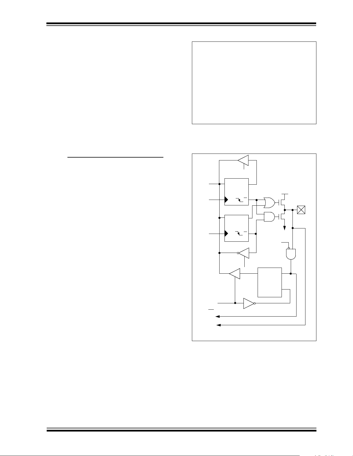
PIC18CXX8
8.0 I/O PORTS
Depending on the device selected, there are up to
eleven ports available. Some pins of the I/O ports are
multiplexe d wi th an a lter nat e fu nct ion from th e pe ri pheral features on the device. In general, when a peripheral is enabled, that pin may not be used as a general
purpose I/ O pin.
Each port has three registers for its operation. These
registers are:
• TRIS register (Data Direction register)
• PORT register (reads the level s on the pins of the
device)
• LAT register (output latch)
The data latch (LAT register) is useful for
read-modify-write operations on the value that the I/O
pins are driving.
8.1 PORTA, TRISA and LATA Registers
PORTA is a 6-bit wide, bi-directional port. The corresponding Data Direction register is TRISA. Setting a
TRISA bit (=1) will make t he co rrespon ding POR TA pin
an input (i.e., put the corresponding output driver in a
hi-impedance mode). Clearing a TRISA bit (=0) will
make the correspondin g POR TA pin an output (i.e., put
the contents of the output latch on the selected pin).
On a Power-on Reset, these pins are configured as
inputs and read as '0'.
Reading the PORTA register reads the status of the
pins, whereas writing to it will write to the port latch.
Read-modify-write operations on the LATA register,
reads and writes the latched output value for PORTA.
The RA4 pin is multiplexed with the Timer0 module
clock input to become the RA4/T0CKI pin. The
RA4/T0CKI pin is a Schmitt Trigger input and an open
drain output. All other R A po rt pin s h ave TTL inpu t le vels and full CMOS output drivers.
The other PORTA pins are multiplexed with analog
inputs and the analog V
operation of each p in is se lected by clearing /settin g the
control bits in the ADCON1 register (A/D Control
Register1). On a Power-on Reset, these pins are configured as analog inputs and read as '0'.
The TRISA register controls the direction of the RA
pins, even when they are bei ng u se d as ana lo g inputs.
The user must ensure the bits in the TRISA register are
maintained set when using them as analog inputs.
REF+ and VREF- inputs. The
EXAMPLE 8-1: INITIALIZING PORTA
CLRF PORTA ; Initialize PORTA by
; clearing output
; data latches
CLRF LATA ; Alternate method
; to clear output
; data latches
MOVLW 0x07 ; Configure A/D
MOVWF ADCON1 ; for digital inputs
MOVLW 0xCF ; Value used to
; initialize data
; direction
MOVWF TRISA ; Set RA3:RA0 as inputs
; RA5:RA4 as outputs
FIGURE 8-1: RA3:RA0 AND RA5 PINS
BLOCK DIAGRAM
RD LATA
Data
Bus
WR LATA
or
WR PORTA
WR TRISA
RD PORTA
SS Input (RA5 only)
To A/D Converter and LVD Modules
Note 1: I/O pins have diode protection to VDD and VSS.
Data Latch
CK
CK
TRIS Latch
QD
Q
QD
Q
RD TRISA
VDD
P
N
V
SS
Analog
Input
Mode
QD
EN
I/O Pin
TTL
Input
Buffer
(1)
2000 Microchip Technology Inc. Advanced Information DS30475A-page 89
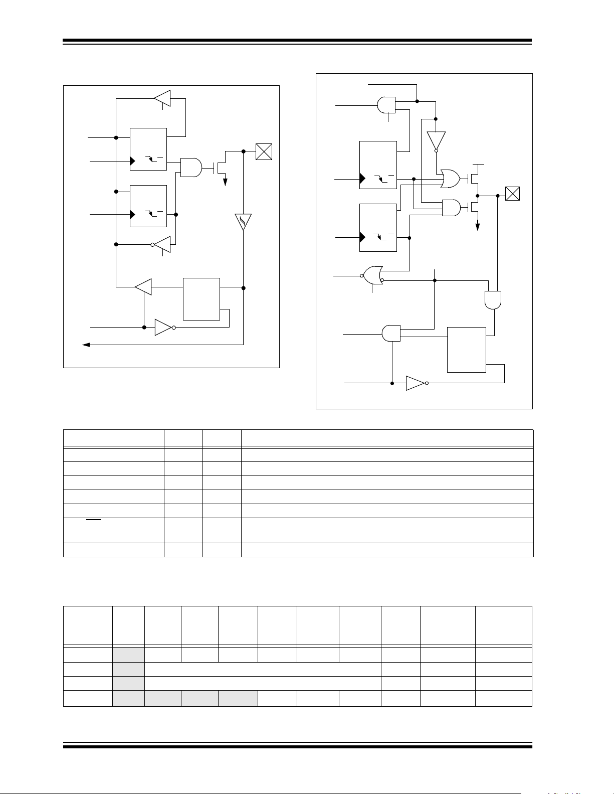
PIC18CXX8
FIGURE 8-2: RA4/T0CKI PIN BLOCK
DIAGRAM
Data
Bus
WR LATA
or
WR PORTA
WR TRISA
RD PORTA
TMR0 Clock Input
RD LATA
D
CK
Data Latch
CK
TRIS Latch
RD TRISA
Q
Q
QD
Q
N
SS
V
Schmitt
Trigger
Input
Buffer
QD
EN
EN
I/O Pin
FIGURE 8-3: RA6 BLOCK DIAGRAM
ECRA6 or
RCRA6 Enable
Data
Bus
RD LATA
QD
(1)
WR LATA
or
WR PORTA
WR
TRISA
Data Bus
Data Bus
CK
Data Latch
CK
TRIS Latch
RD TRISA
Q
QD
Q
ECRA6 or
RCRA6
Enable
VDD
P
I/O Pin
N
V
SS
QD
TTL
Input
Buffer
(1)
Note 1: I/O pin has diode protection to V
SS only.
EN
RD PORTA
Note 1: I/O pins have diode protection to VDD and VSS.
TABLE 8-1: PORTA FUNCTIONS
Name Bit# Buffer Function
RA0/AN0 bit0 TTL Input/output or analog input.
RA1/AN1 bit1 TTL Input/output or analog input.
RA2/AN2/V
RA3/AN3/VREF+ bit3 TTL Input/output or analog input or VREF+.
RA4/T0CKI bit4 ST/OD Input/output or external clock input for Timer0 output is open drain type.
RA5/SS/
OSC2/CLKO/RA6 bit6 TTL OSC2 or clock output or I/O pin.
Legend: TTL = TTL input, ST = Schmitt Trigger input, OD = Open Drain
TABLE 8-2: SUMMARY OF REGISTERS ASSOCIATED WITH PORTA
Name Bit 7 Bit 6 Bit 5 Bit 4 Bit 3 Bit 2 Bit 1 Bit 0
REF- bit2 TTL Input/output or analog input or VREF-.
AN4/LVDIN bit5 TTL Input/output or slave select input for synchronous serial port or analog
input, or low voltage detect input.
Valu e on
POR,
BOR
Value on all
other
RESETS
PORTA
— RA6 RA5 RA4 RA3 RA2 RA1 RA0 -x0x 0000 -uuu uuuu
LATA — Latch A Data Output Register -xxx xxxx -uuu uuuu
TRISA — PORTA Data Direction Register -111 1111 -111 1111
ADCON1
— — VCFG1 VCFG0 PCFG3 PCFG2 PCFG1 PCFG0 --00 0000 --uu uuuu
Legend: x = unknown, u = unchanged, - = unimplemented locations read as '0'.
Shaded cells are not used by PORTA.
DS30475A-page 90 Advanced Information 2000 Microchip Technology Inc.
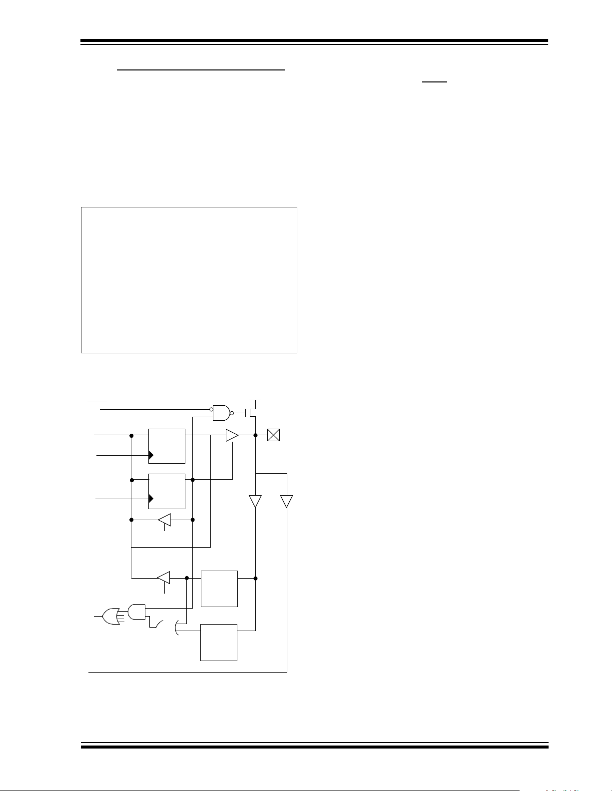
PIC18CXX8
8.2 PORTB, TRISB and LATB Registers
PORTB is an 8-bit wide bi-directional port. The corresponding Data Direction register is TRISB. Setting a
TRISB bit (=1) will make the corres ponding POR TB pi n
an input (i.e., put the corresponding output driver in a
hi-impedance mode). Clearing a TRISB bit (=0) will
make the corresponding PORTB pin an output ( i.e.,
put the contents of the output latch on the selected pin).
Read-modify-write operations on the LATB register
read and write the latched output value for PORTB.
EXAMPLE 8-2: INITIALIZING PORTB
CLRF PORTB ; Initialize PORTB by
; clearing output
; data latches
CLRF LATB ; Alternate method
; to clear output
; data latches
MOVLW 0xCF ; Value used to
; initialize data
; direction
MOVWF TRISB ; Set RB3:RB0 as inputs
; RB5:RB4 as outputs
; RB7:RB6 as inputs
FIGURE 8-4: RB7:RB4 PINS BLOCK
DIAGRAM
V
TTL
Input
Buffer
DD
P
Weak
Pull-up
I/O pin
(1)
(2)
RBPU
Data Bus
WR LATB
WR TRISB
Data Latch
QD
CK
TRIS Latch
QD
CK
Each of the PORTB pi ns has a wea k inte rnal pul l-up. A
single control bit can turn on all the pull- ups. This is performed by cl eari ng b it RB PU
(INTCON2 register). The
weak pull -up is au tomati cally t urned off when th e port
pin is configured as an output. The pull-ups are disabled on a Power-on Reset.
Four of PORTB’s pins, RB7:RB4, have an
interrupt-on-change feature. Only pins configured as
inputs can cause this interrupt to occur (i.e., any
RB7:RB4 pin configured as an output is excluded from
the interrupt-on-change comparison). The input pins
(of RB7:RB4) are compared with the old value latched
on the last r e ad of P ORTB. Th e “mismatch” outputs of
RB7:RB4 are OR’d together to generate the RB Port
Change Interrupt w ith f lag bit RBIF (INTC ON reg ister).
This interrupt can wake the device from SLEEP. The
user, in the Interrupt Service Routine, can clear the
interrupt in the following manner:
a) Any read or write of PORTB (except with the
MOVFF instruction) . This will end the mismatch
condition.
b) Clear flag bit RBIF.
A mismatch c ond it i on wi ll cont i n ue to s et f lag bi t RB IF.
Reading PORTB will end the mismatch condition and
allow flag bit RBIF to be cleared.
The interrupt-on-change feature is recommended for
wake-up on key depression operation and operations
where PORTB is only used for the interrupt on change
feature. Polling of PORTB is not recommended while
using the interrupt-on-change feature.
FIGURE 8-5: RB3:RB0 PINS BLOCK
DIAGRAM
RD TRISB
Latch
QD
Set RBIF
From other
RB7:RB4 pins
2000 Microchip Technology Inc. Advanced Information DS30475A-page 91
RD PORTB
EN
QD
EN
RD PORTB

PIC18CXX8
TABLE 8-3: PORTB FUNCTIONS
Name Bit# Buffer Function
RB0/INT0 bit0 TTL/ST
RB1/INT1 bit1 TTL/ST
RB2/INT2 bit2 TTL/ST
RB3/INT3 bit3 TTL/ST
RB4 bit4 TTL Input/output pin (with interrupt-on -change). Internal software programm able
RB5 bit5 TTL Input/output pin (with interrupt-on-c hange). Internal software programm able
RB6 bit6 TTL/ST
RB7 bit7 TTL/ST
Legend: TTL = TTL input, ST = Schmitt Trigger input
Note 1: This buffer is a Schmitt Trigger input when configured as the external interrupt.
2: This buffer is a Schmitt Trigger input when used in Serial Programming mode.
(1)
Input/output pin or external interrupt 0 input. Internal software
programmable weak pull-up.
(1)
Input/output pin or external interrupt 1 input. Internal software
programmable weak pull-up.
(1)
Input/output pin or external interrupt 2 input. Internal software
programmable weak pull-up.
(1)
Input/output pin or external interrupt 3 input. Internal software
programmable weak pull-up.
weak pull- up.
weak pull- up.
(2)
Input/output pin (with in terrupt-on-change). Internal softw are programmable
weak pull-up. Serial programming clock.
(2)
Input/output pin (with in terrupt-on-change). Internal softw are programmable
weak pull-up. Serial programming data.
TABLE 8-4: SUMMARY OF REGISTERS ASSOCIATED WITH PORTB
Name Bit 7 Bit 6 Bit 5 Bit 4 Bit 3 Bit 2 Bit 1 Bit 0
PORTB RB7 RB6 RB5 RB4 RB3 RB2 RB1 RB0 xxxx xxxx uuuu uuuu
LATB LATB Data Output Register xxxx xxxx uuuu uuuu
TRISB PORTB Data Direction Register 1111 1111 1111 1111
INTCON
INTCON2 RBPU INTEDG0 INTEDG1 INTEDG2 INTEDG3
INTCON3 INT2IP INT1IP INT3IE INT2IE INT1IE INT3IF INT2IF INT1IF 1100 0000 1100 0000
Legend: x = unknown, u = unchanged. Shaded cells are not used by PORTB.
GIE/
GIEH
PEIE/
GIEL
TMR0IE INT0IE RBIE TMR0IF INT0IF RBIF 0000 000x 0000 000u
TMR0IP INT3IP RBIP 1111 1111 1111 1111
Value on
POR,
BOR
Value on
all other
RESETS
DS30475A-page 92 Advanced Information 2000 Microchip Technology Inc.

PIC18CXX8
8.3 PORTC, TRISC and LATC Registers
put, while other peripherals override th e TRIS bit to make
a pin an input. The user should refer to the correspond-
PORTC is an 8-bit wide, bi-directional port. The corresponding Data Direction regi ster is TRISC. Setting a
TRISC bit (=1) will make the corres ponding POR TC pin
an input (i.e., put the corresponding output driver in a
hi-impedance mode). Clearing a TRISC bit (=0) will
make the correspondi ng PORTC pin an output (i.e., p ut
the contents of the output latch on the selected pin).
Read-modify-write operations on the LATC register,
read and write the latched output value for PORTC.
PORTC is mul tiplexed with s everal peri pheral function s
(Table 8-5). PORTC pins have Schmitt Trigger input
buffers.
When enabling peripheral functions, care should be
taken in defining TRIS bits for each PORTC pin. Some
peripherals override the TRIS bit to make a pin an out-
ing peripheral section fo r the c orrec t TRIS bit s etti ngs .
The pin override value is not loaded into the TRIS reg-
ister. Th is allows read-mod ify-write of the TRIS regi ster ,
without concern due to peripheral overrides.
EXAMPLE 8-3: INITIALIZING PORTC
CLRF PORTC ; Initialize PORTC by
; clearing output
; data latches
CLRF LATC ; Alternate method
; to clear output
; data latches
MOVLW 0xCF ; Value used to
; initialize data
; direction
MOVWF TRISC ; Set RC3:RC0 as inputs
; RC5:RC4 as outputs
; RC7:RC6 as inputs
FIGURE 8-6: PORTC BLOCK DIAGRAM (PERIPHERAL OUTPUT OVERRIDE)
Peripheral Out Select
Peripheral Data Out
Data Bus
WR LATC
or
WR PORTC
WR TRISC
RD LATC
QD
Q
CK
Data Latch
QD
Q
CK
TRIS Latch
0
1
TRIS
Override
V
P
N
VSS
DD
I/O Pin
Peripheral Enable
RD PORTC
Peripheral Data In
Note: I/O pins have diode protection to V
2000 Microchip Technology Inc. Advanced Information DS30475A-page 93
RD TRISC
QD
TRIS OVERRIDE
Pin Override Peripheral
RC0 Y es Timer1 OSC for Timer1/Timer3
RC1 Y es Timer1 OSC for Timer1/Timer3
RC2 No —
RC3 Yes
RC4 Yes
RC5 Yes SPI Data Out
RC6 Yes USART Async Xmit, Sync Clock
RC7 Yes USART Sync Data Out
2
C Master Clock
SPI/I
2
I
C Data Out
DD and VSS.
Schmitt
Trigger
EN
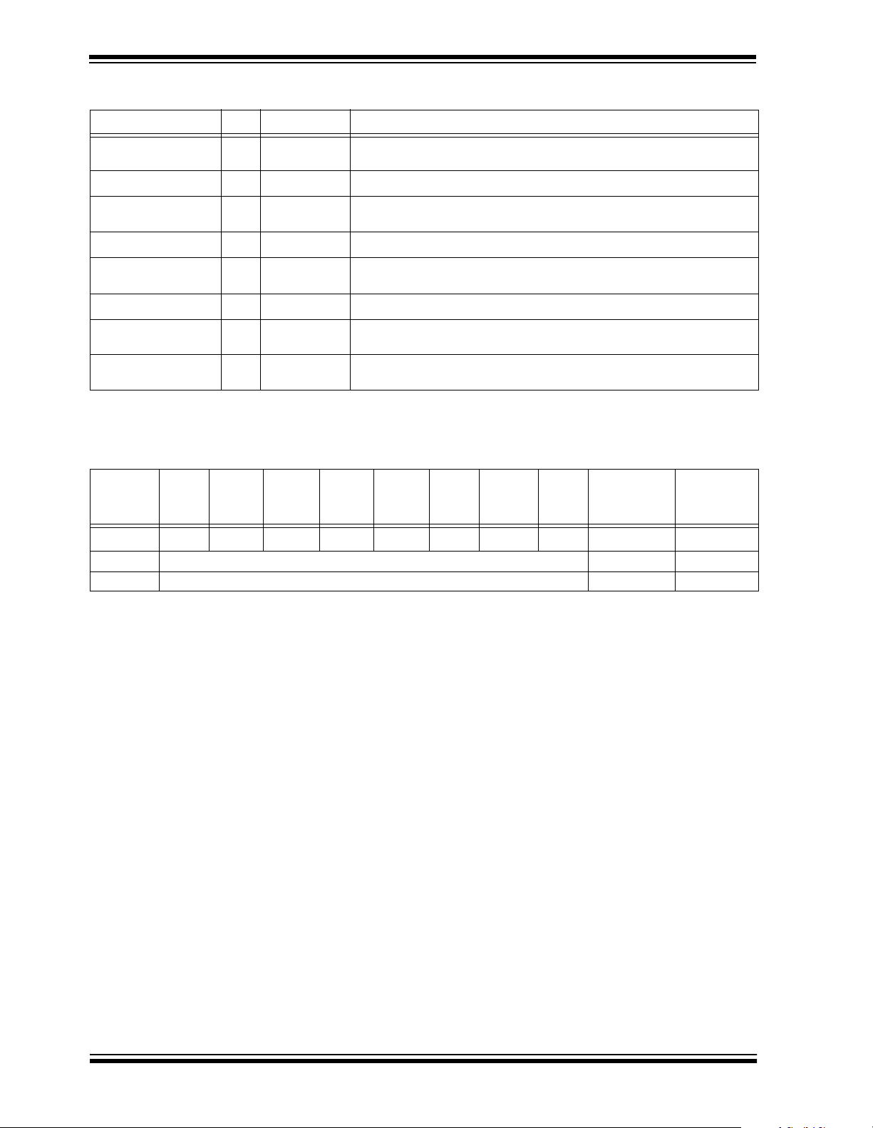
PIC18CXX8
TABLE 8-5: PORTC FUNCTIONS
Name Bit# Buffer Type Function
RC0/T1OSO/T13CKI
RC1/T1OSI
RC2/CCP1
RC3/SCK/SCL
RC4/SDI/SDA
RC5/SDO
RC6/TX/CK
RC7/RX/DT
Legend: ST = Schmitt Trigg er input
bit0
bit1
bit2
bit3
bit4
bit5
bit6
bit7
ST Input/output port pin or T imer1 oscillato r output or Timer1/Timer3 clock
ST Input/output port pin or Timer1 oscillator input.
ST Input/output port pin or Capture1 input/Compare1 output/PWM1
ST Input/output port pin or Synchronous Serial clock for SPI/I
ST Input/output port pin or SPI Data in (SPI mode) or Data I/O
ST Input/output port pin or Synchronous Serial Port data output.
ST Input/output port pin Addressable USART Asynchronous Transmit or
ST Input/output port pin Addressable USART Asynchronous Receive or
input.
output.
2
(I
C mode).
Addressable USART Synchronous Clock.
Addressable USART Synchronous Data.
2
C.
TABLE 8-6: SUMMARY OF REGISTERS ASSOCIATED WITH PORTC
Name Bit 7 Bit 6 Bit 5 Bit 4 Bit 3 Bit 2 Bit 1 Bit 0
PORTC RC7 RC6 RC5 RC4 RC3 RC2 RC1 RC0 xxxx xxxx uuuu uuuu
LATC LATC Data Output Register xxxx xxxx uuuu uuuu
TRISC PORTC Data Direction Register 1111 1111 1111 1111
Legend: x = unknown, u = unchanged
Value on
POR,
BOR
Value on all
other
RESETS
DS30475A-page 94 Advanced Information 2000 Microchip Technology Inc.
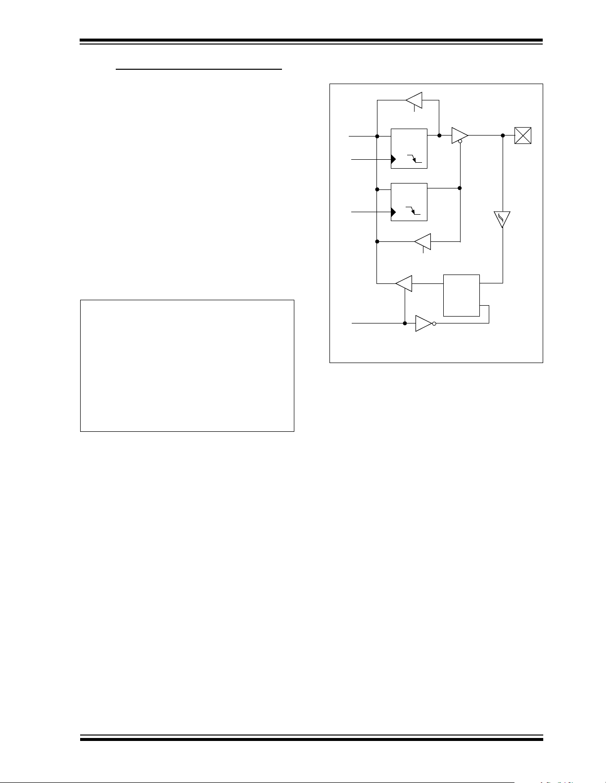
PIC18CXX8
8.4 PORTD, TRISD and LATD Registers
PORTD is an 8-bit wide, bi-directional port. The corresponding Data Direction regi ster is TRISD. Setting a
TRISD bit (=1) will make the corres ponding POR TD pin
an input (i.e., put the corresponding output driver in a
hi-impedance mode). Clearing a TRISD bit (=0) will
make the correspondi ng PORTD pin an output (i.e., p ut
the contents of the output latch on the selected pin).
Read-modify-write operations on the LATD register
reads and writes the latched output value for PORTD.
PORTD is an 8-bit port with Schmitt Trigger input buffers. Each pin is individu all y co nfig ura ble as an inp ut or
output.
PORTD can be configured as an 8-bit wide microprocessor port (parallel slave port), by setting control
bit PSPMODE (PSPCON register). In this mode, the
input buffers are TTL. See Section 9.0 for additional
information on the Parallel Slave Port (PSP).
EXAMPLE 8-4: INITIALIZING PORTD
CLRF PORTD ; Initialize PORTD by
; clearing output
; data latches
CLRF LATD ; Alternate method
; to clear output
; data latches
MOVLW 0xCF ; Value used to
; initialize data
; direction
MOVWF TRISD ; Set RD3:RD0 as inputs
; RD5:RD4 as outputs
; RD7:RD6 as inputs
FIGURE 8-7: PORTD BLOCK DIAGRAM
IN I/O PORT MODE
Data
Bus
WR LATD
or
WR PORTD
WR TRISD
RD PORTD
Note: I/O pins have diode protection to V
RD LATD
CK
Data Latch
QD
CK
TRIS Latch
RD TRISD
QD
Schmitt
Trigger
Input
Buffer
QD
EN
EN
DD and VSS.
I/O Pin
2000 Microchip Technology Inc. Advanced Information DS30475A-page 95

PIC18CXX8
TABLE 8-7: PORTD FUNCTIONS
Name Bit# Buffer Type Function
RD0/PSP0 bit0
RD1/PSP1 bit1
RD2/PSP2 bit2
RD3/PSP3 bit3
RD4/PSP4 bit4
RD5/PSP5 bit5
RD6/PSP6 bit6
RD7/PSP7 bit7
Legend: ST = Schmitt Trigger input, TTL = TTL input
Note 1: Input buffers are Schmitt Triggers when in I/O mode and TTL buffer when in Parallel Slave Port mode.
ST/TTL
ST/TTL
ST/TTL
ST/TTL
ST/TTL
ST/TTL
ST/TTL
ST/TTL
(1)
(1)
(1)
(1)
(1)
(1)
(1)
(1)
Input/output port pin or parallel slave port bit0.
Input/output port pin or parallel slave port bit1.
Input/output port pin or parallel slave port bit2.
Input/output port pin or parallel slave port bit3.
Input/output port pin or parallel slave port bit4.
Input/output port pin or parallel slave port bit5.
Input/output port pin or parallel slave port bit6.
Input/output port pin or parallel slave port bit7.
TABLE 8-8: SUMMARY OF REGISTERS ASSOCIATED WITH PORTD
Name Bit 7 Bit 6 Bit 5 Bit 4 Bit 3 Bit 2 Bit 1 Bit 0
PORTD RD7 RD6 RD5 RD4 RD3 RD2 RD1 RD0 xxxx xxxx uuuu uuuu
LATD LATD Data Output Register xxxx xxxx uuuu uuuu
TRISD PORTD Data Direction Register 1111 1111 1111 1111
PSPCON
Legend: x = unknown, u = unchanged, - = unimplemented, read as '0'. Shaded cells are not used by PORTD.
IBF OBF IBOV PSPMODE — — — — 0000 ---- 0000 ----
Valu e on
POR,
BOR
Value on all
other
RESETS
DS30475A-page 96 Advanced Information 2000 Microchip Technology Inc.

PIC18CXX8
8.5 PORTE, TRISE and LATE Registers
PORTE is an 8-bit wide, bi-directional port. The corresponding Data Direction register is TRISE. Setting a
TRISE bit (=1) will make the corres ponding POR TE pi n
an input (i.e., put the corresponding output driver in a
hi-impedance mode). Clearing a TRISE bit (=0) will
make the corresponding POR TE pin an output (i.e., put
the contents of the output latch on the selected pin).
Read-modify-write operations on the LATE register
reads and writes the latched output value for PORTE.
PORTE is an 8- b it po r t w i t h S c hm it t Trigge r i npu t b u ffers. Each pin is individu all y co nfig ura ble as an inp ut or
output. PORT E is multiplexed w ith several per ipheral
functions (T able 8-9).
FIGURE 8-8: PORTE BLOCK DIAGRAM
Peripheral Out Select
Peripheral Data Out
Data Bus
WR LATE
or
WR PORTE
WR TRISE
RD LATE
QD
Q
CK
Data Latch
QD
Q
CK
TRIS Latch
EXAMPLE 8-5: INITIALIZING PORTE
CLRF PORTE ; Initialize PORTE by
; clearing output
; data latches
CLRF LATE ; Alternate method
; to clear output
; data latches
MOVLW 0x03 ; Value used to
; initialize data
; direction
MOVWF TRISE ; Set RE1:RE0 as inputs
; RE7:RE2 as outputs
V
0
1
TRIS
Override
DD
P
N
VSS
I/O Pin
(1)
Peripheral Enable
RD PORTE
Peripheral Data In
Note 1: I/O pins have diode protection to V
RD TRISE
Pin Override Peripheral
RE0 Yes
RE1 Yes P SP
RE2 Yes
RE3 No
RE4 No —
RE5 No —
RE6 No —
RE7 No —
Schmitt
Trigger
QD
EN
TRIS OVERRIDE
PSP
PSP
—
DD and VSS.
2000 Microchip Technology Inc. Advanced Information DS30475A-page 97

PIC18CXX8
TABLE 8-9: PORTE FUNCTIONS
Name Bit# Buffer Type Function
RE0/RD
RE1/WR
RE2/CS
RE3 bit3 ST Input/output port pin.
RE4 bit4 ST Input/output port pin.
RE5 bit5 ST Input/output port pin.
RE6 bit6 ST Input/output port pin.
RE7/CCP2 bit7 ST Input/output port pin or Capture 2 input/Compare 2 output.
Legend: ST = Schmitt Trigger input, TTL = TTL input
Note 1: Input buffers are Schmitt Triggers when in I/O mode and TTL buffer when in Parallel Slave Port mode.
bit0 ST/TTL
bit1 ST/TTL
bit2 ST/TTL
(1)
Input/output port pin or Re ad contr ol inpu t in Par allel Slav e Port mod e.
(1)
Input/output port pin or Write control input in Parallel Slave Port mode.
(1)
Input/output port pin or Chip Select control input in Parallel Slave Port
mode.
TABLE 8-10: SUMMARY OF REGISTERS ASSOCIATED WITH PORTE
Name Bit 7 Bit 6 Bit 5 Bit 4 Bit 3 Bit 2 Bit 1 Bit 0
TRISE PORTE Data Direction Control Register 1111 1111 1111 1111
PORTE Read PORTE pin/Write PORTE Data Latch xxxx xxxx uuuu uuuu
LATE Read PORTE Data Latch/Write PORTE Data Latch xxxx xxxx uuuu uuuu
PSPCON IBF OBF IBOV PSPMODE — — — — 0000 ---- 0000 ----
Legend: x = unknown, u = unchanged
Valu e on:
POR,
BOR
Value on all
other
RESETS
DS30475A-page 98 Advanced Information 2000 Microchip Technology Inc.

PIC18CXX8
8.6 PORTF, LATF, and TRISF Registers
PORTF is an 8-bit wide, bi-directional port. The corresponding Data Direction register is TRISF. Setting a
TRISF bit (=1) will m ake the corres pondi ng POR TF pi n
an input (i.e., put the corresponding output driver in a
hi-impedance mode). Clearing a TRISF bit (=0) will
make the correspondi ng PORTF pin an outp ut (i.e., put
the contents of the output latch on the selected pin).
Read-modify-write operations on the LATF register
reads and writes the latched output value for PORTF.
PORTF is multiplexed with several analog peripheral
functions incl uding t he A/ D co nverte r inpu ts a nd co mparator inputs, outputs, and voltage reference.
Note 1: On a Power- on Reset , the R F6:RF0 pi ns
EXAMPLE 8-6: INITIALIZING PORTF
CLRF PORTF ; Initialize PORTF by
; clearing output
; data latches
CLRF LATF ; Alternate method
; to clear output
; data latches
MOVLW 0x07 ;
MOVWF CMCON ; Turn off comparators
MOVLW 0x0F ;
MOVWF ADCON1 ; Set PORTF as digital I/O
MOVLW 0xCF ; Value used to
; initialize data
; direction
MOVWF TRISF ; Set RF3:RF0 as inputs
; RF5:RF4 as outputs
; RF7:RF6 as inputs
are configured as inputs and read as ’0’.
2: To configure PORTF as digital I/O, turn off
comparators and set ADCON1 value.
FIGURE 8-9: PORTF RF1/AN6/C2OUT, RF2/AN5/C1OUT BLOCK DIAGRAM
PORT/Comparator Select
Comparator Data Out
Data Bus
WR LATF
or
WR PORTF
WR TRISF
RD LATF
QD
Q
CK
Data Latch
QD
Q
CK
TRIS Latch
0
1
V
DD
P
N
VSS
Analog
Input
Mode
I/O Pin
RD TRISF
QD
EN
RD PORT F
To A/D Converter
Note: I/O pins have diode protection to V
2000 Microchip Technology Inc. Advanced Information DS30475A-page 99
DD and VSS.
Schmitt
Trigger
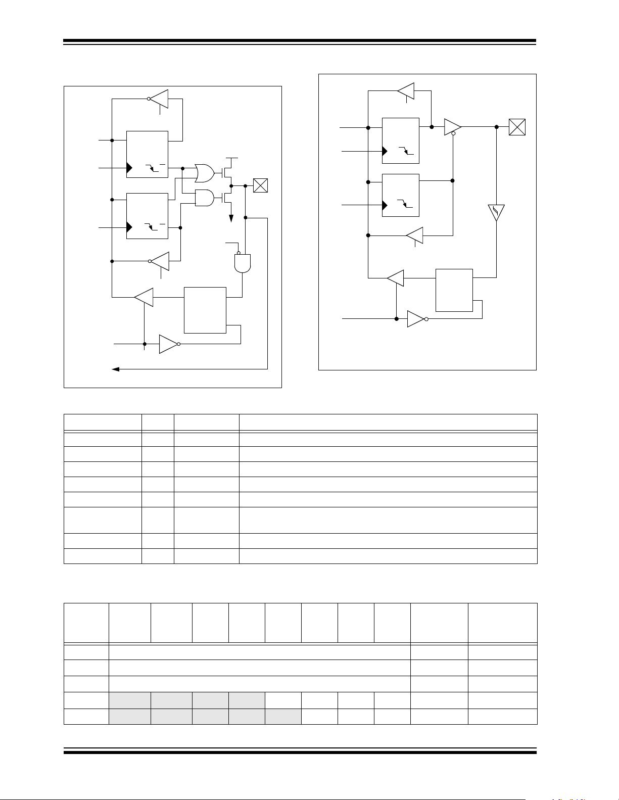
PIC18CXX8
FIGURE 8-10: RF6:RF3 AND RF0 PINS
BLOCK DIAGRAM
RD LATF
Data
Bus
WR LATF
or
WR PORTF
WR TRISF
RD PORTF
To A/D Converter or Comparator Input
Note: I/O pins have diode protection to V
Data Latch
TRIS Latch
CK
CK
QD
Q
QD
Q
RD TRISF
VDD
P
N
V
SS
Analog
Input
Mode
QD
EN
DD and VSS.
I/O Pin
ST
Input
Buffer
FIGURE 8-11: RF7 PIN BLOCK DIAGRAM
Data
Bus
WR LATF
or
WR PORTF
WR TRISF
RD PORTF
Note: I/O pins have diode protection to V
RD LATF
CK
Data Latch
QD
CK
TRIS Latch
RD TRISF
QD
Schmitt
Trigger
Input
Buffer
QD
EN
EN
DD and VSS.
I/O pin
TABLE 8-11 : PORTF FUNCTIONS
Name Bit# Buffer Type Function
RF0/AN5 bit0 ST Input/output port pin or analog input.
RF1/AN6/C2OUT bit1 ST Input/output port pin or analog input or comparator 2 output.
RF2/AN7/C1OUT bit2 ST Input/output port pin or analog input or comparator 1 output.
RF3/AN8 bit3 ST Input/output port pin or analog input or comparator input.
RF4/AN9 bit4 ST Input/output port pin or analog input or comparator input.
RF5/AN10/
CVREF
bit5 ST Input/output port pin or analog input or comparator input or comparator
reference output.
RF6/AN11 bit6 ST Input/output port pin or analog input or comp arator inpu t.
RF7 bit7 ST Input/output port pin.
Legend: ST = Schmitt Trigger input
TABLE 8-12: SUMMARY OF REGISTERS ASSOCIATED WITH PORTF
Value on:
Name Bit 7 Bit 6 Bit 5 Bit 4 Bit 3 Bit 2 Bit 1 Bit 0
POR,
BOR
TRISF PORTF Data Direction Control Register 1111 1111 1111 1111
PORTF Read PORTF pin / Write PORTF Data Latch xxxx xxxx uuuu uuuu
LATF Read PORTF Data Latch/Write PORTF Data Latch 0000 0000 uuuu uuuu
ADCON1
CMCON
— — VCFG1 VCFG0 PCFG3 PCFG2 PCFG1 PCFG0 --00 0000 --00 0000
C2OUT C1OUT C2INV C1INV CIS CM2 CM1 CM0 0000 0000 0000 0000
Legend: x = unknown, u = unchanged
Value on all
other RESETS
DS30475A-page 100 Advanced Information 2000 Microchip Technology Inc.
 Loading...