

Page 1

PIC18CXX2
Data Sheet
High Performance Microcontrollers
with 10-bit A/D
2001 Microchip Technology Inc. DS39026C
Page 2

“All rights reserved. Copyright © 2001, Microchip Technology
Incorporated, USA. Information contained in this publication
regarding device applications and the like is intended through
suggestion only and may be superseded by updates. No representation or warranty is given and no liability is assumed by
Microchip Technology Incorporated with respect to the accuracy or use of such information, or infringement of patents or
other intellectual property rights arising from such use or otherwise. Use of Microchip’s products as critical components in
life support systems is not authorized except with express
written approval by Microchip. No licenses are conveyed,
implicitly or otherwise, under any intellectual property rights.
The Microchip logo and name are registered trademarks of
Microchip Technology Inc. in the U.S.A. and other countries.
All rights reserved. All other trademarks mentioned herein are
the property of their respective companies. No licenses are
conveyed, implicitly or otherwise, under any intellectual property rights.”
Trademarks
The Microchip name, logo, PIC, PICmicro, PICMASTER, PICSTART, PRO MATE, K
EELOQ, SEEVAL, MPLAB and The
Embedded Control Solutions Company are registered trademarks of Microchip Technology Incorporated in the U.S.A. and
other countries.
Total Endurance, ICSP, In-Circuit Serial Programming, FilterLab, MXDEV, microID, FlexROM, fuzzyLAB, MPASM,
MPLINK, MPLIB, PICDEM, ICEPIC, Migratable Memory,
FanSense, ECONOMONITOR, Select Mode and microPort
are trademarks of Microchip Technology Incorporated in the
U.S.A.
Serialized Quick T erm Programming (SQTP) is a service mark
of Microchip Technology Incorporated in the U.S.A.
All other trademarks mentioned herein are property of their
respective companies.
© 2001, Microchip Technology Incorporated, Printed in the
U.S.A., All Rights Reserved.
Microchip received QS-9000 quality system
certification for its worldwide headquarters,
design and wafer fabrication facilities in
Chandler and Tempe, Arizona in July 1999. The
Company’s quality system processes and
procedures are QS-9000 compliant for its
PICmicro
devices, Serial EEPROMs and microperipheral
products. In addition, Microchip’s quality
system for the design and manufacture of
development systems is ISO 9001 certified.
®
8-bit MCUs, KEELOQ
®
code hoppin g
DS39026C - page ii 2001 Microchip Technology Inc.
Page 3
PIC18CXX2
High Performance Microcontrollers with 10-bit A/D
High Performance RISC CPU:
• C compiler optimized architecture/instruction set
- Source code compatible with the PIC16CXX
instruction set
• Linear program memory addressing to 2 Mbytes
• Linear data memory addressing to 4 Kbyte s
On-Chip Program Memory
Device
PIC18C242 16K 8192 512
PIC18C252 32K 16384 1536
PIC18C442 16K 8192 512
PIC18C452 32K 16384 1536
EPROM
(bytes)
# Single Word
Instructions
On-Chip
RAM
(bytes)
• Up to 10 MIPs operation:
- DC - 40 MHz osc./clock input
- 4 MHz - 10 MHz osc./ cl ock i npu t with PLL active
• 16-bit wide instructions, 8-bit wide data path
• Priority levels for interrupts
• 8 x 8 Single Cycle Hardware Multi plier
Peripheral Features:
• High current sink/source 25 mA/25 mA
• Three external interrupt pins
• Timer0 module: 8-bit/16-bit timer/counter with
8-bit programmable prescaler
• Timer1 module: 16-bit timer/counter
• Timer2 module: 8-bit timer/counter with 8-bit
period register (time-base for PWM)
• Timer3 module: 16-bit timer/counter
• Secondary oscillator clock option - Timer1/Timer3
• Two Capture/Compare/PWM (CCP) modules.
CCP pins that can be configured as:
- Capture input: capture is 16-bit,
max. resolution 6.25 ns (T
- Compare is 16-bit, max. resolution 100 ns (T
- PWM output: PWM resolution is 1- to 10-bit.
Max. PWM freq. @: 8-bit resolution = 156 kHz
• Master Synchronous Serial Port (MSSP) module.
Two modes of operation:
- 3-wire SPI™ (supports all 4 SPI modes)
2
-I
C™ master and slave mode
• Addressable USART module:
- Supports interrupt on Address bit
• Parallel Slave Port (PSP) module
CY/16)
CY)
10-bit resolution = 39 kHz
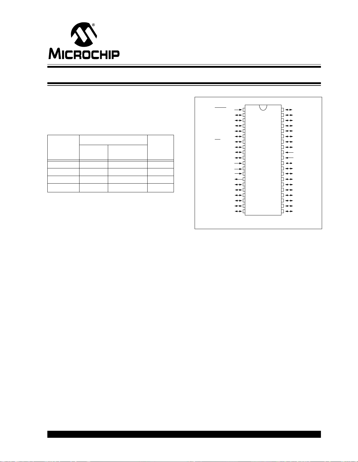
Pin Diagrams
DIP, Windowed CERDIP
MCLR/VPP
RA0/AN0
RA1/AN1
RA2/AN2/V
RA3/AN3/V
RA5/AN4/SS
OSC2/CLKO/RA6
RC0/T1OSO/T1CKI
RC1/T1OSI/CCP2
RC3/SCK/SCL
* RB3 is the alternate pin for the CCP2 pin multiplexing.
Note: Pin compatible with 40-pin PIC16C7X devices.
REF-
REF+
RA4/T0CKI
/LVDIN
RE0/RD/AN5
RE1/WR/AN6
RE2/CS/AN7
V
VSS
OSC1/CLKI
RC2/CCP1
RD0/PSP0
RD1/PSP1
1
2
3
4
5
6
7
8
9
10
DD
11
12
13
14
15
*
16
17
18
19
20
40
39
38
37
36
35
34
33
32
31
30
29
PIC18C4X2
28
27
26
25
24
23
22
21
RB7
RB6
RB5
RB4
RB3/CCP2
RB2/INT2
RB1/INT1
RB0/INT0
DD
V
VSS
RD7/PSP7
RD6/PSP6
RD5/PSP5
RD4/PSP4
RC7/RX/DT
RC6/TX/CK
RC5/SDO
RC4/SDI/SDA
RD3/PSP3
RD2/PSP2
Analog Features:
• Compatible 10-bit Analog-to-Digital Converter
module (A/D) with:
- Fast sampling rate
- Conversion available during SLEEP
- DNL = ±1 LSb, INL = ±1 LSb
• Programmable Low Voltage Detection (LVD)
module
- Supports interrupt-on-low volt ag e dete ction
• Programmable Brown-out Reset (BOR)
Special Microcontroller Features:
• Power-on Reset (POR), Power-up Timer (PWR T)
and Oscillator Start-up Timer (OST)
• Watchdog Timer (WDT) with its own on-chip RC
oscillator for reliable operation
• Programmable code protection
• Power saving SLEEP mode
• Selectable oscillator options including:
- 4X Phase Lock Loop (of primary oscillator)
- Secondary Oscillator (32 kHz) clock input
• In-Circuit Serial Programming (ICSP™) via two pins
CMOS Technology:
• Low power, high speed EPROM technology
• Fully static design
• Wide operating voltage range (2.5V to 5.5V)
• Industrial and Extended temperature ranges
• Low power consumption
*
2001 Microchip Technology Inc. DS39026C-page 1
Page 4
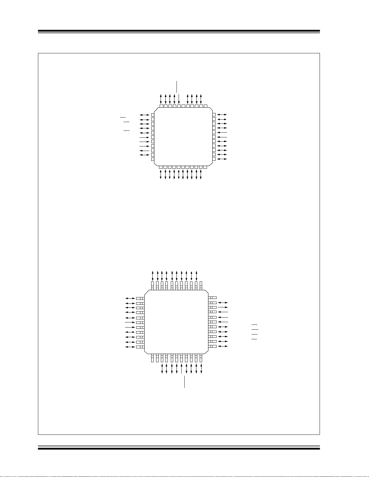
PIC18CXX2
Pin Diagrams
PLCC
REF-
/VPP
RA4/T0CKI
RA5/AN4/SS
OSC2/CLKO/RA6
RC0/T1OSO/T1CKI
/LVDIN
/AN5
RE0/RD
RE1/WR/AN6
RE2/CS
/AN7
V
V
OSC1/CLKI
DD
SS
NC
RA3/AN3/VREF+
RA2/AN2/V
RA1/AN1
RA0/AN0
MCLR
65432
7
8
9
10
11
PIC18C4X2
12
13
14
15
16
181920212223242526
17
RD2/PSP2
RD1/PSP1
RD0/PSP0
RC3/SCK/SCL
RC2/CCP1
RC1/T1OSI/CCP2
*
RC6/TX/CK
RC5/SDO
RC4/SDI/SDA
RD3/PSP3
RD2/PSP2
RD1/PSP1
RD0/PSP0
NC
RB7
1
44
RC4/SDI/SDA
RD3/PSP3
RC3/SCK/SCL
RB6
RB5
42
43
RC5/SDO
RC2/CCP1
RC1/T1OSI/CCP2*NC
RB4
41
27
28
NC
RC6/TX/CK
NC
40
39
38
37
36
35
34
33
32
31
30
29
RB3/CCP2*
RB2/INT2
RB1/INT1
RB0/INT0
V
DD
VSS
RD7/PSP7
RD6/PSP6
RD5/PSP5
RD4/PSP4
RC7/RX/DT
TQFP
RC7/RX/DT
RD4/PSP4
RD5/PSP5
RD6/PSP6
RD7/PSP7
SS
V
VDD
RB0/INT0
RB1/INT1
RB2/INT2
RB3/CCP2
* RB3 is the alternate pin for the CCP2 pin multiplexing.
Note: Pin compatible with 44-pin PIC16C7X devices.
*
4443424140
1
2
3
4
5
6
7
8
9
10
121314
11
NC
NC
38
39
PIC18C4X2
1819202122
15
16
17
RA0/AN0
MCLR
RB7
RB6
RB5
RB4
/VPP
37
363435
RA1/AN1
33
32
31
30
29
28
27
26
25
24
23
RA2/AN2/V
RA3/AN3/VREF+
REF-
NC
RC0/T1OSO/T1CKI
OSC2/CLKO/RA6
OSC1/CLKI
SS
V
VDD
RE2/AN7/CS
RE1/AN6/WR
RE0/AN5/RD
RA5/AN4/SS/LVDIN
RA4/T0CKI
DS39026C-page 2 2001 Microchip Technology Inc.
Page 5
Pin Diagrams (Cont.’d)
PIC18CXX2
DIP, JW
Note: Pin compatible with 40-pin PIC16C7X devices.
MCLR/VPP
RA0/AN0
RA1/AN1
RA2/AN2/V
RA3/AN3/V
RA5/AN4/SS
OSC2/CLKO/RA6
RC0/T1OSO/T1CKI
RC1/T1OSI/CCP2
RC3/SCK/SCL
RA4/T0CKI
/LVDIN
RE0/RD
RE1/WR
RE2/CS
OSC1/CLKI
RC2/CCP1
RD0/PSP0
RD1/PSP1
REF-
REF+
/AN5
/AN6
/AN7
V
VSS
DD
*
1
2
3
4
5
6
7
8
9
10
11
12
13
14
15
16
17
18
19
20
PIC18C4X2
40
39
38
37
36
35
34
33
32
31
30
29
28
27
26
25
24
23
22
21
RB7
RB6
RB5
RB4
RB3/CCP2
RB2/INT2
RB1/INT1
RB0/INT0
V
DD
VSS
RD7/PSP7
RD6/PSP6
RD5/PSP5
RD4/PSP4
RC7/RX/DT
RC6/TX/CK
RC5/SDO
RC4/SDI/SDA
RD3/PSP3
RD2/PSP2
*
DIP, SOIC, JW
MCLR/VPP
RA0/AN0
RA1/AN1
RA2/AN2/V
RA3/AN3/V
RA5/AN4/SS
OSC2/CLKO/RA6
RC0/T1OSO/T1CKI
RC1/T1OSI/CCP2
RC3/SCK/SCL
* RB3 is the alternate pin for the CCP2 pin multiplexing.
Note: Pin compatible with 28-pin PIC16C7X devices.
REF-
REF+
RA4/T0CKI
/LVDIN
V
OSC1/CLKI
RC2/CCP1
SS
*
1
2
3
4
5
6
7
8
9
10
11
12
13
14
PIC18C2X2
28
27
26
25
24
23
22
21
20
19
18
17
16
15
RB7
RB6
RB5
RB4
RB3/CCP2
RB2/INT2
RB1/INT1
RB0/INT0
V
VSS
RC7/RX/DT
RC6/TX/CK
RC5/SDO
RC4/SDI/SDA
*
DD
2001 Microchip Technology Inc. DS39026C-page 3
Page 6

PIC18CXX2
Table of Contents
1.0 Device Overview......................................................................................................................................................................... 7
2.0 Oscillator Configurations........................................................................................................................................................... 17
3.0 Reset......................................................................................................................................................................................... 25
4.0 Memory Organization................................................................................................................................................................ 35
5.0 Table Reads/Table Writes ........................................................................................................................................................ 55
6.0 8 X 8 Hardware Multiplier.......................................................................................................................................................... 61
7.0 Interrupts................................................................................................................................................................................... 63
8.0 I/O Ports.................................................................................................................................................................................... 77
9.0 Timer0 Module................................................................................... .. .... .. .. ....... .. .. .... .. ............................................................ 93
10.0 Timer1 Module........................................................................ ....... .. .. .. .... .. .. ....... .. .. .... .. ............................................................ 97
11.0 Timer2 Module........................................................................ ....... .. .. .. .... .. .. ....... .. .. .... .. .......................................................... 101
12.0 Timer3 Module........................................................................ ....... .. .. .. .... .. .. ....... .. .. .... .. .......................................................... 103
13.0 Capture/Compare/PWM (CCP) Modules................................................................................................................................ 107
14.0 Master Synchronous Serial Port (MSSP) Module................................................................................................................... 115
15.0 Addressable Universal Synchronous Asynchronous Receiver Transmitter (USART) ............................................................ 149
16.0 Compatible 10-bit Analog-to-Digital Converter (A/D) Module..................................... .... ......... .... .... .... ................................... 165
17.0 Low Voltage Detect.......................................... .. ..... .. .. .. .. .. .... .. ..... .. .. .. .. .. .. .... ..... .. .. .. .. .. .. .......................................................... 173
18.0 Special Features of the CPU.................................................................................................................................................. 179
19.0 Instruction Set Summary........................ ............... .............. .............................. .............. ........................................................ 187
20.0 Development Support........................................ ....... .... .. .... .. .. ......... .. .... .. .. ......... .. .. .... .. .... ...................................................... 229
21.0 Electrical Characteristics................................................... ............................................ .......................................................... 235
22.0 DC and AC Characteristics Graphs and Tables ..................................................................................................................... 263
23.0 Packaging Information............................................................................................................................................................ 277
Appendix A: Revision History......................................................................................................................................................... 287
Appendix B: Device Differences............................................................................................... ...................................................... 287
Appendix C: Conversion Considerations.......................................................................... .. .... .. ....... .. ............................................. 288
Appendix D: Migration from Baseline to Enhanced Devices.......................................................................................................... 288
Appendix E: Migration from Mid-Range to Enhanced Devices...................................................................................................... 289
Appendix F: Migration from High-End to Enhanced Devices......................................................................................................... 289
Index ................................................................................................................................................................................................. 291
On-Line Support........................................................................ .... .. ......... .... .. .... .... ....... .... ................................................................ 299
Reader Response............................................................................................................................................................................. 300
PIC18CXX2 Product Identification System ....................................................................................................................................... 301
DS39026C-page 4 2001 Microchip Technology Inc.
Page 7

PIC18CXX2
TO OUR VALUED CUSTOMERS
It is our intention to provide our valued customers with the best documentation possible to ensure successful use of your Microchip
products. To this end, we will continue to improve our publications to better suit your needs. Our publications will be refined and
enhanced as new volumes and updates are introduced.
If you have any questions or c omm ents regarding th is publication, p lease c ontact the M a rketing Communications Department via
E-mail at docerrors@mail.microchip.com or fax the Reader Response Form in the back of this data sheet to (480) 792-4150.
We welcome your feedback.
Most Current Data Sheet
To obtain the most up-to-date version of this data sheet, please register at our Worldwide Web site at:
http://www.microchip.com
You can determine the version of a data sheet by examining its literature number found on the bottom outside corner of any page.
The last character of the literature number is the version number, (e.g., DS30000A is version A of document DS30000).
Errata
An errata sheet, describing minor operational differences from the data sheet and recommended workarounds, may exist for current
devices. As device/documentation issues become known to us, we will publish an errata sheet. The errata will specify the revision
of silicon and revision of document to which it applies.
To determine if an errata sheet exists for a particular device, please check with one of the following:
• Microchip’s Worldwide Web site; http://www.microchip.com
• Your local Microchip sales office (see last page)
• The Microchip Corporate Literature Center; U.S. FAX: (480) 792-7277
When contacting a sales office or the literature center, please specify which device, revision of silicon and data sheet (include literature number) you are using.
Customer Notification System
Register on our web site at www.microchip.com/cn to receive the most current information on all of our products.
2001 Microchip Technology Inc. DS39026C-page 5
Page 8

PIC18CXX2
NOTES:
DS39026C-page 6 2001 Microchip Technology Inc.
Page 9

PIC18CXX2
1.0 DEVICE OVERVIEW
This documen t conta i ns dev ic e spec if i c in for m at i on fo r
the following four devices:
1. PIC18C242
2. PIC18C252
3. PIC18C442
4. PIC18C452
These devices come in 28-pin and 40-pin packages.
The 28-pin devices do not have a Parallel Slave Port
(PSP) implemented and the number of Analog-toDigital (A/D) converter input channels is reduced to 5.
An overview of features is shown in Table 1-1.
The following two figures are device block diagrams
sorted by pin count: 28-pin for Figure 1-1 and 40-pin for
Figure 1-2. The 28-pin and 40-pin pinouts are listed in
Table 1-2 and Table 1-3, respectively.
TABLE 1-1: DEVICE FEATURES
Features PIC18C242 PIC18C252 PIC18C442 PIC18C452
Operating Frequency DC - 40 MHz DC - 40 MHz DC - 40 MHz DC - 40 MHz
Program Memory (Bytes) 16K 32K 16K 32K
Program Memory (Instruction s) 8192 16384 8192 16384
Data Memory (Bytes) 512 1536 512 1536
Interrupt Sources 16 16 17 17
I/O Ports Ports A, B, C Ports A, B, C Ports A, B, C, D, E Ports A, B, C, D, E
Timers 4444
Capture/Compare/PWM Modules 2 2 2 2
Serial Communications MSSP,
Addressable
USART
Parallel Communications ——PSP PSP
10-bit Analog-to-Digital Module 5 input channels 5 input channels 8 input channels 8 input channels
RESETS (and Delays) POR, BOR,
RESET Instruction,
Stack Full,
Stack Underflow
(PWRT, OST)
Programmable Low Voltage
Detect
Programmable Brown-out Reset Yes Yes Yes Yes
Instruction Set 75 Instructions 75 Instructions 75 Instructions 75 Instructions
Packages 28-pin DIP
Yes Yes Yes Yes
28-pin SOIC
28-pin JW
MSSP,
Addressable
USART
POR, BOR,
RESET Instruction,
Stack Full,
Stack Underflow
(PWRT, OST)
28-pin DIP
28-pin SOIC
28-pin JW
MSSP,
Addressable
USART
POR, BOR,
RESET Instruction,
Stack Full,
Stack Underflow
(PWRT, OST)
40-pin DIP
44-pin PLCC
44-pin TQFP
40-pin JW
MSSP,
Addressable
USART
POR, BOR,
RESET Instruction,
Stack Full,
Stack Underflow
(PWRT, OST)
40-pin DIP
44-pin PLCC
44-pin TQFP
40-pin JW
2001 Microchip Technology Inc. DS39026C-page 7
Page 10
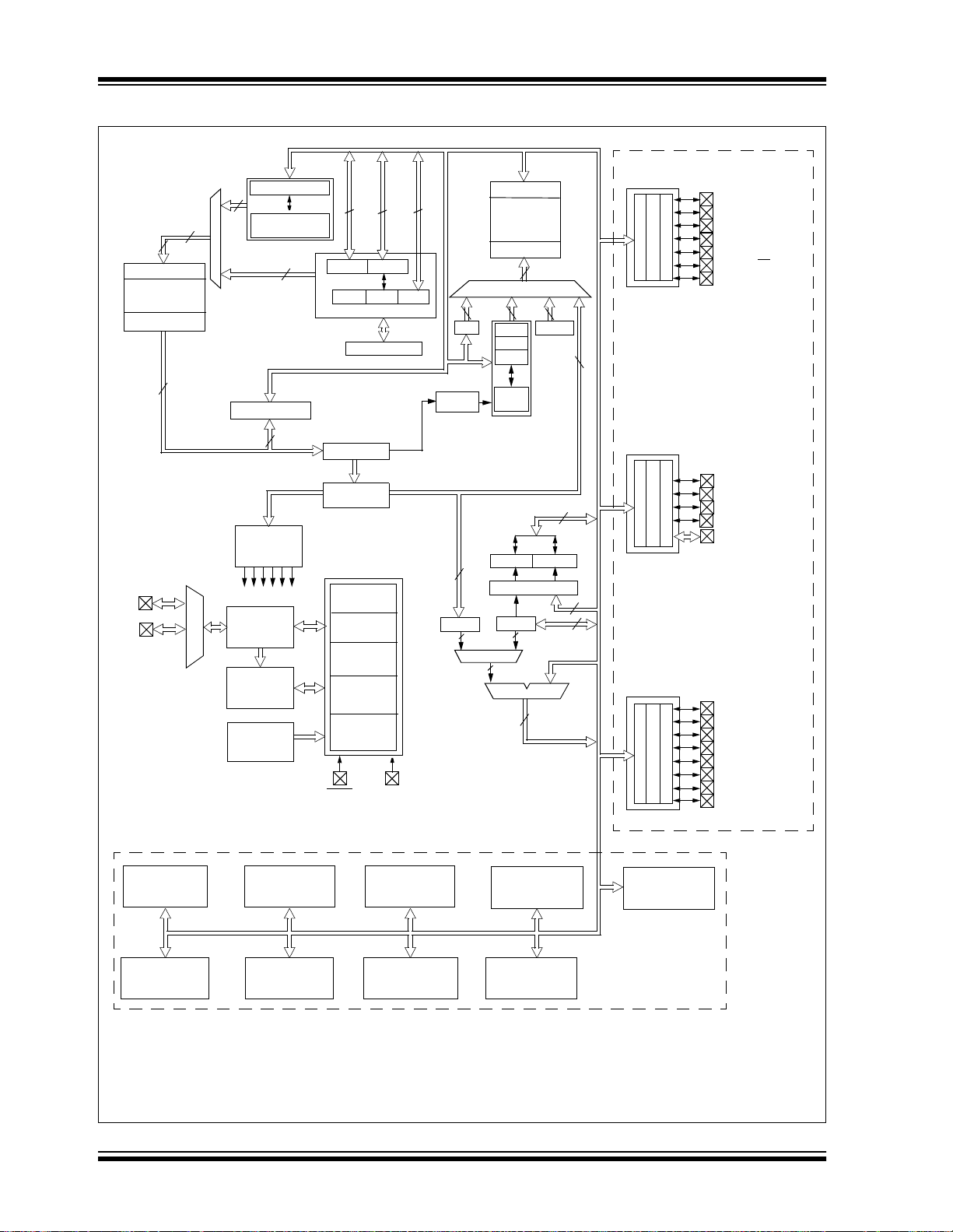
PIC18CXX2
FIGURE 1-1: PIC18C2X2 BLOCK DIAGRAM
Data Bus<8>
Address Latch
Program Memory
(up to 2M Bytes)
Data Latch
OSC2/CLKO
OSC1/CLKI
T1OSI
T1OSO
T able Poin ter <2>
21
8
21
inc/dec logic
8
8
21
PCLATH
PCLATU
20
PCH
PCU
Program Counter
31 Level Stack
16
Table Latch
Instruction
Decode &
Control
Timing
Generation
4X PLL
Precision
Voltage
Reference
8
ROM Latch
Instruction
Register
Power-up
Timer
Oscillator
Start-up Timer
Power-on
Reset
Watchdog
Timer
Brown-out
Reset
MCLR
VDD, VSS
PCL
4
Decode
BIT OP
BSR
3
8
Data Latch
Data RAM
Address Latch
12
Address<12>
12 4
FSR0
FSR1
FSR2
inc/dec
logic
8 x 8 Multiply
WREG
8
8
ALU<8>
8
(2)
Bank0, F
12
8
PRODLPRODH
8
8
PORTA
PORTB
PORTC
RA0/AN0
RA1/AN1
RA2/AN2/VREFRA3/AN3/VREF+
RA4/T0CKI
RA5/AN4/SS
RA6
RB0/INT0
RB1/INT1
RB2/INT2
RB3/CCP2
RB7:RB4
RC0/T1OSO/T1CKI
RC1/T1OSI/CCP2
RC2/CCP1
RC3/SCK/SCL
RC4/SDI/SDA
RC5/SDO
RC6/TX/CK
RC7/RX/DT
/LVDIN
(1)
(1)
Timer0 Timer1 Timer2
Master
CCP1
CCP2
Synchronous
Serial Port
Timer3
Addressable
USART
A/D Converter
Note 1: Optional multiplexing of CCP2 input/output with RB3 is enabled by selection of configuration bit.
2: The high order bits of the Direct Address for the RAM are from the BSR register (except for the
MOVFF instruction).
3: Many of the general purp ose I/O pi n s a re mu l tipl e xed wi th on e o r mo re peripheral modu l e fun cti on s. T he m ulti ple xi ng com bin ati o ns
are device dependent.
DS39026C-page 8 2001 Microchip Technology Inc.
Page 11
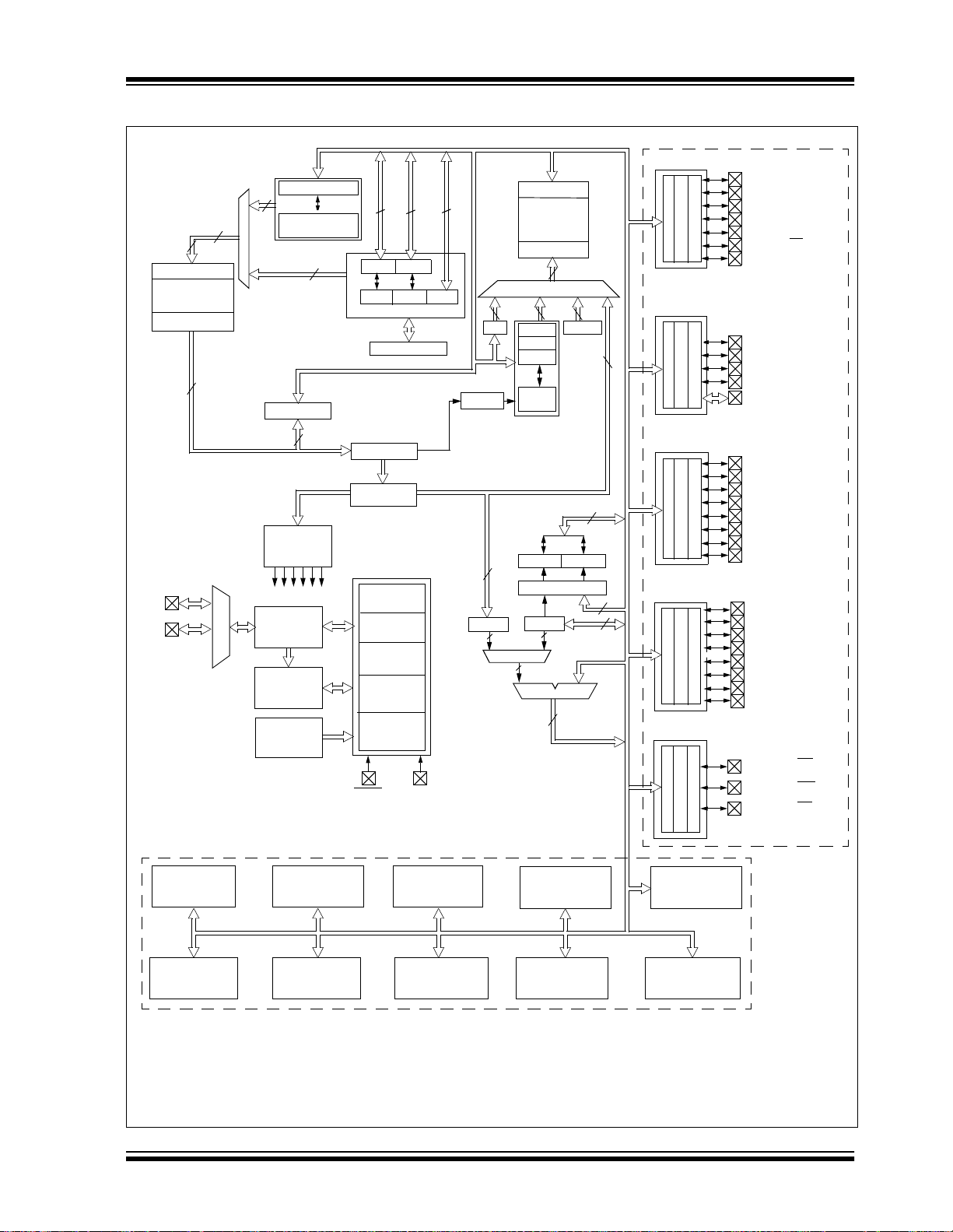
FIGURE 1-2: PIC18C4X2 BLOCK DIAGRAM
Table Pointer <2>
Address Latch
Program Memory
(up to 2M Bytes)
Data Latch
OSC2/CLKO
OSC1/CLKI
T1OSI
T1OSO
21
8
21
21
16
inc/dec logic
Table Latch
Instruction
Decode &
Control
Timing
Generation
4X PLL
Precision
Voltage
Reference
20
8
PCLATU
PCLATH
PCH PCL
PCU
Program Counter
31 Level Stack
ROM Latch
Instruction
Register
Power-up
Timer
Oscillator
Star t-up T im er
Power-on
Reset
Watchdog
Timer
Brown-out
Reset
MCLR
VDD, VSS
8
8
address reach)
12 4
4
BSR
Decode
BIT OP
inc/dec
3
8
Data Bus<8>
Data Latch
Data RAM
(up to 4K
Address Latc h
12
Address<12>
Bank0, F
FSR0
FSR1
FSR2
logic
PRODLPRODH
8 x 8 Multiply
WREG
8
8
ALU<8>
8
PIC18CXX2
PORTA
(2)
PORTB
12
PORTC
8
8
8
PORTD
PORTE
RA0/AN0
RA1/AN1
RA2/AN2/VREFRA3/AN3/VREF+
RA4/T0CKI
RA5/AN4/SS
RA6
RB0/INT0
RB1/INT1
RB2/INT2
RB3/CCP2
RB7:RB4
RC0/T1OSO/T1CKI
RC1/T1OSI/CCP2
RC2/CCP1
RC3/SCK/SCL
RC4/SDI/SDA
RC5/SDO
RC6/TX/CK
RC7/RX/DT
RD0/PSP0
RD1/PSP1
RD2/PSP2
RD3/PSP3
RD4/PSP4
RD5/PSP5
RD6/PSP6
RD7/PSP7
RE0/AN5/RD
RE1/AN6/WR
RE2/AN7/CS
/LVDIN
(1)
(1)
Timer0 Timer1 Timer2
Master
CCP1
Note 1: Optional multiplexing of CCP2 input/output with RB3 is enabled by selection of configuration bit.
2: The high order bits of the Direct Address for the RAM are from the BSR register (except for the
3: Many of the general purpose I/O pins are multiplexed with one or more peripheral module functions. The multiplexing combinations
are device dependent.
CCP2
Synchronous
Serial Port
Timer3
Addressable
USART
A/D Converter
Parallel Slave Port
MOVFF instruction).
2001 Microchip Technology Inc. DS39026C-page 9
Page 12

PIC18CXX2
TABLE 1-2: PIC18C2X2 PINOUT I/O DESCRIPTIONS
Pin Name
/VPP
MCLR
MCLR
VPP
NC ——— —These pins should be left unconnected.
OSC1/CLKI
OSC1
CLKI
OSC2/CLKO/RA6
OSC2
CLKO
RA6
RA0/AN0
RA0
AN0
RA1/AN1
RA1
AN1
RA2/AN2/V
RA2
AN2
V
RA3/AN3/V
RA3
AN3
V
RA4/T0CKI
RA4
T0CKI
RA5/AN4/SS
RA5
AN4
SS
LVDIN
RA6 See the OSC2/CLKO/RA6 pin.
Legend: TTL = TTL compatible input CMOS = CMOS compatible input or output
REF-
REF-
REF+
REF+
/LVDIN
ST = Schmitt Trigger input with CMOS levels I = Input
O = Output P = Power
OD = Open Drain (no P diode to V
Pin Number
DIP SOIC
11
99
10 10
22
33
44
55
66
77
Pin
Type
Buffer
Type
I
P
I
I
O
O
I/O
I/O
I
I/O
I
I/O
I
I
I/O
I
I
I/OIST/OD
I/O
I
I
I
ST
ST
CMOS
—
—
TTL
TTL
Analog
TTL
Analog
TTL
Analog
Analog
TTL
Analog
Analog
ST
TTL
Analog
ST
Analog
DD)
Description
Master clear (input) or programming voltage (input).
Master Clear (Reset) input. This pin is an active low
RESET to the device.
Programming voltage input.
Oscillator crystal or external clock input.
Oscillator crystal input or external clock source input.
ST buffer when configured in RC mode. CMOS otherwise.
External clock source input. Always associated with
pin function OSC1. (See related OSC1/CLKIN,
OSC2/CLKOUT pins.)
Oscillator crystal or clock output.
Oscillator crystal output. Connects to crystal or
resonator in Crystal Oscillator mode.
In RC mode, OSC2 pin outputs CLKOUT which has 1/4
the frequency of OSC1, and denotes the instruction
cycle rate.
General Purpose I/O pin.
PORTA is a bi-directional I/O port.
Digital I/O.
Analog input 0.
Digital I/O.
Analog input 1.
Digital I/O.
Analog input 2.
A/D Reference Voltage (Low) input.
Digital I/O.
Analog input 3.
A/D Reference Voltage (High) input.
Digital I/O. Open drain when configured as output.
Timer0 external clock input.
Digital I/O.
Analog input 4.
SPI Slave S elect input.
Low Voltage Detect Input.
DS39026C-page 10 2001 Microchip Technology Inc.
Page 13

TABLE 1-2: PIC18C2X2 PINOUT I/O DESCRIPTIONS (CONTINUED)
PIC18CXX2
Pin Name
RB0/INT0
RB0
INT0
RB1/INT1
RB1
INT1
RB2/INT2
RB2
INT2
RB3/CCP2
RB3
CCP2
RB4 25 25 I/O TTL Digital I/O.
RB5 26 26 I/O TTL Digital I/O.
RB6 27 27 I/O
RB7 28 28 I/O
Legend: TTL = TTL compatible input CMOS = CMOS compatible input or output
ST = Schmitt Trigger input with CMOS levels I = Input
O = Output P = Power
OD = Open Drain (no P diode to V
Pin Number
DIP SOIC
21 21
22 22
23 23
24 24
Pin
Type
I/O
I
I/O
I
I/O
I
I/O
I/O
I
I/O
Buffer
Type
PORTB is a bi-directional I/O port. PORTB can be software
programmed for internal weak pull-ups on all inputs.
TTL
ST
TTL
ST External Interrupt 1.
TTL
ST
TTL
ST
TTL
ST
TTL
ST
DD)
Digital I/O.
External Interrupt 0.
Digital I/O.
External Interrupt 2.
Digital I/O.
Capture2 input, Compare2 output, PWM2 output.
Interrupt-on-change pin.
Interrupt-on-change pin.
Digital I/O.
Interrupt-on-change pin.
ICSP programming clock.
Digital I/O.
Interrupt-on-change pin.
ICSP programming data.
Description
2001 Microchip Technology Inc. DS39026C-page 11
Page 14

PIC18CXX2
TABLE 1-2: PIC18C2X2 PINOUT I/O DESCRIPTIONS (CONTINUED)
Pin Name
RC0/T1OSO/T1CKI
RC0
T1OSO
T1CKI
RC1/T1OSI/CCP2
RC1
T1OSI
CCP2
RC2/CCP1
RC2
CCP1
RC3/SCK/SCL
RC3
SCK
SCL
RC4/SDI/SDA
RC4
SDI
SDA
RC5/SDO
RC5
SDO
RC6/TX/CK
RC6
TX
CK
RC7/RX/DT
RC7
RX
DT
SS 8, 19 8, 19 P — Ground reference for logic and I/O pins.
V
VDD 20 20 P — Positive supply for logic and I/O pins.
Legend: TTL = TTL compatible input CMOS = CMOS compatible input or output
ST = Schmitt Trigger input with CMOS levels I = Input
O = Output P = Power
OD = Open Drain (no P diode to V
Pin Number
DIP SOIC
11 11
12 12
13 13
14 14
15 15
16 16
17 17
18 18
Pin
Type
I/O
O
I
I/O
I
I/O
I/O
I/O
I/O
I/O
I/O
I/O
I
I/O
I/O
O
I/O
O
I/O
I/O
I
I/O
Buffer
Type
ST
—
ST
ST
CMOS
ST
ST
ST
ST
ST
ST
ST
ST
ST
ST
—
ST
—
ST
ST
ST
ST
DD)
Description
PORTC is a bi-directional I/O port.
Digital I/O.
Timer1 oscillator output.
Timer1/Timer3 external clock input.
Digital I/O.
Timer1 oscillator input.
Capture2 input, Compare2 output, PWM2 output.
Digital I/O.
Capture1 input/Compare1 output/PWM1 output.
Digital I/O.
Synchronous serial clock input/output for SPI mode.
Synchronous serial clock input/output for I
Digital I/O.
SPI Data In.
2
C Data I/O.
I
Digital I/O.
SPI Data Out.
Digital I/O.
USART Asynchronous Transmit.
USART Synchronous Clock (see related RX/DT).
Digital I/O.
USART Asynchronous Receive.
USART Synchronous Data (see related TX/CK).
2
C mode.
DS39026C-page 12 2001 Microchip Technology Inc.
Page 15

TABLE 1-3: PIC18C4X2 PINOUT I/O DESCRIPTIONS
PIC18CXX2
Pin Name
/VPP
MCLR
MCLR
VPP
NC ———These pins should be left unconnected.
OSC1/CLKI
OSC1
CLKI
OSC2/CLKO/RA6
OSC2
CLKO
RA6
RA0/AN0
RA0
AN0
RA1/AN1
RA1
AN1
RA2/AN2/V
RA2
AN2
V
RA3/AN3/V
RA3
AN3
V
RA4/T0CKI
RA4
T0CKI
RA5/AN4/SS
RA5
AN4
SS
LVDIN
RA6 See the OSC2/CLKO/RA6 pin.
Legend: TTL = TTL compatible input CMOS = CMOS compatible input or output
REF-
REF-
REF+
REF+
/LVDIN
ST = Schmitt Trigger input with CMOS levels I = Input
O = Output P = Power
OD = Open Drain (no P diode to V
Pin Number
DIP PLCC TQFP
1218
13 14 30
14 15 31
2319
3420
4521
5622
6723
7824
Pin
Buffer
Type
DD)
Type
I
ST
P
I
ISTCMOS
O
O
I/O
I/OITTL
I/OITTL
I/O
I
I
I/O
I
I
I/OIST/OD
I/O
I
I
I
—
—
TTL
Analog
Analog
TTL
Analog
Analog
TTL
Analog
Analog
ST
TTL
Analog
ST
Analog
Description
Master clear (input) or programming voltage (input).
Master Clear (Reset) input. This pin is an active
low RESET to the device.
Programming voltage input.
Oscillator crystal or external clock input.
Oscillator crystal input or external clock source input.
ST buffer when configured in RC mode, CMOS otherwise.
External cl ock source input. Always associated with
pin function OSC1. (See related OSC1/CLKIN,
OSC2/CLKOUT pins.)
Oscillator crystal output.
Oscillator crystal output. Connects to crystal
or resonator in Crystal Oscillator mode.
In RC mode, OSC2 pin outputs CLKOUT, which has
1/4 the frequency of OSC1 a nd denot es the instruct ion
cycle rate.
General Purpose I/O pin.
PORTA is a bi-directional I/O port.
Digital I/O.
Analog input 0.
Digital I/O.
Analog input 1.
Digital I/O.
Analog input 2.
A/D Reference Voltage (Low) input.
Digital I/O.
Analog input 3.
A/D Reference Voltage (High) input.
Digital I/O. Open drain when configured as output.
Timer0 external clock input.
Digital I/O.
Analog input 4.
SPI Slave Select input.
Low Volt age Detect Inp ut.
2001 Microchip Technology Inc. DS39026C-page 13
Page 16

PIC18CXX2
TABLE 1-3: PIC18C4X2 PINOUT I/O DESCRIPTIONS (CONTINUED)
Pin Name
RB0/INT0
RB0
INT0
RB1/INT1
RB1
INT1
RB2/INT2
RB2
INT2
RB3/CCP2
RB3
CCP2
RB4 37 41 14 I/O TTL Digital I/O. Interrupt-on-change pin.
RB5 38 42 15 I/O TTL Digital I/O. Interrupt-on-change pin.
RB6 39 43 16 I/O
RB7 40 44 17 I/O
Legend: TTL = TTL compatible input CMOS = CMOS compatible input or output
ST = Schmitt Trigger input with CMOS levels I = Input
O = Output P = Power
OD = Open Drain (no P diode to V
Pin Number
DIP PLCC TQFP
33 36 8
34 37 9
35 38 10
36 39 11
Pin
Type
I/O
I
I/O
I
I/O
I
I/O
I/O
I
I/O
DD)
Buffer
Type
PORTB is a bi-directional I/O port. PORTB can be
software programmed for internal weak pull-ups on all
inputs.
TTL
ST
TTL
ST External Interrupt 1.
TTL
ST
TTL
ST
TTLSTDigital I/O. Interrupt-on-change pin.
TTLSTDigital I/O. Interrupt-on-change pin.
Digital I/O.
External Interrupt 0.
Digital I/O.
External Interrupt 2.
Digital I/O.
Capture2 input, Compare2 output, PWM2 output.
ICSP programming clock.
ICSP programming data .
Description
DS39026C-page 14 2001 Microchip Technology Inc.
Page 17

TABLE 1-3: PIC18C4X2 PINOUT I/O DESCRIPTIONS (CONTINUED)
PIC18CXX2
Pin Name
RC0/T1OSO/T1CKI
RC0
T1OSO
T1CKI
RC1/T1OSI/CCP2
RC1
T1OSI
CCP2
RC2/CCP1
RC2
CCP1
RC3/SCK/SCL
RC3
SCK
SCL
RC4/SDI/SDA
RC4
SDI
SDA
RC5/SDO
RC5
SDO
RC6/TX/CK
RC6
TX
CK
RC7/RX/DT
RC7
RX
DT
Legend: TTL = TTL compatible input CMOS = CMOS compatible input or output
ST = Schmitt Trigger input with CMOS levels I = Input
O = Output P = Power
OD = Open Drain (no P diode to V
Pin Number
DIP PLCC TQFP
15 16 32
16 18 35
17 19 36
18 20 37
23 25 42
24 26 43
25 27 44
26 29 1
Pin
Type
I/O
O
I
I/O
I
I/O
I/O
I/O
I/O
I/O
I/O
I/O
I
I/O
I/O
O
I/O
O
I/O
I/O
I
I/O
DD)
Buffer
Type
ST
—
ST
ST
CMOS
ST
ST
ST
ST
ST
ST
ST
ST
ST
ST
—
ST
—
ST
ST
ST
ST
Description
PORTC is a bi-directional I/O port.
Digital I/O.
Timer1 oscillator output.
Timer1/Timer3 external clock input.
Digital I/O.
Timer1 oscillator input.
Capture2 input, Compare2 output, PWM2 output.
Digital I/O.
Capture1 input/Compare1 output/PWM1 output.
Digital I/O.
Synchronous serial clock input/output for
SPI mode.
Synchronous serial clock input/output for
2
C mode.
I
Digital I/O.
SPI Data In.
2
C Data I/O.
I
Digital I/O.
SPI Data Out.
Digital I/O.
USART Asynchronous Transmit.
USART Synchronous Clock (see related RX/DT).
Digital I/O.
USART Asynchronous Receive.
USART Synchronous Data (see related TX/CK).
2001 Microchip Technology Inc. DS39026C-page 15
Page 18
PIC18CXX2
TABLE 1-3: PIC18C4X2 PINOUT I/O DESCRIPTIONS (CONTINUED)
Pin Name
RD0/PSP0 19 21 38 I/O ST
RD1/PSP1 20 22 39 I/O ST
RD2/PSP2 21 23 40 I/O ST
RD3/PSP3 22 24 41 I/O ST
RD4/PSP4 27 30 2 I/O ST
RD5/PSP5 28 31 3 I/O ST
RD6/PSP6 29 32 4 I/O ST
RD7/PSP7 30 33 5 I/O ST
RE0/RD
RE1/WR
RE2/CS
V
VDD 11, 32 12, 35 7, 28 P — Positive supply for logic and I/O pins.
Legend: TTL = TTL compatible input CMOS = CMOS compatible input or output
/AN5
RE0
RD
AN5
/AN6
RE1
WR
AN6
/AN7
RE2
CS
AN7
SS 12, 31 13, 34 6, 29 P — Ground reference for logic and I/O pins.
ST = Schmitt Trigger input with CMOS levels I = Input
O = Output P = Power
OD = Open Drain (no P diode to V
Pin Number
DIP PLCC TQFP
8925I/O
91026I/O
10 11 27 I/O
Pin
Type
DD)
Buffer
Type
TTL
TTL
TTL
TTL
TTL
TTL
TTL
TTL
ST
TTL
Analog
ST
TTL
Analog
ST
TTL
Analog
Description
PORTD is a bi-dir ectional I/O port , or a Parallel Slave Po rt
(PSP) for interfacing to a microprocess or port. Thes e pins
have TTL input buffers when PSP module is enabled.
Digital I/O.
Parallel Slave Port Data.
Digital I/O.
Parallel Slave Port Data.
Digital I/O.
Parallel Slave Port Data.
Digital I/O.
Parallel Slave Port Data.
Digital I/O.
Parallel Slave Port Data.
Digital I/O.
Parallel Slave Port Data.
Digital I/O.
Parallel Slave Port Data.
Digital I/O.
Parallel Slave Port Data.
PORTE is a bi-directional I/O port.
Digital I/O.
Read control for parallel slave port (see also WR
and CS
Analog input 5.
Digital I/O.
Write control for parallel slave port (see CS
and RD
Analog input 6.
Digital I/O.
Chip Select control for parallel slave port (see related
RD
Analog input 7.
pins).
pins).
and WR).
DS39026C-page 16 2001 Microchip Technology Inc.
Page 19

PIC18CXX2
2.0 OSCILLATOR CONFIGURATIONS
2.1 Oscillator Types
The PIC18CXX2 can be operated in eight different
oscillator modes. The user can program three configuration bits (FOSC2 , FOSC1, and FOSC 0) to sel ect on e
of these eight modes:
1. LP Low Power Crystal
2. XT Crystal/Resonator
3. HS High Speed Crystal/Resonator
4. HS + PLL High Speed Crystal/Resonator
with x 4 PLL enabled
5. RC External Resistor/Capacitor
6. RCIO Extern al Resi stor/Capacitor with
RA6 I/O pin enabled
7. EC Extern al Cloc k
8. ECIO External Clock with RA6 I/O pin
enabled
2.2 Crystal Oscillator/Ceramic Resonators
In XT, LP, HS or HS-PLL oscillator modes, a crystal or
ceramic resonator is connected to the OSC1 and
OSC2 pins to establish oscillation. Figure 2-1 shows
the pin connections.
The PIC18CXX2 oscillat or desi gn requ ires th e use o f a
parallel cut crystal.
Note: Use of a series cut crystal may give a fre-
quency out of the crystal manufacturers
specifications.
T ABLE 2-1: CAP ACIT OR SELECTION FOR
CERAMIC RESONATORS
Ranges Tested:
Mode Freq C1 C2
XT 455 kHz
2.0 MHz
4.0 MHz
HS 8.0 MHz
16.0 MHz
These values are for design guid ance only.
See notes following this table.
Resonators Used:
455 kHz Panasonic EFO-A455K04B ± 0.3%
2.0 MHz Murata Erie CSA2.00MG ± 0.5%
4.0 MHz Murata Erie CSA4.00MG ± 0.5%
8.0 MHz Murata Erie CSA8.00MT ± 0.5%
16.0 MHz Murata Erie CSA16.00MX ± 0.5%
All resonators used di d not have built-in capac itors.
Note 1: Higher capacitance increases th e stabi lity
of the oscillator, but also increases the
start-up time.
2: When operating below 3V V
necessary to use high gain HS mode on
lower frequency ceramic resonators.
3: Since each resonator/crystal has its own
characteristics, the user should consult
the resonator/crystal manufacturer for
appropriate values of external components or verify oscillator performance.
68 - 100 pF
15 - 68 pF
15 - 68 pF
10 - 68 pF
10 - 22 pF
68 - 100 pF
15 - 68 pF
15 - 68 pF
10 - 68 pF
10 - 22 pF
DD, it may be
FIGURE 2-1: CRYSTAL/CERAMIC
RESONATOR OPERATION
(HS, XT OR LP
OSC CONFIGURATION)
(1)
C1
(1)
C2
Note 1: See Table 2-1 and Table2-2 for recom-
2: A series resistor (R
3: R
2001 Microchip Technology Inc. DS39026C-page 17
OSC1
XTAL
(2)
RS
OSC2
mended values of C1 and C2.
strip cut crystals.
F varies with the osc mode chosen.
(3)
RF
SLEEP
PIC18CXXX
S) may be required for AT
To
Internal
Logic
Page 20
PIC18CXX2
TABLE 2-2: CAPACITOR SELECTION FOR
CRYSTAL OSCILLATORS
Ranges Tested:
Mode Freq C1 C2
LP 32.0 kHz 33 pF 33 pF
200 kHz 15 pF 15 pF
XT 200 kHz 47-68 pF 47-68 pF
1.0 MHz 15 pF 15 pF
4.0 MHz 15 pF 15 pF
HS 4.0 MHz 15 pF 15 pF
8.0 MHz 15-33 pF 15-33 pF
20.0
MHz
25.0
MHz
These values are for de sign guid ance only.
See notes following this table.
Crystals Used
32.0 kHz Epson C-001R32.768K-A ± 20 PPM
200 kHz STD XTL 200.000kHz ± 20 PPM
1.0 MHz ECS ECS-10-13-1 ± 50 PPM
4.0 MHz ECS ECS-40-20-1 ± 50 PPM
8.0 MHz Epson CA-301 8.000M-C ± 30 PPM
20.0 MHz Epson CA-301 20.000M-C ± 30 PPM
15-33 pF 15-33 pF
15-33 pF 15-33 pF
Note 1: Higher capacitance inc reases the st abilit y
of the oscillator, but also increases the
start-up time.
2: Rs may be required in HS mode, as well
as XT mode, to avoid overdrivi ng crys t als
with low drive level specification.
3: Since each resonator/crystal has its own
characteristics, the user should consult
the resonator/crystal manufacturer for
appropriate values of external components or verify oscillator performance.
An external clock sourc e may also be conne cted to th e
OSC1 pin in these modes, as shown in Figure 2-2.
FIGURE 2-2: EXTERNAL CLOCK INPUT
OPERATION (HS, XT OR
LP CONFIGURATION)
Clock from
Ext. System
Open
OSC1
PIC18CXXX
OSC2
2.3 RC Oscillator
For timing insensitive applications, the “RC” and
"RCIO" device options offer additional cost savings.
The RC oscillator frequency is a function of the supply
voltage, the resistor (R
ues and the operating temperature. In addition to this,
the oscillator frequency will vary from uni t to unit due to
normal process parameter variation. Furthermore, the
difference in le ad fram e c apacitance betw ee n package
types will also affect the oscillation frequency, especially for low C
EXT values. The user also needs to take
into account variation due to tolerance of external R
and C components used. Figure 2-3 shows how the
R/C combination is connected.
In the RC oscillator mode, the oscillator frequency
divided by 4 is available on the OSC2 pin. This signal
may be used f or t e st pu r pos es or t o sy nc hr o n iz e ot he r
logic.
FIGURE 2-3: RC OSCILLATOR MODE
VDD
REXT
CEXT
VSS
F
Recommended values:3 kΩ ≤ REXT ≤ 100 kΩ
The RCIO oscillator mode functions like the RC mode,
except that the OSC2 pin becomes an additional general purpose I/O pin. The I/O pin becomes bit 6 of
PORTA (RA6).
EXT) and capacitor (CEXT) val-
OSC1
OSC2/CLKO
OSC/4
EXT > 20pF
C
Internal
Clock
PIC18CXXX
DS39026C-page 18 2001 Microchip Technology Inc.
Page 21
PIC18CXX2
2.4 External Clock Input
The EC and ECIO os c ill ato r m ode s require an external
clock source to be connected to the OSC1 pin. The
feedback device between OSC1 and OSC2 is turned
off in these modes to save current. There is no oscillator start-up time required after a Power-on Reset or
after a recovery from SLEEP mode.
In the EC oscillator mode, the oscillator frequency
divided by 4 is available on the OSC2 pin. This signal
may be used f or t e st pu r pos es or t o sy nc hr o n iz e ot he r
logic. Figure 2-4 shows the pin connections for the EC
oscillator mode.
FIGURE 2-4: EXTERNAL CLOCK INPUT
OPERATION (EC OSC
CONFIGURATION)
Clock from
Ext. System
F
OSC/4
The ECIO oscillator mode functions like the EC mode,
except that the OSC2 pin becomes an additional general purpose I/O pin. The I/O pin becomes bit 6 of
PORTA (RA6). Figure 2-5 shows the pin connections
for the ECIO oscillator mode.
OSC1
PIC18CXXX
OSC2
FIGURE 2-5: EXTERNAL CLOCK INPUT
OPERATION
(ECIO CONFIGURATION)
Clock from
Ext. System
RA6
OSC1
PIC18CXXX
I/O (OSC2)
2.5 HS/PLL
A Phase Locked Loop circuit is pro vided as a programmable option for users that want to multiply the frequency of the incoming crystal oscillator signal by 4.
For an input clock frequency of 10 MHz, the internal
clock frequency will be multiplied to 40 MHz. This is
useful for customers who are concerned with EMI due
to high frequency crystals.
The PLL can only be enabled when the oscillator configuration bits are programmed for HS mode. I f they are
programmed for any other mode, the PLL is not
enabled and the system clock will come directly from
OSC1.
The PLL is one o f the modes of the FO SC<2:0> co nfiguration bits. The oscillator mode is specified during
device programming.
A PLL lock timer is used to ensure that the PLL has
locked before device execution starts. The PLL lock
timer has a time-out that is called T
PLL.
FIGURE 2-6: PLL BLOCK DIAGRAM
(from Configuration
bit Register)
OSC2
OSC1
PLL Enable
Crystal
Osc
HS Osc
F
Phase
Comparator
IN
FOUT
Loop
Filter
Divide by 4
VCO
SYSCLK
MUX
2001 Microchip Technology Inc. DS39026C-page 19
Page 22

PIC18CXX2
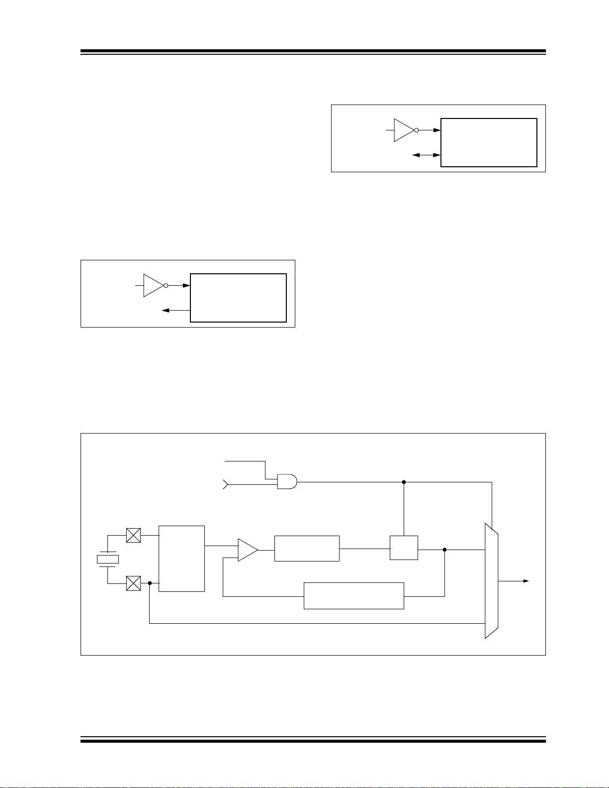
2.6 Oscillator Switching Feature
The PIC18CXX2 devices include a feature that allows
the system clock source to be switched from the main
oscillator t o an alternate lo w frequency clock s ource.
For the PIC18CXX2 devices, this alternate clock
source is the Timer1 oscillator. If a low frequency crystal (32 kHz, for example) has been attached to the
Timer1 oscillator pins and the Timer1 oscillator has
FIGURE 2-7: DEVICE CLOCK SOURCES
PIC18CXXX
OSC2
OSC1
T1OSO
T1OSI
Main Oscillator
SLEEP
Timer1 Oscillator
T1OSCEN
Enable
Oscillator
been enabled, the device can switch to a low power
execution mode. Figure 2-7 shows a block diagram of
the system clock sources. The clock switching feature
is enabled by programming the Oscillator Switching
Enable (OSCSEN
) bit in Configuration Register1H to a
’0’. Clock switching is disabled in an erased device.
See Section 9.0 for further details of the T ime r1 oscill ator. See Sec tion 18.0 for Configuration Register details.
4 x PLL
TOSC
TT1P
Clock Source option
for other modules
TOSC/4
MUX
Clock
Source
TSCLK
2.6.1 SYSTEM CLOCK SWITCH BIT
The system clock so urc e sw it chi ng is performed under
software control. The system clock switch bit, SCS
(OSCCON<0>) controls the clock switching. When the
SCS bit is’0’, the system clo ck so urce comes f rom the
main oscillator that i s s el ec ted b y t he FO SC c onfiguration bits in C onfiguration Register1H. W hen the SCS bit
is set, the system clock source will come from the
Timer1 o scillato r. The SCS bit is clear ed o n all forms of
RESET.
REGISTER 2-1: OSCCON REGISTER
U-0 U-0 U-0 U-0 U-0 U-0 U-0 R/W-1
— — — — — — — SCS
bit 7 bit 0
bit 7-1 Unimplemented: Read as '0'
bit 0 SCS: System Clock Switch bit
When
OSCSEN configuration bit = ’0’ and T1OSCEN bit is set:
1 = Switch to Timer1 oscillator/clock pin
0 = Use primary oscil lator/clock input pin
When
OSCSEN and T1OSCEN are in other states:
bit is forced clear
Note: The Timer1 oscillator m ust be ena bled and
operating to switch the system clock
source. The Timer1 oscillator is enabled by
setting the T1OSCEN bit in the Timer1
control register (T1CON). If the Timer1
oscillator is not enabled, then any write to
the SCS bit will be ignored (SCS bit fo rce d
cleared) and the main oscillator will continue to be the system clock source.
Legend:
R = Readable bit W = Writable bit U = Unimplemented bit, read as ‘0’
- n = Value at POR reset ’1’ = Bit is set ’0’ = Bit is cleared x = Bit is unknown
DS39026C-page 20 2001 Microchip Technology Inc.
Page 23

PIC18CXX2
2.6.2 OSCILLATOR TRANSITIONS
The PIC18CXX2 devices contain circuitry to prevent
"glitches" when switching between oscillator sources.
Essentially, the circuitry waits for eight rising edges of
the clock source that the processor is swit ching to. This
ensures that the ne w cloc k source is sta ble and th at it’s
pulse width will not be less than the shortest pulse
width of the two clock sources.
A timing diagram indicating the transition from the main
oscillator to the Timer1 oscillator is shown in
Figure 2-8. The Timer1 oscillator is assu med to be running all the time. After the SCS bit is set, the pro cessor
is frozen at the next occ urring Q1 cycle. Af ter eight sy nchronization cycles are counted from the Timer1 oscillator, operation resumes. No additional delays are
required after the synchronization cycles.
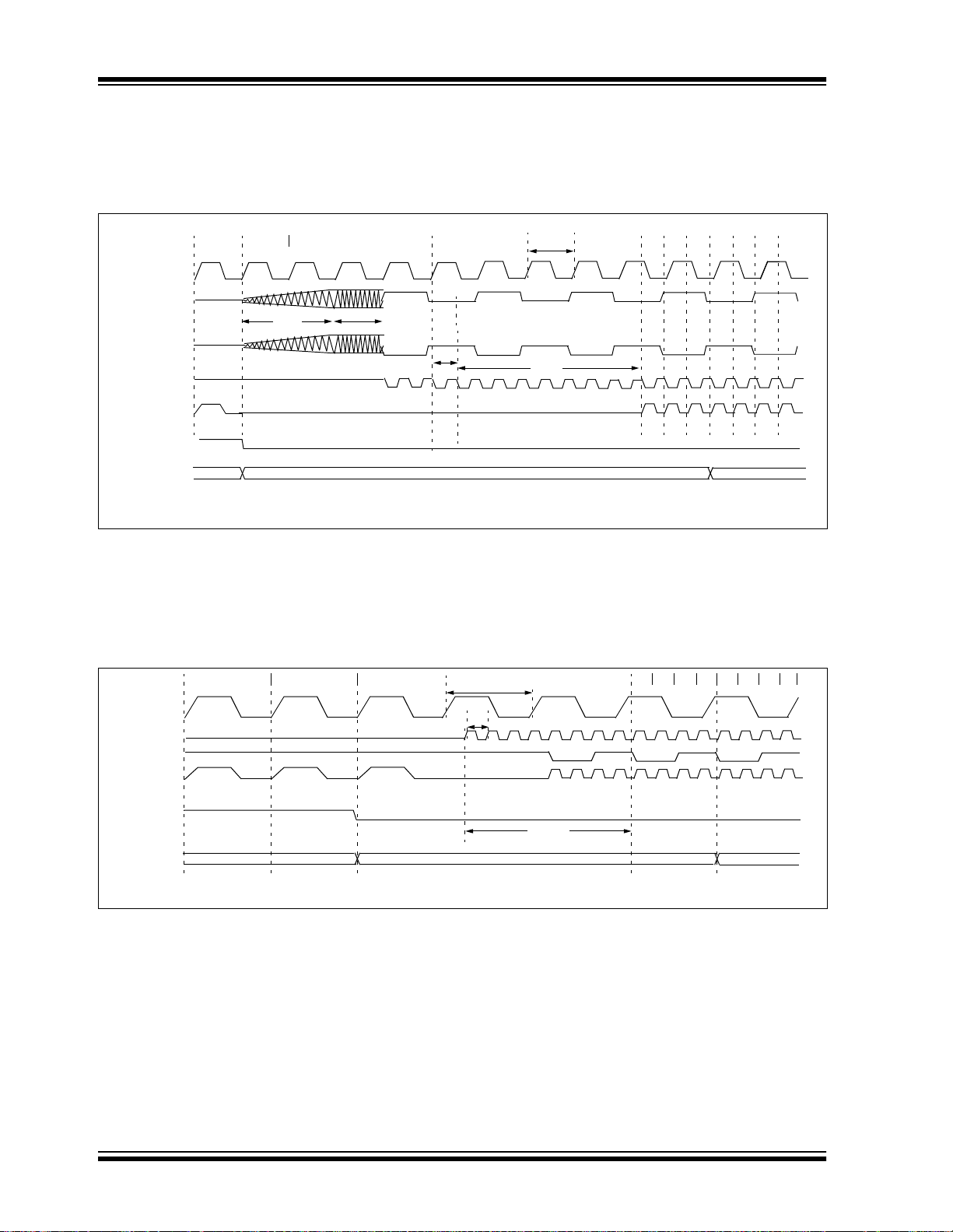
FIGURE 2-8: TIMING DIAGRAM FOR TRANSITION FROM OSC1 TO TIMER1 OSCILLATOR
Q1
T1OSI
OSC1
Internal
System
Clock
SCS
(OSCCON<0>)
Program
Counter
Note 1: Delay on internal system clock is eight oscillator cycles for synchronization.
TOSC
Q1
TDLY
TT1P
21 34 5678
Tscs
PC + 2PC
Q3Q2Q1Q4Q3Q2
Q4 Q1
Q2 Q3 Q4 Q1
PC + 4
The sequence of events that takes place when switching from the Timer1 oscillator to the main oscillator will
depend on the mode of the main oscillator. In addition
to eight clock cycles of the main oscillator, additional
delays may take place.
If the main oscillator is configured for an external crystal (HS, XT, LP), then the transition will tak e pl ace after
an oscillator st art-up time (T
OST) has occurred. A timing
diagram indicating the transition from the Timer1 oscillator to the main oscillator for HS, XT and LP modes is
shown in Figure 2-9.
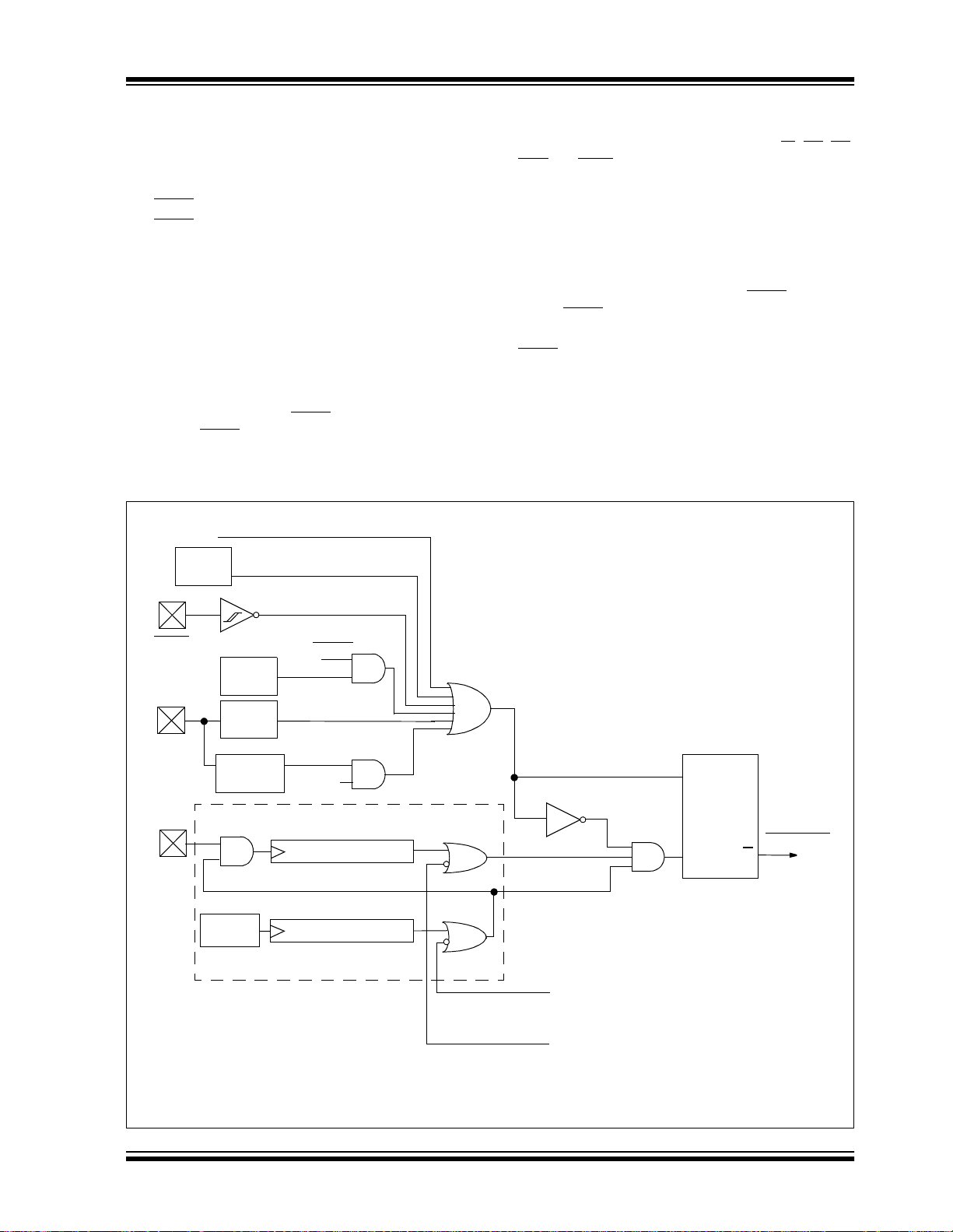
FIGURE 2-9: TIMING FOR TRANSITION BETWEEN TIMER1 AND OSC1 (HS, XT, LP)
Q3 Q4
T1OSI
OSC1
OSC2
Internal System
Clock
SCS
(OSCCON<0>)
Program Counter
Note 1: TOST = 1024TOSC (drawing not to scale).
PC PC + 2
Q1
TOST
TT1P
12345678
TSCS
TOSC
Q1 Q2 Q3 Q4 Q1 Q2
Q3
PC + 6
2001 Microchip Technology Inc. DS39026C-page 21
Page 24
PIC18CXX2
If the main oscil lator is config ured for HS-P LL mode, an
oscillator s tart-up time (T
time-out (T
PLL) will occur. The PLL time-out is typically
OST) plus an additional PLL
frequency. A timing diagram, indicating the transition
from the Timer1 oscillator to the main oscillator for
HS-PLL mode, is shown in Figure 2-10.
2 ms and allows the PLL to lock to the main oscillator
FIGURE 2-10: TIMING FOR TRANSITION BETWEEN TIMER1 AND OSC1 (HS WITH PLL)
Q4 Q1
T1OSI
OSC1
TOST
OSC2
PLL Clock
Input
Internal System
Program Counter
Note 1: TOST = 1024TOSC (drawing not to scale).
Clock
(OSCCON<0>)
SCS
PC PC + 2
TPLL
TT1P
TOSC
1 234 5678
TSCS
Q1 Q2 Q3 Q4 Q1 Q2
Q3
PC + 4
Q4
If the main oscillato r is c onfigur ed in th e RC, R CIO, EC
or ECIO modes, th ere is no os cillator start-up time-ou t.
Operation will resume after eight cycles of the main
cating the transition from the Timer1 oscillator to the
main oscillator for RC, RCIO, EC and ECIO modes, is
shown in Figure 2-11.
oscillator have been counted. A timing diagram, indi-
FIGURE 2-11: TIMING FOR TRANSITION BETWEEN TIMER1 AND OSC1 (RC, EC)
Q3 Q4
T1OSI
OSC1
OSC2
Internal System
Clock
SCS
(OSCCON<0>)
Program Counter
Note 1: RC oscillator mode assumed.
Q1
PC PC + 2
TOSC
1
TT1P
23
45678
TSCS
Q1 Q2 Q3 Q4 Q1 Q2 Q3
Q4
PC + 4
DS39026C-page 22 2001 Microchip Technology Inc.
Page 25

PIC18CXX2
2.7 Effects of SLEEP Mode on the On-chip Oscillator
When the device executes a SLEEP instruction, the
on-chip clocks and oscillator are turned off and the
device is held at the beginning of an instruction cycle
(Q1 state). With the os ci lla tor o f f, the OSC1 and OSC2
signals will stop oscillating. Since all the transistor
switching currents have been removed, SLEEP mode
achieves the lowest current consumption of the device
(only leakage currents). Enabling any on-chip feature
that will operate during SL EEP will increas e the current
consumed during SLEEP. The user can wake from
SLEEP through external RESET, Watchdog Timer
Reset, or through an interrupt.
TABLE 2-3: OSC1 AND OSC2 PIN STATES IN SLEEP MODE
OSC Mode OSC1 Pin OSC2 Pin
RC Floating, external r esistor should
pull high
RCIO Floating, external resistor should
pull high
ECIO Floating Configured as PORTA, bit 6
EC Floating At logic low
LP, XT, and HS Feedback inverter disabled, at
quiescent voltage level
Note: See Table 3-1, in Section 3.0 RESET, for time-outs due to SLEEP and MCLR
2.8 Power-up Delays
Power up del ays are cont rolled by tw o timers , so that
no external RESET circuitry is required for most applications. The delays ensure that the device is kept in
RESET until the device power sup ply and clock are st able. For additional information on RESET operation,
see the “RESET” section.
The first timer is the Power-up Timer (PWRT), which
optionally provid es a fix ed delay of 72 ms (nominal) on
power-up only (POR and BOR). The second timer is
the Oscillator S t art-up T imer , O ST, intended to keep the
chip in RESET until the crystal oscillator is stable.
With the PLL enabled (HS/PLL oscillator mode), the
time-out sequenc e following a Power-on Reset is diff erent from other oscil lator modes. The time-out se quence
is as follows: First, the PWRT time-out is invoked after
a POR time delay has expired. Then, the Oscillator
Start-up Timer (OST) is invoked. However, this is still
not a sufficient amount of time to allow the PLL to lock
at high frequenc ies. The PWR T timer i s used to provide
an additional fixed 2ms (nominal) time-out to allow the
PLL ample time to lock t o the incoming cloc k frequency .
At logic low
Configured as PORTA, bit 6
Feedback inverter disa ble d, at
quiescent voltag e lev el
Reset.
2001 Microchip Technology Inc. DS39026C-page 23
Page 26

PIC18CXX2
NOTES:
DS39026C-page 24 2001 Microchip Technology Inc.
Page 27
PIC18CXX2
3.0 RESET
Most registers are not affected by a WDT wake-up,
since this is viewed as the resumption of normal oper-
The PIC18CXX2 differentiates between various kinds
of RESET:
a) Power-on Reset (POR)
b) MCLR
Reset during normal operation
c) MCLR Reset during SLEEP
d) Watchdog Timer (WDT) Reset (during normal
operation)
e) Programmable Brown-out Reset (BOR)
f) RESET Instruction
g) Stack Full Reset
h) Stack Underflow Reset
Most registers are una ffected b y a RESET. Their status
ation. Status bits from the RCON register, RI
and BOR, are set or cleared differently in different
POR
RESET situations, as i ndicated in Table 3-2. These bits
are used in software to determine the nature of the
RESET. See Table 3-3 for a full description of the
RESET states of all registers.
A simplified block di agram of the On-Chip Reset Circu it
is shown in Figure 3-1.
The Enhanced MCU devices have a MCLR
in the MCLR
Reset path. The filter will detect and
ignore small pulses.
pin is no t driven low by any internal R ESETS,
MCLR
including WDT.
is unknown on POR and unchanged by all other
RESETS. The other registers are forced to a “RESET
state” on Power-on Reset, MCLR
out Reset, MCLR
Reset during SLEEP, and by the
, WDT Reset, Brown-
RESET instruction.
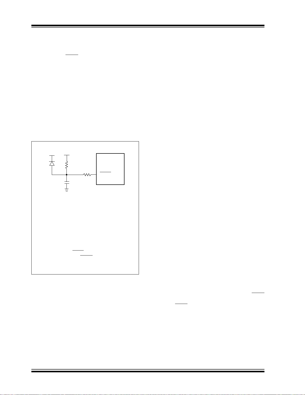
FIGURE 3-1: SIMPLIFIED BLOCK DIAGRAM OF ON-CHIP RESET CIRCUIT
RESET
Instruction
Stack
Pointer
Stack Full/Underflow Reset
, TO, PD,
noise filter
MCLR
VDD
OSC1
WDT
Module
DD Rise
V
Detect
Brown-out
Reset
OST/PWRT
On-chip
(1)
RC OSC
External Reset
SLEEP
WDT
Time-out
Reset
Power-on Reset
BOREN
OST
10-bit Ripple Counter
PWRT
10-bit Ripple Counter
Enable PWRT
Enable OST
S
Chip_Reset
R
(2)
Q
Note 1: This is a separate oscillator from the RC oscillator of the CLKIN pin.
2: See Table 3-1 for time-out situations.
2001 Microchip Technology Inc. DS39026C-page 25
Page 28
PIC18CXX2
3.1 Power-on Reset (POR)
A Power-on Reset pulse is generated on-chip when
DD rise is detected. To take advantage of t he POR cir-
V
cuitry, just tie the MCL R
tor) to V
DD. This will eliminate ex ternal R C compon ents
pin directly (or th rough a resi s-
usually needed to create a Power-on Reset delay. A
minimum rise rate for V
DD is specified (parameter
D004). For a slow rise time, see Figure 3-2.
When the device st arts normal operation (i.e ., ex its the
RESET condition), device operating parameters (voltage, frequency, temperature, etc.) must be met to
ensure operation. If these conditions are not met, the
device must be held in reset until the operating conditions are met.
FIGURE 3-2: EXTERNAL POWER-ON
RESET CIRCUIT (FOR
SLOW V
DD
V
D
R
C
Note 1: External Power-on Reset circuit is required
only if the V
The diode D helps discharge the capacitor
quickly when V
2: R < 40 kΩ is recommended to make sure that
the voltage drop across R does not violate
the device’s electrical specification.
3: R1 = 100Ω to 1 kΩ will limit any current flow-
ing into MCLR
the event of MCLR/
to Electrostatic Discharge (ESD) or Electrical
Overstress (EOS).
DD power-up slope is too slow.
DD POWER-UP)
R1
MCLR
PIC18CXXX
DD powers down.
from external capacitor C in
VPP pin breakdown, due
3.2 Power-up Timer (PWRT)
The Power-up Timer provides a fixed nominal time-out
(parameter #33) only on power-up from the POR. The
Power-up Timer operates on an internal RC oscillator.
The chip is kept in rese t as long as the PWRT is active.
The PWRT’s t ime delay allows V
able level. A configuration bit is provided to enable/
disable the PWRT.
The power-up time delay will vary fr om chip-to-ch ip due
DD, temperature and process variation. See DC
to V
parameter #33 for details.
DD to rise to an accept-
3.3 Oscillator Start-up Timer (OST)
The Oscillator Start-up Timer (OST) provides a 1024
oscillator cycle (from OSC1 input) delay after the
PWRT delay is over (para meter #32). Th is ensures th at
the crystal oscillator or resonator has started and
stabilized.
The OST time-out is invoked only for XT, LP and HS
modes and only on Power-on Reset or wake-up from
SLEEP.
3.4 PLL Lock Time-out
With the PLL enabled, the time-ou t sequen ce foll owin g
a Power-on Reset is different from other oscillator
modes. A portion of the Po wer-up Timer is used t o provide a fixed time-out th at is suff icient for the PLL to lock
to the main oscillator fre quenc y. This PLL lock time-out
PLL) is typically 2 ms and follows the oscillator start-
(T
up time-out (OST).
3.5 Brown-out Reset (BOR)
A configuration bit, BOREN, can disable (if clear/
programmed), or enable (if set) the Brown-out Reset
circuitry. If V
DD falls below parameter D005 for greater
than parameter #35, the brown-out situation will reset
the chip. A RESET may not occur if VDD falls below
parameter D005 for less than p aram et er #35 . The chip
will remain in Brown-out Reset until VDD rises above
DD. The Power- up Timer will then be invok ed and
BV
will keep the chip in RESET an additional time delay
(parameter #33). If VDD drops below BVDD while the
Power-up Timer is running, the chip will go back into a
Brown-out Reset and the Power-up Timer will be ini tialized. Once V
DD rises above BVDD, the Power-up Timer
will execute the additional time delay.
3.6 Time-out Sequence
On power-up, the time-out sequence is as follows:
First, PWRT time-out is invoked after the POR time
delay has expi red. Then, OST is activ ated. The total
time-out will vary based on oscillator configuration and
the status of th e PWRT. For example, in RC mode with
the PWRT disabled, there will be no time-out at all.
Figure 3-3, Figure 3-4, Figure 3-5, Figure 3-6 and
Figure 3-7 depict time-out sequences on power-up.
Since the time-outs occur from the POR pulse, if MC LR
is kept low long enough, the time-outs will expire.
Bringing MCLR
(Figure 3-5). This is useful for testing purposes or to
synchronize more than one PIC18CXXX device operating in parallel.
Table 3-2 shows the RESET conditions for some
Special Function Registers, while Table 3-3 shows the
RESET conditions for all the registers.
high will begin execution immediately
DS39026C-page 26 2001 Microchip Technology Inc.
Page 29

TABLE 3-1: TIME-OUT IN VARIOUS SITUATIONS
Oscillator
Configuration
PWRTE
Power-up
= 0 PWRTE = 1
(2)
Brown-out
PIC18CXX2
(2)
Wake-up from
SLEEP or
Oscillator Switch
72 ms + 1024TOSC
HS with PLL enabled
HS, XT, LP 72 ms + 1024T
EC 72 ms — 72 ms —
External RC 72 ms — 72 ms —
Note 1: 2 ms is the nominal time required for the 4x PLL to lock.
2: 72 ms is the nominal Power-up Timer delay.
(1)
+ 2ms
OSC 1024TOSC 72 ms + 1024TOSC 1024TOSC
1024TOSC
+ 2 ms
72 ms + 1024TOSC
+ 2ms
1024T
OSC + 2 ms
REGISTER 3-1: RCON REGISTER BITS AND POSITIONS
R/W-0 R/W-0 U-0 R/W-1 R/W-1 R/W-1 R/W-0 R/W-0
IPEN LWRT
bit 7 bit 0
Note: See Register 4-3 on page 53 for bit definitions.
— RI TO PD POR BOR
TABLE 3-2: STATUS BITS, THEIR SIGNIFICANCE AND THE INITIALIZATION CONDITION FOR
RCON REGISTER
Condition
Power-on Reset 0000h 00-1 1100 1 1 1 0 0 u u
MCLR Reset during normal
operation
Software Reset during normal
operation
Stack Full Reset during normal
operation
Stack Underflow Reset during
normal operation
MCLR
Reset during SLEEP 0000h 00-u 10uu u 1 0 u u u u
WDT Reset 0000h 0u-u 01uu 1 0 1 u u u u
WDT Wake-up PC + 2 uu-u 00uu u 0 0 u u u u
Brown-out Reset 0000h 0u-1 11u0 1 1 1 1 0 u u
Interrupt wake-up from SLEEP PC + 2
Legend: u = unchanged, x = unknown, - = unimplemented bit, read as '0'.
Note 1: When the wake-up is due to an interrupt and the GIEH or GIEL bits are set, the PC is loaded with the
interrupt vector (0x000008h or 0x000018h).
Program
Counter
0000h 00-u uuuu u u u u u u u
0000h 0u-0 uuuu 0 u u u u u u
0000h 0u-u uu11 u u u u u u 1
0000h 0u-u uu11 u u u u u 1 u
(1)
RCON
Register
uu-u 00uu u 1 0 u u u u
RI TO PD POR BOR STKFUL STKUNF
2001 Microchip Technology Inc. DS39026C-page 27
Page 30

PIC18CXX2
TABLE 3-3: INITIALIZATION CONDITIONS FOR ALL REGISTERS
MCLR
Resets
Register Applicab le Devices
Power-on Reset,
Brown-out Reset
TOSU 242 442 252 452 ---0 0000 ---0 0000 ---0 uuuu
TOSH 242 442 252 452 0000 0000 0000 0000 uuuu uuuu
TOSL 242 442 252 452 0000 0000 0000 0000 uuuu uuuu
STKPTR 242 442 252 452 00-0 0000 00-0 0000 uu-u uuuu
PCLATU 242 442 252 452 ---0 0000 ---0 0000 ---u uuuu
PCLATH 242 442 252 452 0000 0000 0000 0000 uuuu uuuu
PCL 242 442 252 452 0000 0000 0000 0000 PC + 2
TBLPTRU 242 442 252 452 --00 0000 --00 0000 --uu uuuu
TBLPTRH 242 442 252 452 0000 0000 0000 0000 uuuu uuuu
TBLPTRL 242 442 252 452 0000 0000 0000 0000 uuuu uuuu
TABLAT 242 442 252 452 0000 0000 0000 0000 uuuu uuuu
PRODH 242 442 252 452 xxxx xxxx uuuu uuuu uuuu uuuu
PRODL 242 442 252 452 xxxx xxxx uuuu uuuu uuuu uuuu
INTCON 242 442 252 452 0000 000x 0000 000u uuuu uuuu
INTCON2 242 442 252 452 1111 -1-1 1111 -1-1 uuuu -u-u
INTCON3 242 442 252 452 11-0 0-00 11-0 0-00 uu-u u-uu
INDF0 242 442 252 452 N/A N/A N/A
POSTINC0 242 442 252 452 N/A N/A N/A
POSTDEC0 242 442 252 452 N/A N/A N/A
PREINC0 242 442 252 452 N/A N/A N/A
PLUSW0 242 442 252 452 N/A N/A N/A
FSR0H 242 442 252 452 ---- 0000 ---- 0000 ---- uuuu
FSR0L 242 442 252 452 xxxx xxxx uuuu uuuu uuuu uuuu
WREG 242 442 252 452 xxxx xxxx uuuu uuuu uuuu uuuu
INDF1 242 442 252 452 N/A N/A N/A
POSTINC1 242 442 252 452 N/A N/A N/A
POSTDEC1 242 442 252 452 N/A N/A N/A
PREINC1 242 442 252 452 N/A N/A N/A
PLUSW1 242 442 252 452 N/A N/A N/A
Legend: u = unchanged, x = unknown, - = unimplemented bit, read as ’0’, q = value depends on condition
Note 1: One or more bits in the INTCONx or PIRx registers will be affected (to cause wake-up).
2: When the wake-up is d ue t o an interru pt and the GIEL or G IEH bi t is set, the PC is load ed wi th the interrup t
vector (0008h or 0018h).
3: When the wake-up is due to an interrupt and the GIEL or GIEH bit is set, the TOSU, TOSH and TOSL are
updated with the current value of the PC. The STKPTR is modified to point to the next location in the hardware stack.
4: See Table 3-2 for RESET value for specific condition.
5: Bit 6 of PORTA, LATA, and TRISA are enabled in ECIO and RCIO oscillator modes only. In all other
oscillator modes, they are disabled and read ’0’.
6: The long write enable is only reset on a POR or MCLR Reset.
7: Bit 6 of PORTA, LA TA and TRISA are not available on all devices. When unimplemented, they are read as ’0’.
WDT Reset
RESET Instruction
Stack Rese ts
Wake-up via WDT
or Interrupt
(3)
(3)
(3)
(3)
(2)
(1)
(1)
(1)
DS39026C-page 28 2001 Microchip Technology Inc.
Page 31

PIC18CXX2
TABLE 3-3: INITIALIZATION CONDITIONS FOR ALL REGISTERS (CONTINUED)
MCLR
Resets
Register Applicab le Devices
FSR1H 242 442 252 452 ---- 0000 ---- 0000 ---- uuuu
FSR1L 242 442 252 452 xxxx xxxx uuuu uuuu uuuu uuuu
BSR 242 442 252 452 ---- 0000 ---- 0000 ---- uuuu
INDF2 242 442 252 452 N/A N/A N/A
POSTINC2 242 442 252 452 N/A N/A N/A
POSTDEC2 242 442 252 452 N/A N/A N/A
PREINC2 242 442 252 452 N/A N/A N/A
PLUSW2 242 442 252 452 N/A N/A N/A
FSR2H 242 442 252 452 ---- 0000 ---- 0000 ---- uuuu
FSR2L 242 442 252 452 xxxx xxxx uuuu uuuu uuuu uuuu
STATUS 242 442 252 452 ---x xxxx ---u uuuu ---u uuuu
TMR0H 242 442 252 452 xxxx xxxx uuuu uuuu uuuu uuuu
TMR0L 242 442 252 452 xxxx xxxx uuuu uuuu uuuu uuuu
T0CON 242 442 252 452 1111 1111 1111 1111 uuuu uuuu
OSCCON 242 442 252 452 ---- ---0 ---- ---0 ---- ---u
LVDCON 242 442 252 452 --00 0101 --00 0101 --uu uuuu
WDTCON 242 442 252 452 ---- ---0 ---- ---0 ---- ---u
(4, 6)
RCON
TMR1H 242 442 252 452 xxxx xxxx uuuu uuuu uuuu uuuu
TMR1L 242 442 252 452 xxxx xxxx uuuu uuuu uuuu uuuu
T1CON 242 442 252 452 0-00 0000 u-uu uuuu u-uu uuuu
TMR2 242 442 252 452 xxxx xxxx uuuu uuuu uuuu uuuu
PR2 242 442 252 452 1111 1111 1111 1111 1111 1111
T2CON 242 442 252 452 -000 0000 -000 0000 -uuu uuuu
SSPBUF 242 442 252 452 xxxx xxxx uuuu uuuu uuuu uuuu
SSPADD 242 442 252 452 0000 0000 0000 0000 uuuu uuuu
SSPSTAT 242 442 252 452 0000 0000 0000 0000 uuuu uuuu
SSPCON1 242 442 252 452 0000 0000 0000 0000 uuuu uuuu
SSPCON2 242 442 252 452 0000 0000 0000 0000 uuuu uuuu
Legend: u = unchanged, x = unknown, - = unimplemented bit, read as ’0’, q = value depends on condition
Note 1: One or more bits in the INTCONx or PIRx registers will be affected (to cause wake-up).
2: When the wake-up is du e t o an interru pt and the GIEL or G IEH bi t is set, the PC is load ed wi th the interrup t
3: When the wake-up is due to an interrupt and the GIEL or GIEH bit is set, the TOSU, TOSH and TOSL are
4: See Table 3-2 for RESET value for specific condition.
5: Bit 6 of PORTA, LATA, and TRISA are enabled in ECIO and RCIO oscillator modes only. In all other
6: The long write enable is only reset on a POR or MCLR
7: Bit 6 of PORTA, LA TA and TRISA are not available on all devices. When unimplemented, they are read as ’0’.
242 442 252 452 00-1 11q0 00-1 qquu uu-u qquu
vector (0008h or 0018h).
updated with the current value of the PC. The STKPTR is modified to point to the next location in the hard-
ware stack.
oscillator modes, they are disabled and read ’0’.
Power-on Reset,
Brown-out Reset
WDT Reset
RESET Instruction
Stack Rese ts
Reset.
Wake-up via WDT
or Interrupt
2001 Microchip Technology Inc. DS39026C-page 29
Page 32

PIC18CXX2
TABLE 3-3: INITIALIZATION CONDITIONS FOR ALL REGISTERS (CONTINUED)
MCLR
Resets
Register Applicab le Devices
ADRESH 242 442 252 452 xxxx xxxx uuuu uuuu uuuu uuuu
ADRESL 242 442 252 452 xxxx xxxx uuuu uuuu uuuu uuuu
ADCON0 242 442 252 452 0000 0000 0000 0000 uuuu uuuu
ADCON1 242 442 252 452 --0- 0000 --0- 0000 --u- uuuu
CCPR1H 242 442 252 452 xxxx xxxx uuuu uuuu uuuu uuuu
CCPR1L 242 442 252 452 xxxx xxxx uuuu uuuu uuuu uuuu
CCP1CON 242 442 252 452 --00 0000 --00 0000 --uu uuuu
CCPR2H 242 442 252 452 xxxx xxxx uuuu uuuu uuuu uuuu
CCPR2L 242 442 252 452 xxxx xxxx uuuu uuuu uuuu uuuu
CCP2CON 242 442 252 452 --00 0000 --00 0000 --uu uuuu
TMR3H 242 442 252 452 xxxx xxxx uuuu uuuu uuuu uuuu
TMR3L 242 442 252 452 xxxx xxxx uuuu uuuu uuuu uuuu
T3CON 242 442 252 452 0000 0000 uuuu uuuu uuuu uuuu
SPBRG 242 442 252 452 xxxx xxxx uuuu uuuu uuuu uuuu
RCREG 242 442 252 452 xxxx xxxx uuuu uuuu uuuu uuuu
TXREG 242 442 252 452 xxxx xxxx uuuu uuuu uuuu uuuu
TXSTA 242 442 252 452 0000 -01x 0000 -01u uuuu -uuu
RCSTA 242 442 252 452 0000 000x 0000 000u uuuu uuuu
IPR2 242 442 252 452 ---- 1111 ---- 1111 ---- uuuu
PIR2 242 442 252 452 ---- 0000 ---- 0000 ---- uuuu
PIE2 242 442 252 452 ---- 0000 ---- 0000 ---- uuuu
IPR1 242 442 252 452 1111 1111 1111 1111 uuuu uuuu
242 442 252 452 -111 1111 -111 1111 -uuu uuuu
PIR1
PIE1 242 442 252 452 0000 0000 0000 0000 uuuu uuuu
Legend: u = unchanged, x = unknown, - = unimplemented bit, read as ’0’, q = value depends on condition
Note 1: One or more bits in the INTCONx or PIRx registers will be affected (to cause wake-up).
2: When the wake-up is d ue t o an interru pt and the GIEL or G IEH bi t is set, the PC is load ed wi th the interrup t
3: When the wake-up is due to an interrupt and the GIEL or GIEH bit is set, the TOSU, TOSH and TOSL are
4: See Table 3-2 for RESET value for specific condition.
5: Bit 6 of PORTA, LATA, and TRISA are enabled in ECIO and RCIO oscillator modes only. In all other
6: The long write enable is only reset on a POR or MCLR
7: Bit 6 of PORTA, LA TA and TRISA are not available on all devices. When unimplemented, they are read as ’0’.
242 442 252 452 0000 0000 0000 0000 uuuu uuuu
242 442 252 452 -000 0000 -000 0000 -uuu uuuu
242
442 252 452 -000 0000 -000 0000 -uuu uuuu
vector (0008h or 0018h).
updated with the current value of the PC. The STKPTR is modified to point to the next location in the hard-
ware stack.
oscillator modes, they are disabled and read ’0’.
Power-on Reset,
Brown-out Reset
WDT Reset
RESET Instruction
Stack Rese ts
Reset.
Wake-up via WDT
or Interrupt
(1)
(1)
(1)
DS39026C-page 30 2001 Microchip Technology Inc.
Page 33

PIC18CXX2
TABLE 3-3: INITIALIZATION CONDITIONS FOR ALL REGISTERS (CONTINUED)
MCLR
Resets
Register Applicab le Devices
Power-on Reset,
Brown-out Reset
TRISE 242 442 252 452 0000 -111 0000 -111 uuuu -uuu
TRISD
242 442 252 452 1111 1111 1111 1111 uuuu uuuu
TRISC 242 442 252 452 1111 1111 1111 1111 uuuu uuuu
TRISB 242 442 252 452 1111 1111 1111 1111 uuuu uuuu
TRISA
(5, 7)
242 442 252 452 -111 1111
(5)
LATE 242 442 252 452 ---- -xxx ---- -uuu ---- -uuu
LATD 242 442 252 452 xxxx xxxx uuuu uuuu uuuu uuuu
LATC 242 442 252 452 xxxx xxxx uuuu uuuu uuuu uuuu
LATB 242 442 252 452 xxxx xxxx uuuu uuuu uuuu uuuu
LATA
(5, 7)
242 442 252 452 -xxx xxxx
(5)
PORTE 242 442 252 452 ---- -000 ---- -000 ---- -uuu
PORTD
242 442 252 452 xxxx xxxx uuuu uuuu uuuu uuuu
PORTC 242 442 252 452 xxxx xxxx uuuu uuuu uuuu uuuu
PORTB 242 442 252 452 xxxx xxxx uuuu uuuu uuuu uuuu
PORTA
(5, 7)
242 442 252 452 -x0x 0000
(5)
Legend: u = unchanged, x = unknown, - = unimplemented bit, read as ’0’, q = value depends on condition
Note 1: One or more bits in the INTCONx or PIRx registers will be affected (to cause wake-up).
2: When the wake-up is du e t o an interru pt and the GIEL or G IEH bi t is set, the PC is load ed wi th the interrup t
vector (0008h or 0018h).
3: When the wake-up is due to an interrupt and the GIEL or GIEH bit is set, the TOSU, TOSH and TOSL are
updated with the current value of the PC. The STKPTR is modified to point to the next location in the hardware stack.
4: See Table 3-2 for RESET value for specific condition.
5: Bit 6 of PORTA, LATA, and TRISA are enabled in ECIO and RCIO oscillator modes only. In all other
oscillator modes, they are disabled and read ’0’.
6: The long write enable is only reset on a POR or MCLR
7: Bit 6 of PORTA, LA TA and TRISA are not available on all devices. When unimplemented, they are read as ’0’.
WDT Reset
RESET Instruction
Stack Rese ts
-111 1111
-uuu uuuu
-u0u 0000
(5)
(5)
(5)
Reset.
Wake-up via WDT
or Interrupt
-uuu uuuu
-uuu uuuu
-uuu uuuu
(5)
(5)
(5)
2001 Microchip Technology Inc. DS39026C-page 31
Page 34

PIC18CXX2
FIGURE 3-3: TIME-OUT SEQUENCE ON POWER-UP (MCLR TIED TO VDD)
VDD
MCLR
INTERNAL POR
TPWRT
PWRT TIME-OUT
OST TIME-OUT
INTERNAL RESET
TOST
FIGURE 3-4: TIME-OUT SEQUENCE ON POWER-UP (MCLR
VDD
MCLR
INTERNAL POR
TPWRT
PWRT TI ME-OUT
OST TIME-OUT
INTERNAL RESET
NOT TIED TO VDD): CASE 1
TOST
FIGURE 3-5: TIME-OUT SEQUENCE ON POWER-UP (MCLR
VDD
MCLR
INTERNAL POR
TPWRT
PWRT TIME-OUT
OST TIME-OUT
INTERNAL RESET
DS39026C-page 32 2001 Microchip Technology Inc.
NOT TIED TO VDD): CASE 2
TOST
Page 35

FIGURE 3-6: SLOW RISE TIME (MCLR TIED TO VDD)
5V
VDD
MCLR
INTERNAL POR
0V
PWRT
T
1V
PIC18CXX2
PWRT TIME-OUT
OST TIME-OUT
INTERNAL RES ET
TOST
FIGURE 3-7: TIME-OUT SEQUENCE ON POR W/ PLL ENABLED (MCLR
VDD
MCLR
IINTERNAL POR
TPWRT
PWRT TIME-OUT
OST TIME-OUT
PLL TIME-OUT
TOST
TPLL
TIED TO VDD)
INTERNAL RESET
Note: TOST = 1024 clock cycles.
T
PLL ≈ 2 ms max. First three stages of the PWRT timer.
2001 Microchip Technology Inc. DS39026C-page 33
Page 36

PIC18CXX2
NOTES:
DS39026C-page 34 2001 Microchip Technology Inc.
Page 37

4.0 MEMORY ORGANIZATION
There are two memory blocks in Enhanced MCU
devices. These memory blocks are :
• Program Memory
• Data Memory
Program and dat a mem ory us e separate buses so that
concurrent access can occ ur.
4.1 Program Memory Organization
A 21-bit program counter is capable of addressing the
2-Mbyte program memory space. Accessing a location
between the physically implemented memory and the
2-Mbyte address will cause a read of all ’0’s (a NOP
instruction).
PIC18C252 and PIC18C452 have 32 Kbytes of
EPROM, while PIC18C242 and PIC18C442 have
16 Kbytes of EPROM. This means that PIC18CX52
devices can store up to 16K of single word instructions,
and PIC18CX42 devices can store up to 8K of single
word instructions.
The RESET vector address is at 0000h and the interrupt vector addresses are at 0008h and 0018h.
Figure 4-1 shows the Program Memory Map for
PIC18C242/442 devices and Figure 4-2 shows the
Program Memory Map for PIC18C252/452 devices.
PIC18CXX2
2001 Microchip Technology Inc. DS39026C-page 35
Page 38

PIC18CXX2
FIGURE 4-1: PROGRAM MEMORY MAP
AND STACK FOR
PIC18C442/242
PC<20:0>
CALL,RCALL,RETURN
RETFIE,RETLW
Stack Level 1
Stack Level 31
RESET Vect or
High Priority Interrupt Vector
Low Priority Interrupt Vector
On-chip
Program Memory
Read ’0’
21
•
•
•
0000h
0008h
0018h
3FFFh
4000h
User Memory Space
FIGURE 4-2: PROGRAM MEMORY MAP
AND STACK FOR
PIC18C452/252
PC<20:0>
CALL,RCALL,RETURN
RETFIE,RETLW
Stack Level 1
Stack Level 31
RESET Vect or
High Priority Interrupt Vector
Low Priority Interrupt Vector
On-chip
Program Memory
21
•
•
•
0000h
0008h
0018h
7FFFh
8000h
User Memory Space
1FFFFFh
200000h
Read ’0’
1FFFFFh
200000h
DS39026C-page 36 2001 Microchip Technology Inc.
Page 39

PIC18CXX2
4.2 Return Address Stack
The return address s tack allows any co mbination of up
to 31 program calls and interrupts to occur. The PC
(Program Counter) is pushed onto the stack when a
CALL or RCALL instruction is executed, or an interrupt
is acknowledged. The PC value is pulled off the stack
on a RETURN, RETLW or a RETFIE instruction.
PCLATU and PCLATH are not af fected by any of the c all
or return instructions.
The stack operates as a 31-word by 21-bit RAM and a
5-bit stack pointer, with the stack pointer initialized to
00000b after all RESETS. There is no RAM assoc iated
with stack poi nter 00000 b. This is o nly a RESET v alue.
During a CALL type instruc tion caus ing a push o nto the
stack, the stack pointer is first incremented and the
RAM location pointed to by the stack pointer is written
with the contents of the PC. During a RETURN type
instruction causing a pop from the stack, the contents
of the RAM location pointed t o by the ST KPTR i s transferred to the PC and then the stack pointer is
decremented.
The stack space is not part of either program or data
space. The stac k p oi n ter i s r e adab l e a n d wr i tab le, a nd
the address on the top of the stac k is readab le and writable through SFR registers. Data can also be pushed
to, or popped from, the stack, using the top-of-stack
SFRs. Status bits indicate if the stack pointer is at, or
beyond the 31 levels provided.
4.2.1 TOP-OF-STACK ACCESS
The top of the stack is readable and writable. Three
register locations, TOSU, TOSH and TOSL hold the
contents of the stack location pointed to by the
STKPTR register. This allows users to implement a
software stac k, i f nec essa ry. After a CALL, RCALL or
interrupt, the software can read the pushed value by
reading the TOSU, TOSH and TOSL registers. These
values can be p laced on a use r d efined sof twa re st ack .
At return time, the software can replace the TOSU,
TOSH and TOSL and do a return.
The user must disable the global interrupt enable bits
during this time to prevent inadvertent stack operations..
4.2.2 RETURN STACK POINTER (STKPTR)
The STKPTR register contains the stack pointer va lu e,
the STKFUL (stack full) status bit, and the STKUNF
(stack underflow) status bits. Register 4-1 shows the
STKPTR register. The value of the stack pointer can be
0 through 31. The stack pointer increments when values are pushed onto the stack and decrements when
values are popped off the stack. At RESET, the stack
pointer value will be 0. The user may read and write the
stack pointer valu e. This featu re can b e used by a Rea l
Time Operating System for return stack maintenance.
After the PC is push ed ont o the s tac k 31 times (w itho ut
popping any values off the stack), the STKFUL bit is
set. The STKFUL bit can o nly be cle ared in sof tware or
by a POR.
The action that takes place when the stack becomes
full, depends on the state of the STVREN (S t ac k Overflow Reset Enable) configuration bit. Refer to
Section 18.0 for a description of the device configuration bits. If STVREN is set (default), the 31st push will
push the (PC + 2) value onto the st ack, set the STKFU L
bit, and reset the device. The STKFUL bit will remain
set and the stack pointer will be set to 0.
If STVREN is cleared, the STKFUL bit will be set on the
31st push and the stack pointer will increment to 31.
Any additional pushes will not overwrite the 31st push
and STKPTR will remain at 31.
When the stack has been popped enough times to
unload the stac k, the next pop will ret urn a value of zero
to the PC and sets the STKUNF bit, while the stack
pointer remains at 0. The STKUNF bit will remain set
until cleared in software or a POR occurs.
Note: Returning a value of zero to the PC on an
underflow, has the effect of vectoring the
program to the RESET vector, where the
stack condition s can be verifi ed and appropriate actions can be taken.
2001 Microchip Technology Inc. DS39026C-page 37
Page 40

PIC18CXX2
REGISTER 4-1: STKPTR REGISTER
R/C-0 R/C-0 U-0 R/W-0 R/W-0 R/W-0 R/W-0 R/W-0
STKFUL STKUNF
bit 7 bit 0
— SP4 SP3 SP2 SP1 SP0
(1)
bit 7
(1)
bit 6
bit 5 Unimplemented: Read as '0'
bit 4-0 SP4:SP0: Stack Pointer Location bits
STKFUL: Sta ck Full Fla g bit
1 = Stack became full or overflowed
0 = Stack has not become full or overflowed
STKUNF: Stack Underflow Flag bit
1 = Stack underflow occurred
0 = Stack underflow did not occur
Note 1: Bit 7 and bit 6 can only be cleared in user software or by a POR.
Legend:
R = Readable bit W = Writable bit U = Unimplemented bit, read as ‘0’
- n = Value at POR ’1’ = Bit is set ’0’ = Bit is cleared x = Bit is unknown
FIGURE 4-3: RETURN ADDRESS STACK AND ASSOCIATED REGISTERS
Return Address S t ac k
11111
11110
TOSLTOSHTOSU
0x340x1A0x00
Top-of-Stack
0x001A34
0x000D58
11101
00011
00010
00001
00000
STKPTR<4:0>
00010
4.2.3 PUSH AND POP INSTRUCTIONS
Since the Top-of-Stack (TO S) is readable and writable,
the ability to push valu es onto the stack and pull va lues
off the sta ck, withou t disturbi ng normal program ex ecution, is a desirable optio n. To push the current PC value
onto the stack, a PUSH instruction can be executed.
This will i ncrem ent th e stack point er and load the cu rrent PC value onto the stack. TOSU, TOSH and TOSL
can then be modified to place a return address on the
stack.
The ability to pull the TOS value off of the stack and
replace it with the value that was previously pushed
onto the stack, without disturbing normal execution, is
achieved by using the POP inst ruction. T he POP instru ction discards the current TOS by decrementing the
stack pointer. The previous value pushed onto the
stack then becomes the TOS value.
DS39026C-page 38 2001 Microchip Technology Inc.
4.2.4 STACK FULL/UNDERFLOW RESETS
These resets are enabled by programming the
STVREN configuration bit. When the STVREN bit is
disabled, a full or underf low condition will set the appropriate STKFUL or STKUNF bit, but not cause a device
RESET. When the STVREN bit is enabled, a full or
underflow will set the appro priate STKF UL or STKUNF
bit and then cause a device RESET. The STKFUL or
STKUNF bits are only cleared by the user software or
a POR Reset.
Page 41

PIC18CXX2
4.3 Fast Register Stack
A "fast interrupt return " option is available fo r interrupts .
A Fast Register Stack is provided for the STATUS,
WREG and BSR registers and are only one in depth.
The stack is n ot read able o r writable and is loade d wi th
the current value of the corresponding register when
the processor ve ctors for an in terrupt. The va lues in the
registers are then loaded back into the working registers, if the FAST RETURN instruction is used to return
from the interrupt.
A low or high priority interrupt source will push values
into the stack registers. If both low and high priority
interrupts are enabled, the stack registers cannot be
used reliably for low priority interrupts. If a high priority
interrupt occurs while servicing a low priority interrupt,
the stack registe r values stored by the low priority interrupt will be overwritten.
If high priority int errupts are not dis abled duri ng low priority interrupts, users must save the key registers in
software during a low priority interrupt.
If no interrupts are used, the fast register stack can be
used to restore the STATUS, WREG and BSR registe rs
at the end of a subr out ine ca ll. To use the fast registe r
stack for a subroutine call, a FAST CALL instruction
must be executed.
Example 4-1 shows a source code example that uses
the fast register stack.
4.4 PCL, PCLATH and PCLATU
The program counter ( PC) spe ci fie s th e ad dre ss of th e
instruction to fetch for execution. The PC is 21-bits
wide. The low byte is called the PCL register. This register is readable and writable. The high byte is called
the PCH register. This register contains the PC<15:8>
bits and is not directly readable or writable. Updates to
the PCH register may be performed through the
PCLATH register. The upper byte is called PCU. This
register contains th e PC<20 :16> bit s an d is not d irectly
readable or writable. Updates to the PCU register may
be performed through the PCLATU register.
The PC addresses bytes in the program memory. To
prevent the PC from becoming misaligned with word
instructio ns, the LSB of P CL is fi xed to a v alue of ’0’.
The PC increments by 2 to address se que nti al ins truc tions in the program memory.
The CALL, RCALL, GOTO and program branch
instructions write to the program counter directly. For
these instructions, the contents of PCLATH and
PCLATU are not transferred to the program counter.
The contents of PCLATH and PCLATU will be transferred to the program counter by an operation that
writes PCL. Similarly, the upper two bytes of the program counter will be transferred to PCLATH and
PCLATU by an operation that reads PCL. This is useful
for computed offsets to the PC (see Section4.8.1).
EXAMPLE 4-1: FAST REGISTER STACK
CODE EXAMPLE
CALL SUB1, FAST ;STATUS, WREG, BSR
;SAVED IN FAST REGISTER
•
•
SUB1 •
•
•
RETURN FAST ;RESTORE VALUES SAVED
;STACK
;IN FAST REGISTER STACK
FIGURE 4-4: CLOCK/ INSTRUCTION CYCLE
Q2 Q3 Q4
OSC1
Q1
Q2
Q3
Q4
PC
OSC2/CLKOUT
(RC mode)
Q1
PC PC+2 PC+4
Execute INST (PC-2)
Fetch INST (PC) Execute INST (PC)
Q1
Fetch INST (PC+2) Execute INST (PC+2)
4.5 Clocking Scheme/Instruct ion Cycle
The clock input (from OSC1) is internally divided by
four to generate four non-overlapping quadrature
clocks, namely Q1, Q2, Q3 and Q4. Internally, the program counter (PC) is incremented every Q1, the
instruction is fetched from the program memory and
latched into the instruction register in Q4. The instruction is decoded and executed during the following Q1
through Q4. The clocks and instruction execution flow
is shown in Figure 4-4.
Q2 Q3 Q4
Q2 Q3 Q4
Q1
Fetch INST (PC+4)
Internal
Phase
Clock
2001 Microchip Technology Inc. DS39026C-page 39
Page 42

PIC18CXX2
4.6 Instruction Flow/Pipelining
An “Instruction Cycle” consists of four Q cycles (Q1,
Q2, Q3 and Q4). The instruc ti on fe tch and execute are
pipelined such that fetch takes one instruction cyc le,
while decode and execute takes another instruction
cycle. However, due to the pipelining, each instruction
effectively executes in one cycle. If an instruction
causes the program counter to change (e.g. GOTO),
A fetch cycle begins with the program counter (PC)
incrementing in Q1.
In the execution cy cle, the fetched instruction i s latched
into the “Instruction Register" (IR) in cycle Q1. This
instruction is then decoded and executed during the
Q2, Q3, and Q4 cycles. Dat a memory is read during Q2
(operand read) and written during Q4 (destination
write).
then two cycles are re quired to com plete the inst ruction
(Example 4-2).
EXAMPLE 4-2: INSTRUCTION PIPELINE FLOW
TCY0TCY1TCY2TCY3TCY4TCY5
1. MOVLW 55h
2. MOVWF PORTB
3. BRA SUB_1
4. BSF PORTA, BIT3 (Forced NOP)
5. Instruction @ address SUB_1
All instructions are single cycle, except for any program branche s. These take tw o cycles since the fetch instruction
is “flushed” from the pipeline, while the new instruction is being fetched and then executed.
Fetch 1 Execute 1
Fetch 2 Execute 2
Fetch 3 Execute 3
Fetch 4 Flush (NOP)
Fetch SUB_1 Execute SUB_1
4.7 Instructions in Program Memory
The CALL and GOTO ins tructions have an absol ute program memory address embedded into the instruction.
The program memory is addressed in bytes. Instructions are stored as two bytes or four bytes in program
memory. The Least Significant Byte of an instruction
word is always stored in a program memory location
with an even address (LSB =’0’). Figure4-5 shows an
example of how instructi on words are stored in the program memory. To maintain alignment with instruction
boundaries, the PC increments in steps of 2 and the
LSB will always read ’0’ (see Section 4.4).
Since instructions are always stored on word boundaries, the data contained in the instruction is a word
address. The word address is written to PC<20:1>,
which accesses the desired byte address in program
memory. Instruction #2 in Figure 4-5 shows how the
instruction “GOTO 000006h” is enco ded in the program
memory. Program branch instruc tio ns , w hic h e ncode a
relative address offset, operate in the same manner.
The offset value stored in a branch instruction represents the number of single word instructions that the
PC will be offset by. Section 19.0 provides further
details of the instruction set.
FIGURE 4-5: INSTRUCTIONS IN PROGRAM MEMORY
LSB = 1 LSB = 0 ↓
0Fh 55h 000008h
EFh 03h 00000Ah
F0h 00h 00000Ch
C1h 23h 00000Eh
F4h 56h 000010h
Instruction 1:
Instruction 2:
Instruction 3:
Program Memory
Byte Locations
MOVLW 055h
GOTO 000006h
MOVFF 123h, 456h
→
Word Address
000000h
000002h
000004h
000006h
000012h
000014h
DS39026C-page 40 2001 Microchip Technology Inc.
Page 43

PIC18CXX2
4.7.1 TWO-WORD INSTRUCTIONS
The PIC18CXX2 devices have four two-word instructions: MOVFF, CALL, GOTO and LFSR. The second
word of these instructions has the 4 MSBs set to 1’s
and is a special kind of NOP instruct ion. The l ower 12bits of the second word contain data to be used by the
instruction. If the first word of the instruction is executed, the data in the second word is accessed. If the
EXAMPLE 4-3: TWO-WORD INSTRUCTIONS
CASE 1:
Object Code Source Code
0110 0110 0000 0000
1100 0001 0010 0011
1111 0100 0101 0110
0010 0100 0000 0000
CASE 2:
Object Code Source Code
0110 0110 0000 0000
1100 0001 0010 0011
1111 0100 0101 0110
0010 0100 0000 0000
TSTFSZ REG1 ; is RAM location 0?
MOVFF REG1, REG2 ; No, execute 2-word instruction
ADDWF REG3 ; continue code
TSTFSZ REG1 ; is RAM location 0?
MOVFF REG1, REG2 ; Yes
ADDWF REG3 ; continue code
second word of the in struction is executed by it self (first
word was skipped), it will exec ute as a NOP. This action
is necessary when the two-word i nstruction is pr eceded
by a conditional instruc tion that c hanges t he PC. A pr ogram example tha t demonstr ates this conc ept is show n
in Example 4-3. Refer to Section 19.0 for further details
of the instruction set.
; 2nd operand holds address of REG2
; 2nd operand becomes NOP
4.8 Lookup Tables
Lookup tables are implemented two ways. These are:
• Computed GOTO
• Table Reads
4.8.1 COMPUTED GOTO
A computed GOTO is accomplish ed by adding an offset
to the program counter (ADDWF PCL).
A lookup table can be formed with an ADDWF PCL
instruction and a group of RETLW 0xnn instructions.
WREG is loaded with an offset into the table, before
executing a call to tha t t able. The first instructi on of the
called routine is the ADDWF PCL instruction. The next
instruction executed will be one of the RETLW 0xnn
instructions that returns the value 0xnn to the calling
function.
The offset value (va lue in WREG) specifie s the number
of bytes that the program counter should advance.
In this method, only one data byte may be stored in
each instruction location and room on the return
address stack is required.
4.8.2 TABLE READS/TABLE WRITES
A better method of storing data in program memory
allows 2 bytes of data to be stored in each instruction
location.
Lookup table data may be stored 2 bytes per program
word by using ta ble read s and writes . The t abl e point er
(TBLPTR) specifies the byte address and the table
latch (TABLAT) contains the data that is read from, or
written to program memory. Data is transferred to/from
program memory one byte at a time.
A description of the Table Read/Table Write operation
is shown in Section 5.0.
2001 Microchip Technology Inc. DS39026C-page 41
Page 44

PIC18CXX2
4.9 Dat a Memory Organization
The data memory i s impl emented as static RAM. Eac h
register in the data memory has a 12-bit address,
allowing up to 4096 byt es of data mem ory. Figure 4-6
and Figure 4-7 show the data memory organization for
the PIC18CXX2 devices.
The data memory map is divided into as many as 16
banks that contain 256 bytes each. The lower 4 bits of
the Bank Select Register (BSR<3:0>) select which
bank will be accessed. T he upper 4 bits for the BSR are
not implemented.
The data memory contains Special Function Registers
(SFR) and General Purpose Registers (GPR). The
SFRs are used for control and status of the controller
and peripheral functio ns, while GPRs are us ed for data
storage and scratch pad operations in the user’s application. The SFRs start at the last location of Bank 15
(0xFFF) and extend downwards. Any remaining space
beyond the SFRs in the Bank may be implemented as
GPRs. GPRs start at the first location of Bank 0 and
grow upwards. Any re ad of a n un im pl em ente d l oc atio n
will read as ’0’s.
The entire data memory may be accessed directly, or
indirectly. Direct addressi ng m ay requ ire th e us e of th e
BSR register. Indirect addressing requires the use of a
File Select Register (FSRn) and c orresponding Indirect
File Operand (INDFn). Each FSR holds a 12-bit
address value that can be used to access any location
in the Data Memory map without banking.
The instruction set and architecture allow operations
across all banks. This m ay be accompli shed by indirec t
addressing or by the us e of t he MOVFF instruction. The
MOVFF instruction is a two-word/two-cycle instruction
that moves a value from one register to another.
To ensure that commonly used registers (SFRs and
select GPRs) can be accessed in a single cycle,
regardless of the current BSR values, an Access Bank
is implemented. A s egment of Ban k 0 and a segm ent of
Bank 15 comprise the Access RAM. Section4.10 provides a detailed description of the Access RAM.
4.9.1 GENERAL PURPOSE REGISTER FILE
The register file can be acces sed either directly, or indirectly. Indirect addressing operates using the File
Select Registers (FSRn) and corresponding Indirect
File Operand (INDFn). The operation of indirect
addressing is shown in Section 4.12.
Enhanced MCU devices may have banked memory in
the GPR area. GPRs are not initialized by a Power-on
Reset and are unchanged on all other RESETS.
Data RAM is available for use as GPR registers by all
instructio ns. T he to p hal f of ban k 15 (0 xF80 t o 0xFF F)
contains SFR s. All oth er banks of d ata memory c ontai n
GPR registers, starting with bank 0.
4.9.2 SPECIAL FUNCTION REGISTERS
The Special Function Registers (SFRs) are registers
used by the CPU and Peripheral Modules for controlling the desired operation of the device. These registers are implemented as static RAM. A list of these
registers is given in Table 4-1 and Table 4-2.
The SFRs can be classified into two sets; those associated with the “core” function and those related to the
peripheral functions. Those registers related to the
“core” are described in this s ec tio n, w hil e tho se rel ate d
to the operation of the peripheral features are
described in the section of that periphe ral feature.
The SFRs are typic ally d istribute d amo ng the per ipherals whose functions they control.
The unused SFR locations will be unimplemented and
read as '0's. See Table 4-1 for addresses for the SFRs.
DS39026C-page 42 2001 Microchip Technology Inc.
Page 45

FIGURE 4-6: DATA MEMORY MAP FOR PIC18C242/442
PIC18CXX2
BSR<3:0>
= 0000b
= 0001b
= 0010b
= 1110b
= 1111b
When a = 1,
the BSR is used to specify the
RAM location that the instruction uses.
Bank 0
Bank 1
Bank 2
to
Bank 14
Bank 15
Data Memory Map
00h
Access RAM
FFh
00h
FFh
Unused
Read ’00h’
00h
FFh
Unused
GPR
GPR
SFR
000h
07Fh
080h
0FFh
100h
1FFh
200h
EFFh
F00h
F7Fh
F80h
FFFh
Access Bank
Access RAM low
Access RAM high
(SFR’s)
When a = 0,
the BSR is ignored and the
Access Bank is used.
The first 128 bytes are General
Purpose RAM (from Bank 0).
The second 128 bytes are
Special Function Registers
(from Bank 15).
00h
7Fh
80h
FFh
2001 Microchip Technology Inc. DS39026C-page 43
Page 46

PIC18CXX2
FIGURE 4-7: DATA MEMORY MAP FOR PIC18C252/452
BSR<3:0>
= 0000b
= 0001b
= 0010b
= 0011b
= 0100b
= 0101b
= 0110b
= 1110b
= 1111b
When a = 1,
the BSR is used to specify the
RAM location that the instruction uses.
Bank 0
Bank 1
Bank 2
Bank 3
Bank 4
Bank 5
Bank 6
to
Bank 14
Bank 15
Data Memory Map
00h
Access RAM
FFh
00h
FFh
00h
FFh
00h
FFh
00h
FFh
00h
FFh
GPR
GPR
GPR
GPR
GPR
GPR
Unused
Read ’00h’
Unused
SFR
000h
07Fh
080h
0FFh
100h
1FFh
200h
2FFh
300h
3FFh
400h
4FFh
500h
5FFh
600h
EFFh
F00h
F7Fh
F80h
FFFh
Access Bank
Access RAM low
Access RAM high
(SFR’s)
When a = 0,
the BSR is ignored and the
Access Bank is used.
The first 128 bytes are General
Purpose RAM (from Bank 0).
The second 128 bytes are
Special Function Registers
(from Bank 15).
00h
7Fh
80h
FFh
DS39026C-page 44 2001 Microchip Technology Inc.
Page 47

PIC18CXX2
TABLE 4-1: SPECIAL FUNCTION REGISTER MAP
FFFh TOSU FDFh INDF2
FFEh TOSH FDEh POSTINC2
FFDh TOSL FDDh POSTDEC2
FFCh STKPTR FDCh PREINC2
FFBh PCLATU FDBh PLUSW2
FFAh PCLATH FDAh FSR2H FBAh CCP2CON F9Ah
FF9h PCL FD9h FSR2L FB9h — F99h —
FF8h TBLPTRU FD8h STATUS FB8h
FF7h TBLPTRH FD7h TMR0H FB7h
FF6h TBLPTRL FD6h TMR0L FB6h — F96h TRISE
FF5h TABLAT FD5h T0CON FB5h
FF4h PRODH FD4h
FF3h PRODL FD3h OSCCON FB3h TMR3H F93h TRISB
FF2h INTCON FD2h LVDCON FB2h TMR3L F92h TRISA
FF1h INTCON2 FD1h WDTCON FB1h T3CON F91h
FF0h INTCON3 FD0h RCON FB0h — F90h —
(3)
FEFh INDF0
FEEh POSTINC0
FEDh POSTDEC0
FECh PREINC0
FEBh PLUSW0
FCFh TMR1H FAFh SPBRG F8Fh —
(3)
FCEh TMR1L FAEh RCREG F8Eh —
(3)
FCDh T1CON FADh TXREG F8Dh LATE
(3)
FCCh TMR2 FACh TXSTA F8Ch LATD
(3)
FCBh PR2 FABh RCSTA F8Bh LATC
FEAh FSR0H FCAh T2CON FAAh — F8Ah LATB
FE9h FSR0L FC9h SSPBUF FA9h
FE8h WREG FC8h SSPADD FA8h — F88h —
FE7h INDF1
FE6h POSTINC1
FE5h POSTDEC1
FE4h PREINC1
FE3h PLUSW1
(3)
FC7h SSPSTAT FA7h — F87h —
(3)
FC6h SSPCON1 FA6h — F86h —
(3)
FC5h SSPCON2 FA5h — F85h —
(3)
FC4h ADRESH FA4h — F84h PORTE
(3)
FC3h ADRESL FA3h — F83h PORTD
FE2h FSR1H FC2h ADCON0 FA2h IPR2 F82h PORTC
FE1h FSR1L FC1h ADCON1 FA1h PIR2 F81h PORTB
FE0h BSR FC0h
(3)
FBFh CCPR1H F9Fh IPR1
(3)
FBEh CCPR1L F9Eh PIR1
(3)
FBDh CCP1CON F9Dh PIE1
(3)
FBCh CCPR2H F9Ch —
(3)
FBBh CCPR2L F9Bh —
— F98h —
— F97h —
— F95h TRISD
— FB4h — F94h TRISC
— F89h LATA
— FA0h PIE2 F80h PORTA
—
—
(2)
(2)
(2)
(2)
(2)
(2)
Note 1: Unimplemented registers are read as ’0’.
2: This register is not available on PIC18C2X2 devices.
3: This is not a physical register.
2001 Microchip Technology Inc. DS39026C-page 45
Page 48

PIC18CXX2
TABLE 4-2: REGISTER FILE SUMMARY
File Name Bit 7 Bit 6 Bit 5 Bit 4 Bit 3 Bit 2 Bit 1 Bit 0
TOSU
TOSH Top-of-Stack High Byte (TOS<15:8>)
TOSL Top-of-Stack Low Byte (TOS<7:0>)
STKPTR STKFUL STKUNF
PCLATU
PCLATH Holding Register for PC<15:8>
PCL PC Low Byte (PC<7:0>)
TBLPTRU
TBLPTRH Program Memory Table Pointer High Byte (TBLPTR<15:8>)
TBLPTRL Program Memory Table Pointer Low Byte (TBLPTR<7:0>)
TABLAT Program Memory Table Latch
PRODH Product Register High Byte
PRODL Product Register Low Byte
INTCON GIE/GIEH PEIE/GIEL TMR0IE INT0IE RBIE TMR0IF INT0IF RBIF
INTCON2 RBPU INTEDG0 INTEDG1 INTEDG2
INTCON3 INT2IP INT1IP
INDF0 Uses contents of FSR0 to address data memory - value of FSR0 not changed (not a physical register) N/A 50
POSTINC0 Uses contents of FSR0 to address data memory - v alue of FSR0 post-incremented (not a phys ical register) N/A 50
POSTDEC0 Uses contents of FSR0 to address data memory - value of FSR0 post-decremented (not a physical register) N/A 50
PREINC0 Uses contents of FSR0 to address data memory - value of FSR0 pre-incremented (not a physical register) N/A 50
PLUSW0 Uses contents of FSR0 to address data memory - value of FSR0 pre-incremented (not a physical register) -
FSR0H
FSR0L Indirect Data Memory Address Pointer 0 Low Byte
WREG Working Register
INDF1 Uses contents of FSR1 to address data memory - value of FSR1 not changed (not a physical register) N/A 50
POSTINC1 Uses contents of FSR1 to address data memory - v alue of FSR1 post-incremented (not a phys ical register) N/A 50
POSTDEC1 Uses contents of FSR1 to address data memory - value of FSR1 post-decremented (not a physical register) N/A 50
PREINC1 Uses contents of FSR1 to address data memory - value of FSR1 pre-incremented (not a physical register) N/A 50
PLUSW1 Uses contents of FSR1 to address data memory - value of FSR1 pre-incremented (not a physical register) -
FSR1H
FSR1L Indirect Data Memory Address Pointer 1 Low Byte
BSR
INDF2 Uses contents of FSR2 to address data memory - value of FSR2 not changed (not a physical register) N/A 50
POSTINC2 Uses contents of FSR2 to address data memory - v alue of FSR2 post-incremented (not a phys ical register) N/A 50
POSTDEC2 Uses contents of FSR2 to address data memory - value of FSR2 post-decremented (not a physical register) N/A 50
PREINC2 Uses contents of FSR2 to address data memory - value of FSR2 pre-incremented (not a physical register) N/A 50
PLUSW2 Uses contents of FSR2 to address data memory - value of FSR2 pre-incremented (not a physical register) -
FSR2H
FSR2L Indirect Data Memory Address Pointer 2 Low Byte
STATUS
TMR0H Timer0 Register High Byte
TMR0L Timer0 Register Low Byte
T0CON TMR0ON T08BIT T0CS T0SE PSA T0PS2 T0PS1 T0PS0
OSCCON
LVDCON
Legend:
Note 1: RA6 and associated bits are configured as port pins in RCIO and ECIO oscillator mode only, and read '0' in all other oscillator modes.
2: Bit 21 of the TBLPTRU allows access to the device configuration bits.
— — — Top-of-Stack Upper Byte (TOS<20:16>) ---0 0000 37
— Return Stack Pointer 00-0 0000 38
— — — Holding Register for PC<20:16> ---0 0000 39
— — bit21
value of FSR0 offset by value in WREG
— — — — Indirect Data Memory Address Pointer 0 High Byte ---- 0000 50
value of FSR1 offset by value in WREG
— — — — Indirect Data Memory Address Pointer 1 High Byte ---- 0000 50
— — — — Bank Select Register ---- 0000 49
value of FSR2 offset by value in WREG
— — — — Indirect Data Memory Address Pointer 2 High Byte ---- 0000 50
— — — NOVZDCC---x xxxx 52
— — — — — — — SCS ---- ---0 20
— — IRVST LVDEN LVDL3 LVDL2 LVDL1 L VDL0 --00 0101 175
x = unknown, u = unchanged, - = unimplemented, q = value depends on condition
(2)
Program Memory Table Pointer Upper Byte (TBLPTR<20:16>) ---0 0000 57
— TMR0IP — RBIP 1111 -1-1 66
— INT2IE INT1IE — INT2IF INT1IF 11-0 0-00 67
Value on
POR,
BOR
0000 0000 37
0000 0000 37
0000 0000 39
0000 0000 39
0000 0000 57
0000 0000 57
0000 0000 57
xxxx xxxx 61
xxxx xxxx 61
0000 000x 65
N/A 50
xxxx xxxx 50
xxxx xxxx
N/A 50
xxxx xxxx 50
N/A 50
xxxx xxxx 50
0000 0000 95
xxxx xxxx 95
1111 1111 93
Details
on page:
DS39026C-page 46 2001 Microchip Technology Inc.
Page 49

TABLE 4-2: REGISTER FILE SUMMARY (CONTINUED)
PIC18CXX2
File Name Bit 7 Bit 6 Bit 5 Bit 4 Bit 3 Bit 2 Bit 1 Bit 0
WDTCON — — — — — — — SWDTE ---- ---0 183
RCON IPEN LWRT
TMR1H Timer1 Register High Byte
TMR1L Timer1 Register Low Byte
T1CON RD16
TMR2 Timer2 Regis ter
PR2 Timer2 Period Register
T2CON
SSPBUF SSP Receive Buffer/Transmit Register
SSPADD SSP Address Register in I
SSPSTAT SMP CKE D/A
SSPCON1 WCOL SSPOV SSPEN CKP SSPM3 SSPM2 SSPM1 SSPM0
SSPCON2 GCEN ACKSTAT ACKDT ACKEN RCEN PEN RSEN SEN
ADRESH A/D Result Register High Byte
ADRESL A/D Result Register Low Byte
ADCON0 ADCS1 ADCS0 CHS2 CHS1 CHS0 GO/DO NE
ADCON1 ADFM ADCS2
CCPR1H Capture/Compare/PWM Register1 High Byte
CCPR1L Capture/Compare/PWM Register1 Low Byte
CCP1CON
CCPR2H Capture/Compare/PWM Register2 High Byte
CCPR2L Capture/Compare/PWM Register2 Low Byte
CCP2CON
TMR3H Timer3 Register High Byte
TMR3L Timer3 Register Low Byte
T3CON RD16 T3CCP2 T3CKPS1 T3CKPS0 T3CCP1 T3SYNC
SPBRG USART1 Baud Rate Generator
RCREG USART1 Receive Register
TXREG USART1 Transmit Register
TXSTA CSRC TX9 TXEN SYNC
RCSTA SPEN RX9 SREN CREN ADDEN FERR OERR RX9D
Legend:
Note 1: RA6 and associated bits are configured as port pins in RCIO and ECIO oscillator mode only, and read '0' in all other oscillator modes.
2: Bit 21 of the TBLPTRU allows access to the device configuration bits.
— TOUTPS3 TOUTPS2 TOUTPS1 TOUTPS0 TMR2ON T2CKPS1 T2CKPS0 -000 0000 101
— — DC1B1 DC1B0 CCP1M3 CCP1M2 CCP1M1 CCP1M0 --00 0000 107
— — DC2B1 DC2B0 CCP2M3 CCP2M2 CCP2M1 CCP2M0 --00 0000 107
x = unknown, u = unchanged, - = unimplemented, q = value depends on condition
— T1CKPS1 T1CKPS0 T1OSCEN T1SYNC TMR1CS TMR1ON 0-00 0000 97
— RI TO PD POR BOR 0q-1 11qq 53, 56,
2
C Slave Mode. SSP Baud Rate Reload Register in I2C Master Mode. 0000 0000 128
PSR/WUA BF 0000 0000 116
— ADON 0000 00-0 165
— — PCFG3 PCFG2 PCFG1 PCFG0 00-- 0000 166
TMR3CS TMR3ON 0000 0000 103
— BRGH TRMT TX9D 0000 -010 149
Value on
POR,
BOR
xxxx xxxx 97
xxxx xxxx 97
0000 0000 101
1111 1111 102
xxxx xxxx 121
0000 0000 118
0000 0000 120
xxxx xxxx 171,172
xxxx xxxx 171,172
xxxx xxxx 111, 113
xxxx xxxx 111, 113
xxxx xxxx 111, 113
xxxx xxxx 111, 113
xxxx xxxx 103
xxxx xxxx 103
0000 0000 151
0000 0000
0000 0000
0000 000x 150
Details
on page:
74
158, 161,
163
156, 159,
162
2001 Microchip Technology Inc. DS39026C-page 47
Page 50

PIC18CXX2
TABLE 4-2: REGISTER FILE SUMMARY (CONTINUED)
File Name Bit 7 Bit 6 Bit 5 Bit 4 Bit 3 Bit 2 Bit 1 Bit 0
IPR2 — — — — BCLIP LVDIP TMR3IP CCP2IP ---- 1111 73
PIR2
PIE2
IPR1 PSPIP ADIP RCIP TXIP SSPIP CCP1IP TMR2IP TMR1IP
PIR1 PSPIF ADIF RCIF TXIF SSPIF CCP1IF TMR2IF TMR1IF
PIE1 PSPIE ADIE RCIE TXIE SSPIE CCP1IE TMR2IE TMR1IE
TRISE IBF OBF IBOV PSPMODE
TRISD Data Direction Control Register for PORTD
TRISC Data Direction Control Register for PORTC
TRISB Data Direction Control Register for PORTB
TRISA
LATE
LATD Read PORTD Data Latch, Write PORTD Data Latch
LATC Read PORTC Data Latch, Write PORTC Data Latch
LATB Read PORTB Data Latch, Write PORTB Data Latch
LATA
PORTE Read PORTE pins, Write PORTE Data Latch
PORTD Read PORTD pins, Write PORTD Data Latch
PORTC Read PORTC pins, Write PORTC Data Latch
PORTB Read PORTB pins, Write PORTB Data Latch
PORTA
Legend:
Note 1: RA6 and associated bits are configured as port pins in RCIO and ECIO oscillator mode only, and read '0' in all other oscillator modes.
2: Bit 21 of the TBLPTRU allows access to the device configuration bits.
— — — — BCLIF LVDIF TMR3IF CCP2IF ---- 0000 69
— — — — BCLIE LVDIE TMR3IE CCP2IE ---- 0000 71
— Data Direction bits for PORTE 0000 -111 88
— TRISA6
— — — — — Read PORTE Data Latch,
— LATA6
— RA6
x = unknown, u = unchanged, - = unimplemented, q = value depends on condition
(1)
Data Direction Control Register for PORTA -111 1111 77
Write PORTE Data Latch
(1)
Read PORTA Data Latch, Write PORTA Data Latch
(1)
Read PORTA pins, Write PORTA Data Latch
(1)
(1)
Value on
POR,
BOR
1111 1111 72
0000 0000 68
0000 0000 70
1111 1111 85
1111 1111 83
1111 1111 80
---- -xxx 87
xxxx xxxx 85
xxxx xxxx 83
xxxx xxxx 80
-xxx xxxx 77
---- -000 87
xxxx xxxx 85
xxxx xxxx 83
xxxx xxxx 80
-x0x 0000 77
Details
on page:
DS39026C-page 48 2001 Microchip Technology Inc.
Page 51

PIC18CXX2
4.10 Access Bank
The Access Bank is an architectural enhancement,
which is very useful for C compiler code optimization.
The techniques used by the C compiler may also be
useful for programs written in assembly.
This data memory region can be used for:
• Intermediate computational values
• Local variables of subroutines
• Faster context saving/switching of variables
• Common variables
• Faster evaluation/control of SFRs (no banking)
The Access Bank is comprised of the upper 128 bytes
in Bank 15 (SFRs) and the lower 128 bytes in Bank 0.
These two sections will be referred to as Access RAM
High and Access RAM Low, respectively. Figure 4-6
and Figure 4-7 indicate the Access RAM areas.
A bit in the instruction word spec ifie s if the opera tion is
to occur in the bank spec ifi ed by the BSR register or in
the Access B ank. This bit is denot ed by the ’a’ bit (for
access bit).
When forced in the Access Bank (a = ’0’), the last
address in Access RAM Low is followed by the first
address in Access RAM High. Access RAM High maps
the Special Function registers, so that these registers
can be accessed without any software overhead. This
is useful for testing status flags and modifying control
bits.
4.1 1 Bank Select Register (BSR)
The need for a large general purpose memory space
dictates a RAM banking scheme. The data memory is
partitioned into sixteen banks. When using direct
addressing, the BSR should be configured for the
desired bank.
BSR<3:0> holds the upper 4 bits of the 12-bit RAM
address. The BSR<7:4> bits will always read ’0’s, and
writes will have no effect.
A MOVLB instruction has been provided in the instruction set to assist in selecting banks.
If the currently selected bank is not implemented, any
read will return all '0's and all writes are ignored. The
ST ATUS register bits will be set/cleared as appropriate
for the instruction performed.
Each Bank extends up to FFh (256 bytes). All data
memory is implemented as static RAM.
A MOVFF instr uctio n igno res t he BSR, sinc e the 12-bit
addresses are embedded into the instruction word.
Section 4.12 provides a description of indirect a ddressing, which allows linear addressing of the entire RAM
space.
FIGURE 4-8: DIRECT ADDRESSING
Direct Addressing
BSR<3:0> 7
Bank Select
Note 1: For register file map detail, see Table 4-1.
2: The access bit of the instruction can be used to force an override of the selected bank (BSR<3:0>) to the reg-
3: The
(2)
isters of the Access Bank.
MOVFF instruction embeds the entire 12-bit address in the instruction.
Location Select
From Opcode
Data
Memory
(3)
(1)
(3)
0
00h 01h 0Eh 0Fh
000h
0FFh
100h
1FFh
E00h
EFFh
F00h
FFFh
Bank 0 Bank 1 Bank 14 Bank 15
2001 Microchip Technology Inc. DS39026C-page 49
Page 52

PIC18CXX2
4.12 Indirect Addressing, INDF and FSR Registers
Indirect addressing is a mode of addressing dat a memory, where the data memory address in the instruction
is not fixed. An FSR regis ter i s u sed as a poi nte r to th e
data memory location that i s to be read or written. Since
this pointer is in RAM, the cont en t s c an be mo difi ed by
the program. This can be useful for data tables in the
data memory and for software stacks. Figure 4-9
shows the operation of indirect addressing. This shows
the moving of the value to the data memory address,
specified b y the value of the FSR regi ster.
Indirect addressing is possible by using one of the
INDF registers. Any ins tru cti on u si ng the IN DF reg ist er
actually accesses the register pointed to by the File
Select Register, FSR. Reading the INDF register itself,
indirectly (FSR = ’0’), will read 00 h. Writing to the INDF
register indirectly, results in a no operation. The FSR
register contains a 12-bit address, which is shown in
Figure 4-10.
The INDFn register is not a physical register. Addressing INDFn actually addresses the register whose
address is contained in the FSRn register (FSRn is a
pointer). T his is indir ect addressing.
Example 4-4 shows a simple use of indirect a ddressing
to clear the RAM in Bank1 (locations 100h-1FFh) in a
minimum number of instructions.
EXAMPLE 4-4: HOW TO CLEAR RAM
(BANK1) USING INDIRECT
ADDRESSING
LFSR FSR0, 0x100 ;
NEXT CLRF POSTINC0 ; Clear INDF register
; & inc pointer
BTFSS FSR0H, 1 ; All done w/ Bank1?
GOTO NEXT ; NO, clear next
CONTINUE ; YES, continue
There are three indirect addressing registers. To
address the entire data memory space (4096 bytes),
these registers are 12-bit wide. To store the 12-bits of
addressing information, two 8-bit registers are
required. These indirect addres si ng regi ste r s are:
1. FSR0: composed of FSR0H:FSR0L
2. FSR1: composed of FSR1H:FSR1L
3. FSR2: composed of FSR2H:FSR2L
In addition, there are registers INDF0, INDF1 and
INDF2, which are not physically implemented. Reading
or writing to these registers activates indirect addressing, with the value in the corresponding FSR register
being the address of the data.
If an instruction writes a value to INDF0, the value will
be written to t he ad dres s po int ed to by FSR0H:FSR0L.
A read from INDF1 reads the data from the address
pointed to by FSR1H:FS R1L. INDFn can be used in
code anywhere an operand can be used.
If INDF0, I NDF1 or INDF2 are re ad indirectly via an
FSR, all ’0’s are read (zero bit is set). Similarly, if
INDF0, INDF1 or INDF2 are written to indirectly, the
operation will be equivale nt to a NOP instruction and the
ST ATUS bits are not affected.
4.12.1 INDIRECT ADDRESSING OPERATION
Each FSR register has an INDF register associated
with it, plus four addition al register addresses. Perform ing an operation on one of these five registers determines how the FSR will be modified during indirect
addressing.
When data access is done to one of the five INDFn
locations, the address selected will configure the FSRn
register to:
• Do nothing to FSRn after an indirect access (no
change) - INDFn
• Auto-decrement FSRn after an indirect access
(post-decrement) - POSTDECn
• Auto-increment FSRn after an indirect access
(post-increment) - POSTINCn
• Auto-increment FSRn before an indirect access
(pre-increment) - PREINCn
• Use the value in the WREG register as an offset
to FSRn. Do not mo dify the va lue of the WREG or
the FSRn register after an indirect access (no
change) - PLUSWn
When using the auto-increment or auto-decrement features, the effect on the FSR is not reflected in the
STATUS register. For example, if the indirect address
causes the FSR to equal '0', the Z bit will not be set.
Incrementing or decrementing an FSR affects all 12
bits. That is, whe n FSRnL overflows from an increment,
FSRnH will be incremented automatically.
Adding these features allows the FSRn to be used as a
stack pointer, in addition to its uses for tab le operation s
in data memo ry.
Each FSR has an address associated with it that performs an indexed indirect access. When a data access
to this INDFn location (PLUSWn) occurs, the FSRn is
configured to add th e s ig ned v alu e in the WREG register and the value in F S R to f orm the add res s befo re a n
indirect access. The FSR value is not changed.
If an FSR register contains a value that poin ts to one of
the INDFn, an indirect read will read 00h (zero bit is
set), whil e an i ndi re ct wri te will be equ ival ent t o a NOP
(ST ATUS bits are not affected).
DS39026C-page 50 2001 Microchip Technology Inc.
Page 53

If an indirect addressing operation is done where the
target address is an FSRnH or FSRnL register, the
write operation will dominate over the pre- or postincrement/decrement functions.
FIGURE 4-9: INDIRECT ADDRESSING OPERATION
Instruction
Executed
Opcode Address
12
File Address = access of an indirect addressing register
RAM
PIC18CXX2
0h
FFFh
BSR<3:0>
Instruction
Fetched
Opcode
12
4
File
FIGURE 4-10: INDIRECT ADDRESSING
Indirect Addressing
FSR Register11
Location Select
Data
Memory
(1)
12
8
FSR
0
0000h
0FFFh
Note 1: For register file map detail, see Table 4-1.
2001 Microchip Technology Inc. DS39026C-page 51
Page 54

PIC18CXX2
4.13 STATUS Register
The STATUS register, shown in Register4-2, contains
the arithmetic status of the ALU. The STATUS register
can be the destination for any instruction, as with any
other register. If the STATUS register is the destination
for an instruction that af fects the Z, DC, C, OV o r N bits,
then the write to these five bits is disabled. These bits
are set or cleare d a cc ord ing to th e d ev ice l ogi c. The r efore, the result of a n ins tructi on with the STATUS register as destination may be different than intended.
REGISTER 4-2: STATUS REGISTER
U-0 U-0 U-0 R/W-x R/W-x R/W-x R/W-x R/W-x
— — — NOVZDCC
bit 7 bit 0
bit 7-5 Unimplemented: Read as '0'
bit 4 N: Negative bit
This bit is used for signed arithmetic (2’s complement). It indicates whether the result was
negative, (ALU MSB = 1).
1 = Result was negative
0 = Result was positive
bit 3 OV: Overflow bit
This bit is used for signed arithmetic (2’s complement). It indicates an overflow of the 7-bit
magnitude, which causes the sign bit (bit7) to change state.
1 = Overflow occurred for signed arithmetic (in this arithmetic operation)
0 = No overflow occurred
bit 2 Z: Zero bit
1 = The result of an arithmetic or logic operatio n is zero
0 = The result of an arithmetic or logic operation is not zero
bit 1 DC: Digit carry/borrow
For ADDWF, ADDLW, SUBLW, and SUBWF instructions
1 = A carry-out from the 4th low order bit of the result occurred
0 = No carry-out from the 4th low order bit of the result
Note: For borrow,
complement of the second operand. For rotate (RRF, RLF) instruction s, thi s bit is
loaded with either the bit 4 or bit 3 of the source register.
bit 0 C: Carry/borrow bit
For ADDWF, ADDLW, SUBLW, and SUBWF instructions
1 = A carry-out from the Most Significant bit of the result occurred
0 = No carry-out from the Most Significant bit of the result occurred
Note: For borrow,
complement of the second operand. For rotate (RRF, RLF) instruction s, thi s bit is
loaded with either the high or low order bit of the source register.
bit
the polarity is reversed. A subtraction is executed by adding the two’s
the polarity is reversed. A subtraction is executed by adding the two’s
For example, CLRF STATUS will clear the upper three
bits and set t he Z bit. T his leaves the STATUS register
as 000u u1uu (where u = unchanged).
It is recommended, therefore, that only BCF, BSF,
SWAPF, MOVFF and MOVWF instructions are used to
alter the STATUS regis ter, because these instruc tions
do not affect the Z, C, DC, OV or N bits from the
STATUS register. For other instructions not affecting
any status bits, see Table 19-2.
Note: The C and DC bits operate as a borrow and
digit borrow
bit respectively, in subtraction.
Legend:
R = Readable bit W = Writable bit U = Unimplemented bit, read as ‘0’
- n = Value at POR reset ’1’ = Bit is set ’0’ = Bit is cleared x = Bit is unknown
DS39026C-page 52 2001 Microchip Technology Inc.
Page 55

PIC18CXX2
4.13.1 RCON REGISTER
The Reset Control (RCON) register contains flag bits
that allow differentiation between the sources of a
device RESET. These flags include the TO
and RI bits. This re gister is reada ble and w ritabl e.
BOR
, PD, POR,
REGISTER 4-3: RCON REGISTER
R/W-0 R/W-0 U-0 R/W-1 R/W-1 R/W-1 R/W-0 R/W-0
IPEN LWRT
bit 7 bit 0
bit 7 IPEN: Interrupt Priority Enable bit
1 = Enable priority levels on interrupts
0 = Disable priority levels on interrupts (16CXXX compatibility mode)
bit 6 LWRT: Long Write Enable bit
1 = Enable TBLWT to internal program memory
Once this bit is set, it can only be cleared by a POR or MCLR Reset.
0 = Disable TBLWT to internal program memory; TBLWT only to external program memory
bit 5 Unimplemented: Read as '0'
bit 4 RI
bit 3 TO
bit 2 PD
bit 1 POR
bit 0 BOR: Brown-out Reset Status bit
: RESET Instruction Flag bit
1 = The RESET instruction was not executed
0 = The RESET instruction was executed causing a device RESET
(must be set in software after a Brown-out Reset occurs)
: Watchdog Time-out Flag bit
1 = After power-up, CLRWDT instruction, or SLEEP instruction
0 = A WDT time-out occurred
: Power-down Detection Flag bit
1 = After power-up or by the CLRWDT instruction
0 = By execution of the SLEEP instruction
: Power-on Reset Status bit
1 = A Power-on Reset has not occurred
0 = A Power-on Reset occurred
(must be set in software after a Power-on Reset occurs)
1 = A Brown-out Reset has not occurred
0 = A Brown-out Reset occurred
(must be set in software after a Brown-out Reset occurs)
— RI TO PD POR BOR
.
Note 1: If the BOREN configuration bit is set
(Brown-out Reset enabled), the BOR
’1’ on a Power-on Reset. After a Brownout Reset has occurred, the BOR
be clear and must be set by firmware to
indicate the occurrenc e of the next Brownout Reset.
If the BOREN configuration bit is clear
(Brown-out Reset disabled), BOR
unknown after Power-on Reset and
Brown-out R eset conditions.
2: It is recomm ended that the POR
after a Power-on Reset has been
detected, so that subsequent Power-on
Resets may be detected.
bit be set
bit is
bit will
is
Legend:
R = Readable bit W = Writable bit U = Unimplemented bit, read as ‘0’
- n = Value at POR reset ’1’ = Bit is set ’0’ = Bit is cleared x = Bit is unknown
2001 Microchip Technology Inc. DS39026C-page 53
Page 56

PIC18CXX2
NOTES:
DS39026C-page 54 2001 Microchip Technology Inc.
Page 57

PIC18CXX2
5.0 TABLE READS/TABLE WRITES
Enhanced devices have two memory spaces: the program memory space and the data memory space. The
program memory space is 16-bits wide, while the data
memory space is 8 bits wide. Table Reads and Table
Writes have been provided to move data between
these two memory spaces through an 8-bit register
(TABLAT).
The operations that allow the processor to move data
between the data and program memory spaces are:
• Table Read (TBLRD)
• Table Write (TBLWT)
FIGURE 5-1: TABLE READ OPERATION
Instruction: TBLRD*
Program Memory
TBLPTRU
Table Pointer
TBLPTRH TBLPTRL
(1)
Table Read operations retrieve data from program
memory and place it into the data memory space.
Figure 5-1 shows the operation of a Table Read with
program and data memory.
Table Write operations store data from the data memory space into program memory. Figure 5-2 shows the
operation of a Table Write with program and data
memory.
Table operations work with byte entities. A table block
containing dat a is not requ ired to be word a ligned , so a
table block can start and end at any byte address. If a
Table Write is being used to write an executable program to program memory, program instructions will
need to be word aligned.
Table Latch (8-bit)
TABLAT
Program Memory
(TBLPTR)
Note 1: Table Pointer points to a byte in program memory.
FIGURE 5-2: TABLE WRITE OPERATION
Instruction: TBLWT*
Program Memory
(1)
Program Memory
(TBLPTR)
TBLPTRU
Table Pointer
TBLPTRH TBLPTRL
Table Latch (8-bit)
TABLAT
Note 1: Table Pointer points to a byte in program memory.
2001 Microchip Technology Inc. DS39026C-page 55
Page 58

PIC18CXX2
5.1 Control Registers
Several control registers are used in conjunction with
the TBLRD and TBLWT instructions. These include the:
• TBLPTR registers
• TABLAT register
• RCON register
5.1.1 RCON REGISTER
The L WRT bit specifi es the opera tion of Table Writes to
internal memory when the V
MCLR
pin. When the LWRT bit is set, the controller
continues to execute user code, but long Table Writes
are allowed (for programming internal program memory) from user mo de. The LWRT bit can be cleared onl y
by performing either a POR or MCLR
REGISTER 5-1: RCON REGISTER (ADDRESS: FD0h)
R/W-0 R/W-0 U-0 R/W-1 R/W-1 R/W-1 R/W-0 R/W-0
IPEN LWRT
bit 7 bit 0
bit 7 IPEN: Interrupt Priority Enable bit
1 = Enable priority levels on interrupts
0 = Disable priority levels on interrupts (16CXXX compatibility mode)
bit 6 LWRT: Long Write Enable bit
1 = Enable TBLWT to internal program memory
0 = Disable TBLWT to internal program memory.
Note: Only cleared on a POR or MCLR
This bit has no effect on TBLWTs to external program memory.
bit 5 Unimplemented: Read as '0'
bit 4 RI
bit 3 TO
bit 2 PD
bit 1 POR
bit 0 BOR
: RESET Instruction Flag bit
1 = No RESET instruction occurred
0 = A RESET instruction occurred
: Time-out bit
1 = After power-up, CLRWDT instruction, or SLEEP instruct ion
0 = A WDT time-out occurred
: Power-down bit
1 = After power-up or by the CLRWDT instructi on
0 =By execution of the SLEEP instruction
: Power-on Reset Status bit
1 = No Power-on Reset occurred
0 = A Power-on Reset occurred (must be set in software after a Power-on Reset occurs)
: Brown-out Reset Status bit
1 = No Brown-out Reset or POR Reset occurred
0 = A Brown-out Reset or POR Reset occurred
(must be set in software after a Brown-out Reset occurs)
— RI TO PD POR BOR
Reset.
PP voltage is applie d to th e
Reset.
Legend:
R = Readable bit W = Writable bit U = Unimplemented bit, read as ‘0’
- n = Value at POR reset ’1’ = Bit is set ’0’ = Bit is cleared x = Bit is unknown
DS39026C-page 56 2001 Microchip Technology Inc.
Page 59

PIC18CXX2
5.1.2 TABLAT - TABLE LATCH REGISTER
The Table Latch (TABLAT) is an 8-bit register mapped
into the SFR space. The Table Latch is used to hold
8-bit data during data transfers between program
memory and data memory.
5.1.3 TBLPTR - TABLE POINTER REGISTER
The Table Pointer (TBLPTR) addresses a byte within
the program memory. The TBLPTR is comprised of
three SFR registers (Table Pointer Upper Byte, High
Byte and Low Byte). These three registers
(TBLPTRU:TBLPTRH:TBLPTRL) join to form a 22-bit
wide pointer. The lower 21-bits allow the device to
address up to 2 Mbytes of program memory sp ace. The
22nd bit allows access to the Device ID, the User ID
and the Configuration bits.
The Table Pointer, TBLPTR, is used by the TBLRD and
TBLWT instructions. These instructions can update the
TBLPTR in one of four ways , based on the table operation.
These operations are shown in Table 5-1. These operations on the TBLPTR only affect the lower 21-bits .
TABLE 5-1: TABLE POINTER OPERATIONS WITH TBLRD AND TBLWT INSTRUCTIONS
Example Operation on Table Pointer
TBLRD*
TBLWT*
TBLRD*+
TBLWT*+
TBLRD*TBLWT*-
TBLRD+*
TBLWT+*
TBLPTR is incremented after the read/write
TBLPTR is decremented after the read/write
TBLPTR is incremented bef ore the read /write
TBLPTR is not modified
5.2 Internal Program Memory Read/ Writes
5.2.1 TABLE READ OVERVIEW (TBLRD)
The TBLRD instructions are used to read data from
program memory to data memory.
TBLPTR points to a byte address in program space.
Executing TBLRD places the byte pointed to into TABLAT. In addition, TBLPTR can be modified automatically for the next Table Read operation.
Table Reads fr om pro gram mem ory are perform ed one
byte at a time. The instruction will load T ABLAT with the
one byte from program memory poi nted to by TBLPTR .
5.2.2 INTERNAL PROGRAM MEMORY
WRITE BLOCK SIZE
The internal program memory of PIC18CXXX devices
is written in bl ocks . Fo r PIC1 8CXX 2 devi ces , the w rite
block size is 2 bytes. Con seque ntly, Table W rite ope rations to internal program memory are performed in
pairs, one byte at a time.
When a Table Write occurs to an even program memory address (TBLPT R<0> = 0), the conte nts of TABLAT
are transferred to an internal holding register. This is
performed as a short write and the program memory
block is not act ually programm ed at this tim e. The holding register is not accessible by the user.
When a Table Write occurs to an odd p rogra m mem ory
address (TBLPTR<0>=1), a long write is started. During the long write, the contents of TABLAT are written
to the high byte of the program memory block and the
contents of the holding register are transferred to the
low byte of the program memory block.
Figure 5-3 shows the holding register and the program
memory write blocks.
If a single byte is to be programmed, the low (even)
byte of the destination program word should be read
using TBLRD*, modified or changed, if required, and
written back to the same address using TBLWT*+. The
high (odd) byte should be read using TBLRD*, modified
or changed if required, and written back to the same
address using TBLWT. A write to the odd address will
cause a long write to begin. This process ensures that
existing data in either byte will not be changed unless
desired.
2001 Microchip Technology Inc. DS39026C-page 57
Page 60

PIC18CXX2
FIGURE 5-3: HOLDING REGISTER AND THE WRITE BLOCK
Program Memory (x 2-bits)
Block n
Block n + 1
Block n + 2
5.2.2.1 Operation
The long write is what a ctu all y programs words of data
into the internal me mory. When a TBLWT to the MSB of
the write block occurs, instruction execution is halted.
During this time, programming voltage and the data
stored in internal latche s is applied to program memory .
For a long write to occur:
1. MCLR
2. LWRT bit must be set
3. TBLWT to the address of the MSB of the wr ite
If the LWRT bit is clear, a short write will occur and program memory will not be changed. If the TBLWT is not
to the MSB of th e write block, t hen the program ming
phase is not initiated.
Setting the LWRT bit enables long writes when the
MCLR
is set, it can be cleared only by performing a POR or
MCLR
To ensure that the memory location has been well programmed, a minimum programming time is required.
The long write can be terminated after the programming time has expired by a RESET or an interrupt.
Having only one int errupt source en able d to ter minat e
the long write ensures that no uninte nded interrupt s will
prematurely terminate the long write.
/VPP pin must be at the programming
voltage
block
pin is taken to VPP voltage. Once the LWRT bit
Reset.
Write Block
MSB
The write to the MSB of the Write Block
causes the entire block to be written to program memory. The program memory block
that is written depends on the address that is
written to in the MSB of the Write Block.
Holding Register
5.2.2.2 Sequence of Events
The sequenc e of events for program ming an internal
program memory location should be:
1. Enable the interrupt that terminates the long
write. Disable all other interrupts.
2. Clear the source interrupt flag.
3. If Interrupt Service Routine execution is desired
when the device wakes, enable global
interrupts.
4. Set LWRT bit in the RCON register.
5. Raise MCLR
voltage, V
6. Clear the WDT (if enabled).
7. Set the interrupt source to interrupt at the
required time.
8. Execute the Table Write for the lower (even)
byte. This will be a short write.
9. Execute the Table Write for the upper (odd) byt e.
This will be a long wr it e. Th e m ic roc ontroller will
then halt internal operations. (This is not the
same as SLEEP mode, as the clocks and
peripherals will continue to run.) The interrupt
will cause the microcontroller to resume
operation.
10. If GIE was set, service the interrupt request.
11. Lower MCLR
12. Verify the memory location (Table Read).
/VPP pin to the programming
PP.
/VPP pin to VDD.
DS39026C-page 58 2001 Microchip Technology Inc.
Page 61

PIC18CXX2
5.2.3 INTERRUPTS
The long write must be terminated by a RESET or any
interrupt.
The interrupt source must have its interrupt enable bit
set. When the source sets its interrupt flag, programming will terminate. This will occur, regardless of the
settings of interrupt priority bits, the GIE/GIEH bit, or
the PIE/GIEL bit.
Depending on the states of interrupt priority bits, the
GIE/GIEH bit or the PIE/GIEL bit, program execution
can either be vectored to the high or low priority Interrupt Service Routine (ISR), or continue execution from
where programming commenced.
In either case, the interrupt flag will not be cleared
when programming is terminated and will need to be
cleared by the software.
T ABLE 5-2: LONG WRITE EXECUTION, INTERRUPT ENABLE BITS AND INTERRUPT RESULTS
GIE/
GIEH
XX X
XX X 1 0
0
(default)0(default)
0
(default)
1
0
(default)
1
PIE/
GIEL
1
0
(default)
1
0
(default)
Priority
X11
1
high priority
(default)
0
low
0
low
1
high priority
(default)
Interrupt
Enable
0
(default)
11
11
11
11
Interrupt
Flag
X
Action
Long write continues
even if interrupt flag becomes set.
Long write continues, will resume operations
when the interrupt flag is set.
Te rminates long write, executes next instruction.
Interrupt flag not cleared.
Te rminates long write, executes next instruction.
Interrupt flag not cleared.
Te rminates long write, executes next instruction.
Interrupt flag not cleared.
Te rminates long write,
branches to low priority interrupt vector.
Interrupt flag can be cleared by ISR.
Te rminates long write,
branches to high priority interrupt vector.
Interrupt flag can be cleared by ISR.
5.2.4 UNEXPECTED TERMINATION OF WRITE OPERATIONS
If a write is terminated by an unplanned event such as
loss of power, an unexpected RESET, or an interrupt
that was not disabled, the memory location just programmed should be verified and reprogrammed if
needed.
2001 Microchip Technology Inc. DS39026C-page 59
Page 62

PIC18CXX2
NOTES:
DS39026C-page 60 2001 Microchip Technology Inc.
Page 63

PIC18CXX2
6.0 8 X 8 HARDWARE MULTIPLIER
6.1 Introduction
An 8 x 8 hardware multiplier is included in the ALU of
the PIC18CXX2 devices. By making the multiply a
hardware operatio n, i t co mp letes in a single instruc tio n
cycle. This is an unsign ed multiply that gives a 16-bit
result. The result is store d into th e 16-bit produ ct regi ster pair (PRODH:PRODL). The multiplier does not
affect any flags in the ALUSTA register.
TABLE 6-1: PERFORMANCE COMPARISON
Program
Routine Multiply Method
8 x 8 unsigned
8 x 8 signed
16 x 16 unsigned
16 x 16 signed
Without hardware multiply 13 69 6.9 µs27.6 µs69 µs
Hardware multiply 1 1 100 ns 400 ns 1 µs
Without hardware multiply 33 91 9.1 µs36.4 µs91 µs
Hardware multiply 6 6 600 ns 2.4 µs6 µs
Without ha rdware multiply 21 242 24.2 µs96.8 µs242 µs
Hardware multiply 24 24 2.4 µs9.6 µs24 µs
Without ha rdware multiply 52 254 25.4 µs 102.6 µs254 µs
Hardware multiply 36 36 3.6 µs14.4 µs36 µs
Memory
(Words)
Making the 8 x 8 multiplier execute in a single cycle
gives the following advantages:
• Higher computational throughput
• Reduces code size requirements for multiply
algorithms
The performance incre ase allows the device to be used
in applications previously reserved for Digital Signal
Processors.
Table 6-1 shows a performance comparis on between
enhanced devic es using the sin gle cycle hard ware multiply, and performing the same function without the
hardware multiply.
Cycles
(Max)
@ 40 MHz @ 10 MHz @ 4 MHz
Time
6.2 Operation
Example 6-1 shows the sequence to do an 8 x 8
unsigned multiply. Only one instruction is required
when one argument of the multiply is al rea dy lo ade d in
the WREG register.
Example 6-2 shows the sequence to do an 8 x 8 signed
multiply. To account for the sign bits o f the a rgu men ts,
each argumen t’s Most Significant bit (MSb) is tested
and the appropriate subtractions are done.
EXAMPLE 6-1: 8 x 8 UNSIGNED
MULTIPLY ROUTINE
MOVF ARG1, W ;
MULWF ARG2 ; ARG1 * ARG2 ->
; PRODH:PRODL
EXAMPLE 6-2: 8 x 8 SIGNED MULTIPLY
ROUTINE
MOVF ARG1, W
MULWF ARG2 ; ARG1 * ARG2 ->
; PRODH:PRODL
BTFSC ARG2, SB ; Test Sign Bit
SUBWF PRODH, F ; PRODH = PRODH
; - ARG1
MOVF ARG2, W
BTFSC ARG1, SB ; Test Sign Bit
SUBWF PRODH, F ; PRODH = PRODH
; - ARG2
Example 6-3 shows the sequence to do a 16 x 16
unsigned multiply. Equation 6-1 shows the algorithm
that is used. The 32-bit re sult is sto red in four reg isters,
RES3:RES0.
EQUATION 6-1: 16 x 16 UNSIGNED
MULTIPLICATION
ALGORITHM
RES3:RES0 = ARG1H:ARG1L • ARG2H:ARG2L
= (ARG1H
(ARG1H
(ARG1L
(ARG1L
• ARG2H • 2
• ARG2L • 2
• ARG2H • 2
• ARG2L)
16
)+
8
)+
8
)+
2001 Microchip Technology Inc. DS39026C-page 61
Page 64

PIC18CXX2
EXAMPLE 6-3: 16 x 16 UNSIGNED
MULTIPLY ROUTINE
MOVF ARG1L, W
MULWF ARG2L ; ARG1L * ARG2L ->
; PRODH:PRODL
MOVFF PRODH, RES1 ;
MOVFF PRODL, RES0 ;
;
MOVF ARG1H, W
MULWF ARG2H ; ARG1H * ARG2H ->
; PRODH:PRODL
MOVFF PRODH, RES3 ;
MOVFF PRODL, RES2 ;
;
MOVF ARG1L, W
MULWF ARG2H ; ARG1L * ARG2H ->
; PRODH:PRODL
MOVF PRODL, W ;
ADDWF RES1, F ; Add cross
MOVF PRODH, W ; products
ADDWFC RES2, F ;
CLRF WREG, F ;
ADDWFC RES3, F ;
;
MOVF ARG1H, W ;
MULWF ARG2L ; ARG1H * ARG2L ->
; PRODH:PRODL
MOVF PRODL, W ;
ADDWF RES1, F ; Add cross
MOVF PRODH, W ; products
ADDWFC RES2, F ;
CLRF WREG, F ;
ADDWFC RES3, F ;
Example 6-4 shows the sequence to do a 16 x 16
signed multiply. Equation 6-2 shows the algorithm
used. The 32-bit result is stored in four registers,
RES3:RES0. To account for the sign bits of the arguments, each ar gumen t p airs’ Most Significant bit (MSb)
is tested and the appropriate subtractions are done.
EQUATION 6-2: 16 x 16 SIGNED
MULTIPLICATION
ALGORITHM
RES3:RES0
= ARG1H:ARG1L
= (ARG1H
(ARG1H
(ARG1L
(ARG1L
(-1
(-1
• ARG2H<7> • ARG1H:ARG1L • 2
• ARG1H<7> • ARG2H:ARG2L • 2
• ARG2H:ARG2L
• ARG2H • 2
• ARG2L • 2
• ARG2H • 2
• ARG2L)+
16
)+
8
)+
8
)+
16
)+
16
)
EXAMPLE 6-4: 16 x 16 SIGNED
MULTIPLY ROUTINE
MOVF ARG1L, W
MULWF ARG2L ; ARG1L * ARG2L ->
; PRODH:PRODL
MOVFF PRODH, RES1 ;
MOVFF PRODL, RES0 ;
;
MOVF ARG1H, W
MULWF ARG2H ; ARG1H * ARG2H ->
; PRODH:PRODL
MOVFF PRODH, RES3 ;
MOVFF PRODL, RES2 ;
;
MOVF ARG1L, W
MULWF ARG2H ; ARG1L * ARG2H ->
; PRODH:PRODL
MOVF PRODL, W ;
ADDWF RES1, F ; Add cross
MOVF PRODH, W ; products
ADDWFC RES2, F ;
CLRF WREG, F ;
ADDWFC RES3, F ;
;
MOVF ARG1H, W ;
MULWF ARG2L ; ARG1H * ARG2L ->
; PRODH:PRODL
MOVF PRODL, W ;
ADDWF RES1, F ; Add cross
MOVF PRODH, W ; products
ADDWFC RES2, F ;
CLRF WREG, F ;
ADDWFC RES3, F ;
;
BTFSS ARG2H, 7 ; ARG2H:ARG2L neg?
BRA SIGN_ARG1 ; no, check ARG1
MOVF ARG1L, W ;
SUBWF RES2 ;
MOVF ARG1H, W ;
SUBWFB RES3
;
SIGN_ARG1
BTFSS ARG1H, 7 ; ARG1H:ARG1L neg?
BRA CONT_CODE ; no, done
MOVF ARG2L, W ;
SUBWF RES2 ;
MOVF ARG2H, W ;
SUBWFB RES3
;
CONT_CODE
:
DS39026C-page 62 2001 Microchip Technology Inc.
Page 65

PIC18CXX2
7.0 INTERRUPTS
The PIC18CXX2 devices have multiple interrupt
sources and an interrupt priority feature that allows
each interrupt source to be assigned a high priority
level, or a low priority level. The high priority interrupt
vector is at 000008h and the low prio rity interrupt vector
is at 000018h. High priority interrupt events will override any low priority interrupts that may be in progress.
There are ten registers which are used to control interrupt operation. These registers are:
• RCON
• INTCON
• INTCON2
• INTCON3
• PIR1, PIR2
• PIE1, PIE2
• IPR1, IPR2
It is recommended that the Microchip header files supplied with MPLAB
names in these registers. This allows the assembler/
compiler to automatical ly ta ke care of the pla ceme nt of
these bits within the specified register.
Each interrupt source has three bits to control its operation. The functions of these bits are:
• Flag bit to indicate that an interrupt event
occurred
• Enable bit that allows program execution to
branch to the interrupt vector address when the
flag bit is set
• Priority bit to select high priority or low priority
The interrupt priority feature is enabled by setting the
IPEN bit (RCON<7>). When interrupt priority is
enabled, there are two bits which enable in terrupt s gl obally. Setting the GIEH bit (INTCON<7>) enables all
interrupts that hav e the priority bit set. Setting the GIEL
bit (INTCON<6>) enables all interrupts that have the
priority bit cleared. When the interrupt flag, enable bit
and appropriate global interrupt enable bit are set, the
interrupt will vec tor imm ediat ely to addre ss 00 0008h or
000018h, depending on the priority level. Individual
interrupts can be disabled through their corresponding
enable bits.
®
IDE be used for the symbolic bit
When the IPEN bit is cleared (default state), the interrupt priority feature is disabled and interrupts are compatible with PICmicro
Compatibilit y mode, the in terrupt prior ity bits for each
source have no effect. INTCON<6> is the PEIE bit,
which enables/disab les all periph eral interrupt s ources.
INTCON<7> is the GIE bit, which enables/disables all
interrupt sources. All interrupts branch to address
000008h in Compatibility mode.
When an interrupt is responded to, the G lob al In terru pt
Enable bit is cleared to disable further interrupts. If the
IPEN bit is cleared, this is the GIE bit. If interru pt priority
levels are used, this wil l be either the GIEH, or GIEL bit.
High priority interrupt so urc es c an int errup t a l ow pri ority interrupt.
The return address is pushed onto the stack and the
PC is loaded with the interrupt vector address
(000008h or 000018h). Once in the Interrupt Service
Routine, the source(s) of the interrupt can be determined by polling the interrupt flag bits. The interrupt
flag bits must be cleared in software b efore re-e nabling
interrupts to avoid recursive interrupts.
The “return from interrupt” instruction, RETFIE, exits
the interrupt routine and set s the GIE bit (GIEH or GI EL
if priority levels are used), which re-enables interrupts.
For external interrupt events, such as the INT pins or
the PORTB input chang e interrupt, the i nterrupt latenc y
will be three to four instruction cycles. The exact
latency is the same for one or two-cycle instructions.
Individual interrupt flag bits are set, regardless of the
status of their corresponding enable bit or the GIE bit.
®
mid-range devices. In
2001 Microchip Technology Inc. DS39026C-page 63
Page 66

PIC18CXX2
FIGURE 7-1: INTERRUPT LOGIC
Peripheral Interrupt Flag bit
Peripheral Interrupt Enable bit
Peripheral Interrupt Priority bit
TMR1IF
TMR1IE
TMR1IP
XXXXIF
XXXXIE
XXXXIP
High Priority Interrupt Generation
Low Priority Interrupt Generation
Peripheral Interrupt Flag bit
Peripheral Interrupt Enable bit
Peripheral Interrupt Priority bit
TMR1IF
TMR1IE
TMR1IP
XXXXIF
XXXXIE
XXXXIP
Additional Peripheral Interrupts
Additional Peripheral Interrupts
TMR0IF
TMR0IE
TMR0IP
RBIF
RBIE
RBIP
INT0IF
INT0IE
INT1IF
INT1IE
INT1IP
INT2IF
INT2IE
INT2IP
IPE
TMR0IF
TMR0IE
TMR0IP
INT0IE
INT1IE
INT1IP
INT2IE
INT2IP
IPEN
GIEL/PEIE
RBIF
RBIE
RBIP
INT0IF
INT1IF
INT2IF
IPEN
Wake-up if in SLEEP mode
Interrupt to CPU
Vector to location
0008h
GIEH/GIE
Interrupt to CPU
Vector to Location
0018h
GIEL\PEIE
DS39026C-page 64 2001 Microchip Technology Inc.
Page 67

7.1 INTCON Registers
The INTCON Registers are readable and writable registers, which contains various enable, priority, and flag
bits.
REGISTER 7-1: INTCON REGISTER
R/W-0 R/W-0 R/W-0 R/W-0 R/W-0 R/W-0 R/W-0 R/W-x
GIE/GIEH PEIE/GIEL TMR0IE INT0IE RBIE TMR0IF INT0IF RBIF
bit 7 bit 0
bit 7 GIE/GIEH: Global Interrupt Enable bit
When IPEN = 0:
1 = Enables all unmasked interrupts
0 = Disables all interrupts
When IPEN = 1:
1 = Enables all high priority interrupts
0 = Disables all high priority interrupts
bit 6 PEIE/GIEL: Peripheral Interrupt Enable bit
When IPEN = 0:
1 = Enables all unmasked peripheral interrupts
0 = Disables all peripheral interrupts
When IPEN = 1:
1 = Enables all low priority peripheral interrupts
0 = Disables all low priority peripheral interrupts
bit 5 TMR0IE: TMR0 Overflow Interrupt Enable bit
1 = Enables the TMR0 overflow interrupt
0 = Disables the TMR0 overflow interrupt
bit 4 INT0IE: INT0 External Interrupt Enable bit
1 = Enables the INT0 external interrupt
0 = Disables the INT0 external interrupt
bit 3 RBIE: RB Port Change Interrupt Enable bit
1 = Enables the RB port change interrupt
0 = Disables the RB port change interrupt
bit 2 TMR0IF: TMR0 Overflow Interrupt Flag bit
1 = TMR0 register has overflowed (must be cleared in software)
0 = TMR0 register did not overflow
bit 1 INT0IF: INT0 External Interrupt Flag bit
1 = The INT0 external interrupt occurred (must be cleared in software)
0 = The INT0 external interrupt did not occur
bit 0 RBIF: RB Port Change Interrupt Flag bit
1 = At least one of the RB7:RB4 pins changed state (must be cleared in software)
0 = None of the RB7:RB4 pins have changed state
PIC18CXX2
Legend:
R = Readable bit W = Writable bit U = Unimplemented bit, read as ‘0’
- n = Value at POR reset ’1’ = Bit is set ’0’ = Bit is cleared x = Bit is unknown
Note: Interrupt flag bits are set when an interrupt condition occurs, regardless of the state
of its correspondi ng enable bi t, or the globa l enable bit . User soft ware shou ld ensure
the appropriate interru pt fla g bit s are clear prior to enabl ing an interru pt. This featu re
allows for software polling.
2001 Microchip Technology Inc. DS39026C-page 65
Page 68

PIC18CXX2
REGISTER 7-2: INTCON2 REGISTER
R/W-1 R/W-1 R/W-1 R/W-1 U-0 R/W-1 U-0 R/W-1
RBPU INTEDG0 INTEDG1 INTEDG2
bit 7 bit 0
— TMR0IP — RBIP
bit 7 RBPU
bit 6 INTEDG0:External Interrupt0 Edge Select bit
bit 5 INTEDG1: External Interrupt1 Edge Select bit
bit 4 INTEDG2: External Interrupt2 Edge Select bit
bit 3 Unimplemented: Read as '0'
bit 2 TMR0IP: TMR0 Overflow Interrupt Priority bit
bit 1 Unimplemented: Read as '0'
bit 0 RBIP: RB Port Change Interrupt Priority bit
: PORTB Pull-up Enable bit
1 = All PORTB pull-ups are disabled
0 = PORTB pull-ups are enabled by individual port latch values
1 = Interrupt on rising edge
0 = Interrupt on falling edge
1 = Interrupt on rising edge
0 = Interrupt on falling edge
1 = Interrupt on rising edge
0 = Interrupt on falling edge
1 = High priority
0 = Low priority
1 = High priority
0 = Low priority
Legend:
R = Readable bit W = Writable bit U = Unimplemented bit, read as ‘0’
- n = Value at POR reset ’1’ = Bit is set ’0’ = Bit is cleared x = Bit is unknown
Note: Interrupt flag bits are set when an interrupt condition occurs, regardless of the state
of its correspondi ng enable bi t, or the globa l enable bit . User soft ware shou ld ensure
the appropriate interr upt fla g bit s are clear prior to enabl ing an interru pt. This featu re
allows for software polling.
DS39026C-page 66 2001 Microchip Technology Inc.
Page 69

REGISTER 7-3: INTCON3 REGISTER
R/W-1 R/W-1 U-0 R/W-0 R/W-0 U-0 R/W-0 R/W-0
INT2IP INT1IP
bit 7 bit 0
bit 7 INT2IP: INT2 External Interrupt Priority bit
1 = High priority
0 = Low priority
bit 6 INT1IP: INT1 External Interrupt Priority bit
1 = High priority
0 = Low priority
bit 5 Unimplemented: Read as '0'
bit 4 INT2IE: INT2 External Interrupt Enable bit
1 = Enables the INT2 external interrupt
0 = Disables the INT2 external interrupt
bit 3 INT1IE: INT1 External Interrupt Enable bit
1 = Enables the INT1 external interrupt
0 = Disables the INT1 external interrupt
bit 2 Unimplemented: Read as '0'
bit 1 INT2IF: INT2 External Interrupt Flag bit
1 = The INT2 external interrupt occurred
(must be cleared in software)
0 = The INT2 external interrupt did not occur
bit 0 INT1IF: INT1 External Interrupt Flag bit
1 = The INT1 external interrupt occurred
(must be cleared in software)
0 = The INT1 external interrupt did not occur
— INT2IE INT1IE — INT2IF INT1IF
PIC18CXX2
Legend:
R = Readable bit W = Writable bit U = Unimplemented bit, read as ‘0’
- n = Value at POR reset ’1’ = Bit is set ’0’ = Bit is cleared x = Bit is unknown
Note: Interrupt flag bits are set when an interrupt condition occurs, regardless of the state
of its correspondi ng enable bi t, or the globa l enable bit . User soft ware shou ld ensure
the appropriate interru pt fla g bit s are clear prior to enabl ing an interru pt. This featu re
allows for software polling.
2001 Microchip Technology Inc. DS39026C-page 67
Page 70

PIC18CXX2
7.2 PIR Registers
The PIR registers conta in the ind ividu al flag bi ts fo r the
peripheral interrupts. Due to the number of peripheral
interrupt sources, there are two Peripheral Interrupt
Flag Registers (PIR1, PIR2).
Note 1: Interrupt flag bits get set when an interrupt
condition occurs, regardl ess of the st ate of
its corresponding enable bit, or the global
enable bit, GIE (INTCON<7>).
2: User sof tware should e nsure the appropri-
ate interrupt flag bits are cleared prior to
enabling an interrupt, and after servicing
that interrupt.
REGISTER 7-4: PERIPHERAL INTERRUPT REQUEST (FLAG) REGISTER 1 (PIR1)
R/W-0 R/W-0 R-0 R-0 R/W-0 R/W-0 R/W-0 R/W-0
PSPIF ADIF RCIF TXIF SSPIF CCP1IF TMR2IF TMR1IF
bit 7 bit 0
bit 7 PSPIF: Parallel Slave Port Read/Write Interrupt Flag bit
1 = A read or a write operation has taken place (must be cleared in software)
0 = No read or write has occurred
bit 6 ADIF: A/D Converter Interrupt Flag bit
1 = An A/D conversion completed (must be cleared in software)
0 = The A/D conversion is not complete
bit 5 RCIF: USART Receive Interrupt Flag bit
1 = The USART receive buffer, RCREG, is full (cleared when RCREG is read)
0 = The USART receive buffer is empty
bit 4 TXIF: USART Transmit Interrupt Flag bit
1 = The USART transmit buffer, TXREG, is empty (cleared when TXREG is written)
0 = The USART transmit buffer is full
bit 3 SSPIF: Master Synchronous Serial Port Interrupt Flag bit
1 = The transmission/reception is complete (must be cleared in software)
0 = Waiting to transmit/receive
bit 2 CCP1IF: CCP1 Interrupt Flag bit
Capture mode:
1 = A TMR1 register capture occurred (must be cleared in software)
0 = No TMR1 register capture occurred
Compare mode:
1 = A TMR1 register compare match occurred (must be cleared in software)
0 = No TMR1 register compare match occurred
PWM mode:
Unused in this mode
bit 1 TMR2IF: TMR2 to PR2 Match Interrupt Flag bit
1 = TMR2 to PR2 match occurred (must be cleared in software)
0 = No TMR2 to PR2 match occurred
bit 0 TMR1IF: TMR1 Overflow Interrupt Flag bit
1 = TMR1 register overflowed (must be cleared in software)
0 = MR1 register did not overflow
Legend:
R = Readable bit W = Writable bit U = Unimplemented bit, read as ‘0’
- n = Value at POR reset ’1’ = Bit is set ’0’ = Bit is cleared x = Bit is unknown
DS39026C-page 68 2001 Microchip Technology Inc.
Page 71

PIC18CXX2
REGISTER 7-5: PERIPHERAL INTERRUPT REQUEST (FLAG) REGISTER 2 (PIR2)
U-0 U-0 U-0 U-0 R/W-0 R/W-0 R/W-0 R/W-0
— — — — BCLIF LVDIF TMR3IF CCP2IF
bit 7 bit 0
bit 7-4 Unimplemented: Read as '0'
bit 3 BCLIF: Bus Collision Interrupt Flag bit
1 = A bus collision occurred (must be cleared in software)
0 = No bus collision occurred
bit 2 LVDIF: Low Voltage Detect Interrupt Flag bit
1 = A low voltage condition occurred (must be cleared in software)
0 = The device voltage is above the Low Voltage Detect trip point
bit 1 TMR3IF: TMR3 Overflow Interrupt Flag bit
1 = TMR3 register overflowed (must be cleared in software)
0 = TMR3 register did not overflow
bit 0 CCP2IF: CCPx Interrupt Flag bit
Capture mode:
1 = A TMR1 register capture occurred (must be cleared in software)
0 = No TMR1 regi ster capture occurred
Compare mode:
1 = A TMR1 register compare match occurred (must be cleared in software)
0 = No TMR1 register compare match occurred
PWM mode:
Unused in this mode
Legend:
R = Readable bit W = Writable bit U = Unimplemented bit, read as ‘0’
- n = Value at POR reset ’1’ = Bit is set ’0’ = Bit is cleared x = Bit is unknown
2001 Microchip Technology Inc. DS39026C-page 69
Page 72

PIC18CXX2
7.3 PIE Registers
The PIE registers contain the individual enable bits for
the peripheral interrupts. Due to the number of peripheral interrupt sources, there are two Peripheral Interrupt Enable Registers (PIE1, PIE2). When IPEN = 0,
the PEIE bit must be set to enable any of the se perip heral interrupts.
REGISTER 7-6: PERIPHERAL INTERRUPT ENABLE REGISTER 1 (PIE1)
R/W-0 R/W-0 R/W-0 R/W-0 R/W-0 R/W-0 R/W-0 R/W-0
PSPIE ADIE RCIE TXIE SSPIE CCP1IE TMR2IE TMR1IE
bit 7 bit 0
bit 7 PSPIE: Parallel Slave Port Read/W ri te Interru pt Enab le bit
1 = Enables the PSP read/write interrupt
0 = Disables the PSP read/write interrupt
bit 6 ADIE: A/D Converter Interrupt Enable bit
1 = Enables the A/D interrupt
0 = Disables the A/D interrupt
bit 5 RCIE: USART Receive Interrupt Enable bit
1 = Enables the USART receive interrupt
0 = Disables the USART receiv e interrupt
bit 4 TXIE: USART Transmit Interrupt Enable bit
1 = Enables the USART transmit interrupt
0 = Disables the USART transmit interrupt
bit 3 SSPIE: Master Synchronous Serial Port Interrupt Enable bit
1 = Enables the MSSP interrupt
0 = Disables the MSSP interrupt
bit 2 CCP1IE: CCP1 Interrupt Enable bit
1 = Enables the CCP1 interrupt
0 = Disables the CCP1 interrupt
bit 1 TMR2IE: TMR2 to PR2 Match Interrupt Enable bit
1 = Enables the TMR2 to PR2 match interrupt
0 = Disables the TMR2 to PR2 match interrupt
bit 0 TMR1IE: TMR1 Overflow Interrupt Enab le bit
1 = Enables the TMR1 overflow interrupt
0 = Disables the TMR1 overflow interrupt
Legend:
R = Readable bit W = Writable bit U = Unimplemented bit, read as ‘0’
- n = Value at POR ’1’ = Bit is set ’0’ = Bit is cleared x = Bit is unknown
DS39026C-page 70 2001 Microchip Technology Inc.
Page 73

PIC18CXX2
REGISTER 7-7: PERIPHERAL INTERRUPT ENABLE REGISTER 2 (PIE2)
U-0 U-0 U-0 U-0 R/W-0 R/W-0 R/W-0 R/W-0
— — — — BCLIE LVDIE TMR3IE CCP2IE
bit 7 bit 0
bit 7-4 Unimplemented: Read as '0'
bit 3 BCLIE: Bus Collision Interrupt Enable bit
1 = Enabled
0 = Disabled
bit 2 LVDIE: Low Voltage Detect Interrupt Enable bit
1 = Enabled
0 = Disabled
bit 1 TMR3IE: TMR3 Overflow Interrupt Enab le bit
1 = Enables the TMR3 overflow interrupt
0 = Disables the TMR3 overflow interrupt
bit 0 CCP2IE: CCP2 Interrupt Enable bit
1 = Enables the CCP2 interrupt
0 = Disables the CCP2 interrupt
Legend:
R = Readable bit W = Writable bit U = Unimplemented bit, read as ‘0’
- n = Value at POR ’1’ = Bit is set ’0’ = Bit is cleared x = Bit is unknown
2001 Microchip Technology Inc. DS39026C-page 71
Page 74

PIC18CXX2
7.4 IPR Registers
The IPR registers contain the individual priority bits for
the peripheral interrupts. Due to the number of peripheral interrupt sources, there are two Peripheral Interrupt Priority Registers (IPR1, IPR2). The operation of
the priority bits requires that the Interrupt Priority
Enable (IPEN) bit be set.
REGISTER 7-8: PERIPHERAL INTERRUPT PRIORITY REGISTER 1 (IPR1)
R/W-1 R/W-1 R/W-1 R/W-1 R/W-1 R/W-1 R/W-1 R/W-1
PSPIP ADIP RCIP TXIP SSPIP CCP1IP TMR2IP TMR1IP
bit 7 bit 0
bit 7 PSPIP: Parallel Slave Port Read/Wr i te Interru pt Priori ty bit
1 = High priority
0 = Low priority
bit 6 ADIP: A/D Converter Interrupt Priority bit
1 = High priority
0 = Low priority
bit 5 RCIP: USART Receive Interrupt Priority bit
1 = High priority
0 = Low priority
bit 4 TXIP: USART Transmit Interrupt Priority bit
1 = High priority
0 = Low priority
bit 3 SSPIP: Master Synchronous Serial Port Interrupt Priority bit
1 = High priority
0 = Low priority
bit 2 CCP1IP: CCP1 Interrupt Priority bit
1 = High priority
0 = Low priority
bit 1 TMR2IP: TMR2 to PR2 Match Interrupt Priority bit
1 = High priority
0 = Low priority
bit 0 TMR1IP: TMR1 Overflow Interrupt Priority bit
1 = High priority
0 = Low priority
Legend:
R = Readable bit W = Writable bit U = Unimplemented bit, read as ‘0’
- n = Value at POR ’1’ = Bit is set ’0’ = Bit is cleared x = Bit is unknown
DS39026C-page 72 2001 Microchip Technology Inc.
Page 75

PIC18CXX2
REGISTER 7-9: PERIPHERAL INTERRUPT PRIORITY REGISTER 2 (IPR2)
U-0 U-0 U-0 U-0 R/W-1 R/W-1 R/W-1 R/W-1
— — — — BCLIP LVDIP TMR3IP CCP2IP
bit 7 bit 0
bit 7-4 Unimplemented: Read as '0'
bit 3 BCLIP: Bus Collision Interrupt Priority bit
1 = High priority
0 = Low priority
bit 2 LVDIP: Low Voltage Detect Interrupt Priority bit
1 = High priority
0 = Low priority
bit 1 TMR3IP: TMR3 Overflow Interrupt Priority bit
1 = High priority
0 = Low priority
bit 0 CCP2IP: CCP2 Interrupt Priority bit
1 = High priority
0 = Low priority
Legend:
R = Readable bit W = Writable bit U = Unimplemented bit, read as ‘0’
- n = Value at POR ’1’ = Bit is set ’0’ = Bit is cleared x = Bit is unknown
2001 Microchip Technology Inc. DS39026C-page 73
Page 76

PIC18CXX2
7.5 RCON Register
The RCON register contains the bit which is used to
enable prioritized interrupts (IPEN).
REGISTER 7-10: RCON REGISTER
R/W-0 R/W-0 U-0 R/W-1 R-1 R-1 R/W-0 R/W-0
IPEN LWRT
bit 7 bit 0
bit 7 IPEN: Interrupt Priority Enable bit
1 = Enable priority levels on interrupts
0 = Disable priority levels on interrupts (16CXXX compatibility mode)
bit 6 LWRT: Long Write Enable bit
For details of bit operation, see Register 4-3
bit 5 Unimplemented: Read as '0'
bit 4 RI
bit 3 TO: Watchdog Time-out Flag bit
bit 2 PD: Power-down Detection Flag bit
bit 1 POR: Power-on Reset Status bit
bit 0 BOR: Brown-out Reset Status bit
: RESET Instruction Flag bit
For details of bit operation, see Register 4-3
For details of bit operation, see Register 4-3
For details of bit operation, see Register 4-3
For details of bit operation, see Register 4-3
For details of bit operation, see Register 4-3
— RI TO PD POR BOR
Legend:
R = Readable bit W = Writable bit U = Unimplemented bit, read as ‘0’
- n = Value at POR reset ’1’ = Bit is set ’0’ = Bit is cleared x = Bit is unknown
DS39026C-page 74 2001 Microchip Technology Inc.
Page 77

PIC18CXX2
7.6 INT0 Interrupt
External interrupts on the RB0/INT0, RB1/INT1 and
RB2/INT2 pins are edge triggered: either rising, if the
corresponding INTEDGx b it is set in the INTCON2 re gister , or fall ing, if th e INTEDGx bit is clea r . When a vali d
edge appears on the RBx/INTx pin, the corresponding
flag bit INTxF is set. This interrupt can be disabled by
clearing the corresponding enable bit INTxE. Flag bit
INTxF must be cleared in software in th e Inte rrup t Service Routine before re-enabling the interrupt. All external interrupts (INT0, INT1 and INT2) can wake-up the
processor from SLEEP, if bit INTxE was set prior to
going into SLEEP. If the global interrupt enable bit GIE
set, the processor will branch to the interrupt vector
following wake-up.
Interrupt priority for INT1 and INT2 is determ ined by the
value contained in the interrupt priority bits, INT1IP
(INTCON3<6>) and INT2IP (INTCON3<7>). There is
no priority bit associated with INT0. It is always a high
priority interrupt source.
7.7 TMR0 Interrupt
In 8-bit mode (which is the default), an overflow (FFh →
00h) in the TMR0 register will set flag bit TMR0IF. In
16-bit mode, an overflow (FFFFh → 0000h) in the
TMR0H:TMR0L registers will set flag bit TMR0IF. The
interrupt can be enabled/disabled by setting/clearing
enable bit T0IE (INTCON<5>). Interrupt priority for
Timer0 is determined by the value contained in the
interrupt priority bit TMR0IP (INTCON2<2>). See Section 8.0 for further details on the Timer0 module.
7.8 PORTB Interrupt-on-Change
An input change on PORTB<7:4> sets flag bit RBIF
(INTCON<0>). The interrupt can be enabled/disabled
by setting/clearing enable bit, RBIE (INTCON<3>).
Interrupt priority for PORTB Interrupt-on-change is
determined by the value contained in the interrupt priority bit, RBIP (INTCON2<0>).
7.9 Context Saving During Interrupts
During an interrupt, the return PC value is saved on the
stack. Additionally, the WREG, STA TUS and BSR registers are saved on the fast return stack. If a fast return
from interrupt is not used (see Section 4.3), the user
may need to save the WREG, STATUS and BSR registers in software. Depending on the user’s application,
other registers may also need to be saved. Example 7-1
saves and restores the WREG, STATUS and BSR registers during an Interrupt Service Routine.
EXAMPLE 7-1: SAVING STATUS, WREG AND BSR REGISTERS IN RAM
MOVWF W_TEMP ; W_TEMP is in virtual bank
MOVFF STATUS, STATUS_TEMP ; STATUS_TEMP located anywhere
MOVFF BSR, BSR_TEMP ; BSR located anywhere
;
; USER ISR CODE
;
MOVFF BSR_TEMP, BSR ; Restore BSR
MOVF W_TEMP, W ; Restore WREG
MOVFF STATUS_TEMP, STATUS ; Restore STATUS
2001 Microchip Technology Inc. DS39026C-page 75
Page 78

PIC18CXX2
NOTES:
DS39026C-page 76 2001 Microchip Technology Inc.
Page 79

PIC18CXX2
8.0 I/O PORTS
Depending on the de vice s elec ted, the re ar e eithe r five
ports, or three ports available. Some pins of the I/O
ports are multiplexed with an alternate function from
the peripheral features on the device. In general, when
a peripheral is enabled, that pin may not be used as a
general purpose I/O pin.
Each port has three registers for its operation. These
registers are:
• TRIS register (data direction register)
• PORT register (reads the level s on the pin s of the
device)
• LAT register (output latch)
The data latc h ( L AT register) is us ef u l f o r re a d- m od ify -
write operations on the value that the I/O pins are
driving.
8.1 PORTA, TRISA and LATA Registers
PORTA is a 6-bit wide, bi-directional port. The corresponding data direction register is TRISA. Setting a
TRISA bit (= 1) wi ll make the correspondin g PORTA pin
an input (i.e., put the corresponding output driver in a
Hi-Impedance mode). Clearing a TRISA bit (= 0) will
make the correspondin g POR TA pin an output (i.e., put
the contents of the output latch on the selected pin).
Note: On a Power-on Reset, these pins are con-
figured as digital inputs.
Reading the PORTA register reads the status of the
pins, whereas writing to it will write to the port latch.
The Data Latch register (LATA) is also memory
mapped. Read-modify-write operations on the LATA
register reads and writes the latched output value for
PORTA.
The RA4 pin is multiplexed with the Timer0 module
clock input to become the RA4/ T0CKI pin. The RA4 /
T0CKI pin is a Schmitt T r igg er inp ut and an ope n drai n
output. All other RA port pins have TTL input levels an d
full CMOS output drivers.
The other PORTA pins are multiplexed with analog
inputs and the analog V
operation of each p in is se lected by clearing /settin g the
control bits in the ADCON1 register (A/D Control
Register1).
Note: On a Power-on Reset, these pins are con-
figured as analog inputs and read as '0'.
REF+ and VREF- inputs. The
EXAMPLE 8-1: INITIALIZING PORTA
CLRF PORTA ; Initialize PORTA by
CLRF LATA ; Alternate method
MOVLW 0x07 ; Configure A/D
MOVWF ADCON1 ; for digital inputs
MOVLW
0xCF ; Value used to
MOVWF
TRISA ; Set RA<3:0> as inputs
; clearing output
; data latches
; to clear output
; data latches
; initialize data
; direction
;
RA<5:4> as outputs
FIGURE 8-1: BLOCK DIAGRAM OF
RA3:RA0 AND RA5 PINS
RD LATA
Data
Bus
WR LATA
or
PORTA
WR TRISA
TRIS Latch
RD PORTA
SS Input (RA5 only)
To A/D Converter and LVD Modules
Note 1: I/O pins have protection diodes to VDD and VSS.
CK
Data Latch
CK
QD
Q
QD
Q
RD TRISA
VDD
P
N
SS
V
Analog
Input
Mode
QD
EN
I/O pin
TTL
Input
Buffer
(1)
The TRISA register controls the direction of the RA
pins, even when they are be ing us ed as ana lo g inputs.
The user must ensure the bits in the TRISA regi ster are
maintained set when using them as analog inputs.
2001 Microchip Technology Inc. DS39026C-page 77
Page 80

PIC18CXX2
FIGURE 8-2: BLOCK DIAGRAM OF
RA4/T0CKI PIN
Data
Bus
WR LATA
or
PORTA
WR TRISA
RD PORTA
TMR0 Clock Input
RD LATA
QD
Q
CK
Data Latch
QD
Q
CK
TRIS Latch
RD TRISA
N
V
SS
Schmitt
Trigger
Input
Buffer
QD
EN
EN
I/O pin
FIGURE 8-3: BLOCK DIAGRAM OF RA6
ECRA6 or
RCRA6 Enable
Data
Bus
RD LATA
QD
(1)
WR LATA
or
PORTA
WR
TRISA
Data Bus
Data Bus
CK
Data Latch
CK
TRIS Latch
RD TRISA
Q
QD
Q
ECRA6 or
RCRA6
Enable
VDD
P
N
SS
V
QD
I/O pin
TTL
Input
Buffer
(1)
Note 1: I/O pins have protection diodes to V
DD and VSS.
EN
RD PORTA
Note 1: I/O pins have protection diodes to VDD and VSS.
DS39026C-page 78 2001 Microchip Technology Inc.
Page 81

TABLE 8-1: PORTA FUNCTIONS
Name Bit# Buffer Function
RA0/AN0 bit0 TTL Input/output or analog input.
RA1/AN1 bit1 TTL Input/output or analog input.
RA2/AN2/V
RA3/AN3/VREF+ bit3 TTL Input/output or analog input or VREF+.
RA4/T0CKI bit4 ST Input/output or external clock input for Timer0.
RA5/SS/
OSC2/CLKO/RA6 bit6 TTL OSC2 or clock output or I/O pin.
Legend: TTL = TTL input, ST = Schmitt Trigger input
REF- bit2 TTL Input/output or analog input or VREF-.
Output is open drain type.
AN4/LVDIN bit5 TTL Input/output or slave select input for synchronous serial port or analog
input, or low voltage detect input.
PIC18CXX2
TABLE 8-2: SUMMARY OF REGISTERS ASSOCIATED WITH PORTA
Name Bit 7 Bit 6 Bit 5 Bit 4 Bit 3 Bit 2 Bit 1 Bit 0
PORTA
LATA — Latch A Data Output Register --xx xxxx --uu uuuu
TRISA
ADCON1 ADFM ADCS2 — — PCFG3 PCFG2 PCFG1 PCFG0 --0- 0000 --0- 0000
Legend: x = unknown, u = unchanged, - = unimplemented locations read as '0'.
— RA6 RA5 RA4 RA3 RA2 RA1 RA0 --0x 0000 --0u 0000
— PORTA Data Direction Register --11 1111 --11 1111
Shaded cells are not used by PORTA.
Value on
POR,
BOR
Value on all
other
RESETS
2001 Microchip Technology Inc. DS39026C-page 79
Page 82

PIC18CXX2
8.2 PORTB, TRISB and LATB Registers
PORTB is an 8-bit wide, bi-directional port. The corresponding data direction register is TRISB. Setting a
TRISB bit (= 1) will mak e the corresponding PORTB pin
an input (i.e., put the corresponding output driver in a
Hi-Impedance mode). Clearing a TRISB bit (= 0) will
make the corresponding POR TB pin an output (i.e. , put
the contents of the output latch on the selected pin).
Note: On a Power-on Reset, these pins are con-
figured as digital inputs.
The Data Latch register (LATB) is also memory
mapped. Read-modify-write operations on the LATB
register reads and writes the latched output value for
PORTB.
EXAMPLE 8-2: INITIALIZING PORTB
CLRF PORTB ; Initialize PORTB by
CLRF LATB ; Alternate method
0xCF ; Value used to
MOVLW
MOVWF
TRISB ; Set RB<3:0> as inputs
; clearing output
; data latches
; to clear output
; data latches
; initialize data
; direction
;
RB<5:4> as outputs
;
RB<7:6> as inputs
A mismatch c ond it i on wi ll cont i n ue to s et f lag bi t RB IF.
Reading PORTB will end the mismatch condition and
allow flag bit RBIF to be cleared.
The interrupt-on-change feature is recommended for
wake-up on key depression operation and operations
where PORTB is only used for the interrupt-on-change
feature. Polling of PORTB is not recommended while
using the interrupt-on-change feature.
RB3 can be configured by the configuration bit
CCP2MX as the alternate peripheral pin for the CCP2
module (CCP2MX = ‘0’).
FIGURE 8-4: BLOCK DIAGRAM OF
RB7:RB4 PINS
DD
TTL
Input
Buffer
V
P
Weak
Pull-up
I/O
pin
Buffer
(1)
ST
(2)
RBPU
Data Bus
WR LATB
or
PORTB
WR TRISB
Data Latch
QD
CK
TRIS Latch
QD
CK
RD TRISB
Each of the PORTB pi ns has a w eak i nternal pul l-up. A
single control bit can turn on all the pull-ups. This is performed by clearing bit RBPU
(INTCON2<7>). The
weak pull-up is automatically turned off when the port
pin is config ured as an output. The p ull-ups are disabled on a Power-on Reset.
Four of the PORTB pins, RB7:RB4, have an interrupton-change feature. Only pins configured as inputs can
cause this interrupt to occur (i.e., any RB7:RB4 pin
configured as an output is excluded from the interrupton-change comparison). The input pins (of RB7:RB4)
are compared with the old value latched on the last
read of PORTB. The “mismatch” outputs of RB7:RB4
are OR’ed together to generate the RB Port Change
Interrupt with flag bit RBIF (INTCON<0>).
This interrupt can wake the device from SLEEP. The
user, in the Interrupt Service Routine, can clear the
interrupt in the following manne r :
a) Any read or write of PORTB (except with the
MOVFF instruction). This will end the mismatch
condition.
b) Clear flag bit RBIF.
RD LATB
Set RBIF
From other
RB7:RB4 pins
RBx/INTx
Note 1: I/O pins have diode protection to V
2: To enable weak pull-ups, set the appropriate TRIS
RD PORTB
bit(s) and clear the RBPU
Latch
QD
EN
QD
EN
DD and VSS.
bit (INTCON2<7>).
Q1
RD PORTB
Q3
DS39026C-page 80 2001 Microchip Technology Inc.
Page 83

FIGURE 8-5: BLOCK DIAGRAM OF RB2:RB0 PINS
(2)
RBPU
Data Bus
WR Port
WR TRIS
Data Latch
CK
TRIS Latch
CK
RD TRIS
QD
QD
TTL
Input
Buffer
QD
V
P
DD
Weak
Pull-up
I/O pin
PIC18CXX2
(1)
RD Port
RB0/INT
Schmitt Trigger Buffer
Note 1: I/O pins have diode protection to V
2: To enable weak pull-ups, set the appropriate TRIS bit(s) and clear the RBPU
DD and VSS.
FIGURE 8-6: BLOCK DIAGRAM OF RB3
(2)
RBPU
CCP2MX
CCP Output
(3)
Enable
CCP Output
Data Bus
WR LATB or
WR PORTB
WR TRISB
1
0
(3)
Data Latch
QD
CK
TRIS Latch
D
CK
Q
EN
RD Port
bit (OPTION_REG<7>).
V
DD
Weak
P
Pull-up
DD
V
P
N
VSS
TTL
Input
Buffer
I/O pin
(1)
RD TRISB
RD LATB
D
Q
RD PORTB
RD PORTB
CCP2 Input
Note 1: I/O pin has diode protection to VDD and VSS.
2: To enable weak pull-ups, set the appropriate DDR bit(s) and clear the RBPU
3: The CCP2 input/output is multiplexed with RB3, if the CCP2MX bit is enabled (=’0’) in the configuration register.
(3)
Schmitt Trigger
Buffer
CCP2MX = 0
EN
bit (INTCON2<7>).
2001 Microchip Technology Inc. DS39026C-page 81
Page 84

PIC18CXX2
TABLE 8-3: PORTB FUNCTIONS
Name Bit# Buffer Function
RB0/INT0 bit0 TTL/ST
RB1/INT1 bit1 TTL/ST
RB2/INT2 bit2 TTL/ST
(3)
RB3/CCP2
bit3 TTL/ST
RB4 bit4 TTL Input/output pin (with interrupt-on-change). Internal software
RB5 bit5 TTL Input/output pin (with interrupt-on-change). Internal software
RB6 bit6 TTL/ST
RB7 bit7 TTL/ST
Legend: TTL = TTL input, ST = Schmitt Trigger input
Note 1: This buffer is a Schmitt Trigger input when configured as the external inter rupt.
2: This buffer is a Schmitt Trigger input when used in Serial Program ming mode.
3: A device configuration bit selects which I/O pin the CCP2 pin is multiplexed on.
4: This buffer is a Schmitt Trigger input when configured as the CCP2 input.
(1)
Input/output pin or external interrupt input1. Internal software
programmable weak pull-up.
(1)
Input/output pin or external interrupt input2. Internal software
programmable weak pull-up.
(1)
Input/output pin or external interrupt input3. Internal software
programmable weak pull-up.
(4)
Input/output pin. Capture2 input/Compare2 output/PWM output when
CCP2MX configuration bit is enabled. Internal software
programmable weak pull-up.
programmable weak pull-up.
programmable weak pull-up.
(2)
Input/output pin (with interrupt-on-change). Internal software
programmable weak pull-up. Serial programming clock.
(2)
Input/output pin (with interrupt-on-change). Internal software
programmable weak pull-up. Serial programming data.
TABLE 8-4: SUMMARY OF REGISTERS ASSOCIATED WITH PORTB
Name B it 7 Bit 6 Bit 5 Bit 4 Bit 3 Bit 2 Bit 1 Bit 0
PORTB RB7 RB6 RB5 RB4 RB3 RB2 RB1 RB0
LATB LATB Data Output Register
TRISB PORTB Data Direction Register
INTCON GIE/
GIEH
INTCON2 RBPU INTEDG0 INTEDG1 INTEDG2 — TMR0IP — RBIP 1111 -1-1 1111 -1-1
INTCON3 INT2IP INT1IP — INT2IE INT1IE — INT2IF INT1IF 11-0 0-00 11-0 0-00
Legend: x = unknown, u = unchanged. Shaded cells are not used by PORTB.
PEIE/
GIEL
TMR0IE INT0IE RBIE TMR0IF INT0IF RBIF 0000 000x 0000 000u
Value on
POR,
BOR
xxxx xxxx uuuu uuuu
1111 1111 1111 1111
Value on all
other
RESETS
DS39026C-page 82 2001 Microchip Technology Inc.
Page 85

PIC18CXX2
8.3 PORTC, TRISC and LATC Registers
PORTC is an 8-bit wide, bi-directional port. The corresponding Data Direction Register is TRISC. Setting a
TRISC bit (= 1) will make the corresponding PORTC
pin an input (i.e., put the corresponding output driver in
a Hi-Impedance mode). Clearing a TRISC bit (= 0) will
make the correspondi ng PORTC pin an output (i.e., p ut
the contents of the output latch on the selected pin).
Note: On a Power-on Reset, these pins are con-
figured as digital inputs.
The Data Latch register (LATC) is also memory
mapped. Read-modify-write operations on the LATC
register reads and writes the latched output value for
PORTC.
PORTC is mul tiplexed with s everal peri pheral function s
(Table 8-5). PORTC pins have Schmitt Trigger input
buffers.
When enabling peripheral functions, care should be
taken in defining TRIS bits for each PORTC pin. Some
peripherals override the TRIS bit to make a pin an output, while other peripherals override the TRIS bit to make
a pin an input. The user should refer to the corresponding peripheral section for the c orrec t TRIS bit settings.
The pin override value is not loaded into the TRIS register. Th is allows read-mod ify-write of the TRIS regi ster ,
without concern due to peripheral overrides.
RC1 is normally configured by the configuration bit
CCP2MX as the default peripheral pin for the CCP2
module (default/erased state, CCP2MX = ‘1’).
EXAMPLE 8-3: INITIALIZING PORTC
CLRF PORTC ; Initialize PORTC by
CLRF LATC ; Alternate method
MOVLW
0xCF ; Value used to
TRISC ; Set RC<3:0> as inputs
MOVWF
; clearing output
; data latches
; to clear output
; data latches
; initialize data
; direction
; RC<5:4> as outputs
RC<7:6> as inputs
;
FIGURE 8-7: PORTC BLOCK DIAGRAM (PERIPHERAL OUTPUT OVERRIDE)
Port/Peripheral Select
Peripheral Data Out
RD LATC
Data Bus
WR LATC or
WR PORTC
WR TRISC
RD TRISC
Peripheral Output
(3)
Enable
RD PORTC
Peripheral Data In
Note 1: I/O pins have diode protection to VDD and VSS.
2: Port/Peripheral
3: Peripher al Output Enable is only active if peripheral selec t is active.
select signal selects between port data (input) and peripheral output.
(2)
Data Latch
CK
DDR Latch
CK
VDD
0
QD
Q
QD
Q
1
D
Q
EN
P
N
VSS
I/O pin
Schmitt
Trigger
(1)
2001 Microchip Technology Inc. DS39026C-page 83
Page 86

PIC18CXX2
TABLE 8-5: PORTC FUNCTIONS
Name Bit# Buffer Type Function
RC0/T1OSO/T1CKI bit0 ST Input/output port pin or Timer1 oscillat or output/Timer1 clock input.
RC1/T1OSI/CCP2 bit1 ST Input/output port pin, Timer1 oscillator input, or Capture2 input/
Compare2 output/PWM output when CCP2MX configuration bit is
disabled.
RC2/CCP1 bit2 ST Input/output port pin or Capture1 input/Compare1 output/
PWM1 output.
RC3/SCK/SCL bit3 ST RC3 can also be the synchronous serial clock for both SPI and
RC4/SDI/SDA bit4 ST RC4 can also be the SPI Data In (SPI mode) or Data I/O (I
RC5/SDO bit5 ST Input/output port pin or Synchronous Serial Port Data output.
RC6/TX/CK bit6 ST Input/output port pin, Addres sable USAR T A synchronous Transmit, or
RC7/RX/DT bit7 ST Input/output port pi n, Ad dre ssabl e U SART Asynchronous Rec eive, or
Legend: ST = Schmitt Trigger input
2
C modes.
I
Addressable USART Synchronous Clock.
Addressable USART Synchronous Data.
2
C mode).
TABLE 8-6: SUMMARY OF REGISTERS ASSOCIATED WITH PORTC
Name Bit 7 Bit 6 Bit 5 Bit 4 Bit 3 Bit 2 Bit 1 Bit 0
PORTC RC7 RC6 RC5 RC4 RC3 RC2 RC1 RC0
LATC LATC Data Out put Register xxxx xxxx uuuu uuuu
TRISC PORTC Data Direction Register 1111 1111 1111 1111
Legend: x = unknown, u = unchanged
Value on
POR,
BOR
xxxx xxxx uuuu uuuu
Value on all
other
RESETS
DS39026C-page 84 2001 Microchip Technology Inc.
Page 87

PIC18CXX2
8.4 PORTD, TRISD and LATD Registers
This section is only applicable to the PIC18C4X2
devices.
PORTD is an 8-bit wide, bi-directional port. The corresponding Data Direction register is TRISD. Setting a
TRISD bit (= 1) will make the corresponding PORTD
pin an input (i.e., put the corresponding output driver in
a Hi-Impedance mode). Clearing a TRISD bit (= 0) will
make the correspondi ng PORTD pin an output (i.e., p ut
the contents of the output latch on the selected pin).
Note: On a Power-on Reset, these pins are con-
figured as digital inputs.
The Data Latch register (LATD) is also memory
mapped. Read-modify-write operations on the LATD
register reads and writes the latched output value for
PORTD.
PORTD is an 8-bit port with Schmitt Trigger input buffers. Each pin is individu all y co nfig ura ble as an inp ut or
output.
PORTD can be configured as an 8-bit wide microprocessor port (parallel slave p ort) by setting c ontrol bit
PSPMODE (TRISE<4>). In this mode, the input buffers
are TTL. See Section 8.6 for additional information on
the Parallel Slave Port (PSP).
FIGURE 8-8: PORTD BLOCK DIAGRAM
IN I/O PORT MODE
Data
Bus
WR LATD
or
PORTD
WR TRISD
RD PORTD
Note 1: I/O pins have diode protection to V
RD LATD
CK
Data Latch
QD
CK
TRIS Latch
RD TRISD
QD
Schmitt
Trigger
Input
Buffer
QD
EN
EN
DD and VSS.
I/O pin
(1)
EXAMPLE 8-4: INITIALIZING PORTD
CLRF PORTD ; Initialize PORTD by
; clearing output
; data latches
CLRF LATD ; Alternate method
MOVLW 0xCF ; Value used to
MOVWF TRISD ; Set RD<3:0> as inputs
; to clear output
; data latches
; initialize data
; direction
RD<5:4> as outputs
;
RD<7:6> as inputs
;
2001 Microchip Technology Inc. DS39026C-page 85
Page 88
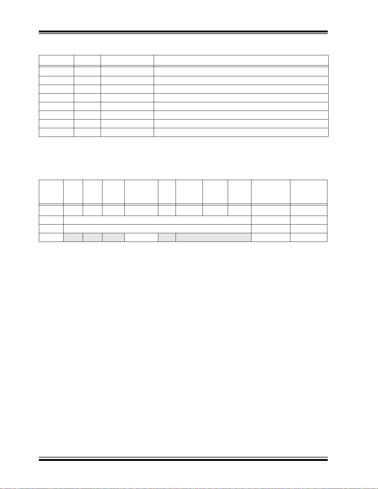
PIC18CXX2
TABLE 8-7: PORTD FUNCTIONS
Name Bit# Buffer Type Function
RD0/PSP0 bit0 ST/TTL
RD1/PSP1 bit1 ST/TTL
RD2/PSP2 bit2 ST/TTL
RD3/PSP3 bit3 ST/TTL
RD4/PSP4 bit4 ST/TTL
RD5/PSP5 bit5 ST/TTL
RD6/PSP6 bit6 ST/TTL
RD7/PSP7 bit7 ST/TTL
Legend: ST = Schmitt Trigger input, TTL = TTL input
Note 1: Input buffers are Schmitt Triggers when in I/O mode and TTL buffers when in Parallel Slave Port mode.
(1)
(1)
(1)
(1)
(1)
(1)
(1)
(1)
Input/output port pin or parallel slave port bit0.
Input/output port pin or parallel slave port bit1.
Input/output port pin or parallel slave port bit2.
Input/output port pin or parallel slave port bit3.
Input/output port pin or parallel slave port bit4.
Input/output port pin or parallel slave port bit5.
Input/output port pin or parallel slave port bit6.
Input/output port pin or parallel slave port bit7.
TABLE 8-8: SUMMARY OF REGISTERS ASSOCIATED WITH PORTD
Name Bit 7 Bit 6 Bit 5 Bit 4 Bit 3 Bit 2 Bit 1 Bit 0
PORTD RD7 RD6 RD5 RD4 RD3 RD2 RD1 RD0
LATD LATD Data Output Register xxxx xxxx uuuu uuuu
TRISD PORTD Data Direction Register 1111 1111 1111 1111
TRISE
Legend: x = unknown, u = unchanged, - = unimplemented, read as '0'. Shaded cells are not used by PORTD.
IBF OBF IBOV PSPMODE — PORTE Data Direction bits 0000 -111 0000 -111
Value on
POR,
BOR
xxxx xxxx uuuu uuuu
Value o n all
other
RESETS
DS39026C-page 86 2001 Microchip Technology Inc.
Page 89

PIC18CXX2
8.5 PORTE, TRISE and LATE Registers
This section is only applicable to the PIC18C4X2
devices.
PORTE is a 3-bit wide, bi-directional port. The corresponding Data Direction register is TRISE. Setting a
TRISE bit (= 1) will mak e the corresponding PORTE pin
an input (i.e., put the corresponding output driver in a
Hi-Impedance mode). Clearing a TRISE bit (= 0) will
make the corresponding POR TE pin an output (i.e. , put
the contents of the output latch on the selected pin).
Note: On a Power-on Reset, these pins are con-
figured as digital inputs.
The Data Latch register (LATE) is also memory
mapped. Read-modify-write operations on the LATE
register reads and writes the latched output value for
PORTE.
PORTE has three pins (RE0/RD
and RE2/CS
/AN7), which are individually configurable
as inputs or outputs. These pins have Schmitt Trigger
input buffers.
Register 8-1 shows the TRISE register, which also controls the parallel slave port operation.
PORTE pins are multiplexed with analog inputs. When
selected as an anal og input, these pins wi ll read as ’0’s.
TRISE controls the direction of the RE pins, even when
they are being used as analog inputs. The user must
make sure to keep the pins configured as inputs when
using them as analog inputs.
Note: On a Power-on Reset, these pins are con-
figured as analog inputs.
/AN5, RE1/WR/AN6
FIGURE 8-9: PORTE BLOCK DIAGRAM
IN I/O PORT MODE
Data
Bus
WR LATE
or
PORTE
WR TRISE
RD PORTE
Note 1: I/O pins have diode protection to VDD and VSS.
RD LATE
QD
CK
Data Latch
QD
CK
TRIS Latch
RD TRISE
To Analog Converter
Schmitt
Trigger
Input
Buffer
QD
EN
EN
I/O pin
(1)
EXAMPLE 8-5: INITIALIZING PORTE
CLRF PORTE ; Initialize PORTE by
CLRF LATE ; Alternate method
MOVLW 0x07 ; Configure A/D
MOVWF ADCON1 ; for digital inputs
MOVLW 0x03 ; Value used to
MOVWF TRISC ; Set RE<0> as inputs
2001 Microchip Technology Inc. DS39026C-page 87
; clearing output
; data latches
; to clear output
; data latches
; initialize data
; direction
; RE<1> as outputs
; RE<2> as inputs
Page 90

PIC18CXX2
REGISTER 8-1: TRISE REGISTER
R-0 R-0 R/W-0 R/W-0 U-0 R/W-1 R/W-1 R/W-1
IBF OBF IBOV PSPMODE
bit 7 bit 0
bit 7 IBF: Input Buffer Full Status bit
1 = A word has been received and waiting to be read by the CPU
0 = No word has been received
bit 6 OBF: Output Buffer Full Status bit
1 = The output buffer still holds a previously written word
0 = The output buffer has been read
bit 5 IBOV: Input Buffer Overflow Detect bit (in Microprocessor mode)
1 = A write occurred when a previously input word has not been read
(must be cleared in software)
0 = No overflow occurred
bit 4 PSPMODE: Parallel Slave Port Mode Select bit
1 = Parallel Slave Port mode
0 = General purpose I/O mode
bit 3 Unimplemented: Read as '0'
bit 2 TRISE2: RE2 Direction Control bit
1 = Input
0 = Output
bit 1 TRISE1: RE1 Direction Control bit
1 = Input
0 = Output
bit 0 TRISE0: RE0 Direction Control bit
1 = Input
0 = Output
— TRISE2 TRISE1 TRISE0
Legend:
R = Readable bit W = Writable bit U = Unimplemented bit, read as ‘0’
- n = Value at POR ’1’ = Bit is set ’0’ = Bit is cleared x = Bit is unknown
DS39026C-page 88 2001 Microchip Technology Inc.
Page 91

PIC18CXX2
TABLE 8-9: PORTE FUNCTIONS
Name Bit# Buffer Type Function
Input/output port pin or read control input in Parallel Slave Port mode
or analog input:
(1)
RE0/RD
RE1/WR
/AN5 bit0 ST/TTL
/AN6 bit1 ST/TTL
RE2/CS/AN7 bit2 ST/TTL
Legend: ST = Schmitt Trigger input, TTL = TTL input
Note 1: Input buffers are Schmitt Triggers when in I/O mode and TTL buffers when in Parallel Slave Port mode.
RD
1 = Not a read operation
0 = Read operation. Reads PORTD register (if chip selected).
Input/output port pin or write control input in Parallel Slave Port mode
or analog input:
(1)
WR
1 = Not a write operation
0 = Write operation. Writes PORTD register (if chip selected).
Input/output port pin or chip select control input in Parallel Slave Port
mode or analog input:
(1)
CS
1 = Device is not selected
0 = Device is selected
TABLE 8-10: SUMMARY OF REGISTERS ASSOCIATED WITH PORTE
Name Bit 7 Bit 6 Bit 5 Bit 4 Bit 3 Bit 2 Bit 1 Bit 0
PORTE
LATE — — — — — LATE Data Output Register ---- -xxx ---- -uuu
TRISE IBF OBF IBOV PSPMODE — PORTE Data Direction bits 0000 -111 0000 -111
ADCON1 ADFM ADCS2 — — PCFG3 P CFG2 PCFG1 PCFG0 --0- -000 --0- -000
Legend: x = unknown, u = unchanged, - = unimplemented, read as '0'. Shaded cells are not used by PORTE.
— — — — — RE2 RE1 RE0
Value o n
POR,
BOR
---- -000 ---- -000
Value on all
other
RESETS
2001 Microchip Technology Inc. DS39026C-page 89
Page 92

PIC18CXX2
8.6 Parallel Sla ve Port
The Parall el Slave P ort is impl emented on t he 40-pin
devices only (PIC 18C 4 X 2).
PORTD operates as an 8-bit wide, parallel slave port,
or microprocessor port, when control bit PSPMODE
(TRISE<4>) is set. It is asynchronously readable and
writable by the external world through RD
pin RE0/RD
and WR control input pin RE1/WR.
It can directly interface to an 8-bit mic rop roc es sor dat a
bus. The external mic roproc essor c an rea d or write th e
PORTD latch as an 8-bit latch. Setting bit PSPMODE
enables port pin RE0/RD
to be the RD input, RE1/WR
to be the WR input and RE2/CS to be the CS (chip
select) input. For this functionality, the corresponding
data direction bits of the TRISE register (TRISE<2:0>)
must be configured as input s (set). The A/D port confi guration bits PCFG2:PCFG0 (ADCON1<2:0>) must be
set, which will configure pins RE2:R E0 as dig ital I/O.
A write to the PSP occurs when both the CS
lines are first detecte d low . A read from th e PSP occurs
when both the CS
and RD lines are first detected low.
The PORTE I/O pins become control inputs for the
microprocessor port when bit PSPMODE (TRISE<4>)
is set. In this mode, the user must make sure that the
TRISE<2:0> bits are set (pins are configured as digital
inputs), and the ADCON1 is configured for digital I/O.
In this mode, the input buffers are TTL.
control input
and WR
FIGURE 8-10: PORTD AND PORTE
BLOCK DIAGRAM
(PARALLEL SLAVE
PORT)
Data Bus
WR LATD
or
PORTD
RD PORTD
RD LATD
One bit of PORTD
Set Interrupt Flag
PSPIF (PIR1<7>)
QD
CK
Data Latch
QD
EN
EN
TTL
RDx
pin
Note: I/O pin has protection diodes to VDD and VSS.
FIGURE 8-11: PARALLEL SLAVE PORT WRITE WAVEFORMS
Q1 Q2 Q3 Q4CSQ1 Q2 Q3 Q4 Q1 Q2 Q3 Q4
WR
RD
PORTD<7:0>
IBF
OBF
PSPIF
Read
Chip Select
Write
TTL
TTL
TTL
RD
CS
WR
DS39026C-page 90 2001 Microchip Technology Inc.
Page 93

FIGURE 8-12: PARALLEL SLAVE PORT READ WAVEFORMS
Q1 Q2 Q3 Q4CSQ1 Q2 Q3 Q4 Q1 Q2 Q3 Q4
WR
RD
PORTD<7:0>
IBF
OBF
PSPIF
PIC18CXX2
TABLE 8-11: REGISTERS ASSOCIATED WITH PARALLEL SLAVE PORT
Name Bit 7 Bit 6 Bit 5 Bit 4 Bit 3 Bit 2 Bit 1 Bit 0
PORTD Port Data Latch when written; Port pins when read
LATD LATD Data Output bits xxxx xxxx uuuu uuuu
TRISD PORTD Data Direction bits 1111 1111 1111 1111
PORTE — — — — — RE2 RE1 RE0 ---- -000 ---- -000
LATE — — — — — LATE Data Output bits ---- -xxx ---- -uuu
TRISE IBF OBF IBOV PSPMODE — PO RTE Data Direction bits 0000 -111 0000 -111
INTCON
PIR1 PSPIF ADIF RCIF TXIF SSPIF CCP1IF TMR2IF TMR1IF 0000 0000 0000 0000
PIE1 PSPIE ADIE RCIE TXIE SSPIE CCP1IE TMR2IE TMR1IE 0000 0000 0000 0000
IPR1 PSPIP ADIP RCIP TXIP SSPIP CCP1IP TMR2IP TMR1IP 0000 0000 0000 0000
ADCON1 ADFM ADCS2 — — PCFG3 PCFG2 PCFG1 PCFG0 --0- -000 --0- -000
Legend: x = unknown, u = unchanged, - = unimplemented, read as '0'. Shaded cells are not used by the Parallel Slave Port.
GIE/
GIEH
PEIE/
GIEL
TMR0IF INT0IE RBIE TMR0IF INT0IF RBIF
Value o n
POR, BOR
xxxx xxxx uuuu uuuu
0000 000x 0000 000u
Value on all
other
RESETS
2001 Microchip Technology Inc. DS39026C-page 91
Page 94

PIC18CXX2
NOTES:
DS39026C-page 92 2001 Microchip Technology Inc.
Page 95

PIC18CXX2
9.0 TIMER0 MODULE
The Timer0 module has the following features:
• Software selectable as an 8-bit or 16-bit timer/
counter
• Readable and writable
• Dedicated 8-bit software programmable prescaler
• Clock source selectable to be external or internal
• Interrupt-on-overflow from FFh to 00h in 8-bit
mode and FFFFh to 0000h in 16-bit mode
• Edge select for external clock
Figure 9-1 shows a simplified block diagram of the
Timer0 module in 8-bit mode and Figure 9-2 shows a
simplified block diagram of the Timer0 module in 16-bit
mode.
The T0CON register (Register 9-1) is a readable and
writable regi ste r th at controls all the as pec ts of Ti mer 0,
including the prescale selection.
REGISTER 9-1: T0CON: TIMER0 CONTROL REGISTER
R/W-1 R/W-1 R/W-1 R/W-1 R/W-1 R/W-1 R/W-1 R/W-1
TMR0ON T08BIT T0CS T0SE PSA T0PS2 T0PS1 T0PS0
bit 7 bit 0
bit 7 TMR0ON: Timer0 On/Off Control bit
1 = Enables Timer0
0 = Stops Timer0
bit 6 T08BIT: Timer0 8-bit/16-bit Control bit
1 = Timer0 is configured as an 8-bit timer/counter
0 = Timer0 is configured as a 16-bit timer/counter
bit 5 T0CS: Timer0 Clock Source Select bit
1 = Transition on T0CKI pin
0 = Internal instruction cycle clock (CLKOUT)
bit 4 T0SE: Timer0 Source Edge Select bit
1 = Increment on high-to-low transition on T0CKI pin
0 = Increment on low-to-high transition on T0CKI pin
bit 3 PSA: Timer0 Prescaler Assignment bit
1 = TImer0 prescaler is NOT assigned. Timer0 clock input bypasses pre s caler.
0 = Timer0 prescaler is assigned. Timer0 clock input comes from prescaler output.
bit 2:0 T0PS2:T0PS0: Timer0 Prescaler Select bits
111 = 1:256 prescale value
110 = 1:128 prescale value
101 = 1:64 prescale value
100 = 1:32 prescale value
011 = 1:16 prescale value
010 = 1:8 prescale value
001 = 1:4 prescale value
000 = 1:2 prescale value
Legend:
R = Readable bit W = Writable bit U = Unimplemented bit, read as ‘0’
- n = Value at POR reset ’1’ = Bit is set ’0’ = Bit is cleared x = Bit is unknown
2001 Microchip Technology Inc. DS39206C-page 93
Page 96

PIC18CXX2
FIGURE 9-1: TIMER0 BLOCK DIAGRAM IN 8-BIT MODE
FOSC/4
RA4/T0CKI
pin
Note: Upon RESET, Timer0 is enabled in 8-bit mode with clock input from T0CKI max. prescale.
T0SE
FIGURE 9-2: TIMER0 BLOCK DIAGRAM IN 16-BIT MODE
0
1
T0PS2, T0PS1, T0PS0
T0CS
Programmable
Prescaler
3
0
1
PSA
Sync with
Internal
Clocks
(2 TCY delay)
Data Bus
8
TMR0
Set Interrupt
Flag bit TMR0IF
on Overflow
FOSC/4
T0CKI pin
T0SE
Note: Upon RESET, Timer0 is enabled in 8-bit mode with cloc k input from T0CKI max. presca le.
0
1
Programmable
Prescaler
T0PS2, T0PS1, T0PS0
T0CS
0
1
3
PSA
Sync with
Internal
Clocks
(2 TCY delay)
TMR0L
TMR0
High Byte
8
8
TMR0H
8
Flag bit TMR0IF
8
Read TMR0L
Write TMR0L
Data Bus<7:0>
Set Interrupt
on Overflow
DS39206C-page 94 2001 Microchip Technology Inc.
Page 97

PIC18CXX2
9.1 Timer0 Operation
Timer0 can operate as a timer or as a counter.
Timer mode is selected by clearing the T0CS bit. In
Timer mode, the Timer0 module will increment every
instruction cycle (w ithout pr escal er). If the TMR0 register is written, the i ncrem ent is inhi bited f or the follow ing
two instruction cycles. The user can work around this
by writing an adjusted value to the TMR0 register.
Counter mode is selected by setting the T0CS bit. In
Counter mode, Timer0 will increment either on every
rising, or falling edge of pin RA4/T0C KI. The increme nting edge is determined by the Timer0 Source Edge
Select bit (T0SE). Clearing the T0SE bit selects the rising edge. Restrictions on the external clock input are
discussed be low.
When an external clock input i s used for T i mer0, it must
meet certain requirements. The requirements ensure
the external clock can be synchronized with the internal
phase clock (T
incrementing of Timer0 after synchronization.
OSC). Also, there is a delay in the actual
9.2 Prescaler
An 8-bit counter is available as a prescaler for the
Timer0 module. The prescaler is not readable or
writable.
The PSA and T0PS2:T0PS0 bits determine the prescaler assignment and prescale ratio.
Clearing bit PSA will assign the p rescaler to the T i mer0
module. When the prescaler is assigned to the Timer0
module, prescale values of 1:2, 1:4,..., 1:256 are
selectable.
When assigned to the Timer0 module, all instructions
writing to the TMR0 regis ter (e.g. CLRF TMR0, MOVWF
TMR0, BSF TMR0, x....etc.) will clear the prescaler
count.
9.2.1 SWITCHING PRESCALER ASSIGNMENT The prescaler assignment is fully under software con-
trol (i.e., it can be changed “on-the-fly” during program
execution).
9.3 Timer0 Interrupt
The TMR0 interrupt is generated when the TMR0 register overflows from FFh to 00h in 8-bit mod e, or FFFFh
to 0000h in 16-bit mo de. This overflow s ets the TMR0IF
bit. The interrupt can be masked by clearing the
TMR0IE bit. The TMR0IE bit must be cleared in software by the Timer0 mod ule Interrupt Service Routi ne
before re-enabling this interrupt. The TMR0 interrupt
cannot awaken the processor from SLEEP, since the
timer is shut-off during SLEEP.
9.4 16-Bit Mode Timer Reads and Writes
TMR0H is not the high byte of the timer/counter in
16-bit mode, but is actually a buffered version of the
high byte of Time r0 (refe r to Figu re9-2). The high byte
of the Timer0 counter/timer is not directly readable nor
writable. TMR0H is updated with the contents of the
high byte of Timer0 during a read of TMR0L. This provides the ability to read all 16-bits of Timer0 without
having to verify that the read of the high and low byte
were valid due to a rollover between successive reads
of the high and low byte.
A write to the high byte of Timer0 must also take place
through the TMR0H buf fer register. Timer0 high by te i s
updated with the contents of TMR0H when a write
occurs to TMR0L. This allows all 16-bits of T imer0 to be
updated at once.
Note: Writing to TMR0 when the prescaler is
assigned to Timer0 will clear the prescaler
count, but will not change the prescaler
assignment.
TABLE 9-1: REGISTERS ASSOCIATED WITH TIMER0
Name Bit 7 Bit 6 Bit 5 Bit 4 Bit 3 Bit 2 Bit 1 Bit 0
TMR0L Timer0 Module’s Low Byte Register
TMR0H Timer0 Module’s High Byte Register 0000 0000 0000 0000
INTCON GIE/GIEH PEIE/GIEL TMR0IE INT0IE RB IE TMR0IF INT0IF RBIF 0000 000x 0000 000u
T0CON TMR0ON T08BIT T0CS T0SE PSA T0PS2 T0PS1 T0PS0 1111 1111 1111 1111
TRISA — — PORTA Data Direction Register --11 1111 --11 1111
Legend: x = unknown, u = unchanged, - = unimplemented locations read as '0'. Shaded cells are not used by Timer0.
2001 Microchip Technology Inc. DS39206C-page 95
Value on
POR, BOR
xxxx xxxx uuuu uuuu
Value on all
other
RESETS
Page 98

PIC18CXX2
NOTES:
DS39206C-page 96 2001 Microchip Technology Inc.
Page 99

PIC18CXX2
10.0 TIMER1 MODULE
The Timer1 module timer/counter has the following
features:
• 16-bit timer/counter
(two 8-bit registers: TMR1H and TMR1L)
• Readable and writable (both registers)
• Internal or external clock select
• Interrupt-on-overflow from FFFFh to 0000h
• Reset from CCP module special event trigger
Figure 10-1 is a simplified block diagram of the Timer1
module.
Register 10-1 details the Timer1 control register. This
register controls the operating mode of the Timer1
module, and contains the Timer1 oscillator enable bit
(T1OSCEN). Tim er1 can be enabled or disabled by setting or clearing control bit TMR1ON (T1CO N <0> ).
REGISTER 10-1: T1CON: TIMER1 CONTROL REGISTER
R/W-0 U-0 R/W-0 R/W-0 R/W-0 R/W-0 R/W-0 R/W-0
RD16
bit 7 bit 0
bit 7 RD16: 16-bit Read/Write Mode Enabl e bit
1 = Enables register Read/Write of TImer1 in one 16-bit operation
0 = Enables register Read/Write of Timer1 in two 8-bit operations
bit 6 Unimplemented: Read as '0'
bit 5-4 T1CKPS1:T1CKPS0: Timer1 Input Clock Prescale Select bits
11 = 1:8 Prescale value
10 = 1:4 Prescale value
01 = 1:2 Prescale value
00 = 1:1 Prescale value
bit 3 T1OSCEN: Timer1 Oscillator Enable bit
1 = Timer1 Oscillator is enabled
0 = Timer1 Oscillator is shut-off
The oscillator inverter and feedback resistor are turned off to el iminate power drain.
bit 2 T1SYNC
When TMR1CS = 1:
1 = Do not synchronize external clock input
0 = Synchronize external clock input
When TMR1CS = 0:
This bit is ignored. Timer1 uses the internal clock when TMR1CS = 0.
bit 1 TMR1CS: Timer1 Clock Source Select bit
1 = External clock from pin RC0/T1OSO/T13CKI (on the rising edge)
0 = Internal clock (F
bit 0 TMR1ON: Timer1 On bit
1 = Enables Timer1
0 = Stops Timer1
— T1CKPS1 T1CKPS0 T1OSCEN T1SYNC TMR1CS TMR1ON
: Timer1 External Clock Input Synchronization Select bit
OSC/4)
Legend:
R = Readable bit W = Writable bit U = Unimplemented bit, read as ‘0’
- n = Value at POR reset ’1’ = Bit is set ’0’ = Bit is cleared x = Bit is unknown
2001 Microchip Technology Inc. DS39206C-page 97
Page 100

PIC18CXX2
10.1 Timer1 Operation
Timer1 can operate in one of these modes:
• As a timer
• As a synchronous counter
• As an asynchronous counter
The operating mode is determined by the clock select
bit, TMR1CS (T1CON<1>).
When TMR1CS = 0, Timer1 increments every instruction cycle. When TMR1CS = 1, Timer1 increments on
every rising edge of the external clock input or the
Timer1 oscillator, if enabled.
When the Timer1 oscillator is enabled (T1OSCEN is
set), the RC1/T1OSI and RC0/T1OSO/T1CKI pins
become inputs. That is, the TRISC<1:0> value is
ignored.
Timer1 also has an internal “RESET input”. This
RESET can be generated by the CCP module
(Section 13.0).
FIGURE 10-1: TIMER1 BLOCK DIAGRAM
TMR1IF
Overflow
Interrupt
Flag bit
T1CKI/T1OSO
T1OSI
TMR1H
T1OSC
TMR1
TMR1L
T1OSCEN
Enable
Oscillator
CLR
(1)
CCP Special Event Trigger
TMR1ON
On/Off
1
OSC/4
F
Internal
Clock
0
TMR1CS
0
1
T1SYNC
Prescaler
1, 2, 4, 8
2
T1CKPS1:T1CKPS0
Synchronized
Clock Input
Synchronize
det
SLEEP Input
Note 1: When enable bit T1OSCEN is cleared, the inverter and feedback resistor are turned off. This eliminates power drain.
FIGURE 10-2: TIMER1 BLOCK DIAGRAM: 16-BIT READ/WRITE MODE
Data Bus<7:0>
8
TMR1H
TMR1L
T1OSCEN
Enable
Oscillator
8
CCP Special Event Trigger
CLR
TMR1ON
On/Off
1
OSC/4
F
(1)
Internal
Clock
0
TMR1CS
0
1
T1SYNC
Prescaler
1, 2, 4, 8
2
T1CKPS1:T1CKPS0
Synchronized
Clock Input
Synchronize
det
SLEEP Input
Write TMR1L
Read TMR1L
TMR1IF
Overflow
Interrupt
Flag bit
T13CKI/T1OSO
T1OSI
8
Timer 1
High Byte
T1OSC
8
TMR1
Note 1: When enable bit T1OSCEN is cleared, the inverter and feedback resistor are turned off. This eliminates power drain.
DS39206C-page 98 2001 Microchip Technology Inc.
 Loading...