

Page 1

PIC18C601/801
High-Performance ROM-less Microcontrollers
with External Memory Bus
High Performance RISC CPU:
• C compiler op timized architecture ins truction set
• Linear program memory addressing up to 2 Mbytes
• Linear data memory addressing to 4 Kbytes
External Program Memory
(bytes)
On-Chip
Maximum
Single Word
Instructions
Device
PIC18C601 256K 128K 1.5K
PIC18C801 2M 1M 1.5K
• Up to 160 ns instruction cycle:
- DC - 25 MHz clock input
- 4 MHz - 6 MHz clock input with PLL active
• 16-bit wide instructions, 8-bit wide data path
• Priority levels for interrupts
• 8 x 8 Single C y cle Hardware Multiplier
Maximum
Addressing
On-Chip
RAM (bytes)
Peripheral Features:
• High current sink/source 25 mA/25 mA
• Up to 47 I/O pins with individual direction control
• Three external interrupt pins
•Timer0 module: 8-bit/16-bit timer/counter with
8-bit programmable prescaler
•Timer1 module: 16-bit timer/counter (time-base for
CCP)
•Timer2 module: 8-bit timer/counter with 8-bit
period register
•Timer3 module: 16-bit timer/counter
• Secondary oscillator clock option - Timer1/Timer3
• Two Capture/Compare/PWM (CCP) modules
CCP pins can be configured as:
- Capture input: 16-bit, max. resolution 10 ns
- Compare is 16-bit, max. resolution 160 ns (TCY)
- PWM output: PWM resolution is 1- to 10-bit
Max. PWM freq. @:
8-bit resolution = 99 kHz
10-bit resolution = 24.4 kHz
• Master Synchronous Serial Port (MSSP) with two
modes of operation:
- 3-wire SPI™ (Supports all 4 SPI modes)
2
-I
C™ Master and Slave mode
• Addressable USART module: Supports Interrupt
on Address bit
Advanced Analog Features:
• 10-bit Analog-to-Digital Converter module (A/D)
with:
- Fast sampling rate
- Conversion available during SLEEP
- DNL = ±1 LSb, INL = ±1 LSb
- Up to 12 channels available
• Programmable Low Voltage Detection (LVD)
module
- Supports interrupt on Low Voltage Detection
Special Microcontroller Features:
• Power-on Reset (POR), Power-up T imer (PWRT),
and Oscillator S tart-up Timer (OST)
• Watchdog Timer (WDT) with its own on-chip RC
oscillator
• On-chip Boot RAM for boot loader application
• 8-bit or 16-bit external memory interface modes
• Up to two software programmable chip select sig-
nals (CS1
• One programmable chip I/O select signal (CSIO
for memory mapped I/O expansion
• Power saving SLEEP mode
• Different oscillator options, including:
- 4X Phase Lock Loop (of primary oscillator)
- Secondary Oscillator (32 kHz) clock input
and CS2)
CMOS Technology:
• Low power, high speed CMOS technology
• Fully static design
• Wide operating voltage range (2.0V to 5.5V)
• Industrial and Extended temperature ranges
• Low power consumption
)
2001 Microchip Technology Inc. Advance Information DS39541A-page 1
Page 2
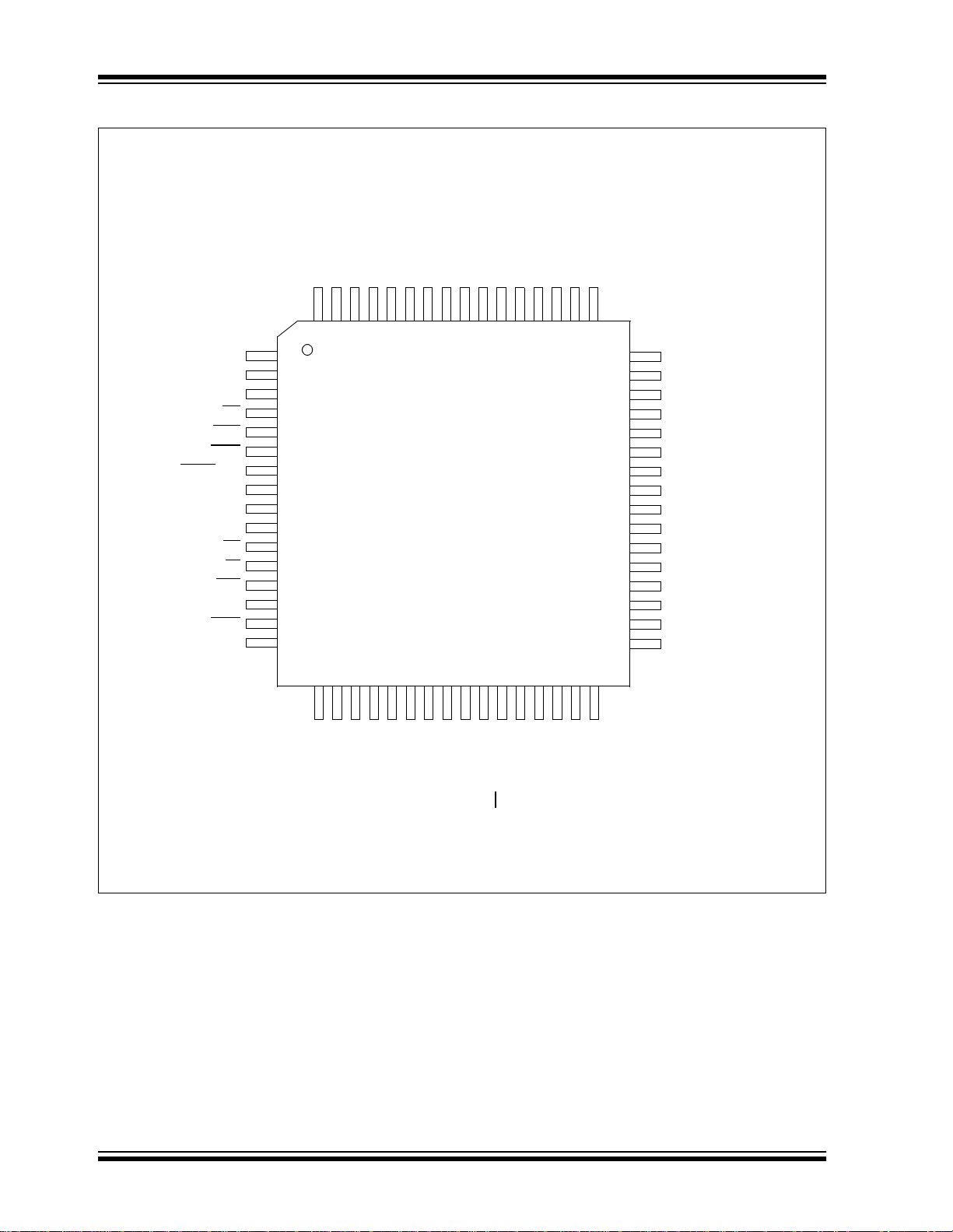
PIC18C601/801
Pin Diagrams
64-Pin TQFP
RE2/AD10
64 63 62 61 60 59 58 57 56 55 54 53 52 51 50 49
RE1/AD9
RE0/AD8
RG0/ALE
RG1/OE
RG2/WRL
RG3/WRH
MCLR/VPP
RG4/BA0
V
SS
VDD
RF7/UB
RF6/LB
RF5/CS1
RF4/A16
RF3/CSIO
RF2/AN7
1
2
3
4
5
6
7
8
9
10
11
12
13
14
15
16
RE3/AD11
RE4/AD12
RE5/AD13
RE6/AD14
RE7/AD15
RD0/AD0
VDDVSS
RD1/AD1
PIC18C601
RD2/AD2
RD3/AD3
RD4/AD4
RD5/AD5
RD6/AD6
RD7/AD7
48
47
46
45
44
43
42
41
40
39
38
37
36
35
34
33
RB0/INT0
RB1/INT1
RB2/INT2
RB3/CCP2
RB4
RB5
RB6
V
SS
OSC2/CLKO
OSC1/CLKI
DD
V
RB7
RC5/SDO
RC4/SDI/SDA
RC3/SCK/SCL
RC2/CCP1
17 18 19 20 21 22 23 24 25 26 27 28 29 30 31 32
-
+
SS
DD
AV
RF0/AN5
RF1/AN6
AV
REF
REF
RA2/AN2/V
RA3/AN3/V
SS
DD
V
V
RA1/AN1
RA0/AN0
RA4/T0CKI
RC1/T1OSI
/AN4/LVDIN
RA5/SS
RC6/TX/CK
RC0/T1OSO/T13CKI
RC7/RX/DT
DS39541A-page 2 Advance Information 2001 Microchip Technology Inc.
Page 3
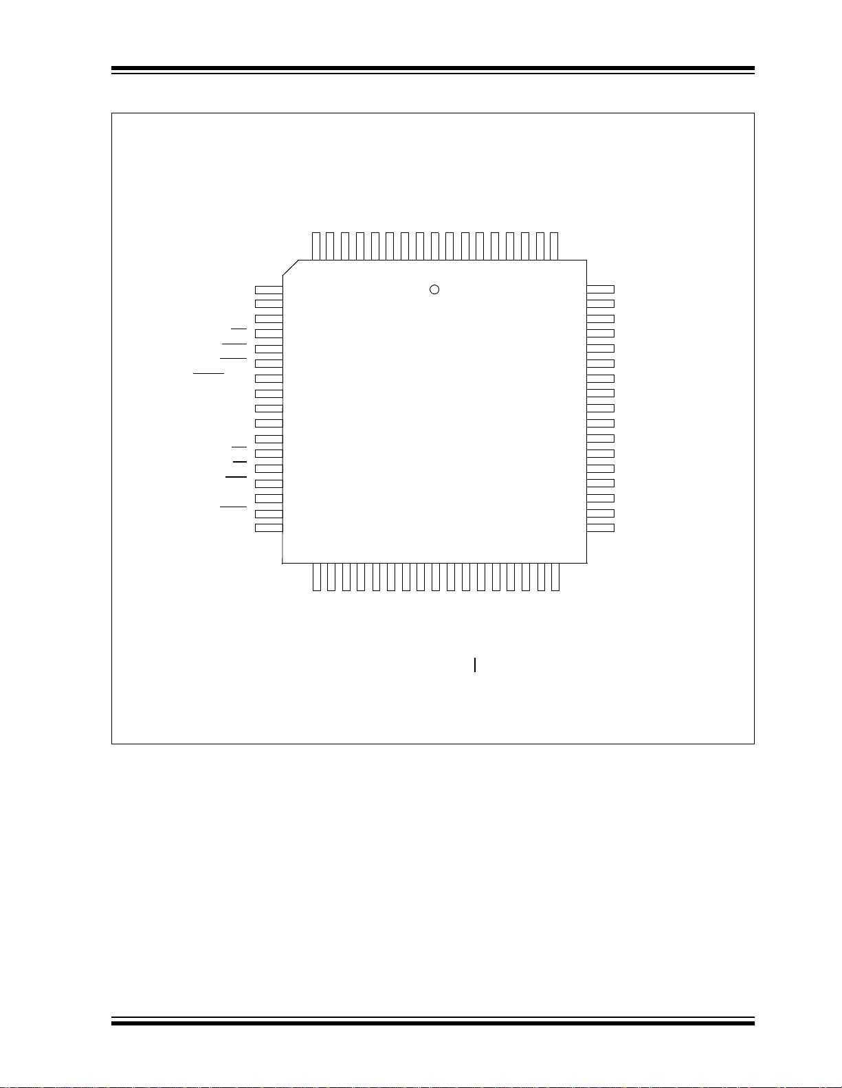
Pin Diagrams (Cont.’d)
68-Pin PLCC
RE1/AD9
RE0/AD8
RG0/ALE
RG1/OE
RG2/WRL
RG3/WRH
MCLR/VPP
RG4/BA0
NC
SS
V
VDD
RF7/UB
RF6/LB
RF5/CS1
RF4/A16
RF3/CSIO
RF2/AN7
RE2/AD10
RE3/AD11
RE4/AD12
RE5/AD13
RE6/AD14
RE7/AD15
9 8 7 6 5 4 3 2 1 6867666564636261
10
11
12
13
14
15
16
17
18
19
20
21
22
23
24
25
26
PIC18C601
RD0/AD0
NC
VDDV
RD1/AD1
RD2/AD2
RD3/AD3
SS
PIC18C601/801
RD4/AD4
RD5/AD5
RD6/AD6
RD7/AD7
60
59
58
57
56
55
54
53
52
51
50
49
48
47
46
45
44
RB0/INT0
RB1/INT1
RB2/INT2
RB3/CCP2
RB4
RB5
RB6
SS
V
NC
OSC2/CLKO
OSC1/CLKI
DD
V
RB7
RC5/SDO
RC4/SDI/SDA
RC3/SCK/SCL
RC2/CCP1
2728 29 30 31 32 33 34 35 36 37 38 39 40 41 42 43
-
+
SS
DD
AV
RF1/AN6
RF0/AN5
AV
REF
REF
RA1/AN1
RA2/AN2/V
RA3/AN3/V
SS
DD
NC
V
V
RA0/AN0
RA4/T0CKI
RC1/T1OSI
/AN4/LVDIN
RA5/SS
RC6/TX/CK
RC0/T1OSO/T13CKI
RC7/RX/DT
2001 Microchip Technology Inc. Advance Information DS39541A-page 3
Page 4
PIC18C601/801
Pin Diagrams (Cont.’d)
80-Pin TQFP
RH0/A16
RH1/A17
80
79
78
RH2/A18
RH3/A19
RE1/AD9
RE0/AD8
RG0/ALE
RG1/OE
RG2/WRL
RG3/WRH
MCLR/VPP
RG4/BA0
V
SS
VDD
RF7/UB
RF6/LB
RF5/CS1
RF4/CS2
RF3/CSIO
RF2/AN7
RH4/AN8
RH5/AN9
1
2
3
4
5
6
7
8
9
10
11
12
13
14
15
16
17
18
19
20
RE2/AD10
RE3/AD11
77 76 75
RE4/AD12
RE5/AD13
RE6/AD14
RE7/AD15
RD0/AD0
VDDVSS
RD1/AD1
PIC18C801
RD2/AD2
RD3/AD3
RD4/AD4
RD5/AD5
RD6/AD6
RD7/AD7
RJ0/D7
RJ1/D6
68 67 66 6572 71 70 6974 73
64 63 62 61
60
59
58
57
56
55
54
53
52
51
50
49
48
47
46
45
44
43
42
41
RJ5/D5
RJ4/D4
RB0/INT0
RB1/INT1
RB2/INT2
RB3/CCP2
RB4
RB5
RB6
V
SS
OSC2/CLKO
OSC1/CLKI
DD
V
RB7
RC5/SDO
RC4/SDI/SDA
RC3/SCK/SCL
RC2/CCP1
RJ3/D3
RJ2/D2
21 22 23 24 25 26 27 28 29 30 31 32
SS
V
RA1/AN1
RA0/AN0
RH6/AN10
RH7/AN11
AVSS
AVDD
RF0/AN5
RF1/AN6
RA2/AN2/VREF-
RA3/AN3/VREF+
33 34
VDD
35 36 38
RA4/T0CKI
/AN4/LVDIN
RA5/SS
RC1/T1OSI
37
RC6/TX/CK
RC0/T1OSO/T13CKI
RC7/RX/DT
39
40
RJ0/D0
RJ1/D1
DS39541A-page 4 Advance Information 2001 Microchip Technology Inc.
Page 5
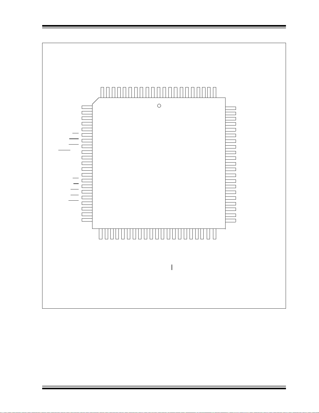
Pin Diagrams (Cont.’d)
84-Pin PLCC
RH1/A17
RH0/A16
RE2/AD10
RE3/AD11
RE4/AD12
RE5/AD13
RE6/AD14
RE7/AD15
RD0/AD0
DD
V
NC
VSS
PIC18C601/801
RD1/AD1
RD2/AD2
RD3/AD3
RD4/AD4
RD5/AD5
RD6/AD6
RD7/AD7
RJ7/D7
RJ6/D6
RH2/A18
RH3/A19
RE1/AD9
RE0/AD8
RG0/ALE
RG1/OE
RG2/WRL
RG3/WRH
MCLR/VPP
RG4/BA0
NC
SS
V
VDD
RF7/UB
RF6/LB
RF5/CS1
RF4/CS2
RF3/CSIO
RF2/AN7
RH4/AN8
RH5/AN9
11
987654321
10
12
13
14
15
16
17
18
19
20
21
22
23
24
25
26
27
28
29
30
31
32
3435 36 37 38 39 40 41 42 43
33
DD
AVSS
AV
RF1/AN6
RH7/AN11
RF0/AN5
RH6/AN10
PIC18C801
REF-
RA2/AN2/V
RA3/AN3/VREF+
NC
RA1/AN1
RA0/AN0
83 82 81
84 75
44
SS
V
VDD
80
797877
4645
4948
47
RA4/T0CKI
RC1/T1OSI
/AN4/LVDIN
RA5/SS
76
51
50
RJ0/D0
RC6/TX/CK
RC7/RX/DT
RC0/T1OSO/T13CKI
74
73
72
71
70
69
68
67
66
65
64
63
62
61
60
59
58
57
56
55
54
5352
RJ1/D1
RJ5/D5
RJ4/D4
RB0/INT0
RB1/INT1
RB2/INT2
RB3/CCP2
RB4
RB5
RB6
V
SS
NC
OSC2/CLKO
OSC1/CLKI
VDD
RB7
RC5/SDO
RC4/SDI/SDA
RC3/SCK/SCL
RC2/CCP1
RJ3/D3
RJ2/D2
2001 Microchip Technology Inc. Advance Information DS39541A-page 5
Page 6

PIC18C601/801
Table of Contents
1.0 Device Overview............................................ ...... ...... ..... ...... ...... .........................................................................9
2.0 Oscillator Configurations....................................................................................................................................21
3.0 RESET...............................................................................................................................................................29
4.0 Memory Organization........................................................................................................................................39
5.0 External Memory Interface............. ..... ........................................ ..... .................................... ..............................63
6.0 Table Reads/Table Writes.................................................................................................................................73
7.0 8 X 8 Hardware Multiplier..................................................................................................................................85
8.0 Interrupts............................................................................................................................................................89
9.0 I/O Ports...........................................................................................................................................................103
10.0 Timer0 Module.................................................................................................................................................127
11.0 Timer1 Module.................................................................................................................................................130
12.0 Timer2 Module.................................................................................................................................................135
13.0 Timer3 Module.................................................................................................................................................137
14.0 Capture/Compare/PWM (CCP) Modules.........................................................................................................141
15.0 Master Synchronous Serial Port (MSSP) Module............................................................................................149
16.0 Addressable Universal Synchronous Asynchronous Receiver Transmitter (USART) .....................................177
17.0 10-bit Analog-to-Digital Converter (A/D) Module.............................................................................................193
18.0 Low Voltage Detect..........................................................................................................................................203
19.0 Special Features of the CPU...........................................................................................................................207
20.0 Instruction Set Summary .................................................................................................................................215
21.0 Development Support......................................................................................................................................259
22.0 Electrical Characteristics............... ..... ........................................ ..... ...... ..........................................................265
23.0 DC and AC Characteristics Graphs and Tables..............................................................................................295
24.0 Packaging Information.....................................................................................................................................297
Appendix A: Data Sheet Revision History..................................................................................................................303
Appendix B: Device Differences ................................................................................................................................303
Appendix C: Device Migrations..................................................................................................................................304
Appendix D: Migrating from other PICmicro Devices.................................................................................................304
Appendix E: Development Tool Version Requirements.............................................................................................305
Index ...........................................................................................................................................................................307
On-Line Support..........................................................................................................................................................315
Reader Response.......................................................................................................................................................316
Product Identification System......................................................................................................................................317
DS39541A-page 6 Advance Information 2001 Microchip Technology Inc.
Page 7

PIC18C601/801
TO OUR VALUED CUSTOMERS
It is our intention to provide our valued customers with the best documentation possible to ensure successful use of your Microchip
products. To this end, we will continue to improve our publications to better suit your needs. Our publications will be refined and
enhanced as new volumes and updates are introduced.
If you have any questions or c omm ents regarding th is publication, p lease c ontact the M a rketing Communications Department via
E-mail at docerrors@mail.microchip.com or fax the Reader Response Form in the back of this data sheet to (480) 792-4150.
We welcome your feedback.
Most Current Data Sheet
To obtain the most up-to-date version of this data sheet, please register at our Worldwide Web site at:
http://www.microchip.com
You can determine the version of a data sheet by examining its literature number found on the bottom outside corner of any page.
The last character of the literature number is the version number, (e.g., DS30000A is version A of document DS30000).
Errata
An errata sheet, describing minor operational differences from the data sheet and recommended workarounds, may exist for current
devices. As device/documentation issues become known to us, we will publish an errata sheet. The errata will specify the revision
of silicon and revision of document to which it applies.
To determine if an errata sheet exists for a particular device, please check with one of the following:
• Microchip’s Worldwide Web site; http://www.microchip.com
• Your local Microchip sales office (see last page)
• The Microchip Corporate Literature Center; U.S. FAX: (480) 792-7277
When contacting a sales office or the literature center, please specify which device, revision of silicon and data sheet (include literature number) you are using.
Customer Notification System
Register on our web site at www.microchip.com/cn to receive the most current information on all of our products.
2001 Microchip Technology Inc. Advance Information DS39541A-page 7
Page 8

PIC18C601/801
NOTES:
DS39541A-page 8 Advance Information 2001 Microchip Technology Inc.
Page 9
PIC18C601/801
1.0 DEVICE OVERVIEW
This documen t conta i ns dev ic e spec if i c in for m at i on fo r
the following two devices:
1. PIC18C601
2. PIC18C801
The PIC18C601 is ava ilable in 64- pin TQFP and 6 8-pin
PLCC packages. The PIC18C801 is av ailable in 80-pin
TQFP and 84-pin PLCC packages.
An overview of features is shown in Table 1-1.
Device block diagrams are provided in Figure 1-1 for
the 64/68-p in confi gurati on, and Figure 1-2 fo r the 80/
84-pin configuration. The pinouts for both packages
are listed in Table 1-2.
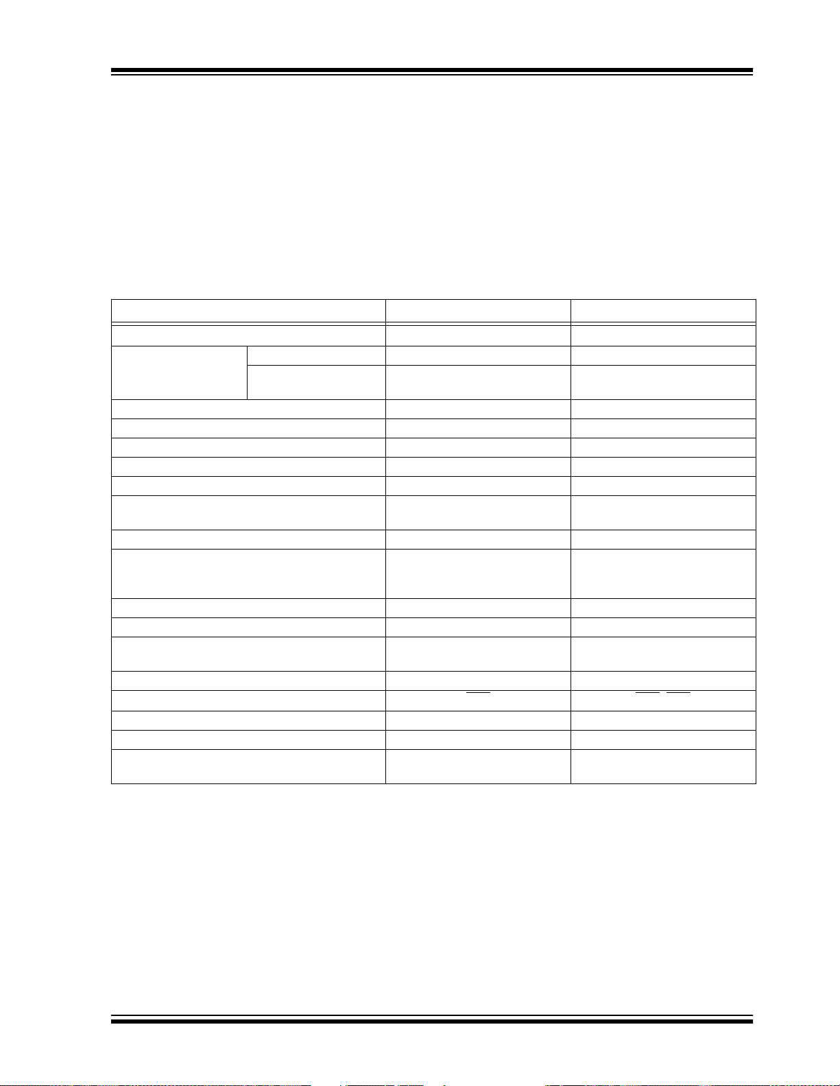
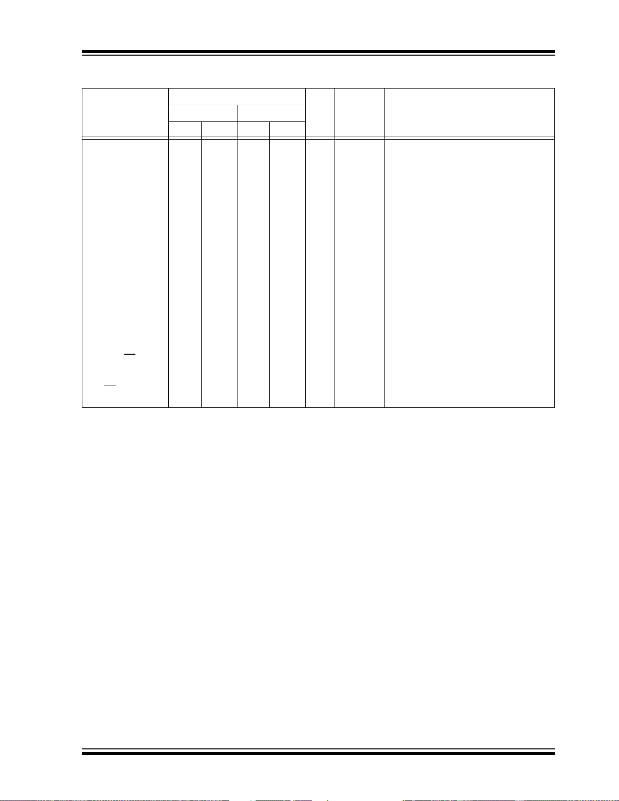
TABLE 1-1: DEVICE FEATURES
Features PIC18C601 PIC18C801
Operating Frequency DC - 25 MHz DC - 25 MHz
External
Program Memory
Data Memory (Bytes) 1536 1536
Interrupt Sources 15 15
I/O Ports Ports A - G Ports A - H, J
Timers 4 4
Capture/Compare/PWM modules 2 2
Serial Communications
10-bit Analog-to-Digital Module 8 input channels 12 input channels
RESETS (and Delays)
Programmable Low Voltage Detect Yes Yes
8-bit External Memory Interface Yes Yes
8-bit De-multiplexed External
Memory Interface
16-bit External Memory Interfaces Yes Yes
On-chip Chip Select Signals CS1
On-chip I/O Chip Select Signal Yes Yes
Instruction Set 75 Instructions 75 Instructions
Packages
Bytes 256K 2M
Max. # of Single Word
Instructions
Addressable USART
RESET Instruction, Stack Full,
Stack Underflow (PWRT, OST)
128K 1M
MSSP,
Addressable USART
POR,
RESET Instruction, Stack Full,
Stack Underflow (PWRT, OST)
No Yes
64-pin TQFP
68-pin PLCC
MSSP,
POR,
CS1, CS2
80-pin TQFP
84-pin PLCC
2001 Microchip Technology Inc. Advance Information DS39541A-page 9
Page 10
PIC18C601/801
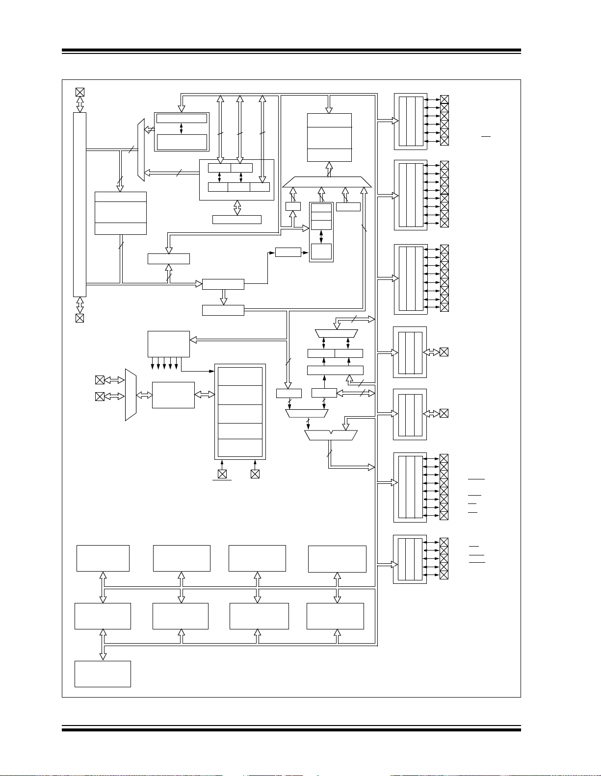
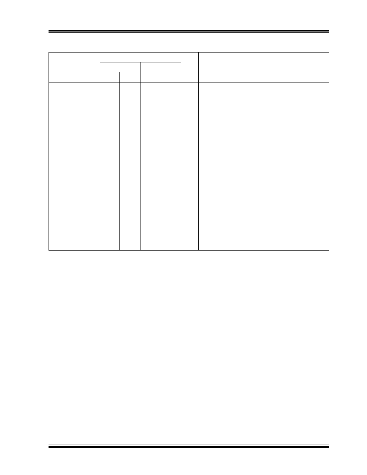
FIGURE 1-1: PIC18C601 BLOCK DIAGRAM
AD7:AD0
Table Pointer<21>
8
8
21
21
inc/dec logic
20
21
Address Latch
Program Memory
(up to 256 Kbytes)
Data Latch
System Bus Interface
16
Table Latch
8
A16, AD15:AD8
Instruction
Decode &
Control
OSC2/CLKO
OSC1/CLKI
T1OSI
T1OSO
Timing
Generation
Timer0 Timer1 Timer2
5
PCLATU
PCLATH
PCH PCL
PCU
Program Counter
31 Level Stack
ROM Latch
IR
Power-up
Timer
Oscillator
Start-upTimer
Power-on
Reset
Watchdog
Timer
Low Voltage
Detect
MCLR
VDD, VSS
Decode
BITOP
4
BSR
3
8
Data Bus<8>
Data Latch
Data RAM
1 Kbyte
Address Latch
12
Address<12>
12 4
Bank0,F
FSR0
FSR1
FSR2
inc/dec
logic
PRODLPRODH
8 x 8 Multiply
WREG
8
8
ALU<8>
8
Timer3
PORTA
RA0/AN0
RA1/AN1
RA2/AN2/VREFRA3/AN3/VREF+
RA4/T0CKI
RA5/AN4/SS
/LVDIN
PORTB
RB0/INT0
RB1/INT1
RB2/INT2
RB3/CCP2
RB4
RB5
RB6
12
RB7
PORTC
RC0/T1OSO/T13CKI
RC1/T1OSI
RC2/CCP1
RC3/SCK/SCL
RC4/SDI/SDA
RC5/SDO
RC6/TX1/CK1
RC7/RX1/DT1
8
PORTD
RD7:RD0/AD7:AD0
8
PORTE
8
RE7:RE0/AD15:AD8
PORTF
RF0/AN5
RF1/AN6
RF2/AN7
RF3/CSIO
RF4/A16
RF5/CS1
RF6/LB
RF7/UB
PORTG
RG0/ALE
RG1/OE
RG2/WRL
RG3/WRH
RG4/BA0
CCP1
CCP2
Synchronous
Serial Port
USART1
10-bit A/D
DS39541A-page 10 Advance Information 2001 Microchip Technology Inc.
Page 11
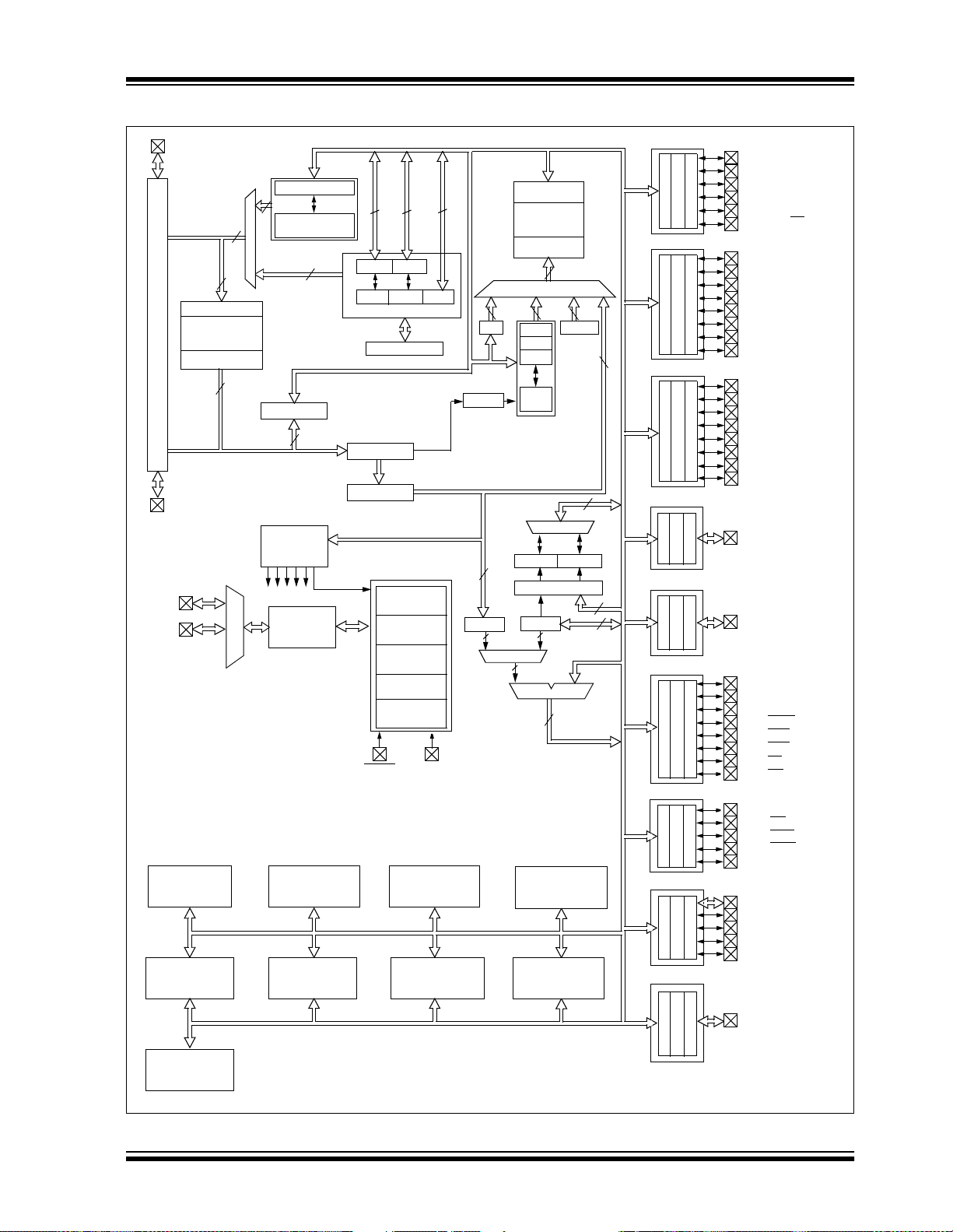
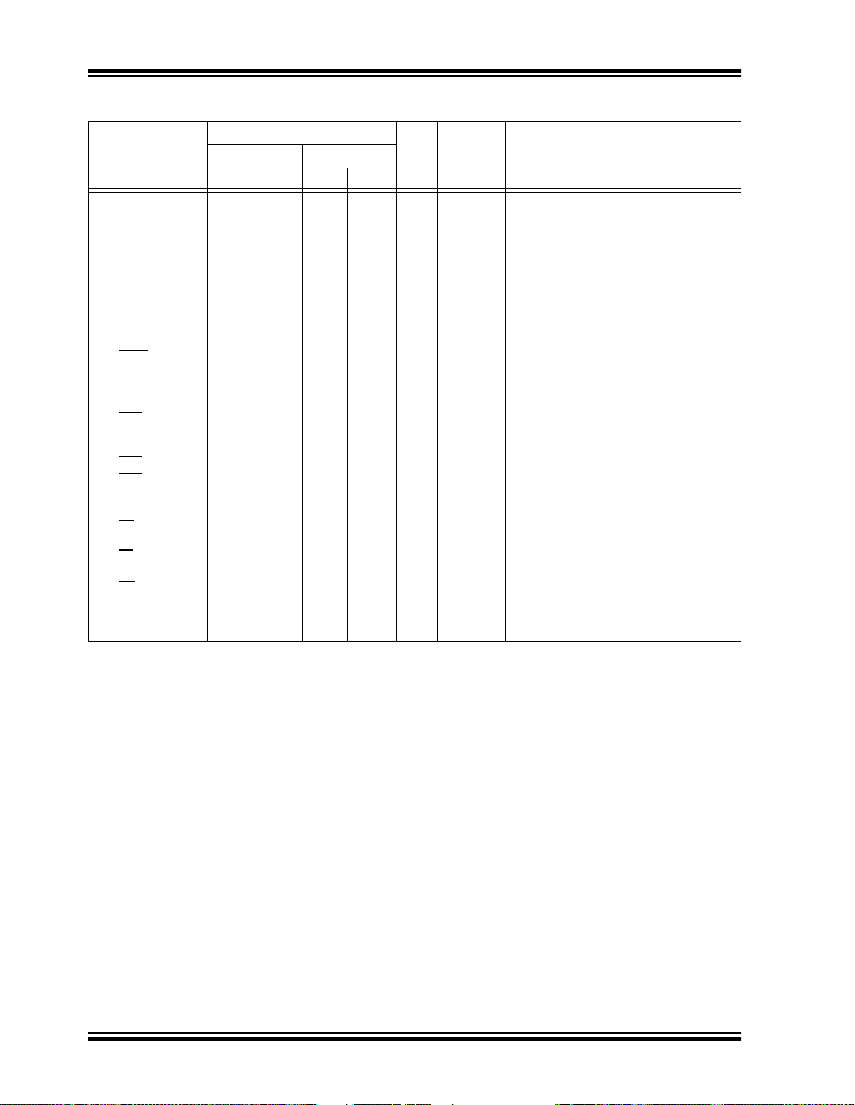
FIGURE 1-2: PIC18C801 BLOCK DIAGRAM
AD7:AD0
TablePointer<21>
8
8
21
21
inc/dec logic
20
21
Address Latch
Program Memory
(up to 2 Mbytes)
Data Latch
System Bus Interface
16
Table Latch
8
A19:A16, AD15:AD0
Instruction
Decode &
Control
OSC2/CLKO
OSC1/CLKI
T1OSI
T1OSO
Timing
Generation
Timer0 Timer1 Timer2
CCP1
CCP2
5
PCLATU
PCLATH
PCH PCL
PCU
Program Counter
31 Level Stack
ROM Latch
IR
Power-up
Timer
Oscillator
Start-upTimer
Power-on
Reset
Watchdog
Timer
Low Voltage
Detect
MCLR
VDD, VSS
Synchronous
Serial Port
Decode
BITOP
4
BSR
3
8
Data Bus<8>
Data Latch
Data RAM
1 Kbyte
Address Latch
12
Address<12>
12 4
Bank0,F
FSR0
FSR1
FSR2
inc/dec
logic
PRODLPRODH
8 x 8 Multiply
WREG
8
8
ALU<8>
8
Timer3
USART1
PIC18C601/801
PORTA
PORTB
12
8
PORTC
PORTD
PORTE
8
8
PORTF
PORTG
PORTH
PORTJ
RA0/AN0
RA1/AN1
RA2/AN2/VREFRA3/AN3/VREF+
RA4/T0CKI
RA5/AN4/SS
RB0/INT0
RB1/INT1
RB2/INT2
RB3/CCP2
RB4
RB5
RB6
RB7
RC0/T1OSO/T13CKI
RC1/T1OSI
RC2/CCP1
RC3/SCK/SCL
RC4/SDI/SDA
RC5/SDO
RC6/TX1/CK1
RC7/RX1/DT1
RD7:RD0/AD7:AD0
RE7:RE0/AD15:AD8
RF0/AN5
RF1/AN6
RF2/AN7
RF3/CSIO
RF4/CS2
RF5/CS1
RF6/LB
RF7/UB
RG0/ALE
RG1/OE
RG2/WRL
RG3/WRH
RG4/BA0
RH3:RH0/A19:A16
RH4/AN8
RH5/AN9
RH6/AN10
RH7/AN11
/LVDIN
RJ7:RJ0/D7:D0
10-bit A/D
2001 Microchip Technology Inc. Advance Information DS39541A-page 11
Page 12
PIC18C601/801
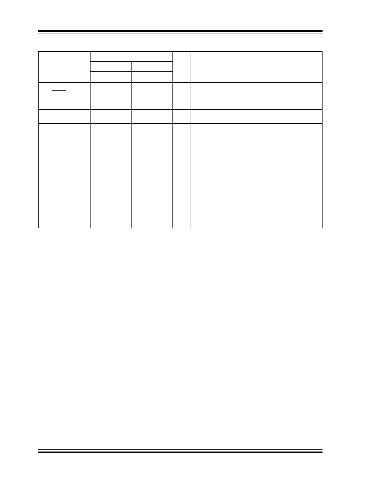
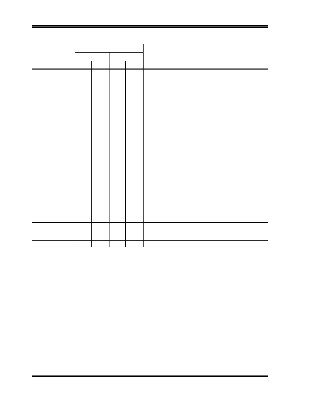
TABLE 1-2: PINOUT I/O DESCRIPTIONS
Pin Number
Pin Name
MCLR
/VPP
MCLR
VPP
NC
OSC1/CLKI
OSC1
CLKI
OSC2/CLKO
OSC2
CLKO
Legend: TTL = TTL compatible i nput CMOS = CMOS compatible input or output
ST = Schmitt Trigger input with CMOS levels Analog = Analog input
I = Input O = Output
P = Power OD = Open Drain (no P diode to V
PIC18C601 PIC18C801
TQFP PLCC TQFP PLCC Description
716920
— 1, 18,
35, 52
39 50 49 62
40 51 50 63
— 1, 22,
43, 64
Pin
Type
——These pins should be left
Buffer
Type
I
P
IICMOS/ST
O
O
ST Master clear (RESET) input. This pin is
CMOS
—
—
an active low RESET to the device.
Programming voltage in put.
unconnected.
Oscillator crystal inp ut or ex te rnal clock
source input. ST buffer when in RC
mode. Otherwise CMOS.
External clock source inp ut.
Always associated with pi n f unction
OSC1 (see OSC1/CLKI, OSC2/CLKO
pins).
Oscillator crystal outp ut .
Connects to crystal or resonator in
Crystal Oscillator mode.
In RC mode, OSC2 pin ou tp ut s C LKO,
which has 1/4 the
frequency of OSC1 an d den ot es the
instruction cycle rate.
DD)
DS39541A-page 12 Advance Information 2001 Microchip Technology Inc.
Page 13
PIC18C601/801
TABLE 1-2: PINOUT I/O DESCRIPTIONS (CONTINUED)
Pin Number
Pin Name
RA0/AN0
RA0
AN0
RA1/AN1
RA1
AN1
RA2/AN2/V
RA3/AN3/VREF+
RA4/T0CKI
RA5/AN4/SS
Legend: TTL = TTL compatible i nput CMOS = CMOS compatible input or output
REF-
RA2
AN2
REF-
V
RA3
AN3
REF+
V
RA4
T0CKI
/LVDIN
RA5
AN4
SS
LVDIN
ST = Schmitt Trigger input with CMOS levels Analog = Analog input
I = Input O = Output
P = Power OD = Open Drain (no P diode to V
PIC18C601 PIC18C801
TQFP PLCC TQFP PLCC Description
24 34 30 42
23 33 29 41
22 32 28 40
21 31 27 39
28 39 34 47
27 38 33 46
Pin
Type
I/O
I/O
I/O
I/O
I/O
I/O
Buffer
Type
PORTA is a bi-directional I/O port.
TTL
I
Analog
TTL
I
Analog
TTL
I
Analog
I
Analog
TTL
I
Analog
I
Analog
ST/OD
I
I
I
I
ST
TTL
Analog
ST
Analog
Digital I/O.
Analog input 0.
Digital I/O.
Analog input 1.
Digital I/O.
Analog input 2.
A/D reference voltage (L ow) inp ut .
Digital I/O.
Analog input 3.
A/D reference voltage (High) input.
Digital I/O – Open drain when
configured as output.
Timer0 external clock input.
Digital I/O.
Analog input 4.
SPI slave select input.
Low voltage detect input .
DD)
2001 Microchip Technology Inc. Advance Information DS39541A-page 13
Page 14

PIC18C601/801
TABLE 1-2: PINOUT I/O DESCRIPTIONS (CONTINUED)
Pin Number
Pin Name
RB0/INT0
RB0
INT0
RB1/INT1
RB1
INT1
RB2/INT2
RB2
INT2
RB3/CCP2
RB3
CCP2
RB4 44 56 54 68 I/O TTL Digital I/O, Interrupt-on- change pin.
RB5 43 55 53 67 I/O TTL Digital I/O, Interrupt-on- change pin.
RB6 42545266I/OITTL
RB7 37484760I/O
Legend: TTL = TTL compatible i nput CMOS = CMOS compatible input or output
ST = Schmitt Trigger input with CMOS levels Analog = Analog input
I = Input O = Output
P = Power OD = Open Drain (no P diode to V
PIC18C601 PIC18C801
TQFP PLCC TQFP PLCC Description
48 60 58 72
47 59 57 71
46 58 56 70
45 57 55 69
Pin
Type
I/O
I/O
I/O
I/O
I/O
I/O
Buffer
Type
PORTB is a bi-directional I/O port. PORTB
can be softw are programmed for internal
weak pull-ups on all inputs.
TTL
I
I
I
ST
TTL
ST
TTL
ST
TTL
ST
ST
TTL
ST
Digital I/O.
External interrupt 0.
Digital I/O.
External interrupt 1.
Digital I/O.
External interrupt 2.
Digital I/O.
Capture2 input, Comp ar e2 output,
PWM2 output.
Digital I/O, Interrupt-on-change pin.
ICSP programming clock.
Digital I/O, Interrupt-on-change pin.
ICSP programming data.
DD)
DS39541A-page 14 Advance Information 2001 Microchip Technology Inc.
Page 15

PIC18C601/801
TABLE 1-2: PINOUT I/O DESCRIPTIONS (CONTINUED)
Pin Number
Pin Name
RC0/T1OSO/T13CKI
RC0
T1OSO
T13CKI
RC1/T1OSI
RC1
T1OSI
RC2/CCP1
RC2
CCP1
RC3/SCK/SCL
RC3
SCK
SCL
RC4/SDI/SDA
RC4
SDI
SDA
RC5/SDO
RC5
SDO
RC6/TX/CK
RC6
TX
CK
RC7/RX/DT
RC7
RX
DT
Legend: TTL = TTL compatible i nput CMOS = CMOS compatible input or output
ST = Schmitt Trigger input with CMOS levels Analog = Analog input
I = Input O = Output
P = Power OD = Open Drain (no P diode to V
PIC18C601 PIC18C801
TQFP PLCC TQFP PLCC Description
30 41 36 49
29 40 35 48
33 44 43 56
34 45 44 57
35 46 45 58
36 47 46 59
31 42 37 50
32 43 38 51
Pin
Type
I/O
I/O
I/O
I/O
I/O
I/O
I/O
I/O
I/O
I/O
I/O
I/O
I/O
I/O
Buffer
Type
PORTC is a bi-directional I/O port.
ST
O
I
I
I
O
O
I
—
ST
ST
CMOS
ST
ST
ST
ST
ST
ST
ST
ST
ST
—
ST
—
ST
ST
ST
ST
Digital I/O.
Timer1 oscillato r output.
Timer1/Timer3 external clock input.
Digital I/O.
Timer1 oscillator input.
Digital I/O.
Capture1 input/Com par e1
output/PWM1 output .
Digital I/O.
Synchronous serial clock
input/output for SPI mode.
Synchronous serial clock
input/output for I
Digital I/O.
SPI data in.
2
C data I/O.
I
Digital I/O.
SPI data out.
Digital I/O.
USART asynchronous transmit.
USART synchronous clock.
Digital I/O.
USART asynchronous receive.
USART synchronous data.
2
C mode.
DD)
2001 Microchip Technology Inc. Advance Information DS39541A-page 15
Page 16

PIC18C601/801
TABLE 1-2: PINOUT I/O DESCRIPTIONS (CONTINUED)
Pin Number
Pin Name
RD0/AD0
RD0
AD0
RD1/AD1
RD1
AD1
RD2/AD2
RD2
AD2
RD3/AD3
RD3
AD3
RD4/AD4
RD4
AD4
RD5/AD5
RD5
AD5
RD6/AD6
RD6
AD6
RD7/AD7
RD7
AD7
Legend: TTL = TTL compatible i nput CMOS = CMOS compatible input or output
ST = Schmitt Trigger input with CMOS levels Analog = Analog input
I = Input O = Output
P = Power OD = Open Drain (no P diode to V
PIC18C601 PIC18C801
TQFP PLCC TQFP PLCC Description
583723
55 67 69 83
54 66 68 82
53 65 67 81
52 64 66 80
51 63 65 79
50 62 64 78
49 61 63 77
Pin
Type
I/O
I/O
I/O
I/O
I/O
I/O
I/O
I/O
I/O
I/O
I/O
I/O
I/O
I/O
I/O
I/O
Buffer
Type
ST
TTL
ST
TTL
ST
TTL
ST
TTL
ST
TTL
ST
TTL
ST
TTL
ST
TTL
PORTD is a bi-directional I/O port. These
pins have TTL input buffers wh en external
memory is enabled.
Digital I/O.
External memory address/data 0.
Digital I/O.
External memory address/data 1.
Digital I/O.
External memory address/data 2.
Digital I/O.
External memory address/data 3.
Digital I/O.
External memory address/data 4.
Digital I/O.
External memory address/data 5.
Digital I/O.
External memory address/data 6.
Digital I/O.
External memory address/data 7.
DD)
DS39541A-page 16 Advance Information 2001 Microchip Technology Inc.
Page 17
PIC18C601/801
TABLE 1-2: PINOUT I/O DESCRIPTIONS (CONTINUED)
Pin Number
Pin Name
RE0/AD8
RE0
AD8
RE1/AD9
RE1
AD9
RE2/AD10
RE2
AD10
RE3/AD11
RE3
AD11
RE4/AD12
RE4
AD12
RE5/AD13
RE5
AD13
RE6/AD14
RE6
AD14
RE7/AD15
RE7
AD15
Legend: TTL = TTL compatible i nput CMOS = CMOS compatible input or output
ST = Schmitt Trigger input with CMOS levels Analog = Analog input
I = Input O = Output
P = Power OD = Open Drain (no P diode to V
PIC18C601 PIC18C801
TQFP PLCC TQFP PLCC Description
211415
110314
649789
638778
627767
616756
605745
594734
Pin
Type
I/O
I/O
I/O
I/O
I/O
I/O
I/O
I/O
I/O
I/O
I/O
I/O
I/O
I/O
I/O
I/O
Buffer
Type
ST
TTL
ST
TTL
ST
TTL
ST
TTL
ST
TTL
ST
TTL
ST
TTL
ST
ST
PORTE is a bi-directional I/O port.
Digital I/O.
External memory address/data 8.
Digital I/O.
External memory address/data 9.
Digital I/O.
External memory address/data 10.
Digital I/O.
External memory address /d at a 11.
Digital I/O.
External memory address/data 12.
Digital I/O.
External memory address/data 13.
Digital I/O.
External memory address/data 14.
Digital I/O.
External memory address/data 15.
DD)
2001 Microchip Technology Inc. Advance Information DS39541A-page 17
Page 18
PIC18C601/801
TABLE 1-2: PINOUT I/O DESCRIPTIONS (CONTINUED)
Pin Number
Pin Name
RF0/AN5
RF0
AN5
RF1/AN6
RF1
AN6
RF2/AN7
RF2
AN7
RF3/CSIO
RF3
CSIO
RF4/A16
RF4/CS2
RF4
A16
CS2
RF5/CS1
RF5
CS1
RF6/LB
RF6
LB
RF7/UB
RF7
UB
Legend: TTL = TTL compatible i nput CMOS = CMOS compatible input or output
ST = Schmitt Trigger input with CMOS levels Analog = Analog input
I = Input O = Output
P = Power OD = Open Drain (no P diode to V
PIC18C601 PIC18C801
TQFP PLCC TQFP PLCC Description
18 28 24 36
17 27 23 35
16 26 18 30
15 25 17 29
14
—
13 23 15 27
12 22 14 26
11 21 13 25
24
—
—
16
—
28
Pin
Type
I/O
I/O
I/O
I/O
I/O
I/O
I/O
I/O
I/O
I/O
Buffer
Type
PORTF is a bi-directional I/O port.
ST
I
Analog
ST
I
Analog
ST
I
Analog
ST
ST
ST
TTL
O
O
O
O
TTL
ST
TTL
ST
TTL
ST
TTL
Digital I/O.
Analog input 5.
Digital I/O.
Analog input 6.
Digital I/O.
Analog input 7.
Digital I/O.
System bus chip select I/O.
Digital I/O.
External memory address 16.
Chip select 2.
Digital I/O.
Chip select 1.
Digital I/O.
Low byte select signal for external
memory interface.
Digital I/O.
High byte select signal for external
memory interface.
DD)
DS39541A-page 18 Advance Information 2001 Microchip Technology Inc.
Page 19

PIC18C601/801
TABLE 1-2: PINOUT I/O DESCRIPTIONS (CONTINUED)
Pin Number
Pin Name
RG0/ALE
RG0
ALE
RG1/OE
RG1
OE
RG2/WRL
RG2
WRL
RG3/WRH
RG3
WRH
RG4/BA0
RG4
BA0
RH0/A16
RH0
A16
RH1/A17
RH1
A17
RH2/A18
RH2
A18
RH3/A19
RH3
A19
RH4/AN8
RH4
AN8
RH5/AN9
RH5
AN9
RH6/AN10
RH6
AN10
RH7/AN11
RH7
AN11
Legend: TTL = TTL compatible i nput CMOS = CMOS compatible input or output
ST = Schmitt Trigger input with CMOS levels Analog = Analog input
I = Input O = Output
P = Power OD = Open Drain (no P diode to V
PIC18C601 PIC18C801
TQFP PLCC TQFP PLCC Description
312516
413617
514718
615819
8 171021
——79 10
——80 11
—— 112
—— 213
——19 31
——20 32
——21 33
——22 34
Pin
Type
I/O
I/O
I/O
I/O
I/O
I/O
I/O
I/O
I/O
I/O
I/O
I/O
I/O
Buffer
Type
PORTG is a bi-directional I/O port.
ST
O
O
O
O
O
O
O
O
O
I
I
I
I
TTL
ST
TTL
ST
TTL
ST
TTL
ST
TTL
ST
TTL
ST
—
ST
—
ST
—
ST
Analog
ST
Analog
ST
Analog
ST
Analog
Digital I/O.
Address Lat ch Enable.
Digital I/O.
Output Enable.
Digital I/O.
Write Low control.
Digital I/O.
Write High control.
Digital I/O.
System bus byte addres s 0.
PORTH is a bi-directional I/O port.
Digital I/O.
External memory address 16.
Digital I/O.
External memory address 17.
Digital I/O.
External memory address 18.
Digital I/O.
External memory address 19.
Digital I/O.
Analog input 8.
Digital I/O.
Analog input 9.
Digital I/O.
Analog input 10.
Digital I/O.
Analog input 11.
DD)
2001 Microchip Technology Inc. Advance Information DS39541A-page 19
Page 20
PIC18C601/801
TABLE 1-2: PINOUT I/O DESCRIPTIONS (CONTINUED)
Pin Number
Pin Name
RJ0/D0
RJ0
D0
RJ1/D1
RJ1
D1
RJ2/D2
RJ2
D2
RJ3/D3
RJ3
D3
RJ4/D4
RJ4
D4
RJ5/D5
RJ5
D5
RJ6/D6
RJ6
D6
RJ7/D7
RJ7
D7
V
SS 9, 25,
DD 10,26,
V
VSS 20 30 26 38 P — Ground reference for analog modules.
A
A
VDD 19 29 25 37 P — Positive supply for analog modules.
Legend: TTL = TTL compatible i nput CMOS = CMOS compatible input or output
ST = Schmitt Trigger input with CMOS levels Analog = Analog input
I = Input O = Output
P = Power OD = Open Drain (no P diode to V
PIC18C601 PIC18C801
TQFP PLCC TQFP PLCC Description
——39 52
——40 53
——41 54
——42 55
——59 73
——60 74
——61 75
——62 76
41, 56
38, 57
19, 36,
53, 68
2, 20,
37, 49
11,31,
51, 70
12,32,
48, 71
23, 44,
65, 84
2, 24,
45, 61
Pin
Type
I/O
I/O
I/O
I/O
I/O
I/O
I/O
I/O
I/O
I/O
I/O
I/O
I/O
I/O
I/O
I/O
Buffer
Type
PORTJ is a bi-directional I/O port.
ST
TTL
ST
TTL
ST
TTL
ST
TTL
ST
TTL
ST
TTL
ST
TTL
ST
TTL
P — Ground reference for logic and I/O pins.
P — Positive supply fo r logic and I/O pins.
Digital I/O.
System bus data bit 0.
Digital I/O.
System bus data bit 1.
Digital I/O.
System bus data bit 2.
Digital I/O.
System bus data bit 3.
Digital I/O.
System bus data bit 4.
Digital I/O.
System bus data bit 5.
Digital I/O.
System bus data bit 6.
Digital I/O.
System bus data bit 7.
DD)
DS39541A-page 20 Advance Information 2001 Microchip Technology Inc.
Page 21
PIC18C601/801
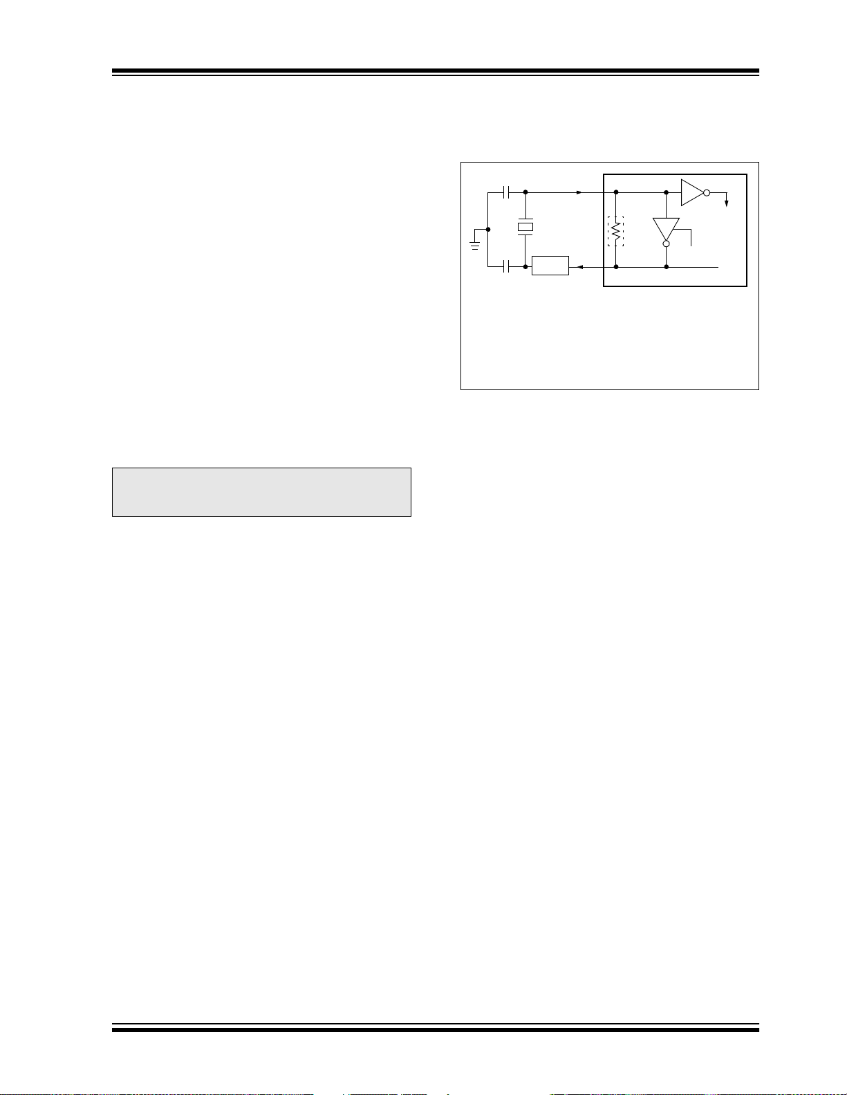
2.0 OSCILLATOR CONFIGURATIONS
2.1 Oscillator Types
PIC18C601/801 can be operated in one of four o sc ill ator modes, programmable by configuration bits
FOSC1:FOSC0 in CONFIG1H register:
1. LP Low Power Crystal
2. HS High Speed Crys tal/Resonator
3. RC External Resistor/Capacitor
4. EC External Clock
2.2 Crystal Oscillator/Ceramic Resonators
In LP or HS oscillator modes, a crystal or ceramic resonator is connected to the OSC1 and OSC2 pins to
establish oscillation. Figure 2-1 shows the pin connections. An external c lock so urce may also be connecte d
to the OSC1 pin, as shown in Figure 2-3 and Figure 2-4.
PIC18C601/801 oscillator design requires the use of a
parallel cut crystal.
Note: Use of a series cut crystal may give a fre-
quency out of the crystal manufacturer’s
specifications.
FIGURE 2-1: CRYSTAL/CERAMIC
RESONATOR OPERATION
(HS OR LP OSC
CONFIGURATION)
(1)
C1
(1)
C2
Note 1: See Table2-1 and Table 2-2 for recom-
2: A series resistor (R
3: R
OSC1
XTAL
(2)
RS
OSC2
mended values of C1 and C2.
strip cut crystals.
F varies with the crystal chosen.
(3)
RF
PIC18C601/801
S) may be required for AT
SLEEP
To
Internal
Logic
2001 Microchip Technology Inc. Advance Information DS39541A-page 21
Page 22
PIC18C601/801
TABLE 2-1: CERAMIC RESONATORS
Ranges Tested:
Mode Freq. OSC1 OSC2
HS 8.0 MHz
16.0 MHz
20.0 MHz
25.0 MHz
10 - 68 pF
10 - 22 pF
TBD
TBD
10 - 68 pF
10 - 22 pF
TBD
TBD
HS+PLL 4.0 MHz TBD TBD
These values are for design guidance only.
See notes on this page.
Resonators Used:
4.0 MHz Murata Erie CSA4.00MG ± 0.5%
8.0 MHz Murata Erie CSA8.00MT ± 0.5%
16.0 MHz Murata Erie CSA16.00MX ± 0.5%
All resonators used did not hav e bu ilt-in capacitors.
TABLE 2-2: CAPACITOR SELECTION FOR
CRYSTAL OSCILLATOR
Osc Type
Crystal
Freq.
LP 32.0 kHz 33 pF 33 pF
200 kHz 15 pF 15 pF
HS 4.0 MHz 15 pF 15 pF
8.0 MHz 15-33 pF 15-33 pF
20.0 MHz 15-33 pF 15-33 pF
25.0 MHz TBD TBD
HS+PLL 4.0 MHz 15 pF 15 pF
These values are for design guidance only.
See notes on this page.
32.0 kHz Epson C-001R32.768K-A ± 20 PPM
200 kHz STD XTL 200.000kHz ± 20 PPM
1.0 MHz ECS ECS-10-13-1 ± 50 PPM
4.0 MHz ECS ECS-40-20-1 ± 50 PPM
8.0 MHz EPSON CA-301 8.000M-C ± 30 PPM
20.0 MHz EPSON CA-301 20.000M-C ± 30 PPM
Cap. Range C1Cap. Range
C2
Crystals Used
Note 1: Recommended values of C1 and C2 are
identical to the ranges tested (Table 2-1).
2: Higher capacitance increases the stability
of the oscillator, but also increases the
start-up time.
3: Since each resonator/crystal has its own
characteristics, the u ser shoul d consult th e
resonator/crystal manufacturer for appropriate values of external components.
4: Rs may be required in HS mode to avoid
overdriving crystals with low drive level
specification.
2.3 RC Oscillator
For timing insensitive applications, the "RC" oscillator
mode offers additional cost savings. The RC oscillator
frequency is a function of the supply volta ge, t he re sis -
EXT) and capacitor (CEXT) values and the operat-
tor (R
ing temperature. In addition to this, the oscillator
frequency will vary from unit to unit due to normal process paramete r variatio n. Further more, the d ifference
in lead frame capacitance between package types will
also affect the oscillation frequency, especially for low
EXT values. The user also needs to take into account
C
variation due t o t ole ranc e of ex ter nal R an d C c om ponents used. Figu re 2-2 shows how the RC comb inatio n
is connected.
In the RC oscillator mode, the oscillator frequency
divided by 4 is available on the OSC2 pin. This signal
may be used f or t e st pu r pos es or t o sy nc hr o n iz e ot he r
logic.
FIGURE 2-2: RC OSCILLATOR MODE
VDD
REXT
OSC1
CEXT
VSS
OSC/4
F
or I/O
Recommended values: 3 kΩ ≤ REXT ≤ 100 kΩ
OSC2/CLKO
C
EXT > 20pF
PIC18C601/801
Internal
Clock
DS39541A-page 22 Advance Information 2001 Microchip Technology Inc.
Page 23
PIC18C601/801
2.4 External Clock Input
The EC oscillator mode requires an external clock
source to be con nected to the OSC1 p in. The fe edback
device between O S C1 a nd OSC2 is turned off in these
modes to save current. There is no oscillator start-up
time required after a Power-on Reset or after a
recovery from SLEEP mode.
In the EC oscillator mode, the oscillator frequency
divided by 4 is available on the OSC2 pin. This signal
may be used f or t e st pu r pos es or t o sy nc hr o n iz e ot he r
logic. Figure 2-3 shows the pin connections for the EC
oscillator mode.
FIGURE 2-3: EXTERNAL CLOCK INPUT
OPERATION (EC OSC
CONFIGURATION)
Clock from
ext. system
OSC/4
F
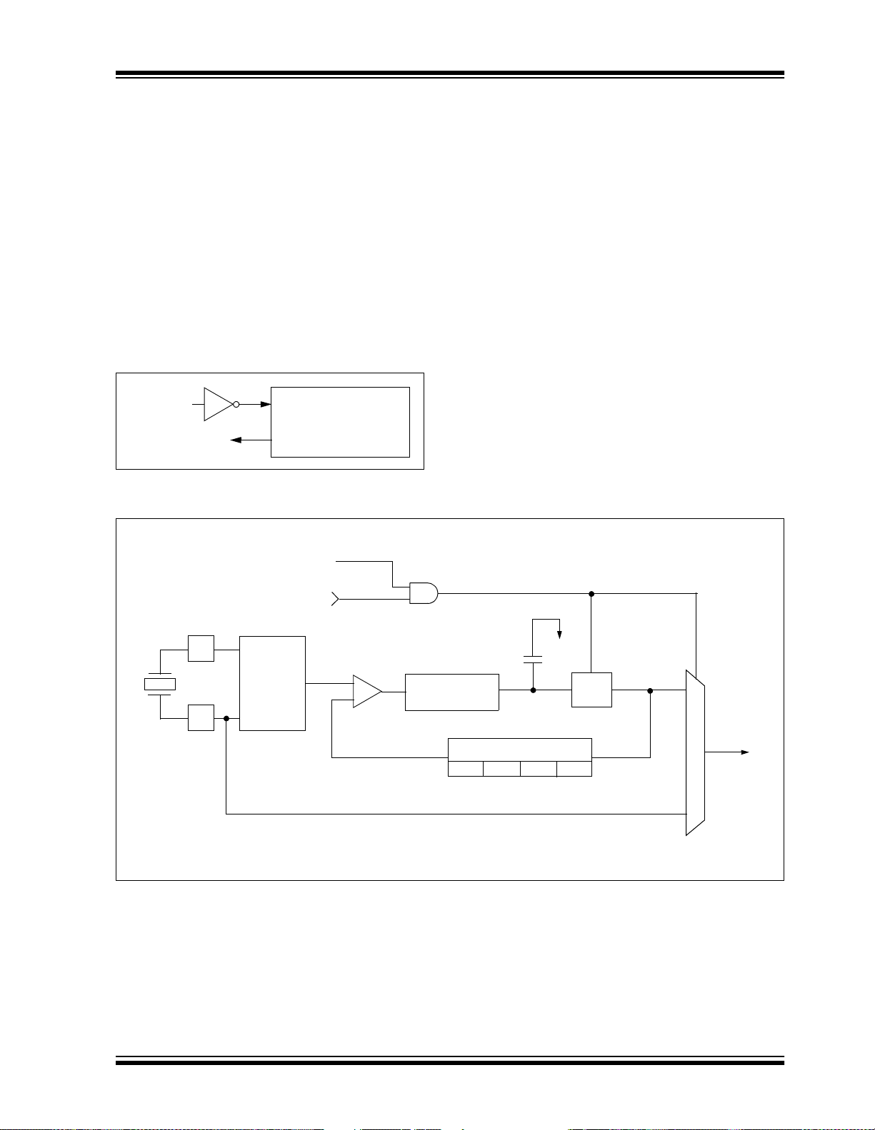
FIGURE 2-4: PLL BLOCK DIAGRAM
OSC1
PIC18C601/801
OSC2
2.5 HS4 (PLL)
A Phase Lock Loop (PLL) circuit is provided as a software programmable optio n for us ers tha t want to m ultiply the frequency of the incoming crystal oscillator
signal by 4. For an input clock frequency of 6 MHz, th e
internal clock frequency will be multiplied to 24 MHz.
This is use ful for custom ers who are conc erned with
EMI due to high frequency crystals.
The PLL is enabled by configuring HS oscillator mode
and setting the PLLEN bit in the OSCON register. If HS
oscillator mode is not selected, or PLLEN bit in
OSCCON register is clear, the PLL is not enabled and
the system clock will come directly from OSC1. HS
oscillator mode i s the d efa ult fo r PIC 1 8C60 1/80 1. In all
other modes, the PLLEN bit and the SCS1 bit are
forced to ‘0’.
A PLL lock timer is used to ensure that the PLL has
locked before device execution starts. The PLL lock
timer has a time-out, referred to as T
PLL.
OSCOUT
OSCIN
PLL Enable
Crystal
Osc
HS Osc
F
Phase
Comparator
IN
FOUT
CVCO
Loop
Filter
Feedback Divider
3210
VCO
SYSCLK
MUX
2001 Microchip Technology Inc. Advance Information DS39541A-page 23
Page 24

PIC18C601/801
2.6 Oscillator Switching Feature
PIC18C601/801 devices include a feature that allows
the system clock source to be switched from the main
oscillator t o an alternate lo w frequency clock s ource.
For PIC18C601/801 devices, this alternate clock
source is the Timer1 oscillator. If a low frequency crystal (32 kHz, for example) has been attached to the
Timer1 oscillator pins and the Timer1 oscillator has
been enabled, the device can switch to a low power
execution mode. Figure 2-5 shows a block diagram of
the system clock sources.
FIGURE 2-5: DEVICE CLOCK SOURCES
PIC18C601/801
OSC2
OSC1
T1OSO
T1OSI
Main Oscillator
SLEEP
Timer 1 Oscillator
T1OSCEN
Enable
Oscillator
2.6.1 SYSTEM CLOCK SWITCH BIT
The system clock source switching is performed under
software control. The system clock switch bit, SCS0
(OSCCON register), controls the clock switching. When
the SCS0 bit is ’0’, the system clock source comes from
the main oscillator, selected by the FOSC2:FOSC0 co nfiguration bits in C ONFIG1H registe r . When the SCS0 b it
is set, the system clock source will come from the Timer1
oscillator . The SCS0 bit is cle ared on all forms of RESET.
Note: The Timer1 oscillator must be enabled to
switch the system clock source. The
Timer1 oscillator is enabled by setting the
T1OSCEN bit in the T imer1 c ontrol register
(T1CON). If the Timer1 oscillator is not
enabled, an y write to the SCS0 bi t will be
ignored (SCS0 bit forced cleared) and the
main oscillator will continue to be the system clock source.
OSC/4
4 x PLL
TOSC
TT1P
T
MUX
Clock
Source
TSCLK
Clock Source option
for other modules
Note: I/O pins have diode protection to VDD and VSS.
DS39541A-page 24 Advance Information 2001 Microchip Technology Inc.
Page 25

REGISTER 2-1: OSCCON REGISTER
U-0 U-0 U-0 U-0 R/W-0 R/W-0 R/W-0 R/W-0
— — — — LOCK PLLEN SCS1 SCS0
bit 7 bit 0
bit 7-4 Unimplemented: Read as '0'
bit 3 LOCK: Phase Lock Loop Lock Status bit
1 = Phase Lock Loop output is stable as system clock
0 = Phase Lock Loop output is not stable and cannot be used as system clock
bit 2 PLLEN: Phase Lock Loop Enable bit
1 = Enable Phase Lock Loop output as system clock
0 = Disable Phase Lock Loop
bit 1 SCS1: System Clock Switch bit 1
When PLLEN and LOCK bit are set:
1 = Use PLL output
0 = Use primary oscillator/clock input pin
When PLLEN bit or LOCK bit is cleared:
Bit is forced clear
bit 0 SCS0: System Clock Switch bit 0
When T1OSCEN bit is set:
1 = Switch to Timer1 oscillator/clock pin
0 = Use primary oscillator/clock input pin
When T1OSCEN is cleared:
Bit is forced clear
PIC18C601/801
Legend:
R = Readable bit W = Writable bit U = Unimplemented bit, read as ‘0’
- n = Value at POR ’1’ = Bit is set ’0’ = Bit is cleared x = Bit is unknown
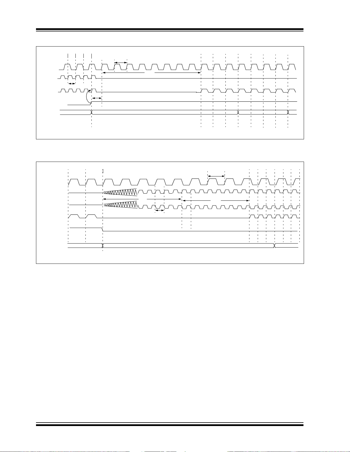
2.6.2 OSCIL LA T OR TRANSITIONS
PIC18C601/801 devices contain circuitry to prevent
"glitches" when switching between oscillator sources.
Essentially, the circuitry waits for eight rising edges of
the clock source that the processor is switching to.
This ensures that the new clock source is stable and
that its pulse width will not be less than the shortest
pulse width of the two clock sources.
A timing diagram indicati ng the transition from the main
oscillator to the Timer1 oscillator is shown in Figure 2-6.
The Timer1 oscillator is assumed to be running all the
time. After the SCS0 bit is set, the processor is frozen
at the next occurri ng Q1 c ycle . Af ter eig ht sy nchroniz ation cycles are counted from the T imer1 oscilla tor, operation resumes. No additional delays are required after
the synchronization cycles.
The sequence of events that takes place when switching from the Timer1 oscillator to the main oscillator will
depend on the mode of the main oscillator. In addition
to eight clock cycles of the main oscillator, additional
delays may take place.
If the main oscillator is configured for an external crystal (HS, LP), the transition will ta ke pl ac e a f ter an oscillator start-up time (T
diagram indicating the transition from the Timer1 oscillator to the main oscillator for HS and LP modes is
shown in Figure 2-7.
OST) has occurred. A timing
2001 Microchip Technology Inc. Advance Information DS39541A-page 25
Page 26
PIC18C601/801
FIGURE 2-6: TIMING DIAGRAM FOR TRANSITION FROM OSC1 TO TIMER1 OSCILLATOR
Q1
T1OSI
OSC1
Internal
System
Clock
SCS0
(OSCCON<0>)
Program
Counter
Note: Delay on internal system clock is eight oscillator cycles for synchronization.
TOSC
Q1
TDLY
TT1P
21 34 5678
TSCS
PC + 2PC
Q3Q2Q1Q4Q3Q2
Q4 Q1
Q2 Q3 Q4 Q1
PC + 4
FIGURE 2-7: TIMING DIAGRAM FOR TRANSITION BETWEEN TIMER1 AND OSC1 (HS, LP)
Q3
T1OSI
OSC1
OSC2
Internal System
Clock
SCS0
(OSCCON<0>)
Q3 Q4
Q1
12345678
TOST
TOSC
TT1P
TSCS
Q1 Q2 Q3 Q4 Q1 Q2
Program Counter
Note: TOST = 1024TOSC (drawing not to scale).
PC
PC + 2
PC + 4
DS39541A-page 26 Advance Information 2001 Microchip Technology Inc.
Page 27
PIC18C601/801
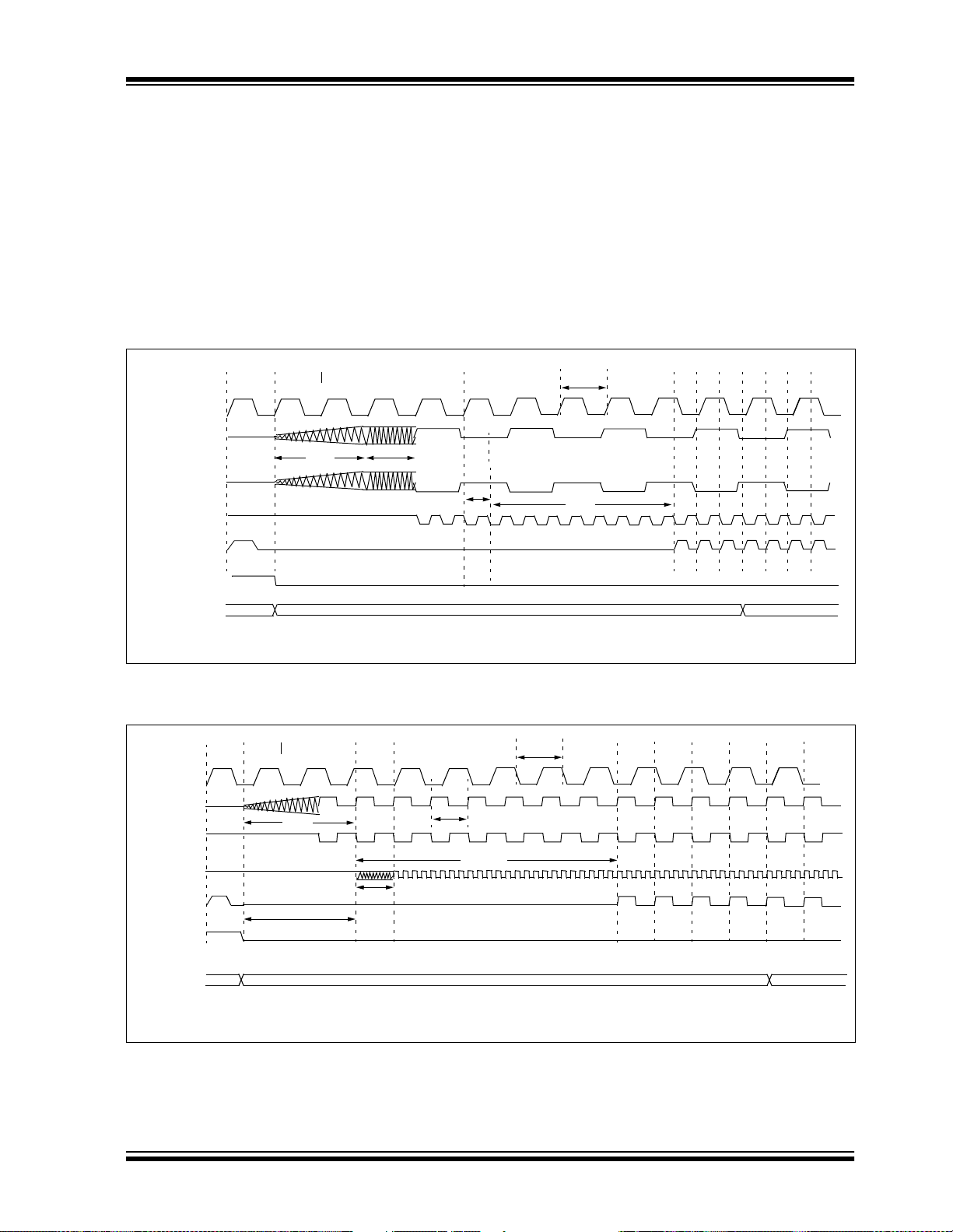
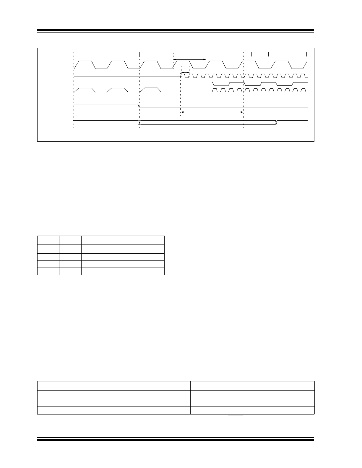
If the main oscillator is configured for HS4 (PLL) mode
with SCS1 bit set to ‘1’, an oscillator start-up time
(T
OST), plus an additional PLL time-out (TPLL) will
occur . The PLL tim e-out is typica lly 2 ms an d allows the
PLL to lock to the main oscillator frequency. A timing
diagram indicating the transition from the Timer1 oscillator to t he main oscill ator for HS4 m ode is shown in
Figure 2-8.
If the main oscill ator is confi gured for HS4 (PLL) m ode,
with SCS1 bit set to ‘0’, only oscillator start-up time
OST) will occur. Since SCS 1 bi t is se t to ‘0’, PLL out-
(T
put is not used, so the sys te m os ci ll ator w i ll c ome from
OSC1 directly and additional delay of TPLL is not
required. A timing diagram indica ting the transit ion from
the Timer1 oscillator to the main oscillator for HS4
mode is shown in Figure 2-9.
If the main oscillator is configured in the RC or EC
modes, there is no osci llator sta rt-up t ime-out. Operation will resume af ter ei ght cycle s of the m ain osc il lator
have been counted. A timing diagram indicating the
transition from the T ime r1 osci llator to the main os cill ator for RC and EC modes is shown in Figure2-10.
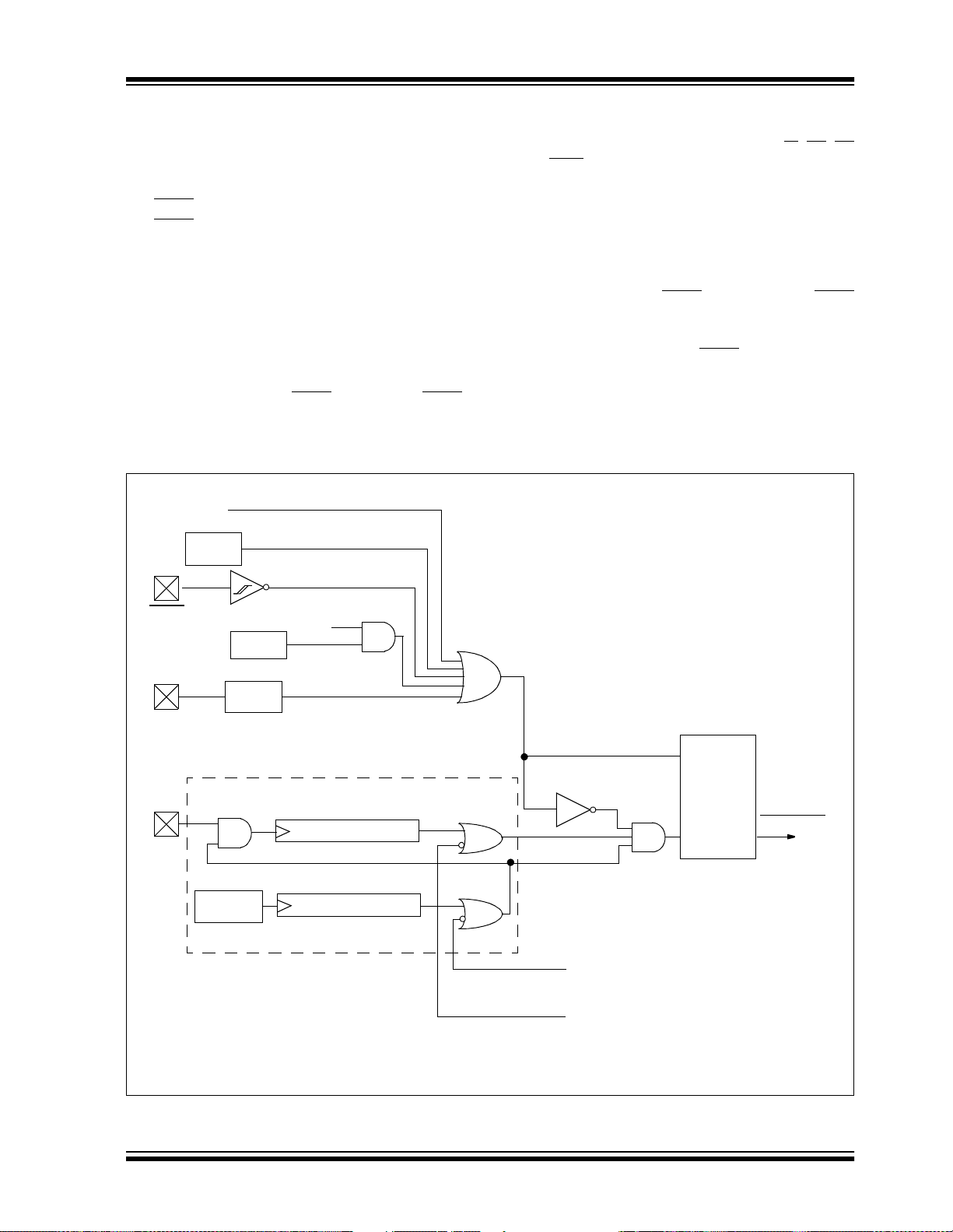
FIGURE 2-8: TIMING FOR TRANSITION BETWEEN TIMER1 AND OSC1 (HS4 WITH SCS1 = 1)
Q3
PC + 4
Q4
T1OSI
OSC1
OSC2
PLL Clock
Input
Internal System
Program Counter
Clock
SCS0
(OSCCON<0>)
Q4 Q1
TOST
PC PC + 2
TPLL
TOSC
TT1P
TSCS
12345678
Q1 Q2 Q3 Q4 Q1 Q2
OST = 1024TOSC (drawing not to scale).
Note: T
FIGURE 2-9: TIMING FOR TRANSITION BETWEEN TIMER1 AND OSC1 (HS4 WITH SCS = 0)
Q4
Q1
T1OSI
OSC1
OSC2
PLL
Clock
Output
Internal
System
Clock
SCS0
(OSCCON<0>)
Program
Counter
Note: TOST = 1024TOSC (drawing not to scale).
PC PC + 2
TOST
T
DLY
TT1P
TOSC
TSCS
TPLL
Q1 Q2 Q3 Q4 Q1 Q2
PC + 4
2001 Microchip Technology Inc. Advance Information DS39541A-page 27
Page 28
PIC18C601/801
FIGURE 2-10: TIMING FOR TRANSITION BETWEEN TIMER1 AND OSC1 (RC, EC)
Q3 Q4
Q1
TT1P
Q1 Q2 Q3 Q4 Q1 Q2 Q3
Q4
T1OSI
OSC1
OSC2
Internal System
Clock
SCS0
(OSCCON<0>)
Program Counter
Note: RC oscillator mode assumed.
PC PC + 2
2.6.3 SCS0, SCS 1 PRIORITY
If both SCS0 and SCS1 are set to ‘1’ simultaneously,
the SCS0 bit has priority over the SCS1 bit. This means
that the low power option will t ake prece dence over the
PLL option. If both bit s are cle ared si mult a neous ly, the
system clock will come from OS C1, after a TOST timeout. If only the SCS0 bit is c leared, the system c lock will
OST
come from the PLL output, following T
and TPLL
time.
TABLE 2-3: SCS0, SCS1 PRIORITY
SCS1 SCS0 Clock Source
0 0 Ext Oscillator OSC1
0 1 Timer1 Oscillator
10HS + PLL
1 1 Timer1 Oscillator
2.7 Effects of SLEEP Mode on the
On-Chip Oscillator
When the device executes a SLEEP instruction, the
on-chip clocks and oscillator are turned off and the
device is held at the beginning of an instruction cycle
(Q1 state). With the os ci lla tor o f f, the OSC1 and OSC2
signals will stop oscillating. Since all the transistor
switching currents have been removed, SLEEP mode
achieves the lowest current consumption of the device
(only leakage currents). Enabling any on-chip feature
that will operate during SLEEP, will increase the cur-
TOSC
1
45678
23
TSCS
PC + 4
rent consumed during SLEEP. The user can wake from
SLEEP through external RESET, Watchdog Timer
Reset, or through an interrupt.
2.8 Power-up Delays
Power-up delays are controlled by two timers, so that
no external RESET circuitry is required for most applications. The delays ensure that the device is kept in
RESET until the device power sup ply and clock are st able. For additional information on RESET operation,
see Section 3.0 RESET .
The first timer is the Power-up Ti mer (PWRT), which
optionally provides a fixed delay of T
#33) on power-up only. The second timer is the Oscillator St art-u p T i mer (O ST), in tended to keep the c hip in
RESET until the crystal oscillator is stable.
PIC18C601/801 devices provide a configuration bit,
PWRTEN
in CONFIG2L register, to enable or disable
the Power-up Timer. By default, the Power-up Timer is
enabled.
With the PLL enabled (HS4 osc illator mode), the time-ou t
sequence fol lowing a Power-o n Reset is different fr om
other oscillator modes. The time-out sequence is as follows: the PWRT time-out is invoked after a POR time
delay has expired, then, the Oscillator Start-up Timer
(OST) is i nvoked. However, this is still not a sufficie nt
amount of time to allow the PLL to lock at high frequencies. The PWRT ti mer is used to prov ide an addition al
time-out, called T
PLL (parameter #7), to allow the PLL
ample time to l oc k to the incoming cl oc k frequency.
PWRT (parameter
TABLE 2-4: OSC1 AND OSC2 PIN STATES IN SLEEP MODE
OSC Mode OSC1 Pin OSC2 Pin
RC Floating, external resistor should pull high At logic low
EC Floating At logic low
LP and HS Feedback inverter disabled, at quiescent voltage level Feedback inverter disabled, at quiescent voltage level
Note: See Table 3-1 in Section 3.0 RESET, for time-outs due to SLEEP and MCLR Reset.
DS39541A-page 28 Advance Information 2001 Microchip Technology Inc.
Page 29
PIC18C601/801
3.0 RESET
Most registers are not affected by a WDT wake-up,
since this is viewed as the resumption of normal oper-
PIC18C601/801 devices differentiate between various
kinds of RESET:
a) Power-on Reset (POR)
b) MCLR
Reset during normal operation
c) MCLR Reset during SLEEP
d) Watchdog Timer (WDT) Reset during normal
operation
e) RESET Instruction
f) Stack Full Reset
g) Stack Underflow Reset
Most registers are una ffected b y a RESET. Their status
is unknown on POR and unchanged by all other
ation. Status bits from the RCON regi ster, RI
and POR, are set or cleared differently in different
RESET situations, as i ndicated in Table 3-2. These bits
are used in software to determine the nature of the
RESET. See Table 3-3 for a full description of the
RESET states of all registers.
A simplified block diagram of the on-chip RESET circuit
is shown in Figure 3-1.
PIC18C601/801 has a MCLR
noise filter in the MCLR
Reset path. The filter will detect and ignore small
pulses.
A WDT Reset does not drive MCLR
pin low.
RESETS. The other registers are forced to a “RESET”
state on Power-on Reset, MCLR
, WDT Reset, MCLR
Reset during SLEEP, and by the RESET instruction.
FIGURE 3-1: SIMPLIFIED BLOCK DIAGRAM OF THE ON-CHIP RESET CIRCUIT
RESET
Instruction
Stack
Pointer
Stack Full/Underflow Reset
External Reset
, TO, PD
MCLR
WDT
Module
VDD Rise
VDD
OSC1
Note 1: This is a separate oscillator from the RC oscillator of the CLKI pin.
2: See Table 3-1 for time-out situations.
Detect
OST/PWRT
On-chip
RC OSC
(1)
SLEEP
WDT
Time-out
Reset
Power-on Reset
OST
10-bit Ripple Counter
PWRT
10-bit Ripple Counter
Enable PWRT
Enable OST
(2)
S
Chip_Reset
R
Q
2001 Microchip Technology Inc. Advance Information DS39541A-page 29
Page 30
PIC18C601/801
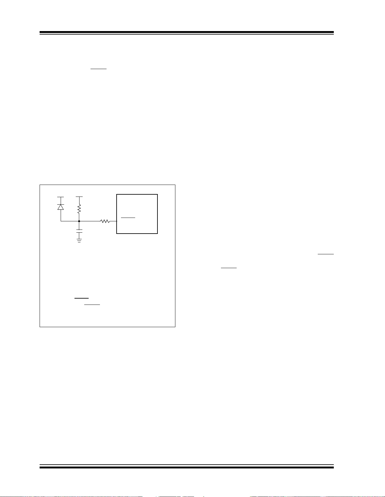
3.1 Power-on Reset (POR)
A Power-on Reset pulse is generated on-chip when a
DD rise is detected. To take advantage of the POR cir-
V
cuitry, connect the MCLR
resistor) to V
DD. This will eliminate ext ernal RC compo-
nents usually needed to create a Power-on Reset
delay . A minimum rise rat e for V
eter D004). For a slow rise time, see Figure 3-2.
When the device starts normal operation (exits the
RESET condition), device operating parameters (voltage, frequency, temperature, etc.) must be met to
ensure operation. If these conditions are not met, the
device must be held in RESET until the operating conditions are m et . Po wer - on R e s et ma y b e us ed t o m ee t
the voltage start-up condition.
FIGURE 3-2: EXTERNAL POWER-ON
V
DD
D
R
C
Note 1: External Power-on Reset circuit is required only
2: R < 40 kΩ is recommended to make sure that
3: R1 = 100Ω to 1 kΩ will limit any current flowing
DD power-up slope is too slow. The diode
if the V
D helps discharge the capacitor quickly when
V
DD powers down.
the voltage drop across R does not violate the
device’s electrical specification.
into MCLR
event of MCLR/
Electrostatic Discharge (ESD), or Electrical
Overstress (EOS).
pin directly (or through a
DD is specified (p aram-
RESET CIRCUIT (FOR
SLOW V
from external capacitor C, in the
VPP pin breakdown due to
DD POWER-UP)
R1
MCLR
PIC18C601/801
3.3 Oscillator Start-up Timer (OST)
The Oscillator Start-up Timer (OST) provides 1024
oscillator cycle (from OSC1 input) delay after the
PWRT delay is over (para meter #32). Th is ensures th at
the crystal oscillator or resonator has started and
stabilized.
The OST time-out is invoked only for LP, HS and HS4
modes and only on Power-on Reset or wake-up from
SLEEP.
3.4 PLL Lock Time-out
With the PLL enabled, the time-ou t sequen ce foll owin g
a Power-on Reset is different from other oscillator
modes. A portion of the Pow er-up T imer is used to provide a fixed time-out th at is suff icient for the PLL to lock
to the main oscillato r frequency. This PLL lock time-out
PLL) is typically 1 ms and follows the oscillator start-
(T
up time-out (OST).
3.5 Time-out Sequence
On power-up, the time-out sequence is as follows:
First, PWRT time-out is invoked after the POR time
delay has expired; then, OST is activated. The total
time-out will vary based on oscillator configuration and
the status of th e PWRT. For example, in RC mode wi th
the PWRT disabled, there will be no time-out at all.
Figure 3-3, Figure 3-4, Figure 3-5, Figure 3-6 and
Figure 3-7 depict time-out sequences on power-up.
Since the time-outs occur from the POR pulse, if MC LR
is kept low long enough, the time-outs will expire.
Bringing MCLR
(Figure 3-5). This is useful for testing purposes or to
synchronize more than one PIC18C601/801 device
operating in parallel.
Table 3-2 shows the RESET conditions for some
Special Function Registers, while Table 3-3 shows the
RESET conditions for all registers.
high will begin execution immediately
3.2 Power-up Timer (PWRT)
The Power-up Timer provides a fixed nominal time-out
(parameter #33), only on power-up from the POR. The
Power-up Timer operates on an internal RC oscillator.
The chip is kept in RESET as long as the PWRT is
active. Th e PWRT t ime de lay al lows V
acceptable level. PIC18C601/801 devices are available with PWRT enabled or disabled.
The power-up time delay wi ll vary from chip to chi p, due
DD, temperature and process variation. See DC
to V
parameter #33 for details.
DS39541A-page 30 Advance Information 2001 Microchip Technology Inc.
DD to rise to an
Page 31

PIC18C601/801
TABLE 3-1: TIME-OUT IN VARIOUS SITUATIONS
Oscillator
Configuration
HS with PLL enabled
HS, LP 72 ms + 1024T
(1)
Power-up
PWRTEN = 0 PWRTEN = 1
72 ms + 1024TOSC 1024TOSC 1024TOSC + 1 ms
OSC 1024TOSC 1024TOSC
(2)
EC 72 ms ——
External RC 72 ms ——
Note 1: 1 ms is the nominal time required for the 4X PLL to lock. Maximum time is 2 ms.
2: 72 ms is the nominal Power-up Timer delay.
REGISTER 3-1: RCON REGISTER BITS AND POSITIONS
R/W-0 U-0 U-0 R/W-1 R/W-1 R/W-1 R/W-1 U-0
IPEN r
bit 7 bit 0
— RI TO PD POR r
Wake-up from
SLEEP or
Oscillator Switch
(1)
TABLE 3-2: STATUS BITS, THEIR SIGNIFICANCE, AND THE INITIALIZATION CONDITION FOR
RCON REGISTER
Condition
Power-on Reset
MCLR Reset during normal
Program
Counter
00000h 0r-1 110r 1 1 1 0 u u
00000h 0r-u uuur u u u u u u
operation
Software Reset during normal
00000h 0r-0 uuur 0 u u u u u
operation
Stack Full Reset during normal
00000h 0r-u uu1r u u u 1 u 1
operation
Stac k Underfl ow Rese t during normal
00000h 0r-u uu1r u u u 1 1 u
operation
MCLR Reset during SLEEP
WDT Reset
00000h 0r-u 10ur u 1 0 u u u
00000h 0r-u 01ur u 0 1 u u u
WDT Wake-up PC + 2
Interrupt wake-up from SLEEP PC + 2
(1)
Legend: u = unchanged, x = unknown, - = unimplemented bit, read as '0', r = reserved, maintain ‘0’
Note 1: When the wake-up is due to an interrupt and the GIEH or GIEL bits are set, the PC is loaded with the
interrupt vector (000008h or 000018h).
RCON
Register
ur-u 00ur u 0 0 u u u
ur-u 00ur u 0 0 u u u
TO PD POR STKFUL STKUNF
RI
2001 Microchip Technology Inc. Advance Information DS39541A-page 31
Page 32

PIC18C601/801
FIGURE 3-3: TIME-OUT SEQUENCE ON POWER-UP (MCLR TIED TO VDD)
VDD
MCLR
INTERNAL POR
TPWRT
PWRT TIME-OUT
OST TIME-OUT
INTERNAL RESET
TOST
FIGURE 3-4: TIME-OUT SEQUENCE ON POWER-UP (MCLR
VDD
MCLR
INTERNAL POR
TPWRT
PWRT TI ME-OUT
OST TIME-OUT
INTERNAL RESET
NOT TIED TO VDD): CASE 1
TOST
FIGURE 3-5: TIME-OUT SEQUENCE ON POWER-UP (MCLR
VDD
MCLR
INTERNAL POR
TPWRT
PWRT TIME-OUT
OST TIME-OUT
INTERNAL RESET
DS39541A-page 32 Advance Information 2001 Microchip Technology Inc.
NOT TIED TO VDD): CASE 2
TOST
Page 33

FIGURE 3-6: SLOW RISE TIME (MCLR TIED TO VDD)
5V
VDD
MCLR
0V
1V
PIC18C601/801
INTERNAL POR
TDEADTIME
PWRT
T
PWRT TIME-OUT
OST TIME-OUT
INTERNAL RES ET
TOST
FIGURE 3-7: TIME-OUT SEQUENCE ON POR W/ PLL ENABLED (MCLR
VDD
MCLR
IINTERNAL POR
TPWRT
PWRT TIME-OUT
OST TIME-OUT
TOST
TPLL
TIED TO VDD)
PLL TIME-OUT
INTERNAL RESET
TOST = 1024 clock cycles.
T
PLL ≈ 2 ms max. First three stages of the PWRT timer.
2001 Microchip Technology Inc. Advance Information DS39541A-page 33
Page 34

PIC18C601/801
TABLE 3-3: INITIALIZATION CONDITIONS FOR ALL REGISTERS
Reset
MCLR
Register
Applicable
Devices
Power-on Reset
Stac k Over/ Unde rflo w Reset
TOSU 601 801 ---0 0000 ---0 0000 ---u uuuu
TOSH 601 801 0000 0000 0000 0000 uuuu uuuu
TOSL 601 801 0000 0000 0000 0000 uuuu uuuu
STKPTR 601 801 00-0 0000 00-0 0000 uu-u uuuu
PCLATU 601 801 ---0 0000 ---0 0000 ---u uuuu
PCLATH 601 801 0000 0000 0000 0000 uuuu uuuu
PCL 601 801 0000 0000 0000 0000 PC + 2
TBLPTRU 601 801 --00 0000 --00 0000 --uu uuuu
TBLPTRH 601 801 0000 0000 0000 0000 uuuu uuuu
TBLPTRL 601 801 0000 0000 0000 0000 uuuu uuuu
TABLAT 601 801 0000 0000 0000 0000 uuuu uuuu
PRODH 601 801 xxxx xxxx uuuu uuuu uuuu uuuu
PRODL 601 801 xxxx xxxx uuuu uuuu uuuu uuuu
INTCON 601 801 0000 000x 0000 000u uuuu uuuu
INTCON2 601 801 1111 -1-1 1111 -1-1 uuuu -u-u
INTCON3 601 801 11-0 0-00 11-0 0-00 uu-u u-uu
INDF0 601 801 (Note 5) (Note 5) (Note 5)
POSTINC0 601 801 (Note 5) (Note 5) (Note 5)
POSTDEC0 601 801 (Note 5) (Note 5) (Note 5)
PREINC0 601 801 (Note 5) (Note 5) (Note 5)
PLUSW0 601 801 (Note 5) (Note 5) (Note 5)
FSR0H 601 801 ---- 0000 ---- 0000 ---- uuuu
FSR0L 601 801 xxxx xxxx uuuu uuuu uuuu uuuu
WREG 601 801 xxxx xxxx uuuu uuuu uuuu uuuu
INDF1 601 801 (Note 5) (Note 5) (Note 5)
POSTINC1 601 801 (Note 5) (Note 5) (Note 5)
POSTDEC1 601 801 (Note 5) (Note 5) (Note 5)
PREINC1 601 801 (Note 5) (Note 5) (Note 5)
PLUSW1 601 801 (Note 5) (Note 5) (Note 5)
FSR1H 601 801 ---- 0000 ---- 0000 ---- uuuu
FSR1L 601 801 xxxx xxxx uuuu uuuu uuuu uuuu
BSR 601 801 ---- 0000 ---- 0000 ---- uuuu
INDF2 601 801 (Note 5) (Note 5) (Note 5)
Legend: u = unchanged, x = unknown, - = unimplem ented b it, read as ’0’, q = value depends on condition,
r = reserved, maintain ‘0’
Note 1: One or more bits in the INTCONx or PIRx registers will be affected (to cause wake-up).
2: When the wake-up is due to an interrupt and the GIEL o r GIE H bit is s et, the PC i s load ed with th e interr upt
vector (00008h or 00018h).
3: When the wake-up is due to an interrupt and the GIEL or GIEH bit is set, the TOSU, TOSH, and TOSL are
updated with the current value of the PC. The SKPTR is modified to point to the next location in the
hardware stack.
4: See Table3-2 for RESET value for specific condition.
5: This is not a physical register. It is an indirect pointer that addresses another register. The contents
returned is the value contained in the addressed register.
WDT Reset
Reset Instruction
Wake-up via WDT or
Interrupt
(3)
(3)
(3)
(3)
(2)
(1)
(1)
(1)
DS39541A-page 34 Advance Information 2001 Microchip Technology Inc.
Page 35

PIC18C601/801
TABLE 3-3: INITIALIZATION CONDITIONS FOR ALL REGISTERS (CONTINUED)
Reset
MCLR
Register
POSTINC2 601 801 (Note 5) (Note 5) (Note 5)
POSTDEC2 601 801 (Note 5) (Note 5) (Note 5)
PREINC2 601 801 (Note 5) (Note 5) (Note 5)
PLUSW2 601 801 (Note 5) (Note 5) (Note 5)
FSR2H 601 801 ---- 0000 ---- 0000 ---- uuuu
FSR2L 601 801 xxxx xxxx uuuu uuuu uuuu uuuu
STATUS 601 801 ---x xxxx ---u uuuu ---u uuuu
TMR0H 601 801 xxxx xxxx uuuu uuuu uuuu uuuu
TMR0L 601 801 xxxx xxxx uuuu uuuu uuuu uuuu
T0CON 601 801 1111 1111 1111 1111 uuuu uuuu
OSCCON 601 801 --00 0-00 --uu u-u0 --uu u-uu
LVDCON 601 801 --00 0101 --00 0101 --uu uuuu
WDTCON 601 801 ---- 1111 ---- uuuu ---- uuuu
(4)
RCON
TMR1H 601 801 xxxx xxxx uuuu uuuu uuuu uuuu
TMR1L 601 801 xxxx xxxx uuuu uuuu uuuu uuuu
T1CON 601 801 0-00 0000 u-uu uuuu u-uu uuuu
TMR2 601 801 xxxx xxxx uuuu uuuu uuuu uuuu
PR2 601 801 1111 1111 1111 1111 1111 1111
T2CON 601 801 -000 0000 -000 0000 -uuu uuuu
SSPBUF 601 801 xxxx xxxx uuuu uuuu uuuu uuuu
SSPADD 601 801 0000 0000 0000 0000 uuuu uuuu
SSPSTAT 601 801 0000 0000 0000 0000 uuuu uuuu
SSPCON1 601 801 0000 0000 0000 0000 uuuu uuuu
SSPCON2 601 801 0000 0000 0000 0000 uuuu uuuu
ADRESH 601 801 xxxx xxxx uuuu uuuu uuuu uuuu
ADRESL 601 801 xxxx xxxx uuuu uuuu uuuu uuuu
ADCON0 601 801 --00 0000 --00 0000 --uu uuuu
ADCON1 601 801 -000 0000 -000 0000 -uuu uuuu
ADCON2 601 801 0--- -000 0--- -000 u--- -uuu
CCPR1H 601 801 xxxx xxxx uuuu uuuu uuuu uuuu
CCPR1L 601 801 xxxx xxxx uuuu uuuu uuuu uuuu
CCP1CON 601 801 --00 0000 --00 0000 --uu uuuu
Legend: u = unchanged, x = unknown, - = unimplem ented b it, read as ’0’, q = value depends on condition,
r = reserved, maintain ‘0’
Note 1: One or more bits in the INTCONx or PIRx registers will be affected (to cause wake-up).
2: When the wake-up is due to an interrupt and the GIEL or GIE H bit is s et, the PC i s load ed with th e interru pt
vector (00008h or 00018h).
3: When the wake-up is due to an interrupt and the GIEL or GIEH bit is set, the TOSU, TOSH, and TOSL are
updated with the current value of the PC. The SKPTR is modified to point to the next location in the
hardware stack.
4: See Table3-2 for RESET value for specific condition.
5: This is not a physical register. It is an indirect pointer that addresses another register. The contents
returned is the value contained in the addressed register.
Applicable
Devices
601 801 0r-1 11qr 0r-1 qqur ur-u qqur
Power-on Reset
Stac k Over/ Unde rflo w Reset
WDT Reset
Reset Instruction
Wake-up via WDT or
Interrupt
2001 Microchip Technology Inc. Advance Information DS39541A-page 35
Page 36

PIC18C601/801
TABLE 3-3: INITIALIZATION CONDITIONS FOR ALL REGISTERS (CONTINUED)
Reset
MCLR
Register
CCPR2H 601 801 xxxx xxxx uuuu uuuu uuuu uuuu
CCPR2L 601 801 xxxx xxxx uuuu uuuu uuuu uuuu
CCP2CON 601 801 --00 0000 --00 0000 --uu uuuu
TMR3H 601 801 xxxx xxxx uuuu uuuu uuuu uuuu
TMR3L 601 801 xxxx xxxx uuuu uuuu uuuu uuuu
T3CON 601 801 0000 0000 uuuu uuuu uuuu uuuu
SPBRG 601 801 xxxx xxxx uuuu uuuu uuuu uuuu
RCREG 601 801 xxxx xxxx uuuu uuuu uuuu uuuu
TXREG 601 801 xxxx xxxx uuuu uuuu uuuu uuuu
TXSTA 601 801 0000 -01x 0000 -01u uuuu -uuu
RCSTA 601 801 0000 000x 0000 000u uuuu uuuu
IPR2 601 801 -1-- 1111 -1-- 1111 -u-- uuuu
PIR2 601 801 -1-- 0000 -1-- 0000 -u-- uuuu
PIE2 601 801 -1-- 0000 -1-- 0000 -u-- uuuu
IPR1 601 801 1111 1111 1111 1111 uuuu uuuu
PIR1 601 801 0000 0000 0000 0000 uuuu uuuu
PIE1 601 801 0000 0000 0000 0000 uuuu uuuu
MEMCON 601 801 0000 --00 0000 --00 uuuu --uu
TRISJ 601 801 1111 1111 1111 1111 uuuu uuuu
TRISH 601 801 1111 1111 1111 1111 uuuu uuuu
TRISG 601 801 ---1 1111 ---1 1111 ---u uuuu
TRISF 601 801 1111 1111 1111 1111 uuuu uuuu
TRISE 601 801 1111 1111 1111 1111 uuuu uuuu
TRISD 601 801 1111 1111 1111 1111 uuuu uuuu
TRISC 601 801 1111 1111 1111 1111 uuuu uuuu
TRISB 601 801 1111 1111 1111 1111 uuuu uuuu
TRISA 601 801 --11 1111 --11 1111 --uu uuuu
LATG 601 801 ---x xxxx ---u uuuu ---u uuuu
LATF 601 801 xxxx xxxx uuuu uuuu uuuu uuuu
LATE 601 801 xxxx xxxx uuuu uuuu uuuu uuuu
Legend: u = unchanged, x = unknown, - = unimplem ented b it, read as ’0’, q = value depends on condition,
r = reserved, maintain ‘0’
Note 1: One or more bits in the INTCONx or PIRx registers will be affected (to cause wake-up).
2: When the wake-up is due to an interrupt and the GIEL o r GIE H bit is s et, the PC i s load ed with th e interr upt
vector (00008h or 00018h).
3: When the wake-up is due to an interrupt and the GIEL or GIEH bit is set, the TOSU, TOSH, and TOSL are
updated with the current value of the PC. The SKPTR is modified to point to the next location in the
hardware stack.
4: See Table3-2 for RESET value for specific condition.
5: This is not a physical register. It is an indirect pointer that addresses another register. The contents
returned is the value contained in the addressed register.
Applicable
Devices
601 801 -111 1111 -111 1111 -uuu uuuu
601 801 -000 0000 -000 0000 -uuu uuuu
601 801 -000 0000 -000 0000 -uuu uuuu
Power-on Reset
Stac k Over/ Unde rflo w Reset
WDT Reset
Reset Instruction
Wake-up via WDT or
Interrupt
(1)
(1)
(1)
DS39541A-page 36 Advance Information 2001 Microchip Technology Inc.
Page 37

PIC18C601/801
TABLE 3-3: INITIALIZATION CONDITIONS FOR ALL REGISTERS (CONTINUED)
Reset
MCLR
Register
LATD 601 801 xxxx xxxx uuuu uuuu uuuu uuuu
LATC 601 801 xxxx xxxx uuuu uuuu uuuu uuuu
LATB 601 801 xxxx xxxx uuuu uuuu uuuu uuuu
LATA 601 801 --xx xxxx --uu uuuu --uu uuuu
PORTJ 601 801 xxxx xxxx uuuu uuuu uuuu uuuu
PORTH 601 801 0000 xxxx 0000 uuuu uuuu uuuu
PORTG 601 801 ---x xxxx ---u uuuu ---u uuuu
PORTF 601 801 xxxx x000 uuuu u000 uuuu uuuu
PORTE 601 801 xxxx xxxx uuuu uuuu uuuu uuuu
PORTD 601 801 xxxx xxxx uuuu uuuu uuuu uuuu
PORTC 601 801 xxxx xxxx uuuu uuuu uuuu uuuu
PORTB 601 801 xxxx xxxx uuuu uuuu uuuu uuuu
PORTA 601 801 --0x 0000 --0u 0000 --uu uuuu
CSEL2 601 801 1111 1111 uuuu uuuu uuuu uuuu
CSELIO 601 801 1111 1111 uuuu uuuu uuuu uuuu
Legend: u = unchanged, x = unknown, - = unimplem ented b it, read as ’0’, q = value depends on condition,
r = reserved, maintain ‘0’
Note 1: One or more bits in the INTCONx or PIRx registers will be affected (to cause wake-up).
2: When the wake-up is due to an interrupt and the GIEL or GIE H bit is s et, the PC i s load ed with th e interru pt
vector (00008h or 00018h).
3: When the wake-up is due to an interrupt and the GIEL or GIEH bit is set, the TOSU, TOSH, and TOSL are
updated with the current value of the PC. The SKPTR is modified to point to the next location in the
hardware stack.
4: See Table3-2 for RESET value for specific condition.
5: This is not a physical register. It is an indirect pointer that addresses another register. The contents
returned is the value contained in the addressed register.
Applicable
Devices
Power-on Reset
Stac k Over/ Unde rflo w Reset
WDT Reset
Reset Instruction
Wake-up via WDT or
Interrupt
2001 Microchip Technology Inc. Advance Information DS39541A-page 37
Page 38

PIC18C601/801
NOTES:
DS39541A-page 38 Advance Information 2001 Microchip Technology Inc.
Page 39

PIC18C601/801
4.0 MEMORY ORGANIZATION
There are two memory blocks in PIC18C601/801
devices. These memory blocks are:
• Program Memory
• Data Memory
Each block has its own bus so that concurrent access
can occur.
4.1 Program Memory Organization
PIC18C601/801 devices have a 21-bit program
counter that is capable of addressing up to 2 Mbyte of
external program memory space. The PIC18C601 has
an external program memory address space of 256
Kbytes. Any program fetch or TBLRD from a program
location greater than 256K will return all NOPs. The
PIC18C801 has an external program memory address
space of 2Mbytes. Refer to Section 5.0 (“External
Memory Interface”) for additional details.
The RESET vector address is mapped to 000000h and
the interrupt vector addresses are at 000008h and
000018h. PIC18C601/801 devices have a 31-level st ack
to store the program counter values during subroutine
calls and interrupts. Figure 4-1 shows the program
memory map and stack for PIC18C601. Figure 4-2
shows the program memory map and stack for the
PIC18C801.
4.1.1 “BOOT RAM” PROGRAM MEMORY
PIC18C601/801 devices have a provision for configuring the last 512 bytes of general purpose user RA M a s
program memory, called “Boot RAM”. This is achieved
by configuring the PGRM bit in the MEMCON register
to ‘1’. (Refer to Section 5.0, “External Memory Interface” for more information.) When the PGRM bit is ‘1’,
the RAM located in data memory locations 400h
through 5FFh (bank 4 throug h 5) is mapped to pro gram
memory locations 1FFE00h to 1FFFFFh.
When configured as program memory, the Boot RAM is
to be used as a te mporary “boot loader” for programming purposes. It can on ly be used for pro gram exec ution. A read from locations 400h to 5FFh in data
memory returns all ‘0’s. Any attempt to write this RAM
as data memo ry when PGRM = 1, d oes no t mod ify an y
of these locations. TBLWT instructions to these locations will cause wr ites to o ccur on the ex ternal memor y
bus. The boot RAM program memory cannot be modified using TBLWT instruction. TBLRD in structions fr om
boot RAM will read memory located on the external
memory bus, not from the on-board RAM. Constants
that are stored in boot RAM are retrieved using the
RETLW instruction.
The default RESET state (power-up) for the PGRM bit
is ‘0’, which configures 1.5K of data RAM and all program memory as external. The PGRM bit can be set
and cleared in the softwar e.
When execution takes place from “Boot RAM”, the
external system bus and all of its control signal s will be
deactivated. If execution takes place from outside of
“Boot RAM”, the external s ystem bu s and all of its co ntrol signals are activated again.
Figure 4-3 and Figure 4-4 show the program memory
map and stack for PIC18C601 and PIC18C801, when
the PGRM bit is set.
2001 Microchip Technology Inc. Advance Information DS39541A-page 39
Page 40

PIC18C601/801
FIGURE 4-1: PROGRAM MEMORY MAP
AND STACK FOR
PIC18C601 (PGRM = 0)
PC<20:0>
Stack Level 1
Stack Level 31
RESET Vector
High Priority Interrupt Vector
Low Priority Interrupt Vector
External
Program Memory
21
•
•
•
0000h
0008h
0018h
3FFFFh
40000h
User Memory Space
FIGURE 4-2: PROGRAM MEMORY MAP
AND STACK FOR
PIC18C801 (PGRM = 0)
PC<20:0>
Stack Level 1
Stack Level 31
RESET Vector
High Priority Interrupt Vector
Low Priority Interrupt Vector
External
Program Memory
21
•
•
•
0000h
0008h
0018h
User Memory Space
Read ’0’
1FFFFFh
1FFFFFh
DS39541A-page 40 Advance Information 2001 Microchip Technology Inc.
Page 41

PIC18C601/801
FIGURE 4-3: PROGRAM MEMORY MAP AND STACK FOR PIC18C601 (PGRM = 1)
PC<20:0>
Stack Level 1
•
•
•
Stack Level 31
High Priority Interrupt Vector
Low Priority Interrupt Vector
21
RESET Vector
External
Program Memory
0000h
0008h
0018h
03FFFFh
040000h
User Memory Space
On-Chip
Boot RAM
1FFE00h
1FFFFFh
Read ’0’
1FFDFFh
1FFE00h
1FFFFFh
EXTERNAL MEMORYINTERNAL MEMORY
2001 Microchip Technology Inc. Advance Information DS39541A-page 41
Page 42

PIC18C601/801
FIGURE 4-4: PROGRAM MEMORY MAP AND STACK FOR PIC18C801 (PGRM = 1)
PC<20:0>
Stack Level 1
•
•
•
Stack Level 31
21
RESET Vector
High Priority Interrupt Vector
Low Priority Interrupt Vector
External
Program Memory
0000h
0008h
0018h
User Memory Space
On-Chip
Boot RAM
1FFE00h
1FFFFFh
1FFDFFh
1FFE00h
External
Table Memory
1FFFFFh
EXTERNAL MEMORYINTERNAL MEMORY
DS39541A-page 42 Advance Information 2001 Microchip Technology Inc.
Page 43

PIC18C601/801
4.1.2 BOOT LOADER
When configured as Program Memory, Boot RAM can
be used as a temporary “Boot Loader” for programming
purposes. If an external memory device is used as program memory, any updates performed by the user program will have to be performed in the “Boot RAM”,
because the user program cannot program and fetch
from external memory, simultaneously.
A typical boot loader execution and external memory
programming sequence would be as follows:
• The boot loader program is transferred from the
external program memory to the last 2 banks of
data RAM by TBLRD and MOVWF instructions.
• Once the “boot loader” program is loaded into
internal memory and verified, open combination
lock and set PGRM bit to con figure the data RAM
into program RAM.
• Jump to beginning of Boot code in Boot RAM.
Program execution begins in Boot RAM to begin
programming the external memory. System bus
changes to an inactive state.
• Boot loader program performs the necessary
external TBLWT and TBLWRD instructions to
perform programming functions.
• When the boot loader program is finished programming external memory, jump to known valid
external program memory location and clear
PGRM bit in MEMCON register to set Boot RAM
as data memory, or reset the part.
4.2 Return Address St ack
The return address stack allows any combination of up to
31 program call s and interrup ts to occur. The PC (Program Counter) is pushed on to the stack when a PUSH,
CALL or RCALL instruction is executed, or an interrupt is
acknowledged. The PC value is pulled off the stack on a
RETURN, RETLW or a RETFIE instruction. PCLATU and
PCLATH are not affected by any of the return instructions.
The stack operates as a 31-word by 21-bit stack memory
and a five-bit stack poin ter, with the stack p ointer i nitia lized to 00000b after all RESETS. There is no RAM associated with stack p oi nte r 00000b. Th is is only a RESE T
value. During a CALL type instruction, causing a push
onto the stack, the stack pointer is first incremented and
the RAM locati on pointed t o by the sta ck pointer i s written
with the contents of the PC. During a RETURN type
instruction, caus ing a pop fr om th e st ack , the c onte nt s of
the RAM location indicated by the STKPTR is transferred
to the PC and th en the stack pointer is decremen ted .
The stack space is not part of either program or data
space. The stac k p oi n ter i s r e adab l e a n d wr i tab le, a nd
the data on the top of the st ack is readable and writable
through SFR registers. Status bits STKOVF and
STKUNF in STKPTR register, indicate whether stack
over/underflow has occurred or not.
4.2.1 TOP-OF-STACK ACCESS
The top of the stack is readable and writable. Three
register locations, TOSU, TOSH and TOSL, allow
access to the con tents of the stack loc ation indicated by
the STKPTR register. This allows users to implement a
software stack, if n ece ssary. After a CALL, RCALL or
interrupt, the software can read the pushed value by
reading the TOSU, TOSH and TOSL registers. These
values can be placed on a user defined software stack.
At return time, the software can replace the TOSU,
TOSH and TOSL and do a return.
The user should disable the global interrupt enable bits
during this time to prevent inadvertent stack operations.
4.2.2 RETURN STACK POINTER (STKPTR)
The STKPTR register contains the stack pointer value,
the STKFUL (stack full) status bit, and the STKUNF
(stack underflow) status bits. Register 4-1 shows the
STKPTR register. The value of the stack pointer can be
0 through 31. The stack pointer increments when values are pushed onto the stack and decrements when
values are popped off the stack. At RESET, the stack
pointer value will be 0. The user may read and write the
stack pointer valu e. This featu re can b e used by a Rea l
Time Operating System for return stack maintenance.
After the PC is push ed ont o the s tac k 31 times (w itho ut
popping any values off the stack), the STKFUL bit is
set. The STKFUL bit can o nly be cle ared in sof tware or
by a POR. Any subse quent pus h operatio n that cau ses
stack overflow will be ignored.
The action that takes place when the stack becomes
full, depends on the state of STVREN (stack overflow
RESET enable) configuration bit in CONFIG4L register. Refer to Section 4.2.4 for more information. If
STVREN is set (default), stack over/underflow will set
the STKFUL bit, and reset th e de vi ce. The ST KFU L b it
will remain set and the stack pointer will be set to 0.
If STVREN is cleared, the STKFUL bit will be set on the
31st push and the st ack pointer will incr ement to 31. Al l
subsequent push attempts will be ignored and
STKPTR remains at 31.
When the stack has been popped enough times to
unload the stac k, the next pop will ret urn a value of zero
to the PC and sets the STKUNF bit, while the stack
pointer remains at 0. The STKUNF bit will remain set
until cleared in software, or a POR occurs.
Note: Returning a value of zero to the PC on an
underflow has the effect of vectoring the
program to the RESET vector, where the
stack condition s can be verifi ed and appropriate actions can be taken.
2001 Microchip Technology Inc. Advance Information DS39541A-page 43
Page 44

PIC18C601/801
REGISTER 4-1: STKPTR - STACK POINTER REGISTER
R/C-0 R/C-0 U-0 R/W-0 R/W-0 R/W-0 R/W-0 R/W-0
STKFUL STKUNF — SP4 SP3 SP2 SP1 SP0
bit 7 bit 0
bit 7 STKFUL: S t ack Full Flag bit
1 = Stack became full or overflowed
0 = Stack has not become full or overflowed
bit 6 STKUNF: Stack Underflow Flag bit
1 = Stack underflow occurred
0 = Stack underflow did not occur
bit 5 Unimplemented: Read as '0'
bit 4-0 SP4:SP0: Stack Pointer Location bits
Note: Bit 7 and bit 6 can only be cleared in user software, or by a POR.
Legend:
= Readable bit W = Writable bit U = Unimplemented bit, read as ‘0’
R
- n = Value at POR ’1’ = Bit is set ’0’ = Bit is cleared C = Clearable bit
FIGURE 4-5: RETURN ADDRESS STACK AND ASSOCIATED REGISTERS
Return Address Stack
11111
11110
TOSLTOSHTOSU
34h1Ah00h
Top-of-Stack
Note 1: No RAM is associated with this address; always maintai ned ‘0’s.
001A34h
000D58h
000000h
11101
00011
00010
00001
00000
STKPTR<4:0>
00010
(1)
DS39541A-page 44 Advance Information 2001 Microchip Technology Inc.
Page 45

PIC18C601/801
4.2.3 PUSH AND POP INSTRUCTIONS
Since the Top-of-Stac k (TOS) is readable and writable,
the ability to push val ues onto the st ack and pop va lues
off the sta ck, withou t disturbi ng normal program ex ecution, is a desirable optio n. To push the current PC value
onto the stack, a PUSH instruction can be executed.
This will i ncrem ent th e stack point er and load the cu rrent PC value onto the stack. TOSU, TOSH and TOSL
can then be modified to place a return address on the
stack.
The POP instruction discards the current TOS by decrementing the stack pointer. The previous value pushed
onto the stack then becomes the TOS value.
4.2.4 STACK FULL/UNDERFLOW RESETS
These RESETS are enabled/dis abled by programmin g
the STVREN configuration bit in CONFIG4L register.
When the STVREN bit is disabled, a full or underflow
condition will set the appropriate STKFUL or STKUNF
bit, but not cause a RESET. When the STVREN bit is
enabled, a full or underflow will set the appropriate
STKFUL or STKUNF bit and then cause a RESET. The
STKFUL or STKUNF bits are only cleared by the user
software or a POR.
4.3 Fast Register Stack
A “fast ret urn” option is available for interrupts and calls.
A fast register stack is provided for the STATUS, WREG
and BSR registers, and is only on e layer i n depth . The
stack is not readable or writable and is loaded wit h the
current value of the corresponding register when the
processor vectors for an interrupt. The values in the fast
register stack are then loaded back into the working registers, if the fast return instructi o n is us e d to re tu rn
from the interrupt.
A low or high priority interrupt source will push values
into the stack registers. If both low and high priority
interrupts are enabled, the stack registers cannot be
used reliably for low priority interrupts. If a high priority
interrupt occurs while servicing a low priority interrupt,
the stack register values stored by the low priority
interrupt will be overwritten.
If high priority inte rrupts a re not dis abled duri ng low pr iority interrupts, users must save the key registers in
software during a low priority interrupt.
If no interrupts are used, the fast register stack can be
used to restore the STATUS, W REG and BSR re gisters
at the end of a subroutine call. To use the fast register
stack for a subroutine call, a fast call instruction
must be executed.
Example 4-1 show s a source c ode exam ple that us es
the fast register stack.
EXAMPLE 4-1: FAST REGISTER STACK
CODE EXAMPLE
CALL SUB1, FAST ;STATUS, WREG, BSR
•
•
SUB1 •
•
•
RETURN FAST ;RESTORE VALUES SAVED
;SAVED IN FAST REGISTER
;STACK
;IN FAST REGISTER STACK
2001 Microchip Technology Inc. Advance Information DS39541A-page 45
Page 46

PIC18C601/801
4.4 PCL, PCLATH and PCLATU
The program counter (PC) specifies the address of the
instruction to fetch for execution. The PC is 21-bits
wide. The low byte is called the PCL register. This register is readable and writable. The high byte is called
the PCH register. This register contains the PC<15:8>
bits and is not directly readable or writable. Updates to
the PCH register may be performed through the
PCLATH register. The upper byte is called PCU. This
register contai ns the PC<20 :16> bi ts an d is not directl y
readable or writable. Updates to the PCU register may
be performed through the PCLATU register.
The PC addresses bytes in the program memory. To
prevent the PC from becoming misaligned with word
instructions, the LSb of the PCL is fix ed to a value of ’0’.
The PC increments by 2 to address sequential instructions in the program memory.
The CALL, RCALL, GOTO and program branch
instructions write to the program counter directly. For
these instructions, the contents of PCLATH and
PCLATU are not transferred to the program counter.
FIGURE 4-6: CLOCK/INSTRUCTION CYCLE
The contents of PCLATH and PCLATU will be transferred to the program counter by an operation that
writes PCL. Similarly, the upper two bytes of the program counter will be transferred to PCLATH and
PCLATU by an operation that reads PCL. This is useful
for computed offsets to the PC (See Section 4.8.1).
4.5 Clocking Scheme/Instruction Cycle
The clock input (from OSC 1 or PLL output) is int ernall y
divided by four to generate four non-overlapping
quadrature clocks, namely Q1, Q2, Q3 and Q4. Internally, the program counter (PC) is incremented every
Q1, the instruction is fetc hed from the program memor y
and latched into the instruction register in Q4. The
instruction is decoded and executed during the following Q1 through Q4. The clocks and instruction execution flow are shown in Figure 4-6.
OSC1
Q1
Q2
Q3
Q4
PC
OSC2/CLKOUT
(RC mode)
Q2 Q3 Q4
Q1
PC
Fetch INST (PC)
Execute INST (PC-2)
Q2 Q3 Q4
Q1
PC+2 PC+4
Fetch INST (PC+2)
Execute INST (PC) Fetch INST (PC+4)
Q2 Q3 Q4
Q1
Execute INST (PC+2)
Internal
Phase
Clock
DS39541A-page 46 Advance Information 2001 Microchip Technology Inc.
Page 47

PIC18C601/801
4.6 Instruction Flow/Pipelining
An “Instruction Cycle” consists of four Q cycles (Q1,
Q2, Q3 and Q4). The instruc ti on fe tch and execute are
pipelined, such that fetch takes one instruction cycle,
while decode and execute takes another instruction
cycle. However, due to the pipelining, each instruction
effectively executes in one cycle. If an instruction
causes the program counter to change (e.g., GOTO),
two cycles are required to complete the instruction
(Example 4-2).
A fetch cycle begins with the program counter (PC)
incrementing in Q1.
In the execution cy cle, the fetc hed instructi on is latche d
into the “Instruction Register” (IR) in cycle Q1. This
instruction is then decoded and executed during the
Q2, Q3, and Q4 cycles. Dat a memory is read during Q2
(operand read) and written during Q4 (destination
write).
EXAMPLE 4-2: INSTRUCTION PIPELINE FLOW
TCY0TCY1TCY2TCY3TCY4TCY5
1. MOVLW 55h
2. MOVWF PORTB
3. BRA SUB_1
4. BSF PORTA, BIT3 (Forced NOP)
5. Instruction @ address SUB_1
Fetch 1 Execute 1
Fetch 2 Execute 2
Fetch 3 Execute 3
4.7 Instructions in Program Memory
The program memory is addressed in bytes. Instructions are stored as two bytes or four bytes in program
memory. The Least Significant Byte of an instruction
word is always stored in a program memory location
with an even address (LSB = ’0’). Figure 4-1 shows an
example of how instruct ion words are stored in the p rogram memory. To maintain alignment with instruction
boundaries, the PC increments in steps of 2 and the
LSB will always read ’0’ (see Section 4.4).
The CALL and GOTO ins tructions have an absol ute program memory address embedded into the instruction.
Since instructions are always stored on word boundaries, the data contained in the instruction is a word
address. The word address is written to PC<20:1>,
which accesses the desired byte address in program
memory. Instruction #2 in Figure 4-1 shows how the
instruction “GOTO 0x06” is encoded in the program
memory. Program branch instructions that encode a
relative address offset operate in the same manner.
The offset value stored in a branch instruction represents the numb er of single word inst ructio ns by w hich
the PC will be offset. Section 20.0 provides further
details of the instruction set.
Fetch 4 Flush
Fetch SUB_1 Execute SUB_1
All instructions are s ingle cycle, exce pt for any program br anches. These t ake two cycles , since the fetch in struction
is “flushed” from the pipeline, while the new instruction is being fetched and then executed.
TABLE 4-1: INSTRUCTIONS IN PROGRAM MEMORY
Instruction Opcode Memory Address
—
MOVLW 055h
GOTO 000006h
MOVFF 123h, 456h
—
2001 Microchip Technology Inc. Advance Information DS39541A-page 47
——000007h
0E55h 55h 000008h
0Eh 000009h
EF03h, F000h 03h 00000Ah
EFh 00000Bh
00h 00000Ch
F0h 00000Dh
C123h, F456h 23h 00000Eh
C1h 00000Fh
56h 000010h
F4h 000011h
——000012h
Page 48

PIC18C601/801
4.7.1 TWO-WORD INSTRUCTIONS
PIC18C601/801 devices have four two-word instructions: MOVFF, CALL, GOTO and LFSR. The second
word of these instructions has the four MSB’s set to 1’s
and is a special kind of NOP instruction. The lower 12
bits of the second word contain data to be used by the
instruction. If the first word of the instruction is executed, the data in the second word is accessed. If the
second word of the in struction is executed by itself (firs t
word was skipped), i t will ex ecute as a NOP. This action
is necessary when the two-word ins truction is prec eded
by a conditional instruction that changes the PC and
skips one instruction. A program example that demonstrates this concept is shown in Example 4-3. Refer to
Section 19.0 for further details of the instruction set.
4.8 Lookup Tables
Lookup tables are implemented two ways:
• Computed GOTO
• Table Reads
4.8.1 COMPUTED GOTO
A computed GOTO is accomplish ed by adding an offs et
to the program counter (ADDWF PCL).
A lookup table can be formed with an ADDWF PCL
instruction and a group of RETLW 0xnn instructions.
WREG is loaded with an offset into the table, before executing a call to that t able. Th e first instruction of the c alled
routine is the ADDWF PCL instruction. The next instruc-
tion executed will be one of t he RETLW 0xnn instructions that returns the value 0xnn to the calling fu nc ti on .
The offset v alue (val ue in WR EG) sp ecifies the numb er
of bytes that the program counter should advance.
In this method, only one data byte may be stored in
each instruction location and room on the return
address stack is required.
Warning: The LSb of the PCL is fixed to a value of ‘0’.
Hence, computed GOTO to an odd add ress
is not possible.
4.8.2 TABLE READS/TABLE WRITES
A better method of storing data in program memory
allows 2 bytes of data to be stored in each instruction
location.
Lookup table data may be stored as 2 bytes per program word by using table reads and writes. The table
pointer (TBLPTR) specifies the byte address and the
table latch (TABLAT) contains the data that is read
from, or written to, program memory. Data is transferred to/from program memory one byte at a time.
A description of the Table Read/Table Write operation
is shown in Section 6.0.
Note: If execution is taking place from Boot RAM
Program Memory, RETLW instructions
must be used to read lookup values from
the Boot RAM itself.
EXAMPLE 4-3: Two-Word Instructions
CASE 1:
Object Code Source Code
0110 0110 0000 0000 TSTFSZ REG1 ; is RAM location 0?
1100 0001 0010 0011 MOVFF REG1, REG2 ; No, execute 2-word instruction
1111 0100 0101 0110 ; 2nd operand holds address of REG2
0010 0100 0000 0000 ADDWF REG3 ; continue code
CASE 2:
Object Code Source Code
0110 0110 0000 0000 TSTFSZ REG1 ; is RAM location 0?
1100 0001 0010 0011 MOVFF REG1, REG2 ; Yes
1111 0100 0101 0110 ; 2nd operand executed as NOP
0010 0100 0000 0000 ADDWF REG3 ; continue code
DS39541A-page 48 Advance Information 2001 Microchip Technology Inc.
Page 49

PIC18C601/801
4.9 Data Memory Organization
The data memory is implemented as static RAM. Each
register in the data memory has a 12-bi t address , all owing up to 4096 bytes of data memory. Figure 4-8 shows
the data memory organization for PIC18C601/801
devices.
The data memory map is divided into banks that contain 256 bytes each. The lower four bits of the Bank
Select Register (BSR<3:0>) select which bank will be
accessed. Th e upp er 4 bits fo r the B SR are no t imp lemented.
The data memory contains Special Function Registers
(SFR) and General Purpose Registers (GPR). The
SFR’s are used for control and status of the controller
and peripheral function s, while GPR’s are used for data
storage and scratch pad operations in the user’s application. The SFR’s start at the last location of Bank 15
(0FFFh) and grow downwards. GPR’s start at the first
location of Bank 0 and grow upwards. Any read of an
unimplemented location will read as ’0’s.
GPR banks 4 and 5 serve a s a Program Memory called
“Boot RAM”, when PGRM bit in M EMCON is set. When
PGRM bit is set, any read from “Boot RAM” returns ‘0’s,
while any write to it is ignored.
The entire data memory may be accessed directly or
indirectly. Direct addressing may require the use of the
BSR register. Indirect addressing requires the use of a
File Select Register (FSR). Each FSR holds a 12-bit
address value that can be used to access any location
in the Data Memory map without banking.
The instruction set and architecture allow operations
across all banks. This m ay be accompli shed by indirec t
addressing, or by the use of the MOVFF instruction. The
MOVFF instruction is a two-word/two-cycle instruction
that moves a value from one register to another.
To ensure that commonly used registers (SFRs and
select GPRs) can be accessed in a single cycle,
regardless of the current BSR values, an Access Bank
is implemented. A s egment of Ban k 0 and a segm ent of
Bank 15 comprise the Access bank. Section 4.10 provides a detailed description of the Access bank.
4.9.1 GENERAL PURPOSE REGISTER FILE
The register file can b e access ed eithe r dire ctly o r indirectly. Indirect addressing operates through the File
Select Registers (FSR). The operation of indirect
addressing is shown in Section 4.12.
PIC18C601/801 devices have banked memory in the
GPR area. GPRs are not initialized by a Power-on
Reset and are unchanged on all other RESETS.
Data RAM is available for use as GPR registers by all
instructions. Bank 15 (0F80h to 0FFFh) contains
SFR’s. All other banks of data memory contain GPR
registers starting with bank 0.
4.9.2 SPECIAL FUNCTION REGISTERS
The Special Function Registers (SFRs) are registers
used by the CPU and Peripheral Modules for controlling the desired operation of the device. These registers are implemented as static RAM. A list of these
registers is given in Table 4-2.
The SFR’s can be classified into two sets: those associated with the “core” function and those related to the
peripheral functions. Those registers related to the
“core” are described in this s ec tio n, w hil e tho se rel ate d
to the operation of the peripheral features are
described in the section of that periphe ral feature.
The SFRs are typica lly d istrib uted a mong the per ipherals whose functions they control.
The unused SFR locations are unimplemented and
read as '0's. See Table 4-2 for addresses for th e SFRs.
4.9.3 SECURED ACCESS REGISTERS
PIC18C601/801 devices contain software programming options for safety critical peripherals. Because
these safety critical peripherals can be programmed in
software, registers used to control these peripherals
are given limited access by the user code. This way,
errant code will not accidentally change settings in
peripherals that could cause catastrophic results.
The registers that are considered safety crit ical are the
Watchdog Timer register (WDTCON), the External
Memory Control register (MEMCON), the Oscillator
Control register (OSCCON) and the Chip Select registers (CSSEL2 and CSELIO).
Two b its called Combinati on Lock (CMLK) bits , loc ate d
in the lower two bits of the PSPCON register, must be
set in sequence by user code to gain access to
Secured Access registers.
2001 Microchip Technology Inc. Advance Information DS39541A-page 49
Page 50

PIC18C601/801
REGISTER 4-2: PSPCON REGISTER
U-0 U-0 U-0 U-0 U-0 U-0 W-0 W-0
— — — — — — CMLK1 CMLK0
bit 7 bit 0
bit 7-2 Unimplemented: Read as '0'
bit 1-0 CMLK<1:0>: Combination Lock bits
Legend:
R = Readable bit W = Writable bit U = Unimplemented bit, read as ‘0’
- n = Value at POR ’1’ = Bit is set ’0’ = Bit is cleared x = Bit is unknown
The Combination Lock bits must be set sequentially,
meaning that as soon as Combinat ion Lock b it CMLK1
is set, the second Combination Lock bit CMLK0 must be
set on the following instruction cycle. If user waits more
than one machine cycle to set the second bit after setting the first, both bits will automatically be cleared in
hardware and the lock will remain closed. T o satisfy this
condition, all interrupts must be disabled before attempting to unlock the Combination Lock. Once secured registers are modified, interrupts may be re-enabled.
Each instruction must only modify one combination lock
bit at a time. This means, user code must use the BSF
instruction to set CMLK bits in the PSPCON register.
Note: The Combination Lock bits are write-only
When the Combination Lock is opened, the user will
have three instruction cycles to modify the safety critical register of choice. After three instruction cycles
have expired, the CMLK bits are cleared, the lock will
close and the user will have to set the CMLK bi ts again,
in order to open the lock. Since there are only three
instruction cyc les allowed af ter the Combina tion Lock is
opened, if a subroutine is used to unlock Combination
Lock bits, user code must preload WREG with the
desired value, call unlock subroutine, and write to the
desired safety critical register itself.
Note: Successive attempts to unlock the Combi-
nation Lock must be separated by at least
three instruction cycles.
bits. These bits will always return ‘0’ when
read.
EXAMPLE 4-4: COMBINATION UNLOCK SUBROUTINE EXAMPLE CODE
BCF INTCON, GIE ; Disable all interrupts
; Lock is closed
MOVLW 5Ah ; Preload WREG with data to be stored in a safety critical register
CALL UNLOCK ; Now unlock it
; Write must take place in next instruction cycle
MOVWF OSCCON
BSF INTCON, GIE ; Re-enable interrupts
•
•
UNLOCK
BSF PSPCON, CMLK1
BSF PSPCON, CMLK0
RETURN
•
•
DS39541A-page 50 Advance Information 2001 Microchip Technology Inc.
Page 51

PIC18C601/801
EXAMPLE 4-5: COMBINATION UNLOCK MACRO EXAMPLE CODE
UNLOCK_N_MODIFY @REG MACRO
BSF PSPCON, CMLK1
BSF PSPCON, CMLK0
ENDM
•
•
MOVLW 5Ah ; Preload WREG for OSCCON register
BCF INTCON, GIE ; Disable interrupts
MOVWF @REG ; Modify given register
BSF INTCON, GIE ; Enable interrupts
UNLOCK_N_MODIFY OSCCON ; Modify OSCCON
FIGURE 4-7: THE DATA MEMORY MAP FOR PIC18C801/601 (PGRM = 0)
BSR<3:0>
= 0000b
= 0001b
= 0010b
= 0011b
= 0100b
= 0101b
Bank 0
Bank 1
Bank 2
Bank 3
Bank 4
Bank 5
Data Memory Map
00h
Access GPR’s
FFh
00h
FFh
00h
FFh
00h
FFh
00h
FFh
00h
FFh
GPR
GPR
GPR
GPR
GPR
GPR
000h
07Fh
080h
0FFh
100h
1FFh
200h
2FFh
300h
3FFh
400h
4FFh
500h
5FFh
Access RAM Bank
Access Bank Low
(GPR’s)
Access Bank High
(SFR’s)
00h
7Fh
80h
FFh
= 0110b
= 1110b
= 1111b
2001 Microchip Technology Inc. Advance Information DS39541A-page 51
Bank 6
to
Bank 14
Bank 15
00h
FFh
Unused
Read ’00h’
Unused
Access SFR’s
EFFh
F00h
F7Fh
F80h
FFFh
When a = 0,
the BSR is ignored and this
Access RAM bank is used.
The first 128 bytes are General
Purpose RAM (from Bank 0).
The next 128 bytes are Special
Function Registers (from
Bank 15).
When a = 1,
the BSR is used to specify
the RAM location that the
instruction uses.
Page 52

PIC18C601/801
FIGURE 4-8: DATA MEMORY MAP FOR PIC18C601/801 (PGRM = 1)
BSR<3:0>
= 0000b
= 0001b
= 0010b
= 0011b
= 0100b
= 1110b
= 1111b
Bank 0
Bank 1
Bank 2
Bank 3
Bank 4
to
Bank 14
Bank 15
Data Memory Map
00h
Access GPR’s
FFh
00h
FFh
00h
FFh
00h
FFh
00h
FFh
GPR
GPR
GPR
GPR
Unused
Read ’00h’
Unused
Access SFR’s
000h
07Fh
080h
0FFh
100h
1FFh
200h
2FFh
300h
3FFh
EFFh
F00h
F7Fh
F80h
FFFh
Access RAM Bank
Access Bank Low
(GPR’s)
Access Bank High
(SFR’s)
When a = 0,
the BSR is ignored and this
Access RAM bank is used.
The first 128 bytes are General
Purpose RAM (from Bank 0).
The next 128 bytes are Special
Function Re gisters (from
Bank 15).
When a = 1,
the BSR is used to specify
the RAM location that the
instruction uses.
00h
7Fh
80h
FFh
DS39541A-page 52 Advance Information 2001 Microchip Technology Inc.
Page 53

FIGURE 4-9: SPECIAL FUNCTION REGISTER MAP
FFFh TOSU FDFh INDF2 FBFh CCPR1H F9Fh IPR1
FFEh TOSH FDEh POSTINC2 FBEh CCPR1L F9Eh PIR1
FFDh TOSL FDDh POSTDEC2 FBDh CCP1CON F9Dh PIE1
FFCh STKPTR FDCh PREINC2 FBCh CCPR2H F9Ch MEMCON
FFBh PCLATU FDBh PLUSW2 FBBh CCPR2L F9Bh
FFAh PCLATH FDAh FSR2H FBAh CCP2CON F9Ah TRISJ
FF9h PCL FD9h FSR2L FB9h Reserved F99h TRISH
FF8h TBLPTRU FD8h STATUS FB8h Reserved F98h TRISG
FF7h TBLPTRH FD7h TMR0H FB7h Reserved F97h TRISF
FF6h TBLPTRL FD6h TMR0L FB6h
FF5h TABLAT FD5h T0CON FB5h
FF4h PRODH FD4h Reserved FB4h
FF3h PRODL FD3h OSCCON FB3h TMR3H F93h TRISB
FF2h INTCON FD2h LVDCON FB2h TMR3L F92h TRISA
FF1h INTCON2 FD1h WDTCON FB1h T3CON F91h LATJ
FF0h INTCON3 FD0h RCON FB0h PSPCON F90h LATH
FEFh INDF0 FCFh TMR1H FAFh SPBRG F8Fh LATG
FEEh POSTINC0 FCEh TMR1L FAEh RCREG F8Eh LATF
FEDh POSTDEC0 FCDh T1CON FADh TXREG F8Dh LATE
FECh PREINC0 FCCh TMR2 FACh TXSTA F8Ch LATD
FEBh PLUSW0 FCBh PR2 FABh RCSTA F8Bh LATC
FEAh FSR0H FCAh T2CON FAAh
FE9h FSR0L FC9h SSPBUF FA9h
FE8h WREG FC8h SSPADD FA8h
FE7h INDF1 FC7h SSPSTAT FA7h CSEL2 F87h PORTH
FE6h POSTINC1 FC6h SSPCON1 FA6h CSELIO F86h PORTG
FE5h POSTDEC1 FC5h SSPCON2 FA5h
FE4h PREINC1 FC4h ADRESH FA4h
FE3h PLUSW1 FC3h ADRESL FA3h
FE2h FSR1H FC2h ADCON0 FA2h IPR2 F82h PORTC
FE1h FSR1L FC1h ADCON1 FA1h PIR2 F81h PORTB
FE0h BSR FC0h ADCON2 FA0h PIE2
PIC18C601/801
—
— F96h TRISE
— F95h TRISD
— F94h TRISC
— F8Ah LATB
— F89h LATA
— F88h PORTJ
— F85h PORTF
— F84h PORTE
— F83h PORTD
F80h PORTA
2001 Microchip Technology Inc. Advance Information DS39541A-page 53
Page 54

PIC18C601/801
TABLE 4-2: REGISTER FILE SUMMARY - PIC18C601/801
File Name Bit 7 Bit 6 Bit 5 Bit 4 Bit 3 Bit 2 Bit 1 Bit 0
FFFh TOSU — — — Top-of-Stack Upper Byte (TOS<20:16>) ---0 0000 ---0 0000
FFEh TOSH Top-of-Stack High Byte (TOS<15:8>) 0000 0000 0000 0000
FFDh TOSL Top-of-Stack Low Byte (TOS<7:0>) 0000 0000 0000 0000
FFCh STKPTR STKOVF STKUNF — Return Stack Pointer 00-0 0000 00-0 0000
FFBh PCLATU — — — Holding Register for PC<20:16> ---0 0000 ---0 0000
FFAh PCLATH Holding Register for PC<15:8> 0000 0000 0000 0000
FF9h PCL PC Low Byte (PC<7:0>) 0000 0000 0000 0000
FF8h TBLPTRU — — r Program Memory Table Pointer Upper Byte (TBLPTR<20:16>) --r0 0000 --r0 0000
FF7h TBLPTRH Program Memory Table Pointer High Byte (TBLPTR<15:8>) 0000 0000 0000 0000
FF6h TBLPTRL Program Memory Table Pointer Low Byte (TBLPTR<7:0>) 0000 0000 0000 0000
FF5h TABLAT Program Memory Table Latch 0000 0000 0000 0000
FF4h PRODH Product Register High Byte xxxx xxxx uuuu uuuu
FF3h PRODL Product Register Low Byte xxxx xxxx uuuu uuuu
FF2h INTCON GIE/GIEH PEIE/GIEL TMR0IE INT0E RBIE TMR0IF INT0F RBIF 0000 000x 0000 000u
FF1h INTCON2 RBPU INTEDG0 INTEDG1 INTEDG2 — T0IP — RBIP 1111 -1-1 1111 -1-1
FF0h INTCON3 INT2P INT1P — INT2E INT1E — INT2F INT1F 11-0 0-00 11-0 0-00
FEFh INDF0 Uses contents of FSR0 to address data memory - value of FSR0 not changed (not a physical register) N/A N/A
FEEh POSTINC0 Uses contents of FSR0 to address data memory - value of FSR0 post-incremented (not a physical register) N/A N/A
FEDh POSTDEC0 Uses contents of FSR0 to address data memory - value of FSR0 post-decremented
FECh PREINC0 Uses contents of FSR0 to address data memory - value of FSR0 pre-incremented
FEBh PLUSW0 Uses contents of FSR0 to address data memory -value of FSR0 offset by WREG
FEAh FSR0H
FE9h FSR0L Indirect Data Memory Addres s Pointer 0 Lo w Byte xxxx xxxx uuuu uuuu
FE8h WREG Working Register xxxx xxxx uuuu uuuu
FE7h INDF1 Uses contents of FSR1 to address data memory - value of FSR1 not changed (not a physical register) N/A N/A
FE6h POSTINC1 Uses contents of FSR1 to address data memory - value of FSR1 post-incremented
FE5h POSTDEC1 Uses contents of FSR1 to address data memory - value of FSR1 post-decremented
FE4h PREINC1 Uses contents of FSR1 t o ad dr es s data memory - value of FSR1 pre-incre me nt ed (not a ph ys ic al re gi st er ) N/A N/A
FE3h PLUSW1 Uses contents of FSR1 to address data memory - value of FSR1 offset by WREG (not a physical register) N/A N/A
FE2h FSR1H
FE1h FSR1L Indirect Data Memory Addres s Pointer 1 Lo w Byte xxxx xxxx uuuu uuuu
FE0h BSR — — — — Bank Select Register ---- 0000 ---- 0000
FDFh INDF2 Uses contents of FSR2 to address data memory - value of FSR2 not changed (not a physical register) N/A N/A
FDEh POSTINC2 Uses contents of FSR2 to address data memory - value of FSR2 post-incremented (not a physical register) N/A N/A
FDDh POSTDE C2 Uses contents of FSR2 to address data memory - value of FSR2 post-decremented
FDCh PREINC2 Uses content s of FSR 2 t o ad dr ess dat a me mo ry - val ue of FSR 2 pre- i nc rem ent ed (n ot a phys i cal re gis t er ) N/A N/A
FDBh PLUSW2 Uses contents of FSR2 to add res s data memory -v alue of FS R2 of fs et by WR EG (not a ph ysic al re gister ) N/A N/A
FDAh FSR2H — — — — Indirect Data Memory Address Pointer 2 High ---- xxxx ---- uuuu
FD9h FSR2L Indi rect Data Memory Address Pointer 2 Low Byte xxxx xxxx uuuu uuuu
FD8h STATUS — — — NOVZDCC---x xxxx ---u uuuu
Legend x = unknown, u = unchanged, - = unimplemented, q = value depends on condition, r = reserved
Note 1: Other (non-power-up) RESETS include external RESET through MCLR
2: These registers can only be modified when the Combination Lock is open.
3: These registers are available on PIC18C 801 onl y.
(not a physical register)
(not a physical register)
(not a physical register)
— — — — Indirect Data Memory Address Pointer 0 High ---- xxxx ---- uuuu
(not a physical register)
(not a physical register)
— — — — Indirect Data Memory Address Pointer 1 High ---- xxxx ---- uuuu
(not a physical register)
and Watchdog Timer Reset.
Value on
POR
N/A N/A
N/A N/A
N/A N/A
N/A N/A
N/A N/A
N/A N/A
Value on
all other
RESETS
(1)
DS39541A-page 54 Advance Information 2001 Microchip Technology Inc.
Page 55

PIC18C601/801
T ABLE 4-2: REGISTER FILE SUMMARY - PIC18C601/801 (CONTINUED)
File Name Bit 7 Bit 6 Bit 5 Bit 4 Bit 3 Bit 2 Bit 1 Bit 0
FD7h TMR0H Timer0 Register High Byte 0000 0000 0000 0000
FD6h TMR0L Timer0 Register Low Byte xxxx xxxx uuuu uuuu
FD5h T0CON TMR0ON 16BIT T0CS T0SE T0PS3 T0PS2 T0PS1 T0PS0 1111 1111 1111 1111
FD4h Reserved rrrr rrrr rrrr rrrr
FD3h OSCCON
FD2h LVDCON
FD1h WDTCON
FD0h RCON IPEN r — RI TO PD POR r 00-1 11qq 00-q qquu
FCFh TMR1H Timer1 Register High Byte xxxx xxxx uuuu uuuu
FCEh TMR1L Timer1 Register Low Byte xxxx xxxx uuuu uuuu
FCDh T1CON RD16 — T1CKPS1 T1CKPS0 T1OSCEN T1SYNC TMR1CS TMR1ON 0-00 0000 u-uu uuuu
FCCh TMR2 Timer2 Register 0000 0000 0000 0000
FCBh PR2 Timer2 Period Register 1111 1111 1111 1111
FCAh T2CON — TOUTPS3 TOUTPS2 TOUTPS1 TOUTPS0 TMR2ON T2CKPS1 T2CKPS0 -000 0000 -000 0000
FC9h SSPBUF SSP Receive Buffer/Transmit Register xxxx xxxx uuuu uuuu
FC8h SSPADD SSP Address Register in I2C Slave Mode. SSP Baud Rate Reload Register in I2C Master Mode 0000 0000 0000 0000
FC7h SSPSTAT SMP CKE D/A PSR/WUA BF 0000 0000 0000 0000
FC6h SSPCON1 WCOL SSPOV SSPEN CKP SSPM3 SSPM2 SSPM1 SSPM0 0000 0000 0000 0000
FC5h SSPCON2 GCEN ACKSTAT ACKDT ACKEN RCEN PEN RSEN SEN 0000 0000 0000 0000
FC4h ADRESH A/D Result Register High Byte xxxx xxxx uuuu uuuu
FC3h ADRESL A/D Result Register Low Byte xxxx xxxx uuuu uuuu
FC2h ADCON0 — — CHS3 CHS2 CHS1 CHS0 GO/DONE ADON --00 0000 --00 0000
FC1h ADCON1 — — VCFG1 VCFG0 PCFG3 PCFG2 PCFG1 PCFG0 --00 0000 --00 0000
FC0h ADCON2 ADFM — — — — ADCS2 ADCS1 ADCS0 0--- -000 0--- -000
FBFh CCPR1H Capture/Compare/PWM Register1 High Byte xxxx xxxx uuuu uuuu
FBEh CCPR1L Capture/Compare/PWM Register1 Low Byte xxxx xxxx uuuu uuuu
FBDh CCP1CON — — DC1B1 DC1B0 CCP1M3 CCP1M2 CCP1M1 CCP1M0 --00 0000 --00 0000
FBCh CCPR2H Capture/Compare/PWM Register2 High Byte xxxx xxxx uuuu uuuu
FBBh CCPR2L Capture/Compare/PWM Register2 Low Byte xxxx xxxx uuuu uuuu
FBAh CCP2CON — — DC2B1 DC2B0 CCP2M3 CCP2M2 CCP2M1 CCP2M0 --00 0000 --uu uuuu
FB9h Reserved rrrr rrrr rrrr rrrr
FB8h Reserved rrrr rrrr rrrr rrrr
FB7h Reserved rrrr rrrr rrrr rrrr
FB6h
FB5h
FB4h
FB3h TMR3H Timer3 Register High Byte xxxx xxxx uuuu uuuu
FB2h TMR3L Timer3 Register Low Byte xxxx xxxx uuuu uuuu
FB1h T3CON RD16 T3CCP2 T3CKPS1 T3CKPS0 T3CCP1 T3SYNC TMR3CS TMR3ON 0000 0000 uuuu uuuu
Legend x = unknown, u = unchanged, - = unimplemented, q = value depends on condition, r = reserved
Note 1: Other (non-power-up) RESETS include external RESET through MCLR
2: These registers can only be modified when the Combination Lock is open.
3: These registers are available on PIC18C 801 onl y.
(2)
— — — — LOCK PLLEN SCS1 SCS0 ---- 0000 ---- uuu0
(2)
— — IRVST LVDEN LVV3 LVV2 LVV1 LVV0 --00 0101 --00 0101
(2)
— — — — WDPS2 WDPS1 WDPS0 SWDTEN ---- 0000 ---- xxxx
and Watchdog Timer Reset.
Value on
POR
Value on
all other
RESETS
(1)
2001 Microchip Technology Inc. Advance Information DS39541A-page 55
Page 56

PIC18C601/801
TABLE 4-2: REGISTER FILE SUMMARY - PIC18C601/801 (CONTINUED)
File Name Bit 7 Bit 6 Bit 5 Bit 4 Bit 3 Bit 2 Bit 1 Bit 0
FB0h PSPCON — — — — — — CMLK1 CMLK0 ---- --00 ---- --00
FAFh SPBRG USART Baud Rate Generator 0000 0000 0000 0000
FAEh RCREG USART Receive Register 0000 0000 0000 0000
FADh TXREG USART Transmit Register 0000 0000 0000 0000
FACh TXSTA CSRC TX9 TXEN SYNC — BRGH TRMT TX9D 0000 -010 0000 -010
FABh RCSTA SPEN RX9 SREN CREN ADEN FERR OERR RX9D 0000 000x 0000 000x
FAAh
FA9h
FA8h
FA7h CSEL2
FA6h CSELIO
FA5h
FA4h
FA3h
FA2h IPR2 — — — — BCLIP LVDIP TMR3IP CCP2IP ---- 1111 ---- 1111
FA1h PIR2 — — — — BCLIF LVDIF TMR3IF CCP2IF ---- 0000 ---- 0000
FA0h PIE2 — — — — BCLIE LVDIE TMR3IE CCP2IE ---- 0000 ---- 0000
F9Fh IPR1 — ADIP RCIP TXIP SSPIP CCP1IP TMR2IP TMR1IP -111 1111 -111 1111
F9Eh PIR1 — ADIF RCIF TXIF SSPIF CCP1IF TMR2IF TMR1IF -000 0000 -000 0000
F9Dh PIE1 — ADIE RCIE TXIE SSPIE CCP1IE TMR2IE TMR1IE -000 0000 -000 0000
F9Ch MEMCON
F9Bh
F9Ah TRISJ
F99h TRISH
F98h TRISG — — — Read PORTG Data Latch, Write PORTG Data Latch ---1 1111 ---1 1111
F96h TRISF Read PORTF Data Latch, Write PORTF Data Latch 1111 1111 1111 1111
F96h TRISE Data Direction Control Register for PO RTE 1111 1111 1111 1111
F95h TRISD Data Direction Control Register for PO RTD 1111 1111 1111 1111
F94h TRISC Data Direction Control Register for PO RTC 1111 1111 1111 1111
F93h TRISB Data Direction Control Register for PO RTB 1111 1111 1111 1111
F92h TRISA — — Data Direction Control Register for PORTA --11 1111 --11 1111
F91h LATJ
F90h LATH
F8Fh LATG — — — Read PORTG Data Latch, Write PORTG Data Latch ---x xxxx ---u uuuu
F8Eh LATF Read PORTF Data Latch, Write PORTF Data Latch xxxx xxxx uuuu uuuu
F8Dh LATE Read PORTE Data Latch, Write PORTE Data Latch xxxx xxxx uuuu uuuu
F8Ch LATD Read PORTD Data Latch, Write PORTD Data Latch xxxx xxxx uuuu uuuu
F8Bh LATC Read PORTC Data Latch, Write PORTC Data Latch xxxx xxxx uuuu uuuu
F8Ah LATB Read PORTB Data Latch, Write PORTB Data Latch xxxx xxxx uuuu uuuu
F89h LATA — — Read PORTA Data Latch, Write PORTA Data Latch --xx xxxx --uu uuuu
F88h PORTJ
F87h PORTH
F86h PORTG — — — Read PORTG pins, Write PORTG Data Latch ---x xxxx ---u uuuu
F85h PORTF Read PORTF pins, Write PORTF Data Latch xxxx xx00 uuuu uu00
Legend x = unknown, u = unchanged, - = unimplemented, q = value depends on condition, r = reserved
Note 1: Other (non-power-up) RESETS include external RESET through MCLR
2: These registers can only be modified when the Combination Lock is open.
3: These registers are available on PIC18C 801 onl y.
(2)
(3)
(3)
(3)
(3)
CSL7 CSL6 CSL5 CSL4 CSL3 CSL2 CSL1 CSL0 1111 1111 uuuu uuuu
(2)
CSIO7 CSIO6 CSIO5 CSIO4 CSIO3 CSIO2 CSIO1 CSIO0 1111 1111 uuuu uuuu
(2)
EBDIS PGRM WAIT1 WAIT0 — — WM1 WM0 0000 --00 0000 --00
Data Direction Control Register for PORTJ 1111 1111 1111 1111
Data Direction Control Register for PORTH 1111 1111 1111 1111
Read PORTJ Data Latch, Write PORTJ Data Latch xxxx xxxx uuuu uuuu
Read PORTH Data Latch, Write PORTH Data Latch xxxx xxxx uuuu uuuu
(3)
Read PORTJ Pins, Write PORTJ Data Latch xxxx xxxx uuuu uuuu
(3)
Read PORTH pins, Write PORTH Data Latch xxxx xxxx uuuu uuuu
and Watchdog Timer Reset.
Value on
POR
Value on
all other
RESETS
(1)
DS39541A-page 56 Advance Information 2001 Microchip Technology Inc.
Page 57

PIC18C601/801
T ABLE 4-2: REGISTER FILE SUMMARY - PIC18C601/801 (CONTINUED)
File Name Bit 7 Bit 6 Bit 5 Bit 4 Bit 3 Bit 2 Bit 1 Bit 0
F84h PORTE Read PORTE Pins, Write PORTE Data Latch xxxx xxxx uuuu uuuu
F83h PORTD Read PORTD pins, Write PORTD Data Latch xxxx xxxx uuuu uuuu
F82h PORTC Read PORTC pins, Write PORTC Data Latch xxxx xxxx uuuu uuuu
F81h PORTB Read PO RTB pins, Write PO RTB Data Latch xxxx xxxx uuuu uuuu
F80h PORTA — — Read PORTA pins, Write PORTA Data Latch --0x 0000 --0u 0000
Legend x = unknown, u = unchanged, - = unimplemented, q = value depends on condition, r = reserved
Note 1: Other (non-power-up) RESETS include external RESET through MCLR
2: These registers can only be modified when the Combination Lock is open.
3: These registers are available on PIC18C 801 onl y.
and Watchdog Timer Reset.
Value on
POR
Value on
all other
RESETS
(1)
2001 Microchip Technology Inc. Advance Information DS39541A-page 57
Page 58

PIC18C601/801
4.10 Access Bank
The Access Bank is an arch itectural e nhanc ement th at
is very useful for C compiler code optimization. The
techniques used by the C compiler are also useful for
programs written in assembly.
This data memory region can be used for:
• Intermediate computational values
• Local variables of subroutines
• Faster context saving/switching of variables
• Common variables
• Faster evaluation/control of SFR’s (no banking)
The Access Bank is comprised of the upper 128 bytes
in Bank 15 (SFR’s) and the lower 128 bytes in Bank 0.
These two sections will be referred to as Access Bank
High and Access Bank Low, respectively. Figure 4-8
indicates the Access Bank areas.
A bit in the instruction word spec ifie s if the opera tion is
to occur in the bank s pecified by t he BSR register, or in
the Access Bank.
When forced in the Access Bank (a = ’0’), the last
address in Access Bank Low is followed by the first
address in Access Bank High. Access Ban k High m aps
all Special Function Registers so that these registers
can be accessed without any software overhead.
4.1 1 Bank Select Register (BSR)
The need for a large general purpose memory space
dictates a RAM banking scheme. When using direct
addressing, the BSR should be configured for the
desired bank.
BSR<3:0> holds the upper 4 bits of the 12-bit RAM
address. The BSR<7:4> bits will always read ’0’s, and
writes will have no effect.
A MOVLB instruction has been provided in the instruction set to assist in selecting banks.
If the currently selected bank is not implemented, any
read will return all '0's and all writes are ignored. The
ST ATUS register bits will b e set/c le ared as ap prop ria te
for the instruction performed.
Each Bank extends up to 0FFh (256 bytes). All data
memory is implemented as static RAM.
A MOVFF instr uctio n igno res t he BSR, sinc e the 12-bit
addresses are embedded into the instruction word.
Section 4.12 provides a description o f indirect addr essing, which allows linear addressing of the entire RAM
space.
FIGURE 4-10: DIRECT ADDRESSING
Direct Addressing
BSR<3:0> 7
bank select
Note 1: For register file map detail, see Table 4-2.
(2)
2: The access bit of the instruction can be used to force an override of the select ed bank (B SR<3: 0>) to t he
registers of the Access Bank.
MOVFF instruction embeds the entire 12-bit address in the instruction.
3: The
location select
from opcode
Data
Memory
(1)
(3)
(3)
0
00h 01h 0Eh 0Fh
000h
0FFh
Bank 0 Bank 1 Bank 14 Bank 15
100h
1FFh
E00h
EFFh
F00h
FFFh
DS39541A-page 58 Advance Information 2001 Microchip Technology Inc.
Page 59

PIC18C601/801
4.12 Indirect Addressing, INDF and FSR Registers
Indirect addressing is a mode of addressing dat a memory, where the data memory address in the instruction
is not fixed. A SFR register is used as a pointer to the
data memory location that i s to be read or written. Since
this pointer is in RAM, the cont en t s c an be mo difi ed by
the program. This can be useful for data tables in the
data memory and for software stacks. Figure 4-11
shows the operation of indirect addressing. This shows
the moving of the value to the data memory address
specified b y the value of the FSR register.
Indirect addressing is possible by using one of the
INDFn (0 ≤ n ≤ 2) registers. Any instruction using the
INDFn register actua lly acc esses the regi ster in dicate d
by the File Se le c t R eg ist e r, FSRn (0 ≤ n ≤ 2). Reading
the INDFn register it self indire ctly (FSRn = ’0’), will read
00h. Writing to the INDFn register indirectly, results in a
no-operation. The FSRn register contains a 12-bit
address, which is shown in Figure 4-11.
Example 4-6 shows a simple use of in direct addr essing
to clear the RAM in Bank 1 (locations 100h-1FFh) in a
minimum number of instructions.
EXAMPLE 4-6: HOW TO CLEAR RAM
(BANK 1) USING
INDIRECT ADDRESSING
LFSR FSR0, 100h ;
NEXTCLRF POSTINC0 ; Clear INDF
; register
; & inc pointer
BTFSS FSR0H, 1 ; All done
; with Bank1?
BRA NEXT ; NO, clear next
CONTINUE;
: ; YES, continue
There are three indirect addressing registers. To
address the entire data memory space (4096 bytes),
these registers are 12-bit wide. To store the 12-bits of
addressing information, two 8-bit registers are
required. These indirect addres si ng regi ste r s are:
1. FSR0: composed of FSR0H:FSR0L
2. FSR1: composed of FSR1H:FSR1L
3. FSR2: composed of FSR2H:FSR2L
In addition, there are registers INDF0, INDF1 and
INDF2, which are not physically implemented. Reading
or writing to these registers activates indirect addressing, with the value in the corresponding FSR register
being the address of the data.
If an instruction writes a value to INDF0, the value will
be written to the address indicated by FSR0H:FSR0L.
A read from INDF1 reads the data from the address
indicated by FSR1H:FSR1L. INDFn can be used in
code anywhere an operand can be used.
If INDF0, INDF1, or INDF2 are read indirectly via an
FSR, all ’0’s are read (zero bit is set). Similarly, if
INDF0, INDF1, or INDF2 are written to indirectly, the
operation will be equivale nt to a NOP instruction and the
ST ATUS bits are not affected.
4.12.1 INDIRECT ADDRESSING OPERATION
Each FSR register has an INDF register associated
with it, plus four addition al register addresses. Perform ing an operation on one of these five registers determines how the FSR will be modified during indirect
addressing.
When data access is done to one of the five INDFn
locations, the address selected will configure the FSRn
register to:
• Do nothing to FSRn after an indirect access (no
change) - INDFn
• Auto-decrement FSRn after an indirect access
(post-decrement) - POSTDECn
• Auto-increment FSRn after an indirect access
(post-increment) - POSTINCn
• Auto-increment FSRn before an indirect access
(pre-increment) - PREINCn
• Use the value in the WREG register as an offset
to FSRn. Do not mo dify the va lue of the WREG or
the FSRn register after an indirect access (no
change) - PLUSWn
When using the auto -increment or auto-decreme nt features, the effect on the FSR is not reflected in the
STATUS register. For example, if the indirect address
causes the FSR to equal '0', the Z bit will not be set.
Incrementing or decrementing an FSR affects all 12
bits. That is, whe n FSRnL overflows from an increment,
FSRnH will be incremented automatically.
Adding these features allows the FSRn to be used as a
software stack pointer, in addition to its uses for table
operations in data mem ory.
Each FSR has an address associated with it that performs an indexed indirect access. When a data access
to this INDFn location (PLUSWn) occurs, the FSRn is
configured to add the 2’s complement value in the
WREG register and the value in FSR to form the
address before an indirect access. The FSR value is
not changed.
If an indirect addressing operation is done where the
target address is an FSRnH or FSRnL register, the
write operation will dominate over the pre- or postincrement/decrement functions.
2001 Microchip Technology Inc. Advance Information DS39541A-page 59
Page 60

PIC18C601/801
FIGURE 4-11: INDIRECT ADDRESSING
Indirect Addressing
FSR Register
11 8 7
FSRnH FSRnL
Location Select
0
0000h
Data
Memory
Note 1: For register file map detail, see Table 4-2.
(1)
0FFFh
DS39541A-page 60 Advance Information 2001 Microchip Technology Inc.
Page 61

PIC18C601/801
4.13 STATUS Register
The STATUS register, shown in Register 4-3, contains
the arithmetic status of the ALU. The STATUS register
can be the destination for any instruction, as with any
other register. If the STATUS register is the destination
for an instruction t hat affect s the Z, DC, C, OV, or N bits,
then the write to these five bits is disabled. These bits
are set or cleare d a cc ord ing to th e d ev ice l ogi c. The r efore, the result of a n ins tructi on with the STATUS re gister as destination may be different than intended.
REGISTER 4-3: STATUS REGISTER
U-0 U-0 U-0 R/W-x R/W-x R/W-x R/W-x R/W-x
— — — NOVZDCC
bit 7 bit 0
bit 7-5 Unimplemented: Read as '0'
bit 4 N: Negative bit
This bit is used for signed arithmetic (2 ’s comp lement). It indicates w hether the result of the ALU
operation was negative (ALU MSb = 1).
1 = Result was negative
0 = Result was posit ive
bit 3 OV: Overflow bit
This bit is used for signed arithmetic (2’s complement). It indicates an overflow of the 7-bit
magnitude, which causes the sign bit (bit 7) to change state.
1 = Overflow occurred for signed arithmetic (in th is arithmetic operation)
0 = No overflow occurred
bit 2 Z: Zero bit
1 = The result of an arithmetic or logic operation is zero
0 = The result of an arithmetic or logic operation is not zero
bit 1 DC: Digi t carry/borrow
For arithmetic addition and subtraction instructions
1 = A carry-out from the 4th low order bit of the result occurred
0 = No carry-out from the 4th low order bit of the result
Note: For borrow,
complement of the second operand. For rotate (RRCF, RRNCF, RLCF, and
RLNCF) instructions, this bit is loaded with either the bit 4, or bit 3 of the source
register.
bit 0 C: Carry/borrow
For arithmetic addition and subtraction instructions
1 = A carry-out from the most significant bit of the result occurred
0 = No carry-out from the most significant bit of the result occurred
Note: For borrow,
complement of the second operand. For rotate (RRCF, RLCF) instruction s, t h is bi t
is loaded with either the high, or low order bit of the source register.
bit
the polarity is reversed. A subtraction is executed by adding the two’s
bit
the polarity is reversed. A subtraction is executed by adding the two’s
For example, CLRF STATUS will clear all implemented
bits and set the Z bit. This leaves the STATUS register
as ---0 0100 (where - = unimplemented).
It is recommended, therefore, that only BCF, BSF,
SWAPF, MOVFF and MOVWF instructions are used to
alter the STATUS regis ter, because t hese i nstruc tions
do not affect the Z, C, DC, OV, or N bits from the
STATUS register. For other instructions which do not
affect the status bits, see Table 20-2.
Note: The C and DC bits operate as a borrow and
digit borrow
bit respectively, in subtraction.
Legend:
R = Readable bit W = Writable bit U = Unimplemented bit, read as ‘0’
- n = Value at POR ’1’ = Bit is set ’0’ = Bit is cleared x = Bit is unknown
2001 Microchip Technology Inc. Advance Information DS39541A-page 61
Page 62

PIC18C601/801
4.14 RCON Register
The Reset Control (RCON) register contains flag bits
that allow differentiation between the sources of a
device RESET. These flags include the TO
and RI bits. This register is readable and writable.
REGISTER 4-4: RCON REGISTER
R/W-0 U-0 U-0 R/W-1 R/W-1 R/W-1 R/W-0 U-0
IPEN r
bit 7 bit 0
bit 7 IPEN: Interrupt Priority Enable bit
1 = Enable priority levels on interrupts
0 = Disable priority levels on interrupts (16CXXX compatibility mode)
bit 6 Reserved: Maintain as ‘0’
bit 5 Unimplemented: Read as '0 '
bit 4 RI
bit 3 TO
bit 2 PD
bit 1 POR
bit 0 Reserved: Maintain as ‘0’
: RESET Instruction Flag bit
1 = The RESET instruction was not execu ted
0 = The RESET instruction was executed causing a device RESET
(must be set in software after RESET instruction was executed)
: Watchdog Time-out Flag bit
1 = After power-up, CLRWDT instruction, or SLEEP instruction
0 = A WDT time-out occurred
: Power-down Detection Flag bit
1 = After power-up or by the CLRWDT instruction
0 = By execution of the SLEEP instruction
: Power-on Reset Status bit
1 = A Power-on Reset has not occurred
0 = A Power-on Reset occurred
(must be set in software after a Power-on Reset occurs)
, PD, POR
— RI TO PD POR r
Note: It is recommended that the POR bit be set
after a Power-on Reset has be en detected,
so that subsequent Power-on Resets may
be detected.
Legend:
R = Readable bit W = Writable bit U = Unimplemented bit, read as ‘0’
- n = Value at POR ’1’ = Bit is set ’0’ = Bit is cleared x = Bit is unknown
r = Reserved
DS39541A-page 62 Advance Information 2001 Microchip Technology Inc.
Page 63

PIC18C601/801
5.0 EXTERNAL MEMORY INTERFACE
The External Memory Interface is a feature of the
PIC18C601/801 that allows the processor to access
external memory devices, such as FLASH, EPROM,
SRAM, etc. Memory mapped peripherals may also be
accessed.
The External Memory Interface physical implementation includes up to 26 pins on the PIC 18C601 and up to
38 pins on the PIC18 C801. These pi ns are reserved for
external address/data bus functions.
REGISTER 5-1: MEMCON REGISTER
R/W-0 R/W-0 R/W-0 R/W-0 U-0 U-0 R/W-0 R/W-0
EBDIS PGRM WAIT1 WAIT0
bit7 bit0
bit 7 EBDIS: External Bus Disable
1 = External system bus disabled, all external bus drivers are mapped as I/O ports
0 = External system bus enabled, and I/O ports are disabled
bit 6 PGRM: Program RAM Enable
1 = 512 bytes of internal RAM enabled as internal program memory from location 1FFE00h to
1FFFFFh, external program memory at these locations is unused. Internal GPR memory
from 400h to 5FFh is disabled and returns 00h.
0 = Internal RAM enabled as internal G PR memor y from 400h to 5 FFh. Program mem ory from
location 1FFE00h to 1FFFFFh is configured as external program memory.
bit 5-4 WAIT<1:0>: Table Reads and Writes Bus Cycle Wait Count
11 = Table reads and writes will wait 0 TCY
10 = Table reads and writes will wait 1 TCY
01 = Table reads and writes will wait 2 TCY
00 = Table reads and writes will wait 3 TCY
bit 3-2 Unimplemented: Read as '0'
bit 1-0 WM<1:0>: TABLWT Operation with 16-bit Bus
1X = Word Write mode: TABLAT0 and T ABLA T1 word output, WRH active when TABLAT1 written
01 = Byte Select mode: TABLAT dat a copied on both MS and LS Byte, WRH and (UB or LB) will
activate
00 = Byte Write mode: T ABLAT data copied on both MS and LS Byte, WRH
These pins are multiplexed with I/O port pins, but the
I/O functions are o nly enabled whe n program execu tion
takes place in internal Boot RAM and the EBDIS bit in
the MEMCON register is set (see Register5-1).
5.1 Memory Control Register (MEMCON)
Register 5-1 shows the Memory Control Register
(MEMCON). This register cont ain s bit s used to contro l
the operation of the External Memory Interface.
— — WM1 WM0
or WRL will activate
Legend:
R = Readable bit W = Writable bit U = Unimplemented bit, read as ‘0’
- n = Value at POR ’1’ = Bit is set ’0’ = Bit is cleared x = Bit is unknown
2001 Microchip Technology Inc. Advance Information DS39541A-page 63
Page 64

PIC18C601/801
5.2 8-bit Mode
The External Memory Interface can operate in 8-bit
mode. The mode sele ction is not so ftware confi gurable,
but is programmable via the configura tion bits.
There are two types of connecti ons in 8-b it mode. They
are referred to as:
• 8-bit Multiplexed
• 8-bit De-Multiplexed
5.2.1 8-BI T MULTIPLEXED MODE
The 8-bit Multiplexed mode applies only to the
PIC18C601. Data an d address lin es are multiplex ed on
port pins and must be decoded with glue logic.
For 8-bit Multiplexed mode on the PIC18C601, the
instructions will be fetched as two 8-bit bytes on a
Therefore, the designer must choose external memory
devices according to timing calculations based on 1/2
Tcy (2 times instruction rate). For proper memory
speed selection, glue logic propagation delay times
must be considered along with setup and hold times.
The Address Latch Enable (ALE) pin ind icate s that the
address bits A<7:0> are available on the External
Memory Interface bus. Th e OE
enable one byte of prog ram memory for a portion of th e
instruction cycle, then BA0 will change and the sec on d
byte will be enabled to form the 16-bit instruction word.
The least significant bit of the address, BA0, must be
connected to the memory devices in this mode.
Figure 5-1 shows an example of 8-bit Multiplexed
mode on the PIC18C601. The control signals used in
8-bit Multiplexed mode are outlined in Table 5-1.
Register 5-2 describes 8-bit Multiplexed mode timing.
shared data/address bus (PORTD). The two bytes are
sequentially fetched within one instruction cycle (T
CY).
FIGURE 5-1: 8-BIT MULTIPLEXED MODE EXAMPLE
AD<7:0>
ALE
PIC18C601
BA0
373
D<7:0>
A<17:0>
output enable signal will
A<x:1>
A0
D<7:0>
(2)
OE
WR
CE
A16, AD<15:8>
CS1
OE
WRL
Note 1: This signal only applies to Table Writes. See Section 6.0, Table Reads and Writes.
TABLE 5-1: 8-BIT MULTIPLEXED MODE CONTROL SIGNALS
Name
RG0/ALE ALE Address Latch Enable (ALE) control pin
RG1/OE
RG2/WRL
RG4/BA0 BA0 Byte address bit 0
RF3/CSIO CSIO Chip Select I/O (See Section 5.4)
RF5/CS1
8-bit Mux
Mode
OE Output Enable (OE) control pin
WRL Write Low (WRL) control pin
CS1 Chip Select 1 (See Section 5.4)
Function
DS39541A-page 64 Advance Information 2001 Microchip Technology Inc.
Page 65

FIGURE 5-2: 8-BIT MULTIPLEXED MODE TIMING
PIC18C601/801
Q1
A16, AD<15:8>
AD<7:0>
BA0
ALE
OE
ABh 55h
5.2.2 8-BIT DE-MULTIPLEXED MODE
The 8-bit De-Multiplexed mode applies only to the
PIC18C801. Data an d address lines are availa ble se parately. External components are not nec essary in this
mode.
For 8-bit De-Multiplexed mode on the PIC18C801, the
instructions are fetched as two 8-bit bytes on a dedicated data bus (PORTJ). The address will be presented for the entire duration of the fetch cycle on a
separate address bus. The two instruction bytes are
sequentially fetched within one instruction cycle (T
Therefore, the designer must choose external memory
devices according to timing calculations, based on 1/2
CY (2 times instruction rate). For proper memory speed
T
selection, setup and hold times must be considered.
CY).
Q2
03Ah
Opcode Fetch
MOVLW 55h
from 007556h
The Address Latch Enable (ALE) pin is left unconnected, since glue logic is not necessary. The OE
put enable signal will enable one byte of program
memory for a portion of the instruction cycle, then BA0
will change and the sec ond byte will be enabled to form
the 16-bit i nstruction wo rd. The least sign ificant bit of
the address, BA0, must be connected to the memory
devices in this mode. Figure 5-3 shows an example of
8-bit De-Multiplexed mode on the PIC18C801. The
control signals used in 8-bit De-Multiplexed mode are
outlined in Register 5-2. Register 5-4 describes 8-bit
De-Multiplexed mode timing.
Q3
Q4
0Eh
out-
2001 Microchip Technology Inc. Advance Information DS39541A-page 65
Page 66

PIC18C601/801
FIGURE 5-3: 8-BIT DE-MULTIPLEXED MODE EXAMPLE
BA0
A<19:16>, AD<15:0>
D<7:0>
A<20:0>
D<7:0>
PIC18C801
ALE
CS1
OE
WRL
Note 1: This signal only applies to Table Writes. See Section 6.0, Table Reads and Writes.
TABLE 5-2: 8-BIT DE-MULTIPLEXED MODE CONTROL SIGNALS
Name 8-bit De-Mux Mode Function
RG0/ALE ALE Address Latch Enable (ALE) control pin
RG1/OE
RG2/WRL
RG4/BA0 BA0 Byte address bit 0
RF3/CSIO
RF4/CS2
RF5/CS1 CS1 Chip Select 1 (See Section 5.4)
OE Output Enab le (OE) control pin
WRL Write Low (WRL) control pin
CSIO Chip Select I/O (See Section 5.4)
CS2 Chip Select 2 (See Section 5.4)
A0
A<x:1>
D<7:0>
CE
OE
WR
(1)
FIGURE 5-4: 8-BIT DE-MULTIPLEXED MODE TIMING
Q1
A16, AD<15:8>
AD<7:0>
BA0
ALE
OE
Q2
03Ah
Opcode Fetch
MOVLW 55h
from 007556h
Q3
55h
Q4
0Eh
DS39541A-page 66 Advance Information 2001 Microchip Technology Inc.
Page 67

PIC18C601/801
5.3 16-bit Mode
The External Memory Interface can operate in 16-bit
mode. The mode sele ction is not so ftware confi gurable,
but is programmable via the configura tion bits.
The WM<1:0> bits in the MEMCON register determine
three types of connections in 16-bit mode. They are
referred to as:
• 16-bit Byte Write
• 16-bit Word Write
• 16-bit Byte Select
For all 16-bit modes, the Address Latch Enable (ALE)
pin indicates that the address bits A<15:0> are available on the External Memory Interface bus. Following
the address latch, the output enable signal (OE
enable both bytes of program memory at once to form
a 16-bit instruction word.
In Byte Select mode, JEDEC standard FLASH memories will require BA0 for the byte address line, and one
I/O line, to select between byte and word mode. The
other 16-bit modes do not need BA0. JEDEC st a nda rd
static RAM memo ries will us e the UB
byte selection.
These three different configurations allow the designer
maximum flexibility in using 8-bit and 16-bit memory
devices.
5.3.1 16-BIT BYTE WRITE MODE
Figure 5-5 shows an example of 16-bit Byte Write
mode for the PIC18C601/801.
FIGURE 5-5: 16-BIT BYTE WRITE MODE EXAMPLE
D<7:0>
PIC18C801
AD<15:8>
A<19:16>
AD<7:0>
ALE
373
373
A<19:0>
D<15:8>
or UL signals f o r
(MSB)
A<x:0>
D<7:0>
CE
(1)
WR
OE OE
WR
D<7:0>
A<x:0>
D<7:0>
CE
(LSB)
) will
(1)
CS1
OE
WRH
WRL
Note 1: This signal only applies to Table Writes. See Section 6.0, Table Reads and Writes.
2001 Microchip Technology Inc. Advance Information DS39541A-page 67
Page 68

PIC18C601/801
5.3.2 16-BIT WORD WRITE MODE
Figure 5-6 shows an example of 16-bit Word Write
mode for the P IC18C801.
FIGURE 5-6: 16-BIT WORD WRITE MODE EXAMPLE
PIC18C801
AD<7:0>
AD<15:8>
ALE
A<19:16>
CS1
O
E
WRH
Note 1: This signal only applies to Table Writes. See Section 6.0, Table Reads and Writes.
373
373
A<20:1>
D<15:0>
5.3.3 16-BIT BYTE SELECT MODE
Figure 5-7 shows an example of 16-bit Byte Select
mode for the P IC18C801.
FIGURE 5-7: 16-BIT BYTE SELECT MODE EXAMPLE
A<x:0>
D<15:0>
JEDEC Word
EPROM Memory
(1)
WR
OE
CE
PIC18C801
AD<7:0>
AD<15:8>
ALE
A<19:16>
O
E
WRH
RL
W
BA0
I/O
CS1
CS2
LB
UB
Note 1: This signal only applies to Table Wr ites. See Section 6.0, Table Reads and Writes.
373
373
A<20:1>
A<20:1>
A<x:1>
CE
A0
BYTE/WORD
A<x:1>
CE
LB
UB
JEDEC Word
FLASH Memory
D<15:0>
(1)
OE WR
JEDEC Word
SRAM Memory
D<15:0>
(1)
WR
OE
D<15:0>
D<15:0>
DS39541A-page 68 Advance Information 2001 Microchip Technology Inc.
Page 69

5.3.4 16-BIT MODE CONTROL SIGNALS
Table 5-3 describes the 16-bit mode control signals for
the PIC18C601/801.
TABLE 5-3: PIC18C601/801 16-BIT MODE CONTROL SIGNALS
PIC18C601/801
Name
RG0/ALE ALE ALE Address Latch Enable (ALE) control pin
RG1/OE
RG2/WRL WRL WRL Write Low (WRL) control pin
RG3/WRH
RG4/BA0 BA0 BA0 Byte address bit 0
RF3/CSIO
RF4/CS2
RF5/CS1
RF6/UB UB UB Upper Byte Enable (UB) control pin
RF7/LB LB LB Lower Byte Enable (LB) control pin
I/O I/O I/O I/O as BYTE/WORD
18C601 16-bit
Mode
OE OE Output Enable (OE) control pin
WRH WRH Write High (WRH) control pin
CSIO CSIO Chip Select I/O (See Section 5.4)
N/A CS2 Chip Select 2 (See Section 5.4)
CS1 CS1 Chip Select 1 (See Section 5.4)
18C801 16-bit
Mode
Function
control pin for JEDEC FLASH
5.3.5 16-BIT MODE TIMING
Figure 5-8 describes the 16-bit mode timing for the
PIC18C601/801.
FIGURE 5-8: 16-BIT MODE TIMING
Q1 Q2 Q3
Q4
A16, AD<15:8>
AD<7:0>
BA0
ALE
OE
WRH
WRL
‘1’
‘1’
3AABh
03Ah
0E55h
Opcode Fetch
MOVLW 55h
from 007556h
2001 Microchip Technology Inc. Advance Information DS39541A-page 69
Page 70

PIC18C601/801
5.4 Chip Selects
Chip select signals are used to select regions of external memory and I/O devices for access. The
PIC18C801 has th ree chip s elect s and al l are programmable. The chip select signals are CS1
. CS1 and CS2 are general purp os e ch ip s ele cts
CSIO
that are used to en able large portion s of program memory. CSIO
The PIC18C601uses two of these programmable chip
selects: CS1
is used to enable external I/O expansion.
and CSIO.
REGISTER 5-2: CSEL2 REGISTER
R/W-1 R/W-1 R/W-1 R/W-1 R/W-1 R/W-1 R/W-1 R/W-1
CSL7 CSL6 CSL5 CSL4 CSL3 CSL2 CSL1 CSL0
bit 7 bit 0
bit 7-0 CSL<7:0>: Chip Select 2 Address Decode bits
XXh = All eight bits are compared to the Most Significant bits PC<20:13> of the program
counter. If PC<20:13> ≥ CSL<7:0> register, then the CS2
If PC<20:13> < CSL<7:0>, CS2
00h =CS2 is inactive
, CS2 and
Two SFRs are used to control the chip select signals.
These are CSEL2 and CSELIO (see Register 5-2 and
Register 5-3). A chip select signal i s asserted low w hen
the CPU makes an access to a dedicated range of
addresses specifie d in the chip select register s, CSEL2
and CSELIO. The 8-bit value found in either of these
registers is decoded as one of 256, 8K banks of pro-
gram memory. If both chip select registers are 00h, all
of the chip select signals are disabled and their corre-
sponding pins are configured as I/O. Since the last 512
bytes of program mem ory are dedicate d to internal p ro-
gram RAM, the chip sele ct signals will not act ivate if the
program memory address falls in this range.
signal is low.
is high.
Legend:
R = Readable bit W = Writable bit U = Unimplemented bit, read as ‘0’
- n = Value at POR ’1’ = Bit is set ’0’ = Bit is cleared x = Bit is unknown
REGISTER 5-3: CSELIO REGISTER
R/W-1 R/W-1 R/W-1 R/W-1 R/W-1 R/W-1 R/W-1 R/W-1
CSIO7 CSIO6 CSIO5 CSIO4 CSIO3 CSIO2 CSIO1 CSIO0
bit7 bit0
bit 7-0 CSIO<7:0>: Chip Select IO Address Decode bits
XXh =All eight bits are compared to the Most Significant bits PC<20:13> of the program
counter. If PC<20:13> = CSIO<7:0>, then the CSIO
00h =CSIO is inactive
Legend:
R = Readable bit W = Writable bit U = Unimplemented bit, read as ‘0’
- n = Value at POR ’1’ = Bit is set ’0’ = Bit is cleared x = Bit is unknown
signal is low. If not, CSIO is high.
DS39541A-page 70 Advance Information 2001 Microchip Technology Inc.
Page 71

PIC18C601/801
5.4.1 CHIP SELECT 1 (CS1)
CS1 is enabled by writing a value other than 00h into
either the CSEL2 register, or the CSELIO register. If
both of the chip select registers are programmed to
00h, the CS1
signal is not enabled and the RF5 pin is
configured as I/O.
is low for all addresses in which CS2 and CSELIO
CS1
are high. Therefore, if CSEL2 = 20h and CSELIO = 80h,
then the CS1
signal will be low for the address that falls
between 000000h and (2000h x 20h) - 1 = 03FFFFh.
CS1
will always be low for the lower 8K of program
memory . Fi gure 5-9 shows an example a ddress map for
.
CS1
5.4.2 CHIP SELECT 2 (CS2)
CS2 is enabled for program memory accesses, starting
at the address derived by the 8-bit value contained in
A 00h value in the CSEL2 register will disable the CS2
signal and will conf ig ure th e RF4 pin as I/O. Figure 5-9
shows an example address map for CS2
.
5.4.3 CHIP SELECT I/O (CSIO)
CSIO is enabled fo r a fi xed 8K ad dres s range s tarting
at the address defined by the 8-bit value contained in
CSELIO. If, for instance, the value contained in the
CSELIO register is 80h, then the CSIO
low for the address range between 100000h and
101FFFh.
If the 8K address block overlaps the address range
specified in the C SEL2 re gister, the CSIO
low, and the CS2
signal will be high, for that region.
A 00h value in the CSELIO register will disable the
CSIO
signal and will configure the RF3 pin as I/O.
Figure 5-9 shows an example address map for CSIO
signal will be
signal will be
CSEL2. For example, if the value contained in the
CSEL2 register is 80h, then the CS2
signal will be
asserted low whenever the address is greater than or
equal to 2000h x 80h = 100000h.
FIGURE 5-9: EXAMPLE CONFIGURATION ADDRESS MAP FOR CS1, CS2, AND CSIO
.
CSEL2 = FFh (DEFAULT)
CSELIO = FFh (DEFAULT)
PROGRAM MEMORY
000000h
1FFDFFh
1FFE00h
1FFFFFh
= CS1 ACTIVE
CSEL2 = 80h
CSELIO = 00h
PROGRAM MEMORY
ACTIVE = CSIO ACTIVE
= CS2
000000h
0FFFFFh
100000h
1FFDFFh
1FFE00h
1FFFFFh
CSEL2 = 20h
CSELIO = 80h
PROGRAM MEMO RY
= NO CHIP SELECT ACTIVE
INTERNAL EXECUTION IF
PGRM = 1
000000h
03FFFFh
040000h
0FFFFFh
100000h
101FFFh
102000h
1FFDFFh
1FFE00h
1FFFFFh
2001 Microchip Technology Inc. Advance Information DS39541A-page 71
Page 72

PIC18C601/801
5.5 External Wait Cycles
The external memory interface supports wait cycles.
Wait cycles only apply to Table Read and Table Write
operations over the external bus. See Section 6.0 for
more details .
Since the device execut ion is tied to instruc tion fetches,
there is no need t o execut e fast er than t he fet ch rate.
So, if the program needs to be slowed, the processor
speed must be slowed with a different T
CY time.
DS39541A-page 72 Advance Information 2001 Microchip Technology Inc.
Page 73

PIC18C601/801
6.0 TABLE READS/TABLE WRITES
PIC18C601/ 801 de vices use two memor y spaces : the
external program me mo ry space and the data memory
space. Table Reads and Table Writes have been provided to move data between thes e two memory space s
through an 8-bit register (TABLAT).
The operations that allow the processor to move data
between the data and external program memory
spaces are:
• Table Read (TBLRD)
• Table Write (TBLWT)
FIGURE 6-1: TABLE READ OPER ATION
(1)
TBLPTRU
Table Pointer
TBLPTRH TBLPTRL
Table Read operations retrieve data from external program memory and place it into the da ta memo ry space.
Figure 6-1 shows the operation of a Table Read with
program and data memory.
Table Write operations store data from the data memory space into external program memory. Figure 6-2
shows the operation of a Table Write with external program and data memory.
Table operations work with byte entities. A table block
containing dat a is not requ ired to be word a ligned , so a
table block can start and end at any byte address. If a
Table Write is being used to write an executable program to program memory, program instructions must
be word aligned.
Table Latch (8-bit)
TABLAT
External Program Memory
Program Memory
Instruction: TBLRD*
Note 1: Table Pointer points to a byte in external program memory.
(TBLPTR)
FIGURE 6-2: TABLE WRITE OPERATION
(1)
External
Program Memory
(TBLPTR)
TBLPTRU
Instruction: TBLWT*
Table Pointer
TBLPTRH TBLPTRL
Table Latch (8-bit)
TABLAT
External Program Memory
Note 1: Table Pointer points to a byte in external program memory.
2001 Microchip Technology Inc. Advance Information DS39541A-page 73
Page 74

PIC18C601/801
6.1 Control Registers
Several control registers are used in conjunction with
the TBLRD and TBLWT instructions. These include:
• TABLAT register
• TBLPTR register s
6.1.1 TABLAT - TABLE LATCH REGISTER
The Table Latch (TABLAT) is an 8-bit register mapped
into the SFR space. The Table Latch is used to hold
8-bit data during data transf ers between program memory and data memory.
6.1.2 TBLPTR - TABLE POINTER REGISTER
The Table Pointer (TBLPTR) addresses a byte within
the program memory. The TBLPTR is comprised of
three SFR registers (Table Pointer Upper byte, High
byte and Low byte). These three registers
(TBLPTRU:TBLPTRH:TBLPTRL) join to form a 21-bit
wide pointer . The 21-bi ts allow the de vice to address u p
to 2 Mbytes of program memory space.
The table pointer T BLPTR is used by the TBLRD and
TBLWRT instructions. These inst ructions can update
the TBLPTR in one of four ways, bas ed on the table
operation. These oper ations are shown in Table 6-1.
These operations o n the TBL PTR only affect the l ow
order 21-bits.
TABLE 6-1: TABLE POINTER OPERATIONS WITH TBLRD AND TBLWT INSTRUCTIONS
Example Operation on Table Pointer
TBLRD*
TBLWT*
TBLRD*+
TBLWT*+
TBLRD*TBLWT*-
TBLRD+*
TBLWT+*
TBLPTR is not modified
TBLPTR is incremented after the read/write
TBLPTR is decremented after the read/write
TBLPTR is incremented bef ore the read /write
DS39541A-page 74 Advance Information 2001 Microchip Technology Inc.
Page 75

PIC18C601/801
6.2 Table Read
The TBLRD instruction is used to retrieve data from
external program memory and place it into data
memory.
TBLPTR points to a byte a ddress i n exter nal prog ram
memory space. Executing TBLRD places the byte into
TABLAT. In addition, TBLPTR can be modified automatically for the next Table Read operation.
Table Reads from external program memory are
performed one byte at a ti me. If the external interface is
8-bit, the bus interface ci rcu itry in TABLAT will load the
external value into TABLAT. If the external interface is
16-bit, interface circui try in T ABLAT will select either the
high or low byte of the data from the 16-bit bus, based
on the least significant bit of the address.
Example 6-1describes how to use TBLRD. Figure 6-3
and Figure 6-4 show Table Read timings for an 8-bit
external interface, and Figure 6-5 describes Table
Read timing for a 16-bit interface.
EXAMPLE 6-1: TABLE READ CODE EXAMPLE
; Read a byte from location 0020h
CLRF TBLPTRU ; clear upper 5 bits of TBLPTR
CLRF TBLPTRH ; clear higher 8 bits of TBLPTR
MOVLW 20h ; Load 20h into
MOVWF TBLPTRL ; TBLPTRL
TBLRD* ; Data is in TABLAT
FIGURE 6-3:
TBLRD EXTERNAL INTERFACE TIMING (8-BIT MULTIPLEXED MODE)
Q2Q1 Q3 Q4 Q2Q1 Q3 Q4
Q2Q1 Q3 Q4
Q2Q1 Q3 Q4
A<15:8>
AD<7:0>
BA0
ALE
OE
WRH
WRL
Memory
Cycle
Instruction
Execution
03Ah 03Ah
AAh
’1’
’1’
Opcode Fetch
TBLRD*
from 007554h
INST(PC-2)
00h ABh 55h 0Eh ACh 55h 0Fh
08h
Opcode Fetch
MOVLW 55h
from 007556h
TBLRD Cycle1
CCFh
33h
T ABLRD 92h
from 199E67h
TBLRD Cycle2
03Ah
92h
’1’
’1’
Opcode Fetch
ADDLW 55h
from 007558h
MOVLW
2001 Microchip Technology Inc. Advance Information DS39541A-page 75
Page 76

PIC18C601/801
FIGURE 6-4: TBLRD EXTERNAL INTERFACE TIMING (8-BIT DE-MULTIPLEXED MODE)
A<15:8>
AD<7:0>
BA0
ALE
OE
WRH
WRL
Memory
Cycle
Instruction
Execution
Q2Q1 Q3 Q4 Q2Q1 Q3 Q4
03AAAh
00h
08h
’1’
’1’
Opcode Fetch
TBLRD*
from 007554h
INST(PC-2)
03AABh
55h 0Eh
Opcode Fetch
MOVLW 55h
from 007556h
TBLRD Cycle1
Q2Q1 Q3 Q4
CCF33h
92h
TABLRD 92h
from 199E67h
TBLRD Cycle2
Q2Q1 Q3 Q4
03AACh
55h
’1’
’1’
Opcode Fetch
ADDLW 55h
from 007558h
MOVLW
FIGURE 6-5:
A<19:16>
AD<15:0>
BA0
ALE
OE
WRH
WRL
Memory
Cycle
Instruction
Execution
TBLRD EXTERNAL BUS TIMING (16-BIT MODE)
Q2Q1 Q3 Q4 Q2Q1 Q3 Q4
0h
3AAAh
’1’
’1’
Opcode Fetch
from 007554h
INST(PC-2)
0008h
TBLRD*
0h
3AABh
Opcode Fetch
MOVLW 55h
from 007556h
TBLRD Cycle1
0E55h
Q2Q1 Q3 Q4
Ch
CF33h
TABLRD 92h
from 199E67h
TBLRD Cycle2
9256h
Q2Q1 Q3 Q4
0h
3AACh
Opcode Fetch
ADDLW 55h
from 007558h
MOVLW
0F55h
’1’
’1’
DS39541A-page 76 Advance Information 2001 Microchip Technology Inc.
Page 77

6.3 Table Write
Table Write operations store data from the data memory space into external program memory.
PIC18C601/801devices perform Table Writes one byte
at a time. T able Writes to external memory are two-cycle
instructions, unless wait states are enabled. The last
cycle writes the data to the external memory location.
16-bit interface Table Writes depend on the type of
external device that is connected and the WM<1:0>
bits in the MEM CON register (See Figure 5- 2).
Example 6-2 describes how to use TBLWT.
EXAMPLE 6-2: TABLE WRITE CODE EXAMPLE
; Write a byte to location 0020h
CLRF TBLPTRU ; clear upper 5 bits of TBLPTR
CLRF TBLPTRH ; clear higher 8 bits of TBLPTR
MOVLW 20h ; Load 20h into
MOVWF TBLPTRL ; TBLPTRL
MOVLW 55h ; Load 55h into
MOVWF TBLAT ; TBLAT
TBLWT* ; Write it
PIC18C601/801
2001 Microchip Technology Inc. Advance Information DS39541A-page 77
Page 78

PIC18C601/801
6.3.1 8-BIT EXTERNAL TABLE WRITES
When the external bus is 8-bit, the byte-wide Table
Write exactl y corr espon ds to t he bu s leng th and there
are no special considerations required.
The WRL
Figure 6-6 and Figure 6-7 show the timings assoc iate d
with the 8-bit modes.
FIGURE 6-6: TBLWT EXTERNAL INTERACE TIMING (8-BIT MULTIPLEXED MODE)
signal is used as the active write signal.
A<19:8>
AD<7:0>
BA0
ALE
OE
WRH
WRL
Memory
Cycle
Instruction
Execution
Q2Q1 Q3 Q4 Q2Q1 Q3 Q4
03Ah 03Ah
AAh
’1’
Opcode Fetch
TBLWT*
from 007554h
INST(PC-2)
08h
00h
ABh
Opcode Fetch
MOVLW 55h
from 007556h
TBLWT Cycle1
55h 0Eh
Q2Q1 Q3 Q4
CCFh
33h
TBLWT 92h
to 199E67h
TBLWT Cycle2
92h
Q2Q1 Q3 Q4
03Ah
ACh
Opcode Fetch
from 007558h
55h 0Fh
ADDLW 55h
MOVLW
DS39541A-page 78 Advance Information 2001 Microchip Technology Inc.
Page 79

PIC18C601/801
FIGURE 6-7: TBLWT EXTERNAL INTERFACE TIMING (8-BIT DE-MULTIPLEXED MODE)
A<19:8>
AD<7:0>
BA0
ALE
OE
WRH
WRL
Memory
Cycle
Instruction
Execution
Q2Q1 Q3 Q4 Q2Q1 Q3 Q4
03Ah
00h
08h
’1’
Opcode Fetch
TBLWT*
from 007554h
INST(PC-2)
03Ah
55h 0Eh
Opcode Fetch
MOVLW 55h
from 007556h
TBLWT Cycle1
Q2Q1 Q3 Q4
CCFh
92h
TBLWT 92h
to 199E67h
TBLWT Cycle2
Q2Q1 Q3 Q4
03Ah
55h 0Fh
Opcode Fetch
ADDLW 55h
from 007558h
MOVLW
2001 Microchip Technology Inc. Advance Information DS39541A-page 79
Page 80

PIC18C601/801
6.3.2 16-BIT EXTERNAL TABLE WRITE (BYTE WRITE MODE)
This mode allows Table Writes to byte-wide external
memories. During a TBLWT cycle, the TABLAT data is
presented on the upper and lower byte of the
AD<15:0> bus. The appropriate WRH
strobed based on the LSb of the TBLPTR. Figure 6-8
shows the timing associated with this mode.
FIGURE 6-8: TBLWT EXTERNAL INTERFACE TIMING (16-BIT BYTE WRITE MODE)
or WRL line is
A<19:16>
AD<15:0>
BA0
ALE
OE
WRH
WRL
UB
LB
Memory
Cycle
Instruction
Execution
Q2Q1 Q3 Q4 Q2Q1 Q3 Q4
0h
3AAAh
Opcode Fetch Opcode Fetch Opcode Fetch
from 007554h
000Dh
TBLWT*+
INST(PC-2)
0h
3AABh
MOVWF TABLAT
from 007556h
TBL WT*+ Cycle1
6FF4h
Q2Q1 Q3 Q4
Ch
CF33h
TBLWT 56h
to 199E66h
TBL WT*+ Cycle2
5656h
Q2Q1 Q3 Q4
0h
3AACh
Opcode Fetch
from 007558h
000Ch
TBLWT*
MOVWF
0h
3AADh
MOVLW 55h
from 00755Ah
TBL WT* Cycle1
0E55h
Q2Q1 Q3 Q4Q2Q1 Q3 Q4
Ch
CF33h
TBLWT 92h
to 199E67h
TBLWT * Cy cl e2
9292h
DS39541A-page 80 Advance Information 2001 Microchip Technology Inc.
Page 81

PIC18C601/801
6.3.3 EXTERNAL TABLE WRITE IN 16-BIT WORD WRITE MODE
During a TBLWT cycle to an odd address, where
TBLPTR<0> = 1, the TABLAT data is pres ent ed on the
upper byte of the AD<15:0> bus. The contents of the
This mode allows Table Writes to any type of wordwide external memories.
This method makes a distinction between TBLWT
cycles to even or odd addresses.
During a TBLWT cycle to an even address, where
TBLPTR<0> = 0, the TABLAT data is transferred to a
holding latch and the external address data bus is tristated for the data portion of the bus cycle. No write
signals are activated.
holding latch are presented on the lower byte of the
AD<15:0> bus. The WRH
write cycle and the WRL
line is strobed for each
line is unused. The BA0 line
indicates the LSb of TBLPTR, but it is unnecessary.
The UB
and LB lines are active to select both bytes.
The obvious limitation to this method is th at th e TBLWT
must be done in pairs on a specific word boundary to
correctly write a word location.
Figure 6-9 shows the timing associated with this mode.
FIGURE 6-9: TBLWT EXTERNAL INTERFACE TIMING (16-BIT WORD WRITE MODE)
A<19:16>
AD<15:0>
Q2Q1 Q3 Q4 Q2Q1 Q3 Q4
0h
3AABh
3AAAh
0h
000Dh
6FF4h
Q2Q1 Q3 Q4
Ch
CF33h
Q2Q1 Q3 Q4
0h 0h
3AACh
000Ch
3AADh
0E55h
Q2Q1 Q3 Q4Q2Q1 Q3 Q4
CF33h
Ch
9256h
BA0
ALE
OE
WRH
WRL
UB
LB
Memory
Cycle
Instruction
Execution
’1’
Opcode Fetch
TBLWT*+
from 007554h
INST(PC-2)
Opcode Fetch
MOVWF TABLAT
from 007556h
TBLWT*+ Cycle1
TBLWT 56h
to 199E66h
TBLWT*+ Cycle2
Opcode Fetch
TBLWT*
from 007558h
MOVWF
Opcode Fetch
MOVLW 55h
from 00755Ah
TBLWT* Cycle1
TBLWT 92h
to 199E67h
TBLWT* Cycle2
2001 Microchip Technology Inc. Advance Information DS39541A-page 81
Page 82

PIC18C601/801
WRL
6.3.4 16-BIT EXTERNAL TABLE WRITE (BYTE SELECT MODE)
This mode allows Table Writes to word-wide external
memories that have byte selection capabilities. This
generally includes word-wide FLASH devices and
word-wide static RAM devices.
During a TBLWT cycle, the TABLAT data is presen ted
on the upper and lower byte of the AD<15:0> bus.
The WRH
line is strobed for each write cycle and the
FIGURE 6-10: TBLWT EXTERNAL INTERFACE TIMING (16-BIT BYTE SELECT MODE)
line is unused. The BA0 or UB or UL lines are
used to select the byte to be written, based on the LS b
of the TBLPTR.
JEDEC standard flash memories will require a I/O port
line to become a BYTE/WORD input signal and will
use the BA0 signal as a byte address. JEDEC standard static RAM memories will use the UB
nals to select the byte.
Figure 6-10 shows the timing associated with this mode.
or UL sig-
A<19:16>
AD<15:0>
BA0
ALE
OE
WRH
WRL
UB
LB
Memory
Cycle
Instruction
Execution
Q2Q1 Q3 Q4 Q2Q1 Q3 Q4
0h
3AAAh
’1’
Opcode Fetch Opcode Fetch Opcode Fetch
from 007554h
000Dh
TBLWT*+
INST(PC-2)
0h
3AABh
MOVWF TABLAT
from 007556h
TBLWT*+ Cycle1
6FF4h
Q2Q1 Q3 Q4
Ch
CF33h
TBLWT 56h
to 199E66h
TBLWT*+ Cycle2
5656h
Q2Q1 Q3 Q4
0h 0h
3AACh
Opcode Fetch
from 007558h
000Ch
TBLWT*
MOVWF
3AADh
MOVLW 55h
from 00755Ah
TBLWT* Cycle1
0E55h
Q2Q1 Q3 Q4Q2Q1 Q3 Q4
Ch
CF33h
TBLWT 92h
to 199E67h
TBLWT* Cycle2
9292h
DS39541A-page 82 Advance Information 2001 Microchip Technology Inc.
Page 83

PIC18C601/801
6.4 Long Writes
Long writes wi ll not be supp orted on t he PIC18 C601/ 801
to program FL ASH config uration memo ry. The configuration location s c an on ly b e p ro gra m med in ICSP mode.
6.5 External Wait Cycles
The Table Reads and Writes have the capability to
insert wait states when accessing external memory.
These wait states on ly apply to the ex ecution of a Table
Read or Write to externa l memory and not to instruc tion
The WAIT<1:0> bits in the MEMCON register will select
0, 1, 2, or 3 extra T
The wait will occur on Q4.
The default setting of the wait on power-up is to assert
a maximum wait of 3T
memories will work in Microprocessor mode immediately after RESET.
Figure 6-11 shows 8-bit external bus timing for a Table
Read with 2 wait cycles. Figure 6-12 shows 16-bit
external bus timing for a Table Read with 1 wait cycle.
fetches out of external memory. The guidelines presented in Section 5.0 must be followed to select the
proper memory speed grade for the device operating
frequency.
FIGURE 6-11: EXTERNAL INTERFACE T IMING (8-BIT MODE)
Apparent Q
Actual Q
A<19:8>
AD<7:0>
Q2Q1 Q3 Q4 Q2Q1 Q3 Q4 Q4Q4 Q4 Q4
Q2Q1 Q3 Q4 Q2Q1 Q3 Q4 Q2Q1 Q3 Q4
ABh
03Ah
55h
0Eh
CCFh
33h
CY cycles per TBLRD/TBWLT cycle.
CY cycles. This insures that slow
Q4Q4 Q4 Q4
Q2Q1 Q3 Q4
92h
BA0
ALE
OE
Opcode Fetch
MOVLW 55h
from 007556h
2TCY Wai t
Tab le Read
of 92h
from 199E67h
2001 Microchip Technology Inc. Advance Information DS39541A-page 83
Page 84

PIC18C601/801
FIGURE 6-12: EXTERNAL INTERFACE TIMING (16-BIT MODE)
Apparent Q
Actual Q
A<19:16>
AD<15:0>
BA0
ALE
OE
WRH
WRL
Q2Q1 Q3 Q4 Q2Q1 Q3 Q4 Q4Q4 Q4 Q4
Q2Q1 Q3 Q4 Q2Q1 Q3 Q4 Q2Q1 Q3 Q4
0h
3AABh
’1’ ’1’
’1’
Opcode Fetch
MOVLW 55h
from 007556h
0E55h
CF33h
from 199E67h
0Ch
Ta ble Read
of 92h
9256h
1T
CY Wait
’1’
DS39541A-page 84 Advance Information 2001 Microchip Technology Inc.
Page 85

PIC18C601/801
7.0 8 X 8 HARDWARE MULTIPLIER
An 8 x 8 hardware multiplier is included in the ALU of
PIC18C601/801 devices. By making the multiply a
hardware operatio n, i t co mp letes in a single instruc tion
cycle. This is an unsign ed multiply that gives a 16-bit
result. The result is store d into th e 16-bit produ ct regi ster pair (PRODH:PRODL). The multiplier does not
affect any flags in the STATUS register.
Making the 8 x 8 multiplier execute in a single cycle
gives the following advantages:
• Higher computational throughput
• Reduces code size requirements for multi ply
algorithms
TABLE 7-1: PERFORMANCE COMPARISON
Program
Routine Multiply Method
8 x 8 unsigned
8 x 8 signed
16 x 16 unsigned
16 x 16 signed
Without hardware multiply 13 69 11.0 µs27.6 µs 69.0 µs
Hardware multiply 1 1 160.0 ns 400.0 ns 1.0 µs
Without hardware multiply 33 91 14.6 µs36.4 µs 91.0 µs
Hardware multiply 6 6 960.0 ns 2.4 µs 6.0 µs
Without hardware multiply 21 242 38.7 µs96.8 µs 242.0 µs
Hardware multiply 24 24 3.8 µs 9.6 µs 24.0 µs
Without hardware multiply 52 254 40.6 µs102.6 µs 254.0 µs
Hardware multiply 36 36 5.8 µs 14.4 µs 36.0 µs
Memory
(Words)
The performance incre ase allows the device to be used
in some applications previously reserved for Digital
Signal Processors.
Tab le 7-1 shows a performance compar ison between
enhanced devic es using the sin gle cycle hard ware multiply, and performing the same function without the
hardware multiply.
Cycles
(Max)
@ 25 MHz @ 10 MHz @ 4 MHz
Time
2001 Microchip Technology Inc. Advance Information DS39541A-page 85
Page 86

PIC18C601/801
7.1 Operation
Example 7-1 shows the sequence to perform an 8 x 8
unsigned multiply. Only one instruction is required
when one argumen t of the multiply is al rea dy lo aded in
the WREG register.
Example 7-2 shows the sequence t o do an 8 x 8 signed
multiply. To ac count for the si gn bi ts of the ar gum ents,
each argument’s most significant bit (MSb) is tested
and the appropriate subtractions are done.
EXAMPLE 7-1: 8 x 8 UNSIGNED
MULTIPLY ROUTINE
MOVFF ARG1, WREG ;
MULWF ARG2 ; ARG1 * ARG2 ->
; PRODH:PRODL
EXAMPLE 7-2: 8 x 8 SIGNED MULTIPLY
ROUTINE
MOVFF ARG1, WREG
MULWF ARG2 ; ARG1 * ARG2 ->
; PRODH:PRODL
BTFSC ARG2, SB ; Test Sign Bit
SUBWF PRODH ; PRODH = PRODH
; - ARG1
MOVFF ARG2, WREG
BTFSC ARG1, SB ; Test Sign Bit
SUBWF PRODH ; PRODH = PRODH
; - ARG2
EXAMPLE 7-3: 16 x 16 UNSIGNED
MULTIPLY ROUTINE
MOVFF ARG1L, WREG
MULWF ARG2L ; ARG1L * ARG2L ->
; PRODH:PRODL
MOVFF PRODH, RES1 ;
MOVFF PRODL, RES0 ;
;
MOVFF ARG1H, WREG
MULWF ARG2H ; ARG1H * ARG2H ->
; PRODH:PRODL
MOVFF PRODH, RES3 ;
MOVFF PRODL, RES2 ;
;
MOVFF ARG1L, WREG
MULWF ARG2H ; ARG1L * ARG2H ->
; PRODH:PRODL
MOVF PRODL, W ;
ADDWF RES1 ; Add cross
MOVF PRODH, W ; products
ADDWFC RES2 ;
CLRF WREG ;
ADDWFC RES3 ;
;
MOVFF ARG1H, WREG ;
MULWF ARG2L ; ARG1H * ARG2L ->
; PRODH:PRODL
MOVF PRODL, W ;
ADDWF RES1 ; Add cross
MOVF PRODH, W ; products
ADDWFC RES2 ;
CLRF WREG ;
ADDWFC RES3 ;
Example 7-3 shows the sequence to perfo rm a 16 x 16
unsigned multiply. Equation 7-1 shows the algorithm
that is used. The 32-bit result is stored in 4 registers
RES3:RES0.
EQUATION 7-1: 16 x 16 UNSIGNED
MULTIPLICATION
ALGORITHM
RES3:RES0 = ARG1H:ARG1L
= (ARG1H
(ARG1H
(ARG1L
(ARG1L
• ARG2H:ARG2L
• ARG2H • 2
• ARG2L • 2
• ARG2H • 2
• ARG2L)
16
)+
8
)+
8
)+
Example 7-4 shows the sequence to perfo rm a 16 x 16
signed multiply. Equation 7-2 shows the algorithm
used. The 32-bit result is stored in four registers,
RES3:RES0. To account for the sign bits of the arguments, each argu me nt p a irs ’ m ost sig nif ic ant b it (M Sb)
is tested and the appropriate subtractions are done.
EQUATION 7-2: 16 x 16 SIGNED
MULTIPLICATION
ALGORITHM
RES3:RES0
= ARG1H:ARG1L
= (ARG1H
(ARG1H
(ARG1L
(ARG1L
(-1
• ARG2H<7> • ARG1H:ARG1L • 2
• ARG1H<7> • ARG2H:ARG2L • 2
(-1
• ARG2H:ARG2L
• ARG2H • 2
• ARG2L • 2
• ARG2H • 2
• ARG2L) +
16
)+
8
)+
8
)+
16
)+
16
)
DS39541A-page 86 Advance Information 2001 Microchip Technology Inc.
Page 87

EXAMPLE 7-4: 16 x 16 SIGNED
MULTIPLY ROUTINE
MOVFF ARG1L, WREG
MULWF ARG2L ; ARG1L * ARG2L ->
; PRODH:PRODL
MOVFF PRODH, RES1 ;
MOVFF PRODL, RES0 ;
;
MOVFF ARG1H, WREG
MULWF ARG2H ; ARG1H * ARG2H ->
; PRODH:PRODL
MOVFF PRODH, RES3 ;
MOVFF PRODL, RES2 ;
;
MOVFF ARG1L, WREG
MULWF ARG2H ; ARG1L * ARG2H ->
; PRODH:PRODL
MOVF PRODL, W ;
ADDWF RES1 ; Add cross
MOVF PRODH, W ; products
ADDWFC RES2 ;
CLRF WREG ;
ADDWFC RES3 ;
;
MOVFF ARG1H, WREG ;
MULWF ARG2L ; ARG1H * ARG2L ->
; PRODH:PRODL
MOVF PRODL, W ;
ADDWF RES1 ; Add cross
MOVF PRODH, W ; products
ADDWFC RES2 ;
CLRF WREG ;
ADDWFC RES3 ;
;
BTFSS ARG2H, 7 ; ARG2H:ARG2L neg?
GOTO SIGN_ARG1 ; no, check ARG1
MOVFF ARG1L, WREG ;
SUBWF RES2 ;
MOVFF ARG1H, WREG ;
SUBWFB RES3
;
SIGN_ARG1
BTFSS ARG1H, 7 ; ARG1H:ARG1L neg?
GOTO CONT_CODE ; no, done
MOVFF ARG2L, WREG ;
SUBWF RES2 ;
MOVFF ARG2H, WREG ;
SUBWFB RES3
;
CONT_CODE
:
PIC18C601/801
2001 Microchip Technology Inc. Advance Information DS39541A-page 87
Page 88

PIC18C601/801
NOTES:
DS39541A-page 88 Advance Information 2001 Microchip Technology Inc.
Page 89

PIC18C601/801
8.0 INTERRUPTS
PIC18C601/801 dev ices have 15 inte rrupt sourc es and
an interrupt priority feature that allows each interrupt
source to be ass ign ed a hi gh prio rity level, or a low priority level. The high priority interrupt vector is at
000008h and the low priority interrupt vector is at
000018h. High priorit y interrupt event s will overrid e any
low priority interrupts that may be in progress.
There are 10 registers that are use d to c ontrol interru pt
operation. These registers are:
• RCON
• INTCON
• INTCON2
• INTCON3
• PIR1, PIR2
• PIE1, PIE2
• IPR1, IPR2
It is recommended that the Microchip header files supplied with MPLAB
names in these registers. This allows the assembler/
compiler to automatical ly ta ke care of the pla ceme nt of
these bits within the specified register.
Each interrupt source has three bits to control its operation. The functions of these bits are:
• Flag bit to indicate that an interrupt event
occurred
• Enable bit that allows program execution to
branch to the interrupt vector address when the
flag bit is set
• Priority bit to select high priority or low priority
The interrupt priority feature is enabled by setting the
IPEN bit (RCON register). When interrupt priority is
enabled, there are two bits that enable interrupts globally. Setting the GI EH bit (IN TCON regi ster) enab les
all interrupts that have the priority bit set. Setting the
GIEL bit (INTCON register) enables all interrupts that
have the pr iority bit cleared. When the interrup t flag,
enable bit and appropriate global interrupt enable bit
are set, the interrupt will v ector im media tely to add ress
000008h or 000018h, depending on the priority level.
Individual interrupts can be disabled through their corresponding enable bits.
®
IDE be used for the symbolic bit
When the IPEN bit is cleared (default state), the interrupt priority feature is disabled and interrupts are
compatible with PICmicro
patibility mode, th e interrupt priority bits for each sourc e
have no effect. The PEIE bit (INTCON register)
enables/disables all peripheral interrupt sources. The
GIE bit (INTCON register) enab les/disables all in terrupt
sources. All interrupts branch to address 000008h in
Compatibility mode.
When an interrupt is responded to, the Glob al Interrupt
Enable bit is cleared to disable further interrupts. If the
IPEN bit is cleared, this is the GIE bit. If in terrupt pri ority levels are used, this will be eith er the GIEH or GIEL
bit. High priority interrupt sources can interrupt a low
priority interrupt.
The return address is pushed onto the stack and the
PC is loaded with the interrupt vector address
(000008h or 000018h). Once in the Interrupt Service
Routine, the source(s) of the interrupt can be determined by polling the interrupt flag bits. The interrupt
flag bits must be cleared in software b efore re-e nabling
interrupts, to avoid recursive interrupts.
The "return from interrupt" instruction, RETFIE, exits
the interrupt routine and set s the GIE bit (GIEH or GI EL
if priority levels are used), which re-enables interrupts.
For external interrupt events, such as the INT pins or
the PORTB input chang e interrupt, the i nterrupt latenc y
will be three to four instruction cycles. The exact
latency is the same for one or two cycle instructions.
Individual interrupt flag bits are set, regardless of the
status of their corresponding enable bit or the GIE bit.
®
mid-range device s. In Com-
2001 Microchip Technology Inc. Advance Information DS39541A-page 89
Page 90

PIC18C601/801
FIGURE 8-1: INTERRUPT LOGIC
Peripheral Interrupt Flag bit
Peripheral Interrupt Enable bit
Peripheral Interrupt Priority bit
TMR1IF
TMR1IE
TMR1IP
XXXXIF
XXXXIE
XXXXIP
High Priority Interrupt Generation
Low Priority Interrupt Generation
Peripheral Interrupt Flag bit
Peripheral Interrupt Enable bit
Peripheral Interrupt Priority bit
TMR1IF
TMR1IE
TMR1IP
XXXXIF
XXXXIE
XXXXIP
Additional Peripheral Interrupts
Additional Peripheral Interrupts
TMR0IF
TMR0IE
TMR0IP
RBIF
RBIE
RBIP
INT0F
INT0E
INT1F
INT1E
INT1P
INT2F
INT2E
INT2P
IPEN
TMR0IF
TMR0IE
TMR0IP
IPEN
GIEL/PEIE
RBIF
RBIE
RBIP
INT0F
INT0E
INT1F
INT1E
INT1P
INT2F
INT2E
INT2P
IPEN
Wake-up if in SLEEP mode
Interrupt to CPU
Vector to location
0008h
GIEH/GIE
Interrupt to CPU
Vector to Location
0018h
GIEL\PEIE
DS39541A-page 90 Advance Information 2001 Microchip Technology Inc.
Page 91

PIC18C601/801
8.1 Control Registers
This section contains the control and status registers.
REGISTER 8-1: INTCON REGISTER
R/W-0 R/W-0 R/W-0 R/W-0 R/W-0 R/W-0 R/W-0 R/W-x
GIE/GIEH PEIE/GIEL TMR0IE INT0IE RBIE TMR0IF INT0IF RBIF
bit 7 bit 0
bit 7 GIE/GIEH: Global Interrupt Enable bit
When IPEN = 0:
1 = Enables all unmasked interrupts
0 = Disables all interrupts
When IPEN = 1:
1 = Enables all high priority interrupts
0 = Disables all high priority interrupts
bit 6 PEIE/GIEL: Peripheral Interrupt Enable bit
When IPEN = 0:
1 = Enables all unmasked peripheral interrupts
0 = Disables all peripheral interrupts
When IPEN = 1:
1 = Enables all low priority peripheral interrupts
0 = Disables all priority peripheral interrupts
bit 5 TMR0IE: TMR0 Overflow Interrupt Enable bit
1 = Enables the TMR0 overflow interrupt
0 = Disables the TMR0 overflow interrupt
bit 4 INT0IE: INT0 External Interrupt Enable bit
1 = Enables the INT0 external interrupt
0 = Disables the INT0 external interrupt
bit 3 RBIE: RB Port Change Interrupt Enable bit
1 = Enables the RB port change interrupt
0 = Disables the RB port change interrupt
bit 2 TMR0IF: TMR0 Overflow Interrupt Flag bit
1 = TMR0 regi ster has overflowed (must be clear ed in software)
0 = TMR0 register did not overflow
bit 1 INT0IF: INT0 External Interrupt Flag bit
1 = The INT0 external interrupt occurred (must be cleared in software)
0 = The INT0 external interrupt did not occur
bit 0 RBIF: RB Port Change Interrupt Flag bit
1 = At least one of the RB7:RB4 pins changed state (must be cleared in software)
0 = None of the RB7:RB4 pins have changed state
8.1.1 INTCON REGISTERS
The INTCON Registers are readable and writable
registers, which contain various enable, priority, and
flag bits.
Legend:
R = Readable bit W = Writable bit U = Unimplemented bit, read as ‘0’
- n = Value at POR ’1’ = Bit is set ’0’ = Bit is cleared x = Bit is unknown
Note: In ter ru pt f la g bi ts ge t se t wh e n an i nt e rr up t cond i ti o n oc c urs , r e gar d le ss of t he stat e
of its correspondi ng enable bi t, or the globa l enable bit . User soft ware shou ld ensure
the appropriate interr upt fla g bit s are clear prior to enabl ing an interru pt. This featu re
allows software polling.
2001 Microchip Technology Inc. Advance Information DS39541A-page 91
Page 92

PIC18C601/801
REGISTER 8-2: INTCON2 REGISTER
R/W-1 R/W-1 R/W-1 R/W-1 U-0 R/W-1 U-0 R/W-1
RBPU INTEDG0 INTEDG1 INTEDG2 — TMR0IP — RBIP
bit 7 bit 0
bit 7 RBPU
bit 6 INTEDG0: External Interrupt 0 Edge Select bit
bit 5 INTEDG1: External Interrupt 1 Edge Select bit
bit 4 INTEDG2: External Interrupt 2 Edge Select bit
bit 3 Unimplemented: Read as ’0’
bit 2 TMR0IP: TMR0 Overflow Interrupt Priority bit
bit 1 Unimplemented: Read as ’0’
bit 0 RBIP: RB Port Change Interrupt Priority bit
: PORTB Pull-up Enable bit
1 = All PORTB pull-ups are disabled
0 = PORTB pull-ups are enabled by individual port latch values
1 = Interrupt on rising edge
0 = Interrupt on falling edge
1 = Interrupt on rising edge
0 = Interrupt on falling edge
1 = Interrupt on rising edge
0 = Interrupt on falling edge
1 = High priority
0 = Low priority
1 = High priority
0 = Low priority
Legend:
R = Readable bit W = Writable bit U = Unimplemented bit, read as ‘0’
- n = Value at POR ’1’ = Bit is set ’0’ = Bit is cleared x = Bit is unknown
Note: Interrupt flag bits get set when an interrupt condition occurs, regardless of the state
of its correspondi ng enable bi t, or the globa l enable bit . User soft ware shou ld ensure
the appropriate interr upt fla g bit s are clear prior to enabl ing an interru pt. This featu re
allows software polling.
DS39541A-page 92 Advance Information 2001 Microchip Technology Inc.
Page 93

REGISTER 8-3: INTCON3 REGISTER
R/W-1 R/W-1 U-0 R/W-0 R/W-0 U-0 R/W-0 R/W-0
INT2IP INT1IP
bit 7 bit 0
bit 7 INT2IP: INT2 External Interrupt Priority bit
1 = High priority
0 = Low priority
bit 6 INT1IP: INT1 External Interrupt Priority bit
1 = High priority
0 = Low priority
bit 5 Unimplemented: Read as ’0’
bit 4 INT2IE: INT2 External Interrupt Enable bit
1 = Enables the INT2 external interrupt
0 = Disables the INT2 external interrupt
bit 3 INT1IE: INT1 External Interrupt Enable bit
1 = Enables the INT1 external interrupt
0 = Disables the INT1 external interrupt
bit 2 Unimplemented: Read as ’0’
bit 1 INT2IF: INT2 External Interrupt Flag bit
1 = The INT2 external interrupt occurred (must be cleared in software)
0 = The INT2 external interrupt did not occur
bit 0 INT1IF: INT1 External Interrupt Flag bit
1 = The INT1 external interrupt occurred (must be cleared in software)
0 = The INT1 external interrupt did not occur
— INT2IE INT1IE — INT2IF INT1IF
PIC18C601/801
Legend:
R = Readable bit W = Writable bit U = Unimplemented bit, read as ‘0’
- n = Value at POR ’1’ = Bit is set ’0’ = Bit is cleared x = Bit is unknown
Note: In ter ru pt f la g bi ts ge t se t wh e n an i nt e rr up t cond i ti o n oc c urs , r e gar d le ss of t he stat e
of its correspondi ng enable bi t, or the globa l enable bit . User soft ware shou ld ensure
the appropriate interr upt fla g bit s are clear prior to enabl ing an interru pt. This featu re
allows software polling.
2001 Microchip Technology Inc. Advance Information DS39541A-page 93
Page 94

PIC18C601/801
8.1.2 PIR REGISTERS
The Peripheral Interrupt Request (PIR) registers contain the individual flag bits for the peripheral interrupts
(Register 8-5). There are two Peripheral Interrupt
Request (Flag) registers (PIR1, PIR2).
Note 1: Interrupt flag bits are set when an interru pt
condition occurs, regardl ess of the s tate of
its corresponding enable bit, or the global
enable bit, GIE (INTCON register).
2: User software sho uld ensure the appropri-
ate interrupt flag bits are cleared prior to
enabling an interrupt, and after servicing
that interrupt.
REGISTER 8-4: RCON REGISTER
R/W-0 U-0 U-0 R/W-1 R/W-1 R/W-1 R/W-0 U-0
IPEN r
bit 7 bit 0
— RI TO PD POR r
8.1.3 PIE REGISTERS
The Peripheral Interrupt En abl e (PIE) regi ste rs c on t ai n
the individual enable bits for the peripheral interrupts
(Register 8-6). There are two two Peripheral Interrupt
Enable registers (PIE1, PIE2). Whe n IPEN is clear, the
PEIE bit must be set to enable any of these peripheral
interrupts.
8.1.4 IPR REGISTERS
The Interrupt Priority (IPR) registers contain the individual priority bi ts for th e peripheral i nterrupts (Re gister 8-9).
There are two Peripheral Interrupt Priority registers
(IPR1, IPR2). T he operation of th e priority bits requ ires
that the Interr upt Pri or ity E na ble b it (IP E N) b e se t.
8.1.5 RCON REGISTER
The Reset Control (RCON ) register cont ains the bit that
is used to enable prioritized interrupts (IPEN).
bit 7 IPEN: Interrupt Priority Enable bit
1 = Enable priority levels on interrupts
0 = Disable priority levels on interrupts (16CXXX compatibility mode)
bit 6 Reserved: Maintain as '0'
bit 5 Unimplemented: Read as '0 '
bit 4 RI
bit 3 TO
bit 2 PD
bit 1 POR
bit 0 Reserved: Maintain as '0'
: RESET Instruction Flag bit
For details of bit operation, see Register 4-4
: Watchdog Time-out Flag bit
For details of bit operation, see Register 4-4
: Power-down Detection Flag bit
For details of bit operation, see Register 4-4
: Power-on Reset Status bit
For details of bit operation, see Register 4-4
Legend:
R = Readable bit W = Writable bit U = Unimplemented bit, read as ‘0’
- n = Value at POR ’1’ = Bit is set ’0’ = Bit is cleared x = Bit is unknown
DS39541A-page 94 Advance Information 2001 Microchip Technology Inc.
Page 95

PIC18C601/801
REGISTER 8-5: PIR1 REGISTER
U-0 R/W-0 R-0 R-0 R/W-0 R/W-0 R/W-0 R/W-0
— ADIF RCIF TXIF SSPIF CCP1IF TMR2IF TMR1IF
bit 7 bit 0
bit 7 Unimplemented: Read as ’0’
bit 6 ADIF: A/D Converter Interrupt Flag bit
1 = An A/D conversion completed
(must be cleared in software)
0 = The A/D conversion is not complete
bit 5 RCIF: USART Receive Interrupt Flag bit
1 = The USART receive buffer, RCREG, is full
(cleared when RCREG is read)
0 = The USART receive buffer is empty
bit 4 TXIF: USART Transmit Interrupt Flag bit
1 = The USART transmit buffer, TXREG, is empty
(cleared when TXREG is written)
0 = The USART transmit buffer is full
bit 3 SSPIF: Master Synchronous Serial Port Interrupt Flag bit
1 = The transmission/reception is complete
(must be cleared in software)
0 = Waiting to transmit/receive
bit 2 CCP1IF: CCP1 Interrupt Flag bit
Capture mode
1 = A TMR1 register capture occurred
(must be cleared in software)
0 = No TMR1 register capture occurred
Compare mode
1 = A TMR1 register compare match occurred
(must be cleared in software)
0 = No TMR1 register compare match occurred
PWM mode:
Unused in this mode
bit 1 TMR2IF: TMR2 to PR2 Match Interrupt Flag bit
1 = TMR2 to PR2 match occurred
(must be cleared in software)
0 = No TMR2 to PR2 match occurred
bit 0 TMR1IF: TMR1 Overflow Interrupt Flag bit
1 = TMR1 register overflowed
(must be cleared in software)
0 = TMR1 register did not overflow
:
:
Legend:
R = Readable bit W = Writable bit U = Unimplemented bit, read as ‘0’
- n = Value at POR ’1’ = Bit is set ’0’ = Bit is cleared x = Bit is unknown
2001 Microchip Technology Inc. Advance Information DS39541A-page 95
Page 96

PIC18C601/801
REGISTER 8-6: PIR2 REGISTER
U-0 U-0 U-0 U-0 R/W-0 R/W-0 R/W-0 R/W-0
— — — — BCLIF LVDIF TMR3IF CCP2IF
bit 7 bit 0
bit 7-4 Unimplemented: Read as’0’
bit 3 BCLIF: Bus Collision Interrupt Flag bit
1 = A bus collision occurred
(must be cleared in software)
0 = No bus collision occurred
bit 2 LVDIF: Low Voltage Detect Interrupt Flag bit
1 = A low voltage condition occurred
(must be cleared in software)
0 = The device voltage is above the Low Voltage Detect trip point
bit 1 TMR3IF: TMR3 Overflow Interrupt Flag bit
1 = TMR3 register overflowed
(must be cleared in software)
0 = TMR3 regist er did not overflow
bit 0 CCP2IF: CCPx Interrupt Flag bit
Capture mode
1 = A TMR1 register capture occurred
(must be cleared in software)
0 = No TMR1 register capture occurred
Compare mode
1 = A TMR1 regist er compare match occurred
(must be cleared in software)
0 = No TMR1 register compare match occurred
PWM mode:
Unused in this mode
:
:
Legend:
R = Readable bit W = Writable bit U = Unimplemented bit, read as ‘0’
- n = Value at POR ’1’ = Bit is set ’0’ = Bit is cleared x = Bit is unknown
DS39541A-page 96 Advance Information 2001 Microchip Technology Inc.
Page 97

PIC18C601/801
REGISTER 8-7: PIE1 REGISTER
U-0 R/W-0 R/W-0 R/W-0 R/W-0 R/W-0 R/W-0 R/W-0
— ADIE RCIE TXIE SSPIE CCP1IE TMR2IE TMR1IE
bit 7 bit 0
bit 7 Unimplemented: Read as ’0’
bit 6 ADIE: A/D Converter Interrupt Enable bit
1 = Enables the A/D interrupt
0 = Disables the A/D interrupt
bit 5 RCIE: USART Receive Interrupt Enable bit
1 = Enables the USART receive interrupt
0 = Disables the USART receive interrupt
bit 4 TXIE: USART Transmit Interrupt Enable bit
1 = Enables the USART transmit interrupt
0 = Disables the USART transmit interrupt
bit 3 SSPIE: Master Synchronous Serial Port Interrupt Enable bit
1 = Enables the MSSP interrupt
0 = Disables the MSSP interrupt
bit 2 CCP1IE: CCP1 Interrupt Enable bit
1 = Enables the CCP1 interrupt
0 = Disables the CCP1 interrupt
bit 1 TMR2IE: TMR2 to PR2 Match Interrupt Enable bit
1 = Enables the TMR2 to PR2 match interrupt
0 = Disables the TMR2 to PR2 match interrupt
bit 0 TMR1IE: TMR1 Overflow Interrupt Enable bit
1 = Enables the TMR1 overflow interrupt
0 = Disables the TMR1 overflow interrupt
Legend:
R = Readable bit W = Writable bit U = Unimplemented bit, read as ‘0’
- n = Value at POR ’1’ = Bit is set ’0’ = Bit is cleared x = Bit is unknown
2001 Microchip Technology Inc. Advance Information DS39541A-page 97
Page 98

PIC18C601/801
REGISTER 8-8: PIE2 REGISTER
U-0 U-0 U-0 U-0 R/W-0 R/W-0 R/W-0 R/W-0
— — — — BCLIE LVDIE TMR3IE CCP2IE
bit 7 bit 0
bit 7-4 Unimplemented: Read as '0'
bit 3 BCLIE: Bus Collision Interrupt Enable bit
1 = Enabled
0 = Disabled
bit 2 LVDIE: Low Voltage Detect Interrupt Enable bit
1 = Enabled
0 = Disabled
bit 1 TMR3IE: TMR3 Overflow Interru pt Enab le bit
1 = Enables the TMR3 overflow interrupt
0 = Disables the TMR3 overflow interrupt
bit 0 CCP2IE: CCP2 Interrupt Enable bit
1 = Enables the CCP2 interrupt
0 = Disables the CCP2 interrupt
Legend:
R = Readable bit W = Writable bit U = Unimplemented bit, read as ‘0’
- n = Value at POR ’1’ = Bit is set ’0’ = Bit is cleared x = Bit is unknown
DS39541A-page 98 Advance Information 2001 Microchip Technology Inc.
Page 99

PIC18C601/801
REGISTER 8-9: IPR1 REGISTER
U-0 R/W-1 R/W-1 R/W-1 R/W-1 R/W-1 R/W-1 R/W-1
— ADIP RCIP TXIP SSPIP CCP1IP TMR2IP TMR1IP
bit 7 bit 0
bit 7 Unimplemented: Read as ’0’
bit 6 ADIP: A/D Converter Interrupt Priority bit
1 = High priority
0 = Low priority
bit 5 RCIP: USART Receive Interrupt Priority bit
1 = High priority
0 = Low priority
bit 4 TXIP: USART Transmit Interrupt Priority bit
1 = High priority
0 = Low priority
bit 3 SSPIP: Master Synchronous Serial Port Interrupt Priority bit
1 = High priority
0 = Low priority
bit 2 CCP1IP: CCP1 Interrupt Priority bit
1 = High priority
0 = Low priority
bit 1 TMR2IP: TMR2 to PR2 Match Interrupt Priority bit
1 = High priority
0 = Low priority
bit 0 TMR1IP: TMR1 Overflow Interrupt Priority bit
1 = High priority
0 = Low priority
Legend:
R = Readable bit W = Writable bit U = Unimplemented bit, read as ‘0’
- n = Value at POR ’1’ = Bit is set ’0’ = Bit is cleared x = Bit is unknown
2001 Microchip Technology Inc. Advance Information DS39541A-page 99
Page 100

PIC18C601/801
REGISTER 8-10: IPR2 REGISTER
U-0 U-0 U-0 U-0 R/W-1 R/W-1 R/W-1 R/W-1
— — — — BCLIP LVDIP TMR3IP CCP2IP
bit 7 bit 0
bit 7-4 Unimplemented: Read as '0'
bit 3 BCLIP: Bus Collision Interrupt Priority bit
1 = High priority
0 = Low priority
bit 2 LVDIP: Low Voltage Detect Interrupt Priority bit
1 = High priority
0 = Low priority
bit 1 TMR3IP: TMR3 Overflow Interrupt Priority bit
1 = High priority
0 = Low priority
bit 0 CCP2IP: CCP2 Interrupt Priority bit
1 = High priority
0 = Low priority
Legend:
R = Readable bit W = Writable bit U = Unimplemented bit, read as ‘0’
- n = Value at POR ’1’ = Bit is set ’0’ = Bit is cleared x = Bit is unknown
DS39541A-page 100 Advance Information 2001 Microchip Technology Inc.
 Loading...