

Page 1
PIC17C4X
High-Performance 8-Bit CMOS EPROM/ROM Microcontroller
Devices included in this data sheet:
• PIC17CR42
• PIC17C42A
• PIC17C43
• PIC17CR43
• PIC17C44
• PIC17C42†
Microcontroller Core Features:
• Only 58 single word instructions to learn
• All single cycle instructions (121 ns) except for
program branches and table reads/writes which
are two-cycle
• Operating speed:
- DC - 33 MHz clock input
✯
- DC - 121 ns instruction cycle
Program Memory
Device
Data Memory
EPROM ROM
PIC17CR42 - 2K 232
PIC17C42A 2K - 232
PIC17C43 4K - 454
PIC17CR43 - 4K 454
PIC17C44 8K - 454
PIC17C42† 2K - 232
• Hardware Multiplier
✯
(Not available on the PIC17C42)
• Interrupt capability
• 16 levels deep hardware stack
• Direct, indirect and relative addressing modes
• Internal/External program memory execution
• 64K x 16 addressable program memory space
Peripheral Features:
• 33 I/O pins with individual direction control
• High current sink/source for direct LED drive
- RA2 and RA3 are open drain, high voltage
(12V), high current (60 mA), I/O
• Two capture inputs and two PWM outputs
- Captures are 16-bit, max resolution 160 ns
- PWM resolution is 1- to 10-bit
• TMR0: 16-bit timer/counter with 8-bit programmable prescaler
• TMR1: 8-bit timer/counter
Pin Diagram
PDIP, CERDIP, Windowed CERDIP
40
VDD
RC0/AD0
RC1/AD1
RC2/AD2
RC3/AD3
RC4/AD4
RC5/AD5
RC6/AD6
RC7/AD7
V
RB0/CAP1
RB1/CAP2
RB2/PWM1
RB3/PWM2
RB4/TCLK12
RB5/TCLK3
RB6
RB7
OSC1/CLKIN
OSC2/CLKOUT
1
2
3
4
5
6
PIC17C4X
7
8
9
10
SS
11
12
13
14
15
16
17
18
19
20
RD0/AD8
39
RD1/AD9
38
RD2/AD10
37
RD3/AD11
36
RD4/AD12
35
RD5/AD13
34
RD6/AD14
33
RD7/AD15
32
MCLR
31
30
29
28
27
26
25
24
23
22
21
/VPP
VSS
RE0/ALE
RE1/OE
RE2/WR
TEST
RA0/INT
RA1/T0CKI
RA2
RA3
RA4/RX/DT
RA5/TX/CK
• TMR2: 8-bit timer/counter
• TMR3: 16-bit timer/counter
• Universal Synchronous Asynchronous Receiver
Transmitter (USART/SCI)
Special Microcontroller Features:
• Power-on Reset (POR), Power-up Timer (PWRT)
and Oscillator Start-up Timer (OST)
• Watchdog Timer (WDT) with its own on-chip RC
oscillator for reliable operation
• Code-protection
• Power saving SLEEP mode
• Selectable oscillator options
CMOS Tec hnology:
• Low-power, high-speed CMOS EPROM/ROM
technology
• Fully static design
• Wide operating voltage range (2.5V to 6.0V)
• Commercial and Industrial Temperature Range
• Low-power consumption
- < 5 mA @ 5V, 4 MHz
- 100 µ A typical @ 4.5V, 32 kHz
- < 1 µ A typical standby current @ 5V
†NOT recommended for new designs, use 17C42A.
1996 Microchip Technology Inc. DS30412C-page 1
Page 2
PIC17C4X
7
8
9
10
11
12
13
14
15
16
17
RC3/AD3
RC2/AD2
RC1/AD1
65432
OSC1/CLKIN
RB7
RB6
RB5/TCLK3
DD
V
RC0/AD0
NC
VDD
RD0/AD8
1
4443424140
PIC17C4X
RA2
RA3
RA4/RX/DT
RA5/TX/CK
OSC2/CLKOUT
RD1/AD9
RD2/AD10
RD3/AD11
2827262524232221201918
RA0/INT
RA1/T0CKI
MQFP
TQFP
RA0/INT
RA1/T0CKI
RA2
RA3
RA4/RX/DT
RA5/TX/CK
OSC2/CLKOUT
RD4/AD12
39
RD5/AD13
38
RD6/AD14
37
RD7/AD15
36
35
34
33
32
31
30
29
MCLR
VSS
VSS
RE0/ALE
RE1/OE
RE2/WR
TEST
/VPP
TEST
RE2/WR
RE1/OE
RE0/ALE
V
VSS
MCLR/VPP
RD7/AD15
RD6/AD14
RD5/AD13
RD4/AD12
SS
4443424140393837363534
1
2
3
4
5
6
7
8
9
10
11
RD1/AD9
RD2/AD10
RD3/AD11
PIC17C4X
VDDVDD
RD0/AD8
RC0/AD0
NC
Pin Diagrams Cont.’d
PLCC
RC4/AD4
RC5/AD5
RC6/AD6
RC7/AD7
SS
V
VSS
RB0/CAP1
RB1/CAP2
RB2/PWM1
RB3/PWM2
RB4/TCLK12
All devices are available in all package types, listed in Section 21.0, with the following exceptions:
• ROM devices are not available in Windowed CERDIP Packages
• TQFP is not available for the PIC17C42.
RB5/TCLK3
OSC1/CLKIN
RB7
RB6
33
32
31
30
29
28
27
26
25
24
23
2221201918171615141312
RC3/AD3
RC2/AD2
RC1/AD1
RB4/TCLK12
RB3/PWM2
RB2/PWM1
RB1/CAP2
RB0/CAP1
SS
V
VSS
RC7/AD7
RC6/AD6
RC5/AD5
RC4/AD4
DS30412C-page 2
1996 Microchip Technology Inc.
Page 3

PIC17C4X
Table of Contents
1.0 Overview..............................................................................................................................................................5
2.0 PIC17C4X Device Varieties.................................................................................................................................7
3.0 Architectural Overview.........................................................................................................................................9
4.0 Reset..................................................................................................................................................................15
5.0 Interrupts............................................................................................................................................................21
6.0 Memory Organization.........................................................................................................................................29
7.0 Table Reads and Table Writes...........................................................................................................................43
8.0 Hardware Multiplier............................................................................................................................................49
9.0 I/O Ports.............................................................................................................................................................53
10.0 Overview of Timer Resources............................................................................................................................65
11.0 Timer0................................................................................................................................................................67
12.0 Timer1, Timer2, Timer3, PWMs and Captures...................................................................................................71
13.0 Universal Synchronous Asynchronous Receiver Transmitter (USART) Module................................................83
14.0 Special Features of the CPU..............................................................................................................................99
15.0 Instruction Set Summary..................................................................................................................................107
16.0 Development Support.......................................................................................................................................143
17.0 PIC17C42 Electrical Characteristics ................................................................................................................147
18.0 PIC17C42 DC and AC Characteristics.............................................................................................................163
19.0 PIC17CR42/42A/43/R43/44 Electrical Characteristics.....................................................................................175
20.0 PIC17CR42/42A/43/R43/44 DC and AC Characteristics.................................................................................193
21.0 Packaging Information......................................................................................................................................205
Appendix A: Modifications..........................................................................................................................................211
Appendix B: Compatibility...........................................................................................................................................211
Appendix C: What’s New............................................................................................................................................212
Appendix D: What’s Changed.....................................................................................................................................212
Appendix E: PIC16/17 Microcontrollers......................................................................................................................213
Appendix F: Errata for PIC17C42 Silicon...................................................................................................................223
Index............................................................................................................................................................................226
PIC17C4X Product Identification System ....................................................................................................................237
For register and module descriptions in this data sheet, device legends show which devices apply to those sections.
For example , the legend belo w sho ws that some features of only the PIC17C43, PIC17CR43, PIC17C44 are described
in this section.
Applicable Devices
42
R42 42A 43 R43 44
To Our Valued Customers
We constantly strive to improve the quality of all our products and documentation. We have spent an excep-
tional amount of time to ensure that these documents are correct. However, we realize that we may have
missed a few things. If you find any information that is missing or appears in error from the previous version of
the PIC17C4X Data Sheet (Literature Number DS30412B), please use the reader response form in the back
of this data sheet to inform us. We appreciate your assistance in making this a better document.
To assist you in the use of this document, Appendix C contains a list of new information in this data sheet,
while Appendix D contains information that has changed
1996 Microchip Technology Inc. DS30412C-page 3
Page 4

PIC17C4X
NOTES:
DS30412C-page 4
1996 Microchip Technology Inc.
Page 5

PIC17C4X
1.0 OVERVIEW
This data sheet covers the PIC17C4X group of the
PIC17CXX family of microcontrollers. The following
devices are discussed in this data sheet:
• PIC17C42
• PIC17CR42
• PIC17C42A
• PIC17C43
• PIC17CR43
• PIC17C44
The PIC17CR42, PIC17C42A, PIC17C43,
PIC17CR43, and PIC17C44 devices include architectural enhancements over the PIC17C42. These
enhancements will be discussed throughout this data
sheet.
The PIC17C4X devices are 40/44-Pin,
EPROM/ROM-based members of the versatile
PIC17CXX family of low-cost, high-performance,
CMOS, fully-static, 8-bit microcontrollers.
All PIC16/17 microcontrollers employ an advanced
RISC architecture. The PIC17CXX has enhanced core
features, 16-le vel deep stack, and multiple internal and
external interrupt sources. The separ ate instruction and
data buses of the Harvard architecture allow a 16-bit
wide instruction word with a separate 8-bit wide data.
The two stage instruction pipeline allows all instructions
to execute in a single cycle, except for program
branches (which require two cycles). A total of 55
instructions (reduced instruction set) are available in
the PIC17C42 and 58 instructions in all the other
devices. Additionally, a large register set gives some of
the architectural innovations used to achieve a very
high performance. For mathematical intensive applications all devices, except the PIC17C42, have a single
cycle 8 x 8 Hardware Multiplier.
PIC17CXX microcontrollers typically achieve a 2:1
code compression and a 4:1 speed improvement over
other 8-bit microcontrollers in their class.
PIC17C4X devices have up to 454 bytes of RAM and
33 I/O pins. In addition, the PIC17C4X adds several
peripheral features useful in many high performance
applications including:
• Four timer/counters
• Two capture inputs
• Two PWM outputs
• A Universal Synchronous Asynchronous Receiver
Transmitter (USART)
These special features reduce external components,
thus reducing cost, enhancing system reliability and
reducing power consumption. There are four oscillator
options, of which the single pin RC oscillator provides a
low-cost solution, the LF oscillator is for low frequency
crystals and minimizes power consumption, XT is a
standard crystal, and the EC is for external clock input.
The SLEEP (power-down) mode offers additional
power saving. The user can wake-up the chip from
SLEEP through several external and internal interrupts
and device resets.
There are four configuration options for the de vice operational modes:
• Microprocessor
• Microcontroller
• Extended microcontroller
• Protected microcontroller
The microprocessor and extended microcontroller
modes allow up to 64K-words of external program
memory.
A highly reliable Watchdog Timer with its own on-chip
RC oscillator provides protection against software malfunction.
Table 1-1 lists the features of the PIC17C4X devices.
A UV-erasable CERDIP-packaged version is ideal for
code development while the cost-effective One-Time
Programmable (OTP) version is suitable for production
in any volume.
The PIC17C4X fits perfectly in applications ranging
from precise motor control and industrial process control to automotive, instrumentation, and telecom applications. Other applications that require extremely fast
execution of complex software programs or the flexibility of programming the software code as one of the last
steps of the manufacturing process would also be well
suited. The EPROM technology makes customization
of application programs (with unique security codes,
combinations, model numbers, parameter storage,
etc.) fast and convenient. Small footprint package
options make the PIC17C4X ideal for applications with
space limitations that require high performance. High
speed execution, powerful peripheral features, flexible
I/O, and low power consumption all at low cost make
the PIC17C4X ideal for a wide range of embedded control applications.
1.1 F
Those users familiar with the PIC16C5X and
PIC16CXX families of microcontrollers will see the
architectural enhancements that have been implemented. These enhancements allow the device to be
more efficient in software and hardware requirements.
Please refer to Appendix A for a detailed list of
enhancements and modifications. Code written for
PIC16C5X or PIC16CXX can be easily ported to
PIC17CXX family of devices (Appendix B).
1.2 De
The PIC17CXX family is supported by a full-featured
macro assembler, a software simulator, an in-circuit
emulator, a universal programmer, a “C” compiler, and
fuzzy logic support tools.
amily and Upward Compatibility
velopment Support
1996 Microchip Technology Inc. DS30412C-page 5
Page 6
PIC17C4X
TABLE 1-1: PIC17CXX FAMILY OF DEVICES
Features PIC17C42 PIC17CR42 PIC17C42A PIC17C43 PIC17CR43 PIC17C44
Maximum Frequency of Operation 25 MHz 33 MHz 33 MHz 33 MHz 33 MHz 33 MHz
Operating Voltage Range 4.5 - 5.5V 2.5 - 6.0V 2.5 - 6.0V 2.5 - 6.0V 2.5 - 6.0V 2.5 - 6.0V
Program Memory x16 (EPROM) 2K - 2K 4K - 8K
(ROM)-2K- -4KData Memory (bytes) 232 232 232 454 454 454
Hardware Multiplier (8 x 8) - Yes Yes Yes Yes Yes
Timer0 (16-bit + 8-bit postscaler) Yes Yes Yes Yes Yes Yes
Timer1 (8-bit) Yes Yes Yes Yes Yes Yes
Timer2 (8-bit) Yes Yes Yes Yes Yes Yes
Timer3 (16-bit) Yes Yes Yes Yes Yes Yes
Capture inputs (16-bit) 222222
PWM outputs (up to 10-bit) 222222
USART/SCI Yes Yes Yes Yes Yes Yes
Power-on Reset Yes Yes Yes Yes Yes Yes
Watchdog Timer Yes Y es Y es Y es Y es Y es
External Interrupts Yes Yes Yes Yes Yes Yes
Interrupt Sources 11 11 11 11 11 11
Program Memory Code Protect Yes Yes Yes Yes Yes Yes
I/O Pins 33 33 33 33 33 33
I/O High Current Capabil-
ity
Package Types 40-pin DIP
Note 1: Pins RA2 and RA3 can sink up to 60 mA.
Source 25 mA 25 mA 25 mA 25 mA 25 mA 25 mA
Sink
(1)
25 mA
44-pin PLCC
44-pin MQFP
44-pin PLCC
44-pin MQFP
44-pin TQFP
(1)
25 mA
40-pin DIP
(1)
25 mA
40-pin DIP
44-pin PLCC
44-pin MQFP
44-pin TQFP
(1)
25 mA
40-pin DIP
44-pin PLCC
44-pin MQFP
44-pin TQFP
(1)
25 mA
40-pin DIP
44-pin PLCC
44-pin MQFP
44-pin TQFP
25 mA
40-pin DIP
44-pin PLCC
44-pin MQFP
44-pin TQFP
(1)
DS30412C-page 6
1996 Microchip Technology Inc.
Page 7

PIC17C4X
2.0 PIC17C4X DEVICE VARIETIES
A variety of frequency ranges and packaging options
are available . Depending on application and production
requirements, the proper device option can be selected
using the information in the PIC17C4X Product Selection System section at the end of this data sheet. When
placing orders, please use the “PIC17C4X Product
Identification System” at the back of this data sheet to
specify the correct part number.
For the PIC17C4X family of devices, there are four
device “types” as indicated in the device number:
1. C , as in PIC17 C 42. These devices have
EPROM type memory and operate over the
standard voltage range.
2. LC , as in PIC17 LC 42. These devices have
EPROM type memory, operate over an
extended voltage range , and reduced frequency
range.
3. CR , as in PIC17 CR 42. These devices have
ROM type memory and operate over the standard voltage range.
4. LCR , as in PIC17 LCR 42. These devices have
ROM type memory, operate over an extended
voltage range, and reduced frequency range.
2.1 UV Erasab
The UV erasable version, offered in CERDIP package,
is optimal for prototype development and pilot programs.
The UV erasable version can be erased and reprogrammed to any of the configuration modes.
Microchip's PRO MATE programmer supports programming of the PIC17C4X. Third party programmers
also are available; refer to the
list of sources.
le Devices
Third Party Guide
for a
2.3 Quic
k-Turnaround-Production (QTP)
Devices
Microchip offers a QTP Programming Service for factory production orders. This service is made available
for users who choose not to program a medium to high
quantity of units and whose code patterns have stabilized. The devices are identical to the OTP devices but
with all EPROM locations and configuration options
already programmed by the factory. Certain code and
prototype verification procedures apply before production shipments are available. Please contact your local
Microchip Technology sales office for more details.
2.4 Serializ
Production (SQTP
Microchip offers a unique programming service where
a few user-defined locations in each device are programmed with different serial numbers. The serial numbers may be random, pseudo-random or sequential.
Serial programming allows each device to have a
unique number which can serve as an entry-code,
password or ID number.
ROM devices do not allow serialization information in
the program memory space.
For information on submitting ROM code, please contact your regional sales office.
2.5 Read Onl
Microchip offers masked ROM versions of several of
the highest volume parts, thus giving customers a low
cost option for high volume, mature products.
For information on submitting ROM code, please contact your regional sales office.
ed Quick-Turnaround
SM
vices
) De
y Memory (ROM) Devices
2.2 One-Time-Pr
ogrammable (OTP)
Devices
The availability of OTP devices is especially useful for
customers expecting frequent code changes and
updates.
The OTP devices, packaged in plastic packages, permit the user to program them once. In addition to the
program memory, the configuration bits must also be
programmed.
1996 Microchip Technology Inc. DS30412C-page 7
Page 8

PIC17C4X
NOTES:
DS30412C-page 8
1996 Microchip Technology Inc.
Page 9

PIC17C4X
3.0 ARCHITECTURAL OVERVIEW
The high performance of the PIC17C4X can be attributed to a number of architectural features commonly
found in RISC microprocessors. To begin with, the
PIC17C4X uses a modified Harvard architecture. This
architecture has the program and data accessed from
separate memories. So the device has a program
memory bus and a data memory bus. This improves
bandwidth over traditional von Neumann architecture,
where program and data are fetched from the same
memory (accesses over the same bus). Separating
program and data memory further allows instructions to
be sized differently than the 8-bit wide data word.
PIC17C4X opcodes are 16-bits wide, enabling single
word instructions. The full 16-bit wide program memory
bus fetches a 16-bit instruction in a single cycle. A twostage pipeline overlaps fetch and execution of instructions. Consequently, all instructions execute in a single
cycle (121 ns @ 33 MHz), except for progr am branches
and two special instructions that transfer data between
program and data memory.
The PIC17C4X can address up to 64K x 16 of program
memory space.
The PIC17C42 and PIC17C42A integrate 2K x 16 of
EPROM program memory on-chip, while the
PIC17CR42 has 2K x 16 of ROM program memory on-
chip.
The PIC17C43 integrates 4K x 16 of EPROM program
memory, while the PIC17CR43 has 4K x 16 of ROM
program memory.
The PIC17C44 integrates 8K x 16 EPROM program
memory.
Program execution can be internal only (microcontroller or protected microcontroller mode), external only
(microprocessor mode) or both (extended microcontroller mode). Extended microcontroller mode does not
allow code protection.
The PIC17CXX can directly or indirectly address its
register files or data memory. All special function registers, including the Program Counter (PC) and Working
Register (WREG), are mapped in the data memory.
The PIC17CXX has an orthogonal (symmetrical)
instruction set that makes it possible to carry out any
operation on any register using any addressing mode.
This symmetrical nature and lack of ‘special optimal situations’ mak e prog ramming with the PIC17CXX simple
yet efficient. In addition, the learning curve is reduced
significantly.
One of the PIC17CXX family architectural enhancements from the PIC16CXX family allows two file registers to be used in some two operand instructions. This
allows data to be moved directly between tw o registers
without going through the WREG register. This
increases performance and decreases program memory usage.
The PIC17CXX devices contain an 8-bit ALU and working register. The ALU is a general purpose arithmetic
unit. It performs arithmetic and Boolean functions
between data in the working register and any register
file.
The ALU is 8-bits wide and capable of addition, subtraction, shift, and logical operations. Unless otherwise
mentioned, arithmetic operations are two's complement in nature.
The WREG register is an 8-bit working register used for
ALU operations.
All PIC17C4X devices (except the PIC17C42) have an
8 x 8 hardware multiplier. This multiplier generates a
16-bit result in a single cycle.
Depending on the instruction executed, the ALU may
affect the values of the Carry (C), Digit Carry (DC), and
Zero (Z) bits in the STATUS register. The C and DC bits
operate as a borro
tively, in subtraction. See the SUBLW and SUBWF
instructions for examples.
Although the ALU does not perform signed arithmetic,
the Overflow bit (OV) can be used to implement signed
math. Signed arithmetic is comprised of a magnitude
and a sign bit. The overflow bit indicates if the magnitude overflows and causes the sign bit to change state.
Signed math can have greater than 7-bit values (magnitude), if more than one byte is used. The use of the
overflow bit only operates on bit6 (MSb of magnitude)
and bit7 (sign bit) of the value in the ALU. That is, the
overflow bit is not useful if trying to implement signed
math where the magnitude, for example, is 11-bits. If
the signed math values are greater than 7-bits (15-, 24or 31-bit), the algorithm must ensure that the low order
bytes ignore the overflow status bit.
Care should be taken when adding and subtracting
signed numbers to ensure that the correct operation is
executed. Example 3-1 shows an item that must be
taken into account when doing signed arithmetic on an
ALU which operates as an unsigned machine.
w and digit borrow out bit, respec-
EXAMPLE 3-1: SIGNED MATH
Hex Value Signed Value
Math
FFh
+ 01h
= ?
Signed math requires the result in REG to
be FEh (-126). This would be accomplished
by subtracting one as opposed to adding
one.
Simplified block diagrams are shown in Figure 3-1 and
Figure 3-2. The descriptions of the device pins are
listed in Table 3-1.
-127
+ 1
= -126 (FEh)
Unsigned Value
Math
255
+ 1
= 0 (00h);
Carry bit = 1
1996 Microchip Technology Inc. DS30412C-page 9
Page 10
PIC17C4X
FIGURE 3-1: PIC17C42 BLOCK DIAGRAM
DECODE
AD <15:0>
PORTC and
PORTD
BUS
SYSTEM
, OE
PORTE
ALE, WR
FACE
INTER-
DD, VSS
V
OSC1, OSC2
TEST
MCLR/VPP
IR BUS <16>
IR BUS <7:0>
8
8
8
IR LATCH <16>
DECODER
INSTRUCTION
RAM ADDR BUFFER
FSR0
FSR1
CONTROL OUTPUTS
LITERAL
232x8
DATA RAM
8
ROM LATCH <16>
TABLE LATCH <16>
DATA LATCH
DATA LATCH
3
4
BSR
MEMORY
PROGRAM
PCLATH<8>
IR <2:0>
IR <7>
2K x 16
(EPROM/ROM)
TABLE PTR<16>
PCH PCL
ADDRESS LATCH
16
POWER ON RESET
WATCHDOG TIMER
CLOCK GENERATOR
TEST MODE SELECT
OSC STARTUP TIMER
11
16
SIGNALS
CONTROL
AND OTHER
CHIP_RESET
Q1, Q2, Q3, Q4
16
STACK
16 x 16
TO CPU
SIGNALS
CONTROL
MODULE
INTERRUPT
DATA BUS <8>
IR BUS <16>
DS30412C-page 10
SPACE
IN DATA
MAPPED
DECODE
READ/WRITE
FOR REGISTERS
WREG <8>
BITOP
ALU
WRF
RDF
DATA BUS <8>
SHIFTER
PWM
CAPTURE
Timer1, Timer2, Timer3
86
PORTB
RB0/CAP1
RB1/CAP2
RB2/PWM1
DIGITAL I/O
PORTS A, B
8
RB2/PWM2
RB4/TCLK12
RB5/TCLK3
RB6
RB7
6
SERIAL PORT
2
6
PORTA
RA0/INT
RA1/T0CKI
1996 Microchip Technology Inc.
RA2
RA3
Timer0 MODULE
T0CKI
RA1/
RA4/RX/DT
RA5/TX/CK
RA1/T0CKI
RA0/INT
PERIPHERALS
Page 11
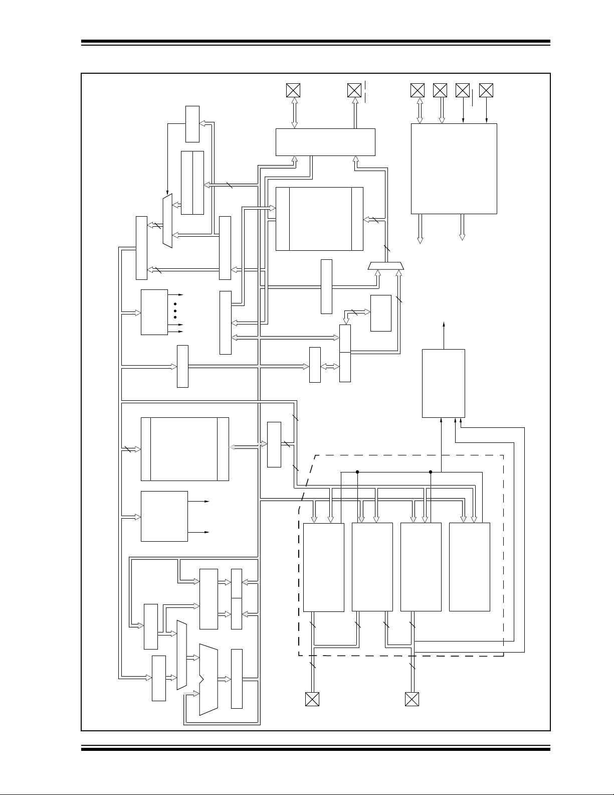
FIGURE 3-2: PIC17CR42/42A/43/R43/44 BLOCK DIAGRAM
PIC17C4X
IR BUS <16>
IR BUS<7:0>
BSR<7:4>
12
8
8
IR LATCH <16>
DECODER
INSTRUCTION
RAM ADDR BUFFER
DATA RAM
DECODE
FSR0
FSR1
CONTROL OUTPUTS
LITERAL
454 x 8 PIC17C43
454 x 8 PIC17CR43
454 x 8 PIC17C44
232 x 8 PIC17C42A
232 x 8 PIC17CR42
8
ROM LATCH <16>
TABLE LATCH <16>
DATA LATCH
MEMORY
PROGRAM
DATA LATCH
3
4
BSR
AD <15:0>
PORTC and
PORTD
SYSTEM
(EPROM/ROM)
2K x 16 - PIC17CR42
PCLATH<8>
IR <2:0>
IR <7>
BUS
FACE
INTER-
ADDRESS LATCH
8K x 16 - PIC17C44
4K x 16 - PIC17C43
4K x 16 - PIC17CR43
2K x 16 - PIC17C42A
16
TABLE PTR<16>
PCH PCL
DATA BUS <8>
, OE
PORTE
ALE, WR
13
STACK
16 x 16
16
Q1, Q2, Q3, Q4
16
DD, VSS
V
OSC1, OSC2
POWER ON RESET
WATCHDOG TIMER
CLOCK GENERATOR
CHIP_RESET
SIGNALS
CONTROL
MODULE
INTERRUPT
TEST
MCLR/VPP
TEST MODE SELECT
OSC STARTUP TIMER
SIGNALS
CONTROL
AND OTHER
TO CPU
WRF
SPACE
IN DATA
MAPPED
DECODE
IR BUS <16>
READ/WRITE
FOR REGISTERS
WREG <8>
BITOP
RDF
8 x 8 mult
ALU
DATA BUS <8>
PRODH PRODL
SHIFTER
PWM
CAPTURE
Timer1, Timer2, Timer3
86
PORTB
RB0/CAP1
RB1/CAP2
RB2/PWM1
DIGITAL I/O
PORTS A, B
8
RB2/PWM2
RB4/TCLK12
RB5/TCLK3
RB6
RB7
6
SERIAL PORT
2
6
PORTA
RA0/INT
RA1/T0CKI
RA2
RA3
RA4/RX/DT
Timer0 MODULE
T0CKI
RA1/
RA5/TX/CK
RA1/T0CKI
RA0/INT
PERIPHERALS
1996 Microchip Technology Inc. DS30412C-page 11
Page 12

PIC17C4X
TABLE 3-1:
Name
OSC1/CLKIN 19 21 37 I ST Oscillator input in crystal/resonator or RC oscillator mode.
OSC2/CLKOUT 20 22 38 O — Oscillator output. Connects to crystal or resonator in crystal
MCLR
/V
PP
RA0/INT 26 28 44 I ST RA0/INT can also be selected as an external interrupt
RA1/T0CKI 25 27 43 I ST RA1/T0CKI can also be selected as an external interrupt
RA2 24 26 42 I/O ST High voltage, high current, open drain input/output port
RA3 23 25 41 I/O ST High voltage, high current, open drain input/output port
RA4/RX/DT 22 24 40 I/O ST RA4/RX/DT can also be selected as the USART (SCI)
RA5/TX/CK 21 23 39 I/O ST RA5/TX/CK can also be selected as the USART (SCI)
RB0/CAP1 11 13 29 I/O ST RB0/CAP1 can also be the CAP1 input pin.
RB1/CAP2 12 14 30 I/O ST RB1/CAP2 can also be the CAP2 input pin.
RB2/PWM1 13 15 31 I/O ST RB2/PWM1 can also be the PWM1 output pin.
RB3/PWM2 14 16 32 I/O ST RB3/PWM2 can also be the PWM2 output pin.
RB4/TCLK12 15 17 33 I/O ST RB4/TCLK12 can also be the external clock input to
RB5/TCLK3 16 18 34 I/O ST RB5/TCLK3 can also be the external clock input to
RB6 17 19 35 I/O ST
RB7 18 20 36 I/O ST
RC0/AD0 2 3 19 I/O TTL This is also the lower half of the 16-bit wide system bus
RC1/AD1 3 4 20 I/O TTL
RC2/AD2 4 5 21 I/O TTL
RC3/AD3 5 6 22 I/O TTL
RC4/AD4 6 7 23 I/O TTL
RC5/AD5 7 8 24 I/O TTL
RC6/AD6 8 9 25 I/O TTL
RC7/AD7 9 10 26 I/O TTL
Legend: I = Input only; O = Output only; I/O = Input/Output; P = Power; — = Not Used; TTL = TTL input;
ST = Schmitt Trigger input.
PINOUT DESCRIPTIONS
DIP
PLCC
No.
32 35 7 I/P ST Master clear (reset) input/Programming Voltage (V
No.
QFP
No.
I/O/P
Type
Buffer
Type
Description
External clock input in external clock mode.
oscillator mode. In RC oscillator or external clock modes
OSC2 pin outputs CLKOUT which has one fourth the frequency of OSC1 and denotes the instruction cycle rate.
This is the active low reset input to the chip.
PORTA is a bi-directional I/O Port except for RA0 and RA1
which are input only.
input. Interrupt can be configured to be on positive or
negative edge.
input, and the interrupt can be configured to be on positive or negative edge. RA1/T0CKI can also be selected
to be the clock input to the Timer0 timer/counter.
pins.
pins.
Asynchronous Receive or USART (SCI) Synchronous
Data.
Asynchronous Transmit or USART (SCI) Synchronous
Clock.
PORTB is a bi-directional I/O Port with software configurable
weak pull-ups.
Timer1 and Timer2.
Timer3.
PORTC is a bi-directional I/O Port.
in microprocessor mode or extended microcontroller
mode. In multiplexed system bus configuration, these
pins are address output as well as data input or output.
) input.
PP
DS30412C-page 12
1996 Microchip Technology Inc.
Page 13
PIC17C4X
TABLE 3-1:
Name
RD0/AD8 40 43 15 I/O TTL This is also the upper byte of the 16-bit system bus in
RD1/AD9 39 42 14 I/O TTL
RD2/AD10 38 41 13 I/O TTL
RD3/AD11 37 40 12 I/O TTL
RD4/AD12 36 39 11 I/O TTL
RD5/AD13 35 38 10 I/O TTL
RD6/AD14 34 37 9 I/O TTL
RD7/AD15 33 36 8 I/O TTL
RE0/ALE 30 32 4 I/O TTL In microprocessor mode or extended microcontroller
RE1/OE
RE2/WR
TEST 27 29 1 I ST Test mode selection control input. Always tie to V
V
SS
V
DD
Legend: I = Input only; O = Output only; I/O = Input/Output; P = Power; — = Not Used; TTL = TTL input;
ST = Schmitt Trigger input.
PINOUT DESCRIPTIONS
DIP
PLCC
No.
29 31 3 I/O TTL In microprocessor or extended microcontroller mode, it is
28 30 2 I/O TTL In microprocessor or extended microcontroller mode, it is
10, 3111,
33, 34
1 1, 44 16, 17 P Positive supply for logic and I/O pins.
No.
12,
QFP
No.
5, 6,
27, 28
I/O/P
Buffer
Type
P Ground reference for logic and I/O pins.
Description
Type
PORTD is a bi-directional I/O Port.
microprocessor mode or extended microprocessor mode
or extended microcontroller mode. In multiplexed system
bus configuration these pins are address output as well
as data input or output.
PORTE is a bi-directional I/O Port.
mode, it is the Address Latch Enable (ALE) output.
Address should be latched on the falling edge of ALE
output.
the Output Enable (OE
the Write Enable (WR
mal operation.
) control output (active low).
) control output (active low).
for nor-
SS
1996 Microchip Technology Inc. DS30412C-page 13
Page 14
PIC17C4X
3.1 Cloc
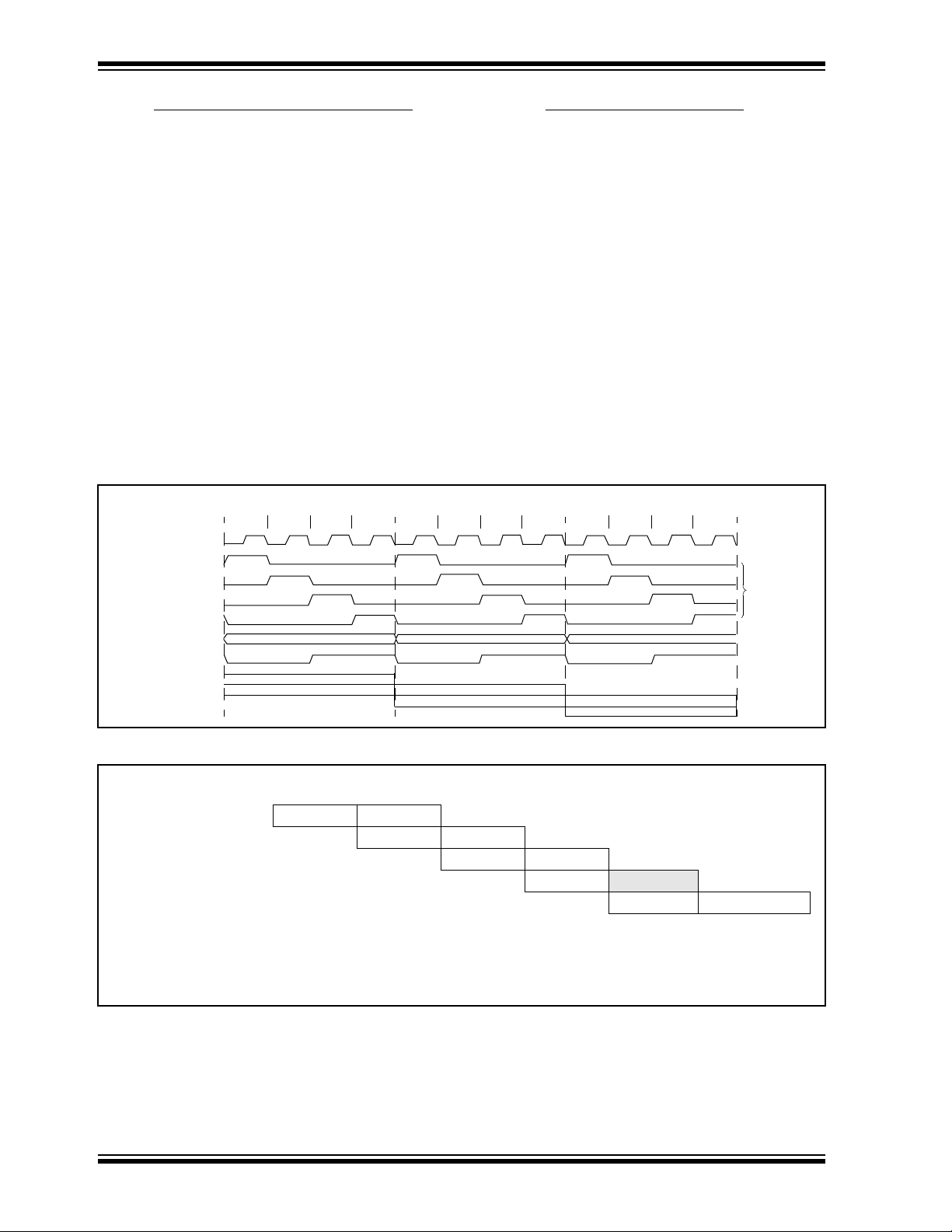
king Scheme/Instruction Cycle
The clock input (from OSC1) is internally divided by
four to generate four non-overlapping quadrature
clocks, namely Q1, Q2, Q3, and Q4. Internally , the program counter (PC) is incremented every Q1, and the
instruction is fetched from the program memory and
latched into the instruction register in Q4. The instruction is decoded and executed during the following Q1
through Q4. The clocks and instruction execution flow
are shown in Figure 3-3.
FIGURE 3-3: CLOCK/INSTRUCTION CYCLE
Q2 Q3 Q4
OSC1
Q1
Q2
Q3
Q4
PC
OSC2/CLKOUT
(RC mode)
Q1
PC PC+1 PC+2
Fetch INST (PC)
Execute INST (PC-1) Fetch INST (PC+1)
Q1
3.2 Instruction Flo
w/Pipelining
An “Instruction Cycle” consists of four Q cycles (Q1,
Q2, Q3, and Q4). The instruction fetch and execute are
pipelined such that fetch takes one instruction cycle
while decode and execute takes another instruction
cycle. However, due to the pipelining, each instruction
effectively executes in one cycle. If an instruction
causes the program counter to change (e.g. GOTO ) then
two cycles are required to complete the instruction
(Example 3-2).
A fetch cycle begins with the program counter incrementing in Q1.
In the execution cycle , the fetched instruction is latched
into the “Instruction Register (IR)” in cycle Q1. This
instruction is then decoded and executed during the
Q2, Q3, and Q4 cycles. Data memory is read during Q2
(operand read) and written during Q4 (destination
write).
Q2 Q3 Q4
Execute INST (PC) Fetch INST (PC+2)
Q2 Q3 Q4
Q1
Execute INST (PC+1)
Internal
phase
clock
EXAMPLE 3-2: INSTRUCTION PIPELINE FLOW
Tcy0 Tcy1 Tcy2 Tcy3 Tcy4 Tcy5
1. MOVLW 55h
2. MOVWF PORTB
3. CALL SUB_1
4. BSF PORTA, BIT3 (Forced NOP)
5. Instruction @ address SUB_1
All instructions are single cycle, except for any program branches. These take two cycles since the fetch
instruction is “flushed” from the pipeline while the new instruction is being fetched and then executed.
DS30412C-page 14
Fetch 1 Execute 1
Fetch 2 Execute 2
Fetch 3 Execute 3
Fetch 4 Flush
Fetch SUB_1 Execute SUB_1
1996 Microchip Technology Inc.
Page 15
PIC17C4X
4.0 RESET
The PIC17CXX differentiates between various kinds of
reset:
• Power-on Reset (POR)
• MCLR
• WDT Reset (normal operation)
Some registers are not affected in any reset condition;
their status is unknown on POR and unchanged in any
other reset. Most other registers are forced to a “reset
state” on Power-on Reset (POR), on MCLR
Reset and on M
affected by a WDT Reset during SLEEP, since this reset
is viewed as the resumption of normal operation. The
T
reset situations as indicated in T ab le 4-3. These bits are
used in software to determine the nature of reset. See
Table 4-4 for a full description of reset states of all registers.
A simplified block diagram of the on-chip reset circuit is
shown in Figure 4-1.
reset during normal operation
or WDT
CLR reset during SLEEP. They are not
O and PD bits are set or cleared differently in diff erent
Note: While the device is in a reset state, the
internal phase clock is held in the Q1 state.
Any processor mode that allows external
execution will force the RE0/ALE pin as a
low output and the RE1/OE
and RE2/WR
pins as high outputs.
4.1 P
ower-on Reset (POR), Power-up
Timer (PWRT), and Oscillator Start-up
Timer (OST)
4.1.1 POWER-ON RESET (POR)
The Power-on Reset circuit holds the device in reset
until V
2.3V). The PIC17C42 does not produce an internal
reset when V
an internal reset for both rising and falling V
advantage of the POR, just tie the MCLR
directly (or through a resistor) to V
external RC components usually needed to create
Power-on Reset. A minimum rise time for V
required. See Electrical Specifications for details.
4.1.2 PO WER-UP TIMER (PWRT)
The Power-up Timer provides a fixed 96 ms time-out
(nominal) on power-up. This occurs from rising edge of
the POR signal and after the first rising edge of MCLR
(detected high). The Power-up Timer operates on an
internal RC oscillator. The chip is kept in RESET as
long as the PWRT is active. In most cases the PWRT
delay allows the V
The power-up time delay will v ary from chip to chip and
to V
details.
is above the trip point (in the range of 1.4V -
DD
DD
declines. All other de vices will produce
DD
. To take
/V
. This will eliminate
DD
DD
to rise to an acceptable level.
DD
and temperature. See DC parameters for
PP
DD
pin
is
FIGURE 4-1: SIMPLIFIED BLOCK DIAGRAM OF ON-CHIP RESET CIRCUIT
External
Reset
MCLR
WDT
Module
V
DD rise
detect
VDD
OSC1
† This RC oscillator is shared with the WDT
OST/PWRT
On-chip
RC OSC†
when not in a power-up sequence.
WDT
Time_Out
Reset
Power_On_Reset
OST
10-bit Ripple counter
PWRT
10-bit Ripple counter
Enable PWRT
Enable OST
Power_Up
(Enable the PWRT timer
only during Power_Up)
(Power_Up + Wake_Up) (XT + LF)
(Enable the OST if it is Power_Up or Wake_Up
from SLEEP and OSC type is XT or LF)
S
Chip_Reset
R
Q
1996 Microchip Technology Inc. DS30412C-page 15
Page 16
PIC17C4X
4.1.3 OSCILLATOR START-UP TIMER (OST)
The Oscillator Start-up Timer (OST) provides a 1024
oscillator cycle (1024T
) delay after MCLR
OSC
is
detected high or a wake-up from SLEEP event occurs.
The OST time-out is invoked only f or XT and LF oscilla-
tor modes on a Power-on Reset or a Wake-up from
SLEEP.
The OST counts the oscillator pulses on the
OSC1/CLKIN pin. The counter only starts incrementing
after the amplitude of the signal reaches the oscillator
input thresholds. This delay allows the crystal oscillator
or resonator to stabilize before the device exits reset.
The length of time-out is a function of the crystal/resonator frequency.
4.1.4 TIME-OUT SEQUENCE
On power-up the time-out sequence is as follows: First
the internal POR signal goes high when the POR trip
point is reached. If MCLR
is high, then both the OST
and PWRT timers start. In general the PWRT time-out
is longer, except with low frequency crystals/resonators. The total time-out also varies based on oscillator
configuration. Table 4-1 shows the times that are associated with the oscillator configuration. Figure 4-2 and
Figure 4-3 display these time-out sequences.
If the device voltage is not within electrical specification
at the end of a time-out, the MCLR
/V
PP
pin must be
held low until the voltage is within the device specification. The use of an external RC delay is sufficient for
many of these applications.
TABLE 4-1: TIME-OUT IN VARIOUS
SITUATIONS
Oscillator
Configuration
XT, LF Greater of:
Power-up Wake up
from
SLEEP
OSC
1024T
96 ms or
1024T
OSC
EC, RC Greater of:
——
96 ms or
1024T
OSC
The time-out sequence begins from the first rising edge
of MCLR
.
Table 4-3 shows the reset conditions for some special
registers, while Table 4-4 shows the initialization conditions for all the registers. The shaded registers (in
Table 4-4) are for all devices except the PIC17C42. In
the PIC17C42, the PRODH and PRODL registers are
general purpose RAM.
MCLR
Reset
—
TABLE 4-2: STATUS BITS AND THEIR
SIGNIFICANCE
TOPD
11
10
01
00
Power-on Reset, MCLR Reset during normal
operation, or
MCLR Reset during SLEEP or interrupt wake-up
from SLEEP
WDT Reset during normal operation
WDT Reset during SLEEP
Event
CLRWDT instruction executed
In Figure 4-2, Figure 4-3 and Figure 4-4, T
T
, as would be the case in higher frequency crys-
OST
tals. For lower frequency crystals, (i.e., 32 kHz) T
PWRT
>
OST
would be greater.
T AB LE 4-3: RESET CONDITION FOR THE PROGRAM COUNTER AND THE CPUSTA REGISTER
Event
Power-on Reset 0000h
MCLR Reset during normal operation 0000h
Reset during SLEEP 0000h
MCLR
WDT Reset during normal operation 0000h
WDT Reset during SLEEP
(3)
Interrupt wake-up from SLEEP GLINTD is set PC + 1
GLINTD is clear
Legend: u = unchanged, x = unknown, - = unimplemented read as '0'.
Note 1: On wake-up, this instruction is executed. The instruction at the appropriate interrupt vector is fetched and
then executed.
2: The OST is only active when the Oscillator is configured for XT or LF modes.
3: The Program Counter = 0, that is the device branches to the reset vector. This is different from the
mid-range devices.
PCH:PCL CPUSTA OST Active
0000h
PC + 1
(1)
--11 11--
--11 11--
--11 10--
--11 01--
--11 00--
--11 10--
--10 10--
Yes
No
Yes
No
Yes
Yes
Yes
(2)
(2)
(2)
(2)
DS30412C-page 16
1996 Microchip Technology Inc.
Page 17
PIC17C4X
FIGURE 4-2: TIME-OUT SEQUENCE ON POWER-UP (MCLR
VDD
MCLR
INTERNAL POR
TPWRT
PWRT TIME-OUT
OST TIME-OUT
INTERNAL RESET
TOST
FIGURE 4-3: TIME-OUT SEQUENCE ON POWER-UP (MCLR
VDD
MCLR
INTERNAL POR
TIED TO V
DD
)
NOT TIED TO V
DD
)
PWRT TIME-OUT
OST TIME-OUT
INTERNAL RESET
FIGURE 4-4: SLOW RISE TIME (MCLR
VDD
MCLR
INTERNAL POR
T TIME-OUT
PWR
OST TIME-OUT
INTERNAL RESET
0V
TIED TO V
TPWRT
DD
TOST
TPWRT
TOST
)
5V
1V
1996 Microchip Technology Inc. DS30412C-page 17
Page 18
PIC17C4X
FIGURE 4-5: OSCILLATOR START-UP TIME
VDD
MCLR
OSC2
OSC1
T
OST TIME_OUT
PWRT TIME_OUT
INTERNAL RESET
This figure shows in greater detail the timings involved
with the oscillator start-up timer. In this example the
low frequency crystal start-up time is larger than
power-up time (TPWRT).
Tosc1 = time for the crystal oscillator to react to an
oscillation level detectable by the Oscillator Start-up
Timer (ost).
TOST = 1024TOSC.
TPWRT
T
OST
FIGURE 4-6: USING ON-CHIP POR
VDD
VDD
MCLR
PIC17CXX
FIGURE 4-8: PIC17C42 EXTERNAL
POWER-ON RESET CIRCUIT
(FOR SLOW V
DD
POWER-UP)
V
VDD
Note 1: An external Power-on Reset circuit is
2: R < 40 kΩ is recommended to ensure
3: R1 = 100Ω to 1 kΩ will limit any current
DD
D
R
R1
MCLR
C
required only if V
PIC17C42
DD power-up time is too
slow. The diode D helps discharge the
capacitor quickly when V
DD powers
down.
that the voltage drop across R does not
exceed 0.2V (max. leakage current spec.
on the MCLR
voltage drop will degrade V
MCLR
flowing into MCLR
tor C in the event of MCLR
/VPP pin is 5 µA). A larger
IH level on the
/VPP pin.
from external capaci-
/VPP pin
breakdown due to Electrostatic Discharge (ESD) or (Electrical Overstress)
EOS.
FIGURE 4-7: BROWN-OUT PROTECTION
CIRCUIT 1
VDD
DD
V
33k
10k
This circuit will activate reset when VDD goes below
(Vz + 0.7V) where Vz = Zener voltage.
40 kΩ
MCLR
PIC17CXX
FIGURE 4-9: BROWN-OUT PROTECTION
CIRCUIT 2
V
DD
VDD
R1
Q1
MCLR
R2
This brown-out circuit is less expensive, albeit less
accurate. Transistor Q1 turns off when VDD is below a
certain level such that:
VDD •
40 kΩ
R1
R1 + R2
PIC17CXX
= 0.7V
DS30412C-page 18
1996 Microchip Technology Inc.
Page 19

PIC17C4X
TABLE 4-4: INITIALIZATION CONDITIONS FOR SPECIAL FUNCTION REGISTERS
Register Address Power-on Reset
Reset
MCLR
WDT Reset
Wake-up from SLEEP
through interrupt
Unbanked
INDF0 00h
FSR0 01h
PCL 02h
PCLATH 03h
ALUSTA 04h
T0STA 05h
CPUSTA
(3)
06h --11 11-- --11 qq-- --uu qq--
INTSTA 07h 0000 0000 0000 0000
0000 0000 0000 0000 0000 0000
xxxx xxxx uuuu uuuu uuuu uuuu
0000h 0000h
PC + 1
(2)
0000 0000 0000 0000 uuuu uuuu
1111 xxxx 1111 uuuu 1111 uuuu
0000 000- 0000 000- 0000 000-
uuuu uuuu
(1)
INDF1 08h 0000 0000 0000 0000 uuuu uuuu
FSR1 09h xxxx xxxx uuuu uuuu uuuu uuuu
WREG 0Ah xxxx xxxx uuuu uuuu uuuu uuuu
TMR0L 0Bh xxxx xxxx uuuu uuuu uuuu uuuu
TMR0H 0Ch xxxx xxxx uuuu uuuu uuuu uuuu
TBLPTRL
TBLPTRH
TBLPTRL
TBLPTRH
(4)
(4)
(5)
(5)
0Dh xxxx xxxx uuuu uuuu uuuu uuuu
0Eh xxxx xxxx uuuu uuuu uuuu uuuu
0Dh 0000 0000 0000 0000 uuuu uuuu
0Eh 0000 0000 0000 0000 uuuu uuuu
BSR 0Fh 0000 0000 0000 0000 uuuu uuuu
Bank 0
PORTA 10h 0-xx xxxx 0-uu uuuu uuuu uuuu
DDRB 11h 1111 1111 1111 1111 uuuu uuuu
PORTB 12h xxxx xxxx uuuu uuuu uuuu uuuu
RCSTA 13h 0000 -00x 0000 -00u uuuu -uuu
RCREG 14h xxxx xxxx uuuu uuuu uuuu uuuu
TXSTA 15h 0000 --1x 0000 --1u uuuu --uu
TXREG 16h xxxx xxxx uuuu uuuu uuuu uuuu
SPBRG 17h xxxx xxxx uuuu uuuu uuuu uuuu
Bank 1
DDRC 10h 1111 1111 1111 1111 uuuu uuuu
PORTC 11h xxxx xxxx uuuu uuuu uuuu uuuu
DDRD 12h 1111 1111 1111 1111 uuuu uuuu
PORTD 13h xxxx xxxx uuuu uuuu uuuu uuuu
DDRE 14h ---- -111 ---- -111 ---- -uuu
PORTE 15h ---- -xxx ---- -uuu ---- -uuu
PIR 16h 0000 0010 0000 0010
uuuu uuuu
(1)
PIE 17h 0000 0000 0000 0000 uuuu uuuu
Legend: u = unchanged, x = unknown, - = unimplemented read as '0', q = value depends on condition.
Note 1: One or more bits in INTSTA, PIR will be affected (to cause wake-up).
2: When the wake-up is due to an interrupt and the GLINTD bit is cleared, the PC is loaded with the interrupt
vector.
3: See Table 4-3 for reset value of specific condition.
4: Only applies to the PIC17C42.
5: Does not apply to the PIC17C42.
1996 Microchip Technology Inc. DS30412C-page 19
Page 20
PIC17C4X
TABLE 4-4: INITIALIZATION CONDITIONS FOR SPECIAL FUNCTION REGISTERS (Cont.’d)
Reset
Register Address Power-on Reset
Bank 2
TMR1 10h xxxx xxxx uuuu uuuu uuuu uuuu
TMR2 11h xxxx xxxx uuuu uuuu uuuu uuuu
TMR3L 12h xxxx xxxx uuuu uuuu uuuu uuuu
TMR3H 13h xxxx xxxx uuuu uuuu uuuu uuuu
PR1 14h xxxx xxxx uuuu uuuu uuuu uuuu
PR2 15h xxxx xxxx uuuu uuuu uuuu uuuu
PR3/CA1L 16h xxxx xxxx uuuu uuuu uuuu uuuu
PR3/CA1H 17h xxxx xxxx uuuu uuuu uuuu uuuu
Bank 3
PW1DCL 10h xx-- ---- uu-- ---- uu-- ----
PW2DCL 11h xx-- ---- uu-- ---- uu-- ----
PW1DCH 12h xxxx xxxx uuuu uuuu uuuu uuuu
PW2DCH 13h xxxx xxxx uuuu uuuu uuuu uuuu
CA2L 14h xxxx xxxx uuuu uuuu uuuu uuuu
CA2H 15h xxxx xxxx uuuu uuuu uuuu uuuu
TCON1 16h 0000 0000 0000 0000 uuuu uuuu
TCON2 17h 0000 0000 0000 0000 uuuu uuuu
Unbanked
PRODL
PRODH
Legend: u = unchanged, x = unknown, - = unimplemented read as '0', q = value depends on condition.
Note 1: One or more bits in INTSTA, PIR will be affected (to cause wake-up).
(5)
(5)
2: When the wake-up is due to an interrupt and the GLINTD bit is cleared, the PC is loaded with the interrupt
vector.
3: See Table 4-3 for reset value of specific condition.
4: Only applies to the PIC17C42.
5: Does not apply to the PIC17C42.
18h xxxx xxxx uuuu uuuu uuuu uuuu
19h xxxx xxxx uuuu uuuu uuuu uuuu
MCLR
WDT Reset
Wake-up from SLEEP
through interrupt
DS30412C-page 20 1996 Microchip Technology Inc.
Page 21
PIC17C4X
5.0 INTERRUPTS
The PIC17C4X devices have 11 sources of interrupt:
• External interrupt from the RA0/INT pin
• Change on RB7:RB0 pins
• TMR0 Overflow
• TMR1 Overflow
• TMR2 Overflow
• TMR3 Overflow
• USART Transmit buffer empty
• USART Receive buffer full
• Capture1
• Capture2
• T0CKI edge occurred
There are four registers used in the control and status
of interrupts. These are:
• CPUSTA
• INTSTA
• PIE
• PIR
The CPUSTA register contains the GLINTD bit. This is
the Global Interrupt Disable bit. When this bit is set, all
interrupts are disabled. This bit is par t of the controller
core functionality and is described in the Memory Organization section.
When an interrupt is responded to, the GLINTD bit is
automatically set to disable any further interrupt, the
return address is pushed onto the stack and the PC is
loaded with the interrupt vector address. There are four
interrupt vectors. Each vector address is for a specific
interrupt source (except the peripheral interrupts which
have the same vector address). These sources are:
• External interrupt from the RA0/INT pin
• TMR0 Overflow
• T0CKI edge occurred
• Any peripheral interrupt
When program execution vectors to one of these inter-
rupt vector addresses (except for the peripheral interrupt address), the interrupt flag bit is automatically
cleared. Vectoring to the peripheral interrupt vector
address does not automatically clear the source of the
interrupt. In the peripheral interrupt service routine, the
source(s) of the interrupt can be determined by testing
the interrupt flag bits. The interr upt flag bit(s) must be
cleared in software before re-enabling interrupts to
avoid infinite interrupt requests.
All of the individual interrupt flag bits will be set regardless of the status of their corresponding mask bit or the
GLINTD bit.
For external interrupt events, there will be an interrupt
latency. For two cycle instructions, the latency could be
one instruction cycle longer.
The “return from interrupt” instruction, RETFIE , can be
used to mark the end of the interrupt service routine.
When this instruction is executed, the stack is
“POPed”, and the GLINTD bit is cleared (to re-enable
interrupts).
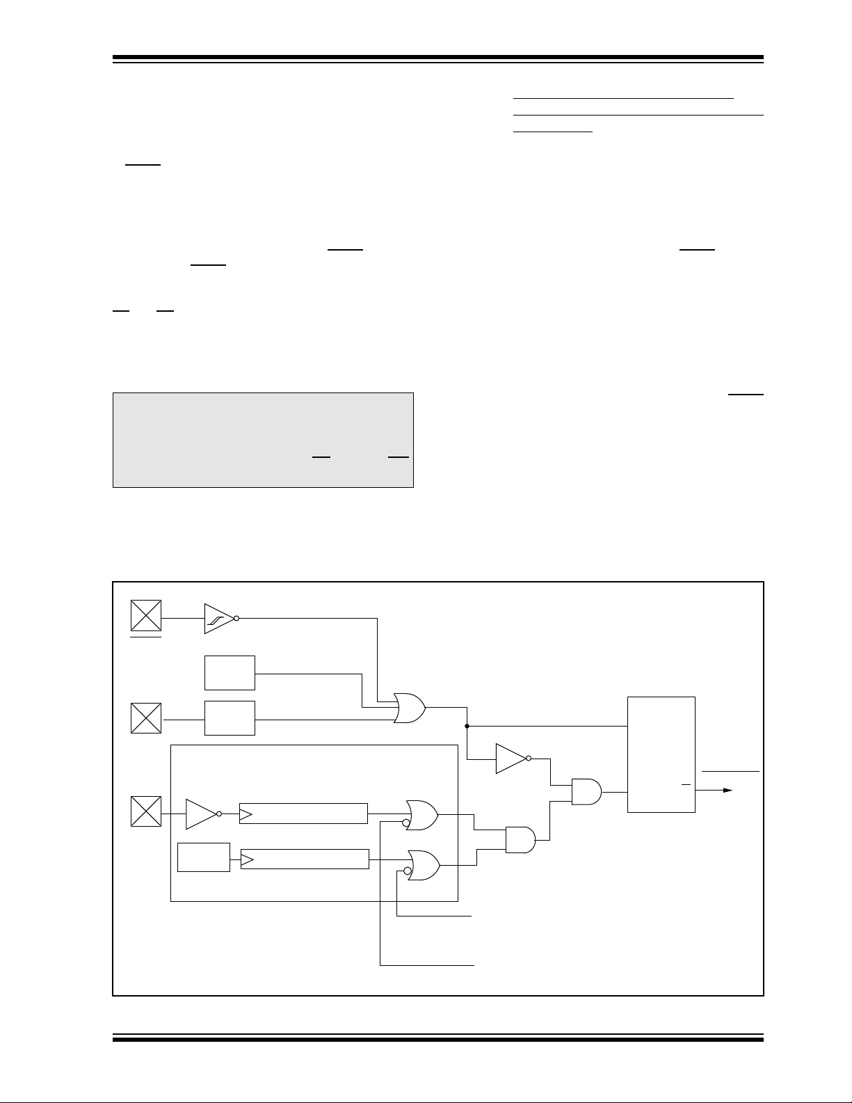
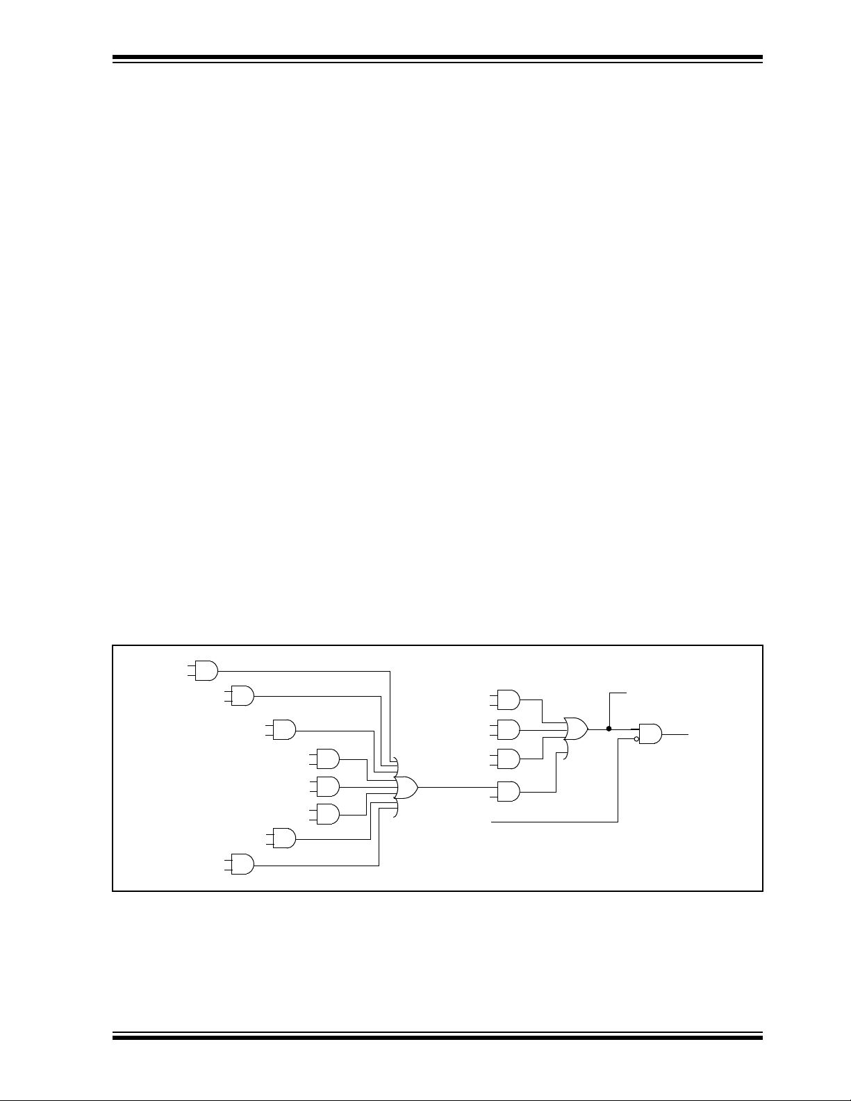
FIGURE 5-1: INTERRUPT LOGIC
TMR1IF
TMR1IE
TMR2IF
TMR2IE
TMR3IF
TMR3IE
CA1IF
CA1IE
CA2IF
CA2IE
TXIF
TXIE
RCIF
RCIE
RBIF
RBIE
T0IF
T0IE
INTF
INTE
T0CKIF
T0CKIE
PEIF
PEIE
GLINTD
Wake-up (If in SLEEP mode)
or terminate long write
Interrupt to CPU
1996 Microchip Technology Inc. DS30412C-page 21
Page 22

PIC17C4X
5.1 Interrupt
The Interrupt Status/Control register (INTSTA) records
the individual interrupt requests in flag bits, and contains the individual interrupt enable bits (not for the
peripherals).
The PEIF bit is a read only , bit wise OR of all the peripheral flag bits in the PIR register (Figure 5-4).
Status Register (INTSTA)
Note: T0IF, INTF, T0CKIF, or PEIF will be set by
the specified condition, even if the corresponding interrupt enable bit is clear (interrupt disabled) or the GLINTD bit is set (all
interrupts disabled).
Care should be taken when clearing any of the INTSTA
register enable bits when interrupts are enabled
(GLINTD is clear). If any of the INTSTA flag bits (T0IF,
INTF, T0CKIF, or PEIF) are set in the same instruction
cycle as the corresponding interrupt enable bit is
cleared, the device will vector to the reset address
(0x00).
When disabling any of the INTSTA enable bits, the
GLINTD bit should be set (disabled).
FIGURE 5-2: INTSTA REGISTER (ADDRESS: 07h, UNBANKED)
R - 0 R/W - 0 R/W - 0 R/W - 0 R/W - 0 R/W - 0 R/W - 0 R/W - 0
PEIF T0CKIF T0IF INTF PEIE T0CKIE T0IE INTE
bit7 bit0
bit 7: PEIF : Peripheral Interrupt Flag bit
This bit is the OR of all peripheral interrupt flag bits AND’ed with their corresponding enable bits.
1 =A peripheral interrupt is pending
0 =No peripheral interrupt is pending
bit 6: T0CKIF : External Interrupt on T0CKI Pin Flag bit
This bit is cleared by hardware, when the interrupt logic forces program execution to vector (18h).
1 =The software specified edge occurred on the RA1/T0CKI pin
0 =The software specified edge did not occur on the RA1/T0CKI pin
bit 5: T0IF : TMR0 Overflow Interrupt Flag bit
This bit is cleared by hardware, when the interrupt logic forces program execution to vector (10h).
1 =TMR0 overflowed
0 =TMR0 did not overflow
bit 4: INTF : External Interrupt on INT Pin Flag bit
This bit is cleared by hardware, when the interrupt logic forces program execution to vector (08h).
1 =The software specified edge occurred on the RA0/INT pin
0 =The software specified edge did not occur on the RA0/INT pin
bit 3: PEIE : Peripheral Interrupt Enable bit
This bit enables all peripheral interrupts that have their corresponding enable bits set.
1 =Enable peripheral interrupts
0 =Disable peripheral interrupts
bit 2: T0CKIE : External Interrupt on T0CKI Pin Enable bit
1 =Enable software specified edge interrupt on the RA1/T0CKI pin
0 =Disable interrupt on the RA1/T0CKI pin
bit 1: T0IE : TMR0 Overflow Interrupt Enable bit
1 =Enable TMR0 overflow interrupt
0 =Disable TMR0 overflow interrupt
bit 0: INTE : External Interrupt on RA0/INT Pin Enable bit
1 =Enable software specified edge interrupt on the RA0/INT pin
0 =Disable software specified edge interrupt on the RA0/INT pin
R = Readable bit
W = Writable bit
- n = Value at POR reset
DS30412C-page 22
1996 Microchip Technology Inc.
Page 23

PIC17C4X
5.2 P
eripheral Interrupt Enable Register
(PIE)
This register contains the individual flag bits for the
Peripheral interrupts.
FIGURE 5-3: PIE REGISTER (ADDRESS: 17h, BANK 1)
R/W - 0 R/W - 0 R/W - 0 R/W - 0 R/W - 0 R/W - 0 R/W - 0 R/W - 0
RBIE TMR3IE TMR2IE TMR1IE CA2IE CA1IE TXIE RCIE
bit7 bit0
bit 7: RBIE : PORTB Interrupt on Change Enable bit
1 =Enable PORTB interrupt on change
0 =Disable PORTB interrupt on change
bit 6: TMR3IE : Timer3 Interrupt Enable bit
1 =Enable Timer3 interrupt
0 =Disable Timer3 interrupt
bit 5: TMR2IE : Timer2 Interrupt Enable bit
1 =Enable Timer2 interrupt
0 =Disable Timer2 interrupt
bit 4: TMR1IE : Timer1 Interrupt Enable bit
1 =Enable Timer1 interrupt
0 =Disable Timer1 interrupt
bit 3: CA2IE : Capture2 Interrupt Enable bit
1 =Enable Capture interrupt on RB1/CAP2 pin
0 =Disable Capture interrupt on RB1/CAP2 pin
bit 2: CA1IE : Capture1 Interrupt Enable bit
1 =Enable Capture interrupt on RB2/CAP1 pin
0 =Disable Capture interrupt on RB2/CAP1 pin
bit 1: TXIE : USART Transmit Interrupt Enable bit
1 =Enable Transmit buffer empty interrupt
0 =Disable Transmit buffer empty interrupt
bit 0: RCIE : USART Receive Interrupt Enable bit
1 =Enable Receive buffer full interrupt
0 =Disable Receive buffer full interrupt
R = Readable bit
W = Writable bit
-n = Value at POR reset
1996 Microchip Technology Inc. DS30412C-page 23
Page 24

PIC17C4X
5.3 P
eripheral Interrupt Request Register
Note: These bits will be set by the specified con-
(PIR)
This register contains the individual flag bits for the
peripheral interrupts.
FIGURE 5-4: PIR REGISTER (ADDRESS: 16h, BANK 1)
R/W - 0 R/W - 0 R/W - 0 R/W - 0 R/W - 0 R/W - 0 R - 1 R - 0
RBIF TMR3IF TMR2IF TMR1IF CA2IF CA1IF TXIF RCIF
bit7 bit0
bit 7: RBIF : PORTB Interrupt on Change Flag bit
1 =One of the PORTB inputs changed (Software must end the mismatch condition)
0 =None of the PORTB inputs have changed
bit 6: TMR3IF : Timer3 Interrupt Flag bit
If Capture1 is enabled (CA1/PR
1 =Timer3 overflowed
0 =Timer3 did not overflow
If Capture1 is disabled (CA1/PR
1 =Timer3 value has rolled over to 0000h from equalling the period register (PR3H:PR3L) value
0 =Timer3 value has not rolled over to 0000h from equalling the period register (PR3H:PR3L) value
bit 5: TMR2IF : Timer2 Interrupt Flag bit
1 =Timer2 value has rolled over to 0000h from equalling the period register (PR2) value
0 =Timer2 value has not rolled over to 0000h from equalling the period register (PR2) value
bit 4: TMR1IF : Timer1 Interrupt Flag bit
If Timer1 is in 8-bit mode (T16 = 0)
1 =Timer1 value has rolled over to 0000h from equalling the period register (PR) value
0 =Timer1 value has not rolled over to 0000h from equalling the period register (PR2) value
If Timer1 is in 16-bit mode (T16 = 1)
1 =TMR1:TMR2 value has rolled over to 0000h from equalling the period register (PR1:PR2) value
0 =TMR1:TMR2 value has not rolled over to 0000h from equalling the period register (PR1:PR2) value
bit 3: CA2IF : Capture2 Interrupt Flag bit
1 =Capture event occurred on RB1/CAP2 pin
0 =Capture event did not occur on RB1/CAP2 pin
bit 2: CA1IF : Capture1 Interrupt Flag bit
1 =Capture event occurred on RB0/CAP1 pin
0 =Capture event did not occur on RB0/CAP1 pin
bit 1: TXIF : USART Transmit Interrupt Flag bit
1 =Transmit buffer is empty
0 =Transmit buffer is full
bit 0: RCIF : USART Receive Interrupt Flag bit
1 =Receive buffer is full
0 =Receive buffer is empty
3 = 1)
3 = 0)
dition, even if the corresponding interrupt
enable bit is cleared (interrupt disabled), or
the GLINTD bit is set (all interrupts disabled). Before enabling an interrupt, the
user may wish to clear the interrupt flag to
ensure that the program does not immediately branch to the peripheral interrupt service routine.
R = Readable bit
W = Writable bit
-n = Value at POR reset
DS30412C-page 24
1996 Microchip Technology Inc.
Page 25

PIC17C4X
5.4 Interrupt
Global Interrupt Disable bit, GLINTD (CPUSTA<4>),
enables all unmasked interrupts (if clear) or disables all
interrupts (if set). Individual interrupts can be disabled
through their corresponding enable bits in the INTSTA
register. Peripheral interrupts need either the global
peripheral enable PEIE bit disabled, or the specific
peripheral enable bit disabled. Disabling the peripherals via the global peripheral enable bit, disables all
peripheral interrupts. GLINTD is set on reset (interrupts
disabled).
The RETFIE instruction allows returning from interrupt
and re-enable interrupts at the same time.
When an interrupt is responded to, the GLINTD bit is
automatically set to disable any further interrupt, the
return address is pushed onto the stack and the PC is
loaded with interrupt vector. There are four interrupt
vectors to reduce interrupt latency.
The peripheral interrupt vector has multiple interrupt
sources. Once in the peripheral interrupt service routine, the source(s) of the interrupt can be determined by
polling the interrupt flag bits. The per ipheral interrupt
flag bit(s) must be cleared in software before reenabling interrupts to avoid continuous interrupts.
The PIC17C4X devices have four interrupt vectors.
These vectors and their hardware priority are shown in
Table 5-1. If two enabled interrupts occur “at the same
time”, the interrupt of the highest priority will be serviced first. This means that the vector address of that
interrupt will be loaded into the program counter (PC).
Operation
TABLE 5-1: INTERRUPT VECTORS/
PRIORITIES
Address Vector Priority
0008h External Interrupt on RA0/
INT pin (INTF)
0010h TMR0 overflow interrupt
(T0IF)
0018h External Interrupt on T0CKI
(T0CKIF)
0020h Peripherals (PEIF) 4 (Lowest)
1 (Highest)
2
3
Note 1: Individual interrupt flag bits are set regard-
less of the status of their corresponding
mask bit or the GLINTD bit.
Note 2: When disabling any of the INTSTA enable
bits, the GLINTD bit should be set
(disabled).
Note 3: For the PIC17C42 only:
If an interrupt occurs while the Global Interrupt Disable (GLINTD) bit is being set, the
GLINTD bit may unintentionally be reenabled by the user’s Interrupt Service
Routine (the RETFIE instruction). The
events that would cause this to occur are:
1. An interrupt occurs simultaneously
with an instruction that sets the
GLINTD bit.
2. The program branches to the Interrupt
vector and executes the Interrupt Service Routine.
3. The Interrupt Service Routine completes with the execution of the RET-
FIE instruction. This causes the
GLINTD bit to be cleared (enables
interrupts), and the program returns to
the instruction after the one which was
meant to disable interrupts.
The method to ensure that interrupts are
globally disabled is:
1. Ensure that the GLINTD bit was set by
the instruction, as shown in the following code:
LOOP BSF CPUSTA, GLINTD ; Disable Global
; Interrupt
BTFSS CPUSTA, GLINTD ; Global Interrupt
; Disabled?
GOTO LOOP ; NO, try again
; YES, continue
; with program
; low
1996 Microchip Technology Inc. DS30412C-page 25
Page 26
PIC17C4X
5.5 RA0/
The external interrupt on the RA0/INT pin is edge triggered. Either the rising edge, if INTEDG bit
(T0STA<7>) is set, or the falling edge, if INTEDG bit is
clear. When a valid edge appears on the RA0/INT pin,
the INTF bit (INTSTA<4>) is set. This interrupt can be
disabled by clearing the INTE control bit (INTSTA<0>).
The INT interrupt can wake the processor from SLEEP.
See Section 14.4 for details on SLEEP operation.
INT Interrupt
5.7 T0CK
The external interrupt on the RA1/T0CKI pin is edge
triggered. Either the rising edge, if the T0SE bit
(T0STA<6>) is set, or the falling edge, if the T0SE bit is
clear. When a valid edge appears on the RA1/T0CKI
pin, the T0CKIF bit (INTSTA<6>) is set. This interr upt
can be disabled by clearing the T0CKIE control bit
(INTSTA<2>). The T0CKI interrupt can wake up the
processor from SLEEP. See Section 14.4 for details on
SLEEP operation.
5.6 TMR0
Interrupt
5.8 P
An overflow (FFFFh → 0000h) in TMR0 will set the
T0IF (INTSTA<5>) bit. The interrupt can be enabled/
disabled by setting/clearing the T0IE control bit
(INTSTA<1>). For operation of the Timer0 module, see
Section 11.0.
The peripheral interrupt flag indicates that at least one
of the peripheral interrupts occurred (PEIF is set). The
PEIF bit is a read only bit, and is a bit wise OR of all the
flag bits in the PIR register AND’ed with the corresponding enable bits in the PIE register. Some of the
peripheral interrupts can wake the processor from
SLEEP. See Section 14.4 for details on SLEEP operation.
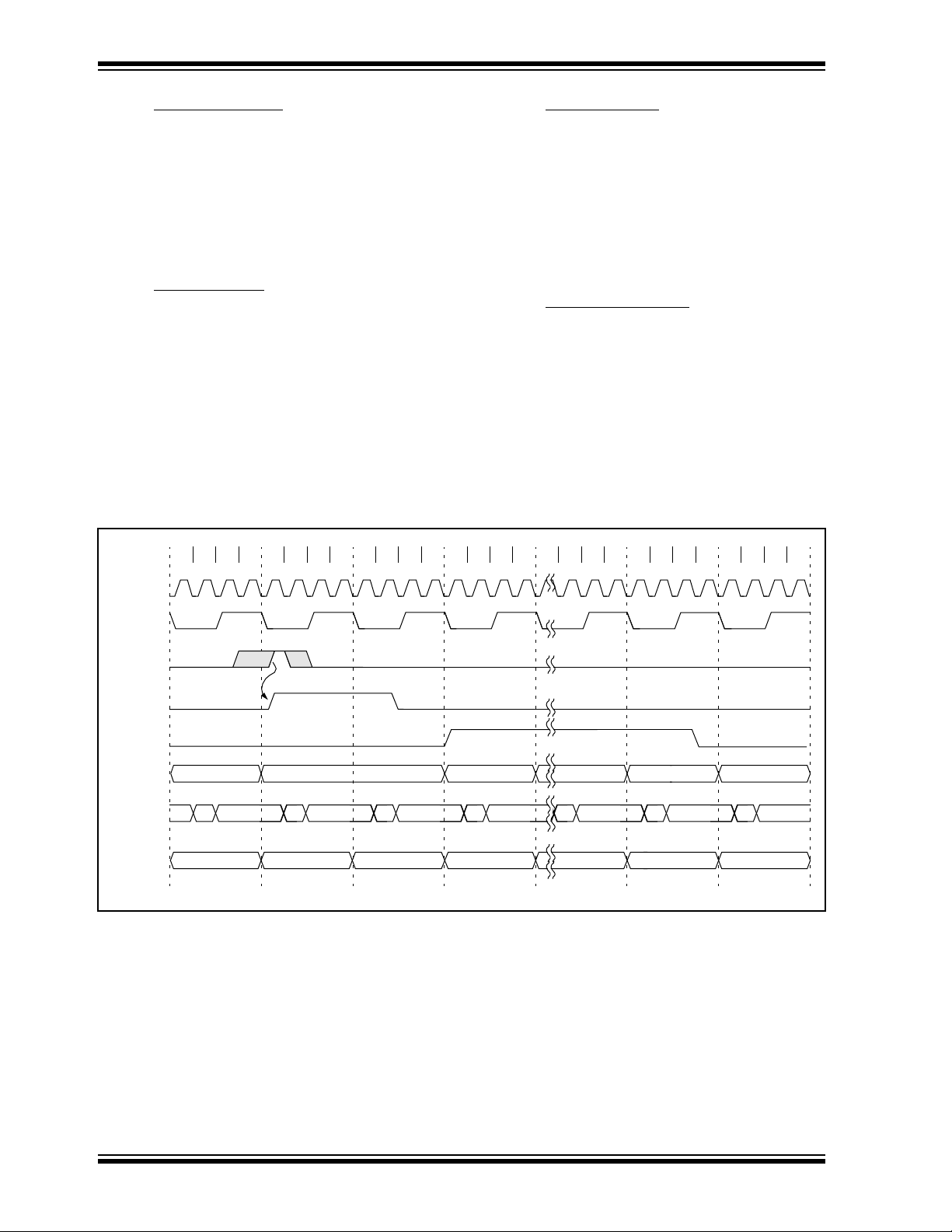
FIGURE 5-5: INT PIN / T0CKI PIN INTERRUPT TIMING
I Interrupt
eripheral Interrupt
OSC1
OSC2
RA0/INT or
RA1/T0CKI
INTF or
T0CKIF
GLINTD
PC
System Bus
Instruction
Fetched
Instruction
executed
Q2Q1 Q3 Q4 Q2Q1 Q3 Q4 Q2Q1 Q3 Q4 Q2Q1 Q3 Q4 Q2Q1 Q3 Q4 Q2Q1 Q3 Q4 Q2Q1 Q3 Q4
PC PC + 1 Addr (Vector)
PC Inst (PC) Inst (PC+1)
Addr
Inst (PC) Dummy Dummy
Addr
Inst (PC+1)
Addr
Inst (Vector)
YY YY + 1
Addr Addr
RETFIE
RETFIE
PC + 1
Inst (YY + 1)
Dummy
DS30412C-page 26
1996 Microchip Technology Inc.
Page 27

PIC17C4X
5.9 Conte
During an interrupt, only the returned PC value is saved
on the stack. Typically, users may wish to save key registers during an interrupt; e.g. WREG, ALUSTA and the
BSR registers. This requires implementation in software.
xt Saving During Interrupts
Example 5-1 shows the saving and restoring of information for an interrupt service routine. The PUSH and
POP routines could either be in each interrupt service
routine or could be subroutines that were called.
Depending on the application, other registers may also
need to be saved, such as PCLATH.
EXAMPLE 5-1: SAVING STATUS AND WREG IN RAM
;
; The addresses that are used to store the CPUSTA and WREG values
; must be in the data memory address range of 18h - 1Fh. Up to
; 8 locations can be saved and restored using
; the MOVFP instruction. This instruction neither affects the status
; bits, nor corrupts the WREG register.
;
;
PUSH MOVFP WREG, TEMP_W ; Save WREG
MOVFP ALUSTA, TEMP_STATUS ; Save ALUSTA
MOVFP BSR, TEMP_BSR ; Save BSR
ISR : ; This is the interrupt service routine
:
POP MOVFP TEMP_W, WREG ; Restore WREG
MOVFP TEMP_STATUS, ALUSTA ; Restore ALUSTA
MOVFP TEMP_BSR, BSR ; Restore BSR
RETFIE ; Return from Interrupts enabled
1996 Microchip Technology Inc. DS30412C-page 27
Page 28

PIC17C4X
NOTES:
DS30412C-page 28
1996 Microchip Technology Inc.
Page 29
PIC17C4X
6.0 MEMORY ORGANIZATION
There are two memory blocks in the PIC17C4X; program memory and data memory. Each block has its
own bus, so that access to each bloc k can occur during
the same oscillator cycle.
The data memory can further be broken down into General Purpose RAM and the Special Function Registers
(SFRs). The operation of the SFRs that control the
“core” are described here. The SFRs used to control
the peripheral modules are described in the section discussing each individual peripheral module.
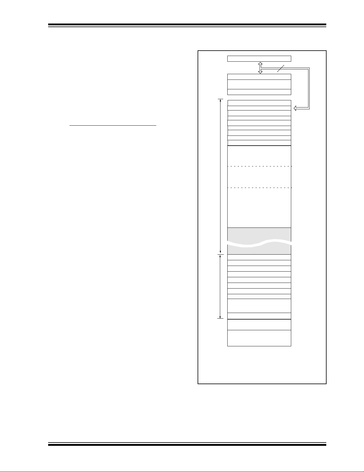
6.1 Pr
PIC17C4X devices have a 16-bit program counter
capable of addressing a 64K x 16 program memory
space. The reset vector is at 0000h and the interrupt
vectors are at 0008h, 0010h, 0018h, and 0020h
(Figure 6-1).
6.1.1 PROGRAM MEMORY OPERATION
The PIC17C4X can operate in one of four possible pro-
gram memory configurations. The configuration is
selected by two configuration bits. The possible modes
are:
• Microprocessor
• Microcontroller
• Extended Microcontroller
• Protected Microcontroller
The microcontroller and protected microcontroller
modes only allow internal execution. Any access
beyond the program memory reads unknown data.
The protected microcontroller mode also enables the
code protection feature.
The extended microcontroller mode accesses both the
internal program memory as well as external program
memory. Execution automatically switches between
internal and external memory. The 16-bits of address
allow a program memory range of 64K-words.
The microprocessor mode only accesses the external
program memory. The on-chip program memory is
ignored. The 16-bits of address allow a program memory range of 64K-words. Microprocessor mode is the
default mode of an unprogrammed device.
The different modes allow different access to the configuration bits, test memory, and boot ROM. Table 6-1
lists which modes can access which areas in memory.
Test Memory and Boot Memory are not required for
normal operation of the device. Care should be taken to
ensure that no unintended branches occur to these
areas.
ogram Memory Organization
FIGURE 6-1: PROGRAM MEMORY MAP
AND STACK
PC<15:0>
CALL, RETURN
RETFIE, RETLW
Stack Level 1
Stack Level 16
Reset Vector
INT Pin Interrupt Vector
Timer0 Interrupt Vector
T0CKI Pin Interrupt Vector
Peripheral Interrupt Vector
(1)
Space
User Memory
FOSC0
FOSC1
WDTPS0
WDTPS1
PM0
Space
Configuration Memory
Note 1: User memory space may be internal, external, or
both. The memory configuration depends on the
processor mode.
2: This location is reserved on the PIC17C42.
Reserved
PM1
Reserved
Reserved
PM2
Test EPROM
Boot ROM
16
•
•
•
0000h
0008h
0010h
0018h
0020h
0021h
7FFh
(PIC17C42,
PIC17CR42,
PIC17C42A)
FFFh
(PIC17C43
PIC17CR43)
1FFFh
(PIC17C44)
FDFFh
FE00h
FE01h
FE02h
FE03h
FE04h
FE05h
FE06h
FE07h
FE08h
(2)
FE0Eh
FE0Fh
FE10h
FF5Fh
FF60h
FFFFh
1996 Microchip Technology Inc. DS30412C-page 29
Page 30
PIC17C4X
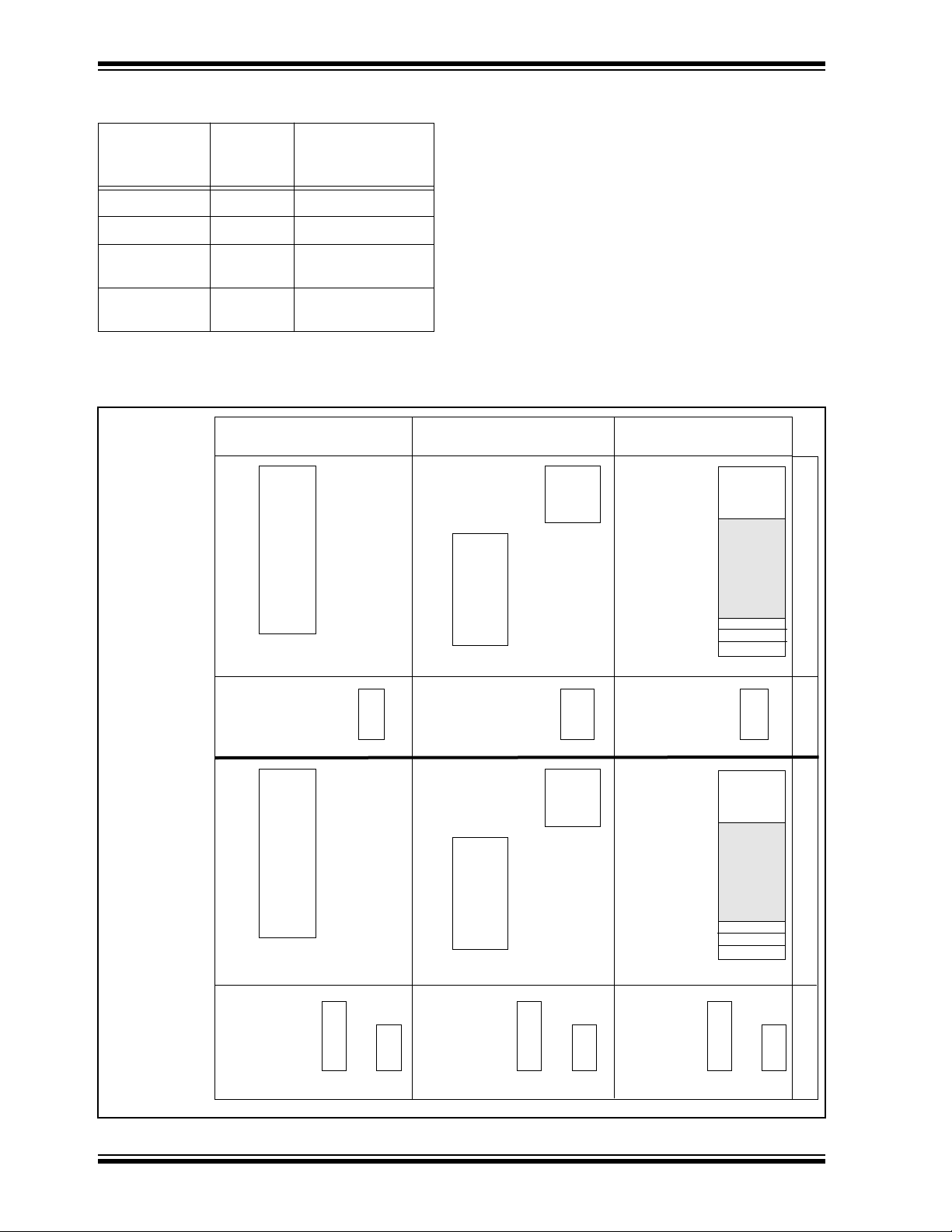
TABLE 6-1: MODE MEMORY ACCESS
The PIC17C4X can operate in modes where the program memory is off-chip. They are the microprocessor
Operating
Mode
Internal
Program
Memory
Configuration Bits,
Test Memory,
Boot ROM
Microprocessor No Access No Access
Microcontroller Access Access
Extended
Microcontroller
Protected
Microcontroller
Access No Access
Access Access
and extended microcontroller modes. The microprocessor mode is the default for an unprogrammed
device.
Regardless of the processor mode, data memory is
always on-chip.
FIGURE 6-2: MEMORY MAP IN DIFFERENT MODES
Extended
Microcontroller
Mode
External
Program
Memory
PIC17C42,
PIC17CR42,
PIC17C42A
Microprocessor
Mode
0000h
External
Program
Memory
FFFFh
OFF-CHIP ON-CHIP OFF-CHIP ON-CHIP OFF-CHIP ON-CHIP
0800h
FFFFh
0000h
07FFh
On-chip
Program
Memory
Microcontroller
Modes
0000h
07FFh
0800h
Config. Bits
FE00h
Test Memory
FFFFh
On-chip
Program
Memory
Boot ROM
PROGRAM SPACEDATA SPACE
PIC17C43,
PIC17CR43,
PIC17C44
00h
FFh
OFF-CHIP ON-CHIP OFF-CHIP ON-CHIP OFF-CHIP ON-CHIP
0000h
0FFFh/1FFFh
External
Program
Memory
FFFFh
OFF-CHIP ON-CHIP OFF-CHIP ON-CHIP OFF-CHIP ON-CHIP
00h
120h
FFh 1FFh
OFF-CHIP ON-CHIP
1000h/
2000h
External
Program
Memory
FFFFh
OFF-CHIP ON-CHIP
00h
FFh
0000h
On-chip
Program
Memory
00h
120h
FFh 1FFh
0000h
0FFFh/1FFFh
1000h/2000h
FE00h
FFFFh
FFh 1FFh
OFF-CHIP ON-CHIP
00h
00h
FFh
On-chip
Program
Memory
Config. Bits
Test Memory
Boot ROM
120h
PROGRAM SPACEDATA SPACE
DS30412C-page 30
1996 Microchip Technology Inc.
Page 31

PIC17C4X
6.1.2 EXTERNAL MEMORY INTERFACE
When either microprocessor or extended microcontrol-
ler mode is selected, PORTC, P ORTD and PORTE are
configured as the system bus. P ORTC and P ORTD are
the multiplexed address/data b us and PORTE is for the
control signals. External components are needed to
demultiplex the address and data. This can be done as
shown in Figure 6-4. The waveforms of address and
data are shown in Figure 6-3. For complete timings,
please refer to the electrical specification section.
FIGURE 6-3: EXTERNAL PROGRAM
MEMORY ACCESS
WAVEFORMS
Q1 Q2 Q4Q3Q1 Q2 Q4
AD
<15:0>
Address out Data in
ALE
OE
'1'
WR
Q3
Read cycle
Address out
Write cycle
The system bus requires that there is no bus conflict
(minimal leakage), so the output value (address) will be
capacitively held at the desired value.
As the speed of the processor increases, external
EPROM memory with faster access time must be used.
Table 6-2 lists external memory speed requirements for
a given PIC17C4X device frequency.
Q1
Data out
In extended microcontroller mode, when the device is
executing out of internal memory, the control signals
will continue to be active. That is, they indicate the
action that is occurring in the internal memory. The
external memory access is ignored.
This following selection is for use with Microchip
EPROMs. For interfacing to other manufacturers memory, please refer to the electr ical specifications of the
desired PIC17C4X device, as well as the desired memory device to ensure compatibility.
TABLE 6-2: EPROM MEMORY ACCESS
TIME ORDERING SUFFIX
EPROM Suffix
PIC17C4X
Oscillator
Frequency
8 MHz 500 ns -25 -25
16 MHz 250 ns -12 -15
20 MHz 200 ns -90 -10
25 MHz 160 ns N.A. -70
33 MHz 121 ns N.A. (1)
Note 1: The access times for this requires the use of
Instruction
Cycle
Time (T
fast SRAMS.
CY
)
PIC17C42
PIC17C43
PIC17C44
Note: The external memory interface is not sup-
ported for the LC devices.
FIGURE 6-4: TYPICAL EXTERNAL PROGRAM MEMORY CONNECTION DIAGRAM
AD15-AD0
Memory
(MSB)
Ax-A0
D7-D0
CE
WR WR
OE OE
AD7-AD0
PIC17C4X
AD15-AD8
ALE
(1)
I/O
OE
WR
Note 1: Use of I/O pins is only required for paged memory.
2: This signal is unused for ROM and EPROM devices.
373
373
A15-A0
138
(1)
Memory
(LSB)
Ax-A0
D7-D0
CE
(2)(2)
1996 Microchip Technology Inc. DS30412C-page 31
Page 32

PIC17C4X
6.2 Data Memor
Data memory is partitioned into two areas. The first is
the General Purpose Registers (GPR) area, while the
second is the Special Function Registers (SFR) area.
The SFRs control the operation of the device.
Portions of data memory are banked, this is for both
areas. The GPR area is banked to allow greater than
232 bytes of general purpose RAM. SFRs are for the
registers that control the peripheral functions. Banking
requires the use of control bits for bank selection.
These control bits are located in the Bank Select Register (BSR). If an access is made to a location outside
this banked region, the BSR bits are ignored.
Figure 6-5 shows the data memory map organization
for the PIC17C42 and Figure 6-6 for all of the other
PIC17C4X devices.
Instructions MOVPF and MOVFP provide the means to
move values from the peripheral area (“P”) to an y location in the register file (“F”), and vice-versa. The definition of the “P” range is from 0h to 1Fh, while the “F”
range is 0h to FFh. The “P” range has six more locations than peripheral registers (eight locations for the
PIC17C42 device) which can be used as General Purpose Registers. This can be useful in some applications
where variables need to be copied to other locations in
the general purpose RAM (such as saving status information during an interrupt).
The entire data memory can be accessed either directly
or indirectly through file select registers FSR0 and
FSR1 (Section 6.4). Indirect addressing uses the
appropriate control bits of the BSR for accesses into the
banked areas of data memory . The BSR is explained in
greater detail in Section 6.8.
y Organization
6.2.1 GENERAL PURPOSE REGISTER (GPR)
All devices hav e some amount of GPR area. The GPRs
are 8-bits wide. When the GPR area is greater than
232, it must be banked to allow access to the additional
memory space.
Only the PIC17C43 and PIC17C44 devices have
banked memory in the GPR area. To facilitate switching
between these banks, the MOVLR bank instruction has
been added to the instruction set. GPRs are not initialized by a Power-on Reset and are unchanged on all
other resets.
6.2.2 SPECIAL FUNCTION REGISTERS (SFR)
The SFRs are used by the CPU and peripheral func-
tions to control the operation of the device (Figure 6-5
and Figure 6-6). These registers are static RAM.
The SFRs can be classified into two sets, those associated with the “core” function and those related to the
peripheral functions. Those registers related to the
“core” are described here, while those related to a
peripheral feature are described in the section for each
peripheral feature.
The peripheral registers are in the banked portion of
memory, while the core registers are in the unbanked
region. To facilitate switching between the peripheral
banks, the MOVLB bank instruction has been provided.
DS30412C-page 32
1996 Microchip Technology Inc.
Page 33
PIC17C4X
FIGURE 6-5: PIC17C42 REGISTER FILE
MAP
Addr Unbanked
00h
01h
02h
03h
04h
05h
06h
07h
08h
09h
0Ah
0Bh
0Ch
0Dh
0Eh
0Fh
10h
11h
12h
13h
14h
15h
16h
17h
18h
1Fh
20h
FFh
Note 1: SFR file locations 10h - 17h are banked. All
INDF0
FSR0
PCL
PCLATH
ALUSTA
T0STA
CPUSTA
INTSTA
INDF1
FSR1
WREG
TMR0L
TMR0H
TBLPTRL
TBLPTRH
BSR
Bank 0 Bank 1
PORTA DDRC TMR1 PW1DCL
DDRB PORTC TMR2 PW2DCL
PORTB DDRD TMR3L PW1DCH
RCSTA PORTD TMR3H PW2DCH
RCREG DDRE PR1 CA2L
TXSTA PORTE PR2 CA2H
TXREG PIR PR3L/CA1L TCON1
SPBRG PIE PR3H/CA1H TCON2
General
Purpose
RAM
(1)
Bank 2
(1)
Bank 3
other SFRs ignore the Bank Select Register
(BSR) bits.
(1)
FIGURE 6-6: PIC17CR42/42A/43/R43/44
REGISTER FILE MAP
Addr Unbanked
00h
01h
02h
03h
04h
05h
06h
07h
08h
09h
0Ah
0Bh
0Ch
0Dh
0Eh
0Fh
10h
11h
12h
13h
14h
15h
16h
17h
18h
19h
1Ah
1Fh
20h
FFh
Note 1: SFR file locations 10h - 17h are banked. All
INDF0
FSR0
PCL
PCLATH
ALUSTA
T0STA
CPUSTA
INTSTA
INDF1
FSR1
WREG
TMR0L
TMR0H
TBLPTRL
TBLPTRH
BSR
General
Purpose
(2)
RAM
(1)
Bank 2
Bank 0 Bank 1
PORTA DDRC TMR1 PW1DCL
DDRB PORTC TMR2 PW2DCL
PORTB DDRD TMR3L PW1DCH
RCSTA PORTD TMR3H PW2DCH
RCREG DDRE PR1 CA2L
TXSTA PORTE PR2 CA2H
TXREG PIR PR3L/CA1L TCON1
SPBRG PIE PR3H/CA1H TCON2
PRODL
PRODH
General
Purpose
(2)
RAM
(1)
Bank 3
other SFRs ignore the Bank Select Register
(BSR) bits.
2: General Purpose Registers (GPR) locations
20h - FFh and 120h - 1FFh are banked. All
other GPRs ignore the Bank Select Register
(BSR) bits.
(1)
1996 Microchip Technology Inc. DS30412C-page 33
Page 34
PIC17C4X
TABLE 6-3: SPECIAL FUNCTION REGISTERS
Address Name Bit 7 Bit 6 Bit 5 Bit 4 Bit 3 Bit 2 Bit 1 Bit 0
Unbanked
00h INDF0 Uses contents of FSR0 to address data memory (not a physical register)
01h FSR0 Indirect data memory address pointer 0
02h PCL Low order 8-bits of PC
(1)
PCLATH Holding register for upper 8-bits of PC
03h
04h ALUSTA FS3 FS2 FS1 FS0 OV Z DC C
05h T0STA INTEDG T0SE T0CS PS3 PS2 PS1 PS0
(2)
CPUSTA
06h
07h INTSTA PEIF T0CKIF T0IF INTF PEIE T0CKIE T0IE INTE 0000 0000 0000 0000
08h INDF1 Uses contents of FSR1 to address data memory (not a physical register)
09h FSR1 Indirect data memory address pointer 1 xxxx xxxx uuuu uuuu
0Ah WREG Working register xxxx xxxx uuuu uuuu
0Bh TMR0L TMR0 register; low byte xxxx xxxx uuuu uuuu
0Ch TMR0H TMR0 register; high byte xxxx xxxx uuuu uuuu
0Dh TBLPTRL Low byte of program memory table pointer (4) (4)
0Eh TBLPTRH High byte of program memory table pointer (4) (4)
0Fh BSR Bank select register 0000 0000 0000 0000
Bank 0
10h
PORTA RBPU
11h DDRB Data direction register for PORTB 1111 1111 1111 1111
12h PORTB PORTB data latch xxxx xxxx uuuu uuuu
13h RCSTA SPEN RX9 SREN CREN
14h RCREG Serial port receive register xxxx xxxx uuuu uuuu
15h TXSTA CSRC TX9 TXEN SYNC
16h TXREG Serial port transmit register xxxx xxxx uuuu uuuu
17h SPBRG Baud rate generator register xxxx xxxx uuuu uuuu
Bank 1
10h DDRC Data direction register for PORTC 1111 1111 1111 1111
11h PORTC
12h DDRD Data direction register for PORTD 1111 1111 1111 1111
13h PORTD
14h DDRE Data direction register for PORTE ---- -111 ---- -111
15h
PORTE
16h PIR RBIF TMR3IF TMR2IF TMR1IF CA2IF CA1IF TXIF RCIF 0000 0010 0000 0010
17h PIE RBIE TMR3IE TMR2IE TMR1IE CA2IE CA1IE TXIE RCIE 0000 0000 0000 0000
Legend: x = unknown, u = unchanged, - = unimplemented read as '0', q - value depends on condition. Shaded cells are unimplemented, read as '0'.
Note 1: The upper byte of the program counter is not directly accessible. PCLATH is a holding register for PC<15:8> whose contents are updated
from or transferred to the upper byte of the program counter.
2: The T
3: Other (non power-up) resets include: external reset through MCLR and the Watchdog Timer Reset.
4: The following values are for both TBLPTRL and TBLPTRH:
5: The PRODL and PRODH registers are not implemented on the PIC17C42.
O and PD status bits in CPUSTA are not affected by a MCLR reset.
All PIC17C4X devices (Power-on Reset 0000 0000) and (All other resets 0000 0000)
except the PIC17C42 (Power-on Reset xxxx xxxx) and (All other resets uuuu uuuu)
— — STKAV GLINTD TO PD — — --11 11-- --11 qq--
— RA5 RA4 RA3 RA2 RA1/T0CKI RA0/INT 0-xx xxxx 0-uu uuuu
— FERR OERR RX9D 0000 -00x 0000 -00u
— — TRMT TX9D 0000 --1x 0000 --1u
RC7/
AD7
RD7/
AD15
RC6/
AD6
RD6/
AD14
— — — — — RE2/WR RE1/OE RE0/ALE ---- -xxx ---- -uuu
RC5/
AD5
RD5/
AD13
RC4/
AD4
RD4/
AD12
RC3/
AD3
RD3/
AD11
RC2/
AD2
RD2/
AD10
RC1/
AD1
RD1/
AD9
— 0000 000- 0000 000-
RC0/
AD0
RD0/
AD8
Value on
Power-on
Reset
---- ---- ---- ---xxxx xxxx uuuu uuuu
0000 0000 0000 0000
0000 0000 uuuu uuuu
1111 xxxx 1111 uuuu
---- ---- ---- ----
xxxx xxxx uuuu uuuu
xxxx xxxx uuuu uuuu
Value on all
other
resets (3)
DS30412C-page 34
1996 Microchip Technology Inc.
Page 35
TABLE 6-3: SPECIAL FUNCTION REGISTERS (Cont.’d)
PIC17C4X
Address Name Bit 7 Bit 6 Bit 5 Bit 4 Bit 3 Bit 2 Bit 1 Bit 0
Bank 2
10h TMR1 Timer1 xxxx xxxx uuuu uuuu
11h TMR2 Timer2 xxxx xxxx uuuu uuuu
12h TMR3L TMR3 register; low byte xxxx xxxx uuuu uuuu
13h TMR3H TMR3 register; high byte xxxx xxxx uuuu uuuu
14h PR1 Timer1 period register xxxx xxxx uuuu uuuu
15h PR2 Timer2 period register xxxx xxxx uuuu uuuu
16h PR3L/CA1L Timer3 period register, low byte/capture1 register; low byte xxxx xxxx uuuu uuuu
17h PR3H/CA1H Timer3 period register, high byte/capture1 register; high byte xxxx xxxx uuuu uuuu
Bank 3
10h PW1DCL DC1 DC0
11h PW2DCL DC1 DC0 TM2PW2
12h PW1DCH DC9 DC8 DC7 DC6 DC5 DC4 DC3 DC2 xxxx xxxx uuuu uuuu
13h PW2DCH DC9 DC8 DC7 DC6 DC5 DC4 DC3 DC2 xxxx xxxx uuuu uuuu
14h CA2L Capture2 low byte xxxx xxxx uuuu uuuu
15h CA2H Capture2 high byte xxxx xxxx uuuu uuuu
16h TCON1 CA2ED1 CA2ED0 CA1ED1 CA1ED0 T16 TMR3CS TMR2CS TMR1CS 0000 0000 0000 0000
17h
TCON2 CA2OVF CA1OVF PWM2ON PWM1ON CA1/PR3
Unbanked
(5)
PRODL Low Byte of 16-bit Product (8 x 8 Hardware Multiply)
18h
(5)
PRODH High Byte of 16-bit Product (8 x 8 Hardware Multiply)
19h
Legend: x = unknown, u = unchanged, - = unimplemented read as '0', q - value depends on condition. Shaded cells are unimplemented, read as '0'.
Note 1: The upper byte of the program counter is not directly accessible. PCLATH is a holding register for PC<15:8> whose contents are updated
from or transferred to the upper byte of the program counter.
2: The T
3: Other (non power-up) resets include: external reset through MCLR and the Watchdog Timer Reset.
4: The following values are for both TBLPTRL and TBLPTRH:
5: The PRODL and PRODH registers are not implemented on the PIC17C42.
O and PD status bits in CPUSTA are not affected by a MCLR reset.
All PIC17C4X devices (Power-on Reset 0000 0000) and (All other resets 0000 0000)
except the PIC17C42 (Power-on Reset xxxx xxxx) and (All other resets uuuu uuuu)
— — — — — — xx-- ---- uu-- ----
— — — — — xx0- ---- uu0- ----
TMR3ON TMR2ON TMR1ON 0000 0000 0000 0000
Value on
Power-on
Reset
xxxx xxxx uuuu uuuu
xxxx xxxx uuuu uuuu
Value on all
other
resets (3)
1996 Microchip Technology Inc. DS30412C-page 35
Page 36

PIC17C4X
6.2.2.1 ALU STATUS REGISTER (ALUSTA)
The ALUSTA register contains the status bits of the
Arithmetic and Logic Unit and the mode control bits for
the indirect addressing register.
As with all the other registers, the ALUSTA register can
be the destination for any instruction. If the ALUSTA
register is the destination for an instruction that affects
the Z, DC or C bits, then the write to these three bits is
disabled. These bits are set or cleared according to the
device logic. Therefore, the result of an instruction with
the ALUSTA register as destination may be different
than intended.
For example , CLRF ALUSTA will clear the upper four bits
and set the Z bit. This leaves the ALUSTA register as
0000u1uu (where u = unchanged).
It is recommended, therefore, that only BCF, BSF, SWAPF
and MOVWF instructions be used to alter the ALUSTA
register because these instructions do not affect any
status bit. To see how other instructions affect the status bits, see the “Instruction Set Summary.”
Note 1: The C and DC bits operate as a borrow
out bit in subtraction. See the SUBLW and
SUBWF instructions for examples.
Note 2: The overflow bit will be set if the 2’s com-
plement result exceeds +127 or is less
than -128.
Arithmetic and Logic Unit (ALU) is capable of carrying
out arithmetic or logical operations on two operands or
a single operand. All single operand instructions operate either on the WREG register or a file register. For
two operand instructions, one of the operands is the
WREG register and the other one is either a file register
or an 8-bit immediate constant.
FIGURE 6-7: ALUSTA REGISTER (ADDRESS: 04h, UNBANKED)
R/W - 1 R/W - 1 R/W - 1 R/W - 1 R/W - x R/W - x R/W - x R/W - x
FS3 FS2 FS1 FS0 OV Z DC C
bit7 bit0
bit 7-6: FS3:FS2: FSR1 Mode Select bits
00 = Post auto-decrement FSR1 value
01 = Post auto-increment FSR1 value
1x = FSR1 value does not change
bit 5-4: FS1:FS0: FSR0 Mode Select bits
00 = Post auto-decrement FSR0 value
01 = Post auto-increment FSR0 value
1x = FSR0 value does not change
bit 3: OV: Overflow bit
This bit is used for signed arithmetic (2’s complement). It indicates an overflow of the 7-bit magnitude,
which causes the sign bit (bit7) to change state.
1 =Overflow occurred for signed arithmetic, (in this arithmetic operation)
0 =No overflow occurred
bit 2: Z: Zero bit
1 =The result of an arithmetic or logic operation is zero
0 =The results of an arithmetic or logic operation is not zero
bit 1: DC: Digit carry/borro
For ADDWF and ADDLW instructions.
1 =A carry-out from the 4th low order bit of the result occurred
0 =No carry-out from the 4th low order bit of the result
Note: For borrow the polarity is reversed.
bit 0: C: carry/borro
For ADDWF and ADDLW instructions.
1 =A carry-out from the most significant bit of the result occurred
Note that a subtraction is executed by adding the two’s complement of the second operand. For rotate
(RRCF, RLCF) instructions, this bit is loaded with either the high or low order bit of the source register.
0 =No carry-out from the most significant bit of the result
Note: For borrow the polarity is reversed.
w bit
w bit
R = Readable bit
W = Writable bit
-n = Value at POR reset
(x = unknown)
DS30412C-page 36 1996 Microchip Technology Inc.
Page 37

6.2.2.2 CPU STATUS REGISTER (CPUSTA)
The CPUSTA register contains the status and control
bits for the CPU. This register is used to globally
enable/disable interrupts. If only a specific interr upt is
desired to be enabled/disabled, please refer to the
INTerrupt STAtus (INTSTA) register and the Peripheral
Interrupt Enable (PIE) register. This register also indicates if the stack is available and contains the
Power-down (PD
and STKAV bits are not writab le. These bits are set and
cleared according to device logic. Therefore, the result
of an instruction with the CPUSTA register as destination may be different than intended.
) and Time-out (TO) bits. The TO, PD,
FIGURE 6-8: CPUSTA REGISTER (ADDRESS: 06h, UNBANKED)
U - 0 U - 0 R - 1 R/W - 1 R - 1 R - 1 U - 0 U - 0
— — STKAV GLINTD TO PD — —
bit7 bit0
bit 7-6: Unimplemented: Read as '0'
bit 5: STKAV: Stack Available bit
This bit indicates that the 4-bit stack pointer value is Fh, or has rolled ov er from Fh → 0h (stack overflow).
1 =Stack is available
0 =Stack is full, or a stack overflow may have occurred (Once this bit has been cleared by a
stack overflow, only a device reset will set this bit)
bit 4: GLINTD: Global Interrupt Disable bit
This bit disables all interrupts. When enabling interrupts, only the sources with their enable bits set can
cause an interrupt.
1 =Disable all interrupts
0 =Enables all un-masked interrupts
bit 3: T
bit 2: PD
bit 1-0: Unimplemented: Read as '0'
O: WDT Time-out Status bit
1 =After power-up or by a CLRWDT instruction
0 =A Watchdog Timer time-out occurred
: Power-down Status bit
1 =After power-up or by the CLRWDT instruction
0 =By execution of the SLEEP instruction
PIC17C4X
R = Readable bit
W = Writable bit
U = Unimplemented bit,
Read as ‘0’
- n = Value at POR reset
1996 Microchip Technology Inc. DS30412C-page 37
Page 38

PIC17C4X
6.2.2.3 TMR0 STATUS/CONTROL REGISTER
(T0STA)
This register contains various control bits. Bit7
(INTEDG) is used to control the edge upon which a signal on the RA0/INT pin will set the RB0/INT interrupt
flag. The other bits configure the Timer0 prescaler and
clock source. (Figure 11-1).
FIGURE 6-9: T0STA REGISTER (ADDRESS: 05h, UNBANKED)
R/W - 0 R/W - 0 R/W - 0 R/W - 0 R/W - 0 R/W - 0 R/W - 0 U - 0
INTEDG T0SE T0CS PS3 PS2 PS1 PS0
bit7 bit0
bit 7: INTEDG: RA0/INT Pin Interrupt Edge Select bit
This bit selects the edge upon which the interrupt is detected.
1 =Rising edge of RA0/INT pin generates interrupt
0 =Falling edge of RA0/INT pin generates interrupt
bit 6: T0SE: Timer0 Clock Input Edge Select bit
This bit selects the edge upon which TMR0 will increment.
When
T0CS = 0
1 =Rising edge of RA1/T0CKI pin increments TMR0 and/or generates a T0CKIF interrupt
0 =Falling edge of RA1/T0CKI pin increments TMR0 and/or generates a T0CKIF interrupt
When
T0CS = 1
Don’t care
bit 5: T0CS: Timer0 Clock Source Select bit
This bit selects the clock source for Timer0.
1 =Internal instruction clock cycle (T
0 =T0CKI pin
bit 4-1: PS3:PS0: Timer0 Prescale Selection bits
These bits select the prescale value for Timer0.
CY)
—
R = Readable bit
W = Writable bit
U = Unimplemented,
reads as ‘0’
-n = Value at POR reset
PS3:PS0 Prescale V alue
0000
0001
0010
0011
0100
0101
0110
0111
1xxx
bit 0: Unimplemented: Read as '0'
DS30412C-page 38 1996 Microchip Technology Inc.
1:1
1:2
1:4
1:8
1:16
1:32
1:64
1:128
1:256
Page 39

PIC17C4X
6.3 Stack Operation
The PIC17C4X devices have a 16 x 16-bit wide hardware stack (Figure 6-1). The stack is not par t of either
the program or data memory space, and the stack
pointer is neither readable nor writable. The PC is
“PUSHed” onto the stack when a CALL instruction is
executed or an interrupt is acknowledged. The stack is
“POPed” in the ev ent of a RETURN, RETLW, or a RETFIE
instruction execution. PCLATH is not affected by a
“PUSH” or a “POP” operation.
The stack operates as a circular buffer, with the stack
pointer initialized to '0' after all resets. There is a stack
available bit (STKAV) to allow software to ensure that
the stack has not overflo wed. The STKAV bit is set after
a device reset. When the stack pointer equals Fh,
STKAV is cleared. When the stack pointer rolls over
from Fh to 0h, the STKAV bit will be held clear until a
device reset.
Note 1: There is not a status bit for stack under-
flow . The STKAV bit can be used to detect
the underflow which results in the stack
pointer being at the top of stack.
Note 2: There are no instruction mnemonics
called PUSH or POP. These are actions
that occur from the execution of the CALL,
RETURN, RETLW, and RETFIE instruc-
tions, or the vectoring to an interrupt vector.
Note 3: After a reset, if a “POP” operation occurs
before a “PUSH” operation, the STKAV bit
will be cleared. This will appear as if the
stack is full (underflow has occurred). If a
“PUSH” operation occurs next (before
another “POP”), the STKAV bit will be
locked clear. Only a device reset will
cause this bit to set.
After the device is “PUSHed” sixteen times (without a
“POP”), the seventeenth push overwrites the value
from the first push. The eighteenth push overwrites the
second push (and so on).
6.4 Indirect Addressing
Indirect addressing is a mode of addressing data
memory where the data memory address in the
instruction is not fixed. That is, the register that is to be
read or written can be modified by the program. This
can be useful for data tables in the data memory.
Figure 6-10 shows the operation of indirect addressing. This shows the moving of the value to the data
memory address specified by the value of the FSR
register.
Example 6-1 shows the use of indirect addressing to
clear RAM in a minimum number of instructions. A
similar concept could be used to move a defined number of bytes (block) of data to the USART transmit register (TXREG). The starting address of the block of
data to be transmitted could easily be modified by the
program.
FIGURE 6-10: INDIRECT ADDRESSING
RAM
Instruction
Executed
Opcode Address
File = INDFx
Instruction
Fetched
Opcode
File
FSR
1996 Microchip Technology Inc. DS30412C-page 39
Page 40

PIC17C4X
6.4.1 INDIRECT ADDRESSING REGISTERS
The PIC17C4X has four registers for indirect address-
ing. These registers are:
• INDF0 and FSR0
• INDF1 and FSR1
Registers INDF0 and INDF1 are not physically imple-
mented. Reading or writing to these registers activates
indirect addressing, with the value in the corresponding FSR register being the address of the data. The
FSR is an 8-bit register and allows addressing anywhere in the 256-byte data memory address range.
For banked memory, the bank of memor y accessed is
specified by the value in the BSR.
If file INDF0 (or INDF1) itself is read indirectly via an
FSR, all '0's are read (Zero bit is set). Similarly, if
INDF0 (or INDF1) is written to indirectly, the operation
will be equivalent to a NOP, and the status bits are not
affected.
6.4.2 INDIRECT ADDRESSING OPERATION
The indirect addressing capability has been enhanced
over that of the PIC16CXX family. There are two control bits associated with each FSR register. These two
bits configure the FSR register to:
• Auto-decrement the value (address) in the FSR
after an indirect access
• Auto-increment the value (address) in the FSR
after an indirect access
• No change to the value (address) in the FSR after
an indirect access
These control bits are located in the ALUSTA register.
The FSR1 register is controlled by the FS3:FS2 bits
and FSR0 is controlled by the FS1:FS0 bits.
When using the auto-increment or auto-decrement
features, the effect on the FSR is not reflected in the
ALUSTA register. For example, if the indirect address
causes the FSR to equal '0', the Z bit will not be set.
If the FSR register contains a value of 0h, an indirect
read will read 0h (Zero bit is set) while an indirect write
will be equivalent to a NOP (status bits are not
affected).
Indirect addressing allows single cycle data transfers
within the entire data space. This is possible with the
use of the MOVPF and MOVFP instructions, where either
'p' or 'f' is specified as INDF0 (or INDF1).
If the source or destination of the indirect address is in
banked memory, the location accessed will be determined by the value in the BSR.
A simple program to clear RAM from 20h - FFh is
shown in Example 6-1.
EXAMPLE 6-1: INDIRECT ADDRESSING
MOVLW 0x20 ;
MOVWF FSR0 ; FSR0 = 20h
BCF ALUSTA, FS1 ; Increment FSR
BSF ALUSTA, FS0 ; after access
BCF ALUSTA, C ; C = 0
MOVLW END_RAM + 1 ;
LP CLRF INDF0 ; Addr(FSR) = 0
CPFSEQ FSR0 ; FSR0 = END_RAM+1?
GOTO LP ; NO, clear next
: ; YES, All RAM is
: ; cleared
6.5 Table Pointer (TBLPTRL and TBLPTRH)
File registers TBLPTRL and TBLPTRH form a 16-bit
pointer to address the 64K program memory space.
The table pointer is used by instructions TABLWT and
TABLRD.
The TABLRD and the TABLWT instructions allow trans-
fer of data between program and data space . The table
pointer serves as the 16-bit address of the data word
within the program memory. For a more complete
description of these registers and the operation of Table
Reads and Table Writes, see Section 7.0.
6.6 Table Latch (TBLATH, TBLATL)
The table latch (TBLAT) is a 16-bit register, with
TBLATH and TBLATL referring to the high and low
bytes of the register. It is not mapped into data or program memory. The table latch is used as a temporary
holding latch during data transfer between program and
data memory (see descriptions of instructions TABLRD,
TABLWT, TLRD and TLWT). For a more complete
description of these registers and the operation of Table
Reads and Table Writes, see Section 7.0.
DS30412C-page 40 1996 Microchip Technology Inc.
Page 41
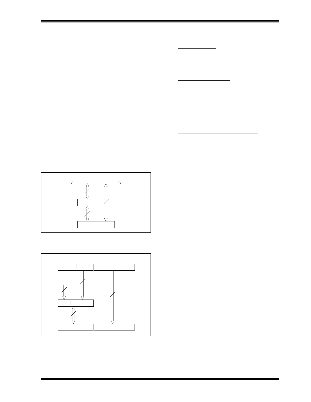
PIC17C4X
6.7 Program Counter Module
The Program Counter (PC) is a 16-bit register. PCL, the
low byte of the PC, is mapped in the data memory. PCL
is readable and writable just as is any other register.
PCH is the high byte of the PC and is not directly
addressable. Since PCH is not mapped in data or program memory , an 8-bit register PCLATH (PC high latch)
is used as a holding latch for the high byte of the PC.
PCLATH is mapped into data memor y. The user can
read or write PCH through PCLATH.
The 16-bit wide PC is incremented after each instruction fetch during Q1 unless:
• Modified by GOTO , CALL, LCALL, RETURN, RETLW,
or RETFIE instruction
• Modified by an interrupt response
• Due to destination write to PCL by an instruction
“Skips” are equivalent to a forced NOP cycle at the
skipped address.
Figure 6-11 and Figure 6-12 show the operation of the
program counter for various situations.
FIGURE 6-11: PROGRAM COUNTER
OPERATION
Internal data bus <8>
8
PCLATH
8
PCH PCL
8
FIGURE 6-12: PROGRAM COUNTER USING
THE CALL AND GOTO
INSTRUCTIONS
12 8 7 0
1315
Opcode
Last write
to PCLATH
3
5
7
15 0
4
PCLATH
8
PCH
5
0
87
8
PCL
Using Figure 6-11, the operations of the PC and
PCLATH for different instructions are as follows:
a) LCALL
instructions:
An 8-bit destination address is provided in the
instruction (opcode). PCLATH is unchanged.
PCLATH → PCH
Opcode<7:0> → PCL
b) Read instr
uctions on PCL:
Any instruction that reads PCL.
PCL → data bus → ALU or destination
PCH → PCLATH
c) Wr
ite instructions on PCL:
Any instruction that writes to PCL.
8-bit data → data bus → PCL
PCLATH → PCH
d) Read-Modify-Wr
ite instructions on PCL:
Any instruction that does a read-write-modify
operation on PCL, such as ADDWF PCL.
Read: PCL → data bus → ALU
Write: 8-bit result → data bus → PCL
PCLATH → PCH
e) RETURN
instruction:
PCH → PCLATH
Stack<MRU> → PC<15:0>
Using Figure 6-12, the operation of the PC and
PCLATH for GOTO and CALL instructions is a follows:
CALL
, GOTO instructions:
A 13-bit destination address is provided in the
instruction (opcode).
Opcode<12:0> → PC <12:0>
PC<15:13> → PCLATH<7:5>
Opcode<12:8> → PCLATH <4:0>
The read-modify-write only affects the PCL with the
result. PCH is loaded with the value in the PCLATH.
For example , ADDWF PCL will result in a jump within the
current page. If PC = 03F0h, WREG = 30h and
PCLATH = 03h before instruction, PC = 0320h after the
instruction. To accomplish a true 16-bit computed jump,
the user needs to compute the 16-bit destination
address, write the high byte to PCLATH and then write
the low value to PCL.
The following PC related operations do not change
PCLATH:
a) LCALL, RETLW, and RETFIE instructions.
b) Interrupt vector is forced onto the PC.
c) Read-modify-write instructions on PCL (e.g. BSF
PCL).
1996 Microchip Technology Inc. DS30412C-page 41
Page 42

PIC17C4X
6.8 Bank Select Register (BSR)
The BSR is used to switch between banks in the data
memory area (Figure 6-13). In the PIC17C42,
PIC17CR42, and PIC17C42A only the lower nibble is
implemented. While in the PIC17C43, PIC17CR43,
and PIC17C44 devices, the entire byte is implemented.
The lower nibble is used to select the peripheral register bank. The upper nibble is used to select the general
purpose memory bank.
All the Special Function Registers (SFRs) are mapped
into the data memory space. In order to accommodate
the large number of registers, a banking scheme has
been used. A segment of the SFRs, from address 10h
to address 17h, is banked. The lo wer nib ble of the bank
select register (BSR) selects the currently active
“peripheral bank.” Effort has been made to group the
peripheral registers of related functionality in one bank.
However, it will still be necessary to switch from bank
to bank in order to address all peripherals related to a
single task. To assist this , a MOVLB bank instruction is
in the instruction set.
FIGURE 6-13: BSR OPERATION (PIC17C43/R43/44)
BSR
7430
(2)
(1)
For the PIC17C43, PIC17CR43, and PIC17C44
devices, the need for a large general purpose memory
space dictated a general purpose RAM banking
scheme. The upper nibble of the BSR selects the currently active general purpose RAM bank. To assist this ,
a MOVLR bank instruction has been provided in the
instruction set.
If the currently selected bank is not implemented (such
as Bank 13), any read will read all '0's. Any write is completed to the bit bucket and the ALU status bits will be
set/cleared as appropriate.
Note: Registers in Bank 15 in the Special Func-
tion Register area, are reserved for
Microchip use. Reading of registers in this
bank may cause random values to be read.
Address
Range
10h
17h
20h
FFh
Note 1: Only Banks 0 through Bank 3 are implemented. Selection of an unimplemented bank is not recommended.
Bank 15 is reserved for Microchip use, reading of registers in this bank may cause random values to be read.
2: Only Banks 0 and Bank 1 are implemented. Selection of an unimplemented bank is not recommended.
01234 15
• • •
Bank 3Bank 2Bank 1Bank 0
012
• • •• • •
Bank 2Bank 1Bank 0
Bank 15Bank 4
15
Bank 15
SFR
Banks
GPR
Banks
DS30412C-page 42 1996 Microchip Technology Inc.
Page 43
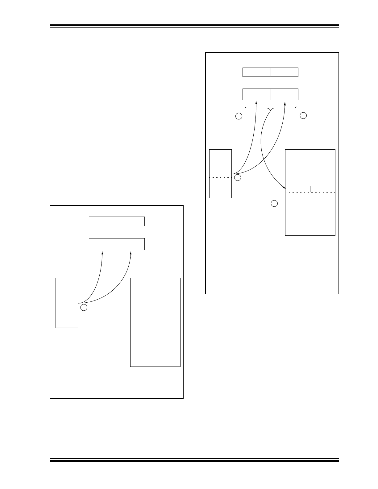
PIC17C4X
7.0 TABLE READS AND TABLE WRITES
The PIC17C4X has four instructions that allow the processor to move data from the data memory space to
the program memory space, and vice versa. Since the
program memory space is 16-bits wide and the data
memory space is 8-bits wide, two operations are
required to move 16-bit values to/from the data memory.
The TLWT t,f and TABLWT t,i,f instructions are
used to write data from the data memory space to the
program memory space. The TLRD t,f and TABLRD
t,i,f instructions are used to write data from the pro-
gram memory space to the data memory space.
The program memory can be internal or external. For
the program memory access to be external, the device
needs to be operating in extended microcontroller or
microprocessor mode.
Figure 7-1 through Figure 7-4 show the operation of
these four instructions.
FIGURE 7-1: TLWT INSTRUCTION
OPERATION
TABLE POINTER
TBLPTRH
TBLPTRL
FIGURE 7-2: TABLWT INSTRUCTION
OPERATION
TABLE POINTER
TBLPTRH
TABLE LATCH (16-bit)
TABLATH TABLATL
3
TABLWT 1,i,f TABLWT 0,i,f
DATA
MEMORY
f
1
TBLPTRL
3
PROGRAM MEMORY
Prog-Mem
(TBLPTR)
2
TABLE LATCH (16-bit)
TABLATH TABLATL
TLWT 1,f TLWT 0,f
DATA
MEMORY
f
1
PROGRAM MEMORY
Note 1: 8-bit value, from register 'f', loaded into the
high or low byte in TABLAT (16-bit).
Note 1: 8-bit value, from register 'f', loaded into
the high or low byte in TABLAT (16-bit).
2: 16-bit TABLAT value written to address
Program Memory (TBLPTR).
3: If “i” = 1, then TBLPTR = TBLPTR + 1,
If “i” = 0, then TBLPTR is unchanged.
1996 Microchip Technology Inc. DS30412C-page 43
Page 44

PIC17C4X
FIGURE 7-3: TLRD INSTRUCTION
OPERATION
TABLE POINTER
TBLPTRH TBLPTRL
TABLE LATCH (16-bit)
TABLATH TABLATL
DATA
MEMORY
f
TLRD 1,f
1
TLRD 0,f
PROGRAM MEMORY
FIGURE 7-4: TABLRD INSTRUCTION
OPERATION
TABLE POINTER
TABLE LATCH (16-bit)
TABLRD 1,i,f
DATA
MEMORY
f
TBLPTRH
TABLATH TABLATL
3
1
TBLPTRL
3
TABLRD 0,i,f
PROGRAM MEMORY
Prog-Mem
(TBLPTR)
2
Note 1: 8-bit value, from TABLAT (16-bit) high or
low byte, loaded into register 'f'.
Note 1: 8-bit value, from TABLAT (16-bit) high or
low byte, loaded into register 'f'.
2: 16-bit value at Program Memory (TBLPTR)
loaded into TABLAT register.
3: If “i” = 1, then TBLPTR = TBLPTR + 1,
If “i” = 0, then TBLPTR is unchanged.
DS30412C-page 44
1996 Microchip Technology Inc.
Page 45

PIC17C4X
7.1 T
A table write operation to internal memory causes a
long write operation. The long write is necessary for
programming the internal EPROM. Instruction execution is halted while in a long write cycle. The long wr ite
will be terminated by any enabled interrupt. To ensure
that the EPROM location has been well programmed,
a minimum programming time is required (see specification #D114 ). Having only one interrupt enabled to
terminate the long write ensures that no unintentional
interrupts will prematurely terminate the long write.
The sequence of events for programming an internal
program memory location should be:
1. Disable all interrupt sources, except the source
2. Raise MCLR
3. Clear the WDT.
4. Do the table write. The interr upt will terminate
5. Verify the memory location (table read).
Note: Programming requirements must be met.
able Writes to Internal Memory
to terminate EPROM program write.
/V
PP
pin to the programming volt-
age.
the long write.
See timing specification in electrical specifications for the desired device. Violating
these specifications (including temperature) may result in EPROM locations that
are not fully programmed and may lose
their state over time.
7.1.1 TERMINATING LONG WRITES
An interrupt source or reset are the only events that
terminate a long write operation. Ter minating the long
write from an interrupt source requires that the interrupt enable and flag bits are set. The GLINTD bit only
enables the vectoring to the interrupt address.
If the T0CKI, RA0/INT, or TMR0 interrupt source is
used to terminate the long write; the interrupt flag, of
the highest priority enabled interrupt, will terminate the
long write and automatically be cleared.
Note 1: If an interrupt is pending, the TABLWT is
aborted (an NOP is executed). The
highest priority pending interrupt, from
the T0CKI, RA0/INT, or TMR0 sources
that is enabled, has its flag cleared.
Note 2: If the interrupt is not being used for the
program write timing, the interrupt
should be disabled. This will ensure that
the interrupt is not lost, nor will it terminate the long write prematurely.
If a peripheral interrupt source is used to terminate the
long write, the interrupt enable and flag bits must be
set. The interr upt flag will not be automatically cleared
upon the vectoring to the interrupt vector address.
If the GLINTD bit is cleared prior to the long write,
when the long write is terminated, the program will
branch to the interrupt vector.
If the GLINTD bit is set prior to the long write, when
the long write is terminated, the program will not vector
to the interrupt address.
TABLE 7-1: INTERRUPT - TABLE WRITE INTERACTION
Interrupt
Source
RA0/INT , TMR0,
T0CKI
Peripheral
1996 Microchip Technology Inc. DS30412C-page 45
GLINTD
0
0
1
1
0
0
1
1
Enable
Bit
1
1
0
1
1
1
0
1
Flag
Bit
1
0
x
1
1
0
x
1
Action
Terminate long table write (to internal program
memory), branch to interrupt vector (branch clears
flag bit).
None
None
Terminate table write, do not branch to interrupt
vector (flag is automatically cleared).
Terminate table write, branch to interrupt vector.
None
None
Terminate table write, do not branch to interrupt
vector (flag is set).
Page 46

PIC17C4X
7.2 T
able Writes to External Memory
Table writes to external memory are always two-cycle
instructions. The second cycle writes the data to the
external memory location. The sequence of events for
an external memory write are the same for an internal
write.
7.2.2 TABLE WRITE CODE
The “i” operand of the TABLWT instruction can specify
that the value in the 16-bit TBLPTR register is automatically incremented for the next write. In
Example 7-1, the TBLPTR register is not automatically
incremented.
EXAMPLE 7-1: TABLE WRITE
Note: If an interrupt is pending or occurs during
the TABLWT , the two cycle table write
completes. The RA0/INT , TMR0, or T0CKI
interrupt flag is automatically cleared or
the pending peripheral interrupt is
acknowledged.
CLRWDT ; Clear WDT
MOVLW HIGH (TBL_ADDR) ; Load the Table
MOVWF TBLPTRH ; address
MOVLW LOW (TBL_ADDR) ;
MOVWF TBLPTRL ;
MOVLW HIGH (DATA) ; Load HI byte
TLWT 1, WREG ; in TABLATCH
MOVLW LOW (DATA) ; Load LO byte
TABLWT 0,0,WREG ; in TABLATCH
; and write to
; program memory
; (Ext. SRAM)
FIGURE 7-5: TABLWT WRITE TIMING (EXTERNAL MEMORY)
Q1 Q2 Q3 Q4 Q1 Q2 Q3 Q4 Q1 Q2 Q3 Q4 Q1 Q2 Q3 Q4
AD15:AD0
Instruction
fetched
Instruction
executed
ALE
OE
WR
Note: If external write GLINTD = '1', Enable bit = '1', '1' → Flag bit, Do table write. The highest pending interrupt is cleared.
PC PC+1 TBL PC+2Data out
TABLWT
INST (PC-1)
'1'
INST (PC+1)
TABLWT cycle1 TABLWT cycle2
Data write cycle
INST (PC+2)
INST (PC+1)
DS30412C-page 46
1996 Microchip Technology Inc.
Page 47

PIC17C4X
FIGURE 7-6: CONSECUTIVE TABLWT WRITE TIMING (EXTERNAL MEMORY)
Q1 Q2 Q3 Q4 Q1 Q2 Q3 Q4 Q1 Q2 Q3 Q4 Q1 Q2 Q3 Q4 Q1 Q2 Q3 Q4 Q1 Q2 Q3 Q4
TBL1
AD15:AD0
PC
PC+1
Data out 1 Data out 2
PC+2
TBL2
PC+3
Instruction
fetched
Instruction
executed
ALE
OE
WR
TABLWT1 TABLWT2 INST (PC+2)
INST (PC-1)
TABLWT1 cycle1
TABLWT1 cycle2 TABLWT2 cycle1
Data write cycle
TABLWT2 cycle2
Data write cycle
INST (PC+3)
INST (PC+2)
1996 Microchip Technology Inc. DS30412C-page 47
Page 48
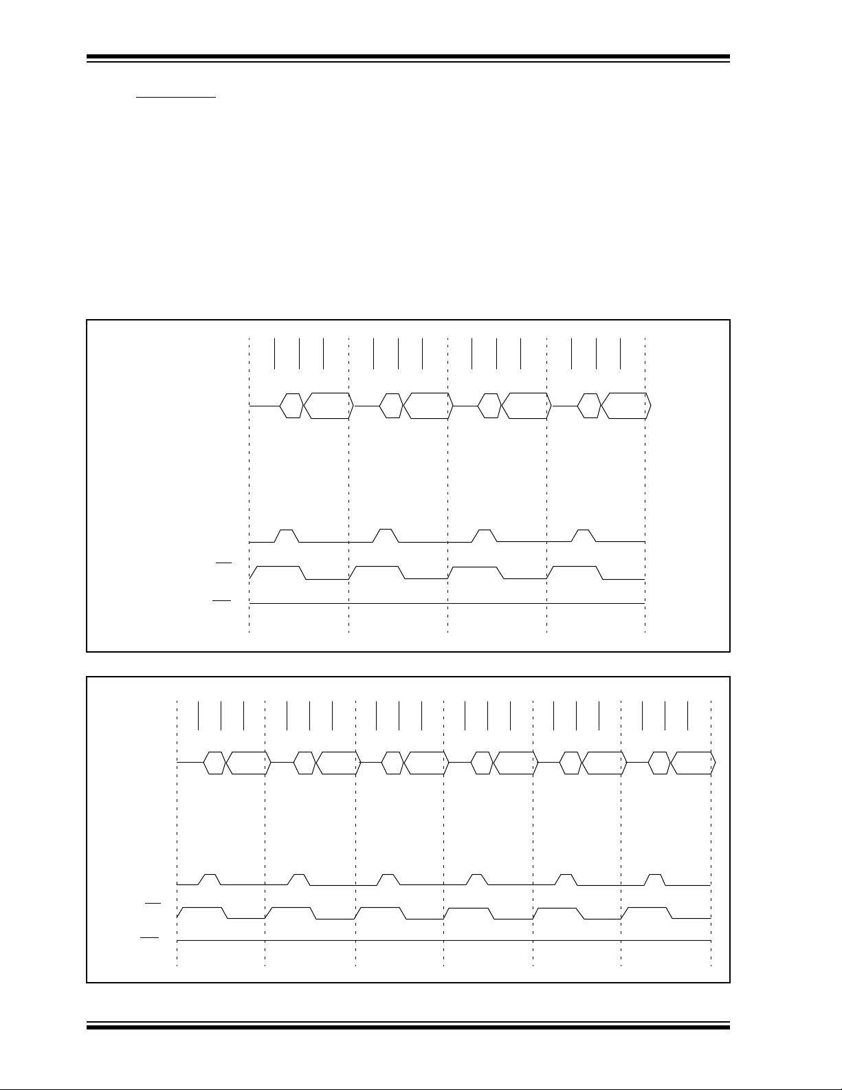
PIC17C4X
7.3 T
able Reads
The table read allows the program memory to be read.
This allows constant data to be stored in the program
memory space, and retrieved into data memory when
needed. Example 7-2 reads the 16-bit value at program memory address TBLPTR. After the dummy byte
has been read from the TABLATH, the TABLATH is
loaded with the 16-bit data from program memory
address TBLPTR + 1. The first read loads the data into
the latch, and can be considered a dummy read
(unknown data loaded into 'f'). INDF0 should be configured for either auto-increment or auto-decrement.
FIGURE 7-7: TABLRD TIMING
Q3
Q4
Q1 Q2
TABLRD cycle1
AD15:AD0
Instruction
fetched
Instruction
executed
Q1 Q2
PC PC+1 TBL Data in
TABLRD INST (PC+1)
INST (PC-1)
EXAMPLE 7-2: TABLE READ
MOVLW HIGH (TBL_ADDR) ; Load the Table
MOVWF TBLPTRH ; address
MOVLW LOW (TBL_ADDR) ;
MOVWF TBLPTRL ;
TABLRD 0,0,DUMMY ; Dummy read,
; Updates TABLATCH
TLRD 1, INDF0 ; Read HI byte
; of TABLATCH
TABLRD 0,1,INDF0 ; Read LO byte
; of TABLATCH and
; Update TABLATCH
Q3
Q4
Q1 Q2
TABLRD cycle2 INST (PC+1)
Data read cycle
Q3
Q4
Q1 Q2
PC+2
INST (PC+2)
Q3
Q4
ALE
OE
WR
'1'
FIGURE 7-8: TABLRD TIMING (CONSECUTIVE TABLRD INSTRUCTIONS)
Q1 Q2 Q3 Q4 Q1 Q2 Q3 Q4 Q1 Q2 Q3 Q4 Q1 Q2 Q3 Q4 Q1 Q2 Q3 Q4 Q1 Q2 Q3 Q4
AD15:AD0
Instruction
fetched
Instruction
executed
ALE
OE
WR
PC
TABLRD1
INST (PC-1) TABLRD1 cycle1 TABLRD1 cycle2 TABLRD2 cycle1
'1'
PC+1
TABLRD2
Data read cycle Data read cycle
TBL1
Data in 1
PC+2
INST (PC+2) INST (PC+3)
TBL2 Data in 2
TABLRD2 cycle2
PC+3
INST (PC+2)
DS30412C-page 48
1996 Microchip Technology Inc.
Page 49

PIC17C4X
8.0 HARDWARE MULTIPLIER
All PIC17C4X devices except the PIC17C42, have an
8 x 8 hardware multiplier included in the ALU of the
device. By making the multiply a hardware operation, it
completes in a single instruction cycle. This is an
unsigned multiply that gives a 16-bit result. The result
is stored into the 16-bit PRODuct register
(PRODH:PRODL). The multiplier does not affect any
flags in the ALUSTA register.
Making the 8 x 8 multiplier execute in a single cycle
gives the following advantages:
• Higher computational throughput
• Reduces code size requirements for multiply
algorithms
The performance increase allows the device to be used
in applications previously reserved for Digital Signal
Processors.
Table 8-1 shows a performance comparison between
the PIC17C42 and all other PIC17CXX devices, which
have the single cycle hardware multiply.
Example 8-1 shows the sequence to do an 8 x 8
unsigned multiply. Only one instruction is required
when one argument of the multiply is already loaded in
the WREG register.
Example 8-2 shows the sequence to do an 8 x 8 signed
multiply. To account for the sign bits of the arguments,
each argument’s most significant bit (MSb) is tested
and the appropriate subtractions are done.
EXAMPLE 8-1: 8 x 8 MULTIPLY ROUTINE
MOVFP ARG1, WREG
MULWF ARG2 ; ARG1 * ARG2 ->
; PRODH:PRODL
EXAMPLE 8-2: 8 x 8 SIGNED MULTIPLY
ROUTINE
MOVFP ARG1, WREG
MULWF ARG2 ; ARG1 * ARG2 ->
; PRODH:PRODL
BTFSC ARG2, SB ; Test Sign Bit
SUBWF PRODH, F ; PRODH = PRODH
; - ARG1
MOVFP ARG2, WREG
BTFSC ARG1, SB ; Test Sign Bit
SUBWF PRODH, F ; PRODH = PRODH
; - ARG2
TABLE 8-1: PERFORMANCE COMPARISON
Routine Device
8 x 8 unsigned PIC17C42 13 69 11.04 µ s N/A
All other PIC17CXX devices 1 1 160 ns 121 ns
8 x 8 signed PIC17C42 — — — N/A
All other PIC17CXX devices 6 6 960 ns 727 ns
16 x 16 unsigned PIC17C42 21 242 38.72 µ s N/A
All other PIC17CXX devices 24 24 3.84 µ s 2.91 µ s
16 x 16 signed PIC17C42 52 254 40.64 µ s N/A
All other PIC17CXX devices 36 36 5.76 µ s 4.36 µ s
Program Memory
(Words)
Cycles (Max)
@ 25 MHz @ 33 MHz
Time
1996 Microchip Technology Inc. DS30412C-page 49
Page 50

PIC17C4X
Example 8-3 shows the sequence to do a 16 x 16
unsigned multiply. Equation 8-1 shows the algorithm
that is used. The 32-bit result is stored in 4 registers
RES3:RES0.
EQUATION 8-1: 16 x 16 UNSIGNED
MULTIPLICATION
ALGORITHM
RES3:RES0 = ARG1H:ARG1L * ARG2H:ARG2L
= (ARG1H * ARG2H * 2
(ARG1H * ARG2L * 2
(ARG1L * ARG2H * 2
(ARG1L * ARG2L)
16
)+
8
)+
8
)+
EXAMPLE 8-3: 16 x 16 MULTIPLY ROUTINE
MOVFP ARG1L, WREG
MULWF ARG2L ; ARG1L * ARG2L ->
; PRODH:PRODL
MOVPF PRODH, RES1 ;
MOVPF PRODL, RES0 ;
;
MOVFP ARG1H, WREG
MULWF ARG2H ; ARG1H * ARG2H ->
; PRODH:PRODL
MOVPF PRODH, RES3 ;
MOVPF PRODL, RES2 ;
;
MOVFP ARG1L, WREG
MULWF ARG2H ; ARG1L * ARG2H ->
; PRODH:PRODL
MOVFP PRODL, WREG ;
ADDWF RES1, F ; Add cross
MOVFP PRODH, WREG ; products
ADDWFC RES2, F ;
CLRF WREG, F ;
ADDWFC RES3, F ;
;
MOVFP ARG1H, WREG ;
MULWF ARG2L ; ARG1H * ARG2L ->
; PRODH:PRODL
MOVFP PRODL, WREG ;
ADDWF RES1, F ; Add cross
MOVFP PRODH, WREG ; products
ADDWFC RES2, F ;
CLRF WREG, F ;
ADDWFC RES3, F ;
DS30412C-page 50
1996 Microchip Technology Inc.
Page 51

PIC17C4X
Example 8-4 shows the sequence to do an 16 x 16
signed multiply. Equation 8-2 shows the algorithm that
used. The 32-bit result is stored in four registers
RES3:RES0. To account for the sign bits of the arguments, each argument pairs most significant bit (MSb)
is tested and the appropriate subtractions are done.
EQUATION 8-2: 16 x 16 SIGNED
MULTIPLICATION
ALGORITHM
RES3:RES0
= ARG1H:ARG1L * ARG2H:ARG2L
= (ARG1H * ARG2H * 2
(ARG1H * ARG2L * 2
(ARG1L * ARG2H * 2
(ARG1L * ARG2L) +
(-1 * ARG2H<7> * ARG1H:ARG1L * 2
(-1 * ARG1H<7> * ARG2H:ARG2L * 2
16
)+
8
)+
8
)+
16
)+
16
)
EXAMPLE 8-4: 16 x 16 SIGNED MULTIPLY
ROUTINE
MOVFP ARG1L, WREG
MULWF ARG2L ; ARG1L * ARG2L ->
; PRODH:PRODL
MOVPF PRODH, RES1 ;
MOVPF PRODL, RES0 ;
;
MOVFP ARG1H, WREG
MULWF ARG2H ; ARG1H * ARG2H ->
; PRODH:PRODL
MOVPF PRODH, RES3 ;
MOVPF PRODL, RES2 ;
;
MOVFP ARG1L, WREG
MULWF ARG2H ; ARG1L * ARG2H ->
; PRODH:PRODL
MOVFP PRODL, WREG ;
ADDWF RES1, F ; Add cross
MOVFP PRODH, WREG ; products
ADDWFC RES2, F ;
CLRF WREG, F ;
ADDWFC RES3, F ;
;
MOVFP ARG1H, WREG ;
MULWF ARG2L ; ARG1H * ARG2L ->
; PRODH:PRODL
MOVFP PRODL, WREG ;
ADDWF RES1, F ; Add cross
MOVFP PRODH, WREG ; products
ADDWFC RES2, F ;
CLRF WREG, F ;
ADDWFC RES3, F ;
;
BTFSS ARG2H, 7 ; ARG2H:ARG2L neg?
GOTO SIGN_ARG1 ; no, check ARG1
MOVFP ARG1L, WREG ;
SUBWF RES2 ;
MOVFP ARG1H, WREG ;
SUBWFB RES3
;
SIGN_ARG1
BTFSS ARG1H, 7 ; ARG1H:ARG1L neg?
GOTO CONT_CODE ; no, done
MOVFP ARG2L, WREG ;
SUBWF RES2 ;
MOVFP ARG2H, WREG ;
SUBWFB RES3
;
CONT_CODE
:
1996 Microchip Technology Inc. DS30412C-page 51
Page 52

PIC17C4X
NOTES:
DS30412C-page 52
1996 Microchip Technology Inc.
Page 53
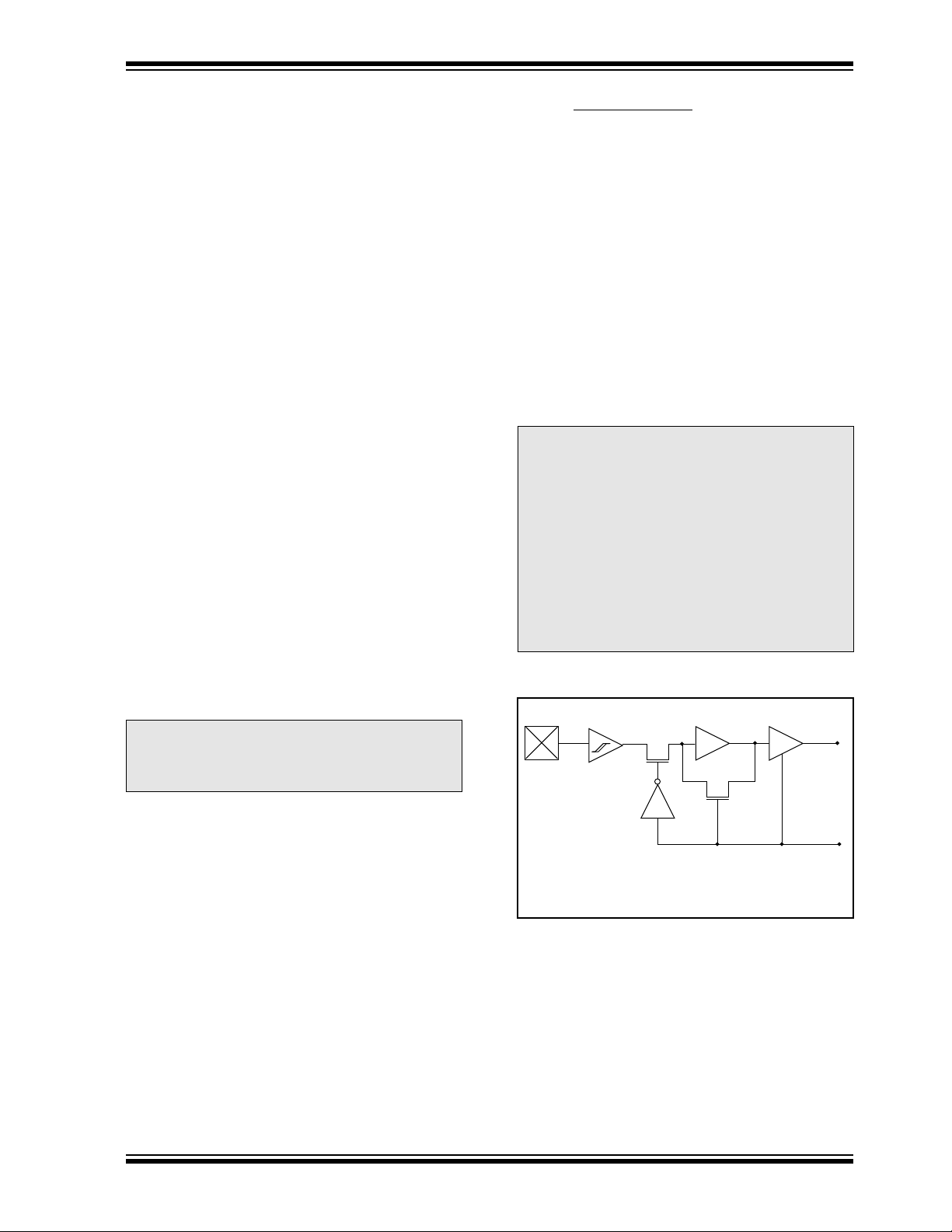
PIC17C4X
9.0 I/O PORTS
The PIC17C4X devices have five I/O ports, PORTA
through PORTE. PORTB through POR TE hav e a corresponding Data Direction Register (DDR), which is used
to configure the port pins as inputs or outputs. These
five ports are made up of 33 I/O pins. Some of these
ports pins are multiplexed with alternate functions.
PORTC, PORTD, and PORTE are multiplexed with the
system bus. These pins are configured as the system
bus when the device’ s configuration bits are selected to
Microprocessor or Extended Microcontroller modes. In
the two other microcontroller modes, these pins are
general purpose I/O.
PORTA and PORTB are multiplex ed with the peripheral
features of the device. These peripheral features are:
• Timer modules
• Capture module
• PWM module
• USART/SCI module
• External Interrupt pin
When some of these peripheral modules are turned on,
the port pin will automatically configure to the alternate
function. The modules that do this are:
• PWM module
• USART/SCI module
When a pin is automatically configured as an output by
a peripheral module, the pins data direction (DDR) bit
is unknown. After disabling the peripheral module, the
user should re-initialize the DDR bit to the desired configuration.
The other peripheral modules (which require an input)
must have their data direction bit configured appropriately.
9.1 POR
PORTA is a 6-bit wide latch. PORTA does not have a
corresponding Data Direction Register (DDR).
Reading PORTA reads the status of the pins.
The RA1 pin is multiplexed with TMR0 clock input, and
RA4 and RA5 are multiplexed with the USART functions. The control of RA4 and RA5 as outputs is automatically configured by the USART module.
9.1.1 USING RA2, RA3 AS OUTPUTS
The RA2 and RA3 pins are open drain outputs. To use
the RA2 or the RA3 pin(s) as output(s), simply write to
the PORTA register the desired value. A '0' will cause
the pin to drive low , while a '1' will cause the pin to float
(hi-impedance). An external pull-up resistor should be
used to pull the pin high. Writes to PORTA will not affect
the other pins.
Note: When using the RA2 or RA3 pin(s) as out-
TA Register
put(s), read-modify-write instructions (such
as BCF , BSF , BTG ) on PORTA are not recommended.
Such operations read the port pins, do the
desired operation, and then write this value
to the data latch. This may inadvertently
cause the RA2 or RA3 pins to switch from
input to output (or vice-versa).
It is recommended to use a shadow register for PORTA. Do the bit oper ations on this
shadow register and then move it to
PORTA.
FIGURE 9-1: RA0 AND RA1 BLOCK
DIAGRAM
Note: A pin that is a peripheral input, can be con-
figured as an output (DDRx<y> is cleared).
The peripheral events will be determined
by the action output on the port pin.
Note: I/O pins have protection diodes to VDD and VSS.
1996 Microchip Technology Inc. DS30412C-page 53
DATA BUS
RD_PORTA
(Q2)
Page 54

PIC17C4X
FIGURE 9-2: RA2 AND RA3 BLOCK
DIAGRAM
QD
Q
CK
Note: I/O pins have protection diodes to VSS.
RD_PORTA
WR_PORTA
TABLE 9-1: PORTA FUNCTIONS
Data Bus
(Q2)
(Q4)
FIGURE 9-3: RA4 AND RA5 BLOCK
DIAGRAM
Serial port input signal
Data Bus
RD_PORTA
Serial port output signals
OE = SPEN,SYNC,TXEN, CREN, SREN for RA4
= SPEN (SYNC+SYNC,CSRC) for RA5
OE
Note: I/O pins have protection diodes to VDD and VSS.
(Q2)
Name Bit0 Buffer Type Function
RA0/INT bit0 ST Input or external interrupt input.
RA1/T0CKI bit1 ST Input or clock input to the TMR0 timer/counter, and/or an external interrupt input.
RA2 bit2 ST Input/Output. Output is open drain type.
RA3 bit3 ST Input/Output. Output is open drain type.
RA4/RX/DT bit4 ST Input or USART Asynchronous Receive or USART Synchronous Data.
RA5/TX/CK bit5 ST Input or USART Asynchronous Transmit or USART Synchronous Clock.
RBPU
bit7 — Control bit for PORTB weak pull-ups.
Legend: ST = Schmitt Trigger input.
TABLE 9-2: REGISTERS/BITS ASSOCIATED WITH PORTA
Address Name Bit 7 Bit 6 Bit 5 Bit 4 Bit 3 Bit 2 Bit 1 Bit 0
10h, Bank 0 PORTA
05h, Unbanked T0STA INTEDG T0SE
13h, Bank 0 RCSTA SPEN
15h, Bank 0 TXSTA CSRC
Legend: x = unknown, u = unchanged, - = unimplemented reads as '0'. Shaded cells are not used by PORTA.
Note 1: Other (non power-up) resets include: external reset through MCLR
RBPU — RA5 RA4 RA3 RA2 RA1/T0CKI RA0/INT 0-xx xxxx 0-uu uuuu
T0CS PS3 PS2 PS1 PS0 —
RC9 SREN CREN — FERR OERR RC9D 0000 -00x 0000 -00u
TX9 TXEN SYNC — — TRMT TX9D 0000 --1x 0000 --1u
Value on
Power-on
0000 000- 0000 000-
and the Watchdog Timer Reset.
Reset
Value on all
other resets
(Note1)
DS30412C-page 54
1996 Microchip Technology Inc.
Page 55
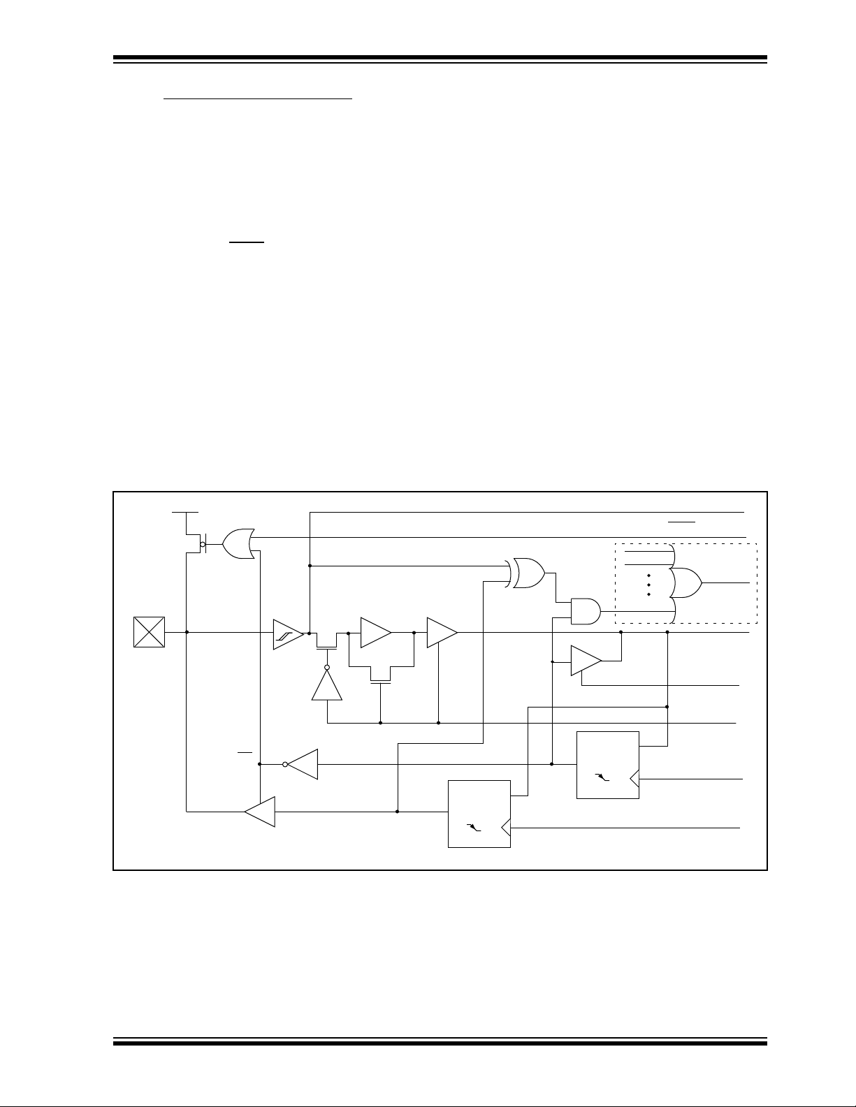
PIC17C4X
9.2 POR
TB and DDRB Registers
This interrupt can wake the device from SLEEP. The
user, in the interrupt service routine, can clear the inter-
PORTB is an 8-bit wide bi-directional port. The corresponding data direction register is DDRB. A '1' in DDRB
configures the corresponding port pin as an input. A '0'
in the DDRB register configures the corresponding port
pin as an output. Reading PORTB reads the status of
the pins, whereas writing to it will write to the port latch.
Each of the PORTB pins has a weak internal pull-up. A
single control bit can turn on all the pull-ups. This is
done by clearing the RBPU
(PORTA<7>) bit. The weak
pull-up is automatically turned off when the port pin is
configured as an output. The pull-ups are enabled on
any reset.
PORTB also has an interrupt on change feature. Only
pins configured as inputs can cause this interrupt to
occur (i.e. any RB7:RB0 pin configured as an output is
excluded from the interrupt on change comparison).
The input pins (of RB7:RB0) are compared with the
rupt by:
a) Read-Write PORTB (such as; MOVPF PORTB,
PORTB ). This will end mismatch condition.
b) Then, clear the RBIF bit.
A mismatch condition will continue to set the RBIF bit.
Reading then writing PORTB will end the mismatch
condition, and allow the RBIF bit to be cleared.
This interrupt on mismatch feature, together with software configurable pull-ups on this port, allows easy
interface to a key pad and mak e it possib le for wake-up
on key-depression. For an example, refer to AN552 in
the
Embedded Control Handbook
The interrupt on change feature is recommended for
wake-up on operations where PORTB is only used for
the interrupt on change feature and key depression
operation.
value in the PORTB data latch. The “mismatch” outputs
of RB7:RB0 are OR’ed together to generate the
PORTB Interrupt Flag RBIF (PIR<7>).
FIGURE 9-4: BLOCK DIAGRAM OF RB<7:4> AND RB<1:0> PORT PINS
Weak
Pull-Up
Match Signal
from other
port pins
.
Peripheral Data in
RBPU
(PORTA<7>)
RBIF
OE
Note: I/O pins have protection diodes to VDD and VSS.
Port
Input Latch
Port
Data
Data Bus
RD_DDRB (Q2)
RD_PORTB (Q2)
D
Q
CK
D
Q
CK
WR_DDRB (Q4)
WR_PORTB (Q4)
1996 Microchip Technology Inc. DS30412C-page 55
Page 56

PIC17C4X
FIGURE 9-5: BLOCK DIAGRAM OF RB3 AND RB2 PORT PINS
Weak
Pull-Up
Port
Input Latch
Match Signal
from other
port pins
Peripheral Data in
(PORTA<7>)
RBPU
RBIF
Data Bus
RD_DDRB (Q2)
RD_PORTB (Q2)
OE
Note: I/O pins have protection diodes to VDD and Vss.
Port
Data
D
Q
CK
D
Q
CK
R
WR_DDRB (Q4)
WR_PORTB (Q4)
PWM_output
PWM_select
DS30412C-page 56
1996 Microchip Technology Inc.
Page 57

PIC17C4X
Example 9-1 shows the instruction sequence to initial-
EXAMPLE 9-1: INITIALIZING PORTB
ize PORTB. The Bank Select Register (BSR) must be
selected to Bank 0 for the port to be initialized.
MOVLB 0 ; Select Bank 0
CLRF PORTB ; Initialize PORTB by clearing
; output data latches
MOVLW 0xCF ; Value used to initialize
; data direction
MOVWF DDRB ; Set RB<3:0> as inputs
; RB<5:4> as outputs
; RB<7:6> as inputs
TABLE 9-3: PORTB FUNCTIONS
Name Bit Buffer Type Function
RB0/CAP1 bit0 ST Input/Output or the RB0/CAP1 input pin. Software programmable weak pull-
up and interrupt on change features.
RB1/CAP2 bit1 ST Input/Output or the RB1/CAP2 input pin. Software programmable weak pull-
up and interrupt on change features.
RB2/PWM1 bit2 ST Input/Output or the RB2/PWM1 output pin. Software programmable weak
pull-up and interrupt on change features.
RB3/PWM2 bit3 ST Input/Output or the RB3/PWM2 output pin. Software programmable weak
pull-up and interrupt on change features.
RB4/TCLK12 bit4 ST Input/Output or the external clock input to Timer1 and Timer2. Software pro-
grammable weak pull-up and interrupt on change features.
RB5/TCLK3 bit5 ST Input/Output or the external clock input to Timer3. Software programmable
weak pull-up and interrupt on change features.
RB6 bit6 ST Input/Output pin. Software programmable weak pull-up and interrupt on
change features.
RB7 bit7 ST Input/Output pin. Software programmable weak pull-up and interrupt on
change features.
Legend: ST = Schmitt Trigger input.
TABLE 9-4: REGISTERS/BITS ASSOCIATED WITH PORTB
Address Name Bit 7 Bit 6 Bit 5 Bit 4 Bit 3 Bit 2 Bit 1 Bit 0
12h, Bank 0 PORTB PORTB data latch
11h, Bank 0 DDRB Data direction register for PORTB
10h, Bank 0 PORTA RBPU
06h, Unbanked CPUSTA — — STKAV GLINTD TO PD ——
07h, Unbanked INTSTA PEIF
16h, Bank 1 PIR RBIF
17h, Bank 1 PIE RBIE
16h, Bank 3 TCON1
17h, Bank 3 TCON2 CA2OVF CA1OVF PWM2ON PWM1ON CA1/PR3 TMR3ON TMR2ON TMR1ON 0000 0000 0000 0000
Legend: x = unknown, u = unchanged, - = unimplemented read as '0', q = Value depends on condition.
Shaded cells are not used by PORTB.
Note 1: Other (non power-up) resets include: external reset through MCLR
CA2ED1 CA2ED0 CA1ED1 CA1ED0 T16 TMR3CS TMR2CS TMR1CS 0000 0000 0000 0000
— RA5 RA4 RA3 RA2 RA1/T0CKI RA0/INT 0-xx xxxx 0-uu uuuu
T0CKIF T0IF INTF PEIE T0CKIE T0IE INTE 0000 0000 0000 0000
TMR3IF TMR2IF TMR1IF CA2IF CA1IF TXIF RCIF 0000 0010 0000 0010
TMR3IE TMR2IE TMR1IE CA2IE CA1IE TXIE RCIE 0000 0000 0000 0000
and the Watchdog Timer Reset.
Value on
Power-on
Reset
xxxx xxxx uuuu uuuu
1111 1111 1111 1111
--11 11-- --11 qq--
Value on all
other
resets
(Note1)
1996 Microchip Technology Inc. DS30412C-page 57
Page 58

PIC17C4X
9.3 POR
TC and DDRC Registers
Example 9-2 shows the instruction sequence to initialize PORTC. The Bank Select Register (BSR) must be
PORTC is an 8-bit bi-directional port. The correspond-
selected to Bank 1 for the port to be initialized.
ing data direction register is DDRC. A '1' in DDRC configures the corresponding port pin as an input. A '0' in
the DDRC register configures the corresponding port
pin as an output. Reading PORTC reads the status of
the pins, whereas writing to it will write to the port latch.
EXAMPLE 9-2: INITIALIZING PORTC
MOVLB 1 ; Select Bank 1
CLRF PORTC ; Initialize PORTC data
PORTC is multiplexed with the system bus. When
operating as the system bus, PORTC is the low order
byte of the address/data bus (AD7:AD0). The timing for
the system bus is shown in the Electrical Characteristics section.
MOVLW 0xCF ; Value used to initialize
MOVWF DDRC ; Set RC<3:0> as inputs
Note: This port is configured as the system bus
when the device’s configuration bits are
selected to Microprocessor or Extended
Microcontroller modes. In the two other
microcontroller modes, this port is a general purpose I/O.
FIGURE 9-6: BLOCK DIAGRAM OF RC<7:0> PORT PINS
; latches before setting
; the data direction
; register
; data direction
; RC<5:4> as outputs
RC<7:6> as inputs
;
to D_Bus → IR
INSTRUCTION READ
TTL
Input
Buffer
Port
0
Data
1
Note: I/O pins have protection diodes to VDD and Vss.
Data Bus
RD_PORTC
CK
CK
S
D
WR_PORTC
D
RD_DDRC
WR_DDRC
EX_EN
DATA/ADDR_OUT
DRV_SYS
SYS BUS
Control
Q
Q
R
DS30412C-page 58
1996 Microchip Technology Inc.
Page 59
TABLE 9-5: PORTC FUNCTIONS
Name Bit Buffer Type Function
RC0/AD0 bit0 TTL Input/Output or system bus address/data pin.
RC1/AD1 bit1 TTL Input/Output or system bus address/data pin.
RC2/AD2 bit2 TTL Input/Output or system bus address/data pin.
RC3/AD3 bit3 TTL Input/Output or system bus address/data pin.
RC4/AD4 bit4 TTL Input/Output or system bus address/data pin.
RC5/AD5 bit5 TTL Input/Output or system bus address/data pin.
RC6/AD6 bit6 TTL Input/Output or system bus address/data pin.
RC7/AD7 bit7 TTL Input/Output or system bus address/data pin.
Legend: TTL = TTL input.
TABLE 9-6: REGISTERS/BITS ASSOCIATED WITH PORTC
PIC17C4X
Address Name Bit 7 Bit 6 Bit 5 Bit 4 Bit 3 Bit 2 Bit 1 Bit 0
11h, Bank 1 PORTC
10h, Bank 1 DDRC Data direction register for PORTC
Legend: x = unknown, u = unchanged.
Note 1: Other (non power-up) resets include: external reset through MCLR
RC7/
AD7
RC6/
AD6
RC5/
AD5
RC4/
AD4
RC3/
AD3
RC2/
AD2
and the Watchdog Timer Reset.
RC1/
AD1
RC0/
AD0
Value on
Power-on
Reset
xxxx xxxx uuuu uuuu
1111 1111 1111 1111
Value on all
other resets
(Note1)
1996 Microchip Technology Inc. DS30412C-page 59
Page 60

PIC17C4X
9.4 POR
TD and DDRD Registers
Example 9-3 shows the instruction sequence to initialize PORTD. The Bank Select Register (BSR) must be
PORTD is an 8-bit bi-directional port. The correspond-
selected to Bank 1 for the port to be initialized.
ing data direction register is DDRD. A '1' in DDRD configures the corresponding port pin as an input. A '0' in
the DDRC register configures the corresponding port
pin as an output. Reading PORTD reads the status of
the pins, whereas writing to it will write to the port latch.
EXAMPLE 9-3: INITIALIZING PORTD
MOVLB 1 ; Select Bank 1
CLRF PORTD ; Initialize PORTD data
PORTD is multiplexed with the system bus. When
operating as the system bus, PORTD is the high order
byte of the address/data bus (AD15:AD8). The timing
for the system bus is shown in the Electrical Characteristics section.
MOVLW 0xCF ; Value used to initialize
MOVWF DDRD ; Set RD<3:0> as inputs
Note: This port is configured as the system bus
when the device’s configuration bits are
selected to Microprocessor or Extended
Microcontroller modes. In the two other
microcontroller modes, this port is a general purpose I/O.
FIGURE 9-7: PORTD BLOCK DIAGRAM (IN I/O PORT MODE)
; latches before setting
; the data direction
; register
; data direction
; RD<5:4> as outputs
RD<7:6> as inputs
;
to D_Bus → IR
INSTRUCTION READ
TTL
Input
Buffer
Port
0
Data
1
Note: I/O pins have protection diodes to VDD and Vss.
Data Bus
RD_PORTD
CK
CK
S
D
WR_PORTD
D
RD_DDRD
WR_DDRD
EX_EN
DATA/ADDR_OUT
DRV_SYS
SYS BUS
Control
Q
Q
R
DS30412C-page 60
1996 Microchip Technology Inc.
Page 61

TABLE 9-7: PORTD FUNCTIONS
Name Bit Buffer Type Function
RD0/AD8 bit0 TTL Input/Output or system bus address/data pin.
RD1/AD9 bit1 TTL Input/Output or system bus address/data pin.
RD2/AD10 bit2 TTL Input/Output or system bus address/data pin.
RD3/AD11 bit3 TTL Input/Output or system bus address/data pin.
RD4/AD12 bit4 TTL Input/Output or system bus address/data pin.
RD5/AD13 bit5 TTL Input/Output or system bus address/data pin.
RD6/AD14 bit6 TTL Input/Output or system bus address/data pin.
RD7/AD15 bit7 TTL Input/Output or system bus address/data pin.
Legend: TTL = TTL input.
PIC17C4X
TABLE 9-8: REGISTERS/BITS ASSOCIATED WITH PORTD
Address Name Bit 7 Bit 6 Bit 5 Bit 4 Bit 3 Bit 2 Bit 1 Bit 0
13h, Bank 1 PORTD
12h, Bank 1 DDRD Data direction register for PORTD
Legend: x = unknown, u = unchanged.
Note 1: Other (non power-up) resets include: external reset through MCLR
RD7/
AD15
RD6/
AD14
RD5/
AD13
RD4/
AD12
RD3/
AD11
RD2/
AD10
and the Watchdog Timer Reset.
RD1/
AD9
RD0/
AD8
Value on
Power-on
Reset
xxxx xxxx uuuu uuuu
1111 1111 1111 1111
Value on all
other resets
(Note1)
1996 Microchip Technology Inc. DS30412C-page 61
Page 62

PIC17C4X
9.4.1 PORTE AND DDRE REGISTER
Example 9-4 shows the instruction sequence to initialize PORTE. The Bank Select Register (BSR) must be
PORTE is a 3-bit bi-directional port. The corresponding
selected to Bank 1 for the port to be initialized.
data direction register is DDRE. A '1' in DDRE configures the corresponding port pin as an input. A '0' in the
DDRE register configures the corresponding port pin
as an output. Reading PORTE reads the status of the
pins, whereas writing to it will write to the port latch.
EXAMPLE 9-4: INITIALIZING PORTE
MOVLB 1 ; Select Bank 1
CLRF PORTE ; Initialize PORTE data
PORTE is multiplexed with the system bus. When
operating as the system bus, POR TE contains the control signals for the address/data bus (AD15:AD0).
These control signals are Address Latch Enable (ALE),
Output Enable (OE
nals OE
and WR are active low signals. The timing for
), and Write (WR). The control sig-
MOVLW 0x03 ; Value used to initialize
MOVWF DDRE ; Set RE<1:0> as inputs
the system bus is shown in the Electrical Characteristics section.
Note: This port is configured as the system bus
when the device’s configuration bits are
selected to Microprocessor or Extended
Microcontroller modes. In the two other
microcontroller modes, this port is a general purpose I/O.
FIGURE 9-8: PORTE BLOCK DIAGRAM (IN I/O PORT MODE)
; latches before setting
; the data direction
; register
; data direction
; RE<2> as outputs
RE<7:3> are always
;
read as '0'
;
TTL
Input
Buffer
Port
0
Data
1
Note: I/O pins have protection diodes to VDD and Vss.
Q
Q
R
CK
CK
S
Data Bus
RD_PORTE
D
WR_PORTE
D
RD_DDRE
WR_DDRE
EX_EN
CNTL
DRV_SYS
SYS BUS
Control
DS30412C-page 62
1996 Microchip Technology Inc.
Page 63

PIC17C4X
TABLE 9-9: PORTE FUNCTIONS
Name Bit Buffer Type Function
RE0/ALE bit0 TTL Input/Output or system bus Address Latch Enable (ALE) control pin.
RE1/OE
RE2/WR
bit2 TTL Input/Output or system bus Write (WR) control pin.
Legend: TTL = TTL input.
TABLE 9-10: REGISTERS/BITS ASSOCIATED WITH PORTE
bit1 TTL Input/Output or system bus Output Enable (OE) control pin.
Address Name Bit 7 Bit 6 Bit 5 Bit 4 Bit 3 Bit 2 Bit 1 Bit 0
15h, Bank 1 PORTE
14h, Bank 1 DDRE Data direction register for PORTE ---- -111 ---- -111
Legend: x = unknown, u = unchanged, - = unimplemented read as '0'. Shaded cells are not used by PORTE.
Note 1: Other (non power-up) resets include: external reset through MCLR and the Watchdog Timer Reset.
— — — — — RE2/WR RE1/OE RE0/ALE ---- -xxx ---- -uuu
Value on
Power-on
Reset
Value on all
other resets
(Note1)
1996 Microchip Technology Inc. DS30412C-page 63
Page 64
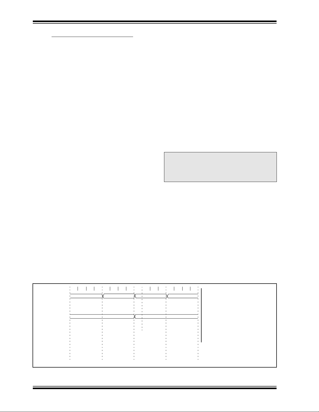
PIC17C4X
9.5 I/O Programming Considerations
9.5.1 BI-DIRECTIONAL I/O PORTS
Any instruction which writes, operates internally as a
read followed by a write operation. For example, the
BCF and BSF instructions read the register into the
CPU, execute the bit operation, and write the result
back to the register. Caution must be used when these
instructions are applied to a port with both inputs and
outputs defined. For example, a BSF operation on bit5
of PORTB will cause all eight bits of PORTB to be read
into the CPU. Then the BSF operation takes place on
bit5 and PORTB is written to the output latches. If
another bit of PORTB is used as a bi-directional I/O pin
(e.g. bit0) and it is defined as an input at this time, the
input signal present on the pin itself would be read into
the CPU and re-written to the data latch of this particular pin, overwriting the previous content. As long as the
pin stays in the input mode, no problem occurs. However, if bit0 is switched into output mode later on, the
content of the data latch may now be unknown.
Reading a port reads the values of the por t pins. Writing
to the port register writes the value to the port latch.
When using read-modify-write instructions (BCF, BSF,
BTG, etc.) on a port, the value of the port pins is read,
the desired operation is performed with this value, and
the value is then written to the port latch.
Example 9-5 shows the effect of two sequential
read-modify-write instructions on an I/O port.
EXAMPLE 9-5: READ MODIFY WRITE
INSTRUCTIONS ON AN
I/O PORT
; Initial PORT settings: PORTB<7:4> Inputs
; PORTB<3:0> Outputs
; PORTB<7:6> have pull-ups and are
; not connected to other circuitry
;
; PORT latch PORT pins
; ---------- --------;
BCF PORTB, 7 01pp pppp 11pp pppp
BCF PORTB, 6 10pp pppp 11pp pppp
;
BCF DDRB, 7 10pp pppp 11pp pppp
BCF DDRB, 6 10pp pppp 10pp pppp
;
; Note that the user may have expected the
; pin values to be 00pp pppp. The 2nd BCF
; caused RB7 to be latched as the pin value
; (High).
Note: A pin actively outputting a Low or High
should not be driven from external devices
in order to change the level on this pin (i.e.
“wired-or”, “wired-and”). The resulting high
output currents may damage the device.
9.5.2 SUCCESSIVE OPERATIONS ON I/O P ORTS
The actual write to an I/O port happens at the end of an
instruction cycle, whereas for reading, the data must be
valid at the beginning of the instruction cycle (Figure 9-
9). Therefore, care must be exercised if a write follo wed
by a read operation is carried out on the same I/O port.
The sequence of instructions should be such to allow
the pin voltage to stabilize (load dependent) before
executing the instruction that reads the values on that
I/O port. Otherwise, the previous state of that pin may
be read into the CPU rather than the “new” state. When
in doubt, it is better to separate these instructions with
a NOP or another instruction not accessing this I/O port.
FIGURE 9-9: SUCCESSIVE I/O OPERATION
Q3
PC + 3
NOP
NOPMOVF PORTB,W
Q4
Note:
This example shows a write to PORTB
followed by a read from PORTB.
Note that:
data setup time = (0.25 TCY - TPD)
where TCY = instruction cycle.
TPD = propagation delay
Therefore, at higher clock
frequencies, a write followed by a
read may be problematic.
NOP
Q3
Q4
Q1 Q2
Q4
Q1 Q2
Instruction
fetched
RB7:RB0
Instruction
executed
DS30412C-page 64 1996 Microchip Technology Inc.
MOVWF PORTB
Q3
PC PC + 1 PC + 2
write to
PORTB
Q1 Q2
MOVF PORTB,W
MOVWF PORTB
write to
PORTB
Q3
Q4
Q1 Q2
Port pin
sampled here
Page 65

PIC17C4X
10.0 OVERVIEW OF TIMER RESOURCES
The PIC17C4X has four timer modules. Each module
can generate an interrupt to indicate that an event has
occurred. These timers are called:
• Timer0 - 16-bit timer with programmable 8-bit
prescaler
• Timer1 - 8-bit timer
• Timer2 - 8-bit timer
• Timer3 - 16-bit timer
For enhanced time-base functionality, two input Captures and two Pulse Width Modulation (PWM) outputs
are possible. The PWMs use the TMR1 and TMR2
resources and the input Captures use the TMR3
resource.
10.1 Timer0
The Timer0 module is a simple 16-bit overflow counter.
The clock source can be either the internal system
clock (Fosc/4) or an external clock.
The Timer0 module also has a programmable prescaler option. The PS3:PS0 bits (T0STA<4:1>) determine the prescaler value. TMR0 can increment at the
following rates: 1:1, 1:2, 1:4, 1:8, 1:16, 1:32, 1:64,
1:128, 1:256.
When TImer0’s clock source is an external clock, the
Timer0 module can be selected to increment on either
the rising or falling edge.
Synchronization of the external clock occurs after the
prescaler. When the prescaler is used, the external
clock frequency may be higher then the device’s frequency. The maximum frequency is 50 MHz, given the
high and low time requirements of the clock.
Overview
10.3 Timer2 Over
The TMR2 module is an 8-bit timer/counter with an 8bit period register (PR2). When the TMR2 value rolls
over from the period match value to 0h, the TMR2IF
flag is set, and an interrupt will be generated when
enabled. In counter mode, the clock comes from the
RB4/TCLK12 pin, which can also be selected to be the
clock for the TMR1 module.
TMR1 can be concatenated to TMR2 to form a 16-bit
timer. The TMR2 register is the MSB and TMR1 is the
LSB. When in the 16-bit timer mode, there is a corresponding 16-bit period register (PR2:PR1). When the
TMR2:TMR1 value rolls over from the period match
value to 0h, the TMR1IF flag is set, and an interrupt
will be generated when enabled.
10.4 Timer3 O
The TImer3 module is a 16-bit timer/counter with a 16bit period register. When the TMR3H:TMR3L value
rolls over to 0h, the TMR3IF bit is set and an interrupt
will be generated when enabled. In counter mode, the
clock comes from the RB5/TCLK3 pin.
When operating in the dual capture mode, the period
registers become the second 16-bit capture register.
10.5 Role of the
The timer modules are general purpose, but have dedicated resources associated with them. TImer1 and
Timer2 are the time-bases for the two Pulse Width
Modulation (PWM) outputs, while Timer3 is the timebase for the two input captures.
view
verview
Timer/Counters
10.2 Timer1
The TImer0 module is an 8-bit timer/counter with an 8bit period register (PR1). When the TMR1 value rolls
over from the period match value to 0h, the TMR1IF
flag is set, and an interrupt will be generated when
enabled. In counter mode, the clock comes from the
RB4/TCLK12 pin, which can also be selected to be the
clock for the Timer2 module.
TMR1 can be concatenated to TMR2 to form a 16-bit
timer. The TMR1 register is the LSB and TMR2 is the
MSB. When in the 16-bit timer mode, there is a corresponding 16-bit period register (PR2:PR1). When the
TMR2:TMR1 value rolls over from the period match
value to 0h, the TMR1IF flag is set, and an interrupt
will be generated when enabled.
1996 Microchip Technology Inc. DS30412C-page 65
Overview
Page 66

PIC17C4X
NOTES:
DS30412C-page 66
1996 Microchip Technology Inc.
Page 67

PIC17C4X
11.0 TIMER0
The Timer0 module consists of a 16-bit timer/counter,
TMR0. The high byte is TMR0H and the low byte is
TMR0L. A software programmable 8-bit prescaler
makes an effective 24-bit overflow timer. The clock
source is also software programmable as either the
internal instruction clock or the RA1/T0CKI pin. The
control bits for this module are in register T0STA
(Figure 11-1).
FIGURE 11-1: T0STA REGISTER
R/W - 0 R/W - 0 R/W - 0 R/W - 0 R/W - 0 R/W - 0 R/W - 0 U - 0
INTEDG T0SE T0CS PS3 PS2 PS1 PS0
bit7 bit0
bit 7: INTEDG : RA0/INT Pin Interrupt Edge Select bit
This bit selects the edge upon which the interrupt is detected
1 =Rising edge of RA0/INT pin generates interrupt
0 =Falling edge of RA0/INT pin generates interrupt
bit 6: T0SE : Timer0 Clock Input Edge Select bit
This bit selects the edge upon which TMR0 will increment
When
T0CS = 0
1 =Rising edge of RA1/T0CKI pin increments TMR0 and/or generates a T0CKIF interrupt
0 =Falling edge of RA1/T0CKI pin increments TMR0 and/or generates a T0CKIF interrupt
When
T0CS = 1
Don’t care
bit 5: T0CS : Timer0 Clock Source Select bit
This bit selects the clock source for TMR0.
1 =Internal instruction clock cycle (T
0 =T0CKI pin
bit 4-1: PS3:PS0 : Timer0 Prescale Selection bits
These bits select the prescale value for TMR0.
(ADDRESS: 05h, UNBANKED)
)
CY
—
R = Readable bit
W = Writable bit
U = Unimplemented,
Read as '0'
-n = Value at POR reset
PS3:PS0 Prescale V alue
0000
0001
0010
0011
0100
0101
0110
0111
1xxx
bit 0: Unimplemented : Read as '0'
1996 Microchip Technology Inc. DS30412C-page 67
1:1
1:2
1:4
1:8
1:16
1:32
1:64
1:128
1:256
Page 68

( ±
PIC17C4X
11.1 Timer0
Operation
When the T0CS (T0STA<5>) bit is set, TMR0 increments on the internal clock. When T0CS is clear, TMR0
increments on the external clock (RA1/T0CKI pin). The
external clock edge can be configured in software.
When the T0SE (T0STA<6>) bit is set, the timer will
increment on the rising edge of the RA1/T0CKI pin.
When T0SE is clear , the timer will increment on the f alling edge of the RA1/T0CKI pin. The prescaler can be
programmed to introduce a prescale of 1:1 to 1:256.
The timer increments from 0000h to FFFFh and rolls
over to 0000h. On overflow, the TMR0 Interrupt Flag bit
(T0IF) is set. The TMR0 interrupt can be masked by
clearing the corresponding TMR0 Interrupt Enable bit
(T0IE). The TMR0 Interrupt Flag bit (T0IF) is automatically cleared when vectoring to the TMR0 interrupt vector.
FIGURE 11-2: TIMER0 MODULE BLOCK DIAGRAM
Prescaler
(8 stage
async ripple
counter)
4
PS3:PS0
(T0STA<4:1>)
PSOUT
RA1/T0CKI
T0SE
(T0STA<6>)
Fosc/4
(T0STA<5>)
0
1
T0CS
11.2 Using
Timer0 with External Clock
When the external clock input is used for Timer0, it is
synchronized with the internal phase clocks.
Figure 11-3 shows the synchronization of the external
clock. This synchronization is done after the prescaler.
The output of the prescaler (PSOUT) is sampled twice
in every instruction cycle to detect a rising or a falling
edge. The timing requirements for the external clock
are detailed in the electrical specification section for the
desired device.
11.2.1 DELAY FROM EXTERNAL CLOCK EDGE
Since the prescaler output is synchronized with the
internal clocks, there is a small delay from the time the
external clock edge occurs to the time TMR0 is actually
incremented. Figure 11-3 shows that this delay is
between 3T
OSC
and 7T
. Thus, for example, mea-
OSC
suring the interval between two edges (e.g. period) will
be accurate within ± 4T
Synchronization
Q2 Q4
OSC
121 ns @ 33 MHz).
Interrupt on overflow
sets T0IF
(INTST A<5>)
TMR0H<8> TMR0L<8>
FIGURE 11-3: TMR0 TIMING WITH EXTERNAL CLOCK (INCREMENT ON FALLING EDGE)
Q1 Q2 Q3 Q4 Q1 Q2 Q3 Q4 Q1 Q2 Q3 Q4 Q1 Q2 Q3 Q4
Prescaler
output
(PSOUT)
Sampled
Prescaler
output
Increment
TMR0
TMR0
(note 1)
T0 T0 + 1 T0 + 2
Note 1: The delay from the T0CKI edge to the TMR0 increment is 3Tosc to 7Tosc.
2: ↑ = PSOUT is sampled here.
3: The PSOUT high time is too short and is missed by the sampling circuit.
(note 3)
(note 2)
DS30412C-page 68
1996 Microchip Technology Inc.
Page 69

PIC17C4X
11.3 Read/Write
Consideration for TMR0
Although TMR0 is a 16-bit timer/counter, only 8-bits at
a time can be read or written during a single instruction
cycle. Care must be taken during any read or write.
11.3.1 READING 16-BIT VALUE
The problem in reading the entire 16-bit value is that
after reading the low (or high) byte, its value may
change from FFh to 00h.
Example 11-1 shows a 16-bit read. To ensure a proper
read, interrupts must be disabled during this routine.
EXAMPLE 11-1: 16-BIT READ
MOVPF TMR0L, TMPLO ;read low tmr0
MOVPF TMR0H, TMPHI ;read high tmr0
MOVFP TMPLO, WREG ;tmplo −> wreg
CPFSLT TMR0L ;tmr0l < wreg?
RETURN ;no then return
MOVPF TMR0L, TMPLO ;read low tmr0
MOVPF TMR0H, TMPHI ;read high tmr0
RETURN ;return
11.3.2 WRITING A 16-BIT VALUE TO TMR0
Since writing to either TMR0L or TMR0H will effectively
inhibit increment of that half of the TMR0 in the next
cycle (following write), but not inhibit increment of the
other half, the user must write to TMR0L first and
TMR0H next in two consecutive instructions, as shown
in Example 11-2. The interrupt must be disabled. Any
write to either TMR0L or TMR0H clears the prescaler.
EXAMPLE 11-2: 16-BIT WRITE
BSF CPUSTA, GLINTD ; Disable interrupt
MOVFP RAM_L, TMR0L ;
MOVFP RAM_H, TMR0H ;
BCF CPUSTA, GLINTD ; Done, enable interrupt
11.4 Prescaler
Timer0 has an 8-bit prescaler. The prescaler assignment is fully under software control; i.e., it can be
changed “on the fly” during program execution. When
changing the prescaler assignment, clearing the prescaler is recommended before changing assignment.
The value of the prescaler is “unknown,” and assigning
a value that is less then the present value makes it difficult to take this unknown time into account.
Assignments
FIGURE 11-4: TMR0 TIMING: WRITE HIGH OR LOW BYTE
Q1 Q2 Q3 Q4 Q1 Q2 Q3 Q4 Q1 Q2 Q3 Q4 Q1 Q2 Q3 Q4 Q1 Q2 Q3 Q4
AD15:AD0
ALE
TMR0L
Fetch
Instruction
executed
TMR0H
PC
T0 T0+1 New T0 (NT0) New T0+1
PC+1 PC+2 PC+3 PC+4
MOVFP W,TMR0L
Write to TMR0L
MOVFP TMR0L,W
Read TMR0L
(Value = NT0)
MOVFP TMR0L,W
Read TMR0L
(Value = NT0)
MOVFP TMR0L,W
Read TMR0L
(Value = NT0 +1)
1996 Microchip Technology Inc. DS30412C-page 69
Page 70

PIC17C4X
FIGURE 11-5: TMR0 READ/WRITE IN TIMER MODE
Q1 Q2 Q3 Q4 Q1 Q2 Q3 Q4 Q1 Q2 Q3 Q4 Q1 Q2 Q3 Q4 Q1 Q2 Q3 Q4 Q1 Q2 Q3 Q4
AD15:AD0
ALE
WR_TRM0L
WR_TMR0H
RD_TMR0L
TMR0H
TMR0L
Instruction
fetched
Instruction
executed
12
FE
MOVFP
DATAL,TMR0L
Write TMR0L
Previously
Fetched
Instruction
In this example, old TMR0 value is 12FEh, new value of AB56h is written.
12
FF
MOVFP
DAT AH,TMR0H
Write TMR0H
MOVFP
DATAL,TMR0L
Write TMR0L
13
56
MOVPF
TMR0L,W
Read TMR0L
MOVFP
DAT AH,TMR0H
Write TMR0H
TABLE 11-1: REGISTERS/BITS ASSOCIATED WITH TIMER0
Address Name Bit 7 Bit 6 Bit 5 Bit 4 Bit 3 Bit 2 Bit 1 Bit 0
05h, Unbanked T0STA
06h, Unbanked CPUSTA — — STKAV GLINTD TO PD — — --11 11-- --11 qq-07h, Unbanked INTSTA PEIF T0CKIF T0IF INTF PEIE T0CKIE T0IE INTE 0000 0000 0000 0000
0Bh, Unbanked TMR0L TMR0 register; low byte
0Ch, Unbanked TMR0H TMR0 register; high byte
Legend: x = unknown, u = unchanged, - = unimplemented read as a '0', q - value depends on condition, Shaded cells are not used by Timer0.
Note 1: Other (non power-up) resets include: external reset through MCLR
INTEDG T0SE T0CS PS3 PS2 PS1 PS0 — 0000 000- 0000 000-
and the Watchdog Timer Reset.
AB
MOVPF
TMR0L,W
Read TMR0L
MOVPF
TMR0L,W
Read TMR0L
57 58
MOVPF
TMR0L,W
Read TMR0L
MOVPF
TMR0L,W
Read TMR0L
Value on
Power-on
xxxx xxxx uuuu uuuu
xxxx xxxx uuuu uuuu
MOVPF
TMR0L,W
Read TMR0L
MOVPF
TMR0L,W
Read TMR0L
Reset
Value on all
other resets
(Note1)
DS30412C-page 70
1996 Microchip Technology Inc.
Page 71

PIC17C4X
12.0 TIMER1, TIMER2, TIMER3, PWMS AND CAPTURES
The PIC17C4X has a wealth of timers and time-based
functions to ease the implementation of control applications. These time-base functions include two PWM outputs and two Capture inputs.
Timer1 and Timer2 are two 8-bit incrementing timers,
each with a period register (PR1 and PR2 respectively)
and separate overflow interrupt flags. Timer1 and
Timer2 can operate either as timers (increment on
internal Fosc/4 clock) or as counters (increment on falling edge of external clock on pin RB4/TCLK12). They
are also software configurable to operate as a single
16-bit timer. These timers are also used as the
time-base for the PWM (pulse width modulation) module.
Timer3 is a 16-bit timer/counter consisting of the
TMR3H and TMR3L registers. This timer has four other
associated registers. Two registers are used as a 16-bit
period register or a 16-bit Capture1 register
(PR3H/CA1H:PR3L/CA1L). The other two registers are
strictly the Capture2 registers (CA2H:CA2L). Timer3 is
the time-base for the two 16-bit captures.
TMR3 can be software configured to increment from
the internal system clock or from an external signal on
the RB5/TCLK3 pin.
Figure 12-1 and Figure 12-2 are the control registers
for the operation of Timer1, Timer2, and Timer3, as w ell
as PWM1, PWM2, Capture1, and Capture2.
FIGURE 12-1: TCON1 REGISTER (ADDRESS: 16h, BANK 3)
R/W - 0 R/W - 0 R/W - 0 R/W - 0 R/W - 0 R/W - 0 R/W - 0 R/W - 0
CA2ED1 CA2ED0 CA1ED1 CA1ED0 T16 TMR3CS TMR2CS TMR1CS
bit7 bit0
bit 7-6: CA2ED1:CA2ED0 : Capture2 Mode Select bits
00 = Capture on every falling edge
01 = Capture on every rising edge
10 = Capture on every 4th rising edge
11 = Capture on every 16th rising edge
bit 5-4: CA1ED1:CA1ED0 : Capture1 Mode Select bits
00 = Capture on every falling edge
01 = Capture on every rising edge
10 = Capture on every 4th rising edge
11 = Capture on every 16th rising edge
bit 3: T16 : Timer1:Timer2 Mode Select bit
1 =Timer1 and Timer2 form a 16-bit timer
0 =Timer1 and Timer2 are two 8-bit timers
bit 2: TMR3CS : Timer3 Clock Source Select bit
1 =TMR3 increments off the falling edge of the RB5/TCLK3 pin
0 =TMR3 increments off the internal clock
bit 1: TMR2CS : Timer2 Clock Source Select bit
1 =TMR2 increments off the falling edge of the RB4/TCLK12 pin
0 =TMR2 increments off the internal clock
bit 0: TMR1CS : Timer1 Clock Source Select bit
1 =TMR1 increments off the falling edge of the RB4/TCLK12 pin
0 =TMR1 increments off the internal clock
R = Readable bit
W = Writable bit
-n = Value at POR reset
1996 Microchip Technology Inc. DS30412C-page 71
Page 72

PIC17C4X
FIGURE 12-2: TCON2 REGISTER (ADDRESS: 17h, BANK 3)
R - 0 R - 0 R/W - 0 R/W - 0 R/W - 0 R/W - 0 R/W - 0 R/W - 0
CA2OVF CA1OVF PWM2ON PWM1ON CA1/PR3
bit7 bit0
bit 7: CA2OVF : Capture2 Overflow Status bit
This bit indicates that the capture value had not been read from the capture register pair (CA2H:CA2L)
before the next capture e v ent occurred. The capture register retains the oldest unread capture value (last
capture before overflo w). Subsequent capture events will not update the capture register with the Timer3
value until the capture register has been read (both bytes).
1 =Overflow occurred on Capture2 register
0 =No overflow occurred on Capture2 register
bit 6: CA1OVF : Capture1 Overflow Status bit
This bit indicates that the capture value had not been read from the capture register pair
(PR3H/CA2H:PR3L/CA2L) before the next capture event occurred. The capture register retains the oldest unread capture value (last capture before overflow). Subsequent capture events will not update the
capture register with the TMR3 value until the capture register has been read (both bytes).
1 =Overflow occurred on Capture1 register
0 =No overflow occurred on Capture1 register
bit 5: PWM2ON : PWM2 On bit
1 =PWM2 is enabled (The RB3/PWM2 pin ignores the state of the DDRB<3> bit)
0 =PWM2 is disabled (The RB3/PWM2 pin uses the state of the DDRB<3> bit for data direction)
bit 4: PWM1ON : PWM1 On bit
1 =PWM1 is enabled (The RB2/PWM1 pin ignores the state of the DDRB<2> bit)
0 =PWM1 is disabled (The RB2/PWM1 pin uses the state of the DDRB<2> bit for data direction)
bit 3: CA1/PR3
1 =Enables Capture1 (PR3H/CA1H:PR3L/CA1L is the Capture1 register. Timer3 runs without
a period register)
0 =Enables the Period register (PR3H/CA1H:PR3L/CA1L is the Period register for Timer3)
bit 2: TMR3ON : Timer3 On bit
1 =Starts Timer3
0 =Stops Timer3
bit 1: TMR2ON : Timer2 On bit
This bit controls the incrementing of the Timer2 register. When Timer2:Timer1 form the 16-bit timer (T16
is set), TMR2ON must be set. This allows the MSB of the timer to increment.
1 =Starts Timer2 (Must be enabled if the T16 bit (TCON1<3>) is set)
0 =Stops Timer2
bit 0: TMR1ON : Timer1 On bit
When
1 =Starts 16-bit Timer2:Timer1
0 =Stops 16-bit Timer2:Timer1
: CA1/PR3
T16 is set (in 16-bit Timer Mode)
Register Mode Select bit
TMR3ON TMR2ONTMR1ON
R = Readable bit
W = Writable bit
-n = Value at POR reset
When
1 =Starts 8-bit Timer1
0 =Stops 8-bit Timer1
DS30412C-page 72
T16 is clear (in 8-bit Timer Mode)
1996 Microchip Technology Inc.
Page 73

PIC17C4X
12.1 Timer1 an
12.1.1 TIMER1, TIMER2 IN 8-BIT MODE
Both Timer1 and Timer2 will operate in 8-bit mode
when the T16 bit is clear . These two timers can be independently configured to increment from the internal
instruction cycle clock or from an external clock source
on the RB4/TCLK12 pin. The timer clock source is configured by the TMRxCS bit (x = 1 for Timer1 or = 2 for
Timer2). When TMRxCS is clear, the clock source is
internal and increments once every instruction cycle
(Fosc/4). When TMRxCS is set, the clock source is the
RB4/TCLK12 pin, and the timer will increment on every
falling edge of the RB4/TCLK12 pin.
The timer increments from 00h until it equals the Period
register (PRx). It then resets to 00h at the next increment cycle. The timer interrupt flag is set when the timer
is reset. TMR1 and TMR2 have individual interrupt flag
bits. The TMR1 interrupt flag bit is latched into TMR1IF,
and the TMR2 interrupt flag bit is latched into TMR2IF.
Each timer also has a corresponding interrupt enable
bit (TMRxIE). The timer interrupt can be enabled b y setting this bit and disabled by clearing this bit. F or peripheral interrupts to be enabled, the Peripheral Interrupt
Enable bit must be enabled (PEIE is set) and global
interrupts must be enabled (GLINTD is cleared).
The timers can be turned on and off under software
control. When the Timerx On control bit (TMRxON) is
set, the timer increments from the clock source. When
TMRxON is cleared, the timer is turned off and cannot
cause the timer interrupt flag to be set.
d Timer2
12.1.1.1 EXTERNAL CLOCK INPUT FOR TIMER1
OR TIMER2
When TMRxCS is set, the clock source is the
RB4/TCLK12 pin, and the timer will increment on every
falling edge on the RB4/TCLK12 pin. The TCLK12 input
is synchronized with internal phase clocks. This causes
a delay from the time a falling edge appears on TCLK12
to the time TMR1 or TMR2 is actually incremented. For
the external clock input timing requirements, see the
Electrical Specification section.
FIGURE 12-3: TIMER1 AND TIMER2 IN TWO 8-BIT TIMER/COUNTER MODE
Fosc/4
RB4/TCLK12
Fosc/4
0
1
TMR1CS
(TCON1<0>)
1
0
TMR2CS
(TCON1<1>)
TMR1ON
(TCON2<0>)
TMR2ON
(TCON2<1>)
TMR1
Comparator<8>Comparator x8
PR1
TMR2
Comparator<8>Comparator x8
PR2
Reset
Equal
Reset
Equal
Set TMR1IF
(PIR<4>)
Set TMR2IF
(PIR<5>)
1996 Microchip Technology Inc. DS30412C-page 73
Page 74

PIC17C4X
12.1.2 TIMER1 & TIMER2 IN 16-BIT MODE
12.1.2.1 EXTERNAL CLOCK INPUT FOR
TMR1:TMR2
To select 16-bit mode, the T16 bit must be set. In this
mode TMR1 and TMR2 are concatenated to form a
16-bit timer (TMR2:TMR1). The 16-bit timer increments until it matches the 16-bit period register
(PR2:PR1). On the following timer clock, the timer
value is reset to 0h, and the TMR1IF bit is set.
When selecting the clock source for the16-bit timer, the
TMR1CS bit controls the entire 16-bit timer and
TMR2CS is a “don’t care.” When TMR1CS is clear, the
timer increments once every instruction cycle (Fosc/4).
When TMR1CS is set, the 16-bit TMR2:TMR1 increments on the falling edge of clock input TCLK12. The
input on the RB4/TCLK12 pin is sampled and synchronized by the internal phase clocks twice every instruction cycle. This causes a delay from the time a falling
edge appears on RB4/TCLK12 to the time
TMR2:TMR1 is actually incremented. For the external
clock input timing requirements, see the Electrical
Specification section.
When TMR1CS is set, the timer increments on every
falling edge of the RB4/TCLK12 pin. For the 16-bit timer
TABLE 12-1: TURNING ON 16-BIT TIMER
to increment, both TMR1ON and TMR2ON bits must be
set (Table 12-1).
TMR2ON TMR1ON Result
11
01
x0
FIGURE 12-4: TMR1 AND TMR2 IN 16-BIT TIMER/COUNTER MODE
16-bit timer
(TMR2:TMR1) ON
Only TMR1 increments
16-bit timer OFF
RB4/TCLK12
Fosc/4
1
0
TMR1CS
(TCON1<0>)
TMR1ON
(TCON2<0>)
TMR2 x 8
PR2 x 8
TMR1 x 8
Comparator<8>
Comparator x16
PR1 x 8
Reset
Set Interrupt TMR1IF
(PIR<4>)
Equal
TABLE 12-2: SUMMARY OF TIMER1 AND TIMER2 REGISTERS
Address Name Bit 7 Bit 6 Bit 5 Bit 4 Bit 3 Bit 2 Bit 1 Bit 0
16h, Bank 3 TCON1
17h, Bank 3 TCON2
10h, Bank 2 TMR1 Timer1 register
11h, Bank 2 TMR2 Timer2 register
16h, Bank 1 PIR
17h, Bank 1 PIE
07h, Unbanked INTSTA PEIF
06h, Unbanked CPUSTA — — STKAV GLINTD TO PD — — --11 11-- --11 qq-14h, Bank 2 PR1 Timer1 period register
15h, Bank 2 PR2 Timer2 period register
10h, Bank 3 PW1DCL DC1 DC0
11h, Bank 3 PW2DCL DC1 DC0 TM2PW2
12h, Bank 3 PW1DCH DC9 DC8 DC7 DC6 DC5 DC4 DC3 DC2 xxxx xxxx uuuu uuuu
13h, Bank 3 PW2DCH DC9 DC8 DC7 DC6 DC5 DC4 DC3 DC2 xxxx xxxx uuuu uuuu
Legend: x = unknown, u = unchanged, - = unimplemented read as a '0', q - value depends on condition,
shaded cells are not used by Timer1 or Timer2.
Note 1: Other (non power-up) resets include: external reset through MCLR
CA2ED1 CA2ED0 CA1ED1 CA1ED0 T16 TMR3CS TMR2CS TMR1CS 0000 0000 0000 0000
CA2OVF CA1OVF PWM2ON PWM1ON CA1/PR3 TMR3ON TMR2ON TMR1ON 0000 0000 0000 0000
RBIF TMR3IF TMR2IF TMR1IF CA2IF CA1IF TXIF RCIF 0000 0010 0000 0010
RBIE TMR3IE TMR2IE TMR1IE CA2IE CA1IE TXIE RCIE 0000 0000 0000 0000
T0CKIF T0IF INTF PEIE T0CKIE T0IE INTE 0000 0000 0000 0000
— — — — — — xx-- ---- uu-- ----
— — — — — xx0- ---- uu0- ----
and WDT Timer Reset.
Value on
Power-on
Reset
xxxx xxxx uuuu uuuu
xxxx xxxx uuuu uuuu
xxxx xxxx uuuu uuuu
xxxx xxxx uuuu uuuu
Value on all
other resets
(Note1)
DS30412C-page 74
1996 Microchip Technology Inc.
Page 75

PIC17C4X
12.1.3 USING PULSE WIDTH MODULATION
(PWM) OUTPUTS WITH TMR1 AND TMR2
Two high speed pulse width modulation (PWM) outputs
are provided. The PWM1 output uses Timer1 as its
time-base, while PWM2 may be software configured to
use either Timer1 or Timer2 as the time-base. The
PWM outputs are on the RB2/PWM1 and RB3/PWM2
pins.
Each PWM output has a maximum resolution of
10-bits. At 10-bit resolution, the PWM output frequency
is 24.4 kHz (@ 25 MHz clock) and at 8-bit resolution the
PWM output frequency is 97.7 kHz. The duty cycle of
the output can vary from 0% to 100%.
Figure 12-5 shows a simplified block diagram of the
PWM module. The duty cycle register is double buffered for glitch free operation. Figure 12-6 shows how a
glitch could occur if the duty cycle registers were not
double buffered.
The user needs to set the PWM1ON bit (TCON2<4>)
to enable the PWM1 output. When the PWM1ON bit is
set, the RB2/PWM1 pin is configured as PWM1 output
and forced as an output irrespective of the data direction bit (DDRB<2>). When the PWM1ON bit is clear,
the pin behaves as a port pin and its direction is controlled by its data direction bit (DDRB<2>). Similarly,
the PWM2ON (TCON2<5>) bit controls the configuration of the RB3/PWM2 pin.
FIGURE 12-5: SIMPLIFIED PWM BLOCK
DIAGRAM
Duty Cycle registers
PWxDCH
(Slave)
Comparator
TMR2
Comparator
PRy
Note 1: 8-bit timer is concatenated with 2-bit internal Q clock
or 2 bits of the prescaler to create 10-bit time-base.
(Note 1)
Clear Timer,
PWMx pin and
Latch D.C.
PWxDCL<7:6>
Write
Read
RCy/PWMx
RSQ
PWMxON
FIGURE 12-6: PWM OUTPUT
010203040 0
PWM
output
Timer
interrupt
Note The dotted line shows PWM output if duty cycle registers were not double buffered.
If the new duty cycle is written after the timer has passed that value, then the PWM does
not reset at all during the current cycle causing a “glitch”.
In this example, PWM period = 50. Old duty cycle is 30. New duty cycle value is 10.
Write new
PWM value
Timer interrupt
new PWM value
transferred to slave
1996 Microchip Technology Inc. DS30412C-page 75
Page 76

PIC17C4X
12.1.3.1 PWM PERIODS
The period of the PWM1 output is determined by
Timer1 and its period register (PR1). The period of the
PWM2 output can be software configured to use either
Timer1 or Timer2 as the time-base. When TM2PW2 bit
(PW2DCL<5>) is clear, the time-base is determined by
TMR1 and PR1. When TM2PW2 is set, the time-base
is determined by Timer2 and PR2.
Running two different PWM outputs on two different
timers allows different PWM periods. Running both
PWMs from Timer1 allows the best use of resources b y
freeing Timer2 to operate as an 8-bit timer. Timer1 and
Timer2 can not be used as a 16-bit timer if either PWM
is being used.
The PWM periods can be calculated as follows:
period of PWM1 =[(PR1) + 1] x 4T
period of PWM2 =[(PR1) + 1] x 4T
[(PR2) + 1] x 4T
The duty cycle of PWMx is determined by the 10-bit
value DCx<9:0>. The upper 8-bits are from register
PWxDCH and the lower 2-bits are from PWxDCL<7:6>
(PWxDCH:PWxDCL<7:6>). Table 12-3 shows the
maximum PWM frequency (F
the period register.
The number of bits of resolution that the PWM can
achieve depends on the operation frequency of the
device as well as the PWM frequency (F
Maximum PWM resolution (bits) for a given PWM frequency:
log (
OSC
F
FPWM
PWM
)
=
log (2)
The PWMx duty cycle is as follows:
PWMx Duty Cycle = (DCx) x T
where DCx represents the 10-bit value from
PWxDCH:PWxDCL.
If DCx = 0, then the duty cycle is zero. If PRx =
PWxDCH, then the PWM output will be low for one to
four Q-clock (depending on the state of the
PWxDCL<7:6> bits). For a Duty Cycle to be 100%, the
PWxDCH value must be greater then the PRx value.
The duty cycle registers for both PWM outputs are double buffered. When the user writes to these registers,
they are stored in master latches. When TMR1 (or
TMR2) overflows and a new PWM period begins, the
master latch values are transferred to the slave latches
and the PWMx pin is forced high.
OSC
or
OSC
OSC
) given the value in
).
PWM
bits
OSC
The user should also avoid any "read-modify-write"
operations on the duty cycle registers, such as: ADDWF
PW1DCH . This may cause duty cycle outputs that are
unpredictable.
TABLE 12-3: PWM FREQUENCY vs.
RESOLUTION AT 25 MHz
PWM
Frequency
PRx Value 0xFF 0x7F 0x5F 0x3F 0x0F
High
Resolution
Standard
Resolution
12.1.3.2 PWM INTERRUPTS
The PWM module makes use of TMR1 or TMR2 inter-
rupts. A timer interrupt is generated when TMR1 or
TMR2 equals its period register and is cleared to zero.
This interrupt also marks the beginning of a PWM
cycle. The user can write new duty cycle values before
the timer roll-over. The TMR1 interrupt is latched into
the TMR1IF bit and the TMR2 interr upt is latched into
the TMR2IF bit. These flags must be cleared in software.
12.1.3.3 EXTERNAL CLOCK SOURCE
The PWMs will operate regardless of the clock source
of the timer. The use of an external clock has ramifications that must be understood. Because the exter nal
TCLK12 input is synchronized internally (sampled once
per instruction cycle), the time TCLK12 changes to the
time the timer increments will vary by as much as T
(one instruction cycle). This will cause jitter in the duty
cycle as well as the period of the PWM output.
This jitter will be ± T
chronized with the processor clock. Use of one of the
PWM outputs as the clock source to the TCLKx input,
will supply a synchronized clock.
In general, when using an external clock source for
PWM, its frequency should be much less than the
device frequency (Fosc).
24.4 48.8 65.104 97.66 390.6
10-bit 9-bit 8.5-bit 8-bit 6-bit
8-bit 7-bit 6.5-bit 6-bit 4-bit
Frequency (kHz)
, unless the external clock is syn-
CY
CY
Note: For PW1DCH, PW1DCL, PW2DCH and
PW2DCL registers, a write operation
writes to the "master latches" while a read
operation reads the "slave latches". As a
result, the user may not read back what
was just written to the duty cycle registers.
DS30412C-page 76
1996 Microchip Technology Inc.
Page 77

PIC17C4X
12.1.3.3.1 MAX RESOLUTION/FREQUENCY FOR
EXTERNAL CLOCK INPUT
The use of an external clock for the PWM time-base
(Timer1 or Timer2) limits the PWM output to a maximum resolution of 8-bits. The PWxDCL<7:6> bits must
be kept cleared. Use of any other value will distort the
PWM output. All resolutions are supported when internal clock mode is selected. The maximum attainable
frequency is also lower. This is a result of the timing
requirements of an external clock input for a timer (see
the Electrical Specification section). The maximum
PWM frequency, when the timers clock source is the
RB4/TCLK12 pin, is shown in Table 12-3 (standard resolution mode).
12.2 Tim
er3
Timer3 is a 16-bit timer consisting of the TMR3H and
TMR3L registers. TMR3H is the high byte of the timer
and TMR3L is the low byte. This timer has an associated 16-bit period register (PR3H/CA1H:PR3L/CA1L).
This period register can be software configured to be a
second 16-bit capture register.
When the TMR3CS bit (TCON1<2>) is clear, the timer
increments every instruction cycle (Fosc/4). When
TMR3CS is set, the timer increments on every falling
edge of the RB5/TCLK3 pin. In either mode, the
TMR3ON bit must be set for the timer to increment.
When TMR3ON is clear, the timer will not increment or
set the TMR3IF bit.
Timer3 has two modes of operation, depending on the
CA1/PR3
bit (TCON2<3>). These modes are:
• One capture and one period register mode
• Dual capture register mode
The PIC17C4X has up to two 16-bit capture registers
that capture the 16-bit value of TMR3 when events are
detected on capture pins. There are two capture pins
(RB0/CAP1 and RB1/CAP2), one for each capture register. The capture pins are multiplexed with PORTB
pins. An event can be:
• a rising edge
• a falling edge
• every 4th rising edge
• every 16th rising edge
Each 16-bit capture register has an interrupt flag asso-
ciated with it. The flag is set when a capture is made.
The capture module is truly part of the Timer3 block.
Figure 12-7 and Figure 12-8 show the block diagrams
for the two modes of operation.
TABLE 12-4: REGISTERS/BITS ASSOCIATED WITH PWM
Address Name Bit 7 Bit 6 Bit 5 Bit 4 Bit 3 Bit 2 Bit 1 Bit 0
16h, Bank 3 TCON1
17h, Bank 3 TCON2 CA2OVF CA1OVF PWM2ON PWM1ON CA1/PR3 TMR3ON TMR2ON TMR1ON 0000 0000 0000 0000
10h, Bank 2 TMR1 Timer1 register
11h, Bank 2 TMR2 Timer2 register
16h, Bank 1 PIR
17h, Bank 1 PIE
07h, Unbanked INTSTA PEIF
06h, Unbanked CPUSTA — — STKAV GLINTD TO PD — — --11 11-- --11 qq-10h, Bank 3 PW1DCL DC1 DC0
11h, Bank 3 PW2DCL DC1 DC0 TM2PW2
12h, Bank 3 PW1DCH DC9 DC8 DC7 DC6 DC5 DC4 DC3 DC2 xxxx xxxx uuuu uuuu
13h, Bank 3 PW2DCH DC9 DC8 DC7 DC6 DC5 DC4 DC3 DC2 xxxx xxxx uuuu uuuu
Legend: x = unknown, u = unchanged, - = unimplemented read as '0', q = value depends on conditions,
shaded cells are not used by PWM.
CA2ED1 CA2ED0 CA1ED1 CA1ED0 T16 TMR3CS TMR2CS TMR1CS 0000 0000 0000 0000
RBIF TMR3IF TMR2IF TMR1IF CA2IF CA1IF TXIF RCIF 0000 0010 0000 0010
RBIE TMR3IE TMR2IE TMR1IE CA2IE CA1IE TXIE RCIE 0000 0000 0000 0000
T0CKIF T0IF INTF PEIE T0CKIE T0IE INTE 0000 0000 0000 0000
— — — — — — xx-- ---- uu-- ----
— — — — — xx0- ---- uu0- ----
Value on
Power-on
Reset
xxxx xxxx uuuu uuuu
xxxx xxxx uuuu uuuu
Value on all
other
resets
(Note1)
1996 Microchip Technology Inc. DS30412C-page 77
Page 78

PIC17C4X
12.2.1 ONE CAPTURE AND ONE PERIOD
REGISTER MODE
In this mode registers PR3H/CA1H and PR3L/CA1L
constitute a 16-bit period register. A block diagram is
shown in Figure 12-7. The timer increments until it
equals the period register and then resets to 0000h.
TMR3 Interrupt Flag bit (TMR3IF) is set at this point.
This interrupt can be disabled by clearing the TMR3
Interrupt Enable bit (TMR3IE). TMR3IF must be
cleared in software.
This mode is selected if control bit CA1/PR3
is clear. In
this mode, the Capture1 register, consisting of high
byte (PR3H/CA1H) and low byte (PR3L/CA1L), is configured as the period control register for TMR3.
Capture1 is disabled in this mode, and the corresponding Interrupt bit CA1IF is never set. TMR3 increments
until it equals the value in the period register and then
resets to 0000h.
Capture2 is active in this mode. The CA2ED1 and
CA2ED0 bits determine the event on which capture will
occur. The possible events are:
• Capture on every falling edge
• Capture on every rising edge
• Capture every 4th rising edge
• Capture every 16th rising edge
When a capture takes place, an interrupt flag is latched
into the CA2IF bit. This interrupt can be enabled by setting the corresponding mask bit CA2IE. The Peripheral
Interrupt Enable bit (PEIE) must be set and the Global
Interrupt Disable bit (GLINTD) must be cleared for the
interrupt to be acknowledged. The CA2IF interrupt flag
bit must be cleared in software.
When the capture prescale select is changed, the prescaler is not reset and an event may be generated.
Therefore, the first capture after such a change will be
ambiguous. However, it sets the time-base for the next
capture. The prescaler is reset upon chip reset.
Capture pin RB1/CAP2 is a multiplexed pin. When used
as a port pin, Capture2 is not disabled. However, the
user can simply disable the Capture2 interrupt by clearing CA2IE. If RB1/CAP2 is used as an output pin, the
user can activate a capture by writing to the port pin.
This may be useful during development phase to emulate a capture interrupt.
The input on capture pin RB1/CAP2 is synchronized
internally to internal phase clocks. This imposes certain
restrictions on the input waveform (see the Electrical
Specification section for timing).
The Capture2 overflow status flag bit is double buffered. The master bit is set if one captured word is
already residing in the Capture2 register and another
“event” has occurred on the RB1/CA2 pin. The new
event will not transfer the Timer3 value to the capture
register, protecting the previous unread capture value.
When the user reads both the high and the low bytes (in
any order) of the Capture2 register, the master o verflow
bit is transferred to the slav e overflo w bit (CA2O VF) and
then the master bit is reset. The user can then read
TCON2 to determine the value of CA2OVF.
The recommended sequence to read capture registers
and capture overflow flag bits is shown in
Example 12-1.
EXAMPLE 12-1: SEQUENCE TO READ
CAPTURE REGISTERS
MOVLB 3 ;Select Bank 3
MOVPF CA2L,LO_BYTE ;Read Capture2 low
;byte, store in LO_BYTE
MOVPF CA2H,HI_BYTE ;Read Capture2 high
;byte, store in HI_BYTE
MOVPF TCON2,STAT_VAL ;Read TCON2 into file
;STAT_VAL
FIGURE 12-7: TIMER3 WITH ONE CAPTURE AND ONE PERIOD REGISTER BLOCK DIAGRAM
RB5/TCLK3
RB1/CAP2
DS30412C-page 78
TMR3CS
(TCON1<2>)
Fosc/4
Edge select
prescaler select
2
CA2ED1: CA2ED0
(TCON1<7:6>)
0
1
TMR3ON
(TCON2<2>)
PR3H/CA1H
Comparator x16
Comparator<8>
TMR3H
Capture1 Enable
CA2H CA2L
PR3L/CA1L
TMR3L
Set TMR3IF
(PIR<6>)
Equal
Reset
Set CA2IF
(PIR<3>)
1996 Microchip Technology Inc.
Page 79

PIC17C4X
12.2.2 DUAL CAPTURE REGISTER MODE
The Capture2 overflow status flag bit is double buffered. The master bit is set if one captured word is
This mode is selected by setting CA1/PR3
gram is shown in Figure 12-8. In this mode , TMR3 runs
without a period register and increments from 0000h to
FFFFh and rolls over to 0000h. The TMR3 interrupt
Flag (TMR3IF) is set on this roll over. The TMR3IF bit
must be cleared in software.
Registers PR3H/CA1H and PR3L/CA1L make a 16-bit
capture register (Capture1). It captures events on pin
RB0/CAP1. Capture mode is configured by the
CA1ED1 and CA1ED0 bits. Capture1 Interrupt Flag bit
(CA1IF) is set on the capture event. The corresponding
interrupt mask bit is CA1IE. The Capture1 Overflow
. A b lock dia-
already residing in the Capture2 register and another
“event” has occurred on the RB1/CA2 pin. The new
event will not transfer the TMR3 value to the capture
register which protects the previous unread capture
value. When the user reads both the high and the low
bytes (in any order) of the Capture2 register , the master
overflow bit is transferred to the slave overflow bit
(CA2OVF) and then the master bit is reset. The user
can then read TCON2 to determine the value of
CA2OVF.
The operation of the Capture1 feature is identical to
Capture2 (as described in Section 12.2.1).
Status bit is CA1OVF.
FIGURE 12-8: TIMER3 WITH TWO CAPTURE REGISTERS BLOCK DIAGRAM
RB0/CAP1
RB5/TCLK3
CA1ED1, CA1ED0
(TCON1<5:4>)
Edge Select
Prescaler Select
Fosc/4
TMR3CS
(TCON1<2>)
2
0
1
TMR3ON
(TCON2<2>)
PR3H/CA1H PR3L/CA1L
Capture Enable
TMR3H TMR3L
Capture Enable
Set CA1IF
(PIR<2>)
Set TMR3IF
(PIR<6>)
Edge Select
Prescaler Select
RB1/CAP2
2
CA2ED1, CA2ED0
(TCON1<7:6>)
TABLE 12-5: REGISTERS ASSOCIATED WITH CAPTURE
Address Name Bit 7 Bit 6 Bit 5 Bit 4 Bit 3 Bit 2 Bit 1 Bit 0
16h, Bank 3 TCON1 CA2ED1 CA2ED0 CA1ED1 CA1ED0
17h, Bank 3 TCON2 CA2OVF CA1OVF
12h, Bank 2 TMR3L TMR3 register; low byte xxxx xxxx uuuu uuuu
13h, Bank 2 TMR3H TMR3 register; high byte xxxx xxxx uuuu uuuu
16h, Bank 1 PIR
17h, Bank 1 PIE
07h, Unbanked INTSTA PEIF
06h, Unbanked CPUSTA
16h, Bank 2 PR3L/CA1L Timer3 period register, low byte/capture1 register, low byte xxxx xxxx uuuu uuuu
17h, Bank 2 PR3H/CA1H Timer3 period register, high byte/capture1 register, high byte xxxx xxxx uuuu uuuu
14h, Bank 3 CA2L Capture2 low byte xxxx xxxx uuuu uuuu
15h, Bank 3 CA2H Capture2 high byte xxxx xxxx uuuu uuuu
Legend: x = unknown, u = unchanged, - = unimplemented read as '0', q - value depends on condition,
shaded cells are not used by Capture.
Note 1: Other (non power-up) resets include: external reset through MCLR and WDT Timer Reset.
RBIF TMR3IF TMR2IF TMR1IF CA2IF CA1IF TXIF RCIF 0000 0010 0000 0010
RBIE TMR3IE TMR2IE TMR1IE CA2IE CA1IE TXIE RCIE 0000 0000 0000 0000
T0CKIF T0IF INTF PEIE T0CKIE T0IE INTE 0000 0000 0000 0000
— — STKAV GLINTD TO PD — — --11 11-- --11 qq--
PWM2ON PWM1ON CA1/PR3 TMR3ON TMR2ON TMR1ON 0000 0000 0000 0000
CA2H CA2L
Power-on
T16 TMR3CS TMR2CS TMR1CS 0000 0000 0000 0000
Value on
Reset
Set CA2IF
(PIR<3>)
Value on all
other resets
(Note1)
1996 Microchip Technology Inc. DS30412C-page 79
Page 80

PIC17C4X
12.2.3 EXTERNAL CLOCK INPUT FOR TIMER3
When TMR3CS is set, the 16-bit TMR3 increments on
the falling edge of clock input TCLK3. The input on the
RB5/TCLK3 pin is sampled and synchronized by the
internal phase clocks twice every instruction cycle. This
causes a delay from the time a falling edge appears on
TCLK3 to the time TMR3 is actually incremented. For
the external clock input timing requirements, see the
Electrical Specification section. Figure 12-9 shows the
timing diagram when operating from an external clock.
12.2.4 READING/WRITING TIMER3
Since Timer3 is a 16-bit timer and only 8-bits at a time
can be read or written, care should be taken when
EXAMPLE 12-2: WRITING TO TMR3
BSF CPUSTA, GLINTD ;Disable interrupt
MOVFP RAM_L, TMR3L ;
MOVFP RAM_H, TMR3H ;
BCF CPUSTA, GLINTD ;Done,enable interrupt
EXAMPLE 12-3: READING FROM TMR3
MOVPF TMR3L, TMPLO ;read low tmr0
MOVPF TMR3H, TMPHI ;read high tmr0
MOVFP TMPLO, WREG ;tmplo −> wreg
CPFSLT TMR3L, WREG ;tmr0l < wreg?
RETURN ;no then return
MOVPF TMR3L, TMPLO ;read low tmr0
MOVPF TMR3H, TMPHI ;read high tmr0
RETURN ;return
reading or writing while the timer is running. The best
method to read or write the timer is to stop the timer,
perform any read or write operation, and then restart
Timer3 (using the TMR3ON bit). However, if it is necessary to keep Timer3 free-running, care must be taken.
For writing to the 16-bit TMR3, Example 12-2 may be
used. For reading the 16-bit TMR3, Example 12-3 may
be used. Interrupts must be disabled during this routine.
FIGURE 12-9: TMR1, TMR2, AND TMR3 OPERATION IN EXTERNAL CLOCK MODE
TCLK12
TMR1, TMR2, or TMR3
PR1, PR2, or PR3H:PR3L
WR_TMR
Read_TMR
TMRxIF
Instruction
executed
Q1 Q2 Q3 Q4 Q1 Q2 Q3 Q4 Q1 Q2 Q3 Q4 Q1 Q2 Q3 Q4 Q1 Q2 Q3 Q4 Q1 Q2 Q3 Q4
34h 35h A8h A9h 00h
'A9h' 'A9h'
MOVWF MOVFP
Write to TMRx Read TMRx Read TMRx
Note 1: TCLK12 is sampled in Q2 and Q4.
2: ↓ indicates a sampling point.
3: The latency from TCLK12 ↓ to timer increment is between 2Tosc and 6Tosc.
TMRx,WTMRx
MOVFP
TMRx,W
DS30412C-page 80 1996 Microchip Technology Inc.
Page 81
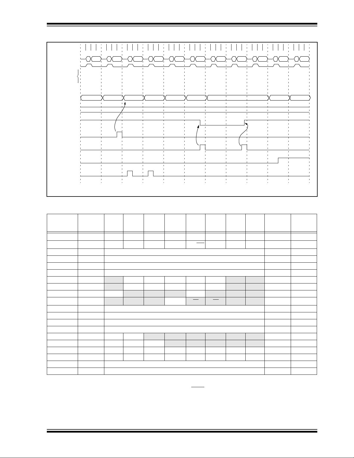
FIGURE 12-10: TMR1, TMR2, AND TMR3 OPERATION IN TIMER MODE
Q1Q2 Q3Q4 Q1Q2 Q3Q4 Q1Q2 Q3Q4 Q1Q2 Q3 Q4 Q1Q2 Q3 Q4 Q1Q2Q3 Q4 Q1Q2Q3 Q4 Q1Q2 Q3Q4 Q1Q2 Q3Q4 Q1Q2 Q3 Q4 Q1Q2 Q3 Q4
AD15:AD0
ALE
Instruction
fetched
MOVWF
TMR1
Write TMR1
MOVF
TMR1, W
Read TMR1
MOVF
TMR1, W
Read TMR1
MOVLB
3 NOP
TCON2, 0
Stop TMR1
BSF
BCF
TCON2, 0
Start TMR1
NOP NOP NOP NOP
PIC17C4X
TMR1
PR1
TMR1ON
WR_TMR1
WR_TCON2
TMR1IF
RD_TMR1
TABLE 12-6: SUMMARY OF TMR1, TMR2, AND TMR3 REGISTERS
Address Name Bit 7 Bit 6 Bit 5 Bit 4 Bit 3 Bit 2 Bit 1 Bit 0
04h 05h 03h 04h 05h 06h 07h 08h 00h
TMR1
reads 03h
TMR1
reads 04h
Value on
Power-on
Reset
Value on all
other resets
(Note1)
16h, Bank 3 TCON1 CA2ED1 CA2ED0 CA1ED1 CA1ED0 T16 TMR3CS TMR2CS TMR1CS 0000 0000 0000 0000
17h, Bank 3 TCON2 CA2OVF CA1OVF PWM2ON PWM1ON CA1/PR3
TMR3ON TMR2ON TMR1ON 0000 0000 0000 0000
10h, Bank 2 TMR1 Timer1 register xxxx xxxx uuuu uuuu
11h, Bank 2 TMR2 Timer2 register xxxx xxxx uuuu uuuu
12h, Bank 2 TMR3L TMR3 register; low byte xxxx xxxx uuuu uuuu
13h, Bank 2 TMR3H TMR3 register; high byte xxxx xxxx uuuu uuuu
16h, Bank 1 PIR
17h, Bank 1 PIE
07h, Unbanked INTSTA PEIF
RBIF TMR3IF TMR2IF TMR1IF CA2IF CA1IF TXIF RCIF 0000 0010 0000 0010
RBIE TMR3IE TMR2IE TMR1IE CA2IE CA1IE TXIE RCIE 0000 0000 0000 0000
T0CKIF T0IF INTF PEIE T0CKIE T0IE INTE 0000 0000 0000 0000
06h, Unbanked CPUSTA — — STKAV GLINTD TO PD — — --11 11-- --11 qq--
14h, Bank 2 PR1 Timer1 period register xxxx xxxx uuuu uuuu
15h, Bank 2 PR2 Timer2 period register xxxx xxxx uuuu uuuu
16h, Bank 2 PR3L/CA1L Timer3 period/capture1 register; low byte xxxx xxxx uuuu uuuu
17h, Bank 2 PR3H/CA1H Timer3 period/capture1 register; high byte xxxx xxxx uuuu uuuu
10h, Bank 3 PW1DCL DC1 DC0
11h, Bank 3 PW2DCL DC1 DC0 TM2PW2
— — — — — — xx-- ---- uu-- ----
— — — — — xx0- ---- uu0- ----
12h, Bank 3 PW1DCH DC9 DC8 DC7 DC6 DC5 DC4 DC3 DC2 xxxx xxxx uuuu uuuu
13h, Bank 3 PW2DCH DC9 DC8 DC7 DC6 DC5 DC4 DC3 DC2 xxxx xxxx uuuu uuuu
14h, Bank 3 CA2L Capture2 low byte xxxx xxxx uuuu uuuu
15h, Bank 3 CA2H Capture2 high byte xxxx xxxx uuuu uuuu
Legend: x = unknown, u = unchanged, - = unimplemented read as '0', q - value depends on condition,
shaded cells are not used by TMR1, TMR2 or TMR3.
Note 1: Other (non power-up) resets include: external reset through MCLR and WDT Timer Reset.
1996 Microchip Technology Inc. DS30412C-page 81
Page 82

PIC17C4X
NOTES:
DS30412C-page 82 1996 Microchip Technology Inc.
Page 83

PIC17C4X
13.0 UNIVERSAL SYNCHRONOUS ASYNCHRONOUS RECEIVER TRANSMITTER (USART) MODULE
The USART module is a serial I/O module. The USART
can be configured as a full duplex asynchronous system that can communicate with peripheral devices such
as CRT terminals and personal computers, or it can be
configured as a half duplex synchronous system that
can communicate with peripheral devices such as A/D
or D/A integrated circuits, Serial EEPROMs etc. The
USART can be configured in the following modes:
• Asynchronous (full duplex)
• Synchronous - Master (half duplex)
• Synchronous - Slave (half duplex)
The SPEN (RCSTA<7>) bit has to be set in order to
configure RA4 and RA5 as the Serial Communication
Interface.
The USART module will control the direction of the
RA4/RX/DT and RA5/TX/CK pins, depending on the
states of the USART configuration bits in the RCSTA
and TXSTA registers. The bits that control I/O direction
are:
• SPEN
• TXEN
• SREN
• CREN
• CSRC
The Transmit Status And Control Register is shown in
Figure 13-1, while the Receive Status And Control
Register is shown in Figure 13-2.
FIGURE 13-1: TXSTA REGISTER (ADDRESS: 15h, BANK 0)
R/W - 0 R/W - 0 R/W - 0 R/W - 0 U - 0 U - 0 R - 1 R/W - x
CSRC TX9 TXEN SYNC
bit7 bit0
bit 7: CSRC : Clock Source Select bit
Synchronous mode:
1 =Master Mode (Clock generated internally from BRG)
0 =Slave mode (Clock from external source)
Asynchronous mode
Don’t care
bit 6: TX9 : 9-bit Transmit Enable bit
1 =Selects 9-bit transmission
0 =Selects 8-bit transmission
bit 5: TXEN : Transmit Enable bit
1 =Transmit enabled
0 =Transmit disabled
SREN/CREN overrides TXEN in SYNC mode
bit 4: SYNC : USART mode Select bit
(Synchronous/Asynchronous)
1 =Synchronous mode
0 =Asynchronous mode
bit 3-2: Unimplemented : Read as '0'
bit 1: TRMT : Transmit Shift Register (TSR) Empty bit
1 =TSR empty
0 =TSR full
bit 0: TX9D : 9th bit of transmit data (can be used to calculated the parity in software)
:
— — TRMT TX9D
R = Readable bit
W = Writable bit
-n = Value at POR reset
(x = unknown)
1996 Microchip Technology Inc. DS30412C-page 83
Page 84

PIC17C4X
FIGURE 13-2: RCSTA REGISTER (ADDRESS: 13h, BANK 0)
R/W - 0 R/W - 0 R/W - 0 R/W - 0 U - 0 R - 0 R - 0 R - x
SPEN RX9 SREN CREN
bit7 bit 0
bit 7: SPEN : Serial Port Enable bit
1 =Configures RA5/RX/DT and RA4/TX/CK pins as serial port pins
0 =Serial port disabled
bit 6: RX9 : 9-bit Receive Enable bit
1 =Selects 9-bit reception
0 =Selects 8-bit reception
bit 5: SREN : Single Receive Enable bit
This bit enables the reception of a single byte. After receiving the byte, this bit is automatically cleared.
Synchronous mode:
1 =Enable reception
0 =Disable reception
Note: This bit is ignored in synchronous slave reception.
A
synchronous mode:
Don’t care
bit 4: CREN : Continuous Receive Enable bit
This bit enables the continuous reception of serial data.
Asynchronous mode:
1 =Enable reception
0 =Disables reception
Synchronous mode:
1 =Enables continuous reception until CREN is cleared (CREN overrides SREN)
0 =Disables continuous reception
bit 3: Unimplemented : Read as '0'
bit 2: FERR : Framing Error bit
1 =Framing error (Updated by reading RCREG)
0 =No framing error
bit 1: OERR : Overrun Error bit
1 =Overrun (Cleared by clearing CREN)
0 =No overrun error
bit 0: RX9D : 9th bit of receive data (can be the software calculated parity bit)
— FERR OERR RX9D
R = Readable bit
W = Writable bit
-n = Value at POR reset
(x = unknown)
DS30412C-page 84
1996 Microchip Technology Inc.
Page 85

FIGURE 13-3: USART TRANSMIT
PIC17C4X
Sync
Master/Slave
÷ 4BRG
CK/TX
DT
Sync/Async
TSR
Start 0 1 7 8 Stop
TXREG
FIGURE 13-4: USART RECEIVE
÷ 4
Master/Slave
CK
RX
OSC
Buffer
Logic
Buffer
Logic
BRG
SPEN
• • •
• • •
01 7
Data Bus
Sync
÷ 16
Majority
Detect
8 Bit Count
Sync/Async
Clock
Load
TXSTA<0>
Clock
Data
Sync/AsyncSync/Async
TXEN/
Write to TXREG
TXIE
enable
Bit Count
START
Detect
RSR
MSb LSb
• • •
÷ 16
Interrupt
Interrupt
Async/Sync
RCIE
SREN/
CREN/
Start_Bit
0178Stop
FIFO
Logic
Clk
FIFO
FERR
FERR
RX9
RCREG
• • •
• • •
017RX9D
017RX9D
Data Bus
Async/Sync
1996 Microchip Technology Inc. DS30412C-page 85
Page 86

PIC17C4X
13.1 USAR
T Baud Rate Generator (BRG)
The BRG supports both the Asynchronous and Synchronous modes of the USART. It is a dedicated 8-bit
baud rate generator. The SPBRG register controls the
period of a free running 8-bit timer. Table 13-1 shows
the formula for computation of the baud rate for different USART modes. These only apply when the USART
is in synchronous master mode (internal clock) and
asynchronous mode.
Given the desired baud rate and Fosc , the nearest integer value between 0 and 255 can be calculated using
the formula below. The error in baud rate can then be
determined.
TABLE 13-1: BAUD RATE FORMULA
SYNC Mode Baud Rate
0
Asynchronous
1
Synchronous
X = value in SPBRG (0 to 255)
F
F
OSC
OSC
/(64(X+1))
/(4(X+1))
Example 13-1 shows the calculation of the baud rate
error for the following conditions:
OSC
= 16 MHz
F
Desired Baud Rate = 9600
SYNC = 0
EXAMPLE 13-1: CALCULATING BAUD
RATE ERROR
Desired Baud rate=Fosc / (64 (X + 1))
9600 = 16000000 /(64 (X + 1))
X = 25.042 = 25
Calculated Baud Rate=16000000 / (64 (25 + 1))
= 9615
Error = (Calculated Baud Rate - Desired Baud Rate)
Desired Baud Rate
= (9615 - 9600) / 9600
= 0.16%
Writing a new value to the SPBRG, causes the BRG
timer to be reset (or cleared), this ensures that the BRG
does not wait for a timer overflow before outputting the
new baud rate.
TABLE 13-2: REGISTERS ASSOCIATED WITH BAUD RATE GENERATOR
Address Name Bit 7 Bit 6 Bit 5 Bit 4 Bit 3 Bit 2 Bit 1 Bit 0
13h, Bank 0 RCSTA SPEN
15h, Bank 0 TXSTA CSRC TX9 TXEN SYNC — — TRMT TX9D 0000 --1x 0000 --1u
17h, Bank 0 SPBRG Baud rate generator register
Legend: x = unknown, u = unchanged, - = unimplemented read as a '0', shaded cells are not used by the Baud Rate Generator.
Note 1: Other (non power-up) resets include: external reset through MCLR
RX9 SREN CREN — FERR OERR RX9D 0000 -00x 0000 -00u
and Watchdog Timer Reset.
Value on
Power-on
Reset
xxxx xxxx uuuu uuuu
Value on all
other resets
(Note1)
DS30412C-page 86
1996 Microchip Technology Inc.
Page 87

PIC17C4X
TABLE 13-3: BAUD RATES FOR SYNCHRONOUS MODE
OSC
= 33 MHz
F
BAUD
RATE
(K)
0.3 NA — — NA — — NA — — NA — —
1.2 NA — — NA — — NA — — NA — —
2.4 NA — — NA — — NA — — NA — —
9.6 NA — — NA — — NA — — NA — —
19.2 NA — — NA — — 19.53 +1.73 255 19.23 +0.16 207
76.8 77.10 +0.39 106 77.16 +0.47 80 76.92 +0.16 64 76.92 +0.16 51
96 95.93 -0.07 85 96.15 +0.16 64 96.15 +0.16 51 95.24 -0.79 41
300 294.64 -1.79 27 297.62 -0.79 20 294.1 -1.96 16 307.69 +2.56 12
500 485.29 -2.94 16 480.77 -3.85 12 500 0 9 500 0 7
HIGH 8250 — 0 6250 — 0 5000 — 0 4000 — 0
LOW 32.22 — 255 24.41 — 255 19.53 — 255 15.625 — 255
= 10 MHz
OSC
BAUD
RATE
19.2 19.23 +0.16 129 19.24 +0.23 92 19.2 0 65
76.8 75.76 -1.36 32 77.82 +1.32 22 79.2 +3.13 15
300 312.5 +4.17 7 298.3 -0.57 5 316.8 +5.60 3
500 500 0 4 NA —
HIGH 2500 — 0 1789.8 — 0 1267 — 0
LOW 9.766 — 255 6.991 — 255 4.950 — 255
BAUD
RATE
19.2 19.04 -0.83 46 19.24 +0.16 12 NA — —
76.8 74.57 -2.90 11 83.34 +8.51 2 NA — —
300 298.3 -0.57 2 NA — — NA — —
500 NA — — NA — — NA — —
HIGH 894.9 — 0 250 — 0 8.192 — 0
LOW 3.496 — 255 0.976 — 255 0.032 — 255
F
(K)
0.3 NA — — NA — — NA — —
1.2 NA — — NA — — NA — —
2.4 NA — — NA — — NA — —
9.6 9.766 +1.73 255 9.622 +0.23 185 9.6 0 131
96 96.15 +0.16 25 94.20 -1.88 18 97.48 +1.54 12
F
OSC
= 3.579 MHz
(K)
0.3 NA — — NA — — 0.303 +1.14 26
1.2 NA — — 1.202 +0.16 207 1.170 -2.48 6
2.4 NA — — 2.404 +0.16 103 NA — —
9.6 9.622 +0.23 92 9.615 +0.16 25 NA — —
96 99.43 _3.57 8 NA — — NA — —
SPBRG
value
(decimal)
F
OSC
= 25 MHz
SPBRG
value
(decimal)
SPBRG
value
(decimal)
F
F
OSC
OSC
SPBRG
value
(decimal)
= 7.159 MHz
= 1 MHz
F
OSC
= 20 MHz
OSC
= 16 MHz
value
OSC
F
OSC
F
F
= 5.068 MHz
= 32.768 kHz
SPBRG
(decimal)KBAUD %ERROR KBAUD %ERROR KBAUD %ERROR KBAUD %ERROR
SPBRG
value
(decimal)KBAUD %ERROR KBAUD %ERROR KBAUD %ERROR
SPBRG
value
(decimal)KBAUD %ERROR KBAUD %ERROR KBAUD %ERROR
SPBRG
(decimal)
SPBRG
value
(decimal)
—NA— —
SPBRG
value
(decimal)
value
1996 Microchip Technology Inc. DS30412C-page 87
Page 88

PIC17C4X
TABLE 13-4: BAUD RATES FOR ASYNCHRONOUS MODE
OSC
= 33 MHz
F
BAUD
RATE
(K)
0.3 NA — — NA — — NA — — NA — —
1.2 NA — — NA — — 1.221 +1.73 255 1.202 +0.16 207
2.4 2.398 -0.07 214 2.396 0.14 162 2.404 +0.16 129 2.404 +0.16 103
9.6 9.548 -0.54 53 9.53 -0.76 40 9.469 -1.36 32 9.615 +0.16 25
19.2 19.09 -0.54 26 19.53 +1.73 19 19.53 +1.73 15 19.23 +0.16 12
76.8 73.66 -4.09 6 78.13 +1.73 4 78.13 +1.73 3 83.33 +8.51 2
96 103.12 +7.42 4 97.65 +1.73 3 104.2 +8.51 2 NA — —
300 257.81 -14.06 1 390.63 +30.21 0 312.5 +4.17 0 NA — —
500 515.62 +3.13 0 NA — — NA — — NA — —
HIGH 515.62 — 0 — — 0 312.5 — 0 250 — 0
LOW 2.014 — 255 1.53 — 255 1.221 — 255 0.977 — 255
F
OSC
BAUD
RATE
(K)
0.3 NA — — NA — — 0.31 +3.13 255
1.2 1.202 +0.16 129 1.203 _0.23 92 1.2 0 65
2.4 2.404 +0.16 64 2.380 -0.83 46 2.4 0 32
9.6 9.766 +1.73 15 9.322 -2.90 11 9.9 -3.13 7
19.2 19.53 +1.73 7 18.64 -2.90 5 19.8 +3.13 3
76.8 78.13 +1.73 1 NA — — 79.2 +3.13 0
96 NA — — NA — — NA — —
300 NA — — NA — — NA — —
500 NA — — NA — — NA — —
HIGH 156.3 — 0 111.9 — 0 79.2 — 0
LOW 0.610 — 255 0.437 — 255 0.309
BAUD
RATE
(K)
0.3 0.301 +0.23 185 0.300 +0.16 51 0.256 -14.67 1
1.2 1.190 -0.83 46 1.202 +0.16 12 NA — —
2.4 2.432 +1.32 22 2.232 -6.99 6 NA — —
9.6 9.322 -2.90 5 NA — — NA — —
19.2 18.64 -2.90 2 NA — — NA — —
76.8 NA — — NA — — NA — —
96 NA — — NA — — NA — —
300 NA — — NA — — NA — —
500 NA — — NA — — NA — —
HIGH 55.93 — 0 15.63 — 0 0.512 — 0
LOW 0.218 — 255 0.061 — 255 0.002 — 255
= 10 MHz
F
OSC
= 3.579 MHz
SPBRG
value
(decimal)
OSC
F
= 25 MHz
SPBRG
value
(decimal)
SPBRG
value
(decimal)
F
F
OSC
OSC
SPBRG
value
(decimal)
= 7.159 MHz
= 1 MHz
F
OSC
= 20 MHz
(decimal)
(decimal)
SPBRG
value
SPBRG
value
SPBRG
value
(decimal)
OSC
F
OSC
F
OSC
= 16 MHz
F
= 5.068 MHz
= 32.768 kHz
SPBRG
(decimal)KBAUD %ERROR KBAUD %ERROR KBAUD %ERROR KBAUD %ERROR
SPBRG
value
(decimal)KBAUD %ERROR KBAUD %ERROR KBAUD %ERROR
—
SPBRG
value
(decimal)KBAUD %ERROR KBAUD %ERROR KBAUD %ERROR
value
2
55
DS30412C-page 88
1996 Microchip Technology Inc.
Page 89

PIC17C4X
13.2 USAR
In this mode, the USART uses standard nonreturn-to-zero (NRZ) format (one start bit, eight or nine
data bits, and one stop bit). The most common data f ormat is 8-bits. An on-chip dedicated 8-bit baud rate generator can be used to derive standard baud rate
frequencies from the oscillator. The USART’s transmitter and receiver are functionally independent but use
the same data format and baud rate. The baud rate
generator produces a clock x64 of the bit shift rate. Parity is not supported by the hardware, but can be implemented in software (and stored as the ninth data bit).
Asynchronous mode is stopped during SLEEP.
The asynchronous mode is selected by clearing the
SYNC bit (TXSTA<4>).
The USART Asynchronous module consists of the following important elements:
• Baud Rate Generator
• Sampling Circuit
• Asynchronous T r ansmitter
• Asynchronous Receiver
13.2.1 USART ASYNCHRONOUS TRANSMITTER
The USART transmitter block diagram is shown in
Figure 13-3. The heart of the transmitter is the transmit
shift register (TSR). The shift register obtains its data
from the read/write transmit buffer (TXREG). TXREG is
loaded with data in software. The TSR is not loaded
until the stop bit has been transmitted from the previous
load. As soon as the stop bit is transmitted, the TSR is
loaded with new data from the TXREG (if available).
Once TXREG transfers the data to the TSR (occurs in
one T
CY
TXREG is empty and an interrupt bit, TXIF (PIR<1>) is
set. This interr upt can be enabled or disabled by the
TXIE bit (PIE<1>). TXIF will be set regardless of TXIE
and cannot be reset in software. It will reset only when
new data is loaded into TXREG. While TXIF indicates
the status of the TXREG, the TRMT (TXSTA<1>) bit
shows the status of the TSR. TRMT is a read only bit
which is set when the TSR is empty. No interrupt logic
is tied to this bit, so the user has to poll this bit in order
to determine if the TSR is empty.
Note: The TSR is not mapped in data memory,
T Asynchronous Mode
at the end of the current BRG cycle), the
so it is not available to the user.
Transmission is enabled by setting the
TXEN (TXSTA<5>) bit. The actual transmission will not
occur until TXREG has been loaded with data and the
baud rate generator (BRG) has produced a shift clock
(Figure 13-5). The transmission can also be started by
first loading TXREG and then setting TXEN. Normally
when transmission is first started, the TSR is empty, so
a transfer to TXREG will result in an immediate transfer
to TSR resulting in an empty TXREG. A back-to-back
transfer is thus possible (Figure 13-6). Clearing TXEN
during a transmission will cause the transmission to be
aborted. This will reset the transmitter and the
RA5/TX/CK pin will revert to hi-impedance.
In order to select 9-bit transmission, the
TX9 (TXSTA<6>) bit should be set and the ninth bit
should be written to TX9D (TXSTA<0>). The ninth bit
must be written before writing the 8-bit data to the
TXREG. This is because a data wr ite to TXREG can
result in an immediate transfer of the data to the TSR
(if the TSR is empty).
Steps to follow when setting up an Asynchronous
Transmission:
1. Initialize the SPBRG register for the appropriate
baud rate.
2. Enable the asynchronous serial port by clearing
the SYNC bit and setting the SPEN bit.
3. If interrupts are desired, then set the TXIE bit.
4. If 9-bit transmission is desired, then set the TX9
bit.
5. Load data to the TXREG register.
6. If 9-bit transmission is selected, the ninth bit
should be loaded in TX9D.
7. Enable the transmission by setting TXEN (starts
transmission).
Writing the transmit data to the TXREG, then enabling
the transmit (setting TXEN) allows tr ansmission to start
sooner then doing these two events in the opposite
order.
Note: To terminate a transmission, either clear
the SPEN bit, or the TXEN bit. This will
reset the transmit logic, so that it will be in
the proper state when transmit is
re-enabled.
1996 Microchip Technology Inc. DS30412C-page 89
Page 90

PIC17C4X
FIGURE 13-5: ASYNCHRONOUS MASTER TRANSMISSION
Write to TXREG
BRG output
(shift clock)
(RA5/TX/CK pin)
TX
TXIF bit
TRMT bit
Word 1
Start Bit Bit 0 Bit 1 Bit 7/8
Word 1
Transmit Shift Reg
Word 1
Stop Bit
FIGURE 13-6: ASYNCHRONOUS MASTER TRANSMISSION (BACK TO BACK)
Write to TXREG
BRG output
(shift clock)
(RA5/TX/CK pin)
TX
TXIF bit
TRMT bit
Word 1
Word 1
Transmit Shift Reg.
Note: This timing diagram shows two consecutive transmissions.
Word 2
Start Bit
Bit 0 Bit 1
Word 1
Bit 7/8 Bit 0
Stop Bit
Word 2
Transmit Shift Reg.
Start Bit
Word 2
TABLE 13-5: REGISTERS ASSOCIATED WITH ASYNCHRONOUS TRANSMISSION
Address Name Bit 7 Bit 6 Bit 5 Bit 4 Bit 3 Bit 2 Bit 1 Bit 0
16h, Bank 1 PIR RBIF TMR3IF TMR2IF TMR1IF CA2IF CA1IF TXIF RCIF 0000 0010 0000 0010
13h, Bank 0 RCSTA SPEN RX9 SREN CREN — FERR OERR RX9D 0000 -00x 0000 -00u
16h, Bank 0 TXREG Serial port transmit register
17h, Bank 1 PIE RBIE TMR3IE TMR2IE TMR1IE CA2IE CA1IE TXIE RCIE 0000 0000 0000 0000
15h, Bank 0 TXSTA
17h, Bank 0 SPBRG Baud rate generator register
CSRC TX9 TXEN SYNC — — TRMT TX9D 0000 --1x 0000 --1u
Value on
Power-on
Reset
xxxx xxxx uuuu uuuu
xxxx xxxx uuuu uuuu
Legend: x = unknown, u = unchanged, - = unimplemented read as a '0', shaded cells are not used for asynchronous
transmission.
Note 1: Other (non power-up) resets include: external reset through MCLR
and Watchdog Timer Reset.
Value on all
other resets
(Note1)
DS30412C-page 90
1996 Microchip Technology Inc.
Page 91
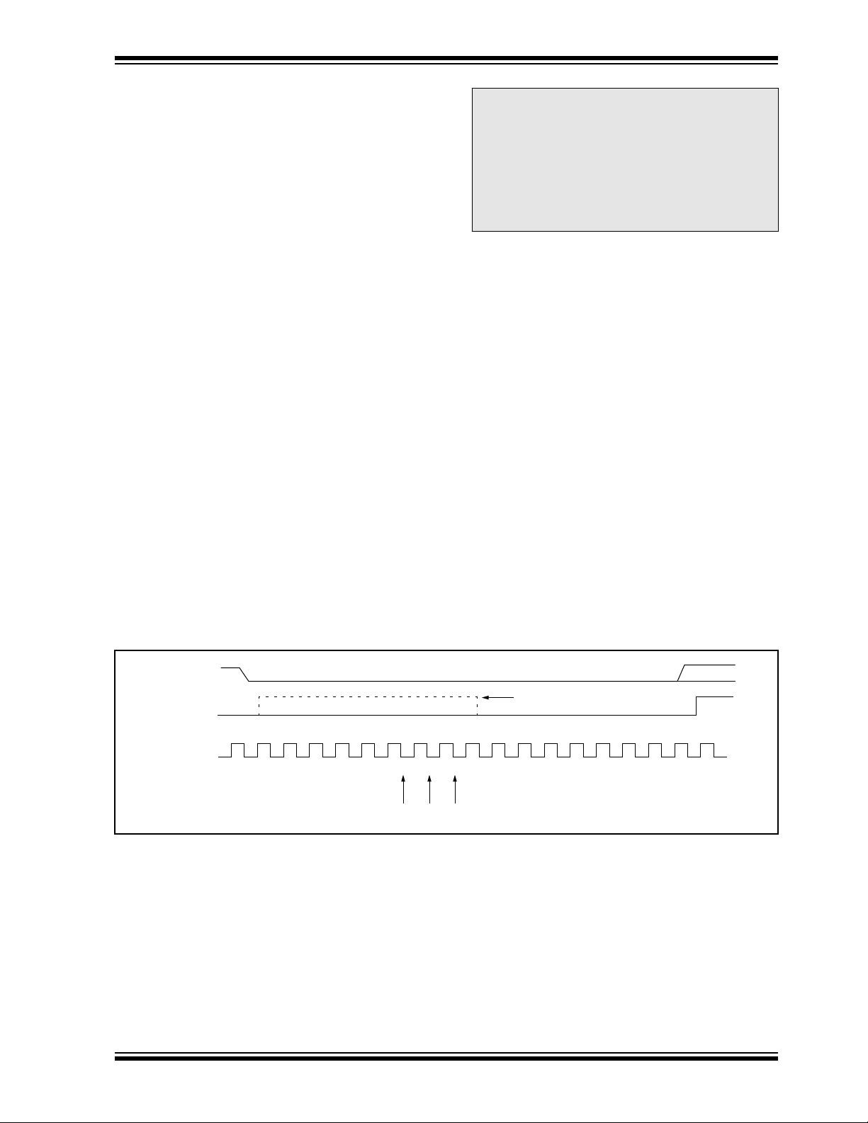
PIC17C4X
13.2.2 USART ASYNCHRONOUS RECEIVER
The receiver block diagram is shown in Figure 13-4.
The data comes in the RA4/RX/DT pin and drives the
data recovery block. The data recovery block is actually
a high speed shifter operating at 16 times the baud
rate, whereas the main receive serial shifter operates
at the bit rate or at F
Once asynchronous mode is selected, reception is
enabled by setting bit CREN (RCSTA<4>).
The heart of the receiver is the receive (serial) shift register (RSR). After sampling the stop bit, the received
data in the RSR is transferred to the RCREG (if it is
empty). If the transfer is complete, the interrupt bit
RCIF (PIR<0>) is set. The actual interrupt can be
enabled/disabled by setting/clearing the RCIE
(PIE<0>) bit. RCIF is a read only bit which is cleared b y
the hardware. It is cleared when RCREG has been
read and is empty. RCREG is a double buffered register; (i.e. it is a two deep FIFO). It is possible for two
bytes of data to be received and transferred to the
RCREG FIFO and a third byte begin shifting to the
RSR. On detection of the stop bit of the third b yte, if the
RCREG is still full, then the overrun error bit,
OERR (RCSTA<1>) will be set. The word in the RSR
will be lost. RCREG can be read twice to retrieve the
two bytes in the FIFO. The OERR bit has to be cleared
in software which is done by resetting the receive logic
(CREN is set). If the OERR bit is set, transfers from the
RSR to RCREG are inhibited, so it is essential to clear
the OERR bit if it is set. The framing error bit
FERR (RCSTA<2>) is set if a stop bit is not detected.
OSC
.
Note: The FERR and the 9th receive bit are buff-
ered the same way as the receive data.
Reading the RCREG register will allow the
RX9D and FERR bits to be loaded with values for the next received Received data;
therefore, it is essential f or the user to read
the RCSTA register before reading
RCREG in order not to lose the old FERR
and RX9D information.
13.2.3 SAMPLING
The data on the RA4/RX/DT pin is sampled three times
by a majority detect circuit to determine if a high or a
low level is present at the RA4/RX/DT pin. The sampling is done on the seventh, eighth and ninth falling
edges of a x16 clock (Figure 11-3).
The x16 clock is a free running clock, and the three
sample points occur at a frequency of every 16 falling
edges.
FIGURE 13-7: RX PIN SAMPLING SCHEME
RX
(RA4/RX/DT pin)
baud CLK
x16 CLK
1 2 3 4 5 6 7 8 9 10 11 12 13 14 15 16 1 2 3
Samples
Start bit
Bit0
Baud CLK for all but start bit
1996 Microchip Technology Inc. DS30412C-page 91
Page 92

PIC17C4X
Steps to follow when setting up an Asynchronous
Reception:
1. Initialize the SPBRG register for the appropriate
baud rate.
2. Enable the asynchronous serial port by clearing
the SYNC bit and setting the SPEN bit.
3. If interrupts are desired, then set the RCIE bit.
4. If 9-bit reception is desired, then set the RX9 bit.
5. Enable the reception by setting the CREN bit.
6. The RCIF bit will be set when reception completes and an interrupt will be generated if the
RCIE bit was set.
FIGURE 13-8: ASYNCHRONOUS RECEPTION
(RA4/RX/DT pin)
Rcv buffer reg
(interrupt flag)
RX
Rcv shift
reg
Read Rcv
buffer reg
RCREG
RCIF
Start
bit
bit1bit0
bit7/8 bit0Stop
bit
Word 1
RCREG
7. Read RCST A to get the ninth bit (if enab led) and
FERR bit to determine if any error occurred during reception.
8. Read RCREG for the 8-bit received data.
9. If an overrun error occurred, clear the error by
clearing the OERR bit.
Note: To ter minate a reception, either clear the
SREN and CREN bits, or the SPEN bit.
This will reset the receive logic, so that it
will be in the proper state when receive is
re-enabled.
Start
bit
bit7/8
Stop
bit
Start
bit
Word 2
RCREG
bit7/8
Stop
bit
Word 3
OERR bit
CREN
Note: This timing diagram shows three words appearing on the RX input. The RCREG (receive buffer) is read after the third word,
causing the OERR (overrun) bit to be set.
TABLE 13-6: REGISTERS ASSOCIATED WITH ASYNCHRONOUS RECEPTION
Address Name Bit 7 Bit 6 Bit 5 Bit 4 Bit 3 Bit 2 Bit 1 Bit 0
16h, Bank 1 PIR
13h, Bank 0 RCSTA SPEN RX9 SREN CREN
14h, Bank 0 RCREG RX7 RX6 RX5 RX4 RX3 RX2 RX1 RX0 xxxx xxxx uuuu uuuu
17h, Bank 1 PIE
15h, Bank 0 TXSTA
17h, Bank 0 SPBRG Baud rate generator register xxxx xxxx uuuu uuuu
Legend: x = unknown, u = unchanged, - = unimplemented read as a '0', shaded cells are not used for asynchronous reception.
Note 1: Other (non power-up) resets include: external reset through MCLR and Watchdog Timer Reset.
RBIF TMR3IF TMR2IF TMR1IF CA2IF CA1IF TXIF RCIF 0000 0010 0000 0010
— FERR OERR RX9D 0000 -00x 0000 -00u
RBIE TMR3IE TMR2IE TMR1IE CA2IE CA1IE TXIE RCIE 0000 0000 0000 0000
CSRC TX9 TXEN SYNC — — TRMT TX9D 0000 --1x 0000 --1u
Value on
Power-on
Reset
Value on all
other resets
(Note1)
DS30412C-page 92
1996 Microchip Technology Inc.
Page 93

PIC17C4X
13.3 USART Synchronous Master Mode
In Master Synchronous mode, the data is transmitted in
a half-duplex manner; i.e. transmission and reception
do not occur at the same time: when transmitting data,
the reception is inhibited and vice versa. The synchronous mode is entered by setting the SYNC
(TXSTA<4>) bit. In addition, the SPEN (RCSTA<7>) bit
is set in order to configure the RA5 and RA4 I/O ports
to CK (clock) and DT (data) lines respectively. The
Master mode indicates that the processor transmits the
master clock on the CK line. The Master mode is
entered by setting the CSRC (TXSTA<7>) bit.
13.3.1 USART SYNCHRONOUS MASTER
TRANSMISSION
The USART transmitter block diagram is shown in
Figure 13-3. The heart of the transmitter is the transmit
(serial) shift register (TSR). The shift register obtains its
data from the read/write transmit buffer TXREG.
TXREG is loaded with data in software. The TSR is not
loaded until the last bit has been transmitted from the
previous load. As soon as the last bit is tr ansmitted, the
TSR is loaded with new data from TXREG (if a vailab le).
Once TXREG transfers the data to the TSR (occurs in
one T
CY at the end of the current BRG cycle), TXREG
is empty and the TXIF (PIR<1>) bit is set. This interrupt
can be enabled/disabled by setting/clearing the TXIE
bit (PIE<1>). TXIF will be set regardless of the state of
bit TXIE and cannot be cleared in software. It will reset
only when new data is loaded into TXREG. While TXIF
indicates the status of TXREG, TRMT (TXSTA<1>)
shows the status of the TSR. TRMT is a read only bit
which is set when the TSR is empty. No interrupt logic
is tied to this bit, so the user has to poll this bit in order
to determine if the TSR is empty. The TSR is not
mapped in data memory, so it is not available to the
user.
Transmission is enabled by setting the TXEN
(TXSTA<5>) bit. The actual transmission will not occur
until TXREG has been loaded with data. The first data
bit will be shifted out on the next available rising edge
of the clock on the RA5/TX/CK pin. Data out is stable
around the falling edge of the synchronous clock
(Figure 13-10). The transmission can also be star ted
by first loading TXREG and then setting TXEN. This is
advantageous when slow baud rates are selected,
since BRG is kept in RESET when the TXEN, CREN,
and SREN bits are clear. Setting the TXEN bit will start
the BRG, creating a shift clock immediately. Normally
when transmission is first started, the TSR is empty, so
a transfer to TXREG will result in an immediate transfer
to the TSR, resulting in an empty TXREG.
Back-to-back transfers are possible.
Clearing TXEN during a transmission will cause the
transmission to be aborted and will reset the transmitter. The RA4/RX/DT and RA5/TX/CK pins will revert to
hi-impedance. If either CREN or SREN are set during
a transmission, the transmission is aborted and the
RA4/RX/DT pin reverts to a hi-impedance state (for a
reception). The RA5/TX/CK pin will remain an output if
the CSRC bit is set (internal clock). The transmitter
logic is not reset, although it is disconnected from the
pins. In order to reset the transmitter, the user has to
clear the TXEN bit. If the SREN bit is set (to interrupt an
ongoing transmission and receive a single word), then
after the single word is received, SREN will be cleared
and the serial port will revert back to transmitting, since
the TXEN bit is still set. The DT line will immediately
switch from hi-impedance receive mode to transmit
and start driving. To avoid this, TXEN should be
cleared.
In order to select 9-bit transmission, the
TX9 (TXSTA<6>) bit should be set and the ninth bit
should be written to TX9D (TXSTA<0>). The ninth bit
must be written before writing the 8-bit data to TXREG.
This is because a data write to TXREG can result in an
immediate transfer of the data to the TSR (if the TSR is
empty). If the TSR was empty and TXREG was written
before writing the “new” TX9D, the “present” value of
TX9D is loaded.
Steps to follow when setting up a Synchronous Master
Transmission:
1. Initialize the SPBRG register for the appropriate
baud rate (see Baud Rate Generator Section for
details).
2. Enable the synchronous master serial port by
setting the SYNC, SPEN, and CSRC bits.
3. Ensure that the CREN and SREN bits are clear
(these bits override transmission when set).
4. If interrupts are desired, then set the TXIE bit
(the GLINTD bit must be clear and the PEIE bit
must be set).
5. If 9-bit transmission is desired, then set the TX9
bit.
6. Start transmission by loading data to the
TXREG register.
7. If 9-bit transmission is selected, the ninth bit
should be loaded in TX9D.
8. Enable the transmission by setting TXEN.
Writing the transmit data to the TXREG, then enabling
the transmit (setting TXEN) allows tr ansmission to start
sooner then doing these two events in the reverse
order.
Note: To terminate a transmission, either clear
the SPEN bit, or the TXEN bit. This will
reset the transmit logic, so that it will be in
the proper state when transmit is
re-enabled.
1996 Microchip Technology Inc. DS30412C-page 93
Page 94

PIC17C4X
TABLE 13-7: REGISTERS ASSOCIATED WITH SYNCHRONOUS MASTER TRANSMISSION
Address Name Bit 7 Bit 6 Bit 5 Bit 4 Bit 3 Bit 2 Bit 1 Bit 0
16h, Bank 1 PIR
13h, Bank 0 RCSTA SPEN RX9 SREN CREN
16h, Bank 0 TXREG TX7 TX6 TX5 TX4 TX3 TX2 TX1 TX0 xxxx xxxx uuuu uuuu
17h, Bank 1 PIE
15h, Bank 0 TXSTA CSRC TX9 TXEN SYNC
17h, Bank 0 SPBRG Baud rate generator register xxxx xxxx uuuu uuuu
RBIF TMR3IF TMR2IF TMR1IF CA2IF CA1IF TXIF RCIF 0000 0010 0000 0010
— FERR OERR RX9D 0000 -00x 0000 -00u
RBIE TMR3IE TMR2IE TMR1IE CA2IE CA1IE TXIE RCIE 0000 0000 0000 0000
— — TRMT TX9D 0000 --1x 0000 --1u
Value on
Power-on
Reset
Value on all
other resets
(Note1)
Legend: x = unknown, u = unchanged, - = unimplemented read as a '0', shaded cells are not used for synchronous
master transmission.
Note 1: Other (non power-up) resets include: external reset through MCLR and Watchdog Timer Reset.
FIGURE 13-9: SYNCHRONOUS TRANSMISSION
Q1 Q2Q3Q4Q1Q2Q3 Q4Q1 Q2Q3Q4Q1 Q2Q3Q4Q1Q2Q3 Q4 Q1 Q2Q3 Q4Q1Q2Q3 Q4Q1Q2Q3 Q4Q1 Q2Q3 Q4Q1 Q2Q3 Q4Q1 Q2Q3 Q4Q3Q4
(RA4/RX/DT pin)
(RA5/TX/CK pin)
CK
Write to
TXREG
TXIF
Interrupt flag
TRMT
TXEN
DT
Write word 1
'1'
bit0
bit1 bit2
Word 1 Word 2
Write word 2
bit7
bit0
Note: Sync master mode; BRG = 0. Continuous transmission of two 8-bit words.
FIGURE 13-10: SYNCHRONOUS TRANSMISSION (THROUGH TXEN)
(RA4/RX/DT pin)
DT
CK
(RA5/TX/CK pin)
Write to
TXREG
TXIF bit
TRMT bit
bit0
bit1
bit2
bit6 bit7
DS30412C-page 94 1996 Microchip Technology Inc.
Page 95

PIC17C4X
13.3.2 USART SYNCHRONOUS MASTER
RECEPTION
Once synchronous mode is selected, reception is
enabled by setting either the SREN (RCSTA<5>) bit or
the CREN (RCSTA<4>) bit. Data is sampled on the
RA4/RX/DT pin on the falling edge of the clock. If
SREN is set, then only a single word is received. If
CREN is set, the reception is continuous until CREN is
reset. If both bits are set, then CREN takes precedence. After clocking the last bit, the received data in
the Receive Shift Register (RSR) is transferred to
RCREG (if it is empty). If the transfer is complete, the
interrupt bit RCIF (PIR<0>) is set. The actual interrupt
can be enabled/disabled by setting/clearing the
RCIE (PIE<0>) bit. RCIF is a read only bit which is
RESET by the hardware. In this case it is reset when
RCREG has been read and is empty. RCREG is a double buffered register; i.e., it is a two deep FIFO. It is
possible for two b ytes of data to be received and transferred to the RCREG FIFO and a third byte to begin
shifting into the RSR. On the clocking of the last bit of
the third byte, if RCREG is still full, then the overrun
error bit OERR (RCSTA<1>) is set. The word in the
RSR will be lost. RCREG can be read twice to retrieve
the two bytes in the FIFO. The OERR bit has to be
cleared in software. This is done by clearing the CREN
bit. If OERR bit is set, transfers from RSR to RCREG
are inhibited, so it is essential to clear OERR bit if it is
set. The 9th receive bit is buffered the same way as the
receive data. Reading the RCREG register will allow
the RX9D and FERR bits to be loaded with values for
the next received data; therefore, it is essential for the
user to read the RCSTA register before reading
RCREG in order not to lose the old FERR and RX9D
information.
Steps to follow when setting up a Synchronous Master
Reception:
1. Initialize the SPBRG register for the appropriate
baud rate. See Section 13.1 for details.
2. Enable the synchronous master serial port by
setting bits SYNC, SPEN, and CSRC.
3. If interrupts are desired, then set the RCIE bit.
4. If 9-bit reception is desired, then set the RX9 bit.
5. If a single reception is required, set bit SREN.
For continuous reception set bit CREN.
6. The RCIF bit will be set when reception is complete and an interrupt will be generated if the
RCIE bit was set.
7. Read RCST A to get the ninth bit (if enab led) and
determine if any error occurred during reception.
8. Read the 8-bit received data by reading
RCREG.
9. If any error occurred, clear the error by clearing
CREN.
Note: To terminate a reception, either clear the
SREN and CREN bits, or the SPEN bit.
This will reset the receive logic, so that it
will be in the proper state when receive is
re-enabled.
FIGURE 13-11: SYNCHRONOUS RECEPTION (MASTER MODE, SREN)
Q3Q4 Q1 Q2Q3 Q4 Q1Q2 Q3 Q4Q2 Q1Q2 Q3 Q4Q1 Q2Q3Q4 Q1 Q2Q3Q4Q1Q2 Q3Q4 Q1Q2Q3 Q4Q1Q2Q3 Q4Q1 Q2Q3Q4
DT
(RA4/RX/DT pin)
CK
(RA5/TX/CK pin)
Write to the
SREN bit
SREN bit
CREN bit
RCIF bit
Read
RCREG
1996 Microchip Technology Inc. DS30412C-page 95
'0'
Note: Timing diagram demonstrates SYNC master mode with SREN = 1.
bit0 bit1 bit2 bit3 bit4 bit5 bit6 bit7
Q1Q2 Q3 Q4
'0'
Page 96

PIC17C4X
TABLE 13-8: REGISTERS ASSOCIATED WITH SYNCHRONOUS MASTER RECEPTION
Address Name Bit 7 Bit 6 Bit 5 Bit 4 Bit 3 Bit 2 Bit 1 Bit 0
16h, Bank 1 PIR
13h, Bank 0 RCSTA SPEN RX9 SREN CREN
14h, Bank 0 RCREG RX7 RX6 RX5 RX4 RX3 RX2 RX1 RX0 xxxx xxxx uuuu uuuu
17h, Bank 1 PIE
15h, Bank 0 TXSTA CSRC
17h, Bank 0 SPBRG Baud rate generator register xxxx xxxx uuuu uuuu
RBIF TMR3IF TMR2IF TMR1IF CA2IF CA1IF TXIF RCIF 0000 0010 0000 0010
— FERR OERR RX9D 0000 -00x 0000 -00u
RBIE TMR3IE TMR2IE TMR1IE CA2IE CA1IE TXIE RCIE 0000 0000 0000 0000
TX9 TXEN SYNC — — TRMT TX9D 0000 --1x 0000 --1u
Value on
Power-on
Reset
Value on all
other resets
(Note1)
Legend: x = unknown, u = unchanged, - = unimplemented read as a '0', shaded cells are not used for synchronous
master reception.
Note 1: Other (non power-up) resets include: external reset through MCLR and Watchdog Timer Reset.
DS30412C-page 96 1996 Microchip Technology Inc.
Page 97

PIC17C4X
13.4 USART Synchronous Slave Mode
The synchronous slave mode differs from the master
mode in the fact that the shift clock is supplied externally at the RA5/TX/CK pin (instead of being supplied
internally in the master mode). This allows the device
to transfer or receive data in the SLEEP mode. The
slave mode is entered by clearing the
CSRC (TXSTA<7>) bit.
13.4.1 USART SYNCHRONOUS SLAVE
TRANSMIT
The operation of the sync master and slave modes are
identical except in the case of the SLEEP mode.
If two words are written to TXREG and then the SLEEP
instruction executes, the following will occur. The first
word will immediately transfer to the TSR and will transmit as the shift clock is supplied. The second word will
remain in TXREG. TXIF will not be set. When the first
word has been shifted out of TSR, TXREG will transfer
the second word to the TSR and the TXIF flag will now
be set. If TXIE is enabled, the interrupt will wake the
chip from SLEEP and if the global interrupt is enabled,
then the program will branch to interrupt vector
(0020h).
Steps to follow when setting up a Synchronous Slave
Transmission:
1. Enable the synchronous slave serial port by set-
ting the SYNC and SPEN bits and clearing the
CSRC bit.
2. Clear the CREN bit.
3. If interrupts are desired, then set the TXIE bit.
4. If 9-bit transmission is desired, then set the TX9
bit.
5. Start transmission by loading data to TXREG.
6. If 9-bit transmission is selected, the ninth bit
should be loaded in TX9D.
7. Enable the transmission by setting TXEN.
Writing the transmit data to the TXREG, then enabling
the transmit (setting TXEN) allows tr ansmission to start
sooner then doing these two events in the reverse
order.
13.4.2 USART SYNCHRONOUS SLAVE
RECEPTION
Operation of the synchronous master and slave modes
are identical except in the case of the SLEEP mode.
Also, SREN is a don't care in slave mode.
If receive is enabled (CREN) prior to the SLEEP instruction, then a word may be received during SLEEP. On
completely receiving the word, the RSR will transfer the
data to RCREG (setting RCIF) and if the RCIE bit is set,
the interrupt generated will wake the chip from SLEEP.
If the global interrupt is enabled, the program will
branch to the interrupt vector (0020h).
Steps to follow when setting up a Synchronous Slave
Reception:
1. Enable the synchronous master serial port by
setting the SYNC and SPEN bits and clearing
the CSRC bit.
2. If interrupts are desired, then set the RCIE bit.
3. If 9-bit reception is desired, then set the RX9 bit.
4. To enable reception, set the CREN bit.
5. The RCIF bit will be set when reception is com-
plete and an interrupt will be generated if the
RCIE bit was set.
6. Read RCST A to get the ninth bit (if enab led) and
determine if any error occurred during reception.
7. Read the 8-bit received data by reading
RCREG.
8. If any error occurred, clear the error by clearing
the CREN bit.
Note: To abort reception, either clear the SPEN
bit, the SREN bit (when in single receive
mode), or the CREN bit (when in continuous receive mode). This will reset the
receive logic, so that it will be in the proper
state when receive is re-enabled.
Note: To terminate a transmission, either clear
the SPEN bit, or the TXEN bit. This will
reset the transmit logic, so that it will be in
the proper state when transmit is
re-enabled.
1996 Microchip Technology Inc. DS30412C-page 97
Page 98
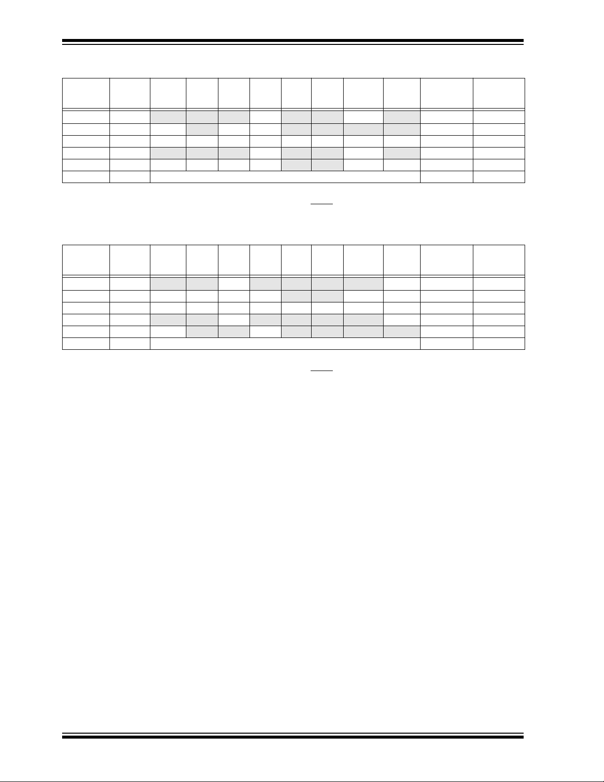
PIC17C4X
TABLE 13-9: REGISTERS ASSOCIATED WITH SYNCHRONOUS SLAVE TRANSMISSION
Address Name Bit 7 Bit 6 Bit 5 Bit 4 Bit 3 Bit 2 Bit 1 Bit 0
16h, Bank 1 PIR
13h, Bank 0 RCSTA SPEN
16h, Bank 0 TXREG TX7 TX6 TX5 TX4 TX3 TX2 TX1 TX0 xxxx xxxx uuuu uuuu
17h, Bank 1 PIE
15h, Bank 0 TXSTA CSRC TX9 TXEN SYNC
17h, Bank 0 SPBRG Baud rate generator register xxxx xxxx uuuu uuuu
RBIF TMR3IF TMR2IF TMR1IF CA2IF CA1IF TXIF RCIF 0000 0010 0000 0010
RX9 SREN CREN — FERR OERR RX9D 0000 -00x 0000 -00u
RBIE TMR3IE TMR2IE TMR1IE CA2IE CA1IE TXIE RCIE 0000 0000 0000 0000
— — TRMT TX9D 0000 --1x 0000 --1u
Value on
Power-on
Reset
Value on all
other resets
(Note1)
Legend: x = unknown, u = unchanged, - = unimplemented read as a '0', shaded cells are not used for synchronous
slave transmission.
Note 1: Other (non power-up) resets include: external reset through MCLR and Watchdog Timer Reset.
TABLE 13-10: REGISTERS ASSOCIATED WITH SYNCHRONOUS SLAVE RECEPTION
Address Name Bit 7 Bit 6 Bit 5 Bit 4 Bit 3 Bit 2 Bit 1 Bit 0
16h, Bank1 PIR
13h, Bank0 RCSTA SPEN RX9 SREN CREN
14h, Bank0 RCREG RX7 RX6 RX5 RX4 RX3 RX2 RX1 RX0 xxxx xxxx uuuu uuuu
17h, Bank1 PIE
15h, Bank 0 TXSTA CSRC
17h, Bank0 SPBRG Baud rate generator register xxxx xxxx uuuu uuuu
RBIF TMR3IF TMR2IF TMR1IF CA2IF CA1IF TXIF RCIF 0000 0010 0000 0010
— FERR OERR RX9D 0000 -00x 0000 -00u
RBIE TMR3IE TMR2IE TMR1IE CA2IE CA1IE TXIE RCIE 0000 0000 0000 0000
TX9 TXEN SYNC — — TRMT TX9D 0000 --1x 0000 --1u
Value on
Power-on
Reset
Value on all
other resets
(Note1)
Legend: x = unknown, u = unchanged, - = unimplemented read as a '0', shaded cells are not used for synchronous
slave reception.
Note 1: Other (non power-up) resets include: external reset through MCLR and Watchdog Timer Reset.
DS30412C-page 98 1996 Microchip Technology Inc.
Page 99

PIC17C4X
14.0 SPECIAL FEATURES OF THE CPU
What sets a microcontroller apart from other processors are special circuits to deal with the needs of real
time applications. The PIC17CXX family has a host of
such features intended to maximize system reliability,
minimize cost through elimination of external components, provide power sa ving operating modes and off er
code protection. These are:
• OSC selection
• Reset
- Power-on Reset (POR)
- Power-up Timer (PWRT)
- Oscillator Start-up Timer (OST)
• Interrupts
• Watchdog Timer (WDT)
• SLEEP
• Code protection
The PIC17CXX has a Watchdog Timer which can be
shut off only through EPROM bits. It runs off its own RC
oscillator for added reliability. There are two timers that
offer necessary delays on power-up. One is the Oscillator Start-up Timer (OST), intended to keep the chip in
RESET until the crystal oscillator is stable. The other is
the Power-up Timer (PWRT), which provides a fixed
delay of 96 ms (nominal) on power-up only, designed to
keep the part in RESET while the power supply stabilizes. With these two timers on-chip, most applications
need no external reset circuitry.
The SLEEP mode is designed to offer a very low current power-down mode. The user can wake from
SLEEP through external reset, Watchdog Timer Reset
or through an interrupt. Several oscillator options are
also made available to allow the part to fit the application. The RC oscillator option saves system cost while
the LF crystal option saves power. Configuration bits
are used to select various options. This configuration
word has the format shown in Figure 14-1.
FIGURE 14-1: CONFIGURATION WORD
R/P - 1 U - x U - x U - x U - x U - x U - x U - x
(1)
PM2
bit15-7 bit0
—
— — — — — —
U - x R/P - 1 U - x R/P - 1 R/P - 1 R/P - 1 R/P - 1 R/P - 1
— PM1 — PM0 WDTPS1 WDTPS0 FOSC1 FOSC0
bit15-7 bit0
bit 15-9: Unimplemented : Read as a '1'
bit 15,6,4: PM2, PM1, PM0 , Processor Mode Select bits
111 = Microprocessor Mode
110 = Microcontroller mode
101 = Extended microcontroller mode
000 = Code protected microcontroller mode
bit 7, 5: Unimplemented : Read as a '0'
bit 3-2: WDTPS1:WDTPS0 , WDT Postscaler Select bits
11 = WDT enabled, postscaler = 1
10 = WDT enabled, postscaler = 256
01 = WDT enabled, postscaler = 64
00 = WDT disabled, 16-bit overflow timer
bit 1-0: FOSC1:FOSC0 , Oscillator Select bits
11 = EC oscillator
10 = XT oscillator
01 = RC oscillator
00 = LF oscillator
Note 1: This bit does not exist on the PIC17C42. Reading this bit will return an unknown value (x).
R = Readable bit
P = Programmable bit
U = Unimplemented
- n = Value for Erased Device
(x = unknown)
1996 Microchip Technology Inc. DS30412C-page 99
Page 100
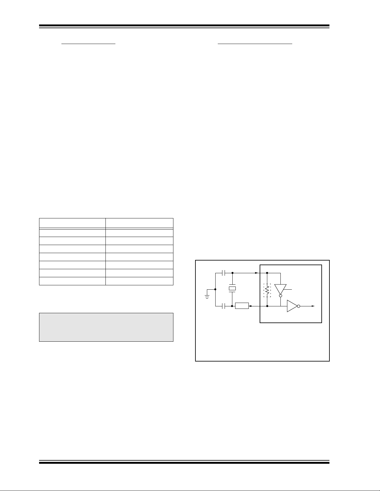
PIC17C4X
14.1 Confi
The PIC17CXX has up to seven configuration locations
(Table 14-1). These locations can be programmed
(read as '0') or left unprogrammed (read as '1') to select
various device configurations. Any write to a configuration location, regardless of the data, will program that
configuration bit. A TABLWT instruction is required to
write to program memory locations. The configuration
bits can be read by using the TABLRD instructions.
Reading any configuration location between FE00h
and FE07h will read the low byte of the configuration
word (Figure 14-1) into the TABLATL register. The TABLATH register will be FFh. Reading a configuration
location between FE08h and FE0Fh will read the high
byte of the configuration word into the TABLATL register. The TABLATH register will be FFh.
Addresses FE00h thorough FE0Fh are only in the program memory space for microcontroller and code protected microcontroller modes. A device programmer
will be able to read the configuration word in any processor mode. See programming specifications f or more
detail.
guration Bits
TABLE 14-1: CONFIGURATION
LOCATIONS
Bit Address
FOSC0 FE00h
FOSC1 FE01h
WDTPS0 FE02h
WDTPS1 FE03h
PM0 FE04h
PM1 FE06h
(1)
PM2
Note 1: This location does not exist on the
PIC17C42.
Note: When programming the desired configura-
tion locations, they must be programmed in
ascending order. Starting with address
FE00h.
FE0Fh
(1)
14.2 Oscillator
14.2.1 OSCILLATOR TYPES
The PIC17CXX can be operated in four different oscil-
lator modes. The user can program two configuration
bits (FOSC1:FOSC0) to select one of these four
modes:
• LF: Low Power Crystal
• XT: Crystal/Resonator
• EC: External Clock Input
• RC: Resistor/Capacitor
14.2.2 CRYSTAL OSCILLATOR / CERAMIC
RESONATORS
In XT or LF modes, a crystal or ceramic resonator is
connected to the OSC1/CLKIN and OSC2/CLKOUT
pins to establish oscillation (Figure 14-2). The
PIC17CXX Oscillator design requires the use of a parallel cut crystal. Use of a series cut crystal may give a
frequency out of the crystal manufacturers specifications.
For frequencies above 20 MHz, it is common for the
crystal to be an overtone mode crystal. Use of overtone
mode crystals require a tank circuit to attenuate the
gain at the fundamental frequency. Figure 14-3 shows
an example of this.
Configurations
FIGURE 14-2: CRYSTAL OR CERAMIC
RESONATOR OPERATION
(XT OR LF OSC
CONFIGURATION)
OSC1
C1
XTAL
OSC2
Note1
C2
See Table 14-2 and Table 14-3 for recommended
values of C1 and C2.
Note 1: A series resistor may be required for AT strip
cut crystals.
RF
PIC17CXX
SLEEP
To internal
logic
DS30412C-page 100
1996 Microchip Technology Inc.
 Loading...