


PIC16F917/916/914/913
Data Sheet
28/40/44-Pin Flash-Based, 8-Bit
CMOS Microcontrollers with
LCD Driver and nanoWatt Technology
© 2005 Microchip Technology Inc. Preliminary DS41250D

Note the following details of the code protection feature on Microchip devices:
• Microchip products meet the specification contained in their particular Microchip Data Sheet.
• Microchip believes that its family of products is one of the most secure families of its kind on the market today, when used in the
intended manner and under normal conditions.
• There are dishonest and possibly illegal methods used to breach the code protection feature. All of these methods, to our
knowledge, require using the Microchip products in a manner outside the operating specifications contained in Microchip’s Data
Sheets. Most likely, the person doing so is engaged in theft of intellectual property.
• Microchip is willing to work with the customer who is concerned about the integrity of their code.
• Neither Microchip nor any other semiconductor manufacturer can guarantee the security of their code. Code protection does not
mean that we are guaranteeing the product as “unbreakable.”
Code protection is constantly evolving. We at Microchip are committed to continuously improving the code protection features of our
products. Attempts to break Microchip’s code protection feature may be a violation of the Digit al Millennium Copyright Act. If suc h a c t s
allow unauthorized access to your software or other copyrighted work, you may have a right to sue for relief under that Act.
Information contained in this publication regarding device
applications and the like is provided only for your convenience
and may be superseded by updates. It is your responsibility to
ensure that your application meets with your specifications.
MICROCHIP MAKES NO REPRESENTATIONS OR WARRANTIES OF ANY KIND WHETHER EXPRESS OR IMPLIED,
WRITTEN OR ORAL, STATUTORY OR OTHERWISE,
RELATED TO THE INFORMATION, INCLUDING BUT NOT
LIMITED TO ITS CONDITION, QUALITY, PERFORMANCE,
MERCHANTABILITY OR FITNESS FOR PURPOSE.
Microchip disclaims all liability arising from this information and
its use. Use of M icrochip’s prod ucts as critical components in
life support systems is not authorized except with express
written approval by Microchip. No licenses are conveyed,
implicitly or otherwise, under any Microchip intellectual property
rights.
Trademarks
The Microchip name and logo, the Microchip logo, Accuron,
dsPIC, K
EELOQ, microID, MPLAB, PIC, PICmicro, PICSTART,
PRO MATE, PowerSmart, rfPIC, and SmartShunt are
registered trademarks of Microchip Technology Incorporated
in the U.S.A. and other countries.
AmpLab, FilterLab, Migratable Memory, MXDEV, MXLAB,
PICMASTER, SEEVAL, SmartSensor and The Embedded
Control Solutions Company are registered trademarks of
Microchip Technology Incorporated in the U.S.A.
Analog-for-the-Digital Age, Application Maestro, dsPICDEM,
dsPICDEM.net, dsPICworks, ECAN, ECONOMONITOR,
FanSense, FlexROM, fuzzyLAB, In-Circuit Serial
Programming, ICSP, ICEPIC, Linear Active Thermistor,
MPASM, MPLIB, MPLINK, MPSIM, PICkit, PICDEM,
PICDEM.net, PICLAB, PICtail, PowerCal, PowerInfo,
PowerMate, PowerTool, rfLAB, rfPICD EM, Select Mode,
Smart Serial, SmartTel, Total Endurance and WiperLock are
trademarks of Microchip Technology Incorporated in the
U.S.A. and other countries.
SQTP is a service mark of Microchip Technology Incorporated
in the U.S.A.
All other trademarks mentioned herein are property of their
respective companies.
© 2005, Microchip Technology Incorporated, Printed in the
U.S.A., All Rights Reserved.
Printed on recycled paper.
Microchip received ISO/TS-16949:2002 quality system certification for
its worldwide headquarters, design and wafer fabrication facilities in
Chandler and Tempe, Arizona and Mountain View, California in
October 2003. The Company’s quality system processes and
procedures are for its PICmicro
devices, Serial EEPROMs, microperipherals, nonvolatile memory and
analog products. In addition, Microchip’s quality system for the design
and manufacture of development systems is ISO 9001:2000 certified.
®
8-bit MCUs, KEELOQ
®
code hopping
DS41250D-page ii Preliminary © 2005 Microchip Technology Inc.

PIC16F917/916/914/913
28/40/44-Pin Flash-Based, 8-Bit CMOS Microcontrollers with
LCD Driver and nanoWatt Technology
High-Performance RISC CPU:
• Only 35 instructions to learn:
- All single-cycle instructions except branches
• Operating speed:
- DC – 20 MHz oscillator/clock input
- DC – 200 n s instruction cycle
• Program Memory Read (PMR) capability
• Interrupt capability
• 8-level deep hardware stack
• Direct, Indirect and Relative Addressing modes
Special Microcontroller Features:
• Precision Internal Oscillator:
- Factory calibrated to ±1%
- Software selectable frequency range of
8 MHz to 32 kHz
- Software tunable
- Two-Speed Start-up mode
- Crystal fail detect for critical applications
- Clock mode switching during operation for
power savings
• Power-saving Sleep mode
• Wide operating voltage range (2.0V-5.5V)
• Industrial and Extended tempera ture range
• Power-on Reset (PO R)
• Power-up Timer (PWRT) and Oscillator Start-up
Timer (OST)
• Brown-out Reset (BOR) with software control
option
• Enhanced Low-Current Watchdog Timer (WDT)
with on-chip oscillator (software selectable
nominal 268 seconds with full prescaler) with
software enable
• Multiplexed Master Clear with pull-up/input pin
• Programmable code protection
• High-Endurance Flash/EEPROM cell:
- 100,000 write Flash endurance
- 1,000,000 write EEPROM endurance
- Flash/Data EEPROM retention: > 40 years
Low-Power Features:
• Standby Current:
- <100 nA @ 2.0V, typical
• Operating Current:
-8.5μA @ 32 kHz, 2.0V, typical
-100μA @ 1 MHz, 2.0V , typical
• Watchdog Timer Current:
-1μA @ 2.0V, typical
Peripheral Features:
• Liquid Crystal Display module:
- Up to 60 pixel drive capability on 28-pin
devices
- Up to 96 pixel drive capability on 40-pin
devices
- Four commons
• Up to 35 I/O pins and 1 input-only pin:
- High-current source/sink for direct LED drive
- Interrupt-on-pin change
- Individually programmable weak pull-ups
• In-Circuit Serial Programming™ (ICSP™) via two
pins
• Analog comparator module with:
- Two analog comparators
- Programmable on-chip voltage reference
(CV
REF) module (% of VDD)
- Comparator inputs and outputs externally
accessible
• A/D Converter:
- 10-bit resolution and up to 8 channels
• Timer0: 8-bit timer/counter with 8-bit
programmable prescaler
• Enhanced Timer1:
- 16-bit timer/counter with prescaler
- External Gate Input mode
- Option to use OSC1 and OSC2 as Timer1
oscillator if INTOSCIO or LP mode is
selected
• Timer2: 8-bit timer/counter with 8-bit period
register, prescaler and postscaler
• Addressable Universal Synchronous
Asynchronous Receiver Transmitter (AUSART)
• Up to 2 Capture, Compare, PWM modules:
- 16-bit Capture, max. resolution 12.5 ns
- 16-bit Compare, max. resolution 200 ns
- 10-bit PWM, max. frequency 20 kHz
• Synchronous Serial Port (SSP) with I
2
C™
© 2005 Microchip Technology Inc. Preliminary DS41250D-page 1

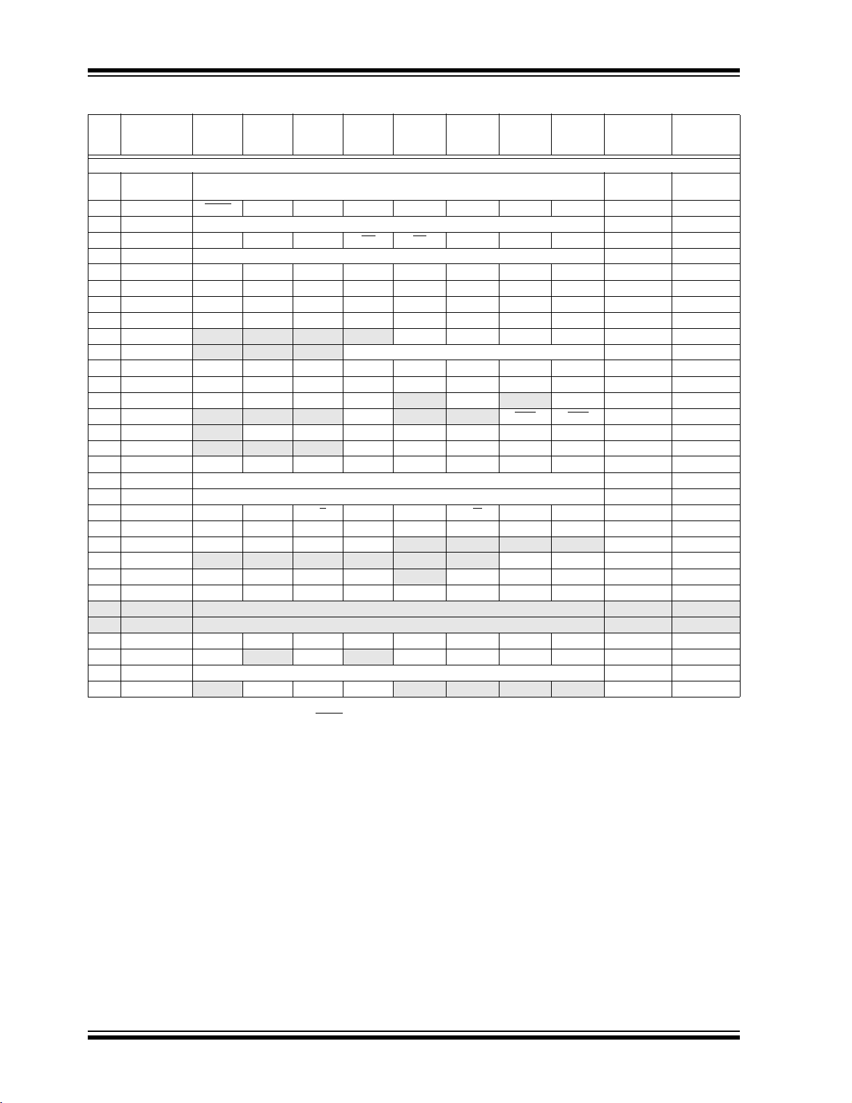
PIC16F917/916/914/913
Program
Memory
Device
Flash
(words/bytes)
Data Memory
SRAM
(bytes)
EEPROM
(bytes)
I/O
10-bit A/D
(ch)
LCD
(segment
drivers)
CCP
Timers
8/16-
PIC16F913 4K/7K 256 256 24 5 16 1 2/1
PIC16F914 4K/7K 256 256 35 8 24 2 2/1
PIC16F916 8K/14K 352 256 24 5 16 1 2/1
PIC16F917 8K/14K 352 256 35 8 24 2 2/1
Pin Diagrams – PIC16F914/917, 40-Pin
40-pin PDIP
RE3/MCLR/VPP
RA0/AN0/C1-/SEG12
RA1/AN1/C2-/SEG7
RA2/AN2/C2+/V
RA3/AN3/C1+/V
RA4/C1OUT/T0CKI/SEG4
RA5/AN4/C2OUT/SS
RA7/OSC1/CLKI/T1OSI
RA6/OSC2/CLKO/T1OSO
REF-/COM2
REF+/SEG15
RE0/AN5/SEG21
RE1/AN6/SEG22
RE2/AN7/SEG23
RC0/VLCD1
RC1/VLCD2
RC2/VLCD3
RC3/SEG6
RD0/COM3
/SEG5
V
DD
VSS
RD1
1
2
3
4
5
6
7
8
9
10
11
12
13
14
15
16
17
18
19
20
PIC16F914/917
40
39
38
37
36
35
34
33
32
31
30
29
28
27
26
25
24
23
22
21
RB7/ICSPDAT/ICDDAT/SEG13
RB6/ICSPCLK/ICDCK/SEG14
RB5/COM1
RB4/COM0
RB3/SEG3
RB2/SEG2
RB1/SEG1
RB0/INT/SEG0
V
DD
VSS
RD7/SEG20
RD6/SEG19
RD5/SEG18
RD4/SEG17
RC7/RX/DT/SDI/SDA/SEG8
RC6/TX/CK/SCK/SCL/SEG9
RC5/T1CKI/CCP1/SEG10
RC4/T1G
RD3/SEG16
RD2/CCP2
/SDO/SEG11
bit
DS41250D-page 2 Preliminary © 2005 Microchip Technology Inc.
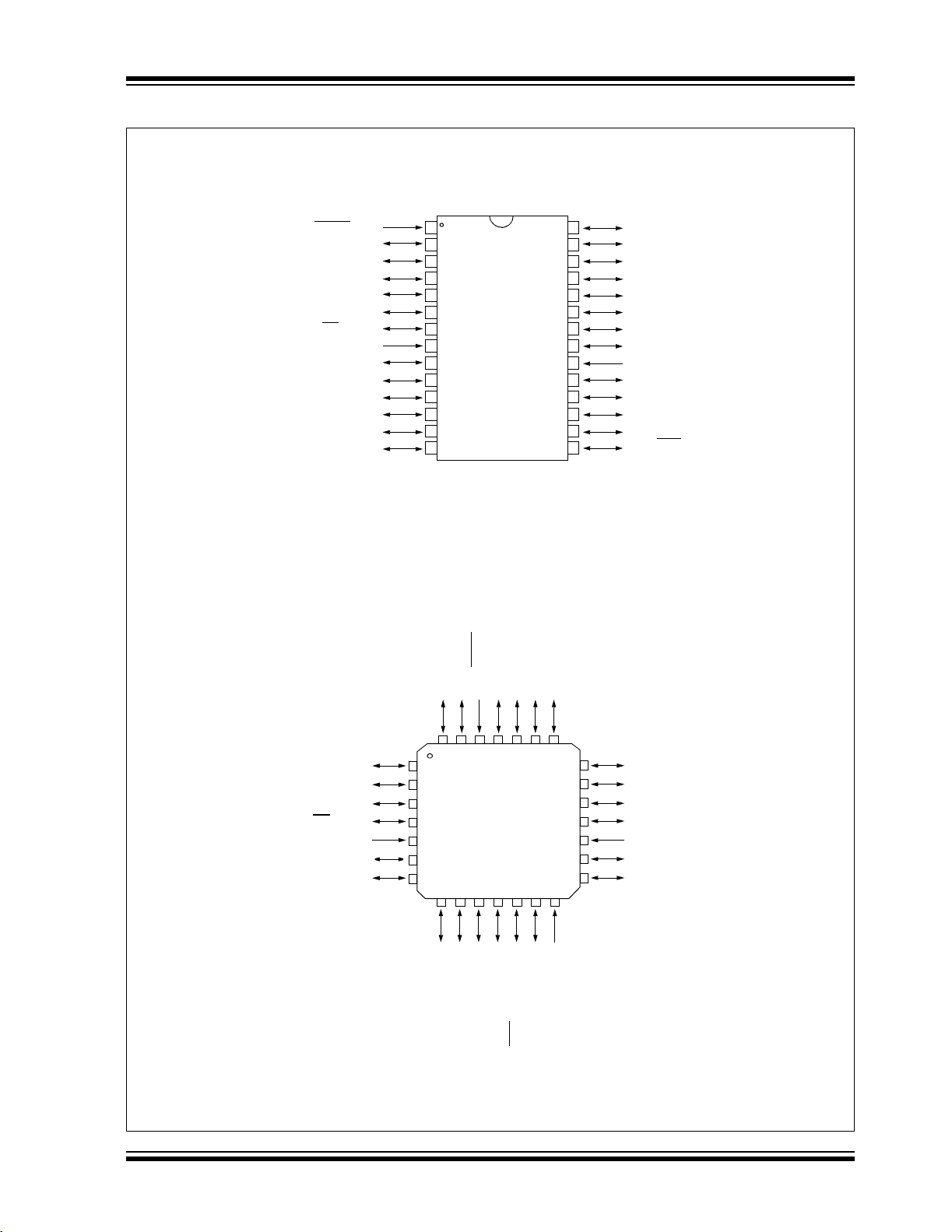
Pin Diagrams – PIC16F913/916, 28-Pin
28-pin PDIP, SOIC, SSOP
PIC16F917/916/914/913
RA3/AN3/C1+/V
28-pin QFN
RE3/MCLR/VPP
RA0/AN0/C1-/SEG12
RA1/AN1/C2-/SEG7
RA2/AN2/C2+/V
REF+/COM3/SEG15
RA4/C1OUT/T0CKI/SEG4
RA5/AN4/C2OUT/SS
RA7/OSC1/CLKI/T1OSI
RA6/OSC2/CLKO/T1OSO
REF-/COM2
/SEG5
RC0/VLCD1
RC1/VLCD2
RC2/VLCD3
RC3/SEG6
PIC16F913/916
28
27
26
25
24
23
22
21
20
19
18
17
16
15
RB7/ICSPDAT/ICDDAT/SEG13
RB6/ICSPCLK/ICDCK/SEG14
RB5/COM1
RB4/COM0
RB3/SEG3
RB2/SEG2
RB1/SEG1
RB0/INT/SEG0
V
DD
VSS
RC7/RX/DT/SDI/SDA/SEG8
RC6/TX/CK/SCK/SCL/SEG9
RC5/T1CKI/CCP1/SEG10
RC4/T1G
/SDO/SEG11
1
2
3
4
5
6
7
V
SS
8
9
10
11
12
13
14
/VPP
RA2/AN2/C2+/VREF-/COM2
RA3/AN3/C1+/V
RA4/C1OUT/T0CKI/SEG4
RA5/AN4/C2OUT/SS
RA7/OSC1/CLKI/T1OSI
RA6/OSC2/CLKO/T1OSO
REF+/COM3/SEG15
/SEG5
SS
V
RA1/AN1/C2-/SEG7
282627
1
2
3
PIC16F913/916
4
5
6
7
8109
RC0/VLCD1
RA0/AN0/C1-/SEG12
RC1/VLCD2
RE3/MCLR
RB7/ICSPDAT/ICDDAT/SEG13
25
11
RC3/SEG6
RC2/VLCD3
12
RB6/ICSPCLK/ICDCK/SEG14
24
/SDO/SEG11
RC4/T1G
RB5/COM1
23
13
RC5/T1CKI/CCP1/SEG10
RB4/COM0
22
14
RC6/TX/CK/SCK/SCL/SEG9
21
20
19
18
17
16
15
RB3/SEG3
RB2/SEG2
RB1/SEG1
RB0/INT/SEG0
DD
V
VSS
RC7/RX/DT/SDI/SDA/SEG8
© 2005 Microchip Technology Inc. Preliminary DS41250D-page 3

PIC16F917/916/914/913
Pin Diagrams – PIC16F914/917, 44-Pin
44-pin TQFP
/SDO/SEG11
RC6/TX/CK/SCK/SCL/SEG9
RC5/T1CKI/CCP1/SEG10
RC4/T1G
RD3/SEG16
RD2/CCP2
RD1
RD0/COM3
RC3/SEG6
RC2/VLCD3
RC1/VLCD2
NC
RC7/RX/DT/SDI/SDA/SEG8
RD4/SEG17
RD5/SEG18
RD6/SEG19
RD7/SEG20
V
RB0/SEG0/INT
VDD
RB1/SEG1
RB2/SEG2
RB3/SEG3
44-pin QFN
4443424140
1
2
3
4
SS
5
6
7
8
9
10
11
121314
NC
RC7/RX/DT/SDI/SDA/SEG8
39
38
PIC16F914/917
16
17
1819202122
15
NC
/VPP
RB4/COM0
RB5/COM1
RE3/MCLR
RB6/ICSPCLK/ICDCK/SEG14
RB7/ICSPDAT/ICDDAT/SEG13
RD4/SEG17
RD5/SEG18
RD6/SEG19
RD7/SEG20
RB0/INT/SEG0
RB1/SEG1
RB2/SEG2
37
RA0/C1-/AN0/SEG12
V
VDD
VDD
363435
RA1/C2-/AN1/SEG7
SS
33
32
31
30
29
28
27
26
25
24
23
REF-/COM2
REF+/C1+/SEG15
RA2/AN2/C2+/V
RA3/AN3/V
NC
RC0/VLCD1
RA6/OSC2/CLKO/T1OSO
RA7/OSC1/CLKI/T1OSI
SS
V
VDD
RE2/AN7/SEG23
RE1/AN6/SEG22
RE0/AN5/SEG21
RA5/AN4/C2OUT/SS
RA4/C1OUT/T0CKI/SEG4
/SDO/SEG11
RC6/TX/CK/SCK/SCL/SEG9
RC5/T1CKI/CCP1/SEG10
RC4/T1G
RD3/SEG16
RD2/CCP2
RD1
4443424140
1
2
3
4
5
6
7
8
9
10
11
121314
39
PIC16F914/917
16
17
15
/SEG5
RD0/COM3
RC3/SEG6
RC2/VLCD3
RC1/VLCD2
RC0/VLDC1
363435
37
38
33
32
31
30
29
28
27
26
25
24
23
1819202122
RA6/OSC2/CLK0/T1OSO
RA7/OSC1/CLKI/T1OSI
V
SS
VSS
NC
V
DD
RE2/AN7/SEG23
RE1/AN6/SEG22
RE0/AN5/SEG21
RA5/AN4/C2OUT/SS
RA4/C1OUT/T0CKI/SEG4
/SEG5
NC
RB3/SEG3
RB4/COM0
RB5/COM1
RB6/ICSPCLK/ICDCK/SEG14
RB7/ICSPDAT/ICDDAT/SEG13
REF-/COM2
RA0/AN0/C1-/SEG12
RA1/AN1/C2-/SEG7
RA2/AN2/C2+/V
REF+/SEG15
RA3/AN3/C1+/V
RE3/MCLR/VPP
DS41250D-page 4 Preliminary © 2005 Microchip Technology Inc.

PIC16F917/916/914/913
Table of Contents
1.0 Device Overview.......................................................................................................................................................................... 7
2.0 Memory Organization................................................................................................................................................................. 13
3.0 I/O Ports............................................................................... ..................... .................................................................................31
4.0 Clock Sources............................................................................................................................................................................ 69
5.0 Timer0 Module ........................................................................................................................................................................... 81
6.0 Timer1 Module With Gate Control. ............................................................................................................................................. 85
7.0 Timer2 Module ........................................................................................................................................................................... 90
8.0 Comparator Module.................................................................................................................................................................... 93
9.0 Liquid Crystal Display (LCD) Driver Module............................................................................. .. .............................................. 101
10.0 Programmable Low-Voltage Detect (PLVD) Module................................................................................................................ 125
11.0 Addressable Universal Synchronous Asynchronous Receiv er Transmitter (USA RT ).............................................................. 127
12.0 Analog-to-Digital Converter (A/D) Module................................................................................................................................ 143
13.0 Data EEPROM and Flash Program Memory Control............................................................................................................... 153
14.0 SSP Module Overview .............................................................................................................................................................159
15.0 Capture/Compare/PWM Modules .................................................................................... .... .... .. .............................................. 177
16.0 Special Features of the CPU.................................................... ..................... ........................................................................... 185
17.0 Instruction Set Summary.......................................................................................................................................................... 205
18.0 Development Support............................................................................................................................................................... 215
19.0 Electrical Specifications............................................................................................................................................................ 221
20.0 DC and AC Characteristics Graphs and Tables....................................................................................................................... 247
21.0 Packaging Information. ..................... ..................... ..................... ..................... ......................................................................... 249
Appendix A: Data Sheet Revision History.......................................................................................................................................... 259
Appendix B: Migrating From Other PICmicro® Devices .................................................................................................................... 259
Appendix C: Conversion Considerations ....................................... .... .. .... .. .... ....... .. .... .. .... .. ....... .... .. .................................................. 260
Index .................................................................................................................................................................................................. 261
On-line Support.................................................................................................................................................................................. 269
Systems Information and Upgrade Hot Line...................................................................................................................................... 269
Reader Response..............................................................................................................................................................................270
Product Identification System ............................................................................................................................................................ 271
TO OUR VALUED CUSTOMERS
It is our intention to provide our valued customers with the best documentation possible to ensure successful use of your Microchip
products. To this end, we will continue to improve our publications to better suit your needs. Our publications will be refined and
enhanced as new volumes and updates are introduced.
If you have any questions or c omm ents regarding t his publication, p lease c ontact the M arket ing Co mmunications Department via
E-mail at docerrors@microchip.com or fax the Reader Response Form in the back of this data sheet to (480) 792-4150. We
welcome your feedback.
Most Current Data Sheet
To obtain the most up-to-date version of this data sheet, please register at our Worldwide Web site at:
http://www.microchip.com
You can determine the version of a data sheet by examining its literature number found on the bottom outside corner of any page.
The last character of the literature number is the version number, (e.g., DS30000A is version A of document DS30000).
Errata
An errata sheet, describing minor operational differences from the data sheet and recommended workarounds, may exist for current
devices. As device/documentation issues become known to us, we will publish an errata sheet. The errata will specify the revision
of silicon and revision of document to which it applies.
To determine if an errata sheet exists for a particular device, please check with one of the following:
• Microchip’s Worldwide Web site; http://www.microchip.com
• Your local Microchip sales office (see last page)
When contacting a sales office, please specify which device, revision of silicon and data sheet (include literature number) you are
using.
Customer Notification System
Register on our web site at www.microchip.com to receive the most current information on all of our products.
© 2005 Microchip Technology Inc. Preliminary DS41250D-page 5

PIC16F917/916/914/913
NOTES:
DS41250D-page 6 Preliminary © 2005 Microchip Technology Inc.

1.0 DEVICE OVERVIEW
This documen t conta i ns dev ic e spec if i c in for m at i on fo r
the PIC16F91X. Addition al informatio n may be found i n
the “PICmicro® Mid-Range MCU Family Reference
Manual” (DS33023), downloaded from the Microchip
web site. The Reference Ma nu al should be consi dered
a complementary document to this data sheet and is
highly recommended reading for a better
understanding of the dev ice arc hitecture and operatio n
of the peripheral modules.
The PIC16F91X devices are covered by this data
sheet. It is available in 28/40/44-pin packages.
PIC16F917/916/914/913
© 2005 Microchip Technology Inc. Preliminary DS41250D-page 7

PIC16F917/916/914/913
5
FIGURE 1-1: PIC16F913/916 BLOCK DIAGRAM
INT
Program Counter
(PRM)
Direct Addr
Power-up
Timer
Oscillator
Power-on
Reset
Watchdog
Timer
Brown-out
Reset
VSS
Data Bus
RAM
256/352 bytes
Registers
Addr MUX
7
Status Reg
3
ALU
8
W Reg
Program
Bus
OSC1/CLKI
OSC2/CLKO
Internal
Oscillator
Block
Configuration
Flash
4k/8k x 14
Program
Memory
14
Instruction Reg
Instruction
Decode and
Control
Timing
Generation
13
8-Level Stack (13-bit)
Program Memory Read
8
Start-up Timer
VDD
File
RAM Addr
9
8
FSR Reg
MUX
Indirect
Addr
8
PORTA
PORTB
PORTC
PORTE
RA0/AN0/C1-/SEG12
RA1/AN1/C2-/SEG7
RA2/AN2/C2+/V
RA3/AN3/C1+/V
RA4/C1OUT/T0CKI/SEG4
RA5/AN4
RA6/OSC2/CLKO/T1OSO
RA7/OSC1/CLKI/T1OSI
RB0/INT/SEG0
RB1/SEG1
RB2/SEG2
RB3/SEG3
RB4/COM0
RB5/COM1
RB6/ICSPCLK/ICDCK/SEG14
RB7/ICSPDAT/ICDDAT/SEG13
RC0/VLCD1
RC1/VLCD2
RC2/VLCD3
RC3/SEG6
RC4/T1G
RC5/T1CKI/CCP1/SEG10
RC6/TX/CK/SCK/SCL/SEG9
RC7/RX/DT/SDI/SDA/SEG8
RE3/MCLR
REF-/COM2
REF+/COM3/SEG1
/C2OUT/SS/SEG5
/SDO/SEG11
/VPP
Data EEPROM
Timer0
Comparators
Timer1 Timer2 10-bit A/D
CCP1 SSP
Addressable
USART
256 bytes
BOR
PLVD
LCD
DS41250D-page 8 Preliminary © 2005 Microchip Technology Inc.
PIC16F917/916/914/913
3
FIGURE 1-2: PIC16F914/917 BLOCK DIAGRAM
INT
Program Counter
8-Level Stack (13-bit)
(PRM)
Direct Addr
Power-up
Timer
Oscillator
Power-on
Reset
Watchdog
Timer
Brown-out
Reset
VSS
Data Bus
256/352 bytes
Registers
Addr MUX
7
3
ALU
8
W Reg
Program
OSC1/CLKI
OSC2/CLKO
Internal
Oscillator
Block
Configuration
4k/8k x 14
Bus
Instruction Reg
Decode and
Flash
Program
Memory
14
Instruction
Control
Timing
Generation
13
Program Memory Read
8
Start-up Timer
VDD
RAM
File
RAM Addr
9
8
FSR Reg
Status Reg
MUX
Indirect
Addr
8
PORTA
PORTB
PORTC
PORTD
RA0/AN0/C1-/SEG12
RA1/AN1/C2-/SEG7
RA2/AN2/C2+/V
RA3/AN3/C1+/V
RA4/C1OUT/T0CKI/SEG4
RA5/AN4
RA6/OSC2/CLKO/T1OSO
RA7/OSC1/CLKI/T1OSI
RB0/INT/SEG0
RB1/SEG1
RB2/SEG2
RB3/SEG3
RB4/COM0
RB5/COM1
RB6/ICSPCLK/ICDCK/SEG14
RB7/ICSPDAT/ICDDAT/SEG1
RC0/VLCD1
RC1/VLCD2
RC2/VLCD3
RC3/SEG6
RC4/T1G
RC5/T1CKI/CCP1/SEG10
RC6/TX/CK/SCK/SCL/SEG9
RC7/RX/DT/SDI/SDA/SEG8
RD0/COM3
RD1
RD2/CCP2
RD3/SEG16
RD4/SEG17
RD5/SEG18
RD6/SEG19
RD7/SEG20
REF-/COM2
REF+/SEG15
/C2OUT/SS/SEG5
/SDO/SEG11
Timer0
Comparators
Timer1 Timer2 10-bit A/D
CCP1
CCP2 SSP
Addressable
USART
PORTE
BOR
RE0/AN5/SEG21
RE1/AN6/SEG22
RE2/AN7/SEG23
RE3/MCLR
PLVD LCD
/VPP
Data EEPROM
256 bytes
© 2005 Microchip Technology Inc. Preliminary DS41250D-page 9

PIC16F917/916/914/913
TABLE 1-1: PIC16F91X PINOUT DESCRIPTIONS
Name Function
RA0/AN0/C1-/SEG12 RA0 TTL CMOS General purpose I/O.
AN0 AN — Analog input Channel 0/C o m parator 1 input – negative.
C1- — AN Comparator 1 negative input.
SEG12 — AN LCD analog ou t put.
RA1/AN1/C2-/SEG7 RA1 TTL CMOS General purpose I/O.
AN1 AN — Analog input Channel 1/C o m parator 2 input – negative.
C2- — AN Comparator 2 negative input.
SEG7 — AN LCD analog output.
RA2/AN2/C2+/V
RA3/AN3/C1+/V
SEG15
RA4/C1OUT/T0CKI/SEG4 RA4 TTL CMOS General purpose I/O.
RA5/AN4/C2OUT/SS
RA6/OSC2/CLKO/T1OSO RA6 T TL CMOS General purpose I/O.
RA7/OSC1/CLKI/T1OSI RA7 TTL CMOS General purpose I/O.
RB0/INT/SEG0 RB0 TTL CMOS General purpose I/O. Individually enabled pull-up.
RB1/SEG1 RB1 TTL CMOS General purpose I/O. Individually enabled pull-up.
Legend: AN = Analog input or output CMOS = CMOS compatible input or ou t put D = Direct
Note 1: COM 3 i s av ai labl e on RA3 for the PIC16F913 /916 and on RD0 for the PIC16F 914/917.
2: Pins available on PIC16F914/917 only.
REF-/COM2 RA2 TTL CMOS General purpose I/O.
AN2 AN — Analog input Channel 2/Comparator 2 input – positive.
C2+ — AN Comparator 2 positive input.
REF- AN — External Voltage Reference – negative.
V
COM2 — AN LCD analog output.
REF+/COM3
TTL = TTL compatible input ST = Schmitt Trigger input with CMOS levels
HV = High Voltage XTAL = Crystal
(1)
/
RA3 TTL CMOS General purpose I/O.
AN3 AN — Analog input Channel 3/Comparator 1 input – positive.
C1+ — AN Comparator 1 positive input.
REF+ AN — External Voltage Reference – positive.
V
COM3
SEG15 — AN LCD analog ou t put.
C1OUT — CMOS Comparator 1 out p ut .
T0CKI ST — Timer0 clock input.
SEG4 — AN LCD analog output.
/SEG5 RA5 TTL CMOS General purpose I/O.
AN4 AN — Analog input Channel 4.
C2OUT — CMOS Comparator 2 out p ut .
SS
SEG5 — AN LCD analog output.
OSC2 — XTAL Crystal/Resonator.
CLKO — CMOS T
T1OSO — XTAL Timer1 oscillator output.
OSC1 XTAL — Cr ystal/Resonator.
CLKI ST — Clock input.
T1OSI XTAL — Timer1 oscilla to r inpu t.
INT ST — External interrupt pin.
SEG0 — AN LCD analog output.
SEG1 — AN LCD analog output.
Input
(1)
Output
Type
TTL — Slave select input.
Type
— AN LCD analog output.
OSC/4 reference clock.
Description
DS41250D-page 10 Preliminary © 2005 Microchip Technology Inc.
PIC16F917/916/914/913
TABLE 1-1: PIC16F91X PINOUT DESCRIPTIONS (CONTINUED)
Input
Name Function
RB2/SEG2 RB2 TTL CMOS General purpose I/O. Individually enabled pull-up.
SEG2 — AN LCD analog output.
RB3/SEG3 RB3 TTL CMOS General purpose I/O. Individually enabled pull-up.
SEG3 — AN LCD analog output.
RB4/COM0 RB4 TTL CMOS General purpose I/O. Individually controlled interrupt-on-
COM0 — AN LCD analog output.
RB5/COM1 RB5 TTL CMOS General purpose I/O. Individually controlled interrupt-on-
COM1 — AN LCD analog output.
RB6/ICSPCLK/ICDCK/SEG14 RB6 TTL CMOS General purpose I/O. Individually controlled interrupt-on-
ICSPCLK ST — ICSP™ clock.
ICDCK ST — ICD clock I/O.
SEG14 — AN LCD analog ou t put.
RB7/ICSPDAT/ICDDAT/SEG13 RB7 TTL CMOS General purpose I/O. Individually controlled interrupt-on-
ICSPDAT ST CMOS ICSP Data I/O.
ICDDAT ST CMOS ICD Data I/O.
SEG13 — AN LCD analog ou t put.
RC0/VLCD1 RC0 ST CMOS General purpose I/O.
VLCD1 AN — LCD analog input.
RC1/VLCD2 RC1 ST CMOS General purpose I/O.
VLCD2 AN — LCD analog input.
RC2/VLCD3 RC2 ST CMOS General purpose I/O.
VLCD3 AN — LCD analog input.
RC3/SEG6 RC3 ST CMOS General purpose I/O.
SEG6 — AN LCD analog output.
RC4/T1G
RC5/T1CKI/CCP1/SEG10 RC5 ST CMOS General purpose I/O.
RC6/TX/CK/SCK/SCL/SEG9 RC6 ST CMOS General purpose I/O.
Legend: AN = Analog input or output CMOS= CMOS compatible input or output D = Direct
Note 1: COM 3 i s av ai labl e on RA3 for the PIC16F913 /916 and on RD0 for the PIC16F 914/917.
/SDO/SEG11 RC4 ST CMOS General purpose I/O.
T1G ST — Timer1 gate inp ut .
SDO — CMOS Serial data output.
SEG11 — AN LCD analog output.
T1CKI ST — Timer1 clock input.
CCP1 ST CMO S C apture 1 input/Compare 1 output / PW M 1 output.
SEG10 — AN LCD analog ou t put.
TX — CM O S U SART asynchronous seria l transm i t .
CK ST CMOS US ART synchronous se rial cl ock.
SCK ST CMOS SPI™ cl ock.
SCL ST CMOS I
SEG9 — AN LCD analog output.
TTL = TTL compatible input ST = Schmitt Trigger input with CMOS levels
HV = High Voltage XTAL = Crystal
2: Pins available on PIC16F914/917 only.
Type
Output
Type
Description
change. Individually enabled pull-up.
change. Individually enabled pull-up.
change. Individually enabled pull-up.
change. Individually enabled pull-up.
2
C™ clock.
© 2005 Microchip Technology Inc. Preliminary DS41250D-page 11

PIC16F917/916/914/913
TABLE 1-1: PIC16F91X PINOUT DESCRIPTIONS (CONTINUED)
Name Function
Input
RC7/RX/DT/SDI/SDA/SEG8 RC7 ST CMOS General purpose I/O.
RX ST — USART asynchronous serial receiv e.
DT ST CM O S USART synchronou s se ri al data.
SDI ST CMOS SPI™ da ta input.
SDA ST CMOS I
SEG8 — AN LCD analog output.
RD0/COM3
(1, 2)
RD0 ST CMOS General purpose I/O.
COM3 — AN LCD analog output.
(2)
RD1
RD2/CCP2
(2)
RD1 ST CMOS General purpose I/O.
RD2 ST CMOS General purpose I/O.
CCP2 ST CMO S C apture 2 input/Compare 2 output / PW M 2 output.
RD3/SEG16
(2)
RD3 ST CMOS General purpose I/O.
SEG16 — AN LCD analog ou t put.
RD4/SEG17
(2)
RD4 ST CMOS General purpose I/O.
SEG17 — AN LCD analog ou t put.
RD5/SEG18
(2)
RD5 ST CMOS General purpose I/O.
SEG18 — AN LCD analog ou t put.
RD6/SEG19
(2)
RD6 ST CMOS General purpose I/O.
SEG19 — AN LCD analog ou t put.
RD7/SEG20
(2)
RD7 ST CMOS General purpose I/O.
SEG20 — AN LCD analog ou t put.
RE0/AN5/SEG21
(2)
RE0 ST CMOS General purpose I/O.
AN5 AN — Analog input Channel 5.
SEG21 — AN LCD analog ou t put.
RE1/AN6/SEG22
(2)
RE1 ST CMOS General purpose I/O.
AN6 AN — Analog input Channel 6.
SEG22 — AN LCD analog ou t put.
RE2/AN7/SEG23
(2)
RE2 ST CMOS General purpose I/O.
AN7 AN — Analog input Channel 7.
SEG23 — AN LCD analog ou t put.
RE3/MCLR
/VPP RE3 ST — Digital input only.
MCLR ST — M aster Clear with internal pull-up.
PP HV — Programming voltage.
V
VDD VDD D — Power supply for microcontroller.
SS VSS D — Ground reference for mi cr ocontroller.
V
Legend: AN = Analog input or output CMOS = CMOS compatible input or ou t put D = Direct
TTL = TTL compatible input ST = Schmitt Trigger input with CMOS levels
HV = High Voltage XTAL = Crystal
Note 1: COM 3 i s av ai labl e on RA3 for the PIC16F913 /916 and on RD0 for the PIC16F 914/917.
2: Pins available on PIC16F914/917 only.
Type
Output
Type
2
C™ data.
Description
DS41250D-page 12 Preliminary © 2005 Microchip Technology Inc.

PIC16F917/916/914/913
2.0 MEMORY ORGANIZATION
2.1 Program Memory Organization
The PIC16F917/916/914/913 has a 13-bit program
counter capable of addressing a 4k x 14 program
memory space for the PIC16F913/914 (0000h-0FFFh)
and an 8k x 14 program memory space for the
PIC16F916/917 (0000h-1FFFh). Accessing a location
above the memory boundaries for the PIC16F913 and
PIC16F914 will cause a wrap around within the first 4k x
14 space. The Reset vector is at 0000h and the interrupt
vector is at 0004h.
FIGURE 2-1: PROGRAM MEMORY MAP
AND STACK FOR THE
PIC16F913/914
pc<12:0>
CALL, RETURN
RETFIE, RETLW
Stack Level 1
Stack Level 2
Stack Level 8
Reset Vector
13
0000h
FIGURE 2-2: PROGRAM MEMORY MAP
AND STACK FOR THE
PIC16F916/917
pc<12:0>
CALL, RETURN
RETFIE, RETLW
On-chip
Program
Memory
Stack Level 1
Stack Level 2
Stack Level 8
Reset Vector
Interrupt Vector
Page 0
Page 1
Page 2
Page 3
13
0000h
0004h
0005h
07FFh
0800h
0FFFh
1000h
17FFh
1800h
1FFFh
On-chip
Program
Memory
Interrupt Vector
Page 0
Page 1
0004h
0005h
07FFh
0800h
0FFFh
1000h
1FFFh
© 2005 Microchip Technology Inc. Preliminary DS41250D-page 13

PIC16F917/916/914/913
2.2 Data Memory Organization
The data memory is partitioned into multiple banks
which contain the General Purpose Registers (GPRs)
and the Special Function Registers (SFRs). Bits RP0
and RP1 are bank select bits.
RP0 RP1 (STATUS<6:5>)
= 00: → Bank 0
= 01: → Bank 1
= 10: → Bank 2
= 11: → Bank 3
Each bank extends up to 7Fh (128 bytes). The lower
locations of each bank are reserved for the Special
Function Registers. Above the Special Function
Registers are the General Purpose Registers,
implemented as static RAM. All implemented banks
contain Special Function Registers. Some frequently
used Special Function Registers from one bank are
mirrored in another bank for code reduction and
quicker access.
2.2.1 GENERAL PURPOSE REGISTER
FILE
The register file is organized as 256x 8 in the
PIC16F913/914 and 352 x 8 in the PIC16F916/917.
Each register is accessed either directly or indirectly
through the File Select Register (FSR) (see Section 2.5
“Indirect Addressing, INDF and FSR Registers”).
2.2.2 SPECIAL FUNCTION REGISTERS
The Special Function Registers are registers used by
the CPU and peripheral functions for controlling the
desired operation of the device (see Tables 2-1,
2-2, 2-3 and 2-4). These registers are static RAM.
The special re gisters can be classifi ed into two sets:
core and peripheral. The Special Function Registers
associated with the “c ore” are des cribed in this sect ion.
Those related to the operation of the peripheral
features are described in the section of that peripheral
feature.
DS41250D-page 14 Preliminary © 2005 Microchip Technology Inc.
PIC16F917/916/914/913
FIGURE 2-3: PIC16F913/916 SPECIAL FUNCTION REGISTERS
File File File File
Address Address Address Address
Indirect addr.
TMR0 01h OPTION_REG 81h TMR0 101h OPTION_REG 181h
PCL 02h PCL 82h PCL 102h PCL 182h
STATUS 03h STATUS 8 3h STATUS 103h STATUS 183h
FSR 04h FSR 84h FSR 104h FSR 184h
PORTA 05h TRISA 85h WDTCON 105h
PORTB 06h TRISB 86h PORTB 106h TRISB 186h
PORTC 07h TRISC 87h LCDCON 107h 187h
PORTE 09h TRISE 89h LVDCON 109h 189h
PCLATH 0Ah PCLATH 8Ah PCLATH 10Ah PCLATH 18Ah
INTCON 0Bh INTCON 8Bh INTCON 10Bh INTCON 18Bh
PIR1 0Ch PIE1 8Ch EEDATL 10Ch EECON1 18Ch
PIR2 0Dh PIE2 8Dh EEADRL 10Dh
TMR1L 0Eh PCON 8Eh EEDATH 10Eh
TMR1H 0Fh OSCCON 8Fh EEADRH 10Fh 18Fh
T1CON 10h OSCTUNE 90h LCDDATA0 110h
TMR2 11h ANSEL 91h LCDDATA1 111h
T2CON 12h PR2 92h
SSPBUF 13h SSPADD 93h LCDDATA3 113h
SSPCON 14h SSPSTAT 94h LCDDATA4 114h
CCPR1L 15h WPUB 95h
CCPR1H 16h IOCB 96h LCDDATA6 116h
CCP1CON 17h CMCON1 97h LCDDATA7 117h
RCSTA 18h TXSTA 98h
TXREG 19h SPBRG 99h LCDDATA9 119h
RCREG 1Ah
ADRESH 1Eh ADRESL 9Eh
ADCON0 1Fh ADCON1 9Fh
(1)
00h Indirect addr.
08h 88h LCDPS 108h 188h
1Bh 9Bh 11Bh
1Ch CMCON0 9Ch LCDSE0 11Ch
1Dh VRCON 9Dh LCDSE1 11Dh
20h
(1)
80h Indirect addr.
9Ah LCDDATA10 11Ah
A0h
(1)
100h Indirect addr.
EECON2
112h
115h
118h
Purpose
Register
96 Bytes
11Eh
11Fh
120h
General
(2)
(1)
(1)
180h
185h
18Dh
18Eh
190h
General
General
Purpose
Register
96 Bytes
7Fh FFh 17Fh 1FFh
Bank 0 Bank 1 Bank 2 Bank 3
Unimplemented data memory locations, read as ‘0’.
Note 1: Not a physical register.
2: On the PIC16F913, unimplemented data memory locations, read as ‘0’.
© 2005 Microchip Technology Inc. Preliminary DS41250D-page 15
Purpose
Register
80 Bytes
accesses
70h-7Fh
EFh 16Fh 1EFh
F0h accesses
General
Purpose
Register
80 Bytes
70h-7Fh
170h accesses
70h-7Fh
1F0h

PIC16F917/916/914/913
FIGURE 2-4: PIC16F914/917 SPECIAL FUNCTION REGISTERS
File File File File
Address Address Address Address
Indirect addr.
TMR0 01h OPTION_REG 81h TMR0 101h OPTION_REG 181h
PCL 02h PCL 82h PCL 102h PCL 182h
STATUS 03h STATUS 8 3h STATUS 103h STATUS 183h
FSR 04h FSR 84h FSR 104h FSR 184h
PORTA 05h TRISA 85h WDTCON 105h
PORTB 06h TRISB 86h PORTB 106h TRISB 186h
PORTC 07h TRISC 87h LCDCON 107h 187h
PORTD 08h TRISD 88h LCDPS 108h
PORTE 09h TRISE 89h LVDCON 109h 189h
PCLATH 0Ah PCLATH 8Ah PCLATH 10Ah PCLATH 18Ah
INTCON 0Bh INTCON 8Bh INTCON 10Bh INTCON 18Bh
PIR1 0Ch PIE1 8Ch EEDATL 10Ch EECON1 18Ch
PIR2 0Dh PIE2 8Dh EEADRL 10Dh
TMR1L 0Eh PCON 8Eh EEDATH 10Eh
TMR1H 0Fh OSCCON 8Fh EEADRH 10Fh 18Fh
T1CON 10h OSCTUNE 90h LCDDATA0 110h
TMR2 11h ANSEL 91h LCDDATA1 111h
T2CON 12h PR2 92h LCDDATA2 112h
SSPBUF 13h SSPADD 93h LCDDATA3 113h
SSPCON 14h SSPSTAT 94h LCDDATA4 114h
CCPR2L 15h WPUB 95h LCDDATA5 115h
CCPR2H 16h IOCB 96h LCDDATA6 116h
CCP2CON 17h CMCON1 97h LCDDATA7 117h
RCSTA 18h TXSTA 98h LCDDATA8 118h
TXREG 19h SPBRG 99h LCDDATA9 119h
RCREG 1Ah
CCPR2L 1Bh 9Bh LCDDATA11 11Bh
CCPR2H 1Ch CMCON0 9Ch LCDSE0 11Ch
CCPR2CON 1Dh VRCON 9Dh LCDSE1 11Dh
ADRESH 1Eh ADRESL 9Eh LCDSE2 11Eh
ADCON0 1Fh ADCON1 9Fh
(1)
00h Indirect addr.
20h
(1)
80h Indirect addr.
9Ah LCDDATA10 11Ah
A0h
(1)
100h Indirect addr.
EECON2
Purpose
Register
96 Bytes
11Fh
120h
General
(2)
(1)
(1)
180h
185h
188h
18Dh
18Eh
190h
General
General
Purpose
Register
96 Bytes
7Fh FFh 17Fh 1FFh
Bank 0 Bank 1 Bank 2 Bank 3
Unimplemented data memory locations, read as ‘0’.
Note 1: Not a physical register.
2: On the PIC16F914, unimplemented data memory locations, read as ‘0’.
DS41250D-page 16 Preliminary © 2005 Microchip Technology Inc.
Purpose
Register
80 Bytes
accesses
70h-7Fh
EFh 16Fh 1EFh
F0h accesses
General
Purpose
Register
80 Bytes
70h-7Fh
170h accesses
70h-7Fh
1F0h

PIC16F917/916/914/913
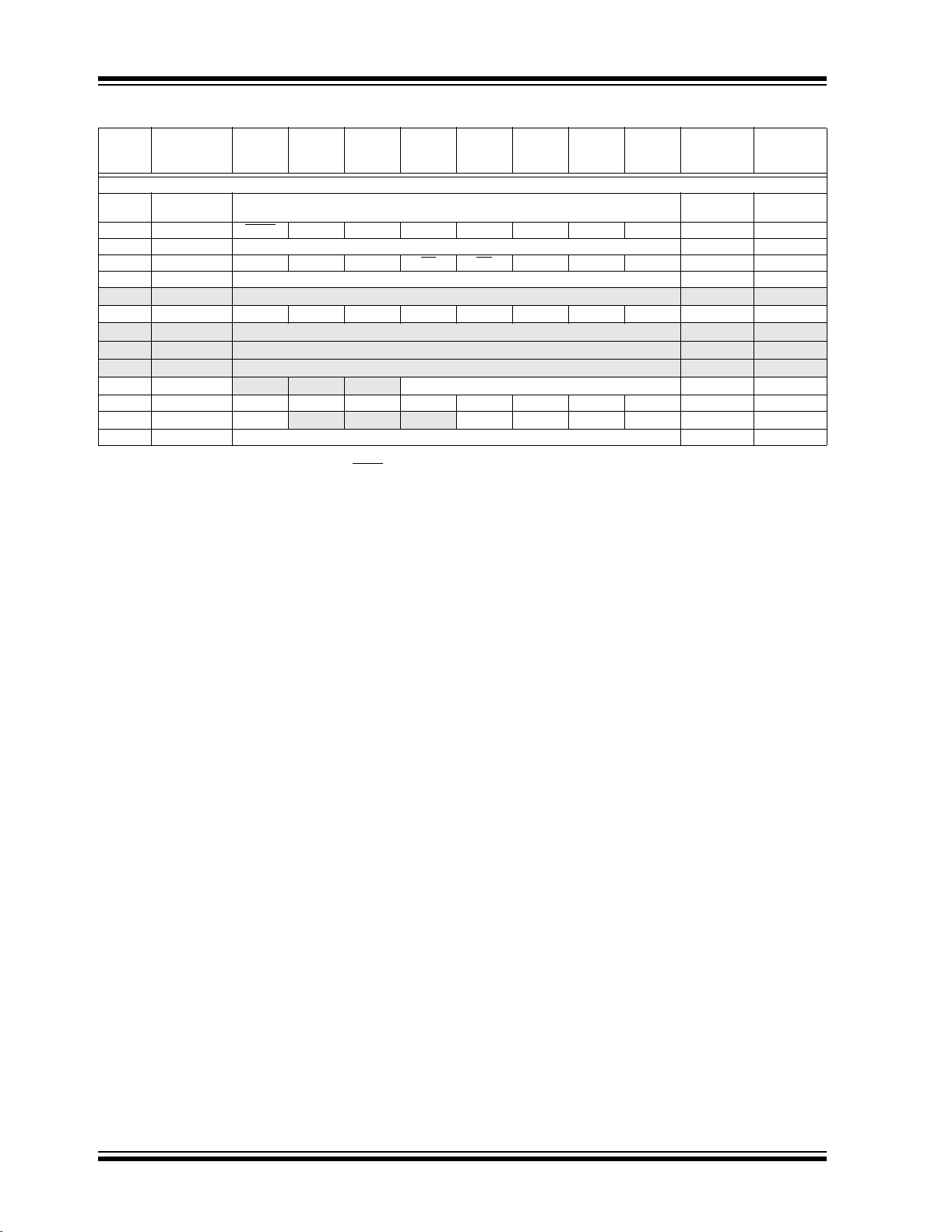
TABLE 2-1: PIC16F917/916/914/913 SPECIAL REGISTERS SUMMARY BANK 0
Addr Name Bit 7 Bit 6 Bit 5 Bit 4 Bit 3 Bit 2 Bit 1 Bit 0
Bank 0
00h INDF Addressing this location uses contents of FSR to address data memory (not a physical register) xxxx xxxx xxxx xxxx
01h TMR0 Timer0 Module Register xxxx xxxx uuuu uuuu
02h PCL Program Counter’s (PC) Least Significant Byte 0000 0000 0000 0000
03h STATUS IRP RP1 RP0 TO
04h FSR Indirect Data Memory Address Pointer xxxx xxxx uuuu uuuu
05h PORTA RA7 RA6 RA5 RA4 RA3 RA2 RA1 RA0 xxxx xxxx uuuu uuuu
06h PORTB RB7 RB6 RB5 RB4 RB3 RB2 RB1 RB0 xxxx xxxx uuuu uuuu
07h PORTC RC7 RC6 RC5 RC4 RC3 RC2 RC1 RC0 xxxx xxxx uuuu uuuu
08h PORTD
09h PORTE
0Ah PCLATH
0Bh INTCON GIE PEIE T0IE INTE RBIE T0IF INTF RBIF 0000 000x 0000 000x
0Ch PIR1
0Dh PIR2
0Eh TMR1L Holding Register for the Least Significant Byte of the 16-bit TMR1 xxxx xxxx uuuu uuuu
0Fh TMR1H Holding Register for the Most Significant Byte of the 16-bit TMR1 xxxx xxxx uuuu uuuu
10h T1CON T1GINV T1GE T1CKPS1 T1CKPS0 T1OSCEN T1SYNC
11h TMR2
12h T2CON
13h SSPBUF Synchron ous Seri al Port Receive Buffer/Transmit Register xxxx xxxx uuuu uuuu
14h SSPCON WCOL SSPOV SSPEN CKP S SPM3 SSPM2 SSPM1 SSPM0 0000 0000 0000 0000
15h CCPR1L Capture/Compare/PWM Register 1 (LSB) xxxx xxxx uuuu uuuu
16h CCPR1H Capture/Compare/PWM Register 1 (MSB) xxxx xxxx uuuu uuuu
17h CCP1CON
18h RCSTA SPEN RX9 SREN CREN ADDEN FERR OERR RX9D 0000 000x 0000 000x
19h TXREG USART Transmit Data Register 0000 0000 0000 0000
1Ah RCREG USART Receive Data Register 0000 0000 0000 0000
(2)
1Bh
(2)
1Ch
(2)
1Dh
1Eh ADRESH A/D Result Register High Byte xxxx xxxx uuuu uuuu
1Fh ADCON0 ADFM VCFG1 V CFG0 CHS2 CHS1 CHS0 GO/DONE
Legend: - = Unimplemented locations read as ‘0’, u = unchanged, x = unknown, q = value depends on condition, shaded = unimplemented
Note 1: Other (non Power-up) Resets include MCLR
(2)
RD7 RD6 RD5 RD4 RD3 RD2 RD1 RD0 xxxx xxxx uuuu uuuu
— — — —RE3RE2
— — — Write Buffer for upper 5 bits of Program Counter ---0 0000 ---0 0000
EEIF ADIF RCIF TXIF SSPIF CCP1IF TMR2IF TMR1IF 0000 0000 0000 0000
OSFIF C2IF C1IF LCDIF —LVDIF— CCP2IF 0000 -0-0 0000 -0-0
Timer2 Module Register 0000 0000 0000 0000
— TOUTPS3 TOUTPS2 TOUTPS1 TOUTPS0 TMR2ON T2CKPS1 T2CKPS0 -000 0000 -000 0000
— — CCP1X CCP1Y CCP1M3 CCP1M2 CCP1M1 CCP1M0 --00 0000 --00 0000
CCPR2L Capture/Compare/PWM Register 2 (LSB) xxxx xxxx uuuu uuuu
CCPR2H Capture/Compare/PWM Register 2 (MSB) xxxx xxxx uuuu uuuu
CCP2CON — — CCP2X CCP2Y CCP2M3 CCP2M2 CCP2M1 CCP2M0 --00 0000 --00 0000
2: PIC16F914/917 only.
Reset and Watchdog Timer Reset dur ing nor mal operation.
PD ZDCC0001 1xxx 000q quuu
(2)
(2)
RE1
TMR1CS TMR1ON 0000 0000 uuuu uuuu
RE0
ADON 0000 0000 0000 0000
Value on
POR/BOR
Reset
(2)
---- xxxx ---- uuuu
Value on
all other
Resets
(1)
© 2005 Microchip Technology Inc. Preliminary DS41250D-page 17
PIC16F917/916/914/913
TABLE 2-2: PIC16F917/916/914/913 SPECIAL FUNCTION REGISTERS SUMMARY BANK 1
Addr Name Bit 7 Bit 6 Bit 5 Bit 4 Bit 3 Bit 2 Bit 1 Bit 0
Bank 1
80h INDF Addressing this location uses contents of FSR to address data memory (not a physical
81h OPTION_REG RBPU
82h PCL Program Counter’s (PC) Least Significant Byte 0000 0000 0000 0000
83h S TATUS IRP RP1 RP0 TO
84h FSR Indirect Data Memory Address Pointer xxxx xxxx uuuu uuuu
85h TRISA TRISA7 TRISA6 TRISA5 TRISA4 TRISA3 TRISA2 TRISA1 TRISA0 1111 1111 1111 1111
86h TRISB TRISB7 TRISB6 TRISB5 TRISB4 TRISB3 TRISB2 TRISB1 TRISB0 1111 1111 1111 1111
87h TRISC TRISC7 TRISC6 TRISC5 TRISC4 TRISC3 TRISC2 TRISC1 TRISC0 1111 1111 1111 1111
88h TRISD
89h TRISE
8Ah PCLATH
8Bh INTCON GIE PEIE T0IE INTE RBIE T0IF INTF RBIF 0000 000x 0000 000x
8Ch PIE1 EEIE ADIE RCIE TXIE SSPIE CCP1IE TMR2IE TMR1IE 0000 0000 0000 0000
8Dh PIE2 OSFIE C2IE C1IE LCDIE
8Eh PCON
8Fh OSCCON
90h OSCTUNE
91h ANSEL ANS7
92h PR2 Timer2 Peri od Regi ster 1111 1111 1111 1111
93h SSPADD Synchronous Serial Port (I
94h SSPSTAT SMP CKE D/A
95h WPUB WPUB7 WPUB6 WPUB5 WPUB4 WPUB3 WPUB2 WPUB1 WPUB0 1111 1111 1111 1111
96h IOCB IOCB7 IOCB6 IOCB5 IOCB4
97h CMCON1
98h TXSTA CSRC TX9 TXEN SYNC
99h SPBRG SPBRG7 SPBRG6 SPBRG5 SPBRG4 SPBRG3 SPBRG2 SPBRG1 SPBRG0 0000 0000 0000 0000
9Ah — Unimplemented — —
9Bh — Unimplemented — —
9Ch CMCON0 C2OUT C1OUT C2INV C1INV CIS CM2 CM1 CM0 0000 0000 0000 0000
9Dh VRCON VREN
9Eh ADRESL A/D Result Register Low Byte xxxx xxxx uuuu uuuu
9Fh ADCON1
Legend: - = Unimplemented locations read as ‘0’, u = unchanged, x = unknown, q = value depends on condition, shaded = unimplemented
Note 1: Other (non Power-up) Resets include MCLR
(2)
2: PIC 16F 91 4/9 17 only.
3: PIC 16F 91 4/9 17 only, forced ‘0’ on PIC16F91 3/9 16.
4: The value of the OSTS bit is dependent on the value of the Configuration Word (CONFIG) of the device. See Section 4.0 “Clock
Sources”.
5: Bit is read-only; TRISE = 1 always.
register)
INTEDG T0CS T0SE PSA PS2 PS1 PS0 1111 1111 1111 1111
PD ZDCC0001 1xxx 000q quuu
TRISD7 TRISD6 TRISD5 TRISD4 TRISD3 TRISD2 TRISD1 TRISD0 1111 1111 1111 1111
— — — — TRISE3
— — — Write Buffer for the upper 5 bits of the Program Counter ---0 0000 ---0 0000
— — —SBOREN— —PORBOR ---1 --qq ---u --uu
— IRCF2 IRCF1 IRCF0 OSTS
— — — TUN4 TUN3 TUN2 TUN1 TUN0 ---0 0000 ---u uuuu
(3)
— — — — — — T1GSS C2SYNC ---- --10 ---- --10
— ADCS2 ADCS1 ADCS0 — — — — -000 ---- -000 ---
(3)
ANS6
—VRR— VR3 VR2 VR1 VR0 0-0- 0000 0-0- 0000
(3)
ANS5
2
ANS4 ANS3 ANS2 ANS1 ANS0 1111 1111 1111 1111
C mode) Address Register 0000 0000 0000 0000
PSR/WUA BF 0000 0000 0000 0000
Reset and Watchdog Timer Reset during normal operation.
(5)
—LVDIE— CCP2IE 0000 -0-0 0000 -0-0
(4)
— — — — 0000 ---- 0000 ----
— BRGH TRMT TX9D 0000 -010 0000 -010
(2)
TRISE2
HTS LTS SCS -110 q000 -110 x000
TRISE1
(2)
TRISE0
Value on
POR/BOR
Reset
xxxx xxxx xxxx xxxx
(2)
---- 1111 ---- 1111
Value on
all other
Resets
(1)
DS41250D-page 18 Preliminary © 2005 Microchip Technology Inc.

PIC16F917/916/914/913
TABLE 2-3: PIC16F917/916/914/913 SPECIAL REGISTERS SUMMARY BANK 2
Addr Name Bit 7 Bit 6 Bit 5 Bit 4 Bit 3 Bit 2 Bit 1 Bit 0
Bank 2
100h INDF Addressing this location uses contents of FSR to address data memory (not a physical register) xxxx xxxx xxxx xxxx
101h TMR0 Timer0 Module Register xxxx xxxx uuuu uuuu
102h PCL Program Counter’s (PC) Least Significant Byte 0000 0000 0000 0000
103h STATUS IRP RP1 RP0 TO
104h FSR Indirect Data Memory Address Pointer xxxx xxxx uuuu uuuu
105h WDTCON
106h PORTB RB7 RB6 RB5 RB4 RB3 RB2 RB1 RB0 xxxx xxxx uuuu uuuu
107h LCDCON LCDEN SLPEN WERR VLCDEN CS1 CS0 LMUX1 LMUX0 0001 0011 0001 0011
108h LCDPS WFT BIASMD LCDA WA LP3 LP2 LP1 LP0 0000 0000 0000 0000
109h LVDCON
10Ah PCLATH
10Bh INTCON GIE PEIE T0IE INTE RBIE T0IF INTF RBIF 0000 000x 0000 000x
EEDATL EEDATL7 EEDATL6 EEDATL5 EEDATL4 EEDATL3 EEDATL2 EEDATL1 EEDATL0 0000 0000 0000 0000
10Ch
EEADRL EEADRL7 EEADRL6 EEADRL5 EEADRL4 EEADRL3 EEADRL2 EEADRL1 EEADRL0 0000 0000 0000 0000
10Dh
10Eh EEDATH
10Fh EEADRH
110h LCDDATA0 SEG7
111h LCDDATA1 SEG15
112h LCDDATA2
113h LCDDATA3 SEG7
114h LCDDATA4 SEG15
115h LCDDATA5
116h LCDDATA6 SEG7
117h LCDDATA7 SEG15
118h LCDDATA8
119h LCDDATA9 SEG7
11Ah LCDDATA10 SEG15
LCDDATA11
11Bh
11Ch LCDSE0
11Dh LCDSE1
11Eh LCDSE2
11Fh — Unimplemented — —
Legend: - = Unimplemented locations read as ‘0’, u = unchanged, x = unknown, q = value depends on condition, shaded = unimplemented
Note 1: Other (non Power-up) Resets include MCLR
(3)
(3)
(2,3)
2: PIC16F914/917 only.
3: This register is only initialized by a POR or BOR reset and is unchanged by other Resets.
— — — WDTPS3 WDTPS2 WDTPS1 WDTPS0 SWDTEN ---0 1000 ---0 1000
— —IRVSTLVDEN— LVDL2 LVDL1 LVDL0 --00 -100 --00 -100
— — — Write Buffer for the upper 5 bits of the Program Counter ---0 0000 ---0 0000
— —
— — —
COM0
COM0
(2)
SEG23
COM0
COM1
COM1
(2)
SEG23
COM1
COM2
COM2
(2)
SEG23
COM2
COM3
COM3
(2)
SEG23
COM3
SE7 SE6 SE5 SE4 SE3 SE2 SE1 SE0 0000 0000 uuuu uuuu
SE15 SE14 SE13 SE12 SE11 SE10 SE9 SE8 0000 0000 uuuu uuuu
SE23 SE22 SE21 SE20 SE19 SE18 SE17 SE16 0000 0000 uuuu uuuu
SEG6
COM0
SEG14
COM0
SEG22
COM0
SEG6
COM1
SEG14
COM1
SEG22
COM1
SEG6
COM2
SEG14
COM2
SEG22
COM2
SEG6
COM3
SEG14
COM3
SEG22
COM3
EEDATH5 EEDATH4 EEDATH3 EEDATH2 EEDATH1 EEDATH0
EEADRH4 EEADRH3 EEADRH2 EEADRH1 EEADRH0
SEG5
COM0
SEG13
COM0
SEG21
COM0
SEG5
COM1
SEG13
COM1
SEG21
COM1
SEG5
COM2
SEG13
COM2
SEG21
COM2
SEG5
COM3
SEG13
COM3
SEG21
COM3
SEG4
COM0
SEG12
COM0
SEG20
COM0
SEG4
COM1
SEG12
COM1
SEG20
COM1
SEG4
COM2
SEG12
COM2
SEG20
COM2
SEG4
COM3
SEG12
COM3
SEG20
COM3
Reset and Watchdog Timer Reset dur ing nor mal operation.
PD ZDCC0001 1xxx 000q quuu
SEG3
COM0
SEG11
COM0
SEG19
COM0
SEG3
COM1
SEG11
COM1
SEG19
COM1
SEG3
COM2
SEG11
COM2
SEG19
COM2
SEG3
COM3
SEG11
COM3
SEG19
COM3
SEG2
COM0
SEG10
COM0
SEG18
COM0
SEG2
COM1
SEG10
COM1
SEG18
COM1
SEG2
COM2
SEG10
COM2
SEG18
COM2
SEG2
COM3
SEG10
COM3
SEG18
COM3
SEG1
COM0
SEG9
COM0
SEG17
COM0
SEG1
COM1
SEG9
COM1
SEG17
COM1
SEG1
COM2
SEG9
COM2
SEG17
COM2
SEG1
COM3
SEG9
COM3
SEG17
COM3
SEG0
COM0
SEG8
COM0
SEG16
COM0
SEG0
COM1
SEG8
COM1
SEG16
COM1
SEG0
COM2
SEG8
COM2
SEG16
COM2
SEG0
COM3
SEG8
COM3
SEG16
COM3
Value on
POR/BOR
Reset
--00 0000 --00 0000
---0 0000 ---0 0000
xxxx xxxx uuuu uuuu
xxxx xxxx uuuu uuuu
xxxx xxxx uuuu uuuu
xxxx xxxx uuuu uuuu
xxxx xxxx uuuu uuuu
xxxx xxxx uuuu uuuu
xxxx xxxx uuuu uuuu
xxxx xxxx uuuu uuuu
xxxx xxxx uuuu uuuu
xxxx xxxx uuuu uuuu
xxxx xxxx uuuu uuuu
xxxx xxxx uuuu uuuu
Value on
all other
Resets
(1)
© 2005 Microchip Technology Inc. Preliminary DS41250D-page 19
PIC16F917/916/914/913
TABLE 2-4: PIC16F917/916/914/913 SPECIAL FUNCTION REGISTERS SUMMARY BANK 3
Addr Name Bit 7 Bit 6 Bit 5 Bit 4 Bit 3 Bit 2 Bit 1 Bit 0
Bank 3
180h INDF Addressing this location uses contents of FSR to address data memory (not a physical
181h OPTION_REG RBPU
182h PCL Program Counter (PC) Least Significant Byte 0000 0000 0000 0000
183h STATUS IRP RP1 RP0 TO
184h FSR Indirect Data Memory Address Pointer xxxx xxxx uuuu uuuu
185h
186h TRISB
187h
188h
189h
18Ah PCLATH
18Bh INTCON GIE PEIE T0IE INTE RBIE T0IF INTF RBIF 0000 000x 0000 000x
18Ch EECON1 EEPGD
18Dh EECON2 EEPROM Control Register 2 (not a physical register) ---- ---- ---- ----
Legend: - = Unimplemented locations read as ‘0’, u = unchanged, x = unknown, q = value depends on condition, shaded = unimplemented
Note 1: Other (non Power-up) Resets include MCLR
— Unimplemented — —
— Unimplemented — —
— Unimplemented — —
— Unimplemented — —
register)
INTEDG T0CS T0SE PSA PS2 PS1 PS0 1111 1111 1111 1111
PD ZDCC0001 1xxx 000q quuu
TRISB7 TRISB6 TRISB5 TRISB4 TRISB3 TRISB2 TRISB1 TRISB0 1111 1111 1111 1111
— — —
— — —
Write Buffer for the upper 5 bits of the Program Counter ---0 0000 ---0 0000
WRERR WREN WR RD 0--- x000 0--- q000
Reset and Watchdog Timer Reset dur ing nor mal operation.
Value on
POR/BOR
Reset
xxxx xxxx xxxx xxxx
Value on
all other
Resets
(1)
DS41250D-page 20 Preliminary © 2005 Microchip Technology Inc.
PIC16F917/916/914/913
2.2.2.1 Status Register
The Status register, shown in Register 2-1, contains:
• the arithmetic status of the ALU
• the Reset status
• the bank select bits for data memory (SRAM)
The Status register can be the destination for any
instruction, like any other register. If the Status register
is the destination for an instruction that affects the Z,
DC or C bits, then the write to these three bits is
disabled. These bit s are set or cleared ac cording to the
device logic. Furthermore, the TO
writable. Therefore, the result of an instruction with the
Status register as destination may be different than
intended.
and PD bits are not
For example, CLRF STATUS will clear the upper three
bits and set the Z bit. Thi s leav es the Status register as
‘000u u1uu’ (where u = unchanged).
It is recommended, therefore, that only BCF, BSF,
SWAPF and MOVWF instructions are used to alter the
Stat us register , beca use these instru ctions do not af fect
any Status bits. For other instructions not affecting any
Status bits (see Section 17.0 “Instruction Set
Summary”).
Note 1: The C and DC bits operate as a Borrow
and Digit Borrow out bit, respectively, in
subtraction. See the SUBLW and SUBWF
instructions for examples.
REGISTER 2-1: STATUS – STATUS REGISTER (ADDRESS: 03h, 83h, 103h OR 183h)
R/W-0 R/W-0 R/W-0 R-1 R-1 R/W-x R/W-x R/W-x
IRP RP1 RP0 TO PD ZDCC
bit 7 bit 0
bit 7
bit 6-5
bit 4
bit 3
bit 2
bit 1
bit 0
IRP: Register Bank Select bit (used for indirect addressing)
1 = Bank 2, 3 (100h-1FFh)
0 = Bank 0, 1 (00h-FFh)
RP<1:0>: Register Bank Select bits (used for direct addressing)
00 = Bank 0 (00h-7Fh)
01 = Bank 1 (80h-FFh)
10 = Bank 2 (100h-17Fh)
11 = Bank 3 (180h-1FFh)
TO: Time-out bit
1 = After power-up, CLRWDT instruction or SLEEP instruction
0 = A WDT time-out occurred
PD: Power-down bit
1 = After power-up or by the CLRWDT instruction
0 = By execution of the SLEEP instruction
Z: Zero bit
1 = The result of an arithmetic or logic operation is zero
0 = The result of an arithmetic or logic operation is not zero
DC: Digit Carry/Borrow bit (ADDWF, ADDLW,SUBLW,SUBWF instructions)
1 = A carry-out from the 4th low-order bit of the result occurred
0 = No carry-out from the 4th low-order bit of the result
C: Carry/Borrow bit (ADDWF, ADDLW, SUBLW, SUBWF instructions)
1 = A carry-out from the Most Significant bit of the result occurred
0 = No carry-out from the Most Significant bit of the result occurred
Note 1: For Borrow,
complement of the second operand. For rotate (RRF, RLF) instructions, this bit is
loaded with either the high or low-order bit of the source register.
the polarity is reversed. A subtraction is executed by adding the two’s
(1)
(1)
Legend:
R = Readable bit W = Writable bit U = Unimplemented bit, read as ‘0’
- n = Value at POR ‘1’ = Bit is set ‘0’ = Bit is cleared x = Bit is unknown
© 2005 Microchip Technology Inc. Preliminary DS41250D-page 21

PIC16F917/916/914/913
2.2.2.2 Option Register
The Option register is a readable and writable register,
which contains various control bits to configure:
• TMR0/WDT prescaler
• External RB0/INT interrupt
•TMR0
• Weak pull-ups on PORTB
REGISTER 2-2: OPTION_REG – OPTION REGISTER (ADDRESS: 81h OR 181h)
R/W-1 R/W-1 R/W-1 R/W-1 R/W-1 R/W-1 R/W-1 R/W-1
RBPU
bit 7 bit 0
INTEDG T0CS T0SE PSA PS2 PS1 PS0
Note: To achieve a 1:1 prescaler assignment for
TMR0, assign the prescaler to the WDT by
setting PSA bit to ‘1’ (OPTION_REG<3>).
See Section 5.4 “Prescaler”.
bit 7 RBPU
bit 6 INTEDG: Interrupt Edge Select bit
bit 5 T0CS: TMR0 Clock Source Select bit
bit 4 T0SE: TMR0 Source Edge Select bit
bit 3 PSA: Prescaler Assignment bit
bit 2-0 PS<2:0>: Prescaler Rate Select bits
: PORTB Pull-up Enable bit
1 = PORTB pull-ups are disabled
0 = PORTB pull-ups are enabled by individual port latch values
1 = Interrupt on rising edge of RB0/INT/SEG0 pin
0 = Interrupt on falling edge of RB0/INT/SEG0 pin
1 = Transition on RA4/C1OUT/T0CKI/SEG4 pin
0 = Internal instruction cycle clock (CLKO)
1 = Increment on high-to-low transition on RA4/C1OUT/T0CKI/SEG4 pin
0 = Increment on low-to-high transition on RA4/C1OUT/T0CKI/SEG4 pin
1 = Prescaler is assigned to the WDT
0 = Prescaler is assigned to the Timer0 module
Bit Va lue TMR0 Rate WDT Rate
000
001
010
011
100
101
110
111
1 : 2
1 : 4
1 : 8
1 : 16
1 : 32
1 : 64
1 : 128
1 : 256
1 : 1
1 : 2
1 : 4
1 : 8
1 : 16
1 : 32
1 : 64
1 : 128
Legend:
R = Readable bit W = Writable bit U = Unimplemented bit, read as ‘0’
- n = Value at POR ‘1’ = Bit is set ‘0’ = Bit is cleared x = Bit is unknown
DS41250D-page 22 Preliminary © 2005 Microchip Technology Inc.
PIC16F917/916/914/913
2.2.2.3 INTCON Register
The INTCON register is a readable and writable
register , which c ontains the various en able and fl ag bit s
for TMR0 register overflow, PORTB change and
external RB0/INT/SEG0 pin interrupts.
Note: Interrupt flag bits are set when an interr upt
condition occurs, regard less of the st ate of
its corresponding enable bit or the global
enable bit, GIE (INTCON<7>). User
software should ensure the appropriate
interrupt flag bits are clear prior to
enabling an interrupt.
REGISTER 2-3: INTCON – INTERRUPT CONTROL REGISTER (ADDRESS: 0Bh, 8Bh, 10Bh OR
18Bh)
R/W-0 R/W-0 R/W-0 R/W-0 R/W-0 R/W-0 R/W-0 R/W-x
GIE PEIE T0IE INTE RBIE T0IF INTF RBIF
bit 7 bit 0
bit 7 GIE: Global Interrupt Enable bit
1 = Enables all unmasked interrupts
0 = Disables all interrupts
bit 6 PEIE: Peripheral Interrupt Enable bit
1 = Enables all unmasked peripheral interrupts
0 = Disables all peripheral interrupts
bit 5 T0IE: TMR0 Overflow Interrupt Enable bit
1 = Enables the TMR0 interrupt
0 = Disables the TMR0 in terrupt
bit 4 INTE: RB0/INT/SEG0 External Interrupt Enable bit
1 = Enables the RB0/INT/SEG0 external interrupt
0 = Disables the RB0/INT/SEF0 external interrupt
bit 3 RBIE: PORTB Change Interrupt Enable bit
1 = Enables the PORTB change interrupt
0 = Disables the PORTB change interrupt
bit 2 T0IF: TMR0 Overflow Interrupt Flag bit
1 = TMR0 regis ter has overflowed (must be cleared in software)
0 = TMR0 register did not overflow
bit 1 INTF: RB0/INT/SEG0 External Interrupt Flag bit
1 = The RB0/INT/SEG0 external interrupt occurred (must be cleared in software)
0 = The RB0/INT/SEG0 external interrupt did not occur
bit 0 RBIF: PORTB Change Interrupt Flag bit
1 = When at least one of the PORTB <5:0> pins changed state (must be cleared in software)
0 = None of the PORTB <7:4> pins have changed state
Note 1: IOCB register must also be enabled.
2: T0IF bit is set when Timer0 rolls over. Timer0 is unchanged on Reset and should
be initialized before clearing T0IF bit.
(1)
(2)
Legend:
R = Readable bit W = Writable bit U = Unimplemented bit, read as ‘0’
- n = Value at POR ‘1’ = Bit is set ‘0’ = Bit is cleared x = Bit is unknown
© 2005 Microchip Technology Inc. Preliminary DS41250D-page 23

PIC16F917/916/914/913
2.2.2.4 PIE1 Regi st er
The PIE1 register contai ns th e in terru pt enable bits, as
shown in Register 2-1.
REGISTER 2-4: PIE1 – PERIPHERAL INTERRUPT ENABLE REGISTER 1 (ADDRESS: 8Ch)
R/W-0 R/W-0 R/W-0 R/W-0 R/W-0 R/W-0 R/W-0 R/W-0
EEIE ADIE RCIE TXIE SSPIE CCP1IE TMR2IE TMR1IE
bit 7 bit 0
bit 7 EEIE: EE Write Complete Interrupt Enable bit
1 = Enabled
0 = Disabled
bit 6 ADIE: A/D Converter Interrupt Enable bit
1 = Enabled
0 = Disabled
bit 5 RCIE: USART Receive Interrupt Enable bit
1 = Enabled
0 = Disabled
bit 4 TXIE: USART Transmit Interrupt Enable bit
1 = Enabled
0 = Disabled
bit 3 SSPIE: Synchronous Serial Port (SSP) Interrupt Enable bit
1 = Enabled
0 = Disabled
bit 2 CCP1IE: CCP1 Interrupt Enable bit
1 = Enabled
0 = Disabled
bit 1 TMR2IE: TMR2 to PR2 Match Interrupt Enable bit
1 = Enabled
0 = Disabled
bit 0 TMR1IE: TMR1 Overflow Interrupt Enable bit
1 = Enabled
0 = Disabled
Note: Bit PEIE (INTCON<6>) must be set to
enable any peripheral interrupt.
Legend:
R = Readable bit W = Writable bit U = Unimplemented bit, read as ‘0’
- n = Value at POR ‘1’ = Bit is set ‘0’ = Bit is cleared x = Bit is unknown
DS41250D-page 24 Preliminary © 2005 Microchip Technology Inc.

PIC16F917/916/914/913
2.2.2.5 PIE2 Regi st er
The PIE2 register contai ns th e in terru pt enable bits, as
shown in Register 2-5.
REGISTER 2-5: PIE2 – PERIPHERAL INTERRUPT ENABLE REGISTER 2 (ADDRESS: 8Dh)
R/W-0 R/W-0 R/W-0 R/W-0 U-0 R/W-0 U-0 R/W-0
OSFIE C2IE C1IE LCDIE —LVDIE— CCP2IE
bit 7 bit 0
bit 7 OSFIE: Oscillator Fail Interrupt Enable bit
1 = Enabled
0 =Disabled
bit 6 C2IE: Comparator 2 Interrupt Enable bit
1 = Enables Comparator 2 interrupt
0 = Disables Comparator 2 interrupt
bit 5 C1IE: Comparator 1 Interrupt Enable bit
1 = Enables Comparator 1 interrupt
0 = Disables Comparator 1 interrupt
bit 4 LCDIE: LCD Module Interrupt Enable bit
1 = LCD interrupt is enabled
0 = LCD interrupt is disabled
bit 3 Unimplemented: Read as ‘0’
bit 2 LVDIE: Low Voltage Detect Interrupt Enable bit
1 = Enables LVD Interrupt
0 = Disables L VD Inte rrup t
bit 1 Unimplemented: Read as ‘0’
bit 0 CCP2IE: CCP2 Interrupt Enable bit (only available in 16F914/917)
1 = Enables the CCP2 interrupt
0 = Disables the CCP2 interrupt
Note: Bit PEIE (INTCON<6>) must be set to
enable any peripheral interrupt.
Legend:
R = Readable bit W = Writable bit U = Unimplemented bit, read as ‘0’
- n = Value at POR ‘1’ = Bit is set ‘0’ = Bit is cleared x = Bit is unknown
© 2005 Microchip Technology Inc. Preliminary DS41250D-page 25

PIC16F917/916/914/913
2.2.2.6 PIR1 Register
The PIR1 register contains the interrupt flag bits, as
shown in Register 2-6.
REGISTER 2-6: PIR1 – PERIPHERAL INTERRUPT REQUEST REGISTER 1 (ADDRESS: 0Ch)
R/W-0 R/W-0 R-0 R-0 R/W-0 R/W-0 R/W-0 R/W-0
EEIF ADIF RCIF TXIF SSPIF CCP1IF TMR2IF TMR1IF
bit 7 bit 0
bit 7 EEIF: EE Write Operation Interrupt Flag bit
1 = The write operation completed (must be cleared in software)
0 = The write operation has not completed or has not started
bit 6 ADIF: A/D Converter Interrupt Flag bit
1 = The A/D conversion completed (must be cleared in software)
0 = The A/D conversion is not complete
bit 5 RCIF: USART Receive Interrupt Flag bit
1 = The USART receive buffer is full (cleared by reading RCREG)
0 = The USART receive buffer is not full
bit 4 TXIF: USART Transmit Interrupt Flag bit
1 = The USART transmit buffer is empty (cleared by writing to TXREG)
0 = The USART transmit buffer is full
bit 3 SSPIF: Synchronous Serial Port (SSP) Interrupt Flag bit
1 = The Transmission/Reception is complete (must be cleared in software)
0 = Waiting to Transmit/Receive
bit 2 CCP1IF: CCP1 Interrupt Flag bit
Capture Mode
1 = A TMR1 register capture occurred (must be cleared in software)
0 = No TMR1 register capture occurred
Compare Mode
1 = A TMR1 register compare match occurred (must be cleared in software)
0 = No TMR1 register compare match occurred
PWM mode
Unused in this mode
bit 1 TMR2IF: TMR2 to PR2 Interrupt Flag bit
1 = A TMR2 to PR2 match occurred (must be cleared in software)
0 = No TMR2 to PR2 match occurred
bit 0 TMR1IF: TMR1 Overflow Interrupt Flag bit
1 = The TMR 1 register overflowed (must be cleared in software)
0 = The TMR1 register did not overflow
Note: Interrupt flag bits are set when an interrupt
condition occurs, regardless of the state of
its corresponding enable bit or the global
enable bit, GIE (INTCON<7>). User
software should ensure the appropriate
interrupt flag bits are clear prior to enabling
an interrupt.
Legend:
R = Readable bit W = Writable bit U = Unimplemented bit, read as ‘0’
- n = Value at POR ‘1’ = Bit is set ‘0’ = Bit is cleared x = Bit is unknown
DS41250D-page 26 Preliminary © 2005 Microchip Technology Inc.

PIC16F917/916/914/913
2.2.2.7 PIR2 Register
The PIR2 register contains the interrupt flag bits, as
shown in Register 2-7.
REGISTER 2-7: PIR2 – PERIPHERAL INTERRUPT REQUEST REGISTER 2 (ADDRESS: 0Dh)
R/W-0 R/W-0 R-0 R-0 U-0 R/W-0 U-0 R/W-0
OSFIF C2IF C1IF LCDIF —LVDIF— CCP2IF
bit 7 bit 0
bit 7 OSFIF: Oscillator Fail Interrupt Flag bit
1 = System oscillator failed, clock input ha s changed to INT OSC (must be c leared in s oftware)
0 = System clock operating
bit 6 C2IF: Comparator 2 Interrupt Flag bit
1 = Comparator output (C2OUT bit) has changed (must be cleared in software)
0 = Comparator output (C2OUT bit) has not changed
bit 5 C1IF: Comparator 1 Interrupt Flag bit
1 = Comparator output (C1OUT bit) has changed (must be cleared in software)
0 = Comparator output (C1OUT bit) has not changed
bit 4 LCDIF: LCD Module Interrupt bit
1 = LCD has generated an interrupt
0 = LCD has not generated an int errupt
bit 3 Unimplemented: Read as ‘0’
bit 2 LVDIF: Low Voltage Detect Interrupt Flag bit
1 = LVD has generated an interrupt
0 = LVD has not generated an interrupt
bit 1 Unimplemented: Read as ‘0’
bit 0 CCP2IF: CCP2 Interrupt Flag bit (only available in 16F914/917)
Capture Mode
1 = A TMR1 register capture occurred (must be cleared in software)
0 = No TMR1 register capture occurred
Compare Mode
1 = A TMR1 register compare match occurred (must be cleared in software)
0 = No TMR1 register compare match occurred
PWM mode
Unused in this mode
Note: Interrupt flag bits are set when an interrupt
condition occurs, regardless of the state of
its corresponding enable bit or the global
enable bit, GIE (INTCON<7>). User
software should ensure the appropriate
interrupt flag bits are clear prior to enabling
an interrupt.
Legend:
R = Readable bit W = Writable bit U = Unimplemented bit, read as ‘0’
- n = Value at POR ‘1’ = Bit is set ‘0’ = Bit is cleared x = Bit is unknown
© 2005 Microchip Technology Inc. Preliminary DS41250D-page 27

PIC16F917/916/914/913
2.2.2.8 PCON Regist er
The Power Control (PCON) register (See Table 17-2)
contains flag bit s to differentiate between a:
• Power-on Reset (POR
• Brown-out Reset (BOR)
• Watchdog Timer Reset (WDT)
• External MCLR
The PCON register also control s the software enable of
the BOR.
The PCON register bits are shown in Register 2-8.
REGISTER 2-8: PCON – POWER CONTROL REGISTER (ADDRESS: 8Eh)
bit 7-5 Unimplemented: Read as ‘0’
bit 4 SBOREN: Software BOR Enable bit
bit 3-2 Unimplemented: Read as ‘0’
bit 1 POR
bit 0 BOR
)
Reset
U-0 U-0 U-0 R/W-1 U-0 U-0 R/W-0 R/W-x
— — — SBOREN — —PORBOR
bit 7 bit 0
(1)
1 = BOR enabled
0 = BOR disabled
: Power-on Reset Status bit
1 = No Power-on Reset occurred
0 = A Power-on Reset occurred (must be set in software after a Power-on Reset occurs)
: Brown-out Reset Status bit
1 = No Brown-out Reset occurred
0 = A Brown-out Reset occurred (must be set in software after a Brown-out Reset occurs)
Note 1: BOREN<1:0> = 01 in the Configuration Word regi ster for this bit to c ontrol the BOR
Legend:
R = Readable bit W = Writable bit U = Unimplemented bit, read as ‘0’
- n = Value at POR ‘1’ = Bit is set ‘0’ = Bit is cleared x = Bit is unknown
.
DS41250D-page 28 Preliminary © 2005 Microchip Technology Inc.

2.3 PCL and PCLATH
h
s
n
The Program Counter ( PC) is 13 bits wide. The low
byte comes from the PCL register, which is a readable
and writable register. The high byte (PC<12:8>) is not
directly readable or writable and comes from
PCLATH. On any Reset, the PC is cleared. Figure 2-5
shows the two situations for the loading of the PC. The
upper example in Figure 2-5 shows how the PC is
loaded on a write to PCL (PCLATH<4:0> → PCH).
The lower example in Figure 2-5 shows how the PC is
loaded during a CALL or GOTO instruction
(PCLATH<4:3> → PCH).
FIGURE 2-5: LOADING OF PC IN
DIFFERENT SITUATIONS
PCH PCL
12 8 7 0
PC
PCLATH<4:0>
5
PCLATH
PCH PCL
12 11 10 0
PC
2
87
PCLATH<4:3>
PCLATH
8
11
2.3.1 COMPUTED GOTO
A computed GOTO is accomplish ed by adding an offset
to the program counter (ADDWF PCL). When performing a table read using a computed GOTO method, care
should be exercise d i f the t able loca tio n cros ses a PCL
memory boundary (each 256-byte block). Refer to the
Application Note AN556, “Implementing a Table Read”
(DS00556).
2.3.2 STACK
The PIC16F917/916/914/913 family has an
8-level x 13-bit wide hardware stack (see Figures 2-1
and 2-2). The stack space is not pa r t of eit her pro gra m
or data space and the Stack Pointer is not readable or
writable. The PC is PUSHed onto the stack when a
CALL instruction is executed or an interrupt causes a
branch. The stack is POPed in the event of a RETURN,
RETLW or a RETFIE instruction ex ecuti on. PC LATH is
not affected by a PUSH or POP operat ion.
The stack opera tes as a circular buf fer . This means that
after the stack has been PUSHed eight ti mes, the nin th
PUSH overwrites the value that was stored from the
first PUSH. The tenth PUSH overwrites the second
PUSH (and so on).
Instruction wit
PCL a
Destinatio
ALU Result
GOTO, CALL
OPCODE<10:0>
PIC16F917/916/914/913
Note 1: There are no Status bits to indicate stack
overflow or stack underflow conditions.
2: There are no instructions/mnemonics
called PUSH or POP. These are actions
that occur from the exec ution of the CALL,
RETURN, RETLW and RETFIE instructions or the vectoring to an interrupt
address.
2.4 Program Memory Paging
All PIC16F917/916/914/913 devices are capable of
addressing a continuous 8K word block of program
memory. The CALL and GOTO instructions pro vide only
1 1 bits of addres s to allow branching within a ny 2K program memory page. When doing a CALL or GOTO
instruction, the upper 2 bits of the addres s are provided
by PCLA TH<4:3>. Wh en doing a CALL or GOTO instruction, the user must ensu re tha t the p age select bits are
programmed so that the desired program memory
page is addressed. If a return from a CALL instruction
(or interrupt) is executed, the entire 13-b it PC is POPed
off the stack. Therefore, manipulation of the
PCLATH<4:3> bits is not required for the RETURN
instructions (which POPs the address from the stack).
Note: The contents of the PCLATH register are
unchanged after a RETURN or RETFIE
instruction is executed. The user must
rewrite the contents of the PCLATH register for any subsequent subroutine calls or
GOTO instructions.
Example 2-1 shows the calling of a subroutine in
page 1 of the prog ram memory. This example as sumes
that PCLATH is saved and restored by the Interrupt
Service Routine
EXAMPLE 2-1: CALL OF A SUBROUTINE
SUB1_P1
(if interrupts are used).
IN PAGE 1 FROM PAGE 0
ORG 0x500
BCF PCLATH,4
BSF PCLATH,3 ;Select page 1
;(800h-FFFh)
CALL SUB1_P1 ;Call subroutine in
: ;page 1 (800h-FFFh)
:
ORG 0x900 ;page 1 (800h-FFFh)
: ;called subroutine
;page 1 (800h-FFFh)
:
RETURN ;return to
;Call subroutine
;in page 0
;(000h-7FFh)
© 2005 Microchip Technology Inc. Preliminary DS41250D-page 29

PIC16F917/916/914/913
2.5 Indirect Addressing, INDF and
FSR Registers
The INDF register is not a physi cal register. Addressing
the INDF register will cause indirect addressing.
Indirect addressing is possible by using the INDF
register. Any instruction using the INDF register
actually accesses data pointed to by the File Select
EXAMPLE 2-2: INDIRECT ADDRESSING
MOVLW 0x20 ;initialize pointer
MOVWF FSR ;to RAM
NEXTCLRF INDF ;clear INDF register
INCF FSR ;inc pointer
BTFSS FSR,4 ;all done?
GOTO NEXT ;no clear next
CONTINUE ;yes continue
Register (FSR). Reading INDF itself indirectly will
produce 00h. Writing to the INDF register indirectly
results in a no operation (although Status bits may be
affected). An effective 9-bit address is obtained by
concatenating the 8-bit FSR register and the IRP bit
(STATUS<7>), as shown in Figure 2-6.
A simple program to clear RA M location 20h -2Fh using
indirect addressing is shown in Example 2-2.
FIGURE 2-6: DIRECT/INDIRECT ADDRESSING PIC16F917/916/914/913
Indirect AddressingDirect Addressing
RP1 RP0 6
Bank Select Location Select
From Opcode
00h
0
00 01 10 11
IRP File Select Register
Bank Select
7
180h
0
Location Select
Data
Memory
7Fh
Bank 0 Bank 1 Bank 2 Bank 3
Note: For memory map detail, see Figures 2-3 and 2-4.
1FFh
DS41250D-page 30 Preliminary © 2005 Microchip Technology Inc.

PIC16F917/916/914/913
3.0 I/O PORTS
This device includ es four 8 -bi t port registers along with
their corresponding TRIS registers and one four bit
port:
• PORTA and TRISA
• PORTB and TRISB
• PORTC and TRISC
• PORTD and TRISD
• PORTE and TRISE
PORTA, PORTB, PORTC and RE3/MCLR
implemente d on al l de vi ce s. PO RTD an d RE <2: 0 > ar e
implemented only on the PIC16F914 and PIC16F917.
3.1 PORTA and TRISA Registers
PORTA is a 8-bit wide, bidirectional port. The
corresponding data direction register is TRISA
(Register 3-2). Setting a TRISA bit (= 1) will make the
corresponding PORTA pin an input (i.e., put the
corresponding output driver in a High-impedance mode).
Clearing a TRISA bit (= 0) will make the corr esponding
PORTA pin an output (i.e., put the contents of the output
latch on the selected pin). Example 3-1 shows how to
initialize PORTA.
Five of the p ins o f PORTA can be c onfig ured a s an alog
inputs. These pins, RA5 and RA<3:0>, are configured
as analog inputs on device power-up and must be
reconfigured by the user to be used as I/O’s. This is
done by writing the a ppropri ate v alues to th e CMCO N0
and ANSEL registers (see Example 3-1).
Reading the PORTA register (Register 3-1) reads the
status of the pins, whereas writing to it will write to the
port latch. All write operations are read-modify-write
operations. Therefore, a write to a port implies that the
port pins are read, this value is modified a nd then written
to the port data latch.
The TRISA register controls the direction of the
PORT A pins, even when they are being us ed as analog
inputs. The user must ensure the bits in the TRISA
register are maint ai ned set when using the m as an alog
inputs. I/O pin s co nfigure d as analo g inpu t alw ays rea d
‘0’.
/VPP are
EXAMPLE 3-1: INITIALIZING PORTA
BCF STATUS,RP0 ;Bank 0
BCF STATUS,RP1 ;
CLRF PORTA ;Init PORTA
BSF STATUS,RP0 ;Bank 1
BCF STATUS,RP1 ;
MOVLW 07h ;Set RA<2:0> to
MOVWF CMCON0 ;digital I/O
CLF ANSEL ;Make all PORTA I/O
MOVLW F0h ;Set RA<7:4> as inputs
MOVWF TRISA ;and set RA<3:0>
; as outputs
BCF STATUS,RP0 ;Bank 0
BCF STATUS,RP1 ;
Note 1: The CMCON0 (9Ch) register must be
initialized to configure an analog channel
as a digital input. Pins configured as
analog inputs will read ‘0’.
2: Analog lines that carry LCD signals
(i.e., SEGx, COMy, where x and y are
segment and common identifiers) are
shown as direct connectio ns to the device
pins. The signals are outputs from the
LCD module and may be tri-stated,
depending on the configuration of the
LCD module.
© 2005 Microchip Technology Inc. Preliminary DS41250D-page 31

PIC16F917/916/914/913
REGISTER 3-1: PORTA – PORTA REGISTER (ADDRESS: 05h)
R/W-x R/W-x R/W-x R/W-x R/W-x R/W-x R/W-x R/W-x
RA7 RA6 RA5 RA4 RA3 RA2 RA1 RA0
bit 7 bit 0
bit 7-0 RA<7:0>: PORTA I/O Pin bits
1 = Port pin is >V
0 = Port pin is <VIL
Legend:
R = Readable bit W = Writable bit U = Unimplemented bit, read as ‘0’
- n = Value at POR ‘1’ = Bit is set ‘0’ = Bit is cleared x = Bit is unknown
REGISTER 3-2: TRISA – PORTA TRI-STATE REGISTER (ADDRESS: 85h)
R/W-1 R/W-1 R/W-1 R/W-1 R/W-1 R/W-1 R/W-1 R/W-1
TRISA7 TRISA6 TRISA5 TRISA4 TRISA3 TRISA2 TRISA1 TRISA0
bit 7 bit 0
bit 7-0 TRISA<7:0>: PORTA Tri-State Control bits
1 = PORTA pin configured as an input (tri-stated)
0 = PORTA pin configured as an output
IH
Note: TRISA<7:6> always reads ‘1’ in XT, HS and LP OSC modes.
Legend:
R = Readable bit W = Writable bit U = Unimplemented bit, read as ‘0’
- n = Value at POR ‘1’ = Bit is set ‘0’ = Bit is cleared x = Bit is unknown
DS41250D-page 32 Preliminary © 2005 Microchip Technology Inc.

PIC16F917/916/914/913
3.1.1 PIN DESCRIPTIONS AND
DIAGRAMS
Each PORTA pin is multiplexed with other functions. The
pins and their combined functions are briefly described
here. For specific information about individual function s,
refer to the appropriate section in this data sheet.
3.1.1.1 RA0/AN0/C1-/SEG12
Figure 3-1 shows the diagram for this pin. The
RA0/AN0/C1-/SEG12 pin is configurable to function as
one of the following:
• a general purpose I/O
• an analog input for the A/D
• an analog input for Comparator 1
• an analog output for the LCD
FIGURE 3-1: BLOCK DIAGRAM OF RA0/AN0/C1-/SEG12
Data Bus
WR PORTA
WR TRISA
CK
Data Latch
CK
TRIS Latch
RD TRISA
RD PORTA
SEG12
QD
Q
QD
Q
SE12 and LCDEN
SE12 and LCDEN
To A/D Converter or Comparator
VDD
I/O Pin
Analog Input or
SE12 and LCDEN
TTL
Input Buffer
© 2005 Microchip Technology Inc. Preliminary DS41250D-page 33

PIC16F917/916/914/913
3.1.1.2 RA1/AN1/C2-/SEG7
Figure 3-2 shows the diagram for this pin. The
RA1/AN1/C2-/SEG7 pin is configurable to function as
one of the following:
• a general purpose I/O
• an analog input for the A/D
• an analog input for Comparator 2
• an analog output for the LCD
FIGURE 3-2: BLOCK DIAGRAM OF RA1/AN1/C2-/SEG7
Data Bus
WR PORTA
WR TRISA
CK
Data Latch
CK
TRIS Latch
RD TRISA
RD PORTA
SEG7
QD
V
Q
QD
Q
Analog Input or
SE7 and LCDEN
SE7 and LCDEN
SE7 and LCDEN
To A/D Converter or Comparator
DD
I/O Pin
TTL
Input Buffer
DS41250D-page 34 Preliminary © 2005 Microchip Technology Inc.

PIC16F917/916/914/913
3.1.1.3 RA2/AN2/C2+/VREF-/COM2
Figure 3-3 shows the diagram for this pin. The
RA2/AN2/C2+/V
function as one of the following:
• a general purpose I/O
• an analog input for the A/D
• an analog input for Comparator 2
• a voltage reference input for the A/D
• an analog output for the LCD
FIGURE 3-3: BLOCK DIAGRAM OF RA2/AN2/C2+/VREF-/COM2
REF-/COM2 pin is configurable to
Data Bus
WR PORT A
WR TRISA
CK
Data Latch
CK
TRIS Latch
RD TRISA
RD PORTA
COM2
QD
V
Q
QD
Q
Analog Input or
LMUX<1:0> = 1X
LCDEN and
LMUX<1:0> = 1X
LCDEN and
LMUX<1:0> = 1X
DD
I/O Pin
LCDEN and
TTL
Input Buffer
To A/D Converter or Comparator
To A/D Module VREF- Input
© 2005 Microchip Technology Inc. Preliminary DS41250D-page 35

PIC16F917/916/914/913
3.1.1.4 RA3/AN3/C1+/VREF+/COM3/SEG15
Figure 3-4 shows the diagram for this pin. The
RA3/AN3/C1+/V
configurable to function as one of the following:
• a general purpose input
• an analog input for the A/D
• an analog input from Comparator 1
• a voltage reference input for the A/D
• analog outputs for the LCD
FIGURE 3-4: BLOCK DIAGRAM OF RA3/AN3/C1+/VREF+/COM3/SEG15
REF+/COM3/SEG15 pin is
Data Bus
WR PORTA
WR TRISA
CK
Data Latch
CK
TRIS Latch
RD TRISA
RD PORTA
(1)
COM3
or SEG15
QD
VDD
Q
Q
QD
Q
Q
Analog Input or
LCDMODE_EN
LCDMODE_EN
LCDMODE_EN
(2)
(2)
V
SS
TTL
Input Buffer
(2)
I/O Pin
To A/D Converter or Comparator
To A/D Module VREF+ Input
Note 1: PIC16F913/916 only.
2: For the PIC16F913/916, the LCDMODE_EN = LCDEN and (SE15 or LMUX<1:0> = 11).
For the PIC16F914/917, the LCDMODE_EN = LCDEN and SE15.
DS41250D-page 36 Preliminary © 2005 Microchip Technology Inc.

PIC16F917/916/914/913
3.1.1.5 RA4/C1OUT/T0CKI/SEG4
Figure 3-5 shows the diagram for this pin. The
RA4/C1OUT/T0CKI/SEG4 pin is configurable to
function as one of the following:
• a general purpose I/O
• a digital output from Comparator 1
• a clock input for TMR0
• an analog output for the LCD
FIGURE 3-5: BLOCK DIAGRAM OF RA4/C1OUT/T0CKI/SEG4
CM<2:0> = 110 or 101
Data Bus
WR PORTA
WR TRISA
CK
Data Latch
CK
TRIS Latch
RD TRISA
RD PORTA
T0CKI
SEG4
C1OUT
QD
Q
QD
Q
SE4 and LCDEN
SE4 and LCDEN
1
0
VDD
I/O Pin
SS
V
Analog Input or
SE4 and LCDEN
TTL
Input Buffer
SE4 and LCDEN
Schmitt
Trigger
© 2005 Microchip Technology Inc. Preliminary DS41250D-page 37

PIC16F917/916/914/913
3.1.1.6 RA5/AN4/C2OUT/SS/SEG5
Figure 3-6 shows the diagram for this pin. The
RA5/AN4/C2OUT/SS
function as one of the following:
• a general purpose I/O
• a digital output from Comparator 2
• a slave select input
• an analog output for the LCD
• an analog input for the A/D
FIGURE 3-6: BLOCK DIAGRAM OF RA5/AN4/C2OUT/SS/SEG5
/SEG5 pin is configurable to
CM<2:0> = 110 or 101
Data Bus
WR PORTA
WR TRISA
RD TRISA
RD PORTA
To SS Input
SEG5
C2OUT
SE5 and LCDEN
1
0
Analog Input or
SE5 and LCDEN
TTL
Input Buffer
AN4
DS41250D-page 38 Preliminary © 2005 Microchip Technology Inc.

PIC16F917/916/914/913
3.1.1.7 RA6/OSC2/CLKO/T1OSO
Figure 3-7 shows the diagram for this pin. The
RA6/OSC2/CLKO/T1OSO pin is configurable to
function as one of the following:
• a general purpose I/O
• a crystal/resonator connection
• a clock output
• a TMR1 oscillator connection
FIGURE 3-7: BLOCK DIAGRAM OF RA6/OSC2/CLKO/T1OSO
Data Bus
WR PORTA
WR TRISA
FOSC = 00x, 010
or T1OSCEN
CK
Data Latch
CK
TRIS Latch
RD TRISA
RD PORTA
OSC = 1x1
F
CLKO (FOSC/4)
QD
Q
QD
Q
From OSC1
1
0
F
OSC = 00x, 010
or T1OSCEN
TTL
Input Buffer
Oscillator
Circuit
VDD
RA6/OSC2/
CLKO/T1OSO
Pin
VSS
© 2005 Microchip Technology Inc. Preliminary DS41250D-page 39

PIC16F917/916/914/913
3.1.1.8 RA7/OSC1/CLKI/T1OSI
Figure 3-8 shows the diagram for this pin. The
RA7/OSC1/CLKI/T1OSI pin is configurable to function
as one of the following:
• a general purpose I/O
• a crystal/resonator connection
• a clock input
• a TMR1 oscillator connection
FIGURE 3-8: BLOCK DIAGRAM OF RA7/OSC1/CLKI/T1OSI
Data Bus
WR PORTA
WR TRISA
FOSC = 10x
CK
Data Latch
CK
TRIS Latch
RD TRISA
RD PORTA
From OSC1
QD
Q
QD
Q
Oscillator
Circuit
FOSC = 011
VDD
RA7/OSC1/
CLKI/T1OSI
Pin
FOSC = 10x
TTL
Input Buffer
TABLE 3-1: SUMMARY OF REGISTERS ASSOCIATED WITH PORTA
Address Name Bit 7 Bit 6 Bit 5 Bit 4 Bit 3 Bit 2 Bit 1 Bit 0
05h PORTA RA7 RA6 RA5 RA4 RA3 RA2 RA1 RA0 xxxx xxxx uuuu uuuu
10h T1CON
14h SSPCON
1Fh ADCON0
81h/181h OPTION_REG
85h TRISA TRISA7 TRISA6 TRISA5 TRISA4 TRISA3 TRISA2 TRISA1 TRISA0 1111 1111 1111 1111
91h ANSEL
9Ch CMCON0
107h LCDCON LCDEN
11Ch LCDSE0
11Dh LCDSE1
Legend: x = unknown, u = unchanged, - = unimplemented locations read as ‘0’. Shaded cells are not used by PORTA.
Note 1: This register is only initialized by a POR or BOR reset and is unchanged by other Resets.
DS41250D-page 40 Preliminary © 2005 Microchip Technology Inc.
T1GINV T1GE T1CKPS1 T1CKPS0 T1OSCEN T1SYNC TMR1CS TMR1ON 0000 0000 uuuu uuuu
WCOL SSPOV SSPEN CKP SSPM3 SSPM2 SSPM1 SSPM0 0000 0000 0000 0000
ADFM VCFG1 VCFG0 CHS2 CHS1 CHS0 GO/DONE ADON 0000 0000 0000 0000
RBPU INTEDG T0CS T0SE PSA PS2 PS1 PS0 1111 1111 1111 1111
ANS7 ANS6 ANS5 ANS4 ANS3 ANS2 ANS1 ANS0 1111 1111 1111 1111
C2OUT C1OUT C2INV C1INV CIS CM2 CM1 CM0 0000 0000 0000 0000
(1)
(1)
SLPEN WERR VLCDEN CS1 CS0 LMUX1 LMUX0 0001 0011 0001 0011
SE7 SE6 SE5 SE4 SE3 SE2 SE1 SE0 0000 0000 uuuu uuuu
SE15 SE14 SE13 SE12 SE11 SE10 SE9 SE8 0000 0000 uuuu uuuu
Value on:
POR, BOR
Value on all
other
Resets

PIC16F917/916/914/913
3.2 PORTB and TRISB Registers
PORTB is a general purpose I/O port with similar
functionality as the PIC16F77. All PORTB pins can have
a weak pull-up feature, and PORTB<7:4> implements an
interrupt-on-input change function.
PORTB is also used for the Serial Flash programming
interface.
Note: Analog lines that carry LCD signals
(i.e., SEGx, COMy , whe re x and y are se gment and common identifiers) are shown
as direct connections to the device pins.
The signals are outputs from the LCD
module and may be tri-stated, depending
on the configuration of the LCD module.
EXAMPLE 3-2: INITIALIZING PORTB
BCF STATUS,RP0 ;Bank 0
BCF STATUS,RP1 ;
CLRF PORTB ;Init PORTB
BSF STATUS,RP0 ;Bank 1
BCF STATUS,RP1 ;
MOVLW FFh ;Set RB<7:0> as inputs
MOVWF TRISB ;
BCF STATUS,RP0 ;Bank 0
BCF STATUS,RP1 ;
3.3 Additional PORTB Pin Functions
RB<7:6> are used as data and clock signals, respectively,
for both serial programming and the in-circuit debugger
features on the device. Also, RB0 can be configured as an
external interrupt input.
3.3.1 WEAK PULL-UPS
Each of the PORTB pins has an indiv idually configurable
internal weak pull-up. Control bits WPUB<7:0> enable or
disable each pull-up. Refer to Register 3-6. Each weak
pull-up is automatically turned off when the port pin is
configured as an output. The pull-ups are disabled on a
Power-on Reset by the RBPU
3.3.2 INTERRUPT-ON-CHANGE
Four of the PORTB pins are individually configurable
as an interrupt-on-change pin. Control bits IOCB<7:4>
enable or disable the interrupt function for each pin.
Refer to Register 3-5. The interrupt-on-change feature
is disabled on a Power-on Reset.
For enabled interrupt-on-change pins, the values are
compared with the old value la tched on the last rea d of
PORTB. The ‘mismatch’ outputs of the last read are
OR’d together to set the PORTB Change Interrupt flag
bit (RBIF) in the INTCON register (Register 2-3).
This interrupt can wake the device from Sleep. The user ,
in the Interrupt Service Routine, clears the interrupt by:
a) Any read or write of PORTB. This will end the
mismatch condition.
b) Clear the flag bit RBIF.
A mismatch c ond it i on w i ll co nt i n ue t o s et f l ag bi t R BI F.
Reading or writing PORTB will end the mismatch condition and allow flag bit RBIF to be cleared. The latch
holding the last read value is not affected by a MCLR
nor Brown-out Reset. After these Re sets, the RBIF flag
will continue to be set if a mismatch is present.
bit (OPTION_REG<7>).
Note: If a change on the I/O pin should occur
when the read operation is being executed
(start of the Q2 cycle), then the RBIF
interrupt flag may not get set. Furthermore,
since a read or write on a port affects all bits
of that port, care must be taken when using
multiple pins in Interrupt-on-change mode.
Changes on one pin may not be seen while
servicing changes on another pin.
© 2005 Microchip Technology Inc. Preliminary DS41250D-page 41

PIC16F917/916/914/913
REGISTER 3-3: PORTB – PORTB REGISTER (ADDRESS: 06h OR 106h)
R/W-x R/W-x R/W-x R/W-x R/W-x R/W-x R/W-x R/W-x
RB7 RB6 RB5 RB4 RB3 RB2 RB1 RB0
bit 7 bit 0
bit 7-0 RB<7:0>: PORTB I/O Pin bits
1 = Port pin is >V
0 = Port pin is <VIL
Legend:
R = Readable bit W = Writable bit U = Unimplemented bit, read as ‘0’
- n = Value at POR ‘1’ = Bit is set ‘0’ = Bit is cleared x = Bit is unknown
REGISTER 3-4: TRISB – PORTB TRI-STATE REGISTER (ADDRESS: 86h, 186h)
R/W-1 R/W-1 R/W-1 R/W-1 R/W-1 R/W-1 R/W-1 R/W-1
TRISB7 TRISB6 TRISB5 TRISB4 TRISB3 TRISB2 TRISB1 TRISB0
bit 7 bit 0
bit 7-0 TRISB<7:0>: PORTB Tri-State Control bits
1 = PORTB pin configured as an input (tri-stated)
0 = PORTB pin configured as an output
IH
Note: TRISB<7:6> always reads ‘1’ in XT, HS and LP OSC modes.
Legend:
R = Readable bit W = Writable bit U = Unimplemented bit, read as ‘0’
- n = Value at POR ‘1’ = Bit is set ‘0’ = Bit is cleared x = Bit is unknown
REGISTER 3-5: IOCB – PORTB INTERRUPT-ON-CHANGE REGISTER (ADDRESS: 96h)
R/W-0 R/W-0 R/W-0 R/W-0 U-0 U-0 U-0 U-0
IOCB7 IOCB6 IOCB5 IOCB4
bit 7 bit 0
bit 7-4 IOCB<7:4>: Interrupt-on-Change bits
1 = Interrupt-on-change enabled
0 = Interrupt-on-change disabled
bit 3-0 Unimplemented: Read as ‘0’
Legend:
R = Readable bit W = Writable bit U = Unimplemented bit, read as ‘0’
- n = Value at POR ‘1’ = Bit is set ‘0’ = Bit is cleared x = Bit is unknown
— — — —
DS41250D-page 42 Preliminary © 2005 Microchip Technology Inc.

PIC16F917/916/914/913
REGISTER 3-6: WPUB – WEAK PULL-UP REGISTER (ADDRESS: 95h)
R/W-1 R/W-1 R/W-1 R/W-1 R/W-1 R/W-1 R/W-1 R/W-1
WPUB7 WPUB6 WPUB5 WPUB4 WPUB3 WPUB2 WPUB1 WPUB0
bit 7 bit 0
bit 7-0 WPUB<7:0>: Weak Pull-up Register bits
1 = Pull-up enabled
0 = Pull-up disabled
Note 1: Global RBPU must be ena bled for individual pull-ups to be enabled.
2: The weak pull-up device is automatically disabled if the pin is in Output mode
(TRISB<7:0> = 0).
Legend:
R = Readable bit W = Writable bit U = Unimplemented bit, read as ‘0’
- n = Value at POR ‘1’ = Bit is set ‘0’ = Bit is cleared x = Bit is unknown
© 2005 Microchip Technology Inc. Preliminary DS41250D-page 43

PIC16F917/916/914/913
3.3.3 PIN DESCRIPTIONS AND
DIAGRAMS
Each PORTB pin is multiplexed with other functions. The
pins and their combined functions are briefly described
here. For specific information about i ndividual functions
such as the LCD or interrupts, refer to the a ppropriate
section in this data sheet.
3.3.3.1 RB0/INT/SEG0
Figure 3-9 shows the diagram for this pin. The
RB0/INT/SEG0 pin is configu rable to function as one of
the following:
• a general purpose I/O
• an external edge triggered interrupt
• an analog output for the LCD
3.3.3.2 RB1/SEG1
Figure 3-9 shows the diagram for this pin. The
RB1/SEG1 pin is c onf igu r abl e to f unc tio n as one of the
following:
• a general purpose I/O
• an analog output for the LCD
3.3.3.3 RB2/SEG2
Figure 3-9 shows the diagram for this pin. The
RB2/SEG2 pin is c onf igu r abl e to f unc tio n as one of the
following:
• a general purpose I/O
• an analog output for the LCD
3.3.3.4 RB3/SEG3
Figure 3-9 shows the diagram for this pin. The
RB3/SEG3 pin is c onf igu r abl e to f unc tio n as one of the
following:
• a general purpose I/O
• an analog output for the LCD
DS41250D-page 44 Preliminary © 2005 Microchip Technology Inc.

FIGURE 3-9: BLOCK DIAGRAM OF RB<3:0>
PIC16F917/916/914/913
(1)
RBPU
Data Bus
WR PORTB
WR TRISB
CK
Data Latch
CK
TRIS Latch
RD TRISB
RD PORTB
SEG<3:0>
(2)
INT
QD
QD
SE0 and LCDEN
SE<3:0>
SE<3:0> and LCDEN
SE<3:0> and LCDEN
Input Buffer
Schmitt
Trigger
TTL
VDD
P
Weak
Pull-up
VDD
I/O Pin
Note 1: To enable weak pull-ups, set the appropriate TRIS bit(s) and clear the RBPU bit.
2: RB0 only.
© 2005 Microchip Technology Inc. Preliminary DS41250D-page 45

PIC16F917/916/914/913
3.3.3.5 RB4/COM0
Figure 3-10 shows the diagram for this pin. The
RB4/COM0 pin is c onfigur able to fu nction as one of th e
following:
• a general purpose I/O
• an analog output for the LCD
FIGURE 3-10: BLOCK DIAGRAM OF RB4/COM0
(1)
RBPU
Data Bus
WR PORTB
WR TRISB
Set RBIF
From other
RB<7:4> pins
QD
CK
Data Latch
QD
CK
TRIS Latch
RD TRISB
RD PORTB
LCDEN
LCDEN
LCDEN
TTL
Input Buffer
Q
EN
Q
EN
VDD
V
Weak
P
Pull-up
D
D
DD
I/O Pin
RD PORTB
FOSC/4
COM0
Note 1: To enable weak pull-ups, set the appropriate TRIS bit(s) and clear the RBPU bit.
DS41250D-page 46 Preliminary © 2005 Microchip Technology Inc.
LCDEN

PIC16F917/916/914/913
3.3.3.6 RB5/COM1
Figure 3-11 shows the diagram for this pin. The
RB5/COM1 pin is c onfigur able to fu nction as one of th e
following:
• a general purpose I/O
• an analog output for the LCD
FIGURE 3-11: BLOCK DIAGRAM OF RB5/COM1
(1)
RBPU
Data Bus
WR PORTB
WR TRISB
Set RBIF
From other
RB<7:4> pins
QD
CK
Data Latch
QD
CK
TRIS Latch
RD TRISB
RD PORTB
LCDEN and LMUX<1:0> ≠ 00
LCDEN and LMUX<1:0> ≠ 00
LCDEN and
LMUX<1:0> ≠ 00
TTL
Input Buffer
Q
Q
D
EN
D
EN
VDD
P
Weak
Pull-up
VDD
I/O Pin
FOSC/4
RD PORTB
COM1
LCDEN and LMUX<1:0>
Note 1: To enable weak pull-ups, set the appropriate TRIS bit(s) and clear the RBPU bit.
© 2005 Microchip Technology Inc. Preliminary DS41250D-page 47
≠ 00

PIC16F917/916/914/913
3.3.3.7 RB6/ICSPCLK/ICDCK/SEG14
Figure 3-12 shows the diagram for this pin. The
RB6/ICSPCLK/ICDCK/SEG14 pin is configurable to
function as one of the following:
• a general purpose I/O
• an In-Circuit Serial Programming™ clock
• an ICD clock I/O
• an analog output for the LCD
FIGURE 3-12: BLOCK DIAGRAM OF RB6/ICSPCLK/ICDCK/SEG14
Program Mode /ICD
RBPU
SE14 and LCDEN
Data Bus
WR PORTB
WR TRISB
Set RBIF
From other
RB<7:4> pins
(1)
CK
Data Latch
CK
TRIS Latch
RD TRISB
RD PORTB
VDD
Weak
P
Pull-up
QD
QD
TTL
Input Buffer
SE14 and LCDEN
Q
Program Mode/ICD
Q
D
EN
D
EN
VDD
I/O Pin
RD PORTB
FOSC/4
SE14 and LCDEN
PGC
SEG14
Note 1: To enable weak pull-ups, set the appropriate TRIS bit(s) and clear the RBPU bit.
DS41250D-page 48 Preliminary © 2005 Microchip Technology Inc.
Schmitt
Trigger Buffer
SE14 and LCDEN

PIC16F917/916/914/913
3.3.3.8 RB7/ICSPDAT/ICDDAT/SEG13
Figure 3-13 shows the diagram for this pin. The
RB7/ICSPDAT/ICDDAT/SEG13 pin is configurable to
function as one of the following:
• a general purpose I/O
• an In-Circuit Serial Programming™ I/O
• an ICD data I/O
• an analog output for the LCD
FIGURE 3-13: BLOCK DIAGRAM OF RB7/ICSPDAT/ICDDAT/SEG13
PORT/Program Mode/ICD
(1)
RBPU
SE13 and LCDEN
VDD
P
Weak
Pull-up
VDD
Data Bus
WR PORTB
WR TRISB
Set RBIF
QD
CK
Data Latch
QD
CK
TRIS Latch
RD TRISB
RD PORTB
SE13 and LCDEN
TTL
Input Buffer
Q
EN
I/O Pin
D
RD PORTB
EN
D
FOSC/4
From other
RB<7:4> pins
PGD
SEG13
Note 1: To enable weak pull-ups, set the appropriate TRIS bit(s) and clear the RBPU bit.
© 2005 Microchip Technology Inc. Preliminary DS41250D-page 49
Schmitt
Trigger Buffer
Q

PIC16F917/916/914/913
TABLE 3-2: SUMMARY OF REGISTERS ASSOCIATED WITH PORTB
Address Name Bit 7 Bit 6 Bit 5 Bit 4 Bit 3 Bit 2 Bit 1 Bit 0
06h/106h PORTB RB7 RB6 RB5 RB4 RB3 RB2 RB1 RB0 xxxx xxxx uuuu uuuu
86h/186h TRISB TRISB7 TRISB6 TRISB5 TRISB4 TRISB3 TRISB2 TRISB1 TRISB0 1111 1111 1111 1111
0Bh/8Bh/
10Bh/18Bh
95h WPUB WPUB7 WPUB6 WPUB5 WPUB4 WPUB3 WPUB2 WPUB1 WPUB0 1111 1111 1111 1111
96h IOCB IOCB7 IOCB6 IOCB5 IOCB4
107h LCDCON LCDEN
11Ch LCDSE0
11Dh LCDSE1
Legend: x = unknown, u = unchanged, - = unimplemented locations read as ‘0’. Shaded cells are not used by PORTB.
Note 1: This register is only initialized by a POR or BOR reset and is unchanged by other Resets.
INTCON
GIE PEIE T0IE INTE RBIE T0IF INTF RBIF 0000 000x 0000 000x
— — — — 0000 ---- 0000 ----
(1)
(1)
SE15 SE14 SE13 SE12 SE11 SE10 SE9 SE8 0000 0000 uuuu uuuu
SLPEN WERR VLCDEN CS1 CS0 LMUX1 LMUX0 0001 0011 0001 0011
SE7 SE6 SE5 SE4 SE3 SE2 SE1 SE0 0000 0000 uuuu uuuu
Value on:
POR, BOR
Value on all
other
Resets
DS41250D-page 50 Preliminary © 2005 Microchip Technology Inc.

PIC16F917/916/914/913
3.4 PORTC and TRISC Registers
PORTC is an 8-bit bidirectional port. PORTC is
multiplexed with several peripheral functions. PORTC
pins have Schmitt Trigger input buffers.
All PORTC pins have latch bits (PORTC register).
They, when written, will modify the contents of the
PORTC latch; thus, modifying the value driven out on
a pin if the corresponding TRISC bit is configured for
output.
Note: Analog lines that carry LCD signals
(i.e., SEGx, VLCDy, where x and y are
segment and LCD bias v oltage identifiers)
are shown as direct connections to the
device pins. The signals are outputs from
the LCD module and may be tri-stated,
depending on the co nfiguration of th e LCD
module.
EXAMPLE 3-3: INITIALIZING PORTC
BCF STATUS,RP0 ;Bank 0
BCF STATUS,RP1 ;
CLRF PORTC ;Init PORTC
BSF STATUS,RP0 ;Bank 1
BCF STATUS,RP1 ;
MOVLW FFh ;Set RC<7:0> as inputs
MOVWF TRISC ;
BCF STATUS,RP0 ;Bank 2
BSF STATUS,RP1 ;
CLRF LCDCON ;Disable VLCD<3:1>
BCF STATUS,RP0 ;Bank 0
BCF STATUS,RP1 ;
REGISTER 3-7: PORTC – PORTC REGISTER (ADDRESS: 07h)
R/W-x R/W-x R/W-x R/W-x R/W-x R/W-x R/W-x R/W-x
RC7 RC6 RC5 RC4 RC3 RC2 RC1 RC0
bit 7 bit 0
bit 7-0 RC<7:0>: PORTC I/O Pin bits
1 = Port pin is >V
0 = Port pin is <VIL
IH
;inputs on RC<2:0>
Legend:
R = Readable bit W = Writable bit U = Unimplemented bit, read as ‘0’
- n = Value at POR ‘1’ = Bit is set ‘0’ = Bit is cleared x = Bit is unknown
REGISTER 3-8: TRISC – PORTC TRI-STATE REGISTER (ADDRESS: 87h)
R/W-1 R/W-1 R/W-1 R/W-1 R/W-1 R/W-1 R/W-1 R/W-1
TRISC7 TRISC6 TRISC5 TRISC4 TRISC3 TRISC2 TRISC1 TRISC0
bit 7 bit 0
bit 7-0 TRISC<7:0>: PORTC Tri-State Control bits
1 = PORTC pin configured as an input (tri-stated)
0 = PORTC pin configured as an output
Note: TRISC <7:6> always reads ‘1’ in XT, HS and LP OSC modes.
Legend:
R = Readable bit W = Writable bit U = Unimplemented bit, read as ‘0’
- n = Value at POR ‘1’ = Bit is set ‘0’ = Bit is cleared x = Bit is unknown
© 2005 Microchip Technology Inc. Preliminary DS41250D-page 51

PIC16F917/916/914/913
3.4.1 PIN DESCRIPTIONS AND
DIAGRAMS
Each PORTC pin is multiplexed with other functions. The
pins and their combined functions are briefly described
here. For specific information about i ndividual functions
such as the LCD or SSP, refer to the appropriat e section
in this data sheet.
3.4.1.1 RC0/VLCD1
Figure 3-14 shows the diagram for this pin. The
RC0/VLCD1 pin is configurable to function as one of
the following:
• a general purpose I/O
• an analog input for the LCD bias voltage
3.4.1.2 RC1/VLCD2
Figure 3-15 shows the diagram for this pin. The
RC1/VLCD2 pin is configurable to function as one of
the following:
• a general purpose I/O
• an analog input for the LCD bias voltage
FIGURE 3-14: BLOCK DIAGRAM OF RC0/VLCD1
3.4.1.3 RC2/VLCD3
Figure 3-16 shows the diagram for this pin. The
RC2/VLCD3 pin is configurable to function as one of
the following:
• a general purpose I/O
• an analog input for the LCD bias voltage
Data Bus
WR PORTC
WR TRISC
RD PORTC
VLCD1
QD
Q
CK
Data Latch
QD
Q
CK
TRIS Latch
RD TRISC
VDD
RC0/VLCD1
Schmitt
Trigger
DS41250D-page 52 Preliminary © 2005 Microchip Technology Inc.

PIC16F917/916/914/913
FIGURE 3-15: BLOCK DIAGRAM OF RC1/VLCD2
Data Bus
WR PORTC
Data Latch
WR TRISC
TRIS Latch
RD PORTC
VLCD2
QD
Q
CK
QD
Q
CK
RD TRISC
(VLCDEN and LMUX<1:0> ≠ 00)
(VLCDEN and LMUX<1:0> ≠ 00)
FIGURE 3-16: BLOCK DIAGRAM OF RC2/VLCD3
VDD
RC1/VLCD2
Pin
Schmitt
Trigger
Data Bus
WR PORTC
WR TRISC
RD PORTC
VLCD3
QD
Q
CK
Data Latch
QD
Q
CK
TRIS Latch
RD TRISC
VDD
RC2/VLCD3
Pin
VLCDEN
Schmitt
Trigger
VLCDEN
© 2005 Microchip Technology Inc. Preliminary DS41250D-page 53

PIC16F917/916/914/913
3.4.1.4 RC3/SEG6
Figure 3-17 shows the diagram for this pin. The
RC3/SEG6 pin is config urable to functi on as on e of the
following:
• a general purpose I/O
• an analog output for the LCD
FIGURE 3-17: BLOCK DIAGRAM OF RC3/SEG6
Data Bus
WR PORTC
WR TRISC
RD PORTC
SEG6 and LCDEN
QD
Q
CK
Data Latch
QD
Q
CK
TRIS Latch
RD TRISC
VDD
RC3/SEG6
Pin
SE6 and LCDEN
Schmitt
Trigger
SE6 and LCDEN
DS41250D-page 54 Preliminary © 2005 Microchip Technology Inc.

PIC16F917/916/914/913
1
3.4.1.5 RC4/T1G/SDO/SEG11
Figure 3-18 shows the diagram for this pin. The
RC4//T1G
as one of the following:
• a general purpose I/O
• a TMR1 gate input
• a serial data output
• an analog output for the LCD
FIGURE 3-18: BLOCK DIAGRAM OF RC4/T1G/SDO/SEG11
/SDO/SEG11pin is configurable to function
PORT/SDO Select
Data Bus
WR PORTC
WR TRISC
QD
CK
Q
Data Latch
QD
CK
Q
TRIS Latch
RD TRISC
RD PORTC
Timer1 Gate
SDO
SE11 and LCDEN
0
1
Schmitt
Trigger
VDD
RC4/T1G/
SDO/SEG1
Pin
V
SS
SEG11
© 2005 Microchip Technology Inc. Preliminary DS41250D-page 55
SE11 and LCDEN

PIC16F917/916/914/913
0
3.4.1.6 RC5/T1CKI/CCP1/SEG10
Figure 3-19 shows the diagram for this pin. The
RC5/T1CKI/CCP1/SEG10 pin is configurable to
function as one of the following:
• a general purpose I/O
•a TMR1 clock input
• a Capture input, Compare output or PWM output
• an analog output for the LCD
FIGURE 3-19: BLOCK DIAGRAM OF RC5/T1CKI/CCP1/SEG10
(PORT/CCP1 Select) and CCPMX
Data Bus
WR PORTC
WR TRISC
CCP1 Data Out
CK
Data Latch
CK
TRIS Latch
RD TRISC
RD PORTC
QD
Q
QD
Q
SE10 and LCDEN
0
1
VDD
RC5/T1CKI/
CCP1/SEG1
Pin
VSS
Schmitt
Trigger
Timer1 Gate
SEG10
DS41250D-page 56 Preliminary © 2005 Microchip Technology Inc.
SE10 and LCDEN

PIC16F917/916/914/913
9
3.4.1.7 RC6/TX/CK/SCK/SCL/SEG9
Figure 3-20 shows the diagram for this pin. The
RC6/TX/CK/SCK/SCL/SEG9 pin is configurable to
function as one of the following:
• a general purpose I/O
• an asynchronous serial output
• a synchronous clock I/O
• a SPI clock I/O
2
C data I/O
•an I
• an analog output for the LCD
FIGURE 3-20: BLOCK DIAGRAM OF RC6/TX/CK/SCK/SCL/SEG9
PORT/SCEN/SSP Mode Select
Data Bus
WR PORTC
WR TRISC
SCEN or I2C™ Drive
I2C™ Data Out
TX/CK Data Out
SCK Data Out
QD
CK
Q
Data Latch
QD
CK
Q
TRIS Latch
RD TRISC
(1)
0
1
2
3
SE9 and LCDEN
Schmitt
Trigger
VDD
RC6/TX/
CK/SCK/
SCL/SEG
VSS
Pin
RD PORTC
CK/SCL/SCK Input
SEG9
Note 1: If all three data output sources are enabled, the following priority order will be used:
• USART data
• SSP data
•PORT data
© 2005 Microchip Technology Inc. Preliminary DS41250D-page 57
SE9 and LCDEN

PIC16F917/916/914/913
3.4.1.8 RC7/RX/DT/SDI/SDA/SEG8
Figure 3-21 shows the diagram for this pin. The
RC7/RX/DT/SDI/SDA/SEG8 pin is configurable to
function as one of the following:
• a general purpose I/O
• an asynchronous serial input
• a synchronous serial data I/O
• a SPI data I/O
2
C data I/O
•an I
• an analog output for the LCD
FIGURE 3-21: BLOCK DIAGRAM OF RC7/RX/DT/SDI/SDA/SEG8
SCEN/I
2C™
Mode Select
DT Data Out
I2C™ Data Out
PORT/(SCEN or I2C™) Select
Data Bus
WR PORTC
D
CK
Data Latch
D
WR TRISC
CK
TRIS Latch
I2C™ Drive
or SCEN Drive
RD TRISC
(1)
0
1
VDD
0
1
Q
Q
RC7/RX/DT/
SDI/SDA/
SEG8
Pin
Q
Q
SE8 and LCDEN
Schmitt
Trigger
RD PORTC
RX/SDI Input
SEG8
Note 1: If SSP and USART outputs are bo th enab led, th e USART dat a ou tput will have prio rity ov er the
SSP data output. Both SSP and USART data outputs will have priority over the PORT data
output.
DS41250D-page 58 Preliminary © 2005 Microchip Technology Inc.
SE8 and LCDEN

PIC16F917/916/914/913
TABLE 3-3: SUMMARY OF REGISTERS ASSOCIATED WITH PORTC
Address Name Bit 7 Bit 6 Bit 5 Bit 4 Bit 3 Bit 2 Bit 1 Bit 0
07h PORTC RC7 RC6 RC5 RC4 RC3 RC2 RC1 RC0 xxxx xxxx uuuu uuuu
10h T1CON
14h SSPCON
17h CCP1CON
18h RCSTA SPEN
87h TRISC TRISC7 TRISC6 TRISC5 TRISC4 TRISC3 TRISC2 TRISC1 TRISC0 1111 1111 1111 1111
107h LCDCON LCDEN
11Ch LCDSE0
11Dh LCDSE1
Legend: x = unknown, u = unchanged, - = unimplemented locations read as ‘0’. Shaded cells are not used by PORTC.
Note 1: This register is only initialized by a POR or BOR reset and is unchanged by other Resets.
T1GINV T1GE T1CKPS1 T1CKPS0 T1OSCEN T1SYNC TMR1CS TMR1ON 0000 0000 uuuu uuuu
WCOL SSPOV SSPEN CKP SSPM3 SSPM2 SSPM1 SSPM0 0000 0000 0000 0000
— — CCP1X CCP1Y CCP1M3 CCP1M2 CCP1M1 CCP1M0 --00 0000 --00 0000
RX9 SREN CREN ADDEN FERR OERR RX9D 0000 000x 0000 000x
(1)
(1)
SE15 SE14 SE13 SE12 SE11 SE10 SE9 SE8 0000 0000 uuuu uuuu
SLPEN WERR VLCDEN CS1 CS0 LMUX1 LMUX0 0001 0011 0001 0011
SE7 SE6 SE5 SE4 SE3 SE2 SE1 SE0 0000 0000 uuuu uuuu
Value on:
POR, BOR
Value on all
other
Resets
© 2005 Microchip Technology Inc. Preliminary DS41250D-page 59

PIC16F917/916/914/913
3.5 PORTD and TRISD Registers
PORTD is an 8-bit port with Schmitt Trigge r input buffers.
Each pin is individually configured as an input or outpu t.
PORTD is only available on the PIC16F914 and
PIC16F917.
Note: Analog lines that carry LCD signals
(i.e., SEGx, COMy , whe re x and y are se gment and common identifiers) are shown
as direct connections to the device pins.
The signals are outputs from the LCD
module and may be tri-stated, depending
on the configuration of the LCD module.
EXAMPLE 3-4: INITIALIZING PORTD
BCF STATUS,RP0 ;Bank 0
BCF STATUS,RP1 ;
CLRF PORTD ;Init PORTD
BSF STATUS,RP0 ;Bank 1
BCF STATUS,RP1 ;
MOVLW FFh ;Set RD<7:0> as inputs
MOVWF TRISD ;
BCF STATUS,RP0 ;Bank 0
BCF STATUS,RP1 ;
REGISTER 3-9: PORTD – PORTD REGISTER (ADDRESS: 08h)
R/W-x R/W-x R/W-x R/W-x R/W-x R/W-x R/W-x R/W-x
RD7 RD6 RD5 RD4 RD3 RD2 RD1 RD0
bit 7 bit 0
bit 7-0 RD<7:0>: PORTD I/O Pin bits
1 = Port pin is >V
0 = Port pin is <VIL
Legend:
R = Readable bit W = Writable bit U = Unimplemented bit, read as ‘0’
- n = Value at POR ‘1’ = Bit is set ‘0’ = Bit is cleared x = Bit is unknown
IH
REGISTER 3-10: TRISD – PORTD TRI-STATE REGISTER (ADDRESS: 88h)
R/W-1 R/W-1 R/W-1 R/W-1 R/W-1 R/W-1 R/W-1 R/W-1
TRISD7 TRISD6 TRISD5 TRISD4 TRISD3 TRISD2 TRISD1 TRISD0
bit 7 bit 0
bit 7-0 TRISD<7:0>: PORTD Tri-State Control bits
1 = PORTD pin configured as an input (tri-stated)
0 = PORTD pin configured as an output
Note: TRISD<7:6> always reads ‘1’ in XT, HS and LP OSC modes.
Legend:
R = Readable bit W = Writable bit U = Unimplemented bit, read as ‘0’
- n = Value at POR ‘1’ = Bit is set ‘0’ = Bit is cleared x = Bit is unknown
DS41250D-page 60 Preliminary © 2005 Microchip Technology Inc.

PIC16F917/916/914/913
3.5.1 PIN DESCRIPTIONS AND
DIAGRAMS
Each PORTD pin is multiplexed with other functions. The
pins and their combined functions are briefly described
here. For specific information about i ndividual functions
such as the comparator or the A/D, refer to the
appropriate section in this data sheet.
3.5.1.1 RD0/COM3
Figure 3-22 shows the diagram for this pin. The
RD0/COM3 pin is con figurable to func tion as one of the
following:
• a general purpose I/O
• an analog input for the A/D
3.5.1.2 RD1
Figure 3-23 shows the diagram for this pin. The RD1
pin is configurable to function as one of the following:
• a general purpose I/O
3.5.1.3 RD2/CCP2
Figure 3-24 shows the diagram for this pin. The
RD2/CCP2 pin is con figurab le to fun ction a s one of th e
following:
• a general purpose I/O
• a Capture input, Compare output or PWM output
3.5.1.7 RD6/SEG19
Figure 3-25 shows the diagram for this pin. The
RD6/SEG19 pin is configurable to function as one of
the following:
• a general purpose I/O
• an analog output for the LCD
3.5.1.8 RD7/SEG20
Figure 3-25 shows the diagram for this pin. The
RD7/SEG20 pin is configurable to function as one of
the following:
• a general purpose I/O
• an analog output for the LCD
3.5.1.4 RD3/SEG16
Figure 3-25 shows the diagram for this pin. The
RD3/SEG16 pin is configurable to function as one of
the following:
• a general purpose I/O
• an analog output for the LCD
3.5.1.5 RD4/SEG17
Figure 3-25 shows the diagram for this pin. The
RD4/SEG17 pin is configurable to function as one of
the following:
• a general purpose I/O
• an analog output for the LCD
3.5.1.6 RD5/SEG18
Figure 3-25 shows the diagram for this pin. The
RD5/SEG18 pin is configurable to function as one of
the following:
• a general purpose I/O
• an analog output for the LCD
© 2005 Microchip Technology Inc. Preliminary DS41250D-page 61

PIC16F917/916/914/913
FIGURE 3-22: BLOCK DIAGRAM OF RD0/COM3
V
DD
Data Bus
WR PORTD
WR TRISD
RD PORTD
COM3
D
Q
CK
Q
Data Latch
D
Q
CK
Q
TRIS Latch
RD TRISD
LCDEN and LMUX<1:0> = 11
FIGURE 3-23: BLOCK DIAGRAM OF RD1
RD0/COM3
Pin
Schmitt
Trigger
LCDEN and
LMUX<1:0> = 11
Data Bus
WR PORTD
WR TRISD
RD PORTD
D
Q
CK
Q
Data Latch
D
Q
CK
Q
TRIS Latch
RD TRISD
Schmitt
Trigger
DD
V
RD1 Pin
DS41250D-page 62 Preliminary © 2005 Microchip Technology Inc.

PIC16F917/916/914/913
FIGURE 3-24: BLOCK DIAGRAM OF RD2/CCP2
(PORT/CCP2 Select) and CCPMX
CCP2 Data Out
0
VDD
Data Bus
WR PORTD
D
CK
Q
Q
1
Data Latch
D
Q
WR TRISD
CK
Q
TRIS Latch
RD TRISD
RD PORTD
CCP2 Input
FIGURE 3-25: BLOCK DIAGRAM OF RD<7:3>
Schmitt
Trigger
DD
V
RD2/CCP2
Pin
Data Bus
WR PORTD
WR TRISD
RD PORTD
SEG<20:16>
D
Q
CK
Q
Data Latch
D
Q
CK
Q
TRIS Latch
RD TRISD
SE<20:16> and LCDEN
SE<20:16> and LCDEN
RD<7:3> Pin
Schmitt
Trigger
© 2005 Microchip Technology Inc. Preliminary DS41250D-page 63

PIC16F917/916/914/913
TABLE 3-4: SUMMARY OF REGISTERS ASSOCIATED WITH PORTD
Address Name Bit 7 Bit 6 Bit 5 Bit 4 Bit 3 Bit 2 Bit 1 Bit 0
08h PORTD RD7 RD6 RD5 RD4 RD3 RD2 RD1 RD0 xxxx xxxx uuuu uuuu
(2)
1Dh
88h TRISD
107h LCDCON LCDEN
11Eh LCDSE2
Legend: x = unknown, u = unchanged, - = unimplemented locations read as ‘0’. Shaded cells are not used by PORTC.
Note 1: This register is only initialized by a POR or BOR reset and is unchanged by other Resets.
CCP2CON — — CCP2X CCP2Y CCP2M3 CCP2M2 CCP2M1 CCP2M0 --00 0000 --00 0000
(2)
2: PIC16F914/917 only.
TRISD7 TRISD6 TRISD5 TRISD4 TRISD3 TRISD2 TRISD1 TRISD0 1111 1111 1111 1111
SLPEN WERR VLCDEN CS1 CS0 LMUX1 LMUX0 0001 0011 0001 0011
(1,2)
SE23 SE22 SE21 SE20 SE19 SE18 SE17 SE16 0000 0000 uuuu uuuu
Value on:
POR, BOR
Value on all
other
Resets
DS41250D-page 64 Preliminary © 2005 Microchip Technology Inc.

PIC16F917/916/914/913
3.6
PORTE is a 4-bit port with Schm itt Trigg er input buffers .
RE<2:0> are individually configured as inputs or outputs. RE3 is only available as an input if MCLRE is ‘0’
in Configu ration Word (Register 16-1).
RE<2:0> are only available on the PIC16F914 and
PIC16F917.
PORTE and TRISE Registers
Note: Analog lines that carry LCD signals
(i.e., SEGx, where x are segment identifiers) are shown as direct connections to
the device pins. The signals are outputs
from the LCD module and may be
tri-stated, depending on the configuration
of the LCD mo dule.
EXAMPLE 3-5: INITIALIZING PORTE
BCF STATUS,RP0 ;Bank 0
BCF STATUS,RP1 ;
CLRF PORTE ;Init PORTE
BSF STATUS,RP0 ;Bank 1
BCF STATUS,RP1 ;
MOVLW 0Fh ;Set RE<3:0> as inputs
MOVWF TRISE ;
CLRF ANSEL ;Make RE<2:0> as I/O’s
BCF STATUS,RP0 ;Bank 0
BCF STATUS,RP1 ;
REGISTER 3-11: PORTE – PORTE REGISTER (ADDRESS: 09h)
U-0 U-0 U-0 U-0 R/W-x R/W-x R/W-x R/W-x
— — — — RE3 RE2 RE1 RE0
bit 7 bit 0
bit 7-4 Unimplemented: Read as ‘0’
bit 3-0 RE<3:0>: PORTE I/O Pin bits
1 = Port pin is >V
0 = Port pin is <VIL
IH
Legend:
R = Readable bit W = Writable bit U = Unimplemented bit, read as ‘0’
- n = Value at POR ‘1’ = Bit is set ‘0’ = Bit is cleared x = Bit is unknown
REGISTER 3-12: TRISE – PORTE TRI-STATE REGISTER (ADDRESS: 89h)
U-0 U-0 U-0 U-0 R-1 R/W-1 R/W-1 R/W-1
— — — — TRISE3 TRISE2 TRISE1 TRISE0
bit 7 bit 0
bit 7-4 Unimplemented: Read as ‘0’
bit 3 TRISE3: Data Direction bit. RE3 is always an input, so this bit always reads as a ‘1’
bit 2-0 TRISE<2:0>: Data Direction bits
Legend:
R = Readable bit W = Writable bit U = Unimplemented bit, read as ‘0’
- n = Value at POR ‘1’ = Bit is set ‘0’ = Bit is cleared x = Bit is unknown
© 2005 Microchip Technology Inc. Preliminary DS41250D-page 65

PIC16F917/916/914/913
3.6.1 PIN DESCRIPTIONS AND
DIAGRAMS
Each PORTE pin is multiplexed with other functions. The
pins and their combined functions are briefly described
here. For specific information about i ndividual functions
such as the comparator or the A/D, refer to the
appropriate section in this data sheet.
3.6.1.1 RE0/AN5/SEG21
Figure 3-26 shows the diagram for this pin. The
RE0/AN5/SEG21pin is configurable to function as one
of the following:
• a general purpose I/O
• an analog input for the A/D
• an analog output for the LCD
3.6.1.2 RE1/AN6/SEG22
Figure 3-26 shows the diagram for this pin. The
RE1/AN6/SEG22 pin is configur abl e to funct ion as one
of the following:
• a general purpose I/O
• an analog input for the A/D
• an analog output for the LCD
3.6.1.3 RE2/AN7/SEG23
Figure 3-26 shows the diagram for this pin. The
RE2/AN7/SEG23 pin is confi gurabl e to function as one
of the following:
• a general purpose I/O
• an analog input for the A/D
• an analog output for the LCD
3.6.1.4 RE3/MCLR/VPP
Figure 3-27 shows the diagram for this pin. The
RE3/MCLR
of the following:
• a digital input only
• as Master Clear Reset with weak pull-up
• a programming voltage reference input
/VPP pin is configurable to function as one
FIGURE 3-26: BLOCK DIAGRAM OF RE<2:0>
Data Bus
WR PORTE
WR TRISE
RD PORTE
SEG<23:21>
D
Q
CK
Q
Data Latch
D
Q
CK
Q
TRIS Latch
RD TRISE
Analog Mode or
SE<23:21> and LCDEN
SE<23:21> and LCDEN
Schmitt
Trigger
V
DD
RE<2:0> Pin
AN<7:5>
DS41250D-page 66 Preliminary © 2005 Microchip Technology Inc.

PIC16F917/916/914/913
FIGURE 3-27: BLOCK DIAGRAM OF RE3/MCLR/VPP
MCLR circuit
MCLR
Filter
(1)
HV
Schmitt Trigger
Buffer
Programmi ng mode
Data Bus
HV Detect
M
CLRE
HV
Schmitt Trigger
Buffer
RE TRIS
RE Port
Note 1: The MCLR filter is bypassed in Emulation mode.
TABLE 3-5: SUMMARY OF REGISTERS ASSOCIATED WITH PORTE
Address Name Bit 7 Bit 6 Bit 5 Bit 4 Bit 3 Bit 2 Bit 1 Bit 0
09h PORTE
1Fh ADCON0
89h TRISE
91h ANSEL ANS7 ANS6 ANS5
107h LCDCON LCDEN
11Eh LCDSE2
Legend: x = unknown, u = unchanged, - = unimplemented locations read as ‘0’. Shaded cells are not used by PORTC.
Note 1: This register is only initialized by a POR or BOR reset and is unchanged by other Resets.
2: PIC16F914/917 only.
3: Bit is read-only; TRISE = 1 always.
(1,2)
— — — — RE3 RE2 RE1 RE0 ---- xxxx ---- uuuu
ADFM VCFG1 VCFG0 CHS2 CHS1 CHS0
— — — —TRISE3
ANS4 ANS3 ANS2 ANS1 ANS0 1111 1111 1111 1111
SLPEN WERR VLCDEN CS1 CS0 LMUX1 LMUX0 0001 0011 0001 0011
SE23 SE22 SE21 SE20 SE19 SE18 SE17 SE16 0000 0000 uuuu uuuu
(3)
TRISE2
(2)
GO/DONE
TRISE1
ADON 0000 0000 0000 0000
(2)
TRISE0
(2)
RE3/MCLR/VPP
Value on:
POR, BOR
---- 1111 ---- 1111
Value on all
other
Resets
© 2005 Microchip Technology Inc. Preliminary DS41250D-page 67

PIC16F917/916/914/913
NOTES:
DS41250D-page 68 Preliminary © 2005 Microchip Technology Inc.

PIC16F917/916/914/913
4.0 CLOCK SOURCES
4.1 Overview
The PIC16F917/916/914/913 has a wide variety of
clock sources and selection features to allow it to be
used in a wide range of applications while maximizing
performance and minimizing power consumption.
Figure 4-1 illustrates a block diagram of the
PIC16F917/916/914/913 clock sources.
Clock sources can be configured from external oscillators,
quartz crystal resonators, ceramic resonators, and
Resistor-Capacitor (RC) circuits. In add ition, the system
clock source can be configured from one of two in ternal
oscillators, with a choice of speeds selectable via
software. Additional clock features include:
• Selectable system clock source between external
or internal via softwa re.
• Two-Speed Clock Start-up mode, which
minimizes latency between external oscillator
start-up and code execu t io n.
• Fail-Safe Clock Monitor (FSCM) designed to
detect a failure of the external clock source (LP,
XT, HS, EC or RC modes) and switch to the
Internal Oscillator.
The PIC16F917/916/914/913 can be configured in on e
of eight clock modes.
1. EC – External clock with I/O on RA6.
2. LP – Low-gain Crystal or Ceramic Resonator
Oscillator mode.
3. XT – Medium-gain Crystal or Ceramic Resonator
Oscillator mode.
4. HS – High-gain Crystal or Ceramic Resonator
mode.
5. RC – External Resistor-Capacitor (RC) with
OSC/4 output on RA6.
F
6. RCIO – External Resistor-Capacitor with I/O on
RA6.
7. INTOSC – Internal oscillator with F
on RA6 and I/O on RA7.
8. INTOSCIO – Internal oscillator with I/O on RA6
and RA7.
Clock source m odes are configu red by t he FOSC<2:0 >
bits in the Configuration Word register (see
Section 16.0 “Special Features of the CPU”). The
internal clock can be generated by two oscillators. The
HFINTOSC is a high-frequency calibrated oscillator.
The LFINTOSC is a low-frequency uncalibrated
oscillator.
OSC/4 output
FIGURE 4-1: PIC16F917/916/914/913 SYSTEM CLOCK BLOCK DIAGRAM
FOSC<2:0>
(Configuration Word)
SCS
(OSCCON<0>)
MUX
LCD Module
Power-up Timer (PWRT)
Watchdog Timer (WDT)
Fail-Safe Clock Monitor (FSCM)
OSC2
OSC1
Internal Oscillator
External Oscillator
HFINTOSC
8 MHz
LFINTOSC
31 kHz
Sleep
Postscaler
8 MHz
4 MHz
2 MHz
1 MHz
500 kHz
250 kHz
125 kHz
31 kHz
LP, XT, HS, RC, RCIO, EC
IRCF<2:0>
(OSCCON<6:4>)
111
110
101
100
011
MUX
010
001
000
System Clock
(CPU and Peripherals)
© 2005 Microchip Technology Inc. Preliminary DS41250D-page 69

PIC16F917/916/914/913
REGISTER 4-1: OSCCON – OSCILLATOR CONTROL REGISTER (ADDRESS: 8Fh)
U-0 R/W-1 R/W-1 R/W-0 R-q R-0 R-0 R/W-0
— IRCF2 IRCF1 IRCF0 OSTS
bit 7 bit 0
bit 7 Unimplemented: Read as ‘0’
bit 6-4 IRCF<2:0>: Internal Oscillator Frequency Select bits
000 =31kHz
001 =125kHz
010 =250kHz
011 =500kHz
100 =1MHz
101 =2MHz
110 =4MHz
111 =8MHz
bit 3 OSTS: Oscillator Start-up Time-out Status bit
1 = Device is running from the external system clock defined by FOSC<2:0>
0 = Device is running from the internal system clock (HFINTOSC or LFINTOSC)
bit 2 HTS: HFINTOSC (High Frequency – 8MHz to 125 kHz) Status bit
1 =HFINTOSC is stable
0 = HFINTOSC is not stable
bit 1 LTS: LFINTOSC (Low Frequency – 31 kHz) Stable bit
1 = LFINTOSC is stable
0 = LFINTOSC is not stable
bit 0 SCS: System Clock Select bit
1 = Internal oscillator is used for system clock
0 = Clock source defined by FOSC<2:0>
(1)
HTS LTS SCS
Note 1: The value of the OSTS bit on device power-up is dependent on the value of the
Configuration Word (CONFIG) of the device. The value of the OSTS bit will be ‘0’
on a device Power- on Reset ( POR) or any automatic clock swi tch, which may occur
from Two-Sp ee d Start-up or Fail-Safe Cloc k Mo nit or, if the following conditio ns are
true:
OSTS = 0 if:
FOSC<2:0> = 000 (LP) or 001 (XT) or 010 (HS)
and
IESO = 1 or FSCM = 1
(IESO will be enabled automatically if FSCM is enabled)
If any of the above conditions are not met, the value of the OSTS bit will be ‘1’ on
a device POR. See Section 4.6 “Two-Speed Clock Start-up Mode” and
Section 4.7 “Fail-Safe Clock Monitor” for more details.
Legend:
R = Readable bit W = Writable bit U = Unimplemented bit, read as ‘0’
- n = Value at POR ‘1’ = Bit is set ‘0’ = Bit is cleared x = Bit is unknown
q = value depends on condition
DS41250D-page 70 Preliminary © 2005 Microchip Technology Inc.

PIC16F917/916/914/913
4.2 Clock Source Modes
Clock source modes can be classified as external or
internal.
• External clock modes rely on external circuitry for
the clock source. Exam ples are oscillator modules
(EC mode), quartz crystal resonators or ceramic
resonators (LP, XT and HS modes), and
Resistor-Capacitor (RC mode) circuits.
• Internal clock sources are contained internally
within the PIC16F917/916/914/913. The
PIC16F917/916/914/913 has two internal oscillators: the 8 MHz High-Frequency Internal Oscillator (HFINTOSC) and 31 kHz Low-Frequency
Internal Oscillator (LFINTOSC).
The system clock can be selected between external or
internal cloc k sourc es via the S ystem Clo ck Selecti on
(SCS) bit (see Section 4.5 “Clock Switching”).
4.3 External Clock Modes
4.3.1 O SCILLA TOR START-UP TIMER
(OST)
If the PIC16F917/916/914/913 is configured for LP, XT
or HS modes, the Oscillator Start-up Timer (OST)
counts 1024 osci llations from the OSC1 pin, fo llowing a
Power-on Reset (POR), and the Power-up Timer
(PWRT) has expired (if configured), or a wake-up from
Sleep. During this time, the program counter does not
increment and program execution is suspended. The
OST ensures that the oscillator circuit, using a quartz
crystal reson ator or ce ramic res onator, has started and
is providing a stable system clock to the
PIC16F917/916/914/913. When switching between
clock sources a de lay is required to all ow the new cl ock
to stabilize. These oscillator delays are shown in
Table 4-1.
4.3.1.1 Special Case
An exception to this is when the device is put to Sleep
while the following condition s are true:
• LP is the selected primary oscillator mode.
• T1OSCEN = 1 (Timer1 oscillator is enabled).
•SCS = 0 (oscillator mode is defined by
FOSC<2:0>).
• OSTS = 1 (device is running from primary system
clock).
For this case, the OST is no t necessary after a wak e-up
from Sleep, since T im er1 conti nues to r un during Sleep
and uses the same LP oscillator circuit as its clock
source. For these devices, this case is typically seen
when the LCD module is running during Sleep.
In applications where the OSC TUNE register is used to
shift the F
expect the F
In this case, the frequency may shift gradually toward
the new value. The time for this frequency shift is less
than eight cycles of the base frequency.
Note: When the OST is invoked, the WDOG is
T abl e 4-1 shows example s where the oscilla tor delay is
invoked.
In order to minimize laten cy between externa l oscillator
start-up and code execution, the Two-Speed Clock
Start-up mode can be selected (see Section 4.6
“Two-Speed Clock Start-up Mode”).
INTOSC frequency, the application should not
INTOSC frequency to stabilize immediately.
held in Reset, because the WDOG ripple
counter is used by th e OST to perform the
oscillator delay count. When the OST
count has expired, the WDOG will begin
counting (if enabled).
© 2005 Microchip Technology Inc. Preliminary DS41250D-page 71

PIC16F917/916/914/913
TABLE 4-1: OSCILLATOR DELAY EXAMPLES
System Clock
Source
LFIOSC 31 kHz Sleep 10 μs internal delay Following a wake-up from Sleep mode
HFIOSC 125 kHz-8 MHz Sleep 10 μs internal delay Following a wake-up from Sleep mode
XT or HS 4-20 MHz INTOSC or Sleep 1024 clock cycles Following a change from INTOSC, an
LP 32 kHz INTOSC or Sleep 1024 clock cycles Following a change from INTOSC, an
LP with T1OSC
enabled
EC, RC 0-20 MHz Sleep 10 μs internal delay Following a wake-up from Sleep mode
EC, RC 0-20 MHz LFIOSC 10 μs internal delay Following a switch from a LFIOSC or
Frequency Switching From
32 kHz Sleep 10 μs internal delay Following a wake-up from Sleep mod e,
Oscillator Delay
(T
OST)
Comments
or POR, an internal delay is invoked to
allow the memory bias to stabilize
before program execution can begin.
or POR, an internal delay is invoked to
allow the memory bias to stabilize
before program execution can begin.
OST of 1024 cycles must occur.
OST of 1024 cycles must occur. See
Section 4.3.1.1 “Special Case” for
special case conditions.
an internal delay is invoked to allow the
memory bias to stabilize before
program execution can begin. See
Section 4.3.1.1 “Special Case” for
details about this special case.
or POR, an internal delay is invoked to
allow the memory bias to stabilize
before program execution can begin.
POR, an internal delay is invoked to
allow the memory bias to stabilize
before program execution can begin.
DS41250D-page 72 Preliminary © 2005 Microchip Technology Inc.

PIC16F917/916/914/913
4.3.2 EC MODE
The External Clock (EC) mode allows an externally
generated logic level as the system clock source.
When operating in this mode, an external clock source
is connected to the OSC1 pin and the RA6 pin is
available for general purpose I/ O. Figure 4-2 shows the
pin connections for EC mode.
The Oscillator Start-up Timer (OST) is disabled when
EC mode is selected. Therefore, there is no delay in
operation after a Power-on Reset (POR) or wake-up
from Sleep. Because the PIC16F917/916/914/913
design is full y static, stoppi ng the extern al clock input
will have the ef fect of halting th e device while leaving all
data intact. Upon restarting the external clock, the
device will resum e ope ration as if no ti me ha d elap se d.
FIGURE 4-2: EXTERNAL CLOCK (EC)
MODE OPERATION
PIC16F917/916/914/913
Clock
(External
System)
RA6
OSC1/
CLKIN
RA6/OSC2/CLKO/T1OSO
FOSC
FOSC<2:0> = 011
Internal
Clock
4.3.3 LP, XT, HS MODES
The LP, XT and HS modes support the use of quartz
crystal resonators or ceramic resonators connected to
the OSC1 and OSC2 pins (Figures 4-3 and 4-4). The
mode selects a low, medium or high gain setting of the
internal inverter-amplifier to support various resonator
types and speed.
LP Oscillator mode selects the lowest gain setting of the
internal inverter-amplifier . LP mode current consum ption
is the least of the three modes. This mode is best suited
to drive resonators with a low drive level specification, for
example, tuning fork type crystals.
Note: In the past, the sources for the LP oscilla-
tor and Timer1 oscillator have been separate circuits. In this family of devices, the
LP oscillator and Timer1 oscillator use the
same oscillator circuitry. When using a
device configured for the LP os cilla tor and
with T1OSCEN = 1, the source of the
clock for each function comes from the
same oscillator block.
XT Oscillator mode selects the intermediate gain
setting of the internal inverter-amplifier. XT mode
current consumption is the mediu m of the three mo des.
This mode is best suited to drive resonators with a
medium drive level specification, for example,
low-frequency/AT-cut quartz crystal resonators.
HS Oscillator mode selects the highest gain setting of
the internal inverter-amplifier. HS mode current
consumption is the highest of the three modes. This
mode is best suited for resonators that require a high
drive setting, for example, high-frequency/AT-cut
quartz crystal resonators or ceramic re sonators.
Figures 4-3 and 4-4 show typical circuits for quartz
crystal and ceramic resonators, respectively.
© 2005 Microchip Technology Inc. Preliminary DS41250D-page 73

PIC16F917/916/914/913
FIGURE 4-3: QUARTZ CRYSTAL
OPERATION (LP, XT OR
HS MODE)
PIC16F917/916/914/913
OSC1
Sleep
To Int.
Logic
(3)
C1
(2)
RF
Quartz
Crystal
OSC2
(1)
R
S
C2
Note 1: A series resistor (RS) may be required for
quartz crystals with low drive level.
2: The v alue of R
F varies with t he oscil lator
mode selected (typically between 2 MΩ to
10 MΩ).
3: If using LP mode and T1OSC in enable,
the LP oscillator will continue to run d uri ng
Sleep.
FIGURE 4-4: CERAMIC RESONATOR
OPERATION
(XT OR HS MODE)
PIC16F917/916/914/913
OSC1
C1
RF
(3)
RF
(2)
OSC2
(1)
Ceramic
C2
Resonator
RS
Note 1: A series resistor (RS) may be required for
ceramic resonators with low drive level.
2: The value of R
F varies with the oscillator
mode selected (typi cally between 2MΩ to
10 MΩ).
3: An additional parallel feedback resistor
P) may be required for proper ceramic
(R
resonator operation (typical value 1 MΩ).
To Int.
Logic
Sleep
Note 1: Quartz crystal characteristics vary
according to type, package and manufacturer. The user should consult the
manufacturer data sheets for specifications and recommended application.
2: Always verify oscillator performance over
DD and temperature range that is
the V
expected for the application.
DS41250D-page 74 Preliminary © 2005 Microchip Technology Inc.

PIC16F917/916/914/913
4.3.4 EXT ERN AL RC MODES
The External Resistor-Capacitor (RC) modes support
the use of an external RC circuit. This allows the
designer maximum flexibility in frequency choice while
keeping costs to a minimum when clock accuracy is not
required. There are two modes, RC and RCIO.
In RC mode, the RC circuit connects to the OSC1 pin.
The OSC2/CLKO pin outputs the RC oscillator
frequency divided by 4. This signal may be used to
provide a clock for external circuitry, synchronization,
calibration, test or other application requirements.
Figure 4-5 shows the RC mode connections.
FIGURE 4-5: RC MODE
VDD
PIC16F917/916/914/913
REXT
OSC1
CEXT
VSS
FOSC/4
Recommended values: 3 kΩ ≤ REXT ≤ 100 kΩ
In RCIO mode, the RC circuit is connected to the OSC1
pin. The OSC2 pin becomes an additional general
purpose I/O pin. The I/O pin becomes bit 4 of PORTA
(RA4). Figure 4-6 shows the RCIO mode connections.
OSC2/CLKO
C
EXT > 20 pF
Internal
Clock
FIGURE 4-6: RCIO MODE
VDD
PIC16F917/916/914/913
REXT
OSC1
CEXT
VSS
RA6
Recommended values :3 kΩ ≤ REXT ≤ 100 kΩ
The RC oscillator frequency is a function of the supply
voltage, the resistor (R
values and the operating temperature. In addition to
this, the oscillator frequency will vary from unit to unit
due to normal threshold voltage. Furthermore, the
difference in le ad fram e c apacitance between pac kag e
types will also a ffe ct the oscil lation freque ncy o r for l ow
EXT values. The user also needs to take into account
C
variation due to tolerance of external RC components
used.
I/O (OSC2)
EXT > 20 pF
C
EXT) and capacitor (CEXT)
Internal
Clock
4.4 Internal Clock Modes
The PIC16F917/916/914/913 has two independent,
internal oscillators that can be configured or selected
as the system clock source.
1. The HFINTOSC (High-Frequency Internal
Oscillator) is factory calibrated and operates at
8 MHz. The frequency of t he HFINT OSC can be
user adjusted ±12% via software using the
OSCTUNE register (Register 4-2).
2. The LFINTOSC (Low-Frequency Internal
Oscillator) is uncalibrated and operates at
approximately 31kHz.
The system cloc k speed ca n be selec ted via sof tware
using the Internal Oscillator Frequency Select (IRCF)
bits.
The system clock ca n be se lec ted betw ee n external or
internal cloc k sourc es via th e System Cl ock Select ion
(SCS) bit (see Section 4 .5 “Clock Switching”).
4.4.1 INTOSC AND INTOSCIO MODES
The INTOSC and INTOSCIO modes configure the
internal oscillators as the system clock source wh en the
device is programmed using the Oscillator Selection
(FOSC) bits in the Configuration Word register
(Register 16-1).
In INTOSC mode, the OSC1 pin is available for ge neral
purpose I/O. The OSC2/CLKO pin outputs the selected
internal oscillator frequency divided by 4. The CLKO
signal may be used to provide a clock for external
circuitry, synchronization, calibration, test or other
application requirements.
In INTOSCIO mode, the OSC1 and OSC2 pins are
available for general purpose I/O.
4.4.2 HFINTOSC
The High-Frequency Int ernal Oscillato r (HFINT OSC) is
a factory calibrated 8 MHz internal clock source. The
frequency of the HFINTOSC can be altered
approximately ±12% via software using the OSC TUNE
register (Register 4-2).
The output of the HFINTOSC connects to a postscaler
and multiplexer (see Figure 4-1). One of seven
frequencies can be selected via software using the
IRCF bits (see Section 4.4.4 “Frequency Select Bits
(IRCF)”).
The HFINTOSC is enabled by selecting any frequency
between 8 MHz and 125 kHz (IRCF ≠ 000) as the
System Clock S ource (S CS = 1), or when Two-Speed
Start-up is enabled (IESO = 1 and IRCF ≠ 000).
The HF Internal Oscillator (HTS) bit (OSCCON<2>)
indicates whether the HFINTOSC is stable or not.
© 2005 Microchip Technology Inc. Preliminary DS41250D-page 75

PIC16F917/916/914/913
4.4.2.1 OSCTUNE Register
The HFINTOSC is factory calibrated but can be
adjusted in software by writing to the OSCTUNE
register (Register4-2).
The OSCTUNE register has a tuning range of ±12%.
The default value of the OSCTUNE register is ‘0’. The
value is a 5-bit two’s complement number. Due to
process variatio n, the m onoton icity and freq uency step
cannot be specified.
When the OSCTUNE register is modified, the HFINTOSC
frequency will begin shifting to the new freque ncy. The
HFINTOSC clock will stabilize within 1 ms. Code
execution continues during this shift. There is no
indication that the shift has occurred.
OSCTUNE does not affect the LFINTOSC frequency.
Operation of features that depend on the LFINTOSC
clock source frequency, such as the Power-up Timer
(PWRT), Watchdog Timer (WDT), Fail-Safe Clock
Monitor (FSCM) and peripherals, are not af fected by the
change in frequency.
REGISTER 4-2: OSCTUNE – OSCILLATOR TUNING RESISTOR (ADDRESS: 90h)
U-0 U-0 U-0 R/W-0 R/W-0 R/W-0 R/W-0 R/W-0
— — — TUN4 TUN3 TUN2 TUN1 TUN0
bit 7 bit 0
bit 7-5 Unimplemented: Read as ‘0’
bit 4-0 TUN<4:0>: Frequency Tuning bits
01111 = Maximum frequency
01110 =
•
•
•
00001 =
00000 = Center frequency. Oscillator module is running at the calibrated frequency.
11111 =
•
•
•
10000 = Minimum frequency
Legend:
R = Readable bit W = Writable bit U = Unimplemented bit, read as ‘0’
- n = Value at POR ‘1’ = Bit is set ‘0’ = Bit is cleared x = Bit is unknown
DS41250D-page 76 Preliminary © 2005 Microchip Technology Inc.

PIC16F917/916/914/913
4.4.3 LFINTOSC
The Low-Frequency Internal Oscillator (LFINTOSC) is
an uncalibrated (approximate) 31 kHz internal clock
source.
The output of the LFINTOSC connects to a postscaler
and multiplexer (see Figure4-1). 31 kHz can be
selected via software using the IRCF bits (see
Section 4.4.4 “Frequency Select Bits (IRCF)”). The
LFINTOSC is also the frequency for the Power-up
Timer (PWRT), Watchdog Timer (WDT) and Fail-Safe
Clock Monitor (FSCM).
The LFINTOSC is enabled by selecting 31 kHz
(IRCF = 000) as the Sys tem Cloc k So urce ( SCS = 1),
or when any of the following are enabled:
• Two-Speed Start-up (IESO = 1 and IRCF = 000)
• Power-up Timer (PWRT)
• Watchdog Timer (WDT)
• Fail-Safe Clock Monitor (FSCM)
• Selected as LCD module clock sourc e
The LF Internal Oscillator (LTS) bit (OSCCON<1>)
indicates whether the LFINTOSC is stable or not.
4.4.4 FREQUENCY SELECT BITS (IRCF)
The output of the 8 MHz HFINTOSC and 31 kHz
LFINTOSC connect to a postscaler and multiplexer
(see Figure 4-1). The Internal Oscillator Frequency
select bits, IRCF<2:0> (OSCCON<6:4>), select the
frequency output of the internal oscillators. One of eight
frequencies can be selected via software:
•8 MHz
• 4 MHz (Default after Reset)
•2 MHz
•1 MHz
• 500 kHz
• 250 kHz
• 125 kHz
•31 kHz
Note: Following any Reset, t he IRCF bit s are set
to ‘110’ and the frequency selection is set
to 4 MHz. The user can modify the IRCF
bits to select a different frequency.
4.4.5 HF AND LF INTOSC CLOCK
SWITCH TIMING
When switching between the LFINTOSC and the
HFINTOSC, the new oscillator may already be shut
down to save power. If this is the case, there is a 10 μs
delay after the IRCF bits are modified before the
frequency selection takes place. The LTS/HTS bits will
reflect the current active status of the LFINTOSC and
the HFINTOSC oscillators. The timing of a frequency
selection is as follows:
1. IRCF bits are modified.
2. If the new clock is shut down, a 10 μs clock
start-up delay is started.
3. Clock switch circuitry waits for a falling edge of
the current clock.
4. CLKO is held low and the clock switch circuitry
waits for a rising edge in the new clock.
5. CLKO is now connected with the new clock.
HTS/LTS bits are updated as required.
6. Clock switch is complete.
If the internal oscillator speed selected is between
8 MHz and 125 kHz, there is no start-up delay before
the new frequency is selected. This is because the old
and the new frequencies are derived from the
HFINTOSC via the postscaler and multiplexer.
4.5 Clock Switching
The system clock source can be switched between
external and internal clock sources via software using
the System Clock Select (SCS) bit.
4.5.1 SYS TEM CLOCK SELECT (SCS) BIT
The System Clock Select (SCS) bit (OSCCON<0>)
selects the system clock source that is used for the
CPU and peripherals.
• When SCS = 0, the system clock source is
determined by configuration of the FOSC<2:0>
bits in the Configuration Word register (CONFIG).
• When SCS = 1, the system clock source is
chosen by the internal oscillator frequency
selected by the IRCF bits. After a Reset, SCS is
always cleared.
Note: Any automatic clock switch, which may
occur from Two-Speed Start-up or
Fail-Safe Clock Monitor, does not update
the SCS bit. The user can monitor the
OSTS (OSCCON<3>) to determine the
current syste m clock source.
© 2005 Microchip Technology Inc. Preliminary DS41250D-page 77

PIC16F917/916/914/913
4.5.2 OSCILLATOR START-UP TIME-OUT
STATUS BIT
The Oscillator Start-up Time-out Status (OSTS) bit
(OSCCON<3>) indicates whether the system clock is
running from the external clock source, as defined by
the FOSC bits, or from the internal clock source. In
particular, OSTS indicates that the Oscillator Start-up
Timer (OST) has timed out for LP, XT or HS modes.
4.6 Two-Speed Clock Start-up Mode
Two-Speed Start-up mode provides additional power
savings by minimizing the latency between external
oscillator start-up and code execution. In applications
that make heavy us e of the Sleep mode, Two-Speed
Start-up will remove the external oscillator start-up
time from the time spent awake and can reduce the
overall power consumption of the device.
This mode allows the application to wake-up from
Sleep, perform a few instructions using the INTOSC
as the clock source and go back to Sleep without
waiting for the primary oscillator to become stable.
Note: Executing a SLEEP instruction will abort
the oscillator start-up time and will cause
the OSTS bit (OSCCON<3>) to remain
clear.
When the PIC16F917/916/914/913 is configured for
LP, XT or HS modes, the Oscillator Start-up Timer
(OST) is enabled (see Section 4.3.1 “Oscillator
Start-up Timer (OST)”). The OST timer will suspend
program execution until 1024 oscillations are counted.
Two-Spe ed Start-up mode minimize s the del ay in cod e
execution by operating from the internal oscillator as
the OST is counting. When the OST count reaches
1024 and the OSTS bit (OSC CO N<3 >) is se t, program
execution switches to the external oscillator.
4.6.2 TWO-SPEED START-UP
SEQUENCE
1. Wake-up from Power-on Reset or Sleep.
2. Instructions begin execution by the internal
oscillator at the frequency set in the IRCF bits
(OSCCON<6:4>).
3. OST enabled to count 1024 clock cycles.
4. OST timed out, wait for falling edge of the
internal oscillator.
5. OSTS is set.
6. System clock held low until the next fal ling edg e
of new clock (LP, XT or HS mode).
7. System clock is switched to external clock
source.
4.6.3 CHE CKING EXTERNAL/I NTERNAL
CLOCK STATUS
Checking the state of the OSTS bit (OSCCON<3>) will
confirm if the PIC16F917/916/914/913 is running from
the extern al c lo c k so urc e as d e f in ed by t h e FO SC b its
in the Configuration Word (CONFIG) or the internal
oscillator.
4.6.1 TWO-SPEED START-UP MODE
CONFIGURATION
Two-Speed Start-up mode is configured by the
following settings:
• IESO = 1 (CONFIG<10>) Internal/External
Switchover bit.
•SCS = 0.
• FOSC configured for LP, XT or HS mode.
Two-Speed Start-up mode is entered after:
• Power-on Reset (PO R) and, if enabled, after
PWRT has expired, or
• Wake-up from Sleep.
If the external clock oscillator is configured to be anything
other than LP, XT or HS mode, then Two-Speed Start-up
is disabled. This is because the external clock oscillator
does not require any stabilization time aft er POR or an
exit from Sleep.
DS41250D-page 78 Preliminary © 2005 Microchip Technology Inc.

FIGURE 4-7: TWO-SPEED START-UP
Q1 Q2 Q3 Q4 Q1 Q2 Q3 Q4 Q1
INTOSC
TOSTT
PIC16F917/916/914/913
OSC1
OSC2
Program Counter
System Clock
0 1 1022 1023
PC PC + 1 PC + 2
4.7 Fail-Safe Clock Monitor
The Fail-Safe Clock Monitor (FSCM) is designed to
allow the device to continue to operate in the event of
an oscillator failure. The FSCM can detect oscillator
failure at any point after the device has exited a Reset
or Sleep condition and the Oscillator Start-up Timer
(OST) has expired.
FIGURE 4-8: FSCM BLOCK DIAGRAM
The frequency of the internal oscillator will depend upon
the value contained in the IRCF bits (OSCCON<6:4>).
Upon entering the Fail-Safe condition, the OSTS bit
(OSCCON<3>) is automatically cleared to reflect that
the internal oscillator is active and the WDT is cleared.
The SCS bit (OSCCON<0>) is not updated. Enabling
FSCM does not affect the LTS bit.
The FSCM sample clock is generated by dividing the
INTOSC clock by 64. This will allow enough time
between FSCM sample clocks for a system clock edge
to occur. Figure 4-8 shows the FSCM block diagram.
On the rising edge of the sample clock, a monitoring
latch (CM = 0) will be cleared. On a falling edge of the
primary system clock, the monitoring latch will be set
(CM = 1). In the event that a fal lin g e dge o f th e s am pl e
clock occurs, and the m onitoring latch is n ot set, a clock
failure has been detected. The assigned internal
oscillator is enabled when FSCM is enabled as
reflected by the IRCF.
The FSCM function is enabled by setting the FCMEN
bit in the Config uration W ord (CO NFIG). It is applic able
to all external clock options (LP, XT, HS, EC or RC
modes).
In the event of an external clock failure, the FSCM will
set the OSFIF bit (PIR2< 7>) and g enerate an os cilla tor
fail interrupt if the OSFIE bit (PIE2<7>) is set. The
device will then switch the system clock to the internal
oscillator. The system clock will continue to come from
the internal oscill ator unless the external clock recovers
and the Fail-Safe condition is exited.
© 2005 Microchip Technology Inc. Preliminary DS41250D-page 79

PIC16F917/916/914/913
4.7.1 FAIL-SAFE CONDITION CLEARING
The Fail-Sa fe conditi on is cle ared afte r a Reset, t he
execution of a SLEEP instruction, or a modi fication of
the SCS bit. While in Fail-Safe condition, the
PIC16F91X uses the internal oscillator as the system
without exiting the Fail-Safe condition.
The Fail-Safe condition must be cleared before the
OSFIF flag can be cleared.
FIGURE 4-9: FSCM TIMING DIAGRAM
Sample Clock
System
Clock
Oscillator
Failure
Output
CM Output
(Q)
Failure
Detected
OSCFIF
CM Test
CM T est CM Test
Note: The system clock is normally at a much higher frequency than the sample clock. The relative
frequencies in this example have been chosen for clarity.
4.7.2 RESET OR WAKE-UP FROM SL EE P
The FSCM is designed to detect oscillator failure at
any point after the device has exited a Reset or Sleep
condition and the Oscillator Start-up Timer (OST) has
expired. If the external clock is EC or RC mode,
monitoring will begin immediately following these
events.
For LP, XT or HS mode the external oscillator may
require a start-up time considerably longer than the
FSCM sample clock time, a false clock failure may be
detected (see Figure 4-9). To prevent this, the internal
oscillator is automatically configured as the system
clock and functions until the external clock is stable
(the OST has timed out). This is identical to
Two-Speed Start-up mode. Once the external
oscillator is stabl e, the LF INTOSC returns to its role as
the FSCM source.
Note: Due to the wide range of oscill ator st art-up
times, the Fail-Safe circuit is not active
during oscillator start-up (i.e., after exiting
Reset or Sleep). After an appropriate
amount of time, the u se r sho uld check the
OSTS bit (OSCCON<3>) to verify the
oscillator start-up and system clock
switchover has successfully completed.
TABLE 4-2: SUMMARY OF REGISTERS ASSOCIATED WITH CLOCK SOURCES
Addr Name Bit 7 Bit 6 Bit 5 Bit 4 Bit 3 Bit 2 Bit 1 Bit 0
8Fh OSCCON
90h OSCTUNE
(1)
2007h
Legend: x = unknown, u = unchanged,
Note 1: See Register 16-1 for operation of all Configuration Word bits.
DS41250D-page 80 Preliminary © 2005 Microchip Technology Inc.
CONFIG CPD CP MCLRE PWRTE WDTE FOSC2 FOSC1 FOSC0 — —
2: See Register 4-1 for details.
— IRCF2 IRCF1 IRCF0 OSTS
— — — TUN4 TUN3 TUN2 TUN1 TUN0 ---0 0000 ---u uuuu
- = unimplemented locations read as ‘0’. Shaded cells are not used by oscillators.
(2)
HTS LTS SCS -110 q000 -110 x000
Val ue on:
POR, BOR
Value on
all other
Resets

PIC16F917/916/914/913
5.0 TIMER0 MODULE
The Timer0 module timer/counter has the following
features:
• 8-bit timer/counter
• Readable and writable
• 8-bit software programmable prescaler
• Internal or external clock select
• Interrupt on overflow from FFh to 00h
• Edge select for external clock
Figure 5-1 is a block diagram of th e Ti mer0 module and
the prescaler shared with the WDT.
Note: Additional information on the Timer0
module is available in the “PICmicro
Mid-Range MCU Family Reference
Manual” (DS33023).
5.1 Timer0 Operation
Timer mode is selected by clearing the T0CS bit
(OPTION_REG<5>). In Timer mode, the Timer0
module will increment every instruction cycle (without
prescaler). If TMR0 is written , the increment is inhibited
for the following two instruction cycles. The user can
work around this by writing an adjusted value to the
TMR0 register.
Counter mode is selected by setting the T0CS bit
(OPTION_REG<5>). In this mode, the Timer0 module
will increment either on every rising or falling edge of pin
RA4/C1OUT/T0CKI/SEG4. The incrementing edge is
determined by the source edge (T0SE) control bit
(OPTION_REG<4>). Clearing the T0SE bit selects the
rising edge.
Note: Counter mode has specific external clock
requirements. Additional information on
these requirements is available in the
®
“PICmicro
Mid-Range MCU Family
Reference Manual” (DS33023).
5.2 Timer0 Interrupt
®
A Timer0 interrupt is generated when the TMR0
register timer/counter overflows from FFh to 00h. This
overflow sets the T0IF bit (INTCON<2>). The interrupt
can be masked by clearing the T0IE bit (INTCO N<5 >).
The T0IF bit must be cleared in softwa re by the T i mer0
module Interrupt Service Routine before re-enabling
this interrupt. The Timer0 interrupt cannot wake the
processor from Sleep, si nc e th e timer is shut off during
Sleep.
FIGURE 5-1: BLOCK DIAGRAM OF THE TIMER0/WDT PRESCALER
CLKO
(= FOSC/4)
0
1
1
T0CKI
pin
T0SE
WDTE
SWDTEN
31 kHz
INTOSC
Note: T0SE, T0CS, PSA and PS<2:0> are bits in the Option register; WDTPS<3:0> are bits in the WDTCON register.
T0CS
Watchdog
Timer
0
1
PSA
16-bit
Prescaler
8-bit
Prescaler
8
16
WDTPS<3:0>
PSA
PS<2:0>
PSA
SYNC 2
Cycles
0
1
WDT
0
Time-out
Data Bus
8
TMR0
Set Flag bit T0IF
on Overflow
© 2005 Microchip Technology Inc. Preliminary DS41250D-page 81

PIC16F917/916/914/913
5.3 Using Timer0 with an External
Clock
When no prescaler is used, the external clock input is the
same as the prescaler output. The synchronization of
T0CKI, with the internal phase clocks, is accomplished by
sampling the prescaler output on the Q2 and Q4 cycles of
the internal phase clocks. Therefore, it is necessar y for
T0CKI to be high for at least 2 T
of 20 ns) and low for at least 2 T
of 20 ns). Refer to the electrical specification of the
desired device.
REGISTER 5-1: OPTION_REG – OPTION REGISTER (ADDRESS: 81h OR 181h)
OSC (and a small RC delay
OSC (and a small RC delay
R/W-1 R/W-1 R/W-1 R/W-1 R/W-1 R/W-1 R/W-1 R/W-1
RBPU
bit 7 bit 0
INTEDG T0CS T0SE PSA PS2 PS1 PS0
bit 7 RBPU
bit 6 INTEDG: Interrupt Edge Select bit
bit 5 T0CS: TMR0 Clock Source Select bit
bit 4 T0SE: TMR0 Source Edge Select bit
bit 3 PSA: Prescaler Assignment bit
bit 2-0 PS<2:0>: Prescaler Rate Select bits
: PORTB Pull-up Enable bit
1 = PORTB pull-ups are disabled
0 = PORTB pull-ups are enabled by individual port latch values in WPUA register
1 = Interrupt on rising edge of RB0/INT/SEG0 pin
0 = Interrupt on falling edge of RB0/INT/SEG0 pin
1 = Transition on RA4/C1OUT/T0CKI/SEG4 pin
0 = Internal instruction cycle clock (CLKO)
1 = Increment on high-to-low transition on RA4/C1OUT/T0CKI/SEG4 pin
0 = Increment on low-to-high transition on RA4/C1OUT/T0CKI/SEG4 pin
1 = Prescaler is assigned to the WDT
0 = Prescaler is assigned to the Timer0 module
Bit Value TMR0 Rate WDT Rate
000
001
010
011
100
101
110
111
1 : 2
1 : 4
1 : 8
1 : 16
1 : 32
1 : 64
1 : 128
1 : 256
(1)
1 : 1
1 : 2
1 : 4
1 : 8
1 : 16
1 : 32
1 : 64
1 : 128
Note 1: A dedicated 16-bit WDT postscaler is available for the PIC16F917/916/914/913.
See Section 16.6 “Watchdog Timer (WDT)” for more information.
Legend:
R = Readable bit W = Writable bit U = Unimplemented bit, read as ‘0’
- n = Value at POR ‘1’ = Bit is set ‘0’ = Bit is cleared x = Bit is unknown
DS41250D-page 82 Preliminary © 2005 Microchip Technology Inc.

PIC16F917/916/914/913
5.4 Prescaler
An 8-bit counter is available as a prescaler for the
Timer0 module, or as a postscaler for the Watchdog
Timer. For simplicity, this counter will be referred to as
“prescaler” throughout this data sheet. The prescaler
assignment is controlled in software by the control bit
PSA (OPTION_REG<3>). Clearing the PSA bit will
assign the prescaler to Timer0. Prescale values are
selectable via the PS<2:0> bits (OPTION_REG<2:0>).
The prescaler is not readable or writable. When
assigned to the Timer0 module, all instructions writing
to the TMR0 register (e.g., CLRF 1, MOVWF 1,
BSF 1, x....etc.) will clear the prescaler. When
assigned to WDT, a CLRWDT instruction will clear the
prescaler along with the Watchdog Timer.
5.4.1 SWITCHING PRESCALER
ASSIGNMENT
The prescaler assignment is fully under software control
(i.e., it can be changed “on-the-fly” during program
execution). To avoid an unintended device Reset, the
following instruction sequence (Example 5-1 and
Example 5-2) must be executed when changing the
prescaler assignment from Timer0 to WDT.
EXAMPLE 5-1: CHANGING PRESCALER
(TIMER0 → WDT)
BCF STATUS,RP0 ;Bank 0
CLRWDT ;Clear WDT
CLRF TMR0 ;Clear TMR0 and
; prescaler
BSF STATUS,RP0 ;Bank 1
MOVLW b’00101111’ ;Required if desired
MOVWF OPTION_REG ; PS2:PS0 is
CLRWDT ; 000 or 001
;
MOVLW b’00101xxx’ ;Set postscaler to
MOVWF OPTION_REG ; desired WDT rate
BCF STATUS,RP0 ;Bank 0
To change prescaler from the WDT to the TMR0
module, use the se quence sh own in Examp le 5-2. This
precaution must be t aken even if the WDT is disabled.
EXAMPLE 5-2: CHANGING PRESCALER
(WDT → TIMER0)
CLRWDT ;Clear WDT and
; prescaler
BSF STATUS,RP0 ;Bank 1
MOVLW b’xxxx0xxx’ ;Select TMR0,
; prescale, and
; clock source
MOVWF OPTION_REG ;
BCF STATUS,RP0 ;Bank 0
TABLE 5-1: REGISTERS ASSOCIATED WITH TIMER0
Address Name Bit 7 Bit 6 Bit 5 Bit 4 Bit 3 Bit 2 Bit 1 Bit 0
01h TMR0 Timer0 Module Register xxxx xxxx uuuu uuuu
0Bh/10Bh INTCON GIE PEIE T0IE
81h OPTION_REG
85h TRISA
Legend:
- = Unimplemented locations, read as ‘0’, u = unchanged, x = unknown. Shaded cells are not used by the Timer0 module.
RBPU INTEDG T0CS T0SE PSA PS2 PS1 PS0 1111 1111 1111 1111
TRISA7 TRISA6 TRISA5 TRISA4 TRISA3 TRISA2 TRISA1 TRISA0 1111 1111 1111 1111
INTE RBIE T0IF INTF RBIF 0000 000x 0000 000x
Valu e o n
POR, BOR
Value on
all other
Resets
© 2005 Microchip Technology Inc. Preliminary DS41250D-page 83

PIC16F917/916/914/913
NOTES:
DS41250D-page 84 Preliminary © 2005 Microchip Technology Inc.

PIC16F917/916/914/913
6.0 TIMER1 MODULE WITH GATE CONTROL
The PIC16F917/916/914/913 has a 16-bit timer.
Figure 6-1 shows the bas ic block dia gram of the T imer1
module. Timer1 has the following features:
The Timer1 Control register (T1CON), shown in
Register 6-1, is used to enable/disable Timer1 and
select the various features of the Timer1 module.
Note: Additional information on timer modules is
available in the “PICmicro
Family Reference Manual” (DS33023).
• 16-bit timer/counter (TMR1H:TMR1L)
• Readable and writable
• Internal or external clock selection
• Synchronous or asynchronous operation
• Interrupt-on-overflow from FFFFh to 0000h
• Wake-up upon overflow (Asynchronous mode)
• Optional external enable input:
- Selectable gate source: T1G
or C2 output
(T1GSS)
- Selectable gate polarity (T1GINV)
• Optional LP oscillator
FIGURE 6-1: TIMER1 ON THE PIC16F917/916/914/913 BLOCK DIAGRAM
TMR1ON
T1GE
TMR1ON
Set Flag bit
TMR1IF on
Overflow
TMR1H
TMR1
(1)
TMR1L
T1GE
0
Synchronized
Clock Input
®
Mid-Range MCU
OSC1/T1OSI
OSC2/T1OSO
FOSC
LP OSC
F
OSC/4
Internal
Clock
1
0
1
T1SYNC
Prescaler
1, 2, 4, 8
2
T1CKPS<1:0>
Synchronize
det
Sleep Input
© 2005 Microchip Technology Inc. Preliminary DS41250D-page 85

PIC16F917/916/914/913
6.1 Timer1 Modes of Operation
Timer1 can operate in one of three modes:
• 16-bit timer with prescaler
• 16-bit synchronous counter
• 16-bit asynchronous counter
In Timer mode, Timer1 is incremented on every
instruction cycle. In Counter mode, Timer1 is incremented
on the rising edge of the external clock input T1CKI. In
addition, the Counter mode clock can be synchronized to
the microcontroller system clock or run asynchronously .
In the Timer1 modu le, the m odule cl ock can b e gated
by the T imer1 gate, which can be select ed as eithe r the
pin or Comparator 2 output.
T1G
If an external clock oscillator is needed (and the
microcontroller is using the INTOSC without CLKO),
Timer1 can use the LP oscillator as a clock source.
Note: In Counter mode, a falling edge must be
registered by the counter prior to the first
incrementing rising edge.
6.2 Timer1 Interrupt
The Timer1 register pair (TMR1H:TMR1L) increments
to FFFFh and rolls over to 0000h. When Timer1 rolls
over, the Timer1 Interrupt Flag bit (PIR1<0>) is set. To
enable the inte rrupt on rollo ver , you must set these bits :
• Timer1 Interrupt Enable bit (PIE1<0>)
• PEIE bit (INTCON<6>)
• GIE bit (INTCON<7>)
The interrupt is cleared by clearing the TMR1IF bit in
the Interrupt Service Routine.
Note: The TMR1H:TTMR1L register p air an d the
TMR1IF bit should be cleared before
enabling interrupts.
6.3 Timer1 Prescaler
Timer1 has four prescaler options allowing 1, 2, 4 or 8
divisions of the clock input. The T1CKPS bits
(T1CON<5:4>) control the prescale counter. The
prescale counter is not directly readable or writable;
however, the prescaler counter is cleared upon a write
to TMR1H or TMR1L.
6.4 Timer1 Gate
Timer1 gate source is software configurable to be the
T1G
pin or the output of Comp ara t or 2. This all ows th e
device to directly time external events using T1G
analog events using Comparator 2. See CMCON1
(Register 8-2) for selecting the Timer1 gate source.
This feature can si mplify the softwa re for a Delta-Si gma
A/D converter and many other applications. For more
information on Delta-Sigma A/D converters, see the
Microchip web site (www.microchip.com).
Note: T1GE bit (T1CON<6>) must be set to use
either T1G
source. See Register 8-2 for more
information on selecting the Timer1 gate
source.
Timer1 gate can be inverted using the T1GINV bit
(T1CON<7>), whether it origin ates fro m the T1G
Comparator 2 output. This configures Timer1 to
measure either the active-high or active-low time
between events.
or C2OUT as the Timer1 gate
or
pin or
FIGURE 6-2: TIMER1 INCREMENTING EDGE
T1CKI = 1
when TMR1
Enabled
T1CKI = 0
when TMR1
Enabled
Note 1: Arrows indicate counter increments.
2: In Counter mode, a falling edge must be registered by the counter prior to the first incrementing
rising edge of the clock.
DS41250D-page 86 Preliminary © 2005 Microchip Technology Inc.

PIC16F917/916/914/913
REGISTER 6-1: T1CON – TIMER1 CONTROL REGISTER (ADDRESS: 10h)
R/W-0 R/W-0 R/W-0 R/W-0 R/W-0 R/W-0 R/W-0 R/W-0
T1GINV T1GE T1CKPS1 T1CKPS0 T1OSCEN T1SYNC
bit 7 bit 0
TMR1CS TMR1ON
(2)
(1)
bit 7 T1GINV: Timer1 Gate Invert bit
1 = Timer1 gate is inverted
0 = Timer1 gate is not inverted
bit 6 T1GE: Timer1 Gate Enable bit
If TMR1ON =
This bit is ignored.
If TMR1ON =
1 = Timer1 gate is enabled
0 = Timer1 gate is disabled
bit 5-4 T1CKPS<1:0>: Timer1 Input Clock Prescale Select bits
11 = 1:8 Prescale Value
10 = 1:4 Prescale Value
01 = 1:2 Prescale Value
00 = 1:1 Prescale Value
bit 3 T1OSCEN: LP Oscillator Enable Control bit
If INTOSC without
1 = LP oscillator is enabled for Timer1 clock
0 = LP oscillator is off
Else:
This bit is ignored.
bit 2 T1SYNC: Timer1 External Clock Input Synchronization Control bit
TMR1CS =
1 = Do not synchronize external clock input
0 = Synchronize external clock input
TMR1CS =
This bit is ignored. Timer1 uses the internal clock.
bit 1 TMR1CS: Timer1 Clock Source Select bit
1 = External clock from RC5/T1CKI/CCP1/SEG10 pin or T1OSC (on the rising edge)
0 = Internal clock (F
bit 0 TMR1ON: Timer1 On bit
1 = Enables Timer1
0 = Stops Timer1
0:
1:
CLKO oscillator is active:
1:
0:
OSC/4)
Note 1: T1GINV bit inverts the Timer1 gate logic, regardless of source.
2: T1GE bit must be set to use either T1G
bit (CMCON1<1>), as a Timer1 gate source.
Legend:
R = Readable bit W = Writable bit U = Unimplemented bit, read as ‘0’
- n = Value at POR ‘1’ = Bit is set ‘0’ = Bit is cleared x = Bit is unknown
© 2005 Microchip Technology Inc. Preliminary DS41250D-page 87
pin or C2OUT, as selected by the T1GSS

PIC16F917/916/914/913
6.5 Timer1 Operation in
Asynchronous Counter Mode
If control bit T1SYNC (T1CON<2>) is set, the external
clock input is not synchronized. The timer continues to
increment asynchronous to the internal phase clocks.
The timer will continue to run during Sleep and can
generate an interrupt-on-overflow, which will wake-up
the processor. However, special precautions in
software are needed to read/write the timer (see
Section 6.5.1 “Reading and Writing Timer1 in
Asynchronous Counter Mode”).
Note: The ANSEL (91h) and CMCON0 (9Ch)
registers must be initia lized to configu re an
analog channel as a digital input. Pins
configured as analog inputs will read ‘0’.
6.5.1 READING AND WRITING TIMER1 IN
ASYNCHRONOUS COUNTER
MODE
Reading TMR1H or TMR1L, while the timer is running
from an external asynchronous clock, will ensure a
valid read (taken care of in hardware). However, the
user should keep i n mind that r eadin g the 16-bit timer
in two 8-bit values it self, poses certain problems, since
the timer may overflow between the reads.
For writes, it is recomm ended that the us er simply stop
the timer and write the desired values. A write
contention may occur by writing to the timer registers,
while the register is incrementi ng. This may pro duce an
unpredictable value in the timer r egister.
Reading the 16-bit value requires some care.
Examples in the “PICmicro
Reference Manual” (DS33023) show how to read and
write Ti mer1 wh en it i s runni ng in Async hronou s mode.
®
Mid-Range MCU Family
6.6 TIMER1 OSCILLATOR
To minimize the multiplexing of peripherals on the I/O
ports, the dedicated TMR1 oscillator, which is normally
used for TMR1 real-time clock applications, is eliminated.
Instead, the TMR1 module can enable the LP oscillator.
If the microcontroller is programmed to run from
INTOSC with no CLKO or LP oscillator:
1. Setting the T1OSCEN and TMR1CS bits to ‘1’
will enable the LP oscilla tor to clock TMR 1 while
the microcontroller is clocked from either the
INTOSC or LP oscillator. Note that the T1OSC
and LP oscillators share the same circuitry.
Therefore, when LP oscillator is selected and
T1OSC is enabled, both the micro contro lle r and
the Timer1 module share the same clock
source.
2. Sleep mode does not shut off the LP oscillator
operation (i.e., if the INTOSC oscillator runs the
microcontroller, and T1OSCEN = 1 (TMR1 is
running from the LP oscillator), then the LP
oscillator will continue to run during Sleep mode.
In all oscillator modes except for INTOSC with no
CLKOUT and LP, the T1OSC enable option is unavailable and is ignored.
Note: When INTOSC without CLKO oscillator is
selected and T1OSCEN = 1, the LP
oscillator will run continuously independent
of the TMR1ON bit.
6.7 Resetting Timer1 Using a CCP
Trigger Output
If the CCP1 or CCP2 module is config ured in C omp are
mode to generate a “special event trigger”
(CCP1M<3:0> = 1011), this signal will reset Timer1.
Note: The special event triggers from the CCP1
and CCP2 modules will not set interrupt
flag bit, TMR1IF (PIR1<0>).
Timer1 mu st be confi gured for eit her T ime r or Synchronized Counter mode to take advantage of this feature.
If Timer1 is running in Asynchronous Counter mode,
this Reset operation may not work.
In the event that a write to Timer1 coincides with a
special event trigger from CCP1 or CCP2, the write will
take precedence.
In this mode of operation, the CCPRxH:CCPRxL register
pair effectively becomes the period register for Timer1.
DS41250D-page 88 Preliminary © 2005 Microchip Technology Inc.

6.8 Resetting of Timer1 Register Pair
(TMR1H, TMR1L)
TMR1H and TMR1L registers are not rese t to 00h on a
POR, or any other Reset, except by the CCP1 and
CCP2 special event triggers.
T1CON register is reset to 00h on a Power-on Reset,
or a Brown-out Reset, which shuts off the timer and
leaves a 1:1 prescale. In all other Resets, the register
is unaffected.
6.9 Timer1 Operation During Sleep
Timer1 can only operate during Sleep when setup in
Asynchronous Count er mode. In this mode, a n external
crystal or clock source can be used to increment the
counter. To set up the timer to wake the device:
• Timer1 must be on (T1CON<0>)
• TMR1IE bit (PIE1<0>) must be set
• PEIE bit (INTCON<6>) must be set
The device will wake-up on an overflow. If the GIE bit
(INTCON<7>) is set, the device will wake-up and jump
to the Interrupt Service Routine (0004h) on an overflow .
If the GIE bit i s clear, execution wi ll continue w ith the
next instruction.
PIC16F917/916/914/913
TABLE 6-1: REGISTERS ASSOCIATED WITH TIMER1
Addr Name Bit 7 Bit 6 Bit 5 Bit 4 Bit 3 Bit 2 Bit 1 Bit 0
0Bh/
INTCON GIE PEIE
8Bh
0Ch PIR1
0Eh TMR1L Holding Register for the Least Significant Byte of the 16-bit TMR1 Register xxxx xxxx uuuu uuuu
0Fh TMR1H Holding Register for the Most Significant Byte of the 16-bit TMR1 Register xxxx xxxx uuuu uuuu
10h T1CON T1GINV T1GE T1CKPS1 T1CKPS0 T1OSCEN T1SYNC
1Ah CMCON1
8Ch PIE1
Legend: x = unknown, u = unchanged,
EEIF ADIF RCIF TXIF SSPIF CCP1IF TMR2IF TMR1IF 0000 0000 0000 0000
— — — — — —T1GSSC2SYNC ---- --10 ---- --10
EEIE ADIE RCIE TXIE SSPIE CCP1IE TMR2IE TMR1IE 0000 0000 0000 0000
T0IE INTE RBIE T0IF INTF RBIF 0000 000x 0000 000x
TMR1CS TMR1ON 0000 0000 uuuu uuuu
- = unimplemented, read as ‘0’. Shaded cells are not used by the Timer1 module.
Value on
POR, BOR
Value on
all other
Resets
© 2005 Microchip Technology Inc. Preliminary DS41250D-page 89

PIC16F917/916/914/913
7.0 TIMER2 MODULE
The Timer2 module timer has the following features:
• 8-bit timer (TMR2 register)
• 8-bit period register (PR2)
• Readable and writable (both registers)
• Software programmable prescaler (1:1, 1:4, 1:16)
• Software programmable postscaler (1:1 to 1:16)
• Interrupt on TMR2 match with PR2
Timer2 has a control register shown in Register 7-1.
TMR2 can be shut-off by clearing control bit TMR2ON
(T2CON<2>) to minimize power consumption.
Figure 7-1 is a simplified block diagram of the Timer2
module. The prescaler and postscaler selection of
Timer2 are controlled by this register.
7.1 Timer2 Operation
Timer2 can be used as the PWM time base for the
PWM mode of the CCP module. The TMR2 register is
readable and writable, and is cleared on any device
Reset. The in put cl ock (F
of 1:1, 1:4 or 1:16, selected by control bits T2CKPSx
(T2CON<1:0>). The match output of TMR2 goes
through a 4-bit postscaler (which gives a 1:1 to 1:16
scaling inclusive) t o generate a TMR 2 interrupt (latc hed
in flag bit TMR2IF, (PIR1<1>)).
The prescaler and postscaler counters are cleared
when any of the following occurs:
• A write to the TMR2 register
• A write to the T2CON register
• Any device Reset (Power-on Reset, MCLR
Watchdog Timer Reset, or Brown-out Reset)
TMR2 is not cleared when T2CON is written.
OSC/4) has a prescale option
REGISTER 7-1: T2CON – TIMER2 CONTROL REGISTER (ADDRESS: 12h)
U-0 R/W-0 R/W-0 R/W-0 R/W-0 R/W-0 R/W-0 R/W-0
— TOUTPS3 TOUTPS2 TOUTPS1 TOUTPS0 TMR2ON T2CKPS1 T2CKPS0
bit 7 bit 0
Reset,
bit 7 Unimplemented: Read as ‘0’
bit 6-3 TOUTPS<3:0>: Timer2 Output Postscale Select bits
0000 =1:1 Postscale
0001 =1:2 Postscale
•
•
•
1111 =1:16 Postscale
bit 2 TMR2ON: Timer2 On bit
1 = Timer2 is on
0 = Timer2 is off
bit 1-0 T2CKPS<1:0>: Timer2 Clock Prescale Select bits
00 =Prescaler is 1
01 =Prescaler is 4
1x =Prescaler is 16
Legend:
R = Readable bit W = Writable bit U = Unimplemented bit, read as ‘0’
- n = Value at POR ‘1’ = Bit is set ‘0’ = Bit is cleared x = Bit is unknown
DS41250D-page 90 Preliminary © 2005 Microchip Technology Inc.

PIC16F917/916/914/913
7.2 Timer2 Interrupt
The Timer2 module has an 8-bit period register, PR2.
Timer2 increments from 00h until it matches PR2 and
then resets to 00h on the next increment cycle. PR2 is
a readable and writable register. The PR2 register is
initialized to FFh upon Reset.
FIGURE 7-1: TIMER2 BLOCK DIAGRAM
OSC/4
F
Prescaler
1:1, 1:4, 1:16
2
T2CKPS<1:0>
TMR2
Comparator
PR2
7.3 Timer2 Output
The output of TMR2 (before the post scaler) is fed to the
SSP module, which optionally uses it to generate the
shift clock.
Sets Flag
bit TMR2IF
Reset
Postscaler
1:1 to 1:16
EQ
TOUTPS<3:0>
TMR2
Output
4
(1)
Note 1: TMR2 register output can be software s elec ted by the SSP module as a baud cloc k.
TABLE 7-1: REGISTERS ASSOCIATED WITH TIMER2
Addr Name Bit 7 Bit 6 Bit 5 Bit 4 Bit 3 Bit 2 Bit 1 Bit 0
0Bh/
INTCON GIE PEIE
8Bh
0Ch PIR1
11h TMR2 Holding Register for the 8-bit TMR2 Register 0000 0000 0000 0000
12h T2CON
8Ch PIE1
92h PR2 Timer2 Period Register 1111 1111 1111 1111
Legend: x = unknown, u = unchanged, - = unimplemented, read as ‘0’. Shaded c ells are not used by the Timer2 module.
EEIF ADIF RCIF TXIF SSPIF CCP1IF TMR2IF TMR1IF 0000 0000 0000 0000
— TOUTPS3 TOUTPS2 TOUTPS1 TOUTPS0 TMR2ON T2CKPS1 T2CKPS0 -000 0000 -000 0000
EEIE ADIE RCIE TXIE SSPIE CCP1IE TMR2IE TMR1IE 0000 0000 0000 0000
T0IE INTE RBIE T0IF INTF RBIF 0000 000x 0000 000x
Value on
POR, BOR
Value on
all other
Resets
© 2005 Microchip Technology Inc. Preliminary DS41250D-page 91

PIC16F917/916/914/913
NOTES:
DS41250D-page 92 Preliminary © 2005 Microchip Technology Inc.

PIC16F917/916/914/913
8.0 COMPARATOR MODULE
The CMCON0 register (Register 8-1) controls the
comparator input and output multiplexers. A block
The comparator module contains two analog
comparators. The inputs to the comparators are
diagram of the various comparator configurations is
shown in Figure 8-3.
multiplexed with I/O port pins RA<3:0>, while the outputs
are multiplexed to pins RA<5:4>. An on-chip Comparator
Voltage Reference (CVRE F) can also be applied to the
inputs of the comparators.
REGISTER 8-1: CMCON0 – COMP ARA TO R CONFIGURA TION REGISTER (ADDRESS: 9Ch)
R-0 R-0 R/W-0 R/W-0 R/W-0 R/W-0 R/W-0 R/W-0
C2OUT C1OUT C2INV C1INV CIS CM2 CM1 CM0
bit 7 bit 0
bit 7 C2OUT: Comparator 2 Output bit
When C2INV
1 =C2 V
0 =C2 V
When C2INV
0 =C2 V
1 =C2 V
bit 6 C1OUT: Comparator 1 Output bit
When C1INV = 0:
1 =C1 V
0 =C1 V
When C1INV
0 =C1 V
1 =C1 V
bit 5 C2INV: Comparator 2 Output Inversion bit
1 = C2 Output inverted
0 = C2 Output not inverted
bit 4 C1INV: Comparator 1 Output Inversion bit
1 = C1 Output inverted
0 = C1 Output not inverted
bit 3 CIS: Comparator Input Switch bit
When CM<2:0>
1 =C1 V
0 =C1 V
When CM<2:0>
1 =C1 V
0 =C1 V
When CM<2:0>
1 =C2 V
0 =C2 V
bit 2-0 CM<2:0>: Comparator Mode bits
See Figure 8-3 for comparator modes and CM<2:0> bit settings.
Note 1: Setting a pin to an analog input automatically disables the digital input circuitry,
= 0:
IN+ > C2 VIN-
IN+ < C2 VIN-
= 1:
IN+ > C2 VIN-
IN+ < C2 VIN-
IN+ > C1 VIN-
IN+ < C1 VIN-
= 1:
IN+ > C1 VIN-
IN+ < C1 VIN-
= 010:
IN- connects to RA3/AN3/C1+/VREF+/SEG15
C2 V
IN- connects to RA2/AN2/C2+/VREF-/COM2
IN- connects to RA0/AN0/C1-/SEG12
IN- connects to RA1/AN1/C2-/SEG7
C2 V
= 001:
IN- connects to RA3/AN3/C1+/VREF+/SEG15
IN- connects to RA0/AN0/C1-/SEG12
= 101:
IN+ connects to internal 0.6V reference
IN+ connects to RA2/AN2/C2+/VREF-/COM2
(1)
weak pull-ups, and interrupt-on-change if available. The corresponding TRIS bit
must be set to Input mod e in order to allow exte rnal control of the volt age on the pin.
Legend:
R = Readable bit W = Writable bit U = Unimplemented bit, read as ‘0’
- n = Value at POR ‘1’ = Bit is set ‘0’ = Bit is cleared x = Bit is unknown
© 2005 Microchip Technology Inc. Preliminary DS41250D-page 93

PIC16F917/916/914/913
O
8.1 Comparator Operation
A single comparator is shown in Figure 8-1 along with
the relationship between the analog input levels and
the digital output . When the analo g input at V
than the analog input V
IN-, the output of the compara tor
is a digital low level. When the analog input at V
greater than the analog input V
IN-, the output of the
comparator is a digital high level. The shaded areas of
the output of the comparator in Figure 8-1 represent
the uncertainty due to input offsets and response time.
Note: To use CIN+ and CIN- pins as analog
inputs, the appropriate bits must be
programmed in the CMCON0 (9Ch)
register.
The polarity of the comparator output can be inverted
by setting the CxINV bits (CMCON0<5:4>). Clearing
CxINV results in a non-inverted output. A complete
table showing the output state versus input conditions
and the polarity bit is shown in Table 8-1.
TABLE 8-1: OUTPUT STATE VS. INPUT
CONDITIONS
Input Conditions CINV CxOUT
IN- > VIN+ 00
V
VIN- < VIN+ 01
VIN- > VIN+ 11
IN- < VIN+ 10
V
IN+ is less
IN+ is
FIGURE 8-1: SINGLE COMPARATOR
VIN+
VIN-
VIN-
V
IN–
VIN+
V
IN+
Output
utput
+
Output
–
8.2 Analog Input Connection
Considerations
A simplified circuit for an analog input is shown in
Figure 8-2. Since the analog pins are connected to a
digital output, they have reverse biased diodes to VDD
and VSS. The analog input, th erefore, must be b etween
SS and VDD. If the input voltage deviates from this
V
range by more than 0.6V in either direction, one of the
diodes is forward biased and a latch-up may occur. A
maximum source i mpedance of 10 k Ω is recommended
for the analog sources. Any external component
connected to an analog inpu t pin , suc h as a capaci tor
or a Zener diode, should have very little leakage.
FIGURE 8-2: ANALOG INPUT MODEL
Rs < 10K
A
IN
VA
Legend: CPIN = Input Capacitance
V
LEAKAGE= Leakage Current at the pin due to various junctions
I
R
R
VA = Analog Voltage
CPIN
5 pF
T = Threshold Voltage
IC = Interconnect Resistance
S = Source Impedance
V
DD
VT = 0.6V
V
T = 0.6V
Leakage
±500 n A
Vss
R
IC
DS41250D-page 94 Preliminary © 2005 Microchip Technology Inc.

PIC16F917/916/914/913
8.3 Comparator Configuration
There are eight modes of operation for the comparators.
The CMCON0 register is used to select these modes.
If the Comparator mode is changed, the comparator
output level may not be valid for the specified mode
change delay shown in Section 19.0 “Electrical
Specifications”.
Figure 8-3 shows the eight possible modes.
Note: Compara tor in terru pts shou ld be disab led
FIGURE 8-3: COMPARATOR I/O OPERATING MODES
Comparators Reset (POR Default Value)
CM<2:0> = 000
RA0/AN0/
C1-/SEG12
RA3/AN3/
C1+/V
REF+/SEG15
RA1/AN1/
C2-/SEG7
RA2/AN2/
C2+/V
REF-/COM2
A
IN-
V
C1
IN+
V
A
A
A
IN-
V
C2
IN+
V
Two Independent Comparators
CM<2:0> = 100
RA0/AN0/
C1-/SEG12
RA3/AN3/
REF+/SEG15
C1+/V
RA1/AN1/
C2-/SEG7
RA2/AN2/
C2+/V
REF-/COM2
A
IN-
V
C1
IN+
V
A
A
IN-
V
C2
IN+
V
A
Off (Read as ‘0’)
Off (Read as ‘0’)
C1OUT
C2OUT
Comparators Off
CM<2:0> = 111
RA0/AN0/
C1-/SEG12
RA3/AN3/
C1+/V
REF+/SEG15
RA1/AN1/
C2-/SEG7
RA2/AN2/
C2+/V
REF-/COM2
Four Inputs Multiplexed to Two Comparators
CM<2:0> = 010
RA0/AN0/
C1-/SEG12
RA3/AN3/
C1+/V
REF+/SEG15
RA1/AN1/
C2-/SEG7
RA2/AN2/
REF-/COM2
C2+/V
during a Comparator mode change.
Otherwise, a false interrupt may occur.
D
D
D
D
A
A
A
A
IN-
V
IN+
V
IN-
V
IN+
V
CIS = 0
CIS = 1
CIS = 0
CIS = 1
C1
C2
IN-
V
C1
IN+
V
IN-
V
C2
IN+
V
From CVREF Module
Off (Read as ‘0’)
Off (Read as ‘0’)
C1OUT
C2OUT
Two Common Reference Comparators
CM<2:0> = 011
RA0/AN0/
C1-/SEG12
RA3/AN3/
REF+/SEG15
C1+/V
RA1/AN1/
C2-/SEG7
RA2/AN2/
REF-/COM2
C2+/V
A
D
A
A
IN-
V
C1
IN+
V
IN-
V
C2
IN+
V
C1OUT
C2OUT
One Independent Comparator with Reference Option
CM<2:0> = 101
RA0/AN0/
C1-/SEG12
RA3/AN3/
REF+/
C1+/V
D
D
IN-
V
Off (Read as ‘0’)
C1
IN+
V
Two Common Reference Comparators with Outputs
CM<2:0> = 110
A
IN-
RA0/AN0/
C1-/SEG12
V
C1
IN+
V
C1OUT
RA4
RA1/AN1/
C2-/SEG7
RA2/AN2/
C2+/V
REF-/COM2
A
IN-
V
C2
V
IN+
A
C2OUT
RA5
Three Inputs Multiplexed to Two Comparators
CM<2:0> = 001
RA0/AN0/
C1-/SEG12
RA3/AN3/
REF+/SEG15
C1+/V
A
CIS = 0
A
CIS = 1
IN-
V
C1
IN+
V
C1OUT
SEG15
RA1/AN1/
C2-/SEG7
RA2/AN2/
REF-/
C2+/V
COM2
V
A
A
CIS = 0
A
CIS = 1
IN-
C2
IN+
V
C2OUT
RA5
RA1/AN1/
C2-/SEG7
RA2/AN2/
C2+/V
REF-/COM2
A
A
IN-
V
C2
IN+
V
C2OUT
Internal 0.6 V referenc e
Legend:
A = Analog Input, port reads zeros always. D = Digital Input. CIS (CMCON0<3>) is the computer Input Switch.
© 2005 Microchip Technology Inc. Preliminary DS41250D-page 95

PIC16F917/916/914/913
FIGURE 8-4: COMPARATOR C1 OUTPUT BLOCK DIAGRAM
MULTIPLEX
Port Pins
To C1OUT pin
C1INV
To Data B u s
RD CMCON
Set C1IF bit
DQ
EN
DQ
EN
CL
NReset
FIGURE 8-5: COMPARATOR C2 OUTPUT BLOCK DIAGRAM
MULTIPLEX
Port Pins
C2SYNC
To TMR1
0
To C2OUT pin
1
DQ
RD CMCON
C2INV
EN
To Data B u s
RD CMCON
Set C2IF bit
Note 1: Comparator 2 output is latched on falling edge of T1 clock source.
DS41250D-page 96 Preliminary © 2005 Microchip Technology Inc.
DQ
EN
EN
CL
TMR1
Clock Source
DQ
Reset
(1)
RD CMCON

PIC16F917/916/914/913
REGISTER 8-2: CMCON1 – COMPARATOR CONFIGURATION REGISTER (ADDRESS: 97h)
U-0 U-0 U-0 U-0 U-0 U-0 R/W-1 R/W-0
— — — — — — T1GSS C2SYNC
bit 7 bit 0
bit 7-2: Unimplemented: Read as ‘0’
bit 1 T1GSS: Timer1 Gate Source Select bit
1 = Timer1 gate source is T1G
0 = Timer1 gate source is Comparator 2 Output
bit 0 C2SYNC: Comparator 2 Synchronize bit
1 = C2 output synchronized with falling edge of Timer1 clock
0 = C2 output not synchronized with Timer1 clock
Legend:
R = Readable bit W = Writable bit U = Unimplemented bit, read as ‘0’
- n = Value at POR ‘1’ = Bit is set ‘0’ = Bit is cleared x = Bit is unknown
pin (RC4 must be configured as digital input)
8.4 Comparator Outputs
The comparator outputs are read through the
CMCON0 register. These bits are read-only. The
comparator outputs may also be directly output to the
RA4 and RA5 I/O pins. When enabled, multiplexers in
the output path of the RA4 and RA5 pins wi ll switch
and the output of each pin will be the unsynchronized
output of the com parator. The uncertainty of each of
the comparators is related to t he input offset vo ltage
and the response time given in the specifications.
Figure 8-4 and Figure 8-5 show the output block
diagram for Comparator 1 and 2.
The TRIS bits will still function as an output
enable/disable for the RA4 and RA5 pins while in this
mode.
The polarity of the comparator outputs can be changed
using the C1INV and C2INV bits (CMCON0<5:4>).
Timer1 gate source can be configured to use the T1G
pin or Comparator 2 output as selected by the T1GSS
bit (CMCON1<1>). This feature can be used to time
the duration or interval of analog events. The output of
Comparator 2 can also be synchronized with Timer1
by setting the C2SYNC bit (CMCON1<0>). When
enabled, the output of Comparator 2 is latched on the
falling edge of Timer1 clock source. If a prescaler is
used with Timer1, Comparator 2 is latched after the
prescaler. To prevent a race condition, the Comparator
2 output is latched on the falling edge of the Timer1
clock source and Timer1 increments on the rising edge
of its clock source. See (Figure 8-5), Comparator 2
Block Diagram and (Figure 6-1), Timer1 Block
Diagram for more information.
It is recommended to synchronize Comparator 2 with
Timer1 by setting the C2SYNC bit when Comparator 2
is used as the Timer1 gate source. This ensures Timer1
does not mi ss an inc rement if Comparator 2 changes
during an increment.
8.5 Comparator Interrupts
The comparator interrupt flags are set whenever there is
a change in the outp ut value of it s respective c omparator .
Software will need to maintain information about the
status of the output bi ts, as re ad from C MCON0< 7:6>, to
determine the a ctual chan ge that has occurred. The CxIF
bits, PIR2<6:5>, ar e the Comp arat or In terrupt flags. Th is
bit must be reset in softwar e by clearing it to ‘0’. Sinc e it
is also possibl e t o w rit e a ‘1’ to this register, a simulated
interrupt may be initiated.
The CxIE bits (PIE2<6:5>) and the PEIE bit
(INTCON<6>) must be set to enable the interrupts. In
addition, the GIE bit must also be set. If any of these
bits are cleared, th e interrupt is n ot enabled, th ough the
CxIF bits will still be se t if an interru pt condi tion occ urs.
The user , in the Interru pt Service Routi ne, can cle ar the
interrupt in the following manner:
a) Any read or write of CMCON0. This will end the
mismatch condition.
b) Clear flag bit CxIF
A mismatch condition will continue to set flag bit CxIF.
Reading CMCON0 w ill end the m ismatch co ndition and
allow flag bits CxIF to be cleared.
Note: If a change in the CMCON0 register
(CxOUT) should occur when a read
operation is bein g executed (st art of the Q2
cycle), then the CxIF (PI R2<6:5>) interru pt
flag may not get set.
© 2005 Microchip Technology Inc. Preliminary DS41250D-page 97

PIC16F917/916/914/913
8.6 Comparator Reference
The comparato r m od ule al so allows the selection of an
internally generated voltage reference for one of the
comparator inputs. The VRCON register, Register 8-3,
controls the voltage reference module shown in
Figure 8-6.
8.6.1 CONFIGURING THE VOLTAGE
REFERENCE
The voltage reference can output 32 distinct voltage
levels; 16 in a high range and 16 in a low range.
The following equation determines the output volt ages:
EQUATION 8-1:
VRR = 1 (low range): CVREF = (VR3:VR0/24) x VDD
VRR = 0 (high range):
REF = ( VDD/4) + (VR3:VR0 x VDD/32)
CV
8.6.2 VOLTAGE REFERENCE
ACCURACY/ERROR
The full range of VSS to VDD cannot be realized due to
the construction of the module. The transistors on the
top and bottom of the resistor ladder network
(Figure 8-6) keep CV
DD. The exception is when the module is disabled by
V
clearing the VREN bit (VRCON< 7>). When disabled,
the reference voltage is VSS when VR<3:0> = 0000.
This allows the comparators to detect a zero-crossing
and not consume CV
The voltage referen ce is V
CV
REF output changes with fluctuations in VDD. The
tested absolute accuracy of the comparator voltage
reference can be found in Section 19.0 “Electrical
Specifications”.
REF from approaching VSS or
REF module current.
DD derived and theref ore, the
FIGURE 8-6: COMPARATOR VOLTAGE REFERENCE BLOCK DIAGRAM
16 Stages
8RRR RR
VDD
VREN
CVREF to
Comparator
Input
16-1 Analog
MUX
VR<3:0>
VREN
VR <3:0> = ‘0000’
VRR
8R
VRR
DS41250D-page 98 Preliminary © 2005 Microchip Technology Inc.
 Loading...