


PIC16F913/914/916/917/946
Data Sheet
28/40/44/64-Pin Flash-Based,
8-Bit CMOS Microcontrollers with
LCD Driver and nanoWatt Technology
© 2007 Microchip Technology Inc. DS41250F
Note the following details of the code protection feature on Microchip devices:
• Microchip products meet the specification contained in their particular Microchip Data Sheet.
• Microchip believes that its family of products is one of the most secure families of its kind on the market today, when used in the
intended manner and under normal conditions.
• There are dishonest and possibly illegal methods used to breach the code protection feature. All of these methods, to our
knowledge, require using the Microchip products in a manner outside the operating specifications contained in Microchip’s Data
Sheets. Most likely, the person doing so is engaged in theft of intellectual property.
• Microchip is willing to work with the customer who is concerned about the integrity of their code.
• Neither Microchip nor any other semiconductor manufacturer can guarantee the security of their code. Code protection does not
mean that we are guaranteeing the product as “unbreakable.”
Code protection is constantly evolving. We at Microchip are committed to continuously improving the code protection features of our
products. Attempts to break Microchip’s code protection feature may be a violation of the Digital Millennium Copyright Act. If such acts
allow unauthorized access to your software or other copyrighted work, you may have a right to sue for relief under that Act.
Information contained in this publication regarding device
applications and the like is provided only for your convenience
and may be superseded by updates. It is your responsibility to
ensure that your application meets with your specifications.
MICROCHIP MAKES NO REPRESENTATIONS OR
WARRANTIES OF ANY KIND WHETHER EXPRESS OR
IMPLIED, WRITTEN OR ORAL, STATUTORY OR
OTHERWISE, RELATED TO THE INFORMATION,
INCLUDING BUT NOT LIMITED TO ITS CONDITION,
QUALITY, PERFORMANCE, MERCHANTABILITY OR
FITNESS FOR PURPOSE. Microchip disclaims all liability
arising from this information and its use. Use of Microchip
devices in life support and/or safety applications is entirely at
the buyer’s risk, and the buyer agrees to defend, indemnify and
hold harmless Microchip from any and all damages, claims,
suits, or expenses resulting from such use. No licenses are
conveyed, implicitly or otherwise, under any Microchip
intellectual property rights.
Trademarks
The Microchip name and logo, the Microchip logo, Accuron,
dsPIC, K
EELOQ, KEELOQ logo, microID, MPLAB, PIC,
PICmicro, PICSTART, PRO MATE, PowerSmart, rfPIC, and
SmartShunt are registered trademarks of Microchip
Technology Incorporated in the U.S.A. and other countries.
AmpLab, FilterLab, Linear Active Thermistor, Migratable
Memory, MXDEV, MXLAB, PS logo, SEEVAL, SmartSensor
and The Embedded Control Solutions Company are
registered trademarks of Microchip Technology Incorporated
in the U.S.A.
Analog-for-the-Digital Age, Application Maestro, CodeGuard,
dsPICDEM, dsPICDEM.net, dsPICworks, ECAN,
ECONOMONITOR, FanSense, FlexROM, fuzzyLAB,
In-Circuit Serial Programming, ICSP, ICEPIC, Mindi, MiWi,
MPASM, MPLAB Certified logo, MPLIB, MPLINK, PICkit,
PICDEM, PICDEM.net, PICLAB, PICtail, PowerCal,
PowerInfo, PowerMate, PowerTool, REAL ICE, rfLAB,
rfPICDEM, Select Mode, Smart Serial, SmartTel, Total
Endurance, UNI/O, WiperLock and ZENA are trademarks of
Microchip Technology Incorporated in the U.S.A. and other
countries.
SQTP is a service mark of Microchip Technology Incorporated
in the U.S.A.
All other trademarks mentioned herein are property of their
respective companies.
© 2007, Microchip Technology Incorporated, Printed in the
U.S.A., All Rights Reserved.
Printed on recycled paper.
Microchip received ISO/TS-16949:2002 certification for its worldwide
headquarters, design and wafer fabrication facilities in Chandler and
Tempe, Arizona; Gresham, Oregon and design centers in California
and India. The Company’s quality system processes and procedures
are for its PIC
devices, Serial EEPROMs, microperipherals, nonvolatile memory and
analog products. In addition, Microchip’s quality system for the design
and manufacture of development systems is ISO 9001:2000 certified.
®
MCUs and dsPIC® DSCs, KEELOQ
®
code hopping
DS41250F-page ii © 2007 Microchip Technology Inc.

PIC16F913/914/916/917/946
28/40/44/64-Pin Flash-Based, 8-Bit CMOS Microcontrollers with
LCD Driver and nanoWatt Technology
High-Performance RISC CPU:
• Only 35 instructions to learn:
- All single-cycle instructions except branches
• Operating speed:
- DC – 20 MHz oscillator/clock input
- DC – 200 ns instruction cycle
• Program Memory Read (PMR) capability
• Interrupt capability
• 8-level deep hardware stack
• Direct, Indirect and Relative Addressing modes
Special Microcontroller Features:
• Precision Internal Oscillator:
- Factory calibrated to ±1%, typical
- Software selectable frequency range of
8 MHz to 125 kHz
- Software tunable
- Two-Speed Start-up mode
- External Oscillator fail detect for critical
applications
- Clock mode switching during operation for
power savings
• Software selectable 31 kHz internal oscillator
• Power-Saving Sleep mode
• Wide operating voltage range (2.0V-5.5V)
• Industrial and Extended temperature range
• Power-on Reset (POR)
• Power-up Timer (PWRT) and Oscillator Start-up
Timer (OST)
• Brown-out Reset (BOR) with software control
option
• Enhanced Low-Current Watchdog Timer (WDT)
with on-chip oscillator (software selectable
nominal 268 seconds with full prescaler) with
software enable
• Multiplexed Master Clear with pull-up/input pin
• Programmable code protection
• High-Endurance Flash/EEPROM cell:
- 100,000 write Flash endurance
- 1,000,000 write EEPROM endurance
- Flash/Data EEPROM retention: > 40 years
Low-Power Features:
• Standby Current:
- <100 nA @ 2.0V, typical
• Operating Current:
-11μA @ 32 kHz, 2.0V, typical
-220μA @ 4 MHz, 2.0V, typical
• Watchdog Timer Current:
-1μA @ 2.0V, typical
Peripheral Features:
• Liquid Crystal Display module:
- Up to 60/96/168 pixel drive capability on
28/40/64-pin devices, respectively
- Four commons
• Up to 24/35/53 I/O pins and 1 input-only pin:
- High-current source/sink for direct LED drive
- Interrupt-on-change pin
- Individually programmable weak pull-ups
• In-Circuit Serial Programming™ (ICSP™) via two
pins
• Analog comparator module with:
- Two analog comparators
- Programmable on-chip voltage reference
(CVREF) module (% of VDD)
- Comparator inputs and outputs externally
accessible
• A/D Converter:
- 10-bit resolution and up to 8 channels
• Timer0: 8-bit timer/counter with 8-bit
programmable prescaler
• Enhanced Timer1:
- 16-bit timer/counter with prescaler
- External Timer1 Gate (count enable)
- Option to use OSC1 and OSC2 as Timer1
oscillator if INTOSCIO or LP mode is
selected
• Timer2: 8-bit timer/counter with 8-bit period
register, prescaler and postscaler
• Addressable Universal Synchronous
Asynchronous Receiver Transmitter (AUSART)
• Up to 2 Capture, Compare, PWM modules:
- 16-bit Capture, max. resolution 12.5 ns
- 16-bit Compare, max. resolution 200 ns
- 10-bit PWM, max. frequency 20 kHz
• Synchronous Serial Port (SSP) with I
2
C™
© 2007 Microchip Technology Inc. DS41250F-page 1
PIC16F913/914/916/917/946
Program
Memory
Device
Flash
(words/bytes)
PIC16F913 4K/7K 256 256 24 5 16
Data Memory
SRAM
(bytes)
EEPROM
(bytes)
I/O
10-bit A/D
(ch)
LCD
(segment
drivers)
(1)
CCP
Timers
8/16-bit
12/1
PIC16F914 4K/7K 256 256 35 8 24 2 2/1
PIC16F916 8K/14K 352 256 24 5 16
(1)
12/1
PIC16F917 8K/14K 352 256 35 8 24 2 2/1
PIC16F946 8K/14K 336 256 53 8 42 2 2/1
Note 1: COM3 and SEG15 share the same physical pin on the PIC16F913/916, therefore SEG15 is not available
when using 1/4 multiplex displays.
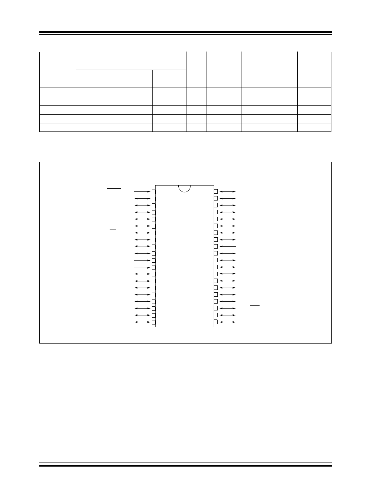
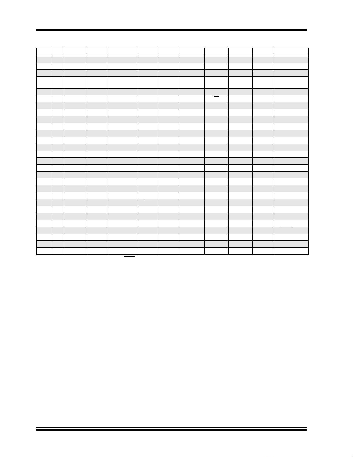
Pin Diagrams – PIC16F914/917, 40-Pin
40-pin PDIP
RE3/MCLR/VPP
RA0/AN0/C1-/SEG12
RA1/AN1/C2-/SEG7
RA2/AN2/C2+/V
RA3/AN3/C1+/V
RA4/C1OUT/T0CKI/SEG4
RA5/AN4/C2OUT/SS
RA7/OSC1/CLKIN/T1OSI
RA6/OSC2/CLKOUT/T1OSO
REF-/COM2
REF+/SEG15
/SEG5
RE0/AN5/SEG21
RE1/AN6/SEG22
RE2/AN7/SEG23
V
DD
VSS
RC0/VLCD1
RC1/VLCD2
RC2/VLCD3
RC3/SEG6
RD0/COM3
RD1
1
2
3
4
5
6
7
8
9
10
11
12
13
14
15
16
17
18
19
20
PIC16F914/917
40
39
38
37
36
35
34
33
32
31
30
29
28
27
26
25
24
23
22
21
RB7/ICSPDAT/ICDDAT/SEG13
RB6/ICSPCLK/ICDCK/SEG14
RB5/COM1
RB4/COM0
RB3/SEG3
RB2/SEG2
RB1/SEG1
RB0/INT/SEG0
V
DD
VSS
RD7/SEG20
RD6/SEG19
RD5/SEG18
RD4/SEG17
RC7/RX/DT/SDI/SDA/SEG8
RC6/TX/CK/SCK/SCL/SEG9
RC5/T1CKI/CCP1/SEG10
RC4/T1G
RD3/SEG16
RD2/CCP2
/SDO/SEG11
DS41250F-page 2 © 2007 Microchip Technology Inc.
PIC16F913/914/916/917/946
TABLE 1: PIC16F914/917 40-PIN SUMMARY
I/O Pin A/D LCD Comparators Timers CCP AUSART SSP Interrupt Pull-Up Basic
RA0 2 AN0 SEG12 C1- — — — — — — —
RA1 3 AN1 SEG7 C2- — — — — — — —
RA2 4 AN2/VREF- COM2 C2+ — — — — — — —
RA3 5
RA4 6 SEG4 C1OUT T0CKI — — — — — —
RA5 7 AN4 SEG5 C2OUT — — — SS
RA6 14 — — — T1OSO — — — — — OSC2/CLKOUT
RA7 13 — — — T1OSI — — — — — OSC1/CLKIN
RB0 33 — SEG0 — — — — — INT Y —
RB1 34 — SEG1 — — — — — — Y —
RB2 35 — SEG2 — — — — — — Y —
RB3 36 — SEG3 — — — — — — Y —
RB4 37 — COM0 — — — — — IOC Y —
RB5 38 — COM1 — — — — — IOC Y —
RB6 39 — SEG14 — — — — — IOC Y ICSPCLK/ICDCK
RB7 40 — SEG13 — — — — — IOC Y ICSPDAT/ICDDAT
RC0 15 — VLCD1 — — — — — — — —
RC1 16 — VLCD2 — — — — — — — —
RC2 17 — VLCD3 — — — — — — — —
RC3 18 — SEG6 — — — — — — — —
RC4 23 — SEG11 — T1G — — SDO — — —
RC5 24 — SEG10 — T1CKI CCP1 — — — — —
RC6 25 — SEG9 — — — TX/CK SCK/SCL — — —
RC7 26 — SEG8 — — — RX/DT SDI/SDA — — —
RD0 19 — COM3 — — — — — — — —
RD1 20 — — — — — — — — — —
RD2 21 — — — — CCP2 — — — — —
RD3 22 — SEG16 — — — — — — — —
RD4 27 — SEG17 — — — — — — — —
RD5 28 — SEG18 — — — — — — — —
RD6 29 — SEG19 — — — — — — — —
RD7 30 — SEG20 — — — — — — — —
RE0 8 AN5 SEG21 — — — — — — — —
RE1 9 AN6 SEG22 — — — — — — — —
RE2 10 AN7 SEG23 — — — — — — — —
RE3 1 — — — — — — — — Y
— 11 — — — — — — — — — VDD
—32 — — — — — — — — — VDD
— 12 — — — — — — — — — VSS
—31 — — — — — — — — — VSS
Note 1: Pull-up enabled only with external MCLR configuration.
AN3/V
SEG15 C1+ — — — — — —
REF+
—
—— —
(1)
MCLR/VPP
© 2007 Microchip Technology Inc. DS41250F-page 3
PIC16F913/914/916/917/946
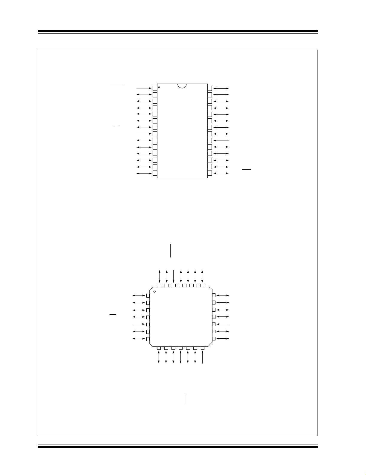
Pin Diagrams – PIC16F913/916, 28-Pin
28-pin PDIP, SOIC, SSOP
RA3/AN3/C1+/V
RA6/OSC2/CLKOUT/T1OSO
28-pin QFN
RE3/MCLR/VPP
RA0/AN0/C1-/SEG12
RA1/AN1/C2-/SEG7
RA2/AN2/C2+/V
RA4/C1OUT/T0CKI/SEG4
RA5/AN4/C2OUT/SS
RA7/OSC1/CLKIN/T1OSI
REF-/COM2
REF+/COM3/SEG15
/SEG5
RC0/VLCD1
RC1/VLCD2
RC2/VLCD3
RC3/SEG6
PIC16F913/916
28
27
26
25
24
23
22
21
20
19
18
17
16
15
RB7/ICSPDAT/ICDDAT/SEG13
RB6/ICSPCLK/ICDCK/SEG14
RB5/COM1
RB4/COM0
RB3/SEG3
RB2/SEG2
RB1/SEG1
RB0/INT/SEG0
V
DD
VSS
RC7/RX/DT/SDI/SDA/SEG8
RC6/TX/CK/SCK/SCL/SEG9
RC5/T1CKI/CCP1/SEG10
RC4/T1G
/SDO/SEG11
1
2
3
4
5
6
7
V
SS
8
9
10
11
12
13
14
/VPP
RA2/AN2/C2+/VREF-/COM2
RA3/AN3/C1+/V
RA6/OSC2/CLKOUT/T1OSO
REF+/COM3/SEG15
RA4/C1OUT/T0CKI/SEG4
RA5/AN4/C2OUT/SS
RA7/OSC1/CLKIN/T1OSI
/SEG5
SS
V
RA1/AN1/C2-/SEG7
282627
1
2
3
PIC16F913/916
4
5
6
7
8109
RC0/VLCD1
RA0/AN0/C1-/SEG12
RC1/VLCD2
RE3/MCLR
RB7/ICSPDAT/ICDDAT/SEG13
25
11
RC3/SEG6
RC2/VLCD3
12
RB6/ICSPCLK/ICDCK/SEG14
24
/SDO/SEG11
RC4/T1G
RB5/COM1
23
13
RC5/T1CKI/CCP1/SEG10
RB4/COM0
22
14
RC6/TX/CK/SCK/SCL/SEG9
21
20
19
18
17
16
15
RB3/SEG3
RB2/SEG2
RB1/SEG1
RB0/INT/SEG0
V
DD
VSS
RC7/RX/DT/SDI/SDA/SEG8
DS41250F-page 4 © 2007 Microchip Technology Inc.
PIC16F913/914/916/917/946
TABLE 2: PIC16F913/916 28-PIN (PDIP, SOIC, SSOP) SUMMARY
I/O Pin A/D LCD Comparators Timers CCP AUSART SSP Interrupt Pull-Up Basic
RA0 2 AN0 SEG12 C1- — — — — — — —
RA1 3 AN1 SEG7 C2- — — — — — — —
RA2 4 AN2/VREF- COM2 C2+ — — — — — — —
RA3 5
RA4 6 — SEG4 C1OUT T0CKI — — — — — —
RA5 7 — SEG5 C2OUT — — — SS
RA6 10 — — — T1OSO — — — — — OSC2/CLKOUT
RA7 9 — — — T1OSI — — — — — OSC1/CLKIN
RB0 21 — SEG0 — — — — — INT Y —
RB1 22 — SEG1 — — — — — — Y —
RB2 23 — SEG2 — — — — — — Y —
RB3 24 — SEG3 — — — — — — Y —
RB4 25 — COM0 — — — — — IOC Y —
RB5 26 — COM1 — — — — — IOC Y —
RB6 27 — SEG14 — — — — — IOC Y ICSPCLK/ICDCK
RB7 28 — SEG13 — — — — — IOC Y ICSPDAT/ICDDAT
RC0 11 — VLCD1 — — — — — — — —
RC1 12 — VLCD2 — — — — — — — —
RC2 13 — VLCD3 — — — — — — — —
RC3 14 — SEG6 — — — — — — — —
RC4 15 — SEG11 — T1G — — SDO — — —
RC5 16 — SEG10 — T1CKI CCP1 — — — — —
RC6 17 — SEG9 — — — TX/CK SCK/SCL — — —
RC7 18 — SEG8 — — — RX/DT SDI/SDA — — —
RE3 1 — — — — — — — — Y
—20————————— VDD
— 8 — — — — — — — — — VSS
—19————————— VSS
Note 1: Pull-up enabled only with external MCLR configuration.
AN3/V
REF+
SEG15/
COM3
C1+ — — — — — —
—— —
—
(1)
MCLR/VPP
© 2007 Microchip Technology Inc. DS41250F-page 5
PIC16F913/914/916/917/946
TABLE 3: PIC16F913/916 28-PIN (QFN) SUMMARY
I/O Pin A/D LCD Comparators Timers CCP AUSART SSP Interrupt Pull-Up Basic
RA0 27 AN0 SEG12 C1- — — — — — — —
RA1 28 AN1 SEG7 C2- — — — — — — —
RA2 1 AN2/VREF- COM2 C2+ — — — — — — —
RA3 2 AN3/V
RA4 3 — SEG4 C1OUT T0CKI — — — — — —
RA5 4 AN4 SEG5 C2OUT — — — SS
RA6 7 — — — T1OSO — — — — — OSC2/CLKOUT
RA7 6 — — — T1OSI — — — — — OSC1/CLKIN
RB0 18 — SEG0 — — — — — INT Y —
RB1 19 — SEG1 — — — — — — Y —
RB2 20 — SEG2 — — — — — — Y —
RB3 21 — SEG3 — — — — — — Y —
RB4 22 — COM0 — — — — — IOC Y —
RB5 23 — COM1 — — — — — IOC Y —
RB6 24 — SEG14 — — — — — IOC Y ICSPCLK/ICDCK
RB7 25 — SEG13 — — — — — IOC Y ICSPDAT/ICDDAT
RC0 8 — VLCD1 — — — — — — — —
RC1 9 — VLCD2 — — — — — — — —
RC2 10 — VLCD3 — — — — — — — —
RC3 11 — SEG6 — — — — — — — —
RC4 12 — SEG11 — T1G — — SDO — — —
RC5 13 — SEG10 — T1CKI CCP1 — — — — —
RC6 14 — SEG9 — — — TX/CK SCK/SCL — — —
RC7 15 — SEG8 — — — RX/DT SDI/SDA — — —
RE3 26 — — — — — — — — Y
—17—————————VDD
— 5 — — — — — — — — — VSS
—16————————— VSS
Note 1: Pull-up enabled only with external MCLR configuration.
REF+ SEG15/
COM3
C1+ — — — — — —
—— —
—
(1)
MCLR/VPP
DS41250F-page 6 © 2007 Microchip Technology Inc.
PIC16F913/914/916/917/946
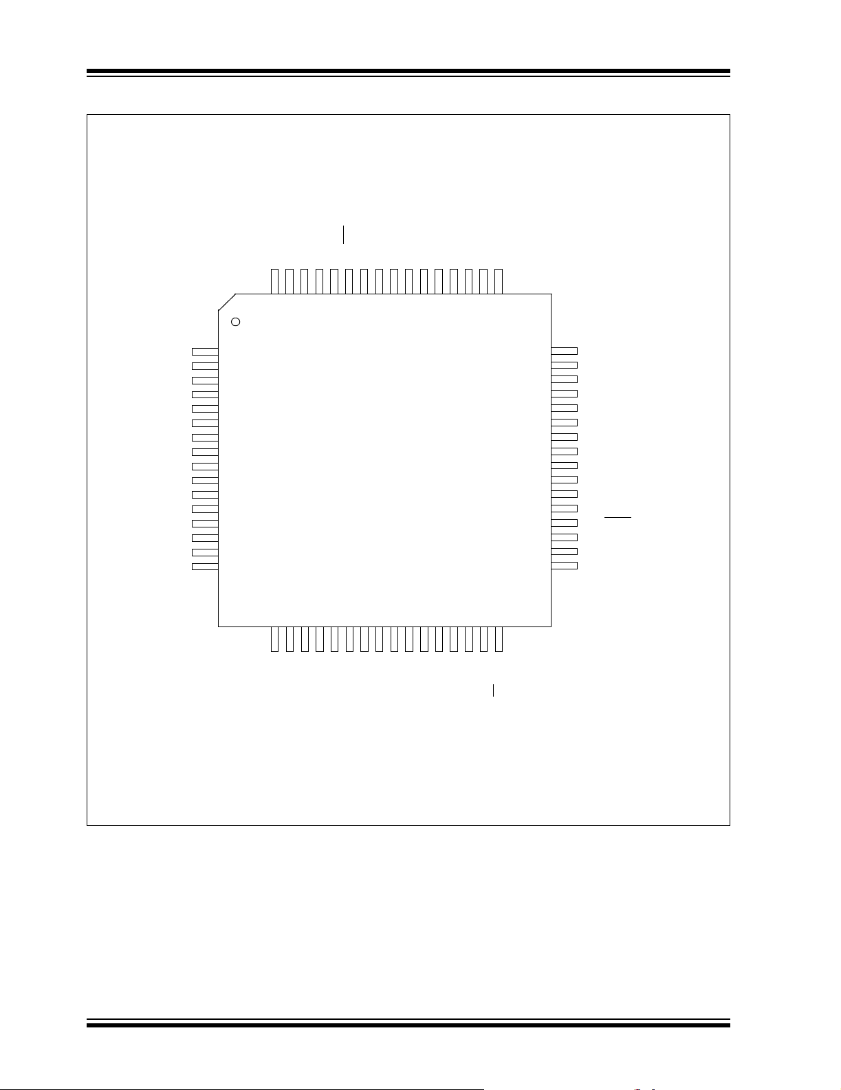
Pin Diagrams – PIC16F914/917, 44-Pin
44-pin TQFP
/SDO/SEG11
RC6/TX/CK/SCK/SCL/SEG9
RC5/T1CKI/CCP1/SEG10
RC4/T1G
RD3/SEG16
RD2/CCP2
RD1
RD0/COM3
RC3/SEG6
RC2/VLCD3
RC1/VLCD2
NC
RC7/RX/DT/SDI/SDA/SEG8
RD4/SEG17
RD5/SEG18
RD6/SEG19
RD7/SEG20
V
RB0/SEG0/INT
VDD
RB1/SEG1
RB2/SEG2
RB3/SEG3
44-pin QFN
4443424140
1
2
3
4
SS
5
6
7
8
9
10
11
121314
NC
RC7/RX/DT/SDI/SDA/SEG8
39
PIC16F914/917
16
17
15
NC
RB4/COM0
RB5/COM1
RB6/ICSPCLK/ICDCK/SEG14
RB7/ICSPDAT/ICDDAT/SEG13
RD4/SEG17
RD5/SEG18
RD6/SEG19
RD7/SEG20
RB0/INT/SEG0
RB1/SEG1
RB2/SEG2
363435
37
38
1819202122
/VPP
REF-/COM2
RE3/MCLR
REF+/C1+/SEG15
RA1/C2-/AN1/SEG7
RA0/C1-/AN0/SEG12
RA2/AN2/C2+/V
RA3/AN3/V
SS
V
VDD
VDD
33
32
31
30
29
28
27
26
25
24
23
NC
RC0/VLCD1
RA6/OSC2/CLKOUT/T1OSO
RA7/OSC1/CLKIN/T1OSI
SS
V
VDD
RE2/AN7/SEG23
RE1/AN6/SEG22
RE0/AN5/SEG21
RA5/AN4/C2OUT/SS
RA4/C1OUT/T0CKI/SEG4
/SDO/SEG11
RC6/TX/CK/SCK/SCL/SEG9
RC5/T1CKI/CCP1/SEG10
RC4/T1G
RD3/SEG16
RD2/CCP2
RD1
RD0/COM3
RC3/SEG6
4443424140
1
2
3
4
5
6
7
8
9
10
11
121314
39
37
38
PIC16F914/917
16
17
1819202122
15
RC2/VLCD3
363435
/SEG5
RC1/VLCD2
RC0/VLDC1
33
32
31
30
29
28
27
26
25
24
23
RA6/OSC2/CLKOUT/T1OSO
RA7/OSC1/CLKIN/T1OSI
SS
V
VSS
NC
V
DD
RE2/AN7/SEG23
RE1/AN6/SEG22
RE0/AN5/SEG21
RA5/AN4/C2OUT/SS
RA4/C1OUT/T0CKI/SEG4
/SEG5
NC
RB3/SEG3
RB4/COM0
RB5/COM1
RB6/ICSPCLK/ICDCK/SEG14
RB7/ICSPDAT/ICDDAT/SEG13
REF-/COM2
RE3/MCLR/VPP
REF+/SEG15
RA1/AN1/C2-/SEG7
RA0/AN0/C1-/SEG12
RA2/AN2/C2+/V
RA3/AN3/C1+/V
© 2007 Microchip Technology Inc. DS41250F-page 7

PIC16F913/914/916/917/946
TABLE 4: PIC16F914/917 44-PIN (TQFP) SUMMARY
I/O Pin A/D LCD Comparators Timers CCP AUSART SSP Interrupt Pull-Up Basic
RA0 19 AN0 SEG12 C1- — — — — — — —
RA1 20 AN1 SEG7 C2- — — — — — — —
RA2 21 AN2/VREF- COM2 C2+ — — — — — — —
RA3 22 AN3/V
RA4 23 — SEG4 C1OUT T0CKI — — — — — —
RA5 24 AN4 SEG5 C2OUT — — — SS
RA6 31 — — — T1OSO — — — — — OSC2/CLKOUT
RA7 30 — — — T1OSI — — — — — OSC1/CLKIN
RB0 8 — SEG0 — — — — — INT Y —
RB1 9 — SEG1 — — — — — — Y —
RB2 10 — SEG2 — — — — — — Y —
RB3 11 — SEG3 — — — — — — Y —
RB4 14 — COM0 — — — — — IOC Y —
RB5 15 — COM1 — — — — — IOC Y —
RB6 16 — SEG14 — — — — — IOC Y ICSPCLK/ICDCK
RB7 17 — SEG13 — — — — — IOC Y ICSPDAT/ICDDAT
RC0 32 — VLCD1 — — — — — — — —
RC1 35 — VLCD2 — — — — — — — —
RC2 36 — VLCD3 — — — — — — — —
RC3 37 — SEG6 — — — — — — — —
RC4 42 — SEG11 — T1G — — SDO — — —
RC5 43 — SEG10 — T1CKI CCP1 — — — — —
RC6 44 — SEG9 — — — TX/CK SCK/SCL — — —
RC7 1 — SEG8 — — — RX/DT SDI/SDA — — —
RD0 38 — COM3 — — — — — — — —
RD1 39 — — — — — — — — — —
RD2 40 — — — — CCP2 — — — — —
RD3 41 — SEG16 — — — — — — — —
RD4 2 — SEG17 — — — — — — — —
RD5 3 — SEG18 — — — — — — — —
RD6 4 — SEG19 — — — — — — — —
RD7 5 — SEG20 — — — — — — — —
RE0 25 AN5 SEG21 — — — — — — — —
RE1 26 AN6 SEG22 — — — — — — — —
RE2 27 AN7 SEG23 — — — — — — — —
RE318————————Y
— 7 — — — — — — — — — VDD
—28—————————VDD
— 6 — — — — — — — — — VSS
—29————————— VSS
— 12 — — — — — — — — — NC
—13————————— NC
— 33 — — — — — — — — — NC
—34————————— NC
Note 1: Pull-up enabled only with external MCLR
REF+ SEG15 C1+ — — — — — —
—— —
configuration.
—
(1)
MCLR/VPP
DS41250F-page 8 © 2007 Microchip Technology Inc.
PIC16F913/914/916/917/946
TABLE 5: PIC16F914/917 44-PIN (QFN) SUMMARY
I/O Pin A/D LCD Comparators Timers CCP AUSART SSP Interrupt Pull-Up Basic
RA0 19 AN0 SEG12 C1- — — — — — — —
RA1 20 AN1 SEG7 C2- — — — — — — —
RA2 21 AN2/VREF- COM2 C2+ — — — — — — —
RA3 22 AN3/V
RA4 23 — SEG4 C1OUT T0CKI — — — — — —
RA5 24 AN4 SEG5 C2OUT — — — SS
RA6 33 — — — T1OSO — — — — — OSC2/CLKOUT
RA7 32 — — — T1OSI — — — — — OSC1/CLKIN
RB0 9 — SEG0 — — — — — INT Y —
RB1 10 — SEG1 — — — — — — Y —
RB2 11 — SEG2 — — — — — — Y —
RB3 12 — SEG3 — — — — — — Y —
RB4 14 — COM0 — — — — — IOC Y —
RB5 15 — COM1 — — — — — IOC Y —
RB6 16 — SEG14 — — — — — IOC Y ICSPCLK/ICDCK
RB7 17 — SEG13 — — — — — IOC Y ICSPDAT/ICDDAT
RC0 34 — VLCD1 — — — — — — — —
RC1 35 — VLCD2 — — — — — — — —
RC2 36 — VLCD3 — — — — — — — —
RC3 37 — SEG6 — — — — — — — —
RC4 42 — SEG11 — T1G — — SDO — — —
RC5 43 — SEG10 — T1CKI CCP1 — — — — —
RC6 44 — SEG9 — — — TX/CK SCK/SCL — — —
RC7 1 — SEG8 — — — RX/DT SDI/SDA — — —
RD0 38 — COM3 — — — — — — — —
RD1 39 — — — — — — — — — —
RD2 40 — — — — CCP2 — — — — —
RD3 41 — SEG16 — — — — — — — —
RD4 2 — SEG17 — — — — — — — —
RD5 3 — SEG18 — — — — — — — —
RD6 4 — SEG19 — — — — — — — —
RD7 5 — SEG20 — — — — — — — —
RE0 25 AN5 SEG21 — — — — — — — —
RE1 26 AN6 SEG22 — — — — — — — —
RE2 27 AN7 SEG23 — — — — — — — —
RE318————————Y
— 7 — — — — — — — — — VDD
—8————————— VDD
— 28 — — — — — — — — — VDD
—6————————— VSS
— 30 — — — — — — — — — VSS
—13————————— NC
— 29 — — — — — — — — — NC
Note 1: Pull-up enabled only with external MCLR
REF+ SEG15 C1+ — — — — — —
—— —
configuration.
—
(1)
MCLR/VPP
© 2007 Microchip Technology Inc. DS41250F-page 9
PIC16F913/914/916/917/946
Pin Diagram – PIC16F946
64-pin TQFP
/SDO/SEG11
DD
RD5/SEG18
RD4/SEG17
RC7/RX/DT/SDI/SDA/SEG8
RC6/TX/CK/SCK/SCL/SEG9
RC5/T1CKI/CCP1/SEG10
V
RC4/T1G
VSS
RD3/SEG16
RD2/CCP2
RD1
RD0/COM3
RC3/SEG6
RC0/VLCD1
RC2/VLCD3
RC1/VLCD2
RD6/SEG19
RD7/SEG20
RG0/SEG36
RG1/SEG37
RG2/SEG38
RG3/SEG39
RG4/SEG40
RG5/SEG41
V
VDD
RF0/SEG32
RF1/SEG33
RF2/SEG34
RF3/SEG35
RB0/INT/SEG0
RB1/SEG1
54 53 52 5158 57 56 5560 5964 63 62 61
1
2
3
4
5
6
7
8
SS
9
10
11
12
13
14
15
16
17 18 19 20 21 22 23 24 25 26
VDD
RB2/SEG2
RB3/SEG3
VSS
PIC16F946
RB4/COM0
RB5/COM1
27 28 29 30 32
DD
AVSS
AV
REF-/COM2
50 49
31
REF+/SEG15
48
47
46
45
44
43
42
41
40
39
38
37
36
35
34
33
/SEG5
RF7/SEG31
RF6/SEG30
RF5/SEG29
RF4/SEG28
RE7/SEG27
RE6/SEG26
RE5/SEG25
V
SS
RA6/OSC2/CLKOUT/T1OSO
RA7/OSC1/CLKIN/T1OSI
VDD
RE4/SEG24
RE3/MCLR/VPP
RE2/AN7/SEG23
RE1/AN6/SEG22
RE0/AN5/SEG21
RA1/AN1/C2-/SEG7
RA0/AN0/C1-/SEG12
RA4/C1OUT/T0CKI/SEG4
RA3/AN3/C1+/V
RA5/AN4/C2OUT/SS
RB6/ICSPCLK/ICDCK/SEG14
RB7/ICSPDAT/ICDDAT/SEG13
RA2/AN2/C2+/V
DS41250F-page 10 © 2007 Microchip Technology Inc.

PIC16F913/914/916/917/946
TABLE 6: PIC16F946 64-PIN (TQFP) SUMMARY
I/O Pin A/D LCD Comparators Timers CCP AUSART SSP Interrupt Pull-Up Basic
RA0 27 AN0 SEG12 C1- — — — — — — —
RA1 28 AN1 SEG7 C2- — — — — — — —
RA2 29 AN2/VREF- COM2 C2+ — — — — — — —
RA3 30 AN3/V
RA4 31 — SEG4 C1OUT T0CKI — — — — — —
RA5 32 AN4 — C2OUT — — — SS
RA6 40 SEG5 — — T1OSO — — — — — OSC2/CLKOUT
RA7 39 — — — T1OSI — — — — — OSC1/CLKIN
RB0 15 — SEG0 — — — — — INT Y —
RB1 16 — SEG1 — — — — — — Y —
RB2 17 — SEG2 — — — — — — Y —
RB3 18 — SEG3 — — — — — — Y —
RB4 21 — COM0 — — — — — IOC Y —
RB5 22 — COM1 — — — — — IOC Y —
RB6 23 — SEG14 — — — — — IOC Y ICSPCLK/ICDCK
RB7 24 — SEG13 — — — — — IOC Y ICSPDAT/ICDDAT
RC0 49 — VLCD1 — — — — — — — —
RC1 50 — VLCD2 — — — — — — — —
RC2 51 — VLCD3 — — — — — — — —
RC3 52 — SEG6 — — — — — — — —
RC4 59 — SEG11 — T1G — — SDO — — —
RC5 60 — SEG10 — T1CKI CCP1 — — — — —
RC6 61 — SEG9 — — — TX/CK SCK/SCL — — —
RC7 62 — SEG8 — — — RX/DT SDI/SDA — — —
RD0 53 — COM3 — — — — — — — —
RD1 54 — — — — — — — — — —
RD2 55 — — — — CCP2 — — — — —
RD3 58 — SEG16 — — — — — — — —
RD4 63 — SEG17 — — — — — — — —
RD5 64 — SEG18 — — — — — — — —
RD6 1 — SEG19 — — — — — — — —
RD7 2 — SEG20 — — — — — — — —
RE0 33 AN5 SEG21 — — — — — — — —
RE1 34 AN6 SEG22 — — — — — — — —
RE2 35 AN7 SEG23 — — — — — — — —
RE3 36 — — — — — — — — Y
RE4 37 — SEG24 — — — — — — — —
RE5 42 — SEG25 — — — — — — — —
RE6 43 — SEG26 — — — — — — — —
RE7 44 — SEG27 — — — — — — — —
RF0 11 — SEG32 — — — — — — — —
RF1 12 — SEG33 — — — — — — — —
RF2 13 — SEG34 — — — — — — — —
Note 1: Pull-up enabled only with external MCLR
REF+ SEG15 C1+ — — — — — —
—— —
configuration.
—
(1)
MCLR/VPP
© 2007 Microchip Technology Inc. DS41250F-page 11
PIC16F913/914/916/917/946
TABLE 6: PIC16F946 64-PIN (TQFP) SUMMARY (CONTINUED)
I/O Pin A/D LCD Comparators Timers CCP AUSART SSP Interrupt Pull-Up Basic
RF3 14 — SEG35 — — — — — — — —
RF4 45 — SEG28 — — — — — — — —
RF5 46 — SEG29 — — — — — — — —
RF6 47 — SEG30 — — — — — — — —
RF7 48 — SEG31 — — — — — — — —
RG0 3 — SEG36 — — — — — — — —
RG1 4 — SEG37 — — — — — — — —
RG2 5 — SEG38 — — — — — — — —
RG3 6 — SEG39 — — — — — — — —
RG4 7 — SEG40 — — — — — — — —
RG5 8 — SEG41 — — — — — — — —
— 26 — — — — — — — — — AVDD
—25 — — — — — — — — — AVSS
— 10 — — — — — — — — — VDD
—19 — — — — — — — — — VDD
— 38 — — — — — — — — — VDD
—57 — — — — — — — — — VDD
— 9 — — — — — — — — — VSS
—20 — — — — — — — — — VSS
— 41 — — — — — — — — — VSS
—56 — — — — — — — — — VSS
Note 1: Pull-up enabled only with external MCLR
configuration.
DS41250F-page 12 © 2007 Microchip Technology Inc.

PIC16F913/914/916/917/946
Table of Contents
1.0 Device Overview ........................................................................................................................................................................ 15
2.0 Memory Organization ................................................................................................................................................................. 23
3.0 I/O Ports ..................................................................................................................................................................................... 43
4.0 Oscillator Module (With Fail-Safe Clock Monitor)....................................................................................................................... 87
5.0 Timer0 Module ........................................................................................................................................................................... 99
6.0 Timer1 Module with Gate Control............................................................................................................................................. 102
7.0 Timer2 Module ......................................................................................................................................................................... 107
8.0 Comparator Module.................................................................................................................................................................. 109
9.0 Addressable Universal Synchronous Asynchronous Receiver Transmitter (AUSART) ........................................................... 121
10.0 Liquid Crystal Display (LCD) Driver Module............................................................................................................................. 143
11.0 Programmable Low-Voltage Detect (PLVD) Module................................................................................................................ 171
12.0 Analog-to-Digital Converter (ADC) Module .............................................................................................................................. 175
13.0 Data EEPROM and Flash Program Memory Control ............................................................................................................... 187
14.0 SSP Module Overview ............................................................................................................................................................. 193
15.0 Capture/Compare/PWM (CCP) Module ................................................................................................................................... 211
16.0 Special Features of the CPU.................................................................................................................................................... 219
17.0 Instruction Set Summary.......................................................................................................................................................... 241
18.0 Development Support............................................................................................................................................................... 251
19.0 Electrical Specifications............................................................................................................................................................ 255
20.0 DC and AC Characteristics Graphs and Tables....................................................................................................................... 283
21.0 Packaging Information.............................................................................................................................................................. 305
Appendix A: Data Sheet Revision History .......................................................................................................................................... 315
Appendix B: Migrating From Other PIC
Appendix C: Conversion Considerations ........................................................................................................................................... 316
Index .................................................................................................................................................................................................. 317
The Microchip Web Site..................................................................................................................................................................... 325
Customer Change Notification Service .............................................................................................................................................. 325
Customer Support .............................................................................................................................................................................. 325
Reader Response .............................................................................................................................................................................. 327
Product Identification System ............................................................................................................................................................ 328
®
Devices.............................................................................................................................. 315
TO OUR VALUED CUSTOMERS
It is our intention to provide our valued customers with the best documentation possible to ensure successful use of your Microchip
products. To this end, we will continue to improve our publications to better suit your needs. Our publications will be refined and
enhanced as new volumes and updates are introduced.
If you have any questions or comments regarding this publication, please contact the Marketing Communications Department via
E-mail at docerrors@microchip.com or fax the Reader Response Form in the back of this data sheet to (480) 792-4150. We
welcome your feedback.
Most Current Data Sheet
To obtain the most up-to-date version of this data sheet, please register at our Worldwide Web site at:
http://www.microchip.com
You can determine the version of a data sheet by examining its literature number found on the bottom outside corner of any page.
The last character of the literature number is the version number, (e.g., DS30000A is version A of document DS30000).
Errata
An errata sheet, describing minor operational differences from the data sheet and recommended workarounds, may exist for current
devices. As device/documentation issues become known to us, we will publish an errata sheet. The errata will specify the revision
of silicon and revision of document to which it applies.
To determine if an errata sheet exists for a particular device, please check with one of the following:
• Microchip’s Worldwide Web site; http://www.microchip.com
• Your local Microchip sales office (see last page)
When contacting a sales office, please specify which device, revision of silicon and data sheet (include literature number) you are
using.
Customer Notification System
Register on our web site at www.microchip.com to receive the most current information on all of our products.
© 2007 Microchip Technology Inc. DS41250F-page 13

PIC16F913/914/916/917/946
NOTES:
DS41250F-page 14 © 2007 Microchip Technology Inc.
PIC16F913/914/916/917/946
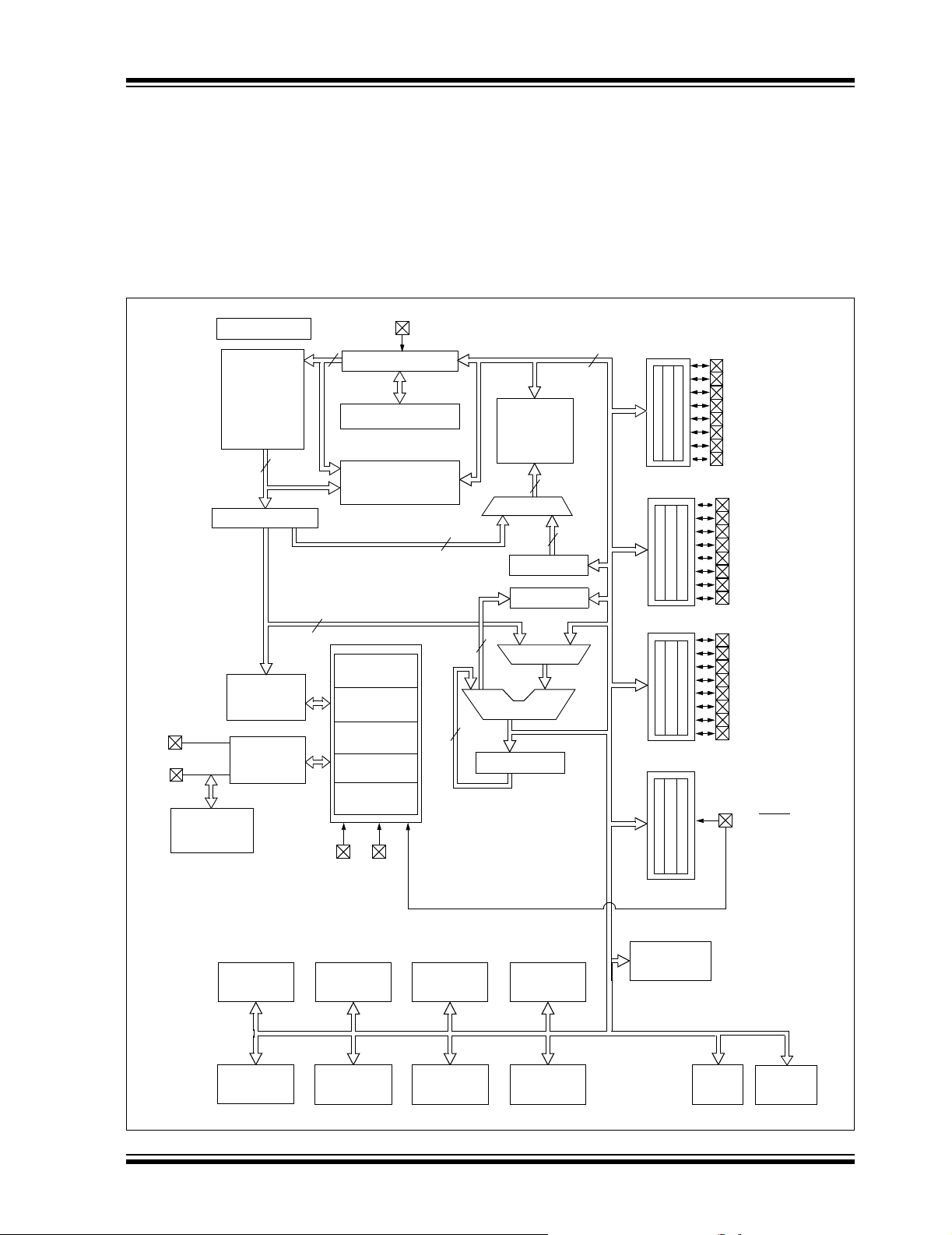
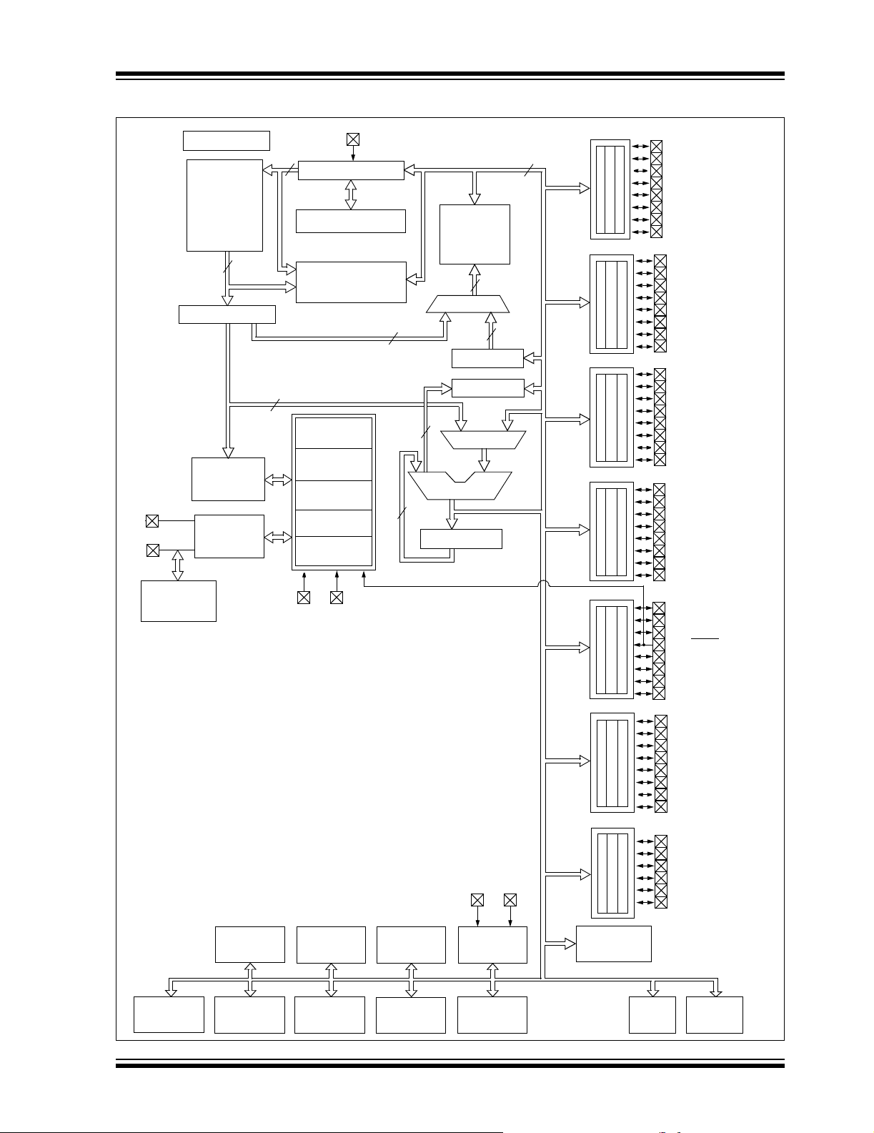
1.0 DEVICE OVERVIEW
The PIC16F91X/946 devices are covered by this data
sheet. They are available in 28/40/44/64-pin packages.
Figure 1-1 shows a block diagram of the PIC16F913/916
device, Figure 1-2 shows a block diagram of the
PIC16F914/917 device, and Figure 1-3 shows a block
diagram of the PIC16F946 device. Table 1-1 shows the
pinout descriptions.
FIGURE 1-1: PIC16F913/916 BLOCK DIAGRAM
INT
Program Counter
8-Level Stack (13-bit)
(PMR)
Direct Addr
Power-up
Timer
Oscillator
Power-on
Reset
Watchdog
Timer
Brown-out
Reset
VSS
256/352 bytes
7
3
ALU
8
W Reg
Program
Bus
OSC1/CLKIN
OSC2/CLKOUT
Internal
Oscillator
Block
Configuration
Flash
4K/8K x 14
Program
Memory
14
Instruction Reg
Instruction
Decode and
Control
Timing
Generation
13
Program Memory Read
8
Start-up Timer
VDD
Data Bus
RAM
File
Registers
Addr MUX
8
FSR Reg
STATUS Reg
MUX
RAM Addr
9
Indirect
Addr
8
PORTA
RA0
RA1
RA2
RA3
RA4
RA5
RA7
PORTB
RB0
RB1
RB2
RB3
RB4
RB5
RB6
RB7
PORTC
RC0
RC1
RC2
RC3
RC4
RC5
RC6
RC7
PORTE
RE3/MCLR
Data EEPROM
Timer0
Comparators
Timer1 Timer2 10-bit A/D
CCP1 SSP
Addressable
USART
256 bytes
PLVD LCD
© 2007 Microchip Technology Inc. DS41250F-page 15
PIC16F913/914/916/917/946
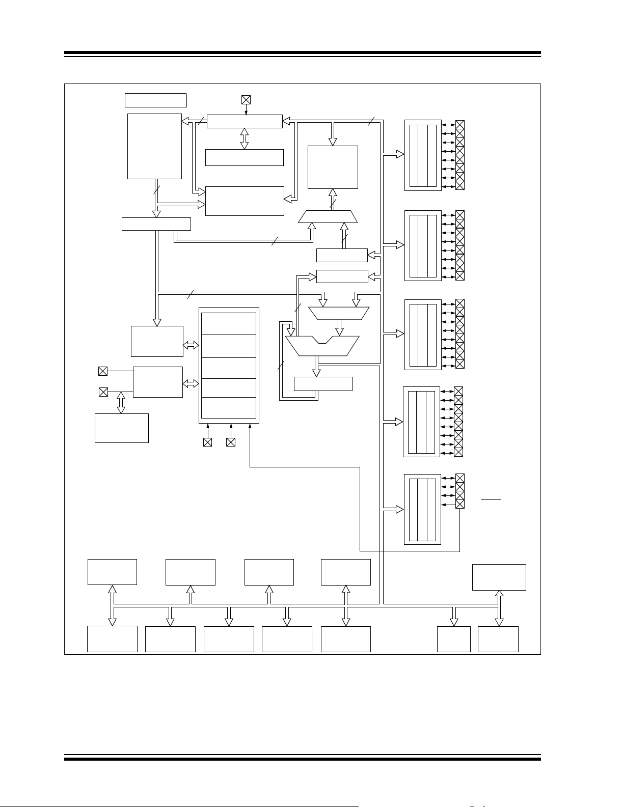
FIGURE 1-2: PIC16F914/917 BLOCK DIAGRAM
INT
Program Counter
8-Level Stack (13-bit)
(PMR)
Direct Addr
Power-up
Timer
Oscillator
Power-on
Reset
Watchdog
Timer
Brown-out
Reset
VSS
Data Bus
RAM
256/352 bytes
File
Registers
9
Addr MUX
7
3
8
8
FSR Reg
STATUS Reg
MUX
ALU
W Reg
Program
Bus
OSC1/CLKIN
OSC2/CLKOUT
Internal
Oscillator
Block
Configuration
Flash
4K/8K x 14
Program
Memory
14
Instruction Reg
Instruction
Decode and
Control
Timing
Generation
13
Program Memory Read
8
Start-up Timer
VDD
8
RAM Addr
Indirect
Addr
PORTA
RA0
RA1
RA2
RA3
RA4
RA5
RA6
RA7
PORTB
RB0
RB1
RB2
RB3
RB4
RB5
RB6
RB7
PORTC
RC0
RC1
RC2
RC3
RC4
RC5
RC6
RC7
PORTD
RD0
RD1
RD2
RD3
RD4
RD5
RD6
RD7
Timer0
Comparators
Timer1 Timer2 10-bit A/D
CCP1
CCP2 SSP
Addressable
USART
PORTE
RE0
RE1
RE2
RE3/MCLR
Data EEPROM
256 bytes
PLVD LCD
DS41250F-page 16 © 2007 Microchip Technology Inc.
PIC16F913/914/916/917/946
FIGURE 1-3: PIC16F946 BLOCK DIAGRAM
INT
Program
Bus
OSC1/CLKIN
OSC2/CLKOUT
Internal
Oscillator
Block
Configuration
Flash
8K x 14
Program
Memory
14
Instruction Reg
Instruction
Decode and
Control
Timing
Generation
13
Program Counter
8-Level Stack (13-bit)
Program Memory Read
(PMR)
Direct Addr
8
Power-up
Timer
Oscillator
Start-up Timer
Power-on
Reset
Watchdog
Timer
Brown-out
Reset
V
VSS
DD
7
3
8
Data Bus
RAM
336 x 8 bytes
File
Registers
Addr MUX
FSR Reg
STATUS Reg
MUX
ALU
W Reg
RAM Addr
9
8
Indirect
Addr
AVSSAVDD
PORTA
8
PORTB
PORTC
PORTD
PORTE
PORTF
PORTG
RA0
RA1
RA2
RA3
RA4
RA5
RA6
RA7
RB0
RB1
RB2
RB3
RB4
RB5
RB6
RB7
RC0
RC1
RC2
RC3
RC4
RC5
RC6
RC7
RD0
RD1
RD2
RD3
RD4
RD5
RD6
RD7
RE0
RE1
RE2
RE3/MCLR
RE4
RE5
RE6
RE7
RF0
RF1
RF2
RF3
RF4
RF5
RF6
RF7
RG0
RG1
RG2
RG3
RG4
RG5
Data EEPROM
256 bytes
PLVD
LCD
Comparators
Timer0
CCP1 CCP2
Timer1 Timer2 10-bit A/D
SSP
Addressable
USART
© 2007 Microchip Technology Inc. DS41250F-page 17
PIC16F913/914/916/917/946
TABLE 1-1: PIC16F91X/946 PINOUT DESCRIPTIONS
Name Function
RA0/AN0/C1-/SEG12 RA0 TTL CMOS General purpose I/O.
AN0 AN — Analog input Channel 0.
C1- AN — Comparator 1 negative input.
SEG12 — AN LCD analog output.
RA1/AN1/C2-/SEG7 RA1 TTL CMOS General purpose I/O.
AN1 AN — Analog input Channel 1.
C2- AN — Comparator 2 negative input.
SEG7 — AN LCD analog output.
RA2/AN2/C2+/V
RA3/AN3/C1+/V
SEG15
RA4/C1OUT/T0CKI/SEG4 RA4 TTL CMOS General purpose I/O.
RA5/AN4/C2OUT/SS
RA6/OSC2/CLKOUT/T1OSO RA6 TTL CMOS General purpose I/O.
RA7/OSC1/CLKIN/T1OSI RA7 TTL CMOS General purpose I/O.
RB0/INT/SEG0 RB0 TTL CMOS General purpose I/O. Individually enabled pull-up.
Legend: AN = Analog input or output CMOS = CMOS compatible input or output OD = Open Drain
Note 1: COM3 is available on RA3 for the PIC16F913/916 and on RD0 for the PIC16F914/917 and PIC16F946.
2: Pins available on PIC16F914/917 and PIC16F946 only.
3: Pins available on PIC16F946 only.
4: I
REF-/COM2 RA2 TTL CMOS General purpose I/O.
AN2 AN — Analog input Channel 2.
C2+ AN — Comparator 2 positive input.
REF- AN — External A/D Voltage Reference – negative.
V
COM2 — AN LCD analog output.
REF+/COM3
TTL = TTL compatible input ST = Schmitt Trigger input with CMOS levels P = Power
HV = High Voltage XTAL = Crystal
2
C Schmitt trigger inputs have special input levels.
(1)
/
RA3 TTL CMOS General purpose I/O.
AN3 AN — Analog input Channel 3.
C1+ AN — Comparator 1 positive input.
REF+ AN — External A/D Voltage Reference – positive.
V
COM3
SEG15 — AN LCD analog output.
C1OUT — CMOS Comparator 1 output.
T0CKI ST — Timer0 clock input.
SEG4 — AN LCD analog output.
/SEG5 RA5 TTL CMOS General purpose I/O.
AN4 AN — Analog input Channel 4.
C2OUT — CMOS Comparator 2 output.
SS
SEG5 — AN LCD analog output.
OSC2 — XTAL Crystal/Resonator.
CLKOUT — CMOS T
T1OSO — XTAL Timer1 oscillator output.
OSC1 XTAL — Crystal/Resonator.
CLKIN ST — Clock input.
T1OSI XTAL — Timer1 oscillator input.
INT ST — External interrupt pin.
SEG0 — AN LCD analog output.
Input
(1)
Output
Type
TTL — Slave select input.
Typ e
— AN LCD analog output.
OSC/4 reference clock.
Description
DS41250F-page 18 © 2007 Microchip Technology Inc.
PIC16F913/914/916/917/946
TABLE 1-1: PIC16F91X/946 PINOUT DESCRIPTIONS (CONTINUED)
Input
Name Function
RB1/SEG1 RB1 TTL CMOS General purpose I/O. Individually enabled pull-up.
SEG1 — AN LCD analog output.
RB2/SEG2 RB2 TTL CMOS General purpose I/O. Individually enabled pull-up.
SEG2 — AN LCD analog output.
RB3/SEG3 RB3 TTL CMOS General purpose I/O. Individually enabled pull-up.
SEG3 — AN LCD analog output.
RB4/COM0 RB4 TTL CMOS General purpose I/O. Individually controlled
COM0 — AN LCD analog output.
RB5/COM1 RB5 TTL CMOS General purpose I/O. Individually controlled
COM1 — AN LCD analog output.
RB6/ICSPCLK/ICDCK/SEG14 RB6 TTL CMOS General purpose I/O. Individually controlled
ICSPCLK ST — ICSP™ clock.
ICDCK ST — ICD clock.
SEG14 — AN LCD analog output.
RB7/ICSPDAT/ICDDAT/SEG13 RB7 TTL CMOS General purpose I/O. Individually controlled inter-
ICSPDAT ST CMOS ICSP Data I/O.
ICDDAT ST CMOS ICD Data I/O.
SEG13 — AN LCD analog output.
RC0/VLCD1 RC0 ST CMOS General purpose I/O.
VLCD1 AN — LCD analog input.
RC1/VLCD2 RC1 ST CMOS General purpose I/O.
VLCD2 AN — LCD analog input.
RC2/VLCD3 RC2 ST CMOS General purpose I/O.
VLCD3 AN — LCD analog input.
RC3/SEG6 RC3 ST CMOS General purpose I/O.
SEG6 — AN LCD analog output.
RC4/T1G
RC5/T1CKI/CCP1/SEG10 RC5 ST CMOS General purpose I/O.
Legend: AN = Analog input or output CMOS = CMOS compatible input or output OD = Open Drain
Note 1: COM3 is available on RA3 for the PIC16F913/916 and on RD0 for the PIC16F914/917 and PIC16F946.
/SDO/SEG11 RC4 ST CMOS General purpose I/O.
T1G ST — Timer1 gate input.
SDO — CMOS Serial data output.
SEG11 — AN LCD analog output.
T1CKI ST — Timer1 clock input.
CCP1 ST CMOS Capture 1 input/Compare 1 output/PWM 1 output.
SEG10 — AN LCD analog output.
TTL = TTL compatible input ST = Schmitt Trigger input with CMOS levels P = Power
HV = High Voltage XTAL = Crystal
2: Pins available on PIC16F914/917 and PIC16F946 only.
3: Pins available on PIC16F946 only.
2
4: I
C Schmitt trigger inputs have special input levels.
Type
Output
Typ e
Description
interrupt-on-change. Individually enabled pull-up.
interrupt-on-change. Individually enabled pull-up.
interrupt-on-change. Individually enabled pull-up.
rupt-on-change. Individually enabled pull-up.
© 2007 Microchip Technology Inc. DS41250F-page 19
PIC16F913/914/916/917/946
TABLE 1-1: PIC16F91X/946 PINOUT DESCRIPTIONS (CONTINUED)
Name Function
Input
RC6/TX/CK/SCK/SCL/SEG9 RC6 ST CMOS General purpose I/O.
TX — CMOS USART asynchronous serial transmit.
CK ST CMOS USART synchronous serial clock.
SCK ST CMOS SPI clock.
SCL ST
SEG9 — AN LCD analog output.
RC7/RX/DT/SDI/SDA/SEG8 RC7 ST CMOS General purpose I/O.
RX ST — USART asynchronous serial receive.
DT ST CMOS USART synchronous serial data.
SDI ST CMOS SPI data input.
SDA ST
SEG8 — AN LCD analog output.
RD0/COM3
(1, 2)
RD0 ST CMOS General purpose I/O.
COM3 — AN LCD analog output.
(2)
RD1
RD2/CCP2
(2)
RD1 ST CMOS General purpose I/O.
RD2 ST CMOS General purpose I/O.
CCP2 ST CMOS Capture 2 input/Compare 2 output/PWM 2 output.
RD3/SEG16
(2)
RD3 ST CMOS General purpose I/O.
SEG16 — AN LCD analog output.
RD4/SEG17
(2)
RD4 ST CMOS General purpose I/O.
SEG17 — AN LCD analog output.
RD5/SEG18
(2)
RD5 ST CMOS General purpose I/O.
SEG18 — AN LCD analog output.
RD6/SEG19
(2)
RD6 ST CMOS General purpose I/O.
SEG19 — AN LCD analog output.
RD7/SEG20
(2)
RD7 ST CMOS General purpose I/O.
SEG20 — AN LCD analog output.
RE0/AN5/SEG21
(2)
RE0 ST CMOS General purpose I/O.
AN5 AN — Analog input Channel 5.
SEG21 — AN LCD analog output.
RE1/AN6/SEG22
(2)
RE1 ST CMOS General purpose I/O.
AN6 AN — Analog input Channel 6.
SEG22 — AN LCD analog output.
RE2/AN7/SEG23
(2)
RE2 ST CMOS General purpose I/O.
AN7 AN — Analog input Channel 7.
SEG23 — AN LCD analog output.
RE3/MCLR
/VPP RE3 ST — Digital input only.
MCLR ST — Master Clear with internal pull-up.
PP HV — Programming voltage.
V
Legend: AN = Analog input or output CMOS = CMOS compatible input or output OD = Open Drain
TTL = TTL compatible input ST = Schmitt Trigger input with CMOS levels P = Power
HV = High Voltage XTAL = Crystal
Note 1: COM3 is available on RA3 for the PIC16F913/916 and on RD0 for the PIC16F914/917 and PIC16F946.
2: Pins available on PIC16F914/917 and PIC16F946 only.
3: Pins available on PIC16F946 only.
2
4: I
C Schmitt trigger inputs have special input levels.
Type
(4)
(4)
Output
Typ e
OD I2C™ clock.
OD I2C™ data.
Description
DS41250F-page 20 © 2007 Microchip Technology Inc.
PIC16F913/914/916/917/946
TABLE 1-1: PIC16F91X/946 PINOUT DESCRIPTIONS (CONTINUED)
Input
Name Function
RE4/SEG24
(3)
RE4 ST CMOS General purpose I/O.
SEG24 — AN LCD analog output.
RE5/SEG25
(3)
RE5 ST CMOS General purpose I/O.
SEG25 — AN LCD analog output.
RE6/SEG26
(3)
RE6 ST CMOS General purpose I/O.
SEG26 — AN LCD analog output.
RE7/SEG27
(3)
RE7 ST CMOS General purpose I/O.
SEG27 — AN LCD analog output.
RF0/SEG32
(3)
RF0 ST CMOS General purpose I/O.
SEG32 — AN LCD analog output.
RF1/SEG33
(3)
RF1 ST CMOS General purpose I/O.
SEG33 — AN LCD analog output.
RF2/SEG34
(3)
RF2 ST CMOS General purpose I/O.
SEG34 — AN LCD analog output.
RF3/SEG35
(3)
RF3 ST CMOS General purpose I/O.
SEG35 — AN LCD analog output.
RF4/SEG28
(3)
RF4 ST CMOS General purpose I/O.
SEG28 — AN LCD analog output.
RF5/SEG29
(3)
RF5 ST CMOS General purpose I/O.
SEG29 — AN LCD analog output.
RF6/SEG30
(3)
RF6 ST CMOS General purpose I/O.
SEG30 — AN LCD analog output.
RF7/SEG31
(3)
RF7 ST CMOS General purpose I/O.
SEG31 — AN LCD analog output.
RG0/SEG36
(3)
RG0 ST CMOS General purpose I/O.
SEG36 — AN LCD analog output.
RG1/SEG37
(3)
RG1 ST CMOS General purpose I/O.
SEG37 — AN LCD analog output.
RG2/SEG38
(3)
RG2 ST CMOS General purpose I/O.
SEG38 — AN LCD analog output.
RG3/SEG39
(3)
RG3 ST CMOS General purpose I/O.
SEG39 — AN LCD analog output.
RG4/SEG40
(3)
RG4 ST CMOS General purpose I/O.
SEG10 — AN LCD analog output.
RG5/SEG41
(3)
RG5 ST CMOS General purpose I/O.
SEG41 — AN LCD analog output.
(3)
DD
AV
(3)
AVSS
DD VDD P — Power supply for microcontroller.
V
AVDD P — Analog power supply for microcontroller.
AVSS P — Analog ground reference for microcontroller.
Legend: AN = Analog input or output CMOS = CMOS compatible input or output OD = Open Drain
TTL = TTL compatible input ST = Schmitt Trigger input with CMOS levels P = Power
HV = High Voltage XTAL = Crystal
Note 1: COM3 is available on RA3 for the PIC16F913/916 and on RD0 for the PIC16F914/917 and PIC16F946.
2: Pins available on PIC16F914/917 and PIC16F946 only.
3: Pins available on PIC16F946 only.
2
4: I
C Schmitt trigger inputs have special input levels.
Type
Output
Typ e
Description
© 2007 Microchip Technology Inc. DS41250F-page 21

PIC16F913/914/916/917/946
TABLE 1-1: PIC16F91X/946 PINOUT DESCRIPTIONS (CONTINUED)
Name Function
VSS VSS P — Ground reference for microcontroller.
Legend: AN = Analog input or output CMOS = CMOS compatible input or output OD = Open Drain
TTL = TTL compatible input ST = Schmitt Trigger input with CMOS levels P = Power
HV = High Voltage XTAL = Crystal
Note 1: COM3 is available on RA3 for the PIC16F913/916 and on RD0 for the PIC16F914/917 and PIC16F946.
2: Pins available on PIC16F914/917 and PIC16F946 only.
3: Pins available on PIC16F946 only.
2
4: I
C Schmitt trigger inputs have special input levels.
Input
Type
Output
Typ e
Description
DS41250F-page 22 © 2007 Microchip Technology Inc.

PIC16F913/914/916/917/946
2.0 MEMORY ORGANIZATION
2.1 Program Memory Organization
The PIC16F91X/946 has a 13-bit program counter
capable of addressing a 4K x 14 program memory
space for the PIC16F913/914 (0000h-0FFFh) and an
8K x 14 program memory space for the PIC16F916/
917 and PIC16F946 (0000h-1FFFh). Accessing a
location above the memory boundaries for the
PIC16F913 and PIC16F914 will cause a wrap around
within the first 4K x 14 space. The Reset vector is at
0000h and the interrupt vector is at 0004h.
FIGURE 2-1: PROGRAM MEMORY MAP
AND STACK FOR THE
PIC16F913/914
pc<12:0>
CALL, RETURN
RETFIE, RETLW
Stack Level 1
Stack Level 2
Stack Level 8
Reset Vector
13
0000h
FIGURE 2-2: PROGRAM MEMORY MAP
AND STACK FOR THE
PIC16F916/917/PIC16F946
pc<12:0>
CALL, RETURN
RETFIE, RETLW
On-chip
Program
Memory
Stack Level 1
Stack Level 2
Stack Level 8
Reset Vector
Interrupt Vector
Page 0
Page 1
Page 2
Page 3
13
0000h
0004h
0005h
07FFh
0800h
0FFFh
1000h
17FFh
1800h
1FFFh
On-chip
Program
Memory
Interrupt Vector
Page 0
Page 1
0004h
0005h
07FFh
0800h
0FFFh
1000h
1FFFh
© 2007 Microchip Technology Inc. DS41250F-page 23

PIC16F913/914/916/917/946
2.2 Data Memory Organization
The data memory is partitioned into multiple banks
which contain the General Purpose Registers (GPRs)
and the Special Function Registers (SFRs). Bits RP0
and RP1 are bank select bits.
RP1
Each bank extends up to 7Fh (128 bytes). The lower
locations of each bank are reserved for the Special
Function Registers. Above the Special Function
Registers are the General Purpose Registers,
implemented as static RAM. All implemented banks
contain Special Function Registers. Some frequently
used Special Function Registers from one bank are
mirrored in another bank for code reduction and
quicker access.
2.2.1 GENERAL PURPOSE REGISTER
The register file is organized as 256 x 8 bits in the
PIC16F913/914, 352 x 8 bits in the PIC16F916/917 and
336 x 8 bits in the PIC16F946. Each register is accessed
either directly or indirectly through the File Select
Register (FSR) (see Section 2.5 “Indirect Addressing,
INDF and FSR Registers”).
RP0
00→ Bank 0 is selected
01→ Bank 1 is selected
10→ Bank 2 is selected
11→ Bank 3 is selected
FILE
2.2.2 SPECIAL FUNCTION REGISTERS
The Special Function Registers are registers used by
the CPU and peripheral functions for controlling the
desired operation of the device (see Tables 2-1, 2-2,
2-3 and 2-4). These registers are static RAM.
The Special Function Registers can be classified into
two sets: core and peripheral. The Special Function
Registers associated with the “core” are described in
this section. Those related to the operation of the
peripheral features are described in the section of that
peripheral feature.
DS41250F-page 24 © 2007 Microchip Technology Inc.
PIC16F913/914/916/917/946
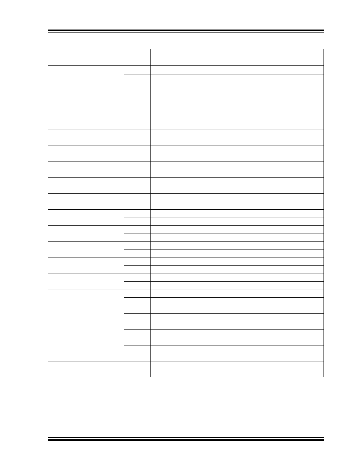
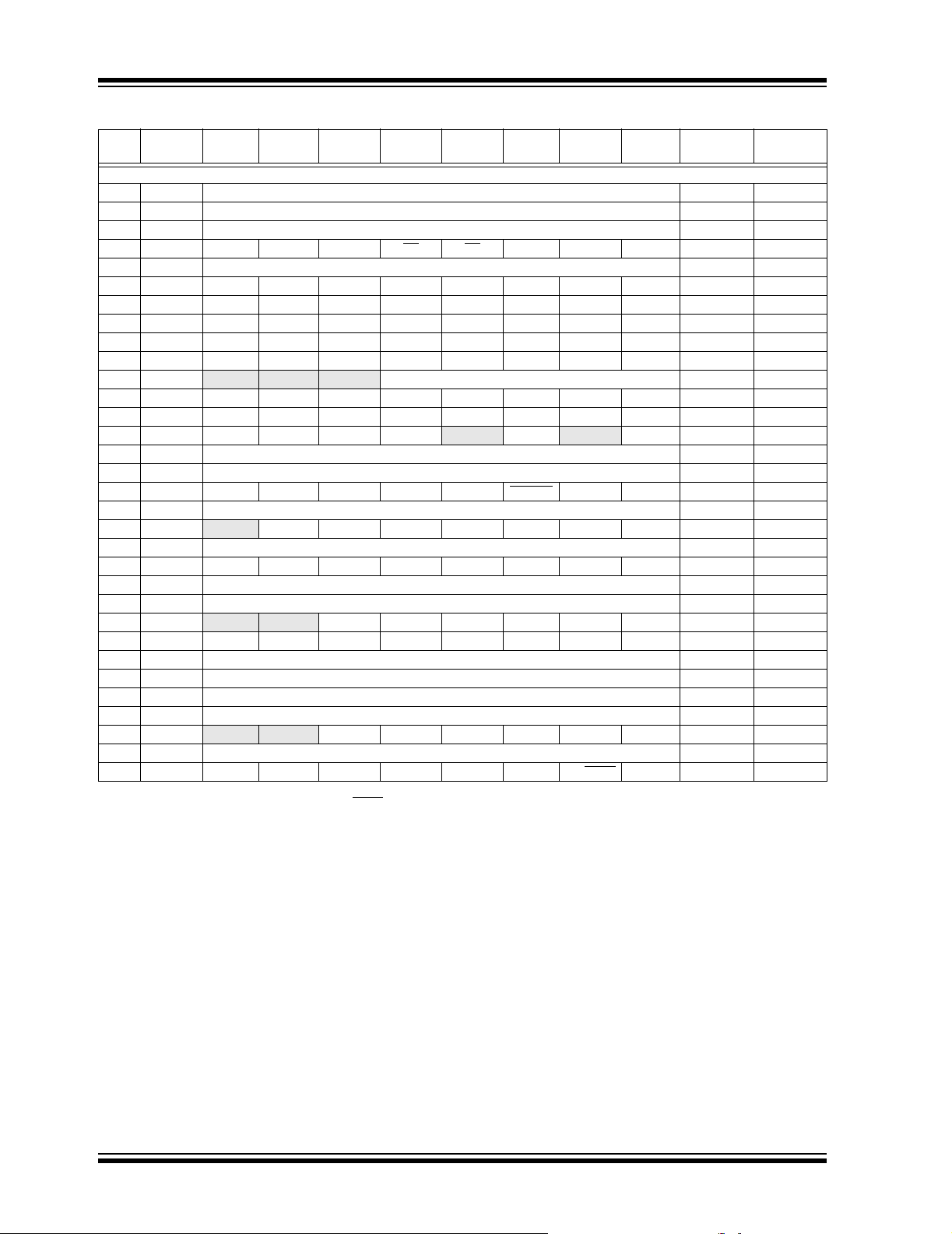
FIGURE 2-3: PIC16F913/916 SPECIAL FUNCTION REGISTERS
File File File File
Address Address Address Address
Indirect addr.
TMR0 01h OPTION_REG 81h TMR0 101h OPTION_REG 181h
PCL 02h PCL 82h PCL 102h PCL 182h
STATUS 03h STATUS 83h STATUS 103h STATUS 183h
FSR 04h FSR 84h FSR 104h FSR 184h
PORTA 05h TRISA 85h WDTCON 105h
PORTB 06h TRISB 86h PORTB 106h TRISB 186h
PORTC 07h TRISC 87h LCDCON 107h 187h
PORTE 09h TRISE 89h LVDCON 109h 189h
PCLATH 0Ah PCLATH 8Ah PCLATH 10Ah PCLATH 18Ah
INTCON 0Bh INTCON 8Bh INTCON 10Bh INTCON 18Bh
PIR1 0Ch PIE1 8Ch EEDATL 10Ch EECON1 18Ch
PIR2 0Dh PIE2 8Dh EEADRL 10Dh EECON2
TMR1L 0Eh PCON 8Eh EEDATH 10Eh
TMR1H 0Fh OSCCON 8Fh EEADRH 10Fh Reserved 18Fh
T1CON 10h OSCTUNE 90h LCDDATA0 110h
TMR2 11h ANSEL 91h LCDDATA1 111h
T2CON 12h PR2 92h
SSPBUF 13h SSPADD 93h LCDDATA3 113h
SSPCON 14h SSPSTAT 94h LCDDATA4 114h
CCPR1L 15h WPUB 95h
CCPR1H 16h IOCB 96h LCDDATA6 116h
CCP1CON 17h CMCON1 97h LCDDATA7 117h
RCSTA 18h TXSTA 98h
TXREG 19h SPBRG 99h LCDDATA9 119h
RCREG 1Ah
ADRESH 1Eh ADRESL 9Eh 11 E h
ADCON0 1Fh ADCON1 9Fh 11Fh
(1)
00h Indirect addr.
08h 88h LCDPS 108h 188h
1Bh 9Bh 11B h
1Ch CMCON0 9Ch LCDSE0 11Ch
1Dh VRCON 9Dh LCDSE1 11Dh
20h
(1)
80h Indirect addr.
9Ah LCDDATA10 11Ah
A0h
(1)
100h Indirect addr.
Reserved 18Eh
112h
115h
118h
Purpose
Register
96 Bytes
120h
General
(2)
(1)
(1)
180h
185h
18Dh
190h
General
General
Purpose
Register
96 Bytes
7Fh FFh 17Fh 1FFh
Bank 0 Bank 1 Bank 2 Bank 3
Unimplemented data memory locations, read as ‘0’.
Note 1: Not a physical register.
2: On the PIC16F913, unimplemented data memory locations, read as ‘0’.
© 2007 Microchip Technology Inc. DS41250F-page 25
Purpose
Register
80 Bytes
accesses
70h-7Fh
EFh 16Fh 1EFh
F0h accesses
General
Purpose
Register
80 Bytes
70h-7Fh
170h accesses
70h-7Fh
1F0h
PIC16F913/914/916/917/946
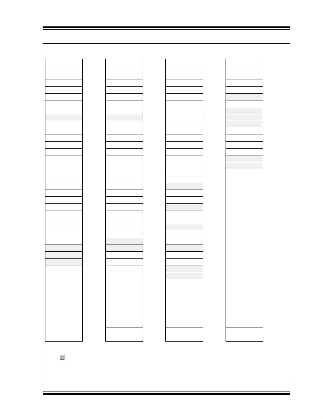
FIGURE 2-4: PIC16F914/917 SPECIAL FUNCTION REGISTERS
File File File File
Address Address Address Address
Indirect addr.
TMR0 01h OPTION_REG 81h TMR0 101h OPTION_REG 181h
PCL 02h PCL 82h PCL 102h PCL 182h
STATUS 03h STATUS 83h STATUS 103h STATUS 183h
FSR 04h FSR 84h FSR 104h FSR 184h
PORTA 05h TRISA 85h WDTCON 105h
PORTB 06h TRISB 86h PORTB 106h TRISB 186h
PORTC 07h TRISC 87h LCDCON 107h 187h
PORTD 08h TRISD 88h LCDPS 108h
PORTE 09h TRISE 89h LVDCON 109h 189h
PCLATH 0Ah PCLATH 8Ah PCLATH 10Ah PCLATH 18Ah
INTCON 0Bh INTCON 8Bh INTCON 10Bh INTCON 18Bh
PIR1 0Ch PIE1 8Ch EEDATL 10Ch EECON1 18Ch
PIR2 0Dh PIE2 8Dh EEADRL 10Dh EECON2
TMR1L 0Eh PCON 8Eh EEDATH 10Eh
TMR1H 0Fh OSCCON 8Fh EEADRH 10Fh Reserved 18Fh
T1CON 10h OSCTUNE 90h LCDDATA0 110h
TMR2 11h ANSEL 91h LCDDATA1 111h
T2CON 12h PR2 92h LCDDATA2 112h
SSPBUF 13h SSPADD 93h LCDDATA3 113h
SSPCON 14h SSPSTAT 94h LCDDATA4 114h
CCPR1L 15h WPUB 95h LCDDATA5 115h
CCPR1H 16h IOCB 96h LCDDATA6 116h
CCP1CON 17h CMCON1 97h LCDDATA7 117h
RCSTA 18h TXSTA 98h LCDDATA8 118h
TXREG 19h SPBRG 99h LCDDATA9 119h
RCREG 1Ah
CCPR2L 1Bh 9Bh LCDDATA11 11Bh
CCPR2H 1Ch CMCON0 9Ch LCDSE0 11Ch
CCP2CON 1Dh VRCON 9Dh LCDSE1 11Dh
ADRESH 1Eh ADRESL 9Eh LCDSE2 11Eh
ADCON0 1Fh ADCON1 9Fh
(1)
00h Indirect addr.
20h
(1)
80h Indirect addr.
9Ah LCDDATA10 11Ah
A0h
(1)
100h Indirect addr.
Reserved 18Eh
General
Purpose
Register
96 Bytes
11Fh
120h
(2)
(1)
(1)
180h
185h
188h
18Dh
190h
General
General
Purpose
Register
96 Bytes
7Fh FFh 17Fh 1FFh
Bank 0 Bank 1 Bank 2 Bank 3
Unimplemented data memory locations, read as ‘0’.
Note 1: Not a physical register.
2: On the PIC16F914, unimplemented data memory locations, read as ‘0’.
DS41250F-page 26 © 2007 Microchip Technology Inc.
Purpose
Register
80 Bytes
accesses
70h-7Fh
EFh 16Fh 1EFh
F0h accesses
General
Purpose
Register
80 Bytes
70h-7Fh
170h accesses
70h-7Fh
1F0h
PIC16F913/914/916/917/946
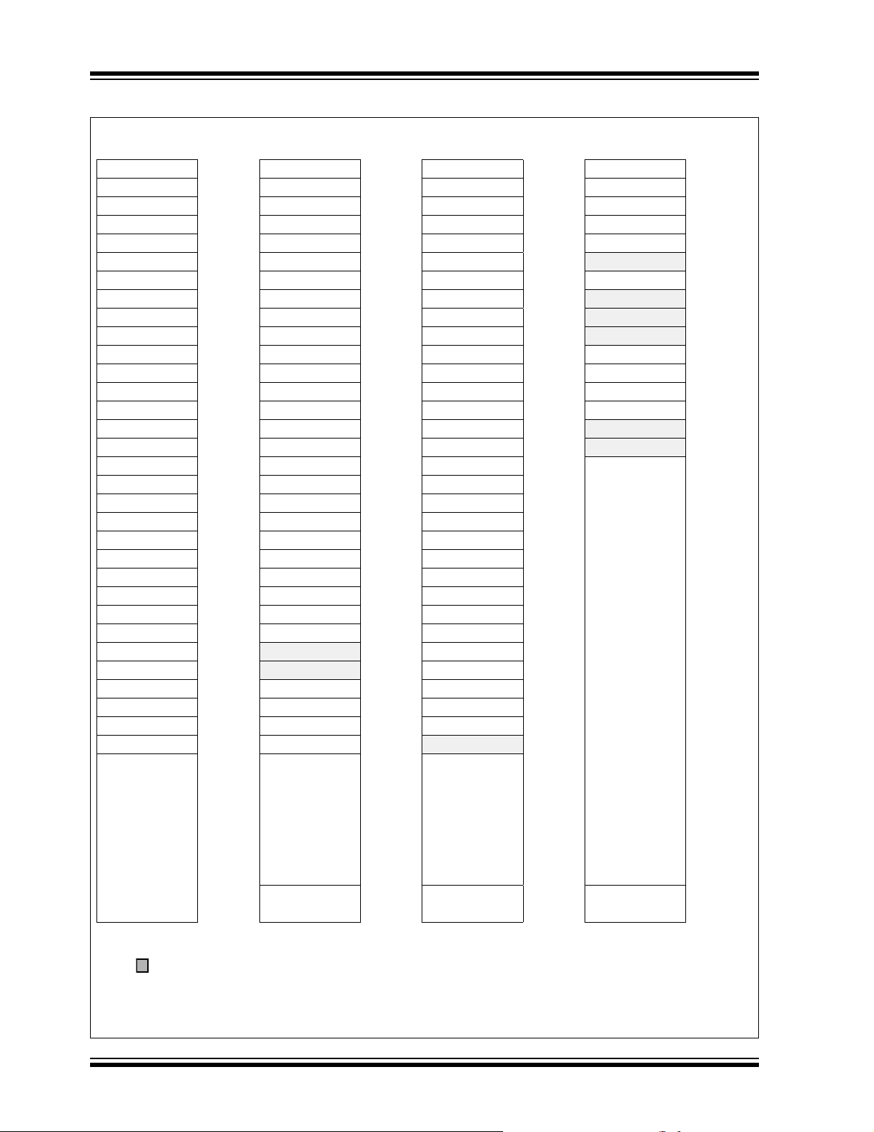
FIGURE 2-5: PIC16F946 SPECIAL FUNCTION REGISTERS
File File File File
Address Address Address Address
Indirect addr.
TMR0 01h OPTION_REG 81h TMR0 101h OPTION_REG 181h
PCL 02h PCL 82h PCL 102h PCL 182h
STATUS 03h STATUS 83h STATUS 103h STATUS 183h
FSR 04h FSR 84h FSR 104h FSR 184h
PORTA 05h TRISA 85h WDTCON 105h TRISF 185h
PORTB 06h TRISB 86h PORTB 106h TRISB 186h
PORTC 07h TRISC 87h LCDCON 107h TRISG 187h
PORTD 08h TRISD 88h LCDPS 108h PORTF 188h
PORTE 09h TRISE 89h LVDCON 109h PORTG 189h
PCLATH 0Ah PCLATH 8Ah PCLATH 10Ah PCLATH 18Ah
INTCON 0Bh INTCON 8Bh INTCON 10Bh INTCON 18Bh
PIR1 0Ch PIE1 8Ch EEDATL 10Ch EECON1 18Ch
PIR2 0Dh PIE2 8Dh EEADRL 10Dh EECON2
TMR1L 0Eh PCON 8Eh EEDATH 10Eh
TMR1H 0Fh OSCCON 8Fh EEADRH 10Fh Reserved 18Fh
T1CON 10h OSCTUNE 90h LCDDATA0 110h LCDDATA12 190h
TMR2 11h ANSEL 91h LCDDATA1 111h LCDDATA13 191h
T2CON 12h PR2 92h LCDDATA2 112h LCDDATA14 192h
SSPBUF 13h SSPADD 93h LCDDATA3 113h LCDDATA15 193h
SSPCON 14h SSPSTAT 94h LCDDATA4 114h LCDDATA16 194h
CCPR1L 15h WPUB 95h LCDDATA5 115h LCDDATA17 195h
CCPR1H 16h IOCB 96h LCDDATA6 116h LCDDATA18 196h
CCP1CON 17h CMCON1 97h LCDDATA7 117h LCDDATA19 197h
RCSTA 18h TXSTA 98h LCDDATA8 118h LCDDATA20 198h
TXREG 19h SPBRG 99h LCDDATA9 119h LCDDATA21 199h
RCREG 1Ah
CCPR2L 1Bh 9Bh LCDDATA11 11Bh LCDDATA23 19Bh
CCPR2H 1Ch CMCON0 9Ch LCDSE0 11Ch LCDSE3 19Ch
CCP2CON 1Dh VRCON 9Dh LCDSE1 11Dh LCDSE4 19Dh
ADRESH 1Eh ADRESL 9Eh LCDSE2 11Eh LCDSE5 19Eh
ADCON0 1Fh ADCON1 9Fh
(1)
00h Indirect addr.
20h
(1)
80h Indirect addr.
9Ah LCDDATA10 11Ah LCDDATA22 19Ah
A0h
(1)
100h Indirect addr.
Reserved 18Eh
11F h 19Fh
120h
(1)
(1)
180h
18Dh
1A0h
General
General
Purpose
Register
96 Bytes
7Fh FFh 17Fh 1FFh
Bank 0Bank 1Bank 2Bank 3
Unimplemented data memory locations, read as ‘0’.
Note 1: Not a physical register.
© 2007 Microchip Technology Inc. DS41250F-page 27
Purpose
Register
80 Bytes
accesses
70h-7Fh
EFh 16Fh 1EFh
F0h accesses
General
Purpose
Register
80 Bytes
70h-7Fh
General
Purpose
Register
80 Bytes
170h accesses
70h-7Fh
1F0h
PIC16F913/914/916/917/946
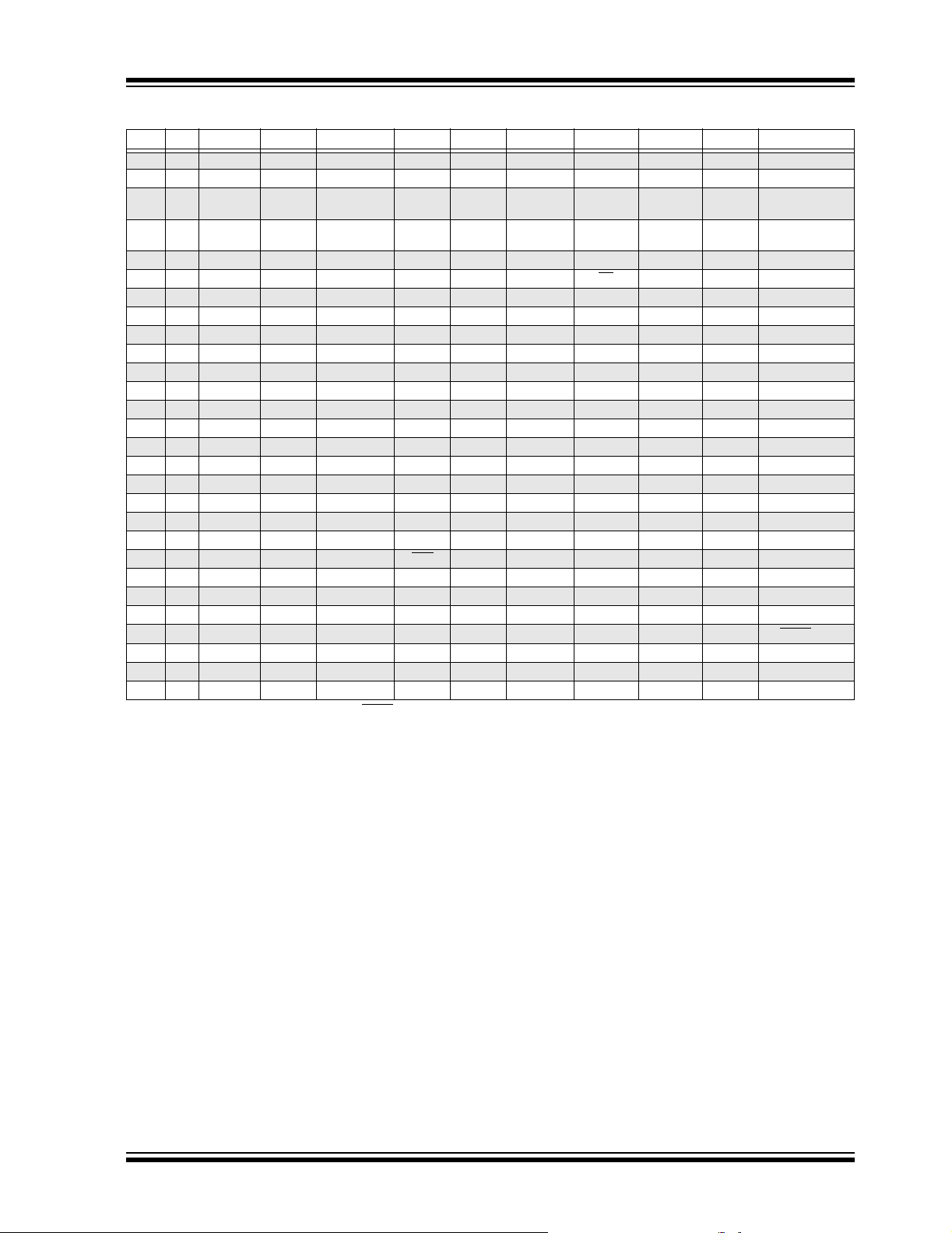
TABLE 2-1: PIC16F91X/946 SPECIAL FUNCTION REGISTERS SUMMARY BANK 0
Addr Name Bit 7 Bit 6 Bit 5 Bit 4 Bit 3 Bit 2 Bit 1 Bit 0
Bank 0
00h INDF Addressing this location uses contents of FSR to address data memory (not a physical register) xxxx xxxx 41,226
01h TMR0 Timer0 Module Register xxxx xxxx 99,226
02h PCL Program Counter’s (PC) Least Significant Byte 0000 0000 40,226
03h STATUS IRP RP1 RP0 TO
04h FSR Indirect Data Memory Address Pointer xxxx xxxx 41,226
05h PORTA RA7 RA6 RA5 RA4 RA3 RA2 RA1 RA0 xxxx xxxx 44,226
06h PORTB RB7 RB6 RB5 RB4 RB3 RB2 RB1 RB0 xxxx xxxx 54,226
07h PORTC RC7 RC6 RC5 RC4 RC3 RC2 RC1 RC0 xxxx xxxx 62,226
08h PORTD
09h PORTE RE7
0Ah PCLATH
0Bh INTCON GIE PEIE T0IE INTE RBIE T0IF INTF RBIF 0000 000x 34,226
0Ch PIR1
0Dh PIR2
0Eh TMR1L Holding Register for the Least Significant Byte of the 16-bit TMR1 xxxx xxxx 102,226
0Fh TMR1H Holding Register for the Most Significant Byte of the 16-bit TMR1 xxxx xxxx 102,226
10h T1CON T1GINV TMR1GE T1CKPS1 T1CKPS0 T1OSCEN T1SYNC
11h T MR2
12h T2CON
13h SSPBUF Synchronous Serial Port Receive Buffer/Transmit Register xxxx xxxx 196,226
14h SSPCON WCOL SSPOV SSPEN CKP SSPM3 SSPM2 SSPM1 SSPM0 0000 0000 195,226
15h CCPR1L Capture/Compare/PWM Register 1 (LSB) xxxx xxxx 213,226
16h CCPR1H Capture/Compare/PWM Register 1 (MSB) xxxx xxxx 213,226
17h CCP1CON
18h RCSTA SPEN RX9 SREN CREN ADDEN FERR OERR RX9D 0000 000x 131,226
19h TXREG USART Transmit Data Register 0000 0000 130,226
1Ah RCREG USART Receive Data Register 0000 0000 128,227
(2)
1Bh
(2)
1Ch
(2)
1Dh
1Eh ADRESH A/D Result Register High Byte xxxx xxxx 182,227
1Fh ADCON0 ADFM VCFG1 VCFG0 CHS2 CHS1 CHS0 GO/DONE
Legend: - = Unimplemented locations read as ‘0’, u = unchanged, x = unknown, q = value depends on condition, shaded = unimplemented
Note 1: Other (non Power-up) Resets include MCLR
(2)
RD7 RD6 RD5 RD4 RD3 RD2 RD1 RD0 xxxx xxxx 71,226
(3)
— — — Write Buffer for upper 5 bits of Program Counter ---0 0000 40,226
EEIF ADIF RCIF TXIF SSPIF CCP1IF TMR2IF TMR1IF 0000 0000 37,226
OSFIF C2IF C1IF LCDIF —LVDIF— CCP2IF
Timer2 Module Register 0000 0000
— TOUTPS3 TOUTPS2 TOUTPS1 TOUTPS0 TMR2ON T2CKPS1 T2CKPS0 -000 0000 108,226
— — CCP1X CCP1Y CCP1M3 CCP1M2 CCP1M1 CCP1M0 --00 0000 212,226
CCPR2L Capture/Compare/PWM Register 2 (LSB) xxxx xxxx 213,227
CCPR2H Capture/Compare/PWM Register 2 (MSB) xxxx xxxx 213,227
CCP2CON — — CCP2X CCP2Y CCP2M3 CCP2M2 CCP2M1 CCP2M0 --00 0000 212,227
2: PIC16F914/917 and PIC16F946 only, forced ‘0’ on PIC16F913/916.
3: PIC16F946 only, forced to ‘0’ on PIC16F91X.
RE6
(3)
RE5
(3)
(3)
RE4
Reset and Watchdog Timer Reset during normal operation.
PD ZDCC0001 1xxx 32,226
RE3 RE2
(2)
(2)
RE1
TMR1CS TMR1ON 0000 0000 105,226
RE0
ADON 0000 0000 180,227
Val ue o n
POR, BOR
(2)
xxxx xxxx 76,226
(2)
0000 -0-0 38,226
Page
107,226
DS41250F-page 28 © 2007 Microchip Technology Inc.

PIC16F913/914/916/917/946
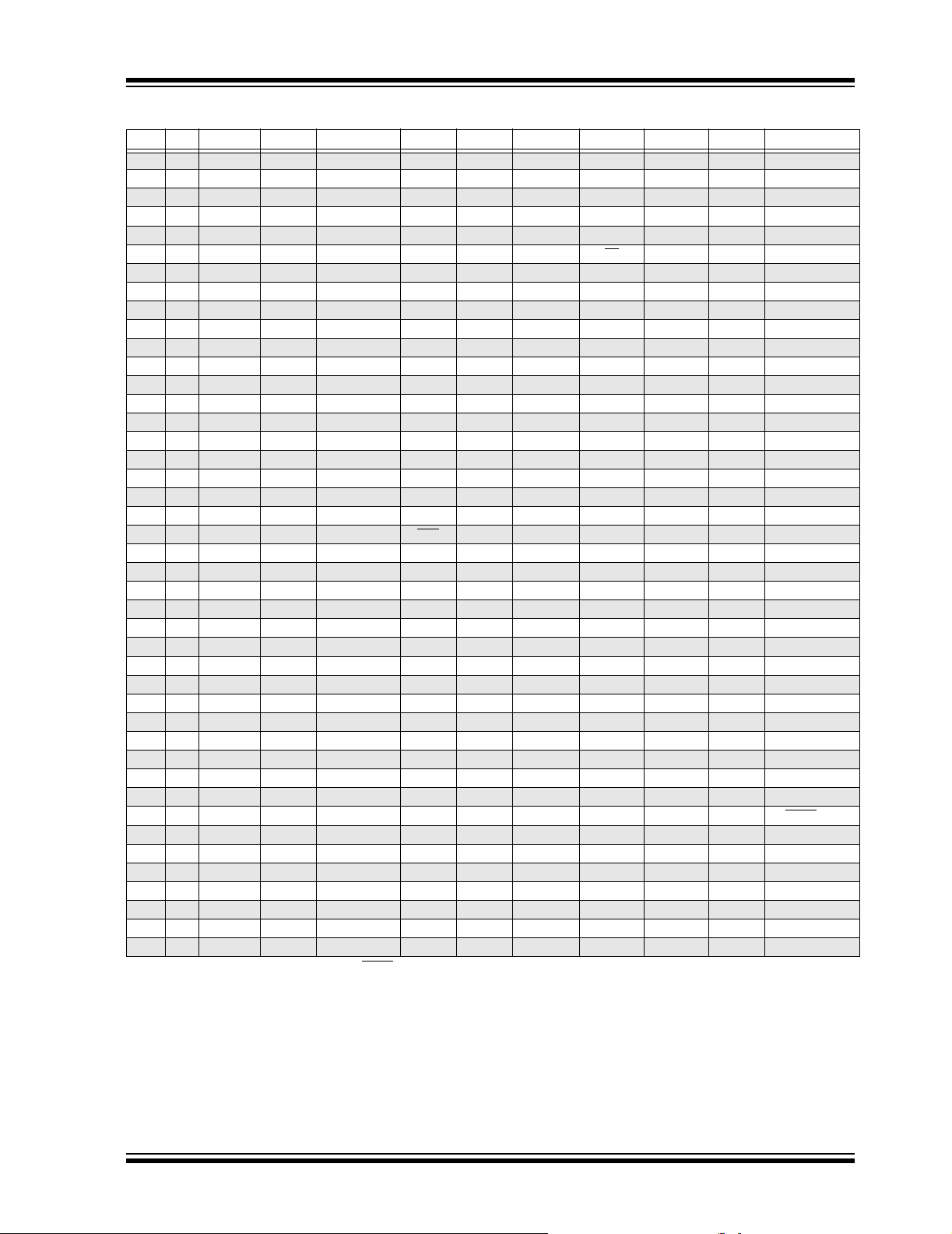
TABLE 2-2: PIC16F91X/946 SPECIAL FUNCTION REGISTERS SUMMARY BANK 1
Addr Name Bit 7 Bit 6 Bit 5 Bit 4 Bit 3 Bit 2 Bit 1 Bit 0
Bank 1
80h INDF Addressing this location uses contents of FSR to address data memory (not a physical register) xxxx xxxx 41,226
81h OPTION_REG RBPU
INTEDG T0CS T0SE PSA PS2 PS1 PS0 1111 1111 33,227
82h PCL Program Counter’s (PC) Least Significant Byte 0000 0000 40,226
83h STATUS IRP RP1 RP0 TO
PD ZDCC0001 1xxx 32,226
84h FSR Indirect Data Memory Address Pointer xxxx xxxx 41,226
85h TRISA TRISA7 TRISA6 TRISA5 TRISA4 TRISA3 TRISA2 TRISA1 TRISA0 1111 1111 44,227
86h TRISB TRISB7 TRISB6 TRISB5 TRISB4 TRISB3 TRISB2 TRISB1 TRISB0 1111 1111 54,227
87h TRISC TRISC7 TRISC6 TRISC5 TRISC4 TRISC3 TRISC2 TRISC1 TRISC0 1111 1111 62,227
88h TRISD
(3)
89h TRISE TRISE7
8Ah PCLATH
TRISD7 TRISD6 TRISD5 TRISD4 TRISD3 TRISD2 TRISD1 TRISD0 1111 1111 71,227
(2)
TRISE6
(2)
TRISE5
(2)
TRISE4
(2)
TRISE3
(5)
TRISE2
(3)
TRISE1
(3)
TRISE0
— — — Write Buffer for the upper 5 bits of the Program Counter ---0 0000 40,226
8Bh INTCON GIE PEIE T0IE INTE RBIE T0IF INTF RBIF 0000 000x 34,226
8Ch PIE1 EEIE ADIE RCIE TXIE SSPIE CCP1IE TMR2IE TMR1IE 0000 0000 35,227
8Dh PIE2 OSFIE C2IE C1IE LCDIE
8Eh PCON
8Fh OSCCON
90h OSCTUNE
91h ANSEL ANS7
— — — SBOREN — —PORBOR ---1 --qq 39,227
— IRCF2 IRCF1 IRCF0 OSTS
— — — TUN4 TUN3 TUN2 TUN1 TUN0 ---0 0000 92,227
(3)
ANS6
(3)
ANS5
(3)
ANS4 ANS3 ANS2 ANS1 ANS0 1111 1111 43,227
—LVDIE— CCP2IE
(4)
HTS LTS SCS -110 q000 88,227
92h PR2 Timer2 Period Register 1111 1111 107,227
93h SSPADD Synchronous Serial Port (I
94h SSPSTAT SMP CKE D/A
2
C mode) Address Register 0000 0000 202,227
PSR/WUA BF 0000 0000 194,227
95h WPUB WPUB7 WPUB6 WPUB5 WPUB4 WPUB3 WPUB2 WPUB1 WPUB0 1111 1111 55,227
96h IOCB IOCB7 IOCB6 IOCB5 IOCB4
97h CMCON1
— — — — — — T1GSS C2SYNC ---- --10 117,227
98h TXSTA CSRC TX9 TXEN SYNC
— — — — 0000 ---- 54,227
— BRGH TRMT TX9D 0000 -010 130,227
99h SPBRG SPBRG7 SPBRG6 SPBRG5 SPBRG4 SPBRG3 SPBRG2 SPBRG1 SPBRG0 0000 0000 132,227
9Ah — Unimplemented — —
9Bh — Unimplemented — —
9Ch CMCON0 C2OUT C1OUT C2INV C1INV CIS CM2 CM1 CM0 0000 0000 116,227
9Dh VRCON VREN
—VRR— VR3 VR2 VR1 VR0 0-0- 0000 118,227
9Eh ADRESL A/D Result Register Low Byte xxxx xxxx 182,227
9Fh ADCON1
— ADCS2 ADCS1 ADCS0 — — — — -000 ---- 181,227
Legend: - = Unimplemented locations read as ‘0’, u = unchanged, x = unknown, q = value depends on condition, shaded = unimplemented
Note 1: Other (non Power-up) Resets include MCLR
Reset and Watchdog Timer Reset during normal operation.
2: PIC16F946 only, forced ‘0’ on PIC16F91X.
3: PIC16F914/917 and PIC16F946 only, forced ‘0’ on PIC16F913/916.
4: The value of the OSTS bit is dependent on the value of the Configuration Word (CONFIG) of the device. See Section 4.2 “Oscillator
Control”.
5: Bit is read-only; TRISE3 = 1 always.
Value on
POR, BOR
(3)
1111 1111 76,227
(3)
0000 -0-0 36,227
Page
© 2007 Microchip Technology Inc. DS41250F-page 29

PIC16F913/914/916/917/946
TABLE 2-3: PIC16F91X/946 SPECIAL FUNCTION REGISTERS SUMMARY BANK 2
Addr Name Bit 7 Bit 6 Bit 5 Bit 4 Bit 3 Bit 2 Bit 1 Bit 0
Bank 2
100h INDF Addressing this location uses contents of FSR to address data memory (not a physical register) xxxx xxxx 41,226
101h TMR0 Timer0 Module Register xxxx xxxx 99,226
102h PCL Program Counter’s (PC) Least Significant Byte 0000 0000 40,226
103h STATUS IRP RP1 RP0 TO
104h FSR Indirect Data Memory Address Pointer xxxx xxxx 41,226
105h WDTCON
106h PORTB RB7 RB6 RB5 RB4 RB3 RB2 RB1 RB0 xxxx xxxx 54,226
107h LCDCON LCDEN SLPEN
108h LCDPS WFT BIASMD LCDA WA LP3 LP2 LP1 LP0 0000 0000 146,227
109h LVDCON
10Ah PCLATH
10Bh INTCON GIE PEIE T0IE INTE RBIE T0IF INTF RBIF 0000 000x 34,226
EEDATL EEDATL7 EEDATL6 EEDATL5 EEDATL4 EEDATL3 EEDATL2 EEDATL1 EEDATL0 0000 0000 188,228
10Ch
EEADRL EEADRL7 EEADRL6 EEADRL5 EEADRL4 EEADRL3 EEADRL2 EEADRL1 EEADRL0 0000 0000 188,228
10Dh
10Eh EEDATH
10Fh EEADRH
110h LCDDATA0 SEG7
111h LCDDATA1 SEG15
112h LCDDATA2
113h LCDDATA3 SEG7
114h LCDDATA4 SEG15
115h LCDDATA5
116h LCDDATA6 SEG7
117h LCDDATA7 SEG15
118h LCDDATA8
119h LCDDATA9 SEG7
11Ah LCDDATA10 SEG15
LCDDATA11
11B h
11Ch LCDSE0
11Dh LCDSE1
11Eh LCDSE2
11F h — Unimplemented — —
Legend: – = Unimplemented locations read as ‘0’, u = unchanged, x = unknown, q = value depends on condition, shaded = unimplemented
Note 1: Other (non Power-up) Resets include MCLR
(3)
(3)
(2,3)
2: PIC16F914/917 and PIC16F946 only.
3: This register is only initialized by a POR or BOR reset and is unchanged by other Resets.
— — — WDTPS3 WDTPS2 WDTPS1 WDTPS0 SWDTEN ---0 1000 235,227
WERR VLCDEN CS1 CS0 LMUX1 LMUX0 0001 0011 145,227
— —IRVSTLVDEN— LVDL2 LVDL1 LVDL0 --00 -100 145,228
— — — Write Buffer for the upper 5 bits of the Program Counter ---0 0000 40,226
— —
— — —
COM0
COM0
(2)
SEG23
COM0
COM1
COM1
(2)
SEG23
COM1
COM2
COM2
(2)
SEG23
COM2
COM3
COM3
(2)
SEG23
COM3
SE7 SE6 SE5 SE4 SE3 SE2 SE1 SE0 0000 0000 147,228
SE15 SE14 SE13 SE12 SE11 SE10 SE9 SE8 0000 0000 147,228
SE23 SE22 SE21 SE20 SE19 SE18 SE17 SE16 0000 0000 147,228
SEG6
COM0
SEG14
COM0
SEG22
COM0
SEG6
COM1
SEG14
COM1
SEG22
COM1
SEG6
COM2
SEG14
COM2
SEG22
COM2
SEG6
COM3
SEG14
COM3
SEG22
COM3
EEDATH5 EEDATH4 EEDATH3 EEDATH2 EEDATH1 EEDATH0
EEADRH4 EEADRH3 EEADRH2 EEADRH1 EEADRH0
SEG5
COM0
SEG13
COM0
SEG21
COM0
SEG5
COM1
SEG13
COM1
SEG21
COM1
SEG5
COM2
SEG13
COM2
SEG21
COM2
SEG5
COM3
SEG13
COM3
SEG21
COM3
SEG4
COM0
SEG12
COM0
SEG20
COM0
SEG4
COM1
SEG12
COM1
SEG20
COM1
SEG4
COM2
SEG12
COM2
SEG20
COM2
SEG4
COM3
SEG12
COM3
SEG20
COM3
Reset and Watchdog Timer Reset during normal operation.
PD ZDCC0001 1xxx 32,226
SEG3
COM0
SEG11
COM0
SEG19
COM0
SEG3
COM1
SEG11
COM1
SEG19
COM1
SEG3
COM2
SEG11
COM2
SEG19
COM2
SEG3
COM3
SEG11
COM3
SEG19
COM3
SEG2
COM0
SEG10
COM0
SEG18
COM0
SEG2
COM1
SEG10
COM1
SEG18
COM1
SEG2
COM2
SEG10
COM2
SEG18
COM2
SEG2
COM3
SEG10
COM3
SEG18
COM3
SEG1
COM0
SEG9
COM0
SEG17
COM0
SEG1
COM1
SEG9
COM1
SEG17
COM1
SEG1
COM2
SEG9
COM2
SEG17
COM2
SEG1
COM3
SEG9
COM3
SEG17
COM3
SEG0
COM0
SEG8
COM0
SEG16
COM0
SEG0
COM1
SEG8
COM1
SEG16
COM1
SEG0
COM2
SEG8
COM2
SEG16
COM2
SEG0
COM3
SEG8
COM3
SEG16
COM3
Value on
POR, BOR
--00 0000 188,228
---0 0000 188,228
xxxx xxxx 147,228
xxxx xxxx 147,228
xxxx xxxx 147,228
xxxx xxxx 147,228
xxxx xxxx 147,228
xxxx xxxx 147,228
xxxx xxxx 147,228
xxxx xxxx 147,228
xxxx xxxx 147,228
xxxx xxxx 147,228
xxxx xxxx 147,228
xxxx xxxx 147,228
Page
DS41250F-page 30 © 2007 Microchip Technology Inc.

PIC16F913/914/916/917/946
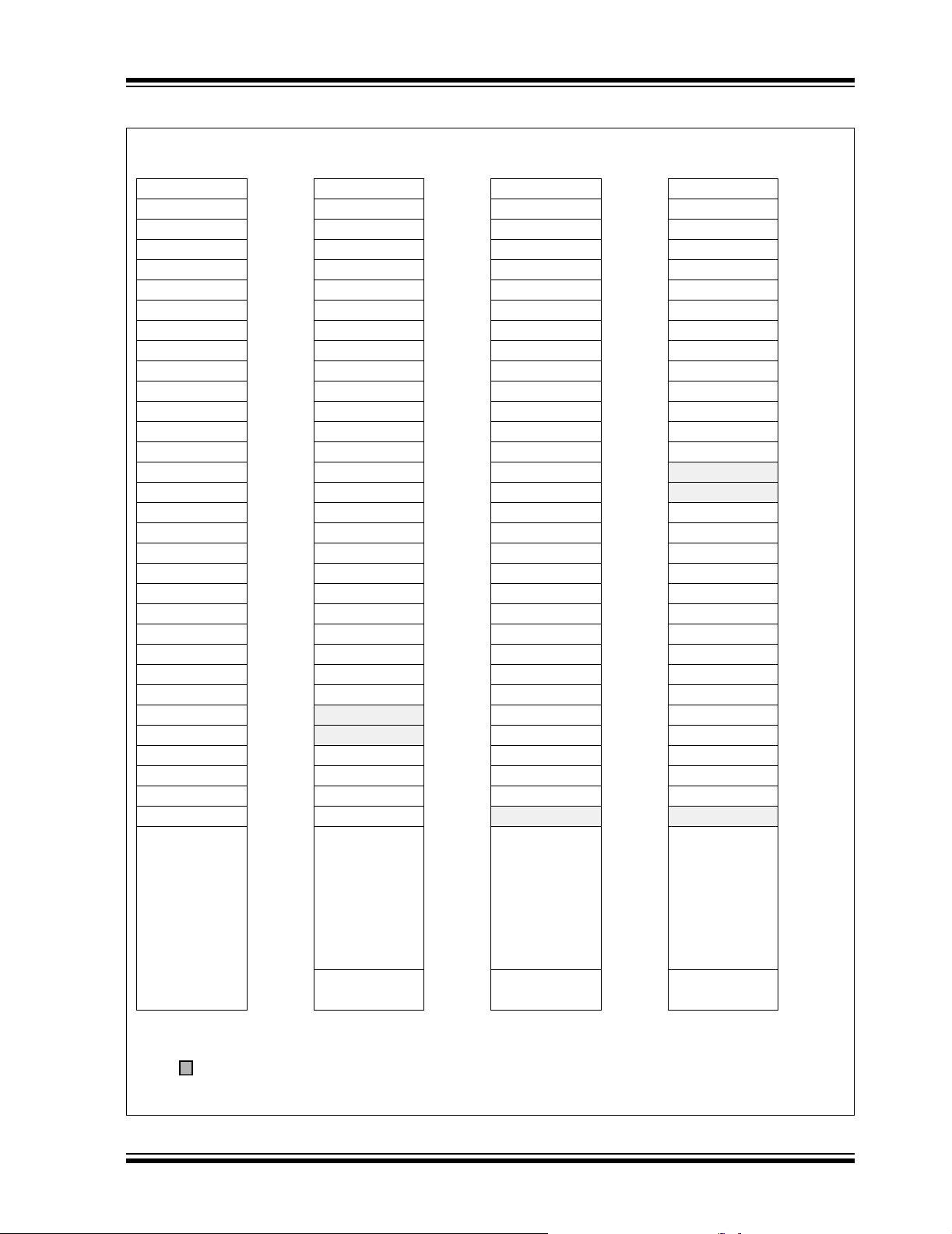
TABLE 2-4: PIC16F91X/946 SPECIAL FUNCTION REGISTERS SUMMARY BANK 3
Addr Name Bit 7 Bit 6 Bit 5 Bit 4 Bit 3 Bit 2 Bit 1 Bit 0
Bank 3
180h INDF Addressing this location uses contents of FSR to address data memory (not a physical
register)
181h OPTION_REG RBPU
INTEDG T0CS T0SE PSA PS2 PS1 PS0
182h PCL Program Counter (PC) Least Significant Byte
183h STATUS IRP RP1 RP0 TO
PD ZDCC
184h FSR Indirect Data Memory Address Pointer
185h TRISF
(3)
TRISF7 TRISF6 TRISF5 TRISF4 TRISF3 TRISF2 TRISF1 TRISF0 1111 1111 81,228
186h TRISB TRISB7 TRISB6 TRISB5 TRISB4 TRISB3 TRISB2 TRISB1 TRISB0 1111 1111 54,227
187h TRISG
188h PORTF
189h PORTG
18Ah PCLATH
(3)
(3)
(3)
— — TRISG5 TRISG4 TRISG3 TRISG2 TRISG1 TRISG0 --11 1111 84,228
RF7 RF6 RF5 RF4 RF3 RF2 RF1 RF0 xxxx xxxx 81,228
— — RG5 RG4 RG3 RG2 RG1 RG0 --xx xxxx 84,228
— — — Write Buffer for the upper 5 bits of the Program Counter
18Bh INTCON GIE PEIE T0IE INTE RBIE T0IF INTF RBIF
18Ch EECON1 EEPGD
— — — WRERR WREN WR RD 0--- x000 189,229
18Dh EECON2 EEPROM Control Register 2 (not a physical register) ---- ---- 187
18Eh — Reserved — —
18Fh — Reserved — —
190h LCDDATA12
191h LCDDATA13
192h LCDDATA14
193h LCDDATA15
194h LCDDATA16
195h LCDDATA17
196h LCDDATA18
197h LCDDATA19
198h LCDDATA20
199h LCDDATA21
19Ah LCDDATA22
19Bh LCDDATA23
19Ch LCDSE3
19Dh LCDSE4
19Eh LCDSE5
(2, 3)
(2, 3)
(2, 3)
(3)
SEG31
COM0
(3)
SEG39
COM0
(3)
(3)
SEG31
COM1
(3)
SEG39
COM1
(3)
(3)
SEG31
COM2
(3)
SEG39
COM2
(3)
(3)
SEG31
COM3
(3)
SEG39
COM3
(3)
SEG30
COM0
SEG38
COM0
— — — — — —SEG41
SEG29
COM0
SEG37
COM0
SEG28
COM0
SEG36
COM0
SEG27
COM0
SEG35
COM0
SEG26
COM0
SEG34
COM0
SEG25
COM0
SE33
COM0
SEG24
SEG32
SEG40
COM0
SEG30
COM1
SEG38
COM1
— — — — — —SEG41
SEG29
COM1
SEG37
COM1
SEG28
COM1
SEG36
COM1
SEG27
COM1
SEG35
COM1
SEG26
COM1
SEG34
COM1
SEG25
COM1
SEG33
COM1
SEG24
SEG32
SEG40
COM1
SEG30
COM2
SEG38
COM2
— — — — — —SEG41
SEG29
COM2
SEG37
COM2
SEG28
COM2
SEG36
COM2
SEG27
COM2
SEG35
COM2
SEG26
COM2
SEG34
COM2
SEG25
COM2
SEG33
COM2
SEG24
SEG32
SEG40
COM2
SEG30
COM3
SEG38
COM3
— — — — — —SEG41
SEG29
COM3
SEG37
COM3
SEG28
COM3
SEG36
COM3
SEG27
COM3
SEG35
COM3
SEG26
COM3
SEG34
COM3
SEG25
COM3
SEG33
COM3
SEG24
SEG32
SEG40
COM3
COM0
COM0
COM0
COM1
COM1
COM1
COM2
COM2
COM2
COM3
COM3
COM3
SE31 SE30 SE29 SE28 SE27 SE26 SE25 SE24 0000 0000 147,229
SE39 SE38 SE37 SE36 SE35 SE34 SE33 SE32 0000 0000 147,229
— — — — — — SE41 SE40 ---- --00 147,229
19Fh — Unimplemented — —
Legend: – = Unimplemented locations read as ‘0’, u = unchanged, x = unknown, q = value depends on condition, shaded = unimplemented
Note 1: Other (non Power-up) Resets include MCLR
Reset and Watchdog Timer Reset during normal operation.
2: This register is only initialized by a POR or BOR reset and is unchanged by other Resets.
3: PIC16F946 only.
Val ue o n
POR, BOR
Page
xxxx xxxx 41,226
1111 1111 33,227
0000 0000 40,226
0001 1xxx 32,226
xxxx xxxx 41,226
---0 0000 40,226
0000 000x 34,226
xxxx xxxx
xxxx xxxx
---- --xx
xxxx xxxx
xxxx xxxx
---- --xx
xxxx xxxx
xxxx xxxx
---- --xx
xxxx xxxx
xxxx xxxx
---- --xx
147,228
147,228
147,228
147,228
147,228
147,228
147,228
147,228
147,228
147,228
147,228
147,228
© 2007 Microchip Technology Inc. DS41250F-page 31

PIC16F913/914/916/917/946
2.2.2.1 STATUS Register
The STATUS register, shown in Register 2-1, contains:
• the arithmetic status of the ALU
• the Reset status
• the bank select bits for data memory (SRAM)
The STATUS register can be the destination for any
instruction, like any other register. If the STATUS
register is the destination for an instruction that affects
the Z, DC or C bits, then the write to these three bits is
disabled. These bits are set or cleared according to the
device logic. Furthermore, the TO
writable. Therefore, the result of an instruction with the
STATUS register as destination may be different than
intended.
and PD bits are not
For example, CLRF STATUS will clear the upper three
bits and set the Z bit. This leaves the STATUS register
as ‘000u u1uu’ (where u = unchanged).
It is recommended, therefore, that only BCF, BSF,
SWAPF and MOVWF instructions are used to alter the
STATUS register, because these instructions do not
affect any Status bits. For other instructions not
affecting any Status bits (see Section 17.0
“Instruction Set Summary”).
Note 1: The C and DC bits operate as Borrow and
Digit Borrow
subtraction.
out bits, respectively, in
REGISTER 2-1: STATUS: STATUS REGISTER
R/W-0 R/W-0 R/W-0 R-1 R-1 R/W-x R/W-x R/W-x
IRP RP1 RP0 TO PD ZDC
bit 7 bit 0
Legend:
R = Readable bit W = Writable bit U = Unimplemented bit, read as ‘0’
-n = Value at POR ‘1’ = Bit is set ‘0’ = Bit is cleared x = Bit is unknown
(1)
(1)
C
bit 7 IRP: Register Bank Select bit (used for indirect addressing)
1 = Bank 2, 3 (100h-1FFh)
0 = Bank 0, 1 (00h-FFh)
bit 6-5 RP<1:0>: Register Bank Select bits (used for direct addressing)
00 = Bank 0 (00h-7Fh)
01 = Bank 1 (80h-FFh)
10 = Bank 2 (100h-17Fh)
11 = Bank 3 (180h-1FFh)
bit 4 TO
bit 3 PD
bit 2 Z: Zero bit
bit 1 DC: Digit Carry/Borrow
bit 0 C: Carry/Borrow
: Time-out bit
1 = After power-up, CLRWDT instruction or SLEEP instruction
0 = A WDT time-out occurred
: Power-down bit
1 = After power-up or by the CLRWDT instruction
0 = By execution of the SLEEP instruction
1 = The result of an arithmetic or logic operation is zero
0 = The result of an arithmetic or logic operation is not zero
bit (ADDWF, ADDLW,SUBLW,SUBWF instructions)
1 = A carry-out from the 4th low-order bit of the result occurred
0 = No carry-out from the 4th low-order bit of the result
(1)
bit
(ADDWF, ADDLW, SUBLW, SUBWF instructions)
1 = A carry-out from the Most Significant bit of the result occurred
0 = No carry-out from the Most Significant bit of the result occurred
(1)
(1)
Note 1: For Borrow
second operand. For rotate (RRF, RLF) instructions, this bit is loaded with either the high-order or low-order
bit of the source register.
DS41250F-page 32 © 2007 Microchip Technology Inc.
, the polarity is reversed. A subtraction is executed by adding the two’s complement of the

PIC16F913/914/916/917/946
2.2.2.2 OPTION register
The OPTION register, shown in Register 2-2, is a
readable and writable register, which contains various
control bits to configure:
• Timer0/WDT prescaler
• External RB0/INT interrupt
•Timer0
• Weak pull-ups on PORTB
REGISTER 2-2: OPTION_REG: OPTION REGISTER
R/W-1 R/W-1 R/W-1 R/W-1 R/W-1 R/W-1 R/W-1 R/W-1
RBPU INTEDG T0CS T0SE PSA PS2 PS1 PS0
bit 7 bit 0
Legend:
R = Readable bit W = Writable bit U = Unimplemented bit, read as ‘0’
-n = Value at POR ‘1’ = Bit is set ‘0’ = Bit is cleared x = Bit is unknown
Note: To achieve a 1:1 prescaler assignment for
Timer0, assign the prescaler to the WDT by
setting PSA bit of the OPTION register to
‘1’. See Section 6.3 “Timer1 Prescaler”.
bit 7 R
BPU: PORTB Pull-up Enable bit
1 = PORTB pull-ups are disabled
0 = PORTB pull-ups are enabled by individual bits in the WPUB register
bit 6 INTEDG: Interrupt Edge Select bit
1 = Interrupt on rising edge of RB0/INT pin
0 = Interrupt on falling edge of RB0/INT pin
bit 5 T0CS: Timer0 Clock Source Select bit
1 = Transition on RA4/T0CKI pin
0 = Internal instruction cycle clock (F
bit 4 T0SE: Timer0 Source Edge Select bit
1 = Increment on high-to-low transition on RA4/T0CKI pin
0 = Increment on low-to-high transition on RA4/T0CKI pin
bit 3 PSA: Prescaler Assignment bit
1 = Prescaler is assigned to the WDT
0 = Prescaler is assigned to the Timer0 module
bit 2-0 PS<2:0>: Prescaler Rate Select bits
Bit Value Timer0 Rate WDT Rate
000
001
010
011
100
101
110
111
1 : 2
1 : 4
1 : 8
1 : 16
1 : 32
1 : 64
1 : 128
1 : 256
OSC/4)
1 : 1
1 : 2
1 : 4
1 : 8
1 : 16
1 : 32
1 : 64
1 : 128
© 2007 Microchip Technology Inc. DS41250F-page 33

PIC16F913/914/916/917/946
2.2.2.3 INTCON Register
The INTCON register is a readable and writable
register, which contains the various enable and flag bits
for TMR0 register overflow, PORTB change and
external RB0/INT/SEG0 pin interrupts.
Note: Interrupt flag bits are set when an interrupt
condition occurs, regardless of the state of
its corresponding enable bit or the global
enable bit, GIE of the INTCON register.
User software should ensure the appropriate interrupt flag bits are clear prior to
enabling an interrupt.
REGISTER 2-3: INTCON: INTERRUPT CONTROL REGISTER
R/W-0 R/W-0 R/W-0 R/W-0 R/W-0 R/W-0 R/W-0 R/W-x
GIE PEIE T0IE INTE RBIE
bit 7 bit 0
Legend:
R = Readable bit W = Writable bit U = Unimplemented bit, read as ‘0’
-n = Value at POR ‘1’ = Bit is set ‘0’ = Bit is cleared x = Bit is unknown
bit 7 GIE: Global Interrupt Enable bit
1 = Enables all unmasked interrupts
0 = Disables all interrupts
bit 6 PEIE: Peripheral Interrupt Enable bit
1 = Enables all unmasked peripheral interrupts
0 = Disables all peripheral interrupts
bit 5 T0IE: Timer0 Overflow Interrupt Enable bit
1 = Enables the Timer0 interrupt
0 = Disables the Timer0 interrupt
bit 4 INTE: RB0/INT External Interrupt Enable bit
1 = Enables the RB0/INT external interrupt
0 = Disables the RB0/INT external interrupt
bit 3 RBIE: PORTB Change Interrupt Enable bit
1 = Enables the PORTB change interrupt
0 = Disables the PORTB change interrupt
bit 2 T0IF: Timer0 Overflow Interrupt Flag bit
1 = TMR0 register has overflowed (must be cleared in software)
0 = TMR0 register did not overflow
bit 1 INTF: RB0/INT External Interrupt Flag bit
1 = The RB0/INT external interrupt occurred (must be cleared in software)
0 = The RB0/INT external interrupt did not occur
bit 0 RBIF: PORTB Change Interrupt Flag bit
1 = When at least one of the PORTB general purpose I/O pins changed state (must be cleared in soft-
ware)
0 = None of the PORTB general purpose I/O pins have changed state
(1)
(2)
(1)
T0IF
(2)
INTF RBIF
Note 1: The appropriate bits in the IOCB register must also be set.
2: T0IF bit is set when Timer0 rolls over. Timer0 is unchanged on Reset and should be initialized before
clearing T0IF bit.
DS41250F-page 34 © 2007 Microchip Technology Inc.

PIC16F913/914/916/917/946
2.2.2.4 PIE1 Register
The PIE1 register contains the interrupt enable bits, as
shown in Register 2-4.
REGISTER 2-4: PIE1: PERIPHERAL INTERRUPT ENABLE REGISTER 1
R/W-0 R/W-0 R/W-0 R/W-0 R/W-0 R/W-0 R/W-0 R/W-0
EEIE ADIE RCIE TXIE SSPIE CCP1IE TMR2IE TMR1IE
bit 7 bit 0
Legend:
R = Readable bit W = Writable bit U = Unimplemented bit, read as ‘0’
-n = Value at POR ‘1’ = Bit is set ‘0’ = Bit is cleared x = Bit is unknown
bit 7 EEIE: EE Write Complete Interrupt Enable bit
1 = Enables the EE write complete interrupt
0 = Disables the EE write complete interrupt
bit 6 ADIE: A/D Converter (ADC) Interrupt Enable bit
1 = Enables the ADC interrupt
0 = Disables the ADC interrupt
bit 5 RCIE: USART Receive Interrupt Enable bit
1 = Enables the USART receive interrupt
0 = Disables the USART receive interrupt
bit 4 TXIE: USART Transmit Interrupt Enable bit
1 = Enables the USART transmit interrupt
0 = Disables the USART transmit interrupt
bit 3 SSPIE: Synchronous Serial Port (SSP) Interrupt Enable bit
1 = Enables the SSP interrupt
0 = Disables the SSP interrupt
bit 2 CCP1IE: CCP1 Interrupt Enable bit
1 = Enables the CCP1 interrupt
0 = Disables the CCP1 interrupt
bit 1 TMR2IE: TMR2 to PR2 Match Interrupt Enable bit
1 = Enables the Timer2 to PR2 match interrupt
0 = Disables the Timer2 to PR2 match interrupt
bit 0 TMR1IE: Timer1 Overflow Interrupt Enable bit
1 = Enables the Timer1 overflow interrupt
0 = Disables the Timer1 overflow interrupt
Note: Bit PEIE of the INTCON register must be
set to enable any peripheral interrupt.
© 2007 Microchip Technology Inc. DS41250F-page 35

PIC16F913/914/916/917/946
2.2.2.5 PIE2 Register
The PIE2 register contains the interrupt enable bits, as
shown in Register 2-5.
REGISTER 2-5: PIE2: PERIPHERAL INTERRUPT ENABLE REGISTER 2
R/W-0 R/W-0 R/W-0 R/W-0 U-0 R/W-0 U-0 R/W-0
OSFIE C2IE C1IE LCDIE —LVDIE —CCP2IE
bit 7 bit 0
Legend:
R = Readable bit W = Writable bit U = Unimplemented bit, read as ‘0’
-n = Value at POR ‘1’ = Bit is set ‘0’ = Bit is cleared x = Bit is unknown
bit 7 OSFIE: Oscillator Fail Interrupt Enable bit
1 = Enables oscillator fail interrupt
0 = Disables oscillator fail interrupt
bit 6 C2IE: Comparator C2 Interrupt Enable bit
1 = Enables Comparator C2 interrupt
0 = Disables Comparator C2 interrupt
bit 5 C1IE: Comparator C1 Interrupt Enable bit
1 = Enables Comparator C1 interrupt
0 = Disables Comparator C1 interrupt
bit 4 LCDIE: LCD Module Interrupt Enable bit
1 = Enables LCD interrupt
0 = Disables LCD interrupt
bit 3 Unimplemented: Read as ‘0’
bit 2 LV DIE: Low Voltage Detect Interrupt Enable bit
1 = Enables LVD Interrupt
0 = Disables LVD Interrupt
bit 1 Unimplemented: Read as ‘0’
bit 0 CCP2IE: CCP2 Interrupt Enable bit
1 = Enables the CCP2 interrupt
0 = Disables the CCP2 interrupt
(1)
Note: Bit PEIE of the INTCON register must be
set to enable any peripheral interrupt.
(1)
Note 1: PIC16F914/PIC16F917/PIC16F946 only.
DS41250F-page 36 © 2007 Microchip Technology Inc.

PIC16F913/914/916/917/946
2.2.2.6 PIR1 Register
The PIR1 register contains the interrupt flag bits, as
shown in Register 2-6.
REGISTER 2-6: PIR1: PERIPHERAL INTERRUPT REQUEST REGISTER 1
R/W-0 R/W-0 R-0 R-0 R/W-0 R/W-0 R/W-0 R/W-0
EEIF ADIF RCIF TXIF SSPIF CCP1IF TMR2IF TMR1IF
bit 7 bit 0
Legend:
R = Readable bit W = Writable bit U = Unimplemented bit, read as ‘0’
-n = Value at POR ‘1’ = Bit is set ‘0’ = Bit is cleared x = Bit is unknown
bit 7 EEIF: EE Write Operation Interrupt Flag bit
1 = The write operation completed (must be cleared in software)
0 = The write operation has not completed or has not started
bit 6 ADIF: A/D Converter Interrupt Flag bit
1 = A/D conversion complete (must be cleared in software)
0 = A/D conversion has not completed or has not been started
bit 5 RCIF: USART Receive Interrupt Flag bit
1 = The USART receive buffer is full (cleared by reading RCREG)
0 = The USART receive buffer is not full
bit 4 TXIF: USART Transmit Interrupt Flag bit
1 = The USART transmit buffer is empty (cleared by writing to TXREG)
0 = The USART transmit buffer is full
bit 3 SSPIF: Synchronous Serial Port (SSP) Interrupt Flag bit
1 = The Transmission/Reception is complete (must be cleared in software)
0 = Waiting to Transmit/Receive
bit 2 CCP1IF: CCP1 Interrupt Flag bit
Capture mode
1 = A TMR1 register capture occurred (must be cleared in software)
0 = No TMR1 register capture occurred
Compare mode
1 = A TMR1 register compare match occurred (must be cleared in software)
0 = No TMR1 register compare match occurred
PWM mode
Unused in this mode
bit 1 TMR2IF: Timer2 to PR2 Interrupt Flag bit
1 = A Timer2 to PR2 match occurred (must be cleared in software)
0 = No Timer2 to PR2 match occurred
bit 0 TMR1IF: Timer1 Overflow Interrupt Flag bit
1 = The TMR1 register overflowed (must be cleared in software)
0 = The TMR1 register did not overflow
:
:
Note: Interrupt flag bits are set when an interrupt
condition occurs, regardless of the state of
its corresponding enable bit or the global
enable bit, GIE of the INTCON register.
User software should ensure the
appropriate interrupt flag bits are clear prior
to enabling an interrupt.
© 2007 Microchip Technology Inc. DS41250F-page 37

PIC16F913/914/916/917/946
2.2.2.7 PIR2 Register
The PIR2 register contains the interrupt flag bits, as
shown in Register 2-7.
REGISTER 2-7: PIR2: PERIPHERAL INTERRUPT REQUEST REGISTER 2
R/W-0 R/W-0 R/W-0 R/W-0 U-0 R/W-0 U-0 R/W-0
OSFIF C2IF C1IF LCDIF —LVDIF—CCP2IF
bit 7 bit 0
Legend:
R = Readable bit W = Writable bit U = Unimplemented bit, read as ‘0’
-n = Value at POR ‘1’ = Bit is set ‘0’ = Bit is cleared x = Bit is unknown
bit 7 OSFIF: Oscillator Fail Interrupt Flag bit
1 = System oscillator failed, clock input has changed to INTOSC (must be cleared in software)
0 = System clock operating
bit 6 C2IF: Comparator C2 Interrupt Flag bit
1 = Comparator output (C2OUT bit) has changed (must be cleared in software)
0 = Comparator output (C2OUT bit) has not changed
bit 5 C1IF: Comparator C1 Interrupt Flag bit
1 = Comparator output (C1OUT bit) has changed (must be cleared in software)
0 = Comparator output (C1OUT bit) has not changed
bit 4 LCDIF: LCD Module Interrupt bit
1 = LCD has generated an interrupt
0 = LCD has not generated an interrupt
bit 3 Unimplemented: Read as ‘0’
bit 2 LV DIF: Low Voltage Detect Interrupt Flag bit
1 = LVD has generated an interrupt
0 = LVD has not generated an interrupt
bit 1 Unimplemented: Read as ‘0’
bit 0 CCP2IF: CCP2 Interrupt Flag bit
Capture Mode:
1 = A TMR1 register capture occurred (must be cleared in software)
0 = No TMR1 register capture occurred
Compare Mode
1 = A TMR1 register compare match occurred (must be cleared in software)
0 = No TMR1 register compare match occurred
PWM mode
Unused in this mode
:
:
(1)
Note: Interrupt flag bits are set when an interrupt
condition occurs, regardless of the state of
its corresponding enable bit or the global
enable bit, GIE of the INTCON register.
User software should ensure the
appropriate interrupt flag bits are clear prior
to enabling an interrupt.
(1)
Note 1: PIC16F914/PIC16F917/PIC16F946 only.
DS41250F-page 38 © 2007 Microchip Technology Inc.

PIC16F913/914/916/917/946
2.2.2.8 PCON Register
The Power Control (PCON) register contains flag bits
(see Table 16-2) to differentiate between a:
• Power-on Reset (POR
• Brown-out Reset (BOR)
• Watchdog Timer Reset (WDT)
• External MCLR
The PCON register also controls the software enable of
the BOR.
The PCON register bits are shown in Register 2-8.
REGISTER 2-8: PCON: POWER CONTROL REGISTER
U-0 U-0 U-0 R/W-1 U-0 U-0 R/W-0 R/W-x
— — — SBOREN — —PORBOR
bit 7 bit 0
Legend:
R = Readable bit W = Writable bit U = Unimplemented bit, read as ‘0’
-n = Value at POR ‘1’ = Bit is set ‘0’ = Bit is cleared x = Bit is unknown
)
Reset
bit 7-5 Unimplemented: Read as ‘0’
bit 4 SBOREN: Software BOR Enable bit
1 = BOR enabled
0 = BOR disabled
bit 3-2 Unimplemented: Read as ‘0’
bit 1 POR
bit 0 BOR
Note 1: Set BOREN<1:0> = 01 in the Configuration Word register for this bit to control the BOR
: Power-on Reset Status bit
1 = No Power-on Reset occurred
0 = A Power-on Reset occurred (must be set in software after a Power-on Reset occurs)
: Brown-out Reset Status bit
1 = No Brown-out Reset occurred
0 = A Brown-out Reset occurred (must be set in software after a Power-on Reset or Brown-out Reset
occurs)
(1)
.
© 2007 Microchip Technology Inc. DS41250F-page 39

PIC16F913/914/916/917/946
2.3 PCL and PCLATH
The Program Counter (PC) is 13 bits wide. The low
byte comes from the PCL register, which is a readable
and writable register. The high byte (PC<12:8>) is not
directly readable or writable and comes from
PCLATH. On any Reset, the PC is cleared. Figure 2-6
shows the two situations for the loading of the PC. The
upper example in Figure 2-6 shows how the PC is
loaded on a write to PCL (PCLATH<4:0> → PCH).
The lower example in Figure 2-6 shows how the PC is
loaded during a CALL or GOTO instruction
(PCLATH<4:3> → PCH).
FIGURE 2-6: LOADING OF PC IN
DIFFERENT SITUATIONS
PCH PCL
12 8 7 0
PC
PCLATH<4:0>
5
PCLATH
PCH PCL
12 11 10 0
PC
2
87
PCLATH<4:3>
PCLATH
8
11
Instruction with
PCL as
Destination
ALU Result
GOTO, CALL
OPCODE<10:0>
2.3.1 COMPUTED GOTO
A computed GOTO is accomplished by adding an offset
to the program counter (ADDWF PCL). When performing a table read using a computed GOTO method, care
should be exercised if the table location crosses a PCL
memory boundary (each 256-byte block). Refer to the
Application Note AN556, “Implementing a Table Read”
(DS00556).
2.3.2 STACK
The PIC16F91X/946 family has an 8-level x 13-bit wide
hardware stack (see Figures 2-1 and 2-2). The stack
space is not part of either program or data space and
the Stack Pointer is not readable or writable. The PC is
PUSHed onto the stack when a CALL instruction is
executed or an interrupt causes a branch. The stack is
POPed in the event of a RETURN, RETLW or a RETFIE
instruction execution. PCLATH is not affected by a
PUSH or POP operation.
The stack operates as a circular buffer. This means that
after the stack has been PUSHed eight times, the ninth
PUSH overwrites the value that was stored from the
first PUSH. The tenth PUSH overwrites the second
PUSH (and so on).
Note 1: There are no Status bits to indicate stack
2.4 Program Memory Paging
All PIC16F91X/946 devices are capable of addressing
a continuous 8K word block of program memory. The
CALL and GOTO instructions provide only 11 bits of
address to allow branching within any 2K program
memory page. When doing a CALL or GOTO instruction,
the upper 2 bits of the address are provided by
PCLATH<4:3>. When doing a CALL or GOTO instruction, the user must ensure that the page select bits are
programmed so that the desired program memory
page is addressed. If a return from a CALL instruction
(or interrupt) is executed, the entire 13-bit PC is POPed
off the stack. Therefore, manipulation of the
PCLATH<4:3> bits is not required for the RETURN
instructions (which POPs the address from the stack).
Note: The contents of the PCLATH register are
Example 2-1 shows the calling of a subroutine in
page 1 of the program memory. This example assumes
that PCLATH is saved and restored by the Interrupt
Service Routine
EXAMPLE 2-1: CALL OF A SUBROUTINE
SUB1_P1
overflow or stack underflow conditions.
2: There are no instructions/mnemonics
called PUSH or POP. These are actions
that occur from the execution of the CALL,
RETURN, RETLW and RETFIE instructions or the vectoring to an interrupt
address.
unchanged after a RETURN or RETFIE
instruction is executed. The user must
rewrite the contents of the PCLATH register for any subsequent subroutine calls or
GOTO instructions.
(if interrupts are used).
IN PAGE 1 FROM PAGE 0
ORG 500h
BCF PCLATH,4
BSF PCLATH,3 ;Select page 1
;(800h-FFFh)
CALL SUB1_P1 ;Call subroutine in
: ;page 1 (800h-FFFh)
:
ORG 900h ;page 1 (800h-FFFh)
: ;called subroutine
;page 1 (800h-FFFh)
:
RETURN ;return to
;Call subroutine
;in page 0
;(000h-7FFh)
DS41250F-page 40 © 2007 Microchip Technology Inc.

PIC16F913/914/916/917/946
2.5 Indirect Addressing, INDF and FSR Registers
The INDF register is not a physical register. Addressing
the INDF register will cause indirect addressing.
Indirect addressing is possible by using the INDF
register. Any instruction using the INDF register
actually accesses data pointed to by the File Select
Register (FSR). Reading INDF itself indirectly will
EXAMPLE 2-2: INDIRECT ADDRESSING
MOVLW 020h ;initialize pointer
MOVWF FSR ;to RAM
BANKISEL 020h
NEXT CLRF INDF ;clear INDF register
INCF FSR ;inc pointer
BTFSS FSR,4 ;all done?
GOTO NEXT ;no clear next
CONTINUE ;yes continue
produce 00h. Writing to the INDF register indirectly
results in a no operation (although Status bits may be
affected). An effective 9-bit address is obtained by
concatenating the 8-bit FSR register and the IRP bit of
the STATUS register, as shown in Figure 2-7.
A simple program to clear RAM location 020h-02Fh
using indirect addressing is shown in Example 2-2.
FIGURE 2-7: DIRECT/INDIRECT ADDRESSING PIC16F91X/946
RP1 RP0 6
Bank Select Location Select
From Opcode
00h
0
00 01 10 11
IRP File Select Register
Bank Select
180h
Indirect AddressingDirect Addressing
7
Location Select
0
Data
Memory
7Fh
Bank 0 Bank 1 Bank 2 Bank 3
Note: For memory map detail, see Figures 2-3 and 2-4.
1FFh
© 2007 Microchip Technology Inc. DS41250F-page 41

PIC16F913/914/916/917/946
NOTES:
DS41250F-page 42 © 2007 Microchip Technology Inc.

PIC16F913/914/916/917/946
3.0 I/O PORTS
The PIC16F913/914/916/917/946 family of devices
includes several 8-bit PORT registers along with their
corresponding TRIS registers and one four bit port:
• PORTA and TRISA
• PORTB and TRISB
• PORTC and TRISC
• PORTD and TRISD
• PORTE and TRISE
• PORTF and TRISF
• PORTG and TRISG
Note 1: PIC16F914/917 and PIC16F946 only.
2: PIC16F946 only
PORTA, PORTB, PORTC and RE3/MCLR/VPP are
implemented on all devices. PORTD and RE<2:0>
(PORTE) are implemented only on the PIC16F914/917
and PIC16F946. RE<7:4> (PORTE), PORTF and
PORTG are implemented only on the PIC16F946.
(1)
(2)
(2)
3.1 ANSEL Register
The ANSEL register (Register 3-1) is used to configure
the Input mode of an I/O pin to analog. Setting the
appropriate ANSEL bit high will cause all digital reads
on the pin to be read as ‘0’ and allow analog functions
on the pin to operate correctly.
The state of the ANSEL bits has no affect on digital output functions. A pin with TRIS clear and ANSEL set will
still operate as a digital output, but the Input mode will
be analog. This can cause unexpected behavior when
executing read-modify-write instructions on the
affected port.
REGISTER 3-1: ANSEL: ANALOG SELECT REGISTER
R/W-1 R/W-1 R/W-1 R/W-1 R/W-1 R/W-1 R/W-1 R/W-1
(2)
ANS7
bit 7 bit 0
ANS6
(2)
ANS5
(2)
ANS4 ANS3 ANS2 ANS1 ANS0
Legend:
R = Readable bit W = Writable bit U = Unimplemented bit, read as ‘0’
-n = Value at POR ‘1’ = Bit is set ‘0’ = Bit is cleared x = Bit is unknown
bit 7-0 ANS<7:0>: Analog Select bits
Analog select between analog or digital function on pins AN<7:0>, respectively.
1 = Analog input. Pin is assigned as analog input
0 = Digital I/O. Pin is assigned to port or special function.
Note 1: Setting a pin to an analog input automatically disables the digital input circuitry, weak pull-ups, and
interrupt-on-change if available. The corresponding TRIS bit must be set to Input mode in order to allow
external control of the voltage on the pin.
2: PIC16F914/PIC16F917/PIC16F946 only.
(1)
.
© 2007 Microchip Technology Inc. DS41250F-page 43

PIC16F913/914/916/917/946
3.2 PORTA and TRISA Registers
PORTA is a 8-bit wide, bidirectional port. The
corresponding data direction register is TRISA
(Register 3-3). Setting a TRISA bit (= 1) will make the
corresponding PORTA pin an input (i.e., put the
The TRISA register controls the direction of the PORTA
pins, even when they are being used as analog inputs.
The user must ensure the bits in the TRISA register are
maintained set when using them as analog inputs. I/O
pins configured as analog inputs always read ‘0’.
corresponding output driver in a High-Impedance mode).
Clearing a TRISA bit (= 0) will make the corresponding
PORTA pin an output (i.e., put the contents of the output
latch on the selected pin). Example 3-1 shows how to
initialize PORTA.
Note 1: The CMCON0 and ANSEL registers must
be initialized to configure an analog
channel as a digital input. Pins configured
as analog inputs will read ‘0’.
Five of the pins of PORTA can be configured as analog
inputs. These pins, RA5 and RA<3:0>, are configured
as analog inputs on device power-up and must be
reconfigured by the user to be used as I/O’s. This is
done by writing the appropriate values to the CMCON0
and ANSEL registers (see Example 3-1).
Reading the PORTA register (Register 3-2) reads the
status of the pins, whereas writing to it will write to the
PORT latch. All write operations are read-modify-write
operations. Therefore, a write to a port means that the
EXAMPLE 3-1: INITIALIZING PORTA
BANKSEL PORTA ;
CLRF PORTA ;Init PORTA
BANKSEL TRISA ;
MOVLW 07h ;Set RA<2:0> to
MOVWF CMCON0 ;digital I/O
CLRF ANSEL ;Make all PORTA digital I/O
MOVLW 0F0h ;Set RA<7:4> as inputs
MOVWF TRISA ;and set RA<3:0> as outputs
port pins are read, this value is modified and then written
to the PORT data latch.
REGISTER 3-2: PORTA: PORTA REGISTER
R/W-x R/W-x R/W-x R/W-x R/W-x R/W-x R/W-x R/W-x
RA7 RA6 RA5 RA4 RA3 RA2 RA1 RA0
bit 7 bit 0
Legend:
R = Readable bit W = Writable bit U = Unimplemented bit, read as ‘0’
-n = Value at POR ‘1’ = Bit is set ‘0’ = Bit is cleared x = Bit is unknown
bit 7-0 RA<7:0>: PORTA I/O Pin bits
1 = Port pin is >V
0 = Port pin is <V
IH min.
IL max.
REGISTER 3-3: TRISA: PORTA TRI-STATE REGISTER
R/W-1 R/W-1 R/W-1 R/W-1 R/W-1 R/W-1 R/W-1 R/W-1
TRISA7 TRISA6 TRISA5 TRISA4 TRISA3 TRISA2 TRISA1 TRISA0
bit 7 bit 0
Legend:
R = Readable bit W = Writable bit U = Unimplemented bit, read as ‘0’
-n = Value at POR ‘1’ = Bit is set ‘0’ = Bit is cleared x = Bit is unknown
bit 7-0 TRISA<7:0>: PORTA Tri-State Control bits
Note 1: TRISA<7:6> always reads ‘1’ in XT, HS and LP Oscillator modes.
1 = PORTA pin configured as an input (tri-stated)
0 = PORTA pin configured as an output
DS41250F-page 44 © 2007 Microchip Technology Inc.

PIC16F913/914/916/917/946
3.2.1 PIN DESCRIPTIONS AND
DIAGRAMS
Each PORTA pin is multiplexed with other functions. The
pins and their combined functions are briefly described
here. For specific information about individual functions,
refer to the appropriate section in this data sheet.
3.2.1.1 RA0/AN0/C1-/SEG12
Figure 3-1 shows the diagram for this pin. The RA0 pin
is configurable to function as one of the following:
• a general purpose I/O
• an analog input for the ADC
• an analog input for Comparator C1
• an analog output for the LCD
FIGURE 3-1: BLOCK DIAGRAM OF RA0
Data Bus
WR PORTA
WR TRISA
CK
Data Latch
CK
TRIS Latch
RD TRISA
RD PORTA
SEG12
QD
Q
QD
Q
SE12 and LCDEN
SE12 and LCDEN
To A/D Converter and Comparator
VDD
I/O Pin
VSS
Analog Input or
SE12 and LCDEN
TTL
Input Buffer
© 2007 Microchip Technology Inc. DS41250F-page 45

PIC16F913/914/916/917/946
3.2.1.2 RA1/AN1/C2-/SEG7
Figure 3-2 shows the diagram for this pin. The RA1 pin
is configurable to function as one of the following:
• a general purpose I/O
• an analog input for the ADC
• an analog input for Comparator C2
• an analog output for the LCD
FIGURE 3-2: BLOCK DIAGRAM OF RA1
Data Bus
WR PORTA
WR TRISA
CK
Data Latch
CK
TRIS Latch
RD TRISA
RD PORTA
SEG7
QD
Q
QD
Q
Analog Input or
SE7 and LCDEN
SE7 and LCDEN
SE7 and LCDEN
To A/D Converter and Comparator
VDD
I/O Pin
VSS
TTL
Input Buffer
DS41250F-page 46 © 2007 Microchip Technology Inc.

PIC16F913/914/916/917/946
3.2.1.3 RA2/AN2/C2+/VREF-/COM2
Figure 3-3 shows the diagram for this pin. The RA2 pin
is configurable to function as one of the following:
• a general purpose I/O
• an analog input for the ADC
• an analog input for Comparator C2
• a voltage reference input for the ADC
• an analog output for the LCD
FIGURE 3-3: BLOCK DIAGRAM OF RA2
Data Bus
WR PORTA
WR TRISA
CK
Data Latch
CK
TRIS Latch
RD TRISA
RD PORTA
COM2
QD
Q
QD
Q
Analog Input or
LMUX<1:0> = 1X
LCDEN and
LMUX<1:0> = 1X
LCDEN and
LMUX<1:0> = 1X
VDD
I/O Pin
VSS
LCDEN and
TTL
Input Buffer
To A/D Converter and Comparator
To A/D Module VREF- Input
© 2007 Microchip Technology Inc. DS41250F-page 47

PIC16F913/914/916/917/946
3.2.1.4 RA3/AN3/C1+/VREF+/COM3/SEG15
Figure 3-4 shows the diagram for this pin. The RA3 pin
is configurable to function as one of the following:
• a general purpose input
• an analog input for the ADC
• an analog input from Comparator C1
• a voltage reference input for the ADC
• analog outputs for the LCD
FIGURE 3-4: BLOCK DIAGRAM OF RA3
Data Bus
WR PORTA
WR TRISA
CK
Data Latch
CK
TRIS Latch
RD TRISA
RD PORTA
(1)
COM3
or SEG15
QD
Q
Q
QD
Q
Q
Analog Input or
LCDMODE_EN
LCDMODE_EN
LCDMODE_EN
(2)
(2)
VDD
VSS
TTL
Input Buffer
(2)
I/O Pin
To A/D Converter and Comparator
To A / D M o du l e VREF+ Input
Note 1: PIC16F913/916 only.
2: For the PIC16F913/916, the LCDMODE_EN = LCDEN and (SE15 or LMUX<1:0> = 11).
For the PIC16F914/917 and PIC16F946, the LCDMODE_EN = LCDEN and SE15.
DS41250F-page 48 © 2007 Microchip Technology Inc.

PIC16F913/914/916/917/946
3.2.1.5 RA4/C1OUT/T0CKI/SEG4
Figure 3-5 shows the diagram for this pin. The RA4 pin
is configurable to function as one of the following:
• a general purpose I/O
• a digital output from Comparator C1
• a clock input for Timer0
• an analog output for the LCD
FIGURE 3-5: BLOCK DIAGRAM OF RA4
CM<2:0> = 110 or 101
Data Bus
WR PORTA
WR TRISA
CK
Data Latch
CK
TRIS Latch
RD TRISA
RD PORTA
T0CKI
SEG4
C1OUT
QD
Q
QD
Q
SE4 and LCDEN
SE4 and LCDEN
1
0
VDD
I/O Pin
VSS
SE4 and LCDEN
TTL
Input Buffer
Schmitt Trigger
SE4 and LCDEN
© 2007 Microchip Technology Inc. DS41250F-page 49

PIC16F913/914/916/917/946
3.2.1.6 RA5/AN4/C2OUT/SS/SEG5
Figure 3-6 shows the diagram for this pin. The RA5 pin
is configurable to function as one of the following:
• a general purpose I/O
• a digital output from Comparator C2
• a slave select input
• an analog output for the LCD
• an analog input for the ADC
FIGURE 3-6: BLOCK DIAGRAM OF RA5
CM<2:0> = 110 or 101
Data Bus
WR PORTA
WR TRISA
CK
Data Latch
CK
TRIS Latch
RD TRISA
RD PORTA
To S S Input
SEG5
C2OUT
QD
Q
QD
Q
SE5 and LCDEN
SE5 and LCDEN
1
0
VDD
I/O Pin
VSS
Analog Input or
SE5 and LCDEN
TTL
Input Buffer
To A/D Converter
DS41250F-page 50 © 2007 Microchip Technology Inc.

PIC16F913/914/916/917/946
3.2.1.7 RA6/OSC2/CLKOUT/T1OSO
Figure 3-7 shows the diagram for this pin. The RA6 pin
is configurable to function as one of the following:
• a general purpose I/O
• a crystal/resonator connection
• a clock output
• a Timer1 oscillator connection
FIGURE 3-7: BLOCK DIAGRAM OF RA6
OSC = 1x1
F
Data Bus
WR PORTA
WR TRISA
FOSC = 00x, 010
or T1OSCEN
CLKOUT (FOSC/4)
QD
CK
Q
Data Latch
QD
CK
Q
TRIS Latch
RD TRISA
1
0
From OSC1
FOSC = 00x, 010
or T1OSCEN
TTL
Input Buffer
Oscillator
Circuit
VDD
I/O Pin
VSS
RD PORTA
© 2007 Microchip Technology Inc. DS41250F-page 51

PIC16F913/914/916/917/946
3.2.1.8 RA7/OSC1/CLKIN/T1OSI
Figure 3-8 shows the diagram for this pin. The RA7 pin
is configurable to function as one of the following:
• a general purpose I/O
• a crystal/resonator connection
• a clock input
• a Timer1 oscillator connection
FIGURE 3-8: BLOCK DIAGRAM OF RA7
Data Bus
WR PORTA
WR TRISA
FOSC = 10x
CK
Data Latch
CK
TRIS Latch
RD TRISA
RD PORTA
To OS C 2
QD
Q
QD
Q
Oscillator
Circuit
FOSC = 011
VDD
I/O Pin
VSS
FOSC = 10x
TTL
Input Buffer
TABLE 3-1: SUMMARY OF REGISTERS ASSOCIATED WITH PORTA
Name Bit 7 Bit 6 Bit 5 Bit 4 Bit 3 Bit 2 Bit 1 Bit 0
ADCON0
ANSEL
CMCON0
(1)
CONFIG
OPTION_REG
LCDCON LCDEN
LCDSE0 SE7
LCDSE1 SE15
PORTA RA7 RA6 RA5 RA4 RA3 RA2 RA1 RA0 xxxx xxxx uuuu uuuu
SSPCON
T1CON
TRISA TRISA7 TRISA6 TRISA5 TRISA4 TRISA3 TRISA2 TRISA1 TRISA0 1111 1111 1111 1111
Legend: x = unknown, u = unchanged, - = unimplemented locations read as ‘0’. Shaded cells are not used by PORTA.
Note 1: See Configuration Word register (CONFIG) for operation of all register bits.
DS41250F-page 52 © 2007 Microchip Technology Inc.
ADFM VCFG1 VCFG0 CHS2 CHS1 CHS0 GO/DONE ADON 0000 0000 0000 0000
ANS7 ANS6 ANS5 ANS4 ANS3 ANS2 ANS1 ANS0 1111 1111 1111 1111
C2OUT C1OUT C2INV C1INV CIS CM2 CM1 CM0 0000 0000 0000 0000
CPD CP MCLRE PWRTE WDTE FOSC2 FOSC1 FOSC0 — —
RBPU INTEDG T0CS T0SE PSA PS2 PS1 PS0 1111 1111 1111 1111
SLPEN WERR VLCDEN CS1 CS0 LMUX1 LMUX0 0001 0011 0001 0011
SE6 SE5 SE4 SE3 SE2 SE1 SE0 0000 0000 uuuu uuuu
SE14 SE13 SE12 SE11 SE10 SE9 SE8 0000 0000 uuuu uuuu
WCOL SSPOV SSPEN CKP SSPM3 SSPM2 SSPM1 SSPM0 0000 0000 0000 0000
T1GINV TMR1GE T1CKPS1 T1CKPS0 T1OSCEN T1SYNC TMR1CS TMR1ON 0000 0000 uuuu uuuu
Valu e o n
POR, BOR
Value on all
other Resets

PIC16F913/914/916/917/946
3.3 PORTB and TRISB Registers
PORTB is an 8-bit bidirectional I/O port. All PORTB pins
can have a weak pull-up feature, and PORTB<7:4>
implements an interrupt-on-input change function.
PORTB is also used for the Serial Flash programming
interface and ICD interface.
EXAMPLE 3-2: INITIALIZING PORTB
BANKSEL PORTB ;
CLRF PORTB ;Init PORTB
BANKSEL TRISB ;
MOVLW 0FFh ;Set RB<7:0> as inputs
MOVWF TRISB ;
3.4 Additional PORTB Pin Functions
RB<7:6> are used as data and clock signals, respectively,
for both serial programming and the in-circuit debugger
features on the device. Also, RB0 can be configured as an
external interrupt input.
3.4.1 WEAK PULL-UPS
Each of the PORTB pins has an individually configurable
internal weak pull-up. Control bits WPUB<7:0> enable or
disable each pull-up. Refer to Register 3-7. Each weak
pull-up is automatically turned off when the port pin is
configured as an output. The pull-ups are disabled on a
Power-on Reset by the RBPU
register.
3.4.2 INTERRUPT-ON-CHANGE
Four of the PORTB pins are individually configurable
as an interrupt-on-change pin. Control bits IOCB<7:4>
enable or disable the interrupt function for each pin.
Refer to Register 3-6. The interrupt-on-change feature
is disabled on a Power-on Reset.
For enabled interrupt-on-change pins, the values are
compared with the old value latched on the last read of
PORTB. The ‘mismatch’ outputs of the last read are
OR’d together to set the PORTB Change Interrupt flag
bit (RBIF) in the INTCON register (Register 2-3).
This interrupt can wake the device from Sleep. The user,
in the Interrupt Service Routine, clears the interrupt by:
a) Any read or write of PORTB. This will end the
mismatch condition.
b) Clear the flag bit RBIF.
A mismatch condition will continue to set flag bit RBIF.
Reading or writing PORTB will end the mismatch condition and allow flag bit RBIF to be cleared. The latch
holding the last read value is not affected by a MCLR
nor Brown-out Reset. After these Resets, the RBIF flag
will continue to be set if a mismatch is present.
Note: If a change on the I/O pin should occur
when the read operation is being executed
(start of the Q2 cycle), then the RBIF
interrupt flag may not get set. Furthermore,
since a read or write on a port affects all bits
of that port, care must be taken when using
multiple pins in Interrupt-on-change mode.
Changes on one pin may not be seen while
servicing changes on another pin.
bit of the OPTION
© 2007 Microchip Technology Inc. DS41250F-page 53

PIC16F913/914/916/917/946
REGISTER 3-4: PORTB: PORTB REGISTER
R/W-x R/W-x R/W-x R/W-x R/W-x R/W-x R/W-x R/W-x
RB7 RB6 RB5 RB4 RB3 RB2 RB1 RB0
bit 7 bit 0
Legend:
R = Readable bit W = Writable bit U = Unimplemented bit, read as ‘0’
-n = Value at POR ‘1’ = Bit is set ‘0’ = Bit is cleared x = Bit is unknown
bit 7-0 RB<7:0>: PORTB I/O Pin bits
1 = Port pin is >V
0 = Port pin is <V
REGISTER 3-5: TRISB: PORTB TRI-STATE REGISTER
R/W-1 R/W-1 R/W-1 R/W-1 R/W-1 R/W-1 R/W-1 R/W-1
TRISB7 TRISB6 TRISB5 TRISB4 TRISB3 TRISB2 TRISB1 TRISB0
bit 7 bit 0
IH min.
IL max.
Legend:
R = Readable bit W = Writable bit U = Unimplemented bit, read as ‘0’
-n = Value at POR ‘1’ = Bit is set ‘0’ = Bit is cleared x = Bit is unknown
bit 7-0 TRISB<7:0>: PORTB Tri-State Control bits
1 = PORTB pin configured as an input (tri-stated)
0 = PORTB pin configured as an output
REGISTER 3-6: IOCB: PORTB INTERRUPT-ON-CHANGE REGISTER
R/W-0 R/W-0 R/W-0 R/W-0 U-0 U-0 U-0 U-0
IOCB7 IOCB6 IOCB5 IOCB4 — — — —
bit 7 bit 0
Legend:
R = Readable bit W = Writable bit U = Unimplemented bit, read as ‘0’
-n = Value at POR ‘1’ = Bit is set ‘0’ = Bit is cleared x = Bit is unknown
bit 7-4 IOCB<7:4>: Interrupt-on-Change bits
1 = Interrupt-on-change enabled
0 = Interrupt-on-change disabled
bit 3-0 Unimplemented: Read as ‘0’
DS41250F-page 54 © 2007 Microchip Technology Inc.

PIC16F913/914/916/917/946
REGISTER 3-7: WPUB: WEAK PULL-UP REGISTER
R/W-1 R/W-1 R/W-1 R/W-1 R/W-1 R/W-1 R/W-1 R/W-1
WPUB7 WPUB6 WPUB5 WPUB4 WPUB3 WPUB2 WPUB1 WPUB0
bit 7 bit 0
Legend:
R = Readable bit W = Writable bit U = Unimplemented bit, read as ‘0’
-n = Value at POR ‘1’ = Bit is set ‘0’ = Bit is cleared x = Bit is unknown
bit 7-0 WPUB<7:0>: Weak Pull-up Register bits
1 = Pull-up enabled
0 = Pull-up disabled
Note 1: Global RBPU
2: The weak pull-up device is automatically disabled if the pin is in Output mode (TRISx<7:0> = 0).
must be enabled for individual pull-ups to be enabled.
© 2007 Microchip Technology Inc. DS41250F-page 55

PIC16F913/914/916/917/946
3.4.3 PIN DESCRIPTIONS AND DIAGRAMS
Each PORTB pin is multiplexed with other functions. The
pins and their combined functions are briefly described
here. For specific information about individual functions
such as the LCD or interrupts, refer to the appropriate
section in this data sheet.
3.4.3.1 RB0/INT/SEG0
Figure 3-9 shows the diagram for this pin. The RB0 pin
is configurable to function as one of the following:
• a general purpose I/O
• an external edge triggered interrupt
• an analog output for the LCD
FIGURE 3-9: BLOCK DIAGRAM OF RB<3:0>
WPUB<3:0>
RBPU
Data Bus
WR PORTB
Data Latch
QD
CK
3.4.3.2 RB1/SEG1
Figure 3-9 shows the diagram for this pin. The RB1 pin
is configurable to function as one of the following:
• a general purpose I/O
• an analog output for the LCD
3.4.3.3 RB2/SEG2
Figure 3-9 shows the diagram for this pin. The RB2 pin
is configurable to function as one of the following:
• a general purpose I/O
• an analog output for the LCD
3.4.3.4 RB3/SEG3
Figure 3-9 shows the diagram for this pin. The RB3 pin
is configurable to function as one of the following:
• a general purpose I/O
• an analog output for the LCD
SE<3:0>
VDD
P
Weak
Pull-up
VDD
I/O Pin
VSS
WR TRISB
TRIS Latch
RD PORTB
SEG<3:0>
INT
Note 1: RB0 only.
CK
RD TRISB
(1)
QD
SE<3:0> and LCDEN
TTL
Input Buffer
SE<3:0> and LCDEN
Schmitt Trigger
SE0 and LCDEN
DS41250F-page 56 © 2007 Microchip Technology Inc.

PIC16F913/914/916/917/946
3.4.3.5 RB4/COM0
Figure 3-10 shows the diagram for this pin. The RB4
pin is configurable to function as one of the following:
• a general purpose I/O
• an analog output for the LCD
FIGURE 3-10: BLOCK DIAGRAM OF RB4
Interrupt-on-
Change
Write ‘0’ to RBIF
Data Bus
WR PORTB
WR TRISB
RD TRISB
RD PORTB
WR IOC
RD IOC
Q
RBPU
S
R
WPUB<4>
CK
Data Latch
CK
TRIS Latch
CK
Set RBIF
From other
RB<7:4> pins
LCDEN
QD
QD
LCDEN
TTL
Input Buffer
QD
Q
LCDEN
Q
EN
Q
EN
D
D
VDD
Weak
P
Pull-up
Q1
RD PORTB
VDD
I/O Pin
VSS
COM0
© 2007 Microchip Technology Inc. DS41250F-page 57
LCDEN

PIC16F913/914/916/917/946
3.4.3.6 RB5/COM1
Figure 3-11 shows the diagram for this pin. The RB5
pin is configurable to function as one of the following:
• a general purpose I/O
• an analog output for the LCD
FIGURE 3-11: BLOCK DIAGRAM OF RB5
Interrupt-on-
Change
Write ‘0’ to RBIF
Data Bus
WR PORTB
WR TRISB
RD TRISB
RD PORTB
WR IOC
RD IOC
Q
RBPU
S
R
WPUB<5>
CK
Data Latch
CK
TRIS Latch
CK
Set RBIF
From other
RB<7:4> pins
LCDEN and LMUX<1:0> ≠ 00
QD
QD
LCDEN and LMUX<1:0>
QD
Q
LCDEN and
LMUX<1:0> ≠ 00
≠ 00
TTL
Input Buffer
Q
EN
Q
D
EN
D
VDD
Weak
P
Pull-up
Q1
RD PORTB
VDD
I/O Pin
VSS
COM1
DS41250F-page 58 © 2007 Microchip Technology Inc.
LCDEN and LMUX<1:0> ≠ 00

PIC16F913/914/916/917/946
3.4.3.7 RB6/ICSPCLK/ICDCK/SEG14
Figure 3-12 shows the diagram for this pin. The RB6
pin is configurable to function as one of the following:
• a general purpose I/O
• an In-Circuit Serial Programming™ clock
• an ICD clock input
• an analog output for the LCD
FIGURE 3-12: BLOCK DIAGRAM OF RB6
Program Mode/ICD Mode
WPUB<6>
RBPU
SE14 and LCDEN
VDD
P
Weak
Pull-up
VDD
Interrupt-on-
Change
Write ‘0’ to RBIF
Data Bus
WR PORTB
WR TRISB
TRIS Latch
RD TRISB
RD PORTB
WR IOC
RD IOC
Set RBIF
Q
S
R
From other
RB<7:4> pins
QD
CK
Data Latch
QD
CK
CK
I/O Pin
VSS
SE14 and LCDEN
TTL
Input Buffer
QD
Q
Program Mode/ICD
D
Q
EN
D
Q
EN
Q1
RD PORTB
Schmitt Trigger
ICSPCLK
SEG14
© 2007 Microchip Technology Inc. DS41250F-page 59
Program Mode or ICD Mode or (SE14 and LCDEN)
SE14 and LCDEN

PIC16F913/914/916/917/946
3.4.3.8 RB7/ICSPDAT/ICDDAT/SEG13
Figure 3-13 shows the diagram for this pin. The RB7
pin is configurable to function as one of the following:
• a general purpose I/O
• an In-Circuit Serial Programming™ I/O
• an ICD data I/O
• an analog output for the LCD
FIGURE 3-13: BLOCK DIAGRAM OF RB7
PORT/Program Mode/ICD
ICSPDAT
Data Bus
WR PORTB
WR TRISB
PGD DRVEN
RD TRISB
RD PORTB
WR IOC
RD IOC
RBPU
SE13 and LCDEN
QD
CK
Data Latch
QD
CK
TRIS Latch
QD
CK
Q
1
0
0
1
SE13 and LCDEN
TTL
Input Buffer
D
Q
EN
VDD
P
Weak
Pull-up
Q1
VDD
I/O Pin
VSS
Program
Mode/ICD
D
Q
EN
Program Mode or ICD Mode or (SE13 and LCDEN)
SE13 and LCDEN
RD PORTB
Interrupt-on-
Change
DS41250F-page 60 © 2007 Microchip Technology Inc.
Q
Write ‘0’ to RBIF
ICSPDAT/ICDDAT
SEG13
S
R
Set RBIF
From other
RB<7:4> pins
Schmitt Trigger

PIC16F913/914/916/917/946
TABLE 3-2: SUMMARY OF REGISTERS ASSOCIATED WITH PORTB
Name Bit 7 Bit 6 Bit 5 Bit 4 Bit 3 Bit 2 Bit 1 Bit 0
INTCON
IOCB IOCB7 IOCB6 IOCB5 IOCB4
LCDCON LCDEN
LCDSE0
LCDSE1
OPTION_REG RBPU
PORTB RB7 RB6 RB5 RB4 RB3 RB2 RB1 RB0 xxxx xxxx uuuu uuuu
TRISB TRISB7 TRISB6 TRISB5 TRISB4 TRISB3 TRISB2 TRISB1 TRISB0 1111 1111 1111 1111
WPUB WPUB7 WPUB6 WPUB5 WPUB4 WPUB3 WPUB2 WPUB1 WPUB0 1111 1111 1111 1111
Legend: x = unknown, u = unchanged, - = unimplemented locations read as ‘0’. Shaded cells are not used by PORTB.
Note 1: This register is only initialized by a POR or BOR reset and is unchanged by other Resets.
2: Configuration Word register bit DEBUG
GIE PEIE T0IE INTE RBIE T0IF INTF RBIF 0000 000x 0000 000x
— — — — 0000 ---- 0000 ----
SLPEN WERR VLCDEN CS1 CS0 LMUX1 LMUX0 0001 0011 0001 0011
SE7 SE6 SE5 SE4 SE3 SE2 SE1 SE0 0000 0000 uuuu uuuu
SE15 SE14 SE13 SE12 SE11 SE10 SE9 SE8 0000 0000 uuuu uuuu
INTEDG T0CS T0SE PSA PS2 PS1 PS0 1111 1111 1111 1111
<12> is also associated with PORTB. See Register 16-1 for more details.
Value on
POR, BOR
Value on all
other Resets
© 2007 Microchip Technology Inc. DS41250F-page 61

PIC16F913/914/916/917/946
3.5 PORTC and TRISC Registers
PORTC is an 8-bit bidirectional port. PORTC is
multiplexed with several peripheral functions. PORTC
pins have Schmitt Trigger input buffers.
All PORTC pins have latch bits (PORTC register).
They will modify the contents of the PORTC latch
(when written); thus, modifying the value driven out on
a pin if the corresponding TRISC bit is configured for
output.
EXAMPLE 3-3: INITIALIZING PORTC
BANKSEL PORTC ;
CLRF PORTC ;Init PORTC
BANKSEL TRISC ;
MOVLW 0FFh ;Set RC<7:0> as inputs
MOVWF TRISC ;
BANKSEL LCDCON ;
CLRF LCDCON ;Disable VLCD<3:1>
;inputs on RC<2:0>
REGISTER 3-8: PORTC: PORTC REGISTER
R/W-x R/W-x R/W-x R/W-x R/W-x R/W-x R/W-x R/W-x
RC7 RC6 RC5 RC4 RC3 RC2 RC1 RC0
bit 7 bit 0
Legend:
R = Readable bit W = Writable bit U = Unimplemented bit, read as ‘0’
-n = Value at POR ‘1’ = Bit is set ‘0’ = Bit is cleared x = Bit is unknown
bit 7-0 RC<7:0>: PORTC I/O Pin bits
1 = Port pin is >V
0 = Port pin is <V
IH min.
IL max.
REGISTER 3-9: TRISC: PORTC TRI-STATE REGISTER
R/W-1 R/W-1 R/W-1 R/W-1 R/W-1 R/W-1 R/W-1 R/W-1
TRISC7 TRISC6 TRISC5 TRISC4 TRISC3 TRISC2 TRISC1 TRISC0
bit 7 bit 0
Legend:
R = Readable bit W = Writable bit U = Unimplemented bit, read as ‘0’
-n = Value at POR ‘1’ = Bit is set ‘0’ = Bit is cleared x = Bit is unknown
bit 7-0 TRISC<7:0>: PORTC Tri-State Control bits
1 = PORTC pin configured as an input (tri-stated)
0 = PORTC pin configured as an output
DS41250F-page 62 © 2007 Microchip Technology Inc.

PIC16F913/914/916/917/946
3.5.1 PIN DESCRIPTIONS AND DIAGRAMS
Each PORTC pin is multiplexed with other functions. The
pins and their combined functions are briefly described
here. For specific information about individual functions
such as the LCD or SSP, refer to the appropriate section
in this data sheet.
3.5.1.1 RC0/VLCD1
Figure 3-14 shows the diagram for this pin. The RC0
pin is configurable to function as one of the following:
• a general purpose I/O
• an analog input for the LCD bias voltage
3.5.1.2 RC1/VLCD2
Figure 3-15 shows the diagram for this pin. The RC1
pin is configurable to function as one of the following:
• a general purpose I/O
• an analog input for the LCD bias voltage
FIGURE 3-14: BLOCK DIAGRAM OF RC0
Data Bus
QD
3.5.1.3 RC2/VLCD3
Figure 3-16 shows the diagram for this pin. The RC2
pin is configurable to function as one of the following:
• a general purpose I/O
• an analog input for the LCD bias voltage
VDD
WR PORTC
WR TRISC
RD PORTC
VLCD1
Q
CK
Data Latch
QD
Q
CK
TRIS Latch
RD TRISC
I/O Pin
VSS
(VLCDEN and LMUX<1:0> ≠ 00)
Schmitt
Trigger
(LCDEN and LMUX<1:0> ≠ 00)
© 2007 Microchip Technology Inc. DS41250F-page 63

PIC16F913/914/916/917/946
FIGURE 3-15: BLOCK DIAGRAM OF RC1
Data Bus
WR PORTC
Data Latch
WR TRISC
TRIS Latch
RD PORTC
VLCD2
QD
Q
CK
QD
Q
CK
RD TRISC
(VLCDEN and LMUX<1:0> ≠ 00)
(LCDEN and LMUX<1:0> ≠ 00)
FIGURE 3-16: BLOCK DIAGRAM OF RC2
VDD
I/O Pin
VSS
Schmitt
Trigger
Data Bus
WR PORTC
WR TRISC
RD PORTC
VLCD3
QD
Q
CK
Data Latch
QD
Q
CK
TRIS Latch
RD TRISC
VDD
I/O Pin
VSS
VLCDEN
Schmitt
Trigger
LCDEN
DS41250F-page 64 © 2007 Microchip Technology Inc.

PIC16F913/914/916/917/946
3.5.1.4 RC3/SEG6
Figure 3-17 shows the diagram for this pin. The RC3
pin is configurable to function as one of the following:
• a general purpose I/O
• an analog output for the LCD
FIGURE 3-17: BLOCK DIAGRAM OF RC3
Data Bus
WR PORTC
WR TRISC
RD PORTC
SEG6 and LCDEN
QD
Q
CK
Data Latch
QD
Q
CK
TRIS Latch
RD TRISC
VDD
I/O Pin
VSS
SE6 and LCDEN
Schmitt
Trigger
SE6 and LCDEN
© 2007 Microchip Technology Inc. DS41250F-page 65

PIC16F913/914/916/917/946
3.5.1.5 RC4/T1G/SDO/SEG11
Figure 3-18 shows the diagram for this pin. The RC4pin
is configurable to function as one of the following:
• a general purpose I/O
• a Timer1 gate input
• a serial data output
• an analog output for the LCD
FIGURE 3-18: BLOCK DIAGRAM OF RC4
PORT/SDO Select
Data Bus
WR PORTC
WR TRISC
CK
Data Latch
CK
TRIS Latch
RD TRISC
RD PORTC
SDO
QD
Q
QD
Q
SE11 and LCDEN
0
1
VDD
I/O Pin
VSS
Schmitt
Trigger
Timer1 Gate
SEG11
DS41250F-page 66 © 2007 Microchip Technology Inc.
SE11 and LCDEN

PIC16F913/914/916/917/946
3.5.1.6 RC5/T1CKI/CCP1/SEG10
Figure 3-19 shows the diagram for this pin. The RC5
pin is configurable to function as one of the following:
• a general purpose I/O
• a Timer1 clock input
• a Capture input, Compare output or PWM output
• an analog output for the LCD
FIGURE 3-19: BLOCK DIAGRAM OF RC5
(PORT/CCP1 Select) and CCPMX
Data Bus
WR PORTC
WR TRISC
CCP1 Data Out
CK
Data Latch
CK
TRIS Latch
RD TRISC
RD PORTC
QD
Q
QD
Q
SE10 and LCDEN
0
1
VDD
I/O Pin
VSS
Schmitt
Trigger
Timer1 Clock Input
SEG10
© 2007 Microchip Technology Inc. DS41250F-page 67
SE10 and LCDEN

PIC16F913/914/916/917/946
3.5.1.7 RC6/TX/CK/SCK/SCL/SEG9
Figure 3-20 shows the diagram for this pin. The RC6
pin is configurable to function as one of the following:
• a general purpose I/O
• an asynchronous serial output
• a synchronous clock I/O
• a SPI clock I/O
2
C data I/O
•an I
• an analog output for the LCD
FIGURE 3-20: BLOCK DIAGRAM OF RC6
PORT/USART/SSP Mode Select
Data Bus
WR PORTC
WR TRISC
USART or I2C™ Drive
2C™
Data Out
I
TX/CK Data Out
SCK Data Out
QD
CK
Q
Data Latch
QD
CK
TRIS Latch
Q
RD TRISC
(1)
SE9 and LCDEN
VDD
I/O Pin
VSS
Schmitt
Trigger
RD PORTC
CK/SCL/SCK Input
SEG9
Note 1: If all three data output sources are enabled, the following priority order will be used:
• USART data (highest)
• SSP data
• PORT data (lowest)
DS41250F-page 68 © 2007 Microchip Technology Inc.
SE9 and LCDEN

PIC16F913/914/916/917/946
3.5.1.8 RC7/RX/DT/SDI/SDA/SEG8
Figure 3-21 shows the diagram for this pin. The RC7
pin is configurable to function as one of the following:
• a general purpose I/O
• an asynchronous serial input
• a synchronous serial data I/O
• a SPI data input
2
C data I/O
•an I
• an analog output for the LCD
FIGURE 3-21: BLOCK DIAGRAM OF RC7
USART/I
2C™
Mode Select
DT Data Out
I2C™ Data Out
PORT/(USART or I2C™) Select
Data Bus
WR PORTC
D
CK
Data Latch
D
WR TRISC
CK
TRIS Latch
I2C™ Drive
or SCEN Drive
RD TRISC
(1)
VDD
0
1
Q
VSS
I/O Pin
Q
Q
Q
SE8 and LCDEN
Schmitt
Trigger
RD PORTC
RX/SDI Input
SEG8
Note 1: If all three data output sources are enabled, the following priority order will be used:
• USART data (highest)
• SSP data
• PORT data (lowest)
© 2007 Microchip Technology Inc. DS41250F-page 69
SE8 and LCDEN

PIC16F913/914/916/917/946
TABLE 3-3: SUMMARY OF REGISTERS ASSOCIATED WITH PORTC
Name Bit 7 Bit 6 Bit 5 Bit 4 Bit 3 Bit 2 Bit 1 Bit 0
CCP1CON
LCDCON LCDEN
LCDSE0
LCDSE1
PORTC RC7 RC6 RC5 RC4 RC3 RC2 RC1 RC0 xxxx xxxx uuuu uuuu
RCSTA SPEN
SSPCON
T1CON
TRISC TRISC7 TRISC6 TRISC5 TRISC4 TRISC3 TRISC2 TRISC1 TRISC0 1111 1111 1111 1111
Legend: x = unknown, u = unchanged, - = unimplemented locations read as ‘0’. Shaded cells are not used by PORTC.
— — CCP1X CCP1Y CCP1M3 CCP1M2 CCP1M1 CCP1M0 --00 0000 --00 0000
SLPEN WERR VLCDEN CS1 CS0 LMUX1 LMUX0 0001 0011 0001 0011
SE7 SE6 SE5 SE4 SE3 SE2 SE1 SE0 0000 0000 uuuu uuuu
SE15 SE14 SE13 SE12 SE11 SE10 SE9 SE8 0000 0000 uuuu uuuu
RX9 SREN CREN ADDEN FERR OERR RX9D 0000 000x 0000 000x
WCOL SSPOV SSPEN CKP SSPM3 SSPM2 SSPM1 SSPM0 0000 0000 0000 0000
T1GINV TMR1GE T1CKPS1 T1CKPS0 T1OSCEN T1SYNC TMR1CS TMR1ON 0000 0000 uuuu uuuu
Val ue o n
POR, BOR
Value on all
other Resets
DS41250F-page 70 © 2007 Microchip Technology Inc.

PIC16F913/914/916/917/946
3.6 PORTD and TRISD Registers
PORTD is an 8-bit port with Schmitt Trigger input buffers.
Each pin is individually configured as an input or output.
PORTD is only available on the PIC16F914/917 and
PIC16F946.
EXAMPLE 3-4: INITIALIZING PORTD
BANKSEL PORTD ;
CLRF PORTD ;Init PORTD
BANKSEL TRISD ;
MOVLW 0FF ;Set RD<7:0> as inputs
MOVWF TRISD ;
REGISTER 3-10: PORTD: PORTD REGISTER
R/W-x R/W-x R/W-x R/W-x R/W-x R/W-x R/W-x R/W-x
RD7 RD6 RD5 RD4 RD3 RD2 RD1 RD0
bit 7 bit 0
Legend:
R = Readable bit W = Writable bit U = Unimplemented bit, read as ‘0’
-n = Value at POR ‘1’ = Bit is set ‘0’ = Bit is cleared x = Bit is unknown
bit 7-0 RD<7:0>: PORTD I/O Pin bits
1 = Port pin is >V
0 = Port pin is <V
IH min.
IL max.
REGISTER 3-11: TRISD: PORTD TRI-STATE REGISTER
R/W-1 R/W-1 R/W-1 R/W-1 R/W-1 R/W-1 R/W-1 R/W-1
TRISD7 TRISD6 TRISD5 TRISD4 TRISD3 TRISD2 TRISD1 TRISD0
bit 7 bit 0
Legend:
R = Readable bit W = Writable bit U = Unimplemented bit, read as ‘0’
-n = Value at POR ‘1’ = Bit is set ‘0’ = Bit is cleared x = Bit is unknown
bit 7-0 TRISD<7:0>: PORTD Tri-State Control bits
1 = PORTD pin configured as an input (tri-stated)
0 = PORTD pin configured as an output
© 2007 Microchip Technology Inc. DS41250F-page 71

PIC16F913/914/916/917/946
3.6.1 PIN DESCRIPTIONS AND DIAGRAMS
Each PORTD pin is multiplexed with other functions. The
pins and their combined functions are briefly described
here. For specific information about individual functions
such as the Comparator or the ADC, refer to the
appropriate section in this data sheet.
3.6.1.1 RD0/COM3
Figure 3-22 shows the diagram for this pin. The RD0
pin is configurable to function as one of the following:
• a general purpose I/O
• an analog output for the LCD
3.6.1.2 RD1
Figure 3-23 shows the diagram for this pin. The RD1
pin is configurable to function as one of the following:
• a general purpose I/O
3.6.1.3 RD2/CCP2
Figure 3-24 shows the diagram for this pin. The RD2
pin is configurable to function as one of the following:
• a general purpose I/O
• a Capture input, Compare output or PWM output
3.6.1.7 RD6/SEG19
Figure 3-25 shows the diagram for this pin. The RD6
pin is configurable to function as one of the following:
• a general purpose I/O
• an analog output for the LCD
3.6.1.8 RD7/SEG20
Figure 3-25 shows the diagram for this pin. The RD7
pin is configurable to function as one of the following:
• a general purpose I/O
• an analog output for the LCD
3.6.1.4 RD3/SEG16
Figure 3-25 shows the diagram for this pin. The RD3
pin is configurable to function as one of the following:
• a general purpose I/O
• an analog output for the LCD
3.6.1.5 RD4/SEG17
Figure 3-25 shows the diagram for this pin. The RD4
pin is configurable to function as one of the following:
• a general purpose I/O
• an analog output for the LCD
3.6.1.6 RD5/SEG18
Figure 3-25 shows the diagram for this pin. The RD5
pin is configurable to function as one of the following:
• a general purpose I/O
• an analog output for the LCD
DS41250F-page 72 © 2007 Microchip Technology Inc.

PIC16F913/914/916/917/946
FIGURE 3-22: BLOCK DIAGRAM OF RD0
VDD
Data Bus
WR PORTD
WR TRISD
RD PORTD
COM3
D
Q
CK
Q
Data Latch
D
Q
CK
Q
TRIS Latch
RD TRISD
LCDEN and LMUX<1:0> = 11
FIGURE 3-23: BLOCK DIAGRAM OF RD1
I/O Pin
VSS
Schmitt
Trigger
LCDEN and
LMUX<1:0> = 11
Data Bus
WR PORTD
WR TRISD
RD PORTD
D
Q
CK
Q
Data Latch
D
Q
CK
Q
TRIS Latch
RD TRISD
VDD
RD1 Pin
VSS
Schmitt
Trigger
© 2007 Microchip Technology Inc. DS41250F-page 73

PIC16F913/914/916/917/946
FIGURE 3-24: BLOCK DIAGRAM OF RD2
(PORT/CCP2 Select) and CCPMX
CCP2 Data Out
0
VDD
Data Bus
WR PORTD
D
CK
Q
Q
1
Data Latch
D
Q
WR TRISD
CK
Q
TRIS Latch
RD TRISD
RD PORTD
CCP2 Input
FIGURE 3-25: BLOCK DIAGRAM OF RD<7:3>
I/O Pin
VSS
Schmitt
Trigger
VDD
Data Bus
WR PORTD
WR TRISD
RD PORTD
SEG<20:16>
D
Q
CK
Q
Data Latch
D
Q
CK
Q
TRIS Latch
RD TRISD
SE<20:16> and LCDEN
SE<20:16> and LCDEN
I/O Pin
VSS
Schmitt
Trigger
DS41250F-page 74 © 2007 Microchip Technology Inc.

PIC16F913/914/916/917/946
TABLE 3-4: SUMMARY OF REGISTERS ASSOCIATED WITH PORTD
Name Bit 7 Bit 6 Bit 5 Bit 4 Bit 3 Bit 2 Bit 1 Bit 0
CCP2CON
LCDCON LCDEN
LCDSE2
PORTD
TRISD
Legend: x = unknown, u = unchanged, - = unimplemented locations read as ‘0’. Shaded cells are not used by PORTD.
Note 1: PIC16F914/917 and PIC16F946 only.
(1)
— — CCP2X CCP2Y CCP2M3 CCP2M2 CCP2M1 CCP2M0 --00 0000 --00 0000
(1)
SE23 SE22 SE21 SE20 SE19 SE18 SE17 SE16 0000 0000 uuuu uuuu
(1)
(1)
RD7 RD6 RD5 RD4 RD3 RD2 RD1 RD0 xxxx xxxx uuuu uuuu
TRISD7 TRISD6 TRISD5 TRISD4 TRISD3 TRISD2 TRISD1 TRISD0 1111 1111 1111 1111
SLPEN WERR VLCDEN CS1 CS0 LMUX1 LMUX0 0001 0011 0001 0011
(1)
POR, BOR
Val ue o n
Value on all
other Resets
© 2007 Microchip Technology Inc. DS41250F-page 75

PIC16F913/914/916/917/946
3.7
PORTE and TRISE Registers
PORTE is a 1-bit, 4-bit or 8-bit port with Schmitt Trigger
input buffers. RE<7:4, 2:0> are individually configured as
inputs or outputs and RE3 is only available as an input if
MCLRE is ‘0’ in Configuration Word (Register 16-1).
RE<2:0> are only available on the PIC16F914/917 and
EXAMPLE 3-5: INITIALIZING PORTE
BANKSEL PORTE ;
CLRF PORTE ;Init PORTE
BANKSEL TRISE ;
MOVLW 0Fh ;Set RE<3:0> as inputs
MOVWF TRISE ;
CLRF ANSEL ;Make RE<2:0> as I/O’s
PIC16F946. RE<7:4> are only available on the
PIC16F946.
REGISTER 3-12: PORTE: PORTE REGISTER
R/W-x R/W-x R/W-x R/W-x R-x R/W-x R/W-x R/W-x
(1,3)
RE7
bit 7 bit 0
Legend:
R = Readable bit W = Writable bit U = Unimplemented bit, read as ‘0’
-n = Value at POR ‘1’ = Bit is set ‘0’ = Bit is cleared x = Bit is unknown
bit 7-0 RE<7:0>: PORTE I/O Pin bits
(1,3)
RE6
1 = Port pin is >V
0 = Port pin is <V
(1,3)
RE5
IH min.
IL max.
RE4
(1,3)
RE3 RE2
(2,4)
RE1
(2,4)
RE0
(2,4)
Note 1: PIC16F946 only.
2: PIC16F914/917 and PIC16F946 only.
3: PIC16F91X, Read as ‘0’.
4: PIC16F913/916, Read as ‘0’.
REGISTER 3-13: TRISE: PORTE TRI-STATE REGISTER
R/W-1 R/W-1 R/W-1 R/W-1 R-1 R/W-1 R/W-1 R/W-1
TRISE7
(1,3)
TRISE6
bit 7 bit 0
Legend:
R = Readable bit W = Writable bit U = Unimplemented bit, read as ‘0’
-n = Value at POR ‘1’ = Bit is set ‘0’ = Bit is cleared x = Bit is unknown
bit 7-0 TRISE<7:0>: PORTE Tri-State Control bits
1 = PORTE pin configured as an input (tri-stated)
0 = PORTE pin configured as an output
Note 1: PIC16F946 only.
2: PIC16F914/917 and PIC16F946 only.
3: PIC16F91X, Read as ‘0’.
4: PIC16F913/916, Read as ‘0’.
(1,3)
TRISE5
(1,3)
TRISE4
(1,3)
TRISE3 TRISE2
(2,4)
TRISE1
(2,4)
TRISE0
(2,4)
DS41250F-page 76 © 2007 Microchip Technology Inc.

PIC16F913/914/916/917/946
3.7.1 PIN DESCRIPTIONS AND DIAGRAMS
Each PORTE pin is multiplexed with other functions. The
pins and their combined functions are briefly described
here. For specific information about individual functions
such as the Comparator or the ADC, refer to the
appropriate section in this data sheet.
3.7.1.1 RE0/AN5/SEG21
Figure 3-26 shows the diagram for this pin. The RE0
pin is configurable to function as one of the following:
• a general purpose I/O
• an analog input for the ADC
• an analog output for the LCD
3.7.1.2 RE1/AN6/SEG22
Figure 3-26 shows the diagram for this pin. The RE1
pin is configurable to function as one of the following:
• a general purpose I/O
• an analog input for the ADC
• an analog output for the LCD
3.7.1.3 RE2/AN7/SEG23
Figure 3-26 shows the diagram for this pin. The RE2
pin is configurable to function as one of the following:
• a general purpose I/O
• an analog input for the ADC
• an analog output for the LCD
(1)
(1)
(1)
3.7.1.7 RE6/SEG26
Figure 3-28 shows the diagram for this pin. The
RE6/SEG26 pin is configurable to function as one of
the following:
• a general purpose I/O
• an analog output for the LCD
3.7.1.8 RE7/SEG27
Figure 3-28 shows the diagram for this pin. The
RE7/SEG27 pin is configurable to function as one of
the following:
• a general purpose I/O
• an analog output for the LCD
Note 1: Pin is available on the PIC16F914/917 and
PIC16F946 only.
2: Pin is available on the PIC16F946 only.
(2)
(2)
3.7.1.4 RE3/MCLR/VPP
Figure 3-27 shows the diagram for this pin. The RE3
pin is configurable to function as one of the following:
• a digital input only
• as Master Clear Reset with weak pull-up
• a programming voltage reference input
3.7.1.5 RE4/SEG24
Figure 3-28 shows the diagram for this pin. The
RE4/SEG24 pin is configurable to function as one of
the following:
• a general purpose I/O
• an analog output for the LCD
3.7.1.6 RE5/SEG25
Figure 3-28 shows the diagram for this pin. The
RE5/SEG25 pin is configurable to function as one of
the following:
• a general purpose I/O
• an analog output for the LCD
(2)
(2)
© 2007 Microchip Technology Inc. DS41250F-page 77

PIC16F913/914/916/917/946
FIGURE 3-26: BLOCK DIAGRAM OF RE<2:0> (PIC16F914/917 AND PIC16F946 ONLY)
VDD
Data Bus
WR PORTE
WR TRISE
RD PORTE
SEG<23:21>
AN<7:5>
D
Q
CK
Q
Data Latch
D
Q
CK
Q
TRIS Latch
RD TRISE
Analog Mode or
SEG<23:21> and LCDEN
and LCDEN
SEG<23:21> and LCDEN
FIGURE 3-27: BLOCK DIAGRAM OF RE3
I/O Pin
VSS
Schmitt
Trigger
Data Bus
RD PORTE
MCLR circuit
Programming mode
RD TRISE
VSS
Filter
MCLR
HV Detect
M
CLRE
HV
Schmitt Trigger
Buffer
Input Pin
VSS
HV
Schmitt Trigger
Buffer
DS41250F-page 78 © 2007 Microchip Technology Inc.

PIC16F913/914/916/917/946
FIGURE 3-28: BLOCK DIAGRAM OF RE<7:4> (PIC16F946 ONLY)
VDD
Data Bus
WR PORTE
WR TRISE
RD PORTE
SEG<27:24>
AN<7:5>
D
Q
CK
Q
Data Latch
D
Q
CK
Q
TRIS Latch
RD TRISE
Analog Mode or
SEG<27:24> and LCDEN
SEG<27:24> and LCDEN
I/O Pin
VSS
Schmitt
Trigger
© 2007 Microchip Technology Inc. DS41250F-page 79

PIC16F913/914/916/917/946
TABLE 3-5: SUMMARY OF REGISTERS ASSOCIATED WITH PORTE
Name Bit 7Bit 6Bit 5Bit 4Bit 3Bit 2Bit 1Bit 0
ADCON0
ANSEL ANS7 ANS6 ANS5
LCDCON LCDEN
LCDSE2
LCDSE3
PORTE RE7
TRISE TRISE7
ADFM VCFG1 VCFG0 CHS2 CHS1 CHS0 GO/DONE ADON 0000 0000 0000 0000
ANS4 ANS3 ANS2 ANS1 ANS0 1111 1111 1111 1111
SLPEN WERR VLCDEN CS1 CS0 LMUX1 LMUX0 0001 0011 0001 0011
(1,2)
SE23 SE22 SE21 SE20 SE19 SE18 SE17 SE16 0000 0000 uuuu uuuu
(1, 3)
SE31 SE30 SE29 SE28 SE27 SE26 SE25 SE24 0000 0000
(3)
(3)
RE6
TRISE6
(3)
(3)
RE5
TRISE5
(3)
(3)
RE4
TRISE4
(3)
(3)
RE3 RE2
(4)
TRISE3
TRISE2
(2)
(2)
RE1
TRISE1
(2)
RE0
(2)
TRISE0
Legend: x = unknown, u = unchanged, - = unimplemented locations read as ‘0’. Shaded cells are not used by PORTC.
Note 1: This register is only initialized by a POR or BOR reset and is unchanged by other Resets.
2: PIC16F914/917 and PIC16F946 only.
3: PIC16F946 only.
4: Bit is read-only; TRISE = 1 always.
POR, BOR
(2)
xxxx xxxx uuuu uuuu
(2)
1111 1111 1111 1111
Valu e o n
Value on all
other Resets
uuuu uuuu
DS41250F-page 80 © 2007 Microchip Technology Inc.

PIC16F913/914/916/917/946
3.8
PORTF is an 8-bit port with Schmitt Trigger input buffers. RF<7:0> are individually configured as inputs or
outputs, depending on the state of the port direction.
The port bits are also multiplexed with LCD segment
functions. PORTF is available on the PIC16F946 only.
REGISTER 3-14: PORTF: PORTF REGISTER
bit 7 bit 0
Legend:
R = Readable bit W = Writable bit U = Unimplemented bit, read as ‘0’
-n = Value at POR ‘1’ = Bit is set ‘0’ = Bit is cleared x = Bit is unknown
bit 7-0 RF<7:0>: PORTF I/O Pin bits
Note 1: PIC16F946 only.
PORTF and TRISF Registers
(1)
R/W-x R/W-x R/W-x R/W-x R/W-x R/W-x R/W-x R/W-x
RF7 RF6 RF5 RF4 RF3 RF2 RF1 RF0
1 = Port pin is >V
0 = Port pin is <V
IH min.
IL max.
EXAMPLE 3-6: INITIALIZING PORTF
BANKSEL PORTF ;
CLRF PORTF ;Init PORTF
BANKSEL TRISF ;
MOVLW 0FFh ;Set RF<7:0> as inputs
MOVWF TRISF ;
REGISTER 3-15: TRISF: PORTF TRI-STATE REGISTER
R/W-1 R/W-1 R/W-1 R/W-1 R/W-1 R/W-1 R/W-1 R/W-1
TRISF7 TRISF6 TRISF5 TRISF4 TRISF3 TRISF2 TRISF1 TRISF0
bit 7 bit 0
Legend:
R = Readable bit W = Writable bit U = Unimplemented bit, read as ‘0’
-n = Value at POR ‘1’ = Bit is set ‘0’ = Bit is cleared x = Bit is unknown
bit 7-0 TRISF<7:0>: PORTF Tri-State Control bits
1 = PORTF pin configured as an input (tri-stated)
0 = PORTF pin configured as an output
Note 1: PIC16F946 only.
(1)
© 2007 Microchip Technology Inc. DS41250F-page 81

PIC16F913/914/916/917/946
3.8.1 PIN DESCRIPTIONS AND DIAGRAMS
Each PORTF pin is multiplexed with other functions. The
pins and their combined functions are briefly described
here. For specific information about individual functions,
refer to the appropriate section in this data sheet.
3.8.1.1 RF0/SEG32
Figure 3-29 shows the diagram for this pin. The RF0
pin is configurable to function as one of the following:
• a general purpose I/O
• an analog output for the LCD
3.8.1.2 RF1/SEG33
Figure 3-29 shows the diagram for this pin. The RF1
pin is configurable to function as one of the following:
• a general purpose I/O
• an analog output for the LCD
3.8.1.3 RF2/SEG34
Figure 3-29 shows the diagram for this pin. The RF2
pin is configurable to function as one of the following:
• a general purpose I/O
• an analog output for the LCD
3.8.1.7 RF6/SEG30
Figure 3-29 shows the diagram for this pin. The RF6
pin is configurable to function as one of the following:
• a general purpose I/O
• an analog output for the LCD
3.8.1.8 RF7/SEG31
Figure 3-29 shows the diagram for this pin. The RF7
pin is configurable to function as one of the following:
• a general purpose I/O
• an analog output for the LCD
3.8.1.4 RF3/SEG35
Figure 3-29 shows the diagram for this pin. The RF3
pin is configurable to function as one of the following:
• a general purpose I/O
• an analog output for the LCD
3.8.1.5 RF4/SEG28
Figure 3-29 shows the diagram for this pin. The RF4
pin is configurable to function as one of the following:
• a general purpose I/O
• an analog output for the LCD
3.8.1.6 RF5/SEG29
Figure 3-29 shows the diagram for this pin. The RF5
pin is configurable to function as one of the following:
• a general purpose I/O
• an analog output for the LCD
DS41250F-page 82 © 2007 Microchip Technology Inc.

PIC16F913/914/916/917/946
FIGURE 3-29: BLOCK DIAGRAM OF RF<7:0>
VDD
Data Bus
WR PORTF
WR TRISF
D
Q
CK
Q
Data Latch
D
Q
CK
Q
I/O Pin
VSS
TRIS Latch
RD TRISF
SE<35:28> and LCDEN
Schmitt
Trigger
RD PORTF
SE<35:28> and LCDEN
SEG<35:28>
TABLE 3-6: SUMMARY OF REGISTERS ASSOCIATED WITH PORTF
Name Bit 7 Bit 6 Bit 5 Bit 4 Bit 3 Bit 2 Bit 1 Bit 0
LCDCON LCDEN
LCDSE3
LCDSE4
PORTF
TRISF
Legend: x = unknown, u = unchanged, – = unimplemented locations read as ‘0’. Shaded cells are not used by PORTF.
Note 1: PIC16F946 only.
(1)
SE31 SE30 SE29 SE28 SE27 SE26 SE25 SE24 0000 0000 uuuu uuuu
(1)
SE39 SE38 SE37 SE36 SE35 SE34 SE33 SE32 0000 0000 uuuu uuuu
(1)
(1)
RF7 RF6 RF5 RF4 RF3 RF2 RF1 RF0 xxxx xxxx uuuu uuuu
TRISF7 TRISF6 TRISF5 TRISF4 TRISF3 TRISF2 TRISF1 TRISF0 1111 1111 1111 1111
SLPEN WERR VLCDEN CS1 CS0 LMUX1 LMUX0 0001 0011 0001 0011
(1)
Value on
POR, BOR
Value on all
other
Resets
© 2007 Microchip Technology Inc. DS41250F-page 83

PIC16F913/914/916/917/946
3.9
PORTG is an 8-bit port with Schmitt Trigger input
buffers. RG<5:0> are individually configured as inputs
or outputs, depending on the state of the port direction.
The port bits are also multiplexed with LCD segment
functions. PORTG is available on the PIC16F946 only.
REGISTER 3-16: PORTG: PORTG REGISTER
bit 7 bit 0
Legend:
R = Readable bit W = Writable bit U = Unimplemented bit, read as ‘0’
-n = Value at POR ‘1’ = Bit is set ‘0’ = Bit is cleared x = Bit is unknown
bit 7-6 Unimplemented: Read as ‘0’
bit 5-0 RG<5:0>: PORTG I/O Pin bits
PORTG and TRISG Registers
(1)
U-0 U-0 R/W-x R/W-x R/W-x R/W-x R/W-x R/W-x
— — RG5 RG4 RG3 RG2 RG1 RG0
1 = Port pin is >V
0 = Port pin is <V
IH min.
IL max.
EXAMPLE 3-7: INITIALIZING PORTG
BANKSEL PORTG ;
CLRF PORTG ;Init PORTG
BANKSEL TRISG ;
MOVLW 3Fh ;Set RG<5:0> as inputs
MOVWF TRISG ;
Note 1: PIC16F946 only.
REGISTER 3-17: TRISG: PORTG TRI-STATE REGISTER
U-0 U-0 R/W-1 R/W-1 R/W-1 R/W-1 R/W-1 R/W-1
— — TRISG5 TRISG4 TRISG3 TRISG2 TRISG1 TRISG0
bit 7 bit 0
Legend:
R = Readable bit W = Writable bit U = Unimplemented bit, read as ‘0’
-n = Value at POR ‘1’ = Bit is set ‘0’ = Bit is cleared x = Bit is unknown
bit 7-6 Unimplemented: Read as ‘0’
bit 5-0 TRISF<5:0>: PORTG Tri-State Control bits
1 = PORTG pin configured as an input (tri-stated)
0 = PORTG pin configured as an output
Note 1: PIC16F946 only.
(1)
DS41250F-page 84 © 2007 Microchip Technology Inc.

PIC16F913/914/916/917/946
3.9.1 PIN DESCRIPTIONS AND DIAGRAMS
Each PORTG pin is multiplexed with other functions. The
pins and their combined functions are briefly described
here. For specific information about individual functions,
refer to the appropriate section in this data sheet.
3.9.1.1 RG0/SEG36
Figure 3-30 shows the diagram for this pin. The RG0
pin is configurable to function as one of the following:
• a general purpose I/O
• an analog output for the LCD
3.9.1.2 RG1/SEG37
Figure 3-30 shows the diagram for this pin. The RG1
pin is configurable to function as one of the following:
• a general purpose I/O
• an analog output for the LCD
3.9.1.3 RG2/SEG38
Figure 3-30 shows the diagram for this pin. The RG2
pin is configurable to function as one of the following:
• a general purpose I/O
• an analog output for the LCD
3.9.1.4 RG3/SEG39
Figure 3-30 shows the diagram for this pin. The RG3
pin is configurable to function as one of the following:
• a general purpose I/O
• an analog output for the LCD
3.9.1.5 RG4/SEG40
Figure 3-30 shows the diagram for this pin. The RG4
pin is configurable to function as one of the following:
• a general purpose I/O
• an analog output for the LCD
3.9.1.6 RG5/SEG41
Figure 3-30 shows the diagram for this pin. The RG5
pin is configurable to function as one of the following:
• a general purpose I/O
• an analog output for the LCD
FIGURE 3-30: BLOCK DIAGRAM OF RG<5:0>
Data Bus
WR PORTG
WR TRISG
SEG<41:36>
D
Q
CK
Q
Data Latch
D
Q
CK
Q
TRIS Latch
RD TRISG
RD PORTG
SE<41:36> and LCDEN
SE<41:36> and LCDEN
VDD
I/O Pin
VSS
Schmitt
Trigger
© 2007 Microchip Technology Inc. DS41250F-page 85

PIC16F913/914/916/917/946
TABLE 3-7: SUMMARY OF REGISTERS ASSOCIATED WITH PORTG
Name Bit 7 Bit 6 Bit 5 Bit 4 Bit 3 Bit 2 Bit 1 Bit 0
LCDCON LCDEN
LCDSE4
LCDSE5
PORTG
TRISG
Legend: x = unknown, u = unchanged, – = unimplemented locations read as ‘0’. Shaded cells are not used by PORTG.
Note 1: PIC16F946 only.
(1)
SE39 SE38 SE37 SE36 SE35 SE34 SE33 SE32 0000 0000 uuuu uuuu
(1)
(1)
(1)
SLPEN WERR VLCDEN CS1 CS0 LMUX1 LMUX0 0001 0011 0001 0011
— — — — — — SE41 SE40 ---- --00 ---- --uu
— — RG5 RG4 RG3 RG2 RG1 RG0 --xx xxxx --uu uuuu
— — TRISG5 TRISG4 TRISG3 TRISG2 TRISG1 TRISG0 --11 1111 --11 1111
(1)
Value on
POR, BOR
Value on all
other
Resets
DS41250F-page 86 © 2007 Microchip Technology Inc.

PIC16F913/914/916/917/946
4.0 OSCILLATOR MODULE (WITH
FAIL-SAFE CLOCK MONITOR)
4.1 Overview
The Oscillator module has a wide variety of clock
sources and selection features that allow it to be used
in a wide range of applications while maximizing performance and minimizing power consumption. Figure 4-1
illustrates a block diagram of the Oscillator module.
Clock sources can be configured from external
oscillators, quartz crystal resonators, ceramic resonators
and Resistor-Capacitor (RC) circuits. In addition, the
system clock source can be configured from one of two
internal oscillators, with a choice of speeds selectable via
software. Additional clock features include:
• Selectable system clock source between external
or internal via software.
• Two-Speed Start-up mode, which minimizes
latency between external oscillator start-up and
code execution.
• Fail-Safe Clock Monitor (FSCM) designed to
detect a failure of the external clock source (LP,
XT, HS, EC or RC modes) and switch
automatically to the internal oscillator.
The Oscillator module can be configured in one of eight
clock modes.
1. EC – External clock with I/O on OSC2/CLKOUT.
2. LP – 32 kHz Low-Power Crystal mode.
3. XT – Medium Gain Crystal or Ceramic
Resonator Oscillator mode.
4. HS – High Gain Crystal or Ceramic Resonator
mode.
5. RC – External Resistor-Capacitor (RC) with
OSC/4 output on OSC2/CLKOUT.
F
6. RCIO – External Resistor-Capacitor (RC) with
I/O on OSC2/CLKOUT.
7. INTOSC – Internal oscillator with F
OSC/4 output
on OSC2 and I/O on OSC1/CLKIN.
8. INTOSCIO – Internal oscillator with I/O on
OSC1/CLKIN and OSC2/CLKOUT.
Clock Source modes are configured by the FOSC<2:0>
bits in the Configuration Word register (CONFIG). The
internal clock can be generated from two internal
oscillators. The HFINTOSC is a calibrated
high-frequency oscillator. The LFINTOSC is an
uncalibrated low-frequency oscillator.
FIGURE 4-1: SIMPLIFIED PIC® MCU CLOCK SOURCE BLOCK DIAGRAM
FOSC<2:0>
(Configuration Word Register)
SCS<0>
(OSCCON Register)
INTOSC
Power-up Timer (PWRT)
Watchdog Timer (WDT)
Fail-Safe Clock Monitor (FSCM)
OSC2
OSC1
External Oscillator
Internal Oscillator
HFINTOSC
8 MHz
LFINTOSC
31 kHz
Sleep
Postscaler
IRCF<2:0>
(OSCCON Register)
8 MHz
4 MHz
2 MHz
1 MHz
500 kHz
250 kHz
125 kHz
31 kHz
111
110
101
100
011
010
001
000
LP, XT, HS, RC, RCIO, EC
MUX
MUX
System Clock
(CPU and Peripherals)
© 2007 Microchip Technology Inc. DS41250F-page 87

PIC16F913/914/916/917/946
4.2 Oscillator Control
The Oscillator Control (OSCCON) register (Figure 4-1)
controls the system clock and frequency selection
options. The OSCCON register contains the following
bits:
• Frequency selection bits (IRCF)
• Frequency Status bits (HTS, LTS)
• System clock control bits (OSTS, SCS)
REGISTER 4-1: OSCCON: OSCILLATOR CONTROL REGISTER
U-0 R/W-1 R/W-1 R/W-0 R-1 R-0 R-0 R/W-0
(1)
(1)
HTS LTS SCS
— IRCF2 IRCF1 IRCF0 OSTS
bit 7 bit 0
Legend:
R = Readable bit W = Writable bit U = Unimplemented bit, read as ‘0’
-n = Value at POR ‘1’ = Bit is set ‘0’ = Bit is cleared x = Bit is unknown
bit 7 Unimplemented: Read as ‘0’
bit 6-4 IRCF<2:0>: Internal Oscillator Frequency Select bits
111 =8MHz
110 = 4 MHz (default)
101 =2MHz
100 =1MHz
011 =500kHz
010 =250kHz
001 =125kHz
000 = 31 kHz (LFINTOSC)
bit 3 OSTS: Oscillator Start-up Time-out Status bit
1 = Device is running from the clock defined by FOSC<2:0> of the Configuration Word
0 = Device is running from the internal oscillator (HFINTOSC or LFINTOSC)
bit 2 HTS: HFINTOSC Status bit (High Frequency – 8 MHz to 125 kHz)
1 = HFINTOSC is stable
0 = HFINTOSC is not stable
bit 1 LT S: LFINTOSC Stable bit (Low Frequency – 31 kHz)
1 = LFINTOSC is stable
0 = LFINTOSC is not stable
bit 0 SCS: System Clock Select bit
1 = Internal oscillator is used for system clock
0 = Clock source defined by FOSC<2:0> of the Configuration Word
Note 1: Bit resets to ‘0’ with Two-Speed Start-up and LP, XT or HS selected as the Oscillator mode or Fail-Safe
mode is enabled.
DS41250F-page 88 © 2007 Microchip Technology Inc.

PIC16F913/914/916/917/946
4.3 Clock Source Modes
Clock Source modes can be classified as external or
internal.
• External Clock modes rely on external circuitry for
the clock source. Examples are: Oscillator modules (EC mode), quartz crystal resonators or
ceramic resonators (LP, XT and HS modes) and
Resistor-Capacitor (RC) mode circuits.
• Internal clock sources are contained internally
within the Oscillator module. The Oscillator
module has two internal oscillators: the 8 MHz
High-Frequency Internal Oscillator (HFINTOSC)
and the 31 kHz Low-Frequency Internal Oscillator
(LFINTOSC).
The system clock can be selected between external or
internal clock sources via the System Clock Select
(SCS) bit of the OSCCON register. See Section 4.6
“Clock Switching” for additional information.
4.4 External Clock Modes
4.4.1 OSCILLATOR START-UP TIMER (OST)
If the Oscillator module is configured for LP, XT or HS
modes, the Oscillator Start-up Timer (OST) counts
1024 oscillations from OSC1. This occurs following a
Power-on Reset (POR) and when the Power-up Timer
(PWRT) has expired (if configured), or a wake-up from
Sleep. During this time, the program counter does not
increment and program execution is suspended. The
OST ensures that the oscillator circuit, using a quartz
crystal resonator or ceramic resonator, has started and
is providing a stable system clock to the Oscillator
module. When switching between clock sources, a
delay is required to allow the new clock to stabilize.
These oscillator delays are shown in Table 4-1.
In order to minimize latency between external oscillator
start-up and code execution, the Two-Speed Clock
Start-up mode can be selected (see Section 4.7
“Two-Speed Clock Start-up Mode”).
TABLE 4-1: OSCILLATOR DELAY EXAMPLES
Switch From Switch To Frequency Oscillator Delay
Sleep/POR
Sleep/POR EC, RC DC – 20 MHz 2 instruction cycles
LFINTOSC (31 kHz) EC, RC DC – 20 MHz 1 cycle of each
Sleep/POR LP, XT, HS 32 kHz to 20 MHz 1024 Clock Cycles (OST)
LFINTOSC (31 kHz) HFINTOSC 125 kHz to 8 MHz 1 μs (approx.)
LFINTOSC
HFINTOSC
31 kHz
125 kHz to 8 MHz
Oscillator Warm-Up Delay (T
WARM)
4.4.2 EC MODE
The External Clock (EC) mode allows an externally
generated logic level as the system clock source. When
operating in this mode, an external clock source is
connected to the OSC1 input and the OSC2 is available
for general purpose I/O. Figure 4-2 shows the pin
connections for EC mode.
The Oscillator Start-up Timer (OST) is disabled when
EC mode is selected. Therefore, there is no delay in
operation after a Power-on Reset (POR) or wake-up
from Sleep. Because the PIC
static, stopping the external clock input will have the
effect of halting the device while leaving all data intact.
Upon restarting the external clock, the device will
resume operation as if no time had elapsed.
®
MCU design is fully
FIGURE 4-2: EXTERNAL CLOCK (EC)
MODE OPERATION
Clock from
Ext. System
I/O
Note 1: Alternate pin functions are listed in
Section 1.0 “Device Overview”.
OSC1/CLKIN
®
PIC
MCU
OSC2/CLKOUT
(1)
© 2007 Microchip Technology Inc. DS41250F-page 89

PIC16F913/914/916/917/946
4.4.3 LP, XT, HS MODES
The LP, XT and HS modes support the use of quartz
crystal resonators or ceramic resonators connected to
OSC1 and OSC2 (Figure 4-3). The mode selects a low,
medium or high gain setting of the internal
inverter-amplifier to support various resonator types
and speed.
LP Oscillator mode selects the lowest gain setting of the
internal inverter-amplifier. LP mode current consumption
is the least of the three modes. This mode is designed to
drive only 32.768 kHz tuning-fork type crystals (watch
crystals).
XT Oscillator mode selects the intermediate gain
setting of the internal inverter-amplifier. XT mode
current consumption is the medium of the three modes.
This mode is best suited to drive resonators with a
medium drive level specification.
HS Oscillator mode selects the highest gain setting of the
internal inverter-amplifier. HS mode current consumption
is the highest of the three modes. This mode is best
suited for resonators that require a high drive setting.
Figure 4-3 and Figure 4-4 show typical circuits for
quartz crystal and ceramic resonators, respectively.
FIGURE 4-3: QUARTZ CRYSTAL
OPERATION (LP, XT OR
HS MODE)
PIC® MCU
OSC1/CLKIN
C1
Quartz
Crystal
RF
(2)
To Internal
Logic
Sleep
Note 1: Quartz crystal characteristics vary according
to type, package and manufacturer. The
user should consult the manufacturer data
sheets for specifications and recommended
application.
2: Always verify oscillator performance over
DD and temperature range that is
the V
expected for the application.
3: For oscillator design assistance, reference
the following Microchip Applications Notes:
• AN826, “Crystal Oscillator Basics and
Crystal Selection for rfPIC
®
and PIC®
Devices” (DS00826)
®
• AN849, “Basic PIC
Oscillator Design”
(DS00849)
®
• AN943, “Practical PIC
Oscillator
Analysis and Design” (DS00943)
• AN949, “Making Your Oscillator Work”
(DS00949)
FIGURE 4-4: CERAMIC RESONATOR
OPERATION
(XT OR HS MODE)
PIC® MCU
OSC1/CLKIN
C1
C2
Ceramic
Resonator
RP
(3)
(1)
R
S
RF
OSC2/CLKOUT
(2)
To Internal
Logic
Sleep
OSC2/CLKOUT
C2
Note 1: A series resistor (RS) may be required for
2: The value of R
DS41250F-page 90 © 2007 Microchip Technology Inc.
(1)
S
R
quartz crystals with low drive level.
selected (typically between 2 MΩ to 10 MΩ).
F varies with the Oscillator mode
Note 1: A series resistor (RS) may be required for
ceramic resonators with low drive level.
2: The value of R
selected (typically between 2 MΩ to 10 MΩ).
3: An additional parallel feedback resistor (R
may be required for proper ceramic resonator
operation.
F varies with the Oscillator mode
P)

PIC16F913/914/916/917/946
4.4.4 EXTERNAL RC MODES
The external Resistor-Capacitor (RC) modes support
the use of an external RC circuit. This allows the
designer maximum flexibility in frequency choice while
keeping costs to a minimum when clock accuracy is not
required. There are two modes: RC and RCIO.
In RC mode, the RC circuit connects to OSC1.
OSC2/CLKOUT outputs the RC oscillator frequency
divided by 4. This signal may be used to provide a clock
for external circuitry, synchronization, calibration, test
or other application requirements. Figure 4-5 shows
the external RC mode connections.
FIGURE 4-5: EXTERNAL RC MODES
VDD
REXT
OSC1/CLKIN
CEXT
VSS
OSC/4 or
F
(2)
I/O
Recommended values: 10 kΩ ≤ REXT ≤ 100 kΩ, <3V
Note 1: Alternate pin functions are listed in
2: Output depends upon RC or RCIO clock mode.
OSC2/CLKOUT
Section 1.0 “Device Overview”.
In RCIO mode, the RC circuit is connected to OSC1.
OSC2 becomes an additional general purpose I/O pin.
The RC oscillator frequency is a function of the supply
voltage, the resistor (REXT) and capacitor (CEXT) values
and the operating temperature. Other factors affecting
the oscillator frequency are:
• threshold voltage variation
• component tolerances
• packaging variations in capacitance
The user also needs to take into account variation due
to tolerance of external RC components used.
PIC® MCU
(1)
3 kΩ ≤ R
C
EXT ≤ 100 kΩ, 3-5V
EXT > 20 pF, 2-5V
Internal
Clock
4.5 Internal Clock Modes
The Oscillator module has two independent, internal
oscillators that can be configured or selected as the
system clock source.
1. The HFINTOSC (High-Frequency Internal
Oscillator) is factory calibrated and operates at
8 MHz. The frequency of the HFINTOSC can be
user-adjusted via software using the OSCTUNE
register (Register 4-2).
2. The LFINTOSC (Low-Frequency Internal
Oscillator) is uncalibrated and operates at 31 kHz.
The system clock speed can be selected via software
using the Internal Oscillator Frequency Select bits
IRCF<2:0> of the OSCCON register.
The system clock can be selected between external or
internal clock sources via the System Clock Selection
(SCS) bit of the OSCCON register. See Section 4.6
“Clock Switching” for more information.
4.5.1 INTOSC AND INTOSCIO MODES
The INTOSC and INTOSCIO modes configure the
internal oscillators as the system clock source when
the device is programmed using the oscillator selection
or the FOSC<2:0> bits in the Configuration Word
register (CONFIG). See Section 16.0 “Special
Features of the CPU” for more information.
In INTOSC mode, OSC1/CLKIN is available for general
purpose I/O. OSC2/CLKOUT outputs the selected
internal oscillator frequency divided by 4. The CLKOUT
signal may be used to provide a clock for external
circuitry, synchronization, calibration, test or other
application requirements.
In INTOSCIO mode, OSC1/CLKIN and OSC2/CLKOUT
are available for general purpose I/O.
4.5.2 HFINTOSC
The High-Frequency Internal Oscillator (HFINTOSC) is
a factory calibrated 8 MHz internal clock source. The
frequency of the HFINTOSC can be altered via
software using the OSCTUNE register (Register 4-2).
The output of the HFINTOSC connects to a postscaler
and multiplexer (see Figure 4-1). One of seven
frequencies can be selected via software using the
IRCF<2:0> bits of the OSCCON register. See
Section 4.5.4 “Frequency Select Bits (IRCF)” for
more information.
The HFINTOSC is enabled by selecting any frequency
between 8 MHz and 125 kHz by setting the IRCF<2:0>
bits of the OSCCON register ≠ 000. Then, set the
System Clock Source (SCS) bit of the OSCCON
register to ‘1’ or enable Two-Speed Start-up by setting
the IESO bit in the Configuration Word register
(CONFIG) to ‘1’.
The HF Internal Oscillator (HTS) bit of the OSCCON
register indicates whether the HFINTOSC is stable or not.
© 2007 Microchip Technology Inc. DS41250F-page 91

PIC16F913/914/916/917/946
4.5.2.1 OSCTUNE Register
The HFINTOSC is factory calibrated but can be
adjusted in software by writing to the OSCTUNE
register (Register 4-2).
The default value of the OSCTUNE register is ‘0’. The
value is a 5-bit two’s complement number.
When the OSCTUNE register is modified, the
HFINTOSC frequency will begin shifting to the new
frequency. Code execution continues during this shift.
There is no indication that the shift has occurred.
OSCTUNE does not affect the LFINTOSC frequency.
Operation of features that depend on the LFINTOSC
clock source frequency, such as the Power-up Timer
(PWRT), Watchdog Timer (WDT), Fail-Safe Clock
Monitor (FSCM) and peripherals, are not affected by the
change in frequency.
REGISTER 4-2: OSCTUNE: OSCILLATOR TUNING REGISTER
U-0 U-0 U-0 R/W-0 R/W-0 R/W-0 R/W-0 R/W-0
— — — TUN4 TUN3 TUN2 TUN1 TUN0
bit 7 bit 0
Legend:
R = Readable bit W = Writable bit U = Unimplemented bit, read as ‘0’
-n = Value at POR ‘1’ = Bit is set ‘0’ = Bit is cleared x = Bit is unknown
bit 7-5 Unimplemented: Read as ‘0’
bit 4-0 TUN<4:0>: Frequency Tuning bits
01111 = Maximum frequency
01110 =
•
•
•
00001 =
00000 = Oscillator module is running at the factory-calibrated frequency.
11111 =
•
•
•
10000 = Minimum frequency
DS41250F-page 92 © 2007 Microchip Technology Inc.

PIC16F913/914/916/917/946
4.5.3 LFINTOSC
The Low-Frequency Internal Oscillator (LFINTOSC) is
an uncalibrated 31 kHz internal clock source.
The output of the LFINTOSC connects to a postscaler
and multiplexer (see Figure 4-1). Select 31 kHz, via
software, using the IRCF<2:0> bits of the OSCCON
register. See Section 4.5.4 “Frequency Select Bits
(IRCF)” for more information. The LFINTOSC is also the
frequency for the Power-up Timer (PWRT), Watchdog
Timer (WDT) and Fail-Safe Clock Monitor (FSCM).
The LFINTOSC is enabled by selecting 31 kHz
(IRCF<2:0> bits of the OSCCON register = 000) as the
system clock source (SCS bit of the OSCCON
register = 1), or when any of the following are enabled:
• Two-Speed Start-up IESO bit of the Configuration
Word register = 1 and IRCF<2:0> bits of the
OSCCON register = 000
• Power-up Timer (PWRT)
• Watchdog Timer (WDT)
• Fail-Safe Clock Monitor (FSCM)
The LF Internal Oscillator (LTS) bit of the OSCCON
register indicates whether the LFINTOSC is stable or
not.
4.5.4 FREQUENCY SELECT BITS (IRCF)
The output of the 8 MHz HFINTOSC and 31 kHz
LFINTOSC connects to a postscaler and multiplexer
(see Figure 4-1). The Internal Oscillator Frequency
Select bits IRCF<2:0> of the OSCCON register select
the frequency output of the internal oscillators. One of
eight frequencies can be selected via software:
•8 MHz
• 4 MHz (Default after Reset)
•2 MHz
•1 MHz
• 500 kHz
• 250 kHz
• 125 kHz
• 31 kHz (LFINTOSC)
Note: Following any Reset, the IRCF<2:0> bits of
the OSCCON register are set to ‘110’ and
the frequency selection is set to 4 MHz.
The user can modify the IRCF bits to
select a different frequency.
4.5.5 HF AND LF INTOSC CLOCK SWITCH TIMING
When switching between the LFINTOSC and the
HFINTOSC, the new oscillator may already be shut
down to save power (see Figure 4-6). If this is the case,
there is a delay after the IRCF<2:0> bits of the
OSCCON register are modified before the frequency
selection takes place. The LTS and HTS bits of the
OSCCON register will reflect the current active status
of the LFINTOSC and HFINTOSC oscillators. The
timing of a frequency selection is as follows:
1. IRCF<2:0> bits of the OSCCON register are
modified.
2. If the new clock is shut down, a clock start-up
delay is started.
3. Clock switch circuitry waits for a falling edge of
the current clock.
4. CLKOUT is held low and the clock switch
circuitry waits for a rising edge in the new clock.
5. CLKOUT is now connected with the new clock.
LTS and HTS bits of the OSCCON register are
updated as required.
6. Clock switch is complete.
See Figure 4-1 for more details.
If the internal oscillator speed selected is between
8 MHz and 125 kHz, there is no start-up delay before
the new frequency is selected. This is because the old
and new frequencies are derived from the HFINTOSC
via the postscaler and multiplexer.
Start-up delay specifications are located under the
oscillator parameters of Section 19.0 “Electrical
Specifications”.
© 2007 Microchip Technology Inc. DS41250F-page 93

PIC16F913/914/916/917/946
FIGURE 4-6: INTERNAL OSCILLATOR SWITCH TIMING
HFINTOSC LFINTOSC (FSCM and WDT disabled)
HFINTOSC
Start-up Time
LFINTOSC
2-cycle Sync Running
IRCF <2:0>
System Clock
HFINTOSC LFINTOSC (Either FSCM or WDT enabled)
HFINTOSC
LFINTOSC
IRCF <2:0>
System Clock
LFINTOSC HFINTOSC
LFINTOSC
HFINTOSC
≠ 0 = 0
2-cycle Sync Running
≠ 0 = 0
Start-up Time 2-cycle Sync
LFINTOSC turns off unless WDT or FSCM is enabled
Running
IRCF <2:0>
System Clock
DS41250F-page 94 © 2007 Microchip Technology Inc.
= 0 ≠ 0

PIC16F913/914/916/917/946
4.6 Clock Switching
The system clock source can be switched between
external and internal clock sources via software using
the System Clock Select (SCS) bit of the OSCCON
register.
4.6.1 SYSTEM CLOCK SELECT (SCS) BIT
The System Clock Select (SCS) bit of the OSCCON
register selects the system clock source that is used for
the CPU and peripherals.
• When the SCS bit of the OSCCON register = 0,
the system clock source is determined by
configuration of the FOSC<2:0> bits in the
Configuration Word register (CONFIG).
• When the SCS bit of the OSCCON register = 1,
the system clock source is chosen by the internal
oscillator frequency selected by the IRCF<2:0>
bits of the OSCCON register. After a Reset, the
SCS bit of the OSCCON register is always
cleared.
Note: Any automatic clock switch, which may
occur from Two-Speed Start-up or Fail-Safe
Clock Monitor, does not update the SCS bit
of the OSCCON register. The user can
monitor the OSTS bit of the OSCCON
register to determine the current system
clock source.
4.6.2 OSCILLATOR START-UP TIME-OUT
STATUS (OSTS) BIT
The Oscillator Start-up Time-out Status (OSTS) bit of
the OSCCON register indicates whether the system
clock is running from the external clock source, as
defined by the FOSC<2:0> bits in the Configuration
Word register (CONFIG), or from the internal clock
source. In particular, OSTS indicates that the Oscillator
Start-up Timer (OST) has timed out for LP, XT or HS
modes.
4.7 Two-Speed Clock Start-up Mode
Two-Speed Start-up mode provides additional power
savings by minimizing the latency between external
oscillator start-up and code execution. In applications
that make heavy use of the Sleep mode, Two-Speed
Start-up will remove the external oscillator start-up
time from the time spent awake and can reduce the
overall power consumption of the device.
This mode allows the application to wake-up from
Sleep, perform a few instructions using the INTOSC
as the clock source and go back to Sleep without
waiting for the primary oscillator to become stable.
When the Oscillator module is configured for LP, XT or
HS modes, the Oscillator Start-up Timer (OST) is
enabled (see Section 4.4.1 “Oscillator Start-up Timer
(OST)”). The OST will suspend program execution until
1024 oscillations are counted. Two-Speed Start-up
mode minimizes the delay in code execution by
operating from the internal oscillator as the OST is
counting. When the OST count reaches 1024 and the
OSTS bit of the OSCCON register is set, program
execution switches to the external oscillator.
4.7.1 TWO-SPEED START-UP MODE CONFIGURATION
Two-Speed Start-up mode is configured by the
following settings:
• IESO (of the Configuration Word register) = 1;
Internal/External Switchover bit (Two-Speed
Start-up mode enabled).
• SCS (of the OSCCON register) = 0.
• FOSC<2:0> bits in the Configuration Word
register (CONFIG) configured for LP, XT or HS
mode.
Two-Speed Start-up mode is entered after:
• Power-on Reset (POR) and, if enabled, after
Power-up Timer (PWRT) has expired, or
• Wake-up from Sleep.
If the external clock oscillator is configured to be
anything other than LP, XT or HS mode, then
Two-Speed Start-up is disabled. This is because the
external clock oscillator does not require any
stabilization time after POR or an exit from Sleep.
4.7.2 TWO-SPEED START-UP SEQUENCE
1. Wake-up from Power-on Reset or Sleep.
2. Instructions begin execution by the internal
oscillator at the frequency set in the IRCF<2:0>
bits of the OSCCON register.
3. OST enabled to count 1024 clock cycles.
4. OST timed out, wait for falling edge of the
internal oscillator.
5. OSTS is set.
6. System clock held low until the next falling edge
of new clock (LP, XT or HS mode).
7. System clock is switched to external clock
source.
Note: Executing a SLEEP instruction will abort
the oscillator start-up time and will cause
the OSTS bit of the OSCCON register to
remain clear.
© 2007 Microchip Technology Inc. DS41250F-page 95

PIC16F913/914/916/917/946
4.7.3 CHECKING TWO-SPEED CLOCK STATUS
Checking the state of the OSTS bit of the OSCCON
register will confirm if the microcontroller is running
from the external clock source, as defined by the
FOSC<2:0> bits in the Configuration Word register
(CONFIG), or the internal oscillator.
FIGURE 4-7: TWO-SPEED START-UP
HFINTOSC
TOSTT
OSC1
OSC2
Program Counter
System Clock
0 1 1022 1023
PC - N
PC
PC + 1
DS41250F-page 96 © 2007 Microchip Technology Inc.

PIC16F913/914/916/917/946
4.8 Fail-Safe Clock Monitor
The Fail-Safe Clock Monitor (FSCM) allows the device
to continue operating should the external oscillator fail.
The FSCM can detect oscillator failure any time after
the Oscillator Start-up Timer (OST) has expired. The
FSCM is enabled by setting the FCMEN bit in the
Configuration Word register (CONFIG). The FSCM is
applicable to all external oscillator modes (LP, XT, HS,
EC, RC and RCIO).
FIGURE 4-8: FSCM BLOCK DIAGRAM
Clock Monitor
External
Clock
LFINTOSC
Oscillator
31 kHz
(~32 μs)
Sample Clock
÷ 64
488 Hz
(~2 ms)
4.8.1 FAIL-SAFE DETECTION
The FSCM module detects a failed oscillator by
comparing the external oscillator to the FSCM sample
clock. The sample clock is generated by dividing the
LFINTOSC by 64. See Figure 4-8. Inside the fail
detector block is a latch. The external clock sets the
latch on each falling edge of the external clock. The
sample clock clears the latch on each rising edge of the
sample clock. A failure is detected when an entire
half-cycle of the sample clock elapses before the
primary clock goes low.
S
R
Latch
Q
Q
Clock
Failure
Detected
4.8.3 FAIL-SAFE CONDITION CLEARING
The Fail-Safe condition is cleared after a Reset,
executing a SLEEP instruction or toggling the SCS bit
of the OSCCON register. When the SCS bit is toggled,
the OST is restarted. While the OST is running, the
device continues to operate from the INTOSC selected
in OSCCON. When the OST times out, the Fail-Safe
condition is cleared and the device will be operating
from the external clock source. The Fail-Safe condition
must be cleared before the OSFIF flag can be cleared.
4.8.4 RESET OR WAKE-UP FROM SLEEP
The FSCM is designed to detect an oscillator failure
after the Oscillator Start-up Timer (OST) has expired.
The OST is used after waking up from Sleep and after
any type of Reset. The OST is not used with the EC or
RC Clock modes so that the FSCM will be active as
soon as the Reset or wake-up has completed. When
the FSCM is enabled, the Two-Speed Start-up is also
enabled. Therefore, the device will always be executing
code while the OST is operating.
Note: Due to the wide range of oscillator start-up
times, the Fail-Safe circuit is not active
during oscillator start-up (i.e., after exiting
Reset or Sleep). After an appropriate
amount of time, the user should check the
OSTS bit of the OSCCON register to verify
the oscillator start-up and that the system
clock switchover has successfully
completed.
4.8.2 FAIL-SAFE OPERATION
When the external clock fails, the FSCM switches the
device clock to an internal clock source and sets the bit
flag OSFIF of the PIR2 register. Setting this flag will
generate an interrupt if the OSFIE bit of the PIE2
register is also set. The device firmware can then take
steps to mitigate the problems that may arise from a
failed clock. The system clock will continue to be
sourced from the internal clock source until the device
firmware successfully restarts the external oscillator
and switches back to external operation.
The internal clock source chosen by the FSCM is
determined by the IRCF<2:0> bits of the OSCCON
register. This allows the internal oscillator to be
configured before a failure occurs.
© 2007 Microchip Technology Inc. DS41250F-page 97

PIC16F913/914/916/917/946
FIGURE 4-9: FSCM TIMING DIAGRAM
Sample Clock
System
Clock
Oscillator
Failure
Output
Clock Monitor Output
(Q)
Failure
Detected
OSCFIF
Te st
Test Test
Note: The system clock is normally at a much higher frequency than the sample clock. The relative frequencies in
this example have been chosen for clarity.
TABLE 4-2: SUMMARY OF REGISTERS ASSOCIATED WITH CLOCK SOURCES
Name Bit 7 Bit 6 Bit 5 Bit 4 Bit 3 Bit 2 Bit 1 Bit 0
(2)
CONFIG
INTCON GIE PEIE
OSCCON
OSCTUNE
PIE2 OSFIE
PIR2
T1CON
Legend: x = unknown, u = unchanged, – = unimplemented locations read as ‘0’. Shaded cells are not used by oscillators.
Note 1: Other (non Power-up) Resets include MCLR
2: See Configuration Word register (CONFIG) for operation of all register bits.
CPD CP MCLRE PWRTE WDTE FOSC2 FOSC1 FOSC0 — —
T0IE INTE RBIE T0IF INTF RBIF 0000 000x 0000 000x
— IRCF2 IRCF1 IRCF0 OSTS HTS LTS SCS -110 x000 -110 x000
— — — TUN4 TUN3 TUN2 TUN1 TUN0 ---0 0000 ---u uuuu
C2IE C1IE LCDIE — LV DIE — CCP2IE 0000 -0-0 0000 -0-0
OSFIF C2IF C1IF LCDIF — LVDI F — CCP2IF 0000 -0-0
T1GINV TMR1GE T1CKPS1 T1CKPS0 T1OSCEN T1SYNC TMR1CS TMR1ON 0000 0000
Reset and Watchdog Timer Reset during normal operation.
Valu e o n
POR, BOR
Valu e o n
all other
(1)
Resets
0000 -0-0
0000 0000
DS41250F-page 98 © 2007 Microchip Technology Inc.
 Loading...