

Page 1

PIC16F87XA
Data Sheet
28/40/44-Pin Enhanced Flash
Microcontrollers
2003 Microchip Technology Inc. DS39582B
Page 2

Note the following details of the code protection feature on Microchip devices:
• Microchip products meet the specification contained in their particular Microchip Data Sheet.
• Microchip believes that its family of products is one of the most secure families of its kind on the market today, when used in the
intended manner and under normal conditions.
• There are dishonest and possibly illegal methods used to breach the code protection feature. All of these methods, to our
knowledge, require using the Microchip products in a manner outside the operating specifications contained in Microchip's Data
Sheets. Most likely, the person doing so is engaged in theft of intellectual property.
• Microchip is willing to work with the customer who is concerned about the integrity of their code.
• Neither Microchip nor any other semiconductor manufacturer can guarantee the security of their code. Code protection does not
mean that we are guaranteeing the product as “unbreakable.”
Code protection is constantly evolving. We at Microchip are committed to continuously impro ving the cod e protection features of our
products. Attempts to break microchip’s code protection feature may be a violation of the Digital Millennium Copyright Act. If such acts
allow unauthorized access to your software or other copyrighted work, you may have a right to sue for relief under that Act.
Information contained in this publication regarding device
applications and the like is intended through suggestion only
and may be superseded by updates. It is your responsibility to
ensure that your application meets with your specifications.
No representation or warranty is given and no liability is
assumed by Microchip Technology Incorporated with respect
to the accuracy or use of such information, or infringement of
patents or other intellectual property rights arising from such
use or otherwise. Use of Microchip’s products as critical
components in life support systems is not authorized except
with express written approval by Microchip. No licenses are
conveyed, implicitly or otherwise, under any intellectual
property rights.
Trademarks
The Microchip name and logo, the Microchip logo, Accuron,
dsPIC, K
EELOQ, MPLAB, PIC, PICmic ro, PI C START,
PRO MATE and PowerSmart are registered trademarks of
Microchip Technology Incorporated in the U.S.A. and other
countries.
AmpLab, FilterLab, microID, MXDEV, MXLAB, PICMASTER,
SEEVAL and The Embedded Control Solutions Company are
registered trademarks of Microchip Technology Incorporated
in the U.S.A.
Application Maestro, dsPICDEM, dsPICDEM.net, ECAN,
ECONOMONITOR, FanSense, FlexROM, fuzzyLAB,
In-Circuit Serial Programming, ICSP, ICEPIC, microPort,
Migratable Memory, MPASM, MPLIB, MPLINK, MPSIM,
PICkit, PICDEM, PICDEM.net, PowerCal, PowerInfo,
PowerMate, PowerTool, rfLAB, rfPIC, Select Mode,
SmartSensor, SmartShunt, SmartT el and Total Endurance are
trademarks of Microchip Technology Incorporated in the
U.S.A. and other countries.
Serialized Quick Turn Programming (SQTP) is a service mark
of Microchip Technology Incorpora ted in the U.S.A.
All other trademarks mentioned herein are property of their
respective companies.
© 2003, Microchip Technology Incorporated, Printed in the
U.S.A., All Rights Reserved.
Printed on recycled paper.
Microchip received QS-9000 quality system
certification for its worldwide headquarters,
design and wafer fabrication facilities in
Chandler and Tempe, Arizona in July 1999
and Mountain View, California in March 2002.
The Company’s quality system processes and
procedures are QS-9000 compliant for its
PICmicro
devices, Serial EEPROMs, microperipherals,
non-volatile memory and analog products. In
addition, Microchip’s quality system for the
design and manufacture of develop m ent
systems is ISO 9001 certified.
®
8-bit MCUs, KEELOQ
®
code hopping
DS39582B-page ii 2003 Microchip Technology Inc.
Page 3

PIC16F87XA
28/40/44-Pin Enhanced Flash Microcontrollers
Devices Included in this Data Sheet:
• PIC16F873A
• PIC16F874A
•PIC16F876A
•PIC16F877A
High-Performance RISC CPU:
• Only 35 single-word instructions to learn
• All single- cycle instru ctions except for program
branches, which are two-cycle
• Operating speed: DC – 20 MHz clock input
DC – 200 ns instruction cycle
• Up to 8K x 14 words of Flash Program Memory,
Up to 368 x 8 bytes of Data Memory (RAM),
Up to 256 x 8 bytes of EEPROM Data Memory
• Pinout compatible to other 28-pin or 40/44-pin
PIC16CXXX and PIC16FXXX microcontrollers
Peripheral Features:
• Timer0: 8-bit timer/counter with 8-bit prescaler
• Timer1: 16-bit timer/counter with prescaler,
can be incremented during Sleep via extern al
crystal/clock
• Timer2: 8-bit timer/counter with 8-bit period
register, prescaler and postscaler
• Two Capture, Compare, PWM module s
- Capture is 16-bit, max. resolution is 12.5 ns
- Compare is 16-bit, max. resolution is 200 ns
- PWM max. resolution is 10-bit
• Synchronous Serial Port (SSP) with SPI™
(Master mode) and I
• Universal Synchronous Asynchronous Receiver
Transmitter (US AR T/SCI) with 9-bi t addre ss
detection
• Parallel Slave Port (PSP) – 8 bits wide with
external RD, WR and CS co ntro ls (40/44-pin only)
• Brown-out detection circuitry for
Brown-out Reset (BOR)
2
C™ (Master/Slave)
Analog Features:
• 10-bit, up to 8-channel Analog-to-Digital
Converter (A/D)
• Brown-out Reset (BOR)
• Analog Comparator module with:
- Two analog comparators
- Programmable on-chip voltage reference
REF) module
(V
- Programmable input mu ltiplexing fr om device
inputs and internal voltage reference
- Comparator outputs are externally accessible
Special Microcontroller Features:
• 100,000 erase/write cycl e Enhan ced Flash
program memory typical
• 1,000,000 erase/write cycle Data EEPROM
memory typical
• Data EEPROM Retention > 40 years
• Self-reprogrammable under software control
• In-Circuit Serial Programming™ (ICSP™)
via two pins
• Single-supply 5V In-Circuit Serial Programming
• Watchdog Timer (WDT) with its own on-chip RC
oscillator for reliable operation
• Programmable code protection
• Power saving Sleep mode
• Selectable oscil la tor opti ons
• In-Circuit Debug (ICD) via two pins
CMOS Technology:
• Low-power, high-speed Flash/EEPROM
technology
• Fully static design
• Wide operating voltage range (2.0V to 5.5V)
• Commercial and Industrial temperature ranges
• Low-power consumption
Program Memory
Device
PIC16F873A 7.2K 4096 192 128 22 5 2 Yes Yes Yes 2/1 2
PIC16F874A 7.2K 4096 192 128 33 8 2 Yes Yes Yes 2/1 2
PIC16F876A 14.3K 8192 368 256 22 5 2 Yes Yes Yes 2/1 2
PIC16F877A 14.3K 8192 368 256 33 8 2 Yes Yes Yes 2/1 2
2003 Microchip Technology Inc. DS39582B-page 1
Bytes
# Single Word
Instructions
Data
SRAM
(Bytes)
EEPROM
(Bytes)
I/O
10-bit
A/D (ch)
CCP
(PWM)
SPI
MSSP
Master
USART
2
C
I
Timers
8/16-bit
Comparators
Page 4
PIC16F87XA
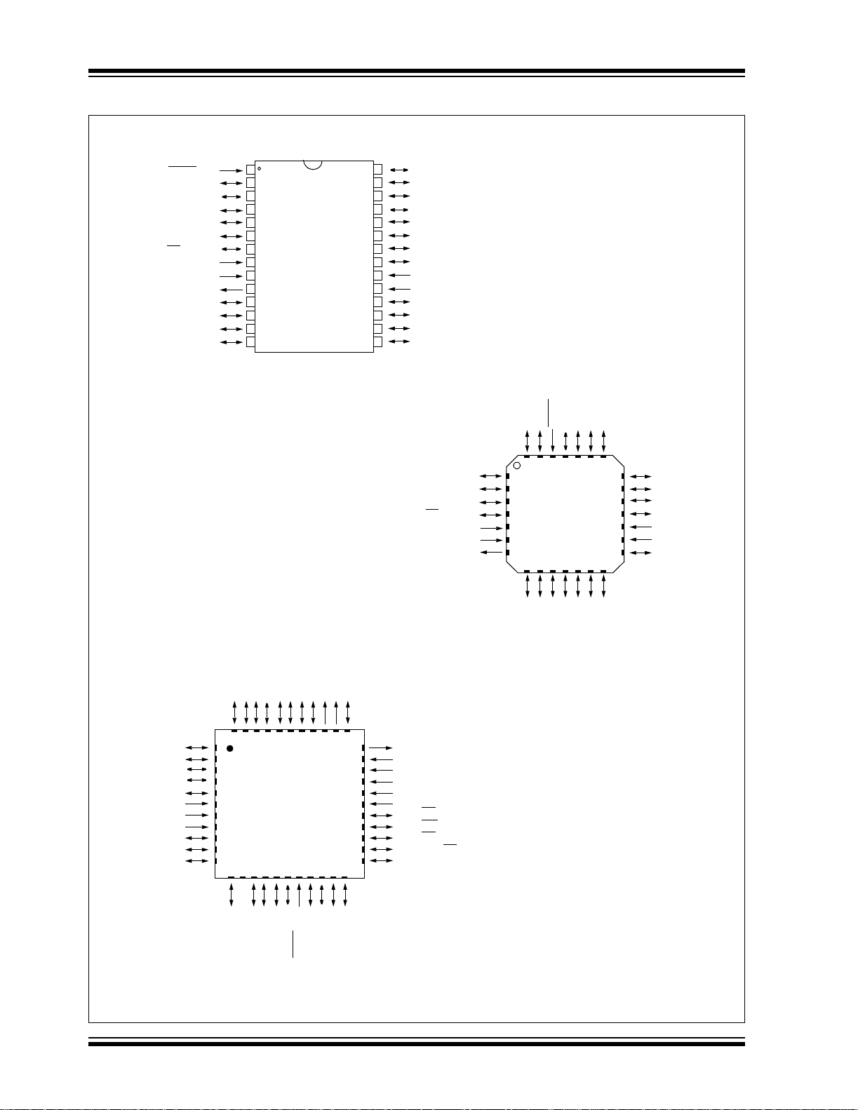
Pin Diagrams
28-Pin PDIP, SOIC, SSOP
MCLR/VPP
RA0/AN0
RA2/AN2/V
RA4/T0CKI/C1OUT
RA5/AN4/SS
RC0/T1OSO/T1CKI
RA1/AN1
REF-/CVREF
RA3/AN3/VREF+
OSC1/CLKI
OSC2/CLKO
RC1/T1OSI/CCP2
RC2/CCP1
RC3/SCK/SCL
/C2OUT
V
1
2
3
4
5
6
7
SS
8
9
10
11
12
13
14
PIC16F873A/876A
28
27
26
25
24
23
22
21
20
19
18
17
16
15
RB7/PGD
RB6/PGC
RB5
RB4
RB3/PGM
RB2
RB1
RB0/INT
V
DD
VSS
RC7/RX/DT
RC6/TX/CK
RC5/SDO
RC4/SDI/SDA
28-Pin QFN
RA1/AN1
RA0/AN0
RB7/PGD
RB6/PGC
RB5
RA2/AN2/VREF-/CVREF
RA3/AN3/VREF+
RA4/T0CKI/C1OUT
RA5/AN4/SS
/C2OUT
V
OSC1/CLKI
OSC2/CLKO
MCLR/VPP
26
27
28
1
2
3
PIC16F873A
4
PIC16F876A
SS
5
6
7
10
8
9
25
11
23
24
121314
RB4
22
21
20
19
18
17
16
15
RB3/PGM
RB2
RB1
RB0/INT
V
DD
VSS
RC7/RX/DT
44-Pin QFN
RC7/RX/DT
RD4/PSP4
RD5/PSP5
RD6/PSP6
RD7/PSP7
SS
V
VDD
VDD
RB0/INT
RB1
RB2
RC6/TX/CK
4443424140
1
2
3
4
5
6
7
8
9
10
11
121314
NC
RB3/PGM
RC5/SDO
RC4/SDI/SDA
RD3/PSP3
RD2/PSP2
RD1/PSP1
39
38
PIC16F874A
PIC16F877A
16
17
181920
15
RB5
RB4
RB6/PGC
RB7/PGD
/VPP
MCLR
RD0/PSP0
RC3/SCK/SCL
RC2/CCP1
363435
37
RA1/AN1
RA0/AN0
RC1/T1OSI/CCP2
33
32
31
30
29
28
27
26
25
24
23
22
21
REF+
REF-/CVREF
RA3/AN3/V
RA2/AN2/V
RC5/SDO
RC2/CCP1
RC1/T1OSI/CCP2
RC0/T1OSO/T1CKI
OSC2/CLKO
OSC1/CLKI
V
SS
VSS
VDD
VDD
RE2/CS/AN7
RE1/WR
/AN6
RE0/RD
/AN5
RA5/AN4/SS
RA4/T0CKI/C1OUT
/C2OUT
RC0/T1OSO/T1CKI
RC4/SDI/SDA
RC3/SCK/SCL
RC6/TX/CK
DS39582B-page 2 2003 Microchip Technology Inc.
Page 5

Pin Diagrams (Continued)
40-Pin PDIP
MCLR/VPP
RA0/AN0
RA2/AN2/V
RA4/T0CKI/C1OUT
RA5/AN4/SS
RC0/T1OSO/T1CKI
RA1/AN1
REF-/CVREF
RA3/AN3/VREF+
/C2OUT
RE0/RD
RE1/WR
RE2/CS
OSC1/CLKI
OSC2/CLKO
RC1/T1OSI/CCP2
RC2/CCP1
RC3/SCK/SCL
RD0/PSP0
RD1/PSP1
/AN5
/AN6
/AN7
V
DD
VSS
1
2
3
4
5
6
7
8
9
10
11
12
13
14
15
16
17
18
19
20
PIC16F87XA
40
39
38
37
36
35
34
33
32
31
30
29
28
27
PIC16F874A/877A
26
25
24
23
22
21
RB7/PGD
RB6/PGC
RB5
RB4
RB3/PGM
RB2
RB1
RB0/INT
V
DD
VSS
RD7/PSP7
RD6/PSP6
RD5/PSP5
RD4/PSP4
RC7/RX/DT
RC6/TX/CK
RC5/SDO
RC4/SDI/SDA
RD3/PSP3
RD2/PSP2
44-Pin PLCC
RA4/T0CKI/C1OUT
RA5/AN4/SS
RE0/RD
RE1/WR
RE2/CS
OSC1/CLKI
OSC2/CLKO
RC0/T1OSO/T1CK1
/C2OUT
/AN5
/AN6
/AN7
V
DD
VSS
NC
REF-/CVREF
/VPP
RA3/AN3/VREF+
RA1/AN1
RA0/AN0
MCLR
RA2/AN2/V
65432
7
8
9
10
11
PIC16F874A
12
PIC16F877A
13
14
15
16
17
181920212223242526
NC
1
RB7/PGD
44
RB6/PGC
43
RB5
42
RB4
41
27
NC
40
39
38
37
36
35
34
33
32
31
30
29
28
RB3/PGM
RB2
RB1
RB0/INT
V
DD
VSS
RD7/PSP7
RD6/PSP6
RD5/PSP5
RD4/PSP4
RC7/RX/DT
44-Pin TQFP
RC7/RX/DT
RD4/PSP4
RD5/PSP5
RD6/PSP6
RD7/PSP7
SS
V
VDD
RB0/INT
RB1
RB2
RB3/PGM
RC6/TX/CK
4443424140
1
2
3
4
5
6
7
8
9
10
11
121314
NC
RC5/SDO
RC4/SDI/SDA
RD3/PSP3
RD2/PSP2
RD1/PSP1
39
PIC16F874A
PIC16F877A
15
16
17
NC
RB5
RB4
RB7/PGD
RB6/PGC
RD0/PSP0
RC3/SCK/SCL
RC2/CCP1
RC1/T1OSI/CCP2
38
363435
37
1819202122
/VPP
RA1/AN1
RA0/AN0
MCLR
REF-/CVREF
RA2/AN2/V
NC
33
32
31
30
29
28
27
26
25
24
23
RA3/AN3/VREF+
NC
RC0/T1OSO/T1CKI
OSC2/CLKO
OSC1/CLKI
SS
V
VDD
RE2/CS/AN7
/AN6
RE1/WR
/AN5
RE0/RD
RA5/AN4/SS
RA4/T0CKI/C1OUT
/C2OUT
RC2/CCP1
RC1/T1OSI/CCP2
RD2/PSP2
RD1/PSP1
RD0/PSP0
RC3/SCK/SCL
RC5/SDO
RD3/PSP3
RC4/SDI/SDA
NC
RC6/TX/CK
2003 Microchip Technology Inc. DS39582B-page 3
Page 6

PIC16F87XA
Table of Contents
1.0 Device Overview......................................................................................................................................................................... 5
2.0 Memory Organization................................................................................................................................................................ 15
3.0 Data EEPROM and Flash Program Memory............................................................................................................................ 33
4.0 I/O Ports.................................................................................................................................................................................... 41
5.0 Timer0 Module............................................... .. .. ....... .. .. .. .... .. .. ....... .. .. .... .. .. .. ....... .. .. .... .. ............................................................ 53
6.0 Timer1 Module............................................... .. .. ....... .. .. .. .... .. .. ....... .. .. .... .. .. .. ....... .. .. .... .. ............................................................ 57
7.0 Timer2 Module............................................... .. .. ....... .. .. .. .... .. .. ....... .. .. .... .. .. .. ....... .. .. .... .. ............................................................ 61
8.0 Capture/Compare/PWM Modules............................................................................................................................................. 63
9.0 Master Synchronous Serial Port (MSSP) Module..................................................................................................................... 71
10.0 Addressable Universal Synchronous Asynchronous Receiver Transmitter (USART)............................................................ 111
11.0 Analog-to-Digital Converter (A/D) Module .................................................................... .... ......... ............................................. 127
12.0 Comparator Module................................................................................................................................................................ 135
13.0 Comparator Voltage Reference Module ................................................................. .... .. .... ......... ............................................. 141
14.0 Special Features of the CPU.................................................................................................................................................. 143
15.0 Instruction Set Summary.................... ............ ......................... ...................................... .......................................................... 159
16.0 Development Support............................................................. ....... .... .. .... .. ....... .... .. .... .. .... ...................................................... 167
17.0 Electrical Characteristics........................................... .............................................................................................................. 173
18.0 DC and AC Characteristics Graphs and Tables ..................................................................................................................... 197
19.0 Packaging Information............................................................................................................................................................ 209
Appendix A: Revision History............................................................................................................................................................ 219
Appendix B: Device Differences........................................................................................................................................................ 219
Appendix C:Conversion Considerations........................................................ .... .. ....... .... .. .... .. .... ...................................................... 220
Index ................................................................................................................................................................................................. 221
On-Line Support.................................................................. .. .... .... .. ......... .... .. .... .... ....... .... ................................................................ 229
Systems Information and Upgrade Hot Line..................................................................................................................................... 229
Reader Response............................................................................................................................................................................. 230
PIC16F87XA Product Identification System...................................................................................................................................... 231
TO OUR VALUED CUSTOMERS
It is our intention to provide our valued customers with the best documentation possible to ensure successful use of your Microchip
products. To this end, we will continue to improve our publications t o better suit your needs. Our publications will be refined and
enhanced as new volumes and updates are introduced.
If you have any questions or c omm ents regarding t his publication, p lease c ontact the M arket ing Co mmunications Department via
E-mail at docerrors@mail.microchip.com or fax the Reader Response Form in the back of this data sheet to (480) 792-4150.
We welcome your feedback.
Most Current Data Sheet
To obtain the most up-to-date version of this data sheet, please register at our Worldwide Web site at:
http://www.microchip.com
You can determine the version of a data sheet by examining its literature number found on the bottom outside corner of any page.
The last character of the literature number is the version number, (e.g., DS30000A is version A of document DS30000).
Errata
An errata sheet, describing minor operational differences from the data sheet and recommended workarounds, may exist for current
devices. As device/documentation issues become known to us, we will publish an errata sheet. The errata will specify the revision
of silicon and revision of document to which it applies.
To determine if an errata sheet exists for a particular device, please check with one of the following:
• Microchip’s Worldwide Web site; http://www.microchip.com
• Your local Microchip sales office (see last page)
• The Microchip Corporate Literature Center; U.S. FAX: (480) 792-7277
When contacting a sales office or the literature center, please specify which device, revision of silicon and data sheet (include literature number) you are using.
Customer Notification System
Register on our Web site at www.microchip.com/cn to receive the most current information on all of our products.
DS39582B-page 4 2003 Microchip Technology Inc.
Page 7

PIC16F87XA
1.0 DEVICE OVERVIEW
This document contains device specific information
about the following devices:
• PIC16F873A
• PIC16F874A
• PIC16F876A
• PIC16F877A
PIC16F873A/876A devic es are avail able on ly in 28-pi n
packages, while PIC16F874A/877A devices are available in 40-pin and 44-pin packages. All devices in the
PIC16F87XA family share common architecture with
the following differences:
• The PIC16F873A and PIC16F874A h ave one-hal f
of the total on-chip memory of the PIC16F876A
and PIC16F877A
• The 28-pin devices ha ve three I/ O ports , while the
40/44-pin devices have five
• The 28-pin device s have four teen interrupt s, while
the 40/44-pin devices have fifteen
• The 28-pin devices have five A/D input channels,
while the 40/44-pin devices have eight
• The Parallel Slave Port is implemented only on
the 40/44-pin devices
The available features are summarized in Table 1-1.
Block diagrams of the PIC16F873A/876A and
PIC16F874A/877A devices are provided in Figure 1-1
and Figure 1-2, respectively. The pinouts for these
device families are listed in Table 1-2 and Table 1-3.
Additional information may be found in the PICmicro
Mid-Range Reference Manual (DS33023), which may
be obtained from your local Microchip Sales Representative or downloaded from the Microchip web site. The
Reference Manual should be considered a complementary document to this data sheet and is highly recommended reading for a better understanding of the device
architecture and operation of the peripheral modules.
®
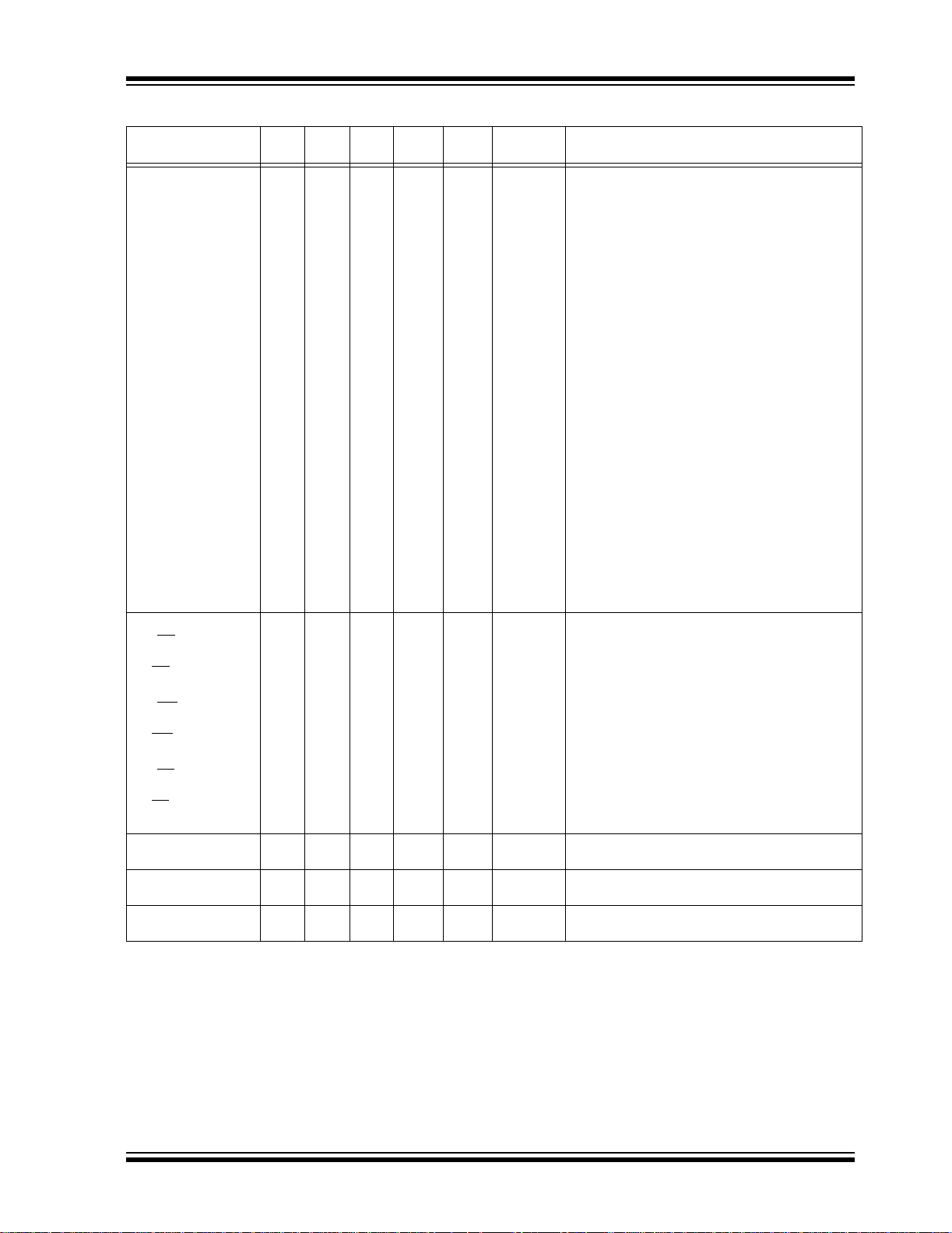
TABLE 1-1: PIC16F87XA DEVICE FEATURES
Key Features PIC16F873A PIC16F874A PIC16F876A PIC16F877A
Operating Frequency DC – 20 MHz DC – 20 MHz DC – 20 MHz DC – 20 MHz
Resets (and Delays) POR, BOR
(PWRT, OST)
Flash Program Memory
(14-bit words)
Data Memory (bytes) 192 192 368 368
EEPROM Data Memory (bytes) 128 128 256 256
Interrupts 14 15 14 15
I/O Ports Ports A, B, C Ports A, B, C, D, E Ports A, B, C Ports A, B, C, D, E
Timers 3333
Capture/Compare/PWM modules2222
Serial Communications MSSP, USART MSSP, USART MSSP, USART MSSP, USART
Parallel Communications — PSP — PSP
10-bit Analog-to-Digital Module 5 input channels 8 input channels 5 input channels 8 input channels
Analog Comparators 2222
Instruction Set 35 Instructions 35 Instructions 35 Instructions 35 Instructions
Packages 28-pin PDIP
4K 4K 8K 8K
28-pin SOIC
28-pin SSOP
28-pin QFN
POR, BOR
(PWRT, OST)
40-pin PDIP
44-pin PLCC
44-pin TQ FP
44-pin QFN
POR, BOR
(PWRT, OST)
28-pin PDIP
28-pin SOIC
28-pin SSOP
28-pin QFN
POR, BOR
(PWRT, OST)
40-pin PDIP
44-pin PLCC
44-pin TQFP
44-pin QFN
2003 Microchip Technology Inc. DS39582B-page 5
Page 8
PIC16F87XA
FIGURE 1-1: PIC16F873A/876A BLOCK DIAGRAM
Program
Bus
OSC1/CLKI
OSC2/CLKO
Flash
Program
Memory
14
Instruction reg
Instruction
Decode &
Control
Timing
Generation
13
Program Counter
8 Level Stack
Direct Addr
8
Power-up
Oscillator
Start-up Timer
Power-on
Watchdog
Brown-out
Debugger
Low-Voltage
Programming
(13-bit)
RAM Addr
7
Timer
Reset
Timer
Reset
In-Circuit
Data Bus
RAM
File
Registers
(1)
Addr MUX
3
ALU
8
W reg
9
Indirect
8
FSR reg
Status reg
MUX
8
Addr
PORTA
PORTB
PORTC
RA0/AN0
RA1/AN1
RA2/AN2/VREF-/CVREF
RA3/AN3/VREF+
RA4/T0CKI/C1OUT
RA5/AN4/SS
RB0/INT
RB1
RB2
RB3/PGM
RB4
RB5
RB6/PGC
RB7/PGD
RC0/T1OSO/T1CKI
RC1/T1OSI/CCP2
RC2/CCP1
RC3/SCK/SCL
RC4/SDI/SDA
RC5/SDO
RC6/TX/CK
RC7/RX/DT
/C2OUT
MCLR
Timer0 Timer1
Data EEPROM
Device Program Flash Data Memory Data EEPROM
PIC16F873A 4K words 192 Bytes 128 Bytes
PIC16F876A 8K words 368 Bytes 256 Bytes
Note 1: Higher order bi ts are from the Status regis ter .
CCP1,2
Timer2
Synchronous
Serial Port
VDD, VSS
10-bit A/D
USART
Comparator
Voltage
Reference
DS39582B-page 6 2003 Microchip Technology Inc.
Page 9
FIGURE 1-2: PIC16F874A/877A BLOCK DIAGRAM
Program
Bus
OSC1/CLKI
OSC2/CLKO
Flash
Program
Memory
14
Instruction reg
Instruction
Decode &
Control
Timing
Generation
13
Program Counter
8 Level Stack
Direct Addr
8
Power-up
Start-up Timer
Power-on
Watchdog
Brown-out
Debugger
Low-Voltage
Programming
MCLR
(13-bit)
RAM Addr
7
Timer
Oscillator
Reset
Timer
Reset
In-Circuit
VDD, VSS
Data Bus
RAM
File
Registers
(1)
Addr MUX
3
ALU
8
W reg
9
Indirect
8
Addr
FSR reg
Status reg
MUX
PIC16F87XA
8
PORTA
PORTB
PORTC
PORTD
PORTE
RA0/AN0
RA1/AN1
RA2/AN2/VREF-/CVREF
RA3/AN3/VREF+
RA4/T0CKI/C1OUT
RA5/AN4/SS
RB0/INT
RB1
RB2
RB3/PGM
RB4
RB5
RB6/PGC
RB7/PGD
RC0/T1OSO/T1CKI
RC1/T1OSI/CCP2
RC2/CCP1
RC3/SCK/SCL
RC4/SDI/SDA
RC5/SDO
RC6/TX/CK
RC7/RX/DT
RD0/PSP0
RD1/PSP1
RD2/PSP2
RD3/PSP3
RD4/PSP4
RD5/PSP5
RD6/PSP6
RD7/PSP7
RE0/RD
RE1/WR
RE2/CS
/C2OUT
/AN5
/AN6
/AN7
Timer0 Timer1
Data EEPROM
Device Program Flash Data Memory Data EEPROM
PIC16F874A 4K words 192 Bytes 128 Bytes
PIC16F877A 8K words 368 Bytes 256 Bytes
Note 1: Higher order bits are from the Status register.
CCP1,2
Timer2
Synchronous
Serial Por t
10-bit A/D
USART
Comparator
Parallel
Slave Port
Voltage
Reference
2003 Microchip Technology Inc. DS39582B-page 7
Page 10

PIC16F87XA
TABLE 1-2: PIC16F873A/876A PINOUT DESCRIPTION
Pin Name
OSC1/CLKI
OSC1
CLKI
OSC2/CLKO
OSC2
CLKO
/VPP
MCLR
MCLR
VPP
RA0/AN0
RA0
AN0
RA1/AN1
RA1
AN1
RA2/AN2/V
CV
RA3/AN3/V
RA4/T0CKI/C1OUT
RA5/AN4/SS
Legend: I = input O = output I/O = input/output P = power
Note 1: This buffer is a Schmitt Trigger input when configured as the external interrupt.
REF-/
REF
RA2
AN2
V
REF-
REF
CV
REF+
RA3
AN3
REF+
V
RA4
T0CKI
C1OUT
/C2OUT
RA5
AN4
SS
C2OUT
— = Not used TTL = TTL input ST = Schmitt Trigger input
2: This buffer is a Schmitt Trigger input when used in Serial Programming mode.
3: This buffer is a Schmitt Trigger input when configured in RC Oscillator mode and a CMOS input otherwise.
PDIP , SOIC,
SSOP Pin#
9
10 7
126
227
328
41
52
63
74
QFN
Pin#
6
I/O/P
Type
I
I
O
O
I
P
I/O
I
I/O
I
I/O
I
I
O
I/O
I
I
I/O
I
O
I/O
I
I
O
Buffer
Type
(3)
ST/CMOS
— Oscillator crystal or clock output.
ST Master Clear (input) or programming voltage (output).
TTL
TTL
TTL
TTL
ST
TTL
Oscillator crystal or external clock input.
Oscillator crystal input or external clock source input. ST
buffer when configured in RC mode; otherwise CMOS.
External clock source input. Always associated with pin
function OSC1 (see OSC1/CLKI, OSC2/CLKO pins).
Oscillator crystal output. Connects to crystal or resonator
in Crystal Oscillator mode.
In RC mode, OSC2 pin outputs CLKO, which has 1/4 the
frequency of OSC1 and denotes the instruction cycle rate.
Master Clear (Reset) input. This pin is an active low Reset
to the device.
Programming voltage input.
PORTA is a bidirectional I/O port.
Digital I/O.
Analog input 0.
Digital I/O.
Analog input 1.
Digital I/O.
Analog input 2.
A/D reference voltage (Low) input.
Comparator V
Digital I/O.
Analog input 3.
A/D reference voltage (High) input.
Digital I/O – Open-drain when configured as output.
Timer0 external clock input.
Comparator 1 output.
Digital I/O.
Analog input 4.
SPI slave select input.
Comparator 2 output.
Description
REF output.
DS39582B-page 8 2003 Microchip Technology Inc.
Page 11

PIC16F87XA
TABLE 1-2: PIC16F873A/876A PINOUT DESCRIPTION (CONTINUED)
Pin Name
RB0/INT
RB0
INT
RB1
RB2
RB3/PGM
RB3
PGM
RB4
RB5
RB6/PGC
RB6
PGC
RB7/PGD
RB7
PGD
RC0/T1OSO/T1CKI
RC0
T1OSO
T1CKI
RC1/T1OSI/CCP2
RC1
T1OSI
CCP2
RC2/CCP1
RC2
CCP1
RC3/SCK/SCL
RC3
SCK
SCL
RC4/SDI/SDA
RC4
SDI
SDA
RC5/SDO
RC5
SDO
RC6/TX/CK
RC6
TX
CK
RC7/RX/DT
RC7
RX
DT
SS 8, 19 5, 6 P — Ground reference for logic and I/O pins.
V
DD 20 17 P — Positive supply for logic and I/O pins.
V
Legend: I = input O = output I/O = input/output P = power
Note 1: This buffer is a Schmitt Trigger input when configured as the external interrupt.
— = Not used TTL = TTL input ST = Schmitt Trigger input
2: This buffer is a Schmitt Trigger input when used in Serial Programming mode.
3: This buffer is a Schmitt Trigger input when configured in RC Oscillator mode and a CMOS input otherwise.
PDIP , SOIC,
SSOP Pin#
21 18
22 19 I/O TTL
23 20 I/O TTL
24 21
25 22 I/O TTL
26 23 I/O TTL
27 24
28 25
11 8
12 9
13 10
14 11
15 12
16 13
17 14
18 15
QFN
Pin#
I/O/P
Type
I/O
I
I/O
I
I/O
I
I/O
I/O
I/O
O
I
I/O
I
I/O
I/O
I/O
I/O
I/O
I/O
I/O
I
I/O
I/O
O
I/O
O
I/O
I/O
I
I/O
Buffer
Type
TTL/ST
TTL
TTL/ST
TTL/ST
ST
ST
ST
ST
ST
ST
ST
ST
Description
PORTB is a bidirectional I/O port. PORTB can be software
programmed for internal weak pull-ups on all inputs.
(1)
Digital I/O.
External interrupt.
Digital I/O.
Digital I/O.
Digital I/O.
Low-voltage (single-supply) ICSP programming enable pin.
Digital I/O.
(2)
(2)
Digital I/O.
Digital I/O.
In-circuit debugger and ICSP programming clock.
Digital I/O.
In-circuit debugger and ICSP programming data.
PORTC is a bidirectional I/O port.
Digital I/O.
Timer1 oscillator output.
Timer1 external clock input.
Digital I/O.
Timer1 oscillator input.
Capture2 input, Compare2 output, PWM2 output.
Digital I/O.
Capture1 input, Compare1 output, PWM1 output.
Digital I/O.
Synchronous serial clock input/output for SPI mode.
Synchronous serial clock input/output for I
Digital I/O.
SPI data in.
2
C data I/O.
I
Digital I/O.
SPI data out.
Digital I/O.
USART asynchronous transmit.
USART1 synchronous clock.
Digital I/O.
USART asynchronous receive.
USART synchronous data.
2
C mode.
2003 Microchip Technology Inc. DS39582B-page 9
Page 12
PIC16F87XA
TABLE 1-3: PIC16F874A/877A PINOUT DESCRIPTION
PDIP
PLCC
Pin Name
OSC1/CLKI
OSC1
CLKI
OSC2/CLKO
OSC2
CLKO
/VPP
MCLR
MCLR
VPP
RA0/AN0
RA0
AN0
RA1/AN1
RA1
AN1
RA2/AN2/V
RA3/AN3/V
RA4/T0CKI/C1OUT
RA5/AN4/SS
Legend: I = input O = output I/O = input/output P = power
Note 1: This buffer is a Schmitt Trigger input when configured as the external interrupt.
REF-/CVREF
RA2
AN2
V
REF-
REF
CV
REF+
RA3
AN3
REF+
V
RA4
T0CKI
C1OUT
/C2OUT
RA5
AN4
SS
C2OUT
— = Not used TTL = TTL input ST = Schmitt Trigger input
2: This buffer is a Schmitt Trigger input when used in Serial Programming mode.
3: This buffer is a Schmitt Trigger input when configured in RC Oscillator mode and a CMOS input otherwise.
Pin#
13 14 30 32
14 15 31 33
1 2 18 18
2 3 19 19
3 4 20 20
4 5 21 21
5 6 22 22
6 7 23 23
7 8 24 24
Pin#
TQFP
Pin#
QFN
Pin#
I/O/P
Type
I
I
O
O
I
P
I/O
I
I/O
I
I/O
I
I
O
I/O
I
I
I/O
I
O
I/O
I
I
O
Buffer
Type
(4)
ST/CMOS
ST Master Clear (input) or programming voltage (output).
TTL
TTL
TTL
TTL
ST
TTL
Oscillator crystal or external clock input.
Oscillator crystal input or external clock source
input. ST buffer when configured in RC mode;
otherwise CMOS.
External clock source input. Always associated
with pin function OSC1 (see OSC1/CLKI,
OSC2/CLKO pins).
— Oscillator crystal or clock output.
Oscillator crystal output.
Connects to crystal or resonator in Crystal
Oscillator mode.
In RC mode, OSC2 pin outputs CLKO, which
has 1/4 the frequency of OSC1 and denotes the
instruction cycle rate.
Master Clear (Reset) input. This pin is an active
low Reset to the device.
Programming voltage input.
PORTA is a bidirectional I/O port.
Digital I/O.
Analog input 0.
Digital I/O.
Analog input 1.
Digital I/O.
Analog input 2.
A/D reference voltage (Low) input.
Comparator V
Digital I/O.
Analog input 3.
A/D reference voltage (High) input.
Digital I/O – Open-drain when configured as
output.
Timer0 external clock input.
Comparator 1 output.
Digital I/O.
Analog input 4.
SPI slave select input.
Comparator 2 output.
Description
REF output.
DS39582B-page 10 2003 Microchip Technology Inc.
Page 13

PIC16F87XA
TABLE 1-3: PIC16F874A/877A PINOUT DESCRIPTION (CONTINUED)
PDIP
PLCC
Pin Name
RB0/INT
RB0
INT
RB1 34 37 9
RB2 35 38 10
RB3/PGM
RB3
PGM
RB4 37 41 14
RB5 38 42 15
RB6/PGC
RB6
PGC
RB7/PGD
RB7
PGD
Legend: I = input O = output I/O = input/output P = power
— = Not used TTL = TTL input ST = Schmitt Trigger input
Note 1: This buffer is a Schmitt Trigger input when configured as the external interrupt.
2: This buffer is a Schmitt Trigger input when used in Serial Programming mode.
3: This buffer is a Schmitt Trigger input when configured in RC Oscillator mode and a CMOS input otherwise.
Pin#
33 36 8
36 39 11
39 43 16
40 44 17
Pin#
TQFP
Pin#
QFN
Pin#
9
10 I/O
11 I/O
12
14 I/O
15 I/O
16
17
I/O/P
Type
I/O
I
I/O
I
I/O
I
I/O
I/O
Buffer
Type
PORTB is a bidirectional I/O port. PORTB can be
software programmed for internal weak pull-up on all
inputs.
(1)
TTL/ST
Digital I/O.
External interrupt.
TTL Digital I/O.
TTL Digital I/O.
TTL
TTL Digital I/O.
TTL Digital I/O.
TTL/ST
TTL/ST
Digital I/O.
Low-voltage ICSP programming enable pin.
(2)
Digital I/O.
In-circuit debugger and ICSP programming clock.
(2)
Digital I/O.
In-circuit debugger and ICSP programming data.
Description
2003 Microchip Technology Inc. DS39582B-page 11
Page 14

PIC16F87XA
TABLE 1-3: PIC16F874A/877A PINOUT DESCRIPTION (CONTINUED)
PDIP
PLCC
Pin Name
RC0/T1OSO/T1CKI
RC0
T1OSO
T1CKI
RC1/T1OSI/CCP2
RC1
T1OSI
CCP2
RC2/CCP1
RC2
CCP1
RC3/SCK/SCL
RC3
SCK
SCL
RC4/SDI/SDA
RC4
SDI
SDA
RC5/SDO
RC5
SDO
RC6/TX/CK
RC6
TX
CK
RC7/RX/DT
RC7
RX
DT
Legend: I = input O = output I/O = input/output P = power
— = Not used TTL = TTL input ST = Schmitt Trigger input
Note 1: This buffer is a Schmitt Trigger input when configured as the external interrupt.
2: This buffer is a Schmitt Trigger input when used in Serial Programming mode.
3: This buffer is a Schmitt Trigger input when configured in RC Oscillator mode and a CMOS input otherwise.
Pin#
15 16 32 34
16 18 35 35
17 19 36 36
18 20 37 37
23 25 42 42
24 26 43 43
25 27 44 44
26 29 1 1
Pin#
TQFP
Pin#
QFN
Pin#
I/O/P
Type
I/O
O
I
I/O
I
I/O
I/O
I/O
I/O
I/O
I/O
I/O
I
I/O
I/O
O
I/O
O
I/O
I/O
I
I/O
Buffer
Type
ST
ST
ST
ST
ST
ST
ST
ST
Description
PORTC is a bidirectional I/O port.
Digital I/O.
Timer1 oscillator output.
Timer1 external clock input.
Digital I/O.
Timer1 oscillator input.
Capture2 i nput, Comp are2 output , PWM2 output.
Digital I/O.
Capture1 i nput, Comp are1 output , PWM1 output.
Digital I/O.
Synchronous serial clock input/output for SPI
mode.
Synchronous serial clock input/output for I
mode.
Digital I/O.
SPI data in.
2
C data I/O.
I
Digital I/O.
SPI data out.
Digital I/O.
USART asynchronous transmit.
USART1 synchronous clock.
Digital I/O.
USART asynchronous receive.
USART synchronous data.
2
C
DS39582B-page 12 2003 Microchip Technology Inc.
Page 15
PIC16F87XA
TABLE 1-3: PIC16F874A/877A PINOUT DESCRIPTION (CONTINUED)
PDIP
PLCC
Pin Name
RD0/PSP0
Pin#
19 21 38 38
Pin#
TQFP
Pin#
RD0
PSP0
RD1/PSP1
20 22 39 39
RD1
PSP1
RD2/PSP2
21 23 40 40
RD2
PSP2
RD3/PSP3
22 24 41 41
RD3
PSP3
RD4/PSP4
27 30 2 2
RD4
PSP4
RD5/PSP5
28 31 3 3
RD5
PSP5
RD6/PSP6
29 32 4 4
RD6
PSP6
RD7/PSP7
30 33 5 5
RD7
PSP7
RE0/RD
/AN5
8 9 25 25
RE0
RD
AN5
RE1/WR
/AN6
9102626
RE1
WR
AN6
RE2/CS
/AN7
10 11 27 27
RE2
CS
AN7
SS 12, 31 13, 34 6, 29 6, 30,
V
DD 11, 32 12, 35 7, 28 7, 8,
V
NC — 1, 17,
28, 40
12,13,
33, 34
Legend: I = input O = output I/O = input/output P = power
— = Not used TTL = TTL input ST = Schmitt Trigger input
Note 1: This buffer is a Schmitt Trigger input when configured as the external interrupt.
2: This buffer is a Schmitt Trigger input when used in Serial Programming mode.
3: This buffer is a Schmitt Trigger input when configured in RC Oscillator mode and a CMOS input otherwise.
QFN
Pin#
I/O/P
Type
Buffer
Type
Description
PORTD is a bidirectional I/O port or Parallel Slave
Port when interfacing to a microprocessor bus.
(3)
ST/TTL
I/O
I/O
ST/TTL
I/O
I/O
ST/TTL
I/O
I/O
ST/TTL
I/O
I/O
ST/TTL
I/O
I/O
ST/TTL
I/O
I/O
ST/TTL
I/O
I/O
ST/TTL
I/O
I/O
Digital I/O.
Parallel Slave Port data.
(3)
Digital I/O.
Parallel Slave Port data.
(3)
Digital I/O.
Parallel Slave Port data.
(3)
Digital I/O.
Parallel Slave Port data.
(3)
Digital I/O.
Parallel Slave Port data.
(3)
Digital I/O.
Parallel Slave Port data.
(3)
Digital I/O.
Parallel Slave Port data.
(3)
Digital I/O.
Parallel Slave Port data.
PORTE is a bidirectional I/O port.
(3)
ST/TTL
I/O
I
I
ST/TTL
I/O
I
I
ST/TTL
I/O
I
I
Digital I/O.
Read control for Parallel Slave Port.
Analog input 5.
(3)
Digital I/O.
Write control for Parallel Slave Port.
Analog input 6.
(3)
Digital I/O.
Chip select control for Parallel Slave Port.
Analog input 7.
P — Ground reference for logic and I/O pins.
31
P — Positive supply for logic and I/O pins.
28, 29
13 — — These pins are not internally connected. These pins
should be left unconnected.
2003 Microchip Technology Inc. DS39582B-page 13
Page 16

PIC16F87XA
NOTES:
DS39582B-page 14 2003 Microchip Technology Inc.
Page 17
PIC16F87XA
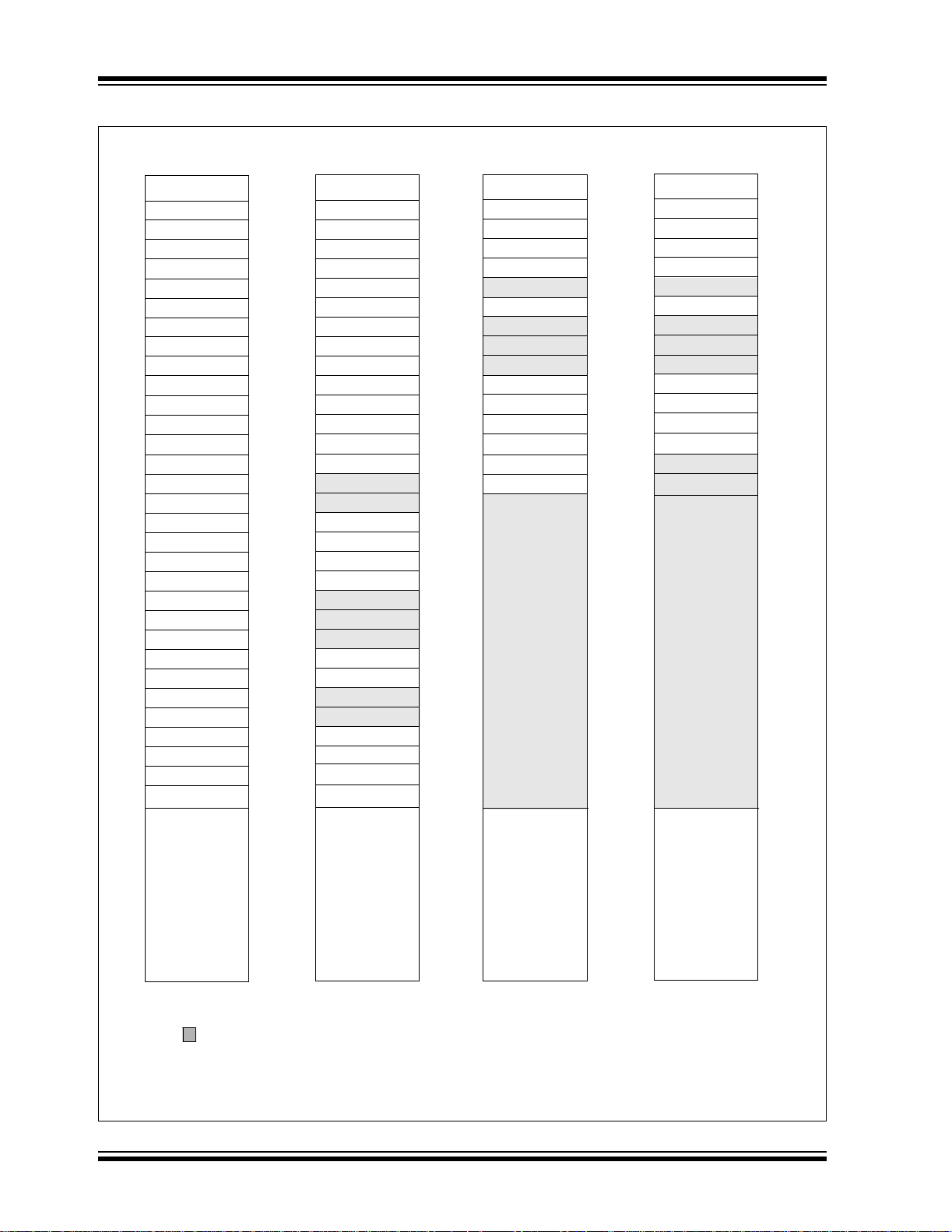
2.0 MEMORY ORGANIZATION
There are three memory blocks in each of the
PIC16F87XA devices. The program memory and data
memory have separate buses so that concurrent
access can oc cur and is detailed in this section. The
EEPROM data memory blo ck is deta iled in Section 3.0
“Data EEPROM and Flash Program Memory”.
Additional informa tion on devi ce memory may be found
in the PIC micro
Manual (DS33023).
FIGURE 2-1: PIC16F876A/877A
CALL, RETURN
RETFIE, RETLW
®
Mid-Range MCU Family Reference
PROGRAM MEMORY MAP
AND STACK
PC<12:0>
13
Stack Level 1
Stack Level 2
2.1 Program Memory Organization
The PIC16F87XA devices have a 13-bit program
counter capable of addressing an 8K word x 14 bit
program memory space. The PIC16F876A/877A
devices have 8K words x 14 bits of Flash program
memory, while PIC16F873A/874A devices have
4K words x 14 bits. Accessing a location above the
physically implemented address will cause a
wraparound.
The Reset vector is at 0000h an d the interrupt vec tor is
at 0004h.
FIGURE 2-2: PIC16F873A/874A
PROGRAM MEMO RY MAP
AND STACK
PC<12:0>
CALL, RETURN
RETFIE, RETLW
Stack Level 1
Stack Level 2
13
On-Chip
Program
Memory
Stack Level 8
Reset Vector
Interrupt Vector
Page 0
Page 1
Page 2
Page 3
0000h
0004h
0005h
07FFh
0800h
0FFFh
1000h
17FFh
1800h
1FFFh
On-Chip
Program
Memory
Stack Level 8
Reset Vector
Interrupt Vector
Page 0
Page 1
0000h
0004h
0005h
07FFh
0800h
0FFFh
1000h
1FFFh
2003 Microchip Technology Inc. DS39582B-page 15
Page 18
PIC16F87XA
2.2 Data Memory Organization
The data memory is partitioned into multiple banks
which contain the General Purpose Registers and the
Special Function Registers. Bits RP1 (Status<6>) and
RP0 (Status<5>) are the bank select bits.
RP1:RP0 Bank
00 0
01 1
10 2
11 3
Each bank extends up to 7Fh (128 bytes). The lower
locations of each bank are reserved for the Special
Function Registers. Ab ove the Speci al Function Registers are General Purpose Registers, implemented as
static RAM. All implemented banks contain Special
Function Registers. Some frequently used Special
Function Registers from one bank may be mirrored in
another bank for code reduction and quicker access.
Note: The EEPROM data memory description can
be found in Section 3.0 “Data EEPROM
and Flash Program Memory” of this data
sheet.
2.2.1 GENERAL PURPOSE REGISTER FILE
The register file can be accessed either directly, or
indirectly, through the File Select Register (FSR).
DS39582B-page 16 2003 Microchip Technology Inc.
Page 19
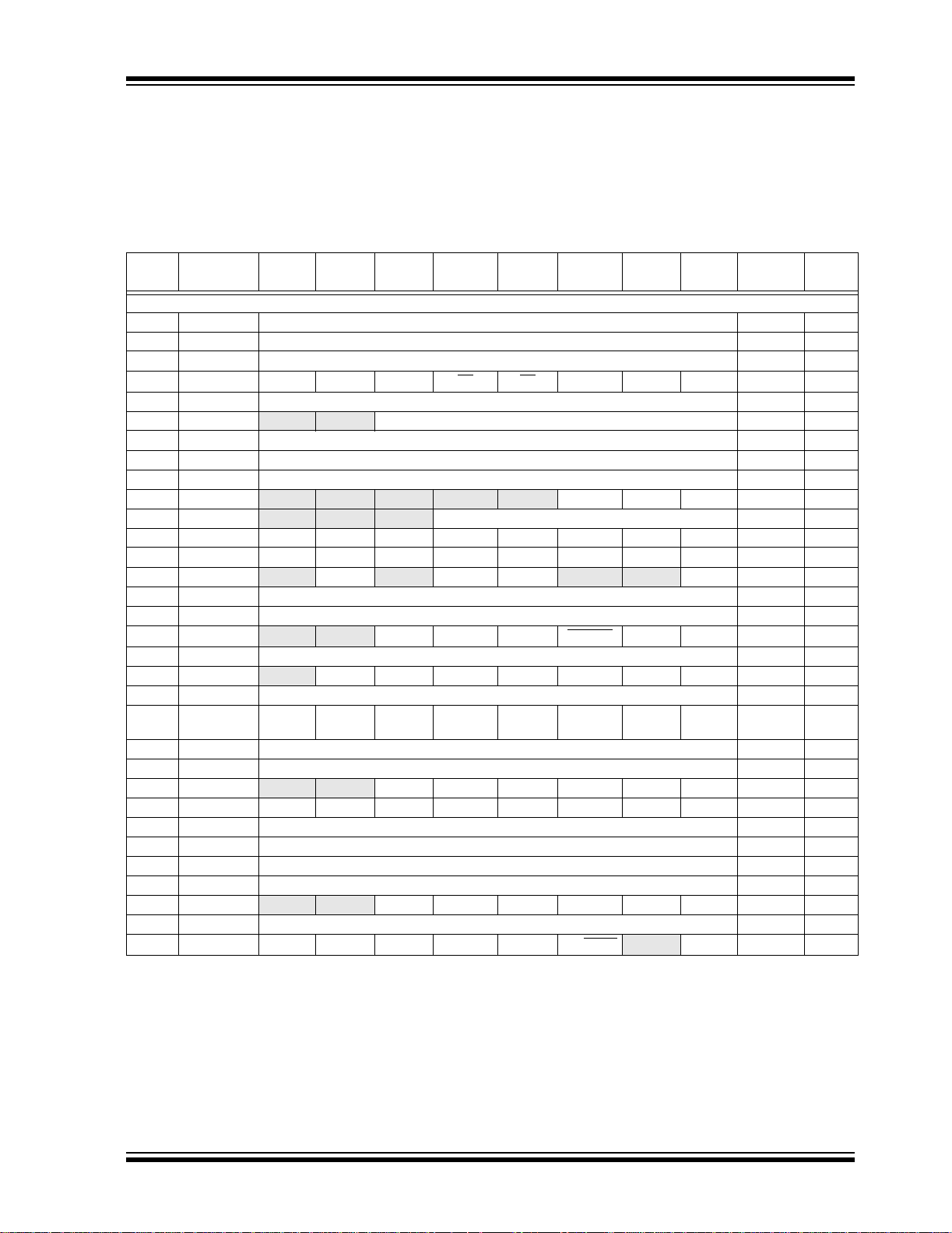
FIGURE 2-3: PIC16F876A/877A REGISTER FI LE MAP
PIC16F87XA
Indirect addr.
TMR0
PCL
STATUS
FSR
PORTA
PORTB
PORTC
PORTD
PORTE
(1)
(1)
PCLATH
INTCON
PIR1
PIR2
TMR1L
TMR1H
T1CON
TMR2
T2CON
SSPBUF
SSPCON
CCPR1L
CCPR1H
CCP1CON
RCSTA
TXREG
RCREG
CCPR2L
CCPR2H
CCP2CON
ADRESH
ADCON0
General
Purpose
Register
96 Bytes
Bank 0
File
Address
(*)
00h
01h
02h
03h
04h
05h
06h
07h
08h
09h
0Ah
0Bh
0Ch
0Dh
0Eh
0Fh
10h
11h
12h
13h
14h
15h
16h
17h
18h
19h
1Ah
1Bh
1Ch
1Dh
1Eh
1Fh
20h
7Fh
Indirect addr.
OPTION_REG
PCL
STATUS
FSR
TRISA
TRISB
TRISC
(1)
TRISD
(1)
TRISE
PCLATH
INTCON
PIE1
PIE2
PCON
SSPCON2
PR2
SSPADD
SSPSTAT
TXSTA
SPBRG
CMCON
CVRCON
ADRESL
ADCON1
General
Purpose
Register
80 Bytes
accesses
70h-7Fh
Bank 1
File
Address
(*)
80h
81h
82h
83h
84h
85h
86h
87h
88h
89h
8Ah
8Bh
8Ch
8Dh
8Eh
8Fh
90h
91h
92h
93h
94h
95h
96h
97h
98h
99h
9Ah
9Bh
9Ch
9Dh
9Eh
9Fh
A0h
EFh
F0h
FFh
Indirect addr.
TMR0
PCL
STATUS
FSR
PORTB
PCLATH
INTCON
EEDATA
EEADR
EEDATH
EEADRH
General
Purpose
Register
16 Bytes
General
Purpose
Register
80 Bytes
accesses
70h-7Fh
Bank 2
File
Address
(*)
100h
101h
102h
103h
104h
105h
106h
107h
108h
109h
10Ah
10Bh
10Ch
10Dh
10Eh
10Fh
110h
111h
112h
113h
114h
115h
116h
117h
118h
119h
11Ah
11Bh
11Ch
11Dh
11Eh
11Fh
120h
16Fh
170h
17Fh
Indirect addr.
OPTION_REG
PCL
STATUS
FSR
TRISB
PCLATH
INTCON
EECON1
EECON2
Reserved
Reserved
(2)
(2)
General
Purpose
Register
16 Bytes
General
Purpose
Register
80 Bytes
accesses
70h - 7Fh
Bank 3
File
Address
(*)
180h
181h
182h
183h
184h
185h
186h
187h
188h
189h
18Ah
18Bh
18Ch
18Dh
18Eh
18Fh
190h
191h
192h
193h
194h
195h
196h
197h
198h
199h
19Ah
19Bh
19Ch
19Dh
19Eh
19Fh
1A0h
1EFh
1F0h
1FFh
Unimplemented data memory locations, read as ‘0’.
* Not a physical register.
Note 1: These registers are not implemented on the PIC16F876A.
2: These registers are reserved; maintain these registers clear.
2003 Microchip Technology Inc. DS39582B-page 17
Page 20
PIC16F87XA
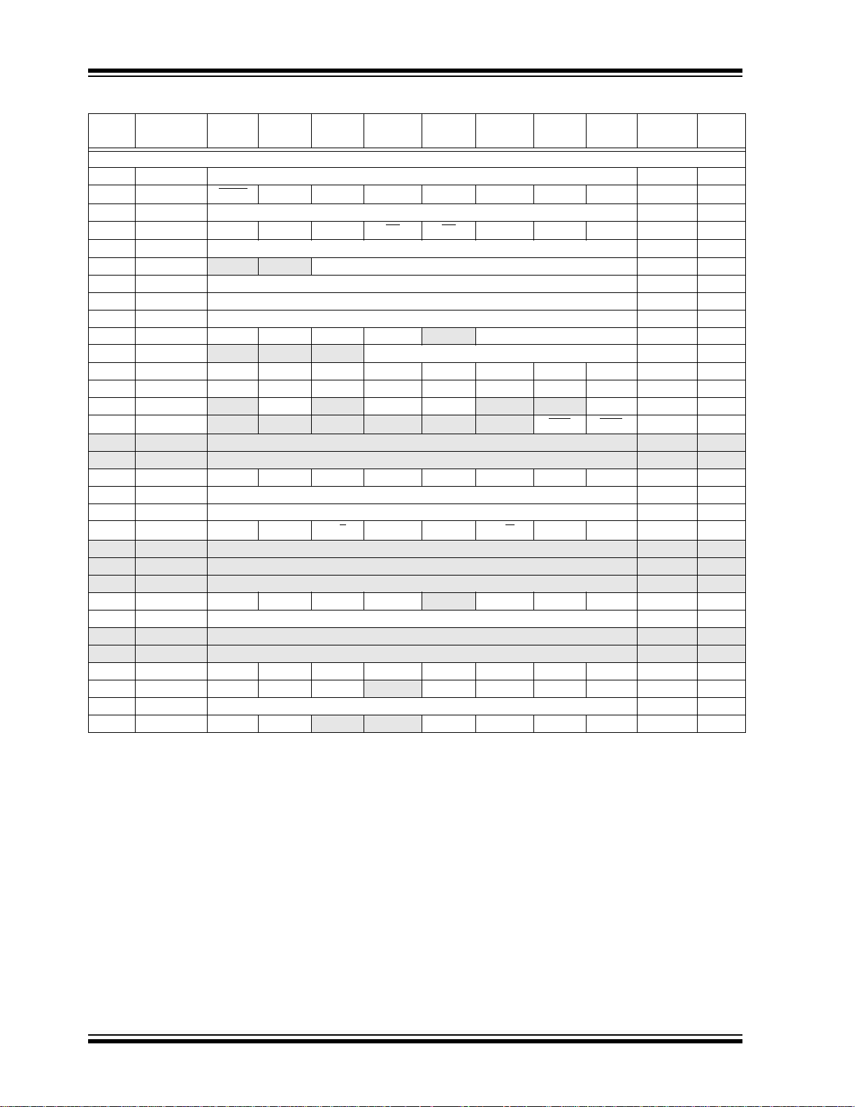
FIGURE 2-4: PIC16F873A/874A REGISTER FI LE MAP
Indirect addr.
TMR0
PCL
STATUS
FSR
PORTA
PORTB
PORTC
PORTD
PORTE
(1)
(1)
PCLATH
INTCON
PIR1
PIR2
TMR1L
TMR1H
T1CON
TMR2
T2CON
SSPBUF
SSPCON
CCPR1L
CCPR1H
CCP1CON
RCSTA
TXREG
RCREG
CCPR2L
CCPR2H
CCP2CON
ADRESH
ADCON0
File
Address
(*)
00h
01h
02h
03h
04h
05h
06h
07h
08h
09h
0Ah
0Bh
0Ch
0Dh
0Eh
0Fh
10h
11h
12h
13h
14h
15h
16h
17h
18h
19h
1Ah
1Bh
1Ch
1Dh
1Eh
1Fh
20h
Indirect addr.
OPTION_REG
PCL
STATUS
FSR
TRISA
TRISB
TRISC
(1)
TRISD
(1)
TRISE
PCLATH
INTCON
PIE1
PIE2
PCON
SSPCON2
PR2
SSPADD
SSPSTAT
TXSTA
SPBRG
CMCON
CVRCON
ADRESL
ADCON1
File
Address
(*)
80h
81h
82h
83h
84h
85h
86h
87h
88h
89h
8Ah
8Bh
8Ch
8Dh
8Eh
8Fh
90h
91h
92h
93h
94h
95h
96h
97h
98h
99h
9Ah
9Bh
9Ch
9Dh
9Eh
9Fh
A0h
Indirect addr.
TMR0
PCL
STAT US
FSR
PORTB
PCLATH
INTCON
EEDATA
EEADR
EEDATH
EEADRH
File
Address
(*)
100h
101h
102h
103h
104h
105h
106h
107h
108h
109h
10Ah
10Bh
10Ch
10Dh
10Eh
10Fh
110h
120h
Indirect addr.
OPTION_REG
PCL
STATUS
FSR
TRISB
PCLATH
INTCON
EECON1
EECON2
Reserved
Reserved
(2)
(2)
File
Address
(*)
180h
181h
182h
183h
184h
185h
186h
187h
188h
189h
18Ah
18Bh
18Ch
18Dh
18Eh
18Fh
190h
1A0h
General
Purpose
Register
96 Bytes
7Fh
Bank 0
General
Purpose
Register
96 Bytes
Bank 1
FFh
accesses
20h-7Fh
Bank 2
16Fh
170h
17Fh
accesses
A0h - FFh
1EFh
1F0h
1FFh
Bank 3
Unimplemented data memory locations, read as ‘0’.
* Not a physical register.
Note 1: These registers are not implemented on the PIC16F873A.
2: These registers are reserved; maintain these r egisters clear.
DS39582B-page 18 2003 Microchip Technology Inc.
Page 21
PIC16F87XA
2.2.2 SPECIAL FUNCTION REGISTERS
The Special Function Registers are registers used by
the CPU and peripheral modules for controlling the
desired operation of the device. These registers are
implemented as static RAM. A list of these registers is
given in Table 2-1.
The Special Function Registers can be classified into
two sets: core (CPU) and peripheral. Those registers
associated with the core functions are described in
detail in this section. Those related to the operation of
the peripheral features are described in detail in the
peripheral features section.
TABLE 2-1: SPECIAL FUNCTION REGISTER SUMMARY
Address Name Bit 7 Bit 6 Bit 5 Bit 4 Bit 3 Bit 2 Bit 1 Bit 0
Bank 0
(3)
00h
01h TMR0 Timer0 Mo dule Register xxxx xxxx 55, 150
02h
03h
04h
05h PORTA
06h PORTB PORTB Data Latch when written: PORTB pins when read xxxx xxxx 45, 150
07h PORTC PORTC Data Latch when written: POR TC pins when read xxxx xxxx 47, 150
08h
09h
0Ah
0Bh
0Ch PIR1 PSPIF
0Dh PIR2
0Eh TMR1L Holding Register for th e Least Sign ifican t Byte of the 16-bit TMR1 Register xxxx xxxx 60, 150
0Fh TMR1H Holding Register for the Most Significant Byte of t he 16-bi t TMR1 Register xxxx xxxx 60, 150
10h T1CON
11h TMR2 Timer2 Module Register 0000 0000 62, 150
12h T2CON
13h SSPBUF Synchronous Serial Port Receive Buffer/Transmit Register xxxx xxxx 79, 150
14h SSPCON WCOL SSPOV SSPEN CKP SSPM3 SSPM2 SSPM1 SSPM0 0000 0000 82, 82,
15h CCPR1L Capture/Compare/P WM Register 1 (LSB ) xxxx xxxx 63, 150
16h CCPR1H Capture/Compare/PWM Register 1 (MSB) xxxx xxxx 63, 150
17h CCP1CON
18h RCSTA SPEN RX9 SREN CREN ADDEN FERR OERR RX9D 0000 000x 112, 150
19h TXREG USART Transmit Data Register 0000 0000 118 , 150
1Ah RCREG USART Receive Data Register 0000 0000 118 , 150
1Bh CCPR2L Capture/Compar e/PWM Regist er 2 (LSB) xxxx xxxx 63, 150
1Ch CCPR2H Capture/Compare/PWM Register 2 (MSB) xxxx xxxx 63, 150
1Dh CCP2CON
1Eh ADRESH A/D Result Register High Byte xxxx xxxx 133, 150
1Fh ADCON0 ADCS1 ADCS0 CHS2 CHS1 CHS0 GO/DONE —ADON0000 00-0 127, 150
Legend: x = unknown, u = unchanged, q = value depends on condition, - = unimplemented, read as ‘0’, r = reserved.
Note 1: The upper byte of the program counter is not directly accessible. PCLA TH is a holding register for the PC<12:8>, whose
INDF Addressing this location uses contents of FSR to address data memory (not a physical regist er) 0000 0000 31, 150
(3)
PCL Program Counter (PC) Least Significant Byte 0000 0000 30, 150
(3)
STATUS IRP RP1 RP0 TO PD ZDCC0001 1xxx 22, 150
(3)
FSR Indirect Data Memory Address Pointer xxxx xxxx 31, 150
— — PORTA Dat a Latch when written: PO R TA pins when read --0x 0000 43, 150
(4)
PORTD PORTD Data Latch when written: POR TD pins when read xxxx xxxx 48, 150
(4)
PORTE — — — — — RE2 RE1 RE0 ---- -xxx 49, 150
(1,3)
PCLAT H — — — Write Buffer for the upper 5 bits of the Program Counter ---0 0000 30, 150
(3)
INTCON GIE PEIE TMR0IE INTE RBIE TMR0IF INTF RBIF 0000 000x 24, 150
Shaded locations are unimplemented, read as ‘0’.
contents are transferred to the upper byte of the program counter.
2: Bits PSPIE and PSPIF are reserved on PIC16F873A/876A devices; always maintain these bits clear.
3: These registers can be addressed from any bank.
4: PORTD, PORTE, TRISD and TRI SE are not implemented on PIC16F873A/876A devices, read as ‘0’.
5: Bit 4 of EEADRH implemented only on the PIC16F876A/877A devices.
(3)
ADIF RCIF TXIF SSPIF CCP1IF TMR2IF TMR1IF 0000 0000 26, 150
—CMIF—EEIFBCLIF— —CCP2IF-0-0 0--0 28, 150
— — T1CKPS1 T1CKPS0 T1OSCEN T1SYNC TMR1CS TMR1ON --00 0000 57, 150
— TOUTPS3 TOUTPS2 TOUTPS1 TOUTPS0 TMR2ON T2CKPS1 T2CKPS0 -000 0000 61, 150
— — CCP1X CCP1Y CCP1M3 CCP1M2 CCP1M1 CCP1M0 --00 0000 64, 150
— — CCP2X CCP2Y CCP2M3 CCP2M2 CCP2M1 CCP2M0 --00 0000 64, 150
Value on:
POR, BOR
Details
on page:
150
2003 Microchip Technology Inc. DS39582B-page 19
Page 22
PIC16F87XA
TABLE 2-1: SPECIAL FUNCTION REGISTER SUMMARY (CONTINUED)
Address Name Bit 7 Bit 6 Bit 5 Bit 4 Bit 3 Bit 2 Bit 1 Bit 0
Bank 1
(3)
80h
81h OPTION_R EG RBPU
82h
83h
84h
85h TRISA
86h TRISB PORTB Data Direction Register 1111 1111 45, 150
87h TRISC PORTC Data Direction Register 1111 1111 47, 150
88h
89h
8Ah
8Bh
8Ch PIE1 PSPIE
8Dh PIE2
8Eh PCON
8Fh — Unimplemented — —
90h — Unimplemented — —
91h SSPCON2 GCEN ACKSTAT ACKDT ACKEN RCEN PEN RSEN SEN 0000 0000 83, 151
92h PR2 Timer2 Period Register 1111 1111 62, 151
93h SSPADD Synchronous Serial Port (I
94h SSPSTAT SMP CKE D/A
95h — Unimplemented — —
96h — Unimplemented — —
97h — Unimplemented — —
98h TXSTA CSRC TX9 TXEN SYNC
99h SPBRG Baud Rate Generator Register 0000 0000 113, 151
9Ah — Unimplemented — —
9Bh — Unimplemented — —
9Ch CMCON C2OUT C1OUT C2INV C1INV CIS CM2 CM1 CM0 0000 0111 135, 151
9Dh CVRCON CVREN CVROE CVRR
9Eh ADRESL A/D Result Register Low Byte xxxx xxxx 133, 151
9Fh ADCON1 ADFM ADCS2
Legend: x = unknown, u = unchanged, q = value depends on condition, - = unimplemented, read as ‘0’, r = rese rved.
Note 1: The upper byte of the program counter is not directly accessible. PCLA TH is a holding register for the PC<12:8>, whose
INDF Addressing this location uses contents of FSR to address data memory (not a physical regist er) 0000 0000 31, 150
(3)
PCL Program Counter (PC) Least Significant Byte 0000 0000 30, 150
(3)
STATUS IRP RP1 RP0 TO PD ZDCC0001 1xxx 22, 150
(3)
FSR Indirect Data Memory Address Pointer xxxx xxxx 31, 150
(4)
TRISD PORTD Data Direction Register 1111 1111 48, 151
(4)
TRISE IBF OBF IBOV PSPMODE — PORTE Data Direction bits 0000 -111 50, 151
(1,3)
PCLAT H — — — Write Buffer for the upper 5 bits of the Program Counter ---0 0000 30, 150
(3)
INTCON GIE PEIE TMR0IE INTE RBIE TMR 0IF INTF RBIF 0000 000x 24, 150
Shaded locations are unimplemented, read as ‘0’.
contents are transferred to the upper byte of the program counter.
2: Bits PSPIE and PSPIF are reserved on PIC16F873A/876A devices; always maintain these bits clear.
3: These registers can be addressed from any bank.
4: PORTD, PORTE, TRISD and TRI SE are not implemented on PIC16F873A/876A devices, read as ‘0’.
5: Bit 4 of EEADRH implemented only on the PIC16F876A/877A devices.
INTEDG T0CS T0SE PSA PS2 PS1 PS0 1111 1111 23, 150
— — PORTA Data Direction Register --11 1111 43, 150
(2)
ADIE RCIE TXIE SSPIE CCP1IE TMR2IE TMR1IE 0000 0000 25, 151
—CMIE— EEIE BCLIE — — CCP2IE -0-0 0--0 27, 151
— — — — — —PORBOR ---- --qq 29, 151
2
C mode) Address Register 0000 0000 79, 151
PSR/WUA BF 0000 0000 79, 151
— BRGH TRMT TX9D 0000 -010 111, 151
— CVR3 CVR2 CVR1 CVR0 000- 0000 141, 151
— — PCFG3 PCFG2 PCFG1 PCFG0 00-- 0000 128, 151
Value on:
POR, BOR
Details
on page:
DS39582B-page 20 2003 Microchip Technology Inc.
Page 23

PIC16F87XA
TABLE 2-1: SPECIAL FUNCTION REGISTER SUMMARY (CONTINUED)
Address Name Bit 7 Bit 6 Bit 5 Bit 4 Bit 3 Bit 2 Bit 1 Bit 0
Value on:
POR, BOR
Bank 2
(3)
100h
INDF Addressing this location uses contents of FSR to address data memory (not a physical regist er) 0000 0000 31, 150
101h TMR0 Timer0 Module Register xxxx xxxx 55, 150
(3)
102h
103h
104h
PCL Program Counter’s (PC) Least Significant Byte 0000 0000 30, 150
(3)
STATUS IRP RP1 RP0 TO PD ZDCC0001 1xxx 22, 150
(3)
FSR Indirect Data Memory Address Pointer xxxx xxxx 31, 150
105h — Unimplemented — —
106h PORTB PORTB Data Latch when written: PORTB pins when read xxxx xxxx 45, 150
107h — Unimplemented — —
108h — Unimplemented — —
109h — Unimplemented — —
(1,3)
10Ah
10Bh
PCLAT H — — — Write Buffer for the upper 5 bits of the Program Counter ---0 0000 30, 150
(3)
INTCON GIE PEIE TMR0IE INTE RBIE TMR0IF INTF RBIF 0000 000x 24, 150
10Ch EEDATA EEPROM Data Register Low Byte xxxx xxxx 39, 151
10Dh EEADR EEPROM Address Register Low Byte xxxx xxxx 39, 151
10Eh EEDATH
10Fh EEADRH
— — EEPROM Data Register High Byte --xx xxxx 39, 151
— — — —
(5)
EEPROM Address Register High Byte ---- xxxx 39, 151
Bank 3
(3)
180h
181h OPTION_REG RBPU
182h
183h
184h
INDF Addressing this location uses contents of FSR to address data memory (not a physical regist er) 0000 0000 31, 150
INTEDG T0CS T0SE PSA PS2 PS1 PS0 1111 1111 23, 150
(3)
PCL Program Counter (PC) Least Significant Byte 0000 0000 30, 150
(3)
STATUS IRP RP1 RP0 TO PD ZDCC0001 1xxx 22, 150
(3)
FSR Indirect Data Memory Address Pointer xxxx xxxx 31, 150
185h — Unimplemented — —
186h TRISB PORTB Data Direction Register 1111 1111 45, 150
187h — Unimplemented — —
188h — Unimplemented — —
189h — Unimplemented — —
(1,3)
18Ah
18Bh
18Ch EECON1 EEPGD
PCLAT H — — — Write Buffer for the upper 5 bits of the Program Counter ---0 0000 30, 150
(3)
INTCON GIE PEIE TMR0IE INTE RBIE TMR0IF INTF RBIF 0000 000x 24, 150
— — — WRERR WREN WR RD x--- x000 34, 151
18Dh EECON2 EEPROM Control Register 2 (not a physical register) ---- ---- 39, 151
18Eh — Reserved; maintain cle ar 0000 0000 —
18Fh — Reserved; maintain clear 0000 0000 —
Legend: x = unknown, u = unchanged, q = value depends on condition, - = unimplemented, read as ‘0’, r = reserved.
Shaded locations are unimplemented, read as ‘0’.
Note 1: The upper byte of the program counter is not directly accessible. PCLA TH is a holding register for the PC<12:8>, whose
contents are transferred to the upper byte of the program counter.
2: Bits PSPIE and PSPIF are reserved on PIC16F873A/876A devices; always maintain these bits clear.
3: These registers can be addressed from any bank.
4: PORTD, PORTE, TRISD and TRI SE are not implemented on PIC16F873A/876A devices, read as ‘0’.
5: Bit 4 of EEADRH implemented only on the PIC16F876A/877A devices.
Details
on page:
2003 Microchip Technology Inc. DS39582B-page 21
Page 24

PIC16F87XA
2.2.2.1 Status Register
The St atus reg ister co ntai ns the ar ithmetic st atu s of the
ALU, the Reset st atu s an d th e ba nk sel ec t bi ts for data
memory.
The Status register can be the destination for any
instruction, as with any othe r regi st er. If the Status re gister is the destinat ion for an instruction that affects the
Z, DC or C bits, then the writ e to these three bits is disabled. These bits are set or cleared according to the
device logic. Furthermore, the TO
writable, therefore, the result of an instruction with the
Status register as destination may be different than
intended.
and PD bits are not
For example, CLRF STATUS, will c lea r the up per three
bits and set the Z bit. Thi s leaves the Status register as
000u u1uu (where u = unchanged).
It is recommended, therefore, that only BCF, BSF,
SWAPF and MOVWF instructions are used to alter the
Stat us regist er because the se inst ructions do not af fect
the Z, C or DC bits from the Status register. For other
instructions not affecting any status bits, see
Section 15.0 “Instruction Set Summary”.
Note: The C and DC bits operate as a borrow
and digit borrow bit, respectively, in subtraction. See the SUBLW and SUBWF
instructions for examples.
REGISTER 2-1: STATUS REGISTER (ADDRESS 03h, 83h, 103h, 183h)
R/W-0 R/W-0 R/W-0 R-1 R-1 R/W-x R/W-x R/W-x
IRP RP1 RP0 TO
bit 7 bit 0
bit 7 IRP: Register Bank Sele ct bit (used for indirect addressing)
1 = Bank 2, 3 (100h-1FFh)
0 = Bank 0, 1 (00h-FFh)
bit 6-5 RP1:RP0: Register Bank Select bits (used for direct addressing)
11 = Bank 3 (180h-1FFh)
10 = Bank 2 (100h-17Fh)
01 = Bank 1 (80h-FFh)
00 = Bank 0 (00h-7Fh)
Each bank is 128 bytes.
bit 4 TO
bit 3 PD
bit 2 Z: Zero bit
bit 1 DC: Digit carry/borrow
bit 0 C: Carry/borrow
: Time-out bit
1 = After power-up, CLRWDT instruction or SLEEP instruction
0 = A WDT time-out occurred
: Power-down bit
1 = After power-up or by the CLRWDT instruction
0 = By execution of the SLEEP instruction
1 = The result of an arithmetic or logic operation is zero
0 = The result of an arithmetic or logic operation is not zero
bit (ADDWF, ADDLW,SUBLW,SUBWF instructions)
(for borrow
1 = A carry-out from the 4th low order bit of the result occurred
0 = No carry-out from the 4th low order bit of the result
1 = A carry-out from the Most Significant bit of the result occurred
0 = No carry-out from the Most Significant bit of the result occurred
Note: For borrow
, the polarity is reversed)
bit (ADDWF, ADDLW,SUBLW,SUBWF instructions)
, the polarity is reversed. A subtraction is executed by adding the two’s
complement of the second operand. For rotate (RRF, RLF) instructions, this bit is
loaded with either the high, or low order bit of the source register.
PD ZDCC
Legend:
R = Readable bit W = Writable bit U = Unimplemented bit, read as ‘0’
- n = Value at POR ‘1’ = Bit is set ‘0’ = Bit is cleared x = Bit is unknown
DS39582B-page 22 2003 Microchip Technology Inc.
Page 25
PIC16F87XA
2.2.2.2 OPTION_RE G Regi st er
The OPTION_R EG Regis ter i s a readabl e an d writ abl e
register , which cont ains various contr ol bits to conf igure
the TMR0 prescaler/WDT postscaler (single assignable register known also as the prescaler), the external
INT interrupt, TMR0 and the weak pull-u ps o n POR TB.
Note: To achieve a 1:1 prescaler assignment for
the TMR0 register, assign the prescaler to
the Watchdog Timer.
REGISTER 2-2: OPTION_REG REGISTER (ADDRESS 81h, 181h)
R/W-1 R/W-1 R/W-1 R/W-1 R/W-1 R/W-1 R/W-1 R/W-1
RBPU
bit 7 bit 0
bit 7 RBPU
1 = PORTB pull-ups are disabled
0 = PORTB pull-ups are enabled by individual port latch values
bit 6 INTEDG: Interrupt Edge Select bit
1 = Interrupt on rising edge of RB0/INT pin
0 = Interrupt on falling edge of RB0/INT pin
bit 5 T0CS: TMR0 Clock Source Select bit
1 = Transition on RA 4/T0CKI pin
0 = Internal instruction cycle clock (CLKO)
bit 4 T0SE: TMR0 Source Edge Select bit
1 = Increment on high-to-low transition on RA4/T0CKI pin
0 = Increment on low-to-high transition on RA4/T0CKI pin
bit 3 PSA: Prescaler Assignment bit
1 = Prescaler is assigned to the WDT
0 = Prescaler is assigned to the Timer0 module
bit 2-0 PS2:PS0: Prescaler Rate Select bits
Bit Value TMR0 Rate WDT Rate
000
001
010
011
100
101
110
111
INTEDG T0CS T0SE PSA PS2 PS1 PS0
: PORTB Pull-up Enable bit
1 : 2
1 : 4
1 : 8
1 : 16
1 : 32
1 : 64
1 : 128
1 : 256
1 : 1
1 : 2
1 : 4
1 : 8
1 : 16
1 : 32
1 : 64
1 : 128
Legend:
R = Readable bit W = Writable bit U = Unimplemented bit, read as ‘0’
- n = Value at POR ‘1’ = Bit is set ‘0’ = Bit is cleared x = Bit is unknown
Note: When using Low-V olta ge ICSP Programm ing (LVP) and the pull-ups on PORTB ar e
enabled, bit 3 in the TRISB register must be cleared to disable the pull-up on RB3
and ensure the proper operation of the device
2003 Microchip Technology Inc. DS39582B-page 23
Page 26
PIC16F87XA
2.2.2.3 INTCON Register
The INTCON register is a readable and writable register, which contains various enable and flag bits for the
TMR0 register overflow, RB port change and external
RB0/INT pin interrupts.
Note: Interrupt flag bits are set when an interrupt
condition occurs regardless of the state of its
corresponding enable bit or the global
enable bit, GIE (INTCON<7>). User software
should ensure the appropriate interrupt flag
bits are clear prior to enabling an interrupt.
REGISTER 2-3: INTCON REGISTER (ADDRESS 0Bh, 8Bh, 10Bh, 18Bh)
R/W-0 R/W-0 R/W-0 R/W-0 R/W-0 R/W-0 R/W-0 R/W-x
GIE PEIETMR0IEINTE RBIETMR0IFINTF RBIF
bit 7 bit 0
bit 7 GIE: Global Interrupt Enable bit
1 = Enables all unmasked interrupts
0 = Disables all interrupts
bit 6 PEIE: Peripheral Interrupt Enable bit
1 = Enables all unmasked peripheral interrupts
0 = Disables all peripheral interrupts
bit 5 TMR0IE: TMR0 Overfl ow Interrupt Enable bit
1 = Enables the TMR0 interrupt
0 = Disables the TMR0 interrupt
bit 4 INTE: RB0/INT External Interrupt Enable bit
1 = Enables the RB0/INT external interrupt
0 = Disables the RB0/INT external interrupt
bit 3 RBIE: RB Port Change Interrupt Enable bit
1 = Enables the RB port change interrupt
0 = Disables the RB port change interrupt
bit 2 TMR0IF: TMR0 Overflow Interrupt Flag bit
1 = TMR0 regis ter has overflowed (must be cleared in software)
0 = TMR0 register did not overflow
bit 1 INTF: RB0/INT External Interrupt Flag bit
1 = The RB0/INT external interrupt occurred (must be cleared in software)
0 = The RB0/INT external interrupt did not occur
bit 0 RBIF: RB Port Change Interrupt Flag bit
1 = At least one of the RB7:RB4 pins ch ang ed s t a te; a mismatch condi tion will continue to s et
the bit. Reading PORTB will end the mismatch condition and allow the bit to be cleared
(must be cleared in software).
0 = None of the RB7:RB4 pins have changed state
Legend:
R = Readable bit W = Writable bit U = Unimplemented bit, read as ‘0’
- n = Value at POR ‘1’ = Bit is set ‘0’ = Bit is cleared x = Bit is unknown
DS39582B-page 24 2003 Microchip Technology Inc.
Page 27

PIC16F87XA
2.2.2.4 PI E1 Regi st er
The PIE1 register cont ains the ind ividual enab le bits for
the periph eral interrupts.
Note: Bit PEIE (INTCON<6>) must be set to
REGISTER 2-4: PIE1 REGISTER (ADDRESS 8Ch)
R/W-0 R/W-0 R/W-0 R/W-0 R/W-0 R/W-0 R/W-0 R/W-0
(1)
PSPIE
bit 7 bit 0
bit 7 PSPIE: Parallel Slav e Port Read/ W r i te Interru pt Enab le bit
1 = Enables the PSP read/write interrupt
0 = Disables the PSP read/write interrupt
Note 1: PSPIE is reserved on PIC16F873A/876A devices; always maintain this bit clear.
bit 6 ADIE: A/D Converter Interrupt Enable bit
1 = Enables the A/D converter interrupt
0 = Disables the A/D converter interrupt
bit 5 RCIE: USART Receive Interrupt Enable bit
1 = Enables the USART receive interrupt
0 = Disables the USART receive interrupt
bit 4 TXIE: USART Transmit Interrupt Enable bit
1 = Enables the USART transmit interrupt
0 = Disables the USART transmit interrupt
bit 3 SSPIE: Synchronous Serial Port Interrupt Enable bit
1 = Enables the SSP interrupt
0 = Disables the SSP interrupt
bit 2 CCP1IE: CCP1 Interrupt Enable bit
1 = Enables the CCP1 interrupt
0 = Disables the CCP1 interrupt
bit 1 TMR2IE: TMR2 to PR2 Match Interrupt Enable bit
1 = Enables the TMR2 to PR2 match interrupt
0 = Disables the TMR2 to PR2 match interrupt
bit 0 TMR1IE: TMR1 Overfl ow Interrupt Enable bit
1 = Enables the TMR1 overflow interrupt
0 = Disables the TMR1 overflow interrupt
ADIE RCIE TXIE SSPIE CCP1IE TMR2IE TMR1IE
enable any peripheral interrupt.
(1)
Legend:
R = Readable bit W = Writable bit U = Unimplemented bit, read as ‘0’
- n = Value at POR ‘1’ = Bit is set ‘0’ = Bit is cleared x = Bit is unknown
2003 Microchip Technology Inc. DS39582B-page 25
Page 28
PIC16F87XA
2.2.2.5 PIR1 Register
The PIR1 register contains the individual flag bits for
the periph eral interrupts.
Note: Interrupt flag bits are set when an interrupt
REGISTER 2-5: PIR1 REGISTER (ADDRESS 0Ch)
R/W-0 R/W-0 R-0 R-0 R/W-0 R/W-0 R/W-0 R/W-0
(1)
PSPIF
bit 7 bit 0
bit 7 PSPIF: Parallel Slave Port Read/Write Interrupt Flag bit
1 = A read or a write operation has taken place (must be cleared in software)
0 = No read or write has occurred
Note 1: PSPIF is reserved on PIC16F873A/876A devices; always maintain this bit clear.
bit 6 ADIF: A/D Converter Interrupt Flag bit
1 = An A/D conversion completed
0 = The A/D conversion is not complete
bit 5 RCIF: USART Receive Interrupt Flag bit
1 = The USART receive buffer is full
0 = The USART receive buffer is empty
bit 4 TXIF: USART Transmit Interrupt Flag bit
1 = The USART transmit buffer is empty
0 = The USART transmit buffer is full
bit 3 SSPIF: Synchronous Serial Port (SSP) Interrupt Flag bit
1 = The SSP interrupt condition has occurred and must be cleared in software before retu rning
from the Interrupt Service Routine. The conditions that will set this bit are:
• SPI – A transmission/reception has taken place.
• I
•I
- A transmission/reception has taken place.
- The initiated Start condition was completed by the SSP module.
- The initiated Stop condition was completed by the SSP module.
- The initiated Restart condition was completed by the SSP module.
- The initiated Acknowledge condition was completed by the SSP module.
- A Start cond ition occ urred whil e the SSP modul e was Idl e (mult i-master s ystem).
- A Stop con dit ion o ccurre d whil e the SSP module was I dle (m ul ti-mas ter s ys tem ).
0 = No SSP interrupt condition has occurred
bit 2 CCP1IF: CCP1 Interrupt Flag bit
Capture mode:
1 = A TMR1 regist er capture occurred (must be cleared in software)
0 = No TMR1 regi ster capture occurred
Compare mode:
1 = A TMR1 register compare match occurred (must be cleared in software)
0 = No TMR1 register compare match occurred
PWM mode:
Unused in this mode.
bit 1 TMR2IF: TMR2 to PR2 Match Interrupt Flag bit
1 = TMR2 to PR2 match occurred (must be cleared in software)
0 = No TMR2 to PR2 match occurred
bit 0 TMR1IF: TMR1 Overflow Interrupt Flag bit
1 = TMR1 register overflowed (must be cleared in software)
0 = TMR1 register did not overflow
ADIF RCIF TXIF SSPIF CCP1IF TMR2IF TMR1IF
2
C Slave – A transmission/reception has taken place.
2
C Master
condition occurs regardless of the state of its
corresponding enable bit or the global
enable bit, GIE (INTCON<7>). User software
should ensure the appropriate interrupt bits
are clear prior to enabling an interrupt.
(1)
Legend:
R = Readable bit W = Writable bit U = Unimplemented bit, read as ‘0’
- n = Value at POR ‘1’ = Bit is set ‘0’ = Bit is cleared x = Bit is unknown
DS39582B-page 26 2003 Microchip Technology Inc.
Page 29
PIC16F87XA
2.2.2.6 PI E2 Regi st er
The PIE2 register cont ains the ind ividual enab le bits for
the CCP2 peripheral interrupt, the SSP bus collision
interrupt, EEPROM write operation interrupt and the
comparator interrupt.
Note: Bit PEIE (INTCON<6>) must be set to
enable any peripheral interrupt.
REGISTER 2-6: PIE2 REGISTER (ADDRESS 8Dh)
U-0 R/W-0 U-0 R/W-0 R/W-0 U-0 U-0 R/W-0
—CMIE— EEIE BCLIE — — CCP2IE
bit 7 bit 0
bit 7 Unimplemented: Read as ‘0’
bit 6 CMIE: Comparator Interrupt Enable bit
1 = Enables the comparator interrupt
0 = Disable the comparator interrupt
bit 5 Unimplemented: Read as ‘0’
bit 4 EEIE: EEPROM Write Operation Interrupt Enable bit
1 = Enable EEPROM write interrupt
0 = Disable EEPROM write interrupt
bit 3 BCLIE: Bus Collision Interrupt Enable bit
1 = Enable bus collision interrupt
0 = Disable bus collision interrupt
bit 2-1 Unimplemented: Read as ‘0’
bit 0 CCP2IE: CCP2 Interrupt Enable bit
1 = Enables the CCP2 interrupt
0 = Disables the CCP2 interrupt
Legend:
R = Readable bit W = Writable bit U = Unimplemented bit, read as ‘0’
- n = Value at POR ‘1’ = Bit is set ‘0’ = Bit is cleared x = Bit is unknown
2003 Microchip Technology Inc. DS39582B-page 27
Page 30
PIC16F87XA
2.2.2.7 PIR2 Register
The PIR2 register contains the flag bits for the CCP2
interrupt, the SSP bus collision interrupt, EEPROM
write operation interrupt and the comparator interrupt.
Note: Interrupt flag bits are set when an in terrupt
condition occurs regardle ss of the sta te of
its corresponding enable bit or the global
enable bit, GIE (INTCON<7>). User
software should ensure the appropriate
interrupt flag bits are clear prior to
enabling an interrupt.
REGISTER 2-7: PIR2 REGISTER (ADDRESS 0Dh)
U-0 R/W-0 U-0 R/W-0 R/W-0 U-0 U-0 R/W-0
—CMIF— EEIF BCLIF — — CCP2IF
bit 7 bit 0
bit 7 Unimplemented: Read as ‘0’
bit 6 CMIF: Comparator Interrupt Flag bit
1 = The comparator input has changed (must be cleared in software)
0 = The comparator input has not changed
bit 5 Unimplemented: Read as ‘0’
bit 4 EEIF: EEPROM Write Operation Interrupt Flag bit
1 = The write operation completed (must be cleared in software)
0 = The write operation is not complete or has not been started
bit 3 BCLIF: Bus Collision Interrupt Flag bit
1 = A bus collision has occurred in the SSP when configured for I
0 = No bus collision has occurred
bit 2-1 Unimplemented: Read as ‘0’
bit 0 CCP2IF: CCP2 Interrupt Flag bit
Capture mode:
1 = A TMR1 regist er capture occurred (must be cleared in software)
0 = No TMR1 regi ster capture occurred
Compare mode:
1 = A TMR1 register compare match occurred (must be cleared in software)
0 = No TMR1 register compare match occurred
PWM mode:
Unused.
2
C Master mode
Legend:
R = Readable bit W = Writable bit U = Unimplemented bit, read as ‘0’
- n = Value at POR ‘1’ = Bit is set ‘0’ = Bit is cleared x = Bit is unknown
DS39582B-page 28 2003 Microchip Technology Inc.
Page 31

PIC16F87XA
2.2.2.8 PCON Regi st er
The Power Control (PCON) register contains flag bits
to allow differentiation between a Power-on Reset
(POR), a Brown-out Reset (BOR), a Watchdog Reset
(WDT) and an external MCLR
Reset.
Note: BOR is unknown on Power-on Reset. It
must be set by the user and checked on
subsequent Resets to see if BOR is clear,
indicating a brown-out has occurred. The
BOR status bit is a “don’t care” and is not
predictable if the brown-out circuit is disabled (by clearing the BODEN bit in the
configuration word).
REGISTER 2-8: PCON REGISTER (ADDRESS 8Eh)
U-0 U-0 U-0 U-0 U-0 U-0 R/W-0 R/W-1
— — — — — —PORBOR
bit 7 bit 0
bit 7-2 Unimplemented: Read as ‘0’
bit 1 POR
bit 0 BOR
: Power-on Reset Status bit
1 = No Power-on Reset occurred
0 = A Power-on Reset occurred (must be set in software after a Power-on Reset occurs)
: Brown-out Reset Status bit
1 = No Brown-out Reset occurred
0 = A Brown-out Reset occurred (must be set in software after a Brown-out Reset occurs)
Legend:
R = Readable bit W = Writable bit U = Unimplemented bit, read as ‘0’
- n = Value at POR ‘1’ = Bit is set ‘0’ = Bit is cleared x = Bit is unknown
2003 Microchip Technology Inc. DS39582B-page 29
Page 32

PIC16F87XA
2.3 PCL and PCLATH
The Program Counter (PC) is 13 bits wide. The low
byte comes from the PCL register which is a readable
and writable register. The upper bits (PC<12:8>) are
not readable, but are indirectly writable through the
PCLATH register. On any Reset, the upper bits of the
PC will be cleared. Fig ure2-5 shows the two situations
for the loading of the PC. The upper example in the
figure shows how the PC is loaded on a write to PCL
(PCLATH<4:0> → PCH). The lower example in the
figure shows how the PC is loaded during a CALL or
GOTO instruction (PCLATH<4:3> → PCH).
FIGURE 2-5: LOADING OF PC IN
DIFFERENT SITUATIONS
PCH PCL
12 8 7 0
PC
PCLATH<4:0>
5
PCLATH
PCH PCL
12 11 10 0
PC
2
87
PCLATH<4:3>
PCLATH
11
2.3.1 COMPUTED GOTO
A computed GOTO is accomplish ed by adding an of fset
to the progr am counter (ADDWF PCL). When doing a
table read using a computed GOTO method, care
should be exercise d i f the t able loca tio n cros ses a PCL
memory boundary (each 256-byte block). Refer to the
application note, AN556, “Implementing a Table Read”
(DS00556).
2.3.2 STACK
The PIC16F87XA family has an 8-level deep x 13-bit
wide hardware stack. The stack space is not part of
either program or data space a nd the stack point er is not
readable or writable. The PC is PUSHed onto the stack
when a CALL instruction is executed, or an interrupt
causes a branch. The stack is POP’ed in the event of a
RETURN, RETLW or a RETFIE instruction execution.
PCLA TH is not affected by a PUSH or POP operation.
The stack opera tes as a circular buf fer . This means that
after the stack has been PUSHed eight ti mes, the nin th
push overwrites the v alue tha t was stored fro m the first
push. The tenth pus h ov erwri t es the se co nd p us h (an d
so on).
8
Instruction with
PCL as
Destination
ALU
GOTO,CALL
Opcode <10:0>
Note 1: There are no status bits to indicate stack
overflow or stack underflow conditions.
2: There are no instructions/mnemonics
called PUSH or POP. These are actions
that occur from the exec ution of the CALL,
RETURN, RETLW and RETFIE instru ction s
or the vectoring to an interrupt address.
2.4 Program Memory Paging
All PIC16F87XA devices are capable of addressing a
continuous 8K word block of program memory. The
CALL and GOTO instructions provide only 11 bits of
address to allow branching within any 2K program
memory page. When doing a CALL or GOTO instruction,
the upper 2 bits of the address are provided by
PCLATH<4:3>. When doing a CALL or GOTO instruction, the user must ensu re tha t the p age select bits ar e
programmed so that the desired program memory
page is addressed. If a return from a CALL instruction
(or interrupt) is execute d, the entire 13-bit PC is popped
off the stack. Therefore, manipulation of the
PCLATH<4:3> bits is not required for the RETURN
instructions (which POPs the address from the stack).
Note: The contents of the PCLATH register are
unchanged after a RETURN or RETFIE
instruction is executed. The user must
rewrite the contents of the PCLATH register for any subsequent subroutine calls or
GOTO instructions.
Example 2-1 shows the calling of a subroutine in
page 1 of the prog ram memory. This example assume s
that PCLATH is saved and restored by the Interrupt
Service Routine
EXAMPLE 2-1: CALL OF A SUBROUTINE
SUB1_P1
(if interrupts are used).
IN PAGE 1 FROM PAGE 0
ORG 0x500
BCF PCLATH,4
BSF PCLATH,3 ;Select page 1
;(800h-FFFh)
CALL SUB1_P1 ;Call subroutine in
: ;page 1 (800h-FFFh)
:
ORG 0x900 ;page 1 (800h-FFFh)
: ;called subroutine
;page 1 (800h-FFFh)
:
RETURN ;return to
;Call subroutine
;in page 0
;(000h-7FFh)
DS39582B-page 30 2003 Microchip Technology Inc.
Page 33

PIC16F87XA
2.5 Indirect Addressing, INDF and FSR Registers
The INDF register is not a physi cal register. Addressing
the INDF register will cause indirect addressing.
Indirect addressing is possible by using the INDF register. Any instruc tion using the INDF register actual ly
accesses the register pointed to by the File Sele ct Register, FSR. Reading the INDF register itself, indirectly
(FSR = 0) will read 00h. Writing to the INDF register
indirectly result s in a no op era tion ( alth oug h status bits
may be affected ). An ef fective 9- bit add ress is obt ained
by concatenating the 8 -bit FSR regi ster and the IRP b it
(Status<7>) as shown in Figure 2-6.
FIGURE 2-6: DIRECT/INDIRECT ADDRESS ING
RP1:RP 0 6
Bank Select Location Select
From Opcode
0
00 01 10 11
00h
80h
100h
A simple program to clear RAM locations 20h-2Fh
using indirect addressing is shown in Example 2-2.
EXAMPLE 2-2: INDIR ECT ADDRESSING
MOVLW 0x20 ;initialize pointer
NEXT CLRF INDF ;clear INDF register
CONTINUE
MOVWF FSR ;to RAM
INCF FSR,F ;inc pointer
BTFSS FSR,4 ;all done?
GOTO NEXT ;no clear next
: ;yes continue
Indirect AddressingDirect Addressing
IRP F SR Register
Bank Select
180h
7
0
Location Select
Data
(1)
Memory
7Fh
Bank 0 Bank 1 Bank 2 Bank 3
Note 1: For register file map detail, see Figure 2-3.
FFh
17Fh
1FFh
2003 Microchip Technology Inc. DS39582B-page 31
Page 34

PIC16F87XA
NOTES:
DS39582B-page 32 2003 Microchip Technology Inc.
Page 35

PIC16F87XA
3.0 DATA EEPROM AND FLASH PROGRAM MEMORY
The data EEPROM and Flash program memory is readable and writable during normal operation (over the full
DD range). This memory is not directly mapped in the
V
register file space. Instead, it is indirectly addressed
through the Special Function Registers. There are six
SFRs used to read and write this memory:
• EECON1
• EECON2
• EEDAT A
• EEDATH
• EEADR
• EEADRH
When interfacing to the data memory block, EEDATA
holds the 8-bit data for read/write and EEADR holds the
address of the EEPROM location being accessed.
These devices have 128 or 256 bytes of da ta EEPROM
(depending on the d evice), w ith an addres s range fro m
00h to FFh. On devic es with 128 by tes, addresses from
80h to FFh are unimplemented and will wraparound to
the beginning of data EEPROM memory. When writing
to unimplemented locations, the on-chip charge pump
will be turned off.
When interfacing the program memory block, the
EEDATA and EEDATH registers form a two-byte word
that holds the 14-bit data fo r read/write and the EEADR
and EEADRH registers f orm a two-byte wor d that holds
the 13-bit address of the program memory location
being accessed. These devices have 4 or 8K words of
program Flash, with an address range from 0000h to
0FFFh for the PIC16F873A/874A and 0000h to 1FFFh
for the PIC16F876A/877A. Addre sses above th e range
of the respective device will wraparound to the
beginning of program memory.
The EEPROM data memory allows single-byte read and
write. The Flash program memory allows single-word
reads and four-word block writes. Program memory
write operations automatically perform an erase-beforewrite on blocks of four words. A byte write in data
EEPROM memory automatically erases the location
and writes the new data (erase-before-write).
The write time is controlled by an on-chip timer. The
write/erase voltages are generated by an on-chip
charge pump, rated to operate over the voltage range
of the device for byte or word operations.
When the device is code-protected, the CPU may
continue to read and write the dat a EEPROM memo ry.
Depending on the settings of the write-protect bits, the
device may or may not be able to write certain blocks
of the program memory; ho wever , reads of the program
memory are allowed. Whe n code-prote cted, the dev ice
programmer can no longer access data or program
memory; this does NOT in hibit internal reads or writes .
3.1 EEADR and EEADRH
The EEADRH:EEADR register pair can address up to
a maximum of 256 bytes of data EEPROM or up to a
maximum of 8K words of program EEPROM. When
selecting a data address value, only the LSByte of the
address is written to the EEADR regist er. When selecting a program address value, the MSByte of the
address is written to the EEADRH register and the
LSByte is written to the EEADR register.
If the device cont ains less me mory than the fu ll address
reach of the address register pair, the Most Significant
bits of the regist ers are not im plem ented. F or exam ple,
if the device has 128 b yte s o f da t a EEPROM , th e Mos t
Significant bit of EEADR i s not im plement ed o n acces s
to data EEPROM.
3.2 EECON1 and EECON2 Registers
EECON1 is the control register for memory accesses.
Control bit, EEPGD, determines if the access will be a
program or data memory access. When clear, as it is
when reset, any subseque nt operati ons will operate on
the data memory. When set, any subsequent
operations will operate on the program memory.
Control bits, RD and WR, initiate read and write or
erase, respectively. These bits cannot be cleared, only
set, in software. They are cleared in hardware at completion of the read or write operation. The inability to
clear the WR bit in software prevents the accidental,
premature termination of a write operation.
The WREN bi t, when set, wil l allow a write or erase
operation. On power-up, the WREN bit is clear. The
WRERR bit is set when a write (or erase) operation is
interrupted by a MCLR
ing normal operation. In these situations, following
Reset, the user can check the WRERR bit and rewrite
the location. The data and address will be unchanged
in the EEDATA and EEADR registers.
Interrupt flag bit, EEIF in the PIR2 register, is set when
the write is complete. It must be cleared in software.
EECON2 is not a physical register. Reading EECON2
will read all ‘0’s. The EECON2 register is used
exclusively in the EEPROM write sequence.
Note: The self-programming mechanism for Flash
program memory has been changed. On
previous PIC16F87X devices, Flash programming was d one in single-wo rd erase/
write cycles. The newer PIC18F87XA
devices use a four-word erase/write
cycle. See Section 3.6 “Writing to Flash
Program Memory” for more information.
or a WDT Time-out Reset dur-
2003 Microchip Technology Inc. DS39582B-page 33
Page 36

PIC16F87XA
REGISTER 3-1: EECON1 REGISTER (ADDRESS 18Ch)
R/W-x U-0 U-0 U-0 R/W-x R/W-0 R/S-0 R/S-0
EEPGD — — — WRERR WREN WR RD
bit 7 bit 0
bit 7 EEPGD: Program/Data EEPROM Select bit
1 = Accesses program memory
0 = Accesses data memory
Reads ‘0’ after a POR; this bit cannot be changed while a write operation is in progress.
bit 6-4 Unimplemented: Read as ‘0’
bit 3 WRERR: EEPROM Error Flag bit
1 = A write operation is prematurely terminated (any MCLR
operation)
0 = The write operation completed
bit 2 WREN: EEPROM Write Enable bit
1 = Allows write cycles
0 = Inhibits write to the EEPROM
bit 1 WR: Write Control bit
1 = Initiates a write cycle. The bit is cleared by hardware once write is complete. The WR bit
can only be set (not cleared) in software.
0 = Write cycle to the EEPROM is complete
bit 0 RD: Read Control bit
1 = Initiates an EEPROM read; RD is cleared in hardware. The RD bit can only be set (not
cleared) in software.
0 = Does not initiate an EEPROM read
or any WDT Reset during normal
Legend:
R = Readable bit W = Writable bit U = Unimplemented bit, read as ‘0’
- n = Value at POR ‘1’ = Bit is set ‘0’ = Bit is cleared x = Bit is unknown
DS39582B-page 34 2003 Microchip Technology Inc.
Page 37

PIC16F87XA
3.3 Reading Data EEPROM Memory
T o read a d ata memory loca tion, the user must write the
address to the EEADR register, clear the EEPGD control bit (EECON1<7>) and then set control bit RD
(EECON1<0>). The data is available in the very next
cycle in the EEDATA register; therefore, it can be read
in the next instruction (see Example3-1). EEDATA will
hold this value until another read or until it is written to
by the user (during a write operation).
The steps to reading the EEPROM data memory are:
1. Write the address to EEADR. Make su re that the
address is not larger than the memory size of
the device.
2. Clear the EEPGD bit to point to EEPROM data
memory.
3. Set the RD bit to start the read operation.
4. Read the data from the EEDATA register.
EXAMPLE 3-1: DATA EEPROM READ
BSF STATUS,RP1 ;
BCF STATUS,RP0 ; Bank 2
MOVF DATA_EE_ADDR,W ; Data Memory
MOVWF EEADR ; Address to read
BSF STATUS,RP0 ; Bank 3
BCF EECON1,EEPGD ; Point to Data
; memory
BSF EECON1,RD ; EE Read
BCF STATUS,RP0 ; Bank 2
MOVF EEDATA,W ; W = EEDATA
3.4 Writing to Data EEPROM Memory
To write an EEPROM data location, the user must first
write the address to the EEADR register and the data to
the EEDATA register. Then the user must follow a
specific write sequence to initiate the write for each byte.
The write will not initiate if the write sequence is not
exactly followed (write 55h to EECON2, write AAh to
EECON2, then set WR bit) for each byte. We strongly
recommend that interrupts be disabled during this
code segment (see Example 3-2).
Additionally, the WREN bit in EECON1 must be set to
enable write. This mechanism prevents accidental
writes to data EEPROM due to errant (unexpected)
code execution (i.e., lost programs). The user should
keep the WREN bit clear at all times, except when
updating EEPROM. The WREN bit is not cleared
by hardware
After a write sequence has been initiated, clearing the
WREN bit will not af fect this wri te cycle. The W R bit will
be inhibited from being set unless the WREN bit is set.
At the completion of the write cycle, the WR bit is
cleared in hardware and the EE Write Complete
Interrupt Flag bit (EEIF) is set. The user can either
enable this interrupt or poll this bit. EEIF must be
cleared by software.
The steps to write to EEPROM data memory are:
1. If step 10 is not implemented, check the WR bit
to see if a write is in progress.
2. Write the address to EEADR. Make su re that the
address is not larger than the memory size of
the device.
3. Write the 8-bit data value to be programmed in
the EEDATA register.
4. Clear the EEPGD bit to point to EEPROM data
memory.
5. Set the WREN bit to enable program ope rations.
6. Disable interrupts (if enabled).
7. Execute the special five instruction sequence:
• Write 55h to EECON2 in two steps (first
to W, then to EECON2)
• Write AAh to EECON2 in two steps (first
to W, then to EECON2)
• Set the WR bit
8. Enable interrupts (if using interrupts).
9. Clear the WREN bit to disable program
operations.
10. At the completion of the write cycle, the WR bit
is cleared and the EEIF interrupt flag bit is set.
(EEIF must be cleared by firmware.) If step 1 is
not implemented, then firmware should check
for EEIF to be set, or WR to clear , to indica te the
end of the program cycle.
EXAMPLE 3-2: DATA EEPROM WRITE
BSF STATUS,RP1 ;
BSF STATUS,RP0
BTFSC EECON1,WR ;Wait for write
GOTO $-1 ;to complete
BCF STATUS, RP0 ;Bank 2
MOVF DATA_EE_ADDR,W ;Data Memory
MOVWF EEADR ;Address to write
MOVF DATA_EE_DATA,W ;Data Memory Value
MOVWF EEDATA ;to write
BSF STATUS,RP0 ;Bank 3
BCF EECON1,EEPGD ;Point to DATA
BSF EECON1,WREN ;Enable writes
BCF INTCON,GIE ;Disable INTs.
MOVLW 55h ;
MOVWF EECON2 ;Write 55h
MOVLW AAh ;
MOVWF EECON2 ;Write AAh
Required
Sequence
BSF EECON1,WR ;Set WR bit to
BSF INTCON,GIE ;Enable INTs.
BCF EECON1,WREN ;Disable writes
;memory
;begin write
2003 Microchip Technology Inc. DS39582B-page 35
Page 38

PIC16F87XA
3.5 Reading Flash Program Memory
T o read a program memory location, the user must write
two bytes of the address to the EEADR and EEA DRH
registers, set the EEPGD control bit (EECON1<7>) and
then set control bit RD (EECON1<0>). Once the read
control bit is set, the program memory Flash cont roller
will use the next two instruction cycles to read the data.
This causes these two instr uctions immedi ately follow-
EXAMPLE 3-3: FLASH PROGRAM READ
BSF STATUS, RP1 ;
BCF STATUS, RP0 ; Bank 2
MOVLW MS_PROG_EE_ADDR ;
MOVWF EEADRH ; MS Byte of Program Address to read
MOVLW LS_PROG_EE_ADDR ;
MOVWF EEADR ; LS Byte of Program Address to read
BSF STATUS, RP0 ; Bank 3
BSF EECON1, EEPGD ; Point to PROGRAM memory
BSF EECON1, RD ; EE Read
;
NOP
NOP ; Any instructions here are ignored as program
Required
Sequence
; memory is read in second cycle after BSF EECON1,RD
;
BCF STATUS, RP0 ; Bank 2
MOVF EEDATA, W ; W = LS Byte of Program EEDATA
MOVWF DATAL ;
MOVF EEDATH, W ; W = MS Byte of Program EEDATA
MOVWF DATAH ;
ing the “BSF EECON1,RD” instruction to be ignor ed.
The data is available in the very next cycle in the
EEDATA and EEDATH registers; therefore, it can be
read as two bytes in the following instructions. EEDAT A
and EEDATH registers will hold this value until another
read or until it i s written to by th e user (during a writ e
operation).
DS39582B-page 36 2003 Microchip Technology Inc.
Page 39

PIC16F87XA
3.6 Writing to Flash Program Memory
Flash program memory may only be written to if the
destination address is in a segment of memory that is
not write-protected, as defin ed in bits WRT1:WRT0 of
the device configuration word (Register 14-1). Flash
program memory must be written in four-word blocks. A
block consists of four words with sequential addresses,
with a lower boundar y defined by an address, where
EEADR<1:0> = 00. At the same time, all block writes to
program memory are done as erase and write operations. The write operation is ed ge-aligned and cannot
occur across boundaries.
To write program data, it must first be loaded into the
buffer registers (see Figure 3-1). This is accomplished
by first wri ting the d estinati on address t o EEADR and
EEADRH and then writing the data to EEDATA and
EEDA TH. After the address an d data ha ve been se t up,
then the following sequence of events must be
executed:
1. Set the EEPGD control bit (EECON1<7>).
2. Write 55h, then AAh, to EECON2 (Flash
programming sequence).
3. Set the WR control bit (EECON1<1>).
All four buffer register locations MUST be written to with
correct data. If only on e, two o r three words ar e being
written to in the block of fo ur words, then a read from
the program memory location(s) not being written to
must be performed. This takes the data from the program location(s) not being written and loads it into the
EEDA T A and EEDA TH reg isters. Then th e sequence of
events to transfer data to the buffer registers must be
executed.
To transfer data from the buffer registers to the program
memory, the EEADR and EEADRH must point to the last
location in the four-word block (EEADR<1:0> = 11).
Then the following sequence of events must be
executed:
1. Set the EEPGD control bit (EECON1<7>).
2. Write 55h, then AAh, to EECON2 (Flash
programming sequence).
3. Set control bit WR (EECON1<1>) to begin the
write operation.
The user must follow the sam e specific sequenc e to initiate the write for each word in the program blo ck , writing each program word in sequence (00,01,10,11).
When the write is performed on the last word
(EEADR<1:0> = 11), the block of four words are
automatically erased and the contents of the buffer
registers are written into the program memory.
After the “BSF EECON1,WR” instructi on, the processor
requires two cycles to se t u p the erase/write op era tio n.
The user must place two NOP instruct ions afte r the WR
bit is set. Since data is being written to buf fe r registers,
the writing of the first three words of the block appears
to occur immediately. The processor will halt internal
operations for the typica l 4 ms, only during the cycle in
which the erase takes place (i.e., the last word of the
four-word block). This is not Sleep mode as the clocks
and peripherals will continue to run. After the write
cycle, the processor will resume operation with the third
instruction after the EECON1 write instruction. If the
sequence is performe d to any o ther locat ion, the ac tion
is ignored.
FIGURE 3-1: BLOCK WRITES TO FLASH PROGRAM MEMORY
First word of block
to be written
EEADR<1:0> = 00
Buffer Register
14
EEADR<1:0> = 01
75
6 8
14 14 14
Buffer Register
Program Memory
07
EEDATAEEDATH
EEADR<1:0> = 10
Buffer Register
0
Four words of
Flash are erased,
then all buffers
are transferred
to Flash
automatically
after this word
is written
EEADR<1:0> = 11
Buffer Register
2003 Microchip Technology Inc. DS39582B-page 37
Page 40

PIC16F87XA
An example of the complete four-word write sequence
is shown in Example 3-4. The initial address is loaded
into the EEADRH:EEADR register pair; the four words
of data are loaded using indirect addressing.
EXAMPLE 3-4: WRITING TO FLASH PROGRAM MEMORY
; This write routine assumes the following:
;
; 1. A valid starting address (the least significant bits = ‘00’)is loaded in ADDRH:ADDRL
; 2. The 8 bytes of data are loaded, starting at the address in DATADDR
; 3. ADDRH, ADDRL and DATADDR are all located in shared data memory 0x70 - 0x7f
;
BSF STATUS,RP1 ;
BCF STATUS,RP0 ; Bank 2
MOVF ADDRH,W ; Load initial address
MOVWF EEADRH ;
MOVF ADDRL,W ;
MOVWF EEADR ;
MOVF DATAADDR,W ; Load initial data address
LOOP MOVF INDF,W ; Load first data byte into lower
MOVWF FSR ;
MOVWF EEDATA ;
INCF FSR,F ; Next byte
MOVF INDF,W ; Load second data byte into upper
MOVWF EEDATH ;
INCF FSR,F ;
BSF STATUS,RP0 ; Bank 3
BSF EECON1,EEPGD ; Point to program memory
BSF EECON1,WREN ; Enable writes
BCF INTCON,GIE ; Disable interrupts (if using)
MOVLW 55h ; Start of required write sequence:
MOVWF EECON2 ; Write 55h
MOVLW AAh ;
MOVWF EECON2 ; Write AAh
BSF EECON1,WR ; Set WR bit to begin write
NOP ; Any instructions here are ignored as processor
Required
Sequence
NOP ; processor will stop here and wait for write complete
BCF EECON1,WREN ; Disable writes
BSF INTCON,GIE ; Enable interrupts (if using)
BCF STATUS,RP0 ; Bank 2
INCF EEADR,F ; Increment address
MOVF EEADR,W ; Check if lower two bits of address are ‘00’
ANDLW 0x03 ; Indicates when four words have been programmed
XORLW 0x03 ;
BTFSC STATUS,Z ; Exit if more than four words,
GOTO LOOP ; Continue if less than four words
; halts to begin write sequence
; after write processor continues with 3rd instruction
DS39582B-page 38 2003 Microchip Technology Inc.
Page 41

PIC16F87XA
3.7 Protection Against Spurious Write
There are conditions when the device should not write
to the data EEPROM or Flash program memory. To
protect against spurious writes, various mechanisms
have been built-in. On power-up, WREN is cleared.
Also, the Power-up T imer (72 ms duration) prevents an
EEPROM write.
The write initiate se quence and the WREN bit tog eth er
help prevent an accidental write during brown-out,
power glitch or software malfunction.
3.8 Operation During Code-Protect
When the data EEPROM is code-protected, the microcontroller can read and writ e to th e EEPROM n ormall y.
However, all external access to the EEPROM is
disabled. External write acce ss to the progra m memory
is also disabled.
When program memory is code-protected, the microcontroller can read and write to program memory normally,
as well as execute instructions. Writes by the device may
be selectively inhibited t o regions of t he memory depe nding on the setting of bits WR1:WR0 of the configuration
word (see Section 14.1 “Configuration Bits” for addi-
tional informat ion). Externa l access to th e memory i s also
disabled.
TABLE 3-1: REGISTERS/BITS ASSOCIATED WITH DATA EEPROM AND
FLASH PROGRAM MEMORIES
Value on
Address Name Bit 7 Bit 6 Bit 5 Bit 4 Bit 3 Bit 2 Bit 1 Bit 0
10Ch EEDATA EEPROM/Flash Data Register Low Byte xxxx xxxx uuuu uuuu
10Dh EEADR EEPROM/Flash Address Register Low Byte xxxx xxxx uuuu uuuu
10Eh EEDATH
10Fh EEADRH
18Ch EECON1 EEPGD
18Dh EECON2 EEPROM Control Register 2 (not a physical register) ---- ---- ---- ---0Dh PIR2
8Dh PIE2
Legend: x = unknown, u = unchanged, - = unimplemented, read as ‘0’, q = value depends upon condition.
Shaded cells are not used by data EEPROM or Flash program memory.
— — EEPROM/Flash Data Register High Byte xxxx xxxx ---0 q000
— — — EEPROM/Flash Address Register High Byte xxxx xxxx ---- ----
— — — WRERR WREN WR RD x--- x000 ---0 q000
— CMIF —EEIFBCLIF — — CCP2IF -0-0 0--0 -0-0 0--0
— CMIE —EEIEBCLIE — — CCP2IE -0-0 0--0 -0-0 0--0
Power-on
Reset
Value on
all other
Resets
2003 Microchip Technology Inc. DS39582B-page 39
Page 42

PIC16F87XA
NOTES:
DS39582B-page 40 2003 Microchip Technology Inc.
Page 43

PIC16F87XA
4.0 I/O PORTS
Some pins for th ese I/O ports are multiplexed with an
alternate function for the peripheral features on the
device. In general, when a peripheral is enabled, that
pin may not be used as a general purpose I/O pin.
Additional inform atio n o n I/O ports may be found in the
PICmicro™ Mid-Range Reference Manual (DS33023).
4.1 PORTA and the TRISA Register
PORTA is a 6-bit wide, bidirectional port. The corresponding data direction register is TRISA. Setting a
TRISA bit (= 1) will make the correspondi ng PORT A pin
an input (i.e., put the corresponding output driver in a
High-Impedance mode). Cle aring a TRISA bi t (= 0) will
make the correspondin g POR TA pin an output (i.e., put
the contents of the output latch on the selected pin).
Reading the PORTA register reads the status of the
pins, whereas writing to i t will wri te to th e po rt latch. All
write operations are read-modify-write operations.
Therefore, a write to a port implies that the port pins are
read, the value is modified and then written to the port
data latch.
Pin RA4 is multiplexed with the Timer0 module clock
input to become the RA4/T0CKI pin. The RA4/T0CKI
pin is a Schmitt T rigger in put and an o pen-drain o utput.
All other PORTA pins have TTL input levels and full
CMOS output drivers.
Other PORTA pins are multiplexed with analog inputs
and the analog V
and the comparators. The operation of each pin is
selected by clear ing/se tting the app ropriate control bit s
in the ADCON1 and/or CMCON registers.
Note: On a Power-on Reset, these pins are co n-
The TRISA register controls the direction of the port
pins even when they are being used as analog inputs.
The user must ensure the bits in the TRISA regi ster are
maintained set when using them as analog inputs.
REF input for both the A/D converters
figured as analog inputs and read as ‘0’.
The comparators are in the off (digital)
state.
EXAMPLE 4-1: INITIALIZING PORTA
BCF STATUS, RP0 ;
BCF STATUS, RP1 ; Bank0
CLRF PORTA ; Initialize PORTA by
; clearing output
BSF STATUS, RP0 ; Select Bank 1
MOVLW 0x06 ; Configure all pins
MOVWF ADCON1 ; as digital inputs
MOVLW 0xCF ; Value used to
MOVWF TRISA ; Set RA<3:0> as inputs
; data latches
; initialize data
; direction
; RA<5:4> as outputs
; TRISA<7:6>are always
; read as '0'.
FIGURE 4-1: BLOCK DIAGRAM OF
RA3:RA0 PINS
Data
Bus
WR
PORTA
WR
TRISA
RD
TRISA
RD PORTA
Data Latch
CK
TRIS Latch
CK
QD
Q
QD
Q
QD
Analog
Input
Mode
EN
VDD
P
N
V
SS
I/O pin
TTL
Input
Buffer
(1)
To A/D Converter or Comparator
Note 1: I/O pins have protection diodes to VDD and VSS.
2003 Microchip Technology Inc. DS39582B-page 41
Page 44

PIC16F87XA
FIGURE 4-2: BLOCK DIAGRAM OF RA4/T0CKI PIN
CMCON<2:0> = x01 or 011
C1OUT
Data Bus
WR PORTA
WR TRISA
RD TRISA
RD PORTA
TMR0 Clock Input
Note 1: I/O pin has protection diodes to V
Data Latch
D
Q
QCK
TRIS Latch
QD
Q
CK
1
0
FIGURE 4-3: BLOCK DIAGRAM OF RA5 PIN
QD
SS only.
Schmitt
Trigger
Input
Buffer
EN
EN
(1)
I/O pin
N
SS
V
CMCON<2:0> = 011 or 101
C2OUT
Data Bus
WR PORTA
WR TRISA
RD TRISA
RD PORT A
A/D Converter or SS Input
Note 1: I/O pin has protection diodes to VDD and VSS.
Data Latch
D
Q
QCK
TRIS Latch
QD
Q
CK
1
0
VDD
P
N
Analog
I
VSS
QD
EN
EN
IP Mode
I/O pin
TTL
Input
Buffer
(1)
DS39582B-page 42 2003 Microchip Technology Inc.
Page 45

PIC16F87XA
TABLE 4-1: PORTA FUNCTIONS
Name Bit# Buffer Function
RA0/AN0 bit 0 TTL Input/output or analog input.
RA1/AN1 bit 1 TTL Input/output or analog input.
RA2/AN2/VREF-/CVREF bit 2 TTL Input/output or analog input or VREF- or CVREF.
RA3/AN3/VREF+ bit 3 TTL Input/output or analog input or VREF+.
RA4/T0CKI/C1OUT bit 4 ST Input/output or external clock input for Timer0 or comparator output.
Output is open-drain type.
RA5/AN4/SS/C2OUT bit 5 TTL Input/output or analog input or slave select input for synchronous serial
port or comparator output.
Legend: TTL = TTL input, ST = Schmitt Trigger input
TABLE 4-2: SUMMARY OF REGISTERS ASSOCIATED WITH PORTA
Address Name Bit 7 Bit 6 Bit 5 Bit 4 Bit 3 Bit 2 Bit 1 Bit 0
05h PORTA
85h TRISA
9Ch CMCON C2OUT C1OUT C2INV C1INV
9Dh CVRCON CVREN CVROE
9Fh ADCON1
Legend: x = unknown, u = unchanged, - = unimplemented locations read as ‘0’. Shaded cells are not used by PORTA.
— — RA5 RA4 RA3 RA2 RA1 RA0 --0x 0000 --0u 0000
— — PORTA Data Direction Register --11 1111 --11 1111
CIS CM2 CM1 CM0 0000 0111 0000 0111
CVRR — CVR3 CVR2 CV R1 CVR0 000- 0000 000- 0000
ADFM ADCS2 — — PCFG3 PCFG2 PCFG1 PCFG0 00-- 0000 00-- 0000
Value on:
POR, BOR
Value on
all other
Resets
Note: When using the SSP module in SPI Slave mode and SS enabled, the A/D converter must be set to one of
the following modes, where PCFG3:PCFG0 = 0100, 0101, 011x, 1101, 1110, 1111.
2003 Microchip Technology Inc. DS39582B-page 43
Page 46

PIC16F87XA
4.2 PORTB and the TRISB Register
PORTB is an 8-bit wide, bidirectional port. The corresponding data direction register is TRISB. Setting a
TRISB bit (= 1) will make the corresponding PORTB
pin an input (i.e., put the corresponding output driver in
a High-Impedance mode). Clearing a TRISB bit (= 0)
will make the c orrespond ing POR TB pi n an out put (i.e.,
put the contents of the outpu t latch on the selected pi n).
Three pins of PORTB are multiplexed with the In-Circuit
Debugger and Low-Voltage Programming function:
RB3/PGM, RB6/PGC and RB7/PGD. The alternate
functions of these pins are described in Section 14.0
“Special Features of the CPU”.
Each of the PORTB pi ns has a w eak i nternal pul l-up. A
single control bit can turn on all the pull-ups. This is performed by clearing bit RBPU
weak pull-up is automatically turned off when the port
pin is configured as an output. The pull-ups are
disabled on a Power-on Reset.
FIGURE 4-4: BLOCK DIAGRAM OF
(2)
RBPU
Data Bus
WR Port
WR TRIS
RD TRIS
RD Port
RB0/INT
RB3/PGM
Note 1: I/O pins have diode protection to V
2: To enable weak pull-ups, set the appropriate TR IS
Data Latch
CK
TRIS Latch
CK
bit(s) and clear the RBPU
(OPTION_REG<7>). The
RB3:RB0 PINS
QD
QD
Schmitt Trigger
Buffer
TTL
Input
Buffer
QD
EN
bit (OPTION_REG<7>).
V
DD
Weak
P
Pull-up
I/O pin
RD Port
DD and VSS.
(1)
This interrupt can wake the device from Sleep. The
user, in the Interrupt Service Routine, can clear the
interrupt in the following manner:
a) Any read or write of PORTB. This will end the
mismatch condition.
b) Clear flag bit RBIF.
A mismatch c ond it i on wi ll cont i n ue to s et f lag bi t RB IF.
Reading PORTB will end the mismatch condition and
allow flag bit RBIF to be cleared.
The interrupt-on-change feature is recommended for
wake-up on key depression operation and operations
where PORTB is only used for the interrupt-on-change
feature. Polling of PORTB is not recommended while
using the interrupt-on-change feature.
This interrupt-on-mismatch feature, together with software configurable pull-ups on these four pins, allow
easy interface to a keypad and make it possible for
wake-up on key depression. Refer to the application
note, AN552, “Implementing Wake-up on Key Stroke”
(DS00552).
RB0/INT is an external interrupt input pin and is
configured using the INTEDG bit (OPTION_REG<6>).
RB0/INT is discusse d in det ai l in Section 14.11.1 “INT
Interrupt”.
FIGURE 4-5: BLOCK DIAGRAM OF
RB7:RB4 PINS
DD
EN
TTL
Input
Buffer
V
P
Weak
Pull-up
I/O pin
Buffer
Q1
(1)
ST
(2)
RBPU
Data Bus
WR Port
WR TRIS
RD TRIS
RD Port
Set RBIF
Data Latch
QD
CK
TRIS Latch
QD
CK
Latch
QD
Four of the PORTB pins, RB7:RB4, have an interrupton-change feature. Only pins configured as inputs can
cause this interrupt to occur (i.e., any RB7:RB4 pin
configured as an output is excluded from the interrupton-change comparison). The input pins (of RB7:RB4)
are compared with the old value latched on the last
read of PORTB. The “mismatch” outputs of RB7:RB4
are OR’ed together to generate the RB port change
From other
RB7:RB4 pins
RB7:RB6
In Serial Programming Mode
Note 1: I/O pins have diode protec tion to V
2: To enable weak pull-ups, set the app ropriate TRIS
bit(s) and clear the RBPU
QD
RD Port
EN
DD and VSS.
bit (OPTION_REG<7>).
Q3
interrupt with flag bit RBIF (INTCON<0>).
DS39582B-page 44 2003 Microchip Technology Inc.
Page 47

PIC16F87XA
TABLE 4-3: PORTB FUNCTIONS
Name Bit# Buffer Function
RB0/INT bit 0 TTL/ST
RB1 bit 1 TTL Input/output pin. Internal software programmable weak pull-up.
RB2 bit 2 TTL Input/output pin. Internal software programmable weak pull-up.
(3)
RB3/PGM
RB4 b it 4 TTL Input/output pin (with interrup t-on-change). In ternal software pro grammable
RB5 b it 5 TTL Input/output pin (with interrup t-on-change). In ternal software pro grammable
RB6/PGC bit 6 TTL/ST
RB7/PGD bit 7 TTL/ST
Legend: TTL = TTL input, ST = Schmitt Trigger input
Note 1: This buffer is a Schmitt Trigger input when configured as the external interrupt.
2: This buffer is a Schmitt Trigger input when used in Serial Programming mode or in-circuit debugger.
3: Low-Voltage ICSP Programming (LVP) is enabled by default which disables the RB3 I/O function. LVP
bit 3 TTL Input/output pin or programming pin in LVP mode. Internal software
must be disabled to enable RB3 as an I/O pin and allow maximum compatibility to the other 28-pin and
40-pin mid-range devices.
(1)
Input/output pin or external interrupt input. Internal software programmable
weak pull-up.
programmable weak pull-up.
weak pull-up.
weak pull-up.
(2)
Input/output pin (with interrupt-on-change) or in-circuit debugger pin.
Internal software programmable weak pull-up. Serial programming clock.
(2)
Input/output pin (with interrupt-on-change) or in-circuit debugger pin.
Internal software programmable weak pull-up. Serial programming data.
TABLE 4-4: SUMMARY OF REGISTERS ASSOCIATED WITH PORTB
Address Name Bit 7 Bit 6 Bit 5 Bit 4 Bit 3 Bit 2 Bit 1 Bit 0
06h, 106h PORTB RB7 RB6 RB5 RB4 RB3 RB2 RB1 RB0 xxxx xxxx uuuu uuuu
86h, 186h TRISB PORTB Data Direction Register 1111 1111 1111 1111
81h, 181h OPTION_REG RBPU INTEDG
Legend: x = unknown, u = unchanged. Shaded cells are not used by POR TB.
T0CS T0SE PSA PS2 PS1 PS0 1111 1111 1111 1111
Value on:
POR, BOR
Value on
all other
Resets
2003 Microchip Technology Inc. DS39582B-page 45
Page 48

PIC16F87XA
4.3 PORTC and the TRISC Register
PORTC is an 8-bit wide, bidirectional port. The corresponding data direction register is TRISC. Setting a
TRISC bi t (= 1) will make the corresponding PORTC
pin an input (i.e., put the corresponding output driver in
a High-Impedance mode). Clearing a TRISC bit (= 0)
will make the correspo nding PORT C pin an output (i.e .,
put the contents of the outpu t latch on the selected pi n).
PORTC is mul tiplexed wit h several peri pheral funct ions
(Table 4-5). PORTC pins have Schmitt Trigger input
buffers.
2
When the I
pins can be configured with normal I
SMBus levels, by using the CKE bit (SSPSTAT<6>).
When enabling peripheral functions, care should be
taken in defining TRIS bit s fo r each POR TC pin. Some
peripherals override the TRIS bit to make a pin an
output, whi le ot her pe r iph e r al s ov e rri d e the TR I S bi t to
make a pin an input. Since the TRIS bit override is in
effect while the peripheral is enabled, read-modifywrite instruct ions (BSF, BCF, XORWF) with TRISC as the
destination, should be avoided. The user should refer
to the corresponding peripheral section for the correct
TRIS bit settings.
FIGURE 4-6: PORTC BLOCK DIAGRAM
Port/Peripheral Select
C module is enabled, the PORTC<4:3>
2
C levels, or with
(PERIPHERAL OUTPUT
OVERRIDE) RC<2:0>,
RC<7:5>
(2)
FIGURE 4-7: PORTC BLOCK DIAGRAM
(PERIPHERAL OUTPUT
OVERRIDE) RC<4:3>
Port/Peripheral Select
Peripheral Data Out
Data Bus
WR Port
WR TRIS
RD TRIS
Peripheral
(3)
OE
RD Port
SSP Input
Note 1: I/O pins have diode protection to VDD and VSS.
2: Port/Peripheral Select signal selects between port data
and peripheral output.
3: Peripheral OE (Output Enable) is only activated if
Peripheral Select is active.
(2)
QD
Q
CK
Data Latch
QD
Q
CK
TRIS Latch
0
1
QD
Schmitt
Trigger
EN
CKE
SSPSTAT<6>
V
P
N
VSS
0
1
DD
I/O
pin
Schmitt
Trigger
with
SMBus
Levels
(1)
Peripheral Data Out
Data Bus
WR Port
WR TRIS
RD TRIS
Peripheral
(3)
OE
RD Port
Peripheral Input
Note 1: I/O pins have diode protection to VDD and VSS.
CK
Data Latch
CK
TRIS Latch
2: Port/Peripheral Select signal selects between port
data and peripheral output.
3: Peripheral OE (Output Enable) is only activated if
Peripheral Select is active.
0
QD
1
Q
QD
Q
QD
EN
Schmitt
Trigger
V
P
N
VSS
DD
pin
I/O
(1)
DS39582B-page 46 2003 Microchip Technology Inc.
Page 49

PIC16F87XA
TABLE 4-5: PORTC FUNCTIONS
Name Bit# Buffer Type Function
RC0/T1OSO/T1CKI bit 0 ST Input/output port pin or Timer1 oscillator output/Timer1 clock input.
RC1/T1OSI/CCP2 bit 1 ST Input/output port pin or Timer1 oscillator input or Capture2 input/
Compare2 output/PWM2 output.
RC2/CCP1 bit 2 ST Input/output port pin or Capture1 input/Compare1 output/
PWM1 output.
RC3/SCK/SCL bit 3 ST RC3 can also be the synchronous serial clock for both SPI and
RC4/SDI/SDA bit 4 ST RC4 can also be the SPI data in (SPI mode) or data I/O (I2C mode).
RC5/SDO bit 5 ST Input/output port pin or Synchronous Serial Port data output.
RC6/TX/CK bit 6 ST Input/output port pin or USART asynchronous transmit or
RC7/RX/DT bit 7 ST Input/output port pin or USART asynchronous receive or
Legend: ST = Schmitt Trigger input
TABLE 4-6: SUMMARY OF REGISTERS ASSOCIATED WITH PORTC
Address Name Bit 7 Bit 6 Bit 5 Bit 4 Bit 3 Bit 2 Bit 1 Bit 0
07h PORTC RC7 RC6 RC5 RC4 RC3 RC2 RC1 RC0 xxxx xxxx uuuu uuuu
87h TRISC PORTC Data Direction Register 1111 1111 1111 1111
Legend: x = unknown, u = unchanged
2
C modes.
I
synchronous clock.
synchronous data.
Value on:
POR, BOR
Value on
all other
Resets
2003 Microchip Technology Inc. DS39582B-page 47
Page 50

PIC16F87XA
4.4 PORTD and TRISD Registers
Note: PORTD and TRISD are not implemented
on the 28-pin devices.
PORTD is an 8-bit port with Schmitt Trigger input
buffers. Each pi n is individually configurable as an input
or output.
PORTD can be configured as an 8-bit wide
microprocessor port (Parallel Slave Port) by setting
control bit, PSPMODE (TRISE<4>). In this mode, the
input buffers are TTL.
FIGURE 4-8: PORTD BLOCK DIAGRAM
(IN I/O PORT MODE)
Data
Bus
WR
Port
WR
TRIS
RD
TRIS
RD Port
Note 1: I/O pins have protection diodes to VDD and VSS.
Data Latch
CK
TRIS Latch
QD
CK
QD
Schmitt
Trigger
Input
Buffer
QD
EN
EN
I/O pin
(1)
TABLE 4-7: PORTD FUNCTIONS
Name Bit# Buffer Type Function
RD0/PSP0 bit 0 ST/TTL
RD1/PSP1 bit 1 ST/TTL
RD2/PSP2 bit2 ST/TTL
RD3/PSP3 bit 3 ST/TTL
RD4/PSP4 bit 4 ST/TTL
RD5/PSP5 bit 5 ST/TTL
RD6/PSP6 bit 6 ST/TTL
RD7/PSP7 bit 7 ST/TTL
(1)
(1)
(1)
(1)
(1)
(1)
(1)
(1)
Input/output port pin or Parallel Slave Port bit 0.
Input/output port pin or Parallel Slave Port bit 1.
Input/output port pin or Parallel Slave Port bit 2.
Input/output port pin or Parallel Slave Port bit 3.
Input/output port pin or Parallel Slave Port bit 4.
Input/output port pin or Parallel Slave Port bit 5.
Input/output port pin or Parallel Slave Port bit 6.
Input/output port pin or Parallel Slave Port bit 7.
Legend: ST = Schmitt Trigger input, TTL = TTL input
Note 1: Input buffers are Schmitt Triggers when in I/O mode and TTL buffers when in Parallel Slave Port mode.
TABLE 4-8: SUMMARY OF REGISTERS ASSOCIATED WITH PORTD
Address Name Bit 7 Bit 6 Bit 5 Bit 4 Bit 3 Bit 2 Bit 1 Bit 0
Value on:
POR, BOR
08h PORTD RD7 RD6 RD5 RD4 RD3 RD2 RD1 RD0 xxxx xxxx uuuu uuuu
88h TRISD PORTD Data Direction Register 1111 1111 1111 1111
89h TRISE
IBF OBF IBOV PSPMODE — PORTE Data Direction Bits 0000 -111 0000 -111
Legend: x = unknown, u = unchanged, - = unimplemented, read as ‘0’. Shaded cells are not used by PORTD.
Value on
all other
Resets
DS39582B-page 48 2003 Microchip Technology Inc.
Page 51

PIC16F87XA
4.5 PORTE and TRISE Register
Note: PORTE and TRISE are not implemented
on the 28-pin devices.
PORTE has three pins (RE0/RD/AN5, RE1/WR/AN6
and RE2/CS
as inputs or outputs. These pins have Schmitt Trigger
input buffers.
The PORTE pins become the I/O control inputs for the
microprocessor port when bit PSPMODE (TRISE<4>) is
set. In this mode, the user must make certain that the
TRISE<2:0> bits are set and that the pins are configu red
as digital inputs. Also, ensure that ADCON1 is configured for digital I/O. In this mode, the input buffers are
TTL.
Register 4-1 shows the TRISE register which also
controls the Parallel Slave Port operation.
PORTE pins are multiplexed with analog inputs. When
selected for analog input, these pins will read as ‘0’s.
TRISE controls the direction of the RE pins, even when
they are being used as analog inputs. The user must
make sure to keep the pins configured as inputs when
using them as analog inputs.
Note: On a Power-on Reset, these pins are
/AN7) which are individually configurable
configured as analog inputs and read as ‘0’.
FIGURE 4-9: PORTE BLOCK DIAGRAM
(IN I/O PORT MODE)
Data
Bus
WR
Port
WR
TRIS
RD
TRIS
RD Port
Note 1: I/O pins have protection diodes to VDD and VSS.
Data Latch
QD
CK
TRIS Latch
QD
CK
Schmitt
Trigger
Input
Buffer
QD
EN
EN
I/O pin
(1)
TABLE 4-9: PORTE FUNCTIONS
Name Bit# Buffer Type Function
I/O port pin or read control input in Parallel Slave Port mode or analog input:
RD
RE0/RD
/AN5 bit 0 ST/TTL
RE1/WR/AN6 bit 1 ST/TTL
RE2/CS
/AN7 bit 2 ST/TTL
Legend: ST = Schmitt Trigger input, TTL = TTL input
Note 1: Input buffers are Schmitt Triggers when in I/O mode and TTL buffers when in Parallel Slave Port mode.
(1)
1 =Idle
0 = Read operation. Contents of PORTD register are output to PORTD
I/O pins (if chip selected).
I/O port pin or write control input in Parallel Slave Port mode or analog input:
WR
(1)
1 =Idle
0 = Write operation. Value of PORTD I/O pins is latched into PORTD
register (if chip selected).
I/O port pin or ch ip sele ct con trol i nput i n Paral lel Slav e Port m ode o r analo g inp ut:
CS
(1)
1 = Device is not selected
0 = Device is selected
2003 Microchip Technology Inc. DS39582B-page 49
Page 52

PIC16F87XA
TABLE 4-10: SUMMARY OF REGISTERS ASSOCIATED WITH PORTE
Address Name Bit 7 Bit 6 Bit 5 B it 4 Bit 3 Bit 2 Bit 1 Bit 0
09h PORTE
89h TRISE
9Fh ADCON1
Legend: x = unknown, u = unchanged, - = unimplemented, read as ‘0’. Shaded cells are not used by PORTE.
— — — — — RE2 RE1 RE0 ---- -xxx ---- -uuu
IBF OBF IBOV PSPMODE — PORTE Data Direction bits 0000 -111 0000 -111
ADFM ADCS2 — — PCFG3 PCFG2 PCFG1 P CFG0 00-- 0000 00-- 0000
Val ue on:
POR, BOR
Value on
all other
Resets
REGISTER 4-1: TRISE REGISTER (ADDRESS 89h)
R-0 R-0 R/W-0 R/W-0 U-0 R/W-1 R/W-1 R/W-1
IBF OBF IBOV PSPMODE — Bit 2Bit 1Bit 0
bit 7 bit 0
Parallel Slave Port Status/Control Bits:
bit 7 IBF: Input Buffer Full Status bit
1 = A word has been received and is waiting to be read by the CPU
0 = No word has been received
bit 6 OBF: Output Buffer Full Status bit
1 = The output buffer still holds a previously written word
0 = The output buffer has been read
bit 5 IBOV: Input Buffer Overflow Detect bit (in Microprocessor mode)
1 = A write occurred when a previously input word has not been read (must be cleared in
software)
0 = No overflow occurred
bit 4 PSPMODE: Parallel Slave Port Mode Select bit
1 = PORTD functions in Parallel Slave Port mode
0 = PORTD functions in general purpose I/O mode
bit 3 Unimplemented: Read as ‘0’
PORTE Data Direction Bits:
bit 2 Bit 2: Direction Control bit for pin RE2/CS/AN7
1 = Input
0 = Output
bit 1 Bit 1: Direction Control bit for pin RE1/WR
1 = Input
0 = Output
bit 0 Bit 0: Direction Control bit for pin RE0/RD
1 = Input
0 = Output
/AN6
/AN5
Legend:
R = Readable bit W = Writable bit U = Unimplemented bit, read as ‘0’
- n = Value at POR ‘1’ = Bit is set ‘0’ = Bit is cleared x = Bit is unknown
DS39582B-page 50 2003 Microchip Technology Inc.
Page 53

PIC16F87XA
4.6 Parallel Slave Port
The Parall el Slave Port (PSP) is n ot implement ed on
the PIC16F873A or PIC16F876A.
PORTD operates as an 8-bit wide Parallel Slave Port,
or microprocessor port, when control bit PSPMODE
(TRISE<4>) is set. In Slave mode, it is a sy nc hro nou sl y
readable and writa ble by the ex ternal world throu gh RD
control input pin, RE0/RD/AN5, and WR control input
pin, RE1/WR
The PSP can directly interface to an 8-bit
microprocessor dat a bus. T he exte rnal mic ropro cessor
can read or write the PORTD latch as an 8-bit latch.
Setting bit PSPMODE enables port pin RE0/RD
be the RD
RE2/CS
functionality, the corresponding data direction bits of
the TRISE register (TRISE<2:0>) must be configured
as inputs (set). The A/D port configuration bits,
PCFG3:PCFG0 (ADCON1<3:0>), must be set to
configure pins RE2:RE0 as digital I/O.
There are actual ly two 8 -bit latc hes: one for dat a outp ut
and one for data input. The user w rites 8-bit d ata to the
PORTD data latch and reads data from the port pin
latch (note that they have the same address). In this
mode, the TRISD register is ignore d sin ce the ext erna l
device is controlling the direction of data flow.
A write to the PSP occurs when both the CS
lines are first detected low. When either the CS or WR
lines become high (l evel triggered) , the Input Buffe r Full
(IBF) status flag bit (TRISE<7>) is set on the Q4 clock
cycle, following the next Q2 cycle, to signal the write is
complete (Figure 4-11). The interrupt flag bit, PSPIF
(PIR1<7>), is also set on the same Q4 clock cycle. IBF
can only be cle are d b y re adi ng the PO R TD i npu t l atc h.
The Input Buffer Overflow (IBOV) status flag bit
(TRISE<5>) is set if a second write to the PSP is
attempted w hen the pre vious byte has not bee n read
out of the buffer.
A read from the PSP occurs when both the CS
lines are first detected low. The Output Buffer Full
(OBF) status flag bit (TRISE<6>) is cleared
immediately (Figure4-12), indicating that the PORTD
latch is waiting to be read by the external bus. When
either the CS
the interrupt flag bit PSPIF is set on the Q4 clo ck cycle,
following the next Q2 cycle, indicating that the read is
complete. OBF remains low until data is written to
PORTD by the user firmware.
/AN6.
/AN5 to
input, RE1/WR/AN6 to be the WR inp ut an d
/AN7 to be the CS (Chip Select) input. For this
and WR
and RD
or RD pin becomes high (level triggere d),
When not in PSP mode, the IBF and OBF bits are hel d
clear. However, if flag bit IBOV was previously set, it
must be cleared in firmware.
An interrupt is generated and latched into flag bit
PSPIF when a read or write operation is completed.
PSPIF must be cleared by the user in fi rmware an d the
interrupt can be disabled by clearing the interrupt
enable bit PSPIE (PIE1<7>).
FIGURE 4-10: PORTD AND PORTE
BLOCK DIAGRAM
(PARALLEL SLAVE PORT)
Data Bus
WR
Port
RD Port
One bit of PORTD
Set Interrupt Flag
PSPIF (PIR1<7>)
Note 1: I/O pins have protection diodes to V
QD
CK
QD
EN
EN
TTL
Read
Chip Select
Write
DD and VSS.
TTL
TTL
TTL
RDx pin
RD
CS
WR
2003 Microchip Technology Inc. DS39582B-page 51
Page 54
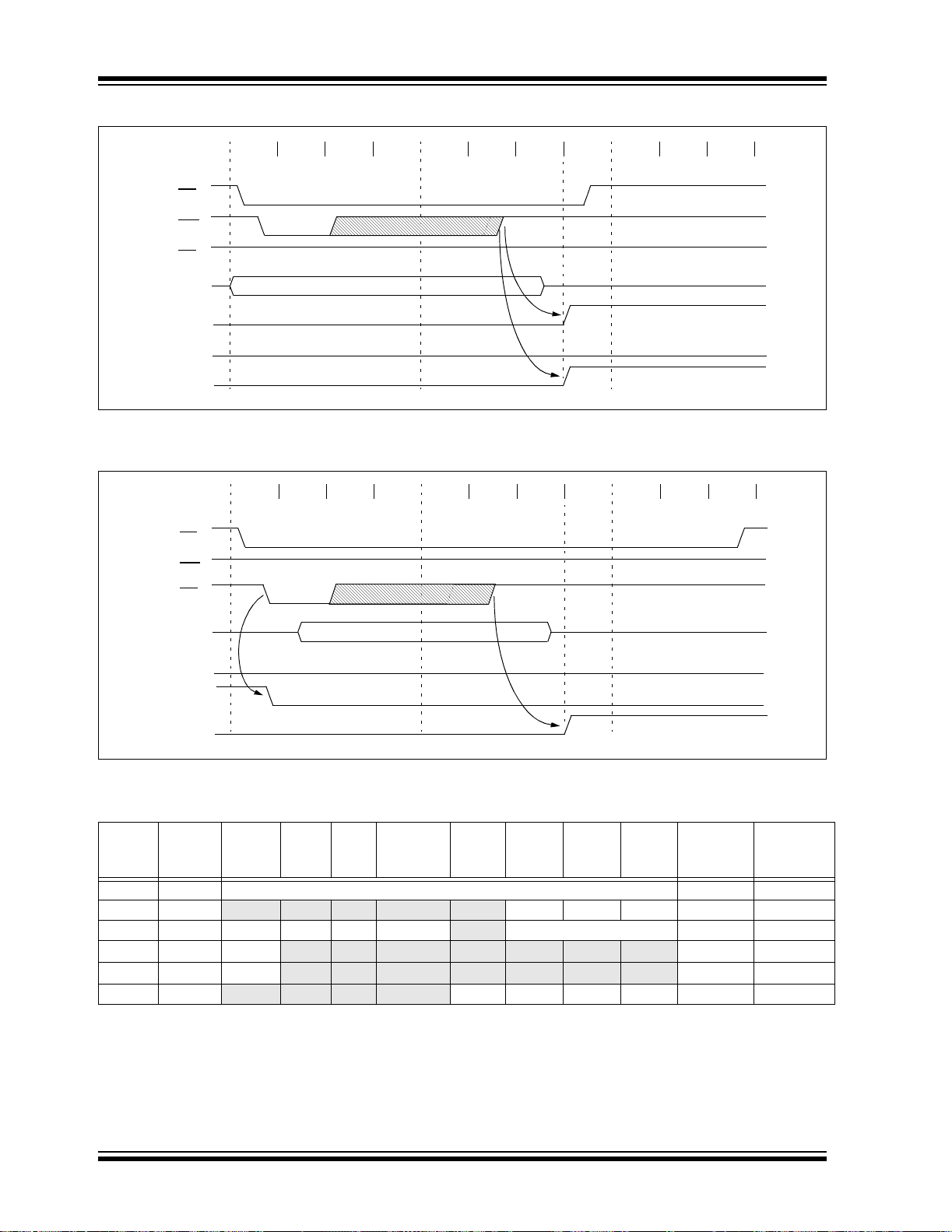
PIC16F87XA
FIGURE 4-11: PARALLEL SLAVE PORT WRITE WAVEFORMS
Q1 Q2 Q3 Q4CSQ1 Q2 Q3 Q4 Q1 Q2 Q3 Q4
WR
RD
PORTD<7:0>
IBF
OBF
PSPIF
FIGURE 4-12: PARALLEL SLAVE PORT READ WAVEFORMS
Q1 Q2 Q3 Q4CSQ1 Q2 Q3 Q4 Q1 Q2 Q3 Q4
WR
RD
PORTD<7:0>
IBF
OBF
PSPIF
TABLE 4-11: REGISTERS ASSOCIATED WITH PARALLEL SLAVE PORT
Address Name Bit 7 Bit 6 Bit 5 Bit 4 Bit 3 Bit 2 Bit 1 Bit 0
08h PORTD Port Data Latch when written; Port pins when read xxxx xxxx uuuu uuuu
09h PORTE
89h TRISE IBF OBF IBOV PSPMODE
0Ch PIR1 PSPIF
8Ch PIE1 PSPIE
9Fh ADCON1
Legend: x = unknown, u = unchanged, - = unimplemented, read as ‘0’. Shaded cells are not used by the Parallel Slave Port.
Note 1: Bits PSPIE and PSPIF are reserved on the PIC16F873A/876A; always maintain these bits clear.
— — — — —RE2RE1RE0---- -xxx ---- -uuu
— PORTE Data Direction bits 0000 -111 0000 -111
(1)
ADIF RCIF TXIF SSPIF CCP1IF TMR2IF TMR1IF 0000 0000 0000 0000
(1)
ADIE RCIE TXIE SSPIE CCP1IE TMR2IE TMR1IE 0000 0000 0000 0000
ADFM ADCS2 — — PCFG3 PCFG2 PCFG1 PCFG0 00-- 0000 00-- 0000
Val ue on:
POR, BOR
Val ue on
all other
Resets
DS39582B-page 52 2003 Microchip Technology Inc.
Page 55

PIC16F87XA
5.0 TIMER0 MODULE
Counter mode is selected by setting bit T0CS
(OPTION_REG<5>). In Counter mode, Timer0 will
The Timer0 module timer/counter has the following
features:
• 8-bit timer/counter
• Readable and writable
• 8-bit software programmable prescaler
• Internal or external clock select
• Interrupt on overflow from FFh to 00h
• Edge select for external clock
Figure 5-1 is a block diagram of th e T imer0 module and
the prescaler shared with the WDT.
increment either on every rising or falling edge of pin
RA4/T0CKI. The incrementing edge is determined by
the Timer0 Source Edge Select bit, T0SE
(OPTION_REG<4>). Clearing bit T0SE selects the rising edge. Restrictions on the external clock input are
discussed in detail in Section 5.2 “Using Timer0 with
an External Clock”.
The prescaler is mutually exclusively shared between
the Timer0 module and the Watchdog Timer. The
prescaler is not readable or writable. Section 5.3
“Prescaler” details the operation of the prescaler.
Additional information on the Timer0 module is
available in the PICmicro® Mid-Range MCU Family
Reference Manual (DS33023).
Timer mode is selected by clearing bit T0CS
(OPTION_REG<5>). In Timer mode, the Timer0
module will increment every instruction cycle (without
prescaler). If the TMR0 register is written, the increment is inhibited for the foll owing two instructi on cycles.
The user can work around this by writing an adjusted
value to the TMR0 register.
5.1 Timer0 Interrupt
The TMR0 interrupt is generated when the TMR0
register overflows from FFh to 00h. This overflow sets
bit TMR0IF (INTCON<2>). The interrupt can be
masked by clearing bit TMR0IE (INTCON<5>). Bit
TMR0IF must be cleared in software by the Timer0
module Interrupt Service Routine before re-enabling
this interrupt. The TMR0 interrupt cannot awaken the
processor from Sleep since the timer is shut-off during
Sleep.
FIGURE 5-1: BLOCK DIAGRAM OF THE TIMER0/WDT PRESCALER
CLKO (= F
RA4/T0CKI
pin
Watchdog
Timer
WDT Enable bit
OSC/4)
T0SE
Data Bus
M
0
U
X
1
T0CS
0
M
U
1
X
PSA
8-bit Prescaler
8-to-1 MUX
0
Time-out
PRESCALER
8
MUX
WDT
1
M
U
0
X
PSA
1
PSA
Sync
2
Cycles
PS2:PS0
8
TMR0 Reg
Set Flag bit TMR0IF
on Overflow
Note: T0CS, T0SE, PSA, PS2:PS0 are (OPTION_REG<5:0>).
2003 Microchip Technology Inc. DS39582B-page 53
Page 56

PIC16F87XA
5.2 Using Timer0 with an External Clock
When no pr escal er is us ed, t he ex ternal clock inpu t is
the same as the prescaler outp ut. Th e synchronization
of T0CKI with the internal phase clocks is accomplished by sampli ng the prescale r output on the Q2 and
Q4 cycles of the internal phase clocks. Therefore, it is
necessary for T0CK I to b e high for at leas t 2 T
a small RC delay of 20 ns) and low for at least 2 T
(and a small RC delay of 20 ns). Refer to the electrical
specification of the desired device.
OSC (and
OSC
Timer0 m odule means that there is no presc aler fo r the
Watchdog Timer and vice versa. This prescaler is not
readable or writable (see Figure 5-1).
The PSA and PS2:PS0 bits (OPTION_REG<3:0>)
determine the prescaler assignment and pre scale ratio.
When assigned to the Timer0 module, all instructions
writing to the TMR0 register (e.g., CLRF
BSF
to WDT, a CLRWDT instruct ion will clear the prescaler
along with the Watchdog Timer. The prescaler is not
readable or writable.
5.3 Prescaler
There is only one pr esc al er av ai lab le wh ich is m utu all y
exclusively sha red between the T imer0 mod ule and the
Watchdog Timer. A prescaler assignment for the
REGISTER 5-1: OPTION_REG REGISTER
R/W-1 R/W-1 R/W-1 R/W-1 R/W-1 R/W-1 R/W-1 R/W-1
RBPU
bit 7 bit 0
bit 7 RBPU
bit 6 INTEDG
bit 5 T0CS: TMR0 Clock Source Select bit
1 = Transition on T0CKI pin
0 = Internal instruction cycle clock (CLKO)
bit 4 T0SE: TMR0 Source Edge Select bit
1 = Increment on high-to-low transition on T0CKI pin
0 = Increment on low-to-high transition on T0CKI pin
bit 3 PSA: Prescaler Assignment bit
1 = Prescaler is assigned to the WDT
0 = Prescaler is assigned to the Timer0 module
bit 2-0 PS2:PS0: Prescaler Rate Select bits
Bit V a lue TMR0 Rate WDT Rate
000
001
010
011
100
101
110
111
INTEDG T0CS T0SE PSA PS2 PS1 PS0
1 : 2
1 : 4
1 : 8
1 : 16
1 : 32
1 : 64
1 : 128
1 : 256
1 : 1
1 : 2
1 : 4
1 : 8
1 : 16
1 : 32
1 : 64
1 : 128
1, MOVWF 1,
1,x.. ..etc.) will clear the pre scaler . When assi gned
Note: Writing to TMR0 when the prescaler is
assigned to T imer0 will cle ar the pre scaler
count, but will not change the prescaler
assignment.
Legend:
R = Readable bit W = Writable bit U = Unimplemented bit, read as ‘0’
- n = Value at POR ‘1’ = Bit is set ‘0’ = Bit is cleared x = Bit is unknown
Note: To avoid an unintended device Reset, the instruction sequence shown in the
PICmicro
cuted when changing the prescaler assignment from Timer0 to the WDT. This
sequence must be followed even if the WDT is disabled.
DS39582B-page 54 2003 Microchip Technology Inc.
®
Mid-Range MCU Family Reference Manual (DS33023) must be exe-
Page 57

PIC16F87XA
TABLE 5-1: REGISTERS ASSOCIATED WITH TIMER0
Address Name Bit 7 Bit 6 Bit 5 Bit 4 Bit 3 Bit 2 Bit 1 B it 0
01h,101h TMR0 Timer0 Module Register xxxx xxxx uuuu uuuu
0Bh,8Bh,
10Bh,18Bh
81h,181h OPTION_REG
Legend: x = unknown, u = unchanged, - = unimplemented locations read as ‘0’. Shaded cells are not used by Timer0.
INTCON GIE PEIE TMR0IE
RBPU INTEDG T0CS T0SE PSA PS2 PS1 PS0 1111 1111 1111 1111
INTE RBIE TMR0IF INTF RBIF 0000 000x 0000 000u
Value on:
POR, BOR
Value on
all other
Resets
2003 Microchip Technology Inc. DS39582B-page 55
Page 58

PIC16F87XA
NOTES:
DS39582B-page 56 2003 Microchip Technology Inc.
Page 59

PIC16F87XA
6.0 TIMER1 MODULE
The Timer1 mod ule is a 16-bi t timer/c ou nter c ons isting
of two 8-bit registers (TMR1H and TMR1L) which are
readable and writable. The TMR1 register pair
(TMR1H:TMR1L) increments from 0000h to FFFFh
and rolls over to 0000h. Th e TMR1 i nterrupt, if e nabled,
is generated on overflow which is latched in interrupt
flag bit, TMR1IF (PIR1<0>). This interrupt can be
enabled/disabled by setting/clearing TMR1 interrupt
enable bit, TMR1IE (PIE1<0>).
Timer1 can operate in one of two modes:
•As a Timer
• As a Counter
The operating mode is determined by the clock select
bit, TMR1CS (T1CON<1>).
In Timer mode, Timer1 increments every instruction
cycle. In Counter mode, it increments on every rising
edge of the external clock input.
Timer1 can be enabled/disabled by setting/clearing
control bit, TMR1ON (T1CON<0>).
Timer1 also has an interna l “Reset in put”. This Reset
can be generated by either of the two CCP modules
(Section 8.0 “Capture/Compare/PWM Modules”).
Register 6-1 shows the Timer1 Control register.
When the Timer1 oscillator is enabled (T1OSCEN is
set), the RC1/T1OSI/CCP2 and RC0/T1OSO/T1CKI
pins become inputs. That is, the TRISC<1:0> value is
ignored and these pins read as ‘0’.
Additional information on timer modules is available in
the PICmicro
Manual (DS33023).
®
Mid-Range MCU Family Reference
REGISTER 6-1: T1CON: TIMER1 CONTROL REGISTER (ADDRESS 10h)
U-0 U-0 R/W-0 R/W-0 R/W-0 R/W-0 R/W-0 R/W-0
— — T1CKPS1 T1CKPS0 T1OSCEN T1SYNC TMR1CS TMR1ON
bit 7 bit 0
bit 7-6 Unimplemented: Read as ‘0’
bit 5-4 T1CKPS1:T1CKPS0: Timer1 Input Clock Prescale Sele ct bits
11 = 1:8 prescale value
10 = 1:4 prescale value
01 = 1:2 prescale value
00 = 1:1 prescale value
bit 3 T1OSCEN: Timer1 Oscillator Enable Control bit
1 = Oscillator is enabled
0 = Oscillator is shut-off (the oscillator inverter is turned off to eliminate powe r drain)
bit 2 T1SYNC
When TMR1CS =
1 = Do not synchronize external clock input
0 = Synchronize external clock input
When TMR1CS =
This bit is ignored. Timer1 uses the internal clock when TMR1CS = 0.
bit 1 TMR1CS: Timer1 Clock Source Select bit
1 = External clock from pin RC0/T1OSO/T1CKI (on the rising edge)
0 = Internal clock (F
bit 0 TMR1ON: Timer1 On bit
1 = Enables Timer1
0 = Stops Timer1
Legend:
R = Readable bit W = Writable bit U = Unimplemented bit, read as ‘0’
- n = Value at POR ‘1’ = Bit is set ‘0’ = Bit is cleared x = Bit is unknown
: Timer1 External Clock Input Synchronization Control bit
1:
0:
OSC/4)
2003 Microchip Technology Inc. DS39582B-page 57
Page 60

PIC16F87XA
6.1 Timer1 Operation in Timer Mode
Timer mode is selected by clearing the TMR1CS
(T1CON<1>) bit. In this mode, the input clock to the
timer is F
(T1CON<2>), has no effect since the internal clock is
always in sync.
FIGURE 6-1: TIMER1 INCREMENTING EDGE
OSC/4. The synchronize control bit, T1SYNC
T1CKI
(Default High)
T1CKI
(Default Low)
Note: Arrows indicate counter increments.
6.2 Timer1 Counter Operation
Timer1 may operate in either a Synchronous, or an
Asynchronous mode, depending on the setting of the
TMR1CS bit.
When Timer1 is being incremented via an external
source, increment s occur on a ri sing edge. After T imer1
is enabled in Coun ter mode, the module mus t first have
a falling edge before the counter begins to increment.
6.3 Timer1 Operation in Sync hronized Counter Mode
Counter mode is selected by setting bit TMR1CS. In
this mode, the timer increm ents on every risin g edge of
clock input on pin RC1/T1OSI/CCP2 when bit
T1OSCEN is se t, or on pin RC0/T 1OSO/T1CK I when
bit T1OSCEN is cleared.
FIGURE 6-2: TIMER1 BLOCK DIAGRAM
Set Flag bit
TMR1IF on
Overflow
RC0/T1OSO/T1CKI
RC1/T1OSI/CCP2
(2)
TMR1H
T1OSC
TMR1
TMR1L
T1OSCEN
Enable
Oscillator
(1)
If T1SYNC is cleared, the n the externa l clock input is
synchronized with internal phase clocks. The synchronization is done after the prescaler stage. The
prescaler stage is an asynchronous ripple counter.
In this configuration, duri ng Sleep mode, Tim er1 will not
increment even if the extern al clock is present sin ce the
synchronization circuit is shut-off. The prescaler,
however, will continue to increment.
Synchronized
Clock Input
Synchronize
det
Q Clock
FOSC/4
Internal
Clock
TMR1ON
On/Off
1
0
TMR1CS
0
1
T1SYNC
Prescaler
1, 2, 4, 8
2
T1CKPS1:T1CKPS0
Note 1: When the T1OSCEN bit is cleared, the inverter is turned off. This eliminates power drain.
DS39582B-page 58 2003 Microchip Technology Inc.
Page 61

PIC16F87XA
6.4 Timer1 Operation in Asynchronous Counter Mode
If control bit T1SYNC (T1CON<2>) is set, the external
clock input is not synchronized. The timer continues to
increment asynchronous to the internal phase clocks.
The timer will continue to run during Sleep and can
generate an interrupt-on-overflow which will wake-up
the processor. However, special precautions in
software are needed to read/write the timer.
In Asynchronous Counter mode, Timer1 cannot be
used as a time base for capture or comp are operations.
6.4.1 READING AND WRITING TIMER1 IN
ASYNCHRONOUS COUNTER MODE
Reading TMR1H or TMR1L while the timer is running
from an external asy nchronous cl ock will ens ure a valid
read (taken care of in hardware). However, the user
should keep in min d that re ading t he 16-b it time r in tw o
8-bit values itself, poses certain problems, since the
timer may overflow between the reads.
For writes, it is recomm ended that the us er simply stop
the timer and write the desired values. A write contention may occur by writing to the tim er registers while the
register is incrementing. This may produce an
unpredictable value in the timer register.
Reading the 16-bit value requires some care.
Examples 12-2 and 12-3 in the PICmicro
MCU Family Reference Manual (DS33023) show how
to read and write Timer1 when it is running in
Asynchronous mode.
®
Mid-Range
6.5 Timer1 Oscillator
A crystal oscillator ci rcuit is built-in betwee n pins T1OSI
(input) and T1OSO (amplifier output). It is enabled by
setting control bit, T1OSCEN (T1CON<3>). The oscillator is a low-power oscillator, rated up to 200 kHz. It
will continue to run durin g Sleep. It is primarily intended
for use with a 32 kHz crystal. Table 6-1 shows the
capacitor selection for the Timer1 oscillator.
The Timer1 oscillator is identical to the LP oscillator.
The user must provide a sof tware t im e del ay to en su re
proper oscillator start-up.
T ABLE 6-1: CAPACITOR SELECTION FOR
THE TIMER1 OSCILLATOR
Osc T y pe Freq. C1 C2
LP 32 kHz 33 pF 33 pF
100 kHz 15 p F 15 pF
200 kHz 15 p F 15 pF
These values are for design guidance only.
Crystals Tested:
32.768 kHz Epson C-001R32.768K-A ± 20 PPM
100 kHz Epson C-2 100.00 KC-P ± 20 PPM
200 kHz STD XTL 200.000 kHz ± 20 PPM
Note 1: Higher cap ac itance increases the stability
of oscillator but also in creases the st art-up
time.
2: Since each resonator/crystal has its own
characteristics, the user should consult
the resonator/crystal manufacturer for
appropriate values of external
components.
6.6 Resetting Timer1 Using a CCP Trigger Output
If the CCP1 or CCP2 module is config ured in C omp are
mode to generate a “special event trigger”
(CCP1M3:CCP1M0 = 1011), this signal will reset
Timer1.
Note: The special event triggers from the CCP1
and CCP2 modules will not set interrupt
flag bit, TMR1IF (PIR1<0>).
Timer1 mu st be confi gured fo r either T ime r or Synchr onized Counter mode to take advantage of this feature.
If Timer1 is running in Asynchronous Counter mode,
this Reset operation may not work.
In the event that a write to Timer1 coincides with a
special event trigger from CCP1 or CCP2, the write will
take precedence.
In this mode of ope rati on, the CCPRxH :CCPRx L regis ter pair effectively becomes the period register for
Timer1.
2003 Microchip Technology Inc. DS39582B-page 59
Page 62

PIC16F87XA
6.7 Resetting of Timer1 Register Pair (TMR1H, TMR1L)
TMR1H and TMR1L registers are not rese t to 00h on a
6.8 Timer1 Prescaler
The prescaler counter is cleared on writes to the
TMR1H or TMR1L registers.
POR, or any other Reset, except by the CCP1 and
CCP2 special event triggers.
T1CON register is reset to 00h on a Power-on Reset,
or a Brown-out Reset, which shuts off the timer and
leaves a 1:1 prescale. In all other Resets, the register
is unaffected.
TABLE 6-2: REGISTERS ASSOCIATED WITH TIMER1 AS A TIMER/COUNTER
Address Name Bit 7 Bit 6 Bit 5 Bit 4 Bit 3 Bit 2 Bit 1 Bit 0
0Bh,8Bh,
10Bh, 18Bh
0Ch PIR1
8Ch PIE1
0Eh TMR1L Holding Register for the Least Significant Byte of the 16-bit TMR1 Register xxxx xxxx uuuu uuuu
0Fh TMR1H Holding Register for the Most Significant Byte of the 16-bit TMR1 Register xxxx xxxx uuuu uuuu
10h T1CON
Legend: x = unknown, u = unchanged, - = unimplemented, read as ‘0’. Shaded cells are not used by the Timer1 module.
Note 1: Bits PSPIE and PSPIF are reserved on the 28-pin devices; always maintain these bits clear.
INTCON GIE PEIE
(1)
PSPIF
PSPIE
ADIF RCIF TXIF SSPIF CCP1IF TMR2IF TMR1IF 0000 0000 0000 0000
(1)
ADIE RCIE TXIE SSPIE CCP1IE TMR2IE TMR1IE 0000 0000 0000 0000
— — T1CKPS1 T1CKPS0 T1OSCEN T1SYNC TMR1CS TMR1ON --00 0000 --uu uuuu
TMR0IE INTE RBIE TMR0IF INTF RBIF 0000 000x 0000 000u
Value on:
POR, BOR
Val ue on
all other
Resets
DS39582B-page 60 2003 Microchip Technology Inc.
Page 63

PIC16F87XA
7.0 TIMER2 MODULE
Timer2 is an 8-bit timer with a prescaler and a
postscaler . It c an be used as the PWM time base f or the
PWM mode of the CCP module(s). The TMR2 register
is readable and writable and is cleared on any device
Reset.
The input clock (F
1:1, 1:4 or 1:16, selected by control bits
OSC/4) has a prescale option of
Register 7-1 shows the Timer2 Control register.
Additional information on timer modules is available in
the PICmicro
®
Mid-Range MCU Family Reference
Manual (DS33023).
FIGURE 7-1: TIMER2 BLOCK DIAGRAM
Sets Flag
bit TMR2IF
TMR2
Output
(1)
T2CKPS1:T2CKPS0 (T2CON<1:0>).
The Timer2 module has an 8-bit period register, PR2.
Timer2 increments from 00h until it matches PR2 and
then resets to 00h on the next increment cycle. PR2 is
a readable and writable register. The PR2 register is
initialized to FFh upon Reset.
The match output of TMR2 goes through a 4-bit
postscaler (which gives a 1:1 to 1:16 scaling inclusive)
to generate a TMR2 interrupt (latched in flag bit,
TMR2IF (PIR1<1>)).
Reset
Postscaler
1:1 to 1:16
4
T2OUTPS3:
T2OUTPS0
Note 1: TMR2 regis ter output can b e software selected by the
SSP module as a baud clock.
EQ
TMR2 Reg
Comparator
PR2 Reg
Prescaler
1:1, 1:4, 1:16
T2CKPS1:
T2CKPS0
Timer2 c an be shut-of f by clearing control bit, T MR2ON
(T2CON<2>) , to minimize power consumption.
REGISTER 7-1: T2CON: TIMER2 CONTROL REGISTER (ADDRESS 12h)
U-0 R/W-0 R/W-0 R/W-0 R/W-0 R/W-0 R/W-0 R/W-0
— TOUTPS3 TOUTPS2 TOUTPS1 TOUTPS0 TMR2ON T2CKPS1 T2CKPS0
bit 7 bit 0
F
OSC/4
2
bit 7 Unimplemented: Read as ‘0’
bit 6-3 TOUTPS3:TOUTPS0: Timer2 Output Postscale Select bits
0000 = 1:1 postscale
0001 = 1:2 postscale
0010 = 1:3 postscale
•
•
•
1111 = 1:16 postscale
bit 2 TMR2ON: Timer2 On bit
1 = Timer2 is on
0 = Timer2 is off
bit 1-0 T2CKPS1:T2CKPS0: Timer2 Clock Prescale Select bits
00 = Prescaler is 1
01 = Prescaler is 4
1x = Prescaler is 16
Legend:
R = Readable bit W = Writable bit U = Unimplemented bit, read as ‘0’
- n = Value at POR ‘1’ = Bit is set ‘0’ = Bit is cleared x = Bit is unknown
2003 Microchip Technology Inc. DS39582B-page 61
Page 64

PIC16F87XA
7.1 Timer2 Prescaler and Postscaler
The prescaler and postscaler counters are cleared
when any of the following occurs:
• a write to the TMR2 register
7.2 Output of TMR2
The output of TMR2 (before the post scaler) is fed to the
SSP module, which optionally uses it to generate the
shift clock.
• a write to the T2CON register
• any device Reset (POR, MCLR
Reset, WDT
Reset or BOR)
TMR2 is not cleared when T2CON is written.
TABLE 7-1: REGISTERS ASSOCIATED WITH TIMER2 AS A TIMER/COUNTER
Address Name Bit 7 Bit 6 Bit 5 Bit 4 Bit 3 Bit 2 Bit 1 Bit 0
0Bh, 8Bh,
10Bh, 18Bh
0Ch PIR1
8Ch PIE1
11h TMR2 Timer2 Module’s Register 0000 0000 0000 0000
12h T2CON
92h PR2 Timer2 Period Register 1111 1111 1111 1111
Legend: x = unknown, u = unchanged, - = unimplemented, read as ‘0’. Shaded cells are not used by the Timer2 module.
Note 1: Bits PSPIE and PSPIF are reserved on 28-pin devices; always maintain these bits clear.
INTCON GIE PEIE
(1)
PSPIF
PSPIE
— TOUTPS3 TOUTPS2 TOUTPS1 TOUTPS0 TMR2ON T2CKPS1 T2CKPS0 -000 0000 -000 0000
ADIF RCIF TXIF SSPIF CCP1IF TMR2IF TMR1IF 0000 0000 0000 0000
(1)
ADIE RCIE TXIE SSPIE CCP1IE TMR2IE TMR1IE 0000 0000 0000 0000
TMR0IE INTE RBIE TMR0IF INTF RBIF 0000 000x 0000 000u
Value on:
POR, BOR
Value on
all other
Resets
DS39582B-page 62 2003 Microchip Technology Inc.
Page 65

PIC16F87XA
8.0 CAPTURE/COMPARE/PWM MODULES
Each Capture/Compare/PWM (CCP) module contains
a 16-bit register which can operate as a:
• 16-bit Capture register
• 16-bit Compare register
• PWM Master/Slave Duty Cycle register
Both the CCP1 and CCP2 modules are identical in
operation, with the e xception being the operation of the
special event trigg er. Tabl e 8-1 and Ta ble8-2 show the
resources and interactions of the CCP module(s). In
the following sections, the operation of a CCP module
is described with respect to CCP1. CCP2 operates the
same as CCP1 except where noted.
CCP1 Module:
Capture/Compare/PWM Register 1 (CCPR1) is com-
prised of two 8-bit registers: CCPR1L (low byte) and
CCPR1H (high byte). The CCP1CON register controls
the operation of CCP1. The special event trigger is
generated by a compare match and will reset Timer1.
CCP2 Module:
Capture/Co mpare/PWM Register 2 (CCPR2 ) is com-
prised of tw o 8-bit registers: CCPR2L (low byte) and
CCPR2H (high byte). The CCP2CON register controls
the operation of CCP2. The special event trigger is
generated by a compare match and will reset Timer1
and start an A/D conversion (if the A/D module is
enabled).
Additional information on CCP modules is available in
the PICmicro
Manual (DS33023) and in application note AN594,
“Using the CCP Module(s)” (DS00594).
®
Mid-Range MCU Family Reference
TABLE 8-1: CCP MODE – TIMER
RESOURCES REQUIRED
CCP Mode Timer Resource
Capture
Compare
PWM
Timer1
Timer1
Timer2
TABLE 8-2: INTERACTION OF TWO CCP MODULES
CCPx Mode CCPy Mode Interaction
Capture Capture Same TMR1 time base
Capture Compare The compare should be configured for the special event trigger which clears TMR1
Compare Compare The compare(s) should be configured for the special event trigger which clears TMR1
PWM PWM The PWMs will have the same frequency and update rate (TMR2 interrupt)
PWM Capture None
PWM Compare None
2003 Microchip Technology Inc. DS39582B-page 63
Page 66

PIC16F87XA
REGISTER 8-1: CCP1CON REGISTER/CCP2CON REGISTER (ADDRESS 17h/1Dh)
U-0 U-0 R/W-0 R/W-0 R/W-0 R/W-0 R/W-0 R/W-0
— — CCPxX CCPxY CCPxM3 CCPxM2 CCPxM1 CCPxM0
bit 7 bit 0
bit 7-6 Unimplemented: Read as ‘0’
bit 5-4 CCPxX:CCPxY: PWM Least Significant bits
Capture mode
Unused.
Compare mode:
Unused.
PWM mode:
These bits are the two LSbs of the PWM duty cycle. The eight MSbs are found in CCPRxL.
bit 3-0 CCPxM3:CCPxM0: CCPx Mode Select bits
0000 =Capture/Compare/PWM disabled (resets CCPx module)
0100 =Capture mode, every falling edge
0101 =Capture mode, every rising edge
0110 =Capture mode, every 4th rising edge
0111 =Capture mode, every 16th rising edge
1000 =Compare mode, set output on match (CCPxIF bit is set)
1001 =Compare mode, clear output on match (CCPxIF bit is set)
1010 =Compare mode, generate software interrupt on match (CCPxIF bit is set, CCPx pin is
1011 = Compare mode, trigger special eve nt (CCPxIF bit is set, CCPx pin is unaffec ted); CCP1
11xx =PWM mode
:
unaffected)
resets TMR1; CCP2 resets TMR1 and starts an A/D conversion (if A/D module is
enabled)
Legend:
R = Readable bit W = Writable bit U = Unimplemented bit, read as ‘0’
- n = Value at POR ‘1’ = Bit is set ‘0’ = Bit is cleared x = Bit is unknown
DS39582B-page 64 2003 Microchip Technology Inc.
Page 67

PIC16F87XA
8.1 Capture Mode
In Capture mode, CCPR1H:CCPR1L captures the
16-bit value of the TMR1 r egister wh en an eve nt occurs
on pin RC2/CCP1. An event is defined as one of the
following:
• Every falling edge
• Every rising edge
• Every 4th rising edge
• Every 16th rising edge
The type of event is configured by control bits,
CCP1M3:CCP1M0 (CCPxCON<3:0>). When a capture is made, the interrupt request flag bit, CCP1IF
(PIR1<2>), is set. The interrupt flag must be cleared in
software. If another capture occurs before the value in
register CCPR1 is read, the old captured value is
overwritten by the new value.
8.1.1 CCP PIN CONFIGURATION
In Capture mode, the RC2/CCP1 pin should be
configured as an input by setting the TRISC<2> bit.
Note: If the RC2/CCP1 pin is configured as an
output, a write to the port can cause a
Capture condition.
FIGURE 8-1: CAPTURE MODE
OPERATION BLOCK
DIAGRAM
Set Flag bit CCP1IF
(PIR1<2>)
CCPR1H CCPR1L
Capture
Enable
TMR1H TMR1L
CCP1CON<3:0>
RC2/CCP1
pin
Prescaler
÷ 1, 4, 16
and
Edge Detect
Qs
8.1.2 TIMER 1 MODE SELECTION
Timer1 must be running in Timer mode, or Synchronized Counter mode, for the CCP module to use the
capture feature. In Asynchronous Counter mode, the
capture operation may not work.
8.1.3 SOFTWARE INTERRUPT
When the Capture mode is changed, a false capture
interrupt may be generated. The user should keep bit
CCP1IE (PIE1<2>) clear to avoid false interrupts and
should clear the flag bit, CCP1IF, following any such
change in operating mode.
8.1.4 CCP PRESCALER
There are four prescaler settings, specified by bits
CCP1M3:CCP1M0. Whenever the CCP module is
turned off, or the CCP module is not in Capture mode,
the prescaler counter is cleared. Any Reset will clear
the prescaler counter.
Switching from one capture prescaler to another may
generate an interrupt. Also, the prescaler counter will
not be cleared, therefore, the first cap ture may be from
a non-zero prescaler. Example 8-1 shows the recommended method for switching between capture
prescalers. This example also clears the prescaler
counter and will not generate the “false” interrupt.
EXAMPLE 8-1: CHANGIN G BETWEEN
CAPTURE PRESCALERS
CLRF CCP1CON ; Turn CCP module off
MOVLW NEW_CAPT_PS ; Load the W reg with
; the new prescaler
; move value and CCP ON
MOVWF CCP1CON ; Load CCP1CON with this
; value
2003 Microchip Technology Inc. DS39582B-page 65
Page 68

PIC16F87XA
8.2 Compare Mode
In Compare mo de, th e 16- bit CCP R1 re gist er valu e is
constantly compared against the TMR1 register pair
value. When a match occurs, the RC2/C CP 1 pin is:
• Driven high
•Driven low
• Remains unchanged
The action on the pin is based on the value of control
bits, CCP1M3:CCP1M0 (CCP1CON<3:0>). At the
same time, interrupt flag bit CCP1IF is set.
FIGURE 8-2: COMPARE MODE
OPERATION BLOCK
DIAGRAM
Special event trigger will:
reset Timer1, but not set interrupt flag bit TMR1IF (PIR1<0>)
and set bit GO/DONE (ADCON0<2>).
Special Event Trigger
Set Flag bit CCP1IF
RC2/CCP1
pin
TRISC<2>
Output Enable
QS
R
CCP1CON<3:0>
(PIR1<2>)
Output
Logic
Mode Select
CCPR1H CCPR1L
Match
TMR1H TMR1L
Comparator
8.2.2 TIMER1 MODE SELECTION
Timer1 must be running in Timer mode, or Synchronized Counter mode, if the CCP module is using the
compare feature. In Asynchronous Counter mode, the
compare operation may not work.
8.2.3 SOFTWARE INTERRUPT MODE
When Generate Softw are Interrupt mode is chosen, the
CCP1 pin is not affecte d. The CCPIF b it is set, c ausing
a CCP interrupt (if enabled).
8.2.4 SPECIAL EVENT TRIGGER
In this mode, an internal hardware trigger is generated
which may be used to initiate an action.
The special event trigger output of CCP1 resets the
TMR1 regist er pai r. This al lows the CCPR 1 re gis ter to
effectively b e a 16-bit progra mmable period registe r for
Timer1.
The special event trigger output of CCP2 resets the
TMR1 register pai r and starts an A/D conversion (if the
A/D module i s enabled).
Note: The special event trigger from the CCP1
and CCP2 modules will not set interrupt
flag bit TMR1IF (PIR1<0>).
8.2.1 CCP PIN CONFIGURATION
The user must configure the RC2/CCP1 pin as an
output by clearing the TRISC<2> bit.
Note: Clearing the CCP1CON register will force
the RC2/CCP1 compare output latch to
the default low level. This is not the
PORTC I/O data latch.
DS39582B-page 66 2003 Microchip Technology Inc.
Page 69

PIC16F87XA
8.3 PWM Mode (PWM)
In Pulse Width Modulation mode, the CCPx pin
produces up to a 10-bit resolution PWM output. Since
the CCP1 pin is mul tiplexed with th e PORTC dat a latch,
the TRISC<2> bit must be cleared to make the CCP1
pin an output.
Note: Clearing the CCP1CON register will force
the CCP1 PWM output latch to th e de fau lt
low level. This is not the PORTC I/O data
latch.
Figure 8-3 shows a simplified block diagram of the
CCP module in PWM mode.
For a step-by-step procedure on how to set up the C CP
module for PWM operation, see Section 8.3.3 “Setup
for PWM Operation”.
FIGURE 8-3: SIMPLIFIED PWM BLOCK
DIAGRAM
Duty Cycle Registers
CCPR1L
CCPR1H (Slave)
Comparator
TMR2
Comparator
PR2
Note 1: The 8-bit timer is concatenated with 2-bit internal Q
(Note 1)
Clear Timer,
CCP1 pin and
latch D.C.
clock, or 2 bits of the prescaler, to create 10-bit time
base.
A PWM output (Figure 8 -4) has a time base (period)
and a time that the output stays high (duty cycle). The
frequency of the PWM is the inverse of the period
(1/period).
FIGURE 8-4: PWM OUTPUT
Period
CCP1CON<5:4>
Q
R
S
TRISC<2>
RC2/CCP1
8.3.1 PWM PE RIOD
The PWM period is specified by writing to the PR2
register. The PWM period can be calculated using the
following formula:
PWM Period = [(PR2) + 1] • 4 • T
OSC •
(TMR2 Prescale Value)
PWM frequency is defined as 1/[PWM period].
When TMR2 is eq ual to PR2, t he following three event s
occur on the ne xt increment cycle:
•TMR2 is cleared
• The CCP1 pin is set (exception: if PWM duty
cycle = 0%, the CCP1 pin will not be set)
• The PWM duty cycle is latc hed from CC PR1L into
CCPR1H
Note: The Timer2 postscaler (see Section 7.1
“Timer2 Prescaler and Postscaler”) is
not used in the determination of the PWM
frequency. The pos tscaler could b e used
to have a servo update rate at a different
frequency than the PWM output.
8.3.2 PWM DUTY CYCLE
The PWM duty cycle is specified by writing to the
CCPR1L register and to the CCP1CON<5:4> bits. Up
to 10-bit re so l uti on is av ai l ab le. T he CC PR 1L c on tai ns
the eight MSbs and the CCP1CON<5:4> contains the
two LSbs. This 10-bit value is represented by
CCPR1L:CCP1CON<5:4>. The following equation is
used to calculate the PWM duty cycle in time:
PWM Duty Cycle =(CCPR1L:CCP1CON<5:4>) •
OSC • (TMR2 Prescale Value)
T
CCPR1L and CCP1CON<5:4> can be written to at any
time, but the duty cycle value is not latched into
CCPR1H until after a match between PR2 and TMR2
occurs (i.e., the period is complete). In PWM mode,
CCPR1H is a read-only register.
The CCPR1H register and a 2-bit internal latch are
used to double-buffer the PWM duty cycle. This
double-buffering is essential for glitch-free PWM
operation.
When the CCPR1H and 2-bit latch match TMR2,
concatenated with an internal 2-bit Q clock or 2 bits of
the TMR2 prescaler, the CCP1 pin is cleared.
The maximum PWM resolution (bits) for a given PWM
frequency is given by the following formula.
EQUATION 8-1:
Duty Cycle
TMR2 = PR2
TMR2 = Duty Cycle
TMR2 = PR2
Note: If the PWM duty cycle value i s lon ger tha n
the PWM period, the CCP1 pin will not be
cleared.
2003 Microchip Technology Inc. DS39582B-page 67
log(
FOSC
FPWM
log(2)
)
bitsResolution =
Page 70

PIC16F87XA
8.3.3 SETUP FOR PWM OPERATION
The following steps should be taken when configuring
the CCP module for PWM operation:
1. Set the PWM period by writing to the PR2 regis ter .
2. Set the PWM duty cycle by writing to the
CCPR1L register and CCP1CON<5:4> bits.
3. Make the CCP1 pin an output by clearing the
TRISC<2> bit.
4. Set the TMR2 prescale val ue and enable T imer2
by writing to T2CON.
5. Configure the CCP1 module fo r PWM operation.
TABLE 8-3: EXAMPLE PWM FREQUENCIES AND RESOLUTIONS AT 20 MHz
PWM Frequency 1.22 kHz 4.88 kHz 19.53 kHz 78.12kHz 156.3 kHz 208.3 kHz
Timer Prescaler (1, 4, 16) 16 4 1 1 1 1
PR2 Value 0xFFh 0xFFh 0xFFh 0x3Fh 0x1Fh 0x17h
Maximum Resolution (bits) 10 10 10 8 7 5.5
TABLE 8-4: REGISTERS ASSOCIATED WITH CAPTURE, COMPARE AND TIMER1
Address Name Bit 7 Bit 6 Bit 5 Bit 4 Bit 3 Bit 2 Bit 1 Bit 0
0Bh,8Bh,
10Bh, 18Bh
0Ch PIR1
0Dh PIR2
8Ch PIE1
8Dh PIE2
87h TRISC PORTC Data Direction Register 1111 1111 1111 1111
0Eh TMR1L Holding Register for the Least Significant Byte of the 16-bit TMR1 Register xxxx xxxx uuuu uuuu
0Fh TMR1H Holding Register for the Most Significant Byte of the 16-bit TMR1 Register xxxx xxxx uuuu uuuu
10h T1CON
15h CCPR1L Capture/Compare/PWM Register 1 (LSB) xxxx xxxx uuuu uuuu
16h CCPR1H Capture/Compare/PWM Register 1 (MSB) xxxx xxxx uuuu uuuu
17h CCP1CON
1Bh CCPR2L Capture/Compare/PWM Register 2 (LSB) xxxx xxxx uuuu uuuu
1Ch CCPR2H Capture/Compare/PWM Register 2 (MSB) xxxx xxxx uuuu uuuu
1Dh CCP2CON
Legend: x = unknown, u = unchanged, - = unimplemented, read as ‘0’. Shaded cells are not used by Capture and Timer1.
Note 1: The PSP is not implemented on 28-pin devices; always maintain these bits clear.
INTCON GIE PEIE
(1)
PSPIF
PSPIE
ADIF RCIF TXIF SSPIF CCP1IF TMR2IF TMR1IF 0000 0000 0000 0000
— — — — — — —CCP2IF---- ---0 ---- ---0
(1)
ADIE RCIE TXIE SSPIE CCP1IE TMR2IE TMR1IE 0000 0000 0000 0000
— — — — — — — CCP2IE ---- ---0 ---- ---0
— — T1CKPS1 T1CKPS0 T1OSCEN T1SYNC TMR1CS TMR1ON --00 0000 --uu uuuu
— — CCP1X CCP1Y CCP1M3 CCP1M2 CCP1M1 CCP1M0 --00 0000 --00 0000
— — CCP2X CCP2Y CCP2M3 CCP2M2 CCP2M1 CCP2M0 --00 0000 --00 0000
TMR0IE INTE RBIE TMR0IF INTF RBIF 0000 000x 0000 000u
Value on:
POR, BOR
Value on
all other
Resets
DS39582B-page 68 2003 Microchip Technology Inc.
Page 71

PIC16F87XA
TABLE 8-5: REGISTERS ASSOCIATED WITH PWM AND TIMER2
Address Name Bit 7 Bit 6 Bit 5 Bit 4 Bit 3 Bit 2 Bit 1 Bit 0
0Bh,8Bh,
10Bh, 18Bh
0Ch PIR1
0Dh PIR2
8Ch PIE1
8Dh PIE2
87h TRISC PORTC Data Direc ti o n Re gi s ter 1111 1111 1111 1111
11h TMR2 Timer2 Module’s Register 0000 0000 0000 0000
92h PR2 Timer2 Module’s Period Register 1111 1111 1111 1111
12h T2CON
15h CCPR1L Capture/ Compare/PWM Register 1 (L SB) xxxx xxxx uuuu uuuu
16h CCPR1H Capture/ Compare/PWM Register 1 (MS B) xxxx xxxx uuuu uuuu
17h CCP1CON
1Bh CCPR2L Capture/Compare/P WM Re gi s ter 2 (LSB) xxxx xxxx uuuu uuuu
1Ch CCPR2H Capture/Comp ar e/ PWM Re gis t er 2 (MS B) xxxx xxxx uuuu uuuu
1Dh CCP2CON
Legend: x = unknown, u = unchanged, - = unimplemented, read as ‘0’. Shaded cells are not used by PWM and Timer2.
Note 1: Bits PSPIE and PSPIF are reserved on 28-pin devices; always maintain these bits clear.
INTCON GIE PEIE
(1)
PSPIF
— — — — — — —CCP2IF---- ---0 ---- ---0
PSPIE
— — — — — — — CCP2IE ---- ---0 ---- ---0
— TOUTPS3 TOUTPS2 TOUTPS1 TOUTPS 0 TMR2ON T2CKPS1 T2CKPS0 -000 0000 -000 0000
— — CCP1X CCP1Y CCP1M3 CCP1M2 CCP1M1 CCP1M0 --00 0000 --00 0000
— — CCP2X CCP2Y CCP2M3 CCP2M2 CCP2M1 CCP2M0 --00 0000 --00 0000
ADIF RCIF TXIF SSPIF CCP1IF TMR2IF TMR1IF 0000 0000 0000 0000
(1)
ADIE RCIE TXIE SSPIE CCP1IE TMR2IE TMR1IE 0000 0000 0000 0000
TMR0IE INTE RBIE TMR0IF INTF RBIF 0000 000x 0000 000u
Value on:
POR, BOR
Val ue on
all other
Resets
2003 Microchip Technology Inc. DS39582B-page 69
Page 72

PIC16F87XA
NOTES:
DS39582B-page 70 2003 Microchip Technology Inc.
Page 73

PIC16F87XA
9.0 MASTER SYNCHRONOUS
SERIAL PORT (MSSP)
MODULE
9.1 Master SSP (MSSP) Module
Overview
The Master Synchronous Serial Port (MSSP) module is
a serial interface, useful for communicating with other
peripheral or microc ontroll er dev ices. Th ese p eriphera l
devices may be serial EEPROMs, shift registers,
display drivers, A/D converte rs, etc. The MSSP mo dule
can operate in one of two modes:
• Serial Peripheral Interface (SPI)
• Inter-Integrated Circuit (I
- Full Master mode
- Slave mode (with general address call)
The I2C interface supports the following modes in
hardware:
•Master mode
• Multi-Master mode
• Slave mode
9.2 Control Registers
The MSSP module has three associated registers.
These include a status register (SSPSTAT) and two
control registers (SSPCON and SSPCON2). The use
of these registers a nd t heir individual config urat ion bits
differ significantly, depending on whether the MSSP
module is operated in SPI or I
Additional details are provided under the individual
sections.
9.3 SPI Mode
The SPI mode allo ws 8 bits of data to be sync hronously
transmitted and received simultaneously. All four
modes of SPI are supported. To accomplish
communication, typically three pins are used:
• Serial Data Out (SDO) – RC5/SDO
• Serial Data In (SDI) – RC4/SDI/SDA
• Serial Clock (SCK) – RC3/SCK/SCL
Additionally, a fourth pin may be used when in a Slave
mode of operation:
• Slave Select (SS
Figure 9-1 shows the block diagram of the MSSP
module when operating in SPI mode.
) – RA5/AN4/SS/C2OUT
2
C)
2
C mode.
FIGURE 9-1: MSSP BLOCK DIAGRAM
(SPI MODE)
Internal
Data Bus
Read Write
SSPBUF reg
SSPSR reg
RC4/SDI/SDA
RC5/SDO
RA5/AN4/
SS
/C2OUT
RC3/SCK/SCL
bit0
Peripheral OE
Control
SS
Enable
Edge
Select
SSPM3:SSPM0
SMP:CKE
2
Edge
Select
Data to TX/RX in SSPSR
TRIS bit
Clock Select
4
Note: When the SPI is in Slave mode with SS pi n
control enabled (SSPCON<3:0> = 0100),
the state of the SS
pin can affect the state
read back from the TRISC<5> bit. The
Peripheral OE signal from the SSP module in PORTC controls the state that is
read back from the TRISC<5> bit (see
Section 4.3 “PORTC and the TRISC
Register” for information on PORTC). If
Read-Modify-Write instructions, such as
BSF, are performed on the TRISC register
while the SS
pin is high, this will ca use th e
TRISC<5> bit to be set, thus disabling the
SDO output.
Shift
Clock
2
TMR2 Outpu t
( )
Prescaler
4, 16, 64
2
OSC
T
2003 Microchip Technology Inc. DS39582B-page 71
Page 74

PIC16F87XA
9.3.1 REGISTERS
The MSSP module has four registers for SPI mode
operation. These are:
• MSSP Control Register (SSPCON)
• MSSP Status Register (SSPSTAT)
• Serial Receive/Transmit Buffer Register
(SSPBUF)
• MSSP Shift Register (SSPSR) – Not directly
accessible
SSPCON and SSPSTAT are the control and status
registers in SPI mode operation. The SSPCON register is readable and writable. The lower six bits of the
SSPSTAT are read-only. The upper two bits of the
SSPSTAT are read/write.
SSPSR is the shift register used for shifting data in or
out. SSPBUF is the buffer register to which data bytes
are written to or read from.
In receive operations, SSPSR and SSPBUF together
create a double-buffered receiver. When SSPSR
receives a complete byte, it is transferred to SSPBUF
and the SSPIF interrupt is set.
During transmission, the SSPBUF is not doublebuffered. A write to SSPBUF will write to both SSPBUF
and SSPSR.
REGISTER 9-1: SSPSTAT: MSSP STATUS REGISTER (SPI MODE) (ADDRESS 94h)
R/W-0 R/W-0 R-0 R-0 R-0 R-0 R-0 R-0
SMP CKE D/A
bit 7 bit 0
bit 7 SMP: Sample bit
SPI Master mode:
1 = Input data sampled at end of data output time
0 = Input data sampled at middle of data output time
SPI Slave mode:
SMP must be cleared when SPI is used in Slave mode.
bit 6 CKE: SPI Clock Select bit
1 = Transmit occurs on transition from active to Idle clock state
0 = Transmit occurs on transition from Idle to active clock state
Note: Polarity of clock state is set by the CKP bit (SSPCON1<4>).
bit 5 D/A
bit 4 P: Stop bit
bit 3 S: Start bit
bit 2 R/W: Read/Write bit information
bit 1 UA: Update Address bit
bit 0 BF: Buffer Full Status bit (Receive mode only)
: Data/Address bit
Used in I2C mode only.
Used in I2C mode only . This bit is cleared when the M SSP module is disabled, SSPEN is cleared.
Used in I2C mode only.
Used in I2C mode only.
Used in I2C mode only.
1 = Receive complete, SSPBUF is full
0 = Receive not complete, SSPBUF is empty
PSR/WUA BF
Legend:
R = Readable bit W = Writable bit U = Unimplemented bit, read as ‘0’
- n = Value at POR ‘1’ = Bit is set ‘0’ = Bit is cleared x = Bit is unknown
DS39582B-page 72 2003 Microchip Technology Inc.
Page 75

PIC16F87XA
REGISTER 9-2: SSPCON1: MSSP CONTROL REGISTER 1 (SPI MODE) (ADDRESS 14h)
R/W-0 R/W-0 R/W-0 R/W-0 R/W-0 R/W-0 R/W-0 R/W-0
WCOL SSPOV SSPEN CKP SSPM3 SSPM2 SSPM1 SSPM0
bit 7 bit 0
bit 7 WCOL: Write Collision Detect bit (Transmit mode only)
1 = The SSPBUF register is written while it is still transmitting the previous word. (Must be
cleared in software.)
0 = No collision
bit 6 SSPOV: Receive Overflow Indicator bit
SPI Slave mode:
1 = A new byte is received whil e the SSPBUF register i s still holding the previous data . In case
of overflow, the data in SSPSR is lost. Overflow can only occur in Slave mode. The user
must read the SSPBUF, even if only transmitting data, to avoid setting overflow. (Must be
cleared in software.)
0 = No overflow
Note: In Master mode, the overflow bit is not set, since each new reception (and
bit 5 SSPEN: Synchronous Serial Port Enable bit
1 = Enables serial port and configures SCK, SDO, SDI, and SS
0 = Disables serial port and configures these pins as I/O port pins
Note: When enabled, these pins must be properly configured as input or output.
transmission) is initiated by writing to the SSPBUF register.
as serial port pins
bit 4 CKP: Clock Polarity Select bit
1 = Idle state for clock is a high level
0 = Idle state for clock is a low level
bit 3-0 SSPM3:SSPM0: Synchronous Serial Port Mode Select bits
0101 = SPI Slave mode, clock = SCK pin. SS
0100 = SPI Slave mode, clock = SCK pin. SS
0011 = SPI Master mode, clock = TMR2 output/2
0010 = SPI Master mode, clock = F
0001 = SPI Master mode, clock = F
0000 = SPI Master mode, clock = F
Note: Bit combinations not specifically listed here are either reserved or implemented in
Legend:
R = Readable bit W = Writable bit U = Unimplemented bit, read as ‘0’
- n = Value at POR ‘1’ = Bit is set ‘0’ = Bit is cleared x = Bit is unknown
2
C mode only.
I
OSC/64
OSC/16
OSC/4
pin control disabled. SS can be used as I/O pin.
pin control enabled.
2003 Microchip Technology Inc. DS39582B-page 73
Page 76

PIC16F87XA
9.3.2 OPERATION
When initializing the SPI, several options need to be
specified. This is done by pro gramming th e appropriate
control bits (SSPCON<5:0> and SSPSTAT<7:6>).
These control bits allow the following to be specified:
• Master mode (SCK is the clock output)
• Slave mode (SCK is the clock input)
• Clock Polarity (Idle state of SCK)
• Data Input Sample Phase (middle or end of data
output time)
• Clock Edge (output data on rising/falling edge of
SCK)
• Clock Rate (Master mode only)
• Slave Select mode (Slave mode only)
The MSSP consists of a transmit/receive shift register
(SSPSR) and a buffer register (SSPBUF). The SSPSR
shifts the data in and out of the device, MSb first. The
SSPBUF holds the data that was written to the SSPSR
until the re ceived data is rea dy. Once the eight bits of
data have been received, that byte is moved to the
SSPBUF register. Then, the Buffer Full detect bit, BF
(SSPSTAT<0>), and the interrupt flag bit, SSPIF, are
set. This double-buffering of the received data
(SSPBUF) allows the next byte to s tart reception befo re
reading the data that was just r eceived. Any write to the
SSPBUF register during transmiss ion/reception of dat a
will be ignored and the wr ite c ol lis io n de tec t bi t, WCO L
(SSPCON<7>), will be set. User software must clear
the WCOL bit so that it can be determin ed if the foll owing write(s) to the SSPBUF register completed
successfully.
When the application software is expecting to receive
valid data, the SSPBUF shoul d be read before the nex t
byte of data to transfer is writ ten to the SSPBUF. Buffer
Full bit, BF (SSPSTAT<0>), indicates when SSPBUF
has been loaded with the received data (transmission
is complete). When the SSPBUF is read, the BF bit is
cleared. This data may be irrelevant if the SPI is only a
transmitter. Generally, the MSSP interrupt is used to
determine when the transmission/reception has completed. The SSPBUF must be read and/or writt en. If the
interrupt method is not going to be used, then software
polling can be d one to ensure that a write collision d oes
not occur. Example 9-1 shows the loading of the
SSPBUF (SSPSR) for data transmission.
The SSPSR is not directly reada ble or writ able and can
only be accessed by addressing the SSPBUF register.
Additionally, the MSSP Status register (SSPSTAT)
indicates the various status conditions.
EXAMPLE 9-1: LOADING THE SSPBUF (SSPSR ) REGISTER
LOOP BTFSS SSPSTAT, BF ;Has data been received(transmit complete)?
BRA LOOP ;No
MOVF SSPBUF, W ;WREG reg = contents of SSPBUF
MOVWF RXDATA ;Save in user RAM, if data is meaningful
MOVF TXDATA, W ;W reg = contents of TXDATA
MOVWF SSPBUF ;New data to xmit
DS39582B-page 74 2003 Microchip Technology Inc.
Page 77
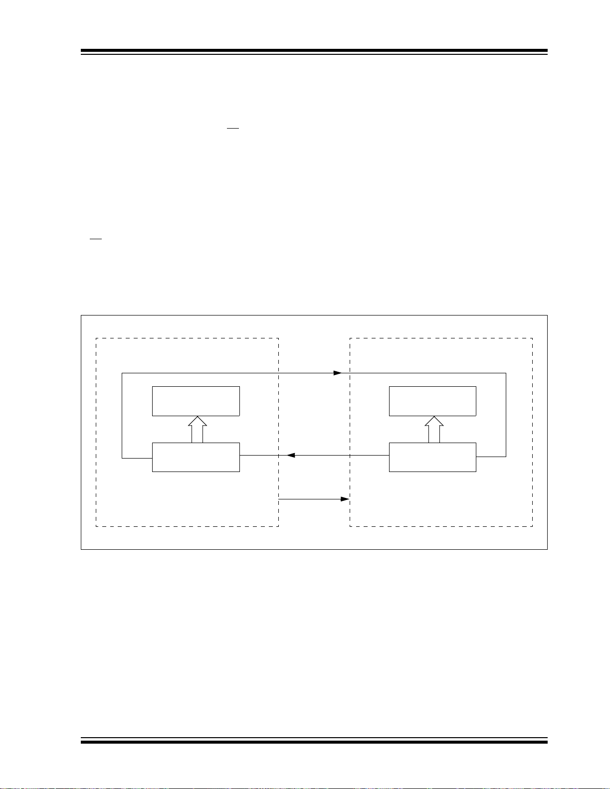
PIC16F87XA
9.3.3 ENABLING SPI I/O
To enable the serial port, SSP Enable bit, SSPEN
(SSPCON<5>), must be set. To reset or reconfigure
SPI mode, clear the SSPEN bit, re-initialize the
SSPCON registers and then set the SSPEN bit. This
configures the SDI, SDO, SCK and SS
port pins. For the pins t o behave as the serial p ort function, some must have their data direction bits (in the
TRIS register) appropriately programmed. That is:
• SDI is automaticall y c on t rol led by the SP I mo dule
• SDO must have TRISC<5> bit cleared
• SCK (Master mode) must have TRISC<3> bit
cleared
• SCK (Slave mode) must have TRISC<3> bit set
•SS
must have TRISC<4> bit set
pins as serial
9.3.4 TYPICAL CONNECTION
Figure 9-2 shows a typical connection between two
microcontrollers. The master controller (Processor 1)
initiates the data transfer by sending the SCK signal.
Data is shifted out of both shift registers on their
programmed clock edge and latched on the opposite
edge of the clock. Both processors should be
programmed to the same Clock Po larity (CKP), then
both controllers would send and receive data at the
same time. Whether the data is me aningful (or dummy
data) depends on the application software. This leads
to three scenarios for data transmission:
• Master sends data – Slave sends dummy data
• Master sends data – Slave sends data
• Master sends dummy data – Slave sends data
Any serial port function that is not desired may be
overridden by programming the corresponding data
direction (TRIS) register to the opposite value.
FIGURE 9-2: SPI MASTER/SLAVE CONNECTION
SPI Master SSPM3:SSPM0 = 00xxb
SDO
SPI Slave SSPM3 :SSPM0 = 010xb
SDI
Serial Input Buffer
(SSPBUF)
Shift Register
(SSPSR)
MSb
PROCESSOR 1
LSb
SDI
SCK
Serial Clock
SDO
SCK
Serial Input Buffer
(SSPBUF)
Shift Register
(SSPSR)
MSb
PROCESSOR 2
LSb
2003 Microchip Technology Inc. DS39582B-page 75
Page 78
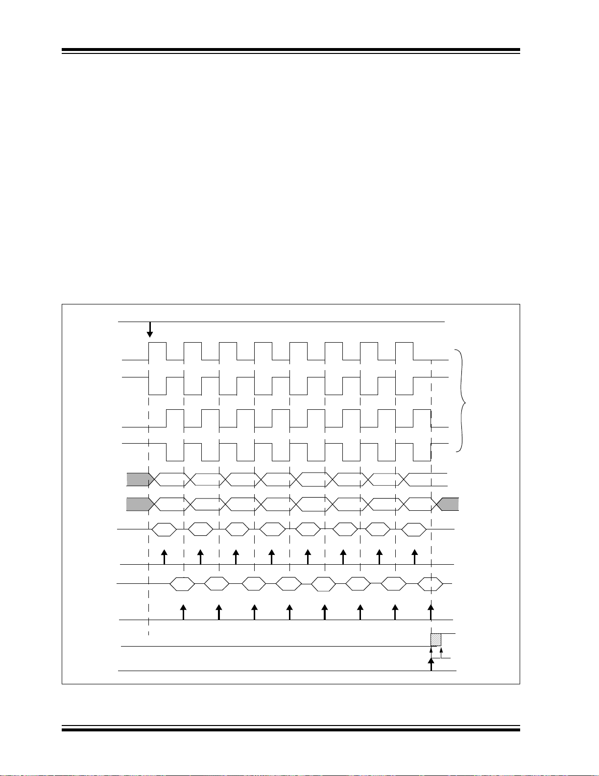
PIC16F87XA
9.3.5 MASTER MODE
The master can initiate the data transfer at any time
because it controls the SCK. The master determines
when the slave (Processor 2, Figure 9-2) is to
broadcast data by the software protocol.
In Master mode, the data is transmitted/received as
soon as the SSPBUF register is written to. If the SPI is
only going to receive, the SDO output could be
disabled (programmed as an input). The SSPSR
register will conti nue to shift i n the signal present on th e
SDI pin at the programmed clock rate. As each byte is
received, it will be loaded into the SSPBUF register as
if a normal received byte (interrupts and status bits
appropriately set). This could be useful in receiver
applications as a “Line Activity Monitor” mode.
The clock polarity is selected by appropriately pro gramming the CKP bit (SSPCON<4>). This then , would give
Figure 9-3, Figure 9-5 and Figure 9-6, where the MSB
is transmitted first. In Master mode, the SPI clock rate
(bit rate) is user programmable to be one of the
following:
OSC/4 (or TCY)
•F
•FOSC/16 (or 4 • TCY)
•F
OSC/64 (or 16 • TCY)
• Timer2 output/2
This allows a maximum data rate (at 40 MHz) of
10.00 Mbps.
Figure 9-3 shows the waveforms for Master mode.
When the CKE bit is set, the SDO data is valid before
there is a clock edge on SCK. The change of the input
sample is shown based on the state of the SMP bit. The
time when the SSPBUF is loaded with the received
data is shown.
waveforms for SPI communication as shown in
FIGURE 9-3: SPI MODE WAVEFORM (MASTER MODE)
Write to
SSPBUF
SCK
(CKP = 0
CKE = 0)
SCK
(CKP = 1
CKE = 0)
SCK
(CKP = 0
CKE = 1)
SCK
(CKP = 1
CKE = 1)
SDO
(CKE = 0)
SDO
(CKE = 1)
SDI
(SMP = 0)
Input
Sample
(SMP = 0)
SDI
(SMP = 1)
Input
Sample
(SMP = 1)
SSPIF
SSPSR to
SSPBUF
bit 7
bit 7
bit 7
bit 7
bit 6
bit 6
bit 5 bit 4
bit 5 bit 4
bit 3
bit 3
bit 2
bit 2
bit 1 bit 0
bit 1 bit 0
bit 0
bit 0
4 Clock
Modes
Next Q4 Cycle
after Q2↓
DS39582B-page 76 2003 Microchip Technology Inc.
Page 79

the SS
9.3.6 SLAVE MODE
In Slave mode, the data is transmitted and receiv ed a s
the external clock pulses appear on SCK. When the
last bit is latched, the SSPIF interrupt flag bit is set.
While in Slave mode, the external clock is supplied by
pin goes high, the SDO pin is no longer driven
even if in the middle o f a transmitted by te and become s
a floating output. External pull-up/pull-down resistors
may be desirable, depending on the application.
Note 1: When the SPI is in Slave mode with SS pin
the external clock source on the SCK pin. This external
clock must meet the minimum high and low times as
specified in the electrical specifications.
While in Sleep mode, the slave can transmit/receive
2: If the SPI is used in Slave Mode with CKE
data. When a byte is received, the device will wake-up
from Sleep.
When the SPI module resets, the bit counter is forced
9.3.7 SLAVE SELECT SYNCHRONIZATION
The SS pin allows a Synchronous Slave mode. The
SPI must be in Slave m ode with SS
(SSPCON<3:0> = 04h). The pin must n ot be drive n low
for the SS pin to function as an input. The data latch
must be high. When the SS
pin is low, tran smission and
reception are enab led and the SDO pin is driv en. When
pin control enabled
to ‘0’. This can be done by either forcing the SS
a high level or clearing the SSPEN bit.
To emulate two-wire communication, the SDO pin can
be connected to the SDI pin. When the SPI needs to
operate as a receiver, the SDO pin can be configured
as an input. This dis ables tran smissi ons from the SD O.
The SDI can always be left as an input (SDI function)
since it cannot create a bus conflict.
FIGURE 9-4: SLAVE SYNCHRONIZATION WAVEFORM
PIC16F87XA
control enabled (SSPCON<3:0> = 0100),
the SPI module will reset if the SS pin is se t
DD.
to V
set, then the SS pin control must be
enabled.
pin to
SS
SCK
(CKP = 0
CKE = 0)
SCK
(CKP = 1
CKE = 0)
Write to
SSPBUF
SDO
SDI
(SMP = 0)
Input
Sample
(SMP = 0)
SSPIF
Interrupt
Flag
SSPSR to
SSPBUF
bit 7
bit 7
bit 6 bit 7
bit 7
bit 0
bit 0
Next Q4 Cycle
after Q2↓
2003 Microchip Technology Inc. DS39582B-page 77
Page 80

PIC16F87XA
FIGURE 9-5: SPI MODE WAVEFORM (SLAVE MODE WITH CKE = 0)
SS
Optional
SCK
(CKP = 0
CKE = 0)
SCK
(CKP = 1
CKE = 0)
Write to
SSPBUF
SDO bit 7
SDI
(SMP = 0)
Input
Sample
(SMP = 0)
SSPIF
Interrupt
Flag
SSPSR to
SSPBUF
bit 7
bit 6
bit 5 bit 4
bit 3
bit 2
bit 1 bit 0
FIGURE 9-6: SPI MODE WAVEFORM (SLAVE MODE WITH CKE = 1)
SS
Not Optional
SCK
(CKP = 0
CKE = 1)
SCK
(CKP = 1
CKE = 1)
Write to
SSPBUF
bit 0
Next Q4 Cycle
after Q2↓
SDO bit 7
SDI
(SMP = 0)
Input
Sample
(SMP = 0)
SSPIF
Interrupt
Flag
SSPSR to
SSPBUF
DS39582B-page 78 2003 Microchip Technology Inc.
bit 7
bit 6
bit 5 bit 4
bit 3
bit 2
bit 1 bit 0
bit 0
Next Q4 Cycle
after Q2↓
Page 81

PIC16F87XA
9.3.8 SLEEP OPERATION
In Master mode, all module clocks are halted and the
transmission/reception will remain in that state until the
device wakes from Sleep. After the device returns to
normal mode, the module will continue to transmit/
receive data.
In Slave mode, the SPI Transmit/Receive Shift register
operates asynchron ously to the devi ce . This al lows the
device to be placed in Sleep mode and data to be
shifted into the SPI Transmit/Receive Shift register.
When all 8 bits have been rec eived, the MSSP interrupt
flag bit will be set and if enabled, will wake the device
from Sleep.
9.3.9 EFFECTS OF A RESET
A Reset disables the MSSP module and termina tes the
current transfer.
9.3.10 BUS MODE COMPATIBILITY
Table 9-1 shows the compatibility between the
standard SPI modes and the states of the CKP and
CKE control bits.
T ABLE 9-1: SPI BUS MODES
Standard SPI M ode
Terminology
0, 0 0 1
0, 1 0 0
1, 0 1 1
1, 1 1 0
There is also a SMP bit whi ch contro ls when th e data is
sampled.
Control Bits State
CKP CKE
TABLE 9-2: REGISTERS ASSOCIATED WITH SPI OPERATION
Name Bit 7 Bit 6 Bit 5 Bit 4 Bit 3 Bit 2 Bit 1 Bit 0
INTCON GIE/
GIEH
PIR1
PIE1
TRISC PORTC Data Direction Register 1111 1111 1111 1111
SSPBUF Synchronous Serial Port Receive Buffer/Transmit Register xxxx xxxx uuuu uuuu
SSPCON WCOL SSPOV SSPEN CKP SSPM3 SSPM2 SSPM1 SSPM0 0000 0000 0000 0000
TRISA
SSPSTAT SMP CKE
Legend: x = unknown, u = unchanged, - = unimplemented, read as ‘0’.
Note 1: The PSPIF, PSPIE and PSPIP bits are reserved on 28-pin devices; always maintain these bits clear.
PSPIF
PSPIE
— PORTA Data Direction Register --11 1111 --11 1111
Shaded cells are not used by the MSSP in SPI mode.
PEIE/
GIEL
(1)
ADIF RCIF TXIF SSPIF CCP1IF TMR2IF TMR1IF 0000 0000 0000 0000
(1)
ADIE RCIE TXIE SSPIE CCP1IE TMR2IE TMR1IE 0000 0000 0000 0000
TMR0IE INT0IE RBIE TMR0IF INT0IF RBIF 0000 000x 0000 000u
D/A P S R/W UA BF 0000 0000 0000 0000
Value on
POR, BOR
Value on
all other
Resets
2003 Microchip Technology Inc. DS39582B-page 79
Page 82

PIC16F87XA
9.4 I2C Mode
The MSSP module in I2C mode fully implements all
master and slave function s (in cl udi ng general call support) and provides interrupts on Start and Stop bits in
hardware to determine a free bus (multi-master function). The MSSP module implements the standard
mode specifications, as well as 7-bit and 10-bit
addressing.
Two pins are used for data transfer:
• Serial clock (SCL) – RC3/SCK/SCL
• Serial data (SDA) – RC4/SDI/SDA
The user must configure these pins as input s or output s
through the TRISC<4:3> bits.
FIGURE 9-7: MSSP BLOCK DIAGRAM
RC3/SCK/SCL
RC4/SDI/
SDA
2
(I
C MODE)
Read Write
SSPBUF reg
Shift
Clock
SSPSR reg
MSb
Match Detect
SSPADD reg
Start and
Stop bit Detect
LSb
Internal
Data Bus
Addr Match
Set, Reset
S, P bits
(SSPST AT reg)
9.4.1 REGISTERS
The MSSP module has six registers for I2C operation.
These are:
• MSSP Control Register (SSPCON)
• MSSP Control Register 2 (SSPCON2)
• MSSP Status Register (SSPSTAT)
• Serial Receive/Transmit Buffer Register
(SSPBUF)
• MSSP Shift Register (SSPSR) – Not directly
accessible
• MSSP Address Register (SSPADD)
SSPCON, SSPCON2 and SSPSTAT are the control
and status registers in I
SSPCON and SSPCON2 registers are readable and
writable. The lower six bits of the SSPSTAT are
read-only. The upper two bits of the SSPSTAT are
read/write.
SSPSR is the shift register used for shifting data in or
out. SSPBUF is the buffer register to which data bytes
are written to or read from.
SSPADD register holds the slave device address
when the SSP is configured in I
the SSP is configured in Master mode, the lower
seven bits of SSPADD act as the baud rate generator
reload value.
In receive operations, SSPSR and SSPBUF together
create a double-buffered receiver. When SSPSR
receives a complete byte, it is transferred to SSPBUF
and the SSPIF interrupt is set.
During transmission, the SSPBUF is not doublebuffered. A write to SSPBUF will write to both SSPBUF
and SSPSR.
2
C mode operation. The
2
C Slave mod e. Wh en
DS39582B-page 80 2003 Microchip Technology Inc.
Page 83

PIC16F87XA
REGISTER 9-3: SSPSTAT: MSSP STATUS REGISTER (I2C MODE) (ADDRESS 94h)
R/W-0 R/W-0 R-0 R-0 R-0 R-0 R-0 R-0
SMP CKE D/A
bit 7 bit 0
bit 7 SMP: Slew Rate Control bit
In Master or Slave mode:
1 = Slew rate control disabled for standard speed mode (100 kHz and 1 MHz)
0 = Slew rate control enabled for high-speed mode (400 kHz)
bit 6 CKE: SMBus Select bit
In Master or Slave mode:
1 = Enable SMBus specific inputs
0 = Disable SMBus specific inputs
bit 5 D/A
bit 4 P: Stop bit
bit 3 S: Start bit
bit 2 R/W
bit 1 UA: Update Address (10-bit Slave mode only)
bit 0 BF: Buffer Full Status bit
: Data/Address bit
In Master mode:
Reserved.
In Slave mode:
1 = Indicates that the last byte received or transmitted was data
0 = Indicates that the last byte received or transmitted was address
1 = Indicates t hat a Stop bit has been detected last
0 = Stop bit was not detected last
Note: This bit is cleared on Reset and when SSPEN is cleared.
1 = Indicates that a Start bit has been detected last
0 = Start bit was not detected last
Note: This bit is cleared on Reset and when SSPEN is cleared.
: Read/Write bit information (I2C mode only)
In Slave mode:
1 = Read
0 = Write
Note: This bit holds the R/W bit information following the last address match. This bit is
In Master mode:
1 = Transmit is in progress
0 = Transmit is not in progress
Note: ORing this bit with SEN, RSEN, PEN, RCEN or ACKEN will indicate i f the MSSP i s
1 = Indicates that the user needs to update the address in the SSPADD register
0 = Address does not need to be updated
In Transmit mode:
1 = Receive complete, SSPBUF is full
0 = Receive not complete, SSPBUF is empty
In Receive mode:
1 = Data Transmit in progress (does not include the ACK
0 = Data Transmit complete (does not include the ACK
only valid from the address match to the next Start bit, Stop bit or not ACK
in Idle mode.
PSR/WUA BF
and Stop bits), SSPBUF is full
and Stop bits), SSPBUF is empty
bit.
Legend:
R = Readable bit W = Writable bit U = Unimplemented bit, read as ‘0’
- n = Value at POR ‘1’ = Bit is set ‘0’ = Bit is cleared x = Bit is unknown
2003 Microchip Technology Inc. DS39582B-page 81
Page 84

PIC16F87XA
REGISTER 9-4: SSPCON1: MSSP CONTROL REGISTER 1 (I2C MODE) (ADDRESS 14h)
R/W-0 R/W-0 R/W-0 R/W-0 R/W-0 R/W-0 R/W-0 R/W-0
WCOL SSPOV SSPEN CKP SSPM3 SSPM2 SSPM1 SSPM0
bit 7 bit 0
bit 7 WCOL: Write Collision Detect bit
In Master Transmit mode:
1 = A write to the SSPBUF register was attempted while the I
a transmission to be started. (Must be cleared in software.)
0 = No collision
In Slave Transmit mode:
1 = The SSPBUF register is written while it is still transmitting the previous word. (Must be
cleared in software.)
0 = No collision
In Receive mode (Master or Slave modes):
This is a “don’t care” bit.
bit 6 SSPOV: Receive Overflow Indicator bit
In Receive mode:
1 = A byte is received while the SSPBUF register is still holding the previous byte. (Must be
cleared in software.)
0 = No overflow
In Transmit mode:
This is a “d on’t care” bit in Transmit mode.
bit 5 SSPEN: Synchronous Serial Port Enable bit
1 = Enables the serial port and configures the SDA and SCL pins as the serial port pins
0 = Disables the serial port and configures these pins as I/O port pins
Note: When enabled, the SDA and SCL pins must be proper ly configu red as in put or outp ut.
2
C conditions were not valid for
bit 4 CKP: SCK Release Control bit
In Slave mode:
1 = Release clock
0 = Holds clock low (clock stretch). (Used to ensure data setup time.)
In Master mode:
Unused in this mode.
bit 3-0 SSPM3:SSPM0: Synchronous Serial Port Mode Select bits
1111 = I
1110 = I
1011 = I
1000 = I
0111 = I
0110 = I
Legend:
R = Readable bit W = Writable bit U = Unimplemented bit, read as ‘0’
- n = Value at POR ‘1’ = Bit is set ‘0’ = Bit is cleared x = Bit is unknown
2
2
2
2
2
2
Note: Bit combinations not specifically listed here are either reserved or implemented in
C Slave mode, 10-bit address with Start and Stop bit interrupts enabled
C Slave mode, 7-bit address with Start and Stop bit interrupts enabled
C Firmware Controlled Master mode (Slave Idle)
C Master mode, clock = FOSC/(4 * (SSPADD + 1))
C Slave mode, 10-bit address
C Slave mode, 7-bit address
SPI mode only.
DS39582B-page 82 2003 Microchip Technology Inc.
Page 85

PIC16F87XA
REGISTER 9-5: SSPCON2: MSSP CONTROL REGISTER 2 (I2C MODE) (ADDRESS 91h)
R/W-0 R/W-0 R/W-0 R/W-0 R/W-0 R/W-0 R/W-0 R/W-0
GCEN ACKSTAT ACKDT ACKEN RCEN PEN RSEN SEN
bit 7 bit 0
bit 7 GCEN: General Call Enable bit (Slave mode only)
1 = Enable interrupt when a general call address (0000h) is received in the SSPSR
0 = General call address disabled
bit 6 ACKSTAT : Acknowledge Status bit (Master Transmit mode only)
1 = Acknowledge was not received from slave
0 = Acknowledge was received from slave
bit 5 ACKDT: Acknowledge Data bit (Master Receive mode only)
1 = Not Acknowledge
0 = Acknowledge
Note: Value tha t will be t ransmitted w hen the us er initiates an Acknowl edge sequ ence at
the end of a receive.
bit 4 ACKEN: Acknowledge Sequence Enable bit (Master Recei ve mo de onl y)
1 = Initiate Acknowledge sequence on SDA and SCL pins and transmit ACKDT data bit.
Automatically cleared by hardware.
0 = Acknowledge sequence Idle
bit 3 RCEN: Receive Enable bit (Master mode only)
1 = Enables Receive mode for I
0 = Receive Idle
bit 2 PEN: Stop Condition Enable bit (Master mode only)
1 = Initiate Stop condition on SDA and SCL pins. Automatically cleared by hardware.
0 = Stop condition Id le
bit 1 RSEN: Repeated Start Condition Enabled bit (Master mode only)
1 = Initiate Repeated Start condition on SDA and SCL pins. Automatically cleared b y hardware.
0 = Repeated Start condition Idle
bit 0 SEN: Start Condition Enabled/Stretch Enabled bit
In Master mode:
1 = Initiate Start condition on SDA and SCL pins. Automatically cleared by hardware.
0 = Start condition Idle
In Slave mode:
1 = Clock stretching is enabled for both slave transmit and slave receive (stretch enabled)
0 = Clock stretching is enabled for slave transmit only (PIC16F87X compatibility)
2
C
Legend:
R = Readable bit W = Writable bit U = Unimplemented bit, read as ‘0’
- n = Value at POR ‘1’ = Bit is set ‘0’ = Bit is cleared x = Bit is unknown
Note: For bits ACKEN, RCEN, PEN, RSEN, SEN: If the I2C module is not in the Idl e mode,
this bit may not be set (no s poo lin g) an d the SS PBUF may no t be w ritt en (or writes
to the SSPBUF are disabled).
2003 Microchip Technology Inc. DS39582B-page 83
Page 86

PIC16F87XA
9.4.2 OPERATION
The MSSP module functions are enabled by setting
MSSP Enable bit, SSPEN (SSPCON<5>).
2
The SSPCON register allows control of the I
tion. Four mode selection bits (SSPCON<3:0>) allow
one of the following I2C modes to be selected:
2
C Master mode, clock = OSC/4 (SSPADD + 1)
•I
2
•I
C Slave mode (7-bit address)
•I2C Slave mode (10-bit address)
•I2C Slave mode (7-bit address) with Start and
Stop bit interrupts enabled
2
C Slave mode (10-bit address) with Start and
•I
Stop bit interrupts enabled
2
C Firmware Controlled Master mode, slave is
•I
Idle
2
Selection of any I
forces the SCL and SDA pins to be open-drain, provided these pins are programmed to inputs by setting
the appropriate TRIS C bits. To ensure proper oper ation
of the module, pull-up resistors must be provided
externally to the SCL and SDA pins.
C mode, with the SSPEN bit set,
C opera-
9.4.3 SLAVE MODE
In Slave mode, the SCL and SDA pins must be confi gured as inputs (TRISC<4:3> set). The MSSP module
will override the input state with the output data when
required (slave-transmitter).
2
C Slave mode hardwa re w i ll alwa ys ge nerate an
The I
interrupt on an address match. Through the mode
select bits, the user can also choose to interrupt on
Start and Stop bits
When an address is match ed, or the dat a trans fer after
an address m atch i s re ceiv ed, the ha rd ware autom ati cally will generate the Acknowledge (ACK
load the SSPBUF register with the received value
currently in the SSPSR register.
Any combination of the following conditions will cause
the MSSP module not to give this ACK
• The buffer full bit, BF (SSPSTAT<0>), was set
before the transfer was received.
• The overflow bit, SSPOV (SSPCON<6>), was set
before the transfer was received.
In this case, the SSPSR register value is not loaded
into the SSPBUF, but bit SSPIF (PIR1<3>) is set. The
BF bit is cleared by reading the SSPBUF registe r , while
bit SSPOV is cleared through software.
The SCL clock input must have a minimum high and
low for proper operati on . Th e h igh an d l ow ti mes of the
2
C specification, as well as the requirement of the
I
MSSP module, are shown in timing parameter #100
and parameter #101.
) pulse and
pulse:
9.4.3.1 Addressing
Once the MSSP module has been enabled, it waits for
a Start co ndition to occ ur. Following the Start co ndition,
the 8 bits are sh ifted into the SSPS R register . All incom ing bits are sampled with the rising edge of the clock
(SCL) line. The value of register SSPSR<7:1> is compared to the value of the SSPADD register. The
address is compared on the falling edge of the eighth
clock (SCL) pulse. If the addresses match, and the BF
and SSPOV bits are clear, the following events occur:
1. The SSPSR register value is loaded into the
SSPBUF register.
2. The Buffer Full bit, BF, is set.
3. An ACK
4. MSSP Interrupt Flag bit, SSPIF (PIR1<3>), is
set (interrupt is generated if enabled) on the
falling edge of the ninth SCL pulse.
In 10-bit Address mode, two address bytes need to be
received by the slave. The five Most Significant bits
(MSbs) of the first a ddress byte specify i f this is a 10-bit
address. Bit R/W
so the slave device will receive the second address
byte. For a 10-bit address, the first byte would equal
‘11110 A9 A8 0’, where ‘A9’ and ‘A8’ are t he two
MSbs of the address. The sequence of events for
10-bit address is as follows, with steps 7 through 9 for
the slave-transmitter:
1. Receive first (high) byte of address (bits SSPIF,
BF and bit UA (SSPSTAT<1>) are set).
2. Update the SSPADD register with second (low)
byte of address (clears bit UA and releases the
SCL line).
3. Read the SSPBUF register (clears bit BF) and
clear flag bit SSPIF.
4. Receive second (low) byte of address (bits
SSPIF, BF and UA are set).
5. Update the SSPADD register with the first (high)
byte of address. If m at ch rel ea ses SC L l in e, thi s
will clear bit UA.
6. Read the SSPBUF register (clears bit BF) and
clear flag bit SSPIF.
7. Receive Repeated Start condition.
8. Receive first (high) byte of address (bits SSPIF
and BF are set).
9. Read the SSPBUF register (clears bit BF) and
clear flag bit SSPIF.
pulse is generated.
(SSPSTAT<2>) must specify a write
DS39582B-page 84 2003 Microchip Technology Inc.
Page 87

PIC16F87XA
9.4.3.2 Reception
When the R/W bit of the address byte is clear and an
address match occurs, the R/W
register is cleare d. The re ceive d addre ss is loa ded in to
the SSPBUF register and the SDA line is held low
).
(ACK
When the address byte overflow condition exists, then
the No Acknowledge (ACK
condition is defined as either bit BF (SSPSTAT<0>) is
set or bit SSPOV (SSPCON<6>) is set.
An MSSP interrupt is generated for each data transfer
byte. Flag bit SSPIF (PIR1<3>) must be cle ared in software. The SSPSTAT register is used to determine the
status of the byte.
If SEN is enabled (SSPCON<0> = 1), RC3/SCK/SCL
will be held low (clock stretch) following each dat a transfer. The clock must be released by setting bit CKP
(SSPCON<4>). See Section 9.4.4 “Clock Stretching”
for more detail.
bit of the SSPSTAT
) pulse is given. An overflow
9.4.3.3 Transmission
When the R/W bit of the incoming address byte is set
and an address match occurs, the R/W
SSPSTAT register is set. The received address is l oaded
into the SSPBUF register. The ACK puls e will be sent on
the ninth bit and pin RC3/SCK/SCL is held low regardless of SEN (see Section 9.4.4 “Clock Stretching” for
more detail). By stretching the clock, the master will be
unable to assert another clock pulse until the slave is
done preparing the transmit data. The transmit data
must be loaded into the SSPBUF register, which also
loads the SSPSR register. Then pin RC3/SCK/SCL
should be enabled by setting bit CKP (SSPCON<4>).
The eight data bits are shifted out on the falling edge of
the SCL input. This ensures that the SDA signal is valid
during the SCL high time (Figure 9-9).
The ACK
the rising edge of the ninth SCL in put pulse. If the SDA
line is high (not ACK), then the data transfer is complete. In this case, when the ACK
slave, the slave logic is reset (resets SSPSTAT register) and the slave monitors for another occurrence of
the Start bit. If the SDA line was low (ACK
transmit data must be loaded into the SSPBUF r egister .
Again, pin RC3/SCK/SCL must be enabled by setting
bit CKP.
An MSSP interrupt is generated for each data transfer
byte. The SSPIF bit must be cleared in software and
the SSPSTAT register is used to determine the status
of the byte. The SSPIF bit is set on the falling edge of
the ninth clock pulse.
pulse from the master-receiver is latched on
bit of the
is latched by the
), the next
2003 Microchip Technology Inc. DS39582B-page 85
Page 88

PIC16F87XA
FIGURE 9-8: I2C SLAVE MODE TIMING WITH SEN = 0 (RECEPTION, 7-BIT ADDRESS)
ACK
Receiving Data
ACK
P
6
D2
Bus master
terminates
transfer
SSPOV is set
because SSPBUF is
still full. ACK is not sent.
Receiving Data
= 0
R/W
Receiving Address
ACK
A7 A6 A5 A4 A3 A2 A1 D7 D6 D5 D4 D3 D2 D1 D0 D7 D6 D5 D4 D3 D1 D0
SDA
1234 56 7 891 2345 6789 1 2345 7 89
S
SCL
Cleared in software
SSPBUF is read
(CKP does not reset to ‘0’ wh e n S E N = 0)
SSPIF
BF (SSPSTAT<0>)
(PIR1<3>)
SSPOV (SSPCON<6>)
CKP
DS39582B-page 86 2003 Microchip Technology Inc.
Page 89

PIC16F87XA
FIGURE 9-9: I2C SLAVE MODE TIMING (TRANSMISSION, 7-BIT ADDRESS)
P
ACK
D0
D1
D2
D3
Transmitting Data
D4
D5
D6
D7
2 3 4 5 6 7 8 9
1
From SSPIF ISR
Cleared in software
SSPBUF is written in so ft w a r e
CKP is set in so f tw a re
ACK
D0
D1
D2
D3
D4
Transmitting Data
D5
D6
SCL held low
while CPU
responds to SSPIF
ACK
1
R/W =
A1
A2
A4 A3
Receiving Address
A5
A6
A7 D7
9 1
1 2 3 4 5 6 7 8 2 3 4 5 6 7 8 9
Data in
sampled
From SSPIF ISR
Cleared in software
SSPBUF is written in software
CKP is set in so f tw a re
S
SDA
SCL
SSPIF (PIR1<3>)
BF (SSPSTAT<0>)
CKP
2003 Microchip Technology Inc. DS39582B-page 87
Page 90

PIC16F87XA
FIGURE 9-10: I2C SLAVE MODE TIMING WITH SEN = 0 (RECEPTION, 10-BIT ADDRESS)
Bus master
terminates
transfer
P
SSPOV is set
because SSPBUF is
ACK
6
D2
still full. ACK is not sent.
Receive Data Byte
D7 D6 D5 D4 D3 D1 D0
12345 789
ACK
6
D2
Receive Data Byte
Clock is held low until
update of SSPADD has
ACK
taken place
Receive Second Byte of Address
Cleared in software
Cleared in software
Cleared by hardware when
SSPADD is updated with high
byte of address
UA is set indicating that
SSPADD needs to be
Cleared in software
Cleared by hardware
Dummy read of SSPBUF
to clear BF flag
when SSPADD is updated
updated
with low byte of address
Clock is held low until
update of SSPADD has
taken place
ACK
R/W = 0
SSPBUF is written with
Receive First Byte of Address
1 1 1 1 0 A9A8 A7 A6A5A4A3A2A1A0 D7 D6D5D4D3 D1D0
SDA
1234 56789 123456789 12345 789
SCL
contents of SSPSR
Cleared in software
S
SSPIF
BF (SSPSTAT<0>)
(PIR1<3>)
SSPOV (SSPCON<6>)
UA is set indicating that
the SSPADD needs to be
updated
(CKP does not reset to ‘0’ when SEN = 0)
UA (SSPSTAT<1>)
CKP
DS39582B-page 88 2003 Microchip Technology Inc.
Page 91

PIC16F87XA
FIGURE 9-11: I2C SLAVE MODE TIMING (TRANSMISSION, 10-BIT ADDRESS)
P
terminates
transfer
Bus master
ACK
D0
6
D2
Completion of
clears BF flag
data transmission
Transmitting Data Byte
12345 789
D7 D6 D5 D4 D3 D1
Clock is held low until
CKP is set to ‘1’
ACK
R/W=1
6
A9
Receive First Byte of Address
Sr
taken place
taken place
ACK
Receive Second Byte of Address
ACK
R/W = 0
Clock is held low until
update of SSPADD has
Clock is held low until
update of SSPADD has
Cleared in software
initiates transmit
Write of SSPBUF
BF flag is clear
third address sequence
at the end of the
Cleared in software
Dummy read of SSPBUF
Cleared in software
Dummy read of SSPBUF
Cleared by hardware when
SSPADD is updated with high
byte of address
to clear BF flag
UA is set indicating that
SSPADD needs to be
updated
Cleared by hardware when
SSPADD is updated with low
byte of address
to clear BF flag
CKP is set in software
CKP is automatically cleared in hardware holding SCL low
SSPBUF is written with
contents of SSPSR
UA is set indicating that
the SSPADD needs to be
updated
11110A9A8 A7 A6A5A4A3A2A1A0 11110 A8
SDA
1234 56 789 1 23456789 12345 789
SCL
S
SSPIF
BF (SSPSTAT<0>)
(PIR1<3>)
UA (SSPSTAT<1>)
CKP (SSPCON<4>)
Receive First Byte of Address
2003 Microchip Technology Inc. DS39582B-page 89
Page 92

PIC16F87XA
9.4.4 CLOCK STRETCHING
Both 7 and 10-bit Slave modes implement automatic
clock stretching during a transmit sequence.
The SEN bit (SSPCON2<0>) allows clock stretching to
be enabled during receives. Setting SEN will cause
the SCL pin to be held low at the end of each data
receive sequence.
9.4.4.1 Clock Stretching for 7-bit Slave
Receive Mode (SEN = 1)
In 7-bit Slave Receive mode, on the falling edge of the
ninth clock at the end of the ACK
bit is set, the CKP bit in the SSPCON register is
automatically cleared, forcing the SCL output to be
held low. The CKP bit being cleared to ‘0’ will assert
the SCL line low . Th e CKP bit mus t be set in the user’s
ISR before reception i s allo wed to co ntinue . By hol ding
the SCL line low, the user has time to service the ISR
and read the contents of the SSPBUF before the
master device can initiate another receive sequence.
This will prevent buffer overruns from occurring (see
Figure 9-13).
Note 1: If the user reads the contents of the
SSPBUF before the falling edge of the
ninth clock, thus clearing the BF bi t, the
CKP bit will not be cleared and clock
stretching will not occur.
2: The CKP bit can be set in software
regardless of the state of the BF bit. The
user should be careful to clear the BF bit
in the ISR before the next receive
sequence in order to prevent an overflow
condition.
sequence, if the BF
9.4.4.3 Clock Stretching for 7-bit Slave
Transmit Mode
7-bit Slave Transmit mode implements clock stretching
by clearing the CKP bit after the falling edge of the ninth
clock, if the BF bit is clear. This occurs regardless of the
state of th e SEN bit.
The user’s ISR must set the CKP bit before transmission is allowed to continue. By holding the SCL line
low, the user has time to service the ISR and load the
contents of the SSPBUF before the master device can
initiate another transmit sequence (see Figure 9-9).
Note 1: If the user loads the co nten t s of SSPBUF,
setting the BF bit bef ore the falling edg e of
the ninth clock, the CKP bit will not be
cleared and clock stretching will n ot occur .
2: The CKP bit can be set in software
regardless of the state of the BF bit.
9.4.4.4 Clock Stretching for 10-bit Slave
Transmit Mode
In 10-bit Slave Transmit mode, clock stretching is controlled during the first two address sequences by the
state of the UA bit, just as it is in 10-bit Slave Receive
mode. The first two addresses are followed by a third
address sequence, which contains the high order bits
of the 10-bit address and the R/W
the third address sequence is performed, the UA bit is
not set, the module is now configured in Transmit
mode and clock stretching is controlled by the BF flag
as in 7-bit Slave Transmit mode (see Figure 9-11).
bit set to ‘1’. After
9.4.4.2 Clock Stretching for 10-bit Slave
Receive Mode (SEN = 1)
In 10-bit Slave Receive mode, during the address
sequence, clock stretching automatically takes place
but CKP is not cleared. During t his time, if th e UA b it i s
set after the ninth clock, clock stretching is initiated.
The UA bit is set after receiving the upper byte of the
10-bit address and following the receive of the second
byte of the 10-bit address, with the R/W
‘0’. The release of the clock line occurs upon updating
SSPADD. Clock stretching will occur on each data
receive sequence as described in 7-bit mode.
Note: If the user polls the UA bit and clears it by
updating the SSPADD register before the
falling edge of the ni nth c lock occurs and if
the user hasn’t cleared the BF bit by reading the SSPBUF register before that time,
then the CKP bit will still NOT be asserted
low. Clock stretchin g, on the basis of the
state of the BF bit, only occurs during a
data sequence, not an address sequence.
DS39582B-page 90 2003 Microchip Technology Inc.
bit cleared to
Page 93

9.4.4.5 Clock Synchronization and the
CKP Bit
When the CKP bit is cleared, the SCL output is forced
to ‘0’; however, setting the CKP bit will not assert the
SCL output low until the SCL output is already sampled
low. Therefore, the CKP bit will not assert the SCL line
until an external I
asserted the SCL line. The SCL output will remain low
until the CKP bit is set and all other devices on the I2C
bus have deasserted SCL. This ensures that a write to
the CKP bit will not violate the minimum high time
requirement for SCL (see Figure 9-12).
2
C master device has already
FIGURE 9-12: CLOCK SYNCHRONIZATION TIMING
Q1 Q2 Q3 Q4 Q1 Q2 Q3 Q4 Q1 Q2 Q3 Q4 Q1 Q2 Q3 Q4 Q1 Q2 Q3 Q4 Q1 Q2 Q3 Q4 Q1 Q2 Q3 Q4
PIC16F87XA
SDA
SCL
CKP
WR
SSPCON
DX-1DX
Master device
asserts clock
Master device
deasserts clock
2003 Microchip Technology Inc. DS39582B-page 91
Page 94

PIC16F87XA
FIGURE 9-13: I2C SLAVE MODE TIMING WITH SEN = 1 (RECEPTION, 7-BIT ADDRESS)
P
Clock is not held low
because ACK = 1
ACK
6
D2
Receiving Data
Clock is held low until
CKP is set to ‘1’
ACK
Bus master
terminates
transfer
SSPOV is set
because SSPBUF is
still full. ACK is not sent.
CKP
written
to ‘1’ in
software
BF is set after falling
edge of the 9th clock,
CKP is reset to ‘0’ and
clock stretching occurs
Receiving Data
Cleared in software
If BF is cleared
prior to the falling
edge of the 9th clock,
CKP will not be reset
to ‘0’ and no clock
Clock is not held low
because buffer full bit is
clear prior to falling edge
of 9th clock
= 0
R/W
Receiving Address
ACK
A7 A6 A5 A4 A3 A2 A1 D7 D6 D5 D4 D3 D2 D1 D0 D7 D6 D5 D4 D3 D1 D0
SDA
1234 56 789 12345 6789 1 2345 7 89
S
SCL
SSPIF
(PIR1<3>)
SSPBUF is read
BF (SSPSTAT<0>)
SSPOV (SSPCON<6>)
CKP
stretching will occur
DS39582B-page 92 2003 Microchip Technology Inc.
Page 95

PIC16F87XA
FIGURE 9-14: I2C SLAVE MODE TIMING SEN = 1 (RECEPTION, 10-BIT ADDRESS)
P
ACK
Clock is not held low
because ACK = 1
6
D2
Receive Data Byte
D7 D6 D5 D4 D3 D1 D0
12345 789
ACK
Clock is held low until
CKP is set to ‘1’
6
D2
Receive Data Byte
transfer
terminates
Bus master
SSPOV is set
because SSPBUF is
still full. ACK is not sent.
Cleared in software
CKP written to ‘1’
in software
Cleared in software
Cleared by hardware when
SSPADD is updated with high
byte of address after falling edge
Dummy read of SSPBUF
to clear BF flag
of ninth clock
before the falling edge of the ninth clock
will have no effect on UA, and UA will
remain set.
Note:An update of the SSPADD register
Clock is held low until
update of SSPADD has
taken place
ACK
UA is set indicating that
SSPADD needs to be
updated
before the falling edge of the ninth clock
will have no effect on UA and UA will
Receive Second Byte of Address
Clock is held low until
update of SSPADD has
taken place
ACK
R/W = 0
Receive First Byte of Address
1 1 1 1 0 A9A8 A7 A6A5A4A3A2A1 A0 D7D6D5D4D3 D1D0
123456789 1 23456789 12345 789
S
Cleared in software
Cleared by hardware when
SSPADD is updated with low
byte of address after falling edge
UA is set indicating that
of ninth clock
SSPADD needs to be
updated
Dummy read of SSPBUF
to clear BF flag
SSPBUF is written with
contents of SSPSR
Cleared in software
remain set.
Note:An update of the SSPADD register
SDA
SCL
SSPIF
BF (SSPSTAT<0>)
(PIR1<3>)
SSPOV (SSPCON<6>)
UA (SSPSTAT<1>)
CKP
2003 Microchip Technology Inc. DS39582B-page 93
Page 96

PIC16F87XA
9.4.5 GENERAL CALL ADDRESS SUPPORT
The addressing procedure for the I2C bus is such that
the first byte after the Start c ondition usu ally determines
which device will be the slave addressed by the master.
The exception is the general call address which can
address all devices. When this address is used, all
devices should, in theory , respond with an Acknowledge.
The general call address is one of eight addresses
reserved for specific purposes by the I
consists of all ‘0’s with R/W
= 0.
The general call address is recognized when the General Call Enable bit (GCEN) is enabled (SSPCON2<7>
set). Following a Start bit detect, 8 bits are shifted into
the SSPSR and the address is compared against the
SSPADD. It is also compared to the general call
2
C protocol. It
If the general call address matches, the SSPSR is
transferred to the SSPBUF, the BF flag bit i s set (eigh th
bit) and on the falling edg e of the ninth bit (ACK
SSPIF interrupt flag bit is set.
When the interrupt is serv ic ed, the s ou r ce f or the int errupt can be checked by reading the contents of the
SSPBUF. The value can be used to determine if the
address was device specific or a general call address.
In 10-bit mode, the SSPADD is required to be updated
for the second half of the addre ss to match an d the UA
bit is set (SSPSTAT<1>). If the general call address is
sampled when the GCEN bit is set, while the slave is
configured in 10-bit Address mode, then the second
half of the address is not necessary, the UA bit will not
be set and the slave will begin receiving data after the
Acknowledge (Figure9-15).
address and fixed in hardware.
FIGURE 9-15: SLAVE MODE GENERAL CALL ADDRESS SEQUENCE
(7 OR 10-BIT ADDRESS MODE)
Address is compared to general call address.
After ACK, set interrupt.
Receiving Data
SDA
General Call Address
R/W
= 0
ACK
D7 D6 D5 D4 D3 D2 D1 D0
bit), the
ACK
SCL
S
SSPIF
BF (SSPSTAT<0>)
SSPOV (SSPCON<6>)
GCEN (SSPCON2<7>)
123456789123456789
Cleared in software
SSPBUF is read
‘0’
‘1’
DS39582B-page 94 2003 Microchip Technology Inc.
Page 97

PIC16F87XA
9.4.6 MASTER MODE
Master mode is enabled by setting and clearing the
appropriate SSPM bits in SSPCON and by setting the
SSPEN bit. In Master mode, the SCL and SDA lines
are manipulated by the MSSP hardware.
Master mode of operation is supported by interrupt
generation on the detection of the Start and Stop conditions. The Stop (P) and Start (S) bi ts are c leared from
a Reset or when the MSSP mod ule is disa bled. Contro l
2
of the I
bus is Idle, with both the S and P bits clear.
In Firmware Controlled Master mode, user code
conducts all I
Stop bit conditions.
Once Master mode is enabled, the user has six
options.
1. Assert a Start condition on SDA and SCL.
2. Assert a Repeated Start condition on SDA and
3. Write to the SSPBUF register, initiating
4. Configure the I
5. Generate an Acknowledge condition at the end
6. Generate a Stop condition on SDA and SCL.
C bus may be taken when the P bit is s et or the
2
C bus operations based on Start and
SCL.
transmission of data/address.
2
C port to receive data.
of a received byte of data.
Note: The MSSP module, when configured in
2
C Master mode, does n ot allow que ueing
I
of events. For instance, the user is not
allowed to initiate a Start condition and
immediately write the SSPBUF register to
initiate transmiss ion before the S tart con dition is complete. I n this ca se, the SSPBUF
will not be written to and the WC O L bi t will
be set, indicating that a write to the
SSPBUF did not occur.
The following events will cause SSP Interrupt Flag bit,
SSPIF, to be set (SSP interrupt if enabled):
• Start condition
• Stop condition
• Data transfer byte transmitted/received
• Acknowledge transmit
• Repeated S t art
FIGURE 9-16: MSSP BLOCK DIAGRAM (I2C MASTER MODE)
Internal
Data Bus
Read Write
SSPBUF
LSb
Shift
Clock
Clock Cntl
Set/Reset, S, P, WCOL (SSPSTAT)
Set SSPIF, BCLIF
Reset ACKSTA T, PEN (SSPCON2)
SDA
SCL
SDA In
Receive Enable
SCL In
Bus Collision
SSPSR
MSb
Start bit, Stop bit,
Acknowledge
Generate
Start bi t Dete ct
Stop bit Detect
Write Collision Detect
Clock Arbitration
State Counter for
end of XMIT/RCV
SSPM3:SSPM0
SSPADD<6:0>
Baud
Rate
Generator
(hold off clock source)
Clock Arbitrate/WCOL Detect
2003 Microchip Technology Inc. DS39582B-page 95
Page 98

PIC16F87XA
9.4.6.1 I2C Master Mode Operation
The master device generates all of the serial clock
pulses and the Start and Stop condit ions. A trans fer is
ended with a Stop condition or with a Repeated Start
condition. Since the Repeated Start condition is also
the beginning of the next serial transfer, the I
not be rele ased.
In Master Transmitter mode, serial data is output
through SDA while SCL outputs the serial clock. The
first byte transmitted contains the slave address of the
receiving de vic e (7 bi ts) and t he Re ad/Wr ite
In this case, the R/W
transmitted 8 bits at a ti me . Afte r ea ch byte is transmitted, an Acknowledge bit is received. Start and Stop
conditions are output to indicate the beginning and the
end of a serial transfer.
In Master Receive mode, the firs t byte transmitt ed contains the slave address of the transmitting device
(7 bits) and the R/W
logic ‘1’. Thus, the first byte transmitted is a 7-bit slave
address followed by a ‘1’ to indicate the receive bit.
Serial data is received via SDA while SCL outputs the
serial clock. Serial data is receive d 8 bits at a time. After
each byte is received, an Acknowledge bit is transmitted. Start and Stop co nditions indicate the beginning
and end of transmission.
The baud rate generator used for the SPI mode ope ration is used to set the SCL clock frequency for either
100 kHz, 400 kHz or 1 MHz I
Section 9.4.7 “Baud Rate Generator” for more det ail.
bit will be lo gic ‘0’ . Se rial da ta is
bit. In this case, the R/W bit will be
2
C operation. See
2
C bus will
(R/W) bit.
A typical transmit sequence would go as follows:
1. The user generates a Start condition by setting
the Start Enable bit, SEN (SSPCON2<0>).
2. SSPIF is set. The MSSP module will wait the
required Start time before any other operation
takes place.
3. The user loads the SSPBUF with the slave
address to transmit.
4. Address is shifted out the SDA pin unt il all 8 bit s
are transmitted.
5. The MSSP module shifts in the ACK bit from the
slave device and writes its value into the
SSPCON2 register (SSPCON2<6>).
6. The MSSP module generate s an interrup t at th e
end of the ninth clo ck cycle by setting t he SSPIF
bit.
7. The user loads the SSPBUF with eight bits of
data.
8. Data is shifted out the SDA pin unt il all 8 bits are
transmitted.
9. The MSSP module shifts in the ACK bit from the
slave device and writes its value into the
SSPCON2 register (SSPCON2<6>).
10. The MSSP module generates an int errupt a t the
end of the ninth clo ck cycle by setting t he SSPIF
bit.
11. The user generates a Stop condition by setting
the Stop Enable bit, PEN (SSPCON2<2>).
12. Interrupt is generated once the S t op cond ition i s
complete.
DS39582B-page 96 2003 Microchip Technology Inc.
Page 99

PIC16F87XA
9.4.7 BAUD RATE GENERATOR
In I2C Master mode , the Baud Ra te Generato r (BRG)
reload value is placed in the lower 7 bits of the
SSP ADD register (Figure 9-17). When a write occurs to
SSPBUF, the Baud Rate Generator will automatically
begin counting. The BRG counts down to 0 and stops
until another reload h as t aken place. The BRG count i s
decremented twice per instruction cycle (T
Q2 and Q4 clock s. In I
2
C Master mode, the BRG is
CY) on the
Once the given operation is complete (i.e., transmission of the last dat a bit is followed by ACK
), the internal
clock will automatically stop counting and the SCL pin
will remain in its last st a te.
Table 9-3 demonstrates clock rates based on
instruction cycles and the BRG value loaded into
SSPADD.
reloaded automatically.
FIGURE 9-17: BAUD RATE GENERATOR BLOCK DIAGRAM
SSPM3:SSPM0
TABLE 9-3: I
SSPM3:SSPM0
SCL
2
C CLOCK RATE W/BRG
Reload
Control
CLKO
FCY FCY*2 BRG Value
10 MHz 20 MHz 19h 400 kHz
10 MHz 20 MHz 20h 312.5 kHz
10 MHz 20 MHz 3Fh 100 kHz
4 MHz 8 MHz 0Ah 400 kHz
4 MHz 8 MHz 0D h 308 kHz
4 MHz 8 MHz 28h 100 kHz
1 MHz 2 MHz 03h 333 kHz
1 MHz 2 MHz 0Ah 100 kHz
1 MHz 2 MHz 00h 1 MHz
Note 1: The I2C interface does not conform to the 400 kHz I2C specification (which applies to rates greater than
100 kHz) in all details, but may be used with care where higher rates are required by the application.
SSPADD<6:0>
Reload
BRG Down Counter
F
OSC/4
SCL
F
(2 Rollovers of BRG)
(1)
(1)
(1)
(1)
2003 Microchip Technology Inc. DS39582B-page 97
Page 100

PIC16F87XA
9.4.7.1 Clock Arbitration
Clock arbitration occurs when the master, during any
receive, transmit or Repeated Start/Stop condition,
deasserts the SCL pin (SCL allowed to float high).
When the SCL pin is allowed to float high, the Baud
Rate Generator (BRG) is suspended from counting
SCL pin is sampled high, the Baud Rate Generator is
reloaded with the contents of SSPADD<6:0> and
begins coun ting. This ensures t hat the SC L high time
will always be at least one BRG rollover count, in the
event that the clock is held low by an external device
(Figure 9-17).
until the SCL pin is actually sampled high. When the
FIGURE 9-18: BAUD RATE GENERATOR TIMING WITH CLOCK ARBITRATION
SDA
SCL
BRG
Value
BRG
Reload
SCL deasserted but slave holds
SCL low (clock arbitration)
03h 02h 01h 00h (hold off) 03h 02h
SCL is sampled high, reload takes
place and BRG starts its count
DX-1DX
SCL allowed to transition high
BRG decrements on
Q2 and Q4 cycles
DS39582B-page 98 2003 Microchip Technology Inc.
 Loading...