


PIC16F872
Data Sheet
28-Pin, 8-Bit CMOS Flash
Microcontroller with 10-Bit A/D
© 2006 Microchip Technology Inc. DS30221C

Note the following details of the code protection feature on Microchip devices:
• Microchip products meet the specification contained in their particular Microchip Data Sheet.
• Microchip believes that its family of products is one of the most secure families of its kind on the market today, when used in the
intended manner and under normal conditions.
• There are dishonest and possibly illegal methods used to breach the code protection feature. All of these methods, to our
knowledge, require using the Microchip products in a manner outside the operating specifications contained in Microchip’s Data
Sheets. Most likely, the person doing so is engaged in theft of intellectual property.
• Microchip is willing to work with the customer who is concerned about the integrity of their code.
• Neither Microchip nor any other semiconductor manufacturer can guarantee the security of their code. Code protection does not
mean that we are guaranteeing the product as “unbreakable.”
Code protection is constantly evolving. We at Microchip are committed to continuously improving the code protection features of our
products. Attempts to break Microchip’s code protection feature may be a violation of the Digital Millennium Copyright Act. If such acts
allow unauthorized access to your software or other copyrighted work, you may have a right to sue for relief under that Act.
Information contained in this publication regarding device
applications and the like is provided only for your convenience
and may be superseded by updates. It is your responsibility to
ensure that your application meets with your specifications.
MICROCHIP MAKES NO REPRESENTATIONS OR
WARRANTIES OF ANY KIND WHETHER EXPRESS OR
IMPLIED, WRITTEN OR ORAL, STATUTORY OR
OTHERWISE, RELATED TO THE INFORMATION,
INCLUDING BUT NOT LIMITED TO ITS CONDITION,
QUALITY, PERFORMANCE, MERCHANTABILITY OR
FITNESS FOR PURPOSE. Microchip disclaims all liability
arising from this information and its use. Use of Microchip
devices in life support and/or safety applications is entirely at
the buyer’s risk, and the buyer agrees to defend, indemnify and
hold harmless Microchip from any and all damages, claims,
suits, or expenses resulting from such use. No licenses are
conveyed, implicitly or otherwise, under any Microchip
intellectual property rights.
Trademarks
The Microchip name and logo, the Microchip logo, Accuron,
dsPIC, K
EELOQ, microID, MPLAB, PIC, PICmicro, PICSTART,
PRO MATE, PowerSmart, rfPIC and SmartShunt are
registered trademarks of Microchip Technology Incorporated
in the U.S.A. and other countries.
AmpLab, FilterLab, Migratable Memory, MXDEV, MXLAB,
SEEVAL, SmartSensor and The Embedded Control Solutions
Company are registered trademarks of Microchip Technology
Incorporated in the U.S.A.
Analog-for-the-Digital Age, Application Maestro, CodeGuard,
dsPICDEM, dsPICDEM.net, dsPICworks, ECAN,
ECONOMONITOR, FanSense, FlexROM, fuzzyLAB,
In-Circuit Serial Programming, ICSP, ICEPIC, Linear Active
Thermistor, Mindi, MiWi, MPASM, MPLIB, MPLINK, PICkit,
PICDEM, PICDEM.net, PICLAB, PICtail, PowerCal,
PowerInfo, PowerMate, PowerTool, REAL ICE, rfLAB,
rfPICDEM, Select Mode, Smart Serial, SmartTel, Total
Endurance, UNI/O, WiperLock and ZENA are trademarks of
Microchip Technology Incorporated in the U.S.A. and other
countries.
SQTP is a service mark of Microchip Technology Incorporated
in the U.S.A.
All other trademarks mentioned herein are property of their
respective companies.
© 2006, Microchip Technology Incorporated, Printed in the
U.S.A., All Rights Reserved.
Printed on recycled paper.
Microchip received ISO/TS-16949:2002 certification for its worldwide
headquarters, design and wafer fabrication facilities in Chandler and
Tempe, Arizona, Gresham, Oregon and Mountain View, California. The
Company’s quality system processes and procedures are for its
PICmicro
EEPROMs, microperipherals, nonvolatile memory and analog
products. In addition, Microchip’s quality system for the design and
manufacture of development systems is ISO 9001:2000 certified.
®
8-bit MCUs, KEEL
®
OQ
code hopping devices, Serial
DS30221C-page ii © 2006 Microchip Technology Inc.

PIC16F872
28-Pin, 8-Bit CMOS FLASH Microcontroller
with 10-bit A/D
High Performance RISC CPU:
• Only 35 single word instructions to learn
• All single cycle instructions except for program
branches, which are two-cycle
• Operating speed: DC - 20 MHz clock input
DC - 200 ns instruction cycle
• 2K x 14 words of FLASH Program Memory
• 128 bytes of Data Memory (RAM)
• 64 bytes of EEPROM Data Memory
• Pinout compatible to the PIC16C72A
• Interrupt capability (up to 10 sources)
• Eight level deep hardware stack
• Direct, Indirect and Relative Addressing modes
Peripheral Features:
• High Sink/Source Current: 25 mA
• Timer0: 8-bit timer/counter with 8-bit prescaler
• Timer1: 16-bit timer/counter with prescaler,
can be incremented during SLEEP via external
crystal/clock
• Timer2: 8-bit timer/counter with 8-bit period
register, prescaler and postscaler
• One Capture, Compare, PWM module
- Capture is 16-bit, max. resolution is 12.5 ns
- Compare is 16-bit, max. resolution is 200 ns
- PWM max. resolution is 10-bit
• 10-bit, 5-channel Analog-to-Digital converter (A/D)
• Synchronous Serial Port (SSP) with SPI™ (Master
mode) and I
• Brown-out detection circuitry for
Brown-out Reset (BOR)
2C™
(Master/Slave)
Pin Diagram
DIP, SOIC, SSOP
PIC16F872
28
27
26
25
24
23
22
21
20
19
18
17
16
15
RB7/PGD
RB6/PGC
RB5
RB4
RB3/PGM
RB2
RB1
RB0/INT
V
DD
VSS
RC7/RX/DT
RC6/TX/CK
RC5/SDO
RC4/SDI/SDA
MCLR/VPP
RA0/AN0
RA1/AN1
RA2/AN2/V
RA3/AN3/V
OSC2/CLKOUT
RC0/T1OSO/T1CKI
RC1/T1OSI/CCP2
RC3/SCK/SCL
REF-
REF+
RA4/T0CKI
RA5/AN4/SS
VSS
OSC1/CLKIN
RC2/CCP1
1
2
3
4
5
6
7
8
9
10
11
12
13
14
Special Microcontroller Features:
• Power-on Reset (POR), Power-up Timer (PWRT)
and Oscillator Start-up Timer (OST)
• Watchdog Timer (WDT) with its own on-chip RC
oscillator for reliable operation
• Programmable code protection
• Power saving SLEEP mode
• Selectable oscillator options
• In-Circuit Serial Programming™ (ICSP™) via two
pins
• Single 5V In-Circuit Serial Programming capability
• In-Circuit Debugging via two pins
• Processor read/write access to program memory
CMOS Technology:
• Low power, high speed CMOS FLASH/EEPROM
technology
• Wide operating voltage range: 2.0V to 5.5V
• Fully static design
• Commercial, Industrial and Extended temperature
ranges
• Low power consumption:
- < 2 mA typical @ 5V, 4 MHz
-20 μA typical @ 3V, 32 kHz
-< 1 μA typical standby current
© 2006 Microchip Technology Inc. DS30221C-page 1

PIC16F872
Table of Contents
1.0 Device Overview......................................................................................................................................................................... 3
2.0 Memory Organization.................................................................................................................................................................. 7
3.0 Data EEPROM and FLASH Program Memory ......................................................................................................................... 23
4.0 I/O Ports.................................................................................................................................................................................... 29
5.0 Timer0 Module .......................................................................................................................................................................... 35
6.0 Timer1 Module .......................................................................................................................................................................... 39
7.0 Timer2 Module .......................................................................................................................................................................... 43
8.0 Capture/Compare/PWM Module ............................................................................................................................................... 45
9.0 Master Synchronous Serial Port (MSSP) Module..................................................................................................................... 51
10.0 Analog-to-Digital Converter (A/D) Module ................................................................................................................................ 79
11.0 Special Features of the CPU .................................................................................................................................................... 87
12.0 Instruction Set Summary......................................................................................................................................................... 103
13.0 Development Support ............................................................................................................................................................. 111
14.0 Electrical Characteristics......................................................................................................................................................... 117
15.0 DC and AC Characteristics Graphs and Tables ..................................................................................................................... 139
16.0 Packaging Information ............................................................................................................................................................ 151
Appendix A: Revision History ........................................................................................................................................................... 155
Appendix B: Conversion Considerations........................................................................................................................................... 155
Index ................................................................................................................................................................................................. 157
On-Line Support................................................................................................................................................................................ 163
Reader Response ............................................................................................................................................................................. 164
PIC16F872 Product Identification System ........................................................................................................................................ 165
TO OUR VALUED CUSTOMERS
It is our intention to provide our valued customers with the best documentation possible to ensure successful use of your Microchip
products. To this end, we will continue to improve our publications to better suit your needs. Our publications will be refined and
enhanced as new volumes and updates are introduced.
If you have any questions or comments regarding this publication, please contact the Marketing Communications Department via
E-mail at docerrors@mail.microchip.com or fax the Reader Response Form in the back of this data sheet to (480) 792-4150.
We welcome your feedback.
Most Current Data Sheet
To obtain the most up-to-date version of this data sheet, please register at our Worldwide Web site at:
http://www.microchip.com
You can determine the version of a data sheet by examining its literature number found on the bottom outside corner of any page.
The last character of the literature number is the version number, (e.g., DS30000A is version A of document DS30000).
Errata
An errata sheet, describing minor operational differences from the data sheet and recommended workarounds, may exist for current
devices. As device/documentation issues become known to us, we will publish an errata sheet. The errata will specify the revision
of silicon and revision of document to which it applies.
To determine if an errata sheet exists for a particular device, please check with one of the following:
• Microchip’s Worldwide Web site; http://www.microchip.com
• Your local Microchip sales office (see last page)
• The Microchip Corporate Literature Center; U.S. FAX: (480) 792-7277
When contacting a sales office or the literature center, please specify which device, revision of silicon and data sheet (include liter-
ature number) you are using.
Customer Notification System
Register on our web site at www.microchip.com/cn to receive the most current information on all of our products.
DS30221C-page 2 © 2006 Microchip Technology Inc.

PIC16F872
1.0 DEVICE OVERVIEW
This document contains device specific information
about the PIC16F872 microcontroller. Additional information may be found in the PICmicro™ Mid-Range
Reference Manual (DS33023), which may be obtained
from your local Microchip Sales Representative or
downloaded from the Microchip website. The Reference Manual should be considered a complementary
document to this data sheet, and is highly recommended reading for a better understanding of the
device architecture and operation of the peripheral
modules.
The block diagram of the PIC16F872 architecture is
shown in Figure 1-1. A pinout description is provided in
Table 1-2.
TABLE 1-1: KEY FEATURES OF THE PIC16F872
Operating Frequency DC - 20 MHz
RESETS (and Delays) POR, BOR (PWRT, OST)
FLASH Program Memory (14-bit words) 2K
Data Memory (bytes) 128
EEPROM Data Memory (bytes) 64
Interrupts 10
I/O Ports Ports A, B, C
Timers 3
Capture/Compare/PWM module 1
Serial Communications MSSP
10-bit Analog-to-Digital Module 5 input channels
Instruction Set 35 Instructions
Packaging 28-lead PDIP
28-lead SOIC
28-lead SSOP
© 2006 Microchip Technology Inc. DS30221C-page 3

PIC16F872
FIGURE 1-1: PIC16F872 BLOCK DIAGRAM
Program
Bus
OSC1/CLKIN
OSC2/CLKOUT
FLASH
Program
Memory
14
Instruction reg
Instruction
Decode &
Control
Timing
Generation
13
Program Counter
8 Level Stack
Direct Addr
8
Power-up
Oscillator
Start-up Timer
Power-on
Watchdog
Brown-out
In-Circuit
Debugger
Low Voltage
Programming
(13-bit)
Timer
Reset
Timer
Reset
RAM Addr (1)
7
8
Data Bus
3
RAM
File
Registers
9
Addr MUX
8
FSR reg
STATUS reg
MUX
ALU
W reg
8
Indirect
Addr
PORTA
PORTB
PORTC
RA0/AN0
RA1/AN1
RA2/AN2/VREFRA3/AN3/VREF+
RA4/T0CKI
RA5/AN4/SS
RB0/INT
RB1
RB2
RB3/PGM
RB4
RB5
RB6/PGC
RB7/PGD
RC0/T1OSO/T1CKI
RC1/T1OSI/CCP2
RC2/CCP1
RC3/SCK/SCL
RC4/SDI/SDA
RC5/SDO
RC6
RC7
MCLR
VDD, VSS
Timer0 Timer1 Timer2
Data EEPROM
Note 1: Higher order bits are from the STATUS register.
CCP
Synchronous
Serial Port
10-bit A/D
DS30221C-page 4 © 2006 Microchip Technology Inc.

TABLE 1-2: PIC16F872 PINOUT DESCRIPTION
PIC16F872
Pin Name Pin#
OSC1/CLKI
OSC1
CLKI
OSC2/CLKO
OSC2
CLKO
/VPP
MCLR
MCLR
VPP
RA0/AN0
RA0
AN0
RA1/AN1
RA1
AN1
RA2/AN2/V
RA2
AN2
V
RA3/AN3/V
RA3
AN3
V
RA4/T0CKI
RA4
T0CKI
RA5/SS/
RA5
SS
AN4
Legend: I = input O = output I/O = input/output P = power
Note 1: This buffer is a Schmitt Trigger input when configured as the external interrupt.
REF-
REF-
REF+
REF+
AN4
— = Not used TTL = TTL input ST = Schmitt Trigger input
2: This buffer is a Schmitt Trigger input when used in Serial Programming mode.
9 I ST/CMOS Oscillator crystal or external clock input.
10 O — Oscillator crystal or clock output.
1 I/P ST Master Clear (input) or programming voltage (output).
2 I/O TTL
3 I/O TTL
4 I/O TTL
5 I/O TTL
6I/O ST
7 I/O TTL
I/O/P
Type
Buffer
Type
Description
Oscillator crystal input or external clock source input. ST
buffer when configured in RC mode. Otherwise CMOS.
External clock source input. Always associated with pin
function OSC1 (see OSC2/CLKO pin).
Oscillator crystal output.
Connects to crystal or resonator in Crystal Oscillator
mode.
In RC mode, OSC2 pin outputs CLKO, which has 1/4 the
frequency of OSC1 and denotes the instruction cycle rate.
Master Clear (Reset) input. This pin is an active low
RESET to the device.
Programming voltage input.
PORTA is a bi-directional I/O port.
Digital I/O.
Analog input 0.
Digital I/O.
Analog input 1.
Digital I/O.
Analog input 2.
Negative analog reference voltage.
Digital I/O.
Analog input 3.
Positive analog reference voltage.
Digital I/O; open drain when configured as output.
Timer0 clock input.
Digital I/O.
Slave Select for the Synchronous Serial Port.
Analog input 4.
© 2006 Microchip Technology Inc. DS30221C-page 5

PIC16F872
TABLE 1-2: PIC16F872 PINOUT DESCRIPTION (CONTINUED)
Pin Name Pin#
RB0/INT
RB0
INT
RB1 22 I/O TTL Digital I/O.
RB2 23 I/O TTL Digital I/O.
RB3/PGM
RB3
PGM
RB4 25 I/O TTL Digital I/O.
RB5 26 I/O TTL Digital I/O.
RB6/PGC
RB6
PGC
RB7/PGD
RB7
PGD
RC0/T1OSO/T1CKI
RC0
T1OSO
T1CKI
RC1/T1OSI
RC1
T1OSI
RC2/CCP1
RC2
CCP1
RC3/SCK/SCL
RC3
SCK
SCL
RC4/SDI/SDA
RC4
SDI
SDA
RC5/SDO
RC5
SDO
RC6 17 I/O ST Digital I/O.
RC7 18 I/O ST Digital I/O.
SS 8, 19 P — Ground reference for logic and I/O pins.
V
VDD 20 P — Positive supply for logic and I/O pins.
Legend: I = input O = output I/O = input/output P = power
— = Not used TTL = TTL input ST = Schmitt Trigger input
Note 1: This buffer is a Schmitt Trigger input when configured as the external interrupt.
2: This buffer is a Schmitt Trigger input when used in Serial Programming mode.
21 I/O TTL/ST
24 I/O TTL
27 I/O TTL/ST
28 I/O TTL/ST
11 I/O ST
12 I/O ST
13 I/O ST
14 I/O ST
15 I/O ST
16 I/O ST
I/O/P
Type
Buffer
Type
Description
PORTB is a bi-directional I/O port. PORTB can be software
programmed for internal weak pull-up on all inputs.
(1)
Digital I/O.
External interrupt pin.
Digital I/O.
Low voltage ICSP programming enable pin.
(2)
Digital I/O.
In-Circuit Debugger and ICSP programming clock.
(2)
Digital I/O.
In-Circuit Debugger and ICSP programming data.
PORTC is a bi-directional I/O port.
Digital I/O.
Timer1 oscillator output.
Timer1 clock input.
Digital I/O.
Timer1 oscillator input.
Digital I/O.
Capture1 input/Compare1 output/PWM1 output.
Digital I/O.
Synchronous serial clock input/output for SPI mode.
Synchronous serial clock input/output for I
Digital I/O.
SPI Data In pin (SPI mode).
SPI Data I/O pin (I
Digital I/O.
SPI Data Out pin (SPI mode).
2
C mode).
2
C mode.
DS30221C-page 6 © 2006 Microchip Technology Inc.

PIC16F872
2.0 MEMORY ORGANIZATION
There are three memory blocks in the PIC16F872. The
Program Memory and Data Memory have separate
buses so that concurrent access can occur. Data memory is covered in this section; the EEPROM data memory and FLASH program memory blocks are detailed in
Section 3.0.
Additional information on device memory may be found
in the PICmicro™ Mid-Range Reference Manual
(DS33023).
2.1 Program Memory Organization
The PIC16F872 has a 13-bit program counter capable
of addressing an 8K word x 14 bit program memory
space. The PIC16F872 device actually has 2K words of
FLASH program memory. Accessing a location above
the physically implemented address will cause a wraparound.
The RESET vector is at 0000h and the interrupt vector
is at 0004h.
FIGURE 2-1: PIC16F872 PROGRAM
MEMORY MAP AND
STACK
PC<12:0>
CALL, RETURN
RETFIE, RETLW
13
2.2 Data Memory Organization
The data memory is partitioned into multiple banks
which contain the General Purpose Registers and the
Special Function Registers. Bits RP1 (STATUS<6>)
and RP0 (STATUS<5>) are the bank select bits.
RP1:RP0 Bank
00 0
01 1
10 2
11 3
Each bank extends up to 7Fh (128 bytes). The lower
locations of each bank are reserved for the Special
Function Registers. Above the Special Function Registers are General Purpose Registers, implemented as
static RAM. All implemented banks contain Special
Function Registers. Some frequently used Special
Function Registers from one bank may be mirrored in
another bank for code reduction and quicker access.
Note: EEPROM Data Memory description can be
found in Section 4.0 of this data sheet.
2.2.1 GENERAL PURPOSE REGISTER FILE
The register file can be accessed either directly, or indirectly through the File Select Register (FSR).
On-Chip
Program
Memory
Stack Level 1
Stack Level 2
Stack Level 8
Reset Vector
Interrupt Vector
Page 0
0000h
0004h
0005h
07FFh
1FFFh
© 2006 Microchip Technology Inc. DS30221C-page 7

PIC16F872
FIGURE 2-2: PIC16F872 REGISTER FILE MAP
File
Address
Indirect addr.
TMR0
PCL
STATUS
FSR
PORTA
PORTB
PORTC
PCLATH
INTCON
PIR1
PIR2
TMR1L
TMR1H
T1CON
TMR2
T2CON
SSPBUF
SSPCON
CCPR1L
CCPR1H
CCP1CON
ADRESH
ADCON0 ADCON1
General
Purpose
Register
96 Bytes
Bank 0
(*)
00h
01h
02h
03h
04h
05h
06h
07h
08h
09h
0Ah
0Bh
0Ch
0Dh
0Eh
0Fh
10h
11h
12h
13h
14h
15h
16h
17h
18h
19h
1Ah
1Bh
1Ch
1Dh
1Eh
1Fh
20h
7Fh
Indirect addr.
OPTION_REG
STATUS
PCLATH
INTCON
SSPCON2
SSPADD
SSPSTAT
ADRESL
General
Purpose
Register
32 Bytes
accesses
70h-7Fh
Bank 1
PCL
FSR
TRISA
TRISB
TRISC
PIE1
PIE2
PCON
PR2
Address
(*)
File
80h
81h
82h
83h
84h
85h
86h
87h
88h
89h
8Ah
8Bh
8Ch
8Dh
8Eh
8Fh
90h
91h
92h
93h
94h
95h
96h
97h
98h
99h
9Ah
9Bh
9Ch
9Dh
9Eh
9Fh
A0h
BFh
C0h
EFh
F0h
FFh
Indirect addr.
TMR0
PCL
STATUS
FSR
PORTB
PCLATH
INTCON
EEDATA
EEADR
EEDATH
EEADRH
accesses
20h-7Fh
accesses
70h-7Fh
Bank 2
Address
(*)
File
100h
101h
102h
103h
104h
105h
106h
107h
108h
109h
10Ah
10Bh
10Ch
10Dh
10Eh
10Fh
110 h
120h
16Fh
170h
17Fh
Indirect addr.
OPTION_REG
PCL
STATUS
FSR
TRISB
PCLATH
INTCON
EECON1
EECON2
Reserved
Reserved
accesses
A0h - BFh
accesses
70h-7Fh
Bank 3
(1)
(1)
File
Address
(*)
180h
181h
182h
183h
184h
185h
186h
187h
188h
189h
18Ah
18Bh
18Ch
18Dh
18Eh
18Fh
190h
1A0h
1BFh
1C0h
1EFh
1F0h
1FFh
Unimplemented data memory locations, read as '0'.
* Not a physical register.
Note 1: These registers are reserved; maintain these registers clear.
DS30221C-page 8 © 2006 Microchip Technology Inc.

PIC16F872
2.2.2 SPECIAL FUNCTION REGISTERS
The Special Function Registers are registers used by
the CPU and peripheral modules for controlling the
desired operation of the device. These registers are
implemented as static RAM. A list of these registers is
given in Table 2-1.
The Special Function Registers can be classified into
two sets: core (CPU) and peripheral. Those registers
associated with the core functions are described in
detail in this section. Those related to the operation of
the peripheral features are described in detail in the
peripheral feature section.
TABLE 2-1: SPECIAL FUNCTION REGISTER SUMMARY
Address Name Bit 7 Bit 6 Bit 5 Bit 4 Bit 3 Bit 2 Bit 1 Bit 0
Bank 0
(2)
00h
01h TMR0 Timer0 Module Register xxxx xxxx 35, 93
02h
03h
04h
05h PORTA
06h PORTB PORTB Data Latch when written: PORTB pins when read xxxx xxxx 31, 93
07h PORTC PORTC Data Latch when written: PORTC pins when read xxxx xxxx 33, 93
08h — Unimplemented — —
09h — Unimplemented — —
0Ah
0Bh
0Ch PIR1 (3) ADIF (3) (3) SSPIF CCP1IF TMR2IF TMR1IF r0rr 0000 16, 93
0Dh PIR2
0Eh TMR1L Holding Register for the Least Significant Byte of the 16-bit TMR1 Register xxxx xxxx 40, 94
0Fh TMR1H Holding Register for the Most Significant Byte of the 16-bit TMR1 Register xxxx xxxx 40, 94
10h T1CON
11h TMR2 Timer2 Module Register 0000 0000 43, 94
12h T2CON
13h SSPBUF Synchronous Serial Port Receive Buffer/Transmit Register xxxx xxxx 55, 94
14h SSPCON WCOL SSPOV SSPEN CKP SSPM3 SSPM2 SSPM1 SSPM0 0000 0000 53, 94
15h CCPR1L Capture/Compare/PWM Register1 (LSB) xxxx xxxx 45, 94
16h CCPR1H Capture/Compare/PWM Register1 (MSB) xxxx xxxx 45, 94
17h CCP1CON
18h — Unimplemented — —
19h — Unimplemented — —
1Ah — Unimplemented — —
1Bh — Unimplemented — —
1Ch — Unimplemented — —
1Dh — Unimplemented — —
1Eh ADRESH A/D Result Register High Byte xxxx xxxx 84, 94
1Fh ADCON0 ADCS1 ADCS0 CHS2 CHS1 CHS0 GO/
Legend: x = unknown, u = unchanged, q = value depends on condition, - = unimplemented, read as '0', r = reserved.
Note 1: The upper byte of the program counter is not directly accessible. PCLATH is a holding register for the PC<12:8> whose contents are
INDF Addressing this location uses contents of FSR to address data memory
(2)
PCL Program Counter (PC) Least Significant Byte 0000 0000 20, 93
(2)
STATUS IRP RP1 RP0 TO PD ZDCC0001 1xxx 12, 93
(2)
FSR Indirect Data Memory Address Pointer xxxx xxxx 21, 93
(1,2)
PCLATH — — — Write Buffer for the upper 5 bits of the Program Counter ---0 0000 20, 93
(2)
INTCON GIE PEIE TMR0IE INTE RBIE TMR0IF INTF RBIF 0000 000x 14, 93
Shaded locations are unimplemented, read as ‘0’.
transferred to the upper byte of the program counter.
2: These registers can be addressed from any bank.
3: These bits are reserved; always maintain these bits clear.
(not a physical register)
— — PORTA Data Latch when written: PORTA pins when read --0x 0000 29, 93
— (3) —EEIFBCLIF— — (3) -r-0 0--r 18, 93
— — T1CKPS1 T1CKPS0 T1OSCEN T1SYNC TMR1CS TMR1ON --00 0000 39, 94
— TOUTPS3 TOUTPS2 TOUTPS1 TOUTPS0 TMR2ON T2CKPS1 T2CKPS0 -000 0000 43, 94
— — CCP1X CCP1Y CCP1M3 CCP1M2 CCP1M1 CCP1M0 --00 0000 45, 94
—ADON
DONE
Value on:
POR,
BOR
0000 0000 21, 93
0000 00-0 79, 94
Details
on
page:
© 2006 Microchip Technology Inc. DS30221C-page 9

PIC16F872
TABLE 2-1: SPECIAL FUNCTION REGISTER SUMMARY (CONTINUED)
Address Name Bit 7 Bit 6 Bit 5 Bit 4 Bit 3 Bit 2 Bit 1 Bit 0
Bank 1
(2)
80h
81h OPTION_REG RBPU
82h
83h
84h
85h TRISA
86h TRISB PORTB Data Direction Register 1111 1111 31, 94
87h TRISC PORTC Data Direction Register 1111 1111 33, 94
88h — Unimplemented — —
89h — Unimplemented — —
8Ah
8Bh
8Ch PIE1 (3) ADIE (3) (3) SSPIE CCP1IE TMR2IE TMR1IE r0rr 0000 15, 94
8Dh PIE2
8Eh PCON
8Fh — Unimplemented — —
90h — Unimplemented — —
91h SSPCON2 GCEN ACKSTAT ACKDT ACKEN RCEN PEN RSEN SEN 0000 0000 54, 94
92h PR2 Timer2 Period Register 1111 1111 43, 94
93h SSPADD Synchronous Serial Port (I
94h SSPSTAT SMP CKE D/A
95h — Unimplemented — —
96h — Unimplemented — —
97h — Unimplemented — —
95h — Unimplemented — —
95h — Unimplemented — —
9Ah — Unimplemented — —
9Bh — Unimplemented — —
9Ch — Unimplemented — —
9Dh — Unimplemented — —
9Eh ADRESL A/D Result Register Low Byte xxxx xxxx 84, 94
9Fh ADCON1 ADFM
Legend: x = unknown, u = unchanged, q = value depends on condition, - = unimplemented, read as '0', r = reserved.
Note 1: The upper byte of the program counter is not directly accessible. PCLATH is a holding register for the PC<12:8> whose contents are
INDF Addressing this location uses contents of FSR to address data memory
(2)
PCL Program Counter (PC) Least Significant Byte 0000 0000 20, 93
(2)
STATUS IRP RP1 RP0 TO PD ZDCC0001 1xxx 12, 93
(2)
FSR Indirect data memory address pointer xxxx xxxx 21, 93
(1,2)
PCLATH — — — Write Buffer for the upper 5 bits of the Program Counter ---0 0000 20, 93
(2)
INTCON GIE PEIE TMR0IE INTE RBIE TMR0IF INTF RBIF 0000 000x 14, 93
Shaded locations are unimplemented, read as ‘0’.
transferred to the upper byte of the program counter.
2: These registers can be addressed from any bank.
3: These bits are reserved; always maintain these bits clear.
(not a physical register)
INTEDG T0CS T0SE PSA PS2 PS1 PS0 1111 1111 13, 94
— — PORTA Data Direction Register --11 1111 29, 94
— (3) —EEIEBCLIE— — (3) -r-0 0--r 17, 94
— — — — — —PORBOR ---- --qq 19, 94
2
C mode) Address Register 0000 0000 58, 94
PSR/WUA BF 0000 0000 52, 94
— — — PCFG3 PCFG2 PCFG1 PCFG0 0--- 0000 80, 94
Value on:
POR,
BOR
0000 0000 21, 93
Details
on
page:
DS30221C-page 10 © 2006 Microchip Technology Inc.

PIC16F872
TABLE 2-1: SPECIAL FUNCTION REGISTER SUMMARY (CONTINUED)
Address Name Bit 7 Bit 6 Bit 5 Bit 4 Bit 3 Bit 2 Bit 1 Bit 0
POR,
BOR
Bank 2
Value on:
(2)
100h
INDF Addressing this location uses contents of FSR to address data memory
0000 0000 21, 93
(not a physical register)
101h TMR0 Timer0 Module Register xxxx xxxx 35, 93
(2)
102h
103h
104h
PCL Program Counter (PC) Least Significant Byte 0000 0000 20, 93
(2)
STATUS IRP RP1 RP0 TO PD ZDCC0001 1xxx 12, 93
(2)
FSR Indirect Data Memory Address Pointer xxxx xxxx 21, 93
105h — Unimplemented — —
106h PORTB PORTB Data Latch when written: PORTB pins when read xxxx xxxx 31, 93
107h — Unimplemented — —
108h — Unimplemented — —
109h — Unimplemented — —
(1,2)
10Ah
10Bh
PCLATH — — — Write Buffer for the upper 5 bits of the Program Counter ---0 0000 20, 93
(2)
INTCON GIE PEIE TMR0IE INTE RBIE TMR0IF INTF RBIF 0000 000x 14, 93
10Ch EEDATA EEPROM Data Register Low Byte xxxx xxxx 23, 94
10Dh EEADR EEPROM Address Register Low Byte xxxx xxxx 23, 94
10Eh EEDATH
10Fh EEADRH
— — EEPROM Data Register High Byte xxxx xxxx 23, 94
— — — EEPROM Address Register High Byte xxxx xxxx 23, 94
Bank 3
(2)
180h
INDF Addressing this location uses contents of FSR to address data memory
0000 0000 21, 93
(not a physical register)
181h OPTION_REG RBPU INTEDG T0CS T0SE PSA PS2 PS1 PS0 1111 1111 13, 94
(2)
182h
183h
184h
PCL Program Counter (PC) Least Significant Byte 0000 0000 20, 93
(2)
STATUS IRP RP1 RP0 TO PD ZDCC0001 1xxx 12, 93
(2)
FSR Indirect Data Memory Address Pointer xxxx xxxx 21, 93
185h — Unimplemented — —
186h TRISB PORTB Data Direction Register 1111 1111 31, 94
187h — Unimplemented — —
188h — Unimplemented — —
189h — Unimplemented — —
(1,2)
18Ah
18Bh
18Ch EECON1 EEPGD
PCLATH — — — Write Buffer for the upper 5 bits of the Program Counter ---0 0000 20, 93
(2)
INTCON GIE PEIE TMR0IE INTE RBIE TMR0IF INTF RBIF 0000 000x 14, 93
— — — WRERR WREN WR RD x--- x000 24, 94
18Dh EECON2 EEPROM Control Register2 (not a physical register) ---- ---- 23, 94
18Eh — Reserved; maintain clear 0000 0000 —
18Fh — Reserved; maintain clear 0000 0000 —
Legend: x = unknown, u = unchanged, q = value depends on condition, - = unimplemented, read as '0', r = reserved.
Shaded locations are unimplemented, read as ‘0’.
Note 1: The upper byte of the program counter is not directly accessible. PCLATH is a holding register for the PC<12:8> whose contents are
transferred to the upper byte of the program counter.
2: These registers can be addressed from any bank.
3: These bits are reserved; always maintain these bits clear.
Details
on
page:
© 2006 Microchip Technology Inc. DS30221C-page 11

PIC16F872
2.2.2.1 STATUS Register
The STATUS register contains the arithmetic status of
the ALU, the RESET status and the bank select bits for
data memory.
The STATUS register can be the destination for any
instruction, as with any other register. If the STATUS
register is the destination for an instruction that affects
the Z, DC or C bits, then the write to these three bits is
disabled. These bits are set or cleared according to the
device logic. Furthermore, the TO
writable, therefore, the result of an instruction with the
STATUS register as destination may be different than
intended.
and PD bits are not
For example, CLRF STATUS will clear the upper three
bits and set the Z bit. This leaves the STATUS register
as 000u u1uu (where u = unchanged).
It is recommended, therefore, that only BCF, BSF,
SWAPF and MOVWF instructions are used to alter the
STATUS register, because these instructions do not
affect the Z, C or DC bits from the STATUS register. For
other instructions not affecting any status bits, see the
“Instruction Set Summary."
Note: The C and DC bits operate as a borrow
and digit borrow bit, respectively, in subtraction. See the SUBLW and SUBWF
instructions for examples.
REGISTER 2-1: STATUS REGISTER (ADDRESS: 03h, 83h, 103h, 183h)
R/W-0 R/W-0 R/W-0 R-1 R-1 R/W-x R/W-x R/W-x
IRP RP1 RP0 TO
bit 7 bit 0
bit 7 IRP: Register Bank Select bit (used for indirect addressing)
1 = Bank 2, 3 (100h - 1FFh)
0 = Bank 0, 1 (00h - FFh)
bit 6:5 RP1:RP0: Register Bank Select bits (used for direct addressing)
11 = Bank 3 (180h - 1FFh)
10 = Bank 2 (100h - 17Fh)
01 = Bank 1 (80h - FFh)
00 = Bank 0 (00h - 7Fh)
Each bank is 128 bytes
bit 4 TO
bit 3 PD
bit 2 Z: Zero bit
bit 1 DC: Digit carry/borrow
bit 0 C: Carry/borrow
: Time-out bit
1 = After power-up, CLRWDT instruction, or SLEEP instruction
0 = A WDT time-out occurred
: Power-down bit
1 = After power-up or by the CLRWDT instruction
0 = By execution of the SLEEP instruction
1 = The result of an arithmetic or logic operation is zero
0 = The result of an arithmetic or logic operation is not zero
bit (ADDWF, ADDLW,SUBLW,SUBWF instructions)
(for borrow
1 = A carry-out from the 4th low order bit of the result occurred
0 = No carry-out from the 4th low order bit of the result
1 = A carry-out from the Most Significant bit of the result occurred
0 = No carry-out from the Most Significant bit of the result occurred
Note: For borrow
the polarity is reversed)
bit (ADDWF, ADDLW,SUBLW,SUBWF instructions)
the polarity is reversed. A subtraction is executed by adding the two’s
complement of the second operand. For rotate (RRF, RLF) instructions, this bit is
loaded with either the high or low order bit of the source register.
PD ZDCC
Legend:
R = Readable bit W = Writable bit U = Unimplemented bit, read as ‘0’
- n = Value at POR ’1’ = Bit is set ’0’ = Bit is cleared x = Bit is unknown
DS30221C-page 12 © 2006 Microchip Technology Inc.

PIC16F872
2.2.2.2 OPTION_REG Register
The OPTION_REG Register is a readable and writable
register, which contains various control bits to configure
the TMR0 prescaler/WDT postscaler (single assignable register known also as the prescaler), the External
INT Interrupt, TMR0 and the weak pull-ups on PORTB.
Note: To achieve a 1:1 prescaler assignment for
the TMR0 register, assign the prescaler to
the Watchdog Timer.
REGISTER 2-2: OPTION_REG REGISTER (ADDRESS 81h, 181h)
R/W-1 R/W-1 R/W-1 R/W-1 R/W-1 R/W-1 R/W-1 R/W-1
RBPU INTEDG T0CS T0SE PSA PS2 PS1 PS0
bit 7 bit 0
bit 7 RBPU
bit 6 INTEDG: Interrupt Edge Select bit
bit 5 T0CS: TMR0 Clock Source Select bit
bit 4 T0SE: TMR0 Source Edge Select bit
bit 3 PSA: Prescaler Assignment bit
bit 2-0 PS2:PS0: Prescaler Rate Select bits
: PORTB Pull-up Enable bit
1 = PORTB pull-ups are disabled
0 = PORTB pull-ups are enabled by individual port latch values
1 = Interrupt on rising edge of RB0/INT pin
0 = Interrupt on falling edge of RB0/INT pin
1 = Transition on RA4/T0CKI pin
0 = Internal instruction cycle clock (CLKOUT)
1 = Increment on high-to-low transition on RA4/T0CKI pin
0 = Increment on low-to-high transition on RA4/T0CKI pin
1 = Prescaler is assigned to the WDT
0 = Prescaler is assigned to the Timer0 module
Bit Value TMR0 Rate WDT Rate
000
001
010
011
100
101
110
111
1 : 2
1 : 4
1 : 8
1 : 16
1 : 32
1 : 64
1 : 128
1 : 256
1 : 1
1 : 2
1 : 4
1 : 8
1 : 16
1 : 32
1 : 64
1 : 128
Legend:
R = Readable bit W = Writable bit U = Unimplemented bit, read as ‘0’
- n = Value at POR ’1’ = Bit is set ’0’ = Bit is cleared x = Bit is unknown
Note: When using low voltage ICSP programming (LVP) and the pull-ups on PORTB are enabled, bit 3
in the TRISB register must be cleared to disable the pull-up on RB3 and ensure the proper operation of the device
© 2006 Microchip Technology Inc. DS30221C-page 13

PIC16F872
2.2.2.3 INTCON Register
The INTCON Register is a readable and writable register, which contains various enable and flag bits for the
TMR0 register overflow, RB Port change and External
RB0/INT pin interrupts.
Note: Interrupt flag bits are set when an interrupt
condition occurs, regardless of the state of
its corresponding enable bit or the global
enable bit, GIE (INTCON<7>). User software should ensure the appropriate interrupt flag bits are clear prior to enabling an
interrupt.
REGISTER 2-3: INTCON REGISTER (ADDRESS: 0Bh, 8Bh, 10Bh, 18Bh)
R/W-0 R/W-0 R/W-0 R/W-0 R/W-0 R/W-0 R/W-0 R/W-x
GIE PEIETMR0IEINTE RBIETMR0IFINTF RBIF
bit 7 bit 0
bit 7 GIE: Global Interrupt Enable bit
1 = Enables all unmasked interrupts
0 = Disables all interrupts
bit 6 PEIE: Peripheral Interrupt Enable bit
1 = Enables all unmasked peripheral interrupts
0 = Disables all peripheral interrupts
bit 5 TMR0IE: TMR0 Overflow Interrupt Enable bit
1 = Enables the TMR0 interrupt
0 = Disables the TMR0 interrupt
bit 4 INTE: RB0/INT External Interrupt Enable bit
1 = Enables the RB0/INT external interrupt
0 = Disables the RB0/INT external interrupt
bit 3 RBIE: RB Port Change Interrupt Enable bit
1 = Enables the RB port change interrupt
0 = Disables the RB port change interrupt
bit 2 TMR0IF: TMR0 Overflow Interrupt Flag bit
1 = TMR0 register has overflowed (must be cleared in software)
0 = TMR0 register did not overflow
bit 1 INTF: RB0/INT External Interrupt Flag bit
1 = The RB0/INT external interrupt occurred (must be cleared in software)
0 = The RB0/INT external interrupt did not occur
bit 0 RBIF: RB Port Change Interrupt Flag bit
1 = At least one of the RB7:RB4 pins changed state; a mismatch condition will continue to set
the bit. Reading PORTB will end the mismatch condition and allow the bit to be cleared
(must be cleared in software).
0 = None of the RB7:RB4 pins have changed state
Legend:
R = Readable bit W = Writable bit U = Unimplemented bit, read as ‘0’
- n = Value at POR ’1’ = Bit is set ’0’ = Bit is cleared x = Bit is unknown
DS30221C-page 14 © 2006 Microchip Technology Inc.

PIC16F872
2.2.2.4 PIE1 Register
The PIE1 register contains the individual enable bits for
the peripheral interrupts.
Note: Bit PEIE (INTCON<6>) must be set to
enable any peripheral interrupt.
REGISTER 2-4: PIE1 REGISTER (ADDRESS: 8Ch)
R/W-0 R/W-0 R/W-0 R/W-0 R/W-0 R/W-0 R/W-0 R/W-0
reserved ADIE reserved reserved SSPIE CCP1IE TMR2IE TMR1IE
bit 7 bit 0
bit 7 Reserved: Always maintain these bits clear
bit 6 ADIE: A/D Converter Interrupt Enable bit
1 = Enables the A/D converter interrupt
0 = Disables the A/D converter interrupt
bit 5-4 Reserved: Always maintain these bits clear
bit 3 SSPIE: Synchronous Serial Port Interrupt Enable bit
1 = Enables the SSP interrupt
0 = Disables the SSP interrupt
bit 2 CCP1IE: CCP1 Interrupt Enable bit
1 = Enables the CCP1 interrupt
0 = Disables the CCP1 interrupt
bit 1 TMR2IE: TMR2 to PR2 Match Interrupt Enable bit
1 = Enables the TMR2 to PR2 match interrupt
0 = Disables the TMR2 to PR2 match interrupt
bit 0 TMR1IE: TMR1 Overflow Interrupt Enable bit
1 = Enables the TMR1 overflow interrupt
0 = Disables the TMR1 overflow interrupt
Legend:
R = Readable bit W = Writable bit U = Unimplemented bit, read as ‘0’
- n = Value at POR ’1’ = Bit is set ’0’ = Bit is cleared x = Bit is unknown
© 2006 Microchip Technology Inc. DS30221C-page 15

PIC16F872
2.2.2.5 PIR1 Register
The PIR1 register contains the individual flag bits for
the peripheral interrupts.
REGISTER 2-5: PIR1 REGISTER (ADDRESS: 0Ch)
R/W-0 R/W-0 R/W-0 R/W-0 R/W-0 R/W-0 R/W-0 R/W-0
reserved ADIF reserved reserved SSPIF CCP1IF TMR2IF TMR1IF
bit 7 bit 0
bit 7 Reserved: Always maintain these bits clear
bit 6 ADIF: A/D Converter Interrupt Flag bit
1 = An A/D conversion completed
0 = The A/D conversion is not complete
bit 5-4 Reserved: Always maintain these bits clear
bit 3 SSPIF: Synchronous Serial Port (SSP) Interrupt Flag
1 = The SSP interrupt condition has occurred, and must be cleared in software before returning
from the Interrupt Service Routine. The conditions that will set this bit are:
• SPI
- A transmission/reception has taken place
2
• I
C Slave
- A transmission/reception has taken place
2
•I
C Master
- A transmission/reception has taken place
- The initiated START condition was completed by the SSP module
- The initiated STOP condition was completed by the SSP module
- The initiated Restart condition was completed by the SSP module
- The initiated Acknowledge condition was completed by the SSP module
- A START condition occurred while the SSP module was idle (multi-master system)
- A STOP condition occurred while the SSP module was idle (multi-master system)
0 = No SSP interrupt condition has occurred
bit 2 CCP1IF: CCP1 Interrupt Flag bit
Capture mode:
1 = A TMR1 register capture occurred (must be cleared in software)
0 = No TMR1 register capture occurred
Compare mode:
1 = A TMR1 register compare match occurred (must be cleared in software)
0 = No TMR1 register compare match occurred
PWM mode:
bit 1 TMR2IF: TMR2 to PR2 Match Interrupt Flag bit
1 = TMR2 to PR2 match occurred (must be cleared in software)
0 = No TMR2 to PR2 match occurred
bit 0 TMR1IF: TMR1 Overflow Interrupt Flag bit
1 = TMR1 register overflowed (must be cleared in software)
0 = TMR1 register did not overflow
Unused in this mode
Note: Interrupt flag bits are set when an interrupt
condition occurs, regardless of the state of
its corresponding enable bit or the global
enable bit, GIE (INTCON<7>). User software should ensure the appropriate interrupt bits are clear prior to enabling an
interrupt.
Legend:
R = Readable bit W = Writable bit U = Unimplemented bit, read as ‘0’
- n = Value at POR ’1’ = Bit is set ’0’ = Bit is cleared x = Bit is unknown
DS30221C-page 16 © 2006 Microchip Technology Inc.

2.2.2.6 PIE2 Register
The PIE2 register contains the individual enable bits for
the CCP2 peripheral interrupt, the SSP bus collision
interrupt, and the EEPROM write operation interrupt.
REGISTER 2-6: PIE2 REGISTER (ADDRESS: 8Dh)
U-0 R/W-0 U-0 R/W-0 R/W-0 U-0 U-0 R/W-0
— reserved — EEIE BCLIE — — reserved
bit 7 bit 0
bit 7 Unimplemented: Read as '0'
bit 6 Reserved: Always maintain this bit clear
bit 5 Unimplemented: Read as '0'
bit 4 EEIE: EEPROM Write Operation Interrupt Enable bit
1 = Enable EEPROM write interrupt
0 = Disable EEPROM write interrupt
bit 3 BCLIE: Bus Collision Interrupt Enable bit
1 = Enable bus collision interrupt
0 = Disable bus collision interrupt
bit 2-1 Unimplemented: Read as '0'
bit 0 Reserved: Always maintain this bit clear
PIC16F872
Legend:
R = Readable bit W = Writable bit U = Unimplemented bit, read as ‘0’
- n = Value at POR ’1’ = Bit is set ’0’ = Bit is cleared x = Bit is unknown
© 2006 Microchip Technology Inc. DS30221C-page 17

PIC16F872
2.2.2.7 PIR2 Register
The PIR2 register contains the flag bits for the CCP2
interrupt, the SSP bus collision interrupt and the
EEPROM write operation interrupt.
.
Note: Interrupt flag bits are set when an interrupt
condition occurs, regardless of the state of
its corresponding enable bit or the global
enable bit, GIE (INTCON<7>). User software should ensure the appropriate interrupt flag bits are clear prior to enabling an
interrupt.
REGISTER 2-7: PIR2 REGISTER (ADDRESS: 0Dh)
U-0 R/W-0 U-0 R/W-0 R/W-0 U-0 U-0 R/W-0
— reserved — EEIF BCLIF — — reserved
bit 7 bit 0
bit 7 Unimplemented: Read as '0'
bit 6 Reserved: Always maintain this bit clear
bit 5 Unimplemented: Read as '0'
bit 4 EEIF: EEPROM Write Operation Interrupt Flag bit
1 = The write operation completed (must be cleared in software)
0 = The write operation is not complete or has not been started
bit 3 BCLIF: Bus Collision Interrupt Flag bit
1 = A bus collision has occurred in the SSP, when configured for I
0 = No bus collision has occurred
bit 2-1 Unimplemented: Read as '0'
bit 0 Reserved: Always maintain this bit clear
2
C Master mode
Legend:
R = Readable bit W = Writable bit U = Unimplemented bit, read as ‘0’
- n = Value at POR ’1’ = Bit is set ’0’ = Bit is cleared x = Bit is unknown
DS30221C-page 18 © 2006 Microchip Technology Inc.

PIC16F872
2.2.2.8 PCON Register
The Power Control (PCON) Register contains flag bits
to allow differentiation between a Power-on Reset
(POR), a Brown-out Reset (BOR), a Watchdog Reset
(WDT) and an external MCLR
Reset.
Note: BOR is unknown on POR. It must be set by
the user and checked on subsequent
RESETS to see if BOR is clear, indicating
a brown-out has occurred. The BOR status
bit is a don’t care and is not predictable if
the brown-out circuit is disabled (by clearing the BODEN bit in the Configuration
Word).
REGISTER 2-8: PCON REGISTER (ADDRESS: 8Eh)
U-0 U-0 U-0 U-0 U-0 U-0 R/W-0 R/W-1
— — — — — —PORBOR
bit 7 bit 0
bit 7-2 Unimplemented: Read as '0'
bit 1 POR
bit 0 BOR
: Power-on Reset Status bit
1 = No Power-on Reset occurred
0 = A Power-on Reset occurred (must be set in software after a Power-on Reset occurs)
: Brown-out Reset Status bit
1 = No Brown-out Reset occurred
0 = A Brown-out Reset occurred (must be set in software after a Brown-out Reset occurs)
Legend:
R = Readable bit W = Writable bit U = Unimplemented bit, read as ‘0’
- n = Value at POR ’1’ = Bit is set ’0’ = Bit is cleared x = Bit is unknown
© 2006 Microchip Technology Inc. DS30221C-page 19

PIC16F872
2.3 PCL and PCLATH
The program counter (PC) is 13-bits wide. The low byte
comes from the PCL register, which is a readable and
writable register. The upper bits (PC<12:8>) are not
readable, but are indirectly writable through the
PCLATH register. On any RESET, the upper bits of the
PC will be cleared. Figure 2-3 shows the two situations
for the loading of the PC. The upper example in the figure shows how the PC is loaded on a write to PCL
(PCLATH<4:0> → PCH). The lower example in the figure shows how the PC is loaded during a CALL or GOTO
instruction (PCLATH<4:3> → PCH).
FIGURE 2-3: LOADING OF PC IN
DIFFERENT SITUATIONS
PCH PCL
12 8 7 0
PC
PCLATH<4:0>
5
PCLATH
PCH PCL
12 11 10 0
PC
2
87
PCLATH<4:3>
PCLATH
11
2.3.1 COMPUTED GOTO
A computed GOTO is accomplished by adding an offset
to the program counter (ADDWF PCL). When doing a
table read using a computed GOTO method, care
should be exercised if the table location crosses a PCL
memory boundary (each 256 byte block). Refer to the
Application Note,
(AN556).
“Implementing a Table Read"
8
Instruction with
PCL as
Destination
ALU
GOTO,CALL
Opcode <10:0>
2.3.2 STACK
The PIC16FXXX family has an 8-level deep x 13-bit
wide hardware stack. The stack space is not part of
either program or data space and the stack pointer is
not readable or writable. The PC is PUSHed onto the
stack when a CALL instruction is executed or an interrupt causes a branch. The stack is POPed in the event
of a RETURN, RETLW or a RETFIE instruction execution. PCLATH is not affected by a PUSH or POP operation.
The stack operates as a circular buffer. This means that
after the stack has been PUSHed eight times, the ninth
push overwrites the value that was stored from the first
push. The tenth push overwrites the second push (and
so on).
Note 1: There are no status bits to indicate stack
overflow or stack underflow conditions.
2: There are no instructions/mnemonics
called PUSH or POP. These are actions
that occur from the execution of the
CALL, RETURN, RETLW and RETFIE
instructions, or the vectoring to an interrupt address.
2.4 Program Memory Paging
All PIC16FXXX devices are capable of addressing a
continuous 8K word block of program memory. The
CALL and GOTO instructions provide only 11 bits of
address to allow branching within any 2K program
memory page. When doing a CALL or GOTO instruction,
the upper 2 bits of the address are provided by
PCLATH<4:3>. Since the PIC16F872 has only 2K
words of program memory or one page, additional code
is not required to ensure that the correct page is
selected before a CALL or GOTO instruction is executed. The PCLATH<4:3> bits should always be maintained as zeros. If a return from a CALL instruction (or
interrupt) is executed, the entire 13-bit PC is popped off
the stack. Therefore, manipulation of the
PCLATH<4:3> bits are not required for the return
instructions (which POPs the address from the stack).
Note: The contents of the PCLATH register are
unchanged after a RETURN or RETFIE
instruction is executed. The user must
rewrite the contents of the PCLATH register for any subsequent subroutine calls or
GOTO instructions.
DS30221C-page 20 © 2006 Microchip Technology Inc.

PIC16F872
2.5 Indirect Addressing, INDF and FSR Registers
The INDF register is not a physical register. Addressing
the INDF register will cause indirect addressing.
Indirect addressing is possible by using the INDF register. Any instruction using the INDF register actually
accesses the register pointed to by the File Select Register, FSR. Reading the INDF register itself indirectly
(FSR = '0'), will read 00h. Writing to the INDF register
indirectly results in a no operation (although status bits
may be affected). An effective 9-bit address is obtained
by concatenating the 8-bit FSR register and the IRP bit
(STATUS<7>), as shown in Figure 2-4.
FIGURE 2-4: DIRECT/INDIRECT ADDRESSING
RP1:RP0 6
Bank Select Location Select
From Opcode
0
00 01 10 11
00h
80h
100h
A simple program to clear RAM locations 20h-2Fh
using indirect addressing is shown in Example 2-1.
EXAMPLE 2-1: INDIRECT ADDRESSING
MOVLW 0x20 ;initialize pointer
NEXT CLRF INDF ;clear INDF register
CONTINUE
MOVWF FSR ;to RAM
INCF FSR,F ;inc pointer
BTFSS FSR,4 ;all done?
GOTO NEXT ;no clear next
: ;yes continue
Indirect AddressingDirect Addressing
IRP FSR Register
Bank Select
180h
7
0
Location Select
Data
(1)
Memory
7Fh
Bank 0 Bank 1 Bank 2 Bank 3
Note 1: For register file map detail, see Figure 2-2.
FFh
17Fh
1FFh
© 2006 Microchip Technology Inc. DS30221C-page 21

PIC16F872
NOTES:
DS30221C-page 22 © 2006 Microchip Technology Inc.

3.0 DATA EEPROM AND FLASH PROGRAM MEMORY
The Data EEPROM and FLASH Program Memory are
readable and writable during normal operation over the
entire V
gle byte for Data EEPROM memory and a single word
for Program memory. A write operation causes an
erase-then-write operation to take place on the specified byte or word. A bulk erase operation may not be
issued from user code (which includes removing code
protection).
Access to program memory allows for checksum calculation. The values written to Program memory do not
need to be valid instructions. Therefore, numbers of up
to 14 bits can be stored in memory for use as calibration parameters, serial numbers, packed 7-bit ASCII,
etc. Executing a program memory location, containing
data that forms an invalid instruction, results in the execution of a NOP instruction.
The EEPROM Data memory is rated for high erase/
write cycles (specification #D120). The FLASH Program memory is rated much lower (specification
#D130) because EEPROM Data memory can be used
to store frequently updated values. An on-chip timer
controls the write time and it will vary with voltage and
temperature, as well as from chip to chip. Please refer
to the specifications for exact limits (specifications
#D122 and #D133).
A byte or word write automatically erases the location
and writes the new value (erase before write). Writing
to EEPROM Data memory does not impact the operation of the device. Writing to Program memory will
cease the execution of instructions until the write is
complete. The program memory cannot be accessed
during the write. During the write operation, the oscillator continues to run, the peripherals continue to function and interrupt events will be detected and
essentially “queued” until the write is complete. When
the write completes, the next instruction in the pipeline
is executed and the branch to the interrupt vector will
take place if the interrupt is enabled and occurred during the write.
Read a
DD range. These operations take place on a sin-
PIC16F872
© 2006 Microchip Technology Inc. DS30221C-page 23

PIC16F872
Write operations have two control bits, WR and WREN,
and two status bits, WRERR and EEIF. The WREN bit
is used to enable or disable the write operation. When
WREN is clear, the write operation will be disabled.
Therefore, the WREN bit must be set before executing
a write operation. The WR bit is used to initiate the write
operation. It also is automatically cleared at the end of
the write operation. The interrupt flag EEIF (located in
register PIR2) is used to determine when the memory
write completes. This flag must be cleared in software
before setting the WR bit. For EEPROM Data memory,
once the WREN bit and the WR bit have been set, the
desired memory address in EEADR will be erased followed by a write of the data in EEDATA. This operation
takes place in parallel with the microcontroller continuing to execute normally. When the write is complete,
the EEIF flag bit will be set. For program memory, once
the WREN bit and the WR bit have been set, the microcontroller will cease to execute instructions. The
desired memory location pointed to by
EEADRH:EEADR will be erased. Then the data value
in EEDATH:EEDATA will be programmed. When complete, the EEIF flag bit will be set and the microcontroller will continue to execute code.
The WRERR bit is used to indicate when the device
has been RESET during a write operation. WRERR
should be cleared after Power-on Reset. Thereafter, it
should be checked on any other RESET. The WRERR
bit is set when a write operation is interrupted by a
Reset or a WDT Time-out Reset during normal
MCLR
operation. In these situations, following a RESET, the
user should check the WRERR bit and rewrite the
memory location if set. The contents of the data registers, address registers and EEPGD bit are not affected
by either MCLR
normal operation.
Reset or WDT Time-out Reset during
REGISTER 3-1: EECON1 REGISTER (ADDRESS 18Ch)
R/W-x U-0 U-0 U-0 R/W-x R/W-0 R/S-0 R/S-0
EEPGD — — — WRERR WREN WR RD
bit 7 bit 0
bit 7 EEPGD: Program/Data EEPROM Select bit
1 = Accesses Program memory
0 = Accesses data memory
(This bit cannot be changed while a read or write operation is in progress.)
bit 6-4 Unimplemented: Read as '0'
bit 3 WRERR: EEPROM Error Flag bit
1 = A write operation is prematurely terminated
(any MCLR
0 = The write operation completed
bit 2 WREN: EEPROM Write Enable bit
1 = Allows write cycles
0 = Inhibits write to the EEPROM
bit 1 WR: Write Control bit
1 = Initiates a write cycle (The bit is cleared by hardware once write is complete. The WR bit
can only be set (not cleared) in software.)
0 = Write cycle to the EEPROM is complete
bit 0 RD: Read Control bit
1 = Initiates an EEPROM read RD is cleared in hardware. The RD bit can only be set (not
cleared) in software.
0 = Does not initiate an EEPROM read
Legend:
S = Settable bit R = Readable bit W = Writable bit
U = Unimplemented bit, read as ‘0’ - n = Value at POR
’1’ = Bit is set ’0’ = Bit is cleared x = Bit is unknown
Reset or any WDT Reset during normal operation)
DS30221C-page 24 © 2006 Microchip Technology Inc.

PIC16F872
3.2 Reading the EEPROM Data Memory
Reading EEPROM Data memory only requires that the
desired address to access be written to the EEADR
register and clear the EEPGD bit. After the RD bit is set,
data will be available in the EEDATA register on the
very next instruction cycle. EEDATA will hold this value
until another read operation is initiated or until it is written by firmware.
The steps to reading the EEPROM Data Memory are:
1. Write the address to EEDATA. Make sure that
the address is not larger than the memory size
of the device.
2. Clear the EEPGD bit to point to EEPROM Data
memory.
3. Set the RD bit to start the read operation.
4. Read the data from the EEDATA register.
EXAMPLE 3-1: EEPROM DATA READ
BSF STATUS, RP1 ;
BCF STATUS, RP0 ;Bank 2
MOVF ADDR, W ;Write address
MOVWF EEADR ;to read from
BSF STATUS, RP0 ;Bank 3
BCF EECON1, EEPGD ;Point to Data memory
BSF EECON1, RD ;Start read operation
BCF STATUS, RP0 ;Bank 2
MOVF EEDATA, W ;W = EEDATA
3.3 Writing to the EEPROM Data Memory
There are many steps in writing to the EEPROM Data
memory. Both address and data values must be written
to the SFRs. The EEPGD bit must be cleared and the
WREN bit must be set to enable writes. The WREN bit
should be kept clear at all times, except when writing to
the EEPROM Data. The WR bit can only be set if the
WREN bit was set in a previous operation, i.e., they
both cannot be set in the same operation. The WREN
bit should then be cleared by firmware after the write.
Clearing the WREN bit before the write actually completes will not terminate the write in progress.
Writes to EEPROM Data memory must also be prefaced with a special sequence of instructions that prevent inadvertent write operations. This is a sequence of
five instructions that must be executed without interruption for each byte written.
The steps to write to program memory are:
1. Write the address to EEADR. Make sure that the
address is not larger than the memory size of
the device.
2. Write the 8-bit data value to be programmed in
the EEDATA registers.
3. Clear the EEPGD bit to point to EEPROM Data
memory.
4. Set the WREN bit to enable program operations.
5. Disable interrupts (if enabled).
6. Execute the special five instruction sequence:
• Write 55h to EECON2 in two steps (first to W,
then to EECON2)
• Write AAh to EECON2 in two steps (first to
W, then to EECON2)
• Set the WR bit
7. Enable interrupts (if using interrupts).
8. Clear the WREN bit to disable program operations.
9. At the completion of the write cycle, the WR bit
is cleared and the EEIF interrupt flag bit is set.
(EEIF must be cleared by firmware). Firmware
may check for EEIF to be set or WR to clear to
indicate end of program cycle.
EXAMPLE 3-2: EEPROM DATA WRITE
BSF STATUS, RP1 ;
BCF STATUS, RP0 ;Bank 2
MOVF ADDR, W ;Address to
MOVWF EEADR ;write to
MOVF VALUE, W ;Data to
MOVWF EEDATA ;write
BSF STATUS, RP0 ;Bank 3
BCF EECON1, EEPGD ;Point to Data memory
;Only disable interrupts
;otherwise discard
;Only enable interrupts
;otherwise discard
© 2006 Microchip Technology Inc. DS30221C-page 25
BSF EECON1, WREN ;Enable writes
BCF INTCON, GIE ;if already enabled,
MOVLW 0x55 ;Write 55h to
MOVWF EECON2 ;EECON2
MOVLW 0xAA ;Write AAh to
MOVWF EECON2 ;EECON2
Required
Sequence
BSF EECON1, WR ;Start write operation
BSF INTCON, GIE ;if using interrupts,
BCF EECON1, WREN ;Disable writes

PIC16F872
3.4 Reading the FLASH Program Memory
Reading FLASH Program memory is much like that of
EEPROM Data memory, only two NOP instructions
must be inserted after the RD bit is set. These two
instruction cycles that the NOP instructions execute will
be used by the microcontroller to read the data out of
program memory and insert the value into the
EEDATH:EEDATA registers. Data will be available following the second NOP instruction. EEDATH and
EEDATA will hold their value until another read operation is initiated, or until they are written by firmware.
EXAMPLE 3-3: FLASH PROGRAM READ
BSF STATUS, RP1 ;
BCF STATUS, RP0 ;Bank 2
MOVF ADDRL, W ;Write the
MOVWF EEADR ;address bytes
MOVF ADDRH,W ;for the desired
MOVWF EEADRH ;address to read
BSF STATUS, RP0 ;Bank 3
BSF EECON1, EEPGD ;Point to Program memory
BSF EECON1, RD ;Start read operation
NOP ;Required two NOPs
NOP ;
Required
Sequence
BCF STATUS, RP0 ;Bank 2
MOVF EEDATA, W ;DATAL = EEDATA
MOVWF DATAL ;
MOVF EEDATH,W ;DATAH = EEDATH
MOVWF DATAH ;
The steps to reading the FLASH Program Memory are:
1. Write the address to EEADRH:EEADR. Make
sure that the address is not larger than the memory size of the device.
2. Set the EEPGD bit to point to FLASH Program
memory.
3. Set the RD bit to start the read operation.
4. Execute two NOP instructions to allow the microcontroller to read out of program memory.
5. Read the data from the EEDATH:EEDATA
registers.
3.5 Writing to the FLASH Program Memory
Writing to FLASH Program memory is unique in that the
microcontroller does not execute instructions while programming is taking place. The oscillator continues to
run and all peripherals continue to operate and queue
interrupts, if enabled. Once the write operation completes (specification #D133), the processor begins executing code from where it left off. The other important
difference when writing to FLASH Program memory is
that the WRT configuration bit, when clear, prevents
any writes to program memory (see Table 3-1).
Just like EEPROM Data memory, there are many steps
in writing to the FLASH Program memory. Both
address and data values must be written to the SFRs.
The EEPGD bit must be set and the WREN bit must be
set to enable writes. The WREN bit should be kept
clear at all times, except when writing to the FLASH
Program memory. The WR bit can only be set if the
WREN bit was set in a previous operation, i.e., they
both cannot be set in the same operation. The WREN
bit should then be cleared by firmware after the write.
Clearing the WREN bit before the write actually completes will not terminate the write in progress.
Writes to program memory must also be prefaced with
a special sequence of instructions that prevent inadvertent write operations. This is a sequence of five
instructions that must be executed without interruption
for each byte written. These instructions must then be
followed by two NOP instructions to allow the microcontroller to setup for the write operation. Once the write is
complete, the execution of instructions starts with the
instruction after the second NOP.
DS30221C-page 26 © 2006 Microchip Technology Inc.

PIC16F872
The steps to write to program memory are:
1. Write the address to EEADRH:EEADR. Make
sure that the address is not larger than the memory size of the device.
2. Write the 14-bit data value to be programmed in
the EEDATH:EEDATA registers.
3. Set the EEPGD bit to point to FLASH Program
memory.
4. Set the WREN bit to enable program operations.
5. Disable interrupts (if enabled).
6. Execute the special five instruction sequence:
• Write 55h to EECON2 in two steps (first to W,
then to EECON2)
• Write AAh to EECON2 in two steps (first to W,
then to EECON2)
• Set the WR bit
7. Execute two NOP instructions to allow the microcontroller to setup for write operation.
8. Enable interrupts (if using interrupts).
9. Clear the WREN bit to disable program
operations.
At the completion of the write cycle, the WR bit is
cleared and the EEIF interrupt flag bit is set. (EEIF
must be cleared by firmware). Since the microcontroller
does not execute instructions during the write cycle, the
firmware does not necessarily have to check either
EEIF or WR to determine if the write had finished.
EXAMPLE 3-4: FLASH PROGRAM WRITE
BSF STATUS, RP1 ;
BCF STATUS, RP0 ;Bank 2
MOVF ADDRL, W ;Write address
MOVWF EEADR ;of desired
MOVF ADDRH, W ;program memory
MOVWF EEADRH ;location
MOVF VALUEL, W ;Write value to
MOVWF EEDATA ;program at
MOVF VALUEH, W ;desired memory
MOVWF EEDATH ;location
BSF STATUS, RP0 ;Bank 3
BSF EECON1, EEPGD ;Point to Program memory
BSF EECON1, WREN ;Enable writes
;Only disable interrupts
;otherwise discard
;Only enable interrupts
;otherwise discard
BCF INTCON, GIE ;if already enabled,
MOVLW 0x55 ;Write 55h to
MOVWF EECON2 ;EECON2
MOVLW 0xAA ;Write AAh to
MOVWF EECON2 ;EECON2
BSF EECON1, WR ;Start write operation
Required
Sequence
NOP ;Two NOPs to allow micro
NOP ;to setup for write
BSF INTCON, GIE ;if using interrupts,
BCF EECON1, WREN ;Disable writes
3.6 Write Verify
The PIC16F87X devices do not automatically verify the
value written during a write operation. Depending on
the application, good programming practice may dictate that the value written to memory be verified against
the original value. This should be used in applications
where excessive writes can stress bits near the specified endurance limits.
3.7 Protection Against Spurious Writes
There are conditions when the device may not want to
write to the EEPROM Data memory or FLASH program
memory. To protect against these spurious write conditions various mechanisms have been built into the
device. On power-up, the WREN bit is cleared and the
Power-up Timer (if enabled) prevents writes.
The write initiate sequence and the WREN bit together
help prevent any accidental writes during brown-out,
power glitches or firmware malfunction.
© 2006 Microchip Technology Inc. DS30221C-page 27

PIC16F872
3.8 Operation While Code Protected
ent effects on writing to program memory. Table 4-1
shows the effect of the code protect bits and the WRT
The PIC16F872 has two code protect mechanisms,
one bit for EEPROM Data memory and two bits for
FLASH Program memory. Data can be read and written
to the EEPROM Data memory regardless of the state
of the code protection bit, CPD. When code protection
is enabled, CPD cleared, external access via ICSP is
disabled regardless of the state of the program memory
code protect bits. This prevents the contents of
EEPROM Data memory from being read out of the
device.
The state of the program memory code protect bits,
CP0 and CP1, do not affect the execution of instructions out of program memory. The PIC16F872 can
always read the values in program memory, regardless
of the state of the code protect bits. However, the state
of the code protect bits and the WRT bit will have differ-
bit on program memory.
Once code protection has been enabled for either
EEPROM Data memory or FLASH Program memory,
only a full erase of the entire device will disable code
protection.
3.9 FLASH Program Memory Write Protection
The configuration word contains a bit that write protects
the FLASH Program memory called WRT. This bit can
only be accessed when programming the device via
ICSP. Once write protection is enabled, only an erase
of the entire device will disable it. When enabled, write
protection prevents any writes to FLASH Program
memory. Write protection does not affect program
memory reads.
TABLE 3-1: READ/WRITE STATE OF INTERNAL FLASH PROGRAM MEMORY
Configuration Bits
Memory Location
CP1 CP0 WRT
000 All program memory Yes No No No
001 All program memory Yes Yes No No
110 All program memory Yes No Yes Yes
111 All program memory Yes Yes Yes Yes
Internal
Read
Internal
Write
ICSP Read ICSP Write
TABLE 3-2: REGISTERS ASSOCIATED WITH DATA EEPROM/PROGRAM FLASH
Address Name Bit 7 Bit 6 Bit 5 Bit 4 Bit 3 Bit 2 Bit 1 Bit 0
0Bh, 8Bh,
10Bh, 18Bh
10Dh EEADR EEPROM Address Register, Low Byte xxxx xxxx uuuu uuuu
10Fh EEADRH
10Ch EEDATA EEPROM Data Register, Low Byte xxxx xxxx uuuu uuuu
10Eh EEDATH
18Ch EECON1 EEPGD
18Dh EECON2 EEPROM Control Register2 (not a physical register) — —
8Dh PIE2
0Dh PIR2
Legend: x = unknown, u = unchanged, r = reserved, - = unimplemented, read as '0'.
Note 1: These bits are reserved; always maintain these bits clear.
INTCON GIE PEIE
— — — EEPROM Address, High Byte xxxx xxxx uuuu uuuu
— — EEPROM Data Register, High Byte xxxx xxxx uuuu uuuu
— (1) —EEIEBCLIE — — (1) -r-0 0--r -r-0 0--r
— (1) —EEIFBCLIF — — (1) -r-0 0--r -r-0 0--r
Shaded cells are not used during FLASH/EEPROM access.
TMR0IE INTE RBIE TMR0IF INTF RBIF 0000 000x 0000 000u
— — — WRERR WREN WR RD x--- x000 x--- u000
Value on:
POR,
BOR
Value on
all other
RESETS
DS30221C-page 28 © 2006 Microchip Technology Inc.

PIC16F872
4.0 I/O PORTS
The PIC16F872 provides three general purpose I/O
ports. Some pins for these ports are multiplexed with an
alternate function for the peripheral features on the
device. In general, when a peripheral is enabled, that
pin may not be used as a general purpose I/O pin.
Additional information on I/O ports may be found in the
PICmicro™ Mid-Range Reference Manual (DS33023).
4.1 PORTA and the TRISA Register
PORTA is a 6-bit wide, bi-directional port. The corresponding data direction register is TRISA. Setting a
TRISA bit (= ‘1’) will make the corresponding PORTA
pin an input (i.e., put the corresponding output driver in
a Hi-Impedance mode). Clearing a TRISA bit (= ‘0’) will
make the corresponding PORTA pin an output (i.e., put
the contents of the output latch on the selected pin).
Reading the PORTA register reads the status of the
pins, whereas writing to it will write to the port latch. All
write operations are read-modify-write operations.
Therefore, a write to a port implies that the port pins are
read, the value is modified and then written to the port
data latch.
Pin RA4 is multiplexed with the Timer0 module clock
input to become the RA4/T0CKI pin. The RA4/T0CKI
pin is a Schmitt Trigger input and an open drain output.
All other PORTA pins have TTL input levels and full
CMOS output drivers.
Other PORTA pins are multiplexed with analog inputs
and analog V
selected by clearing/setting the control bits in the
ADCON1 register (A/D Control Register1).
Note: On a Power-on Reset, these pins are con-
The TRISA register controls the direction of the RA
pins, even when they are being used as analog inputs.
The user must ensure the bits in the TRISA register are
maintained set when using them as analog inputs.
EXAMPLE 4-1: INITIALIZING PORTA
BCF STATUS, RP0 ;
BCF STATUS, RP1 ; Bank0
CLRF PORTA ; Initialize PORTA by
BSF STATUS, RP0 ; Select Bank 1
MOVLW 0x06 ; Configure all pins
MOVWF ADCON1 ; as digital inputs
MOVLW 0xCF ; Value used to
MOVWF TRISA ; Set RA<3:0> as inputs
REF input. The operation of each pin is
figured as analog inputs and read as '0'.
; clearing output
; data latches
; initialize data
; direction
; RA<5:4> as outputs
; TRISA<7:6>are always
; read as '0'.
FIGURE 4-1: BLOCK DIAGRAM OF
RA3:RA0 AND RA5 PINS
Data
Bus
WR
Port
WR
TRIS
RD
TRIS
RD PORT
To A/D Converter
Note 1: I/O pins have protection diodes to VDD and VSS.
Data Latch
QD
Q
CK
TRIS Latch
QD
Q
CK
VDD
V
Analog
Input
Mode
QD
EN
EN
P
I/O pin
N
SS
TTL
Input
Buffer
FIGURE 4-2: BLOCK DIAGRAM OF
RA4/T0CKI PIN
Data
Bus
WR
PORT
WR
TRIS
RD
TRIS
RD PORT
TMR0 clock input
Note 1: I/O pin has protection diodes to VSS only.
Data Latch
QD
Q
CK
TRIS Latch
QD
Q
CK
N
V
SS
Schmitt
Trigger
Input
Buffer
QD
EN
EN
I/O pin
(1)
(1)
© 2006 Microchip Technology Inc. DS30221C-page 29

PIC16F872
TABLE 4-1: PORTA FUNCTIONS
Name Bit# Buffer Function
RA0/AN0 bit0 TTL Input/output or analog input.
RA1/AN1 bit1 TTL Input/output or analog input.
RA2/AN2 bit2 TTL Input/output or analog input.
RA3/AN3/V
RA4/T0CKI bit4 ST Input/output or external clock input for Timer0.
RA5/SS
Legend: TTL = TTL input, ST = Schmitt Trigger input
TABLE 4-2: SUMMARY OF REGISTERS ASSOCIATED WITH PORTA
REF bit3 TTL Input/output or analog input or VREF.
Output is open drain type.
/AN4 bit5 TTL Input/output or slave select input for synchronous serial port or analog input.
Value on:
Address Name Bit 7 Bit 6 Bit 5 Bit 4 Bit 3 Bit 2 Bit 1 Bit 0
05h PORTA — — RA5 RA4 RA3 RA2 RA1 RA0
85h TRISA — — PORTA Data Direction Register
9Fh ADCON1 ADFM — — — PCFG3 PCFG2 PCFG1 PCFG0
Legend: x = unknown, u = unchanged, - = unimplemented locations read as '0'.
Shaded cells are not used by PORTA.
Note: When using the SSP module in SPI Slave mode and SS enabled, the A/D converter must be set to one of
the following modes, where PCFG3:PCFG0 = 0100, 0101, 011x, 1101, 1110, 1111.
POR,
BOR
--0x 0000 --0u 0000
--11 1111 --11 1111
--0- 0000 --0- 0000
Value on all
other
RESETS
DS30221C-page 30 © 2006 Microchip Technology Inc.

PIC16F872
4.2 PORTB and the TRISB Register
PORTB is an 8-bit wide, bi-directional port. The corresponding data direction register is TRISB. Setting a
TRISB bit (= ‘1’) will make the corresponding PORTB
pin an input (i.e., put the corresponding output driver in
a Hi-Impedance mode). Clearing a TRISB bit (= ‘0’) will
make the corresponding PORTB pin an output (i.e., put
the contents of the output latch on the selected pin).
Three pins of PORTB are multiplexed with the Low
Voltage Programming function; RB3/PGM, RB6/PGC
and RB7/PGD. The alternate functions of these pins
are described in the Special Features Section.
Each of the PORTB pins has a weak internal pull-up. A
single control bit can turn on all the pull-ups. This is performed by clearing bit RBPU
weak pull-up is automatically turned off when the port
pin is configured as an output. The pull-ups are disabled on a Power-on Reset.
FIGURE 4-3: BLOCK DIAGRAM OF
(2)
RBPU
Data Bus
WR Port
WR TRIS
Data Latch
CK
TRIS Latch
CK
(OPTION_REG<7>). The
RB3:RB0 PINS
QD
QD
TTL
Input
Buffer
V
P
DD
Weak
Pull-up
I/O pin
(1)
This interrupt can wake the device from SLEEP. The
user, in the Interrupt Service Routine, can clear the
interrupt in the following manner:
a) Any read or write of PORTB. This will end the
mismatch condition.
b) Clear flag bit RBIF.
A mismatch condition will continue to set flag bit RBIF.
Reading PORTB will end the mismatch condition and
allow flag bit RBIF to be cleared.
The interrupt-on-change feature is recommended for
wake-up on key depression operation and operations
where PORTB is only used for the interrupt-on-change
feature. Polling of PORTB is not recommended while
using the interrupt-on-change feature.
This interrupt on mismatch feature, together with software configurable pull-ups on these four pins, allow
easy interface to a keypad and make it possible for
wake-up on key depression. Refer to the Embedded
Control Handbook,
(AN552).
Stroke”
“Implementing Wake-Up on Key
RB0/INT is an external interrupt input pin and is configured using the INTEDG bit (OPTION_REG<6>).
RB0/INT is discussed in detail in Section 11.10.1.
FIGURE 4-4: BLOCK DIAGRAM OF
RB7:RB4 PINS
RD TRIS
QD
RD Port
RB0/INT
RB3/PGM
Schmitt Trigger
Buffer
Note 1: I/O pins have diode protection to V
2: To enable weak pull-ups, set the appropriate TRIS
bit(s) and clear the RBPU
EN
RD Port
DD and VSS.
bit (OPTION_REG<7>).
Four of the PORTB pins, RB7:RB4, have an interrupton-change feature. Only pins configured as inputs can
cause this interrupt to occur (i.e., any RB7:RB4 pin
configured as an output is excluded from the interrupton-change comparison). The input pins (of RB7:RB4)
are compared with the old value latched on the last
read of PORTB. The “mismatch” outputs of RB7:RB4
are OR’ed together to generate the RB Port Change
Interrupt with flag bit RBIF (INTCON<0>).
© 2006 Microchip Technology Inc. DS30221C-page 31

PIC16F872
TABLE 4-3: PORTB FUNCTIONS
Name Bit# Buffer Function
RB0/INT bit0 TTL/ST
RB1 bit1 TTL Input/output pin. Internal software programmable weak pull-up.
RB2 bit2 TTL Input/output pin. Internal software programmable weak pull-up.
RB3/PGM bit3 TTL Input/output pin or programming pin in LVP mode.
RB4 bit4 TTL Input/output pin (with interrupt-on-change).
RB5 bit5 TTL Input/output pin (with interrupt-on-change).
RB6/PGC bit6 TTL/ST
RB7/PGD bit7 TTL/ST
Legend: TTL = TTL input, ST = Schmitt Trigger input
Note 1: This buffer is a Schmitt Trigger input when configured as the external interrupt.
2: This buffer is a Schmitt Trigger input when used in Serial Programming mode.
(1)
Input/output pin or external interrupt input. Internal software
programmable weak pull-up.
Internal software programmable weak pull-up.
Internal software programmable weak pull-up.
Internal software programmable weak pull-up.
(2)
Input/output pin (with interrupt-on-change) or In-Circuit Debugger pin.
Internal software programmable weak pull-up. Serial programming clock.
(2)
Input/output pin (with interrupt-on-change) or In-Circuit Debugger pin.
Internal software programmable weak pull-up. Serial programming data.
TABLE 4-4: SUMMARY OF REGISTERS ASSOCIATED WITH PORTB
Address Name Bit 7 Bit 6 Bit 5 Bit 4 Bit 3 Bit 2 Bit 1 Bit 0
06h, 106h PORTB RB7 RB6 RB5 RB4 RB3 RB2 RB1 RB0
86h, 186h TRISB PORTB Data Direction Register
81h, 181h OPTION_REG RBPU INTEDG T0CS T0SE PSA PS2 PS1 PS0
Legend: x = unknown, u = unchanged. Shaded cells are not used by PORTB.
Value on:
POR,
BOR
xxxx xxxx uuuu uuuu
1111 1111 1111 1111
1111 1111 1111 1111
Value on
all other
RESETS
DS30221C-page 32 © 2006 Microchip Technology Inc.

PIC16F872
4.3 PORTC and the TRISC Register
PORTC is an 8-bit wide, bi-directional port. The corresponding data direction register is TRISC. Setting a
TRISC bit (= ‘1’) will make the corresponding PORTC
pin an input (i.e., put the corresponding output driver in
a Hi-Impedance mode). Clearing a TRISC bit (= ‘0’) will
make the corresponding PORTC pin an output (i.e., put
the contents of the output latch on the selected pin).
PORTC is multiplexed with several peripheral functions
(Table 4-5). PORTC pins have Schmitt Trigger input
buffers.
2
When the I
can be configured with normal I
levels by using the CKE bit (SSPSTAT<6>).
When enabling peripheral functions, care should be
taken in defining TRIS bits for each PORTC pin. Some
peripherals override the TRIS bit to make a pin an output, while other peripherals override the TRIS bit to
make a pin an input. Since the TRIS bit override is in
effect while the peripheral is enabled, read-modifywrite instructions (BSF, BCF, XORWF) with TRISC as
the destination should be avoided. The user should
refer to the corresponding peripheral section for the
correct TRIS bit settings.
C module is enabled, the PORTC (4:3) pins
2
C levels or with SMBus
FIGURE 4-6: PORTC BLOCK DIAGRAM
(PERIPHERAL OUTPUT
OVERRIDE) RC<4:3>
Port/Peripheral Select
Data Bus
WR
PORT
WR
TRIS
RD
RD
(2)
QD
Q
CK
Data Latch
TRIS Latch
Schmitt
Trigger
FIGURE 4-5: PORTC BLOCK DIAGRAM
(PERIPHERAL OUTPUT
OVERRIDE) RC<2:0>
RC<7:5>
Port/Peripheral Select
Peripheral Data Out
Data Bus
WR
PORT
WR
TRIS
RD
TRIS
Peripheral
(3)
OE
RD
PORT
Peripheral Input
Note 1: I/O pins have diode protection to VDD and VSS.
2: Port/Peripheral select signal selects between port
data and peripheral output.
3: Peripheral OE (output enable) is only activated if
peripheral select is active.
(2)
QD
Q
CK
Data Latch
QD
Q
CK
TRIS Latch
0
1
QD
EN
Schmitt
Trig ge r
V
P
N
VSS
DD
I/O pin
(1)
© 2006 Microchip Technology Inc. DS30221C-page 33

PIC16F872
TABLE 4-5: PORTC FUNCTIONS
Name Bit# Buffer Type Function
RC0/T1OSO/T1CKI bit0 ST Input/output port pin or Timer1 oscillator output/Timer1 clock input.
RC1/T1OSI/CCP2 bit1 ST Input/output port pin or Timer1 oscillator input or Capture2 input/
Compare2 output/PWM2 output.
RC2/CCP1 bit2 ST Input/output port pin or Capture1 input/Compare1 output/
PWM output.
RC3/SCK/SCL bit3 ST RC3 can also be the synchronous serial clock for both SPI and I
modes.
RC4/SDI/SDA bit4 ST RC4 can also be the SPI Data In (SPI mode) or Data I/O (I
RC5/SDO bit5 ST Input/output port pin or Synchronous Serial Port data output
(SPI mode).
RC6 bit6 ST Input/output port pin.
RC7 bit7 ST Input/output port pin.
Legend: ST = Schmitt Trigger input
TABLE 4-6: SUMMARY OF REGISTERS ASSOCIATED WITH PORTC
2
C mode).
2
C
Address Name Bit 7 Bit 6 Bit 5 Bit 4 Bit 3 Bit 2 Bit 1 Bit 0
07h PORTC RC7 RC6 RC5 RC4 RC3 RC2 RC1 RC0
87h TRISC PORTC Data Direction Register
Legend: x = unknown, u = unchanged
Value on:
POR,
BOR
xxxx xxxx uuuu uuuu
1111 1111 1111 1111
Value on
all other
RESETS
DS30221C-page 34 © 2006 Microchip Technology Inc.

PIC16F872
5.0 TIMER0 MODULE
Counter mode is selected by setting bit T0CS
(OPTION_REG<5>). In Counter mode, Timer0 will
The Timer0 module timer/counter has the following
features:
• 8-bit timer/counter
• Readable and writable
• 8-bit software programmable prescaler
• Internal or external clock select
• Interrupt on overflow from FFh to 00h
• Edge select for external clock
Figure 5-1 is a block diagram of the Timer0 module and
increment either on every rising or falling edge of pin
RA4/T0CKI. The incrementing edge is determined by
the Timer0 Source Edge Select bit T0SE
(OPTION_REG<4>). Clearing bit T0SE selects the rising edge. Restrictions on the external clock input are
discussed in detail in Section 5.2.
The prescaler is mutually exclusively shared between
the Timer0 module and the Watchdog Timer. The prescaler is not readable or writable. Section 5.3 details the
operation of the prescaler.
the prescaler shared with the WDT.
Additional information on the Timer0 module is available in the PICmicro™ Mid-Range MCU Family Reference Manual (DS33023).
Timer mode is selected by clearing bit T0CS
(OPTION_REG<5>). In Timer mode, the Timer0 module will increment every instruction cycle (without prescaler). If the TMR0 register is written, the increment is
inhibited for the following two instruction cycles. The
user can work around this by writing an adjusted value
5.1 Timer0 Interrupt
The TMR0 interrupt is generated when the TMR0 register overflows from FFh to 00h. This overflow sets bit
TMR0IF (INTCON<2>). The interrupt can be masked
by clearing bit TMR0IE (INTCON<5>). Bit TMR0IF
must be cleared in software by the Timer0 module
Interrupt Service Routine before re-enabling this interrupt. The TMR0 interrupt cannot awaken the processor
from SLEEP, since the timer is shut-off during SLEEP.
to the TMR0 register.
FIGURE 5-1: BLOCK DIAGRAM OF THE TIMER0/WDT PRESCALER
CLKOUT (= F
RA4/T0CKI
Pin
Watchdog
Timer
WDT Enable bit
OSC/4)
T0SE
Data Bus
M
0
U
X
1
T0CS
0
M
U
1
X
PSA
8-bit Prescaler
8 - to - 1MUX
0
Time-out
PRESCALER
8
M U X
WDT
1
M
U
0
X
PSA
1
PSA
SYNC
2
Cycles
PS2:PS0
8
TMR0 reg
Set Flag Bit TMR0IF
on Overflow
Note: T0CS, T0SE, PSA, PS2:PS0 are (OPTION_REG<5:0>).
© 2006 Microchip Technology Inc. DS30221C-page 35

PIC16F872
5.2 Using Timer0 with an External Clock
When no prescaler is used, the external clock input is
the same as the prescaler output. The synchronization
of T0CKI with the internal phase clocks is accomplished by sampling the prescaler output on the Q2 and
Q4 cycles of the internal phase clocks. Therefore, it is
necessary for T0CKI to be high for at least 2T
a small RC delay of 20 ns) and low for at least 2T
(and a small RC delay of 20 ns). Refer to the electrical
specification of the desired device.
OSC (and
OSC
Timer0 module means that there is no prescaler for the
Watchdog Timer, and vice-versa. This prescaler is not
readable or writable (see Figure 5-1).
The PSA and PS2:PS0 bits (OPTION_REG<3:0>)
determine the prescaler assignment and prescale ratio.
When assigned to the Timer0 module, all instructions
writing to the TMR0 register (e.g. CLRF
BSF
to WDT, a CLRWDT instruction will clear the prescaler
along with the Watchdog Timer. The prescaler is not
readable or writable.
5.3 Prescaler
There is only one prescaler available, which is mutually
exclusively shared between the Timer0 module and the
Watchdog Timer. A prescaler assignment for the
REGISTER 5-1: OPTION_REG REGISTER
R/W-1 R/W-1 R/W-1 R/W-1 R/W-1 R/W-1 R/W-1 R/W-1
RBPU
bit 7 bit 0
bit 7 RBPU
bit 6 INTEDG
bit 5 T0CS: TMR0 Clock Source Select bit
1 = Transition on T0CKI pin
0 = Internal instruction cycle clock (CLKOUT)
bit 4 T0SE: TMR0 Source Edge Select bit
1 = Increment on high-to-low transition on T0CKI pin
0 = Increment on low-to-high transition on T0CKI pin
bit 3 PSA: Prescaler Assignment bit
1 = Prescaler is assigned to the WDT
0 = Prescaler is assigned to the Timer0 module
bit 2-0 PS2:PS0: Prescaler Rate Select bits
Bit Value TMR0 Rate WDT Rate
000
001
010
011
100
101
110
111
INTEDG T0CS T0SE PSA PS2 PS1 PS0
1 : 2
1 : 4
1 : 8
1 : 16
1 : 32
1 : 64
1 : 128
1 : 256
1 : 1
1 : 2
1 : 4
1 : 8
1 : 16
1 : 32
1 : 64
1 : 128
1, MOVWF 1,
1,x....etc.) will clear the prescaler. When assigned
Note: Writing to TMR0, when the prescaler is
assigned to Timer0, will clear the prescaler
count, but will not change the prescaler
assignment.
Legend:
R = Readable bit W = Writable bit U = Unimplemented bit, read as ‘0’
- n = Value at POR ’1’ = Bit is set ’0’ = Bit is cleared x = Bit is unknown
Note: To avoid an unintended device RESET, the instruction sequence shown in the PICmicro™ Mid-Range MCU
Family Reference Manual (DS33023) must be executed when changing the prescaler assignment from
Timer0 to the WDT. This sequence must be followed even if the WDT is disabled.
DS30221C-page 36 © 2006 Microchip Technology Inc.

TABLE 5-1: REGISTERS ASSOCIATED WITH TIMER0
PIC16F872
Address Name Bit 7 Bit 6 Bit 5 Bit 4 Bit 3 Bit 2 Bit 1 Bit 0
01h,101h TMR0 Timer0 Module Register
0Bh,8Bh,
10Bh,18Bh
81h,181h OPTION_REG RBPU INTEDG T0CS T0SE PSA PS2 PS1 PS0
Legend: x = unknown, u = unchanged, - = unimplemented locations read as '0'.
INTCON GIE PEIE TMR0IE INTE RBIE TMR0IF INTF RBIF
Shaded cells are not used by Timer0.
Value on:
POR,
BOR
xxxx xxxx uuuu uuuu
0000 000x 0000 000u
1111 1111 1111 1111
Value on
all other
resets
© 2006 Microchip Technology Inc. DS30221C-page 37

PIC16F872
NOTES:
DS30221C-page 38 © 2006 Microchip Technology Inc.

PIC16F872
6.0 TIMER1 MODULE
The Timer1 module is a 16-bit timer/counter consisting
of two 8-bit registers (TMR1H and TMR1L), which are
readable and writable. The TMR1 Register pair
(TMR1H:TMR1L) increments from 0000h to FFFFh
and rolls over to 0000h. The TMR1 Interrupt, if enabled,
is generated on overflow, which is latched in interrupt
flag bit TMR1IF (PIR1<0>). This interrupt can be
enabled/disabled by setting/clearing TMR1 interrupt
enable bit TMR1IE (PIE1<0>).
Timer1 can operate in one of two modes:
•As a Timer
• As a Counter
The operating mode is determined by the clock select
bit, TMR1CS (T1CON<1>).
In Timer mode, Timer1 increments every instruction
cycle. In Counter mode, it increments on every rising
edge of the external clock input.
Timer1 can be enabled/disabled by setting/clearing
control bit TMR1ON (T1CON<0>).
Timer1 also has an internal “RESET input”. This
RESET can be generated by either of the two CCP
modules (Section 8.0). Register 6-1 shows the Timer1
control register.
When the Timer1 oscillator is enabled (T1OSCEN is
set), the RC1/T1OSI/CCP2 and RC0/T1OSO/T1CKI
pins become inputs. That is, the TRISC<1:0> value is
ignored, and these pins read as ‘0’.
Additional information on timer modules is available in
the PICmicro™ Mid-range MCU Family Reference
Manual (DS33023).
REGISTER 6-1: T1CON: TIMER1 CONTROL REGISTER (ADDRESS 10h)
U-0 U-0 R/W-0 R/W-0 R/W-0 R/W-0 R/W-0 R/W-0
— — T1CKPS1 T1CKPS0 T1OSCEN T1SYNC TMR1CS TMR1ON
bit 7 bit 0
bit 7-6 Unimplemented: Read as '0'
bit 5-4 T1CKPS1:T1CKPS0: Timer1 Input Clock Prescale Select bits
11 = 1:8 Prescale value
10 = 1:4 Prescale value
01 = 1:2 Prescale value
00 = 1:1 Prescale value
bit 3 T1OSCEN: Timer1 Oscillator Enable Control bit
1 = Oscillator is enabled
0 = Oscillator is shut off (The oscillator inverter is turned off to eliminate power drain)
bit 2 T1SYNC
When TMR1CS = 1:
1 = Do not synchronize external clock input
0 = Synchronize external clock input
When TMR1CS =
This bit is ignored. Timer1 uses the internal clock when TMR1CS = 0.
bit 1 TMR1CS: Timer1 Clock Source Select bit
1 = External clock from pin RC0/T1OSO/T1CKI (on the rising edge)
0 = Internal clock (F
bit 0 TMR1ON: Timer1 On bit
1 = Enables Timer1
0 = Stops Timer1
Legend:
R = Readable bit W = Writable bit U = Unimplemented bit, read as ‘0’
- n = Value at POR ’1’ = Bit is set ’0’ = Bit is cleared x = Bit is unknown
: Timer1 External Clock Input Synchronization Control bit
0:
OSC/4)
© 2006 Microchip Technology Inc. DS30221C-page 39

PIC16F872
6.1 Timer1 Operation in Timer Mode
Timer mode is selected by clearing the TMR1CS
(T1CON<1>) bit. In this mode, the input clock to the
timer is F
(T1CON<2>) has no effect since the internal clock is
always in sync.
FIGURE 6-1: TIMER1 INCREMENTING EDGE
OSC/4. The synchronize control bit T1SYNC
T1CKI
(Default High)
T1CKI
(Default Low)
Note: Arrows indicate counter increments.
6.2 Timer1 Counter Operation
Timer1 may operate in either a Synchronous or an
Asynchronous mode, depending on the setting of the
TMR1CS bit.
When Timer1 is being incremented via an external
source, increments occur on a rising edge. After Timer1
is enabled in Counter mode, the module must first have
a falling edge before the counter begins to increment.
6.3 Timer1 Operation in Synchronized Counter Mode
Counter mode is selected by setting bit TMR1CS. In
this mode, the timer increments on every rising edge of
clock input on pin RC1/T1OSI/CCP2, when bit
T1OSCEN is set, or on pin RC0/T1OSO/T1CKI, when
bit T1OSCEN is cleared.
FIGURE 6-2: TIMER1 BLOCK DIAGRAM
Set Flag bit
TMR1IF on
Overflow
RC0/T1OSO/T1CKI
RC1/T1OSI/CCP2
(2)
TMR1H
T1OSC
TMR1
TMR1L
T1OSCEN
Enable
Oscillator
(1)
FOSC/4
Internal
Clock
If T1SYNC is cleared, then the external clock input is
synchronized with internal phase clocks. The synchronization is done after the prescaler stage. The prescaler stage is an asynchronous ripple counter.
In this configuration, during SLEEP mode, Timer1 will
not increment even if the external clock is present,
since the synchronization circuit is shut-off. The prescaler, however, will continue to increment.
Synchronized
Clock Input
Synchronize
det
Q Clock
TMR1ON
On/Off
1
0
TMR1CS
0
1
T1SYNC
Prescaler
1, 2, 4, 8
2
T1CKPS1:T1CKPS0
Note 1: When the T1OSCEN bit is cleared, the inverter is turned off. This eliminates power drain.
DS30221C-page 40 © 2006 Microchip Technology Inc.

PIC16F872
6.4 Timer1 Operation in Asynchronous Counter Mode
If control bit T1SYNC (T1CON<2>) is set, the external
clock input is not synchronized. The timer continues to
increment asynchronous to the internal phase clocks.
The timer will continue to run during SLEEP and can
generate an interrupt on overflow, which will wake-up
the processor. However, special precautions in software are needed to read/write the timer (Section 6.4.1).
In Asynchronous Counter mode, Timer1 cannot be
used as a time-base for capture or compare operations.
6.4.1 READING AND WRITING TIMER1 IN
ASYNCHRONOUS COUNTER
MODE
Reading TMR1H or TMR1L while the timer is running
from an external asynchronous clock will guarantee a
valid read (taken care of in hardware). However, the
user should keep in mind that reading the 16-bit timer
in two 8-bit values itself, poses certain problems, since
the timer may overflow between the reads.
For writes, it is recommended that the user simply stop
the timer and write the desired values. A write contention may occur by writing to the timer registers while the
register is incrementing. This may produce an unpredictable value in the timer register.
Reading the 16-bit value requires some care. Examples 12-2 and 12-3 in the PICmicro™ Mid-Range MCU
Family Reference Manual (DS33023) show how to
read and write Timer1 when it is running in Asynchronous mode.
6.5 Timer1 Oscillator
A crystal oscillator circuit is built-in between pins T1OSI
(input) and T1OSO (amplifier output). It is enabled by
setting control bit T1OSCEN (T1CON<3>). The oscillator is a low power oscillator, rated up to 200 kHz. It will
continue to run during SLEEP. It is primarily intended
for use with a 32 kHz crystal. Table 6-1 shows the
capacitor selection for the Timer1 oscillator.
The Timer1 oscillator is identical to the LP oscillator.
The user must provide a software time delay to ensure
proper oscillator start-up.
TABLE 6-1: CAPACITOR SELECTION FOR
THE TIMER1 OSCILLATOR
6.6 Resetting Timer1 using a CCP Trigger Output
If the CCP1 or CCP2 module is configured in Compare
mode to generate a “special event trigger”
(CCP1M3:CCP1M0 = 1011), this signal will reset
Timer1.
Timer1 must be configured for either Timer or Synchronized Counter mode to take advantage of this feature.
If Timer1 is running in Asynchronous Counter mode,
this RESET operation may not work.
In the event that a write to Timer1 coincides with a special event trigger from CCP1 or CCP2, the write will
take precedence.
In this mode of operation, the CCPRxH:CCPRxL register pair effectively becomes the period register for
Timer1.
6.7 Resetting of Timer1 Register Pair (TMR1H, TMR1L)
© 2006 Microchip Technology Inc. DS30221C-page 41

PIC16F872
TABLE 6-2: REGISTERS ASSOCIATED WITH TIMER1 AS A TIMER/COUNTER
Address Name Bit 7 Bit 6 Bit 5 Bit 4 Bit 3 Bit 2 Bit 1 Bit 0
0Bh,8Bh,
10Bh, 18Bh
0Ch PIR1 (3) ADIF (3) (3) SSPIF CCP1IF TMR2IF TMR1IF
8Ch PIE1 (3) ADIE (3) (3) SSPIE CCP1IE TMR2IE TMR1IE
0Eh TMR1L Holding Register for the Least Significant Byte of the 16-bit TMR1 Register xxxx xxxx uuuu uuuu
0Fh TMR1H Holding Register for the Most Significant Byte of the 16-bit TMR1 Register xxxx xxxx uuuu uuuu
10h T1CON
Legend: x = unknown, u = unchanged, - = unimplemented, read as '0'. Shaded cells are not used by the Timer1 module.
INTCON GIE PEIE
— — T1CKPS1 T1CKPS0 T1OSCEN T1SYNC TMR1CS TMR1ON --00 0000 --uu uuuu
TMR0IE INTE RBIE TMR0IF INTF RBIF 0000 000x 0000 000u
Value on:
POR,
BOR
r0rr 0000
r0rr 0000
Value on
all other
RESETS
0000 0000
0000 0000
DS30221C-page 42 © 2006 Microchip Technology Inc.

PIC16F872
7.0 TIMER2 MODULE
Timer2 is an 8-bit timer with a prescaler and a
postscaler. It can be used as the PWM time-base for
the PWM mode of the CCP module(s). The TMR2 register is readable and writable, and is cleared on any
device RESET.
The input clock (F
1:4 or 1:16, selected by control bits
OSC/4) has a prescale option of 1:1,
Register 7-1 shows the Timer2 Control register.
Additional information on timer modules is available in
the PICmicro™ Mid-Range MCU Family Reference
Manual (DS33023).
FIGURE 7-1: TIMER2 BLOCK DIAGRAM
Sets Flag
bit TMR2IF
TMR2
Output
(1)
T2CKPS1:T2CKPS0 (T2CON<1:0>).
The Timer2 module has an 8-bit period register, PR2.
Timer2 increments from 00h until it matches PR2 and
then resets to 00h on the next increment cycle. PR2 is
a readable and writable register. The PR2 register is
initialized to FFh upon RESET.
The match output of TMR2 goes through a 4-bit
postscaler (which gives a 1:1 to 1:16 scaling inclusive)
to generate a TMR2 interrupt (latched in flag bit,
TMR2IF (PIR1<1>)).
Reset
Postscaler
1:1 1:16
to
4
T2OUTPS3:
T2OUTPS0
Note 1: TMR2 register output can be software selected by the
SSP module as a baud clock.
EQ
TMR2 reg
Comparator
PR2 reg
Timer2 can be shut-off by clearing control bit TMR2ON
(T2CON<2>) to minimize power consumption.
REGISTER 7-1: T2CON: TIMER2 CONTROL REGISTER (ADDRESS 12h)
U-0 R/W-0 R/W-0 R/W-0 R/W-0 R/W-0 R/W-0 R/W-0
— TOUTPS3 TOUTPS2 TOUTPS1 TOUTPS0 TMR2ON T2CKPS1 T2CKPS0
bit 7 bit 0
Prescaler
1:1, 1:4, 1:16
2
T2CKPS1:
T2CKPS0
F
OSC/4
bit 7 Unimplemented: Read as '0'
bit 6-3 TOUTPS3:TOUTPS0: Timer2 Output Postscale Select bits
0000 = 1:1 Postscale
0001 = 1:2 Postscale
0010 = 1:3 Postscale
•
•
•
1111 = 1:16 Postscale
bit 2 TMR2ON: Timer2 On bit
1 = Timer2 is on
0 = Timer2 is off
bit 1-0 T2CKPS1:T2CKPS0: Timer2 Clock Prescale Select bits
00 = Prescaler is 1
01 = Prescaler is 4
1x = Prescaler is 16
Legend:
R = Readable bit W = Writable bit U = Unimplemented bit, read as ‘0’
- n = Value at POR ’1’ = Bit is set ’0’ = Bit is cleared x = Bit is unknown
© 2006 Microchip Technology Inc. DS30221C-page 43

PIC16F872
7.1 Timer2 Prescaler and Postscaler
The prescaler and postscaler counters are cleared
when any of the following occurs:
• a write to the TMR2 register
7.2 Output of TMR2
The output of TMR2 (before the postscaler) is fed to the
SSP module, which optionally uses it to generate shift
clock.
• a write to the T2CON register
• any device RESET (POR, MCLR
Reset, WDT
Reset or BOR)
TMR2 is not cleared when T2CON is written.
TABLE 7-1: REGISTERS ASSOCIATED WITH TIMER2 AS A TIMER/COUNTER
Address Name Bit 7 Bit 6 Bit 5 Bit 4 Bit 3 Bit 2 Bit 1 Bit 0
0Bh,8Bh,
10Bh, 18Bh
0Ch PIR1 (3) ADIF (3) (3) SSPIF CCP1IF TMR2IF TMR1IF
8Ch PIE1 (3) ADIE (3) (3) SSPIE CCP1IE TMR2IE TMR1IE
11h TMR2 Timer2 Module Register 0000 0000 0000 0000
12h T2CON
92h PR2 Timer2 Period Register 1111 1111 1111 1111
Legend: x = unknown, u = unchanged, - = unimplemented, read as '0'. Shaded cells are not used by the Timer2 module.
INTCON GIE PEIE
— TOUTPS3 TOUTPS2 TOUTPS1 TOUTPS0 TMR2ON T2CKPS1 T2CKPS0 -000 0000 -000 0000
TMR0IE INTE RBIE TMR0IF INTF RBIF 0000 000x 0000 000u
Value on:
POR,
BOR
r0rr 0000
r0rr 0000
Value on
all other
RESETS
0000 0000
0000 0000
DS30221C-page 44 © 2006 Microchip Technology Inc.

8.0 CAPTURE/COMPARE/PWM MODULE
The Capture/Compare/PWM (CCP) module contains a
16-bit register, which can operate as a:
• 16-bit Capture register
• 16-bit Compare register
• PWM Master/Slave Duty Cycle register
PIC16F872
© 2006 Microchip Technology Inc. DS30221C-page 45

PIC16F872
8.1 Capture Mode
In Capture mode, CCPR1H:CCPR1L captures the
16-bit value of the TMR1 register when an event occurs
on pin RC2/CCP1. An event is defined as one of the
following:
• Every falling edge
• Every rising edge
• Every 4th rising edge
• Every 16th rising edge
The type of event is configured by control bits
CCP1M3:CCP1M0 (CCP1CON<3:0>). When a capture is made, the interrupt request flag bit CCP1IF
(PIR1<2>) is set. The interrupt flag must be cleared in
software. If another capture occurs before the value in
register CCPR1 is read, the old captured value is overwritten by the new value.
8.1.1 CCP PIN CONFIGURATION
In Capture mode, the RC2/CCP1 pin should be configured as an input by setting the TRISC<2> bit.
Note: If the RC2/CCP1 pin is configured as an
output, a write to the port can cause a capture condition.
FIGURE 8-1: CAPTURE MODE
OPERATION BLOCK
DIAGRAM
RC2/CCP1
Pin
Prescaler
÷ 1, 4, 16
Edge Detect
Qs
Set Flag bit CCP1IF
(PIR1<2>)
and
CCP1CON<3:0>
CCPR1H CCPR1L
Capture
Enable
TMR1H TMR1L
8.1.2 TIMER1 MODE SELECTION
Timer1 must be running in Timer mode or Synchronized Counter mode for the CCP module to use the
capture feature. In Asynchronous Counter mode, the
capture operation may not work.
8.1.3 SOFTWARE INTERRUPT
When the Capture mode is changed, a false capture
interrupt may be generated. The user should keep bit
CCP1IE (PIE1<2>) clear to avoid false interrupts and
should clear the flag bit, CCP1IF, following any such
change in operating mode.
8.1.4 CCP PRESCALER
There are four prescaler settings, specified by bits
CCP1M3:CCP1M0. Whenever the CCP module is
turned off, or the CCP module is not in Capture mode,
the prescaler counter is cleared. Any RESET will clear
the prescaler counter.
Switching from one capture prescaler to another may
generate an interrupt. Also, the prescaler counter will
not be cleared, therefore, the first capture may be from
a non-zero prescaler. Example 8-1 shows the recommended method for switching between capture prescalers. This example also clears the prescaler counter
and will not generate the “false” interrupt.
EXAMPLE 8-1: CHANGING BETWEEN
CAPTURE PRESCALERS
CLRF CCP1CON ; Turn CCP module off
MOVLW NEW_CAPT_PS ; Load the W reg with
; the new prescaler
; move value and CCP ON
MOVWF CCP1CON ; Load CCP1CON with this
; value
DS30221C-page 46 © 2006 Microchip Technology Inc.

PIC16F872
8.2 Compare Mode
In Compare mode, the 16-bit CCPR1 register value is
constantly compared against the TMR1 register pair
value. When a match occurs, the RC2/CCP1 pin is:
• Driven high
•Driven low
• Remains unchanged
The action on the pin is based on the value of control
bits, CCP1M3:CCP1M0 (CCP1CON<3:0>). At the
same time, interrupt flag bit CCP1IF is set.
FIGURE 8-2: COMPARE MODE
OPERATION BLOCK
DIAGRAM
Special event trigger will:
reset Timer1, but not set interrupt flag bit TMR1IF (PIR1<0>),
and set bit GO/DONE (ADCON0<2>).
Special Event Trigger
Set Flag bit CCP1IF
RC2/CCP1
Pin
TRISC<2>
Output Enable
QS
R
(PIR1<2>)
Output
Logic
CCP1CON<3:0>
Mode Select
CCPR1H CCPR1L
Match
TMR1H TMR1L
Comparator
8.2.1 CCP PIN CONFIGURATION
The user must configure the RC2/CCP1 pin as an output by clearing the TRISC<2> bit.
Note: Clearing the CCP1CON register will force
the RC2/CCP1 compare output latch to the
default low level. This is not the PORTC
I/O data latch.
8.2.2 TIMER1 MODE SELECTION
Timer1 must be running in Timer mode or Synchronized Counter mode if the CCP module is using the
compare feature. In Asynchronous Counter mode, the
compare operation may not work.
8.2.3 SOFTWARE INTERRUPT MODE
When Generate Software Interrupt mode is chosen, the
CCP1 pin is not affected. The CCPIF bit is set, causing
a CCP interrupt (if enabled).
8.2.4 SPECIAL EVENT TRIGGER
In this mode, an internal hardware trigger is generated,
which may be used to initiate an action.
The special event trigger output of CCP1 resets the
TMR1 register pair and starts an A/D conversion (if the
A/D module is enabled). This allows the CCPR1 register to effectively be a 16-bit programmable period
register for Timer1.
Note: The special event trigger from the CCP
module will not set interrupt flag bit
TMR1IF (PIR1<0>).
TABLE 8-2: REGISTERS ASSOCIATED WITH CAPTURE, COMPARE, AND TIMER1
Value on:
Address Name Bit 7 Bit 6 Bit 5 Bit 4 Bit 3 Bit 2 Bit 1 Bit 0
0Bh,8Bh,
10Bh, 18Bh
0Ch PIR1 (1) ADIF (1) (1) SSPIF CCP1IF TMR2IF TMR1IF r0rr 0000 0000 0000
8Ch PIE1 (1) ADIE (1) (1) SSPIE CCP1IE TMR2IE TMR1IE r0rr 0000 0000 0000
87h TRISC PORTC Data Direction Register 1111 1111 1111 1111
0Eh TMR1L Holding Register for the Least Significant Byte of the 16-bit TMR1 Register xxxx xxxx uuuu uuuu
0Fh TMR1H Holding Register for the Most Significant Byte of the 16-bit TMR1 Register xxxx xxxx uuuu uuuu
10h T1CON
15h CCPR1L Capture/Compare/PWM Register1 (LSB) xxxx xxxx uuuu uuuu
16h CCPR1H Capture/Compare/PWM Register1 (MSB) xxxx xxxx uuuu uuuu
17h CCP1CON
Legend: x = unknown, u = unchanged, - = unimplemented, read as '0'. Shaded cells are not used by Capture and Timer1.
Note 1: These bits are reserved; always maintain clear.
INTCON GIE PEIE
— — T1CKPS1 T1CKPS0 T1OSCEN T1SYNC TMR1CS TMR1ON --00 0000 --uu uuuu
— — CCP1X CCP1Y CCP1M3 CCP1M2 CCP1M1 CCP1M0 --00 0000 --00 0000
TMR0IE INTE RBIE TMR0IF INTF RBIF 0000 000x 0000 000u
POR,
BOR
Value on
all other
RESETS
© 2006 Microchip Technology Inc. DS30221C-page 47

PIC16F872
8.3 PWM Mode (PWM)
In Pulse Width Modulation mode, the CCP1 pin produces up to a 10-bit resolution PWM output. Since the
CCP1 pin is multiplexed with the PORTC data latch, the
TRISC<2> bit must be cleared to make the CCP1 pin
an output.
Note: Clearing the CCP1CON register will force
the CCP1 PWM output latch to the default
low level. This is not the PORTC I/O data
latch.
Figure 8-3 shows a simplified block diagram of the
CCP module in PWM mode.
For a step-by-step procedure on how to set up the CCP
module for PWM operation, see Section 8.3.3.
FIGURE 8-3: SIMPLIFIED PWM BLOCK
DIAGRAM
Duty Cycle Registers
CCPR1L
CCPR1H (Slave)
Comparator
TMR2
Comparator
PR2
Note 1: The 8-bit timer is concatenated with 2-bit internal Q
(Note 1)
Clear Timer,
CCP1 pin and
latch D.C.
clock, or 2 bits of the prescaler to create 10-bit time-base.
A PWM output (Figure 8-4) has a time-base (period)
and a time that the output stays high (duty cycle). The
frequency of the PWM is the inverse of the period
(1/period).
FIGURE 8-4: PWM OUTPUT
Period
CCP1CON<5:4>
Q
R
S
RC2/CCP1
TRISC<2>
8.3.1 PWM PERIOD
The PWM period is specified by writing to the PR2 register. The PWM period can be calculated using the following formula:
PWM period = [(PR2) + 1] • 4 • T
OSC •
(TMR2 prescale va lue )
PWM frequency is defined as 1 / [PWM period].
When TMR2 is equal to PR2, the following three events
occur on the next increment cycle:
•TMR2 is cleared
• The CCP1 pin is set (exception: if PWM duty
cycle = 0%, the CCP1 pin will not be set)
• The PWM duty cycle is latched from CCPR1L into
CCPR1H
Note: The Timer2 postscaler (see Section 7.1) is
not used in the determination of the PWM
frequency. The postscaler could be used
to have a servo update rate at a different
frequency than the PWM output.
8.3.2 PWM DUTY CYCLE
The PWM duty cycle is specified by writing to the
CCPR1L register and to the CCP1CON<5:4> bits. Up
to 10-bit resolution is available. The CCPR1L contains
the eight MSbs and the CCP1CON<5:4> contains the
two LSbs. This 10-bit value is represented by
CCPR1L:CCP1CON<5:4>. The following equation is
used to calculate the PWM duty cycle in time:
P W M d u t y c y c l e = ( C C PR 1 L : C C P 1 C O N < 5 : 4 > ) •
OSC • (TMR2 prescale value)
T
CCPR1L and CCP1CON<5:4> can be written to at any
time, but the duty cycle value is not latched into
CCPR1H until after a match between PR2 and TMR2
occurs (i.e., the period is complete). In PWM mode,
CCPR1H is a read only register.
The CCPR1H register and a 2-bit internal latch are
used to double buffer the PWM duty cycle. This double
buffering is essential for glitch-free PWM operation.
When the CCPR1H and 2-bit latch match TMR2, concatenated with an internal 2-bit Q clock or 2 bits of the
TMR2 prescaler, the CCP1 pin is cleared.
The maximum PWM resolution (bits) for a given PWM
frequency is given by the formula:
F
OSC
FPWM
log(2)
)
bits
log(
Duty Cycle
TMR2 = PR2
TMR2 = Duty Cycle
TMR2 = PR2
DS30221C-page 48 © 2006 Microchip Technology Inc.
Resolution
Note: If the PWM duty cycle value is longer than
the PWM period, the CCP1 pin will not be
cleared.
=

PIC16F872
8.3.3 SETUP FOR PWM OPERATION
The following steps should be taken when configuring
the CCP module for PWM operation:
1. Set the PWM period by writing to the PR2
register.
3. Make the CCP1 pin an output by clearing the
TRISC<2> bit.
4. Set the TMR2 prescale value and enable Timer2
by writing to T2CON.
5. Configure the CCP1 module for PWM operation.
2. Set the PWM duty cycle by writing to the
CCPR1L register and CCP1CON<5:4> bits.
TABLE 8-3: EXAMPLE PWM FREQUENCIES AND RESOLUTIONS AT 20 MHz
PWM Frequency 1.22 kHz 4.88 kHz 19.53 kHz 78.12kHz 156.3 kHz 208.3 kHz
Timer Prescaler (1, 4, 16) 16 4 1 1 1 1
PR2 Value FFh FFh FFh 3Fh 1Fh 17h
Maximum Resolution (bits) 10 10 10 8 7 5.5
TABLE 8-4: REGISTERS ASSOCIATED WITH PWM AND TIMER2
Address Name Bit 7 Bit 6 Bit 5 Bit 4 Bit 3 Bit 2 Bit 1 Bit 0
0Bh,8Bh,
10Bh, 18Bh
0Ch PIR1 (1) ADIF (1) (1) SSPIF CCP1IF TMR2IF TMR1IF 0000 0000 0000 0000
8Ch PIE1 (1) ADIE (1) (1) SSPIE CCP1IE TMR2IE TMR1IE r0rr 0000 0000 0000
87h TRISC PORTC Data Direction Register 1111 1111 1111 1111
11h TMR2 Timer2 Modules Register 0000 0000 0000 0000
92h PR2 Timer2 Module Period Register 1111 1111 1111 1111
12h T2CON
15h CCPR1L Capture/Compare/PWM Register1 (LSB) xxxx xxxx uuuu uuuu
16h CCPR1H Capture/Compare/PWM Register1 (MSB) xxxx xxxx uuuu uuuu
17h CCP1CON
Legend: x = unknown, u = unchanged, - = unimplemented read as '0'. Shaded cells are not used by PWM and Timer2.
Note 1: These bits are reserved; always maintain clear.
INTCON GIE PEIE
— TOUTPS3 TOUTPS2 TOUTPS1 TOUTPS0 TMR2ON T2CKPS1 T2CKPS0 -000 0000 -000 0000
— — CCP1X CCP1Y CCP1M3 CCP1M2 CCP1M1 CCP1M0 --00 0000 --00 0000
TMR0IE INTE RBIE TMR0IF INTF RBIF 0000 000x 0000 000u
Value on:
POR,
BOR
Value on
all other
RESETS
© 2006 Microchip Technology Inc. DS30221C-page 49

PIC16F872
NOTES:
DS30221C-page 50 © 2006 Microchip Technology Inc.

PIC16F872
9.0 MASTER SYNCHRONOUS
SERIAL PORT (MSSP)
MODULE
The Master Synchronous Serial Port (MSSP) module is
a serial interface useful for communicating with other
peripheral or microcontroller devices. These peripheral
devices may be serial EEPROMs, shift registers, display drivers, A/D converters, etc. The MSSP module
can operate in one of two modes:
• Serial Peripheral Interface (SPI)
• Inter-Integrated Circuit (I
The operation of the module in SPI mode is discussed
in greater detail in Section 9.1. The operations of the
module in the the various I
Section 9.2, while special considerations for connecting the I
2
C bus are discussed in Section 9.3.
2
C)
2
C modes are covered in
The MSSP module is controlled by three special function registers:
• SSPSTAT
• SSPCON
• SSPCON2
The SSPSTAT and SSPCON registers are used in both
SPI and I
ent functions depending on the mode selected. The
SSPCON2 register, on the other hand, is associated
only with I
Registers 9-1 through 9-3 on the following pages.
2
C modes; their individual bits take on differ-
2
C operations. The registers are detailed in
© 2006 Microchip Technology Inc. DS30221C-page 51

PIC16F872
REGISTER 9-1: SSPSTAT: SYNC SERIAL PORT STATUS REGISTER (ADDRESS: 94h)
R/W-0 R/W-0 R-0 R-0 R-0 R-0 R-0 R-0
SMP CKE D/A
bit 7 bit 0
bit 7 SMP: Sample bit
SPI Master mode:
1 = Input data sampled at end of data output time
0 = Input data sampled at middle of data output time
SPI Slave mode:
SMP must be cleared when SPI is used in Slave mode
2
In I
C Master or Slave mode:
1= Slew rate control disabled for Standard Speed mode (100 kHz and 1 MHz)
0= Slew rate control enabled for High Speed mode (400 kHz)
bit 6 CKE: SPI Clock Edge Select bit (Figure 9-2, Figure 9-3 and Figure 9-4)
SPI mode:
For CKP = 0
1 = Transmit happens on transition from active clock state to idle clock state
0 = Transmit happens on transition from idle clock state to active clock state
For CKP = 1
1 = Data transmitted on falling edge of SCK
0 = Data transmitted on rising edge of SCK
2
C Master or Slave mode:
In I
1 = Input levels conform to SMBus spec
0 = Input levels conform to I
bit 5 D/A: Data/Address
bit (I2C mode only)
2
C specs
1 = Indicates that the last byte received or transmitted was data
0 = Indicates that the last byte received or transmitted was address
bit 4 P: STOP bit
2
C mode only. This bit is cleared when the MSSP module is disabled, SSPEN is cleared.)
(I
1 = Indicates that a STOP bit has been detected last (this bit is '0' on RESET)
0 = STOP bit was not detected last
bit 3 S: START bit
2
C mode only. This bit is cleared when the MSSP module is disabled, SSPEN is cleared.)
(I
1 = Indicates that a START bit has been detected last (this bit is '0' on RESET)
0 = START bit was not detected last
bit 2 R/W: Read/Write bit information (I
2
This bit holds the R/W bit information following the last address match. This bit is only valid from the
address match to the next START bit, STOP bit or not ACK
2
In I
C Slave mode:
1 = Read
0 = Write
In I2 C Master mode:
1 = Transmit is in progress
0 = Transmit is not in progress.
Logical OR of this bit with SEN, RSEN, PEN, RCEN or ACKEN will indicate if the MSSP is in IDLE
mode.
2
bit 1 UA: Update Address bit (10-bit I
C mode only)
1 = Indicates that the user needs to update the address in the SSPADD register
0 = Address does not need to be updated
bit 0 BF: Buffer Full Status bit
2
Receive (SPI and I
C modes):
1 = Receive complete, SSPBUF is full
0 = Receive not complete, SSPBUF is empty
Transmit (I2 C mode only):
1 = Data Transmit in progress (does not include the ACK and STOP bits), SSPBUF is full
0 = Data Transmit complete (does not include the ACK
PSR/WUA BF
C mode only)
bit.
and STOP bits), SSPBUF is empty
Legend:
R = Readable bit W = Writable bit U = Unimplemented bit, read as ‘0’
- n = Value at POR ’1’ = Bit is set ’0’ = Bit is cleared x = Bit is unknown
DS30221C-page 52 © 2006 Microchip Technology Inc.

PIC16F872
REGISTER 9-2: SSPCON: SYNC SERIAL PORT CONTROL REGISTER (ADDRESS: 14h)
R/W-0R/W-0R/W-0R/W-0R/W-0R/W-0R/W-0R/W-0
WCOL SSPOV SSPEN CKP SSPM3 SSPM2 SSPM1 SSPM0
bit 7 bit 0
bit 7 WCOL: Write Collision Detect bit
Master mode:
1 = A write to SSPBUF was attempted while the I
0 = No collision
Slave mode:
1 = SSPBUF register is written while still transmitting the previous word (must be cleared in software)
0 = No collision
bit 6 SSPOV: Receive Overflow Indicator bit
In SPI mode:
1 = A new byte is received while SSPBUF holds previous data. Data in SSPSR is lost on overflow.
In Slave mode, the user must read the SSPBUF, even if only transmitting data, to avoid overflows. In Master mode, the overflow bit is not set since each operation is initiated by writing to
the SSPBUF register. (Must be cleared in software.)
0 = No overflow
2
C mode:
In I
1 = A byte is received while the SSPBUF is holding the previous byte. SSPOV is a "don’t care" in
Transmit mode. (Must be cleared in software.)
0 = No overflow
bit 5 SSPEN: Synchronous Serial Port Enable bit
In SPI mode
When enabled, these pins must be properly configured as input or output.
1 = Enables serial port and configures SCK, SDO, SDI, and SS
0 = Disables serial port and configures these pins as I/O port pins
In I2 C mode:
When enabled, these pins must be properly configured as input or output.
1 = Enables the serial port and configures the SDA and SCL pins as the source of the serial port pins
0 = Disables serial port and configures these pins as I/O port pins
bit 4 CKP: Clock Polarity Select bit
In SPI mode:
1 = IDLE state for clock is a high level
0 = IDLE state for clock is a low level
In I2 C slave mode:
SCK release control
1 = Enable clock
0 = Holds clock low (clock stretch). (Used to ensure data setup time.)
2
C master mode:
In I
Unused in this mode
bit 3-0 SSPM3:SSPM0: Synchronous Serial Port Mode Select bits
0000 = SPI Master mode, clock = F
0001 = SPI Master mode, clock = F
0010 = SPI Master mode, clock = F
0011 = SPI Master mode, clock = TMR2 output/2
0100 = SPI Slave mode, clock = SCK pin. SS
0101 = SPI Slave mode, clock = SCK pin. SS
0110 =I
0111 =I
1000 =I
1011 =I
1110 =I
1111 =I
1001, 1010, 1100, 1101 = reserved
2
C conditions were not valid
:
as the source of the serial port pins
OSC/4
OSC/16
OSC/64
pin control enabled.
2
C Slave mode, 7-bit address
2
C Slave mode, 10-bit address
2
C Master mode, clock = FOSC / (4 * (SSPADD+1)
2
C Firmware Controlled Master mode (slave idle)
2
C Firmware Controlled Master mode, 7-bit address with START and STOP bit interrupts
enabled
2
C Firmware Controlled Master mode, 10-bit address with START and STOP bit interrupts
pin control disabled. SS can be used as I/O pin.
enabled
Legend:
R = Readable bit W = Writable bit U = Unimplemented bit, read as ‘0’
- n = Value at POR ’1’ = Bit is set ’0’ = Bit is cleared x = Bit is unknown
© 2006 Microchip Technology Inc. DS30221C-page 53

PIC16F872
REGISTER 9-3: SSPCON2: SYNC SERIAL PORT CONTROL REGISTER2 (ADDRESS: 91h)
R/W-0 R/W-0 R/W-0 R/W-0 R/W-0 R/W-0 R/W-0 R/W-0
GCEN ACKSTAT ACKDT ACKEN RCEN PEN RSEN SEN
bit 7 bit 0
2
bit 7 GCEN: General Call Enable bit (In I
1 = Enable interrupt when a general call address (0000h) is received in the SSPSR
0 = General call address disabled
bit 6 ACKSTAT: Acknowledge Status bit (In I
In Master Transmit mode:
1 = Acknowledge was not received from slave
0 = Acknowledge was received from slave
bit 5 ACKDT: Acknowledge Data bit (In I
In Master Receive mode:
Value that will be transmitted when the user initiates an Acknowledge sequence at the end of
a receive.
1 = Not Acknowledge
0 = Acknowledge
bit 4 ACKEN: Acknowledge Sequence Enable bit (In I
In Master Receive mode:
1 = Initiate Acknowledge sequence on SDA and SCL pins, and transmit ACKDT data bit. Auto-
matically cleared by hardware.
0 = Acknowledge sequence IDLE
bit 3 RCEN: Receive Enable bit (In I2C Master mode only).
1 = Enables Receive mode for I2C
0 = Receive IDLE
bit 2 PEN: STOP Condition Enable bit (In I
SCK Release Control:
1 = Initiate STOP condition on SDA and SCL pins. Automatically cleared by hardware.
0 = STOP condition IDLE
bit 1 RSEN: Repeated START Condition Enabled bit (In I
1 = Initiate Repeated START condition on SDA and SCL pins. Automatically cleared by
hardware.
0 = Repeated START condition IDLE
bit 0 SEN: START Condition Enabled bit (In I
1 = Initiate START condition on SDA and SCL pins. Automatically cleared by hardware.
0 = START condition IDLE
Note: For bits ACKEN, RCEN, PEN, RSEN, SEN: If the I
mode, this bit may not be set (no spooling), and the SSPBUF may not be written (or
writes to the SSPBUF are disabled).
C Slave mode only)
2
C Master mode only)
2
C Master mode only)
2
C Master mode only)
2
C Master mode only)
2
C Master mode only)
2
C Master mode only)
2
C module is not in the IDLE
Legend:
R = Readable bit W = Writable bit U = Unimplemented bit, read as ‘0’
- n = Value at POR ’1’ = Bit is set ’0’ = Bit is cleared x = Bit is unknown
DS30221C-page 54 © 2006 Microchip Technology Inc.

PIC16F872
9.1 SPI Mode
The SPI mode allows 8 bits of data to be synchronously
transmitted and received, simultaneously. All four
modes of SPI are supported. To accomplish communication, typically three pins are used:
• Serial Data Out (SDO)
• Serial Data In (SDI)
• Serial Clock (SCK)
Additionally, a fourth pin may be used when in a Slave
mode of operation:
• Slave Select (SS
When initializing the SPI, several options need to be
specified. This is done by programming the appropriate
control bits (SSPCON<5:0> and SSPSTAT<7:6>).
These control bits allow the following to be specified:
• Master mode (SCK is the clock output)
• Slave mode (SCK is the clock input)
• Clock Polarity (IDLE state of SCK)
• Data input sample phase
(middle or end of data output time)
• Clock edge
(output data on rising/falling edge of SCK)
• Clock Rate (Master mode only)
• Slave Select mode (Slave mode only)
Figure 9-4 shows the block diagram of the MSSP module when in SPI mode.
To enable the serial port, MSSP Enable bit, SSPEN
(SSPCON<5>) must be set. To reset or reconfigure SPI
mode, clear bit SSPEN, re-initialize the SSPCON registers, and then set bit SSPEN. This configures the
SDI, SDO, SCK and SS
pins to behave as the serial port function, some must
have their data direction bits (in the TRIS register)
appropriately programmed. That is:
• SDI is automatically controlled by the SPI module
• SDO must have TRISC<5> cleared
• SCK (Master mode) must have TRISC<3>
cleared
• SCK (Slave mode) must have TRISC<3> set
must have TRISA<5> set, and
•SS
• Register ADCON1 must be set in a way that pin
RA5 is configured as a digital I/O
Any serial port function that is not desired may be overridden by programming the corresponding data direction (TRIS) register to the opposite value.
)
pins as serial port pins. For the
FIGURE 9-1: MSSP BLOCK DIAGRAM
(SPI MODE)
Internal
Data Bus
Read Write
SSPBUF reg
SSPSR reg
SDI
SDO
SS
SCK
bit0
Control
SS
Enable
Edge
Select
SSPM3:SSPM0
SMP:CKE
2
Edge
Select
Data to TX/RX in SSPSR
Data Direction bit
Clock Select
4
Shift
Clock
2
TMR2 Output
2
T
Prescaler
4, 16, 64
OSC
9.1.1 MASTER MODE
The master can initiate the data transfer at any time
because it controls the SCK. The master determines
when the slave (Processor 2, Figure 9-5) is to broadcast data by the software protocol.
In Master mode, the data is transmitted/received as
soon as the SSPBUF register is written to. If the SPI
module is only going to receive, the SDO output could
be disabled (programmed as an input). The SSPSR
register will continue to shift in the signal present on the
SDI pin at the programmed clock rate. As each byte is
received, it will be loaded into the SSPBUF register as
if a normal received byte (interrupts and status bits
appropriately set). This could be useful in receiver
applications as a “line activity monitor”.
© 2006 Microchip Technology Inc. DS30221C-page 55

PIC16F872
The clock polarity is selected by appropriately programming bit CKP (SSPCON<4>). This, then, would give
waveforms for SPI communication as shown in
Figure 9-6, Figure 9-8 and Figure 9-9, where the MSb is
transmitted first. In Master mode, the SPI clock rate (bit
rate) is user programmable to be one of the following:
OSC/4 (or TCY)
•F
•F
OSC/16 (or 4 • TCY)
•FOSC/64 (or 16 • TCY)
• Timer2 Output/2
FIGURE 9-2: SPI MODE TIMING, MASTER MODE
SCK (CKP = 0,
CKE = 0)
SCK (CKP = 0,
CKE = 1)
SCK (CKP = 1,
CKE = 0)
SCK (CKP = 1,
CKE = 1)
SDO
bit7
bit6 bit5
bit4
This allows a maximum bit clock frequency (at 20 MHz)
of 5.0 MHz.
Figure 9-6 shows the waveforms for Master mode.
When CKE = 1, the SDO data is valid before there is a
clock edge on SCK. The change of the input sample is
shown based on the state of the SMP bit. The time
when the SSPBUF is loaded with the received data is
shown.
bit3
bit2
bit1 bit0
SDI (SMP = 0)
bit7
SDI (SMP = 1)
bit7 bit0
SSPIF
9.1.2 SLAVE MODE
In Slave mode, the data is transmitted and received as
the external clock pulses appear on SCK. When the
last bit is latched, the interrupt flag bit SSPIF (PIR1<3>)
is set.
While in Slave mode, the external clock is supplied by
the external clock source on the SCK pin. This external
clock must meet the minimum high and low times, as
specified in the electrical specifications.
bit0
While in SLEEP mode, the slave can transmit/receive
data. When a byte is received, the device will wake-up
from SLEEP.
Note 1: When the SPI module is in Slave mode
with SS
pin control enabled
(SSPCON<3:0> = 0100), the SPI module
will reset if the SS pin is set to VDD.
2: If the SPI is used in Slave mode with
CKE = '1', then SS
pin control must be
enabled.
DS30221C-page 56 © 2006 Microchip Technology Inc.

FIGURE 9-3: SPI MODE TIMING (SLAVE MODE WITH CKE = 0)
SS (optional)
SCK (CKP = 0)
SCK (CKP = 1)
PIC16F872
SDO
SDI (SMP = 0)
SSPIF
bit7
bit7 bit0
bit6 bit5
bit4
bit3
FIGURE 9-4: SPI MODE TIMING (SLAVE MODE WITH CKE = 1)
SS
SCK (CKP = 0)
SCK (CKP = 1)
SDO
SDI (SMP = 0)
bit7
bit7 bit0
bit6 bit5
bit4
bit3
bit2
bit2
bit1 bit0
bit1 bit0
SSPIF
TABLE 9-1: REGISTERS ASSOCIATED WITH SPI OPERATION
Address Name Bit 7 Bit 6 Bit 5 Bit 4 Bit 3 Bit 2 Bit 1 Bit 0
0Bh, 8Bh,
10Bh, 18Bh
0Ch PIR1 (1) ADIF (1) (1) SSPIF CCP1IF TMR2IF TMR1IF r0rr 0000 0000 0000
8Ch PIE1 (1) ADIE (1) (1) SSPIE CCP1IE TMR2IE TMR1IE r0rr 0000 0000 0000
13h SSPBUF Synchronous Serial Port Receive Buffer/Transmit Register xxxx xxxx uuuu uuuu
14h SSPCON WCOL SSPOV SSPEN CKP SSPM3 SSPM2 SSPM1 SSPM0 0000 0000 0000 0000
94h SSPSTAT SMP CKE
Legend: x = unknown, u = unchanged, - = unimplemented, read as '0'. Shaded cells are not used by the SSP in SPI mode.
Note 1: These bits are reserved; always maintain these bits clear.
© 2006 Microchip Technology Inc. DS30221C-page 57
INTCON GIE PEIE
TMR0IE INTE RBIE TMR0IF INTF RBIF 0000 000x 0000 000u
D/A P S R/W UA BF 0000 0000 0000 0000
Value on:
POR,
BOR
Value on
all other
RESETS

PIC16F872
9.2 MSSP I2C Operation
The MSSP module in I2C mode, fully implements all
master and slave functions (including general call support) and provides interrupts on START and STOP bits
in hardware to determine a free bus (multi-master function). The MSSP module implements the standard
mode specifications, as well as 7-bit and 10-bit
addressing.
Refer to Application Note (AN578),
Module in the I
2
C Multi-Master Environment."
A "glitch" filter is on the SCL and SDA pins when the pin
is an input. This filter operates in both the 100 kHz and
400 kHz modes. In the 100 kHz mode, when these pins
are an output, there is a slew rate control of the pin that
is independent of device frequency.
FIGURE 9-5: I2C SLAVE MODE BLOCK
DIAGRAM
Read Write
SCL
Shift
Clock
SDA
Two pins are used for data transfer. These are the SCL
pin, which is the clock, and the SDA pin, which is the
data. The SDA and SCL pins are automatically configured when the I
2
C mode is enabled. The SSP module
functions are enabled by setting SSP Enable bit
SSPEN (SSPCON<5>).
The MSSP module has six registers for I
They are the:
• SSP Control Register (SSPCON)
• SSP Control Register2 (SSPCON2)
• SSP Status Register (SSPSTAT)
• Serial Receive/Transmit Buffer (SSPBUF)
• SSP Shift Register (SSPSR) - Not directly
accessible
• SSP Address Register (SSPADD)
SSPBUF reg
SSPSR reg
MSb
Match Detect
SSPADD reg
START and
STOP bit Detect
"Use of the SSP
Internal
Data Bus
LSb
Addr Match
Set, Reset
S, P bits
(SSPSTAT reg)
2
C operation.
The SSPCON register allows control of the I
2
C operation. Four mode selection bits (SSPCON<3:0>) allow
one of the following I2C modes to be selected:
2
C Slave mode (7-bit address)
•I
2
•I
C Slave mode (10-bit address)
•I2C Master mode, clock = OSC/4 (SSPADD +1)
2
Before selecting any I
C mode, the SCL and SDA pins
must be programmed to inputs by setting the appropriate TRIS bits. Selecting an I2C mode by setting the
SSPEN bit, enables the SCL and SDA pins to be used
as the clock and data lines in I
2
C mode. Pull-up resistors must be provided externally to the SCL and SDA
pins for the proper operation of the I2C module.
The CKE bit (SSPSTAT<6:7>) sets the levels of the
SDA and SCL pins in either Master or Slave mode.
When CKE = 1, the levels will conform to the SMBus
specification. When CKE = 0, the levels will conform to
2
C specification.
the I
The SSPSTAT register gives the status of the data
transfer. This information includes detection of a
START (S) or STOP (P) bit, specifies if the received
byte was data or address, if the next byte is the completion of 10-bit address, and if this will be a read or
write data transfer.
SSPBUF is the register to which the transfer data is
written to or read from. The SSPSR register shifts the
data in or out of the device. In receive operations, the
SSPBUF and SSPSR create a doubled buffered
receiver. This allows reception of the next byte to begin
before reading the last byte of received data. When the
complete byte is received, it is transferred to the
SSPBUF register and flag bit SSPIF is set. If another
complete byte is received before the SSPBUF register
is read, a receiver overflow has occurred and bit
SSPOV (SSPCON<6>) is set and the byte in the
SSPSR is lost.
The SSPADD register holds the slave address. In
10-bit mode, the user needs to write the high byte of the
address (1111 0 A9 A8 0). Following the high byte
address match, the low byte of the address needs to be
loaded (A7:A0).
9.2.1 SLAVE MODE
In Slave mode, the SCL and SDA pins must be configured as inputs. The MSSP module will override the
input state with the output data when required (slavetransmitter).
When an address is matched, or the data transfer after
an address match is received, the hardware automatically will generate the Acknowledge (ACK
then load the SSPBUF register with the received value
currently in the SSPSR register.
) pulse, and
DS30221C-page 58 © 2006 Microchip Technology Inc.

PIC16F872
There are certain conditions that will cause the MSSP
module not to give this ACK
(or both):
a) The buffer full bit BF (SSPSTAT<0>) was set
before the transfer was received.
b) The overflow bit SSPOV (SSPCON<6>) was set
before the transfer was received.
If the BF bit is set, the SSPSR register value is not
loaded into the SSPBUF, but bit SSPIF and SSPOV are
set. Table 9-2 shows what happens when a data transfer byte is received, given the status of bits BF and
SSPOV. The shaded cells show the condition where
user software did not properly clear the overflow condition. Flag bit BF is cleared by reading the SSPBUF register, while bit SSPOV is cleared through software.
The SCL clock input must have a minimum high and
low time for proper operation. The high and low times
2
of the I
the MSSP module, is shown in timing parameter #100
and parameter #101 of the electrical specifications.
C specification, as well as the requirement of
pulse. These are if either
9.2.1.1 Addressing
Once the MSSP module has been enabled, it waits for
a START condition to occur. Following the START condition, the 8-bits are shifted into the SSPSR register. All
incoming bits are sampled with the rising edge of the
clock (SCL) line. The value of register SSPSR<7:1> is
compared to the value of the SSPADD register. The
address is compared on the falling edge of the eighth
clock (SCL) pulse. If the addresses match, and the BF
and SSPOV bits are clear, the following events occur:
a) The SSPSR register value is loaded into the
SSPBUF register on the falling edge of the 8th
SCL pulse.
b) The buffer full bit, BF, is set on the falling edge
of the 8th SCL pulse.
c) An ACK
d) SSP interrupt flag bit, SSPIF (PIR1<3>), is set
(interrupt is generated if enabled) on the falling
edge of the 9th SCL pulse.
In 10-bit Address mode, two address bytes need to be
received by the slave. The five Most Significant bits
(MSbs) of the first address byte specify if this is a 10-bit
address. Bit R/W
so the slave device will receive the second address
byte. For a 10-bit address the first byte would equal
‘1111 0 A9 A8 0’, where A9 and A8 are the two
MSbs of the address. The sequence of events for a
10-bit address is as follows, with steps 7-9 for slave
transmitter:
pulse is generated.
(SSPSTAT<2>) must specify a write,
1. Receive first (high) byte of Address (bits SSPIF,
BF and UA (SSPSTAT<1>) are set).
2. Update the SSPADD register with the second
(low) byte of Address (clears bit UA and
releases the SCL line).
3. Read the SSPBUF register (clears bit BF) and
clear flag bit SSPIF.
4. Receive second (low) byte of Address (bits
SSPIF, BF and UA are set).
5. Update the SSPADD register with the first (high)
byte of Address. This will clear bit UA and
release the SCL line.
6. Read the SSPBUF register (clears bit BF) and
clear flag bit SSPIF.
7. Receive Repeated START condition.
8. Receive first (high) byte of Address (bits SSPIF
and BF are set).
9. Read the SSPBUF register (clears bit BF) and
clear flag bit SSPIF.
Note: Following the Repeated START condition
(step 7) in 10-bit mode, the user only
needs to match the first 7-bit address. The
user does not update the SSPADD for the
second half of the address.
9.2.1.2 Slave Reception
When the R/W bit of the address byte is clear and an
address match occurs, the R/W
register is cleared. The received address is loaded into
the SSPBUF register.
When the address byte overflow condition exists, then
no Acknowledge (ACK
condition is defined as either bit BF (SSPSTAT<0>) is
set, or bit SSPOV (SSPCON<6>) is set. This is an error
condition due to user firmware.
An SSP interrupt is generated for each data transfer
byte. Flag bit SSPIF (PIR1<3>) must be cleared in software. The SSPSTAT register is used to determine the
status of the received byte.
Note: The SSPBUF will be loaded if the SSPOV
bit is set and the BF flag is cleared. If a
read of the SSPBUF was performed, but
the user did not clear the state of the
SSPOV bit before the next receive
occurred, the ACK
SSPBUF is updated.
) pulse is given. An overflow
bit of the SSPSTAT
is not sent and the
© 2006 Microchip Technology Inc. DS30221C-page 59

PIC16F872
TABLE 9-2: DATA TRANSFER RECEIVED BYTE ACTIONS
Status Bits as Data
Transfer is Received
Generate ACK
BF SSPOV
SSPSR
→ SSPBUF
Pulse
0 0 Yes Yes Yes
1 0 No No Yes
1 1 No No Yes
0 1 Ye s No Ye s
Note: Shaded cells show the conditions where the user software did not properly clear the overflow condition.
Set bit SSPIF
(SSP Interrupt occurs
if enabled)
9.2.1.3 Slave Transmission
When the R/W bit of the incoming address byte is set
and an address match occurs, the R/W
SSPSTAT register is set. The received address is
loaded into the SSPBUF register. The ACK pulse will
be sent on the ninth bit, and the SCL pin is held low.
The transmit data must be loaded into the SSPBUF
register, which also loads the SSPSR register. Then the
SCL pin should be enabled by setting bit CKP
(SSPCON<4>). The master must monitor the SCL pin
prior to asserting another clock pulse. The slave
devices may be holding off the master by stretching the
clock. The eight data bits are shifted out on the falling
edge of the SCL input. This ensures that the SDA signal is valid during the SCL high time (Figure 9-7).
bit of the
An SSP interrupt is generated for each data transfer
byte. The SSPIF flag bit must be cleared in software
and the SSPSTAT register is used to determine the status of the byte transfer. The SSPIF flag bit is set on the
falling edge of the ninth clock pulse.
As a slave-transmitter, the ACK
receiver is latched on the rising edge of the ninth SCL
input pulse. If the SDA line is high (Not ACK
data transfer is complete. When the Not ACK
by the slave, the slave logic is reset and the slave then
monitors for another occurrence of the START bit. If the
SDA line was low (ACK
), the transmit data must be
loaded into the SSPBUF register, which also loads the
SSPSR register. Then, the SCL pin should be enabled
by setting the CKP bit.
FIGURE 9-6: I2C WAVEFORMS FOR RECEPTION (7-BIT ADDRESS)
Receiving Address
A7 A6 A5 A4
1234
S
SCL
SSPIF
BF (SSPSTAT<0>)
SSPOV (SSPCON<6>)
A3 A2 A1SDA
5
R/W=0
ACK
7
6
9
8
Receiving Data
D5
D6D7
1234
Cleared in software
SSPBUF register is read
Bit SSPOV is set because the SSPBUF register is still full
D2
D3D4
56
D1
7
ACK
D0
89
Receiving Data
D5
D6D7
123
4
ACK is not sent
pulse from the master
Not
ACK
D0
D2
D3D4
D1
9
5
8
7
6
), then the
is latched
P
Bus Master
terminates
transfer
DS30221C-page 60 © 2006 Microchip Technology Inc.

PIC16F872
FIGURE 9-7: I2C WAVEFORMS FOR TRANSMISSION (7-BIT ADDRESS)
R/W
SDA
Receiving Address
A7 A6 A5 A4 A3 A2 A1
= 1
ACK
D7 D6 D5 D4 D3 D2 D1 D0
Transmitting Data
R/W
= 0
Not ACK
SCL
SSPIF
BF (SSPSTAT<0>)
CKP (SSPCON<4>)
123456789 123456789
S
Data in
sampled
9.2.2 GENERAL CALL ADDRESS SUPPORT
The addressing procedure for the I2C bus is such that
the first byte after the START condition usually determines which device will be the slave addressed by the
master. The exception is the general call address,
which can address all devices. When this address is
used, all devices should, in theory, respond with an
Acknowledge.
The general call address is one of eight addresses
reserved for specific purposes by the I
consists of all 0’s with R/W
= 0.
The general call address is recognized when the General Call Enable bit (GCEN) is enabled (SSPCON2<7>
is set). Following a START bit detect, 8-bits are shifted
into SSPSR and the address is compared against
SSPADD. It is also compared to the general call
address and fixed in hardware.
2
C protocol. It
SCL held low
while CPU
responds to SSPIF
If the general call address matches, the SSPSR is
transferred to the SSPBUF, the BF flag is set (eighth
bit), and on the falling edge of the ninth bit (ACK
the SSPIF flag is set.
When the interrupt is serviced, the source for the interrupt can be checked by reading the contents of the
SSPBUF, to determine if the address was device specific or a general call address.
In 10-bit mode, the SSPADD is required to be updated
for the second half of the address to match, and the UA
bit is set (SSPSTAT<1>). If the general call address is
sampled when GCEN is set while the slave is configured in 10-bit Address mode, then the second half of
the address is not necessary, the UA bit will not be set,
and the slave will begin receiving data after the
Acknowledge (Figure 9-8).
Cleared in software
SSPBUF is written in software
Set bit after writing to SSPBUF
(the SSPBUF must be written to
before the CKP bit can be set)
From SSP Interrupt
Service Routine
P
bit),
FIGURE 9-8: SLAVE MODE GENERAL CALL ADDRESS SEQUENCE (7 OR 10-BIT MODE)
Address is compared to General Call Address
after ACK, set interrupt flag
R/W
SDA
SCL
S
SSPIF
BF
(SSPSTAT<0>)
SSPOV
(SSPCON<6>)
GCEN
(SSPCON2<7>)
© 2006 Microchip Technology Inc. DS30221C-page 61
General Call Address
123456789123456789
= 0
ACK
D7 D6 D5 D4 D3 D2 D1 D0
Receiving Data
Cleared in software
SSPBUF is read
ACK
'0'
'1'

PIC16F872
9.2.3 SLEEP OPERATION
While in SLEEP mode, the I2C module can receive
addresses or data. When an address match or com-
9.2.4 EFFECTS OF A RESET
A RESET disables the SSP module and terminates the
current transfer.
plete byte transfer occurs, wake the processor from
SLEEP (if the SSP interrupt is enabled).
TABLE 9-3: REGISTERS ASSOCIATED WITH I2C OPERATION
Address Name Bit 7 Bit 6 Bit 5 Bit 4 Bit 3 Bit 2 Bit 1 Bit 0
0Bh, 8Bh,
10Bh,18Bh
0Ch PIR1 (1) ADIF (1) (1) SSPIF CCP1IF TMR2IF TMR1IF 0000 0000 0000 0000
8Ch PIE1 (1) ADIE (1) (1) SSPIE CCP1IE TMR2IE TMR1IE r0rr 0000 0000 0000
0Dh PIR2
8Dh PIE2
13h SSPBUF Synchronous Serial Port Receive Buffer/Transmit Register xxxx xxxx uuuu uuuu
14h SSPCON WCOL SSPOV SSPEN CKP SSPM3 SSPM2 SSPM1 SSPM0 0000 0000 0000 0000
91h SSPCON2 GCEN ACKSTAT ACKDT ACKEN RCEN PEN RSEN SEN 0000 0000 0000 0000
94h SSPSTAT SMP CKE D/A
Legend: x = unknown, u = unchanged, - = unimplemented, read as '0'. Shaded cells are not used by the SSP in I
Note 1: These bits are reserved; always maintain these bits clear.
INTCON GIE PEIE
— (1) — EEIF BCLIF — (1) CCP2IF -r-0 0--0 -r-0 0--0
— (1) — EEIE BCLIE — (1) CCP2IE -r-0 0--r -r-0 0--r
TMR0IE INTE RBIE TMR0IF INTF RBIF 0000 000x 0000 000u
PSR/WUA BF
Value on:
POR,
BOR
0000 0000 0000 0000
2
C mode.
Value on
all other
RESETS
DS30221C-page 62 © 2006 Microchip Technology Inc.

PIC16F872
9.2.5 MASTER MODE
Master mode of operation is supported by interrupt
generation on the detection of the START and STOP
conditions. The STOP (P) and START (S) bits are
cleared from a RESET or when the MSSP module is
disabled. Control of the I
P bit is set, or the bus is IDLE, with both the S and P
bits clear.
2
C bus may be taken when the
The following events will cause the SSP Interrupt Flag
bit, SSPIF, to be set (an SSP Interrupt will occur if
enabled):
• START condition
• STOP condition
• Data transfer byte transmitted/received
• Acknowledge transmit
• Repeated START
In Master mode, the SCL and SDA lines are manipulated by the MSSP hardware.
FIGURE 9-9: SSP BLOCK DIAGRAM (I2C MASTER MODE)
Internal
Data Bus
Read Write
SSPBUF
LSb
Shift
Clock
clock cntl
SDA
SCL
SDA In
SSPSR
MSb
START bit, STOP bit,
Acknowledge
Generate
Receive Enable
SSPM3:SSPM0,
SSPADD<6:0>
Baud
Rate
Generator
(hold off clock source)
Clock Arbitrate/WCOL Detect
START bit Detect,
SCL In
Bus Collision
STOP bit Detect
Write Collision Detect
Clock Arbitration
State Counter for
End of XMIT/RCV
9.2.6 MULTI-MASTER MODE
In Multi-Master mode, the interrupt generation on the
detection of the START and STOP conditions allows
the determination of when the bus is free. The STOP
(P) and START (S) bits are cleared from a RESET or
when the MSSP module is disabled. Control of the I
bus may be taken when bit P (SSPSTAT<4>) is set, or
the bus is IDLE with both the S and P bits clear. When
the bus is busy, enabling the SSP interrupt will generate the interrupt when the STOP condition occurs.
In Multi-Master operation, the SDA line must be monitored for arbitration to see if the signal level is the
expected output level. This check is performed in hardware, with the result placed in the BCLIF bit.
2
Set/Reset, S, P, WCOL (SSPSTAT)
Set SSPIF, BCLIF
Reset ACKSTAT, PEN (SSPCON2)
The states where arbitration can be lost are:
• Address Transfer
• Data Transfer
• A START Condition
• A Repeated START Condition
C
• An Acknowledge Condition
© 2006 Microchip Technology Inc. DS30221C-page 63

PIC16F872
9.2.7 I2C MASTER MODE SUPPORT
Master mode is enabled by setting and clearing the
appropriate SSPM bits in SSPCON and by setting the
SSPEN bit. Once Master mode is enabled, the user
has six options.
• Assert a START condition on SDA and SCL.
• Assert a Repeated START condition on SDA and
SCL.
• Write to the SSPBUF register, initiating transmis-
sion of data/address.
• Generate a STOP condition on SDA and SCL.
2
• Configure the I
C port to receive data.
• Generate an Acknowledge condition at the end of
a received byte of data.
Note: The MSSP module, when configured in I2C
Master mode, does not allow queueing of
events. For instance, the user is not
allowed to initiate a START condition and
immediately write the SSPBUF register to
initiate transmission, before the START
condition is complete. In this case, the
SSPBUF will not be written to and the
WCOL bit will be set, indicating that a write
to the SSPBUF did not occur.
9.2.7.1 I2C Master Mode Operation
The master device generates all of the serial clock
pulses and the START and STOP conditions. A transfer is ended with a STOP condition or with a Repeated
START condition. Since the Repeated START condition is also the beginning of the next serial transfer, the
2
C bus will not be released.
I
In Master Transmitter mode, serial data is output
through SDA, while SCL outputs the serial clock. The
first byte transmitted contains the slave address of the
receiving device (7 bits) and the Read/Write (R/W
In this case, the R/W
bit will be logic '0'. Serial data is
transmitted 8 bits at a time. After each byte is transmitted, an Acknowledge bit is received. START and STOP
conditions are output to indicate the beginning and the
end of a serial transfer.
In Master Receive mode, the first byte transmitted contains the slave address of the transmitting device
(7 bits) and the R/W
bit. In this case, the R/W bit will be
logic '1'. Thus, the first byte transmitted is a 7-bit slave
address followed by a '1' to indicate receive bit. Serial
data is received via SDA, while SCL outputs the serial
clock. Serial data is received 8 bits at a time. After each
byte is received, an Acknowledge bit is transmitted.
START and STOP conditions indicate the beginning
and end of transmission.
The baud rate generator used for SPI mode operation
is now used to set the SCL clock frequency for either
100 kHz, 400 kHz or 1 MHz I
2
C operation. The baud
rate generator reload value is contained in the lower 7
bits of the SSPADD register. The baud rate generator
) bit.
will automatically begin counting on a write to the
SSPBUF. Once the given operation is complete (i.e.,
transmission of the last data bit is followed by ACK) the
internal clock will automatically stop counting and the
SCL pin will remain in its last state
A typical transmit sequence would go as follows:
a) The user generates a Start Condition by setting
the START enable bit (SEN) in SSPCON2.
b) SSPIF is set. The module will wait the required
start time before any other operation takes place.
c) The user loads the SSPBUF with address to
transmit.
d) Address is shifted out the SDA pin until all 8 bits
are transmitted.
e) The MSSP module shifts in the ACK bit from the
slave device and writes its value into the
SSPCON2 register (SSPCON2<6>).
f) The module generates an interrupt at the end of
the ninth clock cycle by setting SSPIF.
g) The user loads the SSPBUF with eight bits of data.
h) DATA is shifted out the SDA pin until all 8 bits are
transmitted.
i) The MSSP module shifts in the ACK bit from the
slave device, and writes its value into the
SSPCON2 register (SSPCON2<6>).
j) The MSSP module generates an interrupt at the
end of the ninth clock cycle by setting the SSPIF bit.
k) The user generates a STOP condition by setting
the STOP enable bit PEN in SSPCON2.
l) Interrupt is generated once the STOP condition
is complete.
9.2.8 BAUD RATE GENERATOR
In I2C Master mode, the reload value for the BRG is
located in the lower 7 bits of the SSPADD register
(Figure 9-10). When the BRG is loaded with this value,
the BRG counts down to 0 and stops until another reload
has taken place. The BRG count is decremented twice
per instruction cycle (T
2
C Master mode, the BRG is reloaded automatically.
In I
CY), on the Q2 and Q4 clock.
If Clock Arbitration is taking place, for instance, the
BRG will be reloaded when the SCL pin is sampled
high (Figure 9-11).
FIGURE 9-10: BAUD RATE GENERATOR
BLOCK DIAGRAM
SSPM3:SSPM0
SSPM3:SSPM0
SCL
CLKOUT
SSPADD<6:0>
Reload
Control
Reload
BRG Down Counter
F
OSC/4
DS30221C-page 64 © 2006 Microchip Technology Inc.

PIC16F872
FIGURE 9-11: BAUD RATE GENERATOR TIMING WITH CLOCK ARBITRATION
SDA
SCL de-asserted but slave holds
SCL low (clock arbitration)
SCL
9.2.9 I
BRG
Value
BRG
Reload
2
C MASTER MODE START
03h 02h 01h 00h (hold off) 03h 02h
SCL is sampled high, reload takes
place, and BRG starts its count.
CONDITION TIMING
To initiate a START condition, the user sets the START
condition enable bit, SEN (SSPCON2<0>). If the SDA
and SCL pins are sampled high, the baud rate generator is reloaded with the contents of SSPADD<6:0> and
starts its count. If SCL and SDA are both sampled high
when the baud rate generator times out (T
SDA pin is driven low. The action of the SDA being
driven low while SCL is high is the START condition,
and causes the S bit (SSPSTAT<3>) to be set. Following this, the baud rate generator is reloaded with the
contents of SSPADD<6:0> and resumes its count.
When the baud rate generator times out (T
SEN bit (SSPCON2<0>) will be automatically cleared
by hardware. The baud rate generator is suspended,
leaving the SDA line held low, and the START condition
is complete.
BRG), the
BRG), the
DX-1DX
SCL allowed to transition high
BRG decrements
(on Q2 and Q4 cycles)
Note: If, at the beginning of START condition, the
SDA and SCL pins are already sampled
low, or if during the START condition, the
SCL line is sampled low before the SDA
line is driven low, a bus collision occurs,
the Bus Collision Interrupt Flag (BCLIF) is
set, the START condition is aborted, and
2
C module is reset into its IDLE state.
the I
9.2.9.1 WCOL Status Flag
If the user writes the SSPBUF when a START
sequence is in progress, then WCOL is set and the
contents of the buffer are unchanged (the write doesn’t
occur).
Note: Because queueing of events is not
allowed, writing to the lower 5 bits of
SSPCON2 is disabled until the START
condition is complete.
FIGURE 9-12: FIRST START BIT TIMING
Write to SEN bit occurs here
SDA
SCL
© 2006 Microchip Technology Inc. DS30221C-page 65
SDA = 1,
SCL = 1
TBRG
Set S bit (SSPSTAT<3>)
At completion of START bit,
hardware clears SEN bit
and sets SSPIF bit
TBRG
S
Write to SSPBUF occurs here
1st Bit
TBRG
2nd Bit
TBRG

PIC16F872
9.2.10 I2C MASTER MODE REPEATED START CONDITION TIMING
A Repeated START condition occurs when the RSEN
bit (SSPCON2<1>) is programmed high and the I
module is in the IDLE state. When the RSEN bit is set,
the SCL pin is asserted low. When the SCL pin is sampled low, the baud rate generator is loaded with the
contents of SSPADD<6:0> and begins counting. The
SDA pin is released (brought high) for one baud rate
generator count (T
times out if SDA is sampled high, the SCL pin will be
de-asserted (brought high). When SCL is sampled
high, the baud rate generator is reloaded with the contents of SSPADD<6:0> and begins counting. SDA and
SCL must be sampled high for one T
BRG). When the baud rate generator
BRG. This action is
2
C
DS30221C-page 66 © 2006 Microchip Technology Inc.

PIC16F872
9.2.11 I2C MASTER MODE TRANSMISSION
Transmission of a data byte, a 7-bit address, or either
half of a 10-bit address, is accomplished by simply writing a value to SSPBUF register. This action will set the
buffer full flag (BF) and allow the baud rate generator to
begin counting and start the next transmission. Each bit
of address/data will be shifted out onto the SDA pin
after the falling edge of SCL is asserted (see data hold
time spec). SCL is held low for one baud rate generator rollover count (T
SCL is released high (see data setup time spec). When
the SCL pin is released high, it is held that way for
BRG. The data on the SDA pin must remain stable for
T
that duration and some hold time after the next falling
edge of SCL. After the eighth bit is shifted out (the falling edge of the eighth clock), the BF flag is cleared and
the master releases SDA, allowing the slave device
being addressed to respond with an ACK
ninth bit time, if an address match occurs or if data was
received properly. The status of ACK is read into the
ACKDT on the falling edge of the ninth clock. If the
master receives an Acknowledge, the Acknowledge
status bit (ACKSTAT) is cleared. If not, the bit is set.
After the ninth clock, the SSPIF is set and the master
clock (baud rate generator) is suspended until the next
data byte is loaded into the SSPBUF, leaving SCL low
and SDA unchanged (Figure 9-14).
After the write to the SSPBUF, each bit of address will
be shifted out on the falling edge of SCL, until all seven
address bits and the R/W
ing edge of the eighth clock, the master will de-assert
the SDA pin allowing the slave to respond with an
Acknowledge. On the falling edge of the ninth clock, the
master will sample the SDA pin to see if the address
was recognized by a slave. The status of the ACK bit is
loaded into the ACKSTAT status bit (SSPCON2<6>).
Following the falling edge of the ninth clock transmission of the address, the SSPIF is set, the BF flag is
cleared, and the baud rate generator is turned off until
another write to the SSPBUF takes place, holding SCL
low and allowing SDA to float.
BRG). Data should be valid before
bit during the
bit are completed. On the fall-
9.2.11.1 BF Status Flag
In Transmit mode, the BF bit (SSPSTAT<0>) is set
when the CPU writes to SSPBUF and is cleared when
all 8 bits are shifted out.
9.2.11.2 WCOL Status Flag
If the user writes the SSPBUF when a transmit is
already in progress (i.e., SSPSR is still shifting out a
data byte), then WCOL is set and the contents of the
buffer are unchanged (the write doesn’t occur).
WCOL must be cleared in software.
9.2.11.3 ACKSTAT Status Flag
In Transmit mode, the ACKSTAT bit (SSPCON2<6>) is
cleared when the slave has sent an Acknowledge
(ACK = 0), and is set when the slave does Not
Acknowledge (ACK
edge when it has recognized its address (including a
general call), or when the slave has properly received
its data.
= 1). A slave sends an Acknowl-
© 2006 Microchip Technology Inc. DS30221C-page 67

PIC16F872
FIGURE 9-14: I2C MASTER MODE TIMING (TRANSMISSION, 7 OR 10-BIT ADDRESS)
P
ACKSTAT in
SSPCON2 = 1
ACK
Cleared in software
Cleared in software service routine
Transmitting data or second half
of 10-bit address
From slave, clear ACKSTAT bit SSPCON2<6>
SCL held low
123456789 123456789
S
while CPU
responds to SSPIF
= 0 D7D6D5D4D3D2D1D0
Transmit Address to Slave
,
start transmit
SSPBUF written with 7-bit address and R/W
A7 A6 A5 A4 A3 A2 A1 ACK
= 0
R/W
SEN = 0
Write SSPCON2<0> SEN = 1,
START condition begins
from SSP interrupt
Cleared in software
SSPBUF is written in software
SSPBUF written
After START condition SEN cleared by hardware
SDA
SCL
SSPIF
BF (SSPSTAT<0>)
SEN
PEN
DS30221C-page 68 © 2006 Microchip Technology Inc.

PIC16F872
9.2.12 I2C MASTER MODE RECEPTION
Master mode reception is enabled by programming the
receive enable bit, RCEN (SSPCON2<3>).
Note: The SSP module must be in an IDLE state
before the RCEN bit is set, or the RCEN bit
will be disregarded.
The baud rate generator begins counting, and on each
rollover, the state of the SCL pin changes (high to low/
low to high), and data is shifted into the SSPSR. After
the falling edge of the eighth clock, the receive enable
flag is automatically cleared, the contents of the
SSPSR are loaded into the SSPBUF, the BF flag is set,
the SSPIF is set, and the baud rate generator is suspended from counting, holding SCL low. The SSP is
now in IDLE state, awaiting the next command. When
the buffer is read by the CPU, the BF flag is automatically cleared. The user can then send an Acknowledge
bit at the end of reception, by setting the Acknowledge
sequence enable bit, ACKEN (SSPCON2<4>).
9.2.12.1 BF Status Flag
In receive operation, BF is set when an address or data
byte is loaded into SSPBUF from SSPSR. It is cleared
when SSPBUF is read.
9.2.12.2 SSPOV Status Flag
In receive operation, SSPOV is set when 8 bits are
received into the SSPSR, and the BF flag is already set
from a previous reception.
9.2.12.3 WCOL Status Flag
If the user writes the SSPBUF when a receive is
already in progress (i.e., SSPSR is still shifting in a data
byte), then WCOL is set and the contents of the buffer
are unchanged (the write doesn’t occur).
© 2006 Microchip Technology Inc. DS30221C-page 69

PIC16F872
FIGURE 9-15: I2C MASTER MODE TIMING (RECEPTION, 7-BIT ADDRESS)
Bus master
terminates
transfer
Set SSPIF interrupt
at end of Acknow-
ledge sequence
Set P bit
(SSPSTAT<4>)
P
PEN bit = 1
written here
is not sent
ACK
RCEN cleared
RCEN = 1, start
automatically
next receive
D0
D1
D2
D3D4
D5
D6D7
Receiving Data from Slave
ACK
D0
SDA = ACKDT = 1
Set ACKEN, start Acknowledge sequence
ACK from master
SDA = ACKDT = 0
Write to SSPCON2<4>
to start Acknowledge sequence
SDA = ACKDT (SSPCON2<5>) = 0
9
ACK
Set SSPIF at end
of receive
87
6
5
Set SSPIF interrupt
1234
at end of Acknowledge
Data shifted in on falling edge of CLK
and SSPIF
Cleared in
software
SSPOV is set because
SSPBUF is still full
Cleared in software
sequence
Last bit is shifted into SSPSR and
contents are unloaded into SSPBUF
D1
RCEN cleared
automatically
D2
D3D4
D5
D6D7
Receiving Data from Slave
Master configured as a receiver
by programming SSPCON2<3> (RCEN = 1)
SEN = 0
Write to SSPCON2<0> (SEN = 1),
begin START Condition
ACK
= 1
R/W
ACK from slave
A3 A2 A1
Transmit Address to Slave
Start XMIT
Write to SSPBUF occurs here
A7 A6 A5 A4
678 9
5
4
3
12
9
8
7
6
5
4
3
12
S
Cleared in software
Set SSPIF interrupt
at end of receive
Cleared in software
Cleared in software
while CPU
responds to SSPIF
SDA = 0, SCL = 1,
SDA
SCL
SSPIF
BF
(SSPSTAT<0>)
SSPOV
ACKEN
DS30221C-page 70 © 2006 Microchip Technology Inc.

PIC16F872
9.2.13 ACKNOWLEDGE SEQUENCE TIMING
An Acknowledge sequence is enabled by setting the
Acknowledge sequence enable bit, ACKEN
(SSPCON2<4>). When this bit is set, the SCL pin is
pulled low and the contents of the Acknowledge data bit
are presented on the SDA pin. If the user wishes to generate an Acknowledge, the ACKDT bit should be
cleared. If not, the user should set the ACKDT bit before
starting an Acknowledge sequence. The baud rate generator then counts for one rollover period (T
the SCL pin is de-asserted high). When the SCL pin is
BRG), and
sampled high (clock arbitration), the baud rate generator counts for T
lowing this, the ACKEN bit is automatically cleared, the
baud rate generator is turned off, and the SSP module
then goes into IDLE mode (Figure 9-16).
9.2.13.1 WCOL Status Flag
If the user writes the SSPBUF when an acknowledge
sequence is in progress, the WCOL is set and the contents of the buffer are unchanged (the write doesn’t
occur).
FIGURE 9-16: ACKNOWLEDGE SEQUENCE WAVEFORM
BRG. The SCL pin is then pulled low. Fol-
9.2.14 STOP CONDITION TIMING
A STOP bit is asserted on the SDA pin at the end of a
receive/transmit, by setting the Stop Sequence Enable
bit PEN (SSPCON2<2>). At the end of a receive/
transmit, the SCL line is held low after the falling edge
of the ninth clock. When the PEN bit is set, the master
will assert the SDA line low. When the SDA line is sampled low, the baud rate generator is reloaded and
© 2006 Microchip Technology Inc. DS30221C-page 71

PIC16F872
FIGURE 9-17: STOP CONDITION RECEIVE OR TRANSMIT MODE
Write to SSPCON2,
Falling edge of
9th clock
SCL
SDA
Note: TBRG = one baud rate generator period.
set PEN
ACK
T
BRG
T
BRG
T
SDA asserted low before rising edge of clock
to setup STOP condition.
BRG
SCL brought high after T
9.2.15 CLOCK ARBITRATION
Clock arbitration occurs when the master, during any
receive, transmit, or Repeated START/STOP condition, de-asserts the SCL pin (SCL allowed to float high).
When the SCL pin is allowed to float high, the baud rate
generator (BRG) is suspended from counting until the
SCL pin is actually sampled high. When the SCL pin is
sampled high, the baud rate generator is reloaded with
the contents of SSPADD<6:0> and begins counting.
This ensures that the SCL high time will always be at
least one BRG rollover count, in the event that the clock
is held low by an external device (Figure 9-18).
SCL = 1 for T
after SDA sampled high. P bit (SSPSTAT<4>) is set.
P
BRG, followed by SDA = 1 for TBRG
PEN bit (SSPCON2<2>) is cleared by
hardware and the SSPIF bit is set
TBRG
BRG
9.2.16 SLEEP OPERATION
While in SLEEP mode, the I2C module can receive
addresses or data, and when an address match or
complete byte transfer occurs, wake the processor
from SLEEP (if the SSP interrupt is enabled).
9.2.17 EFFECTS OF A RESET
A RESET disables the SSP module and terminates the
current transfer.
FIGURE 9-18: CLOCK ARBITRATION TIMING IN MASTER TRANSMIT MODE
BRG overflow,
release SCL.
If SCL = 1, load BRG with
SSPADD<6:0> and start count
to measure high time interval.
SCL
SDA
DS30221C-page 72 © 2006 Microchip Technology Inc.
BRG overflow occurs,
release SCL. Slave device holds SCL low.
SCL line sampled once every machine cycle (T
Hold off BRG until SCL is sampled high.
TBRG
TBRG
SCL = 1, BRG starts counting
clock high interval
OSC • 4).
TBRG

PIC16F872
9.2.18 MULTI -MASTER COMMUNICATION, BUS COLLISION, AND BUS ARBITRATION
Multi-Master mode support is achieved by bus arbitration. When the master outputs address/data bits onto
the SDA pin, arbitration takes place when the master
outputs a '1' on SDA, by letting SDA float high and
another master asserts a '0'. When the SCL pin floats
high, data should be stable. If the expected data on
SDA is a '1' and the data sampled on the SDA pin = '0',
a bus collision has taken place. The master will set the
Bus Collision Interrupt Flag, BCLIF and reset the I
port to its IDLE state. (Figure 9-19).
If a transmit was in progress when the bus collision
occurred, the transmission is halted, the BF flag is
cleared, the SDA and SCL lines are de-asserted, and
the SSPBUF can be written to. When the user services
the bus collision Interrupt Service Routine, and if the
2
C bus is free, the user can resume communication by
I
2
C
If a START, Repeated START, STOP or Acknowledge
condition was in progress when the bus collision
occurred, the condition is aborted, the SDA and SCL
lines are de-asserted, and the respective control bits in
the SSPCON2 register are cleared. When the user services the bus collision Interrupt Service Routine, and if
2
C bus is free, the user can resume communication
the I
by asserting a START condition.
The master will continue to monitor the SDA and SCL
pins, and if a STOP condition occurs, the SSPIF bit will
be set.
A write to the SSPBUF will start the transmission of
data at the first data bit, regardless of where the transmitter left off when the bus collision occurred.
In Multi-Master mode, the interrupt generation on the
detection of START and STOP conditions allows the
determination of when the bus is free. Control of the I
bus can be taken when the P bit is set in the SSPSTAT
register, or the bus is IDLE and the S and P bits are
cleared.
asserting a START condition.
FIGURE 9-19: BUS COLLISION TIMING FOR TRANSMIT AND ACKNOWLEDGE
2
C
SDA
SCL
BCLIF
Data changes
while SCL = 0
SDA line pulled low
by another source
SDA released
by master
Sample SDA. While SCL is high,
data doesn’t match what is driven
by the master.
Bus collision has occurred.
Set bus collision
interrupt
© 2006 Microchip Technology Inc. DS30221C-page 73

PIC16F872
9.2.18.1 Bus Collision During a START
Condition
During a START condition, a bus collision occurs if:
a) SDA or SCL are sampled low at the beginning of
the START condition (Figure 9-20).
b) SCL is sampled low before SDA is asserted low.
(Figure 9-21).
During a START condition, both the SDA and the SCL
pins are monitored. If either the SDA pin or
is already low, then these events all occur:
• the START condition is aborted,
•and
the BCLIF flag is set
•and the SSP module is reset to its IDLE state
(Figure 9-20).
The START condition begins with the SDA and SCL
pins de-asserted. When the SDA pin is sampled high,
the baud rate generator is loaded from SSPADD<6:0>
and counts down to 0. If the SCL pin is sampled low
the SCL pin
If the SDA pin is sampled low during this count, the
BRG is reset and the SDA line is asserted early
(Figure 9-22). If, however, a '1' is sampled on the SDA
pin, the SDA pin is asserted low at the end of the BRG
count. The baud rate generator is then reloaded and
counts down to 0. During this time, if the SCL pins are
sampled as '0', a bus collision does not occur. At the
end of the BRG count, the SCL pin is asserted low.
Note: The reason that bus collision is not a factor
during a START condition, is that no two
bus masters can assert a START condition
at the exact same time. Therefore, one
master will always assert SDA before the
other. This condition does not cause a bus
collision, because the two masters must be
allowed to arbitrate the first address following the START condition. If the address is
the same, arbitration must be allowed to
continue into the data portion, Repeated
START or STOP conditions.
while SDA is high, a bus collision occurs, because it is
assumed that another master is attempting to drive a
data '1' during the START condition.
FIGURE 9-20: BUS COLLISION DURING START CONDITION (SDA ONLY)
SDA
SCL
SEN
BCLIF
S
SSPIF
SDA goes low before the SEN bit is set.
Set BCLIF,
S bit and SSPIF set because
SDA = 0, SCL = 1.
Set SEN, enable START
condition if SDA = 1, SCL=1
SDA sampled low before
START condition.
S bit and SSPIF set because
SDA = 0, SCL = 1.
Set BCLIF.
SEN cleared automatically because of bus collision.
SSP module reset into IDLE state.
SSPIF and BCLIF are
cleared in software
SSPIF and BCLIF are
cleared in software
DS30221C-page 74 © 2006 Microchip Technology Inc.

PIC16F872
FIGURE 9-21: BUS COLLISION DURING START CONDITION (SCL = 0)
SDA = 0, SCL = 1
TBRG
SCL = 0 before SDA = 0,
bus collision occurs. Set BCLIF.
Interrupts cleared
in software
'0'
'0'
SDA
SCL
SEN
BCLIF
S
SSPIF
Set SEN, enable START
sequence if SDA = 1, SCL = 1
SCL = 0 before BRG time-out,
Bus collision occurs. Set BCLIF.
'0'
'0'
TBRG
FIGURE 9-22: BRG RESET DUE TO SDA COLLISION DURING START CONDITION
SDA = 0, SCL = 1
Less than T
SDA pulled low by other master.
SDA
Reset BRG and assert SDA.
BRG
Set S
TBRG
Set SSPIF
SCL
SEN
BCLIF
S
SSPIF
s
SCL pulled low after BRG
Time-out
Set SEN, enable START
'0'
sequence if SDA = 1, SCL = 1
SDA = 0, SCL = 1
Set SSPIF
Interrupts cleared
in software.
© 2006 Microchip Technology Inc. DS30221C-page 75
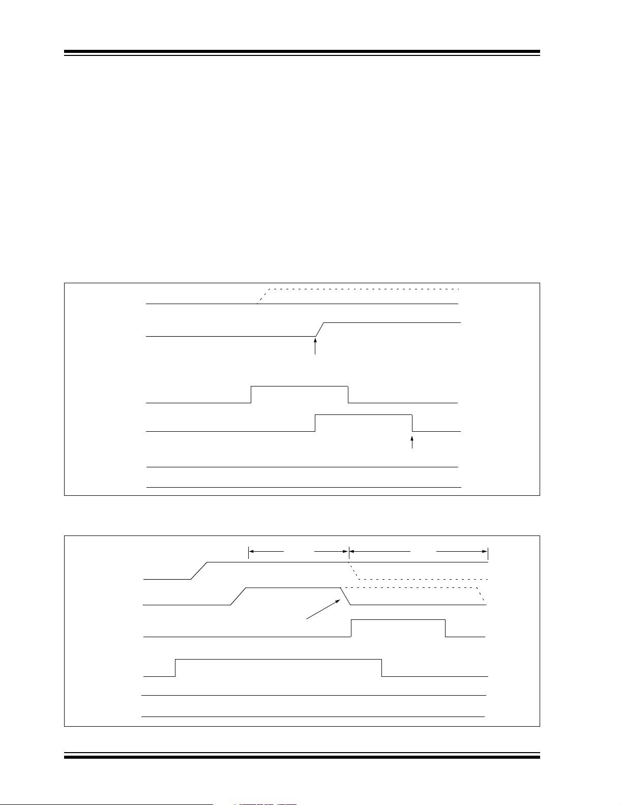
PIC16F872
9.2.18.2 Bus Collision During a Repeated
START Condition
During a Repeated START condition, a bus collision
occurs if:
a) A low level is sampled on SDA when SCL goes
from low level to high level.
b) SCL goes low before SDA is asserted low, indi-
cating that another master is attempting to transmit a data ’1’.
When the user de-asserts SDA and the pin is allowed
to float high, the BRG is loaded with SSPADD<6:0>
and counts down to 0. The SCL pin is then de-asserted,
and when sampled high, the SDA pin is sampled. If
SDA is low, a bus collision has occurred (i.e., another
SDA is sampled high, the BRG is reloaded and begins
counting. If SDA goes from high to low before the BRG
times out, no bus collision occurs, because no two
masters can assert SDA at exactly the same time.
If, however, SCL goes from high to low before the BRG
times out and SDA has not already been asserted, a
bus collision occurs. In this case, another master is
attempting to transmit a data’1’ during the Repeated
START condition.
If, at the end of the BRG time-out, both SCL and SDA
are still high, the SDA pin is driven low, the BRG is
reloaded and begins counting. At the end of the count,
regardless of the status of the SCL pin, the SCL pin is
driven low and the Repeated START condition is complete (Figure 9-23).
master is attempting to transmit a data’0’). If, however,
FIGURE 9-23: BUS COLLISION DURING A REPEATED START CONDITION (CASE 1)
SDA
SCL
Sample SDA when SCL goes high.
If SDA = 0, set BCLIF and release SDA and SCL.
RSEN
BCLIF
Cleared in software
'0'
'0'
S
SSPIF
'0'
'0'
FIGURE 9-24: BUS COLLISION DURING REPEATED START CONDITION (CASE 2)
TBRG TBRG
SDA
SCL
SCL goes low before SDA,
BCLIF
RSEN
S
SSPIF
'0'
'0'
set BCLIF. Release SDA and SCL.
Interrupt cleared
in software
'0'
'0'
DS30221C-page 76 © 2006 Microchip Technology Inc.

PIC16F872
9.2.18.3 Bus Collision During a STOP
Condition
Bus collision occurs during a STOP condition if:
a) After the SDA pin has been de-asserted and
allowed to float high, SDA is sampled low after
the BRG has timed out.
b) After the SCL pin is de-asserted, SCL is sam-
pled low before SDA goes high.
The STOP condition begins with SDA asserted low.
When SDA is sampled low, the SCL pin is allowed to
float. When the pin is sampled high (clock arbitration),
the baud rate generator is loaded with SSPADD<6:0>
and counts down to 0. After the BRG times out, SDA is
sampled. If SDA is sampled low, a bus collision has
occurred. This is due to another master attempting to
drive a data '0'. If the SCL pin is sampled low before
SDA is allowed to float high, a bus collision occurs. This
is a case of another master attempting to drive a data
'0' (Figure 9-25).
FIGURE 9-25: BUS COLLISION DURING A STOP CONDITION (CASE 1)
TBRG TBRG TBRG
SDA
SCL
PEN
BCLIF
P
SSPIF
FIGURE 9-26: BUS COLLISION DURING A STOP CONDITION (CASE 2)
© 2006 Microchip Technology Inc. DS30221C-page 77

PIC16F872
V
9.3 Connection Considerations for I2C Bus
For standard mode I2C bus devices, the values of
resistors
lowing parameters:
• Supply voltage
• Bus capacitance
• Number of connected devices
The supply voltage limits the minimum value of resistor
R
p
at V
example, with a supply voltage of V
FIGURE 9-27: SAMPLE DEVICE CONFIGURATION FOR I2C BUS
R
and
R
p
in Figure 9-27 depend on the fol-
s
(input current + leakage current).
, due to the specified minimum sink current of 3 mA
OL max = 0.4V, for the specified output stages.
DD = 5V+10% and
For
VDD + 10%
OL max = 0.4V at 3 mA, R
1.7 kΩ. V
DD, as a function of
Figure 9-27. The desired noise margin of 0.1 V
the low level limits the maximum value of
resistors are optional and used to improve ESD
susceptibility.
The bus capacitance is the total capacitance of wire,
connections, and pins. This capacitance limits the max-
R
imum value of
, due to the specified rise time
p
(Figure 9-27).
The SMP bit is the slew rate control enabled bit. This bit
is in the SSPSTAT register, and controls the slew rate
of the I/O pins when in I
= (5.5-0.4)/0.003 =
p min
R
, is shown in
p
R
. Series
s
2
C mode (master or slave).
DD for
Note: I
RpRp
SDA
SCL
2
C devices with input levels related to VDD must have one common supply line to which the pull-up resistor is
also connected.
DEVICE
RsRs
Cb=10 - 400 pF
DS30221C-page 78 © 2006 Microchip Technology Inc.

PIC16F872
10.0 ANALOG-TO-DIGITAL CONVERTER (A/D) MODULE
The Analog-to-Digital (A/D) Converter module has five
input channels. The analog input charges a sample and
hold capacitor. The output of the sample and hold
capacitor is the input into the converter. The converter
then generates a digital result of this analog level via
successive approximation. The A/D conversion of the
analog input signal results in a corresponding 10-bit
digital number. The A/D module has high and low voltage reference input that is software selectable to some
combination of V
The A/D converter has a unique feature of being able
to operate while the device is in SLEEP mode. To operate in SLEEP, the A/D clock must be derived from the
A/D’s internal RC oscillator.
DD, VSS, RA2 or RA3.
The A/D module has four registers. These registers
are:
• A/D Result High Register (ADRESH)
• A/D Result Low Register (ADRESL)
• A/D Control Register0 (ADCON0)
• A/D Control Register1 (ADCON1)
The ADCON0 register, shown in Register 10-1, controls the operation of the A/D module. The ADCON1
register, shown in Register 10-2, configures the functions of the port pins. The port pins can be configured
as analog inputs (RA3 can also be the voltage reference), or as digital I/O.
Additional information on using the A/D module can be
found in the PICmicro™ Mid-Range MCU Family Reference Manual (DS33023).
REGISTER 10-1: ADCON0 REGISTER (ADDRESS: 1Fh)
R/W-0 R/W-0 R/W-0 R/W-0 R/W-0 R/W-0 U-0 R/W-0
ADCS1 ADCS0 CHS2 CHS1 CHS0 GO/DONE —ADON
bit 7 bit 0
bit 7-6 ADCS1:ADCS0: A/D Conversion Clock Select bits
00 = FOSC/2
OSC/8
01 = F
10 = F
OSC/32
RC (clock derived from the internal A/D module RC oscillator)
11 = F
bit 5-3 CHS2:CHS0: Analog Channel Select bits
000 = Channel 0 (RA0/AN0)
001 = Channel 1 (RA1/AN1)
010 = Channel 2 (RA2/AN2)
011 = Channel 3 (RA3/AN3)
100 = Channel 4 (RA5/AN4)
bit 2 GO/DONE
If ADON = 1:
1 = A/D conversion in progress (setting this bit starts the A/D conversion)
0 = A/D conversion not in progress (this bit is automatically cleared by hardware when the A/D
bit 1 Unimplemented: Read as '0'
bit 0 ADON: A/D On bit
1 = A/D converter module is operating
0 = A/D converter module is shut-off and consumes no operating current
: A/D Conversion Status bit
conversion is complete)
Legend:
R = Readable bit W = Writable bit U = Unimplemented bit, read as ‘0’
- n = Value at POR ’1’ = Bit is set ’0’ = Bit is cleared x = Bit is unknown
© 2006 Microchip Technology Inc. DS30221C-page 79

PIC16F872
REGISTER 10-2: ADCON1 REGISTER (ADDRESS: 9Fh)
U-0 U-0 R/W-0 U-0 R/W-0 R/W-0 R/W-0 R/W-0
ADFM
bit 7 bit 0
bit 7 ADFM: A/D Result Format Select bit
1 = Right justified. Six Most Significant bits of ADRESH are read as ‘0’.
0 = Left justified. Six Least Significant bits of ADRESL are read as ‘0’.
bit 6-4 Unimplemented: Read as '0'
bit 3-0 PCFG3:PCFG0: A/D Port Configuration Control bits:
PCFG3:
PCFG0
0000 AAAAAVDD VSS 8/0
0001 AV
0010 AAAAAV
0011 AV
0100 DADAAV
0101 DV
011x DDDDDV
1000 AV
1001 AAAAAV
1010 AV
1011 AV
1100 AV
1101 DV
1110 DDDDAV
1111 DV
A = Analog input
D = Digital I/O
— — — PCFG3 PCFG2 PCFG1 PCFG0
AN4
RA5
AN3
RA3
REF+A A A RA3VSS 7/1
REF+A A A RA3VSS 4/1
REF+D A A RA3VSS 2/1
REF+VREF-A A RA3RA2 6/2
REF+A A A RA3VSS 5/1
REF+VREF-A A RA3RA2 4/2
REF+VREF-A A RA3RA2 3/2
REF+VREF-A A RA3RA2 2/2
REF+VREF-D A RA3RA2 1/2
AN2
RA2
AN1
RA1
AN0
RA0
REF+VREF-
V
DD VSS 5/0
DD VSS 3/0
DD VSS 0/0
DD VSS 6/0
DD VSS 1/0
C
HAN/
Refs
(1)
Note 1: This column indicates the number of analog channels available as A/D inputs and
the number of analog channels used as voltage reference inputs.
Legend:
R = Readable bit W = Writable bit U = Unimplemented bit, read as ‘0’
- n = Value at POR ’1’ = Bit is set ’0’ = Bit is cleared x = Bit is unknown
DS30221C-page 80 © 2006 Microchip Technology Inc.

PIC16F872
The ADRESH:ADRESL registers contain the 10-bit
result of the A/D conversion. When the A/D conversion
is complete, the result is loaded into this A/D result register pair, the GO/DONE
bit (ADCON0<2>) is cleared
and the A/D interrupt flag bit ADIF is set. The block diagram of the A/D module is shown in Figure 10-1.
After the A/D module has been configured as desired,
the selected channel must be acquired before the conversion is started. The analog input channels must
have their corresponding TRIS bits selected as inputs.
To determine sample time, see Section 10.1. After this
acquisition time has elapsed, the A/D conversion can
be started.
These steps should be followed for doing an A/D
conversion:
1. Configure the A/D module:
• Configure analog pins/voltage reference and
digital I/O (ADCON1)
• Select A/D input channel (ADCON0)
• Select A/D conversion clock (ADCON0)
• Turn on A/D module (ADCON0)
FIGURE 10-1: A/D BLOCK DIAGRAM
2. Configure A/D interrupt (if desired):
• Clear ADIF bit
• Set ADIE bit
• Set PEIE bit
• Set GIE bit
3. Wait the required acquisition time.
4. Start conversion:
• Set GO/DONE bit (ADCON0)
5. Wait for A/D conversion to complete, by either:
• Polling for the GO/DONE
bit to be cleared
(with interrupts enabled); OR
• Waiting for the A/D interrupt
6. Read A/D Result register pair
(ADRESH:ADRESL), clear bit ADIF if required.
7. For the next conversion, go to step 1 or step 2,
as required. The A/D conversion time per bit is
defined as T
CHS2:CHS0
AD.
A/D
Converter
VREF+
(Reference
Voltage)
VREF-
(Reference
Voltage)
AIN
V
(Input Voltage)
PCFG3:PCFG0
PCFG3:PCFG0
100
011
010
001
000
DD
V
V
SS
RA5/AN4
RA3/AN3/V
RA2/AN2/V
RA1/AN1
RA0/AN0
REF+
REF-
© 2006 Microchip Technology Inc. DS30221C-page 81

PIC16F872
10.1 A/D Acquisition Requirements
For the A/D converter to meet its specified accuracy,
the charge holding capacitor (C
to fully charge to the input channel voltage level. The
analog input model is shown in Figure 10-2. The
source impedance (R
switch (R
SS) impedance directly affect the time
S) and the internal sampling
required to charge the capacitor C
switch (R
(V
SS) impedance varies over the device voltage
DD), Figure 10-2. The maximum recommended
impedance for analog sources is 10 kΩ. As the
HOLD) must be allowed
HOLD. The sampling
decreased. After the analog input channel is selected
(changed), this acquisition must be done before the
conversion can be started.
Equation 10-1 may be used to calculate the minimum
acquisition time. This equation assumes that 1/2 LSb
error is used (1024 steps for the A/D). The 1/2 LSb
error is the maximum error allowed for the A/D to meet
its specified resolution.
To calculate the minimum acquisition time, T
the PICmicro™ Mid-Range Reference Manual
(DS33023).
impedance is decreased, the acquisition time may be
EQUATION 10-1: ACQUISITION TIME
TACQ
TC
TACQ
=
Amplifier Settling Time + Hold Capacitor Charging Time + Temperature Coefficient
AMP + TC + TCOFF
=
T
2 μs + TC + [(Temperature -25°C)(0.05 μs/°C)]
=
HOLD (RIC + RSS + RS) In(1/2047) - 120 pF (1 kΩ + 7 kΩ + 10 kΩ) In(0.0004885)
C
=
16.47 μs
=
2 μs + 16.47 μs + [(50°C -25°C)(0.05 μs/°C)
=
19.72 μs
=
Note 1: The reference voltage (VREF) has no effect on the equation, since it cancels itself out.
2: The charge holding capacitor (CHOLD) is not discharged after each conversion.
3: The maximum recommended impedance for analog sources is 10 kΩ. This is required to meet the pin
leakage specification.
ACQ, see
FIGURE 10-2: ANALOG INPUT MODEL
VDD
R
VA
Legend CPIN
VT
I LEAKAGE
RIC
SS
C
HOLD
ANx
S
CPIN
5 pF
= input capacitance
= threshold voltage
= leakage current at the pin due to
various junctions
= interconnect resistance
= sampling switch
= sample/hold capacitance (from DAC)
VT = 0.6V
T = 0.6V
V
RIC ≤ 1k
I
LEAKAGE
± 500 nA
Sampling
Switch
SS
R
6V
5V
4V
DD
V
3V
2V
SS
CHOLD
= DAC capacitance
= 120 pF
V
SS
567891011
Sampling Switch
(kΩ)
DS30221C-page 82 © 2006 Microchip Technology Inc.

PIC16F872
10.2 Selecting the A/D Conversion Clock
The A/D conversion time per bit is defined as TAD. The
A/D conversion requires a minimum 12T
conversion. The source of the A/D conversion clock is
software selected. The four possible options for T
are:
OSC
•2T
•8TOSC
•32TOSC
• Internal A/D module RC oscillator (2-6 μs)
For correct A/D conversions, the A/D conversion clock
AD) must be selected to ensure a minimum TAD time
(T
of 1.6 μs.
Table 10-1shows the resultant T
the device operating frequencies and the A/D clock
source selected.
AD times derived from
AD per 10-bit
AD
10.3 Configuring Analog Port Pins
The ADCON1, and TRIS registers control the operation
of the A/D port pins. The port pins that are desired as
analog inputs must have their corresponding TRIS bits
set (input). If the TRIS bit is cleared (output), the digital
output level (V
The A/D operation is independent of the state of the
CHS2:CHS0 bits and the TRIS bits.
Note 1: When reading the port register, any pin
OH or VOL) will be converted.
configured as an analog input channel will
read as cleared (a low level). Pins configured as digital inputs will convert an analog input. Analog levels on a digitally
configured input will not affect the conversion accuracy.
2: Analog levels on any pin that is defined as
a digital input (including the AN7:AN0
pins), may cause the input buffer to consume current that is out of the device
specifications.
TABLE 10-1: TAD vs. MAXIMUM DEVICE OPERATING FREQUENCIES (STANDARD DEVICES (C))
AD Clock Source (TAD)
Operation ADCS1:ADCS0
2T
OSC 00 1.25 MHz
8TOSC 01 5 MHz
32TOSC 10 20 MHz
(1, 2, 3)
RC
Note 1: The RC source has a typical TAD time of 4 μs, but can vary between 2-6 μs.
2: When the device frequencies are greater than 1 MHz, the RC A/D conversion clock source is only recom-
mended for SLEEP operation.
3: For extended voltage devices (LC), please refer to the Electrical Characteristics (Sections 14.1 and 14.2).
11 (Note 1)
Maximum Device Frequency
© 2006 Microchip Technology Inc. DS30221C-page 83

PIC16F872
10.4 A/D Conversions
Clearing the GO/DONE bit during a conversion will
abort the current conversion. The A/D result register
pair will NOT be updated with the partially completed
A/D conversion sample. That is, the
ADRESH:ADRESL registers will continue to contain
the value of the last completed conversion (or the last
value written to the ADRESH:ADRESL registers). After
the A/D conversion is aborted, acquisition on the
selected channel is automatically started. The
GO/DONE
FIGURE 10-3: A/D CONVERSION TAD CYCLES
bit can then be set to start the conversion.
TCY to TAD
Set GO bit
TAD1 TAD2 TAD3
b9 b8 b7 b6 b5 b4 b3 b2
Conversion Starts
Holding capacitor is disconnected from analog input (typically 100 ns)
TAD4
TAD5 TAD6
In Figure 10-3, after the GO bit is set, the first time segment has a minimum of TCY and a maximum of TAD.
Note: The GO/DONE bit should NOT be set in
the same instruction that turns on the A/D.
TAD9
TAD7 TAD8
ADRES is loaded
GO bit is cleared
ADIF bit is set
Holding capacitor is connected to analog input
TAD10 TAD11
b1 b0
10.4.1 A/D RESULT REGISTERS
The ADRESH:ADRESL register pair is the location
where the 10-bit A/D result is loaded at the completion
of the A/D conversion. This register pair is 16-bits wide.
The A/D module gives the flexibility to left or right justify
the 10-bit result in the 16-bit result register. The A/D
FIGURE 10-4: A/D RESULT JUSTIFICATION
10-Bit Result
ADFM = 1
2 1 0 77
0000 00
ADRESH ADRESL
10-bit Result
Right Justified
0
Format Select bit (ADFM) controls this justification.
Figure 10-4 shows the operation of the A/D result justification. The extra bits are loaded with ’0’s’. When an
A/D result will not overwrite these locations (A/D
disable), these registers may be used as two general
purpose 8-bit registers.
ADFM = 0
7
ADRESH ADRESL
10-bit Result
0 7 6 5 0
0000 00
Left Justified
DS30221C-page 84 © 2006 Microchip Technology Inc.

PIC16F872
10.5 A/D Operation During SLEEP
The A/D module can operate during SLEEP mode. This
requires that the A/D clock source be set to RC
(ADCS1:ADCS0 = 11). When the RC clock source is
selected, the A/D module waits one instruction cycle
before starting the conversion. This allows the SLEEP
instruction to be executed, which eliminates all digital
switching noise from the conversion. When the conversion is completed, the GO/DONE
the result loaded into the ADRES register. If the A/D
interrupt is enabled, the device will wake-up from
SLEEP. If the A/D interrupt is not enabled, the A/D module will then be turned off, although the ADON bit will
remain set.
When the A/D clock source is another clock option (not
RC), a SLEEP instruction will cause the present conversion to be aborted and the A/D module to be turned off,
though the ADON bit will remain set.
bit will be cleared and
Turning off the A/D places the A/D module in its lowest
current consumption state.
Note: For the A/D module to operate in SLEEP,
the A/D clock source must be set to RC
(ADCS1:ADCS0 = 11). To allow the conversion to occur during SLEEP, ensure the
SLEEP instruction immediately follows the
instruction that sets the GO/DONE
bit.
10.6 Effects of a RESET
A device RESET forces all registers to their RESET
state. This forces the A/D module to be turned off, and
any conversion is aborted. All A/D input pins are configured as analog inputs.
The value that is in the ADRESH:ADRESL registers is
not modified for a Power-on Reset. The
ADRESH:ADRESL registers will contain unknown data
after a Power-on Reset.
TABLE 10-2: REGISTERS/BITS ASSOCIATED WITH A/D
Address Name Bit 7 Bit 6 Bit 5 Bit 4 Bit 3 Bit 2 Bit 1 Bit 0
0Bh,8Bh,
10Bh, 18Bh
0Ch PIR1 (1) ADIF (1) (1) SSPIF CCP1IF TMR2IF TMR1IF r0rr 0000 0000 0000
8Ch PIE1 (1) ADIE (1) (1) SSPIE CCP1IE TMR2IE TMR1IE r0rr 0000 0000 0000
1Eh ADRESH A/D Result Register High Byte xxxx xxxx uuuu uuuu
9Eh ADRESL A/D Result Register Low Byte xxxx xxxx uuuu uuuu
1Fh ADCON0 ADCS1 ADCS0 CHS2 CHS1 CHS0 GO/DONE
9Fh ADCON1 ADFM
85h TRISA
05h PORTA
Legend: x = unknown, u = unchanged, - = unimplemented, read as '0'. Shaded cells are not used for A/D conversion.
Note 1: These bits are reserved; always maintain clear.
INTCON GIE PEIE
— — — PCFG3 PCFG2 PCFG1 PCFG0 --0- 0000 --0- 0000
— — PORTA Data Direction Register --11 1111 --11 1111
— — PORTA Data Latch when written: PORTA pins when read --0x 0000 --0u 0000
TMR0IE INTE RBIE TMR0IF INTF RBIF 0000 000x 0000 000u
—ADON0000 00-0 0000 00-0
POR,
BOR
MCLR
WDT
,
© 2006 Microchip Technology Inc. DS30221C-page 85

PIC16F872
NOTES:
DS30221C-page 86 © 2006 Microchip Technology Inc.

PIC16F872
11.0 SPECIAL FEATURES OF THE CPU
The PIC16F872 microcontroller has a host of features
intended to maximize system reliability, minimize cost
through elimination of external components, provide
power saving operating modes and offer code protection. These are:
• Oscillator Selection
• RESET
- Power-on Reset (POR)
- Power-up Timer (PWRT)
- Oscillator Start-up Timer (OST)
- Brown-out Reset (BOR)
• Interrupts
• Watchdog Timer (WDT)
• SLEEP
• Code Protection
• ID Locations
• In-Circuit Serial Programming
• Low Voltage In-Circuit Serial Programming
• In-Circuit Debugger
The microcontrollers have a Watchdog Timer, which
can be shut-off only through configuration bits. It runs
off its own RC oscillator for added reliability.
There are two timers that offer necessary delays on
power-up. One is the Oscillator Start-up Timer (OST),
intended to keep the chip in RESET until the crystal
oscillator is stable. The other is the Power-up Timer
(PWRT), which provides a fixed delay of 72 ms (nominal) on power-up only. It is designed to keep the part in
RESET while the power supply stabilizes. With these
two timers on-chip, most applications need no external
RESET circuitry.
SLEEP mode is designed to offer a very low current
power-down mode. The user can wake-up from SLEEP
through external RESET, Watchdog Timer Wake-up, or
through an interrupt.
Several oscillator options are also made available to
allow the part to fit the application. The RC oscillator
option saves system cost, while the LP crystal option
saves power. A set of configuration bits is used to
select various options.
Additional information on special features is available
in the PICmicro™ Mid-Range Reference Manual,
(DS33023).
11.1 Configuration Bits
The configuration bits can be programmed (read as '0'),
or left unprogrammed (read as '1'), to select various
device configurations. The erased, or unprogrammed,
value of the configuration word is 3FFFh. These bits
are mapped in program memory location 2007h.
It is important to note that address 2007h is beyond the
user program memory space, which can be accessed
only during programming.
© 2006 Microchip Technology Inc. DS30221C-page 87

PIC16F872
(2)
(1)
REGISTER 11-1: CONFIGURATION WORD (ADDRESS: 2007h)
R/P-1 R/P-1 R/P-1 U-0 R/P-1 R/P-1 R/P-1 R/P-1 R/P-1 R/P-1 R/P-1 R/P-1 R/P-1 R/P-1
CP1 CP0 DEBUG
bit13 bit0
bit 13-12
bit 5-4
bit 11 DEBUG: In-Circuit Debugger Mode bit
bit 10 Unimplemented: Read as ‘1’
bit 9 WRT: FLASH Program Memory Write Enable bit
bit 8 CPD: Data EEPROM Memory Code Protection bit
bit 7 LVP: Low Voltage In-Circuit Serial Programming Enable bit
bit 6 BODEN: Brown-out Reset Enable bit
bit 3 PWRTE
bit 2 WDTE: Watchdog Timer Enable bit
bit 1-0 FOSC1:FOSC0: Oscillator Selection bits
CP1:CP0: FLASH Program Memory Code Protection bits
11 = Code protection off
10 = Not supported
01 = Not supported
00 = All memory code protected
1 = In-Circuit Debugger disabled, RB6 and RB7 are general purpose I/O pins
0 = In-Circuit Debugger enabled, RB6 and RB7 are dedicated to the debugger
1 = Unprotected program memory may be written to by EECON control
0 = Unprotected program memory may not be written to by EECON control
1 = Code protection off
0 = Data EEPROM memory code protected
1 = RB3/PGM pin has PGM function, low voltage programming enabled
0 = RB3 is digital I/O, HV on MCLR
1 = BOR enabled
0 = BOR disabled
1 = PWRT disabled
0 = PWRT enabled
1 = WDT enabled
0 = WDT disabled
11 = RC oscillator
10 = HS oscillator
01 = XT oscillator
00 = LP oscillator
— WRT CPD LVP BODEN CP1 CP0 PWRTE WDTE F0SC1 F0SC0
must be used for programming
(3)
: Power-up Timer Enable bit
(3)
Note 1: The erased (unprogrammed) value of the configuration word is 3FFFh.
2: All of the CP1:CP0 pairs have to be given the same value to enable the code protection
scheme listed.
3: Enabling Brown-out Reset automatically enables Power-up Timer (PWRT), regardless of
the value of bit PWRTE
is enabled.
Legend:
R = Readable bit P = Programmable bit U = Unimplemented bit, read as ‘0’
- n = Value when device is unprogrammed u = Unchanged from programmed state
DS30221C-page 88 © 2006 Microchip Technology Inc.
. Ensure the Power-up Timer is enabled any time Brown-out Reset

PIC16F872
11.2 Oscillator Configurations
11.2.1 OSCILLATOR TYPES
The PIC16F872 can be operated in four different oscillator modes. The user can program two configuration
bits (FOSC1 and FOSC0) to select one of these four
modes:
• LP Low Power Crystal
• XT Crystal/Resonator
• HS High Speed Crystal/Resonator
• RC Resistor/Capacitor
11.2.2 CRYSTAL OSCILLATOR/CERAMIC
RESONATORS
In XT, LP or HS modes, a crystal or ceramic resonator
is connected to the OSC1/CLKIN and OSC2/CLKOUT
pins to establish oscillation (Figure 11-1). The
PIC16F872 oscillator design requires the use of a parallel cut crystal. Use of a series cut crystal may give a
frequency out of the crystal manufacturers specifications. When in XT, LP or HS modes, the device can
have an external clock source to drive the OSC1/
CLKIN pin (Figure 11-2).
FIGURE 11-1: CRYSTAL/CERAMIC
RESONATOR OPERATION
(HS, XT OR LP
OSC CONFIGURATION)
(1)
C1
C2
(1)
XTAL
(2)
RS
OSC1
OSC2
RF
(3)
To
Internal
Logic
SLEEP
PIC16F87X
FIGURE 11-2: EXTERNAL CLOCK INPUT
OPERATION (HS, XT OR
LP OSC
CONFIGURATION)
Clock from
Ext. System
Open
OSC1
PIC16F87X
OSC2
TABLE 11-1: CERAMIC RESONATORS
Ranges Tested:
Mode Freq OSC1 OSC2
XT 455 kHz
2.0 MHz
4.0 MHz
HS 8.0 MHz
16.0 MHz
These values are for design guidance only.
See notes following Table 11-2.
Resonators Used:
455 kHz Panasonic EFO-A455K04B ± 0.3%
2.0 MHz Murata Erie CSA2.00MG ± 0.5%
4.0 MHz Murata Erie CSA4.00MG ± 0.5%
8.0 MHz Murata Erie CSA8.00MT ± 0.5%
16.0 MHz Murata Erie CSA16.00MX ± 0.5%
All resonators used did not have built-in capacitors.
68 - 100 pF
15 - 68 pF
15 - 68 pF
10 - 68 pF
10 - 22 pF
68 - 100 pF
15 - 68 pF
15 - 68 pF
10 - 68 pF
10 - 22 pF
Note 1: See Table 11-1 and Table 11-2 for recom-
© 2006 Microchip Technology Inc. DS30221C-page 89
mended values of C1 and C2.
2: A series resistor (RS) may be required for
AT strip cut crystals.
3: RF varies with the crystal chosen.
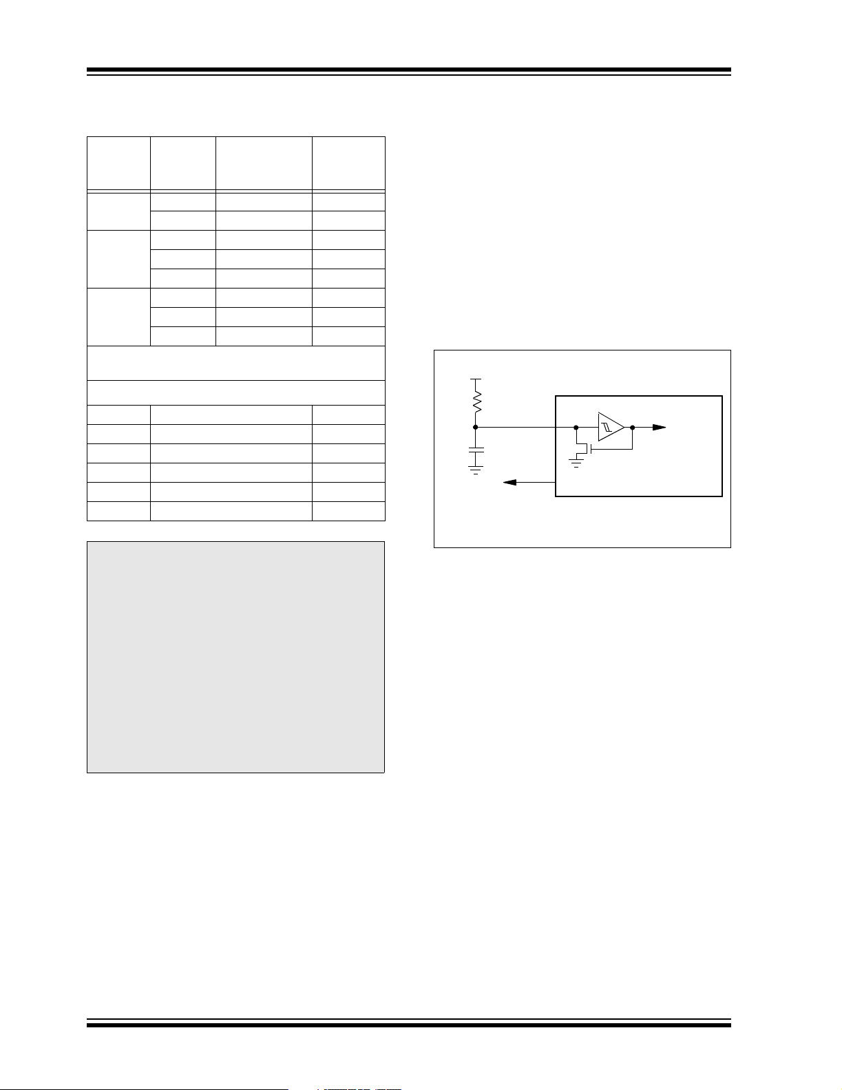
PIC16F872
TABLE 11-2: CAPACITOR SELECTION FOR
CRYSTAL OSCILLATOR
Cap.
Range
C2
Osc Type
Crystal
Freq
Cap. Range
C1
LP 32 kHz 33 pF 33 pF
200 kHz 15 pF 15 pF
XT 200 kHz 47-68 pF 47-68 pF
1 MHz 15 pF 15 pF
4 MHz 15 pF 15 pF
HS 4 MHz 15 pF 15 pF
8 MHz 15-33 pF 15-33 pF
20 MHz 15-33 pF 15-33 pF
These values are for design guidance only.
See notes following this table.
Crystals Used
32 kHz Epson C-001R32.768K-A ± 20 PPM
200 kHz STD XTL 200.000KHz ± 20 PPM
1 MHz ECS ECS-10-13-1 ± 50 PPM
4 MHz ECS ECS-40-20-1 ± 50 PPM
8 MHz EPSON CA-301 8.000M-C ± 30 PPM
20 MHz EPSON CA-301 20.000M-C ± 30 PPM
Note 1: Higher capacitance increases the stability
of oscillator, but also increases the startup time.
2: Since each resonator/crystal has its own
characteristics, the user should consult
the resonator/crystal manufacturer for
appropriate values of external components.
3: Rs may be required in HS mode, as well
as XT mode, to avoid overdriving crystals
with low drive level specification.
4: When migrating from other PICmicro
devices, oscillator performance should be
verified.
11.2.3 RC OSCILLATOR
For timing insensitive applications, the “RC” device
option offers additional cost savings. The RC oscillator
frequency is a function of the supply voltage, the resis-
EXT) and capacitor (CEXT) values, and the operat-
tor (R
ing temperature. In addition to this, the oscillator
frequency will vary from unit to unit due to normal process parameter variation. Furthermore, the difference
in lead frame capacitance between package types will
also affect the oscillation frequency, especially for low
EXT values. The user also needs to take into account
C
variation due to tolerance of external R and C components used. Figure 11-3 shows how the R/C combination is connected to the PIC16F872.
FIGURE 11-3: RC OSCILLATOR MODE
VDD
REXT
OSC1
CEXT
VSS
F
Recommended values: 3 kΩ ≤ REXT ≤ 100 kΩ
®
OSC/4
OSC2/CLKOUT
C
EXT > 20pF
Internal
Clock
PIC16F87X
DS30221C-page 90 © 2006 Microchip Technology Inc.

PIC16F872
11.3 Reset
The PIC16F872 differentiates between various kinds of
RESET:
• Power-on Reset (POR)
•MCLR
•MCLR
• WDT Reset (during normal operation)
• WDT Wake-up (during SLEEP)
• Brown-out Reset (BOR)
Some registers are not affected in any RESET condition. Their status is unknown on POR and unchanged
in any other RESET. Most other registers are reset to a
“RESET state” on Power-on Reset (POR), on the
MCLR and WDT Reset, on MCLR Reset during
Reset during normal operation
Reset during SLEEP
SLEEP, and Brown-out Reset (BOR). They are not
affected by a WDT Wake-up, which is viewed as the
resumption of normal operation. The TO
are set or cleared differently in different RESET situations, as indicated in Table 11-4. These bits are used in
software to determine the nature of the RESET. See
Table 11-6 for a full description of RESET states of all
registers.
A simplified block diagram of the On-Chip Reset circuit
is shown in Figure 11-4.
These devices have a MCLR
Reset path. The filter will detect and ignore small
pulses.
It should be noted that a WDT Reset
MCLR
pin low.
FIGURE 11-4: SIMPLIFIED BLOCK DIAGRAM OF ON-CHIP RESET CIRCUIT
External
RESET
MCLR
VDD
WDT
Module
DD Rise
V
Detect
Brown-out
Reset
SLEEP
WDT
Time-out
Reset
Power-on Reset
BODEN
S
and PD bits
noise filter in the MCLR
does not drive
OST/PWRT
OST
OSC1
(1)
On-Chip
RC OSC
Note 1: This is a separate oscillator from the RC oscillator of the CLKIN pin.
10-bit Ripple Counter
PWRT
10-bit Ripple Counter
Enable PWRT
Enable OST
Chip_Reset
R
Q
© 2006 Microchip Technology Inc. DS30221C-page 91

PIC16F872
11.4 Power-on Reset (POR)
A Power-on Reset pulse is generated on-chip when
DD rise is detected (in the range of 1.2V - 1.7V). To
V
take advantage of the POR, tie the MCLR
(or through a resistor) to V
nal RC components usually needed to create a Poweron Reset. A maximum rise time for V
See Electrical Specifications for details.
When the device starts normal operation (exits the
RESET condition), device operating parameters (voltage, frequency, temperature,...) must be met to ensure
operation. If these conditions are not met, the device
must be held in RESET until the operating conditions
are met. Brown-out Reset may be used to meet the
start-up conditions. For additional information, refer to
Application Note (AN007),
Shooting”
, (DS00007).
DD. This will eliminate exter-
“Power-up Trouble
pin directly
DD is specified.
11.5 Power-up Timer (PWRT)
The Power-up Timer provides a fixed 72 ms nominal
time-out on power-up only from the POR. The Powerup Timer operates on an internal RC oscillator. The
chip is kept in RESET as long as the PWRT is active.
The PWRT’s time delay allows VDD to rise to an acceptable level. A configuration bit is provided to enable/disable the PWRT.
The power-up time delay will vary from chip to chip due
DD, temperature and process variation. See DC
to V
parameters for details (T
PWRT, parameter #33).
11.6 Oscillator Start-up Timer (OST)
The Oscillator Start-up Timer (OST) provides a delay of
1024 oscillator cycles (from OSC1 input) after the
PWRT delay is over (if PWRT is enabled). This helps to
ensure that the crystal oscillator or resonator has
started and stabilized.
The OST time-out is invoked only for XT, LP and HS
modes and only on Power-on Reset or wake-up from
SLEEP.
11.7 Brown-out Reset (BOR)
The configuration bit, BODEN, can enable or disable
the Brown-out Reset circuit. If V
(parameter #D005, about 4V) for longer than TBOR
(parameter #35, about 100 μS), the brown-out situation
will reset the device. If V
BOR, a RESET may not occur.
than T
Once the brown-out occurs, the device will remain in
Brown-out Reset until VDD rises above VBOR. The
Power-up Timer then keeps the device in RESET for
PWRT (parameter #33, about 72 mS). If VDD should fall
T
below V
cess will restart when V
Power-up Timer Reset. The Power-up Timer is always
enabled when the Brown-out Reset circuit is enabled,
regardless of the state of the PWRT configuration bit.
BOR during TPWRT, the Brown-out Reset pro-
DD falls below VBOR for less
DD rises above VBOR with the
DD falls below VBOR
11.8 Time-out Sequence
On power-up, the time-out sequence is as follows: the
PWRT delay starts (if enabled) when a POR Reset
occurs. Then, OST starts counting 1024 oscillator
cycles when PWRT ends (LP, XT, HS). When the OST
ends, the device comes out of RESET.
If MCLR
expire. Bringing MCLR
diately. This is useful for testing purposes or to synchronize more than one PIC16F872 device operating in
parallel.
Table 11-5 shows the RESET conditions for the
STATUS, PCON and PC registers, while Table 11-6
shows the RESET conditions for all the registers.
is kept low long enough, the time-outs will
high will begin execution imme-
11.9 Power Control/Status Register (PCON)
The Power Control/Status Register, PCON, has two bits.
Bit 0 is the Brown-out Reset Status bit (BOR)
is unknown on a Power-on Reset. It must then be set
by the user and checked on subsequent RESETS to
see if bit BOR
When the Brown-out Reset is disabled, the state of the
BOR bit is unpredictable and is, therefore, not valid at
any time.
Bit 1 is the Power-on Reset Status bit (POR
cleared on a Power-on Reset and unaffected otherwise. The user must set this bit following a Power-on
Reset.
cleared, indicating a BOR occurred.
. Bit BOR
). It is
TABLE 11-3: TIME-OUT IN VARIOUS SITUATIONS
Oscillator Configuration
PWRTE
XT, HS, LP 72 ms + 1024T
RC 72 ms — 72 ms —
DS30221C-page 92 © 2006 Microchip Technology Inc.
Power-up
Brown-out
= 0 PWRTE = 1
OSC 1024TOSC 72 ms + 1024TOSC 1024TOSC
Wake-up from
SLEEP

TABLE 11-4: STATUS BITS AND THEIR SIGNIFICANCE
POR BOR TO PD
0x11Power-on Reset
0x0xIllegal, TO
0xx0Illegal, PD is set on POR
1011Brown-out Reset
1101WDT Reset
1100WDT Wake-up
11uuMCLR
1110MCLR
is set on POR
Reset during normal operation
Reset during SLEEP or interrupt wake-up from SLEEP
TABLE 11-5: RESET CONDITION FOR SPECIAL REGISTERS
PIC16F872
Condition
Power-on Reset 000h 0001 1xxx ---- --0x
Reset during normal operation 000h 000u uuuu ---- --uu
MCLR
MCLR Reset during SLEEP 000h 0001 0uuu ---- --uu
WDT Reset 000h 0000 1uuu ---- --uu
WDT Wake-up PC + 1 uuu0 0uuu ---- --uu
Brown-out Reset 000h 0001 1uuu ---- --u0
Interrupt wake-up from SLEEP PC + 1
Legend: u = unchanged, x = unknown, - = unimplemented bit, read as '0'
Note 1: When the wake-up is due to an interrupt and the GIE bit is set, the PC is loaded with the interrupt vector
(0004h).
Program
Counter
(1)
STATUS
Register
uuu1 0uuu ---- --uu
PCON
Register
TABLE 11-6: INITIALIZATION CONDITIONS FOR ALL REGISTERS
Register
W xxxx xxxx uuuu uuuu uuuu uuuu
INDF N/A N/A N/A
TMR0 xxxx xxxx uuuu uuuu uuuu uuuu
PCL 0000h 0000h PC + 1
STATUS 0001 1xxx 000q quuu
FSR xxxx xxxx uuuu uuuu uuuu uuuu
PORTA --0x 0000 --0u 0000 --uu uuuu
PORTB xxxx xxxx uuuu uuuu uuuu uuuu
PORTC xxxx xxxx uuuu uuuu uuuu uuuu
PCLATH ---0 0000 ---0 0000 ---u uuuu
INTCON 0000 000x 0000 000u uuuu uuuu
PIR1 r0rr 0000 r0rr 0000 rurr uuuu
PIR2 -r-0 0--r -r-0 0--r -r-u u--r
Legend: u = unchanged, x = unknown, - = unimplemented bit, read as '0', q = value depends on condition,
r = reserved, maintain clear
Note 1: One or more bits in INTCON, PIR1 and/or PIR2 will be affected (to cause wake-up).
2: When the wake-up is due to an interrupt and the GIE bit is set, the PC is loaded with the interrupt vector
(0004h).
3: See Table 11-5 for RESET value for specific condition.
Power-on Reset,
Brown-out Reset
Resets
MCLR
WDT Reset
(3)
Wake-up via WDT or
Interrupt
(2)
uuuq quuu
(3)
(1)
(1)
(1)
© 2006 Microchip Technology Inc. DS30221C-page 93

PIC16F872
TABLE 11-6: INITIALIZATION CONDITIONS FOR ALL REGISTERS (CONTINUED)
Register
TMR1L xxxx xxxx uuuu uuuu uuuu uuuu
TMR1H xxxx xxxx uuuu uuuu uuuu uuuu
T1CON --00 0000 --uu uuuu --uu uuuu
TMR2 0000 0000 0000 0000 uuuu uuuu
T2CON -000 0000 -000 0000 -uuu uuuu
SSPBUF xxxx xxxx uuuu uuuu uuuu uuuu
SSPCON 0000 0000 0000 0000 uuuu uuuu
CCPR1L xxxx xxxx uuuu uuuu uuuu uuuu
CCPR1H xxxx xxxx uuuu uuuu uuuu uuuu
CCP1CON --00 0000 --00 0000 --uu uuuu
ADRESH xxxx xxxx uuuu uuuu uuuu uuuu
ADCON0 0000 00-0 0000 00-0 uuuu uu-u
OPTION_REG 1111 1111 1111 1111 uuuu uuuu
TRISA --11 1111 --11 1111 --uu uuuu
TRISB 1111 1111 1111 1111 uuuu uuuu
TRISC 1111 1111 1111 1111 uuuu uuuu
PIE1 r0rr 0000 r0rr 0000 rurr uuuu
PIE2 -r-0 0--r -r-0 0--r -r-u u--r
PCON ---- --qq ---- --uu ---- --uu
SSPCON2 0000 0000 0000 0000 uuuu uuuu
PR2 1111 1111 1111 1111 1111 1111
SSPADD 0000 0000 0000 0000 uuuu uuuu
SSPSTAT --00 0000 --00 0000 --uu uuuu
ADRESL xxxx xxxx uuuu uuuu uuuu uuuu
ADCON1 0--- 0000 0--- 0000 u--- uuuu
EEDATA 0--- 0000 0--- 0000 u--- uuuu
EEADR xxxx xxxx uuuu uuuu uuuu uuuu
EEDATH xxxx xxxx uuuu uuuu uuuu uuuu
EEADRH xxxx xxxx uuuu uuuu uuuu uuuu
EECON1 x--- x000 u--- u000 u--- uuuu
EECON2 ---- ---- ---- ---- ---- ---Legend: u = unchanged, x = unknown, - = unimplemented bit, read as '0', q = value depends on condition,
r = reserved, maintain clear
Note 1: One or more bits in INTCON, PIR1 and/or PIR2 will be affected (to cause wake-up).
2: When the wake-up is due to an interrupt and the GIE bit is set, the PC is loaded with the interrupt vector
(0004h).
3: See Table 11-5 for RESET value for specific condition.
Power-on Reset,
Brown-out Reset
Resets
MCLR
WDT Reset
Wake-up via WDT or
Interrupt
DS30221C-page 94 © 2006 Microchip Technology Inc.

PIC16F872
FIGURE 11-5: TIME-OUT SEQUENCE ON POWER-UP (MCLR TIED TO VDD VIA RC NETWORK)
VDD
MCLR
INTERNAL POR
TPWRT
PWRT TIME-OUT
OST TIME-OUT
INTERNAL RESET
TOST
FIGURE 11-6: TIME-OUT SEQUENCE ON POWER-UP (MCLR
VDD
MCLR
INTERNAL POR
TPWRT
PWRT TIME-OUT
OST TIME-OUT
NOT TIED TO VDD): CASE 1
TOST
INTERNAL RESET
© 2006 Microchip Technology Inc. DS30221C-page 95

PIC16F872
FIGURE 11-7: TIME-OUT SEQUENCE ON POWER-UP (MCLR NOT TIED TO VDD): CASE 2
VDD
MCLR
INTERNAL POR
TPWRT
PWRT TIME-OUT
OST TIME-OUT
INTERNAL RESET
FIGURE 11-8: SLOW RISETIME (MCLR
VDD
MCLR
INTERNAL POR
PWRT TIME-OUT
OST TIME-OUT
0V
T
PWRT
TOST
TIED TO VDD VIA RC NETWORK)
5V
1V
TOST
INTERNAL RESET
DS30221C-page 96 © 2006 Microchip Technology Inc.

PIC16F872
11.10 Interrupts
The PIC16F872 has 10 sources of interrupt. The interrupt control register (INTCON) records individual interrupt requests in flag bits. It also has individual and
global interrupt enable bits.
Note: Individual interrupt flag bits are set, regard-
less of the status of their corresponding
mask bit or the GIE bit.
A global interrupt enable bit, GIE (INTCON<7>),
enables (if set) all unmasked interrupts or disables (if
cleared) all interrupts. When bit GIE is enabled, and an
interrupt’s flag bit and mask bit are set, the interrupt will
vector immediately. Individual interrupts can be disabled through their corresponding enable bits in various registers. Individual interrupt bits are set,
regardless of the status of the GIE bit. The GIE bit is
cleared on RESET.
The “return from interrupt” instruction, RETFIE, exits
the interrupt routine, as well as sets the GIE bit, which
re-enables interrupts.
FIGURE 11-9: INTERRUPT LOGIC
The RB0/INT pin interrupt, the RB port change interrupt
and the TMR0 overflow interrupt flags are contained in
the INTCON register.
The peripheral interrupt flags are contained in the special function registers, PIR1 and PIR2. The corresponding interrupt enable bits are contained in special
function registers, PIE1 and PIE2, and the peripheral
interrupt enable bit is contained in special function
register, INTCON.
When an interrupt is responded to, the GIE bit is
cleared to disable any further interrupt, the return
address is pushed onto the stack and the PC is loaded
with 0004h. Once in the Interrupt Service Routine, the
source(s) of the interrupt can be determined by polling
the interrupt flag bits. The interrupt flag bit(s) must be
cleared in software before re-enabling interrupts to
avoid recursive interrupts.
For external interrupt events, such as the INT pin or
PORTB change interrupt, the interrupt latency will be
three or four instruction cycles. The exact latency
depends when the interrupt event occurs. The latency
is the same for one or two-cycle instructions. Individual
interrupt flag bits are set, regardless of the status of
their corresponding mask bit, PEIE bit, or GIE bit
EEIF
EEIE
BCLIF
BCLIE
ADIF
ADIE
TMR1IF
TMR1IE
SSPIF
SSPIE
CCP1IF
CCP1IE
TMR2IF
TMR2IE
TMR0IF
TMR0IE
INTF
INTE
RBIF
RBIE
PEIE
GIE
Wake-up (If in SLEEP mode)
Interrupt to CPU
© 2006 Microchip Technology Inc. DS30221C-page 97

PIC16F872
11.10.1 INT INTERRUPT
External interrupt on the RB0/INT pin is edge triggered,
either rising if bit INTEDG (OPTION_REG<6>) is set,
or falling if the INTEDG bit is clear. When a valid edge
appears on the RB0/INT pin, flag bit INTF
11.10.3 PORTB INTCON CHANGE
An input change on PORTB<7:4> sets flag bit RBIF
(INTCON<0>). The interrupt can be enabled/disabled
by setting/clearing enable bit RBIE (INTCON<4>), see
Section 4.2.
(INTCON<1>) is set. This interrupt can be disabled by
clearing enable bit INTE (INTCON<4>). Flag bit INTF
must be cleared in software in the Interrupt Service
Routine before re-enabling this interrupt. The INT interrupt can wake-up the processor from SLEEP, if bit INTE
was set prior to going into SLEEP. The status of global
interrupt enable bit GIE, decides whether or not the
processor branches to the interrupt vector following
wake-up. See Section 11.13 for details on SLEEP
mode.
11.11 Context Saving During Interrupts
During an interrupt, only the return PC value is saved
on the stack. Typically, users may wish to save key reg-
isters during an interrupt, (i.e., W register and STATUS
register). This will have to be implemented in software.
Since the upper 16 bytes of each bank are common in
PIC16F872 devices, temporary holding registers,
W_TEMP, STATUS_TEMP and PCLATH_TEMP,
should be placed in here. These 16 locations don’t
11.10.2 TMR0 INTERRUPT
An overflow (FFh → 00h) in the TMR0 register will set
flag bit TMR0IF (INTCON<2>). The interrupt can be
require banking and therefore, make it easier for con-
text save and restore. The same code shown in
Example 11-1 can be used.
enabled/disabled by setting/clearing enable bit
TMR0IE (INTCON<5>), see Section 5.0.
EXAMPLE 11-1: SAVING STATUS, W, AND PCLATH REGISTERS IN RAM
MOVWF W_TEMP ;Copy W to TEMP register
SWAPF STATUS,W ;Swap status to be saved into W
CLRF STATUS ;bank 0, regardless of current bank, Clears IRP,RP1,RP0
MOVWF STATUS_TEMP ;Save status to bank zero STATUS_TEMP register
MOVF PCLATH, W ;Only required if using pages 1, 2 and/or 3
MOVWF PCLATH_TEMP ;Save PCLATH into W
CLRF PCLATH ;Page zero, regardless of current page
:
:(ISR) ;(Insert user code here)
:
MOVF PCLATH_TEMP, W ;Restore PCLATH
MOVWF PCLATH ;Move W into PCLATH
SWAPF STATUS_TEMP,W ;Swap STATUS_TEMP register into W
;(sets bank to original state)
MOVWF STATUS ;Move W into STATUS register
SWAPF W_TEMP,F ;Swap W_TEMP
SWAPF W_TEMP,W ;Swap W_TEMP into W
DS30221C-page 98 © 2006 Microchip Technology Inc.
 Loading...