

Page 1

PIC16F870/871
Data Sheet
28/40-Pin, 8-Bit CMOS
FLASH Microcontrollers
2003 Microchip Technology Inc. DS30569B
Page 2

Note the following details of the code protection feature on Microchip devices:
• Microchip products meet the specification contained in their particular Microchip Data Sheet.
• Microchip believes that its family of products is one of the most secure families of its kind on the market today, when used in the
intended manner and under normal conditions.
• There are dishonest and possibly illegal methods used to breach the code protection feature. All of these methods, to our
knowledge, require using the Microchip products in a manner outside the operating specifications contained in Microchip's Data
Sheets. Most likely, the person doing so is engaged in theft of intellectual property.
• Microchip is willing to work with the customer who is concerned about the integrity of their code.
• Neither Microchip nor any other semiconductor manufacturer can guarantee the security of their code. Code protection does not
mean that we are guaranteeing the product as “unbreakable.”
Code protection is constantly evolving. We at Microchip are committed to continuously improving t he code protect ion features of our
products. Attempts to break microchip’s code protection feature may be a violation of the Digital Millennium Copyright Act. If such acts
allow unauthorized access to your software or other copyrighted work, you may have a right to sue for relief under that Act.
Information contained in this publication regarding device
applications and the like is intended through suggestion only
and may be superseded by updates. It is your responsibility to
ensure that your application meets with your specifications.
No representation or warranty is given and no liability is
assumed by Microchip Technology Incorporated with respect
to the accuracy or use of such information, or infringement of
patents or other intellectual property rights arising from such
use or otherwise. Use of Microchip’s products as critical
components in life support systems is not authorized except
with express written approval by Microchip. No licenses are
conveyed, implicitly or otherwise, under any intellectual
property rights.
Trademarks
The Microchip name and logo, the Microchip logo, K
EELOQ,
MPLAB, PIC, PICmicro, PICSTART, PRO MATE and
PowerSmart are registered trademarks of Microchip
Technology Incorporated in the U.S.A. and other countries.
FilterLab, microID, MXDEV , MXLAB, PICMASTE R, SEEVAL
and The Embedded Control Solutions Company are
registered trademarks of Microchip Technology Incorporated
in the U.S.A.
Accuron, Application Maestro, dsPIC, dsPICDEM,
dsPICDEM.net, ECONOMONITOR, FanSense, FlexROM,
fuzzyLAB, In-Circuit Serial Programming, ICSP, ICEPIC,
microPort, Migratable Memory, MPASM, MPLIB, MPLINK,
MPSIM, PICC, PICkit, PICDEM, PICDEM.net, Powe rCal,
PowerInfo, PowerMate, PowerTool, rfLAB, rfPIC, Select
Mode, SmartSensor, SmartShunt, SmartTel and Total
Endurance are trademarks of Microchip Technology
Incorporated in the U.S.A. and other countries.
Serialized Quick Turn Programming (SQTP) is a service mark
of Microchip Technology Incorporated in the U.S.A.
All other trademarks mentioned herein are property of their
respective companies.
© 2003, Microchip Technology Incorporated, Printed in the
U.S.A., All Rights Reserved.
Printed on recycled paper.
Microchip received QS-9000 quality system
certification for its worldwide headquarters,
design and wafer fabrication facilities in
Chandler and Tempe, Arizona in July 1999
and Mountain View, C a lifornia in March 2002.
The Company’s quality system processes and
procedures are QS-9000 compliant for its
PICmicro
devices, Serial EEPROMs, microperipherals,
non-volatile memory and analog products. In
addition, Microchip’s quality system for the
design and manufacture of development
systems is ISO 9001 certified.
®
8-bit MCUs, KEELOQ
®
code hopping
DS30569B-page ii 2003 Microchip Technology Inc.
Page 3

PIC16F870/871
28/40-Pin, 8-Bit CMOS FLASH Mi crocontrollers
Devices Included in this Data Sheet:
•PIC16F870 •PIC16F871
Microcontroller Core Features:
• High performance RISC CPU
• Only 35 single word instructions to learn
• All single cycle instructions except for program
branches which are two-cycle
• Operating speed: DC - 20 MHz clock input
DC - 200 ns instruction cycle
• 2K x 14 words of FLASH Program Memory
128 x 8 bytes of Data Memory (RAM)
64 x 8 bytes of EEPROM Data Memory
• Pinout compatible to the PIC16CXXX 28 and
40-pin devices
• Interrupt capability (up to 11 sources)
• Eight level deep hardware stack
• Direct, Indirect and Relative Addressing modes
• Power-on Reset (POR)
• Power-up Timer (PWRT) and
Oscillator Start-up Timer (OST)
• Watchdog Timer (WDT) with its own on-chip RC
oscillator for reliable operation
• Programmable code protection
• Power saving SLEEP mode
• Selectable oscillator options
• Low power, high speed CMOS FLASH/EEPROM
technology
• Fully static design
• In-Circuit Serial Programming (ICSP) via
two pins
• Single 5V In-Circu it Seria l P rogramming capability
• In-Circuit Debugging via two pins
• Processor read/write access to program memory
• Wide operating voltage range: 2.0V to 5.5V
• High Sink/Source Current: 25 mA
• Commercial and Industrial temperature ranges
• Low power consumption:
- < 1.6 mA typical @ 5V, 4 MHz
-20 µA typical @ 3V, 32 kHz
-< 1 µA typical standby current
Pin Diagram
PDIP
MCLR/VPP/THV
RA0/AN0
RA1/AN1
RA2/AN2/V
RA3/AN3/V
RC0/T1OSO/T1 CKI
REF+
RA4/T0CKI
RA5/AN4
/AN5
RE0/RD
RE1/WR
/AN6
/AN7
RE2/CS
OSC1/CLKI
OSC2/CLKO
RC1/T1OSI
RC2/CCP1
RD0/PSP0
RD1/PSP1
REF-
V
VSS
RC3
DD
1
2
3
4
5
6
7
8
9
10
11
12
13
14
15
16
17
18
19
20
40
39
38
37
36
35
34
33
32
31
30
29
PIC16F871
28
27
26
25
24
23
22
21
RB7/PGD
RB6/PGC
RB5
RB4
RB3/PGM
RB2
RB1
RB0/INT
V
DD
VSS
RD7/PSP7
RD6/PSP6
RD5/PSP5
RD4/PSP4
RC7/RX/DT
RC6/TX/CK
RC5
RC4
RD3/PSP3
RD2/PSP2
Peripheral Features:
• Timer0: 8-bit timer/counter with 8-bit prescaler
• Timer1: 16-bit timer/counter with prescaler,
can be incremented during SLEEP via external
crystal/clock
• Timer2: 8-bit timer/counter with 8-bit period
register, prescaler and postscaler
• One Capture, Compare, PWM module
- Capture is 16-bit, max. resolution is 12.5 ns
- Compare is 16-bit, max. resolution is 200 ns
- PWM max. resolution is 10-bit
• 10-bit multi-channel Analog-to-Digital converter
• Universal Synchronous Asynchronous Receiver
Transmitter (USART/SCI) with 9-bit address
detection
• Parallel Slave Port (PSP) 8-bits wide, with
external RD
• Brown-out detection circuitry for
Brown-out Reset (BOR)
, WR and CS controls (40/44-pin only)
2003 Microchip Technology Inc. DS30569B-page 1
Page 4
PIC16F870/871
Pin Diagrams
DIP, SOIC, SSOP
MCLR/VPP/THV
RA0/AN0
RA1/AN1
RA2/AN2/V
RA3/AN3/V
RC0/T1OSO/T1CKI
REF-
REF+
RA4/T0CKI
RA5/AN4
V
OSC1/CLKI
OSC2/CLKO
RC1/T1OSI
RC2/CCP1
RC3
1
2
3
4
5
6
7
SS
8
9
10
11
12
13
14
PIC16F870
28
27
26
25
24
23
22
21
20
19
18
17
16
15
RC0/T1OSO/T1CK1
RB7/PGD
RB6/PGC
RB5
RB4
RB3/PGM
RB2
RB1
RB0/INT
V
DD
VSS
RC7/RX/DT
RC6/TX/CK
RC5
RC4
RA4/T0CKI
RA5/AN4
RE0/RD
RE1/WR
RE2/CS
OSC1/CLKI
OSC2/CLKO
PLCC
/AN5
/AN6
/AN7
V
DD
VSS
NC
REF-
/VPP/THV
RA3/AN3/VREF+
65432
7
8
9
10
11
12
13
14
15
16
17
181920212223242526
RA2/AN2/V
RA1/AN1
RA0/AN0
MCLR
PIC16F871
NC
1
RB7/PGD
44
RB6/PGC
43
RB5
RB4
NC
40
41
42
39
38
37
36
35
34
33
32
31
30
29
27
28
RB3/PGM
RB2
RB1
RB0/INT
V
DD
VSS
RD7/PSP7
RD6/PSP6
RD5/PSP5
RD4/PSP4
RC7/RX/DT
TQFP
RC7/RX/DT
RD4/PSP4
RD5/PSP5
RD6/PSP6
RD7/PSP7
V
VDD
RB0/INT
RB1
RB2
RB3/PGM
NC
RC5
RC3
RC6/TX/CK
RC5
RC4
RD3/PSP3
RD2/PSP2
RD1/PSP1
RD0/PSP0
RC3
RC2/CCP1
RC1/T1OSI
NC
4443424140
1
2
3
4
SS
5
6
7
8
9
10
11
121314
NC
NC
39
PIC16F871
16
17
15
RB5
RB4
RB7/PGD
RB6/PGC
363435
37
38
1819202122
REF-
RA1/AN1
RA0/AN0
/VPP/THV
RA2/AN2/V
MCLR
33
32
31
30
29
28
27
26
25
24
23
RA3/AN3/VREF+
NC
RC0/T1OSO/T1CKI
OSC2/CLKO
OSC1/CLKI
SS
V
VDD
RE2/CS/AN7
/AN6
RE1/WR
/AN5
RE0/RD
RA5/AN4
RA4/T0CKI
RC1/T1OSI
RC2/CCP1
RC4
RD3/PSP3
RD2/PSP2
RD1/PSP1
RD0/PSP0
RC6/TX/CK
DS30569B-page 2 2003 Microchip Technology Inc.
Page 5

PIC16F870/871
TM
PICmicro
Operating Frequency DC - 20 MHz DC - 20 MHz
RESETS (and Delays) POR, BOR (PWRT, OST) POR, BOR (PWRT, OST)
FLASH Program Memory (14-bit words) 2K 2K
Data Memory (bytes) 128 128
EEPROM Data Memory 64 64
Interrupts 10 11
I/O Ports Ports A,B,C Ports A,B,C,D,E
Timers 3 3
Capture/Compare/PWM modules 1 1
Serial Communications USART USART
Parallel Communications — PSP
10-bit Analog-to-Digital Module 5 input channels 8 input channels
Instruction Set 35 Instructions 35 Instructions
Mid-Range MCU Family Reference Manual
Key Features
PIC16F870 PIC16F871
(DS33023)
2003 Microchip Technology Inc. DS30569B-page 3
Page 6

PIC16F870/871
Table of Contents
1.0 Device Overview ..........................................................................................................................................................................5
2.0 Memory Organization. ................................................................................................................................................................ 11
3.0 Data EEPROM and Flash Program Memory.............................................................................................................................. 27
4.0 I/O Ports...................................... ........................................ ....................................................................................................... 33
5.0 Timer0 Module ...........................................................................................................................................................................45
6.0 Timer1 Module ...........................................................................................................................................................................49
7.0 Timer2 Module ...........................................................................................................................................................................53
8.0 Capture/Compare/PWM Modules ....................................................................... .... .. .... .... ....... .... .............................................. 55
9.0 Addressable Universal Synchronous Asynchronous Receiver Transmitter (USART)................................................................ 61
10.0 Analog-to-Digital (A/D) Converter Module..................................................................................................................................79
11.0 Special Features of the CPU................................... ..................... ..............................................................................................87
12.0 Instruction Set Summary.......................................................................................................................................................... 103
13.0 Development Support. ..............................................................................................................................................................111
14.0 Electrical Characteristics.......................................................................................................................................................... 117
15.0 DC and AC Characteristics Graphs and Tables....................................................................................................................... 137
16.0 Packaging Information..............................................................................................................................................................149
Appendix A: Revision History.............................................................................................................................................................157
Appendix B: Device Differences.........................................................................................................................................................157
Appendix C: Conversion Considerations ........................................................... .. ....... .... .. .... .. .... ....................................................... 158
Appendix D: Migration from Mid-Range to Enhanced Devices.......................................................................................................... 158
Appendix E: Migration from High-End to Enhanced Devices.............................................................................................................159
Index .................................................................................................................................................................................................. 161
On-Line Support...................................................................... .... .. .... ....... .... .... .. .... ......... .. ................................................................. 167
Systems Information and Upgrade Hot Line...................................................................................................................................... 167
Reader Response.............................................................................................................................................................................. 168
PIC16F870/871 Product Identification System ..................................................................................................................................169
TO OUR VALUED CUSTOMERS
It is our intention to provide our valued customers with the best documentation possible to ensure successful use of your Microchip
products. To this end, we will continue to improve our publications to better suit your needs. Our publications will be refined and
enhanced as new volumes and updates are introduced.
If you have any questions or c omm ents regarding t his publication, p lease c ontact the M arket ing Co mmunications Department via
E-mail at docerrors@mail.microchip.com or fax the Reader Response Form in the back of this data sheet to (480) 792-4150.
We welcome your feedback.
Most Current Data Sheet
To obtain the most up-to-date version of this data sheet, please register at our Worldwide Web site at:
http://www.microchip.com
You can determine the version of a data sheet by examining its literature number found on the bottom outside corner of any page.
The last character of the literature number is the version number, (e.g., DS30000A is version A of document DS30000).
Errata
An errata sheet, describing minor operational differences from the data sheet and recommended workarounds, may exist for current
devices. As device/documentation issues become known to us, we will publish an errata sheet. The errata will specify the revision
of silicon and revision of document to which it applies.
To determine if an errata sheet exists for a particular device, please check with one of the following:
• Microchip’s Worldwide Web site; http://www.microchip.com
• Your local Microchip sales office (see last page)
• The Microchip Corporate Literature Center; U.S. FAX: (480) 792-7277
When contacting a sales office or the literature center, please specify which device, revision of silicon and data sheet (include
literature number) you are using.
Customer Notification System
Register on our web site at www.microchip.com/cn to receive the most current information on all of our products.
DS30569B-page 4 2003 Microchip Technology Inc.
Page 7

PIC16F870/871
1.0 DEVICE OVERVIEW
This document contains device specific information.
Additional information may be found in the PICmicro
Mid-Range MCU Family Reference Manual
(DS33023), which may be obtained from your local
Microchip Sales Representative or downloaded from
the Microchip web site. The Reference Manual should
be considered a complementary document to this data
sheet, and is highly recommended reading for a better
understanding of the dev ice arc hitecture and oper atio n
of the peripheral modules.
FIGURE 1-1: PIC16F870 BLO CK D IA GRA M
Device Program FLASH Data Memory Data EEPROM
PIC16F870 2K 128 Bytes 64 Bytes
13
Program Counter
8 Level Stack
Direct Addr
8
Power-up
Oscillator
Start-up Timer
Power-on
Watchdog
Brown-out
Debugger
Low-Voltage
Programming
(13-bit)
Timer
Reset
Timer
Reset
In-Circuit
Program
Bus
OSC1/CLKI
OSC2/CLKO
FLASH
Program
Memory
14
Instruction reg
Instruction
Decode &
Control
Timing
Generation
TM
RAM Addr (1)
7
There are two devices (PIC16F870 and PIC16F871)
covered by this data sheet. The PIC16F870 device
comes in a 28-pin package and the PIC16F871 device
comes in a 40-pi n packa ge. The 28-p in devi ce does n ot
have a Parallel Slave Port implemented.
The following two figures are device block diagrams
sorted by pin number: 28-pin for Figure 1-1 and 40-pin
for Figure 1-2. The 28-pin and 40-pin pinouts are li ste d
in Table 1-1 and Table 1-2, respectively.
PORTA
PORTB
PORTC
RA0/AN0
RA1/AN1
RA2/AN2/VREFRA3/AN3/VREF+
RA4/T0CKI
RA5/AN4
RB0/INT
RB1
RB2
RB3/PGM
RB4
RB5
RB6/PGC
RB7/PGD
RC0/T1OSO/T1CKI
RC1/T1OSI
RC2/CCP1
RC3
RC4
RC5
RC6/TX/CK
RC7/RX/DT
3
8
Data Bus
RAM
File
Registers
Addr MUX
FSR reg
STATUS reg
ALU
W reg
9
8
MUX
8
Indirect
Addr
MCLR
VDD, VSS
10-bit A/DTimer0 Timer1 Timer2
Data EEPROM
CCP1
USART
Note 1: Higher order bits are from the STATUS register.
2003 Microchip Technology Inc. DS30569B-page 5
Page 8

PIC16F870/871
FIGURE 1-2: PIC16F871 BLO CK D IA GRA M
Device Program FLASH Dat a Memory Data EEPROM
PIC16F871 2K 128 Bytes 64 Bytes
Program
Bus
OSC1/CLKI
OSC2/CLKO
FLASH
Program
Memory
14
Instruction reg
Instruction
Decode &
Control
Timing
Generation
13
Program Counter
8 Level Stack
Direct Addr
8
Power-up
Oscillator
Start-up Timer
Power-on
Watchdog
Brown-out
In-Circuit
Debugger
Low-Voltage
Programming
(13-bit)
Timer
Reset
Timer
Reset
RAM Addr (1)
7
8
Data Bus
Addr MUX
3
RAM
File
Registers
FSR reg
STATUS reg
ALU
W reg
9
8
MUX
8
Indirect
Addr
PORTA
PORTB
PORTC
PORTD
PORTE
RA0/AN0
RA1/AN1
RA2/AN2/VREFRA3/AN3/VREF+
RA4/T0CKI
RA5/AN4
RB0/INT
RB1
RB2
RB3/PGM
RB4
RB5
RB6/PGC
RB7/PGD
RC0/T1OSO/T1CKI
RC1/T1OSI
RC2/CCP1
RC3
RC4
RC5
RC6/TX/CK
RC7/RX/DT
RD7/PSP7:RD0/PSP0
RE0/RD
/AN5
/AN6
RE1/WR
RE2/CS
/AN7
Data EEPROM
CCP1
MCLR
Parallel Slave Port
VDD, VSS
10-bit A/DTimer0 Timer1 Timer2
USART
Note 1: Higher order bits are from the STATUS register.
DS30569B-page 6 2003 Microchip Technology Inc.
Page 9

TABLE 1-1: PIC16F870 PINOUT DESCRIPTION
PIC16F870/871
Pin Name
OSC1/CLKI 9 9 I
OSC2/CLKO 10 10 O — Oscillator crystal output. Connects to crystal or resonator in
MCLR
/VPP/THV 1 1 I/P ST Master Clear (Reset) input or programming voltage input or High
RA0/AN0 2 2 I/O TTL RA0 can also be analog input 0.
RA1/AN1 3 3 I/O TTL RA1 can also be analog input 1.
RA2/AN2/V
RA3/AN3/V
RA4/T0CKI 6 6 I/O ST/OD RA4 can also be the clock i nput to t he T imer0 mod ule. Outpu t
RA5/AN4 7 7 I/O TTL RA5 can also be analog input 4.
RB0/INT 21 21 I/O
RB1 22 22 I/O TTL
RB2 23 23 I/O TTL
RB3/PGM 24 24 I/O
RB4 25 25 I/O TTL Interrupt-on-change pin.
RB5 26 26 I/O TTL Interrupt-on-change pin.
RB6/PGC 27 27 I/O
RB7/PGD 28 28 I/O
RC0/T1OSO/T1CKI 11 11 I/O ST RC0 can also be the Timer1 oscillator output or Timer1 clock
RC1/T1OSI 12 12 I/O ST RC1 can also be the Timer 1 oscillator input.
RC2/CCP1 13 13 I/O ST RC2 can also be the Capture1 inpu t/Compare1 output/
RC3 14 14 I/O ST
RC4 15 15 I/O ST
RC5 16 16 I/O ST
RC6/TX/CK 17 17 I/O ST RC6 can also be the USART Asynchronous Transmit or
RC7/RX/DT 18 18 I/O ST RC7 can also be the USART Asynchronous Receive or
V
SS 8, 19 8, 19 P — Ground reference for logic and I/O pins.
DD 20 20 P — Positive supply for logic and I/ O pins.
V
REF- 4 4 I/O TTL RA2 can also be analog input 2 or negative analog reference
REF+ 5 5 I/O TTL RA3 can also be analog input 3 or positive analog reference
DIP
Pin#
SOIC
Pin#
I/O/P
Type
Buffer
Type
ST/CMOS
TTL/ST
TTL/ST
TTL/ST
TTL/ST
Description
(3)
Oscillator crystal input/external clock source input.
Crystal Oscillator mode. In RC mode, the OSC2 pin outputs
CLKO, which has 1/4 the frequency of OSC1, and denotes the
instruction cycle rate.
Voltage Test mode cont rol. This pin is an active low RESET to the
device.
PORTA is a bi-directional I/O port.
voltage.
voltage.
is open drain type.
PORTB is a bi-directio nal I/O port. PORTB can be software
programmed for internal weak pull-up on all inputs.
(1)
(1)
(2)
(2)
RB0 can also be the external interrupt pin.
RB3 can also be the low voltage programming input.
Interrupt-on-change pi n or In-Circuit Debugger pin. Serial
programming clock.
Interrupt-on-change pi n or In-Circuit Debugger pin. Serial
programming data.
PORTC is a bi-directional I/O port.
input.
PWM1 output.
Synchronous Clock.
Synchronous Data.
Legend: I = input O = output I/O = input/output P = power
OD = Open Drain — = Not used TTL = TTL input ST = Schmitt Trigger input
Note 1: This buffer is a Schmitt Trigger input when configured as the external interrupt or LVP mode.
2: This buffer is a Schmitt Trigger input when used in Serial Programming mode.
3: This buffer is a Schmitt Trigger input when configured in RC Oscillator mode and a CMOS input otherwise.
2003 Microchip Technology Inc. DS30569B-page 7
Page 10

PIC16F870/871
TABLE 1-2: PIC16F871 PINOUT DESCRIPTION
DIP
Pin Name
OSC1/CLKI 13 14 30 I
OSC2/CLKO 14 15 31 O — Oscillator crystal output. Connects to crystal or resonator in
MCLR
/VPP/THV 1 2 18 I/P ST Master Clear (Reset) input or programming voltage input or
RA0/AN0 2 3 19 I/O TTL RA0 can also be analog input 0.
RA1/AN1 3 4 20 I/O TTL RA1 can also be analog input 1.
RA2/AN2/V
RA3/AN3/V
RA4/T0CKI 6 7 23 I/O ST RA4 can also be the clock input to t he Timer0
RA5/AN4 7 8 24 I/O TTL RA5 can also be analog input 4.
RB0/INT 33 36 8 I/O
RB1 34 37 9 I/O TTL
RB2 35 38 10 I/O TTL
RB3/PGM 36 39 11 I/O
RB4 37 41 14 I/O TTL Interrupt-on-change pin.
RB5 38 42 15 I/O TTL Interrupt-on-change pin.
RB6/PGC 39 43 16 I/O
RB7/PGD 40 44 17 I/O
RC0/T1OSO/T1CKI 15 16 32 I/O ST RC0 can also be the Timer1 oscillator output or a Timer1
RC1/T1OSI 16 18 35 I/O ST RC1 can also be the Timer1 oscillator input.
RC2/CCP1 17 19 36 I/O ST RC2 can also be the Capture1 input/Compare1 output/
RC3 18 20 37 I/O ST
RC4 23 25 42 I/O ST
RC5 24 26 43 I/O ST
RC6/TX/CK 25 27 44 I/O ST RC6 can also be the USART Asynchronous Transmit or
RC7/RX/DT 26 29 1 I/O ST RC7 can also be the USART Asynchronous Receive or
REF- 4 5 21 I/O TTL RA2 can also be analog input 2 or negative analog
REF+ 5 6 22 I/O TTL RA3 can also be analog input 3 or posit ive analog
Pin#
PLCC
Pin#
Legend: I = input O = output I/O = input/output P = power
— = Not used TTL = TTL input ST = Schmitt Trigger input
Note 1: This buffer is a Schmitt Trigger input when configured as an external interrupt or LVP mode.
2: This buffer is a Schmitt Trigger input when used in Serial Programming mode.
3: This buffer is a Schmitt Trigger input when configured as general purpose I/O and a TTL input when used in the Parallel
Slave Port mode (for interfacing to a microprocessor bus).
4: This buffer is a Schmitt Trigger input when configured in RC Oscillator mode and a CMOS input otherwise.
QFP
Pin#
I/O/P
Type
Buffer
Type
ST/CMOS
TTL/ST
TTL/ST
TTL/ST
TTL/ST
Description
(4)
Oscillator crystal input/external clock source input.
Crystal Oscillator mode. In RC mode, OSC2 pin output s CLKO,
which has 1/4 the frequency of OSC1, and denotes the
instruction cycle rate.
High Voltage Test mode control. This pin is an active low
RESET to the device.
PORTA is a bi-directiona l I/O po r t.
reference v o lta ge.
reference v o lta ge.
timer/counter. Output is open drain type.
PORTB is a bi-directional I/O port. PORTB can be software
programmed for internal weak pull-up on all inputs.
(1)
(1)
(2)
(2)
RB0 can also be the external interrupt pin.
RB3 can also be the low voltage programming input.
Interrupt-on-chan ge pin or In-Circuit Debugger pin.
Serial programming clock.
Interrupt-on-chan ge pin or In-Circuit Debugger pin.
Serial programming data.
PORTC is a bi-dir ec t i onal I/O port.
clock input.
PWM1 output.
Synchronous Clock.
Synchronous Data.
DS30569B-page 8 2003 Microchip Technology Inc.
Page 11
PIC16F870/871
TABLE 1-2: PIC16F871 PINOUT DESCRIPTION (CONTINUED)
DIP
Pin Name
RD0/PSP0 19 21 38 I/O
RD1/PSP1 20 22 39 I/O
RD2/PSP2 21 23 40 I/O
RD3/PSP3 22 24 41 I/O
RD4/PSP4 27 30 2 I/O
RD5/PSP5 28 31 3 I/O
RD6/PSP6 29 32 4 I/O
RD7/PSP7 30 33 5 I/O
RE0/RD
/AN5 8 9 25 I/O
RE1/WR
/AN6 9 10 26 I/O
RE2/CS
/AN7 10 11 27 I/O
V
SS 12,31 13,34 6,29 P — Ground reference for logic and I/O pins.
V
DD 11,32 12,35 7,28 P — Positive supply for logic and I/O pins.
NC — 1,17,28,4012,13,
Pin#
PLCC
Pin#
Legend: I = input O = output I/O = input/output P = power
— = Not used TTL = TTL input ST = Schmitt Trigger input
Note 1: This buffer is a Schmitt Trigger input when configured as an external interrupt or LVP mode.
2: This buffer is a Schmitt Trigger input when used in Serial Programming mode.
3: This buffer is a Schmitt Trigger input when configured as general purpose I/O and a TTL input when used in the Parallel
Slave Port mode (for interfacing to a microprocessor bus).
4: This buffer is a Schmitt Trigger input when configured in RC Oscillator mode and a CMOS input otherwise.
QFP
Pin#
33,34
I/O/P
Type
Buffer
Type
PORTD is a bi-directional I/O port or parallel slave port when
interfacing to a microprocessor bus.
(3)
ST/TTL
(3)
ST/TTL
(3)
ST/TTL
(3)
ST/TTL
(3)
ST/TTL
(3)
ST/TTL
(3)
ST/TTL
(3)
ST/TTL
PORTE is a bi-directional I/ O port.
(3)
ST/TTL
(3)
ST/TTL
(3)
ST/TTL
— These pins are not internally connected. These pins should be
RE0 can also be read control for the p ar allel slave port, or
analog input 5.
RE1 can also be write cont rol for t he p a ralle l slave por t, or
analog input 6.
RE2 can also be select control for the parallel slave port,
or analog input 7.
left unconnected.
Description
2003 Microchip Technology Inc. DS30569B-page 9
Page 12

PIC16F870/871
NOTES:
DS30569B-page 10 2003 Microchip Technology Inc.
Page 13
PIC16F870/871
2.0 MEMORY ORGANIZATION
The PIC16F870/871 devices have three memory
blocks. The Program Memory and Data Memory have
separate buses, so that concurre nt access can occ ur,
and is detailed in this section. The EEPROM data
memory block is detailed in Section 3.0.
Additional informa tion on devi ce memory may be found
in the PICmic ro
Manual (DS33023).
2.1 Program Memory Organization
The PIC16F870/871 devices have a 13-bit program
counter capable of addressing an 8K x 14 program
memory space. The PIC16F870/871 devices have
2K x 14 words of FLASH program memory. Accessing
a location above the physically implemented address
will cause a wraparound.
The RESET vector is at 0000h and the interrupt vector
is at 0004h.
FIGURE 2-1: PIC16F870/871 PROGRAM
CALL, RETURN
RETFIE, RETLW
TM
Mid-Range MCU Family Reference
MEMORY MAP AND STACK
PC<12:0>
13
2.2 Data Memory Organizati on
The data memory is partitioned into multiple banks
which contain the General Purpose Registers and the
Special Function Registers. Bits RP1 (STATUS<6>)
and RP0 (STATUS<5>) are the bank select bits.
RP<1:0> Bank
00 0
01 1
10 2
11 3
Each bank extends up to 7Fh (128 bytes). The lower
locations of each bank are reserved for the Special
Function Registers. Abo ve the Speci al Function Re gisters are General Purpose Registers, implemented as
static RAM. All implemented banks contain Special
Function Registers. Some “high use” Special Function
Registers from one bank may be mirrored in another
bank for code reduction and quicker access.
Note: EEPROM Data Memory description can
be found in Section 3.0 of this Data Sheet.
2.2.1 GENERAL PURPOSE REGISTER
FILE
The register file can be accessed either directly, or
indirectly through the File Select Register FSR.
On-Chip
Program
Memory
Stack Level 1
Stack Level 2
Stack Level 8
RESET Vector
Interrupt Vector
Page 0
0000h
0004h
0005h
07FFh
0800h
1FFFh
2003 Microchip Technology Inc. DS30569B-page 11
Page 14
PIC16F870/871
FIGURE 2-2: PIC16F870/871 RE GISTER F ILE MA P
File
Address
Indirect addr.
TMR0
PCL
STATUS
FSR
PORTA
PORTB
PORTC
PORTD
PORTE
(2)
(2)
PCLATH
INTCON
PIR1
PIR2
TMR1L
TMR1H
T1CON
TMR2
T2CON
(*)
00h
01h
02h
03h
04h
05h
06h
07h
08h
09h
0Ah
0Bh
0Ch
0Dh
0Eh
0Fh
10h
11h
12h
Indirect addr.
OPTION_REG
STATUS
TRISD
TRISE
PCLATH
INTCON
13h
14h
CCPR1L
CCPR1H
CCP1CON
RCSTA
TXREG
RCREG
15h
16h
17h
18h
19h
1Ah
TXSTA
SPBRG
1Bh
1Ch
1Dh
ADRESH
ADCON0 ADCON1
1Eh
1Fh
20h
ADRESL
General
Purpose
Register
General
Purpose
32 Bytes
Register
96 Bytes
accesses
7Fh
70h-7Fh
Bank 0
PCL
FSR
TRISA
TRISB
TRISC
PIE1
PIE2
PCON
PR2
Bank 1
(2)
(2)
(*)
File
Address
80h
81h
82h
83h
84h
85h
86h
87h
88h
89h
8Ah
8Bh
8Ch
8Dh
8Eh
8Fh
90h
91h
92h
93h
94h
95h
96h
97h
98h
99h
9Ah
9Bh
9Ch
9Dh
9Eh
9Fh
A0h
BFh
C0h
EFh
F0h
FFh
Indirect addr.
TMR0
PCL
STATUS
FSR
PORTB
PCLATH
INTCON
EEDATA
EEADR
EEDATH
EEADRH
accesses
20h-7Fh
accesses
70h-7Fh
Bank 2
(*)
File
Address
100h
101h
102h
103h
104h
105h
106h
107h
108h
109h
10Ah
10Bh
10Ch
10Dh
10Eh
10Fh
110h
120h
16Fh
170h
17Fh
Indirect addr.
OPTION_REG
PCL
STATUS
FSR
TRISB
PCLATH
INTCON
EECON1
EECON2
Reserved
Reserved
(1)
(1)
accesses
A0h - BFh
accesses
70h-7Fh
Bank 3
File
Address
(*)
180h
181h
182h
183h
184h
185h
186h
187h
188h
189h
18Ah
18Bh
18Ch
18Dh
18Eh
18Fh
190h
1A0h
1BFh
1C0h
1EFh
1F0h
1FFh
Unimplemented data memory locations, read as '0'.
* Not a physical register.
Note 1: These registers are reserved; maintain these registers clear.
2: These registers are not implemented on the PIC16F870.
DS30569B-page 12 2003 Microchip Technology Inc.
Page 15
PIC16F870/871
2.2.2 SPECIAL FUNCTION REGISTERS
The Special Function Registers are registers used by
the CPU and peripheral modules for controlling the
desired operation of the device. These registers are
implemented as static RAM. A list of these registers is
given in Table 2-1.
The Special Function Registers can be classified into
two sets: core (CPU) and peripheral. Those registers
associated with the core functions are described in
detail in this section. Those related to the operation of
the peripheral features are described in detail in the
peripheral feature section.
TABLE 2-1: SPECIAL FUNCTION REGISTER SUMMARY
Address
Bank 0
(4)
00h
01h TMR0 Timer0 Module’s Register xxxx xxxx uuuu uuuu
(4)
02h
(4)
03h
(4)
04h
05h PORTA
06h PORTB PORTB Data Latch when written: PORTB pins when read xxxx xxxx uuuu uuuu
07h PORTC PORTC Data Latch when written: PORTC pins when read xxxx xxxx uuuu uuuu
(5)
08h
(5)
09h
(1,4)
0Ah
(4)
0Bh
0Ch PIR1 PSPIF
0Dh PIR2
0Eh TMR1L Holding Register for the Least Significant Byte of the 16-bit TMR1 Register xxxx xxxx uuuu uuuu
0Fh TMR1H Holding Register for the Most Significant Byte of the 16-bit TMR1 Register xxxx xxxx uuuu uuuu
10h T1CON
11h TMR2 Timer2 Module’s Register 0000 0000 0000 0000
12h T2CON
13h — Unimplemented — —
14h — Unimplemented — —
15h CCPR1L Capture/Compare/PWM Register1 (LSB) xxxx xxxx uuuu uuuu
16h CCPR1H Capture/Compare/PWM Regist er1 (MSB ) xxxx xxxx uuuu uuuu
17h CCP1CON
18h RCSTA SPEN RX9 SREN CREN ADDEN FERR OERR RX9D 0000 000x 0000 000x
19h TXREG USART Transmit Data Register 0000 0000 0000 0000
1Ah RCREG USART Receive Data Register 0000 0000 0000 0000
1Bh — Unimplemented — —
1Ch — Unimplemented — —
1Dh — Unimplemented — —
1Eh ADRESH A/D Result Register High Byte xxxx xxxx uuuu uuuu
1Fh ADCON0 ADCS1 ADCS0 CHS2 CHS1 CHS0 GO/DONE
Name
INDF Addressing this location uses contents of FSR to address data memory (not a physical register) 0000 0000 0000 0000
PCL Program Counter's (PC) Least Significant Byte 0000 0000 0000 0000
STATUS IRP RP1 RP0 TO PD ZDCC0001 1xxx 000q quuu
FSR Indirect Data Memory Address Pointer xxxx xxxx uuuu uuuu
PORTD PORTD Data Latch when written: PORTD pins when read xxxx xxxx uuuu uuuu
PORTE — — — — — RE2 RE1 RE0 ---- -xxx ---- -uuu
PCLATH — — — Write Buffer for the upper 5 bits of the Program Counter ---0 0000 ---0 0000
INTCON GIE PEIE T0IE INTE RBIE T0IF INTF RBIF 0000 000x 0000 000u
Bit 7 Bit 6 Bit 5 Bit 4 Bit 3 Bit 2 Bit 1 Bit 0
— — PORTA Data Latch when written: PORTA pins when read --0x 0000 --0u 0000
(3)
ADIF RCIF TXIF — CCP1IF TMR2IF TMR1IF 0000 -000 0000 -000
— — —EEIF — — — — ---0 ---- ---0 ----
— — T1CKPS1 T1CKPS0 T1OSCEN T1SYNC TMR1CS TMR1ON --00 0000 --uu uuuu
— TOUTPS3 TOUTPS2 TOUTPS1 TOUTPS0 TMR2ON T2CKPS1 T2CKPS0 -000 0000 -000 0000
— — CCP1X CCP1Y CCP1M3 CCP1M2 CCP1M1 CCP1M0 --00 0000 --00 0000
—ADON0000 00-0 0000 00-0
Value on:
POR, BOR
Legend: x = unknown, u = unchanged, q = value depends on condition, - = unimplemented, read as '0', r = reserved.
Shaded locations are unimplemented, read as ‘0’.
Note 1: The upper byte of the program counter is not directly accessible. PCLATH is a holding register for the PC<12:8> whose
contents are transferred to the upper byte of the program counter.
2: Other (non Power-up) Resets include external RESET through MCLR
and Watchdog Timer Reset.
3: Bits PSPIE and PSPIF are reserved on the 28-pin devices; always maintain these bits clear.
4: These registers can be addressed from any bank.
5: PORTD, PORTE, TRISD and TRISE are not physically implemented on the 28-pin devices, read as ‘0’.
Value on
all other
RESETS
(2)
2003 Microchip Technology Inc. DS30569B-page 13
Page 16
PIC16F870/871
TABLE 2-1: SPECIAL FUNCTION REGISTER SUMMARY (CONTINUED)
Address
Bank 1
(4)
80h
81h OPTION_REG RBPU
(4)
82h
(4)
83h
(4)
84h
85h TRISA
86h TRISB PORTB Data Direction Register 1111 1111 1111 1111
87h TRISC PORTC Data Direction Register 1111 1111 1111 1111
(5)
88h
(5)
89h
(1,4)
8Ah
(4)
8Bh
8Ch PIE1 PSPIE
8Dh PIE2
8Eh PCON
8Fh — Unimplemented — —
90h — Unimplemented — —
91h — Unimplemented — —
92h PR2 Timer2 Period Register 1111 1111 1111 1111
93h — Unimplemented — —
94h — Unimplemented — —
95h — Unimplemented — —
96h — Unimplemented — —
97h — Unimplemented — —
98h TXSTA CSRC TX9 TXEN SYNC
99h SPBRG Baud Rate Generator Register 0000 0000 0000 0000
9Ah — Unimplemented — —
9Bh — Unimplemented — —
9Ch — Unimplemented — —
9Dh — Unimplemented — —
9Eh ADRESL A/D Result Register Low Byte xxxx xxxx uuuu uuuu
9Fh ADCON1 ADFM
Name
INDF Addressing this location uses contents of FSR to address data memory (not a physical register) 0000 0000 0000 0000
PCL Program Counter's (PC) Least Significant Byte 0000 0000 0000 0000
STATUS IRP RP1 RP0 TO PD ZDCC0001 1xxx 000q quuu
FSR Indirect Data Memory Address Pointer xxxx xxxx uuuu uuuu
TRISD PORTD Data Direction Register 1111 1111 1111 1111
TRISE IBF OBF IBOV PSPMODE — PO RTE Data Direction Bits 0000 -111 0000 -111
PCLATH — — — Write Buffer for the upper 5 bits of the Program Counter ---0 0000 ---0 0000
INTCON GIE PEIE T0IE INTE RBIE T0IF INTF RBIF 0000 000x 0000 000u
Bit 7 Bit 6 Bit 5 Bit 4 Bit 3 Bit 2 Bit 1 Bit 0
INTEDG T0CS T0SE PSA PS2 PS1 PS0 1111 1111 1111 1111
— — PORTA Data Direction Register --11 1111 --11 1111
(3)
ADIE RCIE TXIE — CCP1IE TMR2IE TMR1IE 0000 -000 0000 -000
— — — EEIE — — — — ---0 ---- ---0 ----
— — — — — —PORBOR ---- --qq ---- --uu
— BRGH TRMT TX9D 0000 -010 0000 -010
— — — PCFG3 PCFG2 PCFG1 PCFG0 0--- 0000 0--- 0000
Value on:
POR, BOR
Legend: x = unknown, u = unchanged, q = value depends on condition, - = unimplemented, read as '0', r = reserved.
Shaded locations are unimplemented, read as ‘0’.
Note 1: The upper byte of the program counter is not directly accessible. PCLATH is a holding register for the PC<12:8> whose
contents are transferred to the upper byte of the program counter.
2: Other (non Power-up) Resets include external RESET through MCLR
and Watchdog Timer Reset.
3: Bits PSPIE and PSPIF are reserved on the 28-pin devices; always maintain these bits clear.
4: These registers can be addressed from any bank.
5: PORTD, PORTE, TRISD and TRISE are not physically implemented on the 28-pin devices, read as ‘0’.
Value on
all other
RESETS
(2)
DS30569B-page 14 2003 Microchip Technology Inc.
Page 17
PIC16F870/871
TABLE 2-1: SPECIAL FUNCTION REGISTER SUMMARY (CONTINUED)
Address
Bank 2
(4)
100h
101h TMR0 Timer0 Module’s Register xxxx xxxx uuuu uuuu
(4)
102h
(4)
103h
(4)
104h
105h — Unimplemented — —
106h PORTB PORTB Data Latch when written: PORTB pins when read xxxx xxxx uuuu uuuu
107h — Unimplemented — —
108h — Unimplemented — —
109h — Unimplemented — —
(1,4)
10Ah
(4)
10Bh
10Ch EEDATA EEPROM Data Register xxxx xxxx uuuu uuuu
10Dh EEADR EEPROM Address Register xxxx xxxx uuuu uuuu
10Eh EEDATH
10Fh EEADRH
Bank 3
(4)
180h
181h OPTION_REG RBPU INTEDG T0CS T0SE PSA PS2 PS1 PS0 1111 1111 1111 1111
(4)
182h
(4)
183h
(4)
184h
185h — Unimplemented — —
186h TRISB PORTB Data Direction Register 1111 1111 1111 1111
187h — Unimplemented — —
188h — Unimplemented — —
189h — Unimplemented — —
(1,4)
18Ah
(4)
18Bh
18Ch EECON1 EEPGD
18Dh EECON2 EEPROM Control Register2 (not a physical register) ---- ---- ---- ---18Eh — Reserved maintain clear 0000 0000 0000 0000
18Fh — Reserved maintain clear 0000 0000 0000 0000
Name
INDF Addressing this location uses contents of FSR to address data memory (not a physical register) 0000 0000 0000 0000
PCL Program Counter's (PC) Least Significant Byte 0000 0000 0000 0000
STATUS IRP RP1 RP0 TO PD Z DC C 0001 1xxx 000q quuu
FSR Indirect Data Memory Address Pointer xxxx xxxx uuuu uuuu
PCLATH — — — Write Buffer for the upper 5 bits of the Program Counter ---0 0000 ---0 0000
INTCON GIE PEIE T0IE INTE RBIE T0IF INTF RBIF 0000 000x 0000 000u
Bit 7 Bit 6 Bit 5 Bit 4 Bit 3 Bit 2 Bit 1 Bit 0
— — EEPROM Data Register High Byte xxxx xxxx uuuu uuuu
— — — EEPROM Address Register High Byte xxxx xxxx uuuu uuuu
— — — WRERR WREN WR RD x--- x000 x--- u000
Value on:
POR, BOR
Legend: x = unknown, u = unchanged, q = value depends on condition, - = unimplemented, read as '0', r = reserved.
Shaded locations are unimplemented, read as ‘0’.
Note 1: The upper byte of the program counter is not directly accessible. PCLATH is a holding register for the PC<12:8> whose
contents are transferred to the upper byte of the program counter.
2: Other (non Power-up) Resets include external RESET through MCLR
and Watchdog Timer Reset.
3: Bits PSPIE and PSPIF are reserved on the 28-pin devices; always maintain these bits clear.
4: These registers can be addressed from any bank.
5: PORTD, PORTE, TRISD and TRISE are not physically implemented on the 28-pin devices, read as ‘0’.
Value on
all other
RESETS
(2)
2003 Microchip Technology Inc. DS30569B-page 15
Page 18

PIC16F870/871
2.2.2.1 STATUS Register
The STATUS register contains the arithmetic status of
the ALU, the RESET statu s and the b ank sele ct bit s for
data memory.
The STATUS register can be the destination for any
instruction, as with any other register. If the STATUS
register is the destination for an instruction that affects
the Z, DC or C bits, then the write to these three bits is
disabled. These bit s are set or cleared ac cording to the
device logic. Furthermore, the TO
writable, therefore, the result of an instruction with the
STATUS register as destinatio n may be different than
intended.
and PD bits are not
For example, CLRF STATUS will clear the upper three
bits and set the Z bit. This leaves the STATUS register
as 000u u1uu (where u = unchanged).
It is recommended, therefore, that only BCF, BSF,
SWAPF and MOVWF instructions are used to alter the
STATUS register, because these instructions do not
affect the Z, C or DC bits from the ST ATUS register . F or
other instructions not affecting any status bits, see the
“Instruction Set Summary”.
Note 1: The C and DC bits operate as a borrow
and digit bo rrow bit, respectively, in subtraction. See the SUBLW and SUBWF
instructions for examples.
REGISTER 2-1: STATUS REGISTER (ADDRESS: 03h, 83h, 103h, 183h)
R/W-0 R/W-0 R/W-0 R-1 R-1 R/W-x R/W-x R/W-x
IRP RP1 RP0 TO PD ZDCC
bit 7 bit 0
bit 7-6 IRP: Register Bank Select bit (used for indirect addressing)
1 = Bank 2, 3 (100h - 1FFh)
0 = Bank 0, 1 (00h - FFh)
bit 6-5 RP1:RP0: Register Bank Select bits (used for direct addressing)
11 = Bank 3 (180h - 1FFh)
10 = Bank 2 (100h - 17Fh)
11 = Bank 1 (80h - FFh)
10 = Bank 0 (00h - 7Fh)
Each bank is 128 bytes.
bit 4 TO
bit 3 PD
bit 2 Z: Zero bit
bit 1 DC: Digit carry/borrow bit (ADDWF, ADDLW, SUBLW, SUBWF instructions)
bit 0 C: Carry/borrow
: Time-out bit
1 = After power-up, CLRWDT instruction, or SLEEP instruction
0 = A WDT time-out occurred
: Power-down bit
1 = After power-up or by the CLRWDT instruction
0 = By execution of the SLEEP instruction
1 = The result of an arithmetic or logic operation is zero
0 = The result of an arithmetic or logic operation is not zero
(for borrow
1 = A carry-out from the 4th low order bit of the result occurred
0 = No carry-out from the 4th low order bit of the result
1 = A carry-out from the Most Significant bit of the result occurred
0 = No carry-out from the Most Significant bit of the result occurred
Note: For borrow
, the polarity is reversed)
bit (ADDWF, ADDLW, SUBLW, SUBWF instructions)
, the polarity is reversed. A subtraction is executed by adding the two’s
complement of the second operand. For rotate (RRF, RLF) instructions, this bit is
loaded with either the high or low order bit of the source register.
Legend:
R = Readable bit W = Writable bit U = Unimplemented bit, read as ‘0’
- n = Value at POR ‘1’ = Bit is set ‘0’ = Bit is cleared x = Bit is unknown
DS30569B-page 16 2003 Microchip Technology Inc.
Page 19
PIC16F870/871
2.2.2.2 OPTION_RE G Regist er
The OPTION_REG register is a readable and writable
register , which cont ains various contr ol bits to conf igure
the TMR0 prescaler/WDT postscaler (single assignable register k nown als o as th e presca ler), t he Externa l
INT interrupt, TMR0 and the weak pull-u ps o n POR TB.
Note: To achieve a 1:1 prescaler assignment for
the TMR0 register, assign the prescaler to
the Watchdog Timer.
REGISTER 2-2: OPTION_REG REGISTER (ADDRESS: 81h,181h)
R/W-1 R/W-1 R/W-1 R/W-1 R/W-1 R/W-1 R/W-1 R/W-1
RBPU INTEDG T0CS T0SE PSA PS2 PS1 PS0
bit 7 bit 0
bit 7 RBPU
: PORTB Pull-up Enable bit
1 = PORTB pull-ups are disabled
0 = PORTB pull-ups are enabled by individual port latch values
bit 6 INTEDG: Interrupt Edge Select bit
1 = Interrupt on rising edge of RB0/INT pin
0 = Interrupt on falling edge of RB0/INT pin
bit 5 T0CS: TMR0 Clock Source Select bit
1 = Transition on RA 4/T0CKI pin
0 = Internal instruction cycle clock (CLKO)
bit 4 T0SE: TMR0 Source Edge Select bit
1 = Increment on high-to-low transition on RA4/T0CKI pin
0 = Increment on low-to-high transition on RA4/T0CKI pin
bit 3 PSA: Prescaler Assignment bit
1 = Prescaler is assigned to the WDT
0 = Prescaler is assigned to the Timer0 module
bit 2-0 PS2:PS0: Prescaler Rate Select bits
Bit Value T MR0 Rate WDT Rate
000
001
010
011
100
101
110
111
1 : 2
1 : 4
1 : 8
1 : 16
1 : 32
1 : 64
1 : 128
1 : 256
1 : 1
1 : 2
1 : 4
1 : 8
1 : 16
1 : 32
1 : 64
1 : 128
Legend:
R = Readable bit W = Writable bit U = Unimplemented bit, read as ‘0’
- n = Value at POR ‘1’ = Bit is set ‘0’ = Bit is cleared x = Bit is unknown
2003 Microchip Technology Inc. DS30569B-page 17
Page 20

PIC16F870/871
2.2.2.3 INTCON Register
The INTCON register is a readable and writable register, which contains various enable and flag bits for the
TMR0 register overflow, RB Port change and External
RB0/INT pin interrupts.
Note: Interrupt flag bits get set when an interrupt
condition occurs, regar dless of the st ate of
its corresponding enable bit or the global
enable bit, GIE (INTCON<7>). User software should ensure the appropriate interrupt flag bits are clear prior to enabling an
interrupt.
REGISTER 2-3: INTCON REGISTER (ADDRESS: 0Bh, 8Bh, 10Bh, 18Bh)
R/W-0 R/W-0 R/W-0 R/W-0 R/W-0 R/W-0 R/W-0 R/W-x
GIE PEIE T0IE INTE RBIE T0IF INTF RBIF
bit 7 bit 0
bit 7 GIE: Global Interrupt Enable bit
1 = Enables all unmasked interrupts
0 = Disables all interrupts
bit 6 PEIE: Peripheral Interrupt Enable bit
1 = Enables all unmasked peripheral interrupts
0 = Disables all peripheral interrupts
bit 5 T0IE: TMR0 Overflow Interrupt Enable bit
1 = Enables the TMR0 interrupt
0 = Disables the TMR0 interrupt
bit 4 INTE: RB0/INT External Interrupt Enable bit
1 = Enables the RB0/INT external interrupt
0 = Disables the RB0/INT external interrupt
bit 3 RBIE: RB Port Change Interrupt Enable bit
1 = Enables the RB port change interrupt
0 = Disables the RB port change interrupt
bit 2 T0IF: TMR0 Overflow Interrupt Flag bit
1 = TMR0 regis ter has overflowed (must be cleared in software)
0 = TMR0 register did not overflow
bit 1 INTF: RB0/INT External Interrupt Flag bit
1 = The RB0/INT external interrupt occurred (must be cleared in software)
0 = The RB0/INT external interrupt did not occur
bit 0 RBIF: RB Port Change Interrupt Flag bit
1 = At least one of the RB7:RB4 pins changed state (must be cleared in software)
0 = None of the RB7:RB4 pins have changed state
Legend:
R = Readable bit W = Writable bit U = Unimplemented bit, read as ‘0’
- n = Value at POR ‘1’ = Bit is set ‘0’ = Bit is cleared x = Bit is unknown
DS30569B-page 18 2003 Microchip Technology Inc.
Page 21

2.2.2.4 PIE1 Regi st er
The PIE1 register cont ains the ind ividual enab le bits for
the periph eral interrupts.
Note: Bit PEIE (INTCON<6>) must be set to
enable any peripheral interrupt.
REGISTER 2-4: PIE1 REGISTER (ADDRESS: 8Ch)
R/W-0 R/W-0 R/W-0 R/W-0 U-0 R/W-0 R/W-0 R/W-0
(1)
PSPIE
bit 7 bit 0
bit 7 PSPIE
1 = Enables the PSP read/write interrupt
0 = Disables the PSP read/write interrupt
bit 6 ADIE: A/D Converter Interrupt Enable bit
1 = Enables the A/D converter interrupt
0 = Disables the A/D converter interrupt
bit 5 RCIE: USART Receive Interrupt Enable bit
1 = Enables the USART receive interrupt
0 = Disables the USART receive interrupt
bit 4 TXIE: USART Transmit Interrupt Enable bit
1 = Enables the USART transmit interrupt
0 = Disables the USART transmit interrupt
bit 3 Unimplemented: Read as ‘0’
bit 2 CCP1IE: CCP1 Interrupt Enable bit
1 = Enables the CCP1 interrupt
0 = Disables the CCP1 inte rrupt
bit 1 TMR2IE: TMR2 to PR2 Match Interrupt Enable bit
1 = Enables the TMR2 to PR2 match interrupt
0 = Disables the TMR2 to PR2 match interrupt
bit 0 TMR1IE: TMR1 Overflow Interrupt Enable bit
1 = Enables the TMR1 overflow interrupt
0 = Disables the TMR1 overflow interrupt
ADIE RCIE TXIE CCP1IE TMR2IE TMR1IE
(1)
: Parallel Slave Port Read/Write Interrupt Enable bit
PIC16F870/871
Note 1: PSPIE is reserved on the PIC16F870; always maintain this bit clear.
Legend:
R = Readable bit W = Writable bit U = Unimplemented bit, read as ‘0’
- n = Value at POR ‘1’ = Bit is set ‘0’ = Bit is cleared x = Bit is unknown
2003 Microchip Technology Inc. DS30569B-page 19
Page 22

PIC16F870/871
2.2.2.5 PIR1 Register
The PIR1 register contains the individual flag bits for
the periph eral interrupts.
Note: Interrupt flag bits get set when an interrupt
condition occurs , regardle ss of the st ate of
its corresponding enable bit or the global
enable bit, GIE (INTCON<7>). User software should ensure the appropriate interrupt bits are clear prior to enabling an
interrupt.
REGISTER 2-5: PIR1 REGISTER (ADDRESS: 0Ch)
R/W-0 R/W-0 R-0 R-0 U-0 R/W-0 R/W-0 R/W-0
(1)
PSPIF
bit 7 bit 0
bit 7 PSPIF
bit 6 ADIF: A/D Converter Interrupt Flag bit
bit 5 RCIF: USART Receive Interrupt Flag bit
bit 4 TXIF: USART Transmit Interrupt Flag bit
bit 3 Unimplemented: Read as ‘0’
bit 2 CCP1IF: CCP1 Interrupt Flag bit
bit 1 TMR2IF: TMR2 to PR2 Match Interrupt Flag bit
bit 0 TMR1IF: TMR1 Overflow Interrupt Flag bit
(1)
1 = A read or a write operation has taken place (must be cleared in software)
0 = No read or write has occurred
1 = An A/D conversion completed
0 = The A/D conversion is not complete
1 = The USART receive buffer is full
0 = The USART receive buffer is empty
1 = The USART transmit buffer is empty
0 = The USART transmit buffer is full
Capture mode:
1 = A TMR1 regist er capture occurred (must be clear ed in software)
0 = No TMR1 regi ster captur e occurred
Compare mode:
1 = A TMR1 register compare match occurred (must be cleared in software)
0 = No TMR1 register compare match occurred
PWM mode:
Unused in this mode.
1 = TMR2 to PR2 match occurred (must be cleared in software)
0 = No TMR2 to PR2 match occurred
1 = TMR1 register overflowed (must be cleared in software)
0 = TMR1 register did not overflow
ADIF RCIF TXIF CCP1IF TMR2IF TMR1IF
: Parallel Slave Port Read/Wri te Interru pt Fla g bit
Note 1: PSPIF is reserved on the PIC16F870; always maintain this bit clear.
Legend:
R = Readable bit W = Writable bit U = Unimplemented bit, read as ‘0’
- n = Value at POR ‘1’ = Bit is set ‘0’ = Bit is cleared x = Bit is unknown
DS30569B-page 20 2003 Microchip Technology Inc.
Page 23

2.2.2.6 PIE2 Regi st er
The PIE2 register contains the individual enable bit for
the EEPROM write operation interrupt.
REGISTER 2-6: PIE2 REGISTER (ADDRESS: 8Dh)
U-0 U-0 U-0 R/W-0 U-0 U-0 U-0 U-0
— — — EEIE — — — —
bit 7 bit 0
bit 7-5 Unimplemented: Read as '0'
bit 4 EEIE: EEPROM Write Operation Interrupt Enable bit
1 = Enable EE write interrupt
0 = Disable EE w rite interrupt
bit 3-0 Unimplemented: Read as '0'
Legend:
R = Readable bit W = Writable bit U = Unimplemented bit, read as ‘0’
- n = Value at POR ‘1’ = Bit is set ‘0’ = Bit is cleared x = Bit is unknown
PIC16F870/871
2003 Microchip Technology Inc. DS30569B-page 21
Page 24

PIC16F870/871
2.2.2.7 PIR2 Register
The PIR2 register contains the fla g bit for the EEPROM
write operation interrupt.
.
Note: Interrupt flag bits get set when an interrupt
condition occurs , regardle ss of the st ate of
its corresponding enable bit or the global
enable bit, GIE (INTCON<7>). User software should ensure the appropriate interrupt flag bits are clear prior to enabling an
interrupt.
REGISTER 2-7: PIR2 REGISTER (ADDRESS: 0Dh)
U-0 U-0 U-0 R/W-0 U-0 U-0 U-0 U-0
— — — EEIF — — — —
bit 7 bit 0
bit 7-5 Unimplemented: Read as '0'
bit 4 EEIF: EEPROM Write Operation Interrupt Flag bit
1 = The write operation completed (must be cleared in software)
0 = The write operation is not complete or has not been started
bit 3-0 Unimplemented: Read as '0'
Legend:
R = Readable bit W = Writable bit U = Unimplemented bit, read as ‘0’
- n = Value at POR ‘1’ = Bit is set ‘0’ = Bit is cleared x = Bit is unknown
DS30569B-page 22 2003 Microchip Technology Inc.
Page 25

2.2.2.8 PCON Regist er
The Power Control (PCON) register contains flag bits
to allow differentiation between a Power-on Reset
(POR), a Brown-out Reset (BOR), a Watchdog Reset
(WDT) and an external MCLR
Note: BOR is unknown on POR. It must be set
by the user and checked on subsequent
RESETS to see if BOR is clear, indicating
a brown-out has occurred. The BOR
status bit is a don’t care and is not
predictable if the brown-out circuit is disabled (by clearing the BOREN bit in the
configuration word).
Reset.
REGISTER 2-8: PCON REGISTER (ADDRESS: 8Eh)
U-0 U-0 U-0 U-0 U-0 U-0 R/W-0 R/W-1
— — — — — —PORBOR
bit 7 bit 0
PIC16F870/871
bit 7-2 Unimplemented: Read as '0'
bit 1 POR
bit 0 BOR
: Power-on Reset Status bit
1 = No Power-on Reset occurred
0 = A Power-on Reset occurred (must be set in software after a Power-on Reset occurs)
: Brown-out Reset Status bit
1 = No Brown-out Reset occurred
0 = A Brown-out Reset occurred (must be set in software after a Brown-out Reset occurs)
Legend:
R = Readable bit W = Writable bit U = Unimplemented bit, read as ‘0’
- n = Value at POR ‘1’ = Bit is set ‘0’ = Bit is cleared x = Bit is unknown
2003 Microchip Technology Inc. DS30569B-page 23
Page 26
PIC16F870/871
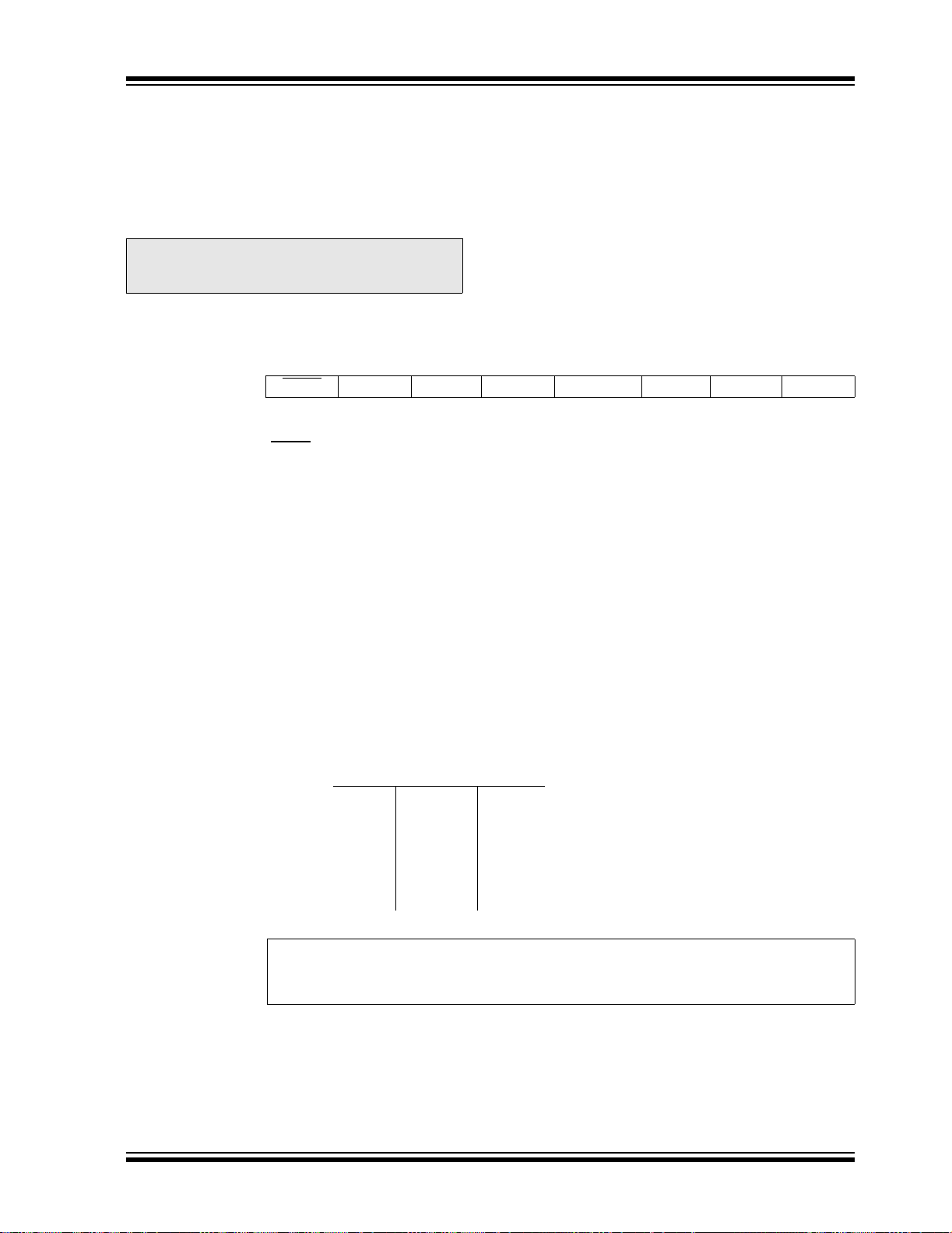
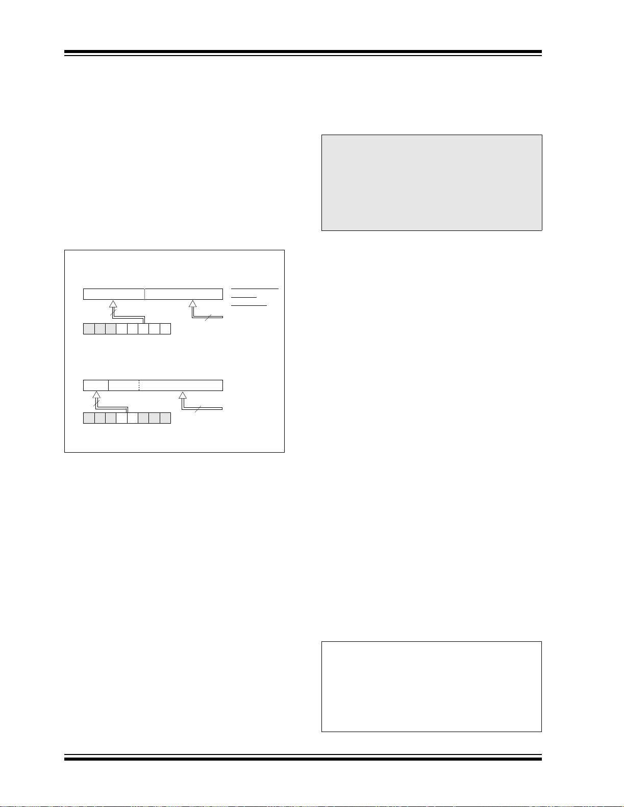
2.3 PCL and PCLATH
The Program Counter (PC) is 13-bits wide. The low
byte comes from the PCL register, which is a readable
and writable register. The upper bits (PC<12:8>) are
not readable, but are indirectly writable through the
PCLA TH reg is ter. On any RESET, the upper bits of the
PC will be cleared. Fig ure2-3 shows the two situations
for the loading of the PC. The up per ex ample in th e figure shows how the PC is loaded on a write to PCL
(PCLATH<4:0> → PCH). The lower example in the fi gure shows how the PC is loaded during a CALL or GOTO
instruction (PCLATH<4:3> → PCH).
FIGURE 2-3: LOADING OF P C IN
DIFFERENT SI T UA T IONS
PCH PCL
12 8 7 0
PC
PCLATH<4:0>
5
PCLATH
PCH PCL
12 11 10 0
PC
2
87
PCLATH<4:3>
11
8
Instruction with
PCL as
Destination
ALU
GOTO,CALL
Opcode <10:0>
The stack operat es as a circular buf fer . This means th at
after the stack has been PUSHed eight times, the ninth
push overwrites the va lue tha t was s tored fro m the first
push. The tenth pus h ov erwr i tes the se co nd push (and
so on).
Note 1: There are no status bits to indicate stack
overflow or stack underflow conditions.
2: There are no instructions/mnemonics
called PUSH or POP. These are actions
that occur from the exec ution of the CALL,
RETURN, RETLW and RETFIE instructions, or the vectoring to an interrupt
address.
2.4 Program Memory Paging
The PIC16FXXX architecture is capable of addressing
a continuous 8K word block of program memory. The
CALL and GOTO instructions provide 11 bits of the
address, which all ows branc hes within any 2K program
memory page. Therefore, the 8K words of program
memory are broken into four pages. Since the
PIC16F872 has only 2K words of program memory or
one page, ad ditional code is not requi red to e nsure th at
the correct pag e is selected before a CALL or GOTO
instruction is executed. The PCLATH<4:3> bits should
always be maintained as zeros. If a return from a CALL
instruction (or interrupt) is executed, the entire 13-bit
PC is popped off the stack. Manipulation of the
PCLATH is not required for the return instructions.
PCLATH
2.3.1 COMPUT ED GOTO
A computed GOTO is accomplish ed by adding an offset
to the progr am counter (ADDWF PCL). When doing a
table read using a computed GOTO method, care
should be exercise d i f the t able loca tio n cros ses a PCL
memory boundary (each 256-byte block). Refer to the
application note, “Implementing a Table Read"
(AN556).
2.3.2 STACK
The PIC16FXXX family has an 8-level deep x 13-bit
wide hardware stack. The stack space is not part of
either program or data space and the stack pointer is
not readable or writable. The PC is PUSHed onto the
stack when a CALL instruction is executed, or an interrupt causes a branch . Th e s t ac k is POPed in the event
of a RETURN, RETLW or a RETFIE instruction
execution. PCLATH is not affected by a PUSH or POP
operation.
2.5 Indirect Addressing, INDF and FSR Registers
The INDF register is not a physica l register . Addr essing
the INDF register will cause indirect address ing.
Indirect addressing is possible by using the INDF register. Any instruction using the INDF register actually
accesses the regist er po int ed to by the File Select register, FSR. Reading the INDF register itself indirectly
(FSR = 0) will read 00h. Writing to the INDF register
indirectly result s in a no op erat ion (alth oug h status bits
may be affected ). An ef fectiv e 9-bit add ress is obt ained
by concatenating the 8 -bit F SR registe r and the IRP bit
(STATUS<7>), as shown in Figure 2-4.
A simple program to clear RAM locations 20h-2Fh
using indirect addressing is shown in Example 2-1.
EXAMPLE 2-1: INDIRECT ADDRESSING
movlw 0x20 ;initialize pointer
movwf FSR ;to RAM
NEXT clrf INDF ;clear INDF register
incf FSR,F ;inc pointer
btfss FSR,4 ;all done?
goto NEXT ;no clear next
CONTINUE
: ;yes continue
DS30569B-page 24 2003 Microchip Technology Inc.
Page 27

FIGURE 2-4: DIRECT/INDIRECT ADDRESSING
RP1: RP0 6
from opcode
0
PIC16F870/871
Indirect AddressingDirect Addressing
IRP FSR Register
7
0
Bank Select Location Select
00 01 10 11
00h
Data
(1)
Memory
7Fh
Bank 0 Bank 1 Bank 2 Bank 3
Note 1: For register file map detail see Figure 2-2.
80h
FFh
100h
17Fh
180h
1FFh
Bank Select
Location Select
2003 Microchip Technology Inc. DS30569B-page 25
Page 28

PIC16F870/871
NOTES:
DS30569B-page 26 2003 Microchip Technology Inc.
Page 29

PIC16F870/871
3.0 DATA EEPROM AND FLASH PROGRAM MEMORY
The Data EEPROM and FLASH Program Memory are
readable and writab le during no rmal operati on over the
entire V
issued from user code (which includes removing code
protection). The d at a m em ory is n ot d ire ctl y ma pped in
the register file sp ace. Instead , it is indirectly ad dressed
through the Special Function Registers (SFR).
There are six SFRs us ed to read and wr ite the pro gram
and data EEPROM memory. These registers are:
• EECON1
• EECON2
• EEDATA
• EEDATH
• EEADR
• EEADRH
The EEPROM data memory allows byte read and write.
When interfacing to the data memory block, EEDATA
holds the 8-bit data for read/write and EEADR holds the
address of the EEPROM locati on bein g access ed. The
registers EEDATH and EEADRH are not used for data
EEPROM access. The PIC16F870/871 devices have
64 bytes of data EEPROM with an addre ss rang e fro m
0h to 3Fh.
The EEPROM data memory is rated for high erase/
write cycles. The write time is controlled by an on-chip
timer. The write time will vary with voltage and temperature, as well as from chip-to-chip. Please refer to the
specifications for exact limits.
The program memory allows word reads and writes.
Program memory acce ss a llo ws fo r c hec ks um c alc ul ation and calibration table storage. A byte or word write
automatically erases the location and writes the new
data (erase before write). Writing to program memory
will cease operati on until the writ e is complete. T he program memory cannot be accessed during the write,
therefore code ca nnot e xecut e. During the w rite operation, the oscillator continues to clock the peripherals,
and therefore, they continue to operate. Interrupt
events will be detected and essentially “queued” until
the write is completed. When the write completes, the
next instruction in the pipeline is executed and the
branch to the interrupt vector address will occur.
When interfacing to the program memory block, the
EEDATH:EEDATA registers form a two-byte word,
which holds the 14-bit data for read/write. The
EEADRH:EEADR registers form a two-byte word,
which holds the 13-bit address of the FLASH location
being accessed. The PIC16F870/871 devices have
2K words of program FLASH with an address range
from 0h to 7FFh. The unused upper bits in both the
EEDATH and EEDATA registers all read as ‘0’s.
DD range. A bulk erase operation may not be
The value written to pr ogram memory does not need to
be a valid instruction. Therefore, up to 14-bit numbers
can be stored in memory for use as calibration parameters, serial numbers, packed 7-bit ASCII, etc. Executing a program memory location containing data that
forms an invalid instruction results in a NOP.
3.1 EEADR
The address registers can address up to a maxim um of
256 bytes of data EEPROM or up to a maximum of
8K words of program FLASH. However, the
PIC16F870/871 have 64 bytes of data EEPROM and
2K words of program FLASH.
When selecting a program address value, the MSByte
of the address is written to the EEADRH register and
the LSByte is written to the EEADR register. When
selecting a data address value, only the LSByte of the
address is written to the EEADR register.
On the PIC16F870/871 devices, the upper two bits of
the EEADR must always be cleared to prevent inadvertent access to the wr on g lo ca tion in d ata EEPROM.
This also applies to the program memory. The upper
five MSbits of EEADRH must always be clear during
program FLASH access.
3.2 EECON1 and EECON2 Registers
The EECON1 register is the control register for configuring and initiatin g the access. The EECON2 reg ister is
not a physically implemented register, but is used
exclusively in the memory write sequence to prevent
inadvertent writes.
There are many bits used to control the read and write
operations to EEPROM data and FLASH program
memory. The EEPGD bit determines if the access will
be a program or data memory access. When clear, any
subsequent operations will work on the EEPROM data
memory. When set, all subsequent operations will
operate in the program memory.
Read operations only us e one additio nal bit, RD, whic h
initiates the read operation from the desired memory
location. Once this bit is set, the value of the desired
memory location will be available in the data registers.
This bit cannot be cleared by firmware. It is automatically cleared at the end of the read operation. For
EEPROM data memory reads, the data will be available in the EEDAT A registe r in the v ery ne xt instruc tion
cycle after the RD bit is set. For program memory
reads, the data will be loaded into the
EEDATH:EEDATA registers, following the second
instruction after the RD bit is set.
2003 Microchip Technology Inc. DS30569B-page 27
Page 30

PIC16F870/871
Write operations have two control bit s, WR and WREN,
and two status bits, WRERR and EEIF. The WREN bit
is used to enable or disable the write operation. When
WREN is clear, the write operation will be disabled.
Therefore, the WREN bit must be set befo re ex ec utin g
a write operation. Th e WR bit is used to initi ate the write
operation. It also is automatically cleared at the end of
the write operation. The interrupt flag EEIF is used to
determine when the mem ory write comp letes. This fla g
must be cleared in software before setting the WR bit.
For EEPROM data memory, once the WREN bit and
the WR bit have been set, the desired memory addres s
in EEADR will be erased, followed by a wri te of the data
in EEDATA. This operation takes place in parallel with
the microcontroller continuing to execute normally.
When the write is c omplete, the EEIF flag bit will be set.
For program memory, once the WREN bit and the WR
bit have been set, the m icrocontr oller will cease to ex e-
cute instructions. T he de sired mem ory l ocatio n poi nted
to by EEADRH:EEADR will be erased. Then, the data
value in EEDATH:EEDATA will be programmed. When
complete, the EEIF flag bit will be set and the
microcontroller will continue to execute code.
The WRERR bit is used to indicate when the
PIC16F870/871 devic es have bee n reset during a write
operation. WRERR should be cleared after Power-on
Reset. Thereafter, it should be checked on any other
RESET. The WRERR bit is set when a write operation
is interrupted by a MCLR
Reset, during normal o peration. In these situati ons, following a RESET , the user should check the WRERR bit
and rewrite the memory locati on, if set. The c ontents of
the data registers, address registers and EEPGD bit
are not affected by either MCLR
Time-out Reset, during normal operation.
REGISTER 3-1: EECON1 REGISTER (ADDRESS: 18Ch)
R/W-x U-0 U-0 U-0 R/W-x R/W-0 R/S-0 R/S-0
EEPGD — — — WRERR WREN WR RD
bit 7 bit 0
bit 7 EEPGD: Program/Data EEPROM Select bit
1 = Accesses program memory
0 = Accesses data memory
(This bit cannot be changed while a read or write operati on is in progress.)
bit 6-4 Unimplemented: Read as '0'
bit 3 WRERR: EEPROM Error Flag bit
1 = A write operation is prematurely terminated (any MCLR
normal operation)
0 = The write operation completed
bit 2 WREN: EEPROM Write Enable bit
1 = Allows write cycles
0 = Inhibits write to the EEPROM
bit 1 WR: Wri te Control bit
1 = Initiates a write cycle. (The bit is cleared by hardware once write is complete. The WR bit
can only be set (not cleared) in software.)
0 = Write cycle to the EEPROM is complete
bit 0 RD: Read Control bit
1 = Initiates an EEPROM read. (RD is cleared in hardware. The RD bit can only be set (not
cleared) in software.)
0 = Does not initiate an EEPROM read
Reset, or a WDT Time-out
Reset, or WDT
Reset or any WDT Reset during
Legend:
R = Readable bit W = Writable bit U = Unimplemented bit, read as ‘0’
- n = Value at POR ’1’ = Bit is set ’0’ = Bit is cleared x = Bit is unknown
DS30569B-page 28 2003 Microchip Technology Inc.
Page 31

PIC16F870/871
3.3 Reading the EEPROM Data Memory
Reading EEPROM data memory only requires that the
desired address to access be written to the EEADR
register and clear th e EEPGD bit. Afte r the RD bit is se t,
data will be av ailable in the EEDATA reg ister on the
very next instruction cycle. EEDAT A will hold this value
until another read operation is initiated or until it is
written by firmware.
The steps to reading the EEPROM data memory are:
1. Write the address to EEDATA. Make sure that
the address is not larger than the memory size
of the PIC16F870/871 devices.
2. Clear the EEPGD bit to point to EEPROM data
memory.
3. Set the RD bit to start the read operation.
4. Read the data from the EEDATA register.
EXAMPLE 3-1: EEPROM DATA READ
BSF STATUS, RP1 ;
BCF STATUS, RP0 ;Bank 2
MOVF ADDR, W ;Write address
MOVWF EEADR ;to read from
BSF STATUS, RP0 ;Bank 3
BCF EECON1, EEPGD ;Point to Data memory
BSF EECON1, RD ;Start read operation
BCF STATUS, RP0 ;Bank 2
MOVF EEDATA, W ;W = EEDATA
3.4 Writing to the EEPROM Data Memory
There are many steps in writing to the EEPROM data
memory . Both address and dat a valu es must be writte n
to the SFRs. The EEPGD bit must be cleared, and the
WREN bit must be set, t o enab le w rites. The WREN b it
should be kept clear at all times, ex cept when writi ng to
the EEPROM data. The WR bit can only be set if the
WREN bit was set in a previous operation (i.e., they
both cannot be set in the same opera tio n). The WREN
bit should then be cleared by firmware after the write.
Clearing the WREN bit before the write actually
completes will not terminate the write in progress.
Writes to EEPROM data memory must also be prefaced with a special sequence of instructions that prevent inadvertent wri te operatio ns. This is a s equence of
five instructions that m ust be executed without in terruptions. The firmware should verify that a write is not in
progress before starting another cycle.
The steps to write to EEPROM data memory are:
1. If step 10 is not implemented, check the WR bit
to see if a write is in progress.
2. Write the address to EEAD R. Make sure that the
address is not larger than the memory size of
the PIC16F870/871 devices.
3. Write the 8-bit data value to be programmed in
the EEDATA register.
4. Clear the EEPGD bit to point to EEPROM data
memory.
5. Set the WREN bit to enable prog ram operations.
6. Disable interrupts (if enabled).
7. Execute the special five instruction sequence:
• Write 55h to EECON2 in two step s (first to W,
then to EECON2)
• Write AAh to EECON2 in two steps (first to
W, then to EECON2)
• Set the WR bit
8. Enable interrupts (if using interrupts).
9. Clear the WREN bit to disable program
operations.
10. At the completion of the write cycle, the WR bit
is cleared and the EEIF interrupt flag bit is set.
(EEIF must be cleared by firmware.) If step 1 is
not implemented, then firmware should check
for EEIF to be set, or WR to clear , to indica te the
end of the program cycle.
EXAMPLE 3-2: EEPROM DATA WRITE
BSF STATUS, RP1 ;
BSF STATUS, RP0 ;Bank 3
BTFSC EECON1, WR ;Wait for
GOTO $-1 ;write to finish
BCF STATUS, RP0 ;Bank 2
MOVF ADDR, W ;Address to
MOVWF EEADR ;write to
MOVF VALUE, W ;Data to
MOVWF EEDATA ;write
BSF STATUS, RP0 ;Bank 3
BCF EECON1, EEPGD ;Point to Data memory
BSF EECON1, WREN ;Enable writes
;Only disable interrupts
BCF INTCON, GIE ;if already enabled,
;otherwise discard
MOVLW 0x55 ;Write 55h to
MOVWF EECON2 ;EECON2
MOVLW 0xAA ;Write AAh to
MOVWF EECON2 ;EECON2
BSF EECON1, WR ;Start write operation
;Only enable interrupts
BSF INTCON, GIE ;if using interrupts,
;otherwise discard
BCF EECON1, WREN ;Disable writes
2003 Microchip Technology Inc. DS30569B-page 29
Page 32

PIC16F870/871
3.5 Reading the FLASH Program Memory
Reading FLASH program memo ry is much like that of
EEPROM data memory, only two NOP instructions must
be inserted after the RD bit is set. These two instruction
cycles that the NOP instructions execute, will be used by
the microcontroller to read the data out of program
memory and insert the value into the EEDATH:EEDAT A
registers. Data will be available following the second
NOP instruction . EEDATH and EEDATA will hold their
value until another read operation is initiated, or until
they are written by firmware.
The steps to rea din g t he FLASH program memory are:
1. Write the address to EEADRH:EEADR. Make
sure that the address is not larger than the
memory size of the PIC16F870/871 devices.
2. Set the EEPGD bit to point to FLASH program
memory.
3. Set the RD bit to start the read operation.
4. Execute two NOP instructions to allow the
microcontroller to read out of program memory.
5. Read the data from the EEDATH:EEDATA
registers.
EXAMPLE 3-3: FLASH PROGRAM READ
BSF STATUS, RP1 ;
BCF STATUS, RP0 ;Bank 2
MOVF ADDRL, W ;Write the
MOVWF EEADR ;address bytes
MOVF ADDRH,W ;for the desired
MOVWF EEADRH ;address to read
BSF STATUS, RP0 ;Bank 3
BSF EECON1, EEPGD ;Point to Program memory
BSF EECON1, RD ;Start read operation
NOP ;Required two NOPs
NOP ;
BCF STATUS, RP0 ;Bank 2
MOVF EEDATA, W ;DATAL = EEDATA
MOVWF DATAL ;
MOVF EEDATH,W ;DATAH = EEDATH
MOVWF DATAH ;
3.6 Writing to the FLASH Program Memory
Writing to FLASH program memory is unique, in that
the microcontroller does not execute instructions while
programming is taking place. The oscillator continues
to run and all peripherals continue to operate and
queue interrupts, if enabled. Once the write operation
completes (specification D133), the processor begins
executing code from where it left off. The other important difference when writing to FLASH program memory is that the WRT configuration bit, when clear,
prevents any writes to program memory (see Table 3-1).
Just like EEPROM data memory, th ere a re ma ny steps
in writing to the FLASH program mem ory . Bot h address
and data values must be written to the SFRs. The
EEPGD bit must be set, and the WREN bit must be set
to enable writes. The WREN bit s hould b e kept clear at
all times, except when writing to the FLASH program
memory. The WR bit can only be set if the WREN bit
was set in a previous operation (i.e., they both cannot
be set in the same operation). The WREN bit should
then be cleared by firmware after the write. Clearing the
WREN bit before the write actually completes will not
terminate the write in progress.
Writes to program memory must also be prefaced with
a special sequence of instructions that prevent inadvertent write operations. This is a sequence of five
instructio ns t h at mu st b e e xe cu t ed w it hou t i n ter r upt i on
for each byt e writ ten. Th ese ins tructi ons must then be
followed by two NOP instructions to allow the microcontroller to setup for th e writ e opera tion. Onc e the wr ite i s
complete, the execution of instructions starts with the
instruction after the second NOP.
The steps to write to program memory are:
1. Write the address to EEADRH:EEADR. Make
sure that the address is not larger than the
memory size of the PIC16F870/871 devices.
2. Write the 14 -bi t da ta value to be programmed in
the EEDATH:EEDATA registers.
3. Set the EEPGD bit to point to FLASH program
memory.
4. Set the WREN bit to enable prog ram operations.
5. Disable interrupts (if enabled).
6. Execute the special five instruction sequence:
• Write 55h to EECON2 in two step s (first to W ,
then to EECON2)
• Write AAh to EECON2 in two steps (first to W ,
then to EECON2)
• Set the WR bit
7. Execute two NOP instructions to allow the
microcontroller to setup for write operation.
8. Enable interrupts (if using interrupts).
9. Clear the WREN bit to disable program
operations.
DS30569B-page 30 2003 Microchip Technology Inc.
Page 33

PIC16F870/871
y
s
o
At the completion of the write cycle, the WR bit is
cleared and the EEIF interrupt flag bit is set. (EEIF
must be cleared by firmware. ) Since the microcont roller
does not execute in structions duri ng the write cy cle, the
firmware does not necessarily have to check either
EEIF, or WR, to determine if the write had finished.
EXAMPLE 3-4: FLASH PROGRAM WRITE
BSF STATUS, RP1 ;
BCF STATUS, RP0 ;Bank 2
MOVF ADDRL, W ;Write address
MOVWF EEADR ;of desired
MOVF ADDRH, W ;program memory
MOVWF EEADRH ;location
MOVF VALUEL, W ;Write value to
MOVWF EEDATA ;program at
MOVF VALUEH, W ;desired memory
MOVWF EEDATH ;location
BSF STATUS, RP0 ;Bank 3
BSF EECON1, EEPGD ;Point to Program memor
BSF EECON1, WREN ;Enable writes
;Only disable interrupt
BCF INTCON, GIE ;if already enabled,
;otherwise discard
MOVLW 0x55 ;Write 55h to
MOVWF EECON2 ;EECON2
MOVLW 0xAA ;Write AAh to
MOVWF EECON2 ;EECON2
BSF EECON1, WR ;Start write operation
NOP ;Two NOPs to allow micr
NOP ;to setup for write
;Only enable interrupts
BSF INTCON, GIE ;if using interrupts,
;otherwise discard
BCF EECON1, WREN ;Disable writes
3.7 Write Verify
The PIC16F870/871 devices do not automatically verify the value written during a write operation. Depending on the appl ication, good pro gramming practic e may
dictate that the value written to memory be verified
against the original value. This should be used in appl ications where exce ssive wr ites can stress bit s near th e
specified endurance limits.
3.8 Protection Against Spurious
Writes
There are conditions when the device may not want to
write to the EEPROM data memory or FL ASH program
memory. To protect against these spurious write conditions, various mechanisms have been built into the
PIC16F870/871 devices. On power-up, the WREN bit
is cleared and the Power-up Timer (if enabled)
prevents writes.
The write initiate se quence an d the WR EN bit togethe r ,
help prevent any accidental writes during brown-out,
power glitches, or firmware malfunction.
3.9 Operation While Code Protected
The PIC16F870/871 devices have two code protect
mechanisms, one bit for EEPROM data memory and
two bits for FLASH program memory. Data can be read
and written to the EEPROM data memory, regardless
of the state of the code protection bit, CPD. When code
protection is enabled and CPD cleared, external
access via ICSP is disabled, regardless of the state of
the program memory code protect bits. This prevents
the contents of EEPROM data me mory from being read
out of the device.
The state of the program memory code protect bits,
CP0 and CP1, do not affect the execution of instructions out of program memory. The PIC16F870/871
devices can always read the values in program memory, regardless of the state of the code protect bits.
However, the state of the code protect bits and the
WRT bit will have dif ferent ef fects on writi ng to program
memory . Tab le 4-1 s hows the ef fect of the cod e protec t
bits and the WRT bit on program memory.
Once code protection has been enabled for either
EEPROM data memory or FLASH program memory,
only a full erase of the entire device will disable code
protection.
2003 Microchip Technology Inc. DS30569B-page 31
Page 34

PIC16F870/871
3.10 FLASH Program Memory Write Protection
The configuration word contains a bit that write protects
the FLASH program memory, called WRT. This bit can
only be accessed when programming the
PIC16F870/871 devices via ICSP. Once write protection is enabled, only an erase of the entire device will
disable it. When enabled , write pr otection pr event s any
writes to FLASH program memory. Write protection
does not affect program memory reads.
TABLE 3-1: READ/WRITE STATE OF INTERNAL FLASH PROGRAM MEMORY
Configuration Bits
Memory Location
CP1 CP0 WRT
00x All program memory Yes No No No
010 Unprotected areas Yes No Yes No
010 Protected areas Yes No No No
011 Unprotected areas Yes Yes Yes No
011 Protected areas Yes No No No
100 Unprotected areas Yes No Yes No
100 Protected areas Yes No No No
101 Unprotected areas Yes Yes Yes No
101 Protected areas Yes No No No
110 All program memory Yes No Yes Yes
111 All program memory Yes Yes Yes Yes
Internal
Read
Internal
Write
ICSP Read ICSP Write
TABLE 3-2: REGISTERS ASSOCIATED WITH DATA EEPROM/PROGRAM FLASH
Address Name Bit 7 Bit 6 Bit 5 Bit 4 Bit 3 Bit 2 Bit 1 Bit 0
0Bh, 8Bh,
10Bh, 18Bh
10Dh EEADR EEPROM Address Register, Low Byte xxxx xxxx uuuu uuuu
10Fh EEADRH
10Ch EEDATA EEPRO M Data Register, Low Byte xxxx xxxx uuuu uuuu
10Eh EEDATH
18Ch EECON1 EEPGD
18Dh EECON2 EEPROM Control Register2 (not a physical register) — —
Legend: x = unknown, u = unchanged, r = reserved, - = unimplemented, read as '0'.
Note 1: These bits are reserved; always maintain these bits clear.
INTCON GIE PEIE
— — — EEPROM Address, High Byte xxxx xxxx uuuu uuuu
— — EEPROM Data Register, High Byte xxxx xxxx uuuu uuuu
Shaded cells are not used during FLASH/EEPROM access.
T0IE INTE RBIE T0IF INTF RBIF 0000 000x 0000 000u
— — — WRERR WREN WR RD x--- x000 x--- u000
Value on:
POR, BOR
Val ue on
all other
RESETS
DS30569B-page 32 2003 Microchip Technology Inc.
Page 35

PIC16F870/871
4.0 I/O PORTS
Some pins for th ese I/O ports are multiplexed with an
alternate function for the peripheral features on the
device. In general, when a peripheral is enabled, that
pin may not be used as a general purpose I/O pin.
Additional inform atio n o n I/O ports may be found i n th e
PICmicro™ Mid-Range MCU Family Reference
Manual (DS33023).
4.1 PORTA and the TRISA Register
PORTA is a 6-bit wide bi-directional port. The corresponding data direction register is TRISA. Setting a
TRISA bit (= 1) will make the correspondi ng PORT A pin
an input (i.e., put the corresponding output driver in a
Hi-Impedance mode). Clearing a TRISA bit (= 0) will
make the correspondin g POR TA pin an output (i.e., put
the contents of the output latch on the selected pin).
Reading the PORT A register reads the status of the pins,
whereas writing to it will write to the port latch. All write
operations are read-modify-write operations. Therefore,
a write to a port implies that the port pins are read, the
value is modified and then written to the port data latch.
Pin RA4 is multiplexed with the Timer0 module clock
input to become the RA4/T0CKI pin. The RA4/T0CKI
pin is a Schmitt Trigger input and an ope n dr ain o utput.
All other PORTA pins have TTL input levels and full
CMOS output drivers.
Other PORTA pins are multiplexed with analog inputs
and analog V
selected by clearing/setting the control bits in the
ADCON1 register (A/D Control Register 1).
Note: On a Power-on Reset, these pins are
The TRISA register controls the direction of the RA
pins, even when they are be ing us ed as ana lo g inputs.
The user must ensure the bits in the TRISA regi ster are
maintained set when using them as analog inputs.
EXAMPLE 4-1: INITIALIZING PORTA
BCF STATUS, RP0 ;
BCF STATUS, RP1 ;Bank0
CLRF PORTA ;Initialize PORTA by
BSF STATUS, RP0 ;Select Bank 1
MOVLW 0x06 ;Configure all pins
MOVWF ADCON1 ;as digital inputs
MOVLW 0xCF ;Value used to
MOVWF TRISA ;Set RA<3:0> as
REF input. The operation of each pin is
configured as analog inputs and read as
'0'.
;clearing output
;data latches
;initialize data
;direction
;inputs
;RA<5:4> as outputs
;TRISA<7:6> are
;always read as '0'.
FIGURE 4-1: BLOCK DIAGRAM OF
RA3:RA0 AND RA5 PINS
Data
Bus
WR
Port
Data Latch
WR
TRIS
TRIS Latch
RD PORT
To A/D Converter
Note 1: I/O pins have protection diodes to VDD and VSS.
CK
CK
QD
Q
QD
Q
RD TRIS
QD
Analog
Input
Mode
EN
VDD
P
N
V
I/O pin
SS
TTL
Input
Buffer
FIGURE 4-2: BLOCK DIAGRAM OF
RA4/T0CKI PIN
Data
Bus
WR
PORT
WR
TRIS
RD PORT
TMR0 Clock Input
Note 1: I/O pin has protection diodes to VSS only.
QD
Q
CK
Data Latch
QD
Q
CK
TRIS Latch
RD TRIS
N
SS
V
Schmitt
Trigger
Input
Buffer
QD
EN
EN
I/O pin
(1)
(1)
2003 Microchip Technology Inc. DS30569B-page 33
Page 36

PIC16F870/871
TABLE 4-1: PORTA FUNCTIONS
Name Bit# Buffer Function
RA0/AN0 bit0 TTL Input/output or analog input.
RA1/AN1 bit1 TTL Input/output or analog input.
RA2/AN2 bit2 TTL Input/output or analog input.
RA3/AN3/VREF bit3 TTL Input/output or analog input or VREF.
RA4/T0CKI bit4 ST Input/output or external clock input for Timer0. Output is open drain type.
RA5/AN4 bit5 TTL Input/output or analog input.
Legend: TT L = TTL input, ST = Schmit t Trigger input
TABLE 4-2: SUMMARY OF REGISTERS ASSOCIATED WITH PORTA
Address Name Bit 7 Bit 6 Bit 5 Bit 4 Bit 3 Bit 2 Bit 1 Bit 0
05h PORTA — — RA5 RA4 RA3 RA2 RA1 RA0 --0x 0000 --0u 0000
85h TRISA — — PORTA Data Direction Register --11 1111 --11 1111
9Fh ADCON1 ADFM — — — PCFG3 PCFG2 PCFG1 PCFG0 --0- 0000 --0- 0000
Legend: x = unknown, u = unchanged, - = unimplemented locations read as '0'.
Shaded cells are not used by PORTA.
Value on:
POR, BOR
Value on
all other
RESETS
DS30569B-page 34 2003 Microchip Technology Inc.
Page 37

PIC16F870/871
4.2 PORTB and the TRISB Register
PORTB is an 8-bit wide, bi-directional port. The corresponding data direction register is TRISB. Setting a
TRISB bit (= 1) will make the corresponding PORTB
pin an input (i.e., put the corresponding output driver in
a Hi-Impeda nc e m od e ). C l e ari ng a T RI SB bi t (= 0) will
make the corresponding POR TB pin an output (i.e. , put
the contents of the output latch on the selected pin).
Three pins of PORTB are multiplexed with the Low
Voltage Programming function: RB3/PGM, RB6/PGC
and RB7/PGD. The alternate functions of these pins
are described in the Special Featu res Sectio n.
Each of the PORTB pi ns has a w eak i nternal pul l-up. A
single control bit can turn on all the pull-ups. This is performed by clearing bit RBPU
weak pull-up is automatically turned off when the port
pin is configured as an output. The pull-ups are
disabled on a Power-on Reset.
FIGURE 4-3 : BLOCK DIA GR AM O F
(2)
RBPU
Data Bus
WR Port
WR TRIS
Data Latch
CK
TRIS Latch
CK
RD TRIS
RD Port
(OPTION_REG<7>). The
RB3:RB0 PINS
QD
QD
TTL
Input
Buffer
QD
EN
V
DD
P
Weak
Pull-up
I/O pin
(1)
This interrupt can wake the device from SLEEP. The
user, in the Interrupt Service Routine, can clear the
interrupt in the following manner:
a) Any read or write of PORTB. This will end the
mismatch condition.
b) Clear flag bit RBIF.
A mismatch c ond it i on wi ll cont i n ue to s et f lag bi t RB IF.
Reading PORTB will end the mismatch condition and
allow flag bit RBIF to be cleared.
The interrupt-on-change feature is recommended for
wake-up on key depression operation and operations
where PORTB is only used for the interrupt-on-change
feature. Polling of PORTB is not recommended while
using the interrupt-on-change feature.
This interrupt on mismatch feature, together with software configurable pull-ups on these four pins, allow
easy interface to a keypad and make it possible for
wake-up on key-depression. Refer to the Embedded
Control Handbook, “Implementing Wake-up on Key
Stroke” (AN552).
RB0/INT is an external interrupt input pin and is
configured using the INTEDG bit (OPTION_REG<6>).
RB0/INT is discussed in detail in Section 11.10.1.
FIGURE 4-4: BLOCK DIAGRAM OF
RB7:RB4 PINS
V
TTL
Input
Buffer
DD
P
Weak
Pull-up
I/O pin
Buffer
(1)
ST
(2)
RBPU
Data Bus
WR Port
WR TRIS
Data Latch
QD
CK
TRIS Latch
QD
CK
RB0/INT
RB3/PGM
Note 1: I/O pins have diode protection to V
2: To enable weak pull-ups, set the appropriate TRIS
bit(s) and clear the RBPU
Schmitt Trigger
Buffer
bit (OPTION_REG<7>).
RD Port
DD and VSS.
Four of PORTB’s pi ns, RB7:RB4, have an interrupt-onchange feature. Only pins configured as inputs can
cause this interrupt to occur (i.e., any RB7:RB4 pin
configured as an output is excluded from the interrupton-change comparison). The input pins (of RB7:RB4)
are compared with the old value latched on the last
read of PORTB. The “mismatch” outputs of RB7:RB4
Set RBIF
From other
RB7:RB4 pins
RB7:RB6 in Serial Programming Mode
Note 1: I/O pins have diode protection to V
2: To enable weak pull-ups, set the appropriate TRIS
RD TRIS
RD Port
bit(s) and clear the RBPU
Latch
QD
EN
QD
RD Port
EN
DD and VSS.
bit (OPTION_REG<7>).
Q1
Q3
are OR’ed together to generate the RB Port Change
Interrupt with flag bit RBIF (INTCON<0>).
2003 Microchip Technology Inc. DS30569B-page 35
Page 38

PIC16F870/871
TABLE 4-3: PORTB FUNCTIONS
Name Bit# Buffer Function
RB0/INT bit0 TTL/ST
RB1 bit1 TTL Input/output pin. Internal software programmable weak pull-up.
RB2 bit2 TTL Input/output pin. Internal software programmable weak pull-up.
RB3/PGM bit3 TTL/ST
RB4 bit4 TTL Input/output pin (with interrup t-on-change). In ternal software pro grammable
RB5 bit5 TTL Input/output pin (with interrup t-on-change). In ternal software pro grammable
RB6/PGC bit6 TTL/ST
RB7/PGD bit7 TTL/ST
Legend: TTL = TTL input, ST = Schmitt Trigger input
Note 1: This buffer is a Schmitt Trigger input when configured as the external interrupt or LVP mode.
2: This buffer is a Schmitt Trigger input when used in Serial Programming mode.
(1)
Input/output pin or external interrupt input. Internal software
programmable weak pull-up.
(1)
Input/output pin or programming pin in LVP mode. Internal software
programmable weak pull-up.
weak pull-up.
weak pull-up.
(2)
Input/output pin (with interrupt-on-change) or In-Circuit Debugger pin.
Internal software programmable weak pull-up. Serial programming clock.
(2)
Input/output pin (with interrupt-on-change) or In-Circuit Debugger pin.
Internal software programmable weak pull-up. Serial programming data.
TABLE 4-4: SUMMARY OF REGISTERS ASSOCIATED WITH PORTB
Address Name Bit 7 Bit 6 Bit 5 Bit 4 Bit 3 Bit 2 Bit 1 Bit 0
06h, 106h PORTB R B 7 RB6 RB5 RB4 RB3 RB2 RB1 RB0 xxxx xxxx uuuu uuuu
86h, 186h TRISB PORTB Data Direction Register 1111 1111 1111 1111
81h, 181h OPTION_REG RBPU INTEDG
Legend: x = unknown, u = unchanged. Shaded cells are not used by PORTB.
T0CS T0SE PSA PS2 PS1 PS0 1111 1111 1111 1111
Val ue on:
POR, BOR
Val ue on
all other
RESETS
DS30569B-page 36 2003 Microchip Technology Inc.
Page 39

PIC16F870/871
4.3 PORTC and the TRISC Register
PORTC is an 8-bit wide, bi-directional port. The corresponding data direction register is TRISC. Setting a
TRISC bi t (= 1) will make the corresponding PORTC
pin an input (i.e., put the corresponding output driver in
a Hi-Impedance mode). Clearing a TRISC bit (= 0) will
make the correspondi ng PORTC pin an output (i.e., p ut
the contents of the output latch on the selected pin).
PORTC is mul tiplexed with s everal peri pheral function s
(Table 4-5). PORTC pins have Schmitt Trigger input
buffers.
When enabling peripheral functions, care should be
taken in defining TRIS bit s fo r each POR TC pin. Some
peripherals override the TRIS bit to make a pin an output, while other peripherals override the TRIS bit to
make a pin an input. Since the TRIS bit override is in
effect while the peripheral is enabled, read-modifywrite instructions (BSF, BCF, XORWF) with TRISC as
the destination should be avoided. The user should
refer to the corresponding peripheral section for the
correct TRIS bit settings.
FIGURE 4-5: PORTC BLOCK DIAGRAM
(PERIPHERAL OUTPUT
OVERRIDE)
CK
Data Latch
CK
TRIS Latch
RD TRIS
RD
PORT
(2)
DD
Schmitt
Trigger
V
P
N
Vss
I/O
pin
(1)
0
QD
1
Q
QD
Q
QD
EN
Port/Peripheral Select
Peripheral Data Out
Data Bus
WR
PORT
WR
TRIS
Peripheral
(3)
OE
Peripheral Input
Note 1: I/O pins have diode protection to VDD and VSS.
2: Port/Peripheral Select signal selects between
port data and peripheral output.
3: Peripheral OE (Output Enable) is only activated
if Peripheral Select is active.
TABLE 4-5: PORTC FUNCTIONS
Name Bit# Buffer Type Function
RC0/T1OSO/T1CKI bit0 ST Input/output port pin or Timer1 oscillator output/Timer1 clock input.
RC1/T1OSI bit1 ST Input/output port pin or Timer1 oscillator input.
RC2/CCP1 bit2 ST Input/output port pin or Capture1 input/Compare1 output/
PWM1 output.
RC3 bit3 ST Input/output port pin.
RC4 bit4 ST Input/output port pin.
RC5 bit5 ST Input/output port pin.
RC6/TX/CK bit6 ST Input/output port pin or USART Asynchronous Transmit or
Synchronous Clock.
RC7/RX/DT bit7 ST Input/output port pin or USART Asynchronous Receive or
Synchronous Data.
Legend: ST = Schmitt Trigger inpu t
TABLE 4-6: SUMMARY OF REGISTERS ASSOCIATED WITH PORTC
Value on
all other
RESETS
Address Name Bit 7 Bit 6 Bit 5 Bit 4 Bit 3 Bit 2 Bit 1 Bit 0
07h PORTC RC7 RC6 RC5 RC4 RC3 RC2 RC1 RC0
87h TRISC PORTC Data Direction Register
Legend: x = unknown, u = unchanged
Value on:
POR, BOR
xxxx xxxx uuuu uuuu
1111 1111 1111 1111
2003 Microchip Technology Inc. DS30569B-page 37
Page 40

PIC16F870/871
4.4 PORTD and TRISD Registers
This section is not applicable to the PIC16F870.
PORTD is an 8-bit port with Schmitt Trigger input buff-
ers. Each pin is individu all y co nfig ura ble as an inp ut or
output.
PORTD can be configured as an 8-bit wide microprocessor port (parallel slave p ort) by setting c ontrol bit
PSPMODE (TRISE<4>). In this mode, the input buffers
are TTL.
FIGURE 4-6: PORTD BLOCK DIAGRAM
(IN I/O PORT MODE )
Data
Bus
WR
Port
WR
TRIS
RD Port
Note 1: I/O pins have protection diodes to VDD and VSS.
CK
Data Latch
QD
CK
TRIS Latch
RD TRIS
QD
Schmitt
Trigger
Input
Buffer
QD
EN
EN
I/O pin
(1)
TABLE 4-7: PORTD FUNCTIONS
Name Bit# Buffer Type Function
RD0/PSP0 bit0
RD1/PSP1 bit1
RD2/PSP2 bit2
RD3/PSP3 bit3
RD4/PSP4 bit4
RD5/PSP5 bit5
RD6/PSP6 bit6
RD7/PSP7 bit7
ST/TTL
ST/TTL
ST/TTL
ST/TTL
ST/TTL
ST/TTL
ST/TTL
ST/TTL
(1)
(1)
(1)
(1)
(1)
(1)
(1)
(1)
Input/output port pin or parallel slave port bit0.
Input/output port pin or parallel slave port bit1.
Input/output port pin or parallel slave port bit2.
Input/output port pin or parallel slave port bit3.
Input/output port pin or parallel slave port bit4.
Input/output port pin or parallel slave port bit5.
Input/output port pin or parallel slave port bit6.
Input/output port pin or parallel slave port bit7.
Legend: ST = Schmitt Trigger input, TTL = TTL input
Note 1: Input buffers are Schmitt Triggers when in I/O mode and TTL buffers when in Parallel Slave Port mode.
TABLE 4-8: SUMMARY OF REGISTERS ASSOCIATED WITH PORTD
Address Name Bit 7 Bit 6 Bit 5 Bit 4 Bit 3 Bit 2 Bit 1 Bit 0
08h PORTD RD7 RD6 RD5 RD4 RD3 RD2 RD1 RD0 xxxx xxxx uuuu uuuu
88h TRISD PORTD Data Direction Register 1111 1111 1111 1111
89h TRISE
IBF OBF IBOV PSPMODE — PORTE Data Directio n Bi ts 0000 -111 0000 -111
Value on:
POR, BOR
Legend: x = unknown, u = unchanged, - = unimplemented read as '0'. Shaded cells are not used by PORTD.
Value on
all other
RESETS
DS30569B-page 38 2003 Microchip Technology Inc.
Page 41

PIC16F870/871
4.5 PORTE and TRISE Register
This section is not applicable to the PIC16F870.
PORTE has three pins, RE0/RD
and RE2/CS
/AN7, which are individually configurable
as inputs or outputs. These pins have Schmitt Trigger
input buffers.
I/O PORTE becomes control inputs for the microprocessor port when bit PSPMODE (TRISE<4>) is set. In
this mode, the user must make sure that the
TRISE<2:0> bits are set (pins are configured as digital
inputs). Ensure ADC ON1 is config ured for digital I/O. In
this mode, the input buffers are TTL.
Register 4-1 shows the TRISE register, which also
controls the parallel slave port operation.
PORTE pins are multiplexed with analog inputs. When
selected as an a nalog input, these pins wi ll read as '0 's.
TRISE controls the direction of the RE pins, even when
they are being used as analog inputs. The user must
make sure to keep the pins configured as inputs when
using them as analog inputs.
Note: On a Power-on Reset, these pins are
configured as analog inputs.
/AN5, RE1/WR/AN6
FIGURE 4-7: PORTE BLOCK DIAG RAM
(IN I/O PORT MO DE)
Data
Bus
WR
PORT
WR
TRIS
RD PORT
Note 1: I/O pins have protection diodes to VDD and VSS.
QD
CK
Data Latch
QD
CK
TRIS Latch
RD TRIS
Schmitt
Trigger
input
buffer
QD
EN
I/O pin
(1)
2003 Microchip Technology Inc. DS30569B-page 39
Page 42

PIC16F870/871
REGISTER 4-1: TRISE REGISTER (ADDRESS: 89h)
R-0 R-0 R/W-0 R/W-0 U-0 R/W-1 R/W-1 R/W-1
IBF OBF IBOV PSPMODE — Bit2 Bit1 Bit0
bit 7 bit 0
bit 7 Parallel Slave Port Status/Control Bits
IBF: Input Buffer Full Status bit
1 = A word has been received and is waiting to be read by the CPU
0 = No word has been received
bit 6 OBF: Output Buffer Full Status bit
1 = The output buffer still holds a previously written word
0 = The output buffer has been read
bit 5 IBOV: Input Buffer Overflow Detect bit (in Microprocessor mode)
1 = A write occurred when a previously input word has not been read
(must be cleared in software)
0 = No overflow occurred
bit 4 PSPMODE: Parallel Slave Port Mode Select bit
1 = Parallel Slave Port mode
0 = General Purpose I/O mode
bit 3 Unimplemented: Read as '0'
PORTE Data Direction Bits
bit 2 Bit2: Direction Control bit for pin RE2/CS/AN7
1 = Input
0 = Output
bit 1 Bit1: Direction Control bit for pin RE1/WR
1 = Input
0 = Output
bit 0 Bit0: Direction Control bit for pin RE0/RD
1 = Input
0 = Output
/AN6
/AN5
Legend:
R = Readable bit W = Writable bit U = Unimplemented bit, read as ‘0’
- n = Value at POR ‘1’ = Bit is set ‘0’ = Bit is cleared x = Bit is unknown
DS30569B-page 40 2003 Microchip Technology Inc.
Page 43

PIC16F870/871
TABLE 4-9: PORTE FUNCTIONS
Name Bit# Buffer Type Function
RE0/RD/AN5 bit0 ST/TTL
RE1/WR
RE2/CS
/AN6 bit1 ST/TTL
/AN7 bit2 ST/TTL
Legend: ST = Schmitt Trigger input, TTL = TTL input
Note 1: Input buffers are Schmitt Triggers when in I/O mode and TTL buffers when in Parallel Slave Port mode.
(1)
Input/output port pin or read co ntrol input in Parall el Slave Port mode or
analog input:
RD
1 = Not a read operation
0 = Read operation. Reads PORTD register (if chip selected.)
(1)
Input/output port pin or write control input in Parallel Slave Port mode
or analog input:
WR
1 = Not a write operation
0 = Write operation. Writes PORTD register (if chip selected).
(1)
Input/output port pin or chip select control input in Parallel Slave Port
mode or analog input:
CS
1 = Device is not selected
0 = Device is selected
TABLE 4-10: SUMMARY OF REGISTERS ASSOCIATED WITH PORTE
Addr Name Bit 7 Bit 6 Bit 5 Bit 4 Bit 3 Bit 2 Bit 1 Bit 0
09h PORTE
89h TRISE IBF OBF IBOV PSPMODE
9Fh ADCON1 ADFM
Legend: x = unknown, u = unchanged, - = unimplemented read as '0'. Shaded cells are not used by PORTE.
— — — — —RE2RE1RE0---- -xxx ---- -uuu
— PORTE Data Direction Bits 0000 -111 0000 -111
— — — PCFG3 PCFG2 PCFG1 PCFG0 --0- 0000 --0- 0000
Val ue on:
POR, BOR
Value on
all other
RESETS
2003 Microchip Technology Inc. DS30569B-page 41
Page 44

PIC16F870/871
4.6 Parallel Slave Port
The Parallel Slave Port is not implemented on the
PIC16F870.
PORTD operates as an 8-bit wide Parallel Slav e Port or
microprocessor port when control bit PSPMODE
(TRISE<4>) is set. I n Sl av e mo de, it is asynchronously
readable and writa ble by the ex ternal world throu gh RD
control input pin RE0/RD and WR control input pin
RE1/WR
It can directly interface to an 8-bit mic rop roc es sor dat a
bus. The external mic roproc essor c an rea d or write th e
PORTD latch as an 8-bit latch. Setting bit PSPMODE
enables port pin RE0/RD
to be the WR input and RE2/CS to be the CS (chip
select) input. For this functionality, the corresponding
data direction bits of the TRISE register (TRISE<2:0>)
must be configured as input s (set). The A/D port confi guration bits PCFG3:PCFG0 (ADCON1<3:0>) must be
set to configure pins RE2:RE0 as digital I/O.
There are actually two 8-bit latches. One for data output and one for data input. The user writes 8-bit data to
the PORTD data la tch and reads dat a from the port pin
latch (note that they have the same address). In this
mode, the TRISD register is ignored, since the
microprocessor is contro lli ng the dire cti on of data flow.
A write to the PSP occurs when both the CS
lines are first detected low. When either the CS or WR
lines become high (l evel triggered) , the Input Buffe r Full
(IBF) status flag bit (TRISE<7>) is set on the Q4 clock
cycle, following the next Q2 cycle, to signal the write is
complete (Figure 4-9). The interrupt flag bit, PSPIF
(PIR1<7>), is also set on the same Q4 clock cycle. IBF
can only be cle are d b y re adi ng the PO R TD i npu t l atc h.
The Input Buffer Overflow (IBOV) status flag bit
(TRISE<5>) is set if a second write to the PSP is
attempted w hen the pre vious byte has not bee n read
out of the buffer.
A read from the PSP occurs when both the CS
lines are first detected low. The Output Buffer Full
(OBF) status flag bit (TRISE<6>) is cleared immediately (Figure 4-10), indicating that the PORTD latch is
waiting to be read by the ext ernal bus . When ei ther the
CS or RD pin becomes high ( level triggered), the interrupt flag bit PSPIF is set on the Q4 clock cycle, following the next Q2 cycle, indicating that the read is
complete. OBF remains low until data is written to
PORTD by the user firmware.
When not in PSP mode, the IBF and OBF bits are held
clear. However, if flag bit IBOV was previously set, it
must be cleared in firmware.
An interrupt is generated and latched into flag bit
PSPIF when a read or write operation is completed.
PSPIF must be cleared by the user in fi rmware and th e
interrupt can be disabled by clearing the interrupt
enable bit PSPIE (PIE1<7>).
.
to be the RD input, RE1/WR
and WR
and RD
FIGURE 4-8: PORTD AND PORTE
BLOCK DIAGRAM
(PARALLEL SLAVE PORT)
Data Bus
WR
Port
RD
Port
One bit of PORTD
Set Interrupt Flag
PSPIF (PIR1<7>)
Note: I/O pin has protection diodes to VDD and VSS.
QD
CK
QD
EN
EN
Read
Chip Select
Write
TTL
TTL
TTL
TTL
RDx
pin
RD
CS
WR
DS30569B-page 42 2003 Microchip Technology Inc.
Page 45

FIGURE 4-9: PARALLEL SLAVE PORT WRITE WAVEFORMS
Q1 Q2 Q3 Q4CSQ1 Q2 Q3 Q4 Q1 Q2 Q3 Q4
WR
RD
PORTD<7:0>
IBF
OBF
PSPIF
FIGURE 4-10: PARALLEL SLAVE PORT READ WAVEFORMS
Q1 Q2 Q3 Q4CSQ1 Q2 Q3 Q4 Q1 Q2 Q3 Q4
PIC16F870/871
WR
RD
PORTD<7:0>
IBF
OBF
PSPIF
TABLE 4-11: REGISTERS ASSOCIATED WITH PARALLEL SLAVE PORT
Address Name Bit 7 Bit 6 Bit 5 Bit 4 Bit 3 Bit 2 Bit 1 Bit 0
08h PORTD Port Data Latch when written: Port pins when read xxxx xxxx uuuu uuuu
09h PORTE
89h TRISE IBF OBF IBOV PSPMODE
0Ch P IR1 PSPIF
8Ch P IE1 PSPIE
9Fh ADCON1 ADFM
Legend: x = unknown, u = unchanged, - = unimplemented, read as '0'. Shaded cells are not used by the Parallel Slave Port.
— — — — —RE2RE1RE0---- -xxx ---- -uuu
— PORTE Data Direction bits 0000 -111 0000 -111
ADIF RCIF TXIF — CCP1IF TMR2IF TMR1IF 0000 0000 0000 0000
ADIE RCIE TXIE — CCP1IE TMR2IE TMR1IE 0000 0000 0000 0000
— — — PCFG3 PCFG2 PCFG1 PCFG0 --0- 0000 --0- 0000
Val ue on:
POR, BOR
Value on
all other
RESETS
2003 Microchip Technology Inc. DS30569B-page 43
Page 46

PIC16F870/871
NOTES:
DS30569B-page 44 2003 Microchip Technology Inc.
Page 47

PIC16F870/871
5.0 TIMER0 MODULE
Counter mode is selected by setting bit T0CS
(OPTION_REG<5>). In Counter mode, Timer0 will
The Timer0 module timer/counter has the following
features:
• 8-bit timer/counter
• Readable and writable
• 8-bit software programmable prescaler
• Internal or external clock select
• Interrupt on overflow from FFh to 00h
• Edge select for external clock
Figure 5-1 is a bloc k diagram o f the T imer0 mod ule and
increment either on every rising, or falling edge of pin
RA4/T0CKI. The incrementing edge is determined by
the Timer0 Source Edge Select bit, T0SE
(OPTION_REG<4>). Clearing bit T0SE selects the rising edge. Restrictions on the external clock input are
discussed in detail in Section 5.2.
The prescaler is mutually exclusively shared between
the Timer0 modu le and t he W a tchdo g Timer. The pres caler is not readabl e or w rit able. Sectio n 5.3 details the
operation of the prescaler.
the prescaler shared with the WDT.
Additional information on the Timer0 module is avail-
able in the PICmicro™ Mid-Range MCU Family
Reference Manual (DS33023).
Timer mode is selected by clearing bit T0CS
(OPTION_REG<5>). In Timer mode, the Timer0 module will incremen t every ins tru ction cycle (without prescaler). If the TMR0 register is written, the increment is
inhibited for the following two instruction cycles. The
user can work around this by writing an adjusted value
5.1 Timer0 Interrupt
The TMR0 interrupt is generated when the TMR0 register overflows from FFh to 00h. This overflow sets bit
T0IF (INTCON<2>). The interrupt can be masked by
clearing bit T0IE (INTCON<5>). Bit T0IF must be
cleared in software by the T imer0 mod ule Interrupt Service Routine before re-enabling this interrupt. The
TMR0 interrupt cannot awaken the processor from
SLEEP, since the timer is shut-off during SLEEP.
to the TMR0 register.
FIGURE 5-1 : BLOCK DIA GR AM OF T H E TIMER0/WDT PRES CA LE R
CLKO (= F
RA4/T0CKI
pin
Watchdog
Timer
WDT Enable bit
OSC/4)
T0SE
Data Bus
M
0
U
X
1
T0CS
0
M
U
1
X
PSA
8-bit Prescaler
8 - to - 1MUX
0
Time-out
PRESCALER
8
M U X
WDT
1
M
U
0
X
PSA
1
SYNC
2
Cycles
PS2:PS0
PSA
8
TMR0 Reg
Set Flag Bit T0IF
on Overflow
Note: T0CS, T0SE, PSA, PS2:PS0 are (OPTION_REG<5:0 >).
2003 Microchip Technology Inc. DS30569B-page 45
Page 48

PIC16F870/871
5.2 Using Timer0 with an External Clock
When no pr escal er is us ed, t he ex ternal clock inpu t is
the same as the prescaler outp ut. Th e synchronization
of T0CKI with the internal phase clocks is accomplished by sampli ng the prescale r output on the Q2 and
Q4 cycles of the internal phase clocks. Therefore, it is
necessary for T0CK I to b e high for at leas t 2 T
a small RC delay of 20 ns) and low for at least 2 T
(and a small RC delay of 20 ns). Refer to the electrical
specification of the desired device.
OSC (and
OSC
5.3 Prescaler
There is only one pres caler av ailable , which is mutua lly
exclusively sha red between the T imer0 module and the
Watchdog Timer. A prescaler assignment for the
Timer0 m odule means that there is no presc aler fo r the
Watchdog Timer, and vice-versa. This prescaler is not
readable or writable (see Figure 5-1).
The PSA and PS2:PS0 bits (OPTION_REG<3:0>)
determine the prescaler assignment and pre scale ratio.
When assigned to the Timer0 module, all instructions
writing to the TMR0 register (e.g., CLRF1, MOVWF1,
BSF1,x....etc.) will clear the prescal er . When as signed
to WDT, a CLRWDT instruction wil l clear the pres caler
along with the Watchdog Timer. The prescaler is not
readable or writable.
REGISTER 5-1: OPTION_REG REGISTER
R/W-1 R/W-1 R/W-1 R/W-1 R/W-1 R/W-1 R/W-1 R/W-1
RBPU INTEDG T0CS T0SE PSA PS2 PS1 PS0
bit 7 bit 0
Note: Writing to TMR0 when the prescaler is
assigned to Timer0, will clear the
prescaler count, but will not change the
prescaler assignment.
bit 7 RBPU
bit 6 INTEDG
bit 5 T0CS: TMR0 Clock Source Select bit
1 = Transition on T0CKI pin
0 = Internal instruction cycle clock (CLKO)
bit 4 T0SE: TMR0 Source Edge Select bit
1 = Increment on high-to-low transition on T0CKI pin
0 = Increment on low-to-high transition on T0CKI pin
bit 3 PSA: Prescaler Assignment bit
1 = Prescaler is assigned to the WDT
0 = Prescaler is assigned to the Timer0 module
bit 2-0 PS2:PS0: Prescaler Rate Select bits
Bit Value TMR0 Rate WDT Rate
000
001
010
011
100
101
110
111
Legend:
R = Readable bit W = Writable bit U = Unimplemented bit, read as ‘0’
- n = Value at POR ‘1’ = Bit is set ‘0’ = Bit is cleared x = Bit is unknown
1 : 2
1 : 4
1 : 8
1 : 16
1 : 32
1 : 64
1 : 128
1 : 256
1 : 1
1 : 2
1 : 4
1 : 8
1 : 16
1 : 32
1 : 64
1 : 128
Note: To av oid an unintende d device RESET, the instruction sequence shown i n the PICmicro™ Mid-Ra nge MCU
Family Reference Manual (DS33023) must be executed when changing the prescaler assignment from
Timer0 to the WDT. This sequence must be followed even if the WDT is disabled.
DS30569B-page 46 2003 Microchip Technology Inc.
Page 49

PIC16F870/871
TABLE 5-1: REGISTERS ASSOCIATED WITH TIMER0
Address Name Bit 7 Bit 6 Bit 5 Bit 4 Bit 3 Bit 2 Bit 1 Bit 0
01h,101h TMR0
0Bh,8Bh,
10Bh,18Bh
81h,181h OPTION_REG RBPU INTEDG T0CS T0SE PSA PS2 PS1 PS0
Legend: x = unknown, u = unchanged, - = unimplemented locations read as '0'.
INTCON GIE PEIE T0IE INTE RBIE T0IF INTF RBIF
Shaded cells are not used by Timer0.
Timer0 Module’s Register
Value on:
POR, BOR
xxxx xxxx uuuu uuuu
0000 000x 0000 000u
1111 1111 1111 1111
Value on
all other
RESETS
2003 Microchip Technology Inc. DS30569B-page 47
Page 50

PIC16F870/871
NOTES:
DS30569B-page 48 2003 Microchip Technology Inc.
Page 51

PIC16F870/871
6.0 TIMER1 MODULE
The Timer1 mod ule is a 16-bi t timer/c ou nter c ons isting
of two 8-bit registers (TMR1H and TMR1L), which are
readable and writable. The TMR1 register pair
(TMR1H:TMR1L) increments from 0000h to FFFFh
and rolls over to 0000h. Th e TMR1 i nterrupt, if e nabled,
is generated on overflow, which is latched in interrupt
flag bit, TMR1IF (PIR1<0>). This interrupt can be
enabled/disabled by setting/clearing TMR1 interrupt
enable bit, TMR1IE (PIE1<0>).
Timer1 can operate in one of two modes:
•As a timer
•As a counter
The Operating mode is determined by the clock select
bit, TMR1CS (T1CON<1>).
In Timer mode, Timer1 increments every instruction
cycle. In Counter mode, it increments on every rising
edge of the external clock input.
Timer1 can be enabled/disabled by setting/clearing
control bit, TMR1ON (T1CON<0>).
Timer1 also has an internal “RESET input”. This
RESET can be generated by either of the two CCP
modules (Section 8.0). Register 6-1 shows the Timer1
control register.
When the Timer1 oscillator is enabled (T1OSCEN is
set), the RC1/T1OSI and RC0/T1OSO/T1CKI pins
become inputs. That is, the TRISC<1:0> value is
ignored, and these pins read as ‘0’.
Additional information on timer modules is available in
the PICmicro™ Mid-Range MCU Family Reference
Manual (DS33023).
REGISTER 6-1: T1CON: TIMER1 CONTROL REGISTER (ADDRESS: 10h)
U-0 U-0 R/W-0 R/W-0 R/W-0 R/W-0 R/W-0 R/W-0
— — T1CKPS1 T1CKPS0 T1OSCEN T1SYNC TMR1CS TMR1ON
bit 7 bit 0
bit 7-6 Unimplemented: Read as '0'
bit 5-4 T1CKPS1:T1CKPS0: Timer1 Input Clock Prescale Select bits
11 = 1:8 Prescale value
10 = 1:4 Prescale value
01 = 1:2 Prescale value
00 = 1:1 Prescale value
bit 3 T1OSCEN: Timer1 Oscillator Enable Control bit
1 = Oscillator is enabled
0 = Oscillator is shut-off (the oscillat or inverter is turned off to eliminate power drain)
bit 2 T1SYNC
When TMR1CS = 1:
1 = Do not synchronize external clock input
0 = Synchronize external cl ock input
When TMR1CS =
This bit is ignored. Timer1 uses the internal clock when TMR1CS = 0.
bit 1 TMR1CS: Timer1 Clock Source Select bit
1 = External clock from pin RC0/T1OSO/T1CKI (on the rising edge)
0 = Internal clock (FOSC/4)
bit 0 TMR1ON: Timer1 On bit
1 = Enables Timer1
0 = Stops Timer1
: Timer1 External Clock Input Synchronization Control bit
0:
Legend:
R = Readable bit W = Writable bit U = Unimplemented bit, read as ‘0’
- n = Value at POR ‘1’ = Bit is set ‘0’ = Bit is cleared x = Bit is unknown
2003 Microchip Technology Inc. DS30569B-page 49
Page 52

PIC16F870/871
6.1 Timer1 Operation in Timer Mode
Timer mode is selected by clearing the TMR1CS
(T1CON<1>) bit. In this mode, the input clock to the
timer is F
(T1CON<2>), has no effect, since the internal clock is
always in sync.
FIGURE 6-1: TIMER1 INCREMENTING EDGE
OSC/4. The synchronize control bit, T1SYNC
T1CKI
(Default High)
T1CKI
(Default Low)
Note: Arrows indicate counter increments.
6.2 Timer1 Counter Operation
Timer1 may operate in either a Synchronous, or an
Asynchronous mode, depending on the setting of the
TMR1CS bit.
When Timer1 is being incremented via an external
source, increment s occur on a ri sing edge. After T imer1
is enabled in Coun ter mode, the module mus t first have
a falling edge before the counter begins to increment.
6.3 Timer1 Operation in Synchronized Counter Mode
Counter mode is selected by setting bit TMR1CS. In
this mode, the timer increm ents on every risin g edge of
clock input on pin RC1/T1OSI, when bit T1OSCEN is
set, or on pin RC0/T1O SO/T1C KI , when bi t T1O SC EN
is cleared.
FIGURE 6-2: TIMER1 BL OCK DI AGRA M
Set Flag bit
TMR1IF on
Overflow
RC0/T1OSO/T1CKI
RC1/T1OSI
TMR1H
T1OSC
TMR1
TMR1L
T1OSCEN
Enable
Oscillator
(1)
If T1SYNC is cleared, the n the externa l clock input is
synchronized with internal phase clocks. The synchronization is done after the prescaler stage. The
prescaler stage is an asynchronous ripple counter.
In this configuration, during SLEEP mode, Timer1 will
not increment even if the external clock is present,
since the synchronization circuit is shut-off. The
prescaler, however, will continue to increment.
Synchronized
Clock Input
Synchronize
det
Q Clock
FOSC/4
Internal
Clock
TMR1ON
On/Off
1
0
TMR1CS
0
1
T1SYNC
Prescaler
1, 2, 4, 8
2
T1CKPS1:T1CKPS0
Note 1: When the T1OSCEN bit is cleared, the inverter is turned off. This eliminates power drain.
DS30569B-page 50 2003 Microchip Technology Inc.
Page 53

PIC16F870/871
6.4 Timer1 Operation in Asynchronous Counter Mode
If control bit T1SYNC (T1CON<2>) is set, the external
clock input is not synchronized. The timer continues to
increment asynchronous to the internal phase clocks.
The timer will continue to run during SLEEP and can
generate an interrupt-on-overflow, which will wake-up
the processor. However, special precautions in
software are needed to read/write the timer
(Section 6.4.1).
In Asynchronous Counter mode, Timer1 cannot be
used as a time base for capture or comp are operations.
6.4.1 READING AND WRITING TIMER1 IN
ASYNCHRONOUS COUNTER
MODE
Reading TMR1H or TMR1L while the timer is running
from an external asynchronous clock, will ensure a
valid read (taken care of in hardware). However, the
user shoul d keep i n mind that r eadin g the 16-bit time r
in two 8-bit values it self, poses certain problems, sinc e
the timer may overflow between the reads.
For writes, it is recomm ended that the us er simply stop
the timer and write the desired values. A write contention may occur by writing to the timer registers, while
the register is incrementing. This may produce an
unpredictable value i n the timer register.
Reading the 16-bit value requires some care.
Examples 12-2 and 12-3 in the PICmicro ™ Mid-Rang e
MCU Family Reference Manual (DS33023) show how
to read and write Timer1 when it is running in
Asynchronous mode.
6.5 Timer1 Oscillator
A crystal oscillator ci rcuit is built-in betwee n pins T1OSI
(input) and T1OSO (amplifier output). It is enabled by
setting control bit, T1OSCEN (T1CON<3>). The oscillator is a low power osci llator , rated up to 200 kH z. It will
continue to run during SLEEP. It is primarily intended
for use with a 32 kHz crystal. Table 6-1 shows the
capacitor selection for the Timer1 oscillator.
The Timer1 oscillator is identical to the LP oscillator.
The user must provide a sof tware t im e del ay to en su re
proper oscillator start-up.
T ABLE 6-1: CAPACITOR SELECTION FOR
THE TIMER1 OSCILLATOR
Osc T y pe Freq. C1 C2
LP 32 kHz 33 pF 33 pF
100 kHz 15 pF 15 pF
200 kHz 15 pF 15 pF
These values are for design guidance only.
Crystals Tested:
32.768 kHz Epson C-001R32.768K-A ± 20 PPM
100 kHz Epson C-2 100.00 KC-P ± 20 PPM
200 kHz STD XTL 200.000 kHz ± 20 PPM
Note 1: Higher capacitance increases the stability
of oscillator, but also increases the start-up
time.
2: Since each resonator/crystal has its own
characteristics, the user should consult the
resonator/crystal manufacturer for
appropriate values of external compo nents.
6.6 Resetting Timer1 Using a CCP Trigger Output
If the CCP1 module is configured in Compare mode to
generate a “special event trigger” (CCP1M3:CCP1M0
= 1011), this signal will reset Timer1.
Note: The special event triggers from the CCP1
module will not set interrupt flag bit
TMR1IF (PIR1<0>).
Timer1 mu st be confi gured fo r either T ime r or Synchr onized Counter mode to take advantage of this feature.
If Timer1 is running in Asynchronous Counter mode,
this RESET operation may not work.
In the event that a write to Timer1 coincides with a
special event trigger from CCP1, the write will take
precedence.
In this mode of operation, the CCPRH:CCPRL register
pair effectiv ely becomes the peri od register for T imer1.
2003 Microchip Technology Inc. DS30569B-page 51
Page 54

PIC16F870/871
6.7 Resetting of Timer1 Register Pair (TMR1H, TMR1L)
TMR1H and TMR1L registers are not rese t to 00h on a
6.8 Timer1 Prescaler
The prescaler counter is cleared on writes to the
TMR1H or TMR1L registers.
POR, or any other RESET, except by the CCP1 special
event trigger.
T1CON register is reset to 00h on a Power-on Reset,
or a Brown-out Reset, which shuts off the timer and
leaves a 1:1 prescale. In all other RESETS, the register
is unaffected.
TABLE 6-2: REGISTERS ASSOCIATED WITH TIMER1 AS A TIMER/COUNTER
Address Name Bit 7 Bit 6 Bit 5 Bit 4 Bit 3 Bit 2 Bit 1 Bit 0
0Bh,8Bh,
10Bh, 18Bh
0Ch PIR1
8Ch PIE1
0Eh TMR1L Holding Register for the Least Significant Byte of the 16-bit TMR1 Register xxxx xxxx uuuu uuuu
0Fh TMR1H Holding Register for the Most Significant Byte of the 16-bit TMR1 Register xxxx xxxx uuuu uuuu
10h T1CON
Legend: x = unknown, u = unchanged, - = unimplemented, read as '0'. Shaded cells are not used by the Timer1 module.
Note 1: Bits PSPIE and PS PIF are reserv ed on the PIC16F870; always maintain these bits clear.
INTCON GIE PEIE
(1)
PSPIF
PSPIE
ADIF RCIF TXIF — CCP1IF TMR2IF TMR1IF 0000 -000 0000 -000
(1)
ADIE RCIE TXIE — CCP1IE TMR2IE TMR1IE 0000 -000 0000 -000
— — T1CKPS1 T1CKPS0 T1OSCEN T1SYNC TMR1CS TMR1ON --00 0000 --uu uuuu
T0IE INTE RBIE T0IF INTF RBIF 0000 000x 0000 000u
Val ue on:
POR, BOR
Value on
all other
RESETS
DS30569B-page 52 2003 Microchip Technology Inc.
Page 55

PIC16F870/871
7.0 TIMER2 MODULE
Timer2 is an 8-bit timer with a prescaler and a
postscaler . It c an be used as the PWM time base f or the
PWM mode of the CCP module(s). The TMR2 register
is readable and writable, and is cleared on any device
RESET.
The input clock (F
1:4, or 1:16, selected by control bits
OSC/4) has a prescale option of 1:1,
Register 7-1 shows the Timer2 control register.
Additional information on timer modules is available in
the PICmicro™ Mid-Range MCU Family Reference
Manual (DS33023).
FIGURE 7-1: TIMER2 BLOCK DIAGRAM
Sets Flag
bit TMR2IF
TMR2
Output
(1)
T2CKPS1:T2CKPS0 (T2CON<1:0>).
RESET
EQ
TMR2 Reg
Comparator
PR2 Reg
1:1, 1:4, 1:16
The Timer2 module has an 8-bit period register, PR2.
Timer2 increments from 00h until it matches PR2 and
then resets to 00h on the next increment cycle. PR2 is
a readable and writable register. The PR2 register is
initialized to FFh upon RESET.
The match output of TMR2 goes through a 4-bit
postscaler (which gives a 1:1 to 1:16 scaling inclusive)
to generate a TMR2 interrupt (latched in flag bit
TMR2IF (PIR1<1>)).
Postscaler
1:1 1:16
to
4
T2OUTPS3:
T2OUTPS0
Note 1: TMR2 register output can be software selected by the
SSP module as a baud clock.
Timer2 c an be shut-of f by clearing control bit, T MR2ON
(T2CON<2>) , to minimize power consum ption.
REGISTER 7-1: T2CON: TIMER2 CONTROL REGISTER (ADDRESS 12h)
U-0 R/W-0 R/W-0 R/W-0 R/W-0 R/W-0 R/W-0 R/W-0
— TOUTPS3 TOUTPS2 TOUTPS1 TOUTPS0 TMR2ON T2CKPS1 T2CKPS0
bit 7 bit 0
Prescaler
T2CKPS1:
T2CKPS0
OSC/4
F
2
bit 7 Unimplemented: Read as '0'
bit 6-3 TOUTPS3:TOUTPS0: Timer2 Output Postscale Select bits
0000 = 1:1 Postscale
0001 = 1:2 Postscale
0010 = 1:3 Postscale
•
•
•
1111 = 1:16 Postscale
bit 2 TMR2ON: Timer2 On bit
1 = Timer2 is on
0 = Timer2 is off
bit 1-0 T2CKPS1:T2CKPS0: Timer2 Clock Prescale Select bits
00 = Prescaler is 1
01 = Prescaler is 4
1x = Prescaler is 16
Legend:
R = Readable bit W = Writable bit U = Unimplemented bit, read as ‘0’
- n = Value at POR ‘1’ = Bit is set ‘0’ = Bit is cleared x = Bit is unknown
2003 Microchip Technology Inc. DS30569B-page 53
Page 56

PIC16F870/871
7.1 Timer2 Prescaler and Postscaler
The prescaler and postscaler counters are cleared
when any of the following occurs:
• a write to the TMR2 register
7.2 Output of TMR2
The output of TMR2 (before the post scaler) is fed to the
SSP module, which optionally uses it to generate shift
clock.
• a write to the T2CON register
• any device RESET (POR, MCLR
Reset, WDT
Reset, or BOR)
TMR2 is not cleared when T2CON is written.
TABLE 7-1: REGISTERS ASSOCIATED WITH TIMER2 AS A TIMER/COUNTER
Address Name Bit 7 Bit 6 Bit 5 Bit 4 Bit 3 Bit 2 Bit 1 Bit 0
0Bh,8Bh,
10Bh,18Bh
0Ch PIR1
8Ch PIE1
11h TMR2 Timer2 Module’s Register 0000 0000 0000 0000
12h T2CON
92h PR2 Timer2 Period Register 1111 1111 1111 1111
Legend: x = unknown, u = unchanged, - = unimplemented, read as '0'. Shaded cells are not used by the Timer2 module.
Note 1: Bits PSPIE and PS PIF are reserv ed on the PIC16F870; always maintain these bits clear.
INTCON GIE PEIE
(1)
PSPIF
PSPIE
— TOUTPS3 TOUTPS2 TOUTPS1 TOUTPS0 TMR2ON T2CKPS1 T2CKPS0 -000 0000 -000 0000
ADIF RCIF TXIF — CCP1IF TMR2IF TMR1IF 0000 -000 0000 -000
(1)
ADIE RCIE TXIE — CCP1IE TMR2IE TMR1IE 0000 -000 0000 -000
T0IE INTE RBIE T0IF INTF RBIF 0000 000x 0000 000u
Val ue on:
POR, BOR
Value on
all other
RESETS
DS30569B-page 54 2003 Microchip Technology Inc.
Page 57

PIC16F870/871
8.0 CAPTURE/COMPARE/PWM MODULES
Each Capture/Compare/PWM (CCP) module contains
a 16-bit register which can operate as a:
• 16-bit Capture register
• 16-bit Compare register
• PWM Master/Slave Duty Cycle register
Table 8- 1 shows th e resourc es and int eract ions of the
CCP module. In the following s ections , the operati on of
a CCP module is described.
Additional information on CCP modules is available in
the PICmicro™ Mid-Range MCU Family Reference
Manual (DS33023) and in application note AN594,
“Using the CCP Modules” (DS00594).
TABLE 8-1: CCP MODE - TIMER
RESOURCES REQUIRED
CCP Mode Timer Resource
Capture
Compare
PWM
8.1 CCP1 Module
Capture/Compare/PWM Register1 (CCPR1) is comprised of two 8-bit registers: CCPR1L (low byte) and
CCPR1H (high byte). The CCP1CON register controls
the operation of CCP1. The special event trigger is
generated by a compare match and will reset Timer1
and start an A/D conversion (if the A/D module is
enabled).
REGISTER 8-1: CCP1CON REGISTER REGISTER (ADDRESS: 17h/1Dh)
U-0 U-0 R/W-0 R/W-0 R/W-0 R/W-0 R/W-0 R/W-0
— — CCP1X CCP1Y CCP1M3 CCP1M2 CCP1M1 CCP1M0
bit 7 bit 0
Timer1
Timer1
Timer2
bit 7-6 Unimplemented: Read as '0'
bit 5-4 CCP1X:CCP1Y: PWM Least Significant bits
Capture mode
Unused
Compare mode:
Unused
PWM mode:
These bits are the two LSbs of the PWM duty cycle. The eight MSbs are found in CCPR1L.
bit 3-0 CCP1M3:CCP1M0: CCP1 Mode Select bits
0000 = Capture/Compare/PWM disabled (resets CCP1 module)
0100 = Capture mode, every falling edge
0101 = Capture mode, every rising edge
0110 = Capture mode, every 4th rising edge
0111 = Capture mode, every 16th rising edge
1000 = Compare mode, set output on match (CCP1IF bit is set)
1001 = Compare mode, clear output on match (CCP1IF bit is set)
1010 = Compare mode, generate software interrupt on match (CCP1IF bit is set, CCP1 pin is
1011 = Compare mode, trigger special event (CCP1IF bit is set, CCP1 pin is unaffected);
11xx = PWM mode
Legend:
R = Readable bit W = Writable bit U = Unimplemented bit, read as ‘0’
- n = Value at POR ‘1’ = Bit is set ‘0’ = Bit is cleared x = Bit is unknown
:
unaffected)
CCP1resets TMR1, and starts an A/D conversion (if A/D module is enabled)
2003 Microchip Technology Inc. DS30569B-page 55
Page 58

PIC16F870/871
8.2 Capture Mode
In Capture mode, CCPR1H:CCPR1L captures the
16-bit value of the TMR1 regi ster when an event occu rs
on pin RC2/CCP1. An event is defined as one of the
following:
• Every falling edge
• Every rising edge
• Every 4th rising edge
• Every 16th rising edge
The type of event is configured by control bits
CCP1M3:CCP1M0 (CCP1CON<3:0>). When a capture is made, the interrupt request flag bit CCP1IF
(PIR1<2>) is set. The interrupt flag must be cleared in
software. If another capture occurs before the value in
register CCPR1 is read, the old captured value is
overwritten by the new value.
8.2.1 CCP PIN CONFIGURATION
In Capture mode, the RC2/CCP1 pin should be
configured as an input by setting the TRISC<2> bit.
Note: If the RC2/CCP1 pin is configured as an
output, a write to the port can cause a
capture condition.
FIGURE 8-1: CAPTURE MODE
OPERATION BL OCK
DIAGRAM
RC2/CCP1
pin
Prescaler
÷ 1, 4, 16
Edge Detect
Qs
Set Flag bit CCP1IF
and
CCP1CON<3:0>
(PIR1<2>)
CCPR1H CCPR1L
Capture
Enable
TMR1H TMR1L
8.2.2 TIMER1 MODE SELECTION
Timer1 must be running in Timer mode, or Synchronized Counter mode, for the CCP module to use the
capture feature. In Asynchronous Counter mode, the
capture operation may not work.
8.2.3 SOFTWARE INTERRUPT
When the Capture mode is changed, a false capture
interrupt may be generated. The user should keep bit
CCP1IE (PIE1<2>) clear to avoid false interrupts and
should clear the flag bit, CCP1IF, following any such
change in Operating mode .
8.2.4 CCP PRESCALER
There are four prescaler settings, specified by bits
CCP1M3:CCP1M0. Whenever the CCP module is
turned off, or the CCP module is not in Capture mode,
the prescaler counter is cleared. Any RESET will clear
the prescaler counter.
Switching from one capture prescaler to another may
generate an interrupt. Also, the prescaler counter will
not be cleared, therefore, the first cap ture may be from
a non-zero prescaler. Example 8-1 shows the recommended method for switching between capture prescalers. This example also clears the prescaler counter
and will not generate the “false” interrupt.
EXAMPLE 8-1: CHANGING BETWEEN
CAPTURE PRESCALERS
CLRF CCP1CON ; Turn CCP module off
MOVLW NEW_CAPT_PS ; Load the W reg with
; the new prescaler
; move value and CCP ON
MOVWF CCP1CON ; Load CCP1CON with this
; value
DS30569B-page 56 2003 Microchip Technology Inc.
Page 59

PIC16F870/871
8.3 Compare Mode
In Compare mo de, th e 16- bit CCP R1 re gist er valu e is
constantly compared against the TMR1 register pair
value. When a match occurs, the RC2/C CP 1 pin is:
• Driven high
•Driven low
• Remains unchanged
The action on the pin is based on the value of control
bits, CCP1M3:CCP1M0 (CCP1CON<3:0>). At the
same time, interrupt flag bit CCP1IF is set.
FIGURE 8-2: COMPARE MODE
OPERATION BL OCK
DIAGRAM
Special event trigger will:
reset Timer1, but not set interrupt flag bit TMR1IF (PIR1<0>),
and set bit GO/DONE (ADCON0<2>).
Special Event Trigger
Set Flag bit CCP1IF
RC2/CCP1
pin
TRISC<2>
Output Enable
QS
R
(PIR1<2>)
Output
Logic
CCP1CON<3:0>
Mode Select
CCPR1H CCPR1L
Match
Comparator
TMR1H TMR1L
8.3.2 TIMER1 MODE SELECTION
Timer1 must be running in Timer mode, or Synchronized Counter mode, if the CCP module is using the
compare feature. In Asynchronous Counter mode, the
compare operation may not work.
8.3.3 SOFTWARE INTERRUPT MODE
When Generate Softw are Interrupt mode is chosen, the
CCP1 pin is not affecte d. The CCPIF bit is set, caus ing
a CCP interrupt (if enabled).
8.3.4 SPECIAL EVENT TRIGGER
In this mode, an internal hardware trigger is gene rated,
which may be used to initiate an action.
The special event trigger output of CCP1 resets the
TMR1 register pair , and st arts an A/D conv ersion (if A/D
module is enabled). This allows the CCPR1 register to
effe ct iv ely b e a 16-bi t program mable peri od regis ter for
Timer1.
Note: The special event trigger from the CCP1
module will not set interrupt flag bit
TMR1IF (PIR1<0>).
8.3.1 CCP PIN CONFIGURATION
The user must configure the RC2/CCP1 pin as an
output by clearing the TRISC<2> bit.
Note: Clearing the CCP1CON register will force
the RC2/CCP1 compare output latch to
the default low level. This is not the
PORTC I/O data latch.
2003 Microchip Technology Inc. DS30569B-page 57
Page 60

PIC16F870/871
8.4 PWM Mode (PWM)
In Pulse Width Modulation mode, the CCP1 pin produces up to a 10-bit resolution PWM output. Since the
CCP1 pin is mult iplexed with the PORTC data latch, the
TRISC<2> bit must be cleared to make the CCP1 pin
an output.
Note: Clearing the CCP1CON register will force
the CCP1 PWM output latch to th e de fau lt
low level. This is not the PORTC I/O data
latch.
Figure 8-3 shows a simplified block diagram of the
CCP module in PWM mode.
For a step-by-step procedure on how to set up the C CP
module for PWM operation, see Section 8.4.3.
FIGURE 8-3: SIMPLIFIED PWM BLOCK
DIAGRAM
Duty Cycle Registers
CCPR1L
CCPR1H (Slave)
Comparator
TMR2
Comparator
PR2
Note 1: The 8-bit timer is concatenated with 2-bit internal Q
(Note 1)
Clear Timer,
CCP1 pin and
latch D.C.
clock, or 2 bits of the prescaler, to create 10-bit time
base.
A PWM output (Figure 8 -4) has a time base (period)
and a time that the output stays high (duty cycle). The
frequency of the PWM is the inverse of the period
(1/period).
FIGURE 8-4: PWM OUTPUT
Period
Duty Cycle
CCP1CON<5:4>
Q
R
S
TRISC<2>
RC2/CCP1
8.4.1 PWM PE RIO D
The PWM period is specified by writing to the PR2
register. The PWM period can be calculated using the
following formula:
PWM period = [(PR2) + 1] • 4 • T
OSC •
(TMR2 prescal e va lu e)
PWM frequency is defined as 1 / [PWM period].
When TMR2 is eq ual to PR2, t he following three event s
occur on the next increment cycle:
•TMR2 is cleared
• The CCP1 pin is set (exception: if PWM duty
cycle = 0%, the CCP1 pin will not be set)
• The PWM duty cycle is latc hed from CC PR1L into
CCPR1H
Note: The Timer2 postscaler (see Sec tion 7.1) is
not used in the determination of the PWM
frequency. The postscal er could be used
to have a servo update rate at a different
frequency than the PWM output.
8.4.2 PWM DUTY CYCLE
The PWM duty cycle is specified by writing to the
CCPR1L register and to the CCP1CON<5:4> bits. Up
to 10-bit re so l uti on is av ai l ab le. T he CC PR 1L c on tai ns
the eight MSbs and the CCP1CON<5:4> contains the
two LSbs. This 10-bit value is represented by
CCPR1L:CCP1CON<5:4>. The following equation is
used to calculate the PWM duty cycle in time:
PWM duty cycle = (CCPR1L:CCP1CON<5:4>) •
OSC • (TMR2 prescale value)
T
CCPR1L and CCP1CON<5:4> can be written to at any
time, but the duty cycle value is not latched into
CCPR1H until after a match between PR2 and TMR2
occurs (i.e., the period is complete). In PWM mode,
CCPR1H is a read-only register.
The CCPR1H register and a 2-bit internal latch are
used to double buf fer the PWM duty cycle. Thi s doubl e
buffering is essential for glitch-free PWM operation.
When the CCPR1H and 2-bit latch match TMR2, concatenated with an internal 2-b it Q clo ck, or 2 bits of the
TMR2 prescaler, the CCP1 pin is cleared.
The maximum PWM resolution (bits) for a given PWM
frequency is given by the formula:
F
OSC
Resolution
log(
=
FPWM
log(2)
)
bits
TMR2 = PR2
TMR2 = Duty Cycle
Note: If the PWM duty cycle value is lon ger tha n
the PWM period, the CCP1 pin will not be
cleared.
TMR2 = PR2
DS30569B-page 58 2003 Microchip Technology Inc.
Page 61

PIC16F870/871
8.4.3 SETUP FOR PWM OPERATION
The following steps should be taken when configuring
the CCP module for PWM operation:
1. Set the PWM period by writing to the PR2
register.
2. Set the PWM duty cycle by writing to the
CCPR1L register and CCP1CON<5:4> bits.
3. Make the CCP1 pin an output by clearing the
TRISC<2> bit.
4. Set the TMR2 presca le value and enable T ime r2
by writing to T2CON.
5. Configure the CCP1 m odule for PWM operatio n.
TABLE 8-2: EXAMPLE PWM FREQUENCIES AND RESOLUTIONS AT 20 MHz
PWM Frequency 1.22 kHz 4.88 kHz 19.53 kHz 78.12kHz 156.3 kHz 208.3 kHz
Timer Prescaler (1, 4, 16) 16 4 1 1 1 1
PR2 Value 0xFFh 0xFFh 0xFFh 0x3Fh 0x1Fh 0x17h
Maximum Resolution (bits) 10 10 10 8 7 6.5
TABLE 8-3: REGISTERS ASSOCIATED WITH CAPTURE, COMPARE, AND TIMER1
Address Name Bit 7 Bit 6 Bit 5 Bit 4 Bit 3 Bit 2 Bit 1 Bit 0
0Bh,8Bh,
10Bh, 18Bh
0Ch PIR1
8Ch PIE1
87h TRISC P ORTC Data Direction Register 1111 1111 1111 1111
0Eh TMR1L Holding Register for the Least Significant Byte of the 16-bit TMR1 Register xxxx xxxx uuuu uuuu
0Fh TMR1H Holding Register for the Most Significant Byte of the 16-bit TMR1 Register xxxx xxxx uuuu uuuu
10h T1CO N
15h CCP R1L Capture/Compare/PWM Register1 (LSB) xxxx xxxx uuuu uuuu
16h CCP R1H Capture/ Compare/PW M Register1 (MSB ) xxxx xxxx uuuu uuuu
17h CCP1CON
Legend: x = unknown, u = unchanged, - = unimplemented, read as '0'. Shaded cells are not used by Capture and Timer1.
Note 1: The PSP is not implemented on the PIC16F870; always maintain these bits clear.
INTCON GIE PEIE
(1)
PSPIF
PSPIE
ADIF RCIF TXIF — CCP1IF TMR2IF TMR1IF 0000 -000 0000 -000
(1)
ADIE RCIE TXIE —CCP1IETMR2IE TMR1IE 0000 -000 0000 -000
— — T1CKPS1 T1CKPS0 T1OSCEN T1SYNC TMR1CS TMR1ON --00 0000 --uu uuuu
— — CCP1X CCP1Y CCP1M3 CCP1M2 CCP1M1 CCP1M0 --00 0000 --00 0000
T0IE INTE RBIE T0IF INTF RBIF 0000 000x 0000 000u
Value on:
POR, BOR
Value on
all other
RESETS
2003 Microchip Technology Inc. DS30569B-page 59
Page 62

PIC16F870/871
TABLE 8-4: REGISTERS ASSOCIATED WITH PWM AND TIMER2
Address Name Bit 7 Bit 6 Bit 5 Bit 4 Bit 3 Bit 2 Bit 1 Bit 0
0Bh,8Bh,
10Bh, 18Bh
0Ch PIR1
8Ch PIE1
87h TRISC PORTC Dat a D i re ct io n Re gis t er 1111 1111 1111 1111
11h TMR2 Timer2 Module’s Register 0000 0000 0000 0000
92h PR2 Timer2 Module’s Period Register 1111 1111 1111 1111
12h T2CON
15h CCPR1L Cap tur e /Co mp ar e/P WM Reg is ter 1 (L SB) xxxx xxxx uuuu uuuu
16h CCPR1H Capture/Compar e/ P WM Re gis t er 1 (MS B) xxxx xxxx uuuu uuuu
17h CCP1CON
Legend: x = unknown, u = unchanged, - = unimplemented, read as '0'. Shaded cells are not used by PWM and Timer2.
Note 1: Bits PSPIE and PS PIF are reserv ed on the PIC16F870; always maintain these bits clear.
INTCON GIE PEIE
(1)
PSPIF
PSPIE
— TOUTPS3 TOUTPS2 TOUTPS1 TOUTPS0 TMR2ON T2CKPS1 T2CKPS0 -000 0000 -000 0000
— — CCP1X CCP1Y CCP1M3 CCP1M2 CCP1M1 CCP1M0 --00 0000 --00 0000
ADIF RCIF TXIF — CCP1IF TMR2IF TMR1IF 0000 -000 0000 -000
(1)
ADIE RCIE TXIE — CCP1IE TMR2IE TMR1IE 0000 -000 0000 -000
T0IE INTE RBIE T0IF INTF RBIF 0000 000x 0000 000u
Val ue on:
POR, BOR
Val ue on
all other
RESETS
DS30569B-page 60 2003 Microchip Technology Inc.
Page 63

PIC16F870/871
9.0 ADDRESSABLE UNIVERSAL
SYNCHRONOUS
ASYNCHRONOUS RECEIVER
T RANSMITTER (USART)
The Universal Synchronous Asynchronous Receiver
Transmitter (USART) module is one of the two serial
I/O modules . (USA RT is als o know n as a S erial Communications Interface or SCI.) The USART can be configured as a full duplex asynchronous system that can
communicate with pe ripheral devices , such as CRT t erminals and perso nal comp uters, or it can be configure d
as a half-duplex synch ronous syste m that ca n comm unicate with peripheral devices, such as A/D or D/A
integrated circuits, serial EEPROMs, etc.
The USART can be configured in the following modes:
• Asynchronous (full-duplex)
• Synchronous - Master (half-duplex)
• Synchronous - Slave (half-duplex)
Bit SPEN (RCSTA<7>) and bits TRISC<7:6> have to
be set in order to configure pins RC6/TX/CK and
RC7/RX/DT as the Universal Synchronous
Asynchronous Receiver Transmitter.
The USART module also has a multi-processor
communication capability using 9-bit address
detection.
REGISTER 9-1: TXSTA: T RANSMIT STATUS AND CONTROL REGISTER (ADDRESS: 98h)
R/W-0 R/W-0 R/W-0 R/W-0 U-0 R/W-0 R-1 R/W-0
CSRC TX9 TXEN SYNC — BRGH TRMT TX9D
bit 7 bit 0
bit 7 CSRC: Clock Source Select bit
Asynchronous mode:
Don’t care
Synchronous mode:
1 = Master mode (clock generated internally from BRG)
0 = Slave mode (clock from external source)
bit 6 TX9: 9-bit Transmit Enable bit
1 = Selects 9-bit transmission
0 = Selects 8-bit transmission
bit 5 TXEN: Transm it Enable bit
1 = Transmit enabled
0 = Transmit disabled
Note: SREN/CREN overrides TXEN in Sync mode.
bit 4 SYNC: USART Mode Select bit
1 = Synchronous mode
0 = Asynchronous mode
bit 3 Unimplemented: Read as '0'
bit 2 BRGH: High Baud Rate Select bit
Asynchronous mode:
1 = High speed
0 = Low speed
Synchronous mode:
Unused in this mode
bit 1 TRMT: Transmit Shift Register Status bit
1 = TSR empty
0 = TSR full
bit 0 TX9D: 9th bit of Transmit Data, can be parity bit
Legend:
R = Readable bit W = Writable bit U = Unimplemented bit, read as ‘0’
- n = Value at POR ‘1’ = Bit is set ‘0’ = Bit is cleared x = Bit is unknown
2003 Microchip Technology Inc. DS30569B-page 61
Page 64

PIC16F870/871
REGISTER 9-2: RCST A: RECEIVE STATUS AND CONTROL REGISTER (ADDRESS 18h)
R/W-0 R/W-0 R/W-0 R/W-0 R/W-0 R-0 R-0 R-x
SPEN RX9 SREN CREN ADDEN FERR OERR RX9D
bit 7 bit 0
bit 7 SPEN: Serial Port Enable bit
1 = Serial port enabled (configures RC7/RX/DT and RC6/TX/CK pins as serial port pins)
0 = Serial port disabled
bit 6 RX9: 9-bit Receive Enable bit
1 = Selects 9-bit reception
0 = Selects 8-bit reception
bit 5 SREN: Single Receive Enable bit
Asynchronous mode:
Don’t care
Synchronous mode - master:
1 = Enables single receive
0 = Disables single receive
This bit is cleared after reception is complete.
Synchronous mode - slave:
Don’t care
bit 4 CREN: Continuous Receive Enable bit
Asynchronous mode:
1 = Enables continuous receive
0 = Disables co ntinuous receive
Synchronous mode:
1 = Enables continuous receive until enable bit CREN is cleared (CREN overrides SREN)
0 = Disables co ntinuous receive
bit 3 ADDEN: Address Detect Enable bit
Asynchronous mode 9-bit (RX9 =
1 = Enables address detection, enables interrupt and load of the receive buffer when
RSR<8> is set
0 = Disables address detection, all bytes are received, and ninth bit can be used as parity bit
bit 2 FERR: Framing Error bit
1 = Framing error (can be updated by reading RCREG register and receive next valid byte)
0 = No framing error
bit 1 OERR: Overrun Error bit
1 = Overrun error (can be cleared by clearing bit CREN)
0 = No overrun error
bit 0 RX9D: 9th bit of Received Data (can be parity bit, but must be calculated by user firmware)
1):
Legend:
R = Readable bit W = Writable bit U = Unimplemented bit, read as ‘0’
- n = Value at POR ‘1’ = Bit is set ‘0’ = Bit is cleared x = Bit is unknown
DS30569B-page 62 2003 Microchip Technology Inc.
Page 65

PIC16F870/871
9.1 USART Baud Rate Generator
(BRG)
The BRG supports both the Asynchronous and Synchronous modes of the USART. It is a dedicated 8-bit
baud rate generator. The SPBRG register controls the
period of a free running 8-bit timer. In Asynchronous
mode, bit BRGH (TXSTA<2>) also controls the baud
rate. In Synchronous mode, bit BRGH is ignored.
Table 9-1 shows the formula for computation of the
baud rate for differen t US ART modes which only apply
in Master mode (internal clock).
Given the desired baud rate and F
integer value for the SPBRG register can be calculated
OSC, the nearest
It may be advantageous to use the high baud rate
(BRGH = 1), even for slower baud clocks. This is
because the FOSC/(16(X + 1)) equation can reduce th e
baud rate error in some cases.
Writing a new value to the SPBRG register causes the
BRG timer to be reset (or cleared). This ensures the
BRG does not wait for a timer overflow before
outputting the new baud rate.
9.1.1 SAMPLING
The data on the RC7/RX/D T pin is sampled three times
by a majority detect circuit to determine if a high or a
low level is present at the RX pin.
using the formula in Table 9-1. From this, the error in
baud rate can be determined.
TABLE 9-1: BAUD RATE FORMULA
SYNC BRGH = 0 (Low Speed) BRGH = 1 (High Speed)
0
1
(Asynchronous) Baud R ate = F
(Synchronous) Baud Rate = F
OSC/(64(X+1))
OSC/(4(X+1))
Baud Rate = F
OSC/(16(X+1))
N/A
Legend: X = value in SPBRG (0 to 255)
TABLE 9-2: REGISTERS ASSOCIATED WITH BAUD RATE GENERATOR
Address Name Bit 7 Bit 6 Bit 5 Bit 4 Bit 3 Bit 2 Bit 1 Bit 0
98h TXSTA
18h RCSTA SPEN
99h SPBRG Baud Rate Generator Register 0000 0000 0000 0000
Legend: x = unknown, - = unimplemented, read as '0'. Shaded cells are not used by the BRG.
CSRC TX9 TXEN SYNC —BRGHTRMT TX9D 0000 -010 0000 -010
RX9 SREN CREN ADDE N FERR OERR RX9D 0000 000x 0000 000x
Value on:
POR, BOR
Val ue on
all other
RESETS
2003 Microchip Technology Inc. DS30569B-page 63
Page 66

PIC16F870/871
TABLE 9-3: BAUD RATES FOR ASYNCHRONOUS MODE (BRGH = 0)
OSC = 20 MHz FOSC = 16 MHz FOSC = 10 MHz
BAUD
RATE
(K)
0.3------- --
1.2 1.221 1.75 255 1.202 0.17 207 1.202 0.17 129
2.4 2.404 0.17 129 2.404 0.17 103 2.404 0.17 64
9.6 9.766 1.73 31 9.615 0.16 25 9.766 1.73 15
19.2 19.531 1.72 15 19.231 0.16 12 19.531 1.72 7
28.8 31.250 8.51 9 27.778 3.55 8 31.250 8.51 4
33.6 34.722 3.34 8 35.714 6.29 6 31.250 6.99 4
57.6 62.500 8.51 4 62.500 8.51 3 52.083 9.58 2
HIGH 1.221 - 255 0.977 - 255 0.610 - 255
LOW 312.500 - 0 250.000 - 0 156.250 - 0
BAUD
RATE
(K)
0.3 0.300 0 207 0.3 0 191
1.2 1.202 0.17 51 1.2 0 47
2.4 2.404 0.17 25 2.4 0 23
9.6 8.929 6.99 6 9.6 0 5
19.2 20.833 8.51 2 19.2 0 2
28.8 31.250 8.51 1 28.8 0 1
33.6 - - - - - -
57.6 62.500 8.51 0 57.6 0 0
HIGH 0.244 - 255 0.225 - 255
LOW 62.500 - 0 57.6 - 0
F
KBAUD%ERROR
OSC = 4 MHz FOSC = 3.6864 MHz
F
%
KBAUD
ERROR
SPBRG
value
(decimal)
SPBRG
value
(decimal) KBAUD
KBAUD%ERROR
%
ERROR
SPBRG
value
(decimal)
SPBRG
value
(decimal)
KBAUD%ERROR
SPBRG
value
(decimal)
DS30569B-page 64 2003 Microchip Technology Inc.
Page 67

PIC16F870/871
TABLE 9-4: BAUD RATES FOR ASYNCHRONOUS MODE (BRGH = 1)
OSC = 20 MHz FOSC = 16 MHz FOSC = 10 MHz
BAUD
RATE
(K)
0.3---------
1.2---------
2.4 - - - - - - 2.441 1.71 255
9.6 9.615 0.16 129 9.615 0.16 103 9.615 0.16 64
19.2 19.231 0.16 64 19.231 0.16 51 19.531 1.72 31
28.8 29.070 0.94 42 29.412 2.13 33 28.409 1.36 21
33.6 33.784 0.55 36 33.333 0.79 29 32.895 2.10 18
57.6 59.524 3.34 20 58.824 2.13 16 56.818 1.36 10
HIGH 4.883 - 255 3.906 - 255 2.441 - 255
LOW 1250.000 - 0 1000.000 0 625.000 - 0
BAUD
RATE
(K)
0.3------
1.2 1.202 0.17 207 1.2 0 191
2.4 2.404 0.17 103 2.4 0 95
9.6 9.615 0.16 25 9.6 0 23
19.2 19.231 0.16 12 19.2 0 11
28.8 27.798 3.55 8 28.8 0 7
33.6 35.714 6.29 6 32.9 2.04 6
57.6 62.500 8.51 3 57.6 0 3
HIGH 0.977 - 255 0.9 - 255
LOW 250.000 - 0 230.4 - 0
F
KBAUD%ERROR
OSC = 4 MHz FOSC = 3.6864 MHz
F
%
KBAUD
ERROR
SPBRG
value
(decimal)
SPBRG
value
(decimal) KBAUD
KBAUD%ERROR
%
ERROR
SPBRG
value
(decimal)
SPBRG
value
(decimal)
KBAUD%ERROR
SPBRG
value
(decimal)
2003 Microchip Technology Inc. DS30569B-page 65
Page 68

PIC16F870/871
9.2 USART Asynchronous Mode
In this mode, the USART uses standard non-return-tozero (NRZ) format (one START bit, eight or nine data
bits, and one STOP bit). The most common data format
is 8-bits. An on-chip, dedicated, 8-bit baud rate generator can be used to derive standard baud rate frequencies from the oscillator. The USART transmits and
receives the LSb fi rst. The t r ansm itte r and rec eiv er a re
functionally indep endent, b ut use th e same data f ormat
and baud rate. The baud rate generator produces a
clock, either x16 or x64 of the bit shift rate, depending
on bit BRGH (TXSTA<2>). Parity is not supported by
the hardware, but can be implemente d in softwar e (and
stored as the ninth data bit). Asynchronous mode is
stopped during SLEEP.
Asynchronous mode is selected by clearing bit SYNC
(TXSTA<4>).
The USART Asynchronous module consists of the
following important elements:
• Baud Rate Generator
• Sampling Circuit
• Asynchronous Transmitter
• Asynchronous Receiver
9.2.1 USART ASYNCHRONOUS TRANSMITTER
The USART transmitter block diagram is shown in
Figure 9-1. The heart of the transmitter is the Transmit
(Serial) Shift register (TSR). The Shift register obtains
its data from the read/write transmit buffer, TXREG . The
TXREG register is loaded with data in software. The
TSR register is not loaded until the STOP bit has been
transmitted from the previous load. As soon as the
STOP bit is transmitted, the TSR is loaded with new
data from the TXREG register (if available). Once the
TXREG register transfers the data to the TSR register
(occurs in one T
flag bit TXIF (PIR1<4>) is set. This interrupt can be
CY), the TXR EG re gist er i s em pty and
enabled/disabled by setting/clearing enable bit TXIE
( PIE1<4>). Flag bit TXIF will be set, regardless of the
state of enable bit TXIE and cannot be cleared in software. It will reset only wh en ne w dat a is loa ded i nto th e
TXREG register . While flag bi t TXIF indicates the st atus
of the TXREG register , anot her bit, TRMT (TXSTA<1>),
shows the status of the TSR register. Status bit TRMT
is a read only bi t, wh ic h i s se t w he n the TSR r egi ste r i s
empty. No interrupt logic is tied to this bit, so the user
has to poll this bit in order to determine if the TSR
register is empty.
Note 1: The TSR register is not mapped in data
memory, so it is not available to the user.
2: Flag bit TXIF is set when enable bit TXEN
is set. TXIF is cleared by loadi ng TXRE G.
Transmission is enabled by setting enable bit TXEN
(TXSTA<5>). The actual transmission will not occur
until the TXREG register has been loaded with data
and the baud rate generator (BRG) has produced a
shift clock (Figure 9-2). The transmission can also be
started by first loading the TXREG register and then
setting enable bit TXEN. Normally, when transmission
is first started, the TSR register is empty. At that point,
transfer to the TXREG register will result in an immediate transfe r to TSR, result ing in an empty TXR EG. A
back-to-back transfer is thus possible (Figure 9-3).
Clearing enable bit TXEN during a transmission will
cause the transmis s ion to be ab orte d a nd will reset the
transmitter. As a result, the RC6/TX/CK pin will revert
to hi-impedance.
In order to select 9-bit transmission, transmit bit TX9
(TXSTA<6>) should be set and the ninth bit should be
written to TX9D (TXSTA<0>). The ninth bit must be
written before writing the 8-bit data to the TXREG register. This is because a data write to the TXREG register can result in an immedi ate transfer of the da ta to the
TSR register (if the TSR is empty). In such a case, an
incorrect ninth data bit may be loaded in the TSR
register.
FIGURE 9-1: USART TRANSMIT BLOCK DIAGRAM
Data Bus
Interrupt
TXIF
MSb
(8)
TXEN
Baud Rate Generator
Baud Rate CLK
SPBRG
TXIE
DS30569B-page 66 2003 Microchip Technology Inc.
TXREG Register
8
• • •
TSR Register
TX9
TX9D
LSb
0
TRMT
Pin Buffer
and Control
SPEN
RC6/TX/CK pin
Page 69

PIC16F870/871
When setting up an Asynchronous Transmission,
follow these steps:
1. Initialize the SPBRG regis te r for the ap prop ria te
baud rate. If a high speed baud rate is desired,
set bit BRGH (Section 9.1).
2. Enable the asynchronous serial port by clearing
bit SYNC and setting bit SPEN.
3. If interrupts are desired, then set enable bit
5. Enable the transmission by setting bit TXEN,
which will also set bit TXIF.
6. If 9-bit transmission is selected, the ninth bit
should be loaded in bit TX9D.
7. Load data to the TXREG register (starts
transmission).
8. If using interrupts, ensure that GIE and PEIE
(bits 7 and 6) of the INTCON register are set.
TXIE.
4. If 9-bit transmission is desired, then set transmit
bit TX9.
FIGURE 9-2: ASYNCHRONOUS MASTER TRANSMISSION
Write to TXREG
BRG Output
(Shift Clock)
RC6/TX/CK (pin)
TXIF bit
(Transmit Buffer
Reg. Empty Flag)
TRMT bit
(Transmit Shift
Reg. Empty Flag)
Word 1
STA RT Bit Bit 0 Bit 1 Bit 7/8
Word 1
Transmit Shift Reg
Word 1
STOP Bit
FIGURE 9-3: ASYNCHRONOUS MASTER TRANSMISSION (BACK TO BACK)
Write to TXREG
BRG Output
(Shift Clock)
RC6/TX/CK (pin)
TXIF bit
(Interrupt Reg. Flag)
TRMT bit
(Transmit Shift
Reg. Empty Flag)
Note: This timing diagram shows two consecutive transmissions.
Word 1
Word 1
Transmit Shift Reg.
Word 2
STAR T Bit
Bit 0 Bit 1
Word 1
Bit 7/8 Bit 0
STOP Bit
Word 2
Transmit Shift Reg.
STAR T Bit
Word 2
TABLE 9-5: REGISTERS ASSOCIATED WITH ASYNCHRONOUS TRANSMISSION
Address Name Bit 7 Bit 6 Bit 5 Bit 4 B it 3 Bit 2 Bit 1 Bit 0
0Bh, 8Bh,
10Bh,18Bh
0Ch PIR1
18h RCSTA
19h TXREG
8Ch PIE1
98h TXSTA
99h SPBRG Baud Rate Generator Register 0000 0000 0000 0000
Legend: x = unknown, - = unimplemented locations read as '0'. Shaded cells are not used for asynchronous transmission.
Note 1: Bi ts PSPIE and PSPIF are reserv ed on the PIC16F870; always maintain these bits clear.
INTCON GIE PEIE
(1)
PSPIF
SPEN RX9 SREN CREN — FERR OERR RX9D 0000 -00x 0000 -00x
USART Transmit Register 0000 0000 0000 0000
PSPIE
CSRC TX9 TXEN SYNC — BRGH TRMT TX9D 0000 -010 0000 -010
ADIF RCIF TXIF — CCP1IF TMR2IF TMR1IF 0000 -000 0000 -000
(1)
ADIE RCIE TXIE — CCP1IE TMR2IE TMR1IE 0000 -000 0000 -000
T0IE INTE RBIE T0IF INTF R0IF 0000 000x 0000 000u
Value on:
POR, BOR
Value on
all other
RESETS
2003 Microchip Technology Inc. DS30569B-page 67
Page 70

PIC16F870/871
9.2.2 USART ASYNCHRONOUS RECEIVER
The receiver block diagra m is shown in Figure9-4. The
data is received on the RC7/RX/DT pin and drives the
data recove ry block. The d ata recove ry block is actu ally
a high speed shifter, operating at x16 times the baud
rate; whereas, the main receive serial shifter operates
at the bit rate or at F
OSC.
Once Asynchronous mode is selected, reception is
enabled by setting bit CREN (RCSTA<4>).
The heart of the receiver is the Receive (Serial) Shift
register (RSR). After sampling the STOP bit, the
received data in the RSR is transferred to the RCREG
register (if it is empty). If the transfer is complete, flag
bit RCIF (P IR1<5 >) is s et. T he ac tual interr upt ca n be
enabled/disabled by setting/clearing enable bit RCIE
(PIE1<5>). Flag bit RCIF is a read only bit, which is
cleared by the hardware. It is cleared when the RCREG
register has been read and is empty. The RCREG is a
double-buffered register (i.e., it is a two-deep FIFO). It
FIGURE 9-4: USART RECEIVE BLOCK DIAGRAM
x64 Baud Rate CLK
÷64
or
÷16
CREN
FOSC
SPBRG
Baud Rate Generator
is possible for two bytes of data to be received and
transferred to the RCREG FIFO and a third byte to
begin shifting to the RSR register. On the detection of
the STOP bit of the third byte, if the RCREG register is
still full, the ov errun error bit OERR (RCST A <1>) will be
set. The word in the RSR will be lost. The RCREG register can be read twice to retrieve the two bytes in the
FIFO. Overrun bit O ERR ha s to b e cle ared in softwar e.
This is don e by resetting th e receive logic (C REN is
cleared and then s et). If bit O ERR is set, transfe rs from
the RSR register to the RCREG register are inhibited,
and no further data will be received. It is therefore,
essential to clear error bit OERR if it is set. Framing
error bit FERR (RCSTA<2>) is set if a STOP bit is
detected as clear. Bit FERR and the 9th receive bit are
buffered the same way as the receiv e data. Reading
the RCREG will load bits RX9D and FERR with new
values, therefore, it is ess ent ial for the us er to re ad th e
RCSTA register before
reading the RCREG register in
order not to lose the old FERR and RX9D informat ion.
MSb
STOP
OERR
(8)
RSR Register
7
• • •
FERR
1
0
LSb
START
RC7/RX/DT
Pin Buffer
and Control
SPEN
Data
Recovery
Interrupt
RX9
RCIF
RCIE
RX9D RCREG Register
8
Data Bus
FIGURE 9-5: ASYNCHRONOUS RECEPTION
RX (pin)
Rcv Shift
Reg
Rcv Buffer Reg
Read Rcv
Buffer Reg
RCREG
RCIF
(Interrupt Flag)
OERR bit
CREN
Note: This timing diagram shows three words appearing on the RX input. The RCREG (receive buffer) is read after the third word,
causing the OERR (overrun) bit to be set.
START
bit
bit1bit0
bit7/8 bit0STOP
bit
START
bit
Word 1
RCREG
bit7/8
Word 2
RCREG
STOP
bit
START
bit
FIFO
bit7/8
STOP
bit
DS30569B-page 68 2003 Microchip Technology Inc.
Page 71

PIC16F870/871
When setting up an Asynchronous Reception, follow
these steps:
1. Initialize the SPBRG regis te r for the ap prop ria te
baud rate. If a high speed baud rate is desired,
set bit BRGH (Section 9.1).
2. Enable the asynchronous serial port by clearing
bit SYNC and setting bit SPEN.
3. If interrupts are desired, then set enable bit
RCIE.
4. If 9-bit reception is desired, then set bit RX9.
5. Enable the reception by setting bit CREN.
6. Flag bit RCIF will b e se t when reception is complete and an interru pt will be g enerated i f enable
bit RCIE is set.
7. Read the RCSTA register to get the ninth bit (if
enabled) and determine if any error occurred
during reception.
8. Read the 8-bit received data by reading the
RCREG register.
9. If any error occurred, clear the error by clearing
enable bit CREN.
10. If using interrupts, ensure that GIE and PEIE
(bits 7 and 6) of the INTCON register are set.
TABLE 9-6: REGISTERS ASSOCIATED WITH ASYNCHRONOUS RECEPTION
Address Name Bit 7 Bit 6 Bit 5 B it 4 Bi t 3 Bit 2 Bit 1 Bit 0
0Bh, 8Bh,
10Bh,18Bh
0Ch PIR1
18h RCSTA SPEN RX9
1Ah RCREG USART Receive Register
8Ch PIE1
98h TXSTA
99h SPBRG Baud Rate Generator Register
Legend: x = unknown, - = unimplemented locations read as '0'. Shaded cells are not used for asynchronous reception.
Note 1: Bi ts PSPIE and PSPIF are reserv ed on the PIC16F870; always maintain these bits clear.
INTCON GIE PEIE
(1)
PSPIF
PSPIE
CSRC TX9 TXEN SYNC —BRGHTRMT TX9D
ADIF RCIF TXIF — CCP1IF TMR2IF TMR1IF
(1)
ADIE RCIE TXIE — CCP1IE TMR2IE TMR1IE
T0IE INTE RBIE T0IF INTF R0IF 0000 000x 0000 000u
SREN CREN — FERR OERR RX9D
Value on:
POR, BOR
-000 0000 -000 0000
0000 -00x 0000 -00x
0000 0000 0000 0000
0000 -000 0000 -000
0000 -010 0000 -010
0000 0000 0000 0000
Val ue on
all other
RESETS
2003 Microchip Technology Inc. DS30569B-page 69
Page 72
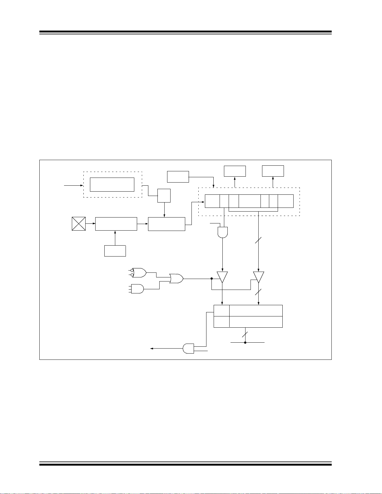
PIC16F870/871
9.2.3 SETTING UP 9-BIT MODE WITH ADDRESS DETEC T
When setting up an Asynchronous Reception with
Address Detect enabled:
• Initialize the SPBRG register for the appropriate
baud rate. If a high spee d baud rate is de sired, set
bit BRGH.
• Enable the asynchronous serial port by clearing
bit SYNC and setting bit SPEN.
• If interrupts are desired, then set enable bit RCIE.
• Set bit RX9 to enable 9-bit reception.
• Set ADDEN to enable address detect.
• Enable the reception by setting enable bit CREN.
FIGURE 9-6: USART RECEIVE BLOCK DIAGRAM
x64 Baud Rate CLK
÷ 64
or
÷ 16
Data
Recovery
CREN
FOSC
RC7/RX/DT
SPBRG
Baud Rate Generator
Pin Buffer
and Control
• Flag bit RCIF will be set when reception is complete, and an interrupt will be generated if enable
bit RCIE was set.
• Read the RCSTA register to get the ninth bit and
determine if any error occurred during reception.
• Read the 8-bit received data by reading the
RCREG register, to determine if the device is
being addressed.
• If any error occurred, clear the error by clearing
enable bit CREN.
• If the device has been addressed, clear the
ADDEN bit to allow dat a b yte s an d ad dres s bytes
to be read into the rec eive buf fer, and interrupt the
CPU.
1
FERR
0
LSb
START
RX9
MSb
STOP
(8)
OERR
7
RSR Register
• • •
SPEN
RX9
ADDEN
RX9
ADDEN
RSR<8>
Interrupt
Enable
Load of
Receive
Buffer
RCIF
RCIE
RX9D
8
8
RCREG Register
8
Data Bus
FIFO
DS30569B-page 70 2003 Microchip Technology Inc.
Page 73

PIC16F870/871
FIGURE 9-7: ASYNCHRONOUS RECEPTION WITH ADDRESS DETECT
RC7/RX/DT (pin)
Load RSR
Read
RCIF
START
bit
bit1bit0
Bit8 = 0, Data Byte Bit8 = 1, Address Byte
bit8 bit0STOP
START
bit bit8
bit
STOP
bit
Word 1
RCREG
Note: Thi s timing diagr am shows a data byte fol lowed by an ad dress byte. The da ta byte is not read into the RCREG (recei ve buffer)
because ADDEN = 1.
FIGURE 9-8: ASYNCHRONOUS RECEPTION WITH ADDRESS BYTE FIRST
RC7/RX/DT (pin)
Load RSR
Read
RCIF
Note: T his timing diagram shows a data byte followed by an address byte. The data byte is not read into the RCREG (rec eive buffer)
because ADDEN was not updated and still = 0.
START
bit
bit1bit0
Bit8 = 1, Address Byte Bit8 = 0, Data Byte
bit8 bit0STOP
START
bit bit8
bit
STOP
bit
Word 1
RCREG
TABLE 9-7: REGISTERS ASSOCIATED WITH ASYNCHRONOUS RECEPTION
Address Name Bit 7 Bit 6 Bit 5 Bit 4 Bit 3 Bit 2 Bit 1 Bit 0
0Bh, 8Bh,
INTCON GIE PEIE
T0IE INTE RBIE T0IF INTF R0IF 0000 000x 0000 000u
Value on:
POR, BOR
10Bh,18Bh
(1)
0Ch PIR1
PSPIF
18h RCSTA SPEN RX9
ADIF RCIF TXIF — CCP1IF TMR2IF TMR1IF 0000 -000 0000 -000
SREN CREN ADDEN FERR OERR RX9D 0000 000x 0000 000x
1Ah RCREG USART Receive Register 0000 0000 0000 0000
8Ch PIE1
98h TXSTA
PSPIE
CSRC TX9 TXEN SYNC —BRGHTRMT TX9D 0000 -010 0000 -010
ADIE RCIE TXIE — CCP1IE TMR2IE TMR1IE 0000 -000 0000 -000
(1)
99h SPBRG Baud Rate Generator Register 0000 0000 0000 0000
Legend: x = unknown, - = unimplemented locations read as '0'. Shaded cells are not used for asynchronous reception.
Note 1: Bits PSPIE and PSPIF are reserved on the PIC16F870; always maintain these bits clear.
Value on
all other
RESETS
2003 Microchip Technology Inc. DS30569B-page 71
Page 74

PIC16F870/871
9.3 USART Synchronous Master Mode
In Synchronous Ma ster mode, the dat a is trans mitted in
a half-duplex manner (i.e., transmission and reception
do not occur at the sa me time). When tran smitting dat a,
the reception is inhibited and vice versa. Synchronous
mode is entered by setting bit SYNC (TXSTA<4>). In
addition, enable bit SPEN (RCSTA<7>) is set in order
to configure the RC6/TX/CK and RC7/RX/DT I/O pins
to CK (clock) and DT (data) lines, respectively. The
Master mode ind icates t hat the pr ocessor transmit s the
master clock on the CK line. The Master mode is
entered by setting bit CSRC (TXSTA<7>).
9.3.1 USART SYNCHRONOUS MASTER
TRANSMISSION
The USART transmitter block diagram is shown in
Figure 9-6. The heart of the transmitter is the Transmit
(Serial) Shift register (TSR). The Shift register obtains
its data from the Read/Write Transmit Buffer register
TXREG. The TXREG register is loaded with data in
software. The TSR register is not loaded until the last
bit has been transmitted from the previous load. As
soon as the last bit is transmitted, the TSR is loaded
with new data from the TXREG (if available). Once the
TXREG register transfers the data to the TSR register
(occurs in one T
rupt bit TXIF (PIR1<4>) is set. The interrupt can be
enabled/disabled by setting/clearing enable bit TXIE
(PIE1<4>). Flag bit TXIF will be set, regardless of the
state of enable bit TXIE and cannot be cleared in software. It will reset o nly when ne w dat a i s loa ded i nto the
TXREG register . While fla g bit TXIF indicates th e status
of the TXREG r egi st e r, another b it T RMT (T X STA<1>)
shows the status of the TSR register. TRMT is a read
only bit which is set when the TSR is empty. No interrupt logic is tied to this bit, so the user has to poll this
bit in orde r to determine if the TSR regis ter is empty.
The TSR is not mapped in data memory, so it is not
available to the user.
Transmission is enabled by setting enable bit TXEN
(TXSTA<5>). The actual transmission will not occur
until the TXREG register has been loaded with data.
The first data bit will be shifted out on the next availabl e
rising edge of the clock on the CK line. Data out is stable around the falling edge of the synchronous clock
(Figure 9-9). The transmission can also be started by
first loading the TXREG register and then setting bit
TXEN (Figure 9-10). This is advantageous when slow
baud rates are selected, since the BRG is kept in
RESET when bits TXEN, CREN and SREN are clear.
Setting enable bit TXEN will start the BRG, creating a
shift clock immed iately. Normally, when transm issio n is
first started, the TSR register is empty, so a transfer to
the TXREG register will re su lt i n an immediate transfer
to TSR, resulting in an empty TXREG. Back-to-back
transfers are possible.
CYCLE), the TXREG is empty an d inter-
Clearing enable bit TXEN during a transmission will
cause the transmis s ion to be ab orte d a nd will reset the
transmitter. The DT and CK pins will revert to hiimpedance. If eithe r bit CRE N or bit SR EN is se t during
a transmission, the transm issi on is abor ted and the D T
pin reverts to a hi-impedance state (for a reception).
The CK pin will remain an output if bit CSRC is set
(internal clock). The transmitter logic, however, is not
reset, although it i s disconnected fro m the pins. In order
to reset the transmitter, the user has to clear bit TXEN.
If bit SREN is set (to i nterrupt an on-goin g transm ission
and receive a sing le word), th en after th e single w ord is
received, bit SREN will be cleared and the serial port
will revert back to transmitting, since bit TXEN is still
set. The DT line will immediately switch from HiImpedance Receiv e mod e to tra nsmit and st art d riv ing.
To avoid this, bit TXEN should be cleared.
In order to select 9-bit transmission, the TX9
(TXSTA<6>) bit should be set and the ninth bit should
be written to bit TX9D (TXSTA<0>). The ninth bit must
be written before writing the 8-bit data to the TXREG
register . This is because a da ta write to the TXREG ca n
result in an immediate transfer of the data to the TSR
register (if the TSR i s empty). If the TSR was empty and
the TXREG was written b efore writ ing the “new” T X9D,
the “present” value of bit TX9D is loaded.
Steps to follow when setting up a Synchronous Master
Transmission:
1. Initialize the SPBRG regis ter for the ap prop ria te
baud rate (Section 9.1).
2. Enable the synchronous master serial port by
setting bits SYNC, SPEN and CSRC.
3. If interrupts are desired, set enable bit TXIE.
4. If 9-bit transmission is desired, set bit TX9.
5. Enable the transmission by setting bit TXEN.
6. If 9-bit transmission is selected, the ninth bit
should be loaded in bit TX9D.
7. St art transmissi on by loading da ta to the TXREG
register.
8. If using interrupts, ensure that GIE and PEIE
(bits 7 and 6) of the INTCON register are set.
DS30569B-page 72 2003 Microchip Technology Inc.
Page 75

PIC16F870/871
TABLE 9-8: REGISTERS ASSOCIATED WITH SYNCHRONOUS MASTER TRANSMISSION
Address Na me B it 7 Bit 6 B it 5 Bit 4 Bit 3 Bit 2 Bit 1 Bit 0
0Bh, 8Bh,
INTCON GIE PEIE
T0IE INTE RBIE T0IF INTF R0IF 0000 000x 0000 000u
10Bh,18Bh
0Ch PIR1
18h RCSTA SPEN
PSPIF
(1)
ADIF RCIF TXIF — CCP1IF TMR2IF TMR1IF
RX9 SREN CREN — FERR OERR RX9D
19h TXREG USART Transmit Register
8Ch PIE1
98h TXSTA CSRC TX9 TXEN SYNC
PSPIE
(1)
ADIE RCIE TXIE — CCP1IE TMR2IE TMR1IE
— BRGH TRMT TX9D
99h SPBRG Baud Rate Generator Register
Legend: x = unknown, - = unimplemented, read as '0'. Shaded cells are not used for synchronous master transmission.
Note 1: Bits PSPIE and PSPIF are reserved on the PIC16F870; always maintain these bits clear.
FIGURE 9-9: SYNCHRONOUS TRANSMISSION
Q1Q2Q3Q4Q1 Q2Q3Q4Q1Q2Q3 Q4 Q1 Q2Q3Q4Q1 Q2 Q3Q4 Q3Q4 Q1Q2Q3Q4Q1Q2 Q3Q4Q1Q2Q3 Q4 Q1 Q2Q3Q4Q1 Q2Q3 Q4Q1 Q2Q3 Q4
Value on:
POR, BOR
0000 -000 0000 -000
0000 -00x 0000 -00x
0000 0000 0000 0000
0000 -000 0000 -000
0000 -010 0000 -010
0000 0000 0000 0000
Value on
all other
RESETS
RC7/RX/DT pin
RC6/TX/CK pin
Write to
TXREG reg
TXIF bit
(Interrupt Flag)
TRMT bit
TXEN bit
Note: Sync Master mode; SPBRG = 0. Continuous transmission of two 8-bit words.
Write Word1
'1' '1'
bit 0 bit 1 bit 7
Word 1
Write Word2
bit 2 bit 0 bit 1 bit 7
Word 2
FIGURE 9-10: SYNCHRONOUS TR ANSMISSI ON (THROUGH TXEN)
RC7/RX/DT pin
RC6/TX/CK pin
Write to
TXREG Reg
TXIF bit
bit0
bit1
bit2
bit6 bit7
TRMT bit
TXEN bit
2003 Microchip Technology Inc. DS30569B-page 73
Page 76

PIC16F870/871
9.3.2 USART SYNCHRONOUS MASTER RECEPTION
Once Synchronous mode is selected, reception is
enabled by setting either enable bit SREN
(RCST A<5>), or enable bit CREN (RCST A<4> ). Data is
sampled on the RC7/RX/DT pin on the falling edge of
the clock. If enable bit SREN is set, then only a single
word is received. If enable bit CREN is set, the reception is continuous unt il CREN is cle ared. If both bi ts are
set, CREN takes pr ecedence. After clock ing the last bit,
the received data in the Receiv e Shift regi ster (R SR) is
transferred to the RCREG register (if it is empty). When
the transfer is complete, interrupt flag bit RCIF
(PIR1<5>) is set. T he actu al i nt erru pt c an b e en abl ed/
disabled by setting/clearing enable bit RCIE
(PIE1<5>). Flag bit RCIF is a read only bit, which is
reset by the hardware. In thi s c ase, it i s r ese t whe n th e
RCREG register has been read and is empty. The
RCREG is a double-buffered register (i.e., it is a twodeep FIFO). It is possible for two bytes of data to be
received and transferred to the RCREG FIFO and a
third byte to begin shifting into the RSR regis ter . On the
clocking of the last bit of the third byte, if the RCREG
register is still full, then overrun error bit OERR
(RCSTA<1>) is set. The word in the RSR will be lost.
The RCREG register can be read twice to retrieve the
two bytes in the FIFO. Bit OERR has to be cleared in
software (by clearing bit CREN). If bit OERR is set,
transfers from the RSR to the RCREG are inhibited, so
it is essen tial to clear bit OERR if it is s et. The ninth
receive bit is buffered the same way as the receive
data. Reading the RCREG register will load bit RX9D
with a new value, therefore, it is essential for the user
to read the RCSTA register before reading RCREG, in
order not to lose the old RX9D information.
When setti ng up a Synchronous Master Receptio n:
1. Initialize the SPBRG regis ter for the ap prop ria te
baud rate (Section 9.1).
2. Enable the synchronous master serial port by
setting bits SYNC, SPEN and CSRC.
3. Ensure bits CREN and SREN are clear.
4. If interrupts are desired, then set enable bit
RCIE.
5. If 9-bit reception is desired, then set bit RX9.
6. If a single reception is required, set bit SREN.
For continuous reception, set bit CREN.
7. Interrupt flag bit RCIF wil l be set when recep tion
is complete and an interrupt will be generated if
enable bit RCIE was set.
8. Read the RCSTA register to get the ninth bit (if
enabled) and determine if any error occurred
during reception.
9. Read the 8-bit received data by reading the
RCREG register.
10. If any error occurred, clear the error by clearing
bit CREN.
11. If using interrupts, ensure that GIE and PEIE
(bits 7 and 6) of the INTCON register are set.
DS30569B-page 74 2003 Microchip Technology Inc.
Page 77

PIC16F870/871
TABLE 9-9: REGISTERS ASSOCIATED WITH SYNCHRONOUS MASTER RECEPTION
Address Na me B it 7 Bit 6 B it 5 Bit 4 Bit 3 Bit 2 Bit 1 Bit 0
0Bh, 8Bh,
INTCON GIE PEIE
T0IE INTE RBIE T0IF INTF R0IF 0000 000x 0000 000u
Value on:
POR, BOR
10Bh,18Bh
(1)
0Ch PIR1
PSPIF
18h RCSTA SPEN RX9
ADIF RCIF TXIF — CCP1IF TMR2IF TMR1IF
SREN CREN — FERR OERR RX9D 0000 -00x 0000 -00x
0000 -000 0000 -000
1Ah RCREG USART Receive Register 0000 0000 0000 0000
(1)
8Ch PIE1
PSPIE
98h TXSTA CSRC
ADIE RCIE TXIE — CCP1IE TMR2IE TMR1IE 0000 -000 0000 -000
TX9 TXEN SYNC — BRGH TRMT TX9D 0000 -010 0000 -010
99h SPBRG Baud Rate Generator Register 0000 0000 0000 0000
Legend: x = unknown, - = unimplemented, read as '0'. Shaded cells are not used for synchronous master reception.
Note 1: Bits PSPIE and PSPIF are reserved on the PIC16F870; always maintain these bits clear.
FIGURE 9-11: SYNCHRONOUS RECEPTION (MASTER MODE, SREN)
Value on
all other
RESETS
Q3Q4 Q1 Q2Q3 Q4Q1 Q2 Q3Q4Q2 Q1Q2Q3 Q4Q1 Q2Q3 Q4 Q1 Q2 Q3Q4Q1Q2 Q3Q4 Q1Q2 Q3Q4Q1 Q2 Q3Q4 Q1 Q2Q3 Q4
RC7/RX/DT pin
RC6/TX/CK pin
Write to
bit SREN
SREN bit
CREN bit
RCIF bit
(Interrupt)
RXREG
Note: Timing diagram demonstrates Sync Master mode with bit SREN = 1 and bit BRG = 0.
'0'
Read
bit0 bit1 bit2 bit3 bit4 bit5 bit6 bit7
Q1Q2 Q3 Q4
'0'
2003 Microchip Technology Inc. DS30569B-page 75
Page 78

PIC16F870/871
9.4 USART Synchronous Slave Mode
Synchronous Slave mode di ffers from the Ma ster mode
in the fact that the shift clock is supplied externally at
the RC6/TX/CK pin (instead of being supplied in ternally
in Master mode). This allows the device to transfer or
receive data while in SLEEP mode. Slave mode is
entered by clearing bit CSRC (TXSTA<7>).
9.4.1 USART SYNCHRONOUS SLAVE TRANSMIT
The operation of the Synchronous Master and Slave
modes is identical, exce pt in the case of the SLEEP mode.
If two words are written to the TXREG and then the
SLEEP instruction is executed, the following will occur:
a) The first word will immediately transfer to the
TSR register and transmit.
b) The second word will remain in TXREG register.
c) Flag bit TXIF will not be set.
d) When the first word has been shifted out of TSR,
the TXREG register will transfer the second word
to the TSR and flag bit TXIF will now be set.
e) If enable bit TXIE is set, the interrupt will wake
the chip from SLEEP and if the global interrupt
is enabled, the program will branch to the
interrupt vector (0004h).
When setting up a Synchronous Slave Transmission,
follow these steps:
1. Enable the synchro nous slav e serial port by setting bits SYNC and SPEN and clearing bit
CSRC.
2. Clear bits CREN and SREN.
3. If interrupts are desired, then set enable bit
TXIE.
4. If 9-bit transmission is desired, then set bit TX9.
5. Enable the transmission by setting enable bit
TXEN.
6. If 9-bit transmission is selected, the ninth bit
should be loaded in bit TX9D.
7. St art transmissi on by loading da ta to the TXREG
register.
8. If using interrupts, ensure that GIE and PEIE
(bits 7 and 6) of the INTCON register are set.
TABLE 9-10: REGISTERS ASSOCIATED WITH SYNCHRONOUS SLAVE TRANSMISSION
Address Name Bit 7 Bit 6 Bit 5 Bit 4 Bi t 3 Bit 2 Bit 1 Bit 0
0Bh, 8Bh,
10Bh,18Bh
0Ch PIR1
18h RCSTA SPEN
19h TXREG USART Transmit Register 0000 0000 0000 0000
8Ch PIE1
98h TXSTA CSRC TX9 TXEN SYNC
99h SPBRG Baud Rate Generator Register 0000 0000 0000 0000
Legend: x = unknown, - = unimplemented, read as '0'. Shaded cells are not used for synchronous slave transmission.
Note 1: Bits PSPIE and PSPIF are reserved on the PIC16F870; always maintain these bits clear.
INTCON GIE PEIE
(1)
PSPIF
PSPIE
ADIF RCIF TXIF — CCP1IF TMR2IF TMR1IF 0000 -000 0000 -000
RX9 SREN CREN ADDEN FERR OERR RX9D 0000 000x 0000 000x
(1)
ADIE RCIE TXIE — CCP1IE TMR2IE TMR1IE 0000 -000 0000 -000
T0IE INTE RBIE T0IF INTF R0IF 0000 000x 0000 000u
— BRGH TRMT TX9D 0000 -010 0000 -010
Val ue on:
POR, BOR
Value on
all other
RESETS
DS30569B-page 76 2003 Microchip Technology Inc.
Page 79

PIC16F870/871
9.4.2 USART SYNCHRONOUS SLAVE RECEPTION
The operation of the Synchronous Master and Slave
modes is identical, except in the case of the SLEEP
mode. Bit SREN is a “don't care” in Slave mode.
If receive is enabled by setting bit CREN prior to the
SLEEP instruction, then a w ord m ay be rec eived durin g
SLEEP. On completely receiving the word, the RSR
register will transfer the data to the RCREG register
and if enable bit RCIE bit is set, the int errupt generate d
will wake the chip from SLEEP. If the global interrupt is
enabled, the program w ill br anch to the interru pt vec tor
(0004h).
When setting up a Synchronous Slave Reception,
follow these steps:
1. Enable the synchronous master serial port by
setting bits SYNC and SPEN and clearing bit
CSRC.
2. If interrupts are desired, set enable bit RCIE.
3. If 9-bit reception is desired, set bit RX9.
4. To enable reception, set enable bit CREN.
5. Flag bit RCIF will b e se t when reception is complete and an interrupt will be generated, if
enable bit RCIE was set.
6. Read the RCSTA register to get the ninth bit (if
enabled) and determine if any error occurred
during reception.
7. Read the 8-bit received data by reading the
RCREG register.
8. If any error occurred, clear the error by clearing
bit CREN.
9. If using interrupts, ensure that GIE and PEIE
(bits 7 and 6) of the INTCON register are set.
TABLE 9-11: REGISTERS ASSOCIATED WITH SYNCHRONOUS SLAVE RECEPTION
Address Na me Bit 7 Bit 6 Bit 5 Bit 4 Bit 3 B it 2 Bit 1 Bit 0
0Bh, 8Bh,
10Bh,18Bh
0Ch PIR1
18h RCSTA SPEN RX9
1Ah RCREG USART Receive Register 0000 0000 0000 0000
8Ch PIE1
98h TXSTA CSRC
99h SPBRG Baud Rate Generator Register 0000 0000 0000 0000
Legend: x = unknown, - = unimplemented, read as '0'. Shaded cells are not used for synchronous slave reception.
Note 1: Bits PSPIE and PSPIF are reserved on the PIC16F870, always maintain these bits clear.
INTCON GIE PEIE
(1)
PSPIF
PSPIE
ADIF RCIF TXIF — CCP1IF TMR2IF TMR1IF 0000 -000 0000 -000
(1)
ADIE RCIE TXIE — CCP1IE TMR2IE TMR1IE 0000 -000 0000 -000
TX9 TXEN SYNC — BRGH TRMT TX9D 0000 -010 0000 -010
T0IE INTE RBIE T0IF INTF R0IF 0000 000x 0000 000u
SREN CREN ADDEN FERR OERR RX9D 0000 000x 0000 000x
Val ue on:
POR, BOR
Val ue on
all other
RESETS
2003 Microchip Technology Inc. DS30569B-page 77
Page 80

PIC16F870/871
NOTES:
DS30569B-page 78 2003 Microchip Technology Inc.
Page 81

PIC16F870/871
10.0 ANALOG-TO-DIGITAL (A/D) CONVERTER MODULE
The Analog-to-Digital (A/D) Converter module has five
inputs for the 28-pin devices and eight for the other
devices.
The analog inpu t cha rges a sam ple a nd hol d ca pac itor.
The output of the sample and hold capacitor is the input
into the converter. The converter then gen era t es a di gital result of th is analog level via successi ve approximation. The A/D conversion of the analog input signal
results in a corresponding 10-bit digital number. The
A/D module has high and low voltage reference input
that is software select able to some combina tion of V
SS, RA2, or RA3.
V
The A/D converter has a unique feature of being able
to operate while the d evice is in SLEEP mode. To operate in SLEEP, the A/D clock must be derived from the
A/D’s internal RC oscillator.
DD,
The A/D module has four registers. These registers
are:
• A/D Result High Register (ADRESH)
• A/D Result Low Register (ADRESL)
• A/D Control Register0 (ADCON0)
• A/D Control Register1 (ADCON1)
The ADCON0 register, shown in Register 10-1, con-
trols the operation of the A/D module. The ADCON1
register, shown in Register 10-2, configures the functions of the port pins. The port pins can be configured
as analog inputs (RA3 can also be the voltage
reference), or as digital I/O.
Additional informa tion on usi ng the A/D module can be
found in the PICmicro™ Mid-Range MCU Family
Reference Manual (DS33023).
REGISTER 10-1: ADCON0 REGISTER (ADDRESS: 1Fh)
R/W-0 R/W-0 R/W-0 R/W-0 R/W-0 R/W-0 U-0 R/W-0
ADCS1 ADCS0 CHS2 CHS1 CHS0 GO/DONE
bit 7 bit 0
—ADON
bit 7-6 ADCS1:ADCS0: A/D Conversion Clock Select bits
00 = FOSC/2
01 = F
OSC/8
OSC/32
10 = F
RC (clock derived from the internal A/D module RC oscillator)
11 = F
bit 5-3 CHS2:CHS0: Analog Channel Select bits
000 = Channel 0, (RA0/AN0)
010 = Channel 2, (RA2/AN2)
011 = Channel 3, (RA3/AN3)
100 = Channel 4, (RA5/AN4)
101 = Channel 5, (RE0/AN5)
110 = Channel 6, (RE1/AN6)
111 = Channel 7, (RE2/AN7)
bit 2 GO/DONE: A/D Conversion Status bit
If ADON =
1 = A/D conversion in progress (setting this bit starts the A/D conversion)
0 = A/D conversion not in progress (th is bit is aut omatic ally cleare d by hardw are when th e A/D
bit 1 Unimplemented: Read as '0'
bit 0 ADON: A/D On bit
1 = A/D converter module is operating
0 = A/D converter module is shut-off and consumes no operating current
Note 1: These channels are not available on the PIC16F870 device.
1:
conversion is comp let e)
(1)
(1)
(1)
Legend:
R = Readable bit W = Writable bit U = Unimplemented bit, read as ‘0’
- n = Value at POR ‘1’ = Bit is set ‘0’ = Bit is cleared x = Bit is unknown
2003 Microchip Technology Inc. DS30569B-page 79
Page 82

PIC16F870/871
REGISTER 10-2: ADCON1 REGISTER (ADDRESS: 9Fh)
U-0 U-0 R/W-0 U-0 R/W-0 R/W-0 R/W-0 R/W-0
ADFM
bit 7 bit 0
bit 7 ADFM: A/D Result Format Select bit
1 = Right justified. 6 Most Significant bits of ADRESH are read as ‘0’.
0 = Left justified. 6 Least Significant bits of ADRESL are read as ‘0’.
bit 6-4 Unimplemented: Read as '0'
bit 3-0 PCFG3:PCFG0: A/D Port Configuration Control bits:
PCFG3:
PCFG0
0000 AAAAAAAAVDD VSS 8/0
0001 AAAAV
0010 DDDA A AAAV
0011 DDDAV
0100 DDDDADAAV
0101 DDDDV
011x DDDDDDDDV
1000 AAAAV
1001 DDAA A AAAV
1010 DDAAV
1011 DDAAV
1100 DDDAV
1101 DDDDV
1110 DDDDDDDAV
1111 DDDDV
A = Analog input D = Digital I/O
— — — PCFG3 PCFG2 PCFG1 PCFG0
(1)
AN7
RE2
AN6
RE1
(1)
AN5
RE0
(1)
AN4
RA5
AN3
RA3
REF+A A A RA3VSS 7/1
REF+A A A RA3VSS 4/1
REF+D A A RA3VSS 2/1
REF+VREF-A A RA3RA2 6/2
REF+A A A RA3VSS 5/1
REF+VREF-A A RA3RA2 4/2
REF+VREF-A A RA3RA2 3/2
REF+VREF-A A RA3RA2 2/2
REF+VREF-D A RA3RA2 1/2
AN2
RA2
AN1
RA1
AN0
RA0
V
REF+VREF-
DD VSS 5/ 0
DD VSS 3/ 0
DD VSS 0/ 0
DD VSS 6/ 0
DD VSS 1/ 0
HAN/
C
Refs
(2)
Note 1: These channels are not available on the PIC16F870 device.
2: This column indicates the number of analog channels available as A/D inputs and
the number of analog channels used as voltage reference inputs.
Legend:
R = Readable bit W = Writable bit U = Unimplemented bit, read as ‘0’
- n = Value at POR ‘1’ = Bit is set ‘0’ = Bit is cleared x = Bit is unknown
The ADRESH:ADRESL registers contain the 10-bit
result of the A/D conversion. W hen the A/D con versio n
is complete, the resu lt is lo aded into this A/D re sult register pair, the GO/DONE
bit (ADCON0<2>) is cleared
To determine sample time, see Section 10.1. After this
acquisition time has elapsed, the A/D conversion can
be started.
and the A/D interrupt flag bit ADIF is set. The block
diagram of the A/D module is shown in Figure 10-1.
After the A/D module has been configured as desired,
the selected cha nne l m ust be acquired before the conversion is started. The analog input channels must
have their correspondin g TRIS bi ts select ed as inputs.
DS30569B-page 80 2003 Microchip Technology Inc.
Page 83
PIC16F870/871
These steps should be followed for doing an A/D
Conversion:
1. Configure the A/D module:
• Configure analog pins/voltage reference and
digital I/O (ADCON1)
• Select A/D input channel (ADCON0)
• Select A/D conversion clock (ADCON0)
• Turn on A/D module (ADCON0)
2. Configure A/D inte rrupt (if desired):
• Clear ADIF bit
• Set ADIE bit
• Set PEIE bit
• Set GIE bit
FIGURE 10-1: A/D BLOCK DIAGRAM
AIN
V
(Input Voltage)
A/D
Converter
3. Wait the required acquisition time.
4. Start conversion:
• S et GO/DONE
bit (ADCON0)
5. Wait for A/D conversion to complete, by either:
• Polling for the GO/DONE bit to be cleared
(with interrupts enabled); OR
• Waiting for the A/D interrupt
6. Read A/D Result register pair
(ADRESH:ADRESL), clear bit ADIF if required.
7. For the next conversion, go to step 1 or step 2,
as required. The A/D conversion time per bit is
defined as T
AD. A minimum wait of 2 TAD is
required before the next acquisition starts.
CHS2:CHS0
111
110
101
100
011
010
001
DD
V
000
RE2/AN7
RE1/AN6
RE0/AN5
RA5/AN4
RA3/AN3/V
RA2/AN2/V
RA1/AN1
RA0/AN0
(1)
(1)
(1)
REF+
REF-
VREF+
(Reference
Voltage)
PCFG3:PCFG0
VREF-
(Reference
Voltage)
PCFG3:PCFG0
Note 1: Not available on the PIC16F870 device.
2003 Microchip Technology Inc. DS30569B-page 81
SS
V
Page 84

PIC16F870/871
10.1 A/D Acquisition Requirements
For the A/D co nverter to meet its s pecified accuracy,
the charge holding capacitor (C
to fully charge to the input channel voltage level. The
analog input model is shown in Figure 10-2. The
source impedance (R
switch (R
SS) impedance directly affect the time
S) and the internal sampling
required to charge the capacitor C
switch (R
(V
SS) impedance varies over the devic e volt age
DD), see Figure 10-2. The maximum recom-
mended impedance for analog sources is 10 kΩ. As
the impedance is decreased, the acquisition time may
EQUATION 10-1: ACQUISITION TIME
TACQ
TC
TACQ
=
Amplifier Settling Time + Hold Capacitor Charging Time + Temperature Coefficient
=
T
AMP + TC + TCOFF
=
2 µs + TC + [(Temperature – 25°C)(0.05 µs/°C)]
=
HOLD (RIC + RSS + RS) In(1/2047)
C
=
- 120 pF (1 kΩ + 7 kΩ + 10 kΩ) In(0.0004885)
=
16.47 µs
=
2 µs + 16.47 µs + [(50°C – 25°C)(0.05 µs/°C)
=
19.72 µs
HOLD) must be allowed
HOLD. The sampling
be decreased. After the analog input channel is
selected (changed), this acquisition must be done
before the conversion can be started.
To calculate the minimum acquisition time,
Equation 10-1 may be used. This equation assumes
that 1/2 LSb error is used (1024 st eps for the A/D). The
1/2 LSb error is the maximu m error all owed for the A/D
to meet its specified resolution.
To calculate the minimum acquisition time, T
ACQ, see
the PICmicro™ Mid-Range MCU Family Reference
Manual (DS33023).
Note 1: The reference voltage (VREF) has no effect on the equation, si nce it cancels itself out.
2: The charge holding capacitor (C
HOLD) is not discharged after each conversion.
3: The maximum recommended impedance for analog sources is 10 kΩ. This is required to meet the pin
leakage specification.
4: After a conversion has completed, a 2.0 T
AD delay must complete before acquisition can begin again.
During this time, the holding capacitor is not connected to the selected A/D input channel.
FIGURE 10-2: ANALOG INPUT MODEL
R
VA
Legend CPIN
VT
I LEAKAGE
RIC
SS
C
HOLD
VDD
ANx
S
CPIN
5 pF
= input capacitance
= threshold voltage
= leakage current at the pin due to
various junctions
= interconnect resistance
= sampling switch
= sample/hold capacitance (from DAC)
VT = 0.6V
T = 0.6V
V
RIC ≤ 1k
I
LEAKAGE
± 500 nA
Sampling
Switch
SS
6V
5V
4V
DD
V
3V
2V
R
SS
567891011
Sampling Switch
CHOLD
= DAC capacitance
= 120 pF
V
SS
(kΩ)
DS30569B-page 82 2003 Microchip Technology Inc.
Page 85

PIC16F870/871
10.2 Selecting the A/D Conversion Clock
The A/D conversion time per bit is defined as TAD. The
A/D conversio n requir es a minimu m 12 T
conversion. The source of the A/D conversion clock is
software selected. The four possible options for T
are:
OSC
•2 T
•8 TOSC
•32 TOSC
• Internal A/D module RC oscillator (2-6 µs)
AD per 10-bit
AD
For correct A/D conversions, the A/D conversion clock
AD) must be selected to ensure a minimum TAD time
(T
of 1.6 µs.
Table 10-1 shows the resultant TAD tim es de ri ve d f ro m
the device operating frequencies and the A/D clock
source selected.
TABLE 10-1: TAD vs. MAXIMUM DEVICE OPERATING FREQUENCIES (STANDARD DEVICES (C))
AD Clock Source (T
Operation ADCS1:ADCS0 Max.
2 T
OSC 00 1.25 MHz
8 TOSC 01 5 MHz
OSC 10 20 MHz
32 T
(1, 2, 3)
RC
Note 1: The RC source has a typical TAD time of 4 µs, but can vary between 2-6 µs.
2: When the device frequencies are greater than 1 MHz, the RC A/D conversion clock source is only
recommended for SLEEP operation.
3: For extended voltage devices (LC), please refer to the Electrical Characteristics (Section 14.1 and 14.2).
AD) Maximum Device Frequency
11 (Note 1)
10.3 Configuring Analog Port Pins
The ADCON1 and TRI S re gis te rs co ntrol the operation
of the A/D port pins. The port pins that are desired as
analog inputs must have their corresponding TRIS bits
set (input). If the TRIS bit is cleare d (output) , the digit al
output level (V
The A/D operation is independent of the state of the
CHS2:CHS0 bits and the TRIS bits.
OH or VOL) will be converted.
Note 1: When reading the port register, any pin
configured as an analog input c hannel will
read as cleared (a lo w l evel). Pins configured as digital inputs will convert an analog input. Analog levels on a digitally
configured input will not affect the
conversion accuracy.
2: Analog levels on any pin that is de fined as
a digital input (including the AN7:AN0
pins), may cause the input buffer to consume current that is out of the device
specifications.
2003 Microchip Technology Inc. DS30569B-page 83
Page 86

PIC16F870/871
10.4 A/D Conversions
Clearing the GO/DONE bit during a conversion will
abort the current conversion. The A/D result register
pair will NOT be updated with the partially completed
A/D conversion sample. That is, the ADRESH:ADRESL
registers will continue to contain the value of the last
completed conversion (or the last value written to the
ADRESH:ADRESL registers). After the A/D conversion
is aborted, a 2 T
FIGURE 10-3: A/D CONVERSION TAD CYCLES
AD wait is required before the next
TCY to TAD
Holding capacitor is disconnected from analog input (typically 100 ns)
Set GO bit
TAD1
TAD2 TAD3
b9 b8 b7 b6 b5 b4 b3 b2
Conversion starts
TAD4
TAD5
TAD6
acquisition is started. After this 2 T
AD wait, acquisition
on the selected channel is automatically started. The
GO/DONE bit can then be set to start the conversion.
In Figure 10-3, after the GO bit is set, the first time
segment has a mi nimum of T
CY and a maximum o f TAD.
Note: The GO/DONE bit should NOT be set in
the same instructio n that tu rns on the A/D.
TAD7 TAD8
ADRES is loaded
GO bit is cleared
ADIF bit is set
Holding capacitor is connected to analog input
TAD9
TAD10 TAD11
b1 b0
10.4.1 A/D RESULT REGISTERS
The ADRESH:ADRESL register pair is the location
where the 10-bit A/D result is loaded at the completion of
the A/D conversion. This register pair is 16-bits wide.
The A/D module gives the flexibility to left or right justify
the 10-bit result in the 16-bit result register. The A/D For-
FIGURE 10-4: A/D RESULT JUSTIFICAT I ON
10-bit Result
ADFM = 1
0
0000 00
ADRESH
2 1 0 77
ADRESL
10-bit Result
Right Justified
mat Select bit (ADFM) controls this justification.
Figure 10-4 shows the operation of the A/D result justification. The extra bits are loaded with ‘0’. When an A/D
result will not overwrite these locations (A/D disable),
these registers may be used as two general purpose
8-bit registers.
ADFM = 0
7
ADRESH
10-bit Result
0 7 6 5 0
0000 00
ADRESL
Left Justified
DS30569B-page 84 2003 Microchip Technology Inc.
Page 87

PIC16F870/871
10.5 A/D Operation During SLEEP
The A/D module can ope rate during SLEEP mode. This
requires that the A/D clock source be set to RC
(ADCS1:ADCS0 = 11). When the R C clock sourc e is
selected, the A/D module waits one instruction cycle
before starting the conversion. This allows the SLEEP
instruction to be executed, which eliminates all digital
switching noise fro m the convers ion. When th e conversion is comple ted, the GO /DONE
the result loaded into the ADRES register. If the A/D
interrupt is enabled, the device will wake-up from
SLEEP . If the A/D interr upt is not enabled , the A/D module will then be turned off, although the ADON bit will
remain set.
When the A/D clock sour ce is anoth er clo ck optio n (not
RC), a SLEEP instruction will caus e the present conversion to be aborte d and the A/D mod ule to be turned of f,
though the ADON bit will remain set.
bit will be cleared and
Turning off the A/D places the A/D module in its lowes t
current consumption state.
Note: For the A/D module to operate in SLEEP,
the A/D clock source must be set to RC
(ADCS1:ADCS0 = 11). To allow the conversion to occur during SLEEP, ensure the
SLEEP instruction immediately follows the
instruction that sets the GO/DONE
bit.
10.6 Effects of a RESET
A device RESET forces all registers to their RESET
state. This forces the A/D module to be turned off, and
any conversion is aborted. All A/D input pins are
configured as analog inputs.
The value that is in the ADRESH:ADRESL registers is
not modified for a Power-on Reset. The
ADRESH:ADRESL registers will contai n unknown dat a
after a Power-on Reset.
TABLE 10-2: REGISTERS/BITS ASSOCIATED WITH A/D
Address Name Bit 7 Bit 6 Bit 5 Bit 4 Bit 3 Bit 2 Bit 1 Bit 0
0Bh,8Bh,
10Bh,18Bh
0Ch PIR1
8Ch PIE1
1Eh ADRESH A/D Result Register High Byte xxxx xxxx uuuu uuuu
9Eh ADRESL A/D Result Register Low Byte xxxx xxxx uuuu uuuu
1Fh ADCON0 ADCS1 ADCS0 CHS2 CHS1 CHS0 GO/DONE
9Fh ADCON1 ADFM
85h TRISA
05h PORTA
(1)
89h
(1)
09h
Legend: x = unknown, u = unchanged, - = unimplemented, read as '0'. Shaded cells are not used for A/D conversion.
Note 1: These registers/bits are not available on the 28-pin devices.
INTCON GIE PEIE
(1)
PSPIF
PSPIE
TRISE IBF OBF IBOV PSPMODE — PORTE Data Direction bits 0000 -111 0000 -111
PORTE — — — — — RE2 RE1 RE0 ---- -xxx ---- -uuu
ADIF RCIF TXIF — CCP1IF TMR2IF TMR1IF 0000 -000 0000 -000
(1)
ADIE RCIE TXIE — CCP1IE TMR2IE TMR1IE 0000 -000 0000 -000
— — PORTA Data Direction Register --11 1111 --11 1111
— — PORTA Data Latch when written: PORT A pins when read --0x 0000 --0u 0000
T0IE INTE RBIE T0IF INTF RBIF 0000 000x 0000 000u
—ADON0000 00-0 0000 00-0
— — —PCFG3PCFG2PCFG1PCFG0--0- 0000 --0- 0000
Value on
POR, BOR
Value on
MCLR,
WDT
2003 Microchip Technology Inc. DS30569B-page 85
Page 88

PIC16F870/871
NOTES:
DS30569B-page 86 2003 Microchip Technology Inc.
Page 89

PIC16F870/871
11.0 SPECIAL FEATURES OF THE CPU
The PIC16F870/871 devices have a host of features
intended to maximize system reli ability, minimize co st
through elimination of external components, provide
Power Saving Operating modes and offer code
protectio n. These are:
• Oscillator Selection
• RESET
- Power-on Reset (POR)
- Power-up Timer (PWRT)
- Oscillator Start-up Timer (OST)
- Brown-out Reset (BOR)
• Interrupts
• Watchdog Timer (WDT)
• SLEEP
• Code Protection
• ID Locations
• In-Circuit Serial Programming
• Low Voltage In-Circuit Serial Programming
• In-Circuit Debugger
PIC16F870/871 devices have a Watchdog Timer,
which can be shu t-off only through configuration bits. It
runs off its own RC oscillator for added reliability.
There are two timers that offer necessary delays on
power-up. One is the Oscillator Start-up Timer (OST),
intended to keep the chip in RESET until the crystal
oscillator is stable. The other is the Power-up Timer
(PWRT), which provides a fixed delay of 72 ms (nominal) on power-up only. It is designed to keep th e p art in
RESET while the power supply stabilizes. With these
two timers on-chip, mo st applications need no external
RESET circuitry.
SLEEP mode is designed to offer a very low current
Power-down mode. The user can wake-up from
SLEEP through external RESET, Watchdog Timer
Wake-up, or through an interrupt.
Several oscillator options are also made available to
allow the part to fit the application. The RC oscillator
option saves system cost while the LP crystal option
saves power. A set of configuration bits is used to
select various options.
Additional information on special features is available
in the PICmicro™ Mid-Range MCU Family Reference
Manual (DS33023).
11. 1 Configuration Bits
The configuration b its can be program med (read as '0'),
or left unprogrammed (read as '1'), to select various
device configurations. The erased, or unprogrammed
value of the configuration word is 3FFFh. These bits
are mapped in program memory locati on 2007h.
It is important to note th at address 2007h is beyo nd the
user program memory space, which can be accessed
only during programming.
2003 Microchip Technology Inc. DS30569B-page 87
Page 90

PIC16F870/871
(2)
(1)
REGISTER 11-1: CONFIGURATION WORD (ADDRESS 2007h)
CP1 CP0 DEBUG — WRT CPD LVP BOREN CP1 CP0 PWRTEN WDTEN FOSC1 FOSC0
bit 13 bit 0
bit 13-12,
bit 5-4
bit 11 DEBUG: In-Circuit Debugger Mode
bit 10 Unimplemented: Read as ‘1’
bit 9 WRT: FLASH Program Memory Write Enable
bit 8 CPD: Data EE Memory Code Protection
bit 7 LVP: Low Voltage In-Circuit Serial Programming Enable bit
bit 6 BOREN: Brown-out Reset Enable bit
bit 3 PWRTEN
bit 2 WDTEN: Watchdog Timer Enable bit
bit 1-0 FOSC1:FOSC0: Oscillator Selection bits
CP1:CP0: FLASH Program Memory Code Protection bits
11 = Code protection off
10 = Not supported
01 = Not supported
00 = Code protection on
1 = In-Circuit Debugger disabled, RB6 and RB7 are general purpose I/O pins
0 = In-Circuit Debugger enabled, RB6 and RB7 are dedicated to the debugger
1 = Unprotected program memory may be written to by EECON control
0 = Unprotected program memory may not be written to by EECON control
1 = Code protection off
0 = Data EEPROM memory code protected
1 = RB3/PGM pin has PGM function, low voltage programming enabled
0 = RB3 is digital I/O, HV on MCLR
1 = BOR enabled
0 = BOR disabled
: Power-up Timer Enable bit
1 = PWRT disabl ed
0 = PWRT enabled
1 = WDT enabl ed
0 = WDT disabled
11 = RC oscillator
10 = HS oscillator
01 = XT oscilla tor
00 = LP oscillator
must be used for programming
(3)
(3)
Legend:
R = Readable bit W = Writable bit U = Unimplemented bit, read as ‘0’
- n = Value at POR ‘1’ = Bit is set ‘0’ = Bit is cleared x = Bit is unknown
Note 1: The erased (unprogrammed) value of the configuration word is 3FFFh.
2: All of the CP1:CP0 pairs have to be given the same value to enable the code protection scheme listed.
3: Enabling Brown-out Reset automatically enables Power-up Timer (PWRT), regardless of the value of bit
PWRTEN
DS30569B-page 88 2003 Microchip Technology Inc.
. Ensure the Power-up Timer is enabled any time Brown-out Reset is enabled.
Page 91

PIC16F870/871
11.2 Oscillator Configurations
11.2.1 OSCILLATOR TYPES
The PIC16F870/871 can be operated in four different
Oscillator modes. The user can p rogram two conf iguration bits (FOSC1 and FOSC0) to select one of these
four modes:
• LP Low Power Crystal
• XT Crystal/Resonator
• HS High Speed Crystal/Resonator
• RC Resistor/Capacitor
11.2.2 CRYSTAL OSCILLATOR/CERAMIC RESONATORS
In XT, LP or HS modes, a crystal or ceramic resonator
is connected to the OSC1/CLKI and OSC2/CLKO pins
to establish oscillation (Figure 11-1). The PIC16F870/
871 oscillator design requires the use of a parallel cut
crystal. Use of a series cut crystal may give a frequency
out of the cryst al manufact urers specifica tions. When in
XT, LP or HS modes, the device can have an external
clock source to dri ve th e OS C1 /C LKI pin (F igu re11-2).
FIGURE 11-1: CRYSTAL/CERAMI C
RESONATO R OPER ATI ON
(HS, XT OR LP
OSC CONFIGURATION)
(1)
C1
C2
(1)
XTAL
(2)
R
s
OSC1
OSC2
RF
(3)
To
Internal
Logic
SLEEP
PIC16F870/871
FIGURE 11-2: EXTERNAL CLOCK INPUT
OPERATION (HS, XT OR LP
OSC CONFIGURATION)
Clock from
Ext. System
Open
OSC1
PIC16F870/871
OSC2
TABLE 11-1: CERAMIC RESONATORS
Ranges Tested:
Mode Freq. OSC1 OSC2
XT 455 kHz
2.0 MHz
4.0 MHz
HS 8.0 MHz
16.0 MHz
These values are for d esign gu idance only.
See notes following Table11-2.
Resonators Used:
455 kHz Panasonic EFO-A455K04B ± 0.3%
2.0 MHz Murata Erie CSA2.00MG ± 0.5%
4.0 MHz Murata Erie CSA4.00MG ± 0.5%
8.0 MHz M ura t a Erie CSA 8.00 MT ± 0.5%
16.0 MHz Murata Erie CSA16.00MX ± 0.5%
All resonators used did not have built-in capacitors.
68 - 100 pF
15 - 68 pF
15 - 68 pF
10 - 68 pF
10 - 22 pF
68 - 100 pF
15 - 68 pF
15 - 68 pF
10 - 68 pF
10 - 22 pF
Note 1: See Table 11-1 and Table 11-2 for
2003 Microchip Technology Inc. DS30569B-page 89
recommended values of C1 and C2.
2: A series resistor (R
AT strip cut crystals.
3: RF varies with the crystal chosen.
) may be required for
s
Page 92

PIC16F870/871
TABLE 11-2: CAPACITOR S ELECTION FOR
CRYSTAL OSCILLATOR
Osc T y pe
Crystal
Freq.
LP 32 kHz 33 pF 33 pF
200 kHz 15 pF 15 pF
XT 200 kHz 47-68 pF 47-68 pF
1 MHz 15 pF 15 pF
4 MHz 15 pF 15 pF
HS 4 MHz 15 pF 15 pF
8 MHz 15-33 pF 15-33 pF
20 MHz 15-33 pF 15-33 pF
These values are for desi gn guidance only.
See notes following this table.
32 kHz Epson C-001R32.768K-A ± 20 PPM
200 kHz STD XTL 200.000KHz ± 20 PPM
1 MHz ECS ECS-10-13-1 ± 50 PPM
4 MHz ECS ECS-40-20-1 ± 50 PPM
8 MHz EPSON CA-301 8.000M-C ± 30 PPM
20 MHz EPSON CA-301 20.000M-C ± 30 PPM
Note 1: Higher capac itance inc reases the st abilit y
of oscillator, but also increases the
start-up time.
2: Since each resonator/crystal has its own
characteristics, the user should consult
the resonator/crystal manufacturer for
appropriate values of external components.
may be required in HS mode, as well
3: R
s
as XT mode, to avoid overdrivi ng crys t als
with low drive level specification.
4: When migrating from other PICmicro
devices, oscillator performance should be
verified.
Cap. Range C1Cap. Range
C2
Crystals Used
®
11.2.3 RC OSCILLATOR
For timing insensitive applications, the “RC” device
option offers additi ona l cos t savings. The RC oscillator
frequency is a function of the supply voltage, the resis -
EXT) and capacitor (CEXT) values, and the operat-
tor (R
ing temperature. In addition to this, the oscillator
frequency will vary from unit to unit due to normal process paramete r variatio n. Further more, the d ifference
in lead frame capacitance between package types will
also affect the oscillation frequency, especially for low
EXT values. The user also needs to take into account
C
variation due to tolerance of external R and C
components used. Figure 11-3 shows how the R/C
combination is connected to the PIC16F870/871.
FIGURE 11-3: RC OSCILLATOR MODE
VDD
REXT
OSC1
CEXT
VSS
F
Recommended values: 3 kΩ ≤ REXT ≤ 100 kΩ
OSC/4
OSC2/CLKO
EXT > 20pF
C
Internal
Clock
PIC16F870/871
DS30569B-page 90 2003 Microchip Technology Inc.
Page 93

PIC16F870/871
11.3 RESET
The PIC16F870/871 differentiates between various
kinds of RESET:
• Power-on Reset (POR)
•MCLR
•MCLR
• WDT Reset (during normal operation)
• WDT Wake-up (during SLEEP)
• Brown-out Reset (BOR)
Some registers are not affected in any RESET condition. Their status is unknown on POR and unchanged
in any other RESET. Most other registers are reset to a
“RESET state” on Power-on Reset (POR), on the
MCLR and WDT Reset, on MCLR Reset during
Reset during normal operation
Reset during SLEEP
SLEEP, and Brown-out Reset (BOR). They are not
affected by a WDT Wake-up, which is viewed as the
resumption of normal operation. The TO
are set or cleared differently in different RESET situations, as indicated in Table 11-4. These bit s are used in
software to determine the nature of the RESET. See
Table 11-6 for a full description of RESET states of all
registers.
A simplified block di agram of the On-Chip Reset Circu it
is shown in Figure 11-4.
These devices have a MCLR
Reset path. The filter will detect and ignore small
pulses.
It should be noted that a WDT Reset does not drive
pin low.
MCLR
FIGURE 11-4: SIMPLIFIED BLOCK DIAGRAM OF ON-CHIP RESET CIRCUIT
External
RESET
MCLR
SLEEP
WDT
Time-out
Reset
Power-on Reset
BOREN
VDD
WDT
Module
DD Rise
V
Detect
Brown-out
Reset
and PD bits
noise filter in the MCLR
S
OST/PWRT
OSC1
On-chip
RC OSC
Note 1: This is a separate oscillator from the RC oscillator of the CLKI pin.
(1)
OST
10-bit Ripple Counter
PWRT
10-bit Ripple Counter
RQ
Chip_Reset
Enable PWRT
Enable OST
2003 Microchip Technology Inc. DS30569B-page 91
Page 94

PIC16F870/871
11. 4 Power-on Reset (POR)
A Power-on Reset pulse is generated on-chip when
DD rise is detected (in the range of 1.2V - 1.7V). To
V
take advantage of the POR, tie the MCLR
(or through a resistor) to V
external RC components usually needed to create a
Power-on Reset. A maximum rise time for V
specified. See Electrical Specifications for details.
When the device starts normal operation (exits the
RESET condition), device operating parameters (voltage, frequency, temperature,...) must be met to ensure
operation. If these cond itions are not met, the d evice
must be held in RESET until the operating conditions
are met. Brown-out Reset may be used to meet the
start-up conditions. For additional information, refer to
Application Note, AN007, “Power-u p T roub le Shooting”
(DS00007).
DD. This will eliminate
pin direc tly
DD is
11. 5 Power-up Timer (PWRT)
The Power-up Timer provides a fixed 72 ms nominal
time-out on power-up only from the POR. The Powerup Timer operates on an internal RC oscillator. The
chip is kept in RESET as long as the PWRT is active.
The PWRT’s time delay allows VDD to rise to an
acceptable level. A configuration bit is provided to
enable/disable the PWRT.
The power-up time dela y will vary from chip to chip due
DD, temperature and process variation. See DC
to V
parameters for details (T
PWRT, parameter #33).
11.6 Oscillator Start-up Timer (OST)
The Oscillator Start-up T imer ( OST) prov ides a delay of
1024 oscillator cycles (from OSC1 input) after the
PWRT delay is over (if PWR T is enabled ). This helps to
ensure that the crystal oscillator or resonator has
started and stabilized.
The OST time-out is invoked only for XT, LP and HS
modes and only on Power-on Reset or Wake-up from
SLEEP.
11. 7 Brown-out Reset (BOR)
The configuration bit, BOREN, can enable or disable
the Brown-out Reset circuit. If V
(parameter D005, about 4V) for longer than TBOR
(parameter #35, about 100 µS), the brown-out situa tion
will reset the device. If V
BOR, a RESET may not occur.
than T
Once the brown-out occurs, the device will remain in
Brown-out Reset until VDD rises above VBOR. The
Power-up Timer then keeps the device in RESET for
PWRT (parameter #33, ab out 72 ms). If VDD sh ould fall
T
below V
cess will restar t when V
Power-up Timer Reset. The Power-up Timer is always
enabled when the Brown-out Reset circuit is enabled,
regardless of the state of the PWRT configuration bit.
BOR during TPWRT, the Brown-out Reset pro-
DD falls below VBOR for less
DD rises above VBOR with the
DD falls be low VBOR
11. 8 Time-out Sequence
On power-up, the time-out se quence is as follows: The
PWRT delay starts (if enabled) when a POR Reset
occurs. Then OST starts counting 1024 oscillator
cycles when PWRT ends (LP, XT, HS). When the OST
ends, the device comes out of RESET.
If MCLR
expire. Bringing MCLR
diately. This is useful for testing purposes or to synchronize more than one PIC16F870/871 d evice operatin g in
parallel.
Table 11-5 shows the RESET conditions for the
STATUS, PCON and PC registers, while Table 11-6
shows the RESET conditions for all the registers.
is kept low long enough, the time-outs will
high will begin execution imme-
11.9 Power Control/Status Register (PCON)
The Power Control/Status Register, PCON, has up to
two bits depending upon the device.
Bit0 is Brown-out Reset Status bit, BOR
unknown on a Power-on Reset. It must then be set by
the user and checked on subsequent RESETS to see if
bit BOR
Brown-out Reset is disabled, the state of the BOR
unpredictable and is, therefore, not valid at any time.
Bit1 is POR
a Power-on Reset and unaffected otherwise. The user
must set this bit following a Power-on Reset.
cleared, indicating a BOR occurred. When the
(Power-on Reset St atus bit). It is cleared on
. Bit BOR is
bit is
TABLE 11-3: TIME-OUT IN VARIOUS SITUATIONS
Oscillator
Configuration
XT, HS, LP 72 ms + 1024 T
RC 72 ms — 72 ms —
DS30569B-page 92 2003 Microchip Technology Inc.
PWRTEN
Power-up
Brown-out Wake-up from SLEEP
= 0 PWRTEN = 1
OSC 1024 TOSC 72 ms + 1024 TOSC 1024 TOSC
Page 95

PIC16F870/871
TABLE 11-4: STATUS BITS AND THEIR SIGNIFICANCE
POR BOR TO PD
0x11Power-on Reset
0x0xIllegal, TO is set on POR
0xx0Illegal, PD is set on POR
1011Brown-out Reset
1101WDT Reset
1100WDT Wake-up
11uuMCLR
1110MCLR Reset during SLEEP or interrupt wake-up from SLEEP
Legend: x = don’t care, u = unchanged
TABLE 11-5: RESET CONDITION FOR SPECIAL REGISTERS
Condition
Power-on Reset 000h 0001 1xxx ---- --0x
Reset during normal operation 000h 000u uuuu ---- --uu
MCLR
Reset during SLEEP 000h 0001 0uuu ---- --uu
MCLR
WDT Reset 000h 0000 1uuu ---- --uu
WDT Wake-up PC + 1 uuu0 0uuu ---- --uu
Brown-out Reset 000h 0001 1uuu ---- --u0
Interrupt wake-up from SLEEP PC + 1
Legend: u = unchanged, x = unknown, - = unimplemented bit, read as '0'
Note 1: When the wake-up is due to an interrupt and the GIE bit is set, the PC is loaded with the interrupt vector (0004h).
Reset during normal operation
Program
Counter
(1)
STATUS
Register
uuu1 0uuu ---- --uu
PCON
Register
TABLE 11-6: INITIALIZATION CONDITIONS FOR ALL REGISTERS
Register Devices
W PIC16F870 PIC16F871 xxxx xxxx uuuu uuuu uuuu uuuu
INDF PIC16F870 PIC16F871 N/A N/A N/A
TMR0 PIC16F870 PIC16F871 xxxx xxxx uuuu uuuu uuuu uuuu
PCL PIC16F870 PIC16F871 0000h 0000h PC + 1
STATUS PIC16F870 PIC16F871 0001 1xxx 000q quuu
FSR PIC16F870 PIC16F871 xxxx xxxx uuuu uuuu uuuu uuuu
PORTA PIC16F870 PIC16F871 --0x 0000 --0u 0000 --uu uuuu
PORTB PIC16F870 PIC16F871 xxxx xxxx uuuu uuuu uuuu uuuu
PORTC PIC16F870 PIC16F871 xxxx xxxx uuuu uuuu uuuu uuuu
PORTD
PORTE
PCLATH PIC16F870 PIC16F871 ---0 0000 ---0 0000 ---u uuuu
INTCON PIC16F870 PIC16F871 0000 000x 0000 000u uuuu uuuu
Legend: u = unchanged, x = unknown, - = unimplemented bit, read as '0', q = value depends on condition,
Note 1: One or more bits in INTCON, PIR1 and/or PIR2 will be affected (to cause wake-up).
2: When the wake-up is due to an interrupt and the GIE bit is set, the PC is loaded with the interrupt vector
3: See Table 11-5 for RESET value for specific condition.
PIC16F8 70 PIC16F871 xxxx xxxx uuuu uuuu uuuu uuuu
PIC16F8 70 PIC16F871 ---- -xxx ---- -uuu ---- -uuu
r = reserved, maintain clear
(0004h).
Power-on Reset,
Brown-out Reset
Resets
MCLR
WDT Reset
(3)
Wake-up via WDT or
Interrupt
uuuq quuu
(2)
(3)
(1)
2003 Microchip Technology Inc. DS30569B-page 93
Page 96

PIC16F870/871
TABLE 11-6: INITIALIZATION CONDITIONS FOR ALL REGISTERS (CONTINUED)
Register Devices
PIR1
PIR2 PIC16F870 PIC16F871 ---0 ---- ---0 ---- ---u ----
TMR1L PIC16F870 PIC16F871 xxxx xxxx uuuu uuuu uuuu uuuu
TMR1H PIC16F870 PIC16F871 xxxx xxxx uuuu uuuu uuuu uuuu
T1CON PIC16F870 PIC16F871 --00 0000 --uu uuuu --uu uuuu
TMR2 PIC16F870 PIC16F871 0000 0000 0000 0000 uuuu uuuu
T2CON PIC16F870 PIC16F871 -000 0000 -000 0000 -uuu uuuu
CCPR1L PIC16F87 0 PIC16F871 xxxx xxxx uuuu uuuu uuuu uuuu
CCPR1H PIC16F870 PIC16F871 xxxx xxxx uuuu uuuu uuuu uuuu
CCP1CON PIC16F870 PIC16F871 --00 0000 --00 0000 --uu uuuu
RCSTA PIC16F870 PIC16F871 0000 000x 0000 000x uuuu uuuu
TXREG PIC16F870 PIC16F871 0000 0000 0000 0000 uuuu uuuu
RCREG PIC16F870 PIC16F871 0000 0000 0000 0000 uuuu uuuu
ADRESH PIC16F870 PIC16F871 xxxx xxxx uuuu uuuu uuuu uuuu
ADCON0 PIC16F870 PIC16F871 0000 00-0 0000 00-0 uuuu uu-u
OPTION_REG PIC16F870 PIC16F871 1111 1111 1111 1111 uuuu uuuu
TRISA PIC16F870 PIC16F871 --11 1111 --11 1111 --uu uuuu
TRISB PIC16F870 PIC16F871 1111 1111 1111 1111 uuuu uuuu
TRISC PIC16F870 PIC16F871 1111 1111 1111 1111 uuuu uuuu
TRISD
TRISE PIC16F870 PIC16F871 0000 -111 0000 -111 uuuu -uuu
PIE1 PIC16F870
PIE2 PIC16F870 PIC16F871 ---0 ---- ---0 ---- ---u ----
PCON PIC16F870 PIC16F871 ---- --qq ---- --uu ---- --uu
PR2 PIC16F870 PIC16F871 1111 1111 1111 1111 1111 1111
TXSTA PIC16F870 PIC16F871 0000 -010 0000 -010 uuuu -uuu
SPBRG PIC16F870 PIC16F871 0000 0000 0000 0000 uuuu uuuu
ADRESL PIC16F870 PIC16F871 xxxx xxxx uuuu uuuu uuuu uuuu
ADCON1 PIC16F870 PIC16F871 0--- 0000 0--- 0000 u--- uuuu
EEDATA PIC16F870 PIC16F871 0--- 0000 0--- 0000 u--- uuuu
EEADR PIC16F870 PIC16F871 xxxx xxxx uuuu uuuu uuuu uuuu
EEDATH PIC16F870 PIC16F871 xxxx xxxx uuuu uuuu uuuu uuuu
EEADRH PIC16F870 PIC16F871 xxxx xxxx uuuu uuuu uuuu uuuu
EECON1 PIC16F870 PIC16F871 x--- x000 u--- u000 u--- uuuu
EECON2 PIC16F870 PIC16F871 ---- ---- ---- ---- ---- ---Legend: u = unchanged, x = unknown, - = unimplemented bit, read as '0', q = value depends on condition,
Note 1: One or more bits in INTCON, PIR1 and/or PIR2 will be affected (to cause wake-up).
2: When the wake-up is due to an interrupt and the GIE bit is set, the PC is loaded with the interrupt vector
3: See Table 11-5 for RESET value for specific condition.
PIC16F870
PIC16F870 PIC16F871 0000 -000 0000 -000 uuuu -uuu
PIC16F870 PIC16F871 1111 1111 1111 1111 uuuu uuuu
PIC16F870 PIC16F871 0000 0000 0000 0000 uuuu uuuu
r = reserved, maintain clear
(0004h).
PIC16F871 r000 -000 r000 -000 ruuu -uuu
PIC16F871 r000 -000 r000 -000 ruuu -uuu
Power-on Reset,
Brown-out Reset
Resets
MCLR
WDT Reset
Wake-up via WDT or
Interrupt
(1)
(1)
(1)
DS30569B-page 94 2003 Microchip Technology Inc.
Page 97

PIC16F870/871
FIGURE 11-5 : TIME-OUT SEQUENCE ON POWER-UP (MCLR TIED TO VDD)
VDD
MCLR
INTERNAL POR
TPWRT
PWRT TIME-OUT
OST TIME-OUT
INTERNAL RESET
TOST
FIGURE 11-6 : TIME-OUT SEQUENCE ON POWER-UP (MCLR
VDD
MCLR
INTERNAL POR
TPWRT
PWRT TIME-OUT
OST TIME-OUT
INTERNAL RESET
NOT TIED TO VDD): CASE 1
TOST
FIGURE 11-7 : TIME-OUT SEQUENCE ON POWER-UP (MCLR
VDD
MCLR
INTERNAL POR
TPWRT
PWRT TIME-OUT
OST TIME-OUT
INTERNAL RESET
2003 Microchip Technology Inc. DS30569B-page 95
NOT TIED TO VDD): CASE 2
TOST
Page 98

PIC16F870/871
FIGURE 11-8: SLOW RISE TIME (MCLR TIED TO VDD)
5V
VDD
MCLR
INTERNAL POR
PWRT TIME-OUT
OST TIME-OUT
INTERNAL RESET
0V
T
PWRT
1V
TOST
11.10 Interrupts
The PIC16F870/871 family has up to 14 sources of
interrupt. The Interrupt Control register (INTCON)
records individual interrupt requests in flag bits. It also
has individual and global interrupt enable bits.
Note: Individual interrupt flag bits are set,
regardless of the status of their
corresponding mask bit, or the GIE bit.
A global interrupt enable bit, GIE (INTCON<7>),
enables (if set) all unmasked interrupts, or disables (if
cleared) all interr upts . When bit GIE i s enab led, a nd an
interrupt’s fl ag bit and mask bi t are set, the interrup t will
vector immediately. Individual interrupts can be disabled through their corresponding enable bits in various registers. Individual interrupt bits are set,
regardless of the status o f the GIE bit . The GIE bi t is
cleared on RESET.
The “return from interrupt” instruction, RETFIE, exits
the inter rupt r outin e as w ell as sets the GIE bit , whi ch
re-enables interrupt s.
The RB0/INT pin interrupt, the RB port change
interrupt, and the TMR0 overflow interrupt flags are
contained in the INTCON regist er.
The peripheral interrupt flags are contained in the special function regis ters, PIR1 and PIR 2. The correspon ding interrupt enable bits are contained in special
function registers, PIE1 and PIE2, and the peripheral
interrupt enable bit is contained in special function
register, INTCON.
When an interrupt is responded to, the GIE bit is
cleared to disable any further interrupt, the return
address is pushed o nto the stack and the PC is loade d
with 0004h. Once in the Interrupt Service Routine, the
source(s) of the interrupt can be determined by polling
the inter rupt fl ag bits. The in terrupt flag b it(s) must be
cleared in software before re-enabling interrupts to
avoid recursive interrupts.
For external interrupt events, such as the INT pin or
PORTB change interrupt, the interrupt latency will be
three or four instruction cycles. The exact latency
depends when the interrupt event occurs. The latency
is the same for one or two- cycl e instr uction s. Indi vi dual
interrupt flag bits are set, regardless of the status of
their corresponding mask bit, PEIE bit, or GIE bit.
DS30569B-page 96 2003 Microchip Technology Inc.
Page 99

FIGURE 11-9: INTERRUPT LOGIC
EEIF
EEIE
PSPIF
PSPIE
ADIF
ADIE
RCIF
RCIE
TXIF
TXIE
T0IF
T0IE
INTF
INTE
RBIF
RBIE
PIC16F870/871
Wake-up (If in SLEEP mode)
Interrupt to CPU
CCP1IF
CCP1IE
TMR2IF
TMR2IE
TMR1IF
TMR1IE
The following table shows which devices have which interrupts.
Device T0IF INTF RBIF PSPIF ADIF RCIF TXIF CCP1IF TMR2IF TMR1IF EEIF
PIC18F870 Yes Ye s Yes — Yes Yes Yes Yes Y es Yes Yes
PIC18F871 Yes Ye s Yes Yes Yes Ye s Yes Yes Yes Y es Yes
11.10.1 INT INTERRUPT
External interrupt on the RB0/INT pin is edge triggered,
either rising, if bit INTEDG (OPTION_REG<6>) is set,
or falling, if the INTEDG bit i s cl ea r. When a valid edge
appears on the RB0/INT pin, flag bit INTF
PEIE
GIE
11.10.2 TMR0 INTERRUPT
An overflow (FFh → 00h) in the TMR0 register will set
flag bit T0IF (INTCON<2>). The interrupt can be
enabled/disabled by setting/clearing enable bit T0IE
(INTCON<5>) (Section 5.0).
(INTCON<1>) is set. This interrupt can be disabled by
clearing enable bit INTE (INTCON<4>). Flag bit INTF
must be cleared in software in the Interrupt Service
Routine before re-enablin g this interrupt. The INT int errupt can wake-up the pro cessor from SLEEP, if bit INTE
was set prior to going into SLEEP. The status of global
interrupt enable bit, GIE, decides whether or not the
11.10.3 PORTB INTCON CHANGE
An input change on PORTB<7:4> sets flag bit RBIF
(INTCON<0>). The interrupt can be enabled/disabled
by setting/clearing enable bit RBIE (INTCON<4>)
(Section 4.2).
processor branches to the interrupt vector following
wake-up. See Section 11.13 for details on SLEEP
mode.
2003 Microchip Technology Inc. DS30569B-page 97
Page 100

PIC16F870/871
11. 11 Context Saving During Interrupts
During an interrupt, only the return PC value is saved
on the stack. Typically, users may wish to save key registers during an interrupt , (i.e., W register and ST ATUS
register). This will h av e to b e im pl em ent ed i n s oftwa r e.
For the PIC16F870/871 devi ces, the regi ster W_TE MP
Since the upper 16 bytes of each bank are common in
the PIC16F870/871 devices, temporary holding registers W_TEMP, STATUS_TEMP, and PCLATH_TEMP
should be placed in here. These 16 locations don’t
require banking and therefore, make it easier for context save and restore. The same code shown in
Example 11-1 can be used.
must be defined in both banks 0 and 1 and must be
defined at the same offse t from the bank bas e addres s
(i.e., If W_TEMP is defined at 0x20 in bank 0, it must
also be defined at 0xA0 in bank 1). The registers,
PCLA TH _ TEM P an d STATUS_TEMP, are only defined
in bank 0.
EXAMPLE 1 1-1: SAVING STATUS, W , A ND PCLATH REGISTERS IN RAM
MOVWF W_TEMP ;Copy W to TEMP register
SWAPF STATUS,W ;Swap status to be saved into W
CLRF STATUS ;bank 0, regardless of current bank, Clears IRP,RP1,RP0
MOVWF STATUS_TEMP ;Save status to bank zero STATUS_TEMP register
MOVF PCLATH, W ;Only required if using pages 1, 2 and/or 3
MOVWF PCLATH_TEMP ;Save PCLATH into W
CLRF PCLATH ;Page zero, regardless of current page
:
:(ISR) ;(Insert user code here)
:
MOVF PCLATH_TEMP, W ;Restore PCLATH
MOVWF PCLATH ;Move W into PCLATH
SWAPF STATUS_TEMP,W ;Swap STATUS_TEMP register into W
;(sets bank to original state)
MOVWF STATUS ;Move W into STATUS register
SWAPF W_TEMP,F ;Swap W_TEMP
SWAPF W_TEMP,W ;Swap W_TEMP into W
DS30569B-page 98 2003 Microchip Technology Inc.
 Loading...