


PIC16F87/88
Data Sheet
18/20/28-Pin Enhanced Flash
Microcontrollers with
nanoWatt Technology
2005 Microchip Technology Inc. DS30487C

Note the following details of the code protection feature on Microchip devices:
• Microchip products meet the specification contained in their particular Microchip Data Sheet.
• Microchip believes that its family of products is one of the most secure families of its kind on the market today, when used in the
intended manner and under normal conditions.
• There are dishonest and possibly illegal methods used to breach the code protection feature. All of these methods, to our
knowledge, require using the Microchip products in a manner outside the operating specifications contained in Microchip’s Data
Sheets. Most likely, the person doing so is engaged in theft of intellectual property.
• Microchip is willing to work with the customer who is concerned about the integrity of their code.
• Neither Microchip nor any other semiconductor manufacturer can guarantee the security of their code. Code protection does not
mean that we are guaranteeing the product as “unbreakable.”
Code protection is constantly evolving. We at Microchip are committed to continuously improving the code protection features of our
products. Attempts to break Microchip’s code protection feature may be a violation of the Digit al Millennium Copyright Act. If suc h a c t s
allow unauthorized access to your software or other copyrighted work, you may have a right to sue for relief under that Act.
Information contained in this publication regarding device
applications and the like is provided only for your convenience
and may be superseded by updates. It is your responsibility to
ensure that your application meets with your specifications.
MICROCHIP MAKES NO REPRESENTATIONS OR WARRANTIES OF ANY KIND WHETHER EXPRESS OR IMPLIED,
WRITTEN OR ORAL, STATUTORY OR OTHERWISE,
RELATED TO THE INFORMATION, INCLUDING BUT NOT
LIMITED TO ITS CONDITION, QUALITY, PERFORMANCE,
MERCHANTABILITY OR FITNESS FOR PURPOSE.
Microchip disclaims all liability arising from this information and
its use. Use of M icrochip’s prod ucts as critical components in
life support systems is not authorized except with express
written approval by Microchip. No licenses are conveyed,
implicitly or otherwise, under any Microchip intellectual property
rights.
Trademarks
The Microchip name and logo, the Microchip logo, Accuron,
dsPIC, K
EELOQ, microID, MPLAB, PIC, PICmicro, PICSTART,
PRO MATE, PowerSmart, rfPIC, and SmartShunt are
registered trademarks of Microchip Technology Incorporated
in the U.S.A. and other countries.
AmpLab, FilterLab, Migratable Memory, MXDEV, MXLAB,
PICMASTER, SEEVAL, SmartSensor and The Embedded
Control Solutions Company are registered trademarks of
Microchip Technology Incorporated in the U.S.A.
Analog-for-the-Digital Age, Application Maestro, dsPICDEM,
dsPICDEM.net, dsPICworks, ECAN, ECONOMONITOR,
FanSense, FlexROM, fuzzyLAB, In-Circuit Serial
Programmin g, IC SP, ICEPI C, M PASM, MPLIB, MPLINK,
MPSIM, PICkit, PICDEM, PICDEM.net, PICLAB, PICtail,
PowerCal, PowerInfo, PowerMate, PowerTool, rfLAB,
rfPICDEM, Select Mode, Smart Serial, SmartT el and Total
Endurance are trademarks of Microchip Technology
Incorporated in the U.S.A. and other countries.
SQTP is a service mark of Microchip Technology Incorporated
in the U.S.A.
All other trademarks mentioned herein are property of their
respective companies.
© 2005, Microchip Technology Incorporated, Printed in the
U.S.A., All Rights Reserved.
Printed on recycled paper.
Microchip received ISO/TS-16949:2002 quality system certification for
its worldwide headquarters, design and wafer fabrication facilities in
Chandler and Tempe, Arizona and Mountain View, California in
October 2003. The Company’s quality system processes and
procedures are for its PICmicro
devices, Serial EEPROMs, microperipherals, nonvolatile memory and
analog products. In addition, Microchip’s quality system for the design
and manufacture of development systems is ISO 9001:2000 certified.
®
8-bit MCUs, KEELOQ
®
code hopping
DS30487C-page ii 2005 Microchip Technology Inc.
PIC16F87/88
18/20/28-Pin Enhanced Fl ash MCUs with nanoWatt Technology
Low-Power Features:
• Power-Managed modes:
- Primary Run: RC oscillator, 76 µA, 1 MHz, 2V
- RC_RUN: 7 µA, 31.25 kHz, 2V
- SEC_RUN: 9 µA, 32 kHz, 2V
- Sleep: 0.1 µA, 2V
• Timer1 Oscillator: 1.8 µA, 32 kHz, 2V
• Watchdog Timer: 2.2 µA, 2V
• Two-Speed Oscillator Start-u p
Oscillators:
• Three Crystal modes:
- LP, XT, HS: up to 20 MHz
• Two External RC modes
• One External Clock mode:
- ECIO: up to 20 MHz
• Internal oscillator block:
- 8 user selectable frequencies: 31 kHz,
125 kHz, 250 kHz, 500 kHz, 1 M Hz, 2 MHz,
4MHz, 8MHz
Peripheral Features:
• Capture, Compare, PWM (CCP) module:
- Capture is 16-bit, max. resolution is 12.5 ns
- Compare is 16-bit, max. resolution is 200 ns
- PWM max. resolution is 10-bit
• 10-bit, 7-channel Analog-to-Digital Converter
• Synchronous Serial Port (SSP) with SPI™
(Master/Slave) and I
• Addressable Universal Synchronous
Asynchronous Receiver Transmitter
(AUSART/SCI) with 9-bit address detection:
- RS-232 operation using internal oscillator
(no extern al crystal required)
• Dual Analog Comparator module:
- Programmable on-chip voltage reference
- Programmable input mu ltiplexing f rom device
inputs and internal voltage reference
- Comparator outputs are externally accessible
2
C™ (Slave)
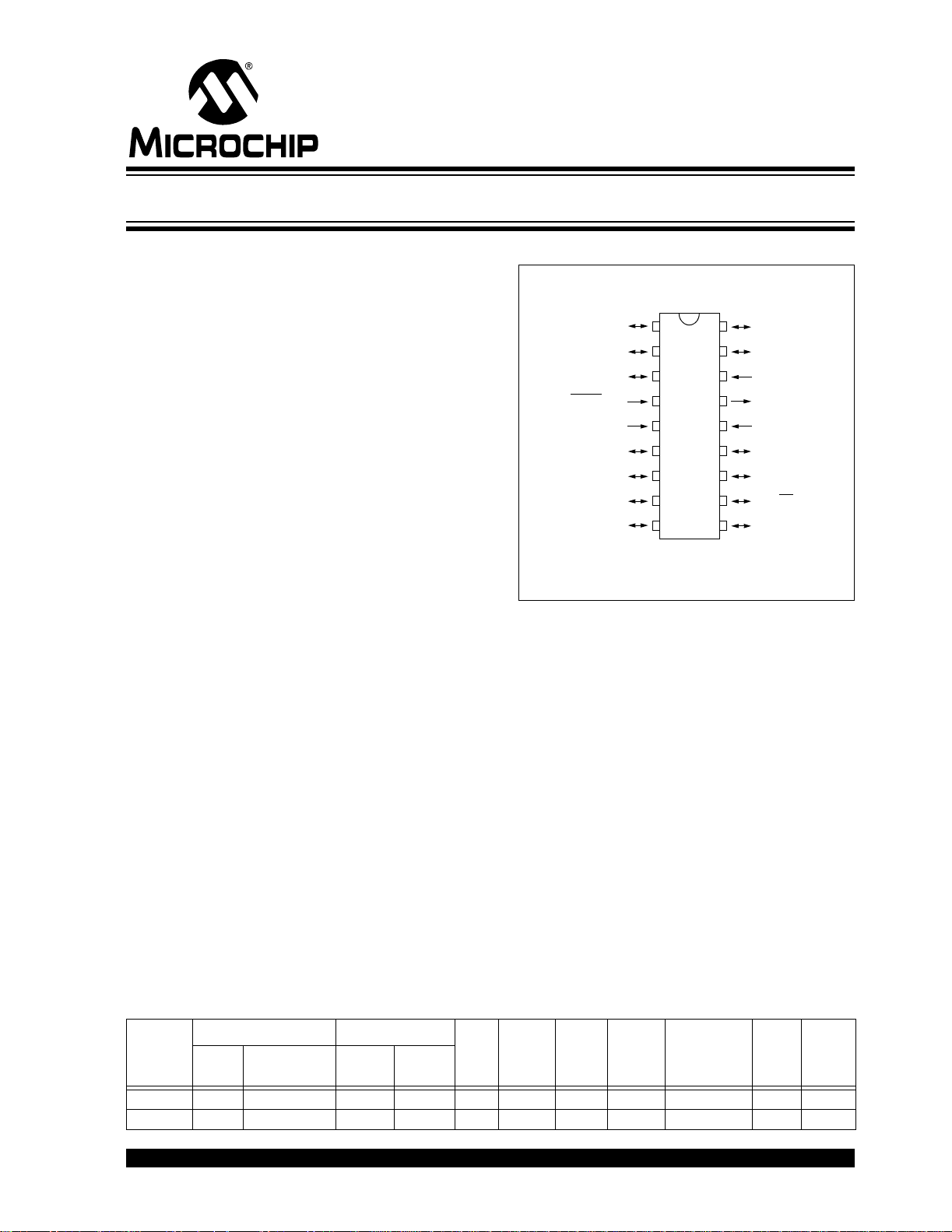
Pin Diagram
18-Pin PDIP, SOIC
RA2/AN2/CV
RA3/AN3/VREF+/
RA4/AN4/T0CKI/
RA5/MCLR
RB0/INT/CCP1
RB1/SDI/SDA
RB2/SDO/RX/DT
RB3/PGM/CCP1
Note 1: The CCP1 pin is determined by the CCPMX bit in
REF/
V
REF-
C1OUT
C2OUT
/VPP
VSS
(1)
(1)
Configuration Word 1 register.
1
18
2
17
3
16
4
15
5
14
6
13
PIC16F88
7
12
8
11
9
10
RA1/AN1
RA0/AN0
RA7/OSC1/CLKI
RA6/OSC2/CLKO
DD
V
RB7/AN6/PGD/
T1OSI
RB6/AN5/PGC/
T1OSO/T1CKI
RB5/SS
/TX/CK
RB4/SCK/SCL
Special Microcontroller Features:
• 100,000 erase/write cycles Enhanced Flash
program memory typical
• 1,000,000 typical erase/write cycles EEPROM
data memory typical
• EEPROM Data Retention: > 40 years
• In-Circuit Serial Programming™ (ICSP™)
via two pins
• Processor read/write access to program memory
• Low-Voltage Progr amming
• In-Circuit Debugging via two pins
• Extended Watchdog Timer (WDT):
- Programmable period from 1ms to 268s
• Wide operating voltage range: 2.0V to 5.5V
Program Memory Data Memory
Device
PIC16F87 7168 4096 368 256 16 N/A 1 Y 2 Y 2/1
PIC16F88 7168 4096 368 256 16 1 1 Y 2 Y 2/1
2005 Microchip Technology Inc. DS30487C-page 1
Flash
(bytes)
# Single-Word
Instructions
SRAM
(bytes)
EEPROM
(bytes)
I/O
Pins
10-bit
A/D (ch)
CCP
(PWM)
AUSART Comparators SSP
Timers
8/16-bit

PIC16F87/88
Pin Diagrams
18-Pin PDIP, SOIC
RA2/AN2/CVREF
RA3/AN3/C1OUT
RA4/T0CKI/C2OUT
RA5/MCLR
RB0/INT/CCP1
RB1/SDI/SDA
RB2/SDO/RX/DT
RB3/PGM/CCP1
20-Pin SSOP
RA2/AN2/CVREF
RA3/AN3/C1OUT
RA4/T0CKI/C2OUT
RA5/MCLR
RB0/INT/CCP1
RB1/SDI/SDA
RB2/SDO/RX/DT
RB3/PGM/CCP1
18-Pin PDIP, SOIC
RA2/AN2/CVREF/VREF-
RA3/AN3/V
RA4/AN4/T0CKI/C2OUT
REF+/C1OUT
RA5/MCLR
RB0/INT/CCP1
RB1/SDI/SDA
RB2/SDO/RX/DT
RB3/PGM/CCP1
/VPP
VSS
/VPP
VSS
/VPP
VSS
1
2
3
4
(1)
(1)
5
6
7
8
9
1
2
3
4
5
6
(1)
7
8
9
(1)
10
1
2
3
4
(1)
(1)
5
6
7
8
9
PIC16F87
PIC16F87
PIC16F88
18
17
16
15
14
13
12
11
10
20
19
18
17
16
15
14
13
12
11
18
17
16
15
14
13
12
11
10
RA1/AN1
RA0/AN0
RA7/OSC1/CLKI
RA6/OSC2/CLKO
DD
V
RB7/PGD/T1OSI
RB6/PGC/T1OSO/T1CKI
/TX/CK
RB5/SS
RB4/SCK/SCL
RA1/AN1
RA0/AN0
RA7/OSC1/CLKI
RA6/OSC2/CLKO
V
DD
VDDVSS
RB7/PGD/T1OSI
RB6/PGC/T1OSO/T1CKI
RB5/SS/TX/CK
RB4/SCK/SCL
RA1/AN1
RA0/AN0
RA7/OSC1/CLKI
RA6/OSC2/CLKO
V
DD
RB7/AN6/PGD/T1OSI
RB6/AN5/PGC/T1OSO/T1CKI
RB5/SS
/TX/CK
RB4/SCK/SCL
20-Pin SSOP
RA2/AN2/CVREF/VREFRA3/AN3/V
RA4/AN4/T0CKI/C2OUT
REF+/C1OUT
RA5/MCLR
RB0/INT/CCP1
RB2/SDO/RX/DT
1/VPP
VSS
RB1/SDI/SDA
1
2
3
4
5
6
(1)
7
8
9
(1)
10
20
19
18
17
16
15
14
PIC16F88
13
12
11
Note 1: The CCP1 pin is determined by the CCPMX bit in Configuration Word 1 register.
DS30487C-page 2 2005 Microchip Technology Inc.
RA1/AN1
RA0/AN0
RA7/OSC1/CLKI
RA6/OSC2/CLKO
V
DD
VDDVSS
RB7/AN6/PGD/T1OSI
RB6/AN5/PGC/T1OSO/T1CKI
RB5/SS/TX/CK
RB4/SCK/SCLRB3/PGM/CCP1
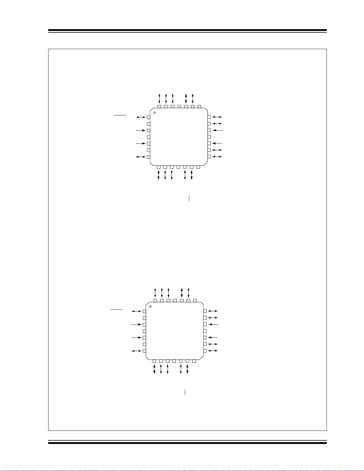
Pin Diagrams (Cont’d)
28-Pin QFN
PIC16F87/88
RA5/MCLR/VPP
RB0/INT/CCP1
28-Pin QFN
NC
VSS
NC
V
NC
RA2/AN2/CVREF
(1)
RB3/PGM/CCP1
11
NC
NC
25
RA1/AN1
24
12
RB4/SCK/SCL
RA0/AN0
23
13
RB5/SS/TX/CK
14
NC
NC
22
21
20
19
18
17
16
15
RA7/OSC1/CLKI
RA6/OSC2/CLKO
V
DD
NC
V
DD
RB7/PGD/T1OSI
RB6/PGC/T1OSO/T1CKI
RA4/T0CKI/C2OUT
RA3/AN3/C1OUT
282627
1
2
3
PIC16F87
4
SS
(1)
5
6
7
8109
RB1/SDI/SDA
RB2/SDO/RX/DT
REF+/C1OUT
RA5/MCLR/VPP
RB0/INT/CCP1
NC
VSS
NC
V
NC
RA4/AN4/T0CKI/C2OUT
RA3/AN3/V
282627
1
2
3
PIC16F88
4
SS
(1)
5
6
7
8109
RB1/SDI/SDA
RB2/SDO/RX/DT
RA2/AN2/CVREF/VREF-
(1)
RB3/PGM/CCP1
NC
25
11
NC
RA1/AN1
24
12
RB4/SCK/SCL
RA0/AN0
23
13
RB5/SS/TX/CK
14
NC
NC
22
21
20
19
18
17
16
15
RA7/OSC1/CLKI
RA6/OSC2/CLKO
DD
V
NC
V
DD
RB7/AN6/PGD/T1OSI
RB6/AN5/PGC/T1OSO/T1CKI
Note 1: The CCP1 pin is determined by the CCPMX bit in Configuration Word 1 register.
2005 Microchip Technology Inc. DS30487C-page 3

PIC16F87/88
Table of Contents
1.0 Device Overview..........................................................................................................................................................................5
2.0 Memory Organization.................................................................................................................................................................11
3.0 Data EEPROM and Flash Program Memory.............................................................................................................................. 27
4.0 Oscillator Configurations............................................................................................................................................................ 35
5.0 I/O Ports............................ ..................... ..................... ..................... .......................................................................................... 51
6.0 Timer0 Module ........................................................................................................................................................................... 67
7.0 Timer1 Module ........................................................................................................................................................................... 71
8.0 Timer2 Module ........................................................................................................................................................................... 79
9.0 Capture/Compare/PWM (CCP) Module ..................................................................................................................................... 81
10.0 Synchronous Serial Port (SSP) Module ..................................................................................................................................... 87
11.0 Addressable Universal Synchronous Asynchronous Receiv er Transmitter (AUS ART ) ............................................................. 97
12.0 Analog-to-Digital Converter (A/D) Module................................................................................................................................ 113
13.0 Comparator Module...................................................................................... ......... .... .. .... .........................................................121
14.0 Comparator Voltage Reference Module................................................... .. ....... .... .. .... .. .... ....... .. .............................................. 127
15.0 Special Features of the CPU........................................................ ..................... ....................................................................... 129
16.0 Instruction Set Summary..........................................................................................................................................................149
17.0 Development Support. .............................................................................................................................................................. 157
18.0 Electrical Characteristics..........................................................................................................................................................163
19.0 DC and AC Characteristics Graphs and Tables....................................................................................................................... 193
20.0 Packaging Information.......................... ..................... ..................... .......................................................................................... 207
Appendix A: Revision History.............................................................................................................................................................213
Appendix B: Device Differences.........................................................................................................................................................213
Index .................................................................................................................................................................................................. 215
The Microchip Web Site....................................... ............................................................. ................................................................. 223
Customer Change Notification Service ..............................................................................................................................................223
Customer Support.............................................................................................................................................................................. 223
Reader Response.............................................................................................................................................................................. 224
PIC16F87/88 Product Identification System ......................................................................................................................................225
TO OUR VALUED CUSTOMERS
It is our intention to provide our valued customers with the best documentation possible to ensure successful use of your Microchip
products. To this end, we will continue to improve our publications to better suit your needs. Our publications will be refined and
enhanced as new volumes and updates are introduced.
If you have any questions or c omm ents regarding t his publication, p lease c ontact the M arket ing Co mmunications Department via
E-mail at docerrors@microchip.com or fax the Reader Response Form in the back of this data sheet to (480) 792-4150. We
welcome your feedback.
Most Current Data Sheet
To obtain the most up-to-date version of this data sheet, please register at our Worldwide Web site at:
http://www.microchip.com
You can determine the version of a data sheet by examining its literature number found on the bottom outside corner of any page.
The last character of the literature number is the version number, (e.g., DS30000A is version A of document DS30000).
Errata
An errata sheet, describing minor operational differences from the data sheet and recommended workarounds, may exist for current
devices. As device/documentation issues become known to us, we will publish an errata sheet. The errata will specify the revision
of silicon and revision of document to which it applies.
To determine if an errata sheet exists for a particular device, please check with one of the following:
• Microchip’s Worldwide Web site; http://www.microchip.com
• Your local Microchip sales office (see last page)
When contacting a sales office, please specify which device, revision of silicon and data sheet (include literature number) you are
using.
Customer Notification System
Register on our web site at www.microchip.com to receive the most current information on all of our products.
DS30487C-page 4 2005 Microchip Technology Inc.

PIC16F87/88
1.0 DEVICE OVERVIEW
This document contains device specific information for
the operation of the PIC16F87/88 devices. Additional
information may be found in the “PICmicro® Mid-Range
MCU Family Reference Manual” (DS33023) which may
be downloaded from the Microchip web site. This
Reference Manual should be considered a complementary document to this data sheet and is highly
recommended reading for a better understanding of the
device architecture and operation of the peripheral
modules.
The PIC16F87/88 belongs to the Mid-Range family of
the PICmicro
are shown in Figure1-1 and Figure 1-2. These devices
contain features that are new to the PIC16 prod uct line:
• Low-power modes: RC_RUN allows the core and
peripherals to be clocked from the INTRC, while
SEC_RUN allows the core and peripherals to be
clocked from the low-power Timer1. Refer to
Section 4.7 “Power-Managed Modes” for
further details.
• Internal RC oscillator with eight selectable
frequencies, including 31.25 kHz, 125 kHz,
250 kHz, 500 kHz, 1 MHz, 2 MHz, 4 MHz and
8 MHz. The INTRC can be configured as a
primary or secondary clock source. Refer to
Section 4.5 “Internal Oscillator Block” for
further details.
• The Timer1 module current consumption has
been greatly reduced from 20 µA (previous PIC16
devices) to 1.8µA typical (32 kHz at 2V), which is
ideal for real-time clock applications. Refer to
Section 7.0 “Timer1 Module” for further details.
• Extended W atchdog T imer (WD T) that can hav e a
programmable period from 1 ms to 268s. The
WDT has its own 16-bit prescaler. Refer to
Section 15.12 “Watchdog Timer (WDT)” for
further details.
• Two-Speed Start-up: When the oscillator is
configured for LP, XT or HS Oscillator mode, this
feature will cl ock t he dev ice f rom the INTRC whil e
the oscillator is warming up. This, in turn, will
enable almost immediate code execution. Refer
to Section 15.12.3 “Two-Speed Cl ock Start-up
Mode” for further details.
• Fail-Safe Clock Monitor: This feature will allow the
device to continue operation if the primary or
secondary clock source fails by switching over to
the INTRC.
• The A/D module has a new register for PIC16
devices named ANSEL. This register allows
easier configuration of analog or digital I/O pins.
®
devices. Block diagrams of the devices
TABLE 1-1: AVAILABLE MEMORY IN
PIC16F87/88 DEVICES
2
Program
Flash
C™
Device
PIC16F87/88 4K x 14 368 x 8 256 x 8
There are 16 I/O pins that are user configurable on a
pin-to-pin basis. Some pins are multiplexed with other
device functions. These functions include:
• External Interrupt
• Change on PORTB Interrupt
• Timer0 Clock Input
• Low-Power Timer1 Clock/Oscillator
• Capture/Compare/PWM
• 10-bit, 7-channel A/D Converter (PI C16F88 onl y)
• SPI™/I
• Two Analog Comparators
• AUSART
•MCLR
Table 1-2 details the pinout of the devices with
descriptions and details for each pin.
(RA5) can be configured as an input
Data
Memory
Data
EEPROM
2005 Microchip Technology Inc. DS30487C-page 5
PIC16F87/88
FIGURE 1-1: PIC16F87 DEVICE BLOCK DIAGRAM
Program
Bus
OSC1/CLKI
OSC2/CLKO
Flash
Program
Memory
4K x 14
14
Instruction reg
Instruction
Decode &
Control
Timing
Generation
13
Program Counter
Direct Addr
8
Start-up Timer
Watchdog
Brown-out
8 Level Stack
(13-bit)
Power-up
Timer
Oscillator
Power-on
Reset
Timer
Reset
RAM Addr
7
3
8
Data Bus
RAM
File
Registers
368 x 8
(1)
Addr MUX
FSR reg
STATUS reg
ALU
W reg
9
8
MUX
8
Indirect
Addr
PORTA
PORTB
RA0/AN0
RA1/AN1
RA2/AN2/CVREF
RA3/AN3/C1OUT
RA4/T0CKI/C2OUT
RA5/MCLR/VPP
RA6/OSC2/CLKO
RA7/OSC1/CLKI
RB0/INT/CCP1
RB1/SDI/SDA
RB2/SDO/RX/DT
RB3/PGM/CCP1
RB4/SCK/SCL
RB5/SS/TX/CK
RB6/PGC/T1OSO/T1CKI
RB7/PGD/T1OSI
(2)
(2)
VDD, VSS
Timer0
Data EE
256 Bytes
SSP
Comparators
Timer2
AUSART
RA5/MCLR
Timer1
CCP1
Note 1: Higher order bits are from the STATUS register.
2: The CCP1 pin is determined by the CCPMX bit in Configuration Word 1 register.
DS30487C-page 6 2005 Microchip Technology Inc.
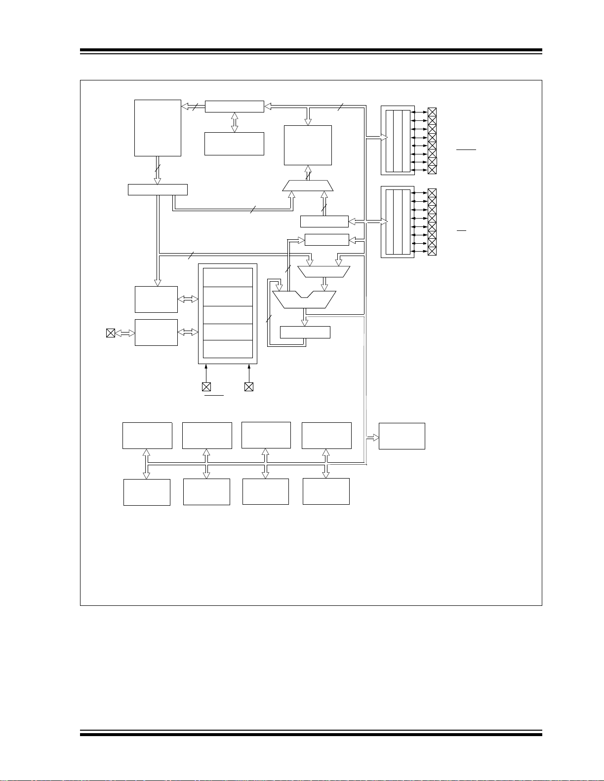
FIGURE 1-2: PIC16F88 DEVICE BLOCK DIAGRAM
PIC16F87/88
Program
Bus
OSC1/CLKI
OSC2/CLKO
Flash
Program
Memory
4K x 14
14
Instruction reg
Instruction
Decode &
Control
Timing
Generation
13
Program Counter
8 Level Stack
Direct Addr
8
Power-up
Start-up Timer
Power-on
Watchdog
Brown-out
(13-bit)
Timer
Oscillator
Reset
Timer
Reset
RAM Addr
7
3
8
Data Bus
RAM
File
Registers
368 x 8
(1)
Addr MUX
FSR reg
STATUS reg
ALU
W reg
9
8
MUX
8
Indirect
Addr
PORTA
PORTB
RA0/AN0
RA1/AN1
RA2/AN2/CVREF/VREFRA3/AN3/VREF+/C1OUT
RA4/AN4/T0CKI/C2OUT
RA5/MCLR/VPP
RA6/OSC2/CLKO
RA7/OSC1/CLKI
RB0/INT/CCP1
RB1/SDI/SDA
RB2/SDO/RX/DT
RB3/PGM/CCP1
RB4/SCK/SCL
RB5/SS/TX/CK
RB6/AN5/PGC/T1OSO/T1CKI
RB7/AN6/PGD/T1OSI
(2)
(2)
VDD, VSS
Timer0
Data EE
256 Bytes
10-bit A/D
Comparators
Timer2
AUSART
RA5/MCLR
Timer1
CCP1
Note 1: Higher order bits are from the STATUS register.
2: The CCP1 pin is determined by the CCPMX bit in Configuration Word 1 register.
SSP
2005 Microchip Technology Inc. DS30487C-page 7

PIC16F87/88
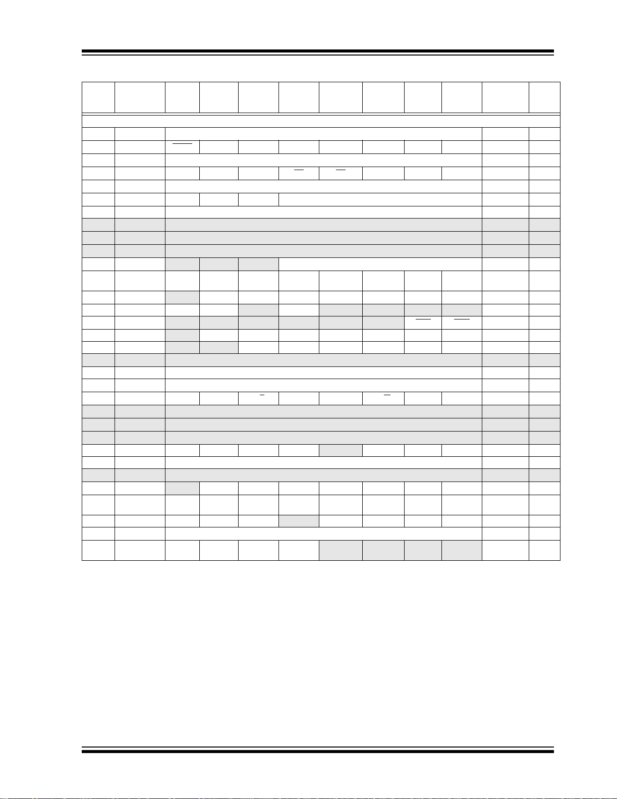
TABLE 1-2: PIC16F87/88 PINOUT DESCRIPTION
PDIP/
Pin Name
RA0/AN0
RA0
AN0
RA1/AN1
RA1
AN1
RA2/AN2/CV
RA2
AN2
CV
VREF-
RA3/AN3/V
RA3
AN3
V
C1OUT
RA4/AN4/T0CKI/C2OUT
RA4
AN4
T0CKI
C2OUT
RA5/MCLR
RA5
MCLR
VPP
RA6/OSC2/CLKO
RA6
OSC2
CLKO
RA7/OSC1/CLKI
RA7
OSC1
CLKI
Legend: I = Input O = Output I/O = Input/Output P = Power
Note 1: T his buffer is a Schmitt Trigger input when configured as the external interrupt.
REF/VREF-
REF
(4)
REF+/C1OUT
(4)
REF+
(4)
/VPP
– = Not used TTL = TTL Input ST = Schmitt Trigger Input
2: This buffer is a Schmitt Trigger input when used in Serial Programming mode.
3: This buffer is a Schmitt Trigger input when configured in RC Oscillator mode and a CMOS input otherwise.
4: PIC 16F88 devices only.
5: The CCP1 pin is determined by the CCPMX bit in Configuration Word 1 register.
SSOP
SOIC
Pin#
17 19 23
18 20 24
1126
2227
3328
441
15 17 20
16 18 21
Pin#
QFN
Pin#
I/O/P
Type
I/O
I
I/O
I
I/O
I
O
I
I/O
I
I
O
I/O
I
I
O
I
I
P
I/O
O
O
I/O
I
I
Buffer
Type
TTL
Analog
TTL
Analog
TTL
Analog
Analog
TTL
Analog
Analog
ST
Analog
ST
ST
ST
–
ST
–
–
ST
ST/CMOS
–
Description
PORTA is a bidirectional I/O port.
Bidirectional I/O pin.
Analog input channel 0.
Bidirectional I/O pin.
Analog input channel 1.
Bidirectional I/O pin.
Analog input channel 2.
Comparator V
A/D reference voltage (Low) input.
Bidirectional I/O pin.
Analog input channel 3.
A/D reference voltage (High) input.
Comparator 1 output.
Bidirectional I/O pin.
Analog input channel 4.
Clock input to the TMR0 timer/counter.
Comparator 2 output.
Input pin.
Master Clear (Reset). Input/programming voltage
input. This pin is an active-low Reset to the device.
Programming voltage input.
Bidirectional I/O pin.
Oscillator crystal output. Connects to crystal or
resonator in Crystal Oscillator mode.
In RC mode, this pin outputs CLKO signal which has
1/4 the frequency of OSC1 and denotes the
instruction cycle rate.
Bidirectional I/O pin.
(3)
Oscillator crystal input.
External clock source input.
REF output.
DS30487C-page 8 2005 Microchip Technology Inc.

PIC16F87/88
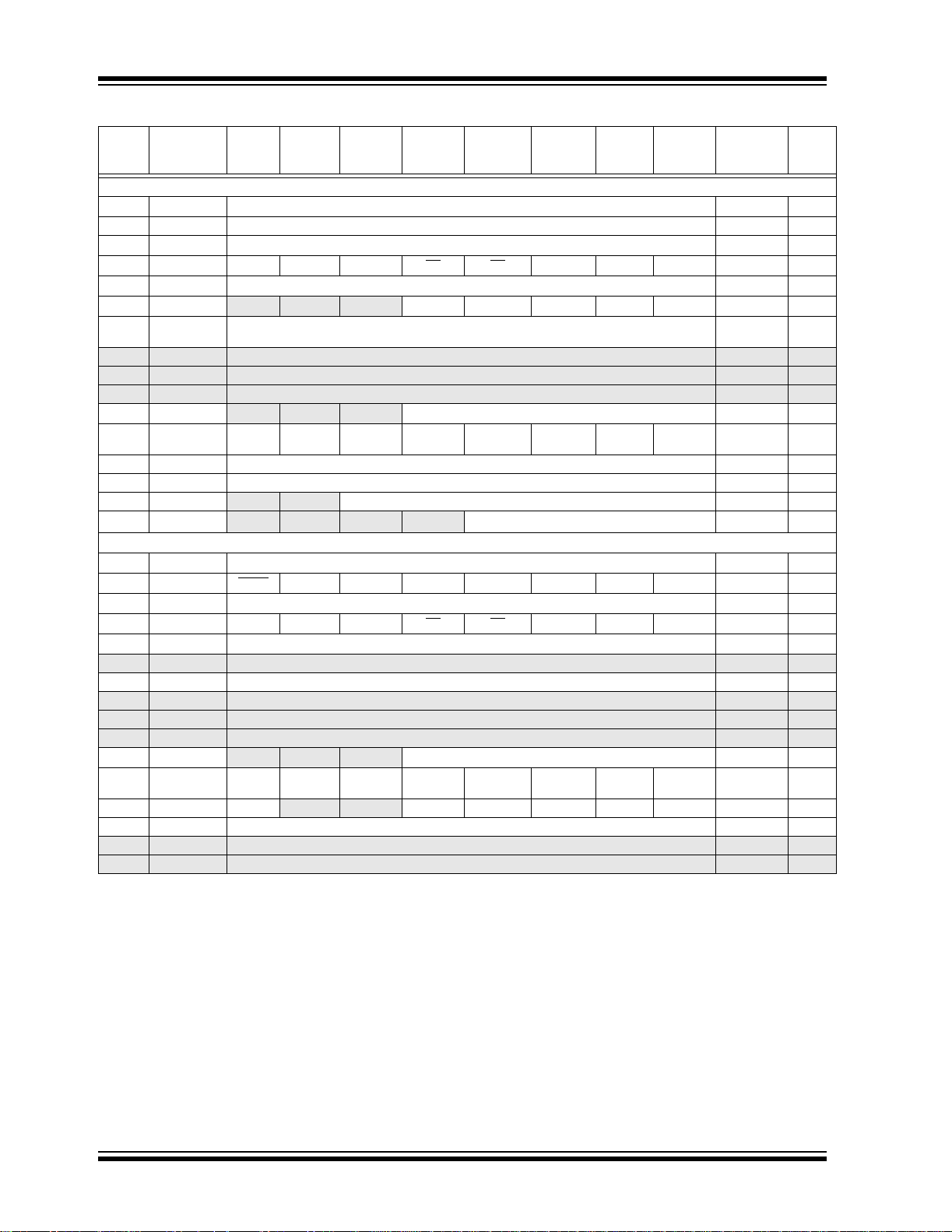
TABLE 1-2: PIC16F87/88 PINOUT DESCRIPTION (CONTINUED)
PDIP/
Pin Name
RB0/INT/CCP1
(5)
SSOP
SOIC
Pin#
Pin#
677
RB0
INT
CCP1
RB1/SDI/SDA
788
RB1
SDI
SDA
RB2/SDO/RX/DT
899
RB2
SDO
RX
DT
RB3/PGM/CCP1
(5)
91010
RB3
PGM
CCP1
RB4/SCK/SCL
10 11 12
RB4
SCK
SCL
RB5/SS
/TX/CK
11 12 13
RB5
SS
TX
CK
RB6/AN5/PGC/T1OSO/
12 13 15
T1CKI
RB6
(4)
AN5
PGC
T1OSO
T1CKI
RB7/AN6/PGD/T1OSI
RB7
(4)
AN6
13 14 16
PGD
T1OSI
SS 5 5, 6 3, 5 P – Ground reference for logic and I/O pins.
V
V
DD 14 15, 16 17, 19 P – Positive supply for logic and I/O pins.
Legend: I = Input O = Output I/O = Input/Output P = Power
– = Not used TTL = TTL Input ST = Schmitt Trigger Input
Note 1: T his buffer is a Schmitt Trigger input when configured as the external interrupt.
2: This buffer is a Schmitt Trigger input when used in Serial Programming mode.
3: This buffer is a Schmitt Trigger input when configured in RC Oscillator mode and a CMOS input otherwise.
4: PIC16F88 devices only.
5: The CCP1 pin is determined by the CCPMX bit in Configuration Word 1 register.
QFN
Pin#
I/O/P
Type
I/O
I
I/O
I/O
I
I/O
I/O
O
I
I/O
I/O
I/O
I
I/O
I/O
I
I/O
I
O
I/O
I/O
I
I/O
O
I
I/O
I
I
I
Buffer
Type
TTL
(1)
ST
ST
TTL
ST
ST
TTL
ST
TTL
ST
ST
TTL
ST
ST
TTL
TTL
TTL
(2)
ST
ST
ST
TTL
(2)
ST
ST
Description
PORTB is a bidirectional I/O port. PORTB can be
software programmed for internal weak pull-up on all
inputs.
Bidirectional I/O pin.
External interrupt pin.
Capture input, Compare output, PWM output.
Bidirectional I/O pin.
SPI™ data in.
2
C™ data.
I
Bidirectional I/O pin.
SPI data out.
AUSART asynchronous receive.
AUSART synchronous detect.
Bidirectional I/O pin.
Low-Voltage ICSP™ Programming enable pin.
Capture input, Compare output, PWM output.
Bidirectional I/O pin. Interrupt-on-change pin.
Synchronous serial clock input/output for SPI.
Synchronous serial clock Input for I
Bidirectional I/O pin. Interrupt-on-change pin.
Slave select for SPI in Slave mode.
AUSART asynchronous transmit.
AUSART synchronous clock.
Bidirectional I/O pin. Interrupt-on-change pin.
Analog input channel 5.
In-Circuit Debugger and programming clock pin.
Timer1 oscillator output.
Timer1 external clock input.
Bidirectional I/O pin. Interrupt-on-change pin.
Analog input channel 6.
In-Circuit Debugger and ICSP programming data pin.
Timer1 oscillator input.
2
C.
2005 Microchip Technology Inc. DS30487C-page 9

PIC16F87/88
NOTES:
DS30487C-page 10 2005 Microchip Technology Inc.
PIC16F87/88
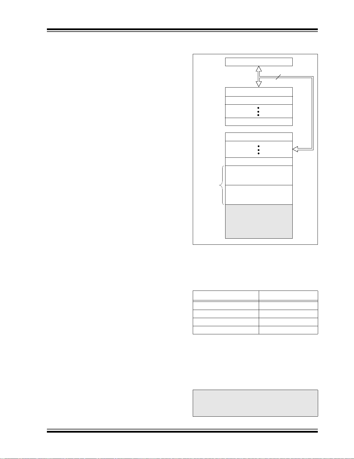
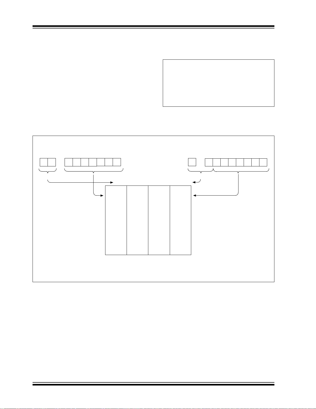
2.0 MEMORY ORGANIZATION
There are two memory blocks in the PIC16F87/88
devices. Thes e are t he p rog ram m emo ry an d the d ata
memory . Each bloc k has its o wn bus, so ac cess to each
block can occur during the same oscillator cycle.
The data memory can be further broken down into the
general purpose RAM and the Special Function
Registers (SFRs). The operation of the SFRs that
control the “core” are described here. The SFRs used
to control the peripheral modules are described in the
section discussing each individual peripheral module.
The data memory area also contains the data EEPROM
memory. This memory is not directly mapped into the
data memory but is indirectly mapped. That is, an indirect address pointer specifies the address of the data
EEPROM memory to read/write. The PIC16F87/88
device’s 256 bytes of data EEPROM memory have the
address range of 00h-FFh. More details on the
EEPROM memory can be found in Section 3.0 “Data
EEPROM and Flash Program Memory”.
Additional informa tion on devi ce memory may be found
in the “PICmicro
Manual” (DS33023).
2.1 Program Memory Organization
The PIC16F87/88 devices have a 13-bit program
counter capable of addressing an 8K x 14 program
memory space. For the PIC16F87/88, the first 4K x 14
(0000h-0FFFh) is physically implemented (see
Figure 2-1). Accessing a location above the physically
implemented address will cause a wraparound. For
example, the same instruction will be accessed at
locations 020h, 420h, 820h, C20h, 1020h, 1420h,
1820h and 1C20h.
The Reset vector is at 0000h an d the interrupt ve ctor is
at 0004h.
®
Mid-Range MCU Family Reference
FIGURE 2-1: PROGRAM MEMORY MAP
AND STACK: PIC16F87/88
PC<12:0>
On-Chip
Program
Memory
CALL, RETURN
RETFIE, RETLW
Stack Level 1
Stac k Lev el 2
Stac k Lev el 8
Reset Vector
Interrupt V ec tor
Page 0
Page 1
Wraps to
0000h-03FFh
13
0000h
0004h
0005h
07FFh
0800h
0FFFh
1000h
1FFFh
2.2 Data Memory Organization
The data memory is pa rtit ioned into m ultipl e ban ks th at
contain the Ge neral Purpose Reg isters and the Special
Function Registers. Bits RP1 (STATUS<6>) and RP0
(STATUS<5>) are the bank select bits.
RP1:RP0 Bank
00 0
01 1
10 2
11 3
Each bank extends up to 7Fh (128 bytes). The lower
locations of each bank are reserved for the Special
Function Registers. Abo ve the Speci al Function Re gisters are General Purpose Registers, implemented as
static RAM. All implemented banks contain SFRs.
Some “high use” SFRs from one bank may be mirrored
in another bank for code reduction and quicker access
(e.g., the STATUS register is in Banks 0-3).
Note: EEPROM data memory description can be
found in Section 3.0 “Data EEPROM and
Flash Program Memory” of this data
sheet.
2005 Microchip Technology Inc. DS30487C-page 11
PIC16F87/88
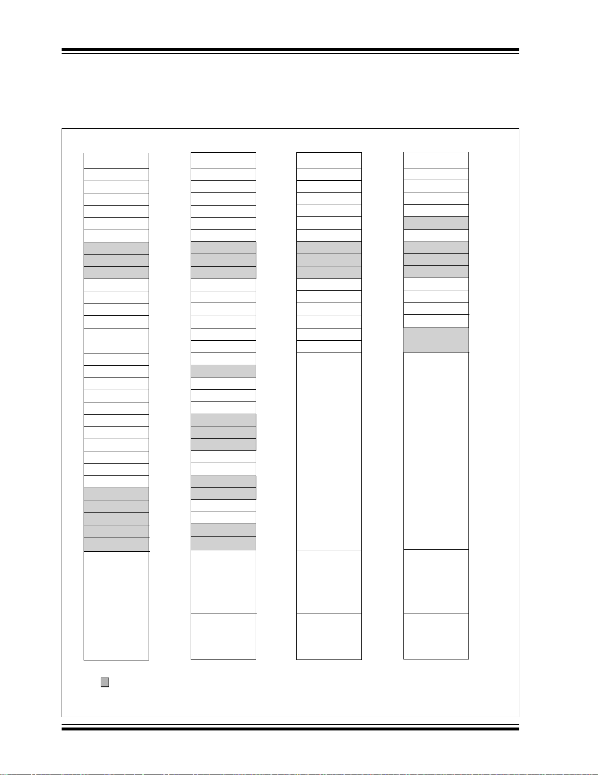
2.2.1 GENERAL PURPOSE REGISTER FILE
The register file can be accessed either directly, or
indirectly, through the File Select Register (FSR).
FIGURE 2-2: PIC16F87 REGISTER FILE MAP
Address
(*)
File
80h
81h
82h
83h
84h
85h
86h
87h
88h
89h
8Ah
8Bh
8Ch
8Dh
8Eh
8Fh
90h
91h
92h
93h
94h
95h
96h
97h
98h
99h
9Ah
9Bh
9Ch
9Dh
9Eh
9Fh
A0h
EFh
F0h
Indirect addr.
TMR0
PCL
STATUS
FSR
PORTA
PORTB
PCLATH
INTCON
PIR1
PIR2
TMR1L
TMR1H
T1CON
TMR2
T2CON
SSPBUF
SSPCON
CCPR1L
CCPR1H
CCP1CON
RCSTA
TXREG
RCREG
General
Purpose
Register
96 Bytes
Address
(*)
File
00h
01h
02h
03h
04h
05h
06h
07h
08h
09h
0Ah
0Bh
0Ch
0Dh
0Eh
0Fh
10h
11h
12h
13h
14h
15h
16h
17h
18h
19h
1Ah
1Bh
1Ch
1Dh
1Eh
1Fh
20h
Indirect addr.
OPTION_REG
PCL
STATUS
FSR
TRISA
TRISB
PCLATH
INTCON
PIE1
PIE2
PCON
OSCCON
OSCTUNE
PR2
SSPADD
SSPSTAT
TXSTA
SPBRG
CMCON
CVRCON
General
Purpose
Register
80 Bytes
accesses
70h-7Fh
File
Address
Indirect addr.
TMR0 OPTION_REG
PCL
STATUS
FSR
WDTCON
PORTB
PCLATH
INTCON
EEDATA
EEADR
EEDATH
EEADRH
General
Purpose
Register
16 Bytes
General
Purpose
Register
80 Bytes
accesses
70h-7Fh
(*)
100h
101h
102h
103h
104h
105h
106h
107h
108h
109h
10Ah
10Bh
10Ch
10Dh
10Eh
10Fh
110h
11Fh
120h
16Fh
170h
Indirect addr.
STATUS
STATUS
PCLATH
INTCON
EECON1
EECON2
Reserved
Reserved
General
Purpose
Register
16 Bytes
General
Purpose
Register
80 Bytes
accesses
70h-7Fh
PCL
FSR
TRISB
(*)
(1)
(1)
File
Address
180h
181h
182h
183h
184h
185h
186h
187h
188h
189h
18Ah
18Bh
18Ch
18Dh
18Eh
18Fh
190h
19Fh
1A0h
1EFh
1F0h
Bank 0
7Fh
Unimplemented data memory locations, read as ‘0’.
* Not a physical register.
Note 1: This register is reserved, maintain this register clear.
DS30487C-page 12 2005 Microchip Technology Inc.
Bank 1
FFh
Bank 2
17Fh 1FFh
Bank 3
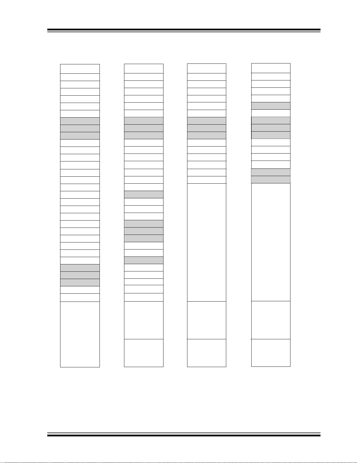
FIGURE 2-3: PIC16F88 REGISTER FILE MAP
File
Address
Indirect addr.
TMR0
PCL
STATUS
FSR
PORTA
PORTB
PCLATH
INTCON
PIR1
PIR2
TMR1L
TMR1H
T1CON
TMR2
T2CON
SSPBUF
SSPCON
CCPR1L
CCPR1H
CCP1CON
RCSTA
TXREG
RCREG
ADRESH
ADCON0 ADCON1
General
Purpose
Register
96 Bytes
Bank 0
(*)
00h
01h
02h
03h
04h
05h
06h
07h
08h
09h
0Ah
0Bh
0Ch
0Dh
0Eh
0Fh
10h
11h
12h
13h
14h
15h
16h
17h
18h
19h
1Ah
1Bh
1Ch
1Dh
1Eh
1Fh
20h
7Fh
Indirect addr.
OPTION_REG
STATUS
TRISA
TRISB
PCLATH
INTCON
PCON
OSCCON
OSCTUNE
SSPADD
SSPSTAT
TXSTA
SPBRG
ANSEL
CMCON
CVRCON
ADRESL
General
Purpose
Register
80 Bytes
accesses
70h-7Fh
Bank 1
PCL
FSR
PIE1
PIE2
PR2
File
Address
(*)
80h
81h
82h
83h
84h
85h
86h
87h
88h
89h
8Ah
8Bh
8Ch
8Dh
8Eh
8Fh
90h
91h
92h
93h
94h
95h
96h
97h
98h
99h
9Ah
9Bh
9Ch
9Dh
9Eh
9Fh
A0h
EFh
F0h
FFh
Indirect addr.
TMR0
PCL
STATUS
FSR
WDTCON
PORTB
PCLATH
INTCON
EEDATA
EEADR
EEDATH
EEADRH
General
Purpose
Register
16 Bytes
General
Purpose
Register
80 Bytes
accesses
70h-7Fh
Bank 2
File
Address
(*)
100h
101h
102h
103h
104h
105h
106h
107h
108h
109h
10Ah
10Bh
10Ch
10Dh
10Eh
10Fh
110h
11Fh
120h
16Fh
170h
17Fh
PIC16F87/88
File
Address
(1)
(1)
(*)
180h
181h
182h
183h
184h
185h
186h
187h
188h
189h
18Ah
18Bh
18Ch
18Dh
18Eh
18Fh
190h
19Fh
1A0h
1EFh
1F0h
1FFh
Indirect addr.
OPTION_REG
PCL
STATUS
FSR
TRISB
PCLATH
INTCON
EECON1
EECON2
Reserved
Reserved
General
Purpose
Register
16 Bytes
General
Purpose
Register
80 Bytes
accesses
70h-7Fh
Bank 3
Unimplemented data memory locations, read as ‘0’.
* Not a physical register.
Note 1: This register is reserved, maintain this register clear.
2005 Microchip Technology Inc. DS30487C-page 13
PIC16F87/88
2.2.2 SPECIAL FUNCTION REGISTERS
The Special Function Registers are registers used by
the CPU and peripheral modules for controlling the
desired operation of the device. These registers are
implemented as static RAM. A list of these registers is
given in Table 2-1.
The Special Function Registers can be classified into
two sets: core (CPU) and peripheral. Those registers
associated with the core functions are described in
detail in this section. Those related to the operation of
the peripheral features are described in detail in the
peripheral feature section.
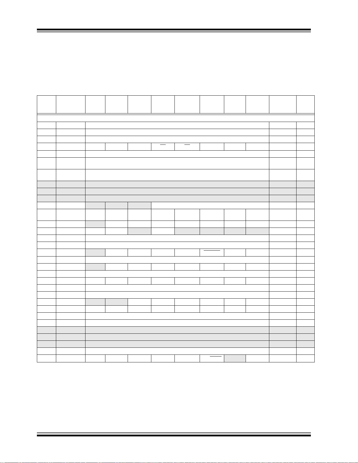
TABLE 2-1: SPECIAL FUNCTION REGISTER SUMMARY
Addre ss Name Bit 7 Bit 6 Bit 5 Bit 4 Bit 3 Bit 2 Bit 1 Bit 0
Bank 0
(2)
00h
01h
02h
03h
04h
05h
06h
07h
08h
09h
0Ah
0Bh
0Ch
0Dh
0Eh
0Fh
10h
11h
12h
13h
14h
15h
16h
17h
18h
19h
1Ah
1Bh
1Ch
1Dh
1Eh
1Fh
INDF Addressing this location uses contents of FSR to address data memory (not a physical register) 0000 0000 26, 1 35
TMR0 Timer0 Module Register xxxx xxxx 69
(2)
PCL Program Counter (PC) Least Significant Byte 0000 0000
(2)
STATUS IRP RP1 RP0 TO PD ZDCC0001 1xxx 17
(2)
FSR Indirect Data Memory Address Poi nter xxxx xxxx 135
PORTA PORTA Data Latch when written; PORTA pins when read (PIC16F87)
PORTB PORTB Data Latch when written; PORTB pins when read (PIC16F87)
— Unimplemented — —
— Unimplemented — —
(1,2)
(2)
— Unimplemented — —
PCLATH — — — Write Buffer for the Upper 5 bits of the Program Counter ---0 0000 135
INTCON GIE PEIE TMR0IE INT0IE RBIE TMR0IF INT0IF RBIF 0000 000x 19, 69,
PIR1 —ADIF
PIR2 OSFIF CMIF — EEIF — — — — 00-0 ---- 23, 34
TMR1L Holding Register for the Least Significant Byte of the 16-bit TMR1 Register xxxx xxxx 77, 83
TMR1H Holding Register for the Most Significant Byte of the 16-bit TMR1 Register xxxx xxxx 77, 83
T1CON — T1RUN T1CKPS1 T1CKPS0 T1OSCEN T1SYNC TMR1CS TMR1ON -000 0000 72, 83
TMR2 Timer2 Module Register 0000 0000 80, 85
T2CON — TOUTPS3 TOUTPS2 TOUTPS1 TOUTPS0 TMR2ON T2CKPS1 T2CKPS0 -000 0000 80, 85
SSPBUF Synchronous Serial Port Receive Buffer/Transmit Register xxxx xxxx 90, 95
SSPCON WCOL SSPOV SSPEN CKP SSPM3 SSPM2 SSPM1 SSPM0 0000 0000 89, 95
CCPR1L Capture/Compare/PWM Register 1 (LSB) xxxx xxxx 83, 85
CCPR1H Capture/Compare/PWM Register 1 (MSB) xxxx xxxx 83, 85
CCP1CON — — CCP1X CCP1Y CCP1M3 CCP1M2 CCP1M1 CCP1M0 --00 0000 81, 83
RCSTA SPEN RX9 SREN CREN ADDEN FERR OERR RX9D 0000 000x 98, 99
TXREG AUSART Transmit Data Register 0000 0000 103
RCREG AUSART Receive Data Register 0000 0000 105
— Unimplemented — —
— Unimplemented — —
— Unimplemented — —
ADRESH
ADCON0
PORTA Data Latch when written; PORTA pins when read (PIC16F88)
PORTB Data Latch when written; PORTB pins when read (PIC16F88)
(4)
RCIF TXIF SSPIF CCP1IF TMR2IF TMR1IF -000 0000 21, 77
(4)
A/D Result Register High Byte xxxx xxxx 120
(4)
ADCS1 ADCS0 CHS2 CHS1 CHS0 GO/DO NE —ADON0000 00-0 114, 120
Legend: x = unknown, u = unchanged, q = value depends on condition, - = unimplemented, read as ‘0’, r = reserved.
Shaded locations are unimplemented, read as ‘0’.
Note 1: The upper byte of the program counter is not directly accessible. PCLATH is a holding register for PC<12:8>, whose
contents are transferred to the upper byte of the program counter.
2: These registers can be addressed from any bank.
3: RA5 is an input only; the state of the TRISA5 bit has no effect and will always read ‘1’.
4: PIC 16F88 device only.
Value on:
POR, BOR
xxxx 0000
xxx0 0000
xxxx xxxx
00xx xxxx
Details
on
page
52
58
77
DS30487C-page 14 2005 Microchip Technology Inc.
PIC16F87/88
TABLE 2-1: SPECIAL FUNCTION REGISTER SUMMARY (CONTINUED)
Addre ss Name Bit 7 Bit 6 Bit 5 Bit 4 Bit 3 Bit 2 Bit 1 Bit 0
Bank 1
(2)
80h
81h
82h
83h
84h
85h
86h
87h
88h
89h
8Ah
8Bh
8Ch
8Dh
8Eh
8Fh
90h
91h
92h
93h
94h
95h
96h
97h
98h
99h
9Ah
9Bh
9Ch
9Dh
9Eh
9Fh
INDF Addressing this location uses contents of FSR to address data memory (not a physical register) 0000 0000
OPTION_REG RBPU INTEDG T0CS T0SE PSA PS2 PS1 PS0 1111 1111
(2)
PCL Program Counter (PC) Least Significant Byte 0000 0000
(2)
STATUS IRP RP1 RP0 TO PD ZDCC0001 1xxx
(2)
FSR Indirect Data Memory Address Poi nter xxxx xxxx
TRISA TRISA7 TRISA6 TRISA5
TRISB PORTB Data Direction Register 1111 1111 58, 85
— Unimplemented — —
— Unimplemented — —
— Unimplemented — —
(1,2)
PCLATH — — — Write Buffer for the Upper 5 bits of the Program Counter ---0 0000
(2)
INTCON GIE PEIE TMR0IE INT0IE RBIE TMR0IF INT0IF RBIF 0000 000x
ADIE
(4)
PIE1
PIE2 OSFIE CMIE —EEIE — — — — 00-0 ---- 22, 34
PCON — — — — — —PORBOR ---- --0q
OSCCON — IRCF2 IRCF1 IRCF0 OSTS IOFS SCS1 SCS0 -000 0000 40
OSCTUNE — — TUN5 T UN4 TUN3 TUN2 TUN1 TUN0 --00 0000 38
— Unimplemented —
PR2 Timer2 Period Register 1111 1111 80, 85
SSPADD Synchronous Serial Port (I2C™ mode) Address Register 0000 0000
SSPSTAT SMP CKE D/A PSR/WUA BF 0000 0000
— Unimplemented
— Unimplemented
— Unimplemented
TXSTA CSRC TX9 TXEN SYNC — BRGH TRMT TX9D 0000 -010 97, 99
SPBRG Baud Rate Generator Register 0000 0000 99, 103
— Unimplemented
(4)
ANSEL
CMCON C2OUT C1OUT C2INV C1INV CIS CM2 CM1 CM0 0000 0111 121,
CVRCON CVREN CVROE CVRR — CVR3 CVR2 CVR1 CVR0 000- 0000 126, 128
(4)
ADRESL
(4)
ADCON1
—
— ANS6 ANS5 ANS4 A NS3 ANS2 ANS1 ANS0 -111 1111
A/D Result Register Low Byte xxxx xxxx
ADFM ADCS2 VCFG1 VCFG0 — — — — 0000 ----
(3)
PORTA Data Direction Register (TRISA<4:0>) 1111 1111
RCIE TXIE SSPIE CCP1IE TMR2IE TMR1IE -000 0000
Legend: x = unknown, u = unchanged, q = value depends on condition, - = unimplemented, read as ‘0’, r = reserved.
Shaded locations are unimplemented, read as ‘0’.
Note 1: The upper byte of the program counter is not directly accessible. PCLATH is a holding register for PC<12:8>, whose
contents are transferred to the upper byte of the program counter.
2: These registers can be addressed from any bank.
3: RA5 is an input only; the state of the TRISA5 bit has no effect and will always read ‘1’.
4: PIC16F88 device only.
Value on:
POR, BOR
— —
— —
— —
— —
Details
on
page
26, 135
18, 69
135
17
135
52, 126
135
19, 69,
77
20, 80
24
—
95
88, 95
120
126, 128
120
52, 115,
120
2005 Microchip Technology Inc. DS30487C-page 15
PIC16F87/88
TABLE 2-1: SPECIAL FUNCTION REGISTER SUMMARY (CONTINUED)
Addre ss Name Bit 7 Bit 6 Bit 5 Bit 4 Bit 3 Bit 2 Bit 1 Bit 0
Bank 2
(2)
100h
101h
102h
103h
104h
105h
106h
107h
108h
109h
10Ah
10Bh
10Ch
10Dh
10Eh
10Fh
Bank 3
180h
181h
182h
183h
184h
185h
186h
187h
188h
189h
18Ah
18Bh
18Ch
18Dh
18Eh — Reserved, maintain clear
18Fh — Reserved, maintain clear
INDF Addressing this location uses contents of FSR to address data memory (not a physical register) 0000 0000
TMR0 Timer0 Module Register xxxx xxxx 69
(2)
PCL Program Counter’s (PC) Least Significant Byte 0000 0000
(2)
STATUS IRP RP1 RP0 TO PD ZDCC0001 1xxx
(2)
FSR Indirect Data Memory Address Poi nter xxxx xxxx
WDTCON
PORTB PORTB Data Latch when written; PORTB pins when read (PIC16F87)
— Unimplemented — —
— Unimplemented — —
— Unimplemented — —
(1,2)
PCLATH — — — Write Buffer for the Upper 5 bits of the Program Counter ---0 0000
(2)
INTCON GIE PEIE TMR0IE INT0IE RBIE TMR0IF INT0IF RBIF 0000 000x
EEDATA EEPROM/Flash Data Register Low Byte xxxx xxxx 34
EEADR EEPROM/Flash Address Register Low Byte xxxx xxxx 34
EEDATH — — EEPROM/Flash Data Register High Byte --xx xxxx 34
EEADRH — — — — EEPROM/Flash Address Regi st er Hi gh Byte ---- xxxx
(2)
INDF Addressing this location uses contents of FSR to address data memory (not a physical register) 0000 0000
OPTION_REG RBPU INTEDG T0CS T0SE PSA PS2 PS1 PS0 1111 1111 18, 69
(2)
PCL Program Counter (PC) Least Significant Byte 0000 0000
(2)
STATUS IRP RP1 RP0 TO PD ZDCC0001 1xxx
(2)
FSR Indirect Data Memory Address Poi nter xxxx xxxx
— Unimplemented — —
TRISB PORTB Data Direction Register 1111 1111 58, 83
— Unimplemented — —
— Unimplemented — —
— Unimplemented — —
(1,2)
PCLATH — — — Write Buffer for the Upper 5 bits of the Program Counter ---0 0000
(2)
INTCON GIE PEIE TMR0IE INT0IE RBIE TMR0IF INT0IF RBIF 0000 000x
EECON1 EEPGD — — FREE WRERR WREN WR RD x--x x000 28, 34
EECON2 EEPROM Control Register 2 (not a physical register) ---- ---- 34
— — —
PORTB Data Latch when written; PORTB pins when read (PIC16F88)
WDTPS3 WDTPS2 WDTPS1 WDTPS0 SWDTEN ---0 1000 142
Legend: x = unknown, u = unchanged, q = value depends on condition, - = unimplemented, read as ‘0’, r = reserved.
Shaded locations are unimplemented, read as ‘0’.
Note 1: The upper byte of the program counter is not directly accessible. PCLATH is a holding register for PC<12:8>, whose
contents are transferred to the upper byte of the program counter.
2: These registers can be addressed from any bank.
3: RA5 is an input only; the state of the TRISA5 bit has no effect and will always read ‘1’.
4: PIC 16F88 device only.
Value on:
POR, BOR
xxxx xxxx
00xx xxxx
0000 0000 —
0000 0000 —
Details
on
page
26, 135
135
17
135
58
135
19, 69,
77
34
135
135
17
135
135
19, 69,
77
DS30487C-page 16 2005 Microchip Technology Inc.

PIC16F87/88
2.2.2.1 STATUS Register
The STATUS register, shown in Register 2-1, contains
the arithmetic status of the ALU, the Reset status and
the bank select bits for data memory.
The STATUS register can be the destination for any
instruction, as with any other register. If the STATUS
register is the destination for an instruction that affects
the Z, DC or C bits, then the write to these three bits is
disabled. These bit s are set or cleared ac cording to the
device logic. Furthermore, the TO
writable. Therefore, the result of an instruction with the
STATUS register as destinatio n may be different than
intended.
and PD bits are not
For example, CLRF STATUS will clear the up per three
bits and set t he Z bit. T his leaves the STATUS register
as ‘000u u1uu’ (where u = unchanged).
It is recommended, therefore, that only BCF, BSF, SWAPF
and MOVWF instructions are used to alter the STATUS
register because these instructions do not affect the Z, C
or DC bits from the STATUS register. For other
instructions not affecting any Status bits, see
Section 16.0 “Instruction Set Summary”.
Note: The C and DC bits operate as a borrow
and digit borrow bit, respectively, in
subtraction. See the SUBLW and SUBWF
instructions for examples.
REGISTER 2-1: STA TUS: ARITHMETIC STATUS REGISTER (ADDRESS 03h, 83h, 103h, 183h)
R/W-0 R/W-0 R/W-0 R-1 R-1 R/W-x R/W-x R/W-x
IRP RP1 RP0 TO
bit 7 bit 0
bit 7 IRP: Register Bank Select bit (used for indirect addressing)
1 = Bank 2, 3 (100h-1FFh)
0 = Bank 0, 1 (00h-FFh)
bit 6-5 RP<1:0>: Register Bank Select bits (used for direct addressing)
11 = Bank 3 (180h-1FFh)
10 = Bank 2 (100h-17Fh)
01 = Bank 1 (80h-FFh)
00 = Bank 0 (00h-7Fh)
Each bank is 128 bytes.
bit 4 TO
bit 3 PD
bit 2 Z: Zero bit
bit 1 DC: Digit carry/borrow bit (ADDWF, ADDLW, SUBLW and SUBWF instructions)
bit 0 C: Carry/borrow
: Tim e- out bit
1 = After power-up, CLRWDT instruction or SLEEP instruction
0 = A WDT time-out occurred
: Power-Down bit
1 = After power-up or by the CLRWDT instruction
0 = By execution of the SLEEP instruction
1 = The result of an arithmetic or logic operation is zero
0 = The result of an arithmetic or logic operation is not zero
1 = A carry-ou t from the 4 th low-order bit of the result occurred
0 = No carry-out from the 4th low-order bit of the result
bit (ADDWF, ADDLW, SUBLW and SUBWF instructions)
1 = A carry-out from the Most Significant bit of the result occurred
0 = No carry-out from the Most Significant bit of the result occurred
PD ZDCC
(1)
(1,2)
Note 1: For borrow, the polarity is reversed. A subtraction is executed by adding the two’s
complement of the second operand.
2: For rotate (RRF, RLF) instructions, this bit is loaded w ith eit her the hi gh or low- order
bit of the source register.
Legend:
R = Readable bit W = Writable bit U = Unimplemented bit, read as ‘0’
-n = Value at POR ‘1’ = Bit is set ‘0’ = Bit is cleared x = Bit is unknown
2005 Microchip Technology Inc. DS30487C-page 17

PIC16F87/88
2.2.2.2 OPTION_REG Register
The OPTION_REG register is a readable and writable
register that contains various control bits to configure
the TMR0 prescaler/WDT postscaler (single assignable register known also as the prescaler), the external
INT interrupt, TMR0 and the weak pull-u ps o n POR TB.
Note: To achieve a 1:1 prescaler assignment for
the TMR0 register, assign the prescaler to
the Watchdog Timer. Although the prescaler can be assigne d to either the WDT or
Timer0, bu t not both, a new div ide co unter
is implemented in the WDT circuit to give
multiple WDT time-out selections. This
allows TMR0 and WDT to each have their
own scaler. Refer to Section 15.12
“Watchdog Timer (WDT)” for further
details.
REGISTER 2-2: OPTION_REG: OPTION CONTROL REGISTER (ADDRESS 81h, 181h)
R/W-1 R/W-1 R/W-1 R/W-1 R/W-1 R/W-1 R/W-1 R/W-1
RBPU
bit 7 bit 0
bit 7 RBPU
1 = PORTB pull-ups are disabled
0 = PORTB pull-ups are enabled by individual port latch values
bit 6 INTEDG: Interrupt Edge Select bit
1 = Interrupt on rising edge of RB0/INT pin
0 = Interrupt on falling edge of RB0/INT pin
bit 5 T0CS: TMR0 Clock Source Select bit
1 = Transition on RA4/T0CKI/C2OUT pin
0 = Internal instruction cycle clock (CLKO)
bit 4 T0SE: TMR0 Source Edge Select bit
1 = Increment on high-to-low transition on RA4/T0CKI/C2OUT pin
0 = Increment on low-to-high transition on RA4/T0CKI/C2OUT pin
bit 3 PSA: Prescaler Assignment bit
1 = Prescaler is assigned to the WDT
0 = Prescaler is assigned to the Timer0 module
bit 2-0 PS<2:0>: Prescaler Rate Select bits
INTEDG T0CS T0SE PSA PS2 PS1 PS0
: PORTB Pull-up Enable bit
Bit Value TMR0 Rate WDT Rate
000 1 : 2 1 : 1
001 1 : 4 1 : 2
010 1 : 8 1 : 4
011 1 : 16 1 : 8
100 1 : 32 1 : 16
101 1 : 64 1 : 32
110 1 : 128 1 : 64
111 1 : 256 1 : 128
Legend:
R = Readable bit W = Writable bit U = Unimplemented bit, read as ‘0’
-n = Value at POR ‘1’ = Bit is set ‘0’ = Bit is cleared x = Bit is unknown
DS30487C-page 18 2005 Microchip Technology Inc.

PIC16F87/88
2.2.2.3 INTCON Register
The INTCON register is a readable and writable register that contains various enable and flag bits for the
TMR0 register overflow, RB Port change and External
RB0/INT pin interrupts.
Note: Interrupt flag bits get set when an interrupt
condition occurs, regar dless of the st ate of
its corresponding enable bit or the global
enable bit, GIE (INTCON<7>). User
software should ensure the appropriate
interrupt flag bits are clear prior to
enabling an interrupt.
REGISTER 2-3: INTCON: INTERRUPT CONTROL REGISTER (ADDRESS 0Bh, 8Bh, 10Bh, 18Bh)
R/W-0 R/W-0 R/W-0 R/W-0 R/W-0 R/W-0 R/W-0 R/W-x
GIE PEIE TMR0IE INT0IE RBIE TMR0IF INT0IF RBIF
bit 7 bit 0
bit 7 GIE: Global Interrupt Enable bit
1 = Enables all unmasked interrupts
0 = Disables all interrupts
bit 6 PEIE: Peripheral Interrupt Enable bit
1 = Enables all unmasked peripheral interrupts
0 = Disables all peripheral interrupts
bit 5 TMR0IE: TMR0 Overflow Interrupt Enable bit
1 = Enables the TMR0 interrupt
0 = Disables the TMR0 interrupt
bit 4 INT0IE: RB0/INT External Interrupt Enable bit
1 = Enables the RB0/INT external interrupt
0 = Disables the RB0/INT external interrupt
bit 3 RBIE: RB Port Change Interrupt Enable bit
1 = Enables the RB port change interrupt
0 = Disables the RB port change interrupt
bit 2 TMR0IF: TMR0 Overflow Interrupt Flag bit
1 = TMR0 register has overflowed (must be cleared in software)
0 = TMR0 register did not overflow
bit 1 INT0IF: RB0/INT External Interrupt Flag bit
1 = The RB0/INT external interrupt occurred (must be cleared in software)
0 = The RB0/INT external interrupt did not occur
bit 0 RBIF: RB Port Change Interrupt Flag bit
A mismatch conditi on will c ontinue t o set fla g bit RBI F. Reading PORTB will end the mismatc h
condition and allow flag bit RBIF to be cleared.
1 = At least one of the RB7:RB4 pins changed state (must be cleared in software)
0 = None of the RB7:RB4 pins have changed state
Legend:
R = Readable bit W = Writable bit U = Unimplemented bit, read as ‘0’
-n = Value at POR ‘1’ = Bit is set ‘0’ = Bit is cleared x = Bit is unknown
2005 Microchip Technology Inc. DS30487C-page 19

PIC16F87/88
2.2.2.4 PIE1 Register
This register contains the individual enable bits for the
peripheral interrupts.
Note: Bit PEIE (INTCON<6>) must be set to
enable any peripheral interrupt.
REGISTER 2-4: PIE1: PERIPHERAL INTERRUPT ENABLE REGISTER 1 (ADDRESS 8Ch)
U-0 R/W-0 R/W-0 R/W-0 R/W-0 R/W-0 R/W-0 R/W-0
—ADIE
bit 7 bit 0
bit 7 Unimplemented: Read as ‘0’
bit 6 ADIE: A/D Converter Interrupt Enable bit
1 = Enabled
0 = Disabled
Note 1: This bit is only implemente d on the PIC16F 88. The bit will read ‘0’ on the PIC16F87.
bit 5 RCIE: AUSART Receive Interrupt Enable bit
1 = Enabled
0 = Disabled
bit 4 TXIE: AUSART Transmit Interrupt Enable bit
1 = Enabled
0 = Disabled
bit 3 SSPIE: Synchronous Serial Port (SSP) Interrupt Enable bit
1 = Enabled
0 = Disabled
bit 2 CCP1IE: CCP1 Interrupt Enable bit
1 = Enabled
0 = Disabled
bit 1 TMR2IE: TMR2 to PR2 Match Interrupt Enable bit
1 = Enabled
0 = Disabled
bit 0 TMR1IE: TMR1 Overflow Interrupt Enable bit
1 = Enabled
0 = Disabled
(1)
RCIE TXIE SSPIE CCP1IE TMR2IE TMR1IE
(1)
Legend:
R = Readable bit W = Writable bit U = Unimplemented bit, read as ‘0’
-n = Value at POR ‘1’ = Bit is set ‘0’ = Bit is cleared x = Bit is unknown
DS30487C-page 20 2005 Microchip Technology Inc.

PIC16F87/88
2.2.2.5 PIR1 Register
This register contains the individual flag bits for the
peripheral interrupts.
Note: Interrupt flag bits are set w hen an in terrupt
condition occurs , regardle ss of the st ate of
its corresponding enable bit, or the global
enable bit, GIE (INTCON<7>). User
software should ensure the appropriate
interrupt flag bits are clear prior to
enabling an interrupt.
REGISTER 2-5: PIR1: PERIPHERAL INTERRUPT REQUEST (FLAG) REGISTER 1 (ADDRESS 0Ch)
U-0 R/W-0 R-0 R-0 R-0 R/W-0 R/W-0 R/W-0
—ADIF
bit 7 bit 0
bit 7 Unimplemented: Read as ‘0’
bit 6 ADIF: A/D Converter Interrupt Flag bit
1 = The A/D conversion completed (must be cleared in software)
0 = The A/D conversion is not complete
Note 1: This bit is only implem ented on the PIC16F8 8. The bit will read ‘0’ on the PIC16F8 7.
bit 5 RCIF: AUSART Receive Interrupt Flag bit
1 = The AUSART receive buffer is full (cleared by reading RCREG)
0 = The AUSART receive buffer is not full
bit 4 TXIF: AUSART Transmit Interrupt Flag bit
1 = The AUSART transmit buffer is empty (cleared by writing to TXREG)
0 = The AUSART transmit buffer is full
bit 3 SSPIF: Synchronous Serial Port (SSP) Interrupt Flag bit
1 = The transmission/reception is complete (must be cleared in software)
0 = Waiting to transmit/receive
bit 2 CCP1IF: CCP1 Interrupt Flag bit
Capture mode:
1 = A TMR1 register capture occurred (must be cleared in software)
0 = No TMR1 register capture occurred
Compare mode:
1 = A TMR1 register compare match occurred (must be cleared in software)
0 = No TMR1 register compare match occurred
PWM mode:
Unused in this mode.
bit 1 TMR2IF: TMR2 to PR2 Interrupt Flag bit
1 = A TMR2 to PR2 match occurred (must be cleared in software)
0 = No TMR2 to PR2 match occurred
bit 0 TMR1IF: TMR1 Overflow Interrupt Flag bit
1 = The TMR1 register overflowed (must be cleared in software)
0 = The TMR1 register did not overflow
(1)
RCIF TXIF SSPIF CCP1IF TMR2IF TMR1IF
(1)
Legend:
R = Readable bit W = Writable bit U = Unimplemented bit, read as ‘0’
-n = Value at POR ‘1’ = Bit is set ‘0’ = Bit is cleared x = Bit is unknown
2005 Microchip Technology Inc. DS30487C-page 21

PIC16F87/88
2.2.2.6 PIE2 Register
The PIE2 register contains the individual enable bit for
the EEPROM write operation interrupt.
REGISTER 2-6: PIE2: PERIPHERAL INTERRUPT ENABLE REGISTER 2 (ADDRESS 8Dh)
R/W-0 R/W-0 U-0 R/W-0 U-0 U-0 U-0 U-0
OSFIE CMIE — EEIE — — — —
bit 7 bit 0
bit 7 OSFIE: Oscillator Fail Interrupt Enable bit
1 = Enabled
0 = Disabled
bit 6 CMIE: Comparator Interrupt Enable bit
1 = Enabled
0 = Disabled
bit 5 Unimplemented: Read as ‘0’
bit 4 EEIE: EEPROM Write Operation Interrupt Enable bit
1 = Enabled
0 = Disabled
bit 3-0 Unimplemented: Read as ‘0’
Legend:
R = Readable bit W = Writable bit U = Unimplemented bit, read as ‘0’
-n = Value at POR ‘1’ = Bit is set ‘0’ = Bit is cleared x = Bit is unknown
DS30487C-page 22 2005 Microchip Technology Inc.

PIC16F87/88
2.2.2.7 PIR2 Register
The PIR2 register contains the fla g bit for the EEPROM
write operation interrupt.
.
Note: Interrupt flag bits are set w hen an in terrupt
condition occurs , regardle ss of the st ate of
its corresponding enable bit, or the global
enable bit, GIE (INTCON<7>). User
software should ensure the appropriate
interrupt flag bits are clear prior to
enabling an interrupt.
REGISTER 2-7: PIR2: PERIPHERAL INTERRUPT REQUEST (FLAG) REGISTER 2 (ADDRESS 0Dh)
R/W-0 R/W-0 U-0 R/W-0 U-0 U-0 U-0 U-0
OSFIF CMIF — EEIF — — — —
bit 7 bit 0
bit 7 OSFIF: Oscillator Fail Interrupt Flag bit
1 = System oscillator failed, clock input has changed to INTRC (must be cleared in software)
0 = System clock operating
bit 6 CMIF: Comparator Interrupt Flag bit
1 = Comparator input has changed (must be cleared in software)
0 = Comparator input has not changed
bit 5 Unimplemented: Read as ‘0’
bit 4 EEIF: EEPROM Write Operation Interrupt Flag bit
1 = The write operation completed (must be cleared in software)
0 = The write operation is not complete or has not been started
bit 3-0 Unimplemented: Read as ‘0’
Legend:
R = Readable bit W = Writable bit U = Unimplemented bit, read as ‘0’
-n = Value at POR ‘1’ = Bit is set ‘0’ = Bit is cleared x = Bit is unknown
2005 Microchip Technology Inc. DS30487C-page 23

PIC16F87/88
2.2.2.8 PCON Register
Note: Interrupt flag bits get set when an interrupt
condition occurs , regardle ss of the st ate of
its corresponding enable bit, or the global
enable bit, GIE (INTCON<7>). User
software should ensure the appropriate
interrupt flag bits are clear prior to
enabling an interrupt.
The Power Control (PCON) register contains a flag bit
to allow differentiation between a Power-on Reset
(POR), a Brown-out Reset, an external MCLR Reset
and WDT Reset.
Note: BOR is unknown on Power-on Reset. It
must then be set by the us er an d c hec ke d
on subsequent Resets to see if BOR
clear , indicating a brown-out has occurred.
The BOR status bit is a ‘don’t care’ and is
not necessarily predictable if the brownout circuit is disabled (by clearing the
BOREN bit in the Configuration Word
register).
REGISTER 2-8: PCON: POWER CONTROL REGISTER (ADDRESS 8Eh)
U-0 U-0 U-0 U-0 U-0 U-0 R/W-0 R/W-x
— — — — — —PORBOR
bit 7 bit 0
bit 7-2 Unimplemented: Read as ‘0’
bit 1 POR
bit 0 BOR
: Power-on Reset Status bit
1 = No Power-on Reset occurred
0 = A Power-on Reset occurred (must be set in software after a Power-on Reset occurs)
: Brown-out Reset Status bit
1 = No Brown-out Reset occurred
0 = A Brown-out Reset occurred (must be set in software after a Brown-out Reset occurs)
is
Legend:
R = Readable bit W = Writable bit U = Unimplemented bit, read as ‘0’
-n = Value at POR ‘1’ = Bit is set ‘0’ = Bit is cleared x = Bit is unknown
DS30487C-page 24 2005 Microchip Technology Inc.

2.3 PCL and PCLATH
The Program Counter (PC) is 13 bits wide. The low
byte comes from the PCL register which is a readable
PIC16F87/88
2005 Microchip Technology Inc. DS30487C-page 25
PIC16F87/88
2.5 Indirect Addressing, INDF and FSR Registers
The INDF register is not a physi cal register. Addressing
the INDF register will cause indirect addressing.
Indirect addressing is possible by using the INDF register. Any instruc tion using the INDF register actual ly
accesses the register pointed to by the File Sele ct Register, FSR. Reading the INDF register itself, indirectly
(FSR = 0) will read 00h. Writing to the INDF register
indirectly result s in a no op era tion ( alth oug h status bits
may be affected ). An ef fective 9- bit add ress is obt ained
by concatenating the 8 -bit FSR regi ster and the IRP b it
(STATUS<7>), as shown in Figure 2-5.
FIGURE 2-5: DIRECT/INDIRECT ADDRESSING
RP1:RP 0 6
Bank Select Location Select
From Opcode
0
00 01 10 11
00h
80h
100h
A simple program to clear RAM locations 20h-2Fh
using indirect addressing is shown in Example 2-2.
EXAMPLE 2-2: INDIRECT ADDRESSING
MOVLW 0x20 ;initialize pointer
NEXT CLRF INDF ;clear INDF register
CONTINUE
MOVWF FSR ;to RAM
INCF FSR, F ;inc pointer
BTFSS FSR, 4 ;all done?
GOTO NEXT ;no clear next
: ;yes continue
Indirect AddressingDirect Addressing
IRP FSR Register
Bank Select
180h
7
0
Location Select
Data
(1)
Memory
7Fh
Bank 0 Bank 1 Bank 2 Bank 3
Note 1: For register file map detail, see Figure 2-2 or Figure 2-3.
FFh
17Fh
1FFh
DS30487C-page 26 2005 Microchip Technology Inc.

PIC16F87/88
3.0 DATA EEPROM AND FLASH PROGRAM MEMORY
The data EEPROM and Flash program memory are
readable and writable during normal operation (over
the full V
in the register file space. Instead, it is indirectly
addressed through the Special Function Registers.
There are six SFRs used to read and write this
memory:
• EECON1
• EECON2
• EEDATA
• EEDATH
• EEADR
• EEADRH
This section focuses on reading and writing data
EEPROM and Flash program memory during normal
operation. Refer to the appropriate device programming specification document for serial programming
information.
When interfacing the data memory block, EEDATA
holds the 8-bit data for read/write and EEADR 0.0677 Tw[(h)12.3(o)-1(ld)12.3w1-1(t)14.3(a)a06772l0 -1.44 cods thad/wi9C.2(8yd EE77 Tw6(h )13.3(EE0-8-651.w3.3(n)0.0101 TFcc)3.5(4nrh)12.)t eo7d.3(eo7)8i1ropo0h
DD range). This memory is not directl y mapped
2005 Microchip Technology Inc. DS30487C-page 27

PIC16F87/88
REGISTER 3-1: EECON1: EEPROM ACCESS CONTROL REGISTER 1 (ADDRESS 18Ch)
R/W-x U-0 U-0 R/W-x R/W-x R/W-0 R/S-0 R/S-0
EEPGD — — FREE WRERR WREN WR RD
bit 7 bit 0
bit 7 EEPGD: Program/Data EEPROM Select bit
1 = Accesses program memory
0 = Accesses data memory
bit 6-5 Unimplemented: Read as ‘0’
bit 4 FREE: EEPROM Forced Row Erase bit
1 = Erase the program memory row a ddressed by EEADRH:EEADR on th e next WR command
0 = Perform write only
bit 3 WRERR: EEPROM Error Flag bit
1 = A write operation is prematurely terminated (any MCLR
operation)
0 = The write operation completed
bit 2 WREN: EEPROM Write Enable bit
1 = Allows write cycles
0 = Inhibits write to the EEPROM
bit 1 WR: Write Control bit
1 = Initiates a write cycle. The bit is cleared by hardware once write is complete. The WR bit
can only be set (not cleared) in software.
0 = Write cycle to the EEPROM is complete
bit 0 RD: Read Control bit
1 = Initiates an EEPROM read, RD is cleared in hardware. The RD bit can only be set (not
cleared) in software.
0 = Does not initiate an EEPROM read
or any WDT Reset during normal
Legend:
R = Readable bi t W = Writable bit U = Un implemented bit, read as ‘0 ’ S = Set only
-n = Value at POR ‘1’ = Bit is set ‘0’ = Bit is cleared x = Bit is unknown
DS30487C-page 28 2005 Microchip Technology Inc.

PIC16F87/88
3.3 Reading Data EEPROM Memory
T o read a d ata memory loca tion, the user must write the
address to the EEADR register, clear the EEPGD control bit (EECON1<7>) and then set control bit RD
(EECON1<0>). The data is available in the very next
cycle in the EEDATA register; therefore, it can be read
in the next instruction (see Example 3-1). EEDATA will
hold this value until another read or until it is written to
by the user (during a write operation).
The steps to reading the EEPROM data memory are:
1. Write the address to EEADR. Make su re that the
address is not larger than the memory size of
the device.
2. Clear the EEPGD bit to point to EEPROM data
memory.
3. Set the RD bit to start the read operation.
4. Read the data from the EEDATA regi ster.
EXAMPLE 3-1: DATA EEPROM READ
BANKSEL EEADR ; Select Bank of EEADR
MOVF ADDR, W ;
MOVWF EEADR ; Data Memory Address
; to read
BANKSEL EECON1 ; Select Bank of EECON1
BCF EECON1, EEPGD; Point to Data memory
BSF EECON1, RD ; EE Read
BANKSEL EEDATA ; Select Bank of EEDATA
MOVF EEDATA, W ; W = EEDATA
The steps to write to EEPROM data memory are:
1. If step 10 is not implemented, check the WR bit
to see if a write is in progress.
2. Write the address to EEADR. Make su re that the
address is not larger than the memory size of
the device.
3. Write the 8-bit data value to be programmed in
the EEDATA register.
4. Clear the EEPGD bit to point to EEPROM data
memory.
5. Set the WREN bit to enable program ope rations.
6. Disable interrupts (if enabled).
7. Execute the special five instruction sequence:
Write 55h to EECON2 in two steps (first to W,
then to EECON2).
Write AAh to EECON2 in two steps (first to W,
then to EECON2).
Set the WR bit.
8. Enable interrupts (if using interrupts).
9. Clear the WREN bit to disable program
operations.
10. At the completion of the write cycle, the WR bit
is cleared and the EEIF interrupt flag bit is set
(EEIF must be cleared by firmware). If step 1 is
not implemented, then firmware should check
for EEIF to be set, or WR to clear , to indica te the
end of the program cycle.
3.4 Writing to Data EEPROM Memory
To write an EEPROM data location, the user must first
write the address to the EEADR register and the data to
the EEDATA register. Then, the user must follow a
specific write sequence to initiate the write for each byte.
The write will not initiate if the write sequence is not
exactly followed (write 55h to EECON2, write AAh to
EECON2, then set WR bit) for each byte. We strongly
recommend that interrupts be disabled during this
code segment (see Example 3-2).
Additionally, the WREN bit in EECON1 must be set to
enable write. This mechanism prevents accidental
writes to data EEPROM due to errant (unexpected)
code execution (i.e., lost programs). The user should
keep the WREN bit clear at all times except when
updating EEPROM. The WREN bit is not cleared
by hardware
After a write sequence has been initiated, clearing the
WREN bit will not af fect this wri te cycle. The W R bit will
be inhibited from being set unless the WREN bit is set.
At the completion of the write cycle, the WR bit is
cleared in hardware and the EE Write Complete
Interrupt Flag bit (EEIF) is set. The user can either
enable this interrupt or poll this bit. EEIF must be
cleared by software.
EXAMPLE 3-2: DATA EEPROM WRITE
BANKSEL EECON1 ; Select Bank of
BTFSC EECON1, WR ; Wait for write
GOTO $-1 ; to complete
BANKSEL EEADR ; Select Bank of
MOVF ADDR, W ;
MOVWF EEADR ; Data Memory
MOVF VALUE, W ;
MOVWF EEDATA ; Data Memory Value
BANKSEL EECON1 ; Select Bank of
BCF EECON1, EEPGD ; Point to DATA
BSF EECON1, WREN ; Enable writes
BCF INTCON, GIE ; Disable INTs.
MOVLW 55h ;
MOVWF EECON2 ; Write 55h
MOVLW AAh ;
MOVWF EECON2 ; Write AAh
Required
Sequence
BSF EECON1, WR ; Set WR bit to
BSF INTCON, GIE ; Enable INTs.
BCF EECON1, WREN ; Disable writes
; EECON1
; EEADR
; Address to write
; to write
; EECON1
; memory
; begin write
2005 Microchip Technology Inc. DS30487C-page 29

PIC16F87/88
3.5 Reading Flash Program Memory
To read a program memory location, the user must
write two bytes of the address to the EEADR and
DS30487C-page 30 2005 Microchip Technology Inc.

EXAMPLE 3-4: ERASING A FLASH PROGRAM MEMORY ROW
BANKSEL EEADRH ; Select Bank of EEADRH
MOVF ADDRH, W ;
MOVWF EEADRH ; MS Byte of Program Address to Erase
MOVF ADDRL, W ;
MOVWF EEADR ; LS Byte of Program Address to Erase
ERASE_ROW
BANKSEL EECON1 ; Select Bank of EECON1
BSF EECON1, EEPGD ; Point to PROGRAM memory
BSF EECON1, WREN ; Enable Write to memory
BSF EECON1, FREE ; Enable Row Erase operation
;
BCF INTCON, GIE ; Disable interrupts (if using)
MOVLW 55h ;
MOVWF EECON2 ; Write 55h
MOVLW AAh ;
MOVWF EECON2 ; Write AAh
BSF EECON1, WR ; Start Erase (CPU stall)
NOP ; Any instructions here are ignored as processor
; halts to begin Erase sequence
NOP ; processor will stop here and wait for Erase complete
; after Erase processor continues with 3rd instruction
BCF EECON1, FREE ; Disable Row Erase operation
BCF EECON1, WREN ; Disable writes
BSF INTCON, GIE ; Enable interrupts (if using)
PIC16F87/88
2005 Microchip Technology Inc. DS30487C-page 31
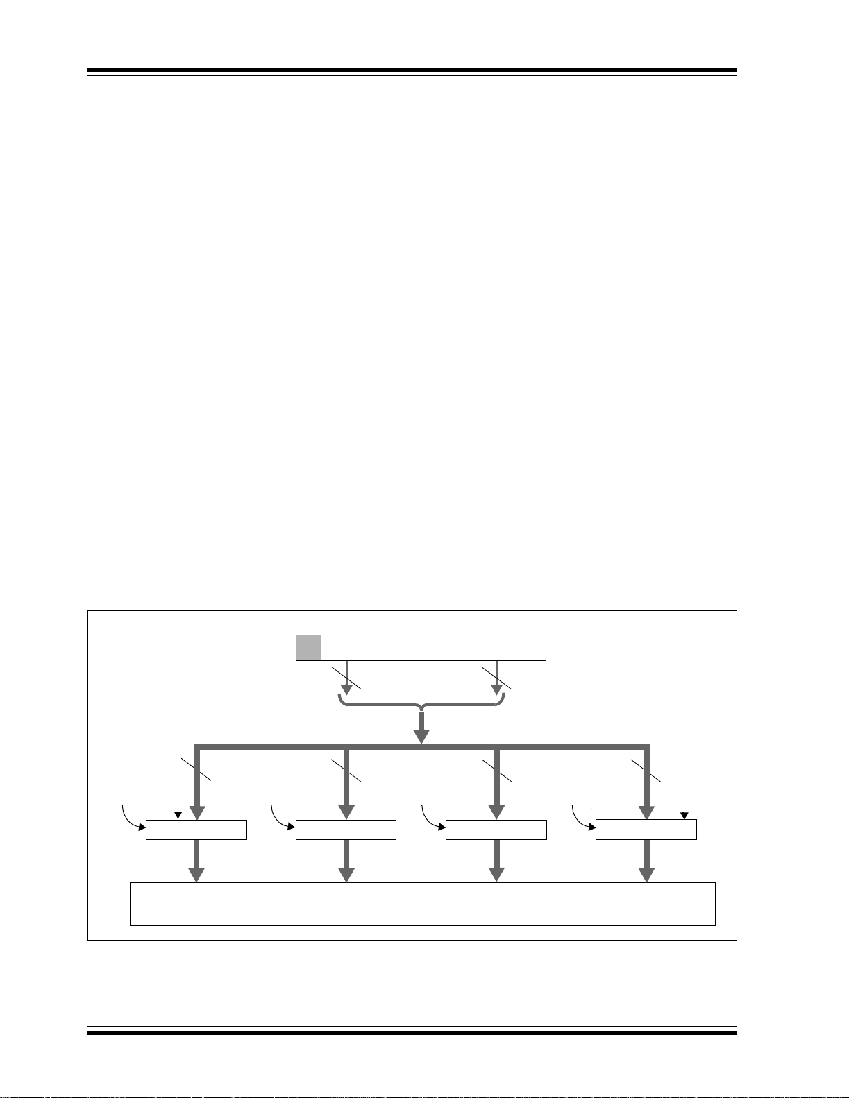
PIC16F87/88
3.7 Writing to Flash Program Memory
Flash program memory may only be written to if the
destination addr ess is in a se gment of memo ry th at is
not write-protected, as defined in bits WRT1:WRT0 of
the device Configuration Word (Register 15-1). Flash
program memo ry must b e writt en in fo ur-word blocks.
A block consists of four words with sequential
addresses, with a lower boundary defined by an
address, wh ere E EAD R<1: 0> = 00. At the same time,
all block wri tes to pr ogra m memo ry ar e do ne as w rite only operations. The program memory must first be
erased. The write oper ation is edge-align ed and cannot
occur across boundaries.
To write to the program memory, the data must first be
loaded into the buffer registers. There are four 14-bit
buffer registers and they are addressed by the low
2 bits of EEADR.
The following sequence of events illustrate how to
perform a write to progra m memory:
• Set the EEPGD and WREN bits in the EECON1
register
• Clear the FREE bit in EECON1
• Write address to EEADRH:EEADR
• Write data to EEDATH:EEDATA
• Write 55 to EECON2
• Write AA to EECON2
• Set WR bit in EECON1
The user must follow the same specific sequence to
initiate the write for each word in the program block
by writing each program word in sequence (00, 01,
10, 11).
There are 4 buffer register words and all four locations
MUST be written to with correct data.
After the “BSF EECON1, WR” instruction, if
EEADR
≠ xxxxxx11, then a short write will occur.
This short write only transfers the data to the buffer
register. The WR bit will be cleared in hardware after
1cycle.
After the “BSF EECON1, WR” instruction, if
EEADR = xxxxxx11, then a long write will occur. This
will simultaneously transfer the data from
EEDA TH:EEDATA to the buffer registers and be gin the
write of all four words. The processor will execute the
next instruction and then ignore the subsequent
instruction. The user sh ould place NOP instruct ions into
the second words. Th e pro cess or wil l th en h alt internal
operations for typicall y 2msec in which the write takes
place. This is not Sleep mode, as the clocks and
peripherals will continue to run. After the write cycle,
the processor will resume operation with the 3rd
instruction after the EECON1 write instruction.
After each long write, the 4 bu ffe r registers wi ll be reset
to 3FFF.
FIGURE 3-1: BLOCK WRITES TO FLASH PROGRAM MEMORY
First word of block
to be written
EEADR<1:0>
= 00
Buffer Register
14
75
6 8
14 14 14
EEADR<1:0>
= 01
Buffer Register
Program Memory
07
EEDATAEEDATH
EEADR<1:0>
= 10
Buffer Register
0
All buffers are
transferred
to Flash
automatically
after this word
is written
EEADR<1:0>
= 11
Buffer Register
DS30487C-page 32 2005 Microchip Technology Inc.

PIC16F87/88
An example of the complete four-word write sequence
is shown in Example 3-5. The initial address is loaded
into the EEADRH:EEADR register pair; the four words
of data are load ed us ing in direct add ressing, assum ing
that a row erase sequence has already been
performed.
EXAMPLE 3-5: WRITING TO FLASH PROGRAM MEMORY
; This write routine assumes the following:
; 1. The 32 words in the erase block have already been erased.
; 2. A valid starting address (the least significant bits = '00') is loaded into EEADRH:EEADR
; 3. This example is starting at 0x100, this is an application dependent setting.
; 4. The 8 bytes (4 words) of data are loaded, starting at an address in RAM called ARRAY.
; 5. This is an example only, location of data to program is application dependent.
; 6. word_block is located in data memory.
BANKSEL EECON1 ;prepare for WRITE procedure
BSF EECON1, EEPGD ;point to program memory
BSF EECON1, WREN ;allow write cycles
BCF EECON1, FREE ;perform write only
BANKSEL word_block
MOVLW .4
MOVWF word_block ;prepare for 4 words to be written
LOOP
BANKSEL EEADRH ;Start writing at 0x100
MOVLW 0x01
MOVWF EEADRH ;load HIGH address
MOVLW 0x00
MOVWF EEADR ;load LOW address
BANKSEL ARRAY
MOVLW ARRAY ;initialize FSR to start of data
MOVWF FSR
BANKSEL EEDATA
MOVF INDF, W ;indirectly load EEDATA
MOVWF EEDATA
INCF FSR, F ;increment data pointer
MOVF INDF, W ;indirectly load EEDATH
MOVWF EEDATH
INCF FSR, F ;increment data pointer
BANKSEL EECON1
MOVLW 0x55 ;required sequence
MOVWF EECON2
MOVLW 0xAA
MOVWF EECON2
BSF EECON1, WR ;set WR bit to begin write
Required
Sequence
NOP ;instructions here are ignored as processor
NOP
BANKSEL EEADR
INCF EEADR, f ;load next word address
BANKSEL word_block
DECFSZ word_block, f ;have 4 words been written?
GOTO loop ;NO, continue with writing
BANKSEL EECON1
BCF EECON1, WREN ;YES, 4 words complete, disable writes
BSF INTCON,GIE ;enable interrupts
2005 Microchip Technology Inc. DS30487C-page 33

PIC16F87/88
3.8 Protection Against Spurious Write
There are conditions when the device should not write
to the data EEPROM memory. To protect against
spurious EEPROM writes, various mechanisms have
been built-in. On power-up, WREN is c leared. Al so, the
Power-up Timer (72 ms duration) prevents an
EEPROM write.
The write initiate se quence and the WREN bit together
help prevent an accidental write during brown-out,
power glitch or software malfunction.
3.9 Operation During Code-Protect
When the data EEPROM is code-protected, the microcontroller can read and writ e to th e EEPROM n ormall y.
However, all external access to the EEPROM is
disabled. External write acce ss to the progra m memory
is also disabled.
When program memory is code-protected, the microcontroller can read and write to program memory
normally, as well as execute instruc tions. Writes by the
device may be selectively inhibited to regions of the
memory depending on the setting of bits WRT1:WRT0
of the Configuration Word (see Section 15.1 “Config-
uration Bits” for additional information). External
access to the memory is also disabled.
TABLE 3-1: REGISTERS/BITS ASSOCIATED WITH DATA EEPROM AND
FLASH PROGRAM MEMORIES
Value on
Address Name Bit 7 Bit 6 Bit 5 Bit 4 Bit 3 Bit 2 Bit 1 Bit 0
10Ch EEDATA EEPROM/Flash Data Register Low Byte xxxx xxxx uuuu uuuu
10Dh EEADR EEPROM/Flash Address Register Low Byte xxxx xxxx uuuu uuuu
10Eh EEDATH
10Fh EEADRH
18Ch EECON1 EEPGD
18Dh EECON2 EEPROM Control Register 2 (not a physical register) ---- ---- ---- ---0Dh PIR2
8Dh PIE2
Legend: x = unknown, u = unchanged, - = unimplemented, read as ‘0’, q = value depends upon condition.
Shaded cells are not used by data EEPROM or Flash program memory.
— — EEPROM/Flash Data Register High Byte --xx xxxx --uu uuuu
— — — — EEPROM/Flash Address Register High Byte ---- xxxx ---- uuuu
— — FREE WRERR WREN WR R D x--x x000 x--x q000
OSFIF CMIF —EEIF— — — — 00-0 ---- 00-0 ----
OSFIE CMIE —EEIE— — — — 00-0 ---- 00-0 ----
Power-on
Reset
Value on
all other
Resets
DS30487C-page 34 2005 Microchip Technology Inc.

4.0 OSCILLATOR CONFIGURATIONS
4.1 Oscillator Types
The PIC16F87/88 can be operated in eight different
oscillator modes. The user can program three configuration bits (FOSC2:FOSC0) to select one of these eight
modes (modes 5-8 are new PIC16 oscillator
configurations):
1. LP Low-Power Crystal
2. XT Crystal/Resonator
PIC16F87/88
2005 Microchip Technology Inc. DS30487C-page 35

PIC16F87/88
FIGURE 4-2: CERAMIC RESONATOR
OPERATION (HS OR XT
OSC CONFIGURATION)
OSC1
(1)
C1
RES
OSC2
(2)
R
S
(1)
C2
Note 1: S ee Table 4-2 for typical values of C1 and
C2.
2: A se ries resistor (R
3: R
(typically between 2 MΩ to 10 MΩ).
F varies with the resonator chosen
(3)
RF
S) may be required.
Sleep
TABLE 4-2: CERAMIC RESONATORS
(FOR DESIGN GUIDANCE
ONLY)
Typical Capacitor Values Used:
Mode Freq OSC1 OSC2
4.3 External Clock Input
The ECIO Oscillator mode requires an external clock
source to be connected to the OSC1 pin. There is no
oscillator start-up time required after a Power-on
Reset, or after an exit from Sleep mode.
In the ECIO Oscillator mode, the OSC2 pin becomes
an additional general purpose I/O pin. The I/O pin
becomes bit 6 of PORTA (RA6). Figure 4-3 shows the
pin connections for the ECIO Oscillator mode.
FIGURE 4-3: EXTERNAL CLOCK INPUT
OPERATION
(ECIO CONFIGURATION)
XT 455 kHz
2.0 MHz
4.0 MHz
HS 8.0 MHz
16.0 MHz
56 pF
47 pF
33 pF
27 pF
22 pF
56 pF
47 pF
33 pF
27 pF
22 pF
Capacitor values are for design guidance only.
These capacitors were tested with the resonators
listed below for basic start-up and operation. These
values were not optimized.
Different cap acitor values may be required to produce
acceptable oscillator operation. The user should test
the performance of the oscillator over the expected
DD and temperature range for the application.
V
See the notes following this table for additional
information.
Note: When using resonators with frequencies
above 3.5 MHz, the use of HS mode,
rather than XT mode, is recommended.
HS mode may be used at any V
DD for
which the controller is rated. If HS is
selected, it is possible that the gain of the
oscillator will overdrive the resonator.
Therefore, a series resistor should be
placed between the OSC2 pin and the
resonator. As a good starting point, the
recommended value of R
S is 330Ω.
DS30487C-page 36 2005 Microchip Technology Inc.
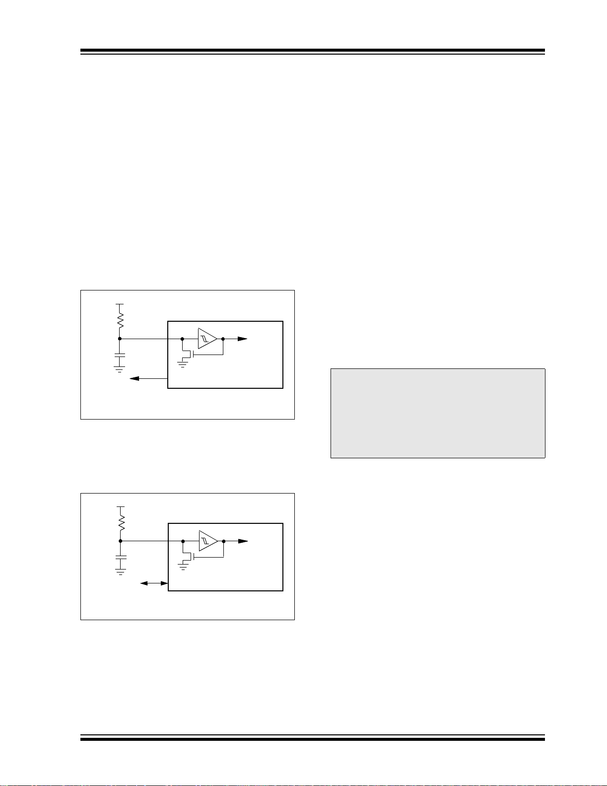
PIC16F87/88
4.4 RC Oscillator
For timing insensitive applications, the “RC” and
“RCIO” device options offer additional cost savings.
The RC oscillator frequency is a function of the supply
voltage, the resistor (R
ues and the operating temperature. In addition to this,
the oscillator frequen cy will vary from unit to unit due to
normal manufacturing variation. Furthermore, the difference in lead frame capacitance between package
types will also affect the oscillation frequency,
especially for low C
take into account variation due to tolerance of external
R and C components used. Figure 4-4 shows how the
R/C combination is connected.
In the RC Oscillator mode, the oscillator frequency
divided by 4 is available on the OSC2 pin. This signal may
be used for test purposes or to synchronize other logic.
FIGURE 4-4: RC OSCILLATOR MODE
VDD
REXT
CEXT
VSS
F
Recommended values: 3 kΩ ≤ REXT ≤ 100 kΩ
The RCIO Oscillator mode (Figure 4-5) functions like
the RC mode, except that the OSC2 pin becomes an
additional general purpose I/O pin. The I/O pin
becomes bit 6 of PORTA (RA6).
EXT) and capacitor (CEXT) val-
EXT values. The user also needs to
Internal
Clock
PIC16F87/88
OSC/4
OSC1
OSC2/CLKO
EXT > 20 pF
C
4.5 Internal Oscillator Block
The PIC16F87/88 devic es in clude an intern al oscil lator
block which generates two different clock signals;
either can be used as the system’s clock source. This
can eliminate the need for external oscillator circuits on
the OSC1 and/or OSC2 pins.
The main output (INTOSC) is an 8 MHz clock source
which can be used to directly drive the system clock. It
also drives the INT OSC posts caler which can provide a
range of six clock frequencies from 125 kHz to 4 MHz.
The other clock source is the internal RC oscillator
(INTRC) which provides a 31.25 kHz (32 µs nominal
period) output. The INTRC oscillator is enabled by
selecting the INTRC as the system clock source or
when any of the following are enabled:
• Power-up Timer
• Watchdog Timer
• Two-Speed Start-up
• Fail-Safe Clock Monito r
These features are discussed in greater detail in
Section 15.0 “Special Features of the CPU”.
The clock source frequency (INTOSC direct, INTRC
direct or INTOSC postscaler) is selected by configuring
the IRCF bits of the OSCCON register (page 40).
Note: Throughout this data sheet, when referring
specifically to a generic clock source, the
term “INTRC” may also be used to refer to
the clock modes usin g the internal oscillato r
block. This is regardless of whether the
actual freq uency us ed is I NTOSC (8 MHz),
the INTOSC postscaler or INTRC
(31.25 kHz).
FIGURE 4-5: RCIO OSCILLATOR MODE
VDD
REXT
OSC1
CEXT
VSS
RA6
Recommended values: 3 kΩ ≤ REXT ≤ 100 kΩ
2005 Microchip Technology Inc. DS30487C-page 37
I/O (OSC2)
C
EXT > 20 pF
Internal
Clock
PIC16F87/88

PIC16F87/88
4.5.1 INTRC MODES
Using the internal oscillator as the clock source can
eliminate the need for up t o two extern al oscilla tor pins,
after whic h it can be us ed for digital I /O. Two distinct
configurations are available:
• In INTIO1 mode, the OSC2 pin outputs F
while OSC1 functions as RA 7 fo r dig it a l in put a nd
output.
• In INTIO2 mode, OSC1 functions as RA7 and
OSC2 functions as RA6, both for digital input and
output.
OSC/4,
4.5.2 OSCTUNE REGISTER
The internal oscillator’s output has been calibrated at the
factory but can be adjusted in the application. This is
done by writing to the OSCTUNE register (Register 4-1).
The tuning sensitivity is constant throughout the tuning
range. The OSCTUNE register has a tuning range of
±12.5%.
When the OSCTUNE register is modified, the INTOSC
and INTRC frequencies will begin shifting to the new frequency. The INTRC clock will reach the new frequency
within 8 clock cycles (approximately 8 * 32 µs = 256 µs);
the INTOSC clock will stabiliz e within 1 ms. Code execution continues during this shift. There is no indication that
the shift has occurred. Operation of features that d epend
on the 31.25 kHz INTRC clock source frequency, such
as the WDT, Fail-Safe Clock Monitor and peripherals,
will also be affected by the change in frequency.
REGISTER 4-1: OSCTUNE: OSCILLATOR TUNING REGISTER (ADDRESS 90h)
U-0 U-0 R/W-0 R/W-0 R/W-0 R/W-0 R/W-0 R/W-0
— — TUN5 TUN4 TUN3 TUN2 TUN1 TUN0
bit 7 bit 0
bit 7-6 Unimplemented: Read as ‘0’
bit 5-0 TUN<5:0>: Frequency Tuning bits
011111 = Maximum frequency
011110 =
•
•
•
000001 =
000000 = Center frequency. Oscillator module is running at the calibrated frequency.
111111 =
•
•
•
100000 = Minimum frequency
Legend:
R = Readable bit W = Writable bit U = Unimplemented bit, read as ‘0’
-n = Value at POR ‘1’ = Bit is set ‘0’ = Bit is cleared x = Bit is unknown
DS30487C-page 38 2005 Microchip Technology Inc.

PIC16F87/88
4.6 Clock Sources and Oscillator Switching
The PIC16F87/88 devic es in clude a fea ture tha t allo ws
the system clock source to be switched from the main
oscillator to an alternate low-frequency clock source.
PIC16F87/88 devices offer three alternate clock
sources. When enabled, these give additional options
for switching to the various power-managed operating
modes.
Essentially, there are three clock sources for these
devices:
• Primary oscillators
• Secondary oscillat ors
• Internal oscillator block (INTRC)
The primary oscillators include the Ex ternal Crystal
and Resonator modes, the External RC modes, the
External Clock mode and the internal oscillator block.
The particular mod e is defined on POR by the content s
of Configuration Word 1. The details of these modes
are covered earlier in this chapter.
The s econdary oscillat ors are those external sources
not connected to the OSC1 or OSC2 pins. These
sources may continue to operate even after the
controller is placed in a power-managed mode.
PIC16F87/88 devices offer the Timer1 oscillator as a
secondary oscillator. This oscillator continues to run
when a SLEEP instruction is executed and is often the
time base for functions such as a real-time clock.
Most often, a 32.768 kHz watch crystal is connected
between the RB6/T1OSO and RB7/T1OSI pins. Like
the LP mode oscillator circuit, loading capacitors are
also connect ed from each pin to ground. The Timer1
oscillator is discussed in greater detail in Section 7.6
“Timer1 Oscillator”.
In addition to being a p rimary clock source, the internal
oscillator block is available as a power-managed
mode clock source. The 31.25 kHz INTRC source is
also used as the clock source for several special
features, such as the WDT, Fail-Safe Clock Monitor,
Power-up Timer and Two-Speed Start-up.
The clock sources for the PIC16F87/88 devices are
shown in Figure 4-6. See Section 7.0 “Timer1 Mod-
ule” for further details of the Timer1 oscillator. See
Section 15.1 “Configuration Bits” for Configuration
register details.
4.6.1 OSCCON REGISTER
The OSCCON register (Register 4-2) controls several
aspects of the system clock’s operation, both in full
power operation and in power-ma nag ed mo des .
The System Clock Select bits, SCS1:SCS0, select the
clock source that is used when the device is operating
in power-managed modes. When the bits are
cleared (SCS<1:0> = 00), the system clock source
comes from the main oscillator that is selected by the
FOSC2:FOSC0 configuration bits in Configuration
Word 1 register. When the bits are set in any other
manner, the system clock source is provided by the
Timer1 oscillator (SCS1:SCS0 = 01) or from the
internal oscillator block (SCS1:SCS0 = 10). After a
Reset, SCS<1:0> are always set to ‘00’.
Note: The instruction to immediately follow the
modification of SCS<1:0> will have an
instruction time (TCY) based on the previous clock source. This should be taken
into consideration when developing time
dependant code.
The Internal Oscill ator Select bit s, IRCF2:IRCF0, select
the frequency output of the interna l oscill ator block th at
is used to dr ive t he sys tem clo ck. Th e choi ces are t he
INTRC source (31.25 kHz), the INTOSC source
(8 MHz) or one of the six frequencies derived from the
INTOSC postscaler (125 kHz to 4 MHz). Cha ngi ng t he
configuration of these bit s has an immediate c hange on
the multiplexor’s frequency output.
The OSTS and IOFS bits indicate the status of the
primary oscillator and INTOSC source; these bits are
set when their respective oscillators are stable. In
particular, OSTS indicates that the Oscillator Start-up
Timer has timed out.
4.6.2 CLOCK SWITCHING
Clock switching will occur for the following reasons:
• The FCMEN (CONFIG2<0>) bit is set, the device
is running from the primary oscillator and the
primary oscillator fails. The clock source will be
the internal RC oscillator.
• The FCMEN bit is set, the device is running from
the T1OSC and T1OSC fails. The clock source
will be the internal RC oscillator.
• Following a wake-up due to a Reset or a POR,
when the device is configured for Two-Speed
Start-up mode, switching will occur between the
INTRC and the system clock defined by the
FOSC<2:0> bits.
• A wake-up from Sleep occurs due to an interrupt or
WDT wake-up and Two-Speed S t art-up is enabled.
If the primary clock is XT, HS or LP, the clock will
switch between the INTRC and the prim ary system
clock after 1024 clocks (OST) and 8 clocks of the
primary oscillator . This is conditional upon the SCS
bits being set equal to ‘00’.
• SCS bits are modified from their original value.
• IRCF bits are modified from their original value.
Note: Because the SCS bits are cleared on any
Reset, no clock switching will occur on a
Reset unless the Two-Speed Start-up is
enabled and the prim ary clock is XT, HS or
LP. The device will wait for the primary
clock to become stable before execution
begins (Two-Speed Start-up disabled).
2005 Microchip Technology Inc. DS30487C-page 39

PIC16F87/88
4.6.3 CLOCK TRANSITION AND WDT
When clock switching is performed, the Watchdog
Timer is disabl ed becau se the W atc hdog rip ple coun ter
is used as the Oscillator Start-up Timer.
Note: The OST is only used when switching to
XT, HS and LP Oscillator modes.
Once the clock transition is complete (i.e., new oscillator selection switch has occurred), the Watchdog
counter is re-enabled with the counter reset. This
allows the user to synchronize the Watchdog Timer to
the start of execution at the new clock frequency.
REGISTER 4-2: OSCCON: OSCILLATOR CONTROL REGISTER (ADDRESS 8Fh)
U-0 R/W-0 R/W-0 R/W-0 R-0 R/W-0 R/W-0 R/W-0
— IRCF2 IRCF1 IRCF0 OSTS
bit 7 bit 0
bit 7 Unimplemented: Read as ‘0’
bit 6-4 IRCF<2:0>: Internal RC Oscillator Frequency Select bits
000 = 31.25 kHz
001 = 125 kHz
010 = 250 kHz
011 = 500 kHz
100 = 1 MHz
101 = 2 MHz
110 = 4 MHz
111 = 8 MHz
bit 3 OSTS: Oscillator Start-up Time-out Status bit
1 = Device is running from the primary system clock
0 = Device is running from T1OSC or INTRC as a secondary system clock
Note 1: Bit resets to ‘ 0’ with Two-Speed Start-up mode and LP, XT or HS selected as the
oscillator mode.
bit 2 IOFS: INTOSC Frequency Stable bit
1 = Frequency is stable
0 = Frequency is not stable
bit 1-0 SCS<1:0>: Os ci ll ator Mode Select bits
00 = Oscillator mode defined by FOSC<2:0>
01 = T1OSC is used for system clock
10 = Internal RC is used for system clock
11 = Reserved
(1)
(1)
IOFS SCS1 SCS0
Legend:
R = Readable bit W = Writable bit U = Unimplemented bit, read as ‘0’
-n = Value at POR ‘1’ = Bit is set ‘0’ = Bit is cleared x = Bit is unknown
DS30487C-page 40 2005 Microchip Technology Inc.
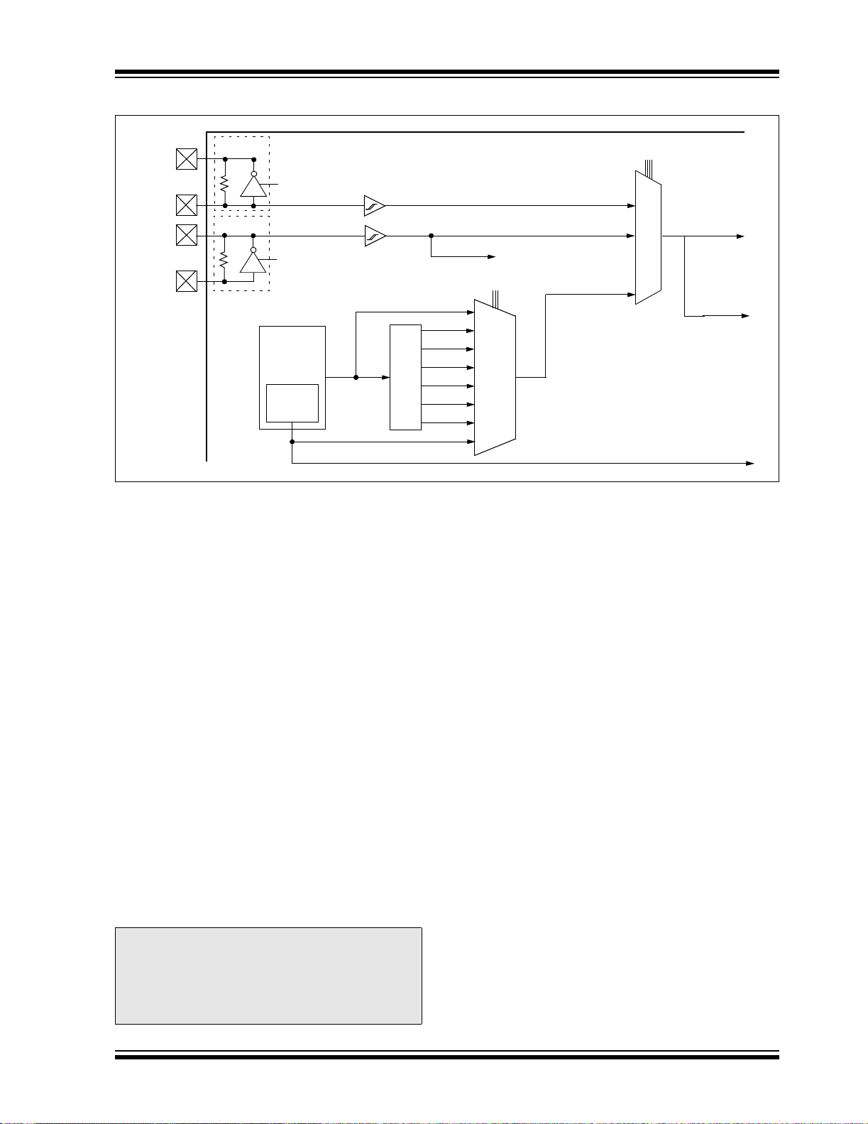
FIGURE 4-6: PIC16F87/88 CLOCK DIAGRAM
PIC16F87/88
OSC2
OSC1
T1OSO
T1OSI
Primary Oscillator
Sleep
Secondary Oscillator
T1OSCEN
Enable
Oscillator
Internal
Oscillator
Block
31.25 kHz
Source
31.25 kHz
(INTRC)
8 MHz
(INTOSC)
Postscaler
4.6.4 MODIFYING THE IRCF BITS
The IRCF bits can be modified at any time regardless of
which clock source is currently being used as the
system clock. The internal oscillator allows users to
change the frequency during run time. This is achieved
by modifying the IRCF bits in the OSCCON register.
The sequence of events th at occur aft er the IRCF bits
are modified is dependent upon the initial value of the
IRCF bits before they are modified. If the INTRC
(31.25 kHz, IRCF<2:0> = 000) is running and the IRCF
bits are modified to any other va lue than ‘000’, a 4 ms
(approx.) clock switch delay is turn ed on. Code execution continues at a higher than expected frequency
while the new frequency stabilizes. Time sensitive code
should wait for the IOFS bit in the OSCCON register to
become set before continuing. This bit can be monitored to ensure that the frequency is stable before using
the system clock in time critical applications.
If the IRCF bit s are modif ied while the int ernal os cillator
is running at any other frequency than INTRC
(31.25 kHz, IRCF<2:0>
4 ms (appro x.) clock switch delay. The new INTOSC
frequency will be stable immediately after the eight falling edges. The IOFS bit will remain set after clock
switching occurs.
Note: Caution must be taken when modifying the
IRCF bits using BCF or BSF instructions. It
is possible to modify the IRCF bits to a
frequency that may be out of the V
ification range; for example, V
and IRCF = 111 (8 MHz).
≠ 000), there is no need for a
DD spec-
DD = 2.0V
8 MHz
4 MHz
2 MHz
1 MHz
500 kHz
250 kHz
125 kHz
31.25 kHz
Configuration Word 1 (FOSC2:FOSC0)
SCS<1:0> (T1OSC)
LP, XT, HS, RC, EC
Peripherals
CPU
WDT, FSCM
To Timer1
OSCCON<6:4>
111
110
101
100
MUX
011
010
001
000
T1OSC
MUX
Internal Oscillator
4.6.5 CLOCK TRANSITION SEQUENCE
Following are three different sequences for switching
the internal RC oscillator frequency.
• Clock before switch: 31.25 kHz (IRCF<2:0> = 000)
1. IRCF bits are modified to an INTOSC/INTOSC
postscaler frequency.
2. The cloc k switching circuitry wai ts for a falling
edge of the cur rent cloc k, at whic h point C LKO
is held low.
3. The cloc k switching circ uitry then waits for eight
falling edges of requested clock, after which it
switches CLKO to this new clock source.
4. The IOFS bit is clear to indica te th at the clock is
unstable and a 4ms (approx.) delay is started.
Time dependent code should wait for IOFS to
become set.
5. Switchover is complete.
• Clock before switch: One of INTOSC/INTOSC
postscaler (IRCF<2:0>
1. IRCF bits are modified to INTRC
(IRCF<2:0> = 000).
2. The cloc k switching circuitry wai ts for a falling
edge of the cur rent cloc k, at whic h point C LKO
is held low.
3. The cloc k switching circ uitry then waits for eight
falling edges of requested clock, after which it
switches CLKO to this new clock source.
4. Oscillator switchover is complete.
≠ 000)
2005 Microchip Technology Inc. DS30487C-page 41

PIC16F87/88
• Clock before switch: One of INTOSC/INTOSC
postscaler (IRCF<2:0>
1. IRCF bits are modified to a different INTOSC/
INTOSC postscaler frequency.
2. The cloc k switching circuitry waits fo r a falling
edge of the cur rent cloc k, at whic h point CL KO
is held low.
3. The clock switching circu itry then waits for eight
falling edges of requested clock, after which it
switches CLKO to this new clock source.
4. The IOFS bit is set.
5. Oscill ator switchover is complete.
≠ 000)
4.6.6 OSCILLATOR DELAY UPON
Table 4-3 shows the different delays invoked for
various clock switching sequences. It also shows the
delays invoked for POR and wake-up.
TABLE 4-3: OSCILLATOR DELAY EXAMPLES
Clock Switch
From To
INTRC
T1OSC
Sleep/POR
INTRC/Sleep EC, RC DC – 20 MHz
INTRC
(31.25 kHz)
Sleep LP, XT , HS 32.768 kHz-20 MHz
INTRC
(31.25 kHz)
Note 1: The 5-10 µs start-up delay is based on a 1 MHz system clock.
INTOSC/
INTOSC
Postscaler
EC, RC DC – 20 MHz
INTOSC/
INTOSC
Postscaler
Frequency Oscillator Delay Comments
31.25 kHz
32.768 kHz
125 kHz-8 MHz
125 kHz-8 MHz 4 ms (approx.)
CPU Start-up
4 ms (approx.) and
CPU Start-up
1024 Clock Cycles
(OST)
(1)
(1)
POWER-UP, WAKE-UP AND
CLOCK SWITCHING
Following a wake-up from Sleep mode or
POR, CPU start-up is invoked to allow the
CPU to become ready for code execution.
Following a change from INTRC, an OST
of 1024 cycles must occur.
Refer to Section 4.6.4 “Modifying the
IRCF Bits” for further details.
DS30487C-page 42 2005 Microchip Technology Inc.

PIC16F87/88
4.7 Power-Managed Modes
If the system clock does not come from the INTRC
(31.25 kHz) when the SCS bits are changed and the
4.7.1 RC_RUN MODE
When SCS bits are configured to run from the INTRC,
a clock transition is generated if the system clock is
not already using the INTRC. The event will clear the
OSTS bit, switch the system clock from the primary
system clock (if SCS<1:0> = 00) determined by the
value contained in the configuration bits, or from the
T1OSC (if SCS<1:0> = 01) to the INTRC clock option
and shut down the primary system clock to conserve
power. Clock switching will not occur if the primary
system clock is already configured as INTRC.
IRCF bits in the OSCCO N regi st er are c on figured for a
frequency other tha n INTRC, the frequency may not b e
stable immediately. The IOFS bit (OSCCON<2>) will
be set when the INTOSC or postscaler frequency is
stable, after 4ms (approx.).
After a clock switch has been executed, the OSTS bit
is cleared, indicating a low-power mode and the
device does not run from the primary system clock.
The internal Q clocks are held in the Q1 state until
eight falling edge clocks are counted on the INTRC
oscillator. After the eight clock periods have
transpired, the clock input to the Q clocks is released
and operation resumes (see Figure 4-7).
FIGURE 4-7: TIMING DIAGRAM FOR XT, HS, LP, EC AND EXTRC TO RC_RUN MODE
Q3Q2 Q4 Q1 Q2
Q3 Q4
INTOSC
OSC1
System
Clock
Q1
TOSC
Q4Q3Q2
Q1
(2)
TINP
(1)
(3)
TSCS
Q1
Q1
SCS<1:0>
Program
Counter
Note 1: T
2: T
3: T
4: T
TDLY
INP =32µs typical.
OSC = 50 ns minimum.
SCS =8 TINP.
DLY =1 TINP.
(4)
PC + 1PC
PC + 2
PC + 3
2005 Microchip Technology Inc. DS30487C-page 43

PIC16F87/88
4.7.2 SEC_RUN MODE
The core and peripherals can be configured to be
clocked by T1OSC using a 32.768 kHz crystal. The
crystal must be connected to the T1OSO and T1OSI
pins. This is the same configuration as the low-power
timer circuit (see Section 7.6 “Timer1 Oscillator”).
When SCS bits are configured to run from T1OSC, a
clock transition is generated. It will clear the OSTS bit,
switch the system cl ock fro m eith er the pri mary sys tem
clock or INTRC, depending on the value of SCS<1:0>
and FOSC<2:0>, to the external low-power Timer1
oscillator input (T1OSC) and shut down the primary
system clock to conserve power.
After a clock switch has been executed, the internal Q
Note 1: The T1OSCEN bit must be enab led and it
is the user’s responsibility to ensure
T1OSC is stable bef ore clock s witching to
the T1OSC inpu t clock can occur.
2: When T1OSCEN = 0, the following possible
effects result.
Original
SCS<1:0>
SCS<1:0>
00 01 00 – no change
00 11 10 – INTRC
10 11 10 – no change
10 01 00 – Oscillator
clocks are held in the Q1 state until eight falling edge
clocks are counted on the T1OSC. After the eight
clock periods have tr anspi red , the cloc k inp ut to the Q
clocks is released and operation resumes (see
Figure 4-8). In addition, T1RUN (In T1CON) is set to
A clock switching event will occur if the
final state of the SCS bits is different from
the original.
indicate that T1OSC is being used as the system
clock.
FIGURE 4-8: TIMING DIAGRAM FOR SWITCHING TO SEC_RUN MODE
Q3Q2 Q4 Q1 Q2
T1OSI
OSC1
System
Clock
Q1
TOSC
Q4Q3Q2
Q1
(2)
TT1P
(1)
(3)
TSCS
Q1
Modified
Final
SCS<1:0>
defined by
FOSC<2:0>
Q3 Q4
Q1
SCS<1:0>
Program
Counter
Note 1: TT1P = 30.52 µs.
2: T
OSC = 50 ns minimum.
SCS = 8 TT1P
3: T
DLY = 1 TT1P.
4: T
TDLY
(4)
PC +1PC
PC + 2
PC + 3
DS30487C-page 44 2005 Microchip Technology Inc.

PIC16F87/88
4.7.3 SEC_RUN/RC_RUN TO PRIMARY CLOCK SOURCE
When switching from a SEC_RUN or RC_RUN mode
back to the primary system clock, following a change
of SCS<1:0> to ‘00’, the sequen ce of ev ent s th at ta kes
place will depend upon the value of the FOSC bits in
the Configuration register. If the primary clock source
is configured as a cry stal (H S, XT or LP), the n the tra nsition will take place after 1024 clock cycles. This is
necessary because the crystal oscillator has been
powered down until the time of the transition. In order
to provide the system with a reliable clock when the
changeover has occurred, the clock will not be
released to the changeover circuit until the 1024 count
has expired.
During the oscillator start-up time, the system clock
comes from the current system clock. Instruction
execution and/or peripheral operation continues using
the currently selected oscillator as the CPU clock
source, until the necessary clock count has expired, to
ensure that the primary system clock is stable.
To know when the OST has expired, the OSTS bit
should be monitored. OSTS = 1 indicates that the
Oscillator Start-up Timer has time d out and the syst e m
clock comes from the prim ary clock sou rce.
Following the oscillator start-up time, the internal Q
clocks are held in the Q1 state until eight falling edge
clocks are counted from the primary sys tem cloc k. The
clock input to the Q clocks is then released and operation resumes with the primar y system clock de termined
by the FOSC bits (see Figure 4-10).
When in SEC_RUN mode, the act of clearing the
T1OSCEN bit in the T1CON register will cause
SCS<0> to be cleared, which causes the SCS<1:0>
bits to revert to ‘00’ or ‘10’ depending on wh at SCS<1>
is. Although the T1OSCEN bit w as cleared, T1OSC wil l
be enabled and in stru ct ion execution will continue unti l
the OST time-out for the main system clock is complete. At that time, the sy stem clock wi ll switch fro m the
T1OSC to the primary clock or the INTRC. Following
this, the T1 oscillator will be shut down.
4.7.3.1 Returning to Primary Clock Source
Sequence
Changing back to the primary oscillator from
SEC_RUN or RC_RUN can be accomplished by either
changing SCS<1:0> to ‘00’, or clearing the T1OSCEN
bit in the T1CON regi ster (if T1 OSC was t he secon dary
clock).
The sequence of events that follows is the same for
both modes:
1. If the primary system clock is configured as EC,
RC or INTRC, then the O ST time-ou t is skippe d.
Skip to step 3.
2. If th e prim ary sys tem clo ck is confi gured as an
external oscillator (HS, XT, LP), then the OST
will be active, waiting for 1024 clocks of the
primary system cl ock .
3. On the following Q1, the device holds the
system clock in Q1.
4. The device stays in Q1 while eight falling edges
of the primary system clock are counted.
5. Once the eight counts transpire, the device
begins to run from the primary oscillator.
6. If the secondary clock was INTRC and the
primary is not INTRC, the INTRC will be shut
down to save current providing that the INTRC
is not being used for any othe r functi on, such a s
WDT or Fail-Safe Cloc k monitoring.
7. If the secondary clock was T1OSC, the T1OSC
will continue to run if T1OSCEN is still set;
otherwise, the T1 oscillator will be shut down.
Note: If th e pr im ar y sys t em clo c k is ei the r RC or
EC, an internal delay timer (5-10 µs) will
suspend operation after ex iting Second ary
Clock mode to allow the CPU to become
ready for code execution.
2005 Microchip Technology Inc. DS30487C-page 45
PIC16F87/88
FIGURE 4-9: TIMING FOR TRANSITION BETWEEN SEC_RUN/RC_RUN AND PRIMARY CLOCK
Secondary
Oscillator
OSC1
OSC2
Primary Clock
System Clock
Q4 Q1
TOST
Q2
Q3
Q4
TOSC
(1)
TT1P
Q1
(3)
or TINP
(2)
TSCS
Q2
Q3 Q4
(4)
Q1
Q2
Q3
Q4
SCS<1:0>
OSTS
Program
Counter
PC PC + 1
Note 1: TT1P = 30.52 µs.
INP = 32 µs typical.
2: T
3: T
OSC = 50 ns minimum.
SCS = 8 TINP OR 8TT1P.
4: T
DLY = 1TINP OR 1TT1P.
5: T
TDLY
(5)
PC + 2
PC + 3
DS30487C-page 46 2005 Microchip Technology Inc.

PIC16F87/88
4.7.3.2 Returning to Primary Oscillator with
a Reset
A Reset will clear SCS<1:0> back to ‘00’. The
sequence for starting the primary oscillator following a
Reset is the same for all forms of Reset, including
POR. There is no transition sequence from the
alternate s ystem clock to th e prim ary sys tem cl ock on
a Reset condition. Instead, the device will reset the
state of the OSCCON register and default to the
primary system clock. The sequence of events that
takes place after this will depend upon the value of the
FOSC bits in the Conf igurat ion r egist er. If the exte rnal
oscillator is configured as a crystal (HS, XT or LP), the
CPU will be hel d in th e Q1 st at e until 1024 clock cyc les
have transpired on the primary clock. This is
necessary because the crystal oscillator has been
powered down until the time of the transition.
During the oscillator start-up time, instruction
execution and/or peripheral operation is suspended.
Note: If Two-Speed Clock Start-up mode is
enabled, the INTRC will act as the system
clock until the OST timer has timed out.
If the primary system clock is either RC, EC or INTRC,
the CPU will begin operating on the first Q1 cycle
following the wake-up event. This means that there is
no oscillator start-up time required because the
primary clock is already stable; however, there is a
delay between the wake-up event and the following
Q2. An internal delay timer of 5-10 µs will suspend
operation after the Reset to allow the CPU to become
ready for code execution. The CPU and peripheral
clock will be held in the first Q1.
The sequence of events is as follows:
1. A device Reset is asserted from one of many
sources (WDT, BOR, MCLR
, etc.).
2. The device resets and the CPU start-up timer is
enabled if in Sleep mode. The device is held in
Reset until the CPU start-up time-out is
complete.
3. If th e prim ary sys tem clo ck is confi gured as an
external oscillator (HS, XT, LP), then the OST
will be active waiting for 1024 clocks of the
primary system clo ck. While w aiting for the OST,
the device will be held in Reset. The OST and
CPU start-up timers run in parallel.
4. After both the CPU start-up and OST timers
have timed out, the de vice will wait fo r o ne add itional clock cycle and instruction execution will
begin.
FIGURE 4-10: PRIMARY SYSTEM CLOCK AFTER RESET (HS, XT, LP)
(1)
Q4 Q1
T1OSI
OSC1
OSC2
CPU Start-up
System Clock
Peripheral
Clock
Reset
Sleep
OSTS
Program
Counter
Note 1: TT1P = 30.52 µs.
2: T
3: T
PC 0000h
OSC = 50 ns minimum.
CPU = 5-10 µs (1 MHz system clock).
TOST
TCPU
TT1P
Q1 Q2 Q3 Q4
(3)
TOSC
Q1 Q2
(2)
Q3 Q4 Q1 Q2
0001h
Q3
0003h
Q4
Q1 Q2 Q3 Q4
0004h 0005h
2005 Microchip Technology Inc. DS30487C-page 47
PIC16F87/88
FIGURE 4-11: PRIMARY SYSTEM CLOCK AFTER RESET (EC, RC, INTRC)
(1)
T
T1P
Q3
Q4
Q1 Q2 Q3 Q4
T1OSI
OSC1
Q4 Q1
Q1 Q2 Q3 Q4
Q1 Q2
Q3 Q4 Q1 Q2
OSC2
CPU Start-up
System Clock
MCLR
OSTS
Program
Counter
PC 0000h
Note 1: TT1P = 30.52 µs.
2: T
CPU = 5-10 µs (1 MHz system clock).
TCPU
(2)
0001h
0002h
0003h 0004h
DS30487C-page 48 2005 Microchip Technology Inc.

PIC16F87/88
TABLE 4-4: CLOCK SWITCHING MODES
Current
System
Clock
LP, XT, HS,
T1OSC,
EC, RC
LP, XT, HS,
INTRC,
EC, RC
INTRC
T1OSC00FOSC<2:0> = EC
INTRC
T1OSC00FOSC<2:0> = LP,
LP, XT, HS 00
Note 1: If the new clock source is the INTOSC or INTOSC postscaler, then the IOFS bit will be set 4 ms (approx.)
SCS Bits <1:0>
Modified to:
10
(INTRC)
FOSC<2:0> = LP,
XT or HS
01
(T1OSC)
FOSC<2:0> = LP,
XT or HS
or
FOSC<2:0> = RC
XT, HS
(Due to Reset)
LP, XT, HS
after the clock change.
Delay
8 Clocks of
INTRC
8 Clocks of
T1OSC
8 Clocks of
EC
or
RC
1024 Clocks
(OST)
+
8 Clocks of
LP, XT, HS
1024 Clocks
(OST)
OSTS
IOFS
T1RUN
Bit
Bit
01
0 N/A 1 T1OSC T1OSCEN bit must be
1 N/A 0 EC
1 N/A 0 LP, XT, HS During the 1024 clocks,
1 N/A 0 LP, XT, HS When a Reset occurs, th ere i s
(1)
Bit
0 INTRC
New
System
Clock
or
INTOSC
or
INTOSC
Postscaler
or
RC
Comments
The internal RC oscillator
frequency is dependant upon
the IRCF bits.
enabled.
program execution is clocked
from the secondary oscillator
until the primary oscillator
becomes stable.
no clock transition sequence.
Instruction execution and/or
peripheral operation is
suspended unless Two-Speed
Star t-u p mode is enable d, after
which the INTRC will act as the
system clock until the OST
timer has expired.
2005 Microchip Technology Inc. DS30487C-page 49

PIC16F87/88
4.7.4 EXITING SLEEP WITH AN INTERRUPT
Any interrupt, such as WDT or INT0, will cause the p art
to leave the Sleep mode.
The SCS bits are unaf fected by a SLEEP comma nd and
are the same before and after entering and leaving
Sleep. The clock source used after an exit from Sleep
is determined by the SCS bits.
4.7.4.1 Sequence of Events
If SCS<1:0> = 00:
1. The device is held in Sleep until the CPU start-up
time-out is complete.
2. If the primary system clock is configured as an
external oscillator (HS, XT, LP), then the OST will
be active waiting for 1024 clocks of the primary
system clock. While waiting for the OST, the
device will be held in Sleep unless Two-Speed
Start-up is enabled. The OST and CPU start-up
timers run in parallel. Refer to Section 15.12.3
“Two-Speed Clock Start-up Mode” for details
on Two-Speed Start-up.
3. After both the CPU start-up and OST timers
have timed out, the device will exit Sleep and
begin instruction execution with the primary
clock defined by the FOSC bits.
If SCS<1:0> = 01 or 10:
1. The device is held in Sleep until the CPU start-up
time-out is complete.
2. After the CPU start-up timer has timed out, the
device will exit Sleep and begin instruction
execution with the selected oscillator mode.
Note: If a user changes SCS<1:0> just before
entering Sleep mode, the system clock
used when exiting Sleep mode could be
different than the system clock used when
entering Sleep mode.
As an example, if SCS<1:0> = 01 and
T1OSC is the system clock and the
following instructions are executed:
BCF OSCCON, SCS0
SLEEP
then a clock change event is executed. If
the primary oscillator is XT, LP or HS, the
core will continue to run off T1OSC and
execute the SLEEP command .
When Sleep is exited, the part will resume
operation with the primary oscillator after
the OST has expired.
DS30487C-page 50 2005 Microchip Technology Inc.

PIC16F87/88
5.0 I/O PORTS
Some pins for th ese I/O ports are multiplexed with an
alternate function for the peripheral features on the
device. In general, when a peripheral is enabled, that
pin may not be used as a general purpose I/O pin.
Additional information on I/O ports may be found in the
“PICmicro
(DS33023).
5.1 PORTA and the TRISA Register
PORTA is an 8-bit wide, bidirectional port. The corresponding data direction register is TRISA. Setting a
TRISA bit (= 1) will make the corresponding PORTA
pin an input (i.e., put the corresponding output driver in
a high-impedance mode). Clearing a TRISA bit (= 0)
will make the correspond ing PORTA pin an output (i.e.,
put the contents of the output latch on the selected pin).
Reading the PORTA register, reads the status of the
pins, whereas writing to it, wil l write to the port lat ch. All
write operations are read-modify-write operations.
Therefore, a write to a port implies that the port pins are
read, this value is modified and then written to the port
data latch.
®
Mid-Range MCU Family Reference Manual”
Note: On a Power-on Reset, the pins
PORTA<4:0> are configured as analog
inputs and read as ‘0’.
Pin RA4 is multiplexed with the Timer0 module clock
input. On PIC16F88 devices, it is also multiplexed with
an analog input to become the RA4/AN4/T0CKI/
C2OUT pin. The RA4/AN4/T0CKI/C2OUT pin is a
Schmitt Trigger input and full CMOS output driver.
Pin RA5 is multiplexed with the Master Clear module
input. The RA5/MCLR
/VPP pin is a Schmitt Trigger
input.
Pin RA6 is multiplexed with the oscil lator module input
and external oscillator ou tput. Pin RA7 is multiplexed
with the oscillator mod ule input and externa l oscillator
input. Pin RA6/OSC2/CLK O and pin RA7/OSC1/CLKI
are Schmitt Trigger inputs and full CMOS output drivers.
Pins RA<1:0> are multiplexed with analog inputs. Pins
RA<3:2> are multiplexed with analog inputs and comparator outputs. On PIC16F88 devices, pins RA<3:2>
are also multiplexed with the V
REF inputs. Pins RA<3:0>
have TTL inputs and full CMOS output drivers.
EXAMPLE 5-1: INITIALIZING PORTA
BANKSEL PORTA ; select bank of PORTA
CLRF PORTA ; Initialize PORTA by
; clearing output
; data latches
BANKSEL ANSEL ; Select Bank of ANSEL
MOVLW 0x00 ; Configure all pins
MOVWF ANSEL ; as digital inputs
MOVLW 0xFF ; Value used to
; initialize data
; direction
MOVWF TRISA ; Set RA<7:0> as inputs
TABLE 5-1: PORTA FUNCTIONS
Name Bit# Buffer Function
RA0/AN0 bit 0 TTL Input/output or analog input.
RA1/AN1 bit 1 TTL Input/output or analog input.
RA2/AN2/CVREF/VREF-
RA3/AN3/V
RA4/AN4
REF+
(2)
/T0CKI/C2OUT bit 4 ST Input/output, analog input, TMR0 external input or
RA5/MCLR/VPP bit 5 ST Input, Master Clear (Reset) or programming voltage input.
RA6/OSC2/CLKO bit 6 ST Input/output, connects to crystal or resonator, oscillator
RA7/OSC1/CLKI bit 7 ST/CMOS
Legend: TTL = TTL input, ST = Schmitt Trigger input
Note 1: This buffer is a Schmitt Trigger input when config ure d i n RC O sc ill ato r m ode a nd a CMOS input otherwise.
2: PIC16F88 onl y.
(2)
bit 2 TTL Input/output, analog input, VREF- or comparator VREF
output.
(2)
/C1OUT bit 3 TTL Input/output, analog input, VREF+ or comparator output.
comparator output.
output or 1/4 the frequency of OSC1 and denotes the
instruction cycle in RC mode.
(1)
Input/output, connects to crystal or resonator or oscillator
input.
2005 Microchip Technology Inc. DS30487C-page 51

PIC16F87/88
TABLE 5-2: SUMMARY OF REGISTERS ASSOCIATED WITH PORTA
(1)
uuuu 0000
(2)
uuu0 0000
Value on
Address Name Bit 7 Bit 6 Bit 5 Bit 4 Bit 3 Bit 2 Bit 1 Bit 0
05h PORTA RA7 RA6 RA5 RA4 RA3 RA2 RA1 RA0 xxxx 0000
85h TRISA TRISA7 TRISA6 TRISA5
9Fh ADCON1 ADFM A DCS2 VCFG1 VCFG0
9Bh ANSEL
Legend: x = unknown, u = unchanged, - = unimplemented locations read as ‘0’. Shaded cells are not used by PORTA.
Note 1: T his value applies only to the PIC16F87.
2: This value applies only to the PIC16F88.
3: Pin 5 is an input only; the state of the TRISA5 bit has no effect and will always read ‘1’.
4: PIC 16F88 device only.
(4)
— ANS6 ANS5 ANS4 ANS3 ANS2 ANS1 ANS0 -111 1111 -111 1111
(3)
PORTA Data Direction Register 1111 1111 1111 1111
— — — — 0000 ---- 0000 ----
Val ue on
POR, BOR
xxx0 0000
FIGURE 5-1: BLOCK DIAGRAM OF RA0/AN0:RA1/AN1 PINS
Data
Bus
WR
PORTA
Data Latch
WR
TRISA
TRIS Latch
CK
CK
RD TRISA
QD
VDD
Q
QD
Q
Analog
Input Mode
Input Buffer
P
N
V
TTL
VDD
I/O pin
SS
all other
Resets
(1)
(2)
DQ
EN
RD PORT A
To Comparator
To A/D Module Channel Input (PIC16F88 only)
DS30487C-page 52 2005 Microchip Technology Inc.
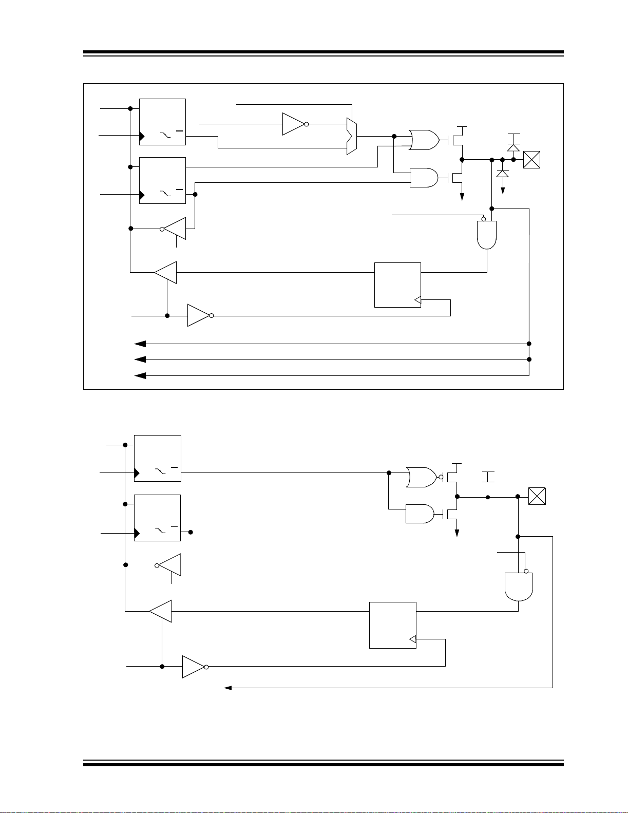
FIGURE 5-2: BLOCK DIAGRAM OF RA3/AN3/VREF+/C1OUT PIN
PIC16F87/88
Data
Bus
WR
PORTA
WR
TRISA
QD
Comparator 1 Output
CK
Q
Data Latch
QD
CK
Q
TRIS Latch
RD TRISA
RD PORTA
To Comparator
To A/D Module Channel Input (PIC16F88 only)
To A/D Module Channel VREF+ Input (PIC16F88 only)
Comparator Mode = 110
Analog
Input Mode
EN
DQ
VDD
P
N
SS
V
TTL
Input Buffer
VDD
RA3 pin
VSS
FIGURE 5-3: BLOCK DIAGRAM OF RA2/AN2/CV
Data
Bus
WR
PORTA
WR
TRISA
Data Latch
TRIS Latch
RD PORTA
CK
CK
RD TRISA
QD
Q
QD
Q
To Comparator
REF/VREF- PIN
DQ
EN
VDD
P
N
V
SS
Analog
Input Mode
Input Buffer
VDD
RA2 pin
TTL
2005 Microchip Technology Inc. DS30487C-page 53

PIC16F87/88
FIGURE 5-4: BLOCK DIAGRAM OF RA4/AN4/T0CKI/C2OUT PIN
Data
Bus
WR
PORTA
WR
TRISA
RD PORTA
QD
CK
Q
Data Latch
TRIS Latch
RD TRISA
TMR0 Clock Input
Comparator Mode = 011, 101, 110
Comparator 2 Output
1
0
Analog
Schmitt Trigger
DQ
EN
VDD
N
SS
V
Input Buffer
RA4 pin
FIGURE 5-5: BLOCK DIAGRAM OF RA5/MCLR
/VPP PIN
DS30487C-page 54 2005 Microchip Technology Inc.

FIGURE 5-6: BLOCK DIAGRAM OF RA6/OSC2/CLKO PIN
Oscillator
Circuit
VDD
P
N
Data
Bus
WR
PORTA
Data Latch
CK
QD
Q
SS
V
PIC16F87/88
RA6/OSC2/CLKO pin
WR
TRISA
RD PORTA
D
CK
TRIS Latch
RD TRISA
Q
Q
DQ
EN
2005 Microchip Technology Inc. DS30487C-page 55

PIC16F87/88
FIGURE 5-7: BLOCK DIAGRAM OF RA7/OSC1/CLKI PIN
Data
Bus
CK
QD
Q
DS30487C-page 56 2005 Microchip Technology Inc.

PIC16F87/88
5.2 PORTB and the TRISB Register
PORTB is an 8-bit wide, bidirectional port. The corresponding data direction register is TRISB. Setting a
TRISB bit (= 1) will make the corresponding PORTB
pin an input (i.e., put the corresponding output driver in
a high-impedance mode). Clearing a TRISB bit (= 0)
will make the c orrespond ing POR TB pi n an out put (i.e.,
put the contents of the outpu t latch on the selected pi n).
Each of the PORTB pi ns has a w eak i nternal pul l-up. A
single cont rol bit can turn on a ll the pull-ups. This is
performed b y clearing bit RBPU
The weak pull-up is automatically turned off when the
port pin is c onfigured as an outp ut. The pull-ups are
disabled on a Power-on Reset.
Four of PORTB’s pi ns, RB7:RB4, have an interrupt-onchange feature. Only pins configured as inputs can
cause this interrupt to occur (i.e., any RB7:RB4 pin
configured as an output is excluded from the interrupton-change comparison). The input pins (of RB7:RB4)
are compared with the old value latched on the last
read of PORTB. The “mismatch” outputs of RB7:RB4
are OR’ed together to generate the RB Port Change
Interrupt with Flag bit RBIF (INTCON<0>).
This interrupt can wake the device from Sleep. The
user, in the Interrupt Service Routine, can clear the
interrupt in the following manne r :
a) Any read or write of PORTB. This will end the
mismatch condition.
b) Clear flag bit RBIF.
(OPTION_REG<7>).
A mismatch c ond it i on wi ll cont i n ue to s et f lag bi t RB IF.
Reading PORTB will end the mismatch condition and
allow flag bit RBIF to be cleared.
The interrupt-on-change feature is recommended for
wake-up on key depression operation and operations
where PORTB is only used for the interrupt-on-change
feature. Polling of PORTB is not recommended while
using the interrupt-on-change feature.
RB0/INT is an external interrupt input pin and is
configured using the INTEDG bit (OPTION_REG<6>).
PORTB is multiplexe d with several pe ripheral functi ons
(see Table 5-3). PORTB pins have Schmitt Trigger
input buffers.
When enabling peripheral functions, care should be
taken in defining TRIS bits for each PORTB pin. Some
peripherals override the TRIS bit to make a pin an
output, while other peripherals override the TRIS bit to
make a pin an input. Since the TRIS bit override is in
effect while the peripheral is enabled, read-modifywrite instructions (BSF, BCF, XORWF) with TRISB as
the destination should be avoided. The user should
refer to the corresponding peripheral section for the
correct TRIS bit settings.
2005 Microchip Technology Inc. DS30487C-page 57

PIC16F87/88
TABLE 5-3: PORTB FUNCTIONS
Name Bit# Buffer Function
RB0/INT/CCP1
(7)
bit 0 TTL/ST
RB1/SDI/SDA bit 1 TTL/ST
RB2/SDO/RX/DT bit 2 TTL/ST
RB3/PGM/CCP1
(3,7)
bit 3 TTL/ST
RB4/SCK/SCL bit 4 TTL/ST
RB5/SS
RB6/AN5
/TX/CK bit 5 TTL Input/output pin or SPI slave select pin (with interrupt-on-change).
(6)
/PGC/
bit 6 TTL/ST
T1OSO/T1CKI
RB7/AN6
(6)
/PGD/
bit 7 TTL/ST
T1OSI
Legend: TTL = TTL input, ST = Schmitt Trigger input
Note 1: This buffer is a Schmitt Trigger input when configured as the e x ternal interrupt.
2: This buffer is a Schmitt Trigger inp ut when used in Serial Programming mode.
3: Low-Voltage ICSP™ Programming (LVP) is enabled by default, which disables the RB3 I/O function. LVP
must be disabled to enable RB3 as an I/O pin and allow maximum compatibility to the other 18-pin
mid-range devices.
4: This buffer is a Schmitt Trigger input when configured for CCP or SSP mode.
5: This buffer is a Sc hmitt Trigger input when con figured for SPI or I
6: PIC16F88 only .
7: The CCP1 pin is determined by the CCPMX bit in Configuration Word 1 register.
(1)
Input/output pin or external interrupt input.
Capture input/Compare output/PWM output pin.
Internal software programmable weak pull-up.
(5)
Input/output pin, SPI™ data input pin or I2C™ data I/O pin.
Internal software programmable weak pull-up.
(4)
Input/output pin, SPI data output pin.
AUSART asynchronous receive or synchronous data.
Internal software programmable weak pull-up.
(2)
Input/output pin, program ming in LVP mode or Capture input/Compare
output/PWM output pin. Internal software programmable weak pull-up.
(5)
Input/output pin or SPI and I2C clock pin (with interrupt-on-change).
Internal software programmable weak pull-up.
AUSART asynchronous transmit or synchronous clock.
Internal software programmable weak pull-up.
(2)
Input/output pin, analog input
(6)
, serial programming clock
(with interrupt-on-c hange), Timer1 oscillator o utput pin or Timer1 clock
input pin. Internal software programmable weak pull-up.
(2)
Input/output pin, analog input
(6)
, serial programming data (with
interrupt-on-change) or Timer1 oscillator input pin.
Internal software programmable weak pull-up.
2
C mode.
TABLE 5-4: SUMMARY OF REGISTERS ASSOCIATED WITH PORTB
(1)
uuuu uuuu
(2)
00uu uuuu
Value on
all other
Resets
(1)
(2)
Address Name Bit 7 Bit 6 Bit 5 Bit 4 Bit 3 Bit 2 Bit 1 Bit 0
06h, 106h PO RTB RB7 RB6 RB5 RB4 RB3 R B2 RB1 RB0 xxxx xxxx
86h, 186h T RISB PORTB Data Direction Register 1111 1111 1111 1111
81h, 181h O PTION_REG RBPU
9Bh ANSEL
Legend: x = unknown, u = unchanged, - = unimplemented, read as ‘0’. Shaded cells are not used by PORTB.
Note 1: This value applies only to the PIC16F87.
2: This value applies only to the PIC16F88.
DS30487C-page 58 2005 Microchip Technology Inc.
(2)
INTEDG T0CS T0SE PSA PS2 PS1 PS0 1111 1111 1111 1111
— ANS6 ANS5 ANS4 ANS3 ANS2 ANS1 ANS0 -111 1111 -111 1111
Val ue on
POR, BOR
00xx xxxx

PIC16F87/88
FIGURE 5-8: BLOCK DIAGRAM OF RB0/INT/CCP1
CCP1M<3:0> = 1000, 1001, 11xx and CCPMX = 1
(2)
RBPU
Data Bus
WR PORTB
WR TRISB
CCP
Data Latch
QD
CK
TRIS Latch
QD
CK
RD TRISB
RD PORTB
0
1
(3)
PIN
CCP1M<3:0> = 000
Q
D
EN
TTL
Input
Buffer
V
DD
P
Weak
Pull-up
I/O pin
(1)
To INT0 or CCP
RD PORT B
Note 1: I/O pins have diode protection to VDD and VSS.
2: To enable weak pull-ups, set the appropriate TRIS bit(s) and clear the RBPU
3: The CCP1 pin is determined by the CCPMX bit in Configuration Word 1 register.
bit.
2005 Microchip Technology Inc. DS30487C-page 59
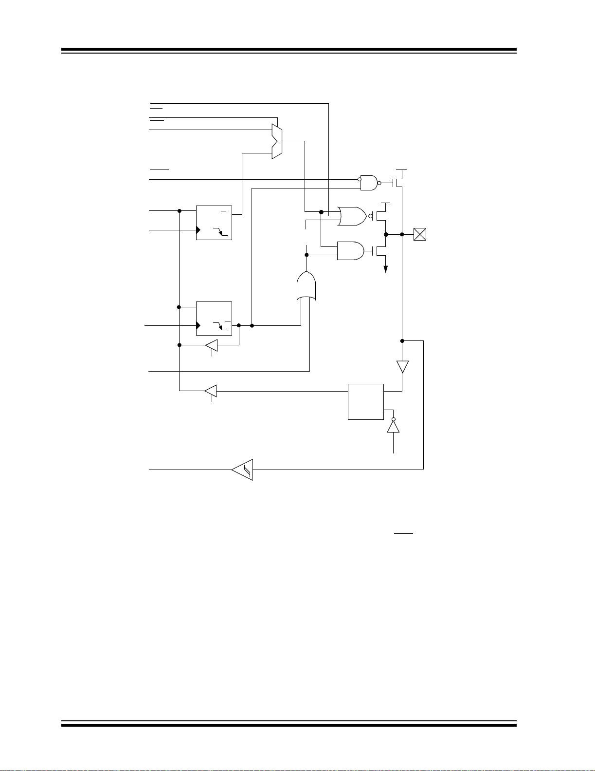
PIC16F87/88
FIGURE 5-9: BLOCK DIAGRAM OF RB1/SDI/SDA PIN
I2C™ ModeSDA D74 Tw[021 T5.52 156.119 690 6326.11.68 l111 T 6316.959 4323.922 l318.56 m59 4323.12.96 -02079 458.72 lcw[(/)61.3203 Tm-0.00(/)61.33TJE52 1516.959 4260.9501TJE52 1511.764 l317.4323.12.96 -0207.12.96 59 4323.6.96 0 0837.679 684.96 0 159.239 6SDA D74159.239 6SDA D2 156.119 690 630.9991.88 l259.456.50191.88 l2559.239 688 0 07154.319 684.8 0 07154.319 684.8 04159.23319 684.8 04159.23319 .8 0 07154.3.394.8 060.519 484.8 0 0715305.639 54830 071530100 07154.3.9 6844159.2310 159.239 6SDA89 54829722 l318.56 m(888 l2559.3 457.76 l257. 159.239 6SDA89 54 457.76 l39 6SDA89 54 45726 159.2S7.76 .56 lf318.119 486.0240433319.516.959 4680.2464 l.4323.12.312.45726 .4 l.54 45726 154159.2310 159.2.0240433319.51S7.762.09 6SD59.2396 .4 l.9 68 0 07155260.399 455.3619 68 l26008 l260259.559 45991.88 l79 569.36 126 59 4323888 lD23888 lD2(9 4323 0 1552699129 6SDA D226 251552694323888 lD2388991.454159.2310 29457.76 07154.7.2310 294558 -28.928558 -28.928558 -56 153(e)]TJ433319.537.2310 2946D2388991.459 456.08 079 511.88 l4 -28.928558 -0.48 ref2 456.08 317.39.92d2 4D226 25 317.39SDA89 5489 54 45726 159.2S6l2515526943319.51S9501TJ7943319.5.88 l.2310 2943319.51S.76 .071551317.39.92d2l257. 159 153.39.92dd2l257. 1™ M)-92dd2l57. 1™ M)079 519.36 1159 153.39.92dd26 59 4.9211™ M
Port/SSPEN Select
SDA Output
(2)
RBPU
Data Bus
WR
WR
Data Latch
D
Q
CK
TRIS Latch
CK
QD
Q
1
0
VDD
P
N
VSS
V
P
DD
Weak
Pull-up
I/O pin
(1)
RD TRISB
SDA Drive
Q
RD PORTB
Schmitt Trigger
(3)
SDA
Note 1: I/O pins have diode protection to V
2: To enable weak pull-ups, set the appropriate TRIS bit(s) and clear the RBPU
3: The SDA Schmitt conforms to the I
Buffer
DD and VSS.
2
C specification.
TTL
Input
Buffer
D
EN
RD PORTB
bit.
DS30487C-page 60 2005 Microchip Technology Inc.

FIGURE 5-10: BLOCK DIAGRAM OF RB2/SDO/RX/DT PIN
SSPEN
PIC16F87/88
SDO
1
0
(2)
RBPU
Data Bus
WR PORTB
WR TRISB
SPEN
DT
Data Latch
D
Q
CK
TRIS Latch
CK
SSPEN + SPEN
1
0
DD
V
Weak
P
Pull-up
VDD
P
(1)
N
VSS
QD
Q
I/O pin
RD TRISB
DT Drive
RD PORTB
Schmitt Trigger
RX/DT
Note 1: I/O pins have diode protection to V
2: To enable weak pull-ups, set the appropriate TRIS bit(s) and clear the RBPU
Buffer
DD and VSS.
bit.
Q
TTL
Input
Buffer
D
EN
RD PORTB
2005 Microchip Technology Inc. DS30487C-page 61
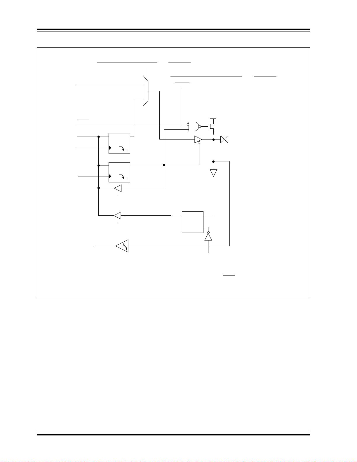
PIC16F87/88
FIGURE 5-11: BLOCK DIAGRAM OF RB3/PGM/CCP1
CCP1M<3:0> = 1000, 1001, 11xx and CCPMX = 0
CCP
RBPU
Data Bus
WR
PORTB
WR
TRISB
0
1
(2)
Data Latch
QD
CK
TRIS Latch
QD
CK
RD TRISB
CCP1M<3:0> = 0100, 0101, 0110, 0111 and CCPMX = 0
or LVP = 1
(3)
PIN
TTL
Input
Buffer
V
P
DD
Weak
Pull-up
I/O pin
(1)
D
Q
RD PORTB
To PGM or CCP
Note 1: I/O pins have diode protection to V
2: To enable weak pull-ups, set the appropriate TRIS bit(s) and clear the RBPU
DD and VSS.
EN
RD PORTB
3: The CCP1 pin is determined by the CCPMX bit in Configuration Word 1 register.
bit.
DS30487C-page 62 2005 Microchip Technology Inc.

FIGURE 5-12: BLOCK DIAGRAM OF RB4/SCK/SCL PIN
Port/SSPEN
SCK/SCL
1
PIC16F87/88
(2)
RBPU
Data Bus
WR
PORTB
WR
TRISB
Set RBIF
From other
RB7:RB4 pins
Data Latch
QD
CK
TRIS Latch
QD
CK
RD TRISB
RD PORTB
0
SCL Drive
VDD
P
N
VSS
TTL
Input
Buffer
Latch
QD
EN
QD
EN
DD
V
Weak
P
Pull-up
I/O pin
Q1
RD PORTB
Q3
(1)
SCK
(3)
SCL
Note 1: I/O pins have diode protection to V
2: To enable weak pull-ups, set the appropriate TRIS bit(s) and clear the RBPU
3: The SCL Schmitt conforms to the I
DD and VSS.
2
C™ specification.
bit.
2005 Microchip Technology Inc. DS30487C-page 63
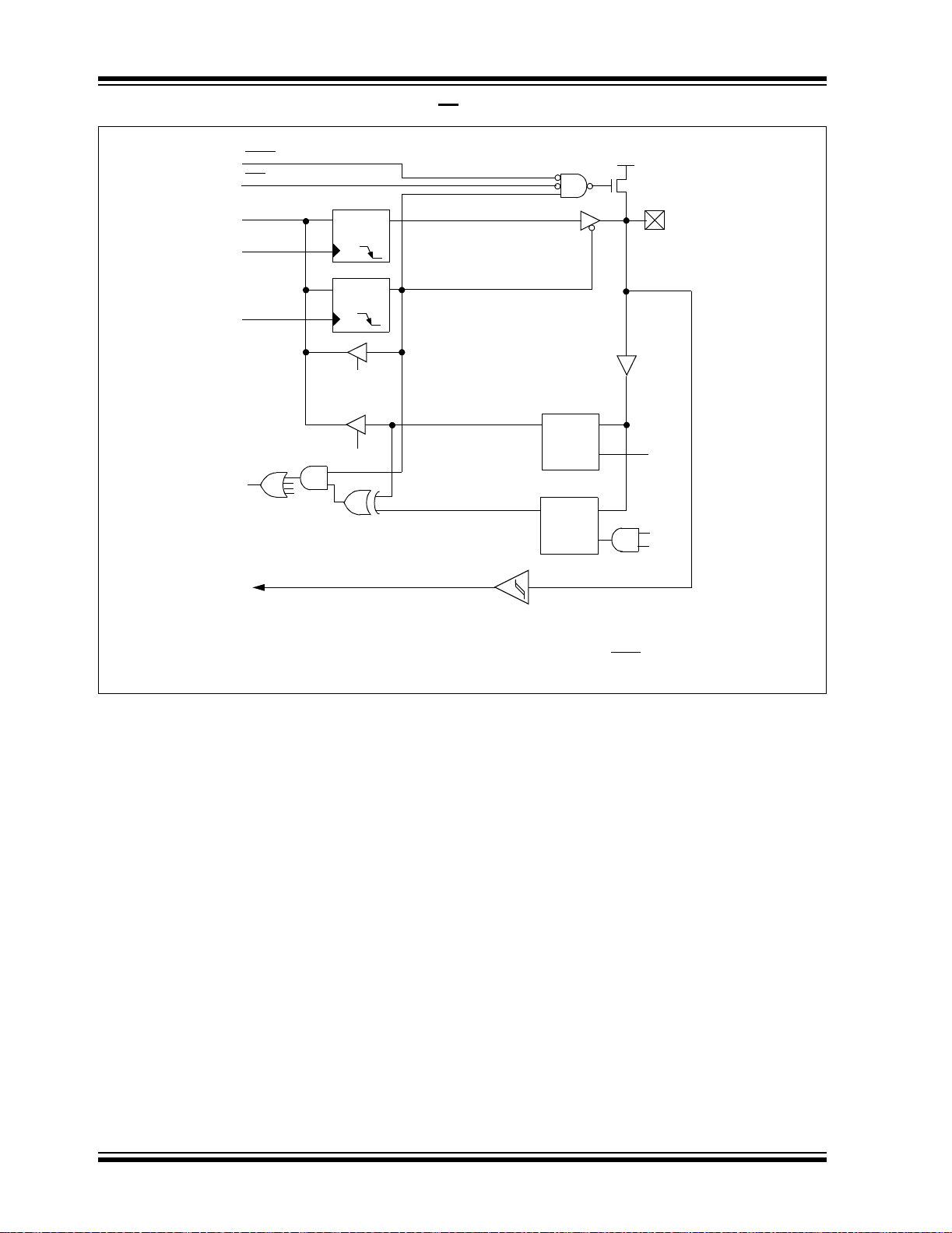
PIC16F87/88
FIGURE 5-13: BLOCK DIAGRAM OF RB5/SS/TX/CK PIN
(2)
RBPU
Port/SSPEN
Data Bus
WR
PORTB
WR
TRISB
Data Latch
QD
CK
TRIS Latch
QD
CK
RD TRISB
TTL
Input
Buffer
Latch
QD
DD
V
P
Weak
Pull-up
I/O pin
(1)
Set RBIF
From other
RB7:RB4 pins
Peripheral Input
Note 1: I/O pins have diode protection to VDD and VSS.
2: To enable weak pull-ups, set the appropriate TRIS bit(s) and clear the RBPU
RD PORTB
QD
EN
EN
Q1
RD PORT B
Q3
bit.
DS30487C-page 64 2005 Microchip Technology Inc.

PIC16F87/88
FIGURE 5-14: BLOCK DIAGRAM OF RB6/AN5
Analog
Input Mode
Data Bus
WR PORTB
WR TRISB
T1OSCEN/ICD/PROG
Mode
RBPU
(2)
Data Latch
QD
CK
TRIS Latch
QD
CK
RD TRISB
(3)
/PGC/T1OSO/T1CKI PIN
Analog
Input Mode
TTL
Input Buffer
Latch
QD
V
P
DD
Weak
Pull-up
I/O pin
(1)
Set RBIF
From other
RB7:RB4 pins
PGC/T1CKI
From T1OSCO Output
To A/D Module Channel Input (PIC16F88 only)
Note 1: I/O pins have diode protection to V
2: To enable weak pull-ups, set the appropriate TRIS bit(s) and clear the RBPU
3: PIC16F88 devices only.
RD PORTB
DD and VSS.
EN
QD
EN
Q1
RD PORTB
Q3
bit.
2005 Microchip Technology Inc. DS30487C-page 65

PIC16F87/88
FIGURE 5-15: BLOCK DIAGRAM OF RB7/AN6
Port/Program Mode/ICD
PGD
Analog Input Mode
(2)
RBPU
Data Bus
WR
PORTB
WR
TRISB
T1OSCEN
PGD DRVEN
Data Latch
QD
CK
TRIS Latch
QD
CK
RD TRISB
1
0
(3)
/PGD/T1OSI PIN
0
1
T1OSCEN
Analog
Input Mode
TTL
Input Buffer
V
P
DD
Weak
Pull-up
I/O pin
(1)
Latch
QD
Set RBIF
From other
RB7:RB4 pins
Note 1: I/O pins have diode protection to V
2: To enable weak pull-ups, set the appropriate TRIS bit(s) and clear the RBPU
3: PIC16F88 devices only.
RD PORTB
PGD
To T1OSCI Input
To A/D Module Channel Input (PIC16F88 only)
DD and VSS.
EN
QD
EN
Q1
RD PORTB
Q3
bit.
DS30487C-page 66 2005 Microchip Technology Inc.

PIC16F87/88
6.0 TIMER0 MODULE
The Timer0 module timer/counter has the following
features:
• 8-bit timer/counter
• Readable and writable
• 8-bit software programmable prescaler
• Internal or external clock select
• Interrupt-on-overflow from FFh to 00h
• Edge select for external clock
Additional information on the Timer0 module is
available in the “PICmicro® Mid-Range MCU Family
Reference Manual” (DS330 23).
Figure 6-1 is a block diagram of th e Ti mer0 module and
the prescaler shared with the WDT.
6.1 Timer0 Operation
Timer0 operation is controlled through the
OPTION_REG register (see Register 2-2). Timer mode
is selected b y clearing bit T0 CS (OPTION_REG<5> ).
In Timer mode , the T ime r0 module wi ll increm ent every
instruction cycle (w ithout pr escal er). If the TMR0 register is written, the i ncrem ent is inhi bited f or the follow ing
two instruction cycles. The user can work around this
by writing an adjusted value to the TMR0 register.
Counter mode is selected by setting bit T0CS
(OPTION_REG<5>). In Counter mod e, Timer0 will increment, either on every risin g or fallin g edge of pin RA4/
T0CKI/C2OUT. The incrementing ed ge is d ete rm in ed by
the Timer0 Source Edge Select bit, T0SE
(OPTION_REG<4>). Clea ring bit T0SE se lects the ris ing
edge. Restrictions on the external clock input are
discussed in d etail in Section 6.3 “Using Timer0 with
an External Clock”.
The prescaler is mutually, exclusively shared between
the Timer0 module and the Watchdog Timer. The
prescaler is not readable or writable. Section 6.4
“Prescaler” details the operation of the prescaler.
6.2 Timer0 Interrupt
The TMR0 interrupt is generated when the TMR0 register overflows from FFh to 00h. This overflow sets bit
TMR0IF (INTCON<2>). The interrupt can be masked
by clearing bit TMR0IE (INTCON<5>). Bit TMR0IF
must be cleared in software by the Timer0 module
Interrupt Service Routine before re-enabling this interrupt. The TMR0 interrupt cann ot awaken th e processor
from Sleep, since the timer is shut off during Sleep.
FIGURE 6-1: BLOCK DIAGRAM OF THE TIMER0/WDT PRESCALER
CLKO (= F
RA4/T0CKI/C2OUT
31.25 kHz
WDT Enable bit
OSC/4)
pin
WDT Timer
Prescaler
T0SE
16-bit
0
1
0
1
M
U
X
T0CS
M
U
X
PSA
1
M
U
0
X
PSA
Prescaler
8-bit Prescaler
8
8-to-1 MUX
01
M U X
Sync
Cycles
2
PS2:PS0
PSA
Data Bus
8
TMR0 reg
Set Flag bit TMR0IF
on Overflow
WDT
Time-out
Note: T0CS, T0SE, PSA and PS2:PS0 bits are (OPTION_REG<5:0>).
2005 Microchip Technology Inc. DS30487C-page 67
PIC16F87/88
6.3 Using Timer0 with an External Clock
When no pr escal er is us ed, t he ex ternal clock inpu t is
the same as the prescaler outp ut. Th e synchronization
of T0CKI, with the internal phase clocks, is accomplished by sampli ng the prescale r output on the Q2 and
Q4 cycles of the internal phase clocks. Therefore, it is
necessary for T0CKI to be high for at least 2 T
a small RC delay of 20 ns) and low for at least 2 T
(and a small RC delay of 20 ns). Refer to the electrical
specification of the desired device.
OSC (and
OSC
6.4 Prescaler
There is only one presca ler a vailable, which i s mutuall y
exclusively sha red between the T imer0 mod ule and the
Watchdog Timer. A prescaler assignment for the
Timer0 module means that the prescaler cannot be
used by the Watchdog Timer and vice versa. This
prescaler is not readable or writable (see Figure6-1).
Note: Although the prescaler can be assigned to
either the WDT or Timer0, but not both, a
new divide counter is implemented in the
WDT circuit to give mul tipl e WDT tim e-o ut
selections. This al low s TMR 0 an d WD T to
each have their own scaler. Refer to
Section 15.12 “Watchdog T imer (WDT)”
for further details.
The PSA and PS2:PS0 bits (OPTION_REG<3:0>)
determine the prescaler assignment and pre scale ratio.
When assigned to the Timer0 module, all instructions
writing to the TMR0 register (e.g., CLRF 1, MOVWF 1,
BSF 1, x....etc.) will clear the prescaler . W hen assigned
to WDT, a CLRWDT instruction wil l clear the pres caler
along with the Watchdog Timer. The prescaler is not
readable or writable.
Note: Writing to TMR0, when the prescaler is
assigned to Timer0, will clear the
prescaler count but will not change the
prescaler assignment.
REGISTER 6-1: OPTION_REG: OPTION CONTROL REGISTER (ADDRESS 81h, 181h)
R/W-1 R/W-1 R/W-1 R/W-1 R/W-1 R/W-1 R/W-1 R/W-1
RBPU
bit 7 bit 0
INTEDG T0CS T0SE PSA PS2 PS1 PS0
bit 7 RBPU: PORTB Pull-up Enable bit
bit 6 INTEDG: Interrupt Edge Select bit
bit 5 T0CS: TMR0 Clock Source Select bit
1 = Transition on T0CKI pin
0 = Internal instruction cycle clock (CLKO)
bit 4 T0SE: TMR0 Source Edge Select bit
1 = Increment on high-to-low transition on T0CKI pin
0 = Increment on low-to-high transition on T0CKI pin
bit 3 PSA: Prescaler Assignment bit
1 = Prescaler is assigned to the WDT
0 = Prescaler is assigned to the Timer0 module
bit 2-0 PS<2:0>: Prescaler Rate Select bits
Bit Value TMR0 Rate WDT Rate
000
001
010
011
100
101
110
111
Legend:
R = Readable bit W = Writable bit U = Unimplemented bit, read as ‘0’
-n = Value at POR ‘1’ = Bit is set ‘0’ = Bit is cleared x = Bit is unknown
1 : 2
1 : 4
1 : 8
1 : 16
1 : 32
1 : 64
1 : 128
1 : 256
1 : 1
1 : 2
1 : 4
1 : 8
1 : 16
1 : 32
1 : 64
1 : 128
Note: To avoid an unintended device Reset, the instruction sequence shown in the
”PICmicro
executed when changing the prescaler assignment from Timer0 to the WDT. This
sequence must be followed even if the WDT is disabled.
DS30487C-page 68 2005 Microchip Technology Inc.
®
Mid-Range MCU Family Reference Manual” (DS33023) must be

PIC16F87/88
EXAMPLE 6-1: CHANGING THE PRESCALER ASSIGNMENT FROM WDT TO TIMER0
CLRWDT ; Clear WDT and prescaler
BANKSEL OPTION_REG ; Select Bank of OPTION_REG
MOVLW b'xxxx0xxx' ; Select TMR0, new prescale
MOVWF OPTION_REG ; value and clock source
TABLE 6-1: REGISTERS ASSOCIATED WITH TIMER0
Address Name Bit 7 Bit 6 Bit 5 Bit 4 Bit 3 Bit 2 Bit 1 Bit 0
01h,101h TMR0 Timer0 Module Register xxxx xxxx uuuu uuuu
0Bh,8Bh,
10Bh,18Bh
81h,181h OPTION_REG
Legend: x = unknown, u = unchanged. Shaded cells are not used by Timer0.
INTCON GIE PEIE TMR0IE
RBPU INTEDG T0CS T0SE PSA PS2 PS1 PS0 1111 1111 1111 1111
INT0IE RBIE TMR0IF INT0IF RBIF 0000 000x 0000 000u
Value on
POR, BOR
Value on
all other
Resets
2005 Microchip Technology Inc. DS30487C-page 69

PIC16F87/88
NOTES:
DS30487C-page 70 2005 Microchip Technology Inc.

PIC16F87/88
7.0 TIMER1 MODULE
The Timer1 mod ule is a 16-bi t timer/c ou nter c ons isting
of two 8-bit registers (TMR1H and TMR1L) which are
readable and writable. The TMR1 register pair
(TMR1H:TMR1L) increments from 0000h to FFFFh
and rolls over to 0000h. Th e TMR1 i nterrupt, if e nabled,
is generated on overflow which is latched in interrupt
flag bit, TMR1IF (PIR1<0>). This interrupt can be
enabled/disabled by setting/clearing TMR1 interrupt
enable bit, TMR1IE (PIE1<0>).
The Timer1 oscillator can be used as a secondary clock
source in low-power modes. When the T1RUN bit is set
along with SCS<1:0> = 01, the Timer1 oscillator is providing the system clock. If the Fail-Safe Clock Monitor is
enabled and the Timer1 oscillator fails while providing
the system clock, polling the T1RUN bit will indicate
whether the clock is being provided by the Timer1
oscillator or another source.
Timer1 can also be used to provide Real-Time Clock
(RTC) functionality to applications with only a minimal
addition of external components and code overhead.
7.1 Timer1 Operation
Timer1 can operate in one of three modes:
•as a Timer
• as a Synchronous Counter
• as an Asynchronous Counter
The operating mode is determined by the clock select
bit, TMR1CS (T1CON<1>).
In Timer mode, Timer1 increments every instruction
cycle. In Counter mode, it increments on every rising
edge of the external clock input.
Timer1 can be enabled/disabled by setting/clearing
control bit, TMR1ON (T1CON<0>).
Timer1 also has an interna l “Reset in put”. This Reset
can be generated by the CCP1 module as the special
event trigger (see Section 9.1 “Capture Mode”).
Register 7-1 shows the Timer1 Control register.
When the Timer1 oscillator is enabled (T1OSCEN is
set), the RB6/PGC/T1OSO/T1CKI and RB7/PGD/
T1OSI pins become inputs. That is, the TRISB<7:6>
value is ignored and these pins read as ‘0’.
Additional information on timer modules is available in
the “PICmicro
Manual” (DS33023).
®
Mid-Range MCU Family Reference
2005 Microchip Technology Inc. DS30487C-page 71

PIC16F87/88
REGISTER 7-1: T1CON: TIMER1 CONTROL REGISTER (ADDRESS 10h)
U-0 R-0 R/W-0 R/W-0 R/W-0 R/W-0 R/W-0 R/W-0
— T1RUN T1CKPS1 T1CKPS0 T1OSCEN T1SYNC TMR1CS TMR1ON
bit 7 bit 0
bit 7 Unimplemented: Read as ‘0’
bit 6 T1RUN: Timer1 System Clock Status bit
1 = System clock is derived from Timer1 oscillator
0 = System clock is derived from another source
bit 5-4 T1CKPS<1:0>: Timer1 Input Clock Prescale Select bits
11 =1:8 Prescale value
10 =1:4 Prescale value
01 =1:2 Prescale value
00 =1:1 Prescale value
bit 3 T1OSCEN: Timer1 Oscillator Enable Control bit
1 = Oscillator is enabled
0 = Oscillator is shut off (the oscillator inverter is turned off to eliminate power drain)
bit 2 T1SYNC
TMR1CS = 1:
1 = Do not synchronize external clock input
0 = Synchronize external clock input
TMR1CS =
This bit is ignored. Timer1 uses the internal clock when TMR1CS = 0.
bit 1 TMR1CS:
: Timer1 External Clock Input Synchronization Control bit
0:
DS30487C-page 72 2005 Microchip Technology Inc.

PIC16F87/88
7.2 Timer1 Operation in Timer Mode
Timer mode is selected by clearing the TMR1CS
(T1CON<1>) bit. In this mode, the input clock to the
timer is F
OSC/4. The synchronize control bit, T1SYNC
(T1CON<2>), has no effect since the internal clock is
always in sync.
7.3 Timer1 Counter Operation
Timer1 may operate in Asynchronous or Synchronous
mode, depending on the setting of the TMR1CS bit.
When Timer1 is being incremented via an external
source, incremen ts occur on a ri sing edge. After T ime r1
is enabled in Coun ter mode, the module mus t first have
a falling edge before the counter begins to increment.
FIGURE 7-1: TIMER1 INCREMENTING EDGE
T1CKI
(Default High)
7.4 Timer1 Operation in Synchronized Counter Mode
Counter mo de is selected by setting bit TMR1C S. In
this mode, the timer increments on every rising edge of
clock input on pin RB7/PGD/T1OSI when bit
T1OSCEN is set, or on pin RB6/PGC/T1OSO/T1CKI
when bit T1OSCEN is cleared.
If T1SYNC
synchronized with internal phase clocks. The synchronization is done after the prescaler stage. The
prescaler stage is an asynchronous ripple counter.
In this configuration, duri ng Sleep mode, Tim er1 will not
increment even if the extern al clock is present sin ce the
synchronization circuit is shut off. The prescaler,
however, will continue to increment.
is cleared, the n the externa l clock input is
T1CKI
(Default Low)
Note: Arrows indicate counter increments.
FIGURE 7-2: TIMER1 BLOCK DIAGRAM
Set Flag bit
TMR1IF on
Overflow
T1OSO/T1CKI
T1OSI
TMR1H
T1OSC
TMR1
TMR1L
T1OSCEN
Enable
Oscillator
(1)
TMR1ON
FOSC/4
Internal
Clock
On/Off
TMR1CS
T1SYNC
1
0
Prescaler
1, 2, 4, 8
T1CKPS1:T1CKPS0
0
1
2
Synchronized
Clock Input
Synchronize
det
Q Clock
Note 1: When the T1OSCEN bit is cleared, the inverter is turned off. This eliminates power drain.
2005 Microchip Technology Inc. DS30487C-page 73

PIC16F87/88
7.5 Timer1 Operation in Asynchronous Counter Mode
If control bit T1SYNC (T1CON<2>) is set, the external
clock input is not synchronized. The timer continues to
increment asynchronous to the internal phase clocks.
The timer will continue to run during Sleep and can
generate an interrupt-on-overflow that will wake-up the
processor. However, special precautions in software
are needed to read/write the timer (see Section 7.5.1
“Reading and Writing Timer1 in Asynchronous
Counter Mode”).
In Asynchronous Counter mode, Timer1 cannot be
used as a time base for capture or comp are operations.
7.5.1 READING AND WRITING TIMER1 IN ASYNCHRONOUS COUNTER MODE
Reading TMR1H or TMR1L while the timer is running
from an external asyn chronous cl ock will e nsure a valid
read (taken care of in hardware). However, the user
should keep in mind that rea ding t he 16-bi t ti mer in two
8-bit values itself, poses certain problems, since the
timer may overflow between the reads.
For writes, it is recommend ed that th e user s imply sto p
the timer and write the desired values. A write contention may occur by writing to the timer registers while the
register is incrementing. This may produce an
unpredictable value in the timer register.
Reading the 16-bit value requires some care. The
example codes provided in Example 7-1 and
Example 7-2 demonstrate how to write to and read
Timer1 while it is running in Asynchronous mode.
EXAMPLE 7-1: WRITING A 16-BIT FREE RUNNING TIMER
; All interrupts are disabled
CLRF TMR1L ; Clear Low byte, Ensures no rollover into TMR1H
MOVLW HI_BYTE ; Value to load into TMR1H
MOVWF TMR1H, F ; Write High byte
MOVLW LO_BYTE ; Value to load into TMR1L
MOVWF TMR1H, F ; Write Low byte
; Re-enable the Interrupt (if required)
CONTINUE ; Continue with your code
EXAMPLE 7-2: READING A 16-BIT FREE RUNNING TIMER
; All interrupts are disabled
MOVF TMR1H, W ; Read high byte
MOVWF TMPH
MOVF TMR1L, W ; Read low byte
MOVWF TMPL
MOVF TMR1H, W ; Read high byte
SUBWF TMPH, W ; Sub 1st read with 2nd read
BTFSC STATUS, Z ; Is result = 0
GOTO CONTINUE ; Good 16-bit read
; TMR1L may have rolled over between the read of the high and low bytes.
; Reading the high and low bytes now will read a good value.
MOVF TMR1H, W ; Read high byte
MOVWF TMPH
MOVF TMR1L, W ; Read low byte
MOVWF TMPL ; Re-enable the Interrupt (if required)
CONTINUE ; Continue with your code
DS30487C-page 74 2005 Microchip Technology Inc.

PIC16F87/88
7.6 Timer1 Oscillator
A crystal oscillator circuit is built between pins T1OSI
(input) and T1OSO (amplifier output). It is enabled by
setting control bit T1OSCEN (T 1CON<3>). The oscill ator is a low-power oscillator, rated up to 32.768 kHz. It
will continue to run during all power-managed modes.
It is primarily intended for a 32 kHz crystal. The circuit
for a typical LP oscillator is shown in Figure 7-3.
Table 7-1 shows the capacitor selection for the Timer1
oscillator.
The user must provide a sof tware t im e del ay to en su re
proper oscillator start-up.
Note: The Timer1 oscillator shares the T1OSI
and T1OSO pins with the PGD and PGC
pins used for programming and
debugging.
When using the Tim er1 oscillator, In-Circuit
Serial Programming™ (ICSP™) may not
function correctly (high voltage or low
voltage), or the In-Circuit Debugger (ICD)
may not communicate with the controller.
As a result of using either ICSP or ICD, the
Timer1 cryst al m ay be dam aged.
If ICSP or ICD opera tions are requi red, the
crystal should be disconnected from the
circuit (disconnect either lead) or installed
after programming. The oscillator loading
capacitors may remain in-circuit during
ICSP or ICD operation.
FIGURE 7-3: EXTERNAL
COMPONENTS FOR THE
TIMER1 LP OSCILLATOR
C1
33 pF
XTAL
32.768 kHz
C2
33 pF
Note: See the Notes with Table 7-1 for additional
information about capacitor selection.
PIC16F87/88
T1OSI
T1OSO
T ABLE 7-1: CAPACITOR SELECTION FOR
THE TIMER1 OSCILLATOR
Osc Ty pe Freq C1 C2
LP 32 kHz 33 pF 33 pF
Note 1: Microchip suggests this value as a starting
point in validating the oscillator c ircuit.
2: Higher capacitance inc reases th e stabilit y
of the oscillator but also increases the
start-up time.
3: Since each resonator/crystal has its own
characteristics, the user should consult
the resonator/crystal manufacturer for
appropriate values of external
components.
4: Capacitor values are for design guidance
only.
7.7 Timer1 Oscillator Layout Considerations
The Timer1 oscillator circuit draws very little power
during operation. Due to the low-power nature of the
oscillator, it may also be sensitive to rapidly changing
signals in close proximity.
The oscillator circuit, shown in Figure 7-3, should be
located as close as possible to the microcontroller.
There should be no ci rcuits p assing withi n the oscillat or
circuit boundaries other than V
If a high-speed circ ui t m us t b e l oc ate d n ear the os c ill ator, a grounded guard ring around the oscillator circuit,
as shown in Figure7-4, may be helpful when used on
a single-sided PCB or in addition to a ground plane.
FIGURE 7-4: OSCILLATOR CIRCUIT
WITH GROUNDED
GUARD RING
SS or VDD.
SS
V
OSC1
OSC2
RB7
RB6
RB5
2005 Microchip Technology Inc. DS30487C-page 75

PIC16F87/88
7.8 Resetting Timer1 Using a CCP Trigger Output
If the CCP1 module is configured in Compare mode to
generate a “special event trigger” signal
(CCP1M3:CCP1M0 = 1011), the signal will reset
Timer1 and start an A/D conversion (if the A/D module
is enabled).
Note: The special event triggers from the CCP1
module will not set interrupt flag bit,
TMR1IF (PIR1<0>).
Timer1 mu st be confi gured for eit her T ime r or Synchronized Counter mode to take advantage of this feature.
If Timer1 is running in Asynchronous Counter mode,
this Reset operation may not work.
In the event that a write to Timer1 coincides with a
special event trigger from CCP1, the write will take
precedence.
In this mode of operation, the CCPR1H:CCPR1L
register pair ef fe cti ve ly becom es th e pe riod register for
Timer1.
7.9 Resetting Timer1 Register Pair (TMR1H, TMR1L)
TMR1H and TMR1L registers are not rese t to 00h on a
POR, or any other Reset, except by the CCP1 special
event triggers.
T1CON register is rese t to 00h on a Powe r-on Rese t or
a Brown-out Reset, which shuts off the timer and
leaves a 1:1 prescale. In all other Resets, the register
is unaffected.
7.10 Timer1 Prescaler
7.11 Using Timer1 as a Real-Time Clock
Adding an external LP os cilla tor to Timer1 (such as the
one described in Section 7.6 “Timer1 Oscillator”)
gives users the option to include RTC functionality to
their applications. This is accomplished with an inexpensive watch crystal to provide an accurate time base
and several lines of application code to calculate the
time. When operating in Sleep mode and using a
battery or supercapacitor as a power source, it can
completely eliminate the need for a separate RTC
device and battery backup.
The application code routine, RTCisr, shown in
Example 7-3, demonstrates a simple method to
increment a counter at one-second intervals using an
Interrupt Service Routine. Incrementing the TMR1
register pair to overflow triggers the interrupt and calls
the routine, which increments the seconds counter by
one; additional counters for minutes and hours are
incremented as the previous counter overflows.
Since the register pair is 16 bits wide, counting up to
overflow the register directly from a 32.768 kHz clock
would take 2 seconds. To force the overflow at the
required one-second intervals, it is necessary to preload it; the simplest meth od is to set the MSb of TM R1H
with a BSF instruction. Note that the TMR1L register is
never preloaded or altered; doing so may introduce
cumulative error over many cycles.
For this method to be accura te, T imer 1 must oper ate in
Asynchronous mode and the Timer1 overflow interrupt
must be enabled (PIE1<0> = 1), as shown in the
routine, RTCinit. The Timer1 oscillator must also be
enabled and running at all times.
The prescaler counter is cleared on writes to the
TMR1H or TMR1L registers.
DS30487C-page 76 2005 Microchip Technology Inc.

PIC16F87/88
EXAMPLE 7-3: IMPLEMENTING A REAL-TIME CLOCK USING A TIMER1 INTERRUPT SERVICE
RTCinit BANKSEL TMR1H
RTCisr BANKSEL TMR1H
MOVLW 0x80 ; Preload TMR1 register pair
MOVWF TMR1H ; for 1 second overflow
CLRF TMR1L
MOVLW b’00001111’ ; Configure for external clock,
MOVWF T1CON ; Asynchronous operation, external oscillator
CLRF secs ; Initialize timekeeping registers
CLRF mins
MOVLW .12
MOVWF hours
BANKSEL PIE1
BSF PIE1, TMR1IE ; Enable Timer1 interrupt
RETURN
BSF TMR1H, 7 ; Preload for 1 sec overflow
BCF PIR1, TMR1IF ; Clear interrupt flag
INCF secs, F ; Increment seconds
MOVF secs, w
SUBLW .60
BTFSS STATUS, Z ; 60 seconds elapsed?
RETURN ; No, done
CLRF seconds ; Clear seconds
INCF mins, f ; Increment minutes
MOVF mins, w
SUBLW .60
BTFSS STATUS, Z ; 60 seconds elapsed?
RETURN ; No, done
CLRF mins ; Clear minutes
INCF hours, f ; Increment hours
MOVF hours, w
SUBLW .24
BTFSS STATUS, Z ; 24 hours elapsed?
RETURN ; No, done
CLRF hours ; Clear hours
RETURN ; Done
TABLE 7-2: REGISTERS ASSOCIATED WITH TIMER1 AS A TIMER/COUNTER
Address Name Bit 7 Bit 6 Bit 5 Bit 4 Bit 3 Bit 2 Bit 1 Bit 0
0Bh, 8Bh,
10Bh, 18Bh
0Ch PIR1
8Ch PIE1
0Eh TMR1L Holding Register for the Least Significant Byte of the 16-bit TMR1 Register xxxx xxxx uuuu uuuu
0Fh TMR1H Holding Register for the Most Significant Byte of the 16-bit TMR1 Register xxxx xxxx uuuu uuuu
10h T1CON
Legend: x = unknown, u = unchanged, - = unimplemented, read as ‘0’. Shaded cells are not used by the Timer1 module.
Note 1: This bit is only implemented on the PIC16F88. The bit will read ‘0’ on the PIC16F87.
2005 Microchip Technology Inc. DS30487C-page 77
INTCON GIE PEIE
— ADIF
— ADIE
— T1RUN T1CKPS1 T 1CKPS0 T1OSCEN T1SYNC TMR1CS TMR1ON -000 0000 -uuu uuuu
TMR0IE INT0IE RBIE TMR0IF INT0IF RBIF 0000 000x 0000 000u
(1)
RCIF TXIF SSPIF CCP1IF TMR2IF TMR1IF -000 0000 -000 0000
(1)
RCIE TXIE SSPIE CCP1IE TMR2IE TMR1IE -000 0000 -000 0000
Value on
POR, BOR
Val ue on
all other
Resets

PIC16F87/88
NOTES:
DS30487C-page 78 2005 Microchip Technology Inc.

PIC16F87/88
8.0 TIMER2 MODULE
Timer2 is an 8-bit timer with a prescaler and a
postscaler . It c an be used as the PWM time base f or the
PWM mode of the CCP 1 module. T he TMR2 register i s
readable and writable and is cleared on any device
Reset.
The input cloc k (F
1:4 or 1:16, selected by control bits
T2CKPS1:T2CKPS0 (T2CON<1:0>).
The Timer2 module has an 8-bit period register, PR2.
Timer2 increments from 00h until it matches PR2 and
then resets to 00h on the next increment cycle. PR2 is
a readable and writable register. The PR2 register is
initialized to FFh upon Reset.
The match output of TMR2 goes through a 4-bit
postscaler (which gives a 1:1 to 1:16 scaling inclusive)
to generate a TMR2 interrupt (latched in flag bit
TMR2IF (PIR1<1>)).
Timer2 ca n be shut off by clearing control bit T MR2O N
(T2CON<2>) to minimize power consumption.
Register 8-1 shows the Timer2 Control register.
Additional information on timer modules is available in
the “PICmicro
Manual” (DS33023).
OSC/4) has a prescale option of 1:1,
®
Mid-Range MCU Family Reference
8.1 Timer2 Prescaler and Postscaler
The prescaler and postscaler counters are cleared
when any of the following occurs:
• A write to the TMR2 register
• A write to the T2CON register
• Any device Reset (Power-o n Re se t, MCLR
, WDT
Reset or Brown-out Reset)
TMR2 is not cleared when T2CON is written.
8.2 Output of TMR2
The output of TMR2 (before the postscaler) is fed to the
Synchronous Serial Port module (SSP) which optionally
uses it to generate a shift clock.
FIGURE 8-1: TIMER2 BLOCK DIAGRAM
Sets Flag
bit TMR2IF
Postscaler
1:1 1:16
TMR2
(1)
Output
Reset
to
4
EQ
TMR2 reg
Comparator
PR2 reg
Prescaler
1:1, 1:4, 1:16
2
OSC/4
F
Note 1: TMR2 register out put c an be so ftwar e selec ted by the
SSP module as a baud clock.
2005 Microchip Technology Inc. DS30487C-page 79

PIC16F87/88
REGISTER 8-1: T2CON: TIMER2 CONTROL REGISTER (ADDRESS 12h)
U-0 R/W-0 R/W-0 R/W-0 R/W-0 R/W-0 R/W-0 R/W-0
— TOUTPS3 TOUTPS2 TOUTPS1 TOUTPS0 TMR2ON T2CKPS1 T2CKPS0
bit 7 bit 0
bit 7 Unimplemented: Read as ‘0’
bit 6-3 TOUTPS<3:0>: Timer2 Output Postscale Select bits
0000 =1:1 Postscale
0001 =1:2 Postscale
0010 =1:3 Postscale
•
•
•
1111 =1:16 Postscale
bit 2 TMR2ON: Timer2 On bit
1 = Timer2 is on
0 = Timer2 is off
bit 1-0 T2CKPS<1:0>: Timer2 Clock Prescale Select bits
00 = Prescaler is 1
01 = Prescaler is 4
1x = Prescaler is 16
Legend:
R = Readable bit W = Writable bit U = Unimplemented bit, read as ‘0’
-n = Value at POR ‘1’ = Bit is set ‘0’ = Bit is cleared x = Bit is unknown
TABLE 8-1: REGISTERS ASSOCIATED WITH TIMER2 AS A TIMER/COUNTER
Address Name Bit 7 Bit 6 Bit 5 Bit 4 B it 3 Bit 2 Bit 1 Bit 0
0Bh, 8Bh,
10Bh, 18Bh
0Ch PIR1
8Ch PIE1
11h TMR2 Timer2 Module Register 0000 0000 0000 0000
12h T2CON
92h PR2 Timer2 Period Register 1111 1111 1111 1111
Legend: x = unknown, u = unchanged, - = unimplemented, read as ‘0’. Shaded cells are not used by the Timer2 module.
Note 1: This bit is only implemented on the PIC16F88. The bit will read ‘0’ on the PIC16F87.
INTCON GIE PEIE
— ADIF
— ADIE
— TOUTPS3 TOUTPS2 TOUTPS1 TOUTPS0 TMR2ON T2CKPS1 T2CKPS0 -000 0000 -000 0000
TMR0IE INT0IE RBIE TMR0IF INT0IF RBIF 0000 000x 0000 000u
(1)
RCIF TXIF SSPIF CCP1IF TMR2IF TMR1IF -000 0000 -000 0000
(1)
RCIE TXIE SSPIE CCP1IE TMR2IE TMR1IE -000 0000 -000 0000
Value on
POR, BOR
Value on
all other
Resets
DS30487C-page 80 2005 Microchip Technology Inc.

PIC16F87/88
9.0 CAPTURE/COMPARE/PWM (CCP) MODULE
The Capture/Compare/PWM (CCP) module contains a
16-bit register that can operate as a:
• 16-bit Capture register
• 16-bit Compare register
• PWM Master/Slave Duty C ycle regis ter.
Table 9-1 shows the timer resources of the CCP
module modes.
Capture/Compare/PWM Register 1 (CCPR1) is comprised of two 8-bit registers: CCPR1L (low byte) and
CCPR1H (high byte). The CCP1CON register controls
the operation of CCP1. The special event trigger is
generated by a comp are match w hich will reset T i mer1
and start an A/D conversion (if the A/D module is
enabled).
The CCP module’s input/output pin (CCP1) can be
configured as RB 0 or RB3 . This sel ection is s et in bit 1 2
(CCPMX) of the Configuration Word.
Additional information on the CCP module is available
in the “PICmicro
Manual” (DS33023) and in Application Note AN594,
“Using the CCP Module(s)” (DS00594).
®
Mid-Range MCU Family Reference
TABLE 9-1: CCP MODE – TIMER
RESOURCE
CCP Mode Timer Resource
Capture
Compare
PWM
Timer1
Timer1
Timer2
REGISTER 9-1: CCP1CON: CAPTURE/COMPARE/PWM CONTROL REGISTER 1 (ADDRESS 17h)
U-0 U-0 R/W-0 R/W-0 R/W-0 R/W-0 R/W-0 R/W-0
— — CCP1X CCP1Y CCP1M3 CCP1M2 CCP1M1 CCP1M0
bit 7 bit 0
bit 7-6 Unimplemented: Read as ‘0’
bit 5-4 CCP1X:CCP1Y: PWM Least Significant bits
Capture mode:
Unused.
Compare mode:
Unused.
PWM mode:
These bits are the two LSbs of the PWM duty cycle. The eight MSbs are found in CCPR1L.
bit 3-0 CCP1M<3:0>: CCP1 Mode Select bits
0000 = Capture/Compare/PWM disabled (resets CCP1 module)
0100 = Capture mode, every falling edge
0101 = Capture mode, every rising edge
0110 = Capture mode, every 4th rising edge
0111 = Capture mode, every 16th rising edge
1000 = Compare mode, set output on match (CCP1IF bit is set)
1001 = Compare mode, clear output on match (CCP1IF bit is set)
1010 = Compare mode, generate software interrupt on match (CCP1IF bit is set, CCP1 pin is
unaffected)
1011 = Compare mode, trigger special ev ent (CCP1IF bit is set, CCP1 pin is unaffect ed); CCP1
resets TMR1 and starts an A/D conversion (if A/D module is enabled)
11xx =PWM mode
Legend:
R = Readable bit W = Writable bit U = Unimplemented bit, read as ‘0’
-n = Value at POR ‘1’ = Bit is set ‘0’ = Bit is cleared x = Bit is unknown
2005 Microchip Technology Inc. DS30487C-page 81

PIC16F87/88
9.1 Capture Mode
In Capture mode, CCPR1H:CCPR1L captures the
16-bit value of the TMR1 regi ster when an event occu rs
on the CCP1 pin. An event is defined as:
• Every falling edge
• Every rising edge
• Every 4th rising edge
• Every 16th rising edge
An event is selected by control bits CCP1M3:CCP1M0
(CCP1CON<3:0>). When a capture is made, the interrupt request flag bit, CCP1IF (PIR1<2>), is set. It must
be cleared in software. If another capture occurs before
the value in register CCPR1 is read, the old captured
value is overwritten by the new captured value.
9.1.1 CCP PIN CONFIGURATION
In Capture mode, the CCP1 pin should be configured
as an input by setting the TRISB<x> bit.
Note 1: If the CCP1 pin is configured as an
output, a write to the port can cause a
capture condition.
2: The TRISB bit (0 o r 3 ) is d epe nde nt upo n
the setting of configuration bit 12
(CCPMX).
9.1.2 TIMER1 MODE SELECTION
Timer1 must be running in Timer mode or Synchronized Counter mode for the CCP module to use the
capture feature. In Asynchronous Counter mode, the
capture operation may not work.
9.1.3 SOFTWARE INTERRUPT
When the Capture mode is changed, a false capture
interrupt may be generated. The user should keep bit
CCP1IE (PIE1<2>) clear to avoid false interrupts and
should clear the flag bit, CCP1IF, following any such
change in operating mode.
9.1.4 CCP PRESCALER
There are four prescaler settings, specified by bits
CCP1M3:CCP1M0. Whenever the CCP module is
turned off, or the CCP module is not in Capture mode,
the prescaler counter is cleared. This means that any
Reset will clear the prescaler counter.
Switching from one capture prescaler to another may
generate an interrupt. Also, the prescaler counter will
not be cleared, therefore, the first cap ture may be from
a non-zero prescaler. Example 9-1 shows the recommended method for switching between capture
prescalers. This example also clears the prescaler
counter and will not generate the “false” interrupt.
FIGURE 9-1: CAPTURE MODE
OPERATION BL OCK
DIAGRAM
Set Flag bit CCP1IF
(PIR1<2>)
CCPR1H CCPR1L
Capture
Enable
TMR1H TMR1L
CCP1 pin
Prescaler
÷ 1, 4, 16
and
Edge Detect
CCP1CON<3:0>
Qs
EXAMPLE 9-1: CHANGING BETWEEN
CAPTURE PRESCALERS
CLRF CCP1CON ;Turn CCP module off
MOVLW NEW_CAPT_PS ;Load the W reg with
;the new prescaler
;move value and CCP ON
MOVWF CCP1CON ;Load CCP1CON with this
;value
DS30487C-page 82 2005 Microchip Technology Inc.

PIC16F87/88
9.2 Compare Mode
In Compare mo de, th e 16- bit CCP R1 re gist er valu e is
constantly compared against the TMR1 register pair
value. When a match occurs, the CCP1 pin is:
• Driven high
•Driven low
• Remains unchanged
The action on the pin is based on the value of control
bits CCP1M3:CCP1M0 (CCP1CON<3:0>). At the
same time, interrupt flag bit, CCP1IF, is set.
FIGURE 9-2: COMPARE MODE
OPERATION BL OCK
DIAGRAM
Special Event Trigger
Set Flag bit CCP1IF
(PIR1<2>)
CCPR1H CCPR1L
QS
Output
CCP1 pin
TRISB<x>
Output Enable
Special Event Trigger will:
• Reset Timer1 but not set interrupt flag bit, TMR1IF
(PIR1<0>)
• Set bit GO/DONE
conversion
Logic
R
CCP1CON<3:0>
Mode Select
(ADCON0<2>) which starts an A/D
Match
Comparator
TMR1H TMR1L
9.2.1 CCP PIN CONFIGURATION
The user must configure the C CP 1 p in a s an outp ut b y
clearing the TRISB<x> bit.
Note 1: Clearing the CCP1CON regi ster will force
the CCP1 compare output latch to the
default low level. This is not the data
latch.
2: The TRISB bit (0 or 3) is depende nt upon
the setting of configuration bit 12
(CCPMX).
9.2.2 TIMER1 MODE SELECTION
Timer1 must be running in Timer mode or Synchronized Counter mode if the CCP module is using the
compare feature. In Asynchronous Counter mode, the
compare operation may not work.
9.2.3 SOFTWARE INTERRUPT MODE
When generate software interru pt is chosen, the CCP1
pin is not affected . Only a CCP interrup t is generated (if
enabled).
9.2.4 SPECIAL EVENT TRIGGER
In this mode, an internal hardware trigger is generated
that may be used to initiate an action.
The special event trigger output of CCP1 resets the
TMR1 register pai r and starts an A/D conversion (if th e
A/D module is enabled). This allows the CCPR1
register to effectively be a 16-bit programmable period
register for Timer1.
Note: The special event trigger from the CCP1
module will not set interrupt flag bit
TMR1IF (PIR1<0>).
TABLE 9-2: REGISTERS ASSOCIATED WITH CAPTURE, COMPARE AND TIMER1
Address Name Bit 7 Bit 6 Bit 5 Bit 4 Bit 3 Bit 2 Bit 1 Bit 0
0Bh,8Bh
10BH,18Bh
0Ch PIR1
8Ch PIE1
86h TRISB PORTB Data Direction Register 1111 1111 1111 1111
0Eh TMR1L Holding Register for the Least Significant Byte of the 16-bit TMR1 Register xxxx xxxx uuuu uuuu
0Fh TMR1H Holding Register for the Most Significant Byte of the 16-bit TMR1 Register xxxx xxxx uuuu uuuu
10h T1CON
15h CCPR1L Capture/Compare/PWM Register 1 (LSB) xxxx xxxx uuuu uuuu
16h CCPR1H Capture/Compare/PWM Register 1 (MSB) xxxx xxxx uuuu uuuu
17h CCP1CON
Legend: x = unknown, u = unchanged, - = unimplemented, read as ‘0’. Shaded cells are not used by Capture and Timer1.
Note 1: This bit is only implemented on the PIC16F88. The bit will read ‘0’ on the PIC16F87.
2005 Microchip Technology Inc. DS30487C-page 83
INTCON GIE PEIE
— ADIF
— ADIE
— T1RUN T1CKPS1 T1CKPS0 T1OSCEN T1SYNC TMR1CS TMR1ON -000 0000 -uuu uuuu
— — CCP1X CCP1Y CCP1M3 CCP1M2 CCP1M1 CCP1M0 --00 0000 --00 0000
TMR0IE INT0IE RBIE TMR0IF INT0IF RBIF 0000 000x 0000 000u
(1)
RCIF TXIF SSPIF CCP1IF TMR2IF TMR1IF -000 0000 -000 0000
(1)
RCIE TXIE SSPIE CCP1IE TMR2IE TMR1IE -000 0000 -000 0000
Value on
POR, BOR
Value on
all other
Resets
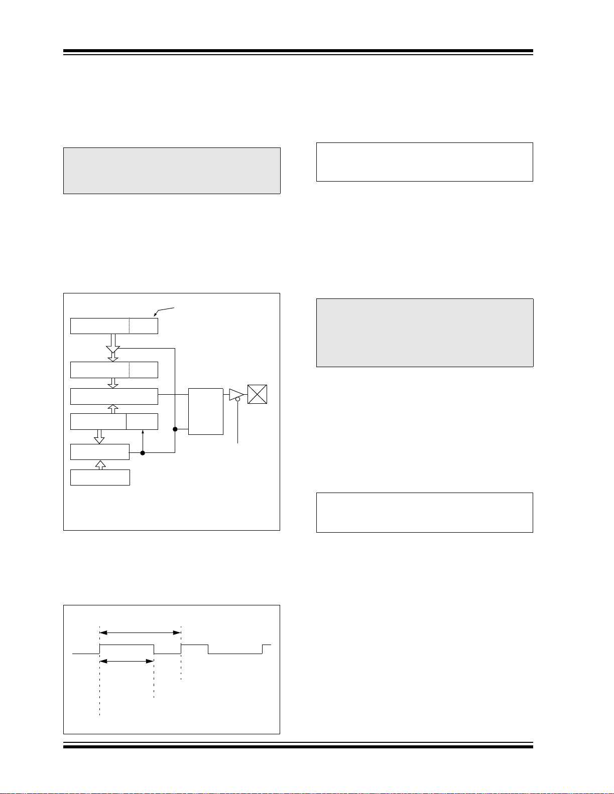
PIC16F87/88
9.3 PWM Mode
In Pulse-Width Modulation (PWM) mode , the CCP1 pin
produces up to a 10-bit resolution PWM output. Since
the CCP1 pin is multip lexed with the POR TB data latch,
the TRISB<x> bit must be cleared to make the CCP1
pin an output.
Note: Clearing the CCP1CON register will force
the CCP1 PWM output latch to th e de fau lt
low level. T his is not t he PORTB I /O data
latch.
Figure 9-3 shows a simplified block diagram of the
CCP module in PWM mode.
For a step-by-step procedure on how to set up the C CP
module for PWM operation, see Section 9.3.3 “Setup
for PWM Operation”.
FIGURE 9-3: SIMPLIFIED PWM BLOCK
DIAGRAM
Duty Cycle Registers
CCPR1L
CCPR1H (Slave)
Comparator
TMR2
Comparator
PR2
Note 1: 8-bit timer is concatenated with 2-bit internal Q
(Note 1)
Clear Timer,
CCP1 pin and
latch D.C.
clock, or 2 bits of the prescaler, to create 10-bit
time base.
CCP1CON<5:4>
Q
R
S
TRISB<x>
CCP1 pin
9.3.1 PW M PE RIO D
The PWM period is specified by writing to the PR2
register. The PWM period can be calculated using the
following formula.
EQUATION 9-1:
PWM Period = [(PR2) + 1] • 4 • TOSC •
(TMR2 Prescale Value)
PWM frequency is defined as 1/[PWM period].
When TMR2 is eq ual to PR2, t he following three event s
occur on the next increment cycle:
•TMR2 is cleared
• The CCP1 pin is set (exception: if PWM duty
cycle = 0%, the CCP1 pin will not be set)
• The PWM duty cycle is latc hed from CC PR1L into
CCPR1H
Note: The Timer2 postscaler (see Section 8.0
“Timer2 Module”) is not used in the deter-
mination of the PWM frequency. The
postscaler could be used to have a servo
update rate at a different frequency than
the PWM output.
9.3.2 PWM DUTY CYCLE
The PWM duty cycle is specified by writing to the
CCPR1L register and to the CCP1CON<5:4> bits. Up
to 10-bit re so l uti on is av ai l ab le. T he CC PR 1L c on tai ns
the eight MSbs and the CCP1CON<5:4> bits contain
the two LSbs. This 10-bit value is represented by
CCPR1L:CCP1CON<5:4>. The following equation is
used to calculate the PWM duty cycle in time.
EQUATION 9-2:
PWM Duty Cycle = (CCPR1L:CCP1CON<5:4>) •
OSC • (TMR2 Prescale Value)
T
A PWM output (Figure 9-4) has a time base (period)
and a time that the output stays high (duty cycle). The
frequency of the PWM is the inverse of the period
(1/period).
CCPR1L and CCP1CON<5:4> can be written to at any
time, but the duty cycle value is not latched into
CCPR1H until after a match between PR2 and TMR2
occurs (i.e., the period is complete). In PWM mode,
CCPR1H is a read-only register.
FIGURE 9-4: PWM OUTPUT
The CCPR1H register and a 2-bit internal latch
are used to double-buffer the PWM duty cycle. This
Period
double-buffering is essential for glitchless PWM
operation.
When the CCPR1H and 2-bit latch match TMR2,
Duty Cycle
concatenated with an internal 2-bit Q clock or 2 bits of
the TMR2 prescaler, the CCP1 pin is cleared.
TMR2 = PR2
TMR2 = Duty Cycle
TMR2 = PR2
DS30487C-page 84 2005 Microchip Technology Inc.

PIC16F87/88
The maximum PWM r esolu tion ( bits ) for a g iven P WM
frequency is given by the following formula.
EQUATION 9-3:
F
OSC
Resolution
log(
=
FPWM
log(2)
)
bits
9.3.3 SETUP FOR PWM OPERATION
The following steps should be taken when configuring
the CCP module for PWM operation:
1. Set the PWM period by writing to the PR2
register.
2. Set the PWM duty cycle by writing to the
CCPR1L register and CCP1CON<5:4> bits.
3. Make the CCP1 pin an output by clearing the
Note: If the PWM duty cycle value is longer than
the PWM period, the CCP1 pin will not be
cleared.
TRISB<x> bit.
4. Set the TMR2 prescale val ue and enable T imer2
by writing to T2CON.
5. Configure the CCP1 modu le for PWM operation.
Note: The TRISB bit (0 or 3) is dependant upon
the setting of configuration bit 12
(CCPMX).
TABLE 9-3: EXAMPLE PWM FREQUENCIES AND RESOLUTIONS AT 20 MHz
PWM Frequency 1.22 kHz 4.88 kHz 19.53 kHz 78.12 kHz 156.3 kHz 208.3 kHz
Timer Prescaler (1, 4, 16) 16 4 1 1 1 1
PR2 Value 0xFF 0xFF 0xFF 0x3F 0x1F 0x17
Maximum Resolution (bits) 10 10 10 8 7 6.6
TABLE 9-4: REGISTERS ASSOCIATED WITH PWM AND TIMER2
Add r e s s Name Bit 7 B it 6 Bit 5 Bit 4 Bit 3 Bit 2 Bit 1 Bit 0
0Bh,8Bh
10Bh,18B h
0Ch PIR1
8Ch PIE1
86h TRISB PORTB Data Direction Register 1111 1111 1111 1111
11h TMR2 Timer2 Module Register 0000 0000 0000 0000
92h PR2 Timer2 Period Register 1111 1111 1111 1111
12h T2CON
15h CCPR1L Capture/Compare/PWM R egister 1 ( LSB) xxxx xxxx uuuu uuuu
16h CCPR1H Capture/Compare/PWM Register 1 (MSB) xxxx xxxx uuuu uuuu
17h CCP1CON
Legend: x = unknown, u = unchanged, - = unimplemented, read as ‘0’. Shaded cells are not used by PWM and Timer2.
Note 1: This bit is only implemented on the PIC16F88. The bit will read ‘0’ on the PIC16F87.
INTCON GIE PEIE
— ADIF
— ADIE
— TOUTPS3 TOUTPS2 TOUTPS1 TOUTPS0 TMR2ON T2CKPS1 T2CKPS0 -000 0000 -000 0000
— — CCP1X CCP1Y CCP1M3 CCP1M2 CCP1M1 CCP1M0 --00 0000 --00 0000
TMR0IE INT0IE RBIE TMR0IF INT0IF RBIF 0000 000x 0000 000u
(1)
RCIF TXIF SSPIF CC P1IF TMR2IF TMR1IF -000 0000 -000 0000
(1)
RCIE TXIE SSPIE CC P1IE TMR2IE TMR1IE -000 0000 -000 0000
Value on
POR, BOR
Value on
all other
Resets
2005 Microchip Technology Inc. DS30487C-page 85

PIC16F87/88
NOTES:
DS30487C-page 86 2005 Microchip Technology Inc.

PIC16F87/88
10.0 SYNCHRONOUS SERIAL PORT (SSP) MODULE
10.1 SSP Module Overview
The Synchronous Serial Port (SSP) module is a serial
interface useful for communicating with other peripheral or microcontroller devices. These peripheral
devices may be serial EEPROMs, shift registers,
display drivers, A/D converters, etc. The SSP module
can operate in one of two modes:
• Serial Peripheral Interface (SPI™)
• Inter-Integrated Circuit (I
2
An overview of I
tion on the SSP module can be found in the “PICmicro
Mid-Range MCU Family Reference Manual”
(DS33023).
Refer to Application Note AN578, “Use of the SSP
Module in the I
(DS00578).
C operations and additional informa-
2
C™)
2
C™ Multi-Master Environment”
10.2 SPI Mode
This section contains register definitions and
operational characteristics of the SPI module.
SPI mode allows 8 bits of data to be synchronously
transmitted and received simultaneously. To
accomplish communication, typically three pins are
used:
• Serial Data Out (SDO) RB2/SDO/RX/DT
• Serial Data In (SDI) RB1/SDI/SDA
• Serial Clock (SCK) RB4/SCK/SCL
Additionally, a fourth pin may be used when in a Slave
mode of operation:
®
• Slave Select (SS
When initializing the SPI, several options need to be
specified. This is done by programming the appropriate
control bits in the SSPCON register (SSPCON<5:0>)
and the SSPSTAT register (SSPSTAT<7:6>). These
control bits allow the following to be specified:
• Master mode (SCK is the clock output)
• Slave mode (SCK is the clock input)
• Clock Polarity (Idle state of SCK)
• Clock Edge (output data on rising/falling
edge of SCK)
• Clock Rate (Master mode only)
• Slave Select mode (Slave mode only)
Note: Before enabling the module in SPI Slave
) RB5/SS/TX/CK
mode, the state of the clock line (SCK)
must match the polarity selected for the
Idle state. The clock line can be observed
by reading the SCK pin. The polarity of the
Idle state is determined by the CKP bit
(SSPCON<4>).
2005 Microchip Technology Inc. DS30487C-page 87

PIC16F87/88
REGISTER 10-1: SSPSTAT : SYNCHRONOUS SERIAL PORT STATUS REGISTER (ADDRESS 94h)
R/W-0 R/W-0 R-0 R-0 R-0 R-0 R-0 R-0
SMP CKE D/A
bit 7 bit 0
bit 7 SMP: SPI Data Input Sample Phase bit
SPI Master mode:
1 = Input data sampled at end of data output time
0 = Input data sampled at middle of data output time (Microwire)
SPI Slave mode:
This bit must be cleared when SPI is used in Slave mode.
I2 C mode:
This bit must be maintained clear.
bit 6 CKE: SPI Clock Edge Select bit
1 = Transmit occurs on transition from active to Idle clock state
0 = Transmit occurs on transition from Idle to active clock state
Note: Polarity of clock state is set by the CKP bit (SSPCON<4>).
bit 5 D/A
bit 4 P: Stop bit
bit 3 S: Start bit
bit 2 R/W
bit 1 UA: Update Address bit (10-bit I
bit 0 BF: Buffer Full Status bit
: Data/Address bit (I2C mode only)
In I2 C Slave mode:
1 = Indicates that the last byte received was data
0 = Indicates that the last byte received was address
(1)
(I2C mode only)
1 = Indicates that a Stop bit has been detected last
0 = Stop bit was not detected last
(1)
(I2C mode only)
1 = Indicates that a Start bit has been detected last (this bit is ‘0’ on Reset)
0 = Start bit was not detected last
: Read/Write Information bit (I2C mode only)
Holds the R/W
match to the next Start bit, Stop bit or ACK
1 =Read
0 = Write
1 = Indicates that the user needs to update the address in the SSPADD register
0 = Address does not need to be updated
Receive (SPI and
1 = Receive complete, SSPBUF is full
0 = Receive not complete, SSPBUF is empty
Transmit (in
1 = Transmit in progress, SSPBUF is full (8 bits)
0 = Transmit complete, SSPBUF is empty
Note 1: This bit is cleared when the SSP module is disabled (i.e., the SSPEN bit is cleared).
bit information following th e last add ress matc h and is on ly valid from addres s
2
C mode only)
I2 C modes):
I2 C mode only):
(1)
P
bit.
(1)
S
R/W UA BF
Legend:
R = Readable bit W = Writable bit U = Unimplemented bit, read as ‘0’
-n = Value at POR ‘1’ = Bit is set ‘0’ = Bit is cleared x = Bit is unknown
DS30487C-page 88 2005 Microchip Technology Inc.

PIC16F87/88
REGISTER 10-2: SSPCON: SYNCHRONOUS SERIAL PORT CONTROL REGISTER (ADDRESS 14h)
R/W-0 R/W-0 R/W-0 R/W-0 R/W-0 R/W-0 R/W-0 R/W-0
WCOL SSPOV SSPEN
bit 7 bit 0
bit 7 WCOL: Write Collision Detect bit
1 = An attempt to write the SSPBUF register failed because the SSP module is busy
(must be cleared in software)
0 = No collision
bit 6 SSPOV: Receive Overflow Indicator bit
In SPI mode:
1 = A new byte is received while th e SSPBUF registe r is still hol ding the pr evious da ta. In cas e
of overflow, the data in SSPSR is lost. Overflow can only occur in Slave mode. The user
must read the SSPBUF, even if only transmitting data, to avoid setting overflow. In Master
mode, the overflow bit is not set since each new reception (and transmission) is initiated
by writing to the SSPBUF register.
0 = No overflow
2
C mode:
In I
1 = A byte is received while the SSPBUF register is still holding the previous byte. SSPOV is
a “don’t care” in Transmit mode. SSPOV must be cleared in software in either mode.
0 = No overflow
bit 5 SSPEN: Synchronous Serial Port Enable bit
In SPI mode:
1 = Enables serial port and configures SCK, SDO and SDI as serial port pins
0 = Disables serial port and configures these pins as I/O port pins
In
I2 C mode:
1 = Enables the serial port and configures the SDA and SCL pins as serial port pins
0 = Disables serial port and configures these pins as I/O port pins
Note 1: In both modes, when enabled, these pins must be properly configured as input or
output.
bit 4 CKP: Clock Polarity Select bit
In SPI mode:
1 = Transmit ha ppens on fal ling edge, rec eive on ris ing edge. Idl e state for c lock is a high le vel.
0 = Transm it h app ens on ris ing edg e, receive on falling edge. Idle st ate for c lo ck is a l ow le ve l.
I2 C Slave mode:
In
SCK release control
1 = Enable clock
0 = Holds clock low (clock stretch). (Used to ensure data setup time.)
bit 3-0 SSPM<3:0>: Synchronous Serial Port Mode Select bits
0000 = SPI Master mode, clock = OSC/4
0001 = SPI Master mode, clock = OSC/16
0010 = SPI Master mode, clock = OSC/64
0011 = SPI Master mode, clock = TMR2 output/2
0100 = SPI Slave mode, clock = SCK pin. SS
0101 = SPI Slave mode, clock = SCK pin. SS
0110 = I
0111 = I
1011 = I
1110 = I
1111 = I
2
C Slave mode, 7-bit address
2
C Slave mode, 10-bit address
2
C Firmware Controlled Master mode (Slave Idle)
2
C Slave mode, 7-bit address with Start and Stop bit interrupts enabled
2
C Slave mode, 10-bit address with Start and Stop bit interrupts enabled
1000, 1001, 1010, 1100, 1101 = Reserved
(1)
CKP SSPM3 SSPM2 SSPM1 SSPM0
(1)
pin control enabled.
pin control disabled. SS can be used as I/O pin.
Legend:
R = Readable bit W = Writable bit U = Unimplemented bit, read as ‘0’
-n = Value at POR ‘1’ = Bit is set ‘0’ = Bit is cleared x = Bit is unknown
2005 Microchip Technology Inc. DS30487C-page 89

PIC16F87/88
FIGURE 10-1: SSP BLOCK DIAGRAM
(SPI™ MODE)
Internal
Data Bus
Read Write
SSPBUF reg
RB1/SDI/SDA
SSPSR reg
2
Shift
Clock
TMR2 Output
2
Prescaler
4, 16, 64
T
RB2/SDO/RX/DT
/
RB5/SS
TX/CK
RB4/SCK/
SCL
bit0
Control
SS
Enable
Edge
Select
SSPM3:SSPM0
Edge
Select
TRISB<4>
Clock Select
4
CY
To enable the serial port, SSP Enable bit, SSPEN
(SSPCON<5>), must be set. To reset or reconfigure
SPI mode, clear bit SSPEN, reinitialize the SSPCON
register and then set bit SSPEN. This configures the
SDI, SDO, SCK and SS
pins as serial p ort pins. Fo r the
pins to behave as the serial port function, they must
have their data direction bits (in the TRISB register)
appropriately programmed. That is:
• SDI must have TRISB<1> set
• SDO must have TRISB<2> cleared
• SCK (Master mode) must have TRISB<4>
cleared
• SCK (Slave mode) must have TRISB<4> set
must have TRISB<5> set
•SS
Note 1: When the SPI is in Slave mode with SS pin
control enabled (SSPCON<3:0>= 0100),
the SPI module will reset if the SS pin is
set to V
DD.
2: If the SPI is used in Slave mode with
CKE = 1, then the SS
pin control must be
enabled.
TABLE 10-1: REGISTERS ASSOCIATED WITH SPI™ OPERATION
Address Name Bit 7 Bit 6 Bit 5 Bit 4 Bit 3 B it 2 Bit 1 Bit 0
0Bh,8Bh
10Bh,18Bh
0Ch PIR1
8Ch PIE1
86h TRISB PORTB Data Direction Register 1111 1111 1111 1111
13h SSPBUF Synchronous Serial Port Receive Buffer/Transmit Register xxxx xxxx uuuu uuuu
14h SSPCON WCOL SSPOV SSPEN CKP SSPM3 SSPM2 SSPM1 SSPM0 0000 0000 0000 0000
94h SSPSTAT SMP CKE
Legend: x = unknown, u = unchanged, - = unimplemented, read as ‘0’. Shaded cells are not used by the SSP in SPI™ mode.
Note 1: This bit is only implemented on the PIC16F88. The bit will read ‘0’ on the PIC16F87.
INTCON GIE PEIE
— ADIF
— ADIE
TMR0IE INT0IE RBIE TMR0IF INT0IF RBIF 0000 000x 0000 000u
(1)
RCIF TXIF SSPIF CCP1IF TMR2IF TMR1IF -000 0000 -000 0000
(1)
RCIE TXIE SSPIE CCP1IE TMR2IE TMR1IE -000 0000 -000 0000
D/A P S R/W UA BF 0000 0000 0000 0000
Val ue on
POR, BOR
Value on
all other
Resets
DS30487C-page 90 2005 Microchip Technology Inc.

FIGURE 10-2: SPI™ MODE TIMING (MASTER MODE)
SCK (CKP = 0,
CKE = 0)
SCK (CKP = 0,
CKE = 1)
SCK (CKP = 1,
CKE = 0)
SCK (CKP = 1,
CKE = 1)
PIC16F87/88
SDO
SDI (SMP = 0)
SDI (SMP = 1)
SSPIF
bit 7
bit 7
bit 7 bit 0
bit 6 bit 5
bit 4
bit 3
bit 2
FIGURE 10-3: SPI™ MODE TIMING (SLAVE MODE WITH CKE = 0)
SS (Optional)
SCK (CKP = 0)
SCK (CKP = 1)
SDO
SDI (SMP = 0)
SSPIF
bit 7
bit 7 bit 0
bit 6 bit 5
bit 4
bit 3
bit 2
bit 1 bit 0
bit 0
bit 1 bit 0
FIGURE 10-4: SPI™ MODE TIMING (SLAVE MODE WITH CKE = 1)
SS
SCK (CKP = 0)
SCK (CKP = 1)
SDO
SDI (SMP = 0)
SSPIF
2005 Microchip Technology Inc. DS30487C-page 91
bit 7
bit 7 bit 0
bit 6 bit 5
bit 4
bit 3
bit 2
bit 1 bit 0
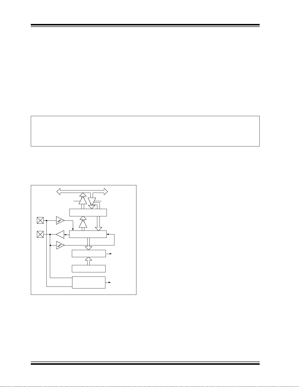
PIC16F87/88
10.3 SSP I2C Mode Operation
The SSP module in I2C mode fully implement s all slave
functions, except general call support and provides
interrupts on S t art and S top bit s in hardware t o facilitate
firmware implement a tion s of the mast er func tio ns . The
SSP module implements the standard mode
specifications, as well as 7-bit and 10-bit addressing.
Two pins are used for data transfe r. The se are the RB4/
SCK/SCL pin, which is the clock (SCL) and the RB1/
SDI/SDA pi n, which i s the data (SDA). T he user must
configure these pins as inputs or outputs through the
TRISB<4, 1> bits.
EXAMPLE 10-1:
MOVF TRISC, W ; Example for an 18-pin part such as the PIC16F818/819
IORLW 0x18 ; Ensures <4:3> bits are ‘11’
ANDLW B’11111001’ ; Sets <2:1> as output, but will not alter other bits
; User can use their own logic here, such as IORLW, XORLW and ANDLW
MOVWF TRISC
T o ensure proper c ommunication of the I
the TRIS bits (TRISx [SDA, SCL]) corresponding to the
I2C pins must be set to ‘1’. If any TRIS bit s (TRISx<7:0>)
of the port containing the I
are changed in software during I
using a Read-Modify-Write instruction (BSF, BCF), then
the I2C mode may stop functioning properly and I2C
communication may suspend. Do not chan ge any of the
TRISx bits (TRIS bits of the port containing the I2C pins)
using the instruction BSF or BCF during I
tion. If it is absolutely necessary to change the TRISx
bits during communication, the follow ing method can be
used:
2
C Slave mode,
2
C pins (PORTx [SDA, SCL])
2
C communication
2
C communica-
The SSP module function s are enabl ed by settin g SSP
Enable bit, SSPEN (SSPCON<5>).
FIGURE 10-5: SSP BLOCK DIAGRAM
Read Write
RB4/SCK/
SCL
Shift
Clock
RB1/
SDI/
SDA
2
(I
C™ MODE)
SSPBUF Reg
SSPSR Reg
MSb
Match Detect
SSPADD Reg
Start and
Stop Bit Detect
Internal
Data Bus
LSb
Addr Match
Set, Reset
S, P Bits
(SSPSTAT Reg)
The SSP module has five registers for I2C operation:
• SSP Control register (SSPCON)
• SSP Status register (SSPSTAT)
• Serial Receive/T ra ns mit Buf f er regi ster (SSPBUF)
• SSP Shift register (SSPSR) – Not directly
accessible
• SSP Address register (SSPADD)
The SSPCON register allows control of the I2C operation. Four mode selection bits (SSPCON<3:0>) allow
one of the following I2C modes to be selected:
2
C Slave mode (7-bit address)
•I
•I2C Slave mode (10-bit address)
2
•I
C Slave mode (7-bit address) with Start and
Stop bit interrupts enabled to support Firmware
Controlled Master mode
•I2C Slave mode (10-bit address) with Start and
Stop bit interrupts enabled to support Firmware
Controlled Master mode
2
C Firmware Controlled Master mode operation
•I
with Start and Stop bit interrupt s ena bl ed; s la ve is
Idle
2
Selection of any I
C mode, with the SSPEN bit set,
forces the SCL and SDA pins to be open-drain, provided these pins are programmed to inputs by setting
the appropr iate TRISB b its. Pull-up resistors must be
provided externally to the SCL a nd SDA pi ns for prop er
operation of the I
Additional information on SSP I
found in the “PICmicro
2
C module.
2
®
C operation may be
Mid-Range MCU Family
Reference Manual” (DS33023).
DS30487C-page 92 2005 Microchip Technology Inc.

PIC16F87/88
10.3.1 SLAVE MODE
In Slave mode, the SCL and SDA pins must be confi gured as inputs (TRISB<4,1 > set). The SSP module will
override the input state with the output data when
required (slave-transmitter).
When an address is match ed, or the dat a trans fer after
an address m atc h is re ceiv ed, the hard ware aut omati cally will generate the Acknowledge (ACK
then load the SSPBUF register with th e re ce ive d valu e
currently in the SSPSR register.
Either or both of the following conditions will cause the
SSP module not to give this ACK
a) The Buffer Full bit, BF (SSPSTAT<0>), was set
before the transfer was received.
b) The Overflow bit, SSPOV (SSPCON<6>), was
set before the transfer was received.
In this case, the SSPSR register value is not loaded
into the SSPBUF, but bit SSPIF (PIR1<3>) is set.
Table 10-2 shows what happens when a data transfer
byte is received, given the status of bits BF and
SSPOV. The shaded cells show the condition where
user software did not properl y clear the over flow condition. Flag bit, BF, is cleared by reading the SSPBUF
register while bit, SSPOV, is cleared through software.
The SCL clock input must have a minimum high and
low for proper operati on . Th e h igh an d l ow ti mes of the
2
C specification, as well as the requirement of the SSP
I
module, are shown in timing parameter #100 and
parameter #101.
pulse:
) pulse and
10.3.1.1 Addressing
Once the SSP module has been enabled, it waits for a
Start condition to occur. Following the Start condition,
the eight bits are shifted into the SSPSR register. All
incoming bits are sampled with the rising edge of the
clock (SCL) line. The value of register SSPSR<7:1> is
compared to the value of the SSPADD register. The
address is compared on the falling edge of the eighth
clock (SCL) pulse. If the addresses match and the BF
and SSPOV bits are clear, the following events occur:
a) The SSPSR register value is loaded into the
SSPBUF register.
b) The Buffer Full bit, BF, is set.
c) An ACK
d) SSP Interrupt Flag bit, SSPIF (PIR1<3>), is set
(interrupt is generated if ena bled) – on the falling
edge of the ninth SCL pulse.
In 10-bit Address mode, two address bytes need to be
received by the slave device. The five Most Significant
bits (MSbs) of the first address byte specify if this is a
10-bit address. Bit R/W
write so the slave device will receive the second
address byte. For a 10-bi t add res s, t he fi rst byt e woul d
equal ‘1111 0 A9 A8 0’, where A9 and A8 are the
two MSbs of the address.
pulse is generated.
(SSPSTAT<2>) must specify a
The sequence of events for 10-bit Address mode is as
follows, with steps 7-9 for slave transmitter:
1. Receive first (high) byte of address (bits SSPIF,
BF and UA (SSPSTAT<1>) are set).
2. Update the SSPADD register with second (low)
byte of address (clears bit UA and releases the
SCL line).
3. Read the SSPBUF register (clears bit BF) and
clear flag bit SSPIF.
4. Receive second (low) byte of address (bits
SSPIF, BF and UA are set).
5. Update the SSPADD register with the firs t (hig h)
byte of address; if match releases SCL line, this
will clear bit UA.
6. Read the SSPBUF register (clears bit BF) and
clear flag bit SSPIF.
7. Receive Repeated Start condition.
8. Receive first (high) byte of address (bits SSPIF
and BF are set).
9. Read the SSPBUF register (clears bit BF) and
clear flag bit SSPIF.
10.3.1.2 Reception
When the R/W bit of the address byte is clear and an
address match occurs, the R/W
register is cleared. Th e receive d addre ss is loa ded in to
the SSPBUF register.
When the address byte overflow condition exists, then
a no Acknowledge (ACK
condition is indic ated if eithe r bit, BF (SSPSTAT<0> ), is
set or bit, SSPOV (SSPCON<6>), is set.
An SSP interrupt is generated for each data transfer
byte. Flag bit, SSPIF (PIR1<3>), must be cleared in
software. The SSPSTAT register is used to determine
the status of the byte.
) pulse is given. An overflow
bit of the SSPSTAT
10.3.1.3 Transmission
When the R/W bit of the incoming address byte is set
and an address match occurs, the R/W
SSPSTAT register is set. The received address is
loaded into the SSPBUF register. The ACK pulse will
be sent on the ninth bit and pin RB4/SCK/SCL is held
low. The transmit data must be loaded into the
SSPBUF register which also load s the SSPSR register.
Then, pin RB4/SCK/SCL should be enabled by setting
bit CKP (SSPCON<4>). The master device must monitor the SCL pin prior to asserting another clock pulse.
The slave device s may be holding of f the maste r device
by stretching the clock. The eight data bits are shifted
out on the falling edge of the SCL input. This ensures
that the SDA signal is valid during the SCL high time
(Figure 10-7).
bit of the
2005 Microchip Technology Inc. DS30487C-page 93

PIC16F87/88
An SSP interrupt is generated for each data transfer
byte. Flag bit, SSPIF, must be cleared in software and
the SSPSTAT register is used to determine the status
of the byte. Flag bit, SSPIF, is set on the falling edge of
the ninth clock pulse.
As a slave transmitter, the ACK
pulse from the master
receiver is latched on the rising edge of the ninth SCL
input pulse. If the SDA line was high (not ACK), then
the data transfe r is com plete. When th e ACK is latched
by the slave device, the slave logic is reset (resets
SSPST AT register) and the slave device then monitors
for another occurrence of the Start bit. If the SDA line
was low (ACK
), the transmit data must be loaded into
the SSPBUF register which also loads the SSPSR
register. Then, pin RB4/SCK/SCL should be enabled
by setting bit CKP.
TABLE 10-2: DATA TRANSFER RECEIVED BYTE ACTIONS
Status Bits as Data
Transfer is Received
SSPSR
→ SSPBUF Generate ACK Pulse
(SSP Interrupt Occurs if Enabled)
BF SSPOV
00 Yes Yes Yes
10 No No Yes
11 No No Yes
0 1 No No Yes
Note 1: Shaded cells show the conditions where the user software did not properly clear the overflow condition.
2
FIGURE 10-6: I
Receiving Address
A7 A6 A5 A4
C™ WAVEFORMS FOR RECEPTION (7-BIT ADDRESS)
R/W = 0
A3 A2 A1SDA
ACK
Receiving Data
D5
D6D7
ACK
D0
D2
D3D4
D1
Receiving Data
D5
D6D7
Set SSPIF Bit
D2
D1
D3D4
ACK
D0
1234
S
SCL
SSPIF (PIR1<3>)
BF (SSPSTAT<0>)
SSPOV (SSPCON<6>)
FIGURE 10-7: I
SDA
SCL
SSPIF (PIR1<3>)
BF (SSPSTAT<0>)
CKP (SSPCON<4>)
A7 A6 A5 A4 A3 A2 A1 ACK
S
123456789 123456789
Data is
sampled
7
6
5
2
C™ WAVEFORMS FOR TRANSMISSION (7-BIT ADDRESS)
8
1234
9
Cleared in software
SSPBUF register is read
Bit SSPOV is set because the SSPBUF register is still full
SCL held low
while CPU
responds to SSPIF
56
7
89
123
D7 D6 D5 D4 D3 D2 D1 D0
Cleared in software
SSPBUF is written in software
4
ACK is not sent
Transmitting DataR/W = 1Receiving Address
5
7
6
From SSP Interrupt
Service Routine
8
9
Bus master
terminates
transfer
ACK
P
P
Set bit after writing to SSPBUF
(the SSPBUF must be written to
before the CKP bit can be set)
DS30487C-page 94 2005 Microchip Technology Inc.

PIC16F87/88
10.3.2 MASTER MODE OPERATION
Master mode operation is supported in firmware using
interrupt generation on the detection of the Start and
Stop conditions. The Stop (P) and Start (S) bits are
cleared from a Reset, or when the SSP module is disabled. The Stop (P) and Start (S) bits will toggle based
on the Start and Stop conditions. Control of the I
may be taken when the P bit is set, or the bus is Idle
and both the S and P bits are clear.
In Master mode operation, the SCL and SDA lines are
manipulated in firmware by clearing the corresponding
TRISB<4,1> bit(s). The output level is always low, irrespective of the value(s) in PORTB<4,1>. So, when
transmitting data, a ‘1’ data bit must have the
TRISB<1> bit set (input) and a ‘0’ data bit must have
the TRISB<1> bit cleared (output). The same scenario
is true for the S CL line wit h the TRIS B<4> bi t. Pull- up
resistors must be provided externally to the SCL and
SDA pins for proper operation of the I
2
C module.
The following events will cause the SSP Interrupt Flag
bit, SSPIF, to be set (SSP Interrupt if enabled):
• Start condition
• Stop condition
• Data transfer byte transmitted/received
Master mode operation can be done with either the
Slave mode Idle (SSPM3:SSPM0 = 1011), or with the
Slave mode active. W he n bo th M as ter mo de operation
and Slave modes are used, the software needs to
differentiate the source(s) of the interrupt.
For more information on Master mode operation, see
Application Note AN554, “Software Implementation of
2
C™ Bus Master”.
I
2
C bus
10.3.3 MULTI-MASTER MODE OPERATION
In Multi-Master mode operation, the interrupt generation on the detection of the Start and Stop conditions
allows the determination of when the bus is free. The
Stop (P) and Start (S) bits are cleared from a Reset, or
when the SSP module is disabled. The Stop (P) and
Start (S) bits will toggle based on the Start and Stop
conditions. Control of the I
bit P (SSPSTAT<4>) is set, or the bus is Idle and both
the S and P b its cl e ar. When th e bu s is b us y, enabling
the SSP interrupt will generate the interrupt when the
Stop condition occurs.
In Multi-Ma ster mode ope rati on, the S DA line mus t be
monitored to see if the signal level is the expected output level. This check only needs to be done when a
high level is output. If a high level is e xpected and a low
level is present, the device needs to release the SDA
and SCL lines (set TRISB<4, 1>). There are two sta ges
where this arbitration can be lost:
• Address Trans fer
• Data Transfer
When the slave logic is enabled, the slave device
continues to receive. If arbitration was lost during the
address transfer stage, communication to the device
may be in progress. If add ressed, a n ACK
generated. If arbitration was lost during the data
transfer stage, the device will need to retransfer the
data at a later time.
For more information on Multi-Master mode operation,
see Application Note AN578, “Use of the SSP Module
in the of I
2
C™ Multi-Master Environment”.
2
C bus may be taken when
pulse will be
TABLE 10-3: REGISTERS ASSOCIATED WITH I2C™ OPERATION
Address Name Bit 7 Bit 6 Bit 5 Bit 4 Bit 3 Bit 2 Bit 1 Bi t 0
0Bh, 8Bh,
10Bh,18Bh
0Ch PIR1
8Ch PIE1
13h SSPBUF Synchronous Serial Port Receive Buffer/Transmit Register xxxx xxxx uuuu uuuu
93h SSPADD Synchronous Serial Port (I
14h SSPCON WCOL SSPOV SSPEN CKP SSPM3 SSPM2 SSPM1 SSPM0 0000 0000 0000 0000
94h SSPSTAT SMP
86h TRISB PORTB Data Direction Register 1111 1111 1111 1111
Legend: x = unknown, u = unchanged, - = unimplemented locations read as ‘0’.
Note 1: This bit is only implemented on the PIC16F88. The bit will read ‘0’ on the PIC16F87.
2005 Microchip Technology Inc. DS30487C-page 95
INTCON GIE PEIE
— ADIF
— ADIE
(2)
CKE
Shaded cells are not used by SSP module in SPI™ mode.
2: Maintain these bits clear in I
TMR0IE INT0IE RBIE TMR0IF INT0IF RBIF 0000 000x 0000 000u
(1)
RCIF TXIF SSPIF CCP1IF TMR2IF TMR1IF -000 0000 -000 0000
(1)
RCIE TXIE SSPIE CCP1IE TMR2IE TMR1IE -000 0000 -000 0000
2
C mode) Address Register 0000 0000 0000 0000
(2)
D/A PSR/WUA BF 0000 0000 0000 0000
2
C™ mode.
Val ue on
POR, BOR
Val ue on
all other
Resets

PIC16F87/88
NOTES:
DS30487C-page 96 2005 Microchip Technology Inc.

PIC16F87/88
1 1.0 ADDRESSABLE UNIVERSAL
SYNCHRONOUS
ASYNCHRONOUS RECEIVER
T RANSMITTER (AUSART)
The Addressable Universal Synchronous Asynchronous
Receiver Transmitter (AUSART) module is one of the
two serial I/O modules. (AUSART is also known as a
Serial Communications Interface or SCI.) The AUSART
can be configured as a full-duplex asynchronous system
that can communicate with peripheral devices, such as
CRT terminals and personal computers, or it can be
configured as a half-duplex synchronous system that
can communicate with peripheral devices, such as A/D
or D/A integrated circuits, serial EEPROMs, etc.
The AUSART can be configured in the following
modes:
• Asynchronous (full-duplex)
• Synchronous – Master (half-duplex)
• Synchronous – Slave (half-duplex)
Bit SPEN (RCSTA<7>) and bits TRISB<5,2> have to
be set in order to configure pins, RB5/SS
RB2/SDO/RX/DT, as the Addressable Universal
Synchronous Asynchronous Receiver Transmitter.
The AUSART module also has a multi-processor
communication capability, using 9-bit address
detection.
/TX/CK and
REGISTER 11-1: TXST A: TRANSMIT ST ATUS AND CONTROL REGISTER (ADDRESS 98h)
R/W-0 R/W-0 R/W-0 R/W-0 U-0 R/W-0 R-1 R/W-0
CSRC TX9 TXEN SYNC — BRGH TRMT TX9D
bit 7 bit 0
bit 7 CSRC: Clock Source Select bit
Asynchronous mode:
Don’t care.
Synchronous mode:
1 = Master mode (clock generated internally from BRG)
0 = Slave mode (clock from external source)
bit 6 TX9: 9-bit Transmit Enable bit
1 = Selects 9-bit transmission
0 = Selects 8-bit transmission
bit 5 TXEN: Transmit Enable bit
1 = Transmit enabled
0 = Transmit disabled
Note: SREN/CREN overrides TXEN in Sync mode.
bit 4 SYNC: AUSART Mode Select bit
1 = Synchronous mode
0 = Asynchronous mode
bit 3 Unimplemented: Read as ‘0’
bit 2 BRGH: High Baud Rate Select bit
Asynchronous mode:
1 = High speed
0 = Low speed
Synchronous mode:
Unused in this mode.
bit 1 TRMT: Transmit Shift Register Status bit
1 = TSR empty
0 = TSR full
bit 0 TX9D: 9th bit of Transmit Data, can be Parity bit
Legend:
R = Readable bit W = Writable bit U = Unimplemented bit, read as ‘0’
-n = Value at POR ‘1’ = Bit is set ‘0’ = Bit is cleared x = Bit is unknown
2005 Microchip Technology Inc. DS30487C-page 97

PIC16F87/88
REGISTER 11-2: RCSTA: RECEIVE STATUS AND CONTROL REGISTER (ADDRESS 18h)
R/W-0 R/W-0 R/W-0 R/W-0 R/W-0 R-0 R-0 R-x
SPEN RX9 SREN CREN ADDEN FERR OERR RX9D
bit 7 bit 0
bit 7 SPEN: Serial Port Enable bit
1 = Serial port enabled (configures RB2/SDO/RX/DT and RB5/SS
0 = Serial port disabled
bit 6 RX9: 9-bit Receive Enable bit
1 = Selects 9-bit reception
0 = Selects 8-bit reception
bit 5 SREN: Single Receive Enable bit
Asynchronous mode:
Don’t care.
Synchronous mode – Master:
1 = Enables single receive
0 = Disables single receive
This bit is cleared after reception is complete.
Synchronous mode
Don’t care.
bit 4 CREN: Continuous Receive Enable bit
Asynchronous mode:
1 = Enables continuous receive
0 = Disables co ntinuous receive
Synchronous mode:
1 = Enables continuous receive until enable bit CREN is cleared (CREN overrides SREN)
0 = Disables co ntinuous receive
bit 3 ADDEN: Address Detect Enable bit
Asynchronous mode 9-bit (RX9 =
1 = Enables address detection, enab les interrup t and load of the receive bu ffer wh en RSR<8>
is set
0 = Disables address detection, all bytes are received and ninth bit can be used as parity bit
bit 2 FERR: Framing Error bit
1 = Framing error (can be updated by reading RCREG register and receive next valid byte)
0 = No framing error
bit 1 OERR: Overrun Error bit
1 = Overrun error (can be cleared by clearing bit CREN)
0 = No overrun error
bit 0 RX9D: 9th bit of Received Data (can be Parity bit, but must be calculated by user firmware)
– Slave:
1):
/TX/CK pins as serial port pins)
Legend:
R = Readable bit W = Writable bit U = Unimplemented bit, read as ‘0’
-n = Value at POR ‘1’ = Bit is set ‘0’ = Bit is cleared x = Bit is unknown
DS30487C-page 98 2005 Microchip Technology Inc.
 Loading...