

Page 1

M
PIC16F84A
Data Sheet
18-pin Enhanced FLASH/EEPROM
8-bit Microcontroller
2001 Microchip Technology Inc. DS35007B
Page 2

Note the following details of the code protection feature on PICmicro® MCUs.
• The PICmicro family meets the specifications contained in the Microchip Data Sheet.
• Microchip believes that its family of PICmicro microcontrollers is one of the most secure products of its kind on the market today ,
when used in the intended manner and under normal conditions.
• There are dishonest and possibly illegal methods used to breach the code protection feature. All of these methods, to our knowledge, require using the PICmicro microcontroller in a manner outside the operating specifications contained in the data sheet.
The person doing so may be engaged in theft of intellectual property.
• Microchip is willing to work with the customer who is concerned about the integrity of their code.
• Neither Microchip nor any other semiconductor manufacturer can guarantee the security of their code. Code protection does not
mean that we are guaranteeing the product as “unbreakable”.
• Code protection is constantly evolving. We at Microchip are committed to continuously improving the code protection features o f
our product.
If you have any further questions about this matter, please contact the local sales office nearest to you.
Information contained in this publication regarding device
applications and the like is intended through suggestion only
and may be superseded by updates. It is your responsibility to
ensure that your application meets with your specifications.
No representation or warranty is given and no liability is
assumed by Microchip Technology Incorporated with respect
to the accuracy or use of such information, or infringement of
patents or other intellectual property rights arising from such
use or otherwise. Use of Microchip’s products as critical components in life support systems is not authorized except with
express written approval by Microchip. No licenses are conveyed, implicitly or otherwise, under any intellectual property
rights.
Trademarks
The Microchip name and lo go, the Microc hip logo , PIC, PICmic ro,
PICMASTER, PICSTART, PRO MATE, K
EELOQ, SEEVAL,
MPLAB and The Embedded Control Solutions Company are registered trademar ks of Micr ochip Technology Incorporated in t he
U.S.A. and other countries.
Total Endurance, ICSP, In-Circuit Serial Programming, Filter-
Flex
ROM,
fuzzy
Lab, MXDEV, microID,
LAB, MPASM,
MPLINK, MPLIB, PICC, PICDEM, PICDEM.net, ICEPIC,
Migratable Memory, FanSense, ECONOMONITOR, Select
Mode and microPort are trademarks of Microchip Technology
Incorporated in the U.S.A.
Serialized Quick T erm Programming (SQTP) is a service mark
of Microchip Technology Incorporated in the U.S.A.
All other trademarks mentioned herein are property of their
respective companies.
© 2001, Microchip Technology Incorporated, Printed in the
U.S.A., All Rights Reserved.
Printed on recycled paper.
Microchip received QS-9000 quality system
certification for its worldwid e head qu art ers,
design and wafer fabrication facilities in
Chandler and Tempe, Arizona in July 1999. The
Company’s quality system processes and
procedures are QS-9000 compliant for its
PICmicro
devices, Serial EEPROMs and microperipheral
products. In addition, Microchip’s quality
system for the design and manufacture of
development systems is ISO 9001 certified.
®
8-bit MCUs, KEELOQ
®
code hoppin g
DS35007B - page ii 2001 Microchip Technology Inc.
Page 3

M
PIC16F84A
18-pin Enhanced FLASH/EEPROM 8-Bit Microcontroller
High Performance RISC CPU Features:
• Only 35 single word instructions to learn
• All instructions single-cycle except for program
branches which are two-cycle
• Operating speed: DC - 20 MHz clock input
DC - 200 ns instruction cycle
• 1024 words of program memory
• 68 bytes of Data RAM
• 64 bytes of Data EEPROM
• 14-bit wide instruction words
• 8-bit wide data bytes
• 15 Special Function Hardware registers
• Eight-level deep hardware stack
• Direct, indirect and relative addressing modes
• Four interrupt sources:
- External RB0/INT pin
- TMR0 timer overflow
- PORTB<7:4> interrupt-on-change
- Data EEPROM write complete
Peripheral Features:
• 13 I/O pins with individual direction control
• High current sink/source for direct LED drive
- 25 mA sink max. per pin
- 25 mA source max. per pin
• TMR0: 8-bit timer/counter with 8-bit
programmable prescaler
Pin Diagrams
PDIP, SOIC
RA2
RA3
RA4/T0CKI
MCLR
VSS
RB0/INT
RB1
RB2
RB3
SSOP
RA2
RA3
RA4/T0CKI
MCLR
VSS
VSS
RB0/INT
RB1
RB2
RB3
•
1
2
3
4
5
6
7
8
9
•
1
2
3
4
5
6
7
8
9
10
PIC16F84A
PIC16F84A
18
17
16
15
14
13
12
11
10
20
19
18
17
16
15
14
13
12
11
RA1
RA0
OSC1/CLKIN
OSC2/CLKOUT
V
DD
RB7
RB6
RB5
RB4
RA1
RA0
OSC1/CLKIN
OSC2/CLKOUT
V
DD
VDD
RB7
RB6
RB5
RB4
Special Microcontroller Features:
• 10,000 erase/write cycles
Program memory typical
• 10,000,000 typical erase/write cy cle s EEPROM
Data memory typical
• EEPROM Data Retention > 40 years
• In-Circuit Serial Programming™ (ICSP™) - via
two pins
• Power-on Reset (POR), Power-up T imer (PWRT),
Oscillator Start-up Timer (OST)
• Watchdog Timer (WDT) with its own On-Chip RC
Oscillator for reliable operation
Enhanced
FLASH
CMOS Enhanced
FLASH/EEPROM
Technology:
• Low power, high speed technology
• Fully static design
• Wide operating voltage range:
- Commercial: 2.0V to 5.5V
- Industrial: 2.0V to 5.5V
• Low power consumption:
- < 2 mA typical @ 5V, 4 MHz
-15 µA typical @ 2V, 32 kHz
- < 0.5 µA typical standby curr ent @ 2V
• Code protection
• Power saving SLEEP mode
• Selectable oscillator options
2001 Microchip Technology Inc. DS35007B-page 1
Page 4

PIC16F84A
Table of Contents
1.0 Device Overview..........................................................................................................................................................................3
2.0 Memory Organization...................................................................................................................................................................5
3.0 Data EEPROM Memory.............................................. ............ ............. ............. ............ ..................... ............. ............ ............. ..13
4.0 I/O Ports.............................. ............. ............ ............. ............ ............. ............. ......... ............ ............ ............. ............ ............. .... 15
5.0 Timer0 Module ........................................................................................................................................................................... 19
6.0 Special Features of the CPU......................................................................................................................................................21
7.0 Instruction Set Summary............................................................................................................................................................35
8.0 Development Support.................................................................................................................................................................43
9.0 Electrical Characteristics............................................................................................................................................................49
10.0 DC/AC Characteristic Graphs ....................................................................................................................................................61
11.0 Packaging Information...................... ......................................................................................................... ............ ............. ........71
Appendix A: Revision History ..............................................................................................................................................................75
Appendix B: Conversion Considerations.............. .................................................................................................................... ............76
Appendix C: Migration from Baseline to Mid-Range Devices..............................................................................................................78
Index ....................................................................................................................................................................................................79
On-Line Support........................ ................................................................. ....................... ............. ......................................................83
Reader Response................................................................................................................................................................................84
PIC16F84A Product Identification System...........................................................................................................................................85
TO OUR VALUED CUSTOMERS
It is our intention to provide our valued customers with the best documentation possible to ensure successful use of your Microchip
products. To this end, we will continue to improve our publications to better suit your needs. Our publications will be refined and
enhanced as new volumes and updates are introduced.
If you have any questions or comments regarding this publication, p lease contact the M arketing Co mm unications Department via
E-mail at docerrors@mail.microchip.com or fax the Reader Response Form in the back of this data sheet to (480) 792-4150.
We welcome your feedback.
Most Current Data Sheet
To obtain the most up-to-date version of this data sheet, please register at our Worldwide Web site at:
http://www.microchip.com
You can determine the version of a data sheet by examining its literature number found on the bottom outside corner of any page.
The last character of the literature number is the version number, (e.g., DS30000A is version A of document DS30000).
Errata
An errata sheet, describing minor operational differences from the data sheet and recommended workarounds, may exist for current
devices. As device/documentation issues become known to us, we will publish an errata sheet. The errata will specify the revision
of silicon and revision of document to which it applies.
To determine if an errata sheet exists for a particular device, please check with one of the following:
• Microchip’s Worldwide Web site; http://www.microchip.com
• Your local Microchip sales office (see last page)
• The Microchip Corporate Literature Center; U.S. FAX: (480) 792-7277
When contacting a sales office or the literature center, please specify which device, revision of silicon and data sheet (include liter-
ature number) you are using.
Customer Notification System
Register on our web site at www.microchip.com/cn to receive the most current information on all of our products.
DS35007B-page 2 2001 Microchip Technology Inc.
Page 5
PIC16F84A
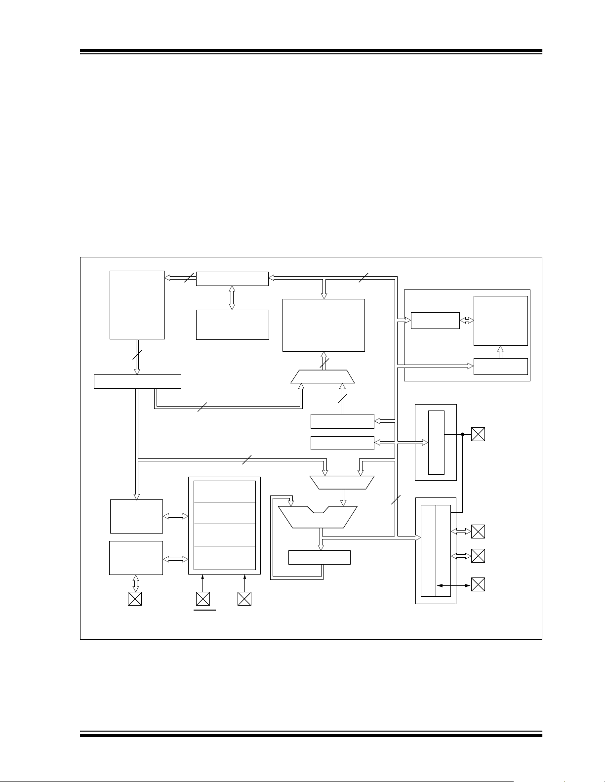
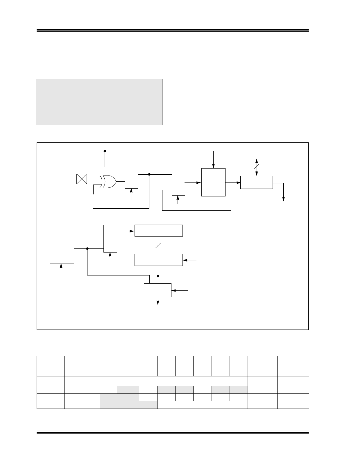
1.0 DEVICE OVERVIEW
This document contains device specific information for
the operation of the PIC16F84A device. Additional
information may be found in the PICmicro™ MidRange Reference Manual, (DS33023), which may be
downloaded from the Microchip website. The Reference Manual should be considered a complementary
document to this data sheet, and is highly recommended reading for a better understanding of the
device architecture and operation of the peripheral
modules.
The PIC16F84A belo ngs to t he mid-range family o f th e
PICmicro
the device is shown in Figure 1-1.
FIGURE 1-1: PIC16F84A BLOCK DIAGRAM
®
microcontroller devices. A block diagram of
13
Program Counter
FLASH
Program
Memory
1K x 14
Program
Bus
Instruction Register
14
8 Level Stack
(13-bit)
Data Bus
File Registers
68 x 8
Addr Mux
The program memory contains 1K words, which translates to 1024 instructions, since each 14-bit program
memory word is the same width as each device instruction. The data memory (RAM) contains 68 bytes. Data
EEPROM is 64 bytes.
There are also 13 I/O pins that are user-configured on
a pin-to-pin basis . Some pins are m ultiplexed with other
device functions. These functions include:
• External interrupt
• Change on PORTB interrupt
• Timer0 clock input
Table 1-1 details the pinout of the device with descrip-
tions and details for each pin.
8
EEPROM Data Memory
RAM
7
EEDATA
RAM Addr
EEPROM
Data Memory
64 x 8
EEADR
Instruction
Decode &
Control
Timing
Generation
OSC2/CLKOUT
OSC1/CLKIN
Direct Addr
5
Power-up
Timer
Oscillator
Start-up Time r
Power-on
Reset
Watchdog
Timer
MCLR
8
VDD, VSS
FSR reg
STATUS reg
ALU
W reg
7
MUX
Indirect
Addr
TMR0
RA4/T0CKI
8
I/O Ports
RA3:RA0
RB7:RB1
RB0/INT
2001 Microchip Technology Inc. DS35007B-page 3
Page 6

PIC16F84A
TABLE 1-1: PIC16F84A PINOUT DESCRIPTION
Pin Name
OSC1/CLKIN 16 16 18 I ST/CMOS
OSC2/CLKOUT 15 15 19 O — Oscillator crystal output. Connects to crystal or
MCLR
RA0 17 17 19 I/O TTL
RA1 18 18 20 I/O TTL
RA2 1 1 1 I/O TTL
RA3 2 2 2 I/O TTL
RA4/T0CKI 3 3 3 I/O ST Can also be selected to be the clo ck input to the
RB0/INT 6 6 7 I/O TTL/ST
RB1 7 7 8 I/O TTL
RB2 8 8 9 I/O TTL
RB3 9 9 10 I/O TTL
RB4 10 10 11 I/O TTL Interrupt-on-change pin.
RB5 11 11 12 I/O TTL Interrupt-on-change pin.
RB6 12 12 13 I/O TTL/ST
RB7 13 13 14 I/O TTL/ST
SS 5 5 5,6 P — Ground reference for logic and I/O pins.
V
DD 14 14 15,16 P — Positive supply for logic and I/O pins.
V
Legend: I= input O = Output I/O = Input/Output P = Power
Note 1: This buffer is a Schmitt Trigger input when configured as the external interrupt.
2: This buffer is a Schmitt Trigger input when used in Serial Programming mode.
3: This buffer is a Schmitt Trigger input when configured in RC oscillator mode and a CMOS input otherwise.
PDIP
SOIC
No.
4 4 4 I/P ST Master Clear (Reset) input/programming voltage
— = Not used TTL = TTL input ST = Schmitt Trigger input
No.
SSOP
No.
I/O/P
Type
Buffer
Type
Description
(3)
Oscillator crystal input /external clock source input.
resonator in Crystal Oscillator mode. In RC mode,
OSC2 pin outputs CLKOUT, which has 1/4 the
frequency of OSC1 and denotes the instruction
cycle rate.
input. This pin is an activ e low RESET to the de vice.
PORTA is a bi-directional I/O port.
TMR0 timer/counter. Output is open drain type.
PORTB is a bi-directional I/O port. PORTB can be
software programmed for internal weak pull-up on
all inputs.
(1)
(2)
(2)
RB0/INT can also be selected as an external
interrupt pin.
Interrupt-on-change pin.
Serial programming clock.
Interrupt-on-change pin.
Serial programming data.
DS35007B-page 4 2001 Microchip Technology Inc.
Page 7

PIC16F84A
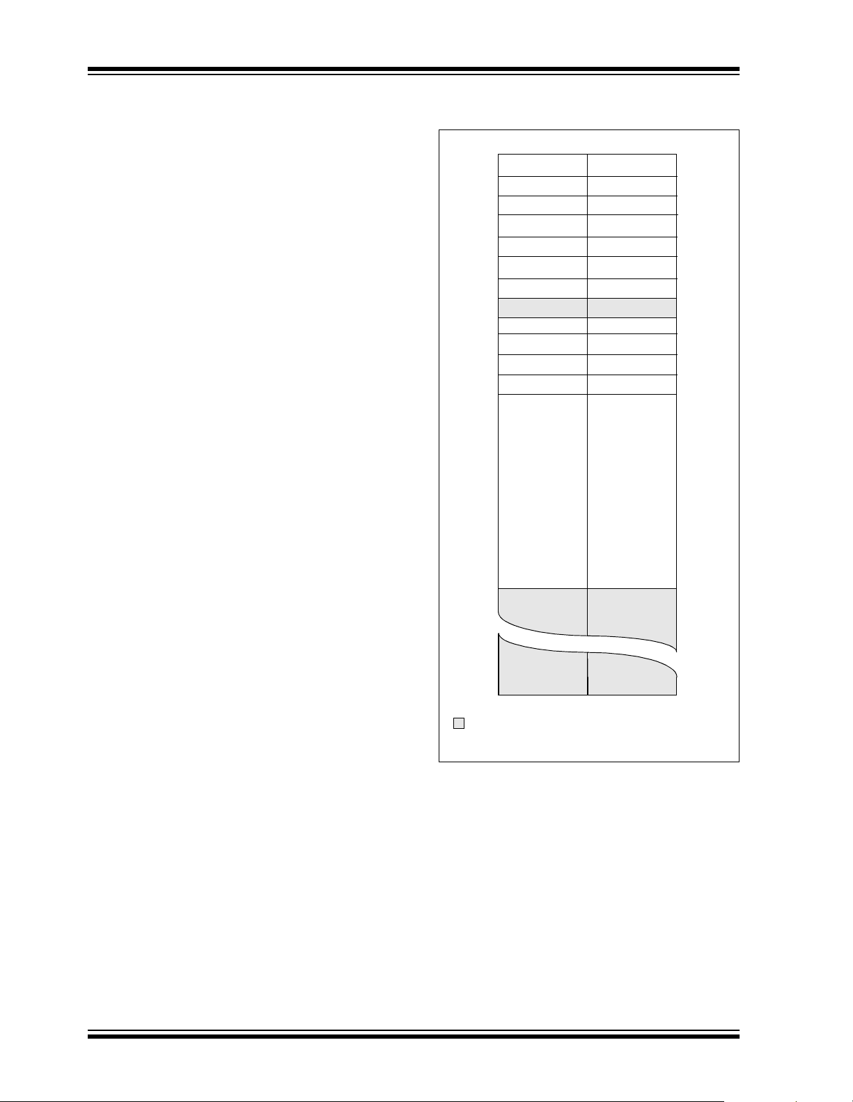
2.0 MEMORY ORGANIZATION
There are two memory blocks in the PIC16F84A.
These are the program memory and the data memory.
Each block has its own bus, so that access to each
block can occur during the same oscillator cycle.
The data memory can further be broken down into the
general purpose RAM and the Special Function
Registers (SFRs). The operation of the SFRs that
control the “core” are described here. The SFRs used
to control the peripheral modules are described in the
section discussing each individual peripheral module.
The data memory area also contains the data
EEPROM memory . This memory is no t directly mapped
into the data m emory, but is indirectly m ap ped . T hat is ,
an indirect address p ointer s pecifies the ad dress of the
data EEPROM memory to read/write. The 64 bytes of
data EEPROM memory have the address range
0h-3Fh. More details on the EEPROM memory can be
found in Section 3.0.
Additional informa tion on devi ce memory m ay be found
in the PICmicro™ Mid-Range Reference Manual,
(DS33023).
2.1 Program Memory Organization
FIGURE 2-1: PROGRAM MEMORY MAP
AND STACK - PIC16F84A
CALL, RETURN
RETFIE, RETLW
Peripheral Interrupt Vector
Space
User Memory
PC<12:0>
Stack Level 1
Stack Level 8
RESET Vector
13
•
•
•
0000h
0004h
3FFh
The PIC16FXX has a 13-bit program counter capable
of addressing an 8K x 14 program memory space. For
the PIC16F84A, the first 1K x 14 (0000h-03FFh) are
physically imple mented (Fi gure 2-1). Accessing a location above the physically implemented address will
cause a wraparound. For example, for locations 20h,
420h, 820h, C20h, 1020h, 1420h, 1820h, and 1C20h,
the instruction will be the same.
The RESET vector is at 0000h and the interrupt vector
is at 0004h.
1FFFh
2001 Microchip Technology Inc. DS35007B-page 5
Page 8
PIC16F84A
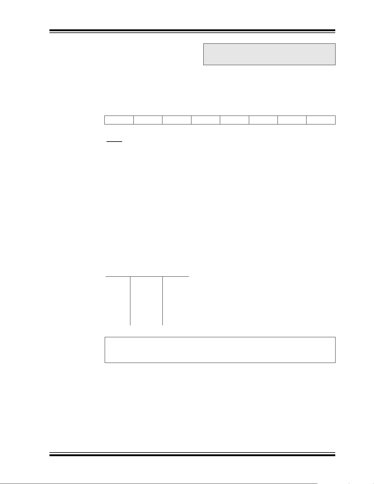
2.2 Data Memory Organization
The data memory is par titione d into two areas. T he first
is the Special Fu nction Regis ters (SFR) a rea, wh ile th e
second is the General Purpose Registers (GPR) area.
The SFRs control the operation of the device.
Portions of data memory are banked. This is for both
the SFR area and the GPR area. The GPR area is
banked to allow greater than 116 bytes of general
purpose RAM. The banked areas of the SFR are for the
registers that control the peripheral functions. Banking
requires the use of control bits for bank selection.
These control bits are loc at ed i n th e STATU S R egi ste r.
Figure 2-2 shows the data memory map organization.
Instructions MOVWF and MOVF can move values from
the W register to any location in the register file (“F”),
and vice-versa.
The entire data memory can be accessed either
directly using the absolute address o f ea ch regi ste r fil e
or indirectly through the File Select Register (FSR)
(Section 2.5). Indirect addressing uses the present
value of the RP0 bit for acces s into the banked ar eas of
data memory.
Data memory is partitioned into two banks which
contain the general purpose registers and the special
function registers. Bank 0 is selected by clearing the
RP0 bit (STATUS<5>). Setting the RP0 bit selects Bank
1. Each Bank extends up to 7Fh (128 bytes). The first
twelve locations of each Bank are reserved for the
Special Funct ion Registers. The remain der are General Purpose Registers, implemented as static RAM.
2.2.1 GENERAL PURPOSE REGISTER FILE
FIGURE 2-2: REGISTER FILE MAP -
PIC16F84A
File Address
00h
01h
02h
03h
04h
05h
06h
07h
08h
09h
0Ah
0Bh
0Ch
4Fh
50h
(1)
Indirect addr.
TMR0 OPTION_REG
PCL
STATUS
FSR
PORTA
PORTB
—
EEDATA
EEADR
PCLATH
INTCON
68
General
Purpose
Registers
(SRAM)
Indirect addr.
STATUS
EECON1
EECON2
PCLATH
INTCON
Mapped
(accesses)
in Bank 0
PCL
FSR
TRISA
TRISB
—
File Address
(1)
(1)
80h
81h
82h
83h
84h
85h
86h
87h
88h
89h
8Ah
8Bh
8Ch
CFh
D0h
Each General Purpose Register (GPR) is 8-bits wide
and is accessed either dire ctl y o r indirectly through the
FSR (Section 2.5).
The GPR addresses in Bank 1 are mapped to
addresses in Bank 0. As an ex ample, addressing location 0Ch or 8Ch will access the same GPR.
DS35007B-page 6 2001 Microchip Technology Inc.
7Fh
Unimplemented data memory location, read as ’0’.
Note 1: Not a physical register.
Bank 0
Bank 1
FFh
Page 9

PIC16F84A
2.3 Special Function Registers
The special function regi sters can be classified into tw o
sets, core and peripheral. Those associated with the
The Special Function Registers (Figure 2-2 and
Table 2-1) are used by the CPU and Peripheral
functions to control the device operation. These
core functions are described in this section. Those
related to the operation of the peripheral features are
described in the section for that specific feature.
registers are static RAM.
TABLE 2-1: SPECIAL FUNCTION REGISTER FILE SUMMARY
Addr Name Bit 7 Bit 6 Bit 5 Bit 4 Bit 3 Bit 2 Bit 1 Bit 0
Bank 0
00h INDF Uses contents of FSR to address Data Memory (not a physical register)
01h TMR0 8-bit Real-Time Clock/Counter
02h PCL Low Order 8 bits of the Program Counter (PC)
03h
STATUS
04h FSR Indirect Data Memory Address Pointer 0
05h PORTA
06h PORTB
07h — Unimplemented location, read as '0' — —
08h EEDATA EEPROM Data Register
09h EEADR EEPROM Address Register
0Ah
PCLATH
0Bh INTCON GIE EEIE T0IE INTE RBIE T0IF INTF RBIF
Bank 1
80h INDF Uses Contents of FSR to address Data Memory (not a physical register)
81h
OPTION_REG RBPU INTEDG T0CS T0SE PSA PS2 PS1 PS0
82h PCL Low order 8 bits of Program Counter (PC)
83h
STATUS
84h FSR Indirect data memory address pointer 0
85h TRISA
86h TRISB PORTB Data Direction Register
87h — Unimplemented location, read as '0' — —
88h EECON1
89h
EECON2 EEPROM Control Register 2 (not a physical register)
0Ah
PCLATH
0Bh INTCON GIE EEIE T0IE INTE RBIE T0IF INTF RBIF
Legend: x = unknown, u = unchanged. - = unimplemented, read as '0', q = value depends on condition
Note 1: The upper byte of the program counter is not directly accessible. PCLATH is a slave register for PC<12:8>. The contents
2: The TO
3: Other (non power-up) RESETS include: external RESET through MCLR
4: On any device RESET, these pins are configured as inputs.
5: This is the value that will be in the port output latch.
(2)
IRP RP1 RP0 TO PD ZDCC
(4)
— — — RA4/T0CKI RA3 RA2 RA1 RA0
(5)
RB7 RB6 RB5 RB4 RB3 RB2 RB1 RB0/INT
— — — Write Buffer for upper 5 bits of the PC
(2)
IRP RP1 RP0 TO PD ZDCC
— — — PORTA Data Direction Register
— — — EEIF WRERR WREN WR RD
— — — Write buffer for upper 5 bits of the PC
of PCLATH can be transferred to the upper byte of the program counter, but the contents of PC<12:8> are never transferred to PCLATH.
and PD status bits in the STATUS register are not affected by a MCLR Reset.
and the Watchdog Tim er Reset.
(1)
(1)
Value on
Power-on
RESET
---- ---xxxx xxxx
0000 0000
0001 1xxx
xxxx xxxx
---x xxxx
xxxx xxxx
xxxx xxxx
xxxx xxxx
---0 0000
0000 000x
---- ---1111 1111
0000 0000
0001 1xxx
xxxx xxxx
---1 1111
1111 1111
---0 x000
---- ----
---0 0000
0000 000x
Details
on page
11
20
11
8
11
16
18
13,14
13,14
11
10
11
9
11
8
11
16
18
13
14
11
10
2001 Microchip Technology Inc. DS35007B-page 7
Page 10

PIC16F84A
2.3.1 STATUS REGISTER
The STATUS register contains the arithmetic status of
the ALU, the RESET status and the bank select bit for
data memory.
As with any register, the STATUS register can be the
destination for any instruction. If the STATUS regi ster is
the destination for an instruction that affects the Z, DC
or C bits, then the write to these three bits is disabled.
These bits ar e s et o r c leared according t o d evi ce lo gic .
Furthermore, the TO
Therefore, the result of an instruction wi th t he STATUS
register as destina tio n may be different than intended.
For example, CLRF STATUS will clear the upper three
bits and set the Z bit. This leaves the STATUS register
as 000u u1uu (where u = unchanged).
Only the BCF, BSF, SWAPF and MOVWF instructions
should be used to alter the STATUS register (Table 7-2),
because these instructions do not affect any status bit.
and PD bits are not writable.
Note 1: The IRP and RP1 bits (STATUS<7:6>)
are not used by the PIC16F84A and
should be progra mmed as c leared. U se of
these bits as general purpose R/W bits is
NOT recommended, since this may affect
upward compatibility with future products.
2: The C and DC bits operate as a borrow
and digit borrow out bit, respectively, in
subtraction. See the SUBLW and SUBWF
instructi ons for examples.
3: When the STATUS register is the
destinati on for an instruct ion that affects
the Z, DC or C bits, then the writ e to these
three bits is disabled. The specified bit(s)
will be updated according to device logic
REGISTER 2-1: STATUS REGISTER (ADDRESS 03h, 83h)
R/W-0 R/W-0 R/W-0 R-1 R-1 R/W-x R/W-x R/W-x
IRP RP1 RP0 TO PD ZDCC
bit 7 bit 0
bit 7-6 Unimplemented: Maintain as ‘0’
bit 5 RP0: Register Bank Select bits (used for direct addressing)
01 = Bank 1 (80h - FFh)
00 = Bank 0 (00h - 7Fh)
bit 4 TO
bit 3 PD
bit 2 Z: Zero bit
bit 1 DC: Digit carry/borrow
bit 0 C: Carry/borrow
: Time-out bit
1 = After power-up, CLRWDT instruction, or SLEEP instruction
0 = A WDT time-out occurred
: Power-down bit
1 = After power-up or by the CLRWDT instruction
0 = By execution of the SLEEP instruction
1 = The result of an arithmetic or logic operation is zero
0 = The result of an arithmetic or logic operation is not zero
bit (ADDWF , ADDLW,SUBLW,SUBWF inst ructio ns) (for borr ow, th e pol arity
is reversed)
1 = A carry-out from the 4th low order bit of the result occurred
0 = No carry-out from the 4th low order bit of the result
bit (ADDWF, ADDLW,SUBLW,SUBWF instructions) (for borrow, the polarity is
reversed)
1 = A carry-out from the Most Significant bit of the result occurred
0 = No carry-out from the Most Significant bit of the result occurred
Note: A subtraction is executed by adding the two’s complement of the second operand.
For rotate (RRF, RLF) instructions, this bi t is loaded with eithe r th e h igh or low order
bit of the source register.
Legend:
R = Readable bit W = Writable bit U = Unimplemented bit, read as ‘0’
- n = Value at POR ’1’ = Bit is set ’0’ = Bit is cleared x = Bit is unknown
DS35007B-page 8 2001 Microchip Technology Inc.
Page 11
PIC16F84A
2.3.2 OPTION REGISTER
The OPTION register is a readable and writable
register which con tain s v arious c ontrol bit s to conf igure
the TMR0/WDT prescaler, the external INT interrupt,
TMR0, and the weak pull-ups on PORTB.
Note: When the prescaler is assigned to
the WDT (PSA = ’1’), TMR0 has a 1:1
prescaler assignment.
REGISTER 2-2: OPTION REGISTER (ADDRESS 81h)
R/W-1 R/W-1 R/W-1 R/W-1 R/W-1 R/W-1 R/W-1 R/W-1
RBPU INTEDG T0CS T0SE PSA PS2 PS1 PS0
bit 7 bit 0
bit 7 RB
bit 6 INTEDG: Interrupt Edge Select bit
bit 5 T0CS: TMR0 Clock Source Select bit
bit 4 T0SE: TMR0 Source Edge Select bit
bit 3 PSA: Prescaler Assignment bit
bit 2-0 PS2:PS0: Prescaler Rate Select bits
PU: PORTB Pull-up Enable bit
1 = PORTB pull-ups are disabled
0 = PORTB pull-ups are enabled by individual port latch values
1 = Interrupt on rising edge of RB0/INT pin
0 = Interrupt on falling edge of RB0/INT pin
1 = Transition on RA4/T0CKI pin
0 = Internal instruction cycle clock (CLKOUT)
1 = Increment on high-to-low transition on RA4/T0CKI pin
0 = Increment on low-to-high transition on RA4/T0CKI pin
1 = Prescaler is assigned to the WDT
0 = Prescaler is assigned to the Timer0 module
Bit Value TMR0 Rate WDT Rate
000
001
010
011
100
101
110
111
1 : 2
1 : 4
1 : 8
1 : 16
1 : 32
1 : 64
1 : 128
1 : 256
1 : 1
1 : 2
1 : 4
1 : 8
1 : 16
1 : 32
1 : 64
1 : 128
Legend:
R = Readable bit W = Writable bit U = Unimplemented bit, read as ‘0’
- n = Value at POR ’1’ = Bit is set ’0’ = Bit is cleared x = Bit is unknown
2001 Microchip Technology Inc. DS35007B-page 9
Page 12

PIC16F84A
2.3.3 INTCON REGISTER
The INTCON register is a readable and writable
register that contains the various enable bits for all
interrupt sources.
Note: Interrupt flag bits are se t whe n an in terru pt
condition occurs, regar dless of the sta te of
its corresponding enable bit or the global
enable bit, GIE (INTCON<7>).
REGISTER 2-3: INTCON REGISTER (ADDRESS 0Bh, 8Bh)
R/W-0 R/W-0 R/W-0 R/W-0 R/W-0 R/W-0 R/W-0 R/W-x
GIE EEIE T0IE INTE RBIE T0IF INTF RBIF
bit 7 bit 0
bit 7 GIE: Global Interrupt Enable bit
1 = Enables all unmasked interrupts
0 = Disables all interrupts
bit 6 EEIE: EE Write Complete Interrupt Enable bit
1 = Enables the EE Write Complete interrupts
0 = Disables the EE Write Complete interrupt
bit 5 T0IE: TMR0 Overflow Interr upt Enable bit
1 = Enables the TMR0 interrupt
0 = Disables the TMR0 interrupt
bit 4 INTE: RB0/INT External Interrupt Enable bit
1 = Enables the RB0/INT external interrupt
0 = Disables the RB0/INT external interrupt
bit 3 RBIE: RB Port Change Interrupt Enable bit
1 = Enables the RB port change interrupt
0 = Disables the RB port change interrupt
bit 2 T0IF: TMR0 Overflow Interrupt Flag bit
1 = TMR0 register has overflowed (must be cleared in software)
0 = TMR0 register did not overflow
bit 1 INTF: RB0/INT External Interrupt Flag bit
1 = The RB0/INT external interrupt occurred (must be cleared in software)
0 = The RB0/INT external interrupt did not occur
bit 0 RBIF: RB Port Change Interrupt Flag bit
1 = At least one of the RB7:RB4 pins changed state (must be cleared in software)
0 = None of the RB7:RB4 pins have changed state
Legend:
R = Readable bit W = Writable bit U = Unimplemented bit, read as ‘0’
- n = Value at POR ’1’ = Bit is set ’0’ = Bit is cleared x = Bit is unknown
DS35007B-page 10 2001 Microchip Technology Inc.
Page 13

PIC16F84A
2.4 PCL and PCLATH
The program counter (PC ) sp eci fie s th e a ddre ss of th e
instruction to fetch for execution. The PC is 13 bits
wide. The low byte is called the PCL register. This register is readable and writable. The high byte is called
the PCH register. This register contains the PC<12:8>
bits and is not directly readable or writable. If the program counter (PC) is modified or a conditional test is
true, the instruction requires two cycles. The second
cycle is executed as a NOP. All updates to t he PCH reg-
ister go through the PCLATH register.
2.4.1 STACK
The stack allows a combination of up to 8 program calls
and interrupts to occur. The stack contains the return
address from this branch in program execution .
Mid-range devices have an 8 level deep x 13-bit wide
hardware s tack. The stack space is not par t of either
program or data space and the stack pointer is not
readable or writabl e. The PC i s PUSHed onto th e stac k
when a CALL instruction is executed or an interrupt
causes a branch. The st ac k is POPed in the event of a
RETURN, RETLW or a RETFIE instruction ex ecution.
PCLATH is not modified wh en th e s tac k i s PU SH ed or
POPed.
After the stack has bee n PUSHed eight time s, the ninth
push overwrites th e value tha t was stored fro m the firs t
push. The tenth pus h ov erwr i tes the se co nd push (and
so on).
2.5 Indirect Addressing; INDF and FSR Registers
The INDF register is no t a physical reg ister . Addr essing
INDF actually addresse s the regi st er whose ad dress i s
contained in the FSR reg ister (FSR is a
indirect addressing.
EXAMPLE 2-1: INDIRECT ADDRESSING
• Register file 05 contains the value 10h
• Register file 06 contains the value 0Ah
• Load the value 05 into the FSR register
• A read of the INDF regi ste r w ill ret urn t he v al ue
of 10h
• Increment the value of the FSR register by one
(FSR = 06)
• A read of the INDF register now will return the
value of 0Ah.
Reading INDF itself indirectly (FSR = 0) will produce
00h. Writing to the INDF register indirectly results in a
no-operation (although STATUS bits may be affected).
A simple program to clear RAM locations 20h-2Fh
using indirect addressing is shown in Example 2-2.
EXAMPLE 2-2: HOW TO CLEAR RAM
USING INDIRECT
ADDRESSING
movlw 0x20 ;initialize pointer
movwf FSR ;to RAM
NEXT clrf INDF ;clear INDF register
incf FSR ;inc pointer
btfss FSR,4 ;all done?
goto NEXT ;NO, clear next
CONTINUE
: ;YES, continue
pointer
). This is
An effective 9-b it addre ss is obt ained b y con catena ting
the 8-bit FSR register and the IRP bit (STATUS<7>), a s
shown in Figure 2-3. However, IRP is not used in the
PIC16F84A.
2001 Microchip Technology Inc. DS35007B-page 11
Page 14
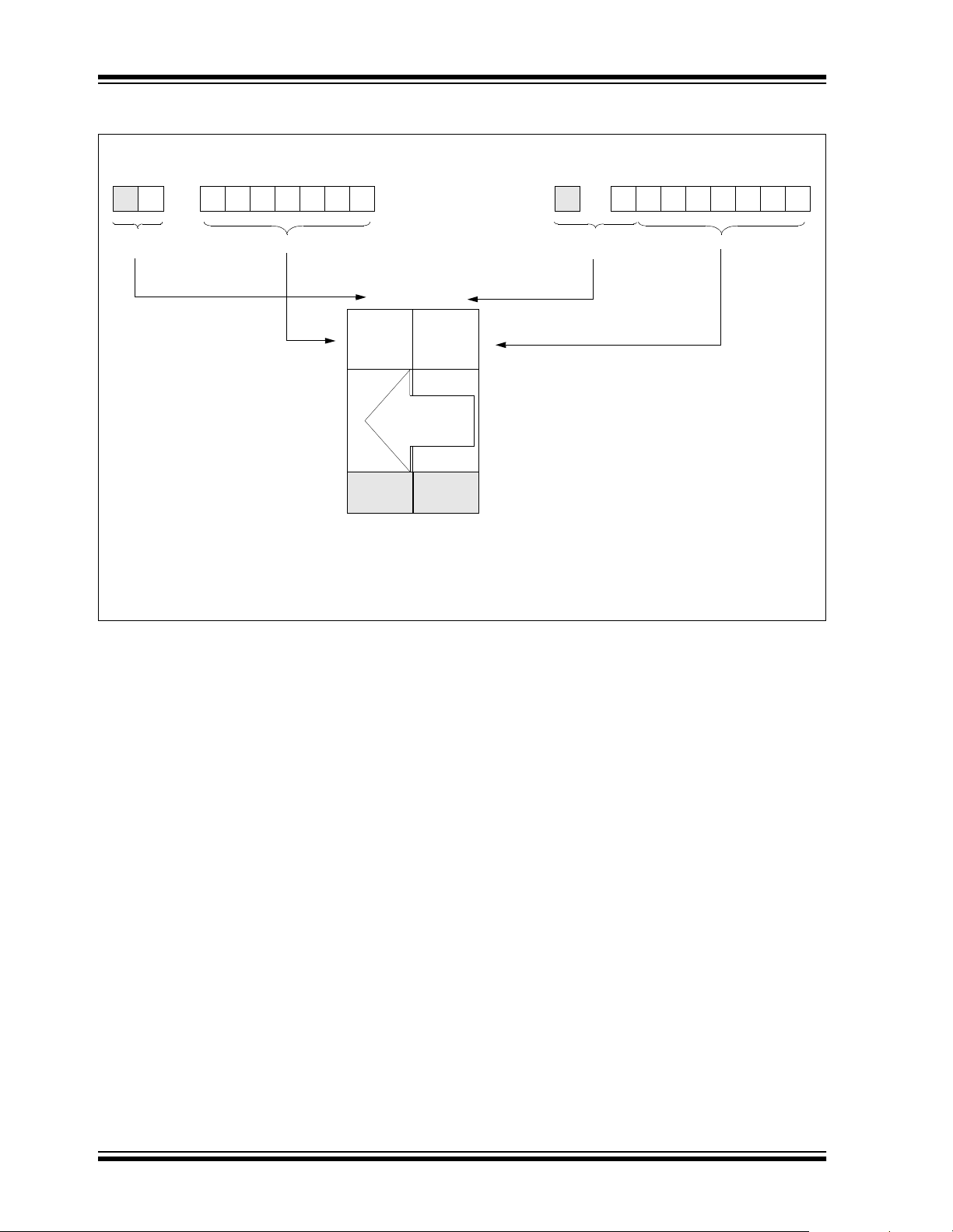
PIC16F84A
FIGURE 2-3: DIRECT/INDIRECT ADDRESSING
Direct Addressing
RP1 RP0 6
(2) (2)
Bank Select Location Select
Note 1: For memory map detail, see Figure 2-2.
2: Maintain as clear for upward compatibility with future products.
3: Not implemented.
From Opcode
Data
(1)
Memory
0IRP7
00 01
00h
0Bh
0Ch
80h
Addresses
map back to
Bank 0
4Fh
50h
7Fh
(3)
Bank 0 Bank 1
(3)
FFh
Bank Select
Indirect Addressing
(FSR)
Location Select
0
DS35007B-page 12 2001 Microchip Technology Inc.
Page 15
PIC16F84A
3.0 DATA EEPROM MEMORY
The EEPROM data memory is readable and writable
during normal operation (full V
is not directly mapped in the register file space. Instead
it is indirectly addressed through the Special Function
Registers. There are four SFRs used to read and write
this memory. These registers are:
• EECON1
• EECON2 (not a physically implemented register)
• EEDA TA
• EEADR
EEDATA holds the 8-bit data for read/write, and
EEADR holds the address of the EEPROM location
being accessed. PIC16F84A devices have 64 bytes of
data EEPROM with an address range from 0h to 3Fh.
DD range). This memory
The EEPROM data memory allows b yte read and write.
A byte write automatically erases the location and
writes the new data (erase be fore write). The EEPROM
data memory is rated fo r high eras e/write c ycles. The
write time is controlled by an on-chip timer. The writetime will vary with voltage and temperature as well as
from chip to c hip. Pl ease refe r to A C s peci ficat io ns fo r
exact limits.
When the device is code protected, the CPU may
continue to read and write th e data EEPROM memory.
The device programmer can no longer access
this memory.
Additional information on the Data EEPROM is available in the PICmicro™ Mid-Range Reference Manual
(DS33023).
REGISTER 3-1: EECON1 REGISTER (ADDRESS 88h)
U-0 U-0 U-0 R/W-0 R/W-x R/W-0 R/S-0 R/S-0
— — — EEIF WRERR WREN WR RD
bit 7 bit 0
bit 7-5 Unimplemented: Read as '0'
bit 4 EEIF: EEPROM Write Operation Interrupt Flag bit
1 = The write operation completed (must be cleared in software)
0 = The write operation is not complete or has not been started
bit 3 WRERR: EEPROM Error Flag bit
1 = A write operation is prematurely termina ted
(any MCLR
0 = The write operation completed
bit 2 WREN: EEPROM Write Enable bit
1 = Allows write cycles
0 = Inhibits write to the EEPROM
bit 1 WR: Write Control bit
1 = Initiates a write cycle. The bit is cleared by hardware once write is complete. The WR bit
can only be set (not cleared) in software.
0 = Write cycle to the EEPROM is complete
bit 0 RD: Read Control bit
1 = Initiates an EEPROM read RD is cleared in hardware. The RD bit can only be set (not
cleared) in software.
0 = Does not initiate an EEPROM read
Reset or any WDT Reset during normal operation)
Legend:
R = Readable bit W = Writable bit U = Unimplemented bit, read as ‘0’
- n = Value at POR ’1’ = Bit is set ’0’ = Bit is cleared x = Bit is unknown
2001 Microchip Technology Inc. DS35007B-page 13
Page 16

PIC16F84A
3.1 Reading the EEPROM Data Memory
T o read a d ata memory lo cation, the user must write the
address to the EEADR register and then set control bit
RD (EECON1<0>). The data is available, in the very
next cycle, in the EEDATA register; th erefore, it can be
read in the next instru ction. EEDATA will hold this valu e
until another read or until it is written to by the user
(during a write operation).
EXAMPLE 3-1: DATA EEPROM READ
BCF STATUS, RP0 ; Bank 0
MOVLW CONFIG_ADDR ;
MOVWF EEADR ; Address to read
BSF STATUS, RP0 ; Bank 1
BSF EECON1, RD ; EE Read
BCF STATUS, RP0 ; Bank 0
MOVF EEDATA, W ; W = EEDATA
3.2 Writing to the EEPROM Data Memory
To write an EEPROM data location, the user must first
write the address to the EEADR register and the data
to the EEDATA register. Then the user must follow a
specific sequence to initiate the write for each byte.
Additionally, the WREN bit in EECON1 must be set to
enable write. This mechanism prevents accident al writes
to data EEPROM due to errant (unexpected) code execution (i.e., lost programs). The user should keep the
WREN bit clear at all times, except when updating
EEPROM. The WREN bit is not cleared by hardware.
After a write sequence has been initiated, clearing the
WREN bit will not affec t this writ e cycle. The WR bit will
be inhibited from being s et unless the WREN bit is set.
At the completion of the write cycle, the WR bit is
cleared in hardware and the EE Write Complete
Interrupt Flag bit (EEIF) is set. The user can either
enable this interrupt or poll this bit. EEIF must be
cleared by software.
3.3 Write Verify
Depending on the application, good programming
practice may dictate that the value written to the Data
EEPROM should be verified (Example 3-3) to the
desired value to be written. This should be used in
applications where an EEPROM bit will be stressed
near the specification limit.
Generally , th e EEPROM write failure wil l be a bit whic h
was written as a ’0’, but reads back as a ’1’ (due to
leakage off the bit).
EXAMPLE 3-2: DATA EEPROM WRITE
BSF STATUS, RP0 ; Bank 1
BCF INTCON, GIE ; Disable INTs.
BSF EECON1, WREN ; Enable Write
MOVLW 55h ;
MOVWF EECON2 ; Write 55h
MOVLW AAh ;
MOVWF EECON2 ; Write AAh
BSF EECON1,WR ; Set WR bit
; begin write
Required
Sequence
BSF INTCON, GIE ; Enable INTs.
The write will not initiate if the above sequence is not
exactly followed (write 55h to EECON2, write AAh to
EECON2, then set WR bit) for each byte. We strongly
recommend that interrupts be disabled during this
code segment.
EXAMPLE 3-3: WRITE VERIFY
BCF STATUS,RP0 ; Bank 0
: ; Any code
: ; can go here
MOVF EEDATA,W ; Must be in Bank 0
BSF STATUS,RP0 ; Bank 1
READ
BSF EECON1, RD ; YES, Read the
; value written
BCF STATUS, RP0 ; Bank 0
;
; Is the value written
; (in W reg) and
; read (in EEDATA)
; the same?
;
SUBWF EEDATA, W ;
BTFSS STATUS, Z ; Is difference 0?
GOTO WRITE_ERR ; NO, Write error
TABLE 3-1: REGISTERS/BITS ASSOCIATED WITH DATA EEPROM
Address Name Bit 7 Bit 6 Bit 5 Bit 4 Bit 3 Bit 2 Bit 1 Bit 0
08h EEDATA EE PROM Data Register
09h EEADR EEPROM Address Register xxxx xxxx uuuu uuuu
88h EECON1
89h EECON2 EEPROM Control Register 2 ---- ---- ---- ---Legend: x = unknown, u = unchanged, - = unimplemented, read as '0', q = value depends upon condition.
Shaded cells are not used by data EEPROM.
— — — EEIF WRERR WREN WR RD ---0 x000 ---0 q000
Value on
Power-on
Reset
xxxx xxxx uuuu uuuu
Value on
all other
RESETS
DS35007B-page 14 2001 Microchip Technology Inc.
Page 17
PIC16F84A
4.0 I/O PORTS
Some pins for thes e I/O ports are mul tiplexed wit h an
alternate function for the peripheral features on the
device. In general, when a peripheral is enabled, that
pin may not be used as a general purpose I/O pin.
Additional inform atio n o n I/O ports ma y b e found in the
PICmicro™ Mid-Range Refer ence M anual (DS33 023).
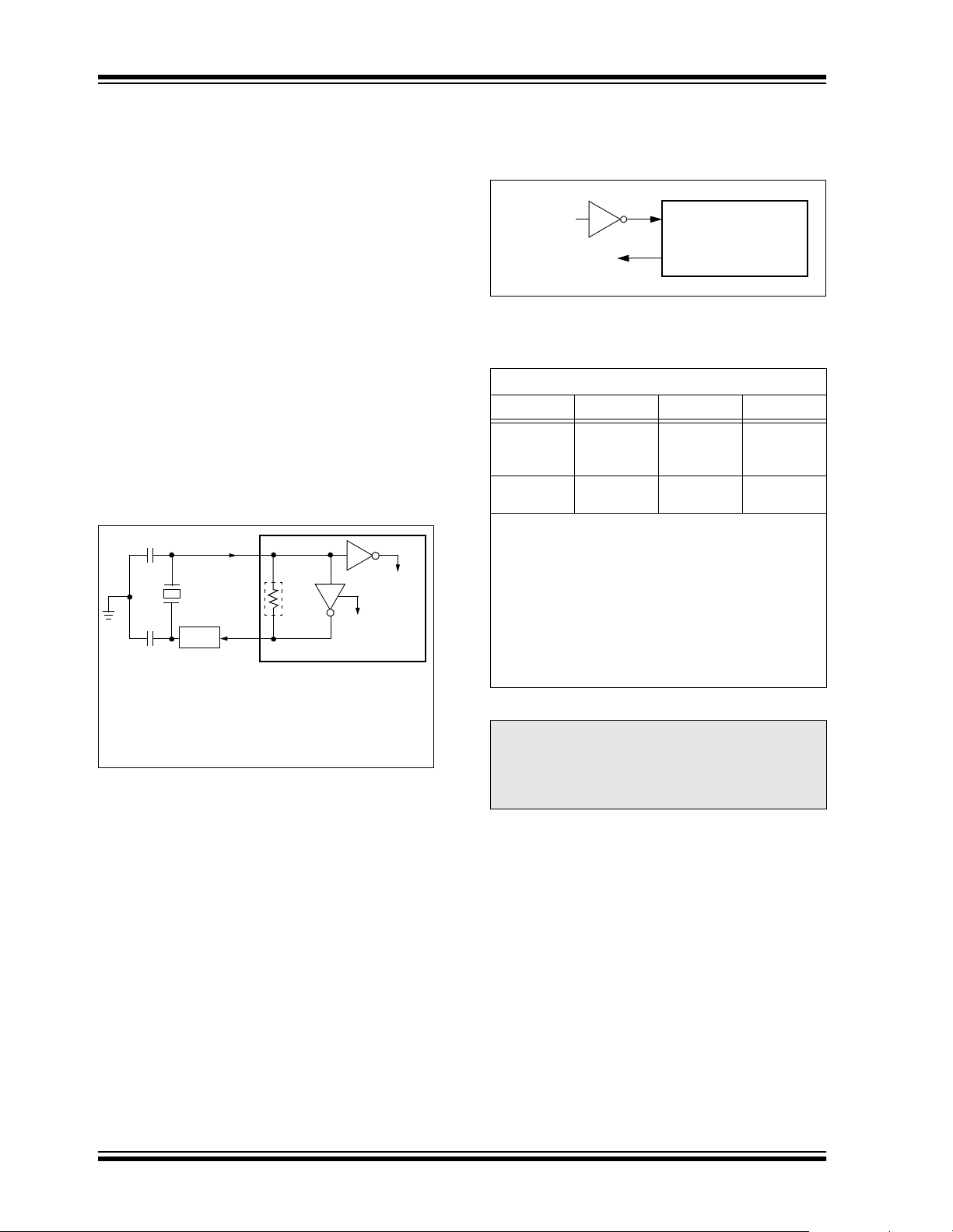
4.1 PORTA and TRISA Registers
PORTA is a 5-bit wide, bi-directional port. The corresponding data direction register is TRISA. Setting a
TRISA bit (= 1) will m ake the corres ponding POR T A pin
an input (i.e., put the corresponding output driver in a
Hi-Impedance mode). Clearing a TRISA bit (= 0) will
make the correspondin g PORTA pin an output (i.e., put
the contents of the output latch on the selected pin).
Note: On a Power-on Reset, these pins are con-
figured as inputs and read as '0'.
Reading the PORTA register reads the status of the
pins, whereas writing to i t will wri te to th e po rt latch. All
write operations are read-modify-write operations.
Therefore, a write to a port implies that the port pins are
read. This value is m odifie d and then written to the port
data latch.
Pin RA4 is multiplexed with the Timer0 module clock
input to become the RA4/T0CKI pin. The RA4/T0CKI
pin is a Schmitt Trig ger input and an open drai n output.
All other RA port pins have TTL input levels and full
CMOS output drivers.
EXAMPLE 4-1: INITIALIZING PORTA
BCF STATUS, RP0 ;
CLRF PORTA ; Initialize PORTA by
; clearing output
; data latches
BSF STATUS, RP0 ; Select Bank 1
MOVLW 0x0F ; Value used to
; initialize data
; direction
MOVWF TRISA ; Set RA<3:0> as inputs
; RA4 as output
; TRISA<7:5> are always
; read as ’0’.
FIGURE 4-1: BLOCK DIAGRAM OF
PINS RA3:RA0
Data
Bus
WR
Port
WR
TRIS
RD Port
Note: I/O pins have protection diodes to VDD and V SS.
CK
Data Latch
D
CK
TRIS Latch
QD
Q
Q
Q
RD TRIS
VDD
P
N
SS
V
TTL
Input
Buffer
QD
EN
I/O pin
FIGURE 4-2: BLOCK DIAGRAM OF PIN
RA4
Data
Bus
WR
Port
WR
TRIS
QD
Q
CK
Data Latch
QD
Q
CK
TRIS Latch
RD TRIS
N
V
Schmitt
Trigger
Input
Buffer
RA4 pin
SS
QD
EN
EN
RD Port
TMR0 Clock Input
Note: I/O pins have protection diodes to VDD and VSS.
2001 Microchip Technology Inc. DS35007B-page 15
Page 18
PIC16F84A
TABLE 4-1: PORTA FUNCTIONS
Name Bit0 Buffer Type Function
RA0 bit0 TTL Input/output
RA1 bit1 TTL Input/output
RA2 bit2 TTL Input/output
RA3 bit3 TTL Input/output
RA4/T0CKI bit4 ST Input/output or external clock input for TMR0.
Output is open drain type.
Legend: TTL = TTL input, ST = Schmitt Trigger input
TABLE 4-2: SUMMARY OF REGISTERS ASSOCIATED WITH PORTA
Address Name Bit 7 Bit 6 Bit 5 Bit 4 Bit 3 Bit 2 Bit 1 Bit 0
05h PORT A
85h TRISA
Legend:x = unknown, u = unchanged, - = unimplemented, read as '0'. Shaded cells are unimplemented, read as '0'.
— — — R A4/T0CKI RA3 RA2 RA1 RA0
— — — TRISA4 TRISA3 TRISA2 T RIS A1 TRISA0
Value on
Power-on
Reset
---x xxxx ---u uuuu
---1 1111 ---1 1111
Value on all
other
RESETS
DS35007B-page 16 2001 Microchip Technology Inc.
Page 19

PIC16F84A
4.2 PORTB and TRISB Registers
PORTB is an 8-bit wide, bi-directional port. The corresponding data direction register is TRISB. Setting a
TRISB bit (= 1) will make the c orresponding POR TB pin
an input (i.e., put the corresponding output driver in a
Hi-Impedance mode). Clearing a TRISB bit (= 0) will
make the correspo nding POR TB pin an output ( i.e., p ut
the contents of the output latch on the selected pin).
EXAMPLE 4-2: INITIALIZING PORTB
BCF STATUS, RP0 ;
CLRF PORTB ; Initialize PORTB by
; clearing output
BSF STATUS, RP0 ; Select Bank 1
MOVLW 0xCF ; Value used to
MOVWF TRISB ; Set RB<3:0> as inputs
Each of the PORTB pins has a we ak inte rnal pul l-up. A
single control bit can turn on all the pull-ups. This is performed by clearing bit RBPU
pull-up is automatically turned off when the port pin is
configured as an outpu t. The pull-ups are disable d on a
Power-on Reset.
Four of PORTB’s pi ns, RB7:RB4, have an interrupt-onchange feature. Only pins configured as inputs can
cause this interrupt to occur (i.e., any RB7:RB4 pin
configured as an output is excluded from the interrupton-change comparison). The input pins (of RB7:RB4)
are compared with the old value latched on the last
read of PORTB. The “mismatch” outputs of RB7:RB4
are OR’ed together to generate the RB Port Change
Interrupt with flag bit RBIF (INTCON<0>).
This interrupt can wake the device from SLEEP. The
user, in the Interrupt Service Routine, can clear the
interrupt in the following manner:
a) Any read or write of PORTB. This will end the
mismatch condition.
b) Clear flag bit RBIF.
A mismatch condition will continue to set flag bit RBIF.
Reading PORTB will end the mismatch condition and
allow flag bit RBIF to be cleared.
The interrupt-on-change feature is recommended for
wake-up on key depression operation and operations
where PORTB is only us ed f or the int errup t-on -ch ang e
feature. Polling of PORTB is not recommended while
using the interrupt-on-change feature.
; data latches
; initialize data
; direction
; RB<5:4> as outputs
; RB<7:6> as inputs
(OPTION<7>). The weak
FIGURE 4-3: BLOCK DIAGRAM OF
PINS RB7:RB4
DD
EN
EN
RD Port
DD and VSS.
V
P
Weak
Pull-up
I/O pin
TTL
Input
Buffer
(1)
RBPU
Data Bus
WR Port
WR TRIS
Set RBIF
From other
RB7:RB4 pins
Note 1: TRISB = ’1’ enables weak pull-up
2: I/O pins have diode protection to V
Data Latch
QD
CK
TRIS Latch
QD
CK
RD TRIS
RD Port
= ’0’ in the OPTION_REG register).
(if RBPU
Latch
QD
QD
FIGURE 4-4: BLOCK DIAGRAM OF
PINS RB3:RB0
DD
TTL
Input
Buffer
D
EN
DD and VSS.
V
Weak
P
Pull-up
I/O pin
RD Port
(1)
RBPU
Data Bus
WR Port
WR TRIS
RB0/INT
Note 1: TRISB = ’1’ enables weak pull-up
2: I/O pins have diode protection to V
Data Latch
QD
CK
TRIS Latch
QD
CK
RD TRIS
Q
RD Port
Schmitt Trigger
Buffer
= ’0’ in the OPTION_REG register).
(if RBPU
(2)
(2)
2001 Microchip Technology Inc. DS35007B-page 17
Page 20

PIC16F84A
TABLE 4-3: PORTB FUNCTIONS
Name Bit Buffer Type I/O Consistency Function
RB0/INT bit0 TTL/ST
RB1 bit1 TTL Input/out put pin. Internal software programmable weak pull-up.
RB2 bit2 TTL Input/out put pin. Internal software programmable weak pull-up.
RB3 bit3 TTL Input/out put pin. Internal software programmable weak pull-up.
RB4 bit4 TTL Input/out put pin (wit h interrupt-on-change).
RB5 bit5 TTL Input/out put pin (wit h interrupt-on-change).
RB6 bit6 TTL/ST
RB7 bit7 TTL/ST
Legend: TTL = TTL input, ST = Schmitt Trigger.
Note 1: This buffer is a Schmitt Trigger input when configured as the external interrupt.
2: This buffer is a Schmitt Trigger input when used in Serial Programming mode.
(1)
Input/output pin or external interrupt input.
Internal software programmable weak pull-up.
Internal software programmable weak pull-up.
Internal software programmable weak pull-up.
(2)
Input/output pin (with interrupt-on-change).
Internal software programmable weak pull-up. Serial programming clock.
(2)
Input/output pin (with interrupt-on-change).
Internal software programmable weak pull-up. Serial programming data.
TABLE 4-4: SUMMARY OF REGISTERS ASSOCIATED WITH PORTB
Address Name Bit 7 Bit 6 Bit 5 Bit 4 Bit 3 Bit 2 Bit 1 Bit 0
06h PORTB RB7 RB6 RB5 RB4 RB3 RB2 RB1 RB0/INT
86h TRISB TRISB7 TRISB6 TRISB5 TRISB4 TRISB3 TRISB2 TRISB1 TRISB0
81h OPTION_REG RBPU
0Bh,8Bh INTCON GIE
Legend:x = unknown, u = unchanged. Shaded cells are not used by PORTB.
INTEDG T0CS T0SE PSA PS2 PS1 PS0
EEIE T0IE INTE RBIE T0IF INTF RBIF
Value on
Power-on
Reset
xxxx xxxx uuuu uuuu
1111 1111 1111 1111
1111 1111 1111 1111
0000 000x 0000 000u
Value on
all other
RESETS
DS35007B-page 18 2001 Microchip Technology Inc.
Page 21
PIC16F84A
5.0 TIMER0 MODULE
The Timer0 module timer/counter has the following
features:
• 8-bit timer/counter
• Readable and writable
• Internal or external clock select
• Edge select for external clock
• 8-bit software programmable prescaler
• Interrupt-on-overflow from FFh to 00h
Figure 5-1 is a simplified block diagram of the Timer0
module.
Additional information on timer modules is available in
the PICmicro™ Mid-Range Reference Manual
(DS33023).
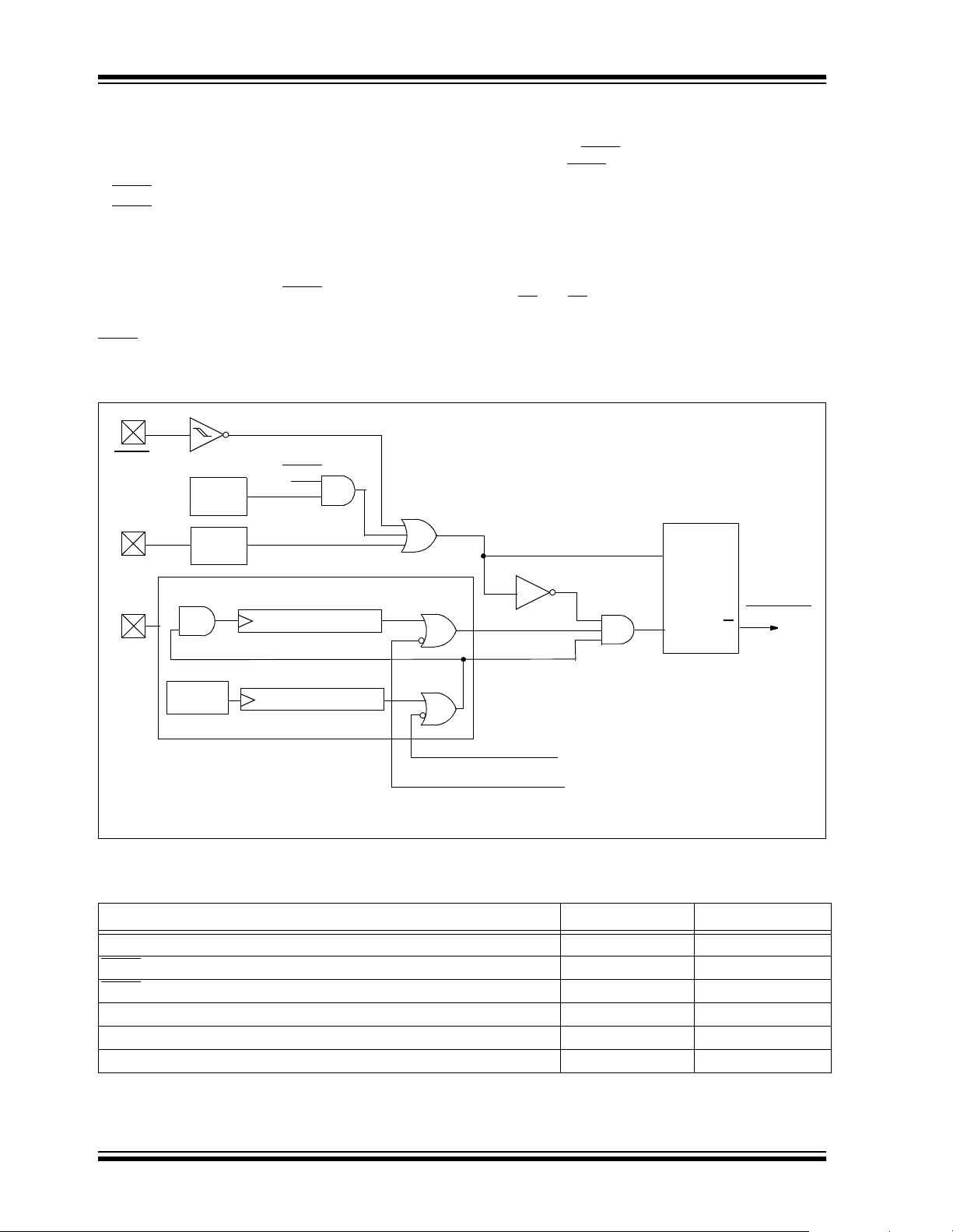
5.1 Timer0 Operation
Timer0 can operate as a timer or as a counter.
Timer mode is selected by clearing bit T0CS
(OPTION_REG<5>). In Timer mode, the Timer0 module will increment ev ery ins tru cti on c y cle (with ou t prescaler). If the TMR0 register is written, the increment is
inhibited for the following two instruction cycles. The
user can work around this by writing an adjusted value
to the TMR0 register.
Counter mode is selected by setting bit T0CS
(OPTION_REG<5>). In Counter mode, Timer0 will
increment, either on every rising or falling edge of pin
RA4/T0CKI. The incrementing edge is determined by
the Timer0 Source Edge Select bit, T0SE
(OPTION_REG<4>). Clearing bit T0SE selects the rising edge. Restrictions on the external clock input are
discussed be low.
When an external clock inpu t is used for T i mer0, it must
meet certain requirements. The requirements ensure
the external clock can be synchronized w ith the internal
phase clock (T
OSC). Also, there is a delay in the actual
incrementing of Timer0 after synchronization.
Additional information on external clock requirements
is available in the PICmicro™ Mid-Range Reference
Manual, (DS33023).
5.2 Prescaler
An 8-bit count er is availa ble as a prescale r for the T imer 0
module, or as a postscaler for the Watchdog Timer,
respectively (Figure 5-2). For simplicity, this counter is
being referred to as “prescaler” throughout this data
sheet. Note that there is only one prescaler available
which is mutual ly exclu sively shar ed between the T imer0
module and the Watchdog Timer. Thus, a prescaler
assignment for t he Tim er0 module me ans that th ere is no
prescaler for the Watchdog Timer, and vice-versa.
The prescaler is not readable or writable.
The PSA and PS2:PS0 bits (OPTION_REG<3:0>)
determine the prescaler assignment and pre scale ratio.
Clearing bit PSA will assign the p rescaler to the T ime r0
module. When the prescaler is assigned to the Timer0
module, prescale values of 1:2, 1:4, ..., 1:256 are
selectable.
Setting bit PSA will assign the prescaler to the Watchdog
Timer (WDT). When the prescaler is assigned to the
WDT , prescale values of 1:1, 1:2, ..., 1:128 are selectable.
When assigned to the Timer0 module, all instructions
writing to the TMR0 regi ster (e.g., CLRF 1, MOVWF 1,
BSF 1,etc.) will clear the presca ler. When assigned to
WDT, a CLRWDT instruction will clear the prescaler
along with the WDT.
Note: Writing to TMR0 when the prescaler is
assigned to Timer0 will clear the prescaler
count, but will not change the prescaler
assignment.
FIGURE 5-1: TIMER0 BLOCK DIAGRAM
Data Bus
FOSC/4
RA4/T0CKI
pin
Note 1: T0CS, T0SE, PSA, PS2:PS0 (OPTION_REG<5:0>).
2001 Microchip Technology Inc. DS35007B-page 19
T0SE
2: The prescaler is shared with Watchdog Timer (refer to Figure5-2 for detailed block diagram).
0
1
T0CS
Programmable
Prescaler
3
PS2, PS1, PS0
1
0
PSA
PS
OUT
Sync with
Internal
Clocks
(2 Cycle Delay)
8
TMR0
PSOUT
Set Interrupt
Flag bit T0IF
on Overflow
Page 22
PIC16F84A
5.2.1 SWITCHING PRESCALER ASSIGNMENT
The prescaler assignment is fully under software con-
trol (i.e., it can be changed “on the fly” during program
execution).
Note: To avoid an unintended device RESET, a
specific instructio n sequence (shown in the
PICmicro™ Mid-Range Reference Manual, DS33023) must be executed when
5.3 Timer0 Interrupt
The TMR0 interrupt is generated when the TMR0 register overflows from FFh to 00h. This overflow sets bit
T0IF (INTCON <2>). The interrup t can be masked by
clearing bit T0IE (INTCON<5>). Bit T0IF must be
cleared in software by th e Ti mer0 module Interru pt Service Routine before re-enabling this interrupt. The
TMR0 interrupt cannot awaken the processor from
SLEEP since the timer is shut-off during SLEEP.
changing the prescaler assignment from
Timer0 to the WDT. This sequence must
be followed even if the WDT is disabled.
FIGURE 5-2: BLOCK DIAGRAM OF THE TIMER0/WDT PRESCALER
CLKOUT (= F
RA4/T0CKI
pin
OSC/4)
T0SE
0
1
T0CS
M
U
X
1
M
U
0
X
PSA
SYNC
2
Cycles
Data Bus
8
TMR0 reg
Set Flag bit T0IF
on Overflow
0
M
U
1
Watchdog
Timer
WDT Enable bit
Note: T0CS, T0SE, PSA, PS2:PS0 are (OPTION_REG<5:0>).
X
PSA
8-bit Prescaler
8
8 - to - 1 MUX
0
Time-out
1
M U X
WDT
PS2:PS0
PSA
TABLE 5-1: REGISTERS ASSOCIATED WITH TIMER0
Address Name Bit 7 Bit 6 Bit 5 Bit 4 Bit 3 Bit 2 Bit 1 Bit 0
01h TMR0 Timer0 Module Register xxxx xxxx uuuu uuuu
0Bh,8Bh INTCON GIE
81h OPTION_REG
85h TRISA
Legend: x = unknown, u = unchanged, - = unimplemented locations read as '0'. Shaded cells are not used by Timer0.
RBPU INTEDG T0CS T0SE PSA PS2 PS1 PS0 1111 1111 1111 1111
EEIE T0IE INTE RBIE T0IF INTF RBIF 0000 000x 0000 000u
— — — PORTA Data Direction Register ---1 1111 ---1 1111
Value on
POR,
BOR
Value on all
other
RESETS
DS35007B-page 20 2001 Microchip Technology Inc.
Page 23

PIC16F84A
6.0 SPECIAL FEATURES OF THE CPU
What sets a microcontroller apart from other
processors are sp ecial circu its to deal with the needs of
real time applications. The PIC16F84A has a host of
such features intended to maximize system reliability,
minimize cost through elimination of external
components, provide power saving operating modes
and offer code protection. These features are:
• OSC Selection
• RESET
- Power-on Reset (POR)
- Power-up Timer (PWRT)
- Oscillator Start-up Timer (OST)
• Interrupts
• Watchdog Timer (WDT)
• SLEEP
• Code Protection
• ID Locations
• In-Circuit Serial Programming™ (ICSP™)
The PIC16F84A has a Watchdog Timer which can be
shut-off only through configuration bits. It runs off its
own RC oscillator for added reliability. There are two
timers that offer nec essar y delays on power-u p. One i s
the Oscillator Start-up Timer (OST), intended to keep
the chip in RESET until the crystal oscillator is stable.
The other is the Power-up Timer (PWRT), which provides a fixed delay of 72 ms (nominal) on power-up
only. This design keeps the device in RESET while the
power supply st abili zes. W ith the se tw o time rs on-c hip,
most applications need no external RESET circuitry.
SLEEP mode offers a very low current power-down
mode. The user can wake-up from SLEEP through
external RESET, Watchdog Timer Time-out or through
an interrupt. Several oscillator options are provided to
allow the part to fit the application. The RC oscillator
option saves system cost while the LP crystal option
saves power. A set of configuration bits are used to
select the various options.
Additional information on special features is available
in the PICmicro™ Mid-Range Reference Manual
(DS33023).
6.1 Configuration Bits
The configuration bit s can be programme d (read as '0'),
or left unprogrammed (read as '1'), to select various
device configurations. These bits are mapped in
program memory location 2007h.
Address 2007h is beyond the user program memory
space and it belongs to the special test/configuration
memory space (2000h - 3FFFh). This space can only
be accessed during programming.
REGISTER 6-1: PIC16F84A CONFIGURATION WORD
R/P-u R/P-u R/P-u R/P-u R/P-u R/P-u R/P-u R/P-u R/P-u R/P-u R/P-u R/P-u R/P-u R/P-u
CP CP CP CP CP CP CP CP CP CP PWRTE
bit13 bit0
bit 13-4 CP: Code Protection bit
1 = Code protection disabled
0 = All program memory is code protected
bit 3 PWRTE
1 = Power-up Timer is disabled
0 = Power-up Timer is enabled
bit 2 WDTE: Watchdog Timer Enable bit
1 = WDT enabled
0 = WDT disabled
bit 1-0 FOSC1:FOSC0: Oscillator Selection bits
11 = RC oscillator
10 = HS oscillator
01 = XT oscillator
00 = LP oscillator
: Power-up Timer Enable bit
WDTE F0SC1 F0SC0
2001 Microchip Technology Inc. DS35007B-page 21
Page 24
PIC16F84A
6.2 Oscillator Configurations
6.2.1 OSCILLATOR TYPES
The PIC16F84A can be operated in four different
oscillator modes. The user can program two
configuration bit s (FOSC1 a nd FOSC0) to sele ct one of
these four modes:
• LP Low Power Crystal
• XT Crystal/Resonator
• HS High Speed Crystal/Resonator
• RC Resistor/Capacitor
6.2.2 CRYSTAL OSCILLATOR/CERAMIC RESONATORS
In XT, LP, or HS modes, a crystal or ceramic resonator
is connected to the OSC1/CLKIN and OSC2/CLKOUT
pins to establish oscillation (Figure6-1).
FIGURE 6-1: CRY STAL/CERAMIC
RESONATOR OPERATION
(HS, XT OR LP OSC
CONFIGURATION)
(1)
C1
(1)
C2
Note 1: See T able 6-1 for recommended values
2: A series resistor (R
The PIC16F84A oscillator design requires the use of a
parallel cut crystal. Use of a series cut crystal may give
a frequency out of the crystal manufacturers
specifications. When in XT, LP, or HS modes, the
device can have an external clock source to drive the
OSC1/CLKIN pin (Figure 6-2).
OSC1
XTAL
OSC2
(2)
RS
of C1 and C2.
for AT strip cut crystals.
(3)
RF
S) may be required
To
Internal
Logic
SLEEP
PIC16FXX
FIGURE 6-2: EXTERNAL CLOCK INPUT
OPERATION (HS, XT OR
LP OSC
CONFIGURATION)
Clock from
Ext. System
Open
OSC1
PIC16FXX
OSC2
TABLE 6-1: CAPACITOR SELECTION FOR
CERAMIC RESONATORS
Ranges Tested:
Mode Freq OSC1/C1 OSC2/C2
XT 455 kHz
2.0 MHz
4.0 MHz
HS 8.0 MHz
10.0 MHz
Note: Recommended values of C1 and C2 are
identical to the ranges tested in this table.
Higher capacitance increases the stability
of the oscillator, but also increases the
start-up time. These values are for design
guidance only. Since each resonator has
its own characteristics, the user should
consult the resonator manufacturer for the
appropriate values of external components.
Note: When using resonators with frequencies
above 3.5 MHz, the use of H S mode rath er
than XT mode, is re commended. HS mod e
may be used at any V
controller is rated.
47 - 100 pF
15 - 33 pF
15 - 33 pF
15 - 33 pF
15 - 33 pF
DD for which the
47 - 100 pF
15 - 33 pF
15 - 33 pF
15 - 33 pF
15 - 33 pF
DS35007B-page 22 2001 Microchip Technology Inc.
Page 25

PIC16F84A
TABLE 6-2: CAPACITOR SELECTION
FOR CRYSTAL OSCILLATOR
Mode Freq OSC1/C1 OSC2/C2
LP 32 kHz
200 kHz
XT 100 kHz
2 MHz
4 MHz
HS 4 MHz
20 MHz
Note: Higher capacitance increases the stability
of the oscillator, but also increases the
start-up time. These values are for design
guidance only. Rs may be required in HS
mode, as well as XT mode , to av oid ove rdriving crystals with low drive level specification. Since each crystal has its own
characteristics , the user should c onsult the
crystal manufacturer for appropriate
values of external components.
DD > 4.5V, C1 = C2 ≈ 30 pF is recom-
For V
mended.
68 - 100 pF
15 - 33 pF
100 - 150 pF
15 - 33 pF
15 - 33 pF
15 - 33 pF
15 - 33 pF
68 - 100 pF
15 - 33 pF
100 - 150 pF
15 - 33 pF
15 - 33 pF
15 - 33 pF
15 - 33 pF
6.2.3 RC OSCILLATOR
For timing insensitive applications, the RC device
option offers additional cost savings. The RC oscillator
frequency is a function of the supply voltage, the
resistor (R
EXT) values, capacitor (CEXT) values, and
the operating temperature. In ad dition to this, the os cillator frequency will vary from unit to unit due to normal
process parameter variation. Furthermore, the
difference in le ad fram e c apacitance between package
types also affects the oscillation frequency, especially
for low C
EXT values. The user needs to take into
account variation, due to tolerance of the external
R and C components. Figure 6-3 shows how an R/C
combination is connected to the PIC16F84A.
FIGURE 6-3: RC OSCILLATOR MODE
VDD
REXT
OSC1
CEXT
VSS
F
Recommended values: 5 kΩ ≤ REXT ≤ 100 k
OSC/4
OSC2/CLKOUT
C
EXT > 20pF
Internal
Clock
PIC16FXX
Ω
2001 Microchip Technology Inc. DS35007B-page 23
Page 26
PIC16F84A
6.3 RESET
Some registers a re not affe cted in any RE SET cond ition;
their statu s is unkn own on a POR an d un ch ange d in a ny
The PIC16F84A differentiates between various kinds
of RESET:
• Power-on Reset (POR)
•MCLR
during normal operation
•MCLR during SLEEP
• WDT Reset (during normal operation)
• WDT Wake-up (during SLEEP)
Figure 6-4 shows a simplified block diagram of the
On-Chip RESET Circuit. The MCLR
Reset path has a
noise filter to ignore small pulses. The electrical specifications state the pulse width requirements for the
pin.
MCLR
other RESET. Most other reg isters are reset to a “RESET
state” on POR, MCLR
ation and on M CLR
or WDT Reset during norm al oper-
during SLEEP. They are not a ffec ted
by a WDT Reset during SLEEP, since this RESET is
viewed as the resumption of normal operation.
Table 6-3 gives a description of RESET conditions for
the program counter (PC) and the STATUS register.
T able 6-4 gives a full description of RESET s tates for all
registers.
The TO
and PD bits are set or cleared differently in different RESET situations (Section 6.7). These bits are
used in software to de termine the nature of th e RESET.
FIGURE 6-4: SIMPLIFIED BLOCK DIAGRAM OF ON-CHIP RESET CIRCUIT
External Reset
MCLR
VDD
OSC1/
CLKIN
WDT
Module
DD Rise
V
Detect
OST/PWRT
On-Chip
(1)
RC Osc
SLEEP
WDT
Time-out
Reset
Power-on Reset
OST
10-bit Ripple Counter
PWRT
10-bit Ripple Counter
S
R
Chip_Reset
Q
See Table 6-5
Enable PWRT
Enable OST
Note 1: This is a separate oscillator from the RC oscillator of the CLKIN pin.
2: See Table 6-5.
TABLE 6-3: RESET CONDITION FOR PROGRAM COUNTER AND THE STATUS REGISTER
Condition Program Counter STATUS Register
Power-on Reset 000h
MCLR during normal operat ion 000h
MCLR during SLEEP 000h
WDT Reset (during normal operation) 000h
WDT Wake-up PC + 1
Interrupt wake-up from SLEEP PC + 1
(1)
Legend: u = unchanged, x = unknown
Note 1: When the wake-up is due to an interrupt and the GIE bit is set, the PC is loaded with the interrupt vector (0004h).
DS35007B-page 24 2001 Microchip Technology Inc.
0001 1xxx
000u uuuu
0001 0uuu
0000 1uuu
uuu0 0uuu
uuu1 0uuu
Page 27

PIC16F84A
TABLE 6-4: RESET CONDITIONS FOR ALL REGISTERS
during:
MCLR
– normal operation
Register Address Power-on Reset
– SLEEP
WDT Reset during
normal operation
W — xxxx xxxx uuuu uuuu uuuu uuuu
INDF 00h ---- ---- ---- ---- ---- ---TMR0 01h xxxx xxxx uuuu uuuu uuuu uuuu
PCL 02h 0000 0000 0000 0000 PC + 1
STATUS 03h 0001 1xxx 000q quuu
(3)
FSR 0 4h xxxx xxxx uuuu uuuu uuuu uuuu
(4)
PORTA
PORTB
(5)
05h ---x xxxx ---u uuuu ---u uuuu
06h xxxx xxxx uuuu uuuu uuuu uuuu
EEDATA 08h xxxx xxxx uuuu uuuu uuuu uuuu
EEADR 09h xxxx xxxx uuuu uuuu uuuu uuuu
PCLATH 0Ah ---0 0000 ---0 0000 ---u uuuu
INTCON 0Bh 0000 000x 0000 000u uuuu uuuu
INDF 80h ---- ---- ---- ---- ---- ---OPTION_REG 81h 1111 1111 1111 1111 uuuu uuuu
PCL 82h 0000 0000 0000 0000 PC + 1
STATUS 83h 0001 1xxx 000q quuu
(3)
FSR 8 4h xxxx xxxx uuuu uuuu uuuu uuuu
TRISA 85h ---1 1111 ---1 1111 ---u uuuu
TRISB 86h 1111 1111 1111 1111 uuuu uuuu
EECON1 88h ---0 x000 ---0 q000 ---0 uuuu
EECON2 89h ---- ---- ---- ---- ---- ---PCLATH 8Ah ---0 0000 ---0 0000 ---u uuuu
INTCON 8Bh 0000 000x 0000 000u uuuu uuuu
Legend: u = unchanged, x = unknown, - = unimplemented bit, read as '0', q = value depends on condition
Note 1: One or more bits in INTCON will be affected (to cause wake-up).
2: When the wake-up is due to an interrupt and the GIE bit is set, the PC is loaded with the interrupt vector
(0004h).
3: Table 6-3 lists the RESET value for each specific condition.
4: On any device RESET, these pins are configured as inputs.
5: This is the value that will be in the port output latch.
Wake-up from SLEEP:
– through interrupt
– through WDT Time-out
uuuq quuu
uuuq quuu
(2)
(3)
(1)
(2)
(3)
(1)
2001 Microchip Technology Inc. DS35007B-page 25
Page 28

PIC16F84A
6.4 Power-on Reset (POR)
A Power-on Reset pulse is generated on-chip when
DD rise is detected (in the range of 1.2V - 1.7V). To
V
take advantage of the POR, just tie the MCLR
directly (or through a resistor) to V
DD. This will
pin
eliminate external RC components usually needed to
create Power-on Reset. A minimum rise time for V
DD
must be met for this to operate properly. See Electrical
Specifications for details.
When the device starts normal operation (exits the
RESET condition), device operating parameters (voltage, frequency, temperature, etc.) must be met to
ensure operation. If these conditions are not met, the
device must be held in RESET until the operating conditions are met.
For additional information, refer to Application Note
AN607, "
Power-up Trouble Shooting
."
The POR circuit does not produce an internal RESET
DD declines.
when V
6.5 Power-up Timer (PWRT)
The Power-up Timer (PWRT) provides a fixed 72 ms
nominal time-out (T
through 6-9). The Power-up Timer operates on an
internal RC oscillator. The chip is kept in RESET as
long as the PWRT is active. The PWRT delay allows
DD to rise to an acceptable level (possible excep-
the V
tion shown in Figure 6-9).
A configuration bit, PWRTE
PWRT. See Register 6-1 for the operation of the
PWRTE bit for a particular device.
The power-up time delay T
chip due to V
DD, temperature, and process variation.
See DC parameters for details.
PWRT) from POR (Figures 6-6
, can enable/disable the
PWRT will vary from c hip t o
6.6 Oscillator Start- up Timer (OST)
The Oscillator Start-up Timer (OST) provides a 1024
oscillator cycle delay (from OSC1 input) after the
PWRT delay en ds (Figure 6-6, Figure 6-7, Fig ure 6-8
and Figure 6-9). This ensures the crystal oscillator or
resonator has started and stabilized.
The OST time-out (T
HS modes and only on Power-on Reset or wake-up
from SLEEP.
When V
T
V
DD rises very slowly, it is possible that the
PWRT time-out and TOST time-out will expire before
DD has reached its final value. In this case
(Figure 6-9), an external Power-on Reset circuit may
be necessary (Figure6-5).
FIGURE 6-5: EXTERNAL POWER-ON
VDD
D
Note 1: External Power-on Reset circuit is required
2: R < 40 kΩ is recommended to make sure
3: R1 = 100Ω to 1 kΩ will limit any current flow-
OST) is invoked only for XT, LP and
RESET CIRCUIT (FOR
SLOW V
V
DD
R
C
only if V
diode D helps discharge the capacitor
quickly when V
DD power-up rate is too slow. The
that voltage drop across R does not exceed
0.2V (max leakage current spec on MCLR
pin is 5µA). A larger voltage drop will
degrade V
ing into MCLR
the event of a MCLR
ESD or EOS.
IH level on the MCLR pin.
DD POWER-UP)
R1
MCLR
PIC16FXX
DD powers down.
from external capacitor C, in
pin breakdown due to
DS35007B-page 26 2001 Microchip Technology Inc.
Page 29

PIC16F84A
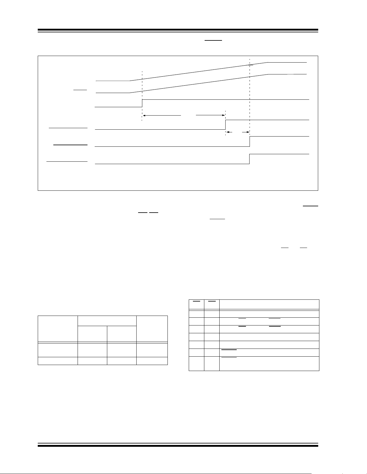
FIGURE 6-6: TIME-OUT SEQUENCE ON POWER-UP (MCLR NOT TIED TO VDD): CASE 1
VDD
MCLR
INTERNAL POR
TPWRT
PWRT TIME-OUT
OST TIME-OUT
INTERNAL RESET
FIGURE 6-7: TIME-OUT SEQUENCE ON POWER-UP (MCLR
VDD
MCLR
INTERNAL POR
TPWRT
PWRT TIME-OUT
OST TIME-OUT
INTERNAL RESET
TOST
NOT TIED TO VDD): CASE 2
TOST
FIGURE 6-8: TIME-OUT SEQUENCE ON POWER-UP (MCLR
TIED TO VDD): FAST VDD RISE
TIME
VDD
MCLR
INTERNAL POR
TPWRT
PWRT TIME-OUT
OST TIME-OUT
INTERNAL RESET
2001 Microchip Technology Inc. DS35007B-page 27
TOST
Page 30
PIC16F84A
FIGURE 6-9: TIME-OUT SEQUENCE ON POWER-UP (MCLR TIED TO VDD):
SLOW V
VDD
MCLR
INTERNAL POR
DD RISE TIME
V1
TPWRT
PWRT TIME-OUT
OST TIME-OUT
INTERNAL RESET
When VDD rises very slowly, it is possible that the TPWRT time-out and TOST time-out will expire before VDD
has reached its final value. In this example, the chip will reset properly if, and only if, V1 ≥ VDD min.
6.7 Time-out Sequence and
Power-down Status Bits (TO
On power-up (Figures 6-6 through 6-9), the time-out
sequence is as follows:
1. PWRT time-out is invoked after a POR has
expired.
2. Then, the OST is activated.
The total time-out will vary based on oscillator configuration and PWRTE configuration bit status. For example, in RC mode with the PWRT disabled, there will be
no time-ou t at all.
TABLE 6-5: TIME-OUT IN VARIOUS
SITUATIONS
Oscillator
Configuration
XT, HS, LP
RC 72 ms ——
Power-up
PWRT
Enabled
72 ms +
OSC
1024T
PWRT
Disabled
1024TOSC 1024TOSC
/PD)
Wake-up
from
SLEEP
TOST
Since the time-outs occur from the PO R pulse, if MCLR
is kept low long enough, the time-outs will expire. Then
bringing MCLR
(Figure 6-6). This is useful for testing purposes or to
synchronize more than one PIC16F84A device when
operating in parallel.
T able6-6 shows the significance of the T O
Table 6-3 lists the RESET conditions for some special
registers, while Table 6-4 lists the RESET conditions
for all the registers.
high, execution will begin immediately
and PD bits.
TABLE 6-6: STATUS BITS AND THEIR
SIGNIFICANCE
TO PD Condition
11
0x
x0
01
00
11
10
Power-on Reset
Illegal, TO is set on POR
Illegal, PD is set on POR
WDT Reset (during normal operation)
WDT Wake-up
MCLR during normal operation
MCLR during SLEEP or interrupt
wake-up from SLEEP
DS35007B-page 28 2001 Microchip Technology Inc.
Page 31

PIC16F84A
6.8 Interrupts
The PIC16F84A has 4 sources of interrup t:
• External interrupt RB0/INT pin
• TMR0 overflow interrupt
• PORTB change interrupts (pins RB7:RB4)
• Data EEPROM write complete interrupt
The interrupt control register (INTCON) records
individual int errup t requests in f lag b its. It also c ontains
the individual and global interrupt enable bits.
The global interrupt enable bit, GIE (INTCON<7>),
enables (if set) all unmasked interrupts or disables (if
cleared) all interrupts. Individual interrupts can be
disabled through their corresponding enable bits in
INTCON register. Bit GIE is cleared on RESET.
The “return from interrupt” instruction, RETFIE, exits
interrupt routine as well as sets the GIE bit, which
re-enables interrupts.
The RB0/INT pin interrupt, the R B port change interrupt
and the TMR0 overflow interrupt flags are contained in
the INTCON register.
When an interrupt is responded to, the GIE bit is
cleared to disable any further interrupt, the return
address is pushed onto the stack a nd the PC is lo ade d
with 0004h. For external interrupt events, such as the
RB0/INT pin or PORTB change interrupt, the interrupt
latency will be three to four instruction cycles. The
exact latency depends when the interrupt event occ urs.
The latency is the same for both one and two cycle
instructions. Once in the Interrupt Service Routine, the
source(s) of the interrupt can be determined by polling
the interrupt flag bits. The interrupt flag bit(s) must be
cleared in software before re-enabling interrupts to
avoid infinite interrupt requests.
Note: Individual interrupt flag bits are set
regardless of the status of their
corresponding mask bit or the GIE bit.
6.8.1 INT INTERRUPT
External interrupt on RB0/INT pin is edge triggered:
either rising if INTEDG bit (OPTION_REG<6>) is set,
or falling if INTEDG bit is clear. When a valid edge
appears on the RB0/INT pin, the INTF bit
(INTCON<1>) is set. This interrupt can be disabled by
clearing control bit INTE (INTCON<4>). Flag bit INTF
must be cleared in software via the Interrupt Service
Routine before re-enabling this interrupt. The INT
interrupt can wake the processor from SLEEP
(Section 6.11) only if the INTE bit was set prior to g oing
into SLEEP. The status of the GIE bit decides whether
the processor branches to the interrupt vector
following wake-up.
6.8.2 TMR0 INTERRUPT
An overflow (FFh → 00h) in TMR0 will set flag bit T0IF
(INTCON<2>). The interrupt can be enabled/disabled
by setting/clearing enable bit T0IE (INTCON<5>)
(Section 5.0).
6.8.3 PORTB INTERRUPT
An input change on PORTB<7:4> sets flag bit RBIF
(INTCON<0>). The interrupt can be enabled/disabled
by setting/clearing enable bit RBIE (INTCON<3>)
(Section 4.2).
Note: For a change on the I/O pin to be
recognized, the pulse width must be at
least TCY wide.
6.8.4 DATA EEPROM INTERRUPT
At the completion of a data EEPROM write cycle, flag
bit EEIF (EECON1<4>) will be set. The interrupt can be
enabled/disabled by setting/clearing enable bit EEIE
(INTCON<6>) (Section 3 .0).
FIGURE 6-10: INTERRUPT LOGIC
T0IF
T0IE
INTF
INTE
RBIF
RBIE
EEIF
EEIE
GIE
2001 Microchip Technology Inc. DS35007B-page 29
Wake-up
(If in SLEEP mode)
Interrupt to CPU
Page 32

PIC16F84A
6.9 Context Saving During Interrupts
During an interrupt, only the return PC value is saved
on the stack. Typically, users wish to sa ve ke y re gi ste r
values during an interrupt (e.g., W register and
STATUS register). This is implemented in s oftware.
The code in Example 6-1 stores and restores the
STATUS and W register’s values. The user defined
registers, W_TEMP and STATUS_TEMP are the temporary storage locations for the W and STATUS
registers values.
Example 6-1 does the following:
a) Stores the W register.
b) Stores the STATUS register in STATUS_TEMP.
c) Executes the Interrupt Service Routine code.
d) Restores the STATUS (and bank select bit)
register.
e) Restores the W register.
EXAMPLE 6-1: SAVING STATUS AND W REGISTERS IN RAM
PUSH MOVWF W_TEMP ; Copy W to TEMP register,
ISR : :
POP SWAPF STATUS_TEMP,W ; Swap nibbles in STATUS_TEMP register
SWAPF STATUS, W ; Swap status to be saved into W
MOVWF STATUS_TEMP ; Save status to STATUS_TEMP register
: ; Interrupt Service Routine
: ; should configure Bank as required
:;
; and place result into W
MOVWF STATUS ; Move W into STATUS register
; (sets bank to original state)
SWAPF W_TEMP, F ; Swap nibbles in W_TEMP and place result in W_TEMP
SWAPF W_TEMP, W ; Swap nibbles in W_TEMP and place result into W
6.10 Watchdog Timer (WDT)
The Watchdog Timer is a free running On-Chip RC
Oscillator which does not require any external
components. This RC oscillator is separate from the
RC oscillator of the OSC1/CLKIN pin. That means that
the WDT will run even if the clock on the OSC1/CLKIN
and OSC2/CLKOUT pins of the device has been
stopped, for example, by execution of a SLEEP
instruction. During normal operation, a WDT time-out
generates a device RESET. If the device is in SLEEP
mode, a WDT wake-up causes the device to wake-up
and continue with normal operation. The WDT can be
permanently disable d by programming c onfiguration bit
WDTE as a '0' (Section6.1).
6.10.1 WDT PERIOD
The WDT has a nominal time-o ut period of 18 ms, (wi th
no prescaler). The time-out periods vary with
temperature, VDD and process varia tions from par t to
part (see DC specs). If longer time-out periods are
desired, a prescaler with a division ratio of up to 1:128
can be assigned to the WDT under software c ontr ol by
writing to the OPTION_REG register. Thus, time-out
periods up to 2.3 seconds can be realized.
The CLRWDT and SLEEP instructions clear the WDT
and the postscaler (if assigned to the WDT) and prevent it from timing out and generating a device
RESETcondition.
The TO
a WDT time-out.
bit in the STATUS register will be cleared upon
DS35007B-page 30 2001 Microchip Technology Inc.
Page 33

6.10.2 WDT PROGRAMMING CONSIDERATIONS
It should also be taken into account that under worst
case conditions (V
DD = Min., T empe rature = Max., M ax.
WDT Prescaler ), it may ta ke sev e ral se co nd s bef o re a
WDT time-out occurs.
FIGURE 6-11: WATCHDOG TIMER BLOCK DIAGRAM
From TMR0 Clock Source
(Figure 5-2)
0
M
1
WDT Timer
•
U
X
PIC16F84A
Postscaler
8
PS2:PS0
To TMR0 (Figure 5-2)
PSA
WDT
Enable Bit
Note: PSA and PS2:PS0 are bits in the OPTION_REG register.
PSA
8 - to -1 MUX
0
MUX
WDT
Time-out
•
1
TABLE 6-7: SUMMARY OF REGISTERS ASSOCIATED WITH THE WATCHDOG TIMER
Addr Name Bit 7 Bit 6 Bit 5 Bit 4 Bit 3 Bit 2 Bit 1 Bit 0
2007h Config. bits
81h O PTION_REG
Legend: x = unknown. Shaded cells are not used by the WDT.
Note 1: See Register 6-1 for operation of the PWRTE
2: See Register 6-1 and Section 6.12 for operation of the code and data protection bits.
(2) (2) (2) (2) PWRTE
RBPU INTEDG T0CS T0SE PSA PS 2 PS1 PS0
bit.
(1)
WDTE FOSC1 FOSC0 (2)
Value on
Power-on
Reset
1111 1111 1111 1111
Value on all
other
RESETS
2001 Microchip Technology Inc. DS35007B-page 31
Page 34
PIC16F84A
6.11 Power-down Mode (SLEEP)
A device may be powered down (SLEEP) and later
powered up (wake-up from SLEEP).
6.11.1 SLEEP
The Power-down mode is entered by executing the
SLEEP instruction.
If enabled, the Watchdog Timer is cleared (but keeps
running), the PD
(STATUS<4>) is set, and the oscillator driver is turned
off. The I/O ports maintain the status they had before
the SLEEP instruction was executed (driving high, low,
or hi-impedance).
For the lowest current consumption in SLEEP mode,
place all I/O pins at either V
circuitry drawing current from the I/O pins, and disable
external clocks. I/O pins that are hi-impedance inputs
should be pulled h igh or lo w exte rnally to avoid switching currents caused by floating in puts. Th e T0CKI inp ut
should also be at V
on-chip pull-ups on PORTB should be considered.
The MCLR pin must be at a logic high level (VIHMC).
It should be noted that a RESET generated by a WDT
time-out does not drive the MCLR
bit (STATUS<3>) is cleared, the TO bit
DD or VSS, with no external
DD or VSS. The contribution from
pin low .
6.11.2 WAKE-UP FROM SLEEP
The device can wake-up from SLEEP through one of
the following events:
1. External RESET input on MCLR
2. WDT wake-up (if WDT was enabled).
3. Interrupt from RB0/INT pin, RB port change, or
data EEPROM write complete.
Peripherals cannot generate interrupts during SLEEP,
since no on-chip Q clocks are present.
The first event (MCLR
Reset) will cause a device
RESET. The two latter ev en t s are c ons id ered a co nti nuation of program execution. The TO and PD bits can
be used to determine the cause of a device RESET.
The PD bit, which is set on pow er-u p, i s clea red w hen
SLEEP is invoked. The TO
bit is cleared if a WDT
time-out occurred (and caused wake-up).
While the SLEEP instruction is being executed, the next
instruction (PC + 1) is pre-fetched. For the device to
wake-up through an interrupt event, the corresponding
interrupt enable bit must be set (enabled). Wake-up
occurs regardless of the state of the GIE bit. If the GIE
bit is clear (disabled), the device continues execution at
the instruction after the SLEEP instruction. If the GIE bit
is set (enabled), the device executes the instruction
after the SLEEP instruction and then branches to the
interrupt address (0004h). In cases where the
execution of the instruction following SLEEP is not
desirable, the user should have a NOP after the
SLEEP instruction.
pin.
FIGURE 6-12: WAKE-UP FROM SLEEP THROUGH INTERRUPT
Q1 Q2 Q3 Q4 Q1 Q2 Q3 Q4 Q1 Q1 Q2 Q3 Q4 Q1 Q2 Q3 Q4 Q1 Q2 Q3 Q4 Q1 Q2 Q3 Q4
OSC1
(4)
CLKOUT
INT pin
INTF Flag
(INTCON<1>)
GIE bit
(INTCON<7>)
INSTRUCTION FLOW
PC
Instruction
Fetched
Instruction
Executed
Note 1: XT, HS, or LP oscillator mode assumed.
OST = 1024TOSC (drawing not to scale). This delay will not be there for RC osc mode.
2: T
3: GIE = ’1’ assumed. In this case after wake-up, the processor jumps to the interrupt routine. If GIE = ’0’, execution will continue in-line.
4: CLKOUT is not available in these osc modes, but shown here for timing reference.
PC PC+1 PC+2
Inst(PC) = SLEEP
Inst(PC - 1)
Inst(PC + 1)
SLEEP
Processor in
SLEEP
(2)
OST
T
Interrupt Latency
(Note 2)
PC+2
Inst(PC + 2)
Inst(PC + 1)
PC + 2
Dummy cycle
0004h 0005h
Inst(0004h)
Dummy cycle
Inst(0005h)
Inst(0004h)
DS35007B-page 32 2001 Microchip Technology Inc.
Page 35

PIC16F84A
6.11.3 WAKE-UP USING INTERRUPTS
When global interrupts are disabled (GIE cleared) and
any inter rupt source has bot h its interrupt en able bit
and interrupt flag bit s et, one of the fo llowin g will oc cur:
• If the interrupt occurs before the execution of a
SLEEP instruction, the SLEEP instruction will com-
plete as a NOP. Therefore, the WDT and WDT
postscaler will not be cl eared, the TO
be set and PD
• If the interrupt occurs during or after the execu-
tion of a SLEEP instruction, the device will immediately wake-up from SLEEP. The SLEEP
instruction will be completely executed before the
wake-up. Therefore, the WDT and WDT
postscaler will be cleared, the TO
and the PD
Even if the flag bits were checked before executing a
SLEEP instructi on, it may be possible f or flag bits to
become set befo re the SLEEP instruction completes. T o
determine whether a SLEEP instruction executed, test
bit. If the PD bit is set, the SLEEP instruction
the PD
was executed as a NOP.
To ensure that the WDT is cleared, a CLRWDT instruction should be executed before a SLEEP instruction.
bits will not be cleared.
bit will be cleared.
bit will not
bit will be set
6.12 Program Verification/Code Protection
If the code protection bit(s) have not been programmed, the on-chip program memory can be read
out for verification purposes.
6.13 ID Locations
Four memory locatio ns (2000h - 2004h) are design ated
as ID locations to store checksum or other code
identification numbers. These locations are not
accessible during normal execution but are readable
and writable only during program/verify. Only the
four Least Significant bits of ID location are usable.
6.14 In-Circuit Serial Programming
PIC16F84A microcontrollers can be serially
programmed while in t he end appl icati on ci rcuit. Th is i s
simply done with two line s for clock and da ta, and three
other lines for power, ground, and the programming
voltage. Customers can manufacture boards with
unprogrammed devices, and then program the
microcontroller just before shipping the product,
allowing the most recent firmware or custom firmware
to be programmed.
For complete details of Serial Programming, please
refer to the In-Circuit Serial Programming™ (ICSP™)
Guide, (DS30277).
2001 Microchip Technology Inc. DS35007B-page 33
Page 36

PIC16F84A
NOTES:
DS35007B-page 34 2001 Microchip Technology Inc.
Page 37

PIC16F84A
7.0 INSTRUCTION SET SUMMARY
Each PIC16CXX instruction is a 14-bit word, divided
into an OPCOD E which specifie s the instruct ion type
and one or mor e operands which fur ther specify the
operation of the instruction. The PIC16CXX instruction
set summary in Table 7-2 lists byte-oriented, bit-ori-
ented, and literal and control operations. Table 7-1
shows the opcode field descriptions.
For byte-oriented inst ruc tio ns, ’f’ represents a file register designator and ’d’ represents a destination designator. The file re gister designator s pecifies which f ile
register is to be used by the instruction.
The destination des ignator specifies w here the result of
the operation is to be placed. If ’d’ is zero, the result is
placed in the W regist er . If ’d’ is one , the result is pl aced
in the file register specified in the instruction.
For bit-oriented instructions, ’b’ represents a bit field
designator which selects the nu mb er o f the bit affecte d
by the operation, while ’ f’ represents the address of the
file in which the bit is located.
For literal and control operations, ’k’ represents an
eight or eleven bit constant or literal value.
TABLE 7-1: OPCODE FIELD
DESCRIPTIONS
Field Description
f
Register file address (0x00 to 0x7F)
W
Working register (accumulator)
b
Bit address within an 8-bit file register
k
Literal field, constant data or label
x
Don't care location (= 0 or 1)
The assembler will generate code with x = 0.
It is the recomme nde d form o f u se for co mpatibility with all Microchip software tools.
d
Destination select; d = 0: store result in W,
d = 1: store result in file register f.
Default is d = 1
PC
Program Counter
TO
Time-out bit
PD
Power-down bit
The instruction set is highly orthogonal and is grouped
into three basic categories:
• Byte-oriented operations
• Bit-oriented operations
• Literal and control operations
All instructions are executed within one single instruction cycle, unless a condition al test is true or t he program counter is changed as a result of an instruction.
In this case, the execution takes two instruction cycles
with the second cycle executed as a NOP. One inst ruc-
tion cycle consists of four oscillator periods. Thus, for
an oscillator freq uency o f 4 MH z, the normal i nstructio n
execution time is 1µs. If a conditional tes t is true o r the
program counter is changed as a result of an instruction, the instruction execution time is 2 µs.
Table 7-2 lists the instructions recognized by the
MPASM™ Assembler.
Figure 7-1 shows the general formats that the instructions can have.
Note: To maintain upward compatibility with
future PIC16CXX products, do not use
the
OPTION and TRIS instruction s .
All examples use the following format to represent a
hexadecimal number:
0xhh
where h signifies a hexadecimal digit.
FIGURE 7-1: GENERAL FORMAT FOR
INSTRUCTIONS
Byte-oriented file register operations
13 8 7 6 0
OPCODE d f (FILE #)
d = 0 for destination W
d = 1 for destination f
f = 7-bit file register address
Bit-oriented file register operations
13 10 9 7 6 0
OPCODE b (BIT #) f (FILE #)
b = 3-bit bit address
f = 7-bit file register address
Literal and control operations
General
13 8 7 0
OPCODE k (literal)
k = 8-bit immediate value
CALL and GOTO instructions only
13 11 10 0
OPCODE k (literal)
k = 11-bit immediate value
A description of each instruction is available in the
PICmicro™ Mid-Range Refere nce Manu al (DS33 023).
2000 Microchip Technology Inc. DS35007B-page 35
Page 38

PIC16F84A
TABLE 7-2: PIC16CXXX INSTRUCTION SET
Mnemonic,
Operands
ADDWF
ANDWF
CLRF
CLRW
COMF
DECF
DECFSZ
INCF
INCFSZ
IORWF
MOVF
MOVWF
NOP
RLF
RRF
SUBWF
SWAPF
XORWF
BCF
BSF
BTFSC
BTFSS
ADDLW
ANDLW
CALL
CLRWDT
GOTO
IORLW
MOVLW
RETFIE
RETLW
RETURN
SLEEP
SUBLW
XORLW
Note 1: When an I/O register is modified as a function of itself ( e.g., MOVF PORTB, 1), the value used will be that value present
f, d
Add W and f
f, d
AND W with f
f
Clear f
-
Clear W
f, d
Complement f
f, d
Decrement f
f, d
Decrement f, Skip if 0
f, d
Increment f
f, d
Increment f, Skip if 0
f, d
Inclusive OR W with f
f, d
Move f
f
Move W to f
-
No Operation
f, d
Rotate Left f through Carry
f, d
Rotate Right f through Carry
f, d
Subtract W from f
f, d
Swap nibbles in f
f, d
Exclusive OR W with f
f, b
Bit Clear f
f, b
Bit Set f
f, b
Bit Test f, Skip if Clear
f, b
Bit Test f, Skip if Set
k
Add literal and W
k
AND literal with W
k
Call subroutine
-
Clear Watchdog Timer
k
Go to address
k
Inclusive OR literal with W
k
Move literal to W
-
Return from interrupt
k
Return with literal in W
-
Return from Subroutine
-
Go into standby mode
k
Subtract W from literal
k
Exclusive OR literal with W
on the pins themselves. For example, if the data latch is ’1’ for a pin configured as input and is driven low by an external
device, the data will be written back with a ’0’.
2: If this instruction is executed on the TMR0 register (and, where applicable, d = 1), the prescaler will be cleared if
assigned to the Timer0 Module.
3: If Program Counter (PC) is modified or a conditional test is true, the instruction requires two cycles. The second cycle is
executed as a
NOP
.
Description Cycles
BYTE-ORIENTED FILE REGISTER OPERATIONS
1
1
1
1
1
1
1 (2)
1
1 (2)
1
1
1
1
1
1
1
1
1
BIT-ORIENTED FILE REGISTER OPERATIONS
1
1
1 (2)
1 (2)
LITERAL AND CONTROL OPERATIONS
1
1
2
1
2
1
1
2
2
2
1
1
1
14-Bit Opcode
MSb LSb
00
0111
dfff
ffff
00
0101
dfff
00
00
00
00
00
00
00
00
00
00
00
00
00
00
00
00
01
01
01
01
11
11
10
00
10
11
11
00
11
00
00
11
11
0001
0001
1001
0011
1011
1010
1111
0100
1000
0000
0000
1101
1100
0010
1110
0110
00bb
01bb
10bb
11bb
111x
1001
0kkk
0000
1kkk
1000
00xx
0000
01xx
0000
0000
110x
1010
lfff
0xxx
dfff
dfff
dfff
dfff
dfff
dfff
dfff
lfff
0xx0
dfff
dfff
dfff
dfff
dfff
bfff
bfff
bfff
bfff
kkkk
kkkk
kkkk
0110
kkkk
kkkk
kkkk
0000
kkkk
0000
0110
kkkk
kkkk
ffff
ffff
xxxx
ffff
ffff
ffff
ffff
ffff
ffff
ffff
ffff
0000
ffff
ffff
ffff
ffff
ffff
ffff
ffff
ffff
ffff
kkkk
kkkk
kkkk
0100
kkkk
kkkk
kkkk
1001
kkkk
1000
0011
kkkk
kkkk
Status
Affected
C,DC,Z
Z
Z
Z
Z
Z
Z
Z
Z
C
C
C,DC,Z
Z
C,DC,Z
Z
,PD
TO
Z
,PD
TO
C,DC,Z
Z
Notes
1,2
1,2
2
1,2
1,2
1,2,3
1,2
1,2,3
1,2
1,2
1,2
1,2
1,2
1,2
1,2
1,2
1,2
3
3
Note: Additional information on the mid-range instruction set is available in the PICmicro™ Mid-Range MCU
Family Reference Manual (DS33023).
DS35007B-page 36 2000 Microchip Technology Inc.
Page 39

7.1 Instruction Descriptions
PIC16F84A
ADDLW Add Literal and W
Syntax: [
Operands: 0 ≤ k ≤ 255
Operation: (W) + k → (W)
Status Affected: C, DC, Z
Description: The content s of the W regis ter
ADDWF Add W and f
Syntax: [
Operands: 0 ≤ f ≤ 127
Operation: (W) + (f) → (destination)
Status Affected: C, DC, Z
Description: Add the content s of the W register
label
] ADDLW k
are added to the eig ht-bit literal ’ k’
and the result is placed in the W
register.
label
] ADDWF f,d
d ∈ [0,1]
with register ’f’. If ’d’ is 0, the result
is stored in the W register. If ’d’ is
1, the result is stored back in
register ’f’.
BCF Bit Clear f
Syntax: [
Operands: 0 ≤ f ≤ 127
Operation: 0 → (f<b>)
Stat us Affected: None
Description: Bit 'b' in register 'f' is cleared.
BSF Bit Set f
Syntax: [
Operands: 0 ≤ f ≤ 127
Operation: 1 → (f<b>)
Stat us Affected: None
Description: Bit 'b' in register 'f' is set.
label
] BCF f,b
0 ≤ b ≤ 7
label
] BSF f,b
0 ≤ b ≤ 7
ANDLW AND Literal with W
label
Syntax: [
Operands: 0 ≤ k ≤ 255
Operation: (W) .AND. (k) → (W)
Status Affected: Z
Description: The content s of W regist er are
ANDWF AND W with f
Syntax: [
Operands: 0 ≤ f ≤ 127
Operation: (W) .AND. (f) → (destination)
Status Affected: Z
Description: AND the W register with register
] ANDLW k
AND’ed with the eight-bit literal
'k'. The result is placed in the W
register.
label
] ANDWF f,d
d ∈ [0,1]
'f'. If 'd' is 0, the result is stored in
the W register. If 'd' is 1, the result
is stored back in register 'f'.
BTFSS Bit Test f, Skip if Set
label
Syntax: [
Operands: 0 ≤ f ≤ 127
Operation: skip if (f<b>) = 1
Stat us Affected: None
Description: If bit 'b' in register 'f' is '0', the nex t
] BTFSS f,b
0 ≤ b < 7
instruction is executed .
If bit 'b' is '1', then the next instruction is discarded and a NOP is executed instead, making this a 2T
instruction.
CY
2000 Microchip Technology Inc. DS35007B-page 37
Page 40

PIC16F84A
BTFSC Bit Test, Skip if Clear
Syntax: [
Operands: 0 ≤ f ≤ 127
Operation: skip if (f<b>) = 0
Status Affected: None
Description: If bit ’b’ in register ’f’ is ’1’, the next
CALL Call Subroutine
Syntax: [
Operands: 0 ≤ k ≤ 2047
Operation: (PC)+ 1→ TOS,
Status Affected: None
Description: Call Subroutine. First, return
label
] BTFSC f,b
0 ≤ b ≤ 7
instruction is executed.
If bit ’b’ in register ’f’ is ’0’, the next
instruction is discarde d, and a NOP
is executed instead, m ak in g thi s a
CY instruction.
2T
label
] CALL k
k → PC<10:0>,
(PCLATH<4:3>) → PC<12:11>
address (PC+1) is pushed onto
the stack. The eleven-bit immediate address is loade d into P C bits
<10:0>. The upper bits of the PC
are loaded from PCLATH. CALL is
a two-cycle instruction.
CLRWDT Clear Watchdog Ti mer
Syntax: [
Operands: None
Operation: 00h → WDT
Stat us Affected: TO, PD
Description: CLRWDT instruction resets the
COMF Complement f
Syntax: [
Operands: 0 ≤ f ≤ 127
Operation: (f
Stat us Affected: Z
Description: The contents of register ’f’ are
label
] CLRWDT
0 → WDT prescaler,
1 → TO
1 → PD
Watchdo g Time r . It also reset s the
prescaler of the WDT. Status bits
and PD are set.
TO
label
] COMF f,d
d ∈ [0,1]
) → (destination)
complemented. If ’d’ is 0, the
result is stored in W. If ’d’ is 1, the
result is stored back in register ’f’.
CLRF Clear f
label
Syntax: [
Operands: 0 ≤ f ≤ 127
Operation: 00h → (f)
Status Affected: Z
Description: The contents of register ’f’ are
CLRW Clear W
Syntax: [
Operands: None
Operation: 00h → (W)
Status Affected: Z
Description: W register is cleared. Zero bit (Z)
DS35007B-page 38 2000 Microchip Technology Inc.
] CLRF f
1 → Z
cleared and the Z bit is set.
label
] CLRW
1 → Z
is set.
DECF Decrement f
label
Syntax: [
Operands: 0 ≤ f ≤ 127
Operation: (f) - 1 → (destination)
Stat us Affected: Z
Description: Decrement register ’f’. If ’d’ is 0,
] DECF f,d
d ∈ [0,1]
the result is stored in the W register. If ’d’ is 1, the result is stored
back in register ’f’.
Page 41

PIC16F84A
DECFSZ Decrement f, Skip if 0
Syntax: [
Operands: 0 ≤ f ≤ 127
Operation: (f) - 1 → (destination);
Status Affected: None
Description: The contents of register ’f’ are
GOTO Unconditional Branch
Syntax: [
Operands: 0 ≤ k ≤ 2047
Operation: k → PC<10:0>
Status Affected: None
Description: GOTO is an unconditional branch.
label
] DECFSZ f,d
d ∈ [0,1]
skip if result = 0
decremented. If ’d’ is 0, the result
is placed in the W register. If ’d’ is
1, the result is placed back in
register ’f’.
If the result is 1, the next instruction is executed. If the result is 0,
then a NOP is executed instead,
making it a 2T
label
PCLATH<4:3> → PC<12:11>
The eleven-bit im me dia te v al ue i s
loaded into PC bits <10:0>. The
upper bits of PC are loaded from
PCLATH<4:3>. GOTO is a twocycle instruction.
CY instruction.
] GOTO k
INCFSZ Increment f, Skip if 0
Syntax: [
Operands: 0 ≤ f ≤ 127
Operation: (f) + 1 → (destination),
Stat us Affected: None
Description: The contents of register ’f’ are
IORLW Inclusive OR Literal with W
Syntax: [
Operands: 0 ≤ k ≤ 255
Operation: (W) .OR. k → (W)
Stat us Affected: Z
Description: The contents of the W register are
label
] INCFSZ f,d
d ∈ [0,1]
skip if result = 0
incremented. If ’ d’ is 0, th e result is
placed in the W registe r. If ’d’ is 1,
the result is placed back in
register ’f’.
If the result is 1, the next instruction is executed. If the result is 0,
a NOP is executed instead, making
CY instruction.
it a 2T
label
] IORLW k
OR’ed with the eight-bit literal 'k'.
The result is placed in the W
register.
INCF Increment f
label
Syntax: [
Operands: 0 ≤ f ≤ 127
Operation: (f) + 1 → (destination)
Status Affected: Z
Description: The contents of register ’f’ are
2000 Microchip Technology Inc. DS35007B-page 39
] INCF f,d
d ∈ [0,1]
incremented. If ’d’ is 0, the result
is placed in the W register. If ’d’ is
1, the result is placed back in
register ’f’.
IORWF Inclusive OR W with f
label
Syntax: [
Operands: 0 ≤ f ≤ 127
Operation: (W) .OR. (f) → (destination)
Stat us Affected: Z
Description: Inclusive OR the W register with
] IORWF f,d
d ∈ [0,1]
register 'f'. If 'd' is 0, the result is
placed in the W regis ter. If 'd' is 1,
the result is placed back in
register 'f'.
Page 42

PIC16F84A
MOVF Move f
Syntax: [
Operands: 0 ≤ f ≤ 127
Operation: (f) → (destination)
Status Affected: Z
Description: The contents of register f are
MOVLW Move Literal to W
Syntax: [
Operands: 0 ≤ k ≤ 255
Operation: k → (W)
Status Affected: None
Description: The eight-bit literal ’k’ is loaded
label
] MOVF f,d
d ∈ [0,1]
moved to a desti nation dependan t
upon the status of d. If d = 0, destination is W register. If d = 1, the
destination is file register f itself.
d = 1 is useful to test a file register,
since status flag Z is affected.
label
] MOVLW k
into W register. The don’t cares
will assemble as 0’s.
RETFIE Return from Interrupt
Syntax: [
Operands: None
Operation: TOS → PC,
Stat us Affected: None
RETLW Return with Literal in W
Syntax: [
Operands: 0 ≤ k ≤ 255
Operation: k → (W);
Stat us Affected: None
Description: The W register is loaded with the
label
] RETFIE
1 → GIE
label
] RETLW k
TOS → PC
eight-bit literal 'k'. The program
counter is loaded from the top of
the stack (the return address).
This is a two-cycle instruction.
MOVWF Move W to f
label
Syntax: [
Operands: 0 ≤ f ≤ 127
Operation: (W) → (f)
Status Affected: None
Description: Move data from W register to
NOP No Operation
Syntax: [
Operands: None
Operation: No operation
Status Affected: None
Description: No operation.
] MOVWF f
register 'f'.
label
] NOP
RETURN Return from Subroutine
label
Syntax: [
Operands: None
Operation: TOS → PC
Stat us Affected: None
Description: Return from subroutine. The stack
] RETURN
is POPed and the top of th e s t a ck
(TOS) is loaded into the program
counter. This is a two-cycle
instruction.
DS35007B-page 40 2000 Microchip Technology Inc.
Page 43
PIC16F84A
RLF Rotate Left f through Carry
Syntax: [
Operands: 0 ≤ f ≤ 12 7
Operation: See description below
Status Affected: C
Description: The contents of register ’f’ are
RRF Rotate Right f through Carry
Syntax: [
Operands: 0 ≤ f ≤ 127
Operation: See description below
Status Affected: C
Description: The contents of register ’f’ are
label
] RLF f,d
d ∈ [0,1]
rotated one bit to the left through
the Carry Flag. If ’d’ is 0, the
result is placed in the W register.
If ’d’ is 1, the result is stored back
in register ’f’.
Register fC
label
] RRF f,d
d ∈ [0,1]
rotated one bit to the righ t through
the Carry Flag. If ’ d’ is 0, t he result
is placed in the W register. If ’d’ is
1, the result is placed back in
register ’f’.
Register fC
SUBLW Subtract W from Literal
Syntax: [
Operands: 0 ≤ k ≤ 255
Operation: k - (W) → (W)
Status Affected: C, DC, Z
Description: The W register is subtracted (2’s
SUBWF Subtract W from f
Syntax: [
Operands: 0 ≤ f ≤ 127
Operation: (f) - (W) → (destination)
Status Affected: C, DC, Z
Description: Subtract (2’s complement method)
label
] SUBLW k
complement method) from the
eight-bit literal 'k'. The result is
placed in the W register.
label
] SUBWF f,d
d ∈ [0,1]
W register from register 'f'. If ' d' is 0,
the result is stored in the W register. If 'd' is 1, the result is stored
back in register 'f'.
SLEEP
label
Syntax: [
Operands: None
Operation: 00h → WDT,
Status Affected: TO, PD
Description: The power-down status b it, PD is
2000 Microchip Technology Inc. DS35007B-page 41
]SLEEP
0 → WDT prescaler,
1 → TO
0 → PD
cleared. Time-out status bit, TO
is set. Watch dog Timer and its
prescaler are cleared.
The processor is put into SLEEP
mode with the oscilla tor stopp ed.
,
SWAPF Swap Nibbles in f
label
Syntax: [
Operands: 0 ≤ f ≤ 127
Operation: (f<3:0>) → (destination<7:4>),
Stat us Affected: None
Description: The upper and lower nibbles of
] SWAPF f,d
d ∈ [0,1]
(f<7:4>) → (destination<3:0>)
register 'f' are exchanged. If 'd' is
0, the result is placed in W register. If 'd' i s 1, the result is placed in
register 'f'.
Page 44

PIC16F84A
XORLW Exclusive OR Literal with W
Syntax: [
Operands: 0 ≤ k ≤ 255
Operation: (W) .XOR. k → (W)
Status Affected: Z
Description: The contents of the W register
label
] XORLW k
are XOR’ed with the eight-bit literal 'k'. The result is placed in
the W register.
XORWF Exclusive OR W with f
Syntax: [
Operands: 0 ≤ f ≤ 127
Operation: (W) .XOR. (f) → (destination)
Stat us Affected: Z
Description: Exclusive OR the contents of the
label
] XORWF f,d
d ∈ [0,1]
W register with register 'f'. If 'd' is
0, the result is stored in the W
register. If 'd' is 1, the result is
stored back in register 'f'.
DS35007B-page 42 2000 Microchip Technology Inc.
Page 45

PIC16F84A
8.0 DEVELOPMENT SUPPORT
The PICmicro® microcontrollers are supported with a
full range of ha rdware a nd softwa re develo pment to ols:
• Integrated Development Environment
- MPLAB
• Assemblers/Compilers/Linkers
- MPASMTM Assembler
- MPLAB C17 and MPLAB C18 C Compilers
- MPLINK
MPLIB
• Simulators
- MPLAB SIM Software Simulator
•Emulators
- MPLAB ICE 2000 In-Circuit Emulator
- ICEPIC™ In-Circuit Emulator
• In-Circuit Debugger
- MPLAB ICD
• Device Programmers
-PRO MATE
- PICSTART® Plus Entry-Level Development
Programmer
• Low Cost Demonstration Boards
- PICDEM
- PICDEM 2 Demonstration Board
- PICDEM
- PICDEM 17 Demonstration Board
-K
8.1 MPLAB Integrated Development
The MPLAB IDE software brings an ease of software
development previously unseen in the 8-bit microcontroller market. The MPLAB IDE is a Windows®-based
application that cont ai ns :
• An interface to debugging tools
- simulator
- programmer (sold separately)
- emulator (sold separately)
- in-circuit debugger (sold separately)
• A full-featured editor
• A project manager
• Customizable toolbar and key mapping
• A status bar
• On-line help
®
IDE Software
TM
Object Linker/
TM
Object Librarian
®
II Universal D evi ce Programmer
TM
1 Demonstration Board
3 Demonstration Board
®
EELOQ
Demonstration Board
Environment Software
The MPLAB IDE allows you to:
• Edit your source files (either assembly or ‘C’)
• One touch assemble (or compile) and download
to PICmicro emulator and simulator tools (automatically updates all project information)
• Debug using:
- source files
- absolute listing file
- machine code
The ability to use MPLAB IDE with multiple debugging
tools allows users to easily switch from the costeffective simulator to a full-featured emulator with
minimal retraining.
8.2 MP ASM Assembler
The MPASM assembler is a full-featured universal
macro assembler for all PICmicro MCU’s.
The MPASM assembler has a command line interface
and a Windows shell. It can be used as a stand-alone
application on a Windows 3.x or greater system, or it
can be used through MPL AB IDE. The MPASM assembler generates relocatable object files for the MPLINK
object linker, Intel
®
standard HEX files, MAP files to
detail memory usage and symbol reference, an absolute LST file that contains source lines and generated
machine code, and a COD file for debugging.
The MPASM assembler features include:
• Integration into MPLAB IDE projects.
• User-defined macros to streamline assembly
code.
• Conditional assembl y for mul ti-p urpo se sourc e
files.
• Directives that allow complete control over the
assembly process.
8.3 MPLAB C17 and MPLAB C18
C Compilers
The MPLAB C17 and MPLAB C18 Code Development
Systems are complete ANSI ‘C’ compilers for
Microchip’s PIC17CXXX and PIC18CXXX family of
microcontrollers, respectively. These compiler s provide
powerful in tegration capabiliti es and ease of use not
found with other compilers.
For easier source level debugging, the compilers provide symbol information that is compatible with the
MPLAB IDE memory display.
2001 Microchip Technology Inc. DS35007B-page 43
Page 46

PIC16F84A
8.4 MPLINK Object Linker/ MPLIB Object Librarian
The MPLINK object linker combines relocatable
objects created by the MPASM assembler and the
MPLAB C17 and MPLAB C18 C compilers. It can also
link relocatable objects from pre-compiled libraries,
using directives from a linker script.
The MPLIB object librarian is a librarian for precompiled code to be used with the MPLINK object
linker. When a routine from a library is called from
another source file, only the modules that contain that
routine will be linked in with the appli cation. Th is allo ws
large libra ries to be used efficiently in man y different
applications. The MPLIB object librarian manages the
creation and modification of library files.
The MPLINK object linker features include:
• Integration with MPASM assembler and MPLAB
C17 and MPLAB C18 C compilers.
• Allows all memory areas t o be d efined as sections
to provide link-time flex ibi lity.
The MPLIB object librarian features include:
• Easier linking because single libraries can be
included instead of many smaller files.
• Helps keep code maintainable by grouping
related modules together.
• Allows libraries to be created and modules to be
added, listed, replaced, deleted or extracted.
8.5 MPLAB SIM Software Simulator
The MPLAB SIM softw are simulator allows code de velopment in a PC-hosted environment by simulating the
PICmicro series microcontrollers on an instruction
level. On any given instruction, the data areas can be
examined or modified and stimuli can be applied from
a file, or user-defined ke y press, to an y of the pins. The
execution can be performed in single step, execute
until break, or trace mode.
The MPLAB SIM simulator fully supports symbolic debugging using the MPLAB C17 and the MPLAB C18 C compilers and the MPASM assembler. The software simulator
offers the flexibility to develop and debug code outside of
the laboratory environmen t, making it an e xcellent mu ltiproject software development tool.
8.6 MPLAB ICE High Performance Universal In-Circuit Emulator with MPLAB IDE
The MPLAB ICE universal in-circuit emulator is intended
to provide the product development engineer with a
complete microcontroller design tool set for PICmicro
microcontrollers (MCUs). Software control of the
MPLAB ICE in-circuit emulator is provided by the
MPLAB Integrated Development Environment (IDE),
which allows editing, b uilding, do wnloadi ng and sourc e
debugging from a single environment.
The MPLAB ICE 2000 is a full-featured emulator system with enhanced trace, trigger and data monitoring
features. Interchang eable proces sor modules allow the
system to be easily reconfigured for emulation of different processors. The universal architecture of the
MPLAB ICE in-circuit emulator allows expansion to
support new PICmicro microcontrollers.
The MPLAB ICE in-circuit emulator system has been
designed as a real-time emulation system, with
advanced features that are generally found on more
expensive development tools. The PC platform and
Microsoft
make these features available to you, the end user.
®
Windows® environment were chosen to bes t
8.7 ICEPIC In-Circuit Emulator
The ICEPIC low cost, in-circuit emulator is a solution
for the Microchip Technology PIC16C5X, PIC16C6X,
PIC16C7X and PIC16CXXX families of 8-bit OneTime-Programmable (OTP) microcontrollers. The modular system can su pport dif ferent subset s of PIC16 C5X
or PIC16CXXX products through the use of interchangeable personality modules, or daughter boards.
The emulator is capable of emulating without target
application circuitry being present.
DS35007B-page 44 2001 Microchip Technology Inc.
Page 47

PIC16F84A
8.8 MPLAB ICD In-Circuit Debugger
Microchip’ s In-Circuit D ebugger , MPLAB IC D, is a powerful, low cost, run-time development tool. This tool is
based on the FLASH PICmicro MCUs an d can be used
to develop for this and other PICmicro m icrocontrollers .
The MPLAB ICD utilize s th e in -circuit debugging c apability built into the FLASH devices. This feature, along
with Microchip’s In-Circuit Serial Programming
col, offers cost-effective in-circuit FLASH debugging
from the graphical user interface of the MPLAB
Integrated Development Environment. This enables a
designer to develop and debug source code by watching variables, singl e-s tep pin g and setting break points .
Running at full speed enab les tes ting hardw are in rea ltime.
TM
proto-
8.9 PRO MATE II Universal Device Programmer
The PRO MATE II universal device programmer is a
full-featured programmer, capable of operating in
stand-alone mode, as well as PC- hosted mode. The
PRO MATE II device program m er is CE compliant.
The PRO MATE II device programmer has programmable V
programmed memory at V
imum reliability. It has an LCD display for instructions
and error messages, keys to enter commands and a
modular detachable socket assembly to support various
package types. In stand-alone mode, the PRO MATE II
device programmer can read, verify, or program
PICmicro devices. It can also set code protection in this
mode.
DD and VPP supplies, which allow it to verify
DD min and VDD max for max-
8.10 PICSTART Plus Entry Level Development Programmer
The PICSTART Plus devel opment programme r is an
easy-to-use , low cost, prototype programmer. It connects to the PC via a COM (RS-232) port. MPLAB
Integrated D evel opment Envir onmen t soft ware m akes
using the programmer simple and efficient.
The PICSTART Plus development programmer supports all PICmicro dev ices with up to 40 pins . Larger pin
count devices, such as the PIC16C92X and
PIC17C76X, may be suppor ted with an a dapter socket.
The PICSTART Plus development programmer is CE
compliant.
8.1 1 PICDEM 1 Low Cost PICmicro Demonstration Board
The PICDEM 1 demonstration board is a simple board
which demonstrates the capabilities of several of
Microchip’s m icroc ontrol lers. T he mi croco ntrolle rs su pported are: PIC16C5X (PIC16C54 to PIC16C58A),
PIC16C61, PIC16C62X, PIC16C71, PIC16C8X,
PIC17C42, PIC17C43 and PIC17C44. All necessary
hardware and software is included to run basic demo
programs. The user can program the sample microcontrollers provided with the PICDEM 1 demonstration
board on a PRO MATE II device programmer, or a
PICSTART Plus development programmer, and easily
test firmware. The user can also connect the
PICDEM 1 demonstration board to the MPLAB ICE incircuit emulator and downlo ad the firmware to the em ulator for testing. A prototype area is available for the
user to build some additional hardware and connect it
to the microcon troller sock et(s). Some of the features
include an RS-232 interface, a potentiometer for simulated analog input, push button switches and eight
LEDs connected to PORTB.
8.12 PICDEM 2 Low Cost PIC16CXX Demonstration Board
The PICDEM 2 demonstration board is a simple demonstration board that supports the PIC16C62,
PIC16C64, PIC16C65, PIC16C73 and PIC16C74
microcontrollers. All the necessary hardware and software is included to run the basic demonstration programs. The user can program the sample
microcontrollers provided with the PICDEM 2 demonstration board on a PRO MATE II device programmer,
or a PICSTART Plus development programmer, and
easily test firmware. The MPLAB ICE in-circuit emulator may also be used with the PICDEM 2 dem onstration
board to test firmware. A prototype area has been provided to the user for adding additional hardware and
connecting it to the microcontroller socket(s). Some of
the features include a RS-232 interface, push button
switches, a potentiomet er for simula ted anal og inpu t, a
serial EEPROM to demonstrate usage of the I2CTM
bus and separate headers for connection to an LCD
module and a keypad.
2001 Microchip Technology Inc. DS35007B-page 45
Page 48

PIC16F84A
8.13 PICDEM 3 Low Cost PIC16CXXX Demonstration Board
The PICDEM 3 demonstration board is a simple demonstration board that supports the PIC16C923 and
PIC16C924 in the PLCC package. It will also support
future 44-pin PLCC microcontrollers with an LCD Mo dule. All the necessary hardware and software is
included to run the basic demons tration progra ms. Th e
user can program the sample microcontrollers provided with the PICDEM 3 demonstration board on a
PRO MA TE II devi ce programmer , o r a PICSTART Plus
development programmer with an adapter socket, and
easily test firmware. The MPLAB ICE in-circuit emulator may also be used with the PICDEM 3 demonstration
board to test firmware. A prototype area has been provided to the user for addin g hardwa re and con necting it
to the microc ontroller so cket(s). Som e of the featu res
include a RS-232 interface, push button switches, a
potentiometer for simulated analog input, a thermistor
and separate headers for connection to an external
LCD module and a keypad. Also provided on the
PICDEM 3 demonstration board is a LCD panel, with 4
commons and 12 se gm ent s , tha t is capable of displaying time, temperature and day of the week. The
PICDEM 3 demonstrat ion boa rd provi des an additi onal
RS-232 interface and Windows software for showing
the demultiplexed LCD signals on a PC. A simple serial
interface allows the user to construct a hardware
demultiplexer for the LCD signals.
8.14 PICDEM 17 Demonstration Board
The PICDEM 17 de mo ns t r at i on bo ar d is an ev al u at i on
board that demonstrates the capabilities of several
Microchip microcontrollers, including PIC17C752,
PIC17C756A, PIC17C762 and PIC17C766. All necessary hardware is inclu ded to run b asic demo p rograms,
which are supplied on a 3.5-inch disk. A programmed
sample is included and the user may erase it and
program it with the other sample programs using the
PRO MATE II device programmer, or the PICSTART
Plus development programmer, and easily debug an d
test the sample code. In addition, the PICDEM 17 demonstration board supports down loading of programs to
and executing out of external FLASH memory on board.
The PICDEM 17 demonstration board is also usable
with the MPLAB ICE in-circuit emulator, or the
PICMASTER emulator and all o f the samp le pro grams
can be run and modified using either emulator. Additionally, a generous prototype area is available for user
hardware.
8.15 KEELOQ Evaluation and Programming Tools
KEELOQ evaluation and programming tools support
Microchip’s HCS Secure Data Products. The HCS evaluation kit includes a LCD display to show changing
codes, a decoder to decode transmissions and a programming interface to program test transmitters.
DS35007B-page 46 2001 Microchip Technology Inc.
Page 49

TABLE 8-1: DEVELOPMENT TOOLS FROM MICROCHIP
PIC16F84A
MCP2510
MCRFXXX
HCSXXX
93CXX
25CXX/
24CXX/
PIC18FXXX
PIC18CXX2
PIC17C7XX
PIC17C4X
PIC16C9XX
PIC16F8XX
PIC16C8X
9
9
9
9
9
9
9
9
9
9
9
9
9
9
9
9
9
9
9
9
9
9
9
9
9
9
9
9
9
9
9
9
9
9
9
9
9
9
9
9
9
9
9
9
9
9
9
9
9
9
9
9
9
9
9
9
9
9
9
ICD In-Circuit Debugger (DV164001) with PIC16C62, 63, 64, 65, 72, 73, 74, 76, 77.
®
9
PIC16C7XX
9
PIC16C7X
9
PIC16F62X
9
PIC16CXXX
9
PIC16C6X
9
PIC16C5X
9
PIC14000
9
PIC12CXXX
9
Integrated
®
®
9
9
9
9
9
9
9
9
Object Linker
Assembler/
C17 C Compiler
C18 C Compiler
TM
TM
®
9
9
9
9
**
9
9
9
9
9
9
9
*
9
9
9
In-Circuit Emulator
ICE In-Circuit Emulator
®
TM
ICD In-Circuit
®
9
9
†
9
9
*
9
Plus Entry Level
®
9
**
**
9
9
9
9
9
9
9
9
9
9
9
9
II
®
†
9
9
9
†
9
9
9
TM
TM
1 Demonstration
2 Demonstration
3 Demonstration
14A Demonstration
TM
TM
TM
17 Demonstration
TM
TM
Programmer’s Kit
Evaluation Kit
Transponder Kit
TM
®
®
Developer’s Kit
TM
Universal Device Programmer
Board
Board
Board
Board
MPLAB
MPLAB
MPLAB
MPASM
MPLAB
ICEPIC
Development Environment
MPLINK
Software Tool s
MPLAB
Debugger
Emulators
Development Programmer
PICSTART
PRO MATE
PICDEM
PICDEM
Debugger
Programmers
PICDEM
PICDEM
Board
PICDEM
KEELOQ
KEELOQ
Developer’s Kit
microID
125 kHz microID
125 kHz Anticollision microID
13.56 MHz Anticollision
microID
Developer’s Kit
Demo Boards and Eval Kits
MCP2510 CAN Developer’s Kit
* Contact the Microchip Technology Inc. web site at www.microchip.com for information on how to use the MPLAB
2001 Microchip Technology Inc. DS35007B-page 47
Development tool is available on select devices.
†
** Contact Microchip Technology Inc. for availability date.
Page 50

PIC16F84A
NOTES:
DS35007B-page 48 2001 Microchip Technology Inc.
Page 51

PIC16F84A
9.0 ELECTRICAL CHARACTERISTICS
Absolute Maximum Ratings †
Ambient temperature under bias.............................................................................................................-55°C to +125°C
Storage temperature.............................................................................................................................. -65°C to +150°C
Voltage on any pin with respect to V
Voltage on V
Voltage on MCLR
DD with respect to VSS ........................................................................................................... -0.3 to +7.5V
with respect to VSS
Voltage on RA4 with respect to V
(2)
Total power dissipation
Maximum current out of V
Maximum current into V
Input clamp current, I
Output clamp current, I
.....................................................................................................................................800 mW
SS pin...........................................................................................................................150 mA
DD pin..............................................................................................................................100 mA
IK (VI < 0 or VI > VDD).....................................................................................................................± 20 mA
OK (VO < 0 or VO > VDD).............................................................................................................± 20 mA
Maximum output current sunk by any I/O pin..........................................................................................................25 mA
Maximum output current sourced by any I/O pin....................................................................................................25 mA
Maximum current sunk by PORTA..........................................................................................................................80 mA
Maximum current sourced by PORTA.....................................................................................................................50 mA
Maximum current sunk by PORTB........................................................................................................................150 mA
Maximum current sourced by PORTB..................................................................................................................100 mA
Note 1: Voltage spikes bel ow V
Thus, a series resistor of 50-100 Ω s ho uld be us ed when applying a “lo w ” le vel to the M CL R
pulling this pin directly to V
2: Power dissipat ion is ca lcula ted as foll ows: Pdis = V
SS (except VDD, MCLR, and RA4).........................................-0.3V to (VDD + 0.3V)
(1)
.......................................................................................................-0.3 to +14V
SS ........................................................................................................... -0.3 to +8.5V
SS at the MCLR pin, inducing currents greater than 80 mA, may cause latch-up.
pin rather than
SS.
DD x {IDD - ∑ IOH} + ∑ {(VDD-VOH) x IOH} + ∑(VOl x IOL).
† NOTICE: Stresses above those listed under “Absolute Maximum Ratings” may cause permanent damage to the
device. This is a stress rating only and functional operation of the device at those or any other conditions above
those indicated in the ope ration listi ngs of this speci fication is not implied. Exposure to maxim um rating co nditions for
extended periods may affect device reliability.
2001 Microchip Technology Inc. DS35007B-page 49
Page 52

PIC16F84A
FIGURE 9-1: PIC16F84A-20 VOLTAGE-FREQUENCY GRAPH
6.0V
5.5V
5.0V
4.5V
4.0V
Voltage
3.5V
3.0V
2.5V
2.0V
Frequency
20 MHz
FIGURE 9-2: PIC16LF84A-04 VOLTAGE-
FREQUENCY GRAPH
6.0V
5.5V
5.0V
4.5V
4.0V
3.5V
Voltage
3.0V
2.5V
2.0V
4 MHz
Frequency
F
MAX = (6.0 MHz/V) (VDDAPPMIN - 2.0V) + 4 MHz
Note 1: VDDAPPMIN is the minimum voltage of the
PICmicro
2: F
®
device in the application.
MAX has a maximum frequency of 10 MHz.
10 MHz
FIGURE 9-3: PIC16F84A-04 VOLTAGE-
FREQUENCY GRAPH
6.0V
5.5V
5.0V
4.5V
4.0V
3.5V
Voltage
3.0V
2.5V
2.0V
4 MHz
Frequency
DS35007B-page 50 2001 Microchip Technology Inc.
Page 53

9.1 DC Characteristics
PIC16LF84A-04
(Commercial, Industrial)
PIC16F84A
Standard Operating Conditions (unless otherwise stated)
Operating temperature 0°C ≤ TA ≤ +70°C (commercial)
-40°C ≤ T
-40°C ≤ T
A ≤ +85°C (industrial)
A ≤ +125°C (extended)
PIC16F84A-04
(Commercial, Industrial, Extended)
PIC16F84A-20
(Commercial, Industrial, Extended)
Param
Symbol Characteristic Min Ty p† Max Units Conditions
No.
DD Supply Voltage
V
Standard Operating Conditions (unless otherwise stated)
Operating temperature 0°C ≤ T
-40°C ≤ T
-40°C ≤ T
A ≤ +70°C (commercial)
A ≤ +85°C (industrial)
A ≤ +125°C (extended)
D001 16LF84A 2.0 — 5.5 V XT, RC, and LP osc configuration
D001
D001A
D002 V
DR RAM Data Retention
16F84A 4.0
4.5——
1.5 — — V Device in SLEEP mode
5.5
5.5VV
XT, RC and LP osc configuration
HS osc configuration
Voltage (Note 1)
D003 V
POR VDD Start Voltage to ensure
— Vss — V See section on Pow er-on Re set for de ta ils
internal Power-on Reset
signal
D004 SVDD VDD Rise Rate to ensure
0.05 — — V/ms
internal Power-on Reset
signal
IDD Supply Current (Note 2)
D010 16LF84A — 1 4 mA RC and XT osc configuration (Note 4)
F
OSC = 2.0 MHz, VDD = 5.5V
D010
D010A
16F84A —
—
1.8
3
4.5
10
mA
RC and XT osc configuration (Note 4)
OSC = 4.0 MHz, VDD = 5.5V
F
RC and XT osc configuration (Note 4)
mA
FOSC = 4.0 MHz, VDD = 5.5V
(During FLASH programming)
D013
—
10
20
HS osc configuration (PIC16F84A-20)
mA
OSC = 20 MHz, VDD = 5.5V
F
D014 16LF84A — 15 45 µA LP osc configuration
F
OSC = 32 kHz, VDD = 2.0V, WDT disabled
Legend: Rows with standard voltage device data only are shaded for improved readability.
† Data in "Typ" column is at 5.0V, 25°C unless otherwise stated. These parameters are for design guidance
only and are not tested.
NR Not rated for operation.
Note 1: This is the limi t to which V
DD can be lowered without losing RAM data.
2: The supply current is mainly a function of the operating voltage and frequency. Other factors, such as I/O
pin loading and switching rate, oscillator type, internal code execution pattern, and temperature also have
an impact on the current consumption.
The test conditions for all IDD measurements in active operation mode are:
OSC1 = external square wave, from rail-to-rail; all I/O pins tri-stated, pulled to V
T0CKI = V
DD, MCLR = VDD; WDT enabled/disabled as specified.
DD,
3: The power-down current in SLEEP mode does not depend on the oscillator type. Power-down current is
measured with the part in SLEEP mode, with all I/O pins in hi-impedance state and tied to VDD and VSS.
4: For RC osc configuration, current through R
estimated by the formula I
R = VDD/2REXT (mA) with REXT in kOhm.
EXT is not included. The current through the resistor can be
5: The ∆ current is the additional current consumed when this peripheral is enabled. This current should be
added to the base I
DD measurement.
2001 Microchip Technology Inc. DS35007B-page 51
Page 54

PIC16F84A
9.1 DC Characteristics (Continued)
PIC16LF84A-04
(Commercial, Industrial)
Standard Operating Conditions (unless otherwise stated)
Operating temperature 0°C ≤ T
-40°C ≤ T
-40°C ≤ T
A ≤ +70°C (commercial)
A ≤ +85°C (industrial)
A ≤ +125°C (extended)
PIC16F84A-04
(Commercial, Industrial, Extended)
PIC16F84A-20
(Commercial, Industrial, Extended)
Param
Symbol Characteristic Min Ty p† Max Units Conditions
No.
I
PD Power-down Current
(Note 3)
Standard Operating Conditions (unless otherwise stated)
Operating temperature 0°C ≤ T
-40°C ≤ T
-40°C ≤ T
A ≤ +70°C (commercial)
A ≤ +85°C (industrial)
A ≤ +125°C (extended)
D020 16LF84A
D020 16F84A-20
16F84A-04
D021A 16LF84A —0.41.0µAVDD = 2.0V, WDT disabled, industrial
D021A 16F84A-20
16F84A-04——
D021B 16F84A-20
16F84A-04——
1.5
1.0
1.5
1.0
3.5
3.0µAµA
5.5
5.0µAµA
VDD = 4.5V, WDT disabled, industrial
V
DD = 4.0V, WDT disabled, industrial
VDD = 4.5V, WDT disabled, extended
DD = 4.0V, WDT disabled, extended
V
Module Differential Current
(Note 5)
D022 ∆IWDT
Watchdog Timer —
—
—
—
—
.20
3.5
3.5
4.8
4.8
16
20
28
25
30
DD = 2.0V, Industrial, Commercial
µA
V
V
DD = 4.0V, Commercial
µA
DD = 4.0V, Industrial, Extended
V
µA
DD = 4.5V, Commercial
V
µA
V
DD = 4.5V, Industrial, Extended
µA
Legend: Rows with standard voltage device data only are shaded for improved readability.
† Data in "Typ" column is at 5.0V, 25°C unless otherwise stated. These parameters are for design guidance
only and are not tested.
NR Not rated for operation.
Note 1: This is the limi t to which V
DD can be lowered without losing RAM data.
2: The supply current is mainly a function of the operating voltage and frequency. Other factors, such as I/O
pin loading and switching rate, oscillator type, internal code execution pattern, and temperature also have
an impact on the current consumption.
The test conditions for all IDD measurements in active operation mode are:
OSC1 = external square wave, from rail-to-rail; all I/O pins tri-stated, pulled to V
T0CKI = V
DD, MCLR = VDD; WDT enabled/disabled as specified.
DD,
3: The power-down current in SLEEP mode does not depend on the oscillator type. Power-down current is
measured with the part in SLEEP mode, with all I/O pins in hi-impedance state and tied to VDD and VSS.
4: For RC osc configuration, current through R
estimated by the formula I
R = VDD/2REXT (mA) with REXT in kOhm.
EXT is not included. The current through the resistor can be
5: The ∆ current is the additional current consumed when this peripheral is enabled. This current should be
added to the base I
DD measurement.
DS35007B-page 52 2001 Microchip Technology Inc.
Page 55

PIC16F84A
9.2 DC Characteristics: PIC16F84A-04 (Commercial, Industrial)
PIC16F84A-20 (Commercial, Industrial)
PIC16LF84A-04 (Commercial, Industrial)
Standard Operating Conditions (unless otherwise stated)
DC Characteristics
All Pins Except Power Supply Pins
Operating temperature 0°C ≤ T
-40°C ≤ T
Operating voltag e V
DD range as described in DC specifications
(Section 9.1)
A ≤ +70°C (commercial)
A ≤ +85°C (industrial)
Param
Symbol Characteristic Min Typ† Max Units Conditions
No.
IL Input Low Vo ltage
V
I/O ports:
D030 with TTL buffer V
SS —0.8 V4.5V ≤ VDD ≤ 5.5V (Note 4)
D030A VSS —0.16VDD V Entire range (Note 4)
D031 with Schmitt Trigger buffer V
SS —0.2VDD V Entire range
D032 MCLR, RA4/T0 CKI VSS —0.2VDD V
D033 OSC1 (XT, HS and LP modes) VSS —0.3VDD V (Note 1)
D034 OSC1 (RC mode) V
SS —0.1VDD V
VIH Input High Voltage
I/O ports: —
D040
D040A
with TTL buffer 2.0
0.25V
D041 with Schmitt Trigger buffer 0.8 V
D042 MCLR
, 0.8 VDD —VDD V
DD
DD+0.8
DD —VDD Entire range
—
VDD
VV4.5V ≤ VDD ≤ 5.5V (Note 4)
Entire range (Note 4)
—
V
D042A RA4/T0CKI 0.8 VDD —8.5 V
D043 OSC1 (XT, HS and LP modes) 0.8 VDD —VDD V (Note 1)
D043A OSC1 (RC mode) 0.9 V
D050 VHYS Hysteresis of Schmitt Trigger
DD VDD V
—0.1—V
Inputs
D070 I
PURB PORTB Weak Pull-up Current 50 250 400 µAVDD = 5.0V, VPIN = VSS
IIL Input Leakage Current
(Notes 2, 3)
D060 I/O ports — — ±1 µAVss ≤ V
PIN ≤ VDD,
Pin at hi-impedance
D061 MCLR
, RA4/T0CKI — — ±5 µAVss ≤ VPIN ≤ VDD
D063 OSC1 — — ±5 µAVss ≤ VPIN ≤ VDD, XT, HS
and LP osc configuration
† Data in “Typ” column is at 5.0V, 25°C unless otherwise stated. These parameters are for design guidance
only and are not tested.
Note 1: In RC oscillator configuration, the OSC1 pin is a Schmitt Trigger input. Do not drive the PIC16F84A with an
external clock while the device is in RC mode, or chip damage may result.
2: The leakage current on the MCLR
pin is strongly dependent on the applied voltage level. The specified
levels represent normal operating conditions. Higher leakage current may be measured at different input
voltages.
3: Negative current is defined as coming out of the pin.
4: The user may choose the better of the two specs.
2001 Microchip Technology Inc. DS35007B-page 53
Page 56

PIC16F84A
9.2 DC Characteristics: PIC16F84A-04 (Commercial, Industrial)
PIC16F84A-20 (Commercial, Industrial)
PIC16LF84A-04 (Commercial, Industrial) (Continued)
Standard Operating Conditions (unless otherwise stated)
DC Characteristics
All Pins Except Power Supply Pins
Operating temperature 0°C ≤ T
-40°C ≤ T
Operating voltag e V
DD range as described in DC specifications
(Section 9.1)
A ≤ +70°C (commercial)
A ≤ +85°C (industrial)
Param
Symbol Characteristic Min Typ† Max Units Conditions
No.
VOL Output Low Voltage
D080 I/O ports ——0.6VI
OL = 8.5 mA, VDD = 4.5V
D083 OSC2/CLKOUT — — 0.6 V IOL = 1.6 mA, VDD = 4.5V,
(RC mode on ly)
OH Output High Voltage
V
D090 I/O ports (Note 3) VDD-0.7 — — V IOH = -3.0 mA, VDD = 4.5V
D092 OSC2/CLKOUT (Note 3) VDD-0.7 — — V IOH = -1.3 mA, VDD = 4.5V
(RC mode on ly)
V
OD Open Drain High Voltage
D150 RA4 pin — — 8.5 V
Capacitive Loading Specs on
Output Pins
D100 C
OSC2 OSC2 pin — — 15 pF In XT, HS and LP modes
when external clock is used
to drive OSC1
D101 CIO All I/O pins and OSC2
——50pF
(RC mode)
Data EEPROM Memory
D120 E
D121 V
D Endurance 1M 10M — E/W 25°C at 5V
DRW VDD for read/write VMIN —5.5 VVMIN = Minimum operating
voltage
D122 T
DEW Erase/Write cycle time — 4 8 ms
Program FLASH Memory
D130 E
P Endurance 1000 10K — E/W
D131 VPR VDD for read VMIN —5.5 VVMIN = Minimum operating
voltage
D132 V
PEW VDD for erase/write 4.5 — 5.5 V
D133 TPEW Erase/Write cycle time — 4 8 ms
† Data in “Typ” column is at 5.0V, 25°C unless otherwise stated. These parameters are for design guidance
only and are not tested.
Note 1: In RC oscillator configuration, the OSC1 pin is a Schmitt Trigger input. Do not drive the PIC16F84A with an
external clock while the device is in RC mode, or chip damage may result.
2: The leakage current on the MCLR
pin is strongly dependent on the applied voltage level. The specified
levels represent normal operating conditions. Higher leakage current may be measured at different input
voltages.
3: Negative current is defined as coming out of the pin.
4: The user may choose the better of the two specs.
DS35007B-page 54 2001 Microchip Technology Inc.
Page 57

9.3 AC (Timing) Characteristics
9.3.1 TIMING PARAMETER SYMBOLOGY
The timing parameter symbols have been created following one of the following formats:
1. TppS2ppS
2. TppS
T
F Frequency T Time
Lowercase letters (pp) and their meanings:
pp
2 to os, osc OSC1
ck CLKOUT ost oscillator start-up timer
cy cycle time pwrt power-up timer
io I/O port rbt RBx pins
inp INT pin t0 T0CKI
mp MCL R
Uppercase letters and their meanings:
S
F Fall P Period
HHigh RRise
I Invalid (high impedance) V Valid
L Low Z High Impedance
wdt watchdog timer
PIC16F84A
2001 Microchip Technology Inc. DS35007B-page 55
Page 58
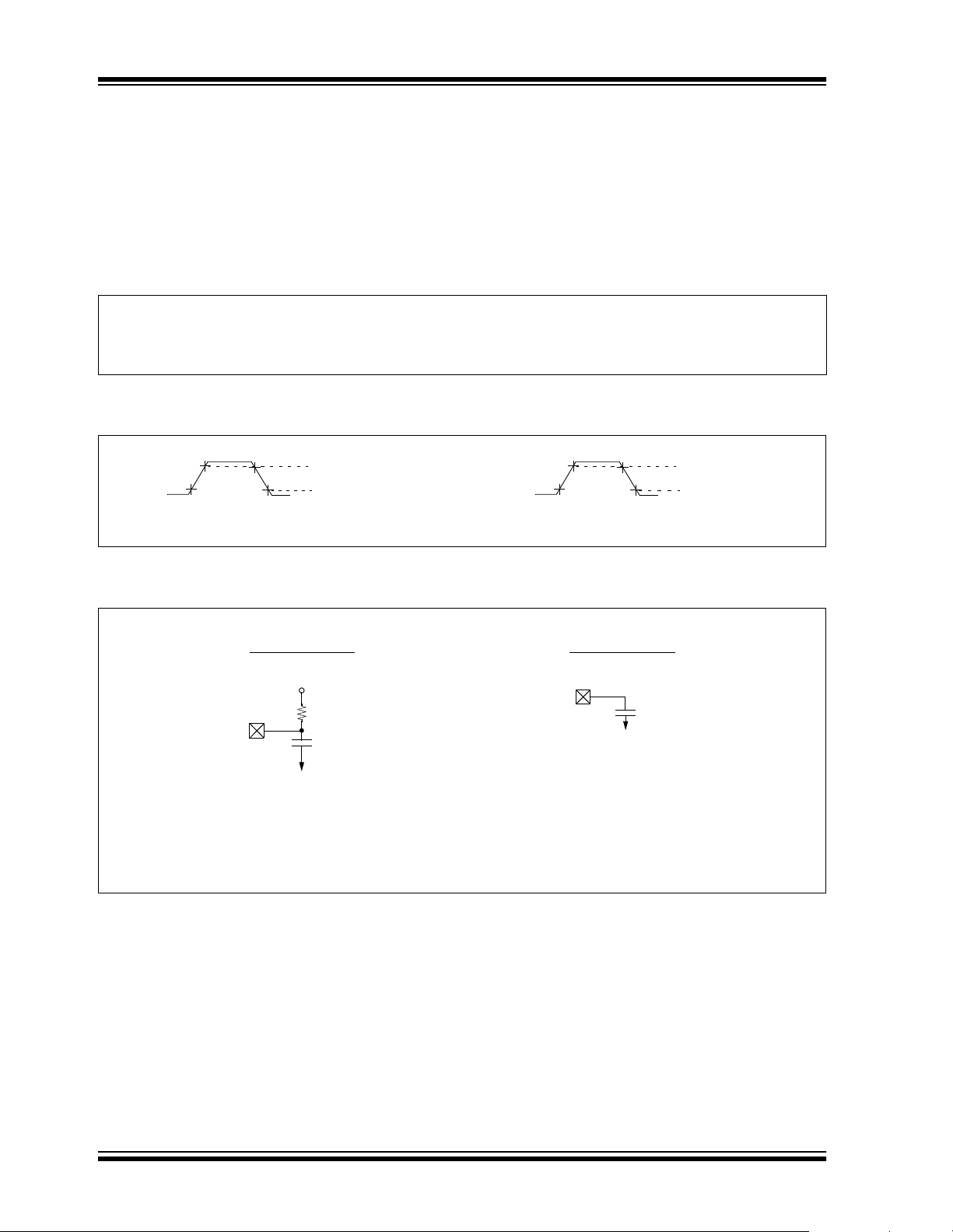
PIC16F84A
9.3.2 TIMING CONDITIONS
The temperature and voltages specified in Table 9-1
apply to all timing specifications unless otherwise
noted. All t imings are measured betw een high and low
measurement points as indicated in Figure 9-4.
Figure 9-5 sp ecifies the load conditions for the timing
specifications.
TABLE 9-1: TEMPERATURE AND VOLTAGE SPECIFICATIONS - AC
Standard Operat ing Conditi ons (unle ss otherw is e stated)
AC CHARACTERISTICS
Operating temperature 0°C ≤ T
-40°C ≤ T
Operating voltage V
DD range as described in DC specifications (Section 9.1)
FIGURE 9-4: PARAMETER MEASUREMENT INFORMATION
0.7 V
DD XTAL
0.8 VDD RC
0.3 V
DD XTAL
0.15 V
DD RC
OSC1 Measurement Points I/O Port Measurement Points
(High)
(Low)
A ≤ +70°C for commercial
A ≤ +85°C for in dustrial
0.9 VDD (High)
0.1 V
DD (Low)
FIGURE 9-5: LOAD CONDITIONS
Load Condition 1 Load Condition 2
VDD/2
RL
Pin
L = 464Ω
R
L = 50 pF for all pins except OSC2
C
15 pF for OSC2 output
CL
VSS
Pin
CL
VSS
DS35007B-page 56 2001 Microchip Technology Inc.
Page 59
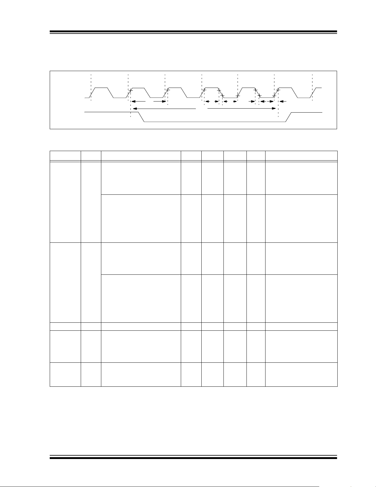
9.3.3 TIMING DIAGRAMS AND SPECIFICATIONS
FIGURE 9-6: EXTERNAL CLOCK TIMING
PIC16F84A
OSC1
CLKOUT
Q4
Q1 Q2
13344
Q3 Q4 Q1
2
TABLE 9-2: EXTERNAL CLOCK TIMING REQUIREMENTS
Param No. Sym Characteristic Min Typ† Max Units Conditions
(1)
(1)
(1)
(1)
DC — 2 MHz XT, RC osc (-04, LF)
DC — 4 MHz XT, RC osc (-04)
DC — 20 MHz HS osc (-20)
DC — 200 kHz LP osc (-04, LF)
DC — 2 MHz RC osc (-04, LF)
DC — 4 MHz RC osc (-04)
0.1 — 2 MHz XT osc (-04, LF)
0.1 — 4 MHz XT osc (-04)
1.0 — 20 MHz HS osc (-20)
DC — 200 kHz LP osc (-04, LF)
500 — — ns XT, RC osc (-04, LF)
250 — — ns XT, RC osc (-04)
50 — — ns HS osc (-20)
5.0 — — µs LP osc (-04, LF)
500 — — ns RC osc (-04, LF)
250 — — ns RC osc (-04)
500 — 10,000 ns XT osc (-04, LF)
250 — 10,000 ns XT osc (-04)
50 — 1,000 ns HS osc (-20)
5.0 — — µs LP osc (-04, LF)
0.2 4/FOSC DC µs
60 — — ns XT osc (-04, LF)
50 — — ns XT osc (-04)
2.0 — — µs LP osc (-04, LF)
17.5 — — ns HS osc (-20)
25 — — ns XT osc (-04)
50 — — ns LP osc (-04, LF)
7.5 — — ns HS osc (-20)
F
OSC External CLKIN Frequency
Oscillator Frequency
1T
2T
3 TosL,
4TosR,
OSC External CLKIN Period
Oscillator Period
CY Instruction Cycle Time
(1)
Clock in (OSC1) High or Low
TosH
Time
Clock in (OSC1) Rise or Fall
TosF
Time
† Data in "Typ" column is at 5.0V, 25°C unless otherwise stated. These parameters are for design guidance
only and are not tested.
Note 1: Inst ruction cycle period (TCY) equals four times the input oscillator time-base period. All specified values
are based on characterization data for that particular oscillator type under standard operating conditions
with the device executin g cod e. Exc eed ing t hes e sp ec ifi ed li mi ts may result in an unstable oscillator ope ration and/or higher than expected current consumption. All devices are tested to operate at "Min." values
with an external clock applied to the OSC1 pin.
When an external clock input is used, the "Max." cycle time limit is "DC" (no clock) for all devices.
2001 Microchip Technology Inc. DS35007B-page 57
Page 60

PIC16F84A
FIGURE 9-7: CLKOUT AND I/O TIMING
17
10
13
Q1
22
23
19
14
20, 21
Q4
OSC1
CLKOUT
I/O Pin
(Input)
I/O Pin
(Output)
Note: All tests must be done with specified capacitive loads (Figure 9-5) 50 pF on I/O pins and CLKOUT.
old value
TABLE 9-3: CLKOUT AND I/O TIMING REQUIREMENTS
Param
No.
10 TosH2ckL OSC1↑ to CLKOUT↓ Standard —1530ns(Note 1)
10A Extended (LF) — 15 120 ns (Note 1)
11 TosH2ckH OSC1↑ to CLKOUT↑ Standard — 15 30 ns (Note 1)
11A Extended (LF) — 15 120 ns (Note 1)
12 TckR CLKOUT rise time Standard — 15 30 ns (Note 1)
12A Extended (LF) — 15 100 ns (Note 1)
13 TckF CLKOUT fall time Standard — 15 30 ns (Note 1)
13A Extended (LF) — 15 100 ns (Note 1)
14 TckL2ioV CLKOUT ↓ to Port out valid — — 0.5T
15 TioV2ckH Port in valid before
16 TckH2ioI Port in hold after CLKOUT ↑ 0——ns(Note 1)
17 TosH2ioV OSC1↑ (Q1 cycle) to
18 TosH2ioI OSC1↑ (Q2 cycle) to Port
19 TioV2osH Port input valid to OSC1
20 TioR Port output rise time Standard — 10 35 ns
20A Extended (LF) — 10 70 ns
21 TioF Port output fall time Standard — 10 35 ns
21A Extended (LF) — 10 70 ns
22 T
22A Extended (LF) 55 — — ns
23 T
23A Extended (LF) T
Note 1: Measurements are taken in RC mode where CLKOUT output is 4 x T
Sym Characteristic Min Typ† Max Units Conditions
CLKOUT ↑
Port out valid
input invalid (I/O in hold time)
(I/O in setup time)
INP INT pin high
or low time
RBP RB7:RB4 change INT
high or low time
† Data in "Typ" column is at 5.0V, 25°C unless otherwise stated. These parameters are for design guidance only and are not tested.
§ By design.
Standard 0.30T
Extended (LF) 0.30T
Standard — — 125 ns
Extended (LF) — — 250 ns
Standard 10 — — ns
Extended (LF) 10 — — ns
↑
Standard -75 — — ns
Extended (LF) -175 — — ns
Standard 20 — — ns
Standard TOSC§— — ns
OSC.
Q2 Q3
11
18
15
12
16
new value
CY +20 ns (Note 1)
CY + 30 — — ns (Note 1)
CY + 80 — — ns (Note 1)
OSC§— — ns
DS35007B-page 58 2001 Microchip Technology Inc.
Page 61

PIC16F84A
FIGURE 9-8: RESET, WATCHDOG TIMER, OSCILLATOR START-UP TIMER AND POWER-UP
TIMER TIMING
VDD
MCLR
30
Internal
POR
PWRT
Time-out
OSC
Time-out
Internal
Reset
Watchdog
Timer
Reset
I/O Pins
33
32
34
31
34
TABLE 9-4: RESET, WATCHDOG TIMER, OSCILLATOR START-UP TIMER AND
POWER-UP TIMER REQUIREMENTS
Parameter
No.
30 TmcL MCLR
31 TWDT
32 T
33 TPWRT Power-up Timer Period 28 72 132 ms VDD = 5.0V
34 T
† Data in "Typ" column is at 5V, 25°C, unless otherwise stated. These parameters are for design guidance
Sym Characteristic Min Typ† Max Units Conditions
Pulse Width (low) 2 ——µsVDD = 5.0V
OST
IOZ
Watchdog Timer Time-out
Period (No Prescaler)
Oscillation Start-up Timer
Period
I/O hi-impedance from MCLR
Low or RESET
71833msV
1024T
OSC ms TOSC = OSC1 period
——100ns
DD = 5.0V
only and are not tested.
2001 Microchip Technology Inc. DS35007B-page 59
Page 62

PIC16F84A
FIGURE 9-9: TIMER0 CLOCK TIMINGS
RA4/T0CKI
40 41
42
TABLE 9-5: TIMER0 CLOCK REQUIREMENTS
Parameter
No.
40 Tt0H T0CKI High Pulse
41 Tt0L T0CKI Low Pulse
42 Tt0P T0CKI Period T
Sym Characteristic Min Typ† Max Units Conditions
No Prescaler 0.5T
Width
Width
† Data in "Typ" column is at 5.0V, 25°C, unless otherwise stated. These parameters are for design guidance
only and are not tested.
With Prescaler 50
No Prescaler 0.5T
With Prescaler 50
CY + 20 ——ns
————nsns2.0V ≤ V
30
CY + 20 — — ns
————nsns2.0V ≤ V
20
CY + 40
N
— — ns N = prescale value
DD ≤ 3.0V
3.0V ≤ V
3.0V ≤ V
(2, 4, ..., 256)
DD ≤ 6.0V
DD ≤ 3.0V
DD ≤ 6.0V
DS35007B-page 60 2001 Microchip Technology Inc.
Page 63

PIC16F84A
10.0 DC/AC CHARACTERISTIC GRAPHS
The graphs provided in this section are for design guidance and are not tested.
In some graphs, th e data presented are outside specified operating ran ge (i.e ., out side sp ecifie d V
for information only and devices are ensured to operate properly only within the specified range.
The data p resented in this section is a statistical summary of data collected on units from different lots over a period
of time and matrix samples. ‘Typical’ represents the mean of the distribution at 25°C. ‘Max’ or ‘Min’ represents
(mean + 3σ) or (mean - 3σ), respectively, where σ is a standard deviation over the whole temperature range.
DD range). This i s
2001 Microchip Technology Inc. DS35007B-page 61
Page 64

PIC16F84A
FIGURE 10-1: TYPICAL IDD vs. FOSC OVER VDD (HS MODE, 25°C)
4.0
3.5
3.0
2.5
2.0
IDD (mA)
1.5
1.0
0.5
2.0 V
0.0
4 6 8 10 12 14 16 18 20
FIGURE 10-2: MAXIMUM I
5.5 V
5.0 V
4.5 V
4.0 V
3.5 V
3.0 V
2.5 V
OSC
F
(MHz)
DD vs. FOSC OVER VDD (HS MODE, -40° TO +125°C)
5.0
4.5
4.0
3.5
3.0
2.5
IDD (mA)
2.0
4.0 V
1.5
1.0
2.5 V
0.5
2.0 V
0.0
4 6 8 10 12 14 16 18 20
3.5 V
3.0 V
OSC
F
(MHz)
5.5 V
5.0 V
4.5 V
DS35007B-page 62 © 2001 Microchip Technology Inc.
Page 65

FIGURE 10-3: TYPICAL IDD vs. FOSC OVER VDD (XT MODE, 25°C)
1.0
0.9
0.8
0.7
0.6
0.5
IDD (mA)
0.4
PIC16F84A
5.5 V
5.0 V
4.5 V
4.0 V
3.5 V
0.3
0.2
0.1
0.0
0.0 0.5 1.0 1.5 2.0 2.5 3.0 3.5 4.0
FIGURE 10-4: MAXIMUM I
1.0
0.9
0.8
0.7
0.6
0.5
IDD (mA)
0.4
0.3
0.2
3.0 V
2.5 V
2.0 V
OSC
F
(MHz)
DD vs. FOSC OVER VDD (XT MODE, -40° TO +125°C)
5.5 V
5.0 V
4.5 V
4.0 V
3.5 V
3.0 V
2.5 V
2.0 V
0.1
0.0
0.0 0.5 1.0 1.5 2.0 2.5 3.0 3.5 4.0
F
OSC
(MHz)
2001 Microchip Technology Inc. DS35007B-page 63
Page 66

PIC16F84A
FIGURE 10-5: TYPICAL IDD vs. FOSC OVER VDD (LP MODE, 25°C)
80
70
60
50
40
IDD (µA)
30
20
10
0
25 50 75 100 125 150 175 200
OSC
(kHz)
F
FIGURE 10-6: MAXIMUM I
DD vs. FOSC OVER VDD (LP MODE, -40° TO +125°C)
5.5 V
5.0 V
4.5 V
4.0 V
3.5 V
3.0 V
2.5 V
2.0 V
250
5.5 V
200
5.0 V
150
IDD (µA)
100
50
0
25 50 75 100 125 150 175 200
OSC
(kHz)
F
4.5 V
4.0 V
3.5 V
3.0 V
2.5 V
2.0 V
DS35007B-page 64 © 2001 Microchip Technology Inc.
Page 67

PIC16F84A
FIGURE 10-7: AVERAGE FOSC vs. VDD FOR R (RC MODE, C = 22 pF , 25°C)
16.0
Ω
3.3 k
14.0
12.0
Ω
5.1 k
10.0
8.0
Freq (MHz)
6.0
4.0
10 k
Ω
2.0
0.0
2.0 2.5 3.0 3.5 4.0 4.5 5.0 5.5
FIGURE 10-8: AVERAGE F
2000
1800
1600
1400
1200
1000
Freq (KHz)
800
600
400
Ω
100 k
DD
V
(V)
OSC vs. VDD FOR R (RC MODE, C = 100 pF, 25
Ω
3.3 k
5.1 kΩ
10 kΩ
°
C)
200
0
2.02.53.03.54.04.55.05.5
DD (V)
V
100 kΩ
2001 Microchip Technology Inc. DS35007B-page 65
Page 68

PIC16F84A
FIGURE 10-9: AVERAGE FOSC vs. VDD FOR R (RC MODE, C = 300 pF, 25°C)
900
800
700
600
500
400
Freq (KHz)
300
200
100
0
2.02.53.03.54.04.55.05.5
FIGURE 10-10: I
Typical: statistical mean @ 25°C
Maximum: mean + 3σ (-40°C to +125°C)
Minimum: mean – 3σ (-40°C to +125°C)
10.0
3.3 kΩ
5.1 kΩ
10 kΩ
100 kΩ
DD (V)
V
PD vs. VDD (SLEEP MODE, ALL PERIPHERALS DISABLED)
Max
1.0
(µA)
PD
I
Typ
0.1
0.0
2.02.53.03.54.04.55.05.5
VDD (V)
DS35007B-page 66 © 2001 Microchip Technology Inc.
Page 69
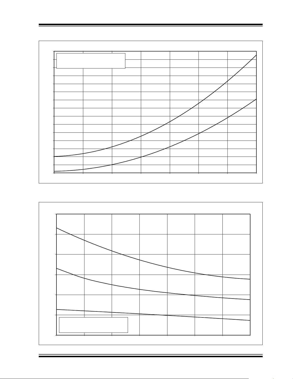
PIC16F84A
x
FIGURE 10-11: IPD vs. VDD (WDT MODE)
15
Typical: statistical mean @ 25°C
14
Maximum: mean + 3σ (-40°C to +125°C)
Minimum: mean – 3σ (-40°C to +125°C)
13
12
11
10
9
8
7
IPD (µA)
6
5
4
3
2
1
0
2.0 2.5 3.0 3.5 4.0 4.5 5.0 5.5
DD
(V)
V
Max
Typ
FIGURE 10-12: TYPICAL, MINIMUM, AND MAXIMUM WDT PERIOD vs. V
60
50
40
Ma
30
WDT Period (ms)
20
10
Typical: statistical mean @ 25°C
Maximum: mean + 3σ (-40°C to +125°C)
Minimum: mean – 3σ (-40°C to +125°C)
0
2.0 2.5 3.0 3.5 4.0 4.5 5.0 5.5
VDD (V)
Typ
Min
DD OVER TEMP
2001 Microchip Technology Inc. DS35007B-page 67
Page 70

PIC16F84A
FIGURE 10-13: TYPICAL, MINIMUM AND MAXIMUM VOH vs. IOH (VDD = 5V, -40°C TO +125°C)
5.0
4.5
4.0
3.5
3.0
2.5
VOH (V)
2.0
1.5
1.0
Typical: statistical mean @ 25°C
Maximum: mean + 3σ (-40°C to +125°C)
0.5
Minimum: mean – 3σ (-40°C to +125°C)
0.0
0.0 2.5 5.0 7.5 10.0 12.5 15.0 17.5 20.0 22.5 25.0
OH
(mA)
I
FIGURE 10-14: TYPICAL, MINIMUM AND MAXIMUM V
Ma
Typ
Min
OH vs. IOH (VDD = 3V, -40
°
C TO +125°C)
3.0
2.5
Max
2.0
Typ
(V)
1.5
OH
V
1.0
0.5
Typical: statistical mean @ 25°C
Maximum: mean + 3σ (-40°C to +125°C)
Min
Minimum: mean – 3σ (-40°C to +125°C)
0.0
0 5 10 15 20 25
OH
(mA)
I
DS35007B-page 68 © 2001 Microchip Technology Inc.
Page 71

PIC16F84A
FIGURE 10-15: TYPICAL, MINIMUM AND MAXIMUM VOL vs. IOL (VDD = 5V, -40°C TO +125°C)
1.0
Typical: statistical mean @ 25°C
Maximum: mean + 3σ (-40°C to +125°C)
0.9
Minimum: mean – 3σ (-40°C to +125°C)
0.8
0.7
Max
0.6
0.5
VOL (V)
0.4
0.3
0.2
0.1
0.0
0 5 10 15 20 25
FIGURE 10-16: TYPICAL, MINIMUM AND MAXIMUM V
1.8
OL
I
(mA)
OL vs. IOL (VDD = 3V, -40
Typ
Min
°
C TO +125°C)
Typical: statistical mean @ 25°C
Maximum: mean + 3σ (-40°C to +125°C)
Minimum: mean – 3σ (-40°C to +125°C)
1.6
1.4
1.2
1.0
VOL (V)
0.8
0.6
0.4
0.2
0.0
0.0 2.5 5.0 7.5 10.0 12.5 15.0 17.5 20.0 22.5 25.0
OL
I
(mA)
Max
Typ
Min
2001 Microchip Technology Inc. DS35007B-page 69
Page 72

PIC16F84A
FIGURE 10-17: MINIMUM AND MAXIMUM VIN vs. VDD, (TTL INPUT, -40°C TO +125°C)
2.00
Typical: statistical mean @ 25°C
Maximum: mean + 3σ (-40°C to +125°C)
Minimum: mean – 3σ (-40°C to +125°C)
1.75
VTH
1.50
VTH
1.25
(V)
1.00
IN
V
0.75
0.50
VTH
0.25
0.00
2.0 2.5 3.0 3.5 4.0 4.5 5.0 5.5
FIGURE 10-18: MINIMUM AND MAXIMUM V
3.50
DD
V
(V)
IN vs. VDD (ST INPUT, -40
°
C TO +125°C)
Typical: statistical mean @ 25°C
Maximum: mean + 3σ (-40°C to +125°C)
3.25
Minimum: mean – 3σ (-40°C to +125°C)
3.00
2.75
2.50
2.25
2.00
VIN (V)
1.75
1.50
VIH Max
VIH Typ
VIL Max
VIH Min
VIL Typ
1.25
1.00
0.75
0.50
2.0 2.5 3.0 3.5 4.0 4.5 5.0 5.5
DD
(V)
V
VIL Min
DS35007B-page 70 © 2001 Microchip Technology Inc.
Page 73

1 1 .0 PACKAGING INFORMATION
11.1 Package Marking Information
PIC16F84A
18-Lead PDIP
XXXXXXXXXXXXXXXXX
XXXXXXXXXXXXXXXXX
YYWWNNN
18-Lead SOIC
XXXXXXXXXXXX
XXXXXXXXXXXX
XXXXXXXXXXXX
YYWWNNN
20-Lead SSOP Example
XXXXXXXXXXX
XXXXXXXXXXX
YYWWNNN
Example
PIC16F84A-04I/P
0110017
Example
PIC16F84A-04
/SO
0110017
PIC16F84A20/SS
0110017
Legend: XX...X Customer specific information*
Y Year code (last digit of calendar year)
YY Year code (last 2 digits of calendar year)
WW Week code (week of January 1 is week ‘01’)
NNN Alphanumeric traceability code
Note: In the event the full Microchip part nu mber ca nnot be m arked on one line , it will
be carried over to the next line thus lim it ing t he nu mb er of a vai la ble cha r ac ters
for customer specific information.
* Standard PICmicro device marking consists of Microchip part number, year code, week code, and
traceability code. For PICmicro device marking beyond this, certain price adders apply. Please check
with your Microchip sales office. For QTP devices, any special marking adders are included in QTP
price.
2001 Microchip Technology Inc. DS35007B-page 71
Page 74
PIC16F84A
18-Lead Plastic Dual In-line (P) – 300 mil (PDIP)
E1
D
2
n
1
α
E
A
c
A1
β
eB
Number of Pins
Pitch
Lead Thickne ss
Mold Draft Angle Top
Mold Draft Angle Bottom
* Controlling Parameter
§ Significant Characteristic
Notes:
Dimensions D and E1 do not include mold flash or protrusions. Mold flash or protrusions shall not exceed
.010” (0.254mm) per side.
JEDEC Equivalent: MS-001
Drawing No. C04-007
n
p
c
α
β
B1
B
p
MILLIMETERSINCHES*Units
2.54.100
0.38.015A1Base to Seating Plane
A2
L
MAXNOMMINMAXNOMMINDimension Limits
1818
4.323.943.56.170.155.140ATop to Seating Plane
3.683.302.92.145.130.115A2Molded Package Thickness
8.267.947.62.325.313.300EShoulder to Shoulder Width
6.606.356.10.260.250.240E1Molded Package Width
22.9922.8022.61.905.898.890DOverall Length
3.433.303.18.135.130.125LTip to Seating Plane
0.380.290.20.015.012.008
1.781.461.14.070.058.045B1Upper Lead Width
0.560.460.36.022.018.014BLower Lead Width
10.929.407.87.430.370.310eBOverall Row Spacing §
1510515105
1510515105
DS35007B-page 72 2001 Microchip Technology Inc.
Page 75
18-Lead Plastic Small Outline (SO) – Wide, 300 mil (SOIC)
PIC16F84A
p
B
n
°
45
c
β
E1
E
D
2
1
h
A
φ
L
A1
α
A2
MILLIMETERSINCHES*Units
Number of Pins
Pitch
Foot Angle
Lead Thickne ss
Mold Draft Angle Top
Mold Draft Angle Bottom
* Controlling Parameter
§ Significant Characteristic
Notes:
Dimensions D and E1 do not include mold flash or protrusions. Mold flash or protrusions shall not exceed
.010” (0.254mm) per side.
JEDEC Equivalent: MS-013
Drawing No. C04-051
n
p
φ
c
α
β
048048
1.27.050
MAXNOMMINMAXNOMMINDimension Limits
1818
2.642.502.36.104.099.093AOverall Height
2.392.312.24.094.091.088A2Molded Package Thickness
0.300.200.10.012.008.004A1Standoff §
10.6710.3410.01.420.407.394EOverall Width
7.597.497.39.299.295.291E1Molded Package Width
11.7311.5311.33.462.454.446DOverall Length
0.740.500.25.029.020.010hChamfer Distance
1.270.840.41.050.033.016LFoot Length
0.300.270.23.012.011.009
0.510.420.36.020.017.014BLead Width
1512015120
1512015120
2001 Microchip Technology Inc. DS35007B-page 73
Page 76

PIC16F84A
20-Lead Plastic Shrink Small Outline (SS) – 209 mil, 5.30 mm (SSOP)
E
p
E1
D
B
n
c
β
Number of Pins
Pitch
Lead Thickness
Foot Angle
Mold Draft Angle Top
Mold Draft Angle Bottom
* Controlling Parameter
§ Significant Characteristic
Notes:
Dimensions D and E1 do not include mold flash or protrusions. Mold flash or protrusions shall not exceed
.010” (0.254mm) per side.
JEDEC Equivalent: MO-150
Drawing No. C04-072
n
p
c
φ
α
β
2
1
A
φ
L
A1
MILLIMETERSINCHES*Units
0.65.026
α
A2
MAXNOMMINMAXNOMMINDimension Limits
2020
1.981.851.73.078.073.068AOverall Height
1.831.731.63.072.068.064A2Molded Package Thickness
0.250.150.05.010.006.002A1Standoff §
8.187.857.59.322.309.299EOverall Width
5.385.255.11.212.207.201E1Molded Package Width
7.347.207.06.289.284.278DOverall Length
0.940.750.56.037.030.022LFoot Length
0.250.180.10.010.007.004
203.20101.600.00840
0.380.320.25.015.013.010BLead Width
10501050
10501050
DS35007B-page 74 2001 Microchip Technology Inc.
Page 77

APPENDIX A: REVISION HISTORY
Version Date Revision Description
A 9/98 This is a new data sheet. However, the devices described in this data sheet are
the upgrades to the devices found in the
B 8/01 Added DC and AC Characteristics Graphs and Tables to Section 10.
PIC16F84A
PIC16F8X Data Sheet
, DS30430.
2001 Microchip Technology Inc. DS35007B-page 75
Page 78

PIC16F84A
APPENDIX B: CONVERSION CONSIDERATIONS
Considerations for converting from one PIC16X8X
device to another are listed in Table 1.
TABLE 1: CONVERSION CONSIDERATIONS - PIC16C84, PIC16F83/F84, PIC16CR83/CR84,
PIC16F84A
Difference PIC16C84 PIC16F83/F84
PIC16CR83/
CR84
Program Memory Size 1K x 14 512 x 14 / 1K x 14 512 x 14 / 1K x 14 1K x 14
Data Memory Size 36 x 8 36 x 8 / 68 x 8 36 x 8 / 68 x 8 68 x 8
Voltage Range 2.0V - 6.0V
(-40°C to +85°C)
Maximum Operating Fre-
10 MHz 10 MHz 10 MHz 20 MHz
2.0V - 6.0V
(-40°C to +85°C)
2.0V - 6.0V
(-40°C to +85°C)
quency
Supply Current (I
DD).
See parameter # D014 in
the electrical specs for
more detail.
Power-down Current
(I
PD). See parameters #
D020, D021, and D021A
in the electrical specs for
IDD (typ) = 60µA
I
DD (max) = 400
(LP osc, F
DD = 2.0V,
V
µ
A
OSC = 32 kHz,
WDT disabled)
I
PD (typ) = 26
PD (max) = 100
I
DD = 2.0V,
(V
µ
A
µ
A
WDT disabled, industrial)
I
DD (typ) = 15
I
DD (max) = 45
(LP osc, F
DD = 2.0V,
V
µ
A
µ
A
OSC = 32 kHz,
WDT disabled)
I
PD (typ) = 0.4
PD (max) = 9
I
DD = 2.0V,
(V
µ
A
µ
A
WDT disabled, industrial)
I
DD (typ) = 15
I
DD (max) = 45
(LP osc, F
DD = 2.0V,
V
WDT disabled)
I
PD (typ) = 0.4
PD (max) = 6
I
DD = 2.0V,
(V
WDT disabled, industrial)
µ
A
µ
A
OSC = 32 kHz,
µ
A
µ
A
more detail.
Input Low Voltage (V
IL).
See parameters # D032
VIL (max) = 0.2VDD
(OSC1, RC mode)
V
IL (max) = 0.1VDD
(OSC1, RC mode)
V
IL (max) = 0.1VDD
(OSC1, RC mode)
and D034 in the electrical
specs for more detail.
Input High Voltage (V
See parameter # D040 in
the electrical specs for
IH).
VIH (min) = 0.36VDD
(I/O Ports with TTL,
4.5V ≤ V
DD
≤
5.5V)
IH (min) = 2.4V
V
(I/O Ports with TTL,
4.5V ≤ V
DD
≤
5.5V)
IH (min) = 2.4V
V
(I/O Ports with TTL,
4.5V ≤ V
DD
≤
5.5V)
more detail.
Data EEPROM Memory
Erase/Write cycle time
(T
DEW). See parameter #
DEW (typ) = 10 ms
T
DEW (max) = 20 ms
T
T
DEW (typ) = 10 ms
DEW (max) = 20 ms
T
T
DEW (typ) = 10 ms
DEW (max) = 20 ms
T
D122 in the electrical
specs for more detail.
Port Output Rise/Fall
time (TioR, TioF). See
parameters #20, 20A,
21, and 21A in the elec-
TioR, TioF (max) = 25 ns
(C84)
TioR, TioF (max) = 60 ns
(LC84)
TioR, Ti oF (max) = 35ns
(C84)
TioR, Ti oF (max) = 70ns
(LC84)
TioR, TioF (max) = 35 ns
(C84)
TioR, TioF (max) = 70 ns
(LC84)
trical specs for more
detail.
MCLR
on-chip filter. See
No Yes Yes Yes
parameter #30 in the
electrical specs for more
detail.
PORTA and crystal oscillator values less than
500 kHz
For crystal oscillator con-
figurations operating
below 500 kHz, the device
N/A N/A N/A
may generate a spurious
internal Q-clock when
PORTA<0> switches
state.
RB0/INT pin TTL TTL/ST*
(*Schmitt Trigger)
TTL/ST*
(*Schmitt Trigger)
PIC16F84A
2.0V - 5.5V
(-40°C to +125°C)
I
DD (typ) = 15
I
DD (max) = 45
(LP osc, F
DD = 2.0V,
V
µ
A
µ
A
OSC = 32 kHz,
WDT disabled)
I
PD (typ) = 0.4
PD (max) = 1
I
DD = 2.0V,
(V
µ
A
µ
A
WDT disabled, industrial)
V
IL (max) = 0.1VDD
(OSC1, RC mode)
IH (min) = 2.4V
V
(I/O Ports with TTL,
4.5V ≤ V
T
DEW (typ) = 4 ms
DEW (max) = 8 ms
T
DD
≤
5.5V)
TioR, TioF (max) = 35 ns
(C84)
TioR, TioF (max) = 70 ns
(LC84)
TTL/ST*
(*Schmitt Trigger)
DS35007B-page 76 2001 Microchip Technology Inc.
Page 79

PIC16F84A
TABLE 1: CONVERSION CONSIDERATIONS - PIC16C84, PIC16F83/F84, PIC16CR83/CR84,
PIC16F84A (CONTINUED)
Difference PIC16C84 PIC16F83/F84
PIC16CR83/
CR84
PIC16F84A
EEADR<7:6> and IDD It is recommended that
The polarity of the
PWRTE
bit
Recommended value of
EXT for RC oscillator
R
circuits
GIE bit unintentional
enable
Packages PDIP, SOIC PDIP, SOIC PDIP, SOIC PDIP, SOIC, SSOP
Open Drain High
Voltage (V
OD)
the EEADR<7:6> bits be
cleared. When either of
these bits is set, the maxi-
DD for the device is
mum I
higher than when both are
cleared.
PWRTE PWRTE
EXT = 3k
RETFIE
Ω
R
If an interrupt occurs while
the Global Interrupt
Enable (GIE) bit is being
cleared, the GIE bit may
unintentionally be re-
enabled by the user’s
Interrupt Service Routine
(the
14V 12V 12V 8.5V
Ω
- 100k
instruction).
N/A N/A N/A
PWRTE PWRTE
REXT = 5kΩ - 100k
N/A N/A N/A
Ω
REXT = 5kΩ - 100k
Ω
REXT = 3kΩ - 100k
Ω
2001 Microchip Technology Inc. DS35007B-page 77
Page 80

PIC16F84A
APPENDIX C: MIGRATION FROM
BASELINE TO
MID-RANGE DEVICES
This section discusses how to migrate from a baseline
device (i.e., PIC16C5X) to a mid-range device (i.e.,
PIC16CXXX).
The following is the list of feature improvements over
the PIC16C5X microcontroller family:
1. Instruction word length is increased to 14-bits.
This allows larger page sizes, both in program
memory (2K now as opposed to 512K before)
and the register file (128 bytes now versus
32 bytes before).
2. A PC latch register (PCLATH) is added to handle program memory pag ing. PA2, PA1 and PA0
bits are removed from the STATUS register and
placed in the OPTION register.
3. Data memory paging is redefined slightly. The
STATUS register is modified.
4. Four new instructions have been added:
RETURN, RETFIE, ADDLW, and SUBLW. Two
instructions, TRIS and OPTION, are being
phased out, although they are kept for
compatibility with PIC16C 5X.
5. OPTION and TRIS registers are made
addressable.
6. Interr upt capa bilit y is add ed. Inte rrupt vector is
at 0004h.
7. Stack size is increased to eight-deep.
8. RESET vector is changed to 0000h.
9. RESET of all registers is revisited. Five d ifferent
RESET (and wake-up) types are recognized.
Registers are reset differently.
10. Wake-up from SLEEP through interrupt is
added.
11. Two separate timers, the Oscillator Start-up
Timer (OST) and Power-up Timer (PWRT), are
included for more reliable power-up. These
timers are invoked selectively to avoid
unnecessary delays on power-up and wake-up.
12. PORTB has weak pull-ups and interrupt-onchange features.
13. T0CKI pin is also a port pin (RA4/T0CKI).
14. FSR is a full 8-bit register.
15. "In system programming" is made possibl e. The
user can program PIC1 6CXX devices using only
five pins: V
(data in/out).
DD, VSS, VPP, RB6 (clock) and RB7
To convert code written for PIC16C5X to PIC16F84A,
the user should take the following steps:
1. Remove any program memory page select
operations (P A2, PA1, PA0 bit s) for CALL, GOTO.
2. Revisit any computed jump operations (write to
PC or add to PC, etc.) to make sure page bits
are set properly under the new scheme.
3. Eliminate any data memory page switching.
Redefine data variables for reallocation.
4. Verify all writes to STATUS, OPTION, and FSR
registers since these have changed.
5. Change RESET vector to 0000h.
DS35007B-page 78 2001 Microchip Technology Inc.
Page 81

INDEX
PIC16F84A
A
Absolute Maximum Ratings................................................49
AC (Timing) Characteristics................................................55
Architecture, Block Diagram .................................................3
Assembler
MPASM Assembler.....................................................43
B
Banking, Data Memory.........................................................6
Block Diagrams
Crystal/Ceramic Resonator Operation........................22
External Clock Input Operation...................................22
External Power-on Reset Circuit.................................26
Interrupt Logic............... ..............................................29
On-Chip Reset............................................................24
PIC16F84A ................. ..................................................3
PORTA
RA3:RA0 Pins.....................................................15
RA4 Pins .............................................................15
PORTB
RB3:RB0 Pins.....................................................17
RB7:RB4 Pins.....................................................17
RC Oscillator Mode.....................................................23
Timer0.........................................................................19
Timer0/WDT Prescaler ...............................................20
Watchdog Timer (WDT)....................... ............... ........31
C
C (Carry) bit .......................................................................... 8
CLKIN Pin.............................................................................4
CLKOUT Pin.........................................................................4
Code Examples
Clearing RAM Using Indirect Addressing....................11
Data EEPOM Write Verify...........................................14
Indirect Addressing..................................................... 11
Initializing PORTA.......................................................15
Initializing PORTB.......................................................17
Reading Data EEPROM .............................................14
Saving STATUS and W Registers in RAM .................30
Writing to Data EEPROM............................................14
Code Protection...........................................................21
Configuration Bits................................................................21
Configuration Word.............................................................21
Conversion Considerations................................ ............... ..76
, 33
D
Data EEPROM Memory............................................ ..........13
Associated Registers.......... ............... ............... ..........14
EEADR Register..............................................7
EECON1 Register............................................7
EECON2 Register............................................7
EEDATA Register............................................7
Write Complete Enable (EEIE Bit) ........................ .. ....29
Write Complete Flag (EEIF Bit)................................... 29
Data EEPROM Write Complete........................... ...............29
Data Memory ............................ ............. ............ ............. ......6
Bank Select (RP0 Bit)...................................................6
Banking......................................................................... 6
DC Bit....................................................................................8
DC Characteristics.......................................................51
Development Support.........................................................43
Device Overview................................................................... 3
, 13, 25
, 13, 25
, 13, 25
, 13, 25
, 53
E
EECON1 Register
EEIF Bit......................................................................29
Electrical Characteristics .................................................... 49
Load Conditions.......................................................... 56
Parameter Measurement Information............. ............56
PIC16F84A-04 Voltage-Frequency Graph ................. 50
PIC16F84A-20 Voltage-Frequency Graph ................. 50
PIC16LF84A-04 Voltage-Frequency Graph ............... 50
Temperature and Voltage Specifications - AC ........... 56
Endurance ............................................................................ 1
Errata .................................................................................... 2
External Clock Input (RA4/T0CKI).
External Interrupt Input (RB0/INT).
External Power-on Reset Circuit......................................... 26
See
Timer0
See
Interrupt Sources
F
Firmware Instructions......................................................... 35
I
I/O Ports ........................................ ............ ............. ............15
ICEPIC In-Circuit Emulator................................................. 44
ID Locations..................................................................21
In-Circuit Serial Programming (ICSP)...........................21
INDF Register .......................................................................7
Indirect Addressing............................................................. 11
FSR Register..............................................6
INDF Register..................................................7
Instruction Format............................................................... 35
Instruction Set.....................................................................35
ADDLW.......................................................................37
ADDWF ...................................................................... 37
ANDLW.......................................................................37
ANDWF ...................................................................... 37
BCF ............................................................................37
BSF............................................................................. 37
BTFSC........................................................................ 38
BTFSS........................................................................ 37
CALL........................................................................... 38
CLRF.......................................................................... 38
CLRW......................................................................... 38
CLRWDT.................................................................... 38
COMF......................................................................... 38
DECF.......................................................................... 38
DECFSZ.....................................................................39
GOTO......................................................................... 39
INCF........................................................................... 39
INCFSZ.......................................................................39
IORLW........................................................................ 39
IORWF........................................................................39
MOVF......................................................................... 40
MOVLW...................................................................... 40
MOVWF...................................................................... 40
NOP............................................................................ 40
RETFIE....................................................................... 40
RETLW....................................................................... 40
RETURN..................................................................... 40
RLF............................................................................. 41
RRF............................................................................ 41
SLEEP........................................................................ 41
SUBLW....................................................................... 41
SUBWF.......................................................................41
SWAPF....................................................................... 41
XORLW ...................................................................... 42
, 33
, 33
, 7, 11, 25
, 11, 25
2001 Microchip Technology Inc. DS35007B-page 79
Page 82

PIC16F84A
XORWF.......................................................................42
Summary Table...........................................................36
INT Interrupt (RB0/INT).......................................................29
INTCON Register.......................................7
EEIE Bit......................... ............ ............. ............ .........29
GIE Bit........................ ............. ............. ............ .... 10
INTE Bit............ ............. ............ ............. ............ ..10
INTF Bit.............................................. ............ ......10
PEIE Bit......................... ............ ............. ............ .........10
RBIE Bit ...............................................................10
RBIF Bit..................................... ............. ........10
T0IE Bit........ ............ ............. ............. ............ ......10
T0IF Bit ....................................... ............. ......10
Interrupt Sources................ ............. ............. ............ .... 21
Block Diagram.............................................................29
Data EEPROM Write Complete........... ................29
Interrupt-on-Change (RB7:RB4) ...............4
RB0/INT Pin, External...............................4
TMR0 Overflow....................................................20
Interrupts, Context Saving During.......................... .............30
Interrupts, Enable Bits
Data EEPROM Write Complete Enable
(EEIE Bit)........................................... ............. ....29
Global Interrupt Enable (GIE Bit)................................ 10
Interrupt-on-Change (RB7:RB4) Enable
(RBIE Bit)............................................................10
Peripheral Interrupt Enable (PEIE Bit)........................10
RB0/INT Enable (INTE Bit).........................................10
TMR0 Overflow Enable (T0IE Bit)...............................10
Interrupts, Flag Bits............... ..............................................29
Data EEPROM Write Complete Flag
(EEIF Bit)............................................................29
Interrupt-on-Change (RB7:RB4) Flag
(RBIF Bit).............................. ............. ............. ....10
RB0/INT Flag (INTF Bit).............................................. 10
TMR0 Overflow Flag (T0IF Bit).......................... .........10
IRP bit ..................................... ............ ............. ............ .........8
, 10, 20, 25, 29
, 29
, 29
, 29
, 29
, 17, 29
, 29
, 20, 29
, 29
, 32
, 17, 29, 32
, 18, 29, 32
, 29
K
KEELOQ Evaluation and Programming Tools ......................46
M
Master Clear (MCLR)
Memory Organization............................................................5
Migration from Baseline to Mid-Range Devices..................78
MPLAB C17 and MPLAB C18 C Compilers........................43
MPLAB ICD In-Circuit Debugger.........................................45
MPLAB ICE High Performance Universal In-Circuit
MPLAB Integrated Development Environment
MPLINK Object Linker/MPLIB Object Librarian ..................44
Pin............... ............. ............ ............. ............. ....4
MCLR
Reset, Normal Operation.................. ...............24
MCLR
MCLR
Reset, SLEEP...................... ............. ........24, 32
Data EEPROM Memory............................................ ..13
Data Memory ............................ ............. ............ ...........6
Program Memory..........................................................5
Emulator with MPLAB IDE..........................................44
Software......................................................................43
O
OPCODE Field Descriptions.................................... ...........35
OPTION Register..................................................................9
INTEDG Bit............................... ............. ............ ...........9
PS2:PS0 Bits ................................................................9
PSA Bit..........................................................................9
Bit............ ............. ............ ............. ............ .........9
RBPU
T0CS Bit....................................................................... 9
T0SE Bit .......................................... ............ ............. .... 9
OPTION_REG Register....................................7
INTEDG Bit.................................. ............ ............. ...... 29
PS2:PS0 Bits..............................................................19
PSA Bit....................................................................... 19
OSC1 Pin..............................................................................4
OSC2 Pin..............................................................................4
Oscillator Configuration .............................................. ..21
Block Diagram ......................................................22
Capacitor Selection for Ceramic Resonators.............. 22
Capacitor Selection for Crystal Oscillator........... ........23
Crystal Oscillator/Ceramic Resonators.......................22
HS.........................................................................22
LP .........................................................................22
Oscillator Types.......................................................... 22
RC ............................................... ............ ......22
XT................................. ............. ............ ...............22
, 18, 20, 25
, 22
, 23
, 28
, 28
, 23, 28
, 28
P
Packaging Information.................. ......................................71
Marking.......................................................................71
Bit....................................................................................8
PD
PICDEM 1 Low Cost PICmicro
Demonstration Board..................................................45
PICDEM 17 Demonstration Board......................................46
PICDEM 2 Low Cost PIC16CXX
Demonstration Board..................................................45
PICDEM 3 Low Cost PIC16CXXX
Demonstration Board..................................................46
PICSTART Plus Entry Level Development
Programmer................................................................ 45
Pinout Descriptions...............................................................4
Pointer, FSR.......................................................................11
See
POR.
PORTA ...........................................................................4
PORTB ...........................................................................4
Postscaler, WDT
Postscaler.
Power-down (PD
Power-down Mode.
Power-on Reset
, 15
Associated Registers............................... ............... .... 16
Functions....................................................................16
Initializing........................ ............................................ 15
PORTA Register.......................................7
RA3:RA0 Block Diagram............................................15
RA4 Block Diagram.................................................... 15
RA4/T0CKI Pin............. ...................................4
TRISA Register...................................7
, 15, 16, 25
, 15, 19
, 15, 16, 20, 25
, 17
Associated Registers............................... ............... .... 18
Functions....................................................................18
Initializing........................ ............................................ 17
PORTB Register.......................................7
Pull-up Enable Bit (RBPU
RB0/INT Edge Select (INTEDG Bit)............................. 9
RB0/INT Pin, External......................................4
RB3:RB0 Block Diagram............................................17
RB7:RB4 Block Diagram............................................17
RB7:RB4 Interrupt-on-Change ........................4
RB7:RB4 Interrupt-on-Change
Enable (RBIE Bit) ...............................................10
RB7:RB4 Interrupt-on-Change
Flag (RBIF Bit)..............................................10
TRISB Register.........................................7
Assignment (PSA Bit)........................ ............... ............9
Rate Select (PS2:PS0 Bits)..........................................9
See
Prescaler
) Bit.
See
See
Bit).......................................9
Power-on Reset (POR)
SLEEP
, 17, 18, 25
, 18, 29
, 17, 29
, 17
, 17, 18, 25
DS35007B-page 80 2001 Microchip Technology Inc.
Page 83

PIC16F84A
Power-on Reset (POR).................................... ......21, 24, 26
Oscillator Start-up Timer (OST)...........................21
Bit.................................................8, 24, 28, 32, 33
PD
Power-up Timer (PWRT) .................................... .21
Time-out Sequence.....................................................28
Time-out Sequence on Power-up ........................27
Bit...........................................8, 24, 28, 30, 32, 33
TO
Prescaler.............................................................................19
Assignment (PSA Bit) .................................................19
Block Diagram.............................................................20
Rate Select (PS2:PS0 Bits)........................................19
Switching Prescaler Assignment....................... ..........20
Prescaler, Timer0
Assignment (PSA Bit) ...................................................9
Rate Select (PS2:PS0 Bits)..........................................9
PRO MATE II Universal Device Programmer .....................45
Program Counter ................................................................11
PCL Register....................................................7
PCLATH Register ............................................7
Reset Conditions............... ..........................................24
Program Memory..................................................................5
General Purpose Registers.................... ............... ........6
Interrupt Vector................... ............. ............ ..........5
RESET Vector....................... ............. ............. ............ ..5
Special Function Registers......................................6
Programming, Device Instructions......................................35
, 26
, 26
, 28
, 11, 25
, 11, 25
, 29
, 7
R
RAM.
See
Data Memory
Register File......................................... .................................6
Register File Map..................................................................6
Registers
Configuration Word.....................................................21
EECON1 (EEPROM Control)......................................13
INTCON.................................. ....................................10
OPTION...................... ..................................................9
STATUS........................................................................8
Reset................ ............. ...............................................21
Block Diagram......................................................24
Reset.
See
MCLR
Power-on Reset (POR).
Reset Conditions for All Registers..............................25
Reset Conditions for Program Counter....................... 24
Reset Conditions for STATUS Register......................24
WDT Reset.
Revision History..................................................................75
RP1:RP0 (Bank Select) bits................................. ............... ..8
MCLR
See
Power-on Reset (POR)
See
Watchdog Timer (WDT)
, 24
, 26
S
Saving W Register and STATUS in RAM...........................30
SLEEP ............................................................21
Software Simulator (MPLAB SIM)..................................... ..44
Special Features of the CPU ..............................................21
Special Function Registers.............................................. 6
Speed, Operating.............. ................................1
Stack.................. ............. ............ ........................................11
STATUS Register ....................... ........................7
C Bit....... ............ ............. ............. ............ ............. ........8
DC Bit............................................................................8
Bit.................................................8, 24, 28, 32, 33
PD
RESET Conditions......................................................24
RP0 Bit..........................................................................6
Bit...........................................8, 24, 28, 30, 32, 33
TO
Z Bit...............................................................................8
, 24, 29, 32
, 7
, 22, 23, 57
, 8, 25, 30
T
Time-out (TO) Bit.
Timer0 ................................................................................ 19
Associated Registers........................... ............... ........ 20
Block Diagram............ ................................................ 19
Clock Source Edge Select (T0SE Bit)..........................9
Clock Source Select (T0CS Bit) ................................... 9
Overflow Enable (T0IE Bit)...................................10
Overflow Flag (T0IF Bit) ................................10
Overflow Interrupt.................................................20
Prescaler.
RA4/T0CKI Pin, External Clock.................................. 19
TMR0 Register ................................................7
Timing Conditions............. .................................................. 56
Timing Diagrams
CLKOUT and I/O........................................................ 58
Diagrams and Specifications.............................. ........ 57
CLKOUT and I/O Requirements......................... 58
External Clock Requirements............................. 57
RESET, Watchdog Timer, Oscillator Start-up
Timer0 Clock Requirements............................... 60
External Clock ............................................................ 57
RESET, Watchdog Timer, Oscillator Start-up
Timer and Power-up Timer.................................59
Time-out Sequence on Power-up.........................27
Timer0 Clock .............................................................. 60
Wake-up From SLEEP Through Interrupt .................. 32
Timing Parameter Symbology ................... ............... ..........55
TO
bit .................................................................................... 8
See
Power-on Reset (POR)
, 29
, 20, 29
, 29
See
Prescaler
, 20, 25
Timer and Power-up
Timer Requirements................................... 59
, 28
W
W Register........................ ............. ............ ............. ......25, 30
Wake-up from SLEEP...............................21
Interrupts..............................................................32
Reset................. ............. ............. ............ ........ 32
MCLR
WDT Reset................... ............. ............. ............ ........ 32
Watchdog Timer (WDT)......................... .......................21
Block Diagram............ ................................................ 31
Postscaler.
Programming Considerations.....................................31
RC Oscillator..............................................................30
Time-out Period............ ............. ............. ............ ........ 30
WDT Reset, Normal Operation...................................24
WDT Reset, SLEEP .............. ............ ............. ......24
WWW, On-Line Support.......................................................2
See
Prescaler
, 26, 28, 29, 32
, 33
, 30
, 32
Z
Z (Zero) bit............................................................................ 8
2001 Microchip Technology Inc. DS35007B-page 81
Page 84

PIC16F84A
NOTES:
DS35007B-page 82 2001 Microchip Technology Inc.
Page 85

PIC16F84A
ON-LINE SUPPORT
Microchip provides on-line support on the Microchip
World Wide Web (WWW) site.
The web site is used b y Micr ochip as a means to mak e
files and information easily available to customers. To
view the site, the use r must hav e access to the Intern et
and a web browser, such as Netscape
Explorer. Files are also available for FTP download
from our FTP site.
Connecting to the Microchip Internet Web Site
The Microchip web site is available by using your
favorite Internet browser to attach to:
www.microchip.com
The file transfer site is available by using an FTP service to connect to:
ftp://ftp.microchip.com
The web site and file transfer site provide a variety of
services. Users may download files for the latest
Development Tools, Data Sheets, Application Notes,
User’s Guides, Articles and Sample Programs. A variety of Micr ochip specific bu siness informati on is also
available, including listings of Microchip sales offices,
distributors and factory representatives. Other data
available for consideration is:
• Latest Microchip Press Releases
• Technical Support Section with Frequently Asked
Questions
• Design Tips
• Device Errata
• Job Postings
• Microchip Consultant Program Member Listing
• Links to other useful web sites related to
Microchip Products
• Conferences for pr oducts, D evelopment Systems,
technical information and more
• Listing of seminars and eve nt s
®
or Microsoft
Systems Information and Upgrade Hot Line
The Systems Information and Upgrade Line provides
system users a listing of the latest versions of all of
Microchip's development systems software products.
Plus, this line provides information on how customers
can receive any currently available upgrade kits.The
®
Hot Line Numbers are:
1-800-755-2345 for U.S. and most of Canada, and
1-480-792-7302 for the rest of the world.
013001
2001 Microchip Technology Inc. DS35007B-page 83
Page 86

PIC16F84A
READER RESPONSE
It is our intentio n to pro vi de you with the bes t documentation po ss ib le to ensure succes sfu l u se of y our Microchip pro duct. If you wish to provid e your c omment s on org anizatio n, clarity, subject matter, and ways in which our doc umenta tion
can better serve you, please FAX your comments to the Technical Publications Manager at (480) 792-4150.
Please list the following information, and use this outline to provide us with your comments about this Data Sheet.
To:
RE: Reader Response
From:
Application (optional):
Would you like a reply? Y N
Device:
Questions:
1. What are the best features of this document?
2. How does this document meet your hardware and software development needs?
3. Do you find the organization of this data sheet easy to follow? If not, why?
Technical Publications Manager
Name
Company
Address
City / State / ZIP / Country
Telephone: (_______) _________ - _________
PIC16F84A
Literature Number:
Total Pages Sen t
FAX: (______) _________ - _________
DS35007B
4. What additions to the data sheet do you think would enhance the structure and subject?
5. What deletions from the data sheet could be made without affecting the overall usefulness?
6. Is there any incorrect or misleading information (what and where)?
7. How would you improve this document?
8. How would you improve our software, systems, and silicon products?
DS35007B-page 84 2001 Microchip Technology Inc.
Page 87

PIC16F84A PRODUCT IDENTIFICATION SYSTEM
To order or obtain information (e.g., on pricing or delivery) refer to the factory or the listed sales office.
PIC16F84A
PART NO. -XX
Device
Device PIC16F84A
Frequency Range 04 = 4 MHz
Temperature
Range
Package P = PDIP
Pattern QTP, SQTP, ROM Code (factory specified) or
Frequency
Range
PIC16LF84A
20 = 20 MHz
-= 0°C to +70°C
I = -40°C to +85°C
SO = SOIC (Gull Wing, 300 mil body)
SS = SSOP
Special Requirements
Windowed devices.
X /XX XXX
Range
(1)
, PIC16F84AT
(1)
, PIC16LF84AT
(2)
(2)
. Blank for OTP and
PatternPackageTemperature
Examples:
a) PIC16F84A -04/P 301 = Commercial
temp., PDIP package, 4 MHz, normal V
limits, QTP pattern #301.
b) PIC16LF84A - 04I/SO = Industrial temp.,
SOIC package, 200 kHz, Extended V
limits.
c) PIC16F84A - 20I/P = Industrial temp.,
PDIP package, 20 MHz, normal V
Note 1: F = Standard VDD range
LF = Extended V
2: T = in tape and reel - SOIC and
SSOP packages only.
DD range
DD
DD limits.
DD
Sales and Support
Data Sheets
Products supported by a preliminary Data Sheet may have an errata sheet describing minor operational differences and recommended workarounds. To determine if an errata sheet exists for a particular device, please contact one of the following:
1. Your local Microchip sales office
2. The Microchip Corporate Literature Center U.S. FAX: (480) 792-7277
3. The Microchip Worldwide Site (www.microchip.com)
Please specify which device, revision of silicon and Data Sheet (include Literature #) you are using.
New Customer Notification System
Register on our web site (www.microchip.com/cn) to receive the most current information on our products.
2001 Microchip Technology Inc. DS35007B-page85
Page 88

M
WORLDWIDE SALES AND SERVICE
AMERICAS
Corporate Office
2355 West Chandler Blvd.
Chandler, AZ 85224-6199
Tel: 480-792-7200 Fax: 480-792-7277
Technical Support: 480-792-7627
Web Address: http://www.microchip.com
Rocky Mountain
2355 West Chandler Blvd.
Chandler, AZ 85224-6199
Tel: 480-792-7966 Fax: 480-792-7456
Atlanta
500 Sugar Mill Road, Suite 200B
Atlanta, GA 30350
Tel: 770-640-0034 Fax: 770-640 -03 07
Austin - Analog
13740 North Highway 183
Building J, Suite 4
Austin, TX 78750
Tel: 512-257-3370 Fax: 512-257 -85 26
Boston
2 Lan Drive, Suite 120
Westford, MA 01886
Tel: 978-692-3848 Fax: 978-692 -38 21
Boston - Analog
Unit A-8-1 Millbrook Tarry Condominium
97 Lowell Road
Concord, MA 01742
Tel: 978-371-6400 Fax: 978-371 -00 50
Chicago
333 Pierce Road, Suite 180
Itasca, IL 60143
Tel: 630-285-0071 Fax: 630-285-0075
Dallas
4570 Westgrove Drive, Suite 160
Addison, TX 75001
Tel: 972-818-7423 Fax: 972-818 -29 24
Dayton
Two Prestige Place, Suite 130
Miamisburg, OH 45342
Tel: 937-291-1654 Fax: 937-291 -91 75
Detroit
Tri-Atria Office Building
32255 Northwestern Highway, Suite 190
Farmington Hills, MI 48334
Tel: 248-538-2250 Fax: 248-538-2260
Los Angeles
18201 Von Karman, Suite 1090
Irvine, CA 92612
Tel: 949-263-1888 Fax: 949-263 -13 38
New York
150 Motor Parkway, Suite 202
Hauppauge, NY 11788
Tel: 631-273-5305 Fax: 631-273 -53 35
San Jose
Microchip Technology Inc.
2107 North First Street, Suite 590
San Jose, CA 95131
Tel: 408-436-7950 Fax: 408-436 -79 55
Toronto
6285 Northam Drive, Suite 108
Mississauga, Ontario L4V 1X5, Canada
Tel: 905-673-0699 Fax: 905-673-6509
ASIA/PACIFIC
Australia
Microchip Technology Australia Pty Ltd
Suite 22, 41 Rawson Street
Epping 2121, NSW
Australia
Tel: 61-2-9868-6733 Fax: 61-2-9868-6755
China - Beijing
Microchip Technology Consulting (Shanghai)
Co., Ltd., Beijing Liaison Office
Unit 915
Bei Hai Wan Tai Bldg.
No. 6 Chaoyangmen Beidajie
Beijing, 100027, No. China
Tel: 86-10-85282100 Fax: 86-10-85282104
China - Chengdu
Microchip Technology Consulting (Shanghai)
Co., Ltd., Chengdu Liaison Office
Rm. 2401, 24th Floor,
Ming Xing Financial Tower
No. 88 TIDU Street
Chengdu 610016, China
Tel: 86-28-6766200 Fax: 86-28-6766599
China - Fuzhou
Microchip Technology Consulting (Shanghai)
Co., Ltd., Fuzhou Liaison Office
Rm. 531, North Building
Fujian Foreign Trade Center Hotel
73 Wusi Road
Fuzhou 350001, China
Tel: 86-591-7557563 Fax: 86-591-7557572
China - Shanghai
Microchip Technology Consulting (Shanghai)
Co., Ltd.
Room 701, Bldg. B
Far East International Plaza
No. 317 Xian Xia Road
Shanghai, 200051
Tel: 86-21-6275-5700 Fax: 86-21-6275-5060
China - Shenzhen
Microchip Technology Consulting (Shanghai)
Co., Ltd., Shenzhen Liaison Office
Rm. 1315, 13/F, Shenzhen Kerry Centre,
Renminnan Lu
Shenzhen 518001, China
Tel: 86-755-2350361 Fax: 86-755-2366086
Hong Kong
Microchip Technology Hongkong Ltd.
Unit 901-6, Tower 2, Metroplaza
223 Hing Fong Road
Kwai Fong, N.T., Hong Kong
Tel: 852-2401-1200 Fax: 852-2401-3431
India
Microchip Technology Inc.
India Liaison Office
Divyasree Chambers
1 Floor, Wing A (A3/A4)
No. 11, O’Shaugnessey Road
Bangalore, 560 025, India
Tel: 91-80-2290061 Fax: 91-80-2290062
Japan
Microchip Technology Japan K.K.
Benex S-1 6F
3-18-20, Shinyokohama
Kohoku-Ku, Yokohama-shi
Kanagawa, 222-0033, Japan
Tel: 81-45-471- 6166 Fax: 81-45-471-6122
Korea
Microchip Technology Korea
168-1, Youngbo Bldg. 3 Floor
Samsung-Dong, Kangnam-Ku
Seoul, Korea 135-882
Tel: 82-2-554-7200 Fax: 82-2-558-5934
Singapore
Microchip Technology Singapore Pte Ltd.
200 Middle Road
#07-02 Prime Centre
Singapore, 188980
Tel: 65-334-8870 Fax: 65-334-8850
Taiwan
Microchip Technology Taiwan
11F-3, No. 207
Tung Hua North Road
Taipei, 105, Taiwan
Tel: 886-2-2717-7175 Fax: 886-2-2545-0139
EUROPE
Denmark
Microchip Technology Denmark ApS
Regus Business Centre
Lautrup hoj 1-3
Ballerup DK-2750 Denmark
Tel: 45 4420 9895 Fax: 45 4420 9910
France
Arizona Microchip Technology SARL
Parc d’Activite du Moulin de Massy
43 Rue du Saule Trapu
Batiment A - ler Etage
91300 Massy, France
Tel: 33-1-69-53-63-20 Fax: 33-1-69-30-90-79
Germany
Arizona Microchip Technology GmbH
Gustav-Heinemann Ring 125
D-81739 Munich, Germany
Tel: 49-89-627-144 0 Fax: 49-89-627-144-44
Germany - Analog
Lochhamer Strasse 13
D-82152 Martinsried, Germany
Tel: 49-89-895650-0 Fax: 49-89-895650-22
Italy
Arizona Microchip Technology SRL
Centro Direzionale Colleoni
Palazzo Taurus 1 V. Le Colleoni 1
20041 Agrate Brianza
Milan, Italy
Tel: 39-039-65791-1 Fax: 39-039-6899883
United Kingdom
Arizona Microchip Technology Ltd.
505 Eskdale Road
Winnersh Triangle
Wokingham
Berkshire, England RG41 5TU
Tel: 44 118 921 5869 Fax: 44-118 921-5820
08/01/01
DS35007B-page 86 2001 Microchip Technology Inc.
 Loading...