


PIC16F818/819
Data Sheet
18/20-Pin
Enhanced Flash Microcontrollers
with nanoWatt Technology
2004 Microchip Technology Inc. DS39598E

Note the following details of the code protection feature on Microchip devices:
• Microchip products meet the specification contained in their particular Microchip Data Sheet.
• Microchip believes that its family of products is one of the most secure families of its kind on the market today, when used in the
intended manner and under normal conditions.
• There are dishonest and possibly illegal methods used to breach the code protection feature. All of these methods, to our
knowledge, require using the Microchip products in a manner outside the operating specifications contained in Microchip’s Data
Sheets. Most likely, the person doing so is engaged in theft of intellectual property.
• Microchip is willing to work with the customer who is concerned about the integrity of their code.
• Neither Microchip nor any other semiconductor manufacturer can guarantee the security of their code. Code protection does not
mean that we are guaranteeing the product as “unbreakable.”
Code protection is constantly evolving. We at Microchip are committed to continuously improving the code protection features of our
products. Attempts to break Microchip’s code protection feature may be a violation of the Digit al Millennium Copyright Act. If suc h a c t s
allow unauthorized access to your software or other copyrighted work, you may have a right to sue for relief under that Act.
Information contained in this publication regarding device
applications and the like is provided only for your convenience
and may be superseded by updates. It is your responsibility to
ensure that your application meets with your specifications.
MICROCHIP MAKES NO REPRESENTATIONS OR WARRANTIES OF ANY KIND WHETHER EXPRESS OR IMPLIED,
WRITTEN OR ORAL, STATUTORY OR OTHERWISE,
RELATED TO THE INFORMATION, INCLUDING BUT NOT
LIMITED TO ITS CONDITION, QUALITY, PERFORMANCE,
MERCHANTABILITY OR FITNESS FOR PURPOSE.
Microchip disclaims all liability arising from this information and
its use. Use of M icrochip’s prod ucts as critical components in
life support systems is not authorized except with express
written approval by Microchip. No licenses are conveyed,
implicitly or otherwise, under any Microchip intellectual property
rights.
Trademarks
The Microchip name and logo, the Microchip logo, Accuron,
dsPIC, K
EELOQ, microID, MPLAB, PIC, PICmicro, PICSTART,
PRO MATE, PowerSmart, rfPIC, and SmartShunt are
registered trademarks of Microchip Technology Incorporated
in the U.S.A. and other countries.
AmpLab, FilterLab, MXDEV, MXLAB, PICMASTER, SEEVAL,
SmartSensor and The Embedded Control Solutions Company
are registered trademarks of Microchip Technology
Incorporated in the U.S.A.
Analog-for-the-Digital Age, Application Maestro, dsPICDEM,
dsPICDEM.net, dsPICworks, ECAN, ECONOMONITOR,
FanSense, FlexROM, fuzzyLAB, In-Circuit Serial
Programming, ICSP, ICEPIC, Migratable Memory, MPASM,
MPLIB, MPLINK, MPSIM, PICkit, PICDEM, PICDEM.net,
PICLAB, PICtail, PowerCal, PowerInfo, PowerMate,
PowerTool, rfLAB, rfPICDEM, Select Mode, Sm art Serial,
SmartTel and Total Endurance are trademarks of Microchip
Technology Incorporated in the U.S.A. and other countries.
SQTP is a service mark of Microchip Technology Incorporated
in the U.S.A.
All other trademarks mentioned herein are property of their
respective companies.
© 2004, Microchip Technology Incorporated, Printed in the
U.S.A., All Rights Reserved.
Printed on recycled paper.
Microchip received ISO/TS-16949:2002 quality system certification for
its worldwide headquarters, design and wafer fabrication facilities in
Chandler and Tempe, Arizona and Mountain View, California in
October 2003. The Company’s quality system processes and
procedures are for its PICmicro
devices, Serial EEPROMs, microperipherals, nonvolatile memory and
analog products. In addition, Microchip’s quality system for the design
and manufacture of development systems is ISO 9001:2000 certified.
®
8-bit MCUs, KEELOQ
®
code hopping
DS39598E-page ii 2004 Microchip Technology Inc.
PIC16F818/819
18/20-Pin Enhanced Flash Microcontr ollers
with nanoWatt Technology
Low-Power Features:
• Power-Managed modes:
- Primary Run: XT, RC oscillator,
87 µA, 1 MHz, 2V
-INTRC: 7µA, 31.25 kHz, 2V
- Sleep: 0.2 µA, 2V
• Timer1 oscillator: 1.8 µA, 32 kHz, 2V
• Watchdog Timer: 0.7 µA, 2V
• Wide operating voltage range:
- Industrial: 2.0V to 5.5V
Oscillators:
• Three Crystal modes:
- LP, XT, HS: up to 20 MHz
• Two External RC modes
• One External Clock mode:
- ECIO: up to 20 MHz
• Internal oscillator block:
- 8 user selectabl e fre que nc i es : 3 1kHz, 125 kHz,
250kHz, 500kHz, 1MHz, 2 MHz, 4 MHz, 8 MHz
Peripheral Features:
• 16 I/O pins with individual direction control
• High sink/source current: 25 mA
• Timer0: 8-bit timer/counter with 8-bit prescaler
• Timer1: 16-b it ti m er/ co un ter with prescaler , c a n b e
incremented during Sleep via external crystal/clock
• Timer2: 8-bit timer/counter with 8-bit period
register, prescaler and postscaler
• Capture, Compare, PWM (CCP) module:
- Capture is 16-bit, max. resolution is 12.5 ns
- Compare is 16-bit, max. resolution is 200 ns
- PWM max. resolution is 10-bit
• 10-bit, 5-channel Analog-to-Digital converter
• Synchronous Serial Port (SSP) with
SPI™ (Master/Slave) and I2C™ (Slave)
Pin Diagram
18-Pin PDIP, SOIC
RA2/AN2/ VREF-
RA3/AN3/V
RA4/AN4/T0CKI
RA5/MCLR
RB2/SDO/CCP1
RB3/CCP1/PGM
REF+
/VPP
VSS
RB0/INT
RB1/SDI/SDA
•1
2
3
4
5
6
7
PIC16F818/819
8
9
RA1/AN1
18
RA0/AN0
17
RA7/OSC1/CLKI
16
RA6/OSC2/C LK O
15
14
13
12
11
10
DD
V
RB7/T1OSI/PGD
RB6/T1OSO/T1CKI/PGC
RB5/SS
RB4/SCK/SCL
Special Microcontroller Features:
• 100,000 erase/write cycles Enhanced Flash
program memory typical
• 1,000,000 typical erase/write cycles EEPROM
data memory typical
• EEPROM Data Retention: > 40 years
TM
• In-Circuit Serial Programming
• Processor read/write access to program memory
• Low-Voltage Progr amming
• In-Circuit Debugging via two pins
(ICSPTM) via two pins
Program Memory Data Memory
Device
PIC16F818 1792 1024 128 128 16 5 1 Y Y 2/1
PIC16F819 3584 2048 256 256 16 5 1 Y Y 2/1
2004 Microchip Technology Inc. DS39598E-page 1
Flash
(Bytes)
# Single-Word
Instructions
SRAM
(Bytes)
EEPROM
(Bytes)
I/O Pins
10-bit
A/D (ch)
CCP
(PWM)
SPI™
SSP
Slave
2
C™
I
Timers
8/16-bit
PIC16F818/819
Pin Diagrams
18-Pin PDIP, SOIC
RA2/AN2/VREF-
RA3/AN3/V
RA4/AN4/T0CKI
RA5/MCLR
RB2/SDO/CCP1
RB3/CCP1/PGM
REF+
/VPP
VSS
RB0/INT
RB1/SDI/SDA
•1
2
3
4
5
6
7
8
9
18
17
16
15
14
13
12
11
PIC16F818/819
10
28-Pin QFN
RA5/MCLR/VPP
NC
VSS
NC
V
NC
RB0/INT
RA1/AN1
RA0/AN0
RA7/OSC1/CLKI
RA6/OSC2/CLKO
V
DD
RB7/T1OSI/PGD
RB6/T1OSO/T1CKI/PGC
RB5/SS
RB4/SCK/SCL
REF+
RA3/AN3/V
RA4/AN4/T0CKI
282627
1
2
3
4
PIC16F818/819
SS
5
6
7
8109
NC
RA2/AN2/VREF-
25
11
20-Pin SSOP
RA2/AN2/ VREF-
RA3/AN3/V
RA4/AN4/T0CKI
RA5/MCLR
RB0/INT
RB1/SDI/SDA
RB2/SDO/CCP1
RB3/CCP1/PGM
RA1/AN1
NC
RA0/AN0
22
23
24
21
20
19
18
17
16
15
14
13
12
•1
REF+
/VPP
VSS
VSS
2
3
4
5
6
7
8
9
10
RA7/OSC1/CLKI
RA6/OSC2/CLKO
DD
V
NC
V
DD
RB7/T1OSI/PGD
RB6/T1OSO/T1CKI/PGC
20
19
18
17
16
15
14
13
PIC16F818/819
12
11
RA1/AN1
RA0/AN0
RA7/OSC1/CLKI
RA6/OSC2/CLKO
V
DD
VDD
RB7/T1OSI/PGD
RB6/T1OSO/T1CKI/PGC
RB5/SS
RB4/SCK/SCL
RB1/SDI/SDA
RB2/SDO/CCP1
NC
RB3/CCP1/PGM
NC
RB5/SS
RB4/SCK/SCL
DS39598E-page 2 2004 Microchip Technology Inc.

PIC16F818/819
Table of Contents
1.0 Device Overview..........................................................................................................................................................................5
2.0 Memory Organization................................................................................................................................................................... 9
3.0 Data EEPROM and Flash Program Memory.............................................................................................................................. 25
4.0 Oscillator Configurations............................................................................................................................................................ 33
5.0 I/O Ports............................................................................... ..................... .................................................................................39
6.0 Timer0 Module ........................................................................................................................................................................... 53
7.0 Timer1 Module ........................................................................................................................................................................... 57
8.0 Timer2 Module ........................................................................................................................................................................... 63
9.0 Capture/Compare/PWM (CCP) Module..................................................................................................................................... 65
10.0 Synchronous Serial Port (SSP) Module ..................................................................................................................................... 71
11.0 Analog-to-Digital Converter (A/D) Module..................................................................................................................................81
12.0 Special Features of the CPU.................................................... ..................... ............................................................................. 89
13.0 Instruction Set Summary.......................................................................................................................................................... 103
14.0 Development Support............................................................................................................................................................... 111
15.0 Electrical Characteristics.......................................................................................................................................................... 117
16.0 DC and AC Characteristics Graphs and Tables....................................................................................................................... 143
17.0 Packaging Information. ..................... ..................... ..................... ..................... ......................................................................... 157
Appendix A: Revision History.............................................................................................................................................................163
Appendix B: Device Differences ........................................................................................................................................................ 163
Index .................................................................................................................................................................................................. 165
On-Line Support................................................................................................................................................................................. 171
Systems Information and Upgrade Hot Line...................................................................................................................................... 171
Reader Response..............................................................................................................................................................................172
PIC16F818/819 Product Identification System ..................................................................................................................................173
TO OUR VALUED CUSTOMERS
It is our intention to provide our valued customers with the best documentation possible to ensure successful use of your Microchip
products. To this end, we will continue to improve our publications to better suit your needs. Our publications will be refined and
enhanced as new volumes and updates are introduced.
If you have any questions or c omm ents regarding t his publication, p lease c ontact the M arket ing Co mmunications Department via
E-mail at docerrors@microchip.com or fax the Reader Response Form in the back of this data sheet to (480) 792-4150. We
welcome your feedback.
Most Current Data Sheet
To obtain the most up-to-date version of this data sheet, please register at our Worldwide Web site at:
http://www.microchip.com
You can determine the version of a data sheet by examining its literature number found on the bottom outside corner of any page.
The last character of the literature number is the version number, (e.g., DS30000A is version A of document DS30000).
Errata
An errata sheet, describing minor operational differences from the data sheet and recommended workarounds, may exist for current
devices. As device/documentation issues become known to us, we will publish an errata sheet. The errata will specify the revision
of silicon and revision of document to which it applies.
To determine if an errata sheet exists for a particular device, please check with one of the following:
• Microchip’s Worldwide Web site; http://www.microchip.com
• Your local Microchip sales office (see last page)
When contacting a sales office, please specify which device, revision of silicon and data sheet (include literature number) you are
using.
Customer Notification System
Register on our web site at www.microchip.com to receive the most current information on all of our products.
2004 Microchip Technology Inc. DS39598E-page 3

PIC16F818/819
NOTES:
DS39598E-page 4 2004 Microchip Technology Inc.

PIC16F818/819
1.0 DEVICE OVERVIEW
This document contains device specific information for
the operation of the PIC16F818/819 devices. Additional
information may be found in the “PICmicro® Mid-Range
MCU Family Reference Manual” (DS33023) which may
be downloaded from the Microchip web site. The
Reference Manual should be considered a comp lementary document to this data sheet and is highly
recommended reading for a better understanding of the
device architecture and operation of the peripheral
modules.
The PIC16F818/819 belongs to the Mid-Range family
of the PICmicro
other in the amount of Flash program memory, data
memory and data EEPROM (see Table 1-1). A block
diagram of the devices is shown in Figure 1-1. These
devices contain features that are new to the PIC16
product line:
• Internal RC oscillator with eight selectable
frequencies, including 31.25 kHz, 125 kHz,
250 kHz, 500 kHz, 1 MHz, 2 MHz, 4 MHz and
8 MHz. The INTRC can be configured as the
system clock via the configuration bits. Refer to
Section 4.5 “Internal Oscillator Block” and
Section 12.1 “Configuration Bits” for further
details.
• The Timer1 module current consumption has
been greatly reduced from 20 µA (previous PIC16
devices) to 1.8µA typical (32 kHz at 2V), which is
ideal for real-time clock applications. Refer to
Section 6 .0 “Timer0 Module” for further details.
• The amount of oscill ator selections ha s increased.
The RC and INTRC modes can be selected with
an I/O pin configured as an I/O or a clock output
OSC/4). An external clock can be configured
(F
with an I/O pin. Refer to Section 4.0 “Oscillator
Configurations” for further details.
®
devices. The device s differ from each
TABLE 1-1: AVAILABLE MEMORY IN
PIC16F818/819 DEVICES
Device
PIC16F818 1K x 14 128 x 8 128 x 8
PIC16F819 2K x14 256 x 8 256 x 8
There are 16 I/O pins that are user configurable on a
pin-to-pin basis. Some pins are multiplexed with other
device functions. These functions include:
• External Interrupt
• Change on PORTB Interrupt
• Timer0 Clock Input
• Low-Power Timer1 Clock/Oscillator
• Capture/Compare/PWM
• 10-bit, 5-channel Analog-to-Digital C onverter
2
• SPI/I
•MCLR (RA5) can be configured as an Input
Table 1-2 details the pinout of the devices with
descriptions and details for each pin.
Program
Flash
C
Data
Memory
Data
EEPROM
2004 Microchip Technology Inc. DS39598E-page 5
PIC16F818/819
FIGURE 1-1: PIC16F818/819 BLOCK DIAGRAM
Program
Bus
RA7/OSC1/CLKI
RA6/OSC2/CLKO
Flash
Program
Memory
1K/2K x 14
14
Instruction reg
Instruction
Decode &
Control
Timing
Generation
13
Program Counter
8-Level Stack
Direct Addr
8
Power-up
Oscillator
Start-up Timer
Power-on
Watchdog
Brown-out
(13-bit)
Timer
Reset
Timer
Reset
RAM Addr
7
3
8
Data Bus
RAM
File
Registers
128/256 x 8
(1)
9
Addr MUX
8
FSR reg
Status reg
MUX
ALU
W reg
8
Indirect
Addr
PORTA
PORTB
RA0/AN0
RA1/AN1
RA2/AN2/VREFRA3/AN3/VREF+
RA4/AN4/T0CKI
RA5/MCLR/VPP
RA6/OSC2/CLKO
RA7/OSC1/CLKI
RB0/INT
RB1/SDI/SDA
RB2/SDO/CCP1
RB3/CCP1/PGM
RB4/SCK/SCL
RB5/SS
RB6/T1OSO/T1CKI/PGC
RB7/T1OSI/PGD
MCLR
VDD, VSS
Timer0
10-bit, 5-channel
A/D
Note 1: Higher or der bits are from the Status register.
Timer1 Timer2
Synchronous
Serial Port
Data EE
128/256 Bytes
CCP1
DS39598E-page 6 2004 Microchip Technology Inc.

PIC16F818/819
TABLE 1-2: PIC16F818/819 PINOUT DESCRIPTIONS
PDIP/
Pin Name
RA0/AN0
RA0
AN0
RA1/AN1
RA1
AN1
RA2/AN2/V
RA3/AN3/VREF+
RA4/AN4/T0CKI
RA5/MCLR
RA6/OSC2/CLKO
RA7/OSC1/CLKI
Legend: I = Input O = Output I/O = Input/Output P = Power
Note 1: This buffer is a Schmitt Trigger input when configured as the external interrupt.
REF-
RA2
AN2
REF-
V
RA3
AN3
REF+
V
RA4
AN4
T0CKI
/VPP
RA5
MCLR
VPP
RA6
OSC2
CLKO
RA7
OSC1
CLKI
– = Not used TTL = TTL Input ST = Schmitt Trigger Input
2: This buffer is a Schmitt Trigger input when used in Serial Programming mode.
3: This buffer is a Schmitt Trigger input when configured in RC Oscillator mode and a CMOS input otherwise.
SSOP
SOIC
Pin#
17 19 23
18 20 24
1126
2227
3328
441
15 17 20
16 18 21
Pin#
QFN
Pin#
I/O/P
Type
I/O
I
I/O
I
I/O
I
I
I/O
I
I
I/O
I
I
I
I
P
I/O
O
O
I/O
I
I
Buffer
Type
TTL
Analog
TTL
Analog
TTL
Analog
Analog
TTL
Analog
Analog
ST
Analog
ST
ST
ST
–
ST
–
–
ST
ST/CMOS
–
Description
PORTA is a bidirectional I/O port.
Bidirectional I/O pin.
Analog input channel 0.
Bidirectional I/O pin.
Analog input channel 1.
Bidirectional I/O pin.
Analog input channel 2.
A/D reference voltage (low) input.
Bidirectional I/O pin.
Analog input channel 3.
A/D reference voltage (high) input.
Bidirectional I/O pin.
Analog input channel 4.
Clock input to the TMR0 timer/counter.
Input pin.
Master Clear (Reset). Input/programming
voltage input. This pin is an active-low Reset
to the device.
Programming threshold voltage.
Bidirectional I/O pin.
Oscillator cryst al outpu t. Connect s to crys tal or
resonator i n Crystal Oscill ator mode.
In RC mode, this pin outputs CLKO signal
which has 1/4 the frequency of OSC1 and
denotes the instruction cycle rate.
Bidirectional I/O pin.
(3)
Oscillator crystal input.
External clock source input.
2004 Microchip Technology Inc. DS39598E-page 7

PIC16F818/819
TABLE 1-2: PIC16F818/819 PINOUT DESCRIPTIONS (CONTINUED)
PDIP/
Pin Name
RB0/INT
RB0
INT
RB1/SDI/SDA
RB1
SDI
SDA
RB2/SDO/CCP1
RB2
SDO
CCP1
RB3/CCP1/PGM
RB3
CCP1
PGM
RB4/SCK/SCL
RB4
SCK
SCL
RB5/SS
RB5
SS
RB6/T1OSO/T1CKI/PGC
RB6
T1OSO
T1CKI
PGC
RB7/T1OSI/PGD
RB7
T1OSI
PGD
SS 5 5, 6 3, 5 P – Ground reference for logic and I/O pins.
V
VDD 14 15, 16 17, 19 P – Positive supply for logic and I/O pins.
Legend: I = Input O = Output I/O = Input/Output P = Power
– = Not used TTL = TTL Input ST = Schmitt Trigger Input
Note 1: This buffer is a Schmitt Trigger input when configured as the external interrupt.
2: This buffer is a Schmitt Trigger input when used in Serial Programming mode.
3: This buffer is a Schmitt Trigger input when configured in RC Oscillator mode and a CMOS input otherwise.
SSOP
SOIC
Pin#
677
788
899
91010
10 11 12
11 12 13
12 13 15
13 14 16
Pin#
QFN
Pin#
I/O/P
Type
I/O
I
I/O
I
I/O
I/O
O
I/O
I/O
I/O
I
I/O
I/O
I
I/O
I
I/O
O
I
I
I/O
I
I
Buffer
Type
TTL
(1)
ST
TTL
ST
ST
TTL
ST
ST
TTL
ST
ST
TTL
ST
ST
TTL
TTL
TTL
ST
ST
(2)
ST
TTL
ST
(2)
ST
Description
PORTB is a bidirectional I/O port. PORTB can be
software programmed fo r in tern al weak pull-up on
all inputs.
Bidirectional I/O pin.
External interrupt pin.
Bidirectional I/O pin.
SPI™ data in.
2
C™ data.
I
Bidirectional I/O pin.
SPI data out.
Capture input, Compare output, PWM output.
Bidirectional I/O pin.
Capture input, Compare output, PWM output.
Low-Voltage ICSP™ Programming enable pin.
Bidirectional I/O pin. Interrupt-on-change pin.
Synchronous serial clock input/output for SPI.
Synchronous serial clock input for I
Bidirectional I/O pin. Interrupt-on-change pin.
Slave select for SPI in Slave mode.
Interrupt-on-change pin.
Timer1 Oscillator output.
Timer1 clock input.
In-circuit debugger and ICSP program m ing
clock pin.
Interrupt-on-change pin.
Timer1 oscillator input.
In-circuit debugger and ICSP program m ing
data pin.
2
C.
DS39598E-page 8 2004 Microchip Technology Inc.

PIC16F818/819
2.0 MEMORY ORGANIZATION
There are two memory blocks in the PIC16F818/819.
These are the program memory and the data memory.
Each block has its own bus, so access to each block
can occur during the same oscillator cycle.
The data memory can be further broken down into the
general purpose RAM and the Special Function
Registers (SFRs). The operation of the SFRs that
control the “core” are described here. The SFRs used
to control the peripheral modules are described in the
section discussing each individual peripheral module.
The data memory area also contains the data
EEPROM memory . This memory is no t directly mapped
into the data memory but is indirectly mapped. That is,
an indirect addres s poin ter speci fies th e addre ss of th e
data EEPROM memory to read/write. The PIC16F818
device’s 128 bytes of dat a EEPROM memory h ave th e
address range of 00 h-7Fh and the PIC16 F819 devic e’s
256 bytes of data EEPROM memo ry hav e the add res s
range of 00h-FFh. More details on the EEPROM
memory can be found in Section 3.0 “Data EEPROM
and Flash Program Memory”.
Additional informa tion on devi ce memory may be found
in the “PICmicro
(DS33023).
®
Mid-Range Reference Manual”
2.1 Program Memory Organization
The PIC16F818/819 devices have a 13-bit program
counter capable of addressing an 8K x 14 program
memory space. For the PIC16F818, the first 1K x 14
(0000h-03FFh) is physically implemented (see
Figure 2-1). For the PIC16F819, the first 2K x 14 is
located at 0000h-07FFh (see Figure 2-2). Accessing a
location above the ph ysicall y implem ented addres s will
cause a wraparound. For example, the same instruction will be accessed at locations 020h, 420h, 820h,
C20h, 1020h, 1420h, 1820h and 1C20h.
The Reset vector is a t 0000h and t he in terrupt vecto r i s
at 0004h.
FIGURE 2-1: PROGRAM MEMORY MAP
AND STACK FOR
PIC16F818
PC<12:0>
CALL, RETURN
RETFIE, RETLW
On-Chip
Program
Memory
Stac k Lev el 1
Stac k Lev el 2
Stack Level 8
Reset Vector
Interru pt Vector
Page 0
Wraps to
0000h-03FFh
13
0000h
0004h
0005h
03FFh
0400h
FIGURE 2-2: PROGRAM MEMORY MAP
AND STACK FOR
PIC16F819
PC<12:0>
CALL, RETURN
RETFIE, RETLW
On-Chip
Program
Memory
Stac k Lev el 1
Stac k Lev el 2
Stack Level 8
Reset Vector
Interrupt Vector
Page 0
Wraps to
0000h-07FFh
13
0000h
0004h
0005h
07FFh
0800h
1FFFh
2004 Microchip Technology Inc. DS39598E-page 9
1FFFh

PIC16F818/819
2.2 Data Memory Organization
The data memory is p arti tioned into m ultip le ban ks th at
contain the Ge neral Purpose Reg isters and the Spe cial
Function Registers. Bits RP1 (Status<6>) and RP0
(Status<5>) are the bank select bits.
RP1:RP0 Bank
00 0
01 1
10 2
11 3
Each bank extends up to 7Fh (128 bytes). The lower
locations of each bank are reserved for the Special
Function Registers. Ab ove the Speci al Function Registers are th e Genera l Purpos e Regist ers, im plement ed
as static RAM. All implemented bank s contain SFRs.
Some “high use” SFRs from one bank may be mirrored
in another bank for code reduction and quicker access
(e.g., the Status register is in Banks 0-3).
Note: EEPROM dat a memory description can be
found in Section 3.0 “Data EEPROM and
Flash Program Memory” of this data
sheet.
2.2.1 GENERAL PURPOSE REGISTER FILE
The register file can be accessed either directly or
indirectly through the File Select Register, FSR.
DS39598E-page 10 2004 Microchip Technology Inc.
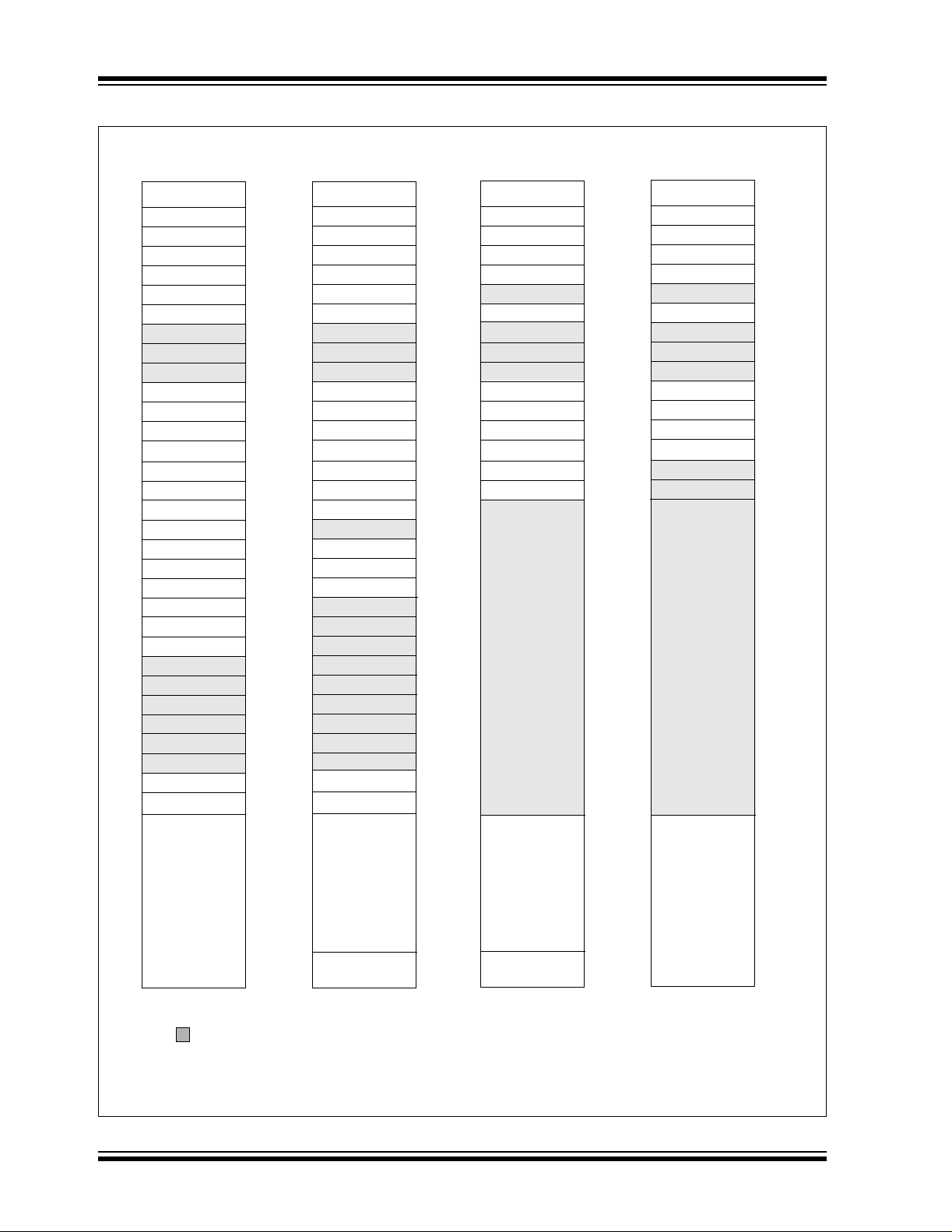
FIGURE 2-3: PIC16F818 REGISTER FILE MAP
PIC16F818/819
File
Address
Indirect addr.(*)
TMR0
PCL
STATUS
FSR
PORTA
PORTB
PCLATH
INTCON
PIR1
PIR2
TMR1L
TMR1H
T1CON
TMR2
T2CON
SSPBUF
SSPCON
CCPR1L
CCPR1H
CCP1CON
ADRESH
ADCON0 ADCON1
General
Purpose
Register
96 Bytes
00h
01h
02h
03h
04h
05h
06h
07h
08h
09h
0Ah
0Bh
0Ch
0Dh
0Eh
0Fh
10h
11h
12h
13h
14h
15h
16h
17h
18h
19h
1Ah
1Bh
1Ch
1Dh
1Eh
1Fh
20h
Indirect addr.(*)
OPTION_REG
STATUS
PCLATH
INTCON
OSCCON
OSCTUNE
SSPADD
SSPSTAT
ADRESL
General
Purpose
Register
32 Bytes
Accesses
40h-7Fh
PCL
FSR
TRISA
TRISB
PIE1
PIE2
PCON
PR2
File
Address
80h
81h
82h
83h
84h
85h
86h
87h
88h
89h
8Ah
8Bh
8Ch
8Dh
8Eh
8Fh
90h
91h
92h
93h
94h
95h
96h
97h
98h
99h
9Ah
9Bh
9Ch
9Dh
9Eh
9Fh
A0h
BFh
C0h
Indirect addr.(*)
TMR0
PCL
STATUS
FSR
PORTB
PCLATH
INTCON
EEDATA
EEADR
EEDATH
EEADRH
Accesses
20h-7Fh
File
Address
100h
101h
102h
103h
104h
105h
106h
107h
108h
109h
10Ah
10Bh
10Ch
10Dh
10Eh
10Fh
110h
11Fh
120h
Indirect addr.(*)
OPTION_REG
PCL
STATUS
FSR
TRISB
PCLATH
INTCON
EECON1
EECON2
Reserved
Reserved
Accesses
20h-7Fh
(1)
(1)
File
Address
180h
181h
182h
183h
184h
185h
186h
187h
188h
189h
18Ah
18Bh
18Ch
18Dh
18Eh
18Fh
190h
19Fh
1A0h
Bank 0
7Fh
Unimplemented data memory locations, read as ‘0’.
* Not a physical register.
Note 1: These registers are reserved; maintain these registers clear.
2004 Microchip Technology Inc. DS39598E-page 11
Bank 1
FFh
Bank 2
17Fh
Bank 3
1FFh
PIC16F818/819
FIGURE 2-4: PIC16F819 REGISTER FILE MAP
File
Address
Indirect addr.(*)
TMR0
PCL
STATUS
FSR
PORTA
PORTB
PCLATH
INTCON
PIR1
PIR2
TMR1L
TMR1H
T1CON
TMR2
T2CON
SSPBUF
SSPCON
CCPR1L
CCPR1H
CCP1CON
ADRESH
ADCON0 ADCON1
00h
01h
02h
03h
04h
05h
06h
07h
08h
09h
0Ah
0Bh
0Ch
0Dh
0Eh
0Fh
10h
11h
12h
13h
14h
15h
16h
17h
18h
19h
1Ah
1Bh
1Ch
1Dh
1Eh
1Fh
20h
Indirect addr.(*)
OPTION_REG
STATUS
PCLATH
INTCON
OSCCON
OSCTUNE
SSPADD
SSPSTAT
ADRESL
PCL
FSR
TRISA
TRISB
PIE1
PIE2
PCON
PR2
File
Address
80h
81h
82h
83h
84h
85h
86h
87h
88h
89h
8Ah
8Bh
8Ch
8Dh
8Eh
8Fh
90h
91h
92h
93h
94h
95h
96h
97h
98h
99h
9Ah
9Bh
9Ch
9Dh
9Eh
9Fh
A0h
Indirect addr.(*)
TMR0
PCL
STATUS
FSR
PORTB
PCLATH
INTCON
EEDATA
EEADR
EEDATH
EEADRH
File
Address
100h
101h
102h
103h
104h
105h
106h
107h
108h
109h
10Ah
10Bh
10Ch
10Dh
10Eh
10Fh
110h
11Fh
120h
Indirect addr.(*)
OPTION_REG
PCL
STATUS
FSR
TRISB
PCLATH
INTCON
EECON1
EECON2
Reserved
Reserved
(1)
(1)
File
Address
180h
181h
182h
183h
184h
185h
186h
187h
188h
189h
18Ah
18Bh
18Ch
18Dh
18Eh
18Fh
190h
19Fh
1A0h
General
Purpose
Register
96 Bytes
7Fh
Bank 0
Unimplemented data memory locations, read as ‘0’.
* Not a physical register.
Note 1: These registers are reserved; maintain these registers clear.
DS39598E-page 12 2004 Microchip Technology Inc.
General
Purpose
Register
80 Bytes
Accesses
70h-7Fh
Bank 1
EFh
F0h
FFh
General
Purpose
Register
80 Bytes
Accesses
70h-7Fh
Bank 2
16Fh
170h
17Fh
Accesses
20h-7Fh
1FFh
Bank 3

PIC16F818/819
2.2.2 SPECIAL FUNCTION REGISTERS
The Special Function Registers are registers used by
the CPU and peripheral modules for controlling the
desired operation of the device. These registers are
implemented as static RAM. A list of these registers is
given in Table 2-1.
The Special Function Registers can be classified into
two sets: core (CPU) and peripheral. Those registers
associated with the core functions are described in
detail in this section. Those related to the operation of
the peripheral features are described in detail in the
peripheral feature section.
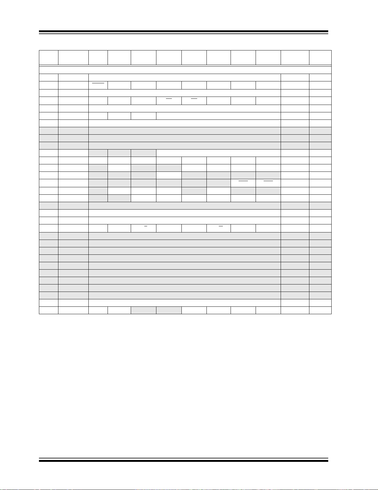
TABLE 2-1: SPECIAL FUNCTION REGISTER SUMMARY
Address Name Bit 7 Bit 6 Bit 5 Bit 4 Bit 3 Bit 2 Bit 1 Bit 0
Bank 0
(1)
00h
01h TMR0 Timer0 Module Register xxxx xxxx 53, 17
02h
03h
04h
05h PORTA PORTA Data Latch when written; PORTA pins when read xxx0 0000 39
06h PORTB PORTB Data Latch when written; PORTB pins when read xxxx xxxx 43
07h — Unimplemented — —
08h — Unimplemented — —
09h — Unimplemented — —
0Ah
0Bh
0Ch PIR1
0Dh PIR2
0Eh TMR1L Holding Register for the Least Significant Byte of the 16-bit TMR1 Register xxxx xxxx 57
0Fh TMR1H Holding Register for the Most Significant Byte of the 16-bit TMR1 Register xxxx xxxx 57
10h T1CON
11h TMR2 Timer2 Module Register 0000 0000 63
12h T2CON
13h SSPBUF Synchronous Serial Port Receive Buffer/Transmit Register xxxx xxxx 71, 76
14h SSPCON WCOL SSPOV SSPEN CKP SSPM3 SSPM2 SSPM1 SSPM0 0000 0000 73
15h CCPR1L Capture/Compare/PWM Register (LSB) xxxx xxxx 66, 67, 68
16h CCPR1H Capture/Compare/PWM Register (MSB) xxxx xxxx 66, 67, 68
17h CCP1CON
18h — Unimplemented — —
19h — Unimplemented — —
1Ah — Unimplemented — —
1Bh — Unimplemented — —
1Ch — Unimplemented — —
1Dh — Unimplemented — —
1Eh ADRESH A/D Result Register High Byte xxxx xxxx 81
1Fh ADCON0 ADCS1 ADCS0 CHS2 CHS1 CHS0 GO/DONE
Legend: x = unknown, u = unchanged, q = value depends on condition, - = unimplemented, read as ‘0’, r = reserved.
Note 1: These registers can be addressed from any bank.
INDF Addressing this location uses contents of FSR to address data memory (not a physical register) 0000 0000 23
(1)
PCL Program Counter’s (PC) Least Significant Byte 0000 0000 23
(1)
STATUS IRP RP1 RP0 TO PD Z DC C 0001 1xxx 16
(1)
FSR Indirect Data Memory Address Pointer xxxx xxxx 23
(1,2)
PCLATH — — — Write Buffer for the upper 5 bits of the Program Counter ---0 0000 23
(1)
INTCON GIE PEIE TMR0IE INTE RBIE TMR0IF INTF RBIF 0000 000x 18
—ADIF — — SSPIF CCP1IF TMR2IF TMR1IF -0-- 0000 20
— — — EEIF — — — — ---0 ---- 21
— — T1CKPS1 T1CKPS0 T1OSCEN T1SYNC TMR1CS TMR1ON --00 0000 57
— TOUTPS3 TOUTPS2 TOUTPS1 TOUTPS0 TMR2ON T2CKPS1 T2CKPS0 -000 0000 64
— — CCP1X CCP1Y CCP1M3 CCP1M2 CCP1M1 CCP1M0 --00 0000 65
—ADON0000 00-0 81
Shaded locations are unimplemented, read as ‘0’.
2: The upper byte of the program counter is not directly accessible. PCLATH is a holding register for the PC<12:8>, whose contents are
transferred to the upper byte of the program counter.
3: Pin 5 is an input only; the state of the TRISA5 bit has no effect and will always read ‘1’.
Value on
POR, BOR
Details on
page:
2004 Microchip Technology Inc. DS39598E-page 13
PIC16F818/819
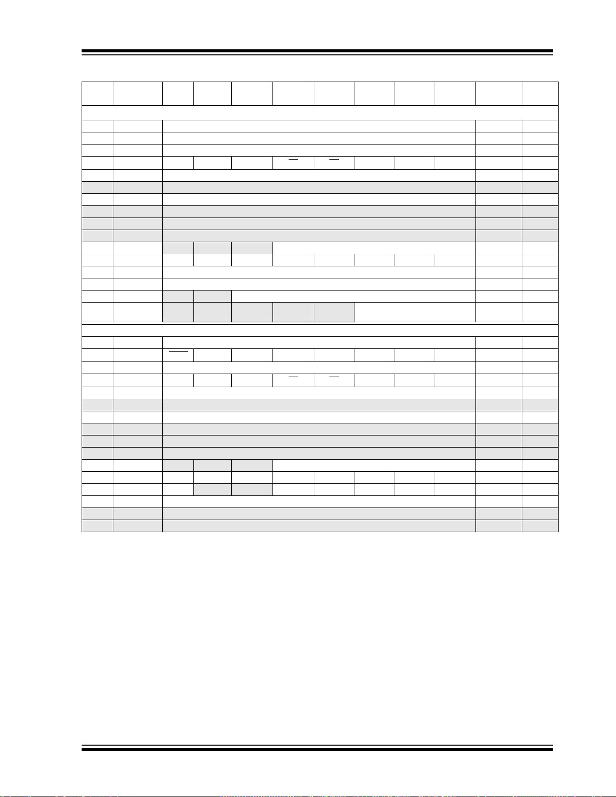
TABLE 2-1: SPECIAL FUNCTION REGISTER SUMMARY (CONTINUED)
Address Name Bit 7 Bit 6 Bit 5 Bit 4 Bit 3 Bit 2 Bit 1 Bit 0
Bank 1
(1)
80h
81h OPTION_REG RBPU
82h
83h
84h
85h TRISA TRISA7 TRISA6 TRISA5
86h TRISB PORTB Data Direction Register 1111 1111 43
87h — Unimplemented — —
88h — Unimplemented — —
89h — Unimplemented — —
8Ah
8Bh
8Ch PIE1
8Dh PIE2
8Eh PCON
8Fh OSCCON
90h
91h — Unimplemented — —
92h PR2 Timer2 Period Registe r 1111 1111 68
93h SSPADD Synchronous Serial Port (I
94h SSPSTAT SMP CKE D/A
95h — Unimplemented — —
96h — Unimplemented — —
97h — Unimplemented — —
98h — Unimplemented — —
99h — Unimplemented — —
9Ah — Unimplemented — —
9Bh — Unimplemented — —
9Ch — Unimplemented — —
9Dh — Unimplemented — —
9Eh ADRESL A/D Result Register Low Byte xxxx xxxx 81
9Fh ADCON1 ADFM ADCS2
Legend: x = unknown, u = unchanged, q = value depends on condition, - = unimplemented, read as ‘0’, r = reserved.
Note 1: These registers can be addressed from any bank.
INDF Addressing this location uses contents of FSR to address data memory (not a physical register) 0000 0000 23
(1)
PCL Program Counter’s (PC) Least Significant Byte 0000 0000 23
(1)
STATUS IRP RP1 RP0 TO PD ZDCC0001 1xxx 16
(1)
FSR Indirect Data Memory Address Pointer xxxx xxxx 23
(1,2)
PCLATH — — — Write Buffer for the upper 5 bits of the PC ---0 0000 23
(1)
INTCON GIE PEIE TMR0IE INTE RBIE TMR0IF INTF RBIF 0000 000x 18
(1)
OSCTUNE — — TUN5 TUN4 TUN3 TUN2 TUN1 TUN0 --00 0000 36
Shaded locations are unimplemented, read as ‘0’.
2: The upper byte of the program counter is not directly accessible. PCLATH is a holding register for the PC<12:8>, whose contents are
transferred to the upper byte of the program counter.
3: Pin 5 is an input only; the state of the TRISA5 bit has no effect and will always read ‘1’.
INTEDG T0CS T0SE PSA PS2 PS1 PS0 1111 1111 17, 54
(3)
PORTA Data Direction Register (TRISA<4:0> 1111 1111 39
—ADIE — — SSPIE CCP1IE TMR2IE TMR1IE -0-- 0000 19
— — — EEIE — — — — ---0 ---- 21
— — — — — —PORBOR ---- --qq 22
— IRCF2 IRCF1 IRCF0 — IOFS — — -000 -0-- 38
2
C™ mode) Address Register 0000 0000 71, 76
PSR/WUA BF 0000 0000 72
— — PCFG3 PCFG2 PCFG1 PCFG0 00-- 0000 82
Value on
POR, BOR
Details on
page:
DS39598E-page 14 2004 Microchip Technology Inc.
PIC16F818/819
TABLE 2-1: SPECIAL FUNCTION REGISTER SUMMARY (CONTINUED)
Address Name Bit 7 Bit 6 Bit 5 Bit 4 Bit 3 Bit 2 Bit 1 Bit 0
Bank 2
(1)
100h
101h TMR0 Timer0 Module Register xxxx xxxx 53
102h
103h
104h
105h — Unimplemented — —
106h PORTB PORTB Data Latch when written; PORTB pins when read xxxx xxxx 43
107h — Unimplemented — —
108h — Unimplemented — —
109h — Unimplemented — —
10Ah
10Bh
10Ch EEDATA EEPROM/Flash Data Register Low Byte xxxx xxxx 25
10Dh EEADR EEPROM/Flash Address Register Low Byte xxxx xxxx 25
10Eh EEDATH
10Fh EEADRH
Bank 3
180h
181h OPTION _REG RBPU
182h
183h
184h
185h — Unimplemented — —
186h TRISB PORTB Data Direction Register 1111 1111 43
187h — Unimplemented — —
188h — Unimplemented — —
189h — Unimplemented — —
18Ah
18Bh
18Ch EECON1 EEPGD
18Dh EECON2 EEPROM Control Register 2 (not a physical register) ---- ---- 25
18Eh — Reserved; maintain clear 0000 0000 —
18Fh — Reserved; maintain clear 0000 0000 —
Legend: x = unknown, u = unchanged, q = value depends on condition, - = unimplemented, read as ‘0’, r = reserved.
Note 1: These registers can be addressed from any bank.
INDF Addressing this location uses contents of FSR to address data memory (not a physical register) 0000 0000 23
(1
PCL Program Counter’s (PC) Least Significant Byte 0000 0000 23
(1)
STATUS IRP RP1 RP0 TO PD ZDCC0001 1xxx 16
(1)
FSR Indirect Data Memory Address Pointer xxxx xxxx 23
(1,2)
PCLATH — — — Write Buffer for the upper 5 bits of the Program Counter ---0 0000 23
(1)
INTCON GIE PEIE TMR0IE INTE RBIE TMR0IF INTF RBIF 0000 000x 18
— — EEPROM/Flash Data Register High Byte --xx xxxx 25
— — — — — E EPROM /F lash A ddr ess Regi st er
(1)
INDF Addressing this location uses contents of FSR to address data memory (not a physical register) 0000 0000 23
(1)
PCL Program Counter’s (PC) Least Significant Byte 0000 0000 23
(1)
STATUS IRP RP1 RP0 TO PD ZDCC0001 1xxx 16
(1)
FSR Indirect Data Memory Address Pointer xxxx xxxx 23
(1,2)
PCLATH — — — Write Buffer for the upper 5 bits of the Program Counter ---0 0000 23
(1)
INTCON GIE PEIE TMR0IE INTE RBIE TMR0IF INTF RBIF 0000 000x 18
Shaded locations are unimplemented, read as ‘0’.
2: The upper byte of the program counter is not directly accessible. PCLATH is a holding register for the PC<12:8>, whose contents are
transferred to the upper byte of the program counter.
3: Pin 5 is an input only; the state of the TRISA5 bit has no effect and will always read ‘1’.
INTEDG T0CS T0SE PSA PS2 PS1 PS0 1111 1111 17, 54
— — FREE WRERR WREN WR RD x--x x000 26
High Byte
Value on
POR, BOR
---- -xxx 25
Details on
page:
2004 Microchip Technology Inc. DS39598E-page 15

PIC16F818/819
2.2.2.1 Status Register
The St atus register , s hown in Register2-1, contains the
arithmeti c statu s of th e ALU, the Re set sta tus an d the
bank select bits for data memory.
The Status register can be the destination for any
instruction, as with any other register. If the Status
register is the destination for an instruction that affects
the Z, DC or C bits, then the write to these three bits is
disabled. These bit s are set or cleared ac cording to the
device logic. Furthermore, the TO
writable. Therefore, the result of an instruction with the
Status register as destination may be different than
intended.
and PD bits are not
For example, CLRF STATUS, w ill c lear the upper three
bits and set the Z bit. Thi s leaves the Status register as
‘000u u1uu’ (where u = unchanged).
It is recommended, therefore, that only BCF, BSF,
SWAPF and MOVWF instructions are used to alter the
Stat us regist er because the se inst ructions do not af fect
the Z, C or DC bits from the Status register. For other
instructions not affecting any status bits, see
Section 13.0 “Instruction Set Summary”.
Note: The C and DC bits operate as a borrow
and digit borrow bit, respectively, in
subtraction. See the SUBLW and SUBWF
instructions for examples.
REGISTER 2-1: STATUS: STATUS REGISTER (ADDRESS 03h, 83h, 103h, 183h)
R/W-0 R/W-0 R/W-0 R-1 R-1 R/W-x R/W-x R/W-x
IRP RP1 RP0 TO
bit 7 bit 0
bit 7 IRP: Register Bank Select bit (used for indirect addressing)
1 = Bank 2, 3 (100h-1FFh)
0 = Bank 0, 1 (00h-FFh)
bit 6-5 RP<1:0>: Register Bank Select bits (used for direct addressing)
11 = Bank 3 (180h-1FFh)
10 = Bank 2 (100h-17Fh)
01 = Bank 1 (80h-FFh)
00 = Bank 0 (00h-7Fh)
Each bank is 128 bytes.
bit 4 TO
bit 3 PD
bit 2 Z: Zero bit
bit 1 DC: Digit carry/borrow
bit 0 C: Carry/borrow
: Time-out bit
1 = After power-up, CLRWDT instruction or SLEEP instruction
0 = A WDT time-out occurred
: Power-down bit
1 = After power-up or by the CLRWDT instruction
0 = By execution of the SLEEP instruction
1 = The result of an arithmetic or logic operation is zero
0 = The result of an arithmetic or logic operation is not zero
bit (ADDWF, ADDLW, SUBLW and SUBWF ins tru cti ons )
1 = A carry-out from the 4th low order bit of the result occurred
0 = No carry-out from the 4th low order bit of the result
bit (ADDWF, ADDLW, SUBLW and SUBWF instructions)
1 = A carry-out from the Most Significant bit of the result occurred
0 = No carry-out from the Most Significant bit of the result occurred
PD ZDCC
(1)
(1,2)
Note 1: For borrow, the polarity is reversed. A subtraction is executed by adding the two’s
complement of the second operand.
2: For rotate (RRF, RLF) instructions, this bi t is loa ded with e ither the high or l ow-order
bit of the source register.
Legend:
R = Readable bit W = Writable bit U = Unimplemented bit, read as ‘0’
-n = Value at POR ‘1’ = Bit is set ‘0’ = Bit is cleared x = Bit is unknown
DS39598E-page 16 2004 Microchip Technology Inc.
PIC16F818/819
2.2.2.2 OPTION_RE G Regist er
The OPTION_REG register is a readable and writable
register that contains various control bits to configure
the TMR0 prescaler/WDT postscaler (single assignable register known also as the prescaler), the external
INT interrupt, TMR0 and the weak pull-u ps o n POR TB.
Note: To achieve a 1:1 prescaler assignment for
the TMR0 register, assign the prescaler to
the Watchdog Timer.
REGISTER 2-2: OPTION_REG: OPTION REGISTER (ADDRESS 81h, 181h)
R/W-1 R/W-1 R/W-1 R/W-1 R/W-1 R/W-1 R/W-1 R/W-1
RBPU
bit 7 bit 0
bit 7 RBPU
1 = PORTB pull-ups are disabled
0 = PORTB pull-ups are enabled by individual port latch values
bit 6 INTEDG: Interrupt Edge Select bit
1 = Interrupt on rising edge of RB0/INT pin
0 = Interrupt on falling edge of RB0/INT pin
bit 5 T0CS: TMR0 Clock Source Select bit
1 = Transition on T0CKI pin
0 = Internal instruction cycle clock (CLKO)
bit 4 T0SE: TMR0 Source Edge Select bit
1 = Increment on high-to-low trans ition on T0CKI pin
0 = Increment on low-to-high trans ition on T0CKI pin
bit 3 PSA: Prescaler Assignment bit
1 = Prescaler is assigned to the WDT
0 = Prescaler is assigned to the Timer0 module
bit 2-0 PS2:PS0: Prescaler Rate Select bit s
Bit Value TMR0 Rate WDT Rate
000
001
010
011
100
101
110
111
INTEDG T0CS T0SE PSA PS2 PS1 PS0
: PORTB Pull-up Enable bit
1 : 2
1 : 4
1 : 8
1 : 16
1 : 32
1 : 64
1 : 128
1 : 256
1 : 1
1 : 2
1 : 4
1 : 8
1 : 16
1 : 32
1 : 64
1 : 128
Legend:
R = Readable bit W = Writable bit U = Unimplemented bit, read as ‘0’
-n = Value at POR ‘1’ = Bit is set ‘0’ = Bit is cleared x = Bit is unknown
2004 Microchip Technology Inc. DS39598E-page 17

PIC16F818/819
2.2.2.3 INTCON Register
The INTCON register is a readable and writable register that contains various enable and flag bits for the
TMR0 register overflow, RB port change and external
RB0/INT pin interrupts.
Note: Interrupt flag bits get set when an interrupt
condition occurs regardle ss of the sta te of
its corresponding enable bit or the Global
Interrupt Enable bit, GIE (INTCON<7>).
User software shoul d ensure the appropriate interrupt flag bits are clear prior to
enabling an interrupt.
REGISTER 2-3: INTCON: INTERRUPT CONTROL REGISTER (ADDRESS 0Bh, 8Bh, 10Bh, 18Bh)
R/W-0 R/W-0 R/W-0 R/W-0 R/W-0 R/W-0 R/W-0 R/W-x
GIE PEIE TMR0IE INTE RBIE TMR0IF INTF RBIF
bit 7 bit 0
bit 7 GIE: Global Interrupt Enable bit
1 = Enables all unmasked interrupts
0 = Disables all interrupts
bit 6 PEIE: Peripheral Interrupt Enable bit
1 = Enables all unmasked peripheral interrupts
0 = Disables all peripheral interrupts
bit 5 TMR0IE: TMR0 Overflow Interrupt Enable bit
1 = Enables the TMR0 interrupt
0 = Disables the TMR0 interrupt
bit 4 INTE: RB0/INT External Interrupt Enable bit
1 = Enables the RB0/INT external interrupt
0 = Disables the RB0/INT external interrupt
bit 3 RBIE: RB Port Change Interrupt Enable bit
1 = Enables the RB port change interrupt
0 = Disables the RB port change interrupt
bit 2 TMR0IF: TMR0 Overflow Interrupt Flag bit
1 = TMR0 register has overflowed (must be cleared in software)
0 = TMR0 register did not overflow
bit 1 INTF: RB0/INT External Interrupt Flag bit
1 = The RB0/INT external interrupt occurred (must be cleared in software)
0 = The RB0/INT external interrupt did not occur
bit 0 RBIF: RB Port Change Interrupt Flag bit
A mismatch condi tio n wil l c on tin ue to set flag bit RBIF. Reading PORTB will end the mis mat ch
condition and allow flag bit RBI F to be cleared.
1 = At least one of the RB7:RB4 pins changed state (must be cleared in software)
0 = None of the RB7:RB4 pins have changed state
Legend:
R = Readable bit W = Writable bit U = Unimplemented bit, read as ‘0’
-n = Value at POR ‘1’ = Bit is set ‘0’ = Bit is cleared x = Bit is unknown
DS39598E-page 18 2004 Microchip Technology Inc.

PIC16F818/819
2.2.2.4 PIE1 Regi st er
This register contains the individual enable bits for the
peripheral interrupts.
Note: Bit PEIE (INTCON<6>) must be set to
enable any peripheral interrupt.
REGISTER 2-4: PIE1: PERIPHERAL INTERRUPT ENABLE REGISTER 1 (ADDRESS 8Ch)
U-0 R/W-0 U-0 U-0 R/W-0 R/W-0 R/W-0 R/W-0
—ADIE— — SSPIE CCP1IE TMR2IE TMR1IE
bit 7 bit 0
bit 7 Unimplemented: Read as ‘0’
bit 6 ADIE: A/D Converter Interrupt Enable bit
1 = Enables the A/D converter interrupt
0 = Disables the A/D converter interrupt
bit 5-4 Unimplemented: Read as ‘0’
bit 3 SSPIE: Synchronous Serial Port Interrupt Enable bit
1 = Enables the SSP interrupt
0 = Disables the SSP interrupt
bit 2 CCP1IE: CCP1 Interrupt Enable bit
1 = Enables the CCP1 interrupt
0 = Disables the CCP1 interrupt
bit 1 TMR2IE: TMR2 to PR2 Match Interrupt Enable bit
1 = Enables the TMR2 to PR2 match interrupt
0 = Disables the TMR2 to PR2 match interrupt
bit 0 TMR1IE: TMR1 Overflow Interrupt Enable bit
1 = Enables the TMR1 overflow interrupt
0 = Disables the TMR1 overflow interrupt
Legend:
R = Readable bit W = Writable bit U = Unimplemented bit, read as ‘0’
-n = Value at POR ‘1’ = Bit is set ‘0’ = Bit is cleared x = Bit is unknown
2004 Microchip Technology Inc. DS39598E-page 19

PIC16F818/819
2.2.2.5 PIR1 Register
This register contains the individual flag bits for the
peripheral interrupts.
Note: Interrupt flag bits are set when an in terrupt
condition occurs regardle ss of the sta te of
its corresponding enable bit or the Global
Interrupt Enable bit, GIE (INTCON<7>).
User software shoul d ensure the appropriate interrupt flag bits are clear prior to
enabling an interrupt.
REGISTER 2-5: PIR1: PERIPHERAL INTERRUPT REQUEST (FLAG) REGISTER 1 (ADDRESS 0Ch)
U-0 R/W-0 U-0 U-0 R/W-0 R/W-0 R/W-0 R/W-0
—ADIF— — SSPIF CCP1IF TMR2IF TMR1IF
bit 7 bit 0
bit 7 Unimplemented: Read as ‘0’
bit 6 ADIF: A/D Converter Interrupt Flag bit
1 = An A/D conversion completed
0 = The A/D conversion is not complete
bit 5-4 Unimplemented: Read as ‘0’
bit 3 SSPIF: Synchronous Serial Port (SSP) Interrupt Flag bit
1 = The SSP interrupt condition has occurred and must be cleared in software befo re returning
from the I n t err upt S erv ic e Ro ut i ne . T h e co ndi ti o ns t hat wil l s et t hi s b i t a re a t ran sm is si on /
reception has taken place.
0 = No SSP interrupt condition has occurred
bit 2 CCP1IF: CCP1 Interrupt Flag bit
Capture mode:
1 = A TMR1 register capture occurred (must be cleared in software)
0 = No TMR1 register capture occurred
Compare mode:
1 = A TMR1 register compare match occurred (must be cleared in software)
0 = No TMR1 register compare match occurred
PWM mode:
Unused in this mode.
bit 1 TMR2IF: TMR2 to PR2 Match Interrupt Flag bit
1 = TMR2 to PR2 match occurred (must be cleared in software)
0 = No TMR2 to PR2 match occurred
bit 0 TMR1IF: TMR1 Overflow Interrupt Flag bit
1 = TMR1 register overfl owed (must be cleared in software)
0 = TMR1 register did not overflow
Legend:
R = Readable bit W = Writable bit U = Unimplemented bit, read as ‘0’
-n = Value at POR ‘1’ = Bit is set ‘0’ = Bit is cleared x = Bit is unknown
DS39598E-page 20 2004 Microchip Technology Inc.

PIC16F818/819
2.2.2.6 PIE2 Regi st er
The PIE2 register contains the individual enable bit for
the EEPROM write operation interrupt.
REGISTER 2-6: PIE2: PERIPHERAL INTERRUPT ENABLE REGISTER 2 (ADDRESS 8Dh)
U-0 U-0 U-0 R/W-0 U-0 U-0 U-0 U-0
— — — EEIE — — — —
bit 7 bit 0
bit 7-5 Unimplemented: Read as ‘0’
bit 4 EEIE: EEPROM Write Operation Interrupt Enable bit
1 = Enable EE write interrupt
0 = Disable EE w rite interrupt
bit 3-0 Unimplemented: Read as ‘0’
Legend:
R = Readable bit W = Writable bit U = Unimplemented bit, read as ‘0’
-n = Value at POR ‘1’ = Bit is set ‘0’ = Bit is cleared x = Bit is unknown
2.2.2.7 PIR2 Register
The PIR2 register contains the fla g bit for the EEPROM
write operation interrupt.
.
Note: Interrupt flag bits are set when an in terrupt
condition occurs regardles s of the sta te of
its corresponding enable bit or the Global
Interrupt Enable bit, GIE (INTCON<7>).
User software shoul d ensure the appropriate interrupt flag bits are clear prior to
enabling an interrupt.
REGISTER 2-7: PIR2: PERIPHERAL INTERRUPT REQUEST ( FLAG) REGIST ER 2 (ADDRESS 0Dh)
U-0 U-0 U-0 R/W-0 U-0 U-0 U-0 U-0
— — — EEIF — — — —
bit 7 bit 0
bit 7-5 Unimplemented: Read as ‘0’
bit 4 EEIF: EEPROM Write Operation Interrupt Enable bit
1 = Enable EE write interrupt
0 = Disable EE w rite interrupt
bit 3-0 Unimplemented: Read as ‘0’
Legend:
R = Readable bit W = Writable bit U = Unimplemented bit, read as ‘0’
-n = Value at POR ‘1’ = Bit is set ‘0’ = Bit is cleared x = Bit is unknown
2004 Microchip Technology Inc. DS39598E-page 21

PIC16F818/819
2.2.2.8 PCON Regist er
Note: Interrupt flag bits get set when an interrupt
condition occurs regardless of the state of
its corresponding enable bit or the Global
Interrupt Enable bit, GIE (INTCON<7>).
User software should en sure the ap propriate interrupt flag bits are clear prior to
enabling an interrupt.
The Power Control (PCON) register contains a flag bit
to allow differentiation between a Power-on Reset
(POR), a Brown-out Reset, an external MCLR Reset
and WDT Reset.
Note: BOR is unknown on Power-on Reset. It
must then be set by the us er an d c hec ke d
on subsequent Resets to see if BOR is
clear , indicating a brown-out has occurred.
The BOR status bit is a ‘don’t care’ and is
not necessarily predictable if the brownout circuit is disabled (by clearing the
BOREN bit in the Configuration word).
REGISTER 2-8: PCON: POWER CONTROL REGISTER (ADDRESS 8Eh)
U-0 U-0 U-0 U-0 U-0 U-0 R/W-0 R/W-x
— — — — — —PORBOR
bit 7 bit 0
bit 7-2 Unimplemented: R e ad as ‘0’
bit 1 POR
bit 0 BOR
: Power-on Reset Status bit
1 = No Power-on Reset occurred
0 = A Power-on Reset occurred (must be set in software after a Power-on Reset occurs)
: Brown-out Reset Status bit
1 = No Brown-out Reset occurred
0 = A Brown-out Reset occurred (must be set in software after a Brown-out Reset occurs)
Legend:
R = Readable bit W = Writable bit U = Unimplemented bit, read as ‘0’
-n = Value at POR ‘1’ = Bit is set ‘0’ = Bit is cleared x = Bit is unknown
DS39598E-page 22 2004 Microchip Technology Inc.
PIC16F818/819
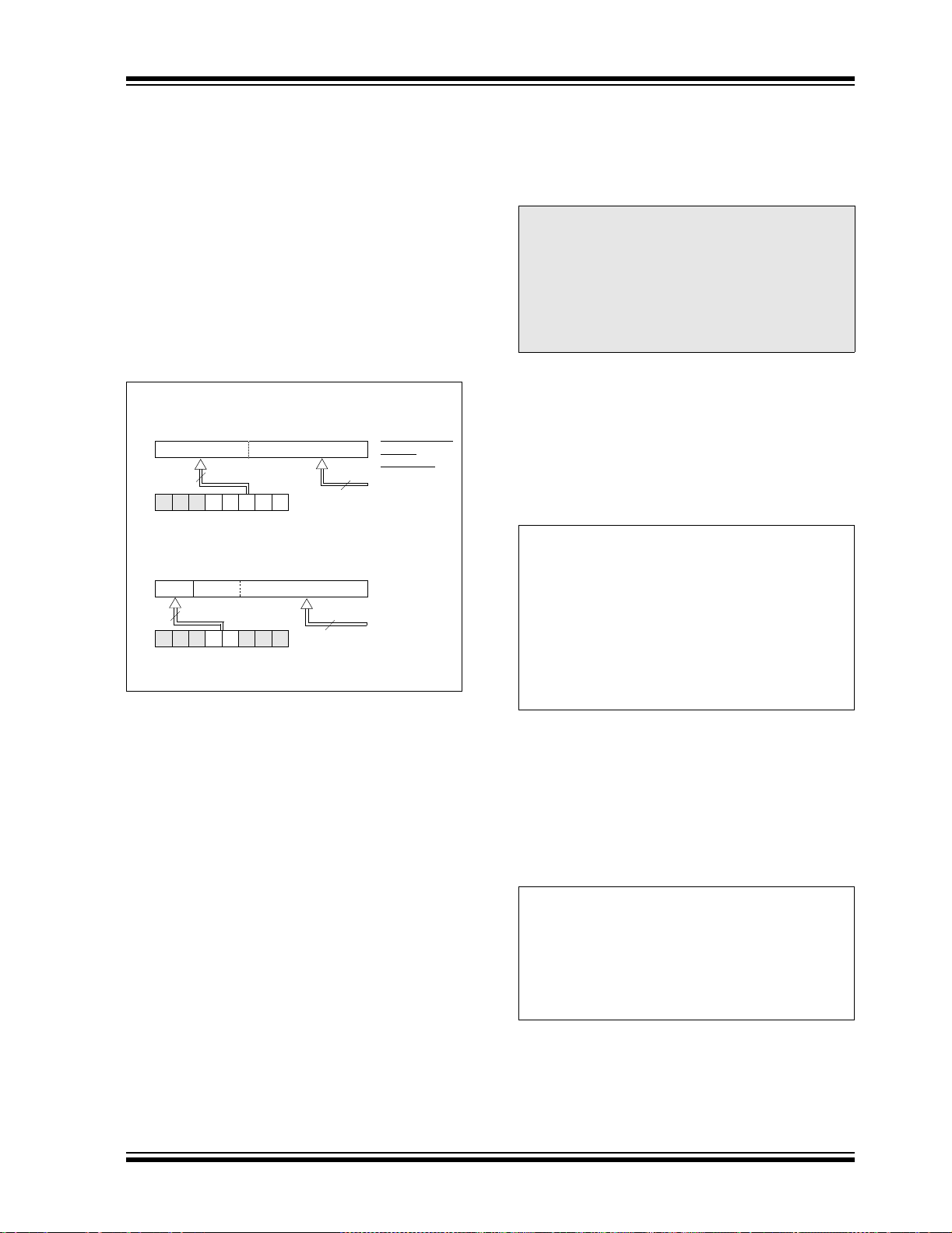
2.3 PCL and PCLATH
The Program Counter (PC) is 13 bits wide. The low
byte comes from the PCL register, which is a readable
and writable register. The upper bits (PC<12:8>) are
not readable but are indirectly writable through the
PCLATH register. On any Reset, the upper bits of the
PC will be cleared. Fig ure2-5 shows the two situations
for the loading of the PC. The upper example in the
figure shows how the PC is loaded on a write to PCL
(PCLATH<4:0> → PCH). The lower example in the
figure shows how the PC is loaded during a CALL or
GOTO instruction (PCLATH<4:3> → PCH).
FIGURE 2-5: LOADING OF PC IN
DIFFERENT SITUATIONS
PCH PCL
12 8 7 0
PC
PCLATH<4:0>
5
PCLATH
PCH PCL
12 11 10 0
PC
2
87
PCLATH<4:3>
PCLATH
11
8
Instruction with
PCL as
Destination
ALU
GOTO,CALL
Opcode <10:0>
The stack operat es as a circular buf fer . This means th at
after the stack has been PUSHed eight times, the ninth
push overwrites th e valu e that was s tored fro m the firs t
push. The tenth pus h ov erwr i tes the se co nd push (and
so on).
Note 1: There are no status bits to indicate stack
overflow or stack underflow conditions.
2: There are no instructions/mnemonics
called PUSH or POP. These are actions
that occur from the execution of the
CALL, RETURN, RETLW and RETFIE
instructions or the vectoring to an
interrupt address.
2.4 Indirect Addressing: INDF and FSR Registers
The INDF register is not a physica l register . Addr essing
INDF actually addresse s the regi st er whose ad dress i s
contained in the FSR reg ister (FSR is a pointer). This is
indirect addressing.
EXAMPLE 2-1: INDIR ECT ADDRESSING
• Register file 05 contains the value 10h
• Register file 06 contains the value 0Ah
• Load the value 05 into the FSR register
• A read of the INDF regi ste r will ret urn the value
of 10h
• Increment the value of the FSR register by one
(FSR = 06)
• A read of the INDF register now will return the
value of 0Ah
2.3.1 COMPUTED GOTO
A computed GOTO is accomplish ed by adding an offset
to the program counter (ADDWF PCL). When doing a
table read using a computed GOTO method, care
should be exercise d i f the t able loca tio n cros ses a PCL
memory boundary (each 256-byte block). Refer to the
application note AN556, “Implementing a Table Read”
(DS00556).
2.3.2 STACK
The PIC16F818/819 family has an 8-level deep x 13-bit
wide hardware stack. The stack space is not part of
either program or data space and the Stack Pointer is
not readable or writable. The PC is PUSHed onto the
stack when a CALL instruction is executed or an
interrupt causes a branch. The stack is POPed in the
event of a RETURN, RETLW or a RETFIE instruction
execution. PCLATH is not affected by a PUSH or POP
operation.
Reading INDF itself indirectly (FSR = 0) will produce
00h. Writing to the INDF register indirectly results in a
no operation (although status bits may be affected).
A simple program to clear RAM locations, 20h-2Fh,
using indirect addressing is shown in Example 2-2.
EXAMPLE 2-2: HOW TO CLEAR RAM
USING INDIRECT
ADDRESSING
MOVLW 0x20 ;initialize pointer
MOVWF FSR ;to RAM
NEXT CLRF INDF ;clear INDF register
INCF FSR ;inc pointer
BTFSS FSR, 4 ;all done?
GOTO NEXT ;NO, clear next
CONTINUE
: ;YES, continue
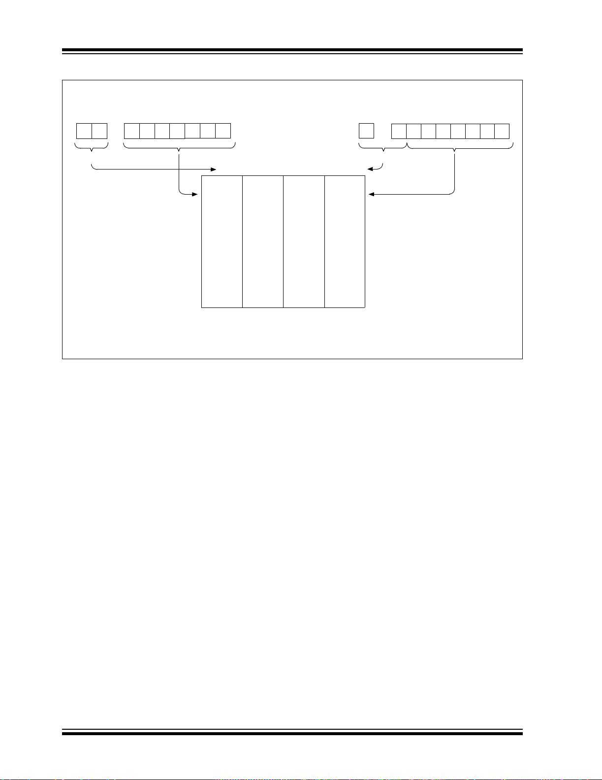
An effective 9-b it addre ss is obtained by concatenating
the 8-bit FSR register and the IRP bit (Status<7>) as
shown in Figure 2-6.
2004 Microchip Technology Inc. DS39598E-page 23
PIC16F818/819
FIGURE 2-6: DIRE CT/INDI RECT ADDRESSING
RP1:RP 0 6
From Opcode
0
Indirect AddressingDirect Addressing
IRP FSR Register
7
0
Bank Select Location Select
00 01 10 11
00h
Data
(1)
Memory
7Fh
Bank 0 Bank 1 Bank 2 Bank 3
Note 1: For register file map detail, see Figure 2-3 or Figure 2-4.
80h
FFh
100h
17Fh
180h
1FFh
Bank Select
Location Select
DS39598E-page 24 2004 Microchip Technology Inc.

PIC16F818/819
3.0 DATA EEPROM AND FLASH PROGRAM MEMORY
The data EEPROM and Flash program memory are
readable and writable during normal operation (over
the full V
in the register file space. Instead, it is indirectly
addressed through the Special Function Registers.
There are six SFRs used to read and write this
memory:
• EECON1
• EECON2
• EEDATA
• EEDATH
• EEADR
• EEADRH
This section focuses on reading and writing data
EEPROM and Flash program memory during normal
operation. Refer to the appropriate device programming specification document for serial programming
information.
When interfacing the data memory block, EEDATA
holds the 8-bit data for read/write and EEADR holds the
address of the EEPROM location being accessed.
These devices have 128 or 256 bytes of data
EEPROM, with an address range from 00h to 0FFh.
Addresses from 80h to FFh are unimplemented on the
PIC16F818 device and will read 00h. When writing to
unimplemented locations, the charge pump will be
turned off.
When interfacing the program memory block, the
EEDATA and EEDATH registers form a two-byte word
that holds the 14-bit data fo r read/write and the EEADR
and EEADRH registers f orm a two-byte wor d that holds
the 13-bit address of the EEPROM location being
accessed. These devices have 1K or 2K words of
program Flash, with an address range from 0000h to
03FFh for the PIC16F818 and 0000h to 07FFh for the
PIC16F819. Addresse s abov e the range of the respe ctive device will wra paround to t he beginning o f program
memory.
The EEPROM data memory allows single byte read
and write. The Flash program memory allows singleword reads and four-word block writes. Program
memory writes must first start with a 32-word block
erase, then write in 4-word blocks. A byte write in data
EEPROM memory automatically erases the location
and writes the new data (erase before write).
The write time is controlled by an on-chip timer. The
write/erase voltages are generated by an on-chip
charge pump, rated to operate over the voltage range
of the device for byte or word operations.
DD range). This memory is not directl y mapped
When the device is code-protected, the CPU may
continue to read and write th e data EEPROM memory.
Depending on the settings of the write-protect bits, the
device may or may not be able to write certain blocks
of the program memory; ho wever , reads of the program
memory are allowed. When co de-prote cted, the devic e
programmer can no longer access data or program
memory; this does NOT inh ib it in tern al re ad s or w ri tes .
3.1 EEADR and EEADRH
The EEADRH:EEADR register pair can address up to
a maximum of 256 bytes of data EEPROM or up to a
maximum of 8K words of program EEPROM. When
selecting a data address value, only the LSB of the
address is written to the EEADR regist er. When selecting a program address value, the MSB of the address
is written to the EEADRH register and the LSB is
written to the EEADR register.
If the device cont ains less me mory than the fu ll address
reach of the address register pair, the Most Significant
bits of the regist ers are not im plem ented. F or exam ple,
if the device has 128 b yte s o f da t a EEPROM , th e Mos t
Significant bit of EEADR i s not im plement ed o n acces s
to data EEPROM.
3.2 EECON1 and EECON2 Registers
EECON1 is the control register for memory accesses.
Control bit, EEPGD, determines if the access will be a
program or data memory access. When clear, as it is
when Reset, any subsequent operations will operate
on the data memory. When set, any subsequent
operations will operate on the program memory.
Control bits, RD and WR, initiate read and write,
respectiv ely. These bits cannot be cleared, only set in
software. They are cleared in hardware at completion
of the read or write operation. The inability to clear the
WR bit in software prevents the accidental, premature
termination of a write operation.
The WREN bi t, when set, wil l allow a write or erase
operation. On power-up, the WREN bit is clear. The
WRERR bit is set when a write (or erase) operation is
interrupted by a MCLR
during normal operation. In these situations, following
Reset, the user can check the WRERR bit and rewrite
the location. The data and address will be unchanged
in the EEDATA and EEADRregisters.
Interrupt flag bit, EEIF in the PIR2 register, is set when
the write is complete. It must be cleared in software.
EECON2 is not a physical register. Reading EECON2
will read all ‘0’s. The EECON2 register is used
exclusively in the EEPROM write sequence.
or a WDT Time-out Reset
2004 Microchip Technology Inc. DS39598E-page 25

PIC16F818/819
REGISTER 3-1: EECON1: EEPROM ACCESS CONTROL REGISTER 1 (ADDRESS 18Ch)
R/W-x U-0 U-0 R/W-x R/W-x R/W-0 R/S-0 R/S-0
EEPGD — — FREE WRERR WREN WR RD
bit 7 bit 0
bit 7 EEPGD: Program/Data EEPROM Select bit
1 = Accesses program memory
0 = Accesses data memory
Reads ‘0’ after a POR; this bit cannot be changed while a write operation is in progress.
bit 6-5 Unimplemented: Read as ‘0’
bit 4 FREE: EEPROM Forced Row Erase bit
1 = Erase the program memory row a ddressed by EEADRH:EEADR on th e next WR command
0 = Perform write-only
bit 3 WRERR: EEPROM Error Flag bit
1 = A write operation is prematurely terminated (any MCLR
operation)
0 = The write operation completed
bit 2 WREN: EEPROM Write Enable bit
1 = Allows write cycles
0 = Inhibits write to the EEPROM
bit 1 WR: Write Control bit
1 = Initiates a write cycle. The bit is cleared by hardware once write is complete. The WR bit
can only be set (not cleared) in software.
0 = Write cycle to the EEPROM is complete
bit 0 RD: Read Control bit
1 = Initiates an EEPROM read, RD is cleared in hardware. The RD bit can only be set (not
cleared) in software.
0 = Does not initiate an EEPROM read
or any WDT Reset during normal
Legend:
R = Readable bit W = Writable bit S = Set only U = Unimplemented bit, read as ‘0’
-n = Value at POR ‘1’ = Bit is set ‘0’ = Bit is cleared x = Bit is unknown
DS39598E-page 26 2004 Microchip Technology Inc.

PIC16F818/819
3.3 Reading Data EEPROM Memory
T o read a d ata memory loca tion, the user must write the
address to the EEADR register, clear the EEPGD
control bit (EECON1<7>) and then set control bit, RD
(EECON1<0>). The data is available in the very next
cycle in the EEDATA register; therefore, it can be read
in the next instruction (see Example 3-1). EEDATA will
hold this value until another read or until it is written to
by the user (during a write operation).
The steps to reading the EEPROM data memory are:
1. Write the address to EEADR. Make su re that the
address is not larger than the memory size of
the device.
2. Clear the EEPGD bit to point to EEPROM data
memory.
3. Set the RD bit to start the read operation.
4. Read the data from the EEDATA regi ster.
EXAMPLE 3-1: DATA EEPROM READ
BANKSEL EEADR ; Select Bank of EEADR
MOVF ADDR, W ;
MOVWF EEADR ; Data Memory Address
; to read
BANKSEL EECON1 ; Select Bank of EECON1
BCF EECON1, EEPGD ; Point to Data memory
BSF EECON1, RD ; EE Read
BANKSEL EEDATA ; Select Bank of EEDATA
MOVF EEDATA, W ; W = EEDATA
The steps to write to EEPROM data memory are:
1. If step 10 is not implemented, check the WR bit
to see if a write is in progress.
2. Write the address to EEADR. Make su re that the
address is not larger than the memory size of
the device.
3. Write the 8-bit data value to be programmed in
the EEDATA register.
4. Clear the EEPGD bit to point to EEPROM data
memory.
5. Set the WREN bit to enable program ope rations.
6. Disable interrupts (if enabled).
7. Execute the special five instruction sequence:
• Write 55h to EECON2 in two steps (first to W,
then to EECON2)
• Write AAh to EECON2 in two steps (first to W,
then to EECON2)
• Set the WR bit
8. Enable interrupts (if using interrupts).
9. Clear the WREN bit to disable program
operations.
10. At the completion of the write cycle, the WR bit
is cleared and the EEIF interrupt flag bit is set
(EEIF must be cleared by firmware). If step 1 is
not implemented, then firmware should check
for EEIF to be set, or WR to b e cle ar, to indicate
the end of the program cycle.
3.4 Writing to Data EEPROM Memory
To write an EEPROM data location, the user must first
write the address to the EEADR register and the data
to the EEDATA register. Then, the user must follow a
specific write sequence to initiate the write for each
byte.
The write will not initiate if the write sequence is not
exactly followed (write 55h to EECON2, write AAh to
EECON2, then set WR bit) for each byte. We strongly
recommend that interrupts be disabled during this
code segment (see Example 3-2).
Additionally, the WREN bit in EECON1 must be set to
enable write. This mechanism prevents accidental
writes to data EEPROM due to errant (unexpected)
code execution (i.e., lost programs). The user should
keep the WREN bit clear at all times except when
updating EEPROM. The WREN bit is not cleared
by hardware
After a write sequence has been initiated, clearing the
WREN bit will not af fect this wri te cycle. The W R bit will
be inhibited from being set unless the WREN bit is set.
At the completion of the write cycle, the WR bit is
cleared in hardware and the EE Write Complete
Interrupt Flag bit (EEIF) is set. The user can either
enable this interrupt or poll this bit. EEIF must be
cleared by software.
EXAMPLE 3-2: DATA EEPROM WRITE
BANKSEL EECON1 ; Select Bank of
BTFSC EECON1, WR ; Wait for write
GOTO $-1 ; to complete
BANKSEL EEADR ; Select Bank of
MOVF ADDR, W ;
MOVWF EEADR ; Data Memory
MOVF VALUE, W ;
MOVWF EEDATA ; Data Memory Value
BANKSEL EECON1 ; Select Bank of
BCF EECON1, EEPGD ; Point to DATA
BSF EECON1, WREN ; Enable writes
BCF INTCON, GIE ; Disable INTs.
MOVLW 55h ;
MOVWF EECON2 ; Write 55h
MOVLW AAh ;
MOVWF EECON2 ; Write AAh
Required
Sequence
BSF EECON1, WR ; Set WR bit to
BSF INTCON, GIE ; Enable INTs.
BCF EECON1, WREN ; Disable writes
; EECON1
; EEADR
; Address to write
; to write
; EECON1
; memory
; begin write
2004 Microchip Technology Inc. DS39598E-page 27

PIC16F818/819
3.5 Reading Flash Program Memory
To read a program memory location, the user must
write two bytes of the address to the EEADR and
EEADRH registers, set the EEPGD control bit
(EECON1<7>) and then set control bit, RD
(EECON1<0>). Once the read control bit is set, the
program memo ry Flash con troller wil l use the sec ond
instruction cycle to read the data. This causes the
second instruction immediately following the
“BSF EECON1, RD” instruction to be ignore d. The da ta
is availabl e in the very next cycle in the EEDATA and
EEDATH registers; therefore, it can be read as two
bytes in the following instructions. EEDATA and
EEDA TH registe rs will h old this valu e until ano ther read
or until it is written to by the user (during a write
operation).
EXAMPLE 3-3: FLASH PROGRAM READ
BANKSEL EEADRH ; Select Bank of EEADRH
MOVF ADDRH, W ;
MOVWF EEADRH ; MS Byte of Program
; Address to read
MOVF ADDRL, W ;
MOVWF EEADR ; LS Byte of Program
; Address to read
BANKSEL EECON1 ; Select Bank of EECON1
BSF EECON1, EEPGD ; Point to PROGRAM
; memory
BSF EECON1, RD ; EE Read
;
NOP ; Any instructions
; here are ignored as
NOP ; program memory is
; read in second cycle
; after BSF EECON1,RD
BANKSEL EEDATA ; Select Bank of EEDATA
MOVF EEDATA, W ; DATAL = EEDATA
MOVWF DATAL ;
MOVF EEDATH, W ; DATAH = EEDATH
MOVWF DATAH ;
3.6 Erasing Flash Program Memory
The minimum erase block is 32 words. Only through
the use of an external programmer, or through ICSP
control, can larger blocks of program memory be bulk
erased. Word erase in the Flash array is not supp orted.
When initiating an erase sequence from the microcontroller itse lf, a block of 32 words of program memor y
is erased. The Most Significant 11 bits of the
EEADRH:EEADR point to the block being erased.
EEADR< 4:0> are ignored.
The EECON1 register commands the erase operation.
The EEPGD bit must be set to point to the Flash
program memory. The WREN bit must be set to enabl e
write operations. The FR EE bit is set to select an eras e
operation.
For protection, the wri te i nit iat e s equ enc e f or EEC ON 2
must be used.
After the “BSF EECON1, WR” instruction, the processor
requires two cycles to set up the erase operation. The
user must place two NOP ins tructions after the WR bit is
set. The processor will halt internal operations for the
typical 2 ms, only during the cycle in which the erase
takes place. This is not Sleep mode, as the clocks and
peripherals will continue to run. After the erase cycle,
the processor will resume operation with the third
instruction after the EECON1 write instruction.
3.6.1 FLASH PROGRAM MEMORY ERASE SEQUENCE
The sequence of events for erasing a block of internal
program memory location is:
1. Load EEADRH:EEADR with address of row
being erased.
2. Set EEPGD bit to point to program memory; set
WREN bit to enable writes and set FREE bit to
enable the erase.
3. Disable interrupts.
4. Write 55h to EECON2.
5. Write AAh to EECON2.
6. Set the WR bit. This will begin the row erase
cycle.
7. The CPU will stall for duration of the erase.
DS39598E-page 28 2004 Microchip Technology Inc.

EXAMPLE 3-4: ERASING A FLASH PROGRAM MEMORY ROW
BANKSEL EEADRH ; Select Bank of EEADRH
MOVF ADDRH, W ;
MOVWF EEADRH ; MS Byte of Program Address to Erase
MOVF ADDRL, W ;
MOVWF EEADR ; LS Byte of Program Address to Erase
ERASE_ROW
BANKSEL EECON1 ; Select Bank of EECON1
BSF EECON1, EEPGD ; Point to PROGRAM memory
BSF EECON1, WREN ; Enable Write to memory
BSF EECON1, FREE ; Enable Row Erase operation
;
BCF INTCON, GIE ; Disable interrupts (if using)
MOVLW 55h ;
MOVWF EECON2 ; Write 55h
MOVLW AAh ;
MOVWF EECON2 ; Write AAh
BSF EECON1, WR ; Start Erase (CPU stall)
NOP ; Any instructions here are ignored as processor
; halts to begin Erase sequence
NOP ; processor will stop here and wait for Erase complete
; after Erase processor continues with 3rd instruction
BCF EECON1, FREE ; Disable Row Erase operation
BCF EECON1, WREN ; Disable writes
BSF INTCON, GIE ; Enable interrupts (if using)
PIC16F818/819
2004 Microchip Technology Inc. DS39598E-page 29

PIC16F818/819
3.7 Writing to Flash Program Memory
Flash program memory may only be written to if the
destination addr ess is in a se gment of memo ry th at is
not write-protected, as defined in bits WRT1:WRT0 of
the device Configuration Word (Register 12-1). Flash
program memo ry must b e writt en in fo ur-word blocks.
A block consists of four words with sequential
addresses, with a lower boundary defined by an
address, wh ere E EAD R<1: 0> = 00. At the same time,
all block wri tes to pr ogra m memo ry ar e do ne as w rite only operations. The program memory must first be
erased. The write oper ation is edge-align ed and cannot
occur across boundaries.
To write to the program memory, the data must first be
loaded into the buffer registers. There are four 14-bit
buffer registers and they are addressed by the low
2 bits of EEADR.
The following sequence of events illustrate how to
perform a write to progra m memory:
• Set the EEPGD and WREN bits in the EECON1
register
• Clear the FREE bit in EECON1
• Write address to EEADRH:EEADR
• Write data to EEDATH:EEDATA
• Write 55 to EECON2
• Write AA to EECON2
• Set WR bit in EECON 1
The user must follow the same specific sequence to
initiate the write for each word in the program block by
writing each program w ord in sequence (00, 01, 10,
11).
There are 4 buffer register words and all four locations
MUST be written to with correct data.
After the “BSF EECON1, WR” instruction, if
EEADR
≠ xxxxxx11, then a short write will occur.
This short write-only transfers the data to the buffer
register. The WR bit will be cleared in hardware after
one cycle.
After the “BSF EECON1, WR” instruction, if
EEADR = xxxxxx11, then a long write will occur. This
will simultaneously transfer the data from
EEDA TH:EEDATA to the buffer registers and be gin the
write of all four words. The processor will execute the
next instruction and then ignore the subsequent
instruction. The user sh ould place NOP instruct ions into
the second words. Th e pro cess or wil l th en h alt internal
operations for typicall y 2msec in which the write takes
place. This is not a Sleep mode, as the clocks and
peripherals will continue to run. After the write cycle,
the processor will resume operation with the 3rd
instruction after the EECON1 write instruction.
After each long write, the 4 bu ffe r registers wi ll be reset
to 3FFF.
FIGURE 3-1: BLOCK WRITES TO FLASH PROGRAM MEMORY
First word of block
to be written
EEADR<1:0> = 00
14
Buffer Register
75
EEDATH
6
14 14 14
EEADR<1:0> = 01
Buffer Register
Program Memory
07
EEDATA
8
EEADR<1:0> = 10
Buffer Register
0
All buffers are
transferred
to Flash
automatically
after this word
is written
EEADR<1:0> = 11
Buffer Register
DS39598E-page 30 2004 Microchip Technology Inc.

PIC16F818/819
An example of the complete four-word write sequence
is shown in Example 3-5. The initial address is loaded
into the EEADRH:EEADR register pair; the four words
of data are load ed us ing in direct add ressing, assum ing
that a row erase sequence has already been
performed.
EXAMPLE 3-5: WRITING TO FLASH PROGRAM MEMORY
; This write routine assumes the following:
; 1. The 32 words in the erase block have already been erased.
; 2. A valid starting address (the least significant bits = '00') is loaded into EEADRH:EEADR
; 3. This example is starting at 0x100, this is an application dependent setting.
; 4. The 8 bytes (4 words) of data are loaded, starting at an address in RAM called ARRAY.
; 5. This is an example only, location of data to program is application dependent.
; 6. word_block is located in data memory.
BANKSEL EECON1 ;prepare for WRITE procedure
BSF EECON1, EEPGD ;point to program memory
BSF EECON1, WREN ;allow write cycles
BCF EECON1, FREE ;perform write only
BANKSEL word_block
MOVLW .4
MOVWF word_block ;prepare for 4 words to be written
LOOP
BANKSEL EEADRH ;Start writing at 0x100
MOVLW 0x01
MOVWF EEADRH ;load HIGH address
MOVLW 0x00
MOVWF EEADR ;load LOW address
BANKSEL ARRAY
MOVLW ARRAY ;initialize FSR to start of data
MOVWF FSR
BANKSEL EEDATA
MOVF INDF, W ;indirectly load EEDATA
MOVWF EEDATA
INCF FSR, F ;increment data pointer
MOVF INDF, W ;indirectly load EEDATH
MOVWF EEDATH
INCF FSR, F ;increment data pointer
BANKSEL EECON1
MOVLW 0x55 ;required sequence
MOVWF EECON2
MOVLW 0xAA
MOVWF EECON2
BSF EECON1, WR ;set WR bit to begin write
Required
Sequence
NOP ;instructions here are ignored as processor
NOP
BANKSEL EEADR
INCF EEADR, f ;load next word address
BANKSEL word_block
DECFSZ word_block, f ;have 4 words been written?
GOTO loop ;NO, continue with writing
BANKSEL EECON1
BCF EECON1, WREN ;YES, 4 words complete, disable writes
BSF INTCON, GIE ;enable interrupts
2004 Microchip Technology Inc. DS39598E-page 31

PIC16F818/819
3.8 Protection Against Spurious Write
There are conditions when the device should not write
to the data EEPROM memory. To protect against
spurious EEPROM writes, various mechanisms have
been built-in. On power-up, WREN is c leared. Al so, the
Power-up Timer (72 ms duration) prevents an
EEPROM write.
The write initiate se quence and the WREN bit together
help prevent an accidental write during brown-out,
power glitch or software malfunction.
3.9 Operation During Code-Protect
When the data EEPROM is code-protected, the microcontroller can read and writ e to th e EEPROM n ormall y.
However, all external access to the EEPROM is
disabled. External write acce ss to the progra m memory
is also disabled.
When program memory is code-protected, the microcontroller can read and write to program memory
normally as well as execute instructions. Writes by the
device may be selectively inhibited to regions of
the memory depending on the setting of bits,
WRT1:WRT0, of the Configuration Word (see
Section 12.1 “Configuration Bits” for additional
information). External access to the memory is also
disabled.
TABLE 3-1: REGISTERS/BITS ASSOCIATED WITH DATA EEPROM AND
FLASH PROGRAM MEMORIES
Address Name Bit 7 Bit 6 Bit 5 Bit 4 Bit 3 Bit 2 Bit 1 Bit 0
10Ch EEDATA EEPROM/Flash Data Register Low Byte xxxx xxxx uuuu uuuu
10Dh EEADR EEPROM/Flash Address Register Low Byte xxxx xxxx uuuu uuuu
10Eh EEDATH
10Fh EEADRH
18Ch EECON1 EEPGD
18Dh EECON2 EEPROM Control Register 2 (not a physical register) ---- ---- ---- ---0Dh PIR2
8Dh PIE2
Legend: x = unknown, u = unchanged, - = unimplemented, read as ‘0’, q = value depends upon condition.
Shaded cells are not used by data EEPROM or Flash program memory.
— — EEPROM/Flash Data Register High Byte --xx xxxx --uu uuuu
— — — — — EEPROM/Flash Address
Register High Byte
— — FREE WRERR WREN WR RD x--x x000 x--x q000
— — — EEIF — — — — ---0 ---- ---0 ----
— — —EEIE— — — — ---0 ---- ---0 ----
Val ue on
Power-on
Reset
---- -xxx ---- -uuu
Value on
all other
Resets
DS39598E-page 32 2004 Microchip Technology Inc.

PIC16F818/819
4.0 OSCILLATOR CONFIGURATIONS
4.1 Oscillator Types
The PIC16F818/819 can be operated in eight different
oscillator modes. The user can program three configuration bits (FOSC2:FOSC0) to select one of these eight
modes (modes 5-8 are new PIC16 oscillator
configurations):
1. LP Low-Power Crystal
2. XT Crystal/Resonator
3. HS High-Speed Crystal/Resonator
4. RC External Resistor/Capac ito r with
OSC/4 output on RA6
F
5. RCIO External Resistor/Capacitor with
I/O on RA6
6. INTIO1 Internal Oscillator with F
output on RA6 and I/O on RA7
7. INTIO2 Internal Oscillator with I/O on RA6
and RA7
8. ECIO External Clock with I/O on RA6
4.2 Crystal Oscilla tor/Ceramic Resonators
In XT, LP or HS modes, a crystal or ceramic resonator
is connected to the OSC1/CLKI and OSC2/CLKO pins
to establish osci llatio n (see Fi gure4-1 and Figure 4-2).
The PIC16F818/819 oscillator design requires the use
of a parallel cut crystal. Use of a series cut crystal may
give a frequency out of the crystal manufacturer’s
specifications.
FIGURE 4-1: CRYSTAL OPERATION
(HS, XT OR LP OSC
CONFIGURATION)
OSC1
(1)
C1
C2
XTAL
OSC2
(2)
R
S
(1)
RF
(3)
OSC/4
PIC16F818/819
Sleep
To Internal
Logic
TABLE 4-1: CAPACITOR SELECTION FOR
CRYSTAL OSCILLATOR (FOR
DESIGN GUIDANCE ONLY)
Osc Type
Crystal
Freq
LP 32 kHz 33 pF 33 pF
200 kHz 15 pF 15 pF
XT 200 kHz 56 pF 56 pF
1 MHz 15 pF 15 pF
4 MHz 15 pF 15 pF
HS 4 MHz 15 pF 15 pF
8 MHz 15 pF 15 pF
20 MHz 15 pF 15 pF
Capacitor values are for design guidance only.
These capacit ors wer e tested with th e crystal s listed
below for basic start-up and operation. These values
were not optimized.
Different cap acitor valu es may be required to prod uce
acceptable oscillator operation. The user should test
the performance of the oscillator over the expected
DD and temperature range for the application.
V
See the notes following this table for additional
information.
Note 1: Higher capacitance increases the stability
of the oscillator but also increases the
start-up time.
2: Since each crystal has its own character-
istics, th e user shoul d cons ult th e crys tal
manufacturer for appropriate values of
external components.
S may be re quir ed i n HS mo de, a s w ell
3: R
as XT mode, to avoid overdrivi ng cryst al s
with low drive level specification.
4: Always verify oscillator performance over
DD and temperature range that is
the V
expected for the application.
T ypical Ca pac itor Values
Tested:
C1 C2
Note 1: See Table 4-1 for typical values of C1 and C2.
2: A series resistor (R
strip cut crystals.
F varies with the crystal chosen (typically
3: R
between 2 MΩ to 1 0 M Ω).
2004 Microchip Technology Inc. DS39598E-page 33
S) may be required for AT

PIC16F818/819
FIGURE 4-2: CER AMIC RESONATOR
OPERATION (HS OR XT
OSC CONFIGURATION)
OSC1
(1)
C1
RES
OSC2
(2)
R
S
(1)
C2
Note 1: See Table 4-2 for typical values of C1 and C2.
2: A series resistor (R
F varies with the resonator chosen (typically
3: R
between 2 MΩ to 10 MΩ).
RF
S) may be required.
PIC16F818/819
(3)
Sleep
To Internal
Logic
TABLE 4-2: CERAMIC RESONATORS (FOR
DESIGN GUIDANCE ONLY)
Typical Capacitor Values Used:
Mode Freq OSC1 OSC2
XT 455 kHz
2.0 MHz
4.0 MHz
HS 8.0 MHz
16.0 MHz
Capacitor values are for design guidance only.
These capacitors were tested with the resonators
listed below for basic start-up and operation. These
values were not optimized.
Different cap acitor values may be required to produce
acceptable oscillator operation. The user should test
the performance of the oscillator over the expected
DD and temperature range for the application.
V
See the notes following this table for additional
information.
56 pF
47 pF
33 pF
27 pF
22 pF
56 pF
47 pF
33 pF
27 pF
22 pF
4.3 External Clock Input
The ECIO Oscillator mode requires an external clock
source to be connected to the OSC1 pin. There is no
oscillator sta rt-up ti me required afte r a P ower-o n Res et
or after an exit from Sleep mode.
In the ECIO Oscillator mode, the OSC2 pin becomes
an additional general purpose I/O pin. The I/O pin
becomes bit 6 of PORTA (RA6). Figure 4-3 shows the
pin connections for the ECIO Oscillator mode.
FIGURE 4-3: EXTERNAL CLOCK INPUT
OPERATION
(ECIO CONFIGURATION)
Clock from
Ext. System
RA6
OSC1/CLKI
PIC16F818/819
I/O (OSC2)
Note: When using resonators with frequencies
above 3.5 MHz, the u se of HS mode rather
than XT mode is recommended. HS mode
may be used at any V
DD for which the
controller is rated. If HS is selected, it is
possible that the gain of the oscillator will
overdrive the resonator. Therefore, a
series resistor should be placed between
the OSC2 pin and the resonator. As a
good starting point, the recommended
value of R
DS39598E-page 34 2004 Microchip Technology Inc.
S is 330Ω.

PIC16F818/819
4.4 RC Oscillator
For timing insensitive applications, the “RC” and
“RCIO” device options offer additional cost savings.
The RC oscillator frequency is a function of the supply
voltage, the resistor (R
values and the operating temperature. In addition to
this, the oscillator frequency will vary from unit to unit
due to normal manufacturing variation. Furthermore,
the difference in lead frame cap acitance bet ween package types will also affect the oscillation frequency,
especially for low C
take into account variation due to tolerance of external
R and C components used. Figure 4-4 shows how the
R/C combination is connected.
In the RC Oscillator mode, the oscillator frequency
divided by 4 is available on the OSC2 pin. This signal may
be used for test purposes or to synchronize other logic.
FIGURE 4-4: RC OSCILLATOR MODE
VDD
REXT
CEXT
VSS
OSC/4
F
Recommended values: 3 kΩ ≤ REXT ≤ 100 kΩ
The RCIO Oscillator mode (Figure 4-5) functions like
the RC mode except that the OSC2 pin becomes an
additional general purpose I/O pin. The I/O pin
becomes bit 6 of PORTA (RA6).
FIGURE 4-5: RCIO OSCILLATOR MODE
VDD
REXT
CEXT
VSS
RA6
EXT) and capacitor (CEXT)
EXT values. The user also needs to
OSC1
OSC2/CLKO
C
EXT > 20 pF
OSC1
I/O (OSC2)
Internal
Clock
PIC16F818/819
Internal
Clock
PIC16F818/819
4.5 Internal Oscillator Block
The PIC16F818/819 devices include an internal
oscillator block which generates two different clock
signals; either can be used as the system’s clock
source. This can eliminate the need for external
oscillator circuits on the OSC1 and/or OSC2 pins.
The main output (INTOSC) is an 8 MHz clock source
which can be used to directly drive the system clock. It
also drives the INT OSC posts caler which can provide a
range of clock frequencies from 125 kHz to 4 MHz.
The other clock source is the internal RC oscillator
(INTRC) which provides a 31.25 kHz (32 µs nominal
period) output. The INTRC oscillator is enabled by
selecting the INTRC as the system clock source or
when any of the following are enabled:
• Power-up Timer
• Watchdog Timer
These features are discussed in greater detail in
Section 12.0 “Special Features of the CPU”.
The clock source frequency (INTOSC direct, INTRC
direct or INTOSC postscaler) is selected by configuring
the IRCF bits of the OSCCON register (Register 4-2).
Note: Throughout this data she et, when referring
specifically to a generi c clock source , the
term “INTRC” may also be used to refer to
the clock modes using the internal
oscillator block. This is regardless of
whether the actual frequency used is
INTOSC (8 MHz), the INTOSC postscaler
or INTRC (31.25 kHz).
4.5.1 INTRC MODES
Using the internal oscillator as the clock source can
eliminate the need f or up to tw o extern al oscillat or pins,
which can then be used for digital I/O. Two distinct
configurations are available:
• In INTIO1 m ode, the OSC 2 pin outputs F
while OSC1 functions as RA7 for digital input and
output.
• In INTIO2 mode, OSC1 functions as RA7 and
OSC2 functions as RA6, both for digital input and
output.
OSC/4
Recommended values: 3 kΩ ≤ REXT ≤ 100 kΩ
2004 Microchip Technology Inc. DS39598E-page 35
EXT > 20 pF
C

PIC16F818/819
4.5.2 OSCTUNE REGISTER
The internal oscillator’s output has been calibrated at the
factory but can be adjusted in the application. This is
done by writing to the OSCTUNE register (Register 4-1).
The tuning sensitivity is constant throughout the tuning
range. The OSCTUNE register has a tuning range of
±12.5%.
When the OSCTUNE register is modified, the INTOSC
and INTRC frequencies will begin shifting to the new frequency. The INTRC clock will reach the new frequency
within 8 clock cycles (approximately 8 * 32 µs = 256 µs);
the INTOSC clock will stabiliz e within 1 ms. Code execution continues during this shift. There is no indication that
the shift has occurred. Operation of features that d epend
on the 31.25 kHz INTRC clock source frequency, such
as the WDT, Fail-Safe Clock Monitor and peripherals,
will also be affected by the change in frequency.
REGISTER 4-1: OSCTUNE: OSCILLATOR TUNING REGISTER (ADDRESS 90h)
U-0 U-0 R/W-0 R/W-0 R/W-0 R/W-0 R/W-0 R/W-0
— — TUN5 TUN4 TUN3 TUN2 TUN1 TUN0
bit 7 bit 0
bit 7-6 Unimplemented: Read as ‘0’
bit 5-0 TUN<5:0>: Frequency Tuning bits
011111 = Maximum frequency
011110 =
•
•
•
000001 =
000000 = Center frequency. Oscillator module is running at the calibrated frequency.
111111 =
•
•
•
100000 = Minimum frequency
Legend:
R = Readable bit W = Writable bit U = Unimplemented bit, read as ‘0’
-n = Value at POR ‘1’ = Bit is set ‘0’ = Bit is cleared x = Bit is unknown
DS39598E-page 36 2004 Microchip Technology Inc.

PIC16F818/819
4.5.3 OSCILLATOR CONTROL REGISTER
The OSCCON register (Register 4-2) controls several
aspects of the system clock’s operation.
The Internal Oscill ator Select bit s, IRCF2:IRCF0, se lect
the frequency output o f the interna l oscill ator block that
is used to dr ive t he sys tem clo ck. Th e ch oice s are the
INTRC source (31.25 kHz), the INTOSC source
(8 MHz) or one of the six frequencies derived from the
INTOSC postscaler (125 kHz to 4 MHz). Changing the
configuration of these bits has an immediate change on
the multiplexor’s frequency output.
4.5.4 MODIFYING THE IRCF BITS
The IRCF bits can be modified at any time regardless of
which clock source is currently being used as the
system clock. The internal oscillator allows users to
change the frequency during run time. This is achieved
by modifying the IRCF bits in the OSCCON register.
The sequence of events th at occur aft er the IRCF bits
are modified is dependent upon the initial value of the
IRCF bits before they are modified. If the INTRC
(31.25 kHz, IRCF<2:0> = 000) is running and the IRCF
bits are modified to any other va lue than ‘000’, a 4 ms
(approx.) clock switch delay is turn ed on. Code execution continues at a higher than expected frequency
while the new frequency stabilizes. Time sensitive code
should wait for the IOFS bit in the OSCCON register to
become set before continuing. This bit can be
monitored to ensure that the frequency is stable before
using the system clock in time critical applications.
If the IRCF bit s are modif ied while the int ernal os cillator
is running at any other frequency than INTRC
(31.25 kHz, IRCF<2:0>
4 ms (appro x.) clock switch delay. The new INTOSC
frequency will be stable immediately after the eight
falling edges. The IOFS bit will remain set after clock
switching occurs.
Note: Caution must be taken when modifying the
IRCF bits using BCF or BSF instructions. It
is possible to modify the IRCF bits to a
frequency that may be out of the V
ification range; for example, V
and IRCF = 111 (8 MHz).
≠ 000), there is no need for a
DD spec-
DD = 2.0V
4.5.5 CLOCK TRANSITION SEQUENCE
WHEN THE IRCF BITS ARE
MODIFIED
Following are three different sequences for switching
the internal RC oscillator frequency.
• Clock before switch: 31.25 kHz (IRCF<2:0> = 000)
1. IRCF bits are modified to an INTOSC/INTOSC
postscaler frequency.
2. The clock switching circuitry waits for a falling
edge of the current clock, at which point CLKO
is held low.
3. The clock switch ing circui try then wai ts for e ight
falling edges of requested clock, after which it
switches CLKO to this new clock source.
4. The IOFS bit is clear to indica te that the cloc k is
unstable and a 4 ms (approx.) delay is started.
Time dependent code should wait for IOFS to
become set.
5. Switchover is complete.
• Clock before switch: One of INTOSC/INTOSC
postscaler (IRCF<2:0>
1. IRCF bits are modified to INTRC
(IRCF<2:0> = 000).
2. The clock switching circuitry waits for a falling
edge of the current clock, at which point CLKO
is held low.
3. The clock switch ing circui try then wai ts for e ight
falling edges of requested clock, after which it
switches CLKO to this new clock source.
4. Oscillator switchover is complete.
• Clock before switch: One of INTOSC/INTOSC
postscaler (IRCF<2:0>
1. IRCF bits are modified to a different INTOSC/
INTOSC postscaler frequency.
2. The clo ck switching circuitry wa its for a falling
edge of the current clock, at which point CLKO
is held low.
3. The clock switching circuitry then waits for eight
falling edges of requested clock, after which it
switches CLKO to this new clock source.
4. The IOFS bit is set.
5. Oscillator switchover is complete.
≠ 000)
≠ 000)
2004 Microchip Technology Inc. DS39598E-page 37

PIC16F818/819
FIGURE 4-6: PIC16F818/819 CLOCK DIAGRAM
OSC2
OSC1
Oscillator
31.25 kHz
31.25 kHz
(INTRC)
Sleep
Internal
Block
Source
8 MHz
(INTOSC)
PIC18F818/819
OSCCON<6:4>
8 MHz
4 MHz
2 MHz
1 MHz
500 kHz
250 kHz
Postscaler
125 kHz
31.25 kHz
111
110
101
100
011
010
001
000
LP, XT, HS, RC, EC
MUX
CONFIG (FOSC2:FOSC0)
Internal Oscillator
MUX
REGISTER 4-2: OSCCON: OSCILLATOR CONTROL REGISTER (ADDRESS 8Fh)
U-0 R/W-0 R/W-0 R/W-0 U-0 R-0 U-0 U-0
— IRCF2 IRCF1 IRCF0 —IOFS— —
bit 7 bit 0
Peripherals
CPU
WDT
bit 7 Unimplemented: Read as ‘0’
bit 6-4 IRCF2:IRCF0: Internal Oscillator Frequency Select bits
111 = 8 M Hz (8 MHz source drives clock directly)
110 = 4 MHz
101 = 2 MHz
100 = 1 MHz
011 = 500 k Hz
010 = 250 k Hz
001 = 125 k Hz
000 = 31.25 kHz (INTRC source drives clock directly)
bit 3 Unimplemented: Read as ‘0’
bit 2 IOFS: INTOSC Frequency Stable bit
1 = Frequency is stable
0 = Frequency is not stable
bit 1-0 Unimplemented: Read as ‘0’
Legend:
R = Readable bit W = Writable bit U = Unimplemented bit, read as ‘0’
-n = Value at POR ‘1’ = Bit is set ‘0’ = Bit is cleared x = Bit is unknown
DS39598E-page 38 2004 Microchip Technology Inc.

PIC16F818/819
5.0 I/O PORTS
Some pins for th ese I/O ports are multiplexed with an
alternate function for the peripheral features on the
device. In general, when a peripheral is enabled, that
pin may not be used as a general purpose I/O pin.
Additional inform atio n o n I/O ports may be found i n th e
“PICmicro
Manual” (DS33023).
5.1 PORTA and the TRISA Register
PORTA is an 8-bit wide, bidirectional port. The corresponding data direction register is TRISA. Setting a
TRISA bit (= 1) will make the corresponding PORTA
pin an input (i.e., put the corresponding output driver in
a high-impedance mode). Clearing a TRISA bit (= 0)
will make the correspond ing PORTA pin an output (i.e.,
put the contents of the output latch on the selected pin).
Note: On a Power-on Reset, the pins
Reading the PORTA register reads the status of the
pins, whereas writing to i t will wri te to th e po rt latch. All
write operations are read-modify-write operations.
Therefore, a write to a port implies that the port pins are
read, this value is modified and then written to the port
data latch.
®
Mid-Range MCU Family Reference
PORTA<4:0> are configured as analog
inputs and read as ‘0’.
Pin RA4 is multiplexed with the Timer0 module clock
input and with an ana log input to bec ome the RA4/AN4/
T0CKI pin. The RA4/AN4/T0CKI pin is a Schmitt
Trigger input and full CMOS output driver.
Pin RA5 is multiplexed with the Master Clear module
input. The RA5/MCLR
/VPP pin is a Schmitt Trigger input.
Pin RA6 is multiplexed with the oscil lator module input
and external oscillator ou tput. Pin RA7 is multiplexed
with the oscillator mod ule input and externa l oscillator
input. Pin RA6/OSC2/CLK O and pin RA7/OSC1/CLKI
are Schmitt Trigger inputs and full CMOS output drivers.
Pins RA<1:0> are multiplexed with analog inputs. Pins
RA<3:2> are multiplexed with analog inputs and V
REF
inputs. Pins RA<3:0> have TTL inputs and full CMOS
output drivers.
EXAMPLE 5-1: INITIALIZING PORTA
BANKSEL PORTA ; select bank of PORTA
CLRF PORTA ; Initialize PORTA by
; clearing output
; data latches
BANKSEL ADCON1 ; Select Bank of ADCON1
MOVLW 0x06 ; Configure all pins
MOVWF ADCON1 ; as digital inputs
MOVLW 0xFF ; Value used to
; initialize data
; direction
MOVWF TRISA ; Set RA<7:0> as inputs
TABLE 5-1: PORTA FUNCTIONS
Name Bit# Buffer Function
RA0/AN0 bit 0 TTL Input/output or analog input.
RA1/AN1 bit 1 TTL Input/output or analog input.
RA2/AN2/VREF- bit 2 TTL Input/output, analog input or VREF-.
RA3/AN3/V
REF+ bit 3 TTL Input/output, analog input or VREF+.
RA4/AN4/T0CKI bit 4 ST Input/output, analog input or external clock input for Timer0.
RA5/MCLR
/VPP bit 5 ST Input, Master Clear (Reset) or programming voltage input.
RA6/OSC2/CLKO bit 6 ST Input/output, connects to crystal or resonator, oscillator output or 1/4 the
frequency of OSC1 and denotes the instruction cycle in RC mode.
RA7/OSC1/CLKI bit 7 ST/CMOS
(1)
Input/output, connects to crystal or resonator or oscillator input.
Legend: TTL = TTL input, ST = Schmitt Trigger input
Note 1: This buffer is a Schmitt Trigger inp ut when con figured in RC Osc illato r mode and a CMOS input oth erwise.
TABLE 5-2: SUMMARY OF REGISTERS ASSOCIATED WITH PORTA
Address Name Bit 7 Bit 6 Bit 5 Bit 4 Bit 3 Bit 2 Bit 1 Bit 0
05h PORTA RA7 RA 6 RA5 RA4 RA3 RA2 RA1 RA0 xxx0 0000 uuu0 0000
85h TRISA TRISA7 TRISA6 TRISA5
9Fh ADCON1 ADFM ADCS2
Legend: x = unknown, u = unchanged, - = unimplemented locations read as ‘0’. Shaded cells are not used by PORTA.
Note 1: Pin 5 is an input only; the state of the TRISA5 bit has no effect and will always read ‘1’.
(1)
PORTA Data Direction Register 1111 1111 1111 1111
— — PCFG3 PCFG2 PCFG1 PCFG0 00-- 0000 00-- 0000
Value on
POR, BOR
Value on all
other Resets
2004 Microchip Technology Inc. DS39598E-page 39

PIC16F818/819
FIGURE 5-1: BLOCK DIAGRAM OF
RA0/AN0:RA1/AN1 PINS
Data
Bus
WR
PORTA
Data Latch
WR
TRISA
TRIS Latch
RD PORTA
To A/D Module Channel Input
CK
CK
RD TRISA
QD
Q
QD
Q
Analog
Input Mode
Input Buffer
EN
VDD
P
N
SS
V
TTL
DQ
VDD
V
SS
I/O pin
FIGURE 5-3: BLOCK DIAGRAM OF
RA2/AN2/V
Data
Bus
WR
PORTA
Data Latch
WR
TRISA
TRIS Latch
RD PORTA
To A/D Module VREF- Input
To A/D Module Channel Input
CK
CK
RD TRISA
QD
Q
QD
Q
Input Mode
REF- PIN
Analog
Input Buffer
EN
VDD
P
N
V
SS
TTL
DQ
VDD
V
I/O pin
SS
FIGURE 5-2: BLOCK DIAGRAM OF
RA3/AN3/V
Data
Bus
WR
PORTA
Data Latch
WR
TRISA
TRIS Latch
RD PORTA
To A/D Module VREF+ Input
CK
CK
RD TRISA
QD
Q
QD
Q
Input Mode
REF+ PIN
Analog
Input Buffer
EN
VDD
P
N
V
SS
TTL
DQ
VDD
SS
V
I/O pin
FIGURE 5-4: BLOCK DIAGRAM OF
RA4/AN4/T0CKI PIN
Data
Bus
WR
PORTA
Data Latch
WR
TRISA
TRIS Latch
RD PORTA
TMR0 Clock Input
CK
CK
RD TRISA
QD
Q
QD
Q
Analog
Input Mode
Schmitt Trigger
Input Buffer
EN
VDD
P
N
SS
V
DQ
VDD
V
SS
I/O pin
To A/D Module Channel Input
DS39598E-page 40 2004 Microchip Technology Inc.
To A/D Module Channel Input

FIGURE 5-5: BLOCK DIAGRAM OF RA5/MCLR/VPP PIN
MCLRE
MCLR Circuit
MCLR Filter
Data
Bus
RD Port
RD TRIS
VSS
Schmitt Trigger
Input Buffer
DQ
EN
FIGURE 5-6: BLOCK DIAGRAM OF RA6/OSC2/CLKO PIN
PIC16F818/819
Schmitt Trigger
Buffer
RA5/MCLR/VPP
VSS
MCLRE
Data
Bus
WR
PORTA
WR
TRISA
CLKO (FOSC/4)
CK
Data Latch
D
CK
TRIS Latch
RD TRISA
(FOSC = 1x1)
QD
Q
Q
Q
OSC = 1x0,011)
(F
DQ
From OSC1
VDD
P
N
V
Oscillator
Circuit
SS
Schmitt Trigger
Input Buffer
VDD
RA6/OSC2/CLKO
VSS
VDD
P
N
VSS
EN
OSC = 1x0,011)
RD PORTA
Note 1: I/O pins have protection diodes to VDD and VSS.
2: CLKO signal is 1/4 of the F
2004 Microchip Technology Inc. DS39598E-page 41
OSC frequency .
(F

PIC16F818/819
FIGURE 5-7: BLOCK DIAGRAM OF RA7/OSC1/CLKI PIN
Data
Bus
WR
PORTA
WR
TRISA
CK
Data Latch
D
CK
TRIS Latch
RD TRISA
QD
Q
Q
Q
From OSC2
EN
Oscillator
Circuit
FOSC = 10x
DQ
(FOSC = 011)
Schmitt Trigger
Input Buffer
FOSC = 10x
VDD
P
N
VSS
VDD
RA7/OSC1/CLKI
SS
V
RD PORTA
Note 1: I/O pins have protection diodes to VDD and VSS.
DS39598E-page 42 2004 Microchip Technology Inc.

PIC16F818/819
5.2 PORTB and the TRISB Register
PORTB is an 8-bit wide, bidirectional port. The corresponding data direction register is TRISB. Setting a
TRISB bit (= 1) will make the corresponding PORTB
pin an input (i.e., put the corresponding output driver in
a high-impedance mode). Clearing a TRISB bit (= 0)
will make the c orrespond ing POR TB pi n an out put (i.e.,
put the contents of the outpu t latch on the selected pi n).
Each of the PORTB pi ns has a w eak i nternal pul l-up. A
single cont rol bit can turn on a ll the pull-ups. This is
performed b y clearing bit RBPU
The weak pull-up is automatically turned off when the
port pin is c onfigured as an outp ut. The pull-ups are
disabled on a Power-on Reset.
Four of PORTB’s pi ns, RB7:RB4, have an interrupt-onchange feature. Only pins configured as inputs can
cause this interrupt to occur (i.e., any RB7:RB4 pin
configured as an output is excluded from the interrupton-change comparison). The input pins (of RB7:RB4)
are compared with the old value latched on the last
read of PORTB. The “mismatch” outputs of RB7:RB4
are ORed together to generate the RB Port Change
Interrupt with Flag bit, RBIF (INTCON<0>).
This interrupt can wake the device from Sleep. The
user, in the Interrupt Service Routine, can clear the
interrupt in the following manne r :
a) Any read or write of PORTB. This will end the
mismatch condition.
b) Clear flag bit RBIF.
(OPTION_REG<7>).
A mismatch c ond it i on wi ll cont i n ue to s et f lag bi t RB IF.
Reading PORTB will end the mismatch condition and
allow flag bit RBIF to be cleared.
The interrupt-on-change feature is recommended for
wake-up on key depression operation and operations
where PORTB is only used for the interrupt-on-change
feature. Polling of PORTB is not recommended while
using the interrupt-on-change feature.
RB0/INT is an external interrupt input pin and is
configured using the INTEDG bit (OPTION_REG<6>).
PORTB is multiplexe d with several pe ripheral functi ons
(see Table 5-3). PORTB pins have Schmitt Trigger
input buffers.
When enabling peripheral functions, care should be
taken in defining TRIS bits for each PORTB pin. Some
peripherals override the TRIS bit to make a pin an output, while other peripherals override the TRIS bit to
make a pin an input. Since the TRIS bit override is in
effect while the peripheral is enabled, read-modifywrite instructions (BSF, BCF, XORWF) with TRISB as
the destination should be avoided. The user should
refer to the corresponding peripheral section for the
correct TRIS bit settings.
2004 Microchip Technology Inc. DS39598E-page 43

PIC16F818/819
TABLE 5-3: PORTB FUNCTIONS
Name Bit# Buffer Function
RB0/INT bit 0 TTL/ST
RB1/SDI/SDA bit 1 TTL/ST
RB2/SDO/CCP1 bit 2 TTL/ST
RB3/CCP1/PGM
(3)
bit 3 TTL/ST
RB4/SCK/SCL bit 4 TTL/ST
RB5/SS
RB6/T1OSO/T1CKI/
bit 5 TTL Input/output pin or SPI slave select pin (with interrupt-on-change).
bit 6 TTL/ST
PGC
RB7/T1OSI/PGD bit 7 TTL/ST
Legend: TTL = TTL input, ST = Schmitt Trigger input
Note 1: This buffer is a Schmitt Trigger input when configured as the external interrupt.
2: This buffer is a Schmitt Trigger input when used in Serial Programming mode.
3: Low-Voltage ICSP™ Programming (LVP) is enabled by default which disables the RB3 I/O function. LVP
must be disabled to enable RB3 as an I/O pin and allow maximum compatibility to the other 18-pin
mid-range devices.
4: This buffer is a Schmitt Trigger input when configured for CCP or SSP mode.
5: This buffer is a Schmitt Trigger input when configured for SPI or I
(1)
Input/output pin or external interrupt input.
Internal software programmable weak pull-up.
(5)
Input/output pin, SPI™ data input pin or I2C™ data I/O pin.
Internal software programmable weak pull-up.
(4)
Input/output pin, SPI data output pin or
Capture input/Compare output/PWM output pin.
Internal software programmable weak pull-up.
(2)
Input/output pin, Capture input/Compare output/PWM output pin
or programming in LVP mode. Internal software programmable
weak pull-up.
(5)
Input/output pin or SPI and I2C clock pin (with interrupt-on-change).
Internal software programmable weak pull-up.
Internal software programmable weak pull-up.
(2)
Input/output pin, Timer1 oscillator output pin, Timer1 clock input pin or
serial programming clock (wi th interrupt-on-change).
Internal software programmable weak pull-up.
(2)
Input/output pin, Timer1 oscillator input pin or serial programming data
(with interrupt-on-change).
Internal software programmable weak pull-up.
2
C mode.
TABLE 5-4: SUMMARY OF REGISTERS ASSOCIATED WITH PORTB
Address Name Bit 7 Bit 6 Bit 5 Bit 4 Bit 3 Bit 2 Bit 1 Bit 0
Value on
POR, BOR
06h, 106h PORTB RB7 RB6 RB5 RB4 RB3 RB2 RB1 RB0 xxxx xxxx uuuu uuuu
86h, 186h TRISB PORTB Data Direction Register 1111 1111 1111 1111
81h, 181h OPTION_REG RB
PU INTEDG T0CS T0SE PSA PS2 PS1 PS0 1111 1111 1111 1111
Legend: x = unknown, u = unchanged. Shaded cells are not used by PORTB.
DS39598E-page 44 2004 Microchip Technology Inc.
Value on
all other
Resets

FIGURE 5-8: BLOCK DIAGRAM OF RB0 PIN
(2)
RBPU
Data Bus
WR
PORTB
WR
TRISB
To INT0 o r CCP
Data Latch
QD
CK
TRIS Latch
QD
CK
RD TRISB
RD PORTB
PIC16F818/819
DD
V
Weak
P
Pull-up
(1)
I/O pin
TTL
Input
Buffer
D
Q
EN
RD PORTB
Note 1: I/O pins have diode protection to VDD and VSS.
2: To enable weak pull-ups, set the appropriate TRIS bit(s) and clear the RBPU
bit.
2004 Microchip Technology Inc. DS39598E-page 45

PIC16F818/819
FIGURE 5-9: BLOCK DIAGRAM OF RB1 PIN
I2C™ Mode
Port/SSPEN Select
SDA Output
(2)
RBPU
Data Bus
WR
PORTB
WR
TRISB
Data Latch
D
Q
CK
TRIS Latch
QD
Q
CK
1
0
VDD
P
N
VSS
V
P
DD
Weak
Pull-up
I/O pin
(1)
SDA Drive
RD PORTB
(3)
SDA
SDI
Note 1: I/O pins have diode protection to V
2: To enable weak pull-ups, set the appropriate TRIS bit(s) and clear the RBPU
3: The SDA Schmitt Trigger conforms to the I
RD TRISB
Schmitt Trigger
Buffer
DD and VSS.
2
C specification.
Q
EN
RD PORTB
TTL
Input
Buffer
D
bit.
DS39598E-page 46 2004 Microchip Technology Inc.

FIGURE 5-10: BLOCK DIAGRAM OF RB2 PIN
CCPMX
Module Select
SDO
CCP
(2)
RBPU
Data Bus
WR
PORTB
WR
TRISB
0
1
Data Latch
QD
CK
TRIS Latch
QD
CK
PIC16F818/819
0
1
V
DD
Weak
P
Pull-up
(1)
I/O pin
TTL
Input
Buffer
RD TRISB
D
Q
RD PORTB
Note 1: I/O pins have diode protection to V
2: To enable weak pull-ups, set the appropriate TRIS bit(s) and clear the RBPU
DD and VSS.
EN
RD PORT B
bit.
2004 Microchip Technology Inc. DS39598E-page 47

PIC16F818/819
FIGURE 5-11: BLOCK DIAGRAM OF RB3 PIN
CCP1<M3:M0> = 1000, 1001, 11xx and CCPMX = 0
CCP
(2)
RBPU
Data Bus
WR
PORTB
WR
TRISB
RD PORTB
To PGM or CCP
Data Latch
QD
CK
TRIS Latch
QD
CK
RD TRISB
CCP1<M3:M0> = 0100, 0101, 0110, 0111 and CCPMX = 0
0
1
or LVP = 1
Q
EN
TTL
Input
Buffer
D
V
DD
P
Weak
Pull-up
I/O pin
(1)
RD PORTB
Note 1: I/O pins have diode protection to VDD and VSS.
2: To enable weak pull-ups, set the appropriate TRIS bit(s) and clear the RBPU
bit.
DS39598E-page 48 2004 Microchip Technology Inc.

FIGURE 5-12: BLOCK DIAGRAM OF RB4 PIN
Port/SSPEN
SCK/SCL
1
PIC16F818/819
(2)
RBPU
Data Bus
WR
PORTB
WR
TRISB
Set RBIF
From other
RB7:RB4 pins
Data Latch
QD
CK
TRIS Latch
QD
CK
RD TRISB
RD PORT B
0
SCL Drive
VDD
P
N
VSS
TTL
Input
Buffer
Latch
QD
EN
QD
EN
DD
V
Weak
P
Pull-up
I/O pin
Q1
RD PORTB
Q3
(1)
SCK
(3)
SCL
Note 1: I/O pins have diode protection to V
2: To enable weak pull-ups, set the appropriate TRIS bit(s) and clear the RBPU
3: The SCL Schmitt Trigger conforms to the I
2004 Microchip Technology Inc. DS39598E-page 49
DD and VSS.
2
C™ specification.
bit.

PIC16F818/819
FIGURE 5-13: BLOCK DIAGRAM OF RB5 PIN
(2)
RBPU
Port/SSPEN
Data Bus
WR
PORTB
WR
TRISB
Data Latch
QD
CK
TRIS Latch
QD
CK
RD TRISB
TTL
Input
Buffer
Latch
QD
V
P
DD
Weak
Pull-up
I/O pin
(1)
Set RBIF
From other
RB7:RB4 pins
SS
Note 1: I/O pins have diode protection to VDD and VSS.
2: To enable weak pull-ups, set the appropriate TRIS bit(s) and clear the RBPU
RD PORTB
EN
QD
EN
Q1
RD PORT B
Q3
bit.
DS39598E-page 50 2004 Microchip Technology Inc.

FIGURE 5-14: BLOCK DIAGRAM OF RB6 PIN
(2)
RBPU
Data Bus
WR
PORTB
WR
TRISB
Data Latch
QD
CK
TRIS Latch
QD
CK
PIC16F818/819
DD
V
Weak
P
Pull-up
(1)
I/O pin
T1OSCEN
T1OSCEN/ICD/
Program Mode
Set RBIF
From other
RB7:RB4 pins
T1CKI/PGC
From T1OSO Output
Note 1: I/O pins have diode protection to V
2: To enable weak pull-ups, set the appropriate TRIS bit(s) and clear the RBPU
RD TRISB
RD PORT B
DD and VSS.
TTL
Input Buffer
Latch
QD
EN
QD
EN
Q1
RD PORTB
Q3
bit.
2004 Microchip Technology Inc. DS39598E-page 51

PIC16F818/819
FIGURE 5-15: BLOCK DIAGRAM OF RB7 PIN
Port/Program Mode/ICD
PGD
1
(2)
RBPU
Data Bus
WR
PORTB
WR
TRISB
T1OSCEN
PGD DRVEN
Set RBIF
From other
RB7:RB4 pins
Data Latch
QD
CK
TRIS Latch
QD
CK
RD TRISB
RD PORT B
0
0
1
T1OSCEN
Analog
Input Mode
Input Buffer
Latch
QD
QD
TTL
EN
EN
V
DD
Weak
P
Pull-up
I/O pin
Q1
RD PORT B
Q3
(1)
PGD
To T1OSI Input
Note 1: I/O pins have diode protection to V
2: To enable weak pull-ups, set the appropriate TRIS bit(s) and clear the RBPU
DD and VSS.
bit.
DS39598E-page 52 2004 Microchip Technology Inc.

PIC16F818/819
6.0 TIMER0 MODULE
The Timer0 module timer/counter has the following
features:
• 8-bit timer/counter
• Readable and writable
• 8-bit software programmable prescaler
• Internal or external clock select
• Interrupt-on-overflow from FFh to 00h
• Edge select for external clock
Additional information on the Timer0 module is
available in the “PICmicro® Mid-Range MCU Family
Reference Manual” (DS33023).
Figure 6-1 is a block diagram of the T imer0 m odule and
the prescaler shared with the WDT.
6.1 Timer0 Operation
Timer0 operation is controlled through the
OPTION_REG register (see Register 2-2). Timer mode
is selected b y clearing bit T0 CS (OPTION_REG<5> ).
In Timer mode , the T ime r0 module wi ll increm ent every
instruction cycle (w ithout pr escal er). If the TMR0 register is written, the i ncrem ent is inhi bited f or the follow ing
two instruction cycles. The user can work around this
by writing an adjusted value to the TMR0 register.
Counter mode is selected by setting bit T0CS
(OPTION_REG<5>). In Counter mode, Timer0 will
increment either on every rising or falling edge of pin
RA4/AN4/T0CKI. The incr ementing edge is det ermined
by the Timer0 Source Edge Select bit, T0SE
(OPTION_REG<4>). Clearing bit T0SE selects the
rising edge. Restrictio ns on the exter nal clock inpu t are
discussed in detail in Section 6.3 “Using Timer0 w ith
an External Clock”.
The prescaler is mutually exclusively shared between
the Timer0 module and the Watchdog Timer. The
prescaler is not readable or writable. Section 6.4
“Prescaler” details the operation of the prescaler.
6.2 Timer0 Interrupt
The TMR0 interrupt is generated when the TMR0
register overflows from FFh to 00h. This overflow sets
bit, TMR0IF (INTCON<2>). The interrupt can be
masked by clearing bit, TMR0IE (INTCON<5>). Bit
TMR0IF must be cleared in software by the Timer0
module Interrupt Service Routine before re-enabling
this interrupt. The TMR0 interrupt cannot awaken the
processor from Sleep since the timer is shut-off during
Sleep.
FIGURE 6-1: BLOCK DIAGRAM OF THE TIMER0/WDT PRESCALER
CLKO (= F
RA4/AN4/T0CKI
WDT Timer
31.25 kHz
WDT Enable bit
pin
OSC/4)
T0SE
M
0
U
X
1
T0CS
0
M
U
1
X
PSA
8-bit Prescaler
8-to-1 MUX
0
PRESCALER
8
MUX
1
M
U
0
X
PSA
1
PSA
Sync
2
Cycles
PS2:PS0
Data Bus
8
TMR0 reg
Set Flag bit TMR0IF
on Overflow
WDT
Time-out
Note: T0CS, T0SE, PSA , PS2:PS0 are (OPTION_REG<5: 0>).
2004 Microchip Technology Inc. DS39598E-page 53

PIC16F818/819
Bit Value TMR0 Rate WDT Rate
6.3 Using Timer0 with an External Clock
When no pr escal er is us ed, t he ex ternal clock inpu t is
the same as the prescaler outp ut. Th e synchronization
of T0CKI with the internal phase clocks is accomplished by sampli ng the prescale r output on the Q2 and
Q4 cycles of the internal phase clocks. Therefore, it is
necessary for T0CKI to be high for at least 2 T
a small RC delay of 20 ns) and low for at least 2 T
(and a small RC delay of 20 ns). Refer to the electrical
specification of the desired device.
OSC (and
OSC
6.4 Prescaler
There is only one pr esc al er av ai lab le wh ich is m utu all y
exclusively sha red between the T imer0 mod ule and the
Watchdog Timer. A prescaler assignment for the
Timer0 m odule means that there is no presc aler fo r the
Watchdog Timer and vice versa. This prescaler is not
readable or writable (see Figure 6-1).
The PSA and PS2:PS0 bits (OPTION_REG<3:0>)
determine the prescaler assignment and pre scale ratio.
When assigned to the Timer0 module, all instructions
writing to the TMR0 register (e.g., CLRF 1, MOVWF 1,
BSF 1, x....etc.) will clear the prescaler. When
assigned to WDT, a CLRWDT instruction will clear the
prescaler along with the Watchdog Timer. The
prescaler is not readable or writable.
Note: Writing to TMR0 when the prescaler is
assigned to T imer0 will cle ar the pre scaler
count but will not change the prescaler
assignment.
REGISTER 6-1: OPTION_REG: OPTION REGISTER (ADDRESS 81h, 181h)
R/W-1 R/W-1 R/W-1 R/W-1 R/W-1 R/W-1 R/W-1 R/W-1
RBPU
bit 7 bit 0
bit 7 RBPU
1 = PORTB pull-ups are disabled
0 = PORTB pull-ups are enabled by individual port latch values
bit 6 INTEDG: Interrupt Edge Select bit
1 = Interrupt on rising edge of RB0/INT pin
0 = Interrupt on falling edge of RB0/INT pin
bit 5 T0CS: TMR0 Clock Source Select bit
1 = Transition on T0CKI pin
0 = Internal instruction cycle clock (CLKO)
bit 4 T0SE: TMR0 Source Edge Select bit
1 = Increment on high-to-low transition on T0CKI pin
0 = Increment on low-to-high transition on T0CKI pin
bit 3 PSA: Prescaler Assignment bit
1 = Prescaler is assigned to the WDT
0 = Prescaler is assigned to the Timer0 module
bit 2-0 PS2:PS0: Prescaler Rate Select bits
INTEDG T0CS T0SE PSA PS2 PS1 PS0
: PORTB Pull-up Enable bit
DS39598E-page 54 2004 Microchip Technology Inc.
000
001
010
011
100
101
110
111
Legend:
R = Readable bit W = Writable bit U = Unimplemented bit, read as ‘0’
-n = Value at POR ‘1’ = Bit is set ‘0’ = Bit is cleared x = Bit is unknown
Note: To avoid an unintended device Reset, the instruction sequence shown in the
1 : 2
1 : 4
1 : 8
1 : 16
1 : 32
1 : 64
1 : 128
1 : 256
“PICmicro
executed when changing the prescaler assignment from Timer0 to the WDT. This
sequence must be followed even if the WDT is disabled.
1 : 1
1 : 2
1 : 4
1 : 8
1 : 16
1 : 32
1 : 64
1 : 128
®
Mid-Range MCU Family Reference Manual” (DS33023) must be

PIC16F818/819
EXAMPLE 6-1: CHANGING THE PRESCALER ASSIGNMENT FROM TIMER0 TO WDT
BANKSEL OPTION_REG ; Select Bank of OPTION_REG
MOVLW b'xx0x0xxx' ; Select clock source and prescale value of
MOVWF OPTION_REG ; other than 1:1
BANKSEL TMR0 ; Select Bank of TMR0
CLRF TMR0 ; Clear TMR0 and prescaler
BANKSEL OPTION_REG ; Select Bank of OPTION_REG
MOVLW b'xxxx1xxx' ; Select WDT, do not change prescale value
MOVWF OPTION_REG
CLRWDT ; Clears WDT and prescaler
MOVLW b'xxxx1xxx' ; Select new prescale value and WDT
MOVWF OPTION_REG
EXAMPLE 6-2: CHANGING THE PRESCALER ASSIGNMENT FROM WDT TO TIMER0
CLRWDT ; Clear WDT and prescaler
BANKSEL OPTION_REG ; Select Bank of OPTION_REG
MOVLW b'xxxx0xxx' ; Select TMR0, new prescale
MOVWF OPTION_REG ; value and clock source
TABLE 6-1: REGISTERS ASSOCIATED WITH TIMER0
Address Name Bit 7 Bit 6 Bit 5 Bit 4 Bit 3 Bit 2 Bit 1 Bit 0
01h,101h TMR0 Timer0 Module Register xxxx xxxx uuuu uuuu
0Bh,8Bh,
10Bh,18Bh
81h,181h OPTION_REG
Legend: x = unknown, u = unchanged, - = unimplemented locations read as ‘0’. Shaded cells are not used by Timer0.
INTCON GIE PEIE TMR0IE
RBPU INTEDG T0CS T0SE PSA PS2 PS1 PS0 1111 1111 1111 1111
INTE RBIE TMR0IF INTF RBIF 0000 000x 0000 000u
Value on
POR, BOR
Value on
all other
Resets
2004 Microchip Technology Inc. DS39598E-page 55

PIC16F818/819
NOTES:
DS39598E-page 56 2004 Microchip Technology Inc.

PIC16F818/819
7.0 TIMER1 MODULE
The Timer1 mod ule is a 16-bi t timer/c ou nter c ons isting
of two 8-bit registers (TMR1H and TMR1L) which are
readable and writable. The TMR1 register pair
(TMR1H:TMR1L) increments from 0000h to FFFFh
and rolls over to 0000h. Th e TMR1 i nterrupt, if e nabled,
is generated on overflow which is latched in interrupt
flag bit, TMR1IF (PIR1<0>). This interrupt can be
enabled/disabled by setting/clearing TMR1 Interrupt
Enable bit, TMR1IE (PIE1<0>).
Timer1 can also be used to provide Real-Time Clock
(RTC) functionality to applications with only a minimal
addition of external components and code overhead.
7.1 Timer1 Operation
Timer1 can operate in one of three modes:
•as a timer
• as a synchronous counter
• as an asynchronous counter
The operating mode is determined by the clock select
bit, TMR1CS (T1CON<1>).
In Timer mode, Timer1 increments every instruction
cycle. In Counter mode, it increments on every rising
edge of the external clock input.
Timer1 can be enabled/disabled by setting/clearing
control bit, TMR1ON (T1CON<0>).
Timer1 also has an interna l “Reset in put”. This Reset
can be generated by the CCP1 module as the special
event trigger (see Section 9.1 “Capture Mode”).
Register 7-1 shows the Timer1 Control register.
When the Timer1 oscillator is enabled (T1OSCEN is
set), the RB6/T1OSO/T1CKI/PGC and RB7/T1OSI/
PGD pins become inputs. That is, the TRISB<7:6>
value is ignored and these pins read as ‘0’.
Additional information on timer modules is available in
the “PICmicro
Manual” (DS33023).
®
Mid-Range MCU Family Reference
REGISTER 7-1: T1CON: TIMER1 CONTROL REGISTER (ADDRESS 10h)
U-0 U-0 R/W-0 R/W-0 R/W-0 R/W-0 R/W-0 R/W-0
— — T1CKPS1 T1CKPS0 T1OSCEN T1SYNC TMR1CS TMR1ON
bit 7 bit 0
bit 7-6 Unimplemented: Read as ‘0’
bit 5-4 T1CKPS1:T1CKPS0: Timer1 Input Clock Prescale Select bits
11 = 1:8 Prescale value
10 = 1:4 Prescale value
01 = 1:2 Prescale value
00 = 1:1 Prescale value
bit 3 T1OSCEN: Timer1 Oscillator Enable Control bit
1 = Oscillator is enabled
0 = Oscillator is shut-off (the oscillator inverter is turned off to eliminate power drain)
bit 2 T1SYNC
TMR1CS = 1:
1 = Do not synchronize external clock input
0 = Synchronize external clock input
TMR1CS =
This bit is ignored. Timer1 uses the internal clock when TMR1CS = 0.
bit 1 TMR1CS: Timer1 Clock Source Select bit
1 = External clock from pin RB6/T1OSO/T1CKI/PGC (on the rising edge)
0 = Internal clock (F
bit 0 TMR1ON: Timer1 On bit
1 = Enables Timer1
0 =Stops Timer1
Legend:
R = Readable bit W = Writable bit U = Unimplemented bit, read as ‘0’
-n = Value at POR ‘1’ = Bit is set ‘0’ = Bit is cleared x = Bit is unknown
: Timer1 External Clock Input Synchronization Control bit
0:
OSC/4)
2004 Microchip Technology Inc. DS39598E-page 57

PIC16F818/819
7.2 Timer1 Operation in Timer Mode
Timer mode is selected by clearing the TMR1CS
(T1CON<1>) bit. In this mode, the input clock to the
timer is F
OSC/4. The synchronize control bit, T1SYNC
(T1CON<2>), has no effect since the internal clock is
always in sync.
7.3 Timer1 Counter Operation
Timer1 may operate in Asynchronous or Synchronous
mode depending on the setting of the TMR1CS bit.
When Timer1 is being incremented via an external
source, incremen ts occur on a ri sing edge. After T ime r1
is enabled in Coun ter mode, the module mus t first have
a falling edge before the counter begins to increment.
FIGURE 7-1: TIMER1 INCREMENTING EDGE
T1CKI
(Default High)
7.4 Timer1 Operation in Synchr onized Counter Mode
Counter mode is selected by setting bit TMR 1CS. In
this mode, the timer increments on every rising edge of
clock input on pin RB7/T1OSI/PGD when bit
T1OSCEN is set, or on pin RB6/T1OSO/T1CKI/PGC
when bit T1OSCEN is cleared.
If T1SYNC
synchronized with internal phase clocks. The synchronization is done after the prescaler stage. The
prescaler stage is an asynchronous ripple counter.
In this configuration, duri ng Sleep mode, Tim er1 will not
increment even if the external clock is present, since
the synchronization circuit is shut-off. The prescaler,
however, will continue to increment.
is cleared, the n the externa l clock input is
T1CKI
(Default Low)
Note: Arrows indicate counter increments.
FIGURE 7-2: TIMER1 BLOCK DIAGRAM
Set Flag bit
TMR1IF on
Overflow
RB6/T1OSO/T1CKI/PGC
RB7/T1OSI/PGD
TMR1H
T1OSC
TMR1
TMR1L
T1OSCEN
Enable
Oscillator
(1)
FOSC/4
Internal
Clock
TMR1ON
On/Off
1
0
TMR1CS
0
1
T1SYNC
Prescaler
1, 2, 4, 8
T1CKPS1:T1CKPS0
2
Synchronized
Clock Input
Synchronize
det
Q Clock
Note 1: When the T1OSCEN bit is cleared, the inverter is turned off. This eliminates power drain.
DS39598E-page 58 2004 Microchip Technology Inc.

PIC16F818/819
7.5 Timer1 Operation in Asynchronous Counter Mode
If control bit, T1SYNC (T1CON<2>), is set, the external
clock input is not synchronized. The timer continues to
increment asynchronous to the internal phase clocks.
The timer will continue to run during Sleep and can
generate an interrupt on overflow that will wake-up the
processor. However, special precautions in software
are needed to read/write the timer.
In Asynchronous Counter mode, Timer1 cannot be
used as a time base for capture or comp are operations.
7.5.1 READING AND WRITING TIMER1 IN ASYNCHRONOUS COUNTER MODE
Reading TMR1H or TMR1L while the timer is running
from an external asyn chronous cl ock will e nsure a valid
read (taken care of in hardware). However, the user
should keep in mind that rea ding t he 16-bi t ti mer in two
8-bit values itself poses certain problems, since the
timer may overflow between the reads.
For writes, it is recommend ed that th e user s imply sto p
the timer and write the desired values. A write contention may occur by writing to the timer registers while the
register is incrementing. This may produce an
unpredictable value in the timer register.
Reading the 16-bit value requires some care. The
example codes provided in Example 7-1 and
Example 7-2 demonstrate how to write to and read
Timer1 while it is running in Asynchronous mode.
EXAMPLE 7-1: WRITING A 16-BIT FREE RUNNING TIMER
; All interrupts are disabled
CLRF TMR1L ; Clear Low byte, Ensures no rollover into TMR1H
MOVLW HI_BYTE ; Value to load into TMR1H
MOVWF TMR1H, F ; Write High byte
MOVLW LO_BYTE ; Value to load into TMR1L
MOVWF TMR1H, F ; Write Low byte
; Re-enable the Interrupt (if required)
CONTINUE ; Continue with your code
EXAMPLE 7-2: READING A 16-BIT FREE RUNNING TIMER
; All interrupts are disabled
MOVF TMR1H, W ; Read high byte
MOVWF TMPH
MOVF TMR1L, W ; Read low byte
MOVWF TMPL
MOVF TMR1H, W ; Read high byte
SUBWF TMPH, W ; Sub 1st read with 2nd read
BTFSC STATUS, Z ; Is result = 0
GOTO CONTINUE ; Good 16-bit read
; TMR1L may have rolled over between the read of the high and low bytes.
; Reading the high and low bytes now will read a good value.
MOVF TMR1H, W ; Read high byte
MOVWF TMPH
MOVF TMR1L, W ; Read low byte
MOVWF TMPL ; Re-enable the Interrupt (if required)
CONTINUE ; Continue with your code
2004 Microchip Technology Inc. DS39598E-page 59

PIC16F818/819
7.6 Timer1 Oscillator
A crystal oscillator ci rcuit is built-in betwee n pins T1OSI
(input) and T1OSO (amplifier output). It is enabled by
setting control bit, T1OSCEN (T1CON<3>). The
oscillator is a low-power oscillator, rated up to
32.768 kH z. It will continue to run during Sleep . It is
primarily intended for a 32 kHz crystal. The circui t fo r a
typical LP oscillator is shown in Figure 7-3. Table 7-1
shows the capa citor sel ection for t he T i mer1 o scill ator.
The user must provide a sof tware t im e del ay to en su re
proper oscillator start-up.
Note: The Timer1 oscillator shares the T1OSI
and T1OSO pins with the PGD and PGC
pins used for programming and
debugging.
When using the Timer1 osci ll at or, In-Circu it
Serial Programming™ (ICSP™) may not
function correctly (high-voltage or lowvoltage) or the In-Circuit Debugger (ICD)
may not communicate with the controller.
As a result of using either ICSP or ICD, the
Timer1 crystal may be damaged.
If ICSP or ICD opera tions are requi red, the
crystal should be disconnected from the
circuit (disconnect either lead) or installed
after programming. The oscillator loading
capacitors may remain in-circuit during
ICSP or ICD operation.
FIGURE 7-3: EXTERNAL
COMPONENTS FOR THE
TIMER1 LP OSCILLATOR
C1
33 pF
XTAL
32.768 kHz
PIC16F818/819
T1OSI
T ABLE 7-1: CAPACITOR SELECTION FOR
THE TIMER1 OSCILLATOR
Osc Type Freq C1 C2
LP 32 kHz 33 pF 33 pF
Note 1: Microchip suggests this value as a starting
point in validating the oscillator c ircuit.
2: Higher capacitance incr eases the st ability
of the oscillator but also increases the
start-up time.
3: Since each resonator/crystal has its own
characteristics, the user should consult
the resonator/crystal manufacturer for
appropriate values of external
components.
4: Capacitor values are for design guidance
only.
7.7 Timer1 Oscillator Layout Considerations
The Timer1 oscillator circuit draws very little power
during operation. Due to the low-power nature of the
oscillator, it may also be sensitive to rapidly changing
signals in close proximity.
The oscillator circuit, shown in Figure 7-3, should be
located as close as possible to the microcontroller.
There should be no ci rcuits p assing withi n the oscillat or
circuit boundaries other than V
If a high-speed circ ui t m us t b e l oc ate d n ear the os c ill ator, a grounded guard ring around the oscillator circuit,
as shown in Figure7-4, may be helpful when used on
a single-sided PCB or in addition to a ground plane.
FIGURE 7-4: OSCILLATOR CIRCUIT
WITH GROUNDED
GUARD RING
SS or VDD.
C2
33 pF
Note: See the Notes with Table 7- 1 for additional
information about capacitor selection.
DS39598E-page 60 2004 Microchip Technology Inc.
T1OSO
V
SS
OSC1
OSC2
RB7
RB6
RB5

PIC16F818/819
7.8 Resetting Timer1 Using a CCP Trigger Output
If the CCP1 module is configured in Compare mode to
generate a “special event trigger” signal
(CCP1M3:CCP1M0 = 1011), the signal will reset
Timer1 and start an A/D conversion (if the A/D module
is enabled).
Timer1 mu st be confi gured for eit her T ime r or Synchronized Counter mode to take advantage of this feature.
If Timer1 is running in Asynchronous Counter mode,
this Reset operation may not work.
In the event that a write to Timer1 coincides with a
special event trigger from CCP1, the write will take
precedence.
In this mode of operation, the CCPR1H:CCPR1L
register pair ef fe cti ve ly becom es th e pe riod register for
Timer1.
7.9 Resetting Timer1 Register Pair (TMR1H, TMR1L)
TMR1H and TMR1L registers are not rese t to 00h on a
POR or any other Reset, except by the CCP1 special
event triggers.
T1CON register is rese t to 00h on a Powe r-on Reset or
a Brown-out Reset, which shuts off the timer and
leaves a 1:1 prescale. In all other Resets, the register
is unaffected.
7.10 Timer1 Prescaler
The prescaler counter is cleared on writes to the
TMR1H or TMR1L registers.
7.11 Using Timer1 as a Real-Time Clock
Adding an external LP os cilla tor to Timer1 (such as the
one described in Section 7.6 “Timer1 Oscillator”),
gives users the option to include RTC functionality in
their applications. This is accomplished with an inexpensive watch crystal to provide an accurate time base
and several lines of application code to calculate the
time. When operating in Sleep mode and using a
battery or supercapacitor as a power source, it can
completely eliminate the need for a separate RTC
device and battery backup.
The application code routine, RTCisr, shown in
Example 7-3, demonstrates a simple method to
increment a counter at one-second intervals using an
Interrupt Service Routine. Incrementing the TMR1
register pair to overflow, triggers the interrupt and calls
the routine which increments the seconds counter by
one; additional counters for minutes and hours are
incremented as the previous counter overflows.
Since the register pair is 16 bits wide, counting up to
overflow the register directly from a 32.768 kHz clock
would take 2 seconds. To force the overflow at the
required one-second intervals, it is necessary to preload it; the simplest m ethod is to set the MSb o f TMR1H
with a BSF instruction. Note that the TMR1L register is
never preloaded or altered; doing so may introduce
cumulative error over many cycles.
For this method to be accurate, Timer1 must operate in
Asynchronous mode and the Timer1 overflow int errupt
must be enabled (PIE1<0> = 1) as shown in the routine,
RTCinit. The Timer1 oscillator must also be enabled
and running at all times.
2004 Microchip Technology Inc. DS39598E-page 61

PIC16F818/819
EXAMPLE 7-3: IMPLEMENTING A REAL-TIME CLOCK USING A TIMER1 INTERRUPT SERVICE
RTCinit BANKSEL TMR1H
RTCisr BANKSEL TMR1H
MOVLW 0x80 ; Preload TMR1 register pair
MOVWF TMR1H ; for 1 second overflow
CLRF TMR1L
MOVLW b’00001111’ ; Configure for external clock,
MOVWF T1CON ; Asynchronous operation, external oscillator
CLRF secs ; Initialize timekeeping registers
CLRF mins
MOVLW .12
MOVWF hours
BANKSEL PIE1
BSF PIE1, TMR1IE ; Enable Timer1 interrupt
RETURN
BSF TMR1H, 7 ; Preload for 1 sec overflow
BCF PIR1, TMR1IF ; Clear interrupt flag
INCF secs, F ; Increment seconds
MOVF secs, w
SUBLW .60
BTFSS STATUS, Z ; 60 seconds elapsed?
RETURN ; No, done
CLRF seconds ; Clear seconds
INCF mins, f ; Increment minutes
MOVF mins, w
SUBLW .60
BTFSS STATUS, Z ; 60 seconds elapsed?
RETURN ; No, done
CLRF mins ; Clear minutes
INCF hours, f ; Increment hours
MOVF hours, w
SUBLW .24
BTFSS STATUS, Z ; 24 hours elapsed?
RETURN ; No, done
CLRF hours ; Clear hours
RETURN ; Done
TABLE 7-2: REGISTERS ASSOCIATED WITH TIMER1 AS A TIMER/COUNTER
Address Name Bit 7 Bit 6 Bit 5 Bit 4 Bit 3 Bit 2 Bit 1 Bit 0
0Bh,8Bh,
10Bh,18Bh
0Ch PIR1
8Ch PIE1
0Eh TMR1L Holding Register for the Least Significant Byte of the 16-bit TMR1 Register xxxx xxxx uuuu uuuu
0Fh TMR1H Holding Register for the Most Significant Byte of the 16-bit TMR1 Register xxxx xxxx uuuu uuuu
10h T1CON
Legend: x = unknown, u = unchanged, - = unimplemented, read as ‘0’. Shaded cells are not used by the Timer1 module.
DS39598E-page 62 2004 Microchip Technology Inc.
INTCON GIE PEIE
— ADIF — — SSPIF CCP1IF TMR2IF TMR1IF -0-- 0000 -0-- 0000
— ADIE — — SSPIE CCP1IE TMR2IE TMR1IE -0-- 0000 -0-- 0000
— — T1CKPS1 T1CKPS0 T1OSCEN T1SYNC TMR1CS TMR1ON --00 0000 --uu uuuu
TMR0IE INTE RBIE TMR0IF INTF RBIF 0000 000x 0000 000u
Value on
POR, BOR
Val ue on
all other
Resets

PIC16F818/819
8.0 TIMER2 MODULE
Timer2 is an 8-bit timer with a prescaler and a
postscaler . It c an be used as the PWM time base f or the
PWM mode of the CCP 1 module. T he TMR2 register i s
readable and writable and is cleared on any device
Reset.
The input cloc k (F
1:4 or 1:16, selected by control bits,
T2CKPS1:T2CKPS0 (T2CON<1:0>).
The Timer2 module has an 8-bit period register, PR2.
Timer2 increments from 00h until it matches PR2 and
then resets to 00h on the next increment cycle. PR2 is
a readable and writable register. The PR2 register is
initialized to FFh upon Reset.
The match output of TMR2 goes through a 4-bit
postscaler (which gives a 1:1 to 1:16 scaling inclusive)
to generate a TMR2 interrupt (latched in flag bit,
TMR2IF (PIR1<1>)).
Timer2 c an be shut-of f by clearing control bit, T MR2ON
(T2CON<2>) , to minimize power consumption.
Register 8-1 shows the Timer2 Control register.
Additional information on timer modules is available in
the “PICmicro
Manual” (DS33023).
OSC/4) has a prescale option of 1:1,
®
Mid-Range MCU Family Reference
8.1 Timer2 Prescaler and Postscaler
The prescaler and postscaler counters are cleared
when any of the following occurs:
• A write to the TMR2 register
• A write to the T2CON register
• Any device Reset (Power-o n Re se t, MCLR
, WDT
Reset or Brown-out Reset)
TMR2 is not cleared when T2CON is written.
8.2 Output of TMR2
The output of TMR2 (before the post scaler) is fed to the
Synchronous Serial Port modu le whi ch op tio nal ly uses
it to generate a shift clock.
FIGURE 8-1: TIMER2 BLOCK DIAGRAM
Sets Flag
bit TMR2IF
Postscaler
1:1 1:16
TMR2
(1)
Output
Reset
to
4
EQ
TMR2 reg
Comparator
PR2 reg
Prescaler
1:1, 1:4, 1:16
2
F
OSC/4
Note 1: TMR2 register output can be software
selected by the SSP module as a baud clock.
2004 Microchip Technology Inc. DS39598E-page 63

PIC16F818/819
REGISTER 8-1: T2CON: TIMER2 CONTROL REGISTER (ADDRESS 12h)
U-0 R/W-0 R/W-0 R/W-0 R/W-0 R/W-0 R/W-0 R/W-0
— TOUTPS3 TOUTPS2 TOUTPS1 TOUTPS0 TMR2ON T2CKPS1 T2CKPS0
bit 7 bit 0
bit 7 Unimplemented: Read as ‘0’
bit 6-3 TOUTPS3:TOUTPS0: Timer2 Output Postscale Select bits
0000 =1:1 Postscale
0001 =1:2 Postscale
0010 =1:3 Postscale
•
•
•
1111 =1:16 Postscale
bit 2 TMR2ON: Timer2 On bit
1 = Timer2 is on
0 = Timer2 is off
bit 1-0 T2CKPS1:T2CKPS0: Timer2 Clock Prescale Select bits
00 = Prescaler is 1
01 = Prescaler is 4
1x = Prescaler is 16
Legend:
R = Readable bit W = Writable bit U = Unimplemented bit, read as ‘0’
-n = Value at POR ‘1’ = Bit is set ‘0’ = Bit is cleared x = Bit is unknown
TABLE 8-1: REGISTERS ASSOCIATED WITH TIMER2 AS A TIMER/COUNTER
Address Name Bit 7 Bit 6 Bit 5 B it 4 B it 3 Bit 2 B it 1 B it 0
0Bh, 8Bh,
10Bh, 18Bh
0Ch PIR1
8Ch PIE1
11h TMR2 Timer2 Module Register 0000 0000 0000 0000
12h T2CON
92h PR2 Timer2 Period Register 1111 1111 1111 1111
Legend: x = unknown, u = unchanged, - = unimplemented, read as ‘0’. Shaded cells are not used by the Timer2 module.
INTCON GIE PEIE
— ADIF — — SSPIF CCP1IF TMR2IF TMR1IF -0-- 0000 -0-- 0000
— ADIE — — SSPIE CCP1IE TMR2IE TMR1IE -0-- 0000 -0-- 0000
— TOUTPS3 TOUTPS2 TOUTPS1 TOUTPS0 TMR2ON T2CKPS1 T2CKPS0 -000 0000 -000 0000
TMR0IE INTE RBIE TMR0IF INTF RBIF 0000 000x 0000 000u
Val ue on
POR, BOR
Value on
all other
Resets
DS39598E-page 64 2004 Microchip Technology Inc.

PIC16F818/819
9.0 CAPTURE/COMPARE/PWM (CCP) MODULE
The Capture/Compare/PWM (CCP) module contains a
16-bit register that can operate as a:
• 16-bit Capture register
• 16-bit Compare register
• PWM Master/Slave Duty C ycle regis ter
Table 9-1 shows the timer resources of the CCP
module modes.
Capture/Compare/PWM Register 1 (CCPR1) is comprised of two 8-bit registers: CCPR1L (low byte) and
CCPR1H (high byte). The CCP1CON register controls
the operation of CCP1. The special event trigger is
generated by a comp are match w hich will reset T i mer1
and start an A/D conversion (if the A/D module is
enabled).
The CCP module’s input/output pin (CCP1) can be
configured as RB 2 or RB3 . This sel ection is s et in bit 1 2
(CCPMX) of the Configuration Word register.
Additional information on the CCP module is available
in the “PICmicro
Manual” (DS33023) and in Application Note AN594,
“Using the CCP Module(s)” (DS00594).
®
Mid-Range MCU Family Reference
TABLE 9-1: CCP MODE – TIMER
RESOURCE
CCP Mode Timer Resource
Capture
Compare
PWM
Timer1
Timer1
Timer2
REGISTER 9-1: CCP1CON: CAPTURE/COMPARE/PWM CONTROL REGISTER 1 (ADDRESS 17h)
U-0 U-0 R/W-0 R/W-0 R/W-0 R/W-0 R/W-0 R/W-0
— — CCP1X CCP1Y CCP1M3 CCP1M2 CCP1M1 CCP1M0
bit 7 bit 0
bit 7-6 Unimplemented: Read as ‘0’
bit 5-4 CCP1X:CCP1Y: PWM Least Significant bits
Capture mode:
Unused.
Compare mode:
Unused.
PWM mode:
These bits are the two LSbs of the PWM duty cycle. The eight MSbs are found in CCPRxL.
bit 3-0 CCP1M3:CCP1M0: CCP1 Mode Select bits
0000 = Capture/Compare/PWM disabled (resets CCP1 module)
0100 = Capture mode, every falling edge
0101 = Capture mode, every rising edge
0110 = Capture mode, every 4th rising edge
0111 = Capture mode, every 16th rising edge
1000 = Compare mode, set output on match (CCP1IF bit is set)
1001 = Compar e mode, clear output on ma tch (CCP1IF bit is set)
1010 = Compare mode, generate software interrupt on match (CCP1IF bit is set, CCP1 pin is
unaffected)
1011 = Compare mode, trigger special event (CCP1IF bit is set, CCP1 pin is unaffected);
CCP1 resets TMR1 and starts an A/D conversion (if A/D module is enabled)
11xx =PWM mode
Legend:
R = Readable bit W = Writable bit U = Unimplemented bit, read as ‘0’
-n = Value at POR ‘1’ = Bit is set ‘0’ = Bit is cleared x = Bit is unknown
2004 Microchip Technology Inc. DS39598E-page 65

PIC16F818/819
9.1 Capture Mode
In Capture mode, CCPR1H:CCPR1L captures the
16-bit value of the TMR1 regi ster when an event occu rs
on the CCP1 pin. An event is defined as:
• Every falling edge
• Every rising edge
• Every 4th rising edge
• Every 16th rising edge
An event is selec ted by contro l bits , CCP1M3 :CCP1M0
(CCP1CON<3:0>). When a capture is made, the interrupt request flag bit, CCP1IF (PIR1<2>), is set. It must
be cleared in software. If another capture occurs before
the value in register CCPR1 is read, the old captured
value is overwritten by the new captured value.
9.1.1 CCP PIN CONFIGURATION
In Capture mode, the CCP1 pin should be configured
as an input by setting the TRISB<x> bit.
Note 1: If the CCP1 pin is configured as an
output, a write to the port can cause a
capture condition.
2: The TRISB b it (2 o r 3 ) is d epe nde nt upo n
the setting of configuration bit 12
(CCPMX).
9.1.2 TIMER1 MODE SELECTION
Timer1 must be running in Timer mode or Synchronized Counter mode for the CCP module to use the
capture feature. In Asynchronous Counter mode, the
capture operation may not work.
9.1.3 SOFTWARE INTERRUPT
When the Capture mode is changed, a false capture
interrupt may be generated. The user should keep bit,
CCP1IE (PIE1<2>), clear to avoid false interrupts and
should clear the flag bit, CCP1IF, following any such
change in operating mode.
9.1.4 CCP PRESCALER
There are four prescaler settings specified by bits
CCP1M3:CCP1M0. Whenever the CCP module is
turned off, or the CCP module is not in Capture mode,
the prescaler counter is cleared. This means that any
Reset will clear the prescaler counter.
Switching from one capture prescaler to another may
generate an interrupt. Also, the prescaler counter will
not be cleared; therefore, the first capture ma y be from
a non-zero prescaler. Example 9-1 shows the
recommended method for switching between capture
prescalers. This example also clears the prescaler
counter and will not generate the “false” interrupt.
FIGURE 9-1: CAP TURE MODE
OPERATION BLOCK
DIAGRAM
Set Flag bit CCP1IF
(PIR1<2>)
CCPR1H CCPR1L
Capture
Enable
TMR1H TMR1L
CCP1CON<3:0>
CCP1 pin
Prescaler
÷ 1, 4, 16
and
Edge Detect
Q’s
EXAMPLE 9-1: CHANGIN G BETWEEN
CAPTURE PRESCALERS
CLRF CCP1CON ;Turn CCP module off
MOVLW NEW_CAPT_PS ;Load the W reg with
;the new prescaler
;move value and CCP ON
MOVWF CCP1CON ;Load CCP1CON with this
;value
DS39598E-page 66 2004 Microchip Technology Inc.

PIC16F818/819
9.2 Compare Mode
In Compare mo de, th e 16- bit CCP R1 re gist er valu e is
constantly compared against the TMR1 register pair
value. When a match occurs, the CCP1 pin is:
• Driven high
•Driven low
• Remains unchanged
The action on the pin is based on the value of control
bits, CCP1M3:CCP1M0 (CCP1CON<3:0>). At the
same time, interrupt flag bit CCP1IF is set.
FIGURE 9-2: COMPARE MODE
OPERATION BLOCK
DIAGRAM
Special Event Trigger
Set Flag bit CCP1IF
(PIR1<2>)
CCPR1H CCPR1L
QS
Output
CCP1 pi n
TRISB<x>
Output Enable
Special event trigger will:
• Reset Timer1 but not set interrupt flag bit, TMR1IF
(PIR1<0>)
• Set GO/DONE bit (ADCON0<2>) which starts an A/D
conversion
Logic
R
CCP1CON<3:0>
Mode Select
Match
Comparator
TMR1H TMR1L
9.2.1 CCP PIN CONFIGURATION
The user must configure the C CP 1 p in a s an outp ut b y
clearing the TRISB<x> bit.
Note 1: Clearing the CCP1C ON registe r will force
the CCP1 compare output latch to the
default low level. This is not the data
latch.
2: The TRISB bit (2 or 3) is dependent upon
the setting of configuration bit 12
(CCPMX).
9.2.2 TIMER1 MODE SELECTION
Timer1 must be running in Timer mode or Synchronized Counter mode if the CCP module is using the
compare feature. In Asynchronous Counter mode, the
compare operation may not work.
9.2.3 SOFTWARE INTERRUPT MODE
When generate software interru pt is chosen, the CCP1
pin is not affected . Only a CCP interrup t is generated (if
enabled).
9.2.4 SPECIAL EVENT TR IGGER
In this mode, an internal hardware trigger is generated
that may be used to initiate an action.
The special event trigger output of CCP1 resets the
TMR1 register pai r and starts an A/D conversion (if th e
A/D module is enabled). This allows the CCPR1
register to effectively be a 16-bit programmable period
register for Timer1.
Note: The special event trigger from the CCP1
module will not set interrupt flag bit,
TMR1IF (PIR1<0>).
TABLE 9-2: REGISTERS ASSOCIATED WITH CAPTURE, COMPARE AND TIMER1
Address Name Bit 7 Bit 6 Bit 5 Bit 4 Bit 3 Bit 2 Bit 1 Bit 0
0Bh,8Bh
10BH,18Bh
0Ch PIR1
8Ch PIE1
86h TRISB PORTB Data Direction Register 1111 1111 1111 1111
0Eh TMR1L Holding Register for the Least Significant Byte of the 16-bit TMR1 Register xxxx xxxx uuuu uuuu
0Fh TMR1H Holding Register for the Most Significant Byte of the 16-bit TMR1 Register xxxx xxxx uuuu uuuu
10h T1CON
15h CCPR1L Capture/Compare/PWM Register 1 (LSB) xxxx xxxx uuuu uuuu
16h CCPR1H Capture/Compare/PWM Register 1 (MSB ) xxxx xxxx uuuu uuuu
17h CCP1CON
Legend: x = unknown, u = unchanged, - = unimplemented, read as ‘0’. Shaded cells are not used by Capture and Timer1.
2004 Microchip Technology Inc. DS39598E-page 67
INTCON GIE PEIE
— ADIF — — SSPIF CCP1IF TMR2IF TMR1IF -0-- 0000 -0-- 0000
— ADIE — — SSPIE CCP1IE TMR2IE TM R1IE -0-- 0000 -0-- 0000
— — T1CKPS1 T1CKPS0 T1OSCEN T1SYNC TMR1CS TMR1ON --00 0000 --uu uuuu
— — CCP1X CCP1Y CCP1M3 CCP1M2 CCP1M1 CCP1M0 --00 0000 --00 0000
TMR0IE INTE RBIE TMR0IF INTF RBIF 0000 000x 0000 000u
Value on
POR, BOR
Val ue on
all other
Resets

PIC16F818/819
9.3 PWM Mode
In Pulse-Width Modulation (PWM) mode , the CCP1 pin
produces up to a 10-bit resolution PWM output. Since
the CCP1 pin is multip lexed with the POR TB data latch,
the TRISB<x> bit must be cleared to make the CCP1
pin an output.
Note: Clearing the CCP1CON register will force
the CCP1 PWM output latch to th e de fau lt
low level. T his is not t he PORTB I /O data
latch.
Figure 9-3 shows a simplified block diagram of the
CCP module in PWM mode.
For a step by step proce dure on h ow to set up the CC P
module for PWM operation, see Section 9.3.3 “Setup
for PWM Operation”.
FIGURE 9-3: SIMPLIFIED PWM BLOCK
DIAGRAM
Duty Cycle Registers
CCPR1L
CCPR1H (Slave)
Comparator
TMR2
Comparator
PR2
Note 1: 8-bit timer is concatenated with 2-bit internal Q clock
or 2 bits of the prescaler to create 10-bit time base.
(Note 1)
Clear Timer,
CCP1 pin and
latch D.C.
A PWM output (Figure 9-4) has a time base (period)
and a time that the output stays high (duty cycle). The
frequency of the PWM is the inverse of the period
(1/period).
FIGURE 9-4: PWM OUTPUT
Period
Duty Cycle
CCP1CON<5:4>
Q
R
S
TMR2 = PR2
CCP1 pin
TRISB<x>
9.3.1 PWM PERIOD
The PWM period is specified by writing to the PR2
register. The PWM period can be calculated using the
following formula.
EQUATION 9-1:
PWM Period = [(PR2) + 1] • 4 • TOSC •
(TMR2 Prescale Value)
PWM frequency is defined as 1/[PWM period].
When TMR2 is eq ual to PR2, t he following three event s
occur on the next increment cycle:
•TMR2 is cleared
• The CCP1 pin is set (exception: if PWM duty
cycle = 0%, the CCP1 pin will not be set)
• The PWM duty cycle is latc hed from CC PR1L into
CCPR1H
Note: The Timer2 postscaler (see Section 8.0
“Timer2 Module”) is not used in the
determination of the PWM frequency. The
postscaler could be used to have a servo
update rate at a different frequency than
the PWM output.
9.3.2 PWM DUTY CYCLE
The PWM duty cycle is specified by writing to the
CCPR1L register and to the CCP1CON<5:4> bits. Up
to 10-bit re so l uti on is av ai l ab le. T he CC PR 1L c on tai ns
the eight MSbs and the CCP1CON<5:4> contains the
two LSbs. This 10-bit value is represented by
CCPR1L:CCP1CON<5:4>. The following equation is
used to calculate the PWM duty cycle in time.
EQUATION 9-2:
PWM Duty Cycle = (CCPR1L:CCP1CON<5:4>) •
OSC • (TMR2 Prescale Value)
T
CCPR1L and CCP1CON<5:4> can be written to at any
time but the duty cycle value is not latched into
CCPR1H until after a match between PR2 and TMR2
occurs (i.e., the period is complete). In PWM mode,
CCPR1H is a read-only register.
The CCPR1H register and a 2-bit internal latch are
used to double-buffer the PWM duty cycle. This
double-buffering is essential for glitchless PWM
operation.
When the CCPR1H and 2-bit latch match TMR2,
concatenated with an internal 2-bit Q clock or 2 bits of
the TMR2 prescaler, the CCP1 pin is cleared.
TMR2 = Duty Cycle
TMR2 = PR2
DS39598E-page 68 2004 Microchip Technology Inc.

PIC16F818/819
The maximum PWM r esolu tion ( bits ) for a g iven P WM
frequency is given by the following formula.
EQUATION 9-3:
F
OSC
Resolution
log(
=
FPWM
log(2)
)
bits
9.3.3 SETUP FOR PWM OPERATION
The following steps should be taken when configuring
the CCP module for PWM operation:
1. Set the PWM period by w riting to t he PR2 register .
2. Set the PWM duty cycle by writing to the
CCPR1L register and CCP1CON<5:4> bits.
3. Make the CCP1 pin an output by clearing the
TRISB<x> bit.
Note: If the PWM duty cycle value is longer than
the PWM period, the CCP1 pin will not be
cleared.
4. Set the TMR2 prescale val ue and enable T imer2
by writing to T2CON.
5. Configure the CCP1 modu le for PWM operation.
Note: The TRISB bit (2 or 3) is dependant upon
the setting of configuration bit 12
(CCPMX).
TABLE 9-3: EXAMPLE PWM FREQUENCIES AND RESOLUTIONS AT 20 MHz
PWM Frequency 1.22 kHz 4 .88 kHz 19.53 kHz 78.12 kHz 156.3 kHz 208.3 kHz
Timer Prescaler (1, 4, 16) 16 4 1 1 1 1
PR2 Value 0xFF 0xFF 0xFF 0x3F 0x1F 0x17
Maximum Resolution (bits) 10 10 10 8 7 5.5
TABLE 9-4: REGISTERS ASSOCIATED WITH PWM AND TIMER2
Addr e s s Name Bit 7 Bit 6 Bit 5 Bit 4 Bit 3 Bit 2 Bit 1 Bit 0
0Bh,8Bh
10Bh,18Bh
0Ch PIR1
8Ch PIE1
86h TRISB PORTB Data Direction Register 1111 1111 1111 1111
11h TMR2 Timer2 Module Register 0000 0000 0000 0000
92h PR2 Timer2 Module Period Register 1111 1111 1111 1111
12h T2CON
15h CCPR1L Capture/Compare/PWM Register 1 (LSB) xxxx xxxx uuuu uuuu
16h CCPR1H Capture/Compare/PWM Register 1 (MSB) xxxx xxxx uuuu uuuu
17h CCP1CON
Legend: x = unknown, u = unchanged, - = unimplemented, read as ‘0’. Shaded cells are not used by PWM and Timer2.
INTCON GIE PEIE
— ADIF — — SSPIF CCP1IF TMR2IF TMR1IF -0-- 0000 -0-- 0000
— ADIE — — SSPIE CCP1IE TMR2IE TMR1IE -0-- 0000 -0-- 0000
— TOUTPS3 TOUTPS2 TOUTPS1 TOUTPS0 TMR2ON T2CKPS1 T2CKPS0 -000 0000 -000 0000
— — CCP1X CCP1Y CCP1M3 CCP1M2 CCP1M1 CCP1M0 --00 0000 --00 0000
TMR0IE INTE RBIE TMR0IF INTF RBIF 0000 000x 0000 000u
Value on
POR, BOR
Val ue on
all other
Resets
2004 Microchip Technology Inc. DS39598E-page 69

PIC16F818/819
NOTES:
DS39598E-page 70 2004 Microchip Technology Inc.

PIC16F818/819
10.0 SYNCHRONOUS SERIAL PORT (SSP) MODULE
10.1 SSP Module Overview
The Synchronous Serial Port (SSP) module is a serial
interface useful for communicating with other peripheral or microcontroller devices. These peripheral
devices may be serial EEPROMs, shift registers,
display drivers, A/D converters, etc. The SSP module
can operate in one of two modes:
• Serial Peripheral Interface (SPI)
• Inter-Integrated Circuit (I
2
An overview of I
tion on the SSP module can be found in the “PICmicro
Mid-Range MCU Family Reference Manual”
(DS33023).
Refer to Application Note AN578, “Use of the SSP
Module in the I
(DS00578).
C operations and additional informa-
2
C)
2
C™ Multi-Master Environment”
10.2 SPI Mode
This section contains register definitions and
operational characteristics of the SPI module.
SPI mode allows 8 bits of data to be synchronously
transmitted and received simultaneously. To
accomplish communication, typically three pins are
used:
• Serial Data Out (SDO) RB2/SDO/CCP1
• Serial Data In (SDI) RB1/SDI/SDA
• Serial Clock (SCK) RB4/SCK/SCL
Additionally, a fourth pin may be used when in a Slave
mode of operation:
®
• Slave Select (SS
When initializing the SPI, several options need to be
specified. This is done by programming the appropriate
control bits in the SSPCON register (SSPCON<5:0>)
and the SSPSTAT register (SSPSTAT<7:6>). These
control bits allow the following to be specified:
• Master mode (SCK is the clock output)
• Slave mode (SCK is the clock input)
• Clock Polarity (Idle state of SCK)
• Clock Edge (output data on rising/falling
edge of SCK)
• Clock Rate (Master mode only)
• Slave Select mode (Slave mode only)
Note: Before enabling the module in SPI Slave
) RB5/SS
mode, the state of the clock line (SCK)
must match the polarity selected for the
Idle state. The clock line can be observed
by reading the SCK pin. The polarity of the
Idle state is determined by the CKP bit
(SSPCON<4>).
2004 Microchip Technology Inc. DS39598E-page 71

PIC16F818/819
REGISTER 10-1: SSPST A T: SYNCHRONOUS SERIAL PORT STATUS REGISTER (ADDRESS 94h)
R/W-0 R/W-0 R-0 R-0 R-0 R-0 R-0 R-0
SMP CKE D/A
bit 7 bit 0
bit 7 SMP: SPI Data Input Sample Phase bit
SPI Master mode:
1 = Input data sampled at end of data output time
0 = Input data sampled at middle of data output time (Microwire)
SPI Slave mode:
This bit must be cleared when SPI is used in Slave mode.
I2 C mode:
This bit must be maintained clear.
bit 6 CKE: SPI Clock Edge Select bit
1 = Transmit occurs on transition from active to Idle clock state
0 = Transmit occurs on transition from Idle to active clock state
Note: Polarity of clock state is set by the CKP bit (SSPCON<4>).
2
C mode:
I
This bit must be maintained clear.
bit 5 D/A: Data/Address bit (I2C mode only)
In I2 C Slave mode:
1 = Indicates that the last byte received was data
0 = Indicates that the last byte received was address
bit 4 P: Stop bit
1 = Indicates that a Stop bit has been detected last
0 = Stop bit was not detected last
bit 3 S: Start bit
1 = Indicates that a Start bit has been detected last (this bit is ‘0’ on Reset)
0 = Start bit was not detected last
bit 2 R/W
Holds the R/W
match to the next Start bit, Stop bit or ACK
1 =Read
0 = Write
bit 1 UA: Update Address bit (10-bit I2C mode only)
1 = Indicates that the user needs to update the address in the SSPADD register
0 = Address does not need to be updated
bit 0 BF: Buffer Full Status bit
Receive (SPI and I2 C modes):
1 = Receive complete, SSPBUF is full
0 = Receive not complete, SSPBUF is empty
Transmit (In
1 = Transmit in progress, SSPBUF is full (8 bits)
0 = Transmit complete, SSPBUF is empty
(1)
(I2C mode only)
(1)
(I2C mode only)
: Read/Write Information bit (I2C mode only)
bit information following the last address match and is only valid from address
I2 C mode only):
PSR/WUA BF
bit.
Note 1: This bit is clear ed when the SSP mo dule is disabl ed (i.e., the SSPEN b it is cleared).
Legend:
R = Readable bit W = Writable bit U = Unimplemented bit, read as ‘0’
-n = Value at POR ‘1’ = Bit is set ‘0’ = Bit is cleared x = Bit is unknown
DS39598E-page 72 2004 Microchip Technology Inc.

PIC16F818/819
REGISTER 10-2: SSPCON: SYNCHRONOUS SERIAL PORT CONTROL REGISTER 1 (ADDRESS 14h)
R/W-0 R/W-0 R/W-0 R/W-0 R/W-0 R/W-0 R/W-0 R/W-0
WCOL SSPOV SSPEN CKP SSPM3 SSPM2 SSPM1 SSPM0
bit 7 bit 0
bit 7 WCOL: Write Collision Detect bit
1 = An attempt to write the SSPBUF register failed because the SSP module is busy
(must be cleared in software)
0 = No collision
bit 6 SSPOV: Receive Overflow Indicator bit
In SPI mode:
1 = A new byte is received while t he SSPBUF regi ster is st ill hol ding t he prev ious d ata . In case
of overflow, the data in SSPSR is lost. Overflow can only occur in Slave mode. The user
must read the SSPBUF, even if only transmitting data, to avoid setting overflow. In Master
mode, the overflow bit is not set since ea ch new recept ion (and transmiss ion) is initia ted by
writing to the SSPBUF register.
0 = No overflow
2
C mode:
In I
1 = A byte is received while the SSPBUF register is still hol ding the previous by te. SSPOV is a
“don’t care” in Transmit mode. SSPOV must be cleared in software in either mode.
0 = No overflow
bit 5 SSPEN: Synchronous Serial Port Enable bit
In SPI mode:
1 = Enables serial port and configures SCK, SDO and SDI as serial port pins
0 = Disables serial port and configures these pins as I/O port pins
In
I2 C mode:
1 = Enables the serial port and configures the SDA and SCL pins as serial port pins
0 = Disables serial port and configures these pins as I/O port pins
Note 1: In both modes, when enabled, these pins must be properly configured as input or
output.
bit 4 CKP: Clock Polarity Select bit
In SPI mode:
1 = Transmit ha ppens on fallin g edge, re ceive on risin g edge. Id le st ate for cl ock is a high le vel.
0 = Transmit happens on rising edge, receive on falling edge. Idle state for clock is a low level.
I2 C Slave mode:
In
SCK release control.
1 = Enable clock
0 = Holds clock low (clock stretch). (Used to ensure data setup time.)
bit 3-0 SSPM<3:0>: Synchronous Serial Port Mode Select bits
0000 = SPI Master mode, clock = OSC/4
0001 = SPI Master mode, clock = OSC/16
0010 = SPI Master mode, clock = OSC/64
0011 = SPI Master mode, clock = TMR2 output/2
0100 = SPI Slave mode, clock = SCK pin. SS
0101 = SPI Slave mode, clock = SCK pin. SS
0110 =I
0111 =I
1011 =I
1110 =I
1111 =I
1000, 1001, 1010, 1100, 1101 = Reserved
2
C Slave mode, 7-bit address
2
C Slave mode, 10-bit address
2
C Firmware Controlled Master mode (Slave Idle)
2
C Slave mode, 7-bit address with Start and Stop bit interrupts enabled
2
C Slave mode, 10-bit address with Start and Stop bit interrupts enabled
(1)
pin control enabled.
pin control disabled. SS can be used as I/O pin.
Legend:
R = Readable bit W = Writable bit U = Unimplemented bit, read as ‘0’
-n = Value at POR ‘1’ = Bit is set ‘0’ = Bit is cleared x = Bit is unknown
2004 Microchip Technology Inc. DS39598E-page 73

PIC16F818/819
FIGURE 10-1: SSP BLOCK DIAGRAM
(SPI™ MODE)
Internal
Data Bus
Read Write
SSPBUF reg
SSPSR reg
2
TMR2 Output
Prescaler
4, 16, 64
Shift
Clock
2
T
RB1/SDI/SDA
RB2/SDO/
CCP1
RB5/SS
RB4/SCK/
SCL
bit 0
Control
SS
Enable
Edge
Select
SSPM3:SSPM0
Edge
Select
TRISB<4>
Clock Select
4
CY
To enable the serial port, SSP Enable bit, SSPEN
(SSPCON<5>), must be set. To reset or reconfigure
SPI mode, clear bit SSPEN, reinitialize the SSPCON
register and then set bit SSPEN. This configures the
SDI, SDO, SCK and SS
pins as serial p ort pins. Fo r the
pins to behave as the serial port function, they must
have their data direction bits (in the TRISB register)
appropriately programmed. That is:
• SDI must have TRISB<1> set
• SDO must have TRISB<2> cleared
• SCK (Master mode) must have TRISB<4> cleared
• SCK (Slave mode) must have TRISB<4> set
must have TRISB<5> set
•SS
Note 1: When the SPI is in Slave mode
with the SS
pin control enabled
(SSPCON<3:0> = 0100), the SPI module
will reset if the SS
pin is set to VDD.
2: If the SPI is used in Slave mode with
CKE = 1, then the SS pin control must be
enabled.
3: When the SPI is in Slave mode
with the SS
pin control enabled
(SSPCON<3:0> = 0100), the state of the
SS pin can affect the state read back from
the TRISB<2> bit. The peripheral OE
signal from the SSP module into PORTB
controls the state that is read back from
the TRISB<2> bit. If read-modify-write
instructions, such as BSF are performed
on the TRISB register while the SS
pin is
high, this will cause the TRISB<2> bit to
be set, thus disabling the SDO output.
TABLE 10-1: REGISTERS ASSOCIATED WITH SPI™ OPERATION
Address Name Bit 7 Bit 6 Bit 5 Bit 4 Bit 3 Bit 2 Bit 1 Bit 0
0Bh,8Bh
10Bh,18Bh
0Ch PIR1
8Ch PIE1
86h TRISB PORTB Data Direction Register 1111 1111 1111 1111
13h SSPBUF Synchronous Serial Port Receive Buffer/Transmit Register xxxx xxxx uuuu uuuu
14h SSPCON WCOL SSPOV SSPEN CKP SSPM3 SSPM2 SSPM1 SSPM0 0000 0000 0000 0000
94h SSPSTAT
Legend: x = unknown, u = unchanged, - = unimplemented, read as ‘0’. Shaded cells are not used by the SSP in SPI™ mode.
DS39598E-page 74 2004 Microchip Technology Inc.
INTCON GIE PEIE
— ADIF — — SSPIF CCP1IF TMR2IF TMR1IF -0-- 0000 -0-- 0000
— ADIE — —SSPIECCP1IE TMR2IE TMR1IE -0-- 0000 -0-- 0000
SMP CKE D/A P S R/W UA BF 0000 0000 0000 0000
TMR0IE INTE RBIE TMR0IF INTF RBIF 0000 000x 0000 000u
Val ue on
POR, BOR
Value on
all other
Resets

FIGURE 10-2: SPI™ MO DE TIMING, MASTER MODE
SCK (CKP = 0,
CKE = 0)
SCK (CKP = 0,
CKE = 1)
SCK (CKP = 1,
CKE = 0)
SCK (CKP = 1,
CKE = 1)
PIC16F818/819
SDO
SDI (SMP = 0)
SDI (SMP = 1)
SSPIF
bit 7
bit 7
bit 7 bit 0
bit 6 bit 5
bit 4
bit 3
bit 2
FIGURE 10-3: SPI™ MODE TIMING (SLAVE MODE WITH CKE = 0)
SS (Optional)
SCK (CKP = 0)
SCK (CKP = 1)
SDO
SDI (SMP = 0)
SSPIF
bit 7
bit 7 bit 0
bit 6 bit 5
bit 4
bit 3
bit 2
bit 1 bit 0
bit 0
bit 1 bit 0
FIGURE 10-4: SPI™ MODE TIMING (SLAVE MODE WITH CKE = 1)
SS
SCK (CKP = 0)
SCK (CKP = 1)
SDO
SDI (SMP = 0)
SSPIF
2004 Microchip Technology Inc. DS39598E-page 75
bit 7
bit 7 bit 0
bit 6 bit 5
bit 4
bit 3
bit 2
bit 1 bit 0

PIC16F818/819
)
10.3 SSP I2C Mode Operation
The SSP module in I2C mode fully imp lements all slave
functions, except general call support and provides
interrupts on S t art and S top bit s in hardware t o facilitate
firmware implement a tion s of the mast er func tio ns . The
SSP module implements the standard mode
specifications, as well as 7-bit and 10-bit addressing.
Two pins are used for data transfer. These are the
RB4/SCK/SCL pin, which is the clock (SCL) and the
RB1/SDI/SDA pin, which is the data (SDA). The user
must configure these pins as inputs or outputs through
the TRISB<4,1> bits.
EXAMPLE 10-1:
MOVF TRISC, W ; Example for an 18-pin part such as the PIC16F818/819
IORLW 0x18 ; Ensures <4:3> bits are ‘11’
ANDLW B’11111001’ ; Sets <2:1> as output, but will not alter other bits
; User can use their own logic here, such as IORLW, XORLW and ANDLW
MOVWF TRISC
T o ensure proper comm unication of the I
the TRIS bits (TRISx [SDA, SCL]) corresponding to the
I2C pins must be set to ‘1’. If any TRIS bit s (TRISx<7:0>)
of the port containing the I
are changed in software during I
using a Read-Modify-Write instruction (BSF, BCF), then
the I2C mode may stop functioning properly and I2C
communication may suspend. Do not chan ge any of the
TRISx bits (TRIS bits of the port containing the I2C pins)
using the instruction BSF or BCF during I
tion. If it is absolutely necessary to change the TRISx
bits during communication, the follow ing method can be
used:
2
C Slave mode,
2
C pins (PORTx [SDA, SCL])
2
C communication
2
C communica-
The SSP module function s are enabl ed by settin g SSP
Enable bit, SSPEN (SSPCON<5>).
FIGURE 10-5: SSP BLOCK DIAGRAM
Read Write
RB4/SCK/
SCL
Clock
RB1/
SDI/
SDA
(I
Shift
MSb
Stop Bit Detect
2
C™ MODE)
SSPBUF Reg
SSPSR Reg
Match Detect
SSPADD Reg
Start and
Internal
Data Bus
LSb
(SSPSTAT Reg
Addr Match
Set, Reset
S, P Bits
The SSP module has five registers for I2C operation:
• SSP Control Register (SSPCON)
• SSP Status Register (SSPSTAT)
• Serial Receive/Transmit Buffer (SSPBUF)
• SSP Shift Register (SSPSR) – Not directly
accessible
• SSP Address Register (SSPADD)
The SSPCON register allows control of the I2C operation. Four mode selection bits (SSPCON<3:0>) allow
one of the following I2C modes to be selected:
2
C Slave mode (7-bit address)
•I
•I2C Slave mode (10-bit address)
2
•I
C Slave mode (7-bit address) with Start and
Stop bit interrupts enabled to support Firmware
Master mode
•I2C Slave mode (10-bit address) with Start and
Stop bit interrupts enabled to support Firmware
Master mode
2
C Firmware Controlled Master mode with Start
•I
and Stop bit interrupts enabled, slave is Idle
2
Selection of any I
C mode, with the SSPEN bit set,
forces the SCL and SDA pins to be open-drain,
provided these pins are programmed to inputs by
setting the appropriate TRISB bits. Pull-up resistors
must be provided externally to the SCL and SDA pins
for proper operation of the I
Additional information on SSP I
found in the “PICmicro
2
C module.
2
®
C operation may be
Mid-Range MCU Family
Reference Manual” (DS33023).
DS39598E-page 76 2004 Microchip Technology Inc.

PIC16F818/819
10.3.1 SLAVE MODE
In Slave mode, the SCL and SDA pins must be confi gured as inputs (TRISB<4,1 > set). The SSP module will
override the input state with the output data when
required (slave-transmitter).
When an address is match ed, or the dat a trans fer after
an address m atc h is re ceiv ed, the hard ware aut omati cally will generate the Acknowledge (ACK
then load the SSPBUF register with th e re ce ive d valu e
currently in the SSPSR register.
Either or both of the following conditions will cause the
SSP module not to give this ACK
a) The Buffer Full bit, BF (SSPSTAT<0>), was set
before the transfer was received.
b) The overflow bit, SSPOV (SSPCON<6>), was
set before the transfer was received.
In this case, the SSPSR register value is not loaded
into the SSPBUF but bit, SSPIF (PIR1<3>), is set.
Table 10-2 shows what happens when a data transfer
byte is received, given the status of bits BF and
SSPOV. The shaded cells show the condition where
user software did not properl y clear the over flow condition. Flag bit BF is cleared by reading the SSPBUF
register while bit SSPOV is cleared through software.
The SCL clock input must have a minimum high and
low for proper operati on . Th e h igh an d l ow ti mes of the
2
C specification, as well as the requirement of the SSP
I
module, are shown in timing parameter #100 and
parameter #101.
pulse:
) pulse and
10.3.1.1 Addressing
Once the SSP module has been enabled, it waits for a
Start condition to occur. Following the Start condition,
the eight bits are shifted into the SSPSR register. All
incoming bits are sampled with the rising edge of the
clock (SCL) line. The value of register SSPSR<7:1> is
compared to the value of the SSPADD register. The
address is compared on the falling edge of the eighth
clock (SCL) pulse. If the addresses match and the BF
and SSPOV bits are clear, the following events occur:
a) The SSPSR register value is loaded into the
SSPBUF register.
b) The Buffer Full bit, BF, is set.
c) An ACK
d) SSP Interrupt Flag bit, SSPIF (PIR1<3>), is set
(interrupt is generated if ena bled) – on the falling
edge of the ninth SCL pulse.
In 10-bit Address mode, two address bytes need to be
received by the slave device. The five Most Significant
bits (MSbs) of the first address byte specify if this is a
10-bit address. Bit R/W
write so the slave device will receive the second
address byte. For a 10-bi t add res s, t he fi rst byt e woul d
equal ‘1111 0 A9 A8 0’, where A9 and A8 are the
two MSbs of the address.
pulse is generated.
(SSPSTAT<2>) must specify a
The sequence of events for 10-bit address is as
follows, with steps 7-9 for slave-tran sm itt er:
1. Receive first (high) byte of address (bits SSPIF,
BF and bit UA (SSPSTAT<1>) are set).
2. Update the SSPADD register with second (low)
byte of address (clears bit UA and releases the
SCL line).
3. Read the SSPBUF register (clears bit BF) and
clear flag bit, SSPIF.
4. Receive second (low) byte of address (bits
SSPIF, BF and UA are set).
5. Update the SSPADD register with the firs t (hig h)
byte of address; if match releases SCL line, this
will clear bit UA.
6. Read the SSPBUF register (clears bit BF) and
clear flag bit, SSPIF.
7. Receive Repeated Start condition.
8. Receive first (high) byte of address (bits SSPIF
and BF are set).
9. Read the SSPBUF register (clears bit BF) and
clear flag bit, SSPIF.
10.3.1.2 Reception
When the R/W bit of the address byte is clear and an
address match occurs, the R/W
register is cleared. Th e receive d addre ss is loa ded in to
the SSPBUF register.
When the address byte overflow condition exists, then
a no Acknowledge (ACK
condition is indic ated if eithe r bit, BF (SSPSTAT<0> ), is
set or bit, SSPOV (SSPCON<6>), is set.
An SSP interrupt is generated for each data transfer
byte. Flag bit, SSPIF (PIR1<3>), must be cleared in
software. The SSPSTAT register is used to determine
the status of the byte.
) pulse is given. An overflow
bit of the SSPSTAT
10.3.1.3 Transmission
When the R/W bit of the incoming address byte is set
and an address match occurs, the R/W
SSPSTAT register is set. The received address is
loaded into the SSPBUF register. The ACK pulse will
be sent on the ninth bit and pin RB4/SCK/SCL is held
low. The transmit data must be loaded into the
SSPBUF register which also load s the SSPSR register.
Then pin RB4/SCK/SCL should be enabled by setting
bit, CKP (SSPCON<4>). The master device must
monitor the SCL pin prior to asserting another clock
pulse. The slave devices ma y be hold ing of f the m aster
device by stretching the clock. The eight data bits are
shifted out on the falling edge of the SCL input. This
ensures that the SDA signal is valid during the SCL
high time (Figure 10-7).
bit of the
2004 Microchip Technology Inc. DS39598E-page 77

PIC16F818/819
An SSP interrupt is generated for each data transfer
byte. Flag bit SSPIF must be cleared in software and
the SSPSTAT register is used to determine the status
of the byte. Flag bit SSPIF is set on the falling edge of
the ninth clock pulse.
As a slave-transmitte r, the ACK
pulse from the masterreceiver is latched on the rising edge of the ninth SCL
input pulse. If the SDA line was high (not ACK), then
the data transfe r is com plete. When th e ACK is latched
by the slave device, the slave logic is reset (resets
SSPST AT register) and the slave device then monitors
for another occurrence of the Start bit. If the SDA line
was low (ACK
), the transmit data must be loaded into
the SSPBUF register which also loads the SSPSR
register . Then pi n RB4/SCK/SC L should be ena bled by
setting bit, CKP.
TABLE 10-2: DATA TRANSFER RECEIVED BYTE ACTIONS
Status Bits as Data
Transfer is Received
SSPSR → SSPBUF Generate ACK Pulse
(SSP interrupt occurs if enabled)
BF SSPOV
00 Yes Yes Yes
10 No No Yes
11 No No Yes
0 1 No No Yes
Note 1: Shaded cells show the conditions where the user software did not properly clear the overflow condition.
2
FIGURE 10-6: I
A7 A6 A5 A4
C™ WAVEFORMS FOR RECEPTION (7-BIT ADDRESS)
Receiving Address
A3 A2 A1SDA
R/W = 0
ACK
Receiving Data
D5
D6D7
ACK
D0
D2
D1
D3D4
Receiving Data
D6D7
Set bit SSPIF
D2
D3D4D5
D1
ACK
D0
1234
S
SCL
SSPIF (PIR1<3>)
BF (SSPSTAT<0>)
SSPOV (SSPCON<6>)
FIGURE 10-7: I
SDA
SCL
SSPIF (PIR1<3>)
BF (SSPSTAT<0>)
CKP (SSPCON<4>)
A7 A6 A5 A4 A3 A2 A1 ACK
123456789 123456789
S
Data is
Sampled
7
6
5
2
C™ WAVEFORMS FOR TRANSMISSION (7-BIT ADDRESS)
8
1234
9
Cleared in software
SSPBUF register is read
Bit SSPOV is set because the SSPBUF register is still full
SCL held low
while CPU
responds to SSPIF
56
7
89
123
D7 D6 D5 D4 D3 D2 D1 D0
Cleared in software
SSPBUF is written in software
4
ACK is not sent
Transmitting DataR/W = 1Receiving Address
5
7
6
From SSP Interrupt
Service Routine
8
9
ACK
P
Bus master
terminates
transfer
P
Set bit after writing to SSPBUF
(the SSPBUF must be written to
before the CKP bit can be set)
DS39598E-page 78 2004 Microchip Technology Inc.

PIC16F818/819
10.3.2 MASTER MODE OPERATION
Master mode operation is supported in firmware using
interrupt generation on the detection of the Start and
Stop conditions. The Stop (P) and Start (S) bits are
cleared from a Reset or when the SSP module is disabled. The Stop (P) and Start (S) bits will toggle based
on the Start and Stop conditions. Control of the I
may be taken when the P bit is s et or the bus is Idle and
both the S and P bits are clear.
In Master mode operation, the SCL and SDA lines are
manipulated in firmware by clearing the corresponding
TRISB<4,1> bit(s). The output level is always low,
irrespective of the value(s) in PORTB<4,1>. So when
transmitting data, a ‘1’ data bit must have the
TRISB<1> bit set (input) and a ‘0’ data bit must have
the TRISB<1> bit cleared (output). The same scenario
is true for the S CL line wit h the TRIS B<4> bi t. Pull- up
resistors must be provided externally to the SCL and
SDA pins for proper operation of the I
2
C module.
The following events will cause the SSP Interrupt Flag
bit, SSPIF, to be set (SSP interrupt if enabled):
• Start condition
• Stop condition
• Data transfer byte transmitted/received
Master mode operation can be done with either the
Slave mode Idle (SSPM3:SSPM0 = 1011) or with the
Slave mode active. W he n bo th M as ter mo de operation
and Slave modes are used, the software needs to
differentiate the source(s) of the interrupt.
For more information on Master mode operation, see
AN554, “Software Implementation of I
Master” (DS00554).
2
C bus
2
C™ Bus
10.3.3 MULTI-MASTER MODE OPERATION
In Multi-Master mode operation, the interrupt generation on the detection of the Start and Stop conditions
allows the determination of when the bus is free. The
Stop (P) and Start (S) bits are cleared from a Reset or
when the SSP module is disabled. The Stop (P) and
Start (S) bits will toggle based on the Start and Stop
conditions. Control of the I
bit P (SSPSTAT<4>) is set or the bus is Idle and both
the S and P b its cl e ar. When th e bu s is b us y, enabling
the SSP interrupt will generate the interrupt when the
Stop condition occurs.
In Multi-Ma ster mode ope rati on, the S DA line mus t be
monitored to see if the signal level is the expected
output level. This check only needs to be done when a
high level is output. If a high level is e xpected and a low
level is present, the device needs to release the SDA
and SCL lines (set TRISB<4, 1>). There are two sta ges
where this arbitration can be lost:
• Address Trans fer
• Data Transfer
When the slave logic is enabled, the Slave device
continues to receive. If arbitration was lost during the
address transfer stage, communication to the device
may be in progress. If add ressed, a n ACK
generated. If arbitration was lost during the data
transfer stage, the device will need to retransfer the
data at a later time.
For more information on Multi-Master mode operation,
see AN578, “Use of the SSP Module in the I
Multi-Master Environment” (DS 00578).
2
C bus may be taken when
pulse will be
2
C™
TABLE 10-3: REGISTERS ASSOCIATED WITH I2C™ OPERATION
Address Na m e Bit 7 Bit 6 Bit 5 Bit 4 Bit 3 Bit 2 Bit 1 Bit 0
0Bh, 8Bh,
10Bh,18Bh
0Ch PIR1
8Ch PIE1
13h SSPBUF Synchronous Serial Port Receive Buffer/Transmit Register xxxx xxxx uuuu uuuu
93h SSPADD Synchronous Serial Port (I
14h SSPCON WCOL SSPOV SSPEN CKP SSPM3 SSPM2 SSPM1 SSPM0 0000 0000 0000 0000
94h SSPSTAT SMP
86h TRISB PORTB Data Direction Register 1111 1111 1111 1111
Legend: x = unknown, u = unchanged, - = unimplemented locations read as ‘0’.
Note 1: Maintain these bits clear in I
2004 Microchip Technology Inc. DS39598E-page 79
INTCON GIE PEIE
— ADIF — —SSPIFCCP1IF TMR2IF TMR1IF -0-- 0000 -0-- 0000
— ADIE — — SSPIE CCP1IE TMR2IE TMR1IE -0-- 0000 -0-- 0000
(1)
CKE
Shaded cells are not used by SSP module in SPI™ mode.
TMR0IE INTE RBIE TMR0IF INTF RBIF 0000 000x 0000 000u
2
C™ mode) Address Register 0000 0000 0000 0000
(1)
D/A PSR/WUA BF 0000 0000 0000 0000
2
C mode.
Val ue on
POR, BOR
Val ue on
all other
Resets

PIC16F818/819
NOTES:
DS39598E-page 80 2004 Microchip Technology Inc.

PIC16F818/819
11.0 ANALOG-TO-DIGITAL CONVERTER (A/D) MODULE
The Analog-to-Digital (A/D) converter module has five
inputs for 18/20 pin devices.
The conversion of an analog input signal results in a
corresponding 10-bit digital number. The A/D module
has a high and low-voltage reference input that is
software selectable to some combination of V
RA2 or RA3.
The A/D converter has a unique feature of being able
to operate while the device is in Sleep mode. To operate in Sleep, the A/D conv ersion clock must b e derive d
from the A/D’s internal RC oscillator.
DD, VSS,
The A/D module has four registers:
• A/D Result High Register (ADRESH)
• A/D Result Low Register (ADRESL)
• A/D Control Register 0 (ADCON0)
• A/D Control Register 1 (ADCON1)
The ADCON0 register, shown in Register 11-1,
controls the operation of the A/D module. The
ADCON1 register, shown in Register 11-2, configures
the functions of the port pins. The port pins can be
configured as anal og inputs (RA3 can also be a voltag e
reference) or as digital I/Os.
Additional informa tion on usi ng the A/D module can be
found in the “PICmicro
Reference Manual” (DS33023).
®
Mid-Range MCU Family
REGISTER 11-1: ADCON0: A/D CONTROL REGISTER 0 (ADDRESS 1Fh)
R/W-0 R/W-0 R/W-0 R/W-0 R/W-0 R/W-0 U-0 R/W-0
ADCS1 ADCS0 CHS2 CHS1 CHS0 GO/DONE
bit 7 bit 0
bit 7-6 ADCS1:ADCS0: A/D Conversion Clock Select bits
If ADCS2 = 0:
00 = FOSC/2
OSC/8
01 = F
OSC/32
10 = F
11 = F
RC (clock derived from the internal A/D module RC oscillator)
If ADCS2 =
00 = FOSC/4
01 = F
10 = F
11 = F
bit 5-3 CHS2:CHS0: Analog Channel Select bits
000 = Channel 0 (RA0/AN0)
001 = Channel 1 (RA1/AN1)
010 = Channel 2 (RA2/AN2)
011 = Channel 3 (RA3/AN3)
100 = Channel 4 (RA4/AN4)
bit 2 GO/DONE
If ADON = 1:
1 = A/D conversion in progress (setting this bit starts the A/D conversion)
0 = A/D conversion not in progress (this bit is automatically cleared by hardware when the
A/D conversion is complete)
bit 1 Unimplemented: Read as ‘0’
bit 0 ADON: A/D On bit
1 = A/D converter module is operating
0 = A/D converter module is shut-off and consumes no operating current
1:
OSC/16
OSC/64
RC (clock derived from the internal A/D module RC oscillator)
: A/D Conversion Status bit
—ADON
Legend:
R = Readable bit W = Writable bit U = Unimplemented bit, read as ‘0’
-n = Value at POR ‘1’ = Bit is set ‘0’ = Bit is cleared x = Bit is unknown
2003 Microchip Technology Inc. DS39598D-page 81

PIC16F818/819
REGISTER 11-2: ADCON1: A/D CONTROL REGISTER 1 (ADDRESS 9Fh)
R/W-0 R/W-0 U-0 U-0 R/W-0 R/W-0 R/W-0 R/W-0
ADFM ADCS2 — — PCFG3 PCFG2 PCFG1 PCFG0
bit 7 bit 0
bit 7 ADFM: A/D Result Format Select bit
1 = Right justified, 6 Most Significant bits of ADRESH are read as ‘0’
0 = Left justified, 6 Least Significant bits of ADRESL are read as ‘0’
bit 6 ADCS2: A/D Clock Divide by 2 Select bit
1 = A/D clock source is divided by 2 when system clo ck is used
0 = Disabled
bit 5-4 Unimplemented: Read as ‘0’
bit 3-0 PCFG<3:0>: A/D Port Configuration Control bits
PCFG AN4 AN3 AN2 AN1 AN0 VREF+VREF-C/R
0000 AA AAAAV
0001 AVREF+ AAAAN3AVSS 4/1
0010 AA AAAAV
0011 AVREF+ AAAAN3AVSS 4/1
0100 DA DAAAVDD AVSS 3/0
0101 DV
011x DD DDDAVDD AVSS 0/0
1000 AVREF+ VREF- AAAN3AN23/2
1001 AA AAAAV
1010 AVREF+ AAAAN3AVSS 4/1
1011 AVREF+ VREF- AAAN3AN23/2
1100 AV
1101 DVREF+ VREF- AAAN3AN22/2
1110 DD DDAAVDD AVSS 1/0
1111 DV
REF+ DAAAN3AVSS 2/1
REF+ VREF- AAAN3AN23/2
REF+ VREF- DAAN3AN21/2
DD AVSS 5/0
DD AVSS 5/0
DD AVSS 5/0
A = Analog input D = Digital I/O
C/R = Number of analog input channels/Number of A/D voltage references
Legend:
R = Readable bit W = Writable bit U = Unimplemented bit, read as ‘0’
-n = Value at POR ‘1’ = Bit is set ‘0’ = Bit is cleared x = Bit is unknown
DS39598D-page 82 2003 Microchip Technology Inc.

PIC16F818/819
The ADRESH:ADRESL registers contain the result of
the A/D conversion. When the A/D conversion is
complete, the result is loaded into the A/D Result register
pair, the GO/DONE
bit (ADCON0<2>) is cleared and
A/D Interrupt Flag bit, ADIF, is set. The block diagram of
the A/D module is shown in Figure 11-1.
After the A/D module has been configured as desired,
the selected channel must be acquired before the
conversion is started. The analog input channels must
have their corresponding TRIS bits selected as inputs.
To determine sample time, see Section 11.1 “A/D
Acquisition Requirements”. After this sample time
has elapsed, the A/D conversion can be started.
These steps should be followed for doing an A/D
conversion:
1. Configure the A/D module:
• Configure analog pins/vo lt a ge reference and
digital I/O (ADCON1)
• Select A/D input channel (ADCON0)
• Select A/D conversion clock (ADCON 0)
• Turn on A/D module (ADCON0)
2. Configure A/D interrupt (if desired):
• Clear ADIF bit
• Set ADIE bit
• Set GIE bit
3. Wait the required acquisition time.
4. Start conversion:
• Set GO/DONE
bit (ADCON0)
5. Wait for A/D conversion to complete by either:
• Polling for the GO/DONE
bit to be cleared
(with interrupts disabled); OR
• Waiting for the A/D interrupt
6. Read A/D Result register pair
(ADRESH:ADRESL), clear bit ADIF if required.
7. For next conversion, go to step 1 or step 2 as
required. The A/D conversion time per bit is
defined as T
AD. A minimum wait of 2 TAD is
required before the next acquisition starts.
FIGURE 11-1: A/D BLOCK DIAGRAM
IN
V
(Input Voltage)
A/D
Converter
VREF+
(Reference
Voltage)
VREF-
(Reference
Voltage)
PCFG<3:0>
PCFG<3:0>
AV
AV
DD
SS
CHS<3:0>
100
011
010
001
000
RA4/AN4/T0CKI
RA3/AN3/V
RA2/AN2/V
RA1/AN1
RA0/AN0
REF+
REF-
2003 Microchip Technology Inc. DS39598D-page 83

PIC16F818/819
11.1 A/D Acquisition Requirements
For the A/D co nverter to meet its s pecified accuracy,
the charge holding capacitor (C
to fully charge to the input channel voltage level. The
analog input model is shown in Figure 11-2. The so urce
impedance (R
S) and the internal sampling switch (RSS)
impedance directly affect the time required to charge
the capacitor CHOLD. The sampling switch (RSS)
impedance varies over the device voltage (V
Figure 11-2. The maximum recommended imped-
ance for analog sourc es is 2.5 k Ω. As the impedance
is decreased, the acquisition time may be decreased.
EQUATION 11-1: ACQUISITION TIME
TACQ
TC
TACQ
=
Amplifier Settling Time + Hold Capacitor Charging Time + Temperature Coefficient
=
T
AMP + TC + TCOFF
=
2 µs + TC + [(Te mperature – 25°C)(0.05 µs/°C)]
=
HOLD (RIC + RSS + RS) In(1/2047)
C
=
-120 pF (1 kΩ + 7 kΩ + 10 kΩ) In(0.0004885)
=
16.47 µs
=
2 µs + 16.47 µs + [(50°C – 25°C)(0.05 µs/°C)
=
19.72 µs
HOLD) must be allowed
DD), see
After the analog input channel is selected (changed),
this acquisition must be done before the conversion
can be started.
To calculate the minimum acquisition time,
Equation 11-1 may be used. This equation assumes
that 1/2 LSb error is used (1024 st eps for the A/D). The
1/2 LSb error is the maximu m error all owed for the A/D
to meet its specified resolution.
To calculate the minimum acquisition time, T
the “PICmicro
®
Mid-Range MCU Family Reference
ACQ, see
Manual” (DS33023).
Note 1: The reference voltage (VREF) has no effect on the equation since it cancels itself out.
2: The charge holding capacitor (C
HOLD) is not discharged after each conversion.
3: The maximum recommended impedance for analog sources is 10 kΩ. This is required to meet the pin
leakage specification.
4: After a conversion has completed, a 2.0 T
AD delay must complete before acquisition can begin again.
During this time, the holding capacitor is not connected to the selected A/D input channel.
FIGURE 11-2: ANALOG INPUT MODEL
S
R
VA
Legend: CPIN
VT
ILEAKAGE
RIC
SS
C
HOLD
VDD
ANx
CPIN
5 pF
= input capacitance
= threshold voltage
= leakage current at the pin due to
various junctions
= interconnect resistance
= sampling switch
= sample/hold capacitance (from DAC)
VT = 0.6V
T = 0.6V
V
RIC ≤ 1K
I
LEAKAGE
± 500 nA
Sampling
Switch
SS
R
6V
5V
4V
DD
V
3V
2V
SS
CHOLD
= DAC Capacitance
= 120 pF
V
SS
567891011
Sampling Switch
(kΩ)
DS39598D-page 84 2003 Microchip Technology Inc.

PIC16F818/819
11. 2 Selecting the A/D Conversion Clock
The A/D conversion time per bit is defined as TAD. The
A/D conversion requires 9.0 T
The source of the A/D conversion clock is software
selectable. The seven possible options for T
OSC
•2T
•4TOSC
•8TOSC
•16TOSC
•32TOSC
•64TOSC
• Internal A/D module RC oscillator (2-6 µs)
For correct A/D conversions, the A/D conversion clock
(T
AD) must be selected to ensure a minimum TAD time
as small as possible, but no less t han 1.6 µs and not
greater than 6.4 µs.
Table 11-1 shows the resultant T
the device operating frequencies and the A/D clock
source selected.
AD per 10-bit conversio n.
AD are:
AD times derived fr om
11. 3 Configuring Analog Port Pins
The ADCON1 and TRISA registers control the operation of the A/D port pins. The port pins that are desired
as analog inputs must have their corresponding TRIS
bits set (input) . If the TRIS bit is cl eared (outpu t), the
digital output level (V
The A/D operation is independent of the state of the
CHS<2:0> bits and the TRIS bits.
Note 1: When reading the Port register, all pins
configured as analog input channels will
read as cleared (a lo w l evel). Pins configured as digital inputs will convert an
analog input. Analog levels on a digitally
configured input will not affect the
conversion accuracy.
2: Analog levels on any pin that is de fined as
a digital input (including the AN4:AN0
pins) may cause the input buffer to
consume current out of the device
specification.
OH or VOL) will be converted.
TABLE 11-1: TAD vs. MAXIMUM DEVICE OPERATING FREQUENCIES (STANDARD DEVICES (F))
AD Clock Source (TAD)
Operation ADCS<2> ADCS<1:0>
2 TOSC 0001.25 MHz
4 TOSC 1002.5 MHz
8 TOSC 001 5 MHz
OSC 101 10 MHz
16 T
32 TOSC 01020 MHz
64 TOSC 11020 MHz
(1,2,3)
RC
Note 1: The RC source has a typical TAD time of 4 µs but can vary between 2-6 µs.
2: When the device frequencies are greater than 1 MHz, the RC A/D conversion clock source is only
recommended for Sleep operation.
3: For extended voltage devices (LF), please refer to Section 15.0 “Electrical Characteristics”.
X11(Note 1)
Maximum Device Frequency
2003 Microchip Technology Inc. DS39598D-page 85

PIC16F818/819
11.4 A/D Conversions
Clearing the GO/DONE bit during a conversion will
abort the cur rent conversio n. The A/D Result register
pair will NOT be up date d with the partially complet ed
A/D conversion sample. That is, the ADRESH:ADRESL
registers will continue to contain the value of the last
completed conversion (or the last value written to the
ADRESH:ADRESL registers). After the A/D conversion
is aborted, a 2-T
acquisition is started. After this 2-T
on the selected channel is automatically started. The
GO/DONE bit can then be set to start the conversion.
In Figure 11-3, after the GO bit is set, the first time
segment has a mi nimum of T
Note: The GO/DONE bit sh ould NOT be set in
FIGURE 11-3: A/D CONVERSION TAD CYCLES
AD wait is required before the next
AD wait, acquisition
CY and a maximum o f TAD.
the same instruction that turns on the A/D.
TCY to TAD
TAD1
TAD2 TAD3 TAD4 TAD5 TAD6
b9 b8 b7 b6 b5 b4 b3 b2
Conversion starts
Holding Capacitor is disconnected from analog input (typically 100 ns)
11.4.1 A/D RESULT REGISTERS
The ADRESH:ADRESL register pair is the location
where the 10-bit A/D result is loaded at the completion
of the A/D conversion. Thi s register p air is 16 bit s wide.
The A/D module gives the flexibility to left or right jus tify
the 10-bit result in the 16-bit result register. The A/D
Format Select bit (ADFM) controls this justification.
Figure 11-4 shows the operation of the A/D result
justification. The extra bits are loaded with ‘0’s. When
an A/D result will not overwrite these locations (A/D
disable), these registers may be used as two general
purpose 8-bit registers.
TAD7 TAD8
TAD9
TAD10 TAD11
b1 b0
Set GO bit
FIGURE 11-4: A/D RESULT JUSTIFICATION
10-bit Result
ADFM = 1
2 1 0 77
0000 00
ADRESH ADRESL
10-bit Result
Right Justified
0
ADRES is loaded,
GO bit is cleared,
ADIF bit is set,
Holding Capacitor is connected to analog input
ADFM = 0
7
ADRESH ADRESL
10-bit Result
0 7 6 5 0
0000 00
Left Justified
DS39598D-page 86 2003 Microchip Technology Inc.

PIC16F818/819
11.5 A/D Operation During Sleep
The A/D module can operate during Sleep mode. This
requires that the A/D clock source be set to RC
(ADCS1:ADCS0 = 11). When the R C clock sourc e is
selected, the A/D module waits one instruction cycle
before starting the conversion. This allows the SLEEP
instruction to be executed which eliminates all digital
switching noise fro m the convers ion. When th e conversion is comple ted, the GO /DONE
the result loaded into the ADRES register. If the A/D
interrupt is enabled, the device will wake-up from
Sleep. If the A/D interrupt is not enabled, the A/D
module will then be tur ned off, alt hough the A DON bi t
will remain set.
When the A/D clock sour ce is anoth er clo ck optio n (not
RC), a SLEEP instruction will caus e the present conversion to be aborte d and the A/D mod ule to be turned of f,
though the ADON bit will remain set.
Turning off the A/D places the A/D module in its lowes t
current consumption state.
Note: For the A/D module to operate in Sleep,
the A/D clock source must be set to RC
(ADCS1:ADCS0 = 11). To perform an A/D
conversion in Sleep, ensure the SLEEP
instruction immediately follows the
instruction that sets the GO/DONE
bit will be cleared and
bit.
11.6 Effects of a Reset
A device Reset forces all registers to their Reset state.
The A/D module is disabled and any conversion in
progress is aborted. All A/D input pins are configured
as analog inputs.
The value that is in the ADRESH:ADRESL registers
is not modified for a Power-on Reset. The
ADRESH:ADRESL registers will contai n unknown dat a
after a Power-on Reset.
11. 7 Use of the CCP Trigger
An A/D conversion can be st arted by the “sp ecial eve nt
trigger” of the CCP module. This requires that the
CCP1M3:CCP1M0 bits (CCP1CON<3:0>) be
programmed as ‘1011’ and that the A/D module is
enabled (ADON bit is set). Wh en the trigger occu rs, the
GO/DONE
and the Timer1 counter will be reset to zero. Timer1 is
reset to automatical ly rep eat th e A/D ac quisi tion p eriod
with minimal software overhead (moving the
ADRESH:ADRESL to the desi red locat ion). The appropriate analog input channel must be selected and the
minimum acquisition done before the “special event
trigger” sets the GO/DONE
If the A/D module is not enabled (ADON is cleared),
then the “special event trigger” will be ignored by the
A/D module but will still reset the Timer1 counter.
bit will be se t, starting the A /D conversion
bit (starts a conversion).
TABLE 11-2: REGISTERS/BITS ASSOCIATED WITH A/D
Address Name Bit 7 Bit 6 Bit 5 Bit 4 Bit 3 Bit 2 Bit 1 Bit 0
0Bh,8Bh
10Bh,18Bh
0Ch PIR1
8Ch PIE1
1Eh ADRESH A/D Result Register High Byte xxxx xxxx uuuu uuuu
9Eh ADRESL A/D Result Register Low Byte xxxx xxxx uuuu uuuu
1Fh ADCON0 ADCS1 ADCS0 CHS2 CHS1 CHS0 GO/DONE
9Fh ADCON1 ADFM ADCS2
05h PORTA
85h TRISA
Legend: x = unknown, u = unchanged, - = unimplemented, read as ‘0’. Shaded cells are not used for A/D conversion.
INTCON GIE PEIE
—ADIF— — SSPIF CCP1IF TMR2IF TMR1IF -0-- 0000 -0-- 0000
—ADIE— — SSPIE CCP1IE TMR2IE TMR1IE -0-- 0000 -0-- 0000
RA7 RA6 RA5 RA4 RA3 RA2 RA1 RA0 xxx0 0000 uuu0 0000
TRISA7 TRISA6 TRISA5 PORTA Data Direction Register 1111 1111 1111 1111
TMR0IE INTE RBIE TMR0IF INTF RBIF 0000 000x 0000 000u
—ADON0000 00-0 0000 00-0
— — PCFG3 PCFG2 PCFG1 PCFG0 00-- 0000 00-- 0000
Val ue on
POR, BOR
Value on
all other
Resets
2003 Microchip Technology Inc. DS39598D-page 87

PIC16F818/819
NOTES:
DS39598D-page 88 2003 Microchip Technology Inc.

PIC16F818/819
12.0 SPECIAL FEATURES OF THE CPU
These devices have a host of features intended to
maximize system reliability, minimize cost through elimi-
nation of external components, provide power-saving
operating modes and offer code protection:
• Reset
- Power-on Reset (POR)
- Power-up Timer (PWRT)
- Oscillator Start-up Timer (OST)
- Brown-out Reset (BOR)
• Interrupts
• Watchdog Timer (WDT)
• Sleep
• Code Protection
• ID Locations
• In-Circuit Serial Programming
There are two timers that offer necessary delays on
power-up. One is the Oscillator Start-up Timer (OST),
intended to keep the chip in Reset until the crystal os cillator is stable. The other is the Power-up T imer (PWRT)
which provides a fixed delay of 72 ms (nominal) on
power-up only. It is designed to keep the part in Reset
while the power supply stabilizes and is enabled or
disabled using a configuration bit. With these two
timers on-chip, most applications need no external
Reset circuitry.
Sleep mode is designed to offer a very low-current
power-down mode. The user can wake-up from Sleep
through external Reset, Watchdog Timer wake-up or
through an interrupt.
Several oscillator options are also made available to
allow the part to fit the application. The RC oscillator
option saves system cost while the LP crystal option
saves power. Configuration bits are used to select the
desired oscillator mode.
Additional information on special features is available
in the “PICmicro
Manual” (DS33023).
®
Mid-Range MCU Family Reference
12.1 Configuration Bits
The configuration bits can be programmed (read as
‘0’), or left unprogrammed (read as ‘1’), to select
various devic e configur ations. Th ese bits are mapp ed
in program memory location 2007h.
The user will note that address 2007h is beyond the
user program memory space which can be accessed
only during programming.
2004 Microchip Technology Inc. DS39598E-page 89

PIC16F818/819
REGISTER 12-1: CONFIGURATION WORD (ADDRESS 2007h)
R/P-1 R/P-1 R/P-1 R/P-1 R/P-1 R/P-1 R/P-1 R/P-1 R/P-1 R/P-1 R/P-1 R/P-1 R/P-1 R/P-1
CP CCPMX DEBUG WRT1 WRT0 CPD LVP BOREN MCLRE FOSC2 PWRTEN WDTEN FOSC1 FOSC0
bit 13 bit 0
bit 13 CP: Flash Program Memory Code Protection bi t
1 = Code protection off
0 = All memory locations code-protected
bit 12 CCPMX: CCP1 Pin Selection bit
1 = CCP1 function on RB2
0 = CCP1 function on RB3
bit 11 DEBUG: In-Circuit Debugger Mode bit
1 = In-Circui t D e bu gg er disabled, RB6 and RB7 a re ge neral purpose I/O pins
0 = In-Circui t D e bu gg er enabled, RB6 and RB7 are de di c ate d to the debugger
bit 10-9 WRT1:WRT0: Flash Program Memory Write Enable bits
For PIC16F818:
11 = Write protection off
10 = 000h to 01 FF wri te-protected, 0200 to 03F F m a y be m od ifi ed b y EEC ON con t ro l
01 = 000h to 03 FF wri t e- pro te ct ed
For PIC16F819:
11 = Write protection off
10 = 0000h to 0 1F Fh wr i te- pro te cte d, 0200h to 07FFh may be m odi fi ed b y EEC ON c on tro l
01 = 0000h to 0 3F Fh wr i te- pro te cte d, 0400h to 07FFh may be m odi fi ed b y EEC ON c on tro l
00 = 0000h to 0 5F Fh wr i te- pro te cte d, 0600h to 07FFh may be m odi fi ed b y EEC ON c on tro l
bit 8 CPD: Data EE Memory Code Protection bit
1 = Code protection off
0 = Data EE memory locations code-protected
bit 7 LVP: Low-Voltage Programming Ena ble bi t
1 = RB3/PGM pin has PGM function, Low-Voltage Programming enabled
0 = RB3/PGM pin has digital I/O function, HV on MCLR
bit 6 BOREN: Brown-out Reset Enable bit
1 = BOR enab led
0 = BOR disabled
bit 5 MCLRE: RA5/MCLR
1 = RA5/MCLR/VPP pin functio n is MC LR
0 = RA5/MCLR/VPP pin func tion is dig ita l I/O, MC LR internally tied to VDD
bit 3 PWRTEN: Power-up Timer En ab le bi t
1 = PWRT disabled
0 = PWRT enabled
bit 2 WDTEN: Watchdog Timer Enable bit
1 = WDT enabled
0 = WDT disabled
bit 4, 1-0 FOSC2:FOSC0: Oscillator Selection bits
111 = EXTRC oscillator; CLKO function o n RA 6/O SC2 /CL KO p in
110 = EXTRC oscillator; port I/O func tio n on RA6 /OS C2 /CLK O pin
101 = INTRC oscillator; CLKO fu ncti on on RA6/OSC2/CLKO pin and po rt I /O fu nc ti on o n
RA7/OSC1/CLKI pi n
100 = INTRC oscillator; port I/O function on both RA6 /O SC 2 /CLKO pin and RA7/OSC1/CL KI pin
011 = EXTCLK; port I/O function on RA6/ OS C2/CL KO p in
010 = HS oscillator
001 = XT oscillator
000 = LP oscillator
Note 1: The erased (unprogrammed) value of the Configuration Word is 3FFFh.
/VPP Pin Function Select bit
(1)
must be used for programming
Legend:
R = Readable bit P = Programmable bit U = Unimplemented bit, read as ‘1’
-n = Value when device is unprogrammed u = Unchanged from programmed state
DS39598E-page 90 2004 Microchip Technology Inc.

PIC16F818/819
12.2 Reset
The PIC16F818/819 differentiates between various
kinds of Reset:
• Power-on Reset (PO R)
•MCLR
•MCLR
• WDT Reset during normal operation
• WDT wake-up during Sleep
• Brown-out Reset (BOR)
Reset during normal operation
Reset during Sleep
Some registers are no t af fected in a ny Reset co ndition.
Their status is unk nown on POR an d unchan ged in any
other Reset. Most other registers are reset to a “Reset
state” on Power-on Reset (POR), on the MCLR
WDT Reset, on MCLR
Reset during Sleep a nd Bro w nout Reset (BOR). They are not affected by a WDT
wake-up which is viewed as the resumption of normal
operation. The TO
and PD bits are set or cleared
differently in different Reset situations as indicated in
Table 12-3. These bits are used in software to
determine the nature of the Reset. Upon a POR, BOR
or wake-up from Sleep, the CPU requires
approximately 5-10µs to become ready for code
execution. This delay runs in parallel with any other
timers. See Tabl e 12-4 f or a full descripti on of Reset
states of all registers.
A simplified block di agram o f the on- chip Re set circ uit
is shown in Figure 12-1.
FIGURE 12-1: SIMPLIFIED BLOCK DIAGRAM OF ON-CHIP RESET CIRCUIT
External
Reset
MCLR
VDD
WDT
Module
V
DD Rise
Detect
Brown-out
Reset
Sleep
WDT
Time-out
Reset
Power-on Reset
BOREN
S
and
OST/PWRT
OST
OSC1
INTRC
31.25 kHz
2004 Microchip Technology Inc. DS39598E-page 91
10-bit Ripple Counter
PWRT
10-bit Ripple Counter
R
Chip_Reset
Q
Enable PWRT
Enable OST

PIC16F818/819
12.3 MCLR
PIC16F818/819 device has a noise filter in the MCLR
Reset path. The filter will detect and ignore small
pulses.
It should be noted that a WDT Reset does not drive
pin low.
MCLR
The behavior of the ESD protection on the MCLR
has been altered from previous devices of this family.
Volt a ges app lied to the pin th at exce ed it s spe cific ation
can result in both MCLR
the device specification during the ESD event. For this
reason, Microchip recommends that the MCLR
longer be tied directly to V
RC network, as shown in Figure 12-2, is suggested.
The RA5/MCL
(default) or as an I/O pin (RA5). This is configured
through the MCLRE bit in the Configuration Word
register.
R/VPP pin can be configured for MCLR
and excessive current be yond
DD. The use of an
pin
pin no
FIGURE 12-2: RECOMMENDED MCLR
CIRCUIT
VDD
R1
1 kΩ (or greater)
C1
0.1 µF
(optional, not critical)
PIC16F818/819
MCLR
12.4 Power-on Reset (POR)
A Power-on Reset pulse is generated on-chip when
DD rise is detected (in the range of 1.2V -1.7V). To take
V
advantage of the POR, tie the MCLR
described i n Section 12.3 “MCLR
time for V
Characteristics” for details.
When the device starts normal operation (exits the
Reset condition), device operating parameters (voltage, frequency, temperature, ...) mus t be met to ensu re
operation. If these cond itions are not met, the d evice
must be held in Reset until the operating conditions are
met. For more information, see Application Note
AN607, “Power-up Trouble Shooting” (DS00607).
DD is specified. See Se ction 15.0 “Electrical
pin to VDD as
”. A maximum rise
12.5 Power-up Timer (PWRT)
The Power-up Timer (PWRT) of the PIC16F818/819 is
a counter that uses the INTRC oscillator as the clock
input. This yields a count of 72 ms. While the PWRT is
counting, the device is held in Reset.
The power-up time delay depends on the INTRC and
will vary from chip-to-chip due to temperature and
process variation. See DC parameter #33 for details.
The PWRT is enabled by clearing configuration bit,
PWRTEN
.
12.6 Oscillator Start-up Timer (OST)
The Oscillator Start-up Timer (OST) provides 1024
oscillator cycles (from OSC1 input) delay after the
PWRT delay is over (if enabled). This helps to ensure
that the crystal oscillator or resonator has started and
stabilized.
The OST time-out is invoked only for XT, LP and HS
modes and only on Power-on Reset or wake-up from
Sleep.
12.7 Brown-out Reset (BOR)
The configuration bit, BOREN, can enable or disable
the Brown-out Reset circuit. If V
(parameter #D005, about 4V) for longer than TBOR
(parameter #35, abou t 100µs), the brown-out situation
will reset the device. If V
BOR, a Reset may not occur.
than T
Once the brown-out occurs, the device will remain in
Brown-out Reset until VDD rises above VBOR. The
Power-up Timer (if enabled) will keep the device in
Reset for T
should fall below VBOR during TPWRT, th e Brown-out
Reset process will restart when V
with the Power-up Timer Reset. Unlike previous PIC16
devices, the PWRT is no longer automatically enabled
when the Brown-out Reset circuit is enabled. The
PWRTEN
independent of each other.
PWRT (parameter #33, about 72ms). If VDD
and BOREN configuration bits are
DD falls below VBOR for less
DD falls be low VBOR
DD rises above VBOR
12.8 Time-out Sequence
On power-up, the time-out sequence is as follows: the
PWRT delay starts (if enabled) when a POR occurs.
Then, OST start s c oun tin g 102 4 os ci ll ator cycles when
PWRT ends (LP, XT, HS). When the OST ends, the
device comes out of Reset.
If MCLR
Bringing MCLR
This is useful for testing purposes or to synchronize
more than one PIC16F818/819 device operating in
parallel.
Table 12-3 shows the Reset conditions for the Status,
PCON and PC registers, while Table 12-4 shows the
Reset conditions for all the registers.
is kept low long enough, all delays will expire.
high will begin execution immediately.
DS39598E-page 92 2004 Microchip Technology Inc.

PIC16F818/819
12.9 Power Control/St atus Register (PCON)
The Power Control/S t atu s regis ter, PCON, has two bits
to indicate the type of Reset that last occurred.
Bit 0 is Brown-out Reset Status bit, BOR. Bit BOR is
unknown on a Power-on Reset. It must then be set by
the user and checked on subsequent Resets to see if
bit BOR
occurred. When the Brown-out Reset is disabled, the
state of the BOR bit is unpredictable.
Bit 1 is Power-on Reset S ta tus bit, POR
a Power-on Reset and unaffected otherwise. The user
must set this bit following a Power-on Reset.
cleared, indicating a Brown-out Reset
TABLE 12-1: TIME-OUT IN VARIOUS SITUATIONS
Oscillator
Configuration
XT, HS, LP T
EXTRC, EXTCLK, INTRC TPWRT 5-10 µs
Note 1: CPU start-up is always invoked on POR, BOR and wake-up from Sleep.
PWRTE
PWRT + 1024 • TOSC 1024 • TOSC TPWRT + 1024 • T OSC 10 24 • TOSC 1024 • TOSC
Power-up Brown-out Reset
= 0 PWRTE = 1 PWRTE = 0 PWRTE = 1
(1)
TPWRT 5-10 µs
TABLE 12-2: STATUS BITS AND THEIR SIGNIFICANCE
POR BOR TO PD
0x11Power-on Reset
0x0xIllegal, TO
0xx0Illegal, PD is set on POR
1011Brown-out Reset
1101WDT Reset
1100WDT wake-up
11uuMCLR
1110MCLR
Legend: u = unchanged, x = unknown
is set on POR
Reset during normal operation
Reset during Sleep or interrupt wake-up from Sleep
. It is cleared on
Wake-up
from Sleep
(1)
5-10 µs
(1)
TABLE 12-3: RESET CONDITION FOR SPECIAL REGISTERS
Condition
Power-on Reset 000h 0001 1xxx ---- --0x
Reset during normal operation 000h 000u uuuu ---- --uu
MCLR
Reset during Sleep 000h 0001 0uuu ---- --uu
MCLR
WDT Reset 000h 0000 1uuu ---- --uu
WDT wake-up PC + 1 uuu0 0uuu ---- --uu
Brown-out Reset 000h 0001 1uuu ---- --u0
Interrupt wake-up from Sleep PC + 1
Legend: u = unchanged, x = unknown, - = unimplemented bit, read as ‘0’
Note 1: When the wake-up is due to an interrupt and the GIE bit is set, the PC is loaded with the interrupt vector
(0004h).
2004 Microchip Technology Inc. DS39598E-page 93
Program
Counter
(1)
Status
Register
uuu1 0uuu ---- --uu
PCON
Register

PIC16F818/819
TABLE 12-4: INITIALIZATION CONDITIONS FOR ALL REGISTERS
Register
W xxxx xxxx uuuu uuuu uuuu uuuu
INDF N/A N/A N/A
TMR0 xxxx xxxx uuuu uuuu uuuu uuuu
PCL 0000h 0000h PC + 1
STATUS 0001 1xxx 000q quuu
FSR xxxx xxxx uuuu uuuu uuuu uuuu
PORTA xxx0 0000 uuu0 0000 uuuu uuuu
PORTB xxxx xxxx uuuu uuuu uuuu uuuu
PCLATH ---0 0000 ---0 0000 ---u uuuu
INTCON 0000 000x 0000 000u uuuu uuuu
PIR1 -0-- 0000 -0-- 0000 -u-- uuuu
PIR2 ---0 ---- ---0 ---- ---u ----
TMR1L xxxx xxxx uuuu uuuu uuuu uuuu
TMR1H xxxx xxxx uuuu uuuu uuuu uuuu
T1CON --00 0000 --uu uuuu --uu uuuu
TMR2 0000 0000 0000 0000 uuuu uuuu
T2CON -000 0000 -000 0000 -uuu uuuu
SSPBUF xxxx xxxx uuuu uuuu uuuu uuuu
SSPCON 0000 0000 0000 0000 uuuu uuuu
CCPR1L xxxx xxxx uuuu uuuu uuuu uuuu
CCPR1H xxxx xxxx uuuu uuuu uuuu uuuu
CCP1CON --00 0000 --00 0000 --uu uuuu
ADRESH xxxx xxxx uuuu uuuu uuuu uuuu
ADCON0 0000 00-0 0000 00-0 uuuu uu-u
OPTION_REG 1111 1111 1111 1111 uuuu uuuu
TRISA 1111 1111 1111 1111 uuuu uuuu
TRISB 1111 1111 1111 1111 uuuu uuuu
PIE1 -0-- 0000 -0-- 0000 -u-- uuuu
PIE2 ---0 ---- ---0 ---- ---u ----
PCON ---- --qq ---- --uu ---- --uu
OSCCON -000 -0-- -000 -0-- -uuu -u--
OSCTUNE --00 0000 --00 0000 --uu uuuu
PR2 1111 1111 1111 1111 1111 1111
SSPADD 0000 0000 0000 0000 uuuu uuuu
SSPSTAT 0000 0000 0000 0000 uuuu uuuu
ADRESL xxxx xxxx uuuu uuuu uuuu uuuu
ADCON1 00-- 0000 00-- 0000 uu-- uuuu
EEDATA xxxx xxxx uuuu uuuu uuuu uuuu
EEADR xxxx xxxx uuuu uuuu uuuu uuuu
EEDATH --xx xxxx --uu uuuu --uu uuuu
EEADRH ---- -xxx ---- -uuu ---- -uuu
EECON1 x--x x000 u--x u000 u--u uuuu
EECON2 ---- ---- ---- ---- ---- ----
Legend: u = unchanged, x = unknown, - = unimplemented bit, read as ‘0’, q = value depends on condition,
r = reserved, maintain clear
Note 1: One or more bits in INTCON, PIR1 and PR2 will be affected (to cause wake-up).
2: When the wake-up is due to an interrupt and the GIE bit is set, the PC is loaded with the interrupt vector (0004h).
3: See Table 12-3 for Reset value for specific conditions.
Power-on Reset,
Brown-out Reset
Reset,
MCLR
WDT Reset
(3)
Wake-up via WDT or
Interrupt
(2)
uuuq quuu
(3)
(1)
(1)
(1)
DS39598E-page 94 2004 Microchip Technology Inc.

PIC16F818/819
FIGURE 12-3: TIME-OUT SEQUENCE ON POWER-UP (MCLR TIED TO VDD THROUGH
PULL-UP RESISTOR)
VDD
MCLR
Internal POR
TPWRT
PWRT Time-out
OST Time-out
Internal Reset
TOST
FIGURE 12-4: TIME-OUT SEQUENCE ON POWER-UP (MCLR
RC NETWORK): CASE 1
VDD
MCLR
Internal POR
TPWRT
PWRT Time-out
OST Time-out
Internal Reset
TIED TO VDD THROUGH
TOST
FIGURE 12-5: TIME-OUT SEQUENCE ON POWER-UP (MCLR
TIED TO VDD THROUGH
RC NETWORK): CASE 2
VDD
MCLR
Internal POR
TPWRT
PWRT Time-out
OST Time-out
Internal Reset
2004 Microchip Technology Inc. DS39598E-page 95
TOST

PIC16F818/819
FIGURE 12-6: SLOW RISE TIME (MCLR TIED TO VDD THROUGH RC NETWORK)
5V
VDD
MCLR
Internal POR
PWRT T ime-out
OST Time -out
Internal Reset
0V
T
PWRT
1V
TOST
12.10 Interrupts
The PIC16F818/819 has up to nine sources of interrupt. The Interrupt Control register (INTCON) records
individual interrupt requests in flag bits. It also has
individual and global interrupt enable bits.
Note: Individual interrupt flag bits are set
regardless of the status of their
corresponding mask bit or the GIE bit.
A Global Interrupt Enable bit, GIE (INTCON<7>),
enables (if set) all unmasked interrupts or disables (if
cleared) all interrupts. When bit GIE is enabled and an
interrupt’s fl ag bit and mask bi t are set, the interrup t will
vector immediately. Individual interrupts can be
disabled through their corresponding enable bits in
various registers. Individual interrupt bits are set
regardless of the status o f the GIE bit . The GIE bi t is
cleared on Reset.
The “return from interrupt” instruction, RETFIE, exits
the interrupt routine, as well as sets the GIE bit, which
re-enables interrupt s.
The RB0/INT pin interrupt, the R B port change interrupt
and the TMR0 overflow interrupt flag s are contained in
the INTCON register.
The peripheral interrupt flags are contained in the
Special Function Register, PIR1. The corresponding
interrupt enable bits are contained in Special Function
Register , PIE1 and the peri pheral interru pt enable bit is
contained in Special Function Register, INTCON.
When an interrupt is serviced, the GIE bit is cleared to
disable any further interrupt, the return address is
pushed onto the stack and the PC is loaded with 0004h.
Once in the Interrupt Service Routine, the source(s) of
the interrupt can be determined by polling the interrupt
flag bits. The interrupt flag bit(s) must be cleared in
software before re-enabling interrupts to avoid
recursive interrupts.
For external interrupt events, such as the INT pin or
PORTB change interrupt, the interrupt latency will be
three or four instruction cycles. The exact latency
depends on when the interrupt event occurs relative to
the current Q cycle. The latency is the same for one or
two-cycle instructions. Individual interrupt flag bits are
set regardless of the status of their corresponding
mask bit, PEIE bit or the GIE bit.
FIGURE 12-7: INTERRUPT LOGIC
EEIF
EEIE
ADIF
ADIE
SSPIF
SSPIE
CCP1IF
CCP1IE
TMR1IF
TMR1IE
TMR2IF
TMR2IE
DS39598E-page 96 2004 Microchip Technology Inc.
TMR0IF
TMR0IE
INTF
INTE
RBIF
RBIE
PEIE
GIE
Wake-up (if in Sleep mode)
Interrupt to CPU

PIC16F818/819
12.10.1 INT INTERRUPT
External interrupt on the RB0/INT pin is edge triggered,
either rising if bit INTEDG (OPTION_REG<6>) is set,
or falling if the INTEDG bit is clear. When a valid edge
appears on the RB0/INT pin, flag bit, INTF
(INTCON<1>), is set. This in terru pt c an b e d isa bl ed b y
clearing e nab le bi t, INT E (I NTC ON< 4>). Fl ag bit I NTF
must be cleared in software in the Interrupt Service
Routine before re-enablin g this interrupt. The INT int errupt can wake-up the processor from Sleep if bit INTE
was set prior to going into Sleep. The status of Global
Interrupt Enable bit, GIE, decides whether or not the
processor branches to the interrupt vector following
wake-up. See Section 12.13 “Power-Down Mode
(Sleep)” for details on Sleep mode.
12.10.2 TMR0 INTERRUPT
An overflow (FFh → 00h) in the TMR0 register will set
flag bit, TMR0IF (INTCON<2>). The interrupt can be
enabled/disabled by setting/clearing enable bit,
TMR0IE (INTCON<5>) (see Section 6.0 “Timer0
Module”).
12.10.3 PORTB INTCON CHANGE
An input change on PORTB<7:4> sets flag bit, RBIF
(INTCON<0>). The interrupt can be enabled/disabled
by setting/clearing en able bit, RBIE (INTCO N<3>). See
Section 3.2 “EECON1 and EECON2 Registers”.
12.1 1 Context Saving During Interrupts
During an interrupt, only the return PC value is saved
on the stack. Typically, users may wish to save key
registers during an interrupt (i.e., W, Status registers).
This will have to be impl em ented in software as shown
in Example 12-1.
For PIC16F81 8 devices, the upper 64 byte s of each
bank are common. Temporary holding registers,
W_TEMP and STATUS_ TEMP, should be placed here.
These 64 locations do not require banking and
therefore, make it easier for context save and restore.
For PIC16F81 9 devices, the upper 16 byte s of each
bank are common.
EXAMPLE 12-1: SAVING STATUS AND W REGISTERS IN RAM
MOVWF W_TEMP ;Copy W to TEMP register
SWAPF STATUS, W ;Swap status to be saved into W
CLRF STATUS ;bank 0, regardless of current bank, Clears IRP,RP1,RP0
MOVWF STATUS_TEMP ;Save status to bank zero STATUS_TEMP register
:
:(ISR) ;Insert user code here
:
SWAPF STATUS_TEMP, W ;Swap STATUS_TEMP register into W
MOVWF STATUS ;Move W into STATUS register
SWAPF W_TEMP, F ;Swap W_TEMP
SWAPF W_TEMP, W ;Swap W_TEMP into W
;(sets bank to original state)
2004 Microchip Technology Inc. DS39598E-page 97

PIC16F818/819
12.12 Watchdog Timer (WDT)
For PIC16F818/819 devices, the WDT is driven by the
INTRC oscillator. When the WDT is enabled, the
INTRC (31.25 kHz) oscillator is enabled. The nominal
WDT period is 16 ms and has the same accuracy as
the INTRC oscillator.
WDT time-out period values may be found in
Section 15.0 “Electrical Characteristics” under
parameter #31. Values for the WDT prescaler (ac tua ll y
a postscaler but shared with the T imer0 pres caler) may
be assigned using the OPTION_REG register.
Note 1: The CLRWDT and SLEEP instructions
During normal oper ation, a WDT ti me-out genera tes a
device Reset (Watchdog Timer Reset). If the device is
in Sleep mode, a WD T time-out causes the device t o
wake-up and continue with normal operation (Watchdog
Timer wake-up). The TO
bit in the Status re gist er will be
cleared upon a Watchdog Timer time-out.
The WDT can be permanently disabled by clearing con-
figuration bit, WDTEN (see Section 12.1 “Configuration
Bits”).
FIGURE 12-8: WATCHDOG TIMER BLOCK DIAGRAM
From TMR0 Clock Source
(Figure 6-1)
INTRC
31.25 kHz
0
M
1
U
X
Postscaler
clear the WDT and the postscaler if
assigned to the WDT and prevent it from
timing out and generating a devic e R eset
condition.
2: When a CLRWDT instruction is executed
and the prescaler is as signed to the WDT,
the prescaler co unt will b e cleared but the
prescaler assignme nt is not chang ed.
8
8-to-1 MUX
WDT
Enable Bit
Note: PSA and PS2:PS0 are bits in the OPTION_REG register.
PSA
0
MUX
WDT
Time-out
1
PS2:PS0
T o TMR0 (Figure 6-1)
PSA
TABLE 12-5: SUMMARY OF WATCHDOG TIMER REGISTERS
Address Name Bit 7 Bit 6 Bit 5 Bit 4 Bit 3 Bit 2 Bit 1 Bit 0
81h,181h OPTION_REG RBPU INTEDG T0CS T0SE PSA PS2 PS1 PS0
(1)
2007h Configuration bits
Legend: Shaded cells are not used by the Watchdog Timer.
Note 1: See Register 12-1 for operation of these bits.
LVP BOREN MCLRE FOSC2 PWRTEN WDTEN FOSC1 FOSC0
DS39598E-page 98 2004 Microchip Technology Inc.
 Loading...