

Page 1

PIC16F7X7
Data Sheet
28/40/44-Pin, 8-Bit CMOS Flash
Microcontrollers with 10-Bit A/D
and nanoWatt Technology
2004 Microchip Technology Inc. DS30498C
Page 2

Note the following details of the code protection feature on Microchip devices:
• Microchip products meet the specification contained in their particular Microchip Data Sheet.
• Microchip believes that its family of products is one of the most secure families of its kind on the market today, when used in the
intended manner and under normal conditions.
• There are dishonest and possibly illegal methods used to breach the code protection feature. All of these methods, to our
knowledge, require using the Microchip products in a manner outside the operating specifications contained in Microchip’s Data
Sheets. Most likely, the person doing so is engaged in theft of intellectual property.
• Microchip is willing to work with the customer who is concerned about the integrity of their code.
• Neither Microchip nor any other semiconductor manufacturer can guarantee the security of their code. Code protection does not
mean that we are guaranteeing the product as “unbreakable.”
Code protection is constantly evolving. We at Microchip are committed to continuously improving the code protection features of our
products. Attempts to break Microchip’s code protection feature may be a violation of the Digit al Millennium Copyright Act. If suc h a c t s
allow unauthorized access to your software or other copyrighted work, you may have a right to sue for relief under that Act.
Information contained in this publication regarding device
applications and the like is provided only for your convenience
and may be superseded by updates. It is your responsibility to
ensure that your application meets with your specifications.
MICROCHIP MAKES NO REPRESENTATIONS OR WARRANTIES OF ANY KIND WHETHER EXPRESS OR IMPLIED,
WRITTEN OR ORAL, STATUTORY OR OTHERWISE,
RELATED TO THE INFORMATION, INCLUDING BUT NOT
LIMITED TO ITS CONDITION, QUALITY, PERFORMANCE,
MERCHANTABILITY OR FITNESS FOR PURPOSE.
Microchip disclaims all liability arising from this information and
its use. Use of M icrochip’s prod ucts as critical components in
life support systems is not authorized except with express
written approval by Microchip. No licenses are conveyed,
implicitly or otherwise, under any Microchip intellectual property
rights.
Trademarks
The Microchip name and logo, the Microchip logo, Accuron,
dsPIC, K
EELOQ, microID, MPLAB, PIC, PICmicro, PICSTART,
PRO MATE, PowerSmart, rfPIC, and SmartShunt are
registered trademarks of Microchip Technology Incorporated
in the U.S.A. and other countries.
AmpLab, FilterLab, MXDEV, MXLAB, PICMASTER, SEEVAL,
SmartSensor and The Embedded Control Solutions Company
are registered trademarks of Microchip Technology
Incorporated in the U.S.A.
Analog-for-the-Digital Age, Application Maestro, dsPICDEM,
dsPICDEM.net, dsPICworks, ECAN, ECONOMONITOR,
FanSense, FlexROM, fuzzyLAB, In-Circuit Serial
Programming, ICSP, ICEPIC, Migratable Memory, MPASM,
MPLIB, MPLINK, MPSIM, PICkit, PICDEM, PICDEM.net,
PICLAB, PICtail, PowerCal, PowerInfo, PowerMate,
PowerTool, rfLAB, rfPICDEM, Select Mode, Sm art Serial,
SmartTel and Total Endurance are trademarks of Microchip
Technology Incorporated in the U.S.A. and other countries.
SQTP is a service mark of Microchip Technology Incorporated
in the U.S.A.
All other trademarks mentioned herein are property of their
respective companies.
© 2004, Microchip Technology Incorporated, Printed in the
U.S.A., All Rights Reserved.
Printed on recycled paper.
Microchip received ISO/TS-16949:2002 quality system certification for
its worldwide headquarters, design and wafer fabrication facilities in
Chandler and Tempe, Arizona and Mountain View, California in
October 2003. The Company’s quality system processes and
procedures are for its PICmicro
devices, Serial EEPROMs, microperipherals, nonvolatile memory and
analog products. In addition, Microchip’s quality system for the design
and manufacture of development systems is ISO 9001:2000 certified.
®
8-bit MCUs, KEELOQ
®
code hopping
DS30498C-page ii 2004 Microchip Technology Inc.
Page 3

Page 4
PIC16F7X7
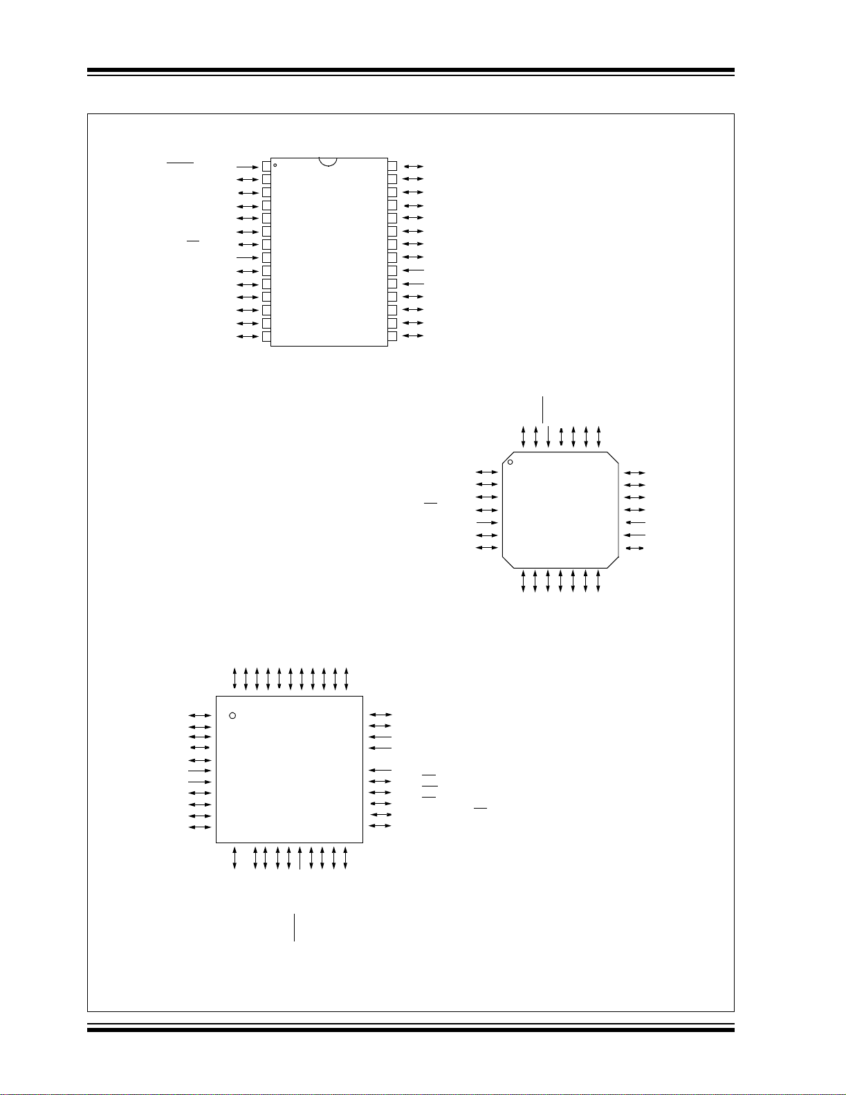
Pin Diagrams
PDIP, SOIC, SSOP (28-pin)
MCLR/VPP/RE3
RA2/AN2/V
RA5/AN4/LVDIN/SS
REF-/CVREF
RA3/AN3/VREF+
RA4/T0CKI/C1OUT
OSC1/CLKI/RA7
OSC2/CLKO/RA6
RC0/T1OSO/T1CKI
RC1/T1OSI/CCP2
RC2/CCP1
RC3/SCK/SCL
RA0/AN0
RA1/AN1
/C2OUT
V
1
2
3
4
5
6
7
SS
(1)
8
9
10
11
12
13
14
28
27
26
25
24
23
22
21
20
19
18
PIC16F737/767
17
16
15
RB7/PGD
RB6/PGC
RB5/AN13/CCP3
RB4/AN11
RB3/CCP2
RB2/AN8
RB1/AN10
RB0/INT/AN12
V
VSS
RC7/RX/DT
RC6/TX/CK
RC5/SDO
RC4/SDI/SDA
(1)
/AN9
DD
QFN (28-pin)
MCLR/VPP/RE3
RB7/PGD
RB6/PGC
RB5/AN13/CCP3
RA2/AN2/VREF-/CVREF
RA3/AN3/VREF+
RA4/T0CKI/C1OUT
RA5/AN4/LVDIN/SS
OSC1/CLKI/RA7
OSC2/CLKO/RA6
/C2OUT
VSS
RA0/AN0
RA1/AN1
2627
28
1
2
3
PIC16F737
4
PIC16F767
5
6
7
10
912
8
25
11
24
23
13 14
RB4/AN11
22
21
20
19
18
17
16
15
RB3/CCP2
RB2/AN8
RB1/AN10
RB0/INT/AN12
V
VSS
RC7/RX/DT
DD
(1)
/AN9
QFN (44-pin)
RC7/RX/DT
RD4/PSP4
RD5/PSP5
RD6/PSP6
RD7/PSP7
VSS
VDD
RB0/INT/AN12
VDD
RB1/AN10
RB2/AN8
RC6/TX/CK
4443424140
1
2
3
4
5
6
7
8
9
10
11
131415
12
NC
/AN9
(1)
RB3/CCP2
RC5/SDO
RC4/SDI/SDA
RD3/PSP3
RD2/PSP2
RD1/PSP1
RD0/PSP0
39
38
PIC16F747
PIC16F777
16
17
18
/VPP/RE3
RB7/PGD
RB6/PGC
RB4/AN11
MCLR
RB5/AN13/CCP3
(1)
RC3/SCK/SCL
RC2/CCP1
RC1/T1OSI/CCP2
363435
37
202122
19
RA1/AN1
RA0/AN0
REF-/CVREF
RA2/AN2/V
(1)
RC5/SDO
RC2/CCP1
RC0/T1OSO/T1CKI
RC0/T1OSO/T1CKI
RC1/T1OSI/CCP2
33
32
31
30
29
28
27
26
25
24
23
REF+
RA3/AN3/V
OSC2/CLKO/RA6
OSC1/CLKI/RA7
SS
V
VSS
NC
VDD
RE2/CS/AN7
/AN6
RE1/WR
RE0/RD
/AN5
RA5/AN4/LVDIN/SS
RA4/T0CKI/C1OUT
/C2OUT
RC4/SDI/SDA
RC3/SCK/SCL
RC6/TX/CK
Note 1: Pin location of CCP2 is determined by the CCPMX bit in Configuration Word Register 1.
DS30498C-page 2 2004 Microchip Technology Inc.
Page 5

Pin Diagrams (Continued)
PIC16F7X7
RC7/RX/DT
RD4/PSP4
RD5/PSP5
RD6/PSP6
RD7/PSP7
RB0/INT/AN12
RB1/AN10
RB2/AN8
RB3/CCP2
(1)
V
VDD
/AN9
RC6/TX/CK
RC5/SDO
RC4/SDI/SDA
RD3/PSP3
RD2/PSP2
RD1/PSP1
RD0/PSP0
RC3/SCK/SCL
RC2/CCP1
RC1/T1OSI/CCP2(1)
NC
4443424140
1
2
3
4
PIC16F747
SS
5
6
7
8
9
10
11
121314
NC
NC
RB4/AN11
16
15
RB6/PGC
RB5/AN13/CCP3
39
37
38
17
1819202122
RA0/AN0
/VPP/RE3
RB7/PGD
MCLR
363435
RA1/AN1
33
32
31
30
29
28
27
26
25
24
23
REF-/CVREF
RA3/AN3/VREF+
RA2/AN2/V
NC
RC0/T1OSO/T1CKI
OSC2/CLKO/RA6
OSC1/CLKI/RA7
V
SS
VDD
RE2/CS/AN7
/AN6
RE1/WR
/AN5
RE0/RD
RA5/AN4/LVDIN/SS
RA4/T0CKI/C1OUT
/C2OUT
2004 Microchip Technology Inc. DS30498C-page 3
Page 6

PIC16F7X7
Table of Contents
1.0 Device Overview..........................................................................................................................................................................5
2.0 Memory Organization.................................................................................................................................................................15
3.0 Reading Program Memory .......................................................................................... ...... ......................................................... 31
4.0 Oscillator Configurations............................................................................................................................................................ 33
5.0 I/O Ports............................ ..................... ..................... ..................... .......................................................................................... 49
6.0 Timer0 Module ........................................................................................................................................................................... 73
7.0 Timer1 Module ........................................................................................................................................................................... 77
8.0 Timer2 Module ........................................................................................................................................................................... 85
9.0 Capture/Compare/PWM Modules ................................................................................................ .............................................. 87
10.0 Master Synchronous Serial Port (MSSP) Module ...................................................................................................................... 93
11.0 Addressable Universal Synchronous Asynchronous Receiver Transmitter (AUSART) ........................................................... 133
12.0 Analog-to-Digital Converter (A/D) Module................................................................................................................................151
13.0 Comparator Module............................................................. .... ......... .. .... .. .... ......... .. .... .... .........................................................161
14.0 Comparator Voltage Reference Module...................................................................................................................................167
15.0 Special Features of the CPU............................................................ ..................... ................................................................... 169
16.0 Instruction Set Summary.......................................................................................................................................................... 193
17.0 Development Support...............................................................................................................................................................201
18.0 Electrical Characteristics.......................................................................................................................................................... 207
19.0 DC and AC Characteristics Graphs and Tables.......................................................................................................................237
20.0 Packaging Information...................... ..................... ..................... ..................... ......................................................................... 251
Appendix A: Revision History.............................................................................................................................................................261
Appendix B: Device Differences.........................................................................................................................................................261
Appendix C: Conversion Considerations .................................................................... .... .. .... .. .... ....................................................... 262
Index .................................................................................................................................................................................................. 263
On-Line Support........................................................................ .. .... .. ......... .... .. .... ......... .. ................................................................... 271
Systems Information and Upgrade Hot Line...................................................................................................................................... 271
Reader Response.............................................................................................................................................................................. 272
PIC16F7X7 Product Identification System.........................................................................................................................................273
TO OUR VALUED CUSTOMERS
It is our intention to provide our valued customers with the best documentation possible to ensure successful use of your Microchip
products. To this end, we will continue to improve our publications to better suit your needs. Our publications will be refined and
enhanced as new volumes and updates are introduced.
If you have any questions or c omm ents regarding t his publication, p lease c ontact the M arket ing Co mmunications Department via
E-mail at docerrors@microchip.com or fax the Reader Response Form in the back of this data sheet to (480) 792-4150. We
welcome your feedback.
Most Current Data Sheet
To obtain the most up-to-date version of this data sheet, please register at our Worldwide Web site at:
http://www.microchip.com
You can determine the version of a data sheet by examining its literature number found on the bottom outside corner of any page.
The last character of the literature number is the version number, (e.g., DS30000A is version A of document DS30000).
Errata
An errata sheet, describing minor operational differences from the data sheet and recommended workarounds, may exist for current
devices. As device/documentation issues become known to us, we will publish an errata sheet. The errata will specify the revision
of silicon and revision of document to which it applies.
To determine if an errata sheet exists for a particular device, please check with one of the following:
• Microchip’s Worldwide Web site; http://www.microchip.com
• Your local Microchip sales office (see last page)
When contacting a sales office, please specify which device, revision of silicon and data sheet (include literature number) you are
using.
Customer Notification System
Register on our web site at www.microchip.com to receive the most current information on all of our products.
DS30498C-page 4 2004 Microchip Technology Inc.
Page 7

PIC16F7X7
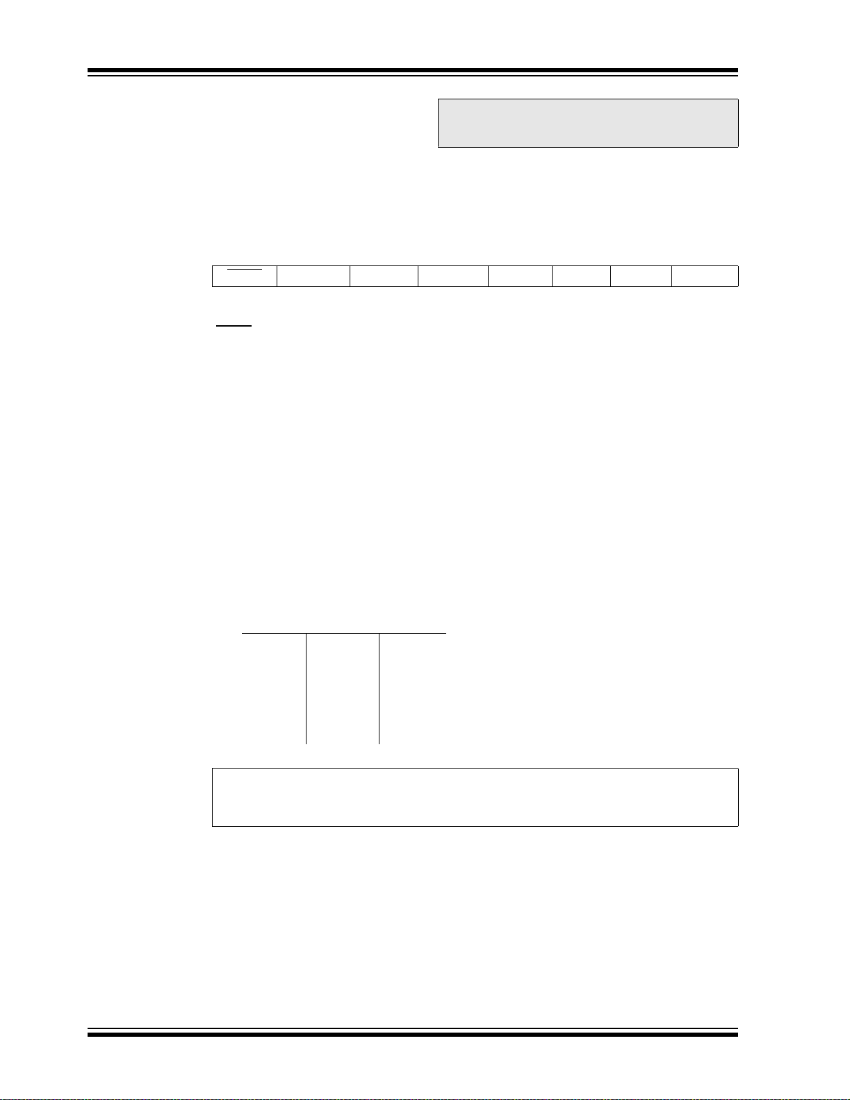
1.0 DEVICE OVERVIEW
This document contains device specific information
about the following devices:
• PIC16F737 • PIC16F767
• PIC16F747 • PIC16F777
PIC16F737/767 devices are available only in 28-pin
packages, while PIC16F747/777 devices are available
in 40-pin and 44-pin packages. All devices in the
PIC16F7X7 family sha re com mon archi tecture with the
following differences:
• The PIC16F737 and PIC1 6F7 67 ha ve on e-h alf of
the total on-chip memory of the PIC16F747 and
PIC16F777.
• The 28-pin devices have 3 I/O ports, while the
40/44-pin devices have 5.
• The 28-pin devices have 16 interrupts, while the
40/44-pin devices have 17.
• The 28-pin devices have 11 A/D input channels,
while the 40/44-pin devices have 14.
• The Parallel Slave Port is implemented only on
the 40/44-pin devices.
• Low-Power m od es: RC_RUN allows the core and
peripherals to be clocked from the INTRC, while
SEC_RUN allows the core and peripherals to be
clocked from the low-power Timer1. Refer to
Section 4.7 “Power-Managed Modes” for
further details.
• Internal R C o scil la t o r w i th ei gh t s e le ctable
frequencies , i nc lu di ng 3 1.2 5kHz, 125 kHz,
250kHz, 500kHz, 1MHz, 2 MHz, 4 MHz and
8 MHz. The INTRC can be configured as a primary
or secondary clock source. Refer to Section 4.5
“Internal Oscilla tor Bloc k” f or fur the r d etails.
• The Timer1 module current consumption has
been greatly reduced from 20µA (previous PIC16
devices) to 1.8 µA typical (32 kHz at 2V), which is
ideal for real-time clock applications. Refer to
Section 7.0 “Timer1 Module” for further details.
• Extended Watchdog Ti me r (W D T) tha t can have a
programmable period from 1 ms to 268s. The WDT
has its own 16-bit pre scaler . Refer to Section 15.17
“Watch dog Timer (WDT)” for further details.
• Two-Speed Start-up: When the oscillator is
configured for LP, XT or HS, this feature will clock
the device from the INTRC while the oscillator is
warming up. This, in turn, will enable almost
immediate code execution. Refer to
Section 15.17.3 “Two-Speed Clock Start-up
Mode” for further details.
• Fail-Safe Clo ck Monitor: This feat ure will allow the
device to continue operation if the primary or
secondary clock source fails by switching over to
the INTRC.
The available features are summarized in Table 1-1.
Block diagrams of the PIC16F737/767 and
PIC16F747/777 devic es are provided i n Figure 1-1 and
Figure 1-2, respectively. The pinouts for these device
families are listed in Table 1-2 and Table 1-3.
Additional information may be found in the “PICmicro
Mid-Range MCU Family Reference Manual”
(DS33023) which may be obtained from your local
Microchip Sales Representative or downloaded from
the Microchip web site. The Reference Manual should
be considered a complementary document to this data
sheet and is highly recommended reading for a better
understanding o f the d ev ic e arc hi tec ture a nd operation
of the peripheral modules.
®
TABLE 1-1: PIC16F7X7 DEVICE FEATURES
Key Features PIC16F737 PIC16F747 PIC16F767 PIC16F777
Operating Frequency DC – 20 MHz DC – 20 MHz DC – 20 MHz DC – 20 MHz
Resets (and Delays) POR, BOR
(PWRT, OST)
Flash Program Memory (14-bit words) 4K 4K 8K 8K
Data Memory (bytes) 368 368 368 368
Interrupts 16 17 16 17
I/O Ports Ports A, B, C Ports A, B, C, D, E Ports A, B, C Ports A, B, C, D, E
Timers 3333
Capture/Compare/PWM Modules 3 3 3 3
Master Serial Communications MSSP, AUSART MSSP, AUSART MSSP , AUSART MSSP, AUSART
Parallel Communications — PSP — PSP
10-bit Analog-to-Digital Module 11 Input Channels 14 Input Channels 11 Input Channels 14 Input Channels
Instruction Set 35 Instructions 35 Instructions 35 Instructions 35 Instructions
Packaging 28-pin PDIP
28-pin SOIC
28-pin SSOP
28-pin QFN
2004 Microchip Technology Inc. DS30498C-page 5
POR, BOR
(PWRT, OST)
40-pin PDIP
44-pin QFN
44-pin TQFP
POR, BOR
(PWRT, OST)
28-pin PDIP
28-pin SOIC
28-pin SSOP
28-pin QFN
POR, BOR
(PWRT, OST)
40-pin PDIP
44-pin QFN
44-pin TQFP
Page 8
PIC16F7X7
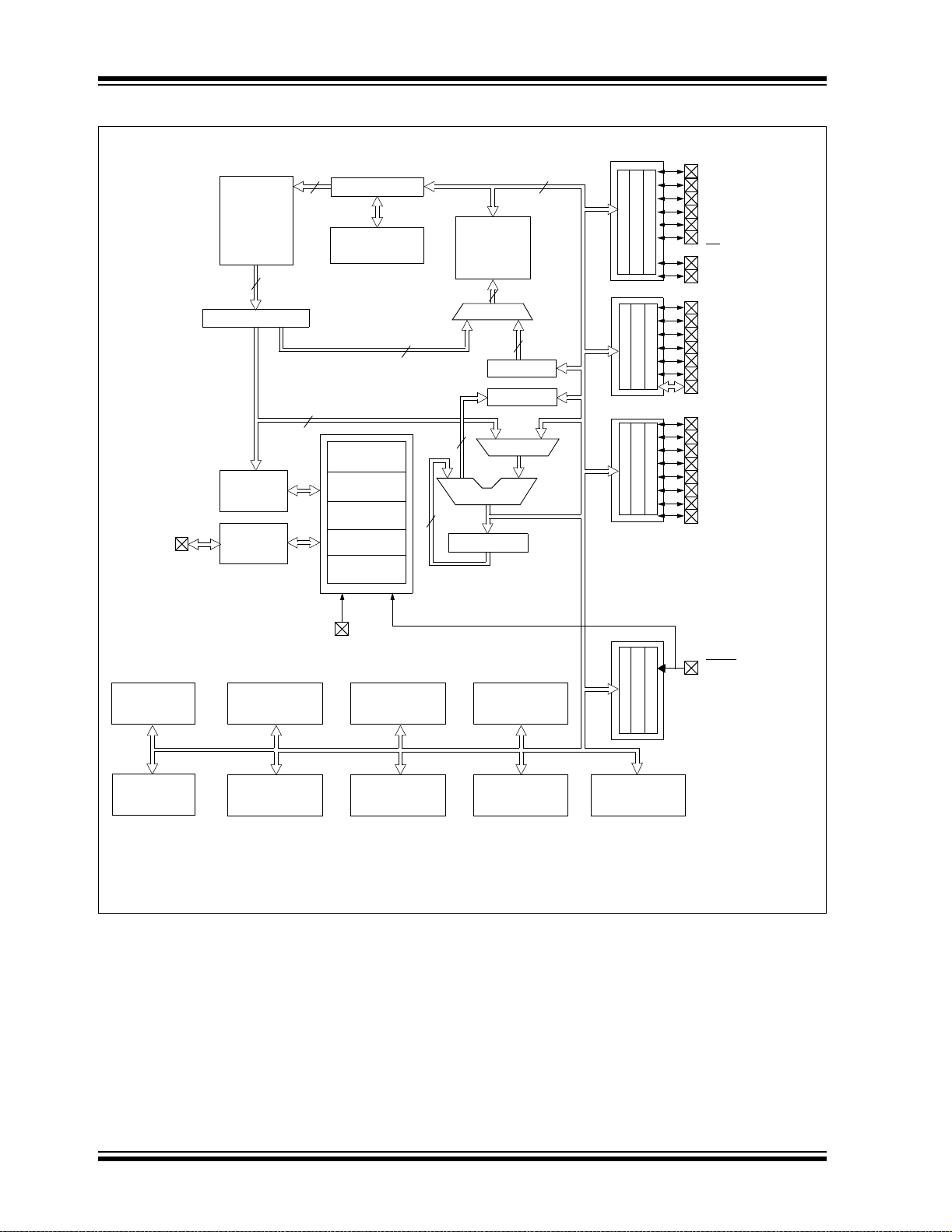
FIGURE 1-1: PIC16F 73 7 AND PIC16F767 BLOCK DIAGRAM
Program
Bus
OSC1/CLKI
OSC2/CLKO
Standard
Flash
Program
Memory
4K/8K x 14
14
Instruction Register
Instruction
Decode &
Control
Timing
Generation
13
Program Counter
8-Level Stack
Direct Addr
8
Power-up
Oscillator
Start-up Timer
Power-on
Watchdog
Brown-out
(13-bit)
Timer
Reset
Timer
Reset
RAM Addr
7
3
8
Data Bus
RAM
File
Registers
368 x 8
(1)
Addr MUX
ALU
WREG
9
Indirect
8
FSR reg
Status reg
MUX
8
Addr
PORTA
PORTB
PORTC
RA0/AN0
RA1/AN1
RA2/AN2/VREF-/CVREF
RA3/AN3/VREF+
RA4/T0CKI/C1OUT
RA5/AN4/LVDIN/
SS/C2OUT
OSC2/CLKO/RA6
OSC1/CLKI/RA7
RB0/INT/AN12
RB1/AN10
RB2/AN8
RB3/CCP2
RB4/AN11
RB5/AN13/CCP3
RB7/PGD:RB6/PGC
RC0/T1OSO/T1CKI
RC1/T1OSI/CCP2
RC2/CCP1
RC3/SCK/SCL
RC4/SDI/SDA
RC5/SDO
RC6/TX/CK
RC7/RX/DT
(1)
/AN9
(1)
V
DD, VSS
10-bit A/DTimer0 Timer1 Timer2
Comparators
Note 1: Pin location of CCP2 is determined by the CCPMX bit in Configuration Word Register 1.
CCP1, 2, 3
MSSP
Addressable
USART
PORTE
BOR/LVD
MCLR
/VPP/RE3
DS30498C-page 6 2004 Microchip Technology Inc.
Page 9
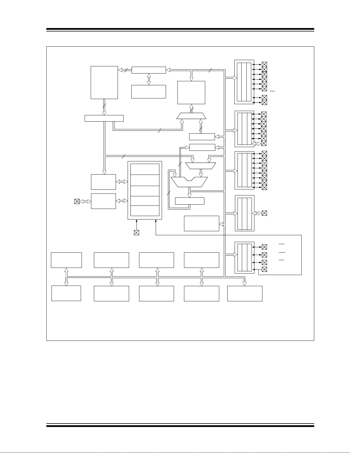
FIGURE 1-2: PIC16F 74 7 AND PIC16F777 BLOCK DIAGRAM
Program
Bus
OSC1/CLKI
OSC2/CLKO
Standard
Flash
Program
Memory
4K/8K x 14
14
Instruction Register
Instruction
Decode &
Control
Timing
Generation
13
Program Counter
8-Level Stack
Direct Addr
8
Start-up Timer
Watchdog
Brown-out
(13-bit)
Power-up
Timer
Oscillator
Power-on
Reset
Timer
Reset
RAM Addr
7
3
8
Data Bus
RAM
File
Registers
368 x 8
(1)
Addr MUX
ALU
WREG
9
Indirect
8
FSR reg
Status reg
MUX
8
Addr
PIC16F7X7
PORTA
RA0/AN0
RA1/AN1
RA2/AN2/VREF-/CVREF
RA3/AN3/VREF+
RA4/T0CKI/C1OUT
RA5/AN4/LVDIN/
/C2OUT
SS
OSC2/CLKO/RA6
OSC1/CLKI/RA7
PORTB
PORTC
PORTD
RB0/INT/AN12
RB1/AN10
RB2/AN8
RB3/CCP2
RB4/AN11
RB5/AN13/CCP3
RB7/PGD:RB6/PGC
RC0/T1OSO/T1CKI
RC1/T1OSI/CCP2
RC2/CCP1
RC3/SCK/SCL
RC4/SDI/SDA
RC5/SDO
RC6/TX/CK
RC7/RX/DT
RD7/PSP7:RD0/PSP0
(1)
/AN9
(1)
Parallel Slave Port
V
DD, VSS
10-bit A/DTimer0 Timer1 Timer2
Comparators BOR/LVD
Note 1: Pin location of CCP2 is determined by the CCPMX bit in Configuration Word Register 1.
CCP1, 2, 3
MSSP
Addressable
USART
PORTE
RE0/RD
/AN5
/AN6
RE1/WR
RE2/CS
/AN7
MCLR/VPP/RE3
2004 Microchip Technology Inc. DS30498C-page 7
Page 10
PIC16F7X7
TABLE 1-2: PIC16F737 AND PIC16F767 PINOUT DESCRIPTION
PDIP
Pin Name
OSC1/CLKI/RA7
OSC1
CLKI
RA7
OSC2/CLKO/RA6
OSC2
CLKO
RA6
/VPP/RE3
MCLR
MCLR
VPP
RE3
RA0/AN0
RA0
AN0
RA1/AN1
RA1
AN1
RA2/AN2/V
RA3/AN3/V
RA4/T0CKI/C1OUT
RA5/AN4/LVDIN/SS
Legend: I = input O = output I/O = input/output P = power
Note 1: This buffer is a Schmitt Trigger input when configured as the external interrupt.
REF-/CVREF
RA2
AN2
V
REF-
REF
CV
REF+
RA3
AN3
REF+
V
RA4
T0CKI
C1OUT
RA5
AN4
LVDIN
SS
C2OUT
2: This buffer is a Schmitt Trigger input when used in Serial Programming mode.
3: This buffer is a Schmitt Trigger input when configured in RC Oscillator mode and a CMOS input otherwise.
4: Pin location of CCP2 is determined by the CCPMX bit in Configuration Word Register 1.
/C2OUT
— = Not used TTL = TTL input ST = Schmitt Trigger input
SOIC
SSOP
Pin #
10 7
QFN
Pin #
96
126
227
328
41
52
63
74
I/O/P
Type
I
I
I/O
O
O
I/O
I
P
I
I/O
I
I/O
I
I/O
I
I
0
I/O
I
I
I/O
I
O
I/O
I
I/O
I
O
Buffer
Type
ST/CMOS
ST
—
ST
ST
ST
TTL
TTL
TTL
TTL
ST
TTL
Description
(3)
Oscillator crystal or external clock input.
Oscillator crystal input or external clock source input. ST
buffer when configured in RC mode; otherwise CMOS.
External clock source input. Always associated with pin
function OSC1 (see OSC1/CLKI, OSC2/CLKO pins).
Digital I/O.
Oscillator crystal or clock output.
Oscillator crystal output.
Connects to crystal or resonator in Crystal Oscillator
mode.
In RC mode, OSC2 pin outputs CLKO whic h has 1/4 t he
frequency of OSC1 and denotes the in str uctio n cycle rat e.
Digital I/O.
Master Clear (input) or programming voltage (output).
Master Clear (Reset) input. This pin is an active-low
Reset to the device.
Programming voltage input.
Digital input only pin.
PORTA is a bidirectional I/O port.
Digital I/O.
Analog input 0.
Digital I/O.
Analog input 1.
Digital I/O.
Analog input 2.
A/D reference voltage input (low).
Comparator voltage reference output.
Digital I/O.
Analog input 3.
A/D reference voltage input (high).
Digital I/O – Open-drain when configured as output.
Timer0 external clock input.
Comparator 1 output bit.
Digital I/O.
Analog input 4.
Low-Voltage Detect input.
SPI™ slave select input.
Comparator 2 output bit.
DS30498C-page 8 2004 Microchip Technology Inc.
Page 11

PIC16F7X7
T ABLE 1-2: PIC16F737 AND PIC16F767 PINOUT DESCRIPTION (CONTINUED)
PDIP
Pin Name
RB0/INT/AN12
RB0
INT
AN12
RB1/AN10
RB1
AN10
RB2/AN8
RB2
AN8
RB3/CCP2/AN9
RB3
(4)
CCP2
AN9
RB4/AN11
RB4
AN11
RB5/AN13/CCP3
RB5
AN13
CCP3
RB6/PGC
RB6
PGC
RB7/PGD
RB7
PGD
Legend: I = input O = output I/O = input/output P = power
Note 1: This buffer is a Schmitt Trigger input when configured as the external interrupt.
— = Not used TTL = TTL input ST = Schmitt Trigger input
2: This buffer is a Schmitt Trigger input when used in Serial Programming mode.
3: This buffer is a Schmitt Trigger input when configured in RC Oscillator mode and a CMOS input otherwise.
4: Pin location of CCP2 is determined by the CCPMX bit in Configuration Word Register 1.
SOIC
SSOP
Pin #
21 18
22 19
23 20
24 21
25 22
26 23
27 24
28 25
QFN
Pin #
I/O/P
Type
I/O
I
I
I/O
I
I/O
I
I/O
I/O
I
I/O
I
I/O
I
I/O
I/O
I/O
I/O
I/O
Buffer
Type
TTL/ST
TTL
TTL
TTL
TTL
TTL
TTL/ST
TTL/ST
Description
PORTB is a bidirectional I/O port. PORTB can be software
programmed for internal weak pull-up on all inputs.
(1)
Digital I/O.
External interrupt.
Analog input channel 12.
Digital I/O.
Analog input channel 10.
Digital I/O.
Analog input channel 8.
Digital I/O.
CCP2 capture input, compare output, PWM output.
Analog input channel 9.
Digital I/O.
Analog input channel 11.
Digital I/O.
Analog input channel 13.
CCP3 capture input, compare output, PWM output.
(2)
Digital I/O.
In-Circuit Debugger and ICSP™ programming clock.
(2)
Digital I/O.
In-Circuit Debugger and ICSP programming data.
2004 Microchip Technology Inc. DS30498C-page 9
Page 12

PIC16F7X7
TABLE 1-2: PIC16F737 AND PIC16F767 PINOUT DESCRIPTION (CONTINUED)
PDIP
Pin Name
RC0/T1OSO/T1CKI
RC0
T1OSO
T1CKI
RC1/T1OSI/CCP2
RC1
T1OSI
(4)
CCP2
RC2/CCP1
RC2
CCP1
RC3/SCK/SCL
RC3
SCK
SCL
RC4/SDI/SDA
RC4
SDI
SDA
RC5/SDO
RC5
SDO
RC6/TX/CK
RC6
TX
CK
RC7/RX/DT
RC7
RX
DT
SS 8, 19 5, 16 P — Ground reference for logic and I/O pins.
V
V
DD 20 17 P — Positive supply for logic and I/O pins.
Legend: I = input O = output I/O = input/output P = power
Note 1: This buffer is a Schmitt Trigger input when configured as the external interrupt.
— = Not used TTL = TTL input ST = Schmitt Trigger input
2: This buffer is a Schmitt Trigger input when used in Serial Programming mode.
3: This buffer is a Schmitt Trigger input when configured in RC Oscillator mode and a CMOS input otherwise.
4: Pin location of CCP2 is determined by the CCPMX bit in Configuration Word Register 1.
SOIC
SSOP
Pin #
11 8
12 9
13 10
14 11
15 12
16 13
17 14
18 15
QFN
Pin #
I/O/P
Type
I/O
O
I
I/O
I
I/O
I/O
I/O
I/O
I/O
I/O
I/O
I
I/O
I/O
O
I/O
O
I/O
I/O
I
I/O
Buffer
Type
ST
ST
ST
ST
ST
ST
ST
ST
Description
PORTC is a bidirectional I/O port.
Digital I/O.
Timer1 oscillator output.
Timer1 external clock input.
Digital I/O.
Timer1 oscillator input.
Capture2 input, Compare2 output, PWM2 output.
Digital I/O.
Capture1 input, Compare1 output, PWM1 output.
Digital I/O.
Synchronous serial clock input/output for SPI™ mode.
Synchronous serial clock input/output for I
Digital I/O.
SPI data in.
2
C data I/O.
I
Digital I/O.
SPI data out.
Digital I/O.
AUSART asynchronous transmit.
AUSART synchronous clock.
Digital I/O.
AUSART asynchronous receive.
AUSART synchronous data.
2
C™ mode.
DS30498C-page 10 2004 Microchip Technology Inc.
Page 13
PIC16F7X7
TABLE 1-3: PIC16F747 AND PIC16F777 PINOUT DESCRIPTION
Pin Name
OSC1/CLKI/RA7
OSC1
CLKI
RA7
OSC2/CLKO/RA6
OSC2
CLKO
RA6
/VPP/RE3
MCLR
MCLR
VPP
RE3
RA0/AN0
RA0
AN0
RA1/AN1
RA1
AN1
RA2/AN2/V
RA3/AN3/V
RA4/T0CKI/C1OUT
RA5/AN4/LVDIN/SS
Legend: I = input O = output I/O = input/output P = power
Note 1: This buffer is a Schmitt Trigger input when configured as an external interrupt.
REF-/CVREF
RA2
AN2
REF-
V
CV
REF
REF+
RA3
AN3
REF+
V
RA4
T0CKI
C1OUT
RA5
AN4
LVDIN
SS
C2OUT
2: This buffer is a Schmitt Trigger input when used in Serial Programming mode.
3: This buffer is a Schmitt Trigger input when configured as a general purpose I/O and a TTL input when used in the Parallel
4: This buffer is a Schmitt Trigger input when configured in RC Oscillator mode and a CMOS input otherwise.
5: Pin location of CCP2 is determined by the CCPMX bit in Configuration Word Register 1.
/C2OUT
— = Not used TTL = TTL input ST = Schmitt Trigger input
Slave Port mode (for interfacing to a microprocessor bus).
PDIP
Pin #
QFN
Pin #
13 32 30
14 33 31
11818
21919
32020
42121
52222
62323
72424
TQFP
Pin #
I/O/P
Type
I
I
I/O
O
O
I/O
I
P
I
I/O
I
I/O
I
I/O
I
I
I
I/O
I
I
I/O
I
O
I/O
I
I
I
I
Buffer
Type
ST/CMOS
ST
—
ST
ST
ST
TTL
TTL
TTL
TTL
ST
TTL
Description
(4)
Oscillator crystal or external clock input.
Oscillator cry stal in put or extern al clock sour ce input.
ST buffer when configured in RC mode; otherwise
CMOS.
External clock source input. Always associated with
pin function OSC1 (see OSC1/CLKI, OSC2/CLKO
pins).
Bidirectional I/O pin.
Oscillator crystal or clock output.
Oscillator crystal output. Connects to crystal or
resonator in Crystal Oscillator mode.
In RC mode, OSC2 pin outputs CLKO which has
1/4 the frequency of OSC1 and denotes the
instruction cycle rate.
Bidirectional I/O pin.
Master Clear (input) or programming voltage (output).
Master Clear (Reset) input. This pin is an
active-low Reset to the device.
Programming voltage input.
Digital input only pin.
PORTA is a bidirectional I/O port.
Digital I/O.
Analog input 0.
Digital I/O.
Analog input 1.
Digital I/O.
Analog input 2.
A/D reference voltage input (low).
Comparator voltage reference output.
Digital I/O.
Analog input 3.
A/D reference voltage input (high).
Digital I/O – Open-drain when configured as output.
Timer0 external clock input.
Comparator 1 output.
Digital I/O.
Analog input 4.
Low-Voltage Detect input.
SPI™ slave select input.
Comparator 2 output.
2004 Microchip Technology Inc. DS30498C-page 11
Page 14

PIC16F7X7
TABLE 1-3: PIC16F747 AND PIC16F777 PINOUT DESCRIPTION (CONTINUED)
Pin Name
RB0/INT/AN12
RB0
INT
AN12
RB1/AN10
RB1
AN10
RB2/AN8
RB2
AN8
RB3/CCP2/AN9
RB3
(5)
CCP2
AN9
RB4/AN11
RB4
AN11
RB5/AN13/CCP3
RB5
AN13
CCP3
RB6/PGC
RB6
PGC
RB7/PGD
RB7
PGD
Legend: I = input O = output I/O = input/output P = power
Note 1: This buffer is a Schmitt Trigger input when configured as an external interrupt.
— = Not used TTL = TTL input ST = Schmitt Trigger input
2: This buffer is a Schmitt Trigger input when used in Serial Programming mode.
3: This buffer is a Schmitt Trigger input when configured as a general purpose I/O and a TTL input when used in the Parallel
Slave Port mode (for interfacing to a microprocessor bus).
4: This buffer is a Schmitt Trigger input when configured in RC Oscillator mode and a CMOS input otherwise.
5: Pin location of CCP2 is determined by the CCPMX bit in Configuration Word Register 1.
PDIP
Pin #
QFN
TQFP
Pin #
33 9 8
34 10 9
35 11 10
36 12 11
37 14 14
38 15 15
39 16 16
40 17 17
Pin #
I/O/P
Type
I/O
I
I
I/O
I
I/O
I
I/O
I/O
I
I/O
I
I/O
I
I
I/O
I/O
I/O
I/O
Buffer
Type
TTL/ST
TTL
TTL
TTL
TTL
TTL
TTL/ST
TTL/ST
Description
PORTB is a bidirectional I/O port. PORTB can be
software programmed for internal weak pull-up on all
inputs.
(1)
Digital I/O.
External interrupt.
Analog input channel 12.
Digital I/O.
Analog input channel 10.
Digital I/O.
Analog input channel 8.
Digital I/O.
CCP2 capture input, compare output, PWM output.
Analog input channel 9.
Digital I/O.
Analog input channel 11
Digital I/O.
Analog input channel 13.
CCP3 capture input, compare output, PWM output.
(2)
Digital I/O.
In-Circuit Debugger and ICSP™ programming
clock.
(2)
Digital I/O.
In-Circuit Debugger and ICSP programming
data.
DS30498C-page 12 2004 Microchip Technology Inc.
Page 15

PIC16F7X7
T ABLE 1-3: PIC16F747 AND PIC16F777 PINOUT DESCRIPTION (CONTINUED)
Pin Name
RC0/T1OSO/T1CKI
RC0
T1OSO
T1CKI
RC1/T1OSI/CCP2
RC1
T1OSI
(5)
CCP2
RC2/CCP1
RC2
CCP1
RC3/SCK/SCL
RC3
SCK
SCL
RC4/SDI/SDA
RC4
SDI
SDA
RC5/SDO
RC5
SDO
RC6/TX/CK
RC6
TX
CK
RC7/RX/DT
RC7
RX
DT
Legend: I = input O = output I/O = input/output P = power
— = Not used TTL = TTL input ST = Schmitt Trigger input
Note 1: This buffer is a Schmitt Trigger input when configured as an external interrupt.
2: This buffer is a Schmitt Trigger input when used in Serial Programming mode.
3: This buffer is a Schmitt Trigger input when configured as a general purpose I/O and a TTL input when used in the Parallel
Slave Port mode (for interfacing to a microprocessor bus).
4: This buffer is a Schmitt Trigger input when configured in RC Oscillator mode and a CMOS input otherwise.
5: Pin location of CCP2 is determined by the CCPMX bit in Configuration Word Register 1.
PDIP
Pin #
QFN
Pin #
15 34 32
16 35 35
17 36 36
18 37 37
23 42 42
24 43 43
25 44 44
26 1 1
TQFP
Pin #
I/O/P
Type
I/O
O
I
I/O
I
I/O
I/O
I/O
I/O
I/O
I/O
I/O
I
I/O
I/O
O
I/O
O
I/O
I/O
I
I/O
Buffer
Type
ST
ST
ST
ST
ST
ST
ST
ST
Description
PORTC is a bidirectional I/O port.
Digital I/O.
Timer1 oscillator output.
Timer1 external clock input.
Digital I/O.
Timer1 oscillator input.
Capture 2 input, Compare 2 output, PWM 2 output.
Digital I/O.
Capture 1 input, Compare 1 output, PWM 1 output.
Digital I/O.
Synchronous serial clock input/output
for SPI™ mode.
Synchronous serial clock input/output
2
C™ mode.
for I
Digital I/O.
SPI data in.
2
C data I/O.
I
Digital I/O.
SPI data out.
Digital I/O.
AUSART asynchronous transmit.
AUSART synchronous clock.
Digital I/O.
AUSART asynchronous receive.
AUSART synchronous data.
2004 Microchip Technology Inc. DS30498C-page 13
Page 16
PIC16F7X7
TABLE 1-3: PIC16F747 AND PIC16F777 PINOUT DESCRIPTION (CONTINUED)
Pin Name
PDIP
Pin #
RD0/PSP0
RD0
PSP0
RD1/PSP1
RD1
PSP1
RD2/PSP2
RD2
PSP2
RD3/PSP3
RD3
PSP3
RD4/PSP4
RD4
PSP4
RD5/PSP5
RD5
PSP5
RD6/PSP6
RD6
PSP6
RD7/PSP7
RD7
PSP7
/AN5
RE0/RD
RE0
RD
AN5
RE1/WR
/AN6
RE1
WR
AN6
/AN7
RE2/CS
RE2
CS
AN7
SS — 31 — P — Analog ground reference.
V
V
SS 12, 31 6, 30 6, 29 P — Ground reference for logic and I/O pins.
DD — 8 — P — Analog positive supply.
V
DD 11, 32 7, 28 7, 28 P — Positive supply for logic and I/O pins.
V
NC — 13, 29 12, 13,
Legend: I = input O = output I/O = input/output P = power
— = Not used TTL = TTL input ST = Schmitt Trigger input
Note 1: This buffer is a Schmitt Trigger input when configured as an external interrupt.
2: This buffer is a Schmitt Trigger input when used in Serial Programming mode.
3: This buffer is a Schmitt Trigger input when configured as a general purpose I/O and a TTL input when used in the Parallel
Slave Port mode (for interfacing to a microprocessor bus).
4: This buffer is a Schmitt Trigger input when configured in RC Oscillator mode and a CMOS input otherwise.
5: Pin location of CCP2 is determined by the CCPMX bit in Configuration Word Register 1.
QFN
TQFP
Pin #
Pin #
19 38 38
20 39 39
21 40 40
22 41 41
27 2 2
28 3 3
29 4 4
30 5 5
82525
92626
10 27 27
33, 34
I/O/P
Type
Buffer
Type
Description
PORTD is a bidirectional I/O port or Parallel Slave Port
when interfacing to a microprocessor bus.
(3)
I/O
I/O
I/O
I/O
I/O
I/O
I/O
I/O
I/O
I/O
I/O
I/O
I/O
I/O
I/O
I/O
ST/TTL
ST/TTL
ST/TTL
ST/TTL
ST/TTL
ST/TTL
ST/TTL
ST/TTL
(3)
(3)
(3)
(3)
(3)
(3)
(3)
Digital I/O.
Parallel Slave Port data.
Digital I/O.
Parallel Slave Port data.
Digital I/O.
Parallel Slave Port data.
Digital I/O.
Parallel Slave Port data.
Digital I/O.
Parallel Slave Port data.
Digital I/O.
Parallel Slave Port data.
Digital I/O.
Parallel Slave Port data.
Digital I/O.
Parallel Slave Port data.
PORTE is a bidirectional I/O port.
(3)
ST/TTL
I/O
I/O
I/O
I
I
(3)
ST/TTL
I
I
(3)
ST/TTL
I
I
Digital I/O.
Read control for Parallel Slave Port.
Analog input 5.
Digital I/O.
Write control for Parallel Slave Port.
Analog input 6.
Digital I/O.
Chip select control for Parallel Slave Port.
Analog input 7.
— — These pins are not internally connected. These pins
should be left unconnected.
DS30498C-page 14 2004 Microchip Technology Inc.
Page 17
PIC16F7X7
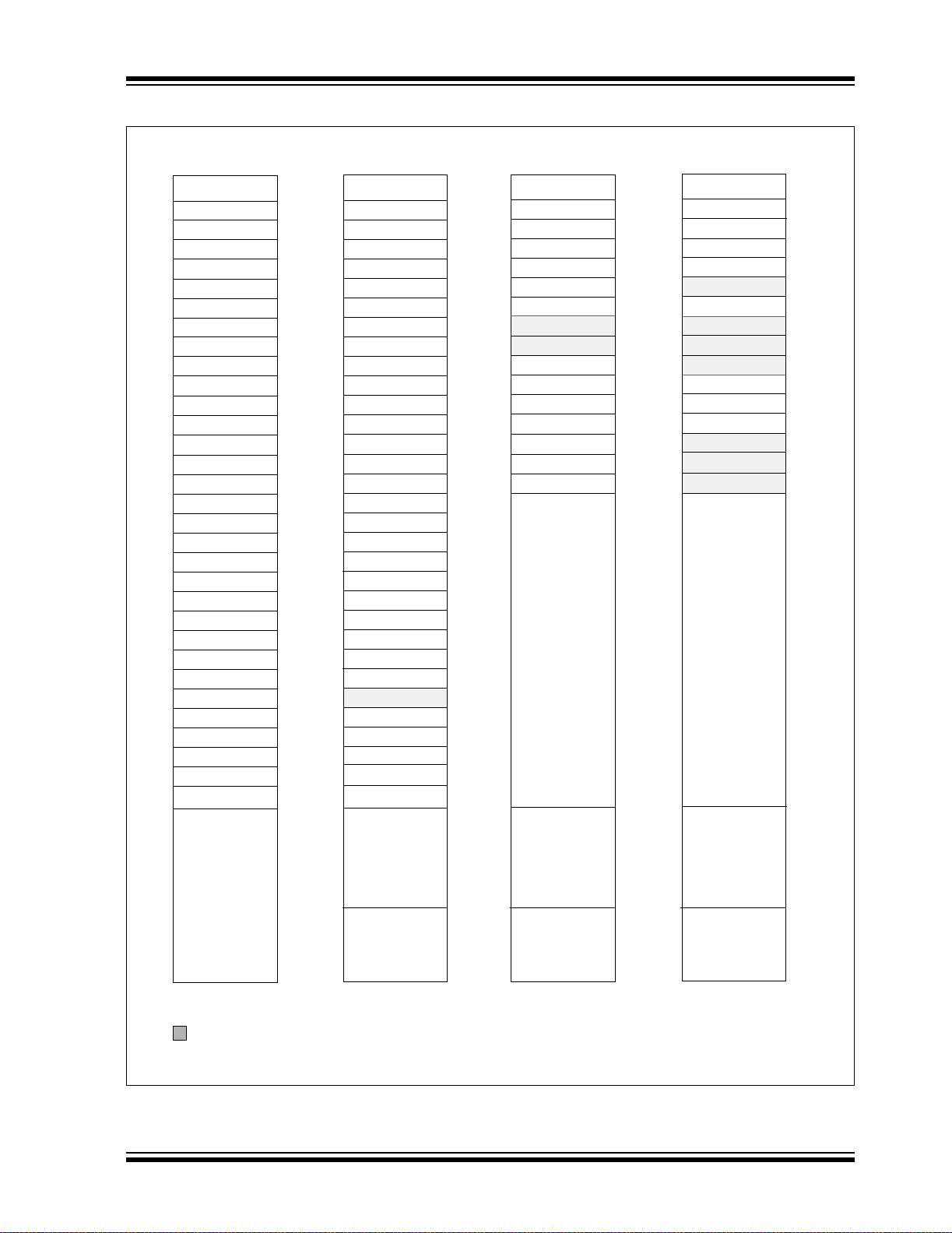
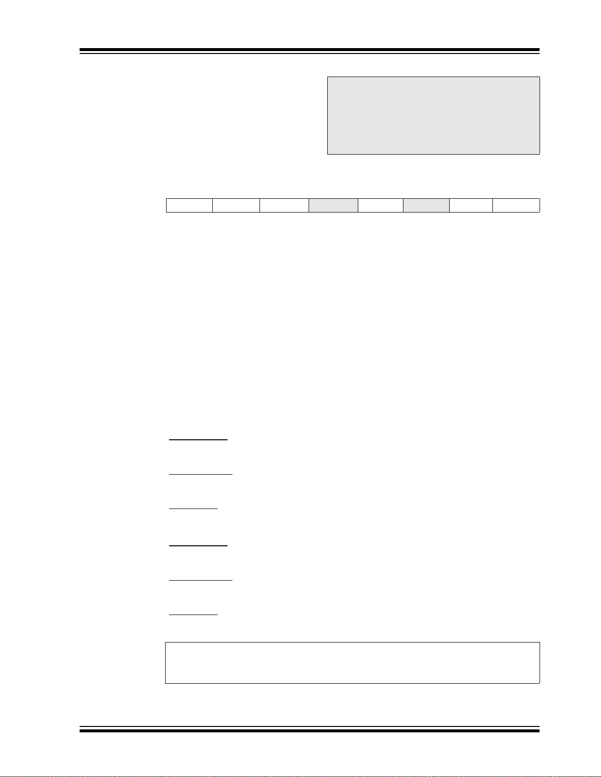
2.0 MEMORY ORGANIZATION
There are two memory blocks in each of these
PICmicro
memory have separate buses so that concurrent
access can oc cur and is detailed in this section. The
program memo ry can be read inte rnally b y user co de
(see Section 3.0 “Reading Program Memory”).
Additional informa tion on devi ce memory may be found
in the “PICmicro
Manual” (DS33023).
2.1 Program Memory Organization
The PIC16F7X7 dev ices have a 13-b it program coun ter
capable of addressing an 8K word x 14-bit program
memory space. The PIC16F767/777 devices have
8K words of Flash program memory and the
PIC16F737/747 devices have 4K words. The program
memory maps for PIC16F7X7 devices are shown in
Figure 2-1. Accessing a location above the physically
implemented address will cause a wraparound.
The Reset vector is at 0000h an d the interrupt ve ctor is
at 0004h.
®
MCUs. The program memory and data
®
Mid-Range MCU Family Reference
2.2 Data Memor y Organization
The data memory is partitioned into multiple banks
which contain the General Purpose Registers and the
Special Function Registers. Bits RP1 (Status<6>) and
RP0 (Status<5>) are the bank select bits:
RP1:RP0 Bank
00 0
01 1
10 2
11 3
Each bank extends up to 7Fh (128 bytes). The lower
locations of each bank are reserved for the Special
Function Registers. Abo ve the Speci al Function Re gisters are General Purpose Registers, implemented as
static RAM. All implemented banks contain Special
Function Registers. Some frequently used Special
Function Registers from one bank may be mirrored in
another bank for code reduction and quicker access.
2.2.1 GENERAL PURPOSE REGISTER FILE
The register file (shown in Figure 2-2 and Figure 2-3)
can be accessed either directly, or indirectly, through
the File Select Register (FSR).
FIGURE 2-1: PROGRAM MEMORY MAPS AND STACKS FOR PIC16F7X7 DEVICES
PC<12:0>
CALL, RETURN
RETFIE, RETLW
On-Chip
Program
Memory
Stack Level 1
Stack Level 2
Stack Level 8
Reset Vector
Interrupt Vector
Page 0
Page 1
Page2
Page 3
13
0000h
0004h
0005h
07FFh
0800h
0FFFh
1000h
17FFh
1800h
1FFFh
Memory available on all
PIC16F7X7.
Memory available on PIC16F767
and PIC16F777. The memory
wraps to 000h through 0FFFh on
the PIC16F737 and PIC16F747.
2004 Microchip Technology Inc. DS30498C-page 15
Page 18
PIC16F7X7
FIGURE 2-2: DATA MEMORY MAP FOR PIC16F737 AND THE PIC16F767
Indirect addr.
TMR0
PCL
STATUS
FSR
PORTA
PORTB
PORTC
PORTE
PCLATH
INTCON
PIR1
PIR2
TMR1L
TMR1H
T1CON
TMR2
T2CON
SSPBUF
SSPCON
CCPR1L
CCPR1H
CCP1CON
RCSTA
TXREG
RCREG
CCPR2L
CCPR2H
CCP2CON
ADRESH
ADCON0
General
Purpose
Register
96 Bytes
Bank 0
File
Address
(*)
00h
01h
02h
03h
04h
05h
06h
07h
08h
09h
0Ah
0Bh
0Ch
0Dh
0Eh
0Fh
10h
11h
12h
13h
14h
15h
16h
17h
18h
19h
1Ah
1Bh
1Ch
1Dh
1Eh
1Fh
20h
7Fh
Indirect addr.
OPTION_REG
PCL
STATUS
FSR
TRISA
TRISB
TRISC
TRISE
PCLATH
INTCON
PIE1
PIE2
PCON
OSCCON
OSCTUNE
SSPCON2
PR2
SSPADD
SSPSTAT
CCPR3L
CCPR3H
CCP3CON
TXSTA
SPBRG
ADCON2
CMCON
CVRCON
ADRESL
ADCON1
General
Purpose
Register
80 Bytes
Accesses
70h-7Fh
Bank 1
File
Address
(*)
80h
81h
82h
83h
84h
85h
86h
87h
88h
89h
8Ah
8Bh
8Ch
8Dh
8Eh
8Fh
90h
91h
92h
93h
94h
95h
96h
97h
98h
99h
9Ah
9Bh
9Ch
9Dh
9Eh
9Fh
A0h
EFh
F0h
FFh
Indirect addr.
TMR0
PCL
STATUS
FSR
WDTCON
PORTB
LVDCON
PCLATH
INTCON
PMDATA
PMADR
PMDATH
PMADRH
General
Purpose
Register
16 Bytes
General
Purpose
Register
80 Bytes
Accesses
70h-7Fh
Bank 2
File
Address
(*)
100h
101h
102h
103h
104h
105h
106h
107h
108h
109h
10Ah
10Bh
10Ch
10Dh
10Eh
10Fh
110h
11Fh
120h
16Fh
170h
17Fh 1FFh
Indirect addr.
OPTION_REG
PCL
STATUS
FSR
TRISB
PCLATH
INTCON
PMCON1
General
Purpose
Register
16 Bytes
General
Purpose
Register
80 Bytes
Accesses
70h-7Fh
Bank 3
File
Address
(*)
180h
181h
182h
183h
184h
185h
186h
187h
188h
189h
18Ah
18Bh
18Ch
18Dh
18Eh
18Fh
190h
19Fh
1A0h
1EFh
1F0h
Unimplemented data memory locations read as ‘0’.
* Not a phys ic al regis ter.
DS30498C-page 16 2004 Microchip Technology Inc.
Page 19
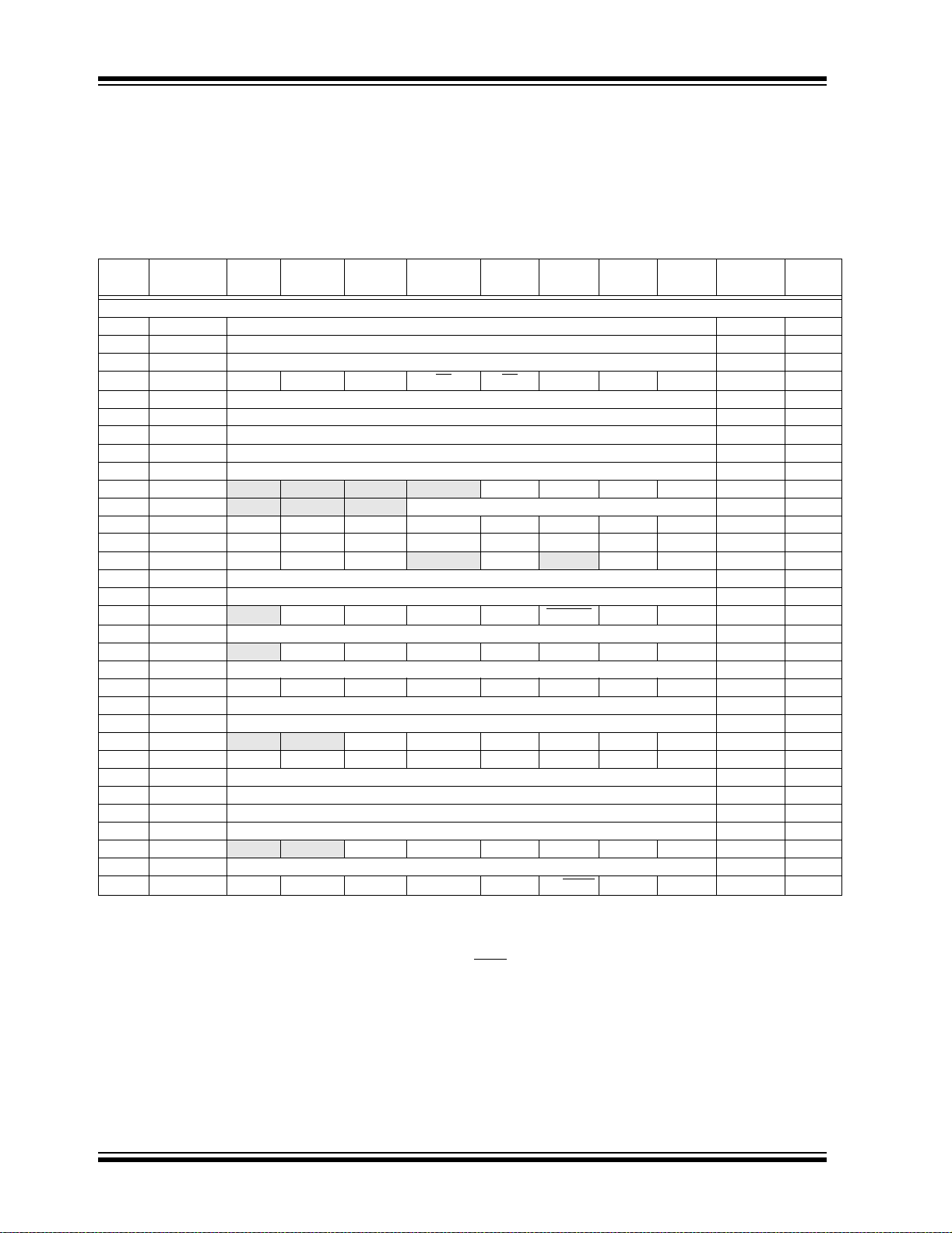
PIC16F7X7
FIGURE 2-3: DATA MEMORY MAP FOR PIC16F747 AND THE PIC16F777
Indirect addr.
TMR0
PCL
STATUS
FSR
PORTA
PORTB
PORTC
PORTD
PORTE
PCLATH
INTCON
PIR1
PIR2
TMR1L
TMR1H
T1CON
TMR2
T2CON
SSPBUF
SSPCON
CCPR1L
CCPR1H
CCP1CON
RCSTA
TXREG
RCREG
CCPR2L
CCPR2H
CCP2CON
ADRESH
ADCON0
General
Purpose
Register
96 Bytes
Bank 0
File
Address
(*)
00h
01h
02h
03h
04h
05h
06h
07h
08h
09h
0Ah
0Bh
0Ch
0Dh
0Eh
0Fh
10h
11h
12h
13h
14h
15h
16h
17h
18h
19h
1Ah
1Bh
1Ch
1Dh
1Eh
1Fh
20h
7Fh
Indirect addr.
OPTION_REG
PCL
STATUS
FSR
TRISA
TRISB
TRISC
TRISD
TRISE
PCLATH
INTCON
PIE1
PIE2
PCON
OSCCON
OSCTUNE
SSPCON2
PR2
SSPADD
SSPSTAT
CCPR3L
CCPR3H
CCP3CON
TXSTA
SPBRG
ADCON2
CMCON
CVRCON
ADRESL
ADCON1
General
Purpose
Register
80 Bytes
Accesses
70h-7Fh
Bank 1
File
Address
(*)
80h
81h
82h
83h
84h
85h
86h
87h
88h
89h
8Ah
8Bh
8Ch
8Dh
8Eh
8Fh
90h
91h
92h
93h
94h
95h
96h
97h
98h
99h
9Ah
9Bh
9Ch
9Dh
9Eh
9Fh
A0h
EFh
F0h
FFh
Indirect addr.
TMR0
PCL
STATUS
FSR
WDTCON
PORTB
LVDCON
PCLATH
INTCON
PMDATA
PMADR
PMDATH
PMADRH
General
Purpose
Register
16 Bytes
General
Purpose
Register
80 Bytes
Accesses
70h-7Fh
Bank 2
File
Address
(*)
100h
101h
102h
103h
104h
105h
106h
107h
108h
109h
10Ah
10Bh
10Ch
10Dh
10Eh
10Fh
110h
11Fh
120h
16Fh
170h
17Fh 1FFh
Indirect addr.
OPTION_REG
PCL
STATUS
FSR
TRISB
PCLATH
INTCON
PMCON1
General
Purpose
Register
16 Bytes
General
Purpose
Register
80 Bytes
Accesses
70h-7Fh
Bank 3
File
Address
(*)
180h
181h
182h
183h
184h
185h
186h
187h
188h
189h
18Ah
18Bh
18Ch
18Dh
18Eh
18Fh
190h
19Fh
1A0h
1EFh
1F0h
Unimplemented data memory locations read as ‘0’.
* Not a phys ic al regis ter.
2004 Microchip Technology Inc. DS30498C-page 17
Page 20
PIC16F7X7
2.2.2 SPECIAL FUNCTION REGISTERS
The Special Function Registers are registers used by
the CPU and peripheral modules for controlling the
desired operation of the device. These registers are
implemented as static RAM. A list of these registers is
given in Table 2-1.
The Special Function Registers can be classified into
two sets: core (CPU) and peripheral. Those registers
associated with the core functions are described in
detail in this section. Those related to the operation of
the peripheral features are described in detail in the
peripheral feature section.
TABLE 2-1: SPECIAL FUNCTION REGISTER SUMMARY
Address
Bank 0
(4)
00h
01h TMR0 Timer0 Module Register xxxx xxxx 76, 180
(4)
02h
(4)
03h
(4)
04h
05h PORTA PORTA Data Latch when written: PORTA pins when read xx0x 0000 55, 180
06h PORTB PORTB Data Latch when written: PORTB pins when read xx00 0000 64, 180
07h PORTC PORTC Data Latch when written: PORTC pins when read xxxx xxxx 66, 180
(5)
08h
(5)
09h
(1,4)
0Ah
(4)
0Bh
0Ch PIR1 PSPIF
0Dh PIR2 OSFIF CMIF LVDIF
0Eh TMR1L Holding Register for the Least Significant Byte of the 16-bit TMR1 Register xxxx xxxx 83, 180
0Fh TMR1H Holding Register for the Most Significant Byte of the 16-bit TMR1 Register xxxx xxxx 83, 180
10h T1CON
11h TMR2 Timer2 Module Register 0000 0000 86, 180
12h T2CON
13h SSPBUF Synchronous Serial Port Receive Buffer/Transmit Register xxxx xxxx 101, 180
14h SSPCON WCOL SSPOV SSPEN CKP SSPM3 SSPM2 SSPM1 SSPM0 0000 0000 101, 180
15h CCPR1L Capture/Compare/PWM Register 1 (LSB) xxxx xxxx 90, 180
16h CCPR1H Capture/Compare/PWM Register 1 (MSB) xxxx xxxx 90, 180
17h CCP1CON
18h RCSTA SPEN RX9 SREN CREN ADDEN FERR OERR RX9D 0000 000x 134, 180
19h TXREG AUSART Transmit Data Register 0000 0000 139, 180
1Ah RCREG AUSART Receive Data Register 0000 0000 141, 180
1Bh CCPR2L Capture/Compare/PWM Register 2 (LSB) xxxx xxxx 92, 180
1Ch CCPR2H Capture/Compare/PWM Register 2 (MSB) xxxx xxxx 92, 180
1Dh CCP2CON
1Eh ADRESH A/D Result Register High Byte xxxx xxxx 160, 180
1Fh ADCON0 ADCS1 ADCS0 CHS2 CHS1 CHS0 GO/DONE
Legend: x = unknown, u = unchanged, q = value depends on condition, — = unimplemented, read as ‘0’, r = reserved.
Note 1: The upper byte of the progra m c oun ter is n ot dire ctly a ccessi bl e. PCLATH is a holding regis ter f or the P C<1 2:8 > bits, whose contents
Name Bit 7 Bit 6 Bit 5 Bit 4 Bit 3 Bit 2 Bit 1 Bit 0
INDF Addressing this location uses contents of FSR to address data memory (not a physical register) 0000 0000 30, 180
PCL Program Counter (PC) Least Significant Byte 0000 0000 29, 180
STATUS IRP RP1 RP0 TO PD ZDCC0001 1xxx 21, 180
FSR Indirect Data Memory Address Pointer xxxx xxxx 30, 180
PORTD PORTD Data Latch when written: PORTD pins when read xxxx xxxx 67, 180
PORTE — — — — RE3 RE2 RE1 RE0 ---- x000 68, 180
PCLATH — — — Write Buffer for the upper 5 bits of the Program Counter ---0 0000 29, 180
INTCON GIE PEIE TMR0IE INT0IE RBIE TMR0IF INT0IF RBIF 0000 000x 23, 180
Shaded locations are unimplemented, read as ‘0’.
are transferred to the upper byte of the program counter during branches (CALL or GOTO).
2: Other (non Powe r-up) Resets include external Reset through MCLR
3: Bits PSPIE and PSPIF are reserved on the 28-pin devices; alway s maintain these bits clear .
4: These regist ers can be addressed from any bank.
5: PORTD, PORTE, TRISD and TRISE are not physically implement ed on the 28-pin devices (except for RE3), read as ‘ 0’.
6: This bit always reads as a ‘1’.
7: OSCCON<OSTS> bit resets to ‘0’ with dual-speed start-up and LP, HS or HS-PLL selected as the oscillator.
8: RE3 is an input only. The state of the TRISE3 bit has no effect and will always read ‘1’.
(3)
ADIF RCIF TXIF SSPIF CCP1IF TMR2IF TMR1IF 0000 0000 25, 180
—BCLIF— CCP3IF CCP2IF 000- 0-00 27, 180
— T1RUN T1CKPS1 T1CKPS0 T1OSCEN T1SYNC TMR1CS TMR1ON -000 0000 83, 180
— TOUTPS3 TOUTPS2 TOUTPS1 TOUTPS0 TMR2ON T2CKPS1 T2CKPS0 -000 0000 86, 180
— — CCP1X CCP1Y CCP1M3 CCP1M2 CCP1M1 CCP1M0 --00 0000 88, 180
— — CCP2X CCP2Y CCP2M3 CCP2M2 CCP2M1 CCP2M0 --00 0000 88, 180
CHS3 ADON 0000 0000 152, 180
and Watchdog Timer Reset.
Value on:
POR, BOR
Details
on page
DS30498C-page 18 2004 Microchip Technology Inc.
Page 21
PIC16F7X7
TABLE 2-1: SPECIAL FUNCTION REGISTER SUMMARY (CONTINUED)
Address
Name Bit 7 Bit 6 Bit 5 Bit 4 Bit 3 Bit 2 Bit 1 Bit 0
Value on:
POR, BOR
Bank 1
(4)
80h
81h
82h
83h
84h
INDF Addressing this location uses contents of FSR to address data memory (not a physical register) 0000 0000 30, 180
OPTION_REG
(4)
PCL Program Counter’s (PC) Least Significant Byte 0000 0000 29, 180
(4)
STATUS IRP RP1 RP0 TO PD ZDCC0001 1xxx 21, 180
(4)
FSR Indirect Data Memory Address Pointer xxxx xxxx 30, 180
RBPU INTEDG T0CS T0SE PSA PS2 PS1 PS0 1111 1111 22, 180
85h TRISA PORTA Data Direction Register 1111 1111 55, 181
86h TRISB PORTB Data Direction Register 1111 1111 64, 181
87h TRISC PORTC Data Direction Register 1111 1111 66, 181
(5)
88h
89h
8Ah
8Bh
8Ch PIE1 PSPIE
8Dh PIE2 OSFIE CMIE LVDIE
8Eh PCON
8Fh OSCCON
90h OSCTUNE
TRISD PORTD Data Direction Register 1111 1111 67, 181
(5)
TRISE IBF
(1,4)
PCLATH — — — Write Buffer for the upper 5 bits of the Program Counter ---0 0000 23, 180
(4)
INTCON GIE PEIE TMR0IE INT0IE RBIE TMR0IF INT0IF RBIF 0000 000x 25, 180
(5)
(3)
OBF
(5)
IBOV
(5)
PSPMODE
(5)
(8)
—
PORTE Data Direction bits 0000 1111 69, 181
ADIE RCIE TXIE SSPIE CCP1IE TMR2IE TMR1IE 0000 0000 24, 181
—BCLIE— CCP3IE CCP2IE 000- 0-00 26, 181
— — — — — SBOREN POR BOR ---- -1qq 28, 181
— IRCF2 IRCF1 IRCF0 OSTS
(7)
IOFS SCS1 SCS0 -000 1000 38, 181
— — TUN5 TUN4 TUN3 TUN2 TUN1 TUN0 --00 0000 36, 181
91h SSPCON2 GCEN ACKSTAT ACKDT ACKEN RCEN PEN RSEN SEN 0000 0000 105
92h PR2 Timer2 Period Register 1111 1111 86, 181
2
93h SSPADD Synchronous Serial Port (I
94h SSPSTAT SMP CKE D/A
C™ mode) Address Register 0000 0000 101, 181
PSR/WUA BF 0000 0000 101, 181
95h CCPR3L Capture/Compare/PWM Register 3 (LSB) xxxx xxxx 92
96h CCPR3H Capture/Compare/PWM Register 3 (MSB) xxxx xxxx 92
97h CCP3CON
98h TXSTA CSRC TX9 TXEN SYNC
— — CCP3X CCP3Y CCP3M3 CCP3M2 CCP3M1 CCP3M0 --00 0000 92
—BRGHTRMTTX9D0000 -010 145, 181
99h SPBRG Baud Rate Generator Register 0000 0000 145, 181
9Ah — Unimplemented — —
9Bh ADCON2
— — ACQT2 ACQT1 ACQT0 — — — --00 0--- 154
9Ch CMCON C2OUT C1OUT C2INV C1INV CIS CM2 CM1 CM0 0000 0111 55, 161
9Dh CVRCON CVREN CVROE CVRR
— CVR3 CVR2 CVR1 CVR0 000- 0000 55, 167
9Eh ADRESL A/D Result Register Low Byte xxxx xxxx 180
9Fh ADCON1 ADFM ADCS2 VCFG1 VCFG0 PCFG3 PCFG2 PCFG1 PCFG0 0000 0000 153, 181
Legend: x = unknown, u = unchanged, q = value depends on condition, — = unimplemented, r ead as ‘0’, r = reserved.
Shaded locations are unimplemented, read as ‘0’.
Note 1: The upper byte of the pr ogra m coun ter is not dire ctly a cces sibl e. PCLATH is a holding regis ter f or the P C<1 2:8 > bit s, whos e con tents
are transferred to the upper byte of the program counter during branches (CALL or GOTO).
2: Other (non Powe r-up) Resets include external Reset through MCLR
and Watchdog Timer Reset.
3: Bits PSPIE and PSPIF are reserved on the 28-pin devices; alway s maintain these bits clear .
4: These regist ers can be addressed from any bank.
5: PORTD, PORTE, TRISD and TRISE are not physically implement ed on the 28-pin devices (except for RE3), read as ‘ 0’.
6: This bit always reads as a ‘1’.
7: OSCCON<OSTS> bit resets to ‘0’ with dual-speed start-up and LP, HS or HS-PLL selected as the oscillator.
8: RE3 is an input only. The state of the TRISE3 bit has no effect and will always read ‘1’.
Details
on page
2004 Microchip Technology Inc. DS30498C-page 19
Page 22
PIC16F7X7
TABLE 2-1: SPECIAL FUNCTION REGISTER SUMMARY (CONTINUED)
Address
Name Bit 7 Bit 6 Bit 5 Bit 4 Bit 3 Bit 2 Bit 1 Bit 0
Value on:
POR, BOR
Bank 2
(4)
100h
INDF Addressing this location uses contents of FSR to address data memory (not a physical register) 0000 0000 30, 180
101h TMR0 Timer0 Module Register xxxx xxxx 76, 180
(4)
102h
103h
104h
105h WDTCON
PCL Program Counter (PC) Least Significant Byte 0000 0000 29, 180
(4)
STATUS IRP RP1 RP0 TO PD ZDCC0001 1xxx 21, 180
(4)
FSR Indirect Data Memory Address Pointer xxxx xxxx 30, 180
— — — WDTPS3 WDTPS2 WDTPS1 WDTPS0 SWDTEN ---0 1000 187
106h POR TB PORTB Data Latch when written: PORTB pins when read xxxx xxxx 64, 180
107h — Unimplemented — —
108h — Unimplemented — —
109h LVDCON
(1,4)
10Ah
10Bh
PCLATH — — — Write Buffer for the upper 5 bits of the Program Counter ---0 0000 23, 180
(4)
INTCON GIE PEIE TMR0IE INT0IE RBIE TMR0IF INT0IF RBIF 0000 000x 25, 180
— — IRVST LVDEN LVDL3 LVDL2 LVDL1 LVDL0 --00 0101 176
10Ch PMDATA EEPROM Data Register Low Byte xxxx xxxx 32, 181
10Dh PMADR EEPROM Address Register Low Byte xxxx xxxx 32, 181
10Eh PMDATH
10Fh PMADRH
— — EEPROM Data Register High Byte --xx xxxx 32, 181
— — — — EEPROM Address Register High Byte ---- xxxx 32, 181
Bank 3
(4)
180h
181h
182h
183h
184h
INDF Addressing this location uses contents of FSR to address data memory (not a physical register) 0000 0000 30, 180
OPTION_REG
(4)
PCL Program Counter (PC) Least Significant Byte 0000 0000 29, 180
(4)
STATUS IRP RP1 RP0 TO PD ZDCC0001 1xxx 21, 180
(4)
FSR Indirect Data Memory Address Pointer xxxx xxxx 30, 180
RBPU INTEDG T0CS T0SE PSA PS2 PS1 PS0 1111 1111 22, 180
185h — Unimplemented — —
186h TRISB PORTB Data Direction Register 1111 1111 64, 181
187h — Unimplemented — —
188h — Unimplemented — —
189h — Unimplemented — —
(1,4)
18Ah
18Bh
18Ch PMCON1
PCLATH — — — Write Buffer for the upper 5 bits of the Program Counter ---0 0000 23, 180
(4)
INTCON GIE PEIE TMR0IE INT0IE RBIE TMR0IF INT0IF RBIF 0000 000x 25, 180
(6)
r
— — — — — —RD1--- ---0 32, 181
18Dh — Reserved, maintain clear — —
18Eh — Reserved, maintain clear — —
18Fh — Reserved, maintain clear — —
Legend: x = unknown, u = unchanged, q = value depends on condition, — = unimplemented, read as ‘0’, r = reserved.
Shaded locations are unimplemented, read as ‘0’.
Note 1: The upper byte of the progra m c oun ter is n ot dire ctly a ccessi bl e. PCLATH is a holding regis ter f or the P C<1 2:8 > bits, whose contents
are transferred to the upper byte of the program counter during branches (CALL or GOTO).
2: Other (non Powe r-up) Resets include external Reset through MCLR
and Watchdog Timer Reset.
3: Bits PSPIE and PSPIF are reserved on the 28-pin devices; alway s maintain these bits clear .
4: These regist ers can be addressed from any bank.
5: PORTD, PORTE, TRISD and TRISE are not physically implement ed on the 28-pin devices (except for RE3), read as ‘ 0’.
6: This bit always reads as a ‘1’.
7: OSCCON<OSTS> bit resets to ‘0’ with dual-speed start-up and LP, HS or HS-PLL selected as the oscillator.
8: RE3 is an input only. The state of the TRISE3 bit has no effect and will always read ‘1’.
Details
on page
DS30498C-page 20 2004 Microchip Technology Inc.
Page 23
PIC16F7X7
2.2.2.1 Status Register
The St atus reg ister co ntai ns the ar ithmetic st atu s of the
ALU, the Reset status and the bank select bits for data
memory.
The Status register can be the destination for any
instruction, as with any other register. If the Status
register is the destination for an instruction that affects
the Z, DC or C bits, then the write to these three bits is
disabled. These bit s are set or cleared ac cording to the
device logic. Furthermore, the TO
writable, therefore, the result of an instruction with the
Status register as destination may be different than
intended.
and PD bits are not
For example, CLRF STATUS, w ill c lear the upper three
bits and set the Z bit. Thi s leav es the Status register as
000u u1uu (where u = unchanged).
It is recommended, therefore, that only BCF, BSF,
SWAPF and MOVWF instructions are used to alter the
Stat us regist er because the se inst ructions do not af fect
the Z, C or DC bits from the Status register. For other
instructions not affecting any Status bits, see
Section 16.0 “Instruction Set Summary”.
Note 1: The C and DC bits operate as a borrow
and digit borrow bit, respectively, in
subtraction. See the SUBLW and SUBWF
instructions for examples.
REGISTER 2-1: STATUS: ARITHMETIC STATUS REGISTER (ADDRESS 03h, 83h, 103h, 183h)
R/W-0 R/W-0 R/W-0 R-1 R-1 R/W-x R/W-x R/W-x
IRP RP1 RP0 TO
bit 7 bit 0
bit 7 IRP: Register Bank Select bit (use d for indirect addressi ng)
1 = Bank 2, 3 (100h-1FFh)
0 = Bank 0, 1 (00h-FFh)
bit 6-5 RP1:RP0: Register Bank Select bits (used for direct addressing)
11 = Bank 3 (180h-1FFh)
10 = Bank 2 (100h-17Fh)
01 = Bank 1 (80h-FFh)
00 = Bank 0 (00h-7Fh)
Each bank is 128 bytes.
bit 4 TO
bit 3 PD
bit 2 Z: Zero bit
bit 1 DC: Digit Carry/borrow
bit 0 C: Carry/borrow
: Time-out bit
1 = After power-up, CLRWDT instruction or SLEEP instruction
0 = A WDT time-out occurred
: Power-Down bit
1 = After power-up or b y the CLRWDT instruction
0 = By execution of the SLEEP instruction
1 = The result of an arithmetic or logic operation is zero
0 = The result of an arithmetic or logic operation is not zero
bit (ADDWF, ADDLW, SUBLW, SUBWF instructions)
1 = A carry-out from the 4th low-order bit of the result occurred
0 = No carry-out from the 4th low-order bit of the result
bit (ADDWF, ADDLW, SUBLW, SUBWF instructions)
1 = A carry-out from the Most Significant bit of the result occurred
0 = No carry-out from the Most Significant bit of the result occurred
Note: For borrow
two’s complement of the second operand. For rotate (RRF, RLF) instructions, this
bit is loaded with either the high or low-order bit of the source register.
, the polarity is reversed. A subtraction is executed by adding the
PD ZDCC
Legend:
R = Readable bit W = Writable bit U = Unimplemented bit, read as ‘0’
-n = Value at POR ‘1’ = Bit is set ‘0’ = Bit is cleared x = Bit is unknown
2004 Microchip Technology Inc. DS30498C-page 21
Page 24
PIC16F7X7
2.2.2.2 OPTION_REG Register
The OPTION_REG register is a readable and writable
register which c ont ains vario us cont rol bi t s to c onfigu re
the TMR0 prescaler/WDT postscaler (single assignable register also known as the prescaler), the external
INT interrupt, TMR0 and the weak pull-u ps o n POR TB.
Note: To achieve a 1:1 prescaler assignment for
the TMR0 register, assign the prescaler to
the Watchdog Timer.
REGISTER 2-2: OPTION_REG: OPTION CONTROL REGISTER (ADDRESS 81h, 181h)
R/W-1 R/W-1 R/W-1 R/W-1 R/W-1 R/W-1 R/W-1 R/W-1
RBPU
bit 7 bit 0
bit 7 RBPU
1 = PORTB pull-u ps are disabled
0 = PORTB pull-ups are enabled by individual port latch values
bit 6 INTEDG: Interrupt Edge Select bit
1 = Interrupt on rising edge of RB0/INT pin
0 = Interrupt on falling edge of RB0/INT pin
bit 5 T0CS: TMR0 Clock Source Select bit
1 = Transition on RA4/T0CKI pin
0 = Internal instruction cycle clock (CLKO)
bit 4 T0SE: TMR0 Source Edge Select bit
1 = Increment on high-to-low transition on RA4/T0CKI pin
0 = Increment on low-to-high transition on RA4/T0CKI pin
bit 3 PSA: Prescaler Assignment bit
1 = Prescaler is assigned to the WDT
0 = Prescaler is assigned to the Timer0 module
bit 2-0 PS2:PS0: Prescaler Rate Select bits
INTEDG T0CS T0SE PSA PS2 PS1 PS0
: PORTB Pull-up Enable bit
Bit Value TMR0 Rate WDT Rate
000
001
010
011
100
101
110
111
1 : 2
1 : 4
1 : 8
1 : 16
1 : 32
1 : 64
1 : 128
1 : 256
1 : 1
1 : 2
1 : 4
1 : 8
1 : 16
1 : 32
1 : 64
1 : 128
Legend:
R = Readable bit W = Writable bit U = Unimplemented bit, read as ‘0’
-n = Value at POR ‘1’ = Bit is set ‘0’ = Bit is cleared x = Bit is unknown
DS30498C-page 22 2004 Microchip Technology Inc.
Page 25
PIC16F7X7
2.2.2.3 INTCON Register
The INTCON register is a readable and writable register which contains various enable and flag bits for the
TMR0 register overflow, RB port change and external
RB0/INT pin interrupts.
Note: Interrupt flag bits are set when an in terrupt
condition occurs regardles s of the sta te of
its corresponding enable bit or the Global
Interrupt Enable bit, GIE (INTCON<7>).
User software shoul d ensure the appropriate interrupt flag bits are clear prior to
enabling an interrupt.
REGISTER 2-3: INTCON: INTERRUPT CONTROL REGISTER (ADDRESS 0Bh, 8Bh, 10Bh, 18Bh)
R/W-0 R/W-0 R/W-0 R/W-0 R/W-0 R/W-0 R/W-0 R/W-x
GIE PEIE TMR0IE INT0IE RBIE TMR0IF INT0IF RBIF
bit 7 bit 0
bit 7 GIE: Global Interrupt Enable bit
1 = Enables all unmasked interrupts
0 = Disables all interrupts
bit 6 PEIE: Peripheral Interrupt Enable bit
1 = Enables all unmasked peripheral interrupts
0 = Disables all peripheral interrupts
bit 5 TMR0IE: TMR0 Overflow Interrupt Enable bit
1 = Enables the TMR0 interrupt
0 = Disables the TMR0 interrupt
bit 4 INT0IE: RB0/INT External Interrupt Enable bit
1 = Enables the RB0/INT external interrupt
0 = Disables the RB0/INT external interrupt
bit 3 RBIE: RB Port Change Interrupt Enable bit
1 = Enables the RB port change interrupt
0 = Disables the RB port change interrupt
bit 2 TMR0IF: TMR0 Overflow Interrupt Flag bit
1 = TMR0 regis ter has overflowed (must be cleared in software)
0 = TMR0 register did not overflow
bit 1 INT0IF: RB0/INT External Interrupt Flag bit
1 = The RB0/INT external interrupt occurred (must be cleared in software)
0 = The RB0/INT external interrupt did not occur
bit 0 RBIF: RB Port Change Interrupt Flag bit
A mismatch condition will continue to set flag bit RBIF. Reading PORTB will end the mismatch
condition and allow flag bit RBIF to be cleared.
1 = At least one of the RB7:RB4 pins changed state (must be cleared in software)
0 = None of the RB7:RB4 pins have changed state
Legend:
R = Readable bit W = Writable bit U = Unimplemented bit, read as ‘0’
-n = Value at POR ‘1’ = Bit is set ‘0’ = Bit is cleared x = Bit is unknown
2004 Microchip Technology Inc. DS30498C-page 23
Page 26

PIC16F7X7
2.2.2.4 PIE1 Register
The PIE1 register cont ains the ind ividual enab le bits for
the periph eral interrupts.
Note: Bit PEIE (INTCON<6>) must be set to
enable any peripheral interrupt.
REGISTER 2-4: PIE1: PERIPHERAL INTERRUPT ENABLE REGISTER 1 (ADDRESS 8Ch)
R/W-0 R/W-0 R/W-0 R/W-0 R/W-0 R/W-0 R/W-0 R/W-0
(1)
PSPIE
bit 7 bit 0
bit 7 PSPIE: Parallel Slave Port Read/Write Interrupt Enable bit
1 = Enables the PSP read/write interrupt
0 = Disables the PSP read/write interrupt
Note 1: PSPIE is reserved on 28-pin devices; always maintain this bit clear.
bit 6 ADIE: A/D Converter Interrupt Enable bit
1 = Enables the A/D converter interrupt
0 = Disables the A/D converter interrupt
bit 5 RCIE: AUSART Receive Interrupt Enab le bit
1 = Enables the AUSART receive interrupt
0 = Disables the AUSART receive interru pt
bit 4 TXIE: AUSART Transmit Interrupt Enable bit
1 = Enables the AUSART transmit interrupt
0 = Disables the AUSART transmit interrupt
bit 3 SSPIE: Synchronous Serial Port Interrupt Enable bit
1 = Enables the SSP interrupt
0 = Disables the SSP interrupt
bit 2 CCP1IE: CCP1 Interrupt Enable bit
1 = Enables the CCP1 interrupt
0 = Disables the CCP1 interrupt
bit 1 TMR2IE: TMR2 to PR2 Match Interrupt Enable bit
1 = Enables the TMR2 to PR2 match interrupt
0 = Disables the TMR2 to PR2 match interrupt
bit 0 TMR1IE: TMR1 Overflow Interrupt Enable bit
1 = Enables the TMR1 overflow interrupt
0 = Disables the TMR1 overflow interrupt
ADIE RCIE TXIE SSPIE CCP1IE TMR2IE TMR1IE
(1)
Legend:
R = Readable bit W = Writable bit U = Unimplemented bit, read as ‘0’
-n = Value at POR ‘1’ = Bit is set ‘0’ = Bit is cleared x = Bit is unknown
DS30498C-page 24 2004 Microchip Technology Inc.
Page 27

PIC16F7X7
2.2.2.5 PIR1 Register
The PIR1 register contains the individual flag bits for
the periph eral interrupts.
Note: Interrupt flag bits are set when an interrupt
condition occurs regardless of the state of its
corresponding enable bit or the Global Interrupt Enable bit, GIE (INTCON<7>). User
software should ensure the appropriate interrupt bits are clear prior to enabling an interrupt.
REGISTER 2-5: PIR1: PERIPHERAL INTERRUPT REQUEST (FLAG) REGISTER 1 (ADDRESS 0Ch)
R/W-0 R/W-0 R-0 R-0 R/W-0 R/W-0 R/W-0 R/W-0
(1)
PSPIF
bit 7 bit 0
bit 7 PSPIF: Parallel Slave Port Read/Write Interrupt Flag bit
1 = A read or a write operation has taken place (must be cleared in software)
0 = No read or write has occurred
Note: PSPIF is reserved on 28-pin devices; always maintain this bit clear.
bit 6 ADIF
ADIF RCIF TXIF SSPIF CCP1IF TMR2IF TMR1IF
(1)
2004 Microchip Technology Inc. DS30498C-page 25
Page 28

PIC16F7X7
2.2.2.6 PIE2 Register
The PIE2 register cont ains the ind ividual enab le bits for
the CCP2 and CCP3 peripheral interrupts.
REGISTER 2-6: PIE2: PERIPHERAL INTERRUPT ENABLE REGISTER 2 (ADDRESS 8Dh)
R/W-0 R/W-0 R/W-0 U-0 R/W-0 U-0 R/W-0 R/W-0
OSFIE CMIE LVDIE
bit 7 bit 0
bit 7 OSFIE: Oscillator Fail Interrupt Enable bit
1 = Enabled
0 = Disabled
bit 6 CMIE: Comparator Interrupt Enable bit
1 = Enabled
0 = Disabled
bit 5 LVDIE: Low-Voltage Detect Interrupt Enable bit
1 = LVD interrupt is enabled
0 = LVD interrupt is disabled
bit 4 Unimplemented: Read as ‘0’
bit 3 BCLIE: Bus Collision Interrupt Enable bit
1 = Enable bus collision interrupt in the SSP when configured for I
0 = Disable bus collision interrupt in the SSP when configured for I
bit 2 Unimplemented: Read as ‘0’
bit 1 CCP3IE: CCP3 Interrupt Enable bit
1 = Enables the CCP3 interrupt
0 = Disables the CCP3 interrupt
bit 0 CCP2IE: CCP2 Interrupt Enable bit
1 = Enables the CCP2 interrupt
0 = Disables the CCP2 interrupt
—BCLIE— CCP3IE CCP2IE
2
C Master mode
2
C Master mode
Legend:
R = Readable bit W = Writable bit U = Unimplemented bit, read as ‘0’
-n = Value at POR ‘1’ = Bit is set ‘0’ = Bit is cleared x = Bit is unknown
DS30498C-page 26 2004 Microchip Technology Inc.
Page 29
PIC16F7X7
2.2.2.7 PIR2 Register
The PIR2 register contains the flag bits for the CCP2
interrupt.
REGISTER 2-7: PIR2: PERIPHERAL INTERRUPT REQUEST (FLAG) REGISTER 2 (ADDRESS 0Dh)
R/W-0 R/W-0 R/W-0 U-0 R/W-0 U-0 R/W-0 R/W-0
OSFIF CMIF LVDIF —BCLIF— CCP3IF CCP2IF
bit 7 bit 0
bit 7 OSFIF: Oscillator Fail Interrupt Flag bit
1 = System oscillator failed, clock input has changed to INTRC (must be cleared in software)
0 = System clock operating
bit 6 CMIF: Comparator Interrupt Fl ag bit
1 = Comparator input has changed (must be cleared in software)
0 = Comparator input has not changed
bit 5 LVDIF: Low-Voltage Detect Interrupt Flag bit
1 = The supply vol tage h as falle n below the spec ified LVD voltage ( must be c leared in softwar e)
0 = The supply voltage is greater then the specified LVD voltage
bit 4 Unimplemented: Read as ‘0’
bit 3 BCLIF: Bus Collision Interrupt Flag bit
1 = A bus collision has occurred in the SSP when configured for I
0 = No bus collision has occurred
bit 2 Unimplemented: Read as ‘0’
bit 1 CCP3IF: CCP3 Interrupt Flag bit
Capture mode:
1 = A TMR1 register capture occurred (must be cleared in software)
0 = No TMR1 register capture occurred
Compare mode:
1 = A TMR1 register compare match occurred (must be cleared in software)
0 = No TMR1 register compare match occurred
PWM mode:
Unused in this mode.
bit 0 CCP2IF: CCP2 Interrupt Flag bit
Capture mode:
1 = A TMR1 register capture occurred (must be cleared in software)
0 = No TMR1 register capture occurred
Compare mode:
1 = A TMR1 register compare match occurred (must be cleared in software)
0 = No TMR1 register compare match occurred
PWM mode:
Unused.
Note: Interrupt flag bits are set when an in terrupt
condition occurs regardles s of the sta te of
its corresponding enable bit or the Global
Interrupt Enable bit, GIE (INTCON<7>).
User software shoul d ensure the appropriate interrupt flag bits are clear prior to
enabling an interrupt.
2
C Master mode
Legend:
R = Readable bit W = Writable bit U = Unimplemented bit, read as ‘0’
-n = Value at POR ‘1’ = Bit is set ‘0’ = Bit is cleared x = Bit is unknown
2004 Microchip Technology Inc. DS30498C-page 27
Page 30
PIC16F7X7
2.2.2.8 PCON Register
The Power Control (PCON) register contains flag bits
to allow differentiation between a Power-on Reset
(POR), a Brown-out Reset (BOR), a Watchdog Reset
(WDT) and an external MCLR
Reset.
Note: BOR is unknown on POR. It must be set
by the user and checked on subsequent
Resets to see if BOR is clear, indicating a
brown-out has occurred. The BOR status
bit is not predictab le if the brown-ou t circuit
is disabled (by clearing the BOREN bit in
the Configuration Word register).
REGISTER 2-8: PCON: POWER CONTROL/STATUS REGISTER (ADDRESS 8Eh)
U-0 U-0 U-0 U-0 U-0 R/W-1 R/W-0 R/W-1
— — — — — SBOREN POR BOR
bit 7 bit 0
bit 7-3 Unimplemented: Read as ‘0’
bit 2 SBOREN: Software Brown-out Reset Enable bit
If BORSEN in Configuration Word 2 is a ‘
1 = BOR enabled
0 = BOR disabled
bit 1 POR
1 = No Power-on Reset occurred
0 = A Power-on Reset occurred (must be set in software after a Power-on Reset occurs)
bit 0 BOR
1 = No Brown-out Reset occurred
0 = A Brown-out Reset occurred (must be set in software after a Brown-out Reset occurs)
: Power-on Reset Status bit
: Brown-out Reset Status bit
1’ and BOREN in Configuration Word 1 is ‘0’:
Legend:
R = Readable bit W = Writable bit U = Unimplemented bit, read as ‘0’
-n = Value at POR ‘1’ = Bit is set ‘0’ = Bit is cleared x = Bit is unknown
DS30498C-page 28 2004 Microchip Technology Inc.
Page 31

PIC16F7X7
2.3 PCL and PCLATH
The Program Counter (PC) is 13 bits wide. The low
byte comes from the PCL register which is a readable
and writable register. The upper bits (PC<12:8>) are
not readable but are indirectly writable through the
PCLATH register. On any Reset, the upper bits of the
PC will be cleared. Fig ure2-4 shows the two situations
for the loading of the PC. The upper example in the
figure shows how the PC is loaded on a write to PCL
(PCLATH<4:0> → PCH). The lower example in the
figure shows how the PC is loaded during a CALL or
GOTO instruction (PCLATH<4:3> → PCH).
FIGURE 2-4: LOADING OF PC IN
DIFFERENT SITUATIONS
PCH PCL
12 8 7 0
PC
PCLATH<4:0>
5
PCLATH
PCH PCL
12 11 10 0
PC
2
87
PCLATH<4:3>
11
8
Instruction with
PCL as
Destination
ALU
GOTO,CALL
Opcode <10:0>
The stack operat es as a circular buf fer . This means th at
after the stack has been PUSHed eight times, the ninth
push overwrites th e valu e that was s tored fro m the firs t
push. The tenth pus h ov erwr i tes the se co nd push (and
so on).
Note 1: There are no Status bits to indicate stack
overflow or stack underflow conditions.
2: There are no instructions/mnemonics
called PUSH or POP. These are actions
that occur from the execution of the
CALL, RETURN, RETLW and RETFIE
instructions or the vectoring to an
interrupt address.
2.4 Program Memory Paging
PIC16F7X7 devices are capable of addressing a continuous 8K word block of program memory. The CALL
and GOTO instructions provide only 1 1 bits of addres s to
allow branc hin g wit hin any 2K pr ogra m mem ory page.
When doing a CALL or GOTO instruction, the upper
2 bits of the address are provided by PCLATH<4:3>.
When doing a CALL or GOTO instruct ion, the user must
ensure that t he page select bits are progra mmed so
that the desired progr am memory p age is a ddressed. If
a return from a CALL instruction (or interrupt) is
executed, the entire 13-bit PC is POPed off the stack.
Therefore, manipulation of the PCLATH<4:3> bits is
not required for the RETURN instructions (which POPs
the address from the stack).
PCLATH
2.3.1 COMPUTED GOTO
A computed GOTO is accomplish ed by adding an offset
to the program counter (ADDWF PCL). When doing a
table read using a computed GOTO method, care
should be exercise d i f the t able loca tio n cros ses a PCL
memory boundary (each 256-byte block). Refer to the
Application Note, AN556 “Implementing a Table Read”
(DS00556).
2.3.2 STACK
The PIC16F7X7 family has an 8-level deep x 13-bit
wide hardware stack. The stack space is not part of
either program or data space and the stack pointer is
not readable or writable. The PC is PUSHed onto the
stack when a CALL instruction is executed or an
interrupt causes a branch. The stack is POPed in the
event of a RETURN, RETLW or a RETFIE in struction
execution. PCLATH is not affected by a PUSH or POP
operation.
Note: The contents of the PCLATH are
unchanged after a RETURN or RETFIE
instruction is executed. The user must set
up the PCLA TH for an y subsequent CALLs
or GOTOs.
Example 2-1 shows the calling of a subroutine in
page 1 of the program memory . This exa mple assu mes
that PCLATH is saved and restored by the Interrupt
Service Routine
(if interrupts are used).
EXAMPLE 2-1: CALL OF A SUBROUTINE
IN PAGE 1 FROM PAGE 0
ORG 0x500
BCF PCLATH, 4
BSF PCLATH, 3 ;Select page 1
CALL SUB1_P1 ;Call subroutine in
: ;page 1 (800h-FFFh)
:
ORG 0x900 ;page 1 (800h-FFFh)
SUB1_P1
: ;called subroutine
: ;page 1 (800h-FFFh)
:
RETURN ;return to Call
;(800h-FFFh)
;subroutine in page 0
;(000h-7FFh)
2004 Microchip Technology Inc. DS30498C-page 29
Page 32

PIC16F7X7
2.5 Indirect Addressing, INDF and FSR Registers
The INDF register is not a physi cal register. Addressing
the INDF register will cause indirect addressing.
Indirect addressing is possible by using the INDF
register. Any instruction using the INDF register
actually accesses the register pointed to by the File
Select Register, FSR. Reading the INDF register itself
indirectly (FSR = 0) will read 00h. Writing to the INDF
register indirectly results in a no operation (although
Status bits may be affected). An effective 9-bit address
is obtained by concat enating the 8-bit FSR regis ter and
the IRP bit ( Status<7>) as shown in Figure 2-5.
A simple program to clear RAM locations 20h-2Fh
using indirect addressing is shown in Example 2-2.
FIGURE 2-5: DIRECT/INDIRECT ADDRESSING
RP1:RP 0 6
Bank Select Location Select
From Opcode
0
00 01 10 11
00h
80h
100h
EXAMPLE 2-2: INDIRECT ADDRESSING
MOVLW 0x20 ;initialize pointer
NEXT CLRF INDF ;clear INDF register
CONTINUE
MOVWF FSR ;to RAM
INCF FSR, F ;inc pointer
BTFSS FSR, 4 ;all done?
GOTO NEXT ;no clear next
: ;yes continue
Indirect AddressingDirect Addressing
IRP FSR Register
Bank Select
180h
7
Location Select
0
Data
Memory
Note 1: For register file map detail, see Figure 2-2.
(1)
7Fh
Bank 0 Bank 1 Bank 2 Bank 3
FFh
17Fh
1FFh
DS30498C-page 30 2004 Microchip Technology Inc.
Page 33

PIC16F7X7
3.0 READING PROGRAM MEMORY
The Flash program memory is readable during normal
operation over the entire V
addressed through Special Function Registers (SFR).
Up to 14-bit numbers can be stored in memory for use
as calibration param eters, serial nu mbers, packe d 7-bit
ASCII, etc. Executing a program memory location
containing data that forms an invalid instruction results
in a NOP.
There are five SFRs used to read the program and
memory. These registers are:
•PMCON1
•PMDATA
•PMDATH
•PMADR
• PMADRH
The program memory allows word reads. Program
memory access allows for checksum calculation and
reading calibration t abl es .
DD range. It is indirectly
When interfacing to the program memory block, the
PMDATH:PMDATA registers form a two-byte word
which holds the 14-bit data for reads. The
PMADRH:PMADR registers form a two-byte word
which holds the 13-bit address of the Flash location
being accessed. These devices can have up to
8K words of program Flash, with an address range
from 0h to 3FFFh. The unused upper bits in both the
PMDATH an d PMADRH registers are not implemented
and read as ‘0’s.
3.1 PMADR
The address registers can address up to a maxim um of
8K words of program Flash.
When selecting a program address value, the MSB of
the address is written to the PMADRH regis ter and the
LSB is written to the PMADR register. The upper Most
Significant bits of PMADRH must always be clear.
3.2 PMCON1 Register
PMCON1 is the control register for memory accesses.
The control bit, RD, initiates read operations. This bit
cannot be cleared, only set, in so ftware . I t is cleare d in
hardware at the completion of the read operation.
REGISTER 3-1: PMCON1: PROGRAM MEMORY CONTROL REGISTER 1 (ADDRESS 18Ch)
R-1 U-0 U-0 U-0 U-x U-0 U-0 R/S-0
reserved — — — — — —RD
bit 7 bit 0
bit 7 Reserved: Read as ‘1’
bit 6-1 Unimplemented: Read as ‘0’
bit 0 RD: Read Control bit
1 = Initiates a Flash read, RD is cleared in hardware. The RD bit can only be set (not cleared)
in software.
0 = Flash read completed
Legend:
R = Readable bit W = Writable bit U = Unimplemented bit, read as ‘0’
-n = Value at POR ‘1’ = Bit is set ‘0’ = Bit is cleared x = Bit is unknown
2004 Microchip Technology Inc. DS30498C-page 31
Page 34

PIC16F7X7
3.3 Reading the Flash Program Memory
A program memory loca tion may be read by wri ting two
bytes of the address t o the PMADR and PMADRH re gisters and then setting control bit, RD (PMCON1<0>).
Once the read control bit is set, the microcontroller will
use the next two instruction cy cles to read the data. The
data is available in the PMDATA and PMDATH
registers after the second NOP instruction; therefore, it
can be read as two bytes in the following instructions.
The PMDATA and PMDATH registers will hold this
value until the next read operation.
3.4 Operation During Code-Protect
Flash program memory has its own code-protect
mechanism. External read and write operations by
programmers are disabled if this mechanism is
enabled.
The microcontroller can read and execute instructions
out of the internal Flash program memory, regardless
of the state of the code-protect configuration bits.
EXAMPLE 3-1: FLASH PROGRAM READ
BCF STATUS, RP0 ; Bank 2
MOVF ADDRH, W ;
MOVWF PMADRH ; MSByte of Program Address to read
MOVF ADDRL, W ;
BSF STATUS, RP0 ; Bank 3 Required
Required BSF PMCON1, RD ; EEPROM Read Sequence
Sequence NOP ; memory is read in the next two cycles after BSF PMCON1,RD
NOP ;
BSF STATUS, RP1 ;
MOVWF PMADR ; LSByte of Program Address to read
BCF STATUS, RP0 ; Bank 2
MOVF PMDATH, W ; W = MSByte of Program PMDATH
TABLE 3-1: REGISTERS ASSOCIATED WITH PROGRAM FLASH
Address Name Bit 7 Bit 6 Bit 5 Bit 4 Bit 3 Bit 2 Bit 1 Bit 0
10Dh PMADR EEPROM Address Register Low Byte xxxx xxxx uuuu uuuu
10Fh PMADRH
10Ch PMDATA EEPROM Data Register Low Byte xxxx xxxx uuuu uuuu
10Eh PMDATH
18Ch PMCON1
Legend: x = unknown, u = unchanged, — = unimplemented, read as ‘0’. Shaded cell s a re n ot us ed d uring Fl ash acc ess.
Note 1: This bit always reads as a ‘1’.
MOVF PMDATA, W ; W = LSByte of Program PMDATA
— — — — EEPROM Address Register High Byte ---- xxxx ---u uuuu
— — EEPROM Data Register High Byte --xx xxxx --uu uuuu
reserved
(1)
— — — — — — RD 1--- ---0 1--- ---0
Value on:
POR, BOR
Value on
all other
Resets
DS30498C-page 32 2004 Microchip Technology Inc.
Page 35

PIC16F7X7
4.0 OSCILLATOR CONFIGURATIONS
4.1 Oscillator Types
The PIC16F7X7 can be operated in eig ht different oscillator modes. The user can program three configuration
bits (FOSC2:FOSC0) to select one of thes e eight modes
(modes 5-8 are new PIC16 oscillator configurations):
1. LP Low-Power Crystal
2. XT Crystal/Resonator
3. HS High-Speed Crystal/Resonator
4. RC External Resistor/Capacitor with
FOSC/4 output on RA6
5. RCIO Exte rnal Resistor/Capacitor with
I/O on RA6
6. INTIO1 Internal Oscillator with F
output on RA6 and I/O on RA7
7. INTIO2 Internal Oscillator with I/O on RA6
and RA7
8. ECIO External Clock with I/O on RA6
4.2 Crystal Oscillator/Ceramic Resonators
In XT, LP or HS modes, a crystal or ceramic resonator
is connected to the OSC1/CLKI and OSC2/CLKO pins
to establish osci llatio n (see Fi gure4-1 and Figure 4-2).
The PIC16F7X7 oscillator design requires the use of a
parallel cut crystal. Use of a series cut crystal may give
a frequency out of the crystal manufacturer’s
specifications.
FIGURE 4-1: CRYSTAL OPERATION
(HS, XT OR LP OSC
CONFIGURATION)
OSC1
(1)
C1
C2
XTAL
OSC2
(2)
R
S
(1)
RF
(3)
OSC/4
PIC16F7X7
Sleep
To Internal
Logic
T ABLE 4-1: CAPACITOR SELECTION FOR
CRYSTAL OSCILLATOR (FOR
DESIGN GUIDANCE ONLY)
Osc Type
Crystal
Freq
LP 32 kHz 33 pF 33 pF
200 kHz 15 pF 15 pF
XT 200 kHz 56 pF 56 pF
1 MHz 15 pF 15 pF
4 MHz 15 pF 15 pF
HS 4 MHz 15 pF 15 pF
8 MHz 15 pF 15 pF
20 MHz 15 pF 15 pF
Capacitor values are for design guidance only.
These capacit ors wer e tested with th e crystal s listed
below for basic start-up and operation. These values
were not optimized.
Different cap acitor valu es may be required to prod uce
acceptable oscillator operation. The user should test
the performance of the oscillator over the expected
DD and temperature range for the application.
V
See the notes following this table for additional
information.
Note 1: Higher capacitance inc reases the st abilit y
of oscillator but also increases the
start-up time.
2: Since each crystal has its own character-
istics, th e user shoul d cons ult th e crys tal
manufacturer for appropriate values of
external components.
3: Rs may be required in HS mode, as well
as XT mode, to avoid overdrivi ng cryst al s
with low drive level specification.
4: Always verify oscillator per form ance ov er
DD and temperature range that is
the V
expected for the application.
T ypical Ca pac itor Values
Tested:
C1 C2
Note 1: See T able 4-1 for typical values of C1 and C2.
2: A series resistor (R
strip cut crystals.
F varies with the crystal chosen (typically
3: R
between 2 MΩ to 10 MΩ).
2004 Microchip Technology Inc. DS30498C-page 33
S) may be required for AT
Page 36

PIC16F7X7
FIGURE 4-2: CERAMIC RESONATOR
OPERATION (HS OR XT
OSC CONFIGURATION)
OSC1
(1)
C1
RES
OSC2
(2)
R
S
(1)
C2
Note 1: See T able 4-2 for typical values of C1 and C2.
2: A series resistor (R
3: R
between 2 MΩ to 10 MΩ).
F varies with the resonator chosen (typically
RF
S) may be required.
(3)
PIC16F7X7
Sleep
To Internal
Logic
TABLE 4-2: CERAMIC RESONATORS (FOR
DESIGN GUIDANCE ONLY)
Typical Capacitor Values Used:
Mode Freq OSC1 OSC2
XT 455 kHz
2.0 MHz
4.0 MHz
HS 8.0 MHz
16.0 MHz
Capacitor values are for design guidance only.
These capacitors were tested with the resonators
listed below for basic start-up and operation. These
values were not optimized.
Different cap acitor values may be required to produce
acceptable oscillator operation. The user should test
the performance of the oscillator over the expected
DD and temperature range for the application.
V
See the notes following this table for additional
information.
56 pF
47 pF
33 pF
27 pF
22 pF
56 pF
47 pF
33 pF
27 pF
22 pF
4.3 External Clock Input
The ECIO Oscillator mode requires an external clock
source to be connected to the OSC1 pin. There is no
oscillator sta rt-up ti me required afte r a P ower-o n Res et
or after an exit from Sleep mode.
In the ECIO Oscillator mode, the OSC2 pin becomes
an additional general purpose I/O pin. The I/O pin
becomes bit 6 of PORTA (RA6). Figure 4-3 shows the
pin connections for the ECIO Oscillator mode.
FIGURE 4-3: EXTERNAL CLOCK INPUT
OPERATION
(ECIO CONFIGURATION)
Clock from
Ext. System
RA6
OSC1/CLKI
PIC16F7X7
I/O (OSC2)
Note: When using resonators with frequencies
above 3.5 MHz, the u se of HS mode rather
than XT mode is recommended. HS mode
may be used at any V
DD for which the
controller is rated. If HS is selected, it is
possible that the gain of the oscillator will
overdrive the resonator. Therefore, a
series resistor should be placed between
the OSC2 pin and the resonator. As a
good starting point, the recommended
value of R
DS30498C-page 34 2004 Microchip Technology Inc.
S is 330Ω.
Page 37

4.4 RC Oscillator
For timing insensitive applications, the “RC” and “RCIO”
device options offer additional cost savings. The RC
oscillator frequency is a function of the supply voltage,
the resistor (R
operating temperature. In addition to this, the oscillator
frequency will vary from unit to unit due to normal
manufacturing variation. Furthermore, the difference in
lead frame capacitance betwee n package types will also
affect the oscillation frequency, especially for low C
values. The user also needs to take into account variation due to tolerance of external R and C components
used. Figure 4-4 shows how the R/C combination is
connected.
In the RC Oscillator mode, the oscillator frequency
divided by 4 is available on the OSC2 pin. This signal may
be used for test purposes or to synchronize other logic.
FIGURE 4-4: RC OSCILLATOR MODE
EXT) and capacitor (CEXT) values and the
EXT
PIC16F7X7
The RCIO Oscillator mode (Figure 4-5) functions like
the RC mode, except that the OSC2 pin becomes an
additional general purpose I/O pin. The I/O pin
becomes bit 6 of PORTA (RA6).
FIGURE 4-5: RCIO OSCILLATOR MODE
2004 Microchip Technology Inc. DS30498C-page 35
Page 38

PIC16F7X7
4.5.1 INTRC MODES
Using the internal oscillator as the clock source can
eliminate the need for up t o two extern al oscilla tor pins,
after whic h it can be us ed for digital I /O. Two distinct
configurations are available:
• In INTIO1 mode, the OSC2 pin outputs F
while OSC1 functions as RA 7 fo r dig it a l in put a nd
output.
• In INTIO2 mode, OSC1 functions as RA7 and
OSC2 functions as RA6, both for digital input and
output.
OSC/4,
4.5.2 OSCTUNE REGISTER
The internal oscillator’s output has been calibrated at the
factory but can be adjusted in the application. This is
done by writing to the OSCTUNE register (Register 4-1).
The tuning sensitivity is constant throughout the tuning
range. The OSCTUNE register has a tuning range of
±12.5%.
When the OSCTUNE register is modified, the INTOSC
and INTRC frequencies will begin shifting to the new
frequency. The INTRC clock will reach the new
frequency within 8 clock cycles (approximately
8*32µs = 256 µs); the INTOSC clock will stabilize
within 1 ms. Code execution continues during this shift.
There is no indication that the shift has occurred. Operation of features that depend on the 31.25 kHz INTRC
clock source frequency, such as the WDT, Fail-Safe
Clock Monitor and peripherals, will also be affected by
the change in frequency.
REGISTER 4-1: OSCTUNE: OSCILLATOR TUNING REGISTER (ADDRESS 90h)
U-0 U-0 R/W-0 R/W-0 R/W-0 R/W-0 R/W-0 R/W-0
— — TUN5 TUN4 TUN3 TUN2 TUN1 TUN0
bit 7 bit 0
bit 7-6 Unimplemented: Read as ‘0’
bit 5-0 TUN<5:0>: Frequency Tuning bits
011111 = Maximum frequency
011110 =
•
•
•
000001 =
000000 = Center frequency. Oscillator module is running at the calibrated frequency.
111111 =
•
•
•
100000 = Minimum frequency
Legend:
R = Readable bit W = Writable bit U = Unimplemented bit, read as ‘0’
-n = Value at POR ‘1’ = Bit is set ‘0’ = Bit is cleared x = Bit is unknown
DS30498C-page 36 2004 Microchip Technology Inc.
Page 39

PIC16F7X7
4.6 Clock Sources and Oscillator Switching
The PIC16F7X7 devices include a feature that allows
the system clock source to be switched from the main
oscillator to an alternate low-frequency clock source.
PIC16F7X7 devices offer three alternate clock sources.
When enabled, these give additional options for
switching to the various power-managed operating
modes.
Essentially, there are three clock sources for these
devices:
• Primary oscillators
• Secondary oscillators
• Internal oscillator block (INTRC)
The primary oscillators include the Ex ternal Crystal
and Resonator modes, the External RC modes, the
External Clock mode and the internal oscillator block.
The particular mod e is defined on POR by the content s
of Configuration Word 1. The details of these modes
are covered earlier in this chapter.
The s econdary oscillat ors are those external sources
not connected to the OSC1 or OSC2 pins. These
sources may continue to operate even after the
controller is placed in a power-managed mode.
PIC16F7X7 devices offer the Timer1 oscillator as a
secondary oscillator. This oscillator continues to run
when a SLEEP instruction is executed and is often the
time base for functions, such as a real-time clock.
Most often, a 32.768 kHz watch crystal is connected
between the RC0/T 1OSO/T1CKI and RC1/T1 OSI/CCP2
pins. Like the LP m ode o scillat or c ircu it, lo adin g capac itors are a lso connected from each pin to grou nd. The
Timer1 oscillator is discussed in greater detail in
Section 7.6 “Timer1 Oscillator”.
In addition to being a p rimary clock source, the internal
oscillator block is available as a power-managed
mode clock source. The 31.25 kHz INTRC source is
also used as the clock source for several special
features, such as the WDT, Fail-Safe Clock Monitor,
Power-up Timer and Two-Speed Start-up.
The clock sources for the PIC16F7X7 devices are shown
in Figure 4-6. See Section 7.0 “Timer1 Module” for
further details of the Timer1 oscillator. See Section 15.1
“Configuration Bits” for Configuration register details.
4.6.1 OSCCON REGISTER
The OSCCON register (Register 4-2) controls several
aspects of the system clock’s operation, both in full
power operation and in power-ma nag ed mo des .
The system clock se lect bits, SCS1:SCS0, se lect the
clock source that is used when the device is operating
in power-managed modes. When the bits are cleared
(SCS<1:0> = 00), the system clock source comes from
the main oscillator that is selected by the
FOSC2:FOSC0 configuration bits in Configuration
Register 1. When the bits are set in any other manner,
the system clock source is provided by the Timer1
oscillator (SCS1:SCS0 = 01) or from the internal
oscillator block (SCS1:SCS0 = 10). After a Reset,
SCS<1:0> are always set to ‘00’.
The internal oscillator select bits, IRCF2:IRCF0, select
the frequency output of the interna l oscill ator block th at
is used to dr ive t he sys tem clo ck. Th e choi ces are t he
INTRC source (31.25 kHz), the INTOSC source
(8 MHz) or one of the six frequencies derived from the
INTOSC postscaler (125 kHz to 4 MHz). Cha ngi ng t he
configuration of these bit s has an immediate c hange on
the multiplexor’s frequency output.
The OSTS and IOFS bits indicate the status of the
primary oscillator and INTOSC source; these bits are
set when their respective oscillators are stable. In
particular, OSTS indicates that the Oscillator Start-up
Timer has timed out.
4.6.2 CLOCK SWITCHING
Clock switching will occur for the following reasons:
• The FCMEN (CONFIG2<0>) bit is set, the device
is running from the primary oscillator and the
primary oscillator fails. The clock source will be
the internal RC oscillator.
• The FCMEN bit is set, the device is running from
the Timer1 oscillator (T1OSC ) and T1OSC fails.
The clock source will be the internal RC oscillator.
• Following a wake-up due to a Reset or a POR,
when the device is configured for T wo-Sp eed
Start-up mode, sw itching will occur between the
INTRC and the system clock defined by the
FOSC<2:0> bits.
• A wake-up from Sleep occurs due to interrupt or
WDT wake-up and Two-Speed Start-up is
enabled. If the primary clock is XT, HS or LP, the
clock will switch between the INTRC and the
primary system clock after 102 4 cloc k s and
8 clocks of the primary oscillator. This is
conditional upon the SCS bits being set equal
to ‘00’.
• SCS bits are modified from their original value.
• IRCF bits are modified from their original value.
Note: Because the SCS bits are cleared on any
Reset, no clock switching will occur on a
Reset unless the Two-Speed Start-up is
enabled and the prim ary clock is XT, HS or
LP. The device will wait for the primary
clock to become stable before execution
begins (Two-Speed Start-up disabled).
2004 Microchip Technology Inc. DS30498C-page 37
Page 40

PIC16F7X7
4.6.3 CLOCK TRANSITION AND WDT
When clock switching is performed, the Watchdog
Timer is disabled because the Watchdog Ripple
Counter is used as the Osci llator S tart-up T imer (OST).
Note: The OST is only used when switching to
XT, HS and LP Oscillator modes.
Once the clock transition is complete (i.e., new oscillator selection switch has occurred), the Watchdog
Counter is re-enabled with the Counter Reset. This
allows the user to synchronize the Watchdog Timer to
the start of execution at the new clock frequency.
REGISTER 4-2: OSCCON: OSCILLATOR CONTROL REGISTER (ADDRESS 8Fh)
U-0 R/W-0 R/W-0 R/W-0 R-0 R-0 R/W-0 R/W-0
— IRCF2 IRCF1 IRCF0 OSTS
bit 7 bit 0
bit 7 Unimplemented: Read as ‘0’
bit 6-4 IRCF<2:0>: Internal RC Oscillator Frequency Select bits
000 = 31.25 kHz
001 = 125 kHz
010 = 250 kHz
011 = 500 kHz
100 = 1 MHz
101 = 2 MHz
110 = 4 MHz
111 = 8 MHz
bit 3 OSTS: Oscillator Start-up Time-out Status bit
1 = Device is running from the primary system cloc k
0 = Device is running from the T imer1 oscillator (T1OSC) or INTR C as a seconda ry system cloc k
Note 1: Bit resets to ‘0’ with Tw o -Spee d Start-up and LP, XT or HS selected as the osc il lat or
mode.
bit 2 IOFS: INTOSC Frequency Stable bit
1 = Frequency is stable
0 = Frequency is not stable
bit 1-0 SCS<1:0>: Oscillator Mode Select bits
00 = Oscillator mode defined by FOSC<2:0>
01 = T1OSC is used for system clock
10 = Internal RC is used for system clock
11 = Reserved
(1)
(1)
IOFS SCS1 SCS0
Legend:
R = Readable bit W = Writable bit U = Unimplemented bit, read as ‘0’
-n = Value at POR ‘1’ = Bit is set ‘0’ = Bit is cleared x = Bit is unknown
DS30498C-page 38 2004 Microchip Technology Inc.
Page 41

FIGURE 4-6: PIC16F7X7 CLOCK DIAGRAM
PIC16F7X7
OSC2
OSC1
T1OSO
T1OSI
Primary Oscillator
Sleep
Secondary Oscillator
T1OSCEN
Enable
Oscillator
Internal
Oscillator
Block
31.25 kHz
Source
31.25 kHz
(INTRC)
8 MHz
(INTOSC)
Postscaler
4.6.4 MODIFYING THE IRCF BITS
The IRCF bits can be modified at any time regardless of
which clock source is currently being used as the
system clock. The internal oscillator allows users to
change the frequency during run time. This is achieved
by modifying the IRCF bits in the OSCCON register.
The sequence of events th at occur aft er the IRCF bits
are modified is dependent upon the initial value of the
IRCF bits before they are modified. If the INTRC
(31.25 kHz, IRCF<2:0> = 000) is running and the IRCF
bits are modified to any other va lue than ‘000’, a 4 ms
(approx.) clock switch delay is turn ed on. Code execution continues at a higher than expected frequency
while the new frequency stabilizes. Time sensitive code
should wait for the IOFS bit in the OSCCON register to
become set before continuing. This bit can be
monitored to ensure that the frequency is stable before
using the system clock in time critical applications.
8 MHz
4 MHz
2 MHz
1 MHz
500 kHz
250 kHz
125 kHz
31.25 kHz
CONFIG1 (FOSC2:FOSC0)
SCS<1:0> (T1OSC)
LP, XT, HS, RC, EC
Peripherals
CPU
WDT, FSCM
To Timer1
OSCCON<6:4>
111
110
101
100
MUX
011
010
001
000
T1OSC
MUX
Internal Oscillator
If the IRCF bit s are modified while the inte rnal oscil lator
is running at any other frequency than INTRC
(31.25 kHz, IRCF<2:0> ≠ 000), there is no need for a
4 ms (appro x.) clock switch delay. The new INTOSC
frequency will be stable immediately after the eight
falling edges. The IOFS bit will remain set after clock
switching occu rs.
Note: Caution must be taken when mo difying the
IRCF bits using BCF or BSF in st ructions. It
is possible to modify the IRCF bits to a
frequency that may be out of the V
specification range; for example:
DD = 2.0V and IRCF = 111 (8 MHz).
V
DD
2004 Microchip Technology Inc. DS30498C-page 39
Page 42

PIC16F7X7
4.6.5 CLOCK TRANSITION SEQUENCE
The following are three different sequences for
switching the internal RC oscillator frequency:
• Clock before switch: 31.25 kHz
(IRCF<2:0> = 000)
1. IRCF bits are modified to an INTOSC/INTOSC
postscaler frequency.
2. The clock switching circuitry waits for a falling
edge of the current clock, at which point CLKO
is held low.
3. The clock switching circuitry then waits for eight
falling edges of requested clock, after which it
switches CLKO to this new clock source.
4. The IOFS bit is clear to indic ate that the clock i s
unstable and a 4 ms (approx.) delay is started.
Time dependent code should wait for IOFS to
become set.
5. Switchover is complete.
• Clock before switch: One of INTOSC/INTOSC
postscaler (IRCF<2:0> ≠ 000)
1. IRCF bits are modified to INTRC
(IRCF<2:0> = 000).
2. The clock switching circuitry waits for a falling
edge of the current clock, at which point CLKO
is held low.
3. The clock switching circuitry then waits for eight
falling edges of requested clock, after which it
switches CLKO to this new clock source.
4. Oscillator switch over is complete.
• Clock before switch: One of INTOSC/INTOSC
postscaler (IRCF<2:0> ≠ 000)
1. IRCF bits are modified to a different INTOSC/
INTOSC postscaler frequency.
2. The clock switching circuitry waits for a falling
edge of the current clock, at which point CLKO
is held low.
3. The clock switching circuitry then waits for
eight falling edges of requested clock, after
which it switches CLKO to this new clock
source.
4. The IOFS bit is set.
5. Oscillator switchover is complete.
4.6.6 OSCILLATOR DELAY UPON
POWER-UP, WAKE-UP AND CLOCK
SWITCHING
Table 4-3 shows the different delays invoked for
various clock switching sequences. It also shows the
delays invoked for POR and wake-up.
TABLE 4-3: OSCILLATOR DELAY EXAMPLES
Clock Switch
From To
INTRC
Sleep/POR
INTRC/
Sleep
INTRC
(31.25 kHz)
Sleep LP, XT, HS 32.768 kHz-20 MHz 1024 Clock Cycles
INTRC
(31.25 kHz)
Note 1: The 5 µs-10 µs start-up delay is based on a 1 MHz system clock.
T1OSC
INTOSC/INTOSC
Postscaler
EC, RC DC – 20 MHz
EC, RC DC – 20 MHz
INTOSC/INTOSC
Postscaler
Frequency Oscillator Delay Comments
31.25 kHz
32.768 kHz
125 kHz-8 MHz
125 kHz-8 MHz 4 ms (approx.)
CPU Start-up
4 ms (approx.) and
CPU Start-up
(1)
(1)
Following a wake-up from Sleep mode
or POR, CPU start-up is invoked to
allow the CPU to become ready for
code execution.
Following a change from INTRC, the
OST count of 1024 cycles must occur.
Refer to Section 4.6.4 “Modifying the
IRCF Bits” for further details.
DS30498C-page 40 2004 Microchip Technology Inc.
Page 43

PIC16F7X7
4.7 Power-Managed Modes
If the system clock does not come from the INTRC
(31.25 kHz) when the SCS bits are changed and the
4.7.1 RC_RUN MODE
When SCS bits are configured to run from the INTRC,
a clock transition is generated if the sy stem cloc k is not
already using the INTRC. The event will clear the
OSTS bit and switch the system clock from the primary
system clock (if SCS<1:0> = 00) determined by the
value contained in the configuration bits, or from the
T1OSC (if SCS<1:0> = 01) to the INTRC clock option
and shut-down the primary system clock to conserve
power. Clock switching will not occur if the primary
system clock is already configured as INTRC.
IRCF bits in the OSCCO N regi st er are c on figured for a
frequency other tha n INTRC, the frequency may not b e
stable immediately. The IOFS bit (OSCCON<2>) will
be set when the INTOSC or postscaler frequency is
stable, after 4ms (approx.).
After a clock switch has been executed, the OSTS bit
is cleared, indicating a lo w-power mode and the devic e
does not run from the primary system clock. The internal Q clocks are held in the Q1 state until eight falling
edge clocks are count ed on the INT RC osci llator. After
the eight clock periods hav e trans pi red , the clo ck inp ut
to the Q clocks is released an d operation resu mes (see
Figure 4-7).
FIGURE 4-7: TIMING DIAGRAM FOR XT, HS, LP, EC, EXTRC TO RC_RUN MODE
Q3Q2 Q4 Q1 Q2
INTOSC
OSC1
System
Clock
Q1
TOSC
Q4Q3Q2
Q1
(2)
TINP
(1)
(3)
TSCS
Q1
Q3 Q4
Q1
SCS<1:0>
Program
Counter
Note 1: T
2: T
3: T
4: T
TDLY
INP = 32 µs typical.
OSC = 50 ns minimum.
SCS = 8 TINP.
DLY = 1 TINP.
(4)
PC + 1PC
PC + 2
PC + 3
2004 Microchip Technology Inc. DS30498C-page 41
Page 44

PIC16F7X7
4.7.2 SEC_RUN MODE
The core and peripherals can be configured to be
clocked by T1OSC using a 32.768 kHz crystal. The
crystal must be connected to the T1OSO and T1OSI
pins. This is the same configuration as the low-power
timer circuit (see Section 7.6 “Timer1 Oscillator”).
When SCS bits are configured to run from T1OSC, a
clock transition is generated. It will clear the OSTS bit,
switch the system cl ock fro m eith er the pri mary sys tem
clock or INTRC, depending on the value of SCS<1:0>
and FOSC<2:0>, to the external low-power Timer1
oscillator input (T1OSC) and shut-down the primary
system clock to conserve power.
After a clock switch has been executed, the internal Q
clocks are held in the Q1 state until eight falling edge
clocks are counted on the T1OS C. After the eigh t clock
periods have transp ire d, the clock i npu t to th e Q clo cks
is released and opera tio n re su mes (s ee Fig ure 4-8). In
addition, T1RUN (in T1CON) is set to indicate that
T1OSC is being used as the system clock.
FIGURE 4-8: TIMING DIAGRAM FOR SWITCHING TO SEC_RUN MODE
Note 1: The T1OSCEN bit must be enabled and i t
is the user’s responsibility to ensure
T1OSC is stable before clock switching to
the T1OSC inpu t clock can occur.
2: When T1OSCEN = 0, the following
possible effe c t s re su lt.
Original
SCS<1:0>
Modified
SCS<1:0>
00 01 00 – no change
00 11 10 – INTRC
10 11 10 – no change
10 01 00 – Oscillator
A clock switching event will occur if the
final state of the SCS bits is different from
the original.
Final
SCS<1:0>
defined by
FOSC<2:0>
Q1
T1OSI
OSC1
System
Clock
SCS<1:0>
Program
Counter
Note 1: TT1P = 30.52 µs.
2: T
3: T
4: T
(2)
TOSC
OSC = 50 ns minimum.
SCS = 8 TT1P
DLY = 1 TT1P.
Q4Q3Q2
Q1
TT1P
(1)
(3)
TSCS
PC + 1PC
Q1
Q3Q2 Q4 Q1
DS30498C-page 42 2004 Microchip Technology Inc.
Page 45

PIC16F7X7
4.7.3 SEC_RUN/RC_RUN TO PRIMARY CLOCK SOURCE
When switching from a SEC_RUN or RC_RUN mode
back to the primary sy stem clock, fo llowing a chang e of
SCS<1:0> to ‘00’, the sequence of events that take
place will depend upon the value of the FOSC bits in
the Configuration regis ter . If the primary clo ck source is
configured as a crystal (HS, XT or LP), then the
transition will take place after 1024 clock cycles. This is
necessary because the crystal oscillator has been
powered down until the time of the transition. In order
to provide the system with a reliable clock when the
changeover has occurred, the clock will not be
released to the changeove r circuit until the 1024 co unts
have expired.
During the oscillator start-up time, the system clock
comes from the current system clock. Instruction
execution and/or peripheral operation continues using
the currently selected oscillator as the CPU clock
source, until the necessary clock count has expired, to
ensure that the primary system clock is stable.
To know when the OST has expired, the OSTS bit
should be monitored. OSTS = 1 indicates that the
Oscillator Start-up Timer has time d out and the syst e m
clock comes from the prim ary clock sou rce.
Following the oscillator start-up time, the internal Q
clocks are held in the Q1 state until eight falling edge
clocks are counted from the primary sys tem cloc k. The
clock input to the Q clocks is then released and
operation resumes with the primary system clock
determined by the FOSC bits (see Figure 4-10).
When in SEC_RUN mode, the act of clearing the
T1OSCEN bit in the T1CON register will cause
SCS<0> to be cleared, which causes the SCS<1:0>
bits to revert to ‘00’ or ‘10’ depending on what SCS< 1>
is. Although the T1OSCEN bit w as cleared, T1OSC wil l
be enabled and in stru ct ion execution will continue unti l
the OST time-out for the main system clock is complete. At that time, the sy stem clock wi ll switch fro m the
T1OSC to the primary clock or the INTRC. Following
this, the Timer1 oscillator will be shut-down.
4.7.3.1 Returning to Primary Clock Source
Sequence
Changing back to the primary oscillator from
SEC_RUN or RC_RUN can be accomplished by either
changing SCS<1:0> to ‘00’ or clearing the T1OSCEN
bit in the T1CON regi ster (if T1 OSC was t he secon dary
clock).
The sequence of events that follows is the same for
both modes:
1. If the primary system clock is configured as EC,
RC or INTRC, then the O ST time-ou t is skippe d.
Skip to step 3.
2. If th e prim ary sys tem clo ck is confi gured as an
external oscillator (HS, XT, LP), then the OST
will be active, waiting for 1024 clocks of the
primary system cl ock .
3. On the following Q1, the device holds the
system clock in Q1.
4. The device stays in Q1 while eight falling edges
of the primary system clock are counted.
5. Once the eight counts transpire, the device
begins to run from the primary oscillator.
6. If the secondary clock was INTRC and the
primary clock is not INTRC, the INTRC will be
shut-down to save current, providing that the
INTRC is not being used for any other function,
such as WDT or Fail-Safe Clock Monitoring.
7. If th e secondary clock was T1O SC, the T1OSC
will continue to run if T1OSCEN is still set;
otherwise, the Timer1 oscillator will be shut-down.
Note: I f th e p rim ar y sys t em clo c k is ei t he r R C or
EC, an internal delay timer (5-10 µs) will
suspend operation after ex iting Second ary
Clock mode to allow the CPU to become
ready for code execution.
2004 Microchip Technology Inc. DS30498C-page 43
Page 46
PIC16F7X7
FIGURE 4-9: TIMING FOR TRANSITION BETWEEN SEC_RUN/RC_RUN AND
PRIMARY CLOCK
Secondary
Secondary
Oscillator
Oscillator
OSC1
OSC1
OSC2
OSC2
Primary Clock
Primary Clock
System Clock
System Clock
SCS<1:0>
SCS<1:0>
OSTS
OSTS
Program
Program
Counter
Counter
Q3
Q4 Q1
Q4 Q1
PC PC + 1
PC PC + 1
TOST
TOST
Q2
Q2
Q3
(6)
(6)
TDLY
TDLY
(1)
(1)
TT1P
TT1P
Q1
Q4
Q4
TOSC
TOSC
(5)
(5)
Q1
(3)
(3)
or TINP
or TINP
(2)
(2)
TSCS
TSCS
Q2
Q2
Q3 Q4
Q3 Q4
(4)
(4)
PC + 2
PC + 2
Q1
Q1
Q2
Q2
PC + 3
PC + 3
Q3
Q3
Q4
Q4
Note 1: TT1P = 30.52 µs.
INP = 32 µs typical.
2: T
OSC = 50 ns minim um .
3: T
4: T
SCS = 8 TINP OR 8TT1P.
DLY = 1TINP OR 1TT1P.
5: T
6: Refer to parameter D032 in Section 18.0 “Electrical Characteristics”.
DS30498C-page 44 2004 Microchip Technology Inc.
Page 47

PIC16F7X7
4.7.3.2 Returning to Primary Oscillator with
a Reset
A Reset will clear SCS<1:0> back to ‘00’. The
sequence for starting the primary oscillator following a
Reset is the same for all forms of Reset, including
POR. There is no transition sequence from the
alternate s ystem clock to th e prim ary sys tem cl ock on
a Reset condition. Instead, the device will reset the
state of the OSCCON register and default to the
primary system clock. The sequence of events that
take place after this will depend upon the value of the
FOSC bits in the Conf igurat ion r egist er. If the exte rnal
oscillator is configured as a crystal (HS, XT or LP), the
CPU will be hel d in th e Q1 st at e until 1024 clock cyc les
have transpired on the primary clock. This is
necessary because the crystal oscillator had been
powered down until the time of the transition.
During the oscillator start-up time, instruction
execution and/or peripheral operation is suspended.
Note: If Two-Speed Clock Start-up mode is
enabled, the INTRC will act as the system
clock until the Oscillat or Sta rt-up T imer has
timed out.
If the primary system clock is either RC, EC or INTRC,
the CPU will begin operating on the first Q1 cycle
following the wake-up event. This means that there is
no oscillator start-up time required because the
primary clock is already stable; however, there is a
delay between the wake-up event and the following
Q2. An internal delay timer of 5-10 µs will suspend
operation after the Reset to allow the CPU to become
ready for code execution. The CPU and peripheral
clock will be held in the first Q1.
The sequence of events is as follows:
1. A device Reset is asserted from one of many
sources (WDT, BOR, MCLR
, etc.).
2. The device resets and the CPU start-up timer is
enabled if in Sleep mode. The device is held in
Reset until the CPU start-up time-out is
complete.
3. If th e prim ary sys tem clo ck is confi gured as an
external oscillator (HS, XT, LP), then the OST
will be active waiting for 1024 clocks of the primary system clock. While waiting for the OST,
the device will be held in Reset. The OST and
CPU start-up timers run in parallel.
4. After both the CPU start-up timer and the
Oscillator Start-up Timer have timed out, the
device will wait for one additional clock cycle
and instruction execution will begin.
FIGURE 4-10: TIMING LP CLOCK TO PRIMARY SYSTEM CLOCK AFTER RESET (HS, XT, LP)
(1)
Q4 Q1
T1OSI
OSC1
(4)
OSC2
CPU Start-up
System Clock
Peripheral
Clock
Reset
Sleep
OSTS
Program
Counter
Note 1: TT1P = 30.52 µs.
2: T
3: T
4: Refer to parameter D032 in Section 18.0 “Electrical Characteristics”.
PC 0000h
OSC = 50 ns minim um .
EPU = 5-10µs.
TOST
TEPU
(3)
Q1 Q2 Q3 Q4
TT1P
TOSC
Q1 Q2
(2)
Q3 Q4 Q1 Q2
0001h
0003h
Q3
Q4
Q1 Q2 Q3 Q4
0004h 0005h
2004 Microchip Technology Inc. DS30498C-page 45
Page 48

PIC16F7X7
FIGURE 4-11: TIMING LP CLOCK TO PRIMARY SYSTEM CLOCK AFTER RESET
(EC, RC, INTRC)
(1)
T
T1P
Q3
Q4
Q1 Q2 Q3 Q4
T1OSI
OSC1
Q4 Q1
Q1 Q2 Q3 Q4
Q1 Q2
Q3 Q4 Q1 Q2
OSC2
CPU Start-up
System Clock
MCLR
OSTS
Program
Counter
Note 1: TT1P = 30.52 µs.
2: T
PC 0000h
CPU = 5-10 µs.
TCPU
(2)
0001h
0002h
0003h 0004h
DS30498C-page 46 2004 Microchip Technology Inc.
Page 49

PIC16F7X7
TABLE 4-4: CLOCK SWITCHING MODES
Current
System
Clock
LP, XT, HS,
T1OSC,
EC, RC
LP, XT, HS,
INTRC,
EC, RC
INTRC
T1OSC00FOSC<2:0> = EC
INTRC
T1OSC00FOSC<2:0> = LP,
LP, XT, HS 00
Note 1: If the new clock source is the INTOSC or INTOSC postscaler, then the IOFS bit will be set 4 ms (approx.)
SCS bits<1:0>
Modified to:
10
(INTRC)
FOSC<2:0> = LP,
XT or HS
01
(T1OSC)
FOSC<2:0> = LP,
XT or HS
or
FOSC<2:0> = RC
XT, HS
(Due to Reset)
LP, XT, HS
after the clock change.
Delay
8 Clocks of
INTRC
8 Clocks of
T1OSC
8 Clocks of
EC
or
RC
1024 Clocks
+
8 Clocks of
LP, XT, HS
1024 Clocks 1 N/A 0 LP, XT, HS When a Reset occurs, there is
OSTS
IOFS
bit
01
0 N/A 1 T1OSC T1OSCEN bit must be enabl ed.
1 N/A 0 EC
1 N/A 0 LP, XT, HS During the 1024 clocks,
bit
(1)
T1RUN
bit
0 INTRC
New
System
Clock
or
INTOSC
or
INTOSC
Postscaler
or
RC
Comments
The internal RC oscill ator
frequency is dependant upon
the IRCF bits.
program execution is clocked
from the secondary oscillator
until the primary oscillator
becomes stable.
no clock transition sequence.
Instruction
execution and/or peripheral
operation is suspended unless
Two-Speed Start-up mode is
enabled, after which the IN TRC
will act as the system clock
until the Oscillator Start-up
Timer has expired.
2004 Microchip Technology Inc. DS30498C-page 47
Page 50

PIC16F7X7
4.7.4 EXITING SLEEP WITH AN INTERRUPT
Any interrupt, such as WDT or INT0, will cause the p art
to leave the Sleep mode.
The SCS bits are unaf fected by a SLEEP comma nd and
are the same before and after entering and leaving
Sleep. The clock source used after an exit from Sleep
is determined by the SCS bits.
4.7.4.1 Sequence of Events
If SCS<1:0> = 00:
1. The device is held in Sleep until the CPU start-up
time-out is complete.
2. If the primary system clock is configured as an
external oscillator (HS, XT, LP), then the OST will
be active waiting for 1024 clocks of the primary
system clock. While waiting for the OST, the
device will be held in Sleep unless Two-Speed
Start-up is enabled. The OST and CPU start-up
timers run in parallel. Refer to Section 15.17.3
“Two-Speed Clock Start-up Mode” for details
on Two-Speed Start-up.
3. After both the CPU start-up timer and the
Oscillator Start-up Timer have timed out, the
device will exit Sleep and begin instruction
execution with the primary clock defined by the
FOSC bits.
If SCS<1:0> = 01 or 10:
1. The device is held in Sleep until the CPU start-up
time-out is complete.
2. After the CPU start-up timer has timed out, the
device will exit Sleep and begin instruction
execution with the selected oscillator mode.
Note: If a user changes SCS<1:0> just before
entering Sleep mode, the system clock
used when exiting Sleep mode could be
different than the system clock used when
entering Sleep mode.
As an example, if SCS<1 :0> = 01, T 1OSC
is the system clock and the following
instructions are executed:
BCF OSCCON,SCS0
SLEEP
then a clock change event is executed. If
the primary oscillator is XT, LP or HS, the
core will continue to run off T1OSC and
execute the SLEEP command .
When Sleep is exited, the part will resume
operation with the primary oscillator after
the OST has expired.
DS30498C-page 48 2004 Microchip Technology Inc.
Page 51

PIC16F7X7
5.0 I/O PORTS
Some pins for th ese I/O ports are multiplexed with an
alternate function for the peripheral features on the
device. In general, when a peripheral is enabled, that
pin may not be used as a general purpose I/O pin.
Additional inform atio n o n I/O ports may be found i n th e
“PICmicro
Manual” (DS33023).
5.1 PORTA and the TRISA Register
PORTA is a 8-bit wide, bidirectional port. The corresponding data direction register is TRISA. Setting a
TRISA bit (= 1) will make the correspondi ng PORT A pin
an input (i.e., put the corresponding output driver in a
high-impedance mode). Clearing a TRISA bit (= 0) will
make the correspondin g POR TA pin an output (i.e., put
the contents of the output latch on the selected pin).
Reading the PORTA register reads the status of the
pins, whereas writing to it, will write to the port latch.
The RA4 pin is multiplexed with the Timer0 module
clock input and one of the comparator outputs to
become the RA4/T0CKI/C1OUT pin. Pins RA6 and
RA7 are multiplexed with the main oscillator pins; they
are enabled as oscillator or I/O pins by the selection of
the main oscillator in Configuration Register 1H (see
Section 15.1 “Configuration Bits” for details). When
they are not used as port pins, RA6 and RA7 and their
associated TRIS and LAT bits are read as ‘0’.
®
Mid-Range MCU Family Reference
The other PORTA pins are multiplexed with analog
inputs, the analog V
REF+ and VREF- inputs and the
comparator voltage reference output. The op eration of
pins RA3:RA0 and RA5 as A/D converter inputs is
selected by clearing/setting the control bits in the
ADCON1 register ( A/D Control Register 1). Pins RA0
through RA5 may also be used as comparator inputs or
outputs by setting th e appropriate bits in the CMCON
register.
Note: On a Power-on Reset, RA5 and RA3:RA0
are configured as analog inputs and read
as ‘0’. RA4 is configured as a digital input.
The RA4/T0 CKI/C1O UT pin i s a Schm itt Trigger input
and an open-drain output. All other PORTA pins have
TTL input levels and full CMOS output drivers.
The TRISA register contr ols the direction of the RA pins
even when they are being used as analog inputs. The
user must ensure the bits in the TRISA register are
maintained set when using them as analog inputs.
EXAMPLE 5-1: INITIALI ZING PORTA
BCF STATUS, RP0 ;
BCF STATUS, RP1 ; Bank0
CLRF PORTA ; Initialize PORTA by
BSF STATUS, RP0 ; Select Bank 1
MOVLW 0x0F ; Configure all pins
MOVWF ADCON1 ; as digital inputs
MOVLW 0xCF ; Value used to
MOVWF TRISA ; Set RA<3:0> as inputs
; clearing output
; data latches
; initialize data
; direction
; RA<5:4> as outputs
; TRISA<7:6>are always
; read as '0'.
2004 Microchip Technology Inc. DS30498C-page 49
Page 52
PIC16F7X7
FIGURE 5-1: BLOCK DIAGRAM OF
RA0/AN0:RA1/AN1 PINS
Data
Bus
WR
PORTA
WR
TRISA
Data Latch
TRIS Latch
RD PORTA
CK
CK
RD TRISA
QD
Q
QD
Q
Analog
Input Mode
Input Buffer
EN
VDD
P
N
SS
V
TTL
DQ
I/O pin
FIGURE 5-2: BLOCK DIAGRAM OF
Data
Bus
WR
PORT A
WR
TRISA
RD PORTA
CK
Data Latch
CK
TRIS Latch
RD TRISA
RA3/AN3/V
QD
Q
QD
Q
Input Mode
REF+ PIN
Analog
Input Buffer
EN
VDD
P
N
SS
V
TTL
DQ
I/O pin
To Comparator
To A/D Module Channel Input
To Comparator
To A/D Module Channel Input
To A/D Module VREF+ Input
DS30498C-page 50 2004 Microchip Technology Inc.
Page 53

FIGURE 5-3: BLOCK DIAGRAM OF RA2/AN2/VREF-/CVREF PIN
Data
Bus
WR
PORTA
WR
TRISA
D
Data Latch
TRIS Latch
CK
CK
Q
VDD
Q
QD
Q
P
N
SS
V
Input Mode
PIC16F7X7
RA2/AN2/VREF-/
CVREF pin
Analog
RD TRISA
DQ
EN
RD PORTA
To Comparator
To A/D Module VREF-
To A/D Module Channel Input
CVROE
CV
REF
FIGURE 5-4: BLOCK DIAGRAM OF RA4/T0CKI/C1OUT PIN
Data
Bus
WR
PORTA
WR
TRISA
CK
Data Latch
CK
TRIS Latch
RD TRISA
QD
Q
QD
Q
Comparator Mode = 011, 101, 001
Comparator 1 Output
1
0
Analog
Input Mode
TTL
Input Buffer
Schmitt Trigger
Input Buffer
N
SS
V
RA4/T0CKI/
C1OUT pin
DQ
EN
RD PORTA
TMR0 Clock Input
2004 Microchip Technology Inc. DS30498C-page 51
Page 54

PIC16F7X7
FIGURE 5-5: BLOCK DIAGRAM OF RA5/AN4/LVDIN/SS/C2OUT PIN
Data
Bus
WR
PORTA
WR
TRISA
RD PORTA
SS Input
CK
Data Latch
CK
TRIS Latch
RD TRISA
QD
Comparator 2 Output
Q
QD
Q
Comparator Mode = 011, 101
1
0
Input Mode
Analog
EN
VDD
P
N
V
SS
TTL
Buffer
DQ
RA5/AN4/LVDIN/
SS/C2OUT pin
LVDIN
To A/D Module Channel Input
DS30498C-page 52 2004 Microchip Technology Inc.
Page 55
FIGURE 5-6: BLOCK DIAGRAM OF OSC2/CLKO/RA6 PIN
(FOSC = 1x1)
CLKO (FOSC/4)
1
0
From OSC1
PIC16F7X7
Oscillator
Circuit
VDD
Data
Bus
WR
PORTA
WR
TRISA
CK
Data Latch
D
CK
TRIS Latch
RD PORTA
QD
Q
Q
Q
RD TRISA
EMUL + F
DQ
EN
OSC = 00x,010
OSC = 1x1)
(F
EMUL
OSC = 1x0,011)
(F
VDD
P
VDD
P
N
SS
V
EMUL
1
0
(FOSC = 1x0,011)
TTL
Buffer
OSC2/CLKO
RA6 pin
(FOSC = 1x1)
EMUL + FOSC = 00x, 010
Note 1: CLKO signal is 1/4 of the FOSC frequency.
2004 Microchip Technology Inc. DS30498C-page 53
N
V
SS
Page 56

PIC16F7X7
FIGURE 5-7: BLOCK DIAGRAM OF OSC1/CLKI/RA7 PIN
Oscillator
Circuit
Data
Bus
WR
PORTA
Data Latch
CK
QD
Q
VDD
P
VDD
OSC1/CLKI
WR
TRISA
D
CK
TRIS Latch
RD PORT A
Q
Q
(FOSC = 10x) + EMUL
RD TRISA
(FOSC = 10x) + EMUL
EN
N
SS
V
(FOSC = 10x)
DQ
VDD
P
N
V
SS
NEMUL
1
0
RA7 pin
(FOSC = 10x)
DS30498C-page 54 2004 Microchip Technology Inc.
Page 57

PIC16F7X7
TABLE 5-1: PORTA FUNCTIONS
Name Bit# Buffer Function
RA0/AN0 bit 0 TTL Input/output or analog input.
RA1/AN1 bit 1 TTL Input/output or analog input.
RA2/AN2/VREF-/CVREF bit 2 TTL Input/output or analog input or VREF-.
RA3/AN3/V
RA4/T0CKI/C1OUT bit 4 ST Input/output or external clock input for Timer0. Output is
RA5/AN4/LVDIN/SS
OSC2/CLKO/RA6 bit 6 ST Input/output, connects to crystal or resonator, oscillator output or
OSC1/CLKI/RA7 bit 7 ST/CMOS
Legend: TTL = TTL input, ST = Schmitt Trigge r input
Note 1: This buffer is a Schmitt Trigger input when configured in RC Oscillator mode and a CMOS input otherwise.
TABLE 5-2: SUMMARY OF REGISTERS ASSOCIATED WITH PORTA
Address Name Bit 7 Bit 6 Bit 5 Bit 4 Bit 3 Bit 2 Bit 1 Bit 0
05h PORTA RA7 RA6 RA5 RA4 RA3 RA2 RA1 RA0 xx0x 0000 uu0u 0000
85h TRISA PORTA Data Direction Register 1111 1111 1111 1111
9Fh ADCON1 ADFM ADCS2 VCFG1 VCFG0 PCFG3 PCFG2 PCFG1 PCFG0 0000 0000 0000 0000
9Ch CMCON C2OUT C1OUT C2INV C1INV CIS CM2 CM1 CM0 0000 0111 0000 0111
9Dh CVRCON CVREN CVROE CVRR
Legend: x = unknown, u = unchanged, — = unimplemented locations read as ‘0’. Shaded cells are not used by PORTA.
REF+ bit 3 TTL Input/output or analog input or VREF+.
open-drain type.
/C2OUT bit 5 TTL Input/output or slave select input for synchronous serial port or
analog input.
1/4 the frequency of OSC1 and denotes the instruction cycle in
RC mode.
(1)
Input/output, connects to crystal or resonator or oscillator input.
— CVR3 CVR2 CVR1 CVR0 000- 0000 000- 0000
Value on:
POR, BOR
Value on
all other
Resets
Note: When using the SSP module in SPI Slave mode and SS enabled, the A/D converter must be set to one of
the following modes, where PCFG2:PCFG0 = 100, 101, 11x.
2004 Microchip Technology Inc. DS30498C-page 55
Page 58

PIC16F7X7
5.2 PORTB and the TRISB Register
PORTB is an 8-bit wide, bidirectional port. The corresponding data direction register is TRISB. Setting a
TRISB bit (= 1) will make the corresponding PORTB
pin an input (i.e., put the corresponding output driver in
a high-imped ance mode). Cl earing a TRISB bit (= 0)
will make the c orrespond ing POR TB pi n an out put (i.e.,
put the contents of the outpu t latch on the selected pi n).
Each of the PORTB pi ns has a w eak i nternal pul l-up. A
single cont rol bit can turn on a ll the pull-ups. This is
performed b y clearing bit RBPU
The weak pull-up is automatically turned off when the
port pin is c onfigured as an out put. The pull-ups are
disabled on a Power-on Reset.
PORTB pins are multiplexed with analog inputs. The
operation of each p in is se lected by clearing /settin g the
appropriate control bit s in the ADCON1 register.
Note: On a Power-on Reset, these pins are
configured as analog inputs and read as
‘0’.
Four of the PORTB pins (RB7:RB4) have an interrupton-change feature. Only pins configured as inputs can
cause this interrupt to occur (i.e., any RB7:RB4 pin
configured as an output is excluded from the interrupton-change comparison). The input pins (of RB7:RB4)
are compared with the old value latched on the last
read of PORTB. The “mismatch” outputs of RB7:RB4
are ORed together to generate the RB port change
interrupt with flag bit, RBIF (INTCON<0>).
This interrupt can wake the device from Sleep. The
user, in the Interrupt Service Routine, can clear the
interrupt in the following manne r :
a) Any read or write of PORTB. This will end the
mismatch condition.
b) Clear flag bit RBIF.
A mismatch condition will continue to set flag bit RBIF.
Reading PORTB will end the mismatch condition and
allow flag bit RBIF to be cleared.
(OPTION_REG<7>).
The interrupt-on-change feature is recommended for
wake-up on key depression operation and operations
where PORTB is only used for the interrupt-on-change
feature. Polling of PORTB is not recommended while
using the interrupt-on-change feature.
This interrupt on mismatch feature, together with software configureable pull-ups on these four pins, allow
easy interface to a keypad and make it possible for
wake-up on key depression. Refer to the Application
Note AN552 “Implementing Wake-up on Key Stroke”
(DS00552).
RB0/INT is an external interrupt input pin and is
configured using the INTEDG bit (OPTION_REG<6>).
RB0/INT is discus sed i n det ai l in Se ction 15.15.1 “INT
Interrupt”.
PORTB is multiplexe d with several pe ripheral functi ons
(see Table 5-3). PORTB pins have Schmitt Trigger
input buffers.
When enabling peripheral functions, care should be
taken in defining TRIS bits for each PORTB pin. Some
peripherals override the TRIS bit to make a pin an output, while other peripherals override the TRIS bit to
make a pin an input. Since the TRIS bit override is in
effect while the peripheral is enabled, read-modifywrite instructions (BSF, BCF, XORWF) with TRISB as
destination shoul d be avoided. The us er should refer to
the corresponding peripheral section for the correct
TRIS bit settings.
DS30498C-page 56 2004 Microchip Technology Inc.
Page 59

FIGURE 5-8: BLOCK DIAGRAM OF RB0/INT/AN12 PIN
Analog
Input Mode
(1)
RBPU
Data Bus
WR PORTB
WR TRISB
To INT
Data Latch
QD
CK
TRIS Latch
QD
CK
RD TRISB
RD PORTB
Analog
Input Mode
Analog
Input Mode
Input Buffer
Q
PIC16F7X7
V
DD
Weak
P
Pull-up
I/O pin
TTL
D
EN
RD PORTB
To A/D Channel Input
Note 1: To enable weak pull-ups, set the appropriate TRIS bit(s) and clear the RBPU bit.
FIGURE 5-9: BLOCK DIAGRAM OF RB1/AN10 PIN
Analog
Input Mode
(1)
RBPU
Data Bus
WR PORTB
WR TRISB
Data Latch
QD
CK
TRIS Latch
QD
CK
RD TRISB
RD PORTB
Analog
Input Mode
Input Buffer
Q
TTL
D
EN
V
DD
P
Weak
Pull-up
I/O pin
RD PORTB
To A/D Channel Input
Note 1: To enable weak pull-ups, set the appropriate TRIS bit(s) and clear the RBPU bit.
2004 Microchip Technology Inc. DS30498C-page 57
Page 60

PIC16F7X7
FIGURE 5-10: BLOCK DIAGRAM OF RB2/AN8 PIN
(1)
RBPU
Data Bus
WR PORTB
WR TRISB
Data Latch
QD
CK
TRIS Latch
QD
CK
RD TRISB
Analog
Input Mode
Input Buffer
Q
TTL
D
V
P
DD
Weak
Pull-up
I/O pin
RD PORTB
To A/D Channel Input
Note 1: To enable weak pull-ups, set the appropriate TRIS bit(s) and clear the RBPU bit.
EN
RD PORTB
DS30498C-page 58 2004 Microchip Technology Inc.
Page 61

PIC16F7X7
FIGURE 5-11: BLOCK DIAGRAM OF RB3/CCP2
Input Mode
CCP2 Output Select and CCPMX
CCP2 Output
(2)
RBPU
Data Bus
WR PORTB
WR TRISB
Data Latch
D
Q
CK
TRIS Latch
CK
RD TRISB
QD
Q
(1)
/AN9 PIN
Analog
1
0
Analog
Input Mode
TTL
Input Buffer
VDD
P
N
VSS
DD
V
P
Weak
Pull-up
I/O pin
Q
D
RD PORTB
To A/D Channel Input
Schmitt Trigger
(3)
To CCP Module Input
Note 1: Pin location of CCP2 is determined by the CCPMX bit in Configuration Word Register 1.
2: To enable weak pull-ups, set the appropriate TRIS bit(s) and clear the RBPU
3: The SDA Schmitt Trigger conforms to the I
Buffer
Analog
Input Mode
2
C™ specification.
EN
RD PORTB
bit.
2004 Microchip Technology Inc. DS30498C-page 59
Page 62

PIC16F7X7
FIGURE 5-12: BLOCK DIAGRAM OF RB4/AN11 PIN
Analog
Input Mode
RBPU
(1)
VDD
V
DD
P
Weak
Pull-up
Data Bus
WR PORTB
WR TRISB
Set RBIF
From other
RB7:RB4 pins
To A/D channel input
RD PORT B
Data Latch
QD
CK
TRIS Latch
QD
CK
RD TRISB
Analog
Input Mode
Analog
Input Mode
TTL
Input Buffer
Latch
QD
QD
P
N
VSS
EN
EN
I/O pin
Q1
RD PORTB
Q3
Note 1: To enable weak pull-ups, set the appropriate TRIS bit(s) and clear the RBPU
DS30498C-page 60 2004 Microchip Technology Inc.
bit.
Page 63

FIGURE 5-13: BLOCK DIAGRAM OF RB5/AN13/CCP3 PIN
Analog
Input Mode
CCP3 Output Select
CCP3 Output
RBPU
Data Bus
WR PORTB
WR TRISB
(1)
Data Latch
QD
CK
TRIS Latch
QD
CK
RD TRISB
1
0
Analog
Input Mode
TTL
Input Buffer
PIC16F7X7
V
DD
Weak
P
Pull-up
I/O pin
Latch
QD
Set RBIF
From other
RB7:RB4 pins
To CCP Module Input
To A/D Channel Input
Note 1: To enable weak pull-ups, set the appropriate TRIS bit(s) and clear the RBPU
RD PORTB
Schmitt Trigger
Buffer
Analog
Input Mode
Analog
Input Mode
EN
QD
EN
Q1
RD PORTB
Q3
bit.
2004 Microchip Technology Inc. DS30498C-page 61
Page 64
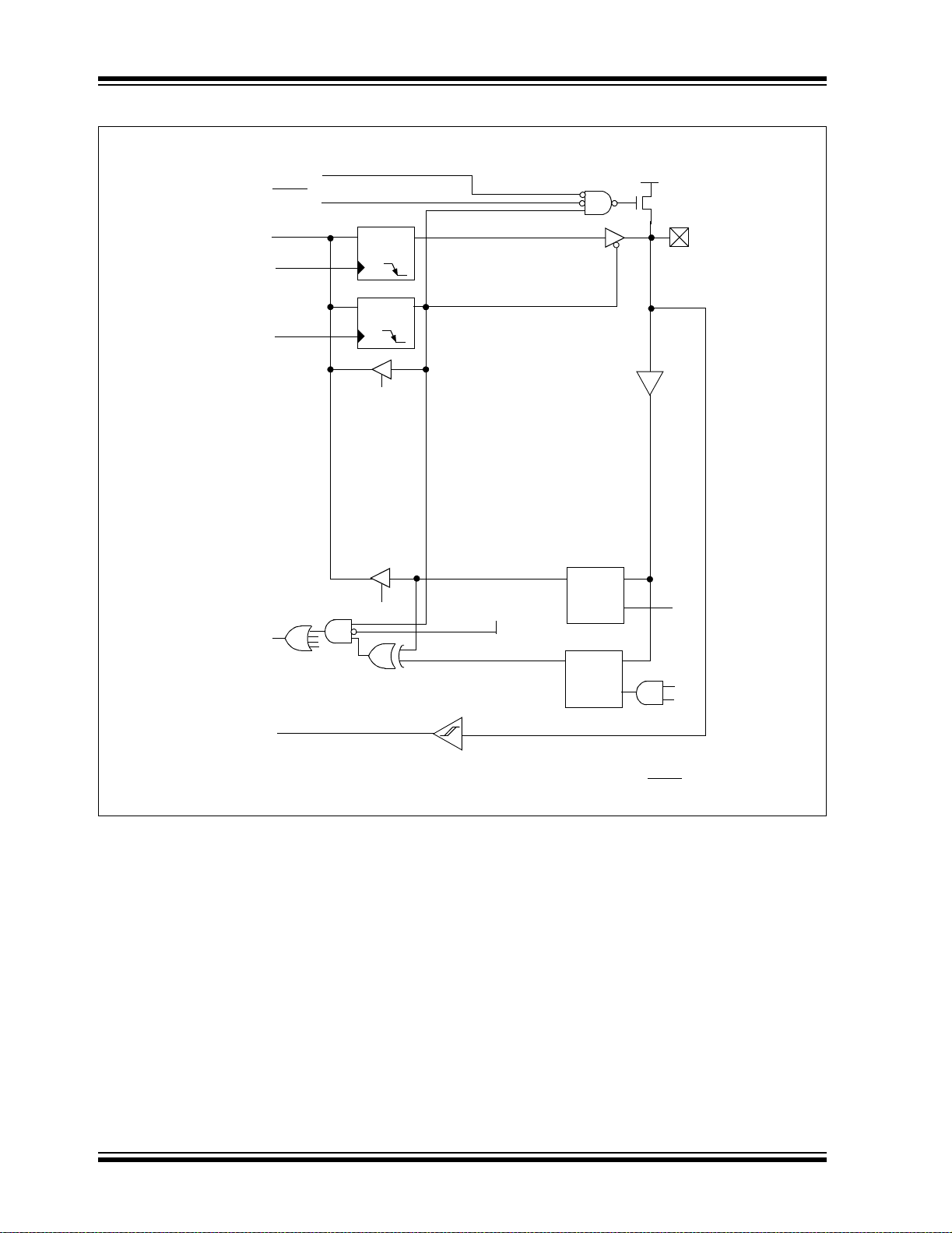
PIC16F7X7
FIGURE 5-14: BLOCK DIAGRAM OF RB6/PGC PIN
Program Mode/ICD
(1)
RBPU
Data Bus
WR PORTB
WR TRISB
Set RBIF
Data Latch
CK
TRIS Latch
CK
RD TRISB
RD PORTB
V
DD
Weak
P
Pull-up
QD
I/O pin
QD
TTL
Input Buffer
Latch
QD
Program Mode/ICD
EN
Q1
From other
RB7:RB4 pins
Schmitt Trigger
PGC
Note 1: To enable weak pull-ups, set the appropriate TRIS bit(s) and clear the RBPU
Buffer
QD
EN
RD PORTB
Q3
bit.
DS30498C-page 62 2004 Microchip Technology Inc.
Page 65

FIGURE 5-15: BLOCK DIAGRAM OF RB7/PGD PIN
(1)
RBPU
Data Latch
QD
CK
QD
CK
PIC16F7X7
DD
V
P
I/O pin
From other
QD
EN
QD
EN
2004 Microchip Technology Inc. DS30498C-page 63
Page 66

PIC16F7X7
TABLE 5-3: PORTB FUNCTIONS
Name Bit# Buffer Function
RB0/INT/AN12 bit 0 TTL/ST
RB1/AN10 bit 1 TTL Input/output pin. Internal software programmable weak pull-up or
RB2/AN8 bit 2 TTL Input/output pin. Internal software programmable weak pull-up or
RB3/CCP2/AN9 bit 3 TTL Input/output pin or Capture 2 input/Compare 2 output/PWM 2 output.
RB4/AN11 bit 4 TTL Input/output pin (with interrupt-on-change). Internal software
RB5/AN13/CCP3 bit 5 TTL Input/output pin (with interrupt-on-change). Internal software
RB6/PGC bit 6 TTL/ST
RB7/PGD bit 7 TTL/ST
Legend: TTL = TTL input, ST = Schmitt Trigger input
Note 1: This buffer is a Schmitt Trigger input when configured as the external interrupt.
2: This buffer is a Schmitt Trigger input when us ed in Serial Programming mode.
(1)
Input/output pin or external interrupt input. Internal software
programmable weak pull-up or analog input.
analog input.
analog input.
Internal software programmable weak pull-up or analog input.
programmable weak pull-up or analog input.
programmable weak pull-up or analog input or Capture 2 input/
Compare 2 output/PWM 2 output.
(2)
Input/output pin (with interrupt-on-change). Internal software
programmable weak pull-up. Serial programming clock.
(2)
Input/output pin (with interrupt-on-change). Internal software
programmable weak pull-up. Serial programming data.
TABLE 5-4: SUMMARY OF REGISTERS ASSOCIATED WITH PORTB
Address Name Bit 7 Bit 6 Bit 5 Bit 4 Bit 3 Bit 2 Bit 1 Bit 0
06h, 106h PORTB RB7 RB6 RB5 RB4 RB3 RB2 RB1 RB0 xx00 0000 uu00 0000
86h, 186h TRISB PORTB Data Direction Register 1111 1111 1111 1111
81h, 181h OPTION_REG RBPU
9Fh ADCON1 ADFM ADCS2 VCFG1 VCFG0 PCFG3 PCFG2 PCFG1 PCFG0 0000 0000 0000 0000
Legend: x = unknown, u = unchanged. Shaded cells are not used by PORTB.
INTEDG T0CS T0SE PSA PS2 PS1 PS0 1111 1111 1111 1111
Val ue on:
POR, BOR
Val ue on
all other
Resets
DS30498C-page 64 2004 Microchip Technology Inc.
Page 67

PIC16F7X7
5.3 PORTC and the TRISC Register
PORTC is an 8-bit wide, bidirectional port. The corresponding data direction register is TRISC. Setting a
TRISC bi t (= 1) will make the corresponding PORTC
pin an input (i.e., put the corresponding output driver in
a high-impedance mode). Clearing a TRISC bit (= 0)
will make the correspo nding PORT C pin an output (i.e .,
put the contents of the outpu t latch on the selected pi n).
PORTC is mul tiplexed with s everal peri pheral function s
(Table 5-5). PORTC pins have Schmitt Trigger input
buffers.
When enabling peripheral functions, care should be
taken in defining TRIS bit s fo r each POR TC pin. Some
peripherals override the TRIS bit to make a pin an
output, whi le ot her pe r iph e r al s ov e rri d e the TR I S bi t to
make a pin an input. Since the TRIS bit override is in
effect while the peripheral is enabled, read-modifywrite instructions (BSF, BCF, XORWF) with TRISC as
destination shoul d be avoided. The us er should refer to
the corresponding peripheral section for the correct
TRIS bit s etting s and to Section 16.1 “Read-Modify-
Write Operations” for additional information on
read-modify-write operations.
FIGURE 5-16: PORTC BLOCK DIAGRAM
(PERIPHERAL OUTPUT
OVERRIDE) RC<2:0>,
RC<7:5> PINS
Port/Peripheral Select
Peripheral Data Out
Data Bus
WR
Port
WR
TRIS
RD
TRIS
Peripheral
(3)
OE
(2)
CK
Data Latch
CK
TRIS Latch
DD
Schmitt
Trigger
V
P
N
VSS
I/O
pin
(1)
0
QD
1
Q
QD
Q
QD
FIGURE 5-17: PORTC BLOCK DIAGRAM
(PERIPHERAL OUTPUT
OVERRIDE) RC<4:3> PINS
CK
Data Latch
CK
TRIS Latch
(2)
0
QD
1
Q
QD
Q
QD
EN
CKE
SSPSTAT<6>
Schmitt
Trigger
V
P
N
Vss
0
1
DD
I/O
pin
Schmitt
Trigger
with
SMBus
Levels
(1)
Port/Peripheral Select
Peripheral Data Out
Data Bus
WR
Port
WR
TRIS
RD
TRIS
Peripheral
(3)
OE
RD
Port
SSPl Input
Note 1: I/O pins have diode protection to VDD and VSS.
2: Port/Peripheral Select signal selects between port data
and peripheral output.
3: Peripheral OE (Output Enable) is only activated if
Peripheral Select is active.
RD
Port
Peripheral Input
Note 1: I/O pins have diode protection to VDD and VSS.
2: Port/Peripheral Select signal selects between port
data and peripheral output.
3: Peripheral OE (Output Enable) is only activated if
Peripheral Select is active.
EN
2004 Microchip Technology Inc. DS30498C-page 65
Page 68

PIC16F7X7
TABLE 5-5: PORTC FUNCTIONS
Name Bit# Buffer Type Function
RC0/T1OSO/T1CKI bit 0 ST Input/output port pin or Timer1 oscillator output/Timer1 clock input.
RC1/T1OSI/CCP2 bit 1 ST Input/output port pin or Timer1 oscillator input or Capture 2 input/
Compare 2 output/PWM 2 output.
RC2/CCP1 bit 2 ST Input/output port pin or Capture 1 input/Compare 1 output/PWM 1
output.
RC3/SCK/SCL bit 3 ST RC3 can also be the synchronous serial clock for both SPI™ and
RC4/SDI/SDA bit 4 ST RC4 can also be the SPI data in (SPI mode) or data I/O (I2C mode).
RC5/SDO bit 5 ST Input/output port pin or Synchronous Serial Port data output.
RC6/TX/CK bit 6 ST Input/output port pin or AUSART asynchronous transmit or
RC7/RX/DT bit 7 ST Input/output port pin or AUSART asynchronous receive or
Legend: ST = Schmitt Trigger input
TABLE 5-6: SUMMARY OF REGISTERS ASSOCIATED WITH PORTC
Address Name Bit 7 Bit 6 Bit 5 Bit 4 Bit 3 Bit 2 Bit 1 Bit 0
2
C™ modes.
I
synchronous clock.
synchronous dat a.
Value on:
POR, BOR
Value on
all other
Resets
07h PORTC RC7 RC6 RC5 RC4 RC3 RC2 RC1 RC0 xxxx xxxx uuuu uuuu
87h TRISC PORTC Data Direction Register 1111 1111 1111 1111
Legend: x = unknown, u = unchanged
DS30498C-page 66 2004 Microchip Technology Inc.
Page 69

PIC16F7X7
5.4 PORTD and TRISD Registers
This section is not applicable to the PIC16F737 or
PIC16F767.
PORTD is an 8-bit port with Schmitt Trigger input
buffers. Each pin is individually configureable as an
input or output.
PORTD can be configured as an 8-bit wide microprocessor port (Parallel Slave Port) by setting control
bit, PSPMODE (TRISE<4>). In this mode, the input
buffers are TTL.
FIGURE 5-18: PORTD BLOCK DIAGRAM
(IN I/O PORT MODE)
DataBus
WR Port
WR TRIS
RD TRIS
RD Port
Note 1: I/O pins have protection diodes to VDD and VSS.
CK
Data Latch
QD
CK
TRIS Latch
QD
QD
EN
Schmitt
Trigger
Input
Buffer
EN
I/O pin
(1)
TABLE 5-7: PORTD FUNCTIONS
Name Bit# Buffer Type Function
RD0/PSP0 bit 0 ST/TTL
RD1/PSP1 bit 1 ST/TTL
RD2/PSP2 bit 2 ST/TTL
RD3/PSP3 bit 3 ST/TTL
RD4/PSP4 bit 4 ST/TTL
RD5/PSP5 bit 5 ST/TTL
RD6/PSP6 bit 6 ST/TTL
RD7/PSP7 bit 7 ST/TTL
(1)
(1)
(1)
(1)
(1)
(1)
(1)
(1)
Input/output port pin or Parallel Slave Port bit 0.
Input/output port pin or Parallel Slave Port bit 1.
Input/output port pin or Parallel Slave Port bit 2.
Input/output port pin or Parallel Slave Port bit 3.
Input/output port pin or Parallel Slave Port bit 4.
Input/output port pin or Parallel Slave Port bit 5.
Input/output port pin or Parallel Slave Port bit 6.
Input/output port pin or Parallel Slave Port bit 7.
Legend: ST = Schmitt Trigger input, TTL = TTL input
Note 1: Input buffers are Schmitt Triggers when in I/O mode and TTL buffers when in Parallel Slave Port mode.
TABLE 5-8: SUMMARY OF REGISTERS ASSOCIATED WITH PORTD
Address Name Bit 7 Bit 6 Bit 5 Bit 4 Bit 3 Bit 2 Bit 1 Bit 0
08h PORTD RD7 RD6 RD5 RD4 RD3 RD2 RD1 RD0 xxxx xxxx uuuu uuuu
88h TRISD PORTD Data Direction Register 1111 1111 1111 1111
89h TRISE
Legend: x = unknown, u = unchanged, — = unimplemented, read as ‘0’. Shaded cells are not used by PORTD.
Note 1: RE3 is an input only. The state of the TRISE3 bit has no effect and will always read ‘1’.
IBF OBF IBOV PSPMODE —
(1)
PORTE Data Direction bits 0000 1111 0000 1111
Value on:
POR, BOR
Value on
all other
Resets
2004 Microchip Technology Inc. DS30498C-page 67
Page 70

PIC16F7X7
5.5 PORTE and TRISE Register
This section is not applicable to the PIC16F737 or
PIC16F767.
PORTE has four pins, RE0/RD
RE2/CS
ally configureable as inputs or outputs. These pins have
Schmitt Trigger input buffers . RE3 is only available as an
input if MCLRE is ‘0’ in Configuration Word 1.
I/O PORTE becomes control inputs for the microprocessor port when bit, PSPMODE (TRISE<4>), is
set. In this mode, the user must make sure that the
TRISE<2:0> bits are set (pins are configured as digital
/AN7 and MCLR/VPP/RE3, which are individu-
/AN5, RE1/WR/AN6,
DS30498C-page 68 2004 Microchip Technology Inc.
Page 71

REGISTER 5-1: TRISE REGISTER (ADDRESS 89h)
R-0 R-0 R/W-0 R/W-0 U-0 R/W-1 R/W-1 R/W-1
IBF OBF IBOV PSPMODE —
bit 7 bit 0
bit 7 Parallel Slave Port Status/Control bits:
IBF: Input Buffer Full Status bit
1 = A word has been received and is waiting to be read by the CPU
0 = No word has been received
bit 6 OBF: Output Buffer Full Status bit
1 = The output buffer still holds a previously written word
0 = The output buffer has been read
bit 5 IBOV: Input Buffer Overflow Detect bit (in Microprocessor mode)
1 = A write occurred when a previous ly input word has not been read (must be cleared in
software)
0 = No overflow occurred
bit 4 PSPMODE: Parallel Slave Port Mode Select bit
1 = Parallel Slave Port mode
0 = General Purpose I/O mode
bit 3 Unimplemented: Read as ‘1’
Note 1: RE3 is an input only . The state of the TRISE3 bit has no e ffect and will always read ‘ 1’.
bit 2 PORTE Data Direction bits:
TRISE2: Direction Control bit for pin RE2/CS/AN7
1 = Input
0 = Output
bit 1 TRISE1: Direction Control bit for pin RE1/WR
1 = Input
0 = Output
bit 0 TRISE0: Direction Control bit for pin RE0/RD
1 = Input
0 = Output
(1)
/AN6
/AN5
PIC16F7X7
(1)
TRISE2 TRISE1 TRISE0
Legend:
R = Readable bit W = Writable bit U = Unimplemented bit, read as ‘0’
-n = Value at POR ‘1’ = Bit is set ‘0’ = Bit is cleared x = Bit is unknown
2004 Microchip Technology Inc. DS30498C-page 69
Page 72

PIC16F7X7
5.6 Parallel Slave Port
The Parallel Slave Port (PSP) is not implemented on
the PIC16F737 or PIC16F767.
PORTD operates as an 8-bit wide Parallel Slav e Port or
microprocessor port when control bit, PSPMODE
(TRISE<4>), is set. In Sla ve mode, it i s asynchronousl y
readable and writable by an external system using the
read control input pin RE0/RD
input pin RE1/WR
pin RE2/CS
/AN6 and the chip select co ntrol input
/AN7.
The PSP can directly interface to an 8-bit microprocessor data bus. Th e extern al micropr ocessor c an
read or write the POR TD latch as an 8-bit latch. Setting
bit PSPMODE enables port pin RE0/RD
input, RE1/WR/AN6 to be the WR input and
RD
RE2/CS
/AN7 to be the CS (Chip Select) input. For this
functionality, the corresponding data direction bits of
the TRISE register (TRISE<2:0>) must be configured
as inputs (i.e., set). The A/D port configuration bits,
PCFG3:PCFG0 (ADCON1<3:0>), must be set to
configure pins RE2:RE0 as digital I/O.
There are actual ly two 8 -bit latc hes, one for dat a outp ut
(external reads) and one for data input (external
writes). The firmware writes 8-bit data to the PORTD
output data latch and reads data from the PORTD input
data latch (note that they have the same address). In
this mode, the TRISD register is ignored since the
external device is controlling the direction of data flow.
An external write to the PSP occurs when the CS
WR
lines are both detected low. Firmware can read the
actual data on the PORTD pins during this time. When
either the CS
or WR lines become high (level triggered), the data on the PORTD pins is latched and the
Input Buffer Full (IBF) status flag bit (TRISE<7>) and
interrupt flag bit, PSPIF (PIR1<7>), are set on the Q4
clock cycle following the next Q2 cycle to signal t he
write is complete (Figure 5-21). Firmware clears the
IBF flag by reading the latc hed POR TD dat a and clears
the PSPIF bit.
The Input Buffer Overflow (IBOV) status flag bit
(TRISE<5>) is set if an external write to the PSP occu rs
while the IBF flag is set from a previous external write.
The previous PORTD data is overwritten with the new
data. IBOV is cleared by reading PORTD and clearing
IBOV.
A read from the PSP occurs when both the CS
lines are detected low. The data in the PORTD output
latch is output to the PORTD pins. The Output Buffer
Full (OBF) status flag bit (TRISE<6>) is cleared immediately (Figure 5-22), indicating that the PORTD latch i s
being read or has been read by the external bus. If
firmware writes ne w da t a to the output latch during this
time, it is immediately output to the PORTD pins but
OBF will remain cleared.
/AN5, the write control
/AN5 to be the
and
and RD
When either the CS
or RD pins are detected high, the
PORTD outputs are disabled and the interrupt flag bit
PSPIF is set on the Q4 clock cycle following the next
Q2 cycle, indicating that the read is complete. OBF
remains low until firmware writes new data to PORTD.
When not in PSP mode, the IBF and OBF bits are held
clear . Flag bit IBOV remains uncha nged. The PSPIF b it
must be cleared by the user in firmware; the interrupt
can be disabled by clearing the interrupt enable bit,
PSPIE (PIE1<7>).
FIGURE 5-20: PORTD AND PORTE
BLOCK DIAGRAM
(PARALLEL SLAVE PORT)
Data Bus
WR
Port
RD
Port
One bit of PORTD
Set Interrupt Flag
PSPIF (PIR1<7>)
Note: I/O pin has protection diodes to VDD and VSS.
QD
CK
QD
EN
EN
TTL
Read
Chip Select
Write
TTL
TTL
TTL
RDx pin
RD
CS
WR
DS30498C-page 70 2004 Microchip Technology Inc.
Page 73

FIGURE 5-21: PARALLEL SLAVE PORT WRITE WAVEFORMS
Q1 Q2 Q3 Q4CSQ1 Q2 Q3 Q4 Q1 Q2 Q3 Q4
WR
RD
PORTD<7:0>
IBF
OBF
PSPIF
FIGURE 5-22: PARALLEL SLAVE PORT READ WAVEFORMS
PIC16F7X7
Q1 Q2 Q3 Q4
CS
WR
RD
PORTD<7:0>
IBF
OBF
PSPIF
Q1 Q2 Q3 Q4 Q1 Q2 Q3 Q4
TABLE 5-11: REGISTERS ASSOCIATED WITH PARALLEL SLAVE PORT
Address Name Bit 7 Bit 6 Bit 5 Bit 4 Bit 3 Bit 2 Bit 1 Bit 0
08h PORTD Port Data Latch when written: Port pins when read xxxx xxxx uuuu uuuu
09h PORTE
89h TRISE IBF OBF IBOV PSPMODE
0Ch PIR1 PSPIF
8Ch PIE1 PSPIE
9Fh ADCON1 ADFM ADCS2 VCFG1 VCFG0 PCFG3 PCFG2 PCFG1 PCFG0 0000 0000 0000 0000
Legend: x = unknown, u = unchanged, — = unimplemented, read as ‘0’. Shaded cells are not used by the Parallel Slave Port.
Note 1: Bits PSPIE and PSPIF are reserved on the PIC16F737/767; always maintain these bits clear.
2: RE3 is an input only. The state of the TRISE3 bit has no effect and will always read ‘1’.
— — — — RE3 RE2 RE1 RE0 ---- x000 ---- x000
(1)
ADIF RCIF TXIF SSPIF CCP1IF TMR2IF TMR1IF 0000 0000 0000 0000
(1)
ADIE RCIE TXIE SSPIE CCP1IE TMR2IE TMR1IE 0000 0000 0000 0000
(2)
—
PORTE Data Direction bits 0000 1111 0000 1111
Value on:
POR, BOR
Value on
all other
Resets
2004 Microchip Technology Inc. DS30498C-page 71
Page 74

PIC16F7X7
NOTES:
DS30498C-page 72 2004 Microchip Technology Inc.
Page 75

PIC16F7X7
6.0 TIMER0 MODULE
The Timer0 module timer/counter has the following
features:
• 8-bit timer/counter
• Readable and writable
• 8-bit software programmable prescaler
• Internal or external clock select
• Interrupt on overflow from FFh to 00h
• Edge select for external clock
Additional information on the Timer0 module is
available in the “PICmicro® Mid-Range MCU Family
Reference Manual” (DS330 23).
Figure 6-1 is a block diagram of th e Ti mer0 module and
the prescaler shared with the WDT.
6.1 Timer0 Operation
Timer0 operation is controlled through the
OPTION_REG register (see Register 2-2). Timer mode
is selected b y clearing bit T0 CS (OPTION_REG<5> ).
In Timer mode , the T ime r0 module wi ll increm ent every
instruction cycle (w ithout pr escal er). If the TMR0 register is written, the i ncrem ent is inhi bited f or the follow ing
two instruction cycles. The user can work around this
by writing an adjusted value to the TMR0 register.
Counter mode is selected by setting bit, T0CS
(OPTION_REG<5>). In Counter mode, Timer0 will
increment, either on every rising or falling edge of pin
RA4/T0CKI/C1OUT. The incrementing edge is
determined by the Timer0 Source Edge Select bit, T0SE
(OPTION_REG<4>). Clea ring bit T0SE se lects the ris ing
edge. Restrictions on the external clock input are
discussed in detail in Section 6.3 “Using Timer0 With
an External Clock”.
The prescaler is mutually, exclusively shared between
the Timer0 module and the Watchdog Timer. The
prescaler is not readable or writable. Section 6.4
“Prescaler” details the operation of the prescaler.
6.2 Timer0 Interrupt
The TMR0 interrupt is generated when the TMR0 register overflows from FFh to 00h. This overflow sets bit
TMR0IF (INTCON<2>). The interrupt can be masked
by clearing bit TMR0IE (INTCON<5>). Bit TMR0IF
must be cleared in software by the Timer0 module
Interrupt Service Routine before re-enabling this
interrupt. The TMR0 interrupt cannot awaken the
processor from Sleep since the timer is shut-off during
Sleep.
FIGURE 6-1: BLOCK DIAGRAM OF THE TIMER0/WDT PRESCALER
CLKO (= F
RA4/T0CKI/C1OUT
31.25 kHz
WDT Enable bit
OSC/4)
pin
WDT Timer
Prescaler
T0SE
16-bit
0
1
0
1
M
U
X
T0CS
M
U
X
PSA
1
M
U
0
X
PSA
Prescaler
8-bit Prescaler
8
8-to-1 MUX
0
MUX
Sync
2
Cycles
PS2:PS0
1
PSA
Data Bus
8
TMR0 Reg
Set Flag bit TMR0IF
on Overflow
WDT Time-out
Note: T0CS, T0SE, PSA and PS2:PS0 are (OPTION_REG<5:0>).
2004 Microchip Technology Inc. DS30498C-page 73
Page 76

PIC16F7X7
6.3 Using Timer0 With an External Clock
When no pr escal er is us ed, t he ex ternal clock inpu t is
the same as the prescaler outp ut. Th e synchronization
of T0CKI with the internal phase clocks is accomplished by sampli ng the prescale r output on the Q2 and
Q4 cycles of the internal phase clocks. Therefore, it is
necessary for T0CKI to be high for at least 2 T
a small RC delay of 20 ns) and low for at least 2 T
(and a small RC delay of 20 ns). Refer to the electrical
specification of the desired device.
OSC (and
OSC
6.4 Prescaler
There is only one presca ler a vailable, which i s mutuall y
exclusively sha red between the T imer0 mod ule and the
Watchdog Timer. A prescaler assignment for the
Timer0 module means that the prescaler cannot be
used by the Watchdog Timer and vice versa. This
prescaler is not readable or writable (see Figure6-1).
Note: Although the prescaler can be assigned to
either the WDT or Timer0, but not both, a
new divide counter is implemented in the
WDT circuit to give mul tipl e WDT tim e-o ut
selections. This al low s TMR 0 an d WD T to
each have their own scaler. Refer to
Section 15.17 “Watchdog T imer (WDT)”
for further details.
The PSA and PS2:PS0 bits (OPTION_REG<3:0>)
determine the prescaler assignment and pre scale ratio.
When assigned to the Timer0 module, all instructions
writing to the TMR0 register (e.g., CLRF 1, MOVWF 1,
BSF 1,x....etc.) will clear the prescaler . When assigned
to WDT, a CLRWDT instruction will clear the prescaler
along with the Watchdog Timer. The prescaler is not
readable or writable.
Note: Writing to TMR0 when the prescaler is
assigned to T imer0 will cle ar the pre scaler
count but will not change the prescaler
assignment.
DS30498C-page 74 2004 Microchip Technology Inc.
Page 77

PIC16F7X7
REGISTER 6-1: OPTION_REG: OPTION CONTROL REGISTER (ADDRESS 181h)
R/W-1 R/W-1 R/W-1 R/W-1 R/W-1 R/W-1 R/W-1 R/W-1
RBPU
bit 7 bit 0
INTEDG T0CS T0SE PSA
(1)
PS2 PS1 PS0
bit 7 RBPU
bit 6 INTEDG: Interrupt Edge Select bit
bit 5 T0CS: TMR0 Clock Source Select bit
bit 4 T0SE: TMR0 Source Edge Select bit
bit 3 PSA: Prescaler Assignment bit
bit 2-0 PS<2:0>: Prescaler Rate Select bits
: PORTB Pull-up Enable bit
1 = PORTB pull-ups are disabled
0 = PORTB pull-ups are enabled
1 = Interrupt on rising edge of RB0/INT pin
0 = Interrupt on falling edge of RB0/INT pin
1 = Transition on T0CKI pin
0 = Internal instruction cycle clock (CLKO)
1 = Increment on high-to-low transition on T0CKI pin
0 = Increment on low-to-high transition on T0CKI pin
(1)
1 = Prescaler is assigned to the WDT
0 = Prescaler is assigned to the Timer0 module
Note 1: To avoid an unintended device Reset, the instruction sequence shown in the
”PICmicro
executed when changing the prescaler assignment from Timer0 to the WDT. This
sequence must be followed even if the WDT is disabled.
Bit Value TMR0 Rate WDT Rate
000
001
010
011
100
101
110
111
1 : 2
1 : 4
1 : 8
1 : 16
1 : 32
1 : 64
1 : 128
1 : 256
®
Mid-Range MCU Family Reference Manual” (DS33023) must be
1 : 1
1 : 2
1 : 4
1 : 8
1 : 16
1 : 32
1 : 64
1 : 128
Legend:
R = Readable bit W = Writable bit U = Unimplemented bit, read as ‘0’
-n = Value at POR ‘1’ = Bit is set ‘0’ = Bit is cleared x = Bit is unknown
2004 Microchip Technology Inc. DS30498C-page 75
Page 78

PIC16F7X7
EXAMPLE 6-1: CHANGING THE PRESCALER ASSIGNMENT FROM WDT TO TIMER0
CLRWDT ; Clear WDT and prescaler
BANKSEL OPTION_REG ; Select Bank of OPTION_REG
MOVLW b'xxxx0xxx' ; Select TMR0, new prescale
MOVWF OPTION_REG ; value and clock source
TABLE 6-1: REGISTERS ASSOCIATED WITH TIMER0
Address Name Bit 7 Bit 6 Bit 5 Bit 4 Bit 3 Bit 2 Bit 1 Bit 0
01h,101h TMR0 Timer0 Module Register xxxx xxxx uuuu uuuu
0Bh,8Bh,
10Bh,18Bh
81h,181h OPTION_REG
Legend: x = unknown, u = unchanged, - = unimplemented locations read as ‘0’. Shaded cells are not used by Timer0.
INTCON GIE PEIE TMR0IE
RBPU INTEDG T0CS T0SE PSA PS2 PS1 PS0 1111 1111 1111 1111
INT0IE RBIE TMR0IF INT0IF RBIF 0000 000x 0000 000u
Value on
POR, BOR
Val ue on
all other
Resets
DS30498C-page 76 2004 Microchip Technology Inc.
Page 79

PIC16F7X7
7.0 TIMER1 MODULE
The Timer1 mod ule is a 16-bi t timer/c ou nter c ons isting
of two 8-bit registers (TMR1H and TMR1L) which are
readable and writable. The TMR1 register pair
(TMR1H:TMR1L) increments from 0000h to FFFFh
and rolls over to 0000h. Th e TMR1 i nterrupt, if e nabled,
is generated on overflow which is latched in interrupt
flag bit, TMR1IF (PIR1<0>). This interrupt can be
enabled/disabled by setting/clearing TMR1 interrupt
enable bit, TMR1IE (PIE1<0>).
The Time r1 oscillator c an be used as a secondary cloc k
source in low-power mo des. When the T1RUN bit is s et
along with SCS<1:0> = 01, the Timer1 osci llator is providing the syst em clock. If the F ail-Saf e Clock Mon itor
is enabled and the Timer1 oscillator fails while
providing the system clock, polling the T1RUN bit will
indicate whether the clock is being provided by the
Timer1 oscillator or another source.
Timer1 can also be used to provide Real-Time Clock
(RTC) functionality to applications with only a minimal
addition of external components and code overhead.
7.1 Timer1 Operation
Timer1 can operate in one of three modes:
•as a Timer
• as a Synchronous Counter
• as an Asynchronous Counter
The operating mode is determined by the clock select
bit, TMR1CS (T1CON<1>).
In Timer mode, Timer1 increments every instruction
cycle. In Counter mode, it increments on every rising
edge of the external clock input.
Timer1 can be enabled/disabled by setting/clearing
control bit, TMR1ON (T1CON<0>).
Timer1 also has an interna l “Reset in put”. This Reset
can be generated by the CCP1 module as the special
event trigger (see Section 9.4 “Capture Mode”).
Register 7-1 shows the Timer1 Control register.
When the Timer1 oscillator is enabled (T1OSCEN is
set), the RC0/T1OSO/T1CKI and RC1/T1OSI/CCP2
pins become inputs. That is, the TRISB<7:6> value is
ignored and these pins read as ‘0’.
Additional information on timer modules is available in
the “PICmicro
Manual” (DS33023).
®
Mid-Range MCU Family Reference
2004 Microchip Technology Inc. DS30498C-page 77
Page 80

PIC16F7X7
REGISTER 7-1: T1CON: TIMER1 CONTROL REGISTER (ADDRESS 10h)
U-0 R-0 R/W-0 R/W-0 R/W-0 R/W-0 R/W-0 R/W-0
— T1RUN T1CKPS1 T1CKPS0 T1OSCEN T1SYNC TMR1CS TMR1ON
bit 7 bit 0
bit 7 Unimplemented: Read as ‘0’
bit 6 T1RUN: Timer1 System Clock Status bit
1 = System clock is derived from Timer1 oscillator
0 = System cloc k is derived from another source
bit 5-4 T1CKPS<1:0>: Timer1 Input Clock Prescale Select bits
11 = 1:8 Prescale value
10 = 1:4 Prescale value
01 = 1:2 Prescale value
00 = 1:1 Prescale value
bit 3 T1OSCEN: Timer1 Oscillator Enable Control bit
1 = Oscillator is enabled
0 = Oscillator is shut-off (the oscillator inverter is turned off to eliminate power drain)
bit 2 T1SYNC
TMR1CS = 1:
1 = Do not synchronize external clock input
0 = Synchronize external clock input
TMR1CS =
This bit is ignored. Timer1 uses the internal clock when TMR1CS = 0.
bit 1 TMR1CS: Timer1 Clock Source Select bit
1 = External clock from pin RC0/T1OSO/T1CKI (on the rising edge)
0 = Internal cl ock (F
bit 0 TMR1ON: Timer1 On bit
1 = Enables Timer1
0 =Stops Timer1
: Timer1 External Clock Input Synchronization Control bit
0:
OSC/4)
Legend:
R = Readable bit W = Writable bit U = Unimplemented bit, read as ‘0’
-n = Value at POR ‘1’ = Bit is set ‘0’ = Bit is cleared x = Bit is unknown
DS30498C-page 78 2004 Microchip Technology Inc.
Page 81

7.2 Timer1 Operation in Timer Mode
Timer mode is selected by clearing the TMR1CS
(T1CON<1>) bit. In this mode, the input clS
PIC16F7X7
2004 Microchip Technology Inc. DS30498C-page 79
Page 82

PIC16F7X7
7.5 Timer1 Operation in Asynchronous Counter Mode
If control bit, T1SYNC (T1CON<2>), is set, the external
clock input is not synchronized. The timer continues to
increment asynchronous to the internal phase clocks.
The timer will continue to run during Sleep and can
generate an interrupt on overflow that will wake-up the
processor. However, special precautions in software
are needed to read/write the timer (Section 7.5.1
“Reading and Writing Timer1 in Asynchronous
Counter Mode”).
In Asynchronous Counter mode, Timer1 cannot be
used as a time base for capture or comp are operations.
7.5.1 READING AND WRITING T I MER1 IN ASYNCHRONOUS COUNTER MODE
Reading TMR1H or TMR1L while the timer is running
from an external asyn chronous cl ock will e nsure a valid
read (taken care of in hardware). However, the user
should keep in mind that rea ding t he 16-bi t ti mer in two
8-bit values itself, poses certain problems, since the
timer may overflow between the reads.
For writes, it is recommend ed that th e user s imply sto p
the timer and write the desired values. A write contention may occur by writing to the Timer registers while
the register is incrementing. This may produce an
unpredictable value i n the Timer regis ter.
Reading the 16-bit value requires some care. The
example codes provided in Example 7-1 and
Example 7-2 demonstrate how to write to and read
Timer1 while it is running in Asynchronous mode.
EXAMPLE 7-1: WRITING A 16-BIT FREE RUNNING TIMER
; All interrupts are disabled
CLRF TMR1L ; Clear Low byte, Ensures no rollover into TMR1H
MOVLW HI_BYTE ; Value to load into TMR1H
MOVWF TMR1H, F ; Write High byte
MOVLW LO_BYTE ; Value to load into TMR1L
MOVWF TMR1H, F ; Write Low byte
; Re-enable the Interrupt (if required)
CONTINUE ; Continue with your code
EXAMPLE 7-2: READING A 16-BIT FREE RUNNING TIMER
; All interrupts are disabled
MOVF TMR1H, W ; Read high byte
MOVWF TMPH
MOVF TMR1L, W ; Read low byte
MOVWF TMPL
MOVF TMR1H, W ; Read high byte
SUBWF TMPH, W ; Sub 1st read with 2nd read
BTFSC STATUS, Z ; Is result = 0
GOTO CONTINUE ; Good 16-bit read
; TMR1L may have rolled over between the read of the high and low bytes.
; Reading the high and low bytes now will read a good value.
MOVF TMR1H, W ; Read high byte
MOVWF TMPH
MOVF TMR1L, W ; Read low byte
MOVWF TMPL ; Re-enable the Interrupt (if required)
CONTINUE ; Continue with your code
DS30498C-page 80 2004 Microchip Technology Inc.
Page 83
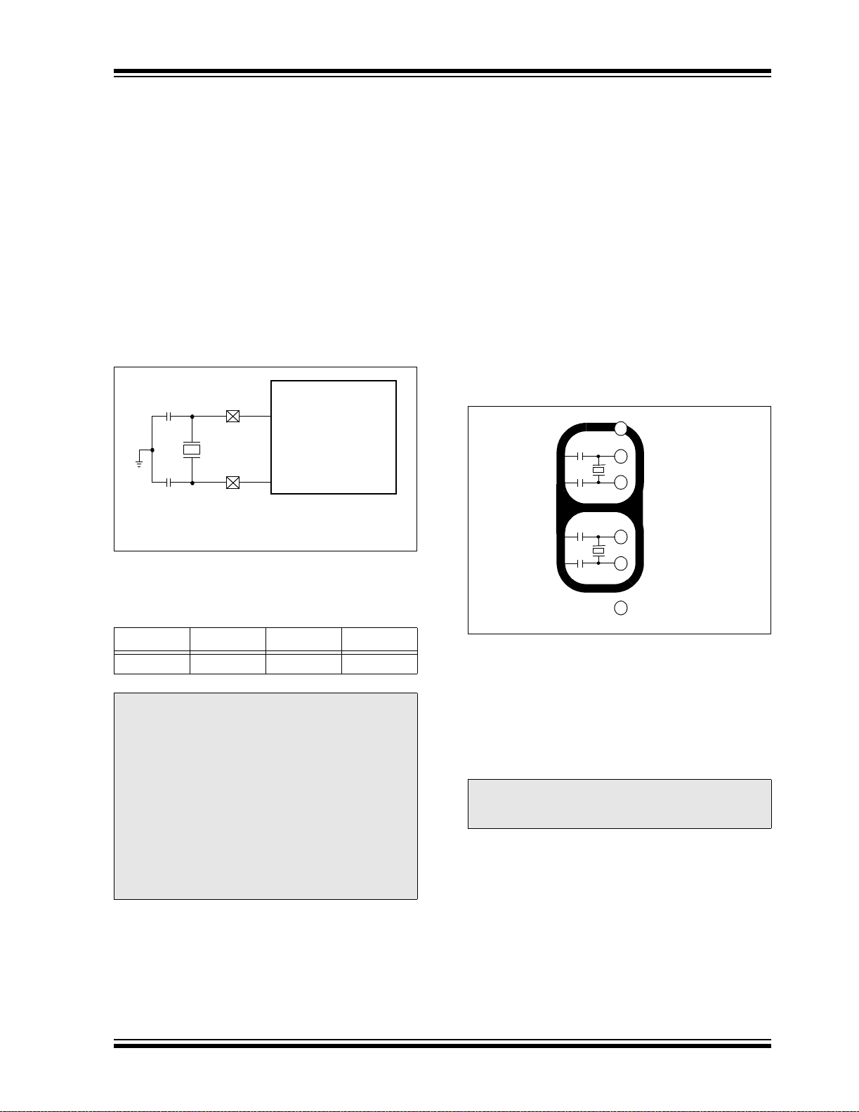
PIC16F7X7
7.6 Timer1 Oscillator
A crystal oscillator circuit is built between pins T1OSI
(input) and T1OSO (amplifier output). It is enabled by
setting control bit, T1OSCEN (T1CON<3>). The oscillator is a low-power oscillator, rated up to 32.768 kHz.
It will continue to run durin g all power-managed mo des.
It is primarily intended for a 32 kHz crystal. The circuit
for a typical LP oscillator is shown in Figure 7-3.
Table 7-1 shows the capacitor selection for the Timer1
oscillator.
The user must provide a sof tware t im e del ay to en su re
proper oscillator start-up.
FIGURE 7-3: EXTERNAL
COMPONENTS FOR THE
TIMER1 LP OSCILLATOR
C1
33 pF
XTAL
32.768 kHz
C2
33 pF
Note: See the Notes with Table 7-1 for additional
information about capacitor selection.
PIC16F7X7
T1OSI
T1OSO
7.7 Timer1 Oscillator Layout Considerations
The Timer1 oscillator circuit draws very little power
during operation. Due to the low-power nature of the
oscillator, it may also be sensitive to rapidly changing
signals in close proximity.
The oscillator circuit, shown in Figure 7-3, should be
located as close as possible to the microcontroller.
There should be no ci rcuits p assing withi n the oscillat or
circuit boundaries other than V
If a high-speed circ ui t m us t b e l oc ate d n ear the os c ill ator, a grounded guard ring around the oscillator circuit,
as shown in Figure7-4, may be helpful when used on
a single sided PCB or in addition to a ground plane.
FIGURE 7-4: OSCILLATOR CIRCUIT
WITH GROUNDED
GUARD RING
SS or VDD.
V
SS
OSC1
OSC2
RC0
TABLE 7-1: CAPACITOR SELECTION FOR
THE TIMER1 OSCILLATOR
Osc Type Freq C1 C2
LP 32 kHz 33 pF 33 pF
Note 1: Microchip suggests this value as a starting
point in validating the oscillator circuit.
2: Higher capacitance inc reases th e stabilit y
of the oscillator but also increases the
start-up time.
3: Since each resonator/crystal has its own
characteristics, the user should consult
the resonator/crystal manufacturer for
appropriate values of external
components.
4: Capacitor values are for design guidance
only.
RC1
RC2
7.8 Resetting Timer1 Using a CCP Trigger Output
If the CCP1 module is configured in Compare mode to
generate a “special event trigger” signal
(CCP1M3:CCP1M0 = 1011), the signal will reset
Timer1 and start an A/D conversion (if the A/D module
is enabled).
Note: The special event triggers from the CCP1
module will not set interrupt flag bit,
TMR1IF (PIR1<0>).
Timer1 mu st be confi gured fo r either T ime r or Synchr onized Counter mode to take advantage of this feature.
If Timer1 is running in Asynchronous Counter mode,
this Reset operation may not work.
In the event that a write to Timer1 coincides with a
special event trigger from CCP1, the write will take
precedence.
In this mode of operation, the CCPR1H:CCPR1L
register pair ef fe cti ve ly b ec ome s th e pe riod regi ste r for
Timer1.
2004 Microchip Technology Inc. DS30498C-page 81
Page 84

PIC16F7X7
7.9 Resetting Timer1 Register Pair (TMR1H, TMR1L)
TMR1H and TMR1L registers are not rese t to 00h on a
POR, or any other Reset, except by the CCP1 special
event triggers.
T1CON register is rese t to 00h on a Powe r-on Rese t or
a Brown-out Reset, which shuts off the timer and
leaves a 1:1 prescale. In all other Resets, the register
is unaffected.
7.10 Timer1 Prescaler
The prescaler counter is cleared on writes to the
TMR1H or TMR1L registers.
7.11 Using Timer1 as a Real-Time Clock
Adding an external LP oscilla tor to Timer1 (such as the
one described in Section 7.6 “Timer1 Oscillator”)
gives users the option to include RTC functionality in
their applications. This is accomplished with an inexpensive watch cr ysta l t o prov ide a n accura te time base
and several lines of application code to calculate the
time. When operating in Sleep mode and using a
battery or supercapacitor as a power source, it can
completely eliminate the need for a separate RTC
device and battery backup.
The application code routine, RTCisr, shown in
Example 7-3, demonstrates a simple method to
increment a counter at one-second intervals using an
Interrupt Service Rou tin e. I ncrementing the TMR1 register pair to overfl ow, triggers the interrupt and calls th e
routine which increments the seconds counter by one;
additional counters for minutes and hours are
incremented as the previous counter overflows.
Since the register pair is 16 bits wide, counting up to
overflow the register directly from a 32.768 kHz clock
would take 2 seconds. To force the overflow at the
required one-second intervals, it is necessary to
preload it. The simplest method is to set the MSb of
TMR1H with a BSF instruction. Note that the TMR1L
register is never preloaded or altered; doing so may
introduce cumulative error over many cycles.
For this method to be accura te, T imer 1 must oper ate in
Asynchronous mode and the Timer1 overflow interrupt
must be enabled (PIE1<0> = 1) as shown in the
routine, RTCinit. The Timer1 oscillator must also be
enabled and running at all times.
EXAMPLE 7-3: IMPLEMENTING A REAL-TIME CLOCK USING A TIMER1 INTERRUPT SERVICE
RTCinit BANKSEL TMR1H
RTCisr BANKSEL TMR1H
MOVLW 0x80 ; Preload TMR1 register pair
MOVWF TMR1H ; for 1 second overflow
CLRF TMR1L
MOVLW b’00001111’ ; Configure for external clock,
MOVWF T1CON ; Asynchronous operation, external oscillator
CLRF secs ; Initialize timekeeping registers
CLRF mins
MOVLW .12
MOVWF hours
BANKSEL PIE1
BSF PIE1, TMR1IE ; Enable Timer1 interrupt
RETURN
BSF TMR1H, 7 ; Preload for 1 sec overflow
BCF PIR1, TMR1IF ; Clear interrupt flag
INCF secs, F ; Increment seconds
MOVF secs, w
SUBLW .60
BTFSS STATUS, Z ; 60 seconds elapsed?
RETURN ; No, done
CLRF seconds ; Clear seconds
INCF mins, f ; Increment minutes
MOVF mins, w
SUBLW .60
BTFSS STATUS, Z ; 60 seconds elapsed?
RETURN ; No, done
CLRF mins ; Clear minutes
INCF hours, f ; Increment hours
MOVF hours, w
SUBLW .24
BTFSS STATUS, Z ; 24 hours elapsed?
RETURN ; No, done
CLRF hours ; Clear hours
RETURN ; Done
DS30498C-page 82 2004 Microchip Technology Inc.
Page 85

PIC16F7X7
TABLE 7-2: REGISTERS ASSOCIATED WITH TIMER1 AS A TIMER/COUNTER
Address Name Bit 7 Bit 6 Bit 5 Bit 4 Bit 3 Bit 2 Bit 1 Bit 0
0Bh, 8Bh,
10Bh, 18Bh
0Ch PIR1 PSPIF
8Ch PIE1 PSPIE
0Eh TMR1L Holding Register for the Least Significant Byte of the 16-bit TMR1 Register xxxx xxxx uuuu uuuu
0Fh TMR1H Ho lding Register for the Most Significant Byte of the 16-bit TMR1 Register xxxx xxxx uuuu uuuu
10h T1CON
Legend: x = unknown, u = unchanged, — = unimplemented, read as ‘0’. Shaded cells are not used by the Timer1 module.
Note 1: Bits PSPIE and PSPIF are reserved on the PIC16F737/767 devices; always maintain these bits clear.
INTCON GIE PEIE
(1)
(1)
ADIE RCIE TXIE SSPIE CCP1IE TMR2IE TMR1IE 0000 0000 0000 0000
— T1RUN T1CKPS1 T1CKPS0 T1OSCEN T1SYNC TMR1CS TMR1ON -000 0000 -uuu uuuu
TMR0IE INT0IE RBIE TMR0IF INT0IF RBIF 0000 000x 0000 000u
ADIF RCIF TXIF SSPIF CCP1IF TMR2IF TMR1IF 0000 0000 0000 0000
Val ue on
POR, BOR
Value on
all other
Resets
2004 Microchip Technology Inc. DS30498C-page 83
Page 86

PIC16F7X7
NOTES:
DS30498C-page 84 2004 Microchip Technology Inc.
Page 87

PIC16F7X7
8.0 TIMER2 MODULE
Timer2 is an 8-bit timer with a prescaler and a
postscaler . It c an be used as the PWM time base f or the
PWM mode of the CCP module(s). The TMR2 register
is readable and writable and is cleared on any device
Reset.
The input cloc k (F
1:4 or 1:16, selected by control bits,
T2CKPS1:T2CKPS0 (T2CON<1:0>).
The Timer2 module has an 8-bit period register, PR2.
Timer2 increments from 00h until it matches PR2 and
then resets to 00h on the next increment cycle. PR2 is
a readable and writable register. The PR2 register is
initialized to FFh upon Reset.
The match output of TMR2 goes through a 4-bit
postscaler (which gives a 1:1 to 1:16 scaling inclusive)
to generate a TMR2 interrupt, latched in flag bit,
TMR2IF (PIR1<1>).
Timer2 c an be shut-of f by clearing control bit, T MR2ON
(T2CON<2>), to minimize power consumption.
Register 8-1 shows the Timer2 Control register.
Additional information on timer modules is available in
the “PICmicro
Manual” (DS33023).
OSC/4) has a prescale option of 1:1,
®
Mid-Range MCU Family Reference
8.1 Timer2 Prescaler and Postscaler
The prescaler and postscaler counters are cleared
when any of the following occurs:
• a write to the TMR2 register
• a write to the T2CON register
• any device Reset (POR, MCLR
Reset, WDT
Reset or BOR)
TMR2 is not cleared when T2CON is written.
8.2 Output of TMR2
The output of TMR2 (before the post scaler) is fed to the
SSP module which optionally uses it to generate the
shift clock.
FIGURE 8-1: TIMER2 BLOCK DIAGRAM
Sets Flag
bit TMR2IF
Postscaler
1:1 to 1:16
TOUTPS3:
TOUTPS0
4
TMR2
Output
Reset
EQ
(1)
TMR2 Reg
Comparator
PR2 Reg
Prescaler
1:1, 1:4, 1:16
2
T2CKPS1:
T2CKPS0
F
OSC/4
Note 1: TMR2 register output can be software selected by the
SSP module as a baud clock.
2004 Microchip Technology Inc. DS30498C-page 85
Page 88

PIC16F7X7
REGISTER 8-1: T2CON: TIMER2 CONTROL REGISTER (ADDRESS 12h)
U-0 R/W-0 R/W-0 R/W-0 R/W-0 R/W-0 R/W-0 R/W-0
— TOUTPS3 TOUTPS2 TOUTPS1 TOUTPS0 TMR2ON T2CKPS1 T2CKPS0
bit 7 bit 0
bit 7 Unimplemented: Read as ‘0’
bit 6-3 TOUTPS3:TOUTPS0: Timer2 Output Postscale Select bits
0000 = 1:1 Postscale
0001 = 1:2 Postscale
0010 = 1:3 Postscale
•
•
•
1111 = 1:16 Postscale
bit 2 TMR2ON: Timer2 On bit
1 = Timer2 is on
0 = Timer2 is off
bit 1-0 T2CKPS1:T2CKPS0: Timer2 Clock Prescale Select bits
00 = Prescaler is 1
01 = Prescaler is 4
1x = Prescaler is 16
Legend:
R = Readable bit W = Writable bit U = Unimplemented bit, read as ‘0’
-n = Value at POR ‘1’ = Bit is set ‘0’ = Bit is cleared x = Bit is unknown
TABLE 8-1: REGISTERS ASSOCIATED WITH TIMER2 AS A TIMER/COUNTER
Address Name Bit 7 Bit 6 Bit 5 Bit 4 Bit 3 Bit 2 Bit 1 Bit 0
0Bh,8Bh,
10Bh, 18Bh
0Ch PIR1
8Ch PIE1
11h TMR2 Timer2 Module Register 0000 0000 0000 0000
12h T2CON
92h PR2 Timer2 Period Register 1111 1111 1111 1111
Legend: x = unknown, u = unchanged, — = unimplemented, read as ‘0’. Shaded cells are not used by the Timer2 module.
Note 1: Bits PSPIE and PSPIF are reserved on the PIC16F737/767 devices; always maintain these bits clear.
INTCON GIE PEIE
(1)
PSPIF
PSPIE
— TOUTPS3 TOUTPS2 TOUTPS1 TOUTPS0 TMR2ON T2CKPS1 T2CKPS0 -000 0000 -000 0000
ADIF RCIF TXIF SSPIF CCP1IF TMR2IF TMR1IF 0000 0000 0000 0000
(1)
ADIE RCIE TXIE SSPIE CCP1IE TMR2IE TMR1IE 0000 0000 0000 0000
TMR0IE INT0IE RBIE TMR0IF INT0IF RBIF 0000 000x 0000 000u
Val ue on:
POR, BOR
Value on
all other
Resets
DS30498C-page 86 2004 Microchip Technology Inc.
Page 89

PIC16F7X7
9.0 CAPTURE/COMPARE/PWM MODULES
Each Capture/Compare/PWM (CCP) module contains
a 16-bit register which can operate as a:
• 16-bit Capture register
• 16-bit Compare register
• PWM Master/Slave Duty Cycle register
The CCP1, CCP2 and CCP3 modules are identical in
operation, with the e xception being the operation of the
special event trigg er. Table 9-1 and T a ble9-2 show the
resources and interactions of the CCP module(s). In
the following sections, the operation of a CCP module
is described with respect to CCP1. CCP2 and CCP3
operate the same as CCP1, except where noted.
9.1 CCP1 Module
Capture/Compare/PWM Register 1 (CCPR1) is
comprised of t wo 8-bit registers: CCP R1L (low byte)
and CCPR1H (high byte). The CCP1CO N register controls the operation of CCP1. The special event trigger
is generated by a compare match and will clear both
TMR1H and TMR1L registers.
9.2 CCP2 Module
Capture/Compare/PWM Register 2 (CCPR2) is comprised of two 8-bit registers: CCPR2L (low byte) and
CCPR2H (high byte). The CCP2CON register controls
the operation of CCP2. The special event trigger is generated by a compare match; it will clear both TMR1H and
TMR1L registers and start an A/D conversion (if the A/D
module is enabled).
Additional information on CCP modules is available in
the “PICmicro
Manual” (DS33023) and in Application Note AN594
“Using the CCP Module(s)” (DS00594).
®
Mid-Range MCU Family Reference
9.3 CCP3 Module
Capture/Co mpare/PWM Register 3 (CCPR3 ) is co mprised of two 8-bit registers: CCPR3L (low byte) and
CCPR3H (high byte). The CCP3CON register controls
the operation of CCP3.
TABLE 9-1: CCP MODE – TIMER
RESOURCES REQUIRED
CCP Mode Timer Resource
Capture
Compare
PWM
Timer1
Timer1
Timer2
TABLE 9-2: INTERACTION OF TWO CCP MODULES
CCPx Mode CCPy Mode Interaction
Capture Capture Same TMR1 time base.
Capture Compare Same TMR1 time base.
Compare Compare Same TMR1 time base.
PWM PWM The PWMs will have the same frequency and update rate (TMR2 interrupt).
The rising edges are aligned.
PWM Capture None.
PWM Compare None.
2004 Microchip Technology Inc. DS30498C-page 87
Page 90

PIC16F7X7
REGISTER 9-1: CCPxCON: CCPx CONTROL REGISTER (ADDRESS 17h, 1Dh, 97h)
U-0 U-0 R/W-0 R/W-0 R/W-0 R/W-0 R/W-0 R/W-0
— — CCPxX CCPxY CCPxM3 CCPxM2 CCPxM1 CCPxM0
bit 7 bit 0
bit 7-6 Unimplemented: Read as ‘0’
bit 5-4 CCPxX:CCPxY: PWM Least Significant bits
Capture mode:
Unused.
Compare mode:
Unused.
PWM mode:
These bits are the two LSbs of the PWM duty cycle. The eight MSbs are found in CCPRxL.
bit 3-0 CCPxM3:CCPxM0: CCPx Mode Select bits
0000 =Capture/Compare/PWM disabled (resets CCPx module)
0100 =Capt ure mode, every falling edge
0101 =Capt ure mode, every rising edge
0110 =Capt ure mode, every 4th rising edge
0111 =Capture mode, every 16th rising edge
1000 =Compare mode, set output on match (CCPxIF bit is set)
1001 =Compare mode, clear output on match (CCPxIF bit is set)
1010 =Compare mode, generate software interrupt on match (CCPxIF bit is set, CCPx pin is
1011 = Compare mode, trigger special event (CCPxIF bit is set, CCPx pin is unaffected);
11xx =PWM mode
unaffected)
CCP1 clears Ti mer1; C CP2 clea rs Timer1 and starts an A/D convers ion (if A/D mo dule
is enabled)
Legend:
R = Readable bit W = Writable bit U = Unimplemented bit, read as ‘0’
-n = Value at POR ‘1’ = Bit is set ‘0’ = Bit is cleared x = Bit is unknown
DS30498C-page 88 2004 Microchip Technology Inc.
Page 91

PIC16F7X7
9.4 Capture Mode
In Capture mode, CCPR1H:CCPR1L captures the
16-bit value of the TMR1 r egister wh en an eve nt occurs
on pin RC2/CCP1. An event is defined as one of the
following and is configured by CCPxCON<3:0>:
• Every falling edge
• Every rising edge
• Every 4th rising edge
• Every 16th rising edge
An event is selec ted by contro l bits , CCP1M3 :CCP1M0
(CCP1CON<3:0>). When a capture is made, the interrupt request flag bit, CCP1IF (PIR1<2>), is set. The
interrupt flag must be cleared in software. If another
capture occurs before the value in register CCPR1 is
read, the old captured value is overwritten by the new
captured value.
9.4.1 CCP PIN CONFIGURATION
In Capture mode, the RC2/CCP1 pin should be
configured as an input by setting the TRISC<2> bit.
Note: If the RC2/CCP1 pin is configured as an
output, a write to the port can cause a
capture condition.
FIGURE 9-1: CAPTURE MODE
OPERATION BLOCK
DIAGRAM
CCPR1H CCPR1L
9.4.4 CCP PRESCALER
There are four prescaler settings specified by bits,
CCP1M3:CCP1M0. Whenever the CCP module is
turned off, or the CCP module is not in Capture mode,
the prescaler counter is cleared. Any Reset will clear
the prescaler counter.
Switching from one capture prescaler to another may
generate an interrupt. Also, the prescaler counter will
not be cleared, therefore, the first cap ture may be from
a non-zero prescaler. Example 9-1 shows the
recommended method for switching between capture
prescalers. This example also clears the prescaler
counter and will not generate the “false” interrupt.
EXAMPLE 9-1: CHANGING BETWEEN
CAPTURE PRESCALERS
9.5 Compare Mode
In Compare mode, the 16-bit CCPR1 register value is
constantly compared against the TMR1 register pair
value. When a match occurs, the RC2/CCP1 pin is:
• Driven high
•Driven low
• Remains unchanged
The action on the pin is based on the value of control
bits, CCP1M3:CCP1M0 (CCP1CON<3:0>). At the
same time, interrupt flag bit CCP1IF is set.
TMR1H TMR1L
FIGURE 9-2: COMPARE MODE
OPERATION BLOCK
DIAGRAM
9.4.2 TIMER1 MODE SELECTION
Timer1 must be running in Timer mode or Synchronized Counter mode for the CCP module to use the
capture feature. In Asynchronous Counter mode, the
capture operation may not work.
9.4.3 SOFTWARE INTERRUPT
When the Capture mode is changed, a false capture
interrupt may be generated. The user should keep bit,
CCP1IE (PIE1<2>), clear to avoid false interrupts and
should clear the flag bit, CCP1IF, following any such
change in operating mode.
2004 Microchip Technology Inc. DS30498C-page 89
Page 92

PIC16F7X7
9.5.1 CCP PIN CONFIGURATION
The user must configure the RC2/CCP1 pin as an
output by clearing the TRISC<2> bit.
Note: Clearing the CCP1CON register will force
the RC2/CCP1 compare output latch to
the default low level. This is not the
PORTC I/O data latch.
9.5.2 TIMER1 MODE SELECTION
Timer1 must be running in Timer mode or Synchronized Counter mode if the CCP module is using the
compare feature. In Asynchronous Counter mode, the
compare operation may not work.
9.5.4 SPECIAL EVENT TRIGGER
In this mode, an internal hardware trigger is generated
which may be used to initiate an action.
The special event trigger output of CCP1 resets the
TMR1 regist er pai r. This al lows the CCPR 1 re gis ter to
effectively b e a 16-bit progra mmable period registe r for
Timer1.
The special event trigger output of CCP2 resets the
TMR1 register pai r and starts an A/D conversion (if th e
A/D module i s enabled).
Note: The special event trigger from the CCP1
and CCP2 modules will not set interrupt
flag bit, TMR1IF (PIR1<0>).
9.5.3 SOFTWARE INTERRUPT MODE
When Generate Softw are Interrupt mode is chosen, the
CCP1 pin is not affect ed. The CCP1 IF or CCP 2IF bit is
set, causing a CCP interrupt (if enabled).
TABLE 9-3: REGISTERS ASSOCIATED WITH CAPTURE, COMPARE AND TIMER1
Address Name Bit 7 Bit 6 Bit 5 Bit 4 Bit 3 Bit 2 Bit 1 Bit 0
0Bh,8Bh,
10Bh,18Bh
0Ch PIR1
0Dh PIR2 OSFIF CMIF LVDIF
8Ch PIE1
8Dh PIE2 OSFIE CMIE L VDIE
87h TRISC PORTC Dat a Dir ection Regi ster 1111 1111 1111 1111
0Eh TMR1L Holding Register for the Least Significan t Byte of t he 16-bi t TMR1 Re giste r xxxx xxxx uuuu uuuu
0Fh TMR1H Holding Register for the Most Significa nt Byte of the 16-bi t TMR1 Regist er xxxx xxxx uuuu uuuu
10h T1CON
15h CCPR1L Capture/Compare/PWM Register 1 (LSB) xxxx xxxx uuuu uuuu
16h CCPR1H Capture/Compare/PWM Register 1 (MSB) xxxx xxxx uuuu uuuu
17h CCP1CON
1Bh CCPR2L Capture/Compare/PWM Register 2 (LSB) xxxx xxxx uuuu uuuu
1Ch CCPR2H Capture/Compare/PWM Register 2 (MSB) xxxx xxxx uuuu uuuu
1Dh CCP2CON
95h CCPR3L Capture/Compare/PWM Regist er 3 (LSB) xxxx xxxx uuuu uuuu
96h CCPR3H Capture/Compare/PWM Register 3 (MSB) xxxx xxxx uuuu uuuu
97h CCP3CON
Legend: x = unknown, u = unchanged, — = unimplemented, read as ‘0’. Shaded cells are not used by Capture and Timer1.
Note 1: The PSP is not implemented on the PIC16F737/767 devices; always maintain these bits clear.
INTCON GIE PEIE
(1)
PSPIF
(1)
PSPIE
— T1RUN T1CKPS1 T1CKPS0 T1OSCEN T1SYNC TMR1CS TMR1ON -000 0000 -uuu uuuu
— — CCP1X CCP1Y CCP1M3 CCP1M2 CCP1M1 CCP1M0 --00 0000 --00 0000
— — CCP2X CCP2Y CCP2M3 CCP2M2 CCP2M1 CCP2M0 --00 0000 --00 0000
— — CCP3X CCP3Y CCP3M3 CCP3M2 CCP3M1 CCP3M0 --00 0000 --00 0000
TMR0IE INT0IE RBIE TMR0IF INT0IF RBIF 0000 000x 0000 000u
ADIF RCIF TXIF SSPIF CCP1IF TMR2IF TMR1IF 0000 0000 0000 0000
—BCLIF— CCP3IF CCP2IF 000- 0-00 000- 0-00
ADIE RCIE TXIE SSPIE CCP1IE TMR2IE TMR1IE 0000 0000 0000 0000
—BCLIE—CCP3IECCP2IE000- 0-00 000- 0-00
Value on:
POR, BOR
Value on
all other
Resets
DS30498C-page 90 2004 Microchip Technology Inc.
Page 93

PIC16F7X7
9.6 PWM Mode (PWM)
In Pulse-Width Modulation mode, the CCPx pin
produces up to a 10-bit resolution PWM output. Since
the CCP1 pin is mul tiplexed with th e PORTC dat a latch,
the TRISC<2> bit must be cleared to make the CCP1
pin an output.
Note: Clearing the CCP1CON register will force
the CCP1 PWM output latch to th e de fau lt
low level. This is not the PORTC I/O data
latch.
Figure 9-3 shows a simplified block diagram of the
CCP module in PWM mode.
For a step-by-step procedure on how to set up the C CP
module for PWM operation, see Section 9.6.3 “Setup
for PWM Operation”.
FIGURE 9-3: SIMPLIFIED PWM BLOCK
DIAGRAM
Duty Cycle Registers
CCPR1L
CCPR1H (Slave)
CCP1CON<5:4>
9.6.1 PWM PERIOD
The PWM period is specified by writing to the PR2
register. The PWM period can be calculated using the
following formula:
EQUATION 9-1:
PWM frequency is defined as 1/[PWM period].
When TMR2 is eq ual to PR2, t he following three event s
occur on the ne xt increment cycle:
•TMR2 is cleared
• The CCP1 pin is set (exception: if PWM duty
cycle = 0%, the CCP1 pin will not be set)
• The PWM duty cy cle is latche d from CCPR 1L into
CCPR1H
Note: The Timer2 postscaler (see Section 9.4
Comparator
TMR2
(Note 1)
Comparator
PR2
Note 1: The 8-bit timer is concatenated with the 2-bit
internal Q clock or 2 bits of the prescaler to create
the 10-bit time base.
(1)
Clear Timer,
CCP1 pin and
latch D.C.
RQ
RC2/CCP1
S
TRISC<2>
A PWM output (Figure 9-4) has a time base (period)
and a time that the output stays high (duty cycle). The
frequency of the PWM is the inverse of the period
(1/period).
FIGURE 9-4: PWM OUTPUT
TMR2
Reset
Period
Duty Cycle
TMR2
Reset
9.6.2 PWM DUTY CYCLE
The PWM duty cycle is specified by writing to the
CCPR1L register and to the CCP1CON<5:4> bits. Up
to 10-bit re so l uti on is av ai l ab le. T he CC PR 1L c on tai ns
the eight MSbs and the CCP1CON<5:4> contains the
two LSbs. This 10-bit value is represented by
CCPR1L:CCP1CON<5:4>. The following equation is
used to calculate the PWM duty cycle in time:
EQUATION 9-2:
CCPR1L and CCP1CON<5:4> can be written to at any
time, but the duty cycle value is not latched into
CCPR1H until after a match between PR2 and TMR2
occurs (i.e., the period is complete). In PWM mode,
CCPR1H is a read-only register.
TMR2 = PR2
TMR2 = Duty Cycle
TMR2 = PR2
2004 Microchip Technology Inc. DS30498C-page 91
Page 94

PIC16F7X7
The CCPR1H register and a 2-bit internal latch are
used to double-buffer the PWM duty cycle. This
double-buffering is essential for glitchless PWM
operation.
When the CCPR1H and 2-bit latch match TMR2,
concatenated with an internal 2-bit Q clock or 2 bits of
the TMR2 prescaler, the CCP1 pin is cleared.
The maximum PWM r esolu tion ( bits ) for a g iven P WM
frequency is given by the formula:
EQUATION 9-3:
F
OSC
Resolution
log(
=
FPWM
log(2)
)
bits
9.6.3 SETUP FOR PWM OPERATION
The following steps should be taken when configuring
the CCP module for PWM operation:
1. Set the PWM period by w riting to t he PR2 register .
2. Set the PWM duty cycle by writing to the
CCPR1L register and CCP1CON<5:4> bits.
3. Make the CCP1 pin an output by clearing the
TRISC<2> bit.
4. Set the TMR2 prescale val ue and enable T imer2
by writing to T2CON.
5. Configure the CCP1 module fo r PWM operation.
Note: If the PWM duty cycle value is longer than
the PWM period, the CCP1 pin will not be
cleared.
TABLE 9-4: EXAMPLE PWM FREQUENCIES AND RESOLUTIONS (FOSC = 20 MHz)
PWM Frequency 1.22 kHz 4.88 kHz 19.53 kHz 78.12 kHz 156.3 kHz 208.3 kHz
Timer Prescale (1, 4, 16) 16 4 1 1 1 1
PR2 Value 0xFF 0xFF 0xFF 0x3F 0x1F 0x17
Maximum Resolution (bits) 10 10 10 8 7 6.6
TABLE 9-5: REGISTERS ASSOCIATED WITH PWM AND TIMER2
Add ress Name Bit 7 Bit 6 Bit 5 Bit 4 Bit 3 Bit 2 Bit 1 Bit 0
0Bh,8Bh,
10Bh,18Bh
0Ch PIR1
0Dh PIR2
8Ch PIE1
8Dh PIE2
87h TRISC PORTC Data Direction Register 1111 1111 1111 1111
11h TMR2 Timer2 Module Register 0000 0000 0000 0000
92h PR2 T imer2 Period Register 1111 1111 1111 1111
12h T2CON
15h CCPR1L Capture/Compare/PWM Register 1 (LSB) xxxx xxxx uuuu uuuu
16h CCPR1H Capture/Compare/PWM Register 1 (MSB) xxxx xxxx uuuu uuuu
17h CCP1CON
1Bh CCPR2L Capture/Compare/PWM Register 2 (LSB) xxxx xxxx uuuu uuuu
1Ch CCPR2H Capture/Compare/PWM Register 2 (MSB) xxxx xxxx uuuu uuuu
1Dh CC P2CON
95h CCPR3L Capture/Compare/PWM Register 3 (LSB) xxxx xxxx uuuu uuuu
96h CCPR3H Capture/Compare/PWM Register 3 (MSB) xxxx xxxx uuuu uuuu
97h CCP3CON
Legend: x = unknown, u = unchanged, — = unimplemented, read as ‘0’. Shaded cells are not used by PWM and Timer2.
Note 1: Bits P SPIE and PSPIF are reserved on the P IC16F737/767 devices; always maintain these bits clear.
INTCON GIE PEIE TMR0IE INT0IE RBIE TMR0IF INT0IF RBIF 0000 000x 0000 000u
(1)
PSPIF
OSFIF CMIF LVDIF — BCLIF — CCP3IF CCP2IF 000- 0-00 000- 0-00
PSPIE
OSFIE CMIE LVDIE — BCLIE — CCP3IE CCP2IE 000- 0-00 000- 0-00
— TOUTPS3 TOUTPS2 TOUTPS1 TOUTPS0 TMR2ON T2CKPS1 T2CKPS0 -000 0000 -000 0000
— — CCP1X CCP1Y CCP1M3 CCP1M2 CCP1M1 CCP1M0 --00 0000 --00 0000
— — CCP2X CCP2Y CCP2M3 CCP2M2 CCP2M1 CCP2M0 --00 0000 --00 0000
— — CCP3X CCP3Y CCP3M3 CCP3M2 CCP3M1 CCP3M0 --00 0000 --00 0000
ADIF RCIF TXIF SSPIF CCP1IF TMR2IF TMR1IF 0000 0000 0000 0000
(1)
ADIE RCIE TXIE SSPIE CCP1IE TMR2IE TMR1IE 0000 0000 0000 0000
Value on:
POR, BOR
Value on
all other
Resets
DS30498C-page 92 2004 Microchip Technology Inc.
Page 95

PIC16F7X7
)
10.0 MASTER SYNCHRONOUS SERIAL PORT (MSSP) MODULE
10.1 Master SSP (MSSP) Module Overview
The Master Synchronous Serial Port (MSSP) module is
a serial interface, useful for communicating with other
peripheral or microc ontroll er dev ices. Th ese p eriphera l
devices may be serial EEPROMs, shift registers,
display drivers, A/D converte rs, etc. The MSSP mo dule
can operate in one of two modes:
• Serial Peripheral Interface (SPI™)
• Inter-Integrated Circuit (I
- Full Master mode
- Slave mode (with general address call)
The I2C interface supports the following modes in
hardware:
•Master mode
• Multi-Master mode
• Slave mode
10.2 Control Registers
2
C™)
FIGURE 10-1: MSSP BLOCK DIAGRAM
(SPI™ MODE)
Internal
Data Bus
Read Write
SSPBUF Reg
RC4/SDI/
SDA
SSPSR Reg
RC5/SDO
RA5/AN4/
LVDIN/SS/
C2OUT
bit 0
Peripheral OE
Control
SS
Enable
Edge
Select
Clock Select
Shift
Clock
2
The MSSP module has three associated registers.
These include a status register (SSPSTAT) and two
control registers (SSPCON and SSPCON2). The use
of these registers a nd t heir individual configuration bits
differ significantly, depending on whether the MSSP
module is operated in SPI or I
2
C mode.
Additional details are provided under the individual
sections.
10.3 SPI Mode
The SPI mode allows 8 bits of data to be sy nchronous ly
transmitted and received simultaneously. All four modes
of SPI are supported. To accomplish communication,
typically three pins are used:
• Serial Data Out (SDO) – RC5/SDO
• Serial Data In (SDI) – RC4/SDI/SDA
• Serial Clock (SCK) – RC3/SCK/SCL
Additionally, a fourth pin may be used when in a Slave
mode of operation:
• Slave Select (SS
Figure 10-1 shows the block diagram of the MSSP
module when operating in SPI mode.
) – RA5/AN4/LVDIN/SS/C2OUT
RC3/
SCK/
SCL
SSPM3:SSPM0
SMP:CKE
Edge
Select
4
2
Data to TX/RX in SSPSR
TRIS bit
TMR2 Output
(
2
OSC
Prescaler
4, 16, 64
T
2004 Microchip Technology Inc. DS30498C-page 93
Page 96

PIC16F7X7
10.3.1 REGISTERS
The MSSP module has four registers for SPI mode
operation. These are:
• MSSP Control Register (SSPCON)
• MSSP Status Register (SSPSTAT)
• Serial Receive/Transmit Buffer (SSPBUF)
• MSSP Shift Register (SSPSR) – Not directly
accessible
SSPCON and SSPSTAT are the control and status
registers in SPI mode operation. The SSPCON
register is readable and writable. The lower 6 bits of
the SSPSTAT are read-only. The upper two bits of the
SSPSTAT are read/write.
SSPSR is the shift register used for shifting data in or
out. SSPBUF is the buffer register to which data bytes
are written to or read from.
In receive operations, SSPSR and SSPBUF together
create a double-buffered receiver. When SSPSR
receives a complete byte, it is transferred to SSPBUF
and the SSPIF interrupt is set.
During transmission, the SSPBUF is not doublebuffered. A write to SSPBUF will write to both SSPBUF
and SSPSR.
REGISTER 10-1: SSPSTAT: MSSP STATUS (SPI MODE) REGISTER (ADDRESS 94h)
R/W-0 R/W-0 R-0 R-0 R-0 R-0 R-0 R-0
SMP CKE D/A
bit 7 bit 0
bit 7 SMP: Sample bit
SPI Master mode:
1 = Input data sampled at end of data output time
0 = Input data sampled at middle of data output time
SPI Slave mode:
SMP must be cleared when SPI is used in Slave mode.
bit 6 CKE: SPI Clock Edge Select bit
1 = Transmit occurs on transition from active to Idle clock state
0 = Transmit occurs on transition from Idle to active clock state
Note: Polarity of clock state is set by the CKP bit (SSPCON1<4>).
bit 5 D/A
bit 4 P: Stop bit
bit 3 S: Start bit
bit 2 R/W: Read/Write bit Information
bit 1 UA: Update Address bit
bit 0 BF: Buffer Full Status bit (Receive mode only)
: Data/Address bit
Used in I2C mode only.
Used in I2C mode only . This bit is cleared when the M SSP module is disabled, SSPEN is cleared.
Used in I2C mode only.
Used in I2C mode only.
Used in I2C mode only.
1 = Receive complete, SSPBUF is full
0 = Receive not complete, SSPBUF is empty
PSR/WUA BF
Legend:
R = Readable bit W = Writable bit U = Unimplemented bit, read as ‘0’
-n = Value at POR ‘1’ = Bit is set ‘0’ = Bit is cleared x = Bit is unknown
DS30498C-page 94 2004 Microchip Technology Inc.
Page 97

PIC16F7X7
REGISTER 10-2: SSPCON: MSSP CONTROL (SPI MODE) REGISTER 1 (ADDRESS 14h)
R/W-0 R/W-0 R/W-0 R/W-0 R/W-0 R/W-0 R/W-0 R/W-0
WCOL SSPOV SSPEN CKP SSPM3 SSPM2 SSPM1 SSPM0
bit 7 bit 0
bit 7 WCOL: Write Collision Detect bit (Transmit mode only)
1 = The SSPBUF register is written while it is still transmitting the previous word.
(Must be cleared in software.)
0 = No collision
bit 6 SSPOV: Receive Overflow Indicator bit
SPI Slave mode:
1 = A new byte is received whil e the SSPBUF register is still ho lding the previous d ata. In case
of overflow, the data in SSPSR is lost. Overflow can only occur in Slave mode. The user
must read the SSPBUF, even if only transmitting data, to avoid setting overflow.
(Must be cleared in software.)
0 = No overflow
Note: In Master mode, the overflow bit is not set since each new reception (and
bit 5 SSPEN: Synchronous Serial Port Enable bit
1 = Enables serial port and configures SCK, SDO, SDI and SS
0 = Disables serial port and configures these pins as I/O port pins
Note: When enabled, these pins must be properly configured as input or output.
bit 4 CKP: Clock Polarity Select bit
1 = Idle state for clock is a high level
0 = Idle state for clock is a low level
bit 3-0 SSPM3:SSPM0: Synchronous Serial Port Mode Select bits
0101 = SPI Slave mode, clock = SCK pin. SS
0100 = SPI Slave mode, clock = SCK pin. SS
0011 = SPI Master mode, clock = TMR2 output/2
0010 = SPI Master mode, clock = F
0001 = SPI Master mode, clock = F
0000 = SPI Master mode, clock = F
Note: Bit combinations not specifically listed here are either reserved or implemented in
transmission) is initiated by writing to the SSPBUF register.
as serial port pins
pin control disabled. SS can be used as I/O pin.
pin control enabled.
OSC/64
OSC/16
OSC/4
2
C mode only.
I
Legend:
R = Readable bit W = Writable bit U = Unimplemented bit, read as ‘0’
-n = Value at POR ‘1’ = Bit is set ‘0’ = Bit is cleared x = Bit is unknown
2004 Microchip Technology Inc. DS30498C-page 95
Page 98

PIC16F7X7
10.3.2 OPERATION
When initializing the SPI, several options need to be
specified. This is done by pro gramming th e appropriate
control bits (SSPCON<5:0> and SSPSTAT<7:6>).
These control bits allow the following to be specified:
• Master mode (SCK is the clock output)
• Slave mode (SCK is the clock input)
• Clock Polarity (Idle state of SCK)
• Data Input Sample Phase (middle or end of data
output time)
• Clock Edge (output data on rising/falling edge of
SCK)
• Clock Rate (Master mode only)
• Slave Select mode (Slave mode only)
The MSSP consists of a Transm it/Receive Shift register
(SSPSR) and a Buffer register (SSPBUF). The SSPSR
shifts the data in and out of the device, MSb first. The
SSPBUF holds the data that was written to the SSPSR
until the received data is ready. Once the 8 bits of data
have been received, that byte is moved to the SSPBUF
register. Then, the Buffer Full detect bit, BF
(SSPST AT<0>) and the interrupt flag bit, SSPIF , are set.
This double-buffering of the received data (SSPBUF)
allows the next byte to start reception before readi ng the
data that was just received. Any write to the SSPBUF
register during transmission/reception of data will be
ignored and the Write Collision detect bit, WCOL
(SSPCON<7>), will be set. User software must cl ear the
WCOL bit so that it can be determined if the following
write(s) to the SSPBUF register completed successfully.
When the application software is expecting to receive
valid data, the SSPBUF shoul d be read before the nex t
byte of data to transfer is writ ten to the SSPBUF. Buffer
Full bit, BF (SSPSTAT<0>), indicates when SSPBUF
has been loaded with the received data (transmission
is complete). When the SSPBUF is read, the BF bit is
cleared. This data may be irrelevant if the SPI is only a
transmitter. Generally, the MSSP interrupt is used to
determine when the transmission/reception has completed. The SSPBUF must be read and/or writt en. If the
interrupt method is not going to be used, then software
polling can be d one to ensure that a write c ollision d oes
not occur. Example 10-1 shows the loading of the
SSPBUF (SSPSR) for data transmission.
The SSPSR is not directly reada ble or writ able and can
only be accessed by addressing the SSPBUF register.
Additionally, the MSSP Status register (SSPSTAT)
indicates the various status conditions.
EXAMPLE 10-1: LOADING THE SSPBUF (SSPSR) REGISTER
LOOP BTFSS SSPSTAT, BF ;Has data been received (transmit complete)?
BRA LOOP ;No
MOVF SSPBUF, W ;WREG reg = contents of SSPBUF
MOVWF RXDATA ;Save in user RAM, if data is meaningful
MOVF TXDATA, W ;W reg = contents of TXDATA
MOVWF SSPBUF ;New data to xmit
DS30498C-page 96 2004 Microchip Technology Inc.
Page 99

PIC16F7X7
10.3.3 ENABLING SPI I/O
To enable the serial port, SSP Enable bit, SSPEN
(SSPCON<5>), must be set. To reset or reconfigure
SPI mode, clear the SSPEN bit, reinitialize the
SSPCON registers and then set the SSPEN bit. This
configures the SDI, SDO, SCK and SS
port pins. For the pins to behave as the serial port
function, so me must have their data di rection bits (in
the TRIS register) appropriately programmed. That is:
• SDI is auto ma tic all y c on trol led by the SPI module
• SDO must have TRISC<5> bit cleared
• SCK (Master mode) must have TRISC<3> bit
cleared
• SCK (Slave mode) must have TRISC<3> bit set
•SS
must have TRISA<5> bit set
pins as serial
10.3.4 TYPICAL CONNECTION
Figure 10-2 shows a typical connection between two
microcontrollers. The master controller (Processor 1)
initiates the data transfer by sending the SCK signal.
Data is shifted out of both shift registers on their programmed clock e dge and l atched on the oppos ite edge
of the clock. Both processo rs should be prog rammed to
the same Clock Polarity (CKP), then both controllers
would send and receive data at the same time.
Whether the data is meaningful (or dummy data)
depends on the application software. This leads to
three scenarios for data transmission:
• Master sends data – Slave s ends dummy data
• Master sends data – Slave sends data
• Master sends dummy data – Slave sends data
Any serial port function that is not desired may be
overridden by programming the corresponding data
direction (TRIS) register to the opposite value.
FIGURE 10-2: SPI™ MASTER/SLAVE CONNECTION
SPI™ Master SSPM3:SSPM0 = 00xxb
Serial Input Buffer
(SSPBUF)
Shift Register
(SSPSR)
MSb
PROCESSOR 1
LSb
SDO
SDI
SCK
Serial Clock
SPI™ Slave SSPM3:S SP M0 = 010xb
SDI
Serial Input Buffer
(SSPBUF)
SDO
SCK
Shift Register
(SSPSR)
MSb
PROCESSOR 2
LSb
2004 Microchip Technology Inc. DS30498C-page 97
Page 100

PIC16F7X7
10.3.5 MASTER MODE
The master can initiate the data transfer at any time
because it controls the SCK. The master determines
when the slave (Processor 2, Figure 10-2) is to
broadcast data by the software protocol.
In Master mode, the data is transmitted/received as
soon as the SSPBUF register is written to. If the SPI is
only going to receive, the SDO output could be disabled (programmed as an input). The SSPSR register
will continue to shift in the sig nal p resent on the SDI pin
at the programmed clock rate. As each byte is
received, it will be loaded into the SSPBUF register as
if it is a normal receiv ed b yte (int errupts and status bits
appropriately set). This could be useful in receiver
applications, such as a “Line Activity Monitor” mode.
The clock polarity is selected by appropriately pro gramming the CKP bit (SSPCON<4>). This then , would give
Figure 10-3, Figure 10-5 and Figure 10-6, where the
MSB is transmitted f irst. In M as ter mo de, the SPI clock
rate (bit rate) is user programmable to be one of the
following:
OSC/4 (or TCY)
•F
•FOSC/16 (or 4 • TCY)
•F
OSC/64 (or 16 • TCY)
• Timer2 output/2
This allows a maximum data rate (at 40 MHz) of
10.00 Mbps.
Figure 10-3 shows the waveforms for Master mode.
When the CKE bit is set, the SDO data is valid before
there is a clock edge on SCK. The change of the input
sample is shown based on the state of the SMP bit. The
time when the SSPBUF is loaded with the received
data is shown.
waveforms for SPI communication as shown in
FIGURE 10-3: SPI™ MODE WAVEFORM (MASTER MODE)
Write to
SSPBUF
SCK
(CKP = 0
CKE = 0)
SCK
(CKP = 1
CKE = 0)
SCK
(CKP = 0
CKE = 1)
SCK
(CKP = 1
CKE = 1)
SDO
(CKE = 0)
SDO bit 7
(CKE = 1)
SDI
(SMP = 0)
Input
Sample
(SMP = 0)
SDI
(SMP = 1)
Input
Sample
(SMP = 1)
SSPIF
SSPSR to
SSPBUF
bit 7
bit 7
bit 7
bit 6
bit 6
bit 5 bit 4
bit 5 bit 4
bit 3
bit 3
bit 2
bit 2
bit 1 bit 0
bit 1 bit 0
bit 0
bit 0
4 Clock
Modes
Next Q4 Cycle
after Q2↓
DS30498C-page 98 2004 Microchip Technology Inc.
 Loading...