

Page 1

M
PIC16F7X
Data Sheet
28/40-pin, 8-bit CMOS FLASH
Microcontrollers
2002 Microchip Technology Inc. DS30325B
Page 2

Note the following details of the code protection feature on PICmicro® MCUs.
• The PICmicro family meets the specifications contained in the Microchip Data Sheet.
• Microchip believes that its family of PICmicro microcontrollers is one of the most secure products of its kind on the market today,
when used in the intended manner and under normal conditions.
• There are dishonest and possibly illegal methods used to breach the code protection feature. All of these methods, to our knowledge, require using the PICmicro microcontroller in a manner outside the operating specifications contained in the data sheet.
The person doing so may be engaged in theft of intellectual property.
• Microchip is willing to work with the customer who is concerned about the integrity of their code.
• Neither Microchip nor any other semiconductor manufacturer can guarantee the security of their code. Code protection does not
mean that we are guaranteeing the product as “unbreakable”.
• Code protection is constantly evolving. We at Microchip are committed to continuously improving the code protection features of
our product.
If you have any further questions about this matter, please contact the local sales office nearest to you.
Information contained in this publication regarding device
applications and the like is intended through suggestion only
and may be superseded by updates. It is your responsibility to
ensure that your application meets with your specifications.
No representation or warranty is given and no liability is
assumed by Microchip Technology Incorporated with respect
to the accuracy or use of such information, or infringement of
patents or other intellectual property rights arising from such
use or otherwise. Use of Microchip’s products as critical components in life support systems is not authorized except with
express written approval by Microchip. No licenses are conveyed, implicitly or otherwise, under any intellectual property
rights.
Trademarks
The Microchip name and logo, the Microchip logo, FilterLab,
K
EELOQ, MPLAB, PIC, PICmicro, PICMASTER, PICSTART,
PRO MATE, SEEVAL and The Embedded Control Solutions
Company are registered trademarks of Microchip Technology
Incorporated in the U.S.A. and other countries.
dsPIC, ECONOMONITOR, FanSense, FlexROM, fuzzyLAB,
In-Circuit Serial Programming, ICSP, ICEPIC, microID,
microPort, Migratable Memory, MPASM, MPLIB, MPLINK,
MPSIM, MXDEV , PIC C, PICDEM, PICDEM.ne t, rfPIC, Sel ect
Mode and Total Endurance are trademarks of Microchip
Technology Incorporated in the U.S.A.
Serialized Quick T erm Programming (SQTP) is a service mark
of Microchip Technology Incorporated in the U.S.A.
All other trademarks mentioned herein are property of their
respective companies.
© 2002, Microchip Technology Incorporated, Printed in the
U.S.A., All Rights Reserved.
Printed on recycled paper.
Microchip received QS-9000 quality system
certification for its worldwide headquarters,
design and wafer fabrication facilities in
Chandler and Tempe, Arizona in July 1999. The
Company’s quality system processes and
procedures are QS-9000 compliant for its
PICmicro
devices, Serial EEPROMs and microperipheral
products. In addition, Microchip’s quality
system for the design and manufacture of
development systems is ISO 9001 certified.
®
8-bit MCUs, KEELOQ
®
code hoppin g
DS30325B - page ii 2002 Microchip Technology Inc.
Page 3

M
28/40-Pin 8-Bit CMOS FLASH Microcontrollers
PIC16F7X
Devices Included in this Data Sheet:
• PIC16F73
• PIC16F74
• PIC16F76
• PIC16F77
High Performance RISC CPU:
• High performance RISC CPU
• Only 35 single word instructions to learn
• All single cycle instructions except for program
branches which are two-cycle
• Operating speed: DC - 20 MHz clock input
DC - 200 ns instruction cycle
• Up to 8K x 14 words of FLASH Program M em ory,
Up to 368 x 8 bytes of Data Memory (RAM)
• Pinout compatible to the PIC16C73B/74B/76/77
• Pinout compatible to the PIC16F873/874/876/877
• Interrupt capability (up to 12 sources)
• Eight level deep hardware stack
• Direct, Indirect and Relative Addressing modes
• Processor read access to program memory
Special Microcontroller Features:
• Power-on Reset (POR)
• Power-up Timer (PWRT) and
Oscillator Start-up Timer (OST)
• Watchdog Timer (WDT) with its own on-chip RC
oscillator for reliable operation
• Programmable code protection
• Power saving SLEEP mode
• Selectable oscillator options
• In-Circuit Serial Programming (ICSP) via two
pins
Peripheral Features:
• Timer0: 8-bit timer/counter with 8-bit prescaler
• Timer1: 16-bit timer/counter with prescaler,
can be incremented during SLEEP via external
crystal/clock
• Timer2: 8-bit timer/counter with 8-bit period
register, prescaler and postscaler
• Two Capture, Compare, PWM modules
- Capture is 16-bit, max. resolution is 12.5 ns
- Compare is 16-bit, max. resolution is 200 ns
- PWM max. resolution is 10-bit
• 8-bit, up to 8-channel Analog-to-Digital converter
• Synchronous Serial Port (SSP) wit h SPI (Master
mode) and I
• Universal Synchronous Asynchronous Receiver
Transmitter (USART/SCI)
• Parallel Slave Port (PSP), 8-bits wide with
external RD
• Brown-out detection circuitry for
Brown-out Reset (BOR)
2
C (Slave)
, WR and CS controls (40/44-pin only)
CMOS Technology:
• Low power, high speed CMOS FLASH tech nol og y
• Fully static design
• Wide operating voltage range: 2.0V to 5.5V
• High Sink/S ource Current: 25 mA
• Industrial temperature range
• Low power consumption:
- < 2 mA typical @ 5V, 4 MHz
-20 µA typical @ 3V, 32 kHz
-< 1 µA typical standby current
SPI
(Master)
SSP
2
C
I
(Slave)
USART
Timers
8/16-bit
Device
PIC16F73 4096 192 22 11 5 2 Yes Yes Yes 2 / 1
PIC16F74 4096 192 33 12 8 2 Yes Yes Yes 2 / 1
PIC16F76 8192 368 22 11 5 2 Yes Yes Yes 2 / 1
PIC16F77 8192 368 33 12 8 2 Yes Yes Yes 2 / 1
2002 Microchip Technology Inc. DS30325B-page 1
Program Memory
(# Single Wor d
Instructions)
Data
SRAM
(Bytes)
I/O Interrupts
8-bit
A/D (ch)
CCP
(PWM)
Page 4
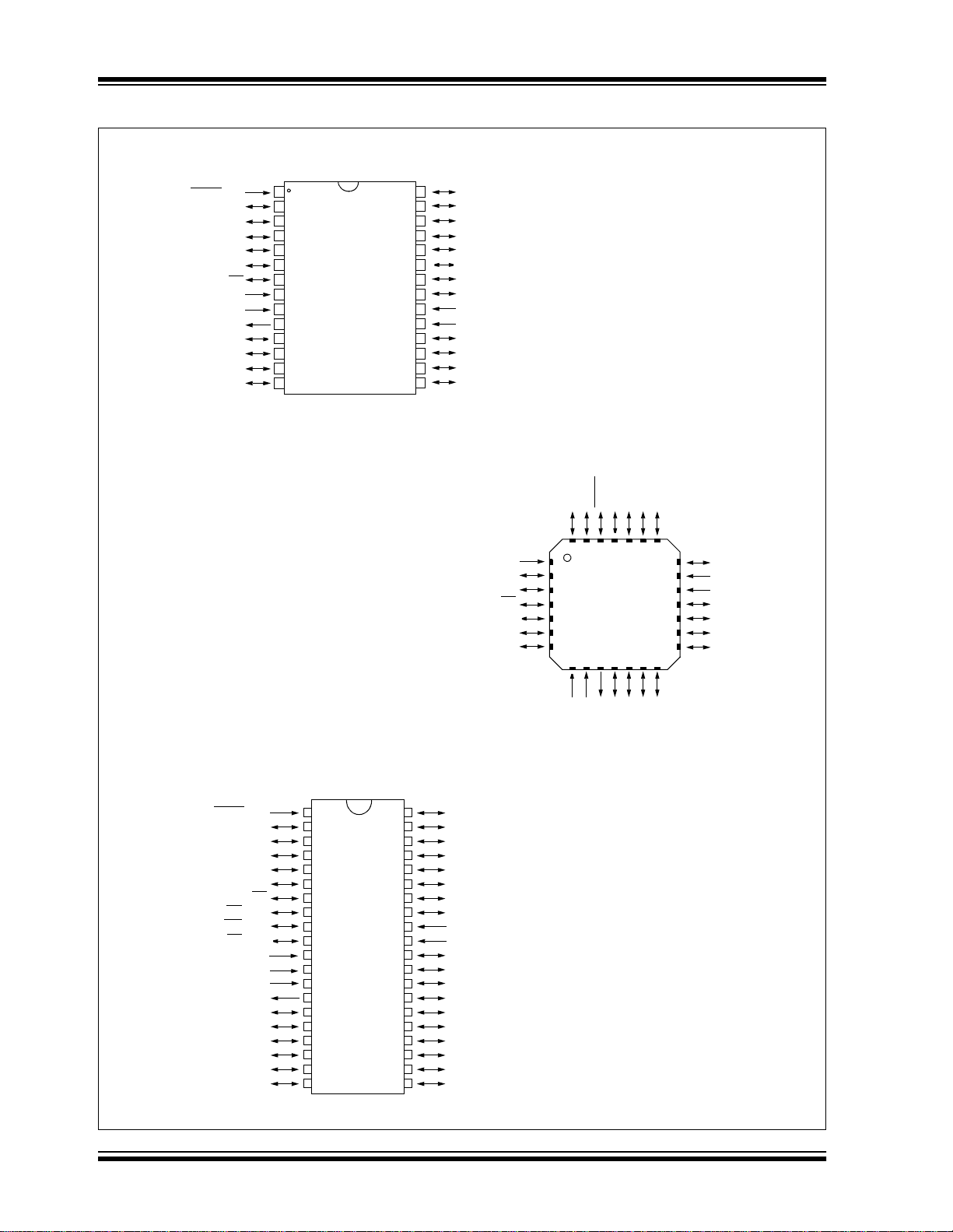
PIC16F7X
Pin Diagrams
DIP, SOIC, SS OP
MCLR/VPP
RA0/AN0
RA1/AN1
RA2/AN2
RA3/AN3/V
OSC1/CLKIN
OSC2/CLKOUT
RC0/T1OSO/T1CKI
RC1/T1OSI/CCP2
RC3/SCK/SCL
REF
RA4/T0CKI
RA5/AN4/SS
VSS
RC2/CCP1
1
2
3
4
5
6
7
8
9
10
11
12
13
14
28
27
26
25
24
23
22
21
20
19
PIC16F76/73
18
17
16
15
RB7/PGD
RB6/PGC
RB5
RB4
RB3/PGM
RB2
RB1
RB0/INT
V
DD
VSS
RC7/RX/DT
RC6/TX/CK
RC5/SDO
RC4/SDI/SDA
MLF
MCLR/VPP
RA0/AN0
RA1/AN1
RB7/PGD
RB6/PGC
RB5
RB4
24
23
26
RA2/AN2
RA3/AN3/V
RA4/T0CKI
RA5/AN4/SS
OSC1/CLKI
OSC2/CLKO
REF
VSS
27
28
1
2
3
PIC16F73
4
PIC16F76
5
6
7
10
912
8
22
25
11
13 14
21
20
19
18
17
16
15
RB3/PGM
RB2
RB1
RB0/INT
DD
V
VSS
RC7/RX/DT
RC5/SDO
PDIP
MCLR/VPP
RA0/AN0
RA1/AN1
RA2/AN2
RA3/AN3/V
RE1/WR
OSC2/CLKOUT
RC0/T1OSO/T1CKI
RC1/T1OSI/CCP2
RC3/SCK/SCL
REF
RA4/T0CKI
RA5/AN4/SS
RE0/RD/AN5
/AN6
RE2/CS
/AN7
DD
V
VSS
OSC1/CLKIN
RC2/CCP1
RD0/PSP0
RD1/PSP1
RC2/CCP1
RC1/T1OSI/CCP2
RC0/T1OSO/T1CKI
1
2
3
4
5
6
7
8
9
10
11
12
13
14
15
16
17
18
19
20
40
39
38
37
36
35
34
33
32
31
30
29
PIC16F77/74
28
27
26
25
24
23
22
21
RB7/PGD
RB6/PGC
RB5
RB4
RB3/PGM
RB2
RB1
RB0/INT
DD
V
VSS
RD7/PSP7
RD6/PSP6
RD5/PSP5
RD4/PSP4
RC7/RX/DT
RC6/TX/CK
RC5/SDO
RC4/SDI/SDA
RD3/PSP3
RD2/PSP2
RC4/SDI/SDA
RC3/SCK/SCL
RC6/TX/CK
DS30325B-page 2 2002 Microchip Technology Inc.
Page 5

Pin Diagrams (Continued)
PLCC
PIC16F7X
/VPP
RA3/AN3/VREF
RA2/AN2
RA1/AN1
RA0/AN0
MCLR
NC
RB7/PGD
RB6/PGC
RB5
RB4
NC
QFP
RA4/T0CKI
RA5/AN4/SS
RE0/RD/AN5
RE1/WR
/AN6
RE2/CS
/AN7
V
DD
VSS
OSC1/CLKIN
OSC2/CLKOUT
RC0/T1OSO/T1CK1
NC
65432
7
8
9
10
11
12
13
14
15
16
17
181920212223242526
RC1/T1OSI/CCP2
RC6/TX/CK
RC5/SDO
1
PIC16F77
PIC16F74
RD2/PSP2
RD1/PSP1
RD0/PSP0
RC2/CCP1
RC3/SCK/SCL
RC4/SDI/SDA
RD3/PSP3
RD2/PSP2
44
RD3/PSP3
RD1/PSP1
RD0/PSP0
41
42
43
27
RC5/SDO
RC6/TX/CK
RC4/SDI/SDA
RC3/SCK/SCL
RC2/CCP1
RC1/T1OSI/CCP2
40
39
38
37
36
35
34
33
32
31
30
29
28
NC
NC
RB3/PGM
RB2
RB1
RB0/INT
V
DD
VSS
RD7/PSP7
RD6/PSP6
RD5/PSP5
RD4/PSP4
RC7/RX/DT
RC7/RX/DT
RD4/PSP4
RD5/PSP5
RD6/PSP6
RD7/PSP7
V
VDD
RB0/INT
RB1
RB2
RB3/PGM
4443424140
1
2
3
4
SS
5
6
7
8
9
10
11
121314
NC
NC
39
PIC16F77
PIC16F74
16
17
15
RB5
RB4
RB7/PGD
RB6/PGC
363435
37
38
1819202122
/VPP
RA2/AN2
RA1/AN1
RA0/AN0
MCLR
33
32
31
30
29
28
27
26
25
24
23
RA3/AN3/VREF
NC
RC0/T1OSO/T1CKI
OSC2/CLKOUT
OSC1/CLKIN
SS
V
VDD
RE2/AN7/CS
RE1/AN6/WR
RE0/AN5/RD
RA5/AN4/SS
RA4/T0CKI
2002 Microchip Technology Inc. DS30325B-page 3
Page 6

PIC16F7X
Table of Contents
1.0 Device Overview......................................................................................................................................................................... 5
2.0 Memory Organization................................................................................................................................................................ 13
3.0 Reading Program Memory........................................................................................................................................................ 29
4.0 I/O Ports.................................................................................................................................................................................... 31
5.0 Timer0 Module................................................................................. .. .... .. .. .. ....... .. .. .... .. ............................................................ 43
6.0 Timer1 Module................................................................................. .. .... .. .. .. ....... .. .. .... .. ............................................................ 47
7.0 Timer2 Module................................................................................. .. .... .. .. .. ....... .. .. .... .. ............................................................ 51
8.0 Capture/Compare/PWM Modules............................................................................................................................................. 53
9.0 Synchronous Serial Port (SSP) Module.................................................................................................................................... 59
10.0 Universal Synchronous Asynchronous Receiver Transmitter (USART) ................................................................................... 69
11.0 Analog-to-Digital Converter (A/D) Module ................................................................................................................................ 83
12.0 Special Features of the CPU .................................................................................................................................................... 89
13.0 Instruction Set Summary......................................................................................................................................................... 105
14.0 Development Support........................................ ....... .... .. .... .. ....... .... .. .... .. .... ....... .. .... .. .... .. ...................................................... 113
15.0 Electrical Characteristics.................................... ............................................. ........................................................................ 119
16.0 DC and AC Characteristics Graphs and Tables ..................................................................................................................... 141
17.0 Packaging Information............................................................................................................................................................ 151
Appendix A: Revision History ........................................................................................................................................................ 161
Appendix B: Device Differences .................................................................................................................................................... 161
Appendix C: Conversion Considerations ........................................................ .. .. ....... .. .... .. .. .... ..... .... ............................................. 162
Index ................................................................................................................................................................................................. 163
On-Line Support...................................................................... .. .... .... ....... .... .... .. .... ....... .... ................................................................ 169
Reader Response............................................................................................................................................................................. 170
PIC16F7X Product Identification System.. ........................................................................................................................................ 171
TO OUR VALUED CUSTOMERS
It is our intention to provide our valued customers with the best documentation possible to ensure successful use of your Microchip
products. To this end, we will continue to improve our publications to better suit your needs. Our publications will be refined and
enhanced as new volumes and updates are introduced.
If you have any questions or c omm ents regarding th is publication, p lease c ontact the M a rketing Communications Department via
E-mail at docerrors@mail.microchip.com or fax the Reader Response Form in the back of this data sheet to (480) 792-4150.
We welcome your feedback.
Most Current Data Sheet
To obtain the most up-to-date version of this data sheet, please register at our Worldwide Web site at:
http://www.microchip.com
You can determine the version of a data sheet by examining its literature number found on the bottom outside corner of any page.
The last character of the literature number is the version number, (e.g., DS30000A is version A of document DS30000).
Errata
An errata sheet, describing minor operational differences from the data sheet and recommended workarounds, may exist for current
devices. As device/documentation issues become known to us, we will publish an errata sheet. The errata will specify the revision
of silicon and revision of document to which it applies.
To determine if an errata sheet exists for a particular device, please check with one of the following:
• Microchip’s Worldwide Web site; http://www.microchip.com
• Your local Microchip sales office (see last page)
• The Microchip Corporate Literature Center; U.S. FAX: (480) 792-7277
When contacting a sales office or the literature center, please specify which device, revision of silicon and data sheet (include literature number) you are using.
Customer Notification System
Register on our web site at www.microchip.com/cn to receive the most current information on all of our products.
DS30325B-page 4 2002 Microchip Technology Inc.
Page 7

PIC16F7X
1.0 DEVICE OVERVIEW
This document contains device specific information
about the following devices:
• PIC16F73
• PIC16F74
• PIC16F76
• PIC16F77
PIC16F73/76 devic es are ava ilable only in 28-pin packages, while PIC16F74/77 devices are available in
40-pin and 44-pin packages. All devices in the
PIC16F7X fam ily sh are co mmon archi tec tur e, wi th the
following differences:
• The PIC16F73 and PIC16F76 have one-half of
the total on-chip memory of the PIC16F74 and
PIC16F77
• The 28-pin devices have 3 I/O ports, while the
40/44-pin devices have 5
• The 28-pin devices have 11 interrupts, while the
40/44-pin devices have 12
• The 28-pin devices have 5 A/D input channels,
while the 40/44-pin devices have 8
• The Parallel Slave Port is implemented only on
the 40/44-pin devices
The available features are summarized in Table 1-1.
Block diagrams of the PIC16F73/76 and PIC16F74/77
devices are provided in Figure 1-1 and Figure1-2,
respectively. The pinouts for these device families are
listed in Table 1-2 and Table 1-3.
Additional information may be found in the PICmicro™
Mid-Range Reference Manual (DS33023), which may
be obtained from your local Microchip Sales Representative or downloaded from the Microchip website. The
Reference Manual should be considered a complementary document to this data sheet, and is highly recommended reading for a better understanding of the device
architecture and operation of the peripheral modules.
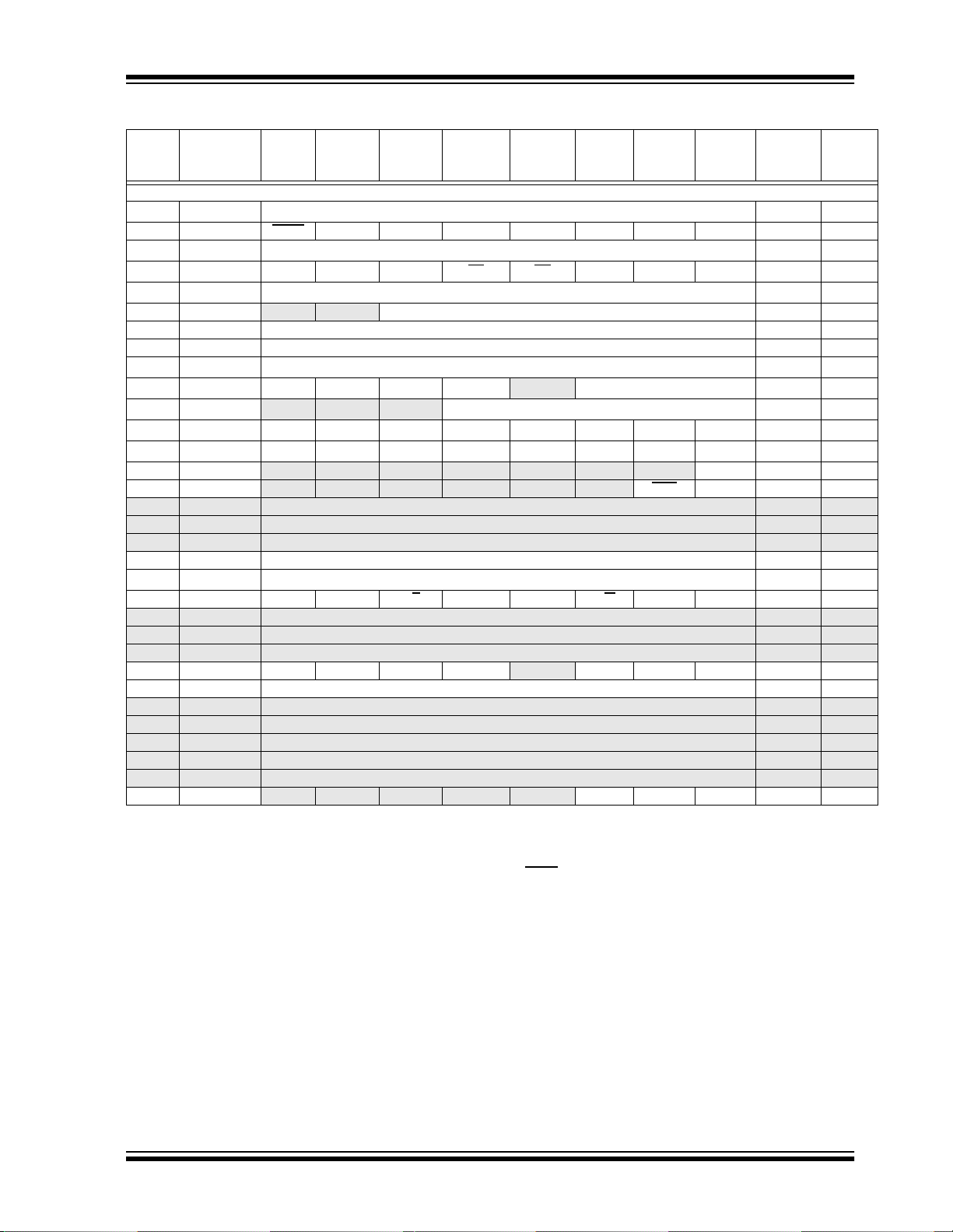
TABLE 1-1: PIC16F7X DEVICE FEATURES
Key Features PIC16F73 PIC16F74 PIC16F76 PIC16F77
Operating Frequency DC - 20 MHz DC - 20 MHz DC - 20 MHz DC - 20 MHz
RESETS (and Delays) POR, BOR
(PWRT, OST)
FLASH Program Memory
(14-bit words)
Data Memory (bytes) 192 192 368 368
Interrupts 11 12 11 12
I/O Ports Ports A,B,C Ports A,B,C,D,E Ports A,B,C Ports A,B,C,D,E
Timers 3333
Capture/Compare/PWM Modules 2 2 2 2
Serial Communications SSP, USART SSP, USART SSP, USART SSP, USART
Parallel Communications — PSP — PSP
8-bit Analog-to-Digital Module 5 Input Channels 8 Input Channels 5 Input Channels 8 Input Channels
Instruction Set 35 Instructions 35 Instructions 35 Instructions 35 Instructions
Packaging 28-pin DIP
4K 4K 8K 8K
28-pin SOIC
28-pin SSOP
28-pin MLF
POR, BOR
(PWRT, OST)
40-pin PDIP
44-pin PLCC
44-pin TQFP
POR, BOR
(PWRT, OST)
28-pin DIP
28-pin SOIC
28-pin SSOP
28-pin MLF
POR, BOR
(PWRT, OST)
40-pin PDIP
44-pin PLCC
44-pin TQFP
2002 Microchip Technology Inc. DS30325B-page 5
Page 8
PIC16F7X
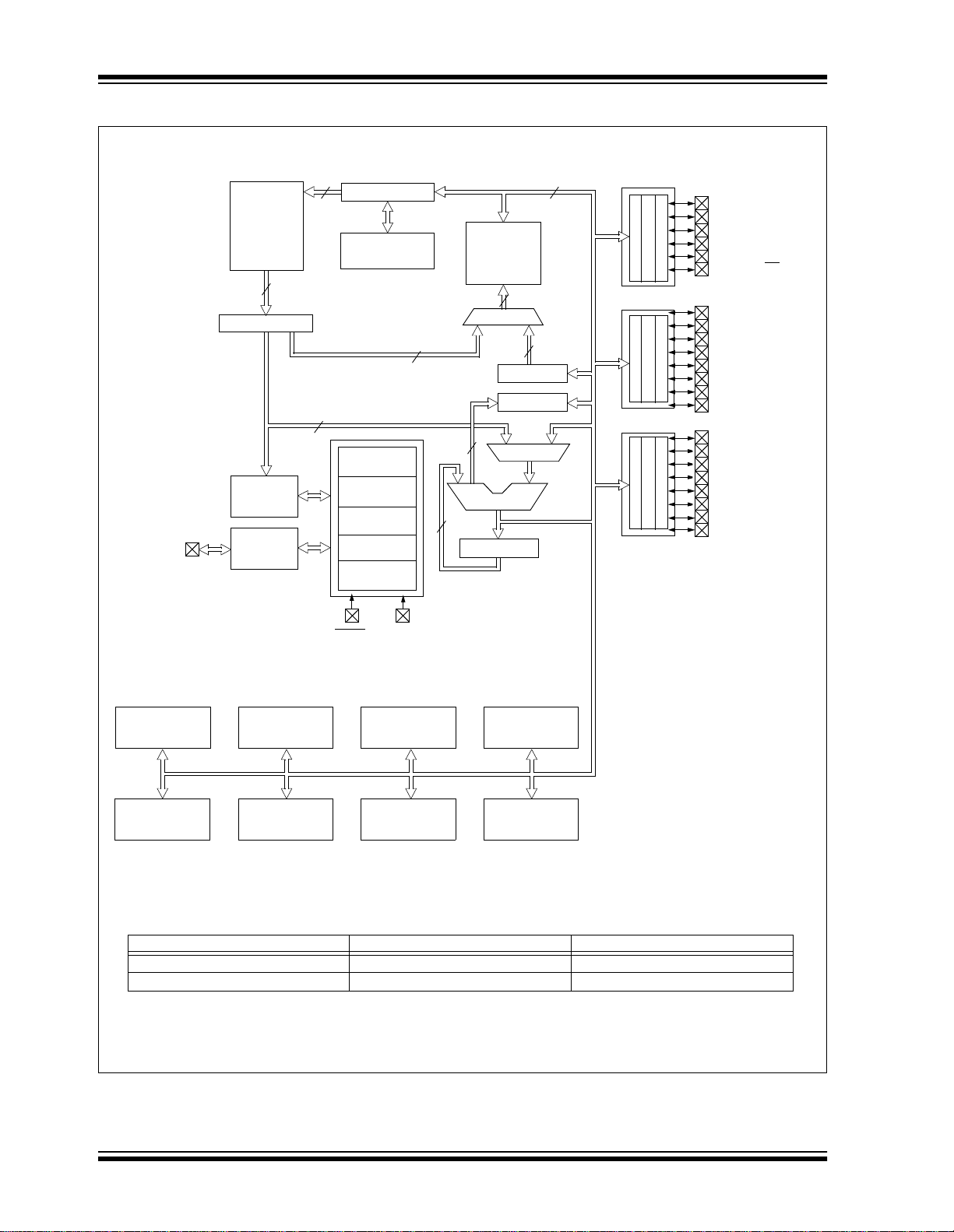
FIGURE 1-1: PIC16F73 AND PIC16F76 BLOCK DIAGRAM
Program
Bus
OSC1/CLKIN
OSC2/CLKOUT
FLASH
Program
Memory
14
Instruction reg
Instruction
Decode &
Control
Timing
Generation
13
Program Counter
8 Level Stack
Direct Addr
8
Power-up
Start-up Timer
Power-on
Watchdog
Brown-out
(13-bit)
Timer
Oscillator
Reset
Timer
Reset
RAM Addr
7
3
8
Data Bus
RAM
File
Registers
(1)
Addr MUX
FSR reg
STATUS reg
ALU
W reg
9
8
MUX
8
Indirect
Addr
PORTA
PORTB
PORTC
RA0/AN0
RA1/AN1
RA2/AN2/
RA3/AN3/VREF
RA4/T0CKI
RA5/AN4/SS
RB0/INT
RB1
RB2
RB3/PGM
RB4
RB5
RB6/PGC
RB7/PGD
RC0/T1OSO/T1CKI
RC1/T1OSI/CCP2
RC2/CCP1
RC3/SCK/SCL
RC4/SDI/SDA
RC5/SDO
RC6/TX/CK
RC7/RX/DT
MCLR
CCP1
Device Program FLASH Data Memory
PIC16F73 4K 192 Bytes
PIC16F76 8K 368 Bytes
Note 1: Higher order bits are from the STATUS register.
CCP2
VDD, VSS
Synchronous
Serial Port
8-bit A/DTimer0 Timer1 Timer2
USART
DS30325B-page 6 2002 Microchip Technology Inc.
Page 9
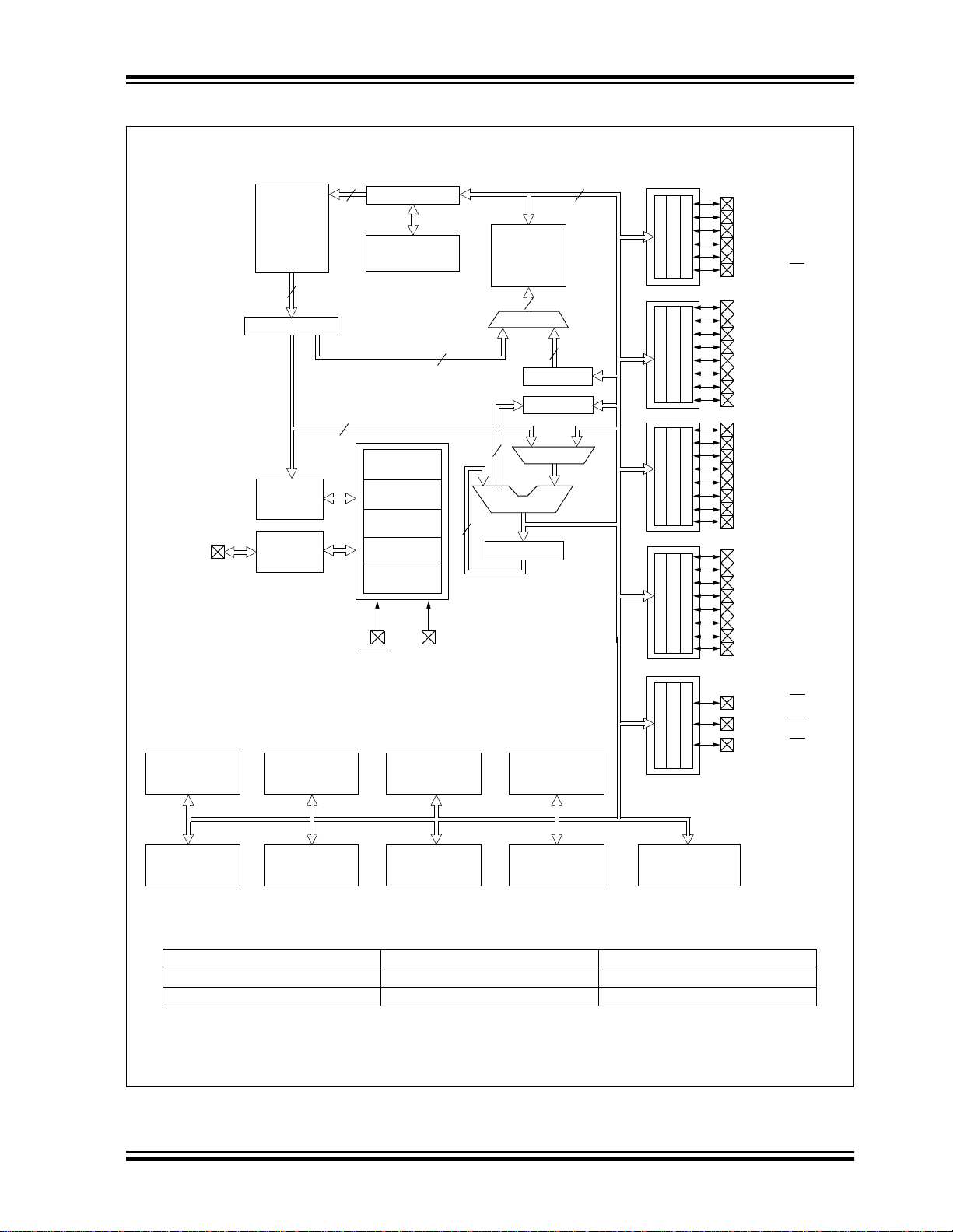
FIGURE 1-2: PIC16F74 AND PIC16F77 BLOCK DIAGRAM
PIC16F7X
Program
Bus
OSC1/CLKIN
OSC2/CLKOUT
FLASH
Program
Memory
14
Instruction reg
Instruction
Decode &
Control
Timing
Generation
13
Program Counter
8 Level Stack
Direct Addr
8
Power-up
Oscillator
Start-up Timer
Power-on
Watchdog
Brown-out
MCLR
(13-bit)
Timer
Reset
Timer
Reset
VDD, VSS
RAM Addr
7
3
8
Data Bus
RAM
File
Registers
(1)
Addr MUX
FSR reg
STATUS reg
ALU
W reg
9
8
MUX
8
Indirect
Addr
PORTA
PORTB
PORTC
PORTD
PORTE
RA0/AN0
RA1/AN1
RA2/AN2
RA3/AN3/VREF
RA4/T0CKI
RA5/AN4/SS
RB0/INT
RB1
RB2
RB3/PGM
RB4
RB5
RB6/PGC
RB7/PGD
RC0/T1OSO/T1CKI
RC1/T1OSI/CCP2
RC2/CCP1
RC3/SCK/SCL
RC4/SDI/SDA
RC5/SDO
RC6/TX/CK
RC7/RX/DT
RD0/PSP0
RD1/PSP1
RD2/PSP2
RD3/PSP3
RD4/PSP4
RD5/PSP5
RD6/PSP6
RD7/PSP7
CCP1
PIC16F74 4K 192 Bytes
PIC16F77 8K 368 Bytes
Note 1: Higher order bits are from the STATUS register.
CCP2
Device Program FLAS H Data Memory
Synchronous
Serial Port
8-bit A/DTimer0 Timer1 Timer2
USART
RE0/AN5/RD
RE1/AN6/WR
RE2/AN7/CS
Parallel Slave Port
2002 Microchip Technology Inc. DS30325B-page 7
Page 10

PIC16F7X
TABLE 1-2: PIC16F73 AND PIC16F76 PINOUT DESCRIPTION
DIP
Pin Name
OSC1/CLKI
OSC1
CLKI
OSC2/CLKO
OSC2
CLKO
/VPP
MCLR
MCLR
VPP
RA0/AN0
RA0
AN0
RA1/AN1
RA1
AN1
RA2/AN2
RA2
AN2
RA3/AN3/V
RA4/T0CKI
RA5/SS/
Legend: I = input O = output I/O = input/output P = power
Note 1: This buffer is a Schmitt Trigger input when configured as the external interrupt.
REF
RA3
AN3
REF
V
RA4
T0CKI
AN4
RA5
SS
AN4
— = Not used TTL = TTL input ST = Schmitt Trigger input
2: Th is buffer is a Schmitt Trigger input when used in Serial Programming mode.
3: Th is buffer is a Schmitt Trigger input when configured in RC Oscillator mode and a CMOS input otherwise.
SSOP
SOIC
Pin#
96
10 7
126
227
328
41
52
64
75
MLF
Pin#
I/O/P
Type
I
I
O
O
I
P
I/O
I
I/O
I
I/O
I
I/O
I
I
I/O
I
I/O
I
I
Buffer
Type
(3)
ST/CMOS
— Oscillator crystal or clock output.
ST Master Clear (input) or programming voltage (output).
TTL
TTL
TTL
TTL
ST
TTL
Oscillator crystal or external clock input.
Oscillator crystal input or external clock source input. ST
buffer when configured in RC mode. Otherwise CMOS.
External clock source input. Always associated with pin
function OSC1 (see OSC1/CLKI, OSC2/CLKO pins).
Oscillator crystal output.
Connects to crystal or resonator in Crystal Oscillator
mode.
In RC mode, OSC2 pin outputs CLKO, which has 1/4 the
frequency of OSC1 and denotes the instruction cycle rate.
Master Clear (Reset) input. This pin is an active low
RESET to the device.
Programming voltage input.
PORTA is a bi-directional I/O port.
Digital I/O.
Analog input 0.
Digital I/O.
Analog input 1.
Digital I/O.
Analog input 2.
Digital I/O.
Analog input 3.
A/D reference voltage input.
Digital I/O – Open drain when configured as output.
Timer0 external clock input.
Digital I/O.
SPI slave select input.
Analog input 4.
Description
DS30325B-page 8 2002 Microchip Technology Inc.
Page 11

TABLE 1-2: PIC16F73 AND PIC16F76 PINOUT DESCRIPTION (CONTINUED)
DIP
Pin Name
RB0/INT
RB0
INT
RB1 22 19
RB2 23 20
RB3/PGM
RB3
PGM
RB4 25 22
RB5 26 23
RB6/PGC
RB6
PGC
RB7/PGD
RB7
PGD
RC0/T1OSO/T1CKI
RC0
T1OSO
T1CKI
RC1/T1OSI/CCP2
RC1
T1OSI
CCP2
RC2/CCP1
RC2
CCP1
RC3/SCK/SCL
RC3
SCK
SCL
RC4/SDI/SDA
RC4
SDI
SDA
RC5/SDO
RC5
SDO
RC6/TX/CK
RC6
TX
CK
RC7/RX/DT
RC7
RX
DT
SS 8, 19 5, 16 P — Ground reference for logic and I/O pins.
V
DD 20 17 P — Positive supply for logic and I/O pins.
V
Legend: I = input O = output I/O = input/output P = power
Note 1: This buffer is a Schmitt Trigger input when configured as the external interrupt.
— = Not used TTL = TTL input ST = Schmitt Trigger input
2: This buffer is a Schmitt Trigger input when used in Serial Programming mode.
3: This buffer is a Schmitt Trigger input when configured in RC Oscillator mode and a CMOS input otherwise.
SSOP
SOIC
Pin#
21 18
24 21
27 24
28 25
11 8
12 9
13 10
14 11
15 12
16 13
17 14
18 15
MLF
Pin#
I/O/P
Type
I/O
I
I/O
I/O
I/O
I/O
I/O
I/O
I/O
I/O
I/O
I/O
I/O
O
I
I/O
I
I/O
I/O
I/O
I/O
I/O
I/O
I/O
I
I/O
I/O
O
I/O
O
I/O
I/O
I
I/O
Buffer
Type
PORTB is a bi-directional I/O port. PORTB can be software
programmed for internal weak pull-up on all inputs.
(1)
TTL/ST
TTL Digital I/O.
TTL Digital I/O.
TTL
TTL Digital I/O.
TTL Digital I/O.
(2)
TTL/ST
(2)
TTL/ST
ST
ST
ST
ST
ST
ST
ST
ST
Digital I/O.
External interrupt.
Digital I/O.
Low voltage ICSP programming enable pin.
Digital I/O.
In-Circuit Debugger and ICSP programming clock.
Digital I/O.
In-Circuit Debugger and ICSP programming data.
PORTC is a bi-directional I/O port.
Digital I/O.
Timer1 oscillator output.
Timer1 external clock input.
Digital I/O.
Timer1 oscillator input.
Capture2 input, Compare2 output, PWM2 output.
Digital I/O.
Capture1 input/Compare1 output/PWM1 output.
Digital I/O.
Synchronous serial clock input/output for SPI mode.
Synchronous serial clock input/output for I
Digital I/O.
SPI data in.
2
I
C data I/O.
Digital I/O.
SPI data out.
Digital I/O.
USART asynchronous transmit.
USART 1 synchronous clock.
Digital I/O.
USART asynchronous receive.
USART synchronous data.
Description
PIC16F7X
2
C mode.
2002 Microchip Technology Inc. DS30325B-page 9
Page 12

PIC16F7X
TABLE 1-3: PIC16F74 AND PIC16F77 PINOUT DESCRIPTION
DIP
Pin Name
OSC1/CLKI
OSC1
CLKI
OSC2/CLKO
OSC2
CLKO
/VPP
MCLR
MCLR
VPP
RA0/AN0
RA0
AN0
RA1/AN1
RA1
AN1
RA2/AN2
RA2
AN2
RA3/AN3/V
RA4/T0CKI
RA5/SS/
Legend: I = input O = output I/O = input/output P = power
Note 1: This buffer is a Schmitt Trigger input when configured as an external interrupt.
REF
RA3
AN3
REF
V
RA4
T0CKI
AN4
RA5
SS
AN4
— = Not used TTL = TTL input ST = Schmitt Trigger input
2: Th is buffer is a Schmitt Trigger input when used in Serial Programming mode.
3: Th is buffer is a Schmitt Trigger input when configured as general purpose I/O and a TTL input when used in the Parallel
Slave Port mode (for interfacing to a microprocessor bus).
4: Th is buffer is a Schmitt Trigger input when configured in RC Oscillator mode and a CMOS input otherwise.
PLCC
Pin#
Pin#
13 14 30
14 15 31
1218
2319
3420
4521
5622
6723
7824
QFP
Pin#
I/O/P
Type
I
I
O
O
I
P
I/O
I
I/O
I
I/O
I
I/O
I
I
I/O
I
I/O
I
I
Buffer
Type
ST/CMOS
(4)
Oscillator crystal or external clock input.
Oscillator crystal input or external clock source input.
ST buffer when configured in RC mode. Otherwise
CMOS.
External clock source input. Always associated with pin
function OSC1 (see OSC1/CLKI, OSC2/CLKO pins).
— Oscillator crystal or clock output.
Oscillator crystal output.
Connects to crystal or resonator in Crystal Oscillator
mode.
In RC mode, OSC2 pin outputs CLKO, which has 1/4
the frequency of OSC1 and denotes the instruction
cycle rate.
ST Master Clear (input) or programming voltage (output).
TTL
TTL
TTL
TTL
ST
TTL
Master Clear (Reset) input. This pin is an active low
RESET to the device.
Programming voltage input.
PORTA is a bi-directional I/O port.
Digital I/O.
Analog input 0.
Digital I/O.
Analog input 1.
Digital I/O.
Analog input 2.
Digital I/O.
Analog input 3.
A/D reference voltage input.
Digital I/O – Open drain when configured as output.
Timer0 external clock input.
Digital I/O.
SPI slave select input.
Analog input 4.
Description
DS30325B-page 10 2002 Microchip Technology Inc.
Page 13

PIC16F7X
TABLE 1-3: PIC16F74 AND PIC16F77 PINOUT DESCRIPTION (CONTINUED)
DIP
Pin Name
RB0/INT
RB0
INT
RB1 34 37 9
RB2 353810
RB3/PGM
RB3
PGM
RB4 374114
RB5 384215
RB6/PGC
RB6
PGC
RB7/PGD
RB7
PGD
RC0/T1OSO/T1CKI
RC0
T1OSO
T1CKI
RC1/T1OSI/CCP2
RC1
T1OSI
CCP2
RC2/CCP1
RC2
CCP1
RC3/SCK/SCL
RC3
SCK
SCL
RC4/SDI/SDA
RC4
SDI
SDA
RC5/SDO
RC5
SDO
RC6/TX/CK
RC6
TX
CK
RC7/RX/DT
RC7
RX
DT
Legend: I = input O = output I/O = input/output P = power
— = Not used TTL = TTL input ST = Schmitt Trigger input
Note 1: This buffer is a Schmitt Trigger input when configured as an external interrupt.
2: This buffer is a Schmitt Trigger input when used in Serial Programming mode.
3: This buffer is a Schmitt Trigger input when configured as general purpose I/O and a TTL input when used in the Parallel
Slave Port mode (for interfacing to a microprocessor bus).
4: This buffer is a Schmitt Trigger input when configured in RC Oscillator mode and a CMOS input otherwise.
PLCC
Pin#
Pin#
33 36 8
36 39 11
39 43 16
40 44 17
15 16 32
16 18 35
17 19 36
18 20 37
23 25 42
24 26 43
25 27 44
26 29 1
QFP
Pin#
I/O/P
Type
I/O
I
I/O
I/O
I/O
I/O
I/O
I/O
I/O
I/O
I/O
I/O
I/O
O
I
I/O
I
I/O
I/O
I/O
I/O
I/O
I/O
I/O
I
I/O
I/O
O
I/O
O
I/O
I/O
I
I/O
Buffer
Type
PORTB is a bi-directional I/O port. PORTB can be software
programmed for internal weak pull-up on all inputs.
(1)
TTL/ST
Digital I/O.
External interrupt.
TTL Digital I/O.
TTL Digital I/O.
TTL
TTL Digital I/O.
TTL Digital I/O.
(2)
TTL/ST
(2)
TTL/ST
ST
ST
ST
ST
ST
ST
ST
ST
Digital I/O.
Low voltage ICSP programming enable pin.
Digital I/O.
In-Circuit Debugger and ICSP programming clock.
Digital I/O.
In-Circuit Debugger and ICSP programming data.
PORTC is a bi-directional I/O port.
Digital I/O.
Timer1 oscillator output.
Timer1 external clock input.
Digital I/O.
Timer1 oscillator input.
Capture2 input, Compare2 output, PWM2 output.
Digital I/O.
Capture1 input/Compare1 output/PWM1 output
Digital I/O
Synchronous serial clock input/output for SPI mode.
Synchronous serial clock input/output for I
Digital I/O.
SPI data in.
2
C data I/O.
I
Digital I/O.
SPI data out.
Digital I/O.
USART asynchronous transmit.
USART 1 synchronous clock.
Digital I/O.
USART asynchronous receive.
USART synchronous data.
Description
2
C mode.
2002 Microchip Technology Inc. DS30325B-page 11
Page 14

PIC16F7X
TABLE 1-3: PIC16F74 AND PIC16F77 PINOUT DESCRIPTION (CONTINUED)
DIP
Pin Name
RD0/PSP0
PLCC
Pin#
Pin#
19 21 38
RD0
PSP0
RD1/PSP1
20 22 39 I
RD1
PSP1
RD2/PSP2
21 23 40 I
RD2
PSP2
RD3/PSP3
22 24 41
RD3
PSP3
RD4/PSP4
27 30 2
RD4
PSP4
RD5/PSP5
28 31 3
RD5
PSP5
RD6/PSP6
29 32 4
RD6
PSP6
RD7/PSP7
30 33 5
RD7
PSP7
RE0/RD
/AN5
8925
RE0
RD
AN5
RE1/WR
/AN6
91026
RE1
WR
AN6
RE2/CS
/AN7
10 11 27
RE2
CS
AN7
SS 12,31 13,34 6,29 P — Ground reference for logic and I/O pins.
V
DD 11,32 12,35 7,28 P — Positive supply for logic and I/O pins.
V
NC — 1,17,2
8, 40
Legend: I = input O = output I/O = input/output P = power
— = Not used TTL = TTL input ST = Schmitt Trigger input
Note 1: This buffer is a Schmitt Trigger input when configured as an external interrupt.
2: Th is buffer is a Schmitt Trigger input when used in Serial Programming mode.
3: Th is buffer is a Schmitt Trigger input when configured as general purpose I/O and a TTL input when used in the Parallel
Slave Port mode (for interfacing to a microprocessor bus).
4: Th is buffer is a Schmitt Trigger input when configured in RC Oscillator mode and a CMOS input otherwise.
QFP
Pin#
12,13,
33, 34
I/O/P
Type
I/O
I/O
I/O
I/O
I/O
I/O
I/O
I/O
I/O
I/O
I/O
I/O
I/O
I/O
I/O
I/O
I/O
I
I
I/O
I
I
I/O
I
I
Buffer
Type
Description
PORTD is a bi-directional I/O port or parallel slave port
when interfacing to a microprocessor bus.
(3)
ST/TTL
Digital I/O.
Parallel Slave Port data.
(3)
ST/TTL
Digital I/O.
Parallel Slave Port data.
(3)
ST/TTL
Digital I/O.
Parallel Slave Port data.
(3)
ST/TTL
Digital I/O.
Parallel Slave Port data.
(3)
ST/TTL
Digital I/O.
Parallel Slave Port data.
(3)
ST/TTL
Digital I/O.
Parallel Slave Port data.
(3)
ST/TTL
Digital I/O.
Parallel Slave Port data.
(3)
ST/TTL
Digital I/O.
Parallel Slave Port data.
PORTE is a bi-directional I/O port.
(3)
ST/TTL
Digital I/O.
Read control for parallel slave port .
Analog input 5.
(3)
ST/TTL
Digital I/O.
Write control for parallel slave port .
Analog input 6.
(3)
ST/TTL
Digital I/O.
Chip select control for parallel slave port .
Analog input 7.
— These pins are not internally connected. These pins should
be left unconnected.
DS30325B-page 12 2002 Microchip Technology Inc.
Page 15

PIC16F7X
2.0 MEMORY ORGANIZATION
There are two memory blocks in each of these
PICmicro
Memory have separate buses so that concurrent
access can oc cur and is detailed in this section. The
Program Mem ory can be read i ntern ally by user co de
(see Section 3.0).
Additional informa tion on devi ce memory may be found
in the PICmicro Mid-Range Reference Manual
(DS33023).
2.1 Program Memory Organization
The PIC16F7X devices have a 13-bit program counter
capable of addressing an 8K word x 14-bit program
memory space. The PIC16F77/76 devices have
8K words of FLASH program memory and the
PIC16F73/74 devices have 4K words. The program
memory maps for PIC16F7X devices are shown in
Figure 2-1. Accessing a location above the physically
implemented address will cause a wraparound.
The RESET Ve ctor is at 0000h an d the Interrup t V ector
is at 0004h.
®
MCUs. The Program Memory and Data
2.2 Data Memory Organization
The Data Memory is partitioned into multiple banks,
which contain the General Purpose Registers and the
Special Function Registers. Bits RP1 (STATUS<6>)
and RP0 (STATUS<5>) are the bank select bits:
RP1:RP0 Bank
00 0
01 1
10 2
11 3
Each bank extends up to 7Fh (128 bytes). The lower
locations of each bank are reserved for the Special
Function Registers. Abo ve the Speci al Function Re gisters are General Purpose Registers, implemented as
static RAM. All implemented banks contain Special
Function Registers. Some frequently used Special
Function Registers from one bank may be mirrored in
another bank for code reduction and quicker access.
2.2.1 GENERAL PURPOSE REGISTER FILE
The register file (shown in Figure 2-2 and Figure 2-3)
can be accessed either directly, or indirectly, through
the File Select Register FSR.
FIGURE 2-1: PROGRAM MEMORY MAPS AND STACKS FOR PIC16F7X DEVICES
CALL, RETURN
RETFIE, RETLW
On-Chip
Program
Memory
PIC16F76/77
PC<12:0>
Stack Level 1
Stack Level 2
Stack Level 8
RESET Vector
Interrupt Vector
Page 0
Page 1
Page 2
Page 3
13
0000h
0004h
0005h
07FFh
0800h
0FFFh
1000h
17FFh
1800h
1FFFh
CALL, RETURN
RETFIE, RETLW
On-Chip
Program
Memory
PIC16F73/74
PC<12:0>
13
Stack Level 1
Stack Level 2
Stack Level 8
RESET Vector
Interrupt Vector
Page 0
Page 1
Unimplemented
Read as ‘0’
0000h
0004h
0005h
07FFh
0800h
0FFFh
1000h
1FFFh
2002 Microchip Technology Inc. DS30325B-page 13
Page 16

PIC16F7X
FIGURE 2-2: PIC16F77/76 REGIST ER FIL E MAP
Indirect addr.(*)
TMR0
PCL
STATUS
FSR
PORTA
PORTB
PORTC
PORTD
PORTE
SSPBUF
SSPCON
CCPR1L
CCPR1H
CCP1CON
CCP2CON
ADCON0
(1)
(1)
PCLATH
INTCON
PIR1
PIR2
TMR1L
TMR1H
T1CON
TMR2
T2CON
RCSTA
TXREG
RCREG
CCPR2L
CCPR2H
ADRES
File
Address
00h
01h
02h
03h
04h
05h
06h
07h
08h
09h
0Ah
0Bh
0Ch
0Dh
0Eh
0Fh
10h
11h
12h
13h
14h
15h
16h
17h
18h
19h
1Ah
1Bh
1Ch
1Dh
1Eh
1Fh
20h
Indirect addr.(*)
OPTION_REG
PCL
STATUS
FSR
TRISA
TRISB
TRISC
(1)
TRISD
(1)
TRISE
PCLATH
INTCON
PIE1
PIE2
PCON
PR2
SSPADD
SSPSTAT
TXSTA
SPBRG
ADCON1
File
Address
80h
81h
82h
83h
84h
85h
86h
87h
88h
89h
8Ah
8Bh
8Ch
8Dh
8Eh
8Fh
90h
91h
92h
93h
94h
95h
96h
97h
98h
99h
9Ah
9Bh
9Ch
9Dh
9Eh
9Fh
A0h
Indirect addr.(*)
TMR0
PCL
STATUS
FSR
PORTB
PCLATH
INTCON
PMDATA
PMADR
PMDATH
PMADRH
General
Purpose
Register
16 Bytes
File
Address
100h
101h
102h
103h
104h
105h
106h
107h
108h
109h
10Ah
10Bh
10Ch
10Dh
10Eh
10Fh
110h
111h
112h
113h
114h
115h
116h
117h
118h
119h
11Ah
11Bh
11Ch
11Dh
11Eh
11Fh
120h
Indirect addr .(*)
OPTION_REG
PCL
STATUS
FSR
TRISB
PCLATH
INTCON
PMCON1
General
Purpose
Register
16 Bytes
File
Address
180h
181h
182h
183h
184h
185h
186h
187h
188h
189h
18Ah
18Bh
18Ch
18Dh
18Eh
18Fh
190h
191h
192h
193h
194h
195h
196h
197h
198h
199h
19Ah
19Bh
19Ch
19Dh
19Eh
19Fh
1A0h
General
Purpose
Register
96 Bytes
7Fh
Bank 0
U nimplemented data memory locations, read as ’0’.
* Not a physical register.
Note 1: These registers are not implemented on 28-pin devi ce s.
DS30325B-page 14 2002 Microchip Technology Inc.
General
Purpose
Register
80 Bytes 80 Bytes 80 Bytes
accesses
70h-7Fh
Bank 1
EFh
F0h
FFh
General
Purpose
Register
accesses
70h-7Fh
Bank 2
16Fh
170h
17Fh
General
Purpose
Register
accesses
70h - 7Fh
Bank 3
1EFh
1F0h
1FFh
Page 17

FIGURE 2-3: PIC16F74/73 REGIST ER FIL E MAP
PIC16F7X
Indirect addr.(*)
TMR0
PCL
STATUS
FSR
PORTA
PORTB
PORTC
PORTD
PORTE
SSPCON
CCP1CON
CCP2CON
(1)
(1)
PCLATH
INTCON
PIR1
PIR2
TMR1L
TMR1H
T1CON
TMR2
T2CON
SSPBUF
CCPR1L
CCPR1H
RCSTA
TXREG
RCREG
CCPR2L
CCPR2H
ADRES
ADCON0
File
Address
00h
01h
02h
03h
04h
05h
06h
07h
08h
09h
0Ah
0Bh
0Ch
0Dh
0Eh
0Fh
10h
11h
12h
13h
14h
15h
16h
17h
18h
19h
1Ah
1Bh
1Ch
1Dh
1Eh
1Fh
20h
Indirect addr.(*)
OPTION_REG
PCL
STATUS
FSR
TRISA
TRISB
TRISC
(1)
TRISD
(1)
TRISE
PCLATH
INTCON
PIE1
PIE2
PCON
PR2
SSPADD
SSPSTAT
TXSTA
SPBRG
ADCON1
File
Address
80h
81h
82h
83h
84h
85h
86h
87h
88h
89h
8Ah
8Bh
8Ch
8Dh
8Eh
8Fh
90h
91h
92h
93h
94h
95h
96h
97h
98h
99h
9Ah
9Bh
9Ch
9Dh
9Eh
9Fh
A0h
Indirect addr.(*)
TMR0
PCL
STATUS
FSR
PORTB
PCLATH
INTCON
PMDATA
PMADR
PMDATH
PMADRH
File
Address
100h
101h
102h
103h
104h
105h
106h
107h
108h
109h
10Ah
10Bh
10Ch
10Dh
10Eh
10Fh
110h
120h
Indirect addr.(*)
OPTION_REG
PCL
STATUS
FSR
TRISB
PCLATH
INTCON
PMCON1
File
Address
180h
181h
182h
183h
184h
185h
186h
187h
188h
189h
18Ah
18Bh
18Ch
18Dh
18Eh
18Fh
190h
1A0h
General
Purpose
Register
96 Bytes
7Fh
Bank 0
Unimplemented data memory locations, read as ’0’.
* Not a physical register .
Note 1: These registers are not implemented on 28-pin devices.
2002 Microchip Technology Inc. DS30325B-page 15
General
Purpose
Register
96 Bytes
Bank 1
FFh
accesses
20h-7Fh
Bank 2
16Fh
170h
17Fh
accesses
A0h - FFh
1EFh
1F0h
1FFh
Bank 3
Page 18
PIC16F7X
2.2.2 SPECIAL FUNCTION REGISTERS
The Special Function Registers are registers used by
the CPU and peripheral modules for controlling the
desired operation of the device. These registers are
implemented as static RAM. A list of these registers is
given in Table 2-1.
The Special Function Registers can be classified into
two sets: core (CPU) and peripheral. Those registers
associated with the core functions are described in
detail in this section. Those related to the operation of
the peripheral features are described in detail in the
peripheral feature section.
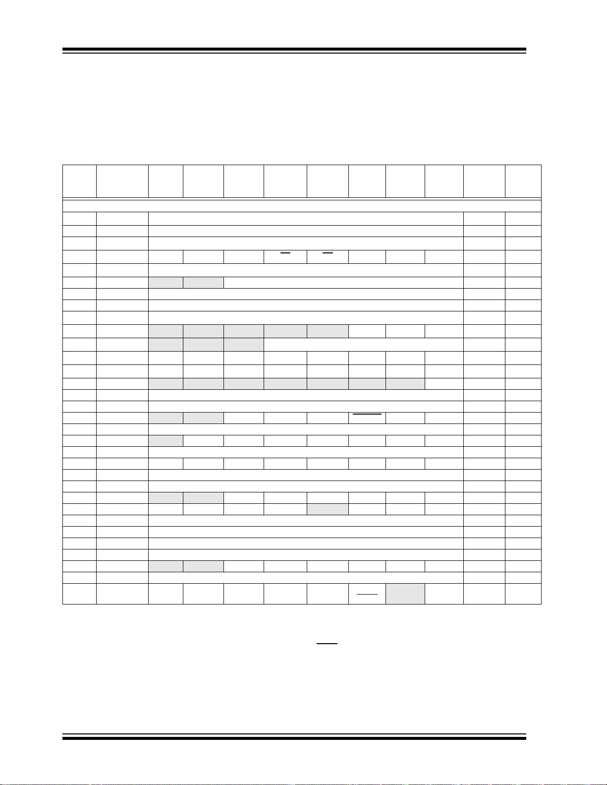
TABLE 2-1: SPECIAL FUNCTION REGISTER SUMMARY
Address Name Bit 7 Bit 6 Bit 5 Bit 4 Bit 3 Bit 2 Bit 1 Bit 0
Value on:
POR,
BOR
Bank 0
(4)
00h
01h TMR0 Timer0 Module Register
02h
03h
04h
05h PORTA — — PORT A Data Latch when written: PORTA pins when read --0x 0000 32, 96
06h PORTB PORTB Data Latch when written: PORTB pins when read
07h PORTC PORTC Data Latch when written: PORTC pins when read
08h
09h
0Ah
0Bh
0Ch PIR1
0Dh PIR2 — — — — — — — CCP2IF ---- ---0 24, 96
0Eh TMR1L Holding Register for the Least Significant Byte of the 16-bit TMR1 Register
0Fh TMR1H Holding Register for the Most Significant Byte of the 16-bit TMR1 Register
10h T1CON — — T1CKPS1 T1CKPS0 T1OSCEN T1SYNC TMR1CS TMR1ON
11h TMR2 Timer2 Module Register
12h T2CON — TOUTPS3 TOUTPS2 TOUTPS TOUTPS0 TMR2ON T2CKPS1 T2CKPS0
13h SSPBUF Synchronous Serial Port Receive Buffer/Transmit Register xxxx xxxx 6 4, 68, 96
14h SSPCON WCOL SSPOV SSPEN CKP SSPM3 SSPM2 SSPM1 SSPM0
15h CCPR1L Capture/Compare/PWM Register1 (LSB)
16h CCPR1H Capture/Compare/PWM Register1 (MSB)
17h CCP1CON — — CCP1X CCP1Y CCP1M3 CCP1M2 CCP1M1 CCP1M0
18h RCSTA SPEN RX9 SREN CREN — FERR OERR RX9D
19h TXREG USART Transmit Data Register 0000 0000 74, 96
1Ah RCREG USART Receiv e Dat a Reg i ste r 0000 0000 76, 96
1Bh CCPR2L Capture/Compare/PWM Register2 (LSB)
1Ch CCPR2H Capture/Compare/PWM Register2 (MSB)
1Dh CCP2CON — — CCP2X CCP2Y CCP2M3 CCP2M2 CCP2M1 CCP2M0
1Eh ADRES A/D Result Registe r Byt e
1Fh ADCON0 ADCS1 ADCS0 CHS2 CHS1 CHS0
Legend: x = unknown, u = unchanged, q = value depends on condition, - = unimplemented, read as '0', r = reserved.
Note 1: The upper byte of the program counter is not directly ac cessible. PCLATH is a holding register for the PC<12:8>, whose
INDF Addressing this location uses contents of FSR to address data memory (not a physical register)
(4)
PCL Program Counter (PC) Least Significant Byte
(4)
STATUS IRP RP1 RP0 TO PD ZDCC
(4)
FSR Indirect Data Memory Address Pointer
(5)
PORTD PORTD Data Latch when written: PORTD pins when read
(5)
PORTE — — — — — RE2 RE1 RE0
(1,4)
PCLATH — — — Write Buffer for the upper 5 bits of the Program Counter
(4)
INTCON GIE PEIE TMR0IE INTE RBIE TMR0IF INTF RBIF
(3)
PSPIF
Shaded locations are unimplemented, read as ‘0’.
contents are transferred to the upper byte of the program counter du ring branches (
2: Other (non power-up) RESETS include external RESET through MCLR
3: Bits PSPIE and PSPIF are reserved on the 28-pin devices; always maintain these bits clea r.
4: These registers can be addressed from any bank.
5: PORTD, PORTE, TRISD, and TRISE are not physically implemented on the 28-pin devices, read as ‘0’.
6: This bit always reads as a ‘1’.
ADIF RCIF TXIF SSPIF CCP1IF TMR2IF TMR1IF
GO/
DONE
and Watchdog Timer Reset.
— ADON
CALL or GOTO).
0000 0000 27, 96
xxxx xxxx 45, 96
0000 0000 26, 96
0001 1xxx 19, 96
xxxx xxxx 27, 96
xxxx xxxx 34, 96
xxxx xxxx 35, 96
xxxx xxxx 36, 96
---- -xxx 39, 96
---0 0000 26, 96
0000 000x 21, 96
0000 0000 23, 96
xxxx xxxx 50, 96
xxxx xxxx 50, 96
--00 0000 47, 96
0000 0000 52, 96
-000 0000 52, 96
0000 0000 61, 96
xxxx xxxx 56, 96
xxxx xxxx 56, 96
--00 0000 54, 96
0000 -00x 70, 96
xxxx xxxx 58, 96
xxxx xxxx 58, 96
--00 0000 54, 96
xxxx xxxx 88, 96
0000 00-0 83, 96
Details
on page
DS30325B-page 16 2002 Microchip Technology Inc.
Page 19
PIC16F7X
TABLE 2-1: SPECIAL FUNCTION REGISTER SUMMARY (CONTINUED)
Address Name Bit 7 Bit 6 Bit 5 Bit 4 Bit 3 Bit 2 Bit 1 Bit 0
POR,
BOR
Value on:
Bank 1
(4)
80h
INDF Addressing this location uses contents of FSR to address data memory (not a physical register)
81h OPTION_REG RBPU INTEDG T0CS T0SE PSA PS2 PS1 PS0
(4)
82h
83h
84h
PCL Program Counter’s (PC) Least Significant Byte
(4)
STATUS IRP RP1 RP0 TO PD ZDCC0001 1xxx 19, 96
(4)
FSR Indirect data memory address pointer
85h TRISA — — PORTA Data Direction Register
86h TRISB PORTB Data Direction Register
87h TRISC PORTC Data Direction Register
(5)
88h
89h
8Ah
8Bh
8Ch PIE1
TRISD PORTD Data Direction Register
(5)
TRISE IBF OBF IBOV PSPMODE — PORTE Data Direction Bits 0000 -111 38, 96
(1,4)
PCLATH — — — Write Buffer for the upper 5 bits of the Program Counter
(4)
INTCON GIE PEIE TMR0IE INTE RBIE TMR0IF INTF RBIF 0000 000x 23, 96
(3)
PSPIE
ADIE RCIE TXIE SSPIE CCP1IE TMR2IE TMR1IE
8Dh PIE2 — — — — — — — CCP2IE
8Eh PCON — — — — — — POR BOR
8Fh — Unimplemented
90h — Unimplemented
0000 0000 27, 96
1111 1111 2 0, 44, 96
0000 0000 26, 96
xxxx xxxx 27, 96
--11 1111 32, 96
1111 1111 34, 96
1111 1111 35, 96
1111 1111 36, 96
---0 0000 21, 96
0000 0000 22, 96
---- ---0 24, 97
---- --qq 25, 97
— —
— —
91h — Unimplemented — —
92h PR2 Timer2 Period Register 1111 1111 52, 97
93h SSPADD
Synchronous Serial Port (I
94h SSPSTAT SMP CKE D/A PSR/WUA BF
2
C mode) Address Register
0000 0000 68, 97
0000 0000 60, 97
95h — Unimplemented — —
96h — Unimplemented — —
97h — Unimplemented
98h TXSTA CSRC TX9 TXEN SYNC — BRGH TRMT TX9D
99h SPBRG Baud Rate Generator Register
9Ah — Unimplemented
9Bh — Unimplemented
— —
0000 -010 69, 97
0000 0000 71, 97
—
—
9Ch — Unimplemented —
9Dh — Unimplemented
9Eh — Unimplemented
9Fh ADCON1 — — — — — PCFG2 PCFG1 PCFG0
Legend:
x = unknown, u = unchanged, q = value depends on condition, - = unimplemented, read as '0' , r = reserved.
—
—
---- -000 84, 97
Shaded locations are unimplemented, read as ‘0’.
Note 1: The upper byte of the program counter is not directly ac cessible. PCLATH is a holding register for the PC<12:8>, whose
contents are transferred to the upper byte of the program counter during branches (
2: Other (non power-up) RESETS include external RESET through MCLR
and Watchdog Timer Reset.
CALL or GOTO).
3: Bits PSPIE and PSPIF are reserved on the 28-pin devices; always maintain these bits clea r.
4: These registers can be addressed from any bank.
5: PORTD, PORTE, TRISD, and TRISE are not physically implemented on the 28-pin devices, read as ‘0’.
6: This bit always reads as a ‘1’.
Details
on page
2002 Microchip Technology Inc. DS30325B-page 17
Page 20

PIC16F7X
TABLE 2-1: SPECIAL FUNCTION REGISTER SUMMARY (CONTINUED)
Address Name Bit 7 Bit 6 Bit 5 Bit 4 Bit 3 Bit 2 Bit 1 Bit 0
POR,
BOR
Value on:
Bank 2
(4)
100h
INDF Addressing this location uses contents of FSR to address data memory (not a physical register)
101h TMR0 Timer0 Module Register
(4)
102h
103h
104h
PCL Program Counter (PC) Least Significant Byte
(4)
STATUS IRP RP1 RP0 TO PD ZDCC0001 1xxx 19, 96
(4)
FSR Indirect Data Memory Address Pointer
105h — Unimplemented
106h PORTB PORTB Data Latch when written: PORTB pins when read
107h — Unimplemented
108h — Unimplemented
0000 0000 27, 96
xxxx xxxx 45, 96
0000 0000 26, 96
xxxx xxxx 27, 96
— —
xxxx xxxx 34, 96
— —
— —
109h — Unimplemented — —
10Ah
10Bh
(1,4)
PCLATH — — — Write Buffer for the upper 5 bits of the Program Counter
(4)
INTCON GIE PEIE TMR0IE INTE RBIE TMR0IF INTF RBIF
---0 0000 21, 96
0000 000x 23, 96
10Ch PMDATA Data Register Low Byte xxxx xxxx 29, 97
10Dh PMADR Address Register Low Byte
10Eh PMDA TH — — Data Register High Byte
10Fh PMADRH — — — Address Register High Byte
xxxx xxxx 29, 97
xxxx xxxx 29, 97
xxxx xxxx
Bank 3
(4)
180h
INDF Addressing this location uses contents of FSR to address data memory (not a physical register)
181h OPTION_REG RBPU INTEDG T0CS T0SE PSA PS2 PS1 PS0
(4)
182h
183h
184h
PCL Program Counter (PC) Least Significant Byte 0000 0000 26, 96
(4)
STATUS IRP RP1 RP0 TO PD ZDCC
(4)
FSR Indirect Data Memory Address Pointer xxxx xxxx 27, 96
185h — Unimplemented — —
186h TRISB PORTB Data Direction Register 1111 1111 34, 96
187h — Unimplemented
188h — Unimplemented
189h — Unimplemented
(1,4)
18Ah
18Bh
PCLATH — — —
(4)
INTCON GIE PEIE TMR0IE INTE RBIE TMR0IF INTF RBIF
18Ch PMCON1
—
(6)
— — — — — — RD
Write Buffer for the upper 5 bits of the Program Counter
18Dh — Unimplemented
18Eh — Reserved maintain clear
18Fh — Reserved maintain clear
Legend:
x = unknown, u = unchanged, q = value depends on condition, - = unimplemented, read as '0', r = reserved.
Shaded locations are unimplemented, read as ‘0’.
Note 1: The upper byte of the program counter is not directly ac cessible. PCLATH is a holding register for the PC<12:8>, whose
contents are transferred to the upper byte of the program counter du ring branches (
2: Other (non power-up) RESETS include external RESET through MCLR
and Watchdog Timer Reset.
CALL or GOTO).
3: Bits PSPIE and PSPIF are reserved on the 28-pin devices; always maintain these bits clea r.
4: These registers can be addressed from any bank.
5: PORTD, PORTE, TRISD, and TRISE are not physically implemented on the 28-pin devices, read as ‘0’.
6: This bit always reads as a ‘1’.
0000 0000 27, 96
1111 1111 2 0, 44, 96
0001 1xxx 19, 96
— —
— —
— —
---0 0000 21, 96
0000 000x 23, 96
1--- ---0 29, 97
—
0000 0000
0000 0000
Details
on page
29, 97
DS30325B-page 18 2002 Microchip Technology Inc.
Page 21
PIC16F7X
2.2.2.1 STATUS Register
The STATUS register contains the arithmetic status of
the ALU, the RESET statu s and the ba nk sele ct bit s for
data memory.
The STATUS register can be the destination for any
instruction, as with any other register. If the STATUS
register is the destination for an instruction that affects
the Z, DC, or C bits, then the wri te to thes e three bi ts is
disabled. These bit s are set or cleared ac cording to the
device logic. Furthermore, the TO
writable, therefore, the result of an instruction with the
STATUS regist er as destinat ion may be differen t than
intended.
and PD bits are not
For example, CLRF STATUS will clear the upper three
bits and set the Z bit. This leaves the STATUS register
as 000u u1uu (where u = unchanged).
It is recommended, therefore, that only BCF, BSF,
SWAPF and MOVWF instructions are used to alter the
STATUS register, because these instructions do not
affect the Z, C, or DC bits from the STATUS register.
For other in s tru ct i o ns no t aff ec t in g an y s tat us b its, s ee
the "Instruction Set Summary."
Note 1: The C and DC bits operate as a borrow
and digit borrow bit, respectively, in subtraction. See the SUBLW and SUBWF
instructions for examples.
REGISTER 2-1: STATUS REGISTER (ADDRESS 03h, 83h, 103h, 183h)
R/W-0 R/W-0 R/W-0 R-1 R-1 R/W-x R/W-x R/W-x
IRP RP1 RP0 TO
bit 7 bit 0
bit 7 IRP: Register Bank Select bi t (used for indirect addr essing)
1 = Bank 2, 3 (100h - 1FFh)
0 = Bank 0, 1 (00h - FFh)
bit 6-5 RP1:RP0: Register Bank Select bits (used for direct addressing)
11 = Bank 3 (180h - 1FFh)
10 = Bank 2 (100h - 17Fh)
01 = Bank 1 (80h - FFh)
00 = Bank 0 (00h - 7Fh)
Each bank is 128 bytes
bit 4 TO
bit 3 PD
bit 2
bit 1 DC: Digit carry/borrow
bit 0 C: Carry/borrow
: Time-out bit
1 = After power-up, CLRWDT instruction, or SLEEP instruction
0 = A WDT time-out occurred
: Power-down bit
1 = After power-up or by the CLRWDT instruction
0 = By execution of the SLEEP instruction
Z: Zero bit
1 = The result of an arithmetic or logic operation is zero
0 = The result of an arithmetic or logic operation is not zero
bit (ADDWF, ADDLW, SUBLW, SUBWF instructions)
1 = A carry-out from the 4th low order bit of the result occurred
0 = No carry-out from the 4th low order bit of the result
bit (ADDWF, ADDLW, SUBLW, SUBWF instructions)
1 = A carry-out from the Most Significant bit of the result occurred
0 = No carry-out from the Most Significant bit of the result occurred
PD ZDCC
Note: For borrow
complement of the second operand. For rotate (RRF, RLF) instructions, this bit is
loaded with either the high or low order bit of the source register.
Legend:
R = Readable bit W = Writable bit U = Unimplemented bit, read as ‘0’
- n = Value at POR reset ’1’ = Bit is set ’0’ = Bit is cleared x = Bit is unknown
2002 Microchip Technology Inc. DS30325B-page 19
, the polarity is reversed. A subtraction is executed by adding the two’s
Page 22

PIC16F7X
2.2.2.2 OPTION_REG Register
The OPTION_REG register is a readable and writable
register , which cont ains various contr ol bits to conf igure
the TMR0 prescaler/WDT postscaler (single assignable register k nown als o as th e presca ler), t he Externa l
INT Interrupt, TMR0 and the w eak pull-up s on POR TB.
Note: To achieve a 1:1 prescaler assignment for
the TMR0 register, assign the prescaler to
the Watchdog Timer.
REGISTER 2-2: OPTION_REG REGISTER (ADDRESS 81h, 181h)
R/W-1 R/W-1 R/W-1 R/W-1 R/W-1 R/W-1 R/W-1 R/W-1
RBPU
bit 7 bit 0
bit 7 RBPU
1 = PORTB pull-ups are disabled
0 = PORTB pull-ups are enabled by individual port latch values
bit 6 INTEDG: Interrupt Edge Select bit
1 = Interrupt on rising edge of RB0/INT pin
0 = Interrupt on falling edge of RB0/INT pin
bit 5 T0CS: TMR0 Clock Source Select bit
1 = Transition on RA4/T0CKI pin
0 = Internal instruction cycle clock (CLKOUT)
bit 4 T0SE: TMR0 Source Edge Select bit
1 = Increment on high-to-low transition on RA4/T0CKI pin
0 = Increment on low-to-high transition on RA4/T0CKI pin
bit 3 PSA: Prescaler Assignment bit
1 = Prescaler is assigned to the WDT
0 = Prescaler is assigned to the Timer0 module
bit 2-0 PS2:PS0: Prescaler Rate Select bits
INTEDG T0CS T0SE PSA PS2 PS1 PS0
: PORTB Pull-up Enable bit
Bit Value TMR0 Rate WDT Rate
000
001
010
011
100
101
110
111
1 : 2
1 : 4
1 : 8
1 : 16
1 : 32
1 : 64
1 : 128
1 : 256
1 : 1
1 : 2
1 : 4
1 : 8
1 : 16
1 : 32
1 : 64
1 : 128
Legend:
R = Readable bit W = Writable bit U = Unimplemented bit, read as ‘0’
- n = Value at POR reset ’1’ = Bit is set ’0’ = Bit is cleared x = Bit is unknown
DS30325B-page 20 2002 Microchip Technology Inc.
Page 23

PIC16F7X
2.2.2.3 INTCON Register
The INTCON register is a readable and writable register, which contains various enable and flag bits for the
TMR0 register overflow, RB Port change and External
RB0/INT pin interrupts.
Note: Interrupt flag bits are set when an interru pt
condition occurs, re gardless of the state of
its corresponding enable bit or the global
enable bit, GIE (INTCON<7>). User software should ensure the appropriate interrupt flag bits are clear prior to enabling an
interrupt.
REGISTER 2-3: INTCON REGISTER (ADDRESS 0Bh, 8Bh, 10Bh, 18Bh)
R/W-0 R/W-0 R/W-0 R/W-0 R/W-0 R/W-0 R/W-0 R/W-x
GIE PEIE TMR0IE INTE RBIE TMR0IF INTF RBIF
bit 7 bit 0
bit 7 GIE: Glob al Interrupt Enable bit
1 = Enables all unmasked interrupts
0 = Disables all interrupts
bit 6 PEIE: Peripheral Interrupt Enable bit
1 = Enables all unmasked peripheral interrupts
0 = Disables all peripheral interrupts
bit 5 TMR0IE: TMR0 Overflow Interrupt Enable bit
1 = Enables the TMR0 interrupt
0 = Disables the TMR0 interrupt
bit 4 INTE: RB0/INT External Interrupt Enable bit
1 = Enables the RB0/INT external interrupt
0 = Disables the RB0/INT external interrupt
bit 3 RBIE: RB Port Change Interrupt Enable bit
1 = Enables the RB port change interrupt
0 = Disables the RB port change interrupt
bit 2 TMR0IF: TMR0 Overflow Interrupt Flag bit
1 = TMR0 register has overflowed (must be cleared in software)
0 = TMR0 register did not overflow
bit 1 INTF: RB0/INT External Interrupt Flag bit
1 = The RB0/INT external interrupt occurred (must be cleared in software)
0 = The RB0/INT external interrupt did not occur
bit 0 RBIF: RB Port Change Interrupt Flag bit
A mismatch condition wi ll cont inu e to set flag b it RBIF. Reading PORTB will end the mis match
condition and allow flag bit RBIF to be cleared.
1 = At least one of the RB7:RB4 pins changed state (must be cleared in software)
0 = None of the RB7:RB4 pins have changed state
Legend:
R = Readable bit W = Writable bit U = Unimplemented bit, read as ‘0’
- n = Value at POR reset ’1’ = Bit i s set ’0’ = Bit is cleared x = Bit is unknown
2002 Microchip Technology Inc. DS30325B-page 21
Page 24

PIC16F7X
2.2.2.4 PIE1 Register
The PIE1 register cont ains the ind ividual enab le bits for
the periph eral interrupts.
Note: Bit PEIE (INTCON<6>) must be set to
REGISTER 2-4: PIE1 REGISTER (ADDRESS 8Ch)
R/W-0 R/W-0 R/W-0 R/W-0 R/W-0 R/W-0 R/W-0 R/W-0
(1)
PSPIE
bit 7 bit 0
bit 7 PSPIE
1 = Enables the PSP read/write interrupt
0 = Disables the PSP read/write interrupt
bit 6 ADIE: A/D Converter Interrupt Enable bit
1 = Enables the A/D converter interrupt
0 = Disables the A/D converter interrupt
bit 5 RCIE: USART Receive Interrupt Enable bit
1 = Enables the USART receive interrupt
0 = Disables the USART receive interrupt
bit 4 TXIE: USART Transmit Interrupt Enable bit
1 = Enables the USART transmit interrupt
0 = Disables the USART transmit interrupt
bit 3 SSPIE: Synchronous Serial Port Interrupt Enable bit
1 = Enables the SSP interrupt
0 = Disables the SSP interrupt
bit 2 CCP1IE: CCP1 Interrupt Enable bit
1 = Enables the CCP1 interrupt
0 = Disables the CCP1 interrupt
bit 1 TMR2IE: TMR2 to PR2 Match Interrupt Enable bit
1 = Enables the TMR2 to PR2 match interrupt
0 = Disables the TMR2 to PR2 match interrupt
bit 0 TMR1IE: TMR1 Overflow Interrupt Enable bit
1 = Enables the TMR1 overflow interrupt
0 = Disables the TMR1 overflow interrupt
ADIE RCIE TXIE SSPIE CCP1IE TMR2IE TMR1IE
(1)
: Parallel Slave Port Read/Wri te Interru pt Enab le bit
enable any peripheral interrupt.
Note 1: PSPIE is reserved on 28-pin devices; always maintain this bit clear.
Legend:
R = Readable bit W = Writable bit U = Unimplemented bit, read as ‘0’
- n = Value at POR reset ’1’ = Bit is set ’0’ = Bit is cleared x = Bit is unknown
DS30325B-page 22 2002 Microchip Technology Inc.
Page 25

PIC16F7X
2.2.2.5 PIR1 Register
Note: Interrupt flag bits are set when an interrupt
The PIR1 register contains the individual flag bits for
the periph eral interrupts.
REGISTER 2-5: PIR1 REGISTER (ADDRESS 0Ch)
R/W-0 R/W-0 R-0 R-0 R/W-0 R/W-0 R/W-0 R/W-0
(1)
PSPIF
bit 7 bit 0
bit 7 PSPIF
bit 6 ADIF: A/D Converter Interrupt Flag bit
bit 5 RCIF: USART Receive Interrupt Flag bit
bit 4 TXIF: USA RT Tra n smit Inte rrupt Flag b it
bit 3 SSPIF: Synchronous Serial Port (SSP) Interrupt Flag
bit 2 CCP1IF: CCP1 Interr u pt Flag bi t
bit 1 TMR2IF: TMR2 to PR2 Match Interrupt Flag bit
bit 0 TMR1IF: TMR1 Overflow Interrupt Flag bit
(1)
1 = A read or a write operation has tak en pl ace (must be cleared in softw a re)
0 = No read or write has occurred
1 = An A/D conversion is com pl et ed (must be cleared in software)
0 = The A/D conversion is not complete
1 = The USART receive buffer is full
0 = The USART receive buffer is empty
1 = The USART transmit buffer is empty
0 = The USART transmit buffer is full
1 = The SSP interrupt condition has o ccurred, and must be cleared in sof tw ar e bef or e
returning from the Interrupt Service Routine. The conditions that will set this bit are:
SPI
A transmission/reception has taken place.
2
C Slave
I
A transmission/reception has taken place.
2
I
C Master
A transmission/reception has taken place.
The initiated START condition was completed by the SSP modu le.
The initiated STOP condition w as co m pl et ed by t he SSP module.
The initiated Restart cond iti on was completed by the SSP mo dule.
The initiated Acknowledge condition was com p leted by the SSP module.
A START condition occurred while the SSP module was IDLE (m ult i -master system).
A STOP condition occurred w hile the SSP module was IDLE (mul t i-m aster system).
0 = No SSP inter rupt condition has occurred
Capture mod e:
1 = A TMR1 register capture o ccurred (must be cleared in sof tw ar e)
0 = No TMR1 register capture occurred
Compare mode:
1 = A TMR1 register compare match occurred (must be cleared in software)
0 = No TMR1 register compar e m at ch occurred
PWM mode:
Unused in this mode
1 = TMR2 to PR2 match occurred (must be cleared in software)
0 = No TMR2 to PR2 match occurred
1 = TMR1 register overflowed (must be cleared in software)
0 = TMR1 register did not overflow
Note 1: PSPIF is r ese rv ed o n 28- pin d evice s; always maintain this bit clear.
ADIF RCIF TXIF SSPIF CCP1IF TMR2IF TMR1IF
: Parallel Slave Port Read/Writ e In terrupt Flag bit
condition occurs, regardless of the state of
its corresponding enable bit or the global
enable bit, GIE (INTCON<7>). User software should en sure the approp riate interrup t
bits are cle ar pri or to en ab li ng an i nte rru pt.
Legend:
R = Readable bit W = Writable bit U = Un implemented bit, read as ‘0’
- n = Value at POR reset ’1’ = Bit is set ’0’ = Bit is cleared x = Bit is unknown
2002 Microchip Technology Inc. DS30325B-page 23
Page 26

PIC16F7X
2.2.2.6 PIE2 Register
The PIE2 register cont ains the ind ividual enab le bits for
the CCP2 peripheral interrupt.
REGISTER 2-6: PIE2 REGISTER (ADDRESS 8Dh)
U-0 U-0 U-0 U-0 U-0 U-0 U-0 R/W-0
— — — — — — — CCP2IE
bit 7 bit 0
bit 7-1 Unimplemented: Re ad as '0'
bit 0 CCP2IE: CCP2 Interrupt Enable bit
1 = Enables the CCP2 interrupt
0 = Disables the CCP2 interrupt
Legend:
R = Readable bit W = Writable bit U = Unimplemented bit, read as ‘0’
- n = Value at POR reset ’1’ = Bit is set ’0’ = Bit is cleared x = Bit is unknown
2.2.2.7 PIR2 Register
The PIR2 register contains the flag bits for the CCP2
interrupt.
Note: Interrupt flag bits are set when an interru pt
REGISTER 2-7: PIR2 REGISTER (ADDRESS 0Dh)
U-0 U-0 U-0 U-0 U-0 U-0 U-0 R/W-0
— — — — — — — CCP2IF
bit 7 bit 0
bit 7-1 Unimplemented: Read as '0'
bit 0 CCP2IF: CCP2 Interrupt Flag bit
Capture mode:
1 = A TMR1 register capture occurred (must be cleared in software)
0 = No TMR1 register capture occurred
Compare mode:
1 = A TMR1 register compare match occurred (must be cleared in software)
0 = No TMR1 register compare match occurred
PWM mode:
Unused
condition occurs, re gardless of the state of
its corresponding enable bit or the global
enable bit, GIE (INTCON<7>). User software should ensure the appropriate interrupt flag bits are clear prior to enabling an
interrupt.
Legend:
R = Readable bit W = Writable bit U = Unimplemented bit, read as ‘0’
- n = Value at POR reset ’1’ = Bit is set ’0’ = Bit is cleared x = Bit is unknown
DS30325B-page 24 2002 Microchip Technology Inc.
Page 27
PIC16F7X
2.2.2.8 PCON Register
The Power Control (PCON) register contains flag bits
to allow differentiation between a Power-on Reset
(POR), a Brown-out Reset (BOR), a Watchdog Reset
(WDT) and an external MCLR
Reset.
Note: BOR is unknown on POR. It must be set b y
REGISTER 2-8: PCON REGISTER (ADDRESS 8Eh)
U-0 U-0 U-0 U-0 U-0 U-0 R/W-0 R/W-1
— — — — — — POR BOR
bit 7 bit 0
bit 7-2 Unimplemented: Read as '0'
bit 1 POR
bit 0 BOR
: Power-on Reset Status bit
1 = No Power-on Reset occurred
0 = A Power-on Reset occurred (must be set in software after a Power-on Reset occurs)
: Brown-out Reset Status bit
1 = No Brown-out Reset occurred
0 = A Brown-out Reset occurred (must be set in software after a Brown-out Reset occurs)
the user and checked on subsequent
RESETS to see if BOR is clear, indicating
a brown-out has occurre d. The BOR st atus
bit is not predict able if the bro wn-out circu it
is disabled (by clearing the BODEN bit in
the configuration word).
Legend:
R = Readable bit W = Writable bit U = Unimplemented bit, read as ‘0’
- n = Value at POR reset ’1’ = Bit is set ’0’ = Bit is cleared x = Bit is unknown
2002 Microchip Technology Inc. DS30325B-page 25
Page 28
PIC16F7X
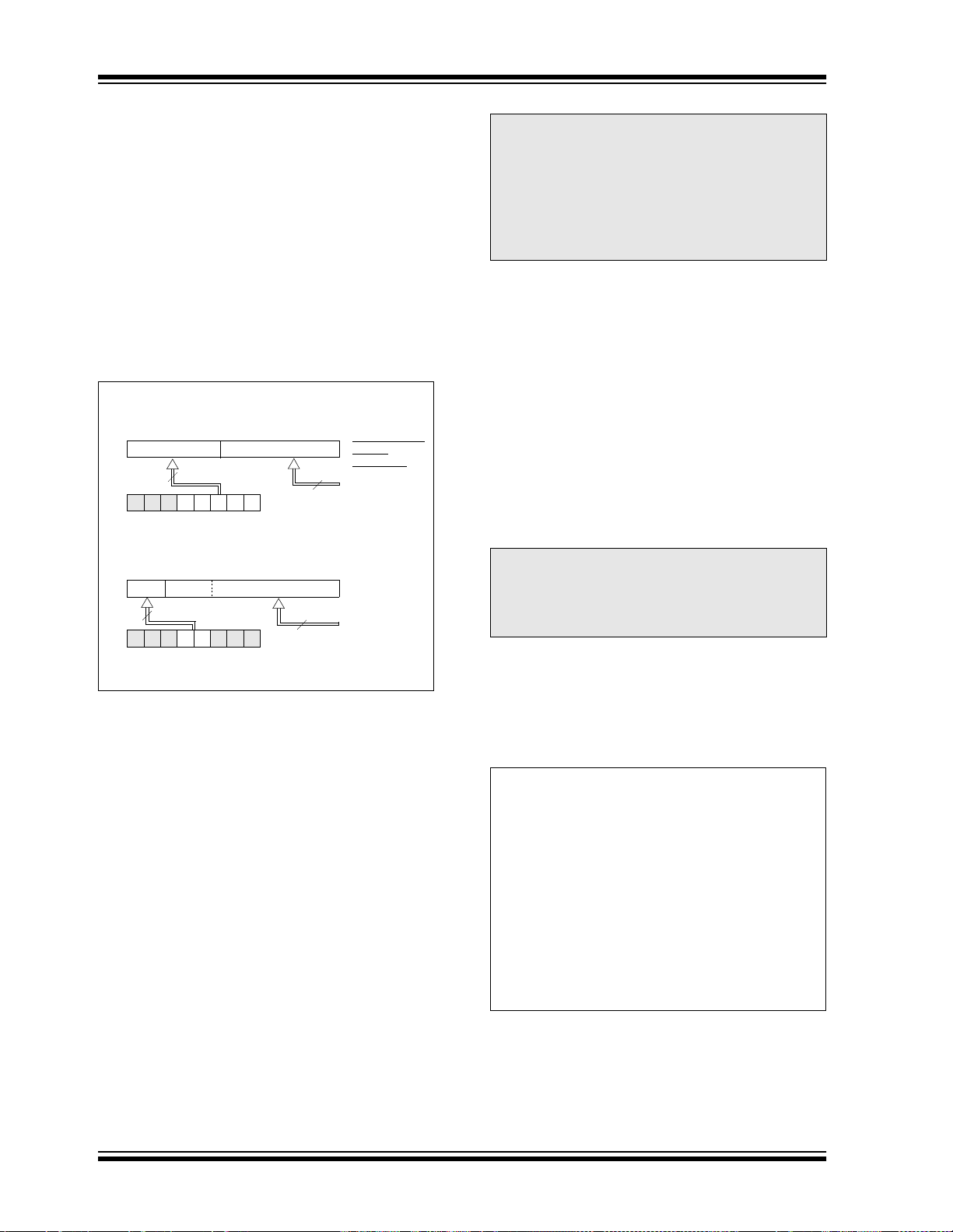
2.3 PCL and PCLATH
The program count er (PC) is 13 bit s wide. The low byte
comes from the PCL register, which is a readable and
writable register. The upper bits (PC<12:8>) are not
readable, but are indirectly writable through the
PCLA TH reg is ter. On any RESET, the upper bits of the
PC will be cleared. Fig ure2-4 shows the two situation s
for the loading of the PC. The up per ex ample in th e figure shows how the PC is loaded on a write to PCL
(PCLATH<4:0> → PCH). The lower example in the figure shows how the PC is loaded during a CALL or GOTO
instruction (PCLATH<4:3> → PCH).
FIGURE 2-4: LOADING OF PC IN
DIFFERENT SITUATIONS
PCH PCL
12 8 7 0
PC
PCLATH<4:0>
5
PCLATH
PCH PCL
12 11 10 0
PC
2
2.3.1 COMPUTED
87
PCLATH<4:3>
PCLATH
11
GOTO
A computed GOTO is accomplish ed by adding an offset
to the progr am counter (ADDWF PCL). When doing a
table read using a computed GOTO method, care
should be exercise d i f the t able loca tio n cros ses a PCL
memory boundary (each 256 byte block). Refer to the
Application Note, “Implementing a Table Read"
(AN556).
2.3.2 STACK
The PIC16F7X fami ly has an 8 -level de ep x 13-bi t wide
hardware s tack. The stack space is not part of either
program or data space and the stack pointer is not
readable or writabl e. The PC i s PUSHed onto th e stac k
when a CALL instruction is executed, or an interrupt
causes a branch. The st ac k is POPed in the ev en t of a
RETURN, RETLW or a RETFIE instruction ex ecution.
PCLATH is not affected by a PUSH or POP operation.
The stack opera tes as a circular buf fer . This means that
after the stack has been PUSHed eight ti mes, the nin th
push overwrites the v alue tha t was stored fro m the first
push. The tenth pus h ov erwri t es the se co nd p us h (an d
so on).
8
Instruction with
PCL as
Destination
ALU
GOTO,CALL
Opcode <10:0>
Note 1: There are no status bits to indicate stack
overflow or stack underflow conditions.
2: There are no instructions/mnemonics
called PUSH or POP. These are actions
that occur from the execution of the
CALL, RETURN, RETLW and RETFIE
instructions, or the vectoring to an interrupt address.
2.4 Program Memory Paging
PIC16F7X devices are cap able of add ressi ng a conti nuous 8K word block of program memory. The CALL and
GOTO instructions provide only 11 bits of address to
allow branching within any 2K program memory page.
When doing a CALL or GOTO ins truction, th e upper 2
bits of the address are provided by PCLATH<4:3>.
When doing a CALL or GOTO instruct ion, the user must
ensure that t he page select bits are progr ammed so
that the desired prog ram memory pa ge is addre ssed. If
a return from a CALL instruction (or interrupt) is executed, the entire 13-bit PC is popped off the stack.
Therefore, manipulation of the PCLATH<4:3> bits are
not required for the RETURN instructions (which P OPs
the address from the stack).
Note: The contents of the PCLATH are
unchanged after a RETURN or RETFIE
instruction is executed. The user must
setup the PCLATH for any subsequent
CALLS or GOTOS.
Example 2-1 shows the calling of a subroutine in
page 1 of the program memory . Thi s example as sumes
that PCLATH is saved and restored by the Interrupt
Service Routine
EXAMPLE 2-1: CALL OF A SUBROUTINE
SUB1_P1
RETURN ;return to Call
(if interrupts are used).
IN PAGE 1 FROM PAGE 0
ORG 0x500
BCF PCLATH,4
BSF PCLATH,3 ;Select page 1
;(800h-FFFh)
CALL SUB1_P1 ;Call subroutine in
: ;page 1 (800h-FFFh)
:
ORG 0x900 ;page 1 (800h-FFFh)
: ;called subroutine
: ;page 1 (800h-FFFh)
:
;subroutine in page 0
;(000h-7FFh)
DS30325B-page 26 2002 Microchip Technology Inc.
Page 29
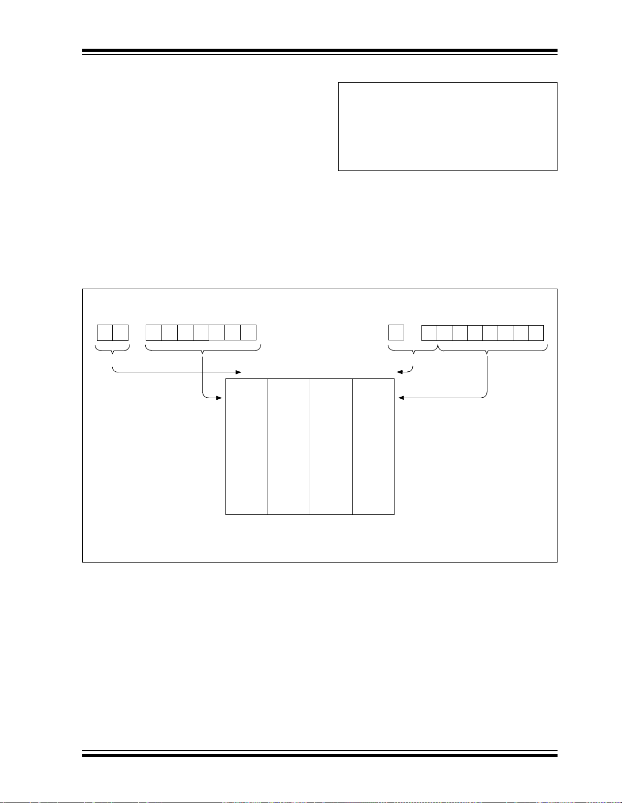
PIC16F7X
2.5 Indirect Addressing, INDF and FSR Registers
The INDF register is not a physi cal register. Addressing
the INDF register will cause indirect addressing.
Indirect addressing is possible by using the INDF register. Any instruc tion using the INDF register actual ly
accesses the register pointed to by the File Sele ct Register, FSR. Reading the INDF register itself indirectly
(FSR = ’0’) will read 00h. Writing to the INDF register
indirectly result s in a no op era tion ( alth oug h status bits
may be affected ). An ef fective 9- bit add ress is obt ained
by concatenating the 8 -bit FSR regi ster and the IRP b it
(STATUS<7>), as shown in F igure 2-5.
A simple program to clear RAM locations 20h-2Fh
using indirect addressing is shown in Example 2-2.
FIGURE 2-5: DIRECT/INDIRECT ADDRESSING
RP1:RP 0 6
Bank Sele ct Location Select
From Opcode
0
00 01 10 11
00h
80h
100h
EXAMPLE 2-2: INDIRECT ADDRESSING
MOVLW 0x20 ;initialize pointer
NEXT CLRF INDF ;clear INDF register
CONTINUE
MOVWF FSR ;to RAM
INCF FSR,F ;inc pointer
BTFSS FSR,4 ;all done?
GOTO NEXT ;no clear next
: ;yes continue
Indirect AddressingDirect Addressing
IRP FSR Register
Bank Select
180h
7
Location Select
0
Data
(1)
Memory
7Fh
Bank 0 Bank 1 Bank 2 Bank 3
Note 1: For register file map detail, see Figure 2-2.
FFh
17Fh
1FFh
2002 Microchip Technology Inc. DS30325B-page 27
Page 30

PIC16F7X
NOTES:
DS30325B-page 28 2002 Microchip Technology Inc.
Page 31

PIC16F7X
3.0 READING PROGRAM MEMORY
The FLASH Program Memory is readable during normal operation over the entire V
addressed through Special Function Registers (SFR).
Up to 14-bit numbers can be stored in memory for use
as calibration param eters, serial nu mbers, packe d 7-bit
ASCII, etc. Executing a pro gram m em ory location containing data tha t forms an inval id instructi on result s in a
NOP.
There are five SFRs used to read the program and
memory. These registers are:
• PMCON1
• PMDATA
• PMDATH
• PMADR
• PMADRH
The program memory allows word reads. Program
memory access allows for checksum calculation and
reading calibration t abl es .
DD range. It is indirectly
When interfacing to the program memory block, the
PMDATH:PMDATA registers form a two-byte word,
which holds the 14-bit data for reads. The
PMADRH:PMADR registers form a two-byte word,
which holds the 13-bit address of the FLASH location
being accessed. These devices can have up to 8K
words of program FLASH, with an address range from
0h to 3FFFh. The unused upper bits in both the
PMDATH an d PMADRH registers are not implemented
and read as “0’s”.
3.1 PMADR
The address registers can address up to a maxim um of
8K words of program FLASH.
When selecting a program address value, the MSByte
of the address is written to the PMADRH register and
the LSByte is written to the PMADR regi ster . The upper
MSbits of PMADRH must always be clear.
3.2 PMCON1 Register
PMCON1 is the control register for memory accesses.
The control bit RD initiates read operations. This bit
cannot be cleared, only set, in so ftware . I t is cleare d in
hardware at the completion of the read operation.
REGISTER 3-1: PMCON1 REGISTER (ADDRESS 18Ch)
R-1 U-0 U-0 U-0 U-x U-0 U-0 R/S-0
reserved — — — — — — RD
bit 7 bit 0
bit 7 Reserved: Read as ‘1’
bit 6-1 Unimplemented: Read as '0'
bit 0 RD: Read Control bit
1 = Initiates a FLASH read, RD is cleare d in har dware. Th e RD bi t can on ly be set (not cle ared)
in software.
0 = FLASH read completed
Legend:
R = Readable bit W = Writable bit U = Unimplemented bit, read as ‘0’
- n = Value at POR reset ’1’ = Bit is set ’0’ = Bit is cleared x = Bit is unknown
2002 Microchip Technology Inc. DS30325B-page 29
Page 32
PIC16F7X
3.3 Reading the FLASH Program Memory
A program memory loca tion may be read by wri ting two
bytes of the address to the PMADR and PMADRH registers and then setting control bit RD (PMCON1<0>).
Once the read control bit is set, the microcontroller will
use the next two instruction cy cles to read the data. The
data is available in the PMDATA and PMDATH regis-
3.4 Operation During Code Protect
FLASH program memory has its own code protect
mechanism. External Read and Write operations by
programmers are disabled if this mechanism is
enabled.
The microcontroller can read and execute instructions
out of the internal FLASH program me mory, regardless
of the state of the code protect configuration bits.
ters after the second NOP instruction. T h ere f ore , i t c an
be read as two bytes in the following instructions. The
PMDATA and PMDATH registers will hold this value
until the next read operation.
EXAMPLE 3-1: FLASH PROGRAM READ
BCF STATUS, RP0 ; Bank 2
MOVF ADDRH, W ;
MOVWF PMADRH ; MSByte of Program Address to read
MOVF ADDRL, W ;
BSF STATUS, RP0 ; Bank 3 Required
Required BSF PMCON1, RD ; EEPROM Read Sequence
Sequence NOP ; memory is read in the next two cycles after BSF PMCON1,RD
NOP ;
BCF STATUS, RP0 ; Bank 2
MOVF PMDATH, W ; W = MSByte of Program PMDATA
BSF STATUS, RP1 ;
MOVWF PMADR ; LSByte of Program Address to read
MOVF PMDATA, W ; W = LSByte of Program PMDATA
TABLE 3-1: REGISTERS ASSOCIATED WITH PROGRAM FLASH
Address Name Bit 7 Bit 6 Bit 5 Bit 4 Bit 3 Bit 2 Bit 1 Bit 0
10Dh PMA DR Address Register Low Byte
10Fh PMADRH — — — Address Register High Byte xxxx xxxx uuuu uuuu
10Ch PMDATA Data Register Low Byte xxxx xxxx uuuu uuuu
10Eh PMDATH — — Data Register High Byte xxxx xxxx uuuu uuuu
18Ch PMCON1 —
Legend: x = unknown, u = unchanged, r = reserved, - = unimplemented read as '0'. Shaded cells are not used during FLASH access.
Note 1: This bit always reads as a ‘1’.
(1)
— — — — — — RD 1--- ---0 1--- ---0
Value on:
POR,
BOR
xxxx xxxx uuuu uuuu
Val ue on
all other
RESETS
DS30325B-page 30 2002 Microchip Technology Inc.
Page 33
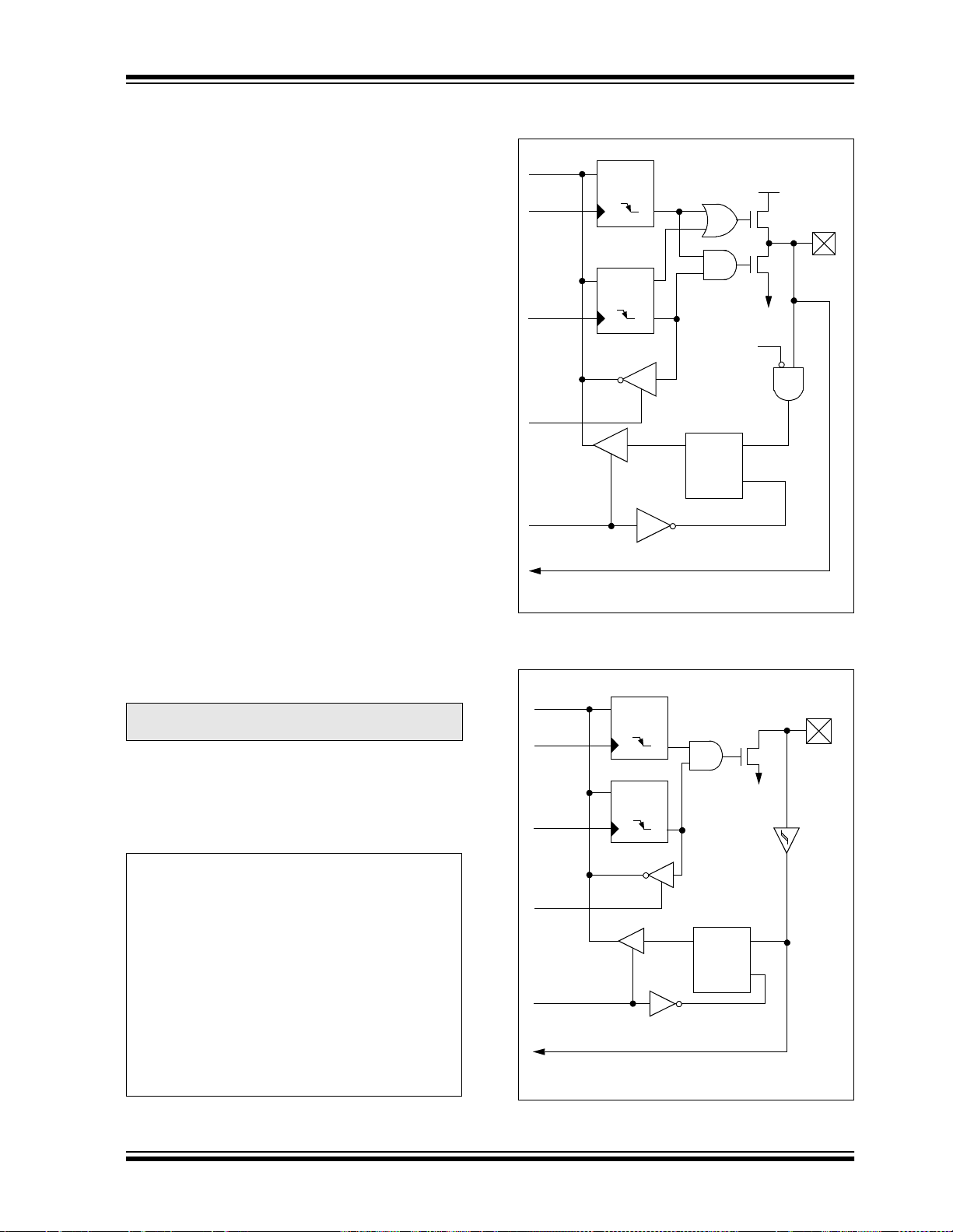
PIC16F7X
4.0 I/O PORTS
Some pins for th ese I/O ports are multiplexed with an
alternate function for the peripheral features on the
device. In general, when a peripheral is enabled, that
pin may not be used as a general purpose I/O pin.
Additional inform atio n o n I/O ports may be found in th e
PICmicro™ Mid-Range Reference Manual,
(DS33023).
4.1 PORTA and the TRISA Register
PORTA is a 6-bit wide, bi-directional port. The corresponding data direction register is TRISA. Setting a
TRISA bit (= ‘1’) will make the corresponding PORTA
pin an input (i.e., put the corresponding output driver in
a Hi-Impedance mode). Cle aring a TRISA bit (= ‘0’) will
make the correspondin g POR TA pin an output (i.e., put
the contents of the output latch on the selected pin).
Reading the PORTA register reads the status of the
pins, whereas writing to i t will wri te to th e po rt latch. All
write operations are read-modify-write operations.
Therefore, a write to a port implies that the port pins are
read, the value is modified and then written to the port
data latch.
Pin RA4 is multiplexed with the Timer0 module clock
input to become the RA4/T0CKI pin. The RA4/T0CKI
pin is a Schmitt Trigger input and an open d rai n outpu t.
All other PORTA pins have TTL input levels and full
CMOS output drivers.
Other PORTA pins are multiplexed with analog inputs
and analog V
selected by clearing/setting the control bits in the
ADCON1 register (A/D Control Register1).
Note: On a Power-on Reset, these pins are con-
The TRISA register controls the direction of the RA
pins, even when they are be ing us ed as ana lo g inputs.
The user must ensure the bits in the TRISA regi ster are
maintained set, when using them as analog inputs.
EXAMPLE 4-1: INITIALIZING PORTA
BCF STATUS, RP0 ;
BCF STATUS, RP1 ; Bank0
CLRF PORTA ; Initialize PORTA by
BSF STATUS, RP0 ; Select Bank 1
MOVLW 0x06 ; Configure all pins
MOVWF ADCON1 ; as digital inputs
MOVLW 0xCF ; Value used to
MOVWF TRISA ; Set RA<3:0> as inputs
REF input. The operation of each pin is
figured as analog inputs and read as '0'.
; clearing output
; data latches
; initialize data
; direction
; RA<5:4> as outputs
; TRISA<7:6>are always
; read as ’0’.
FIGURE 4-1: BLOCK DIAGRAM OF
RA3:RA0 AND RA5 PINS
Data Bus
WR Port
WR TRIS
RD TRIS
RD PORT
To A/D Converter
Note 1: I/O pins have protection diodes to VDD and VSS.
Q
CK
Data Latch
Q
CK
TRIS Latch
QD
QD
QD
EN
Analog
Input
Mode
EN
VDD
P
N
V
SS
I/O pin
TTL
Input
Buffer
FIGURE 4-2: BLOCK DIAGRAM OF
RA4/T0CKI PIN
DataBus
WR PORT
WRTRIS
RD TRIS
RD PORT
TMR0 Clock Input
Note 1: I/O pin has protection diodes to VSS only.
CK
Data Latch
CK
TRIS Latch
QD
Q
QD
Q
Schmitt
Trigger
Input
Buffer
QD
EN
EN
I/O pin
N
SS
V
(1)
(1)
2002 Microchip Technology Inc. DS30325B-page 31
Page 34
PIC16F7X
TABLE 4-1: PORTA FUNCTIONS
Name Bit# Buffer Function
RA0/AN0 bit0 TTL Input/output or analog input.
RA1/AN1 bit1 TTL Input/output or analog input.
RA2/AN2 bit2 TTL Input/output or analog input.
RA3/AN3/V
RA4/T0CKI bit4 ST Input/output or external clock input for Timer0. Output is open drain type.
RA5/SS
Legend: TTL = TTL input, ST = Schmitt Trigger input
TABLE 4-2: SUMMARY OF REGISTERS ASSOCIATED WITH PORTA
REF bit3 TTL Input/output or analog input or VREF.
/AN4 bit5 TTL Input/output or slave select input for synchronous serial port or analog input.
Value on:
Address Name Bit 7 Bit 6 Bit 5 Bit 4 Bit 3 Bit 2 Bit 1 Bit 0
05h PORTA
85h TRISA — — POR TA Data Direction Register
9Fh ADCON1 — — — — — PCFG2 PCFG1 PCFG0
Legend: x = unknown, u = unchanged, - = unimplemented locations read as '0'. Shaded cells are not used by PORTA.
Note: When using the SSP module in SPI Slave mode and SS enabled, the A/D converter must be set to one of
the following modes where PCFG2:PCFG0 = 100, 101, 11x.
— — RA5 RA4 RA3 RA2 RA1 RA0
POR,
BOR
--0x 0000 --0u 0000
--11 1111 --11 1111
---- -000 ---- -000
Value on all
other
RESETS
DS30325B-page 32 2002 Microchip Technology Inc.
Page 35
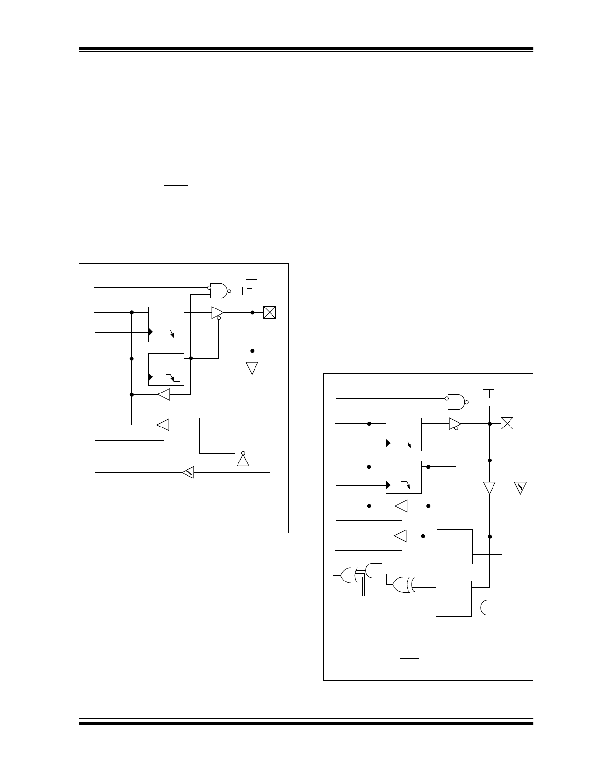
PIC16F7X
4.2 PORTB and the TRISB Register
PORTB is an 8-bit wide, bi-directional port. The corresponding data direction register is TRISB. Setting a
TRISB bit (= ‘1’) will make the corresponding PORTB
pin an input (i.e., put the corresponding output driver in
a Hi-Impedance mode). Cle aring a TRISB bit (= ‘0’) will
make the corresponding POR TB pin an output (i.e. , put
the contents of the output latch on the selected pin).
Each of the PORTB pi ns has a w eak i nternal pul l-up. A
single control bit can turn on all the pull-ups. This is performed by clearing bit RBPU
weak pull-up is automatically turned off when the port
pin is configured as an output. The pull-ups are disabled on a Power-on Reset.
FIGURE 4-3: BLOCK DIAGRAM OF
(2)
RBPU
Data Bus
WR Port
WR TRIS
RD TRIS
RD Port
RB0/INT
Note 1: I/O pins have diode protection to V
2: To enable weak pull-ups, set the a ppropriate TRIS
Four of the PORTB pins (RB7:RB4) have an interrupt-on-change feat ure. On ly pin s c on fig ured as inputs
can cause this inte rrupt t o oc cur (i .e., a ny RB 7:RB4 pin
configured as an output is excluded from the interrupt-on-change comparison). The input pins (of
RB7:RB4) are compared with the old value latched on
the last read of PORTB. The “mismatch” outputs of
RB7:RB4 are ORed together to generate the RB Port
Change Interrupt with flag bit RBIF (INTCON<0>).
Data Latch
CK
TRIS Latch
CK
bit(s) and clear the RBPU
(OPTION_REG<7>). The
RB3:RB0 PINS
QD
QD
Schmitt Trigger
Buffer
TTL
Input
Buffer
QD
EN
DD and VSS.
bit (OPTION_REG<7>).
DD
V
Weak
P
Pull-up
RD Port
pin
I/O
(1)
This interrupt can wake the device from SLEEP. The
user, in the Interrupt Service Routine, can clear the
interrupt in the following manner:
a) Any read or write of PORTB. This will end the
mismatch condition.
b) Clear flag bit RBIF.
A mismatch c ond it i on wi ll cont i n ue to s et f lag bi t RB IF.
Reading PORTB will end the mismatch condition and
allow flag bit RBIF to be cleared.
The interrupt-on-change feature is recommended for
wake-up on key depression operation and operations
where PORTB is only used for the interrupt-on-change
feature. Polling of PORTB is not recommended while
using the interrupt-on-change feature.
This interrupt on mismatch feature, together with software configureable pull-ups on these four pins, allow
easy interface to a keypad and make it possible for
wake-up on key depression. Refer to the Embedded
Control Handbook, “Implementing Wake-up on Key
Stroke” (AN552).
RB0/INT is an ext ernal i nterrupt input pin a nd is confi gured using the INTEDG bit (OPTION_REG<6>).
RB0/INT is discussed in detail in Section 12.11.1.
FIGURE 4-4: BLOCK DIAGRAM OF
RB7:RB4 PINS
DD
EN
EN
TTL
Input
Buffer
V
P
Weak
Pull-up
I/O
(1)
pin
ST
Buffer
Q1
RD Port
Q3
(2)
RBPU
Data Bus
WR Port
WR TRIS
RD TRIS
RD Port
Set RBIF
From other
RB7:RB4 pins
RB7:RB6 in Serial Programming mode
Data Latch
QD
CK
TRIS Latch
QD
CK
Latch
QD
QD
Note 1: I/O pins have diode protection to V
2: To enable weak pull-ups, set the appropriate TRIS bit(s)
and clear the RBPU
bit (OPTION_REG<7>).
DD and VSS.
2002 Microchip Technology Inc. DS30325B-page 33
Page 36
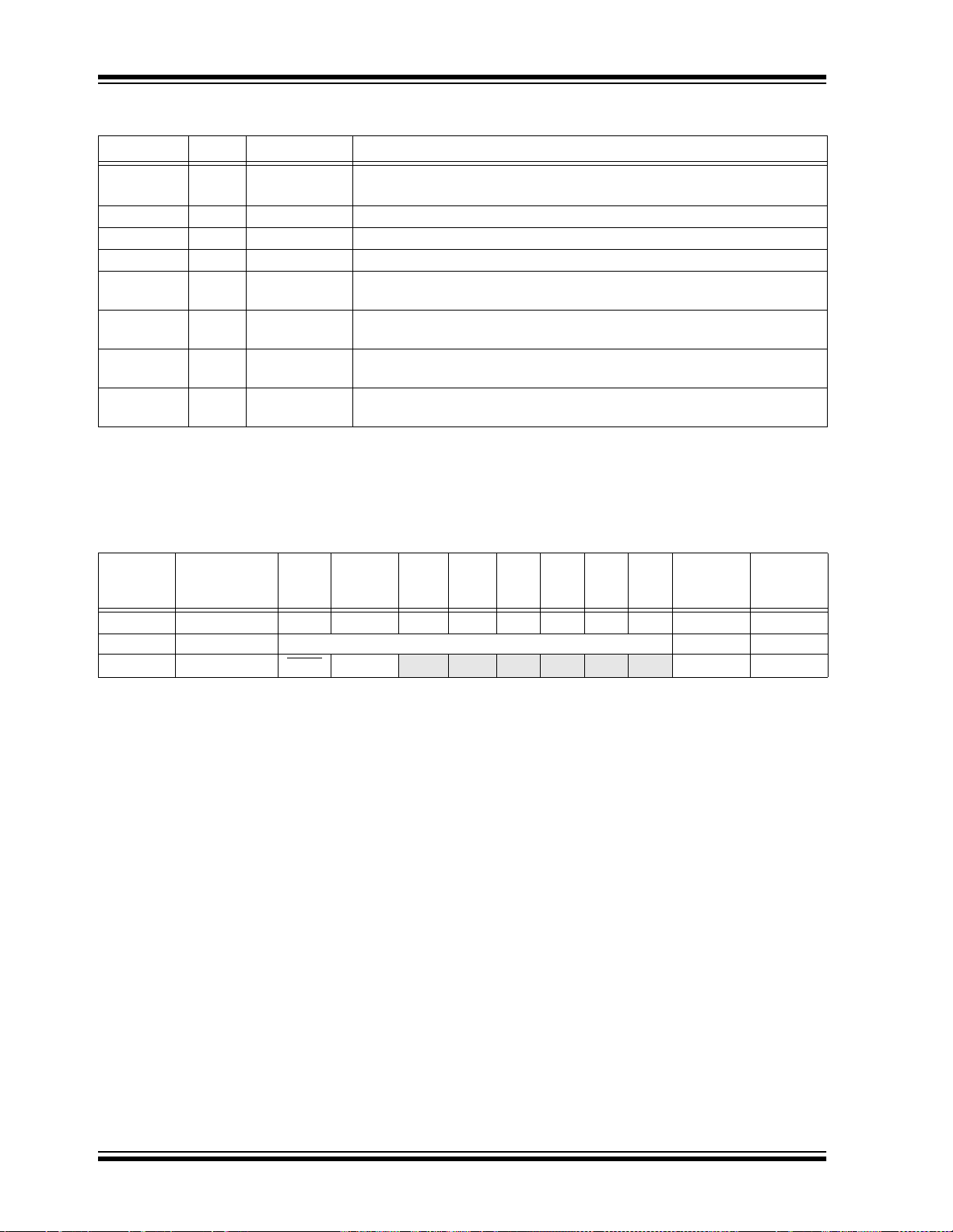
PIC16F7X
TABLE 4-3: PORTB FUNCTIONS
Name Bit# Buffer Function
RB0/INT bit0 TTL/ST
RB1 bit1 TTL Input/output pin. Internal software programmable weak pull-up.
RB2 bit2 TTL Input/output pin. Internal software programmable weak pull-up.
RB3 bit3 TTL Input/output pin. Internal software programmable weak pull-up.
RB4 bit4 TTL Input/output pin (with interrupt-on-chang e). Internal softwar e programmable
RB5 bit5 TTL Input/output pin (with interrupt-on-chang e). Internal softwar e programmable
RB6 bit6 TTL/ST
RB7 bit7 TTL/ST
Legend: TTL = TTL input, ST = Schmitt Trigger input
Note 1: This buffer is a Schmitt Trigger input when configured as the external interrupt.
2: This buffer is a Schmitt Trigger input when used in Serial Programming mode.
(1)
Input/output pin or external interrupt input. Internal software
programmable weak pull-up.
weak pull-up.
weak pull-up.
(2)
Input/output pin (with interrupt-on-change).
Internal software programmable weak pull-up. Serial programming clock.
(2)
Input/output pin (with interrupt-on-change).
Internal software programmable weak pull-up. Serial programming data.
TABLE 4-4: SUMMARY OF REGISTERS ASSOCIATED WITH PORTB
Address Name Bit 7 Bit 6 Bit 5 Bit 4 Bit 3 Bit 2 Bit 1 Bit 0
06h, 106h P O RTB RB7 RB6 RB5 RB4 RB3 RB2 RB1 RB0
86h, 186h T RI SB PORTB Data Direction Register 1111 1111 1111 1111
81h, 181h O PTION_REG RBPU INTEDG T0CS T0SE PSA PS2 PS1 PS0 1111 1111 1111 1111
Legend: x = unknown, u = unchanged. Shaded cells are not used by PORTB.
Val ue on:
POR,
BOR
xxxx xxxx uuuu uuuu
Val ue on
all other
RESETS
DS30325B-page 34 2002 Microchip Technology Inc.
Page 37
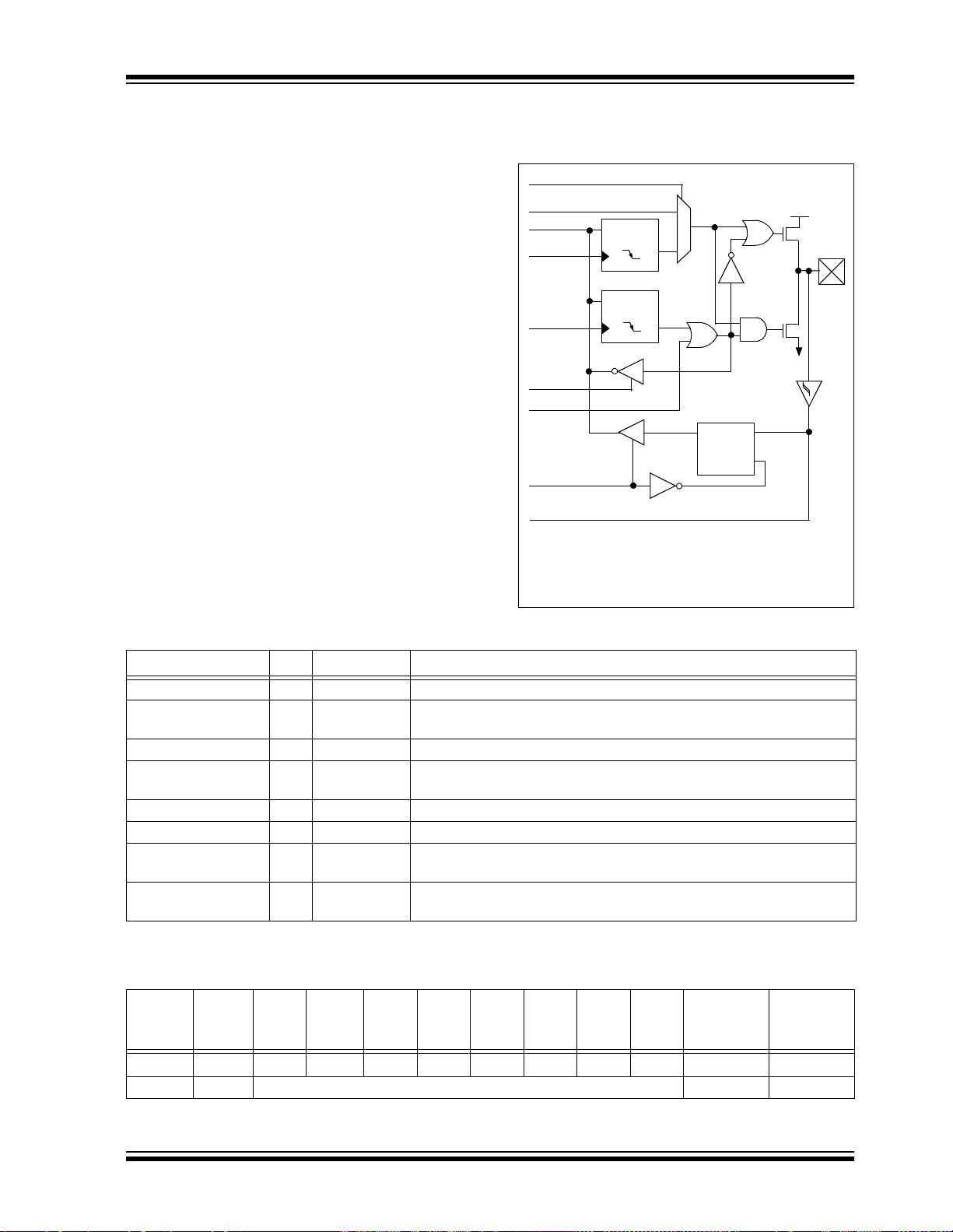
PIC16F7X
4.3 PORTC and the TRISC Register
PORTC is an 8-bit wide, bi-directional port. The corresponding data direction register is TRISC. Setting a
TRISC bit (= ‘1’) will make the corresponding PORTC
pin an input (i.e., put the corresponding output driver in
a Hi-Impedance mode ). Clearing a TRISC bi t (= ‘0’) wil l
make the correspondi ng PORTC pin an output (i.e., p ut
the contents of the output latch on the selected pin).
PORTC is mul tiplexed with s everal peri pheral function s
(Table 4-5). PORTC pins have Schmitt Trigger input
buffers.
When enabling peripheral functions, care should be
taken in defining TRIS bit s fo r each POR TC pin. Some
peripherals override the TRIS bit to make a pin an
output, whi le ot her pe r iph e r al s ov e rri d e the TR I S bi t to
make a pin an input. Since the TRIS bit override is
in effect while the peripheral is enabled,
read-modify-write instructions (BSF, BCF, XORWF)
with TRISC as destinat ion should be avoid ed. The user
should refer to the co rrespondin g periphera l section for
the correct TRIS bit settings, and to Section 13.1 for
additional informa t io n on re ad-modify-write operations.
FIGURE 4-5: PORTC BLOCK DIAGRAM
(PERIPHERAL OUTPUT
OVERRIDE)
Port/Peripheral Select
Peripheral Data Out
Data Bus
WR Port
WR TRIS
RD TRIS
Peripheral
(3)
OE
RD Port
Peripheral Input
Note 1: I/O pins have diode protection to V
2: Port/Peripheral select signal selects between port data
and peripheral output.
3: Peripheral OE (output enable) is only activated if
peripheral select is active.
(2)
QD
Q
CK
Data Latch
QD
Q
CK
TRIS Latch
0
1
QD
Schmitt
Trigger
EN
DD and VSS.
V
P
N
VSS
DD
pin
I/O
(1)
TABLE 4-5: PORTC FUNCTIONS
Name Bit# Buffer Type Function
RC0/T1OSO/T1CKI bit0 ST Input/output port pin or Timer1 oscillator output/Timer1 clock input.
RC1/T1OSI/CCP2 bit1 ST Input/output port pin or Timer1 oscillator input or Capture2
input/Compare2 output/PWM2 output.
RC2/CCP1 bit2 ST Input/output port pin or Capture1 input/Compare1 ou tput/PWM1 output.
2
RC3/SCK/SCL bit3 ST RC3 can also be the synchronous serial clock for both SPI and I
C
modes.
2
RC4/SDI/SDA bit4 ST RC4 can also be the SPI Data In (SPI mode) or Data I/O (I
C mode).
RC5/SDO bit5 ST Input/output port pin or Synchronous Serial Port data output.
RC6/TX/CK bit6 ST Input/output port pin or USART Asynchronous Transmit or
Synchronous Clock.
RC7/RX/DT bit7 ST Input/output port pin or USART Asynchronous Receive or
Synchronous Data.
Legend: ST = Schmitt T r igg er input
TABLE 4-6: SUMMARY OF REGISTERS ASSOCIATED WITH PORTC
Value on:
Address Name Bit 7 Bit 6 Bit 5 Bit 4 Bit 3 Bit 2 Bit 1 Bit 0
POR,
BOR
07h PORTC RC7 RC6 RC5 RC4 RC3 RC2 RC1 RC0 xxxx xxxx uuuu uuuu
87h TRISC PORTC Data Direction Register 1111 1111 1111 1111
Legend: x = unknown, u = unchanged
Value on
all other
RESETS
2002 Microchip Technology Inc. DS30325B-page 35
Page 38
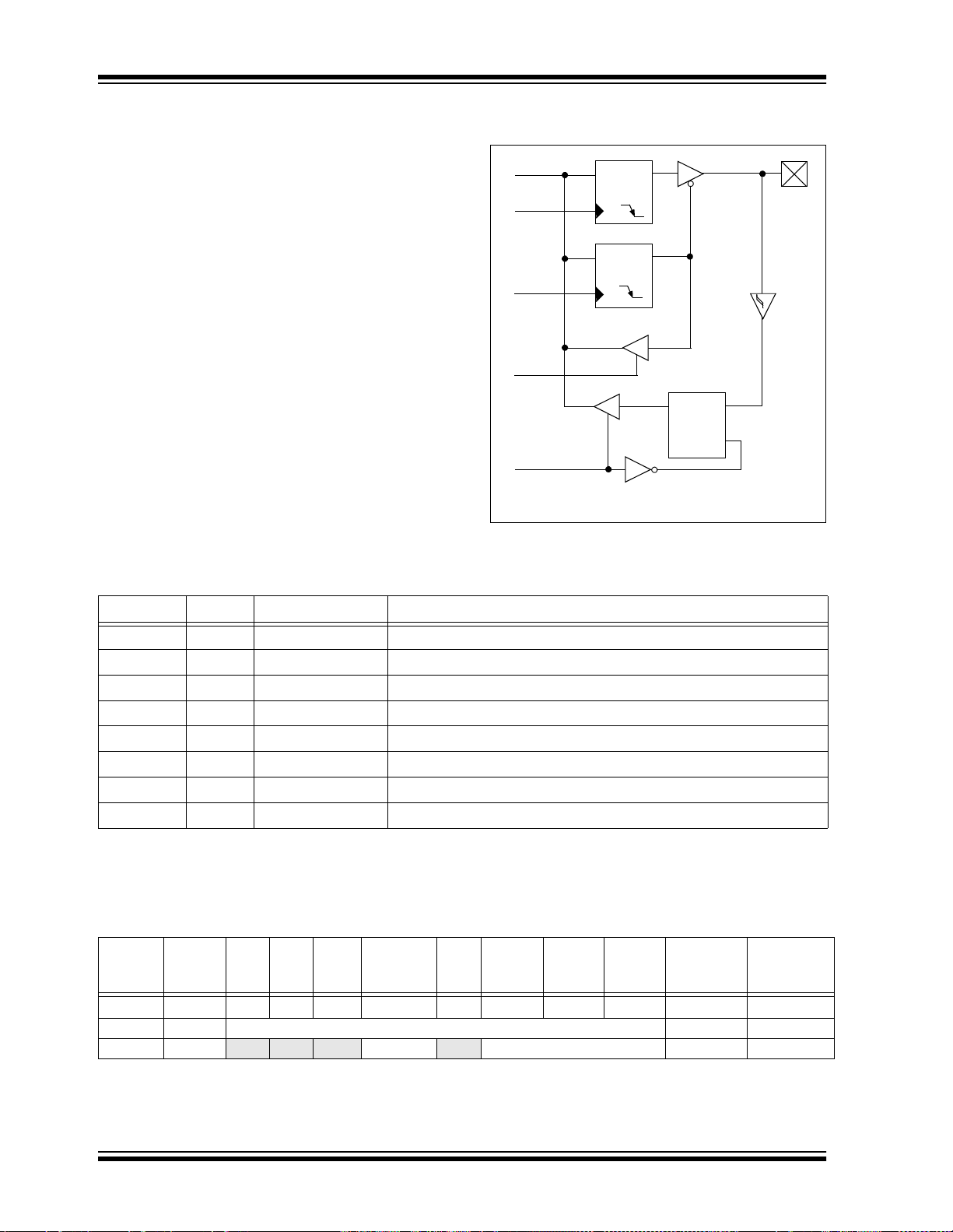
PIC16F7X
4.4 PORTD and TRISD Registers
This section is not applicable to the PIC16F73 or
PIC16F76.
PORTD is an 8-bit port with Schmitt Trigger input buffers. Each pin is in dividually co nfigureable as a n input or
output.
PORTD can be configured as an 8-bit wide microprocessor port (paral lel slav e port) by se tting cont rol bit
PSPMODE (TRISE<4>). In this mode, the input buffers
are TTL.
FIGURE 4-6: PORTD BLOCK DIAGRAM
(IN I/O PORT MODE)
DataBus
WR Port
WR TRIS
RD TRIS
RD Port
Note 1: I/O pins have protection diodes to VDD and VSS.
CK
Data Latch
QD
CK
TRIS Latch
QD
QD
EN
Schmitt
Trigger
Input
Buffer
EN
I/O pin
(1)
TABLE 4-7: PORTD FUNCTIONS
Name Bit# Buffer Type Function
RD0/PSP0 bit0
RD1/PSP1 bit1
RD2/PSP2 bit2
RD3/PSP3 bit3
RD4/PSP4 bit4
RD5/PSP5 bit5
RD6/PSP6 bit6
RD7/PSP7 bit7
ST/TTL
ST/TTL
ST/TTL
ST/TTL
ST/TTL
ST/TTL
ST/TTL
ST/TTL
(1)
(1)
(1)
(1)
(1)
(1)
(1)
(1)
Input/output port pin or parallel slave port bit0
Input/output port pin or parallel slave port bit1
Input/output port pin or parallel slave port bit2
Input/output port pin or parallel slave port bit3
Input/output port pin or parallel slave port bit4
Input/output port pin or parallel slave port bit5
Input/output port pin or parallel slave port bit6
Input/output port pin or parallel slave port bit7
Legend: ST = Schmitt Trigger input, TTL = TTL input
Note 1: Input buffers are Schmitt Triggers when in I/O mode and TTL buffers when in Parallel Slave Port mode.
TABLE 4-8: SUMMARY OF REGISTERS ASSOCIATED WITH PORTD
Address Name Bit 7 Bit 6 Bit 5 Bit 4 Bit 3 Bit 2 Bit 1 Bit 0
08h PORTD RD7 RD6 RD5 RD4 RD3 RD2 RD1 RD0
88h TRISD PORTD Data Direction Register 1111 1111 1111 1111
89h TRISE IBF OBF IBOV PSPMODE — PORTE Data Direction bits 0000 -111 0000 -111
Legend: x = unknown, u = unchanged, - = unimplemented read as '0'. Shaded cells are not used by PORTD.
Value on:
POR,
BOR
xxxx xxxx uuuu uuuu
Value on
all other
RESETS
DS30325B-page 36 2002 Microchip Technology Inc.
Page 39
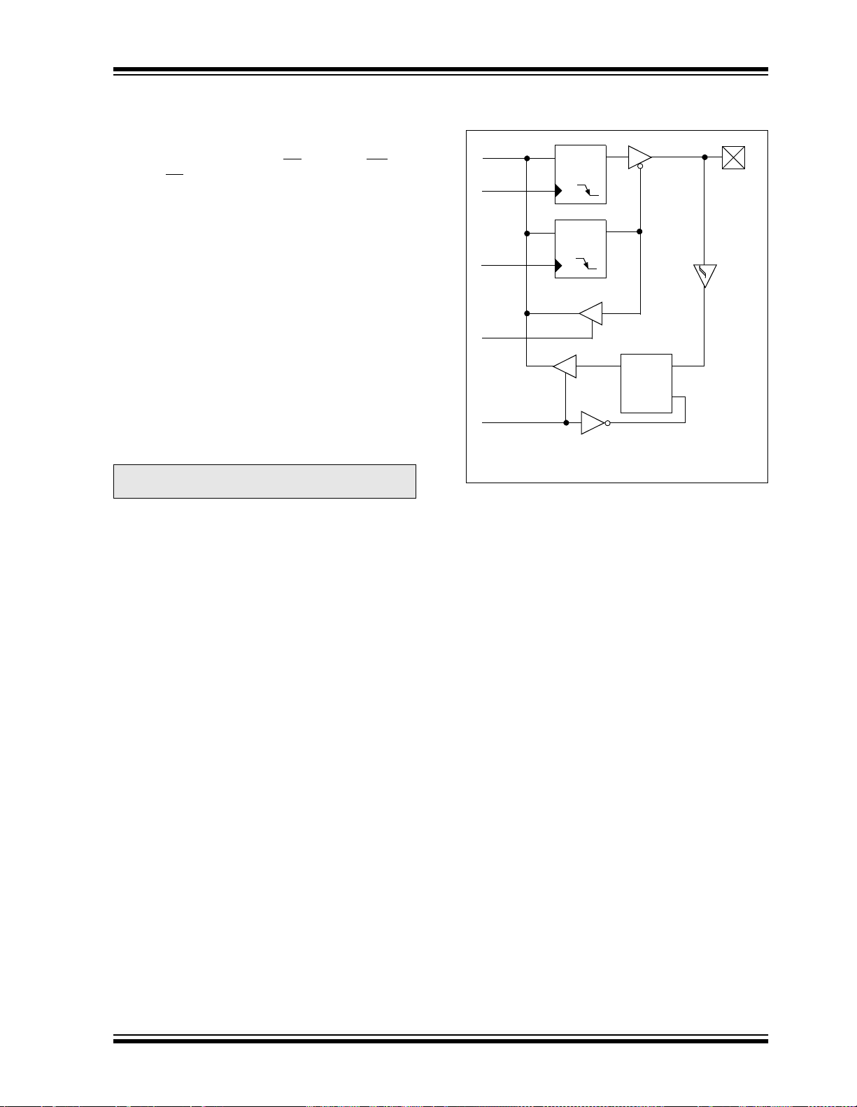
PIC16F7X
4.5 PORTE and TRISE Register
This section is not applicable to the PIC16F73 or
PIC16F76.
PORTE has three pins, RE0/RD
and RE2/CS
/AN7, which are indivi dua lly configureable
as inputs or outputs. These pins have Schmitt Trigger
input buffers.
I/O PORTE becomes control inputs for the microprocessor port when bit PSPMODE (TRISE<4>) is set.
In this mode, the user must make sure that the
TRISE<2:0> bits are set (pins are configured as digital
inputs). Ensure ADC ON1 is config ured for digital I/O. In
this mode, the input buffers are TTL.
Register 4-1 shows the TRISE register, which also controls the parallel slave port operation.
PORTE pins are multiplexed with analog inputs. When
selected as an anal og input, these pins wi ll read as ’0’s.
TRISE controls the direction of the RE pins, even when
they are being used as analog inputs. The user must
make sure to keep the pins configured as inputs when
using them as analog inputs.
Note: On a Power-on Reset, these pins are con-
figured as analog inputs and read as ‘0’.
/AN5, RE1/WR/AN6
FIGURE 4-7: PORTE BLOCK DIAGRAM
(IN I/O PORT MODE)
Data Bus
WR Port
WR TRIS
RD TRIS
RD Port
Note 1: I/O pins have protection diodes to VDD and VSS.
CK
Data Latch
QD
CK
TRIS Latch
QD
QD
EN
Schmitt
Trigger
Input
Buffer
EN
I/O pin
(1)
2002 Microchip Technology Inc. DS30325B-page 37
Page 40

PIC16F7X
REGISTER 4-1: TRISE REGISTER (ADDRESS 89h)
R-0 R-0 R/W-0 R/W-0 U-0 R/W-1 R/W-1 R/W-1
IBF OBF IBOV PSPMODE
bit 7 bit 0
bit 7 Parallel Slave Port Status/Control bits:
IBF: Input Buffer Full Status bit
1 = A word has been received and is waiting to be read by the CPU
0 = No word has been received
bit 6 OBF: Output Buffer Full Status bit
1 = The output buffer still holds a previously written word
0 = The output buffer has been read
bit 5 IBOV: Input Buffer Overflow Detect bit (in Microprocessor mode)
1 = A write occurred when a previously input word has not been read
(must be cleared in software)
0 = No overflow occurred
bit 4 PSPMODE: Parallel Slave Port Mode Select bit
1 = Parallel Slave Port mode
0 = General Purpose I/O mode
bit 3 Unimplemented: Read as '0'
bit 2 PORTE Data Direction bits:
Bit2: Direction Control bit for pin RE2/CS/AN7
1 = Input
0 = Output
bit 1 Bit1: Direction Control bit for pin RE1/WR
1 = Input
0 = Output
bit 0 Bit0: Direction Control bit for pin RE0/RD
1 = Input
0 = Output
/AN6
/AN5
— Bit2 Bit1 Bit0
Legend:
R = Readable bit W = Writable bit U = Unimplemented bit, read as ‘0’
- n = Value at POR reset ’1’ = Bit is set ’0’ = Bit is cleared x = Bit is unknown
DS30325B-page 38 2002 Microchip Technology Inc.
Page 41
PIC16F7X
TABLE 4-9: PORTE FUNCTIONS
Name Bit# Buffer Type Function
(1)
RE0/RD/AN5 bit0 ST/TTL
RE1/WR
RE2/CS
/AN6 bit1 ST/TTL
/AN7 bit2 ST/TTL
Legend: ST = Schmitt Trigger input, TTL = TTL input
Note 1: Input buffers are Schmitt Triggers when in I/O mode and TTL buffers when in Parallel Slave Port mode.
Input/output port pin or read co ntrol input in Parall el Slave Port mode or
analog input.
For RD (PSP mode):
1 = IDLE
0 = Read operation. Contents of PORTD register output to PORTD I/O
pins (if chip selected).
(1)
Input/output port pin or write control input in Parallel Slave Port mode
or analog input.
For WR (PSP mode):
1 =IDLE
0 = Write operation. Value of PORTD I/O pins latched into PORTD
register (if chip selected).
(1)
Input/output port pin or chip select control input in Parallel Slave Port
mode or analog input.
For CS (PSP mode):
1 =Device is not selected
0 =Device is selected
TABLE 4-10: SUMMARY OF REGISTERS ASSOCIATED WITH PORTE
Addr Name Bit 7 Bit 6 Bit 5 Bit 4 Bit 3 Bit 2 Bit 1 Bit 0
09h PORTE
89h TRISE IBF OBF IBOV PSPMODE — PORTE Data Direction bits 0000 -111 0000 -111
9Fh ADCON1 — — — — — PCFG2 PCFG1 PCFG0 ---- -000 ---- -000
Legend: x = unknown, u = unchanged, - = unimplemented, read as '0'. Shaded cells are not used by PORTE.
— — — — — RE2 RE1 RE0 ---- -xxx ---- -uuu
Val ue on:
POR,
BOR
Value on all
other
RESETS
2002 Microchip Technology Inc. DS30325B-page 39
Page 42

PIC16F7X
4.6 Parallel Slave Port
The Parallel Slave Port (PSP) is not implemented on
the PIC16F73 or PIC16F 76.
PORTD operates as an 8-bit wide Parallel Slave Port,
or Microprocessor Port, when control bit PSPMODE
(TRISE<4>) is set. I n Sl av e mo de, it is asynchronously
readable and writable by an external system using the
read control input pin RE0/RD
pin RE1/WR
RE2/CS
, and the chip select control input pin
.
The PSP can directly interface to an 8-bit microprocessor data bus. Th e extern al micropr ocessor c an
read or write the POR TD latch as an 8-bit latch. Setting
bit PSPMODE enables port pin RE0/RD
input, RE1/WR to be the WR input and RE2/CS to be
the CS
(chip select) input. Fo r this function ality , th e corresponding data direction bits of the TRISE register
(TRISE<2:0>) must be configured as inputs (i.e., set).
The A/D port configuration bits PCFG3:PCFG0
(ADCON1<3:0>) must be set to configure pins
RE2:RE0 as digital I/O.
There are actual ly two 8 -bit latc hes, one for dat a outp ut
(external reads) and one for data input (external
writes). The firmware writes 8-bit data to the PORTD
output data latch and reads data from the PORTD input
data latch (note that they have the same address). In
this mode, the TRISD register is ignored, since the
external device is controlling the direction of data flow.
An external write to the PSP occurs when the CS
WR
lines are both detected low. Firmware can read the
actual data on the PORTD pins during this time. When
either the CS or WR lines become high (level triggered), the data on the PORTD pins is latched, and the
Input Buffer Full (IBF) status flag bit (TRISE<7>) and
interrupt flag bit PSPIF (PIR1<7>) are set on the Q4
clock cycle, following the next Q2 cycle to signal the
write is complete (Fi gure 4-9 ) . Firmw are cl ears the IBF
flag by reading the latched PO RTD dat a, and cl ears the
PSPIF bit.
The Input Buffer Overflow (IBOV) status flag bit
(TRISE<5>) is set if an external write to the PSP occu rs
while the IBF flag is set from a previous external write.
The previous PORTD data is overwritten with the new
data. IBOV is cleared by reading PORTD and clearing
IBOV.
A read from the PSP occurs when both the CS
lines are detected low. The data in the PORTD output
latch is output to the PORTD pins. The Output Buffer
Full (OBF) status flag bit (TRISE<6>) is cleared immediately (Figure 4-10), indicating that the PORTD latch is
being read, or has been read by the external bus. If
firmware writes ne w da t a to the output latch during this
time, it is immediately output to the PORTD pins, but
OBF will remain cleared.
, the write control input
to be the RD
and
and RD
When either the CS
or RD pins are detected high, the
PORTD outputs are disabled, and the interrupt flag bit
PSPIF is set on the Q4 clock cycle following the next
Q2 cycle, indicating that the read is complete. OBF
remains low until firmware writes new data to PORTD.
When not in PSP mode, the IBF and OBF bits are held
clear . Flag bit IBOV remains uncha nged. The PSPIF b it
must be cleared by the user in firmware; the interrupt
can be disabled by clearing the interrupt enable bit
PSPIE (PIE1<7>).
FIGURE 4-8: PORTD AND PORTE
BLOCK DIAGRAM
(PARALLEL SLAVE PORT)
Data Bus
WR
Port
RD
Port
One bit of PORTD
Set Interrupt Flag
PSPIF (PIR1<7>)
Note: I/O pin has protection diodes to V
QD
CK
QD
EN
EN
Read
Chip Select
Write
DD and VSS.
TTL
TTL
TTL
TTL
RDx
pin
RD
CS
WR
DS30325B-page 40 2002 Microchip Technology Inc.
Page 43

FIGURE 4-9: PARALLEL SLAVE PORT WRITE WAVEFORMS
Q1 Q2 Q3 Q4CSQ1 Q2 Q3 Q4 Q1 Q2 Q3 Q4
WR
RD
PORTD<7:0>
IBF
OBF
PSPIF
FIGURE 4-10: PARALLEL SLAVE PORT READ WAVEFORMS
PIC16F7X
Q1 Q2 Q3 Q4CSQ1 Q2 Q3 Q4 Q1 Q2 Q3 Q4
WR
RD
PORTD<7:0>
IBF
OBF
PSPIF
TABLE 4-11: REGISTERS ASSOCIATED WITH PARALLEL SLAVE PORT
Address Name Bit 7 Bit 6 Bit 5 Bit 4 Bit 3 Bit 2 Bit 1 Bit 0
08h PORTD Port data latch when written: Port pins when read
09h PORTE — — — — — RE2 RE1 RE0 ---- -xxx ---- -uuu
89h TRISE IBF OBF IBOV PSPMODE — PORTE Data Direction Bits 0000 -111 0000 -111
0Ch PIR1
8Ch PIE1
9Fh ADCON1 — — — — — PCFG2 PCFG1 PCFG0 ---- -000 ---- -000
Legend: x = unknown, u = unchanged, - = unimplemented, read as '0'. Shaded cells are not used by the Parallel Slave Port.
Note 1: Bits PSPIE and PSPIF are reserved on the PIC16F73/76; always maintain these bits clear.
PSPIF
PSPIE
(1)
ADIF RCIF TXIF SSPIF CCP1IF TMR2IF TMR1IF 0000 0000 0000 0000
(1)
ADIE RCIE TXIE SSPIE CCP1IE TMR2IE TMR1IE 0000 0000 0000 0000
Value on:
POR,
BOR
xxxx xxxx uuuu uuuu
Value on
all other
RESETS
2002 Microchip Technology Inc. DS30325B-page 41
Page 44

PIC16F7X
NOTES:
DS30325B-page 42 2002 Microchip Technology Inc.
Page 45

PIC16F7X
5.0 TIMER0 MODULE
The Timer0 module timer/counter has the following
features:
• 8-bit timer/counter
• Readable and writable
• 8-bit software programmable prescaler
• Internal or external clock select
• Interrupt on overflow from FFh to 00h
• Edge select for external clock
Additional information on the Timer0 module is available in the PICmicro™ Mid-Range MCU Family Reference Manual (DS33023).
Figure 5-1 is a block diagram of the T imer0 m odule and
the prescaler shared with the WDT.
Timer0 operation is controlled through the
OPTION_REG register (Register 5-1 on the following
page). Timer mode is selected by clearing bit T0CS
(OPTION_REG<5>). In Timer mode, the Timer0 module will incremen t every ins tru ction cycle (without prescaler). If the TMR0 register is written, the increment is
inhibited for the following two instruction cycles. The
user can work around this by writing an adjusted value
to the TMR0 register.
Counter mode is selected by setting bit T0CS
(OPTION_REG<5>). In Counter mode, Timer0 will
increment, either on every rising or falling edge of pin
RA4/T0CKI. The incrementing edge is determined by
the Timer0 Source Edge Select bit T0SE
(OPTION_REG<4>). Clearing bit T0SE selects the rising edge. Restrictions on the external clock input are
discussed in detail in Section 5.2.
The prescaler is mutually exclusively shared between
the Timer0 modu le and t he W a tchdo g Timer. The prescaler is not readabl e or w rit able. Sectio n 5.3 details the
operation of the prescaler.
5.1 Timer0 Interrupt
The TMR0 interrupt is generated when the TMR0 register overflows from FFh to 00h. This overflow sets bit
TMR0IF (INTCON<2>). The interrupt can be masked
by clearing bit TMR0IE (INTCON<5>). Bit TMR0IF
must be cleared in software by the Timer0 module
Interrupt Service Routin e, b efore re -enabling this interrupt. The TMR0 interrupt cann ot awaken th e processor
from SLEEP, since the timer is shut-off during SLEEP.
FIGURE 5-1: BLOCK DIAGRAM OF THE TIMER0 MODULE AND PRESCALER
CLKOUT (= F
RA4/T0CKI
pin
Watchdog
Timer
WDT Enable bit
OSC/4)
T0SE
M
0
U
X
1
T0CS
0
M
U
1
X
PSA
8-bit Prescaler
8 - to - 1MUX
0
PRESCALER
8
M U X
1
M
U
0
X
PSA
1
PSA
SYNC
2
Cycles
PS2:PS0
Data Bus
8
TMR0 reg
Set Flag bit TMR0IF
on Overflow
WDT
Time-out
Note: T0CS, T0SE, PSA, PS2:PS0 are (OPTION_REG<5:0>).
2002 Microchip Technology Inc. DS30325B-page 43
Page 46

PIC16F7X
5.2 Using Timer0 with an External Clock
When no pr escal er is us ed, t he ex ternal clock inpu t is
the same as the prescaler outp ut. Th e synchronization
of T0CKI, with the internal phase clocks, is accomplished by sampli ng the prescale r output on the Q2 and
REGISTER 5-1: OPTION_REG REGISTER
R/W-1 R/W-1 R/W-1 R/W-1 R/W-1 R/W-1 R/W-1 R/W-1
RBPU
bit 7 bit 0
bit 7 RBPU
bit 6 INTEDG: Interrupt Edge Select bit (see Section 2.2.2.2)
bit 5 T0CS: TMR0 Clock Source Select bit
1 = Transition on T0CKI pin
0 = Internal instruction cycle clock (CLKOUT)
bit 4 T0SE: TMR0 Source Edge Select bit
1 = Increment on high-to-low transition on T0CKI pin
0 = Increment on low-to-high transition on T0CKI pin
bit 3 PSA: Prescaler Assignment bit
1 = Prescaler is assigned to the WDT
0 = Prescaler is assigned to the Timer0 module
bit 2-0 PS2:PS0: Prescaler Rate Select bits
Bit Value TMR0 Rate WDT Rate
000
001
010
011
100
101
110
111
INTEDG T0CS T0SE PSA PS2 PS1 PS0
: PORTB Pull-up Enable bit (see Section 2.2.2.2)
1 : 2
1 : 4
1 : 8
1 : 16
1 : 32
1 : 64
1 : 128
1 : 256
1 : 1
1 : 2
1 : 4
1 : 8
1 : 16
1 : 32
1 : 64
1 : 128
Q4 cycles of the internal phase clocks. Therefore, it is
necessary for T0CKI to be high for at least 2Tosc (and
a small RC delay of 20 ns) and low for at least 2Tosc
(and a small RC delay of 20 ns). Refer to the electrical
specification of the desired device.
Legend:
R = Readable bit W = Writable bit U = Unimplemented bit, read as ‘0’
- n = Value at POR reset ’1’ = Bit is set ’0’ = Bit is cleared x = Bit is unknown
Note: To avoid an unintended device RESET, the instruction sequences shown in
Example 5-1 and Example 5-2 (page 45) must be executed when chang ing the prescaler assignment between Timer0 and the WDT. This sequence must be followed
even if the WDT is disabled.
DS30325B-page 44 2002 Microchip Technology Inc.
Page 47

PIC16F7X
5.3 Prescaler
There is only one prescaler available on the microcontroller; it is shared exclusively between the Timer0
module and the Watchdog Timer. The usage of the
prescaler is also m utually e xclusive: t hat is, a prescal er
assignment for the Timer0 module means that there is
no prescaler for the Watchdog Timer, and vice versa.
This prescaler is not readable or writable (see
Figure 5-1).
however, these lines must be used to set a temporary
value. The final 1:1 value is then set in lines 10 and 11
(highlighted). (Line numbers are included in the example for illustrati ve purp oses on ly, and are not p art of th e
actual code.)
When assigned to the Timer0 module, all instructions
writing to the TMR0 register ( e.g. CLRF
1,x.. ..etc.) will clear the pre scaler . When assi gned
BSF
to WDT, a CLRWDT instruction wil l clear the pres caler
along with the Watchdog Timer.
The PSA and PS2:PS0 bits (OPTION_REG<3:0>)
determine the prescale r assignment and presc ale ratio.
Examples of code for assigning the prescaler assignment are shown in Example 5-1 and Example 5-2.
Note that when the prescaler is being assigned to the
Note: Writing to TMR0 when the prescaler is
assigned to T imer0, will clear the pre scaler
count but will not change the prescaler
assignment.
WDT with ratios other than 1:1, lines 2 and 3 (highlighted) are option al. If a prescal e ratio of 1:1 i s to used,
EXAMPLE 5-1: CHANGING THE PRESCALER ASSIGNMENT FROM TIMER0 TO WDT
1) BSF STATUS, RP0 ; Bank1
2) MOVLW b’xx0x0xxx’ ; Select clock source and prescale value of
3) MOVWF OPTION_REG ; other than 1:1
4) BCF STATUS, RP0 ; Bank0
5) CLRF TMR0 ; Clear TMR0 and prescaler
6) BSF STATUS, RP1 ; Bank1
7) MOVLW b’xxxx1xxx’ ; Select WDT, do not change prescale value
8) MOVWF OPTION_REG
9) CLRWDT ; Clears WDT and prescaler
10) MOVLW b’xxxx1xxx’ ; Select new prescale value and WDT
11) MOVWF OPTION_REG
12) BCF STATUS, RP0 ; Bank0
1, MOVWF 1,
EXAMPLE 5-2: CHANGING THE PRESCALER ASSIGNMENT FROM WDT TO TIMER0
CLRWDT ; Clear WDT and prescaler
BSF STATUS, RP0 ; Bank1
MOVLW b’xxxx0xxx’ ; Select TMR0, new prescale
MOVWF OPTION_REG ; value and clock source
BCF STATUS, RP0 ; Bank0
TABLE 5-1: REGISTERS ASSOCIATED WITH TIMER0
Address N a me Bit 7 Bit 6 Bit 5 Bit 4 Bit 3 Bit 2 Bit 1 Bit 0
01h,101h T M R0 Timer0 Module Register
0Bh,8Bh,
10Bh,18Bh
81h,181h OPTION_REG RBPU INTEDG T0CS T0SE PSA PS2 PS1 PS0 1111 1111 1111 1111
Legend: x = unknown, u = unchanged, - = unimplemented locations read as ’0’. Shaded cells are not used by Timer0.
INTCON GIE PEIE TMR0IE
INTE RBIE TMR0IF INTF RBIF 0000 000x 0000 000u
Value on:
POR,
BOR
xxxx xxxx uuuu uuuu
Value on
all other
RESETS
2002 Microchip Technology Inc. DS30325B-page 45
Page 48

PIC16F7X
NOTES:
DS30325B-page 46 2002 Microchip Technology Inc.
Page 49

PIC16F7X
6.0 TIMER1 MODULE
The Timer1 mod ule is a 16-bi t timer/c ou nter c ons isting
of two 8-bit registers (TMR1H and TMR1L), which are
readable and writable. The TMR1 Register pair
(TMR1H:TMR1L) increments from 0000h to FFFFh
and rolls over to 0000 h. The TMR1 Inte rrupt, if enabled,
is generated on overflow, which is latched in interrupt
flag bit TMR1IF (PIR1<0>). This interrupt can be
enabled/disabled by setting/clearing TMR1 interrupt
enable bit TMR1IE (PIE1<0>).
Timer1 can operate in one of two modes:
• As a timer
• As a counter
The operating mode is determined by the clock select
bit, TMR1CS (T1CON<1>).
In Timer mode, Timer1 increments every instruction
cycle. In Counter mode, it increments on every rising
edge of the external clock input.
Timer1 can be enabled/disabled by setting/clearing
control bit TMR1ON (T1CON<0> ) .
Timer1 also has an internal “RESET input”. This
RESET can be generated by either of the two CCP
modules as the special event trigger (see Sections 8.1
and 8.2). Register 6-1 shows the Timer1 Control
register.
When the Timer1 oscillator is enabled (T1OSCEN is
set), the RC1/T1OSI/CCP2 and RC0/T1OSO/T1CKI
pins become inputs. That is, the TRISC<1:0> value is
ignored and these pins read as ‘0’.
Additional information on timer modules is available in
the PICmicro™ Mid-Range MCU Family Reference
Manual (DS33023).
REGISTER 6-1: T1CON: TIMER1 CONTROL REGISTER (ADDRESS 10h)
U-0 U-0 R/W-0 R/W-0 R/W-0 R/W-0 R/W-0 R/W-0
— — T1CKPS1 T1CKPS0 T1OSCEN T1SYNC TMR1CS TMR1ON
bit 7 bit 0
bit 7-6 Unimplemented: Read as ‘0’
bit 5-4 T1CKPS1:T1CKPS0: Timer1 Input Clock Prescale Select bits
11 = 1:8 Prescale value
10 = 1:4 Prescale value
01 = 1:2 Prescale value
00 = 1:1 Prescale value
bit 3 T1OSCEN: Timer1 Oscillator Enable Control bit
1 = Oscillator is enabled
0 = Oscillator is shut-off (the oscillator inverter is turned off to eliminate power drain)
bit 2 T1SYNC
TMR1CS = 1:
1 = Do not synchronize external clock input
0 = Synchronize external clock input
TMR1CS = 0:
This bit is ignored. Timer1 uses the internal clock when TMR1CS = 0.
bit 1 TMR1CS: Timer1 Clock Source Select bit
1 = External clock from pin RC0/T1OSO/T1CKI (on the rising edge)
0 = Internal clock (F
bit 0 TMR1ON: Timer1 On bit
1 = Enables Timer1
0 = Stops Timer1
Legend:
R = Readable bit W = Writable bit U = Unimplemented bit, read as ‘0’
- n = Value at POR reset ’1’ = Bit is set ’0’ = Bit is cleared x = Bit is unknown
: Timer1 External Clock Input Synchronization Control bit
OSC/4)
2002 Microchip Technology Inc. DS30325B-page 47
Page 50
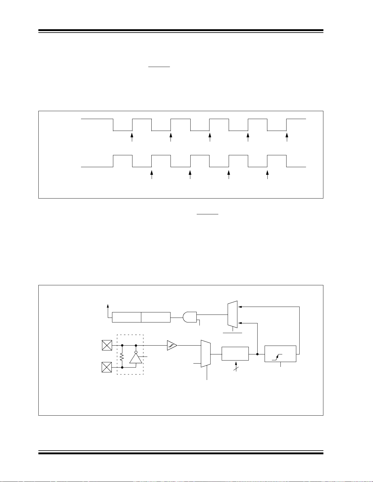
PIC16F7X
6.1 Timer1 Operation in Timer Mode
Timer mode is selected by clearing the TMR1CS
(T1CON<1>) bit. In this mode, the input clock to the
timer is F
OSC/4. The synchronize control bit T1SYNC
(T1CON<2>) has no effect, since the internal clock is
always in sync.
FIGURE 6-1: TIMER1 INCREMENTING EDGE
T1CKI
(Default high)
T1CKI
(Default low)
Note: Arrows indicate counter increments.
6.3 Timer1 Operation in Synchronized Counter Mode
Counter mode is selected by setting bit TMR1CS. In
this mode, the timer increm ents on every risin g edge of
clock input on pin RC1/T1OSI/CCP2, when bit
T1OSCEN is set, or on pi n RC0/T1 OSO/T 1CKI , when
bit T1OSCEN is cleared.
6.2 Timer1 Counter Operation
Timer1 may operate in Asynchronous or Synchronous
mode, depending on the setting of the TMR1CS bit.
When Timer1 is being incremented via an external
source, increment s occur on a ri sing edge. After T imer1
is enabled in Coun ter mode, the module mus t first have
a falling edge before the counter begins to increment.
If T1SYNC
synchronized with internal phase clocks. The synchronization is done after the prescaler stage. The prescaler stage is an asynchronous ripple counter.
In this configuration, during SLEEP mode, Timer1 will
not increment even if the external clock is present,
since the synchronization circuit is shut-off. The
prescaler, however, will continue to increment.
is cleared, the n the externa l clock input is
FIGURE 6-2: TIMER1 BLOCK DIAGRAM
Set Flag bit
TMR1IF on
Overflow
RC0/T1OSO/T1CKI
RC1/T1OSI/CCP2
Note 1: When the T1OSCEN bit is cleared, the inverter is turned off. This eliminates power drain.
2: For the PIC16F73/76, the Schmitt Trigger is not implemented in External Clock mode.
(2)
TMR1H
T1OSC
TMR1
TMR1L
T1OSCEN
Enable
Oscillator
(1)
(2)
FOSC/4
Internal
Clock
TMR1ON
On/Off
1
0
TMR1CS
0
1
T1SYNC
Prescaler
1, 2, 4, 8
2
T1CKPS1:T1CKPS0
Synchronized
Clock Input
Synchronize
det
Q Clock
DS30325B-page 48 2002 Microchip Technology Inc.
Page 51

PIC16F7X
6.4 Timer1 Operation in Asynchronous Counter Mode
If control bit T1SYNC (T1CON<2>) is set, the external
clock input is not synchronized. The timer continues to
increment asynchronous to the internal phase clocks.
The timer will continue to run during SLEEP and can
generate an interrupt on overflow, which will wake-up
the processor. However, special precautions in software are needed to read/write the time r (Section 6.4.1).
In Asynchronous Counter mode, Timer1 cannot be
used as a time-base for capture or compare operations.
6.4.1 READING AND WRITING TIMER1 IN ASYNCHRONOUS COUNTER MODE
Reading TMR1H or TMR1L, while the timer is running
from an external asynchronous clock, will ensure a
valid read (taken care of in hardware). However, the
user should keep in mind that reading the 16-bit timer
in two 8-bit values it self, poses certain problems, sinc e
the timer may overflow between the reads.
For writes, it is recommend ed that th e user s imply sto p
the timer and write the desired values. A write contention may occur by writing to the timer registers, while
the register is incrementing. This may produce an
unpredictable value in the timer register.
Reading the 16-bit value requires some care. The
example code provided in Example 6-1 and
Example 6-2 demonstrates how to write to and read
Timer1 while it is running in Asynchronous mode.
EXAMPLE 6-1: WRITING A 16-BIT FREE-RUNNING TIMER
; All interrupts are disabled
CLRF TMR1L ; Clear Low byte, Ensures no rollover into TMR1H
MOVLW HI_BYTE ; Value to load into TMR1H
MOVWF TMR1H, F ; Write High byte
MOVLW LO_BYTE ; Value to load into TMR1L
MOVWF TMR1H, F ; Write Low byte
; Re-enable the Interrupt (if required)
CONTINUE ; Continue with your code
EXAMPLE 6-2: READING A 16-BIT FREE-RUNNING TIMER
; All interrupts are disabled
MOVF TMR1H, W ; Read high byte
MOVWF TMPH
MOVF TMR1L, W ; Read low byte
MOVWF TMPL
MOVF TMR1H, W ; Read high byte
SUBWF TMPH, W ; Sub 1st read with 2nd read
BTFSC STATUS,Z ; Is result = 0
GOTO CONTINUE ; Good 16-bit read
; TMR1L may have rolled over between the read of the high and low bytes.
; Reading the high and low bytes now will read a good value.
MOVF TMR1H, W ; Read high byte
MOVWF TMPH
MOVF TMR1L, W ; Read low byte
MOVWF TMPL ; Re-enable the Interrupt (if required)
CONTINUE ; Continue with your code
2002 Microchip Technology Inc. DS30325B-page 49
Page 52
PIC16F7X
6.5 Timer1 Oscillator
A crystal oscillator ci rcuit is built-in betwee n pins T1OSI
(input) and T1OSO (amplifier output). It is enabled by
setting control bit T1OSCEN (T 1CON<3>). The oscill ator is a low power oscillator rated up to 200 kHz. It will
continue to run during SLEEP. It is primarily intended
for use with a 32 kHz crystal. Table 6-1 shows the
capacitor selection for the Timer1 oscillator.
The Timer1 oscillator is identical to the LP oscillator.
The user must provide a sof tware t im e del ay to en su re
proper oscillator start-up.
6.6 Resetting Timer1 using a CCP Trigger Output
If the CCP1 or CCP2 module is config ured in Com pa re
mode to generate a “special event trigger”
(CCP1M3:CCP1M0 = ‘1011’), this signal will reset
Timer1.
Note: The special event triggers from the CCP1
and CCP2 modules will not set interrupt
flag bit TMR1IF (PIR1<0>).
Timer1 mu st be confi gured for eit her T ime r or Synchronized Counter mode, to t ake adv an tage of this feature.
If Timer1 is running in Asynchronous Counter mode,
this RESET operation may not work.
In the event that a write to Timer1 coincides with a special event trigger from CCP1 or CCP2, the write will
take precedence.
In this mode of operati on, the CCPRxH :CCPRx L regi ster pair effectively becomes the period register for
Timer1.
6.7 Resetting of Timer1 Register Pair (TMR1H, TMR1L)
TMR1H and TMR1L registers are not rese t to 00h on a
POR, or any other RESET, except by the CCP1 and
CCP2 special event triggers.
T ABLE 6-1: CAPACITOR SELECTION FOR
THE TIMER1 OSCILLATOR
Osc T y pe Frequency
LP 32 kHz 47 pF 47 pF
100 kHz 33 pF 3 3 pF
200 kHz 15 pF 1 5 pF
Capacitor values are for design guidance only.
These capacitors were tested with the crystals listed
below for basic start-up and operation. These values
were not optimized.
Different ca pacitor val ues may be re quired to prod uce
acceptable oscillator operation. The user should test
the performance of the oscillator over the expected
DD and temperature range for the application.
V
See the notes (below) table for add itional information.
Commonly Used Crystals:
32.768 kHz Epson C-001R32.768K-A
100 kHz Epson C-2 100.00 KC-P
200 kHz STD XTL 200.000 kHz
Note 1: Higher capacitance increases the stability
of the oscillator, but also increases the
start-up time.
2: Since each resonator/crystal has its own
characteristics, the u ser shoul d consult th e
resonator/crystal manufacturer for appropriate values of external components.
T1CON register is rese t to 00h on a Powe r-on Rese t or
a Brown-out Reset, which shuts off the timer and
leaves a 1:1 presca le. In all oth er RESETS, the register
is unaffected.
Capacitors Used:
OSC1 OSC2
6.8 Timer1 Prescaler
The prescaler counter is cleared on writes to the
TMR1H or TMR1L registers.
TABLE 6-2: REGISTERS ASSOCIATED WITH TIMER1 AS A TIMER/COUNTER
Address Name Bit 7 Bit 6 Bit 5 Bit 4 Bit 3 Bit 2 Bit 1 Bit 0
0Bh,8Bh,
10Bh,18Bh
0Ch PIR1 PSPIF
8Ch PIE1 PSPIE
0Eh TMR1L Holding register for the Least Significant Byte of the 16-bit TMR1 Register xxxx xxxx uuuu uuuu
0Fh TMR1H Holding register for the Most Significant Byte of the 16-bit TMR1 Register xxxx xxxx uuuu uuuu
10h T1CON — — T1CKPS1 T1CKPS0 T1OSCEN T1SYNC TMR1CS TMR1ON --00 0000 --uu uuuu
Legend: x = unknown, u = unchanged, - = unimplemented, read as '0'. Shaded cells are not used by the Timer1 module.
Note 1: Bits PSPIE and PSPIF are reserved on the PIC16F73/76; always maintain these bits clear.
DS30325B-page 50 2002 Microchip Technology Inc.
INTCON GIE PEIE
(1)
(1)
TMR0IE INTE RBIE TMR0IF INTF RBIF 0000 000x 0000 000u
ADIF RCIF TXIF SSPIF CCP1IF TMR2IF TMR1IF 0000 0000 0000 0000
ADIE RCIE TXIE SSPIE CCP1IE TMR2IE TMR1IE 0000 0000 0000 0000
Value on:
POR,
BOR
Val ue on
all other
RESETS
Page 53
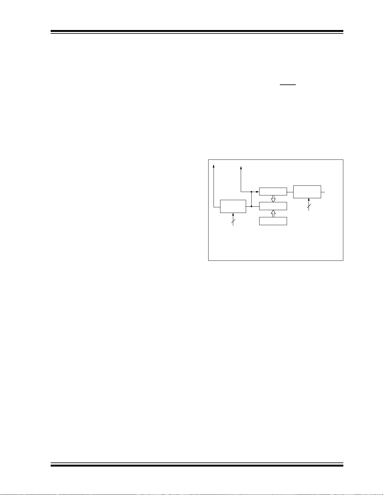
PIC16F7X
7.0 TIMER2 MODULE
Timer2 is an 8-bit timer with a prescaler and a
postscaler. It can be used as the PW M time-base fo r
the PWM mode of the CCP mod ule (s). The T MR2 re gister is readable and writable, and is cleared on any
device RESET.
The input clock (F
1:4 or 1:16, selected by control bits
T2CKPS1:T2CKPS0 (T2CON<1:0>).
The Timer2 module has an 8-bit period register, PR2.
Timer2 increments from 00h until it matches PR2 and
then resets to 00h on the next increment cycle. PR2 is
a readable and writable register. The PR2 register is
initialized to FFh upon RESET.
The match output of TMR2 goes through a 4-bit
postscaler (which gives a 1:1 to 1:16 scaling inclusive)
to generate a TMR2 interrupt (latched in flag bit
TMR2IF, (PIR1<1>)).
Timer2 c an b e s hu t-off by clearing control bit TMR2ON
(T2CON<2>) to minimize power consumption.
Register 7-1 shows the Timer2 control register.
Additional information on timer modules is available in
the PICmicro™ Mid-Range MCU Family Reference
Manual (DS33023).
OSC/4) has a prescale option of 1:1,
7.1 Timer2 Prescaler and Postscaler
The prescaler and postscaler counters are cleared
when any of the following occurs:
• a write to the TMR2 register
• a write to the T2CON register
• any device RESET (POR, MCLR
Reset, WDT
Reset or BOR)
TMR2 is not cleared when T2CON is written.
7.2 Output of TMR2
The output of TMR2 (before the post scaler) is fed to the
SSP module, which optionally uses it to generate shift
clock.
FIGURE 7-1: TIMER2 BLOCK DIAGRAM
Sets Flag
bit TMR2IF
Postscaler
1:1 to 1:16
T2OUTPS3:
T2OUTPS0
4
TMR2
Output
Reset
EQ
(1)
TMR2 reg
Comparator
PR2 reg
Prescaler
1:1, 1:4, 1:16
2
T2CKPS1:
T2CKPS0
OSC/4
F
Note 1: TMR2 register output can be software selected by the
SSP module as a baud clock.
2002 Microchip Technology Inc. DS30325B-page 51
Page 54
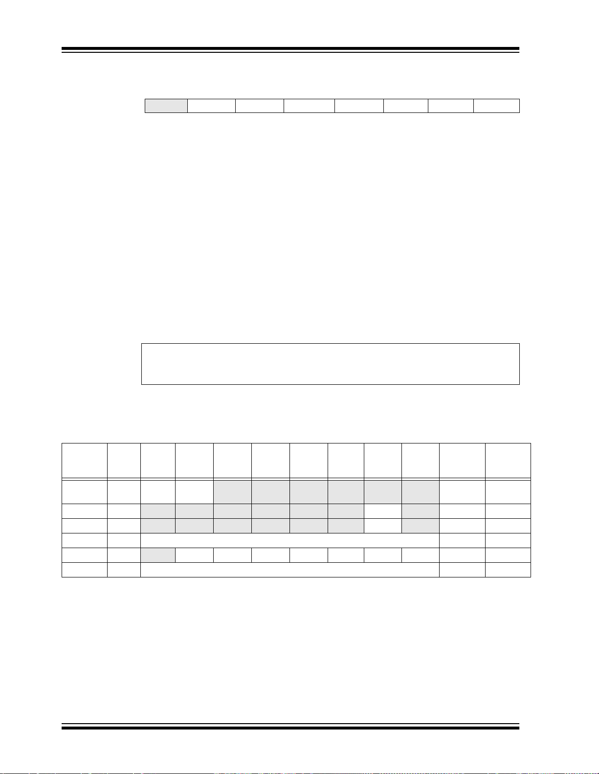
PIC16F7X
REGISTER 7-1: T2CON: TIMER2 CONTROL REGISTER (ADDRESS 12h)
U-0 R/W-0 R/W-0 R/W-0 R/W-0 R/W-0 R/W-0 R/W-0
— TOUTPS3 TOUTPS2 TOUTPS1 TOUTPS0 TMR2ON T2CKPS1 T2CKPS0
bit 7 bit 0
bit 7 Unimplemented: Read as ‘0’
bit 6-3 TOUTPS3:TOUTPS0: Timer2 Output Postscale Select bits
0000 = 1:1 Postscale
0001 = 1:2 Postscale
0010 = 1:3 Postscale
•
•
•
1111 = 1:16 Postscale
bit 2 TMR2ON: Timer2 On bit
1 = Timer2 is on
0 = Timer2 is off
bit 1-0 T2CKPS1:T2CKPS0: Timer2 Clock Prescale Select bits
00 = Prescaler is 1
01 = Prescaler is 4
1x = Prescaler is 16
Legend:
R = Readable bit W = Writable bit U = Unimplemented bit, read as ‘0’
- n = Value at POR reset ’1’ = Bit is set ’0’ = Bit is cleared x = Bit is unknown
TABLE 7-1: REGISTERS ASSOCIATED WITH TIMER2 AS A TIMER/COUNTER
Address Name Bit 7 Bit 6 Bit 5 Bit 4 Bit 3 Bit 2 Bit 1 Bit 0
0Bh,8Bh,
10Bh, 18Bh
0Ch PIR1 PSPIF
8Ch PIE1 PSPIE
11h TMR2 Timer2 Module Register
12h T2CON — TOUTPS3 TOUTPS2 T OUTPS1 TOUTPS0 TMR2ON T2CKPS1 T2CKPS0
92h PR2 Timer2 Period Register
Legend: x = unknown, u = unchanged, - = unimplemented, read as '0'. Shaded cells are not used by the Timer2 module.
Note 1: Bits PSPIE and PSPIF are reserved on the PIC16F73/76; always maintain these bits clear.
INTCON GIE PEIE
(1)
ADIF RCIF TXIF SSPIF CCP1IF TMR2IF TMR1IF
(1)
ADIE RCIE TXIE SSPIE CCP1IE T MR2I E TMR1IE
TMR0IE INTE RBIE TMR0IF INTF RBIF
Value on:
POR,
BOR
0000 000x 0000 000u
0000 0000 0000 0000
0000 0000 0000 0000
0000 0000 0000 0000
-000 0000 -000 0000
1111 1111 1111 1111
Value on
all other
RESETS
DS30325B-page 52 2002 Microchip Technology Inc.
Page 55

PIC16F7X
8.0 CAPTURE/COMPARE/PWM MODULES
Each Capture/Compare/PWM (CCP) module contains
a 16-bit register which can operate as a:
• 16-bit Capt ure register
• 16-bit Compare register
• PWM Master/Slave Duty Cycle register
Both the CCP1 and CCP2 modules are identical in
operation, with the e xception being the operation of the
special event trigg er. T abl e 8-1 and Table 8-2 show the
resources and interactions of the CCP module(s). In
the following sections, the operation of a CCP module
is described with respect to CCP1. CCP2 operates the
same as CCP1, except where noted.
8.1 CCP1 Module
Capture/Compare/PWM Register1 (CCPR1) is comprised of two 8-bit registers: CCPR1L (low byte) and
CCPR1H (high byte). The CCP1CON register controls
the operation of CCP1. The special event trigger is
generated by a compare match and will clear both
TMR1H and TMR1L registers.
8.2 CCP2 Module
Capture/Compare/PWM Register1 (CCPR1) is comprised of tw o 8-bit registers: CCPR1L (low byte) and
CCPR1H (high byte). The CCP2CON register controls
the operation of CCP2. The special event trigger is
generated by a compare match; it will clear both
TMR1H and TMR1L regi sters, and st art an A/D co nversion (if the A/D module is enabled).
Additional information on CCP modules is available in
the PICmicro™ Mid-Range MCU Family Reference
Manual (DS33023) and in Application Note AN594,
“Using the CCP Modules” (DS00594).
TABLE 8-1: CCP MODE - TIMER
RESOURCES REQUIRED
CCP Mode Timer Resource
Capture
Compare
PWM
Timer1
Timer1
Timer2
TABLE 8-2: INTERACTION OF TWO CCP MODULES
CCPx Mode CCPy Mode Interaction
Capture Capture Same TMR1 time-base.
Capture Compare
Compare Compare
PWM PWM The PWMs will have the same frequency and update rate (TMR2 interrupt).
PWM Capture None.
PWM Compare None.
Same TMR1 time-base.
Same TMR1 time-base.
The rising edges are aligned.
2002 Microchip Technology Inc. DS30325B-page 53
Page 56

PIC16F7X
REGISTER 8-1: CCP1CON REGISTER/CCP2CON REGISTER (ADDRESS: 17h/1Dh)
U-0 U-0 R/W-0 R/W -0 R/W-0 R/W-0 R/W- 0 R/W-0
— — CCPxX CCPxY CCPxM3 CCPxM2 CCPxM1 CCPxM0
bit 7 bit 0
bit 7-6 Unimplemented: Read as '0'
bit 5-4 CCPxX:CCPxY: PWM Least Significant bits
Capture mode:
Unused
Compare mode:
Unused
PWM mode:
These bits are the two LSbs of the PWM duty cycle. The eight MSbs are found in CCPRxL.
bit 3-0 CCPxM3:CCPxM0: CCPx Mode Select bits
0000 =Capture/Compare/PWM disabled (resets CCPx module)
0100 =Capture mode, every falling edge
0101 =Capture mode, every rising edge
0110 =Capture mode, every 4th rising edge
0111 =Capture mode, every 16th rising edge
1000 =Compare mode, set output on match (CCPxIF bit is set)
1001 =Compare mode, clear output on match (CCPxIF bit is set)
1010 = Compare mode, generate software interrupt on match (CCPxIF bit is set, CCPx pin is
1011 = Compare mode, trigger special event (CCPxIF bit is set, CCPx pin is unaffected);
11xx =PWM mode
unaffected)
CCP1 clears T imer1; CCP2 clears T imer1 and st arts an A/D conversion (if A/D module
is enabled)
Legend:
R = Readable bit W = Writable bit U = Unimplemented bit, read as ‘0’
- n = Value at POR reset ’1’ = Bit is set ’0’ = Bit is cleared x = Bit is unknown
DS30325B-page 54 2002 Microchip Technology Inc.
Page 57
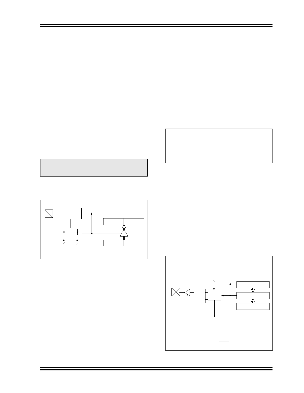
PIC16F7X
8.3 Capture Mode
In Capture mode, CCPR1H:CCPR1L captures the
16-bit value of the TMR1 r egister wh en an eve nt occurs
on pin RC2/CCP1. An ev ent is defined as on e of the following and is configured by CCPxCON<3:0>:
• Every falling edge
• Every rising edge
• Every 4th rising edge
• Every 16th rising edge
An event is selected by control bits CCP1M3:CCP1M0
(CCP1CON<3:0>). When a capture is made, the interrupt request flag bit CCP1IF (PIR1<2>) is set. The
interrupt flag must be cleared in software. If another
capture occurs before the value in register CCPR1 is
read, the old captured value is overwritten by the new
captured value.
8.3.1 CCP PIN CONFIGURATION
In Capture mode, the R C2/ CCP 1 pin sh oul d b e configured as an input by setti ng the TRISC<2> bit.
Note: If the RC2/CCP1 pin is configured as an
output, a write to the port can cause a
capture condition.
FIGURE 8-1: CAPTURE MODE
OPERATION BLOCK
DIAGRAM
Set Flag bit CCP1IF
Prescaler
÷ 1, 4, 16
RC2/CCP1
pin
and
Edge Detect
CCP1CON<3:0>
Q’s
8.3.2 TIMER1 MODE SELECTION
Timer1 must be running in Timer mode or Synchronized Counter mode for the CCP module to use the
capture feature. In Asynchronous Counter mode, the
capture operation may not work.
8.3.3 SOFTWARE INTERRUPT
When the Capture mode is changed, a false capture
interrupt may be generated. The user should keep bit
CCP1IE (PIE1<2>) clear to avoid false interrupts and
should clear the flag bit CCP1IF following any such
change in operating mode.
(PIR1<2>)
CCPR1H CCPR1L
Capture
Enable
TMR1H TMR1L
8.3.4 CCP PRESCALER
There are four prescaler settings, specified by bits
CCP1M3:CCP1M0. Whenever the CCP module is
turned off, or the CCP module is not in Capture mode,
the prescaler counter is cleared. Any RESET will clear
the prescaler counter.
Switching from one capture prescaler to another may
generate an interrupt. Also, the prescaler counter will
not be cleared, therefore, the first cap ture may be from
a non-zero prescaler. Example 8-1 shows the recommended method for switching between capture prescalers. This example also clears the prescaler counter
and will not generate the “false” interrupt.
EXAMPLE 8-1: CHANGING BETWEEN
CAPTURE PRESCALERS
CLRF CCP1CON ;Turn CCP module off
MOVLW NEW_CAPT_PS ;Load the W reg with
MOVWF CCP1CON ;Load CCP1CON with this
;the new prescaler
;move value and CCP ON
;value
8.4 Compare Mode
In Compare mode, the 16-bit CCPR1 register value is
constantly compared against the TMR1 register pair
value. When a match occurs, the RC2/CCP1 pin is:
• Driven high
• Driven low
• Remains unchanged
The action on the pin is based on the value of control
bits CCP1M3:CCP1M0 (CCP1CON<3:0>). At the
same time, interrupt flag bit CCP1IF is set.
FIGURE 8-2: COMPARE MODE
OPERATION BLOCK
DIAGRAM
CCP1CON<3:0>
Mode Select
Set Flag bit CCP1IF
(PIR1<2>)
CCPR1H CCPR1L
QS
Output
RC2/CCP1
Pin
TRISC<2>
Output Enable
Special Event Trigger will:
• clear TMR1H and TMR1L registers
• NOT set interrupt flag bit TMR1F (PIR1<0>)
• (for CCP2 only) set the GO/DONE
Logic
R
Special Event Trigger
Match
Comparator
TMR1H TMR1L
bit (ADCON0<2>)
2002 Microchip Technology Inc. DS30325B-page 55
Page 58
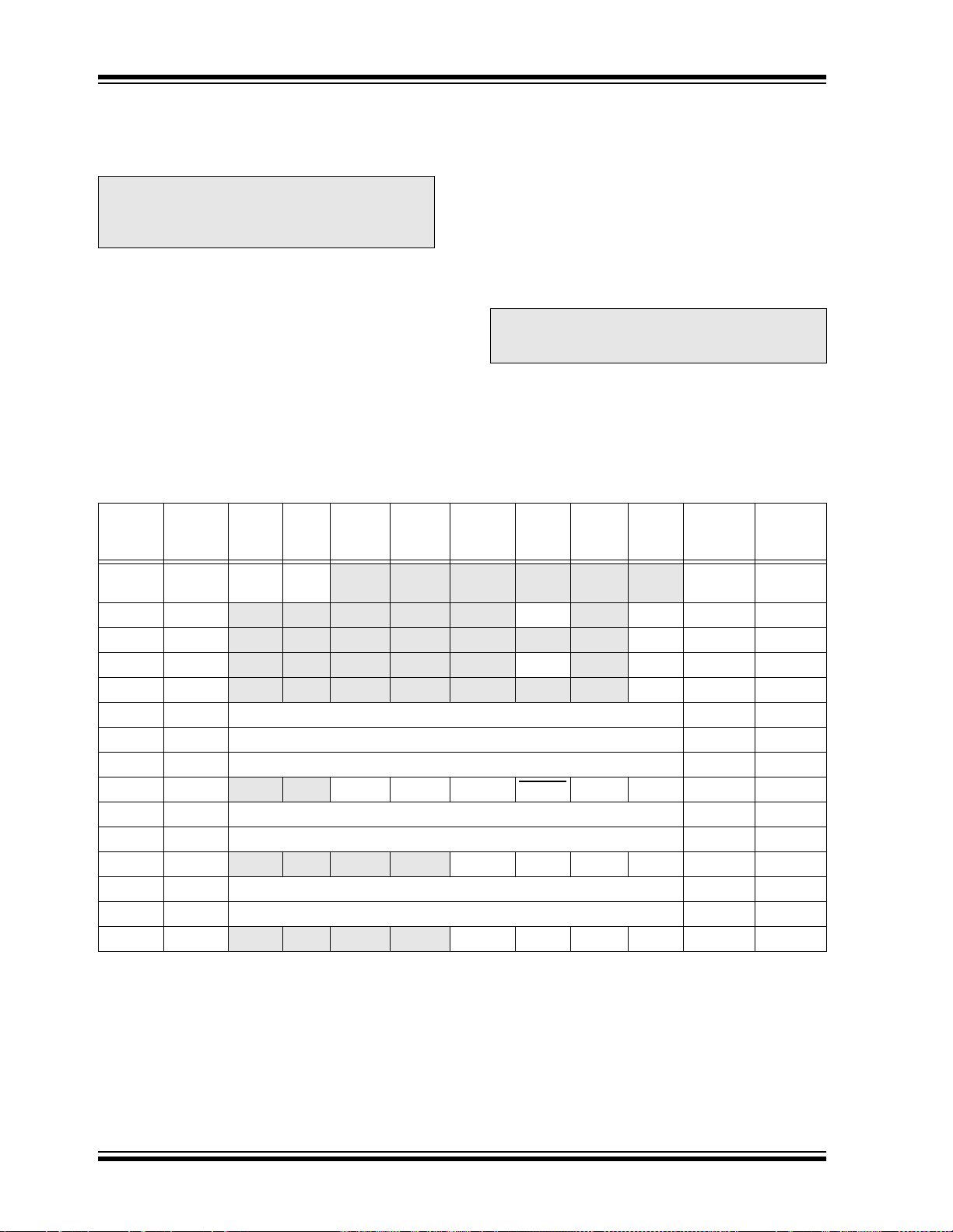
PIC16F7X
8.4.1 CCP PIN CONFIGURATION
The user must configure the RC2/CCP1 pin as an output by clearing the TRISC<2> bit.
Note: Clearing the CCP1CON register will force
the RC2/CCP1 compare outp ut latch to the
default low level. This is not the PORTC
I/O data latch.
8.4.2 TIMER1 MODE SELECTION
Timer1 must be running in Timer mode or Synchronized Counter mode if the CCP module is using the
compare feature. In Asynchronous Counter mode, the
compare operation may not work.
8.4.4 SPECIAL EVENT TRIGG ER
In this mode, an internal hardware trigger is gene rated,
which may be used to initiate an action.
The special event trigger output of CCP1 resets the
TMR1 regist er pai r. This al lows the CCPR 1 re gis ter to
effectively b e a 16-bit progra mmable period registe r for
Timer1.
The special event trigger output of CCP2 resets the
TMR1 register pai r and starts an A/D conversion (if the
A/D module i s enabled).
Note: The special event trigger from the CCP1
and CCP2 modules will not set interrupt
flag bit TMR1IF (PIR1<0>).
8.4.3 SOFTWARE INTERRUPT MODE
When Generate Softw are Interrupt mode is chosen, the
CCP1 pin is not affect ed. The CCP1 IF or CCP 2IF bit is
set, causing a CCP interrupt (if enabled).
TABLE 8-3: REGISTERS ASSOCIATED WITH CAPTURE, COMPARE, AND TIMER1
Val ue on:
Address Name Bit 7 Bit 6 Bit 5 Bit 4 Bit 3 Bit 2 Bit 1 Bit 0
POR,
BOR
Val ue on
all other
RESETS
0Bh,8Bh,
10Bh,18Bh
0Ch PIR1 PSPIF
0Dh PIR2 — — — — — — — CCP2IF ---- ---0 ---- ---0
8Ch PIE1 PSPIE
8Dh PIE2 — — — — — — — CCP2IE ---- ---0 ---- ---0
87h TRISC PORTC Data Direction Register 1111 1111 1111 1111
0Eh TMR1L Holding Register for the Least Significan t Byte of t he 16-bi t TMR1 Reg ister xxxx xxxx uuuu uuuu
0Fh TMR1H Holding Reg ister for the Most Signi fican t Byte of t he 1 6-bit TMR1 Regi ster xxxx xxxx uuuu uuuu
10h T1CON — — T1CKPS1 T1CKPS0 T1OSCEN T1SYNC TMR1CS TMR1ON --00 0000 --uu uuuu
15h CCPR1L Capture/Compare/PWM Register1 (LSB) xxxx xxxx uuuu uuuu
16h CCPR1H Capture/Compare/PWM Register1 (MSB) xxxx xxxx uuuu uuuu
17h CCP1CON — — CCP1X CCP1Y CCP1M3 CCP1M2 CCP1M1 CCP1M0 --00 0000 --00 0000
1Bh CCPR2L Capture/Compare/PWM Register2 (LSB) xxxx xxxx uuuu uuuu
1Ch CCPR2H Capture/Compare/PWM Register2 (MSB) xxxx xxxx uuuu uuuu
1Dh CCP2CON — — CCP2X CCP2Y CCP2M3 CCP2M2 CCP2M1 CCP2M0 --00 0000 --00 0000
Legend: x = unknown, u = unchanged, - = unimplemented, read as '0'. Shaded cells are not used by Capture and Timer1.
Note 1: The PSP is not implemented on the PIC16F73/76; always maintain these bits clear.
INTCON GIE PEIE
(1)
(1)
TMR0IE INTE RBIE TMR0IF INTF RBIF 0000 000x 0000 000u
ADIF RCIF TXIF SSPIF CCP1IF TMR2IF TMR1IF 0000 0000 0000 0000
ADIE RCIE TXIE SSPIE CCP1IE TMR2IE TMR1IE 0000 0000 0000 0000
DS30325B-page 56 2002 Microchip Technology Inc.
Page 59
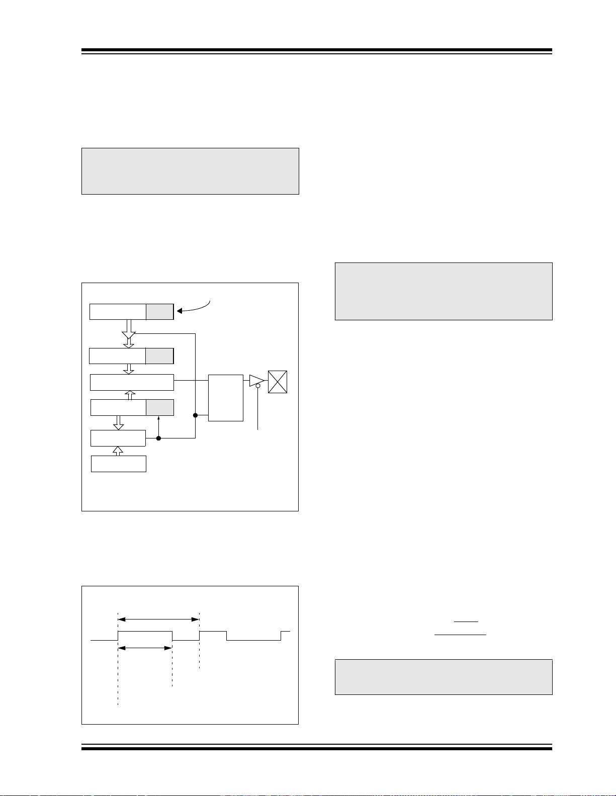
PIC16F7X
8.5 PWM Mode (PWM)
In Pulse Width Modulation mo de, the CCPx pin produces up to a 10-bit resolution PWM output. Since the
CCP1 pin is mult iplexed with the PORTC data latch, the
TRISC<2> bit must be cleared to make the CCP1 pin
an output.
Note: Clearing the CCP1CON register will force
the CCP1 PWM output latch to the default
low level. This is not the PORTC I/O data
latch.
Figure 8-3 shows a simplified block diagram of the
CCP module in PWM mode.
For a step-by-step procedure on how to set up the C CP
module for PWM operation, see Section 8.5.3.
FIGURE 8-3: SIMPLIFIED PWM BLOCK
DIAGRAM
Duty Cycle Registers
CCPR1L
CCPR1H (Slave)
Comparator
TMR2
(Note 1)
Comparator
PR2
Note 1: The 8-b it timer is concatenated with the 2-bit inter-
nal Q clock or the 2 bits of the prescaler to create the
10-bit time-base.
A PWM output (Figure 8-4) has a time-base (period)
and a time that the output stays high (duty cycle). The
frequency of the PWM is the inverse of the period
(1/period).
FIGURE 8-4: PWM OUTPUT
TMR2
RESET
Period
Duty Cycle
CCP1CON<5:4>
RQ
(1)
Clear Timer,
CCP1 pin and
latch D.C.
TMR2 = Duty Cycle
S
TMR2
RESET
TMR2 = PR2
RC2/CCP1
TRISC<2>
8.5.1 PWM PERIO D
The PWM period is specified by writing to the PR2
register. The PWM period can be calculated using the
following formula:
PWM period = [(PR2) + 1] • 4 • T
OSC •
(TMR2 prescale value)
PWM frequency is defined as 1 / [PWM period].
When TMR2 is eq ual to PR2, t he following three event s
occur on the ne xt increment cycle:
• TMR2 is cleared
• The CCP1 pin is set (exception: if PWM duty
cycle = 0%, the CCP1 pin will not be set)
• The PWM duty cycle is latc hed from CC PR1L into
CCPR1H
Note: The Timer2 postscaler (see Section8.3) is
not used in the determination of the PWM
frequency . T he posts caler coul d be used to
have a servo update rate at a different frequency than the PWM output.
8.5.2 PWM DUTY CYCLE
The PWM duty cycle is specified by writing to the
CCPR1L register and to the CCP1CON<5:4> bits. Up
to 10-bit re so l uti on is av ai l ab le. T he CC PR 1L c on tai ns
the eight MSbs and the CCP1CON<5:4> contains the
two LSbs. This 10-bit value is represented by
CCPR1L:CCP1CON<5:4>. The following equation is
used to calculate the PWM duty cycle in time:
PWM duty cycle = (CCPR1L:CCP1CON<5:4>) •
OSC • (TMR2 prescale valu e)
T
CCPR1L and CCP1CON<5:4> can be written to at any
time, but the duty cycle value is not latched into
CCPR1H until after a match between PR2 and TMR2
occurs (i.e., the period is complete). In PWM mode,
CCPR1H is a read only register.
The CCPR1H register and a 2-bit internal latch are
used to double buf fer the PWM duty cycle. Thi s doubl e
buffering is essential for glitchless PWM operation.
When the CCPR 1H and 2 -bit latch match T MR2, con catenated with an internal 2-bit Q clock or 2 bits of the
TMR2 prescaler, the CCP1 pin is cleared.
The maximum PWM resolution (bits) for a given PWM
frequency is given by the formula:
F
OSC
FPWM
log(2)
)
bits
log(
Resolution
=
Note: If the PWM duty cycle value is longer than
the PWM period, the CCP1 pin will not be
cleared.
TMR2 = PR2
2002 Microchip Technology Inc. DS30325B-page 57
Page 60

PIC16F7X
8.5.3 SETUP FOR PWM OPERATION
The following steps should be taken when configuring
the CCP module for PWM operation:
1. Set the PWM period by writ ing to the PR2 register .
3. Make the CCP1 pin an output by clearing the
TRISC<2> bit.
4. Set the TMR2 prescale value a nd enable T imer2
by writing to T2CON.
5. Configure the CCP1 module for PWM o peration.
2. Set the PWM duty cycle by writing to the
CCPR1L register and CCP1CON<5:4> bits.
TABLE 8-4: EXAMPLE PWM FREQUENCIES AND RESOLUTIONS (FOSC = 20 MHz)
PWM Frequency 1.22 kHz 4.88 kHz 19.53 kHz 78.12 kHz 156.3 kHz 208.3 kHz
Timer Prescale (1, 4, 16) 16 4 1 1 1 1
PR2 Value 0xFF 0xFF 0xFF 0x3F 0x1F 0x17
Maximum Resolution (bits) 10 10 10 8 7 5.5
TABLE 8-5: REGISTERS ASSOCIATED WITH PWM AND TIMER2
Val ue on:
Addr e s s Name Bit 7 Bit 6 Bit 5 Bit 4 Bit 3 Bit 2 Bit 1 Bit 0
0Bh,8Bh,
10Bh,18Bh
0Ch PIR1 PSPIF
0Dh PIR2 — — — — — — — CCP2I F ---- ---0 ---- ---0
8Ch PIE1 PSPIE
8Dh PIE2 — — — — — — — CCP2IE ---- ---0 ---- ---0
87h TRISC PORTC Data Direction Reg ister 1111 1111 1111 1111
11h TMR2 Timer2 Modu le R egiste r 0000 0000 0000 0000
92h PR2 Timer2 Module Period Register 1111 1111 1111 1111
12h T2CON — TOUTPS3 TOUTPS2 TOUTPS1 TOUTPS0 TMR2ON T2CKPS1 T2CKPS0 -000 0000 -000 0000
15h CCPR1L Capture/Compare/PWM Register1 (LSB) xxxx xxxx uuuu uuuu
16h CCPR1H Capture/Compare/PWM Register1 (MSB) xxxx xxxx uuuu uuuu
17h CCP1CON — — CCP1X CCP1Y CCP1M3 CCP1M2 CCP1M1 CCP1M0 --00 0000 --00 0000
1Bh CCPR2L Capture/Compare/PWM Register2 (LSB) xxxx xxxx uuuu uuuu
1Ch CCPR2H Capture/Compare/PWM Register2 (MSB) xxxx xxxx uuuu uuuu
1Dh CCP2CON — — CCP2X CCP2Y CCP2M3 CCP2M2 CCP2M1 CCP2M0 --00 0000 --00 0000
Legend: x = unknown, u = unchanged, - = unimplemented, read as '0'. Shaded cells are not used by PWM and Timer2.
Note 1: Bits PSPIE and PSPIF are reserved on the PIC16F73/76; always maintain these bits clear.
INTCON GIE PEIE
(1)
ADIF RCIF TXIF SSPIF CCP1IF TMR2IF TMR1IF 0000 0000 0000 0000
(1)
ADIE RCIE TXIE SSPIE CCP1IE TMR2IE TMR1IE 0000 0000 0000 0000
TMR0IE INTE RBIE TMR0IF INTF RBIF 0000 000x 0000 000u
POR,
BOR
Value on
all other
RESETS
DS30325B-page 58 2002 Microchip Technology Inc.
Page 61

PIC16F7X
9.0 SYNCHRONOUS SERIAL PORT
(SSP) MODULE
9.1 SSP Module Overview
The Synchronous Serial Port (SSP) module is a serial
interface useful for communicating with other peripheral or microcontroller devices. These peripheral
devices may be Serial EEPROMs, shift registers, display drivers, A/D conv erte rs, et c. The SSP m odu le ca n
operate in one of two modes:
• Serial Peripheral Interface (SPI)
• Inter-Integrated Circuit (I
2
An overview of I
tion on the SSP module can be found in the PICmicro™
Mid-Range MCU Family Reference Manual
(DS33023).
Refer to Application Note AN578, “Use of the SSP
Module in the I
(DS00578).
C operations and additional informa-
2
C)
2
C Multi-Master Environment”
9.2 SPI Mode
This section contains register definitions and operational characteristics of the SPI module. Additional
information on the SPI module can be found in the
PICmicro™ Mid-Range MCU Family Reference Manual (DS33023A).
SPI mode allows 8 bits of data to be synchronously
transmitted and received simultaneously. To accomplish communication, typically three pins are used:
• Serial Data Out (SDO) RC5/SDO
• Serial Data In (SDI) RC4/SDI/SDA
• Serial Clock (SCK) RC3/SCK/SCL
Additionally, a fourth pin may be used when in a Slave
mode of operation:
• Slave Select (SS
When initializing the SPI, several options need to be
specified. This is done by programming the appropriate
control bits in the SSPCON register (SSPCON<5:0>)
and SSPSTAT<7:6>. These control bits allow the following to be specified:
• Master mode (SCK is the cloc k output)
• Slave mode (SCK is the clock input)
• Clock Polarity (IDLE state of SCK)
• Clock edge (output data on rising/falling edge of
SCK)
• Clock Rate (Master mode only)
• Slave Select mode (Slave mode only)
) RA5/SS/AN4
2002 Microchip Technology Inc. DS30325B-page 59
Page 62

PIC16F7X
REGISTER 9-1: SSPSTAT: SYNC SERIAL PORT STATUS REGISTER (ADDRESS 94h)
R/W-0 R/W-0 R-0 R-0 R-0 R-0 R-0 R-0
SMP CKE D/A
bit 7 bit 0
bit 7 SMP: SPI Data Input Sample Phase bit
SPI Master mode:
1 = Input data sampled at end of data output time
0 = Input data sampled at middle of data output time (Microwire
SPI Slave mode:
SMP must be cleared when SPI is used in Slave mode
2
I
C mode:
This bit must be maintained clear
bit 6 CKE: SPI Clock Edge Select bit (Figure9-2, Figure 9-3, and Figure 9-4)
SPI mode, CKP = 0:
1 = Data transmitted on rising edge of SCK (Microwire® alternate)
0 = Data transmitted on falling edge of SCK
SPI mode, CKP = 1:
1 = Data transmitted on falling edge of SCK (Microwire® default)
0 = Data transmitted on rising edge of SCK
2
I
C mode:
This bit must be maintained clear
bit 5 D/A
: Data/Address bit (I2C mode only)
1 = Indicates that the last byte received or transmitted was data
0 = Indicates that the last byte received or transmitted was address
2
bit 4 P: STOP bit (I
C mode only)
This bit is cleared when the SSP module is disabled, or when the START bit is detected last.
SSPEN is cleared.
1 = Indicates that a STOP bit has been detected last (this bit is ’0’ on RESET)
0 = STOP bit was not detected last
bit 3 S: START bit (I
2
C mode only)
This bit is cleared when the SSP module is disabled, or when the STOP bit is detected last.
SSPEN is cleared.
1 = Indicates that a START bit has been detected last (this bit is ’0’ on RESET)
0 = START bit was not detected last
bit 2 R/W
: Read/Write bit Information (I2C mode only)
This bit holds the R/W bit inform ation followin g the last address match. This bit is only vali d from
the address match to the next START bit, STOP bit, or ACK
1 = Read
0 = Write
2
bit 1 UA: Update Address bit (10-bit I
C mode only)
1 = Indicates that the user needs to update the address in the SSPADD register
0 = Address does not need to be updated
bit 0 BF: Buffer Full Status bit
Receive (SPI and I2 C modes):
1 = Receive complete, SSPBUF is full
0 = Receive not complete, SSPBUF is empty
2
Transmit (I
C mode only):
1 = Transmit in progress, SSPBUF is full
0 = Transmit complete, SSPBUF is empty
PSR/WUA BF
®
)
bit.
Legend:
R = Readable bit W = Writable bit U = U nimplemented bit, read as ‘0’
- n = Value at POR reset ’1’ = Bit is set ’0’ = Bit is cleared x = Bit is unknown
DS30325B-page 60 2002 Microchip Technology Inc.
Page 63

PIC16F7X
REGISTER 9-2: SSPCON: SYNC SERIAL PORT CONTROL REGISTER (ADDRESS 14h)
R/W-0 R/W-0 R/W-0 R/W-0 R/W-0 R/W-0 R/W-0 R/W-0
WCOL SSPOV SSPEN CKP SSPM3 SSPM2 SSPM1 SSPM0
bit 7 bit 0
bit 7 WCOL: Write Collision Detect bit
1 = The SSPBUF register is written while it is still transmitting the previous word
(must be cleared in software)
0 = No collision
bit 6 SSPOV: Receive Overflow Indicator bit
In SPI mode:
1 = A new byte is received while the SSPBUF regi ster is s till hol ding the pre vious d ata. In case
of overflow, the data in SSPSR is lost. Overflow can only occur in Slave mode. The user
must read the SSPBUF, even if only transmitting data, to avoid setting overflow. In
Master mode, the overflow bit is not set since each new reception (and transmission) is
initiated by writing to the SSPBUF register.
0 = No overflow
In I2 C mode:
1 = A byte is received while the SSPBUF register is still holding the previous byte. SSPOV
is a “don’t care” in Transmit mode. SSPOV must be cleared in software in either mode.
0 = No overflow
bit 5 SSPEN: Synchronous Serial Port Enable bit
In SPI mode:
1 = Enables serial port and configures SCK, SDO, and SDI as serial port pins
0 = Disables serial port and configures these pins as I/O port pins
2
C mode:
In I
1 = Enables the serial port and configures the SDA and SCL pins as serial port pins
0 = Disables serial port and configures these pins as I/O port pins
In both modes, when enabled, these pins must be properly configured as input or output.
bit 4 CKP: Clock Polarity Select bit
In SPI mode:
1 = IDLE state for clock is a high level (Microwire® default)
0 = IDLE state for clock is a low level (Microwire
2
In I
C mode:
SCK release control
1 = Enable clock
0 = Holds clock low (clock stretch). (Used to ensure data setup time.)
bit 3-0 SSPM3:SSPM0: Synchronous Serial Port Mode Select bits
0000 = SPI Master mode, clock = F
0001 = SPI Master mode, clock = F
0010 = SPI Master mode, clock = F
OSC/4
OSC/16
OSC/64
0011 = SPI Master mode, clock = TMR2 output/2
0100 = SPI Slave mode, clock = SCK pin. SS pin control enabled.
0101 = SPI Slave mode, cl oc k = SCK pin . SS
0110 = I
0111 = I
1011 = I
1110 = I
1111 = I
2
C Slave mode, 7-bit address
2
C Slave mode, 10-bit address
2
C Firmware Controlled Master mode (slave IDLE)
2
C Slave mode, 7-bit address with START and STOP bit interrupts enabled
2
C Slave mode, 10-bit address with START and STOP bit interrupts enabled
®
alternate)
pin control disabled. SS can be used as I/O pin .
Legend:
R = Readable bit W = Writable bit U = Unimplemented bit, read as ‘0’
- n = Value at POR reset ’1’ = Bit is set ’0’ = Bit is cleared x = Bit is unknown
2002 Microchip Technology Inc. DS30325B-page 61
Page 64
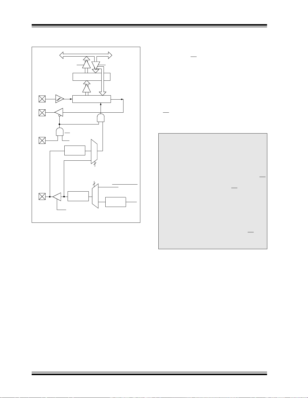
PIC16F7X
FIGURE 9-1: SSP BLOCK DIAGRAM
(SPI MODE)
Internal
Data Bus
Read Write
SSPBUF reg
SSPSR reg
2
Shift
Clock
TMR2 Output
Prescaler
4, 16, 64
2
T
RC4/SDI/SDA
RC5/SDO
RA5/SS/AN4
RC3/SCK/
SCL
bit0
Peripheral OE
Control
SS
Enable
Edge
Select
SSPM3:SSPM0
Edge
Select
TRISC<3>
Clock Select
4
CY
To enable the serial port, SSP enable bit, SSPEN
(SSPCON<5>) must be set. T o res et or reconfigure SPI
mode, clear bit SSPEN, re-initialize the SSPCON register, and then set bit SSPEN. This configures the SDI,
SDO, SCK, and SS
pins as serial port pins. For the pins
to behave as the serial port function, they must have
their data direction bits (in the TRISC register) appropriately programmed. That is:
• SDI must have TRISC<4> set
• SDO must have TRISC<5> cleared
• SCK (Master mode) must have TRISC<3>
cleared
• SCK (Slave mode) must have TRISC<3> set
must have TRISA<5> set and ADCON must
• SS
be configured such that RA5 is a digital I/O
.
Note 1: When the SPI is in Slave mode with SS pin
control enabled (SSPCON<3:0> = 0100),
the SPI module will reset if the SS pin is set
DD.
to V
2: If the SPI is used in Slave mode with
CKE = '1', then the SS p in control mus t be
enabled.
3: When the SPI is in Slave mode with SS
pin control enabled (SSPCON<3:0> =
‘0100’), the state of the SS
pin can affect
the state read back from the TRISC<5>
bit. The Peripheral OE signal from the
SSP module into PORTC controls the
state that is read back from the
TRISC<5> bit (see Section 4.3 for information on PORTC). If Read-Modi fy-Write
instructions, such as BSF are perfor med
on the TRISC register while the SS
pin is
high, this will cause the TRISC<5> bit to
be set, thus disabling the SDO output.
DS30325B-page 62 2002 Microchip Technology Inc.
Page 65

FIGURE 9-2: SPI MODE TIMING, MASTER MODE
SCK (CKP = 0,
CKE = 0)
SCK (CKP = 0,
CKE = 1)
SCK (CKP = 1,
CKE = 0)
SCK (CKP = 1,
CKE = 1)
PIC16F7X
SDO
SDI (SMP = 0)
SDI (SMP = 1)
SSPIF
bit7
bit7
bit7 bit0
bit6 bit5
bit4
bit3
FIGURE 9-3: SPI MODE TIMING (SLAVE MODE WITH CKE = 0)
SS (optional)
SCK (CKP = 0)
SCK (CKP = 1)
SDO
SDI (SMP = 0)
bit7
bit6 bit5
bit4
bit3
bit2
bit2
bit1 bit0
bit0
bit1 bit0
bit7 bit0
SSPIF
FIGURE 9-4: SPI MODE TIMING (SLAVE MODE WITH CKE = 1)
SS
SCK (CKP = 0)
SCK (CKP = 1)
SDO
SDI (SMP = 0)
SSPIF
2002 Microchip Technology Inc. DS30325B-page 63
bit7
bit7 bit0
bit6 bit5
bit4
bit3
bit2
bit1 bit0
Page 66
PIC16F7X
TABLE 9-1: REGISTERS ASSOCIATED WITH SPI OPERATION
Address Name Bit 7 Bit 6 Bit 5 Bit 4 Bit 3 Bit 2 Bit 1 Bit 0
0Bh,8Bh.
10Bh,18Bh
0Ch PIR1 PSPIF
8Ch PIE1 PSPIE
87h TRISC PORTC Data Direction Register 1111 1111 1111 1111
13h SSPBUF Synchronous Serial Port Receive Buffer/Transmit Register xxxx xxxx uuuu uuuu
14h SSPCON WCOL SSPOV SSPEN CKP SSPM3 SSPM2 SSPM1 SSPM0 0000 0000 0000 0000
85h TRISA — — PORTA Data Direction Register --11 1111 --11 1111
94h SSPSTAT SMP CKE D/A P S R/W UA BF 0000 0000 0000 0000
Legend: x = unknown, u = unchanged, - = unimplemented, read as '0'. Shaded cells are not used by the SSP in SPI mode.
Note 1: Bits PSPIE and PSPIF are reserved on the PIC16F73/76; always maintain these bits clear.
INTCON GIE PEIE
(1)
(1)
TMR0IE INTE RBIE TMR0IF INTF RB IF 0000 000x 0000 000u
ADIF RCIF TXIF SSPIF CCP1IF TMR2IF TMR1IF 0000 0000 0000 0000
ADIE RCIE TXIE SSPIE CCP1IE TMR2IE TMR1IE 0000 0000 0000 0000
Value on:
POR,
BOR
Value on
all other
RESETS
DS30325B-page 64 2002 Microchip Technology Inc.
Page 67
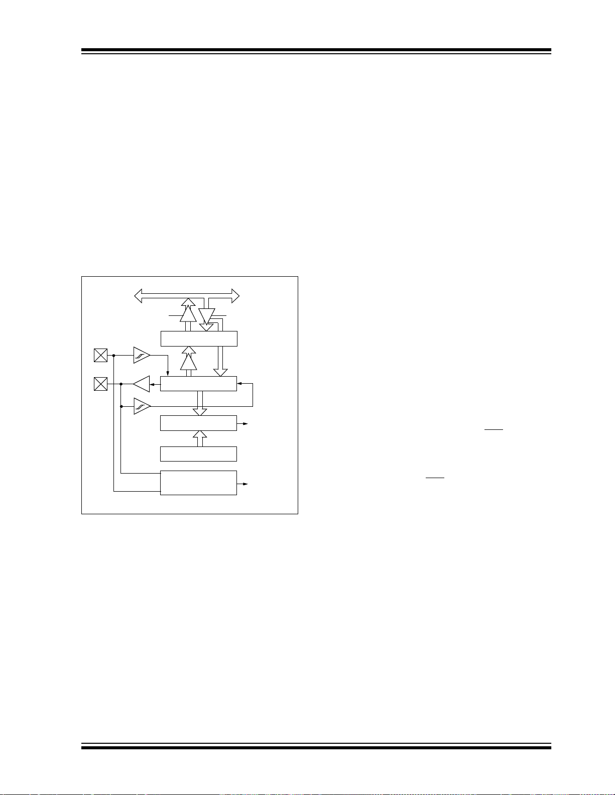
9.3 SSP I2 C Operation
The SSP module in I2C mode, fully implements all slave
functions, except general call support, and provides
interrupts on ST ART and STOP bit s in hardware to facilitate firmware implementations of the master functions.
The SSP module implements the standard mode specifications as well as 7-bit and 10-bit addressing.
Two pin s are used for dat a transfer . These ar e the RC3/
SCK/SCL pin, which is the clock (SCL), and the RC4/
SDI/SDA pi n, which i s the data (SDA). T he user must
configure these pins as inputs or outputs through the
TRISC<4:3> bits.
The SSP module function s are enabl ed by settin g SSP
enable bit SSPEN (SSPCON<5>).
FIGURE 9-5: SSP BLOCK DIAGRAM
Read Write
RC3/SCK/SCL
Shift
Clock
RC4/
SDI/
SDA
The SSP module has five registers for I2C operation.
These are the:
• SSP Control Register (SSPCON)
• SSP Status Register (SSPSTAT)
• Serial Receive/Transmit Buffer (SSPBUF)
• SSP Shift Register (SSPSR) - No t di rec tly ac ces sibl e
• SSP Address Register (SSPADD)
2
(I
C MODE)
SSPBUF reg
SSPSR reg
MSb
Match Detect
SSPADD reg
START and
STOP bit Dete c t
Internal
Data Bus
LSb
Set, RESET
(SSPSTAT reg)
Addr Match
S, P bits
PIC16F7X
2
The SSPCON register allows control of the I
tion. Four mode selection bits (SSPCON<3:0>) allow
one of the following I
2
C Slave mode (7-bit address)
• I
2
• I
C Slave mode (10-bit address)
2
C modes to be selected:
• I2C Slave mode (7-bit address), with START and
STOP bit interrupts enabled to support Firmware
Master mode
2
• I
C Slave mode (10-bit address ), with ST AR T and
STOP bit interrupts enabled to support Firmware
Master mode
2
• I
C START and STOP bit interrupts enabled to
support Firmware Master mode, Slave is IDLE
2
Selection of any I
C mode with the SSPEN bit set,
forces the SCL and SDA pins to be open drain, provided these pins are programmed to inputs by setting
the appropriate TRISC bits. Pull-up resistors must be
provided externally to the SCL a nd SDA pi ns for prop er
operation of the I
Additional information on SSP I
2
C module.
2
C operation can be
found in the PICmicro™ Mid-Range MCU Family Reference Manual (DS33023A).
9.3.1 SLAVE MODE
In Slave mode, the SCL and SDA pins must be configured as inputs (TRISC<4:3> set). The SSP module will
override the input state with the output data when
required (slave-transmitter).
When an address is match ed, or the dat a trans fer after
an address match is received, the hardware automatically will generate the Acknowledge (ACK
then load the SSPBUF register with th e re cei ved v alu e
currently in the SSPSR register.
There are certain conditions that will cause the SSP
module not to give this ACK
or both):
a) The buffer full bit BF (SSPSTAT<0>) was set
before the transfer was received.
b) The overflow bit SSPOV (SSPCON<6>) was set
before the transfer was received.
In this case, the SSPSR register value is not loaded
into the SSPBUF, but bit SSPIF (PIR1<3>) is set.
Table 9-2 shows what happens when a data transfer
byte is received, given the status of bits BF and
SSPOV. The shaded cells show the condition where
user software did not properl y clear the overflo w condition. Flag bit BF is cleared by read ing the SSPBUF register, while bit SSPOV is cleared through software.
The SCL clock input must have a minimum high and
low for proper operati on. The hi gh and low times of the
2
C specification, as well as the requirements of the
I
SSP module, are shown in timing parameter #100 and
parameter #101.
pulse. They include (either
C opera-
) pulse, and
2002 Microchip Technology Inc. DS30325B-page 65
Page 68
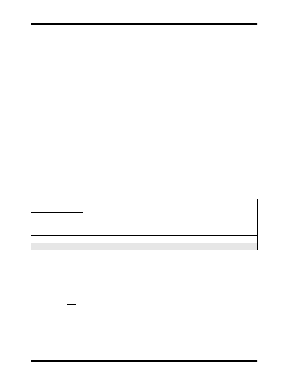
PIC16F7X
9.3.1.1 Addressing
Once the SSP module has been enabled, it waits for a
ST AR T conditi on to occu r. Following the ST AR T cond ition, the 8-bits are shifted into the SSPSR register. All
incoming bits are sampled with the rising edge of the
clock (SCL) line. The value of register SSPSR<7:1> is
compared to the value of the SSPADD register. The
address is compared on the falling edge of the eighth
clock (SCL) pulse. If the addresses match, and the BF
and SSPOV bits are clear, the following events occur:
a) The SSPSR register value is loaded into the
SSPBUF register.
b) The buffer full bit, BF is set.
c) An ACK
d) SSP interrupt flag bit, SSPIF (PIR1<3>) is set
(interrupt is genera ted if e nabled ) - on the fallin g
edge of the ninth SCL pulse.
In 10-bit Address mode, two address bytes need to be
received by the slave (Figure 9-7). The five Most Significant bits (MSbs) of the first address byte specify if
this is a 10 -bit add ress. Bit R/W
specify a write so the s la ve d e v ice will receive the second address byte. For a 10-bit address, the first byte
would equal ‘1111 0 A9 A8 0’, where A9 and A8 are
the two MSbs of the address.
pulse is generated.
(SSPSTAT<2>) must
The sequence of events for 10-bit address is as follows, with steps 7 - 9 for slave-transmitter:
1. Receive first (high) byte of address (bits SSPIF,
BF, and bit UA (SSPSTAT<1>) are set).
2. Update the SSPADD register with second (low)
byte of address (clears bit UA and releases the
SCL line).
3. Read the SSPBUF register (clears bit BF) and
clear flag bit SSPIF.
4. Receive second (low) byte of address (bits
SSPIF, BF, and UA are set).
5. Update the SSPADD register with the first (high)
byte of address, if match releases SCL line, this
will clear bit UA.
6. Read the SSPBUF register (clears bit BF) and
clear flag bit SSPIF.
7. Receive Repeated START condition.
8. Receive first (high) byte of address (bits SSPIF
and BF are set).
9. Read the SSPBUF register (clears bit BF) and
clear flag bit SSPIF.
TABLE 9-2: DATA TRANSFER RECEIVED BYTE ACTIONS
Status Bits as Data
Transfer is Received
BF SSPOV
00 Yes Yes Yes
10 No No Yes
11 No No Yes
0 1 No No Yes
Note: Shaded cells show the conditions where the user software did not properly clear the overflow condition.
SSPSR → SSPBUF
9.3.1.2 Reception
When the R/W bit of the address byte is clear and an
address match occurs, the R/W
register is cleare d. The re ceive d addre ss is loa ded in to
the SSPBUF register.
When the address byte overflow condition exists, then
no Acknowledge (ACK
condition is defined as either bit BF (SSPSTAT<0>) is
set, or bit SSPOV (SSPCON<6>) is set. This i s an error
condition due to the user’s firmware.
) pulse is given. An overflow
bit of the SSPSTAT
Generate ACK
Pulse
An SSP interrupt is generated for each data transfer
byte. Flag bit SSPIF (PIR1<3>) m ust be c leared in software. The SSPSTAT register is used to determine the
status of the byte.
Set bit SSPIF
(SSP Interrupt occurs
if enabled)
DS30325B-page 66 2002 Microchip Technology Inc.
Page 69
FIGURE 9-6: I2C WAVEFORMS FOR RECEPTION (7-BIT ADDRESS)
PIC16F7X
Receiving Address
A7 A6 A5 A4
1234
S
SCL
SSPIF (PIR1<3>)
BF (SSPSTAT<0>)
SSPOV (SSPCON<6>)
A3 A2 A1SDA
5
R/W=0
ACK
7
6
9
8
Receiving Data
D5
D6D7
1234
Cleared in software
SSPBUF register is read
9.3.1.3 Transmission
When the R/W bit of the incoming address byte is set
and an address match occurs, the R/W
SSPSTAT register is set. The received address is
loaded into the SSPBUF register. The ACK
be sent on the ninth bit, and pin RC3/SCK/SCL is held
low. The transmit data must be loaded into the
SSPBUF register, which also loads the SSPSR register. The n, pin RC3/SCK/SCL shou ld be enabled by setting bit CKP (SSPCON<4>). The master must monitor
the SCL pin prior to asse rtin g another clock pulse. The
slave devices may be holding off the master by stretching the clock. The eight data bits are shifted out on the
falling edge of the SCL input. This ensures that the
SDA signal is valid during the SCL high time (Figure 9-7).
bit of the
pulse will
ACK
D0
D2
D3D4
D1
7
56
Bit SSPOV is set because the SSPBUF register is still full.
89
Receiving Data
D5
D6D7
123
D2
D3D4
5
6
4
ACK is not sent.
D1
7
An SSP interrupt is generated for each data transfer
byte. Flag bit SSPIF must be cleared in software, and
the SSPSTAT register is used to determine the status
of the byte. Flag bit SSPIF is set on the falling edge of
the ninth clock pulse.
As a slave-transmi tte r, the ACK
pulse from the masterreceiver is latched on the rising edge of the ninth SCL
input pulse. If the SDA line was high (not ACK), then
the data transfe r is com plete. When th e ACK
by the slave, the slave logic is reset (resets SSPSTAT
register) and the slave then mo nitors for another occ urrence of the START bit. If the SDA line was low (ACK
the transmit data must be load ed into the SSPBUF register, which also loads the SSPSR register. Then pin
RC3/SCK/SCL should be enabled by setting bit CKP.
D0
8
ACK
9
P
Bus Master
terminates
transfer
is latched
),
FIGURE 9-7: I2C WAVEFORMS FOR TRANSMISSION (7-BIT ADDRESS)
Transmitting DataR/W = 1Receiving Address
SDA
SCL
SSPIF (PIR1<3>)
BF (SSPSTAT<0>)
CKP (SSPCON<4>)
A7 A6 A5 A4 A3 A2 A1 ACK
123456789 123456789
S
Data in
sampled
SCL held low
while CPU
responds to SSPIF
D7 D6 D5 D4 D3 D2 D1 D0
Cleared in software
SSPBUF is written in software
Set bit after writing to SSPBUF
(the SSPBUF must be written to
before the CKP bit can be set)
From SSP Interrupt
Service Routine
2002 Microchip Technology Inc. DS30325B-page 67
ACK
P
Page 70

PIC16F7X
9.3.2 MASTER MODE
Master mode of operation is supported in firmware
using interrupt generation on the detection of the
START and STOP conditions. The STOP (P) and
ST AR T (S) bits are cleared from a RESET or when the
SSP module is disabled. The ST OP (P) and ST ART (S)
bits will toggle based on the START and STOP conditions. Control of the I
bit is set, or the bus is IDLE and both the S and P bits
are clear.
In Master mode, the SCL and SDA lines are manipulated by clearing the c orresp onding TRISC<4 :3> bit(s ).
The output level is always low, irrespective of the
value(s) in PORT C <4:3 >. So wh en transmitting data, a
’1’ data bit must have the TRISC<4> bit set (input) and
a ’0’ dat a bit must have the TRISC<4> bit cleared (output). The same scenario is true for the SCL li ne with the
TRISC<3> bit. Pull-up resistors must be provided
externally to the SCL and SDA pins for proper operation of the I
2
C module.
The following events will cause SSP Interrupt Flag bit,
SSPIF, to be set (SSP Interrupt will occur if enabled):
• START condition
• STOP condition
• Data transfer byte transmitted/received
Master mode of operation can be done with either the
Slave mode IDLE (SSPM3:SSPM0 = 1011), or with th e
Slave active. When both Master and Slave modes are
enabled, the software needs to differentiate the
source(s) of the interrupt.
2
C bus may be taken when the P
9.3.3 MULTI-MASTER MODE
In Multi-Master mode, the interrupt generation on the
detection of the START and STOP conditions, allows
the determination of when the bus is free. The STOP
(P) and START (S) bits are cleared from a RESET or
when the SSP module is disabled. The STOP (P) and
START (S) bits will toggle based on the START and
STOP conditions. Control of the I
when bit P (SSPSTAT<4>) is set, or the bus is IDLE
and both the S and P bits clear. When the bus is busy,
enabling the SSP Interrupt will generate the interrupt
when the STOP condition occurs.
In Multi-Master operation, the SDA line must be monitored to see if the signal level is the expected output
level. This check only needs to be done when a high
level is output. If a h igh level is exp ected and a low le vel
is present , the device need s to release th e SDA and
SCL lines (set TRISC<4:3>). There are two stages
where this arbitration can be lost, these are:
• Address Trans fer
• Data Transfer
When the slave log ic is enab led, the s lave co nti nues to
receive. If arbitrati on was los t during the address transfer stage, communication to the device may be in
progress. If addressed, an ACK
ated. If arbitration was lost during the data transfer
stage, the device will need to retransfer the data at a
later time.
2
C bus may be taken
pulse will be gener-
TABLE 9-3: REGISTERS ASSOCIATED WITH I2C OPERATION
Address Name Bit 7 Bit 6 Bit 5 Bit 4 Bit 3 Bit 2 Bit 1 Bit 0
0Bh, 8Bh,
10Bh,18Bh
0Ch PIR1 PSPIF
8Ch PIE1 PSPIE
13h SSPBUF Sync hronous Ser ial Port Receive Buffer/Transmit Register xxxx xxxx uuuu uuuu
93h SSPADD Synch ronous Ser ial Port (I2C mode) Address Register 0000 0000 0000 0000
14h SSPCON WCOL SSPOV SSPEN CKP SSPM3 SSPM2 SSPM1 SSPM0 0000 0000 0000 0000
94h SSPSTAT SMP
87h TRISC PORTC Data Direction Register 1111 1111 1111 1111
Legend: x = unknown, u = unchanged, - = unimplemented locations read as ’0’. Shaded cells are not used by SSP module in I2C mode.
Note 1: PSPIF and PSPIE are reserved on the PIC16F73/76; always maintain these bits clear.
INTCON GIE PEIE
(1)
(1)
(2)
2: Maintain these bits clear in I
CKE
TMR0IE INTE RBIE TMR0IF INTF RBIF 0000 000x 0000 000u
ADIF RCIF TXIF SSPIF CCP1IF TMR2IF TMR1IF 0000 0000 0000 0000
ADIE RCIE TXIE SSPIE CCP1IE TMR2IE TMR1IE 0000 0000 0000 0000
(2)
D/A PSR/WUA BF 0000 0000 0000 0000
2
C mode.
Value on:
POR,
BOR
Value on
all other
RESETS
DS30325B-page 68 2002 Microchip Technology Inc.
Page 71

PIC16F7X
10.0 UNIVERSAL SYNCHRONOUS ASYNCHRONOUS RECEIVER T RANSMITTER (USART)
The Universal Synchronous Asynchronous Receiver
Transmitter (USART) module is one of the two serial
I/O modules . (USA RT is als o know n as a S erial Communications Interface or SCI.) The USART can be configured as a full duplex asynchronous system that can
communicate with pe ripheral devices , such as CRT t erminals and perso nal comp uters, or it can be configure d
as a half duplex s yn chronous system that can communicate with peripheral devices, such as A/D or D/A integrated circuits, serial EEPROMs, etc.
The USART can be configured in the following modes:
• Asynchronous (full duplex)
• Synchronous - Master (half duplex)
• Synchronous - Slave (half duplex)
Bit SPEN (RCSTA<7>) and bits TRISC<7:6> have to
be set in order to configure pins RC6/TX/CK and
RC7/RX/DT as the Universal Synchronous Asynchronous Receiver Transmitter.
REGISTER 10-1: TXSTA: TRANSMIT STATUS AND CONTROL REGISTER (ADDRESS 98h)
R/W-0 R/W-0 R/W-0 R/W-0 U-0 R/W-0 R-1 R/W-0
CSRC TX9 TXEN SYNC — BRGH TRMT TX9D
bit 7 bit 0
bit 7 CSRC: Clock So urce Select b it
Asynchronous mode:
Don’t care
Synchronous mode:
1 = Master mode (clock generated internally from BRG)
0 = Slave mode (clock from external source)
bit 6 TX9: 9-bit Transmit Enable bit
1 = Selects 9-bit transmission
0 = Selects 8-bit transmission
bit 5 TXEN: Transmit Enable bit
1 = Transmit enabled
0 = Transmit disabled
Note: SREN/CREN overrides TXEN in Sync mode.
bit 4 SYNC: USART Mode Select bit
1 = Synchronous mode
0 = Asynchrono us mode
bit 3 Unimplemented: Read as '0'
bit 2 BRGH: High Baud Rate Select bit
Asynchronous mode:
1 = High speed
0 = Low speed
Synchronous mode:
Unused in this mode
bit 1 TRMT: Transmit Shift Register Status bit
1 = TSR empty
0 = TSR full
bit 0 TX9D: 9th bit of Transmit Data
Can be parity bit
Legend:
R = Readable bit W = Writable bit U = Unimplemented bit, read as ‘0’
- n = Value at POR reset ’1’ = Bit is set ’0’ = Bit is cleared x = Bit is unknown
2002 Microchip Technology Inc. DS30325B-page 69
Page 72

PIC16F7X
REGISTER 10-2: RCSTA: RECEIVE STATUS AND CONTROL REGISTER (ADDRESS 18h)
R/W-0 R/W-0 R/W-0 R/W-0 U-0 R-0 R-0 R-x
SPEN RX9 SREN CREN
bit 7 bit 0
bit 7 SPEN: Serial Port Enable bit
1 = Serial port enabled (configures RC7/RX/DT and RC6/TX/CK pins as serial port pins)
0 = Serial port disabled
bit 6 RX9: 9-bit Receive Enable bit
1 = Selects 9-bit reception
0 = Selects 8-bit reception
bit 5 SREN: Single Receive Enable bit
Asynchronous mode:
Don’t care
Synchronous mode - Master:
1 = Enables single receive
0 = Disables single recei ve
This bit is cleared after reception is complete.
Synchronous mode - Slave:
Don’t care
bit 4 CREN: Continuous Receive Enable bit
Asynchronous mode:
1 = Enables continuous receive
0 = Disables continuou s receive
Synchronous mode:
1 = Enables continuous receive until enable bit CREN is cleared (CREN overrides SREN)
0 = Disables continuou s receive
bit 3 Unimplemented: Read as '0'
bit 2 FERR: Framing Error bit
1 = Framing error (can be updated by reading RCREG register and receive next valid byte)
0 = No framing error
bit 1 OERR: Overrun Error bit
1 = Overrun error (can be cleared by clearing bit CREN)
0 = No overrun error
bit 0 RX9D: 9th bit of Received Data
Can be parity bit (parity to be calcu lat ed by firm ware )
— FERR OERR RX9D
Legend:
R = Readable bit W = Writable bit U = Unimplemented bit, read as ‘0’
- n = Value at POR rese t ’1’ = Bit is set ’0’ = Bit is cleared x = Bit is unknown
DS30325B-page 70 2002 Microchip Technology Inc.
Page 73
PIC16F7X
10.1 USART Baud Rate Generator (BRG)
The BRG supports both the Asynchronous and Synchronous modes of the USART. It is a dedicated 8-bit
baud rate generator. The SPBRG register controls the
period of a free running 8-bit timer. In Asynchronous
mode, bit BRGH (TXSTA<2>) also controls the baud
rate. In Synchronous mode, bit BRGH is ignored.
Table 10-1 shows the formula for computation of the
baud rate for differen t US ART modes which only apply
in Master mode (internal clock).
Given the desired baud rate and F
integer value for the SPBRG register can be calculated
using the formula in Table10-1. From this, the error in
baud rate can be determined.
OSC, the nearest
It may be advantageous to use the high baud rate
(BRGH = 1), even for slower baud clocks. This is
because the F
baud rate error in some cases.
Writing a new value to the SPBRG register causes the
BRG timer to be reset (or cleared). This ensures the
BRG does not wait for a timer overflow before outputting the new baud rate.
OSC/(16(X + 1)) equat ion c an red uce th e
10.1.1 SAMPLING
The data on the RC7/RX/D T pin is sampled three times
by a majority detect circuit to determine if a high or a
low level is present at the RX pin.
TABLE 10-1: BAUD RATE FORMULA
SYNC BRGH = 0 (Low Speed) BRGH = 1 (High Speed)
0
1
X = value in SPBRG (0 to 255)
(Asynchronous) Baud Rate = F
(Synchronous) Baud Rate = F
OSC/(64(X+1))
OSC/(4(X+1))
Baud Rate = F
OSC/(16(X+1))
N/A
TABLE 10-2: REGISTERS ASSOCIATED WITH BAUD RATE GENERATOR
Address Name Bit 7 Bit 6 Bit 5 Bit 4 Bit 3 Bit 2 Bit 1 Bit 0
98h TXSTA CSRC TX9 TXEN SYNC — BRGH TRMT TX9D
18h RCSTA SPEN RX9 SREN CREN — FERR OERR RX9D
99h SPBRG Baud Rate Generator Register
Legend: x = unknown, - = unimplemented, read as '0'. Shaded cells are not used by the BRG.
Value on:
POR,
BOR
0000 -010 0000 -010
0000 -00x 0000 -00x
0000 0000 0000 0000
Value on
all other
RESETS
2002 Microchip Technology Inc. DS30325B-page 71
Page 74

PIC16F7X
TABLE 10-3: BAUD RATES FOR ASYNCHRONOUS MODE (BRGH = 0)
OSC = 20 MHz FOSC = 16 MHz FOSC = 10 MHz
F
BAUD
RATE
1200
2400
9600
19,200
38,400
57,600
76,800
96,000
115,200
250,000
BAUD
RATE
300
1200
2400
9600
19,200
38,400
57,600
76,800
BAUD
1,221 1.73% 255 1,202 0.16% 207 1,202 0.16% 129
2,404 0.16% 129 2,404 0.16% 103 2,404 0.16% 64
9,470 -1.36% 32 9,615 0.16% 25 9,766 1.73% 15
19,531 1.73% 15 19,231 0.16% 12 19,531 1.73% 7
39,063 1.73% 7 35,714 -6.99% 6 39,063 1.73% 3
62,500 8.51% 4 62,500 8.51% 3 52,083 -9.58% 2
78,125 1.73% 3 83,333 8.51% 2 78,125 1.73% 1
104,167 8.51% 2 83,333 -13.19% 2 78,125 -18.62% 1
104,167 -9.58% 2 125,000 8.51% 1 78,125 -32.18% 1
312,500 25.00% 0 250,000 0.00% 0 156,250 -37.50% 0
BAUD
300 0.16% 207 300 0.00% 191 301 0.23% 185
1,202 0.16% 51 1,200 0.00% 47 1,190 -0.83% 46
2,404 0.16% 25 2,400 0.00% 23 2,432 1.32% 22
8,929 -6.99% 6 9,600 0.00% 5 9,322 -2.90% 5
20,833 8.51% 2 19,200 0.00% 2 18,643 -2.90% 2
31,250 -18.62% 1 28,800 -25.00% 1 27,965 -27.17% 1
62,500 8.51% 0 57,600 0.00% 0 55,930 -2.90% 0
62,500 -18.62% 0
%
ERROR
F
OSC = 4 MHz FOSC = 3.6864 MHz FOSC = 3.579545 MHz
%
ERROR
SPBRG
VALUE
(DECIMAL)
SPBRG
VALUE
(DECIMAL)
BAUD
BAUD
—— — —— —
%
ERROR
%
ERROR
SPBRG
VALUE
(DECIMAL)
SPBRG
VALUE
(DECIMAL)
BAUD
BAUD
%
ERROR
%
ERROR
SPBRG
VALUE
(DECIMAL)
SPBRG
VALUE
(DECIMAL)
TABLE 10-4: BAUD RATES FOR ASYNCHRONOUS MODE (BRGH = 1)
OSC = 20 MHz FOSC = 16 MHz FOSC = 10 MHz
F
BAUD
RATE
2400 —— — —— —
9600
19,200
38,400
57,600
76,800
96,000
115,200
250,000
300,000
BAUD
RATE
(K)
1200
2400
9600
19,200
38,400
57,600
76,800
96,000
115,200
250,000
BAUD
9,615 0.16% 129 9,615 0.16% 103 9,615 0.16% 64
19,231 0.16% 64 19,231 0.16% 51 18,939 -1.36% 32
37,879 -1.36% 32 38,462 0.16% 25 39,063 1.73% 15
56,818 -1.36% 21 58,824 2.12% 16 56,818 -1.36% 10
78,125 1.73% 15 76,923 0.16% 12 78,125 1.73% 7
96,154 0.16% 12 100,000 4.17% 9 89,286 -6.99% 6
113,636 -1.36% 10 111,111 -3.55% 8 125,000 8.51% 4
250,000 0.00% 4 250,000 0.00% 3 208,333 -16.67% 2
312,500 4.17% 3 333,333 11.11% 2 312,500 4.17% 1
BAUD
1,202 0.16% 207 1,200 0.00% 191 1,203 0.23% 185
2,404 0.16% 103 2,400 0.00% 95 2,406 0.23% 92
9,615 0.16% 25 9,600 0.00% 23 9,727 1.32% 22
19,231 0.16% 12 19,200 0.00% 11 18,643 -2.90% 11
35,714 -6.99% 6 38,400 0.00% 5 37,287 -2.90% 5
62,500 8.51% 3 57,600 0.00% 3 55,930 -2.90% 3
83,333 8.51% 2 76,800 0.00% 2 74,574 -2.90% 2
83,333 -13.19% 2 115,200 20.00% 1 111,861 16.52% 1
125,000 8.51% 1 115,200 0.00% 1 111,861 -2.90% 1
250,000 0.00% 0 230,400 -7.84% 0 223,722 -10.51% 0
%
ERROR
OSC = 4 MHz FOSC = 3.6864 MHz FOSC = 3.579545 MHz
F
%
ERROR
SPBRG
VALUE
(DECIMAL)
SPBRG
VALUE
(DECIMAL)
BAUD
BAUD
%
ERROR
%
ERROR
SPBRG
VALUE
(DECIMAL)
SPBRG
VALUE
(DECIMAL)
BAUD
2,441 1.73% 255
BAUD
%
ERROR
%
ERROR
SPBRG
VALUE
(DECIMAL)
SPBRG
VALUE
(DECIMAL)
DS30325B-page 72 2002 Microchip Technology Inc.
Page 75

PIC16F7X
10.2 USART Asynchronous Mode
In this mode, the USART uses standard non-return-tozero (NRZ) format (one START bit, eight or nine data
bits, and one STOP bit). The most common data format
is 8-bits. An on-chip, dedicated, 8-bit baud rate generator can be used to derive standard baud rate frequencies from the oscillator. The USART transmits and
receives the LSb first. The USART’s transmitter and
receiver are functionally independent, but use the
same data forma t an d b aud rate. The baud rate generator produces a clock, either x16 or x64 of the bit shift
rate, depending on bit BRGH (TXST A<2>). Pari ty is not
supported by the hardware, but can be imple mente d in
software (and stored as the ninth data bit). Asynchronous mode is stopped during SLEEP.
Asynchronous mode is selected by clearing bit SYNC
(TXSTA<4>).
The USART Asynchronous module consists of the following important elements:
• Baud Rate Generator
• Sampling Circuit
• Asynchronous Transmitter
• Asynchronous Receiver
10.2.1 USART ASYNCHRONOUS TRANSMITTER
The USART transmitter block diagram is shown in
Figure 10-1. The heart of the transmitter is the transmit
(serial) shift register (TSR). The shift register obtains its
data from the read/write transmit buffer, TXREG. The
TXREG register is loaded with data by firmware. The
TSR register is not loaded until the STOP bit has been
transmitted from the previous load. As soon as the
STOP bit is transmitted, the TSR is loaded with new dat a
from the TXREG register (if available). Once the TXREG
register transfers the data to the TSR register, the
TXREG register is empty. One instruction cycle later,
flag bit TXIF (PIR1<4>) and flag bit TRMT (TXSTA<1>)
are set. The TXIF interrupt can be enabled/disabled by
setting/clearing enable bit TXIE (PIE1<4>). Flag bit TXIF
will be set, regardless of the st ate of enable bit TXIE and
cannot be cleared in software. It will reset only when new
data is loaded into the TXREG register. While flag bit
TXIF indicates the status of the TXREG register , another
bit TRMT (TXSTA<1>) shows the st atus of the TSR register. Status bit TRMT is a read only bit, which is set one
instruction cycle after the TSR register becomes empty,
and is cleared one instruction cycle after the TSR register is loaded. No interrupt logic is tied to this bit, so the
user has to poll this bit in order to determine if the TSR
register is empty.
Note 1: The TSR register is not mapped in data
memory, so it is not available to the user.
2: Flag bit TXIF is set when enabl e bit TXEN
is set. TXIF is cleared by loadi ng TXRE G.
Transmission is enabled by setting enable bit TXEN
(TXSTA<5>). The actual transmission will not occur until
the TXREG register has been loaded with data and the
baud rate generator (BRG) has produced a shift clock
(Figure 10-2). The transmission can also be started by
first loading the TXREG register and then setting enable
bit TXEN. Normally, when transmission is first started,
the TSR register is empty. At that point, transfer to the
TXREG register will result in an immediate transfer to
TSR, resulting in an empty TXREG. A back-to-back
transfer is thus possible (Figure 10-3). Clearing enable
bit TXEN during a transmission will cause the transmission to be aborted and will reset the transmitter. As a
result, the RC6/TX/CK pin will revert to hi-impedance.
In order to sel ect 9-bit transmission, transmit bit TX9
(TXSTA<6>) should be set and the ninth bit should be
written to TX9D (TXSTA<0>). The ninth bit must be written before writing t he 8 -bit d ata to t he TXRE G re gister.
This is because a data write to the TXREG register can
result in an immedia te transfer of t he data to the TSR
register (if the TSR is empty). In such a case, an incorrect ninth data bit may be loaded in the TSR register.
FIGURE 10-1: USART TRANSMIT BLOCK DIAGRAM
Data Bus
Interrupt
TXIF
TXEN
Baud Rate CLK
SPBRG
Baud Rate Generator
MSb
(8)
TXIE
2002 Microchip Technology Inc. DS30325B-page 73
TXREG Register
8
• • •
TSR Register
TX9
TX9D
LSb
0
TRMT
Pin Buffer
and Control
SPEN
RC6/TX/CK pin
Page 76

PIC16F7X
Steps to follow when setting up an Asynchronous
Transmission:
1. Initialize the SPBRG register for the ap prop ria te
baud rate. If a high speed baud rate is desired,
set bit BRGH (Section 10.1).
2. Enable the asynchronous serial port by clearing
bit SYNC and setting bit SPEN.
3. If interrupts are desired, then set enable bit TXIE.
5. Enable the transmission by setting bit TXEN,
which will also set bit TXIF.
6. If 9-bit transmission is selected, the ninth bit
should be loaded in bit TX9D.
7. Load data to the TXREG register (starts
transmission).
8. If using interrupts, ensure that GIE and PEIE in
the INTCON register are set.
4. If 9-bit transmission is desired, then set transmit
bit TX9.
FIGURE 10-2: ASYNCHRONOUS MASTER TRANSMISSION
Write to TXREG
BRG Output
(Shift Clock)
RC6/TX/CK (pin)
TXIF bit
(Transmit Buffer
Reg. Empty Flag)
TRMT bit
(Transmit Shift
Reg. Empty Flag)
Word 1
START Bit Bit 0 Bit 1 Bit 7/8
Word 1
Transmit Shift Reg
Word 1
STOP Bit
FIGURE 10-3: ASYNCHRONOUS MASTER TRANSMISSION (BACK TO BACK)
Write to TXREG
BRG Output
(Shift Clock)
RC6/TX/CK (pin)
(Interrupt Reg. Flag)
Reg. Empty Flag)
Note: This timing diagram shows two consecutive transmissions.
TXIF bit
TRMT bit
(Transmit Shift
Word 1
Word 1
Transmit Shift Reg.
Word 2
START Bit
Bit 0 Bit 1
Word 1
Bit 7/8 Bit 0
STOP Bit
Word 2
Transmit Shift Reg.
START Bit
Word 2
TABLE 10-5: REGISTERS ASSOCIATED WITH ASYNCHRONOUS TRANSMISSION
Address Name
0Bh, 8Bh,
10Bh,18Bh
0Ch PIR1 PSPIF
18h RCSTA SPEN RX9 SREN CREN — FERR OERR RX9D 0000 -00x 0000 -00x
19h TXREG USART Transmit Register 0000 0000 0000 0000
8Ch PIE1 PSPIE
98h TXSTA CSRC TX9 TXEN SYNC — BRGH TRMT TX9D 0000 -010 0000 -010
99h SPBRG Baud Rate Generator Register 0000 0000 0000 0000
Legend: x = unknown, - = unimplemented locations read as '0'. Shaded cells are not used for asynchronous transmission.
Note 1: Bits PSPIE and PSPIF are reserved on the PIC16F73/76; always maintain these bits clear.
INTCON GIE PEIE
Bit 7
Bit 6 B it 5 Bit 4 Bit 3 Bit 2 Bit 1 Bit 0
TMR0IE INTE RBIE TMR0IF INTF RBIF 0000 000x 0000 000u
(1)
ADIF RCIF TXIF SSPIF CCP1IF TMR2IF TMR1IF 0000 0000 0000 0000
(1)
ADIE RCIE TXIE SSPIE CCP1IE TMR2IE TMR1IE 0000 0000 0000 0000
Value on:
POR,
BOR
Value on
all other
RESETS
DS30325B-page 74 2002 Microchip Technology Inc.
Page 77

PIC16F7X
10.2.2 USART ASYNCHRONOUS
RECEIVER
The receiver block diagram is shown in Figure 10-4.
The data is received on th e R C7/R X/DT p in an d dri ve s
the data recovery block. The data recovery block is
actually a high s pe ed sh ifte r op erating at x16 times the
baud rate, whereas th e main receive serial shifte r operates at the bit rate, or at F
OSC.
Once Asynchronous mode is selected, reception is
enabled by setting bit CREN (RCSTA<4>).
The heart of the rece iver is the r eceive (serial) shift register (RSR). After sampling the STOP bit, the received
data in the RSR is tra nsferred to the RCREG register (if
it is empty). If the transfer is complete, flag bit RCIF
(PIR1<5>) is set. T he actu al i nt erru pt c an b e en abl ed/
disabled by setting/clearing enable bit RCIE
(PIE1<5>). Flag bit RCIF is a read only bit which is
cleared by the hardware. It is cleared when the RCREG
register has been read and is empty. The RCREG is a
double buffered register (i.e., it is a two deep FIFO). It
FIGURE 10-4: USART RECEIVE BLOCK DIAGRAM
x64 Baud Rate CLK
CREN
FOSC
RC7/RX/DT
SPBRG
Baud Rate Generator
Pin Buffer
and Control
÷64
or
÷16
Data
Recovery
is possible for two bytes of data to be received and
transferred to the RCREG FIFO and a third byte to
begin shifting to the RSR register. On the detection of
the STOP bit of the third byte, if the RCREG register is
still full, the ove rrun error bit OE RR (RCST A<1>) will be
set. The word in the RSR will be lost. The RCREG register can be read twice to retrieve the two bytes in the
FIFO. Overrun bit O ERR ha s to b e clea red in softwar e.
This is don e by resetting th e receive logic (C REN is
cleared and then s et). If bit O ERR is s et, tran sfer s from
the RSR register to the RCREG register are inhibited
and no further data will be received, therefore, it is
essential to clear error bit OERR if it is set. Framing
error bit FERR (RCSTA<2>) is set if a STOP bit is
detected as clear. Bit FERR and the 9th receive bit are
buffered the same way as the receiv e data. Reading
the RCREG will load bits RX9D and FERR with new
values, therefore, it is ess ent ial for the us er to re ad th e
RCSTA register before
reading RCREG register, in
order not to lose the old FERR and RX9D informat ion.
FERR
1
0
LSb
START
MSb
RX9
STOP
OERR
(8)
RSR Register
7
• • •
SPEN
Interrupt
2002 Microchip Technology Inc. DS30325B-page 75
RCIF
RCIE
RX9D
RCREG Register
8
Data Bus
FIFO
Page 78

PIC16F7X
FIGURE 10-5: ASYNCHRON OUS RECEPTION
RX (pin)
Rcv Shift
Reg
Rcv Buffer Reg
Read Rcv
Buffer reg
RCREG
RCIF
(Interrupt Flag)
OERR bit
CREN
Note: This timing diagram shows three words appearing on the RX input. The RCREG (receive buffer) is read after the third word,
causing the OERR (overrun) bit to be set. An overrun error indicates an error in user firmware.
START
bit
bit1bit0
bit7/8 bit0STOP
bit
START
bit
Word 1
RCREG
bit7/8
Word 2
RCREG
STOP
bit
START
bit
bit7/8
STOP
bit
Steps to follow when setting up an Asynchronous
Reception:
1. Initialize the SPBRG register for the ap prop ria te
baud rate. If a high speed baud rate is desired,
set bit BRGH (Section 10.1).
2. Enable the asynchronous serial port by clearing
bit SYNC and setting bit SPEN.
3. If interrupts are desired, then set enable bit
RCIE.
4. If 9-bit reception is desired, then set bit RX9.
5. Enable the reception by setting bit CREN.
6. Flag bit RCIF will be set when rec ept ion is com plete and an interru pt will be g enerated i f enable
bit RCIE is set.
7. Read the RCSTA register to get the ninth bit (if
enabled) and determine if any error occurred
during reception.
8. Read the 8-bit received data by reading the
RCREG register.
9. If any error occurred, clear the error by clearing
enable bit CREN.
10. If using interrupts, ensure that GIE and PEIE in
the INTCON register are set.
TABLE 10-6: REGISTERS ASSOCIATED WITH ASYNCHRONOUS RECEPTION
Value on:
Address Name Bit 7 Bit 6 Bit 5 Bit 4 Bit 3 B it 2 Bit 1 Bit 0
0Bh, 8Bh,
10Bh,18Bh
0Ch PIR1 PSPIF
18h RCSTA S PEN RX9 SREN CREN — FERR OERR RX9D 0000 -00x 0000 -00x
1Ah RCREG USART Receive Register 0000 0000 0000 0000
8Ch PIE1 PSPIE
98h TXSTA CSRC TX9 TXEN SYNC — BRGH TRMT TX9D 0000 -010 0000 -010
99h SPBRG Baud Rate Generator Register 0000 0000 0000 0000
Legend: x = unknown, - = unimplemented locations read as '0'. Shaded cells are not used for asynchronous reception.
Note 1: Bits PSPIE and PSPIF are reserved on the PIC16F73/76 devices; always maintain these bits clear.
INTCON GIE PEIE
(1)
ADIF RCIF TXIF SSPIF CCP1IF TMR2IF TMR1IF 0000 0000 0000 0000
(1)
ADIE RCIE TXIE SSPIE CCP1IE TMR2IE TMR1IE 0000 0000 0000 0000
TMR0IE INTE RBIE TMR0IF INTF RBIF 0000 000x 0000 000u
POR,
BOR
Value on
all other
RESETS
DS30325B-page 76 2002 Microchip Technology Inc.
Page 79

PIC16F7X
10.3 USART Synchronous Master Mode
In Synchronous Ma ster mode, the dat a is trans mitted in
a half-duplex manner (i.e., transmission and reception
do not occur at the sa me time). When tran smitting dat a,
the reception is inhibited and vice versa. Synchronous
mode is entered by setting bit SYNC (TXSTA<4>). In
addition, enable bit SPEN (RCSTA<7>) is set in order
to configure the RC6/TX/CK and RC7/RX/DT I/O pins
to CK (clock) and DT (data) lines, respectively. The
Master mode ind icates t hat the pr ocessor transmit s the
master clock on the CK line. The Master mode is
entered by setting bit CSRC (TXSTA<7>).
10.3.1 USART SYNCHRONOUS MASTER
TRANSMISSION
The USART transmitter block diagram is shown in
Figure 10-1. The heart of the transmitter is the tr ansmit
(serial) shift regist er (TSR). The s hift register obtains it s
data from the read/write transmit buffer register
TXREG. The TXREG register is loaded with data in
software. The TSR register is not loaded until the last
bit has been transmitted from the previous load. As
soon as the last bit is transmitted, the TSR is loaded
with new data from the TXREG (if available). Once the
TXREG register transfers the data to the TSR register
(occurs in one T
rupt bit TXIF (PIR1<4>) is set. The interrupt can be
enabled/disabled by setting/clearing enable bit TXIE
(PIE1<4>). Flag bit TXIF will be set, regardless of the
state of enable bit TXIE and cannot be cleared in software. It will reset o nly when ne w dat a i s loa ded i nto the
TXREG register . While fla g bit TXIF indicates th e status
of the TXREG r egi st e r, another b it T RMT (T X STA<1>)
shows the status of the TSR register. TRMT is a read
only bit, which is set when the TSR is empty. No interrupt logic is tied to this bit, so the user has to poll this
bit in orde r to determine if the TSR regis ter is empty.
The TSR is not mapped in data memory, so it is not
available to the user.
Transmission is enabled by setting enable bit TXEN
(TXSTA<5>). The actual transmission will not occur
until the TXREG register has been loaded with data.
The first data bit will be shifted out on the next availabl e
rising edge of the clock on the CK line. Data out is
stable around the fal ling edge of the sync hronous cloc k
(Figure 10-6). The transmission can also be started by
first loading the TXREG register and then setting bit
TXEN (Figure 10-7). This is advantageous when slow
baud rates are selected, since the BRG is kept in
RESET when bits TXEN, CREN and SREN are clear.
Setting enable bit TXEN will start the BRG, creating a
shift clock immed iately. Normally, when t ransm issio n is
first started, the TSR register is empty, so a transfer to
the TXREG register will re su lt i n an imm ed ia te transfer
to TSR, resulting in an empty TXREG. Back-to-back
transfers are possible.
CYCLE), the TXREG is empty an d inter-
Clearing enable bit TXEN during a transmission will
cause the transmis s ion to be ab orte d a nd will reset the
transmitter. The DT and CK pins will revert to hiimpedance. If eithe r bit CRE N or bit SR EN is se t during
a transmission, the transm issi on is abor ted and the D T
pin reverts to a hi-impedance state (for a reception).
The CK pin will remain an output if bit CSRC is set
(internal clock). The transmitter logic, however, is not
reset, although it i s disconnected fro m the pins. In order
to reset the transmitter, the user has to clear bit TXEN.
If bit SREN is set (to i nterrupt an on-goin g transm ission
and receive a sing le word), th en after th e single w ord is
received, bit SREN will be cleared and the serial port
will revert back to transmitting, since bit TXEN is still
set. The DT line will immediately switch from Hiimpedance Receive mode to tran smit an d st art dr ivin g.
To avoid this, bit TXEN should be cleared.
In order to select 9-bit transmission, the TX9
(TXSTA<6>) bit should be set and the ninth bit should
be written to bit TX9D (TXSTA<0>). The ninth bit must
be written before writing the 8-bit data to the TXREG
register . This is because a da ta write to the TXREG ca n
result in an immediate transfer of the data to the TSR
register (if the TSR i s empty). If the TSR was empty and
the TXREG was written before writing the “new” TX9D,
the “present” value of bit TX9D is loaded.
Steps to follow when setting up a Synchronous Master
Transmission:
1. Initialize the SPBRG register for the ap prop ria te
baud rate (Section 10.1).
2. Enable the synchronous master serial port by
setting bits SYNC, SPEN and CSRC.
3. If interrupts are desired, set enable bit TXIE.
4. If 9-bit transmission is desired, set bit TX9.
5. Enable the tr ansmission by setting bit TXEN.
6. If 9-bit transmission is selected, the ninth bit
should be loaded in bit TX9D.
7. Start transm ission by loa ding data to th e TXREG
register.
8. If using interrupts, ensure that GIE and PEIE in
the INTCON register are set.
2002 Microchip Technology Inc. DS30325B-page 77
Page 80
PIC16F7X
FIGURE 10-6: SYNCHRONOUS TRANSMISS ION
Q1Q2 Q3Q4Q1 Q2Q3Q4Q1Q2Q3Q4Q1Q2Q3Q4Q1 Q2 Q3Q4 Q3Q4 Q1Q2 Q3Q4 Q1Q2Q3Q4Q1Q2Q3 Q4Q1Q2Q3Q4Q1Q2Q3 Q4Q1Q2Q3Q4
RC7/RX/DT
pin
RC6/TX/CK
pin
Write to
TXREG reg
TXIF bit
(Interrupt Flag)
TRMT
TRMT bit
TXEN bit
Note: Sync Master mode; SPBRG = ’0’. Continuous transmission o f two 8-bit words.
Write Word 1
’1’ ’1’
bit 0 bit 1 bit 7
Word 1
Write Word 2
bit 2 bit 0 bit 1 bit 7
Word 2
FIGURE 10-7: SYNCHRONOUS TRANSMISSION (THROUGH TXEN)
RC7/RX/DT pin
RC6/TX/CK pin
Write to
TXREG reg
bit0
bit1
bit2
bit6 bit7
TXIF bit
TRMT bit
TXEN bit
TABLE 10-7: REGISTERS ASSOCIATED WITH SYNCHRONOUS MASTER TRANSMISSION
Address Name Bit 7 Bit 6 Bit 5 Bit 4 Bit 3 Bit 2 Bit 1 Bit 0
POR,
BOR
Value on:
0Bh, 8Bh,
INTCON GIE PEIE
TMR0IE INTE RBIE TMR0IF INTF RBIF 0000 000x 0000 000u
10Bh,18Bh
0Ch PIR1 PSPIF
(1)
ADIF RCIF TXIF SSPIF CCP1IF TMR2IF TMR1IF 0000 0000 0000 0000
18h RCSTA SPEN RX9 SREN CREN — FERR OERR RX9D 0000 -00x 0000 -00x
19h TXREG USART Transmit Register 0000 0000 0000 0000
8Ch PIE1 PSPIE
(1)
ADIE RCIE TXIE SSPIE CCP1IE TMR2IE TMR1IE 0000 0000 0000 0000
98h TXSTA CSRC TX9 TXEN SYNC — BRGH TRMT TX9D 0000 -010 0000 -010
99h SPBRG Baud Rate Generator Register 0000 0000 0000 0000
Legend: x = unknown, - = unimplemented, read as '0'. Shaded cells are not used for synchronous master transmission.
Note 1: Bits PSPIE and PSPIF are reserved on the PIC16F73/76 devices; always maintain these bits clear.
Value on
all other
RESETS
DS30325B-page 78 2002 Microchip Technology Inc.
Page 81
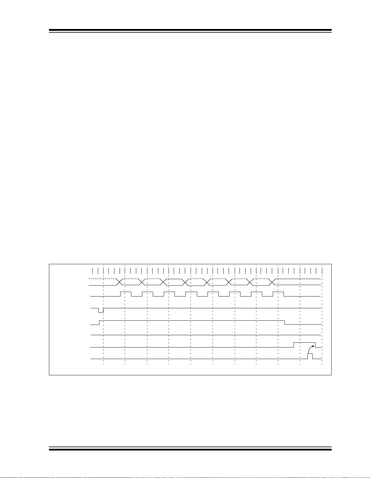
PIC16F7X
10.3.2 USART SYNCHRONOUS MASTER RECEPTION
Once synchronous mode is selected, reception is
enabled by setting either enable bit SREN (RCST A<5>),
or enable bit CREN (RCSTA<4>). Data is sampled on
the RC7/RX/DT pin on the falling edge of the clock. If
enable bit SREN is set, then only a single word is
received. If enable bit CREN is set, the reception is continuous until CREN is cleared. If both bits are set, CREN
takes precedence. After clocking the last bit, the
received data in the Receive Shift Register (RSR) is
transferred to the RCREG register (if it is empty). When
the transfer is complete, interrupt flag bit RCIF
(PIR1<5>) is set. The actual interrupt can be enabled/
disabled by setting/clearing enable bit RCIE (PIE1<5>).
Flag bit RCIF is a read only bit, which is reset by the
hardware. In this case, it is reset when the RCREG register has been read and is empty. The RCREG is a double buffered register (i.e., it is a two deep FIFO). It is
possible for two bytes of data to be received and transferred to the RCREG FIFO and a third byte to begin shifting into the RSR register. On the clocking of the last bit
of the third byte, if the RCREG register is still full, then
overrun error bit OERR (RCSTA<1>) is set. The word in
the RSR will be lost. The RCREG register can be read
twice to retrieve the two bytes in the FIFO. Bit OERR has
to be cleared in software (by clearing bit CREN). If bit
OERR is set, transfers from the RSR to the RCREG are
inhibited, so it is essential to clear bit OERR if it is set.
The ninth receive bit is buffered the same way as the
receive data. Reading the RCREG register will load bit
RX9D with a new value, therefore, it is essential for the
user to read the RCST A register before reading RCREG,
in order not to lose the old RX9D information.
Steps to follow when setting up a Synchronous Master
Reception:
1. Initialize the SPBRG register for the ap prop ria te
baud rate (Section 10.1).
2. Enable the synchronous master serial port by
setting bits SYNC, SPEN and CSRC.
3. Ensure bits CREN and SREN are clear.
4. If interrupts are desired, then set enable bit
RCIE.
5. If 9-bit reception is desired, then set bit RX9.
6. If a single reception is required, set bit SREN.
For continuous reception set bit CREN.
7. Interrupt flag bit RCIF will be set when recep tion
is complete and an interrupt will be generated if
enable bit RCIE was set.
8. Read the RCSTA register to get the ninth bit (if
enabled) and determine if any error occurred
during reception.
9. Read the 8-bit received data by reading the
RCREG register.
10. If any error occurred, clear the error by clearing
bit CREN.
11. If using interrupts, ensure that GIE and PEIE in
the INTCON register are set.
FIGURE 10-8: SYNCHRONOUS RECEPTION (MASTER MODE, SREN)
Q3Q4 Q1 Q2Q3Q4 Q1Q2Q3 Q4Q2 Q1Q2Q3 Q4Q1 Q2 Q3Q4 Q1 Q2 Q3Q4Q1Q2Q3 Q4 Q1 Q2Q3Q4Q1 Q2 Q3 Q4 Q1Q2Q3 Q4
RC7/RX/DT pin
RC6/TX/CK pin
Write to
bit SREN
SREN bit
CREN bit
RCIF bit
(Interrupt)
RXREG
Note: Timing diagram demonstrates Sync Master mode with bit SREN = ’1’ and bit BRG = ’0’.
’0’
Read
bit0 bit1 bit2 bit3 bit4 bit5 bit6 bit7
Q1Q2 Q3 Q4
’0’
2002 Microchip Technology Inc. DS30325B-page 79
Page 82
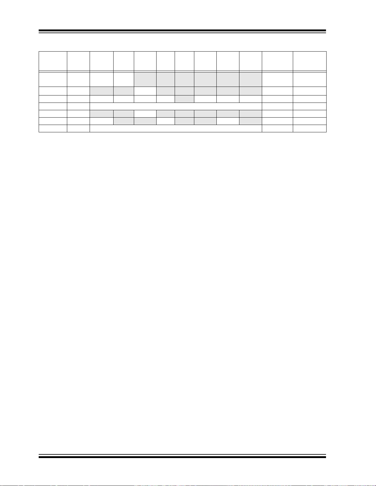
PIC16F7X
TABLE 10-8: REGISTERS ASSOCIATED WITH SYNCHRONOUS MASTER RECEPTION
Address Name Bit 7 Bit 6 Bit 5 Bit 4 Bit 3 Bit 2 Bit 1 Bit 0
0Bh, 8Bh,
10Bh,18Bh
0Ch PIR1 PSPIF
18h RCSTA SPEN RX9 SRE N CREN — FERR OERR RX9D 0000 -00x 0000 -00x
1Ah RCREG USART Receive Register 0000 0000 0000 0000
8Ch PIE1 PSPIE
98h TXSTA CSRC TX9 TXEN SYNC — BRGH TRMT TX9D 0000 -010 0000 -010
99h SPBRG Baud Rate Generator Register 0000 0000 0000 0000
Legend: x = unknown, - = unimplemented, read as '0'. Shaded cells are not used for synchronous master reception.
Note 1: Bits PSPIE and PSPIF are reserved on the PIC16F73/76 devices; always maintain these bits clear.
INTCON GIE PEIE
(1)
(1)
10.4 USART Synchronous Slave Mode
TMR0IE INTE RBIE TMR0IF INTF RBIF 0000 000x 0000 000u
ADIF RCIF TXIF SSPIF CCP1IF TMR2IF TMR1IF 0000 0000 0000 0000
ADIE RCIE TXIE SSPIE CCP1IE TMR2IE TMR1IE 0000 0000 0000 0000
Follow these steps when setting up a Synchronous
Value on:
POR, BOR
Value on
all other
RESETS
Slave Transmission:
Synchronous Slave mode differs from the Master
mode, in that the shift cloc k is s upplied externally at the
RC6/TX/CK pin (instead of being supplied internally in
Master mode). This allows the device to transfer or
receive data while in SLEEP mode. Slave mode is
entered by clearing bit CSRC (TXSTA<7>).
1. Enable the synchronous slave s erial port by setting bits SYNC and SPEN and clearing bit
CSRC.
2. Clear bits CREN and SREN.
3. If interrupts are desired, then set enable bit
TXIE.
10.4.1 USART SYNCHRONOUS SLAVE TRANSMIT
The operation of the Synchronous Master and Slave
modes are ide ntical exce pt in the case of the SLEEP
mode.
If two words are written to the TXREG and then the
SLEEP instruction is executed, the following will occur:
a) The first word will immediately transfer to the
TSR register and transmit when the master
4. If 9-bit transmission is desired, then set bi t TX9.
5. Enable the transmission by setting enable bit
TXEN.
6. If 9-bit transmission is selected, the ninth bit
should be loaded in bit TX9D.
7. Start transm ission by loa ding data to th e TXREG
register.
8. If using interrupts, ensure that GIE and PEIE in
the INTCON register are set.
device drives the CK line.
b) The second word will remain in TXREG register.
c) Flag bit TXIF will not be set.
d) When the first word has been shifted out of TSR,
the TXREG register will transfer the second
word to the TSR and flag bit TXIF will now be
set.
e) If enable bit TXIE is set, the interrupt will wake
the chip from SLEEP and if the global interrupt
is enabled, the program will branch to the inter-
rupt vector (0004h).
DS30325B-page 80 2002 Microchip Technology Inc.
Page 83
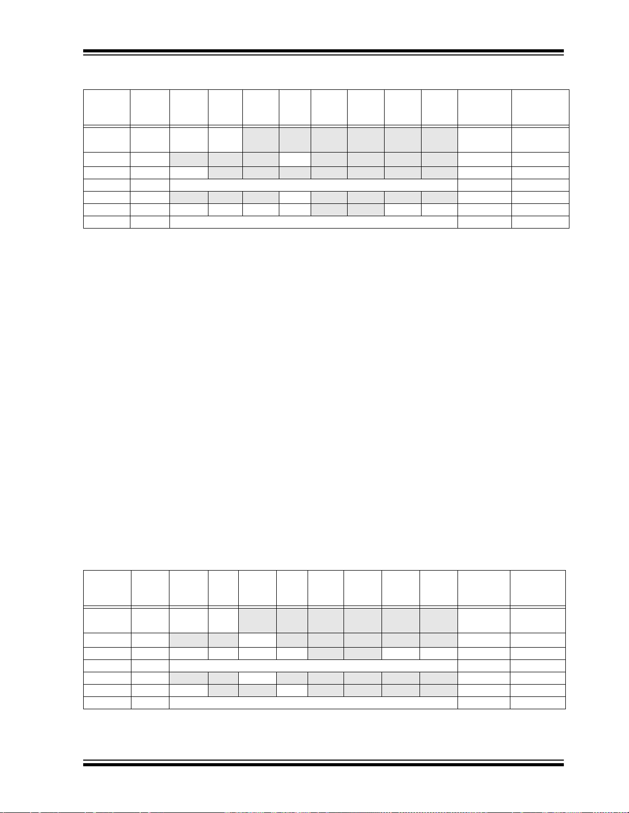
PIC16F7X
TABLE 10-9: REGISTERS ASSOCIATED WITH SYNCHRONOUS SLAVE TRANSMISSION
Val ue on:
Address Name Bit 7 Bit 6 Bit 5 Bit 4 Bit 3 Bit 2 Bit 1 Bit 0
0Bh, 8Bh,
10Bh,18Bh
0Ch PIR1 PSPIF
18h RCSTA SPEN RX9 SREN CREN ADDEN FERR OERR RX9D 0000 000x 0000 000x
19h TXR EG USART Transmit Register 0000 0000 0000 0000
8Ch PIE1 PSPIE
98h TXSTA CSRC TX9 TXEN SYNC — BRGH TRMT TX9D 0000 -010 0000 -010
99h SPB RG Baud Rate Generator Register 0000 0000 0000 0000
Legend: x = unknown, - = unimplemented, read as '0'. Shaded cells are not used for synchronous slave transmission.
Note 1: Bits PSPIE and PSPIF are reserved on the PIC16F73/76 devices; always maintain these bits clear.
10.4.2 USART SYNCHRONOUS SLAVE
The operation of the Synchronous Master and Slave
modes is identical, except in the case of the SLEEP
mode. Bit SREN is a “don't care” in Slave mode.
If receive is enabled by setting bit CREN prior to the
SLEEP instruction, then a w ord m ay be rec eived durin g
SLEEP. On completely receiving the word, the RSR
register will transfer the data to the RCREG register
and if enable bit RCIE bit is set, the int errupt generate d
will wake the chip from SLEEP. If the global interrupt is
enabled, the program w ill br anch to the interru pt vec tor
(0004h).
INTCON GIE PEIE
(1)
ADIF RCIF TXIF SSPIF CCP1IF TMR2IF TMR1IF 0000 0000 0000 0000
(1)
ADIE RCIE TXIE SSPIE CCP1IE TMR2IE TMR1IE 0000 0000 0000 0000
RECEPTION
TMR0IE INTE RBIE TMR0IF INTF RBIF 0000 000x 0000 000u
Follow these steps when setting up a Synchronous
Slave Reception:
1. Enable the synchronous master serial port by
setting bits SYNC and SPEN and clearing bit
CSRC.
2. If interrupts are desired, set enable bit RCIE.
3. If 9-bit reception is desired, set bit RX9.
4. To enable reception, set enable bit CREN.
5. Flag bit RCIF will be set when rec ept ion is com plete and an interrupt will be generated, if
enable bit RCIE was set.
6. Read the RCSTA register to get the ninth bit (if
enabled) and determine if any error occurred
POR,
BOR
Val ue on
all other
RESETS
during reception.
7. Read the 8-bit received data by reading the
RCREG register.
8. If any error occurred, clear the error by clearing
bit CREN.
9. If using interrupts, ensure that GIE and PEIE in
the INTCON register are set.
TABLE 10-10: REGISTERS ASSOCIATED WITH SYNCHRONOUS SLAVE RECEPTION
Value on:
Address Name Bit 7 Bit 6 Bit 5 Bit 4 Bit 3 Bit 2 Bit 1 Bit 0
0Bh, 8Bh,
10Bh,18Bh
0Ch PIR1 PSPIF
18h RCSTA SPEN RX9 SREN CREN ADDEN FERR OERR RX9D 0000 000x 0000 000x
1Ah RCREG USART Receive Register 0000 0000 0000 0000
8Ch PIE1 PSPIE
98h TXSTA CSRC TX9 TXEN SYNC — BRGH TRMT TX9D 0000 -010 0000 -010
99h SPBRG Baud Rate Generator Register 0000 0000 0000 0000
Legend: x = unknown, - = unimplemented, read as '0'. Shaded cells are not used for synchronous slave reception.
Note 1: Bits PSPIE and PSPIF are reserved on the PIC16F73/76 devices, always maintain these bits clear.
2002 Microchip Technology Inc. DS30325B-page 81
INTCON GIE PEIE
(1)
(1)
TMR0IE INTE RBIE TMR0IF INTF RBIF 0000 000x 0000 000u
ADIF RCIF TXIF SSPIF CCP1IF TMR2IF TM R1IF 0000 0000 0000 0000
ADIE RCIE TXIE SSPIE CCP1IE TMR2IE TMR1IE 0000 0000 0000 0000
POR,
BOR
Value on
all other
RESETS
Page 84

PIC16F7X
NOTES:
DS30325B-page 82 2002 Microchip Technology Inc.
Page 85

PIC16F7X
11.0 ANALOG-TO-DIGITAL CONVERTER (A/D) MODULE
The 8-bit analog-to-digital (A/D) converter module has
five inputs for the PIC16F73/76 and eight for the
PIC16F74/77.
The A/D allows conversi on of an anal og inp ut signal to
a corresponding 8-bit digital number. The output of the
sample and hold is the input into the converter, which
generates the result via successive approximation. The
analog reference voltage is software selectable to
either the device’s positive supply voltage (V
voltage level on the RA3/AN3/V
The A/D converter has a unique feature of being able
to operate while the d evice is in SLEEP mode. To operate in SLEEP, the A/D conversion clock must be
derived from the A/D’s internal RC oscillator.
REF pin.
DD), or the
The A/D module ha s three registers. Thes e registers
are:
• A/D Result Register ((ADRES)
• A/D Control Register 0 (ADCON0)
• A/D Control Register 1 ((ADCON1)
The ADCON0 register, shown in Register 11-1, controls the operation of the A/D module. The ADCON1
register, shown in Register 11-2, configures the functions of the port pins. The port pins can be configured
as analog input s (RA3 can als o be a voltag e reference),
or as digital I/O.
Additional informa tion on usi ng the A/D module can be
found in the PICmicro™ Mid-Range MCU Family Reference Manual (DS33023) and in Application Note,
AN546 (DS00546).
REGISTER 11-1: ADCON0 REGISTER (ADDRESS 1Fh)
R/W-0 R/W-0 R/W-0 R/W-0 R/W-0 R/W-0 U-0 R/W-0
ADCS1 ADCS0 CHS2 CHS1 CHS0 GO/DONE
bit 7 bit 0
bit 7-6 ADCS1:ADCS0: A/D Conversion Clock Select bits
OSC/2
00 = F
OSC/8
01 = F
10 = F
OSC/32
RC (clock derived from the internal A/D module RC oscillator)
11 = F
bit 5-3 CHS2:CHS0: Analog Channel Select bits
000 = Channel 0 (RA0/AN0)
001 = Channel 1 (RA1/AN1)
010 = Channel 2 (RA2/AN2)
011 = Channel 3 (RA3/AN3)
100 = Channel 4 (RA5/AN4)
101 = Channel 5 (RE0/AN5)
110 = Channel 6 (RE1/AN6)
111 = Channel 7 (RE2/AN7)
bit 2 GO/DONE: A/D Conversion Statu s bit
If ADON = 1:
1 = A/D conversion in progress (setting this bit starts the A/D conversion)
0 = A/D conversion not in progress (this bit is automatically cleared by hardware when the
A/D conversion is complete)
bit 1 Unimplemented: Read as '0'
bit 0 ADON: A/D On bi t
1 = A/D converter module is operating
0 = A/D converter module is shut-off and consumes no operating current
Note 1: A/D channels 5, 6 and 7 are implemented on the PIC16F74/77 only.
(1)
(1)
(1)
— ADON
Legend:
R = Readable bit W = Writable bit U = Unimplemented bit, read as ‘0’
- n = Value at POR reset ’1’ = Bit is set ’0’ = Bit is cleared x = Bit is unknown
2002 Microchip Technology Inc. DS30325B-page 83
Page 86
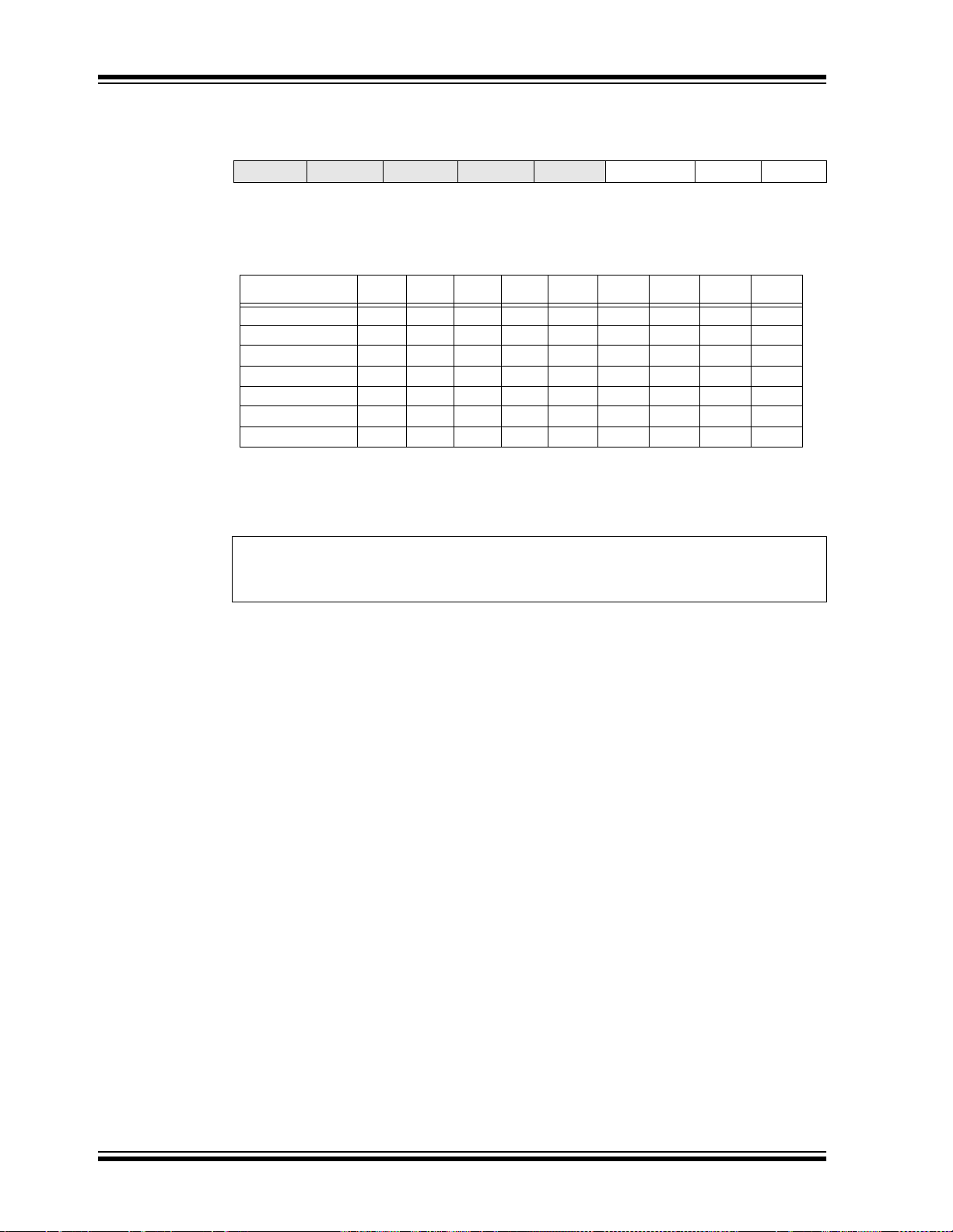
PIC16F7X
REGISTER 11-2: ADCON1 REGISTER (ADDRESS 9Fh)
U-0 U-0 U-0 U-0 U-0 R/W-0 R/W-0 R/W-0
— — — — — PCFG2 PCFG1 PCFG0
bit 7 bit 0
bit 7-3 Unimplemented: Read as '0'
bit 2-0 PCFG2:PCFG0: A/D Port Configuration Control bits
PCFG2:PCFG0 RA0 RA1 RA2 RA5 RA3 RE0
000 AAAAAAAAVDD
001 AAAAVREF AAARA3
010 AAAAADDDV
011 AAAAVREF DDDRA3
100 AADDADDDV
101 AADDVREF DDDRA3
11x DDDDDDDDV
A = Analog input
D = Digital I/O
Note 1: RE0, RE1 and RE2 are implemented on the PIC16F74/77 only.
Legend:
R = Readable bit W = Writable bit U = Unimplemented bit, read as ‘0’
- n = Value at POR reset ’1’ = Bit is set ’0’ = Bit is cleared x = Bit is unknown
(1)
RE1
(1)
RE2
(1)
VREF
DD
DD
DD
DS30325B-page 84 2002 Microchip Technology Inc.
Page 87

PIC16F7X
The following steps should be followed for doing an
A/D conversion:
1. Co nfigure the A /D module:
• Configure analog pins, voltage reference,
and digital I/O (ADCON1)
• Select A/D conversion clock (ADCON0)
• Turn on A/D module (ADCON0)
2. Configure the A/D interr upt (if desir ed):
• Clear ADIF bit
• Set ADIE bit
• Set PEIE bit
• Set GIE bit
3. Sel ect an A/D input channel (ADCON0).
FIGURE 11-1: A/D BLOCK DIAGRAM
IN
V
(Input Voltage)
A/D
Converter
VREF
(Reference
Voltage)
PCFG2:PCFG0
V
4. Wait for at least an appropriate acquisition
period.
5. Start conversion:
• Set GO/DONE
bit (ADCON0)
6. Wait for the A/D conversion to complete, by
either:
• Polling for the GO/DONE
bit to be cleared
(interrupts disabled)
OR
• Waiting for the A/D interrupt
7. Read A/D result register (ADRES), and clear bit
ADIF if required.
8. For next conversion, go to step 3 or step 4, as
required.
CHS2:CHS0
111
110
101
100
011
010
001
DD
000 or
010 or
100 or
11x
001 or
011 or
101
000
RE2/AN7
RE1/AN6
RE0/AN5
RA5/AN4
RA3/AN3/V
RA2/AN2
RA1/AN1
RA0/AN0
(1)
(1)
(1)
REF
Note 1: Not available on PIC16F73/76.
2002 Microchip Technology Inc. DS30325B-page 85
Page 88

PIC16F7X
11.1 A/D Acquisition Requirements
For the A/D co nverter to meet its s pecified accuracy,
the charge holding capacitor (C
to fully charge to the input channel voltage level. The
analog input model is shown in Figure 11-2. Th e source
impedance (R
S) and the internal sampling switch (RSS)
impedance directly affect the time required to charge
the capacitor C
HOLD. The sampling switch (RSS)
impedance varies over the device voltage (V
Figure 11-2. The source impedance affects the offset
voltage at the analog input (due to pin leakage curre nt).
FIGURE 11-2: ANALOG INPUT MODEL
VA
Legend CPIN
HOLD) must be allowed
ANx
R
S
CPIN
5 pF
VT
I leakage
R
SS
C
= input capacitance
= threshold voltage
= leakage current at the pin due t o
various junctions
= interconnect resistance
IC
= sampling switch
= sample/hold capacitance (from DAC)
HOLD
DD), see
VDD
VT = 0.6V
T = 0.6V
V
The maximum recommended impedance for analog sources is 10 kΩ. After the analog input channel is
selected (changed), the acquisition period must pass
before the conversion can be started.
To calculate the minimum acquisition time, T
ACQ, see
the PICmicro™ Mid-Range MCU Family Reference
Manual (DS33023). In general, however, given a maximum source impedan ce of 10 kΩ and at a temperature
of 100°C, T
R
IC ≤ 1k
I leakage
± 500 nA
ACQ will be no more than 16 µsec.
Sampling
Switch
SS
R
SS
CHOLD
= DAC Capacitance
= 51.2 pF
SS
V
6V
5V
DD
4V
V
3V
2V
567891011
Sampling Switch
(k
Ω)
TABLE 11-1: T
AD vs. MAXIMUM DEVICE OPERATING FREQUENCIES (STANDARD DEVICES (C))
AD Clock Source (TAD) Maximum Device Frequency
Operation ADCS1:ADCS0 Max.
2T
OSC 00 1.25 MHz
8TOSC 01 5 MHz
32TOSC 10 20 MHz
RC
(1, 2, 3)
11 (Note 1)
Note 1: The RC source has a typical TAD time of 4 µs but can vary between 2-6 µs.
2: When the device frequencies are greater than 1 MHz, the RC A/D conversion clock source is only
recommended for SLEEP operation.
3: For extended voltage devices (LC), please refer to the Electrical Specifications section.
DS30325B-page 86 2002 Microchip Technology Inc.
Page 89

PIC16F7X
11. 2 Selecting the A/D Conversion Clock
The A/D conversion time per bit is defined as TAD. The
A/D conversion requires 9.0 T
The source of the A/D conversion clock is software
selectable. The four possible options for TAD are:
OSC (FOSC/2)
• 2 T
• 8 TOSC (FOSC/8)
• 32 T
OSC (FOSC/32)
• Internal RC oscillator (2-6 µs)
For correct A/D conversions, the A/D conversion clock
AD) must be selected to ensure a minimum TAD time
(T
as small as possible, but no less than 1.6 µs.
AD per 8-bit conversion.
11. 3 Configuring Analog Port Pins
The ADCON1, TRISA and TRISE registers control the
operation of the A/D port pins. The port pins that are
desired as analog inputs must have their corresponding TRIS bits set (input). If the TRIS bit is cleared (output), the digital output level (V
converted.
The A/D operation is independent of the state of the
CHS2:CHS0 bits and the TRIS bits.
Note 1: When reading the port register, all pins
configured as analog input channels will
read as cleared (a low level). Pins configured as digital inputs will convert an analog input. Analog levels on a digitally
configured input w i ll not af fect the conversion accuracy.
2: Analog levels on a ny pin that is de fined as
a digital input, but not as an analog input,
may cause the digital input buffer to consume current that is out of the devi ce’s
specification.
OH or VOL) will be
Clearing the GO/DONE
abort the current conversion. The ADRES register will
NOT be changed, and the ADIF flag will not be set.
After the GO/DONE
conversion, or by firmware, ano the r conv ers io n can be
initiated by setting the GO/DONE bit. Users must still
take into account the appropriate acquisition time for
the application.
bit during a conversion will
bit is cleared at either the end of a
11. 5 A/D Operation During SLEEP
The A/D module can ope rate during SLEEP mode. This
requires that the A/D clock source be set to RC
(ADCS1:ADCS0 = ‘11’). When the RC clock source is
selected, the A/D module waits one instruction cycle
before starting the conversion. This allows the SLEEP
instruction to be executed, which eliminates all digital
switching noise fro m the convers ion. When th e conversion is completed, the GO/DONE
and the result loaded into the ADRES register. If the
A/D interrupt is enabled, the device will wake-up from
SLEEP . If the A/D interru pt is not enabled , the A/D module will then be turned off, although the ADON bit will
remain set.
When the A/D clock s ource is anothe r cloc k op tion (n ot
RC), a SLEEP instruction will cause the present conversion to be aborted and the A /D m odule to b e turn ed of f,
though the ADON bit will remain set.
Turning off the A/D places the A/D module in its lowes t
current consumption state.
Note: For the A/D module to operate in SLEEP,
the A/D clock source must be set to RC
(ADCS1:ADCS0 = 11). To perform an A/D
conversion in SLEEP, ensure the SLEEP
instruction immediately follows the instruction that sets the GO/DONE
bit will be clea red,
bit.
11.6 Effects of a RESET
11.4 A/D Conversions
Note: The GO/DONE bit s hould NOT be set in
the same instruction that turns on the A/D.
Setting the GO/DONE bit begins an A/D conversion.
When the conversion completes, the 8-bit result is
placed in the ADRES register, the GO/DONE bit is
cleared, and the ADIF flag (PIR<6>) is set.
If both the A/D interrupt bit ADIE (PIE1<6>) and the
peripheral interrupt enable bit PEIE (INTCON<6>) are
set, the device will wake from SLEEP whenever ADIF
is set by hardware. In addition, an interrupt will also
occur if the global i nterrupt bit GI E (INTCON<7>) is set.
2002 Microchip Technology Inc. DS30325B-page 87
A device RESET forces all registers to their RESET
state. The A/D module is disabled and any conversion
in progress is aborted. All A/D inp ut pins are confi gured
as analog inputs.
The ADRES register will contain unknown data after a
Power-on Reset.
Page 90

PIC16F7X
11.7 Use of the CCP Trigger
An A/D conversion can be st arted by the “special event
trigger” of the CCP2 module. This requires that the
CCP2M3:CCP2M0 bits (CCP2CON<3:0>) be programmed as 1011 and th at th e A/D m od ule is ena ble d
(ADON bit is set). When the trigger occurs, the
GO/DONE
and the Timer1 counter will be reset to zero. Timer1 is
bit will be set, s tarting t he A/D conversi on,
with minimal software overhead (moving the ADRES to
the desired location). The appropriate analog input
channel must be selected and an appropriate acquisition time should pass befo re the “special event trigger”
sets the GO/DONE
bit (starts a conversion).
If the A/D module is not enabled (ADON is cleared),
then the “special event t rigger” will be ignored by the
A/D module, but will still reset the Timer1 counter.
reset to automatica lly re peat th e A/D acqui sitio n period
TABLE 11-2: SUMMARY OF A/D REGISTERS
Address Name Bit 7 Bit 6 Bit 5 Bit 4 Bit 3 Bit 2 Bit 1 Bit 0
0Bh,8Bh,
10Bh, 18Bh
0Ch PIR1 PSPIF
0Dh PIR2 — — — — — — — CCP2IF ---- ---0 ---- ---0
8Ch PIE1 PSPIE
8Dh PIE2 — — — — — — — CCP2IE ---- ---0 ---- ---0
1Eh ADRES A/D Result Register xxxx xxxx uuuu uuuu
1Fh ADCON0 ADCS1 ADCS0 CHS2 CHS1 CHS0 GO/DONE — ADON 0000 00-0 0000 00-0
9Fh ADCON1 — — — — — PCFG2 PCFG1 PCFG0 ---- -000 ---- -000
05h PORTA — — RA5 RA4 RA3 RA2 RA1 RA0 --0x 0000 --0u 0000
85h TRISA — — PORTA Data Direction Register --11 1111 --11 1111
09h PORTE
89h TRISE
Legend: x = unknown, u = unchanged, - = unimplemented, read as '0'. Shaded cells are not used for A/D conversion.
Note 1: Bits PSPIE and PSPIF are reserved on the PIC16F73/76; always maintain these bits clear.
INTCON GIE PEIE
(1)
(1)
(2)
— — — — — RE2 RE1 RE0 ---- -xxx ---- -uuu
(2)
IBF OBF IBOV PSPMODE — PORTE Data Direction Bits 0000 -111 0000 -111
2: These registers are reserved on the PIC16F73/76.
TMR0IE INTE RBIE TMR0IF INTF RBIF 0000 000x 0000 000u
ADIF RCIF TXIF SSPIF CCP1IF TMR2IF TMR1IF 0000 0000 0000 0000
ADIE RCIE TXIE SSPIE CCP1IE TMR2IE TMR1IE 0000 0000 0000 0000
Value on:
POR,
BOR
Value on
all other
RESETS
DS30325B-page 88 2002 Microchip Technology Inc.
Page 91

PIC16F7X
12.0 SPECIAL FEATURES OF THE CPU
These devices h ave a host of fea tures intended to maximize system reliability, minimize cost through elimination of external components, provide power saving
operating modes an d offer code protection. These are:
• Oscillator S election
• RESET
- Power-on Reset (POR)
- Power-up Timer (PWRT)
- Oscillator Start-up Timer (OST)
- Brown-out Reset (BOR)
• Interrupts
• Watchdog Timer (WDT)
• SLEEP
• Code Protection
• ID Locations
• In-Circuit Serial Programming
These devices have a Watchdog Timer, which can be
enabled or disa bled, using a configu ration bit. I t runs of f
its own RC oscillator for added reliability.
There are two timers that offer necessary delays on
power-up. One is the Oscillator Start-up Timer (OST),
intended to keep the chip in RESET until the crystal
oscillator is stable. The other is the Power-up Timer
(PWRT), which provides a fixed delay of 72 ms (nominal) on power-up only. It is designed to keep th e par t in
RESET while the power supply stabilizes, and is
enabled or disabled, using a configuration bit. With
these two timers on-chip, most applications need no
external RESET circuitry.
SLEEP mode is designed to offer a very low current
power-down mode. The user can w ake-up from SLEEP
through external RESET, Watchdo g T imer W ake-up, or
through an interrupt.
Several oscillator options are also made available to
allow the part to fit the application. The RC oscillator
option saves system cost while the LP crystal option
saves power. Configuration bits are used to select the
desired oscillator mode.
Additional information on special features is available
in the PICmicro™ Mid-Range Reference Manual
(DS33023).
12.1 Configuration Bits
The configuration b its can be program med (read as '0'),
or left unprogrammed (read as '1'), to select various
device configurations. These bits are mapped in program memory location 2007h.
The user will note that address 2007h is beyond the
user program memory space, which can be accessed
only during programming.
2002 Microchip Technology Inc. DS30325B-page 89
Page 92

PIC16F7X
REGISTER 12-1: CONFIGURATION WORD (ADDRESS 2007h)
U-0 U-0 U-0 U-0 U-0 U-0 U-0 R/P-1 U-0 R/P-1 R/P-1 R/P-1 R/P-1 R/P-1
— — — — — — —BOREN— CP0 PWRTEN WDTEN FOSC1 FOSC0
bit13 bit0
bit 13-7 Unimplemented: Read as ‘1’
bit 6 BOREN: Brown-out Reset Enable bit
1 = BOR enabled
0 = BOR disabled
bit 5 Unimplemented: Read as ‘1’
bit 4 CP0: FLA SH Program Me mory Code Prot ection bit
1 = Code protection off
0 = All memory locations code protected
bit 3 PWRTEN
1 = PWRT disabled
0 = PWRT enabled
bit 2 WDTEN: Watchdog Timer Enable bit
1 = WDT enabled
0 = WDT disabled
bit 1-0 FOSC1:FOSC0: Oscillator Selection bits
11 = RC oscillator
10 = HS oscillator
01 = XT oscillator
00 = LP oscillator
: Power-up Timer Enable bit
(1)
Note 1: The erased (unprogrammed) value of the configuration word is 3FFFh.
Legend:
R = Readable bit P = Programmable bit U = Unimplemented bit, read as ‘0’
- n = Value when device is unprogrammed u = Unchanged from programmed state
DS30325B-page 90 2002 Microchip Technology Inc.
Page 93

PIC16F7X
12.2 Oscillator Configurations
12.2.1 OSCILLATOR TYPES
The PIC16F7X can be operated in four different oscillator modes. The user can program two configuration
bits (FOSC1 and FOSC0) to select one of these four
modes:
• LP Low Power Crystal
• XT Crystal/Resonator
• HS High Speed Crystal/Resonator
• RC Resistor/Capacitor
12.2.2 CRYSTAL OSCILLATOR/CERAMIC
RESONATORS
In XT , LP or HS mod es, a crystal or ceramic resonator is
connected to the OSC1/CLKIN and OSC2/CLKOUT
pins to establish oscillation (Figure 12-1). The
PIC16F7X oscillator design requires the use of a parallel
cut crystal. Use of a series cut crystal may give a frequency out of the crystal manufacturers specifications.
When in HS mode, the device can accept an external
clock source to drive the OSC1/CLKIN pin (Figure 12-2).
See Figure 15-1 or Figure 15-2 (depending on the part
number and V
frequencies.
FIGURE 12-1: CRYSTAL/CERAMIC
C1
C2
Note 1: See Table 12-1 and Table 12-2 for recom-
2: A series resistor (RS) may be required for AT
3: RF varies with the crystal chosen.
DD range) for valid external clock
RESONATOR OPERATION
(HS, XT OR LP
OSC CONFIGURATION)
(1)
(1)
OSC1
XTAL
OSC2
(2)
RS
mended values of C1 and C2.
strip cut crystals.
RF
(3)
SLEEP
PIC16F7X
To
Internal
Logic
FIGURE 12-2: EXTERNAL CLOCK INPUT
OPERATION (HS OSC
CONFIGURATION)
Clock from
Ext. System
Open
OSC1
PIC16F7X
(HS Mode)
OSC2
TABLE 12-1: CERAMIC RESONATORS
(FOR DESIGN GUIDANCE
ONLY)
Typical Capacitor Values Used:
Mode Freq OSC1 OSC2
XT 455 kHz
2.0 MHz
4.0 MHz
HS 8. 0 M Hz
16.0 MHz
Capacitor values are for design guidance only.
These capacitors were tested with the resonators
listed below for basic start-up and operation. These
values were not optimized.
Different cap acitor values may be required to prod uce
acceptable oscillator operation. The user should test
the performance of the oscillator over the expected
DD and temperature range for the application.
V
See the note s a t the b ot t om o f pa ge 92 for additional
information.
Resonators Used:
455 kHz Panasonic EFO-A455K04B
2.0 MHz Murata Erie CSA2.00MG
4.0 MHz Murata Erie CSA4.00MG
8.0 MHz Murata Erie CSA8.00MT
16.0 MHz Murata Erie CSA16.00MX
56 pF
47 pF
33 pF
27 pF
22 pF
56 pF
47 pF
33 pF
27 pF
22 pF
2002 Microchip Technology Inc. DS30325B-page 91
Page 94

PIC16F7X
TABLE 12-2: CAPACITOR SELECTION FOR
CRYSTAL OSCILLATOR
(FOR DESIGN GUIDANCE
ONLY)
Osc T y pe
Crystal
Freq
LP 32 kHz 33 pF 33 pF
200 kHz 15 pF 15 pF
XT 200 kHz 56 pF 56 pF
1 MHz 15 pF 15 pF
4 MHz 15 pF 15 pF
HS 4 MHz 15 pF 15 pF
8 MHz 15 pF 15 pF
20 MHz 15 pF 15 pF
Capacitor values are for design guidance only.
These capacitors were tested with the crystals listed
below for basic start-up and operation. These values
were not optimized.
Different capa citor values may be required to produc e
acceptable oscillator operation. The user should test
the performance of the oscillator over the expected
DD and temperature range for the application.
V
See the notes following this table for additional
information.
Crystals Used:
32 kHz Epson C-001R32.768K-A
200 kHz STD XTL 200.000KHz
1 MHz ECS ECS-10-13-1
4 MHz ECS ECS-40-20-1
8 MHz EPSON CA-301 8.000M-C
20 MHz EPSON CA-301 20.000M-C
T ypical Cap acitor V alues
Tested:
C1 C2
12.2.3 RC OSCILLATOR
For timing insensitive applications, the “RC” device
option offers additi ona l cos t savings. The RC oscillator
frequency is a function of the supply voltage, the resis-
EXT) and capacitor (CEXT) values, and the operat-
tor (R
ing temperature. In addition to this, the oscillator
frequency will vary from unit to unit due to normal process paramete r variatio n. Further more, the d ifference
in lead frame capacitance between package types will
also affect the oscillation frequency, especially for low
EXT values. The user also needs to take into account
C
variation due t o t ole ranc e of ex ter nal R an d C c om ponents used. Figure 12-3 shows how the R/C combination is connected to the PIC16F7X.
FIGURE 12-3: RC OSCILLATOR MODE
VDD
REXT
OSC1
CEXT
VSS
OSC/4
F
Recommended values: 3 kΩ ≤ REXT ≤ 100 kΩ
OSC2/CLKOUT
CEXT > 20pF
Internal
Clock
PIC16F7X
Note 1: Higher capacita nce increase s the stabi lity
of oscillator, but also increases the startup time.
2: Since each resonator/crystal has its own
characteristics, the user should consult
the resonator/crystal manufacturer for
appropriate values of external components.
3: Rs may be required in HS mode, as well
as XT mode, to avoid overdrivi ng crys t als
with low drive level specification.
4: Always verify oscillator pe rform an ce ov er
DD and temperature range that is
the V
expected for the application.
DS30325B-page 92 2002 Microchip Technology Inc.
Page 95

PIC16F7X
12.3 RESET
Some registers are not affected in any RESET condition. Their status is unknown on POR and unchanged
The PIC16F7X differentiates between various kinds of
RESET:
• Power-on Reset (POR)
• MCLR
• MCLR
Reset during normal operation
Reset during SLEEP
• WDT Reset (during normal operation)
• WDT Wake-up (during SLEEP)
• Brown-out Reset (BOR)
in any other RESET. Most other registers are reset to a
“RESET state” on Power-on Reset (POR), on the
MCLR and WDT Reset, on MCLR Reset during
SLEEP, and Brown-out Reset (BOR). They are not
affected by a WDT Wake-up, which is viewed as the
resumption of normal operation. The TO
are set or cleared differently in different RESET situations, as indicated in Table 12-4. These bits are used in
software to determine the nature of the RESET. See
Table 12-6 for a full description of RESET states of all
registers.
A simplified block diagram of the on-chip RESET circuit
is shown in Figure 12-4.
FIGURE 12-4: SIMPLIFIED BLOCK DIAGRAM OF ON-CHIP RESET CIRCUIT
External
RESET
MCLR
VDD
WDT
Module
DD Rise
V
Detect
Brown-out
Reset
SLEEP
WDT
Time-out
Reset
Power-on Reset
BODEN
S
and PD bits
OST/PWRT
OST
10-bit Ripple Counter
OSC1
(1)
On-chip
RC OSC
Note 1: This is a separate oscillator from the RC oscillator of the CLKIN pin.
PWRT
10-bit Ripple Counter
RQ
Chip_Reset
Enable PWRT
Enable OST
2002 Microchip Technology Inc. DS30325B-page 93
Page 96
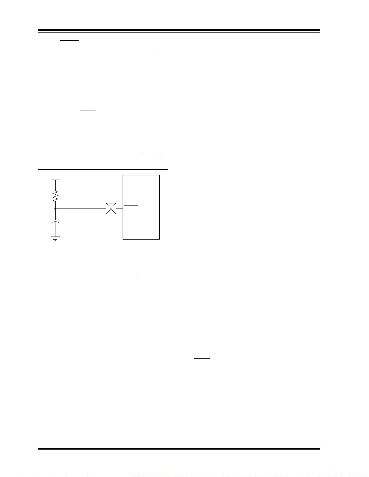
PIC16F7X
12.4 MCLR
PIC16F7X devices have a noise filter in the MCLR
Reset path. The filter will detect and ignore small
pulses.
It should be noted that a WDT Reset does not drive
pin low.
MCLR
The behavior of the ESD protection on the MCLR
pin
has been altered from previous devices of this family.
Volt a ges app lied to the pin th at exce ed it s spe cific ation
can result in both MCLR
Resets and excessiv e c urre nt
beyond the de v ic e sp e ci fic at i on du ri ng th e ESD ev e nt .
For this reason, Microchip recommends that the MCLR
pin no longer be tied directly to VDD. The use of an RC
network, as shown in Figure 12-5, is suggested.
FIGURE 12-5: RECOMMENDE D MCLR
CIRCUIT
DD
V
R1
1 k
Ω (or greater)
C1
µF
0.1
(optional, not critical)
PIC16F7X
MCLR
12.5 Power-on Reset (POR)
A Power-on Reset pulse is generated on-chip when
DD rise is detected (in the range of 1.2V - 1.7V). To
V
take advant age of the POR, tie the MCLR
described in Section 12.4. A maximum rise time for
DD is specified. See the Electrical Specifications for
V
details.
When the device starts normal operation (exits the
RESET condition), device operating parameters (voltage, frequency, temperature,...) m ust be m et to en su re
operation. If these cond itions are not met, the d evice
must be held in RESET until the operating conditions
are met. For additional information, refer to Application
Note, AN607, “Power-up Trouble Shooting”
(DS00607).
pin to VDD as
12.6 Power-up Timer (PWRT)
The Power-up Timer provides a fixed 72 ms nominal
time-out on power-up only from the POR. The Powerup Timer operates on an internal RC oscillator. The
chip is kept in RESET as long as the PWRT is active.
The PWRT’s ti me delay allow s V
DD to rise to an accept-
able level. A configuration bit is provided to enable/
disable the PWRT.
The power-up time dela y will vary from chip to chip, due
DD, temperature and process variation. See DC
to V
parameters for details (T
PWRT, parameter #33).
12.7 Oscillator Start-up Timer (OST)
The Oscillator S tart-up T imer (OST) provides 1024 oscillator cycles (from OSC1 input) delay after the PWRT
delay is over (if enabled). This helps to ensure that the
crystal oscillator or resonator has started and st ab ilized.
The OST time-out is invoked only for XT, LP and HS
modes and only on Power-on Reset, or wake-up from
SLEEP.
12.8 Brown-out Reset (BOR)
The configuration bit, BODEN, can enable or disable
the Brown-out Reset circuit. If V
DD falls be low VBOR
(parameter D005, about 4V) for longer than TBOR
(parameter #35, about 100 µS), the brown-out situa tion
will reset the device. If V
than T
BOR, a RESET may not occur.
DD falls below VBOR for less
Once the brown-out occurs, the device will remain in
Brown-out Reset until V
DD rises above VBOR. The
Power-up Timer then keeps the device in RESET for
TPWRT (parameter #33, ab out 72 mS). If VDD should fall
below V
cess will restart when V
BOR during TPWRT, the Brown-out Reset pro-
DD rises above VBOR, with the
Power-up Timer Reset. The Power-up Timer is always
enabled when the Brown-out Reset circuit is enabled,
regardless of the state of the PWRT configuration bit.
12.9 Time-out Sequence
On power-up, the time-out sequence is as follows: the
PWRT delay starts (if enabled) when a POR Reset
occurs. Then, OST starts counting 1024 oscillator
cycles when PWRT ends (LP, XT, HS). When the OST
ends, the device comes out of RESET.
If MCLR
Bringing MCLR
This is useful for testing purposes or to synchronize
more than one PIC16F7X device operating in parallel.
Table 12-5 shows the RESET conditions for the
STATUS, PCON and PC registers, while Table 12-6
shows the RESET conditions for all the registers.
is kept low long enough, all delays will expire.
high will begin execution immediately.
DS30325B-page 94 2002 Microchip Technology Inc.
Page 97
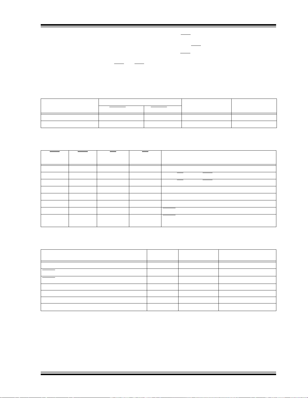
PIC16F7X
12.10 Power Control/Status Register (PCON)
The Power Control/Status Register, PCON, has two
bits to indicate the type of RESET that last occurred.
Bit0 is Brown-out Reset Status bit, BOR
unknown on a Power-on Reset. It must then be set by
the user and checked on subsequent RESETS to see
. Bit BOR is
if bit BOR
occurred. When the Brown-out Reset is disabled, the
state of the BOR
Bit1 is POR
a Power-on Reset and unaffected otherwise. The user
must set this bit following a Power-on Reset.
cleared, indicating a Brown-out Reset
bit is unpredictable.
(Power-on Reset St atus bit). It is cleared on
TABLE 12-3: TIME-OUT IN VARIOUS SITUATIONS
Oscillator Configuration
XT, HS, LP 72 ms + 1024 T
RC 72 ms — 72 ms —
PWRTE
Power-up
= 0 PWRTE = 1
OSC 1024 TOSC 72 ms + 1024 TOSC 1024 TOSC
Brown-out
Wake-up from
TABLE 12-4: STATUS BITS AND THEIR SIGNIFICANCE
POR
(PCON<1>)
0x 1 1Power-on Reset
0x 0 xIllegal, TO
0x x 0Illegal, PD is set on POR
10 1 1Brown-out Reset
11 0 1WDT Reset
11 0 0WDT Wake-up
11 u uMCLR
11 1 0MCLR Reset during SLEEP or interrupt wake-up from
BOR
(PCON<0>)TO(STATUS<4>)PD(STATUS<3>)
Significance
is set on POR
Reset during normal operation
SLEEP
SLEEP
TABLE 12-5: RESET CONDITION FOR SPECIAL REGISTERS
Condition
Power-on Reset 000h 0001 1xxx ---- --0x
Reset during normal operation 000h 000u uuuu ---- --uu
MCLR
Reset during SLEEP 000h 0001 0uuu ---- --uu
MCLR
WDT Reset 000h 0000 1uuu ---- --uu
WDT Wake-up PC + 1 uuu0 0uuu ---- --uu
Brown-out Reset 000h 0001 1uuu ---- --u0
Interrupt wake-up from SLEEP PC + 1
Legend: u = unchanged, x = unkno wn, - = unimplemented bit, read as '0'
Note 1: When the wake-up is due to an interrupt and the GIE bit is set, the PC is loaded with the interrupt vector
(0004h).
2002 Microchip Technology Inc. DS30325B-page 95
Program
Counter
(1)
STATUS
Register
uuu1 0uuu ---- --uu
PCON
Register
Page 98
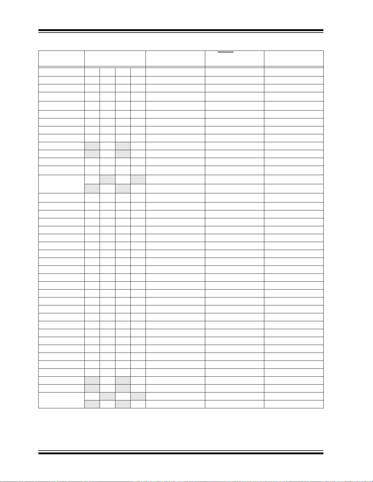
PIC16F7X
TABLE 12-6: INITIALIZATION CONDITIONS FOR ALL REGISTERS
Register Devices
W 73747677 xxxx xxxx uuuu uuuu uuuu uuuu
INDF 73 74 76 77 N/A N/A N/A
TMR0 73 74 76 77 xxxx xxxx uuuu uuuu uuuu uuuu
PCL 73747677 0000h 0000h PC + 1
STATUS 73 74 76 77 0001 1xxx 000q quuu
FSR 73747677 xxxx xxxx uuuu uuuu uuuu uuuu
PORTA 73747677 --0x 0000 --0u 0000 --uu uuuu
PORTB 73747677 xxxx xxxx uuuu uuuu uuuu uuuu
PORTC 73747677 xxxx xxxx uuuu uuuu uuuu uuuu
PORTD
PORTE
PCLATH 73 74 76 77 ---0 0000 ---0 0000 ---u uuuu
INTCON 73 74 76 77 0000 000x 0000 000u uuuu uuuu
PIR1 73 74 76 77 r000 0000 r000 0000 ruuu uuuu
PIR2 73 74 76 77 ---- ---0 ---- ---0 ---- ---u
TMR1L 73747677 xxxx xxxx uuuu uuuu uuuu uuuu
TMR1H 73747677 xxxx xxxx uuuu uuuu uuuu uuuu
T1CON 73747677 --00 0000 --uu uuuu --uu uuuu
TMR2 73 74 76 77 0000 0000 0000 0000 uuuu uuuu
T2CON 73747677 -000 0000 -000 0000 -uuu uuuu
SSPBUF 73 74 76 77 xxxx xxxx uuuu uuuu uuuu uuuu
SSPCON 73 74 76 77 0000 0000 0000 0000 uuuu uuuu
CCPR1L 73747677 xxxx xxxx uuuu uuuu uuuu uuuu
CCPR1H 73747677 xxxx xxxx uuuu uuuu uuuu uuuu
CCP1CON 73 74 76 77 --00 0000 --00 0000 --uu uuuu
RCSTA 73 74 76 77 0000 -00x 0000 -00x uuuu -uuu
TXREG 73747677 0000 0000 0000 0000 uuuu uuuu
RCREG 73 74 76 77 0000 0000 0000 0000 uuuu uuuu
CCPR2L 73747677 xxxx xxxx uuuu uuuu uuuu uuuu
CCPR2H 73747677 xxxx xxxx uuuu uuuu uuuu uuuu
CCP2CON 73 74 76 77 0000 0000 0000 0000 uuuu uuuu
ADRES 73747677 xxxx xxxx uuuu uuuu uuuu uuuu
ADCON0 73 74 76 77 0000 00-0 0000 00-0 uuuu uu-u
OPTION_REG 73 74 76 77 1111 1111 1111 1111 uuuu uuuu
TRISA 73747677 --11 1111 --11 1111 --uu uuuu
TRISB 73747677 1111 1111 1111 1111 uuuu uuuu
TRISC 73747677 1111 1111 1111 1111 uuuu uuuu
TRISD
TRISE
PIE1 73 74 76 77 r000 0000 r000 0000 ruuu uuuu
Legend: u = unchanged, x = unkno wn, - = unimplemented bit, read as ’0’, q = value depends on condition,
r = reserved, maintain clear
Note 1: One or more bits in INTCON, PIR1 and/or PIR2 will be affected (to cause wake-up).
2: When the wake-up is due to an interrupt and the GIE bit is set, the PC is loaded with the interrupt vector (0004h).
3: See T able12-5 for RESET value for specific condition.
73 74 76 77 xxxx xxxx uuuu uuuu uuuu uuuu
73 74 76 77 ---- -xxx ---- -uuu ---- -uuu
73 74 76 77 0000 0000 0000 0000 uuuu uuuu
73 74 76 77 1111 1111 1111 1111 uuuu uuuu
73 74 76 77 0000 -111 0000 -111 uuuu -uuu
73 74 76 77 0000 0000 0000 0000 uuuu uuuu
Power-on Reset,
Brown-out Reset
Reset,
MCLR
WDT Reset
(3)
Wake-up via WDT or
Interrupt
(2)
uuuq quuu
(3)
(1)
(1)
(1)
(1)
DS30325B-page 96 2002 Microchip Technology Inc.
Page 99
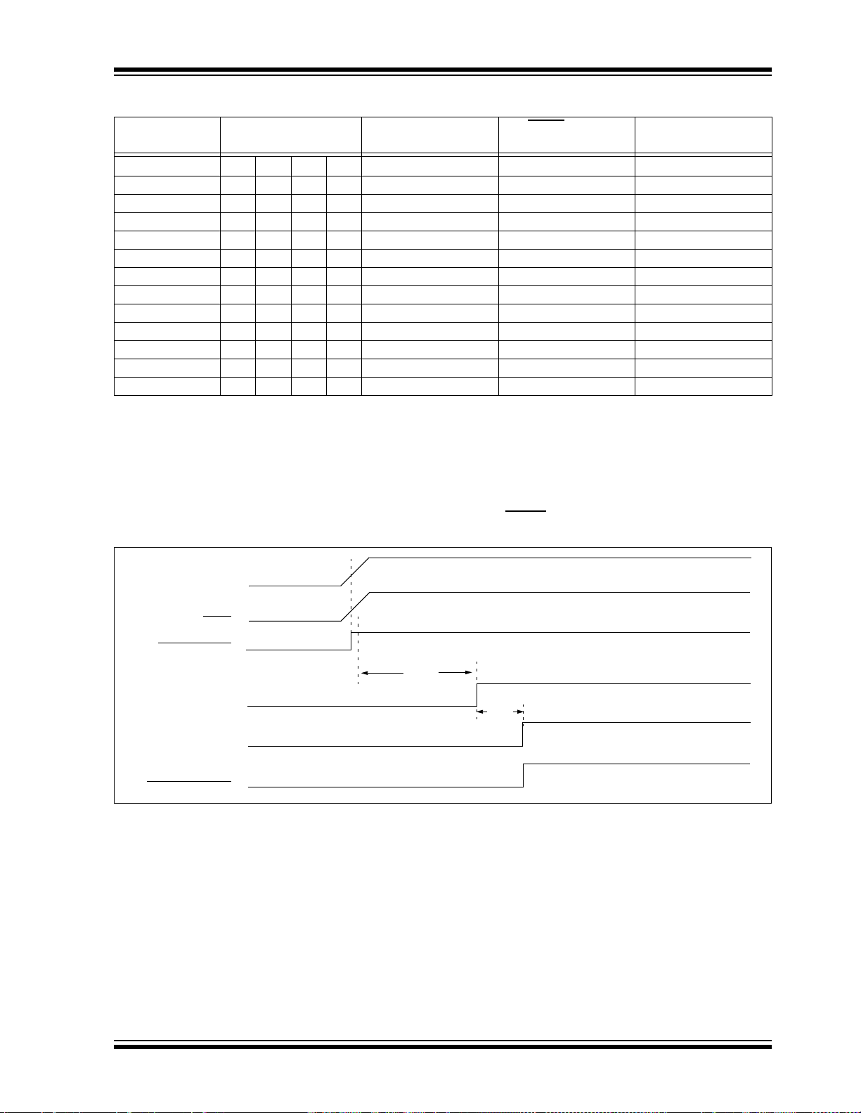
PIC16F7X
TABLE 12-6: INITIALIZATION CONDITIONS FOR ALL REGISTERS (CONTINUED)
Register Devices
Power-on Reset,
Brown-out Reset
Reset,
MCLR
WDT Reset
Wake-up via WDT or
Interrupt
PIE2 73 74 76 77 ---- ---0 ---- ---0 ---- ---u
PCON 73 74 76 77 ---- --qq ---- --uu ---- --uu
PR2 73747677 1111 1111 1111 1111 1111 1111
SSPSTAT 73 74 76 77 --00 0000 --00 0000 --uu uuuu
SSPADD 73747677 0000 0000 0000 0000 uuuu uuuu
TXSTA 73747677 0000 -010 0000 -010 uuuu -uuu
SPBRG 73 74 76 77 0000 0000 0000 0000 uuuu uuuu
ADCON1 73 74 76 77 ---- -000 ---- -000 ---- -uuu
PMDATA 73 74 76 77 0--- 0000 0--- 0000 u--- uuuu
PMADR 73747677 xxxx xxxx uuuu uuuu uuuu uuuu
PMDATH 73 74 76 77 xxxx xxxx uuuu uuuu uuuu uuuu
PMADRH 73 74 76 77 xxxx xxxx uuuu uuuu uuuu uuuu
PMCON1 73 74 76 77 1--- ---0 1--- ---0 1--- ---u
Legend: u = unchanged, x = unkno wn, - = unimplemented bit, read as ’0’, q = value depends on condition,
r = reserved, maintain clear
Note 1: One or more bits in INTCON, PIR1 and/or PIR2 will be affected (to cause wake-up).
2: When the wake-up is due to an interrupt and the GIE bit is set, the PC is loaded with the interrupt vector (0004h).
3: See T able12-5 for RESET value for specific condition.
FIGURE 12-6: TIME-OUT SEQUENCE ON POWER-UP (MCLR TIED TO VDD THROUGH
RC NETWORK)
VDD
MCLR
INTERNAL POR
PWRT TIME-OUT
OST TIME-OUT
INTERNAL RESET
TPWRT
TOST
2002 Microchip Technology Inc. DS30325B-page 97
Page 100
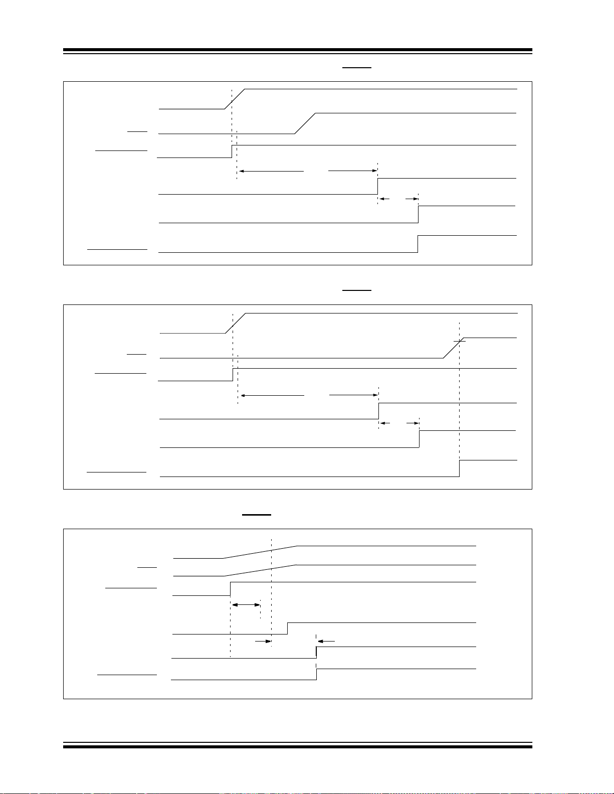
PIC16F7X
FIGURE 12-7: TIME-OUT SEQUENCE ON POWER-UP (MCLR NOT TIED TO VDD): CASE 1
VDD
MCLR
INTERNAL POR
TPWRT
PWRT TIME-OUT
OST TIME-OUT
INTERNAL RESET
FIGURE 12-8: TIME-OUT SEQUENCE ON POWER-UP (MCLR
VDD
MCLR
INTERNAL POR
TPWRT
PWRT TIME-OUT
OST TIME-OUT
INTERNAL RESET
TOST
NOT TIED TO VDD): CASE 2
TOST
FIGURE 12-9: SLOW RISE TIME (MCLR
VDD
MCLR
INTERNAL POR
PWRT TIME-OUT
OST TIME-OUT
INTERNAL RESET
0V
T
PWRT
TIED TO VDD THROUGH RC NETWORK)
5V
1V
TOST
DS30325B-page 98 2002 Microchip Technology Inc.
 Loading...