

Page 1

M
PIC16F72
Data Sheet
28-Pin, 8-Bit CMOS FLASH
Microcontroller with A/D Converter
2002 Microchip Technology Inc. DS39597B
Page 2

Note the following details of the code protection feature on PICmicro® MCUs.
• The PICmicro family meets the specifications contained in the Microchip Data Sheet.
• Microchip believes that its family of PICmicro microcontrollers is one of the most secure products of its kind on the market today,
when used in the intended manner and under normal conditions.
• There are dishonest and possibly illegal methods used to breach the code protection feature. All of these methods, to our knowledge, require using the PICmicro microcontroller in a manner outside the operating specifications contained in the data sheet.
The person doing so may be engaged in theft of intellectual property.
• Microchip is willing to work with the customer who is concerned about the integrity of their code.
• Neither Microchip nor any other semiconductor manufacturer can guarantee the security of their code. Code protection does not
mean that we are guaranteeing the product as “unbreakable”.
• Code protection is constantly evolving. We at Microchip are committed to continuously improving the code protection features of
our product.
If you have any further questions about this matter, please contact the local sales office nearest to you.
Information contained in this publication regarding device
applications and the like is intended through suggestion only
and may be superseded by updates. It is your responsibility to
ensure that your application meets with your specifications.
No representation or warranty is given and no liability is
assumed by Microchip Technology Incorporated with respect
to the accuracy or use of such information, or infringement of
patents or other intellectual property rights arising from such
use or otherwise. Use of Microchip’s products as critical components in life support systems is not authorized except with
express written approval by Microchip. No licenses are conveyed, implicitly or otherwise, under any intellectual property
rights.
Trademarks
The Microchip name and logo, the Microchip logo, FilterLab,
K
EELOQ, microID, MPLAB, PIC, PICmicro, PICMASTER,
PICSTART, PRO MATE, SEEVAL and The Embedded Control
Solutions Company are registered trademarks of Microchip Technology Incorporated in the U.S.A. and other countries.
dsPIC, ECONOMONITOR, FanSense, FlexROM, fuzzyLAB,
In-Circuit Serial Programming, ICSP, ICEPIC, microPort,
Migratable Memory, MPASM, MPLIB, MPLINK, MPSIM,
MXDEV , MXLAB, PICC , PICDEM, PICDEM.net, rfP IC, Select
Mode and Total Endurance are trademarks of Microchip
Technology Incorporated in the U.S.A.
Serialized Quick Turn Programming (SQTP) is a service mark
of Microchip Technology Incorporated in the U.S.A.
All other trademarks mentioned herein are property of their
respective companies.
© 2002, Microchip Technology Incorporated, Printed in the
U.S.A., All Rights Reserved.
Printed on recycled paper.
Microchip received QS-9000 quality system
certification for its worldwide headquarters,
design and wafer fabrication facilities in
Chandler and Tempe, Arizona in July 1999
and Mountain View, California in March 2002.
The Company’s quality system processes and
procedures are QS-9000 compliant for its
PICmicro
devices, Serial EEPROMs, microperipherals,
non-volatile memory and analog products. In
addition, Microchip’s quality system for the
design and manufacture of development
systems is ISO 9001 certified.
®
8-bit MCUs, KEELOQ
®
code hoppin g
DS39597B - page ii 2002 Microchip Technology Inc.
Page 3
M
PIC16F72
28-Pin, 8-Bit CMOS FLASH MCU with A/D Converter
Device Included:
• PIC16F72
High Performance RISC CPU:
• Only 35 single word instructions to learn
• All single cycle instructions except for program
branches, which are two-cycle
• Operating speed: DC - 20 MHz clock input
DC - 200 ns instruction cycle
• 2K x 14 words of Program Memory,
128 x 8 bytes of Data Memory (RAM)
• Pinout compatible to PIC16C72/72A and
PIC16F872
• Interrupt capability
• Eight-level deep hardware stack
• Direct, Indirect and Relative Addressing modes
Peripheral Features:
• High Sink/Source Current: 25 mA
• Timer0: 8-bit timer/counter with 8-bit prescaler
• Timer1: 16-bit timer/counter with prescaler,
can be incremented during SLEEP via external
crystal/clock
• Timer2: 8-bit timer/counter with 8-bit period
register, prescaler and postscaler
• Capture, Compare, PWM (CCP) module
- Capture is 16-bit, max. resolution is 12.5 ns
- Compare is 16-bit, max. resolution is 200 ns
- PWM max. resolution is 10-bit
• 8-bit, 5-channel analog-to-digital converter
• Synchronous Serial Port (SSP) with
SPI™ (Master/Slave) and I
2
C™ (Slave)
• Brown-out detection circuitry for
Brown-out Reset (BOR)
CMOS Technology:
• Low power, high speed CMOS FLASH technology
• Fully static design
• Wide operating voltage range: 2.0V to 5.5V
• Industrial temperature range
• Low power consumption:
- < 0.6 mA typical @ 3V, 4 MHz
-20 µA typical @ 3V, 32 kHz
-< 1 µA typical standby current
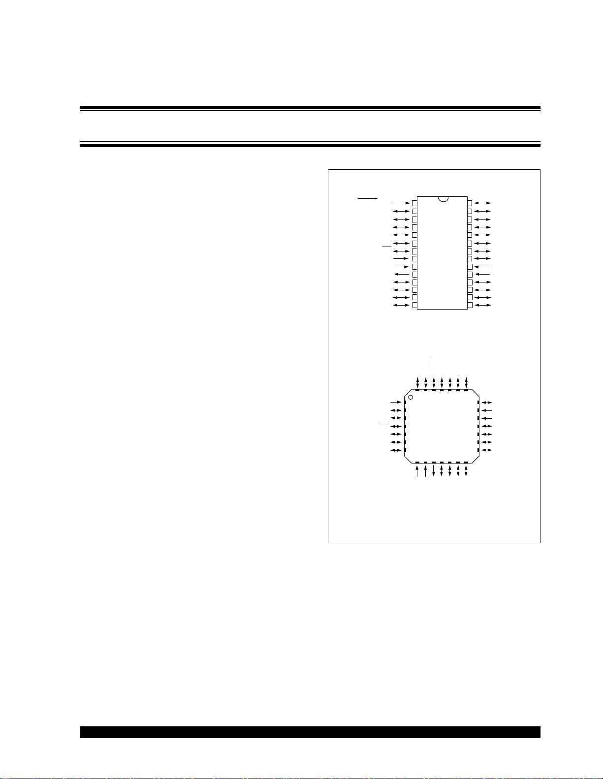
Pin Diagrams
PDIP, SOIC, SSOP
MCLR/VPP
RA0/AN0
RA1/AN1
RA2/AN2
RA3/AN3/V
RC0/T1OSO/T1CKI
RC3/SCK/SCL
REF
RA4/T0CKI
RA5/AN4/SS
VSS
OSC1/CLKI
OSC2/CLKO
RC1/T1OSI
RC2/CCP1
• 1
2
3
4
5
6
7
8
9
10
11
12
13
14
28
27
26
25
PIC16F72
24
23
22
21
20
19
18
17
16
15
RB7/PGD
RB6/PGC
RB5
RB4
RB3
RB2
RB1
RB0/INT
V
DD
VSS
RC7
RC6
RC5/SDO
RC4/SDI/SDA
QFN
/VPP
RA1/AN1
RA0/AN0
MCLR
RB7/PGD
RB6/PGC
RB5
RB4
PIC16F72
10 118 9 12 13 14
RC2/CCP1
RC1/T1OSI
RC3/SCK/SCL
232425262728 22
RC4/SDI/SDA
21
20
19
18
17
16
15
RC6
RC5/SDO
RB3
RB2
RB1
RB0/INT
V
DD
VSS
RC7
RA2/AN2
RA3/AN3/V
RA4/T0CKI
RA5/AN4/SS
OSC1/CLKI
OSC2/CLKO
REF
V
1
2
3
4
SS
5
6
7
RC0/T1OSO/T1CKI
Special Microcontroller Features:
• 1,000 erase/write cycle FLASH program memory
typical
• Power-on Reset (POR), Power-up Timer (PWR T)
and Oscillator Start-up Timer (OST)
• Watchdog Timer (WDT) with its own on-chip
RC oscillator for reliable operation
• Programmable code protection
• Power saving SLEEP mode
• Selectable oscilla tor opti ons
• In-Circuit Serial Programming™ (ICSP ™) vi a 2 pins
• Processor read access to program memo ry
2002 Microchip Technology Inc. DS39597B-page 1
Page 4

PIC16F72
FLASH Program Memory - (14-bit words, 1000 E/W cycles) 2K
Key Reference Manual Features PIC16F72
Operating Frequency DC - 20 MHz
RESETS and (Delays) POR, BOR, (PWRT, OST)
Data Memory - RAM (8-bit bytes) 128
Interrupts 8
I/O Ports PORTA, PORTB, PORTC
Timer s Timer0, Timer1, Time r2
Capture/Compare/PWM Modules 1
Serial Communications SSP
8-bit A/D Converter 5 channels
Instruction Set (No. of Instructions) 35
DS39597B-page 2 2002 Microchip Technology Inc.
Page 5

PIC16F72
Table of Contents
1.0 Device Overview.......................................................................................................................................................................... 5
2.0 Memory Organization................................................................................................................................................................... 7
3.0 I/O Ports.................. ........................................ ..................... ...................................................................................................... 21
4.0 Reading Program Memory ......................................................................................................................................................... 27
5.0 Timer0 Module ........................................................................................................................................................................... 29
6.0 Timer1 Module ........................................................................................................................................................................... 31
7.0 Timer2 Module ........................................................................................................................................................................... 35
8.0 Capture/Compare/PWM (CCP) Module..................................................................................................................................... 37
9.0 Synchronous Serial Port (SSP) Module ..................................................................................................................................... 43
10.0 Analog-to-Digital Converter (A/D) Module..................................................................................................................................53
11.0 Special Features of the CPU............................... .......................................................................................................................59
12.0 Instruction Set Summary............................................................................................................................................................ 73
13.0 Development Support.................................................................................................................................................................81
14.0 Electrical Characteristics............................................................................................................................................................ 87
15.0 DC and AC Characteristics Graphs and Tables.......................................................................................................................107
16.0 Package Marking Information.. ................................................................................................................................................. 117
Appendix A: Revision History ........................................................................................................................................................ 123
Appendix B: Conversion Considerations.............................................................................. .... .. .. .... .............................................. 123
Index .................................................................................................................................................................................................. 125
On-Line Support................................................................................................................................................................................. 131
Reader Response..............................................................................................................................................................................132
Product Identification System ............................................................................................................................................................ 133
TO OUR VALUED CUSTOMERS
It is our intention to provide our valued customers with the best documentation possible to ensure successful use of your Microchip
products. To this end, we will continue to improve our publications to better suit your needs. Our publications will be refined and
enhanced as new volumes and updates are introduced.
If you have any questions or c omm ents regarding th is publication, p lease c ontact the M a rketing Communications Department via
E-mail at docerrors@mail.microchip.com or fax the Reader Response Form in the back of this data sheet to (480) 792-4150.
We welcome your feedback.
Most Current Data Sheet
To obtain the most up-to-date version of this data sheet, please register at our Worldwide Web site at:
http://www.microchip.com
You can determine the version of a data sheet by examining its literature number found on the bottom outside corner of any page.
The last character of the literature number is the version number, (e.g., DS30000A is version A of document DS30000).
Errata
An errata sheet, describing minor operational differences from the data sheet and recommended workarounds, may exist for current
devices. As device/documentation issues become known to us, we will publish an errata sheet. The errata will specify the revision
of silicon and revision of document to which it applies.
To determine if an errata sheet exists for a particular device, please check with one of the following:
• Microchip’s Worldwide Web site; http://www.microchip.com
• Your local Microchip sales office (see last page)
• The Microchip Corporate Literature Center; U.S. FAX: (480) 792-7277
When contacting a sales office or the literature center, please specify which device, revision of silicon and data sheet (include
literature number) you are using.
Customer Notification System
Register on our web site at www.microchip.com/cn to receive the most current information on all of our products.
2002 Microchip Technology Inc. DS39597B-page 3
Page 6

PIC16F72
NOTES:
DS39597B-page 4 2002 Microchip Technology Inc.
Page 7
PIC16F72
1.0 DEVICE OVERVIEW
This documen t conta i ns dev ic e spec if i c in for m at i on fo r
the operation of the PIC16F 72 de vic e. Additi ona l inf ormation may be found in the PICmicro™ Mid-Range
MCU Reference Manual (DS33023), which may be
downloaded from the Microchip website. The Reference Manual should be considered a complementary
document to this data sheet, and is highly recommended reading for a better understanding of the
device architecture and operation of the peripheral
modules.
The PIC16F72 belongs to the Mid-Range family of the
PICmicro devices. A block diagram of the device is
shown in Figure 1-1.
FIGURE 1-1: PIC16F72 BLOCK DIAGRAM
13
Program Counter
8-Level Stack
Direct Addr
8
Power-up
Oscillator
Start-up Timer
Power-on
Watchdog
Brown-out
(13-bit)
RAM Addr
7
Timer
Reset
Timer
Reset
Program
Bus
OSC1/CLKI
OSC2/CLKO
FLASH
Program
Memory
2K x 14
14
Instruction reg
Instruction
Decode &
Control
Timing
Generation
3
8
The program memory contains 2K words, which translate to 2048 instructions, since each 14-bit program
memory word is the same width as each device
instruction. The data memory (RAM) cont ains 128 bytes.
There are 22 I/O pins that are user configurable on a
pin-to-pin basis. Some pins are multiplexed with other
device functions. These functions include:
• External interrupt
• Change on PORTB interrupt
• Timer0 clock input
• Timer1 clock/oscillator
• Capture/Compare/PWM
• A/D converter
2
• SPI/I
C
Table 1-1 details the pinout of the device with
descriptions and details for each pin.
Data Bus
RAM
File
Registers
128 x 8
(1)
Addr MUX
FSR reg
STATUS reg
ALU
W reg
9
8
MUX
8
Indirect
Addr
PORTA
PORTB
PORTC
RA0/AN0
RA1/AN1
RA2/AN2
RA3/AN3/VREF
RA4/T0CKI
RA5/AN4/SS
RB0/INT
RB1
RB2
RB3
RB4
RB5
RB6/PGC
RB7/PGD
RC0/T1OSO/T1CKI
RC1/T1OSI
RC2/CCP1
RC3/SCK/SCL
RC4/SDI/SDA
RC5/SDO
RC6
RC7
MCLR
VDD, VSS
Timer0
A/D
Note 1: Higher order bits are from the STATUS register.
Timer1 Timer2
Synchronous
Serial Por t
CCP1
2002 Microchip Technology Inc. DS39597B-page 5
Page 8

PIC16F72
TABLE 1-1: PIC16F72 PINOUT DESCRIPTION
PDIP,
Pin Name
OSC1/CLKI 9 6 I
OSC2/CLKO 10 7 O — Oscillator crystal output. Connects to crystal or resonator in Crystal
MCLR
/VPP
RA0/AN0 2 27 I/O TTL RA0 can also be analog input0.
RA1/AN1 3 28 I/O TTL RA1 can also be analog input1.
RA2/AN2 4 1 I/O TTL RA2 can also be analog input2.
RA3/AN3/V
RA4/T0CKI 6 3 I/O ST RA4 can also be the clock input to the Timer0 module. Output is
RA5/AN4/SS
RB0/INT 21 18 I/O TTL/ST
RB1 22 19 I/O TTL
RB2 23 20 I/O TTL
RB3 24 21 I/O TTL
RB4 25 22 I/O TTL Interrupt-on-change pin.
RB5 26 23 I/O TTL Interrupt-on-change pin.
RB6/PGC 27 24 I/O TTL/ST
RB7/PGD 28 25 I/O TTL/ST
RC0/T1OSO/
T1CKI
RC1/T1OSI 12 9 I/O ST RC1 can also be the Timer1 oscillator input.
RC2/CCP1 13 10 I/O ST RC2 can also be the Capture1 input/Compare1 output/
RC3/SCK/SCL 14 11 I/O ST RC3 can also be the synchronous serial clock input/output for both
RC4/SDI/SDA 15 12 I/O ST RC4 can also be the SPI Data In (SPI mode) or
RC5/SDO 16 13 I/O ST RC5 can also be the SPI Data Out (SPI mode).
RC6 17 14 I/O ST
RC7 18 15 I/O ST
SS 8, 19 5, 16 P — Ground reference for logic and I/O pins.
V
V
DD 20 17 P — Positive supply for logic and I/O pins.
Legend: I = input O = output I/O = input/output P = power
Note 1: This buffer is a Schmitt Trigger input when configured as the external interrupt.
— = Not used TTL = TTL input ST = Schmitt Trigger input
2: This buffer is a Schmitt Trigger input when used in Serial Programming mode.
3: This buffer is a Schmitt Trigger input when configured in RC Oscillator mode and a CMOS input otherwise.
SOIC,
SSOP
Pin#
REF 5 2 I/O TTL RA3 can also be analog input3 or analog reference voltage.
MLF
Pin#
1 26 I/P ST Master Clear (Reset) input or programming voltage input. This pin is
7 4 I/O TTL RA5 can also be analog input4 or the slave select for the
11 8 I/O ST RC0 can also be the Timer1 oscillator output or Ti mer1 clock input.
I/O/P
Type
Buffer
Type
ST/CMOS
Description
(3)
Oscillator crystal input/external clock source input.
Oscillator mode. In RC mode, the OSC2 pin outputs CLKO, which has
1/4 the frequency of OSC1, and denotes the instruction cycle rate.
an active low RESET to the device.
PORTA is a bi-directional I/O port.
open drain type.
synchronous serial port.
PORTB is a bi-directional I/O port. PORTB can be software
programmed for internal weak pull-up on all inputs.
(1)
(2)
(2)
RB0 can also be the external interrupt pin.
Interrupt-on-change pin. Serial programming clock.
Interrupt-on-change pin. Serial programming data.
PORTC is a bi-directional I/O port.
PWM1 output.
2
SPI and I
Data I/O (I
C modes.
2
C mode).
DS39597B-page 6 2002 Microchip Technology Inc.
Page 9
PIC16F72
2.0 MEMORY ORGANIZATION
There are two memo ry b loc ks in the PIC16F72 device.
These are the program memory and the data memory.
Each block has separate buses so that concurrent
access can occur. Program memory and data memory
are explained in this section. Program memory can be
read internally by the user code (see Section 4.0).
The data memory can further be broken down into the
general purpose RAM and the Special Function
Registers (SFRs). The operation of the SFRs that
control the “core” are described here. The SFRs used
to control the peripheral modules are described in the
section discussing each individual peripheral module.
Additional informa tion on devi ce memory may be found
in the PICmicro™ Mid-Range Reference Manual,
(DS33023).
2.1 Program Memory Organization
PIC16F72 devices have a 13-bit program counter capable of addressing a 8K x 14 program memory space.
The address range for this program memory is 0000h 07FFh. Accessing a location above the physically
implemented address will cause a wraparound.
The RESET Ve ctor is at 0000h an d the Interrup t V ector
is at 0004h.
FIGURE 2-1: PROGRAM MEMORY MAP
AND STACK
2.2 Data Memory Organization
The Data Memo ry is partiti oned into mult iple banks th at
contain the Ge neral Purpose Reg isters and the Special
Function Registers. Bits RP1 (STATUS<6>) and RP0
(STATUS<5>) are the bank select bits.
RP1:RP0 Bank
00 0
01 1
10 2
11 3
Each bank extends up to 7Fh (128 bytes). The lower
locations of each bank are reserved for the Special
Function Registers. Abo ve the Speci al Function Re gisters are General Purpose Registers, implemented as
static RAM.
All implemented ban ks co nta in SFR s. Some “h igh use”
SFRs from one bank m ay be m irro red in an othe r b ank ,
for code reduction and quicker access (e.g., the
STATUS register is in Banks 0 - 3).
2.2.1 GENERAL PURPOSE REGISTER
FILE
The register file can be acces sed either directly, or indirectly, through the File Select Register FSR (see
Section 2.5).
CALL, RETURN
RETFIE, RETLW
Space
User Memory
On-chip Program
PC<12:0>
13
Stack Level 1
Stack Level 8
RESET Vector
Interrupt Vector
Memory
0000h
0004h
0005h
07FFh
0800h
1FFFh
2002 Microchip Technology Inc. DS39597B-page 7
Page 10
PIC16F72
FIGURE 2-2: PIC16F72 REGISTER FILE MAP
File
Address
Indirect addr.(*)
TMR0
PCL
STATUS
FSR
PORTA
PORTB
PORTC
PCLATH
INTCON
PIR1
TMR1L
TMR1H
T1CON
TMR2
T2CON
SSPBUF
SSPCON
CCPR1L
CCPR1H
CCP1CON
ADRES
ADCON0 ADCON1
General
Purpose
Register
96 Bytes
00h
01h
02h
03h
04h
05h
06h
07h
08h
09h
0Ah
0Bh
0Ch
0Dh
0Eh
0Fh
10h
11h
12h
13h
14h
15h
16h
17h
18h
19h
1Ah
1Bh
1Ch
1Dh
1Eh
1Fh
20h
Indirect addr.(*)
OPTION
STATUS
PCLATH
INTCON
SSPADD
SSPSTAT
General
Purpose
Register
32 Bytes
accesses
40h-7Fh
PCL
FSR
TRISA
TRISB
TRISC
PIE1
PCON
PR2
File
Address
80h
81h
82h
83h
84h
85h
86h
87h
88h
89h
8Ah
8Bh
8Ch
8Dh
8Eh
8Fh
90h
91h
92h
93h
94h
95h
96h
97h
98h
99h
9Ah
9Bh
9Ch
9Dh
9Eh
9Fh
A0h
BFh
C0h
Indirect addr.(*)
TMR0
PCL
STATUS
FSR
PORTB
PCLATH
INTCON
PMDATL
PMADRL
PMDATH
PMADRH
accesses
20h-7Fh
File
Address
100h
101h
102h
103h
104h
105h
106h
107h
108h
109h
10Ah
10Bh
10Ch
10Dh
10Eh
10Fh
110h
11Fh
120h
Indirect addr.(*)
OPTION
PCL
STATUS
FSR
TRISB
PCLATH
INTCON
PMCON1
accesses
A0h -BFh
accesses
40h -7Fh
File
Address
180h
181h
182h
183h
184h
185h
186h
187h
188h
189h
18Ah
18Bh
18Ch
18Dh
18Eh
18Fh
190h
19Fh
1A0h
1BFh
1C0h
Bank 0
7Fh
Unimplemented data memory locations, read as ‘0’.
* Not a physical register.
DS39597B-page 8 2002 Microchip Technology Inc.
Bank 1
FFh
Bank 2
17Fh
Bank 3
1FFh
Page 11
PIC16F72
2.2.2 SPECIAL FUNCTION REGISTERS
The Special Function Registers are registers used by
the CPU and peripheral modules for controlling the
desired operation of the device. These registers are
implemented as static RAM. A list of these registers is
given in Table 2-1.
The Special Function Registers can be classified into
two sets: core (CPU) and peripheral. Those registers
associated with the core functions are described in
detail in this section. Those related to the operation of
the peripheral features are described in detail in the
peripheral feature section.
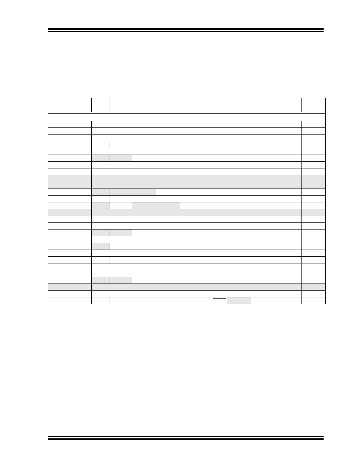
TABLE 2-1: SPECIAL FUNCTION REGISTER SUMMARY
Address Name Bit 7 Bit 6 Bit 5 Bit 4 Bit 3 Bit 2 Bit 1 Bit 0
Bank 0
(1)
00h
01h TMR0 Timer0 Module’s Register xxxx xxxx 29,13
02h
03h
04h
05h PORTA
06h PORTB PORTB Data Latch when written: PORTB pins when read xxxx xxxx 23
07h PORTC PORTC Data Latch when written: PORTC pins when read xxxx xxxx 25
08h — Unimplemented — —
09h — Unimplemented — —
0Ah
0Bh
0Ch PIR1
0Dh — Unimplemented — —
0Eh TMR1L Holding Register for the Least Significant Byte of the 16-bit TMR1 Register xxxx xxxx 31
0Fh TMR1H Holding Register for the Most Significant Byte of the 16-bit TMR1 Register xxxx xxxx 31
10h T1CON
11h TMR2 Timer2 Module’s Register 0000 0000 35
12h T2CON
13h SSPBUF Synchronous Serial Port Receive Buffer/Transmit Register xxxx xxxx 43,48
14h SSPCON WCOL SSPOV SSPEN CKP SSPM3 SSPM2 SSPM1 SSPM0 0000 0000 45
15h CCPR1L Capture/Compare/PWM Register (LSB) xxxx xxxx 38,39,41
16h CCPR1H Capture/Compare/PWM Register (MSB) xxxx xxxx 38,39,41
17h CCP1CON
18h-1Dh — Unimplemented — —
1Eh ADRES A/D Result Register xxxx xxxx 53
1Fh ADCON0 ADCS1 ADCS0 CHS2 CHS1 CHS0 GO/DONE
Legend: x = unknown, u = unchanged, q = value depend s on condition, - = unimplemented, read as ‘0’, r = reserved.
Note 1: These registers can be addressed from any bank.
INDF Addressing this location uses contents of FSR to address data memory (not a physical register) 0000 0000 19
(1)
PCL Program Counter's (PC) Least Significant Byte 0000 0000 18
(1)
STATUS IRP RP1 RP0 TO P D Z DC C 0001 1xxx 12
(1)
FSR Indirect Data Memory Address Pointer xxxx xxxx 19
— — PORTA Data Latch when written: PORTA pins when read --0x 0000 21
(1,2)
PCLATH — — — Write Buffer for the upper 5 bits of the Program Counter ---0 0000 18
(1)
INTCON GIE PEIE TMR0IE INTE RBIE TMR0IF INTF RBIF 0000 000x 14
— ADIF — — SSPIF CCP1IF TMR2IF TMR1IF -0-- 0000 16
— — T1CKPS1 T1CKPS0 T1OSCEN T1SYNC TMR1CS TMR1ON --00 0000 31
— TOUTPS3 TOUTPS2 TOUTPS1 TOUTPS0 TMR2ON T2CKPS1 T2CKPS0 -000 0000 36
— — CCP1X CCP1Y CCP1M3 CCP1M2 CCP1M1 CCP1M0 --00 0000 37
— ADON 0000 00-0 53
Shaded locations are unimplemented, read as ‘0’.
2: The upper byte of the program counter is not directly accessible. PCLATH is a holding register for the PC<12:8> whose
contents are transferred to the upper byte of the program counter.
3: Th i s bi t always reads as a ‘1’.
Value on
POR, BOR
Details on
page:
2002 Microchip Technology Inc. DS39597B-page 9
Page 12
PIC16F72
TABLE 2-1: SPECIAL FUNCTION REGISTER SUMMARY (CONTINUED)
Address Name Bit 7 Bit 6 Bit 5 Bit 4 Bit 3 Bit 2 Bit 1 Bit 0
Bank 1
(1)
80h
81h OPTION RBPU
82h
83h
84h
85h TRISA
86h TRISB PORTB Data Direction Register 1111 1111 23
87h TRISC PORTC Data Direction Register 1111 1111 25
88h — Unimplemented — —
89h — Unimplemented — —
8Ah
8Bh
8Ch PIE1
8Dh — Unimplemented — —
8Eh PCON
8Fh — Unimplemented — —
90h — Unimplemented — —
91h — Unimplemented — —
92h PR2 Timer2 Period Regis ter 1111 1111 41
93h SSPADD Synchronous Serial Port (I
94h SSPSTAT SMP CKE D/A
95h — Unimplemented — —
96h — Unimplemented — —
97h — Unimplemented — —
98h — Unimplemented — —
99h — Unimplemented — —
9Ah — Unimplemented — —
9Bh — Unimplemented — —
9Ch — Unimplemented — —
9Dh — Unimplemented — —
9Eh — Unimplemented — —
9Fh ADCON1
Legend: x = unknown, u = unchanged, q = value depend s on condition, - = unimplemented, read as ‘0’, r = reserved.
Note 1: These registers can be addressed from any bank.
INDF Addressing this location uses contents of FSR to address data memory (not a physical register) 0000 0000 19
INTEDG T0CS T0SE PSA PS2 PS1 PS0 1111 1111 13
(1)
PCL Program Counter’s (PC) Least Significant Byte 0000 0000 18
(1)
STATUS IRP RP1 RP0 TO PD ZDCC0001 1xxx 12
(1)
FSR Indirect Data Memory Address Pointer xxxx xxxx 19
— — PORTA Data Direction Register --11 1111 21
(1,2)
PCLATH — — — Write Buffer for the upper 5 bits of the PC ---0 0000 18
(1)
INTCON GIE PEIE TMR0IE INTE RBIE TMR0IF INTF RBIF 0000 000x 14
— ADIE — — SSPIE CCP1IE TMR2IE TMR1IE -0-- 0000 15
— — — — — — POR BOR ---- --qq 17
2
C mode) Address Register 0000 0000 43,48
PSR/WUA BF 0000 0000 44
— — — — — PCFG2 PCFG1 PCFG0 ---- -000 54
Shaded locations are unimplemented, read as ‘0’.
2: The upper byte of the program counter is not directly accessible. PCLATH is a holding register for the PC<12:8> whose
contents are transferred to the upper byte of the program counter.
3: Th i s bi t always reads as a ‘1’.
Value on
POR, BOR
Details on
page:
DS39597B-page 10 2002 Microchip Technology Inc.
Page 13
PIC16F72
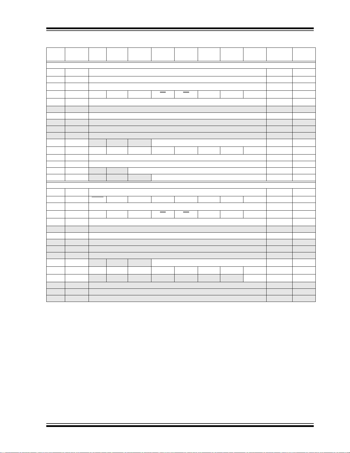
TABLE 2-1: SPECIAL FUNCTION REGISTER SUMMARY (CONTINUED)
Address Name Bit 7 Bit 6 Bit 5 Bit 4 Bit 3 Bit 2 Bit 1 Bit 0
Value on
POR, BOR
Bank 2
(1)
100h
INDF Addressing this location uses contents of FSR to address data memory (not a physical register) 0000 0000 19
101h TMR0 Timer0 Module’s Register xxxx xxxx 29
(1
102h
103h
104h
PCL Program Counter's (PC) Least Significant Byte 0000 0000 18
(1)
STATUS IRP RP1 RP0 TO PD ZDCC0001 1xxx 12
(1)
FSR Indirect Data Memory Address Pointer xxxx xxxx 19
105h — Unimplemented — —
106h PORTB PORTB Data Latch when written: PORTB pins when read xxxx xxxx 23
107h — Unimplemented — —
108h — Unimplemented — —
109h — Unimplemented — —
(1,2)
10Ah
10Bh
PCLATH — — — Write Buffer for the upper 5 bits of the Program Counter ---0 0000 18
(1)
INTCON GIE PEIE TMR0IE INTE RBIE TMR0IF INTF RBIF 0000 000x 14
10Ch PMDATL Data Register Low Byte xxxx xxxx 27
10Dh PMADRL Address Register Low Byte xxxx xxxx 27
10Eh PMDATH
10Fh PMADRH
— — Data Register High Byte --xx xxxx 27
— — — Address Register High Byte ---x xxxx 27
Bank 3
(1)
180h
181h OPTION RBPU
182h
183h
184h
INDF Addressing this location uses contents of FSR to address data memory (not a physical register) 0000 0000 19
INTEDG T0CS T0SE PSA PS2 PS1 PS0 1111 1111 13
(1)
PCL Program Counter's (PC) Least Significant Byte 0000 0000 18
(1)
STATUS IRP RP1 RP0 TO PD ZDCC0001 1xxx 12
(1)
FSR Indirect Data Memory Address Pointer xxxx xxxx 19
185h — Unimplemented — —
186h TRISB PORTB Data Direction Register 1111 1111 23
187h — Unimplemented — —
188h — Unimplemented — —
189h — Unimplemented — —
(1,2)
18Ah
18Bh
PCLATH — — —
(1)
INTCON GIE PEIE TMR0IE INTE RBIE TMR0IF INTF RBIF 0000 000x 14
18Ch PMCON1
—
(3)
— — — — — — RD 1--- ---0 27
Write Buffer for the upper 5 bits of the Program Counter
---0 0000 18
18Dh — Unimplemented — —
18Eh — Reserved, maintain clear 0000 0000 —
18Fh — Reserved, maintain clear 0000 0000 —
Legend: x = unknown, u = unchanged, q = value depend s on condition, - = unimplemented, read as ‘0’, r = reserved.
Shaded locations are unimplemented, read as ‘0’.
Note 1: These registers can be addressed from any bank.
2: The upper byte of the program counter is not directly accessible. PCLATH is a holding register for the PC<12:8> whose
contents are transferred to the upper byte of the program counter.
3: Th i s bi t always reads as a ‘1’.
Details on
page:
2002 Microchip Technology Inc. DS39597B-page 11
Page 14

PIC16F72
2.2.2.1 STATUS Register
The STATUS register, shown in Register 2-1, contains
the arithmetic st atus of th e ALU, the RE SET statu s and
the bank select bits for data memory.
The STATUS register can be the destination for any
instruction, as with any other register. If the STATUS
register is the destination for an instruction that affects
the Z, DC or C bits, then the write to these three bits is
disabled. These bit s are set or cleared ac cording to the
device logic. Furthermore, the TO
writable. Therefore, the result of an instruction with the
STATUS register as destinatio n may be different than
intended.
and PD bits are not
For example, CLRF STATUS will clear the up per three
bits and set t he Z bit. T his leaves the STA TUS reg ister
as ‘000u u1uu’ (where u = unchanged).
It is recommended, therefore, that only BCF, BSF,
SWAPF and MOVWF instructions are used to alter the
STATUS register, because these instructions do not
affect the Z, C or DC bits from the ST ATUS register . F or
other instructions, not affecting any status bits, see
Section 12.0, Instruction Set Summary.
Note 1: The C and DC bits operate as a borrow
and digit borrow bit, respectively, in subtraction. See the SUBLW and SUBWF
instructions for examples.
REGISTER 2-1: STATUS REGISTER (ADDRESS 03h, 83h, 103h, 183h)
R/W-0 R/W-0 R/W-0 R-1 R-1 R/W-x R/W-x R/W-x
IRP RP1 RP0 TO
bit 7 bit 0
bit 7 IRP: Register Bank Select bit (used for indirect addressing)
1 = Bank 2, 3 (100h - 1FFh)
0 = Bank 0, 1 (00h - FFh)
bit 6-5 RP<1:0>: Register Bank Select bits (used for direct addressing)
11 = Bank 3 (180h - 1FFh)
10 = Bank 2 (100h - 17Fh)
01 = Bank 1 (80h - FFh)
00 = Bank 0 (00h - 7Fh)
Each bank is 128 bytes
bit 4 TO
bit 3 PD
bit 2 Z: Zero bit
bit 1 DC: Digit carry/borrow
bit 0 C: Carry/borrow
: Tim e-out bit
1 = After power-up, CLRWDT instru cti on, or SLEEP instruction
0 = A WDT time-out occurred
: Power-down bit
1 = After power-up or by the CLRWDT instruction
0 = By execution of the SLEEP instruction
1 = The result of an arithmetic or logic operation is zero
0 = The result of an arithmetic or logic operation is not zero
bit (ADDWF, ADDLW, SUBLW and SUBWF instructions)
1 = A carry-out from the 4th low order bit of the result occurred
0 = No carry-out from the 4th low order bit of the result
bit (ADDWF, ADDLW, SUBLW and SUBWF instructions)
1 = A carry-out from the Most Significant bit of the result occurred
0 = No carry-out from the Most Significant bit of the result occurred
PD ZDCC
(1,2)
(1)
Note 1: For borrow, the polarity is reversed. A subtraction is executed by adding the two’s
complement of the second operand.
2: For rotate (RRF, RLF) i nstruc tions, th is bit is loade d with e ither th e high or low orde r
bit of the source register.
Legend:
R = Readable bit W = Writable bit U = Unimplemented bit, read as ‘0’
- n = Value at POR ‘1’ = Bit is set ‘0’ = Bit is cleared x = Bit is unknown
DS39597B-page 12 2002 Microchip Technology Inc.
Page 15
2.2.2.2 OPTION Register
The OPTION register is a readable and writable register that contains various control bits to configure the
TMR0 prescaler/WDT postscaler (single assignable
register known also as the p res ca ler), the External INT
Interrupt, TMR0, and the weak pull-ups on PORTB.
Note: To achieve a 1:1 prescaler assignment for
the TMR0 register, assign the prescaler to
the Watchdog Timer.
REGISTER 2-2: OPTION REGISTER (ADDRESS 81h, 181h)
R/W-1 R/W-1 R/W-1 R/W-1 R/W-1 R/W-1 R/W-1 R/W-1
RBPU
bit 7 bit 0
INTEDG T0CS T0SE PSA PS2 PS1 PS0
PIC16F72
bit 7 RBPU
bit 6 INTEDG: Interrupt Edge Select bit
bit 5 T0CS: TMR0 Clock Source Select bit
bit 4 T0SE: TMR0 Source Edge Select bit
bit 3 PSA: Prescaler Assignment bit
bit 2-0 PS2:PS0: Prescaler Rate Select bits
: PORTB Pull-up Enable bit
1 = PORTB pull-ups are disabled
0 = PORTB pull-ups are enabled by individual port latch values
1 = Interrupt on rising edge of RB0/INT pin
0 = Interrupt on falling edge of RB0/INT pin
1 = Transition on RA4/T0CKI pin
0 = Internal instruction cycle clock ( CLKO)
1 = Increment on high-to-low transition on RA4/T0CKI pin
0 = Increment on low-to-high transition on RA4/T0CKI pin
1 = Prescaler is assigned to the WDT
0 = Prescaler is assigned to the Timer0 module
Bit Value TMR0 Rate WDT Rate
000
001
010
011
100
101
110
111
1 : 2
1 : 4
1 : 8
1 : 16
1 : 32
1 : 64
1 : 128
1 : 256
1 : 1
1 : 2
1 : 4
1 : 8
1 : 16
1 : 32
1 : 64
1 : 128
Legend:
R = Readable bit W = Writable bit U = Unimplemented bit, read as ‘0’
- n = Value at POR ‘1’ = Bit is set ‘0’ = Bit is cleared x = Bit is unknown
2002 Microchip Technology Inc. DS39597B-page 13
Page 16

PIC16F72
2.2.2.3 INTCON Register
The INTCON Register is a readabl e and writ able register that contains various enable and flag bits for the
TMR0 register overflow, RB Port change and External
RB0/INT pin interrupts.
Note: Interrupt flag bits get set when an interru pt
condition occurs, re gardless of the state of
its corresponding enable bit or the global
enable bit, GIE (INTCON<7>). User software should ensure the appropriate interrupt flag bits are clear prior to enabling an
interrupt.
REGISTER 2-3: INTCON: INT ERRUPT CONTROL REGISTER (ADDRESS 0Bh, 8Bh, 10Bh, 18Bh)
R/W-0 R/W-0 R/W-0 R/W-0 R/W-0 R/W-0 R/W-0 R/W-x
GIE PEIE TMR0IE INTE RBIE TMR0IF INTF RBIF
bit 7 bit 0
bit 7 GIE: Global Interrupt Enable bit
1 = Enables all unmasked interrupts
0 = Disables all interrupts
bit 6 PEIE: Peripheral Interrupt Enable bit
1 = Enables all unmasked peripheral interrupts
0 = Disables all peripheral interrupts
bit 5 TMR0IE: TMR0 Overflow Interrupt Enable bit
1 = Enables the TMR0 interrupt
0 = Disables the TMR0 interrupt
bit 4 INTE: RB0/INT External Interrupt Enable bit
1 = Enables the RB0/INT external interrupt
0 = Disables the RB0/INT external interrupt
bit 3 RBIE: RB Port Change Interrupt Enable bit
1 = Enables the RB port change interrupt
0 = Disables the RB port change interrupt
bit 2 TMR0IF: TMR0 Overflow Interrupt Flag bit
1 = TMR0 register has overflowed (must be cleared in software)
0 = TMR0 register did not overflow
bit 1 INTF: RB0/INT External Interrupt Flag bit
1 = The RB0/INT external interrupt occurred (must be cleared in software)
0 = The RB0/INT external interrupt did not occur
bit 0 RBIF: RB Port Change Interrupt Flag bit
A mismatch condit ion w il l c on tinu e t o s et flag bi t R BIF. Re adi ng PORTB will end the mismat ch
condition and allow flag bit RBIF to be cleared.
1 = At least one of the RB7:RB4 pins changed state (must be cleared in software)
0 = None of the RB7:RB4 pins have changed state
Legend:
R = Readable bit W = Writable bit U = Unimplemented bit, read as ‘0’
- n = Value at POR ‘1’ = Bit is set ‘0’ = Bit is cleared x = Bit is unknown
DS39597B-page 14 2002 Microchip Technology Inc.
Page 17

PIC16F72
2.2.2.4 PIE1 Regist er
This register contains the individual enable bits for the
peripheral interrupts.
Note: Bit PEIE (INTCON<6>) must be set to
enable any peripheral interrupt.
REGISTER 2-4: PIE1: PERIPHERAL INTERRUPT ENABLE REGISTER 1 (ADDRESS 8Ch)
U-0 R/W-0 U-0 U-0 R/W-0 R/W-0 R/W-0 R/W-0
—
bit 7 bit 0
bit 7 Unimplemented: Read as ‘0’
bit 6 ADIE: A/D Converter Interrupt Enable bit
1 = Enables the A/D converter interrupt
0 = Disables the A/D converter interrupt
bit 5-4 Unimplemented: Read as ‘0’
bit 3 SSPIE: Synchronous Serial Port Interrupt Enable bit
1 = Enable s the SSP interrupt
0 = Disables the SSP interrupt
bit 2 CCP1IE: CCP1 Interrupt Enable bit
1 = Enable s the CCP1 interru pt
0 = Disables the CCP1 interrupt
bit 1 TMR2IE: TMR2 to PR2 Match Interrupt Enable bit
1 = Enables the TMR2 to PR2 match interrupt
0 = Disables the TMR2 to PR2 match interrupt
bit 0 TMR1IE: TMR1 Overflow Interrupt Enable bit
1 = Enables the TMR1 overflow interrupt
0 = Disables the TMR1 overflow interrupt
ADIE
— —
SSPIE CCP1IE TMR2IE TMR1IE
Legend:
R = Readable bit W = Writable bit U = Unimplemented bit, read as ‘0’
- n = Value at POR ‘1’ = Bit is set ‘0’ = Bit is cleared x = Bit is unknown
2002 Microchip Technology Inc. DS39597B-page 15
Page 18

PIC16F72
2.2.2.5 PIR1 Register
This register contains the individual flag bits for the
Peripheral interrupts.
REGISTER 2-5: PIR1: PERIPHERAL INTERRUPT FLAG REGISTER 1 (ADDRESS 0Ch)
U-0 R/W-0 U-0 U-0 R/W-0 R/W-0 R/W-0 R/W-0
— ADIF — — SSPIF CCP1IF TMR2IF TMR1IF
bit 7 bit 0
bit 7 Unimplemented: Read as ‘0’
bit 6 ADIF: A/D Converter Interrupt Flag bit
1 = An A/D convers ion comp le ted
0 = The A/D conversion is not complete
bit 5-4 Unimplemented: Read as ‘0’
bit 3 SSPIF: Synchronous Serial Port (SSP) Interrupt Flag bit
1 = The SSP interrupt condition has occurred, and must be cleared in software before re turning
from the Interrupt Service Routine.
The conditions that will set this bit are a transmission/reception has taken place.
0 = No SSP interrupt condition has occurred
bit 2 CCP1IF: CCP1 Interrupt Flag bit
Capture mode:
1 = A TMR1 register capture occurred (must be cleared in software)
0 = No TMR1 register capture occurred
Compare mode:
1 = A TMR1 register compare match occurred (must be cleared in software)
0 = No TMR1 register compare mat c h occurred
PWM mode:
Unused in this mode
bit 1 TMR2IF: TMR2 to PR2 Match Interrupt Flag bit
1 = TMR2 to PR2 match occurred (must be cleared in software)
0 = No TMR2 to PR2 match occurred
bit 0 TMR1IF: TMR1 Overflow Interrupt Flag bit
1 = TMR1 register overflowed (must be cleared in software)
0 = TMR1 register did not overflow
Legend:
R = Readable bit W = Writable bit U = Unimplemented bit, read as ‘0’
- n = Value at POR ‘1’ = Bit is set ‘0’ = Bit is cleared x = Bit is unknown
DS39597B-page 16 2002 Microchip Technology Inc.
Page 19

PIC16F72
2.2.2.6 PCON Register
Note: Interrupt flag bits get set when an interrupt
condition occur s, re ga rdle ss of the state of
its corresponding enable bit or the global
enable bit, GIE (INTCON<7>). User software should ensure the appropriate interrupt flag bits are clear prior to enabling an
interrupt.
The Power Control (PCON) register contains a flag bit
to allow differentiation between a Power-on Reset
(POR), a Brown-out Reset, an external MCLR
and WDT Reset.
Reset
Note: BOR is unknown on Power-on Reset. It
must then be set by the user and checked
on subsequent RESETS to see if BOR
clear , indicati ng a brow n-out has occ urred.
The BOR status bit is a ‘don't care’ and is
not necessarily predic table if the brown-o ut
circuit is disabled (by clearing the BOREN
bit in the Configuration word).
REGISTER 2-6: PCON: POWER CONTROL REGISTER (ADDRESS 8Eh)
U-0 U-0 U-0 U-0 U-0 U-0 R/W-0 R/W-x
— — — — — — POR BOR
bit 7 bit 0
bit 7-2 Unimplemented: Read as ‘0’
bit 1 POR
bit 0 BOR
: Power-on Reset Status bit
1 = No Power-on Reset occurred
0 = A Power-on Reset occurred (must be set in software after a Power-on Reset occurs)
: Brown-out Reset Status bit
1 = No Brown-out Reset occurred
0 = A Brown-out Reset occurred (must be set in software after a Brown-out Reset occurs)
is
Legend:
R = Readable bit W = Writable bit U = Unimplemented bit, read as ‘0’
- n = Value at POR ‘1’ = Bit is set ‘0’ = Bit is cleared x = Bit is unknown
2002 Microchip Technology Inc. DS39597B-page 17
Page 20
PIC16F72
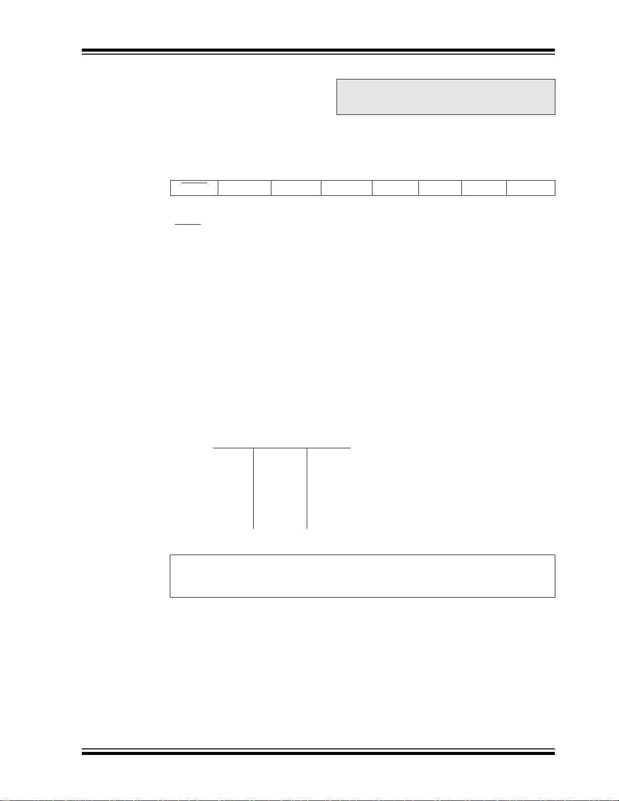
2.3 PCL and PCLATH
The program counter (PC) specifies the address of the
instruction to fetch for execution. The PC is 13-bits
wide. The low byte is called the PCL register. This register is readable and writable. The high byte is called
the PCH register. This register contains the PC<12:8>
bits and is not d irec tly re ada ble or writable. All updates
to the PCH register go through the PCLATH register.
Figure 2-3 shows the four situations for the loading of
the PC.
• Example 1 shows how the PC is loa ded on a writ e
to PCL (PCLATH<4:0> → PCH).
• Example 2 shows how the PC is loaded during a
GOTO instruction (PCLATH<4:3> → PCH).
• Example 3 shows how the PC is loaded during a
CALL instruction (PCLATH<4:3> → PCH), with
the PC loaded (PUSH’d) onto the Top-of-Stack.
• Example 4 shows how the PC is loaded during
one of the return instructions, where the PC is
loaded (POP’d) from the Top-of-Stack.
FIGURE 2-3: LOADING OF PC IN DIFFERENT SITUATIONS
Example 1 - Instruction with PCL as destination
PCH PCL
12 8 7 0
PC
11
8
ALU result
Opcode <10:0>
PCLATH<4:0>
5
PCLATH
Example 2 - GOTO Instruction
PCH PCL
12 11 10 0
PC
2
87
PCLATH<4:3>
Stack (13-bits x 8)
Top-of-Stack
Stack (13-bits x 8)
Top-of-Stack
PCLATH
Example 3 - CALL Instruction
13
PCH PCL
12 11 10 0
PC
2
Example 4 - RETURN, RETFIE, or RETLW Instruction
12 11 10 0
PC
Note: PCLATH is not updated with the contents of PCH.
87
PCLATH
PCH PCL
87
PCLATH
11PCLATH<4:3>
11
Opcode <10:0>
13
Opcode <10:0>
Stack (13-bits x 8)
Top-of-Stack
Stack (13-bits x 8)
Top-of-Stack
DS39597B-page 18 2002 Microchip Technology Inc.
Page 21
PIC16F72
2.3.1 COMPUTED GOTO
A computed GOTO is accomplish ed by adding an offset
to the program counter (ADDWF PCL). When doing a
table read using a computed GOTO method, care
should be exercise d i f the t able loca tio n cros ses a PCL
memory boundary (each 256-byte block). Refer to the
Application Note, “Implementing a Table Read"
(AN556).
2.3.2 STACK
The stack allows a combination of up to eight program
calls and interrupts to occur. The stack contains the
return address from this branch in program execution.
Mid-range devices have an 8-level deep x 13-bit wide
hardware s tack. The stack space is not part of either
program or data space and the stack pointer is not
readable or writable. The PC is PUSH’d onto the stack
when a CALL instruction is executed, or an interrupt
causes a branch. The stack is POP’d in the event of a
RETURN, RETLW or a RETFIE instruction ex ecution.
PCLATH is not modified when the stack is P USH’d or
POP’d.
After the stack has bee n PUSH ’d eight times, the ninth
push overwrites the v alue tha t was stored fro m the first
push. The tenth pus h ov erwri t es the se co nd p us h (an d
so on). An example of the overwriting of the stack is
shown in Figure 2-4.
FIGURE 2-4: STACK MODIFICATION
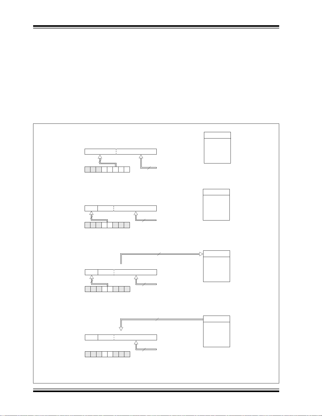
2.4 Program Memory Paging
The CALL and GOTO instructions provide 11 bits of
address to allow branching within any 2K program
memory page. When doing a CALL or GOTO instruction,
the upper two bits of the address are provided by
PCLATH<4:3>. When doing a CALL or GOTO instruction, the user must ensu re tha t the p age select bits are
programmed so that the desired program memory
page is addressed. If a return from a CALL instruction
(or interrupt) is executed, the en tire 13-bit PC is pushed
onto the stack. Therefore, manipulation of the
PCLATH<4:3> bits is not required for the return
instructions (which POPs the address from the stack).
Note: The PIC16F72 device ignores th e paging
bit PCLATH<4:3>. The use of
PCLATH<4:3> as a general purpose read/
write bit is not recommended, since this
may affect upwa rd comp ati bility with future
products.
2.5 Indirect Addressing, INDF and FSR Registers
The INDF register is no t a phy sica l reg ist er. Addressing INDF actually addresses the register whose
address is contained in the FSR regis ter (FSR is a
pointer). This is indirect addressing.
A simple program to clear RAM locations 20h-2Fh
using indirect addressing is shown in Example 2-1.
Stack
Push1 Push9
Push2 Push10
Push3
Push4
Push5
Push6
Push7
Push8
Note 1: There are no status bi ts to indi cate stack
overflow or stack underfl ow cond iti ons .
2: There are no instructions/mnemonics
called PUSH or POP. These are actions
that occur from the execution of the
CALL, RETURN, RETLW and RETFIE
instructions, or the vectoring to an
interrupt address.
Top-of-Stack
EXAMPLE 2-1: INDIR ECT ADDRESS ING
movlw 0x20 ;initialize pointer
movwf FSR ;to RAM
NEXT clrf INDF ;clear INDF register
incf FSR ;inc pointer
btfss FSR,4 ;all done?
goto NEXT ;NO, clear next
CONTINUE
: ;YES, continue
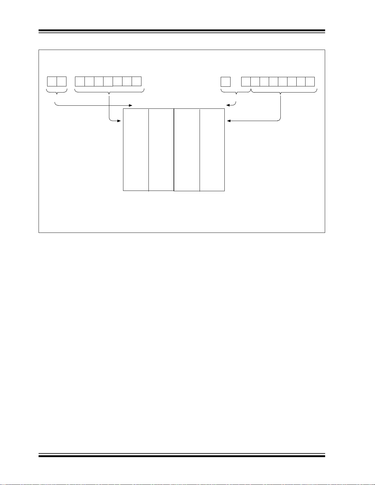
An effective 9-bit address is obtai ned by conca tenating
the 8-bit FSR register and the IRP bi t (ST ATUS<7>), as
shown in Figure 2-5.
2002 Microchip Technology Inc. DS39597B-page 19
Page 22
PIC16F72
FIGURE 2-5: DIRECT/INDIRECT ADDRESSING
RP1:RP 0 6
From Opcode
0
Indirect AddressingDirect Addressing
IRP FSR Register
7
0
Bank Select Location Select
00 01 10 11
80h
FFh
Data
Memory
00h
(1)
7Fh
Bank 0 Bank 1 Bank 2 Bank 3
Note 1: For register file map detail, see Figure 2-2.
100h
17Fh
180h
1FFh
Bank Select
Location Select
DS39597B-page 20 2002 Microchip Technology Inc.
Page 23
PIC16F72
3.0 I/O PORTS
Some pins for th ese I/O ports are multiplexed with an
alternate function for the peripheral features on the
device. In general, when a peripheral is enabled, that
pin may not be used as a general purpose I/O pin.
Additional inform atio n o n I/O ports may be found i n th e
PICmicro™ Mid-Range MCU Reference Manual,
(DS33023).
3.1 PORTA and the TRISA Register
PORTA is a 6-bit wide, bi-directional port. The corresponding data direction register is TRISA. Setting a
TRISA bit (= 1) will make the corresponding PO RT A pin
an input (i.e., put the corresponding output driver in a
Hi-Impedance mode). Clearing a TRISA bit (= 0) will
make the correspondin g POR TA pin an output (i.e., put
the contents of the output latch on the selected pin).
Reading the PORTA register, reads the status of the
pins, whereas writing to i t will wri te to th e po rt latch. All
write operations are read-modify-write operations.
Therefore, a write to a port implies that the port pins are
read, this value is modified and then written to the port
data latch.
Pin RA4 is multiplexed with the Timer0 module clock
input to become the RA4/T0CKI pin. The RA4/T0CKI
pin is a Schmitt Trigger input and an ope n drai n o utput.
All other RA port pins have TTL input levels and full
CMOS output drivers.
Other PORTA pins are multiplexed with analog inputs
and analog V
selected by clearing/setting the control bits in the
ADCON1 register (A/D Control Register1).
Note: On a Power-on Reset, these pins are c on-
The TRISA register controls the direction of the RA
pins, even when they are be ing us ed as ana lo g inputs.
The user must ensure the bits in the TRISA regi ster are
maintained set when using them as analog inputs.
EXAMPLE 3-1: INITIALIZING PORTA
BANKSEL PORTA ; select bank for PORTA
CLRF PORTA ; Initialize PORTA by
; clearing output
; data latches
BANKSEL ADCON1 ; Select Bank for ADCON1
MOVLW 0x06 ; Configure all pins
MOVWF ADCON1 ; as digital inputs
MOVLW 0xCF ; Value used to
; initialize data
; direction
MOVWF TRISA ; Set RA<3:0> as inputs
; RA<5:4> as outputs
; TRISA<7:6> are always
; read as ‘0’.
REF input. The operation of each pin is
figured as analog inputs and read as ‘0’.
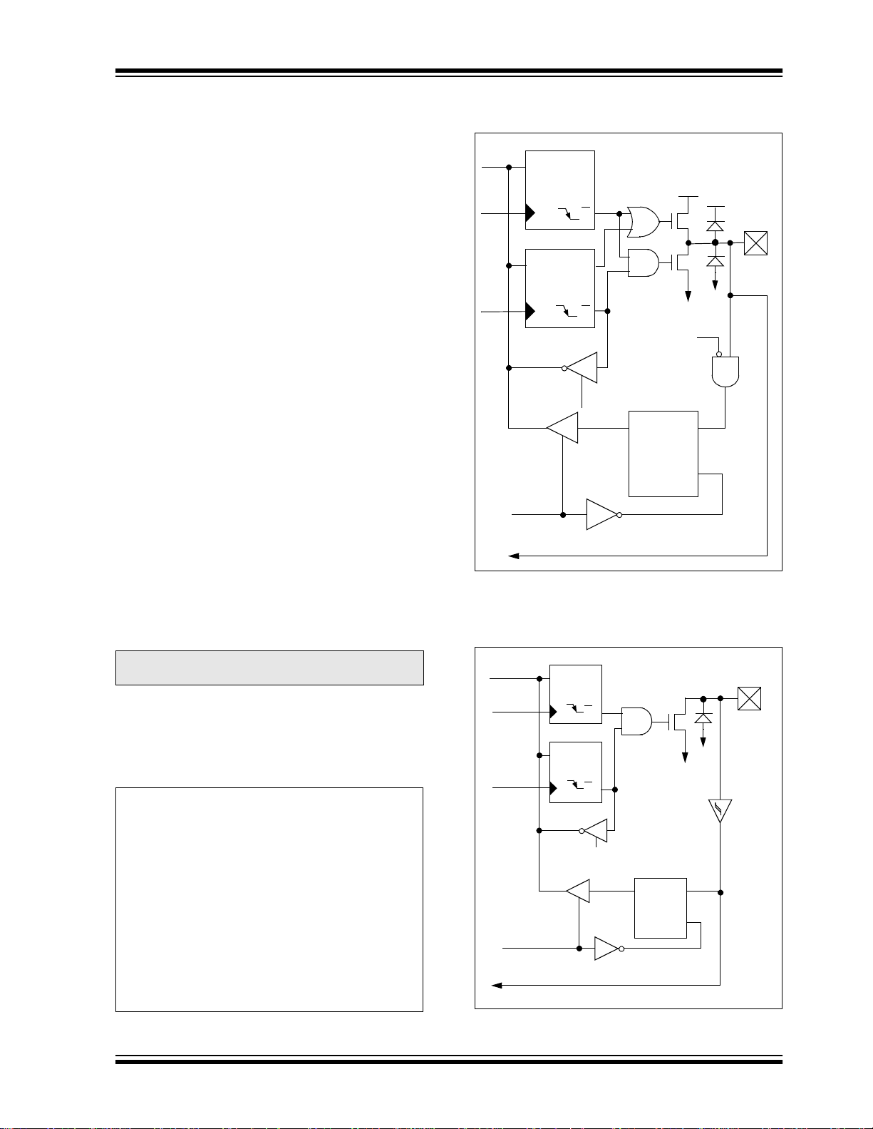
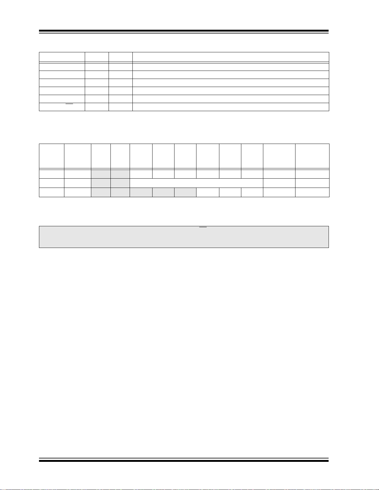
FIGURE 3-1: BLOCK DIAGRAM OF
RA3:RA0 AND RA5 PINS
Data
Bus
WR
Port
WR
TRIS
RD Port
To A/D Converter
CK
Data Latch
CK
TRIS Latch
QD
Q
QD
Q
RD TRIS
VDD
DD
V
P
N
VSS
V
SS
Analog
Input
Mode
QD
EN
I/O pin
TTL
Input
Buffer
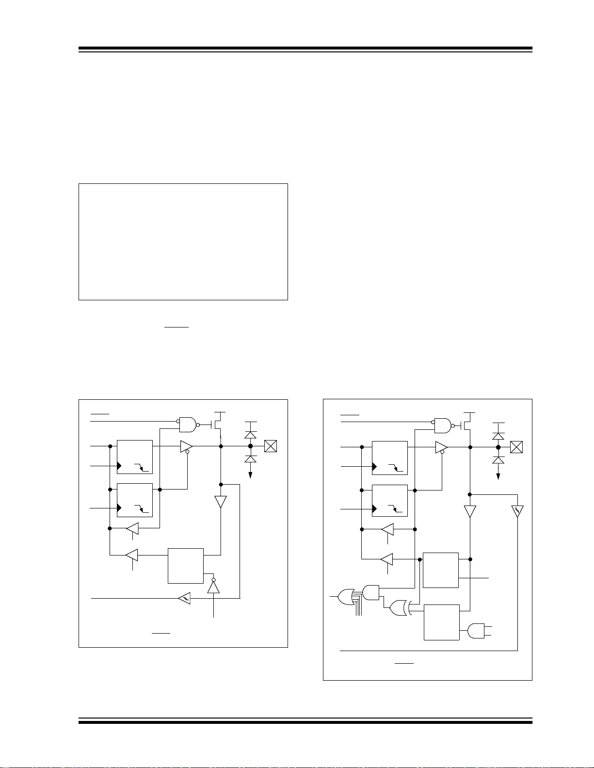
FIGURE 3-2: BLOCK DIAGRAM OF
RA4/T0CKI PIN
Data
Bus
WR
Port
WR
TRIS
RD Port
TMR0 Clock Input
QD
Q
CK
Data Latch
QD
Q
CK
TRIS Latch
RD TRIS
N
VSS
SS
V
Schmitt
Trigger
Input
Buffer
QD
EN
EN
I/O pin
2002 Microchip Technology Inc. DS39597B-page 21
Page 24
PIC16F72
TABLE 3-1: PORTA FUNCTIONS
Name Bit# Buffer Function
RA0/AN0 bit 0 TTL Input/output or analog input.
RA1/AN1 bit 1 TTL Input/output or analog input.
RA2/AN2 bit 2 TTL Input/output or analog input.
RA3/AN3/VREF bit 3 TTL Input/output or analog input or VREF.
RA4/T0CKI bit 4 ST Input/output or external clock input for Timer0. Output is open drain type.
RA5/AN4/SS bit 5 TTL Input/output or analog input or slave select input for synchronous serial port.
Legend: TTL = TTL input, ST = Schmitt Trigger input
TABLE 3-2: SUMMARY OF REGISTERS ASSOCIATED WITH PORTA
Value on
all other
RESETS
Address Name Bit 7 Bit 6 Bit 5 Bit 4 Bit 3 Bit 2 Bit 1 Bit 0
Value on
POR, BOR
05h PORTA
85h TRISA
9Fh ADCON1
Legend: x = unknown, u = unchanged, - = unimplemented locations read as ‘0’.
Shaded cells are not used by PORTA.
Note: When using the SSP module in SPI Slave mode and SS enabled , th e A/ D Po rt Conf igu rati on Con trol bits
(PCFG2:PCFG0) in the A/D C ontrol Re gister ( ADCON 1) must be set to o ne of the follow ing con figurat ion s:
100, 101, 11x.
— — RA5 RA4 RA3 RA2 RA1 RA0 --0x 0000 --0u 0000
— — PORTA Data Direction Register --11 1111 --11 1111
— — — — — PCFG2 PCFG1 PCFG0 ---- -000 ---- -000
DS39597B-page 22 2002 Microchip Technology Inc.
Page 25
PIC16F72
3.2 PORTB and the TRISB Register
PORTB is an 8-bit wide, bi-directional port. The corresponding data direction register is TRISB. Setting a
TRISB bit (= 1) will make the corresponding PORTB
pin an input (i.e., put the corresponding output driver in
a Hi-Impedance mode). Clearing a TRISB bit (= 0) will
make the corresponding POR TB pin an output (i.e. , put
the contents of the output latch on the selected pin).
EXAMPLE 3-2: INITIALIZING PORTB
BANKSEL PORTB ; Select bank for PORTB
CLRF PORTB ; Initialize PORTB by
; clearing output
; data latches
BANKSEL TRISB ; Select Bank for TRISB
MOVLW 0xCF ; Value used to
; initialize data
; direction
MOVWF TRISB ; Set RB<3:0> as inputs
; RB<5:4> as outputs
; RB<7:6> as inputs
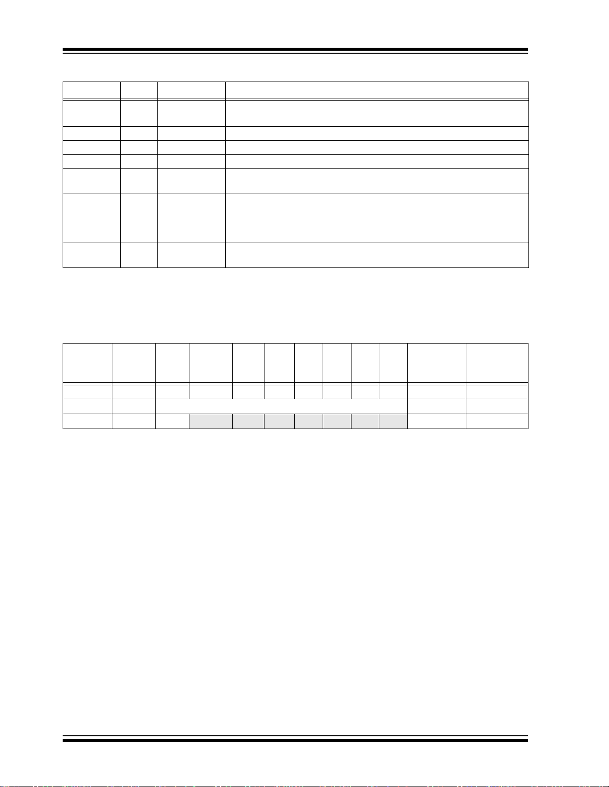
Each of the PORTB pi ns has a w eak i nternal pul l-up. A
single control bit can turn on all the pull-ups. This is performed by clearing bit RBPU
pull-up is automatically turned off when the port pin is
configured as an outpu t. The pull-ups are disable d on a
Power-on Reset.
(OPTION<7>). The weak
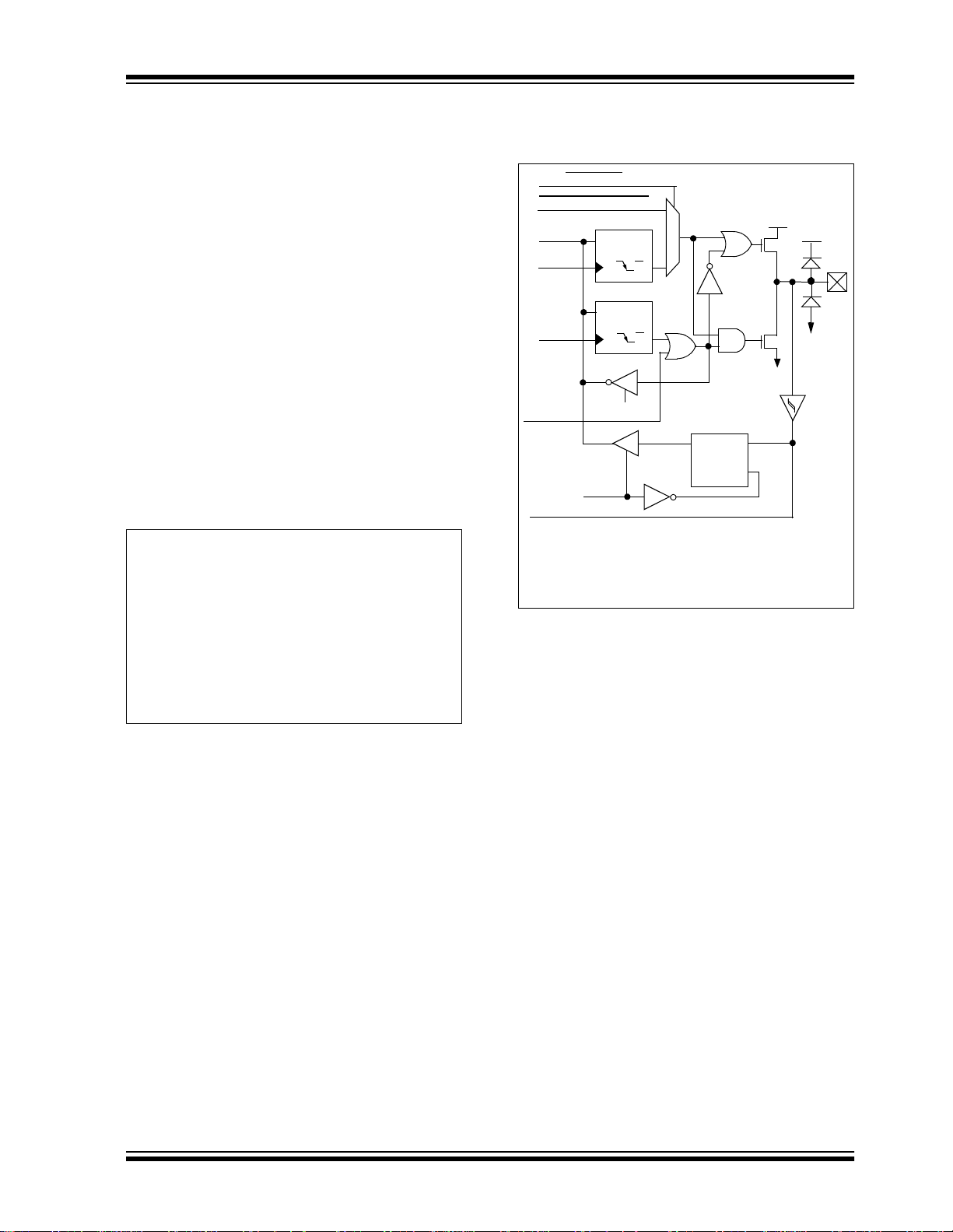
are compared with the old value latched on the last
read of PORTB. The “mismatch” outputs of RB7:RB4
are OR’d together to generate the RB Port Change
Interrupt with flag bit RBIF (INTCON<0>).
This interrupt can wake the device from SLEEP. The
user, in the Interrupt Service Routine, can clear the
interrupt in the following manner:
a) Any read or write of PORTB. This will end the
mismatch condition.
b) Clear flag bit RBIF.
A mismatch c ond it i on wi ll cont i n ue to s et f lag bi t RB IF.
Reading PORTB will end the mismatch condition and
allow flag bit RBIF to be cleared.
The interrupt-on-change feature is recommended for
wake-up on key depression operation and operations
where PORTB is only used for the interrupt-on-change
feature. Polling of PORTB is not recommended while
using the interrupt-on-change feature.
This interrupt-on-mismatch feature, together with software configurable pull-ups on these four pins, allow
easy interface to a keypad and make it possible for
wake-up on key depression. Refer to the Embedded
Control Handbook, “Implementing Wake-Up on Key
Stroke” (AN552).
RB0/INT is an external interrupt input pin and is
configured using the INTEDG bit (OPTION<6>).
FIGURE 3-3: BLOCK DIAGRAM OF
RB3:RB0 PINS
DD
EN
TTL
Input
Buffer
V
Weak
P
Pull-up
RD Port
V
VSS
DD
I/O pin
(1)
RBPU
Data
Data Latch
Bus
WR
Port
WR
TRIS
RB0/INT
Note 1: To enable weak pull-ups, set the appropriate TRIS bit(s)
and clear the RBPU bit (OPTION<7>).
CK
TRIS Latch
CK
RD TRIS
RD Port
QD
QD
QD
Schmitt Trigger
Buffer
Four of PORTB’s pins , RB7:RB4, have an interrupt-onchange feature. Only pins configured as inputs can
cause this interrupt to occur (i.e., any RB7:RB4 pin
configured as an output is excluded from the interrupt
on change comparison). The input pins (of RB7:RB4)
FIGURE 3-4: BLOCK DIAGRAM OF
RB7:RB4 PINS
DD
TTL
Input
Buffer
EN
EN
V
P
Weak
Pull-up
V
DD
VSS
Buffer
Q1
RD Port
Q3
(1)
RBPU
Data
Bus
WR
Port
WR
TRIS
Set RBIF
From Other
RB7:RB4 Pins
RB7:RB6 in Serial Programming Mode
Note 1: To enable weak pull-ups, set the appropriate TRIS bit(s)
Data Latch
QD
CK
TRIS Latch
QD
CK
RD TRIS
RD Port
and clear the RBPU bit (OPTION<7>).
Latch
QD
QD
I/O pin
ST
2002 Microchip Technology Inc. DS39597B-page 23
Page 26
PIC16F72
TABLE 3-3: PORTB FUNCTIONS
Name Bit# Buffer Function
RB0/INT bit 0 TTL/ST
RB1 bit 1 TTL Input/output pin. Internal software programmable weak pull-up.
RB2 bit 2 TTL Input/output pin. Internal software programmable weak pull-up.
RB3 bit 3 TTL Input/output pin. Internal software programmable weak pull-up.
RB4 bit 4 TTL Input/output pin (with interrupt-on-change). In ternal software pro grammable
RB5 bit 5 TTL Input/output pin (with interrupt-on-change). In ternal software pro grammable
RB6 bit 6 TTL/ST
RB7 bit 7 TTL/ST
Legend: TTL = TTL input, ST = Schmitt Trigger input
Note 1: This buffer is a Schmitt Trigger input when configured as the external interrupt.
2: This buffer is a Schmitt Trigger input when used in Serial Programming mode.
(1)
Input/output pin or external interrupt input. Internal software
programmable weak pull-up.
weak pull-up.
weak pull-up.
(2)
Input/output pin (with interrup t-on-change). In ternal software pro grammable
weak pull-up. Serial pr ogramming clock.
(2)
Input/output pin (with interrup t-on-change). In ternal software pro grammable
weak pull-up. Serial programming data.
TABLE 3-4: SUMMARY OF REGISTERS ASSOCIATED WITH PORTB
Address Name Bit 7 Bit 6 Bit 5 Bit 4 Bit 3 Bit 2 Bit 1 Bit 0
06h, 106h PORTB RB7 RB6 RB5 RB4 RB3 RB2 RB1 RB0 xxxx xxxx uuuu uuuu
86h, 186h TRISB PORTB Data Direction Register 1111 1111 1111 1111
81h, 181h OPTION RBPU
Legend: x = unknown, u = unchanged. Shaded cells are not used by PORTB.
INTEDG T0CS T0SE PSA PS2 PS1 PS0 1111 1111 1111 1111
Value on
POR, BOR
Value on
all other
RESETS
DS39597B-page 24 2002 Microchip Technology Inc.
Page 27
PIC16F72
3.3 PORTC and the TRISC Register
PORTC is an 8-bit wide, bi-directional port. The corresponding data direction register is TRISC. Setting a
TRISC bit (= 1) will make the corresponding PORTC
pin an input (i.e., put the corresponding output driver in
a Hi-Impedance mode). Clearing a TRISC bit (= 0) will
make the correspondi ng PORTC pin an output (i.e., p ut
the contents of the output latch on the selected pin).
PORTC is mul tiplexed with s everal peri pheral function s
(Table 3-5). PORTC pins have Schmitt Trigger input
buffers.
When enabling peripheral functions, care should be
taken in defining TRIS bit s fo r each POR TC pin. Some
peripherals override the TRIS bit to make a pin an output, while other peripherals override the TRIS bit to
make a pin an input. Since the TRIS bit override is in
effect while the peripheral is enabled, read-modifywrite instructions (BSF, BCF, XORWF) with TRISC as
destination shoul d be avoided. The us er should refer to
the corresponding peripheral section for the correct
TRIS bit settings.
EXAMPLE 3-3: INITIALIZING PORTC
BANKSEL PORTC ; Select Bank for PORTC
CLRF PORTC ; Initialize PORTC by
; clearing output
; data latches
BANKSEL TRISC ; Select Bank for TRISC
MOVLW 0xCF ; Value used to
; initialize data
; direction
MOVWF TRISC ; Set RC<3:0> as inputs
; RC<5:4> as outputs
; RC<7:6> as inputs
FIGURE 3-5: PORTC BLOCK DIAGRAM
(PERIPHERAL OUTPUT
OVERRIDE)
Port/Peripheral Select
Peripheral Data Out
Data
Bus
WR
Port
WR
TRIS
Peripheral
(2)
OE
Peripheral Input
Note 1: Port/Peripheral select signal selects
CK
Data Latch
CK
TRIS Latch
RD TRIS
RD
Port
between port data and peripheral output.
2: Peripheral OE (output enable) is only
activated if peripheral select is active.
(1)
0
QD
1
Q
QD
Q
QD
EN
VSS
Schmitt
Trigger
DD
V
VDD
P
I/O
pin
VSS
N
2002 Microchip Technology Inc. DS39597B-page 25
Page 28
PIC16F72
TABLE 3-5: PORTC FUNCTIONS
Name Bit# Buffer Type Function
RC0/T1OSO/T1CKI
RC1/T1OSI bit 1 ST Input/output port pin or Timer1 oscillator input.
RC2/CCP1 bit 2 ST Input/output port pin or Capture1 input/Compare1 output/PWM1
RC3/SCK/SCL bit 3 ST
RC4/SDI/SDA bit 4 ST
RC5/SDO bit 5 ST Input/output port pin or Synchronous Serial Port data output.
RC6 bit 6 ST Input/output port pin.
RC7 bit 7 ST Input/output port pin.
Legend: ST = Schmitt Trigger input
TABLE 3-6: SUMMARY OF REGISTERS ASSOCIATED WITH PORTC
Address Name Bit 7 Bit 6 Bit 5 Bit 4 Bit 3 Bit 2 Bit 1 Bit 0
bit 0
ST Input/output port pin or Timer1 oscillator output/Timer1 clock input.
output.
RC3 can also be the synchronous serial clock for both SPI and I
modes.
RC4 can also be the SPI Data In (SPI mode) or data I/O (I
Value on
POR, BOR
2
2
C mode).
Value on
all other
RESETS
C
07h PORTC RC7 RC6 RC5 RC4 RC3 RC2 RC1 RC0 xxxx xxxx uuuu uuuu
87h TRISC PORTC Data Direction Register 1111 1111 1111 1111
Legend: x = unknown, u = unchanged
DS39597B-page 26 2002 Microchip Technology Inc.
Page 29

PIC16F72
4.0 READING PROGRAM MEMORY
The FLASH Program Memory is readable during normal operation over the entire V
addressed through Special Function Registers (SFR).
Up to 14-bit wide num bers can be sto red in mem ory for
use as calibration parameters, serial numbers, packed
7-bit ASCII, etc. Exe cut ing a p rogram memory location
containing data that forms an invalid instruction results
in a NOP.
There are five SFRs used to read the program and
memory:
• PMCON1
• PMDATL
• PMDATH
• PMADRL
• PMADRH
The program memory allows word reads. Program
memory access allows for checksum calculation and
reading calibration t abl es .
When interfacing to the program memory block, the
PMDATH:PMDATL registers form a two-byte word,
which holds the 14-bit data for reads. The
PMADRH:PMADRL registers form a two-byte word,
which holds the 13-bit address of the FLASH location
being accessed. This device has up to 2K words of
program FLASH, with an address range from 0h to
07FFh. The unused upper bits PMDATH<7:6> and
PMADRH<7:5> are not implemented and read as
zeros.
DD range. It is indirectly
4.1 PMADR
The address registers can address up to a maxim um of
8K words of program FLASH.
When selecting a program address value, the MSByte
of the address is written to the PMADRH register and
the LSByte is written to the PMADRL register. The
upper MSbits of PMADRH must always be clear.
4.2 PMCON1 Register
PMCON1 is the control register for memory accesses.
The control bit RD initiates read operations. This bit
cannot be cleared, only set, in so ftware . I t is cleare d in
hardware at the completion of the read operation.
REGISTER 4-1: PMCON1: PROGRAM MEMORY CONTROL REGISTER 1 (ADDRESS 18Ch)
R-1 U-0 U-0 U-0 U-0 U-0 U-0 R/S-0
reserved — — — — — — RD
bit 7 bit 0
bit 7 Reserved: Read as ‘1’
bit 6-1 Unimplemented: Read as ‘0’
bit 0 RD: Read Control bit
1 = Initiates a FLASH read, RD is cleare d in hard ware. Th e RD bit c an only be set (not cleared )
in software.
0 = Does not initiate a FLASH read
Legend:
W = Writable bit U = Unimplemented bit, read as ‘0’
R = Readable bit S = Settable bit -n = Value at POR
‘1’ = Bit is set ‘0’ = Bit is cleared x = Bit is unknown
2002 Microchip Technology Inc. DS39597B-page 27
Page 30
PIC16F72
4.3 Reading the FLASH Program Memory
To read a program memory location, the user must
write two bytes of the address to the PMADRL and
PMADRH registers and then set control bit, RD
(PMCON1<0>). Once the read control bit is set, the
program memory F LASH con trol ler will use t he se cond
instruction cycle afte r to read the data . This ca uses the
second instruction immediately following the “BSF
PMCON1,RD” instruction to be ignored. The data is
available in the very next cycle in the PMDATL and
PMDATH registers; therefore, it can be read as two
bytes in the following instructions. PMDATL and
PMDATH registers will hold this value until another
read, or until it is written to by the user (during a write
operation).
4.4 Operation During Code Protect
The FLASH program memory control can read anywhere within the program memory, whether or not the
program memory is code protected.
This does not compromise the code, because there is
no way to rewrite a portion of the program memory, or
leave contents of a progra m me mo ry read in a regist er
while changing modes.
EXAMPLE 4-1: FLASH PROGRAM READ
BANKSEL PMADRH ; Select Bank for PMADRH
MOVLW MS_PROG_EE_ADDR ;
MOVWF PMADRH ; MS Byte of Program Address to read
MOVLW LS_PROG_EE_ADDR ;
MOVWF PMADRL ; LS Byte of Program Address to read
BANKSEL PMCON1 ; Select Bank for PMCON1
BSF PMCON1, RD ; EE Read
;
NOP ; Any instructions here are ignored as program
NOP ; memory is read in second cycle after BSF PMCON1,RD
;
; First instruction after BSF PMCON1,RD executes normally
BANKSEL PMDATL ; Select Bank for PMDATL
MOVF PMDATL, W ; W = LS Byte of Program PMDATL
MOVF PMDATH, W ; W = MS Byte of Program PMDATL
TABLE 4-1: REGISTERS ASSOCIATED WITH PROGRAM FLASH
Address Name Bit 7 Bit 6 Bit 5 Bit 4 Bit 3 Bit 2 Bit 1 Bit 0
10Dh PMADRL Address Register Low Byte xxxx xxxx uuuu uuuu
10Fh PMADRH
10Ch PMDATL Data Register Low Byte xxxx xxxx uuuu uuuu
10Eh PMDATH — — Data Register High Byte xxxx xxxx uuuu uuuu
18Ch PMCON1
Legend: x = unknown, u = unchanged, r = reserved , - = unim pleme nted, read as ' 0'.
Shaded cells are not used during FLASH access.
Note 1: This bit always reads as a ‘1’.
DS39597B-page 28 2002 Microchip Technology Inc.
— — — Address Register High Byte xxxx xxxx uuuu uuuu
(1)
—
— — — — — — RD 1--- ---0 1--- ---0
Value on
POR, BOR
Value on
all other
RESETS
Page 31
PIC16F72
5.0 TIMER0 MODULE
The Timer0 module timer/counter has the following
features:
• 8-bit timer/counter
• Readable and writable
• 8-bit software programmable prescaler
• Internal or external clock select
• Interrupt on overflow from FFh to 00h
• Edge select for external clock
Figure 5-1 is a block diagram of th e T imer0 module and
the prescaler shared with the WDT.
Additional information on the Timer0 module is
available in the PICmicro™ Mid-Range MCU Family
Reference Manual (DS33023).
5.1 Timer0 Operation
Timer mode is selected by clearing bit T0CS
(OPTION<5>). In Timer mode, the Timer0 module will
increment every ins tru cti on cy cl e (w i tho ut p r es ca ler). If
the TMR0 register is written, the increment is inhibited
for the following two instruction cycles. The user can
work around this by writing an adjusted value to the
TMR0 register.
Counter mode is selected by setting bit T0CS
(OPTION<5>). In Counter mode, Timer0 will increment, either on every rising or falling edge of pin RA4/
T0CKI. The incrementing edge is determined by the
Timer0 Source Edge Select bit T0SE (OPTION<4>).
Clearing bit T0SE selects the rising edge. Restrictions
on the external clock input are discussed in detail in
Section 5.3.
The prescaler is mutually exclusively shared between
the Timer0 modu le and t he W a tchdo g Timer. The pres caler is not readabl e or w rit able. Sectio n 5.4 details the
operation of the prescaler.
5.2 Timer0 Interrupt
The TMR0 interrupt is generated when the TMR0 register overflows from FFh to 00h. This overflow sets bit
TMR0IF (INTCON<2>). The interrupt can be masked
by clearing bit TMR0IE (INTCON<5>). Bit TMR0IF
must be cleared in software by the Timer0 module
Interrupt Service Routin e, b efore re -enabling this interrupt. The TMR0 interrupt cann ot awaken th e processor
from SLEEP, since the timer is shut-off during SLEEP.
FIGURE 5-1: BLOCK DIAGRAM OF THE TIMER0/WDT PRESCALER
CLKO (= F
Watchdog
Timer
WDT Enable bit
OSC/4)
RA4/T0CKI
pin
T0SE
M
0
U
X
1
T0CS
0
M
U
1
X
PSA
8-bit Prescaler
8 - to - 1MUX
0
PRESCALER
8
M U X
1
M
U
0
X
PSA
1
PSA
SYNC
2
Cycles
PS2:PS0
Data Bus
8
TMR0 reg
Set Flag bit TMR0IF
on Overflow
WDT
Time-out
Note: T0CS, T0SE, PSA, PS2:PS0 are (OPTION<5:0>).
2002 Microchip Technology Inc. DS39597B-page 29
Page 32

PIC16F72
5.3 Using Timer0 with an External Clock
When no pr escal er is us ed, t he ex ternal clock inpu t is
the same as the prescaler outp ut. Th e synchronization
of T0CKI, with the internal phase clocks, is accomplished by sampli ng the prescale r output on the Q2 and
Q4 cycles of the internal phase clocks. Therefore, it is
necessary for T0CKI to be high for at least 2 T
a small RC delay of 20 ns) and low for at least 2 T
(and a small RC delay of 20 ns). Refer to the electrical
specification of the desired device.
OSC (and
OSC
5.4 Prescaler
There is only one presca ler a vailable, which i s mutuall y
exclusively sha red between the T imer0 mod ule and the
Watchdog Timer. A prescaler assignment for the
Timer0 m odule means that there is no presc aler fo r the
Watchdog Timer, and vice-versa. This prescaler is not
readable or writable (see Figure 5-1).
The PSA and PS2:PS0 bits (OPTION<3:0>) de termine
the prescaler assignment and prescale ratio.
When assigned to the Timer0 module, all instructions
writing to the TMR0 regi ster (e.g., CLRF 1, MOVWF 1,
BSF 1,x....etc.) will clear the prescaler. When
assigned to WDT, a CLRWDT instruction will clear the
prescaler along with the Watchdog Timer. The
prescaler is not readable or writable.
Note: Writing to TMR0 when the prescaler is
assigned to T imer0, will clear the pre scaler
count but will not change the prescaler
assignment.
TABLE 5-1: REGISTERS ASSOCIATED WITH TIMER0
Address Name Bit 7 Bit 6 Bit 5 Bit 4 Bit 3 Bit 2 Bit 1 Bit 0
01h,101h TMR0 Timer0 Module Register xxxx xxxx uuuu uuuu
0Bh,8Bh,
10Bh,18Bh
81h,181h O PTION RBPU INTEDG T0CS T0SE PSA PS2 PS1 PS0 1111 1111 1111 1111
Legend: x = unknown, u = unchanged, - = unimplemented locations read as ‘0’. Shaded cells a re not used by Time r0.
INTCON GIE PEIE TMR0IE
INTE RBIE TMR0IF INTF RBIF 0000 000x 0000 000u
Value on
POR, BOR
Value on
all other
RESETS
DS39597B-page 30 2002 Microchip Technology Inc.
Page 33

PIC16F72
6.0 TIMER1 MODULE
The Timer1 module timer/counter has the following
features:
• 16-bit timer/counter
(Two 8-bit registers; TMR1H and TMR1L)
• Readable and writable (both registers)
• Internal or external clock select
• Interrupt on overflow from FFFFh to 0000h
• RESET from CCP module trigger
Timer1 has a control register, shown in Register 6-1.
Timer1 can be enabled/disabled by setting/clearing
control bit TMR1ON (T1CON<0>).
Figure 6-2 is a simplified block diagram of the Timer1
module.
Additional information on timer modules is available in
the PICmicro™ Mid-Range MCU Reference Manual,
(DS33023).
6.1 Timer1 Operation
Timer1 can ope rate in one of these mo des :
• As a timer
• As a synchronous counter
• As an asynchronous counter
The Operating mode is determined by the clock select
bit, TMR1CS (T1CON<1>).
In Timer mode, Timer1 increments every instruction
cycle. In Counter mode, it increments on every rising
edge of the external clock input.
When the Timer1 oscillator is enabled (T1OSCEN is
set), the RC1/T1OSI and RC0/T1OSO/T1CKI pins
become inputs. That is, the TRISC<1:0> value is
ignored.
Timer1 also has an internal “RESET input”. This
RESET can be generated by the CCP module
(Section 8.0).
REGISTER 6-1: T1CON: TIMER1 CONTROL REGISTER (ADDRESS 10h)
U-0 U-0 R/W-0 R/W-0 R/W-0 R/W-0 R/W-0 R/W-0
— — T1CKPS1 T1CKPS0 T1OSCEN T1SYNC TMR1CS TMR1ON
bit 7 bit 0
bit 7-6 Unimplemented: Read as ‘0’
bit 5-4 T1CKPS1:T1CKPS0: Timer1 Input Clock Prescale Select bits
11 =1:8 Prescale value
10 =1:4 Prescale value
01 =1:2 Prescale value
00 =1:1 Prescale value
bit 3 T1OSCEN: Timer1 Oscillator Enable Control bit
1 = Oscillator is enabled
0 = Oscillator is shut-off (The oscillator inverter is turned off to eliminate power drain.)
bit 2 T1SYNC
TMR1CS = 1:
1 = Do not synchronize external clock input
0 = Synchronize external clock input
TMR1CS = 0:
This bit is ignored. Timer1 uses the internal clock when TMR1CS = ‘0’.
bit 1 TMR1CS: Timer1 Clock Source Select bit
1 = External clock from pin RC0/T1OSO/T1CKI (on the rising edge)
0 = Internal clock (F
bit 0 TMR1ON: Timer1 On bit
1 = Enable s Timer1
0 = Stops Timer1
Legend:
R = Readable bit W = Writable bit U = Unimplemented bit, read as ‘0’
- n = Value at POR ‘1’ = Bit is set ‘0’ = Bit is cleared x = Bit is unknown
: Timer1 External Clock Input Synchronization Control bit
OSC/4)
2002 Microchip Technology Inc. DS39597B-page 31
Page 34

PIC16F72
6.2 Timer1 Operation in Timer Mode
Timer mode is selected by clearing the TMR1CS
(T1CON<1>) bit. In this mode, the input clock to the
timer is F
OSC/4. The synchronize control bit T1SYNC
(T1CON<2>) has no effect, since the internal clock is
always in sync.
6.3 Timer1 Counter Operation
Timer1 may operate in Asynchronous or Synchronous
mode, depending on the setting of the TMR1CS bit.
When Timer1 is being incremented via an external
source, incremen ts occur on a ri sing edge. After T ime r1
is enabled in Coun ter mode, the module mus t first have
a falling edge before the counter begins to increment.
FIGURE 6-1: TIMER1 INCREMENTING EDGE
T1CKI
(Default High)
6.4 Timer1 Operation in Synchroni zed Counter Mode
Counter mode is selected by setting bit TMR 1CS. In
this mode, the timer increments on every rising edge of
clock input on pin RC1/T1OSI whe n bit T1OSCEN is
set, or on pin RC0/T1OSO/T1CKI when bit T1OSCEN
is cleared.
If T1SYNC
synchronized with internal phase clocks. The synchronization is done after the prescaler stage. The
prescaler stage is an asynchronous ripple counter.
In this configuration, during SLEEP mode, Timer1 will
not increment even if the external clock is present,
since the synchronization circuit is shut-off. The
prescaler, however, will continue to increment.
is cleared, the n the externa l clock input is
T1CKI
(Default Low)
Note: Arrows indicate counter increments.
FIGURE 6-2: TIMER1 BLOCK DIAGRAM
Set Flag bit
TMR1IF on
Overflow
RC0/T1OSO/T1CKI
RC1/T1OSI
TMR1H
T1OSC
TMR1
TMR1L
T1OSCEN
Enable
Oscillator
(1)
(2)
FOSC/4
Internal
Clock
TMR1ON
On/Off
1
0
TMR1CS
0
1
T1SYNC
Prescaler
1, 2, 4, 8
2
T1CKPS1:T1CKPS0
Synchronized
Clock Input
Synchronize
det
Q Clock
Note 1: When the T1OSCEN bit is cleared, the inverter is turned off. This eliminates power drain.
DS39597B-page 32 2002 Microchip Technology Inc.
Page 35

PIC16F72
6.5 Timer1 Operation in Asynchronous Counter Mode
If control bit T1SYNC (T1CON<2>) is set, the external
clock input is not synchronized. The timer continues to
increment asynchronous to the internal phase clocks.
The timer will continue to run during SLEEP and can
generate an interrupt on ove rflow, that will wake-up the
processor. However, special precautions in software
are needed to read/write the timer (Section 6.5.1).
In Asynchronous Counter mode, Timer1 cannot be
used as a time base for capture or comp are operations.
6.5.1 READING AND WRITING TIMER1 IN
ASYNCHRONOUS COUNTER
MODE
Reading TMR1H or TMR1L while the timer is running
from an external asy nchronous cl ock will ens ure a valid
read (taken care of in hardware). However, the user
should keep in min d that re ading t he 16-b it time r in tw o
8-bit values itself, poses certain problems, since the
timer may overflow between the reads.
For writes, it is recomm ended that the us er simply stop
the timer and write the desired values. A write contention may occur by writing to the timer registers, while
the register is incrementing. This may produce an
unpredictable value in the timer register. Data in the
Timer1 register (TMR1) may become corrupted. Corruption occurs when the ti mer enable is turne d off at the
same instant that a ripple carry occurs in the timer
module.
Reading the 16-bit value requires some care. Examples 12-2 and 12-3 in the PICmicro™ Mid-Rang e MCU
Family Reference Manual (DS33023) show how to
read and write Timer1 when it is running in
Asynchronous mode.
6.6 Timer1 Oscillator
A crystal oscillator circuit is built between pins T1OSI
(input) and T1OSO (amplifier output). It is enabled by
setting control bit T1OSCEN (T 1CON<3>). The oscill ator is a low power oscillator rated up to 200 kHz. It will
continue to run during SLEEP. It is primarily intended
for a 32 kHz crystal. Table 6-1 shows the capacitor
selection for the Timer1 oscillator.
The Timer1 oscillator is identical to the LP oscillator.
The user must provide a sof tware t im e del ay to en su re
proper oscillator start-up.
T ABLE 6-1: CAPACITOR SELECTION FOR
THE TIMER1 OSCILLATOR
Osc Type Freq C1 C2
LP 32 kHz 33 pF 33 pF
100 kHz 15 pF 15 pF
200 kHz 15 pF 15 pF
These values are for de si gn guidance only.
Note 1: Higher capacitance increases the stability
of oscillator, but also incre ases the start-up
time.
2: Since each resonator/cry stal has its own
characteristics, the user should consult
the resonator/crystal manufacturer for
appropriate values of external
components.
6.7 Timer1 Interrupt
The TMR1 register pair (TMR1H:TMR1L) increments
from 0000h to FFFFh and rolls over to 0000h. The
TMR1 interrupt, if enabled, is generated on overflow,
which is latched in i nterrupt flag bit TMR1IF (PI R1<0>).
This interrupt can be enabled/disabled by setting/
clearing TMR1 interrupt enable bit TMR1 IE (PIE1<0>).
6.8 Resetting Timer1 Using a CCP Trigger Output
If the CCP module is configured in Compare mode to
generate a “special event trigger" signal
(CCP1M3:CCP1M0 = 1011), the signal will reset
Timer1 and start an A/D conversion (if the A/D module
is enabled).
Note: The special event triggers from the CCP1
module will not set interrupt flag bit
TMR1IF (PIR1<0>).
Timer1 mu st be confi gured fo r either T ime r or Synchr onized Counter mode to take advantage of this feature.
If Timer1 is running in Asynchronous Counter mode,
this RESET operation may not work.
In the event that a write to Timer1 coincides with a
special event trigger from CCP1, the write will take
precedence.
In this mode of operation, the CCPR1H:CCPR1L registers pair effectively becomes the period register for
Timer1.
2002 Microchip Technology Inc. DS39597B-page 33
Page 36

PIC16F72
6.9 Resetting Timer1 Register Pair (TMR1H, TMR1L)
TMR1H and TMR1L registers are not rese t to 00h on a
POR, or any other RESET, except by the CCP1 special
event triggers.
T1CON register is rese t to 00h on a Powe r-on Rese t or
a Brown-out Reset, which shuts off the timer and
leaves a 1:1 prescale. In all other RESETS, the register
is unaffected.
6.10 Timer1 Prescaler
The prescaler counter is cleared on writes to the
TMR1H or TMR1L registers.
TABLE 6-2: REGISTERS ASSOCIATED WITH TIMER1 AS A TIMER/COUNTER
Address Name Bit 7 Bit 6 Bit 5 Bit 4 Bit 3 Bit 2 Bit 1 Bit 0
0Bh,8Bh,
10Bh,18Bh
0Ch PIR1 — ADIF — — SSPIF CCP1IF TMR2IF TMR1IF 0000 0000 0000 0000
8Ch PIE1 — ADIE — — SSPIE CCP1IE TMR2IE TMR1IE 0000 0000 0000 0000
0Eh TMR1L Holding register for the Least Significant Byte of the 16-bit TMR1 Register xxxx xxxx uuuu uuuu
0Fh T M R1H Holding register for the Most Significant Byte of the 16-bit TMR1 Register xxxx xxxx uuuu uuuu
10h T1CON — — T1CKPS1 T1CKPS0 T1OSCEN T1SYNC TMR1CS TMR1ON --00 0000 --uu uuuu
Legend: x = unknown, u = unchanged, - = unimplemented, read as ‘0’. Shaded cells are not used by the Timer1 module.
INTCON GIE PEIE
TMR0IE INTE RBIE TMR0IF INTF RBIF 0000 000x 0000 000u
Value on
POR, BOR
Val ue on
all other
RESETS
DS39597B-page 34 2002 Microchip Technology Inc.
Page 37

PIC16F72
7.0 TIMER2 MODULE
The Timer2 module timer has the following features:
• 8-bit time r (TMR2 register)
• 8-bit period register (PR2)
• Readable and writable (both registers)
• Software programmable prescaler (1:1, 1:4, 1:16)
• Software programmable postscaler (1:1 to 1:16)
• Interrupt on TMR2 match of PR2
• SSP module optional use of TMR2 output to
generate clock shift
Timer2 has a control register, shown in Register 7-1.
Timer2 c an b e s hu t-off by clearing control bi t TMR2ON
(T2CON<2>) to minimize power consumption.
Figure 7-1 is a simplified block diagram of the Timer2
module.
Additional information on timer modules is available in
the PICmicro™ Mid-Range MCU Reference Manual,
(DS33023).
7.1 Timer2 Operation
Timer2 can be used as the PWM time-base for PWM
mode of the CCP module.
The TMR2 register is readable and writable, and is
cleared on any device RESET.
The input clock (F
1:4 or 1:16, selected by control bits
T2CKPS1:T2CKPS0 (T2CON<1:0>).
The match output of TMR2 goes through a 4-bit
postscaler (which gives a 1:1 to 1:16 scaling inclusive)
to generate a TMR2 interrupt (latched in flag bit
TMR2IF, (PIR1<1>)).
OSC/4) has a prescale option of 1:1,
7.2 Timer2 Prescaler and Postscaler
The prescaler and postscaler counters are cleared
when any of the following occurs:
• A write to the TMR2 register
• A write to the T2CON register
• Any device RESET (Power-on Reset, MCLR
,
WDT Reset, or Brown-out Reset)
TMR2 is not cleared when T2CON is written.
7.3 Timer2 Interrupt
The Timer2 module has an 8-bit period register, PR2.
Timer2 increments from 00h until it matches PR2 and
then resets to 00h on the next increment cycle. PR2 is
a readable and writable register. The PR2 register is
initialized to FFh upon RESET.
7.4 Output of TMR2
The output of TMR2 (before the post scaler) is fed to the
Synchronous Serial Port m odule, which optionally use s
it to generate a shift clock.
FIGURE 7-1: TIMER2 BLOCK DIAGRAM
Sets Flag
bit TMR2IF
Postscaler
1:1 1:16
Note 1: TMR2 register output can be software
TMR2
(1)
Output
RESET
to
4
selected by the SSP module as a baud clock.
EQ
TMR2 reg
Comparator
PR2 reg
Prescaler
1:1, 1:4, 1:16
2
OSC/4
F
2002 Microchip Technology Inc. DS39597B-page 35
Page 38

PIC16F72
REGISTER 7-1: T2CON: TIMER2 CONTROL REGISTER (ADDRESS 12h)
U-0 R/W-0 R/W-0 R/W-0 R/W-0 R/W-0 R/W-0 R/W-0
— TOUTPS3 TOUTPS2 TOUTPS1 TOUTPS0 TMR2ON T2CKPS1 T2CKPS0
bit 7 bit 0
bit 7 Unimplemented: Read as ‘0’
bit 6-3 TOUTPS3:TOUTPS0: Timer2 Output Postscale Select bits
0000 =1:1 Postscale
0001 =1:2 Postscale
0010 =1:3 Postscale
•
•
•
1111 =1:16 Postscale
bit 2 TMR2ON: Timer2 On bit
1 = Timer2 is on
0 = Timer2 is off
bit 1-0 T2CKPS1:T2CKPS0: Timer2 Clock Prescale Select bits
00 = Prescaler is 1
01 = Prescaler is 4
1x = Prescaler is 16
Legend:
R = Readable bit W = Writable bit U = Unimplemented bit, read as ‘0’
- n = Value at POR ‘1’ = Bit is set ‘0’ = Bit is cleared x = Bit is unknown
TABLE 7-1: REGISTERS ASSOCIATED WITH TIMER2 AS A TIMER/COUNTER
Address Name Bit 7 Bit 6 Bit 5 Bit 4 Bit 3 Bit 2 Bit 1 Bit 0
0Bh,8Bh,
10Bh, 18Bh
0Ch PIR1 — ADIF — — SSPIF CC P1IF TMR2IF TMR1IF -0-- 0000 0000 0000
8Ch PIE1 — ADIE — — SSPIE CCP1IE TMR2IE TMR1IE -0-- 0000 0000 0000
11h TMR2 Timer2 Module Register 0000 0000 0000 0000
12h T2CON — TOUTPS3 TOUTPS2 TOUTPS1 TOUTPS0 TMR2ON T2CKPS1 T2CKPS0 -000 0000 -000 0000
92h PR2 Timer2 Period Register 1111 1111 1111 1111
Legend: x = unknown, u = unchanged, - = unimplemented, read as ‘0’. Shaded cells are not used by the Timer2 module.
INTCON GIE PEIE
TMR0IE INTE RBIE TMR0IF INTF RBIF 0000 000x 0000 000u
Value on
POR, BOR
Value on
all other
RESETS
DS39597B-page 36 2002 Microchip Technology Inc.
Page 39

PIC16F72
8.0 CAPTURE/COMPARE/PWM (CCP) MODULE
The CCP (Capture/Comp a r e/PW M) m od ule co nt ai ns a
16-bit register that can operate as a:
• 16-bit capture register
• 16-bit compare register
• PWM master/slave duty cycle register.
Table 8-1 shows the timer resources of the CCP
Module modes.
Capture/Compare/PWM Register1 (CCPR1) is comprised of two 8-bit registers: CCPR1L (low byte) and
CCPR1H (high byte). The CCP1CON register controls
the operation of CCP1. All are readable and writable.
REGISTER 8-1:
bit 7-6 Unimplemented: Read as '0'
bit 5-4 CCPxX:CCPxY: PWM Least Significant bits
bit 3-0 CCPxM3:CCPxM0: CCPx Mode Select bits
CCPCON1: CAPTURE/COMPARE/PWM CONTROL REGISTER 1 (ADDRESS 17h)
U-0 U-0 R/W-0 R/W -0 R/W-0 R/W-0 R/W-0 R/W-0
— — CCPxX CCPxY CCPxM3 CCPxM2 CCPxM1 CCPxM0
bit 7 bit 0
Capture mode:
Unused
Compare mode:
Unused
PWM mode:
These bits are the two LSbs of the PWM duty cycle. The eight MSbs are found in CCPRxL.
0000 = Capture/Compare/PWM disabled (resets CCPx module)
0100 = Capture mode, every falling edge
0101 = Capture mode, every rising edge
0110 = Capture mode, every 4th rising edge
0111 = Capture mode, every 16th rising edge
1000 = Compare mode, set output on match (CCPxIF bit is set)
1001 = Compare mode, clear output on match (CCPxIF bit is set)
1010 = Compare mode, generate software interrupt on match (CCPxIF bit is set,
CCPx pin is unaffected)
1011 = Compare mode, trigger special event (CCPxIF bit is set, CCPx pin is unaffected);
CCP1 resets TMR1 and starts an A/D conversion (if A/D module is enabled)
11xx = PWM mode
Additional information on the CCP module is available
in the PICmicro™ Mid-Range MCU Refer ence Man ual,
(DS33023).
TABLE 8-1: CCP MODE - TIMER
RESOURCE
CCP Mode Timer Resource
Capture
Compare
PWM
Timer1
Timer1
Timer2
Legend:
R = Readable bit W = Writable bit U = Unimplemented bit, read as ‘0’
- n = Value at POR ‘1’ = Bit is set ‘0’ = Bit is cleared x = Bit is unknown
2002 Microchip Technology Inc. DS39597B-page 37
Page 40

PIC16F72
8.1 Capture Mode
In Capture mode, CCPR1H:CCPR1L captures the
16-bit value of the TMR1 regi ster when an event occu rs
on pin RC2/CCP1. An event is defined as:
• Every falling edge
• Every rising edge
• Every 4th rising edge
• Every 16th rising edge
An event is selected by control bits CCP1M3:CCP1M0
(CCP1CON<3:0>). When a capture is made, the interrupt request flag bit CCP1IF (PIR1<2>) is set. It must
be cleared in software. If another capture occurs before
the value in register CCPR1 is read, the old captured
value is overwritten by the new captured value.
8.1.1 CCP PIN CONFIGURATION
In Capture mode, the RC2/CCP1 pin should be
configured as an input by setting the TRISC<2> bit.
Note: If the RC2/CCP1 is configured as an out-
put, a write to the port can cause a captur e
condition.
FIGURE 8-1: CAPTURE MODE
OPERATION BLOCK
DIAGRAM
8.1.2 TIMER1 MODE SELECTION
Timer1 must be running in Timer mode or Synchronized Counter mode for the CCP module to use the
capture feature. In Asynchronous Counter mode, the
capture operation may not work.
8.1.3 SOFTWARE INTERRUPT
When the Capture mode is changed, a false capture
interrupt may be generated. The user should keep bit
CCP1IE (PIE1<2>) clear to avoid false interrupts and
should clear the flag bit CCP1IF, following any such
change in Operating mode .
8.1.4 CCP PRESCALER
There are four prescaler settings, specified by bits
CCP1M3:CCP1M0. Whenever the CCP module is
turned off, or the CCP module is not in Capture mode,
the prescaler counter is cleared. This means that any
RESET will clear the prescaler counter.
Switching from one capture prescaler to another may
generate an interrupt. Also, the prescaler counter will
not be cleared, therefore, the first cap ture may be from
a non-zero prescaler. Example 8-1 shows the recommended method for switching between capture prescalers. This example also clears the prescaler counter
and will not generate the “false” interrupt.
RC2/CCP1
pin
Prescaler
÷ 1, 4, 16
and
edge detect
CCP1CON<3:0>
Q’s
Set Flag bit CCP1IF
(PIR1<2>)
Capture
Enable
CCPR1H CCPR1L
TMR1H TMR1L
EXAMPLE 8-1: CHANGIN G BETWEEN
CAPTURE PRESCALERS
CLRF CCP1CON ; Turn CCP module off
MOVLW NEW_CAPT_PS ; Load the W reg with
; the new prescaler
; mode value and CCP ON
MOVWF CCP1CON ; Load CCP1CON with
; this value
DS39597B-page 38 2002 Microchip Technology Inc.
Page 41
PIC16F72
8.2 Compare Mode
In Compare mo de, th e 16- bit CCP R1 re gist er valu e is
constantly compared against the TMR1 register pair
value. When a match occurs, the RC2/C CP 1 pin is:
• Driven High
• Driven Low
• Remains Unchanged
The action on the pin is based on the value of control
bits CCP1M3:CCP1M0 (CCP1CON<3:0>). At the
same time, interrupt flag bit CCP1IF is set.
The output may beco me inverted w hen the mo de of the
module is changed from Compare/Clear on Match
(CCPxM<3:0> = ‘1001’) to Compare/Set on Match
(CCPxM<3: 0> = ‘1000’). This may occur as a result of
any operation that se lec t iv el y c le ars bit C CP xM0, s uc h
as a BCF instruction.
When this condition occurs, the output becomes
inverted when the i ns truc tio n i s ex ecuted. It will remain
inverted for all following Compare operations, until the
module is reset.
FIGURE 8-2: COMPARE MODE
OPERATION BLOCK
DIAGRAM
Special event trigger will:
• RESET Timer1, but not set interrupt flag bit TMR1IF
(PIR1<0>)
• Set bit GO/DONE
conversion
RC2/CCP1
pin
TRISC<2>
Output Enable
(ADCON0<2>) bit, which starts an A/D
Special Event Trigger
Set Flag bit CCP1IF
(PIR1<2>)
CCPR1H CCPR1L
QS
Output
Logic
R
CCP1CON<3:0>
Mode Select
Match
Comparator
TMR1H TMR1L
8.2.1 CCP PIN CONFIGURATION
The user must configure the RC2/CCP1 pin as an
output by clearing the TRISC<2> bit.
Note: Clearing the CCP1CON register will force
the RC2/CCP1 compare output latch to the
default low level. This i s n ot th e da t a la tc h.
8.2.2 TIMER1 MODE SELECTION
Timer1 must be running in Timer mode or Synchronized Counter mode, if the CCP module is using the
compare feature. In Asynchronous Counter mode, the
compare operation may not work.
8.2.3 SOFTWARE INTERRUPT MODE
When generate software interru pt is chosen, the CCP1
pin is not affected . Only a CCP interrup t is generated (if
enabled).
8.2.4 SPECIAL EVENT TRIGGER
In this mode, an internal hardware trigger is generated
that may be used to initiate an action.
The special event trigger output of CCP1 resets the
TMR1 regist er pair. This al low s t he CC PR 1 re gis ter t o
effectively b e a 16-bit progra mmable period registe r for
Timer1.
The special trigger output of CCP1 resets the TMR1
register pair, and starts an A/D conversion (if the A/D
module is enabled).
Note: The special event trigger from the CCP1
module will not set interrupt flag bit
TMR1IF (PIR1<0>).
2002 Microchip Technology Inc. DS39597B-page 39
Page 42

PIC16F72
TABLE 8-2: REGISTERS ASSOCIATED WITH CAPTURE, COMPARE, AND TIMER1
Address Name Bit 7 Bit 6 Bit 5 Bit 4 Bit 3 Bit 2 Bit 1 Bit 0
0Bh,8Bh
10Bh,18Bh
0Ch PIR1 — ADIF — — SSPIF CCP1IF TMR2IF TMR1IF -0-- 0000 0000 0000
8Ch PIE1 — ADIE — — SSPIE CCP1IE TMR2IE TMR1IE -0-- 0000 0000 0000
87h TRISC P ORTC Data Direction Register 1111 1111 1111 1111
0Eh TMR1L Holding Register for the Least Significant Byte of the 16-bit TMR1 Register xxxx xxxx uuuu uuuu
0Fh TMR1H Holding Register for the Most Significant Byte of the 16-bit TMR1 Register xxxx xxxx uuuu uuuu
10h T1CON — — T1CKPS1 T1CKPS0 T1OSCEN T1SYNC TMR1CS TMR1ON --00 0000 --uu uuuu
15h CCPR1L Capture/Com pare/PWM Register1 (LSB ) xxxx xxxx uuuu uuuu
16h CCPR1H Capture/Compare/PWM Register1 (MSB) xxxx xxxx uuuu uuuu
17h CCP1CON — — CCP1X CCP1Y CCP1M3 CCP1 M2 CCP1M1 CCP1M0 --00 0000 --00 0000
Legend: x = unknown, u = unchanged, - = unimplemented, read as ‘0’. Shaded cells are not used by Capture and Timer1.
INTCON GIE PEIE
TMR0IE INTE RBIE TMR0IF INTF RBIF 0000 000x 0000 000u
Value on
POR, BOR
Value on
all other
RESETS
DS39597B-page 40 2002 Microchip Technology Inc.
Page 43

PIC16F72
8.3 PWM Mode
In Pulse Width Modulation (PWM) mode, the CCP1 pin
produces up to a 10-bit resolution PWM output. Since
the CCP1 pin is mul tiplexed with th e PORTC dat a latch,
the TRISC<2> bit must be cleared to make the CCP1
pin an output.
Note: Clearing the CCP1CON register will force
the CCP1 PWM output latch to the default
low level. This is not the PORTC I/O data
latch.
Figure 8-3 shows a simplified block diagram of the
CCP module in PWM mode.
For a step by step proce dure on h ow to set up the CC P
module for PWM operation, see Section 8.3.3.
FIGURE 8-3: SIMPLIFIED PWM BLOCK
DIAGRAM
Duty Cycle Registers
CCPR1L
CCPR1H (Slave)
Comparator
TMR2
Comparator
PR2
Note 1: 8-bit timer is concatenated with 2-bit internal Q clock
or 2 bits of the prescaler to create 10-bit time-base.
(Note 1)
Clear Timer,
CCP1 pin and
latch D.C.
CCP1CON<5:4>
Q
R
S
RC2/CCP1
TRISC<2>
8.3.1 PWM PERIOD
The PWM period is specifi ed by writin g to the PR2 register. The PWM period can be calculated using the
formula in Equation 8-1.
EQUATION 8-1: PWM PERIOD
PWMperiod= [(PR2)+1]•4•TOSC •
(TMR2 prescal e va lu e)
PWM frequency is defined as 1 / [PWM period].
When TMR2 is eq ual to PR2, t he following three event s
occur on the ne xt increment cycle:
• TMR2 is cleared
• The CCP1 pin is set (exception: if PWM duty
cycle = 0%, the CCP1 pin will not be set)
• The PWM duty cycle is latc hed from CC PR1L into
CCPR1H
Note: The Timer2 pos t sc al er (s ee Sect i on 7.0) is
not used in the determination of the PWM
frequency . T he posts caler coul d be used to
have a servo update rate at a different
frequency than the PWM output.
8.3.2 PWM DUTY CYCLE
The PWM duty cycle is specified by writing to the
CCPR1L register and to the CCP1CON<5:4> bits. Up
to 10-bit resolution is available: the CCPR1L contains
the eight MSbs and the CCP1CON<5:4> contains the
two LSbs. This 10-bit value is represented by
CCPR1L:CCP1CON<5:4>. Equation 8-2 is used to
calculate the PWM duty cycle in time.
EQUATION 8-2: PWM DUTY CYCLE
PWM duty cycle = (CCPR1L:CCP1CON<5:4>) •
OSC • (TMR2 prescale value)
T
A PWM output (Figure 8-4) has a time-base (period)
and a time that the output stays high (duty cycle). The
frequency of the PWM is the inverse of the period
(1/period).
CCPR1L and CCP1CON<5:4> can be written to at any
time, but the duty cycle value is not latched into
CCPR1H until after a match between PR2 and TMR2
occurs (i.e., the period is complete). In PWM mode,
CCPR1H is a read only register.
FIGURE 8-4: PWM OUTPUT
Period
The CCPR1H register and a 2-bit internal latch are
used to double buf fer the PWM duty cycle. Thi s doubl e
buffering is essential for glitchless PWM operation.
When the CCPR1H and 2-bit latch match TMR2,
concatenated with an internal 2-bit Q clock or 2 bits of
Duty Cycle
the TMR2 prescaler, the CCP1 pin is cleared.
TMR2 = PR2
TMR2 = Duty Cycle
TMR2 = PR2
2002 Microchip Technology Inc. DS39597B-page 41
Page 44

PIC16F72
Maximum PWM resolution (bits) for a given PWM
frequency is calculated using Equation 8-3.
EQUATION 8-3: PWM MAX RESOLUTION
FOSC
PWM Maximum Resolution =
log (
F
PWM
log(2)
)
bits
8.3.3 SET-UP FOR PWM OPERATION
The following steps should be taken when configuring
the CCP module for PWM operation:
1. Set the PWM period by writing to the PR2 r egiste r.
2. Set the PWM duty cycle by writing to the
CCPR1L register and CCP1CON<5:4> bits.
3. Make the CCP1 pin an output by clearing the
Note: If the PWM duty cycle value is longer than
the PWM period, the CCP1 pin will not be
cleared.
For a sample PWM period and duty cycle calculation,
TRISC<2> bit.
4. Set the TMR2 prescale val ue and enable T imer2
by writing to T2CON.
5. Configure the CCP1 module fo r PWM operation.
see the PICmicro™ Mid-Range MCU Reference
Manual (DS33023).
TABLE 8-3: EXAMPLE PWM FREQUENCIES AND RESOLUTIONS AT 20 MHz
PWM Frequency 1.22 kHz 4.88 kHz 19.53 kHz 78.12 kHz 156.3 kHz 208.3 kHz
Timer Prescaler (1, 4, 16) 16 4 1 1 1 1
PR2 Value 0xFF 0xFF 0xFF 0x3F 0x1F 0x17
Maximum Resolution (bits) 10 10 10 8 7 5.5
TABLE 8-4: REGISTERS ASSOCIATED WITH PWM AND TIMER2
Addr e s s Name Bit 7 Bit 6 Bit 5 Bit 4 Bit 3 Bit 2 Bit 1 Bit 0
0Bh,8Bh
10Bh,18Bh
0Ch PIR1 — ADIF — — SSPIF CCP1IF TMR2IF TMR1IF -0-- 0000 0000 0000
8Ch PIE1 — ADIE — — SSPIE CCP1IE TMR2IE TMR1IE -0-- 0000 0000 0000
87h TRISC PORTC Data Direction Register 1111 1111 1111 1111
11h TMR2 Tim er2 Module Regi ster 0000 0000 0000 0000
92h PR2 Timer2 Module Period Register 1111 1111 1111 1111
12h T2CON — TOUTPS3 TOUTPS2 TOUTPS1 TOUTPS0 TMR2ON T2CKPS1 T2CKPS0 -000 0000 -000 0000
15h CCPR1L Capture/Compare/PWM Register1 (LSB) xxxx xxxx uuuu uuuu
16h CCPR1H Capture/Compare/PWM Register1 (MSB) xxxx xxxx uuuu uuuu
17h CCP1CON — — CCP1X CCP1Y CCP1M3 CCP1M2 CCP1M1 CCP1M0 --00 0000 --00 0000
Legend: x = unknown, u = unchanged, - = unimplemented, read as ‘0’. Shaded cells are not used by PWM and Timer2.
INTCON GIE PEIE
TMR0IE INTE RBIE TMR0IF INTF RBIF 0000 000x 0000 000u
Val ue on
POR, BOR
Value on
all other
RESETS
DS39597B-page 42 2002 Microchip Technology Inc.
Page 45

PIC16F72
9.0 SYNCHRONOUS SERIAL PORT (SSP) MODULE
9.1 SSP Module Overview
The Synchronous Serial Port (SSP) module is a serial
interface useful for communicating with other peripheral or microcontroller devices. These peripheral
devices may be Serial EEPROMs, shift registers, display drivers, A/D conv erte rs, et c. The SSP m odu le ca n
operate in one of two modes:
• Serial Peripheral Interface (SPI)
• Inter-Integrated Circuit (I
2
An overview of I
tion on the SSP module can be found in the PICmicro™
Mid-Range MCU Family Reference Manual
(DS33023).
Refer to Application Note AN578, “Use of the SSP
Module in the I
C operations and additional informa-
2
C Multi-Master Environment.”
2
C)
9.2 SPI Mode
This section contains register definitions and
operational characteristics of the SPI module.
SPI mode allows 8 bits of data to be synchronously
transmitted and received simultaneously. T o accomplish
communication, typically three pins are used:
• Serial Data Out (SDO) RC5/SDO
• Serial Data In (SDI) RC4/SDI/SDA
• Serial Clock (SCK) RC3/SCK/SCL
Additionally, a fourth pin may be used when in a Slave
mode of operation:
• Slave Select (SS
When initializing the SPI, several options need to be
specified. This is done by programming the appropriate
control bits in the SSPCON register (SSPCON<5:0>)
and SSPSTAT<7:6>. These control bits allow the
following to be specified:
• Master mode (SCK is the cloc k output)
• Slave mode (SCK is the clock input)
• Clock Polarity (IDLE state of SCK)
• Clock edge (output data on rising/falling edge of
SCK)
• Clock Rate (Master mode only)
• Slave Select mode (Slave mode only)
) RA5/AN4/SS
2002 Microchip Technology Inc. DS39597B-page 43
Page 46

PIC16F72
REGISTER 9-1: SSPSTAT: SYNCHRONOUS SERIAL PORT STATUS REGISTER (ADDRESS 94h)
R/W-0 R/W-0 R-0 R-0 R-0 R-0 R-0 R-0
SMP CKE D/A
bit 7 bit 0
bit 7 SMP: SPI Data Input Sample Phase bits
SPI Master mode:
1 = Input data sampled at end of data output time
0 = Input data sampled at middle of data output time (Microwire
SPI Slave mode:
SMP must be cleared when SPI is used in Slave mode
I2 C mode:
This bit must be maintained clear
bit 6 CKE: SPI Clock Edge Select bits (Figure 9-2, Figure 9-3, and Figure 9-4)
SPI mode, CKP = 0:
1 = Data transmitted on rising edge of SCK (Microwire alternate)
0 = Data transmitted on falling edge of SCK
SPI mode,
CKP = 1:
1 = Data transmitted on falling edge of SCK (Microwire default)
0 = Data transmitted on rising edge of SCK
2
C mode:
I
This bit must be maintained clear
bit 5 D/A
: Data/Address bit (I2C mode only)
1 = Indicates that the last byte received or transmitted was data
0 = Indicates that the last byte received or transmitted was address
bit 4 P: STOP bit (I
2
C mode only) – This bit is cleared when the SSP module is disabled, or when
the START bit is detected last. SSPEN is cleared.
1 = Indicates that a STOP bit has been detected last (this bit is ‘0’ on RESET)
0 = STOP bit was not detected last
2
bit 3 S: START bit (I
C mode only) – This bit is cleared when the SSP module is disabled, or when
the STOP bit is detected last. SSPEN is cleared.
1 = Indicates that a START bit has been detected last (this bit is ‘0’ on RESET)
0 = START bit was not detected last
bit 2 R/W
: Read/Write Informatio n bit (I2C mode only) – This bit holds the R/W bit information fo llow-
ing the last address match. This bit is only valid from the address match to the next START bit,
STOP bit, or ACK bit.
1 =Read
0 = Write
2
bit 1 UA: Update Address bit (10-bit I
C mode only)
1 = Indicates that the user needs to update the address in the SSPADD register
0 = Address does not need to be updated
bit 0 BF: Buffer Full Status bit
2
Receive (SPI and I
C modes):
1 = Receive complete, SSPBUF is full
0 = Receive not complete, SSPBUF is empty
2
Transmit (I
C mode only):
1 = Transmit in progress, SSPBUF is full
0 = Transmit complete, SSPBUF is empty
PSR/WUA BF
®
)
Legend:
R = Readable bit W = Writable bit U = Unimplemented bit, read as ‘0’
- n = Value at POR ‘1’ = Bit is set ‘0’ = Bit is cleared x = Bit is unknown
DS39597B-page 44 2002 Microchip Technology Inc.
Page 47

PIC16F72
REGISTER 9-2: SSPCON: SYNC SERIAL PORT CONTROL REGISTER (ADDRESS 14h)
R/W-0 R/W-0 R/W-0 R/W-0 R/W-0 R/W-0 R/W-0 R/W-0
WCOL SSPOV SSPEN CKP SSPM3 SSPM2 SSPM1 SSPM0
bit 7 bit 0
bit 7 WCOL: Write Collision Detect bit
1 = The SSPBUF register is written while it is still transmitting the previous word (must be
cleared in s oftware)
0 = No collision
bit 6 SSPOV: Receive Overflow Indicator bit
In SPI mode
1 = A new byte is received while the SSPBUF register is still ho lding the previous d ata. In case
of overflow, the data in SSPSR is lost. Overflow can only occur in Slave mode. The user
must read the SSPBUF, even if only transmitting dat a , to avoid se ttin g ov erfl ow. In Master
mode, the overflow bit is not set since each new reception (and transmission) is initiated
by writing to the SSPBUF register.
0 = No overflow
2
C mode:
In I
1 = A byte is received while the SSPBUF register is still holding the previous byte. SSPOV
is a "don’t care" in Transmit mode. SSPOV must be cleared in software in either mode.
0 = No overflow
bit 5 SSPEN: Synchronous Serial Port Enable bit
In SPI mode:
1 = Enables serial port and configures SCK, SDO, and SDI as serial port pins
0 = Disables serial port and configures these pins as I/O port pins
2
C mode:
In I
1 = Enables the serial port and configures the SDA and SCL pins as serial port pins
0 = Disables serial port and configures these pins as I/O port pins
In both modes, when enabled, these pins must be properly configured as input or output.
bit 4 CKP: Clock Polarity Select bit
In SPI mode:
1 = IDLE state for clock is a high level (Microwire
0 = IDLE state for clock is a low level (Microwire alternate)
2
C mode:
In I
SCK release control
1 = Enable clock
0 = Holds clock low (clock stretch - used to ensure data setup time)
bit 3-0 SSPM<3:0>: Synchronous Serial Port Mode Select bits
0000 = SPI Master mode, clock = FOSC/4
0001 = SPI Master mode, clock = F
0010 = SPI Master mode, clock = F
0011 = SPI Master mode, clock = TMR2 output/2
0100 = SPI Slave mode, clock = SCK pin. SS
0101 = SPI Slave mode, clock = SCK pin. SS
0110 =I
0111 =I
1011 =I
1110 =I
1111 =I
:
®
default)
OSC/16
OSC/64
pin control enabled.
2
C Slave mode, 7-bit address
2
C Slave mode, 10-bit address
2
C firmware controlled Master mode (Slave IDLE)
2
C Slave mode, 7-bit address with START and STOP bit interrupts enabled
2
C Slave mode, 10-bit address with START and STOP bit interrupts enabled
pin control disabled . SS can be used as I/O pin.
Legend:
R = Readable bit W = Writable bit U = Unimplemented bit, read as ‘0’
- n = Value at POR ‘1’ = Bit is set ‘0’ = Bit is cleared x = Bit is unknown
2002 Microchip Technology Inc. DS39597B-page 45
Page 48

PIC16F72
FIGURE 9-1: SSP BLOCK DIAGRAM
(SPI MODE)
Internal
Data Bus
Read Write
SSPBUF reg
SSPSR reg
2
Prescaler
4, 16, 64
Shift
Clock
TMR2 Output
2
T
RC4/SDI/SDA
RC5/SDO
RA5/AN4/SS
RC3/SCK/
SCL
bit0
Control
SS
Enable
Edge
Select
SSPM3:SSPM0
Edge
Select
TRISC<3>
Clock Select
4
CY
To enable the serial port, SSP enable bit, SSPEN
(SSPCON<5>) must be set. T o res et or reconfigure SPI
mode, clear bit SSPEN, re-initialize the SSPCON register, and then set bit SSPEN. This configures the SDI,
SDO, SCK, and SS
pins as serial port pins. For the pins
to behave as the serial port function, they must have
their data direction bits (in the TRISC register)
appropriately programmed. That is:
• SDI must have TRISC<4> set
• SDO must have TRISC<5> cleared
• SCK (Master mode) must have TRISC<3>
cleared
• SCK (Slave mode) must have TRISC<3> set
must have TRISA<5> set and ADCON must
• SS
be configured such that RA5 is a digital I/O
.
Note 1: When the SPI is in Slave mode with SS pin
control enabled (SSPCON<3:0>= 0100),
the SPI module will reset if the SS pin is
set to V
DD.
2: If the SPI is used in Slave mode with
CKE = ‘1’, then the SS
pin control must be
enabled.
TABLE 9-1: REGISTERS ASSOCIATED WITH SPI OPERATION
Address Name Bit 7 Bit 6 Bit 5 Bit 4 Bit 3 Bit 2 Bit 1 Bit 0
0Bh,8Bh
10Bh,18Bh
0Ch PIR1 — ADIF — — SSPIF CCP1IF TMR2IF TM R1IF -0-- 0000 0000 0000
8Ch PIE1 — ADIE — — SSPIE CCP1IE TMR2IE TMR1IE -0-- 0000 0000 0000
87h TRISC PORTC Data Direction Register 1111 1111 1111 1111
13h SSPBUF Synchronous Serial Port Receive Buffer/Transmit Register xxxx xxxx uuuu uuuu
14h SSPCON WCOL SSPOV SSPEN CKP SSPM3 SSPM2 SSPM1 SSPM0 0000 0000 0000 0000
85h TRISA — — PORTA Data Direction Register --11 1111 --11 1111
94h SSPSTAT — — D/A P S R/W UA BF --00 0000 --00 0000
Legend: x = unknown, u = unchanged, - = unimplemented, read as ‘0’. Shaded cells are not used by the SSP in SPI mode.
INTCON GIE PEIE
TMR0IE INTE RBIE TMR0IF INTF RBIF 0000 000x 0000 000u
Val ue on
POR, BOR
Value on
all other
RESETS
DS39597B-page 46 2002 Microchip Technology Inc.
Page 49

FIGURE 9-2: SPI MODE TIMING, MASTER MODE
SCK (CKP = 0,
CKE = 0)
SCK (CKP = 0,
CKE = 1)
SCK (CKP = 1,
CKE = 0)
SCK (CKP = 1,
CKE = 1)
PIC16F72
SDO
SDI (SMP = 0)
SDI (SMP = 1)
SSPIF
bit7
bit7
bit7 bit0
bit6 bit5
bit4
bit3
FIGURE 9-3: SPI MODE TIMING (SLAVE MODE WITH CKE = 0)
SS (optional)
SCK (CKP = 0)
SCK (CKP = 1)
SDO
SDI (SMP = 0)
SSPIF
bit7
bit7 bit0
bit6 bit5
bit4
bit3
bit2
bit2
bit1 bit0
bit0
bit1 bit0
FIGURE 9-4: SPI MODE TIMING (SLAVE MODE WITH CKE = 1)
SS
SCK (CKP = 0)
SCK (CKP = 1)
SDO
SDI (SMP = 0)
SSPIF
2002 Microchip Technology Inc. DS39597B-page 47
bit7
bit7 bit0
bit6 bit5
bit4
bit3
bit2
bit1 bit0
Page 50

PIC16F72
9.3 SSP I2C Mode Operation
The SSP module in I2C mode fully imp lements all slave
functions, except general call support and provides
interrupts on START and STOP bits in hardware to
facilitate firmware implementations of the master functions. The SSP module implem ents th e S ta ndard mod e
specifications, as well as 7-bit and 10-bit addressing.
Two pi ns are used for dat a transfer . These a re the RC3/
SCK/SCL pin, which is the clock (SCL), and the RC4/
SDI/SDA pi n, which i s the data (SDA). T he user must
configure these pins as inputs or outputs through the
TRISC<4:3> bits.
The SSP module function s are enabl ed by settin g SSP
Enable bit SSPEN (SSPCON<5>).
FIGURE 9-5: SSP BLOCK DIAGRAM
Read Write
RC3/SCK/SCL
Shift
Clock
RC4/
SDI/
SDA
The SSP module has five registers for I2C operation:
• SSP Control Register (SSPCON)
• SSP Status Register (SSPSTAT)
• Serial Receive/Transmit Buffer (SSPBUF)
• SSP Shift Register (SSPSR) - Not directly
accessible
• SSP Address Register (SSPADD)
The SSPCON register allows control of the I
tion. Four mode selection bits (SSPCON<3:0>) allow
one of the following I
2
C Slave mode (7-bit address)
• I
• I2C Slave mode (10-bit address)
• I2C Slave mode (7-bit address), with START and
STOP bit interrupts enabled
2
C Slave mode (10-bit address) , with ST AR T and
• I
STOP bit interrupts enabled
2
C Firmware controlled Master operation, Slave
• I
is IDLE
2
(I
C MODE)
Data Bus
SSPBUF Reg
SSPSR Reg
MSb
Match Detect
SSPADD Reg
START and
STOP Bit Dete ct
2
C modes to be selected:
LSb
(SSPSTAT Reg)
Internal
Addr Match
Set, RESET
S, P Bits
2
C opera-
Selection of any I2C mode, with the SSPEN bit set,
forces the SCL and SDA pins to be open drain, provided these pins are programmed to inputs by setting
the appropriate TRISC bits.
2
Additional information on SSP I
C operation may be
found in the PICmicro™ Mid-Range MCU Reference
Manual (DS33023).
9.3.1 SLAVE MODE
In Slave mode, the SCL and SDA pins must be confi gured as inputs (TRISC<4:3> set). The SSP module will
override the input state with the output data when
required (slave-transmitter).
When an address is matched or the data transfer after
an address match is received, the hardware automatically will generate the Acknowledge (ACK
) pulse, and
then load the SSPBUF register with th e re cei ved v alu e
currently in the SSPSR register.
Either or both of the following conditions will cause the
SSP module not to give this ACK
pulse.
a) The buffer full bit BF (SSPSTAT<0>) was set
before the transfer was received.
b) The overflow bit SSPOV (SSPCON<6>) was set
before the transfer was received.
In this case, the SSPSR register value is not loaded
into the SSPBUF, but bit SSPIF (PIR1<3>) is set.
Table 9-2 shows what happens when a data transfer
byte is received, given the status of bits BF and
SSPOV. The shaded cells show the condition where
user software did not properl y clear the overflo w condition. Flag bit BF is cleared by reading the SSPBUF
register while bit SSPOV is cleared through software.
The SCL clock input must have a minimum high and
low for proper operati on. The hi gh and low times of the
2
C specification, as well as the requirement of the SSP
I
module are shown in timing parameter #100 and
parameter #101.
9.3.1.1 Addressing
Once the SSP module has been enabled, it waits for a
ST AR T conditi on to occu r. Following the ST AR T condition, the eight bits are shifted into the SSPSR register.
All incoming bits are sampled with the rising edge of the
clock (SCL) line. The value of register SSPSR<7:1> is
compared to the value o f the SSPADD register. The
address is compared on the falling edge of the eighth
clock (SCL) pulse. If the addresses match, and the BF
and SSPOV bits are clear, the following events occur:
a) The SSPSR register value is loaded into the
SSPBUF register.
b) The buffer full bit, BF is set.
c) An ACK
d) SSP interrupt flag bit, SSPIF (PIR1<3>) is set
(interrupt is generated, if enable d) - on the falling
edge of the ninth SCL pulse.
pulse is generated.
DS39597B-page 48 2002 Microchip Technology Inc.
Page 51

PIC16F72
In 10-bit Address mode, two address bytes need to be
received by the slave device. The five Most Significant
bits (MSbs) of the first address byte specify if this is a
10-bit address. Bit R/W
write so the slave device will receive the second
address byte. For a 10-bit address the first byte would
equal ‘1111 0 A9 A8 0’, where A9 and A8 are the
two MSbs of the address.
The sequence of events for 10-bit address is as
follows, with steps 7- 9 for slave-transmitter:
1. Receive first (high) byte of address (bits SSPIF,
BF, and bit UA (SSPSTAT<1>) are set).
2. Update the SSPADD register with second (low)
byte of address (clears bit UA and releases the
SCL line).
3. Read the SSPBUF register (clears bit BF) and
clear flag bit SSPIF.
4. Receive second (low) byte of address (bits
SSPIF, BF, and UA are set).
5. Update the SSP ADD register with the first (high)
byte of Address, if mat ch releas es SCL li ne, thi s
will clear bit UA.
6. Read the SSPBUF register (clears bit BF) and
clear flag bit SSPIF.
7. Receive Repeated START condition.
8. Receive first (high) byte of address (bits SSPIF
and BF are set).
9. Read the SSPBUF register (clears bit BF) and
clear flag bit SSPIF.
(SSPSTAT<2>) must specify a
9.3.1.2 Reception
When the R/W bit of the address byte is clear and an
address match occurs, the R/W
register is cleare d. The re ceive d addre ss is loa ded in to
the SSPBUF register.
When the address byte overflow condition exists, then
a no Acknowledge (ACK
condition is indicated if either bit BF (SSPSTAT<0>) is
set, or bit SSPOV (SSPCON<6>) is set.
An SSP interrupt is generated for each data transfer
byte. Flag bit SSPIF (PIR1<3>) must be cle ared in software. The SSPSTAT register is used to determine the
status of the byte.
) pulse is given. An overflow
bit of the SSPSTAT
9.3.1.3 Transmission
When the R/W bit of the incoming address byte is set
and an address match occurs, the R/W
SSPSTAT register is set. The received address is
loaded into the SSPBUF register. The ACK
be sent on the ninth bit, and pin RC3/SCK/SCL is held
low. The transmit data must be loaded into the
SSPBUF register, which also loads the SSPSR register. Th en p in R C3 /SC K/SC L s ho uld be e na ble d by se tting bit CKP (SSPCON<4>). The master device must
monitor the SCL pin prior to asserting another clock
pulse. The slave devices ma y be hold ing of f the m aster
device by stretching the clock. The eight data bits are
shifted out on the falling edge of the SCL input. This
ensures that the SDA signal is valid during the SCL
high time (Figure 9-7).
An SSP interrupt is generated for each data transfer
byte. Flag bit SSPIF must be cleared in software and
the SSPSTAT register is used to determine the status
of the byte. Flag bit SSPIF is set on the falling edge of
the ninth clock pulse.
As a slave-transmi tte r, the ACK
receiver is latched on the rising edge of the ninth SCL
input pulse. If the SDA line was high (not ACK
the data transfe r is com plete. When th e ACK
by the slave device, the slave logic is reset (resets
SSPST AT register) and the slave device then monitors
for another occurrence o f the ST AR T bit. If th e SDA line
was low (ACK
the SSPBUF register , which also loads the SSPSR register. Then, pin RC3/SCK/SCL should be enabled by
setting bit CKP.
), the transmit data must be loaded into
pulse from the master-
bit of the
pulse will
), then
is latched
TABLE 9-2: DATA TRANSFER RECEIVED BYTE ACTIONS
Status Bits as Data
Transfer is Received
BF SSPOV
00 Yes Yes Yes
10 No No Yes
11 No No Yes
0 1 No No Yes
Note 1: Shaded cells show the conditions where the user software did not properly clear the overflow condition.
2002 Microchip Technology Inc. DS39597B-page 49
SSPSR
→ SSPBUF Generate ACK Pulse
(SSP Interrupt occurs if enabled)
Set bit SSPIF
Page 52

PIC16F72
FIGURE 9-6: I2C WAVEFORMS FOR RECEPTION (7-BIT ADDRESS)
Receiving Address
A7 A6 A5 A4
1234
S
SCL
SSPIF (PIR1<3>)
BF (SSPSTAT<0>)
SSPOV (SSPCON<6>)
FIGURE 9-7: I
SDA
SCL
SSPIF (PIR1<3>)
BF (SSPSTAT<0>)
CKP (SSPCON<4>)
A7 A6 A5 A4 A3 A2 A1 ACK D7 D6 D5 D4 D3 D2 D1 D0
123456789 123456789
S
Data is
sampled
R/W = 0
A3 A2 A1SDA
6
5
2
C WAVEFORMS FOR TRANSMISSION (7-BIT ADDRESS)
ACK
7
9
8
Receiving Data
D5
D6D7
1234
Cleared in software
SSPBUF register is read
Bit SSPOV is set because the SSPBUF register is still full.
SCL held low
while CPU
responds to SSPIF
D2
D3D4
56
ACK
D0
D1
7
89
Cleared in software
SSPBUF is written in software
Set bit after writing to SSPBUF
(the SSPBUF must be written to
before the CKP bit can be set)
Receiving Data
D5
D6D7
123
4
Transmitting DataR/W = 1Receiving Address
D2
D3D4
D1
5
7
6
ACK is not sent.
From SSP Interrupt
Service Routine
D0
ACK
9
8
ACK
P
Bus Master
terminates
transfer
P
DS39597B-page 50 2002 Microchip Technology Inc.
Page 53

PIC16F72
9.3.2 MASTER MODE OPERATION
Master mode operation is supported in firmware using
interrupt generation on th e detec tion of the START and
STOP conditions. The STOP (P) and START (S) bits
are cleared from a RESET or when the SSP module is
disabled. The STOP (P) and START (S) bits wil l toggle,
based on the START and STOP conditions. Control of
2
C bus may be taken when the P bit is set, or the
the I
bus is IDLE and both the S and P bits are clear.
In Master mode operation, the SCL and SDA lines are
manipulated in firmware by clearing the corresponding
TRISC<4:3> bit(s). The output level is always low, irrespective of the value(s) in PORTC<4:3>. So, when
transmitting data, a ‘1’ data bit must have the
TRISC<4> bit set (input) and a ‘0’ data bit must have
the TRISC<4> bit cleared (out put ). The sa me sce nari o
is true for the SCL line with the TRISC<3> bit.
The following events will cause the SSP Interrupt Flag
bit, SSPIF, to be set (SSP Interrupt if enabled):
• START condition
• STOP condition
• Data transfer byte transmitted/received
Master mode operation can be done with either the
Slave mode IDLE (SSPM3:SSPM0 = 1011), or with the
Slave mode active. W he n bo th M as ter mo de operation
and Slave modes are used, the software needs to
differentiate the source(s) of the interrupt.
For more information on Master mode operation, see
AN554 - Software Implementation of I
2
C Bus Master.
9.3.3 MULTI-MASTER MODE OPERATION
In Multi-Master mode operation, the interrupt generation on the detection of the START and STOP conditions allows the determination of when the bus is free.
The STOP (P) and START (S) bits are cleared from a
RESET or when the SSP module is disabled. The
STOP (P) and START (S) bits will tog gl e, b ased o n th e
START and STOP conditions. Control of the I
may be taken when bit P (SSPSTAT<4>) is set, or the
bus is IDLE and both the S and P bits clear. When the
bus is busy, enabling the SSP interrupt will generate
the interrupt when the STOP condition occurs.
In Multi-Ma ster mode ope rati on, the S DA line mus t be
monitored to see if the signal level is the expected output level. This check only needs to be done when a
high level is output. If a high level is e xpected and a low
level is present, the device needs to release the SDA
and SCL lines (set TRISC<4:3>). The re are two sta ges
where this arbitration can be lost:
• Address Trans fer
• Data Transfer
When the slave log ic is e nab le d, the Slave device continues to receive. If arbitration was lost during the
address transfer stage, communication to the device
may be in progress. If add ressed, a n ACK
generated. If arbitration was lost during the data transfer stage, the device will need to retransfer the data at
a later time.
For more information on Multi-Master mode operation,
see AN578 - Use of the SSP Module in the I
Multi-Master Environment.
2
C bus
pulse will be
2
C
TABLE 9-3: REGISTERS ASSOCIATED WITH I2C OPERATION
Address Name Bit 7 Bit 6 Bit 5 Bit 4 Bit 3 Bit 2 Bit 1 Bit 0
0Bh, 8Bh,
10Bh,18Bh
0Ch
8Ch
13h SSPBUF Synchronous Serial Port Receive Buffer/Transmit Register
93h SSPADD Synchronous Serial Port (I2C mode) Address Register
14h SSPCON WCOL SSPOV SSPEN CKP SSPM3 SSPM2 SSPM1 SSPM0
94h SSPSTAT SMP
87h TRISC
Legend: x = unknown, u = unchanged, - = unimplemented locations read as ‘0’.
Note 1: Maintain these bits clear in I
2002 Microchip Technology Inc. DS39597B-page 51
INTCON GIE PEIE
PIR1
PIE1
Shaded cells are not used by SSP module in SPI mode.
— ADIF — — SSPIF CCP1IF TMR2IF TMR1IF -0-- 0000 0000 0000
— ADIE — — SSPIE CCP1IE TMR2IE TMR1IE -0-- 0000 0000 0000
(1)
CKE
PORTC Data Direction Register
TMR0IE INTE RBIE TMR0IF INTF RB IF
(1)
D/A PSR/WUA BF
2
C mode.
Val ue on
POR, BOR
0000 000x 0000 000u
xxxx xxxx uuuu uuuu
0000 0000 0000 0000
0000 0000 0000 0000
0000 0000 0000 0000
1111 1111 1111 1111
Value on
all other
RESETS
Page 54

PIC16F72
NOTES:
DS39597B-page 52 2002 Microchip Technology Inc.
Page 55

PIC16F72
10.0 ANALOG-TO-DIGITAL
CONVERTER (A/D) MODULE
The analog-to-digital (A/D) converter module has five
inputs for the PIC16F72.
The A/D allows conversi on of an anal og inp ut signal to
a corresponding 8 -bit di git al num ber. The output of the
sample and hold is the input into the converter, which
generates the result via successive approximation. The
analog reference voltage is software selectable to
either the device’s positive supply voltage (V
voltage level on the RA3/AN3/V
The A/D converter has a unique feature of being able
to operate while the d evice is in SLEEP mode. To operate in SLEEP, the A/D conversion clock must be
derived from the A/D’s internal RC oscillator.
REF pin.
DD) or the
The A/D module has three registers:
• A/D Result Register ADRES
• A/D Control Register 0 ADCON0
• A/D Control Register 1 ADCON1
A device RESET forces all registers to their RESET
state. This forces the A/D module to be turned off and
any conversion is aborted .
The ADCON0 register, shown in Register 10-1, controls the operation of the A/D module. The ADCON1
register, shown in Register 10-2, configures the functions of the port pins. The port pins can be configured
as analog input s (RA3 can al so be a vo ltage re ference)
or a digital I/O.
For more information on use of the A/D Converter, see
AN546 - Use of A/D Converter, or refer to the
PICmicro™ Mid-Range MCU Family Reference
Manual (DS33023).
REGISTER 10-1: ADCON0: A/D CONTROL REGISTER 0 (ADDRESS 1Fh)
R/W-0 R/W-0 R/W-0 R/W-0 R/W-0 R/W-0 U-0 R/W-0
ADCS1 ADCS0 CHS2 CHS1 CHS0 GO/DONE — ADON
bit 7 bit 0
bit 7-6 ADCS<1:0>: A/D Conversion Clock Select bits
OSC/2
00 =F
OSC/8
01 =F
10 =F
OSC/32
RC (clock derived from the internal A/D module RC oscillator)
11 =F
bit 5-3 CHS<2:0>: Analog Channel Select bits
000 = Channel 0, (RA0/AN0)
001 = Channel 1, (RA1/AN1)
010 = Channel 2, (RA2/AN2)
011 = Channel 3, (RA3/AN3)
100 = Channel 4, (RA5/AN4)
bit 2 GO/DONE
If ADON = 1:
1 = A/D conversion in progress (setting this bit starts the A/D conversion)
0 = A/D conversion not in progress (th is bit is autom atically cl eared by hard ware when the A/D
bit 1 Unimplemented: Read as ‘0’
bit 0 ADON: A/D On bit
1 = A/D converter module is operating
0 = A/D converter module is shut-off and consumes no operating current
Legend:
R = Readable bit W = Writable bit U = Unimplemented bit, read as ‘0’
- n = Value at POR ‘1’ = Bit is set ‘0’ = Bit is cleared x = Bit is unknown
: A/D Conversion Status bit
conversion is complete)
2002 Microchip Technology Inc. DS39597B-page 53
Page 56

PIC16F72
REGISTER 10-2: ADCON1: A/D CONTROL REGISTER 1 (ADDRESS 9Fh)
U-0 U-0 U-0 U-0 U-0 R/W-0 R/W-0 R/W-0
— — — — — PCFG2 PCFG1 PCFG0
bit 7 bit 0
bit 7-3 Unimplemented: Read as ‘0’
bit 2-0 PCFG<2:0>: A/D Port Configuration Control bits
PCFG2:PCFG0 RA0 RA1 RA2 RA5 RA3 VREF
000 AAAAAVDD
001 AAAAVREF RA3
010 AAAAAV
011 AAAAVREF RA3
100 AADDAV
101 AADDVREF RA3
11x DDDDDV
A = Analog input D = Digital I/O
Legend:
R = Readable bit W = Writable bit U = Unimplemented bit, read as ‘0’
- n = Value at POR ‘1’ = Bit is set ‘0’ = Bit is cleared x = Bit is unknown
DD
DD
DD
The ADRES register co ntains th e result of the A/D conversion. When the A/D conversion is complete, the
result is loaded into the ADRES register , the GO/DONE
bit (ADCON0<2>) is cleared, and A/D interrupt flag bit
ADIF is set. The block diagram of the A/D module is
shown in Figure 10-1.
The value in the ADRES register is not modified for a
Power-on Reset. The ADRES register will contain
unknown data after a Power-on Reset.
After the A/D module has been configured as desired,
the selected cha nne l m ust be acquired before the conversion is started. The analog input channels must
have their corresponding TRIS bits selected as an
input. To determine acquisition time, see Section10.1.
After this acquisition time has elapsed, the A/D
conversion can be started.
The following steps should be followed for doing an
A/D conversion:
1. Configure the A/D module:
• Configure analog pins/vo ltage reference and
digital I/O (ADCON1)
• Select A/D input channel (ADCON0)
• Select A/D conversion clock (ADCON0)
• Turn on A/D module (ADCON0)
2. Configure A/D interrupt (if desired):
• Clear ADIF bit
• Set ADIE bit
• Set GIE bit
3. Wait the required acquisition time.
4. Start conversion:
• Set GO/DONE
5. Wait for A/D conversion to complete, by either:
• Polling for the GO/DONE
OR
• Waiting for the A/D interrupt
6. Read A/D Result register (ADRES), clear bit
ADIF if required.
7. For next conversion, go to step 1 or step 2 as
required. The A/D conversion time per bit is
defined as T
required before the next acquisition starts.
bit (ADCON0)
bit to be cleared
AD. A minimum wait of 2 TAD is
DS39597B-page 54 2002 Microchip Technology Inc.
Page 57

FIGURE 10-1: A/D BLOCK DIAGRAM
PIC16F72
CHS2:CHS0
AIN
V
(Input Voltage)
A/D
Converter
VREF
(Reference
Voltage)
PCFG2:PCFG0
FIGURE 10-2: ANALOG INPUT MODEL
VDD
VT = 0.6 V
V
VA
Rs
ANx
CPIN
5 pF
T = 0.6 V
V
DD
000 or
010 or
100
001 or
011 or
101
IC ≤ 1 k
R
I leakage
± 500 nA
Sampling
Switch
SS
R
100
011
010
001
000
SS
CHOLD
= DAC capacitance
= 51.2 pF
V
SS
RA5/AN4
RA3/AN3/V
RA2/AN2
RA1/AN1
RA0/AN0
REF
Legend:
C
PIN
VT
I leakage
IC
R
SS
C
HOLD
= input capacitance
= threshold voltage
= leakage current at the pin due to
various junctions
= interconnect resistance
= sampling switch
= sample/hold capacitance (from DAC)
6V
5V
DD
4V
V
3V
2V
567891011
Sampling Switch
Ω )
( k
2002 Microchip Technology Inc. DS39597B-page 55
Page 58

PIC16F72
10.1 A/D Acquisition Requirements
For the A/D co nverter to meet its s pecified accuracy,
the charge holding capacitor (C
HOLD) must be allowed
to fully charge to the input channel voltage level. The
analog input model is shown in Figure 10-2. The
source impedance (R
switch (R
SS) impedance directly affect the time
required to charge the capacitor C
switch (R
(V
SS) impedance varies over the devic e volt age
DD). The source impedanc e affec ts the of fset vol tag e
S) and the internal sampling
HOLD. The sampling
at the analog input (due to pin leakage current).
The maximum recommended impedance for analog sources is 10 kΩ. After the analog input channel is
selected (changed), this acquisition must be done
before the conversion can be started.
To calculate the minimum acquisition time, T
ACQ, see
the PICmicro™ Mid-Range MCU Reference Manual,
(DS33023). In general, ho wev er, given a max of 10 kΩ
and at a temperature of 100°C, T
ACQ will be no more
than 16 µs.
10.2 Selecting the A/D Conversion Clock
The A/D conversion time per bit is defined as TAD. The
A/D conversion requires 9.0T
The source of the A/D conversion clock is software
selectable. The four possible options for TAD are:
OSC
• 2T
• 8TOSC
• 32 T OSC
• Internal RC oscillator (2 - 6 µs)
For correct A/D conversions, the A/D conversion clock
AD) must be selected to ensure a minimum TAD time
(T
as small as possible, but no less t han 1.6 µs and not
greater than 6.4 µs.
Table 10-1 shows the resultant T
the device operating frequencies and the A/D clock
source selected.
AD per 8-bit conversion.
AD times deriv e d fr om
10.3 Configuring Analog Port Pins
The ADCON1, and TRISA registers control the operation of the A/D port pins. The port pins that are desired
as analog inputs must have their corresponding TRIS
bits set (input) . If the TRIS bit is cleared (outpu t), the
digital output level (V
OH or VOL) will be converted.
The A/D operation is independent of the state of the
CHS<2:0> bits and the TRIS bits.
Note 1: When reading the port register, all pins
configured as analog input channels will
read as cleared (a low level). Pins configured as digital inputs, will convert an
analog input. Analog levels on a digitally
configured input will not affect the
conversion accuracy.
2: Analog le vels on any pin tha t is defined as
a digital input (including the AN4:AN0
pins), may cause the input buffer to
consume current out of the device
specification.
10.4 A/D Conversions
Note: The GO/DONE bit should NOT be set in
the same instruction that turns on the A/D.
Clearing the GO/DONE bit during a conversion will
abort the current conversion. The ADRES register will
NOT be updated with the partially completed A/D conversion sample. That is, the ADRES register will continue to contain the value of the last completed
conversion (or the las t value w ritten to the AD RES register). After the A/D conv ers io n is abo rted , a 2T
is required before the next acquisition is started. After
AD wait, an ac quisition is automatica lly started
this 2 T
on the selected channel. The GO/DONE
be set to start the conversion.
AD wait
bit can then
TABLE 10-1: TAD vs. MAXIMUM DEVICE OPERATING FREQUENCIES (STANDARD DEVICES (C))
AD Clock Source (TAD) Maximum Device Frequency
Operation ADCS<1:0> Max.
OSC 00 1.25 MHz
2 T
OSC 01 5 MHz
8 T
32 TOSC 10 20 MHz
(1, 2)
RC
Note 1: The RC source has a typical T
AD time of 4 µs, but can vary between 2-6 µs.
2: When the device frequencies are greater than 1 MHz, the RC A/D conversion clock source is only
recommended for SLEEP operation.
DS39597B-page 56 2002 Microchip Technology Inc.
11 (Note 1)
Page 59

PIC16F72
10.5 A/D Operation During SLEEP
The A/D module can ope rate during SLEEP mode. This
requires that the A/D clock source be set to RC
(ADCS1:ADCS0 = 11). When the R C clock sourc e is
selected, the A/D module waits one instruction cycle
before starting the conversion. This allows the SLEEP
instruction to be executed, which eliminates all digital
switching noise fro m the convers ion. When th e conversion is completed, the GO/DONE
and the result loaded into the ADRES register. If the
A/D interrupt is enabled, the device will wake-up from
SLEEP . If the A/D interr upt is not enabled , the A/D module will then be turned off, although the ADON bit will
remain set.
When the A/D clock sour ce is anoth er clo ck optio n (not
RC), a SLEEP instruction will caus e the present conversion to be aborte d and the A/D mod ule to be turned of f,
though the ADON bit will remain set.
Turning off the A/D places the A/D module in its low est
current consumption state.
Note: For the A/D module to operate in SLEEP,
the A/D clock source must be set to RC
(ADCS1:ADCS0 = 11). To perform an A/D
conversion in SLEEP, ensure the SLEEP
instruction immediately follows the
instruction that sets the GO/DONE
bit will be cl eared,
bit.
10.6 Effects of a RESET
A device RESET forces all registers to their RESET
state. The A/D module is disabled and any conversion
in progress is aborted. All A/D inp ut pins are confi gured
as analog inputs.
The ADRES register will contain unknown data after a
Power-on Reset.
10.7 Use of the CCP Trigger
An A/D conversion can be st arted by the “special event
trigger” of the CCP1 module. This requires that the
CCP1M3:CCP1M0 bits (CCP1CON<3:0>) be programmed as 1011 and th at th e A/D m od ule is ena bled
(ADON bit is set). When the trigger occurs, the
GO/DONE
and the Timer1 counter will be reset to zero. Timer1 is
reset to automatically repea t the A/D acquisi tion p eriod
with minimal software overhea d (moving the ADRES to
the desired location). The appropriate analog input
channel must be s elected an d the minim um acqu isition
done before the “special event trigger” sets the
GO/DONE
If the A/D module is not enabled (ADON is cleared),
then the “special event t rigger” will be ignored by the
A/D module, but will still reset the Timer1 counter.
bit will be set, s tarting t he A/D conversi on,
bit (starts a conversion).
TABLE 10-2: REGISTERS/BITS ASSOCIATED WITH A/D
Address Name Bit 7 Bit 6 Bit 5 Bit 4 Bit 3 Bit 2 Bit 1 Bit 0
0Bh,8Bh
10Bh,18Bh
0Ch
8Ch
1Eh
1Fh
9Fh
05h PORTA — — RA 5 RA4 RA3 RA2 RA1 RA0
85h TRISA — — PORTA Data Direction Register
Legend: x = unknown, u = unchanged, - = unimplemented, read as ‘0’. Shaded cells are not used for A/D conversion.
INTCON GIE PEIE
PIR1
PIE1
ADRES A/D Result Register
ADCON0 ADCS1 ADCS0 CHS2 CHS1 CHS0 GO/DONE
ADCON1
— ADIF — — SSPIF CCP1IF TMR2IF TMR1IF -0-- 0000 -0-- 0000
— ADIE — — SSPIE CCP1IE TMR2IE TMR1IE -0-- 0000 -0-- 0000
— — — — — PCFG2 PCFG1 PCFG0 ---- -000 ---- -000
TMR0IE INTE RBIE TMR0IF INTF RBIF 0000 000x 0000 000u
— ADON 0000 00-0 0000 00-0
Val ue on
POR, BOR
xxxx xxxx uuuu uuuu
--0x 0000 --0u 0000
--11 1111 --11 1111
Value on
all other
RESETS
2002 Microchip Technology Inc. DS39597B-page 57
Page 60

PIC16F72
NOTES:
DS39597B-page 58 2002 Microchip Technology Inc.
Page 61

PIC16F72
11.0 SPECIAL FEATURES OF THE CPU
These devices h ave a host of fea tures intended to maximize system reliability, minimize cost through elimination of external components, provide power saving
Operating modes and offer code protection:
• Oscillator S election
• RESET
- Power-on Reset (POR)
- Power-up Timer (PWRT)
- Oscillator Start-up Timer (OST)
- Brown-out Reset (BOR)
• Interrupts
• Watchdog Timer (WDT)
• SLEEP
• Code Protection
• ID Locations
• In-Circuit Serial Programming
These devices have a Watchdog Timer, which can be
enabled or disabled using a con figurat ion bi t. It runs of f
its own RC oscillator for added reliability.
There are two timers that offer necessary delays on
power-up. One is the Oscillator Start-up Timer (OST),
intended to keep the chip in RESET until the crystal
oscillator is stable. The other is the Power-up Timer
(PWRT), which provides a fixed delay of 72 ms (nominal) on power-up only. It is designed to keep th e p art in
RESET while the power supply stabilizes, and is
enabled or disabled using a configuration bit. With
these two timers on-chip, most applications need no
external RESET circuitry.
SLEEP mode is designed to offer a very low current
Power-down mode. The user can wake-up from
SLEEP through external RESET, Watchdog Timer
Wake-up, or through an interrupt.
Several oscillator options are also made available to
allow the part to fit the application. The RC oscillator
option saves system cost while the LP crystal option
saves power. Configuration bits are used to select the
desired oscillator mode.
Additional information on special features is available
in the PICmicro™ Mid-Range Reference Manual
(DS33023).
11. 1 Configuration Bits
The configuration bits can be programmed (read as
‘0’), or left unprogrammed (read as ‘1’), to select vari-
ous device configurations. These bits are mapped in
program memory location 2007h.
The user will note that address 2007h is beyond the
user program memory space, which can be accessed
only during programming.
2002 Microchip Technology Inc. DS39597B-page 59
Page 62

PIC16F72
REGISTER 11-1: CONFIGURATION WORD (ADDRESS 2007h)
U-1 U-1 U-1 U-1 U-1 U-1 U-1 u-1 U-1 u-1 u-1 u-1 u-1 u-1
— — — — — — — BOREN — CP PWRTEN WDTEN F0SC1 F0SC0
bit13 bit0
bit 13-7 Unimplemented: Read as ‘1’
bit 6 BOREN: Brown-out Reset Enable bit
1 = BOR enabled
0 = BOR disabled
bit 5 Unimplemented: Read as ‘1’
bit 4 CP: FLASH Program Memory Code Protection bit
1 = Code protection off
0 = All memory locations code protected
bit 3 PWRTEN
1 = PWRT disabled
0 = PWRT enabled
bit 2 WDTEN: Watchdog Timer Enable bit
1 = WDT enabled
0 = WDT disabled
bit 1-0 FOSC1:FOSC0: Oscillator Selection bits
11 = RC oscillator
10 = HS oscillator
01 = XT oscillator
00 = L P oscillator
: Power-up Timer Enable bit
(2)
(1)
Note 1: The erased (unprogrammed) value of the configuration word is 3FFFh.
2: Enabling Brown-out Reset automatically enables Power-up Timer (PWRT), regardless of
the value of bi t PWRTEN
Reset is enabled.
Legend:
R = Readable bit P = Programmable bit U = Unimplemented bit, read as ‘1’
- n = Value when device is unprogrammed u = Unchanged from programmed state
. Ensure the Power-up Timer is enabled any time Brown-out
DS39597B-page 60 2002 Microchip Technology Inc.
Page 63
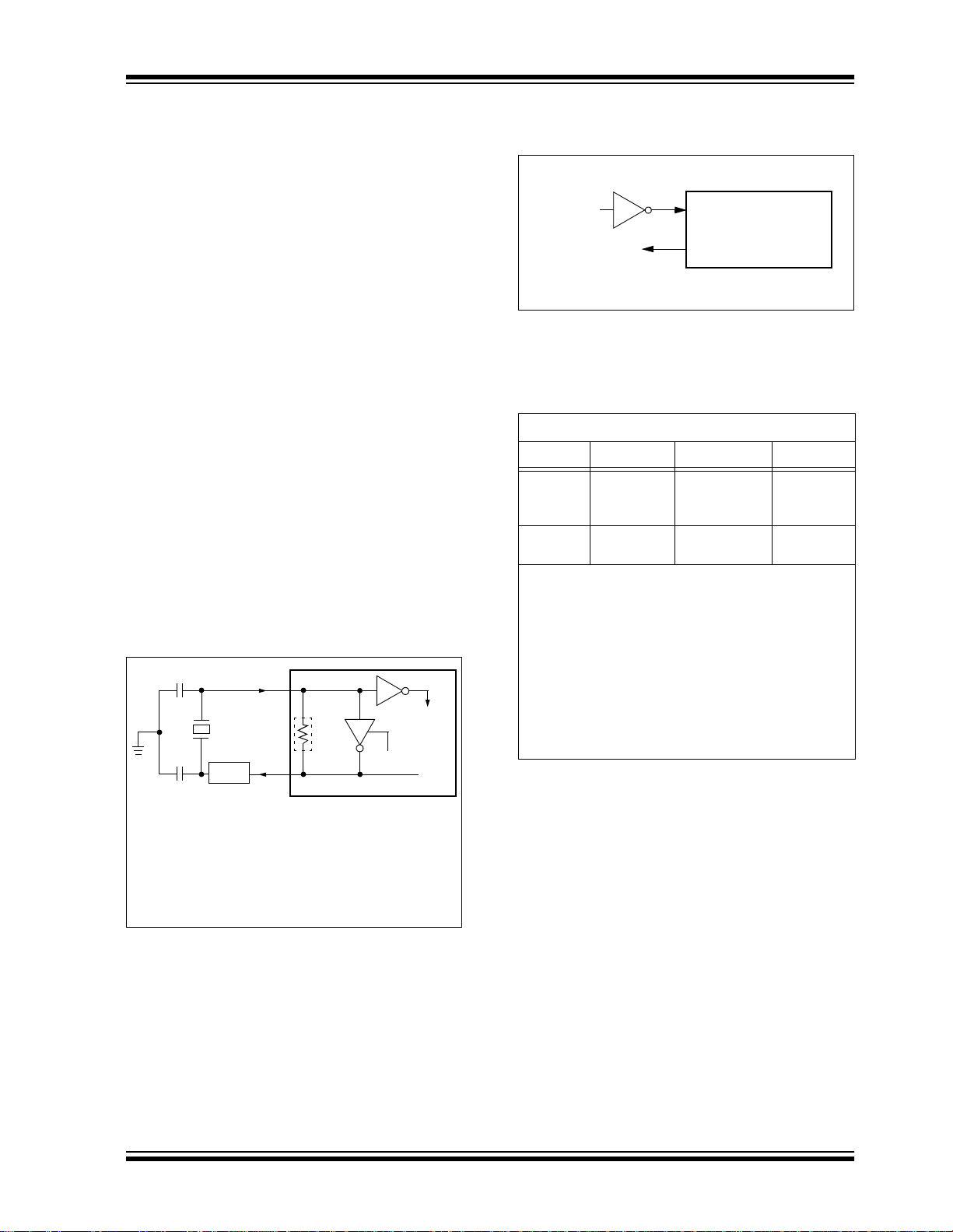
PIC16F72
11.2 Oscillator Configurations
11.2.1 OSCILLATOR TYPES
The PIC16F72 can be operated in four different Oscillator modes. The user can program two configuration
bits (FOSC1 and FOSC0) to select one of these four
modes:
• LP Low Power Crystal
• XT Crystal/Resonator
• HS High Speed Crystal/Resonator
• RC Resistor/Capacitor
11.2.2 CRYSTAL OSCILLATOR/CERAMIC
RESONATORS
In XT, LP or HS modes, a crystal or ceramic resonator
is connected to the OSC1/CLKI and OSC2/CLKO pins
to establish oscillation (Figure 11-1). The PIC16F72
oscillator desig n requ ire s the use of a p a r al lel cut cry stal. Use of a s eries cut cryst al may g ive a fre quency o ut
of the crystal manufacturers spec ifications. Wh en in HS
mode, the device can accept an external clock source
to drive the OSC1/CLKI pin (Figure11-2). See
Figure 14-1 or Figure 14-2 (depending on the part
number and V
frequencies.
FIGURE 11-1: CRYSTAL/CERAMIC
C1
C2(1)
DD range) for valid external clock
RESONATOR OPERATION
(HS, XT OR LP
OSC CONFIGURATION)
(1)
XTAL
(2)
RS
OSC1
OSC2
RF(3)
SLEEP
PIC16F72
To
internal
logic
FIGURE 11-2: EXTERNAL CLOCK INPUT
OPERATION (HS OSC
CONFIGURATION)
Clock from
Ext. System
Open
OSC1
PIC16F72
(HS Mode)
OSC2
TABLE 11-1: CERAMIC RESONATORS
(FOR DESIGN
GUIDANCE ONLY)
Typical Capacitor Values Used:
Mode Freq OSC1 OSC2
XT 455 kHz
2.0 MHz
4.0 MHz
HS 8.0 MHz
16.0 MHz
Capacitor values are for design guidance only.
These capacitors were tested with the resonators
listed below for basic start-up and operation. These
values were not optimized.
Different cap acitor values may be required to prod uce
acceptable oscillator operation. The user should test
the performance of the oscillator over the expected
DD and temperature range for the application.
V
See the notes at the bottom of page 62 for additional
information.
56 pF
47 pF
33 pF
27 pF
22 pF
56 pF
47 pF
33 pF
27 pF
22 pF
Note 1: See Table 11-1 and Table 11-2 for typical
2002 Microchip Technology Inc. DS39597B-page 61
values of C1 and C2.
2: A series resistor (RS) may be required for
AT strip cut crystals.
3: RF varies with the crystal chosen.
Page 64

PIC16F72
TABLE 11-2: CAPACITOR SELECTION FOR
CRYSTAL OSCILLATOR (FOR
DESIGN GUIDANCE ONLY)
Osc T y pe
Crystal
Freq
LP 32 kHz 33 pF 33 pF
200 kHz 15 pF 15 pF
XT 200 kHz 56 pF 56 pF
1 MHz 15 pF 15 pF
4 MHz 15 pF 15 pF
HS 4 MHz 15 pF 15 pF
8 MHz 15 pF 15 pF
20 MHz 15 pF 15 pF
Capacitor values are for design guidance only.
These capacitors were tested with the crystals listed
below for basic start-up and operation. These values
were not optimized.
Different capa citor values may be required to produc e
acceptable oscillator operation. The user should test
the performance of the oscillator over the expected
DD and temperature range for the application.
V
See the notes following this table for additional
information.
T ypical Cap acitor V alues
Tested:
C1 C2
11.2.3 RC OSCILLATOR
For timing insensitive applications, the “RC” device
option offers additi ona l cos t savings. The RC oscillator
frequency is a function of the supply voltage, the resis -
EXT) and capacitor (CEXT) values, and the operat-
tor (R
ing temperature. In addition to this, the oscillator
frequency will vary from unit to unit due to normal process paramete r variatio n. Further more, the d ifference
in lead frame capacitance between package types will
also affect the oscillation frequency, especially for low
EXT values. The user also needs to take into account
C
variation due to tolerance of external R and C components used. Figure 11-3 shows how the R/C
combination is connected to the PIC16F72.
FIGURE 11-3: RC OSCILLATOR MODE
VDD
REXT
OSC1
CEXT
VSS
F
Recommended values: 3 kΩ ≤ REXT ≤ 100 kΩ
OSC/4
OSC2/CLKO
CEXT > 20 pF
Internal
Clock
PIC16F72
Note 1: Higher capacita nce increase s the st ability
of oscillator, but also increases the
start-up time.
2: Since each resonator/crystal has its own
characteristics, the user should consult the
resonator/crystal manufacturer for appropriate values of external components.
3: Rs may be required in HS mode, as well
as XT mode, to avoid overdrivi ng crys t als
with low drive level specification.
4: Always verify oscilla tor pe rform an ce over
DD and temperature range that is
the V
expected for the application.
11.3 RESET
The PIC16F72 differentiates between various kinds of
RESET:
• Power-on Reset (POR)
• MCLR
• MCLR
• WDT Reset (during normal operation)
• WDT Wake-up (during SLEEP)
• Brown-out Reset (BOR)
Some registers are not affected in any RESET condition. Their status is unknown on POR and unchanged
in any other RESET. Most other registers are rese t to a
“RESET state” on Power-on Reset (POR), on the
MCLR and WDT Reset, on MCLR Reset during
SLEEP, and Brown-out Reset (BOR). They are not
affected by a WDT Wake-up, which is viewed as the
resumption of normal operation. The TO
are set or cleared differently in different RESET situations, as indicated in Table 11-4. These bi ts are used in
software to determine the nature of the RESET. See
Table 11-6 for a full description of RESET states of all
registers.
A simplified block diagram of the on-chip RESET circuit
is shown in Figure 11-4.
Reset during normal operation
Reset during SLEEP
and PD bits
DS39597B-page 62 2002 Microchip Technology Inc.
Page 65

FIGURE 11-4: SIMPLIFIED BLOCK DIAGRAM OF ON-CHIP RESET CIRCUIT
External
RESET
PIC16F72
MCLR
WDT
Module
DD Rise
V
Detect
VDD
Brown-out
Reset
OST/PWRT
OST
OSC1
(1)
On-chip
RC OSC
Note 1: This is a separate oscillator from the RC oscillator of the CLKI pin.
PWRT
SLEEP
WDT
Time-out
Reset
Power-on Reset
BOREN
10-bit Ripple Counter
10-bit Ripple Counter
S
Chip_Reset
R
Q
Enable PWRT
Enable OST
11.4 MCLR
PIC16F72 device has a noise filter in the MCLR Reset
path. The filter will detect and ignore small pulses.
It should be noted that a WDT Reset does not drive
pin low.
MCLR
The behavior of the ESD protection on the MCLR
has been altered from previous devices of this family.
Volt a ges app lied to the pin th at exce ed it s spe cific ation
can result in both MCLR
and excessive current beyon d
the device specification during the ESD event. For this
reason, Microchip recommends that the MCLR pin no
longer be tied directly to V
DD. The use of an
RC network, as shown in Figure 11-5, is suggested.
pin
FIGURE 11-5: RECOMMENDED MCLR
CIRCUIT
V
DD
R1
1 k
Ω (or greater)
C1
µF
0.1
(optional, not critical)
PIC16F72
MCLR
2002 Microchip Technology Inc. DS39597B-page 63
Page 66

PIC16F72
11. 5 Power-on Reset (POR)
A Power-on Reset pulse is generated on-chip when
DD rise is detected (in the range of 1.2V - 1.7V). To
V
take advantage of the POR, tie the MCLR
as described in Section 11.4. A maximum rise time for
VDD is specified. See Section 14.0, Electrical
Characteristics for details.
When the device starts normal operation (exits the
RESET condition), device operating parameters (voltage, frequency, temperature,...) m ust be met to ensure
operation. If these cond itions are not met, the d evice
must be held in RESET until the operating conditions
are met. For more information, see Application Note,
AN607- Power-up Trouble Shooting (DS00607).
pin to VDD,
11.6 Power-up Timer (PWRT)
The Power-up Timer provides a fixed 72 ms nominal
time-out on power-up only from the POR. The Powerup Timer operates on an internal RC oscillator. The
chip is kept in RESET as long as the PWRT is active.
The PWRT’s t ime delay allows VDD to rise to an ac ceptable level. A configuration bit is provided to enable/
disable the PWRT.
The power-up time dela y will vary from chip to chip due
DD, temperature and process variation. See DC
to V
parameters for details (T
PWRT, parameter #33).
11.7 Oscillator Start-up Timer (OST)
11. 9 Time-out Sequence
On power-up, the time-out sequence is as follows: the
PWRT delay starts (if enabled) when a POR occurs.
Then, OST start s c oun tin g 102 4 os ci ll ator cycles when
PWRT ends (LP, XT, HS). When the OST ends, the
device comes out of RESET.
If MCLR
Bringing MCLR
This is useful for testing purposes or to synchronize
more than one PIC16F72 de vice operating in parallel.
Table 11-5 shows the RESET conditions for the
STATUS, PCON and PC registers, while Table 11-6
shows the RESET conditions for all the registers.
is kept low long enough, all delays will expire.
high will begin execution immediately.
11.10 Power Control/Status Register (PCON)
The Power Control/Status Register, PCON, has two
bits to indicate the type of RESET that last occurred.
Bit0 is Brown-out Reset Status bit, BOR. Bit BOR is
unknown on a Power-on Reset. It must then be set by
the user and checked on subsequent RESETS to see
if bit BOR
occurred. When the Brown-out Reset is disabled, the
state of the BOR
Bit1 is POR
a Power-on Reset and unaffected otherwise. The user
must set this bit following a Power-on Reset.
cleared, indicating a Brown-out Reset
bit is unpredictable.
(Power-on Reset St atus bit). It is cleared on
The Oscillator Start-up Timer (OST) provides 1024
oscillator cycles (from OSC1 input) delay after the
PWRT delay is over (if enabled). This helps to ensure
that the crystal oscillator or resonator has started and
stabilized.
The OST time-out is invoked only for XT, LP and HS
modes and only on Power-on Reset or wake-up from
SLEEP.
11.8 Brown-out Reset (BOR)
The configuration bit, BOREN, can enable or disable
the Brown-out Reset circuit. If V
(parameter D005, about 4V) for longer than TBOR
(parameter #35, abou t 100µs), the brown-out situation
will reset the device. If V
than T
BOR, a RESET may not occur.
Once the brown-out occurs, the device will remain in
Brown-out Reset until V
Power-up Timer then keeps the device in RESET for
TPWRT (parameter #33, abou t 72 ms). If VDD should fall
below V
cess will restart when V
Power-up Timer Reset. The Power-up Timer is always
enabled when the Brown-out Reset circuit is enabled,
regardless of the state of the PWRT configuration bit.
BOR during TPWRT, the Brown-out Reset pro-
DD falls below VBOR for less
DD rises above VBOR. The
DD rises above VBOR, with the
DD falls below VBOR
DS39597B-page 64 2002 Microchip Technology Inc.
Page 67

TABLE 11-3: TIME-OUT IN VARIOUS SITUATIONS
Oscillator Configuration
XT, HS, LP 72 ms + 1024 T
RC 72 ms — 72 ms —
PWRTEN
Power-up
= 0 PWRTEN = 1
OSC 1024 TOSC 72 ms + 1024 TOSC 1024 TOSC
TABLE 11-4: STATUS BITS AND THEIR SIGNIFICANCE
POR
(PCON<1>)
0x 1 1Power-on Reset
0x 0 xIllegal, TO
0x x 0Illegal, PD is set on POR
u0 1 1Brown-out Reset
uu 0 1WDT Reset
uu 0 0WDT Wake-up
uu u uMCLR
uu 1 0MCLR
BOR
(PCON<0>)TO(STATUS<4>)PD(STATUS<3>)
Reset during normal operation
Reset during SLEEP or interrupt wake-up from
SLEEP
Brown-out
Significance
is set on POR
PIC16F72
Wake-up from
SLEEP
TABLE 11-5: RESET CONDITION FOR SPECIAL REGISTERS
Condition
Power-on Reset 000h 0001 1xxx ---- --0x
Reset during normal operation 000h 000u uuuu ---- --uu
MCLR
Reset during SLEEP 000h 0001 0uuu ---- --uu
MCLR
WDT Reset 000h 0000 1uuu ---- --uu
WDT Wake-up PC + 1 uuu0 0uuu ---- --uu
Brown-out Reset 000h 0001 1uuu ---- --u0
Interrupt Wake-up from SLEEP PC + 1
Legend: u = unchanged, x = unknown, - = unimplemented bit, read as '0'.
Note 1: When the wake-up is due to an interrupt and the GIE bit is set, the PC is loaded with the interrupt vector
(0004h).
Program
Counter
(1)
STATUS
Register
uuu1 0uuu ---- --uu
PCON
Register
2002 Microchip Technology Inc. DS39597B-page 65
Page 68

PIC16F72
TABLE 11-6: INITIALIZATION CONDITIONS FOR ALL REGISTERS
Register
W xxxx xxxx uuuu uuuu uuuu uuuu
INDF N/A N/A N/A
TMR0 xxxx xxxx uuuu uuuu uuuu uuuu
PCL 0000h 0000h PC + 1
STATUS 0001 1xxx 000q quuu
FSR xxxx xxxx uuuu uuuu uuuu uuuu
PORTA --0x 0000 --0u 0000 --uu uuuu
PORTB xxxx xxxx uuuu uuuu uuuu uuuu
PORTC xxxx xxxx uuuu uuuu uuuu uuuu
PCLATH ---0 0000 ---0 0000 ---u uuuu
INTCON 0000 000x 0000 000u uuuu uuuu
PIR1 -0-- 0000 -0-- 0000 -u-- uuuu
TMR1L xxxx xxxx uuuu uuuu uuuu uuuu
TMR1H xxxx xxxx uuuu uuuu uuuu uuuu
T1CON --00 0000 --uu uuuu --uu uuuu
TMR2 0000 0000 0000 0000 uuuu uuuu
T2CON -000 0000 -000 0000 -uuu uuuu
SSPBUF xxxx xxxx uuuu uuuu uuuu uuuu
SSPCON 0000 0000 0000 0000 uuuu uuuu
CCPR1L xxxx xxxx uuuu uuuu uuuu uuuu
CCPR1H xxxx xxxx uuuu uuuu uuuu uuuu
CCP1CON --00 0000 --00 0000 --uu uuuu
ADRES xxxx xxxx uuuu uuuu uuuu uuuu
ADCON0 0000 00-0 0000 00-0 uuuu uu-u
OPTION 1111 1111 1111 1111 uuuu uuuu
TRISA --11 1111 --11 1111 --uu uuuu
TRISB 1111 1111 1111 1111 uuuu uuuu
TRISC 1111 1111 1111 1111 uuuu uuuu
PIE1 -0-- 0000 -0-- 0000 -u-- uuuu
PCON ---- --qq ---- --uu ---- --uu
PR2 1111 1111 1111 1111 1111 1111
SSPADD 0000 0000 0000 0000 uuuu uuuu
SSPSTAT --00 0000 --00 0000 --uu uuuu
ADCON1 ---- -000 ---- -000 ---- -uuu
PMDATL 0--- 0000 0--- 0000 u--- uuuu
PMADRL xxxx xxxx uuuu uuuu uuuu uuuu
PMDATH xxxx xxxx uuuu uuuu uuuu uuuu
PMADRH xxxx xxxx uuuu uuuu uuuu uuuu
PMCON1 1--- ---0 1--- ---0 1--- ---u
Legend: u = unchanged, x = unknown, - = unimplemented bit, read as ’0’, q = value depends on condition,
r = reserved, maintain clear.
Note 1: One or more bits in INTCON, PIR1 will be affected (to cause wake-up).
2: When the wake-up is due to an interrupt and the GIE bit is set, the PC is loaded with the interrupt vector
(0004h).
3: See Table 11-5 for RESET value for specific condition.
Power-on Reset,
Brown-out Reset
Reset,
MCLR
WDT Reset
(3)
Wake-up via WDT or
Interrupt
(2)
uuuq quuu
(3)
(1)
(1)
DS39597B-page 66 2002 Microchip Technology Inc.
Page 69

PIC16F72
FIGURE 11-6: TIME-OUT SEQUENCE ON POWER-UP (MCLR TIED TO VDD THROUGH
PULL-UP RESISTOR)
VDD
MCLR
INTERNAL POR
TPWRT
PWRT TIME-OUT
OST TIME-OUT
INTERNAL RESET
TOST
FIGURE 11-7: TIME-OUT SEQUENCE ON POWER-UP (MCLR
RC NETWORK): CASE 1
VDD
MCLR
INTERNAL POR
TPWRT
PWRT TIME-OUT
OST TIME-OUT
INTERNAL RESET
TIED TO VDD THROUGH
TOST
FIGURE 11-8: TIME-OUT SEQUENCE ON POWER-UP (MCLR
TIED TO VDD THROUGH
RC NETWORK): CASE 2
VDD
MCLR
INTERNAL POR
TPWRT
PWRT TIME-OUT
OST TIME-OUT
INTERNAL RESET
2002 Microchip Technology Inc. DS39597B-page 67
TOST
Page 70

PIC16F72
FIGURE 11-9: SLOW RISE TIME (MCLR TIED TO VDD THROUGH RC NETWORK)
5V
VDD
MCLR
INTERNAL POR
PWRT TIME-OUT
OST TIME-OUT
INTERNAL RESET
0V
T
PWRT
1V
TOST
11.11 Interrupts
The PIC16F72 has up to eight sources of interru pt. The
interrupt control register (INTCON) records individual
interrupt requests in flag bits. It also has individual and
global interrupt enable bits.
Note: Individual interrupt fl ag bits are set, regard-
less of the status of their corresponding
mask bit, or the GIE bit.
A global interrupt enable bit, GIE (INTCON<7>)
enables (if set) all unmasked interrupts, or disables (if
cleared) all interr upts . When bit GIE i s enab led, a nd an
interrupt’s fl ag bit and mask bi t are set, the interrup t will
vector immediately. Individual interrupts can be disabled through their corresponding enable bits in various registers. Individual interrupt bits are set,
regardless of the status o f the GIE bit . The GIE bi t is
cleared on RESET.
The “return from interrupt” instruction, RETFIE, exits
the interrupt routine, as well as sets the GIE bit, which
re-enables interrupt s.
FIGURE 11-10: INTERRUPT LOGIC
The RB0/INT pin interrupt, the R B port change interrupt
and the TMR0 overflow interrupt flag s are contained in
the INTCON register.
The peripheral interrupt flags are contained in the
Special Function Register, PIR1. The corresponding
interrupt enable bits are contained in Special Function
Register, PIE1, and the peripheral interrupt enable bit
is contained in Special Function Re gister INTCON.
When an interrupt is serviced, the GIE bit is cleared to
disable any further interrupt, the return address is
pushed onto the stack, and the PC is loaded with
0004h. Once in the Interrupt Service Routine, the
source(s) of the interrupt can be determined by polling
the inter rupt fl ag bits. The in terrupt flag b it(s) must be
cleared in software before re-enabling interrupts to
avoid recursive interrupts.
For external interrupt events, such as the INT pin or
PORTB change interrupt, the interrupt latency will be
three or four instruction cycles. The exact latency
depends when the interrupt event occurs, relative to
the current Q cycle. The latency is the same for one or
two cycle ins tructions . Individua l interrupt flag bits are
set, regardless of the status of their corresponding
mask bit, PEIE bit, or the GIE bit.
TMR0IF
TMR0IE
ADIF
ADIE
SSPIF
SSPIE
CCP1IF
CCP1IE
TMR1IF
TMR1IE
TMR2IF
TMR2IE
DS39597B-page 68 2002 Microchip Technology Inc.
INTF
INTE
RBIF
RBIE
PEIE
GIE
Wake-up (If in SLEEP mode)
Interrupt to CPU
Page 71

PIC16F72
11.11.1 INT INTERRUPT
External interrupt on the RB0/INT pin is edge triggered,
either rising, if bit INTEDG (OPTION<6>) is set, or falling, if the INTEDG bit is clear. When a valid edge
appears on the RB0/INT pin, flag bit INTF
(INTCON<1>) is set. This interrupt can be disabled by
clearing enable bit INTE (INTCON<4>). Flag bit INTF
must be cleared in software in the Interrupt Service
Routine before re-enablin g this interrupt. The INT int errupt can wake-up the pro cessor from SLEEP, if bit INTE
was set prior to going into SLEEP. The status of global
interrupt enable bit GIE decides whether or not the
processor branches to the interrupt vector following
wake-up. See Section 11.14 for details on SLEEP
mode.
11.11.2 TMR0 INTERRUPT
An overflow (FFh → 00h) in the TMR0 register will set
flag bit TMR0IF (INTCON<2>). The interrupt can be
enabled/disabled by setting/clearing enable bit
TMR0IE (INTCON<5>) (see Section 5.0).
11.11.3 PORTB INTCON CHANGE
An input change on PORTB<7:4> sets flag bit RBIF
(INTCON<0>). The interrupt can be enabled/disabled
by setting/clearing enable bit RBIE (INTCON<4>) (see
Section 3.2).
11. 12 Context Saving During Interrupts
During an interrupt, only the return PC value is saved
on the stack. T ypically, users may wish to save key re gisters during an interrupt (i.e., W, STATUS registers).
This will have to be imple mented in software, a s show n
in Example 11-1.
For the PIC16F72 device, the register W_TEMP must
be defined in both banks 0 and 1 and must be defined
at the same offset from the bank base address (i.e., if
W_TEMP is defined at 20h in bank 0, it must also be
defined at A0h in bank 1). The register STA TUS_TEMP
is only defined in bank 0.
EXAMPLE 11-1: SAVING STATU S, W AND PCLATH REGISTERS IN RAM
MOVWF W_TEMP ;Copy W to TEMP register
SWAPF STATUS,W ;Swap status to be saved into W
CLRF STATUS ;bank 0, regardless of current bank, Clears IRP,RP1,RP0
MOVWF STATUS_TEMP ;Save status to bank zero STATUS_TEMP register
:
:(ISR) ;Insert user code here
:
SWAPF STATUS_TEMP,W ;Swap STATUS_TEMP register into W
MOVWF STATUS ;Move W into STATUS register
SWAPF W_TEMP,F ;Swap W_TEMP
SWAPF W_TEMP,W ;Swap W_TEMP into W
;(sets bank to original state)
2002 Microchip Technology Inc. DS39597B-page 69
Page 72

PIC16F72
11. 13 Watchdog Timer (WDT)
The Watchdog Timer is a free running, on-chip RC
oscillator that does not require any external components. This RC osci llator i s sep arate from the R C osci llator of the OSC1/CLKI pin. That means that the WDT
WDT time-out period values may be found in the Electrical Specifications section under parameter #31. Values for the WDT prescaler (actually a postscaler, but
shared with the Timer0 prescaler) may be assigned
using the OPTION register.
will run, even if the clock on the OSC1/CLKI and OSC2/
CLKO pins of the device has been stopped, for
example, by execution of a SLEEP instruction.
During normal oper ation, a WDT ti me-out genera tes a
device RESET (Watchdog Timer Reset). If the device is
in SLEEP mode, a W DT t ime- ou t cause s t he de vice t o
wake-up and continue with normal operation (Watchdog
Timer Wake-up). The TO
bit in the STATUS register will
be cleared upon a Watchdog Timer time-out.
The WDT can be permanently disabled by clearing
configuration bit WDTEN (see Section 11.1).
FIGURE 11-11: WATCHDOG TIMER BLOCK DIAGRAM
From TMR0 Clock Source
(Figure 5-1)
0
M
1
WDT Timer
U
X
Note 1: The CLRWDT and SLEEP instructions
clear the WDT and the postscaler, if
assigned to the WDT, and prevent it from
timing out and generating a device
RESET condition.
2: When a CLRWDT instruction is executed
and the prescaler is as signed to the WDT,
the prescaler count will be cleared, but
the prescaler ass ig nm ent is no t c han ge d.
Postscaler
8
WDT
Enable Bit
Note: PSA and PS2:PS0 are bits in the OPTION register.
PSA
8 - to - 1 MUX
0
MUX
WDT
Time-out
1
PS2:PS0
To TMR0 (Fi gure 5-1)
PSA
TABLE 11-7: SUMMARY OF WATCHDOG TIMER REGISTERS
Address Name Bit 7 Bit 6 Bit 5 Bit 4 Bit 3 Bit 2 Bit 1 Bit 0
2007h Config. bits (1) BOREN
81h,181h OPTION
RBPU INTEDG T0CS T0SE PSA PS2 PS1 PS0
(1)
— CP PWRTEN
Legend: Shade d cells are not us ed by the Watchdog Timer.
Note 1: See Register 11-1 for operation of these bits.
(1)
WDTEN FOSC1 FOSC0
DS39597B-page 70 2002 Microchip Technology Inc.
Page 73

PIC16F72
11.14 Power-down Mode (SLEEP)
Power-down mode is entered by exec uting a SLEEP
instruction.
If enabled, the Watchdog Timer will be cleared but
keeps running, the PD
TO
(STATUS<4>) bit is set, and the oscillator driver is
turned off. The I/O ports maintain the status they had
before the SLEEP instruction was executed (driving
high, low, or hi-impedance).
For lowest cur rent cons umpt ion in thi s mode , plac e all
I/O pins at either V
cuitry is draw ing cu rrent from th e I/O pi n, powe r-down
the A/D and disable external clocks. Pull all I/O pins
that are hi-impedance inputs, high or low externally, to
avoid switching curre nts caus ed by fl oating input s. Th e
T0CKI input should also be at V
current consumption. The contribution from on-chip
pull-ups on PORTB should also be considered.
The MCLR
pin must be at a logic high level (VIHMC).
11.14.1 WAKE-UP FROM SLEEP
The device can wake-up from SLEEP through one of
the following events:
1. External RESET input on MCLR
2. Watchdog Timer wake-up (if WDT was
enabled).
3. Interrupt from INT pin, RB port change or a
peripheral interrupt.
External MCLR
other events are considered a continuation of program
execution and ca us e a " wak e-up". The TO and PD bits
in the STATUS register can be used to determine the
cause of the devi ce RESET. The PD
power-up, is cleared when SLEEP is invoked. The TO
bit is cleared if a WDT time-out occurred and caused
wake-up.
The following periph eral interrupt s can wake the device
from SLEEP:
1. TMR1 interrupt. T imer1 must be operati ng as an
asynchronous counter.
2. CCP Capture mode interrupt.
3. Special event trigger (Timer1 in Asynchronous
mode using an external clock).
4. SSP (START/STOP) bit detect interrupt.
5. SSP transmit or receive in Slave mode
6. A/D conversion (when A/D clock source is RC).
(SPI/I
2
C).
bit (STATUS<3>) is cleared, the
DD or VSS, ensure no external cir-
DD or VSS for lowest
pin.
Reset will cause a device RESET. All
bit, which is set on
Other peripherals cannot generate interrupts since
during SLEEP, no on-chip clocks are present.
When the SLEEP instruc tion is being e xecuted, the next
instruction (PC + 1) is pre-fetched. For the device to
wake-up through an interrup t eve nt, the co rres pon din g
interrupt enable bit must be set (enabled). Wake-up
occurs regardless of the state of the GIE bit. If the GIE
bit is clear (disabled), the device continues execution at
the instruction after the SLEEP inst ruction. If the GIE b it
is set (enabled), the device executes the instruction
after the SLEEP instruction and then branches to the
interrupt address (0004h). In cases where the execution of the instruction following SLEEP is not desirable,
the user should have a NOP after t he SLEEP instruction.
11.14.2 WAKE-UP USING INTERRUPTS
When global interrupts are disabled (GIE cleared) and
any interrupt source has both its interrupt enable bit
and interrupt flag bi t set, one of the fo llow ing wil l occu r:
• If the interrupt occurs before the execution of a
SLEEP instruction, the SLEEP instruction will complete as a NOP. Therefore, the WDT and WDT
postscaler will not be cleared, the TO
be set and PD
• If the interrupt occurs during or after the execu-
tion of a SLEEP instruction, the device will immediately wake-up from SLEEP. The SLEEP
instruction will be completely executed before the
wake-up. Therefore, the WDT and WDT
postscaler will be cleared, the TO
and the PD
Even if the flag bits were checked before executing a
SLEEP instruction, it may be possible for flag bits to
become set befo re the SLEEP instruct ion completes . To
determine whether a SLEEP instruction exe cuted, te st
bit. If the PD bit is set, the SLEEP instru ction
the PD
was executed as a NOP.
T o ensure that the WD T is cleared, a CLRWDT instruction
should be executed before a SLEEP instruction.
bits will not be cleared.
bit will be cleared.
bit will not
bit will be set
2002 Microchip Technology Inc. DS39597B-page 71
Page 74
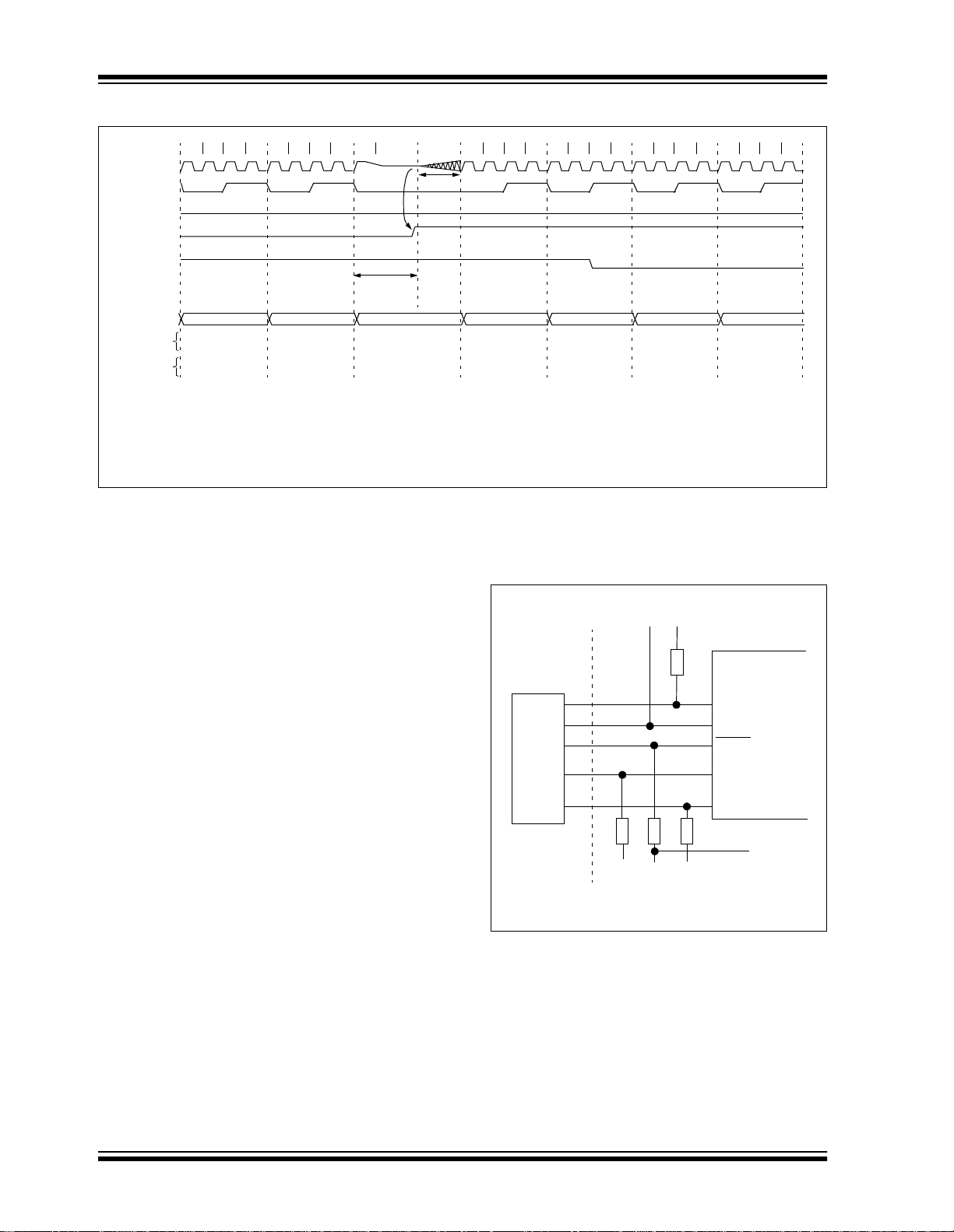
PIC16F72
FIGURE 11-12: WAKE-UP FROM SLEEP THROUGH INTERRUPT
Q1 Q2 Q3 Q4 Q1 Q2 Q3 Q4 Q1 Q1 Q2 Q3 Q4 Q1 Q2 Q3 Q4 Q1 Q2 Q3 Q4 Q1 Q2 Q3 Q4
OSC1
(4)
CLKO
INT pin
INTF Flag
(INTCON<1>)
GIE bit
(INTCON<7>)
INSTRUCTION FLOW
PC
Instruction
Fetched
Instruction
Executed
Inst(PC) = SLEEP
Inst(PC - 1)
Processor in
SLEEP
PC PC+1 PC+2
Inst(PC + 1)
SLEEP
T
OST
(2)
PC+2
Inst(PC + 2)
Inst(PC + 1)
Interrupt Latency
(Note 2)
PC + 2 0004h 0005h
Dummy cycle
Inst(0004h)
Dummy cycle
Inst(0005h)
Inst(0004h)
Note 1: XT, HS or LP Oscillator mode assumed.
OST = 1024 TOSC (drawing not to scale) This delay will not be there for RC Osc mode.
2: T
3: GIE = ‘1' assumed. In this case, after wake-up, the processor jumps to the interrupt routine.
If GIE = ‘0', execution will continue in-line.
4: CLKO is not available in these Osc modes, but shown here for timing reference.
11.15 Program Verification/ Code Protection
If the code protection bit(s) have not been programmed, the on-chip program memory can be read
out for verification purposes.
11.16 ID Locations
Four memory locations (2000h - 2003h) are desig nated
as ID locations, where the user can store checksum or
other code identification numbers. These locations are
not accessible during normal execution, but are readable and writable during program/verify. It is recommended that only the four Least Significant bits of the
ID location are used.
11. 1 7 In-Circuit Serial Programming
PIC16F72 microcontrollers can be serially programmed
while in the end app lication circui t. This is simply done
with two lines for clock and data and three other lines for
power, ground, and the programming voltage (see
Figure 11-13 for an example). This allows customers to
manufacture boards with unprogrammed devices, and
then program the microcontrol ler just before shipping
the product. This al so allows the most recent firmware
or a custom firmware to be programmed.
For general information of serial programming, please
refer to the In-Circuit Serial Programming™ (ICSP™)
Guide (DS30277). For speci fic det ails on progra mming
commands and operations for the PIC16F72 devices,
please refer to the latest version of the PIC16F72
FLASH Program Memory Programming Specification
(DS39588).
FIGURE 11-13: TYPICAL IN-CIRCUIT
SERIAL PROGRAMMING
CONNECTION
To Normal
Connections
External
Connector
Signals
+5V
0V
PP
V
CLK
Data I/O
* * *
To Normal
Connections
*
Isolation devices (as required).
*
PIC16F72
V
DD
VSS
MCLR/VPP
RB6
RB7
VDD
DS39597B-page 72 2002 Microchip Technology Inc.
Page 75

PIC16F72
12.0 INSTRUCTION SET SUMMARY
Each PIC16F72 ins tructio n is a 14 -bit wo rd div ided into
an OPCODE that specif ies the instruct ion type and on e
or more operands that further specify the operation of
the instruction. T he PIC16 F72 ins truction set summary
in Table 12-2 lists byte-oriented, bit-oriented, and lit-
eral and control operations. Table 12-1 shows the
opcode field descriptions.
For byte-oriented instr ucti ons, ‘f’ represents a file register designator and ‘d’ represents a destination designator. The file regi ster designator s pecifies which fi le
register is to be used by the instruction.
The destination des ignator specifies w here the result of
the operation is to be placed. If ‘d’ is zero, the result is
placed in the W regis ter . If ‘d’ is one, the result is placed
in the file register specified in the instruction.
For bit-oriented inst ructions, ‘b’ represents a bit field
designator which selects the number of th e bi t a f fe cted
by the operation, whil e ‘f’ represents the number of the
file in which the bit is located.
For literal and control operations, ‘k’ represents an
eight or eleven-bit constant or literal value.
TABLE 12-1: OPCODE FIELD
DESCRIPTIONS
Field Description
f Register file address (0x00 to 0x7F)
W Working register (accumulator)
b Bit address within an 8-bit file register
k Literal field, constant data or label
x Don’t care location (= 0 or 1).
The assembler will generate code with x = 0. It is the
recommended form of use for compatibility with all
Microchip software tools.
d Destination select; d = 0: store result in W,
d = 1: store result in file register f.
Default is d = 1.
PC Program Counter
TO Time-out bit
PD Power-down bit
The instruction set is highly orthogonal and is grouped
into three basic categories :
• Byte-oriented operations
• Bit-oriented operations
• Literal and control operations
All instructions are executed within one single instruction cycle , unless a conditio nal test i s true or the program counter is changed as a result of an instruction.
In this case, the execution takes two instruction cycles,
with the sec ond cycl e ex ecut ed as a
tion cycle consists of four oscillator periods. Thus, for
an oscillator frequency of 4 M Hz, the normal i nstructio n
execution time is 1 µs . If a conditio nal test is true , or the
program counter is changed as a result of an
instruction, the instruction execution time is 2 µs.
NOP. One instruc-
Table 12-2 lists the instructions recognized by the
TM
MPASM
assembler.
Figure 12-1 shows the general formats that the
instructions can have.
All examples use the following format to represent a
hexadecimal number:
0xhh
where h signifies a hexadecimal digit.
FIGURE 12-1: GENERAL FORMAT FOR
INSTRUCTIONS
Byte-oriented file register operations
13 8 7 6 0
OPCODE d f (FILE # )
d = 0 for destination W
d = 1 for destination f
f = 7-bit file register address
Bit-oriented file register operations
13 10 9 7 6 0
OPCODE b (BIT #) f (FILE #)
b = 3-bit bit address
f = 7-bit file register address
Literal and control operations
General
13 8 7 0
OPCODE k (literal)
k = 8-bit immediate value
CALL and GOTO instructions only
13 11 10 0
OPCODE k (literal)
k = 11-bit immediate value
A description of each instruction is available in the
PICmicro™ Mid-Range MCU Family Reference
Manual (DS33023).
2002 Microchip Technology Inc. DS39597B-page 73
Page 76

PIC16F72
TABLE 12-2: PIC16F72 INSTRUCTION SET
Mnemonic,
Operands
ADDWF
ANDWF
CLRF
CLRW
COMF
DECF
DECFSZ
INCF
INCFSZ
IORWF
MOVF
MOVWF
NOP
RLF
RRF
SUBWF
SWAPF
XORWF
BCF
BSF
BTFSC
BTFSS
ADDLW
ANDLW
CALL
CLRWDT
GOTO
IORLW
MOVLW
RETFIE
RETLW
RETURN
SLEEP
SUBLW
XORLW
Note 1: When an I/O register is modified as a function of itself (e.g.,
2: If this instruction is executed on the TMR0 register (and where applicable, d = 1), the prescaler will be cleared if assigned
3: If Pr ogram Counter (PC) is modif ied or a conditional test is true, the instruction requires two cycles. The second cycle is
f, d
Add W and f
f, d
AND W with f
f
Clear f
-
Clear W
f, d
Complement f
f, d
Decrement f
f, d
Decrement f, Skip if 0
f, d
Increment f
f, d
Increment f, Skip if 0
f, d
Inclusive OR W with f
f, d
Move f
f
Move W to f
-
No Operation
f, d
Rotate Left f through Carry
f, d
Rotate Right f through Carry
f, d
Subtract W from f
f, d
Swap nibbles in f
f, d
Exclusive OR W with f
f, b
Bit Clear f
f, b
Bit Set f
f, b
Bit Test f, Skip if Clear
f, b
Bit Test f, Skip if Set
k
Add literal and W
k
AND literal with W
k
Call subroutine
-
Clear Watchdog Timer
k
Go to address
k
Inclusive OR literal with W
k
Move literal to W
-
Return from interrupt
k
Return with literal in W
-
Return from Subroutine
-
Go into Standby mode
k
Subtract W from literal
k
Exclusive OR literal with W
the pins themselves. For example, if the data latch is ‘1’ for a pin configured as input and is driven low by an external
device, the data will be written back with a ‘0’.
to the Timer0 module.
executed as a
NOP.
Description Cycles
BYTE-ORIENTED FILE REGISTER OPERATIONS
1
1
1
1
1
1
1(2)
1
1(2)
1
1
1
1
1
1
1
1
1
BIT-ORIENTED FILE REGISTER OPERATIONS
1
1
1 (2)
1 (2)
LITERAL AND CONTROL OPERATIONS
1
1
2
1
2
1
1
2
2
2
1
1
1
MOVF PORTB, 1), the value used will be that value present on
14-Bit Opcode
MSb LSb
00
0111
dfff
ffff
00
0101
dfff
00
00
00
00
00
00
00
00
00
00
00
00
00
00
00
00
01
01
01
01
11
11
10
00
10
11
11
00
11
00
00
11
11
0001
0001
1001
0011
1011
1010
1111
0100
1000
0000
0000
1101
1100
0010
1110
0110
00bb
01bb
10bb
11bb
111x
1001
0kkk
0000
1kkk
1000
00xx
0000
01xx
0000
0000
110x
1010
lfff
0xxx
dfff
dfff
dfff
dfff
dfff
dfff
dfff
lfff
0xx0
dfff
dfff
dfff
dfff
dfff
bfff
bfff
bfff
bfff
kkkk
kkkk
kkkk
0110
kkkk
kkkk
kkkk
0000
kkkk
0000
0110
kkkk
kkkk
ffff
ffff
xxxx
ffff
ffff
ffff
ffff
ffff
ffff
ffff
ffff
0000
ffff
ffff
ffff
ffff
ffff
ffff
ffff
ffff
ffff
kkkk
kkkk
kkkk
0100
kkkk
kkkk
kkkk
1001
kkkk
1000
0011
kkkk
kkkk
Status
Affected
C,DC,Z
Z
Z
Z
Z
Z
Z
Z
Z
C
C
C,DC,Z
Z
C,DC,Z
Z
,PD
TO
Z
,PD
TO
C,DC,Z
Z
Notes
1,2
1,2
2
1,2
1,2
1,2,3
1,2
1,2,3
1,2
1,2
1,2
1,2
1,2
1,2
1,2
1,2
1,2
3
3
Note: Additional information on the mid-range instruction set is available in the PICmicro™ Mid-Range MCU Family Reference
Manual (DS33023).
DS39597B-page 74 2002 Microchip Technology Inc.
Page 77

12.1 Instruction Descriptions
PIC16F72
ADDLW Add Literal and W
Syntax: [ label ] ADDLW k
Operands: 0 ≤ k ≤ 255
Operation: (W) + k → (W)
Status Affected: C, DC, Z
Description: The contents of the W register
are added to the eight-bi t literal ‘k’
and the result is placed in the W
register.
ADDWF Add W and f
Syntax: [ label ] ADDWF f,d
Operands: 0 ≤ f ≤ 127
d ∈ [0,1]
Operation: (W) + (f) → (destination)
Status Affected: C, DC, Z
Description: Add the contents of the W register
with register ‘f’. If ‘d’ = ‘0’, the
result is stored i n the W re gister. If
‘d’ = ‘1’, the result is stored back
in register ‘f’.
ANDWF AND W with f
Syntax: [ label ] ANDWF f,d
Operands: 0 ≤ f ≤ 127
d ∈ [0,1]
Operation: (W) .AND. (f) → (destination)
Status Affected: Z
Description: AND the W register with register
‘f’. If ‘d’ = ‘0’, the result is stored in
the W register. If ‘d’ = ‘1’, the
result is stored back in r egister ‘f’.
BCF Bit Clear f
Syntax: [ label ] BCF f,b
Operands: 0 ≤ f ≤ 127
0 ≤ b ≤ 7
Operation: 0 → (f<b>)
Status Affected: None
Description: Bit ‘b’ in register ‘f’ is cleared.
ANDLW AND Literal with W
Syntax: [ label ] ANDLW k
Operands: 0 ≤ k ≤ 255
Operation: (W) .AND. (k) → (W)
Status Affected: Z
Description: The contents of W register are
AND’ed with the eight-bit literal
‘k’. The result is placed in the W
register.
2002 Microchip Technology Inc. DS39597B-page 75
BSF Bit Set f
Syntax: [ label ] BSF f,b
Operands: 0 ≤ f ≤ 127
0 ≤ b ≤ 7
Operation: 1 → (f<b>)
Status Affected: None
Description: Bit ‘b’ in register ‘f’ is set.
Page 78

PIC16F72
BTFSS Bit Test f, Skip if Set
Syntax: [ label ] BTFSS f,b
Operands: 0 ≤ f ≤ 127
0 ≤ b < 7
Operation: skip if (f<b>) = 1
Status Affected: None
Description: If bit ‘b’ in register ‘f’ = ‘0’, the next
instruction is executed.
If bit ‘b’ = ‘1’, then the next instruc-
tion is discarde d a nd a NOP is exe-
cuted instead, maki ng thi s a 2 T
instruction.
BTFSC Bit Test, Skip if Clear
Syntax: [ label ] BTFSC f,b
Operands: 0 ≤ f ≤ 127
0 ≤ b ≤ 7
Operation: skip if (f<b>) = 0
Status Affected: None
Description: If bit ‘b’ in register ‘f’ = ‘1’, the next
instruction is executed.
If bit ‘b’ in register ‘f’ = ‘0’, the n ex t
instruction is disc arded, and a NOP
is executed instead, m ak in g thi s a
CY instruction.
2 T
CY
CLRF Clear f
Syntax: [ label ] CLRF f
Operands: 0 ≤ f ≤ 127
Operation: 00h → (f)
1 → Z
Status Affected: Z
Description: The contents of register ‘f’ are
cleared and the Z bit is set.
CLRW Clear W
Syntax: [ label ] CLRW
Operands: None
Operation: 00h → (W)
1 → Z
Status Affected: Z
Description: W register is cleared. Zero bit (Z)
is set.
CALL Call Subroutine
Syntax: [ label ] CALL k
Operands: 0 ≤ k ≤ 2047
Operation: (PC) + 1 → TOS,
k → PC<10:0>,
(PCLA TH<4:3>) → PC<12:11>
Status Affected: None
Description: Call Subroutine. First, return
address (PC+1) is pushed onto
the stack. The eleven-bit immedi-
ate address is loade d i nto PC bits
<10:0>. The upper bits of the PC
are loaded from PCLATH. CALL is
a two-cycle instruction.
DS39597B-page 76 2002 Microchip Technology Inc.
CLRWDT Clear Watchdog Timer
Syntax: [ label ] CLRWDT
Operands: None
Operation: 00h → WDT
0 → WDT prescaler,
1 → TO
1 → PD
Status Affected: TO, PD
Description: CLRWDT instruction resets the
Watchdo g Time r. It also resets the
prescaler of the WDT. Status bits
and PD are set.
TO
Page 79

PIC16F72
COMF Complement f
Syntax: [ label ] COMF f,d
Operands: 0 ≤ f ≤ 127
d ∈ [0,1]
Operation: (f) → (destination)
Status Affected: Z
Description: The contents of register ‘f’ are
complemented. If ‘d’ = ‘0’, the
result is stored in W. If ‘d’ = ‘1’, the
result is stored back in register ‘f’.
DECF Decrement f
Syntax: [ label ] DECF f,d
Operands: 0 ≤ f ≤ 127
d ∈ [0,1]
Operation: (f) - 1 → (destination)
Status Affected: Z
Description: Decrement register ‘f’. If ‘d’ = ‘0’,
the result is stored in the W
register. If ‘d’ = ‘1’, the result is
stored back in register ‘f’.
GOTO Unconditional Branch
Syntax: [ label ] GOTO k
Operands: 0 ≤ k ≤ 2047
Operation: k → PC<10:0>
PCLATH<4:3> → PC<12:11>
Status Affected: None
Description: GOTO is an unconditional branch.
The eleven-bit im me dia t e v alu e i s
loaded into PC bits <10:0>. The
upper bits of PC are loaded from
PCLATH<4:3>. GOTO is a
two-cycle inst ruction.
INCF Increment f
Syntax: [ label ] INCF f,d
Operands: 0 ≤ f ≤ 127
d ∈ [0,1]
Operation: (f) + 1 → (destination)
Status Affected: Z
Description: The contents of register ‘f’ are
incremented. If ‘d’ = ‘0’, the result
is placed in the W register. If
‘d’ = ‘1’, the result is placed back
in register ‘f’.
DECFSZ Decrement f, Skip if 0
Syntax: [ label ] DECFSZ f,d
Operands: 0 ≤ f ≤ 127
d ∈ [0,1]
Operation: (f) - 1 → (destination);
skip if result = 0
Status Affected: None
Description: The contents of register ‘f’ are
decremented. If ‘d’ = ‘0’, the result
is placed in the W register. If
‘d’ = ‘1’, the result is placed back
in register ‘f’.
If the result is ‘1’, the next instruc-
tion is executed. If th e result is ‘0’,
then a NOP is executed instead,
making it a 2 T
2002 Microchip Technology Inc. DS39597B-page 77
CY instruction.
INCFSZ Increment f, Skip if 0
Syntax: [ label ] INCFSZ f,d
Operands: 0 ≤ f ≤ 127
d ∈ [0,1]
Operation: (f) + 1 → (destination),
skip if result = 0
Status Affected: None
Description: The contents of register ‘f’ are
incremented. If ‘d’ = ‘0’, the result
is placed in the W register. If
‘d’ = ‘1’, the result is placed back
in register ‘f’.
If the result is ‘1’, the next instruc-
tion is executed. If the res ul t i s ‘0’,
a NOP is execu ted instead , maki ng
CY instruction.
it a 2 T
Page 80

PIC16F72
IORLW Inclusive OR Literal with W
Syntax: [ label ] IORLW k
Operands: 0 ≤ k ≤ 255
Operation: (W) .OR. k → (W)
Status Affected: Z
Description: The contents of t he W register are
OR’d with the eight-bit literal ‘k’.
The result is placed in the W
register.
IORWF Inclusive OR W with f
Syntax: [ label ] IORWF f,d
Operands: 0 ≤ f ≤ 127
d ∈ [0,1]
Operation: (W) .OR. (f) → (destination)
Status Affected: Z
Description: Inclusive OR the W register with
register ‘f’. If ‘d’ = ‘0’, the result is
placed in the W regi ster . If ‘d’ = ‘1’,
the result is placed back in
register ‘f’.
MOVLW Move Literal to W
Syntax: [ label ] MOVLW k
Operands: 0 ≤ k ≤ 255
Operation: k → (W)
Status Affected: None
Description: The eight-bit literal ‘k’ is loaded
into W register. The don’t cares
will assemble as ‘0’s.
MOVWF Move W to f
Syntax: [ label ] MOVWF f
Operands: 0 ≤ f ≤ 127
Operation: (W) → (f)
Status Affected: None
Description: Move data from W register to
register ‘f’.
MOVF Move f
Syntax: [ label ] MOVF f,d
Operands: 0 ≤ f ≤ 127
d ∈ [0,1]
Operation: (f) → (destination)
Status Affected: Z
Description: The contents of register ‘f’ are
moved to a desti nation dependan t
upon the status of ‘d’. If ‘d’ = ‘0’,
the destination is W re gister. If
‘d’ = ‘1’, the destination is file reg-
ister ‘f’ itself. ‘d’ = ‘1’ is useful to
test a file register, since status
flag Z is affected.
NOP No Operation
Syntax: [ label ] NOP
Operands: None
Operation: No operation
Status Affected: None
Description: No operation.
DS39597B-page 78 2002 Microchip Technology Inc.
Page 81

PIC16F72
RETFIE Return from Interrupt
Syntax: [ label ] RETFIE
Operands: None
Operation: TOS → PC,
1 → GIE
Status Affected: None
RETLW Return with Literal in W
Syntax: [ label ] RETLW k
Operands: 0 ≤ k ≤ 255
Operation: k → (W);
TOS → PC
Status Affected: None
Description: The W register is loaded with the
eight-bit literal ‘k’. The program
counter is loaded from the top of
the stack (the return address).
This is a two-cycle instruction.
RLF Rotate Left f through Carry
Syntax: [ label ] RLF f,d
Operands: 0 ≤ f ≤ 127
d ∈ [0,1]
Operation: See description below
Status Affected: C
Description: The contents of register ‘f’ are
rotated one bit to the left through
the Carry Flag. If ‘d’ = ‘0’, the
result is placed in the W register.
If ‘d’ = ‘1’, the result is stored
back in register ‘f’.
Register fC
RRF Rotate Right f through Carry
Syntax: [ label ] RRF f,d
Operands: 0 ≤ f ≤ 127
d ∈ [0,1]
Operation: See description below
Status Affected: C
Description: The contents of register ‘f’ are
rotated one bit to the righ t through
the Carry Flag. If ‘d’ = ‘0’, the
result is placed in the W register.
If ‘d’ = ‘1’, the result i s placed back
in register ‘f’.
Register fC
RETURN Return from Subroutine
Syntax: [ label ] RETURN
Operands: None
Operation: TOS → PC
Status Affected: None
Description: Return from subrouti ne. The sta ck
is POPed and the top o f the stack
(TOS) is loaded into the program
counter. This is a two-cycle
instruction.
2002 Microchip Technology Inc. DS39597B-page 79
SLEEP
Syntax: [ label ]SLEEP
Operands: None
Operation: 00h → WDT,
0 → WDT prescaler,
1 → TO
0 → PD
Status Affected: TO, PD
Description: The power-down status b it, PD is
cleared. Time-out status bit, TO
is set. Watchdog Timer and its
prescaler are cleared.
The processor is put i nto SLEEP
mode with the oscillator sto pped.
,
Page 82

PIC16F72
SUBLW Subtract W from Literal
Syntax: [ label ] SUBLW k
Operands: 0 ≤ k ≤ 255
Operation: k - (W) → (W)
Status Affected: C, DC, Z
Description: The W register is subtra cte d (2’s
complement method) from the
eight-bit literal ‘k’. The result is
placed in the W regist er.
SUBWF Subtract W from f
Syntax: [ label ] SUBWF f,d
Operands: 0 ≤ f ≤ 127
d ∈ [0,1]
Operation: (f) - (W) → (destination)
Status Affected: C, DC, Z
Description: Subtract (2’s complement method)
W register from register ‘f’. If
‘d’ = ‘0’, the result is stored in the W
register . If ‘d’ = ‘1’, the result is
stored back in register ‘f’.
XORLW Exclusive OR Literal with W
Syntax: [ label ]XORLW k
Operands: 0 ≤ k ≤ 255
Operation: (W) .XOR. k → (W)
Status Affected: Z
Description: The contents of the W register
are XOR’ed with the eight-bit
literal ‘k’. The result is placed in
the W register.
XORWF Exclusive OR W with f
Syntax: [ label ] XORWF f,d
Operands: 0 ≤ f ≤ 127
d ∈ [0,1]
Operation: (W) .XOR. (f) → (destination)
Status Affected: Z
Description: Exclusive OR the contents of the
W register with register ‘f’. If
‘d’ = ‘0’, the result is stored in the
W register. If ‘d’ = ‘1’, the result is
stored back in register ‘f’.
SWAPF Swap Nibbles in f
Syntax: [ label ] SWAPF f,d
Operands: 0 ≤ f ≤ 127
d ∈ [0,1]
Operation: (f<3:0>) → (destination<7:4>),
(f<7:4>) → (destination<3:0>)
Status Affected: None
Description: The upper and lower nibbles of
register ‘f’ are exchanged. If
‘d’ = ‘0’, the result is placed in W
register. If ‘d’ = ‘1’, the result is
placed in register ‘f’.
DS39597B-page 80 2002 Microchip Technology Inc.
Page 83

PIC16F72
13.0 DEVELOPMENT SUPPORT
The PICmicro® microcontrollers are supported with a
full range of ha rdware a nd softwa re develo pment to ols:
• Integrated Development Environment
- MPLAB
• Assemblers/Compilers/Linkers
- MPASM
- MPLAB C17 and MPLAB C18 C Compilers
-MPLINK
• Simulators
- MPLAB SIM Software Simulator
• Emulators
- MPLAB ICE 2000 In-Circuit Emulator
- ICEPIC™ In-Circuit Emulator
• In-Circuit Debugger
- MPLAB ICD
• Device Programmers
-PRO MATE
- PICSTART® Plus Entry-Level Development
• Low Cost Demonstration Boards
- PICDEM
- PICDEM 2 Demonstration Board
- PICDEM
- PICDEM 17 Demonstration Board
-K
13.1 MPLAB Integrated Development
The MPLAB IDE software brings an ease of software
development previously unseen in the 8-bit microcontroller market. The MPLAB IDE is a Windows®-based
application that contains:
• An interface to debugging tools
- simulator
- programmer (sold separately)
- emulator (sold separately)
- in-circuit debugger (sold separately)
• A full-featured editor
• A project manager
• Customizable toolbar and key mapping
• A status bar
• On-line help
®
IDE Software
TM
Assembler
TM
Object Linker/
TM
MPLIB
Object Librarian
®
II Universal Device Programmer
Programmer
TM
1 Demonstration Board
3 Demonstration Board
®
EELOQ
Demonstration Board
Environment Software
The MPLAB IDE allows you to:
• Edit your source files (either assembly or ‘C’)
• One touch assemble (or compile) and download
to PICmicro emulator and simulator tools (automatically updates all project information)
• Debug using:
- source files
- absolute listing file
- machine code
The ability to use MPLAB IDE with multiple debugging
tools allows users to easily switch from the costeffective simulator to a full-featured emulator with
minimal retraining.
13.2 MPASM Assembler
The MPASM assembler is a full-featured universal
macro assembler for all PICmicro MCU’s.
The MPASM assembler has a command line interface
and a Windows shell. It can be used as a stand-alone
application on a Windows 3.x or greater system, or it
can be used through MPL AB IDE. The MPASM assembler generates relocatable object files for the MPLINK
object linker, Intel
®
standard HEX files, MAP files to
detail memory usage and symbol reference, an absolute LST file that contains source lines and generated
machine code, and a COD file for debugging.
The MPASM assembler features include:
• Integration into MPLAB IDE projects.
• User-defined macros to streamline assembly
code.
• Conditional assembly for multi-purpose source
files.
• Directives that allow complete control over the
assembly process.
13.3 MPLAB C17 and MPLAB C18
C Compilers
The MPLAB C17 and MPLAB C18 Code Devel op ment
Systems are complete ANSI ‘C’ compilers for
Microchip’s PIC17CXXX and PIC18CXXX family of
microcontrollers, respectively. These compilers provide
powerful integration capabilities and ease of use not
found with other compilers.
For easier source level debugging, the compilers provide symbol information that is compatible with the
MPLAB IDE memory display.
2002 Microchip Technology Inc. DS39597B-page 81
Page 84

PIC16F72
13.4 MPLINK Object Linker/ MPLIB Object Librarian
The MPLINK object linker combines relocatable
objects created by the MPASM assembler and the
MPLAB C17 and MPLAB C18 C compilers. It can also
link relocatable objects from pre-compiled libraries,
using directives from a linker script.
The MPLIB object librarian is a librarian for precompiled code to be used with the MPLINK object
linker. When a routine from a library is called from
another source file, only the modules that contain that
routine will be linked in with the appli cation. Th is allow s
large libra ries to be used efficiently in m any different
applications. The MPLIB object librarian manages the
creation and modification of library files.
The MPLINK object linker features include:
• Integration with MPASM assembler and MPLAB
C17 and MPLAB C18 C compilers.
• Allows all memory areas t o be defined as sections
to provide link-time flex ibi lity.
The MPLIB object librarian features include:
• Easier linking because single libraries can be
included instead of many smaller files.
• Helps keep code maintainable by grouping
related modules together.
• Allows libraries to be created and modules to be
added, listed, replaced, deleted or extracted.
13.5 MPLAB SIM Software Simulator
The MPLAB SIM software simula tor allows code deve lopment in a PC-hosted environment by simulating the
PICmicro series microcontrollers on an instruction
level. On any given instruction, the data areas can be
examined or modified and stimuli can be applied from
a file, or user-defined ke y press, to an y of the pins. The
execution can be performed in single step, execute
until break, or trace mode.
The MPLAB SIM simulator fully supports symbolic debugging using the MPLAB C17 and the MPLAB C18 C compilers and the MPASM assembler. The software simulator
offers the flexibility to develop and debug code outside of
the laboratory environment, making it an excelle nt multiproject software development tool.
13.6 MPLAB ICE High Performance Universal In-Circuit Emulator with MPLAB IDE
The MPLAB ICE universal in-circuit emulator is intended
to provide the product development engineer with a
complete microcontroller design tool set for PICmicro
microcontrollers (MCUs). Software control of the
MPLAB ICE in-circuit emulator is provided by the
MPLAB Integrated Development Environment (IDE),
which allows editing, b uilding, do wnloadi ng and sourc e
debugging from a single environment.
The MPLAB ICE 2000 is a full-featured emulator system with enhanced trace, trigger and data monitoring
features. Interchang eable processo r modules al low the
system to be easily reconfigured for emulation of different processors. The universal architecture of the
MPLAB ICE in-circuit emulator allows expansion to
support new PICmicro microcon trol le rs.
The MPLAB ICE in-circuit emulator system has been
designed as a real-time emulation system, with
advanced features that are generally found on more
expensive development tools. The PC platform and
Microsoft
make these features available to you, the end user.
®
Windows environment were chosen to best
13.7 ICEPIC In-Circuit Emulator
The ICEPIC low cost, in-circuit emulator is a solution
for the Microchip Technology PIC16C5X, PIC16C6X,
PIC16C7X and PIC16CXXX families of 8-bit OneTime-Programmable (OTP) microcontrollers. The modular system can su pport dif ferent s ubsets of PIC16C 5X
or PIC16CXXX products through the use of interchangeable personality modules, or daughter boards.
The emulator is capable of emulating without target
application circuitry bei ng pres en t.
DS39597B-page 82 2002 Microchip Technology Inc.
Page 85

PIC16F72
13.8 MPLAB ICD In-Circuit Debugger
Microchip’s In-Circuit Debugger, MPLAB ICD, is a pow-
erful, low cost, run-time development tool. This tool is
based on the FLASH PI Cmicro MCUs and c an be use d
to develop for this and other PICmicro mic rocontrollers .
The MPLAB ICD utilize s th e in -circuit debugging capability built into the FLASH devices. This feature, along
with Microchip’s In-Circuit Serial Program ming
col, offers cost-effective in-circuit FLASH debugging
from the graphical user interface of the MPLAB
Integrated Development Environment. This enables a
designer to develop and debug source code by watching variables, singl e-s tep pin g and setting break points.
Running at full speed enab les tes ting hardwa re in rea ltime.
TM
proto-
13.9 PRO MATE II Universal Device
Programmer
The PRO MATE II universal device programmer is a
full-featured programmer, capable of operating in
stand-alone mode, as well as PC -hosted mode. The
PRO MATE II device programmer is CE compliant.
The PRO MATE II device programmer has programmable V
programmed memory at V
imum reliability. It has an LCD display for instructions
and error messages, keys to enter commands and a
modular detachable socket assembly to support various
package types. In stand-alone mode, the PRO MATE II
device programmer can read, verify, or program
PICmicro devices. It can also set code protection in this
mode.
DD and VPP supplies, which allow it to verify
DD min and VDD max for max-
13.10 PICSTART Plus Entry Level
Development Programmer
The PICSTART Plus dev elopment programme r is an
easy-to-use , low cost, prototyp e programmer. It connects to the PC via a COM (RS-232) port. MPLAB
Integrated Devel opmen t Envi ronme nt sof tware makes
using the programmer simple and efficient.
The PICSTART Plus development programmer supports all PICmicro dev ices with up to 40 pins . Larger pin
count devices, such as the PIC16C92X and
PIC17C76X, may be suppor ted with an a dapter socket.
The PICSTART Plus development programmer is CE
compliant.
13.1 1 PICDEM 1 Low Cost PICmicro Demonstration Board
The PICDEM 1 demonstration board is a simple board
which demonstrates the capabilities of several of
Microchip’s m icroc ontrol lers. T he mi croco ntrolle rs su pported are: PIC16C5X (PIC16C54 to PIC16C58A),
PIC16C61, PIC16C62X, PIC16C71, PIC16C8X,
PIC17C42, PIC17C43 and PIC17C44. All necessary
hardware and software is included to run basic demo
programs. The user can program the sample microcontrollers provided with the PICDEM 1 demonstration
board on a PRO MATE II device programmer, or a
PICSTART Plus development programmer, and easily
test firmware. The user can also connect the
PICDEM 1 demonstration board to the MPLAB ICE incircuit emulator and downlo ad the firmware to the em ulator for testing. A prototype area is available for the
user to build some additional hardware and connect it
to the microc ontroller sock et(s). Some o f the features
include an RS-232 interface, a potentiometer for simulated analog input, push button switches and eight
LEDs connected to PORTB.
13.12 PICDEM 2 Low Cost PIC16CXX Demonstration Board
The PICDEM 2 demonstration board is a simple demonstration board that supports the PIC16C62,
PIC16C64, PIC16C65, PIC16C73 and PIC16C74
microcontrollers. All the necessary hardware and software is included to run the basic demonstration programs. The user can program the sample
microcontrollers provided with the PICDEM 2 demonstration board on a PRO MATE II device programmer,
or a PICSTART Plus development programmer, and
easily test firmware. The MPLAB ICE in-circuit emulator may also be used with the PICDEM 2 demonstration
board to test firmware. A prototype area has been provided to the user for adding additional hardware and
connecting it to the microcontroller socket(s). Some of
the features include a RS-232 interface, push button
switches, a potentiomet er for sim ulated analog i nput, a
serial EEPROM to demonstrate usage o f the I
and separate headers for connection to an LCD
module and a keypad.
2
CTM bus
2002 Microchip Technology Inc. DS39597B-page 83
Page 86

PIC16F72
13.13 PICDEM 3 Low Cost PIC16CXXX Demonstration Board
The PICDEM 3 demonstration board is a simple demonstration board that supports the PIC16C923 and
PIC16C924 in the PLCC package. It will also support
future 44-pin PLCC microcontrolle rs with an LCD Mo dule. All the necessary hardware and software is
included to run the bas ic dem onstrat ion pro grams . The
user can program the sample microcontrollers provided with the PICDEM 3 demonstration board on a
PRO MA TE II devi ce programmer , o r a PICST A RT Plus
development programmer with an adapter socket, and
easily test firmware. The MPLAB ICE in-circuit emulator may also be used with the PICDEM 3 demonstration
board to test firmware. A prototype area has been provided to the user for addin g hardware a nd conne cting it
to the microc ontroller so cket(s). S ome of the featu res
include a RS-232 interface, push button switches, a
potentiometer for simulated analog input, a thermistor
and separate headers for connection to an external
LCD module and a keypad. Also provided on the
PICDEM 3 demonstration board is a LCD panel, with 4
commons and 12 se gments, that is capable of displa ying time, temperature and day of the week. The
PICDEM 3 demonstration board pr ovi des an additi onal
RS-232 interface and Windows software for showing
the demultiplexed LCD signals on a PC. A si mple serial
interface allows the user to construct a hardware
demultiplexer for the LC D signals.
13.14 PICDEM 17 Demonstration Board
The PICDEM 17 de mo ns t rat i on bo a rd is an ev al u at i on
board that demonstrates the capabilities of several
Microchip microcontrollers, including PIC17C752,
PIC17C756A, PIC17C762 and PIC17C766. All necessary hardware is inclu ded to run b asic dem o programs,
which are supplied on a 3.5-inch disk. A programmed
sample is included and the user may erase it and
program it with the other sample programs using the
PRO MATE II device programmer, or the PICSTART
Plus development progr ammer, and easily debug and
test the sample code. In addition, the PICDEM 17 demonstration board supports down loading of programs t o
and executing out of external FLASH memory on board.
The PICDEM 17 demonstration board is also usable
with the MPLAB ICE in-circuit emulator, or the
PICMASTER emulator and all o f the samp le pro grams
can be run and modified using either emulator. Additionally, a generous prototype area is available for user
hardware.
13.15 KEELOQ Evaluation and Programming Tools
KEELOQ evaluation and programming tools support
Microchip’s HCS Secure Data Products. The HCS evaluation kit includes a LCD display to show changing
codes, a decoder to decode transmissions and a programming interface to program test transmitters.
DS39597B-page 84 2002 Microchip Technology Inc.
Page 87

TABLE 13-1: DEVELOPMENT TOOLS FROM MICROCHIP
PIC16F72
MCP2510
MCRFXXX
HCSXXX
93CXX
25CXX/
24CXX/
PIC18FXXX
PIC18CXX2
PIC17C7XX
PIC17C4X
PIC16C9XX
PIC16F8XX
PIC16F8X
PIC16C8X/
9
9
9
9
9
9
9
9
9
9
9
9
9
9
9
9
9
9
9
9
9
9
9
9
9
9
9
9
9
9
9
9
9
9
9
9
9
9
9
9
9
9
9
9
9
9
9
9
9
9
9
9
9
9
9
9
9
9
9
ICD In-Circuit Debugger (DV164001) with PIC16C62, 63, 64, 65, 72, 73, 74, 76, 77.
®
9
PIC16C7XX
9
PIC16C7X
9
PIC16F62X
9
PIC16CXXX
9
PIC16C6X
9
PIC16C5X
9
PIC14000
9
PIC12CXXX
9
Integrated
®
®
9
9
9
9
9
9
9
9
Object Linker
Assembler/
C17 C Compiler
C18 C Compiler
TM
TM
®
9
9
9
9
**
9
9
9
9
9
9
9
*
9
9
9
In-Circuit Emulator
ICE In-Circuit Emulator
®
TM
ICD In-Circuit
®
9
9
†
9
9
*
9
®
9
**
**
9
9
9
9
9
9
9
9
9
9
9
9
II
Plus Entry Level
®
†
9
9
9
†
9
9
9
TM
TM
1 Demonstration
2 Demonstration
3 Demonstration
14A Demonstration
TM
TM
TM
17 Demonstration
TM
TM
Programmer’s Kit
Evaluation Kit
Transponder Kit
TM
®
®
Developer’s Kit
TM
Universal Device Programmer
Board
Board
Board
Board
MPLAB
MPLAB
MPLAB
MPASM
MPLAB
ICEPIC
Development Environment
MPLINK
Software Tool s
MPLAB
Emulators
Development Prog rammer
PICSTART
PRO MATE
PICDEM
PICDEM
Debugger
Debugger
Programmers
PICDEM
PICDEM
Board
PICDEM
KEELOQ
KEELOQ
Developer’s Kit
microID
125 kHz microID
125 kHz Anticollision microID
13.56 MHz Anticollision
microID
Developer’s Kit
Demo Boards and Eval Kits
MCP2510 CAN Developer’s Kit
* Contact the Microchip Technology Inc. web site at www.microchip.com for information on how to use the MPLAB
2002 Microchip Technology Inc. DS39597B-page 85
Development tool is available on select devices.
†
** Contact Microchip Technology Inc. for availability date.
Page 88

PIC16F72
NOTES:
DS39597B-page 86 2002 Microchip Technology Inc.
Page 89

PIC16F72
14.0 ELECTRICAL CHARACTERISTICS
Absolute Maximum Ratings †
Ambient temperature under bias................................................................................................................ -55 to +125°C
Storage temperature .............................................................................................................................. -65°C to +150°C
Voltage on any pin with respect to V
Voltage on V
Voltage on MCLR
Voltage on RA4 with respect to Vss...................................................................................................................0 to +12V
Total power dissipatio n (Note 1) ...............................................................................................................................1.0W
Maximum current out of V
Maximum current into V
Input clamp current, I
Output clamp current, I
Maximum output current sunk by any I/O pin..........................................................................................................25 mA
Maximum output current sourced by any I/O pin....................................................................................................25 mA
Maximum current sunk by PORTA, PORTB..........................................................................................................200 mA
Maximum current sourced by PORTA, PORTB ....................................................................................................200 mA
Maximum current sunk by PORTC .......................................................................................................................200 mA
Maximum current sourced by PORTC..................................................................................................................200 mA
Note 1: Power dissipation i s cal cul ate d as fo llo ws: Pd is = V
† NOTICE: Stresses above those listed under “Absolute Maximum Ratings” may cause permanent damage to the
device. This is a stress rating only and functional operation of the device at those or any other conditions above those
indicated in the operation listings of this specification is not implied. Exposure to maximum rating conditions for
extended periods may affect device reliability.
DD with respect to VSS ............................................................................................................ -0.3 to +6.5V
with respect to VSS (Note 2)..............................................................................................0 to +13.5V
SS pin...........................................................................................................................300 mA
DD pin..............................................................................................................................250 mA
IK (VI < 0 or VI > VDD).....................................................................................................................± 20 mA
OK (VO < 0 or VO > VDD) ............................................................................................................. ± 20 mA
2: Voltage spikes at the MCLR
should be used to pull MCLR
SS (except VDD, MCLR. and RA4)......................................... -0.3V to (VDD + 0.3V)
DD x {IDD - ∑ IOH} + ∑ {(VDD - V OH) x IOH} + ∑(VOl x IOL)
pin may cause unpredictable results. A series resistor of greater than 1 kΩ
to VDD, rather than tying the pin directly to VDD.
2002 Microchip Technology Inc. DS39597B-page 87
Page 90
PIC16F72
FIGURE 14-1: PIC16F72 (INDUSTRIAL, EXTENDED) VOLTAGE-FREQUENCY GRAPH
6.0V
5.5V
5.0V
4.5V
4.0V
3.5V
Voltage
3.0V
2.5V
2.0V
16 MHz
20 MHz
Frequency
FIGURE 14-2: PIC16LF72 (INDUSTRIAL) VOLTAGE-FREQUENCY GRAPH
6.0V
5.5V
5.0V
4.5V
4.0V
3.5V
Voltage
3.0V
2.5V
2.0V
4 MHz 10 MHz
Frequency
FMAX = (12 MHz/V) (VDDAPPMIN - 2.5V) + 4 MHz
Note 1: V
Note 2: FMAX has a maximum frequency of 10 MHz.
DS39597B-page 88 2002 Microchip Technology Inc.
DDAPPMIN is the minimum voltage of the PICmicro
®
device in the application.
Page 91

14.1 DC Characteristics:PIC16F72 (Industrial, Extended)
PIC16LF72 (Industrial)
PIC16F72
PIC16LF72
(Industrial)
PIC16F72
(Industrial, Extended)
Param
No.
Sym Characteristic Min Typ† Max Units Conditions
DD Supply Voltage
V
D001 PIC16LF72 2.0
D001
PIC16F72 4.0
D001A
D002* V
DR RAM Data Retention
Standard Operating Conditions (unless otherwise stated)
Operating temperature -40°C ≤ T
A ≤ +85°C for industrial
Standard Operating Conditions (unless otherwise stated)
Operating temperature -40°C ≤ T
-40°C ≤ T
—
5.5
V
2.5
2.2
—
—
5.5
5.5
V
V
——5.5
BOR*
V
5.5VV
A ≤ +85°C for industrial
A ≤ +125°C for extended
A/D not used, -40°C to +85°C
A/D in use, -40°C to +85°C
A/D in use, 0°C to +85°C
All configurations
BOR enabled (Note 7)
— 1.5 — V
Voltage (Note 1)
D003 V
POR VDD Start Voltage to
— VSS — V See section on Power -on Reset for details
ensure internal Power-on
Reset signal
D004* SVDD VDD Rise Rate to ensure
0.05 ——V/ms See section on Po wer-on Reset for details
internal Power-on Reset
signal
D005 VBOR Brown-out Reset Voltag e 3.65 4.0 4.35 V BOREN bit in configuration word enabled
* These parameters are characterized but not tested.
† Data in "Typ" column is at 5V, 25°C unless otherw ise s t ate d. The se p arameters are for design guidanc e o nly
and are not tested.
Note 1: This is the limit to which V
DD can be lowered without losing RAM data.
2: T he supply current is mainly a func tion of th e operati ng volt a ge and freq uency. Other factors, such as I/O pin
loading and switching rate, oscillator type, internal code execution pattern and temperature, also have an
impact on the current consumption. The test conditions for all I
DD measurements in active Operation mode
are:
OSC1 = external square wave, from rail-to-rail; all I/O pins tri-stated, pulled to V
MCLR
= VDD; WDT enabled/disabled as specified.
DD
3: The power-down current in SLEEP mode does not depend on the oscillator type. Power-down current is
measured with the part in SLEEP mode, with all I/O pins in hi-impedance state and tied to V
4: For RC osc configuration, current through R
estimated by the formula Ir = V
DD/2REXT (mA) with REXT in kΩ.
EXT is not included. The current through the resistor can be
DD and VSS.
5: Timer1 oscillator (when enabled) adds approximately 20 µA to the specification. This value is from
characterization and is for design guidance only. This is not tested.
6: The ∆ current is the additional current consumed when this peripheral is enabled. This current should be
added to the base I
7: When BOR is enabled, the device will operate correctly until the V
DD or IPD measurement.
BOR voltage trip point is reached.
2002 Microchip Technology Inc. DS39597B-page 89
Page 92

PIC16F72
14.1 DC Characteristics:PIC16F72 (Industrial, Extended)
PIC16LF72 (Industrial) (Continued)
PIC16LF72
(Industrial)
PIC16F72
(Industrial, Extended)
Param
No.
Sym Characteristic Min Typ† Max Units Conditions
Standard Operating Conditions (unless otherwise stated)
Operating temperature -40°C ≤ T
A ≤ +85°C for industrial
Standard Operating Conditions (unless otherwise stated)
Operating temperature -40°C ≤ T
-40°C ≤ T
A ≤ +85°C for industrial
A ≤ +125°C for extended
IDD Supply Current (Notes 2, 5)
D010
D010A
PIC16LF72 ——0.4252.048mAµAXT, RC osc configuration
OSC = 4 MHz, VDD = 3.0V (Note 4)
F
LP osc configuration
FOSC = 32 kHz, VDD = 3.0V, WDT disabled
D010
D013
D015* ∆I
BOR Brown-out Reset Current
PIC16F72 -
0.9
—
5.2415mAmA
XT, RC osc configuration
F
OSC = 4 MHz, VDD = 5.5V (Note 4)
HS osc configuration
OSC = 20 MHz, VDD = 5.5V
F
— 25 200 µA BOR enabled, VDD = 5.0V
(Note 6)
PD Power-down Current (Notes 3, 5)
I
D020
PIC16LF72 ——2.0
D021
D020
PIC16F72 — 5.0
D021
D023* ∆IBOR Brown-out Reset Current
0.1305µAµA
0.14219µAµA
— 25 200 µA BOR enabled, VDD = 5.0V
DD = 3.0V, WDT enabled, -40°C to +85°C
V
DD = 3.0V, WDT disabled, -40°C to +85°C
V
VDD = 4.0V, WDT enabled, -40°C to +85°C
V
DD = 4.0V, WDT disabled, -40°C to +85°C
(Note 6)
* These parameters are characterized but not tested.
† Data in "Typ" column is at 5V, 25°C unl es s o t he rwise s tated. These parameters ar e f or d es ign gu ida nc e o nly
and are not tested.
Note 1: This is the limit to which V
DD can be lowered without losing RAM data.
2: T he supply current is mainly a func tion of th e operati ng volt age and freque ncy. Other factors, such as I/O pin
loading and switching rate, oscillator type, internal code execution pattern and temperature, also have an
impact on the current consumption. The test conditions for all I
DD measurements in active Operation mode
are:
OSC1 = external square wave, from rail-to-rail; all I/O pins tri-stated, pulled to V
MCLR
= VDD; WDT enabled/disabled as specified.
DD
3: The power-down current in SLEEP mode does not depend on the oscillator type. Power-down current is
measured with the part in SLEEP mode, with all I/O pins in hi-impedance state and tied to V
4: For RC osc configuration, current through R
estimated by the formula Ir = V
DD/2REXT (mA) with REXT in kΩ.
EXT is not included. The current through the resistor can be
DD and VSS.
5: Timer1 oscillator (when enabled) adds approximately 20 µA to the specification. This value is from
characterization and is for design guidance only. This is not tested.
6: The ∆ current is the additional current consumed when this peripheral is enabled. This current should be
added to the base I
7: When BOR is enabled, the device will operate correctly until the V
DD or IPD measurement.
BOR voltage trip point is reached.
DS39597B-page 90 2002 Microchip Technology Inc.
Page 93
PIC16F72
14.2 DC Characteristics: PIC16F72 (Industrial, Extended)
PIC16LF72 (Industrial)
Standard Operating Conditions (unless otherwise stated)
Operating temperature -40°C ≤ T
DC CHARACTERISTICS
Operatin g voltage V
DD range as described in DC Specification,
-40°C ≤ T
Section 14.1.
Param
No.
Sym Characteristic Min Typ† Max Units Conditions
V
IL Input Low Voltage
I/O ports
D030 with TTL buffer V
D030A V
D031 with Schmitt Trigger buffer V
SS — 0.15 VDD V For entire VDD range
SS — 0.8V V 4.5V ≤ VDD ≤ 5.5V
SS — 0.2 VDD V
D032 MCLR, OSC1 (in RC mode) VSS — 0.2 VDD V
D033 OSC1 (in XT and LP mode) V
OSC1 (in HS mode) V
SS — 0.3V V (Note 1)
SS — 0.3 VDD V (Note 1)
VIH Input High Voltage
I/O ports
D040 with TTL buffer 2.0 — V
D040A 0.25 V
D041 with Schmitt Trigger buffer 0.8 V
DD + 0.8V — VDD V For entire VDD range
DD — VDD V For entire VDD range
DD V4.5V ≤ VDD ≤ 5.5V
D042 MCLR 0.8 VDD — VDD V
D042A OSC1 (in XT and LP mode) 1.6V — V
OSC1 (in HS mode) 0.7 V
D043 OSC1 (in RC mode) 0.9 V
DD — VDD V (Note 1)
DD — VDD V
DD V (Note 1)
D070 IPURB PORTB Weak Pull-up Current 50 250 400 µAVDD = 5V, VPIN = VSS
IIL Input Leakage Current (Notes 2, 3)
D060 I/O ports ——±1 µAVss ≤ V
D061 MCLR
, RA4/T0CKI ——±5 µAVss ≤ VPIN ≤ VDD
D063 OSC1 ——±5 µAVss ≤ VPIN ≤ VDD, XT, HS
* These parameters are characterized but not tested.
† Data in "Typ" column is at 5V, 25°C unless otherwise stated. These parameters are for design guidance only
and are not tested.
Note 1: In RC oscillator configuration, the OSC1/CLKI pin is a Schmitt Trigger input. It is not recommended that the
PIC16F72 be driven with external clock in RC mode.
2: The leakage current on the MCLR
pin is strongly dependent on the app lied vol tag e level. The speci fied leve ls
represent normal operating conditions. Higher leakage current may be measured at different input voltages.
3: Negative current is defined as current sourced by the pin.
A ≤ +85°C for industrial
A ≤ +125°C for extended
PIN ≤ VDD, Pin at
hi-impedance
and LP osc configuration
2002 Microchip Technology Inc. DS39597B-page 91
Page 94
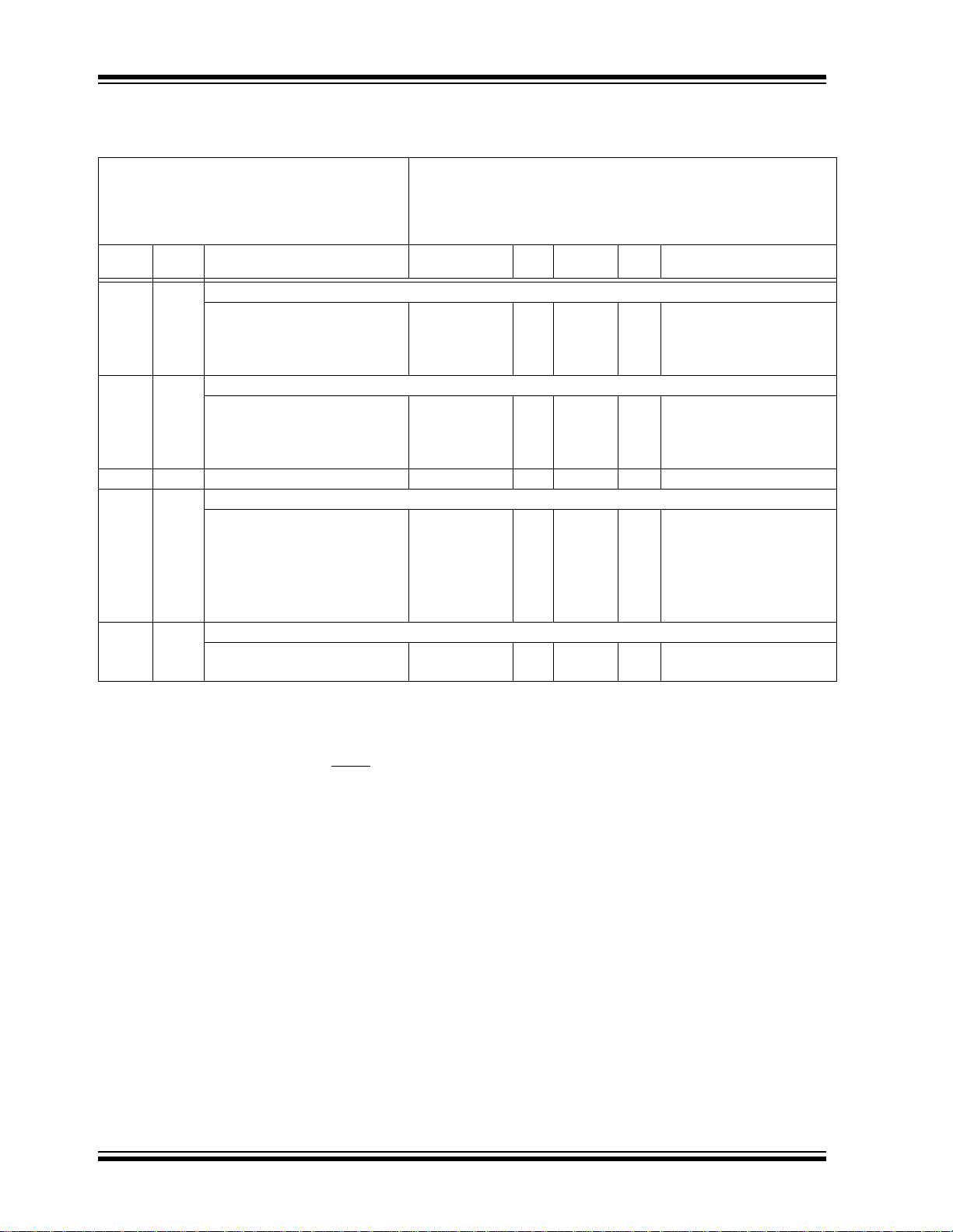
PIC16F72
14.2 DC Characteristics: PIC16F72 (Industrial, Extended)
PIC16LF72 (Industrial) (Continued)
Standard Operating Conditions (unless otherwise stated)
Operating temperature -40°C ≤ T
DC CHARACTERISTICS
Operatin g voltage V
DD range as described in DC Specification,
-40°C ≤ T
Section 14.1.
Param
No.
Sym Characteristic Min Typ† Max Units Conditions
VOL Output Low Voltage
D080 I/O ports ——0.6 V IOL = 8.5 mA, VDD = 4.5V,
D083 OSC2/CLKO (RC osc config) ——0.6 V IOL = 1.6 mA, VDD = 4.5V,
V
OH Output High Voltage
D090 I/O ports (Note 3) VDD - 0.7 —— VIOH = -3.0 mA, VDD = 4.5V,
D092 OSC2/CLKO (RC osc config) VDD - 0.7 —— VIOH = -1.3 mA, VDD = 4.5V,
D150* V
OD Open Drain High Voltage ——12 V RA4 pin
Capacitive Loading Specs on Output Pins
D100 COSC2 OSC2 pin ——15 pF In XT, HS and LP modes
D101 C
IO All I/O pins and OSC2
——50 pF
(in RC mode)
D102 C
B
SCL, SDA in I2C mode
——400 pF
Program FLASH Memory
D130 E
D131 V
P Endurance 100 1000 — E/W 25°C at 5V
PR VDD for read 2.0 — 5.5 V
* These parameters are characterized but not tested.
† Data in "Typ" column is at 5V, 25°C unless otherwise stated. These parameters are for design guidance only
and are not tested.
Note 1: In RC oscillator configuration, the OSC1/CLKI pin is a Schmitt Trigger input. It is not recommended that the
PIC16F72 be driven with external clock in RC mode.
2: The leakage current on the MCLR
pin is strongly dependent on the app lied vol tag e level. The speci fied leve ls
represent normal operating conditions. Higher leakage current may be measured at different input voltages.
3: Negative current is defined as current sourced by the pin.
A ≤ +85°C for industrial
A ≤ +125°C for extended
-40°C to +85°C
-40°C to +85°C
-40°C to +85°C
-40°C to +85°C
when external clo ck is used
to drive OSC1
DS39597B-page 92 2002 Microchip Technology Inc.
Page 95
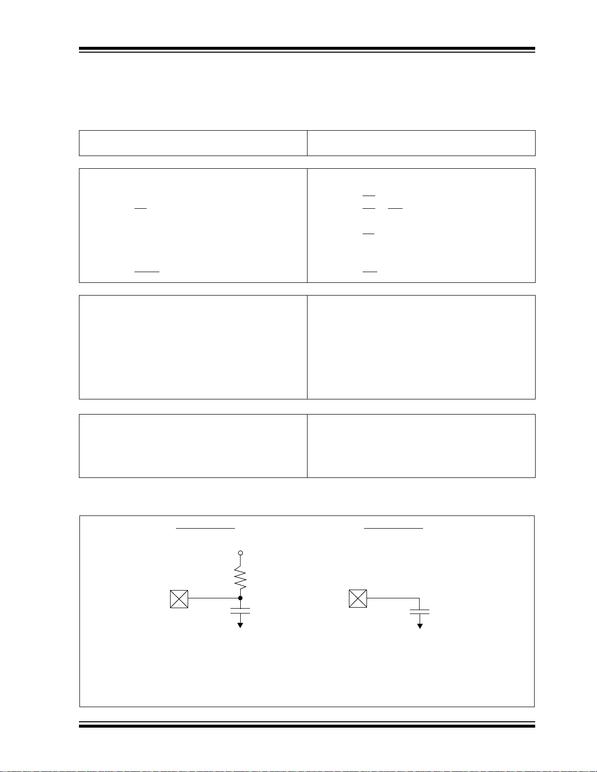
14.3 Timing Parameter Symbology
The timing parameter symbols have been created following one of the following formats:
1. TppS2ppS
2. TppS
CC:ST (I
3. T
4. Ts (I
T
F Frequency T Time
Lowercase letters (pp) and their meanings:
pp
cc CCP1 osc OSC1
ck CLKO rd RD
cs CS rw RD or WR
di SDI sc SCK
do SDO ss SS
dt Data in t0 T0CKI
io I/O port t1 T1CKI
mc MCLR wr WR
Uppercase letters and t heir meanings:
S
FFall PPeriod
HHigh RRise
I Invalid (Hi-impedance) V Valid
L Low Z Hi-impedance
2
I
C only
AA output access High High
BUF Bus free Low Low
TCC:ST (I2C specifications only)
CC
HD Hold SU Setup
ST
DAT DATA input hold STO STOP condition
STA START condition
2
C specifications only)
2
C specifications only)
PIC16F72
FIGURE 14-3: LOAD CONDITIONS
Load Condition 1
VDD/2
RL
C
Pin Pin
RL = 464Ω
CL = 50 pF for all pins except OSC2
15 pF for OSC2 output
2002 Microchip Technology Inc. DS39597B-page 93
L
SS
V
Load Condition 2
CL
VSS
Page 96

PIC16F72
FIGURE 14-4: EXTERNAL CLOCK TIMING
Q4 Q1 Q2 Q3 Q4 Q1
OSC1
1
CLKO
3
2
3
TABLE 14-1: EXTERNAL CLOCK TIMING REQUIREMENTS
Parameter
No.
1
2
3
4
† Data in "Typ" column is at 5V, 25°C unless otherwise stated. These parameters are for design guidance
Note 1: Instruction cycle period (T
Symbol Characteristic Min Typ† Max Units Conditions
F
OSC External CLKI Frequency
(Note 1)
DC — 1MHzXT Osc mode
DC — 20 MHz HS Osc mode
DC — 32 kHz LP Osc mode
Oscillator Frequency
(Note 1)
TOSC External CLKI Period
(Note 1)
DC — 4 MHz RC osc mod e
0.1 — 4 MHz XT Osc mode
4
5
—
—
200
1000 ——ns XT Osc mode
50 ——ns HS Osc mode
5 ——ms LP Osc mode
Oscillator Period
(Note 1)
250 ——ns RC Osc mode
250 — 10,000 ns XT Osc mode
50 — 250 ns HS Osc mode
5 ——ms LP Osc mode
TCY Instruction Cycle Time
200 TCY DC ns TCY = 4/FOSC
(Note 1)
TosL,
TosH
External Clock in (OSC1)
High or Low Time
500 ——ns XT oscillator
2.5 ——ms LP oscillator
15 ——ns HS oscillator
TosR,
TosF
External Clock in (OSC1)
Rise or Fall Time
— — 25 ns XT oscillator
— — 50 ns LP oscillator
——15 ns HS oscillator
only and are not tested.
CY) equals four times th e input os cillato r time-bas e period. Al l specif ied value s are
based on characterization dat a for t hat p art ic ula r osci lla tor typ e under standard operating conditions with
the device executing code. Exceeding these specified limits may result in an unstable oscillator operation
and/or higher than expecte d current consumption. All devices are tested to operate at "mi n" va lu es with an
external clock applied to the OSC1/CLKI pin. When an external clock input is used, the "max" cycle time
limit is "DC" (no clock) for all devices.
20
4
MHz
kHz
4
HS Osc mode
LP Osc mode
DS39597B-page 94 2002 Microchip Technology Inc.
Page 97

FIGURE 14-5: CLKO AND I/O TIMING
PIC16F72
17
14
20, 21
Q1
19
Q4
OSC1
10
CLKO
13
I/O Pin
(Input)
I/O Pin
(Output)
Note: Refer to Figure 14-3 for load conditions.
Old Value
TABLE 14-2: CLKO AND I/O TIMING REQUIREMENTS
Param
No.
Symbol Characteristic Min Typ† Max Units Conditions
Q2 Q3
18
15
11
12
16
New Value
10* TosH2ckL OSC1
11* TosH2ckH OSC1
12* TckR CLKO rise time — 35 100 ns (Note 1)
13* TckF CLKO fall time — 35 100 ns (Note 1)
14* TckL2ioV CLKO
15* TioV2ckH Port in valid before CLKO
16* TckH2ioI Port in hold after CLKO
17* TosH2ioV OSC1
18* TosH2ioI OSC1
19* TioV2osH Port input valid to OSC1
20* TioR Port output rise time Standard (F) — 10 40 ns
21* TioF Port output fall time Standard (F) — 10 40 ns
22††*T
23††*T
Note 1: Measurements are taken in RC mode, where CLKO output is 4 x T
INP INT pin high or low time TCY ——ns
RBP RB7:RB4 change INT high or low time TCY ——ns
* These parameters are characterized but not tested.
† Data in "Typ" column is at 5V, 25°C unless otherwise stated. These parameters are for design guidance only and are
not tested .
†† These parameters are asynchronous events, not related to any internal clock edges.
↑ to CLKO↓ — 75 200 ns (Note 1)
↑ to CLKO↑ — 75 200 ns (Note 1)
↓ to Port out valid ——0.5 TCY + 20 ns (Note 1)
↑ TOSC + 200 ——ns (Note 1)
↑ 0——ns (Note 1)
↑ (Q1 cycle) to Port out valid — 100 255 ns
↑ (Q2 cycle) to
Port input invalid (I/O in
hold time)
Standard (F)100——ns
Extended (LF)200——ns
↑ (I/O in setup time) 0 ——ns
Extended (LF) ——145 ns
Extended (LF) ——145 ns
OSC.
2002 Microchip Technology Inc. DS39597B-page 95
Page 98

PIC16F72
FIGURE 14-6: RESET, WATCHDOG TIMER, OSCILLATOR START-UP TIMER AND POWER-UP
TIME R TIMING
VDD
MCLR
Internal
POR
PWRT
Time-out
OSC
Time-out
Internal
RESET
Watchdog
Timer
Reset
I/O Pins
Note: Refer to Figure 14-3 for load conditions.
33
32
FIGURE 14-7: BROWN-OUT RESET TIMING
VDD
VBOR
34
30
31
34
35
TABLE 14-3: RESET, WATCHDOG TIMER, OSCILLATOR START-UP TIMER, POWER-UP TIMER,
AND BROWN-OUT RESET REQUIREMENTS
Parameter No. Symbol Characteristic Min Typ† Max Units Conditions
30 TmcL MCLR
31* T
32 T
33* T
34 T
35 T
* These parameters are characterized but not tested.
† Data in "Typ" column is at 5V, 2 5°C unless otherwise stated. These parameters are for design guida nce only and are not tested.
DS39597B-page 96 2002 Microchip Technology Inc.
WDT Watchdog Timer Time-out Period
OST Oscillation Start-up Timer Period — 1024 TOSC ——TOSC = OSC1 period
PWRT Power-up Timer Period 28 72 132 ms VDD = 5V, -40°C to +85°C
IOZ I/O Hi-impedance from MCLR Low
BOR Brown-out Reset Pulse Width 100 ——µsVDD ≤ VBOR (D005)
Pulse Width (low) 2 ——µsVDD = 5V, -40°C to +85°C
71833msVDD = 5V, -40°C to +85°C
(No Prescaler)
——2.1 µs
or Watchdog Timer Reset
Page 99

FIGURE 14-8: TIMER0 AND TIMER1 EXTERNAL CLOCK TIMINGS
RA4/T0CKI
PIC16F72
40
42
RC0/T1OSO/T1CKI
45
47
TMR0 or
TMR1
Note: Refer to Figure 1 4-3 for load conditions.
41
46
48
TABLE 14-4: TIMER0 AND TIMER1 EXTERNAL CLOCK REQUIREMENTS
Param
No.
40* Tt0H T0CKI High Pulse Width No Prescaler 0.5 T
41* Tt0L T0CKI Low Pulse Width No Prescaler 0.5 T
42* Tt0P T0CKI Period No Prescaler T
45* Tt1H T1CKI High Time Synchronous, Prescaler = 1 0.5 T
46* Tt1L T1CKI Low Time Synchronous, Prescaler = 1 0.5 T
47* Tt1P T1CKI Input
Symbol Characteristic Min Typ† Max Units Conditions
CY + 20 ——ns Must also meet
With Prescaler 10 ——ns
CY + 20 ——ns Must also meet
With Prescaler 10 ——ns
CY + 40 ——ns
With Prescaler Greater of:
Synchronous,
Prescaler = 2,4,8
Asynchronous Standard(F)30——ns
Synchronous,
Prescaler = 2,4,8
Asynchronous Standard(F)30——ns
Synchronous Standard(F) Greater of:
Period
Asynchronous Standard(F)60——ns
Ft1 Timer1 Oscillator Input Frequency Range
(oscillator enabled by setting bit T1OSCEN)
48 TCKEZtmr1 Delay from External Clock Edge to Timer Increment 2 T
* These parameters are characterized but not tested.
† Data in "Typ" column is at 5V, 25°C unless otherwise stated. These parameters are for design guidance only and are
not tested .
Standard(F)15——ns
Extended(LF)25 ——ns
Extended(LF)50 ——ns
Standard(F)15——ns
Extended(LF)25 ——ns
Extended(LF)50 ——ns
Extended(LF) Greater of:
Extended(LF) 100 ——ns
CY + 40
20 or T
N
CY + 20 ——ns Must also meet
CY + 20 ——ns Must also meet
CY + 40
30 or T
N
50 or T
CY + 40
N
DC — 200 kHz
OSC — 7 T OSC —
——ns N = prescale value
——ns N = prescale value
parameter 42
parameter 42
(2, 4, ..., 256)
parameter 47
parameter 47
(1, 2, 4, 8)
N = prescale value
(1, 2, 4, 8)
2002 Microchip Technology Inc. DS39597B-page 97
Page 100
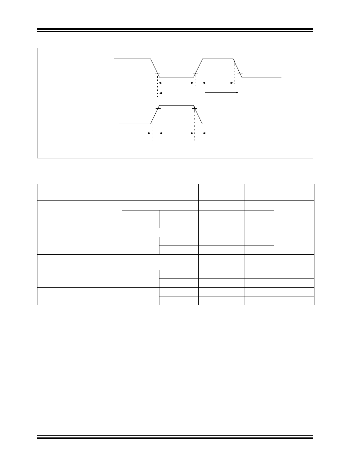
PIC16F72
FIGURE 14-9: CAPTURE/COMPARE/PWM TIMINGS (CCP1 )
RC2/CCP1
(Capture Mode)
50 51
52
(Compare or PWM Mode)
Note: Refer to Figure 14-3 for load conditions.
RC2/CCP1
53 54
TABLE 14-5: CAPTURE/COMPARE/PWM REQUIREMENTS (CCP1)
Param
Symbol Characteristic Min T yp† Max Units Conditions
No.
50* TccL CCP1 input low
time
51* TccH CCP1 input high
time
52* TccP CCP1 input period 3 TCY + 40
53* TccR CCP1 output rise time Standard(F) — 10 25 ns
54* TccF CCP1 output fall time Standard(F) — 10 25 ns
* These parameters are characterized but not tested.
† Data in "Typ" column is at 5V, 25°C unless otherwi se st ated. Th ese p arame ters are for de sign gu idanc e only
and are not tested.
No Prescaler 0.5 T
With Prescaler
No Prescaler 0.5 TCY + 20 ——ns
With Prescaler
Standard(F)10——ns
Extended(LF)20——ns
Standard(F)10——ns
Extended(LF)20——ns
Extended(LF) — 25 50 ns
Extended(LF) — 25 45 ns
CY + 20 ——ns
——ns N = prescale
N
value (1,4 or 16)
DS39597B-page 98 2002 Microchip Technology Inc.
 Loading...