


查询PIC16F688T-E/ML供应商
PIC16F688
Data Sheet
14-Pin Flash-Based, 8-Bit
CMOS Microcontrollers with
nanoWatt Technology
© 2007 Microchip Technology Inc. DS41203D

Note the following details of the code protection feature on Microchip devices:
• Microchip products meet the specification contained in their particular Microchip Data Sheet.
• Microchip believes that its family of products is one of the most secure families of its kind on the market today, when used in the
intended manner and under normal conditions.
• There are dishonest and possibly illegal methods used to breach the code protection feature. All of these methods, to our
knowledge, require using the Microchip products in a manner outside the operating specifications contained in Microchip’s Data
Sheets. Most likely, the person doing so is engaged in theft of intellectual property.
• Microchip is willing to work with the customer who is concerned about the integrity of their code.
• Neither Microchip nor any other semiconductor manufacturer can guarantee the security of their code. Code protection does not
mean that we are guaranteeing the product as “unbreakable.”
Code protection is constantly evolving. We at Microchip are committed to continuously improving the code protection features of our
products. Attempts to break Microchip’s code protection feature may be a violation of the Digit al Millennium Copyright Act. If suc h a c t s
allow unauthorized access to your software or other copyrighted work, you may have a right to sue for relief under that Act.
Information contained in this publication regarding device
applications and t he lik e is provided only for your convenience
and may be su perseded by upda t es . It is y our responsibility to
ensure that your application meets with your specifications.
MICROCHIP MAKES NO REPRESENTATIONS OR
WARRANTIES OF ANY KIND WHETHER EXPRESS OR
IMPLIED, WRITTEN OR ORAL, STATUTORY OR
OTHERWISE, RELATED TO THE INFORMATION,
INCLUDING BUT NOT LIMITED TO ITS CONDITION,
QUALITY, PERFORMANCE, MERCHANTABILITY OR
FITNESS FOR PURPOSE. Microchip disclaims all liability
arising from this information and its use. Use of Microchip
devices in life supp ort and/or safety ap plications is entir ely at
the buyer’s risk, and the buyer agrees to defend, indemnify and
hold harmless M icrochip from any and all dama ges, claims,
suits, or expenses re sulting from such use. No licens es are
conveyed, implicitly or otherwise, under any Microchip
intellectual property rights.
Trademarks
The Microchip name and logo, the Microchip logo, Accuron,
dsPIC, K
EELOQ, KEELOQ logo, microID, MPLAB, PIC,
PICmicro, PICSTART, PRO MATE, PowerSmart, rfPIC, an d
SmartShunt are registered trademarks of Microchip
Technology Incorporated in the U.S.A. and other countries.
AmpLab, FilterLab, Linear Active Thermistor, Migratable
Memory, MX DEV, MXLAB, PS logo, SEEVAL, SmartSensor
and The Embedded Control Solutions Company are
registered trademarks of Microchip Technology Incorporated
in the U.S.A.
Analog-for-the-Digital Age, Application Maestro, CodeGuard,
dsPICDEM, dsPICDEM.net, dsPICworks, ECAN,
ECONOMONITOR, FanSense, FlexROM, fuzzyLAB,
In-Circuit Serial Programming, ICSP, ICEPIC, Mindi, MiWi,
MPASM, MPLAB Certified logo, MPLIB, MPLINK, PICkit,
PICDEM, PICDEM.net, PICLAB, PICtail, PowerCal,
PowerInfo, PowerMate, PowerTool, REAL ICE, rfLAB,
rfPICDEM, Select Mode, Smart Serial, SmartT el, Total
Endurance, UNI/O, WiperLock and ZENA are trademarks of
Microchip Technology Incorporated in the U.S.A. and other
countries.
SQTP is a service mark of Microchip Technology Incorporated
in the U.S.A.
All other trademarks mentioned herein are property of their
respective companies.
© 2007, Microchip Technology Incorporated, Printed in the
U.S.A., All Rights Reserved.
Printed on recycled paper.
Microchip received ISO/TS-16949:2002 certification for its worldwide
headquarters, design and wafer fabrication facilities in Chandler and
Tempe, Arizona, Gresham, Oregon and Mountain View, California. The
Company’s quality system processes and procedures are for its PIC
MCUs and dsPIC® DSCs, KEELOQ
EEPROMs, microperipherals, nonvolatile memory and analog
products. In addition, Microchip’s quality system for the design and
manufacture of development systems is ISO 9001:2000 certified.
®
code hopping devices, Serial
DS41203D-page ii © 2007 Microchip Technology Inc.
®

PIC16F688
14-Pin Flash-Based, 8-Bit CMOS Microcontrollers with nanoWatt Technology
High-Performance RISC CPU:
• Only 35 instructions to learn:
- All single-cycle instructions except branches
• Operating speed:
- DC – 20 MHz oscillator/clock input
- DC – 200 ns instr uction cycle
• Interrupt capability
• 8-level deep hardware stack
• Direct, Indirect and Relative Addressing modes
Special Microcontroller Features:
• Precision Internal Oscillator:
- Factory calibrated to ±1%
- Software selectable frequency range of
8 MHz to 125 kHz
- Software tunable
- Two-Speed Start-Up mo de
- Crystal fail detect for critical applications
- Clock mode switching during operation for
power savings
• Power-Saving Sleep mode
• Wide operating voltage range (2.0V-5.5V)
• Industrial and Extended tempera ture range
• Power-on Reset (POR)
• Power-up Timer (PWRT) and Oscillator Start-up
Timer (OST)
• Brown-out Reset (BOR) with software control
option
• Enhanced Low-Current Watchdog Timer (WDT)
with on-chip oscillator (software selectable nominal 268 seconds with full prescaler) with software
enable
• Multiplexed Master Clear with weak pull-up or
input only pin
• Programmable code protection
• High-Endurance Flash/EEPROM cell:
- 100,000 write Flash endurance
- 1,000,000 write EEPROM endurance
- Flash/Data EEPROM retention: > 40 years
Low-Power Features:
• Standby Current:
- 50 nA @ 2.0V, typical
• Operating Current:
-11μA @ 32 kHz, 2.0V, typical
-220μA @ 4 MHz, 2.0V, typical
• Watchdog Timer Current:
-1μA @ 2.0V, typical
Peripheral Features:
• 12 I/O pins with indiv idual direction control:
- High-current source/sink for direct LED drive
- Interrupt-on-change pin
- Individually programmable weak pull-ups
- Ultra Low-Power Wake-up
• Analog Comparator module with:
- Two analog comparators
- Programmable On-chip Voltage Reference
(CV
REF) module (% of VDD)
- Comparator inputs and outputs externally
accessible
• A/D Converter:
- 10-bit resolution and 8 channels
• Timer0: 8-bit timer/counter with 8-bit
programmable prescaler
• Enhanced Timer1:
- 16-bit timer/counter with prescaler
- External Timer1 Gate (count enable)
- Option to use OSC1 and OSC2 in LP mode as
Timer1 oscillator if INTOSC mode selected
• Enhanced USART Module:
- Supports RS-485, RS-232, and LIN 1.2
- Auto-Baud Detect
- Auto-wake-up on Start bit
• In-Circuit Serial Programming™ (ICSP™) via two
pins
Program
Memory
Device
Flash
(words)
PIC16F688 4096 256 256 12 8 2 1/1
© 2007 Microchip Technology Inc. DS41203D-page 1
Data Memory
SRAM
(bytes)
EEPROM
(bytes)
I/O
10-bit A/D
(ch)
Comparators
Timers
8/16-bit

PIC16F688
Pin Diagram (PDIP, SOIC, TSSOP)
14-pin PDIP, SOIC, TSSOP
RA5/T1CKI/OSC1/CLKIN
RA4/AN3/T1G
/OSC2/CLKOUT
RA3/MCLR
RC4/C2OUT/TX/CK
VDD
/VPP
RC5/RX/DT
RC3/AN7
1
2
3
4
5
6
7
14
13
12
11
10
PIC16F688
9
8
VSS
RA0/AN0/C1IN+/ICSPDAT/ULPWU
RA1/AN1/C1IN-/VREF/ICSPCLK
RA2/AN2/T0CKI/INT/C1OUT
RC0/AN4/C2IN+
RC1/AN5/C2INRC2/AN6
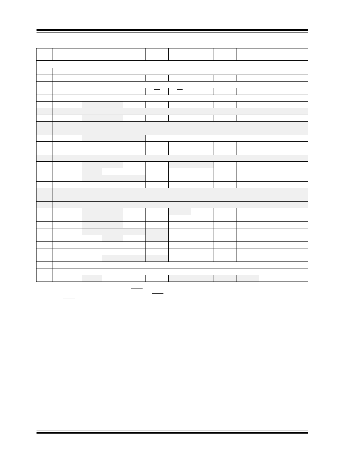
TABLE 1: PIC16F688 14-PIN SUMMARY (PDIP, SOIC, TSSOP)
I/O Pin Analog Comparators Timers EUSART Interrupt Pull-up Basic
RA0 13 AN0/ULPWU C1IN+ — — IOC Y ICSPDAT
RA1 12 AN1 C1IN- — — IOC Y V
RA2 11 AN2 C1OUT T0CKI — IOC/INT Y —
RA3 4 — — — — IOC Y
RA4 3 AN3 — T1G — IOC Y OSC2/CLKOUT
RA5 2 — — T1CKI — IOC Y OSC1/CLKIN
RC0 10 AN4 C2IN+ — — — — —
RC1 9 AN5 C2IN- — — — — —
RC2 8 AN6 — — — — — —
RC3 7 AN7 — — — — — —
RC4 6 — C2OUT — TX/CK — — —
RC5 5 — — — RX/DT — — —
— 1 — — — — — — VDD
—14 — — — — — — VSS
Note 1: Pull-up activated only with external MCLR configuration.
(1)
REF/ICSPCLK
MCLR/VPP
DS41203D-page 2 © 2007 Microchip Technology Inc.

Pin Diagram (QFN)
16-pin QFN
VDD
NCNCVSS
PIC16F688
RA5/T1CKI/OSC1/CLKIN
RA4/AN3/T1G
/OSC2/CLKOUT
RA3/MCLR
/VPP
RC5/RX/DT
16
1
2
PIC16F688
3
4
5
RC4/C2OUT/TX/CK
15
6
RC3/AN7
14
7
RC2/AN6
12
10
RC1/AN5/C2IN-
13
11
8
RA0/AN0/C1IN+/ICSPDAT/ULPWU
RA1/AN1/C1IN-/V
RA2/AN2/T0CKI/INT/C1OUT
9
RC0/AN4/C2IN+
REF/ICSPCLK
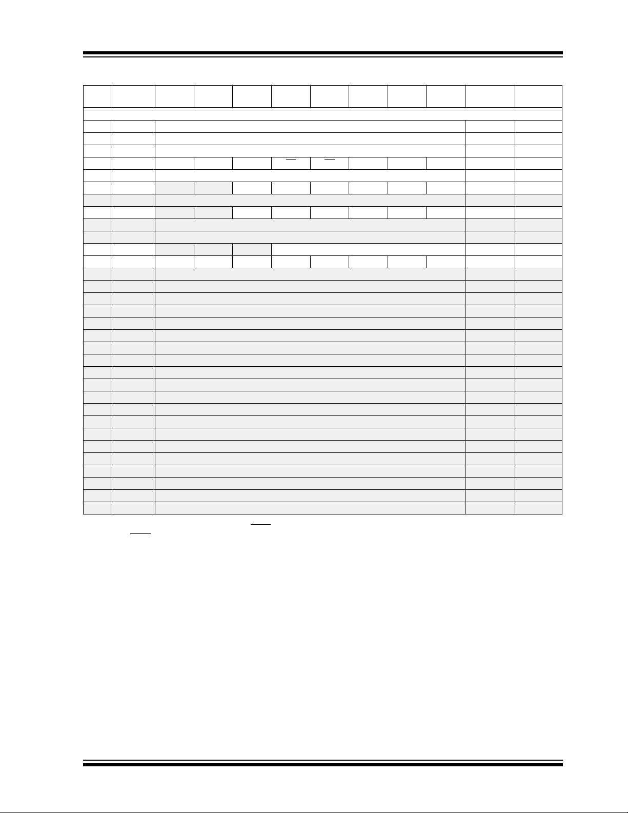
T ABLE 2: PIC16F688 16-PIN SUMMARY (QFN)
I/O Pin Analog Comparators Timers EUSART Interrupt Pull-up Basic
RA0 12 AN0/ULPWU C1IN+ — — IOC Y ICSPDAT
RA1 11 AN1 C1IN- — — IOC Y VREF/ICSPCLK
RA2 10 AN2 C1OUT T0CKI — IOC/INT Y —
RA3 3 — — — — IOC Y
RA4 2 AN3 — T1G — IOC Y OSC2/CLKOUT
RA5 1 — — T1CKI — IOC Y OSC1/CLKIN
RC0 9 AN4 C2IN+ — — — — —
RC1 8 AN5 C2IN- — — — — —
RC2 7 AN6 — — — — — —
RC3 6 AN7 — — — — — —
RC4 5 — C2OUT — TX/CK — — —
RC5 4 — — — RX/DT — — —
— 16 — — — — — — VDD
—13 — — — — — — VSS
— 14 — — — — — — NC
—15 — — — — — — NC
Note 1: Pull-up activated only with external MCLR
configuration.
(1)
MCLR/VPP
© 2007 Microchip Technology Inc. DS41203D-page 3

PIC16F688
Table of Contents
1.0 Device Overview ......................................................................................................................................................................... 5
2.0 Memory Organization. ................................................................................................................................................................. 7
3.0 Clock Sources ........................................................................................................................................................................... 21
4.0 I/O Ports .................................................................................................................................................................................... 33
5.0 Timer0 Module .......................................................................................................................................................................... 45
6.0 Timer1 Module with Gate Control.............................................................................................................................................. 49
7.0 Comparator Module............................................................. .. ......... .... .. .... .... ....... .... .. .... .... ........................................................ 55
8.0 Analog-to-Digital Converter (A/D) Module................................................................................................................................. 65
9.0 Data EEPROM and Flash Program Memory Control................................................................................................................ 77
10.0 Enhanced Universal Asynchronous Receiver Transmitter (EUSART) ...................................................................................... 83
11.0 Special Features of the CPU......................................... .......................................................................................................... 109
12.0 Instruction Set Summary......................................................................................................................................................... 129
13.0 Development Support .............................................................................................................................................................. 139
14.0 Electrical Specifications........................................................................................................................................................... 143
15.0 DC and AC Characteristics Graphs and Tables...................................................................................................................... 163
16.0 Packaging Information...................................................................... ....................................................................................... 185
Appendix A: Data Sheet Revision History......................................................................................................................................... 191
Appendix B: Migrating from other PIC® Devices................................................................................. ............................................. 191
Index ................................................................................................................................................................................................. 193
On-line Support .................................................................................................................................................................................197
Systems Information and Upgrade Hot Line..................................................................................................................................... 197
Reader Response............................................................................................................................................................................. 198
Product Identification System............................................................................................................................................................ 199
TO OUR VALUED CUSTOMERS
It is our intention to provide our valued customers with the best documentation possible to ensure successful use of your Microchip
products. To this end, we will continue to improve our publications to better suit your needs. Our publications will be refined and
enhanced as new volumes and updates are introduced.
If you have any questions or c omm ents regarding t his publication, p lease c ontact the M arket ing Co mmunications Department via
E-mail at docerrors@microchip.com or fax the Reader Response Form in the back of this data sheet to (480) 792-4150. We
welcome your feedback.
Most Current Data Sheet
To obtain the most up-to-date version of this data sheet, please register at our Worldwide Web site at:
http://www.microchip.com
You can determine the version of a data sheet by examining its literature number found on the bottom outside corner of any page.
The last character of the literature number is the version number, (e.g., DS30000A is version A of document DS30000).
Errata
An errata sheet, describing minor operational differences from the data sheet and recommended workarounds, may exist for current
devices. As device/documentation issues become known to us, we will publish an errata sheet. The errata will specify the revision
of silicon and revision of document to which it applies.
To determine if an errata sheet exists for a particular device, please check with one of the following:
• Microchip’s Worldwide Web site; http://www.microchip.com
• Your local Microchip sales office (see last page)
When contacting a sales office, please specify which device, revision of silicon and data sheet (include literature number) you are
using.
Customer Notification System
Register on our web site at www.microchip.com to receive the most current information on all of our products.
DS41203D-page 4 © 2007 Microchip Technology Inc.
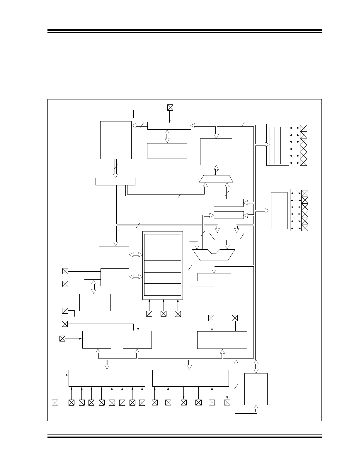
1.0 DEVICE OVERVIEW
The PIC16F688 is covered by this data sheet. It is
available in 14-pin PDIP, SOIC, TSSOP and QFN
packages. Figure 1-1 shows a block diagram of the
PIC16F688 device. Table 1-1 shows the pinout
description.
FIGURE 1-1: PIC16F688 BLOCK DIAGRAM
PIC16F688
OSC1/CLKIN
OSC2/CLKOUT
T1G
Program
Bus
Internal
Oscillator
Block
Configuration
Flash
4k x 14
Program
Memory
14
Instruction Reg
Instruction
Decode &
Control
Timing
Generation
13
8
MCLR
INT
Program Counter
8-Level Stack
(13 bit)
Direct Addr
Power-up
Timer
Oscillator
Start-up Timer
Power-on
Reset
Watchdog
Timer
Brown-out
Reset
DD
V
VSS
7
RAM Addr
3
8
Data Bus
RAM
256 bytes
File
Registers
9
Addr MUX
Indirect
8
Addr
FSR Reg
STATUS Reg
MUX
ALU
W Reg
RX/DT TX/CK
8
PORTA
RA0
RA1
RA2
RA3
RA4
RA5
PORTC
RC0
RC1
RC2
RC3
RC4
RC5
T1CKI
T0CKI
VREF
Timer0 Timer1
Analog-to-Digital Converter
AN0 AN1 AN2 AN3
AN4 AN5 AN6 AN7
Analog Comparators
and Referen ce
C1IN- C1IN+ C1OUT
2
C2IN- C2IN+ C2OUT
EUSART
EEDAT
256 bytes
8
EEPROM
EEADDR
DATA
© 2007 Microchip Technology Inc. DS41203D-page 5

PIC16F688
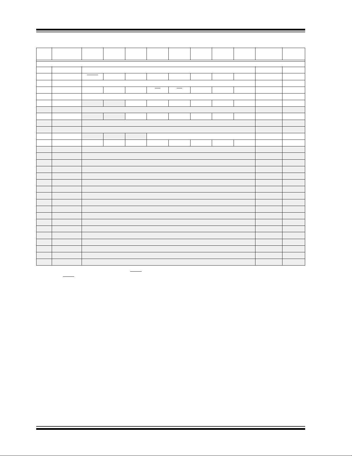
TABLE 1-1: PIC16F688 PINOUT DESCRIPTION
Name Function
RA0/AN0/C1IN+/ICSPDAT/ULPWU RA0 TTL CMOS PORTA I/O w/prog pull-up and interrupt-on-change
AN0 AN — A/D Channel 0 input
C1IN+ AN — Comparator 1 input
ICSPDAT TTL CMOS Serial Programming Data I/O
ULPWU AN — Ultra Low-Power Wake-up input
RA1/AN1/C1IN-/V
RA2/AN2/T0CKI/INT/C1OUT R A 2 ST CMOS PORTA I/O w/prog pull-up and interrupt-on-change
RA3/MCLR
RA4/AN3/T1G
RA5/T1CKI/OSC1/CLKIN
RC0/AN4/C2IN+ RC0 TTL CMOS PORTC I/O
RC1/AN5/C2IN- RC1 TTL CMOS PORTC I/O
RC2/AN6 RC2 TTL CMOS PORTC I/O
RC3/AN7 RC3 TTL CMOS PORTC I/O
RC4/C2OUT/TX/CK RC4 TTL CMOS PORTC I/O
RC5/RX/DT RC5 TTL CMOS Port C I/O
SS VSS Power — Ground reference
V
DD VDD Power — Positive supply
V
Legend: AN = Analog input or output CMOS = CMOS compatible input or output OC = Open collector output
REF/ICSPCLK RA1 TTL CMOS PORTA I/O w/prog pull-up and interrupt-on-change
AN1 AN — A/D Channel 1 input
C1IN- AN — Comparator 1 input
REF AN — External Voltage Reference for A/D
V
ICSPCLK ST — Serial Programming Clock
AN2 AN — A/D Channel 2 input
T0CKI ST — Timer0 clock input
INT ST — External Interrupt
C1OUT — CMOS Comparator 1 output
/VPP RA3 TTL — PORTA input with interrupt-on-change
MCLR
PP HV — Programming voltage
V
/OSC2/CLKOUT RA4 TTL CMOS PORTA I/O w/prog pull-up and interrupt-on-change
AN3 AN — A/D Channel 3 input
T1G
OSC2 — XTAL Crystal/Resonator
CLKOUT — CMOS F
RA5 TTL CMOS PORTA I/O w/prog pull-up and interrupt-on-change
T1CKI ST — Timer1 clock
OSC1 XTAL — Crystal/Resonator
CLKIN ST — External clock input/RC oscillator connection
AN4 AN — A/D Channel 4 input
C2IN+ AN Comparator 2 input
AN5 AN — A/D Channel 5 input
C2IN- AN Comparator 2 input
AN6 AN — A/D Channel 6 input
AN7 AN — A/D Channel 7 input
C2OUT — CMOS Comparator 2 output
TX — CMOS USART asynchronous output
CK ST CMOS USART asynchronous clock
RX ST CMOS USART asynchronous input
DT S T CMOS USART asynchronous data
TTL = TTL compatible input ST = Schmitt Trigger input with CMOS levels
HV = High Voltage XTAL = Crystal
Input
Type
ST — Master Clear w/internal pull-up
ST — Timer1 gate
Output
Type
Description
OSC/4 output
DS41203D-page 6 © 2007 Microchip Technology Inc.
PIC16F688
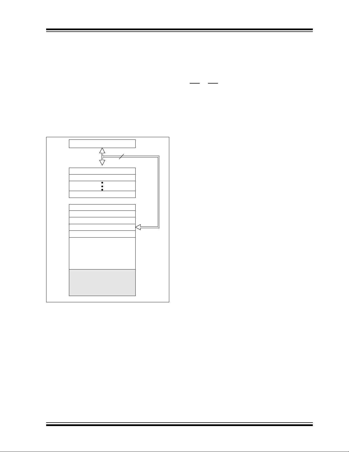
2.0 MEMORY ORGANIZATION
2.1 Program Memory Organization
The PIC16F688 has a 13-bit program counter capable
of addressin g a 4 K x 14 prog r a m memo r y spac e. On ly
the first 4K x 14 (0000h-01FFF) for the PIC16F688 is
physically implemented. Accessing a location above
these boundaries will cause a wraparound within the
first 4K x 14 space. The Reset vector is at 0000h and
the interrupt vector is at 0004h (see Figure 2-1).
FIGURE 2-1 : PR OG RA M M EMO RY MA P
AND STACK FOR THE
PIC16F688
PC<12:0>
CALL, RETURN
RETFIE, RETLW
Stack Level 1
Stack Level 2
Stack Level 8
Reset Vector
13
0000h
2.2 Data Memory Organization
The data memory is partitioned into multiple banks,
which contain the General Purpose Registers (GPR)
and the Special Function Registers (SFR). Bits RP0
and RP1 are bank select bits.
RP1
Each bank extends up to 7Fh (128 bytes). The lower
locations of each bank are reserved for the Special
Function Registers. Abo ve the Speci al Function Re gisters are th e Genera l Purpos e Regist ers, im plement ed
as static RAM. All implemented banks contain Special
Function Registers. Some frequently used Special
Function Registers from one bank are mirrored in
another bank for code reduction and quicker access.
2.2.1 GENERAL PURPOSE REGISTER
The register file is organized as 256 x 8 in the
PIC16F688. Each register is accessed, either directly
or indirectly, through the File Select Register (FSR)
(see Section 2.4 “Indirect Addressing, INDF and
FSR Registers”).
RP0
00→ Bank 0 is selected
01→ Bank 1 is selected
10→ Bank 2 is selected
11→ Bank 3 is selected
FILE
Interrupt Vector
On-chip Program
Memory
Wraps to 0000h-07FFh
0004h
0005h
01FFh
02000h
1FFFh
2.2.2 SPECIAL FUNCTION REGISTERS
The Special Function Registers are registers used by
the CPU and peripheral functions for controlling the
desired operation of the device (see Tables 2-1, 2-2,
2-3 and 2-4). These registers are static RAM.
The special registers can be classified into two sets:
core and peripheral. The Special Function Registers
associated with the “c ore” are des cribed in thi s sectio n.
Those related to the operation of the peripheral
features are described in the section of that peripheral
feature.
© 2007 Microchip Technology Inc. DS41203D-page 7
PIC16F688
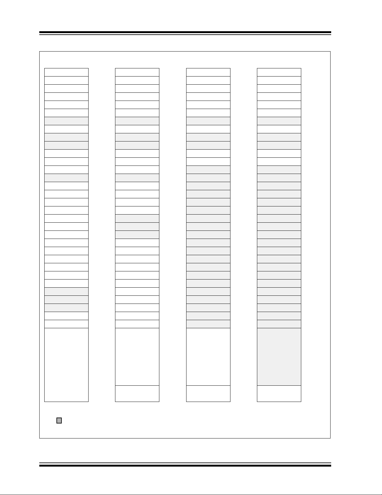
FIGURE 2-2: PIC16F688 SPECIAL FUNCTION REGISTERS
File File File File
Address Address Address Address
Indirect addr.
TMR0 01h OPTION_REG 81h TMR0 101h OPTION_REG 181h
PCL 02h PCL 82h PCL 102h PCL 182h
STATUS 03h STATUS 83h STATUS 103h STATUS 183h
FSR 04h FSR 84h FSR 104h FSR 184h
PORTA 05h TRISA 85h PORTA 105h TRISA 185h
PORTC 07h TRISC 87h PORTC 107h TRISC 187h
PCLATH 0Ah PCLATH 8Ah PCLATH 10Ah PCLATH 18Ah
INTCON 0Bh INTCON 8Bh INTCON 10Bh INTCON 18Bh
PIR1 0Ch PIE1 8Ch
TMR1L 0Eh PCON 8Eh 10Eh 18Eh
TMR1H 0Fh OSCCON 8Fh 10Fh 18Fh
T1CON 10h OSCTUNE 90h
BAUDCTL 11h ANSEL 91h 111h 191h
SPBRGH 12h 92h 112h 192h
SPBRG 13h
RCREG 14h 94h 114h 194h
TXREG 15h WPUA 95h 115h 195h
TXSTA 16h IOCA 96h
RCSTA 17h EEDATH 97h 117h 197h
WDTCON 18h EEADRH 98h 118h 198h
CMCON0 19h VRCON 99h
CMCON1 1Ah EEDAT 9Ah 11Ah 19Ah
ADRESH 1Eh ADRESL 9Eh 11Eh 19Eh
ADCON0 1Fh ADCON1 9Fh
(1)
00h Indirect addr.
06h 86h 106h 186h
08h 88h 108h 188h
09h 89h 109h 189h
0Dh 8Dh 10Dh 18Dh
1Bh EEADR 9Bh 11Bh 19Bh
1Ch EECON1 9Ch 11Ch 19Ch
1Dh EECON2
20h
(1)
80h Indirect addr.
93h 113h 193h
(1)
9Dh 11Dh 19Dh
A0h
(1)
100h Indirect addr.
10Ch 18Ch
110h 190h
116h 196h
119h 199h
11Fh 19Fh
120h
(1)
180h
1A0h
General
General
Purpose
Register
96 Bytes
7Fh FFh 17Fh 1FFh
Bank 0Bank 1Bank 2Bank 3
Unimplemented data memory locations, read as ‘0’.
Note 1: Not a physical register.
DS41203D-page 8 © 2007 Microchip Technology Inc.
Purpose
Register
80 Bytes
accesses
Bank 0
EFh 16Fh
F0h accesses
General
Purpose
Register
80 Bytes
Bank 0
170h accesses
Bank 0
1EFh
1F0h
PIC16F688
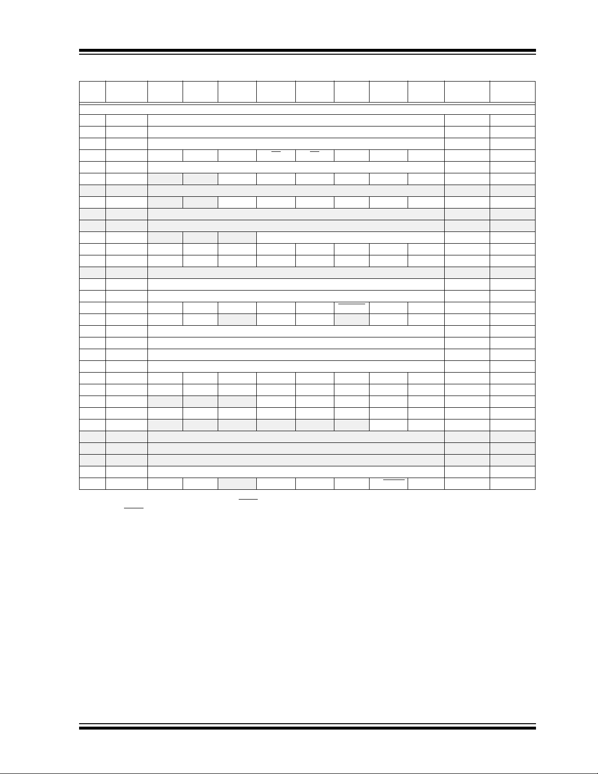
TABLE 2-1: PIC16F688 SPECIAL REGISTERS SUMMARY BANK 0
Addr Name Bit 7 Bit 6 Bit 5 Bit 4 Bit 3 Bit 2 Bit 1 Bit 0
Bank 0
00h INDF Addressing this location uses contents of FSR to address data memory (not a physical register) xxxx xxxx 20, 117
01h TMR0 Timer0 Module’s register xxxx xxxx
02h PCL Program Counter’s (PC) Least Significant Byte 0000 0000
03h STATUS IRP RP1 RP0 TO
04h FSR Indirect Data Memory Address Pointer xxxx xxxx
05h PORTA
06h — Unimplemented — —
07h PORTC
08h — Unimplemented — —
09h — Unimplemented — —
0Ah PCLATH
0Bh INTCON GIE PEIE T0IE INTE RAIE T0IF INTF RAIF
0Ch PIR1
0Dh — Unimplemented — —
0Eh TMR1L Holding Register for the Least Significant Byte of the 16-bit TMR1 xxxx xxxx
0Fh TMR1H Holding Register for the Most Significant Byte of the 16-bit TMR1 xxxx xxxx
10h T1CON T1GINV TMR1GE T1CKPS1 T1CKPS0 T1OSCEN T1SYNC
11h BAUDCTL ABDOVF RCIDL
12h SPBRGH USART Baud Rate High Generator 0000 0000 95, 117
13h SPBRG USART Baud Rate Generator 0000 0000 95, 117
14h RCREG USART Receive Register 0000 0000 87, 117
15h TXREG USART Transmit Register 0000 0000 87, 117
16h TXSTA CSRC TX9 TXEN SYNC SENDB BRGH TRMT TX9D 0000 0010 92, 117
17h RCSTA SPEN RX9 SREN CREN ADDEN FERR OERR RX9D 0000 000x 93, 117
18h WDTCON
19h CMCON0 C2OUT C1OUT
1Ah CMCON1
1Bh — Unimplemented — —
1Ch — Unimplemented — —
1Dh — Unimplemented — —
1Eh ADRESH Most Significant 8 bits of the left shifted A/D result or 2 bits of right shifted result xxxx xxxx
1Fh ADCON0 ADFM VCFG
Legend: – = Unimplemented locations rea d as ‘0’, u = unchanged, x = unknow n, q = value depends on condition, shaded = unimplemented
Note 1: Other (non Power-up) Resets include MCLR
2: MCLR
mismatched exists.
— — RA5 RA4 RA3 RA2 RA1 RA0 --x0 x000
— — RC5 RC4 RC3 RC2 RC1 RC0 --xx 0000 42, 117
— — — Write Buffer for upper 5 bits of Program Counter ---0 0000
EEIF ADIF RCIF C2IF C1IF OSFIF TXIF TMR1IF 0000 0000 17, 117
— SCKP BRG16 —WUEABDEN01-0 0-00 94, 117
— — — WDTPS3 WDTPS2 WDTPS1 WDTPS0 SWDTEN ---0 1000 124, 117
C2INV C1INV CIS CM2 CM1 CM0 0000 0000 61, 117
— — — — — — T1GSS C2SYNC ---- --10 62, 117
— CHS2 CHS1 CHS0 GO/DONE ADON 00-0 0000
Reset and Watchdog Timer Reset dur ing nor mal operation.
and WDT Reset does not affect the previous value data latch. The RAIF bit will be cleared upon Reset but will set again if the
PD ZDCC0001 1xxx 13, 117
TMR1CS TMR1ON 0000 0000 51, 117
Value on
POR/BOR
(2)
0000 000x 15, 117
Page
45, 117
19, 117
20, 117
33, 117
19, 117
48, 117
48, 117
72, 117
71, 117
© 2007 Microchip Technology Inc. DS41203D-page 9
PIC16F688
TABLE 2-2: PIC16F688 SPECIAL FUNCTION REGISTERS SUMMARY BANK 1
Addr Name Bit 7 Bit 6 Bit 5 Bit 4 Bit 3 Bit 2 Bit 1 Bit 0
Bank 1
80h INDF Addressing this location uses contents of FSR to address data memory (not a physical register) xxxx xxxx 20, 117
81h OPTION_REG RAPU
82h PCL Program Counter’s (PC) Least Significant Byte 0000 0000 19, 117
83h STATUS IRP RP1 RP0 TO
84h FSR Indirect Data Memory Address Pointer xxxx xxxx 20, 117
85h TRISA
86h — Unimplemented — —
87h TRISC
88h — Unimplemented — —
89h — Unimplemented — —
8Ah PCLATH
8Bh INTCON GIE PEIE T0IE INTE RAIE T0IF INTF RAIF
8Ch PIE1 EEIE ADIE RCIE C2IE C1IE OSFIE TXIE TMR1IE 0000 0000 16, 117
8Dh — Unimplemented — —
8Eh PCON
8Fh OSCCON
90h OSCTUNE
91h ANSEL ANS7 ANS6 ANS5 ANS4 ANS3 ANS2 ANS1 ANS0 1111 1111 34, 118
92h — Unimplemented — —
93h — Unimplemented — —
94h — Unimplemented — —
95h WPUA
96h IOCA
97h EEDATH
98h EEADRH
99h VRCON VREN
9Ah EEDAT EEDAT7 EEDAT6 EEDAT5 EEDAT4 EEDAT3 EEDAT2 EEDAT1 EEDAT0 0000 0000 78, 118
9Bh EEADR EEADR7 EEADR6 EEADR5 EEADR4 EEADR3 EEADR2 EEADR1 EEADR0 0000 0000 78, 118
9Ch EECON1 EEPGD
9Dh EECON2 EEPROM Control 2 Register (not a physical register) ---- ---- 77, 118
9Eh ADRESL Least Significant 2 bits of the left shifted result or 8 bits of the right shifted result xxxx xxxx 72, 118
9Fh ADCON1
Legend: – = Unimplemented locations read as ‘0’, u = unchanged, x = unknown, q = value depends on condition, shaded = unimplemented
Note 1: Other (non Power-up) Resets include MCLR
(2)
2: RA3 pull-up is enabled when pin is configured as MCLR
3: MCLR
and WDT Reset does not affect the previous value data latch. The RAIF bit will be cleared upon Reset but will set again if the
mismatched exists.
INTEDG T0CS T0SE PSA PS2 PS1 PS0 1111 1111 14, 117
PD ZDCC0001 1xxx 13, 117
— — TRISA5 TRISA4 TRISA3 TRISA2 TRISA1 TRISA0 --11 1111 33, 117
— — TRISC5 TRISC4 TRISC3 TRISC2 TRISC1 TRISC0 --11 1111 42, 117
— — — Write Buffer for upper 5 bits of Program Counter ---0 0000 19, 117
— — ULPWUE SBOREN — —PORBOR --01 --qq 18, 117
— IRCF2 IRCF1 IRCF0 OSTS HTS LTS SCS -110 x000 22, 118
— — — TUN4 TUN3 TUN2 TUN1 TUN0 ---0 0000 26, 118
— — WPUA5 WPUA4 — WPUA2 WPUA1 WPUA0 --11 -111 35, 118
— — IOCA5 IOCA4 IOCA3 IOCA2 IOCA1 IOCA0 --00 0000 35, 118
— — EEDATH5 EEDATH4 EEDATH3 EEDATH2 EEDATH1 EEDATH0 --00 0000 78, 118
— — — — EEADRH3 EEADRH2 EEADRH1 EEADRH0 ---- 0000 78, 118
—VRR — VR3 VR2 VR1 VR0 0-0- 0000 63, 118
— — — WRERR WREN WR RD x--- x000 79, 118
— ADCS2 ADCS1 ADCS0 — — — — -000 ---- 71, 118
Reset and Watchdog Timer Reset during normal operation.
in the Configuration Word register.
Value on
POR/BOR
(3)
0000 000x 15, 117
Page
DS41203D-page 10 © 2007 Microchip Technology Inc.
PIC16F688
TABLE 2-3: PIC16F688 SPECIAL REGISTERS SUMMARY BANK 2
AddrNameBit 7Bit 6Bit 5Bit 4Bit 3Bit 2 Bit 1Bit 0
Bank 2
100h INDF Addressing this location uses contents of FSR to address data memory (not a physical register) xxxx xxxx 20, 117
101h TMR0 Timer0 Module’s register xxxx xxxx 45, 117
102h PCL Program Counter’s (PC) Least Significant Byte 0000 0000 19, 117
103h STATUS IRP RP1 RP0 TO
104h FSR Indirect Data Memory Address Pointer xxxx xxxx 20, 117
105h PORTA
106h — Unimplemented — —
107h PORTC
108h — Unimplemented — —
109h — Unimplemented — —
10Ah PCLATH
10Bh INTCON GIE PEIE T0IE INTE RAIE T0IF INTF RAIF
10Ch — Unimplemented — —
10Dh — Unimplemented — —
10Eh — Unimplemented — —
10Fh — Unim plemented — —
110h — Unimplemented — —
111h — Unimplemented — —
112h — Unimplemented — —
113h — Unimplemented — —
114h — Unimplemented — —
115h — Unimplemented — —
116h — Unimplemented — —
117h — Unimplemented — —
118h — Unimplemented — —
119h — Unimplemented — —
11Ah — Unimplemented — —
11Bh — Unimplemented — —
11Ch — Unimplemented — —
11Dh — Unimplemented — —
11Eh — Unimplemented — —
11Fh — Unimplemented — —
Legend: – = Unimplemented locations rea d as ‘0’, u = unchanged, x = unknow n, q = value depends on condition, shaded = unimplemented
Note 1: Other (non Power-up) Resets include MCLR
2: MCLR
mismatched exists.
— — RA5 RA4 RA3 RA2 RA1 RA0 --x0 x000
— — RC5 RC4 RC3 RC2 RC1 RC0 --xx 0000 42, 117
— — — Write Buffer for upper 5 bits of Program Counter ---0 0000 19, 117
Reset and Watchdog Timer Reset dur ing nor mal operation.
and WDT Reset does not affect the previous value data latch. The RAIF bit will be cleared upon Reset but will set again if the
PD ZDCC0001 1xxx 13, 117
Value on
POR/BOR
(2)
0000 000x 15, 117
Page
33, 117
© 2007 Microchip Technology Inc. DS41203D-page 11
PIC16F688
TABLE 2-4: PIC16F688 SPECIAL FUNCTION REGISTERS SUMMARY BANK 3
Addr Name Bit 7 Bit 6 Bit 5 Bit 4 Bit 3 Bit 2 Bit 1 Bit 0
Bank 3
180h INDF Addressing this location uses contents of FSR to address data memory (not a physical register) xxxx xxxx 20, 117
181h OPTION_REG RAPU
182h PCL Program Counter’s (PC) Least Significant Byte 0000 0000 19, 117
183h STATUS IRP RP1 RP0 TO
184h FSR Indirect Data Memory Address Pointer xxxx xxxx 20, 117
185h TRISA
186h — Unimplemented — —
187h TRISC
188h — Unimplemented — —
189h — Unimplemented — —
18Ah PCLATH
18Bh INTCON GIE PEIE T0IE INTE RAIE T0IF INTF RAIF
18Ch — Unimplemented — —
18Dh — Unimplemented — —
190h — Unimplemented — —
191h — Unimplemented — —
192h — Unimplemented — —
193h — Unimplemented — —
194h — Unimplemented — —
195h — Unimplemented — —
196h — Unimplemented — —
19Ah — Unimplemented — —
19Bh — Unimplemented — —
199h — Unimplemented — —
19Ah — Unimplemented — —
19Bh — Unimplemented — —
19Ch — Unimplemented — —
19Dh — Unimplemented — —
19Eh — Unimplemented — —
19Fh — Unimplemented — —
Legend: – = Unimplemented locations read as ‘0’, u = unchanged, x = unknown, q = value depends on condition, shaded = unimplemented
Note 1: Other (non Power- up) Resets includ e M C LR
2: MCLR
and WDT Reset does not affect the previous value data latch. The RAIF bit will be cleared upon Reset but will set again if the
mismatched exists.
INTEDG T0CS T0SE PSA PS2 PS1 PS0 1111 1111 14, 117
PD ZDCC0001 1xxx 13, 117
— — TRISA5 TRISA4 TRISA3 TRISA2 TRISA1 TRISA0 --11 1111 33, 117
— — TRISC5 TRISC4 TRISC3 TRISC2 TRISC1 TRISC0 --11 1111 42, 117
— — — Write Buffer for upper 5 bits of Program Counter ---0 0000 19, 117
Reset and Watchdog Timer Reset during normal operation.
Value on
POR/BOR
(2)
0000 000x 15, 117
Page
DS41203D-page 12 © 2007 Microchip Technology Inc.
PIC16F688
2.2.2.1 STATUS Register
The STATUS register, shown i n R e gis ter2-1, contains:
• the arithmetic status of the ALU
• the Reset status
• the bank select bits for data memory (SRAM)
The STATUS register can be the destination for any
instruction, like any other register. If the STATUS
register is the destination for an instruction that affects
the Z, DC or C bits, then the write to these three bits is
disabled. These bit s are set or cleared ac cording to the
device logic. Furthermore, the TO
writable. Therefore, the result of an instruction with the
STATUS register as destin ation may be diffe rent than
intended.
and PD bits are not
It is recommended, therefore, that only BCF, BSF,
SWAPF and MOVWF instructions are used to alter the
STATUS register, because these instructions do not
affect any Status bits. For other instructions not affecting any S t atus bi ts (see Sec tion 12.0 “Instruction Set
Summary”).
Note 1: Bits IRP and RP1 of the ST ATUS register
are not used by the PIC16F688 and
should be maintained as clear. Use of
these bits is n ot reco mmen ded, s ince this
may affect upward compatibility with
future products.
2: The C and DC bits operate as a Borrow
and Digit Borrow out bit, respectively, in
subtraction.
For example, CLRF STATUS will clear the upper three
bits and set the Z bit. This leaves the STATUS register
as ‘000u u1uu’ (where u = unchanged).
REGISTER 2-1: STATUS: STATUS REGISTER
R/W-0 R/W-0 R/W-0 R-1 R-1 R/W-x R/W-x R/W-x
IRP RP1 RP0 TO
bit 7 bit 0
Legend:
R = Readable bit W = Writable bit U = Unimplemented bit, read as ‘0’
-n = Value at POR ‘1’ = Bit is set ‘0’ = Bit is cleared x = Bit is unknown
PD ZDC
(1)
(1)
C
bit 7 IRP: Register Bank Select bit (used for indirect addressing)
1 = Bank 2, 3 (100h-1FFh)
0 = Bank 0, 1 (00h-FFh)
bit 6-5 RP<1:0>: Register Bank Select bits (used for direct addressing)
00 = Bank 0 (00h-7Fh)
01 = Bank 1 (80h-FFh)
10 = Bank 2 (100h-17Fh)
11 = Bank 3 (180h-1FFh)
bit 4 TO
bit 3 PD
bit 2 Z: Zero bit
bit 1 DC: Digit Carry/Borrow
bit 0 C: Carry/Borrow
Note 1: For Borrow
For rotate (RRF, RLF) instructions, this bit is loaded with either the high-order or low-order bit of the source register.
: Time-out bit
1 = After power-up, CLRWDT instruction or SLEEP instruction
0 = A WDT time-out occurred
: Power-down bit
1 = After power-up or by the CLRWDT instruction
0 = By execution of the SLEEP instruction
1 = The result of an arithmetic or logic operation is zero
0 = The result of an arithmetic or logic operation is not zero
bit (ADDWF, ADDLW,SUBLW,SUBWF instructions)
1 = A carry-out from the 4th low-order bit of the result occurred
0 = No carry-out from the 4th low-order bit of the result
1 = A carry-out from the Most Significant bit of the result occurred
0 = No carry-out from the Most Significant bit of the result occurred
, the polarity is reversed. A subtraction is executed by adding the two’s complement of the second operand.
(1)
bit
(ADDWF, ADDLW, SUBLW, SUBWF instructions)
(1)
(1)
© 2007 Microchip Technology Inc. DS41203D-page 13
PIC16F688
2.2.2.2 OPTION Register
The OPTION register is a readable and writable
register, which contains various control bits to
configure:
• Timer0/WDT prescaler
• External RA2/INT interrupt
•Timer0
• Weak pull-ups on PORTA
REGISTER 2-2: OPTION_REG: OPTION REGISTER
R/W-1 R/W-1 R/W-1 R/W-1 R/W-1 R/W-1 R/W-1 R/W-1
RAPU
bit 7 bit 0
Legend:
R = Readable bit W = Writable bit U = Unimplemented bit, read as ‘0’
-n = Value at POR ‘1’ = Bit is set ‘0’ = Bit is cleared x = Bit is unknown
INTEDG T0CS T0SE PSA PS2 PS1 PS0
Note: To achieve a 1:1 prescaler assignment for
Timer0, assign the prescaler to the WDT
by setting PSA bit of the OPTION register
to ‘1’. See Section 5.1.3 “Software
Programmable Prescaler”.
bit 7 RAPU
: PORTA Pull-up Enable bit
1 = PORTA pull-ups are disabled
0 = PORTA pull-ups are enabled by individual PORT latch values
bit 6 INTEDG: Interrupt Edge Select bit
1 = Interrupt on rising edge of RA2/INT pin
0 = Interrupt on falling edge of RA2/INT pin
bit 5 T0CS: Timer0 Clock Source Select bit
1 = Transition on R A2/T0CKI pi n
0 = Internal instruction cycle clock (F
bit 4 T0SE: Timer0 Source Edge Select bit
1 = Increment on high-to-low transition on RA2/T0CKI pin
0 = Increment on low-to-high transition on RA2/T0CKI pin
bit 3 PSA: Prescaler Assignment bit
1 = Prescaler is assigned to the WDT
0 = Prescaler is assigned to the Timer0 module
bit 2-0 PS<2:0>: Prescaler Rate Select bits
Bit Value Timer0 Rate WDT Rate
000
001
010
011
100
101
110
111
1 : 2
1 : 4
1 : 8
1 : 16
1 : 32
1 : 64
1 : 128
1 : 256
OSC/4)
1 : 1
1 : 2
1 : 4
1 : 8
1 : 16
1 : 32
1 : 64
1 : 128
DS41203D-page 14 © 2007 Microchip Technology Inc.

PIC16F688
2.2.2.3 INTCON Register
The INTCON register is a readable and writable
register , which c ontains the various en able and fl ag bit s
for TMR0 register overflow, PORTA change and
external RA2/INT pin interrupts.
Note: Interrupt flag bits are set when an interrupt
condition occurs, regard less of the st ate of
its corresponding enable bit or the global
enable bit, GIE of the INTCON register.
User software should ensu re the appropriate interrupt flag bits are clear prior to
enabling an interrupt.
REGISTER 2-3: INTCON: INTERRUPT CONTROL REGISTER
R/W-0 R/W-0 R/W-0 R/W-0 R/W-0 R/W-0 R/W-0 R/W-x
GIE PEIE T0IE INTE RAIE T0IF INTF RAIF
bit 7 bit 0
Legend:
R = Readable bit W = Writable bit U = Unimplemented bit, read as ‘0’
-n = Value at POR ‘1’ = Bit is set ‘0’ = Bit is cleared x = Bit is unknown
bit 7 GIE: Global Interrupt Enable bit
1 = Enables all unmasked interrupts
0 = Disables all interrupts
bit 6 PEIE: Peripheral Interrupt Enable bit
1 = Enables all unmasked peripheral interrupts
0 = Disables all peripheral interrupts
bit 5 T0IE: Timer0 Overfl ow Interru pt E nab le bit
1 = Enables the Timer0 interrupt
0 = Disables the Timer0 interrupt
bit 4 INTE: RA2/INT External Interrupt Enable bit
1 = Enables the RA2/INT external interrupt
0 = Disables the RA2/INT external interrupt
bit 3 RAIE: PORTA Change Interrupt Enable bit
1 = Enables the PORTA change interrupt
0 = Disables the PORTA change interrupt
bit 2 T0IF: Timer0 Overflow Interrupt Flag bit
1 = Timer0 register has overflowed (must be cleared in software)
0 = Timer0 register did not overflow
bit 1 INTF: RA2/INT External Interrupt Flag bit
1 = The RA2/INT external interrupt occurred (must be cleared in software)
0 = The RA2/INT external interrupt did not occur
bit 0 RAIF: PORTA Change Interrupt Flag bit
1 = When at least one of the PORTA <5:0> pins changed state (must be cleared in software)
0 = None of the PORTA <5:0> pins have changed state
(1)
(2)
Note 1: IOCA register must also be enabled.
2: T0IF bit is set when TMR0 rolls over. TMR0 is unchanged on Reset and should be initialized before
clearing T0IF bit.
© 2007 Microchip Technology Inc. DS41203D-page 15

PIC16F688
2.2.2.4 PIE1 Register
The PIE1 register contai ns th e in terru pt enable bits, as
shown in Register 2-4.
REGISTER 2-4: PIE1: PERIPHERAL INTERRUPT ENABLE REGISTER 1
R/W-0 R/W-0 R/W-0 R/W-0 R/W-0 R/W-0 R/W-0 R/W-0
EEIE ADIE RCIE C2IE C1IE OSFIE TXIE TMR1IE
bit 7 bit 0
Legend:
R = Readable bit W = Writable bit U = Unimplemented bit, read as ‘0’
-n = Value at POR ‘1’ = Bit is set ‘0’ = Bit is cleared x = Bit is unknown
bit 7 EEIE: EE Write Complete Interrupt Enable bit
1 = Enables the EE write complete interrupt
0 = Disables the EE write complete interrupt
bit 6 ADIE: A/D Converter (ADC) Interrupt Enable bit
1 = Enables the ADC interrupt
0 = Disables the ADC interrupt
bit 5 RCIE: EUSART Receive Interrupt Enable bit
1 = Enables the EUSART receive interrupt
0 = Disables the EUSART receive interrupt
bit 4 C2IE: Comparator 2 Interrupt Enable bit
1 = Enables the Comparator C2 interrupt
0 = Disables the Comparator C2 interrupt
bit 3 C1IE: Comparator 1 Interrupt Enable bit
1 = Enables the Comparator C1 interrupt
0 = Disables the Comparator C1 interrupt
bit 2 OSFIE: Oscillator Fail Interrupt Enable bit
1 = Enables the oscillator fail interrupt
0 = Disables the oscillator fail interrupt
bit 1 TXIE: EUSART Transmit Interrupt Enable bit
1 = Enables the EUSART transmit interrupt
0 = Disables the EUSART transmit interrupt
bit 0 TMR1IE: Timer1 Overflow Interrupt Enable bit
1 = Enables the Timer1 overflow interrupt
0 = Disables the Timer1 overflow interrupt
Note: Bit PEIE of the INTCON register must be
set to enable any peripheral interrupt.
DS41203D-page 16 © 2007 Microchip Technology Inc.

PIC16F688
2.2.2.5 PIR1 Register
The PIR1 register contains the interrupt flag bits, as
shown in Register 2-5.
REGISTER 2-5: PIR1: PERIPHERAL INTERRUPT REQUEST REGISTER 1
R/W-0 R/W-0 R-0 R/W-0 R/W-0 R/W-0 R-0 R/W-0
EEIF ADIF RCIF C2IF C1IF OSFIF TXIF TMR1IF
bit 7 bit 0
Legend:
R = Readable bit W = Writable bit U = Unimplemented bit, read as ‘0’
-n = Value at POR ‘1’ = Bit is set ‘0’ = Bit is cleared x = Bit is unknown
bit 7 EEIF: EEPROM Write Operation Interrupt Flag bit
1 = The write operation completed (must be cleared in software)
0 = The write operation has not completed or has not been started
bit 6 ADIF: A/D Converter Interrupt Flag bit
1 = A/D conversion complete (must be cleared in software)
0 = A/D conversion has not completed or has not been started
bit 5 RCIF: EUSART Receive Interrupt Flag bit
1 = The EUSART receive buffer is full (cleared by reading RCREG)
0 = The EUSART receive buffer is not full
bit 4 C2IF: Comparator C2 Interrupt Flag bit
1 = Comparator output (C2OUT bit) has changed (must be cleared in software)
0 = Comparator output (C2OUT bit) has not changed
bit 3 C1IF: Comparator C1 Interrupt Flag bit
1 = Comparator output (C1OUT bit) has changed (must be cleared in software)
0 = Comparator output (C1OUT bit) has not changed
bit 2 OSFIF: Oscillator Fail Interrupt Flag bit
1 = System oscillator failed, clock input has changed to INTOSC (must be cleared in software)
0 = System clock operating
bit 1 TXIF: EUSART Transmit Interrupt Flag bit
1 = The EUSART transmit buffer is empty (cleared by writing to TXREG)
0 = The EUSART transmit buffer is full
bit 0 TMR1IF: Timer1 Overflow Interrupt Flag bit
1 = The TMR1 register overflowed (must be cleared in software)
0 = The TMR1 register did not overflow
Note: Interrupt flag bits are set when an interrupt
condition occurs, regar dless of the st ate of
its corresponding enable bit or the global
enable bit, GIE bit of the I NTC ON r egiste r.
User software shoul d ensure the appropriate interrupt flag bits are clear prior to
enabling an interrupt.
© 2007 Microchip Technology Inc. DS41203D-page 17

PIC16F688
2.2.2.6 PCON Register
The Power Control (PCON) register (see Register 2-6)
contains flag bit s to differentiate between a:
Reset
)
.
(1)
— —PORBOR
• Power-on Reset (POR
• Brown-out Reset (BOR)
• Watchdog Timer Reset (WDT)
• External MCLR
The PCON register also controls the Ultra Low-Power
Wake-up and software enable of the BOR
REGISTER 2-6: PCON: POWER CONTROL REGISTER
U-0 U-0 R/W-0 R/W-1 U-0 U-0 R/W-0 R/W-x
— — ULPWUE SBOREN
bit 7 bit 0
Legend:
R = Readable bit W = Writable bit U = Unimplemented bit, read as ‘0’
-n = Value at POR ‘1’ = Bit is set ‘0’ = Bit is cleared x = Bit is unknown
bit 7-6 Unimplemented: Read as ‘0’
bit 5 ULPWUE: Ultra Low-Power Wake-up Enable bit
1 = Ultra low-power wake-up enabled
0 = Ultra low-power wake-up disabled
bit 4 SBOREN: Software BOR Enable bit
1 = BOR enabled
0 = BOR disabled
bit 3-2 Unimplemented: Read as ‘0’
bit 1 POR
bit 0 BOR
Note 1: BOREN<1:0> = 01 in the Configuration Word register for this bit to control the BOR
: Power-on Reset Status bit
1 = No Power-on Reset occurred
0 = A Power-on Reset occurred (must be set in software after a Power-on Reset occurs)
: Brown-out Reset Status bit
1 = No Brown-out Reset occurred
0 = A Brown-out Reset occurred (must be set in software after a Brown-out Reset occurs)
(1)
.
DS41203D-page 18 © 2007 Microchip Technology Inc.
PIC16F688
h
s
n
2.3 PCL and PCLATH
The Program Counter (PC) is 13 bits wide. The low byte
comes from the PCL register, which is a readable and
writable register. The high byte (PC<12:8>) is not
directly readable or writable and comes from PCLATH.
On any Reset, the PC is cleared. Figure 2-3 shows the
two situations for the loading of the PC. The upper
example in Figure 2-3 shows how the PC is loaded on a
write to PCL (PCLATH<4:0> → PCH). The lower example in Figure 2-3 shows how the PC is loaded during a
CALL or GOTO instruction (PCLATH<4:3> → PCH).
FIGURE 2-3: LO AD IN G O F P C IN
DIFFERENT SI T UA T IONS
PCH PCL
12 8 7 0
PC
PCLATH<4:0>
5
PCLATH
PCH PCL
12 11 10 0
PC
2
87
PCLATH<4:3>
8
11
Instruction wit
PCL a
Destinatio
ALU Result
GOTO, CALL
OPCODE<10:0>
2.3.2 STACK
The PIC16F688 family has an 8-level x 13-bit wide
hardware stack (see Figure 2-1). The stack space is
not part of either program or data space and the Stack
Pointer is not readable or writable. The PC is PUSHed
onto the stack when a CALL instruction is executed or
an interrupt causes a branch. The stack is POPed in
the event of a RETURN, RETLW or a RETFIE
instruction execution. PCLATH is not affected by a
PUSH or POP operation.
The stack operat es as a circular buf fer . This means th at
after the stack has been PUSHed eight times, the ninth
push overwrites th e valu e that was s tored fro m the firs t
push. The tenth pus h ov erwr i tes the se co nd push (and
so on).
Note 1: There are no Status bits to indicate stack
overflow or stack underflow conditions.
2: There are no instructions/mnemonics
called PUSH or POP. These are actions
that occur from the execution of the
CALL, RETURN, RETLW and RETFIE
instructions or the vectoring to an
interrupt address.
PCLATH
2.3.1 COMPUTED GOTO
A computed GOTO is accomplish ed by adding an offs et
to the program counter (ADDWF PCL). When performing a table read using a computed GOTO method, care
should be exercise d i f the t able loca tio n cros ses a PCL
memory boundary (each 256-byte block). Refer to the
Application Note AN556, “Implementing a Table Read”
(DS00556).
© 2007 Microchip Technology Inc. DS41203D-page 19
PIC16F688
2.4 Indirect Addressing, INDF and
FSR Registers
The INDF register is not a physi cal register. Addres sing
the INDF register will cause indirect addressing.
Indirect addressing is possible by using the INDF
register. Any instruction using the INDF register
actually accesses data pointed to by the File Select
Register (FSR). Reading INDF itself indirectly will
produce 00h. Writing to the INDF register indirectly
results in a no operation (although Status bits may be
A simple program to clear RAM location 20h-2Fh using
indirect addressing is shown in Example 2-1.
EXAMPLE 2-1: INDIRECT ADDRESSING
MOVLW 0x20 ;initialize pointer
MOVWF FSR ;to RAM
NEXT CLRF INDF ;clear INDF register
INCF FSR ;inc pointer
BTFSS FSR,4 ;all done?
GOTO NEXT ;no clear next
CONTINUE ;yes continue
affected). An effective 9-bit address is obtained by
concatenating the 8-bit FSR register and the IRP bit of
the STATUS register, as shown in Figure 2-4.
FIGURE 2-4: DIRECT/INDIRECT ADDRESSING PIC16F688
RP1 RP0 6
Bank Select Location Select
From Opcode
00h
0
00 01 10 11
IRP File Select Register
Bank Select
180h
Indirect AddressingDirect Addressing
7
Location Select
0
Data
Memory
7Fh
Bank 0 Bank 1 Bank 2 Bank 3
Note: For memory map detail, see Figure 2-2.
1FFh
DS41203D-page 20 © 2007 Microchip Technology Inc.
PIC16F688
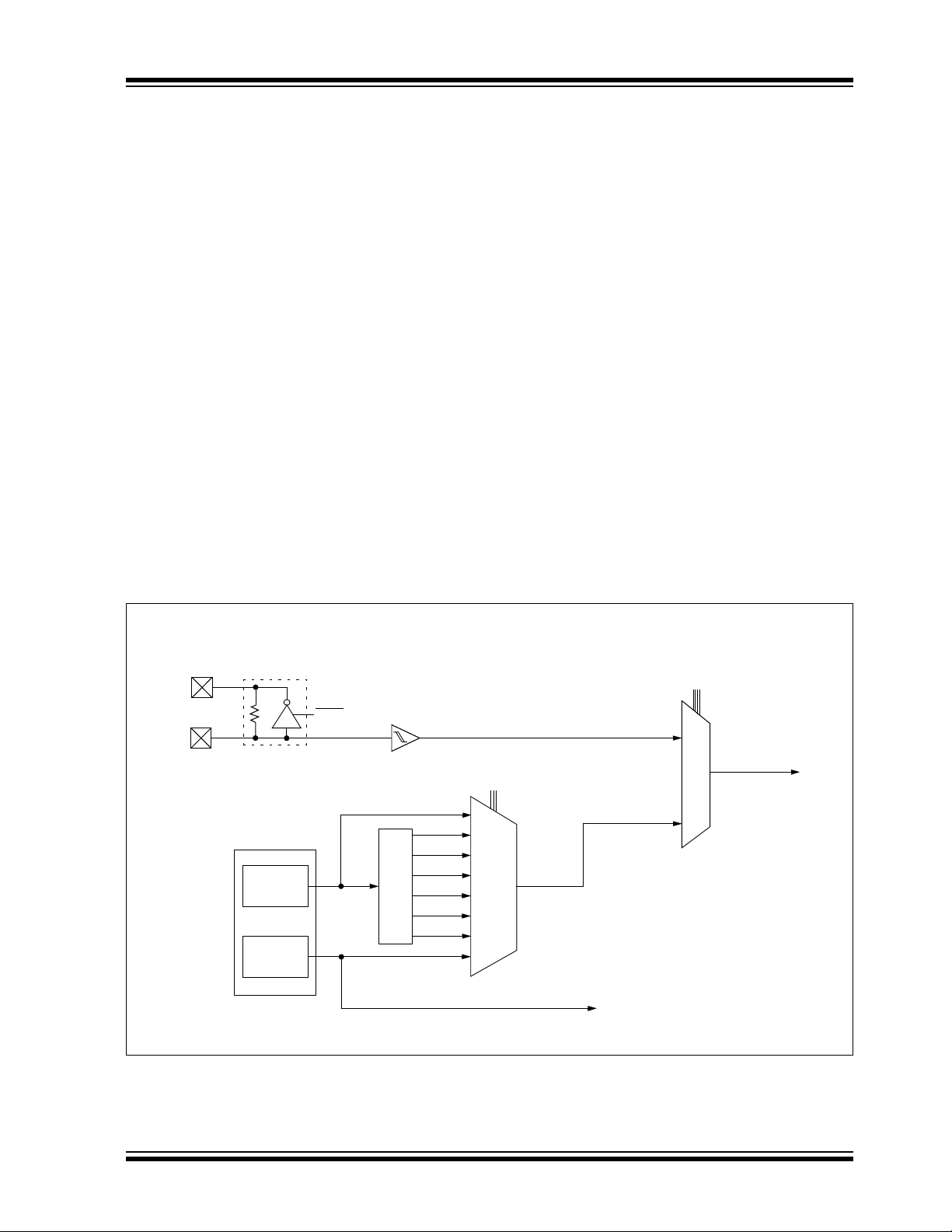
3.0 OSCILLATOR MODULE (WITH
FAIL-SAFE CLOCK MONITOR)
3.1 Overview
The Oscillator module has a wide variety of clock
sources and selection features that allow it to be used
in a wide range of applicati ons while maximiz ing performance and minimizing power consumption. Figure 3-1
illustrates a block diagram of the Oscillator module.
Clock sources can be configured from external
oscillators, quartz cryst al resonators , ceramic resonators
and Resistor-Capacitor (RC) circuits. In addition, the
system clock source can be configured from one of two
internal oscillators, with a choice of speeds select able via
software. Additional clo ck feat ures inc lud e:
• Selectable system clock source between external
or internal via software.
• Two -Spe ed Start-Up mo de, whic h min im iz es
latency between external oscillator start-up and
code execution.
• Fail-Safe Clock Monitor (FSCM) designed to
detect a failure of the external clock source (LP,
XT, HS, EC or RC modes) and switch
automatically to the internal oscillator.
The Oscillator mod ule can be c onfigured in one of eig ht
clock modes.
1. EC – External clock with I/O on OSC2/CLKOUT.
2. LP – 32 kHz Low-Power Crystal mode.
3. XT – Medium Gain Crystal or Ceramic
Resonator Oscillator mode.
4. HS – High Gain Crystal or Ceramic Resonator
mode.
5. RC – External Resistor-Capacitor (RC) with
OSC/4 output on OSC2/CLKOUT.
F
6. R CIO – External Resistor- Capacitor (RC) with
I/O on OSC2/CLKOUT.
7. INTOSC – Internal oscillator with F
OSC/4 output
on OSC2 and I/O on OSC1/CLKIN.
8. INTOSCIO – Internal oscillator with I/O on
OSC1/CLKIN and OSC2/CLKOUT.
Clock Source modes are configured by the FOSC <2:0>
bits in the Configuration Word register (CONFIG). The
internal clock can be generated from two internal
oscillators. The HFINTOSC is a calibrated highfrequency oscillator. The LFINTOSC is an uncalibrated
low-frequency oscillator.
FIGURE 3-1: PIC® MCU CLOCK SOURCE BLOCK DIAGRAM
External Oscillator
OSC2
OSC1
Internal Oscillator
HFINTOSC
8 MHz
LFINTOSC
31 kHz
Sleep
Postscaler
IRCF<2:0>
(OSCCON Register)
8 MHz
4 MHz
2 MHz
1 MHz
500 kHz
250 kHz
125 kHz
31 kHz
111
110
101
100
011
010
001
000
LP, XT, HS, RC, RCIO, EC
MUX
FOSC<2:0>
(Configuration Word Register)
SCS<0>
(OSCCON Register)
MUX
(CPU and Peripherals)
INTOSC
Power-up Timer (PWRT)
Watchdog Timer (WDT)
Fail-Safe Clock Monitor (FSCM)
System Clock
© 2007 Microchip Technology Inc. DS41203D-page 21
PIC16F688
3.2 Oscillator Control
The Oscillator Control (OSCCON) register (Figure3-1)
controls the system clock and frequency selection
options. The OSCCON register contains the following
bits:
• Frequency selection bits (IRCF)
• Frequency Status bits (HTS, LTS)
• System clock control bits (OSTS, SCS)
REGISTER 3-1: OSCCON: OSCILLATOR CONTROL REGISTER
U-0 R/W-1 R/W-1 R/W-0 R-1 R-0 R-0 R/W-0
(1)
(1)
HTS LTS SCS
— IRCF2 IRCF1 IRCF0 OSTS
bit 7 bit 0
Legend:
R = Readable bit W = Writable bit U = Unimplemented bit, read as ‘0’
-n = Value at POR ‘1’ = Bit is set ‘0’ = Bit is cleared x = Bit is unknown
bit 7 Unimplemented: Read as ‘0’
bit 6-4 IRCF<2:0>: Internal Oscillator Frequency Select bits
111 =8MHz
110 = 4 MHz (default)
101 =2MHz
100 =1MHz
011 =500kHz
010 =250kHz
001 =125kHz
000 = 31 kHz (LFINTOSC)
bit 3 OSTS: Oscillator Start-up Time-out Status bit
1 = Device is running from the external clock defined by FOSC<2:0> of the Configuration Word
0 = Device is running from the internal oscillator (HFINTOSC or LFINTOSC)
bit 2 HTS: HFINTOSC Status bit (High Frequency – 8MHz to 125 kHz)
1 = HFINTOSC is stable
0 = HFINTOSC is not stable
bit 1 LTS: LFINTOSC Stable bit (Low Frequency – 31 kHz)
1 = LFINTOSC is stable
0 = LFINTOSC is not stabl e
bit 0 SCS: Syst em Clock Select bit
1 = Internal oscillator is used for system clock
0 = Clock source defined by FOSC<2:0> of the Configuration Word
Note 1: Bit resets to ‘0’ with Two-Speed Start-up and LP, XT or HS selected as the Oscillator mode or Fail-Safe
mode is enabled.
DS41203D-page 22 © 2007 Microchip Technology Inc.
PIC16F688
3.3 Clock Source Modes
Clock Source modes can be classified as external or
internal.
• External Clock mod es rely on e xternal circui try fo r
the clock source. Examples are: Oscillator modules (EC mode), quartz crystal resonators or
ceramic resonators (LP, XT and HS modes) and
Resistor-Capacitor (RC) mode circuits.
• Internal clock sources are contained internally
within the Oscillator module. The Oscillator
module has two internal oscillators: the 8 MHz
High-Frequency Internal Oscillator (HFINTOSC)
and the 31 kHz Low-Freq uency Inte rnal Osci llator
(LFINTOSC).
The system clock can be selected between extern al or
internal clock sources via the System Clock Select
(SCS) bit of the OSCCON register. See Section 3.6
“Clock Switching” for additional information.
3.4 External Clock Modes
3.4.1 OSCILLATOR START-UP TIMER (OST)
If the Oscillator module is configured for LP, XT or HS
modes, the Oscillator Start-up Timer (OST) counts
1024 oscillations from OSC1. This occurs following a
Power-on Reset (POR) and when the Power-up Timer
(PWRT) has expired (if configured), or a wake-up from
Sleep. During this time, the program counter does not
increment and program execution is suspended. The
OST ensures that the oscillator circuit, using a quartz
crystal resonator o r ce ramic res onator, has started and
is providing a stable system clock to the Oscillator
module. When switching between clock sources, a
delay is required to allow the new clock to stabilize.
These oscillator delays are shown in Table 3-1.
In order to minimize laten cy between externa l oscillator
start-up and code execution, the Two-Speed Clock
Start -up mode ca n be selected (s ee Section 3.7 “Two-
Speed Clock Start-up Mode”).
TABLE 3-1: OSCILLATOR DELAY EXAMPLES
Switch From Switch To Frequency Oscillator Delay
Sleep/POR
Sleep/POR EC, RC DC – 20 MHz 2 instruction cycles
LFINTOSC (31 kHz) EC, RC DC – 20 MHz 1 cycle of each
Sleep/POR LP, XT, HS 32 kHz to 20 MHz 1024 Clock Cycles (OST)
LFINTOSC (31 kHz) HFINTOSC 125 kHz to 8 MHz 1 μs (approx.)
LFINTOSC
HFINTOSC
31 kHz
125 kHz to 8 MHz
Oscillator Warm-Up Delay (T
WARM)
3.4.2 EC MODE
The External Clock (EC) mode allows an externally
generated logic level as the system clock source. When
operating in this mode, an external clock source is
connected to the OSC1 input and the OSC2 is available
for general purpose I/O. Figure 3-2 shows the pin
connections for EC mode.
The Oscillator Start-up Timer (OST) is disabled when
EC mode is selected. Therefore, there is no delay in
operation after a Power-on Reset (POR) or wake-up
from Sleep. Because the PIC
static, stopping the external clock input will have the
effect of halting the device while leaving all data intact.
Upon restarting the external clock, the device will
resume operation as if no time had elapsed.
®
MCU design is fully
FIGURE 3-2: EXTERNAL CLOCK (EC)
MODE OPERATION
Clock from
Ext. System
I/O
Note 1: Alternate pin functions are listed in
Section 1.0 “Device Overview”.
OSC1/CLKIN
®
PIC
MCU
OSC2/CLKOUT
(1)
© 2007 Microchip Technology Inc. DS41203D-page 23
PIC16F688
3.4.3 LP, XT, HS MODES
The LP, XT and HS modes support the use of quartz
crystal resonators or ceramic resonators connected to
OSC1 and OSC2 (Figu re 3-3). The mod e selects a low ,
medium or high gain setting of the internal inverteramplifier to support v arious resonato r types and spee d.
LP Oscillator mode selects the lowest gain setting of
the internal inverter-amplifier. LP mode current consumption is the least of the three modes. This mode is
best suited to drive resonator s with a low drive lev el
specification, for example, tuning fork type crystals.
This mode is designed to drive only 32.768 kHz tuningfork type crystals (watch crystals).
XT Oscillator mode selects the intermediate gain
setting of the internal inverter-amplifier. XT mode
current consumption is the medi um of the three modes.
This mode is best suited to drive resonators with a
medium drive level specification.
HS Oscillator mode select s the highest gain setting of the
internal inverter-amplifie r. H S mode current consum ption
is the highest of the three modes. This mode is best
suited for resonators that require a high drive setting.
Figure 3-3 and Figure 3-4 show typical circuits for
quartz crystal and ceramic resonators, respectively.
Note 1: Quartz cryst al characterist ics vary accor ding
to type, package and manufacturer. The
user should consult the manu facturer data
sheets for sp ecifica tions and re comm ende d
application.
2: Always verify oscillator performance over
DD and temperature range that is
the V
expected for the application.
3: For oscillator design assistance, reference
the following Microchip Applications Notes:
• AN826, “Crystal Oscillator Basics and
Crystal Selection for rfPIC
®
and PIC®
Devices” (DS00826)
®
• AN849, “Basic PIC
Oscillator Design”
(DS00849)
®
• AN943, “Practical PIC
Oscillator
Analysis and Design” (DS00943)
• AN949, “Making Your Oscillator Work”
(DS00949)
FIGURE 3-4: CERAMIC RESONATOR
OPERATION
(XT OR HS MODE)
FIGURE 3-3: QUARTZ CRYSTAL
OPERATION (LP, XT OR
HS MODE)
PIC® MCU
OSC1/CLKIN
C1
Quartz
Crystal
C2
Note 1: A series resistor (RS) may be required for
2: The value of R
(1)
S
R
quartz crystals with low drive level.
selected (typically between 2 MΩ to 10 MΩ).
F varies with the Oscillator mode
(2)
RF
OSC2/CLKOUT
To Internal
Logic
Sleep
PIC® MCU
OSC1/CLKIN
C1
(3)
RP
C2
Ceramic
Resonator
Note 1: A series resistor (RS) may be required for
ceramic resonators with low drive level.
2: The value of R
selected (typically between 2 MΩ to 10 M Ω).
3: An additional parallel feedback resistor (R
may be required for proper ceramic resonator
operation.
(1)
R
S
F varies with the Oscillator mode
(2)
RF
OSC2/CLKOUT
To Internal
Logic
Sleep
P)
DS41203D-page 24 © 2007 Microchip Technology Inc.
PIC16F688
e.
3.4.4 EXTERN AL RC MODES
The external Resistor-Capacitor (RC) modes support
the use of an external RC circuit. This allows the
designer maximum flexibility in frequency choice while
keeping costs to a minimum when clock accuracy is not
required. There are two modes: RC and RCIO.
In RC mode, the RC circuit connects to OSC1. OSC2/
CLKOUT outputs the RC oscillator frequency divided
by 4. This signal may be used to provide a clock for
external circuitry, synchronization, calibration, test or
other application requirements. Figure 3-5 shows the
external RC mode connections.
FIGURE 3-5: EXTERNAL RC MODES
VDD
REXT
OSC1/CLKIN
CEXT
VSS
OSC/4 or
F
(2)
I/O
Recommended values: 10 kΩ ≤ REXT ≤ 100 kΩ, <3V
Note 1: Alternate pin functions are listed in
2: Output depends upon RC or RCIO clock mod
OSC2/CLKOUT
Section 1.0 “Device Overview”.
In RCIO mode, the RC circuit is connected to OSC1.
OSC2 becomes an additional general purpose I/O pin.
The RC oscillator frequency is a function of the supply
voltage, the resistor (REXT) and capacito r (CEXT) values
and the operating temperature. Other factors affecting
the oscillator frequency are:
• threshold voltage variation
• component tolerances
• packaging variations in capacitance
The user also needs to take into account variation due
to tolerance of external RC components used.
PIC® MCU
(1)
3 kΩ ≤ R
C
EXT ≤ 100 kΩ, 3-5V
EXT > 20 pF, 2-5V
Internal
Clock
3.5 Internal Clock Modes
The Oscillator module has two independent, internal
oscillators that can be configured or selected as the
system clock source.
1. The HFINTOSC (High-Frequency Internal
Oscillator) is factory calibrated and operates at
8 MHz. The frequ ency of t he HFINT OSC can be
user-adju ste d via software using the OSCTUNE
register (Register 3-2).
2. The LFINTOSC (Low-Frequency Internal
Oscillator) is uncalibrated and operates at 31 kHz.
The system cloc k speed ca n be selec ted via sof tware
using the Internal Oscillator Frequency Select bits
IRCF<2:0> of the OSCCON register.
The system clock ca n be se lec ted betw ee n external or
internal cloc k sourc es via th e System Cl ock Select ion
(SCS) bit of the OSCCON register. See Section 3.6
“Clock Switching” for more information.
3.5.1 INTOSC AND INTOSCIO MODES
The INTOSC and INTOSCIO modes configure the
internal oscillators as the system clock source when
the device is progra mmed usi ng the osc illator se lectio n
or the FOSC<2:0> bits in the Configuration Word
register (CONFIG). See Section 11.0 “Special
Features of the CPU” for more information.
In INTOSC mode, OSC1/CLKIN i s available for general
purpose I/O. OSC2/CLKOUT outputs the selected
internal oscillator fre quency divide d by 4. The CLKO UT
signal may be used to provide a clock for external
circuitry, synchronization, calibration, test or other
application requirements.
In INTOSCIO mode, OSC1/CLKIN and OSC2/CLKOUT
are available for general purpose I/O.
3.5.2 HFINTOSC
The High-Frequency Int ernal Oscillato r (HFINT OSC) is
a factory calibrated 8 MHz internal clock source. The
frequency of the HFINTOSC can be altered via
software using the OSCTUNE register (Register 3-2).
The output of the HFINTOSC connects to a postscaler
and multiplexer (see Figure 3-1). One of seven
frequencies can be selected via software using the
IRCF<2:0> bits of the OSCCON register. See
Section 3.5.4 “Frequency Select Bits (IRCF)” for
more information.
The HFINTOSC is enabled by selecting any frequency
between 8 MHz and 125 kHz by setting the IRCF<2:0>
bits of the OSCCON register ≠ 000. Then, set the
System Clock Source (SCS) bit of the OSCCON
register to ‘1’ or en able Two-Speed Start-up by se tting
the IESO bit in the Configuration Word register
(CONFIG) to ‘1’.
The HF Internal Oscillator (HTS) bit of the OSCCON
register indicates whether the HFINTOSC is stable or not.
© 2007 Microchip Technology Inc. DS41203D-page 25

PIC16F688
3.5.2.1 OSCTUNE Register
The HFINTOSC is factory calibrated but can be
adjusted in software by writing to the OSCTUNE
register (Register3-2).
The default value of the OSCTUNE register is ‘0’. The
value is a 5-bit two’s complement number.
When the OSCTUNE register is modified, the
HFINTOSC frequency will begin shifting to the new
frequency. Code execution continues during this shift.
There is no indication that the shift has occurred.
OSCTUNE does not affect the LFINTOSC frequency.
Operation of features that depend on the LFINTOSC
clock source frequency, such as the Power-up Timer
(PWRT), Watchdog Timer (WDT), Fail-Safe Clock
Monitor (FSCM) and peripherals, are not af fected by the
change in frequency.
REGISTER 3-2: OSCTUNE: OSCILLATOR TUNING REGISTER
U-0 U-0 U-0 R/W-0 R/W-0 R/W-0 R/W-0 R/W-0
— — — TUN4 TUN3 TUN2 TUN1 TUN0
bit 7 bit 0
Legend:
R = Readable bit W = Writable bit U = Unimplemented bit, read as ‘0’
-n = Value at POR ‘1’ = Bit is set ‘0’ = Bit is cleared x = Bit is unknown
bit 7-5 Unimplemented: Read as ‘0’
bit 4-0 TUN<4:0>: Frequency Tuning bits
01111 = Maximum frequen cy
01110 =
•
•
•
00001 =
00000 = Oscillator module is running at the calibrated frequency.
11111 =
•
•
•
10000 = Minimum frequency
DS41203D-page 26 © 2007 Microchip Technology Inc.

PIC16F688
3.5.3 LFINTOSC
The Low-Frequency Internal Oscillator (LFINTOSC) is
an uncalibrated 31 kHz internal clock source.
The output of the LFINTOSC connects to a postscaler
and multiplexer (see Figure3-1). Select 31 kHz, via
software, using the IRCF<2:0> bits of the OSCCON
register. See Section 3.5.4 “Frequency Select Bits
(IRCF)” for more information. The LFINTO SC is also the
frequency for the Power-up Timer (PWRT), Watchdog
Timer (WDT) and Fail-Safe Clock Mo nitor (FSCM).
The LFINTOSC is enabled by selecting 31 kHz
(IRCF<2:0> bits of the OSCCON register= 000) as the
system clock source (SCS bit of the OSCCON
register = 1), or when any of the fo llow ing are ena bled:
• Two-Spe ed Star t-up IESO bi t of the C o nfi gura tio n
Word register = 1 and IRCF<2:0> bits of the
OSCCON register = 000
• Power-up Timer (PWRT)
• Watchdog Timer (WDT)
• Fail-Safe Clock Monitor (FSCM)
The LF Internal Oscillator (LTS) bit of the OSCCON
register indicates whether the LFINTOSC is stable or
not.
3.5.4 FREQUENCY SELECT BITS (IRCF)
The output of the 8 MHz HFINTOSC and 31 kHz
LFINTOSC connects to a postscaler and multiplexer
(see Figure 3-1). The Internal Oscillator Frequency
Select b its IRCF<2:0> of the OSCCON register select
the frequency output of the internal oscillators. One of
eight frequencies can be selected via software:
•8 MHz
• 4 MHz (Default after Reset)
•2 MHz
•1 MHz
• 500 kHz
• 250 kHz
• 125 kHz
• 31 kHz (LFINTOSC)
Note: Following any Reset, the IRCF <2:0 > bit s of
the OSCCON register are set to ‘110’ and
the frequency selection is set to 4 MHz.
The user can modify the IRCF bits to
select a different frequency.
3.5.5 HF AND LF INTOSC CLOCK
SWITCH TIMING
When switching between the LFINTOSC and the
HFINTOSC, the new oscillator may already be shut
down to save power (see Figure 3-6). If this is the case,
there is a delay after the IRCF<2:0> bits of the
OSCCON register are modified before the frequency
selection takes place. The LTS and HTS bits of the
OSCCON register will reflect the current active status
of the LFINTOSC and HFINTOSC oscillators. The
timing of a frequency selection is as follows:
1. IRCF<2:0> bits of the OSCCON register are
modified.
2. If the new clock is shut down, a clock start-up
delay is started.
3. Clock switch circuitry waits for a falling edge of
the current clock.
4. CLKOUT is held low and the clock switch
circuitry waits fo r a ris ing edge in the new clock.
5. CLKOUT is now connected with the new clock.
LTS and HTS bits of the OS CCON regi ster are
updated as required.
6. Clock switch is complete.
See Figure 3-1 for more details.
If the internal oscillator speed selected is between
8 MHz and 125 kHz, there is no start-up delay before
the new frequency is selected. This is because the old
and new frequencies are derived from the HFINTOSC
via the postscaler and multi ple xe r.
Start-up delay specifications are located in the
Section 14.0 “Electrical Specifications”, under the
AC Specifications (Oscillator Module).
© 2007 Microchip Technology Inc. DS41203D-page 27

PIC16F688
FIGURE 3-6: INTERNAL OSCILLATOR SWITCH TIMING
(1)
LF
HF
HFINTOSC LFINTOSC (FSCM and WDT disabled)
HFINTOSC
Start-up Time
LFINTOSC
2-cycle Sync Running
IRCF <2:0>
System Clock
Note 1: When going from LF to HF.
HFINTOSC LFINTOSC (Either FSCM or WDT enabled)
HFINTOSC
LFINTOSC
IRCF <2:0>
System Clock
LFINTOSC HFINTOSC
LFINTOSC
HFINTOSC
≠ 0 = 0
2-cycle Sync Running
≠ 0 = 0
LFINTOSC turns off unless WDT or FSCM is enabled
Start-up Time 2-cycle Sync
Running
IRCF <2:0>
System Clock
DS41203D-page 28 © 2007 Microchip Technology Inc.
= 0 ≠ 0

PIC16F688
3.6 Clock Switching
The system clock source can be switched between
external and internal clock sources via software using
the System Clock Select (SCS) bit of the OSCCON
register.
3.6.1 SYSTEM CLOCK SELECT (SCS) BIT
The System Clock Select (SCS) bit of the OSCCON
register selects the system clock source that is used for
the CPU and peripherals.
• When the SCS bit of the OSCCON register = 0,
the system clock source is determined by
configuration of the FOSC<2:0> bits in the
Configuration Word regist er (CONFIG).
• When the SCS bit of the OSCCON register = 1,
the system clock source is chosen by the internal
oscillator frequency selected by the IRCF<2:0>
bits of the OSCCON register. After a Reset, the
SCS bit of the OSCCON register is always
cleared.
Note: Any automatic clock switch, which may
occur from T wo-Speed Sta rt-up or Fail-Safe
Clock Monitor , does not update the SCS bit
of the OSCCON register. The user can
monitor the OSTS bit of the OSCCON
register to determine the current system
clock source.
3.6.2 OSCIL LA T OR START-UP TIME-OUT
STATUS (OSTS) BIT
The Oscillator Start-up Time-out Status (OSTS) bit of
the OSCCON register indicates whether the system
clock is running from the external clock source, as
defined by the FOSC<2:0> bits in the Configuration
Word register (CONFIG), or from the internal clock
source. In particular, OSTS indicates that the Oscillator
Start-up Timer (OST) has timed out for LP, XT or HS
modes.
3.7 Two-Speed Clock Start-up Mode
Two-Speed Start-up mode provides additional power
savings by minimizing the latency between external
oscillator start-up and code execution. In applications
that make heavy us e of the Sleep mode, Two-Speed
Start-up will remove the external oscillator start-up
time from the time spent awake and can reduce the
overall power consumption of the device.
This mode allows the application to wake-up from
Sleep, perform a few instructions using the INTOSC
as the clock source and go back to Sleep without
waiting for the primary oscillator to become stable.
When the Oscillator module is configured for LP, XT or
HS modes, the Oscillator Start-up Timer (OST) is
enabled (see Section 3.4.1 “Oscillator Start-up Timer
(OST)”). The OST will suspend program execution until
1024 oscillations are counted. Two-Speed Start-up
mode minimizes the delay in code execution by
operating from the internal oscillator as the OST is
counting. When the OST count rea ches 1024 and the
OSTS bit of the OSCCON register is set, program
execution switches to the external oscillator.
3.7.1 TWO-SPEED START-UP MODE
CONFIGURATION
Two-Speed Start-up mode is configured by the
following settings:
• IESO (of the Configuration Word register) = 1;
Internal/External Switc hover bi t (Two-Speed S t artup mode enabled).
• SCS (of the OSCCON register) = 0.
• FOSC<2:0> bits in the Configuration Word
register (CONFIG) configured for LP, XT or HS
mode.
Two-Speed Start-up mode is entered after:
• Power-on Reset (POR) and, if enabled, after
Power-up Timer (PWRT) has expired, or
• Wake-up from Sleep.
If the external clock oscillator is configured to be
anything other than LP, XT or HS mode, then TwoSpeed St art-up is d isabled. Thi s is becaus e the extern al
clock oscillator do es not require any stabilizat ion time
after POR or an exit from Sleep.
3.7.2 TWO-SPEED START-UP
SEQUENCE
1. Wake-up from Power-on Reset or Sleep.
2. Instructions begin execution by the internal
oscillator at the frequency set in the IRCF<2:0>
bits of the OSCCON register.
3. OST enabled to count 1024 clock cycles.
4. OST timed out, wait for falling edge of the
internal oscillator.
5. OSTS is set.
6. System clock held low until the next falling edge
of new clock (LP, XT or HS mode).
7. System clock is switched to external clock
source.
Note: Executing a SLEEP instruction will abort
the oscillator start-up time and will cause
the OSTS bit of the OSCCON register to
remain clear.
© 2007 Microchip Technology Inc. DS41203D-page 29

PIC16F688
3.7.3 CHECKING TWO-SPEED CLOCK
STATUS
Checking the state of the OSTS bit of the OSCCON
register will confirm if the microcontroller is running
from the external clock source, as defined by the
FOSC<2:0> bits in the Configuration Word register
(CONFIG), or the internal oscillator.
FIGURE 3-7: TWO-SPEED START-UP
HFINTOSC
TOSTT
OSC1
OSC2
Program Counter
System Clock
0 1 1022 1023
PC - N
PC
PC + 1
DS41203D-page 30 © 2007 Microchip Technology Inc.

PIC16F688
3.8 Fail-Safe Clock Monitor
The Fail-Safe Clock Monit or (FSCM) al low s the dev ic e
to continue operat ing sh oul d the external oscill ator fai l.
The FSCM can detect oscillator failure any time after
the Oscillator Start-up Timer (OST) has expired. The
FSCM is enabled by setting the FCMEN bit in the
Configuration Word register (CONFIG). The FSCM is
applicable to all external oscillator modes (LP, XT, HS,
EC, RC and RCIO).
FIGURE 3-8: FSCM BLOCK DIAGRAM
Clock Monitor
External
Clock
LFINTOSC
Oscillator
31 kHz
(~32 μs)
Sample Clock
÷ 64
488 Hz
(~2 ms)
3.8.1 FAIL-SAFE DETECTION
The FSCM module detects a failed oscillator by
comparing the ex tern al osci llator to the FS CM sa mple
clock. The sample clock is generated by dividing the
LFINTOSC by 64. See Figure 3-8. Inside the fail
detector block is a latch. The external clock sets the
latch on each falling edge of the external clock. The
sample clock cle ars the latch on each ris ing edge of th e
sample clock. A fail ure is d ete cte d w h en an ent ire halfcycle of the sample clock elapses before the primary
clock goes low.
Latch
S
R
Q
Q
Clock
Failure
Detected
3.8.3 FAIL-SAFE CONDITION CLEARING
The Fail-Safe condition is cleared after a Reset,
executing a SLEEP instruction or togg ling the SC S bit
of the OSCCON register. When the SCS bit is toggled,
the OST is restarted. While the OST is running, the
device continue s to op erat e from t he INT OSC sele cted
in OSCCON. When the OST times out, the Fail-Safe
condition is cleared and the device will be operating
from the external clock s ource. Th e Fail-Saf e condi tion
must be cleared before th e O SFIF f lag ca n be cle are d.
3.8.4 RESET OR WAKE-UP FROM SLEEP
The FSCM is designed to detect an oscillator failure
after the Oscillator Start-up Timer (OST) has expired.
The OST is used after waking up from Sleep and after
any type of Reset. The OST is not used with the EC or
RC Clock modes so that the FSCM will be active as
soon as the R eset or wake- up has complet ed. When
the FSCM is enabled, the Two-Speed Start-up is also
enabled. Therefore, the device will always be executing
code while the OST is operating.
Note: Due to the wide range of oscillator start-up
times, the Fail-Safe circuit is not active
during oscillator start-up (i.e., after exiting
Reset or Sleep). After an appropriate
amount of time, the user should check the
OSTS bit of the OSCCON register to verify
the oscillator start-up and that the system
clock switchover has successfully
completed.
3.8.2 FAIL-SAFE OPER ATION
When the external clock fails, the FSCM switches the
device clock to an internal cl ock sourc e and set s the bit
flag OSFIF of the PIR2 register. Setting this flag will
generate an interrupt if the OSFIE bit of the PIE2
register is also set. The device firmware can then take
steps to mitigate the problems that may arise from a
failed clock. The system clock will continue to be
sourced from the internal clock source until the device
firmware successfully restarts the external oscillator
and switches back to external operation.
The internal clock source chosen by the FSCM is
determined by the IRCF<2:0> bits of the OSCCON
register. This allows the internal oscillator to be
configured before a failure occurs.
© 2007 Microchip Technology Inc. DS41203D-page 31

PIC16F688
FIGURE 3-9: FSCM TIMING DIAGRAM
Sample Clock
System
Clock
Output
Clock Monitor Output
(Q)
OSCFIF
Test
Note: The system clock is normally at a m uch higher frequency than the sam ple clock. The relative frequencies in
this example have been chosen for clarity.
Oscillator
Failure
Failure
Detected
Test Test
TABLE 3-2: SUMMARY OF REGISTERS ASSOCIATED WITH CLOCK SOURCES
Name Bit 7 Bit 6 Bit 5 Bit 4 Bit 3 Bit 2 Bit 1 Bit 0
CONFIG
INTCON GIE PEIE
OSCCON
OSCTUNE
PIE1
PIR1
Legend: x = unknown, u = unchanged, – = unimplemented locations read as ‘0’. Shaded cells are not used by oscillators.
Note 1: Other (non Power-up) Resets include MCLR
(2)
2: See Configuration Word register (CONFIG) for operation of all register bits.
CPD CP MCLRE PWRTE WDTE FOSC2 FOSC1 FOSC0 — —
T0IE INTE RAIE T0IF INTF RAIF 0000 000x 0000 000x
— IRCF2 IRCF1 IRCF0 OSTS HTS LTS SCS -110 x000 -110 x000
— — — TUN4 TUN3 TUN2 TUN1 TUN0 ---0 0000 ---u uuuu
EEIE ADIE RCIE C2IE C1IE OSFIE TXIE TMR1IE
EEIF ADIF RCIF C2IF C1IF OSFIF TXIF TMR1IF
Reset and Watchdog Timer Reset during normal operation.
Val ue on
POR, BOR
0000 0000 0000 0000
0000 0000 0000 0000
Val ue on
all other
Resets
(1)
DS41203D-page 32 © 2007 Microchip Technology Inc.

PIC16F688
4.0 I/O PORTS
There are as many as twelve ge neral pur pose I/O pi ns
available. Depending on which peripherals are enabled,
some or all of the pins may not be available as general
purpose I/O. In gen eral, when a periphe ral is enabled,
the associated pin may not be used as a general
purpose I/O pin.
4.1 PORTA and the TRISA Registers
PORTA is a 6-bit wide, bidirectional port. The
corresponding dat a direction register is TR ISA. Se ttin g
a TRISA bit (= 1) will make the corresponding PORTA
pin an input (i.e., put the corresponding output driver in
a High-Impedance mode). Clearing a TRISA bit (= 0)
will make the correspond ing PORTA pin an output (i.e.,
put the contents of the outpu t latch on the selected pi n).
The exception is RA3, whi ch is input only and its TR ISA
bit will always read as ‘1’. Example 4-1 shows how to
initialize PORTA.
Reading the PORTA register reads the status of the
pins, whereas writing to it will write to the PORT latch.
All write operations are read-modify-write operations.
REGISTER 4-1: PORTA: PORTA REGISTER
Therefore, a write t o a port implies that the port p ins are
read, this value is modified and then written to the
PORT data latch. RA3 reads ‘0’ when MCLRE = 1.
The TRISA register controls the direction of the
PORT A pins, even when they are being used as analo g
inputs. The user must ensure the bits in the TRISA
register are maintained set when using the m as analog
inputs. I/O pins co nfigure d a s analo g i nput a lways read
‘0’.
Note: The ANSEL and CMCON0 registers must
be initialized to configure an analog
channel as a digital input. Pins configured
as analog inputs will read ‘0’.
EXAMPLE 4-1: INITIALIZING PORTA
BANKSEL PORTA ;
CLRF PORTA ;Init PORTA
MOVLW 07h ;Set RA<2:0> to
MOVWF CMCON0 ;digital I/O
BANKSEL ANSEL ;
CLRF ANSEL ;digital I/O
MOVLW 0Ch ;Set RA<3:2> as inputs
MOVWF TRISA ;and set RA<5:4,1:0>
;as outputs
U-0 U-0 R/W-x R/W-0 R-x R/W-0 R/W-0
— — RA5 RA4 RA3 RA2 RA1 RA0
bit 7
Legend:
R = Readable bit W = Writable bit U = Unimplemented bit, read as ‘0’
-n = Value at POR ‘1’ = Bit is set ‘0’ = Bit is cleared x = Bit is unknown
bit 7-6 Unimplemented: Read as ‘0’
bit 5-0 RA<5:0>: PORTA I/O Pin bit
1 = Port pin is > V
0 = Port pin is < VIL
IH
R/W-0
bit 0
REGISTER 4-2: TRISA: PORTA TRI-STATE REGISTER
U-0 U-0 R/W-1 R/W-1 R-1 R/W-1 R/W-1 R/W-1
— — TRISA5 TRISA4 TRISA3 TRISA2 TRISA1 TRISA0
bit 7 bit 0
Legend:
R = Readable bit W = Writable bit U = Unimplemented bit, read as ‘0’
-n = Value at POR ‘1’ = Bit is set ‘0’ = Bit is cleared x = Bit is unknown
bit 7-6 Unimplemented: Read as ‘0’
bit 5-0 TRISA<5:0>: PORTA Tri-State Control bits
Note 1: TRISA<3> always reads ‘1’.
2: TRISA<5:4> always reads ‘1’ in XT, HS and LP Oscillator modes.
1 = PORTA pin configured as an input (tri-stated)
0 = PORTA pin configured as an output
© 2007 Microchip Technology Inc. DS41203C-page 33

PIC16F688
4.2 Additional Pin Functions
Every PORTA pin on the PIC16F688 has an interrupton-change option and a weak pull-up option. PORTA
also provides an Ultra Lo w-Power W ake-up option. The
next three sections descr ibe these functions.
4.2.1 ANSEL REGISTER
The ANSEL register is used to configure the Input
mode of an I/O pin to analog . Refer to Register 4-3.
Setting the appropriate ANSEL bit high will cause all
digital reads on the pin to be read as ‘0’ and allow
analog functions on the pin to operate correctly.
The state of the ANSEL bits has no affect on digital
output functions. A pin with TRIS clear and ANSEL set
will still operate as a digital output, but the Input mode
will be analog. This can cause unexpected behavior
when executing read-modify-write instructions on the
affected port.
4.2.2 WEAK PULL-UPS
Each of the PORTA pins, except RA3, has an
individually configurable internal weak pull-up. Control
bits WPUAx enable or disable each pull-up. Refer to
Register 4-4. Each weak pull-up is automatically turned
off when the p ort pin is co nfigured as an output. T he
pull-ups are disabled on a Power-on Reset by the
bit of the OPTION register. A weak pull-up is
RAPU
automatically enabled for RA3 when configured as
and disabled when RA3 is an I/O. There is no
MCLR
software control of the MCLR
pull-up.
4.2.3 INTERRUPT-ON-CHANGE
Each of the PORTA pins is individually configurable as
an interrupt-on-change pin. Control bits IOCAx enable
or disable the interrupt function for each pin. Refer to
Register 4-5. The interrupt-on-change is disabled on a
Power-on Reset.
For enabled interrupt-on-change pins, the values are
compared with the old value latch ed on the la st read of
PORTA. The ‘mismatch’ outputs of the last read are
OR’d together to set th e POR TA Change I nterrupt Flag
bit (RAIF) in the INTCON register.
This interrupt can wake the device from Sleep. The user,
in the Interrupt Service Routine, clears the interrupt by:
a) Any read or write of PORTA. This will end the
b) Clear the flag bit RAIF.
A mismatch c ond it i on wi ll cont i n ue to s et f lag bi t RA IF.
Reading PORTA will end the mismatch condition and
allow flag bit RAIF to be cleared. The latch holding the
last read value is not affected by a MCLR
Reset. After these Resets, the RAIF flag will continue
to be set if a mismatch is present.
Note: If a change on the I/O pin should occur
REGISTER 4-3: ANSEL: ANALOG SELECT REGISTER
mismatch condition, then
nor BOR
when the read operation is bei ng executed
(start of the Q2 cycle), then the RAIF
interrupt flag may not get set.
R/W-1 R/W-1 R/W-1 R/W-1 R/W-1 R/W-1 R/W-1 R/W-1
ANS7 ANS6 ANS5 ANS4 ANS3 ANS2 ANS1 ANS0
bit 7 bit 0
Legend:
R = Readable bit W = Writable bit U = Unimplemented bit, read as ‘0’
-n = Value at POR ‘1’ = Bit is set ‘0’ = Bit is cleared x = Bit is unknown
bit 7-0 ANS<7:0>: Analog Select bits
Analog select between analog or digital function on pins AN<7:0>, respectively.
1 = Analog input. Pin is assigned as analog input
0 = Digital I/O. Pin is assigned to port or special function.
Note 1: Setting a pin to an analog input automatically disables the digital input circuitry, weak pull-ups and
interrupt-on-change, if available. The corresponding TRIS bit must be set to Input mode in order to allow
external control of the voltage on the pin.
(1)
.
DS41203C-page 34 © 2007 Microchip Technology Inc.

PIC16F688
REGISTER 4-4: WPUA: WEAK PULL-UP PORTA REGISTER
U-0 U-0 R/W-1 R/W-1 U-0 R/W-1 R/W-1 R/W-1
— — WPUA5 WPUA4 — WPUA2 WPUA1 WPUA0
bit 7 bit 0
Legend:
R = Readable bit W = Writable bit U = Unimplemented bit, read as ‘0’
-n = Value at POR ‘1’ = Bit is set ‘0’ = Bit is cleared x = Bit is unknown
bit 7-6 Unimplemented: Read as ‘0’
bit 5-4 WPUA<5:4>: Weak Pull-up Control bits
1 = Pull-up enabled
0 = Pull-up disabled
bit 3 Unimplemented: Read as ‘0’
bit 2-0 WPUA<2:0>: Weak Pull-up Control bits
1 = Pull-up enabled
0 = Pull-up disabled
Note 1: Global RAP
2: The weak pull-up device is automatically disabled if the pin is in Output mode (TRISA = 0).
3: The RA3 pull-up is enabled when configured as MCLR
4: WPUA<5:4> always reads ‘1’ in XT, HS and LP OSC modes.
U must be enabled for individual pull-ups to be enabled.
and disabled as an I/O in the Configuration Word.
REGISTER 4-5: IOCA: INTERRUPT-ON-CHANGE PORTA REGISTER
U-0 U-0 R/W-0 R/W-0 R/W-0 R/W-0 R/W-0 R/W-0
— — IOCA5 IOCA4 IOCA3 IOCA2 IOCA1 IOCA0
bit 7 bit 0
Legend:
R = Readable bit W = Writable bit U = Unimplemented bit, read as ‘0’
-n = Value at POR ‘1’ = Bit is set ‘0’ = Bit is cleared x = Bit is unknown
bit 7-6 Unimplemented: Read as ‘0’
bit 5-0 IOCA<5:0>: Interrupt-on-change PORTA Control bits
1 = Interrupt-on-change enabled
0 = Interrupt-on-change disabled
Note 1: Global Interrupt Enable (GIE) must be enabled for individual interrupts to be recognized.
2: IOCA<5:4> always reads ‘1’ in XT, HS and LP OSC modes.
© 2007 Microchip Technology Inc. DS41203C-page 35

PIC16F688
4.2.4 ULTRA LOW-POWER WAKE-UP
The Ultra Low-Power Wake-up (ULPWU) on RA0
allows a slow falling voltage to generate an interrupton-change on RA0 without excess current consumption. The mode is selected by setting the ULPWUE bit
of the PCON register. This enables a small cu rrent sink
which can be used to discharge a capacitor on RA0.
To use this feature, the RA0 pin is configured to output
‘1’ to charge the capac itor , interrupt-o n-change for RA 0
is enabled, and RA0 is configured as an input. The
ULPWUE bit is set to be gin the dis charge and a SLEEP
instruction is performed. When the voltage on RA0
drops below V
will cause the device to wake-up. Depending on the
state of the GIE bit of the INTCON register, the device
will either jump to the interrupt vector (0004h) or
execute the next instruction when the interrupt event
occurs. See Section 4.2.3 “INTERRUPT-ON-
CHANGE” and Section 1 1. 3.3 “P ORTA In terrupt” for
more information.
This feature provides a low-power technique for
periodically waking up the device from Sleep. The
time-out is dependent on the discharge time of the RC
circuit on RA0. See Example 4-2 for initializing the
Ultra Low-Power Wake-up module.
The series resistor provides overcurrent protection for
the RA0 pin and can allow fo r soft wa re ca lib ratio n of t he
time-out. (see Figure 4-1). A timer can be used to
measure the charge time and discharge time of the
capacitor. The charge time can then be adjusted to
provide the desired interrupt delay. This technique will
compensate for the affects of temperature, voltage and
component accuracy. The Ultra Low-Power Wake-up
peripheral can also be configured as a simple
programmable low voltage detect or temperature senso r .
IL, an interrupt will be generated which
EXAMPLE 4-2: ULTRA LOW-POWER
WAKE-UP INITIALIZATION
BANKSEL PORTA ;
BSF PORTA,0 ;Set RA0 data latch
MOVLW H’7’ ;Turn off
MOVWF CMCON0 ; comparators
BANKSEL ANSEL ;
BCF ANSEL,0 ;RA0 to digital I/O
BANKSEL TRISA ;
BCF TRISA,0 ;Output high to
CALL CapDelay ; charge capacitor
BSF PCON,ULPWUE ;Enable ULP Wake-up
BSF IOCA,0 ;Select RA0 IOC
BSF TRISA,0 ;RA0 to input
MOVLW B’10001000’ ;Enable interrupt
MOVWF INTCON ; and clear flag
SLEEP ;Wait for IOC
NOP ;
Note: For more information, refer to Application
Note AN879, “Using the Microchip Ultra
Low-Power Wake-up Module”
(DS00879).
DS41203C-page 36 © 2007 Microchip Technology Inc.

PIC16F688
4.2.5 PIN DESCRIPTIONS AND
DIAGRAMS
Each PORTA pin is multiplexed with other functions.
The pins and their combined functions are briefly
described here. For specific information about individual functions such as the comparator or the A/D, refer
to the appropriate section in this data sheet.
FIGURE 4-1: BLOCK DIAGRAM OF RA0
Data Bus
WR
WPUDA
WPUDA
PORTA
RD
WR
D
Q
CK
Q
D
Q
CK
Q
4.2.5.1 RA0/AN0/C1IN+/ICSPDAT/ULPWU
Figure 4-1 shows the di agram fo r this pi n. The RA 0 pin
is configurable to function as one of the following:
• a general purpose I/O
• an analog input for the A/D
• an analog input to the comparator
• an analog input to the Ultra Low-Power Wake-up
• In-Circuit Serial Programming™ data
(1)
Analog
Input Mode
RAPU
VDD
Weak
VDD
I/O PIN
WR
TRISA
RD
TRISA
RD
PORTA
WR
IOCA
RD
IOCA
Interrupt-on-
Change
VSS
-
+V
D
Q
CK
Q
01
(1)
Analog
Input Mode
D
Q
D
RD PORTA
Q
EN
D
Q
EN
CK
Q
To Comparator
To A/D Converter
ULPWUE
Q3
T
IULP
Vss
Note 1: Comparator mode and ANSEL determines analog Input mode.
© 2007 Microchip Technology Inc. DS41203C-page 37

PIC16F688
4.2.5.2 RA1/AN1/C1IN-/VREF/ICSPCLK
Figure 4-2 shows th e diagr am for thi s pin. Th e RA1 pin
is configurable to function as one of the following:
• a general purpose I/O
• an analog input for the A/D
• an analog input to the comparator
• a voltage reference input for the A/D
• In-Circu it Serial Programming™ clock
FIGURE 4-2: BLOCK DIAGRAM OF RA1
(1)
Analog
Data Bus
WR
WPUA
RD
WPUA
WR
PORTA
WR
TRISA
RD
TRISA
D
CK
D
CK
D
CK
Q
Q
Q
Q
Q
Q
Input Mode
RAPU
Input Mode
Analog
VDD
Weak
VDD
I/O pin
(1)
VSS
4.2.5.3 RA2/AN2/T0CKI/INT/C1OUT
Figure 4-3 shows the di agram fo r this pi n. The RA 2 pin
is configurable to function as one of the following:
• a general purpose I/O
• an analog input for the A/D
• the clock input for Timer0
• an external edge triggered interrupt
• a digital output from the comparator
FIGURE 4-3: BLOCK DIAGRAM OF RA2
(1)
Analog
Data Bus
WR
WPUA
RD
WPUA
WR
PORTA
WR
TRISA
RD
TRISA
D
CK
D
CK
D
CK
Q
Q
Q
Q
Q
Q
Input Mode
RAPU
C1OUT
Enable
C1OUT
Input Mode
1
0
Analog
VDD
Weak
VDD
I/O pin
VSS
(1)
RD
PORTA
D
Q
D
Q
EN
Q
EN
Q3
D
change
CK
Q
To Compar ator
To A/D Converter
Input mode.
RD PORTA
WR
IOCA
RD
IOCA
Interrupt-on-
Note 1: Comparator mode and ANSEL determin es analog
RD
PORTA
Q
D
D
Q
EN
Q
EN
RD PORTA
D
change
CK
Q
To Time r0
To INT
To A/D Converter
WR
IOCA
RD
IOCA
Interrupt-on-
Note 1: Analog Input mode is based upon ANSEL.
Q3
DS41203C-page 38 © 2007 Microchip Technology Inc.

PIC16F688
4.2.5.4 RA3/MCLR/VPP
Figure 4-4 shows th e diagr am for thi s pin. Th e RA3 pi n
is configurable to function as one of the following:
• a general purpose input
• as Master Clear Reset with weak pull-up
FIGURE 4-4: BLOCK DIAGRAM OF RA3
VDD
Data Bus
RD
TRISA
RD
PORTA
WR
IOCA
RD
IOCA
Interrupt-on-
change
MCLRE
Reset
VSS
Q
D
CK
Q
MCLRE
MCLRE
Q
Q
RD PORTA
EN
EN
Weak
Input
pin
SS
V
D
Q3
D
4.2.5.5 RA4/AN3/T1G
/OSC2/CLKOUT
Figure 4-5 shows the di agram fo r this pi n. The RA 4 pin
is configurable to function as one of the following:
• a general purpose I/O
• an analog input for the A/D
• a Timer1 gate input
• a crystal/resona tor connec tio n
• a clock output
FIGURE 4-5: BLOCK DIAGRAM OF RA4
(3)
Analog
Data Bus
WR
WPUA
RD
WPUA
WR
PORTA
WR
TRISA
RD
TRISA
RD
PORTA
WR
IOCA
RD
IOCA
Input Mode
Q
D
CK
Q
OSC1
Q
D
CK
Q
D
Q
CK
Q
Q
D
CK
Q
Fosc/4
CLKOUT
INTOSC/
RC/EC
CLKOUT
Enable
Enable
Input Mode
CLK
Modes
RAPU
Oscillator
Circuit
CLKOUT
Enable
1
0
(2)
Analog
Q
Q
(1)
VDD
Weak
VDD
I/O pin
VSS
(3)
D
EN
Q3
D
Interrupt-on-
change
To T1G
To A/D Converter
Note 1: CLK modes are XT, HS, LP, LPTMR1 and CLKOUT
Enable.
2: With CLKOUT option.
3: Analog Input mode is ANSEL.
EN
RD PORTA
© 2007 Microchip Technology Inc. DS41203C-page 39

PIC16F688
4.2.5.6 RA5/T1CKI/OSC1/CLKIN
Figure 4-6 shows th e diagr am for thi s pin. Th e RA5 pin
is configurable to function as one of the following:
• a general purpose I/O
• a Timer1 clock input
• a crystal/resonator connection
• a clock input
FIGURE 4-6: BLOCK DIAGRAM OF RA5
INTOSC
Data Bus
WR
WPUA
RD
WPUA
WR
PORTA
WR
TRISA
RD
TRISA
RD
PORTA
WR
IOCA
RD
IOCA
Mode
TMR1LPEN
Q
D
CK
Q
RAPU
Oscillator
Circuit
D
Q
CK
Q
D
Q
CK
Q
D
Q
CK
Q
OSC2
INTOSC
Mode
Q
Q
EN
(1)
VDD
Weak
VDD
I/O pin
VSS
(2)
D
Q3
D
Interrupt-on-
change
RD PORTA
To Timer1 or CLKGEN
Note 1: T imer1 LP oscillator enabled.
2: When using Timer1 with LP oscillator, the
Schmitt Trigger is bypassed.
EN
DS41203C-page 40 © 2007 Microchip Technology Inc.

PIC16F688
TABLE 4-1: SUMMARY OF REGISTERS ASSOCIATED WITH PORTA
Name Bit 7 Bit 6 Bit 5 Bit 4 Bit 3 Bit 2 Bit 1 Bit 0
ANSEL
CMCON0
PCON
INTCON GIE
IOCA
OPTION_REG RAPU
PORTA
TRISA
WPUA
Legend: x = unknown, u = unchanged, – = unimplemented locations read as ‘0’. Shaded cells are not used by P ORTA.
ANS7 ANS6 ANS5 ANS4 ANS3 ANS2 ANS1 ANS0 1111 1111 1111 1111
C2OUT C1OUT C2INV C1INV CIS CM2 CM1 CM0 0000 0000 0000 0000
— —ULPWUESBOREN — — POR BOR --01 --qq --0u --uu
PEIE T0IE INTE RAIE T0IF INTF RAIF 0000 000x 0000 000x
— — IOCA5 IOCA4 IOCA3 IOCA2 IOCA1 IOCA0 --00 0000 --00 0000
INTEDG T0CS T0SE PSA PS2 PS1 PS0 1111 1111 1111 1111
— — RA5 RA4 RA3 RA2 RA1 RA0 --x0 x000 --x0 x000
— — TRISA5 TRISA4 TRISA3 TRISA2 TRISA1 TRISA0 --11 1111 --11 1111
— —WPUA5WPUA4— WPUA2 WPUA1 WPUA0 --11 -111 --11 -111
Value on
POR, BOR
Value on
all other
Resets
© 2007 Microchip Technology Inc. DS41203C-page 41

PIC16F688
4.3 PORTC
PORTC is a general purpose I/ O port consisting of 6
bidirectional pins. The pins can be configured for either
digital I/O or analog input to A/D converter or comparator. For specific information about individual function s
such as the EUSART or the A/D converter, refer to the
appropriate section in this data sheet.
Note: The ANSEL and CMCON0 registers must
be initialized to configure an analog
channel as a digital input. Pins configured
as analog inputs will read ‘0’.
EXAMPLE 4-3: INITIALIZING PORTC
BANKSEL PORTC ;
CLRF PORTC ;Init PORTC
MOVLW 07h ;Set RC<4,1:0> to
MOVWF CMCON0 ;digital I/O
BANKSEL ANSEL ;
CLRF ANSEL ;digital I/O
MOVLW 0Ch ;Set RC<3:2> as inputs
MOVWF TRISC ;and set RC<5:4,1:0>
;as outputs
REGISTER 4-6: PORTC: PORTC REGISTER
U-0 U-0 R/W-x R/W-x R/W-0 R/W-0 R/W-0 R/W-0
— — RC5 RC4 RC3 RC2 RC1 RC0
bit 7 bit 0
Legend:
R = Readable bit W = Writable bit U = Unimplemented bit, read as ‘0’
-n = Value at POR ‘1’ = Bit is set ‘0’ = Bit is cleared x = Bit is unknown
bit 7-6 Unimplemented: Read as ‘0’
bit 5-0 RC<5:0>: PORTC I/O Pin bit
1 = PORTC pin is > V
0 = PORTC pin is < VIL
IH
REGISTER 4-7: TRISC: PORTC TRI-ST ATE REGISTER
U-0 U-0 R/W-1 R/W-1 R/W-1 R/W-1 R/W-1 R/W-1
— — TRISC5 TRISC4 TRISC3 TRISC2 TRISC1 TRISC0
bit 7 bit 0
Legend:
R = Readable bit W = Writable bit U = Unimplemented bit, read as ‘0’
-n = Value at POR ‘1’ = Bit is set ‘0’ = Bit is cleared x = Bit is unknown
bit 7-6 Unimplemented: Read as ‘0’
bit 5-0 TRISC<5:0>: PORTC Tri-State Control bits
1 = PORTC pin configured as an input (tri-stated)
0 = PORTC pin configured as an output
DS41203C-page 42 © 2007 Microchip Technology Inc.

PIC16F688
4.3.1 RC0/AN4/C2IN+
Figure 4-7 shows the diagram for this pin. The RC0 is
configurable to function as one of the following:
• a general purpose I/O
• an analog input for the A/D Converter
• an analog input to the comparator
4.3.2 RC1/AN5/C2IN-
Figure 4-7 shows the diagram for this pin. The RC1 is
configurable to function as one of the following:
• a general purpose I/O
• an analog input for the A/D Converter
• an analog input to the comparator
FIGURE 4-7: BLOCK DIAGRAM OF RC0
AND RC1
Data Bus
VDD
I/O Pin
VSS
WR
PORTC
WR
TRISC
RD
TRISC
RD
PORTC
D
Q
CK
Q
D
Q
CK
Q
To Comparators
To A/D Converter
Analog Input
Mode
(1)
4.3.3 RC2/AN6
Figure 4-8 shows the diagram for this pin. The RC2 is
configurable to function as one of the following:
• a general purpose I/O
• an analog input for the A/D Converter
4.3.4 RC3/AN7
Figure 4-8 shows the diagram for this pin. The RC3 is
configurable to function as one of the following:
• a general purpose I/O
• an analog input for the A/D Converter
FIGURE 4-8: BLOCK DIAGRAM OF RC2
AND RC3
Data Bus
D
Q
WR
PORTC
WR
TRISC
RD
TRISC
RD
PORTC
Note 1: Analog Input mode comes from ANSEL.
CK
Q
D
Q
CK
Q
To A/D Converter
Analog Input
(1)
Mode
VDD
I/O Pin
VSS
Note 1: Analog Input mode is based upon Comparator mode
and ANSEL.
© 2007 Microchip Technology Inc. DS41203C-page 43

PIC16F688
4.3.5 RC4/C2OUT/TX/CK
Figure 4-9 shows the diagram for this pin. The RC4 is
configurable to function as one of the following:
• a general purpose I/O
• a digital output from the comparator
• a digital I/O for the EUSART
FIGURE 4-9: BLOCK DIAGRAM OF RC4
Data Bus
WR
PORTC
WR
TRISC
RD
TRISC
USART Select
C2OUT EN
EUSART
TX/CLKOUT
D
D
C2OUT
CK
CK
(1)
VDD
0
1
Q
Q
Q
Q
0
1
I/O Pin
VSS
4.3.6 RC5/RX/DT
The RC5 is configurable to function as one of the
following:
• a general purpose I/O
• a digital I/O for the EUSART
FIGURE 4-10: BLOCK DIAGRAM OF RC5
PIN
Data Bus
WR
PORTC
WR
TRISC
RD
TRISC
RD
PORTC
To EUSART RX/DT In
D
D
CK
CK
EUSART Out
Q
Q
Q
Q
Enable
EUSART
DT Out
VDD
1
0
I/O Pin
VSS
RD
PORTC
To EUSART CLK Input
Note 1: USART Select signals selects between port
data and peripheral output.
TABLE 4-2: SUMMARY OF REGISTERS ASSOCIATED WITH PORTC
Name Bit 7 Bit 6 Bit 5 Bit 4 Bit 3 Bit 2 Bit 1 Bit 0
ANSEL ANS7 ANS6 ANS5 ANS4
CMCON0
PORTC
TRISC
C2OUT C1OUT C2INV C1INV CIS CM2 CM1 CM0 0000 0000 0000 0000
— — RC5 RC4 RC3 RC2 RC1 RC0 --xx 0000 --xx 0000
— — TRISC5 TRISC4 TRISC3 TRISC2 TRISC1 TRISC0 --11 1111 --11 1111
ANS3 ANS2 ANS1 ANS0 1111 1111 1111 1111
Legend: x = unknown, u = unchanged, – = unimplemented locations read as ‘0’. Shaded cells are not used by PORTC.
Val ue on
POR, BOR
Val ue on
all other
Resets
DS41203C-page 44 © 2007 Microchip Technology Inc.

PIC16F688
5.0 TIMER0 MODULE
The Timer0 module is an 8-bit timer/c ounter with the
following features:
• 8-bit timer/counter register (TMR0)
• 8-bit prescaler (shared with Watchdog Timer)
• Programmable internal or external clock source
• Programmable external clock edge selection
• Interrupt on overflow
Figure 5-1 is a block diagram of the Timer0 module.
5.1 Timer0 Operation
When used as a timer, the T im er0 mo dule ca n be use d
as either an 8-bit timer or an 8-bit counter.
5.1.1 8-BIT TIMER MODE
When used as a timer, the Timer0 module will
increment every instruction cyc le (without prescaler ).
Timer mode is selected by clearing the T0CS bit of the
OPTION register to ‘0’.
When TMR0 is written, the increment is inhibited for
two instruction cycles immediately following the write.
Note: The value written to the T MR0 register can
be adjusted, in order to ac count for th e two
instruction cycle delay when TMR0 is
written.
5.1.2 8-BIT COUNTER MODE
When used as a counter, the Timer0 module will
increment on every rising or falling edge of the T0CKI
pin. The incrementing edge is determined by the T0SE
bit of the OPTION register. Counter mode is selected by
setting the T0CS bit of the OPTION register to ‘1’.
FIGURE 5-1: BLOCK DIAGRAM OF THE TIMER0/WDT PRESCALER
FOSC/4
0
1
T0CKI
pin
T0SE
WDTE
SWDTEN
31 kHz
INTOSC
Note 1: T0SE, T0CS, PSA, PS<2:0> are bits in the OPTION register.
2: SWDTEN and WDTPS<3:0> are bits in the WDTCON register.
3: WDTE bit is in the Configuration Word register.
T0CS
Watchdog
Timer
0
1
PSA
16-bit
Prescaler
8-bit
Prescaler
16
WDTPS<3:0>
8
PS<2:0>
1
0
PSA
1
0
PSA
Sync
2 Tcy
WDT
Time-out
Data Bus
8
TMR0
Set Flag bit T0IF
on Overflow
© 2007 Microchip Technology Inc. DS41203D-page 45

PIC16F688
5.1.3 SOFTWARE PROGRAMMABLE
PRESCALER
A single software programmable prescaler is available
for use with either Timer0 or the Watchdog Timer
(WDT), but not both simultaneously. The prescaler
assignment is controlled by the PSA bit o f the OP TION
register. To assign t he p res ca ler t o Timer0, the PSA bit
must be cleared to a ‘0’.
There are 8 prescaler options for the Timer0 module
ranging from 1:2 to 1:256. The prescale values are
selectable vi a the PS<2:0> bit s of the OPTIO N register .
In order to have a 1:1 prescaler value for the Timer0
module, the prescaler must be assigned to the WDT
module.
The prescaler is not readable or writable. When
assigned to the Tim er0 module, all instructions w riting to
the TMR0 register will clear the prescaler .
When the prescaler is assigned to WDT, a CLRWDT
instruction will clear the prescaler along with the WDT.
5.1.3.1 Switching Prescaler Between
Timer0 and WDT Modules
As a result of hav ing the prescaler assigned to either
Timer0 or the WDT, it is possible to generate an
unintended device Reset when switching prescaler
values. When changin g th e presca le r ass ig nme nt from
Timer0 to the WDT module, the instr uction sequence
shown in Example 5-1, must be executed.
EXAMPLE 5-1: CHANGING PRESCALER
(TIMER0 → WDT)
BANKSEL TMR0 ;
CLRWDT ;Clear WDT
CLRF TMR0 ;Clear TMR0 and
;prescaler
BANKSEL OPTION_REG ;
BSF OPTION_REG,PSA ;Select WDT
CLRWDT ;
;
MOVLW b’11111000’ ;Mask prescaler
ANDWF OPTION_REG,W ;bits
IORLW b’00000101’ ;Set WDT prescaler
MOVWF OPTION_REG ;to 1:32
When changing the prescaler assignment from the
WDT to the Timer0 module, the following instruction
sequence must be executed (see Example 5-2).
EXAMPLE 5-2: CHANGING PRESCALER
(WDT → TIMER0)
CLRWDT ;Clear WDT and
;prescaler
BANKSEL OPTION_REG ;
MOVLW b’11110000’ ;Mask TMR0 select and
ANDWF OPTION_REG,W ;prescaler bits
IORLW b’00000011’ ;Set prescale to 1:16
MOVWF OPTION_REG ;
5.1.4 TIMER0 INTERRUPT
Timer0 will generate an interrupt when the TMR0
register overflows from FFh to 00h. The T0IF interrupt
flag bit of the INTCON register is set every time the
TMR0 register overflows, regardless of whether or not
the Timer0 interrupt is enabled. The T0IF bit must be
cleared in software. The Timer0 interrupt enable is the
T0IE bit of the INTCON register.
Note: The Timer0 interrupt cannot wake the
processor from Sleep since the timer is
frozen during Sleep.
5.1.5 USING TIMER0 WITH AN
EXTERNAL CLOCK
When Timer0 is in Coun ter mo de, t he synchronizatio n
of the T0CKI input and the Timer0 register is accomplished by sampling the prescaler output on the Q2 and
Q4 cycles of the internal phas e clocks. Ther efore, t he
high and low periods of the extern al cl oc k so urc e mus t
meet the timing requirements as shown in
Section 14.0 “Electrical Specifications”.
DS41203D-page 46 © 2007 Microchip Technology Inc.

PIC16F688
REGISTER 5-1: OPTION_REG: OPTION REGISTER
R/W-1 R/W-1 R/W-1 R/W-1 R/W-1 R/W-1 R/W-1 R/W-1
RAPU
bit 7 bit 0
Legend:
R = Readable bit W = Writable bit U = Unimplemented bit, read as ‘0’
-n = Value at POR ‘1’ = Bit is set ‘0’ = Bit is cleared x = Bit is unknown
INTEDG T0CS T0SE PSA PS2 PS1 PS0
bit 7 RAPU
: PORTA Pull-up Enable bit
1 = PORTA pull-ups are disabled
0 = PORTA pull-ups are enabled by individual PORT latch values
bit 6 INTEDG: Interrupt Edge Select bit
1 = Interrupt on rising edge of INT pin
0 = Interrupt on falling edge of INT pin
bit 5 T0CS: TMR0 Clock Source Select bit
1 = Transition on T0CKI pin
0 = Internal instruction cycle clock (F
bit 4 T0SE: TMR0 Source Edge Select bit
1 = Increment on high-to-low transition on T0CKI pin
0 = Increment on low-to-high transition on T0CKI pin
bit 3 PSA: Prescaler Assignment bit
1 = Prescaler is assigned to the WDT
0 = Prescaler is assigned to the Timer0 module
bit 2-0 PS<2:0>: Prescaler Rate Select bits
BIT VALUE TMR0 RATE WDT RATE
000
001
010
011
100
101
110
111
1 : 2
1 : 4
1 : 8
1 : 16
1 : 32
1 : 64
1 : 128
1 : 256
OSC/4)
1 : 1
1 : 2
1 : 4
1 : 8
1 : 16
1 : 32
1 : 64
1 : 128
Note 1: A dedicated 16-bit WDT postscaler is available. See Section11.5 “Watchdog Timer (WDT)” for more
information.
TABLE 5-1: SUMMARY OF REGISTERS ASSOCIATED WITH TIMER0
Name Bit 7 Bit 6 Bit 5 Bit 4 Bit 3 Bit 2 Bit 1 Bit 0
Value on
POR, BOR
TMR0 Timer0 Module Register xxxx xxxx uuuu uuuu
INTCON GIE PEIE T0IE
OPTION_REG
RAPU INTEDG T0CS T0SE PSA PS2 PS1 PS0 1111 1111 1111 1111
INTE RAIE T0IF INTF RAIF 0000 000x 0000 000x
TRISA — — TRISA5 TRISA4 TRISA3 TRISA2 TRISA1 TRISA0 --11 1111 --11 1111
Legend: – = Unimplemented locati ons , re ad as ‘ 0’, u = unchanged, x = unknown. Shaded ce lls a re no t used by the
Timer0 module.
© 2007 Microchip Technology Inc. DS41203D-page 47
Value on
all other
Resets

PIC16F688
6.0 TIMER1 MODULE WITH GATE
CONTROL
The Timer1 module is a 16-bit timer/counter with the
following features:
• 16-bit timer/counter regist er pair (TMR1H: TMR1L)
• Programmable internal or external clock source
• 3-bit prescaler
• Optional LP oscillator
• Synchronous or asynchronous operation
• Timer1 gate (count enable) via comparator or
T1G
pin
• Interrupt on overflow
• Wake-up on overflow (exter nal clock,
Asynchronous mode only)
Figure 6-1 is a block diagram of the Timer1 module.
FIGURE 6-1: TIMER1 BLOCK DIAGRAM
6.1 Timer1 Operation
The Timer1 module is a 16-bit incrementing counter
which is accesse d through the TMR1H:TM R1L reg ister
pair. Writes to TMR1H or TMR1L directly update the
counter.
When used with an internal c lock sourc e, the mod ule is
a timer. When used with an ext ernal cl ock so urce, the
module can be used as either a timer or counter.
6.2 Clock Source Selection
The TMR1CS bit of the T1CON register is used to select
the clock source. When TMR1CS = 0, the clock source
is FOSC/4. When TMR1CS = 1, the clock source is
supplied externally.
Clock Source TMR1CS Clock Source
F
OSC/4 0 FOSC/4
T1CKI pin 1 T1CKI pin
TMR1GE
T1GINV
Set flag bit
TMR1IF on
Overflow
OSC1/T1CKI
OSC2/T1G
INTOSC
Without CLKOUT
T1OSCEN
Note 1: ST Buffer is low power type when using LP oscillator, or high speed type when using T1CKI.
(2)
TMR1
TMR1H TMR1L
Oscillator
2: Timer1 register increments on rising edge.
3: Synchronize does not operate while in Sleep.
EN
(1)
OSC/4
F
Internal
Clock
TMR1ON
To C2 Comparator Module
Timer1 Clock
0
1
1
0
TMR1CS
T1SYNC
Prescaler
1, 2, 4, 8
2
T1CKPS<1:0>
C2OUT
Synchronized
clock input
Synchronize
det
1
0
T1GSS
(3)
DS41203D-page 48 © 2007 Microchip Technology Inc.

PIC16F688
6.2.1 INTERNAL CLOCK SOURCE
When the internal clock source is selected the
TMR1H:TMR1L register pair will increment on multiples
CY as determined by the Timer1 prescaler.
of T
6.2.2 EXTERN AL CLOCK SOURCE
When the external clock source is selected, the Timer1
module may work as a timer or a counter.
When counting, Timer1 is incremented on the rising
edge of the external clock input T1CKI. In addition, the
Counter mode clock can be synchronized to the
microcontroller system clock or run asynchronously.
If an external clock oscillator is needed (and the
microcontroller is us ing the INTOS C without CLKOUT),
Timer1 can use the LP oscillator as a clock source.
Note: In Counter mode, a falling edge must be
registered by the counter prior to the first
incrementing rising edge.
6.3 Timer1 Prescaler
Timer1 has four prescaler options allowing 1, 2, 4 or 8
divisions of the clock input. The T1CKPS bits of the
T1CON register control the prescale counter. The
prescale counter is not directly readable or writable;
however, the prescaler counter is cl eared upon a write to
TMR1H or TMR1L.
6.4 Timer1 Oscillator
A low-power 32.768 kHz crystal oscillator is built-in
between pins OSC1 (input) and OSC2 (amplifier
output). The oscillator is enabled by setting the
T1OSCEN control bit of the T1CON register. The
oscillator will continue to run during Sleep.
The Timer1 oscillator is shared with the system LP
oscillator. Thus, Timer 1 can use th is mode on ly when
the primary system clock is derived from the internal
oscillator or when in LP osci llator m ode. The us er must
provide a software time delay to ensure proper oscillator start-up.
TRISA5 and TRISA4 bits are set when the Timer1
oscillator is enabled. RA5 and RA4 bit s rea d a s ‘0’ an d
TRISA5 and TRISA4 bits read as ‘1’.
Note: The oscillator requires a start-up and
stabilization time before use. Thus,
T1OSCEN should be set and a suitable
delay observed prior to enabling Timer1.
6.5 Timer1 Operation in
Asynchronous Counter Mode
If control bit T1SYNC of the T1CON register is set, the
external clock input is not synchronized. The timer
continues to increment asynchronous to the internal
phase clocks. The timer will continue to run during
Sleep and can generate an interrupt on overflow,
which will wake-up the processor. However, special
precautions in software are needed to read/write the
timer (see Section 6.5.1 “Reading and Writing
Timer1 in Asynchronous Counter Mode”).
Note: When switching from synchronous to
asynchronous operation, it is possible to
skip an increment. When switching from
asynchronous to synchronous operation,
it is possible to produce a single spurious
increment.
6.5.1 READING AND WRITING TIMER1 IN
ASYNCHRONOUS COUNTER
MODE
Reading TMR1H or TMR1L while the timer is running
from an external asyn chronous cl ock will e nsure a valid
read (taken care of in hardware). However, the user
should keep in mind that rea ding t he 16-bi t ti mer in two
8-bit values itself, poses certain problems, since the
timer may overflow between the reads.
For writes, it is recommend ed that th e user s imply sto p
the timer and write the desired values. A write
contention may occ ur by w ritin g to th e timer regist ers,
while the register is incrementi ng. This may pro duce an
unpredictable value in the TMR1H:TTMR1L register
pair.
6.6 Timer1 Gate
Timer1 gate source is software configurable to be the
pin or the output of Comparator 2. This allows the
T1G
device to directly time external events using T1G
analog events using Comparator 2. See the CMCON1
register (Register 7-2) for selecting the Timer1 gate
source. This feature can simplify the software for a
Delta-Sigma A/D converter and many other applications.
For more information on Delta-Sigma A/D converters,
see the Microchip web site (www.microchip.com).
Note: TMR1GE bit of the T1CON register mu st
be set to use either T1G
Timer1 gate so urce. See Register 7-2 for
more information on selecting the Timer1
gate source.
Timer1 gate can be inverted using the T1GINV bit of
the T1CON register , wheth er it originates from the T1G
pin or Comparator 2 output. This configures Timer1 to
measure either the active-high or active-low time
between events.
or C2OUT as the
or
© 2007 Microchip Technology Inc. DS41203D-page 49

PIC16F688
6.7 Timer1 Interrupt
The Timer1 register pair (TMR1H:TMR1L) increments
to FFFFh and rolls over to 0000h. When Timer1 rolls
over , the T i mer1 in terrupt fl ag bit of th e PIR1 regis ter is
set. To enable the interrupt on rollover, you must set
these bits:
• Timer1 interrupt enable bit of the PIE1 register
• PEIE bit of the INTCON register
• GIE bit of the INTCON register
The interrupt is cleared by clearing the TMR1IF bit in
the Interrupt Service Routine.
Note: The TMR1H:TTMR1L register p air and the
TMR1IF bit should be cleared before
enabling interrupts.
FIGURE 6-2: TIMER1 INCREMENTING EDGE
T1CKI = 1
when TMR1
Enabled
T1CKI = 0
when TMR1
Enabled
6.8 Timer1 Operation During Sleep
Timer1 can only operate during Sleep when setup in
Asynchronous Counte r mode. In this mode, an external
crystal or clock source can be used to increment the
counter. To set up the timer to wake the device:
• TMR1ON bit of the T1CON register must be set
• TMR1IE bit of the PIE1 register must be set
• PEIE bit of the INTCON register must be set
The device will wake-up on an overflow and execute
the next instruction. If the GIE bit of the INTCON
register is set, the device will call the Interrupt Service
Routine (0004h).
Note 1: Arrows indicate counter increments.
2: In Counter mode, a falling edge must be registered by the counter prior to the first incrementing rising edge of
the clock.
DS41203D-page 50 © 2007 Microchip Technology Inc.

PIC16F688
6.9 Timer1 Control Register
The Timer1 Control register (T1CON), shown in
Register 6-1, is used to control Timer1 and select the
various features of the Timer1 module.
REGISTER 6-1: T1CON: TIMER 1 CONTROL REGISTER
R/W-0 R/W-0 R/W-0 R/W-0 R/W-0 R/W-0 R/W-0 R/W-0
(1)
T1GINV
bit 7 bit 0
Legend:
R = Readable bit W = Writable bit U = Unimplemented bit, read as ‘0’
-n = Value at POR ‘1’ = Bit is set ‘0’ = Bit is cleared x = Bit is unknown
TMR1GE
(2)
T1CKPS1 T1CKPS0 T1OSCEN T1SYNC TMR1CS TMR1ON
bit 7 T1GINV: Timer1 Gate Invert bit
1 = Timer1 gate is active high (Timer1 counts when gate is high)
0 = Timer1 gate is active low (Timer1 counts when gate is low)
bit 6 TMR1GE: Timer1 Gate Enable bit
If TMR1ON = 0:
This bit is ignored
If TMR1ON =
1 = Timer1 is on if Timer1 gate is active
0 = Timer1 is on
bit 5-4 T1CKPS<1:0>: Timer1 Input Clock Prescale Select bits
11 = 1:8 Prescale Value
10 = 1:4 Prescale Value
01 = 1:2 Prescale Value
00 = 1:1 Prescale Value
bit 3 T1OSCEN: LP Oscillator Enable Control bit
If INTOSC without CLKOUT oscillator is active:
1 = LP oscillator is enabled for Timer1 clock
0 = LP oscillator is off
Else:
This bit is ignored. LP oscillator is disabled.
bit 2 T1SYNC
TMR1CS =
1 = Do not synchronize external clock inp ut
0 = Synchronize external clock input
TMR1CS =
This bit is ignored. Timer1 uses the internal clock
bit 1 TMR1CS: Timer1 Clock Source Select bit
1 = External clock from T1CKI pin (on the rising edge)
0 = Internal clock (F
bit 0 TMR1ON: Timer1 On bit
1 = Enables Timer1
0 = Stops Timer1
1:
: Timer1 External Clock Input Synchronization Control bit
1:
0:
OSC/4)
(1)
(2)
Note 1: T1GINV bit inverts the Timer1 gate logic, regardless of source.
2: TMR1GE bit must be set to use e ither T1 G
register, as a Timer1 gate source.
© 2007 Microchip Technology Inc. DS41203D-page 51
pin or C2OUT, as selected by the T1GSS bit o f the C M2CO N1

PIC16F688
TABLE 6-1: SUMMARY OF REGISTERS ASSOCIATED WITH TIMER1
Name Bit 7 Bit 6 Bit 5 Bit 4 Bit 3 Bit 2 Bit 1 Bit 0
CMCON1
INTCON GIE PEIE
PIE1
PIR1
TMR1H Holding Register for the Most Significant Byte of the 16-bit TMR1 Register xxxx xxxx uuuu uuuu
TMR1L Holding Register for the Least Significant Byte of the 16-bit TMR1 Register xxxx xxxx uuuu uuuu
T1CON T1GINV TMR1GE T1CKPS1 T1CKPS0 T1OSCEN T1SYNC TMR1CS TMR1ON 0000 0000 uuuu uuuu
Legend: x = unknown, u = unchanged, – = unimplemented, read as ‘0’. Shaded cells are not used by the Timer1 module.
— — — — — —T1GSSC2SYNC ---- --10 00-- --10
T0IE INTE RAIE T0IF INTF RAIF 0000 000x 0000 000 x
EEIE ADIE RCIE C2IE C1IE OSFIE TXIE TMR1IE 0000 0000 0000 0000
EEIF ADIF RCIF C2IF C1IF OSFIF TXIF TMR1IF 0000 0000 0000 0000
Value on
POR, BOR
Value on
all other
Resets
DS41203D-page 52 © 2007 Microchip Technology Inc.
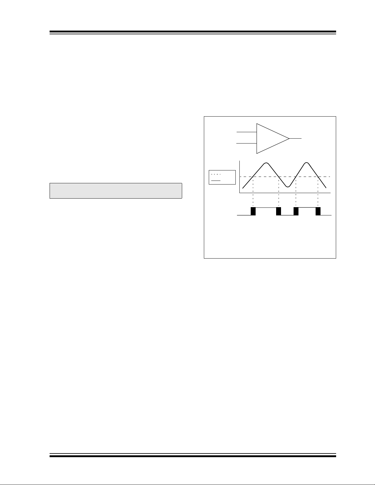
PIC16F688
7.0 COMPARATOR MODULE
Comparators are used to interface analog circuits to a
digital circuit by comparing two analog voltages and
providing a digital indication of their relative magnitudes.
The comparators are very useful mixed signal building
blocks because they provide analog functionality
independent of the program execution. The Analog
Comparator module includes the following features:
• Dual compara tors
• Multiple comparator configurations
• Comparator outputs are available internally/externally
• Programmable output polarity
• Interrupt-on-change
• Wake-up from Sleep
• Timer1 gate (co unt ena ble )
• Output synchronization to Timer1 clock input
• Programmable voltage reference
Note: Only Comparator C2 can be linked to
Timer1.
7.1 Comparator Overview
A comparator is shown in Figure 7-1 along with the
relationship between the analog input levels and the
digital output. When the analog voltage at V
than the analog voltage at V
comparator is a digital low level. When the analog
voltage at V
V
IN-, the output of the comparat or is a digit al high le vel.
IN+ is greater than the analog voltage at
IN-, the output of the
FIGURE 7-1: SINGLE COMPARATOR
Output
VIN+
IN-
V
VIN-
VIN+
+
–
IN+ is less
Output
Note: The black areas of the output of the
comparator represents the uncertainty
due to input offsets and response time.
This device contains two comparators as shown in
Figure 7-2 and Figure 7-3. The comparators are not
independently configurable.
© 2007 Microchip Technology Inc. DS41203D-page 53

PIC16F688
FIGURE 7-2: COMPARATOR C1 OUTPUT BLOCK DIAGRAM
MULTIPLEX
Port Pins
C1INV
C1
To C1OUT pin
DQ
Q1
Q3*RD CMCON0
Note 1: Q1 and Q3 are phases of the four-phase system clock (FOSC).
2: Q1 is held high during Sleep mode.
Reset
EN
DQ
EN
CL
RD CMCON0
FIGURE 7-3: COMPARATOR C2 OUTPUT BLOCK DIAGRAM
MULTIPLEX
Port Pins
C2
C2INV
Timer1
clock source
DQ
(1)
C2SYNC
0
1
To Data Bus
Set C1IF bit
T o Timer1 Gate
To C2OUT pin
DQ
Q1
Q3*RD CMCON0
Note 1: Comparator output is latched on falling edge of Timer1 clock source.
2: Q1 and Q3 are phases of the four-phase system clock (F
3: Q1 is held high during Sleep mode.
DS41203D-page 54 © 2007 Microchip Technology Inc.
Reset
EN
DQ
EN
CL
RD CMCON0
OSC).
To Data Bus
Set C2IF bit

7.1.1 ANALOG INPUT CONNECTION
CONSIDERATIONS
A simplified circuit for an analog input is shown in
Figure 7-4. Since the analog i nput pins share thei r connection with a digital input, they have reverse biased
ESD protection diodes to V
input, therefore, must be between V
input voltage deviates from this range by more than
0.6V in either direction, one of the diodes is forward
biased and a latch-up may occur.
A maximum source impedance of 10 kΩ is recommended
for the analog sources. Also, any external component
connected to an analog input pin, such as a capacitor or
a Zener diode, should have very little leakage curr ent to
minimize inaccuracies introduced.
DD and VSS. The analog
SS and VDD. If the
FIGURE 7-4: ANALOG INPUT MODEL
VDD
PIC16F688
Note 1: When reading a PORT register, all pins
configured as anal og inp uts will read as a
‘0’. Pins configured as digital inputs will
convert as an analog input, according to
the input specification.
2: Analog levels on any pin defined as a
digital input, may cause the input buffer to
consume more current than is specified.
Rs < 10K
AIN
C
VA
Legend: CPIN = In put Capacitance
I
LEAKAGE = Leakage Current at the pin due to various junctions
IC = Interconnect Resistance
R
S = Source Impedance
R
V
A = Analog Voltage
T = Threshold Voltage
V
PIN
5 pF
VT ≈ 0.6V
VT ≈ 0.6V
RIC
To ADC Input
ILEAKAGE
±500 nA
Vss
© 2007 Microchip Technology Inc. DS41203D-page 55

PIC16F688
7.2 Comparator Configuration
There are eight mod es of operat ion fo r the comp arato r.
The CM<2:0> bits of th e CMCON0 reg ister are used to
select these modes as shown in Figure 7-5. I/O lines
change as a function of the mode and are designated
as follows:
• Analog function (A): digital input buffer is disabled
• Digital function (D): comparator digital output,
overrides port function
• Normal port function (I/O): independent of
comparator
The port pins denoted as “A” will read as a ‘0’
regardless of the state of the I/O pin or the I/O control
TRIS bit. Pins used as analog inputs should also have
the corresponding TRIS bit set to ‘1’ to disable the
digital output driver. Pins denoted as “D” should have
the corresponding TRIS bit set to ‘0’ to enable the
digital output driver.
Note: Comparator interrupts should be disabled
during a Comparator mode change to
prevent unintended inter r upts.
DS41203D-page 56 © 2007 Microchip Technology Inc.

FIGURE 7-5: COMPARATOR I/O OPERATING MODES
Comparators Reset (POR Default Value)
CM<2:0> = 000
A
C1INC1IN+
C2INC2IN+
VIN-
(1)
C1
IN+
V
A
A
VIN-
C2
IN+
V
A
Off
Off
(1)
Two Independent Comparators
CM<2:0> = 100
C1INC1IN+
C2INC2IN+
PIC16F688
A
VIN-
C1
IN+
V
A
A
VIN-
C2
IN+
V
A
C1OUT
C2OUT
Three Inputs Multiplexed to Two Comparators
CM<2:0> = 001
C1INC1IN+
C2INC2IN+
A
CIS = 0
A
CIS = 1
A
A
VINVIN+
VINVIN+
C1
C2
Four Inputs Multiplexed to Two Comparators
CM<2:0> = 010
C1INC1IN+
C2INC2IN+
A
A
A
A
CIS = 0
CIS = 1
CIS = 0
CIS = 1
VIN-
C1
VIN+
VIN-
C2
VIN+
From CVREF Module
Two Common Reference Comparators
CM<2:0> = 011
A
I/O
VIN-
IN+
V
C1
C1OUT
C1INC1IN+
C1OUT
C2OUT
C1OUT
C2OUT
One Independent Comparator
CM<2:0> = 101
I/O
I/O
A
A
VIN-
IN+
V
VIN-
IN+
V
C1
C2
(1)
Off
C2OUT
C1INC1IN+
C2INC2IN+
Two Common Reference Comparators with Outputs
CM<2:0> = 110
A
C1IN-
C1OUT(pin)
C2INC2IN+
C2OUT(pin)
VIN-
C1
IN+
V
D
A
VIN-
C2
IN+
V
A
D
C1OUT
C2OUT
Comparators Off (Lowest Power)
CM<2:0> = 111
I/O
I/O
VIN-
IN+
V
C1
Off
(1)
C1INC1IN+
C2INC2IN+
VIN-
C2
VIN+
A
C2OUT
C2INC2IN+
I/O
I/O
VIN-
IN+
V
C2
Off
(1)
A
Legend: A = Analog Input, ports always reads ‘0’ CIS = Comparator Input Switch (CMCON0<3>)
I/O = Normal port I/O D = Comparator Digital Output
Note 1: Reads as ‘0’, unless CxINV = 1.
© 2007 Microchip Technology Inc. DS41203D-page 57

PIC16F688
7.3 Comparator Control
The CMCON0 register (Register 7-1) provides access
to the following comparator features:
• Mode selection
• Output state
• Output polarity
• Input switch
7.3.1 COMPARATOR OUTPUT STATE
Each comparator state can always be read internally
via the associat ed CxO UT bit of the CMCON0 regi ste r.
The comparator outputs are directed to the CxOUT
pins when CM<2:0> = 110. When this mode is
selected, the TRIS bits for the associated CxOUT pins
must be cleared to enable the output drivers.
7.3.2 COMPARATOR OUTPUT POLARITY
Inverting the output of a comparator is functionally
equivalent to swapping the comparator inputs. The
polarity of a comparator output can be inverted by setting the CxI NV bits of th e CMCON0 reg ister. Clearing
CxINV results in a non-inverted output. A complete
table showing the output state versus input conditions
and the polarity bit is shown in Table 7-1.
TABLE 7-1: OUTPUT STATE VS. INPUT
CONDITIONS
Input Conditions CxINV CxOUT
V
IN- > VIN+ 00
VIN- < VIN+ 01
IN- > VIN+ 11
V
VIN- < VIN+ 10
Note: CxOUT refers to both the register bit and
output pin.
DS41203D-page 58 © 2007 Microchip Technology Inc.

PIC16F688
7.3.3 COMPARATOR INPUT SWITCH
The inverting inpu t of the compa rators may be sw itched
between two analog pins in the following modes:
• CM<2:0> = 001 (Comparator C1 only)
• CM<2:0> = 010 (Comparators C1 and C2)
In the above modes, both pins remain in analog mode
regardless of which pin is selected as the input. Th e CIS
bit of the CMCON0 register controls the comparator
input switch.
7.4 Comparator Response Time
The comparator output is indeterminate for a period of
time after the chang e of an input source o r the selectio n
of a new reference voltage . This period is refe rred to as
the response time. The response time of the
comparator differs from the settling time of the voltage
reference. Therefore, both of these times must be
considered when determining the total response time
to a comparator input ch ange. See the Comparato r and
Voltage Reference specifications in Section 14.0
“Electrical Specifications” for more details.
7.5 Comparator Interrupt Operation
The comparator interrupt flag is set whenever there is
a change in the output value of the comparator.
Changes are recognized by means of a mismatch
circuit which consists of two latches and an exclusiveor gate (see Figure 7-2 and Figure 7-3). One latch is
updated with the comparator output level when the
CMCON0 register is read. This latch retains the value
until the next read of the CMCON0 register or the
occurrence of a Reset. The other latch of the mismatch
circuit is updated on every Q1 system clock. A
mismatch condition will occur when a comparator
output change is clocked through the second latch on
the Q1 clock cycle. The mi smatch cond ition will pers ist,
holding the CxIF bit of the PIR1 register true, until either
the CMCON0 register is read or the comparator output
returns to the previous state.
Note: A write operation to the CMCON0 register
will also clear the mismatch condition
because all writes include a read
operation at the beginning of the write
cycle.
Software will need to maintain information about the
status of the comparat or output to dete rmine the actual
change that has occurred.
The CxIF bit of the PIR1 register is the comparator
interrupt flag. This bit must be reset in software by
clearing it to ‘0’. Since it is also possible to wr ite a ‘1’ to
this register, a simulated interrupt may be initiated.
The CxIE bit of the PIE1 re gister and the PEIE and GIE
bits of the INTCON register must all be set to enable
comparator interrupts. If any of these bits are cleared,
the interrupt is not enabl ed, althou gh the CxI F bit of the
PIR1 register will still be set if an interrupt condition
occurs.
The user , in the Interru pt Service Routi ne, can cle ar the
interrupt in the following manner:
a) Any read or write of CMCON0. This will end the
mismatch condition. See Figures 7-6 and 7-7
b) Clear the CxIF interrupt flag.
A persistent mismatch condition will preclude clearing
the CxIF interrupt flag. Reading CMCON0 will end the
mismatch condition and allow the CxIF bit to be
cleared.
© 2007 Microchip Technology Inc. DS41203D-page 59

PIC16F688
FIGURE 7-6: COMPARATOR
INTERRUPT TIMING W/O
CMCON0 READ
Q1
Q3
IN+
C
OUT
C
Set CMIF (level)
CMIF
TRT
reset by software
FIGURE 7-7: COMPARATOR
INTERRUPT TIMING WITH
CMCON0 READ
Q1
Q3
IN+
C
OUT
C
Set CMIF (level)
CMIF
cleared by CMCON0 read
Note 1: If a change in the CM1CON0 register
2: When either comparator is first enabled,
TRT
reset by software
(CxOUT) occurs when a read operation is
being executed (start of the Q2 cycle),
then the CxIF Interrupt Flag bit of the
PIR1 register may not get set.
bias circuitry in the Comparator module
may cause an invalid output from the
comparator until the bias circuitry is stable.
Allow about 1 μs for bias settling then clear
the mismatch condition and interrupt flags
before enabling comparator interrupts.
7.6 Operation During Sleep
The comparator , if enabled before entering Sleep m ode,
remains active during Sleep. The additional current
consumed by the comparator is shown separately in
Section 14.0 “Electrical Specifications”. If the
comparator is not used to wake the device, power
consumption can be minimized while in Sleep mode by
turning off the comparator. The comparator is turned off
by selecting mode CM<2:0> = 000 or CM<2:0> = 111
of the CMCON0 register.
A change to the comparator output can wake-up the
device from Sleep. To enable the comparator to wake
the device from Sleep, the CxIE bi t of the PIE1 reg ister
and the PEIE bit of the INTCON register must be set.
The instruction following the Sleep instruction always
executes following a wake from Sleep. If the GIE bit of
the INTCON register is also set, the device will then
execute the Interrupt Service Routine.
7.7 Effects of a Reset
A device Reset forces the CMCON0 and CMCON1
registers to their R eset st ates . This forces th e Co mp arator module to be in the Comparator Reset mode
(CM<2:0> = 000). Thus, all comparator inputs are
analog inputs with the co mparator disab led to consume
the smallest current possible.
DS41203D-page 60 © 2007 Microchip Technology Inc.

PIC16F688
REGISTER 7-1: CMCON0: COMPARATOR CONFIGURATION REGISTER
R-0 R-0 R/W-0 R/W-0 R/W-0 R/W-0 R/W-0 R/W-0
C2OUT C1OUT C2INV C1INV CIS CM2 CM1 CM0
bit 7 bit 0
Legend:
R = Readable bit W = Writable bit U = Unimplemented bit, read as ‘0’
-n = Value at POR ‘1’ = Bit is set ‘0’ = Bit is cleared x = Bit is unknown
bit 7 C2OUT: Comparator 2 Output bit
When C2INV =
1 = C2 VIN+ > C2 VIN0 = C2 V
When C2INV =
1 = C2 VIN+ < C2 VIN0 = C2 V
bit 6 C1OUT: Comparator 1 Output bit
When C1INV = 0:
1 = C1 VIN+ > C1 VIN0 = C1 V
When C1INV = 1:
1 = C1 VIN+ < C1 VIN0 = C1 V
bit 5 C2INV: Comparator 2 Output Inver s ion bit
1 = C2 output inverted
0 = C2 output not inverted
bit 4 C1INV: Comparator 1 Output Inver s ion bit
1 = C1 Output inverted
0 = C1 Output not inverted
bit 3 CIS: Comparator Input Switch bit
When CM<2:0> = 010:
1 = C1IN+ connects to C1 VIN-
C2IN+ connects to C2 V
0 = C1IN- connects to C1 V
C2IN- connects to C2 V
When CM<2:0> =
1 = C1IN+ connects to C1 VIN0 = C1IN- connects to C1 V
bit 2-0 CM<2:0>: Comparator Mode bits (See Figure 7-5)
000 = Comparators off. CxIN pins are configured as analog
001 = Three inputs multiplexed to two compar ators
010 = Four inputs multiplexed to two comparators
011 = Two common reference comparators
100 = Two independent comparators
101 = One independent comparator
110 = Two common reference comparators with outputs
111 = Comparators off. CxIN pins are configured as digital I/O
0:
IN+ < C2 VIN-
1:
IN+ > C2 VIN-
IN+ < C1 VIN-
IN+ > C1 VIN-
IN-
IN-
IN-
001:
IN-
© 2007 Microchip Technology Inc. DS41203D-page 61

PIC16F688
7.8 Comparator C2 Gating Timer1
This feature can be used to time the duration or interval
of analog events. Clearing the T1GSS bit of the
CMCON1 register will enable Timer1 to increment
based on the output of Comparator C2. This requires
that Timer1 is on and gating is enabled. See
Section 6.0 “Timer1 Module with Gate Control” for
details.
It is recommended to synchronize Comparator C2 with
Timer1 by setting the C2SYNC bit when the comparator
is used as the Timer1 gate source. This ensures Timer1
does not miss an increme nt if the compar a tor ch an ges
during an increment.
7.9 Synchronizing Comparator C2
Output to Timer1
The output of Comparator C2 can be synchronized with
Timer1 by setting the C2SYNC bit of the CMCON1
register. When enabled, the comparator output is
latched on the falling edge of the Timer1 clock source.
If a prescaler is used with Timer1, the comparator
output is latched after the prescaling function. To
prevent a race condition, the comparator output is
latched on the falling ed ge of the Timer1 clock source
and Timer1 increments on the rising edge of its clock
source. Reference the comparator block diagrams
(Figure 7-2 and Figure 7-3) and the Timer1 Block
Diagram (Figure 6-1) for more information.
REGISTER 7-2: CMCON1: COMPARATOR CONFIGURATION REGISTER
U-0 U-0 U-0 U-0 U-0 U-0 R/W-1 R/W-0
— — — — — — T1GSS C2SYNC
bit 7 bit 0
Legend:
R = Readable bit W = Writable bit U = Unimplemented bit, read as ‘0’
-n = Value at POR ‘1’ = Bit is set ‘0’ = Bit is cleared x = Bit is unknown
bit 7-2 Unimplemented: Read as ‘0’
bit 1 T1GSS: Timer1 Gate Source Select bit
1 = Timer1 gate source is T1G pin (pin should be configured as digital input)
0 = Timer1 gate source is Comparator C2 output
bit 0 C2SYNC: Comparator C2 Output Synchronization bit
1 = Output is synchronized with falling edge of Timer1 clock
0 = Output is asynchronous
Note 1: Refer to Section 6.6 “Timer1 Gate”.
2: Refer to Figure 7-3.
(1)
(2)
DS41203D-page 62 © 2007 Microchip Technology Inc.

PIC16F688
7.10 Comparator Voltage Reference
The Comparator Voltage Reference module provides
an internally generat ed voltage reference for the comparators. The following features are available:
• Independent from Comparator operation
EQUATION 7-1: CVREF OUTPUT VOLTAGE
RR 1 (low range):=
V
CV
REF (VR<3:0>/24) VDD×=
VRR 0 (high range):=
REF (VDD/4) + =
CV
• Two 16-level voltage ranges
• Output clamped to V
SS
• Ratiometric with VDD
The VRCON register (Figure7-3) controls the Voltage
Reference module shown in Figure 7-8.
7.10.1 INDEPENDENT OPERATION
The comparator voltage reference is independent of
the comparator configuration. Setting the VREN bit of
the VRCON register will enable the voltage reference.
7.10.2 OUTPUT VOLTAGE SELECTION
The full range of VSS to VDD cannot be realized due to
the construction of the module. See Figure 7-8.
7.10.3 OUTPUT CLAMPED TO VSS
The CVREF output voltage can be set to Vss with no
power consumption by configuring VRCON as follo ws:
•VREN=0
•VRR=1
•VR<3:0>=0000
This allows the comparator to detect a zero-crossing
while not consuming additional CV
The CVREF voltage reference has 2 ranges with 16
voltage levels in each range. Range selection is
controlled by the VRR bit of the VRCON register. The
16 levels are set with the VR<3:0> bits of the VRCON
register.
The CVREF output voltage is determined by the following
equations:
7.10.4 OUTPUT RATIOMETRIC TO VDD
The comparator voltage reference is VDD d erived and
therefore, the CV
DD. The tested absolute accur acy of the Comparator
V
Voltage Reference can be found in Section 14.0
“Electrical Specifications”.
REF output changes with fluctuations in
REGISTER 7-3: VRCON: VOLTAGE REFERENCE CONTROL REGISTER
(VR<3:0> V
REF module current.
DD/32)×
R/W-0 U-0 R/W-0 U-0 R/W-0 R/W-0 R/W-0 R/W-0
VREN —VRR— VR3 VR2 VR1 VR0
bit 7 bit 0
Legend:
R = Readable bit W = Writable bit U = Unimplemented bit, read as ‘0’
-n = Value at POR ‘1’ = Bit is set ‘0’ = Bit is cleared x = Bit is unknown
bit 7 VREN: CV
1 = CV
0 = CV
REF Enable bit
REF circuit powered on
REF circuit powered down, no IDD drain and CVREF = VSS.
bit 6 Unimplemented: Read as ‘0’
bit 5 VRR: CVREF Range Selection bit
1 = Low range
0 = High range
bit 4 Unimplemented: Read as ‘0’
bit 3-0 VR<3:0>: CV
When V
REF Value Selection bits (0 ≤ VR<3:0> ≤ 15)
RR = 1: CVREF = (VR<3:0>/24) * VDD
When VRR = 0: CVREF = VDD/4 + (VR<3:0> /32) * VDD
© 2007 Microchip Technology Inc. DS41203D-page 63

PIC16F688
FIGURE 7-8: COMPARATOR VOLTAGE REFERENCE BLOCK DIAGRAM
16 Stages
8R R R R R
VDD
VRR
VREN
CVREF to
Comparator
Input
16-1 Analog
MUX
15
14
2
1
0
VR<3:0>
8R
(1)
VREN
VR<3:0> = 0000
VRR
Note 1: Care should be taken to ensure VREF remains
within the comparator common mode input
range. See Section 14.0 “Electrical Specifica-
tions” for more detail.
T ABLE 7-2: SUMMARY OF REGISTERS ASSOCIATED WITH THE COMPARATOR AND V OLT AGE
REFERENCE MODULES
Name Bit 7 Bit 6 Bit 5 Bit 4 Bit 3 Bit 2 Bit 1 Bit 0
ANSEL ANS7 ANS6 ANS5 ANS4
CMCON0 C2OUT C1OUT
CMCON1
INTCON GIE PEIE
PIE1
PIR1
PORTA
PORTC
TRISA
TRISC
VRCON VREN
Legend: x = unknown, u = unchanged, – = unimplemented, read as ‘0’. Shaded cells are not used for comparator.
— — — — — — T1GSS C2SYNC ---- --10 ---- --10
EEIE ADIE RCIE C2IE C1IE OSFIE TXIE TMR1IE 0000 0000 0000 0000
EEIF ADIF RCIF C2IF C1IF OSFIF TXIF TMR1IF 0000 0000 0000 0000
— — RA5 RA4 RA3 RA2 RA1 RA0 --x0 x000 --x0 x000
— — RC5 RC4 RC3 RC2 RC1 RC0 --xx 0000 --xx 0000
— — TRISA5 TRISA4 TRISA3 TRISA2 TRISA1 TRISA0 --11 1111 --11 1111
— — TRISC5 TRISC4 TRISC3 TRISC2 TRISC1 TRISC0 --11 1111 --11 1111
—VRR— VR3 VR2 VR1 VR0 0-0- 0000 0-0- 0000
C2INV C1INV CIS CM 2 CM1 CM0 0000 0000 0000 0000
T0IE INTE RAIE T0IF INTF RAIF 0000 000x 0000 000x
ANS3 ANS2 ANS1 ANS0 1111 1111 1111 1111
Val ue on
POR, BOR
Value on
all other
Resets
DS41203D-page 64 © 2007 Microchip Technology Inc.
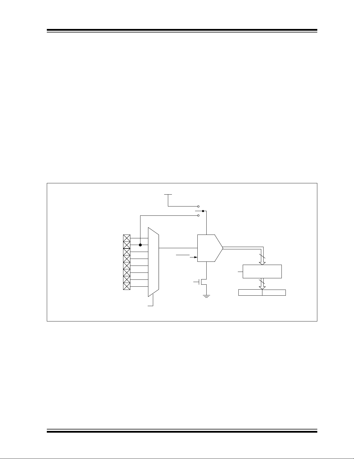
8.0 ANALOG-TO-DIGITAL
CONVERTER (ADC) MODULE
The Analog-to-Digital Converter (ADC) allows
conversion of an analog input signal to a 10-bit binary
representation of that signal. This device uses analog
inputs, which are multiplexed into a single sample and
hold circuit. The output of the sample and hold is
connected to the input of the converter. The converter
generates a 10-bit binary result via successive
approximation and stores the conversion result into the
ADC result registers (ADRESL and ADRESH).
The ADC voltage reference is software selectable to
DD or a voltage appli ed to the ex ternal reference
either V
pins.
The ADC can generate an interrupt upon completion of
a conversion. This interrupt can be used to wak e-up the
device from Sleep.
Figure 8-1 shows the block diagram of the ADC.
FIGURE 8-1: ADC BLOCK DIAGRAM
PIC16F688
RA0/AN0
RA1/AN1/VREF
RA2/AN2
RA4/AN3
RC0/AN4
RC1/AN5
RC2/AN6
RC3/AN7
VREF
CHS
000
001
010
011
100
101
110
111
VDD
VCFG = 0
VCFG = 1
GO/DONE
ADON
VSS
A/D
ADFM
0 = Left Justify
1 = Right Justify
ADRESH
10
10
ADRESL
© 2007 Microchip Technology Inc. DS41203D-page 65

PIC16F688
8.1 ADC Configuration
When configuring and using the ADC the following
functions must be considered:
• Port configuration
• Channel selection
• ADC voltage reference selection
• ADC conversion clock source
• Interrupt control
• Results formatting
8.1.1 PORT CONFIGURATION
The ADC can be used to convert both analog and digital
signals. When converting analog signals, the I/O pin
should be configured for analog by setting the associated
TRIS and ANSEL bits. See the corresponding Port
section for more information.
Note: Analog voltages on any pin that is defined
as a digital input may cause the input
buffer to conduct excess current.
8.1.2 CHANNEL SELECTION
The CHS bits of the ADCON0 regi ster determ ine which
channel is connected to the sample and hold circuit.
When changing channels, a delay is required before
starting the next conversion. Refer to Section 8.2
“ADC Operation” for more information.
For correct conversion, the approp riate TAD specification
must be met. See A/D conversion requirements in
Section 14.0 “Electrical Specifications” for more
information. Table 8-1 gives examples of appropriate
ADC clock selections.
Note: Unless using the FRC, any changes in the
system clock frequency will change the
ADC clock frequency, which may
adversely affect the ADC result.
8.1.3 ADC VOLTAGE REFERENCE
The VCFG bit of the ADCON0 register prov ides contro l
of the positive voltage reference. The positive voltage
reference can be either VDD or an external voltage
source. The negative voltage reference is always
connected to the ground reference.
8.1.4 CONVERSION CLOCK
The source of the conversion clock is software selectable via the AD CS bi ts of t he AD CO N1 re gis te r. There
are seven possible clock options:
OSC/2
•F
•FOSC/4
•FOSC/8
•F
OSC/16
•FOSC/32
•FOSC/64
•F
RC (dedicated internal oscillator)
The time to complete one bit conversion is defined as
TAD. One full 10-bit conversion requires 11 TAD periods
as shown in Figure8-3.
DS41203D-page 66 © 2007 Microchip Technology Inc.

PIC16F688
TABLE 8-1: ADC CLOCK PERIOD (T AD) VS. DEVICE OPERATING FREQUENCIES (VDD > 3.0V)
ADC Clock Period (TAD) Device Frequency (FOSC)
ADC Clock Source ADCS<2:0> 20 MHz 8 MHz 4 MHz 1 MHz
F
OSC/2 000 100 ns
FOSC/4 100 200 ns
OSC/8 001 400 ns
F
FOSC/16 101 800 ns
(2)
(2)
(2)
(2)
FOSC/32 010 1.6 μs4.0 μs 8.0 μs
FOSC/64 110 3.2 μs 8.0 μs
FRC x11 2-6 μs
(1,4)
Legend: Shaded cells are outside of recommended range.
Note 1: The FRC source has a typical TAD time of 4 μs for VDD > 3.0V.
2: These values violate the minimum required TAD time.
3: For faster conversion times, the selection of another clock source is recommended.
4: When the device frequency is greater than 1 MHz, the F
conversion will be performed during Sleep.
250 ns
500 ns
1.0 μs
(2)
(2)
(2)
(2)
500 ns
1.0 μs
(2)
2.0 μs
4.0 μs
2.0 μs 8.0 μs
2.0 μs4.0 μs 16.0 μs
(3)
(3)
(1,4)
2-6 μs
RC clock source is only recommended if the
2-6 μs
16.0 μs
(3)
(1,4)
32.0 μs
64.0 μs
2-6 μs
(3)
(3)
(3)
(3)
(1,4)
FIGURE 8-2: ANALOG-TO-DIGITAL CONVERSION T
TCY to TAD
Set GO/DONE bit
TAD1 TAD2 TAD3 TAD4 TAD5 TAD6 TAD7 TAD8 TAD9
b9 b8 b7 b6 b5 b4 b3 b2
Conversion Starts
Holding Capacitor is Disconnected from Analog Input (typically 100 ns)
ADRESH and ADRESL registers are loaded,
GO bit is cleared,
ADIF bit is set,
Holding capacitor is connected to analog input
AD CYCLES
TAD10 TAD11
b1 b0
© 2007 Microchip Technology Inc. DS41203D-page 67

PIC16F688
8.1.5 INTERRUPTS
The ADC module allows for the ability to generate an
interrupt upon completion of an Analog-to-Digital
Conversio n. The ADC int errupt flag is the ADIF bit in
the PIR1 register . The A DC interrupt enable is the ADIE
bit in the PIE1 register . The ADIF bit must be cleared in
software.
Note: The ADIF bit is set at the completion of
every conversion, regardless of whether
or not the ADC interrupt is enabled.
This interrupt can be generated while the device is
operating or while in Sle ep. If the device is in Sleep, the
interrupt will wake-up the device. Upon waking from
Sleep, the next instruction following the SLEEP
instruction is always executed. If the user is attempting
to wake-up from Sleep and resume in-line code
execution, the global interrupt must be disabled. If the
global interrupt is enabled, execution will switch to the
Interrup t Service Routine.
Please see Section 8.1.5 “Interrupts” for more
information.
8.1.6 RESULT FORMATTING
The 10-bit A/D Conversion result can be supplied in
two formats, left j ustified or right ju stified. T he ADFM bit
of the ADCON0 register controls the output format.
Figure 8-4 shows the two output formats.
FIGURE 8-3: 10-BIT A/D CONVERSION RESULT FORMAT
ADRESH ADRESL
(ADFM = 0)MSB LSB
bit 7 bit 0 bit 7 bit 0
10-bit A/D Result Unimplemented: Read as ‘0’
(ADFM = 1)
bit 7 bit 0 bit 7 bit 0
Unimplemented: Read as ‘0’ 10-bit A/D Result
MSB LSB
DS41203D-page 68 © 2007 Microchip Technology Inc.

PIC16F688
8.2 ADC Operation
8.2.1 STARTING A CONVERSION
To enable the ADC module, the ADON bit of the
ADCON0 register must be set to a ‘1’. Setting the GO/
DONE bit of the ADCON0 register to a ‘1’ will start the
Analog-to-Digital Conversion.
Note: The GO/DONE bit should not be set in the
same instruction that turns on the ADC.
Refer to Section 8.2.5 “A/D Conversion
Procedure”.
8.2.2 COMPLETION OF A CONVERSION
When the convers ion is complet e, the ADC module will:
• Clear the GO/DONE
• Set the ADIF flag bit
• Update the ADRESH:ADRESL regis ters with new
conversion result
8.2.3 T ERMINATING A CONVERSION
If a conversion must be terminated before completion,
the GO/DONE
ADRESH:ADRESL registers will not be updated with
the partially complete Analog-to-Digital Conversion
sample. Instead, the ADRESH:ADRESL register pair
will retain the value of the prev ious conversi on. Additionally, a 2 T
sition can be initiated. Following this delay, an input
acquisition is automatically started on the selected
channel.
AD delay is required before ano ther acqui-
bit
bit can be cleared in software. The
8.2.5 A/D CONVERSION PROCEDURE
This is an example procedure for using the ADC to
perform an Analog-to-Digital Conversion:
1. Configure Port:
• Disable pin output driver (See TRIS register)
• Configure pin as analog
2. Configure the ADC module:
• Select ADC conversion clock
• Configure voltage refere nc e
• Select ADC input channel
• Select result format
• Turn on ADC module
3. Configure ADC interrupt (optional):
• Clear ADC interrupt flag
• Enable ADC interrupt
• Enable peripheral interrupt
• Enable global interrupt
4. Wait the required acquisition time
5. Start conversion by setting the GO/DONE bit.
6. Wait for ADC conversion to complete by one of
the following:
• Polling the GO/DONE
• Waiting for the ADC interrupt (interrupts
enabled)
7. Read ADC Result
8. Clear the ADC interrupt flag (required if interrupt
is enabled).
(1)
bit
(2)
.
Note: A device Reset forces all registers to their
Reset state. Thus, the ADC module is
turned off and any pending conversion is
terminated.
8.2.4 ADC OPERATION DURING SLEEP
The ADC module can operate during Sleep. This
requires the ADC clock source to be set to the F
option. When the FRC clock source is selected, the
ADC waits one a dditional instructi on before sta rting the
conversion. This allows the SLEEP instruction to be
executed, which can reduce system noise during the
conversion. If the ADC interrupt is enabled, the device
will wake-up from Sleep when the conversion
completes. If the ADC interrupt is disabled, the ADC
module is turned off after the conversion completes,
although the ADON bit remains set.
When the ADC clock source is something other than
RC, a SLEEP instruction causes the present conver-
F
sion to be a borted an d the ADC mo dule is tu rned off,
although the ADON bit remains set.
RC
Note 1: The global interrupt can be disabled i f the
user is attempting to wake-up from Sleep
and resume in-line code execution.
2: See Section 8.3 “A/D Acquisition
Requirements”.
© 2007 Microchip Technology Inc. DS41203D-page 69

PIC16F688
EXAMPLE 8-1: A/D CONVERSION
;This code block configures the ADC
;for polling, Vdd reference, Frc clock
;and AN0 input.
;
;Conversion start & polling for completion
; are included.
;
BANKSEL ADCON1 ;
MOVLW B’01110000’ ;ADC Frc clock
MOVWF ADCON1 ;
BANKSEL TRISA ;
BSF TRISA,0 ;Set RA0 to input
BANKSEL ANSEL ;
BSF ANSEL,0 ;Set RA0 to analog
BANKSEL ADCON0 ;
MOVLW B’10000001’ ;Right justify,
MOVWF ADCON0 ;Vdd Vref, AN0, On
CALL SampleTime ;Acquisiton delay
BSF ADCON0,GO ;Start conversion
BTFSC ADCON0,GO ;Is conversion done?
GOTO $-1 ;No, test again
BANKSEL ADRESH ;
MOVF ADRESH,W ;Read upper 2 bits
MOVWF RESULTHI ;store in GPR space
BANKSEL ADRESL ;
MOVF ADRESL,W ;Read lower 8 bits
MOVWF RESULTLO ;Store in GPR space
DS41203D-page 70 © 2007 Microchip Technology Inc.

PIC16F688
8.2.6 ADC REGISTER DEFINITIONS
The following registers are used to control the operation of the ADC.
REGISTER 8-1: ADCON0: A/D CONTROL REGISTER 0
R/W-0 R/W-0 U-0 R/W-0 R/W-0 R/W-0 R/W-0 R/W-0
ADFM VCFG
bit 7 bit 0
Legend:
R = Readable bit W = Writable bit U = Unimplemented bit, read as ‘0’
-n = Value at POR ‘1’ = Bit is set ‘0’ = Bit is cleared x = Bit is unknown
bit 7 ADFM: A/D Conversion Result Format Select bit
1 = Right justified
0 = Left justified
bit 6 VCFG: Voltage Reference bit
= VREF pin
1
0
= VDD
bit 5 Unimplemented: Read as ‘0’
bit 4-2 CHS<2:0>: Analog Channel Select bits
—
000 = AN0
001 = AN1
010 = AN2
011 = AN3
100 = AN4
101 = AN5
110 = AN6
111 = AN7
bit 1 GO/DONE: A/D Conversio n Status bit
1
= A/D Conversion cycle in progress. Setting this bit starts an A/D Conversion cycle.
This bit is automatically cleared by hardware when the A/D Conversion has completed.
0
= A/D Conversion completed/not in progress
bit 0 ADON: ADC Enable bit
1 = ADC is enabled
0 = ADC is disabled and consumes no operating current
REGISTER 8-2: ADCON1: A/D CONTROL REGISTER 1
CHS2 CHS1 CHS0 GO/DONE ADON
U-0 R/W-0 R/W-0 R/W-0 U-0 U-0 U-0 U-0
—
bit 7 bit 0
Legend:
R = Readable bit W = Writable bit U = Unimplemented bit, read as ‘0’
-n = Value at POR ‘1’ = Bit is set ‘0’ = Bit is cleared x = Bit is unknown
bit 7 Unimplemented: Read as ‘0’
bit 6-4
ADCS2 ADCS1 ADCS0
ADCS<2:0>: A/D Conversion Clock Select bits
000 = F
001 = F
010 = F
x11 = F
100 = F
OSC/2
OSC/8
OSC/32
RC (clock derived from a dedicated internal oscillator = 500 kHz max)
OSC/4
— — — —
101 = FOSC/16
110 = F
bit 3-0 Unimplemented: Read as ‘0’
© 2007 Microchip Technology Inc. DS41203D-page 71
OSC/64

PIC16F688
REGISTER 8-3: ADRESH: ADC RESULT REGISTER HIGH (ADRESH) ADFM = 0
R/W-x R/W-x R/W-x R/W-x R/W-x R/W-x R/W-x R/W-x
ADRES9 ADRES8 ADRES7 ADRES6 ADRES5 ADRES4 ADRES3 ADRES2
bit 7 bit 0
Legend:
R = Readable bit W = Writable bit U = Unimplemented bit, read as ‘0’
-n = Value at POR ‘1’ = Bit is set ‘0’ = Bit is cleared x = Bit is unknown
bit 7-0 ADRES<9:2>: ADC Result Register bits
REGISTER 8-4: ADRESL: ADC RESULT REGISTER LOW (ADRESL) ADFM = 0
R/W-x R/W-x R/W-x R/W-x R/W-x R/W-x R/W-x R/W-x
ADRES1 ADRES0
bit 7 bit 0
Legend:
R = Readable bit W = Writable bit U = Unimplemented bit, read as ‘0’
-n = Value at POR ‘1’ = Bit is set ‘0’ = Bit is cleared x = Bit is unknown
Upper 8 bits of 10-bit conversion result
— — — — — —
bit 7-6 ADRES<1:0>: ADC Result Register bits
bit 5-0 Reserved: Do not use.
Lower 2 bits of 10-bit conversion result
REGISTER 8-5: ADRESH: ADC RESULT REGISTER HIGH (ADRESH) ADFM = 1
R/W-x R/W-x R/W-x R/W-x R/W-x R/W-x R/W-x R/W-x
— — — — — — ADRES9 ADRES8
bit 7 bit 0
Legend:
R = Readable bit W = Writable bit U = Unimplemented bit, read as ‘0’
-n = Value at POR ‘1’ = Bit is set ‘0’ = Bit is cleared x = Bit is unknown
bit 7-2 Reserved: Do not use.
bit 1-0 ADRES<9:8>: ADC Result Register bits
Upper 2 bits of 10-bit conversion result
REGISTER 8-6: ADRESL: ADC RESULT REGISTER LOW (ADRESL) ADFM = 1
R/W-x R/W-x R/W-x R/W-x R/W-x R/W-x R/W-x R/W-x
ADRES7 ADRES6 ADRES5 ADRES4 ADRES3 ADRES2 ADRES1 ADRES0
bit 7 bit 0
Legend:
R = Readable bit W = Writable bit U = Unimplemented bit, read as ‘0’
-n = Value at POR ‘1’ = Bit is set ‘0’ = Bit is cleared x = Bit is unknown
bit 7-0 ADRES<7:0>: ADC Result Register bits
Lower 8 bits of 10-bit conversion result
DS41203D-page 72 © 2007 Microchip Technology Inc.

PIC16F688
8.3 A/D Acquisition Requirements
For the ADC to meet its specified accuracy, the charge
holding capacitor (C
charge to the input channel voltage level. The Analog
Input model is shown in Figure 8-4. The source
impedance (R
impedance directly affect the time required to charge the
capacitor CHOLD. The sampling switch (RSS) impedance
varies over the device voltage (V
The maximum recommended impedance for analog
sources is 10 kΩ. As the source impedance is
decreased, the acquisition time may be decreased.
After the analog input channel is selected (or changed),
an A/D acquisition must be done before the conversion
EQUATION 8-1: ACQUISITION TIME EXAMPLE
Assumptions:
The value for T
HOLD) must be allowed to fully
S) and the internal sampling switch (RSS)
DD), see Figure 8-4.
Temperature 50°C and external impedance of 10k
TACQ Amplifier Settling Time Hold Capacitor Charging Time Temperature Coefficient++=
AMP TC TCOFF++=
T
2µs T
C can be approximated with the following equations:
C Temperature - 25°C()0.05µs/°C()[]++=
can be started. To calculate the minimum acquisition
time, Equation 8-1 may be used. This equation
assumes that 1/2 LSb error is used (1024 steps for the
ADC). The 1/2 LSb error is the maximum er ror allow ed
for the ADC to meet its specified resolution.
Ω
5.0V V DD=
VAPPLIED 1
VAPPLIED 1e
VAPPLIED 1e
Solving for T
TC CHOLD RIC RSS RS++() ln(1/2047)–=
Therefore:
ACQ 2µS 1.37µS 50°C- 25°C()0.05µS/°C()[]++=
T
⎛⎞
----------- -
–
⎝⎠
2047
⎛⎞
–
⎜⎟
⎝⎠
⎛⎞
–
⎜⎟
⎝⎠
C:
10pF 1k
= µs
1.37
4.67µ
S=
1
TC–
--------- RC
Tc–
-------- RC
Ω
=
7k
Ω
++()– ln(0.0004885)=
VCHOLD=
VCHOLD=
VAPPLIED 1
10k
⎛⎞
⎝⎠
Ω
–
1
----------- 2047
;[1] VCHOLD charged to within 1/2 lsb
CHOLD charge response to VAPPLIED
;[2] V
;combining [1] and [2]
Note 1: The reference voltage (VREF) has no effect on the equation, since it cancels itself out.
2: The charge holding capacitor (C
3: The maximum recommended impedance for analog sources is 10 kΩ. This is required to meet the pin
leakage specification.
© 2007 Microchip Technology Inc. DS41203D-page 73
HOLD) is not discharged after each conversion.

PIC16F688
FIGURE 8-4: ANALOG INPUT MODEL
V
DD
Rs
ANx
VT = 0.6V
RIC ≤ 1k
Sampling
Switch
SS
Rss
CPIN
5 pF
various junctions
T = 0.6V
V
Legend: CPIN
VT
I LEAKAGE
RIC
SS
C
HOLD
VA
= Input Capacitance
= Threshold Voltage
= Leakage current at the pin due to
= Interconnect Resistance
= Sampling Switch
= Sample/Hold Capacitance
FIGURE 8-5: ADC TRANSFER FUNCTION
Full-Scale Range
3FFh
3FEh
3FDh
3FCh
3FBh
I
LEAKAGE
± 500 nA
DD
V
6V
5V
4V
3V
2V
Sampling Switch
1 LSB ideal
C
HOLD = 10 pF
SS/VREF-
V
RSS
567891011
(kΩ)
ADC Output Code
VSS/VREF-
004h
003h
002h
001h
000h
1 LSB ideal
Zero-Scale
Transition
DD/VREF+
V
Full-Scale
Transition
Analog Input Voltage
DS41203D-page 74 © 2007 Microchip Technology Inc.

PIC16F688
TABLE 8-2: SUMMARY OF ASSOCIATED ADC REGISTERS
Name Bit 7 Bit 6 Bit 5 Bit 4 Bit 3 Bit 2 Bit 1 Bit 0
ADCON0 ADFM VCFG
ADCON1
ANSEL ANS7 ANS6 ANS5 ANS4 ANS3 ANS2 ANS1 ANS0 1111 1111 1111 1111
ADRESH A/D Result Register High Byte xxxx xxxx uuuu uuuu
ADRESL A/D Result Register Low Byte xxxx xxxx uuuu uuuu
INTCON GIE PEIE
PIE1
PIR1
PORTA
PORTC
TRISA
TRISC
Legend: x = unknown, u = unchanged, — = unimplemented read as ‘0’. Shaded cells are not used for ADC module.
— ADCS2 ADCS1 ADCS0 — — — — -000 ---- -000 ----
EEIE ADIE RCIE C2IE C1IE OSFIE T XIE TMR1IE 0000 0000 0000 0000
EEIF ADIF RCIF C2IF C1IF OSFIF TXIF TMR1IF 0000 0000 0000 0000
— — RA5 RA4 RA3 RA2 RA1 RA0 --x0 x000 --x0 x000
— — RC5 RC4 RC3 RC2 RC1 RC0 --xx 0000 --xx 0000
— — TRISA5 TRISA4 TRISA3 TRISA2 TRISA1 TRISA0 --11 1111 --11 1111
— — TRISC5 TRISC4 TRISC3 TRISC2 TRISC1 TRISC0 --11 1111 --11 1111
— CHS2 CHS1 CHS0 GO/DONE ADON 00-0 0000 00-0 0000
T0IE INTE RAIE T0IF INTF RAIF 0000 000x 0000 000x
Val ue on
POR, BOR
Val ue on
all other
Resets
© 2007 Microchip Technology Inc. DS41203D-page 75

PIC16F688
NOTES:
DS41203D-page 76 © 2007 Microchip Technology Inc.

PIC16F688
9.0 DATA EEPROM AND FLASH
PROGRAM MEMORY
CONTROL
Data EEPROM memory is readable and writable and
the Flash program memory is readable during normal
operation (full VDD range). These memories are not
directly mapped i n t he register file sp ac e. Ins tea d, they
are indirectly addressed through the Special Function
Registers. There are six SFRs used to access these
memories:
• EECON1
• EECON2
• EEDA T
• EEDA TH
• EEADR
• EEADRH
When interfacing the data memory block, EEDAT holds
the 8-bit data for read/write, and EEADR holds the
address of the EE data location being accessed. This
device has 256 bytes of dat a EEPROM with an address
range from 0h to 0FFh.
When interfacing the program memory block, the
EEDAT and EEDATH registers f orm a 2 -by te wo rd th at
holds the 14-bit data for read/write, and the EEADR
and EEADRH registers form a 2-byte word that holds
the 12-bit address of the EEPROM location being
accessed. This device has 4K words of program
EEPROM with an address range from 0h to 0FFFh.
The program memory allows one word reads.
The EEPROM data memory allows byte read and write.
A byte write automatically erases the location and
writes the new data (erase before write).
The write time is controlled by an on-chip timer. The
write/erase voltages are generated by an on-chip
charge pump rated t o operate over t he voltag e range of
the device for byte or word operations.
When the device is code-protected, the CPU may
continue to read and write the data EEPROM memory
and read t he p rog ram mem ory. When co de-pr ot ect ed,
the device programmer can no longer access data or
program memory.
9.1 EEADR and EEADRH Registers
The EEADR and EEADRH registers can address up to
a maximum of 256 bytes of data EEPROM or up to a
maximum of 4K words of program EEPROM.
When selecting a program address value, the MSB of
the address is written to the EEADRH register and the
LSB is written to t he EEADR regi ster. When sele cting a
data address value, only the LSB of the address is
written to the EEADR register.
9.1.1 EECON1 AND EECON2 REGISTERS
EECON1 is the control register for EE memory
accesses.
Control bit EEPGD determi nes if the access will be a
program or data memory access. When clear, as it is
when reset, any subsequent operati ons will operate on
the data memory. When set, any subsequent operations
will operate on the pr ogram memory. Program memory
can only be read.
Control bits RD and WR initiate read and write,
respectiv el y. These bits ca nno t be cl ea re d, on ly s et, in
software. They are cleared in hardware at completion
of the read or write operation. The inability to clear the
WR bit in software prevents the accidental, premature
termination of a write operation.
The WREN bit, when set, will all ow a write op eratio n to
data EEPROM. On power-up, the WREN bit is clear.
The WRERR bit is set when a write operation is interrupted by a MCLR
normal operation. In these situations, following Reset,
the user can check the WRERR bit and rewrite the
location. The data and address will be unchanged in
the EEDAT and EEADR registers.
Interrupt flag bit EEIF of the PIR1 register is set when
write is complete. It must be cleared in the software.
EECON2 is not a physical register. Reading EECON2
will read all ‘0’s. The EECON2 register is used
exclusively in the data EEPROM write sequence.
or a WDT Time-o ut Reset during
© 2007 Microchip Technology Inc. DS41203D-page 77

PIC16F688
REGISTER 9-1: EEDAT: EEPROM DATA REGISTER
R/W-0 R/W-0 R/W-0 R/W-0 R/W-0 R/W-0 R/W-0 R/W-0
EEDAT7 EEDAT6 EEDAT5 EEDAT4 EEDAT3 EEDAT2 E EDAT1 EEDAT0
bit 7 bit 0
Legend:
R = Readable bit W = Writable bit U = Unimplemented bit, read as ‘0’
-n = Value at POR ‘1’ = Bit is set ‘0’ = Bit is cleared x = Bit is unknown
bit 7-0 EEDATn: Byte Value to Write to or Read from Data EEPROM bits
REGISTER 9-2: EEADR: EEPROM ADDRESS REGISTER
R/W-0 R/W-0 R/W-0 R/W-0 R/W-0 R/W-0 R/W-0 R/W-0
EEADR7 EEADR6 EEADR5 EEADR4 EEADR3 EEADR2 EEADR1 EEADR0
bit 7 bit 0
Legend:
R = Readable bit W = Writable bit U = Unimplemented bit, read as ‘0’
-n = Value at POR ‘1’ = Bit is set ‘0’ = Bit is cleared x = Bit is unknown
(1)
bit 7-0 EEADR<7:0>: 8 Least Significant Address bits for EEPROM Read/Write Operation
or Read from program memory
REGISTER 9-3: EEDATH: EEPROM DATA HIGH BYTE REGISTER
U-0 U-0 R/W-0 R/W-0 R/W-0 R/W-0 R/W-0 R/W-0
— — EEDATH5 EEDATH4 EEDATH3 EEDATH2 EEDATH1 EEDATH0
bit 7 bit 0
Legend:
R = Readable bit W = Writable bit U = Unimplemented bit, read as ‘0’
-n = Value at POR ‘1’ = Bit is set ‘0’ = Bit is cleared x = Bit is unknown
bit 7-6 Unimplemented: Read as ‘0’
bit 5-0 EEDATH<5:0>: 6 Most Significant Data bits from program memory
REGISTER 9-4: EEADRH: EEPROM ADDRESS HIGH BYTE REGISTER
U-0 U-0 U-0 U-0 R/W-0 R/W-0 R/W-0 R/W-0
— — — — EEADRH3 EEADRH2 EEADRH1 EEADRH0
bit 7 bit 0
Legend:
R = Readable bit W = Writable bit U = Unimplemented bit, read as ‘0’
-n = Value at POR ‘1’ = Bit is set ‘0’ = Bit is cleared x = Bit is unknown
bit 7-4 Unimplemented: Read as ‘0’
bit 3-0 EEADRH<3:0>: Specifies the 4 Most Significant Address bits or high bits for program memory reads
DS41203D-page 78 © 2007 Microchip Technology Inc.

PIC16F688
REGISTER 9-5: EECON1: EEPROM CONTROL REGISTER
R/W-x U-0 U-0 U-0 R/W-x R/W-0 R/S-0 R/S-0
EEPGD — — — WRERR WREN WR RD
bit 7 bit 0
Legend:
S = Bit can only be set
R = Readable bit W = Writable bit U = Unimplemented bit, read as ‘0’
-n = Value at POR ‘1’ = Bit is set ‘0’ = Bit is cleared x = Bit is unknown
bit 7 EEPGD: Program/Data EEPROM Select bit
1 = Accesses program memory
0 = Accesses data memory
bit 6-4 Unimplemented: Read as ‘0’
bit 3 WRERR: EEPROM Error Flag bit
1 = A write operation is prematurely terminated (any MCLR
normal operation or BOR Reset)
0 = The write operation completed
bit 2 WREN: EEPROM Write Enable bit
1 = Allows write cycles
0 = Inhibits write to the data EEPROM
bit 1 WR: Write Control bit
EEPGD =
This bit is ignored
EEPGD = 0:
1 = Initiates a write cycl e (The bit is cle ared by hardw are o nce w rite is co mplet e. The WR b it ca n only
0 = Write cycle to the data EEPROM is complete
bit 0 RD: Read Control bit
1 = Initiates a memory read (the RD is cleared in hardware and can only be set, not cleared, in
0 = Does not initiate a memory read
1:
be set, not cleared, in software.)
software.)
Reset, any WDT Reset during
© 2007 Microchip Technology Inc. DS41203D-page 79

PIC16F688
Sequence
9.1.2 READING THE DATA EEPROM
MEMORY
T o read a d ata memory loca tion, the user must write the
address to the EEADR register, clear the EEPGD
control bit of the EECON1 reg ister , and then set contro l
bit RD of the EECON1 regis ter. The dat a is avai lable i n
the very next cycle, in the EEDAT register; therefore, it
can be read in the next inst ruction. EEDAT will hol d this
value until another read or until it is written to by the
user (during a write operation).
EXAMPLE 9-1: DATA EEPROM READ
BANKSEL EEADR ;
MOVLW DATA_EE_ADDR ;
MOVWF EEADR ;Data Memory
;Address to read
BCF EECON1, EEPGD ;Point to DATA
;memory
BSF EECON1, RD ;EE Read
MOVF EEDAT, W ;W = EEDAT
9.1.3 WRITING TO THE DATA EEPROM
MEMORY
To write an EEPROM data location, the user must first
write the ad dress to t he EEADR r egiste r and the d ata
to the EEDAT register. Then the user must follow a
specific sequence to initiate the write for each byte.
The write will not initiate if the above sequence is not
followed exactly (write 55h to EECON2, write AAh to
EECON2, then set WR bit) for each byte. Interrupts
should be disabled during this code segment.
Additionally, the WREN bit in EECON1 must be set to
enable write. This mechanism prevents accidental
writes to data EEPROM due to errant (unexpected)
code execution (i.e., lost programs). The user should
keep the WREN bit clear at all times, except when
updating EEPROM. The WREN bit is not cleared
by hardware.
After a write sequence has been initiated, clearing the
WREN bit will not af fect this writ e cycle. The WR bit will
be inhibited from being s et u nle ss the WREN bit is set.
At the completion of the write cycle, the WR bit is
cleared in hardware and the EE Write Complete
Interrupt Flag bit (EEIF) is set. The user can either
enable this interrupt or poll this bit. EEIF must be
cleared by software.
EXAMPLE 9-2: DATA EEPROM WRITE
BANKSEL EEADR ;
MOVLW DATA_EE_ADDR ;
MOVWF EEADR ;Data Memory Address to write
MOVLW DATA_EE_DATA ;
MOVWF EEDAT ;Data Memory Value to write
BANKSEL EECON1 ;
BCF EECON1, EEPGD ;Point to DATA memory
BSF EECON1, WREN ;Enable writes
BCF INTCON, GIE ;Disable INTs.
BTFSC INTCON, GIE ;SEE AN576
GOTO $-2
MOVLW 55h ;
MOVWF EECON2 ;Write 55h
MOVLW AAh ;
MOVWF EECON2 ;Write AAh
Required
BSF EECON1, WR ;Set WR bit to begin write
BSF INTCON, GIE ;Enable INTs.
SLEEP ;Wait for interrupt to signal write complete
BCF EECON1, WREN ;Disable writes
DS41203D-page 80 © 2007 Microchip Technology Inc.

PIC16F688
9.1.4 READING THE FLASH PROGRAM
MEMORY
To read a program memory location, the user must
write two bytes of the address to the EEADR and
EEADRH registers, set the EEPGD control bit of the
EECON1 register, and then set control bit RD of the
EECON1 register. Once the read control bit is set, the
program memo ry Flash con troller wil l use the sec ond
instruction cycle to read the data. This cau se s the se cond instruction immediately following the “
EECON1,RD
” instruction to be ignored. The data is
available in the very next cycle, in the EEDAT and
BSF
EEDAT and EEDATH registers will hold this value until
another read or until it is written to by the user (during
a write operation).
Note 1: The two instructions following a program
memory read are required to be NOP’s.
This prevents the user from executing a
two-cycle instruction on the next
instruction after the RD bit is set.
2: If the WR bit is set when EEPGD = 1, it
will be immediately reset to ‘0’ and no
operation will take place.
EEDATH registers; therefore, it can be read as two
bytes in the following instructions.
EXAMPLE 9-3: FLASH PROGRAM READ
BANKSEL EEADR ;
MOVLW MS_PROG_EE_ADDR ;
MOVWF EEADRH ;MS Byte of Program Address to read
MOVLW LS_PROG_EE_ADDR ;
MOVWF EEADR ;LS Byte of Program Address to read
BANKSEL EECON1 ;
BSF EECON1, EEPGD ;Point to PROGRAM memory
BSF EECON1, RD ;EE Read
;
;First instruction after BSF EECON1,RD executes normally
Required
Sequence
NOP
NOP ;Any instructions here are ignored as program
;
BANKSEL EEDAT ;
MOVF EEDAT, W ;W = LS Byte of Program Memory
MOVWF LOWPMBYTE ;
MOVF EEDATH, W ;W = MS Byte of Program EEDAT
MOVWF HIGHPMBYTE ;
BCF STATUS, RP1 ;Bank 0
;memory is read in second cycle after BSF EECON1,RD
© 2007 Microchip Technology Inc. DS41203D-page 81
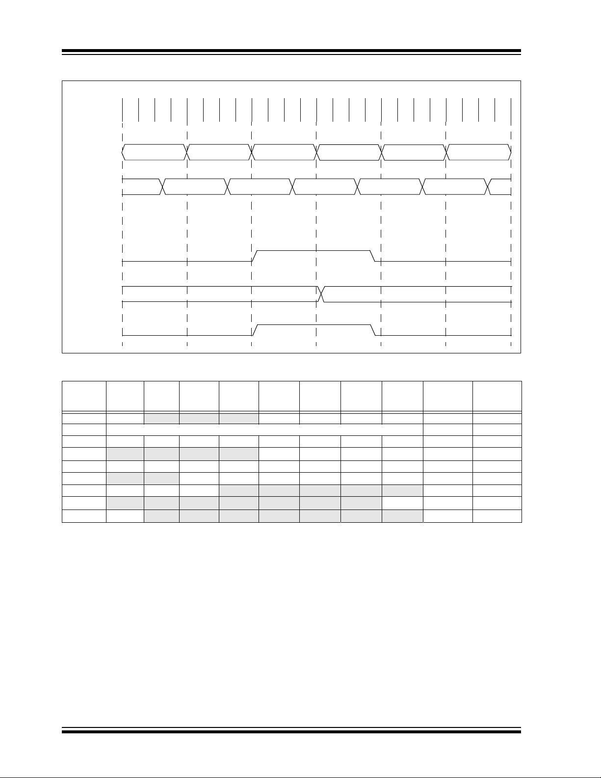
PIC16F688
FIGURE 9-1: FLASH PROGRAM MEMORY READ CYCLE EXECUTION
Q1 Q2 Q3 Q4 Q1 Q2 Q3 Q4 Q1 Q2 Q3 Q4 Q1 Q2 Q3 Q4 Q1 Q2 Q3 Q4 Q1 Q2 Q3 Q4
Flash ADDR
Flash Data
RD bit
EEDATH
EEDAT
Register
EERHLT
PC
INSTR(PC - 1)
executed here
PC + 1 EEADRH,EEADR
INSTR (PC) INSTR (PC + 3) INSTR (PC + 4)
BSF EECON1,RD
executed here
INSTR (PC + 1)
INSTR(PC + 1)
executed here
EEDATH,EEDAT
PC + 3 PC + 4
PC+3
Forced NOP
executed here
INSTR(PC + 3)
executed here
PC + 5
INSTR(PC + 4)
executed here
TABLE 9-1: SUMMARY OF REGISTERS ASSOCIATED WITH DATA EEPROM
Name Bit 7 Bit 6 Bit 5 Bit 4 Bit 3 Bit 2 Bit 1 Bit 0
EECON1 EEPGD
EECON2 EEPROM Control Register 2 (not a physical register) ---- ---- ---- ---EEADR EEADR7 EEADR6 EEADR5 EEADR4 EEADR3 EEADR2 EEADR1 EEADR0 0000 0000 0000 0000
EEADRH
EEDAT EEDAT7 EEDAT6 EEDAT5 EEDAT4 EEDAT3 EEDAT2 EEDAT1 EEDAT0 0000 0000 0000 0000
EEDATH
INTCON GIE PEIE T0IE
PIE1
PIR1
— — — — EEADRH3 EEADRH2 EEADRH1 EEADRH0 ---- 0000 ---- 0000
— — EEDATH5 EEDATH4 EEDATH3 EEDATH2 EEDATH1 EEDATH0 --00 0000 --00 0000
EEIE ADIE RCIE C2IE C1IE OSFIE TXIE TMR1IE
EEIF ADIF RCIF C2IF C1IF OSFIF TXIF TMR1IF
— — — WRERR WREN WR RD x--- x000 0--- q000
INTE RABIE T0IF INTF RABIF 0000 000x 0000 000x
Value on
POR, BOR
0000 0000 0000 0000
0000 0000 0000 0000
Legend: x = unknown, u = unchanged, — = unimplemented read as ‘0’, q = value depends upon condition.
Shaded cells are not used by data EEPROM module.
Value on
all other
Resets
DS41203D-page 82 © 2007 Microchip Technology Inc.

PIC16F688
10.0 ENHANCED UNIVERSAL
SYNCHRONOUS
ASYNCHRONOUS RECEIVER
T RANSMITTER (EUSART)
The EUSART module includes the following capabilities:
• Full-duplex asynchronous transmit and receive
• Two-character input buffer
• One-character output buffer
• Programmable 8-bit or 9-bit character length
The Enhanced Universal Synchronous Asynchronous
Receiver Transmitter (EUSART) module is a serial I/O
communications peripheral. It contains all the clock
generators, shift registers and data buffers necessary
to perform an input or output serial data transfer
independent of device program execution. The
EUSART, also known as a Serial Communications
Interface (SCI), can be configured as a full-duplex
asynchronous system or half-duplex synchronous
system. Full-Duplex mode is useful for
communications with peripheral systems, such as CRT
terminals and personal computers. Half-Duplex
Synchronous mode is intended for communications
with peripheral devices, such as A/D or D/A integrated
circuits, serial EEPROMs or other microcontrollers.
These devices t ypica lly d o not ha ve in tern al cloc ks fo r
baud rate generation and require the external clock
signal provided by a master synchronous device.
• Address detection in 9-bit mode
• Input buffer overrun error detection
• Received character framing error detection
• Half-duplex synchron ous master
• Half-duplex synchron ous slave
• Programmable clock polarity in synchronous
modes
The EUSART module implements the following
additional features, making it ideally suited for use in
Local Interconnect Network (LIN) bus systems:
• Automatic detection and cali bration of the baud rate
• Wake-up on Break reception
• 13-bit Break character transmit
Block diagrams of the EUSART transmitter and
receiver are shown in Figure 10-1 and Figure10-2.
FIGURE 10-1: EUSART TRANSMIT BLOCK DIAGRAM
Baud Rate Generator
BRG16
SPBRGSPBRGH
TXEN
FOSC
+ 1
Multiplier x4 x16 x64
SYNC 1X00 0
BRGH X110 0
BRG16 X101 0
÷ n
Data Bus
TXREG Register
8
MSb
(8)
Transmit Shift Register (TSR)
n
•••
TX9
TX9D
LSb
0
TRMT
TXIF
TXIE
Pin Buffer
and Control
Interrupt
TX/CK pin
SPEN
© 2007 Microchip Technology Inc. DS41203D-page 83

PIC16F688
FIGURE 10-2: EUSART RECEIVE BLOCK DIAGRAM
SPEN
RX/DT pin
Pin Buffer
and Control
Baud Rate Generator
BRG16
SPBRGSPBRGH
+ 1
Multiplier x4 x16 x64
SYNC 1X00 0
BRGH X110 0
BRG16 X101 0
FOSC
The operation of the EUSART module is controlled
through three registers:
• Transmit Status and Control (TXSTA)
• Receive Status and Control (RCSTA)
• Baud Rate Control (BAUDCTL)
These registers are detailed in Register 10-1,
Register10-2 and Register10-3, respectively.
Data
Recovery
÷ n
n
FERR
CREN OERR
MSb
Stop
RSR Register
(8) 7 1 0
RX9
RX9D
• • •
RCREG Register
8
Data Bus
RCIF
RCIE
RCIDL
LSb
START
FIFO
Interrupt
DS41203D-page 84 © 2007 Microchip Technology Inc.

PIC16F688
10.1 EUSART Asynchronous Mode
The EUSART transmits and receives data using the
standard non-return-to-zero (NRZ) format. NRZ is
implemented with two levels: a V
represents a ‘1’ data bit, and a V
represents a ‘0’ data bit. NRZ refers to the fact that
consecutively transmitted data bits of the same value
stay at the output level of that bit without ret urning to a
neutral level between each bit transmission. An NRZ
transmission port idles in the mark state. Each character
transmission consists of one Start bit followed by eight
or nine data bits and is always terminated by one or
more Stop bits. The Start bit is always a space and the
Stop bits are always marks. The most common data
format is 8 bits. Each transmitted bit persists for a period
of 1/(Baud Rate). An on-chip dedicated 8-bit/16-bit Baud
Rate Generator is used to derive standard baud rate
frequencies from the system oscillator. See Table 10-5
for examples of baud rate configurations.
The EUSART transmits and receives the LSb first. The
EUSART’s transmitter and receiver are functionally
independent, but share th e same data format an d baud
rate. Parity is not supported by the hardware, but can
be implemented in software and stored as the ninth
data bit.
10.1.1 EUSART ASYNCHRONOUS
TRANSMITTER
The EUSART transmitter block diagram is shown in
Figure 10-1. The heart of the transmitter is the serial
Transmit Shift Register (TSR), which is not directly
accessible b y softwa re . The TS R obtain s its data from
the transmit buffer, which is the TXREG register.
10.1.1.1 Enabling the Transmitter
The EUSART transmitter is enabled for asynchronous
operations by configuring the following three control
bits:
•TXEN = 1
• SYNC = 0
• SPEN = 1
All other EUSART control bits are assumed to be in
their default state.
Setting the TXEN bit of the TXSTA register enables the
transmitter circuitry of the EUSART. Clearing the SYNC
bit of the TXSTA register configures the EUSART for
asynchronous operation. Setting the SPEN bit of the
RCSTA register enables the EUSART and automatically
configures the TX/CK I/O pin as an output. If the TX/CK
pin is shared with an analog peripheral the analog I/O
function must be disabled by clearing the corresponding
ANSEL bit.
OH mark state which
OL space state which
Note 1: When the SPEN bit i s set, the RX/DT I/O
pin is automatically configured as an input,
regardless of the state of the corresponding
TRIS bit and whet her or not the EU SART
receiver is enabled. The RX/DT pin data
can be read via a normal PORT read but
PORT latch data output is precluded.
2: The TXIF transmitter interrupt flag is set
when the TXEN enable bit is set.
10.1.1.2 Transmitting Data
A transmission is initiated by writing a character to the
TXREG register. If this is the first character, or the
previous character has been completely flushed from
the TSR, the data in the TXREG is immediately
transferred to the TSR register. If the TSR still co ntains
all or part of a previous character, the new character
data is held in the TXREG until the Stop bit of the
previous character has been transmitted. The pending
character in the TXREG is then transferred to the TSR
in one T
transmission. The transmission of the Start bit, data bit s
and Stop bit sequence commences immediately
following the transfer of the data to the TSR from the
TXREG.
CY immediately following the Stop bit
10.1.1.3 Transmit Interrupt Flag
The TXIF interrupt flag bit of the P IR1 register is set
whenever the EUSART transmitter is enabled and no
character is being held for transmission in the TXREG.
In other words, the TXIF bit is only clear when the TSR
is busy with a character and a new character has been
queued for transmission in the TXREG . The TXIF flag bit
is not cleared immediately upon writing TXREG. TXIF
becomes valid in the second instruction cycle following
the write execution. Polling TXIF immediately following
the TXREG write will return invalid results. The TXIF bit
is read-only, it cannot be set or cleared by software.
The TXIF interrupt can be enabled by setting the TXIE
interrupt enable bit of the PIE1 register. However, the
TXIF flag bit will be set wheneve r the TXR EG is emp ty,
regardless of the state of TXIE enable bit.
To use interrupts when transmitting data, set the TXIE
bit only when there is more data to send. Clear the
TXIE interrupt enab le bit u pon wri ting the last c haract er
of the transmission to the TXREG.
© 2007 Microchip Technology Inc. DS41203D-page 85

PIC16F688
10.1.1.4 TSR Status
The TRMT bit of the TXSTA register indicates the
status of the TSR register. This is a read-only bit. The
TRMT bit is set when the TSR register is empty and is
cleared when a character is transferred to the TSR
register from the TXREG. The TRMT bit remains clear
until all bits have been shifted out of the TSR register.
No interrupt logic is tied to this bit, so the user has to
poll this bit to determine the TSR status.
Note: The TSR register is not mapped in data
memory, so it is not available to the user.
10.1.1.5 Transmitting 9-Bit Characters
The EUSART supports 9-bit character transmissions.
When the TX9 bit of the TXSTA register is set the
EUSART will shift 9 bits out for eac h character transm itted. The TX9D bit of the TXSTA register is the ninth,
and Most Significant, data bit. When transmitting 9-bit
data, the TX9D data bit must be written before writing
the 8 Least Significant bi ts into the TXRE G. All nine bits
of data will be transferred to the TSR shift register
immediately after the TXREG is written.
A special 9-bit Address mode is available for use with
multiple receivers. See Section 10.1.2.7 “Address
Detection” for more inform ation on th e Address mode.
10.1.1.6 Asynchronous Transmission Set-up:
1. Initialize the SPBRGH, SPBRG register pair and
the BRGH and BRG16 bits to achieve the d esired
baud rate (see Section 10.3 “EUSART Baud
Rate Generator (BRG)”).
2. Enable the asynchronous serial port by clearing
the SYNC bit and setting the SPEN bit.
3. If 9-bit transmission is desired, set the TX9 co ntrol bit. A set ninth data bi t will indicat e that the 8
Least Significant data bits are an address when
the receiver is set for address detection.
4. Enable the transmission by setting the TXEN
control bi t. T his w il l ca use t he TXIF int err upt bit
to be set.
5. If interrupts are desired, set the TXIE interrupt
enable bit. An interrupt will occur immediately
provided that the GIE and PEIE bits of the
INTCON register are also set.
6. If 9-bit transmission is selected, the ninth bit
should be loaded into the TX9D data bit.
7. Load 8-bit data into the TXREG register. This
will start the transmission.
FIGURE 10-3: ASYNCHRONOUS TRANSMISSION
Write to TXREG
BRG Output
(Shift Clock)
RC4/C2OUT/TX/CK
(Transmit Buffer
Reg. Empty Flag)
(Transmit Shift
Reg. Empty Flag)
pin
TXIF bit
TRMT bit
Word 1
Start bit bit 0 bit 1 bit 7/8
1 TCY
Word 1
Transmit Shift Reg
Word 1
FIGURE 10-4: ASYNCHR ONOUS TRANSMISSION (BACK-TO-BACK)
Write to TXREG
BRG Output
(Shift Clock)
RC4/C2OUT/TX/CK
(Interrupt Reg. Flag)
(Transm it Shift
Reg. Empty Flag)
pin
TXIF bit
TRMT bit
Word 1
1 TCY
Word 1
Transmit Shift Reg.
Word 2
Start bit
bit 0 bit 1
1 TCY
Word 1
bit 7/8 bit 0
Stop bit
Word 2
Transmit Shift Reg.
Stop bit
Start bit
Word 2
Note: This timing diagram shows two consecutive transmissions.
DS41203D-page 86 © 2007 Microchip Technology Inc.

PIC16F688
TABLE 10-1: REGISTERS ASSOCIATED WITH ASYNCHRONOUS TRANSMISSION
NameBit 7Bit 6Bit 5Bit 4Bit 3Bit 2Bit 1Bit 0
BAUDCTL
INTCON
PIE1
PIR1
RCREG
RCSTA SPEN
SPBRG BRG7 BRG6 BRG5 BRG4 BRG3 BRG2 BRG1 BRG0 0000 0000 0000 0000
SPBRGH BRG15 BRG14 BRG13 BRG12 BRG11 BRG10 BRG9 BRG8 0000 0000 0000 0000
TRISC
TXREG EUSART Transmit Data Register 0000 0000 0000 0000
TXSTA CSRC TX9 TXEN SYNC SENDB BRGH TRMT TX9D 0000 0010 0000 0010
Legend: x = unknown, – = unimplemented read as ‘0’. Shaded cells are not used for Asynchronous Transmission.
ABDOVF RCIDL — SCKP BRG16 — WUE ABDEN 01-0 0-00 01-0 0-00
GIE PEIE T0IE INTE RAIE T0IF INTF RAIF
EEIE ADIE RCIE C2IE C1I E OSFIE TXIE TMR1IE
EEIF ADIF RCIF C2IF C1IF OSFIF TXIF TMR1IF
EUSART Receive Data Register 0000 0000 0000 0000
RX9 SREN CREN ADDEN FERR OERR RX9D 0000 000x 0000 000x
— — TRI SC5 TRISC4 TRISC3 TRISC2 TRISC1 TRISC0 --11 1111
Value on
POR, BOR
0000 000x 0000 000x
0000 0000 0000 0000
0000 0000 0000 0000
Value on
all other
Resets
--11 1111
© 2007 Microchip Technology Inc. DS41203D-page 87

PIC16F688
10.1.2 EUSART ASYNCHRONOUS
RECEIVER
The Asynchronous mode would typically be used in
RS-232 systems. Th e rec ei ve r bl ock di ag ram is sh ow n
in Figure 10-2. The data is received on the RX/DT pin
and drives the data recovery block. The data recovery
block is actually a high-speed shifter operating at 16
times the baud rate, whereas the serial Receive Shift
Register (RSR) operat es at the bi t rate. W hen al l 8 or 9
bits of the character have been shifted in, they are
immediately transferred to a two character First-InFirst-Out (FIFO) memory. The FIFO buffering allows
reception of two compl ete cha rac ters and the s t art of a
third character befo re so ftwar e must start servici ng th e
EUSART receiver. The FIFO and RSR registers are not
directly accessible by software. Access to the received
data is via the RCREG register.
10.1.2.1 Enabling the Receiver
The EUSART receiver is enabled for asynchronous
operation by configu ring the following three co ntrol bits:
• CREN = 1
• SYNC = 0
• SPEN = 1
All other EUSART control bits are assumed to be in
their default state.
Setting the CREN bit of the RCST A register enables the
receiver circuitry of the EUSART. Clearing the SYNC bit
of the TXSTA register configures the EUSART for
asynchronous operation. Setting the SPEN bit of the
RCSTA register enables the EUSART and automatically
configures the RX/DT I/O pin as an input. If the RX/DT
pin is shared with an analog peripheral the analog I/O
function must be disabled by clearing the corresponding
ANSEL bit.
Note: When the SPEN bit is set the TX/CK I/O
pin is automatically configured as an
output, regardless of the state of the
corresponding TRI S bit and whe ther or n ot
the EUSART transmitter is enabled. The
PORT latch is disconnected from the
output driver so it is not possible to use the
TX/CK pin as a general purpose output.
10.1.2.2 Receiving Data
The receiver data recovery circuit initiates character
reception on the fallin g edge of the first bit. Th e f irst bit,
also known as the Start bit, is always a zero. The data
recovery circuit co unt s one-h alf bi t time to t he cent er of
the Start bit and verifies that the bit is still a zero. If it is
not a zero then the data recovery circuit aborts
character reception, without generating an error, and
resumes looking for the falling edge of the Start bit. If
the Start bit zero verification succeeds then the data
recovery circuit cou nts a fu ll bit time to the cente r of the
next bit. The bit is then sampled by a majority detect
circuit and the resulti ng ‘0’ or ‘1’ is shifted into the R SR.
This repeats until all data bits have been sampled and
shifted into the RSR. One final bit time is measured and
the level sample d . Thi s is th e Stop bit, whic h is alw ays
a ‘1’. If the data recovery circuit samples a ‘0’ in the
Stop bit position then a framing error is set for this
character , otherwise th e framing error i s cleared for thi s
character. See Section 10.1.2.4 “Receive Framing
Error” for more information on framing errors.
Immediately after all data bits and the Stop bit have
been received, the character in the RSR is transferred
to the EUSART receive FIFO and the RCIF interrupt
flag bit of the PIR1 register is set. The top character in
the FIFO is transferred out of the FIFO by reading the
RCREG register.
Note: If the receive FIFO is overrun, no additional
characters will be received until the overrun
condition is cleared. See Section 10.1.2.5
“Receive Overrun Error” for more
information on overrun errors.
10.1.2.3 Receive Interrupts
The RCIF interrupt flag bit of the PIR1 register is set
whenever the EUSAR T receiver i s enabled and there i s
an unread character in the receive FIFO. The RCIF
interrupt flag bit is rea d-only, it cannot be set or cleared
by software.
RCIF interrupts are enabled by setting the following
bits:
• RCIE interrupt enable bit of the PIE1 register
• PEIE peripheral interrupt enable bit of the
INTCON register
• GIE global interrupt enable bit of the INTCON
register
The RCIF interrupt flag bit will be set when there is an
unread character in the FIFO, rega rdless of the st ate of
interrupt enable bits.
DS41203D-page 88 © 2007 Microchip Technology Inc.

PIC16F688
10.1.2.4 Receive Framing Error
Each character in the receive FIFO buffer has a
corresponding framing error Status bit. A framing error
indicates t hat a Stop bit was not seen at the ex pected
time. The framing error status is accessed via the
FERR bit of the RCSTA register. The FERR bit
represents the s ta tus o f the top u nread charac ter in the
receive FI FO. Therefore, the FERR bit must be read
before reading the RCREG.
The FERR bit is read-only and only applies to the top
unread cha racter in the r eceive FIFO. A framin g error
(FERR = 1) does not preclude reception of additional
characters. It is not necessary to clear the FERR bit.
Reading the next character from the FIFO buffer will
advance the FIFO to the next character and the next
corresponding framing error.
The FERR bit can be forced clear by clearing the SPEN
bit of the RCSTA register which resets the EUSART.
Clearing the CREN bit of the RCSTA register does not
affect the FERR bit. A framing error by itself does not
generate an interrupt.
Note: If all receive characters in the receive
FIFO have framing errors, repeated reads
of the RCREG will not clear the FERR bit.
10.1.2.7 Address Detection
A special Address Detection mode is available for use
when multiple receivers share the same transmission
line, such as in RS-485 systems. Address detection is
enabled by setting the ADDEN bit of the RCSTA
register.
Address detection requires 9-bit character reception.
When address detection is enabled, only characters
with the ninth data bit set will be transferred to the
receive FI F O bu ffe r, there by s et t i ng th e R CI F i nt er r up t
bit. All other characters will be ignored.
Upon receiving an address character, user software
determines if the address matches its own. Upon
address match, user software must disable address
detection by clearing the ADDEN bit before the next
Stop bit o ccurs. Whe n user so ftware dete ct s the end of
the message, determined by the message protocol
used, software places the receiver back into the
Address Detection mode by setting the ADDEN bit.
10.1.2.5 Receive Overrun Error
The receive FIFO buffer can hold two characters. An
overrun error will be generat ed If a third characte r , in its
entirety , is rece ived before the FIFO is accessed. When
this happens the O ERR bit of the RC ST A register is set.
The characters already in the FIFO buffer can be read
but no additional characters will be received until the
error is cleared. The error must be cleared by either
clearing the CREN bit of the RCSTA register or by
resetting the EUSART by clearing the SPEN bit of the
RCSTA register.
10.1.2.6 Receiving 9-bit Characters
The EUSART sup ports 9-bit c haracter rece ption. When
the RX9 bit of the RCSTA register is set the EUSART
will shift 9 bits into the RSR for each character
received. The RX9D bit of the RCSTA register is the
ninth and Most Significant data bit of the top unread
character in the receive FIFO. Whe n reading 9-bit dat a
from the receive FIFO buffer, the RX9D data bit must
be read before reading the 8 Leas t Significa nt bits from
the RCREG.
© 2007 Microchip Technology Inc. DS41203D-page 89

PIC16F688
10.1.2.8 Asynchronous Reception Set-up:
1. Initialize the SPBRGH, SPBRG register pair an d
the BRGH and BRG16 bits to achieve the
desired baud rate (see Section 10.3 “EUSART
Baud Rate Generator (BRG)”).
2. Enable the serial port by setting the SPEN bit.
The SYNC bit must be clear for asynchronous
operation.
3. If interrupts are desired, set the RCIE interrupt
enable bit and set the GIE and PEIE bits of the
INTCON register.
4. If 9-bit reception is desired, set the RX9 bit.
5. Enable reception by setting the CREN bit.
6. The RCIF interrupt flag bit will be set when a
character is transferred from the RSR to the
receive buffer. An interrupt will be generated if
the RCIE interrupt enable bit was also set.
7. Read the RCSTA register to get the error flags
and, if 9-bit data reception is enabled, the ninth
data bit.
8. Get the received 8 Least Significant data bits
from the receive buffer by reading the RCREG
register.
9. If an overrun occurred, clear the OERR flag by
clearing the CREN receiver enable bit.
10.1.2.9 9-bit Address Detection Mode Set-up
This mode would ty pi ca lly be used in RS-48 5 sy ste ms .
To set up an Asynchronous Reception with Address
Detect Enable:
1. Initialize the SPBRGH, SPBRG register pair and
the BRGH and BRG16 bits to achieve the
desired baud rate (see Section 10.3 “EUSART
Baud Rate Generator (BRG)”).
2. Enable the serial port by setting the SPEN bit.
The SYNC bit mu st be clear for asynchronous
operation.
3. If interrupts are desired, set the RCIE interrupt
enable bit and set the GIE and PEIE bits of the
INTCON register.
4. Enable 9-bit reception by setting the RX9 bit.
5. Enable address detection by setti ng the ADDE N
bit.
6. Enable reception by setting the CREN bit.
7. The RCIF interrupt flag bit will be set when a
character with the ninth bit set is transferred
from the RSR to the receive buffer. An interrupt
will be generated if t he RCIE inte rrupt en able b it
was also set.
8. Read the RCS TA register to get th e err or f lag s.
The ninth data bit will always be set.
9. Get the received 8 Least Significant data bits
from the rece ive buffer by re ading the RCR EG
register. Software determines if this is the
device’s address.
10. If an overrun occurred, clear the OERR flag by
clearing the CREN receiver enable bit.
11. If the device has been addressed, clear the
ADDEN bit to allow all received data into the
receive buffer and generate interrupts.
FIGURE 10-5: ASYNCHRONOUS RECEPTION
Start
RX/DT pin
Rcv Shift
Reg
Rcv Buffer Reg
RCIDL
Read Rcv
Buffer Reg
RCREG
RCIF
(Interrupt Flag)
OERR bit
CREN
Note: This timing diagram shows th ree words app earing on the RX inp ut. The RCREG (receive buffer) is read afte r the third wor d,
DS41203D-page 90 © 2007 Microchip Technology Inc.
causing the OERR (overrun) bit to be set.
bit
bit 1bit 0
bit 7/8
bit
Start
bit
Word 1
RCREG
bit 0Stop
bit 7/8
Word 2
RCREG
Stop
bit
Start
bit
bit 7/8
Stop
bit

PIC16F688
TABLE 10-2: REGISTERS ASSOCIATED WITH ASYNCHRONOUS RECEPTION
NameBit 7Bit 6Bit 5Bit 4Bit 3Bit 2Bit 1Bit 0
BAUDCTL
INTCON
PIE1
PIR1
RCREG EUSART Receive Data Register 0000 0000 0000 0000
RCSTA SPEN RX9 SREN CREN ADDEN FER R OERR RX9D 0000 000x 0000 000x
SPBRG BRG7 BRG6 BRG5 BRG4 BRG3 BRG2 BRG1 BRG0 0000 0000 0000 0000
SPBRGH BRG15 BRG14 BRG13 BRG12 BRG11 BRG10 BRG9 BRG8 0000 0000 0000 0000
TRISC
TXREG EUSART Transmit Data Register 0000 0000 0000 0000
TXSTA
Legend: x = unknown, – = unimplemented read as ‘0’. Shaded cells are not used for Asynchronous Reception.
ABDOVF RCIDL — SCKP BRG16 —WUEABDEN 01-0 0-00 01-0 0-00
GIE PEIE T0IE INTE RAIE T0IF INTF RAIF
EEIE ADIE RCIE C2IE C1IE OSFIE TXIE TMR1IE
EEIF ADIF RCIF C2IF C1IF OSFIF TXIF TMR1IF
— — TRI SC5 TRISC4 TRISC3 TRISC2 TRISC1 TRISC0 --11 1111
CSRC TX9 TXEN SYNC SENDB BRGH TRMT TX9D 0000 0010 0000 0010
Value on
POR, BOR
0000 000x 0000 000x
0000 0000 0000 0000
0000 0000 0000 0000
Value on
all other
Resets
--11 1111
© 2007 Microchip Technology Inc. DS41203D-page 91

PIC16F688
10.2 Clock Accuracy with
Asynchronous Operation
The factory calibrates the internal oscillator block output (INTOSC). However, the INTOSC frequency may
drift as VDD or temperature changes, and this directly
affects the as ynchron ous baud rate. Two method s may
be used to adjust the baud rate clock, but both require
a reference clock source of some kind.
The first (preferred) method uses the OSCTUNE
register to adjust the INTOSC output. Adjusting the
value in the OSCTUNE register allows for fine resolution
changes to the system clock source. See Section 3.5
“Internal Clock Modes” for more information.
The other method adjusts the value in the Baud Rate
Generator. This can be done automatically with the
Auto-Baud Detect feature (see Section 10.3.1 “Auto-
Baud Detect”). There may not be fine enough
resolution when adjusting the Baud Rate Generator to
compensate for a gradual change in the peripheral
clock frequency.
REGISTER 10-1: TXSTA: TRANSMIT STATUS AND CONTROL REGISTER
R/W-0 R/W-0 R/W-0 R/W-0 R/W-0 R/W-0 R-1 R/W-0
CSRC TX9 TXEN
bit 7 bit 0
Legend:
R = Readable bit W = Writable bit U = Unimplemented bit, read as ‘0’
-n = Value at POR ‘1’ = Bit is set ‘0’ = Bit is cleared x = Bit is unknown
bit 7 CSRC: Clock Source Select bit
Asynchronous mode
Don’t care
Synchronous mode
1 = Master mode (clock generated internally from BRG)
0 = Slave mode (clock from external source)
bit 6 TX9: 9-bit Transmit Enable bit
1 = Selects 9-bit transmission
0 = Selects 8-bit transmission
bit 5 TXEN: Transmit Enable bit
1 = Transmit enabled
0 = Transmit disabled
bit 4 SYNC: EUSART Mode Select bit
1 = Sync hronous mode
0 = Asy nchronous mode
bit 3 SENDB: Send Break Character bit
Asynchronous mode
1 = Send Sync Break on next transmission (cleared by hardware upon completion)
0 = Sync Break transmission co mpleted
Synchronous mode
Don’t care
bit 2 BRGH: High Baud Rate Select bit
Asynchronous mode
1 = High speed
0 = Low speed
Synchronous mode:
Unused in this mode
bit 1 TRMT: Transmit Shift Register Status bit
1 = TSR empty
0 = TSR full
bit 0 TX9D: Ninth bit of Transmit Data
Can be address/data bit or a parity bit.
(1)
:
:
(1)
:
:
:
SYNC SENDB BRGH TRMT TX9D
Note 1: SREN/CREN overrides TXEN in Sync mode.
DS41203D-page 92 © 2007 Microchip Technology Inc.

PIC16F688
REGISTER 10-2: RCSTA: RECEIVE STATUS AND CONTROL REGISTER
R/W-0 R/W-0 R/W-0 R/W-0 R/W-0 R-0 R-0 R-x
SPEN RX9 SREN CREN ADDEN FERR OERR RX9D
bit 7 bit 0
Legend:
R = Readable bit W = Writable bit U = Unimplemented bit, read as ‘0’
-n = Value at POR ‘1’ = Bit is set ‘0’ = Bit is cleared x = Bit is unknown
bit 7 SPEN: Serial Port Enable bit
1 = Serial port enabled (configures RX/DT and TX/CK pins as serial port pins)
0 = Serial port disabled (held in Reset)
bit 6 RX9: 9-bit Receive Enable bit
1 = Selects 9-bit reception
0 = Selects 8-bit reception
bit 5 SREN: Single Receive Enable bit
Asynchronous mode
Don’t care
Synchronous mode – Master
1 = Enables si ngle receive
0 = Disables single receive
This bit is cleared after reception is complete.
Synchronous mode – Slave
Don’t care
bit 4 CREN: Conti nuo us Receiv e Enab le bit
Asynchronous mode:
1 = Enables receiver
0 = Disables receiver
Synchronous mode
1 = Enables continuous receive until enable bit CREN is cleared (CREN overrides SREN)
0 = Disables continuous r ece iv e
bit 3 ADDEN: Address Detect Enable bit
Asynchronous mode 9-bit (RX9 =
1 = Enables address detection, enable interrupt and load the receive buffer when RSR<8> is set
0 = Disables address detection, all bytes are received and ninth bit can be used as parity bit
Asynchronous mode 8-bit (RX9 =
Don’t care
bit 2 FERR: Framing Error bit
1 = Framing error (can be updated by reading RCREG register and receive next valid byte)
0 = No framing error
bit 1 OERR: Overrun Error bit
1 = Overrun error (can be cleared by clearing bit CREN)
0 = No overrun error
bit 0 RX9D: Ninth bit of Received Data
This can be address/data bit or a parity bit and must be calculated by user firmware.
:
:
:
1):
0):
(1)
© 2007 Microchip Technology Inc. DS41203D-page 93

PIC16F688
REGISTER 10-3: BAUDCTL: BAUD RATE CONTROL REGISTER
R-0 R-1 U-0 R/W-0 R/W-0 U-0 R/W-0 R/W-0
ABDOVF RCIDL
bit 7 bit 0
Legend:
R = Readable bit W = Writable bit U = Unimplemented bit, read as ‘0’
-n = Value at POR ‘1’ = Bit is set ‘0’ = Bit is cleared x = Bit is unknown
bit 7 ABDOVF: Auto-Baud Detect Overflow bit
Asynchronous mode
1 = Auto-baud timer overflowed
0 = Auto-baud timer did not overflow
Synchronous mode
Don’t care
bit 6 RCIDL: Receive Idle Flag bit
Asynchronous mode
1 = Receiver is Idle
0 = Start bit has been received and the receiver is receiving
Synchronous mode
Don’t care
bit 5 Unimplemented: Read as ‘0’
bit 4 SCKP: Synchronous Clock Po larity Select bit
Asynchronous mode
1 = Transmit inverted data to the RB7/TX/CK pin
0 = Transmit non-inverted data to the RB7/TX/CK pin
Synchronous mode
1 = Data is clocked on rising edge of the clock
0 = Data is clocked on falling edge of the clock
bit 3 BRG16: 16-bit Baud Rate Generator bit
1 = 16-bit Baud Rate Generator is used
0 = 8-bit Baud Rate Generator is used
bit 2 Unimplemented: Read as ‘0’
bit 1 WUE: Wake-up Enable bit
Asynchronous mode
1 = Receiver is waiting for a fal ling edge. N o character w ill be rece ived byte RCIF will be se t. WUE will
automatically clear after RCIF is set.
0 = Receiver is operatin g normally
Synchronous mode:
Don’t care
bit 0 ABDEN: Auto-Baud Detect Enable bit
Asynchronous mode:
1 = Auto-Baud Detect mode is enabled (clears when auto-baud is complete)
0 = Auto-Baud Detect mode is disabled
Synchronous mode
Don’t care
— SCKP BRG16 — WUE ABDEN
:
:
:
:
:
:
:
:
DS41203D-page 94 © 2007 Microchip Technology Inc.

PIC16F688
e
e
---
10.3 EUSART Baud Rate Generator
(BRG)
The Baud Rate Generator (BRG) is an 8-bit or 16-bit
timer that is dedicated to the support of both the
asynchronous and synchronous EUSART operation.
By default, the BRG ope rates in 8-bit mode. Se tting the
BRG16 bit of the BAUDCTL register selects 16-bit
mode.
The SPBRGH, SPBRG register pair determines the
period of the free running baud rate timer. In
Asynchronous mode the multiplier of the baud rate
period is determined by both the BRGH bit of the TXST A
register and the BRG16 bit of the BAUDCTL register. In
Synchronous mode, the BRGH bit is ignored.
Table 10-3 contains the formulas for determining the
baud rate. Example10-1 provides a sample calculation
for determining the baud rate and baud rate error.
Typical baud rates and error values for various
asynchronous modes have been computed for your
convenience and are shown in Table 10-3. It may be
advantageous to use the high baud rate (BRGH = 1),
or the 16-bit BRG (BRG16 = 1) to reduce the baud rate
error. The 16-bit BRG mode is used to achieve slow
baud rates for fast oscillator frequencies.
Writing a new value to the SPBRGH, SPBRG register
pair causes the BRG timer to be reset (or cleared). This
ensures that the BRG do es not wait fo r a timer overfl ow
before outputting the new baud rate.
If the system clo ck is c ha nged during an activ e r ece iv e
operation, a receive error or data loss may result. To
avoid this problem, ch eck the st atus of the RCIDL bi t to
make sure that the receive operation is Idle before
changing the system clock.
EXAMPLE 10-1: CALCULATING BAUD
RATE ERROR
For a device w ith FOSC of 16 MHz, desired baud rat
of 9600, Asynchronous mode, 8-bit BRG:
Desired Baud Rate
Solving for SPBRGH:SPBRG:
Calculated Baud Rate
Error
-------------------------------------------------------------------- -
=
64 [SPBRGH:SPBRG] 1+()
OSC
F
--------------------------------------------Desired Baud Rate
---------------------------------------------
X
25.042[]25==
=
9615=
=
64
16000000
----------------------- 9600
----------------------- -
64
16000000
---------------------------
64 25 1+()
Calc. Baud Rate Desired Baud Rat
----------------------------------------------------------------------------------------Desired Baud Rate
9615 9600–()
---------------------------------9600
F
OSC
1–=
–
1–=
0.16%==
TABLE 10-3: BAUD RATE FORMULAS
Configuration Bits
SYNC BRG16 BRGH
000 8-bit/Asynchronous F
001 8-bit/Asynchronous
010 16-bit/Asynchronous
011 16-bit/Asynchronous
11x 16-bit/Synchronous
Legend: x = Don’t care, n = value of SPBRGH, SPBRG register pair
BRG/EUSART Mode
Baud Rate Formula
OSC/[64 (n+1)]
F
OSC/[16 (n+1)]
F
OSC/[4 (n+1)]10x 8-bit/Synchronous
TABLE 10-4: REGISTERS ASSOCIATED WITH THE BAUD RATE GENERATOR
NameBit 7Bit 6Bit 5Bit 4Bit 3Bit 2Bit 1Bit 0
BAUDCTL ABDOVF RCIDL — SCKP BRG16 — WUE ABDEN 01-0 0-00 01-0 0-00
RCSTA SPEN
SPBRG BRG7 BRG6 BRG5 BRG4 BRG3 BRG2 BRG1 BRG0 0000 0000 0000 0000
SPBRGH BRG15 BRG14 BRG13 BRG12 BRG11 BRG10 BRG9 BRG8 0000 0000 0000 0000
TXSTA
Legend: x = unknown, – = unimplemented read as ‘0’. Shaded cells are not used for the Baud Rate Generator.
CSRC TX9 TXEN SYNC SENDB BRGH TRMT TX9D 0000 0010 0000 0010
RX9 SREN CREN ADDEN FERR OERR RX9D 0000 000x 0000 000x
Value on
POR, BOR
Value on
all other
Resets
© 2007 Microchip Technology Inc. DS41203D-page 95

PIC16F688
TABLE 10-5: BAUD RATES FOR ASYNCHRONOUS MODES
SYNC = 0, BRGH = 0, BRG16 = 0
OSC = 20.000 MHz FOSC = 18.432 MHz FOSC = 11.0592 MHz FOSC = 8.000 MHz
BAUD
RATE
300—— — —— — —— — —— —
1200 1221 1.73 255 1200 0.00 239 1200 0.00 143 1202 0.16 103
2400 2404 0.16 129 2400 0.00 119 2400 0.00 71 2404 0.16 51
9600 9470 -1.36 32 9600 0.00 29 9600 0.00 17 9615 0.16 12
10417 10417 0.00 29 10286 -1.26 27 10165 -2.42 16 10417 0.00 11
19.2k 19.53k 1.73 15 19.20k 0.00 14 19.20k 0.00 8 — — —
57.6k
115.2k — — — — — — — — — — — —
BAUD
RATE
300 300 0.16 207 300
1200 1202 0.16 51 1200 0.00 47 1202 0.16 25 1202 0.16 12
2400 2404 0.16 25 2400 0.00 23 2404 0.16 12 — — —
9600 — — — 9600 0.00 5 — — — — — —
10417 10417 0.00 5 — — — 10417 0.00 2 — — —
19.2k — — — 19.20k 0.00 2 — — — — — —
57.6k — — —
115.2k — — — — — — — — — — — —
F
Actual
Rate%Error
— — — 57.60k
OSC = 4.000 MHz FOSC = 3.6864 MHz FOSC = 2.000 MHz FOSC = 1.000 MHz
F
Actual
Rate%Error
SPBRG
value
(decimal)
SPBRG
value
(decimal)
Actual
Rate%Error
0.00
Actual
Rate%Error
0.00
57.60k
0.00 0 — — — — — —
SPBRG
value
(decimal)
SYNC = 0, BRGH = 0, BRG16 = 0
SPBRG
value
(decimal)
191 300 0.16 103 300 0.16 51
Actual
Rate%Error
7 57.60k
Actual
Rate%Error
0.00 2 — — —
SPBRG
value
(decimal)
SPBRG
value
(decimal)
Actual
Rate%Error
Actual
Rate%Error
SPBRG
value
(decimal)
SPBRG
value
(decimal)
SYNC = 0, BRGH = 1, BRG16 = 0
OSC = 20.000 MHz FOSC = 18.432 MHz FOSC = 11.0592 MHz FOSC = 8.000 MHz
BAUD
RATE
300
1200 — — — — — — — — — — — —
2400 — — — — — —
9600 9615 0.16 129 9600 0.00 119 9600 0.00 71 9615 0.16 51
10417 10417 0.00 119 10378 -0.37 110 10473 0.53 65 10417 0.00 47
19.2k 19.23k 0.16 64 19.20k 0.00 59 19.20k 0.00 35 19231 0.16 25
57.6k 56.82k -1.36 21 57.60k 0.00 19 57.60k 0.00 11 55556 -3.55 8
115.2k 113.64k -1.36 10 115.2k 0.00 9 115.2k 0. 00 5 — — —
F
Actual
Rate%Error
—— — —— — —— — —— —
SPBRG
value
(decimal)
Actual
Rate%Error
SPBRG
value
(decimal)
Actual
Rate%Error
—— —
SPBRG
value
(decimal)
Actual
Rate%Error
2404 0.16 207
SPBRG
value
(decimal)
DS41203D-page 96 © 2007 Microchip Technology Inc.

PIC16F688
TABLE 10-5: BAUD RATES FOR ASYNCHRONOUS MODES (CONTINUED)
SYNC = 0, BRGH = 1, BRG16 = 0
F
BAUD
RATE
300 — — — — — — — — — 300 0.16 207
1200 1202 0.16 207 1200 0.00 191 1202 0.16 103 1202 0.16 51
2400 2404 0.16 103 2400 0.00 95 2404 0. 16 51 2404 0.16 25
9600 9615 0.16 25 9600 0.00 23 9615 0.16 12 — — —
10417 10417 0.00 23 10473 0.53 21 10417 0.00 11 10417 0.00 5
19.2k 19.23k 0.16 12 19.2k 0.00 11 — — — — — —
57.6k — — — 57.60k 0.00 3 — — — — — —
115.2k — — — 115.2k 0.00 1 — — — — — —
BAUD
RATE
300 300.0 -0.01 4166 300.0 0.00 3839 300.0 0.00 2303 299.9 -0.02 1666
1200 1200 -0.03 1041 1200 0.00 959 1200 0.00 575 1199 -0.08 416
2400 2399 -0.03 520 2400 0.00 479 2400 0.00 287 2404 0.16 207
9600 9615 0.16 129 9600 0.00 119 9600 0.00 71 9615 0.16 51
10417 10417 0.00 119 10378 -0.37 110 10473 0.53 65 10417 0.00 47
19.2k 19.23k 0.16 64 19.20k 0.00 59 19.20k 0.00 35 19.23k 0.16 25
57.6k 56.818 -1.36 21 57.60k 0.00 19 57.60k 0. 00 11 55556 -3.55 8
115.2k 113.636 -1.36 10 115.2k 0.00 9 115.2k 0.00 5 — — —
OSC = 4.000 MHz FOSC = 3.6864 MHz FOSC = 2.000 MHz FOSC = 1.000 MHz
Actual
Rate%Error
OSC = 20.000 MHz FOSC = 18.432 MHz FOSC = 11.0592 MHz FOSC = 8.000 MHz
F
Actual
Rate%Error
SPBRG
value
(decimal)
SPBRG
value
(decimal)
Actual
Rate%Error
Actual
Rate%Error
SPBRG
value
(decimal)
SYNC = 0, BRGH = 0, BRG16 = 1
SPBRG
value
(decimal)
Actual
Rate%Error
Actual
Rate%Error
SPBRG
value
(decimal)
SPBRG
value
(decimal)
Actual
Rate%Error
Actual
Rate%Error
(decimal)
(decimal)
SPBRG
value
SPBRG
value
SYNC = 0, BRGH = 0, BRG16 = 1
OSC = 4.000 MHz FOSC = 3.6864 MHz FOSC = 2.000 MHz FOSC = 1.000 MHz
BAUD
RATE
300 300.1 0.04 832 300.0 0.00 767 299.8 -0.108 416 300.5 0.16 207
1200 1202 0.16 207 1200 0.00 191 1202 0.16 103 1202 0.16 51
2400 2404 0.16 103 2400 0.00 95 2404 0. 16 51 2404 0.16 25
9600 9615 0.16 25 9600 0.00 23 9615 0.16 12 — — —
10417 10417 0.00 23 10473 0.53 21 10417 0.00 11 10417 0.00 5
19.2k 19.23k 0.16 12 19.20k 0.00 11 — — — — — —
57.6k — — — 57.60k 0.00 3 — — — — — —
115.2k — — — 115.2k 0.00 1 — — — — — —
F
Actual
Rate%Error
SPBRG
value
(decimal)
Actual
Rate%Error
SPBRG
value
(decimal)
Actual
Rate%Error
SPBRG
value
(decimal)
Actual
Rate%Error
SPBRG
value
(decimal)
© 2007 Microchip Technology Inc. DS41203D-page 97

PIC16F688
TABLE 10-5: BAUD RATES FOR ASYNCHRONOUS MODES (CONTINUED)
SYNC = 0, BRGH = 1, BRG16 = 1 or SYNC = 1, BRG16 = 1
F
BAUD
RATE
300 300.0 0.00 16665 300.0 0.00 15359 300.0 0.00 9215 300.0 0.00 6666
1200 1200 -0.01 4166 1200 0.00 3839 1200 0.00 2303 1200 -0.02 1666
2400 2400 0.02 2082 2400 0.00 1919 2400 0.00 1151 2401 0.04 832
9600 9597 -0.03 520 9600 0.00 479 9600 0.00 287 9615 0.16 207
10417 10417 0.00 479 10425 0.08 441 10433 0.16 264 10417 0 191
19.2k 19.23k 0.16 259 19.20k 0.00 239 19.20k 0.00 143 19.23k 0.16 103
57.6k 57.47k -0.22 86 57.60k 0.00 79 57.60k 0.00 47 57.14k -0.79 34
115.2k 116.3k 0.94 42 115.2k 0.00 39 115.2k 0.00 23 117.6k 2.12 16
BAUD
RATE
300 300.0 0.01 3332 300.0 0.00 3071 299.9 -0.02 1666 300.1 0.04 832
1200 1200 0.04 832 1200 0.00 767 1199 -0.08 416 1202 0.16 207
2400 2398 0.08 416 2400 0.00 383 2404 0.16 207 2404 0.16 103
9600 9615 0.16 103 9600 0.00 95 9615 0. 16 51 9615 0.16 25
10417 10417 0.00 95 10473 0.53 87 10417 0.00 47 10417 0.00 23
19.2k 19.23k 0.16 51 19.20k 0.00 47 19.23k 0.16 25 19.23k 0.16 12
57.6k 58.82k 2.12 16 57.60k 0.00 15 55.56k -3.55 8 — — —
115.2k 111.1k -3.55 8 115.2k 0.00 7 — — — — — —
OSC = 20.000 MHz FOSC = 18.432 MHz FOSC = 11.0592 MHz FOSC = 8.000 MHz
Actual
Rate%Error
OSC = 4.000 MHz FOSC = 3.6864 MHz FOSC = 2.000 MHz FOSC = 1.000 MHz
F
Actual
Rate%Error
SPBRG
value
(decimal)
SPBRG
value
(decimal)
Actual
Rate%Error
SYNC = 0, BRGH = 1, BRG16 = 1 or SYNC = 1, BRG16 = 1
Actual
Rate%Error
SPBRG
value
(decimal)
SPBRG
value
(decimal)
Actual
Rate%Error
Actual
Rate%Error
SPBRG
value
(decimal)
SPBRG
value
(decimal)
Actual
Rate%Error
Actual
Rate%Error
(decimal)
(decimal)
SPBRG
value
SPBRG
value
DS41203D-page 98 © 2007 Microchip Technology Inc.
 Loading...