


PIC16F685/687/689/690
Data Sheet
20-Pin Flash-Based, 8-Bit
CMOS Microcontrollers with
nanoWatt Technology
© 2005 Microchip Technology Inc. Preliminary DS41262A
Note the following details of the code protection feature on Microchip devices:
• Microchip products meet the specification contained in their particular Microchip Data Sheet.
• Microchip believes that its family of products is one of the most secure families of its kind on the market today, when used in the
intended manner and under normal conditions.
• There are dishonest and possibly illegal methods used to breach the code protection feature. All of these methods, to our
knowledge, require using the Microchip products in a manner outside the operating specifications contained in Microchip’s Data
Sheets. Most likely, the person doing so is engaged in theft of intellectual property.
• Microchip is willing to work with the customer who is concerned about the integrity of their code.
• Neither Microchip nor any other semiconductor manufacturer can guarantee the security of their code. Code protection does not
mean that we are guaranteeing the product as “unbreakable.”
Code protection is constantly evolving. We at Microchip are committed to continuously improving the code protection features of our
products. Attempts to break Microchip’s code protection feature may be a violation of the Digit al Millennium Copyright Act. If suc h a c t s
allow unauthorized access to your software or other copyrighted work, you may have a right to sue for relief under that Act.
Information contained in this publication regarding device
applications and the like is provided only for your convenience
and may be superseded by updates. It is your responsibility to
ensure that your application meets with your specifications.
MICROCHIP MAKES NO REPRESENTATIONS OR WARRANTIES OF ANY KIND WHETHER EXPRESS OR IMPLIED,
WRITTEN OR ORAL, STATUTORY OR OTHERWISE,
RELATED TO THE INFORMATION, INCLUDING BUT NOT
LIMITED TO ITS CONDITION, QUALITY, PERFORMANCE,
MERCHANTABILITY OR FITNESS FOR PURPOSE.
Microchip disclaims all liability arising from this information and
its use. Use of M icrochip’s prod ucts as critical components in
life support systems is not authorized except with express
written approval by Microchip. No licenses are conveyed,
implicitly or otherwise, under any Microchip intellectual property
rights.
Trademarks
The Microchip name and logo, the Microchip logo, Accuron,
dsPIC, K
EELOQ, microID, MPLAB, PIC, PICmicro, PICSTART,
PRO MATE, PowerSmart, rfPIC, and SmartShunt are
registered trademarks of Microchip Technology Incorporated
in the U.S.A. and other countries.
AmpLab, FilterLab, Migratable Memory, MXDEV, MXLAB,
PICMASTER, SEEVAL, SmartSensor and The Embedded
Control Solutions Company are registered trademarks of
Microchip Technology Incorporated in the U.S.A.
Analog-for-the-Digital Age, Application Maestro, dsPICDEM,
dsPICDEM.net, dsPICworks, ECAN, ECONOMONITOR,
FanSense, FlexROM, fuzzyLAB, In-Circuit Serial
Programmin g, IC SP, ICEPI C, M PASM, MPLIB, MPLINK,
MPSIM, PICkit, PICDEM, PICDEM.net, PICLAB, PICtail,
PowerCal, PowerInfo, PowerMate, PowerTool, rfLAB,
rfPICDEM, Select Mode, Smart Serial, SmartTel, Total
Endurance and WiperLock are trademarks of Microchip
Technology Incorporated in the U.S.A. and other countries.
SQTP is a service mark of Microchip Technology Incorporated
in the U.S.A.
All other trademarks mentioned herein are property of their
respective companies.
© 2005, Microchip Technology Incorporated, Printed in the
U.S.A., All Rights Reserved.
Printed on recycled paper.
Microchip received ISO/TS-16949:2002 quality system certification for
its worldwide headquarters, design and wafer fabrication facilities in
Chandler and Tempe, Arizona and Mountain View, California in
October 2003. The Company’s quality system processes and
procedures are for its PICmicro
devices, Serial EEPROMs, microperipherals, nonvolatile memory and
analog products. In addition, Microchip’s quality system for the design
and manufacture of development systems is ISO 9001:2000 certified.
®
8-bit MCUs, KEELOQ
®
code hopping
DS41262A-page ii Preliminary © 2005 Microchip Technology Inc.

PIC16F685/687/689/690
20-Pin Flash-Based, 8-Bit CMOS Microcontrollers with
nanoWatt Technology
High-Performance RISC CPU:
• Only 35 instructions to learn:
- All single-cycle instructions except branches
• Operating speed:
- DC – 20 MHz oscillator/clock input
- DC – 200 n s instruction cycle
• Interrupt capability
• 8-level deep hardware stack
• Direct, Indirect and Relative Addressing modes
Special Microcontroller Features:
• Precision Internal Oscillator:
- Factory calibrated to ±1%
- Software selectable frequency range of
8 MHz to 32 kHz
- Software tunable
- Two-Speed Start-up mode
- Crystal fail detect for critical applications
- Clock mode switching during operation for
power savings
• Power-saving Sleep mode
• Wide operating voltage range (2.0V-5.5V)
• Industrial and Extended Temperature range
• Power-on Reset (PO R)
• Power-up Timer (PWRTE) and Oscillator Start-up
Timer (OST)
• Brown-out Reset (BOR) with software control
option
• Enhanced low-current Watchdog Timer (WDT)
with on-chip oscillator (software selectable
nominal 268 seconds with full prescaler) with
software enable
• Multiplexed Master Clear/Input pin
• Programmable code protection
• High Endurance Flash/EEPROM cell:
- 100,000 write Flash endurance
- 1,000,000 write EEPROM endurance
- Flash/Data EEPROM retention: > 40 years
• Enhanced USART Module:
- Supports RS-485, RS-232, and LIN 2.0
- Auto-Baud Detect
- Auto-wake-up on Start bit
Low-Power Features:
• Standby Current:
- 1 nA @ 2.0V, typical
• Operating Current:
-20μA @ 32 kHz, 2.0V, typical
- <1 mA @ 4 MHz, 5.5V, typical
• Watchdog Timer Current:
-<1μA @ 2.0V, typical
Peripheral Features:
• 17 I/O pins and 1 input only pin:
- High current source/sink for direct LED drive
- Interrupt-on-pin change
- Individually programmable weak pull-ups
- Ultra Low-Power Wake-up (ULPWU)
• Analog comparator module with:
- Two analog comparators
- Programmable on-chip voltage reference
REF) module (% of VDD)
(CV
- Comparator inputs and outputs externally
accessible
- SR Latch mode
- Timer 1 Gate Sync Latch
• A/D Converter:
- 10-bit resolution and 12 channels
• Timer0: 8-bit timer/counter with 8-bit
programmable prescaler
• Enhanced Timer1:
- 16-bit timer/counter with prescaler
- External Gate Input mode
- Option to use OSC1 and OSC2 in LP mode
as Timer1 oscillator if INTOSC mode
selected
• Timer2: 8-bit timer/counter with 8-bit period
register, prescaler and postscaler
• Enhanced Capture, Compare, PWM+ module:
- 16-bit Capture, max resolution 12.5 ns
- Compare, max resolution 200 ns
- 10-bit PWM with 1, 2 or 4 output channels,
programmable “dead time”, max frequency
20 kHz
- PWM output steering control
• Synchronous Serial Port (SSP):
- SPI™ mode (Master and Slave)
2
C™ (Master/Slave modes):
•I
2
C™ address mask
-I
• In-Circuit Serial Programming
pins
TM
(ICSPTM) via two
© 2005 Microchip Technology Inc. Preliminary DS41262A-page 1
PIC16F685/687/689/690
Program
Memory
Device
Flash
(words)
Data Memory
SRAM
EEPROM
(bytes)
(bytes)
I/O
10-bit A/D
(ch)
Comparators
Timers
8/16-bit
SSP ECCP+ EUSART
PIC16F685 4096 256 256 18 12 2 2/1 No Yes No
PIC16F687 2048 128 256 18 12 2 1/1 Yes No Yes
PIC16F689 4096 256 256 18 12 2 1/1 Yes No Yes
PIC16F690 4096 256 256 18 12 2 2/1 Yes Yes Yes
Pin Diagrams
20-pin PDIP, SOIC, SSOP
RA5/T1CKI/OSC1/CLKIN
RA4/AN3/T1G
/OSC2/CLKOUT
RA3/MCLR
RC5/CCP1/P1A
RC4/C2OUT/P1B
RC3/AN7/P1C
VDD
/VPP
RC6/AN8
RC7/AN9
RB7
1
2
3
4
5
6
7
8
9
10
PIC16F685
20
19
18
17
16
15
14
13
12
11
VSS
RA0/AN0/C1IN+/ICSPDAT/ULPWU
RA1/AN1/C12IN-/V
RA2/AN2/T0CKI/INT/C1OUT
RC0/AN4/C2IN+
RC1/AN5/C12INRC2/AN6/P1D
RB4/AN10
RB5/AN11
RB6
REF/ICSPCLK
RA5/T1CKI/OSC1/CLKIN
RA4/AN3/T1G
RA5/T1CKI/OSC1/CLKIN
RA4/AN3/T1G
/OSC2/CLKOUT
RA3/MCLR
RC7/AN9/SDO
/OSC2/CLKOUT
RA3/MCLR
RC5/CCP1/P1A
RC4/C2OUT/P1B
RC3/AN7/P1C
RC7/AN9/SDO
VDD
/VPP
RC5/CPP1
RC4/C2OUT
RC3/AN7
RC6/AN8/SS
RB7/TX/CK
VDD
/VPP
RC6/AN8/SS
RB7/TX/CK
1
2
3
4
5
6
7
8
9
10
1
2
3
4
5
6
7
8
9
10
PIC16F687/689
PIC16F690
20
19
18
17
16
15
14
13
12
11
20
19
18
17
16
15
14
13
12
11
VSS
RA0/AN0/C1IN+/ICSPDAT/ULPWU
RA1/AN1/C12IN-/V
RA2/AN2/T0CKI/INT/C1OUT
RC0/AN4/C2IN+
RC1/AN5/C12INRC2/AN6
RB4/AN10/SDI/SDA
RB5/AN11/RX/DT
RB6/SCK/SCL
VSS
RA0/AN0/C1IN+/ICSPDAT/ULPWU
RA1/AN1/C12IN-/V
RA2/AN2/T0CKI/INT/C1OUT
RC0/AN4/C2IN+
RC1/AN5/C12INRC2/AN6/P1D
RB4/AN10/SDI/SDA
RB5/AN11/RX/DT
RB6/SCK/SCL
REF/ICSPCLK
REF/ICSPCLK
DS41262A-page 2 Preliminary © 2005 Microchip Technology Inc.
Pin Diagrams (Continued)
20-pin QFN
PIC16F685/687/689/690
RA3/MCLR/VPP
RC5/CCP1/P1A
RC4/C2OUT/P1B
RC3/AN7/P1C
RC6/AN8/SS
RA5/T1CKI/OSC1/CLKIN
19
689/690
7
(2)
(2)
RB7/TX/CK
DD
VSS
V
18
8
RB6/SCK/SCL
RA0/AN0/C1IN+/ICSPDAT/ULPWU
17
16
15
14
13
12
11
9
10
(2)
(2)
RB5/AN11/RX/DT
RB4/AN10/SDI/SDA
RA1/AN1/C12IN-/VREF/ICSPCLK
RA2/AN2/T0CKI/INT/C1OUT
RC0/AN4/C2IN+
RC1/AN5/C12INRC2/AN6/P1D
(1)
RA4/AN3/T1G/OSC2/CLKOUT
20
1
(1)
(1)
(1)
(2)
2
PIC16F685/687/
3
4
5
6
(2)
RC7/AN9/SDO
Note 1: P1A, P1B, P1C and P1D are available on PIC16F685/PIC16F690 only.
2: SS
, SDO, SDA, RX and DT available on PIC16F687/PIC16F689/PIC16F690 only.
© 2005 Microchip Technology Inc. Preliminary DS41262A-page 3

PIC16F685/687/689/690
Table of Contents
1.0 Device Overview..........................................................................................................................................................................5
2.0 Memory Organization.................................................................................................................................................................15
3.0 Clock Sources............................................................................................................................................................................ 35
4.0 I/O Ports....... ............................................................. ..................... ..................... ....................................................................... 47
5.0 Timer0 Module ........................................................................................................................................................................... 69
6.0 Timer1 Module with Gate Control...............................................................................................................................................73
7.0 Timer2 Module ........................................................................................................................................................................... 77
8.0 Comparator Module.............................................................................. .... .... ....... .... .... .. .... .........................................................79
9.0 Analog-to-Digital Converter (A/D) Module..................................................................................................................................93
10.0 Data EEPROM and Flash Program Memory Control ............................................................................................................... 105
11.0 Enhanced Capture/Compare/PWM+ (ECCP+) Module ........................................................................................................... 113
12.0 Enhanced Universal Synchronous Asynchronous Receiver Transmitter (EUSART)............................................................... 131
13.0 SSP Module Overview .............................................................................................................................................................155
14.0 Special Features of the CPU........................................................ ..................... ....................................................................... 173
15.0 Instruction Set Summary.......................................................................................................................................................... 193
16.0 Development Support. .............................................................................................................................................................. 203
17.0 Electrical Specifications ............................................................................................................................................................ 209
18.0 DC and AC Characteristics Graphs and Tables....................................................................................................................... 237
19.0 Packaging Information.......................... ..................... .......................................... ..................................................................... 239
Appendix A: Data Sheet Revision History.......................................................................................................................................... 245
Appendix B: Migrating from other PICmicro® Devices ...................................................................................................................... 245
The Microchip Web Site....................................... ............................................................. ................................................................. 253
Customer Change Notification Service ..............................................................................................................................................253
Customer Support.............................................................................................................................................................................. 253
Reader Response.............................................................................................................................................................................. 254
Product Identification System............................................................................................................................................................. 255
TO OUR VALUED CUSTOMERS
It is our intention to provide our valued customers with the best docum entation possible to ensure s uccessful use of your Microchip
products. To this end, we will continue to improve our publications to better suit your needs. Our publications will be refined and
enhanced as new volumes and updates are introduced.
If you have any questions or comments regarding this publication, please contact the Marketing Communications Department via Email at docerrors@microchip.com or fax the Reader Response Form in the back of this data sheet to (480) 792-4150. We welcome your feedback.
Most Current Data Sheet
To obtain the most up-to-date version of this data sheet, please register at our Worldwide Web site at:
http://www.microchip.com
You can determine the version of a data sheet by examining its literature number found on the bottom outside corner of any page.
The last character of the literature number is the version number, (e.g., DS30000A is version A of document DS30000).
Errata
An errata sheet, describing minor operational differences from the data sheet and recommended workarounds, may exist for current
devices. As device/documentation issues become known to us, we will publish an errata sheet. The errata will specify the revision of
silicon and revision of document to which it applies.
To determine if an errata sheet exists for a particular device, please check with one of the following:
• Microchip’s Worldwide Web site; http://www.microchip.com
• Your local Microchip sales office (see last page)
When contacting a sales office, please specify which device, revision of silicon and data sheet (include literature number) you are
using.
Customer Notification System
Register on our web site at www.microchip.com to receive the most current information on all of our products.
DS41262A-page 4 Preliminary © 2005 Microchip Technology Inc.
PIC16F685/687/689/690
1.0 DEVICE OVERVIEW
The PIC16F685/687/689/690 devices are covered by
this data sheet. They are available in 20-pin PDIP,
SOIC, TSSOP and QFN packages.
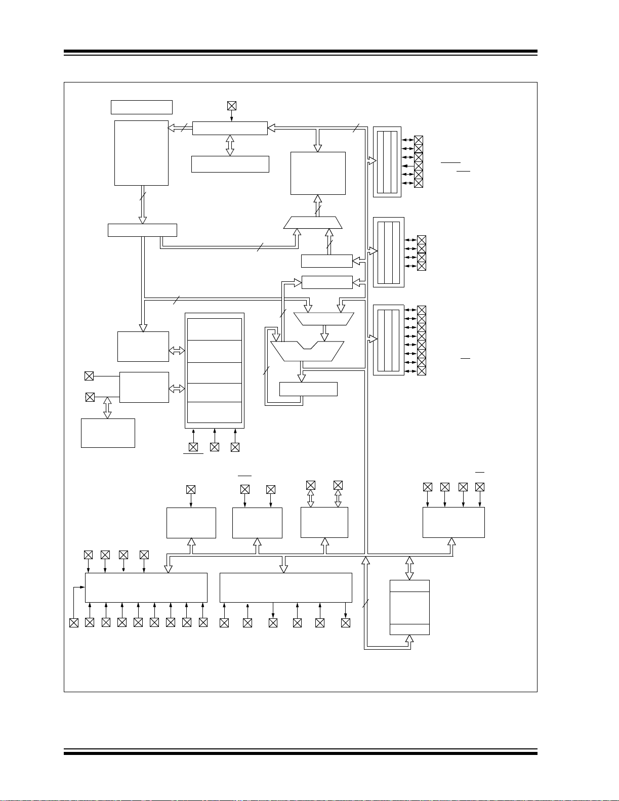
FIGURE 1-1: PIC16F685 BLOCK DIAGRAM
INT
Program
OSC1/CLKI
OSC2/CLKO
Internal
Oscillator
Block
Configuration
Bus
Instruction Reg
Decode and
Flash
4k x 14
Program
Memory
14
Instruction
Control
Timing
Generation
13
Program Counter
8-Level Stack (13-bit)
Direct Addr
8
Power-up
Timer
Oscillator
Start-up Timer
Power-on
Reset
Watchdog
Timer
Brown-out
Reset
VDD
MCLR
7
3
8
VSS
T1G T1CKIT0CKI
Block Diagrams and pinout descriptions of the devices
are as follows:
• PIC16F685 (Figure 1-1, Table 1-1)
• PIC16F687/PIC16F689 (Figure 1-2, Table 1-2)
• PIC16F690 (Figure 1-3, Table 1-3)
8
Data Bus
256 bytes
Registers
Addr MUX
ALU
W Reg
RAM
File
RAM Addr
9
8
FSR Reg
Status Reg
MUX
Indirect
Addr
PORTA
PORTB
PORTC
RA0/AN0/C1IN+/ICSPDAT/ULPWU
RA1/AN1/C12IN-/V
RA2/AN2/T0CKI/INT/C1OUT
RA3/MCLR
RA4/AN3/T1G/OSC2/CLKOUT
RA5/T1CKI/OSC1/CLKIN
RB4/AN10
RB5/AN11
RB6
RB7
RC0/AN4/C2IN+
RC1/AN5/C12INRC2/AN6/P1D
RC3/AN7/P1C
RC4/C2OUT/P1B
RC5/CCP1/P1A
RC6/AN8
RC7/AN9
CCP1/
P1A
P1B P1C P1D
/VPP
REF/ICSPCLK
AN8 AN9 AN10 AN11
Analog-To-Digital Converter
VREF
AN0 AN1 AN2 AN3 AN4 AN5 AN6
Timer0 Timer1
Analog Comparators
AN7
C1IN- C1IN+ C1OUT
2
and Reference
Timer2
C2IN- C2IN+ C2OUT
8
ECCP+
EEDAT
256 Bytes
Data
EEPROM
EEADR
© 2005 Microchip Technology Inc. Preliminary DS41262A-page 5
PIC16F685/687/689/690
U
FIGURE 1-2: PIC16F687/PIC16F689 BLOCK DIAGRAM
INT
Program
Bus
OSC1/CLKI
OSC2/CLKO
Internal
Oscillator
Block
Configuration
Flash
(1)
2k
/4k x 14
Program
Memory
14
Instruction Reg
Instruction
Decode and
Control
Timing
Generation
13
Program Counter
8-Level Stack (13-bit)
Direct Addr
8
Power-up
Timer
Oscillator
Start-up Timer
Power-on
Reset
Watchdog
Timer
Brown-out
Reset
VDD
MCLR
VSS
T1G
Data Bus
RAM
(1)
/256 bytes
128
File
Registers
RAM Addr
9
Addr MUX
7
3
ALU
8
W Reg
T1CKIT0CKI
TX/CK RX/DT
8
FSR Reg
Status Reg
MUX
Indirect
Addr
8
PORTA
RA0/AN0/C1IN+/ICSPDAT/ULPW
RA1/AN1/C12IN-/VREF/ICSPCLK
RA2/AN2/T0CKI/INT/C1OUT
RA3/MCLR
RA4/AN3/T1G/OSC2/CLKOUT
RA5/T1CKI/OSC1/CLKIN
PORTB
RB4/AN10/SDI/SDA
RB5/AN11/RX/DT
RB6/SCK/SCL
RB7/TX/CK
PORTC
RC0/AN4/C2IN+
RC1/AN5/C12INRC2/AN6
RC3/AN7
RC4/C2OUT
RC5/CCP1
RC6/AN8/SS
RC7/AN9/SDO
SDO
/VPP
SDI/ SCK/
SDA SCL
SS
Timer0 Timer1
AN8 AN9 AN10 AN11
Analog-To-Digital Converter
AN0 AN1 AN2 AN3 AN4 AN5 AN6
AN7
EUSART
2
Analog Comparators
and Reference
C1IN- C1IN+ C1OUTVREF
C2IN- C2IN+ C2OUT
8
EEDAT
256 Bytes
Data
EEPROM
EEADR
Synchronous
Serial Por t
Note 1: PIC16F687 only.
DS41262A-page 6 Preliminary © 2005 Microchip Technology Inc.
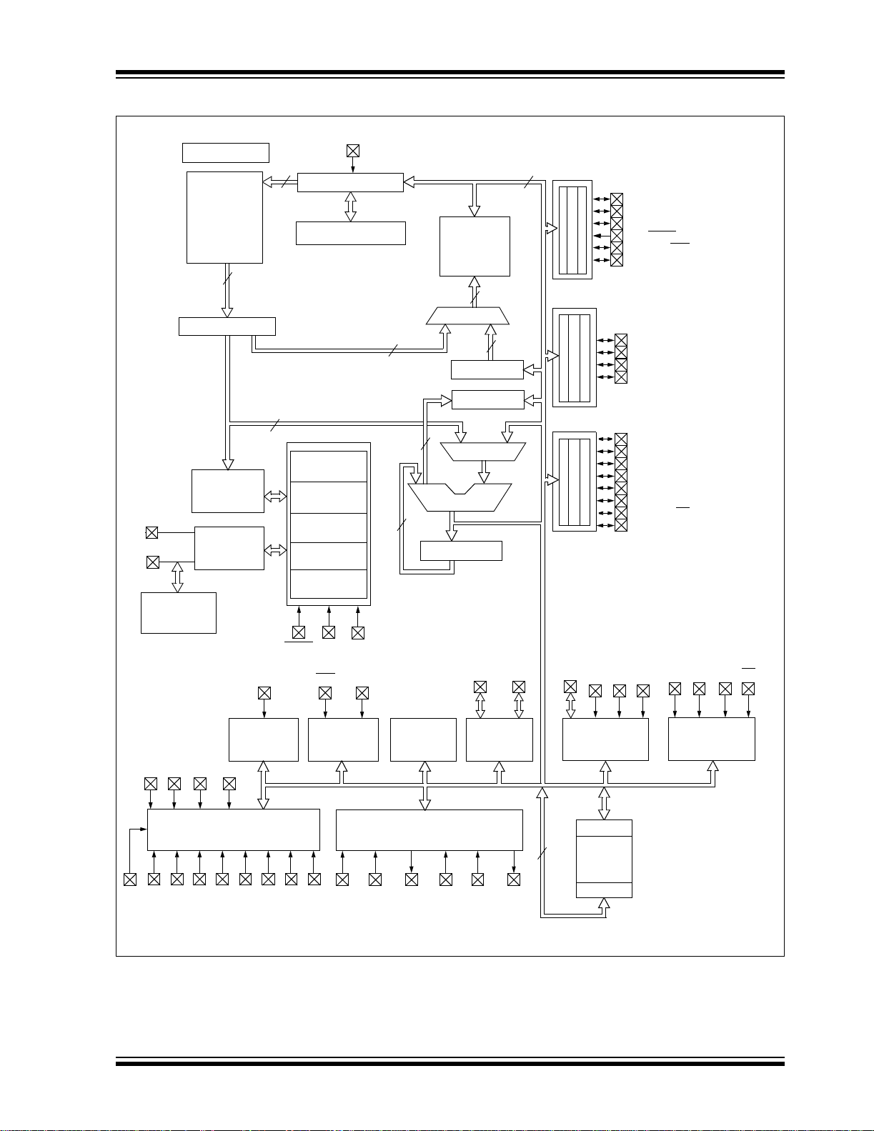
FIGURE 1-3: PIC16F690 BLOCK DIAGRAM
U
INT
Program
OSC1/CLKI
OSC2/CLKO
Internal
Oscillator
Block
Configuration
Bus
Instruction Reg
Decode and
Flash
4k x 14
Program
Memory
14
Instruction
Control
Timing
Generation
13
Program Counter
8-Level Stack (13-bit)
Direct Addr
8
Power-up
Timer
Oscillator
Start-up Timer
Power-on
Reset
Watchdog
Timer
Brown-out
Reset
VDD
MCLR
T1G
7
3
8
VSS
T1CKIT0CKI
PIC16F685/687/689/690
8
Data Bus
RAM
256 bytes
Registers
Addr MUX
Status Reg
ALU
W Reg
File
RAM Addr
9
Indirect
Addr
8
FSR Reg
MUX
TX/CK RX/DT
PORTA
PORTB
PORTC
CCP1/
P1A
RA0/AN0/C1IN+/ICSPDAT/ULPW
RA1/AN1/C12IN-/VREF/ICSPCLK
RA2/AN2/T0CKI/INT/C1OUT
RA3/MCLR
RA4/AN3/T1G/OSC2/CLKOUT
RA5/T1CKI/OSC1/CLKIN
RB4/AN10/SDI/SDA
RB5/AN11/RX/DT
RB6/SCK/SCL
RB7/TX/CK
RC0/AN4/C2IN+
RC1/AN5/C12INRC2/AN6/P1D
RC3/AN7/P1C
RC4/C2OUT/P1B
RC5/CCP1/P1A
RC6/AN8/SS
RC7/AN9/SDO
P1B P1C P1D
/VPP
SDO
SDI/ SCK/
SDA SCL
SS
Synchronous
Serial Port
AN8 AN9 AN10 AN11
Analog-To-Digital Converter
VREF
AN0 AN1 AN2 AN3 AN4 AN5 AN6
Timer0 Timer1
AN7
C1IN- C1IN+ C1OUT
Timer2
2
Analog Comparators
and Reference
C2IN- C2IN+ C2OUT
EUSART
8
ECCP+
EEDAT
256 Bytes
Data
EEPROM
EEADR
© 2005 Microchip Technology Inc. Preliminary DS41262A-page 7
PIC16F685/687/689/690
TABLE 1-1: PINOUT DESCRIPTION – PIC16F685
Name Function
RA0/AN0/C1IN+/ICSPDAT/
ULPWU
RA1/AN1/C12IN-/V
RA2/AN2/T0CKI/INT/C1OUT RA2 ST CMOS General purpose I/O. Individually controlled interrupt-on-
RA3/MCLR
RA4/AN3/T1G
RA5/T1CKI/OSC1/CLKIN RA5 TTL CMOS General purpose I/O. Individually controlled interrupt-on-
RB4/AN10 RB4 TTL CMOS General purpose I/O. Individually controlled interrupt-on-
RB5/AN11 RB5 TTL CMOS General purpose I/O. Individually controlled interrupt-on-
RB6 RB6 TTL CMOS General purpose I/O. Individually controlled interrupt-on-
RB7 RB7 TTL CMOS General purpose I/O. Individually controlled interrupt-on-
RC0/AN4/C2IN+ RC0 ST CMOS General purpose I/O.
Legend: AN = Analog input or output CMOS = CMOS compatible input or output
REF/ICSPCLK RA1 TTL CMOS General purpose I/O. Individually controlled interrupt-on-
/VPP RA3 TTL — General purpose input. Individually controlled interrupt-on-
/OSC2/CLKOUT RA4 TTL CMOS General purpose I/O. Individually controlled interrupt-on-
TTL = TTL compatible input ST = Schmitt Trigger input with CMOS levels
HV = High Voltage XTAL = Crystal
RA0 TTL — General purpose I/O. Individually controlled interrupt-on-
AN0 AN — A/D Channel 0 input.
C1IN+ AN — Comparator 1 positive input.
ICSPDAT TTL CMOS ICSP™ Data I/O.
ULPWU AN — Ultra Low-Power Wake-up input.
AN1 AN — A/D Channel 1 input.
C12IN- AN — Comparator 1 or 2 negative input.
REF AN — External Voltage Reference for A/D.
V
ICSPCLK ST — ICSP™ clock.
AN2 AN — A/D Channel 2 input.
T0CKI ST — Timer0 clock input.
INT ST —
C1OUT — CMOS Comparator 1 output.
MCLR
PP HV — Programming voltage.
V
AN3 AN — A/D Channel 3 input.
T1G
OSC2 — XTAL Crystal/Resonator.
CLKOUT — CMOS F
T1CKI ST — Timer1 clock input.
OSC1 XTAL — Crystal/Resonator.
CLKIN ST — External clock input/RC oscillator connection.
AN10 AN — A/D Channel 10 input.
AN11 AN — A/D Channel 11 input.
AN4 AN — A/D Channel 4 input.
C2IN+ AN — Comparator 2 positive input.
Input
Type
Output
Type
change. Individually enabled pull-up.
change. Individually enabled pull-up.
change. Individually enabled pull-up.
Description
External interrupt pin.
change.
ST — Master Clear with internal pull-up.
change. Individually enabled pull-up.
ST — Timer1 gate input.
OSC/4 output.
change. Individually enabled pull-up.
change. Individually enabled pull-up.
change. Individually enabled pull-up.
change. Individually enabled pull-up.
change. Individually enabled pull-up.
DS41262A-page 8 Preliminary © 2005 Microchip Technology Inc.
PIC16F685/687/689/690
TABLE 1-1: PINOUT DESCRIPTION – PIC16F685 (CONTINUED)
Name Function
RC1/AN5/C12IN- RC1 ST CMOS General purpose I/O.
AN5 AN — A/D Channel 5 input.
C12IN- AN — Comparator 1 or 2 negative input.
RC2/AN6/P1D RC2 ST CMOS General purpose I/O.
AN6 AN — A/D Channel 6 input.
P1D — CMOS PWM output.
RC3/AN7/P1C RC3 ST CMOS General purpose I/O.
AN7 AN — A/D Channel 7 input.
P1C — CMOS PWM output.
RC4/C2OUT/P1B RC4 ST CMOS General purpose I/O.
C2OUT — CMOS Comparator 2 output.
P1B — CMOS PWM output.
RC5/CCP1/P1A RC5 ST CMOS General purpose I/O.
CCP1 ST CMOS Capture/Compare input.
P1A ST CMOS PWM output.
RC6/AN8 RC6 ST CMOS General purpose I/O.
AN8 AN — A/D Channel 8 input.
RC7/AN9 RC7 ST CMOS General purpose I/O.
AN9 AN — A/D Channel 9 input.
SS VSS Power — Ground reference.
V
DD VDD Power — Positive supply.
V
Legend: AN = Analog input or output CMOS = CMOS compatible input or output
TTL = TTL compatible input ST = Schmitt Trigger input with CMOS levels
HV = High Voltage XTAL = Crystal
Input
Type
Output
Type
Description
© 2005 Microchip Technology Inc. Preliminary DS41262A-page 9
PIC16F685/687/689/690
TABLE 1-2: PINOUT DESCRIPTION – PIC16F687/PIC16F689
Name Function
RA0/AN0/C1IN+/ICSPDAT/
ULPWU
RA1/AN1/C12IN-/V
RA2/AN2/T0CKI/INT/C1OUT RA2 ST CMOS General purpose I/O. Individually controlled interrupt-on-
RA3/MCLR
RA4/AN3/T1G
RA5/T1CKI/OSC1/CLKIN RA5 TTL CMOS General purpose I/O. Individually controlled interrupt-on-
RB4/AN10/SDI/SDA RB4 TTL CMOS General purpose I/O. Individually controlled interrupt-on-
RB5/AN11/RX/DT RB5 TTL CMOS General purpose I/O. Individually controlled interrupt-on-
Legend: AN = Analog input or output CMOS = CMOS compatible input or output OD = Open Drain
REF/ICSPCLK RA1 TTL CMOS General purpose I/O. Individually controlled interrupt-on-
/VPP RA3 TTL — General purpose input. Individually controlled interrupt-on-
/OSC2/CLKOUT RA4 TTL CMOS General purpose I/O. Individually controlled interrupt-on-
TTL = TTL compatible input ST = Schmitt Trigger input with CMOS levels
HV = High Voltage XTAL = Crystal
RA0 TTL — General purpose I/O. Individually controlled interrupt-on-
AN0 AN — A/D Channel 0 input.
C1IN+ AN — Comparator 1 positive input.
ICSPDAT TTL C MOS ICSP Data I/O.
ULPWU AN — Ultra Low-Power Wake-up input.
AN1 AN — A/D Channel 1 input.
C12IN- AN — Comparator 1 or 2 negative input.
REF AN — External Voltage Reference for A/D.
V
ICSPCLK ST — ICSP™ clock.
AN2 AN — A/D Channel 2 input.
T0CKI ST — Timer0 clock input.
INT ST — External Interrupt.
C1OUT — CMOS Comparator 1 output.
MCLR
PP HV — Programming voltage.
V
AN3 AN — A/D Channel 3 input.
T1G
OSC2 — XTAL Crystal/Resonator.
CLKOUT — CMOS F
T1CKI ST — Timer1 clock input.
OSC1 XTAL — Crystal/Resonator.
CLKIN ST — External clock input/RC oscillator connection.
AN10 AN — A/D Channel 10 input.
SDI ST — SPI™ data input.
SDA ST OD I
AN11 AN — A/D Channel 11 input.
RX ST — EUSART asynchronous input.
DT ST CMOS EUSART synchronous data.
Input
Type
Output
Type
change. Individually enabled pull-up.
change. Individually enabled pull-up.
change. Individually enabled pull-up.
change.
ST — Master Clear with internal pull-up.
change. Individually enabled pull-up.
ST — Timer1 gate input.
OSC/4 output.
change. Individually enabled pull-up.
change. Individually enabled pull-up.
2
C data input/output.
change. Individually enabled pull-up.
Description
DS41262A-page 10 Preliminary © 2005 Microchip Technology Inc.
PIC16F685/687/689/690
TABLE 1-2: PINOUT DESCRIPTION – PIC16F687/PIC16F689 (CONTINUED)
Name Function
RB6/SCK/SCL RB6 TTL CMOS General purpose I/O. Individually controlled interrupt-on-
SCK ST CMOS SPI™ clock.
SCL ST OD I
RB7/TX/CK RB7 TTL CMOS General purpose I/O. Individually controlled interrupt-on-
TX — CMOS EUSART asynchronous output.
CK ST CMOS EUSART synchronous clock.
RC0/AN4/C2IN+ RC0 ST CMOS General purpose I/O.
AN4 AN — A/D Channel 4 input.
C2IN+ AN — Comparator 2 positive input.
RC1/AN5/C12IN- RC1 ST CMOS General purpose I/O.
AN5 AN — A/D Channel 5 input.
C12IN- AN — Comparator 1 or 2 negative input.
RC2/AN6 RC2 ST CMOS General purpose I/O.
AN6 AN — A/D Channel 6 input.
RC3/AN7 RC3 ST CMOS General purpose I/O.
AN7 AN — A/D Channel 7 input.
RC4/C2OUT RC4 ST CMOS General purpose I/O.
C2OUT — CMOS Comparator 2 output.
RC5/CCP1 RC5 ST CMOS General purpose I/O.
CCP1 ST CMOS Capture/Compare input.
RC6/AN8/SS
RC7/AN9/SDO RC7 ST CMOS General purpose I/O.
SS VSS Power — Ground reference.
V
DD VDD Power — Positive supply.
V
Legend: AN = Analog input or output CMOS = CMOS compatible input or output OD = Open Drain
TTL = TTL compatible input ST = Schmitt Trigger input with CMOS levels
HV = High Voltage XTAL = Crystal
RC6 ST CMOS General purpose I/O.
AN8 AN — A/D Channel 8 input.
SS
AN9 AN — A/D Channel 9 input.
SDO — CMOS SPI data output.
Input
Type
Output
Type
change. Individually enabled pull-up.
2
C™ clock.
change. Individually enabled pull-up.
ST — Slave Select input.
Description
© 2005 Microchip Technology Inc. Preliminary DS41262A-page 11

PIC16F685/687/689/690
TABLE 1-3: PINOUT DESCRIPTION – PIC16F690
Name Function
RA0/AN0/C1IN+/ICSPDAT/
ULPWU
RA1/AN1/C12IN-/V
RA2/AN2/T0CKI/INT/C1OUT RA2 ST CMOS General purpose I/O. Individually controlled interrupt-on-
RA3/MCLR
RA4/AN3/T1G
RA5/T1CKI/OSC1/CLKIN RA5 TTL CMOS General purpose I/O. Individually controlled interrupt-on-
RB4/AN10/SDI/SDA RB4 TTL CMOS General purpose I/O. Individually controlled interrupt-on-
RB5/AN11/RX/DT RB5 TTL CMOS General purpose I/O. Individually controlled interrupt-on-
Legend: AN = Analog input or output CMOS = CMOS compatible input or output OD = Open Drain
REF/ICSPCLK RA1 TTL CMOS General purpose I/O. Individually controlled interrupt-on-
/VPP RA3 TTL — General purpose input. Individually controlled interrupt-on-
/OSC2/CLKOUT RA4 TTL CMOS General purpose I/O. Individually controlled interrupt-on-
TTL = TTL compatible input ST = Schmitt Trigger input with CMOS levels
HV = High Voltage XTAL = Crystal
RA0 TTL — General purpose I/O. Individually controlled interrupt-on-
AN0 AN — A/D Channel 0 input.
C1IN+ AN — Comparator 1 positive input.
ICSPDAT TTL C MOS ICSP Data I/O.
ULPWU AN — Ultra Low-Power Wake-up input.
AN1 AN — A/D Channel 1 input.
C12IN- AN — Comparator 1 or 2 negative input.
REF AN — External Voltage Reference for A/D.
V
ICSPCLK ST — ICSP™ clock.
AN2 AN — A/D Channel 2 input.
T0CKI ST — Timer0 clock input.
INT ST — External Interrupt.
C1OUT — CMOS Comparator 1 output.
MCLR
PP HV — Programming voltage.
V
AN3 AN — A/D Channel 3 input.
T1G
OSC2 — XTAL Crystal/Resonator.
CLKOUT — CMOS F
T1CKI ST — Timer1 clock input.
OSC1 XTAL — Crystal/Resonator.
CLKIN ST — External clock input/RC oscillator connection.
AN10 AN — A/D Channel 10 input.
SDI ST — SPI data input.
SDA ST OD I
AN11 AN — A/D Channel 11 input.
RX ST — EUSART asynchronous input.
DT ST CMOS EUSART synchronous data.
Input
Type
Output
Type
change. Individually enabled pull-up.
change. Individually enabled pull-up.
change. Individually enabled pull-up.
change.
ST — Master Clear with internal pull-up.
change. Individually enabled pull-up.
ST — Timer1 gate input.
OSC/4 output.
change. Individually enabled pull-up.
change. Individually enabled pull-up.
2
C data input/output.
change. Individually enabled pull-up.
Description
DS41262A-page 12 Preliminary © 2005 Microchip Technology Inc.
PIC16F685/687/689/690
TABLE 1-3: PINOUT DESCRIPTION – PIC16F690 (CONTINUED)
Name Function
RB6/SCK/SCL RB6 TTL CMOS General purpose I/O. Individually controlled interrupt-on-
SCK ST CMOS SPI™ clock.
SCL ST OD I
RB7/TX/CK RB7 TTL CMOS General purpose I/O. Individually controlled interrupt-on-
TX — CMOS EUSART asynchronous output.
CK ST CMOS EUSART synchronous clock.
RC0/AN4/C2IN+ RC0 ST CMOS General purpose I/O.
AN4 AN — A/D Channel 4 input.
C2IN+ AN — Comparator 2 positive input.
RC1/AN5/C12IN- RC1 ST CMOS General purpose I/O.
AN5 AN — A/D Channel 5 input.
C12IN- AN — Comparator 1 or 2 negative input.
RC2/AN6/P1D RC2 ST CMOS General purpose I/O.
AN6 AN — A/D Channel 6 input.
P1D — CMOS PWM output.
RC3/AN7/P1C RC3 ST CMOS General purpose I/O.
AN7 AN — A/D Channel 7 input.
P1C — CMOS PWM output.
RC4/C2OUT/P1B RC4 ST CMOS General purpose I/O.
C2OUT — CMOS Comparator 2 output.
P1B — CMOS PWM output.
RC5/CCP1/P1A RC5 ST CMOS General purpose I/O.
CCP1 ST CMOS Capture/Compare input.
P1A ST CMOS PWM output.
RC6/AN8/SS
RC7/AN9/SDO RC7 ST CMOS General purpose I/O.
SS VSS Power — Ground reference.
V
DD VDD Power — Positive supply.
V
Legend: AN = Analog input or output CMOS = CMOS compatible input or output OD = Open Drain
TTL = TTL compatible input ST = Schmitt Trigger input with CMOS levels
HV = High Voltage XTAL = Crystal
RC6 ST CMOS General purpose I/O.
AN8 AN — A/D Channel 8 input.
SS
AN9 AN — A/D Channel 9 input.
SDO — CMOS SPI data output.
Input
Type
Output
Type
change. Individually enabled pull-up.
2
C™ clock.
change. Individually enabled pull-up.
ST — Slave Select input.
Description
© 2005 Microchip Technology Inc. Preliminary DS41262A-page 13

PIC16F685/687/689/690
NOTES:
DS41262A-page 14 Preliminary © 2005 Microchip Technology Inc.
PIC16F685/687/689/690
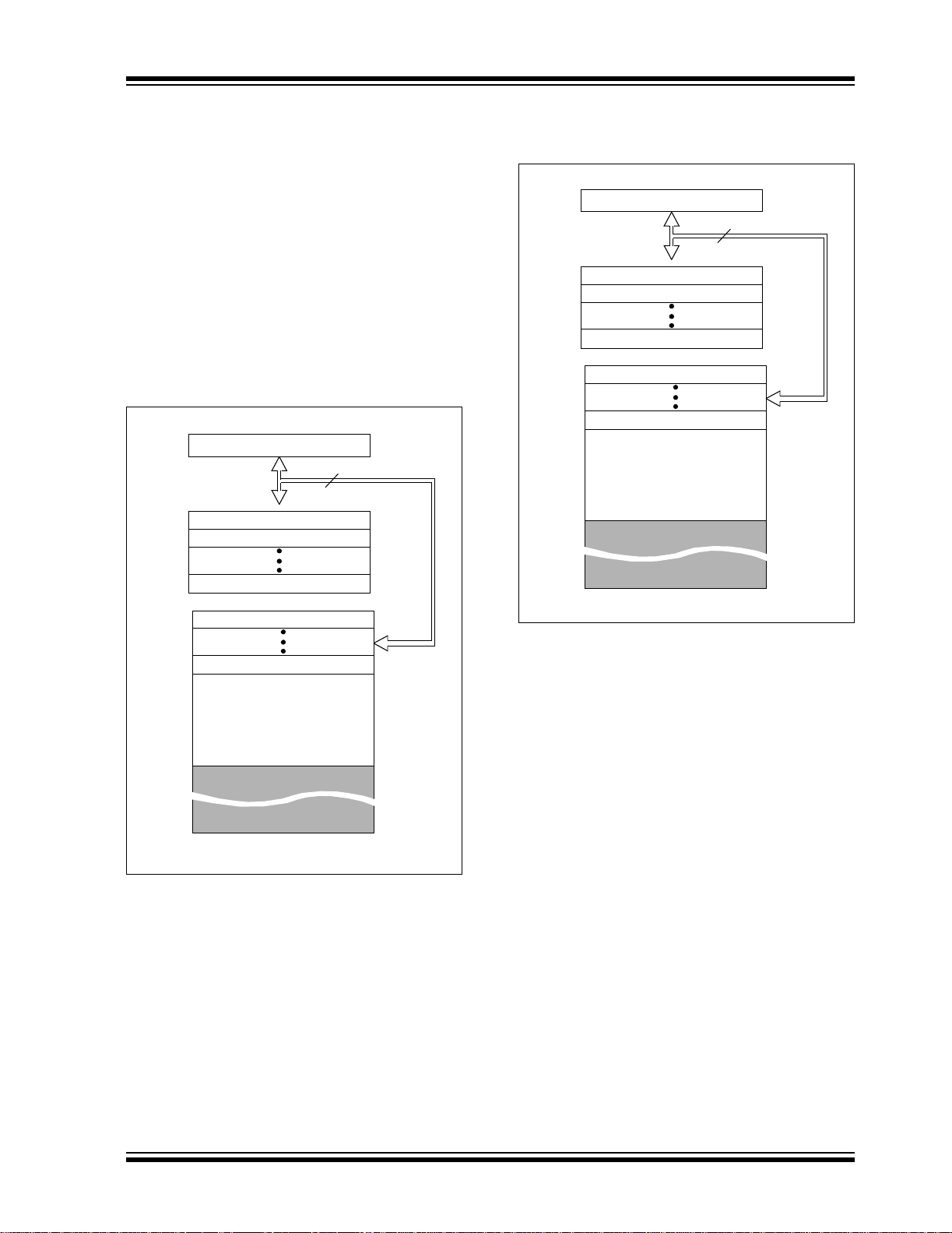
2.0 MEMORY ORGANIZATION
2.1 Program Memory Organization
The PIC16F685/687/689/690 has a 13-bit program
counter capable of addressing an 8k x 14 program
memory space. Onl y the first 2k x 14 (0000h-07 FFh) for
the PIC16F687 is physic ally impleme nted and first 4k x
14 (0000h-0FFFh) for the PIC16F685/PIC16F689/
PIC16F690. Accessing a location above these
boundaries will caus e a wrap around. The Reset vector
is at 0000h and the interrupt vector is at 0004h (see
Figures 2-1 and 2-2).
FIGURE 2-1: PROGRAM MEMORY MAP
AND STACK FOR THE
PIC16F685/689/690
PC<12:0>
CALL, RETURN
RETFIE, RETLW
Stack Level 1
Stack Level 2
13
FIGURE 2-2: PROGRAM MEMORY MAP
AND STACK FOR THE
PIC16F687
PC<12:0>
CALL, RETURN
RETFIE, RETLW
Stack Level 1
Stack Level 2
Stack Level 8
Reset Vector
Interrupt Vector
On-chip Program
Memory
Access 0-7FFh
13
0000h
0004h
0005h
07FFh
0800h
Stack Level 8
Reset Vector
Interrupt Vector
On-chip Program
Memory
Access 0-FFFh
1FFFh
0000h
0004h
0005h
0FFFh
1000h
1FFFh
© 2005 Microchip Technology Inc. Preliminary DS41262A-page 15

PIC16F685/687/689/690
2.2 Data Memory Organization
The data memory (see Figures 2-3, 2-4 and 2-5) is
partitioned into four banks which contain the General
Purpose Registers (GPR) and the Special Function
Registers (SFR). The Special Function Registers are
located in the fir st 32 l oca tio ns o f eac h ba nk. Regi ste r
locations 20h-7Fh in Bank 0 and A0h-EFh (A0-BF,
PIC16F687 only) in Bank 1 are General Purpose
Registers, implemented as static RAM. Register
locations F0h-FFh i n Bank 1, 170 h-17Fh in Ban k 2 an d
1F0h-1FFh in Bank 3 point to addresses 70h-7Fh in
Bank 0. Other General Purpose Resisters (GPR) are
also available in Bank 1 an d Ban k 2 , depending on the
device. Details are shown in Figures 2-3, 2-4 and 2-5.
All other RAM is unimplemented and returns ‘0’ when
read. RP<1:0> (STATUS<6:5>) are the bank select
bits:
RP1
RP0
00→ Bank 0 is selected
01→ Bank 1 is selected
10→ Bank 2 is selected
11→ Bank 3 is selected
2.2.1 GENERAL PURPOSE REGISTER
FILE
The register file is organized as 128 x 8 in the
PIC16F687 and 256 x 8 in the PIC16F685/PIC16F689/
PIC16F690. Each register is accessed, either directly or
indirectly, through the File Select Register (FSR) (see
Section 2.4 “Indirect Addressing, INDF and FSR
Registers”).
2.2.2 SPECIAL FUNCTION REGISTERS
The Special Function Registe rs are registers used by
the CPU and peripheral functions for controlling the
desired operation of the device (see Tables 2-1, 2-2, 2-3
and 2-4). These registers are static RAM.
The special re gisters can be classifi ed into two sets:
core and peripheral. The Special Function Registers
associated with the “c ore” are des cribed in this sect ion.
Registers related to the operati on of peripheral features
are described in the section of that peri phe ral feature .
DS41262A-page 16 Preliminary © 2005 Microchip Technology Inc.
PIC16F685/687/689/690
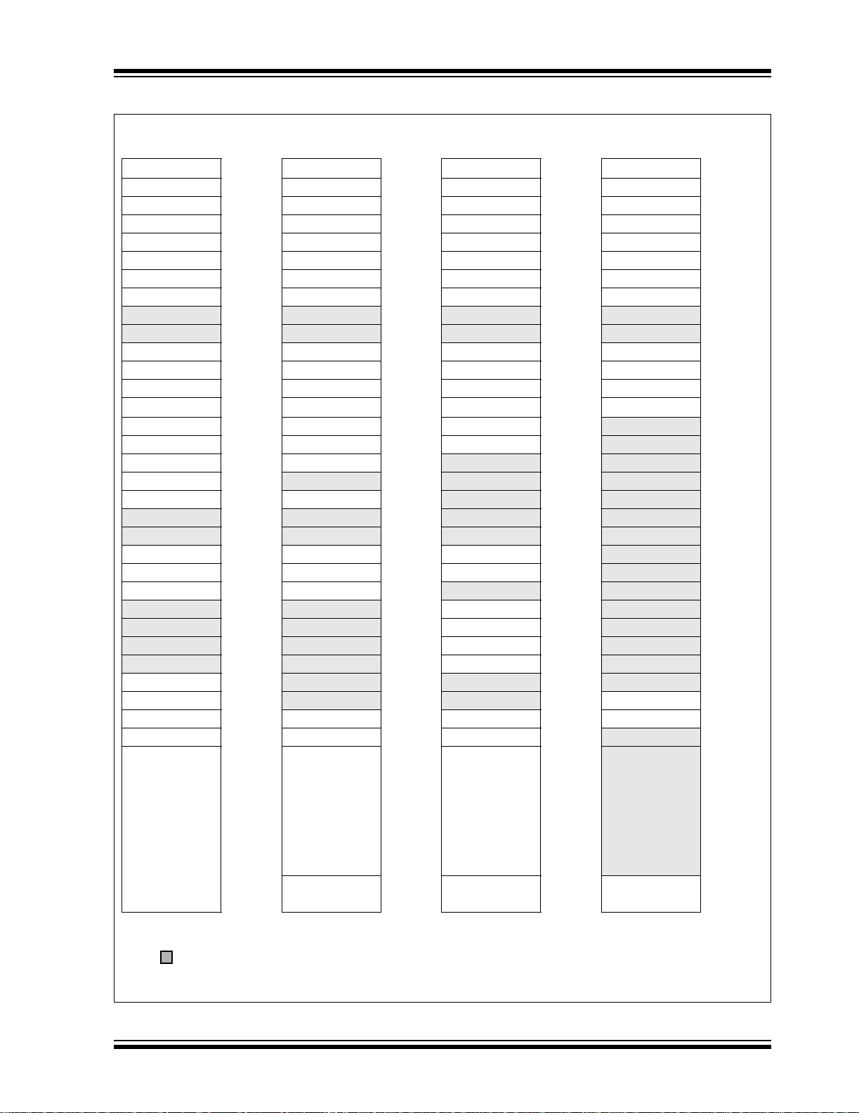
FIGURE 2-3: PIC16F685 SPECIAL FUNCTION REGISTERS
File File File File
Address Address Address Address
Indirect addr.
TMR0 01h OPTION_REG 81h TMR0 101h OPTION_REG 181h
PCL 02h PCL 82h PCL 102h PCL 182h
STATUS 03h STATUS 83h STATUS 103h STATUS 183h
FSR 04h FSR 84h FSR 104h FSR 184h
PORTA 05h TRISA 85h PORTA 105h TRISA 185h
PORTB 06h TRISB 86h PORTB 106h TRISB 186h
PORTC 07h TRISC 87h PORTC 107h TRISC 187h
PCLATH 0Ah PCLATH 8Ah PCLATH 10Ah PCLATH 18Ah
INTCON 0Bh INTCON 8Bh INTCON 10Bh INTCON 18Bh
PIR1 0Ch PIE1 8Ch EEDAT 10Ch EECON1 18Ch
PIR2 0Dh PIE2 8Dh EEADR 10Dh EECON2
TMR1L 0Eh PCON 8Eh EEDATH 10Eh 18Eh
TMR1H 0Fh OSCCON 8Fh EEADRH 10Fh 18Fh
T1CON 10h OSCTUNE 90h
TMR2 11h 91h 111h 191h
T2CON 12h PR2 92h 112h 192h
CCPR1L 15h WPUA 95h WPUB 115h 195h
CCPR1H 16h IOCA 96h IOCB 116h
CCP1CON 17h WDTCON 97h 117h 197h
PWM1CON 1Ch
ECCPAS 1Dh 9Dh 11Dh PSTRCON 19Dh
ADRESH 1Eh ADRESL 9Eh ANSEL 11Eh SRCON 19Eh
ADCON0 1Fh ADCON1 9Fh ANSELH 11Fh
(1)
00h Indirect addr.
08h 88h 108h 188h
09h 89h 109h 189h
13h 93h 113h 193h
14h 94h 114h 194h
18h 98h VRCON 118h 198h
19h 99h CM1CON0 119h 199h
1Ah 9Ah CM2CON0 11Ah 19Ah
1Bh 9Bh CM2CON1 11Bh 19Bh
20h
(1)
80h Indirect addr.
9Ch 11Ch 19Ch
A0h
(1)
100h Indirect addr.
110h 190h
120h
(1)
(1)
180h
18Dh
196h
19Fh
1A0h
General
General
Purpose
Register
96 Bytes
7Fh FFh 17Fh 1FFh
Bank 0 Bank1 Bank2 Bank3
Unimplemented data memory locations, read as ‘0’.
Note 1: Not a physical register.
© 2005 Microchip Technology Inc. Preliminary DS41262A-page 17
Purpose
Register
80 Bytes
accesses
70h-7Fh
EFh 16Fh
F0h accesses
General
Purpose
Register
80 Bytes
70h-7Fh
170h accesses
70h-7Fh
1F0h
PIC16F685/687/689/690
FIGURE 2-4: PIC16F687/P IC16 F689 SPECIAL FUNCTION REGISTERS
File File File File
Address Address Address Address
Indirect addr.
(1)
00h Indirect addr.
TMR0 01h OPTION_REG 81h TMR0 101h OPTION_REG 181h
PCL 02h PCL 82h PCL 102h PCL 182h
STATUS 03h STATUS 83h STATUS 103h STATUS 183h
FSR 04h FSR 84h FSR 104h FSR 184h
PORTA 05h TRISA 85h PORTA 105h TRISA 185h
PORTB 06h TRISB 86h PORTB 106h TRISB 186h
PORTC 07h TRISC 87h PORTC 107h TRISC 187h
08h 88h 108h 188h
09h 89h 109h 189h
PCLATH 0Ah PCLATH 8Ah PCLATH 10Ah PCLATH 18Ah
INTCON 0Bh INTCON 8Bh INTCON 10Bh INTCON 18Bh
PIR1 0Ch PIE1 8Ch EEDAT 10Ch EECON1 18Ch
PIR2 0Dh PIE2 8Dh EEADR 10Dh EECON2
TMR1L 0Eh PCON 8Eh EEDATH
TMR1H 0Fh OSCCON 8Fh EEADRH
T1CON 10h OSCTUNE 90h 110h 190h
11h 91h 111h 191h
12h 92h 112h 192h
SSPBUF 13h SSPADD
SSPCON 14h SSPSTAT 94h 114h 194h
15h WPUA 95h WPUB 115h 195h
16h IOCA 96h IOCB 116h 196h
17h WDTCON 97h 117h 197h
RCSTA 18h TXSTA 98h VRCON 118h
TXREG 19h SPBRG 99h CM1CON0 119h
RCREG 1Ah SPBRGH 9Ah CM2CON0 11Ah 19Ah
1Bh BAUDCTL 9Bh CM2CON1 11Bh 19Bh
1Ch 9Ch 11Ch 19Ch
1Dh 9Dh 11Dh 19Dh
ADRESH 1Eh ADRESL 9Eh ANSEL 11Eh SRCON 19Eh
ADCON0 1Fh ADCON1 9Fh ANSELH 11Fh
20h
General
Purpose
Register
96 Bytes
General
Purpose
Register
32 Bytes
48 Bytes
(PIC16F689 only)
accesses
7Fh FFh 17Fh 1FFh
70h-7Fh
Bank 0 Bank1 Bank2 Bank3
(1)
80h Indirect addr.
(2)
93h 113h 193h
A0h
General
Purpose
BFh
C0h
EFh
Register
80 Bytes
(PIC16F689 only)
F0h accesses
70h-7Fh
(1)
100h Indirec t addr.
(3)
10Eh 18Eh
(3)
10Fh 18Fh
120h
170h accesses
70h-7Fh
(1)
(1)
180h
18Dh
198h
199h
19Fh
1A0h
1F0h
Unimplemented data memory locations, read as ‘0’.
Note 1: Not a physical register.
2: Address 93h also access es t he SSP Mask (SSPMSK) regist er under certain conditions.
See Registers 13-2 an d 13-3 for more details.
3: PIC16F689 only.
DS41262A-page 18 Preliminary © 2005 Microchip Technology Inc.

PIC16F685/687/689/690
FIGURE 2-5: PIC16F690 SPECIAL FUNCTION REGISTERS
File File File File
Address Address Address Address
Indirect addr.
TMR0 01h OPTION_REG 81h TMR0 101h OPTION_REG 181h
PCL 02h PCL 82h PCL 102h PCL 182h
STATUS 03h STATUS 83h STATUS 103h STATUS 183h
FSR 04h FSR 84h FSR 104h FSR 184h
PORTA 05h TRISA 85h PORTA 105h TRISA 185h
PORTB 06h TRISB 86h PORTB 106h TRISB 186h
PORTC 07h TRISC 87h PORTC 107h TRISC 187h
PCLATH 0Ah PCLATH 8Ah PCLATH 10Ah PCLATH 18Ah
INTCON 0Bh INTCON 8Bh INTCON 10Bh INTCON 18Bh
PIR1 0Ch PIE1 8Ch EEDAT 10Ch EECON1 18Ch
PIR2 0Dh PIE2 8Dh EEADR 10Dh EECON2
TMR1L 0Eh PCON 8Eh EEDATH 10Eh 18Eh
TMR1H 0Fh OSCCON 8Fh EEADRH 10Fh
T1CON 10h OSCTUNE 90h 110h 190h
TMR2 11h 91h 111h 191h
T2CON 12h PR2 92h
SSPBUF 13h SSPADD
SSPCON 14h SSPSTAT 94h
CCPR1L 15h WPUA 95h WPUB 115h 195h
CCPR1H 16h IOCA 96h IOCB 116h 196h
CCP1CON 17h WDTCON 97h
RCSTA 18h TXSTA 98h VRCON 118h 198h
TXREG 19h SPBRG 99h CM1CON0 119h 199h
RCREG 1Ah SPBRGH 9Ah CM2CON0 11Ah
PWM1CON 1Ch 9Ch 11Ch 19Ch
ECCPAS 1Dh
ADRESH 1Eh ADRESL 9Eh ANSEL 11Eh SRCON 19Eh
ADCON0 1Fh ADCON1 9Fh ANSELH 11Fh 19Fh
(1)
00h Indirect addr.
08h 88h 108h 188h
09h 89h 109h 189h
1Bh BAUDCTL 9Bh CM2CON1 11Bh 19Bh
20h
(1)
80h Indirect addr.
(2)
93h 113h 193h
9Dh 1 1Dh PSTRCON 19Dh
A0h
(1)
100h Indirect addr.
112h 192h
114h 194h
117h 197h
120h
(1)
(1)
180h
18Dh
18Fh
19Ah
1A0h
General
General
Purpose
Register
96 Bytes
7Fh FFh 17Fh 1FFh
Bank 0 Bank1 Bank2 Bank3
Unimplemented data memory locations, read as ‘0’.
Note 1: Not a physical register.
2: Address 93h also accesses the SSP Mask (SSPMSK) register under certain conditions.
See Registers 13-2 and 13-3 for more details.
© 2005 Microchip Technology Inc. Preliminary DS41262A-page 19
Purpose
Register
80 Bytes
accesses
70h-7Fh
EFh 16Fh
F0h accesses
General
Purpose
Register
80 Bytes
70h-7Fh
170h accesses
70h-7Fh
1F0h

PIC16F685/687/689/690
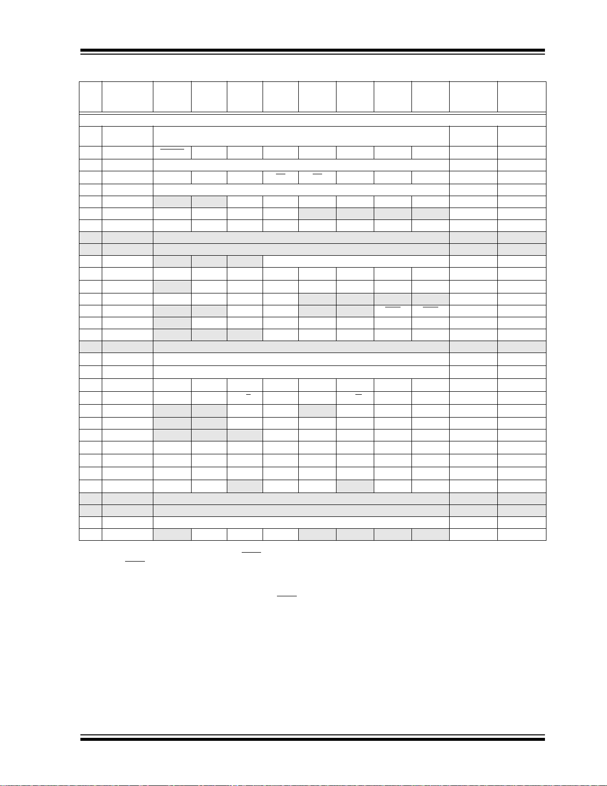
TABLE 2-1: PIC16F685/687/689/690 SPECIAL REGISTERS SUMMARY BANK 0
Addr Name Bit 7 Bit 6 Bit 5 Bit 4 Bit 3 Bit 2 Bit 1 Bit 0
POR/BOR
Reset
Bank 0
00h INDF Addressing this location uses contents of FSR to address data memory (not a physical register) xxxx xxxx xxxx xxxx
01h TMR0 Timer0 Module Register xxxx xxxx uuuu uuuu
02h PCL Program Counter’s (PC) Least Significant Byte 0000 0000 0000 0000
Value on
03h STATUS IRP RP1 RP0 TO
PD ZDCC0001 1xxx 000q quuu
04h FSR Indirect Data Memory Address Pointer xxxx xxxx uuuu uuuu
05h PORTA
06h PORTB RB7 RB6 RB5 RB4
— — RA5 RA4 RA3 RA2 RA1 RA0 --xx xxxx --uu uuuu
— — — — xxxx ---- uuuu ----
07h PORTC RC7 RC6 RC5 RC4 RC3 RC2 RC1 RC0 xxxx xxxx uuuu uuuu
08h — Unimplemented — —
09h — Unimplemented — —
0Ah PCLATH
0Bh INTCON GIE PEIE T0IE INTE RABIE T0IF INTF RABIF
0Ch PIR1
0Dh PIR2
— — — Write Buffer for upper 5 bits of Program Counter ---0 0000 ---0 0000
(2)
0000 000x 0000 000x
— ADIF RCIF
(3)
TXIF
(3)
SSPIF
(3)
CCP1IF
(4)
TMR2IF
(4)
TMR1IF -000 0000 -000 0000
OSFIF C2IF C1IF EEIF — — — — 0000 ---- 0000 ----
0Eh TMR1L Holding Register for the Least Significant Byte of the 16-bit TMR1 xxxx xxxx uuuu uuuu
0Fh TMR1H Holding Register for the Most Significant Byte of the 16-bit TMR1 xxxx xxxx uuuu uuuu
10h T1CON T1GINV TMR1GE T1CKPS1 T1CKPS0 T1OSCEN T1SYNC
TMR1CS TMR1ON 0000 0000 uuuu uuuu
11h TMR2 Timer2 Module Register 0000 0000 0000 0000
12h T2CON
13h SSPBUF
14h SSPCON
15h CCPR1L
16h CCPR1H
17h CCP1CON
18h RCSTA
19h TXREG
1Ah RCREG
(3)
(3)
(3)
(3)
(3, 5)
(4)
(4)
— TOUTPS3 TOUTPS2 TOUTPS1 TOUTPS0 TMR2ON T2CKPS1 T2CKPS0 -000 0000 -000 0000
Synchronous Serial Port Receive Buffer/Transmit Register xxxx xxxx uuuu uuuu
WCOL SSPOV SSPEN CKP SSPM3 SSPM2 SSPM1 SSPM0 0000 0000 0000 0000
Capture/Compare/PW M Regi st er 1 (LSB ) xxxx xxxx uuuu uuuu
Capture/Compare/PW M Regi st er 1 (MSB ) xxxx xxxx uuuu uuuu
(4)
P1M1 P1M0 DC1B1 DC1B0 CCP1M3 CCP1M2 CCP1M1 CCP1M0 0000 0000 0000 0000
SPEN RX9 SREN CREN ADDEN FERR OERR RX9D 0000 000x 0000 000x
EUSART Transmit Data Register 0000 0000 0000 0000
EUSART Receive Data Register 0000 0000 0000 0000
1Bh — Unimplemented — —
1Ch
1Dh
PWM1CON
ECCPAS
(4)
PRSEN PDC6 PDC5 PDC4 PDC3 PDC2 PDC1 PDC0 0000 0000 0000 0000
(4)
ECCPASE ECCPAS2 ECCPAS1 ECCPAS0 PSSAC1 PSSAC0 PSSBD1 PSSBD0 0000 0000 0000 0000
1Eh ADRESH A/D Result Register High Byte xxxx xxxx uuuu uuuu
1Fh ADCON0 ADFM VCFG CHS3 CHS2 CHS1 CHS0 GO/DONE
ADON 0000 0000 0000 0000
Legend: – = Unimplemented locations read as ‘0’, u = unchanged, x = unknown, q = value depends on condition, shaded = unimplemented
Note 1: Other (non Power-up) Resets include MCLR
2: MCLR
and WDT Reset do not affect the previous value data latch. The RABIF bit will be cleared upon Reset but will set again if the
Reset and Watchdog Timer Reset dur ing nor mal operation.
mismatched exists.
3: PIC16F687/PIC16F689/PIC16F690 only.
4: PIC16F685/PIC16F690 only.
5: When SSPCON bits SSPM<3:0> = 1001, any reads or writes to the SSPADD SFR address are accessed through the SSPMSK register.
See Registers 13-2 and 13 -3 for mo re detail .
Value on
all other
Resets
(1)
DS41262A-page 20 Preliminary © 2005 Microchip Technology Inc.
PIC16F685/687/689/690
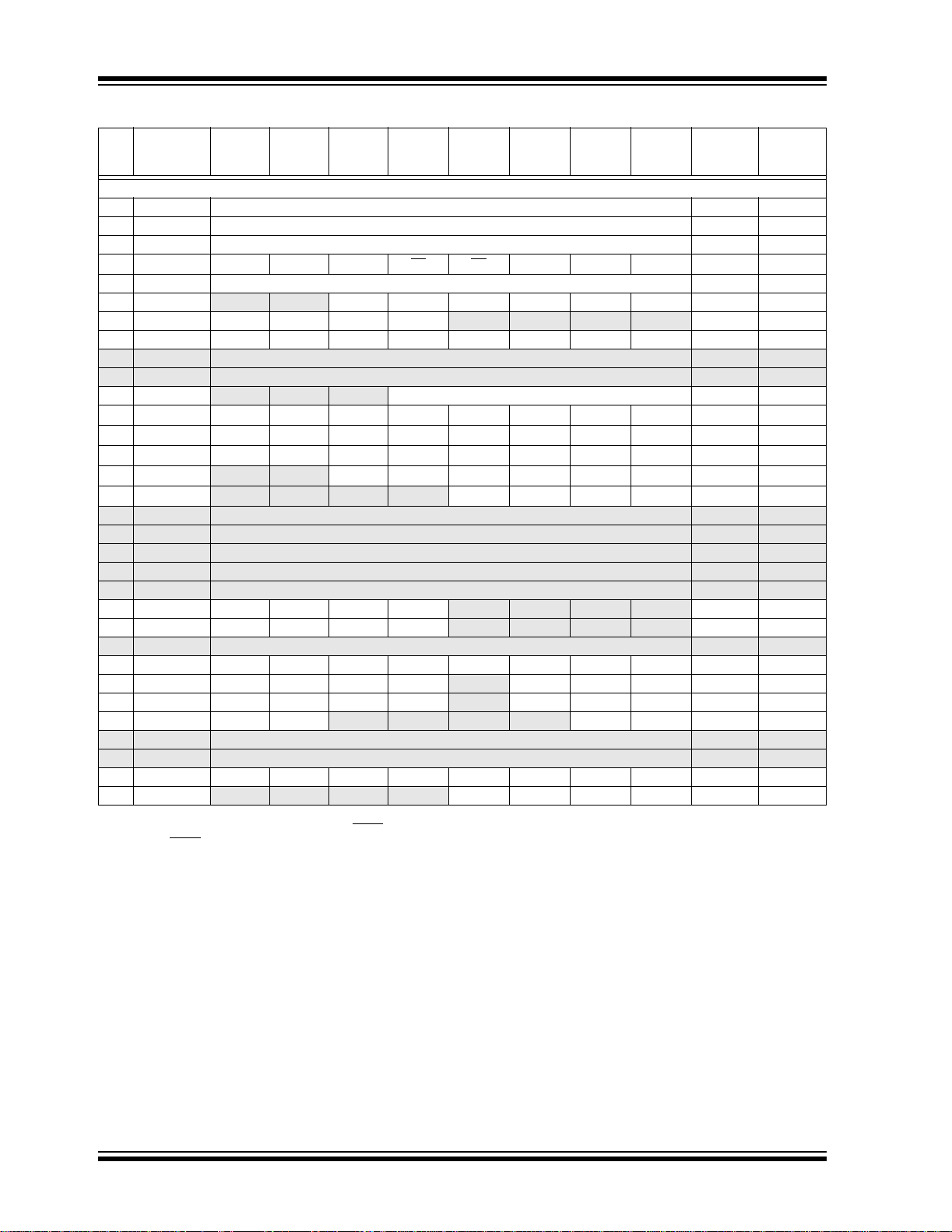
TABLE 2-2: PIC16F685/687/689/690 SPECIAL FUNCTION REGISTERS SUMMARY BANK 1
Addr Name Bit 7 Bit 6 Bit 5 Bit 4 Bit 3 Bit 2 Bit 1 Bit 0
POR/BOR
Reset
Bank 1
Value on
80h INDF Addressing this location uses contents of FSR to address data memory (not a physical
81h OPTION_REG RABPU
register)
INTEDG T0CS T0SE PSA PS2 PS1 PS0 1111 1111 1111 1111
xxxx xxxx xxxx xxxx
82h PCL Program Counter’s (PC) Least Significant Byte 0000 0000 0000 0000
83h STATUS IRP RP1 RP0 TO
PD ZDCC0001 1xxx 000q quuu
84h FSR Indirect Data Memory Address Pointer xxxx xxxx uuuu uuuu
85h TRISA
86h TRISB TRISB7 TRISB6 TRISB5 TRISB4
— — TRISA5 TRISA4 TRISA3 TRISA2 TRISA1 TRISA0 --11 1111 --11 1111
— — — — 1111 ---- 1111 ----
87h TRISC TRISC7 TRISC6 TRISC5 TRISC4 TRISC3 TRISC2 TRISC1 TRISC0 1111 1111 1111 1111
88h — Unimplemented — —
89h — Unimplemented — —
8Ah PCLATH
8Bh INTCON GIE PEIE T0IE INTE RABIE T0IF INTF RABIF
8Ch PIE1
8Dh PIE2 OSFIE C2IE C1IE EEIE
8Eh PCON
8Fh OSCCON
90h OSCTUNE
— — — Write Buffer for the upper 5 bits of the Program Counter ---0 0000 ---0 0000
(2)
0000 000x 0000 000x
— ADIE RCIE
(3)
TXIE
(3)
SSPIE
(3)
CCP1IE
(4)
TMR2IE
(4)
TMR1IE -000 0000 -000 0000
— — — — 0000 ---- 0000 ----
— — ULPWUE SBOREN — —PORBOR --01 --qq --0u --uu
— IRCF2 IRCF1 IRCF0 OSTS HTS LTS SCS -110 q000 -110 x000
— — — TUN4 T UN3 TUN2 TUN1 TUN0 ---0 0000 ---u uuuu
91h — Unimplemented — —
92h PR2
(4)
93h SSPADD
93h SSPMSK
94h SSPSTAT
95h WPUA
(5)
96h IOCA
97h WDTCON
98h TXSTA
99h SPBRG
9Ah SPBRGH
9Bh BAUDCTL
Timer2 Period Register 1111 1111 1111 1111
(3, 6)
Synchronous Serial Port (I2C mode) Address Register 0000 0000 0000 0000
(3, 6)
MSK7 MSK6 MSK5 MSK4 MSK3 MSK2 MSK1 MSK0 1111 1111 1111 1111
(3)
SMP CKE D/A PSR/WUA BF 0000 0000 0000 0000
— —WPUA5WPUA4— WPUA2 WPUA1 WPUA0 --11 -111 --11 -111
— — IOCA5 IOCA4 IOCA3 IOCA2 IOCA1 IOCA0 --00 0000 --00 0000
— — — WDTPS3 WDTPS2 WDTPS1 WDTPS0 SWDTEN ---0 1000 ---0 1000
(3)
(3)
CSRC TX9 TXEN SYNC SENB BRGH TRMT TX9D 0000 0010 0000 0010
BRG7 BRG6 BRG5 BRG4 BRG3 BRG2 BRG1 BRG0 0000 0000 0000 0000
(3)
BRG15 BRG14 BRG13 BRG1 2 BRG11 BRG10 BRG9 BRG8 0000 0000 0000 0000
(3)
ABDOVF RCIDL — SCKP BRG16 — WUE ABDEN 01-0 0-00 01-0 0-00
9Ch — Unimplemented — —
9Dh — Unimplemented — —
9Eh ADRESL A/D Result Register Low Byte xxxx xxxx uuuu uuuu
9Fh ADCON1
— ADCS2 ADCS1 ADCS0 — — — — -000 ---- -000 ---
Legend: – = Unimplemented locations read as ‘0’, u = unchanged, x = unknown, q = value depends on condition, shaded = unimplemented
Note 1: Other (non Power-up) Resets include MCLR
2: MCLR
and WDT Reset do not affect the previous value data latch. The RABIF bit will be cleared upon Reset but will set again if the
Reset and Watchdog Timer Reset during normal operation.
mismatched exists.
3: PIC16F687/PIC16F689/PIC16F690 only.
4: PIC16F685/PIC16F690 only.
5: RA3 pull-up is enabled when pin is configured as MCLR
in Configuration Word.
6: Accessible only when SSPM<3:0> = 1001.
Value on
all other
Resets
(1)
© 2005 Microchip Technology Inc. Preliminary DS41262A-page 21
PIC16F685/687/689/690
TABLE 2-3: PIC16F685/687/689/690 SPECIAL REGISTERS SUMMARY BANK 2
Addr Name Bit 7 Bit 6 Bit 5 Bit 4 Bit 3 Bit 2 Bit 1 Bit 0
Bank 2
100h INDF Addressing this location uses contents of FSR to address data memory (not a physical register) xxxx xxxx xxxx xxxx
101h TMR0 Timer0 Module Register xxxx xxxx uuuu uuuu
102h PCL Program Counter’s (PC) Least Significant Byte 0000 0000 0000 0000
103h STATUS IRP RP1 RP0 TO
104h FSR Indirect Data Memory Address Pointer xxxx xxxx uuuu uuuu
105h PORTA
106h PORTB RB7 RB6 RB5 RB4
107h PORTC RC7 RC6 RC5 RC4 RC3 RC2 RC1 RC0 xxxx xxxx uuuu uuuu
108h — Unimplemented — —
109h — Unimplemented — —
10Ah PCLA TH
10Bh INTCON GIE PEIE T0IE INTE RABIE T0IF INTF RABIF
EEDAT EEDAT7 EEDAT6 EEDAT5 EEDAT4 EEDAT3 EEDAT2 EEDAT1 EEDAT0 0000 0000 0000 0000
10Ch
EEADR EEADR7 EEADR6 EEADR5 EEADR4 EEADR3 EEADR2 EEADR1 EEADR0 0000 0000 0000 0000
10Dh
10Eh EEDATH
10Fh EEADRH
110h — Unimplemented — —
111h — Unimplemented — —
112h — Unimplemented — —
113h — Unimplemented — —
114h — Unimplemented — —
115h WPUB WPUB7 WPUB6 WPUB5 WPUB4
116h IOCB IOCB7 IOCB6 IOCB5 IOCB4
117h — Unimplemented — —
118h VRCON C1VREN C2VREN VRR VP6EN VR3 V R2 VR1 VR0 0000 0000 0000 0000
119h CM1CON0 C1ON C1OUT
11Ah CM2CON0 C2ON C2OUT
11Bh CM2 CON1 MC1OUT M C2OUT
11Ch — Unimplemented — —
11Dh — Unimplemented — —
11Eh ANSEL ANS7 ANS6 ANS5 ANS4 ANS3 ANS2 ANS1 ANS0 1111 1111 1111 1111
11Fh ANSELH
Legend: – = Unimplemented locations read as ‘0’, u = unchanged, x = unknown, q = value depends on condition, shaded = unimplemented
Note 1: Other (non Power-up) Resets include MCLR
(3)
(3)
2: MCLR
mismatched exists.
3: PIC16F685/PIC16F689/PIC16F690 only.
— — RA5 RA4 RA3 RA2 RA1 RA0 --xx xxxx --uu uuuu
— — — Write Buffer for the upper 5 bits of the Program Counter ---0 0000 ---0 0000
— —
— — — —
— — — — ANS11 ANS10 ANS9 A NS8 ---- 1111 ---- 1111
and WDT Reset does not affect the previous value data latch. The RABIF bit will be cleared upon Reset but will set again if the
EEDATH5 EEDATH4 EEDATH3 EEDATH2 EEDATH1 EEDATH0
C1OE C1POL — C1R C1CH1 C1CH0 0000 -000 0000 -000
C2OE C2POL — C2R C2CH1 C2CH0 0000 -000 0000 -000
— — — — T1GSS C2SYNC 00-- --10 00-- --10
Reset and Watchdog Timer Reset dur ing nor mal operation.
PD ZDCC0001 1xxx 000q quuu
— — — — xxxx ---- uuuu ----
EEADRH3 EEADRH2 EEADRH1 EEADRH0
— — — — 1111 ---- 1111 ----
— — — — 0000 ---- 0000 ----
Value on
POR/BOR
Reset
(2)
0000 000x 0000 000x
--00 0000 --00 0000
---- 0000 ---- 0000
Value on
all other
Resets
(1)
DS41262A-page 22 Preliminary © 2005 Microchip Technology Inc.
PIC16F685/687/689/690
TABLE 2-4: PIC16F685/687/689/690 SPECIAL FUNCTION REGISTERS SUMMARY BANK 3
Addr Name Bit 7 Bit 6 Bit 5 Bit 4 Bit 3 Bit 2 Bit 1 Bit 0
Bank 3
180h INDF Addressing this location uses contents of FSR to address data memory (not a physical
181h OPTION_REG RABPU
182h PCL Program Counter’s (PC) Least Significant Byte 0000 0000 0000 0000
183h STATUS IRP RP1 RP0 TO
184h FSR Indirect Data Memory Address Pointer xxxx xxxx uuuu uuuu
185h TRISA
186h TRISB TRISB7 TRISB6 TRISB5 TRISB4
187h TRISC TRISC7 TRISC6 TRISC5 TRISC4 TRISC3 TRISC2 TRISC1 TRISC0 1111 1111 1111 1111
188h — Unimplemented — —
189h — Unimplemented — —
18Ah PCLATH
18Bh INTCON GIE PEIE T0IE INTE RABIE T0IF INTF RABIF
18Ch EECON1 EEPGD
18Dh EECON2 EEPROM Control Register 2 (not a physical register) ---- ---- ---- ---18Eh — Unimplemented — —
18Fh — Unimplemented — —
190h — Unimplemented — —
191h — Unimplemented — —
192h — Unimplemented — —
193h — Unimplemented — —
194h — Unimplemented — —
195h — Unimplemented — —
196h — Unimplemented — —
197h — Unimplemented — —
198h — Unimplemented — —
199h — Unimplemented — —
19Ah — Unimplemented — —
19Bh — Unimplemented — —
19Ch — Unimplemented — —
19Dh PSTRCON
19Eh SRCON SR1 SR0 C1SEN C2REN PULSS PULSR
19Fh — Unimplemented — —
Legend: – = Unimplemented locations read as ‘0’, u = unchange d, x = unknown, q = value depends on condition, shaded = unimplemented
Note 1: Other (non Power-up) Resets include MCLR
2: MCLR
mismatched exists.
3: PIC16F685/PIC16F690 only.
register)
INTEDG T0CS T0SE PSA PS2 PS1 PS0 1111 1111 1111 1111
PD ZDCC0001 1xxx 000q quuu
— — TRISA5 TRISA4 TRISA3 TRISA2 TRISA1 TRISA0 --11 1111 --11 1111
— — — — 1111 ---- 1111 ----
— — — Write Buffer for the upper 5 bits of the Program Counter ---0 0000 ---0 0000
— — — WRERR WREN WR RD x--- x000 0--- q000
(3)
— — — STRSYNC STRD STRC STRB STRA ---0 0001 ---0 0001
— — 0000 00-- 0000 00--
and WDT Reset does not affect the previous value data latch. The RABIF bit will be cleared upon Reset but will set again if the
Reset and Watchdog Timer Reset during normal operation.
Value on
POR/BOR
Reset
xxxx xxxx xxxx xxxx
(2)
0000 000x 0000 000x
Value on
all other
Resets
(1)
© 2005 Microchip Technology Inc. Preliminary DS41262A-page 23

PIC16F685/687/689/690
2.2.2.1 Status Register
The Status register, shown in Register 2-1, contains:
• the arithmetic status of the ALU
• the Reset status
• the bank select bits for data memory (GPR and
SFR)
The Status register can be the destination for any
instruction, like any other register. If the Status register
is the destination for an instruction that affects the Z,
DC or C bits, then the write to these three bits is
writable. Therefore, the result of an instruction with the
Status register as destination may be different than
intended.
For example, CLRF STATUS, will clear the upper three
bits and set the Z bit. Thi s leaves the Status register as
‘000u u1uu’ (where u = unchanged).
It is recommended, therefore, that only BCF, BSF,
SWAPF and MOVWF instructions are used to alter the
Stat us register , beca use these instru ctions do not af fect
any Status bits. For other instructions not affecting any
Status bits, see the “Instruction Set Summary.”
disabled. These bit s are set or cleared ac cording to the
device logic. Furthermore, the TO
and PD bits are not
Note 1: The C and DC bits operate as a Borrow
and Digit Borrow out bit, respectively, in
subtraction. See the SUBLW and SUBWF
instructions for examples.
REGISTER 2-1: STATUS – STATUS REGISTER (ADDRESS: 03h, 83h, 103h OR 183h)
R/W-0 R/W-0 R/W-0 R-1 R-1 R/W-x R/W-x R/W-x
(1)
(1)
bit 7
bit 6-5
bit 4
bit 3
bit 2
bit 1
bit 0
IRP RP1 RP0 TO PD ZDC
bit 7 bit 0
IRP: Register Bank Select bit (used for indirect addressing)
1 = Bank 2, 3 (100h-1FFh)
0 = Bank 0, 1 (00h-FFh)
RP<1:0>: Register Bank Select bits (used for direct addressing)
00 = Bank 0 (00h-7Fh)
01 = Bank 1 (80h-FFh)
10 = Bank 2 (100h-17Fh)
11 = Bank 3 (180h-1FFh)
TO: Time-out bit
1 = After power-up, CLRWDT instruction or SLEEP instruction
0 = A WDT time-out occurred
PD: Power-down bit
1 = After power-up or by the CLRWDT instruction
0 = By execution of the SLEEP instruction
Z: Zero bit
1 = The result of an arithmetic or logic operation is zero
0 = The result of an arithmetic or logic operation is not zero
DC: Digit Carry/Borrow bit (ADDWF, ADDLW,SUBLW,SUBWF instructions)
1 = A carry-out from the 4th low-order bit of the result occurred
0 = No carry-out from the 4th low-order bit of the result
C: Carry/Borrow bit (ADDWF, ADDLW, SUBLW, SUBWF instructions)
(1)
1 = A carry-out from the Most Significant bit of the result occurred
0 = No carry-out from the Most Significant bit of the result occurred
Note 1: For Bo
rrow, the polarity is reversed. A subtraction is executed by adding the two’s
complement of the second operand. For rotate (RRF, RLF) instructions, this bit is
loaded with either the high or low-order bit of the source register.
(1)
C
Legend:
R = Readable bit W = Writable bit U = Unimplemented bit, read as ‘0’
- n = Value at POR ‘1’ = Bit is set ‘0’ = Bit is cleared x = Bit is unknown
DS41262A-page 24 Preliminary © 2005 Microchip Technology Inc.

PIC16F685/687/689/690
2.2.2.2 OPTION Register
The OPTION register is a readable and writable
register, which contains various control bits to
configure:
• TMR0/WDT prescaler
• External RA2/INT interrupt
•TMR0
• Weak pull-ups on PORTA/PORTB
REGISTER 2-2: OPTION_REG – OPTION REGISTER (ADDRESS: 81h OR 181h)
R/W-1 R/W-1 R/W-1 R/W-1 R/W-1 R/W-1 R/W-1 R/W-1
RABPU
bit 7 bit 0
INTEDG T0CS T0SE PSA PS2 PS1 PS0
Note: To achieve a 1:1 prescaler assignment for
TMR0, assign the prescaler to the WDT by
setting PSA bit to ‘1’ (OPTION_REG<3>).
See Section 5.4 “Prescaler”.
bit 7 RABPU
1 = PORTA/PORTB pull-ups are disabled
0 = PORTA/PORTB pull-ups are enabled by individual port latch values
bit 6 INTEDG: Interrupt Edge Select bit
1 = Interrupt on rising edge of RA2/AN2/T0CKI/INT/C1OUT pin
0 = Interrupt on falling edge of RA2/AN2/T0CKI/INT/C1OUT pin
bit 5 T0CS: TMR0 Clock Source Select bit
1 = Transition on RA2/AN2/T0CKI/INT/C1OUT pin
0 = Internal instruction cycle clock (CLKOUT)
bit 4 T0SE: TMR0 Source Edge Select bit
1 = Increment on high-to-low transition on RA2/AN2/T0CKI/INT/C1OUT pin
0 = Increment on low-to-high transition on RA2/AN2/T0CKI/INT/C1OUT pin
bit 3 PSA: Prescaler Assignment bit
1 = Prescaler is assigned to the WDT
0 = Prescaler is assigned to the Timer0 module
bit 2-0 PS<2:0>: Prescaler Rate Select bits
: PORTA/PORTB Pull-up Enable bit
Bit Va lue TMR0 Rate WDT Rate
000
001
010
011
100
101
110
111
1 : 2
1 : 4
1 : 8
1 : 16
1 : 32
1 : 64
1 : 128
1 : 256
(1)
1 : 1
1 : 2
1 : 4
1 : 8
1 : 16
1 : 32
1 : 64
1 : 128
Note 1: A dedicated 16-bit WDT postscaler is available. See Section 14.5 “Watchdog
Timer (WDT)” for more information.
Legend:
R = Readable bit W = Writable bit U = Unimplemented bit, read as ‘0’
- n = Value at POR ‘1’ = Bit is set ‘0’ = Bit is cleared x = Bit is unknown
© 2005 Microchip Technology Inc. Preliminary DS41262A-page 25

PIC16F685/687/689/690
2.2.2.3 INTCON Register
The INTCON register is a readable and writable
register , which c ontains the various en able and fl ag bit s
for TMR0 register overflow, PORTA change and
external RA2/AN2/T0CKI/INT/C1OUT pin interrupts.
Note: Interrupt flag bits are set when an interru pt
condition occurs, regar dless of the st ate of
its corresponding enable bit or the global
enable bit, GIE (INTCON<7>). User
software should ensure the appropriate
interrupt flag bits are clear prior to
enabling an interrupt.
REGISTER 2-3: INTCON – INTERRUPT CONTROL REGISTER (ADDRESS: 0Bh, 8Bh, 10Bh OR
18Bh)
R/W-0 R/W-0 R/W-0 R/W-0 R/W-0 R/W-0 R/W-0 R/W-x
GIE PEIE T0IE INTE RABIE
bit 7 bit 0
bit 7 GIE: Global Interrupt Enable bit
1 = Enables all unmasked interrupts
0 = Disables all interrupts
bit 6 PEIE: Peripheral Interrupt Enable bit
1 = Enables all unmasked peripheral interrupts
0 = Disables all peripheral interrupts
bit 5 T0IE: TMR0 Overflow Interrupt Enable bit
1 = Enables the TMR0 interrupt
0 = Disables the TMR0 in terrupt
bit 4 INTE: RA2/INT External Interrupt Enable bit
1 = Enables the RA2/INT external interrupt
0 = Disables the RA2/INT external interrupt
bit 3 RABIE: PORTA/PORTB Change Interrupt Enable bit
1 = Enables the PORTA/PORTB change interrupt
0 = Disables the PORTA/PORTB change interrupt
bit 2 T0IF: TMR0 Overflow Interrupt Flag bit
1 = TMR0 regis ter has overflowed (must be cleared in software)
0 = TMR0 register did not overflow
bit 1 INTF: RA2/INT External Interrupt Flag bit
1 = The RA2/INT external interrupt occurred (must be cleared in software)
0 = The RA2/INT external interrupt did not occur
bit 0 RABIF: PORTA/PORTB Change Interrupt Flag bit
1 = When at least o ne of the PORTA or PORTB general purpose I/O p ins cha nge d s tate (must
be cleared in software)
0 = None of the PORTA or PORTB general purpose I/O pins have changed state
(2)
(1,3)
(1, 3)
T0IF
(2)
INTF RABIF
Note 1: IOCA or IOCB register must also be enabled.
2: T0IF bit is set when Timer0 rolls over. Timer0 is unchanged on Reset and should
be initialized before clearing T0IF bit.
3: Includes ULPWU interrupt.
Legend:
R = Readable bit W = Writable bit U = Unimplemented bit, read as ‘0’
- n = Value at POR ‘1’ = Bit is set ‘0’ = Bit is cleared x = Bit is unknown
DS41262A-page 26 Preliminary © 2005 Microchip Technology Inc.

PIC16F685/687/689/690
2.2.2.4 PIE1 Register
The PIE1 register contai ns th e in terru pt enable bits, as
shown in Register 2-4.
REGISTER 2-4: PIE1 – PERIPHERAL INTERRUPT ENABLE REGISTER 1 (ADDRESS: 8Ch)
U-0 R/W-0 R/W-0 R/W-0 R/W-0 R/W-0 R/W-0 R/W-0
— ADIE RCIE
bit 7 bit 0
bit 7 Unimplemented: Read as ‘0’
bit 6 ADIE: A/D Converter Interrupt Enable bit
1 = Enabled
0 = Disabled
bit 5 RCIE: EUSART Receive Interrupt Enable bit
1 = Enabled
0 = Disabled
bit 4 TXIE: EUSART Transmit Interrupt Enable bit
1 = Enabled
0 = Disabled
bit 3 SSPIE: Synchronous Serial Port (SSP) Interrupt Enable bit
1 = Enabled
0 = Disabled
bit 2 CCP1IE: CCP1 Interrupt Enable bit
1 = Enabled
0 = Disabled
bit 1 TMR2IE: TMR2 to PR2 Match Interrupt Enable bit
1 = Enabled
0 = Disabled
bit 0 TMR1IE: TMR1 Overflow Interrupt Enable bit
1 = Enabled
0 = Disabled
(2)
Note: Bit PEIE (INTCON<6>) must be set to
enable any peripheral interrupt.
(1)
TXIE
(2)
(2)
(2)
SSPIE
(1)
(2)
CCP1IE
(2)
(1)
TMR2IE
(1)
TMR1IE
Note 1: PIC16F685/PIC16F690 only.
2: PIC16F687/PIC16F689/PI C16F6 90 onl y.
Legend:
R = Readable bit W = Writable bit U = Unimplemented bit, read as ‘0’
- n = Value at POR ‘1’ = Bit is set ‘0’ = Bit is cleared x = Bit is unknown
© 2005 Microchip Technology Inc. Preliminary DS41262A-page 27

PIC16F685/687/689/690
2.2.2.5 PIE2 Register
The PIE2 register contai ns th e in terru pt enable bits, as
shown in Register 2-5.
REGISTER 2-5: PIE2 – PERIPHERAL INTERRUPT ENABLE REGISTER 2 (ADDRESS: 8Dh)
R/W-0 R/W-0 R/W-0 R/W-0 U-0 U-0 U-0 U-0
OSFIE C2IE C1IE EEIE — — — —
bit 7 bit 0
bit 7 OSFIE: Oscillator Fail Interrupt Enable bit
1 = Enabled
0 =Disabled
bit 6 C2IE: Comparator 2 Interrupt Enable bit
1 = Enables Comparator 2 interrupt
0 = Disables Comparator 2 interrupt
bit 5 C1IE: Comparator 1 Interrupt Enable bit
1 = Enables Comparator 1 interrupt
0 = Disables Comparator 1 interrupt
bit 4 EEIE: EE Write Operation Interrupt Enable bit
1 = Enabled
0 =Disabled
bit 3-0 Unimplemented: Read as ‘0’
Note: Bit PEIE (INTCON<6>) must be set to
enable any peripheral interrupt.
Legend:
R = Readable bit W = Writable bit U = Unimplemented bit, read as ‘0’
- n = Value at POR ‘1’ = Bit is set ‘0’ = Bit is cleared x = Bit is unknown
DS41262A-page 28 Preliminary © 2005 Microchip Technology Inc.

PIC16F685/687/689/690
2.2.2.6 PIR1 Register
The PIR1 register contains the interrupt flag bits, as
shown in Register 2-6.
REGISTER 2-6: PIR1 – PERIPHERAL INTERRUPT REQUEST REGISTER 1 (ADDRESS: 0Ch)
U-0 R/W-0 R-0 R-0 R/W-0 R/W-0 R/W-0 R/W-0
—
ADIF RCIF
bit 7 bit 0
bit 7 Unimplemented: Read as ‘0’
bit 6 ADIF: A/D Converter Interrupt Flag bit
1 = The A/D conversion completed (must be cleared in software)
0 = The A/D conversion is not complete
bit 5 RCIF: EUSART Receive Interrupt Flag bit
1 = The EUSART receive buffer is full (cleared by reading RCREG)
0 = The EUSART receive buffer is not full
bit 4 TXIF: EUSART Transmit Interrupt Flag bit
1 = The EUSART transmit buffer is empty (cleared by writing to TXREG)
0 = The EUSART transmit buffer is full
bit 3 SSPIF: Synchronous Serial Port (SSP) Interrupt Flag bit
1 = The Transmission/Reception is complete (must be cleared in software)
0 = Waiting to Transmit/Receive
bit 2 CCP1IF: CCP1 Interrupt Flag bit
Capture mode
1 = A TMR1 register capture occurred (must be cleared in software)
0 = No TMR1 register capture occurred
Compare mode
1 = A TMR1 register compare match occurred (must be cleared in software)
0 = No TMR1 register compare match occurred
PWM mode
Unused in this mode
bit 1 TMR2IF: TMR2 to PR2 Interrupt Flag bit
1 = A TMR2 to PR2 match occurred (must be cleared in software)
0 = No TMR2 to PR2 match occurred
bit 0 TMR1IF: TMR1 Overflow Interrupt Flag bit
1 = The TMR1 register overflowed (must be cleared in software)
0 = The TMR1 register did not overflow
(1)
(2)
Note: Interrupt flag bits are set when an interru pt
condition occurs, regar dless of the st ate of
its corresponding enable bit or the global
enable bit, GIE (INTCON<7>). User
software should ensure the appropriate
interrupt flag bits are clear prior to
enabling an interrupt.
TXIF
(1)
(1)
(1)
(2)
SSPIF
(1)
CCP1IF
(1)
(2)
TMR2IF
(2)
TMR1IF
Note 1: PIC16F687/PIC16F689/PIC16F690 onl y.
2: PIC16F685/PIC16F690 only.
Legend:
R = Readable bit W = Writable bit U = Unimplemented bit, read as ‘0’
- n = Value at POR ‘1’ = Bit is set ‘0’ = Bit is cleared x = Bit is unknown
© 2005 Microchip Technology Inc. Preliminary DS41262A-page 29

PIC16F685/687/689/690
2.2.2.7 PIR2 Register
The PIR2 register contains the interrupt flag bits, as
shown in Register 2-7.
REGISTER 2-7: PIR2 – PERIPHERAL INTERRUPT REQUEST REGISTER 2 (ADDRESS: 0Dh)
R/W-0 R/W-0 R/W-0 R/W-0 U-0 U-0 U-0 U-0
OSFIF C2IF C1IF EEIF — — — —
bit 7 bit 0
bit 7 OSFIF: Oscillator Fail Interrupt Flag bit
1 = System oscillator failed, cloc k input ha s changed to INT OSC (must be c leared in softw are)
0 = System clock operating
bit 6 C2IF: Comparator 2 Interrupt Flag bit
1 = Comparator output (C2OUT bit) has changed (must be cleared in software)
0 = Comparator output (C2OUT bit) has not changed
bit 5 C1IF: Comparator 1 Interrupt Flag bit
1 = Comparator output (C1OUT bit) has changed (must be cleared in software)
0 = Comparator output (C1OUT bit) has not changed
bit 4 EEIF: EE Write Operation Interrupt Flag bit
1 = Write operation completed (must be cleared in software)
0 = Write operation has not completed or has not started
bit 3-0 Unimplemented: Read as ‘0’
Note: Interrupt flag bits are set when an interrupt
condition occurs, regardless of the state of
its corresponding enable bit or the global
enable bit, GIE (INTCON<7>). User
software should ensure the appropriate
interrupt flag bits are clear prior to enabling
an interrupt.
Legend:
R = Readable bit W = Writable bit U = Unimplemented bit, read as ‘0’
- n = Value at POR ‘1’ = Bit is set ‘0’ = Bit is cleared x = Bit is unknown
DS41262A-page 30 Preliminary © 2005 Microchip Technology Inc.
PIC16F685/687/689/690
2.2.2.8 PCON Register
The Power Control (PCON) register (see Register 2-8)
contains flag bit s to differentiate between a:
• Power-on Reset (POR
• Brown-out Reset (BOR)
• Watchdog Timer Reset (WDT)
• External MCLR
The PCON register also controls the Ultra Low-Power
Wake-up and software enable of the BO
REGISTER 2-8: PCON — POWER CONTROL REGISTER (ADDRESS: 8Eh)
bit 7-6 Unimplemented: Read as ‘0’
bit 5 ULPWUE: Ultra Low-Power Wake-up Enable bit
bit 4 SBOREN: Software BOR Enable bit
bit 3-2 Unimplemented: Read as ‘0’
bit 1 POR
bit 0 BO
)
Reset
R.
U-0 U-0 R/W-0 R/W-1 U-0 U-0 R/W-0 R/W-x
— — ULPWUE SBOREN
bit 7 bit 0
1 = Ultra Low-Power Wake-up enabled
0 = Ultra Low-Power Wake-up disabled
(1)
1 = BOR enabled
0 = BOR disabled
: Power-on Reset Status bit
1 = No Power-on Reset occurred
0 = A Power-on Reset occurred (must be set in software after a Power-on Reset occurs)
R: Brown-out Reset Status bit
1 = No Brown-out Reset occurred
0 = A Brown-out Reset occurred (must be set in software after a Brown-out Reset occurs)
(1)
— —PORBOR
Note 1: BOREN<1:0> = 01 in the Configuration Word register for this bit to control the BOR.
Legend:
R = Readable bit W = Writable bit U = Unimplemented bit, read as ‘0’
- n = Value at POR ‘1’ = Bit is set ‘0’ = Bit is cleared x = Bit is unknown
© 2005 Microchip Technology Inc. Preliminary DS41262A-page 31

PIC16F685/687/689/690
h
s
n
2.3 PCL and PCLATH
The Program Counter (PC) is 13 bits wide. The lo w byte
comes from the PCL register, which is a readable and
writable register . The hig h byte (PC<12:8>) is not directl y
readable or writable and comes from PCLATH. On any
Reset, the PC is cleared. Figure 2-6 shows the two
situatio ns fo r t he l o ad i n g o f t h e PC . The u p pe r e x am pl e
in Figure 2-6 shows how the PC is loaded on a write to
PCL (PCLATH<4:0> → PCH). The lower example in
Figure 2-6 shows how the PC is loaded during a CALL or
GOTO instruction (PCLATH<4:3> → PCH).
FIGURE 2-6: LOADING OF PC IN
DIFFERENT SITUATIONS
PCH PCL
12 8 7 0
PC
PCLATH<4:0>
5
PCLATH
PCH PCL
12 11 10 0
PC
2
2.3.1 COMPUTED
87
PCLATH<4:3>
PCLATH
11
GOTO
A computed GOTO is accomplished by adding an offset
to the program counter (ADDWF PCL). When performing
a table read using a computed GOTO method, care
should be exercised if the table location crosses a PCL
memory boundary (each 256-byte block). Refer to the
Application Note AN556, “Implementing a Table Read”
(DS00556).
Instruction wit
PCL a
Destinatio
8
ALU Result
GOTO, CALL
OPCODE<10:0>
The stack operat es as a circular buf fer . This means th at
after the stack has been PUSHed eight times, the ninth
push overwrites the va lue tha t was s tored fro m the first
push. The tenth pus h ov erwr i tes the se co nd push (and
so on).
Note 1: There are no Status bits to indicate stack
overflow or stack underflow conditions.
2: There are no instructions/mnemonics
called PUSH or POP. These are actions
that occur from the execution of the
CALL, RETURN, RETLW and RETFIE
instructions or the vectoring to an
interrupt address.
2.4 Indirect Addressing, INDF and
FSR Registers
The INDF register is not a physica l register . Addr essing
the INDF register will cause indirect addressing.
Indirect addressing is possible by using the INDF
register. Any instruction using the INDF register actually
accesses data pointe d to by the File Select Register
(FSR). Reading INDF itself in direct ly will pro duce 00h.
Writing to the INDF register indirectly resul ts in a no
operation (although Status bits may be affected). An
effective 9-bit address is obtained by concatenating the
8-bit FSR and the IRP bit (STATUS<7>), as shown in
Figure 2-7.
A simple program to clear RAM location 20h-2Fh using
indirect addressing is shown in Example 2-1.
EXAMPLE 2-1: INDIRECT ADDRESSING
MOVLW 0x20 ;initialize pointer
MOVWF FSR ;to RAM
NEXT CLRF INDF ;clear INDF register
INCF FSR ;inc pointer
BTFSS FSR,4 ;all done?
GOTO NEXT ;no clear next
CONTINUE ;yes continue
2.3.2 STACK
The PIC16F685/687/689/690 devices have an
8-level x 13-bit wide hardware stack (see Figures 2-1
and 2-2). The stack spac e is not part of eit her progra m
or data space and the Stack Pointer is not readable or
writable. The PC is PUSHed onto the stack when a
CALL instruction is executed or an interrupt causes a
branch. The st ack i s POPe d in th e eve nt of a RETURN,
RETLW or a RETFIE instruction ex ecuti on. PC LATH is
not affected by a PUSH or POP operat ion.
DS41262A-page 32 Preliminary © 2005 Microchip Technology Inc.

PIC16F685/687/689/690
FIGURE 2-7: DIRECT/INDIRECT ADDRESSING PIC16F685/687/689/690
Indirect AddressingDirect Addressing
RP1 RP0 6
From Opcode
0
IRP File Select Register
7
0
Bank Select Location Select
00 01 10 11
00h
Data
Memory
7Fh
Bank 0 Bank 1 Bank 2 Bank 3
For memory map detail, see Figures 2-3, 2-4 and 2-5.
Bank Select
180h
1FFh
Location Select
© 2005 Microchip Technology Inc. Preliminary DS41262A-page 33

PIC16F685/687/689/690
NOTES:
DS41262A-page 34 Preliminary © 2005 Microchip Technology Inc.

PIC16F685/687/689/690
3.0 CLOCK SOURCES
3.1 Overview
The PIC16F685/687/689/690 devices have a wide
variety of clock sources and selection features to allow
it to be used in a wide range of applications while
maximizing performance and minimizing power
consumption. Figure 3-1 illustrates a block diagram of
the PIC16F685/687/689/690 clock sources.
Clock sources can be configured from external
oscillators, quartz cryst al resonators , ceramic resonators
and Resistor-Capacitor (RC) circuits. In addition, the
system clock source can be configured from one of two
internal oscillators, with a choice of speeds select able via
software. Additional clo ck feat ures inc lud e:
• Selectable system clock source between external
or internal via softwa re.
• Two-Speed Clock Start-up mode, which
minimizes latency between external oscillator
start-up and code execu t io n.
• Fail-Safe Clock Monitor (FSCM) designed to
detect a failure of the external clock source (LP,
XT, HS, EC or RC modes) and switch to the
internal oscillator.
The PIC16F685/687/689/690 can be configured in on e
of eight clock modes.
1. EC – External clock with I/O on RA4.
2. LP – 32 kHz low-power Crystal mode.
3. XT – Medium gain Crystal or Ceramic Resonator
Oscillator mode.
4. HS – High gain Crystal or Ceramic Resonator
mode.
5. RC – External Resistor-Capacitor (RC) with
OSC/4 output on RA4.
F
6. RCIO – External Resistor-Capacitor with I/O on
RA4.
7. INTOSC – Internal oscillator with F
OSC/4 output
on RA4 and I/O on RA5.
8. INTOSCIO – Internal oscillator with I/O on RA4
and RA5.
Clock Source modes are configured by the FOSC<2:0>
bits in the Configuratio n Word register (see Secti on 14.0
“Special Features of the CPU ”). The intern al clock can
be generated from two internal oscillators. The
HFINTOSC is a high -frequency cali brated osci llator . The
LFINTOSC is a low -frequ enc y un calibrated oscillator .
FIGURE 3-1: PIC16F685/687/689/690 CLOCK SOURCE BLOCK DIAGRAM
FOSC<2:0>
(Configuration Word)
SCS
(OSCCON<0>)
INTOSC
Power-up Timer (PWRT)
Watchdog Timer (WDT)
Fail-Safe Clock Monitor (FSCM)
OSC2
OSC1
External Oscillator
Internal Oscillator
HFINTOSC
8 MHz
LFINTOSC
31 kHz
Sleep
Postscaler
(OSCCON<6:4>)
8 MHz
4 MHz
2 MHz
1 MHz
500 kHz
250 kHz
125 kHz
31 kHz
IRCF<2:0>
111
110
101
100
011
010
001
000
LP, XT, HS, RC, RCIO, EC
MUX
MUX
System Clock
(CPU and Peripherals)
© 2005 Microchip Technology Inc. Preliminary DS41262A-page 35

PIC16F685/687/689/690
3.2 Clock Source Modes
Clock Source modes can be classified as external or
internal.
• External Clock mod es rely on e xternal circui try fo r
the clock source. Exam ples are oscillator modules
(EC mode), quartz crystal resonators or ceramic
resonators (LP, XT and HS modes), and
Resistor-Capacitor (RC mode) circuits.
• Internal clock sources are contained internally
within the PIC16F685/687/689/690. The
PIC16F685/687/689/690 has two internal
oscillators, the 8 MHz High-Frequency Internal
Oscillator (HFINTOSC) and 31 kHz
Low-Frequency Internal Oscillator (LFINTOSC).
The system clock can be selected between external or
internal clock sources via the System Clock Selection
(SCS) bit (see Section 3.5 “Clock Switching”).
3.3 External Clock Modes
3.3.1 OSCILLATOR START-UP TIMER (OST)
If the PIC16F685/687/689/690 is configured for LP, XT
or HS modes, the Oscillator Start-up Timer (OST)
counts 1024 osci llations from the OSC1 pi n, following a
Power-on Reset (POR) and the Power-up Timer
(PWRT) has expired (if configured), or a wake-up from
Sleep. During this time, the program counter does not
increment and program execution is suspended. The
OST ensures that the oscillator circuit, using a quartz
crystal resonator o r ce ramic res onator, has started an d
is providing a stable system clock to the PIC16F685/
687/689/690. When s witching betwe en clock so urces a
delay is required to allow the new clock to stabilize.
These oscillator delays are shown in Table 3-1.
In order to minimize latency between external
oscillator start-up and code execution, the Two-Speed
Clock St art-up mode can be selected (see Section 3.6
“Two-Speed Clock Start-up Mode”).
TABLE 3-1: OSCILLATOR DELAY EXAMPLES
Switch From Switch To Frequency Oscillator Delay
Sleep/POR
Sleep/POR EC, RC DC – 20 MHz
LFINTOSC (31 kHz) EC, RC DC – 20 M Hz
Sleep/POR LP, XT, HS 32 kHz to 20 MHz 1024 Clock Cycles (OST)
LFINTOSC (31 kHz) HFINTOSC 125 kHz to 8 MHz 1 μs (approx.)
Note 1: The 5 μs to 10 μs start-up delay is based on a 1 MHz system clock.
LFINTOSC
HFINTOSC
31 kHz
125 kHz to 8 MHz
5 μs-10 μs (approx.) CPU Start-up
(1)
3.3.2 EC MODE
The External Clock (EC) mode allows an externally
generated logic level as the system clock source. When
operating in this mode, an external clock source is
connected to the OSC1 pin and the RA4/AN3/T1G
OSC2/CLKOUT pin is available for general purpose I/O.
Figure 3-2 shows the pin connections for EC mode.
The Oscillator Start-up Timer (OST) is disabled when
EC mode is selected. Therefore, there is no delay in
operation after a Power-on Reset (POR) or wake-up
from Sleep. Because the PIC16F685/687/689/690
design is full y static, stoppi ng the extern al clock input
will have the ef fect of halting th e device while leaving all
data intact. Upon restarting the external clock, the
device will resum e ope ration as if no ti me ha d elap se d.
FIGURE 3-2: EXTERNAL CLOCK (EC)
MODE OPERATION
/
Clock from
Ext. System
RA4/AN3/T1G
OSC2/CLKOUT
/
OSC1/CLKIN
PIC16F685/687/689/690
I/O (OSC2)
DS41262A-page 36 Preliminary © 2005 Microchip Technology Inc.

PIC16F685/687/689/690
r
r
)
r
3.3.3 LP, XT, HS MODES
The LP, XT and HS modes support the use of quartz
crystal resonators or ceramic resonators connected to
the OSC1 and OSC2 pins (Figure 3-3). The mode
selects a low, medium or high gain setting of the
internal inverter-amplifier to support various resonator
types and speed.
LP Oscillator mode selects the lowest gain setting of the
internal inverter-amplifier. LP mode current consumption
is the least of the three modes. This mode is best suited
to drive resonators with a low drive level specification, for
example, tuning fork type crystals.
XT Oscillator mode selects the intermediate gain
setting of the internal inverter-amplifier. XT mode
current consumption is the medi um of the three modes.
This mode is best suited to drive resonators with a
medium drive level specification, for example, lowfrequency/AT-cut quartz crystal resonators.
HS Oscillator mode selects the highest gain setting of
the internal inverter-amplifier. HS mode current
consumption is the highest of the three modes. This
mode is best suited for resonato rs that req uire a hi gh
drive setting, for example, high-frequency/AT-cut
quartz crystal resonators or ceramic resonators.
Figure 3-3 and Figure3-4 show typical circuits for
quartz crystal and ceramic resonators, respectively.
FIGURE 3-4: CERAMIC RESONATOR
OPERATION
(XT OR HS MODE)
PIC16F685/687/689/690
OSC1
C1
(3)
RP
OSC2
(1)
S
C2
Ceramic
Resonator
Note 1: A series resistor (RS) may be required fo
2: The value of R
3: An a dditional parallel feedback resistor (R
R
ceramic resonators with low drive level.
mode selected (typically between 2 MΩ to
10 MΩ).
may be required for proper ceramic resonato
operation (typical value 1 MΩ).
(2)
RF
F varies with the Oscillato
To Internal
Logic
Sleep
P
FIGURE 3-3: QUARTZ CRYSTAL
OPERATION (LP, XT OR
HS MODE)
PIC16F685/687/689/690
OSC1
C1
Quartz
Crystal
OSC2
(1)
R
S
C2
Note 1: A series resistor (RS) may be required for
quartz crystals with low drive level.
2: The value of R
mode selected (typically between 2 MΩ to
10 MΩ).
(2)
RF
F varies with the Oscillator
Note 1: Quartz crystal characteristics vary
according to type, package and
manufacturer. The user should consult the
manufacturer data sheets for specifications
and recommended application.
2: Always verify oscillator performan ce ov er
DD and temperature range that is
the V
expected for the application.
To Internal
Logic
Sleep
© 2005 Microchip Technology Inc. Preliminary DS41262A-page 37
PIC16F685/687/689/690
3.3.4 EXTERNAL RC MODES
The External Resistor-Capacitor (RC) modes support
the use of an external RC circuit. This allows the
designer maximum flexibility in frequency choice while
keeping costs to a minimum when clock accuracy is not
required. There are two modes, RC and RCIO.
In RC mode, the RC circuit connects to the OSC1 pin.
The OSC2/CLKOUT pin outputs the RC oscillator
frequency divided by 4. This signal may be used to
provide a clock for external circuitry, synchronization,
calibration, test or other application requirements.
Figure 3-5 shows the RC mode connections.
FIGURE 3-5: RC MODE
VDD
REXT
OSC1
CEXT
VSS
OSC/4
F
Recommended values: 3 kΩ ≤ REXT ≤ 100 kΩ
PIC16F685/687/689/690
OSC2/CLKOUT
C
EXT > 20 pF
Internal
Clock
In RCIO mode, the RC circuit is connecte d to the OSC1
pin. The OSC2 pin becomes an additional general
purpose I/O pin. The I/O pin becomes bit 4 of PORTA
(RA4). Figure 3-6 shows the RCIO mode connections.
FIGURE 3-6: RCIO MODE
VDD
REXT
OSC1
CEXT
VSS
RA4
Recommended values: 3 kΩ ≤ REXT ≤ 100 kΩ
PIC16F685/687/689/690
I/O (OSC2)
C
EXT > 20 pF
The RC oscillator frequency is a function of the supply
voltage, the resistor (R
EXT) and capacitor (CEXT)
values and the operating temperature. Other factors
affecting the oscillator frequency are:
• threshold voltage variation
• component tolerances
• packaging variations in capacitance
The user also needs to take into account variation due
to tolerance of external RC components used.
Internal
Clock
3.4 Internal Clock Modes
The PIC16F685/687/689/690 has two independent,
internal oscillators that can be configured or selected
as the system clock source.
1. The HFINTOSC (High-Frequency Internal
Oscillator) is factory calibrated and operates at
8 MHz. The frequency of t he HFINT OSC can be
user adjusted ±12% via software using the
OSCTUNE register (Register 3-1).
2. The LFINTOSC (Low-Frequency Internal
Oscillator) is uncalibrated and operates at
approximately 31 kHz.
The system cloc k speed ca n be selec ted via sof tware
using the Internal Oscillator Frequency Select (IRCF)
bits.
The system clock ca n be se lec ted betw ee n external or
internal clock sources via the System Clock Selection
(SCS) bit (see Section 3.5 “Clock Switching”).
3.4.1 INTOSC AND INTOSCIO MODES
The INTOSC and INTOSCIO modes configure the
internal oscillators as the system clock source when
the device is programmed using the Oscillator Selection (FOSC) bits in the Configuration Word register
(Register 14-1).
In INTOSC mode, the OSC1 pin is available for ge neral
purpose I/O. The OSC2/CLKOUT pin outputs the
selected internal os ci lla tor freq uen cy div ide d by 4. The
CLKOUT signal may be used to provide a clock for
external circuitry, synchronization, calibration, test or
other application require me nt s .
In INTOSCIO mode, the OSC1 and OSC2 pins are
available for general purpose I/O.
3.4.2 HFINTOSC
The High-Frequency Int ernal Oscillato r (HFINT OSC) is
a factory calibrated 8 MHz internal clock source. The
frequency of the HFINTOSC can be altered
approximately ±12% via software using the OSCTU NE
register (Register 3-1).
The output of the HFINTOSC connects to a postscaler
and multiplexer (see Figure 3-1). One of seven
frequencies can be selected via software using the
IRCF bits (see Section 3.4.4 “Frequency Select Bits
(IRCF)”).
The HFINTOSC is enabled by selecting any frequency
between 8 MHz and 125 kHz (IRCF ≠ 000) as the
system clock s ource (SCS = 1), or when Two-Speed
Start-up is enabled (IESO = 1 and IRCF ≠ 000).
The HF Internal Oscillator (HTS) bit (OSCCON<2>)
indicates whether the HFINTOSC is stable or not.
DS41262A-page 38 Preliminary © 2005 Microchip Technology Inc.

PIC16F685/687/689/690
3.4.2.1 OSCTUNE Register
The HFINTOSC is factory calibrated but can be
adjusted in software by writing to the OSCTUNE
register (Register3-1).
The OSCTUNE register has a tuning range of ±12%.
The default value of the OSCTUNE register is ‘0’. The
value is a 5-bit two’s complement number. Due to
process variatio n, the m onoton icity and freq uency step
cannot be specified.
When the OSCTUNE register is modified, the
HFINTOSC frequency will begin shifting to the new
frequency. The HFINTOSC clock will stabilize within
1 ms. Code execution continues during this shift. There
is no indication that the shift has occurred.
OSCTUNE does not affect the LFINTOSC frequency.
Operation of features that depend on the LFINTOSC
clock source frequency, such as the Power-up Timer
(PWRT), Watchdog Timer (WDT), Fail-Safe Clock
Monitor (FSCM) and peripherals, are not af fected by the
change in frequency.
REGISTER 3-1: OSCTUNE – OSCILLATOR TUNING RESISTOR (ADDRESS: 90h)
U-0 U-0 U-0 R/W-0 R/W-0 R/W-0 R/W-0 R/W-0
— — — TUN4 TUN3 TUN2 TUN1 TUN0
bit 7 bit 0
bit 7-5 Unimplemented: Read as ‘0’
bit 4-0 TUN<4:0>: Frequency Tuning bits
01111 = Maximum frequency
01110 =
•
•
•
00001 =
00000 = Oscillator module is running at the calibrated frequency.
11111 =
•
•
•
10000 = Minimum frequency
Legend:
R = Readable bit W = Writable bit U = Unimplemented bit, read as ‘0’
-n = Value at POR ‘1’ = Bit is set ‘0’ = Bit is cleared x = Bit is unknown
© 2005 Microchip Technology Inc. Preliminary DS41262A-page 39

PIC16F685/687/689/690
3.4.3 LFINTOSC
The Low-Frequency Internal Oscillator (LFINTOSC) is
an uncalibrated (approximate) 31 kHz internal clock
source.
The output of the LFINTOSC connects to a postscaler
and multiplexer (see Figure3-1). 31 kHz can be
selected via software using the IRCF bits (see
Section 3.4.4 “Frequency Select Bits (IRCF)”). The
LFINTOSC is also the frequency for the Power-up
Timer (PWRT), Watchdog Timer (WDT) and Fail-Safe
Clock Monitor (FSCM).
The LFINTOSC is enabled by selecting 31 kHz
(IRCF = 000) as the system clock sourc e (SCS = 1), or
when any of the following are enabled:
• Two-Speed Start-up (IESO = 1 and IRCF = 000)
• Power-up Timer (PWRT)
• Watchdog Timer (WDT)
• Fail-Safe Clock Monitor (FSCM)
The LF Internal Oscillator (LTS) bit (OSCCON<1>)
indicates whether the LFINTOSC is stable or not.
3.4.4 FREQUENCY SELECT BITS (IRCF)
The output of the 8 MHz HFINTOSC and 31 kHz
LFINTOSC connects to a postscaler and multiplexer
(see Figure 3-1). The Internal Oscillator Frequency
select bits, IRCF<2:0> (OSCCON<6:4>), select the
frequency output of the internal oscillators. One of eight
frequencies can be selected via software:
•8 MHz
• 4 MHz (Default after Reset)
•2 MHz
•1 MHz
• 500 kHz
• 250 kHz
• 125 kHz
•31 kHz
Note: Following any Reset, the IRCF bit s are s et
to ‘110’ and the frequency selection is set
to 4 MHz. The user can modify the IRCF
bits to select a different frequency.
3.4.5 HF AND LF INTOSC CLOCK
SWITCH TIMING
When switching between the LFINTOSC and the
HFINTOSC, the new oscillator may already be shut
down to save power. If this is the case, there is a 10 μs
delay after the IRCF bits are modified before the
frequency selection takes place. The LTS/HTS bits will
reflect the current active status of the LFINTOSC and
the HFINTOSC oscillators. The timing of a frequency
selection is as follows:
1. IRCF bits are modified.
2. If the new clock is sh ut down, a 10 μs clock start-
up delay is started.
3. Clock switch circuitry waits for a falling edge of
the current clock.
4. CLKOUT is held low and the clock switch
circuitry waits fo r a ris ing edge in the new clock.
5. CLKOUT is now connected with the new clock.
HTS/LTS bits are updated as required.
6. Clock switch is complete.
If the internal oscillator speed selected is between
8 MHz and 125 kHz, there is no start-up delay before
the new frequency is selected. This is because the old
and the new frequencies are derived from the
HFINTOSC via the postscaler and multiplexer.
DS41262A-page 40 Preliminary © 2005 Microchip Technology Inc.

PIC16F685/687/689/690
3.5 Clock Switching
The system clock source can be switched between
external and internal clock sources via software using
the System Clock Select (SCS) bit.
3.5.1 SYSTEM CLOCK SELECT (SCS) BIT
The System Clock Select (SCS) bit (OSCCON<0>)
selects the system clock source that is used for the
CPU and peripherals.
• When SCS = 0, the system clock source is
determined by configuration of the FOSC<2:0>
bits in the Configuration Word register (CONFIG).
• When SCS = 1, the system clock source is
chosen by the internal oscillator frequency
selected by the IRCF bits. After a Reset, SCS is
always cleared.
Note: Any automatic clock switch, which may
occur from Two-Speed Start-up or
Fail-Safe Clock Monitor, does not update
the SCS bit. The user can monitor the
OSTS (OSCCON<3>) to determine the
current system clock source.
3.5.2 OSCILLA TOR START-UP TIME-OUT
STATUS BIT
The Oscillator Start-up Time-out Status (OSTS) bit
(OSCCON<3>) indicates whether the system clock is
running from the external clock source, as defined by
the FOSC bits, or from internal clock source. In
particular, OSTS indicates that the Oscillator Start-up
Timer (OST) has timed out for LP, XT or HS modes.
3.6 Two-Speed Clock Start-up Mode
Two-Speed Start-up mode provides additional power
savings by minimizing the latency between external
oscillator start-up and code execution. In applications
that make heavy us e of the Sleep mode, Two-Speed
Start-up will remove the external oscillator start-up
time from the time spent awake and can reduce the
overall power consumption of the device.
This mode allows the application to wake-up from
Sleep, perform a few instructions using the INTOSC
as the clock source and go back to Sleep without
waiting for the primary oscillator to become stable.
When the PIC16F685/687/689/690 is configured for
LP, XT or HS modes, the Oscillator Start-up Timer
(OST) is enabled (see Section 3.3.1 “Oscillator St art-
up Timer (OST)”). The OST timer will suspend
program execution until 1024 oscillations are counted.
Two-Speed Start-up mode minimizes the delay in code
execution by operating from the internal oscillator as
the OST is counting. When the OST count reaches
1024 and the OSTS bit ( OSCC O N<3> ) is se t, pro gram
execution switches to the external oscillator.
3.6.1 TWO-SPEED STAR T-UP MODE
CONFIGURATION
Two-Speed Start-up mode is configured by the
following settings:
• IESO = 1 (CONFIG<10>) Internal/External
Switchover bit.
•SCS = 0.
• FOSC configured for LP, XT or HS mode.
Two-Speed Start-up mode is entered after:
• Power-on Reset (POR) and, if enabled, after
PWRT has expired, or
• Wake-up from Sleep.
If the external clock oscillator is configured to be
anything other than LP, XT or HS mode, then TwoSpeed Start-up is disabled. This is because the external
clock oscillator do es not require any stabilizat ion time
after POR or an exit from Sleep.
3.6.2 TWO-SPEED START-UP
SEQUENCE
1. Wake-up from Power-on Reset or Sleep.
2. Instructions begin execution by the internal
oscillator at the frequency set in the IRCF bits
(OSCCON<6:4>).
3. OST enabled to count 1024 clock cycles.
4. OST timed out, wait for falling edge of the
internal oscillator.
5. OSTS is set.
6. System clock held low until the next fal ling edg e
of new clock (LP, XT or HS mode).
7. System clock is switched to external clock
source.
Note: Executing a SLEEP instruction will abort
the oscillator start-up time and will cause
the OSTS bit (OSCCON<3>) to remain
clear.
© 2005 Microchip Technology Inc. Preliminary DS41262A-page 41

PIC16F685/687/689/690
3.6.3 CHECKING EXTERNAL/INTERNAL
CLOCK STATUS
Checking the state of the OSTS bit (OSCCON<3>) will
confirm if the PIC16F685/687/689/690 is running from
the exter nal c lo ck source as d e fi ned by t h e FO SC b i ts
in the Configuration Word register (CONFIG) or the
internal oscillator.
FIGURE 3-7: TWO-SPEED START-UP
Q1 Q2 Q3 Q4 Q1 Q2 Q3 Q4 Q1
INTOSC
TOSTT
OSC1
OSC2
Program Counter
System Clock
0 1 1022 1023
PC PC + 1 PC + 2
DS41262A-page 42 Preliminary © 2005 Microchip Technology Inc.
PIC16F685/687/689/690
3.7 Fail-Safe Clock Monitor
The Fail-Safe Clock Monit or (FSCM) al low s the dev ic e
to continue operat ing sh oul d the external oscillator fail.
The FSCM can detect oscillator failure anytime after
the Oscillator Start-up Timer (OST) has expired. The
FSCM is enabled by setting the FCMEN bit in the
Configuration Word register (CONFIG). The FSCM is
applicable to all external oscillator modes (LP, XT, HS,
EC, RC and RCIO).
FIGURE 3-8: FSCM BLOCK DIAGRAM
Clock Monitor
Latch (CM)
Primary
Clock
LFINTOSC
Oscillator
31 kHz
(~32 μs)
÷ 64
488 Hz
(~2 ms)
3.7.1 FAIL-SAFE D ETECTION
The FSCM module detects a failed oscillator by
comparing the ex tern al osci llator to the FS CM sa mple
clock. The sample clock is generated by dividing the
LFINTOSC by 64. See Figure 3-8. Inside the fail
detector block is a latch. The external clock sets the
latch on each falling edge of the external clock. The
sample clock clears the latch on each falling edge of
the sample clock. If a sample clock edge occurs while
the latch is cleared, a failure has occurred.
(edge-triggered)
S
Q
C
Q
Clock
Failure
Detected
3.7.3 FAIL-SAFE CONDITION CLEARING
The Fail-Safe condition is cleared after a Reset,
executing a SLEEP instruction or togg ling the SC S bit
(OSCCON<0>). When the SCS bit is tog gle d, th e OS T
is restarted. While the OST is running, the device
continues to operate from the INTOSC selected in
OSCCON. When the OST times out, the Fail-Safe
condition is cleared and the device will be operating
from the external clock s ource. Th e Fail-Saf e condi tion
must be cleared before th e O SFIF f lag ca n be cle are d.
3.7.4 RESET OR WAKE-UP FROM SLEEP
The FSCM is designed to detect an oscillator failure
after the Os cillator Start-up Time (OST) has expi red.
The OST is used after waking up from Sleep and after
any type of Reset. The OST is not used with the EC or
RC clock modes so the FSCM will be active as soon as
the Reset or wake-up have completed. When the
FSCM is enabled, the Two-Speed Start-up is also
enabled. Therefore, the device will always be executing
code while the OST is operating.
Note: Due to the wide range of oscillato r st art-up
times, the Fail-Safe circuit is not active
during oscillator start-up (i.e., after exiting
Reset or Sleep). After an appropriate
amount of time, the u se r sho uld check the
OSTS bit (OSCCON<3>) to verify the
oscillator start-up and system clock
switchover has successfully completed.
3.7.2 FAIL-SAFE OPERATION
When the external clock fails, the FSCM switches the
device clock to an internal clock source and sets the
OSFIF (PIR2<7>) flag . Setting thi s flag will gen erate an
interrupt if the OSFIE (PIE2<7>) bit is also set. The
device firmware can then take steps to mitigate the
problems that may arise from a failed clock. The
system clock will continue to be sourced from the
internal clock source until the device firmware
successfully restarts the external oscillator and
switches back to external operation.
The internal clock source chosen by the FSCM is
determined by the IRCF bits (OSCCON<6:4>). This
allows the internal oscillator to be configured before a
failure occurs.
© 2005 Microchip Technology Inc. Preliminary DS41262A-page 43
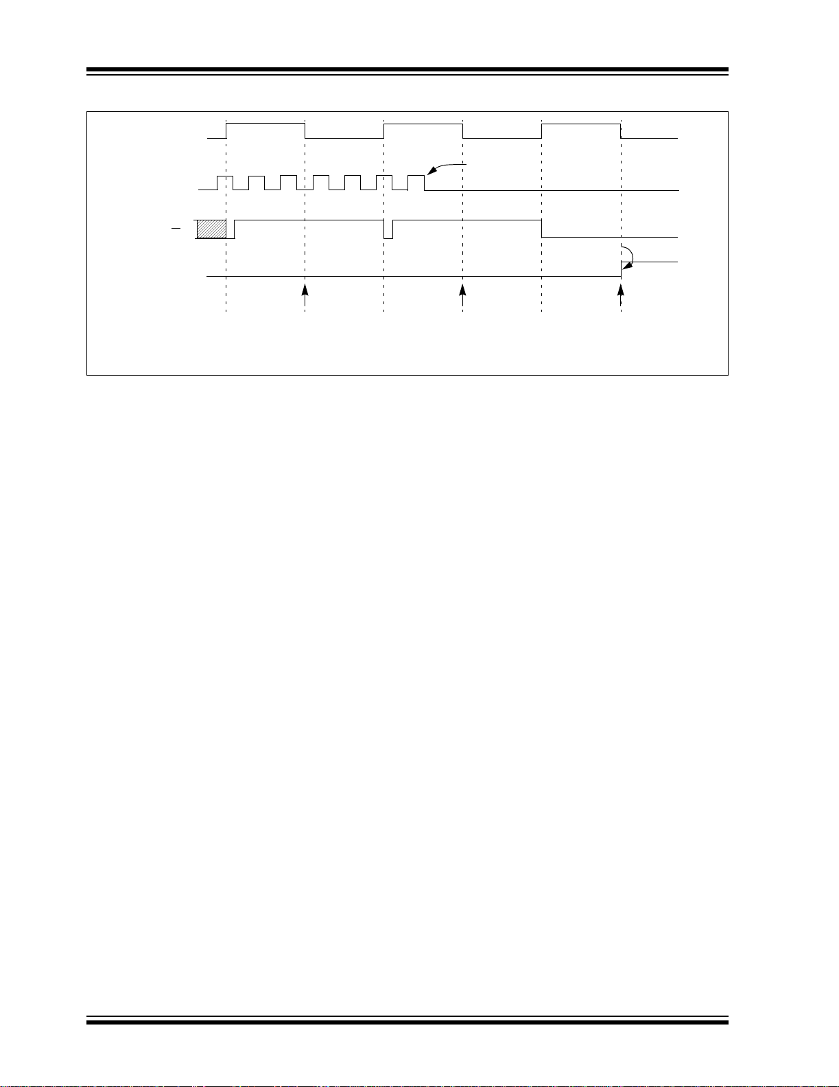
PIC16F685/687/689/690
FIGURE 3-9: FSCM TIMING DIAGRAM
Sample Clock
System
Clock
Output
CM Output
(Q)
OSCFIF
CM Test
Note: The system clock is norm ally at a much higher frequenc y than the sample clock. The relative frequencies in
this example have been chosen for clarity.
Oscillator
Failure
Failure
Detected
CM Test CM Test
DS41262A-page 44 Preliminary © 2005 Microchip Technology Inc.
PIC16F685/687/689/690
REGISTER 3-2: OSCCON – OSCILLATOR CONTROL REGISTER (ADDRESS: 8Fh)
U-0 R/W-1 R/W-1 R/W-0 R-1 R-0 R-0 R/W-0
— IRCF2 IRCF1 IRCF0 OSTS
bit 7 bit 0
bit 7 Unimplemented: Read as ‘0’
bit 6-4 IRCF<2:0>: Internal Oscillator Frequency Select bits
000 =31kHz
001 =125kHz
010 =250kHz
011 =500kHz
100 =1MHz
101 =2MHz
110 =4MHz (default)
111 =8MHz
bit 3 OSTS: Oscillator Start-up Time-out Status bit
(1)
1 = Device is running from the external clock defined by FOSC<2:0>
0 = Device is running from the internal oscillator (HFINTOSC or LFINTOSC)
bit 2 HTS: HFINTOSC (High Frequency – 8 MHz to 125 kHz) Status bit
1 =HFINTOSC is stable
0 = HFINTOSC is not stable
bit 1 LTS: LFINTOSC (Low Frequency – 31 kHz) Stable bit
1 = LFINTOSC is stable
0 = LFINTOSC is not stable
bit 0 SCS: System Clock Select bit
1 = Internal oscillator is used for system clock
0 = Clock source defined by FOSC<2:0 >
(1)
HTS LTS SCS
Note 1: Bit resets to ‘0’ with T wo-Speed S tart-u p and LP, XT or HS selected as the Oscillator
mode or Fail-Safe mode is enabled.
Legend:
R = Readable bit W = Writable bit U = Unimplemented bit, read as ‘0’
-n = Value at POR ‘1’ = Bit is set ‘0’ = Bit is cleared x = Bit is unknown
TABLE 3-2: SUMMARY OF REGISTERS ASSOCIATED WITH CLOCK SOURCES
Address Name Bit 7 Bit 6 Bit 5 Bit 4 B it 3 Bit 2 Bit 1 Bit 0
0Ch PIR1 — ADIF RCIF TXIF SSPIF CCP1IF TMR2IF TMR1IF -000 0000 -000 0000
8Ch PIE1
8Fh OSCCON
90h OSCTUNE
(2)
2007h
Legend: x = unknown, u = unchanged, – = unimplemented locations read as ‘0’. Shaded cells are not used by oscillators.
Note 1: Other (non Power-up) Resets include MCLR
CONFIG CPD CP MCLRE PWRTE WDTE FOSC2 FOSC1 FOSC0 — —
2: See
Register 14-1 for operation of all Configuration Word register bits.
— ADIE RCIE TXIE SSPIE CCP1IE TMR2IE TMR1IE -000 0000 -000 0000
— IRCF2 IRCF1 IRCF0 OSTS HTS LTS SCS -110 x000 -110 x000
— — — TUN4 TUN3 TUN2 TUN1 TUN0 ---0 0000 ---u uuuu
Reset and Watchdog Timer Reset during normal operation.
Val ue on:
POR, BOR
Val ue on
all other
Resets
(1)
© 2005 Microchip Technology Inc. Preliminary DS41262A-page 45

PIC16F685/687/689/690
NOTES:
DS41262A-page 46 Preliminary © 2005 Microchip Technology Inc.

PIC16F685/687/689/690
4.0 I/O PORTS
There are as many as eighteen general purpose I/O
pins available. Depending on which peripherals are
enabled, some or all of the pins may not be a vailable a s
general purpose I/O. In general, when a peripheral is
enabled, the associated pin may not be used as a
general purpose I/O pin.
4.1 PORTA and the TRISA Registers
PORTA is a 6-bit wide, bidirectional port. The
corresponding data direction register is TRISA
(Register 4 -2). Setting a TRISA bit (= 1) will make the
corresponding PORTA pin an input (i.e., put the
corresponding output driver i n a High-impedance mod e).
Clearing a TRIS A bi t (= 0) will make the corresponding
PORTA pin an output (i.e., put the contents of th e output
latch on the selected pin). The exception is RA3, which
is input only and its TRIS bit will always read as ‘1’.
Example 4-1 shows how to initialize PORTA.
Reading the PORTA register (Register 4-1) reads the
status of the pins, whereas writing to it will write to the
port latch. All write operations are read-modify-write
operations. Therefore, a write to a port implies that the
port pins are read, this value is modified and then
written to the port data latch. RA3 reads ‘0’ when
MCLRE = 1.
The TRISA register controls the direction of the
PORT A pins, even when they are being used as an alog
inputs. The user must ensure the bits in the TRISA
register are maint ai ned set when using the m as an alog
inputs. I/O pin s co nfigure d as analo g inpu t alw ays rea d
‘0’.
EXAMPLE 4-1: INITIALIZING PORTA
BCF STATUS,RP0 ;Bank 0
BCF STATUS,RP1 ;
CLRF PORTA ;Init PORTA
BSF STATUS,RP1 ;Bank 2
CLRF ANSEL ;digital I/O
BSF STATUS,RP0 ;Bank 1
BCF STATUS,RP1 ;
MOVLW 0Ch ;Set RA<3:2> as inputs
MOVWF TRISA ;and set RA<5:4,1:0>
BCF STATUS,RP0 ;Bank 0
;as outputs
4.2 Additional Pin Functions
Every PORTA pin on the PIC16F685/687/689/690 has
an interrupt-on-change option and a weak pull-up
option. RA0 also has an Ultra Low-Power Wake-up
option. The next three sections describe these
functions.
4.2.1 WEAK PULL-UPS
Each of the PORTA pins, except RA3, has an
individually configurable internal weak pull-up. Control
bits WPUAx enable or disable each pull-up. Refer to
Register 4-3. Each weak pull-up is automatically turne d
off when the port pin is configured as an output. The
pull-ups are disabled on a Power-on Reset by the
RABPU
automatically enabled for RA3 when configured as
MCLR and disabled when RA3 is an I/O. There is no
software control of the MCLR
bit (OPTION_REG<7>). A weak pull-up is
pull-up.
Note: The ANSEL (11Eh) register must be
initialized to configure an analog channel
as a digital input. Pins configured as
analog inputs will read ‘0’.
REGISTER 4-1: PORTA – PORTA REGISTER (ADDRESS: 05h OR 105h)
U-0 U-0 R/W-x R/W-x R/W-x R/W-x R/W-x R/W-x
— — RA5 RA4 RA3 RA2 RA1 RA0
bit 7 bit 0
bit 7-6: Unimplemented: Read as ‘0’
bit 5-0: RA<5:0>: PORTA I/O Pin bit
1 = Port pin is > V
0 = Port pin is < VIL
Legend:
R = Readable bit W = Writable bit U = Unimplemented bit, read as ‘0’
-n = Value at POR ‘1’ = Bit is set ‘0’ = Bit is cleared x = Bit is unknown
IH
© 2005 Microchip Technology Inc. Preliminary DS41262A-page 47

PIC16F685/687/689/690
REGISTER 4-2: TRISA – PORTA T RI-STATE PORT A REGISTER (ADDRESS: 85h OR 185h)
U-0 U-0 R/W-1 R/W-1 R-1 R/W-1 R/W-1 R/W-1
— — TRISA5 TRISA4 TRISA3 TRISA2 TRISA1 TRISA0
bit 7 bit 0
bit 7-6 Unimplemented: Read as ‘0’
bit 5-0 TRISA<5:0>: PORTA Tri-State Control bit
1 = PORTA pin configured as an input (tri-stated)
0 = PORTA pin configured as an output
Note: TRISA<5:4> always reads ‘1’ in XT, HS and LP OSC modes.
Legend:
R = Readable bit W = Writable bit U = Unimplemented bit, read as ‘0’
-n = Value at POR ‘1’ = Bit is set ‘0’ = Bit is cleared x = Bit is unknown
REGISTER 4-3: WPUA – WEAK PULL-UP PORTA REGISTER (ADDRESS: 95h)
U-0 U-0 R/W-1 R/W-1 U-0 R/W-1 R/W-1 R/W-1
— — WPUA5 WPUA4 — WPUA2 WPUA1 WPUA0
bit 7 bit 0
bit 7-6 Unimplemented: Read as ‘0’
bit 5-4 WPUA<5:4>: Weak Pull-up Register bit
1 = Pull-up enabled
0 = Pull-up disabled
bit 3 Unimplemented: Read as ‘0’
bit 2-0 WPUA<2:0>: Weak Pull-up Register bit
1 = Pull-up enabled
0 = Pull-up disabled
Note 1: Global RABPU
2: The weak pull-up device is automatically disabled if the pin is in Output mode
(TRISA = 0).
3: The RA3 pull-up is enabled when configured as MCLR
the Configuration Word.
4: WPUA<5:4> always reads ‘1’ in XT, HS and LP OSC modes.
Legend:
R = Readable bit W = Writable bit U = Unimplemented bit, read as ‘0’
-n = Value at POR ‘1’ = Bit is set ‘0’ = Bit is cleared x = Bit is unknown
must be enabl ed for individual pull -ups to be enabled.
and disabled as an I/O in
DS41262A-page 48 Preliminary © 2005 Microchip Technology Inc.

PIC16F685/687/689/690
4.2.2 INTERRUPT-ON-CHANGE
Each of the PORTA pins is individually configurable as
an interrupt-on-change pin. Control bits IOCAx enable
or disable the interrupt function for each pin. Refer to
Register 4-4. The interrupt-on-change is disabled on a
Power-on Reset.
For enabled interrupt-on-change pins, the values are
compared with the old value la tched on the last rea d of
PORTA. The ‘mismatch’ outputs of the last read are
OR’d together to set t he PORTA Change Interrupt Flag
bit (RABIF) in the INTCON register (Register 2-3).
This interrupt can wake the device from Sleep. The
user, in the Interrupt Service Routine, clears the
interrupt by:
a) Any read or write of PORTA. This will end the
mismatch condition, then,
b) Clear the flag bit RABIF.
A mismatch condition will continue to set flag bit RABIF .
Reading PORTA will end the mismatch condition and
allow flag bit RABIF to be cleared. The latch holding the
last read value is not affected by a MCLR
Reset. After these Re se t s, the RABIF flag will continue
to be set if a mismatch is present.
Note: If a change on the I/O pin should occur
when the read operation is being ex ecuted
(start of the Q2 cycle), then the RABIF
interrupt flag may not get set.
nor BOR
REGISTER 4-4: IOCA – INTERRUPT-ON-CHANGE PORTA REGISTER (ADDRESS: 96h)
U-0 U-0 R/W-0 R/W-0 R/W-0 R/W-0 R/W-0 R/W-0
— — IOCA5 IOCA4 IOCA3 IOCA2 IOCA1 IOCA0
bit 7 bit 0
bit 7-6 Unimplemented: Read as ‘0’
bit 5-0 IOCA<5:0>: Interrupt-on-change PORTA Control bit
1 = Interrupt-on-change enabled
0 = Interrupt-on-change disabled
Note 1: Global Interrupt Enable (GIE) must be enabled for individual interrupts to be
recognized.
Legend:
R = Readable bit W = Writable bit U = Unimplemented bit, read as ‘0’
-n = Value at POR ‘1’ = Bit is set ‘0’ = Bit is cleared x = Bit is unknown
© 2005 Microchip Technology Inc. Preliminary DS41262A-page 49

PIC16F685/687/689/690
4.2.3 ULTRA LOW-POWER WAKE-UP
The Ultra Low-Power Wake-up (ULPWU) on RA0 allows
a slow falling voltage to generate an interrupt-on-change
on RA0 without excess current consumption. The mode
is selected by setting the ULPWUE bit (PCON<5>). This
enables a small current sink which can be used to
discharge a capacitor on RA0.
To use this feature, the RA0/AN0/C1IN+/ICSPDAT/
ULPWU pin is configured to output ‘1’ to charge the
capacitor, interrupt-on-change for RA0 is enabled, and
RA0 is configured as an input. The ULPWUE bit is set to
begin the discharge and a SLEEP instruction is performed. When the voltage on RA0 drops below V
interrupt will be generated which will cause the device to
wake-up. Depending on the state of the GIE bit
(INTCON<7>), the device will either jump to the interrupt
vector (0004h) or execute the next instruction when the
interrupt event occurs. See Section 4.2.2 “Interrupt-
on-change” and Section 14.3.3 “PORTA/PORTB
Interrupt” for more information.
This feature provides a low-power technique for
periodically waking up the device from Sleep. The
time-out is dependent on the discharge time of the RC
circuit on RA0. See Example 4-2 for initializing the
Ultra Low-Power Wake-up module.
IL, an
The series resistor provides overcurrent protection for
the RA0/AN0/C1IN+/ICSPDAT/ULPWU pin and can
allow for software calibration of the time-out (see
Figure 4-1). A timer can be us ed to measure the c harge
time and discharge time of the capacitor. The charge
time can then be adjusted to provide the desired
interrupt delay. This technique will compensate for the
affects of temperature, voltage and component
accuracy. The Ultra Low-Power Wake-up peripheral
can also be configured as a simple Programmable Low
Voltage Detect or temperature sensor.
Note: For more information, refer to AN879,
“Using the Microchip Ultra Low-Power
Wake-up Module” Application Note
(DS00879).
EXAMPLE 4-2: ULTRA LOW-POWER
WAKE-UP INITIALIZATION
BCF STATUS,RP0 ;Bank 0
BCF STATUS,RP1 ;
BSF PORTA,0 ;Set RA0 data latch
BSF STATUS,RP1 ;BANK 2
BCF ANSEL,0 ;RA0 to digital I/O
BSF STATUS,RP0 ;BANK 1
BCF STATUS,RP1 ;
BCF TRISA,0 ;Output high to
CALL CapDelay ;charge capacitor
BSF PCON,ULPWUE ;Enable ULP Wake-up
BSF IOCA,0 ;Select RA0 IOC
BSF TRISA,0 ;RA0 to input
MOVLW B’10001000’ ;Enable interrupt
MOVWF INTCON ;and clear flag
BCF STATUS,RP0 ;BANK 0
SLEEP ;Wait for IOC
DS41262A-page 50 Preliminary © 2005 Microchip Technology Inc.

PIC16F685/687/689/690
4.2.4 PIN DESCRIPTIONS AND
DIAGRAMS
Each PORT A pin is multiplexed with other functio ns. The
pins and their combined functions are briefly described
here. For specific information about individual functions
such as the comparator or the A/D Converter, refer to the
appropriate section in this data sheet.
FIGURE 4-1: BLOCK DIAGRAM OF RA0
Data Bus
WR
WPUDA
WPUDA
PORTA
RD
WR
D
Q
CK
Q
D
Q
CK
Q
4.2.4.1 RA0/AN0/C1IN+/ICSPDAT/ULPWU
Figure 4-2 shows the diagram for this pin. The RA0/
AN0/C1IN+/ICSPDAT/ULPWU
to function as one of the following:
• a general purpose I/O
• an analog input for the A/D
• an analog input to Comparator 1
• In-Circuit Seria l Programming data
• an analog input for the Ultra Low-Power Wake-up
(1)
Analog
Input Mode
RABPU
VDD
Weak
pin is configurable
VDD
I/O Pin
WR
TRISA
RD
TRISA
RD
PORTA
WR
IOCA
RD
IOCA
Interrupt-on-
Change
VSS
-
+V
D
Q
CK
Q
01
(1)
Analog
Input Mode
D
Q
D
RD PORTA
Q
EN
D
Q
EN
CK
Q
To Comparator
To A/D Converter
ULPWUE
Q3
T
IULP
VSS
Note 1: ANSEL determines Analog Input mode.
© 2005 Microchip Technology Inc. Preliminary DS41262A-page 51

PIC16F685/687/689/690
4.2.4.2 RA1/AN1/C12IN-/VREF/ICSPCLK
Figure 4-2 shows the diagram for this pin. The RA1/
AN1/C12IN-/V
REF/ICSPCLK pin is configurable to
function as one of the following:
• a general purpose I/ O
• an analog input for the A/D
• an analog input to Comparator 1 or 2
• a voltage reference input for the A/D
• In-Circuit Serial Programming clock
FIGURE 4-2: BLOCK DIAGRAM OF RA1
(1)
Analog
Data Bus
WR
WPUA
RD
WPUA
WR
PORTA
WR
TRISA
RD
TRISA
D
CK
D
CK
D
CK
Q
Q
Q
Q
Q
Q
Input Mode
RA
Input Mode
BPU
Analog
VDD
Weak
VDD
I/O Pin
VSS
(1)
4.2.4.3 RA2/AN2/T0CKI/INT/C1OUT
Figure 4-3 shows the diagram for this pin. The RA2/
AN2/T0CKI/INT/C1OUT
pin is configurable to function
as one of the following:
• a general purpose I/O
• an analog input for the A/D
• the clock input for TMR0
• an external edge triggered interrupt
• a digital output from Comparator 1
FIGURE 4-3: BLOCK DIAGRAM OF RA2
(1)
Analog
Data Bus
WR
WPUA
RD
WPUA
WR
PORTA
WR
TRISA
RD
TRISA
D
CK
D
CK
D
CK
Q
Q
Q
Q
Q
Q
Input Mode
RABPU
C1OUT
Enable
C1OUT
Input Mode
1
0
Analog
VDD
Weak
VDD
I/O Pin
VSS
(1)
RD
PORTA
D
Q
D
Q
EN
D
Q
EN
Change
CK
Q
To Comparator
To A/D Converter
RD PORTA
WR
IOCA
RD
IOCA
Interrupt-on-
Note 1: ANSEL determines Analo g Input mode.
Q3
RD
PORTA
D
Q
Q
EN
Q
EN
RD PORTA
Change
CK
Q
To TMR0
To INT
To A/D Converter
WR
IOCA
RD
IOCA
Interrupt-on-
Note 1: ANSEL determines Analo g Input mode.
D
Q3
D
DS41262A-page 52 Preliminary © 2005 Microchip Technology Inc.

PIC16F685/687/689/690
4.2.4.4 RA3/MCLR/VPP
Figure 4-4 shows the diagram for this pin. The RA3/
MCLR
/VPP pin is configurable to function as one of
the following:
• a general purpose input
• as Master Clear Reset with weak pull-up
FIGURE 4-4: BLOCK DIAGRAM OF RA3
VDD
Data Bus
RD
TRISA
RD
PORTA
WR
IOCA
RD
IOCA
Interrupt-on-
Change
MCLRE
Reset
VSS
Q
D
CK
Q
MCLRE
MCLRE
Q
Q
RD PORTA
EN
EN
Weak
Input
Pin
V
SS
D
Q3
D
4.2.4.5 RA4/AN3/T1G
/OSC2/CLKOUT
Figure 4-5 shows the diagram for this pin. The RA4/
AN3/T1G
/OSC2/CLKOUT pin is configurable to
function as one of the following:
• a general purpose I/O
• an analog input for the A/D
• a TMR1 gate input
• a crystal/resona tor connec tio n
• a clock output
FIGURE 4-5: BLOCK DIAGRAM OF RA4
(3)
Analog
Data Bus
WR
WPUA
RD
WPUA
WR
PORTA
WR
TRISA
RD
TRISA
RD
PORTA
WR
IOCA
RD
IOCA
Input Mode
Q
D
CK
Q
OSC1
D
Q
CK
Q
Q
D
CK
Q
D
Q
CK
Q
FOSC/4
CLKOUT
INTOSC/
RC/EC
CLKOUT
Enable
Enable
CLK
Modes
RABPU
Oscillator
Circuit
CLKOUT
Enable
1
0
(2)
Analog
Input Mode
Q
Q
(1)
EN
VDD
Weak
VDD
I/O Pin
VSS
D
Q3
D
Interrupt-on-
Change
To T1G
To A/D Converter
Note 1: CLK modes are XT, HS, LP, LPTMR1 and CLKOUT
Enable.
2: With CLKOUT option.
3: ANSEL determines Analog Input mode.
EN
RD PORTA
© 2005 Microchip Technology Inc. Preliminary DS41262A-page 53
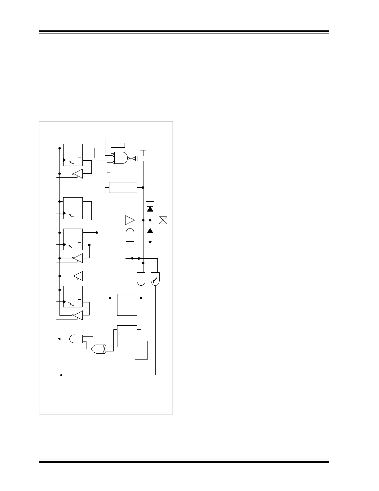
PIC16F685/687/689/690
4.2.4.6 RA5/T1CKI/OSC1/CLKIN
Figure 4-6 shows the diagram for this pin. The RA5/
T1CKI/OSC1/CLKIN
as one of the following:
• a general purpose I/ O
•a TMR1 clock input
• a crystal/resonator connection
• a clock input
FIGURE 4-6: BLOCK DIAGRAM OF RA5
Data Bus
WPUA
WPUA
PORTA
WR
RD
WR
D
CK
D
CK
pin is configurable to function
INTOSC
Mode
TMR1LPEN
Q
Q
RABPU
Oscillator
Circuit
Q
Q
OSC2
(1)
VDD
Weak
VDD
D
Q
WR
TRISA
RD
TRISA
RD
PORTA
WR
IOCA
RD
IOCA
Interrupt-on-
CK
Q
D
Q
CK
Q
Change
To TMR1 or CLKGEN
Note 1: T imer1 LP Oscillator enabled.
2: When using Timer1 with LP oscillator, the
Schmitt Trigger is bypassed.
INTOSC
Mode
Q
Q
RD PORTA
EN
EN
I/O Pin
VSS
(2)
D
Q3
D
DS41262A-page 54 Preliminary © 2005 Microchip Technology Inc.

PIC16F685/687/689/690
TABLE 4-1: SUMMARY OF REGISTERS ASSOCIATED WITH PORTA
Address Name Bit 7 Bit 6 Bit 5 Bit 4 Bit 3 Bit 2 Bit 1 Bit 0
05h/105h PORTA
0Bh/8Bh/
10Bh/18Bh
10h T1CON
14h SSPCON
1Fh ADCON0
81h/181h OPTION_REG
85h/185h TRISA
95h WPUA
96h IOCA
119h CM1CON0
11Eh ANSEL
Legend: x = unknown, u = unchanged, – = unimplemented locations read as ‘0’. Shaded cells are not used by PORTA.
INTCON GIE
— — RA5 RA4 RA3 RA2 RA1 RA0 --xx xxxx --uu uuuu
PEIE T0IE INTE RABIE T0IF INTF RABIF 0000 000x 0000 000x
T1GINV TMR1GE T1CKPS1 T1CKPS0 T1OSCEN T1SYNC TMR1CS TMR1ON 0000 0000 uuuu uuuu
WCOL SSPOV SSPEN CKP SSPM3 SSPM2 SSPM1 SSPM0 0000 0000 0000 0000
ADFM VCFG CHS3 CHS2 CHS1 CHS0 GO/DONE ADON 0000 0000 0000 0000
RABPU INTEDG T0CS T0SE PSA PS2 PS1 PS0 1111 1111 1111 1111
— — TRISA5 TRISA4 TRISA3 TRISA2 TRISA1 TRISA0 --11 1111 --11 1111
— —WPUA5WPUA4 — WPUA2 WPUA1 WPUA0 --11 -111 --11 -111
— — IOCA5 IOCA4 IOCA3 IOCA2 IOCA1 IOCA0 --00 0000 --00 0000
C1ON C1OUT C1OE C1POL — C1R C1CH1 C1CH0
ANS7 ANS6 ANS5 ANS4 ANS3 ANS2 ANS1 ANS0 1111 1111 1111 1111
Value on:
POR, BOR
0000 -000 0000 -000
Value on
all other
Resets
© 2005 Microchip Technology Inc. Preliminary DS41262A-page 55

PIC16F685/687/689/690
4.3 PORTB and TRISB Registers
PORTB is a 4-bit wide, bidirectional port. The
corresponding data direction register is TRI SB (Register
4-6). Setting a TRISB bit (= 1) will make the
corresponding PORTB pin an input (i.e., put the
corresponding output driver in a High-impedance mode).
Clearing a TRISB bit (= 0) will make the correspondi ng
PORTB pin an output (i.e., put the contents of the output
latch on the selected pin). Example 4-3 shows how to
initialize PORTB. Reading the PORTB register (Register
4-5) reads the status of the pins, whereas writing to it will
write to the port latch. All write operations are readmodify-write operations. Therefore, a write to a port
implies that the port pins are r ead, this value is modifi ed
and then written to the port data latch.
The TRISB register controls the direction of the PORTB
pins, even when they are being used as analog inputs.
The user must ensure the bits in the TRIS B register are
maintained set when using them as analog inputs. I/O
pins configured as analog input always read ‘0’.
EXAMPLE 4-3: INITIALIZING PORTB
BCF STATUS,RP0 ;Bank 0
BCF STATUS,RP1 ;
CLRF PORTB ;Init PORTB
BSF STATUS,RP0 ;Bank 1
MOVLW FFh ;Set RB<7:4> as inputs
MOVWF TRISB ;
BCF STATUS,RP0 ;Bank 0
Note: The ANSELH (11Fh) register must be
initialized to configure an analog channel
as a digital input. Pins configured as
analog inputs will read ‘0’.
4.4 Additional PORTB Pin Functions
PORTB pins RB<7:4> on the PIC16F685/687/689/690
have an interrupt-o n-cha nge op tion a nd a we ak pu ll-up
option. The following three sections describe these
PORTB pin functions.
4.4.1 WEAK PULL-UPS
Each of the PORTB pins has an indiv idually configurable
internal weak pull-up. Control bits WPUB<7:4> enable or
disable each pull-up. Refer to Register 4-7. Each weak
pull-up is automatically turned off when the port pin is
configured as an output. The pull-ups are disabled on a
Power-on Reset by the RABPU
4.4.2 INTERRUPT-ON-CHANGE
Four of the PORTB pins are individually configurable
as an interrupt-on-change pin. Control bits IOCB<7:4>
enable or disable the interrupt function for each pin.
Refer to Register 4-8. The interrupt-on-change feature
is disabled on a Power-on Reset.
For enabled interrupt-on-change pins, the values are
compared with the old value latch ed on the la st read of
PORTB. The ‘mismatch’ outputs of the last read are
OR’d together to set the PORTB Change Interrupt flag
bit (RABIF) in the INTCON register (Register 2-3).
This interrupt can wake the device from Sleep. The user ,
in the Interrupt Service Routine, clears the interrupt by:
a) Any read or write of PORTB. This will end the
mismatch condition.
b) Clear the flag bit RABIF.
A mismatch conditio n will contin ue to set flag bit RABIF.
Reading or writing PORTB will end the mismatch
condition and allow flag bit RABIF to be cleared. The latch
holding the last read value is not affected by a MCLR
Brown-out Reset. After these Resets, the RABIF flag will
continue to be set if a mismatch is present.
bit (OPTION_REG<7>).
nor
Note: If a change on the I/O pin should occur
when the read operation is being executed
(start of the Q2 cycle), then the RABIF
interrupt flag may not get set. Furthermore,
since a read or write on a port affects all bits
of that port, care must be taken when using
multiple pins in Interrupt-on-change mode.
Changes on one pin may not be seen while
servicing changes on another pin.
DS41262A-page 56 Preliminary © 2005 Microchip Technology Inc.

PIC16F685/687/689/690
REGISTER 4-5: PORTB – PORTB REGISTER (ADDRESS: 06h OR 106h)
R/W-x R/W-x R/W-x R/W-x U-0 U-0 U-0 U-0
RB7 RB6 RB5 RB4 — — — —
bit 7 bit 0
bit 7-4 RB<7:4>: PORTB I/O Pin bits
1 = Port pin is > V
0 = Port pin is < VIL
bit 3-0 Unimplemented: Read as ‘0’
Legend:
R = Readable bit W = Writable bit U = Unimplemented bit, read as ‘0’
- n = Value at POR ‘1’ = Bit is set ‘0’ = Bit is cleared x = Bit is unknown
REGISTER 4-6: TRISB – TRI-STATE PORTB REGISTER (ADDRESS: 86h OR 186h)
R/W-1 R/W-1 R/W-1 R/W-1 U-0 U-0 U-0 U-0
TRISB7 TRISB6 TRISB5 TRISB4 — — — —
bit 7 bit 0
IH
bit 7-4 TRISB<7:4>: PORTB Tri-State Control bits
1 = PORTB pin configured as an input (tri-stated)
0 = PORTB pin configured as an output
bit 3-0 Unimplemented: Read as ‘0’
Legend:
R = Readable bit W = Writable bit U = Unimplemented bit, read as ‘0’
- n = Value at POR ‘1’ = Bit is set ‘0’ = Bit is cleared x = Bit is unknown
REGISTER 4-7: WPUB – WEAK PULL-UP PORTB REGISTER (ADDRESS: 115h)
R/W-1 R/W-1 R/W-1 R/W-1 U-0 U-0 U-0 U-0
WPUB7 WPUB6 WPUB5 WPUB4
bit 7 bit 0
bit 7-4 WPUB<7:4>: Weak Pull-up Register bits
1 = Pull-up enabled
0 = Pull-up disabled
bit 3-0 Unimplemented: Read as ‘0’
Note 1: Global RABPU
2: The weak pull-up device is automatically disabled if the pin is in Output mode
(TRISB<7:4> = 0).
must be enabl ed for individual pull -ups to be enabled.
— — — —
Legend:
R = Readable bit W = Writable bit U = Unimplemented bit, read as ‘0’
- n = Value at POR ‘1’ = Bit is set ‘0’ = Bit is cleared x = Bit is unknown
© 2005 Microchip Technology Inc. Preliminary DS41262A-page 57

PIC16F685/687/689/690
REGISTER 4-8: IOCB – INTERRUPT-ON-CHANGE PORTB REGISTER (ADDRESS: 116h)
R/W-0 R/W-0 R/W-0 R/W-0 U-0 U-0 U-0 U-0
IOCB7 IOCB6 IOCB5 IOCB4 — — — —
bit 7 bit 0
bit 7-4 IOCB<7:4>: Interrupt-on-Change bits
1 = Interrupt-on-change enabled
0 = Interrupt-on-change disabled
bit 3-0 Unimplemented: Read as ‘0’
Legend:
R = Readable bit W = Writable bit U = Unimplemented bit, read as ‘0’
- n = Value at POR ‘1’ = Bit is set ‘0’ = Bit is cleared x = Bit is unknown
DS41262A-page 58 Preliminary © 2005 Microchip Technology Inc.
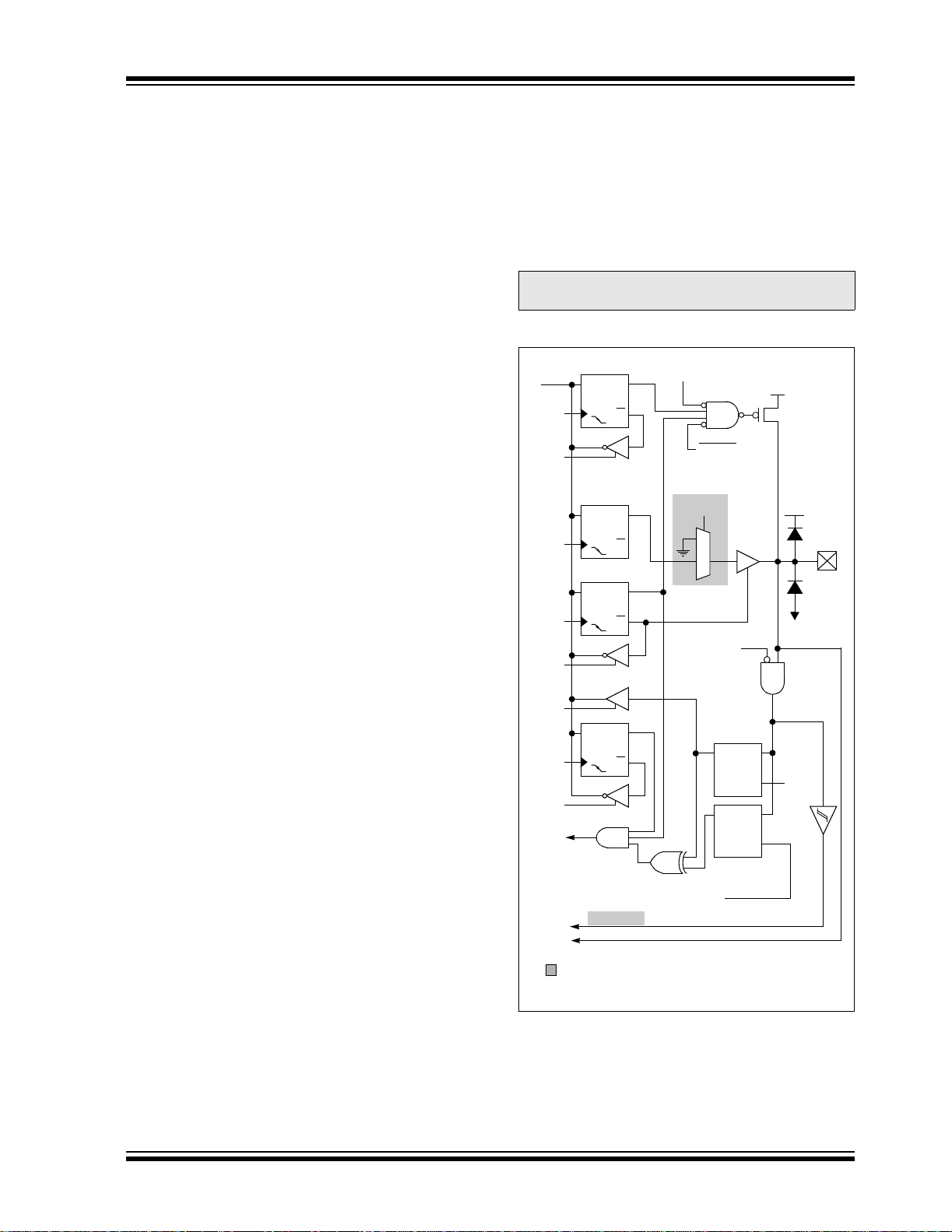
PIC16F685/687/689/690
4.4.3 PIN DESCRIPTIONS AND
DIAGRAMS
Each PORTB pin is multiplexed with other functions. The
pins and their combined functions are briefly described
here. For specific information about i ndividual functions
such as the SSP, I
section in this data sheet.
2
C or interrupts, refer to the appropriate
4.4.3.1 RB4/AN10/SDI/SDA
Figure 4-7 shows the diagram for this pin. The RB4/
AN10/SDI/SDA
of the following:
• a general purpose I/O
• an analog input for the A/D
• a SPI data I/O
2
C data I/O
•an I
Note 1: SDI and SDA are available on
(1)
pin is configurable to fu nction as on e
PIC16F687/PIC16F689/PIC16F690 only.
FIGURE 4-7: BLOCK DIAGRAM OF RB4
(1)
Analog
Data Bus
WR
WPUB
RD
WPUB
WR
PORTB
WR
TRISB
RD
TRISB
D
CK
D
CK
D
CK
Q
Q
Q
Q
Q
Q
Input Mode
RABPU
SSPEN
Input Mode
0
1
1
0
Analog
VDD
Weak
VDD
I/O Pin
VSS
(1)
RD
PORTB
D
Q
D
WR
IOCB
RD
IOCB
Interrupt-on-
CK
Q
Change
RD PORTB
To SSPSR
To A/D Converter
Available on PIC16F68 7/PIC1 6F 689 /P IC16 F6 90 only.
Note 1: ANSEL determines Analog Input mode.
Q
EN
D
Q
EN
Q3
ST
© 2005 Microchip Technology Inc. Preliminary DS41262A-page 59

PIC16F685/687/689/690
4.4.3.2 RB5/AN11/RX/DT
Figure 4-8 shows the diagram for this pin. The RB5/
AN11/RX/DT
of the following:
• a general purpose I/ O
• an analog input for the A/D
• an asynchronous serial input
(1)
pin is configurable to function as one
• a synchronous serial data I/O
Note 1: RX and DT are available on PIC16F687/
PIC16F689/PIC16F690 only.
FIGURE 4-8: BLOCK DIAGRAM OF RB5
(1)
Analog
Data Bus
WR
WPUB
RD
WPUB
WR
PORTB
WR
TRISB
RD
TRISB
RD
PORTB
WR
IOCB
RD
IOCB
Interrupt-on-
Change
D
CK
D
CK
D
CK
D
CK
Q
Q
Q
Q
Q
Q
Q
Q
Input Mode
RABPU
SYNC
SPEN
EUSART
DT
Input Mode
0
1
1
0
Analog
Q
Q
VDD
Weak
VDD
I/O Pin
EN
EN
VSS
D
Q3
D
ST
(1)
RD PORTB
T o EUSART RX/DT
To A/D Converter
Available on PIC16F687/ PI C1 6F 68 9/PIC16F690 only.
Note 1: ANSEL determines Analog Input mode.
DS41262A-page 60 Preliminary © 2005 Microchip Technology Inc.

PIC16F685/687/689/690
4.4.3.3 RB6/SCK/SCL
Figure 4-9 shows the diagram for this pin. The RB6/
SCK/SCL
following:
• a general purpose I/ O
• a SPI™ clock
• an I
(1)
pin is configura ble to func tion as one o f the
2
C™ clock
Note 1: SCK and SCL are available on
PIC16F687/PIC16F689/PIC16F690 only.
FIGURE 4-9: BLOCK DIAGRAM OF RB6
Data Bus
WPUB
WPUB
PORTB
TRISB
TRISB
PORTB
IOCB
IOCB
D
WR
RD
D
WR
D
WR
RD
RD
D
WR
RD
Interrupt-on-
Change
CK
CK
CK
CK
Q
Q
RABPU
Q
Q
Q
Q
Q
Q
SSPEN
0
1
0
1
Q
Q
EN
EN
VDD
Weak
VDD
I/O Pin
VSS
D
Q3
D
ST
RD PORTB
To SSPSR
Available on PIC16F687/PIC16F689/PIC16F690 only.
© 2005 Microchip Technology Inc. Preliminary DS41262A-page 61

PIC16F685/687/689/690
4.4.3.4 RB7/TX/CK
Figure 4-10 shows the diagram for this pin. The RB7/
(1)
TX/CK
following:
• a general purpose I/ O
• an asynchronous serial output
• a synchronous clock I/O
pin is configurable to function as one of the
Note 1: TX and CK are available on PIC16F687/
PIC16F689/PIC16F690 only.
FIGURE 4-10: BLOCK DIAGRAM OF RB7
Data Bus
WPUB
WPUB
PORTB
TRISB
TRISB
PORTB
IOCB
IOCB
WR
RD
WR
WR
RD
RD
WR
RD
D
Q
CK
Q
RABPU
SPEN
TXEN
SYNC
EUSART
CK
0
TX
1
1
0
Q
Q
D
CK
D
CK
D
CK
EUSART
Q
Q
Q
Q
Q
Q
VDD
Weak
VDD
0
1
0
1
D
EN
D
I/O Pin
VSS
Q3
Interrupt-on-
Change
RD PORTB
Available on PIC16F687/PIC16F689/PIC16F690 only.
EN
DS41262A-page 62 Preliminary © 2005 Microchip Technology Inc.

PIC16F685/687/689/690
TABLE 4-2: SUMMARY OF REGISTERS ASSOCIATED WITH PORTB
Address Name Bit 7 Bit 6 Bit 5 Bit 4 Bit 3 Bit 2 Bit 1 Bit 0
06h/106h PORTB RB7 RB6 RB5 RB4
86h/186h TRISB TRISB7 TRISB6 TRISB5 TRISB4
0Bh/8Bh/
10Bh/18Bh
115h WPUB WPUB7 WPUB6 WPUB5 WPUB4
116h IOCB IOCB7 IOCB6 IOCB5 IOCB4
Legend: x = unknown, u = unchanged, – = unimplemented locations read as ‘0’. Shaded cells are not used by PORTB.
INTCON
GIE PEIE T0IE INTE RABIE T0IF INTF RABIF 0000 000x 0000 000x
— — — — xxxx ---- uuuu ----
— — — — 1111 ---- 1111 ----
— — — — 1111 ---- 1111 ----
— — — — 0000 ---- 0000 ----
Value on:
POR, BOR
Value on all
other
Resets
© 2005 Microchip Technology Inc. Preliminary DS41262A-page 63

PIC16F685/687/689/690
4.5 PORTC and TRISC Registers
PORTC is a 8-bit wide, bidirectional port. The
correspondin g da t a dir ec ti on regi s ter is TRISC (Register
4-10). Setting a TRISC bit (= 1) will make the
corresponding PORTC pin an input (i.e., put the
correspondin g output driver in a High-impedan ce mode).
Clearing a TRISC bit (= 0) will make the corresponding
PORTC pin an output (i.e., put the contents of the output
latch on the sele cted pin). Example 4-4 sh ows how to
initialize PORTC. Reading the PORTC register (Register
4-9) reads the status of the pins, whereas writing to it will
write to the port latch. All write operations are readmodify-write operations. Therefore, a write to a port
implies that the port pins are read, this value is modified
and then written to th e p ort d at a l atc h .
The TRISC regi st er co nt rol s the di re ct io n of the P ORTC
pins, even when they are being used as analog inputs.
The user must en sur e the bi ts in th e T RI SC r egi st er are
maintained set when using them as analog inputs. I/O
pins config ure d a s an al og i np ut always read ‘0’.
Note: The ANSEL (11Eh) and ANSELH (11Fh)
registers must be initialized to configure
an analog channel as a digital input. Pins
configured as analog inputs will read ‘0’.
EXAMPLE 4-4: INITIALIZING PORTC
BCF STATUS,RP0 ;Bank 0
BCF STATUS,RP1 ;
CLRF PORTC ;Init PORTC
BSF STATUS,RP1 ;Bank 2
CLRF ANSEL ;digital I/O
BSF STATUS,RP0 ;Bank 1
BCF STATUS,RP1 ;
MOVLW 0Ch ;Set RC<3:2> as inputs
MOVWF TRISC ;and set RC<5:4,1:0>
;as outputs
BCF STATUS,RP0 ;Bank 0
REGISTER 4-9: PORTC – PORTC REGISTER (ADDRESS: 07h OR 107h)
R/W-x R/W-x R/W-x R/W-x R/W-x R/W-x R/W-x R/W-x
RC7 RC6 RC5 RC4 RC3 RC2 RC1 RC0
bit 7 bit 0
bit 7-0 RC<7:0>: PORTC General Purpose I/O Pin bits
1 = Port pin is > V
0 = Port pin is < VIL
Legend:
R = Readable bit W = Writable bit U = Unimplemented bit, read as ‘0’
-n = Value at POR ‘1’ = Bit is set ‘0’ = Bit is cleared x = Bit is unknown
IH
REGISTER 4-10: TRISC – TRI-STATE PORTC REGISTER (ADDRESS: 87h OR 187h)
R/W-1 R/W-1 R/W-1 R/W-1 R/W-1 R/W-1 R/W-1 R/W-1
TRISC7 TRISC6 TRISC5 TRISC4 TRISC3 TRISC2 TRISC1 TRISC0
bit 7 bit 0
bit 7-0 TRISC<7:0>: PORTC Tri-State Control bit
1 = PORTC pin configured as an input (tri-stated)
0 = PORTC pin configured as an output
Legend:
R = Readable bit W = Writable bit U = Unimplemented bit, read as ‘0’
-n = Value at POR ‘1’ = Bit is set ‘0’ = Bit is cleared x = Bit is unknown
DS41262A-page 64 Preliminary © 2005 Microchip Technology Inc.

PIC16F685/687/689/690
4.5.1 RC0/AN4/C2IN+
The RC0 is configurable to function as one of the
following:
• a general purpose I/ O
• an analog input for the A/D
• an analog input to Comparator 2
4.5.2 RC1/AN5/C12IN-
The RC1 is configurable to function as one of the
following:
• a general purpose I/ O
• an analog input for the A/D
• an analog input to Comparator 1 or 2
FIGURE 4-11: BLOCK DIAGRAM OF RC0
AND RC1
Data Bus
D
Q
WR
PORTC
WR
TRISC
RD
TRISC
RD
PORTC
Note 1: ANSEL determines Analog Input mode.
CK
Q
D
Q
CK
Q
To Comparators
To A/D Converter
Analog Input
Mode
(1)
VDD
I/O Pin
VSS
4.5.3 RC2/AN6/P1D
The RC2/AN6/P1D
one of the following:
• a general purpose I/O
• an analog input for the A/D
• a PWM output
Note 1: P1D is available on PIC16F685/
(1)
is configurable to function as
PIC16F690 only.
4.5.4 RC3/AN7/P1C
The RC3/AN7/P1C
of the following:
• a general purpose I/O
• an analog input for the A/D
• a PWM output
Note 1: P1C is available on PIC16F685/
(1)
is configurable to funct ion as one
PIC16F690 only.
FIGURE 4-12: BLOCK DIAGRAM OF RC2
AND RC3
Data Bus
WR
PORTC
WR
TRISC
RD
TRISC
RD
PORTC
D
CK
D
CK
To A/D Converter
CCPOUT
Enable
Q
Q
CCPOUT
Q
Q
0
1
1
0
Analog Input
(1)
Mode
VDD
I/O Pin
VSS
Available on PIC16F685/PIC16F690 only.
Note 1: ANSEL determines Analog Input mode.
© 2005 Microchip Technology Inc. Preliminary DS41262A-page 65

PIC16F685/687/689/690
4.5.5 RC4/C2OUT/P1B
The RC4/C2OUT/P1B
as one of the following:
• a general purpose I/ O
• a digital output from Comparator 2
• a PWM output
Note 1: Enabling both C2OUT and P1B will cause
a conflict on RC4 and create unpredictable
results. Therefore, if C2OUT is enabled,
the ECCP+ can not be used in Half-bridge
or Full-bridge mode and vise-versa.
2: P1B is available on PIC16F685/
PIC16F690 only.
(1, 2)
is configurable to function
FIGURE 4-13: BLOCK DIAGRAM OF RC4
C2OUT EN
CCPOUT EN
C2OUT EN
CCPOUT EN
Data Bus
WR
PORTC
C2OUT
CCPOUT
D
CK
0
1
1
0
Q
Q
VDD
I/O Pin
VSS
4.5.6 RC5/CCP1/P1A
The RC5/CCP1/P1A
one of the following:
• a general purpose I/O
• a digital input/output for the Enhanced CCP
• a PWM output
Note 1: CCP1 and P1A are available on
PIC16F685/PIC16F690 only.
(1)
is configurable to function as
FIGURE 4-14: BLOCK DIAGRAM OF RC5
Data bus
WR
PORTC
WR
TRISC
RD
TRISC
RD
PORTC
D
CK
D
CK
To Enhanced CCP
Q
Q
Q
Q
CCP1OUT
Enable
CCP1OUT
VDD
0
1
0
1
I/O Pin
VSS
D
Q
WR
TRISC
RD
TRISC
RD
PORTC
CK
Q
Available on PIC16F68 5/PIC1 6F 690 onl y.
Available on PIC16F685/PIC16F690 only.
DS41262A-page 66 Preliminary © 2005 Microchip Technology Inc.

PIC16F685/687/689/690
4.5.7 RC6/AN8/SS
The RC6/AN8/SS
of the following:
• a general purpose I/ O
• an analog input for the A/D
• a slave select input
Note 1: SS is available on PIC16F687/PIC16F689/
(1)
is configurable to function as one
PIC16F690 only.
FIGURE 4-15: BLOCK DIAGRAM OF RC6
Data Bus
D
Q
WR
PORTC
WR
TRISC
RD
TRISC
RD
PORTC
Note 1: ANSEL determines Analog Input mode.
CK
Q
D
Q
CK
Q
Analog Input
To SS Input
To A/D Converter
Available on PIC16F685/ P IC1 6F 69 0 only.
Mode
(1)
VDD
I/O Pin
VSS
4.5.8 RC7/AN9/SDO
The RC7/AN9/SDO
one of the following:
• a general purpose I/O
• an analog input for the A/D
• a serial data output
Note 1: SDO is available on PIC16F687/
(1)
is configurable to function as
PIC16F689/PIC16F690 only.
FIGURE 4-16: BLOCK DIAGRAM OF RC7
PORT/SDO
Select
Data Bus
D
Q
WR
PORTC
WR
TRISC
RD
TRISC
RD
PORTC
Note 1: ANSEL determines Analog Input mode.
CK
Q
D
Q
CK
Q
To A/D Converter
Available on PIC16F685/PIC16F690 only.
SDO
0
1
1
0
Analog Input
Mode
VDD
I/O Pin
VSS
(1)
© 2005 Microchip Technology Inc. Preliminary DS41262A-page 67

PIC16F685/687/689/690
TABLE 4-3: SUMMARY OF REGISTERS ASSOCIATED WITH PORTC
Address Name Bit 7 Bit 6 Bit 5 Bit 4 Bit 3 Bit 2 Bit 1 Bit 0
07h/107h
14h SSPCON
17h CCP1CON
1Dh
87h/187h TRISC TRISC7 TRISC6 TRISC5 TRISC4 TRISC3 TRISC2 TRISC1 TRISC0 1111 1111 1111 1111
11Ah
11Bh
11Eh ANSEL ANS7 ANS6 ANS5 ANS4
11Fh ANSELH
19Dh PSTRCON
19Eh SRCON SR1 SR0 C1SEN C2REN PULSS PULSR
118h VRCON C1VREN C2VREN VRR VP6EN VR3 VR2 VR1 VR0 0000 0000 0000 0000
Legend: x = unknown, u = unchanged, – = unimplemented locations read as ‘0’. Shaded cells are not used by PORTC.
Note 1: PIC16F687/PIC16F689/PIC16F690 only.
PORTC
ECCPAS
CM2CON0 C2ON C2OUT
CM2CON1 MC1OUT MC2OUT
2: PIC16F685/PIC16F690 only.
RC7 RC6 RC5 RC4 RC3 RC2 RC1 RC0 xxxx xxxx uuuu uuuu
(1)
WCOL SSPOV SSPEN CKP SSPM3 SSPM2 SSPM1 SSPM0 0000 0000 0000 0000
(2)
P1M1 P1M0
(2)
ECCPASE ECCPAS2 ECCPAS1 ECCPAS0 PSSAC1 PSSAC0 PSSBD1 PSSBD0 0000 0000 0000 0000
— — — —
— — — STRSYNC STRD STRC STRB STRA ---0 0001 ---0 0001
DC1B1 DC1B0 CCP1M3 CCP1M2 CCP1M1 CCP1M0 0000 0000 0000 0000
C2OE C2POL — C2R C2CH1 C2CH0
— — — — T1GSS C2SYNC
ANS3 ANS2 ANS1 ANS0 1111 1111 1111 1111
ANS11 ANS10 ANS9 ANS8 ---- 1111 ---- 1111
— — 0000 00-- 0000 00--
Value on:
POR, BOR
0000 -000 0000 -000
00-- --10 00-- --10
Value on
all other
Resets
DS41262A-page 68 Preliminary © 2005 Microchip Technology Inc.
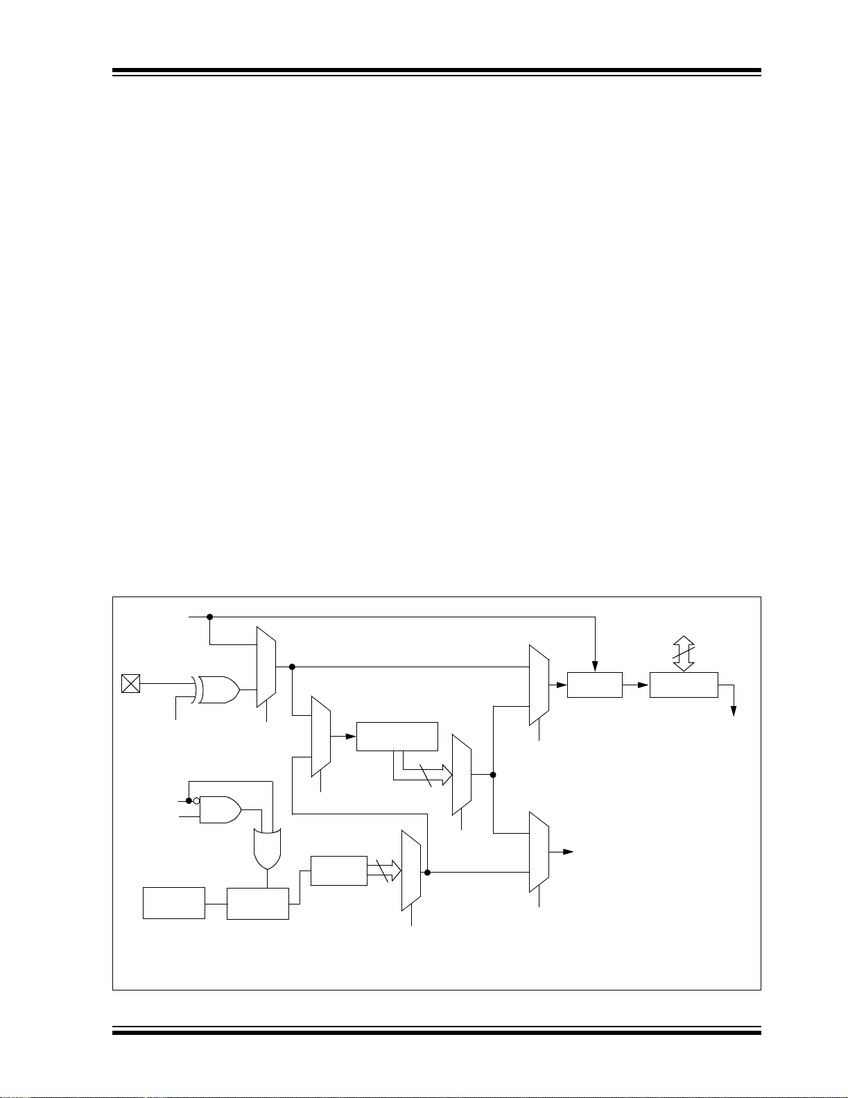
PIC16F685/687/689/690
5.0 TIMER0 MODULE
The Timer0 module timer/counter has the following
features:
• 8-bit timer/counter
• Readable and writable
• 8-bit software programmable prescaler
• Internal or external clock select
• Interrupt on overflow from FFh to 00h
• Edge select for external clock
Figure 5-1 is a block diagram of th e Ti mer0 module and
the prescaler shared with the WDT.
5.1 Timer0 Operation
Timer mode is selected by clearing the T0CS bit
(OPTION_REG<5>). In Timer mode, the Timer0
module will increment every instruction cycle (without
prescaler). If TMR0 is written , the increment is inhibited
for the following two instruction cycles. The user can
work around this by writing an adjusted value to the
TMR0 register.
Counter mode is selected by setting the T0CS bit
(OPTION_REG<5>). In this mode, the Timer0 module
will increment either on every rising or falling edge of pin
RA2/AN1/T0CKI/INT/C1OUT. The incrementing edge is
determined by the source edge (T0SE) control bit
(OPTION_REG<4>). Clearing the T0SE bit selects the
rising edge.
5.2 Timer0 Interrupt
A Timer0 interrupt is generated when the TMR0
register timer/counter overflows from FFh to 00h. This
overflow sets the T0IF bit (INTCON<2>). The interrupt
can be masked by clearing the T0IE bit (INTCO N<5 >).
The T0IF bit must be cleared in softwa re by the T i mer0
module Interrupt Service Routine before re-enabling
this interrupt. The Timer0 interrupt cannot wake the
processor from Sleep since the timer is shut off during
Sleep.
FIGURE 5-1: BLOCK DIAGRAM OF THE TIMER0/WDT PRESCALER
CLKOUT
(= FOSC/4)
0
1
1
T0CKI
pin
T0SE
WDTE
SWDTEN
31 kHz
INTOSC
Note 1: T0SE, T0CS, PSA, PS<2:0> are bits in the OPTION register, WDTPS<3:0> are bits in the WDTCON register.
T0CS
Watchdog
Timer
0
1
PSA
16-bit
Prescaler
8-bit
Prescaler
8
PS<2:0>
16
WDTPS<3:0>
0
PSA
1
0
PSA
Sync 2
cycles
WDT
Time-out
Data Bus
8
TMR0
Set Flag bit T0IF
on Overflow
© 2005 Microchip Technology Inc. Preliminary DS41262A-page 69
PIC16F685/687/689/690
5.3 Using Timer0 with an External
Clock
When no prescaler is used, the external clock input is
the same as the prescaler output . The syn chroniza tion
of T0CKI, with the internal phase clocks, is
accomplished by sampling the prescaler ou tput on the
Q2 and Q4 cycles of the internal phase clocks.
Therefore, it is necessar y for T0CKI to be high for at
least 2 T
at least 2 T
to the electrical specification of the desired device.
REGISTER 5-1: OPTION_REG – OPTION REGISTER (ADDRESS: 81h OR 181h)
OSC (and a small RC delay of 20 ns) and low for
OSC (and a small RC delay of 20 ns). Re fer
Note: The ANSEL (11Eh) register must be
initialized to configure an analog channel
as a digital input. Pins configured as
analog inputs will read ‘0’.
R/W-1 R/W-1 R/W-1 R/W-1 R/W-1 R/W-1 R/W-1 R/W-1
RABPU
bit 7 bit 0
INTEDG T0CS T0SE PSA PS2 PS1 PS0
bit 7 RABPU
1 = PORTA/PORTB pull-ups are disabled
0 = PORTA/PORTB pull-ups are enabled by individual port latch values
bit 6 INTEDG: Interrupt Edge Select bit
1 = Interrupt on rising edge of RA2/AN2/T0CKI/INT/C1OUT pin
0 = Interrupt on falling edge of RA2/AN2/T0CKI/INT/C1OUT pin
bit 5 T0CS: TMR0 Clock Source Select bit
1 = Transition on RA2/AN2/T0CKI/INT/C1OUT pin
0 = Internal instruction cycle clock (CLKOUT)
bit 4 T0SE: TMR0 Source Edge Select bit
1 = Increment on high-to-low transition on RA2/AN2/T0CKI/INT/C1OUT pin
0 = Increment on low-to-high transition on RA2/AN2/T0CKI/INT/C1OUT pin
bit 3 PSA: Prescaler Assignment bit
1 = Prescaler is assigned to the WDT
0 = Prescaler is assigned to the Timer0 module
bit 2-0 PS<2:0>: Prescaler Rate Select bits
: PORTA/PORTB Pull-up Enable bit
BIT VALUE TMR0 RATE WDT RATE
000
001
010
011
100
101
110
111
1 : 2
1 : 4
1 : 8
1 : 16
1 : 32
1 : 64
1 : 128
1 : 256
(1)
1 : 1
1 : 2
1 : 4
1 : 8
1 : 16
1 : 32
1 : 64
1 : 128
Note 1: A dedicated 16-bit WDT postscaler is available. See Section 14.5 “Watchdog
Timer (WDT)” for more information.
Legend:
R = Readable bit W = Writable bit U = Unimplemented bit, read as ‘0’
-n = Value at POR ‘1’ = Bit is set ‘0’ = Bit is cleared x = Bit is unknown
DS41262A-page 70 Preliminary © 2005 Microchip Technology Inc.

PIC16F685/687/689/690
5.4 Prescaler
An 8-bit counter is available as a prescaler for the
Timer0 module, or as a postscaler for the Watchdog
Timer. For simplicity, this counter will be referred to as
“prescaler” throughout this data sheet. The prescaler
assignment is controlled in software by the control bit
PSA (OPTION_REG<3>). Clearing the PSA bit will
assign the prescaler to Timer0. Prescale values are
selectable via the PS<2:0> bits (OPTION_REG<2:0>).
The prescaler is not readable or writable. When
assigned to the Timer0 module, all instructions writing
to the TMR0 register (e.g., CLRF 1, MOVWF 1,
BSF 1, x....etc.) will clear the prescaler. When
assigned to WDT, a CLRWDT instruction will clear the
prescaler along with the Watchdog Timer.
5.4.1 SWITCHING PRESCALER
ASSIGNMENT
The prescaler assignment is fully under software
control (i.e., it can be changed “on the fly” during
program execution). To avoid an unintended device
Reset, the following instruction sequence (Example 5-1
and Example 5-2) must be executed when changing
the prescaler assignment from Timer0 to WDT.
EXAMPLE 5-1: CHANGING PRESCALER
(TIMER0 → WDT)
BCF STATUS,RP0 ;Bank 0
BCF STATUS,RP1 ;
CLRWDT ;Clear WDT
CLRF TMR0 ;Clear TMR0 and
;prescaler
BSF STATUS,RP0 ;Bank 1
MOVLW b’00101111’ ;Required if desired
MOVWF OPTION_REG ;PS<2:0> is
CLRWDT ;000 or 001
;
MOVLW b’00101xxx’ ;Set postscaler to
MOVWF OPTION_REG ;desired WDT rate
BCF STATUS,RP0 ;Bank 0
To change prescaler from the WDT to the TMR0
module, use the se quence sh own in Examp le 5-2. This
precaution must be t aken even if the WDT is disabled.
EXAMPLE 5-2: CHANGING PRESCALER
(WDT → TIMER0)
CLRWDT ;Clear WDT and
;prescaler
BSF STATUS,RP0 ;Bank 1
BCF STATUS,RP1 ;
MOVLW b’xxxx0xxx’ ;Select TMR0,
;prescale, and
;clock source
MOVWF OPTION_REG ;
BCF STATUS,RP0 ;Bank 0
TABLE 5-1: REGISTERS ASSOCIATED WITH TIMER0
Address Name Bit 7 Bit 6 Bit 5 Bit 4 Bit 3 Bit 2 Bit 1 Bit 0
01h/101h TMR0 Timer0 Module Register xxxx xxxx uuuu uuuu
0Bh/8Bh/
10Bh/18Bh
81h/181h OPTION_REG
85h/185h TRISA
Legend: – = Unimplemented locations, read as ‘0’, u = unchanged, x = unknown. Shaded cells are not used by the Timer0 module.
INTCON GIE PEIE T0IE
RABPU INTEDG T0CS T0SE PSA PS2 PS1 PS0 1111 1111 1111 1111
— — TRISA5 TRISA4 TRISA3 TRISA2 TRISA1 TRISA0 --11 1111 --11 1111
INTE RABIE T0IF INTF RABIF 0000 000x 0000 000x
Value on
POR, BOR
Value on
all other
Resets
© 2005 Microchip Technology Inc. Preliminary DS41262A-page 71

PIC16F685/687/689/690
NOTES:
DS41262A-page 72 Preliminary © 2005 Microchip Technology Inc.

PIC16F685/687/689/690
6.0 TIMER1 MODULE WITH GATE CONTROL
The Timer1 module has the following features:
• 16-bit timer/counter (TMR1H:TMR1L)
• Readable and writable
• Internal or external clock selection
• Synchronous or asynchronous operation
• Interrupt on overflow from FFFFh to 0000h
• Wake-up upon overflow (Asynchronous mode)
• Optional external enable input
- Selectable gate source: T1G
(T1GSS)
- Selectable gate polarity (T1GINV)
• Optional LP oscillator
FIGURE 6-1: TIMER1 BLOCK DIAGRAM
Set flag bit
TMR1IF on
Overflow
or C2 output
TMR1
TMR1H
(1)
TMR1L
Figure 6-1 shows the block diagram of the Timer1
module.
The Timer1 Control register (T1CON), shown in
Register 6-1, is used to enable/disable Timer1 and
select the various features of the Timer1 module.
TMR1ON
TMR1GE
TMR1ON
TMR1GE
To C2 Comparator Module
TMR1 Clock
0
Synchronized
clock input
T1GINV
Oscillator
OSC1/T1CKI
OSC2/T1G
FOSC = 000
FOSC = X00
T1OSCEN
T1CKI
T1OSCEN
* ST Buffer is low power type when using LP osc, or high speed type when using T1CKI.
Note 1: Timer1 register increments on rising edge
1
0
T1CS
F
OSC/4
Internal
Clock
1
0
1
T1SYNC
Prescaler
1, 2, 4, 8
2
T1CKPS<1:0>
C2OUT
Synchronize
det
Sleep input
1
0
T1GSS
© 2005 Microchip Technology Inc. Preliminary DS41262A-page 73
PIC16F685/687/689/690
6.1 Timer1 Modes of Operation
Timer1 can operate in one of three modes:
• 16-bit Timer with presc ale r
• 16-bit Synchronous counter
• 16-bit Asynchronous counter
In Timer mode, Timer1 is incremented on every
instruction cycle. In Counter mode, Timer1 is
incremented on the rising edge of the external clock
input T1CKI. In addition, the Counter mode clock can be
synchronized to the microcontroller system clock or run
asynchronously.
In Counter and Timer modules, the counter/timer clock
can be gated by the Timer1 gate, which can be
selected as either the T1G
If an external clock oscillator is needed (and the
microcontroller is us ing the INTOS C without CLKOUT),
Timer1 can use the LP oscillator as a clock source.
Note: In Counter mode, a falling edge must be
registered by the counter prior to the first
incrementing rising edge.
pin or Comparator 2 output.
6.2 Timer1 Interrupt
The Timer1 register pair (TMR1H:TMR1L) increments
to FFFFh and rolls over to 0000h. When Timer1 rolls
over, the Timer1 interrupt flag bit (PIR1<0>) is set. To
enable the inte rrupt on rollo ver , you must set these bits :
• Timer1 interrupt enable bit (PIE1<0>)
• PEIE bit (INTCON<6>)
• GIE bit (INTCON<7>)
The interrupt is cleared by clearing the TMR1IF bit in
the Interrupt Service Routine.
Note: The TMR1H:TTMR1L register p air and the
TMR1IF bit should be cleared before
enabling interrupts.
6.3 Timer1 Prescaler
Timer1 has four prescaler options allowing 1, 2, 4 or 8
divisions of the clock input. The T1CKPS bits
(T1CON<5:4>) control the prescale counter. The
prescale counter is not directly readable or writable;
however, the prescaler counter is cl eared upon a write to
TMR1H or TMR1L.
6.4 Timer1 Gate
Timer1 gate source is software configurable to be the
T1G
pin or the output of Comp ara t or 2. This all ows th e
device to directly time external events using T1G
analog events using Comparator 2. See CM2CON1
(Register 8-3) for selecting the Timer1 gate source.
This feature can si mplify the softwa re for a Delta-Si gma
A/D converter and many other applications. For more
information on Delta-Sigma A/D converters, see the
Microchip web site (www.microchip.com).
Note: TMR1GE bit (T1CON<6>) must be set to
use either T1G
gate source. See Register 8-3 for more
information on selecting the Timer1 gate
source.
Timer1 gate can be inverted using the T1GINV bit
(T1CON<7>), whether it origin ates fro m the T1G
Comparator 2 output. This configures Timer1 to
measure either the active-high or active-low time
between events.
or C2OUT as the Timer1
or
pin or
FIGURE 6-2: TIMER1 INCREMENTING EDGE
T1CKI = 1
when TMR1
Enabled
T1CKI = 0
when TMR1
Enabled
Note 1: Arrows indicate counter increments.
2: In Counter mode, a falling edge must be registered by the counter prior to the first incrementing rising edge of
the clock.
DS41262A-page 74 Preliminary © 2005 Microchip Technology Inc.

PIC16F685/687/689/690
REGISTER 6-1: T1CON – TIMER1 CONTROL REGISTER (ADDRESS: 10h)
R/W-0 R/W-0 R/W-0 R/W-0 R/W-0 R/W-0 R/W-0 R/W-0
(1)
T1GINV
bit 7 bit 0
TMR1GE
(2)
T1CKPS1 T1CKPS0 T1OSCEN T1SYNC TMR1CS TMR1ON
bit 7 T1GINV: Timer1 Gate Invert bit
1 = Timer1 gate is inverted
0 = Timer1 gate is not inverted
bit 6 TMR1GE: Timer1 Gate Enable bit
If TMR1ON =
This bit is ignored
If TMR1ON = 1:
1 = Timer1 is on if Timer1 gate is not active
0 = Timer1 is on
bit 5-4 T1CKPS<1:0>: Timer1 Input Clock Prescale Select bits
11 = 1:8 Prescale Value
10 = 1:4 Prescale Value
01 = 1:2 Prescale Value
00 = 1:1 Prescale Value
bit 3 T1OSCEN: LP Oscillator Enable Control bit
If INTOSC without CLKOUT oscillator is active:
1 = LP oscillator is enabled for Timer1 clock
0 = LP oscillator is off
Else:
This bit is ignored
bit 2 T1SYNC: Timer1 External Clock Input Synchronization Control bit
TMR1CS =
1 = Do not synchronize external clock input
0 = Synchronize external clock input
TMR1CS =
This bit is ignored. Timer1 uses the internal clock.
bit 1 TMR1CS: Timer1 Clock S ource Selec t bit
1 = External clock from T1CKI pin (on the rising edge)
0 = Internal clock (FOSC/4)
bit 0 TMR1ON: Timer1 On bit
1 = Enables Timer1
0 = Stops Timer1
0:
1:
0:
(1)
(2)
Note 1: T1GINV bit inverts the Timer1 gate logic, regardless of source.
2: TMR1GE bit must be set to use either T1G
T1GSS bit (CM2CON1<1>), as a Timer1 gate source.
Legend:
R = Readable bit W = Writable bit U = Unimplemented bit, read as ‘0’
-n = Value at POR ‘1’ = Bit is set ‘0’ = Bit is cleared x = Bit is unknown
© 2005 Microchip Technology Inc. Preliminary DS41262A-page 75
pin or C2OUT, as selected by the
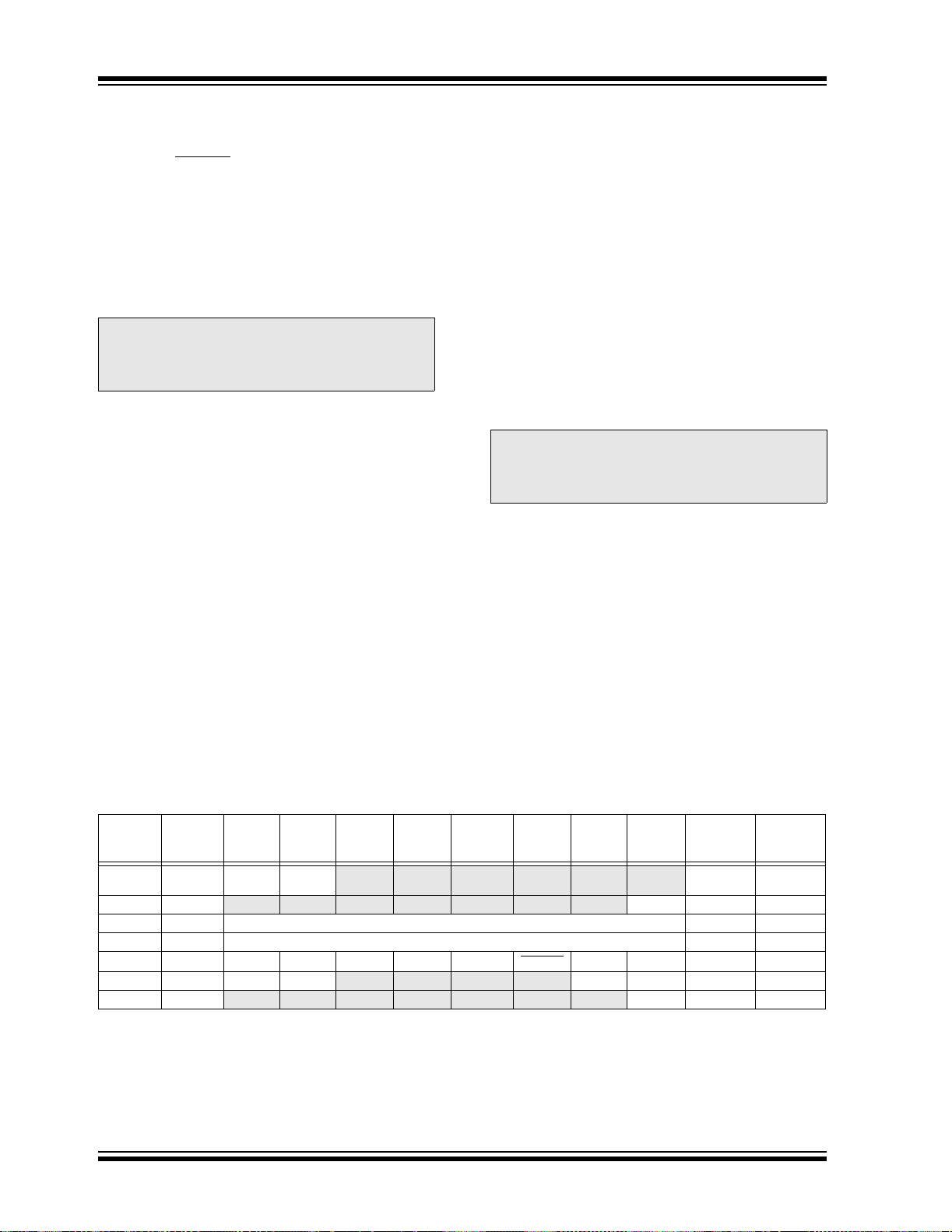
PIC16F685/687/689/690
6.5 Timer1 Operation in
Asynchronous Counter Mode
If control bit T1SYNC (T1CON<2>) is set, the external
clock input is not synchronized. The timer continues to
increment asynchronous to the internal phase clocks.
The timer will continue to run during Sleep and can
generate an interrupt on overflow, which will wake-up
the processor. However, special precautions in
software are needed to read/write the timer (see
Section 6.5.1 “Reading and Writing Timer1 in
Asynchronous Counter Mode”).
Note: The ANSEL (11Eh) register must be
initialized to configure an analog channel
as a digital input. Pins configured as analog
inputs will read ‘0’.
6.5.1 READING AND WRITING TIMER1 IN
ASYNCHRONOUS COUNTER
MODE
Reading TMR1H or TMR1L while the timer is running
from an external asy nchronous cl ock will ens ure a valid
read (taken care of in hardware). However, the user
should keep in min d that re ading t he 16-b it time r in tw o
8-bit values itself, poses certain problems, since the
timer may overflow between the reads.
For writes, it is recomm ended that the us er simply stop
the timer and write the desired values. A write
contention may occur by writing to the timer registers,
while the register is incrementi ng. This may pro duce an
unpredictable value in the timer r egister.
6.6 Timer1 Oscillator
A crystal oscilla tor circuit is built-in between pin s OSC1
(input) and OSC2 (amplifier output). It is enabled by
setting control bit, T1OSCEN (T1CON<3>). The
oscillator is a low-p ower oscil lator rated up to 32 kHz . It
will continue to run durin g Sleep. It is primarily intended
for a 32 kHz crystal. Table 3-1 shows the capacitor
selection for the T im er1 osc il lat or.
The Timer1 oscillator is shared with the system LP
oscillator. Thus, Timer1 can use this mode only when
the primary system clock is derived from the internal
oscillator. As with the system LP oscillator, the user
must provide a software time delay to ensure proper
oscillator start-up.
TRISA5 and TRISA4 bits are set when the Timer1
oscillator is enabled. RA5 and RA4 bits read as ‘0’ an d
TRISA5 and TRISA4 bits read as ‘1’.
Note: The oscillator requires a start-up and
stabilization time before use. Thus,
T1OSCEN should be set and a suitable
delay observed prior to enabling Timer1.
6.7 Timer1 Operation During Sleep
Timer1 can only operate during Sleep when setup in
Asynchronous Counte r mode. In this mode, an external
crystal or clock source can be used to increment the
counter. To set up the timer to wake the device:
• Timer1 must be on (T1CON<0>)
• TMR1IE bit (PIE1<0>) must be set
• PEIE bit (INTCON<6>) must be set
The device will wake-up on an overflow. If the GIE bit
(INTCON<7>) is set, the devi ce w il l wake -up and jump
to the Interrupt Service Routine (0004h) on an overflow .
If the GIE bit is clear, executio n will contin ue with the
next instruction.
TABLE 6-1: REGISTERS ASSOCIATED WITH TIMER1
Addr Name Bit 7 Bit 6 Bit 5 Bit 4 Bit 3 Bit 2 Bit 1 Bit 0
0Bh/8Bh/
10Bh/18Bh
0Ch PIR1
0Eh TMR1L Holding register for the Least Significant Byte of the 16-bit TMR1 Register xxxx xxxx uuuu uuuu
0Fh TMR1H Holding register for the Most Significant Byte of the 16-bit TMR1 Register xxxx xxxx uuuu uuuu
10h T1CON T1GINV TMR1GE T1CKPS1 T1CKPS0 T1OSCEN T1SYNC
11Bh CM2CON1 MC1OUT MC2OUT
8Ch PIE1
Legend: x = unknown, u = unchanged, — = unimplemented, read as ‘0’. Shaded cells are not used by the Timer1 module.
DS41262A-page 76 Preliminary © 2005 Microchip Technology Inc.
INTCON GIE PEIE
— ADIF RCIF TXIF SSPIF CCP1IF TMR2IF TMR1IF -000 0000 -000 0000
— ADIE RCIE TXIE SSPIE CCP1IE TMR2IE TMR1IE -000 0000 -000 0000
T0IE INTE RABIE T0IF INTF RABIF 0000 000x 0000 000x
TMR1CS TMR1ON 0000 0000 uuuu uuuu
— — — — T1GSS C2SYNC 00-- --10 00-- --10
Value on
POR, BOR
Value on
all other
Resets

PIC16F685/687/689/690
7.0 TIMER2 MODULE
The Timer2 module timer has the following features:
• 8-bit timer (TMR2 register)
• 8-bit period register (PR2)
• Readable and writable (both registers)
• Software programmable prescaler (1:1, 1:4, 1:16)
• Software programmable postscaler (1:1 to 1:16)
• Interrupt on TMR2 match with PR2
Timer2 has a control register shown in Register 7-1.
TMR2 can be shut-of f by cl earing control bit, TMR2ON
(T2CON<2>), to minimize power consumption.
Figure 7-1 is a simplified block diagram of the Timer2
module. The prescaler and postscaler selection of
Timer2 are controlled by this register.
7.1 Timer2 Operation
Timer2 can be used as the PWM time base for the
PWM mode of the ECCP+ modu le. The TM R 2 reg ist er
is readable and writable, and is cleared on any device
Reset. The in put cl ock (F
of 1:1, 1:4 or 1:16, selected by control bits
T2CKPS<1:0> (T2CON<1:0>). The match output of
TMR2 goes through a 4-bit postscaler (which gives a
1:1 to 1:16 scaling inclusive) to generate a TMR2
interrupt (latched in flag bit, TMR2IF (PIR1<1>)).
The prescaler and postscaler counters are cleared
when any of the following occurs:
• A write to the TMR2 register
• A write to the T2CON register
• Any device Reset (Power-on Reset, MCLR
Watchdog Timer Reset, or Brown-out Reset)
TMR2 is not cleared when T2CON is written.
OSC/4) has a prescale option
REGISTER 7-1: T2CON — TIMER2 CONTROL REGISTER (ADDRESS: 12h)
U-0 R/W-0 R/W-0 R/W-0 R/W-0 R/W-0 R/W-0 R/W-0
— TOUTPS3 TOUTPS2 TOUTPS1 TOUTPS0 TMR2ON T2CKPS1 T2CKPS0
bit 7 bit 0
Reset,
bit 7 Unimplemented: Read as ‘0’
bit 6-3 TOUTPS<3:0>: Timer2 Output Post sca le Sele ct bits
0000 =1:1 postscale
0001 =1:2 postscale
•
•
•
1111 =1:16 postscale
bit 2 TMR2ON: Timer2 On bit
1 = Timer2 is on
0 = Timer2 is of f
bit 1-0 T2CKPS<1:0>: Timer2 Clock Prescale Selec t bit s
00 = Prescaler is 1
01 = Prescaler is 4
1x = Prescaler is 16
Legend:
R = Readable bit W = Writable bit U = Unimplemented bit, read as ‘0’
-n = Value at POR ‘1’ = Bit is set ‘0’ = Bit is cleared x = Bit is unknown
© 2005 Microchip Technology Inc. Preliminary DS41262A-page 77

PIC16F685/687/689/690
7.2 Timer2 Interrupt
The Timer2 module has an 8-bit period register, PR2.
Timer2 increments from 00h until it matches PR2 and
then resets to 00h on the next increment cycle. PR2 is
a readable and writable register. The PR2 register is
initialized to FFh upon Reset.
FIGURE 7-1: TIMER2 BLOCK DIAGRAM
TMR2
Output
OSC/4
F
Prescaler
1:1, 1:4, 1:16
2
T2CKPS<1:0>
TMR2
Comparator
PR2
TABLE 7-1: REGISTERS ASSOCIATED WITH TIMER2
Addr Name Bit 7 Bit 6 Bit 5 Bit 4 Bit 3 Bit 2 Bit 1 Bit 0
0Bh/8Bh/
10Bh/18Bh
0Ch PIR1
11h TMR2 Holding Register for the 8-bit TMR2 Register 0000 0000 0000 0000
12h T2CON
8Ch PIE1
92h PR2 Timer2 Module Period Register 1111 1111 1111 1111
Legend: x = unknown, u = unchanged, — = unimplemented, read as ‘0’. Shaded cells are not used by the Timer2 module.
INTCON GIE PEIE
— ADIF RCIF TXIF SSPIF CCP1IF TMR2IF TMR1IF -000 0000 -000 0000
— TOUTPS3 TOUTPS2 TOUTPS1 TOUTPS0 TMR2ON T2CKPS1 T2CKPS0 -000 0000 -000 0000
— ADIE RCIE TXIE SSPIE CCP1IE TMR2IE TMR1IE -000 0000 -000 0000
T0IE INTE RABIE T0IF INTF RABIF 0000 000x 0000 000x
Reset
Postscaler
1:1 to 1:16
EQ
TOUTPS<3:0>
4
Sets Flag
bit TMR2IF
Value on
POR, BOR
Value on
all other
Resets
DS41262A-page 78 Preliminary © 2005 Microchip Technology Inc.

PIC16F685/687/689/690
8.0 COMPARATOR MODULE
The comparator module has two separate voltage
comparators: Comparator C1 and Comparator C2.
Each comparator offers the following list of features:
• Control and configuration register
• Comparator output available externally
• Programmable output polarity
• Interrupt-on-change flags
• Wake-up from Sleep
• Configurable as feedback input to the PWM
• Programmable four input multiplexer
• Programmable two input reference selections
• Timer1 gate
• Output synchronization to Timer1 clock input
(Comparator C2 only)
Note: C2 can be linked to Timer1Gate.
8.1 Control Registers
Both comparators have separate control and
configuration registers: CM1CON0 for C1 and CM2CON0
for C2. In addition, Comparator C2 has a second control
register, CM2CON1, for synchronization control and
simultaneous reading of both comparator outputs.
A complete table showing the output state versus input
conditions and the polarity bit is shown in Table 8-1.
TABLE 8-1: C1 OUTPUT STATE VS.
INPUT CONDITIONS
Input Condition C1POL C1OUT
C1VN > C1VP 00
C1VN < C1VP 01
C1VN > C1VP 11
C1VN < C1VP 10
Note 1: The internal output of the comparator is
latched at the end of each instruction
cycle. Exte rnal outputs are not latched.
2: The C1 interrupt will operate correctly
with C1OE set or cleared.
3: For C1 output on RA2/AN2/T0CKI/INT/
C1OUT:
C1OE = 1, C1ON = 1 and TRISA<2> = 0.
8.1.1 COMPARATOR C1 CONTROL
REGISTER
The CM1CON0 register (shown in Register 8-1)
contains the control and Status bits for the following:
• Comparator enable
• Comparator input selection
• Comparator reference selection
• Output mode
Setting C1ON (CM1CON0<7>) enables Comparator
C1 for operation.
Bits C1CH<1:0> (CM1CON0<1:0>) select the
comparator input fro m the four anal og pins AN<7:5,1 >.
Note: To use AN<7:5,1> as analog inputs the
appropriate bits must be programmed to
‘1’ in the ANSEL register.
Setting C1R (CM1CON0<2>) selects the C1V
output of the comparator voltage reference module as
the reference volt age for the comp arator. Clearing C1R
selects the C1IN+ input on the RA0/AN0/C1IN+/
ICSPDAT/ULPWU pin.
The output of the comparator is available internally via
the C1OUT flag (CM1CON0<6>). To make the output
available for an external connection, the C1OE bit
(CM1CON0<5>) must be set.
The polarity of the comparator output can be inverted
by setting the C1POL bit (CM1CON0<4>). Clearing
C1POL results in a non-inverted output.
REF
© 2005 Microchip Technology Inc. Preliminary DS41262A-page 79
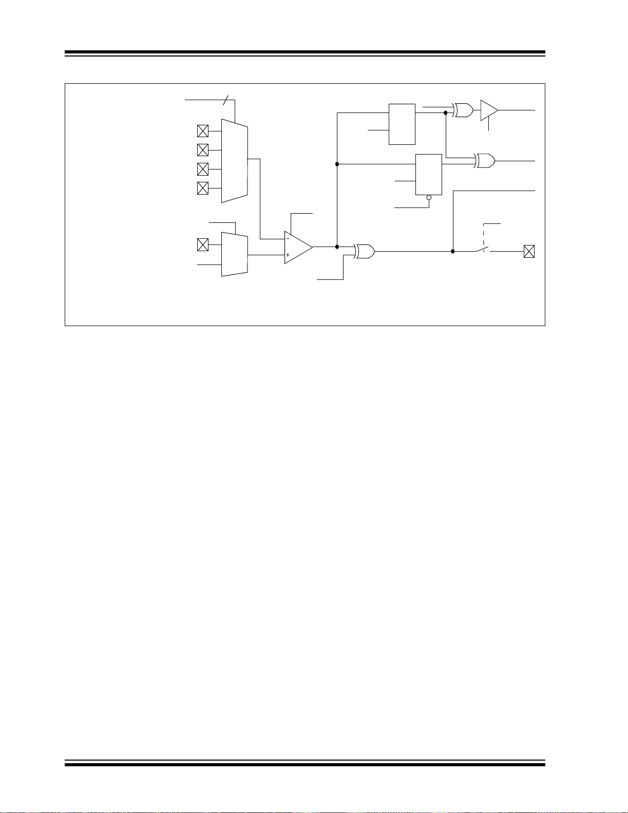
PIC16F685/687/689/690
)
FIGURE 8-1: COMPARATOR C1 SIMPLIFIED BLOCK DIAGRAM
C1CH<1:0>
RA1/AN1/C12IN-/V
RA0/AN0/C1IN+/ICSPDAT/ULPWU
Note 1: When C1ON = 0, the C1 comparator will produce a ‘0’ output to the XOR Gate.
REF/ICSPCLK
RC1/AN5/C12IN1-
RC2/AN6/P1D
RC3/AN7/P1C
C1VREF
2: Output shown for reference only. For more detail see Figure 4-3.
C1R
2
0
1
MUX
2
3
0
MUX
1
C1VN
C1VP
C1ON
C1
Q3*RD_CM1CON0
(1)
C1POL
Q1
DQ
EN
NRESET
C1OUT
C1POL
Data Bus
RD_CM1CON0
DQ
EN
CL
RA2/AN2/T0CKI/INT/C1OUT
Set C1IF
To PWM Logic
C1OE
To
(2
DS41262A-page 80 Preliminary © 2005 Microchip Technology Inc.

PIC16F685/687/689/690
REGISTER 8-1: CM1CON0 – COMPARATOR C1 CONTROL REGISTER 0 (ADDRESS: 119h)
R/W-0 R-0 R/W-0 R/W-0 U-0 R/W-0 R/W-0 R/W-0
C1ON C1OUT C1OE C1POL — C1R C1CH1 C1CH0
bit 7 bit 0
bit 7 C1ON: Comparator C1 Enable bit
1 = C1 Comparator is enabled
0 = C1 Comparator is disabled
bit 6 C1OUT: Comparator C1 Output bit
If C1POL =
C1OUT = 1, C1VP < C1VN
C1OUT = 0, C1VP > C1VN
If C1POL =
C1OUT = 1, C1VP > C1VN
C1OUT = 0, C1VP < C1VN
bit 5 C1OE: Comparator C1 Output Enable bit
1 = C1OUT is present on the RA2/AN2/T0CKI/INT/C1OUT pin
0 = C1OUT is internal only
bit 4 C1POL: Comparator C1 Output Polarity Select bit
1 = C1OUT logic is inverted
0 = C1OUT logic is not inverted
bit 3 Unimplemented: Read as ‘0’
bit 2 C1R: Comparator C1 Reference Select bit (non-inverting input)
1 = C1VP connects to C1VREF output
0 = C1VP connects to RA0/AN0/C1IN+/ICSPDAT/ULPWU
bit 1-0 C1CH<1:0>: Comparator C1 Channel Select bit
00 = C1VN of C1 connects to RA1/AN1/C12IN-/V
01 = C1VN of C1 connects to RC1/AN5/C12IN-
10 = C1VN of C1 connects to RC2/AN6/P1D
11 = C1VN of C1 connects to RC3/AN7/P1C
1 (inverted polarity):
0 (non-inverted polarity):
REF/ICSPCLK
(1)
Note 1: C1OUT will only drive RA2/AN2/T0CKI/INT/C1OUT if:
C1OE = 1, C1ON = 1 and TRISA<2> = 0.
Legend:
R = Readable bit W = Writable bit U = Unimplemented bit, read as ‘0’
- n = Value at POR ‘1’ = Bit is set ‘0’ = Bit is cleared x = Bit is unknown
© 2005 Microchip Technology Inc. Preliminary DS41262A-page 81

PIC16F685/687/689/690
)
8.1.2 COMPARATOR 2 CONTROL
REGISTERS
The Comparator 2 (C2) register (CM2CON0) is a
functional copy of the CM1CON0 register described in
Section 8.1.1 “Comparator C1 Control Register”. A
second control register, CM2CON1, is also present for
control of an additional synchronizing feature, as well
as mirrors of both comparator outputs.
8.1.2.1 Comparator 2 Control Register 0
The CM2CON0 register, shown in Register 8-2,
contains the cont rol and S t atus bit s for Comp arator C2.
Setting C2ON (CM2CON0<7>) enables Comparator
C2 for operation.
Bits C2CH<1:0> (CM2CON0<1:0>) select the comparator input from the four analog pins, AN<7:5,1>.
Note 1: To use AN<7:5,1> as analog inputs, the
appropriate bits must be programmed to
1 in the ANSEL register.
C2R (CM2CON0<2>) selects the reference to be used
with the comparator. Setting C2R (CM2CON0<2>)
selects the C2V
reference module as the reference voltage for the
comparator. Clearing C2R selects th e C2IN+ in put on
the RC0/AN4/C2IN+ pin.
The output of the comparator is available internally via
the C2OUT bit (CM2CON0<6>). To make the output
available for an external connection, the C2OE bit
(CM2CON0<5>) must be set.
REF output of the comparator voltage
The comparator output, C2OUT, can be inverted by
setting the C2POL bit (CM2CON0<4>). Clearing
C2POL results in a non-inverted output.
A complete table showing the output state versus input
conditions and the polarity bit is shown in Table 8-2.
T ABLE 8-2: C2 OUTPUT STATE VS. INPUT
CONDITIONS
Input Condition C2POL C2OUT
C2VN > C2VP 00
C2VN < C2VP 01
C2VN > C2VP 11
C2VN < C2VP 10
Note 1: The internal output of the comparator is
latched at the end of each instruction
cycle. Exte rnal outputs are not latched.
2: The C2 interrupt will operate correctly
with C2OE set or cleared. An external
output is not requ ired fo r the C2 interrupt.
3: For C2 output on RC4/C2OUT/P1B:
C2OE = 1, C2ON = 1 and TRISC<4> = 0.
FIGURE 8-2: COMPARATOR C2 SIMPLIFIED BLOCK DIAGRAM
DQ
Q1
EN
RA1/AN1/C12IN-/V
RC1/AN5/C12IN-
RC0/AN4/C2IN+
Note 1: When C2ON = 0, the C2 comparator will produce a ‘0’ output to the XOR Gate.
C2CH<1:0>
REF/ICSPCLK
RC2/AN6/P1D
RC3/AN7/P1C
C2VREF
2: Output shown for reference only. See Figure 4-14 for more detail.
C2R
2
0
1
MUX
2
3
0
MUX
1
C2VN
C2VP
C2ON
C2
(1)
C2POL
From TMR1
Q3*RD_CM2CON0
NRESET
C2OUT
DQ
Clock
C2POL
DQ
EN
CL
C2SYNC
0
MUX
1
Data Bus
RD_CM2CON0
Set C2IF
Timer1
To PWM Logic
C2OE
RC4/C2OUT/P1B
To
(2
DS41262A-page 82 Preliminary © 2005 Microchip Technology Inc.

PIC16F685/687/689/690
REGISTER 8-2: CM2CON0 – COMPARATOR 2 CONTROL REGISTER 0 (ADDRESS: 11AH)
R/W-0 R-0 R/W-0 R/W-0 U-0 R/W-0 R/W-0 R/W-0
C2ON C2OUT C2OE C2POL — C2R C2CH1 C2CH0
bit 7 bit 0
bit 7 C2ON: Comparator C2 Enable bit
1 = C2 Comparator is enabled
0 = C2 Comparator is disabled
bit 6 C2OUT: Comparator C2 Output bit
If C2POL =
C2OUT = 1, C2VP < C2VN
C2OUT = 0, C2VP > C2VN
If C2POL =
C2OUT = 1, C2VP > C2VN
C2OUT = 0, C2VP < C2VN
bit 5 C2OE: Comparator C2 Output Enable bit
1 = C2OUT is present on RC4/C2OUT/P1B
0 = C2OUT is internal only
bit 4 C2POL: Comparator C2 Output Polarity Select bit
1 = C2OUT logic is inverted
0 = C2OUT logic is not inverted
bit 3 Unimplemented: Read as ‘0’
bit 2 C2R: Comparator C2 Reference Select bits (non-i nverting input)
1 = C2VP connects to C2V
0 = C2VP connects to RC0/AN4/C2IN+
bit 1-0 C2CH<1:0>: Comparator C2 Channel Select bits
00 = C2VN of C2 connects to RA1/AN1/C12IN-/VREF/ICSPCLK
01 = C2VN of C2 connects to RC1/AN5/C12IN-
10 = C2VN of C2 connects to RC2/AN6/P1D
11 = C2VN of C2 connects to RC3/AN7/P1C
1 (inverted polarity):
0 (non-inverted polarity):
(1)
REF
Note 1: C2OUT will only drive RC4/C2OUT/P1B if:
C2OE = 1, C2ON = 1 and TRISC<4> = 0.
Legend:
R = Readable bit W = Writable bit U = Unimplemented bit, read as ‘0’
- n = Value at POR ‘1’ = Bit is set ‘0’ = Bit is cleared x = Bit is unknown
© 2005 Microchip Technology Inc. Preliminary DS41262A-page 83
PIC16F685/687/689/690
8.1.2.2 Comparator 2 Control Register 1
Comparator 2 has one addition al feat ure: it s output can
be synchronized to the Timer1 clock input. Setting
C2SYNC (CM2CON1<0>) synchronizes the output of
Comparator 2 to the fal ling edge of T imer1’ s clock input
(see Figure 8-2 and Register 8-3).
The CM2CON1 register also contains mirror copies of
both comparator outputs, MC1OUT and MC2OUT
(CM2CON1<7:6>). The ability to read both outputs
simultaneously from a single register eliminates the
timing skew of reading separate registers.
Note 1: Obtaining the status of C1OUT or C2OUT
by reading CM2CON 1 do es not af fect the
comparator interrupt mismatch registers.
REGISTER 8-3: CM2CON1 – COMPARATOR 2 CONTROL REGISTER 1 (ADDRESS: 11Bh)
R-0 R-0 U-0 U-0 U-0 U-0 R/W-1 R/W-0
MC1OUT MC2OUT — — — — T1GSS C2SYNC
bit 7 bit 0
bit 7 MC1OUT: Mirror Copy of C1OUT bit (CM1CON0<6>)
bit 6 MC2OUT: Mirror Copy of C2OUT bit (CM2CON0<6>)
bit 5-2 Unimplemented: Read as ‘0’
bit 1 T1GSS: Timer1 Gate Source Select bit
1 = Timer1 gate source is RA4/AN3/T1G
0 = Timer1 gate source is C2OUT.
bit 0 C2SYNC: C2 Output Synchronous Mode bit
1 = C2 output is synchronous to falling edge of TMR1 clock
0 = C2 output is asynchronous
/OSC2/CLKOUT
Legend:
R = Readable bit W = Writable bit U = Unimplemented bit, read as ‘0’
- n = Value at POR ‘1’ = Bit is set ‘0’ = Bit is cleared x = Bit is unknown
DS41262A-page 84 Preliminary © 2005 Microchip Technology Inc.

PIC16F685/687/689/690
8.2 Comparator Outputs
The comparator outputs are read through the
CM1CON0, COM2CON0 or CM2CON1 registers.
CM1CON0 and CM2CON0 each contain the individual
comparator output of Comparator 1 and Comparator 2,
respectively. CM2CON1 contains a mirror copy of both
comparator outputs facilitating a simultaneous read of
both comparators. These bits are read-only. The
comparator outputs may also be directly output t o the
RA2/AN2/T0CKI/INT/C1OUT and RC4/C2OUT/P1B I/O
pins. When enabled, multiplexers in the output path of
the RA2/AN2/T0CKI/INT/C1OUT and RC4/C2OUT/
P1B pins will switch and the output of each pin will be
the unsynchronized output of the comparator. The
uncertainty of each of the comparators is relat ed t o th e
input offset voltage and the response time given in the
specifications. Figure 8-1 and Figure 8-2 show the
output block diagrams for Comparators 1 and 2,
respectively.
The TRIS bits will still function as an output enable/
disable for the RA2/AN2/T0CKI/INT/C1OUT and RC4/
C2OUT/P1B pins while in this mode.
The polarity of the comparator outputs can be changed
using the C1POL and C2POL bits (CMxCON0<4>).
Timer1 gate source can be configured to use the T1G
pin or Comparator 2 output as selected b y the T1GSS bit
(CM2CON1<1>). The Timer1 gate feature can be used
to time the duration or interval of analog events. The
output of Comparator 2 can also be synchronized with
Timer1 by setting the C2SYNC bit (CM2CON1<0>).
When enabled, the output of Comparator 2 is latched on
the falling edge of Timer1 clock source. If a prescaler is
used with Timer1, Comparator 2 is latched after the
prescaler. To prevent a race condition, the Comparator 2
output is latched on the falling edge of the Timer1 clock
source and Timer1 increments on the rising edge of its
clock source. See the Comparator 2 Block Diagram
(Figure 8-2) and the Timer1 Block Diagram (Figure 6-1)
for more information.
It is recommended to synchronize Comparator 2 with
Timer1 by setting the C2SYNC bit when Comparator 2
is used as the Timer1 gate source. This ensures Timer1
does not mi ss an inc rement if Comparator 2 changes
during an increment.
8.2.1 COMPARATOR INTERRUPT
OPERATION
The comparator interrupt flags are set whenever there
is a change in the output value of its respective
comparator. Software will need to maintain information
about the status of the output bits, as read from
CM2CON0<7:6>, to determine the actual change that
has occurred. The CxIF bits, PIR2<6:5>, are the
Comparator Interrupt Flags. Each comparator interrupt
bit must be reset in software by clearing it to ‘0’. Since
it is also possible to write a ‘1’ to this register, a
simulated interrupt may be initiated.
The CxIE bits (PIE2<6:5>) and the PEIE bit
(INTCON<6>) must be set to enable the interrupts. In
addition, the GIE bit must also be set. If any of these
bits are cleared, th e interrupt is n ot enabled, th ough the
CxIF bits will still be se t if an interru pt condi tion occ urs.
The comparator interrupt of the PIC16F685/687/689/
690 differs from previous designs in that the interrupt
flag is set by the mismatc h ed ge an d no t the mis matc h
level. This means that the interrupt flag can be reset
without the additional step of reading or writing the
CMxCON0 register to clear the mismatch registers.
When the mismatch registers are not cleared, an
interrupt will not occur when the comparator output
returns to the previous state. When the mismatch
registers are cleared, an interrupt will occur when the
comparator returns to the previous state.
Note 1: If a change in the CMxCON0 register
(CxOUT) should occur when a read
operation is being executed (start of the
Q2 cycle), then the CxIF (PIR2<5:6>)
interrupt flag may not get set.
2: When either comparator is first enabled,
bias circuitry in the comparator module
may cause an invalid output from the
comparator until the bias circuitry is stable. Allow about 1 μs for bias settling then
clear the mismatch condition and interrupt flags before enabling comparator
interrupts.
© 2005 Microchip Technology Inc. Preliminary DS41262A-page 85

PIC16F685/687/689/690
8.3 SR Latch Output
An SR latch is connected to the comparator outputs
C1OUT and C2OUT. Upon any Reset, the SR latch is
always disabled. As a result, the latch output must be
initialized before the outputs are made available to the
output pins. Additionally, the applicable TRIS bits of the
corresponding ports must be set to output (‘0’) and the
respective comparator output enable bits (C1OE and/or
C2OE) must be initialized in order to make the latch
outputs available on the output pins. The four different
configurations available for the SR latch are shown in
Figure 8-5, and the SR<1:0> bits in the SRCON register
(Register 8-4) control whether or not the latch is
enabled. The latch enable state is completely
independent of the enable state for the comparators.
The SR latch is a Reset-dominant latch that does not
depend on a clock source. Each of the Set and Reset
inputs are acti ve-high. The Se t input is dri ven by the C1
comparator output following the inversion gate, which
is accounted for wi th the C1INV bi t. If the ef fective com parator output si gnal is low , t hen the la tch can be set b y
writing ‘1’ to the PULSS bit. Conversely, the Reset input
is driven by the C1 comparator output following the
inversion gate, which is accounted for with the C2INV
bit. If the compara tor output si gnal is low, then the latch
can be reset by writing ‘1’ to the PULSR bit.
REGISTER 8-4: SRCON – SR LATCH CONTROL REGISTER (ADDRESS: 19Eh)
R/W-0 R/W-0 R/W-0 R/W-0 R/W-0 R/W-0 U-0 U-0
(2)
SR1
bit 7 bit 0
bit 7-6 SR<1:0>: SR Latch Configuration bits
00 = SR latch is disabled
01 = SR latch is enabled. C1OUT pin is the latch non-inverting output. C2OUT pin is the C2
comparator output.
10 = SR latch is enabled. C1OUT pin is the C1 comparator output. C2OUT pin is the latch
inverting output.
11 = SR latch is enabled. C1OUT pin is the latch non-inverting output. C2OUT pin is the latch
inverting output.
bit 5 C1SEN: C1 Set Enable bit
1 = C1 comparator output sets SR latch
0 = C1 comparator output has no effect on SR latch
bit 4 C2REN: C2 Reset Enable bit
1 = C2 comparator output resets SR la tch
0 = C2 comparator output has no effect on SR latch
bit 3 PULSS: Pulse the SET Input of the SR Latch bit
1 = Pulse input
0 = Always reads back ‘0’
bit 2 PULSR: Pulse the Reset Input of the SR Latch bit
1 = Pulse input
0 = Always reads back ‘0’
bit 1-0 Unimplemented: Read as ‘0’.
SR0
(2)
C1SEN C2REN PULSS PULSR — —
(2)
Note 1: The C1OUT or C2OUT bits in the CM1CON0 and CM2CON0 registers, respectively,
will always reflect the actual comparator outputs (not the pins), regardless the SR
latch operation.
2: To enable the SR Latch output to the pins, the appropriate C1OE, C2OE, TRISA2
and TRISC4 bits (CM1CON0, CM2CON0, TRISA and TRISC registers, respectively) must be properly configured.
Legend:
R = Readable bit W = Writable bit U = Unimplemented bit, read as ‘0’
-n = Value at POR ‘1’ = Bit is set ‘0’ = Bit is cleared x = Bit is unknown
DS41262A-page 86 Preliminary © 2005 Microchip Technology Inc.

FIGURE 8-3: SR LATCH CONFIGURATIONS
SR<1:0> = 00
C1
C2
C1OUT
C2OUT
PIC16F685/687/689/690
SR<1:0> = 11
RC1/AN5/C12INRC0/AN4/C2IN+
PULSS
A
A
PULSR
V
V
IN-
IN+
Pulse
Gen
C1
C2
Pulse
Gen
S
R
C1OUT
Q
C2OUT
Q
SR<1:0> = 01
PULSS
PULSR
Note: Pulse Generator causes a 1/2 Q-state (1 TOSC) pulse width.
Pulse
Gen
C1
C2
Pulse
Gen
S
R
C1OUT
Q
Q
SR<1:0> = 10
RA1/AN1/C12IN-/
REF/ICSPCLK
V
RA0/AN0/C1IN+/
ICSPDAT/ULPWU
RC1/AN5/C12IN-
RC0/AN4/C2IN+
FIGURE 8-4: SR LATCH SIMPLIFIED BLOCK DIAGRAM
PULSS
C1
C1SEN
S
Q
PULSS
A
A
A
A
PULSR
SR<1:0>
VIN-
IN+
V
V
IN-
IN+
V
3
2
1
0
2
MUX
Pulse
Gen
C1
C2
Pulse
Gen
S
Q
C2OUT
Q
R
to RA2 port logic
C2
C2REN
PULSR
Q
R
Reset
Dominant
3
(1)
2
MUX
to RC4 port logic
1
0
SR<1:0>
Note 1: If R = 1 and S = 1 simultaneously , Q = 0, Q = 1
2
© 2005 Microchip Technology Inc. Preliminary DS41262A-page 87

PIC16F685/687/689/690
8.4 Comparator Reference
The comparato r m od ule al so allows the selection of an
internally generated voltage reference for one of the
comparator inputs. There are two voltage references
available in the PIC16F685/687/689/690: The voltage
referred to as the comparator reference (CV
variable volt age ba se d on V
as the VP6 reference is a fixed voltage derived from a
stable band gap source. Each source may be
individually routed internally to the comparators. The
VRCON register (Register 8-5) controls the voltage
reference module shown in Figure 8-5.
DD; The voltage referred to
8.4.1 CONFIGURING THE VOLTAGE
REFERENCE
The voltage reference can output 32 distinct voltage
levels, 16 in a high range and 16 in a low range.
The following equation determines the output volt ages:
EQUATION 8-1: VOLTAGE REFERENCE
OUTPUT VOLTAGE
VRR = 1 (low range): CVREF = (VR<3:0>/24) X VDD
VRR = 0 (high range):
REF = (VDD/4) + (VR<3:0> X VDD/32)
CV
REF) is a
8.4.3 VP6 REFERENCE
The VP6 reference has a constant voltage output of
0.6V nominal. This reference ca n be enabled by setting
the VP6EN bit to ‘1’ (VRCON<4>). This reference is
always enabled when the HFINTOSC oscillator is
active.
8.4.4 VP6 STABILIZATION PERIOD
When the voltage reference module is enabled, it will
require some time for the reference and its amplifier
circuits to stabilize. The user program must include a
small delay routine to allow the module to settle. See
the electrical specifications section for the minimum
delay requirement.
8.4.2 VOLTAGE REFERENCE
ACCURACY/ERROR
The full range of VSS to VDD cannot be realized due to
the construction of t he module. The transistors on th e top
and bottom of the resistor ladder network (Figure 8-5)
keep CV
exception is when the module is disabled by clearing
C1VREN and C2VREN bits (VRCON<7:6>). When
disabled, the reference voltage is V
‘0000’ and the VRR (VRCON<5>) bit is set. This allows
the comparators to detect a zero-crossing and not
consume CV
The voltage referen ce is V
CV
tested absolute accuracy of the comparator voltage
Reference can be found in Section 17.0 “Electrical
Specifications”.
REF from approaching VSS or VDD. The
SS when VR<3:0> is
REF module current.
DD derived and therefore, the
REF output changes with fluctuations in VDD. The
DS41262A-page 88 Preliminary © 2005 Microchip Technology Inc.

PIC16F685/687/689/690
REGISTER 8-5: VRCON – VOLTAGE REFERENCE CONTROL REGISTER (ADDRESS: 118h)
R/W-0 R/W-0 R/W-0 R/W-0 R/W-0 R/W-0 R/W-0 R/W-0
C1VREN C2VREN VRR VP6EN VR3 VR2 VR1 VR0
bit 7 bit 0
bit 7 C1VREN: Comparator 1 Voltage Reference Enable bit
REF circuit powered on and routed to C1VREF input of Comparator 1.
1 = CV
0 = 0.6 Volt constant reference routed to C1V
bit 6 C2VREN: Comparator 2 Voltage Reference Enable bit
1 = CVREF circuit powered on and routed to C2VREF input of Comparator 2.
0 = 0.6 Volt constant reference routed to C2V
bit 5 VRR: Comparator Voltage Reference CV
1 = Low Range
0 = High Range
bit 4 VP6EN: 0.6V Reference Enable bit
1 = enabled
0 = disabled
bit 3-0 VR<3:0>: Comparator Voltage Reference CV
When VRR = 1: CVREF = (VR<3:0>/24) * VDD
When VRR = 0: CVREF = VDD/4 + (VR<3:0>/32) * VDD
REF input of Comparator 1.
REF input of Comparator 2.
REF Range Selection bit
REF Value Selection 0 ≤ VR<3:0> ≤ 15
Legend:
R = Readable bit W = Writable bit U = Unimplemented bit, read as ‘0’
-n = Value at POR ‘1’ = Bit is set ‘0’ = Bit is cleared x = Bit is unknown
© 2005 Microchip Technology Inc. Preliminary DS41262A-page 89
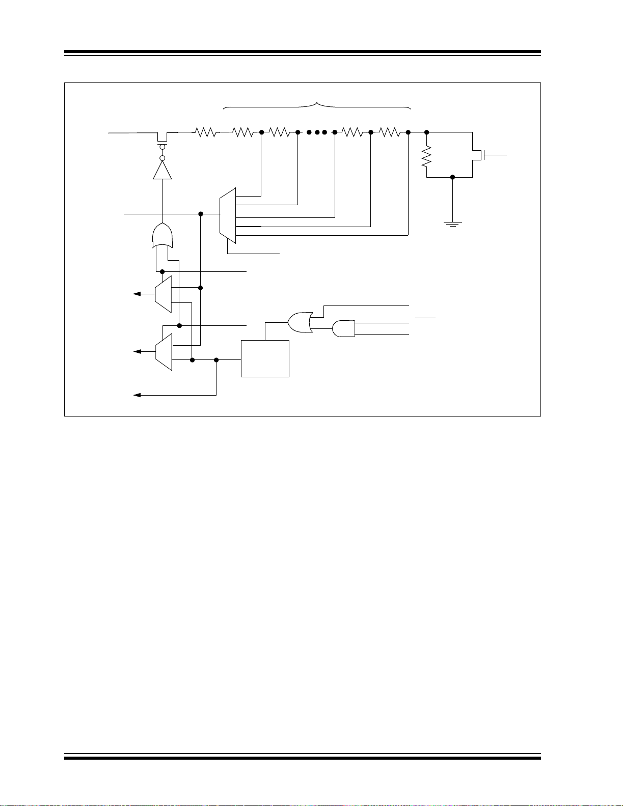
PIC16F685/687/689/690
FIGURE 8-5: COMPARATOR VOLTAGE REFERENCE BLOCK DIAGRAM
16 Stages
8RRR RR
VDD
C1V
REF to
Comparator 1
Input
C2VREF to
Comparator 2
Input
A/D Converter
Module
CVREF
8R
16-1 Analog
MUX
VR<3:0>
C1VREN
VRR
1
0
C2VREN
1
0.6V
0
EN
VP6
Reference
VP6EN
Sleep
HFINTOSC enable
DS41262A-page 90 Preliminary © 2005 Microchip Technology Inc.
PIC16F685/687/689/690
8.5 Comparator Response Time
Response time is the minimum time, after selecting a
new reference voltage or input source, before the
comparator output is ensured to have a valid level. If
the internal reference is changed, the maximum delay
of the internal voltage reference must be considered
when using the comparator outputs. Otherwise, the
maximum delay of the comparators should be used
(Table 17-8).
8.6 Operation During Sleep
The comparators and voltage reference, if enabled
before entering Sleep mode, remain active during Sleep.
This results in higher Sleep currents than shown in the
power-down specifications. The additional current
consumed by the comparator and the voltage reference
is shown separately in the specifications. To minimize
power consumption while in Sleep mode, turn off the
comparator, CMxCON0<7> = 0, and voltage reference,
VRCON<7:6>= 00.
While the comparator is enabled during Sleep, an
interrupt will wake-up the device. If the GIE bit
(INTCON<7>) is set, the device will jump to the interrupt
vector (0004h), and if clear , continues execution w ith the
next instruction. If the device wakes up from Sleep, the
contents of the CM1CON0, CM2CON0 and VRCON
registers are not affected.
8.7 Effects of a Reset
A device Reset forces the CM1CON0, CM2CON0 and
VRCON registers to their Reset states. This forces the
comparator module to be in the Comparator Reset
mode, CMxC O N0< 7 >= 0, and the volta ge refe rence to
its OFF state. Thus, all potential inputs are analog
TABLE 8-3: REGISTERS ASSOCIATED WITH COMPARATOR MODULE
Address Name Bit 7 Bit 6 Bit 5 Bit 4 Bit 3 Bit 2 Bit 1 Bit 0
05h, 105h PORTA
07h, 107h PORTC
0Bh/8Bh/
10Bh/18Bh
0Ch PIR1
8Ch PIE1
85h/185h TRISA
87h/187h TRISC
118h VRCON C1VREN C2VREN VRR VP6EN VR3 VR2 VR1 VR0 0000 0000 0000 0000
119h CM1CON0 C1ON C1OUT C1OE C1POL
11Ah CM2CON0 C2ON C2OUT C2OE C2POL
11Bh CM2CON1 MC1OUT MC2OUT
11Eh ANSEL ANS7 ANS6 ANS5 ANS4
19Eh SRCON SR1 SR0 C1SEN C2SEN PULSS PULSR
Legend: x = unknown, u = unchanged, – = unimplemented, read as ‘0’. Shaded cells are not used by the Capture, Compare or Timer1 module.
INTCON GIE PEIE
— — RA5 RA4 RA3 RA2 RA1 RA0 --xx xxxx --uu uuuu
RC7 RC6 RC5 RC4 RC3 RC2 RC1 RC0 xxxx xxxx uuuu uuuu
T0IE INTE RABIE T0IF INTF RABIF 0000 000x 0000 000x
— ADIF RCIF TXIF SSPIF CCP1IF TMR2IF TMR1IF -000 0000 -000 0000
— ADIE RCIE TXIE SSPIE CCP1IE TMR2IE TMR1IE -000 0000 -000 0000
— — TRISA5 TRISA4 TRISA3 TRISA2 TRISA1 TRISA0 --11 1111 --11 1111
TRISC7 TRISC6 TRISC5 TRISC4 TRISC3 TRISC2 TRISC1 TRISC0 1111 1111 1111 1111
— C1R C1CH1 C1CH0 0000 0000 0000 -000
— C2R C2CH1 C2CH0 0000 0000 0000 -000
— — — — T1GSS C2SYNC 00-- --10 00-- --10
ANS3 ANS2 ANS1 ANS0 1111 1111 1111 1111
— — 0000 00-- 0000 00--
Value on
POR, BOR
Value on
all other
Resets
© 2005 Microchip Technology Inc. Preliminary DS41262A-page 91

PIC16F685/687/689/690
NOTES:
DS41262A-page 92 Preliminary © 2005 Microchip Technology Inc.

9.0 ANALOG-TO-DIGITAL CONVERTER (A/D) MODULE
The analog-to-digital converter (A/D) allows conversion of
an analog input signal to a 10-bit binary representation of
that signal. The PIC16F685/687/689/690 has twelve
analog I/O inputs, plus two int ernal inputs, mult iplexed
into one sample and hold circuit. The output of the sample
and hold is connected to the inp ut of the converter. The
converter generates a binary result via successive
approximation and st ores the resulting or remai ning 10
bits of data into ADRESL (9Eh) and ADRESH (1Eh). The
voltage reference used in the conversion is software
selectable to either V
pin. Figure 9-1 shows the block diagram of the A/D on the
PIC16F685/687/689/690.
FIGURE 9-1: A/D BLOCK DIAGRAM
DD or a voltage applied by the VREF
VREF
PIC16F685/687/689/690
VDD
VCFG = 0
VCFG = 1
RA0/AN0/C1IN+/ICSPDAT/ULPWU
RA1/AN1/C12IN-/V
RA2/AN2/T0CKI/INT/C1OUT
RA4/AN3/T1G
RB4/AN10/SDI/SDA
Note 1: When ADON = 0 all input channels are disconnected from ADC (no loading).
2: P1C and P1D available on PIC16F685/PIC16F690 only.
3: SS, SDO, SDA, RX and DT available on PIC16F687/PIC16F689/PIC16F690 only.
REF/ICSPCLK
/OSC2/CLKOUT
RC0/AN4/C2IN+
RC1/AN5/C12IN1-
RC2/AN6/P1D
RC3/AN7/P1C
RC6/AN8/SS
RC7/AN9/SDO
RB5/AN11/RX/DT
CVREF
VP6 Reference
(2)
(2)
(3)
(3)
(3)
(3)
CHS<3:0>
0
13
GO/DONE
ADON
A/D
(1)
VSS
10
ADFM
10
ADRESH ADRESL
© 2005 Microchip Technology Inc. Preliminary DS41262A-page 93

PIC16F685/687/689/690
9.1 A/D Configuration and Operation
There are four registers available to control the
functionality of the A/D module:
1. ANSEL (Register 9-1)
2. ANSELH (Register 9-2)
3. ADCON0 (Register 9-3)
4. ADCON1 (Register 9-4)
9.1.1 ANALOG PORT PINS
The ANS<11:0> bits (ANSEL<7:0> and
ANSELH<3:0>) and the TRISA<4,2:0>, TRISB<5:4>
and TRISC<7:6,3:0>> bits control the operation of the
A/D port pins. Set the corresponding TRISx bits to ‘1’ to
set the pin output driver to its high-impedance state.
Likewise, set the correspo nding ANSx bit to disable the
digital input buffer.
Note: Analog voltages on any pin that is defined
as a digital input may cause the input
buffer to conduct excess current.
9.1.2 CHANNEL SELECTION
There are fourteen analog channels on
PIC16F685/687/689/690. The CHS<3:0> bits
(ADCON0<5:2>) control w hich channel is co nnected to
the sample and hold circuit.
9.1.3 VOLTAGE REFERENCE
There are two options for the voltage reference to the
A/D converter: either V
applied to V
REF is used. The VCFG bit (ADCON0<6>)
DD is used or an analog voltage
controls the volt age reference s election. If VC FG is set,
then the voltage on the VREF pin is the reference;
otherwise, V
DD is the reference.
9.1.4 CONVERSION CLOCK
The A/D conversion cycle requires 11 TAD. The source
of the conversion clock is software selectable via the
ADCS bits (ADCON1<6:4>). There are seven possible
clock options:
OSC/2
•F
•FOSC/4
•FOSC/8
•F
OSC/16
•FOSC/32
•FOSC/64
•F
RC (dedicated internal oscillator)
For correct conversion, the A/D conversion clock
(1/TAD) must be select ed to ensu re a minimu m TAD of
1.6 µs. Table 9-1 shows a few T
selected frequencies.
AD calculations for
TABLE 9-1: TAD VS. DEVICE OPERATING FREQUENCIES
A/D Clock Source (TAD) Device Frequency
Operation ADCS<2:0> 20 MHz 5 MHz 4 MHz 1.25 MHz
2 T
OSC 000 100 n s
OSC 100 200 n s
4 T
8 TOSC 001 400 ns
16 TOSC 101 800 ns
(2)
(2)
(2)
(2)
32 TOSC 010 1.6 μs6.4 μs 8.0 μs
64 TOSC 110 3.2 μs 12.8 μs
A/D RC x11 2-6 μs
(1,4)
Legend: Shaded cells are outside of recommended range.
Note 1: The A/D RC source has a typical T
AD time of 4 μs for VDD > 3.0V.
2: These values violate the minimum required TAD time.
3: For faster conversion times, the selection of another clock source is recommended.
4: When the device frequency is greater than 1 MHz, the A/D RC clock source is only recommended if the
conversion will be performed during Sleep.
400 ns
800 ns
(2)
(2)
500 ns
1.0 μs
(2)
(2)
1.6 μs2.0 μs6.4 μs
3.2 μs4.0 μs 12.8 μs
2-6 μs
(3)
(1,4)
16.0 μs
2-6 μs
(3)
(3)
(1,4)
25.6 μs
51.2 μs
2-6 μs
1.6 μs
3.2 μs
(3)
(3)
(3)
(1,4)
DS41262A-page 94 Preliminary © 2005 Microchip Technology Inc.

PIC16F685/687/689/690
9.1.5 STARTING A CONVERSION
The A/D conversion is initiated by setting the
GO/DONE
bit (ADCON0 <1> ). W hen th e co nvers ion is
complete, the A/D module:
• Clears the GO/DONE
bit
• Sets the ADIF flag (PIR1<6>)
• Generates an interrupt (if enabled)
If the conversion must be aborted, the GO/DONE
bit
can be cleared in software. The ADRESH:ADRESL
registers will not be u pdated with th e pa rtiall y comple te
FIGURE 9-2: A/D CONVERSION TAD CYCLES
TCY to TAD
Holding Capacitor is Disconnected from Analog Input (typically 100 ns)
Set GO/DONE bit
TAD1 TAD2
b9 b8 b7 b6 b5 b4 b3 b2
Conversion Starts
TAD3
TAD4
TAD5 TAD6 TAD7 TAD8
A/D conversion sample. Instead, the
ADRESH:ADRESL registers will retain the value of th e
previous conversion. After an aborted conversion, a
AD delay is required before another acquisition can
2T
be initiated. Following the delay, an input acquisition is
automatically started on the selected channel.
Note: The GO/DONE bit should not be set in the
same instruction that turns on the A/D.
TAD10 TAD11
TAD9
b1 b0
ADRESH and ADRESL registers are loaded,
GO bit is cleared,
ADIF bit is set,
Holding capacitor is connected to analog input
9.1.6 CONVERSION OUTPUT
The A/D conversion can be s upplied in two forma ts: left
or right justified. The ADFM bit (ADCON0<7>) controls
the output format. Figure9-3 shows the output formats .
FIGURE 9-3: 10-BIT A/D RESULT FORMAT
ADRESH ADRESL
(ADFM = 0)MSB LSB
bit 7 bit 0 bit 7 bit 0
10-bit A/D Result Unimplemented: Read as ‘0’
(ADFM = 1)
bit 7 bit 0 bit 7 bit 0
Unimplemented: Read as ‘0’ 10-bit A/D Result
MSB LSB
© 2005 Microchip Technology Inc. Preliminary DS41262A-page 95
PIC16F685/687/689/690
REGISTER 9-1: ANSEL – ANALOG SELECT REGISTER (ADDRESS: 11Eh)
R/W-1 R/W-1 R/W-1 R/W-1 R/W-1 R/W-1 R/W-1 R/W-1
ANS7 ANS6 ANS5 ANS4 ANS3 ANS2 ANS1 ANS0
bit 7 bit 0
bit 7-0 ANS<7:0>: Analog Select bits
Select between analog or digital function on pins AN<7:0>, respectively.
1 = Analog input. Pin is assigned as analog input.
0 = Digital I/O. Pin is assigned to port or special function.
Note 1: Setting a pin to an analog input automatically disables the digital input circuitry,
weak pull-ups, and interrupt-on-change if available. The corresponding TRIS bit
must be set to Input mod e in order to allow exte rnal control of the volt age on the pin.
Legend:
R = Readable bit W = Writable bit U = Unimplemented bit, read as ‘0’
- n = Value at POR ‘1’ = Bit is set ‘0’ = Bit is cleared x = Bit is unknown
(1)
REGISTER 9-2: ANSELH – ANALOG SELECT HIGH REGISTER (ADDRESS: 11Fh)
U-0 U-0 U-0 U-0 R/W-1 R/W-1 R/W-1 R/W-1
— — — — ANS1 1 ANS10 ANS9 ANS8
bit 7 bit 0
bit 7-4 Unimplemented: Read as ‘0’.
bit 3-0 ANS<11:8>: Analog Select bit s
Select between analog or digital function on pins AN<11:8>, respectively.
1 = Analog input. Pin is assigned as analog input.
0 = Digital I/O. Pin is assigned to port or special function.
Note 1: Setting a pin to an analog input automatically disables the digital input circuitry,
weak pull-ups, and interrupt-on-change if available. The corresponding TRIS bit
must be set to Input mod e in order to allow exte rnal control of the volt age on the pin.
Legend:
R = Readable bit W = Writable bit U = Unimplemented bit, read as ‘0’
- n = Value at POR ‘1’ = Bit is set ‘0’ = Bit is cleared x = Bit is unknown
(1)
TABLE 9-2: ANALOG SELECT CROSS REFERENCE
Analog
RB5 RB4 RC7 RC6 RC3 RC2 RC1 RC0 RA4 RA2 RA1 RA0
Select ANS11 ANS10 ANS9 ANS8 ANS7 ANS6 ANS5 ANS4 ANS3 ANS2 ANS1 ANS0
Channel AN11 AN10 AN9 AN8 AN7 AN6 AN5 AN4 AN3 AN2 AN1 AN0
I/O Pins
DS41262A-page 96 Preliminary © 2005 Microchip Technology Inc.

PIC16F685/687/689/690
REGISTER 9-3: ADCON0 – A/D CONTROL REGISTER (ADDRESS: 1Fh)
R/W-0 R/W-0 R/W-0 R/W-0 R/W-0 R/W-0 R/W-0 R/W-0
ADFM VCFG CHS3 CHS2 CHS1 CHS0 GO/DONE
bit 7 bit 0
bit 7 ADFM: A/D Result Formed Select bit
1 = Right justified
0 = Left justified
bit 6 VCFG: Voltage Reference bit
REF pin
1 = V
0 = V
DD
bit 5-2 CHS<3:0>: Analog Channel Select bits
0000 = Channel 00 (AN0)
0001 = Channel 01 (AN1)
0010 = Channel 02 (AN2)
0011 = Channel 03 (AN3)
0100 = Channel 04 (AN4)
0101 = Channel 05 (AN5)
0110 = Channel 06 (AN6)
0111 = Channel 07 (AN7)
1000 = Channel 08 (AN8)
1001 = Channel 09 (AN9)
1010 = Channel 10 (AN10)
1011 = Channel 11 (AN11)
1100 =CV
1101 =VP6
1110 = Reserved. Do not use.
1111 = Reserved. Do not use.
bit 1 GO/DONE
1 = A/D conversion cycle in progress. Setting this bit starts an A/D conversion cycle.
This bit is automatically cleared by hardware when the A/D conversion has completed.
0 = A/D conversion completed/not in progress
bit 0 ADON: A/D Enable bit
1 = A/D converter module is enabled
0 = A/D converter is shut off and consumes no operating current
REF
: A/D Conversion Status bit
ADON
Legend:
R = Readable bit W = Writable bit U = Unimplemented bit, read as ‘0’
- n = Value at POR ‘1’ = Bit is set ‘0’ = Bit is cleared x = Bit is unknown
© 2005 Microchip Technology Inc. Preliminary DS41262A-page 97

PIC16F685/687/689/690
REGISTER 9-4: ADCON1 – A/D CONTROL REGISTER 1 (ADDRESS: 9Fh)
U-0 R/W-0 R/W-0 R/W-0 U-0 U-0 U-0 U-0
— ADCS2 ADCS1 ADCS0 — — — —
bit 7 bit 0
bit 7 Unimplemented: Read as ‘0’
bit 6-4 ADCS<2:0>: A/D Conversion Clock Select bits
000 =F
001 =F
010 =F
x11 =F
100 =F
101 =F
110 =F
bit 3-0 Unimplemented: Read as ‘0’
Legend:
R = Readable bit W = Writable bit U = Unimplemented bit, read as ‘0’
- n = Value at POR ‘1’ = Bit is set ‘0’ = Bit is cleared x = Bit is unknown
OSC/2
OSC/8
OSC/32
RC (clock derived from a dedicated internal oscillator = 500 kHz max)
OSC/4
OSC/16
OSC/64
DS41262A-page 98 Preliminary © 2005 Microchip Technology Inc.
 Loading...