


PIC16F684
Data Sheet
14-Pin Flash-Based, 8-Bit
CMOS Microcontrollers with
nanoWatt Technology
2004 Microchip Technology Inc. Preliminary DS41202C

Note the following details of the code protection feature on Microchip devices:
• Microchip products meet the specification contained in their particular Microchip Data Sheet.
• Microchip believes that its family of products is one of the most secure families of its kind on the market today, when used in the
intended manner and under normal conditions.
• There are dishonest and possibly illegal methods used to breach the code protection feature. All of these methods, to our
knowledge, require using the Microchip products in a manner outside the operating specifications contained in Microchip’s Data
Sheets. Most likely, the person doing so is engaged in theft of intellectual property.
• Microchip is willing to work with the customer who is concerned about the integrity of their code.
• Neither Microchip nor any other semiconductor manufacturer can guarantee the security of their code. Code protection does not
mean that we are guaranteeing the product as “unbreakable.”
Code protection is constantly evolving. We at Microchip are committed to continuously improving the code protection features of our
products. Attempts to break Microchip’s code protection feature may be a violation of the Digit al Millennium Copyright Act. If suc h a c t s
allow unauthorized access to your software or other copyrighted work, you may have a right to sue for relief under that Act.
Information contained in this publication regarding device
applications and the like is intended through suggestion only
and may be superseded by updates. It is your responsibility to
ensure that your application meets with your specifications.
No representation or warranty is given and no liability is
assumed by Microchip Technology Incorporated with respect
to the accuracy or use of such information, or infringement of
patents or other intellectual property rights arising from such
use or otherwise. Use of Microchip’s products as critical
components in life support systems is not authorized except
with express written approval by Microchip. No licenses are
conveyed, implicitly or otherwise, under any intellectual
property rights.
Trademarks
The Microchip name and logo, the Microchip logo, Accuron,
dsPIC, K
EELOQ, microID, MPLAB, PIC, PICmicro, PICSTART,
PRO MATE, PowerSmart, rfPIC, and SmartShunt are
registered trademarks of Microchip Technology Incorporated
in the U.S.A. and other countries.
AmpLab, FilterLab, MXDEV, MXLAB, PICMASTER, SEEVAL,
SmartSensor and The Embedded Control Solutions Company
are registered trademarks of Microchip Technology
Incorporated in the U.S.A.
Analog-for-the-Digital Age, Application Maestro, dsPICDEM,
dsPICDEM.net, dsPICworks, ECAN, ECONOMONITOR,
FanSense, FlexROM, fuzzyLAB, In-Circuit Serial
Programming, ICSP, ICEPIC, Migratable Memory, MPASM,
MPLIB, MPLINK, MPSIM, PICkit, PICDEM, PICDEM.net,
PICLAB, PICtail, PowerCal, PowerInfo, PowerMate,
PowerTool, rfLAB, rfPICDEM, Select Mode, Smart Serial,
SmartTel and Tot al Endurance are trademarks of Microchip
Technology Incorporated in the U.S.A. and other countries.
SQTP is a service mark of Microchip Technology Incorporated
in the U.S.A.
All other trademarks mentioned herein are property of their
respective companies.
© 2004, Microchip Technology Incorporated, Printed in the
U.S.A., All Rights Reserved.
Printed on recycled paper.
Microchip received ISO/TS-16949:2002 quality system certification for
its worldwide headquarters, design and wafer fabrication facilities in
Chandler and Tempe, Arizona and Mountain View, California in
October 2003. The Company’s quality system processes and
procedures are for its PICmicro
devices, Serial EEPROMs, microperipherals, nonvolatile memory and
analog products. In addition, Microchip’s quality system for the design
and manufacture of development systems is ISO 9001:2000 certified.
®
8-bit MCUs, KEELOQ
®
code hopping
DS41202C-page ii Preliminary 2004 Microchip Technology Inc.

PIC16F684
14-Pin Flash-Based, 8-Bit CMOS Microcontrollers with nanoWatt Technology
High-Performance RISC CPU:
• Only 35 instructions to learn:
- All single-cycle instructions except branches
• Operating speed:
- DC – 20 MHz oscillator/clock input
- DC – 200 ns instruction cycle
• Interrupt capability
• 8-level deep hardware stack
• Direct, Indirect and Relative Addressing modes
Special Microcontroller Features:
• Precision Internal Oscillator:
- Factory calibrated to ±1%
- Software selectable frequency range of
8 MHz to 31 kHz
- Software tunable
- Two-speed Start-up mode
- Crystal fail detect for critical applications
- Clock mode switching during operation for
power savings
• Power-saving Sleep mode
• Wide operating voltage range (2.0V-5.5V)
• Industrial and Extended Temperature range
• Power-on Reset (POR)
• Power-up Timer (PWRT) and Oscillator Start-up
Timer (OST)
• Brown-out Detect (BOD) with software control
option
• Enhanced low-current Watchdog Timer (WDT)
with on-chip oscillator (software selectable
nominal 268 seconds with full prescaler) with
software enable
• Multiplexed Master Clear with pull-up/input pin
• Programmable code protection
• High Endurance Flash/EEPROM cell:
- 100,000 write Flash endurance
- 1,000,000 write EEPROM endurance
- Flash/Data EEPROM retention: > 40 years
Low-Power Features:
• Standby Current:
- 1 nA @ 2.0V, typical
• Operating Current:
-8.5µA @ 32 kHz, 2.0V, typical
-100µA @ 1 MHz, 2.0V , typical
• Watchdog Timer Current:
-1µA @ 2.0V, typical
Peripheral Features:
• 12 I/O pins with individual direction control:
- High current source/sink for direct LED drive
- Interrupt-on-pin change
- Individually programmable weak pull-ups
- Ultra Low-power Wake-up (ULPWU)
• Analog comparator module with:
- Two analog comparators
- Programmable on-chip voltage reference
(CVREF) module (% of VDD)
- Comparator inputs and outputs externally
accessible
• A/D Converter:
- 10-bit resolution and 8 channels
• Timer0: 8-bit timer/counter with 8-bit
programmable prescaler
• Enhanced Timer1:
- 16-bit timer/counter with prescaler
- External Gate Input mode
- Option to use OSC1 and OSC2 in LP mode
as Timer1 oscillator if INTOSC mode
selected
• Timer2: 8-bit timer/counter with 8-bit period
register, prescaler and postscaler
• Enhanced Capture, Compare, PWM module:
- 16-bit Capture, max resolution 12.5 ns
- Compare, max resolution 200 ns
- 10-bit PWM with 1, 2 or 4 output channels,
programmable “dead time”, max frequency
20 kHz
• In-Circuit Serial Programming
pins
TM
(ICSPTM) via two
Program
Device
PIC16F684 2048 128 256 12 8 2 2/1
2004 Microchip Technology Inc. Preliminary DS41202C-page 1
Memory
Flash
(words)
Data Memory
SRAM
(bytes)
EEPROM
(bytes)
I/O
10-bit A/D
(ch)
Comparators
Timers
8/16-bit
PIC16F684
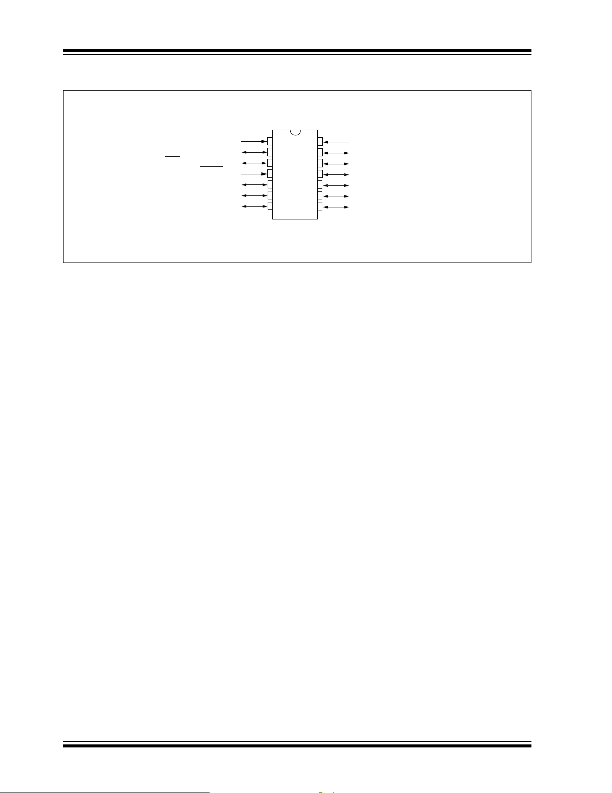
Pin Diagram
14-pin PDIP, SOIC, TSSOP
RA5/T1CKI/OSC1/CLKIN
RA4/AN3/T1G
/OSC2/CLKOUT
RA3/MCLR
RC5/CCP1/P1A
RC4/C2OUT/P1B
RC3/AN7/P1C
VDD
/VPP
1
2
3
4
5
6
7
PIC16F684
14
13
12
11
10
9
8
VSS
RA0/AN0/C1IN+/ICSPDAT/ULPWU
RA1/AN1/C1IN-/V
RA2/AN2/T0CKI/INT/C1OUT
RC0/AN4/C2IN+
RC1/AN5/C2INRC2/AN6/P1D
REF/ICSPCLK
DS41202C-page 2 Preliminary 2004 Microchip Technology Inc.

PIC16F684
Table of Contents
1.0 Device Overview......................................................................................................................................................................... 5
2.0 Memory Organization.................................................................................................................................................................. 7
3.0 Clock Sources........................................................................................................................................................................... 19
4.0 I/O Ports................................................. ................................................. .................................................................................. 31
5.0 Timer0 Module .......................................................................................................................................................................... 45
6.0 Timer1 Module with Gate Control.............................................................................................................................................. 49
7.0 Timer2 Module .......................................................................................................................................................................... 53
8.0 Comparator Module................................................................................................................................................................... 55
9.0 Analog-to-Digital Converter (A/D) Module................................................................................................................................. 63
10.0 Data EEPROM Memory.................................................. ................. ................. ........................................................................ 71
11.0 Enhanced Capture/Compare/PWM (ECCP) Module................................................................................................................. 75
12.0 Special Features of the CPU........................................... ................. ................. ................. ....................................................... 91
13.0 Instruction Set Summary......................................................................................................................................................... 111
14.0 Development Support.............................................................................................................................................................. 121
15.0 Electrical Specifications........................................................................................................................................................... 127
16.0 DC and AC Characteristics Graphs and Tables........................................................................... ........................................... 147
17.0 Packaging Information. ................. ................. ................ ................. ................. ........................................................................ 149
Appendix A: Data Sheet Revision History......................................................................................................................................... 153
Appendix B: Migrating from other PICmicro® Devices ..................................................................................................................... 153
Index ................................................................................................................................................................................................. 155
On-Line Support................................................................................................................................................................................ 159
Systems Information and Upgrade Hot Line..................................................................................................................................... 159
Reader Response............................................................................................................................................................................. 160
Product Identification System ........................................................................................................................................................... 161
TO OUR VALUED CUSTOMERS
It is our intention to provide our valued customers with the best documentation possible to ensure successful use of your Microchip
products. To this end, we will continue to improve our publications to better suit your needs. Our publications will be refined and
enhanced as new volumes and updates are introduced.
If you have any questions or c omm ents regarding t his publication, p lease c ontact the M arket ing Co mmunications Department via
E-mail at docerrors@mail.microchip.com or fax the Reader Response Form in the back of this data sheet to (480) 792-4150.
We welcome your feedback.
Most Current Data Sheet
To obtain the most up-to-date version of this data sheet, please register at our Worldwide Web site at:
http://www.microchip.com
You can determine the version of a data sheet by examining its literature number found on the bottom outside corner of any page.
The last character of the literature number is the version number, (e.g., DS30000A is version A of document DS30000).
Errata
An errata sheet, describing minor operational differences from the data sheet and recommended workarounds, may exist for current
devices. As device/documentation issues become known to us, we will publish an errata sheet. The errata will specify the revision
of silicon and revision of document to which it applies.
To determine if an errata sheet exists for a particular device, please check with one of the following:
• Microchip’s Worldwide Web site; http://www.microchip.com
• Your local Microchip sales office (see last page)
• The Microchip Corporate Literature Center; U.S. FAX: (480) 792-7277
When contacting a sales office or the literature center, please specify which device, revision of silicon and data sheet (include
literature number) you are using.
Customer Notification System
Register on our web site at www.microchip.com/cn to receive the most current information on all of our products.
2004 Microchip Technology Inc. Preliminary DS41202C-page 3

PIC16F684
NOTES:
DS41202C-page 4 Preliminary 2004 Microchip Technology Inc.
PIC16F684
1.0 DEVICE OVERVIEW
This documen t conta i ns dev ic e spec if i c in for m at i on fo r
the PIC16F684. Addition al informa tion may b e found in
the “PICmicro® Mid-Range MCU Family Reference
Manual” (DS33023), which may be obtained from your
local Microchip Sales Representative or downloaded
from the Microchip web site.
FIGURE 1-1: PIC16F684 BLOCK DIAGRAM
INT
Program Counter
8-Level Stack 128 Bytes
(13-Bit)
Addr
Direct
Power-up
Timer
Oscillator
Start-up Timer
Power-on
Reset
Watchdog
Timer
Brown-out
Detect
VDD
MCLR
VSS
OSC1/CLKIN
OSC2/CLKOUT
T1G
Program
Bus
Internal
Oscillator
Block
Configuration
Flash
2k X 14
Program
Memory
14
Instruction Reg
Instruction
Decode &
Control
Timing
Generation
13
8
The reference manual shou ld be cons ider ed a com plementary document to this data sheet and is highly
recommended reading for a better unders tanding of the
device architecture and operation of the peripheral
modules.
The PIC16F684 is covered by this data sheet. It is
available in 14-pin PDIP, SOIC and TSSOP packages.
Figure 1-1 shows a block diagram of the PIC16F684
device. Table 1-1 shows the pinout description.
RAM Addr
7
Data Bus
Registers
3
8
CCP1/P1A
RAM
File
9
Addr MUX
8
FSR Reg
Status Reg
MUX
ALU
W Reg
P1B P1C P1D
Indirect
Addr
8
PORTA
PORTC
RA0
RA1
RA2
RA3
RA4
RA5
RC0
RC1
RC2
RC3
RC4
RC5
T1CKI
T0CKI
VREF
2004 Microchip Technology Inc. Preliminary DS41202C-page 5
AN0 AN1 AN2 AN3
Timer0 Timer1
Analog-To-Digital Converter
AN4 AN5 AN6 AN7
C1IN- C1IN+ C1OUT
Timer2
2 Analog Comparators
and Reference
C2IN- C2IN+ C2OUT
ECCP
EEDATA
256 Bytes
8
EEPROM
EEADDR
Data

PIC16F684
TABLE 1-1: PIC16F684 PINOUT DESCRIPTION
Name Function
RA0/AN0/C1IN+/ICSPDAT/ULPWU RA0 TTL CMOS PORTA I/O w/programmable pull-up and interrupt-on-change
AN0 AN — A/D Channel 0 input
C1IN+ AN — Comparator 1 input
ICSPDAT TTL CMOS Serial Program ming Da ta I/O
ULPWU AN — Ultra Low-power Wake-up input
RA1/AN1/C1IN-/V
RA2/AN2/T0CKI/INT/C1OUT RA2 ST CMOS PORTA I/O w/programmable pull-up and interrupt-on-change
RA3/MCLR
RA4/AN3/T1G
RA5/T1CKI/OSC1/CLKIN RA5 TTL CMOS PORTA I/O w/programmable pull-up and interrupt-on-change
RC0/AN4/C2IN+ RC0 TTL CMOS PORTC I/O
RC1/AN5/C2IN- RC1 TTL CMOS PORTC I/O
RC2/AN6/P1D RC2 TTL CMOS PORTC I/O
RC3/AN7/P1C RC3 TTL CMOS PORTC I/O
RC4/C2OUT/P1B RC4 TTL CMOS PORTC I/O
RC5/CCP1/P1A RC5 TTL CMOS PORTC I/O
SS VSS Power — Ground reference
V
DD VDD Power — Positive supply
V
Legend: TTL = TTL input buffer, ST = Schmitt Trigger input buffer, AN = Analog input
REF/ICSPCLK RA1 TTL CMOS PORTA I/O w/programmable pull-up and interrupt-on-change
AN1 AN — A/D Channel 1 input
C1IN- AN — Comparator 1 input
REF AN — External Voltage Reference for A/D
V
ICSPCLK ST — Serial Programming Clock
AN2 AN — A/D Channel 2 input
T0CKI ST — Timer0 clock input
INT ST — External Interru p t
C1OUT — CMOS Comparator 1 output
/VPP RA3 TTL — PORTA input with interrupt-on-change
MCLR
PP HV — Programming voltage
V
/OSC2/CLKOUT RA4 TTL CMOS PORTA I/O w/programmable pull-up and interrupt-on-change
AN3 AN — A/D Channel 3 input
T1G
OSC2 — XTAL Crystal/Resonator
CLKOUT — CMOS F
T1CKI ST — Timer1 clock
OSC1 XTAL — Crystal/Resonator
CLKIN ST — Ex tern al clock input/RC oscillator connection
AN4 AN — A/D Channel 4 input
C2IN+ AN — Comparator 2 input
AN5 AN — A/D Channel 5 input
C2IN- AN — Comparator 2 input
AN6 AN — A/D Channel 6 input
P1D — CMOS PWM output
AN7 AN — A/D Channel 7 input
P1C — CMOS PWM output
C2OUT — CMOS Comparator 2 output
P1B — CMOS PWM output
CCP1 ST CMOS Capture input/Compare output
P1A — CMOS PWM output
Input
Type
Output
Type
ST — Master Clear w/internal pull-up
ST — Timer1 gate
OSC/4 output
Description
DS41202C-page 6 Preliminary 2004 Microchip Technology Inc.
PIC16F684
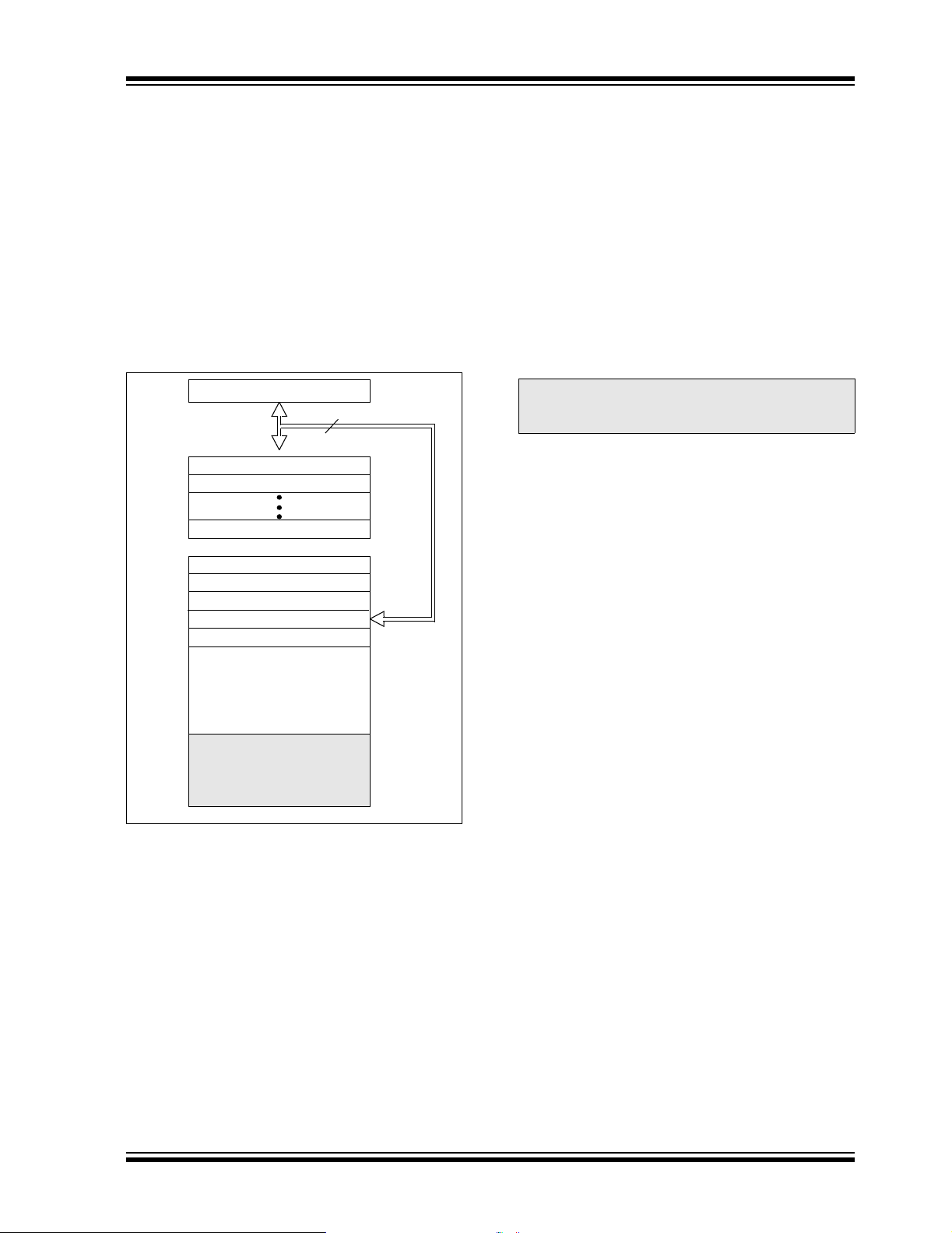
2.0 MEMORY ORGANIZATION
2.1 Program Memory Organization
The PIC16F684 has a 13-bit program counter capable
of addressing an 8k x 14 pr ogram mem ory spac e. Only
the first 2k x 14 (0000h-07FFh) for the PIC16F684 is
physically implemented. Accessing a location above
these boundaries will cause a wrap around within the
first 2k x 14 space. The Reset vector is at 0000h and
the interrupt vector is at 0004h (see Figure 2-1).
FIGURE 2-1: PROGRAM MEMORY MAP
AND STACK FOR THE
PIC16F684
PC<12:0>
CALL, RETURN
RETFIE, RETLW
Stack Level 1
Stack Level 2
Stack Level 8
Reset Vector
13
000h
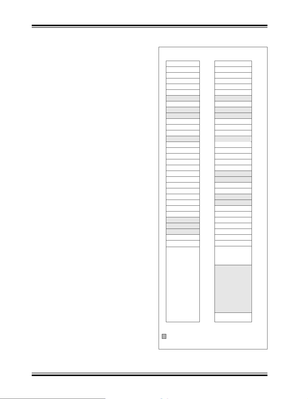
2.2 Data Memory Organization
The data memory (see Figure 2-2) is partitioned into
two banks, which contain the General Purpose Registers (GPR) and the Special Function Registers (SFR).
The Special Function Registers are located in the first
32 locations of each bank. Register locations 20h-7Fh
in Bank 0 and A0h-BFh in Bank 1 are General Purpose
Registers, implemented as static RAM. Register
locations F0h-FFh in Bank 1 point to addresses
70h-7Fh in Bank 0. All other RAM is unimplemented
and returns ‘0’ when re ad. RP0 (Status<5>) is t he bank
select bit.
RP0 = 0: → Bank 0 is selected
RP0 = 1: → Bank 1 is selected
Note: The IRP and RP1 bits Status<7:6> are
reserved and should always be
maintained as ‘0’s.
Interrupt Vector
On-chip Program
Memory
0004
0005
07FFh
0800h
1FFFh
2004 Microchip Technology Inc. Preliminary DS41202C-page 7
PIC16F684
2.2.1 GENERAL PURPOSE REGISTER
FILE
The register file is organized as 128 x 8 in the
PIC16F684. Each register is accessed, either directly
or indirectly, through the File Select Register (FSR)
(see Section 2.4 “Indirect Addressing, INDF and
FSR Registers”).
2.2.2 SPECIAL FUNCTION REGISTERS
The Special Function Registers are registers used by
the CPU and peripheral functions for controlling the
desired operation of the device (see Table 2-1). These
registers are static RAM.
The special re gisters can be classifi ed into two sets:
core and peripheral. The Special Function Registers
associated with the “c ore” are des cribed in this sect ion.
Those related to the operation of the peripheral
features are described in the section of that peripheral
feature.
FIGURE 2-2: DATA MEMORY MAP OF
THE PIC16F684
File
Address
TMR0
PCL
FSR
PIR1
TMR2
(1)
00h
01h
02h
03h
04h
05h
06h
07h
08h
09h
0Ah
0Bh
0Ch
0Dh
0Eh
0Fh
10h
11h
12h
13h
14h
15h
16h
17h
18h
19h
1Ah
1Bh
1Ch
1Dh
1Eh
1Fh
20h
Indirect Addr.
OPTION_REG
STATUS
TRISA
PCLATH
INTCON
PCON
OSCCON
OSCTUNE
ANSEL
PR2
WPUA
EEDAT
EEADR
EECON1
EECON2
ADRESL
ADCON1
General
Purpose
Registers
32 Bytes
Indirect Addr.
STATUS
PORTA
PORTC
PCLATH
INTCON
TMR1L
TMR1H
T1CON
T2CON
CCPR1L
CCPR1H
CCP1CON
PWM1CON
ECCPAS
WDTCON
CMCON0 VRCON
CMCON1
ADRESH
ADCON0
General
Purpose
Registers
96 Bytes
PCL
FSR
TRISC
PIE1
IOCA
File
Address
(1)
80h
81h
82h
83h
84h
85h
86h
87h
88h
89h
8Ah
8Bh
8Ch
8Dh
8Eh
8Fh
90h
91h
92h
93h
94h
95h
96h
97h
98h
99h
9Ah
9Bh
9Ch
(1)
9Dh
9Eh
9Fh
A0h
BFh
F0h
FFh
BANK 0
ACCESSES 70h-7Fh
7Fh
BANK 1
Unimplemented data memory locations, read as ‘0’.
Note 1: Not a physical register.
DS41202C-page 8 Preliminary 2004 Microchip Technology Inc.
PIC16F684
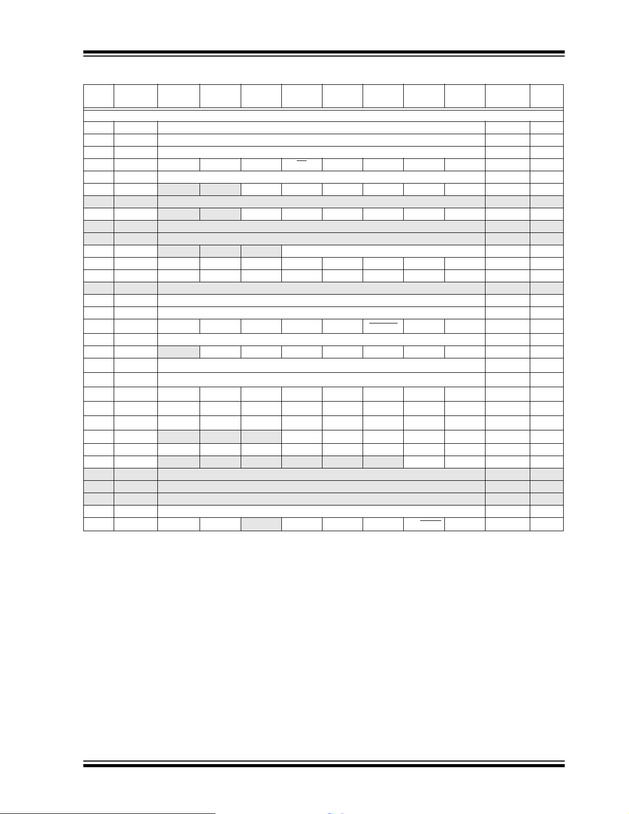
TABLE 2-1: PIC16F684 SPECIAL REGISTERS SUMMARY BANK 0
Addr Name Bit 7 Bit 6 Bit 5 Bit 4 Bit 3 Bit 2 Bit 1 Bit 0
Bank 0
00h INDF Addressing this location uses contents of FSR to address data memory (not a physical register) xxxx xxxx 17, 99
01h TMR0 Timer0 Module’s register xxxx xxxx 45, 99
02h PCL Program Counter’s (PC) Least Significant Byte 0000 0000 17, 99
03h STATUS IRP
04h FSR Indirect Data Memory Address Pointer xxxx xxxx 17, 99
05h PORTA
06h — Unimplemented — —
07h PORTC
08h — Unimplemented — —
09h — Unimplemented — —
0Ah PCLATH
0Bh INTCON GIE PEIE T0IE INTE RAIE T0IF INTF RAIF 0000 0000 13, 99
0Ch PIR1
0Dh — Unimplemented — —
0Eh TMR1L Holding Register for the Least Significant Byte of the 16-bit TMR1 xxxx xxxx 49, 99
0Fh TMR1H Holding Register for the Most Significant Byte of the 16-bit TMR1 xxxx xxxx 49, 99
10h T 1CON T1GINV TMR1GE T1CKPS1 T1CKPS0 T1OSCEN T1SYNC
11h
TMR2 Timer2 Module register 0000 0000 53, 99
12h
T2CON — TOUTPS3 TOUTPS2 TOUTPS1 TOUTPS0 TMR2ON T2CKPS1 T2CKPS0 -000 0000 53, 99
13h
CCPR1L Capture/Compare/PWM Register 1 Low Byte
14h
CCPR1H Capture/Compare/PWM Register 1 High Byte
15h
CCP1CON P1M1 P1M0 DC1B1 DC1B0 CCP1M3 CCP1M2 CCP1M1 CCP1M0
16h
PWM1CON PRSEN PDC6 PDC5 PDC4 PDC3 PDC2 PDC1 PDC0
17h
ECCPAS ECCPASE ECCPAS2 ECCPAS1 ECCPAS0 PSSAC1 PSSAC0 PSSBD1 PSSBD0
18h WDTCON
19h CMCON0 C2OUT C1OUT
1Ah CMCON1
1Bh — Unimplemented — —
1Ch — Unimplemented — —
1Dh — Unimplemented — —
1Eh ADRESH Most Significant 8 bits of the left shifted A/D result or 2 bits of right shifted result xxxx xxxx 65, 99
1Fh ADCON0 ADFM VCFG
(1)
— — RA5 RA4 RA3 RA2 RA1 RA0 --xx xxxx 31, 99
— — RC5 RC4 RC3 RC2 RC1 RC0 --xx xxxx 40, 99
— — — Write Buffer for upper 5 bits of Program Counter ---0 0000 17, 99
EEIF ADIF CCP1IF C2IF C1IF OSFIF TMR2IF TMR1IF 0000 0000 15, 99
— — —
— — — — — — T1GSS C2SYNC ---- --10 59, 99
RP1
(1)
RP0 TO PD Z DC C 0001 1xxx 11, 99
TMR1CS TMR1ON
WDTPS3 WDTPS2 WDTPS1 WDTPS0 SWDTEN ---0 1000 106, 99
C2INV C1INV CIS CM2 CM1 CM0 0000 0000 55, 99
— CHS2 CHS1 CHS0 GO/DONE ADON
Legend: — = Unimplemented locations read as ‘0’, u = unchanged, x = unknown, q = value depends on condition, shaded =
unimplemented
Note 1: IRP and RP1 bits are reserved, always maintain these bits clear.
Value on
POR, BOD
0000 0000 51, 99
XXXX XXXX 75, 99
XXXX XXXX 75, 99
0000 0000 75, 99
0000 0000 85, 99
0000 0000 86, 99
00-0 0000 66, 99
Page
2004 Microchip Technology Inc. Preliminary DS41202C-page 9
PIC16F684
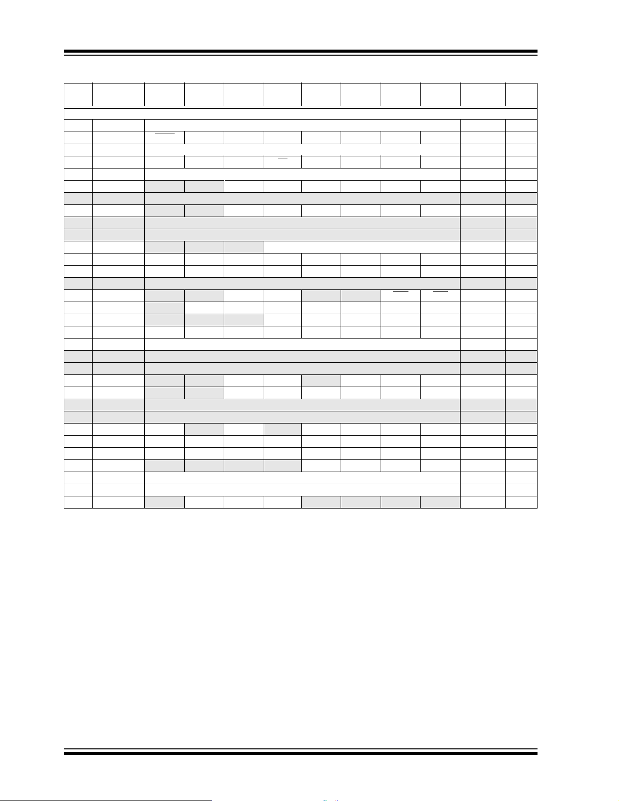
TABLE 2-2: PIC16F684 SPECIAL FUNCTION REGISTERS SUMMARY BANK 1
Addr Name Bit 7 Bit 6 Bit 5 Bit 4 Bit 3 Bit 2 Bit 1 Bit 0
Bank 1
80h INDF Addressing this location uses contents of FSR to address data memory (not a physical register) xxxx xxxx 17, 99
81h OPTION_REG RAPU
82h PCL Program Counter’s (PC) Least Significant Byte 0000 0000 17, 99
83h STATUS IRP
84h FSR Indirect Data Memory Address Pointer xxxx xxxx 17, 99
85h TRISA
86h — Unimplemented — —
87h TRISC
88h — Unimplemented — —
89h — Unimplemented — —
8Ah PCLATH
8Bh INTCON GIE PEIE T0IE INTE RAIE T0IF INTF RAIF 0000 0000 13, 99
8Ch PIE1 EEIE ADIE CCP1IE C2IE C1IE OSFIE TMR2IE TMR1IE 0000 0000 14, 99
8Dh — Unimplemented — —
8Eh PCON
8Fh OSCCON
90h OSCTUNE
91h ANSEL ANS7 ANS6 ANS5 ANS4 ANS3 ANS2 ANS1 ANS0 1111 1111 65, 99
92h PR2 Timer2 Module P erio d Re gis te r 1111 1111 53, 99
93h — Unimplemented — —
94h — Unimplemented — —
95h WPUA
96h IOCA
97h — Unimplemented — —
98h — Unimplemented — —
99h VRCON VREN
9Ah EEDAT EEDAT7 EEDAT6 EEDAT5 EEDAT4 EEDAT3 EEDAT2 EEDAT1 EEDAT0 0000 0000 71, 100
9Bh EEADR EEADR7 EEADR6 EEADR5 EEADR4 EEADR3 EEADR2 EEADR1 EEADR0 0000 0000 71, 100
9Ch EECON1
9Dh EECON2 EEPROM Control Register 2 (not a physical register) ---- ---- 72, 100
9Eh ADRESL Least Significant 2 bits of the left shifted result or 8 bits of the right shifted result xxxx xxxx 65, 100
9Fh ADCON1
Legend: — = Unimplemented locations read as ‘0’, u = unchanged, x = unknown, q = value depends on condition, shaded = unimplemented
Note 1: IRP and RP1 bits are reserved, always maintain these bits clear.
(3)
2: OSTS bit OSCCON <3> reset to ‘0’ with Dual Speed Start-up and LP, HS or XT selected as the oscillator.
3: RA3 pull-up is enabled when MCLRE is ‘1’ in the Configuration Word register.
— — TRISA5 TRISA4 TRISA3 TRISA2 TRISA1 TRISA0 --11 1111 32, 99
— — TRISC5 TRISC4 TRISC3 TRISC2 TRISC1 TRISC0 --11 1111 43, 99
— — — Write Buffer for upper 5 bits of Program Counter ---0 0000 17, 99
— — ULPWUE SBODEN — —PORBOD --01 --qq 16, 99
— IRCF2 IRCF1 IRCF0 OSTS
— — — TUN4 TUN3 T UN2 TUN1 TUN0 ---0 0000 23, 99
— — WPUA5 WPUA4 — WPUA2 WPUA1 WPUA0 --11 -111 32, 100
— — IOCA5 IOCA4 IOCA3 IOCA2 IOCA1 IOCA0 --00 0000 33, 100
— — — — WRERR WREN WR RD ---- x000 72, 100
— ADCS2 ADCS1 ADCS0 — — — — -000 ---- 66, 100
INTEDG T0CS T0SE PSA PS2 PS1 PS0 1111 1111 12, 99
(1)
(1)
RP1
—VRR— VR3 VR2 VR1 VR0 0-0- 0000 62, 100
RP0 TO PD Z DC C 0001 1xxx 11, 99
(2)
HTS LTS SCS -110 x000 29, 99
Value on
POR, BOD
Page
DS41202C-page 10 Preliminary 2004 Microchip Technology Inc.

PIC16F684
2.2.2.1 Status Register
The Status register, shown in Register2-1, contains:
• the arithmetic status of the ALU
• the Reset status
• the bank select bits for data memory (SRAM)
The Status register can be the destination for any
instruction, like any other register. If the Status register
is the destination for an instruction that affects the Z,
DC or C bits, then the write to these three bits is disabled. These bits are set or cleared according to the
device logic. Furthermore, the TO
writable. Therefore, the result of an instruction with the
Status register as destination may be different than
intended.
and PD bits are not
For example, CLRF STATUS, will c lea r the up per three
bits and set the Z bit. Thi s leav es the Status register a s
‘000u u1uu’ (where u = unchanged).
It is recommended, therefore, that only BCF, BSF,
SWAPF and MOVWF instructions are used to alter the
Stat us register , beca use these instru ctions do not af fect
any Status bits. For other instructions not affecting any
Status bits, see the “Instruction Set Summary”.
Note 1: Bits IRP and RP1 (Status<7:6>) are not
used by the PIC16F684 and should be
maintained as clear. Use of these bits is
not recommended, since this may affect
upward compatibility with future products.
2: The C and DC bits operate as a Borrow
and Digit Borrow out bit, respectively, in
subtraction. See the SUBLW and SUBWF
instructions for examples.
REGISTER 2-1: STATUS – STATUS REGISTER (ADDRESS: 03h OR 83h)
Reserved Reserved R/W-0 R-1 R-1 R/W-x R/W-x R/W-x
IRP RP1 RP0 TO PD Z DC C
bit 7 bit 0
bit 7 IRP: This bit is reserved and should be maintained as ‘0’
bit 6 RP1: This bit is reserved and should be maintained as ‘0’
bit 5 RP0: Register Bank Select bit (used for direct addressing)
1 = Bank 1 (80h – FFh)
0 = Bank 0 (00h – 7Fh)
bit 4 TO
bit 3 PD: Power-down bit
bit 2 Z: Zero bit
bit 1 DC: Digit carry/borrow bit (ADDWF, ADDLW,SUBLW,SUBWF instructions)
bit 0 C: Carry/borrow bit (ADDWF, ADDLW, SUBLW, SUBWF instructions)
: Time-out bit
1 = After power-up, CLRWDT instruction or SLEEP instruction
0 = A WDT time-out occurred
1 = After power-up or by the CLRWDT instruction
0 = By execution of the SLEEP instruction
1 = The result of an arithmetic or logic operation is zero
0 = The result of an arithmetic or logic operation is not zero
For borrow ,
1 = A carry-out from the 4th low-order bit of the result occurred
0 = No carry-out from the 4th low-order bit of the result
1 = A carry-out from the Most Significant bit of the result occurred
0 = No carry-out from the Most Significant bit of the result occurred
the polarity is reversed.
Note 1: For borrow,
complement of the second operand. For rotate (RRF, RLF) instructions, this bit is
loaded with either the high-order or low-order bit of the source register.
Legend:
R = Readable bit W = Writable bit U = Unimplemented bit, read as ‘0’
-n = Value at POR ‘1’ = Bit is set ‘0’ = Bit is cleared x = Bit is unknown
2004 Microchip Technology Inc. Preliminary DS41202C-page 11
the polarity is reversed. A subtraction is executed by adding the two’s

PIC16F684
2.2.2.2 Option Register
The Option register is a readable and writable register,
which contains various control bits to configure:
• TMR0/WDT prescaler
• External RA2/INT interrupt
•TMR0
• Weak pull-ups on PORTA
REGISTER 2-2: OPTION_REG – OPTION REGISTER (ADDRESS: 81h)
R/W-1 R/W-1 R/W-1 R/W-1 R/W-1 R/W-1 R/W-1 R/W-1
RAPU INTEDG T0CS T0SE PSA PS2 PS1 PS0
bit 7 bit 0
Note: To achieve a 1:1 prescaler assignment for
TMR0, assign the prescaler to the WDT by
setting PSA bit to ‘1’ (OPTION_REG<3>).
See Section 5.4 “Prescaler”.
bit 7 RAPU
: PORTA Pull-up Enable bit
1 = PORTA pull-ups are disabled
0 = PORTA pull-ups are enabled by individual port latch values
bit 6 INTEDG: Interrupt Edge Select bit
1 = Interrupt on rising edge of RA2/INT pin
0 = Interrupt on falling edge of RA2/INT pin
bit 5 T0CS: TMR0 Clock Source Sele ct bit
1 = Transition on RA 2/T0CKI pin
0 = Internal instruction cycle clock (CLKOUT)
bit 4 T0SE: TMR0 Source Edge Select bit
1 = Increment on high-to-low transition on RA2/T0CKI pin
0 = Increment on low-to-high transition on RA2/T0CKI pin
bit 3 PSA: Prescaler Assignment bit
1 = Prescaler is assigned to the WDT
0 = Prescaler is assigned to the Timer0 module
bit 2-0 PS<2:0>: Prescaler Rate Select bits
BIT VALUE TMR0 RATE WDT RAT E
000
001
010
011
100
101
110
111
1 : 2
1 : 4
1 : 8
1 : 16
1 : 32
1 : 64
1 : 128
1 : 256
1 : 1
1 : 2
1 : 4
1 : 8
1 : 16
1 : 32
1 : 64
1 : 128
Legend:
R = Readable bit W = Writable bit U = Unimplemented bit, read as ‘0’
-n = Value at POR ‘1’ = Bit is set ‘0’ = Bit is cleared x = Bit is unknown
DS41202C-page 12 Preliminary 2004 Microchip Technology Inc.

PIC16F684
2.2.2.3 INTCON Register
The INTCON register is a readable and writable
register , which c ontains the various en able and fl ag bit s
for TMR0 register overflow, PORTA change and
external RA2/INT pin interrupts.
Note: Interrupt flag bits are set when an interr upt
condition occurs, regard less of the st ate of
its corresponding enable bit or the global
enable bit, GIE (INTCON<7>). User
software should ensure the appropriate
interrupt flag bits are clear prior to
enabling an interrupt.
REGISTER 2-3: INTCON – INTERRUPT CONTROL REGISTER (ADDRESS: 0Bh OR 8Bh)
R/W-0 R/W-0 R/W-0 R/W-0 R/W-0 R/W-0 R/W-0 R/W-0
GIE PEIE T0IE INTE RAIE T0IF INTF RAIF
bit 7 bit 0
bit 7 GIE: Global Interrupt Enable bit
1 = Enables all unmasked interrupts
0 = Disables all interru pts
bit 6 PEIE: Peripheral Interrupt Enable bit
1 = Enables all unmasked peripheral interrupts
0 = Disables all peripheral interrupts
bit 5 T0IE: TMR0 Overflow Interrupt Enable bit
1 = Enables the TMR0 interrupt
0 = Disables the TMR0 interrupt
bit 4 INTE: RA2/INT External Interrupt Enable bit
1 = Enables the RA2/INT external interrupt
0 = Disables the RA2/INT external interrupt
bit 3 RAIE: PORTA Change Interrupt Enable bit
1 = Enables the PORTA change interrupt
0 = Disables the PORTA change interrupt
bit 2 T0IF: TMR0 Overflow Interrupt Flag bit
1 = TMR0 regis ter has overflowed (must be cleared in software)
0 = TMR0 register did not overflow
bit 1 INTF: RA2/INT External Interrupt Flag bit
1 = The RA2/INT external interrupt occurred (must be cleared in software)
0 = The RA2/INT external interrupt did not occur
bit 0 RAIF: PORTA Change Interrupt Flag bit
1 = When at least one of the PORTA <5:0> pins changed state (must be cleared in software)
0 = None of the PORTA <5:0> pins have changed state
(1)
(2)
Note 1: IOCA register must also be enabled.
2: T0IF bit is set when Timer0 rolls over. Timer0 is unchanged on Reset and should
be initialized before clearing T0IF bit.
Legend:
R = Readable bit W = Writable bit U = Unimplemented bit, read as ‘0’
-n = Value at POR ‘1’ = Bit is set ‘0’ = Bit is cleared x = Bit is unknown
2004 Microchip Technology Inc. Preliminary DS41202C-page 13

PIC16F684
2.2.2.4 PIE1 Register
The PIE1 register contai ns th e in terru pt enable bits, as
shown in Register 2-4.
REGISTER 2-4: PIE1 – PERIPHERAL INTERRUPT ENABLE REGISTER 1 (ADDRESS: 8Ch)
R/W-0 R/W-0 R/W-0 R/W-0 R/W-0 R/W-0 R/W-0 R/W-0
EEIE ADIE CCP1IE C2IE C1IE OSFIE TMR2IE TMR1IE
bit 7 bit 0
bit 7 EEIE: EE Write Complete Interrupt Enable bit
1 = Enables the EE write complete interrupt
0 = Disables the EE write complete interrupt
bit 6 ADIE: A/D Converter Interrupt Enable bit
1 = Enables the A/D converter interrupt
0 = Disables the A/D converter interrupt
bit 5 CCP1IE: CCP1 Interrupt Enable bit
1 = Enables the CCP1 interrupt
0 = Disables the CCP1 interrupt
bit 4 C2IE: Comparator 2 Interrupt Enable bit
1 = Enables the Comparator 2 interrupt
0 = Disables the Comparator 2 interrupt
bit 3 C1IE: Comparator 1 Interrupt Enable bit
1 = Enables the Comparator 1 interrupt
0 = Disables the Comparator 1 interrupt
bit 2 OSFIE: Oscillator Fail Interrupt Enable bit
1 = Enables the oscillator fail interrupt
0 = Disables the oscillator fail interr upt
bit 1 TMR2IE: Timer2 to PR2 Match Interrupt Enable bit
1 = Enables the Timer2 to PR2 match interrupt
0 = Disables the Timer2 to PR2 match interrupt
bit 0 TMR1IE: Timer1 Overflow Interrupt Enable bit
1 = Enables the Timer1 overflow interrupt
0 = Disables the Timer1 overflow interrupt
Note: Bit PEIE (INTCON<6>) must be set to
enable any peripheral interrupt.
Legend:
R = Readable bit W = Writable bit U = Unimplemented bit, read as ‘0’
-n = Value at POR ‘1’ = Bit is set ‘0’ = Bit is cleared x = Bit is unknown
DS41202C-page 14 Preliminary 2004 Microchip Technology Inc.

PIC16F684
2.2.2.5 PIR1 Register
The PIR1 register contains the interrupt flag bits, as
shown in Register 2-5.
REGISTER 2-5: PIR1 – PERIPHERAL INTERRUPT REQUEST REGISTER 1 (ADDRESS: 0Ch)
R/W-0 R/W-0 R/W-0 R/W-0 R/W-0 R/W-0 R/W-0 R/W-0
EEIF ADIF CCP1IF C2IF C1IF OSFIF TMR2IF TMR1IF
bit 7 bit 0
bit 7 EEIF: EEPROM Write Operation Interrupt Flag bit
1 = The write operation completed (must be cleared in software)
0 = The write operation has not completed or has not been started
bit 6 ADIF: A/D Interrupt Flag bit
1 = A/D conversion complete
0 = A/D conversion has not completed or has not been started
bit 5 CCP1IF: CCP1 Interrupt Flag bit
Capture mod
1 = A TMR1 register capture occurred (must be cleared in software)
0 = No TMR1 regi ster capture occurred
Compare mode:
1 = A TMR1 register compare match occurred (must be cleared in software)
0 = No TMR1 register compare match occurred
PWM mode
Unused in this mode
bit 4 C2IF: Comparator 2 Interrupt Flag bit
1 = Comparator 2 output has changed (must be cleared in software)
0 = Comparator 2 output has not changed
bit 3 C1IF: Comparator 1 Interrupt Flag bit
1 = Comparator 1 output has changed (must be cleared in software)
0 = Comparator 1 output has not changed
bit 2 OSFIF: Oscillator Fail Interrupt Flag bit
1 = System oscilla tor failed, clock input h as ch ang ed to INTOSC (must be cle are d i n s oftw a re)
0 = System clock operating
bit 1 TMR2IF: Timer2 to PR2 Match Interrupt Flag bit
1 = Timer2 to PR2 match occurred (must be cleared in software)
0 = Timer2 to PR2 match has not occurred
bit 0 TMR1IF: Timer1 Overflow Interrupt Flag bit
1 = Timer1 register overflowed (must be cleared in software)
0 = Timer1 has not overflowed
e:
:
Note: Interrupt flag bits are set w hen an in terrupt
condition occurs, regar dless of the st ate of
its corresponding enable bit or the global
enable bit, GIE (INTCON<7>). User
software should ensure the appropriate
interrupt flag bits are clear prior to
enabling an interrupt.
Legend:
R = Readable bit W = Writable bit U = Unimplemented bit, read as ‘0’
-n = Value at POR ‘1’ = Bit is set ‘0’ = Bit is cleared x = Bit is unknown
2004 Microchip Technology Inc. Preliminary DS41202C-page 15

PIC16F684
2.2.2.6 PCON Register
The Power Control (PCON) register (see Table 12-2)
contains flag bit s to differentiate between a:
• Power-on Reset (POR
• Brown-out Detect (BOD)
• Watchdog Timer Reset (WDT)
• External MCLR
The PCON register also controls the ultra low-power
wake-up and software enable of the BOD
The PCON register bits are shown in Register 2-6.
REGISTER 2-6: PCON – POWER CONTROL REGISTER (ADDRESS: 8Eh)
bit 7-6 Unimplemented: Read as ‘0’
bit 5 ULPWUE: Ultra Low-Power Wake-up Enable bit
bit 4 SBODEN: Software BOD Enable bit
bit 3-2 Unimplemented: Read as ‘0’
bit 1 POR
bit 0 BOD
)
Reset
.
U-0 U-0 R/W-0 R/W-1 U-0 U-0 R/W-0 R/W-x
— — ULPWUE SBODEN — —PORBOD
bit 7 bit 0
1 = Ultra low-power wake-up enabled
0 = Ultra low-power wake-up disabled
(1)
1 = BOD enabled
0 = BOD disabled
: Power-on Reset Status bit
1 = No Power-on Reset occurred
0 = A Power-on Reset occurred (must be set in software after a Power-on Reset occurs)
: Brown-out Detect Status bit
1 = No Brown-out Detect occurred
0 = A Brown-out Detect occurred (must be set in software after a Brown-out Detect occurs)
Note 1: BODEN<1:0> = 01 in the Configuration W ord register for this bit to control the BO D
Legend:
R = Readable bit W = Writable bit U = Unimplemented bit, read as ‘0’
-n = Value at POR ‘1’ = Bit is set ‘0’ = Bit is cleared x = Bit is unknown
DS41202C-page 16 Preliminary 2004 Microchip Technology Inc.
.
PIC16F684
h
>
s
n
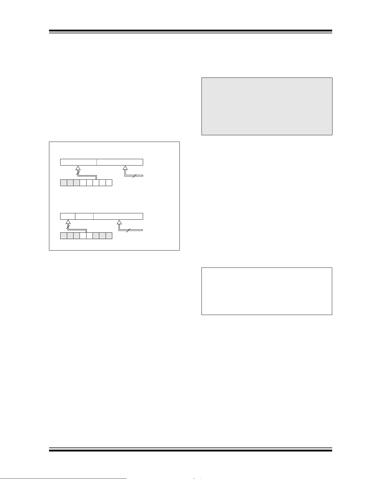
2.3 PCL and PCLATH
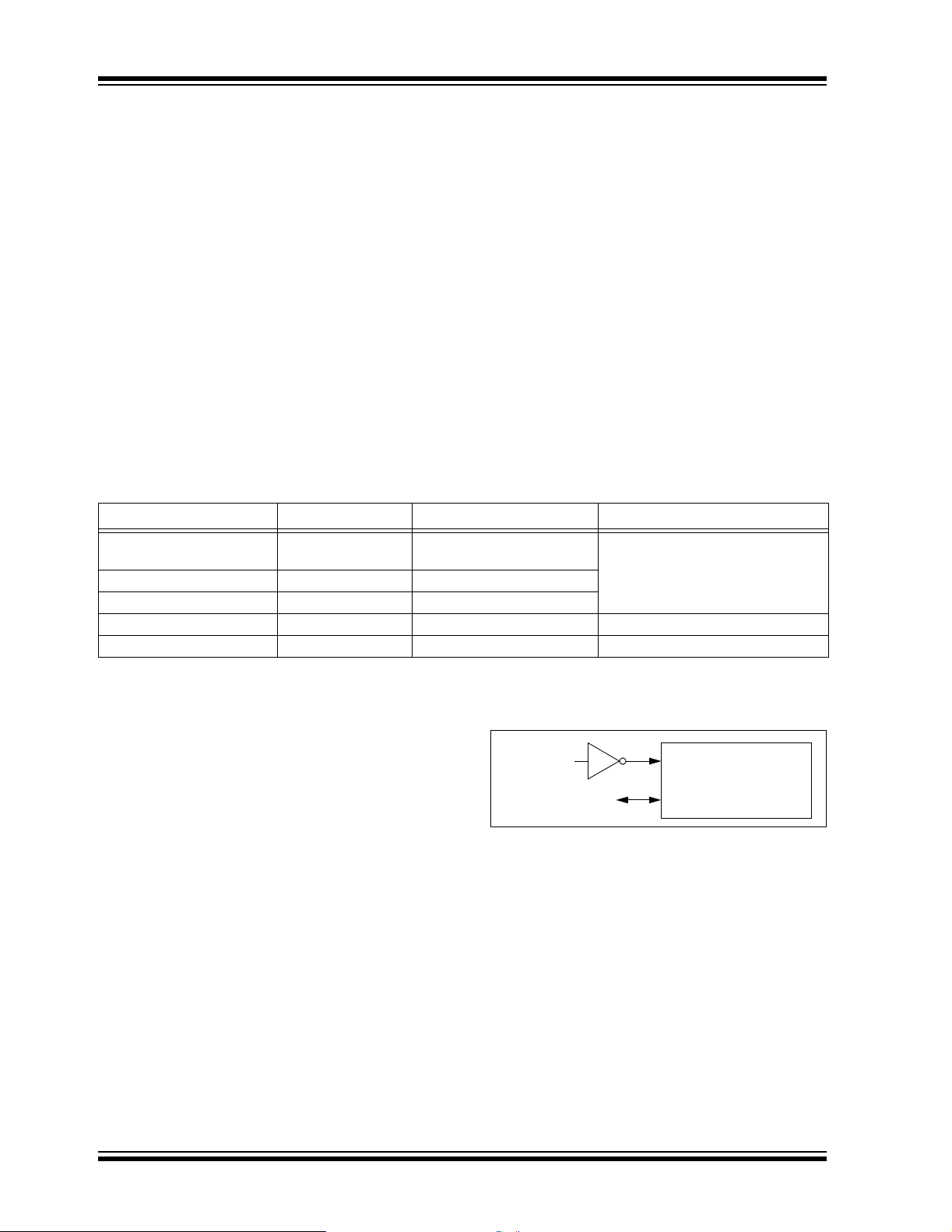
The Program Counter (PC) is 13 bits wide. The low byte
comes from the PCL register, which is a readable and
writable register. The high byte (PC<12:8>) is not
directly readable or writable and comes from PCLATH .
On any Reset, the PC is cleared. Figure 2-3 shows the
two situations for the loading of the PC. The upper
example in Figure 2-3 shows how the PC is loaded on a
write to PCL (PCLATH<4:0> → PCH). The lower example in Figure 2-3 shows how the PC is loaded during a
CALL or GOTO instruction (PCLATH<4:3> → PCH).
FIGURE 2-3: LOADING OF PC IN
DIFFERENT SITUATIONS
PCH PCL
12 8 7 0
PC
PCLATH<4:0>
5
PCLATH
PCH PCL
12 11 10 0
PC
2
87
PCLATH<4:3>
PCLATH
8
11
2.3.1 COMPUTED GOTO
A computed GOTO is accomplish ed by adding an offset
to the program counter (ADDWF PCL). When performing a table read using a computed GOTO method, care
should be exercise d i f the t able loca tio n cros ses a PCL
memory boundary (each 256-byte block). Refer to the
Application Note AN556, “Implementing a Table Read”
(DS00556).
Instruction wit
PCL a
Destinatio
ALU Result
GOTO, CALL
OPCODE <10:0
The stack operat es as a circular buf fer . This means th at
after the stack has been PUSHed eight times, the ninth
push overwrites th e valu e that was s tored fro m the firs t
push. The tenth pus h ov erwr i tes the se co nd push (and
so on).
Note 1: There are no Status bits to indicate stack
overflow or stack underflow conditions.
2: There are no instructions/mnemonics
called PUSH or POP. These are actions
that occur from the execution of the
CALL, RETURN, RETLW and RETFIE
instructions or the vectoring to an
interrupt address.
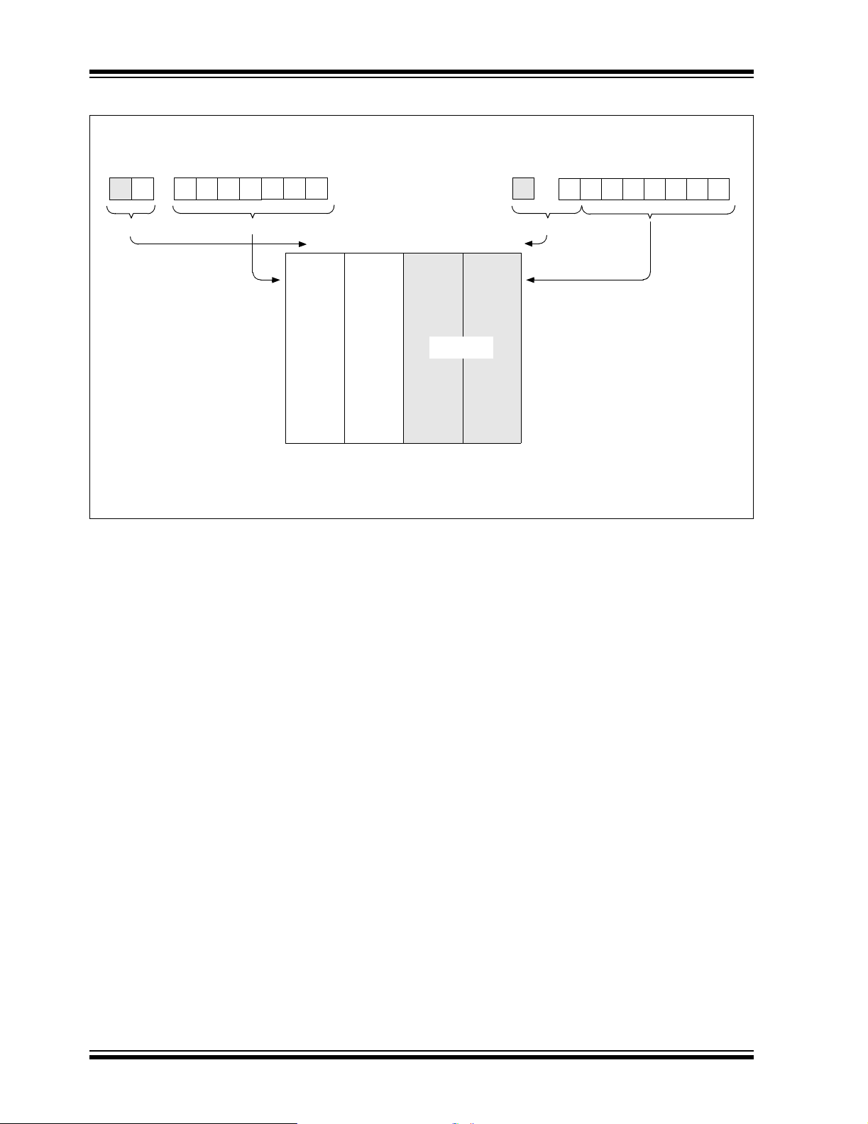
2.4 Indirect Addressing, INDF and FSR Registers
The INDF register is not a physica l register . Addr essing
the INDF register will cause indirect addressing.
Indirect addressing is possible by using the INDF
register. Any instruction using the INDF register
actually accesses data pointed to by the File Select
Register (FSR). Reading INDF itself indirectly will
produce 00h. Writing to the INDF register indirectly
results in a no operation (although Status bits may be
affected). An effective 9-bit address is obtained by
concatenating the 8-bit FSR and the IRP bit
(Status<7>), as shown in Figure2-4.
A simple program to clear RAM location 20h-2Fh using
indirect addressing is shown in Example 2-1.
EXAMPLE 2-1: INDIRECT ADDRESS ING
MOVLW0x20;initialize pointer
MOVWFFSR ;to RAM
NEXT CLRFINDF ;clear INDF register
INCFFSR ;INC POINTER
BTFSSFSR,4;all done?
GOTONEXT ;no clear next
CONTINUE ;yes continue
2.3.2 STACK
The PIC16F684 Family has an 8-level x 13-bit wide
hardware s tack (see Figure 2-1). The stack space is
not part of either program or data space and the stack
pointer is n ot re ad a bl e or wr i tabl e. T h e P C i s P U SHed
onto the s tack w hen a CALL instruction is executed or
an interrupt causes a branch. The stack is POPed in
the event of a RETURN, RETLW or a RETFIE
instruction execution. PCLATH is not affected by a
PUSH or POP operation.
2004 Microchip Technology Inc. Preliminary DS41202C-page 17
PIC16F684
FIGURE 2-4: DIRECT/INDIRECT ADDRESSING PIC16F684
RP1
(1)
RP0 6
From Opcode
0
IRP
Indirect AddressingDirect Addressing
(1)
7
File Select Register
0
Bank Select Location Select
00h
Data
Memory
7Fh
For memory map detail, see Figure 2-2.
Note 1: The RP1 and IRP bits are reserved; always maintain these bits clear.
00 01 10 11
NOT USED
Bank 0 Bank 1 B ank 2 Bank 3
Bank Select
180h
1FFh
Location Select
DS41202C-page 18 Preliminary 2004 Microchip Technology Inc.
PIC16F684
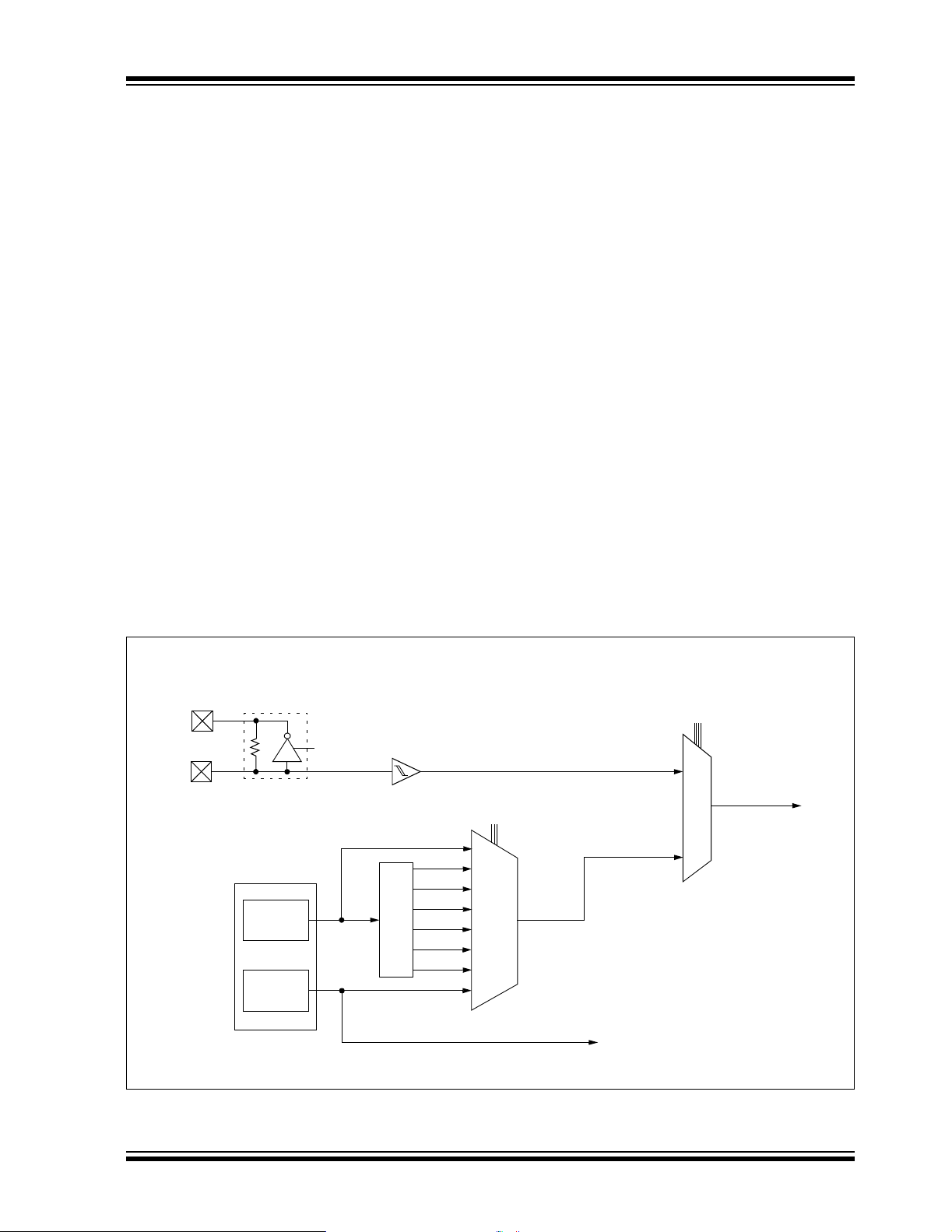
3.0 CLOCK SOURCES
3.1 Overview
The PIC16F684 has a wide variety of clock sources
and selection features to allow it to be used in a wide
range of applications while maximizing performance
and minimizing power consumption. Figure 3-1
illustrates a block diagram of the PIC16F684 clock
sources.
Clock sources can be configured from external
oscillators, quartz crystal resonators, ceramic
resonators and Resistor-Capacitor (RC) circuits. In
addition, the system clock source can be configured
from one of two internal oscillators, with a choice of
speeds selectable via software. Additional clock
features i nclude:
• Selectable system clock source between external
or internal via software.
• Two-Speed Clock Start-up mode, which minimizes latency betw e en ext ernal oscillator start-u p
and code execution.
• Fail-Safe Clock Monitor (FSCM) designed to
detect a failure of the external clock source (LP,
XT, HS, EC or RC modes) and switch to the
internal oscillator.
The PIC16F684 can b e conf igured in one of ei ght cloc k
modes.
1. EC – External clock with I/O on RA4.
2. LP – Low gain Crystal or Ceramic Resonator
Oscillator mode.
3. XT – Medium gain Crystal or Ceramic Resonator Oscillator mode.
4. HS – High gain Crystal or Ceramic Resonator
mode.
5. RC – External Resistor-Capacitor (RC) with
OSC/4 out put on RA4.
F
6. RCIO – External Resistor-Capacitor with I/O on
RA4.
7. INTRC – Internal oscillator with F
OSC/4 output
on RA4 and I/O on RA5.
8. INTRCIO – Internal oscillator with I/O on RA4
and RA5.
Clock source m odes are configu red by t he FOSC<2:0 >
bits in the Configuration Word register (see
Section 12.0 “Special Features of the CPU”). The
internal clock can be generated by two oscillators. The
HFINTOSC is a high-frequency calibrated oscillator.
The LFINTOSC is a low-frequency uncalibrated
oscillator.
FIGURE 3-1: PIC16F684 CLOCK SOURCE BLOCK DIAGRAM
External Oscillator
OSC2
OSC1
Internal Oscillator
HFINTOSC
8 MHz
LFINTOSC
31 kHz
Sleep
Postscaler
(OSCCON<6:4>)
8 MHz
4 MHz
2 MHz
1 MHz
500 kHz
250 kHz
125 kHz
31 kHz
IRCF<2:0>
111
110
101
100
011
010
001
000
LP, XT, HS, RC, RCIO, EC
MUX
Power-up Timer (PWRT)
Watchdog Timer (WDT)
Fail-Safe Clock Monitor (FSCM)
FOSC<2:0>
(Configuration Word)
SCS
(OSCCON<0>)
MUX
(CPU and Peripherals)
System Clock
2004 Microchip Technology Inc. Preliminary DS41202C-page 19
PIC16F684
3.2 Clock Source Modes
Clock source modes can be classified as external or
internal.
• External clock mode s rely on ext erna l circuitry for
the clock source. Exam ples are oscillator modules
(EC mode), quartz crystal resonators or ceramic
resonators (LP, XT and HS modes), and
Resistor- Capacitor (RC mode) circuits.
• Internal clock sources are contained internally
within the PIC16F684. The PIC16F684 has two
internal oscillators, the 8 MHz High-Frequency
Internal Oscillator (HFINTOSC) and 31 kHz
Low-Frequency Internal Oscillator (LFINTOSC).
The system clock can be selected between external or
internal clock sources via the System Clock Selection
(SCS) bit (see Section 3.5 “Clock Switching”).
3.3 External Clock Modes
3.3.1 OSCILLATOR START-UP TIMER (OST)
If the PIC16F684 is co nfigured for LP, XT or HS modes,
the Oscillator Start-up Timer (OST) counts 1024 oscillations from the OSC1 pin, followi ng a Power-on Res et
(POR) and the Power-up T i mer (PWR T ) has ex pired ( if
configured), or a wake -up from Sleep. D urin g this t ime,
the program counter does not increment and program
execution is suspended. The OST ensures that the
oscillator circuit, using a quartz crystal resonator or
ceramic resonator, has st arted and i s providing a stabl e
system clock to the PIC16F684. When switching
between clock sources a delay is required to allow the
new clock to stabilize. These oscillator delays are
shown in Table 3-1.
In order to minimize laten cy between externa l oscillator
start-up and code execution, the Two-Speed Clock
Start-up mode can be selected (see Section 3.6
“Two-Speed Clock Start-up Mode”).
TABLE 3-1: OSCILLATOR DELAY EXAMPLES
Switch From Switch To Frequency Oscillator Delay
Sleep/POR
Sleep/POR EC, RC DC – 20 MHz
LFINTOSC (31 kHz) EC, RC DC – 20 MHz
Sleep/POR LP, XT, HS 31 kHz to 20 MHz 1024 Clock Cycles (OST)
LFINTOSC (31 kHz) HFINTOSC 125 kHz to 8 MHz 1 µs (approx.)
Note 1: The 5 µs to 10 µs start-up delay is based on a 1MHz system clock.
LFINTOSC
HFINTOSC
31 kHz
125 kHz to 8 MHz
5 µs-10 µs (approx.) CPU Start-up
(1)
3.3.2 EC MODE
The External Clock (EC) mode allows an externally
generated logic level as the system clock source.
When operating in this mode, an external clock source
is connected to the OSC1 pin and the RA5 pin is
available for general purpose I/ O. Figure 3-2 shows the
pin connections for EC mode.
The Oscillator Start-up Timer (OST) is disabled when
EC mode is selected. Therefore, there is no delay in
operation after a Power-on Reset (POR) or wake-up
from Sleep. Because the PIC16F684 design is fully
static, stopping the external clock input will have the
effect of halting the device while leaving all data intact.
Upon restarting the external clock, the device will
resume operation as if no time had elapsed.
FIGURE 3-2: EXTERNAL CLOCK (EC)
MODE OPERATION
Clock from
Ext. System
RA4
OSC1/CLKIN
PIC16F684
I/O (OSC2)
DS41202C-page 20 Preliminary 2004 Microchip Technology Inc.
PIC16F684
r
r
)
r
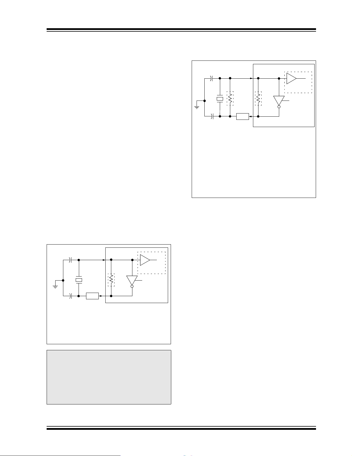
3.3.3 LP, XT, HS MODES
The LP, XT and HS modes support the use of quartz
crystal resonators or ceramic resonators connected to
the OSC1 and OSC2 pins (Figure 3-1). The mode
selects a low, medium or high gain setting of the
internal inverter-amplifier to support various resonator
types and speed.
LP Oscillator mode selects the lowest gain setting of
the internal inverter-amplifier. LP mode current consumption is the least of the three modes. This mode is
best suited to drive resonator s with a low drive lev el
specification, for example, tuning fork type crystals.
XT Oscillator mode selects the intermediate gain
setting of the internal inverter-amplifier. XT mode
current consumption is the medi um of the three modes.
This mode is best suited to drive resonators with a
medium drive level specification, for example,
low-frequency/AT-cut quartz crystal resonators.
HS Oscillator mode selects the highest gain setting of
the internal inverter-amplifier. HS mode current
consumption is the highest of the three modes. This
mode is best suited for resonato rs that req uire a hi gh
drive setting, for example, high-frequency/AT-cut
quartz crystal resonators or ceramic resonators.
Figure 3-3 and Figure3-4 show typical circuits for
quartz crystal and ceramic resonators, respectively.
FIGURE 3-4: CERAMIC RESONATOR
OPERATION
(XT OR HS MODE)
PIC16F684
OSC1
C1
(3)
RP
OSC2
(1)
R
S
C2
Ceramic
Resonator
Note 1: A series resistor (RS) may be required fo
ceramic resonators with low drive level.
2: The value of R
mode selected (typically between 2 MΩ to
10 MΩ).
3: An additional parallel feedback resistor (R
may be required for proper ceramic resonato
operation (typical value 1 MΩ).
(2)
RF
F varies with the Oscillato
To Internal
Logic
Sleep
P
FIGURE 3-3: QUARTZ CRYSTAL
OPERATION (LP, XT OR
HS MODE)
PIC16F684
OSC1
C1
Quartz
Crystal
OSC2
(1)
R
S
C2
Note 1: A series resistor (RS) may be required for
quartz crystals with low drive level.
2: The value of R
mode selected (typically between 2 MΩ to
10 MΩ).
(2)
RF
F varies with the Oscillator
Note 1: Quartz crystal characteristics vary
according to type, package and manufacturer. The user should consult the manufacturer data sh eets for speci fications and
recommended application.
2: Always verify oscillator perform an ce ov er
DD and temperature range that is
the V
expected for the application.
To Internal
Logic
Sleep
2004 Microchip Technology Inc. Preliminary DS41202C-page 21
PIC16F684
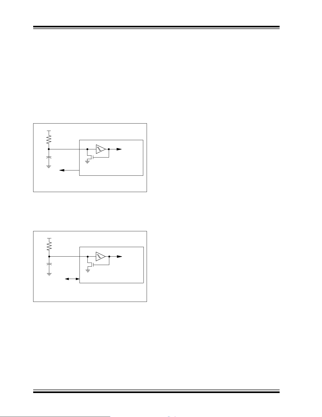
3.3.4 EXTERNAL RC MODES
The External Resistor-Capacitor (RC) modes support
the use of an external RC circuit. This allows the
designer maximum flexibility in frequency choice while
keeping costs to a minimum when clock accuracy is not
required. There are two modes, RC and RCIO.
In RC mode, the RC circuit connects to the OSC1 pin.
The OSC2/CLKOUT pin outputs the RC oscillator
frequency divided by 4. This signal may be used to
provide a clock for external circuitry, synchronization,
calibration, test or other application requirements.
Figure 3-5 shows the RC mode connections.
FIGURE 3-5: RC MODE
VDD
REXT
OSC1
CEXT
VSS
F
Recommended values: 3 kΩ ≤ REXT ≤ 100 kΩ
OSC/4
OSC2/CLKOUT
C
EXT > 20 pF
Internal
Clock
PIC16F684
In RCIO mode, the RC circuit is connecte d to the OSC1
pin. The OSC2 pin becomes an additional general
purpose I/O pin. The I/O pin becomes bit 4 of PORTA
(RA4). Figure 3-6 shows the RCIO mode connections.
FIGURE 3-6: RCIO MODE
VDD
3.4 Internal Clock Modes
The PIC16F684 has two independent, internal
oscillators that can be configured or selected as the
system clock source.
1. The HFINTOSC (High-Frequency Internal
Oscillator) is factory calibrated and operates at
8 MHz. The frequency of t he HFINT OSC can be
user adjusted ±12% via software using the
OSCTUNE register (Register 3-1).
2. The LFINTOSC (Low-Frequency Internal
Oscillator) is uncalibrated and operates at
approximately 31 kHz.
The system cloc k speed ca n be selec ted via sof tware
using the Internal Oscillator Frequency Select (IRCF)
bits.
The system clock ca n be se lec ted betw ee n external or
internal clock sources via the System Clock Selection
(SCS) bit (see Section 3.5 “Clock Switching”).
3.4.1 INTRC AND INTRCIO MODES
The INTRC and INTRCIO m odes conf igure the int ernal
oscillators as th e sys tem cl ock so urce when the dev ice
is programmed using the Oscillator Selection (FOSC)
bits in the Configuration Word register (Register 12-1).
In INTRC mode, the OSC1 pin is available for general
purpose I/O. The OSC2/CLKOUT pin outputs the
selected internal os ci lla tor freq uen cy div ide d by 4. The
CLKOUT signal may be used to provide a clock for
external circuitry, synchronization, calibration, test or
other application require me nt s .
In INTRCIO mode, the OSC1 and OSC2 pins are
available for general purpose I/O.
REXT
OSC1
CEXT
VSS
RA4
Recommended values: 3 kΩ ≤ REXT ≤ 100 kΩ
I/O (OSC2)
EXT > 20 pF
C
PIC16F684
Internal
Clock
3.4.2 HFINTOSC
The High-Frequency Int ernal Oscillato r (HFINT OSC) is
a factory calibrated 8 MHz internal clock source. The
frequency of the HFINTOSC can be altered
approximately ±12% via software using the OSCT UNE
register (Register 3-1).
The output of the HFINTOSC connects to a postscaler
and multiplexer (see Figure 3-1). One of seven
frequencies can be selected via software using the
IRCF bits (see Section 3.4.4 “Frequency Select Bits
The RC oscillator frequency is a function of the supply
voltage, the resistor (R
EXT) and capacitor (CEXT)
values and the operating temperature. Other factors
affecting the oscillator frequency are:
• threshold voltage variation
• component tolerances
• packaging variations i n capacitance
(IRCF)”).
The HFINTOSC is enabled by selecting any frequency
between 8 MHz and 125 kHz (IRCF ≠ 000) as the
system clock s ource (SCS = 1), or when Two-Speed
Start-up is enabled (IESO = 1 and IRCF ≠ 000).
The HF Internal Oscillator (HTS) bit (OSCCON<2>)
indicates whether the HFINTOSC is stable or not.
The user also needs to take into account variation due
to tolerance of external RC components used.
DS41202C-page 22 Preliminary 2004 Microchip Technology Inc.

PIC16F684
3.4.2.1 OSCTUNE Register
The HFINTOSC is factory calibrated but can be
adjusted in software by writing to the OSCTUNE
register (Register3-1).
The OSCTUNE register has a tuning range of ±12%.
The default value of the OSCTUNE register is ‘0’. The
value is a 5-bit two’s complement number. Due to
process variatio n, the m onoton icity and freq uency step
cannot be specified.
When the OSCTUNE register is modified, the
HFINTOSC frequency will begin shifting to the new
frequency. The HFINTOSC clock will stabilize within
1 ms. Code execution continues during this shift. There
is no indication that the shift has occurred.
OSCTUNE does not affect the LFINTOSC frequency.
Operation of features that depend on the LFINTOSC
clock source frequency, such as the Power-up Timer
(PWRT), Watchdog Timer (WDT), Fail-Safe Clock
Monitor (FSCM) and peripherals, are not af fected by the
change in frequency.
REGISTER 3-1: OSCTUNE – OSCILLATOR TUNING RESISTOR (ADDRESS: 90h)
U-0 U-0 U-0 R/W-0 R/W-0 R/W-0 R/W-0 R/W-0
— — — TUN4 TUN3 TUN2 TUN1 TUN0
bit 7 bit 0
bit 7-5 Unimplemented: Read as ‘0’
bit 4-0 TUN<4:0>: Frequency Tuning bits
01111 = Maximum frequency
01110 =
•
•
•
00001 =
00000 = Oscillator module is running at the calibrated frequency.
11111 =
•
•
•
10000 = Minimum frequency
Legend:
R = Readable bit W = Writable bit U = Unimplemented bit, read as ‘0’
-n = Value at POR ‘1’ = Bit is set ‘0’ = Bit is cleared x = Bit is unknown
2004 Microchip Technology Inc. Preliminary DS41202C-page 23

PIC16F684
3.4.3 LFINTOSC
The Low-Frequency Internal Oscillator (LFINTOSC) is
an uncalibrated (approximate) 31 kHz internal clock
source.
The output of the LFINTOSC connects to a postscaler
and multiplexer (see Figure3-1). 31 kHz can be
selected via software using the IRCF bits (see
Section 3.4.4 “Frequency Select Bits (IRCF)”). The
LFINTOSC is also the frequency for the Power-up
Timer (PWRT), Watchdog Timer (WDT) and Fail-Safe
Clock Monitor (FSCM).
The LFINTOSC is enabled by selecting 31 kHz
(IRCF = 000) as the system clock sourc e (SCS = 1), or
when any of the following are enabled:
• Two-Speed Start-up (IESO = 1 and IRCF = 000)
• Power-up Timer (PWRT)
• Watchdog Timer (WDT)
• Fail-Safe Clock Monitor (FSCM)
The LF Internal Oscillator (LTS) bit (OSCCON<1>)
indicates whether the LFINTOSC is stable or not.
3.4.4 FREQUENCY SELECT BITS (IRCF)
The output of the 8 MHz HFINTOSC and 31 kHz
LFINTOSC connects to a postscaler and multiplexer
(see Figure 3-1). The Internal Oscillator Frequency
select bits, IRCF<2:0> (OSCCON<6:4>), select the
frequency output of the internal oscillators. One of eight
frequencies can be selected via software:
•8 MHz
• 4 MHz (Default after Reset)
•2 MHz
•1 MHz
• 500 kHz
• 250 kHz
• 125 kHz
•31 kHz
Note: Following any Reset, t he IR CF bit s are set
to ‘110’ and the frequency selection is set
to 4 MHz. The user can modify the IRCF
bits to select a different frequency.
3.4.5 HF AND LF INTOSC CLOCK
SWITCH TIMING
When switching between the LFINTOSC and the
HFINTOSC, the new oscillator may already be shut
down to save power. If this is the case, there is a 10 µs
delay after the IRCF bits are modified before the
frequency selection takes place. The LTS/HTS bits will
reflect the current active status of the LFINTOSC and
the HFINTOSC oscillators. The timing of a frequency
selection is as follows:
1. IRCF bits are modified.
2. If the new clock is shut down, a 10 µs clock
start-up delay is started.
3. Clock switch circuitry waits for a falling edge of
the current clock.
4. CLKOUT is held low and the clock switch
circuitry waits fo r a ris ing edge in the new clock.
5. CLKOUT is now connected with the new clock.
HTS/LTS bits are updated as required.
6. Clock switch is complete.
If the internal oscillator speed selected is between
8 MHz and 125 kHz, there is no start-up delay before
the new frequency is selected. This is because the old
and the new frequencies are derived from the
HFINTOSC via the postscaler and multiplexer.
DS41202C-page 24 Preliminary 2004 Microchip Technology Inc.

PIC16F684
3.5 Clock Switching
The system clock source can be switched between
external and internal clock sources via software using
the System Clock Select (SCS) bit.
3.5.1 SYSTEM CLOCK SELECT (SCS) BIT
The System Clock Select (SCS) bit (OSCCON<0>)
selects the system clock source that is used for the
CPU and peripherals.
• When SCS = 0, the system clock source is
determined by configuration of the FOSC<2:0>
bits in the Configuration Word register (CONFIG).
• When SCS = 1, the system clock source is
chosen by the internal oscillator frequency
selected by the IRCF bits. After a Reset, SCS is
always cleared.
Note: Any automatic clock switch, which may
occur from Two-Speed Start-up or
Fail-Safe Clock Monitor, does not update
the SCS bit. The user can monitor the
OSTS (OSCCON<3>) to determine the
current system clock source.
3.5.2 OSCILLATOR START-UP TIME-OUT
STATUS BIT
The Oscillator Start-up Time-out Status (OSTS) bit
(OSCCON<3>) indicates whether the system clock is
running from the external clock source, as defined by
the FOSC bits, or from internal clock source. In
particular, OSTS indicates that the Oscillator Start-up
Timer (OST) has timed out for LP, XT or HS modes.
3.6 Two-Speed Clock Start-up Mode
Two-Speed Start-up mode provides additional power
savings by minimizing the latency between external
oscillator start-up and code execution. In applications
that make heavy us e of the Sleep mode, Two-Speed
Start-up will remove the external oscillator start-up
time from the time spent awake and can reduce the
overall power consumption of the device.
This mode allows the application to wake-up from
Sleep, perform a few instructions using the INTOSC
as the clock source and go back to Sleep without
waiting for the primary oscillator to become stable.
When the PIC16F684 is configured for LP, XT or HS
modes, the Oscillator Start-up Timer (OST) is enabled
(see Section 3.3.1 “Oscillator Start-up Timer
(OST)”). The OST timer will suspend program execution until 1024 oscillations are counted. Two-Speed
Start-up mode minimizes the delay in code execution
by operating from the internal oscillator as the OST is
counting. When the OST count reaches 1024 and the
OSTS bit (OSCCON<3>) is set, program execution
switches to the external oscillator.
3.6.1 TWO-SPEED START-UP MODE
CONFIGURATION
Two-Speed Start-up mode is configured by the
following settings:
• IESO = 1 (CONFIG<10>) Internal/External Switch
Over bit.
•SCS = 0.
• FOSC configured for LP, XT or HS mode.
Two-Speed Start-up mode is entered after:
• Power-on Reset (POR) and, if enabl ed, after
PWRT has expired, or
• Wake-up from Sleep.
If the external clock oscillator is configured to be anything other than LP, XT or HS mode, then Two-Speed
Start-up is disabled. This is because the ex tern al clock
oscillator does not require any stabilization time after
POR or an exit from Sleep.
3.6.2 TWO-SPEED START-UP
SEQUENCE
1. Wake-up from Power-on Reset or Sleep.
2. Instructions begin execution by the internal
oscillator at the frequency set in the IRCF bits
(OSCCON<6:4>).
3. OST enabled to count 1024 clock cycles.
4. OST timed out, wait for falling edge of the
internal oscillator.
5. OSTS is set.
6. System clock held low until the next fal ling edg e
of new clock (LP, XT or HS mode).
7. System clock is switched to external clock
source.
Note: Executing a SLEEP instruction will abort
the oscillator start-up time and will cause
the OSTS bit (OSCCON<3>) to remain
clear.
2004 Microchip Technology Inc. Preliminary DS41202C-page 25
PIC16F684
3.6.3 CHECKING EXTERNAL/INTERNAL
CLOCK STATUS
Checking the state of the OSTS bit (OSCCON<3>) will
confirm if the PIC16F684 is running from the external
clock source as defined by the FOSC bits in the
Configuration Word register (CONFIG) or the internal
oscillator.
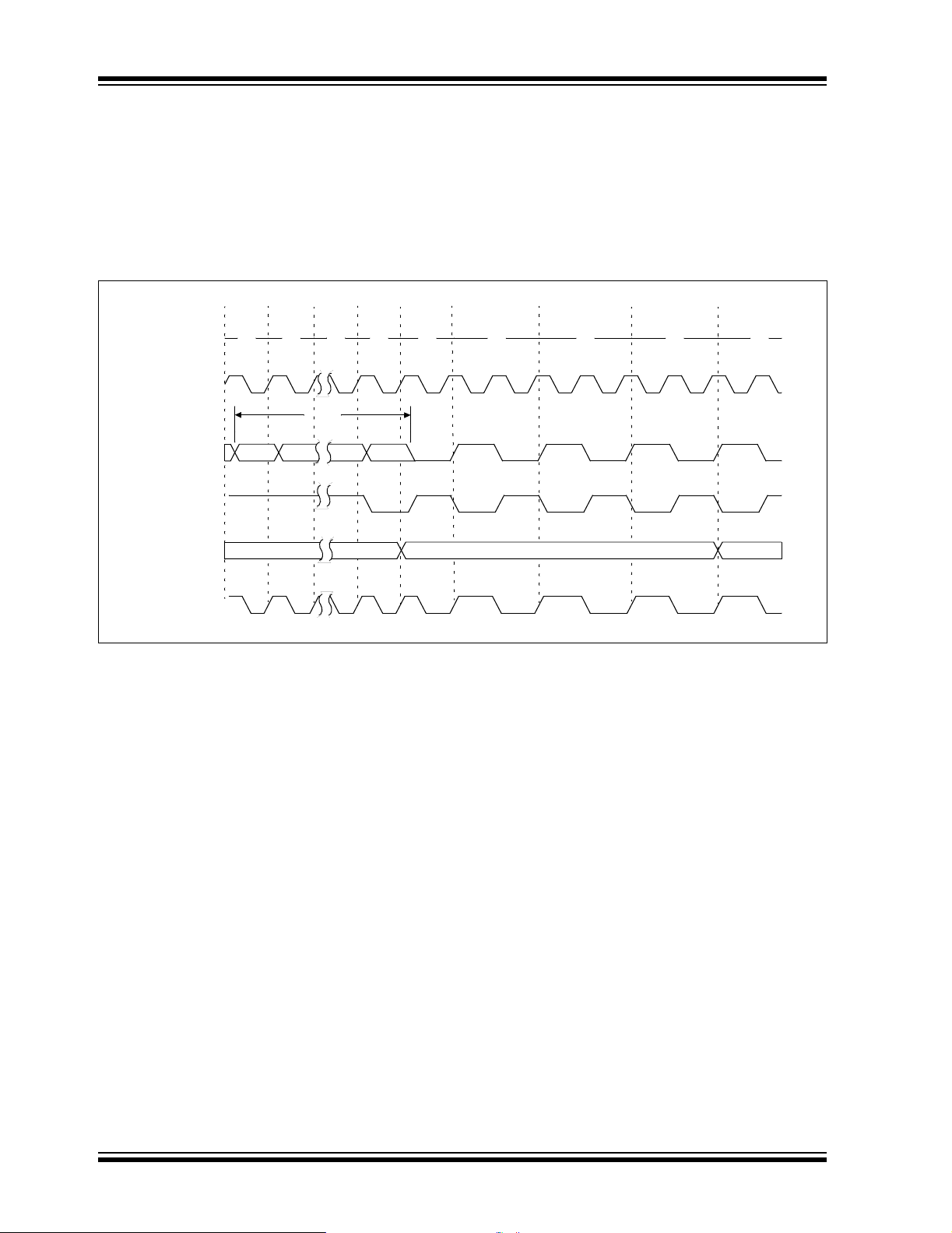
FIGURE 3-7: TWO-SPEED START-UP
Q1 Q2 Q3 Q4 Q1 Q2 Q3 Q4 Q1
INTOSC
TOSTT
OSC1
OSC2
Program Counter
System Clock
0 1 1022 1023
PC PC + 1 PC + 2
DS41202C-page 26 Preliminary 2004 Microchip Technology Inc.
PIC16F684
3.7 Fail-Safe Clock Monitor
The Fail-Safe Clock Monitor (FSCM) is designed to
allow the device to continue to operate in the event of
an oscillator failure. The FSCM can detect oscillator
failure at any point after the device has exited a Reset
or Sleep condition and the Oscillator Start-up Timer
(OST) has expired.
FIGURE 3-8: FSCM BLOCK DIAGRAM
Clock Monitor
Latch (CM)
Primary
Clock
LFINTOSC
Oscillator
31 kHz
(~32 µs)
÷ 64
488 Hz
(~2 ms)
The FSCM function is enabled by setting the FCMEN
bit in the Confi guration Word regist er (CONFIG). It is
applicable to all ex ternal clo ck options (LP, XT , HS, EC,
RC or IO modes).
In the event of an external clock failure, the FSCM will
set the OSFIF bit (PIR1< 2>) and g enerate an os cilla tor
fail interrupt if the OSFIE bit (PIE1<2>) is set. The
device will then switch the system clock to the internal
oscillator. The system clock will continue to come from
the internal oscill ator unless the external clock recovers
and the Fail-Safe condition is exited.
(edge-triggered)
S
Q
C
Q
Clock
Failure
Detected
The frequency of the internal oscillator will depend
upon the value contained in the IRCF bits
(OSCCON<6:4>). Upon entering the Fail-Safe
condition, the OSTS bit (OSCCON<3>) is automatically cleared to reflect that the internal oscillator is
active and the WDT is cleared. The SCS bit
(OSCCON<0 >) is not upda ted. Enabling FSCM does
not affect the LTS bit.
The FSCM sample clock is generated by dividing the
INTRC clock by 64. This will allow enough time
between FSCM sample clocks for a system clock edge
to occur. Figure 3-8 shows the FSCM block diagram.
On the rising edge of the sample clock, the monitoring
latch (CM = 0) will be cleared. On a falling edge of the
primary system clock, the monitoring latch will be set
(CM = 1). In the event that a fal lin g e dge o f th e s am pl e
clock occurs, and the m onitoring latch is n ot set, a clock
failure has been detected. The assigned internal
oscillator is enabled when FSCM is enabled, as
reflected by the IRCF.
Note: Two-Speed Start-up is automatically
enabled when the Fail-Safe Clock Monit or
mode is enabled.
Note: Primary clocks with a frequency ≤ ~488 Hz
will be considered failed by the FSCM. A
slow starting oscillator can cause an
FSCM interrupt.
3.7.1 FAIL-SAFE CONDITION CLEARING
The Fail-Safe condition is cleared after a Reset, the
execution of a SLEEP instruction, or a modification of
the SCS bit. While in Fail-Safe condition, the
PIC16F684 uses the internal oscillator as the system
clock sourc e. The IRCF bits (OSCCON< 6:4>) can be
modified to adjust the internal oscillator frequency
without exiting the Fail-Safe condition.
The Fail-Safe condition must be cleared before the
OSFIF flag can be cleared.
2004 Microchip Technology Inc. Preliminary DS41202C-page 27
PIC16F684
FIGURE 3-9: FSCM TIMING DIAGRAM
Sample Clock
System
Clock
Output
CM Output
(Q)
OSCFIF
CM Test
Note: The system clock is normally at a mu ch higher frequency than the sam ple clock. The relative fr equencies in
this example have been chosen for clarity.
Oscillator
Failure
Failure
Detected
CM Test CM Test
3.7.2 RESET OR WAKE-UP FROM SLEEP
The FSCM is designed to detect oscillator failure at
any point after the device has exited a Reset or Sleep
condition and the Oscillator Start-up Timer (OST) has
expired. If the external clock is EC or RC mode,
monitoring will begin immediately following these
events.
For LP, XT or HS mode, the external oscillator may
require a start-up time considerably longer than the
FSCM sample clock time, a false clock failure may be
detected (see Figure 3-9). To prevent this, the internal
oscillator is automatically configured as the system
clock and functions until the external clock is stable
(the OST has timed out). This is identical to
Two-Speed Start-up mode. Once the external oscillator is stable, the LFINTOSC returns to its role as the
FSCM source.
Note: Due to the wide range of oscillato r start-u p
times, the Fail-Safe circuit is not active
during oscillator start-up (i.e., after exiting
Reset or Sleep). After an appropriate
amount of time, the u se r should check the
OSTS bit (OSCCON<3>) to verify the
oscillator start-up and system clock
switchover has successfull y com pl ete d.
DS41202C-page 28 Preliminary 2004 Microchip Technology Inc.

PIC16F684
REGISTER 3-2: OSCCON – OSCILLATOR CONTROL REGISTER (ADDRESS: 8Fh)
U-0 R/W-1 R/W-1 R/W-0 R-1 R-0 R-0 R/W-0
— IRCF2 IRCF1 IRCF0 OSTS
bit 7 bit 0
bit 7 Unimplemented: Read as ‘0’
bit 6-4 IRCF<2:0>: Internal Oscillator Frequency Select bits
000 =31kHz
001 =125kHz
010 =250kHz
011 =500kHz
100 =1MHz
101 =2MHz
110 =4MHz
111 =8MHz
bit 3 OSTS: Oscillator Start-up Time-out Status bit
1 = Device is running from the external system clock defined by FOSC<2:0>
0 = Device is running from the internal system clock (HFINTOSC or LFINTOSC)
bit 2 HTS: HFINTOSC (High Frequency – 8 MHz to 125 kHz) Status bit
1 =HFINTOSC is stable
0 = HFINTOSC is not stable
bit 1 LTS: LFINTOSC (Low Frequency – 31 kHz) Stable bit
1 = LFINTOSC is stable
0 = LFINTOSC is not stable
bit 0 SCS: System Clock Select bit
1 = Internal oscillator is used for system clock
0 = Clock source defined by FOSC<2:0>
(1)
HTS LTS SCS
Note 1: Bit resets to ‘0’ with T wo-Speed S tart-u p and LP, XT or HS selected as the Oscillat or
mode or Fail-Safe mode is enabled.
Legend:
R = Readable bit W = Writable bit U = Unimplemented bit, read as ‘0’
-n = Value at POR ‘1’ = Bit is set ‘0’ = Bit is cleared x = Bit is unknown
TABLE 3-2: SUMMARY OF REGISTERS ASSOCIATED WITH CLOCK SOURCES
Address Name Bit 7 Bit 6 Bit 5 Bit 4 Bit 3 Bit 2 Bit 1 Bit 0
0Ch PIR1
8Ch PIE1
8Fh OSCCON
90h OSCTUNE
(1)
2007h
Legend: x = unknown, u = unchanged, — = unimplemented locations read as ‘0’. Shaded cells are not used by oscillators.
Note 1: See Register 12-1 for operation of all Configuration Word register bits.
CONFIG CPD CP MCLRE PWRTE WDTE FOSC2 FOSC1 FOSC0 — —
EEIF ADIF CCP1IF C2IF C1IF OSFIF TMR2IF TMR1IF 0000 0000 0000 0000
EEIE ADIE CCP1IE C2IE C1IE OSFIE TMR2IE TMR1IE 0000 0000 0000 0000
— IRCF2 IRCF1 IRCF0 OSTS HTS LTS SCS -110 x000 -110 x000
— — — TUN4 TUN3 TUN2 TUN1 TUN0 ---0 0000 ---u uuuu
Value on:
POR, BOD
Value on
all other
Resets
2004 Microchip Technology Inc. Preliminary DS41202C-page 29

PIC16F684
NOTES:
DS41202C-page 30 Preliminary 2004 Microchip Technology Inc.

PIC16F684
4.0 I/O PORTS
There are as many as twelve general purp ose I/O pins
available. Depending on which peripherals are
enabled, some or all of the pins may not be a vailable a s
general purpose I/O. In general, when a peripheral is
enabled, the associated pin may not be used as a
general purpose I/O pin.
Note: Additional information on I /O po rts ma y be
found in the “PICmicro
Family Reference Manual” (DS33023).
4.1 PORTA and the TRISA Registers
PORTA is a 6-bit wide, bidirectional port. The
corresponding data direction register is TRISA
(Register 4-2). Setting a TRISA bit (= 1) will make the
corresponding PORTA pin an input (i.e., put the
corresponding output driver in a High-impedance
mode). Clearing a TRISA bit (= 0) will make the
corresponding PORTA pin an output (i.e., put the
contents of the output latch on the selected pin). The
exception is RA3, which is input only and its TRIS bit
will always read as ‘1’. Example 4-1 shows how to
initialize PORTA.
Reading the PORTA register (Register 4-1) reads the
status of the pins, whereas writing to it will write to the
port latch. All write operations are read-modify-write
operations. Therefore, a write to a port implies that the
port pins are read, this value is modified and then
written to the port data latch. RA3 reads ‘0’ when
MCLRE = 1.
The TRISA register controls the direction of the
PORT A pins, even when they are being used as an alog
inputs. The user must ensure the bits in the TRISA
register are maint ai ned set when using the m as an alog
inputs. I/O pin s co nfigure d as analo g inpu t alw ays rea d
‘0’.
®
Mid-Range MCU
EXAMPLE 4-1: INITIALIZING PORTA
BCF STATUS,RP0 ;Bank 0
CLRF PORTA ;Init PORTA
MOVLW 07h ;Set RA<2:0> to
MOVWF CMCON0 ;digital I/O
BSF STATUS,RP0 ;Bank 1
CLRF ANSEL ;digital I/O
MOVLW 0Ch ;Set RA<3:2> as inputs
MOVWF TRISA ;and set RA<5:4,1:0>
BCF STATUS,RP0 ;Bank 0
;as outputs
4.2 Additional Pin Functions
Every PORTA pin on the PIC16F684 has an interrupton-change option and a weak pull-up option. RA0 has
an Ultra Low-Power Wake-up option. The next three
sections describe these functions.
4.2.1 WEAK PULL-UPS
Each of the PORTA pins, except RA3, has an in div id ually configurable internal weak pull-up. Control bits
WPUAx enable or disable each pull-up. Refer to
Register 4-3. Each weak pull-up is automatically turne d
off when the port pin is configured as an output. The
pull-ups are disabled on a Power-on Reset by the
bit (OPTION_REG<7>). A weak pull-up is auto-
RAPU
matically enabled for RA3 when configured as MCLR
and disabled when RA 3 is an I/O . T here is no s oftware
control of the MCLR
pull-up.
Note: The ANSEL (91h) and CMCON0 (19h)
registers must be initialized to configure
an analog channel as a digital input. Pins
configured as analog inputs will read ‘0’.
REGISTER 4-1: PORTA – PORTA REGISTER (ADDRESS: 05h)
U-0 U-0 R/W-x R/W-x R/W-x R/W-x R/W-0 R/W-0
— — RA5 RA4 RA3 RA2 RA1 RA0
bit 7 bit 0
bit 7-6: Unimplemented: Read as ‘0’
bit 5-0: RA<5:0>: PORTA I/O Pin bit
1 = Port pin is > VIH
0 = Port pin is < VIL
Legend:
R = Readable bit W = Writable bit U = Unimplemented bit, read as ‘0’
-n = Value at POR ‘1’ = Bit is set ‘0’ = Bit is cleared x = Bit is unknown
2004 Microchip Technology Inc. Preliminary DS41202C-page 31

PIC16F684
REGISTER 4-2: TRISA – PORTA TRI-STATE REGISTER (ADDRESS: 85h)
U-0 U-0 R/W-1 R/W-1 R-1 R/W-1 R/W-1 R/W-1
— — TRISA5 TRISA4 TRISA3 TRISA2 TRISA1 TRISA0
bit 7 bit 0
bit 7-6: Unimplemented: Read as ‘0’
bit 5-0: TRISA<5:0>: PORTA Tri-State Control bit
1 = PORTA pin configured as an input (tri-stated)
0 = PORTA pin configured as an output
Note 1: TRISA<3> always reads ‘1’.
2: TRISA<5:4> always reads ‘1’ in XT, HS and LP OSC modes.
Legend:
R = Readable bit W = Writable bit U = Unimplemented bit, read as ‘0’
-n = Value at POR ‘1’ = Bit is set ‘0’ = Bit is cleared x = Bit is unknown
REGISTER 4-3: WPUA – WEAK PULL-UP REGISTER (ADDRESS: 95h)
U-0 U-0 R/W-1 R/W-1 U-0 R/W-1 R/W-1 R/W-1
— — WPUA5 WPUA4 — WPUA2 WPUA1 WPUA0
bit 7 bit 0
bit 7-6 Unimplemented: Read as ‘0’
bit 5-4 WPUA<5:4>: Weak Pull-up Register bit
1 = Pull-up enabled
0 = Pull-up disabled
bit 3 Unimplemented: Read as ‘0’
bit 2-0 WPUA<2:0>: Weak Pull-up Register bit
1 = Pull-up enabled
0 = Pull-up disabled
Note 1: Global RAPU
2: The weak pull-up device is automatically disabled if the pin is in Output mode
(TRISA = 0).
3: The RA3 pull-up is enabled when configured as MCLR
the configuration word.
4: WPUA<5:4> always reads ‘1’ in XT, HS and LP OSC modes.
Legend:
R = Readable bit W = Writable bit U = Unimplemented bit, read as ‘0’
-n = Value at POR ‘1’ = Bit is set ‘0’ = Bit is cleared x = Bit is unknown
must be enabl ed for individual pull-ups to be enable d.
and disabled as an I/O in
DS41202C-page 32 Preliminary 2004 Microchip Technology Inc.

PIC16F684
4.2.2 INTERRUPT-ON-CHANGE
Each of the PORTA pins is individually configurable as
an interrupt-on-change pin. Control bits IOCAx enable
or disable the interrupt function for each pin. Refer to
Register 4-4. The interrupt-on-change is disabled on a
Power-on Reset.
For enabled interrupt-on-change pins, the values are
compared with the old value la tched on the last rea d of
PORTA. The ‘mismatch’ outputs of the last read are
OR’d together to set t he PORTA Change Interrupt Flag
bit (RAIF) in the INTCON register (Register 2-3).
This interrupt can wake the device from Sleep. The
user, in the Interrupt Service Routine, clears the
interrupt by:
a) Any read or write of PORTA. This will end the
mismatch condition, then,
b) Clear the flag bit RAIF.
A mismatch c ond it i on wi ll cont i n ue to s et f lag bi t RA IF.
Reading PORTA will end the mismatch condition and
allow flag bit RAIF to be cleared. The latch holding the
last read value is not affected by a MCLR
Reset. After these resets , the RAIF flag wil l conti nue to
be set if a mismatch is present.
Note: If a change on the I/O pin should occur
when the read operation is being ex ecuted
(start of the Q2 cycle), then the RAIF
interrupt flag may not get set.
nor BOD
REGISTER 4-4: IOCA – INTERRUPT-ON-CHANGE PORTA REGISTER (ADDRESS: 96h)
U-0 U-0 R/W-0 R/W-0 R/W-0 R/W-0 R/W-0 R/W-0
— — IOCA5 IOCA4 IOCA3 IOCA2 IOCA1 IOCA0
bit 7 bit 0
bit 7-6 Unimplemented: Read as ‘0’
bit 5-0 IOCA<5:0>: Interrupt-on-change PORTA Control bit
1 = Interrupt-on-change enabled
0 = Interrupt-on-change disabled
Note 1: Global Interrupt Enable (GIE) must be enabled for individual interrupts to be
recognized.
2: IOCA<5:4> always reads ‘1’ in XT, HS and LP OSC modes.
Legend:
R = Readable bit W = Writable bit U = Unimplemented bit, read as ‘0’
-n = Value at POR ‘1’ = Bit is set ‘0’ = Bit is cleared x = Bit is unknown
2004 Microchip Technology Inc. Preliminary DS41202C-page 33

PIC16F684
4.2.3 ULTRA LOW-POWER WAKE-UP
The Ultra Low-power Wake-up (ULPWU) on RA0
allows a slow falling voltage to generate an interrupton-change on RA0 without excess current consumption. The mode is selected by setting the ULPWUE bit
(PCON<5>). This enables a small current sink which
can be used to discharge a capacitor on RA0.
To use this feature, the RA0 pin is configured to output
‘1’ to charge the capacitor, interrupt-on-change for RA0
is enabled, and RA0 is configured as an input. The
ULPWUE bit is set to begin the discharge and a SLEEP
instruction is performed. When the voltage on RA0 drops
below V
the device to wake-up. Depending on the state of the
GIE bit (INTCON<7>), the device will either jump to the
interrupt vector (0004h) or execute the next instruction
when the interrupt event occurs. See Section 4.2.2
“Interrupt-on-change” and Section 12.4.3 “PORTA
Interrupt” for more information.
This feature provides a low-power technique for
periodically waking up the device from Sleep. The
time-out is dependent on the discharge time of the RC
circuit on RA0. See Example 4-2 for initializing the
Ultra Low-Power Wake-up module.
IL, an interrupt will be generated which will cause
The series resistor provides overcurrent protection for
the RA0 pin and can allow for software calibration of
the time-out (see Figure 4-1). A timer can be used to
measure the charge time and discharge time of the
capacitor . The charge time c an then be adj usted to provide the desired interrupt delay. This technique will
compensate for the af fec ts of te mperat ure, v olta ge an d
component accuracy. The Ultra Low-power Wake-up
peripheral can also be configured as a simple
Programmable Low Voltage Detect or temperature
sensor.
Note: For more information, refer to AN879,
“Using the Microchip Ultra Low-Power
Wake-up Module” Application Note
(DS00879).
EXAMPLE 4-2: ULTRA LOW-POWER
WAKE-UP INITIALIZATION
BCF STATUS,RP0 ;Bank 0
BSF PORTA,0 ;Set RA0 data latch
MOVLW H’7’ ;Turn off
MOVWF CMCON0 ;comparators
BSF STATUS,RP0 ;Bank 1
BCF ANSEL,0 ;RA0 to digital I/O
BCF TRISA,0 ;Output high to
CALL CapDelay ; charge capacitor
BSF PCON,ULPWUE ;Enable ULP Wake-up
BSF IOCA,0 ;Select RA0 IOC
BSF TRISA,0 ;RA0 to input
MOVLW B’10001000’ ;Enable interrupt
MOVWF INTCON ; and clear flag
SLEEP ;Wait for IOC
DS41202C-page 34 Preliminary 2004 Microchip Technology Inc.

FIGURE 4-1: BLOCK DIAGRAM OF RAO
Data Bus
WR
WPUDA
D
Q
CK
Q
(1)
Analog
Input Mode
PIC16F684
VDD
Weak
RAPU
RD
WPUDA
WR
PORTA
WR
TRISA
RD
TRISA
RD
PORTA
WR
IOCA
RD
IOCA
VDD
D
Q
CK
Q
-
+V
D
Q
CK
Q
01
(1)
Analog
Input Mode
D
Q
D
CK
Q
Q
EN
D
Q
ULPWUE
Q3
T
IULP
VSS
I/O PIN
VSS
Interrupt-on-
Change
RD PORTA
To Comparator
To A/D Converter
Note 1: Comparator mode and ANSEL determines Analog Input mode.
EN
2004 Microchip Technology Inc. Preliminary DS41202C-page 35

PIC16F684
4.2.4 PIN DESCRIPTIONS AND
DIAGRAMS
Each PORTA pin is multiplexed with other functions.
The pins and their combined functions are briefly
described here. For specific information about individual functions such as the comparator or the A/D, refer
to the appropriate section in this data sheet.
4.2.4.1 RA0/AN0/C1IN+/ICSPDAT/ULPWU
Figure 4-2 shows the diagr am for thi s pin. Th e RA0 pin
is configurable to function as one of the following:
• a general purpose I/O
• an analog input for the A/D
• an analog input to the comparator
• In-Circuit Serial Programming data
• an analog input for the Ultra Low-power Wake-up
4.2.4.2 RA1/AN1/C1IN-/VREF/ICSPCLK
Figure 4-2 shows the diagr am for thi s pin. Th e RA1 pin
is configurable to function as one of the following:
• a general purpose I/O
• an analog input for the A/D
• an analog input to the comparator
• a voltage reference input for the A/D
• In-Circuit Serial Programming clock
FIGURE 4-2: BLOCK DIAGRAM OF RA1
(1)
Analog
Data Bus
WR
WPUA
RD
WPUA
WR
PORTA
WR
TRISA
RD
TRISA
RD
PORTA
WR
IOCA
RD
IOCA
D
CK
D
CK
D
CK
D
CK
Q
Q
Q
Q
Q
Q
Q
Q
Input Mode
RAPU
Input Mode
Analog
Q
Q
VDD
Weak
VDD
I/O PIN
EN
VSS
D
Q3
D
(1)
Interrupt-on-
Change
RD PORTA
To Comparator
T o A/D Converter
Note 1: Comparator mode a nd ANSEL determines Analog
Input mode.
EN
DS41202C-page 36 Preliminary 2004 Microchip Technology Inc.

PIC16F684
4.2.4.3 RA2/AN2/T0CKI/INT/C1OUT
Figure 4-3 shows the diagr am for thi s pin. Th e RA2 pi n
is configurable to function as one of the following:
• a general purpose I/O
• an analog input for the A/D
• the clock input for TMR 0
• an external edge triggered interrupt
• a digital output from comparator 1
FIGURE 4-3: BLOCK DIAGRAM OF RA2
(1)
Analog
Data Bus
WR
WPUA
RD
WPUA
WR
PORTA
WR
TRISA
RD
TRISA
D
CK
D
CK
D
CK
Q
Q
Q
Q
Q
Q
Input Mode
RAPU
COUT 1
Enable
COUT
Input Mode
1
0
Analog
VDD
Weak
VDD
I/O PIN
VSS
(1)
4.2.4.4 RA3/MCLR
/VPP
Figure 4-4 shows the diagram for this pin. The RA3 pin
is configurable to function as one of the following:
• a general purpose input
• as Master Clear Reset with weak pull-up
FIGURE 4-4: BLOCK DIAGRAM OF RA3
VDD
Data Bus
RD
TRISA
RD
PORTA
WR
IOCA
RD
IOCA
Interrupt-on-
Change
MCLRE
Reset
VSS
Q
D
CK
Q
MCLRE
MCLRE
Q
Q
RD PORTA
EN
EN
Weak
Input
pin
SS
V
D
Q3
D
RD
PORTA
Q
D
D
Q
EN
Q
EN
RD PORTA
D
Change
CK
Q
To TMR0
To INT
To A/D Converter
WR
IOCA
RD
IOCA
Interrupt-on-
Note 1: Analog Input mode is generated by ANSEL.
Q3
2004 Microchip Technology Inc. Preliminary DS41202C-page 37

PIC16F684
4.2.4.5 RA4/AN3/T1G/OSC2/CLKOUT
Figure 4-5 shows the diagr am for thi s pin. Th e RA4 pin
is configurable to function as one of the following:
• a general purpose I/O
• an analog input for the A/D
• a TMR1 gate input
• a crystal/resonator connection
• a clock output
FIGURE 4-5: BLOCK DIAGRAM OF RA4
(3)
Analog
Input Mode
Data Bus
WR
WPUA
RD
WPUA
WR
PORTA
WR
TRISA
RD
TRISA
RD
PORTA
WR
IOCA
RD
IOCA
Interrupt-on-
Change
Note 1: CLK modes are XT, HS, LP, LPTMR1 and CLKOUT
2: With CLKOUT option.
3: Analog Input mode comes from ANSEL.
Q
D
CK
Q
Q
D
CK
Q
D
Q
CK
Q
Q
D
CK
Q
To T1G
To A/D Converter
Enable.
OSC1
FOSC/4
INTOSC/
RC/EC
CLKOUT
Enable
CLKOUT
Enable
Input Mode
(1)
CLK
Modes
RAPU
Oscillator
Circuit
CLKOUT
Enable
1
0
(2)
Analog
Q
EN
Q
EN
RD PORTA
VDD
Weak
VDD
I/O PIN
VSS
D
Q3
D
4.2.4.6 RA5/T1CKI/OSC1/CLKIN
Figure 4-6 shows the diagram for this pin. The RA5 pin
is configurable to function as one of the following:
• a general purpose I/O
•a TMR1 clock input
• a crystal/resona tor connec tio n
• a clock input
FIGURE 4-6: BLOCK DIAGRAM OF RA5
INTOSC
Mode
Data Bus
WPUA
WPUA
PORTA
TRISA
TRISA
PORTA
IOCA
IOCA
D
Q
WR
RD
WR
WR
RD
RD
WR
RD
Interrupt-on-
CK
Q
D
Q
CK
Q
Q
D
CK
Q
Q
D
CK
Q
Change
To TMR1 or CLKGEN
Note 1: Timer1 LP Oscillator enabled.
2: When using Timer1 with LP oscillator, the
Schmitt Trigger is bypassed.
OSC2
TMR1LPEN
RAPU
Oscillator
Circuit
INTOSC
Mode
Q
Q
RD PORTA
EN
EN
(1)
VDD
Weak
VDD
I/O PIN
VSS
(2)
D
Q3
D
DS41202C-page 38 Preliminary 2004 Microchip Technology Inc.

PIC16F684
TABLE 4-1: SUMMARY OF REGISTERS ASSOCIATED WITH PORTA
Addr Name Bit 7 Bit 6 Bit 5 Bit 4 Bit 3 Bit 2 Bit 1 Bit 0
05h PORTA
0Bh/8Bh INTCON GIE
19h CMCON0
81h OPTION_REG RAPU
85h TRISA
91h ANSEL
95h WPUA
96h IOCA
Legend: x = unknown, u = unchanged, — = unimplemented locations read as ‘0’. Shaded cells are not used by PORTA.
— — RA5 RA4 RA3 RA2 RA1 RA0 --xx xx00 --uu uu00
PEIE T0IE INTE RAIE T0IF INTF RAIF 0000 0000 0000 0000
C2OUT C1OUT C2INV C1INV CIS CM2 CM1 CM0 0000 0000 0000 0000
INTEDG T0CS T0SE PSA PS2 PS1 PS0 1111 1111 1111 1111
— — TRISA5 TRISA4 TRISA3 TRISA2 TRISA1 TRISA0 --11 1111 --11 1111
ANS7 ANS6 ANS5 ANS4 ANS3 ANS2 ANS1 ANS0 1111 1111 1111 1111
— —WPUA5WPUA4— WPUA2 WPUA1 WPUA0 --11 -111 --11 -111
— — IOCA5 IOCA4 IOCA3 IOCA2 IOCA1 IOCA0 --00 0000 --00 0000
Val ue on:
POR, BOD
Value on all
other
Resets
2004 Microchip Technology Inc. Preliminary DS41202C-page 39

PIC16F684
4.3 PORTC
PORTC is a general purpose I/O port consisting of 6
bidirectional pins . The pins can be con figured for e ither
digital I/O or anal og inp ut to A/D c onverte r or comp arator. For specific information about individual functions
such as the Enhanced CCP or the A/D, refer to the
appropriate section in this data sheet.
Note: The ANSEL (91h) and CMCON0 (19h)
registers must be initialized to configure
an analog channel as a digital input. Pins
configured as analog inputs will read ‘0’.
EXAMPLE 4-3: INITIALIZING PORTC
BCF STATUS,RP0 ;Bank 0
CLRF PORTC ;Init PORTC
MOVLW 07h ;Set RC<4,1:0> to
MOVWF CMCON0 ;digital I/O
BSF STATUS,RP0 ;Bank 1
CLRF ANSEL ;digital I/O
MOVLW 0Ch ;Set RC<3:2> as inputs
MOVWF TRISC ;and set RC<5:4,1:0>
;as outputs
BCF STATUS,RP0 ;Bank 0
4.3.1 RC0/AN4/C2IN+
The RC0 is configurable to function as one of the
following:
• a general purpose I/O
• an analog input for the A/D Converter
• an analog input to the comparator
FIGURE 4-7: BLOCK DIAGRAM OF RC0
AND RC1
Data Bus
D
Q
WR
PORTC
WR
TRISC
RD
TRISC
RD
PORTC
CK
Q
D
Q
CK
Q
Analog Input
(1)
Mode
To Comparators
To A/D Converter
Note 1: Analog Input mode comes from ANSEL or
Comparator mode.
VDD
I/O PIN
VSS
4.3.2 RC1/AN5/C2IN-
The RC1 is configurable to function as one of the
following:
• a general purpose I/O
• an analog input for the A/D Converter
• an analog input to the comparator
DS41202C-page 40 Preliminary 2004 Microchip Technology Inc.

PIC16F684
4.3.3 RC2/AN6/P1D
The RC2 is configurable to function as one of the
following:
• a general purpose I/O
• an analog input for the A/D Converter
• a digital output from the Enhanced CCP
4.3.4 RC3/AN7/P1C
The RC3 is configurable to function as one of the
following:
• a general purpose I/O
• an analog input for the A/D Converter
• a digital output from the Enhanced CCP
FIGURE 4-8: BLOCK DIAGRAM OF RC2
AND RC3
Data Bus
WR
PORTC
WR
TRISC
RD
TRISC
RD
PORTC
D
CK
D
CK
To A/D Converter
Q
Q
Q
Q
CCPOUT
Enable
CCPOUT
1
0
Analog Input
(1)
Mode
VDD
I/O PIN
VSS
4.3.5 RC4/C2OUT/P1B
The RC4 is configurable to function as one of the
following:
• a general purpose I/O
• a digital output from the comparator
• a digital output from the Enhanced CCP
Note: Enabling both C2OUT and P1B will cause
a conflict on RC4 and create unpredi ctable
results. Therefore, if C2OUT is enabled,
the ECCP can not be used in Half-bridge
or Full-bridge mode and vise-versa.
FIGURE 4-9: BLOCK DIAGRAM OF RC4
C2OUT EN
CCPOUT EN
C2OUT EN
CCPOUT EN
Data Bus
WR
PORTC
WR
TRISC
RD
TRISC
RD
PORTC
C2OUT
CCPOUT
D
CK
D
CK
1
0
Q
Q
Q
Q
VDD
I/O PIN
VSS
Note 1: Analog Input mode comes from ANSEL.
Note 1: Port/Peripheral Select signals selects between
port data and peripheral output.
2004 Microchip Technology Inc. Preliminary DS41202C-page 41

PIC16F684
4.3.6 RC5/CCP1/P1A
The RC5 is configurable to function as one of the
following:
• a general purpose I/O
• a digital input/output for the Enhanced CCP
FIGURE 4-10: BLOCK DIAGRAM OF RC5
PIN
Data bus
WR
PORTC
WR
TRISC
RD
TRISC
RD
PORTC
D
Q
CK
Q
CCP1OUT
D
Q
CK
Q
To Enhanced CCP
CCP1OUT
Enable
1
0
VDD
I/O PIN
VSS
DS41202C-page 42 Preliminary 2004 Microchip Technology Inc.

PIC16F684
REGISTER 4-5: PORTC – PORTC REGISTER (ADDRESS: 07h)
U-0 U-0 R/W-x R/W-x R/W-x R/W-x R/W-0 R/W-0
— — RC5 RC4 RC3 RC2 RC1 RC0
bit 7 bit 0
bit 7-6: Unimplemented: Read as ‘0’
bit 5-0: RC<5:0>: PORTC General Purpose I/O Pin bits
1 = Port pin is >V
0 = Port pin is <VIL
Legend:
R = Readable bit W = Writable bit U = Unimplemented bit, read as ‘0’
-n = Value at POR ‘1’ = Bit is set ‘0’ = Bit is cleared x = Bit is unknown
REGISTER 4-6: TRISC – PORTC TRI-STATE REGISTER (ADDRESS: 87h)
U-0 U-0 R/W-1 R/W-1 R/W-1 R/W-1 R/W-1 R/W-1
— — TRISC5 TRISC4 TRISC3 TRISC2 TRISC1 TRISC0
bit 7 bit 0
IH
bit 7-6: Unimplemented: Read as ‘0’
bit 5-0: TRISC<5:0>: PORTC Tri-State Control bit
1 = PORTC pin configured as an input (tri-stated)
0 = PORTC pin configured as an output
Legend:
R = Readable bit W = Writable bit U = Unimplemented bit, read as ‘0’
-n = Value at POR ‘1’ = Bit is set ‘0’ = Bit is cleared x = Bit is unknown
TABLE 4-2: SUMMARY OF REGISTERS ASSOCIATED WITH PORTC
Address Name Bit 7 Bit 6 Bit 5 Bit 4 Bit 3 Bit 2 Bit 1 Bit 0
07h PORTC
19h CMCON0
87h TRISC
91h ANSEL ANS7 ANS 6 ANS 5 ANS 4
Legend: x = unknown, u = unchanged, — = unimplemented locations read as ‘0’. Shaded cells are not used by PORTC.
— — RC5 RC4 RC3 RC2 RC1 RC0 --xx xx00 --uu uu00
C2OUT C1OUT C2INV C1INV CIS CM2 C M1 CM0 0000 0000 0000 0000
— — TRISC5 TRISC4 TRISC3 TRISC2 TRISC1 TRISC0 --11 1111 --11 1111
ANS3 ANS2 ANS1 ANS0 1111 1111 1111 1111
Val ue on:
POR, BOD
Value on
all other
Resets
2004 Microchip Technology Inc. Preliminary DS41202C-page 43

PIC16F684
NOTES:
DS41202C-page 44 Preliminary 2004 Microchip Technology Inc.

PIC16F684
5.0 TIMER0 MODULE
The Timer0 module timer/counter has the following
features:
• 8-bit timer/counter
• Readable and writable
• 8-bit software programmable prescaler
• Internal or external clock select
• Interrupt on overflow from FFh to 00h
• Edge select for external clock
Figure 5-1 is a block diagram of th e Ti mer0 module and
the prescaler shared with the WDT.
Note: Additional information on the Timer0
module is available in the “PICmicro
Mid-Range MCU Family Reference
Manual” (DS33023).
5.1 Timer0 Operation
Timer mode is selected by clearing the T0CS bit
(OPTION_REG<5>). In Timer mode, the Timer0
module will increment every instruction cycle (without
prescaler). If TMR0 is written , the increment is inhibited
for the following two instruction cycles. The user can
work around this by writing an adjusted value to the
TMR0 register.
Counter mode is selected by setting the T0CS bit
(OPTION_REG<5>). In this mode, the Timer0 module
will increment either on every rising or falling edge of
pin RA2/T0CKI. The incrementing edge is determined
by the source edge (T0SE) control bit
(OPTION_REG<4>). Clearing the T0SE bit selects the
rising edge.
Note: Counter mode has specific external clock
requirements. Additional information on
these requirements is available in the
®
”PICmicro
Mid-Range MCU Family
Reference Manual” (DS33023).
5.2 Timer0 Interrupt
®
A Timer0 interrupt is generated when the TMR0
register timer/counter overflows from FFh to 00h. This
overflow sets the T0IF bit (INTCON<2>). The interrupt
can be masked by clearing the T0IE bit (INTCON<5>).
The T0IF bit must be cleared in softwa re by the T i mer0
module Interrupt Service Routine before re-enabling
this interrupt. The Timer0 interrupt cannot wake the
processor from Sleep since the timer is shut off during
Sleep.
FIGURE 5-1: BLOCK DIAGRAM OF THE TIMER0/WDT PRESCALER
CLKOUT
(= FOSC/4)
0
1
1
T0CKI
pin
T0SE
WDTE
SWDTEN
31 kHz
INTRC
Note 1: T0SE, T0CS, PSA, PS<2:0> are bits in the Option register, WDTPS<3:0> are bits in the WDTCON register.
T0CS
Watchdog
Timer
0
1
PSA
16-bit
Prescaler
8-bit
Prescaler
8
16
WDTPS<3:0>
PSA
PS<2:0>
PSA
SYNC 2
Cycles
0
1
WDT
0
Time-out
Data Bus
8
TMR0
Set Flag bit T0IF
on Overflow
2004 Microchip Technology Inc. Preliminary DS41202C-page 45

PIC16F684
5.3 Using Timer0 with an External Clock
When no pr escal er is us ed, t he ex ternal clock inpu t is
the same as the prescaler outp ut. Th e synchronization
of T0CKI, with the internal phase clocks, is accomplished by sampli ng the prescale r output on the Q2 and
Q4 cycles of the internal phase clocks. Therefore, it is
necessary for T0CK I to b e high for at leas t 2 T
a small RC delay of 20 ns) and low for at least 2 T
(and a small RC delay of 20 ns). Refer to the electrical
specification of the desired device.
Note: The ANSEL (91h) and CMCON0 (19h)
registers must be initialized to configure
an analog channel as a digital input. Pins
configured as analog inputs will read ‘0’.
REGISTER 5-1: OPTION_REG – OPTION REGISTER (ADDRESS: 81h)
R/W-1 R/W-1 R/W-1 R/W-1 R/W-1 R/W-1 R/W-1 R/W-1
RAPU
bit 7 bit 0
INTEDG T0CS T0SE PSA PS2 PS1 PS0
OSC (and
OSC
bit 7 RAPU
bit 6 INTEDG: Interrupt Edge Select bit
bit 5 T0CS: TMR0 Clock Source Select bit
bit 4 T0SE: TMR0 Source Edge Select bit
bit 3 PSA: Prescaler Assignment bit
bit 2-0 PS<2:0>: Prescaler Rate Select bits
: PORTA Pull-up Enable bit
1 = PORTA pull-ups are disabled
0 = PORTA pull-ups are enabled by individual port latch values in WPUA register
1 = Interrupt on rising edge of RA2/INT pin
0 = Interrupt on falling edge of RA2/INT pin
1 = Transition on RA 2/T0CKI pin
0 = Internal instruction cycle clock (CLKOUT)
1 = Increment on high-to-low transition on RA2/T0CKI pin
0 = Increment on low-to-high transition on RA2/T0CKI pin
1 = Prescaler is assigned to the WDT
0 = Prescaler is assigned to the Timer0 module
Bit Value TMR0 Rate WDT Rate
000
001
010
011
100
101
110
111
1 : 2
1 : 4
1 : 8
1 : 16
1 : 32
1 : 64
1 : 128
1 : 256
(1)
1 : 1
1 : 2
1 : 4
1 : 8
1 : 16
1 : 32
1 : 64
1 : 128
Note 1: A dedicated 16-bit WDT postscaler is available for the PIC16F684. See
Section 12.6 “Watchdog Timer (WDT)” for more information.
Legend:
R = Readable bit W = Writable bit U = Unimplemented bit, read as ‘0’
-n = Value at POR ‘1’ = Bit is set ‘0’ = Bit is cleared x = Bit is unknown
DS41202C-page 46 Preliminary 2004 Microchip Technology Inc.

PIC16F684
5.4 Prescaler
An 8-bit counter is available as a prescaler for the
Timer0 module, or as a postscaler for the Watchdog
Timer. For simplicity, this counter will be referred to as
“prescaler” throughout this data sheet. The prescaler
assignment is controlled in software by the control bit
PSA (OPTION_REG<3>). Clearing the PSA bit will
assign the prescaler to Timer0. Prescale values are
selectable via the PS<2:0> bits (OPTION_REG<2:0>).
The prescaler is not readable or writable. When
assigned to the Timer0 module, all instructions writing
to the TMR0 register (e.g., CLRF 1, MOVWF 1,
BSF 1, x....etc.) will clear the prescaler. When
assigned to WDT, a CLRWDT instruction will clear the
prescaler along with the Watchdog Timer.
5.4.1 SWITCHING PRESCALER
ASSIGNMENT
The prescaler assignment is fully under software
control (i.e., it can be changed “on the fly” during
program execution). To avoid an unintended device
Reset, the following instruction sequence
(Example 5-1 and Example 5-2) must be executed
when changin g the pre scale r assi gnment f rom Timer0
to WDT.
EXAMPLE 5-1: CHANGING PRESCALER
(TIMER0→WDT)
BCF STATUS,RP0 ;Bank 0
CLRWDT ;Clear WDT
CLRF TMR0 ;Clear TMR0 and
; prescaler
BSF STATUS,RP0 ;Bank 1
MOVLW b’00101111’ ;Required if desired
MOVWF OPTION_REG ; PS2:PS0 is
CLRWDT ; 000 or 001
;
MOVLW b’00101xxx’ ;Set postscaler to
MOVWF OPTION_REG ; desired WDT rate
BCF STATUS,RP0 ;Bank 0
To change prescaler from the WDT to the TMR0
module, use the se quence sh own in Examp le 5-2. This
precaution must be t aken even if the WDT is disabled.
EXAMPLE 5-2: CHANGING PRESCALER
(WDT→TIMER0)
CLRWDT ;Clear WDT and
; prescaler
BSF STATUS,RP0 ;Bank 1
MOVLW b’xxxx0xxx’ ;Select TMR0,
; prescale, and
; clock source
MOVWF OPTION_REG ;
BCF STATUS,RP0 ;Bank 0
TABLE 5-1: REGISTERS ASSOCIATED WITH TIMER0
Address Na m e Bit 7 Bit 6 Bit 5 Bit 4 B it 3 Bit 2 B it 1 Bit 0
01h TMR0 Timer0 Module register xxxx xxxx uuuu uuuu
0Bh/8Bh INTCON GIE PEIE T0IE
81h OPTION_REG
85h TRISA
Legend: — = Unimplemented locations, read as ‘0’, u = unchanged, x = unknown. Shaded cells are not used by the Timer0
module.
RAPU INTEDG T0CS T0SE PSA PS2 PS1 PS0 1111 1111 1111 1111
— — TRISA5 TRISA4 TRISA3 TRISA2 TRISA1 TRISA0 --11 1111 --11 1111
INTE RAIE T0IF INTF RAIF 0000 0000 0000 0000
Val ue on
POR, BOD
Val ue on
all other
Resets
2004 Microchip Technology Inc. Preliminary DS41202C-page 47

PIC16F684
NOTES:
DS41202C-page 48 Preliminary 2004 Microchip Technology Inc.

PIC16F684
6.0 TIMER1 MODULE WITH GATE CONTROL
The PIC16F684 has a 16-bit timer. Figure 6 -1 shows
the basic block diagram of the Timer1 module. Timer1
has the following features:
• 16-bit timer/counter (TMR1H:TMR1L)
The Timer1 Control register (T1CON), shown in
Register 6-1, is used to enable/disable Timer1 and
select the various features of the Timer1 module.
Note: Additional information on ti me r m odu les i s
available in the “PICmicro
MCU Family Reference Manual”
(DS33023).
• Readable and writable
• Internal or external clock selection
• Synchronous or asynchronous operation
• Interrupt on overflow from FFFFh to 0000h
• Wake-up upon overflow (Asynchronous mode)
• Optional external enable input
- Selectable gate source: T1G
or C2 output
(T1GSS)
- Selectable gate polarity (T1GINV)
• Optional LP oscillator
FIGURE 6-1: TIMER1 ON THE PIC16F684 BLOCK DIAGRAM
Set Flag bit
TMR1IF on
Overflow
TMR1H
TMR1
(1)
TMR1L
To C2 Comparator Module
TMR1 Clock
0
TMR1ON
TMR1GE
TMR1ON
TMR1GE
Synchronized
Clock Input
®
Mid-Range
T1GINV
OSCILLATOR
OSC1/T1CKI
OSC2/T1G
INTOSC
without CLKOUT
T1OSCEN
Note 1: Timer1 increments on the rising edge.
2: ST Buffer is low power type when using LP oscillator or high speed type when
using T1CKI.
(2)
F
Internal
Clock
OSC/4
1
0
T1CKPS<1:0>
TMR1CS
1
T1SYNC
Prescaler
1, 2, 4, 8
2
C2OUT
Synchronize
det
Sleep Input
1
0
T1GSS
2004 Microchip Technology Inc. Preliminary DS41202C-page 49

PIC16F684
6.1 Timer1 Modes of Operation
Timer1 can operate in one of three modes:
• 16-bit Timer with presc ale r
• 16-bit Synchronous counter
• 16-bit Asynchronous counter
In Timer mode, Timer1 is incremented on every instruc-
tion cycle. In Counter mode, Timer1 is incremented on
the rising edge of the external clock input T1CKI. In
addition, the Counter mode clock can be synchronized
to the microcontroller system clock or run
asynchronously.
In Counter and Timer modules, the counter/timer cl oc k
can be gated by the Timer1 gate, which can be
selected as either the T1G
If an external clock oscillator is needed (and the
microcontroller is us ing the INTOS C without CLKOUT),
Timer1 can use the LP oscillator as a clock source.
Note: In Counter mode, a falling edge must be
registered by the counter prior to the first
incrementing rising edge.
pin or Comparator 2 output.
6.2 Timer1 Interrupt
The Timer1 register pair (TMR1H:TMR1L) increments
to FFFFh and rolls over to 0000h. When Timer1 rolls
over, the Timer1 interrupt flag bit (PIR1<0>) is set. To
enable the inte rrupt on rollo ver , you must set these bits :
• Timer1 interrupt enable bit (PIE1<0>)
• PEIE bit (INTCON<6>)
• GIE bit (INTCON<7>)
The interrupt is cleared by clearing the TMR1IF bit in
the Interrupt Service Routine.
6.3 Timer1 Prescaler
Timer1 has four prescaler options allowing 1, 2, 4 or 8
divisions of the clock input. The T1CKPS bits
(T1CON<5:4>) control the prescale counter. The
prescale counter is not directly readable or writable;
however, the prescaler counter is cleared upon a write
to TMR1H or TMR1L.
6.4 Timer1 Gate
Timer1 gate source is software configurable to be the
T1G
pin or the output of Comp ara t or 2. This all ows th e
device to directly time external events using T1G
analog events using Comparator 2. See CMCON1
(Register 8-2) for selecting the Timer1 gate source.
This feature can si mplify the softwa re for a Delta-Si gma
A/D converter and many other applications. For more
information on Delta-Sigma A/D converters, see the
Microchip web site (www.microchip.com).
Note: TMR1GE bit (T1CON<6>) must be set to
use either T1G
gate source. See Register 8-2 for more
information on selecting the Timer1 gate
source.
Timer1 gate can be inverted using the T1GINV bit
(T1CON<7>), whether it origin ates fro m the T1G
Comparator 2 output. This configures Timer1 to
measure either the active-high or active-low time
between events.
or C2OUT as the Timer1
or
pin or
Note: The TMR1H:TTMR1L register p air and th e
TMR1IF bit should be cleared before
enabling interrupts.
FIGURE 6-2: TIMER1 INCREMENTING EDGE
T1CKI = 1
when TMR1
Enabled
T1CKI = 0
when TMR1
Enabled
Note 1: Arrows indicate counter increments.
2: In Counter mode, a falling edge must be registered by the counter prior to the firs t incrementing rising edge of
the clock.
DS41202C-page 50 Preliminary 2004 Microchip Technology Inc.

PIC16F684
REGISTER 6-1: T1CON – TIMER1 CONTROL REGISTER (ADDRESS: 10h)
R/W-0 R/W-0 R/W-0 R/W-0 R/W-0 R/W-0 R/W-0 R/W-0
T1GINV TMR1GE T1CKPS1 T1CKPS0 T1OSCEN T1SYNC
bit 7 bit 0
TMR1CS TMR1ON
bit 7 T1GINV: Timer1 Gate Invert bit
1 = Timer1 gate is inverted
0 = Timer1 gate is not inverted
bit 6 TMR1GE: Timer1 Gate Enable bit
If TMR1ON =
This bit is ignored
If TMR1ON = 1:
1 = Timer1 is on if Timer1 gate is not active
0 = Timer1 is on
bit 5-4 T1CKPS<1:0>: Timer1 Input Clock Prescale Select bits
11 = 1:8 Prescale Value
10 = 1:4 Prescale Value
01 = 1:2 Prescale Value
00 = 1:1 Prescale Value
bit 3 T1OSCEN: LP Oscillator Enable Control bit
If INTOSC without CLKOUT oscillator is active:
1 = LP oscillator is enabled for Timer1 clock
0 = LP oscillator is off
Else:
This bit is ignored
bit 2 T1SYNC
TMR1CS =
1 = Do not synchronize external clock input
0 = Synchronize external clock input
TMR1CS = 0:
This bit is ignored. Timer1 uses the internal clock.
bit 1 TMR1CS: Timer1 Clock Source Select bit
1 = External clock from T1CKI pin (on the rising edge)
0 = Internal clock (F
bit 0 TMR1ON: Timer1 On bit
1 = Enables Timer1
0 = Stops Timer1
0:
: Timer1 External Clock Input Synchronization Control bit
1:
OSC/4)
(1)
(2)
Note 1: T1GINV bit inverts the Timer1 gate logic, regardless of source.
2: TMR1GE bit must be set to use either T1G
T1GSS bit (CMCON1<1>), as a Timer1 gate source.
Legend:
R = Readable bit W = Writable bit U = Unimplemented bit, read as ‘0’
-n = Value at POR ‘1’ = Bit is set ‘0’ = Bit is cleared x = Bit is unknown
2004 Microchip Technology Inc. Preliminary DS41202C-page 51
pin or C2OUT, as selected by the

PIC16F684
6.5 Timer1 Operation in Asynchronous Counter Mode
If control bit T1SYNC (T1CON<2>) is set, the external
clock input is not synchronized. The timer continues to
increment asynchronous to the internal phase clocks.
The timer will co ntinue to run during Sleep and can
generate an inter ru pt on ove rflo w, which will wa ke-up
the processor. However, special precautions in
software are needed to read/write the timer (see
Section 6.5.1 “Reading and Writing Timer1 in
Asynchronous Counter Mode”).
Note: The ANSEL (91h) and CMCON0 (19h)
registers must be initialized to configure
an analog channel as a digital input. Pins
configured as analog inputs will read ‘0’.
6.5.1 READING AND WRITING TIMER1 IN
ASYNCHRONOUS COUNTER
MODE
Reading TMR1H or TMR1L while the timer is running
from an external asy nchronous cl ock will ens ure a valid
read (taken care of in hardware). However, the user
should keep in min d that re ading t he 16-b it time r in tw o
8-bit values itself, poses certain problems, since the
timer may overflow between the reads.
For writes, it is recomm ended that the us er simply stop
the timer and write the desired values. A write contention may occur by writing to the timer registers, while
the register is incrementing. This may produce an
unpredictable value in the timer register.
Reading the 16-bit value requires some care.
Examples in the “PICmicro
Reference Manual” (DS33023) show how to read and
write Ti mer1 wh en it i s runni ng in Async hronou s mode.
®
Mid-Range MCU Fami ly
6.6 Timer1 Oscillator
A crystal oscilla tor circuit is built-in between pin s OSC1
(input) and OSC2 (amplifier output). It is enabled by
setting control bit, T1OSCEN (T1CON<3>). The
oscillator is a low-p ower oscil lator rated up to 32 kHz . It
will continue to run durin g Sleep. It is primarily intended
for a 32 kHz crystal. Table 3-1 shows the capacitor
selection for the T im er1 osc il lat or.
The Timer1 oscillator is shared with the system LP
oscillator. Thus, Timer1 can use this mode only when
the primary system clock is derived from the internal
oscillator. As with the system LP oscillator, the user
must provide a software time delay to ensure proper
oscillator start-up.
TRISA5 and TRISA4 bits are set when the Timer1
oscillator is enabled. RA5 and RA4 read as ‘0’ and
TRISA5 and TRISA4 bits read as ‘1’.
Note: The oscillator requires a start-up and
stabilization time before use. Thus,
T1OSCEN should be set and a suitable
delay observed prior to enabling Timer 1.
6.7 Timer1 Operation During Sleep
Timer1 can only operate during Sleep when setup in
Asynchronous Counte r mode. In this mode, an external
crystal or clock source can be used to increment the
counter. To set up the timer to wake the device:
• Timer1 must be on (T1CON<0>)
• TMR1IE bit (PIE1<0>) must be set
• PEIE bit (INTCON<6>) must be set
The device will wake-up on an overflow. If the GIE bit
(INTCON<7>) is set, the devi ce w il l wake -up and jump
to the Interrupt Service Routine (0004h) on an overflow .
If the GIE bit is clear, executio n will contin ue with the
next instruction.
TABLE 6-1: REGISTERS ASSOCIATED WITH TIMER1
Addr Name B it 7 Bit 6 Bit 5 Bit 4 Bit 3 Bit 2 Bit 1 Bit 0
0Bh/
INTCON GIE PEIE
8Bh
0Ch PIR1
0Eh TMR1L Holding register for the Least Significant Byte of the 16-bit TMR1 register xxxx xxxx uuuu uuuu
0Fh TMR1H Holding register for the Most Significant Byte of the 16-bit TMR1 register xxxx xxxx uuuu uuuu
10h T1CON T1GINV TMR1GE T1CKPS1 T1CKPS0 T1OSCEN T1SYNC
1Ah CMCON1
8Ch PIE1
Legend: x = unknown, u = unchanged, — = unimplemented, read as ‘0’. Shaded cells are not used by the Timer1 module.
DS41202C-page 52 Preliminary 2004 Microchip Technology Inc.
EEIF ADIF CCP1IF C2IF C1IF OSFIF TMR2IF TM R1IF 0000 0000 0000 0000
— — — — — —T1GSSC2SYNC ---- --10 ---- --10
EEIE ADIE CCP1IE C2IE C1IE OSFIE TMR2IE TMR1IE 0000 0000 0000 0000
T0IE INTE RAIE T0IF INTF RAIF 0000 0000 0000 0000
TMR1CS TMR1ON 0000 0000 uuuu uuuu
Value on
POR, BOD
Value on
all other
Resets

PIC16F684
7.0 TIMER2 MODULE
The Timer2 module timer has the following features:
• 8-bit timer (TMR2 register)
• 8-bit period register (PR2)
• Readable and writable (both registers)
• Software programmable prescaler (1:1, 1:4, 1:16)
• Software programmable postscaler (1:1 to 1:16)
• Interrupt on TMR2 match with PR2
Timer2 has a control register shown in Register 7-1.
TMR2 can be shut-of f by cl earing control bit, TMR2ON
(T2CON<2>), to minimize power consumption.
Figure 7-1 is a simplified block diagram of the Timer2
module. The prescaler and postscaler selection of
Timer2 are controlled by this register.
7.1 Timer2 Operation
Timer2 can be used as the PWM time base for the
PWM mode of the ECCP module. The T MR2 register i s
readable and writable, and is cleared on any device
Reset. The in put cl ock (F
of 1:1, 1:4 or 1:16, selected by control bits
T2CKPS<1:0> (T2CON<1:0>). The match output of
TMR2 goes through a 4-bit postscaler (which gives a
1:1 to 1:16 scaling inclusive) to generate a TMR2
interrupt (latched in flag bit, TMR2IF (PIR1<1>)).
The prescaler and postscaler counters are cleared
when any of the following occurs:
• A write to the TMR2 register
• A write to the T2CON register
• Any device Reset (Power-on Reset, MCLR
Watchdog Timer Reset, or Brown-out Reset)
TMR2 is not cleared when T2CON is written.
OSC/4) has a prescale option
REGISTER 7-1: T2CON — TIMER2 CONTROL REGISTER (ADDRESS: 12h)
U-0 R/W-0 R/W-0 R/W-0 R/W-0 R/W-0 R/W-0 R/W-0
— TOUTPS3 TOUTPS2 TOUTPS1 TOUTPS0 TMR2ON T2CKPS1 T2CKPS0
bit 7 bit 0
Reset,
bit 7 Unimplemented: Read as ‘0’
bit 6-3 TOUTPS<3:0>: Timer2 Output Postscale Select bits
0000 =1:1 postscale
0001 =1:2 postscale
•
•
•
1111 =1:16 postscale
bit 2 TMR2ON: Timer2 On bit
1 =Timer2 is on
0 =Timer2 is off
bit 1-0 T2CKPS<1:0>: Timer2 Clock Prescale Select bits
00 = Prescaler is 1
01 = Prescaler is 4
1x = Prescaler is 16
Legend:
R = Readable bit W = Writable bit U = Unimplemented bit, read as ‘0’
-n = Value at POR ‘1’ = Bit is set ‘0’ = Bit is cleared x = Bit is unknown
2004 Microchip Technology Inc. Preliminary DS41202C-page 53

PIC16F684
7.2 Timer2 Interrupt
The Timer2 module has an 8-bit period register, PR2.
Timer2 increments from 00h until it matches PR2 and
then resets to 00h on the next increment cycle. PR2 is
a readable and writable register. The PR2 register is
initialized to FFh upon Reset.
FIGURE 7-1: TIMER2 BLOCK DIAGRAM
TMR2
Output
OSC/4
F
Prescaler
1:1, 1:4, 1:16
2
T2CKPS<1:0>
TMR2
Comparator
PR2
TABLE 7-1: REGISTERS ASSOCIATED WITH TIMER2
Addr Name Bit 7 Bit 6 Bit 5 Bit 4 Bit 3 Bit 2 Bit 1 Bit 0
0Bh/
INTCON GIE PEIE
8Bh
0Ch PIR1
11h TMR2 Holding register for the 8-bit TMR2 register 0000 0000 0000 0000
12h T2CON
8Ch PIE1
92h PR2 Timer2 Module Period register 1111 1111 1111 1111
Legend: x = unknown, u = unchanged, — = unimplemented, read as ‘0’. Shaded cells are not used by the Timer2 module.
EEIF ADIF CCP1IF C2IF C1IF OSFIF TMR2IF TMR1IF 0000 0000 0000 0000
— TOUTPS3 TOUTPS2 TOUTPS1 TOUTPS0 TMR2ON T2CKPS1 T2CKPS0 -000 00 00 -000 0000
EEIE ADIE CCP1IE C2IE C1IE OSFIE TMR2IE TMR1IE 000 0 0000 0000 0000
T0IE INTE RAIE T0IF INTF RAIF 0000 0000 0000 0000
Reset
Postscaler
1:1 to 1:16
EQ
TOUTPS<3:0>
4
Sets Flag
bit TMR2IF
Value on
POR, BOD
Value on
all other
Resets
DS41202C-page 54 Preliminary 2004 Microchip Technology Inc.

PIC16F684
8.0 COMPARATOR MODULE
The CMCON0 register (Register 8-1) controls the
comparator input and output multiplexers. A block
The comparator module contains two analog
comparators. The inputs to the comparators are
diagram of the various comparator configurations is
shown in Figure 8-3.
multiplexed with I/O port pins RA0, RA1, RC0 and
RC1, while the outputs are multiplexed to pins RA2
and RC4. An on-chip Comparator Voltage Reference
REF) can also be applied to the inputs of the
(CV
comparators.
REGISTER 8-1: CMCON0 – COMPARATOR CONFIGURATION REGISTER (ADDRESS: 19h)
R-0 R-0 R/W-0 R/W-0 R/W-0 R/W-0 R/W-0 R/W-0
C2OUT C1OUT C2INV C1INV CIS CM2 CM1 CM0
bit 7 bit 0
bit 7 C2OUT: Comparator 2 Output bit
When C2INV =
1 = C2 VIN+ > C2 VIN0 = C2 V
When C2INV = 1:
1 = C2 VIN+ < C2 VIN0 = C2 V
bit 6 C1OUT: Comparator 1 Output bit
When C1INV = 0:
1 = C1 VIN+ > C1 VIN0 = C1 V
When C1INV = 1:
1 = C1 VIN+ < C1 VIN0 = C1 V
bit 5 C2INV: Comparator 2 Output Inversion bit
1 = C2 output inverted
0 = C2 output not inverted
bit 4 C1INV: Comparator 1 Output Inversion bit
1 = C1 Output inverted
0 = C1 Output not inverted
bit 3 CIS: Comparator Input Switch bit
When CM<2:0> = 010:
1 = C1 VIN- connects to RA0/AN0
C2 V
0 = C1 V
C2 V
When CM
1 = C1 VIN- connects to RA0/AN0
0 = C1 V
bit 2-0 CM<2:0>: Comparator Mode bits
Figure 8-3 shows the Comparator modes and CM<2:0> bit settings
0:
IN+ < C2 VIN-
IN+ > C2 VIN-
IN+ < C1 VIN-
IN+ > C1 VIN-
IN- connects to RC0/AN4
IN- connects to RA1/AN1
IN- connects to RC1/AN5
<2:0> = 001:
IN- connects to RA1/AN1
Legend:
R = Readable bit W = Writable bit U = Unimplemented bit, read as ‘0’
-n = Value at POR ‘1’ = Bit is set ‘0’ = Bit is cleared x = Bit is unknown
2004 Microchip Technology Inc. Preliminary DS41202C-page 55

PIC16F684
O
8.1 Comparator Operation
A single comparator is shown in Figure 8-1 along with
the relationship between the analog input levels and
the digital output . When the analo g input at V
than the analog input V
IN-, the output of the compara tor
is a digital low level. When the analog input at V
greater than the analog input V
IN-, the output of the
comparator is a digital high level. The shaded areas of
the output of the comparator in Figure 8-1 represent
the uncertainty due to input offsets and response time.
Note: To use CIN+ and CIN- pins as analog
inputs, the appropriate bits must be
programmed in the CMCON0 (19h)
register.
The polarity of the comparator output can be inverted
by setting the CxINV bits (CMCON0<5:4>). Clearing
CxINV results in a non-inverted output. A complete
table showing the output state versus input conditions
and the polarity bit is shown in Table 8-1.
TABLE 8-1: OUTPUT STATE VS. INPUT
CONDITIONS
Input Conditions CINV CxOUT
IN- > VIN+ 00
V
IN- < VIN+ 01
V
VIN- > VIN+ 11
VIN- < VIN+ 10
IN+ is less
IN+ is
FIGURE 8-1: SINGLE COMPARATOR
VIN-
V
IN–
VIN+
V
IN+
Output
utput
VIN+
VIN-
+
Output
–
8.2 Analog Input Connection Considerations
A simplified circuit for an analog input is shown in
Figure 8 -2. Since the analog pins are connected to a
digital output, they have reverse biased diodes to VDD
and VSS. The analog input, th erefore, must be b etween
SS and VDD. If the input voltage deviates from this
V
range by more than 0.6V in either direction, one of the
diodes is forward biased and a latch-up may occur. A
maximum source i mpedance of 10 k Ω is recommended
for the analog sources. Any external component
connected to an analog inpu t pin , suc h as a capaci tor
or a Zener diode, should have very little leakage
current.
Note 1: When reading the PORT register, all pins
configured as anal og inp uts will read as a
‘0’. Pins configured as digital inputs will
convert as analog inpu t s acc ord ing to th e
input specification.
2: Analog levels on any pin defined as a
digital input may cau se the in put bu ffer to
consume more current than is specified.
FIGURE 8-2: ANALOG INPUT MODEL
DD
V
Rs < 10K
VA
A
IN
CPIN
5 pF
VT = 0.6V
V
T = 0.6V
Leakage
±500 nA
Vss
Legend: CPIN = Input Capacitance
T = T hreshold Voltage
V
I
LEAKAGE = Leakage Current at the pin due to various junctions
IC = Interconnect Resistance
R
S = Source Impedance
R
VA = Analog Voltage
DS41202C-page 56 Preliminary 2004 Microchip Technology Inc.
RIC

PIC16F684
8.3 Comparator Configuration
There are eight modes of operation for the comparators. The CMCON0 register is used to select these
If the Comparator mode is changed, the comparator
output level may not be valid for the specified mode
change delay shown in Section 15.0 “Electrical
Specifications”.
modes. Figure 8-3 shows the eight possible modes.
Note: Comparator interrupts should be disabled
FIGURE 8-3: COMPARATOR I/O OPERATING MODES
Comparators Reset (POR Default Value)
CM<2:0> = 000
A
RA1/AN1
RA0/AN0
RC1/AN5
RC0/AN4
VIN-
C1
IN+
V
A
A
VIN-
C2
IN+
V
A
Off (Read as ‘0’)
Off
(Read as ‘0’)
Two Independent Comparators
CM<2:0> = 100
A
RA1/AN1
RA0/AN0
VIN-
C1
IN+
V
A
C1OUT
Comparators Off (Lowest Power)
CM<2:0> = 111
RA1/AN1
RA0/AN0
RC1/AN5
RC0/AN4
Four Inputs Multiplexed to Two Comparators
CM<2:0> = 010
RA1/AN1
RA0/AN0
during a Comparator mode change.
Otherwise, a false interrupt may occur.
D
VIN-
(Read as ‘0’)
VIN-
IN+
V
Off
Off
(Read as ‘0’)
C1
C1OUT
D
D
D
A
A
IN+
V
VIN-
IN+
V
CIS = 0
CIS = 1
C1
C2
A
RC1/AN5
RC0/AN4
VIN-
C2
VIN+
A
C2OUT
Two Common Reference Comparators
CM<2:0> = 011
A
RA1/AN1
RA0/AN0
RC1/AN5
RC0/AN4
VIN-
C1
IN+
V
D
A
VIN-
C2
IN+
V
A
C1OUT
C2OUT
One Independent Comparator
CM<2:0> = 101
D
RA1/AN1
RA0/AN0
RC1/AN5
RC0/AN4
VIN-
C1
IN+
V
D
A
VIN-
C2
IN+
V
A
Off
C2OUT
(Read as ‘0’)
RC1/AN5
RC0/AN4
A
A
CIS = 0
CIS = 1
VIN-
C2
IN+
V
From CVREF Module
C2OUT
Two Common Reference Comparators with Outputs
CM<2:0> = 110
A
RA1/AN1
RA2/C1OUT
RC1/AN5
RC0/AN4
RC4/C2OUT
VIN-
C1
IN+
V
D
A
VIN-
C2
IN+
V
A
C1OUT
C2OUT
Three Inputs Multiplexed to Two Comparators
CM<2:0> = 001
RA1/AN1
RA0/AN0
RC1/AN5
RC0/AN4
A
CIS = 0
A
CIS = 1
A
A
VIN-
IN+
V
VIN-
IN+
V
C1
C2
C1OUT
C2OUT
Legend: A = Analog Input, ports always read ‘0’ CIS (CMCON0<3>) is the Comparator Input Switch
D = Digital Input
2004 Microchip Technology Inc. Preliminary DS41202C-page 57

PIC16F684
FIGURE 8-4: INVERTIBLE COMPARATOR C1 OUTPUT BLOCK DIAGRAM
MULTIPLEX
Port Pins
To C1OUT pin
C1INV
To Data Bus
RD CMCON
Set C1IF bit
EN
DQ
Q3
DQ
EN
RD CMCON
CL
NRESET
FIGURE 8-5: INVERTIBLE COMPARATOR C2 OUTPUT BLOCK DIAGRAM
MULTIPLEX
Port Pins
C2SYNC
To TMR1
0
To C2OUT pin
1
DQ
C2INV
EN
To Data Bus
RD CMCON
Set C2IF bit
Note 1: Comparator 2 output is latched on falling edge of T1 clock source.
DS41202C-page 58 Preliminary 2004 Microchip Technology Inc.
DQ
EN
DQ
EN
CL
TMR1
Clock Source
Reset
(1)
Q3
RD CMCON

PIC16F684
REGISTER 8-2: CMCON1 – COMPARATOR CONFIGURATION REGISTER (ADDRESS: 1Ah)
U-0 U-0 U-0 U-0 U-0 U-0 R/W-1 R/W-0
— — — — — — T1GSS C2SYNC
bit 7 bit 0
bit 7-2: Unimplemented: Read as ‘0’
bit 1 T1GSS: Timer1 Gate Source Select bit
1 = Timer1 gate source is T1G
0 = Timer1 gate source is comparator 2 output
bit 0 C2SYNC: Comparator 2 Synchronize bit
1 = C2 output synchronized with falling edge of Timer1 clock
0 = C2 output not synchronized with Timer1 clock
Legend:
R = Readable bit W = Writable bit U = Unimplemented bit, read as ‘0’
-n = Value at POR ‘1’ = Bit is set ‘0’ = Bit is cleared x = Bit is unknown
pin (RA4 must be configured as digital input)
8.4 Comparator Outputs
The comparator outputs are read through the
CMCON0 register. These bits are read-only. The
comparator outputs may also be directly output to the
RA2 and RC 4 I /O pins . W he n en abl ed, mul tip le xer s i n
the output path of the RA2 and RC4 pins will switch
and the output of each pin will be the unsynchronized
output of the com parator. The uncertainty of each of
the comparators is related to t he input offset vo ltage
and the response time given in the specifications.
Figure 8-4 and Figure 8-5 show the output block
diagram for Comparator 1 and 2.
The TRIS bits will still function as an output enable/
disable for the RA2 and RC4 pins while in this mode.
The polarity of the comparator outputs can be changed
using the C1INV and C2INV bits (CMCON0<5:4>).
Timer1 gate source can be configured to use the T1G
pin or Comparator 2 output as selected by the T1GSS
bit (CMCON1<1>). This featu re can be used to time the
duration or interval of analog events. The output of
Comparator 2 can als o be synchronized with Tim er1 by
setting the C2SYNC bit (CMCON1<0>). When
enabled, the output of Comparator 2 is latched on the
falling edge of Timer1 clock source. If a prescaler is
used with Timer1, Comparator 2 is latched after the
prescaler. To prevent a race c ond iti on, the Comparator
2 output is latched on the falling edge of the Timer1
clock source and Timer1 increme nts on the rising edge
of its clock source. See the Comparator 2 Block
Diagram (Figure 8-5) and the Timer1 Block Diagram
(Figure 6-1) for more information.
It is recommended to synchronize Comparator 2 with
Timer1 by setting the C2SYNC bit when Comparator 2
is used as the Timer1 gate source. This ensures Timer1
does not mi ss an inc rement if Comparator 2 changes
during an increment.
8.5 Comparator Interrupts
The comparator interrupt flags are set whenever there
is a change in t he output value of its respecti ve comparator. Software will need to maintain information about
the status of the output bits, as read from
CMCON0<7:6>, to determine the actual change that
has occurred. The CxIF bits, PIR1<4:3>, are the
Comparator In terrupt Flags. This bit must be re set in
software by clearing it to ‘0’. Since it is also possible to
write a ‘1’ to this register, a simulated interrupt may be
initiated.
The CxIE bits (PIE1<4:3>) and the PEIE bit
(INTCON<6>) must be set to enable the interrupts. In
addition, the GIE bit must also be set. If any of these
bits are cleared, th e interrupt is n ot enabled, th ough the
CxIF bits will still be se t if an interru pt condi tion occ urs.
The user , in the Interru pt Service Routi ne, can cle ar the
interrupt in the following manner:
a) Any read or write of CMCON0. This will end the
mismatch condition.
b) Clear flag bit CxIF.
A mismatch condition will continue to set flag bit CxIF.
Reading CMCON0 w ill end the m ismatch co ndition and
allow flag bit CxIF to be cleared.
Note: If a change in the CMCON0 register
(CxOUT) should occur when a read
operation is bein g executed (st art of the Q2
cycle), then the CxIF (PI R1<4: 3>) in terrupt
flag may not get set.
2004 Microchip Technology Inc. Preliminary DS41202C-page 59

PIC16F684
8.6 Comparator Reference
The comparato r m od ule al so allows the selection of an
internally generated voltage reference for one of the
comparator input s. The VRCON reg ister (R egister8-3)
controls the voltage reference module shown in
Figure 8-6.
8.6.1 CONFIGURING THE VOLTAGE
REFERENCE
The voltage reference can output 32 distinct voltage
levels, 16 in a high range and 16 in a low range.
The following equation determines the output volt ages:
EQUATION 8-1:
VRR = 1 (low range): CVREF = (VR3:VR0/24) X VDD
VRR = 0 (high range):
REF = (VDD/4) + (VR3:VR0 X VDD/32)
CV
8.6.2 VOLTAGE REFERENCE
ACCURACY/ERROR
The full range of VSS to VDD cannot be realized due to
the construction of the module. The transistors on the
top and bottom of the resistor ladder network
(Figure 8-6) keep CV
DD. The exception is when the module is disabled by
V
clearing the VREN bit (VRCON< 7>). When disabled,
the reference voltage is VSS when VR<3:0> is ‘0000’
and the VRR (VRC ON<5>) bit i s set. This al lows the
comparators to detect a zero-crossing and not
consume CV
REF module current.
The voltage referen ce is V
REF output changes with fluctuations in VDD. The
CV
tested absolute accuracy of the comparator voltage
Reference can be found in Section 15.0 “Electrical
Specifications”.
REF from approaching VSS or
DD derived and theref ore, the
FIGURE 8-6: COMPARATOR VOLTAGE REFERENCE BLOCK DIAGRAM
16 Stages
8R R R R R
VDD
VREN
CVREF to
Comparator
Input
16-1 Analog
MUX
VR3:VR0
VREN
VR3:VR0 = ‘0000’
VRR
8R
VRR
DS41202C-page 60 Preliminary 2004 Microchip Technology Inc.

PIC16F684
8.7 Comparator Response Time
Response time is the minimum time, after selecting a
new reference voltage or input source, before the
comparator output is ensured to have a valid level. If
the internal reference is changed, the maximum delay
of the internal voltage reference must be considered
when using the comparator outputs. Otherwise, the
maximum delay of the comparators should be used
(Table 15-8).
8.8 Operation During Sleep
The comparators and voltage reference, if enabled
before entering Sleep mode, remain active during
Sleep. This results in higher Sleep curre nts than sh own
in the power-down specifications. The additional
current consumed by the comparator and the voltage
reference is shown separately in the specifications. To
minimize power cons umption whil e in Sleep mod e, turn
off the comparator, CM<2:0> = 111, and voltage
reference, VRCON<7> = 0.
While the comp arator is enabl ed during Sleep, an interrupt will wake-up the device. If the GIE bit
(INTCON<7>) is set, the device will jump to the interrupt vector (0004h), and if clear, continues execution
with the next instruction. If the device wakes up from
Sleep, the contents of the CMCON0, CMCON1 and
VRCON registers are not affected.
8.9 Effects of a Reset
A device Reset forces the CMCON0, CMCON1 and
VRCON registers to their Reset states. This forces the
comparator module to be in the Comparator Reset
mode, CM<2:0> = 000 and the voltage re fere nce to its
off state. Thus, all potential inputs are analog inputs
with the comparator and voltage reference disabled to
consume the smallest current possible.
2004 Microchip Technology Inc. Preliminary DS41202C-page 61

PIC16F684
REGISTER 8-3: VRCON – VOLT AGE REFERENCE CONTROL REGISTER (ADDRESS: 99h)
R/W-0 U-0 R/W-0 R/W-0 R/W-0 R/W-0 R/W-0 R/W-0
VREN —VRR— VR3 VR2 VR1 VR0
bit 7 bit 0
bit 7 VREN: CV
1 = CV
0 = CV
REF Enable bit
REF circuit powered on
REF circuit powered down, no IDD drain and CVREF = VSS
bit 6 Unimplemented: Read as ‘0’
bit 5 VRR: CV
REF Range Selection bit
1 = Low range
0 = High range
bit 4 Unimplemented: Read as ‘0’
bit 3-0 VR<3:0>: CV
When V
REF Value Selection 0 ≤ VR<3:0> ≤ 15
RR = 1: CVREF = (VR<3:0>/24) * VDD
When VRR = 0: CVREF = VDD/4 + (VR<3:0>/32) * VDD
Legend:
R = Readable bit W = Writable bit U = Unimplemented bit, read as ‘0’
-n = Value at POR ‘1’ = Bit is set ‘0’ = Bit is cleared x = Bit is unknown
TABLE 8-2: REGISTERS ASSOCIATED WITH COMPARATOR MODULE
Address Name Bit 7 Bit 6 Bit 5 Bit 4 Bit 3 Bit 2 Bit 1 Bit 0
0Bh/8Bh INTCON GIE PEIE T0IE INTE RAIE T0IF INTF RAIF 0000 0000 0000 0000
0Ch PIR1
19h CMCON0 C2OUT C1OUT
1Ah CMCON1
85h TRISA
87h TRISC
8Ch PIE1
99h VRCON VREN
Legend: x = unknown, u = unchanged, — = unimplemented, read as ‘0’. Shaded cells are not used by the Capture, Compare or
Timer1 module.
EEIF ADIF CCP1IF C2IF C1IF OSFIF TMR2IF TMR1IF 0000 0000 0000 0000
C2INV C1INV CIS CM2 CM1 CM0 0000 0000 0000 0000
— — — — — — T1GSS C2SYNC ---- --10 ---- --10
— — TRISA5 TRISA4 TRISA3 TRISA2 TRISA1 TRISA0 --11 1111 --11 1111
— — TRISC5 TRISC4 TRISC3 TRISC2 TRISC1 TRISC0 --11 1111 --11 1111
EEIE ADIE CCP1IE C2IE C1IE OSFIE TMR2IE TMR1IE 0000 0000 0000 0000
—VRR— VR3 VR2 VR1 VR0 0-0- 0000 0-0- 0000
Val ue on
POR, BOD
Value on
all other
Resets
DS41202C-page 62 Preliminary 2004 Microchip Technology Inc.

PIC16F684
9.0 ANALOG-TO-DIGITAL CONVERTER (A/D) MODULE
The Analog-to-Digital converter (A/D) allows conversion of an analog input signal to a 10-bit binary representation of that signal. The PIC16F684 has eight
analog inputs, multiplexed into one sample and hold
FIGURE 9-1: A/D BLOCK DIAGRAM
VDD
VREF
RA0/AN0
RA1/AN1/VREF
RA2/AN2
RA4/AN3
RC0/AN4
RC1/AN5
RC2/AN6
RC3/AN7
VCFG = 0
VCFG = 1
GO/DONE
ADON
circuit. The output of the sam ple and hold is conne cted
to the input of the converter. The conver ter generat es a
binary result via successive approximation and stores
the result in a 10-bit register. The voltage reference
used in the conversion is software selectable to either
DD or a voltage applied by the VREF pin. Figure9-1
V
shows the block dia gram of the A/D on the PIC16 F684.
A/D
10
ADFM
10
VSS
ADRESH ADRESL
CHS<2:0>
9.1 A/D Configuration and Operation
There are three registers available to control the
functionality of the A/D module:
1. ANSEL (Register 9-1)
2. ADCON0 (Register 9-2)
3. ADCON1 (Register 9-3)
9.1.1 ANALOG PORT PINS
The ANS<7:0> bits (ANSEL<7:0>) and the TRIS bits
control the operation of the A/D port pins. Set the
corresponding TRIS bits to set the pin output driver to
its high-imp edance st ate. Likewis e, set the corresponding ANSEL bit to disable the digital input buffer.
Note: Analog voltages on any pin that is defined
as a digital input may cause the input
buffer to conduct excess current.
9.1.2 CHANNEL SELECTION
There are eight analog channels on the PIC16F684,
AN0 through AN7. The CHS<2:0> bits
(ADCON0<4:2>) control w hich channel is co nnected to
the sample and hold circuit.
9.1.3 VOLTAGE REFERENCE
There are two options for the voltage reference to the
A/D converter: either V
applied to V
REF is used. The VCFG bit (ADCON0<6>)
controls the volt age reference s election. If VC FG is set,
then the voltage on the VREF pin is the reference;
otherwise, V
DD is the reference.
DD is used, or an analog volt age
2004 Microchip Technology Inc. Preliminary DS41202C-page 63

PIC16F684
9.1.4 CONVERSION CLOCK
The A/D conversion cycle requires 11 TAD. The source
of the conversio n clock is software selec table via the
ADCS bits (ADCON1<6:4>). There are seven possible
clock options:
OSC/2
•F
•F
OSC/4
•FOSC/8
•FOSC/16
•FOSC/32
•F
OSC/64
•FRC (dedicated internal oscillator)
For correct conversion, the A/D conversion clock
AD) must be selecte d to ensure a minimum TAD of
(1/T
1.6 µs. Table 9-1 shows a few T
AD calculations for
selected frequencies.
TABLE 9-1: TAD VS. DEVICE OPERATING FREQUENCIES
A/D Clock Source (TAD) Device Frequency
Operation ADCS2:ADCS0 20 MHz 5 MHz 4 MHz 1.25 MHz
OSC 000 100 ns
2 T
4 TOSC 100 200 ns
8 TOSC 001 400 ns
OSC 101 800 ns
16 T
(2)
(2)
(2)
(2)
32 TOSC 010 1.6 µs6.4 µs 8.0 µs
64 TOSC 110 3.2 µs 12.8 µs
A/D RC x11 2-6 µs
(1,4)
Legend: Shaded cells are outside of recommended range.
Note 1: The A/D RC source has a typical TAD time of 4 µs for VDD > 3.0V.
2: These values violate the minimum required T
AD time.
3: For faster conversion times, the selection of another clock source is recommended.
4: When the device frequency is greater than 1 MHz, the A/D RC clock source is only recommended if the
conversion will be performed during Sleep.
400 ns
800 ns
(2)
(2)
500 ns
1.0 µs
(2)
(2)
1.6 µs
3.2 µs
1.6 µs2.0 µs6.4 µs
3.2 µs4.0 µs 12.8 µs
2-6 µs
(3)
(1,4)
16.0 µs
2-6 µs
(3)
(3)
(1,4)
25.6 µs
51.2 µs
2-6 µs
(3)
(3)
(3)
(1,4)
9.1.5 STARTING A CONVERSION
The A/D conversion is initiated by setting the
GO/DONE
bit (ADCON0 <1> ). W hen th e co nvers ion is
complete, the A/D module:
• Clears the GO/DONE
bit
• Sets the ADIF flag (PIR1<6>)
• Generates an interrupt (if enabled)
FIGURE 9-2: A/D CONVERSION TAD CYCLES
TCY to TAD
Set GO bit
TAD1
TAD2 TAD3 TAD4 TAD5 TAD6
b9 b8 b7 b6 b5 b4 b3 b2
Conversion Starts
Holding Capacitor is Disconnected from Analog Input (typically 100 ns)
If the conversion must be aborted, the GO/DONE
bit
can be cleared in software. The ADRESH:ADRESL
registers will not be u pdated with the p ar tially comp lete
A/D conversion sample. Instead, the
ADRESH:ADRESL registers will retain the value of th e
previous conversion. After an aborted conversion, a
AD delay is required before another acquisition can
2T
be initiated. Following the delay, an input acquisition is
automatically started on the selected channel.
Note: The GO/DONE bit should not be set in th e
same instruction that turns on the A/D.
TAD11
TAD7 TAD8
ADRESH and ADRESL registers are Loaded,
GO bit is Cleared,
ADIF bit is Set,
Holding Capacitor is Connected to Analog Input
TAD9
TAD10
b1 b0
DS41202C-page 64 Preliminary 2004 Microchip Technology Inc.

9.1.6 CONVERSION OUTPUT
The A/D conversion can be s upplied in two forma ts: left
or right shifted. The ADFM bit (ADCON0<7>) controls
the output format. Figure9-3 shows the output formats .
FIGURE 9-3: 10-BIT A/D RESULT FORMAT
ADRESH ADRESL
(ADFM = 0)MSB LSB
bit 7bit 0bit 7bit 0
10-bit A/D Result Unimplemented: Read as ‘0’
PIC16F684
(ADFM = 1)
bit 7bit 0bit 7bit 0
Unimplemented: Read as ‘0’ 10-bit A/D Result
MSB LSB
REGISTER 9-1: ANSEL – ANALOG SELECT REGISTER (ADDRESS: 91h)
R/W-1 R/W-1 R/W-1 R/W-1 R/W-1 R/W-1 R/W-1 R/W-1
ANS7 ANS6 ANS5 ANS4 ANS3 ANS2 ANS1 ANS0
bit 7 bit 0
bit 7-0: ANS<7:0>: Analog Select bits
Analog select between analog or digital function on pins AN<7:0>, respectively.
1 = Analog input. Pin is assigned as analog input
0 = Digital I/O. Pin is assigned to port or special function.
Note 1: Setting a pin to an analog input automatically disables the digital input circuitry,
weak pull-ups, and interrupt-on-change if available. The corresponding TRIS bit
must be set to input mode in order to al low external cont rol of the voltage on the pin.
Legend:
R = Readable bit W = Writable bit U = Unimplemented bit, read as ‘0’
-n = Value at POR ‘1’ = Bit is set ‘0’ = Bit is cleared x = Bit is unknown
(1)
.
2004 Microchip Technology Inc. Preliminary DS41202C-page 65

PIC16F684
REGISTER 9-2: ADCON0 – A/D CONTROL REGISTER (ADDRESS: 1Fh)
R/W-0 R/W-0 U-0 R/W-0 R/W-0 R/W-0 R/W-0 R/W-0
ADFM VCFG — CHS2 CHS1 CHS0 GO/DONE ADON
bit 7 bit 0
bit 7 ADFM: A/D Result Formed Select bit
1 = Right justified
0 = Left justified
bit 6 VCFG: Voltage Reference bit
1 = VREF pin
DD
0 = V
bit 5 Unimplemented: Read as ‘0’
bit 4-2 CHS<2:0>: Analog Channel Select bits
000 = Channel 00 (AN0)
001 = Channel 01 (AN1)
010 = Channel 02 (AN2)
011 = Channel 03 (AN3)
100 = Channel 04 (AN4)
101 = Channel 05 (AN5)
110 = Channel 06 (AN6)
111 = Channel 07 (AN7)
bit 1 GO/DONE
1 = A/D conversion cycle in progress. Setting this bit starts an A/D conversion cycle.
This bit is automatically cleared by hardware when the A/D conversion has completed.
0 = A/D conversion completed/not in progress
bit 0 ADON: A/D Conversion Status bit
1 = A/D converter module is operating
0 = A/D converter is shut-off and consumes no operating current
: A/D Conversion Status bit
Legend:
R = Readable bit W = Writable bit U = Unimplemented bit, read as ‘0’
-n = Value at POR ‘1’ = Bit is set ‘0’ = Bit is cleared x = Bit is unknown
REGISTER 9-3: ADCON1 – A/D CONTROL REGISTER 1 (ADDRESS: 9Fh)
U-0 R/W-0 R/W-0 R/W-0 U-0 U-0 U-0 U-0
— ADCS2 ADCS1 ADCS0 — — — —
bit 7 bit 0
bit 7: Unimplemented: Read as ‘0’
bit 6-4: ADCS<2:0>: A/D Conversion Clock Select bits
000 =F
001 =F
010 =F
x11 =F
100 =F
101 =F
110 =F
bit 3-0: Unimplemented: Read as ‘0’
Legend:
R = Readable bit W = Writable bit U = Unimplemented bit, read as ‘0’
-n = Value at POR ‘1’ = Bit is set ‘0’ = Bit is cleared x = Bit is unknown
OSC/2
OSC/8
OSC/32
RC (clock derived from a dedicated internal oscillator = 500 kHz max)
OSC/4
OSC/16
OSC/64
DS41202C-page 66 Preliminary 2004 Microchip Technology Inc.

PIC16F684
9.1.7 CONFIGURING THE A/D
After the A/D module has been configured as desired,
the selected channel must be acquired before the
conversion is started. The analog input channels must
have their corresponding TRIS bits selected as inputs.
To determine sample time, see Section 15.0 “Electri-
cal Specifications”. After this sample time has
elapsed, the A/D conversion can be started.
These steps sh ou ld be followed for an A/D c onv ers io n:
1. Configure the A/D module:
• Configure analog/digital I/O (ANSEL)
• Configure voltage reference (ADCON0)
• Select A/D input channel (ADCON0)
• Select A/D conversion clock (ADCO N1)
• Turn on A/D module (ADCON0)
2. Configure A/D interrupt (if desired):
• Clear ADIF bit (PIR1<6>)
• Set ADIE bit (PIE1<6>)
• Set PEIE and GIE bits (INTCON<7:6>)
3. Wait the required acquisition time.
4. Start conversion:
• Set GO/DONE
5. Wait for A/D conversion to complete, by either:
• Polling for the GO/DONE bit to be cleared
(with interrupts disabled); OR
• Waiting for the A/D interrupt
6. Read A /D Result reg ister pair
(ADRESH:ADRESL), clear bit ADIF if required.
7. For nex t conversion, go to step 1 or s tep 2 as
required. The A/D conversion time per bit is
defined as T
required before the next acquisiti on starts.
bit (ADCON0<0>)
AD. A minimum wait of 2 TAD is
EXAMPLE 9-1: A/D CONVERSI ON
;This code block configures the A/D
;for polling, Vdd reference, R/C clock
;and RA0 input.
;
;Conversion start & wait for complete
;polling code included.
;
BSF STATUS,RP0 ;Bank 1
MOVLW B’01110000’ ;A/D RC clock
MOVWF ADCON1
BSF TRISA,0 ;Set RA0 to input
BSF ANSEL,0 ;Set RA0 to analog
BCF STATUS,RP0 ;Bank 0
MOVLW B’10000001’ ;Right, Vdd Vref, AN0
MOVWF ADCON0
CALL SampleTime ;Wait min sample time
BSF ADCON0,GO ;Start conversion
BTFSC ADCON0,GO ;Is conversion done?
GOTO $-1 ;No, test again
MOVF ADRESH,W ;Read upper 2 bits
MOVWF RESULTHI
BSF STATUS,RP0 ;Bank 1
MOVF ADRESL,W ;Read lower 8 bits
MOVWF RESULTLO
2004 Microchip Technology Inc. Preliminary DS41202C-page 67

PIC16F684
9.2 A/D Acquisition Requirements
For the A/D converter to meet its specified accuracy, the
charge holding capacitor (C
fully charge to the input channel voltage level. The analog input model is shown in Figure 9-4. The source
impedance (R
S) and the internal sampling switch (RSS)
impedance directly affect the time required to charge
the capacitor CHOLD. The sampling switch (RSS) impedance varies over the device voltage (V
Figure 9-4. The maximum recommended impedance
for analog sources is 10 kΩ. As the impedance is
HOLD) must be allowed to
DD), see
After the analog input chan nel is selected (changed),
this acquisition must be done before the conversion can
be started.
To calculate the minimum acquisition time, Equation 9-1
may be used. This equation assumes that 1/2 LSb error is
used (1024 steps for the A/D). Th e 1/2 LSb error is the
maximum error allowed for the A/D to meet its specified
resolution.
To calculate the minimum acquisition time, T
®
the “PICmicro
Mid-Range MCU Family Reference
Manual” (DS33023).
decreased, the acquisition time may be decreased.
EQUATION 9-1: ACQUISITION TIME
TACQ = Amplifier Settling Time + Hold Capacitor Charging Time + Temperature Coefficient
AMP + TC + TCOFF
= T
= 2 µs + T C + [(Temperature -25°C)(0.05 µs/°C)]
T
C = CHOLD (RIC + RSS + RS) In(1/2047)
= -120 pF (1 k
µ
= 16.47
s
Ω + 7 kΩ + 10 kΩ
) In(0.0004885)
ACQ, see
T
ACQ = 2
µ
s + 16.47 µs + [(50°C-25°C)(0.05 µs/°C)]
µ
= 19.72
s
Note 1: The reference voltage (VREF) has no effect on the equation, since it cancels itself out.
2: The charge holding capacitor (C
HOLD) is not discharged after each conversion.
3: The maximum recommended impedance for analog sources is 10 kΩ. This is required to meet the pin
leakage specification.
FIGURE 9-4: ANALOG INPUT MODEL
V
Legend: CPIN
VT
I LEAKAGE
RIC
SS
HOLD
C
DD
ANx
S
R
VA
= Input Capacitance
= Threshold Voltage
= Leakage Current at the pin due to
= Interconnect Resistance
= Sampling Switch
= Sample/Hold Capacitance (from DAC)
CPIN
5 pF
various junctions
VT = 0.6V
V
T = 0.6V
RIC ≤ 1k
I LEAKAGE
± 500 nA
Sampling
Switch
SS
R
6V
5V
V
DD
4V
3V
2V
SS
CHOLD
= DAC capacitance
= 120 pF
V
SS
567891011
Sampling Switch
(kΩ)
DS41202C-page 68 Preliminary 2004 Microchip Technology Inc.

PIC16F684
9.3 A/D Operation During Sleep
The A/D converter module can operate during Sleep.
This requires the A/D clock source to be set to the
internal oscillator. When the RC clock source is
selected, the A/D waits one instruction before starting
the conversion . This allo ws the SLEEP in struc tion to b e
executed, thus elim inating much of the switching noise
from the conversion. When the conversion is complete,
the GO/DONE
into the ADRESH:ADRESL registers.
FIGURE 9-5: A/D TRANSFER FUNCTION
bit is cleared and the result is loaded
Full-Scale Range
3FFh
3FEh
3FDh
3FCh
3FBh
004h
A/D Output Code
003h
002h
001h
000h
1 LSB ideal
If the A/D interrupt is enabled, the device awakens from
Sleep. If the GIE bit (INTCON<7>) is set, the program
counter is set to the interrupt vector (0004h), if GIE is
clear, the next instruction is executed. If the A/D interrupt is not enabled, the A/D module is turned off,
although the ADON bit remains set.
When the A/D clock source is something other than
RC, a SLEEP instruction causes the presen t conversion
to be aborted, and the A/D module is turned off. The
ADON bit remains set.
1 LSB ideal
Full-Scale
Transition
Analog Input Voltage
0V
Zero-Scale
Transition
9.4 Effects of Reset
A device Reset forces all registers to their Reset state.
Thus, the A/D module is turned off and any pending
conversion is aborted. The ADRESH:ADRESL
registers are unchanged.
9.5 Use of the ECCP Trigger
An A/D conversion can be st arted by the “sp ecial eve nt
trigger” of the ECCP module. This requires that the
CCP1M3:CCP1M0 bits (CCP1CON<3:0>) be
programmed as ‘1011’ and that the A/D module is
enabled (ADON bit is set). Wh en the trigger occurs, the
GO/DONE
and the Timer1 counter will be reset to zero. Timer1 is
reset to automatica lly re peat th e A/D acqui sitio n period
with minimal software overhead (moving the
ADRESH:ADRESL to the desired location).
bit will be set, starting the A/D conversion
V
REF
The appropriate analog input channel must be selected
and the minimum acquisition done before the “special
event trigger” sets the GO/DONE
bit (starts a
conversion).
If the A/D module is not enabled (ADON is cleared),
then the “special event trigger” will be ignored by the
A/D module, but will still reset the Timer1 counter. See
Section 11.0 “Enhanced Capture/Compare/PWM
(ECCP) Module” for more information.
2004 Microchip Technology Inc. Preliminary DS41202C-page 69

PIC16F684
TABLE 9-2: SUMMARY OF A/D REGISTERS
Addr Name Bit 7 Bit 6 Bit 5 Bit 4 Bit 3 Bit 2 Bit 1 Bit 0
05h PORTA
07h PORTC
0Bh/
INTCON GIE PEIE
8Bh
0Ch PIR1
1Eh ADRESH Most Significant 8 bit s of th e left shi ft ed A/D resul t or 2 bi ts o f the right sh ifted resu lt xxxx xxxx uuuu uuuu
1Fh ADCON0 ADFM VCFG
85h TRISA
87h TRISC
8Ch PIE1
91h ANSEL ANS7 ANS6 ANS5 ANS4 ANS3 ANS2 ANS1 ANS0 1111 1111 1111 1111
9Eh ADRESL Least Significant 2 bits of the lef t shi fte d A/D resul t or 8 bit s of the ri ght shi f ted resu lt xxxx xxxx uuuu uuuu
9Fh ADCON1
Legend: x = unknown, u = unchanged, — = unimplemented read as ‘0’. Shaded cells are not used for A/D module.
— — RA5 RA4 RA3 RA2 RA1 RA0 --xx xxxx --uu uuuu
— — RC5 RC4 RC3 RC2 RC1 RC0 --xx xxxx --uu uuuu
T0IE INTE RAIE T0IF INTF RAIF 0000 0000 0000 0000
EEIF ADIF CCP1IF C2IF C1IF OSFIF TMR2IF TMR1IF 0000 0000 0000 0000
— CHS2 CHS1 CHS0 GO/DONE ADON 00-0 0000 00-0 0000
— — TRISA5 TRISA4 TRISA3 TRISA2 TRISA1 TRISA0 --11 1111 --11 1111
— — TRISC5 TRISC4 TRISC3 TRISC2 TRISC1 TRISC0 --11 1111 --11 1111
EEIE ADIE CCP1IE C2IE C1IE OSFIE TMR2IE TMR1IE 0000 0000 0000 0000
— ADCS2 ADCS1 ADCS0 — — — — -000 ---- -000 ----
Val ue on:
POR, BOD
Value on
all other
Resets
DS41202C-page 70 Preliminary 2004 Microchip Technology Inc.

PIC16F684
10.0 DATA EEPROM MEMORY
The EEPROM data memory is readable and writable
during normal operation (full V
is not directly mapped in the register file space.
Instead, it is indirectly addressed through the Special
Function Registers. There are four SFRs used to read
and write this memory:
• EECON1
• EECON2 (not a physically implemented register)
• EEDA T
• EEADR
EEDA T hol ds the 8-b it da t a fo r read/ write , and EEADR
holds the address of the EEPROM location being
accessed. PIC16F684 has 256 bytes of dat a EEPROM
with an address range from 0h to FFh.
DD range). This memory
The EEPROM data memory allows b yte read and write.
A byte write automatically erases the location and
writes the new data (erase be fore write). The EEPROM
data memory is rated fo r high er ase/writ e cycles. T he
write time is controlled by an on-chip timer. The write
time will vary with voltage and temperature as well as
from chip-to-chip. Please refer to AC Specifications in
Section 15.0 “Electrical Specifications” for exact
limits.
When the data memory is code-protected, the CPU
may continue to read and write the data EEPROM
memory . The device progra mmer can no longer access
the data EEPROM data and will read zeroes.
Additional information on the data EEPROM is
available in the “PICmicro
Reference Manual” (DS33023).
®
Mid-Range MCU Family
REGISTER 10-1: EEDAT – EEPROM DATA REGISTER (ADDRESS: 9Ah)
R/W-0 R/W-0 R/W-0 R/W-0 R/W-0 R/W-0 R/W-0 R/W-0
EEDAT7 EEDAT6 EEDAT5 EEDAT4 EEDAT3 EEDAT2 EEDAT1 EEDAT0
bit 7 bit 0
bit 7-0 EEDATn: Byte Value to Write to or Read From Data EEPROM bits
Legend:
R = Readable bit W = Writable bit U = Unimplemented bit, read as ‘0’
-n = Value at POR ‘1’ = Bit is set ‘0’ = Bit is cleared x = Bit is unknown
REGISTER 10-2: EEADR – EEPROM ADDRESS REGISTER (ADDRESS: 9Bh)
R/W-0 R/W-0 R/W-0 R/W-0 R/W-0 R/W-0 R/W-0 R/W-0
EEADR7 EEADR6 EEADR5 EEADR4 EEADR3 EEADR2 EEADR1 EEADR0
bit 7 bit 0
bit 7-0 EEADR: Specifies One of 256 Locations for EEPROM Read/Write Operation bits
Legend:
R = Readable bit W = Writable bit U = Unimplemented bit, read as ‘0’
-n = Value at POR ‘1’ = Bit is set ‘0’ = Bit is cleared x = Bit is unknown
2004 Microchip Technology Inc. Preliminary DS41202C-page 71

PIC16F684
10.1 EECON1 and EECON2 Registers
EECON1 is the control register with four low-order bits
physically implemented. The upper four bits are nonimplemented and read as ‘0’s.
Control bits RD and WR initiate read and write,
respectively. These bits cannot be cleared, only set in
software. They are cleared in hardware at completion
of the read or wr i t e ope r a tio n. T he ina bi l it y t o cl ea r t he
WR bit in software prevents the accidental, premature
termination of a write operation.
The WREN bit, when set, will allow a write operation.
On power-up, the WREN bit is c lear . The WRERR bit is
set when a write operation is interrupted by a MCLR
Reset, or a WDT Time-out Reset during normal
operation. In these situ ations, fo llowing Re set, the us er
can check the WRERR bit, clear it and rewrite the
location. The data and address will be cleared. Therefore, the EEDAT and EEADR registers will need to be
re-initialized.
Interrupt flag, EEIF bit (PIR1<7>), is set when write is
complete. This bit must be cleared in software.
EECON2 is not a physical register. Reading EECON2
will read all ‘0’s. The EECON2 register is used
exclusively in the data EEPROM write sequence.
Note: The EECON1, EEDAT and EEADR
registers should not be modified during a
data EEPROM write (WR bit = 1).
REGISTER 10-3: EECON1 – EEPROM CONTROL REGISTER (ADDRESS: 9Ch)
U-0 U-0 U-0 U-0 R/W-x R/W-0 R/S-0 R/S-0
— — — — WRERR WREN WR RD
bit 7 bit 0
bit 7-4 Unimplemented: Read as ‘0’
bit 3 WRERR: EEPROM Error Flag bit
1 =A write operation is prematurely terminated (any MCLR
normal operation or BOD detect)
0 =The write operation completed
bit 2 WREN: EEPROM Write Enable bit
1 = Allows write cycles
0 = Inhibits write to the data EEPROM
bit 1 WR: Write Control bit
1 =Initiates a write cycle (The bit is cleared by hardware once write is complete. The WR bit
can only be set, not cleared, in software.)
0 =Write cycle to the data EEPROM is complete
bit 0 RD: Read Control bit
1 =Initiates an EEPROM read (Read takes one cycle. RD is cleared in hardware. The RD bit
can only be set, not cleared, in software.)
0 = Does not initiate an EEPROM read
Reset, any WDT Reset during
Legend:
S = Bit can only be set
R = Readable bit W = Writable bit U = Unimplemented bit, read as ‘0’
-n = Value at POR ‘1’ = Bit is set ‘0’ = Bit is cleared x = Bit is unknown
DS41202C-page 72 Preliminary 2004 Microchip Technology Inc.

PIC16F684
10.2 Reading the EEPROM Data
Memory
T o read a d ata memory loca tion, the user must write the
address to the EEADR register and then set control bit
RD (EECON1<0>), as shown in Example 10-1. The
data is available, in the very next cycle, in the EEDAT
register. Therefore, it can be read in the next
instruction. EEDAT holds this value until another read,
or until it is written to by the user (during a write
operation).
EXAMPLE 10-1: DATA EEPROM READ
BSF STATUS,RP0 ;Bank 1
MOVLW CONFIG_ADDR ;
MOVWF EEADR ;Address to read
BSF EECON1,RD ;EE Read
MOVF EEDAT,W ;Move data to W
10.3 Writing to the EEPROM Data
Memory
To write an EEPROM data location, the user must first
write the address to the EEADR register and the data
to the EEDAT register. Then the user must follow a
specific sequence to initiate the write for each byte, as
shown in Example 10-2.
EXAMPLE 10-2: DATA EEPROM WRITE
BSF STATUS,RP0 ;Bank 1
BSF EECON1,WREN ;Enable write
BCF INTCON,GIE ;Disable INTs
MOVLW 55h ;Unlock write
MOVWF EECON2 ;
MOVLW AAh ;
MOVWF EECON2 ;
Required
Sequence
BSF EECON1,WR ;Start the write
BSF INTCON,GIE ;Enable INTS
The write will not initiate if the above sequence is not
exactly followed (write 55h to EECON2, write AAh to
EECON2, then set WR bit) for each byte. We strongly
recommend that interrupts be disabled during this
code segment. A cycle count is executed during the
required sequence. A ny number th at is not equa l to the
required cycles to execute the required sequence will
prevent the data from being writte n into the EEPROM.
Additionally, the WREN bit in EECON1 must be set to
enable write. This mechanism prevents accidental
writes to data EEPROM due to errant (unexpected)
code execution (i.e., lost programs). The user should
keep the WREN bit clear at all times, except when
updating EEPROM. The WREN bit is not cleared
by hardware.
After a write sequence has been initiated, clearing the
WREN bit will not af fect this writ e cycle. The WR bit will
be inhibited from being s et u nle ss the WREN bit is set.
At the completion of the write cycle, the WR bit is
cleared in hardware and the EE Write Complete
Interrupt Flag bit (EEIF) is set. The user can either
enable this interrupt or poll this bit. The EEIF bit
(PIR1<7>) register must be cleared by software.
10.4 Write Verify
Depending on the application, good programming
practice may dictate that the value written to the data
EEPROM should be verified (see Example10-3) to the
desired value to be written.
EXAMPLE 10-3: WRITE VERIFY
BSF STATUS,RP0 ;Bank 1
MOVF EEDAT,W ;EEDAT not changed
;from previous write
BSF EECON1,RD ;YES, Read the
;value written
XORWF EEDAT,W
BTFSS STATUS,Z ;Is data the same
GOTO WRITE_ERR ;No, handle error
: ;Yes, continue
10.4.1 USING THE DATA EEPROM
The data EEPROM is a hi gh-endu rance, byte a ddress able array that has been optimized for the storage of
frequently changing information. The maximum
endurance for any EEPROM cell is specified as Dxxx.
D120 or D120A specify a maximum nu mber of write s to
any EEPROM location before a refresh is required of
infrequently changing memory locations.
10.4.2 EEPROM ENDURANCE
A hypothetical data EEPROM i s 6 4 b yt es lon g a nd ha s
an endurance of 1M w rites. It also h as a refresh p arameter of 10M writes. If every memory location in the cell
were written the maximum number of times, the data
EEPROM would fail after 64M write cycles. If every
memory location save one were written the maximum
number of times, the data EEPROM would fail after
63M write cycles, but the one remaining location could
fail after 10M cycles. If proper re freshes occurred , the n
the lone memory location would have to be refreshed
six times for the data to remain correct.
2004 Microchip Technology Inc. Preliminary DS41202C-page 73

PIC16F684
10.5 Protection Against Spurious Write
There are c onditions when the user may no t want to
write to the data EEPROM memory. To protect against
spurious EEPROM writes, various mechanisms have
been built in. On power-up, WREN is cleared. Als o, the
Power-up Timer (64 ms duration) prevents
EEPROM write.
The write initiate se quence and the WREN bit together
help preven t an accidental write during:
• Brown-out
•Power Glitch
• Software Malfunction
10.6 Data EEPROM Operation During Code-Protect
Data memory can be code-p rotected by progr amming
the CPD bit in the Configuration Word register
(Register 12-1) to ‘0’.
When the data memory is code-protected, the CPU is
able to read and write data to the data EEPROM. It is
recommended to code-protect the program memory
when code-protecting data memory. This prevents
anyone from programming zeroes over the existing
code (which will execute as NOPs) to reach an added
routine, programmed in unused program memory,
which outputs the contents of data memory.
Programming unused locations in program memory to
‘0’ will also help prevent data memory code protection
from becoming breached.
TABLE 10-1: REGISTERS/BITS ASSOCIATED WITH DATA EEPROM
AddressName Bit 7Bit 6Bit 5Bit 4Bit 3Bit 2 Bit 1Bit 0
0Bh/8Bh INTCON GIE PEIE
0Ch PIR1 EEIF
8Ch PIE1
9Ah EEDAT EEDAT7 EEDAT6 EEDAT5 EEDAT4 EEDAT3 EEDAT2 EEDAT1 EEDAT0 0000 0000 0000 0000
9Bh EEADR EEADR7 EEADR6 EEADR5 EEADR EEADR EEADR EEADR EEADR 0000 0000 0000 0000
9Ch EECON1
9Dh EECON2
Legend: x = unknown, u = unchanged, — = unimplemented read as ‘0’, q = value depends upon condition.
Shaded cells are not used by data EEPROM module.
Note 1: EECON2 is not a physical register.
EEIE ADIE CCP1IE C2IE C1IE OSFIE TMR2IE TMR1IE 0000 0000 0000 0000
— — — — WRERR WREN WR RD ---- x000 ---- q000
(1)
EEPROM Control register 2 ---- ---- ---- ----
ADIF CCP1IF C2IF C1IF OSFIF TMR2IF TMR1IF 0000 0000 0000 0000
T0IE INTE RAIE T0IF INTF RAIF 0000 0000 0000 0000
Value on
POR, BOD
Val ue on
all other
Resets
DS41202C-page 74 Preliminary 2004 Microchip Technology Inc.

PIC16F684
11.0 ENHANCED CAPTURE/COMPARE/PWM (ECCP) MODULE
The enhanced Capture/Compare/PWM (ECCP)
module contai ns a 16 -bit regi ster which c an opera te as
a:
• 16-bit Capture register
• 16-bit Compare register
• PWM Master/Slave Duty Cycle register
Capture/Compare/PWM Register 1 (CCPR1) is
comprised of t wo 8-bit registers: CCP R1L (low byte)
and CCPR1H (high byte).
The CCP1CON register controls the operation of
ECCP. The special event trigger is generated by a
compare match and will cl ear both TMR1H and TMR 1L
registers.
TABLE 11-1: ECCP MODE – TIMER
RESOURCES REQUIRED
ECCP Mode Timer Resource
Capture Timer1
Compare Timer1
PWM Timer2
REGISTER 11-1: CCP1CON — ENHANCED CCP OPERATION REGISTER (ADDRESS: 15h)
R/W-0 R/W-0 R/W-0 R/W-0 R/W-0 R/W-0 R/W-0 R/W-0
P1M1 P1M0 DC1B1 DC1B0 CCP1M3 CCP1M2 CCP1M1 CCP1M0
bit 7 bit 0
bit 7-6 P1M<1:0>: PWM Output Configuration bits
If CCP1M<3:2> = 00, 01, 10:
xx = P1A assigned as Capture/Compare input; P1B, P1C, P1D assigned as port pins
If CCP1M<3:2> =
00 = Single output; P1A modulated; P1B, P1C, P1D assigned as port pins
01 = Full-bridge output forward; P1D modulated; P1A active; P1B, P1C inactive
10 = Half-bridge output; P1A, P1B modulated with dead band control; P1C, P1D assigned as
port pins
11 = Full-bridge output reverse; P1B modulated; P1C active; P1A, P1D inactive
bit 5-4 DC1B<1:0>: PWM Duty Cycle Least Significant bits
Capture mode:
Unused.
Compare mode:
Unused.
PWM mode:
These bits are the two LSbs of the PWM duty cycle. The eight MSbs are found in CCPR1L.
bit 3-0 CCP1M<3:0>: ECCP Mode Select bits
0000 = Capture/Compare/PWM off (resets ECCP module)
0001 = Unused (reserved)
0010 = Compare mode, toggle output on match (CCP1IF bit is set)
0011 = Unused (reserved)
0100 = Capture mode, every falling edge
0101 = Capture mode, every rising edge
0110 = Capture mode, every 4th rising edge
0111 = Capture mode, every 16th rising edge
1000 = Compare mode, set output on match (CCP1IF bit is set)
1001 = Compare mode, clear output on match (CCP1IF bit is set)
1010 = Compare mode, generate software interrupt on match (CCP1IF bit is set, CCP1 pin
is unaffected)
1011 = Compare m ode, trigge r special event (CCP1 IF bit is se t; CCP1 rese ts TMR1o r TMR2,
and starts an A/D conversion, if the A/D module is enabled)
1100 = PWM mode; P1A, P1C active-high; P1B, P1D active-high
1101 = PWM mode; P1A, P1C active-high; P1B, P1D active-low
1110 = PWM mode; P1A, P1C active-low; P1B, P1D active-high
1111 = PWM mode; P1A, P1C active-low; P1B, P1D active-low
11:
Legend:
R = Readable bit W = Writable bit U = Unimplemented bit, read as ‘0’
-n = Value at POR ‘1’ = Bit is set ‘0’ = Bit is cleared x = Bit is unknown
2004 Microchip Technology Inc. Preliminary DS41202C-page 75

PIC16F684
11. 1 Capture Mode
In Capture mode, CCPR1H:CCPR1L captures the
16-bit value of the TMR1 regi ster when an event occu rs
on pin RC5/CCP1/P1A. An event is defined as one of
the following and is configured by CCP1CON<3:0>:
• Every falling edge
• Every rising edge
• Every 4th rising edge
• Every 16th rising edge
When a capture is made, the interrupt request flag bit,
CCP1IF (PIR1<5>), is set. The interrupt flag must be
cleared in software. If another capture occurs before
the value in register CCPR1 is read, the old captured
value is overwritten by the new captured value.
11.1.1 CCP1 PIN CONFIGURATION
In Capture m ode, the RC5/CCP1/P1 A pin should be
configured as an input by setting the TRISC<5> bit.
Note: If the RC5/CCP1/P 1A pin is configured as
an output, a write to the port can cause a
capture condition.
FIGURE 11-1: CAPTURE MODE
OPERATION BLOCK
DIAGRAM
Set Flag bit CCP1IF
Prescaler
÷ 1, 4, 16
RC5/CCP1/P1A
pin
Edge Detect
Q’s
and
CCP1CON<3:0>
(PIR1<5>)
CCPR1H CCPR1L
Capture
Enable
TMR1H TMR1L
11.1.4 ECCP PRESCALER
There are four prescaler settings specified by bits
CCP1M<3:0> (CCP1C ON<3:0>). Whenever t he ECCP
module is turned off, or the ECCP module is not in
Capture mode, the prescaler counter is cleared. Any
Reset will clear the prescaler counter.
Switching from one capture prescaler to another may
generate an interrupt. Also, the prescaler counter will
not be cleared; therefore, the first cap ture may be from
a non-zero prescaler. Example 11-1 shows the recommended method for switching between capture
prescalers. This example also clears the prescaler
counter and will not generate the “false” interrupt.
EXAMPLE 11-1: CHANGING BETWEEN
CAPTURE PRESCALERS
CLRF CCP1CON ;Turn ECCP module off
MOVLW NEW_CAPT_PS;Load the W reg with
;the new prescaler
;move value and ECCP ON
MOVWF CCP1CON ;Load CCP1CON with this
;value
11.1.2 TIMER1 MODE SELECTION
Timer1 must be running in Timer mode or Synchronized Counter mode for the ECCP module to use the
capture feature. In Asynchronous Counter mode, the
capture operation may not work.
11.1.3 SOFTWARE INTERRUPT
When the Capture mode is changed, a false capture
interrupt may be generated. The user should keep bit
CCP1IE (PIE1<5>) clear to avoid false interrupts and
should clear the flag bit CCP1IF (PIR1<5>) following
any such change in operating mode.
DS41202C-page 76 Preliminary 2004 Microchip Technology Inc.

PIC16F684
11.2 Compare Mode
In Compare mo de, th e 16- bit CCP R1 re gist er valu e is
constantly compared against the TMR1 register pair
value. When a match occurs, the RC5/CCP1/P1A pin
is:
• Driven high
•Driven low
• Remains unchanged
The action on the pin is based on the value of control
bits, CCP1M<3:0> (CCP1CON<3:0>). At the same
time, interrupt flag bit, CCP1IF (PIR1<5>), is set.
FIGURE 11-2: COMPARE MODE
OPERATION BLOCK
DIAGRAM
CCP1CON<3:0>
Mode Select
Set Flag bit CCP1IF
Output
Logic
(PIR1<5>)
Match
CCPR1H CCPR1L
Comparator
TMR1H TMR1L
RC5/CCP1/P1A
pin
QS
R
TRISC<5>
Output Enable
Special Event Trigger
Special Event Trigger will:
• clear TMR1H and TMR1L registers
• NOT set interrupt flag bit TMR1F (PIR1<0>)
• set the GO/DONE
bit (ADCON0<1>)
11.2.1 CCP1 PIN CONFIGURATION
The user must co nfig ure the RC5/CCP1/P1A pin as a n
output by clearing the TRISC<5> bit.
Note: Clearing the CCP1CON register will force
the RC5/CC P1/P 1A compare out put latc h
to the default low level. This is not the
PORTC I/O data latch.
11.2.2 TIMER1 MODE SELECTION
Timer1 must be running in Timer mode or Synchronized Counter mode if the ECCP module is using the
compare feature. In Asynchronous Counter mode, the
compare operation may not work.
11.2.3 SOFTWARE INTERRUPT MODE
When Generate Software Interrupt mode is chosen
(CCP1M<3:0> = 1010), the CC P1 pin is not affected.
The CCP1IF (PIR1<5>) bit is set, causing a ECCP
interrupt (if enabled). See Register 11-1.
11.2.4 SPECIAL EVENT TRIGGER
In this mode (CCP1M<3:0> = 1011), an internal
hardware trigger is generated, which may be used to
initiate an action. See Register 11-1.
The special event trigger output of ECCP resets the
TMR1 regist er pair. This al low s t he CC PR 1 re gis ter t o
effectively b e a 16-bit progra mmable period registe r for
Timer1. The special event trigger output also starts an
A/D conversion (if the A/D module is enabled).
Note: The special event trigger from the ECCP
module will not set interrupt flag bit
TMR1IF (PIR1<0>).
TABLE 11-2: REGISTERS ASSOCIATED WITH CAPTURE, COMPARE, AND TIMER1
Addr Name Bit 7 Bit 6 Bit 5 B it 4 Bit 3 Bit 2 Bit 1 Bit 0
0Bh/
INTCON GIE PEIE
8Bh
0Ch PIR1
0Eh TMR1L Holding register for the Least Significant Byte of the 16-bit TMR1 register xxxx xxxx uuuu uuuu
0Fh TMR1H Holding register for the Most Significant Byte of the 16-bit TMR1 register xxxx xxxx uuuu uuuu
10h T1CON T1GINV TMR1GE T1CKPS1 T1CKPS0 T1OSCEN T1SYNC
1Ah CMCON1
13h CCPR1L Capture/Compare/PWM Register 1 Low Byte xxxx xxxx uuuu uuuu
14h CCPR1H Capture/Compare/PWM Register 1 High Byte xxxx xxxx uuuu uuuu
15h CCP1CON P1M1 P1M0 DC1B1 DC1B0 CCP1M3 CCP1M2 CCP1M1 CCP1M0 0000 0000 0000 0000
87h TRISC
8Ch PIE1
Legend: — = Unimplemented locations, read as ‘0’, u = unchanged, x = unknown. Shaded cells are not used by the Capture,
Compare or Timer1 module.
2004 Microchip Technology Inc. Preliminary DS41202C-page 77
EEIF ADIF CCP1IF C2IF C1IF OSFIF TMR2IF TMR1IF 0000 0000 0000 0000
— — — — — —T1GSSC2SYNC ---- --10 ---- --10
— —TRISC5TRISC4 TRISC3 TRISC2 TRISC1 TRISC0 --11 1111 --11 1111
EEIE ADIE CCP1IE C2IE C1IE OSFIE TMR2IE TMR1IE 0000 0000 0000 0000
T0IE INTE RAIE T0IF INTF RAIF 0000 0000 0000 0000
TMR1CS TMR1ON 0000 0000 uuuu uuuu
Value on
POR, BOD
Value on
all other
Resets

PIC16F684
11.3 Enhanced PWM Mode
The Enhanced CCP module produces up to a 10-bit
resolution PWM output and may have up to four
outputs, depending on the selected operating mode.
These outputs, designated P1A through P1D, are
multiplexed with I/O pins on PORTC. The pin
assignments a re summarized in Table 11-3.
Figure 11-3 shows a simplified block diagram of PWM
operation.
T o confi gure I/O pins as PWM o utputs, the prop er PWM
mode must be selected by setting the P1M<1:0> and
CCP1M<3:0> bits (CCP1CON<7:6> and
CCP1CON<3:0>, respectively). The appropriate
TRISC bits must also be set as outputs.
FIGURE 11-3: SIMPLIFIED BLOCK DIAGRAM OF THE ENHANCED PWM MODULE
Duty Cycle Registers
CCPR1L
CCPR1H (Slave)
Comparator
TMR2
Comparator
PR2
CCP1CON<5:4>
(1)
Clear Timer2,
toggle PWM pin and
latch duty cycle
P1M<1:0>
RQ
S
Output
Controller
PWM1CON
2
CCP1/P1A
P1B
P1C
P1D
CCP1M<3:0>
4
RC5/CCP1/P1A
TRISC<5>
RC4/C2OUT/P1B
TRISC<4>
RC3/AN7/P1C
TRISC<3>
RC2/AN6/P1D
TRISC<2>
Note 1: The 8-bit timer TMR2 register is concatenated with the 2-bit internal Q clock, or 2 bits of the prescaler to
11.3.1 PWM OUTPUT CONFIGURATIONS
The P1M<1:0> bits in the CCP1CON register allows
one of four configurations:
• Single Output
• Half-bridge Output
• Full-bridge Output, Forward mode
create the 10-bit time base.
The general relationship of the outputs in all
configurations is summarized in Figure 11-3.
Note: Clearing the CCP1CON register will force
the PWM output latches to their default
inactive levels. This is not the PORTC I/O
data latch.
• Full-bridge Output, Revers e mod e
TABLE 11-3: PIN ASSIGNMENTS FOR VARIOUS ENHANCED CCP MODES
ECCP Mode
Compatible CCP 00xx11xx CCP1
Dual PWM 10xx11xx P1A P1B
Quad PWM x1xx11xx P1A P1B P1C P1D
Legend: x = Don’t care. Shaded cells indicate pin assignments not used by ECCP in a given mode.
Note 1: TRIS register values must be configured appropriately.
2: With ECCP in Dual or Quad PWM mode, the C2OUT output control of PORTC must be disabled.
CCP1CON
Configuration
RC5 RC4 RC3 RC2
RC4/C2OUT RC3/AN7 RC2/AN6
RC3/AN7 RC2/AN6
DS41202C-page 78 Preliminary 2004 Microchip Technology Inc.

PIC16F684
11.3.2 PWM PERIOD
A PWM output (Figure11-4 and F igure 11-5) has a time
base (peri od) an d a t im e th at t h e o utp ut i s a ct iv e (du ty
cycle). The PWM period is specified by writing to the
PR2 register . The PWM perio d can be calc ulated usin g
the following formula:
EQUATION 11-1:
PWM period PR2()1+[]4TOSC •••=
(TMR2 prescale value)
PWM frequency is defined as 1 / [PWM period].
When TMR2 is eq ual to PR2, the followi ng three ev ents
occur on the next increment cycle:
• TMR2 is cleared
• The appropriate PWM pin toggles. In Dual PWM
mode, this occurs after the dead band delay
expires (exception: if PWM duty cycle = 0%, the
pin will not be set)
• The PWM duty cycle is latched from CCPR1L into
CCPR1H
Note: The Timer2 postscaler (see Section 7.1
“Timer2 Operation”) is not used in the
determination of the PWM frequency. The
postscaler c ould be us ed to h ave a servo
update rate at a different frequency than
the PWM output.
11.3.3 PWM DUTY CYCLE
The PWM duty cycle is specified by writing to the
CCPR1L register and to the DC1B<1:0>
(CCP1CON<5:4>) bits. Up to 10 bits of resolution is
available. The CCPR1L contains the eight MSbs and
the DC1B<1:0> contains the two LSbs. CCPR1L and
DC1B<1:0> can be written to at any time. In PWM
mode, CCPR1H is a read-only register. This 10-bit
value is represented by CCPR1L (CCP1CON<5:4>).
The following equation is used to calculate the PWM
duty cycle in time:
EQUATION 11-2:
PWM duty cycle CCPR1L:CCP1CON<5:4>() •=
TOSC • (TMR2 prescale value)
When the CCPR1H and 2-bit latch match TMR2,
concatenated with an internal 2-bit Q clock or 2 bits of
the TMR2 prescaler, the appropriate PWM pin is
toggled. In Dual PWM mode, the pin will be toggled
after the dead band time has expired.
The polarity (active-h igh or active-low) and mo de of the
signal are configured by the P1M<1:0>
(CCP1CON<7:6>) and CCP1M<3:0>
(CCP1CON<3:0>) bits.
The maximum PWM resolution for a given PWM
frequency is given by the formula:
EQUATION 11-3:
OSC
-------------------------------------------------------------
log
FPWM TMR2 Prescaler•
Resolution
All control registers are dou ble buf fered a nd are lo aded
at the beginning of a new PWM cycle (the period
boundary when Timer2 resets) in order to prevent
glitches on any of the outputs. The exception is the
PWM delay register, which is loaded at either the duty
cycle boundary or the period boundary (whichever
comes first). Because of the buffering, the module
waits until the timer resets, instead of starting immediately. This means that enhanced PWM waveforms do
not exactly match the standard PWM waveforms, but
are instead offset by one full inst ru cti on cy cl e (4 T
Note: If the PWM duty cycle value i s lon ger tha n
---------------------------------------------------------------------------
the PWM period, the assigned PWM pin(s )
will remain unchanged.
F
2()log
bits=
OSC).
TABLE 11-4: EXAMPLE PWM FREQUENCIES AND RESOLUTIONS (FOSC = 20 MHz)
PWM Frequency 1.22 kHz
Timer Prescale (1, 4, 16) 16 4 1 1 1 1
PR2 Value 0xFF 0xFF 0xFF 0x3F 0x1F 0x17
Maximum Resolution (bits) 10 10 10 8 7 6.6
Note 1: Changing duty cycle will cause a glitch.
2004 Microchip Technology Inc. Preliminary DS41202C-page 79
(1)
4.88 kHz
(1)
19.53 kHz 78.12 kHz 156.3 kHz 208.3 kHz

PIC16F684
FIGURE 11-4: PWM OUTPUT RELATIONSHIPS (ACTIVE-HIGH STATE)
CCP1CON
<7:6>
SIGNAL
0
Duty
Cycle
Period
PR2+1
(SINGLE OUTPUT)
00
(Half-bridge)
10
(Full-bridge,
01
Forward)
(Full-bridge,
11
Reverse)
Relationships:
• Period = 4 * T
• Duty Cycle = T
• Delay = 4 * T
Note 1: Dead band delay is programmed using the PWM1CON register (Section 11.3.6 “Programmable Dead Band Delay”).
P1A MODULATED
P1A MODULATED
P1B MODULATED
P1A ACTIVE
P1B INACTIVE
P1C INACTIVE
P1D MODULATED
P1A INACTIVE
P1B MODULATED
P1C ACTIVE
P1D INACTIVE
OSC * (PR2 + 1) * (TMR2 prescale value)
OSC * (CCPR1L<7:0>:CCP1CON<5:4>) * (TMR2 prescale value)
OSC * (PWM1CON<6:0>)
Delay
(1)
Delay
(1)
FIGURE 11-5: PWM OUTPUT RELATIONSHIPS (ACTIVE-LOW STATE)
CCP1CON
SIGNAL
<7:6>
0
(SINGLE OUTPUT)
00
(Half-bridge)
10
(Full-bridge,
01
11
Relationships:
Forward)
(Full-bridge,
Reverse)
• Period = 4 * T
• Duty Cycle = T
• Delay = 4 * T
Note 1: Dead band delay is programmed using the PWM1CON register (Section 11.3.6 “Programmable Dead Band Del ay ”).
P1A MODULATED
P1A MODULATED
Delay
P1B MODULATED
P1A ACTIVE
P1B INACTIVE
P1C INACTIVE
P1D MODULATED
P1A INACTIVE
P1B MODULATED
P1C ACTIVE
P1D INACTIVE
OSC * (PR2 + 1) * (TMR2 prescale value)
OSC * (CCPR1L<7:0>:CCP1CON<5:4>) * (TMR2 prescale value)
OSC * (PWM1CON<6:0>)
(1)
Duty
Cycle
Period
Delay
(1)
PR2+1
DS41202C-page 80 Preliminary 2004 Microchip Technology Inc.

PIC16F684
11.3.4 HALF-BRIDGE MODE
In the Half-bridge Output mode, two pins are used as
outputs to drive push-pull loads. The PWM output signal is output on the RC5/CCP1 /P1A pin, while th e complementary PWM output signal is output on the
Since the P1A and P1B outputs are multiplexed with
the PORTC<5:4> data latches, the TRISC<5:4> bits
must be cleared to configure P1A and P1B as outputs.
FIGURE 11-6: HALF-BRIDGE PWM
RC4/C2OUT/P1B pin (Figure 11-6). This mode can be
used for half-bridge applications, as shown in
Figure 11-7, or for full-bridge applications, where four
power switches are being modulated with two PWM
signals.
In Half-bridge Output mode, the programmable dead
band delay can be used to prevent shoot-through
current in half-bridge power devices. The value of bits
P1A
P1B
Duty Cycle
(2)
td
(2)
PDC<6:0> (PWM1CON<6:0>) sets the number of
instruction cycles before the output is driven active. If
(1)
the value is greater than the duty cycle, the corresponding output remains inactive during the entire
td = Dead Band Delay
cycle. See Section 11.3.6 “Programmable Dead
Band Delay” for more details of the dead band delay
Note 1: At this time, the TMR2 register is equal to the
operations.
2: Output signals are shown as active-high.
FIGURE 11-7: EXAMPLES OF HALF-BRIDGE APPLICATIONS
Standard Half-bridge Circuit (“Push-Pull”)
V+
Period
td
PR2 register.
OUTPUT
Period
(1) (1)
P1A
PIC16F684
P1B
Half-bridge Output Drivi ng a Full-bridge Circuit
FET
Driver
P1A
PIC16F684
P1B
FET
Driver
FET
Driver
FET
Driver
V+
Load
+
V
-
Load
+
V
-
V-
FET
Driver
FET
Driver
V-
2004 Microchip Technology Inc. Preliminary DS41202C-page 81

PIC16F684
11.3.5 FULL-BRIDGE MODE
In Full-bridge Output mode, four pins are used as
outputs; however, only two outputs are active at a time. In
the Forward mode, pin RC5/CCP1/P1A is continuously
active and pin RC2/AN6/P1D is modulated.
FIGURE 11-8: FULL-BRIDGE PWM OUTPUT
FORWARD MODE
Period
(2)
P1A
Duty Cycle
(2)
P1B
(2)
P1C
(2)
P1D
(1)
In the Reverse mode, RC3/AN7/P1C pin is continuously
active and RC4/C2OUT/P1B pin is modulated. These
are illustrated in Figure 1 1-8.
P1A, P1B, P1C and P1D outputs are multiplexed with
the PORTC<5:2> data latches. The TRISC<5:2> bits
must be cleared to make the P1A, P1B, P1C and P1D
pins output.
(1)
REVERSE MODE
Period
Duty Cycle
(2)
P1A
(2)
P1B
(2)
P1C
(2)
P1D
(1)
Note 1: At this time, the TMR2 register is equal to the PR2 register.
2: Output signal is shown as active-high.
(1)
DS41202C-page 82 Preliminary 2004 Microchip Technology Inc.

FIGURE 11-9: EXAMPLE OF FULL-BRIDGE APPLICATION
V+
PIC16F684
FET
Driver
P1A
P1B
PIC16F684
P1C
P1D
FET
Driver
11.3.5.1 Direction Change in Full-Bridge
Mode
In the Full-bridge Output mode, the P1M1 bit
(CCP1CON<7>) allows user to control the
Forward/Reverse direction. When the application firmware changes this direction control bit, the module will
assume the new direction on the next PWM cycle.
Just before the end of the current PWM period, the
modulated outputs (P1B and P1D) are placed in their
inactive state, while the unmodulated outputs (P1A and
P1C) are switched to drive in the opposite direction. This
occurs in a time interval of (4 T
value)) before the next PWM period begins. The Timer2
prescaler will be either 1, 4 or 16, depending on the
value of the T2CKPS<1:0> bits (T2CON<1:0>). During
the interval from the switch of the unmodulated outputs
to the beginning of the next period, the modulated outputs (P1B and P1D) remain inactive. This relationship is
shown in Figure 11-10.
Note that in the Full-bridge Output mode, the ECCP
module does not provide any dead band delay. In
general, since on ly one output is modulated at all times,
dead band del ay is not required. However, there is a
situation where a dead band delay might be required.
This situation occurs when both of the following
conditions are true:
1. The direction of the PWM output changes when
the duty cycle of the output is at or near 100%.
2. The tur n off time of the pow er switch , includ ing
the power device and driver circuit, is greater
than the turn on time.
OSC*(Timer2 Prescale
QA
Load
QB
V-
QC
QD
FET
Driver
FET
Driver
Figure 11-11 shows an example where the PWM
direction changes from forward to reverse, at a near
100% duty cycle. At time t1, the output P1A and P1D
become inactive, while output P1C becomes active. In
this example, since the turn off time of the power
devices is longer than th e turn on time, a shoo t-through
current may flow through power devices QC and QD
(see Figure 11-9) for the duration of ‘t’. The same
phenomenon will occur to power devices QA and QB
for PWM direction change from reverse to forward.
If changing PWM direction at high duty cycle is required
for an application, one of the following requirements
must be met:
1. Reduce PWM duty cycle for one PWM period
before changing directions.
2. Use switch drivers that c an drive the switc hes off
faster than they can drive them on.
Other options to prevent shoot-through current may
exist.
2004 Microchip Technology Inc. Preliminary DS41202C-page 83

PIC16F684
FIGURE 11-10: PWM DIRECTION CHANGE
(1)
SIGNAL
P1A (Active-High)
P1B (Active-High)
P1C (Active-High)
P1D (Active-High)
DC
Note 1: The direction bit in the ECCP Control register (CCP1CON<7>) is written any time during the PWM cycle.
2: When changing directions, the P1A and P1C signals swit ch before the end of the current PWM cycle at intervals
OSC, 16 TOSC or 64 TOSC, depending on the Timer2 prescaler value. The modulated P1B and P1D signals
of 4 T
are inactive at this time.
Period
DC
(2)
FIGURE 11-11: PWM DIRECTION CHANGE AT NEAR 100% DUTY CYCLE
Period
Forward Period Reverse Period
P1A
P1B
P1C
P1D
External Switch C
External Switch D
Potential
Shoot-Through
Current
Note 1:All signals are shown as active-high.
2: T
ON is the turn on delay of power switch QC and its driver.
OFF is the turn off delay of power switch QD and its driver.
3: T
t1
DC
DC
TON
TOFF
T = TOFF - TON
DS41202C-page 84 Preliminary 2004 Microchip Technology Inc.

PIC16F684
11.3.6 PROGRAMMABLE DEAD BAND
DELAY
In half-bridge app lications where all power switches a re
modulated at the PWM frequency at all times, the
power switches normally require more time to turn off
than to turn on. If both the upper and lower power
switches are switched at the same time (one turned on,
and the other turned off), both switches may be on for
a short period of time until one switch completely turns
off. During this brief interval, a very high current
(shoot-through current) may flow through both power
switches, shorting the bridge supply. To avoid this
potentially destructive shoot-through current from
flowing during switc hin g, tu rni ng o n ei the r of th e po wer
switches is normally delayed to allow the other switch
to completely turn off.
In the Half-bridge Output mode, a digitally programmable dead band delay is available to avoid
shoot-through current from destroying the bridge
power switches. The delay occurs at the signal transition from the non-active state to the active state. See
Figure11-6 for illustration. The lower seven bits of the
PWM1CON register (Register 11-2) sets the delay
period in terms of microcontroller instruction cycles
CY or 4 TOSC).
(T
11.3.7 ENHANCED PWM
AUTO-SHUTDOWN
When the ECCP is programmed for any of the
enhanced PWM modes, the active output pins may be
configured for auto-shutdown. Auto-shutdown immediately places the enhanced PWM output pins into a
defined shutdown state when a shutdown event
occurs.
A shutdown event can be caused by either of the two
comparators or the INT pin (or any combination of
these three sources). Th e compara tors may b e used to
monitor a voltage input proportional to a current being
monitored in the bridge circui t. If the vo ltag e exce eds a
threshold, the comp arator switches s tate an d triggers a
shutdown. Alternatively, a digital signal on the INT pin
can also trigger a shutdown. The auto-shutdown
feature can be disabled by not selecting any
auto-shutdown s ources. The auto-shut down sou rces to
be used are selected using the ECCPAS<2:0> bits
(ECCPAS<6:4>).
When a shutdown occurs, the output pins are
asynchronously placed in their shutdown states, specified by the PSSAC<1:0> and PSSBD<1:0> bits
(ECCPAS<3:0>). Each pin pair (P1A/P1C and
P1B/P1D) m ay be set to drive high, drive low, or be
tri-stated (not driving). The ECCPASE bit
(ECCPAS<7>) is also set to hold the enhanced PWM
outputs in their shutdown states.
The ECCP ASE bit is set by hardware when a shutdown
event occurs. If Auto-restarts are not enabled, the
ECCP ASE bit is cleared by firmware whe n the caus e of
the shutdown clears. If Auto-restarts are enabled, the
ECCPASE bit is automatically cleared when the cause
of the auto-shutdown has cleared. See
Section 11.3.7 .1 “Auto-sh utdown and Auto-restart”
for more information.
REGISTER 11-2: PWM1CON – PWM CONFIGURATION REGISTER (ADDRESS: 16h)
R/W-0 R/W-0 R/W-0 R/W-0 R/W-0 R/W-0 R/W-0 R/W-0
PRSEN PDC6 PDC5 PDC4 PDC3 PDC2 PDC1 PDC0
bit 7 bit 0
bit 7 PRSEN: PWM Restart Enable bit
1 = Upon auto-shutdown, the ECCPASE bit clears automatically once the shutdown event
goes away; the PWM restarts automatically.
0 = Upon auto-shutdown, ECCPASE must be cleared in software to restart the PWM.
bit 6-0 PDC<6:0>: PWM Delay Count bits
Number of F
transition active, and the actual time it transitions active.
Legend:
R = Readable bit W = Writable bit U = Unimplemented bit, read as ‘0’
-n = Value at POR ‘1’ = Bit is set ‘0’ = Bit is cleared x = Bit is unknown
2004 Microchip Technology Inc. Preliminary DS41202C-page 85
OSC/4 (4*TOSC) cycles between the scheduled time when a PWM signal should

PIC16F684
REGISTER 11-3: ECCPAS – ENHANCED CAPTURE/COMPARE/PWM AUTO-SHUTDOWN
CONTROL REGISTER (ADDRESS: 17
R/W-0 R/W-0 R/W-0 R/W-0 R/W-0 R/W-0 R/W-0 R/W-0
ECCP AS E ECCPAS2 ECCPAS1 ECCPAS0 PSSAC1 PSSAC0 PSSBD1 PSSBD0
bit 7 bit 0
bit 7 ECCPASE: ECCP Auto-shutdown Event Status bit
1 = A shutdown event has occurred; ECCP outputs are in shutdown state
0 = ECCP outputs are operating
bit 6-4 ECCPAS<2:0>: ECCP Auto-shutdown Source Select bits
000 = Auto-shutdown is disabled
001 = Comparator 1 output change
010 = Comparator 2 output change
011 = Either Comparator 1 or 2 change
100 = V
101 = V
110 = V
111 = V
bit 3-2 PSSACn: Pin A and C Shutdown State Control bits
00 = Drive Pins A and C to ‘0’
01 = Drive Pins A and C to ‘1’
1x = Pins A and C tri-state
bit 1-0 PSSBDn: Pin B and D Shutdown State Control bits
00 = Drive Pins B and D to ‘0’
01 = Drive Pins B and D to ‘1’
1x = Pins B and D tri-state
IL on INT pin
IL on INT pin or Comparator 1 change
IL on INT pin or Comparator 2 change
IL on INT pin or Comparator 1 or Comparator 2 change
h)
Legend:
R = Readable bit W = Writable bit U = Unimplemented bit, read as ‘0’
-n = Value at POR ‘1’ = Bit is set ‘0’ = Bit is cleared x = Bit is unknown
DS41202C-page 86 Preliminary 2004 Microchip Technology Inc.

PIC16F684
11.3.7.1 Auto-shutdown and Auto-restart
The auto-shutdown feature can be configured to allow
auto-restart s of the module fo llowing a shutd own event.
This is enabled by setting the PRSEN bit of the
PWM1CON register (PWM1CON<7>).
In Shutdown mode wi th PRSEN = 1 (Figur e 11-12), the
ECCPASE bit will remain set for as long as the cause
of the shutdown continues. When the shutdown condition clears, the ECCPASE bit is cleared. If PRSEN = 0
(Figure 11-13), once a shutdown condition occurs, the
ECCPASE bit will remain set until it is cleared by firmware. Once ECCPASE is cleared, the enhanced PWM
will resume at the beginning of the next PWM period.
Note: Writing to the ECCPASE bit is disabled
while a shutdown condition is active.
Independent of the PRSEN bit setting, whether the
auto-shutdown source is one of the comparators or
INT, the shutdown condition is a level. The ECCPASE
bit cannot be cleared as long as the cause of the shutdown persists.
The Auto-shutdown mo de can be forced by wri ting a ‘1’
to the ECCPASE bit.
11.3.8 START-UP CONSIDERATIONS
When the ECCP module is used in the PWM mode, th e
application hardware must use the proper external
pull-up and/or pull-down resistors on the PWM output
pins. When the microcontrol le r is rele as ed from Rese t,
all of the I/O pins are in the high-impedance state. The
external circuits mu st keep the pow er switch devic es in
the off state, until the microcontroller drives the I/O pins
with the proper signal levels, or activates the PWM
output(s).
The CCP1M<1:0> bits (CCP1CON<1:0>) allow the
user to choose whether the PWM output signals are
active-high or active-low for each pair of PWM output
pins (P1A/P1C and P1B/P1D) . T he PWM output polarities must be sele cted bef ore the PWM pins a re co nfigured as outputs. Changing the polarity configuration
while the PWM pins are configured as outputs is not
recommended since it may result in damage to the
application circuits.
The P1A, P1B, P1C and P1D output latches may not
be in the proper st ates w hen the PWM modu le is ini tialized. Enabling the PWM pins for output at the same
time as the ECCP module may cause damage to the
application circuit. The EC CP module must be ena bled
in the proper Output mode and complete a full PWM
cycle before configur ing the PW M pins as out puts . The
completion of a full PWM cycle is indicated by the
TMR2IF bit being set as the second PWM period
begins.
FIGURE 11-12: PWM AUTO-SHUTDOWN (PRSEN = 1, AUTO-RESTART ENABLED)
PWM Period
Shutdown
Event
ECCPASE bit
PWM
Activity
Start of
PWM Period
Normal PWM
Shutdown
Event Occurs
Shutdown
Event Clears
PWM
Resumes
FIGURE 11-13: PWM AUTO-SHUTDOWN (PRSEN = 0, AUTO-RESTART DISABLED)
PWM Period
Shutdown
Event
ECCPASE bit
PWM
Activity
Start of
PWM Period
Normal PWM
Shutdown
Event Occurs
Shutdown
Event Clears
ECCPASE
Cleared by
Firmware
PWM
Resumes
2004 Microchip Technology Inc. Preliminary DS41202C-page 87

PIC16F684
11.3.9 OPERATION IN SLEEP MODE
In Sleep mode, all clock sources are disabled. Timer2
will not increment, and the state of the module will not
change. If the ECCP pin is driving a value, it will
continue to drive that value. When the device wakes
up, it will continue from this state.
11.3.9.1 OPERATION WITH FAIL-SAFE
CLOCK MONITOR
If the Fail-Safe Cloc k Monitor is enabled , a clock failure
will force the ECCP to be clocked from the internal
oscillator clock source, which may have a different
clock frequency than the primary clock.
See Section 3.0 “Clock Sources” for additional
details.
11.3.10 EFFECTS OF A RESET
Any Reset will force all ports to Input mode and the
ECCP registers to their Reset states.
This forces the Enhanced CCP module to reset to a
state compatible with the standard CCP module.
11.3.11 SETUP FOR PWM OPERATION
The following steps should be taken when configuring
the ECCP module for PWM operation:
1. Configure the PWM pins P1A and P1B (and
P1C and P1D, if used) as inputs by setting the
corresponding TRISC bits.
2. Set the PWM period by loading the P R2 register .
3. Configure the ECCP module for the desired
PWM mode and configuration by loading the
CCP1CON register with the appropriate values:
• Select one of the available output
configurations and direction with the
P1M<1:0> bits.
• Select the polarities of the PWM output
signals with the CCP1M<3:0> bits.
4. Set the PWM duty cycle by loading the CCPR1L
register and CCP1CON<5:4> bits.
5. For Half-bridge Output mo de, set the d ead band
delay by loading PWM1CON<6:0> with the
appropriate value.
6. If auto-shutdown operation is required, load the
ECCPAS register:
• Select the auto-shutdown sources using the
ECCPAS<2:0> bits.
• Select the shutdown states of the PWM
output pins using PSSAC<1:0> and
PSSBD<1:0> bits.
• Set the ECCPASE bit (ECCPAS<7>).
• Configure the comparators using the
CMCON0 register (Register 8-1).
• Configure the comparator inputs as analog
inputs.
7. If auto-restart operation is required, set the
PRSEN bit (PWM1CON<7>).
8. Configure and start TMR2:
• Clear the TMR2 interrupt flag bit by clearing
the TMR2IF bit (PIR1<1>).
• Set the TMR2 prescale value by loading the
T2CKPS bits (T2CON<1:0>).
• Enable Timer2 by setting the TMR2ON bit
(T2CON<2>).
9. Enable PWM outputs after a new PWM cycle
has started:
• Wait until TMR2 overflows (TMR2IF bit is set).
• Enable the CCP1/P1A, P1B, P1C and/or P1D
pin outputs by clearing the respective TRISC
bits.
• Clear the ECCPASE bit (ECCPAS<7>).
DS41202C-page 88 Preliminary 2004 Microchip Technology Inc.

PIC16F684
TABLE 11-5: REGISTERS ASSOCIATED WITH PWM AND TIMER2
Addr Name Bit 7 Bit 6 Bit 5 Bit 4 Bit 3 Bit 2 Bit 1 Bit 0
0Bh/
INTCON GIE PEIE
8Bh
0Ch PIR1
11h
TMR2 Timer2 Module register 0000 0000 0000 0000
12h
T2CON — TOUTPS3 TOUTPS2 TOUTPS1 TOUTPS0 TMR2ON T2CKPS1 T2CKPS0 -000 0000 -000 0000
13h CCPR1L Capture/Compare/PWM Register1 Low Byte xxxx xxxx uuuu uuuu
14h CCPR1H Capture/Compare/PWM Regis ter1 High Byte xxxx xxxx uuuu uuuu
15h CCP1CON P1M1 P1M0 DC1B1 DC1B0 CCP1M3 CCP1M2 CCP1M1 CCP1M0 0000 0000 0000 0000
16h PWM1CON PRSEN PDC6 PDC5 PDC4 PDC3 PDC2 PDC1 PDC0 0000 0000 0000 0000
17h ECCPAS ECCPASE ECCPAS2 ECCPAS1 ECCPAS0 PSSAC1 PSSAC0 PSSBD1 PSSBD0 0000 0000 0000 0000
87h TRISC
8Ch PIE1
92h PR2 Timer2 Module Period register 1111 1111 1111 1111
Legend: — = Unimplemented l ocations, read as ‘0’, u = unchanged, x = unknown. Shaded cells are not used by the Capture, Compare or Timer1
module.
EEIF ADIF CCP1IF C2IF C1IF OSFIF TMR2IF TMR1IF 0000 0000 0000 0000
— — TRISC5 TRISC4 TRISC3 TRISC2 TRISC1 TRISC0 --11 1111 --11 1111
EEIE ADIE CCP1IE C2IE C1IE OSFIE TMR2IE TMR1IE 0000 0000 0000 0000
T0IE INTE RAIE T0IF INTF RAIF 0000 0000 0000 0000
Value on
POR, BOD
Value on
all other
Resets
2004 Microchip Technology Inc. Preliminary DS41202C-page 89

PIC16F684
NOTES:
DS41202C-page 90 Preliminary 2004 Microchip Technology Inc.

PIC16F684
12.0 SPECIAL FEATURES OF THE CPU
The PIC16F684 has a host of features intended to
maximize system reliability, minimize cost through
elimination of external components, provide power
saving features and offer code protection.
These features are:
• Reset
- Power-on Reset (POR)
- Power-up Timer (PWRT)
- Oscillator Start-up Timer (OST)
- Brown-out Detect (BOD)
• Interrupts
• Watchdog Timer (WDT)
• Oscillator selection
• Sleep
• Code protection
• ID Locations
• In-Circuit Serial Programming
The PIC16F684 has two timers that offer necessary
delays on power-up. One is the Oscillator Start-up
Timer (OST), intended to keep the chip in Reset unti l
the crystal oscillator is stable. The other is the Power-up
Timer (PWRT), which provides a fixed delay of 64ms
(nominal) on pow er-up only, designed to keep th e part
in Reset while the power supply stabilizes. There is also
circuitry to reset the device if a brown-out occurs, which
can use the Powe r-up Timer to provi de at le ast a 64ms
Reset. With these three functions-on-chip, most
applications need no external Reset circuitry.
The Sleep mode is des igned to of fer a very low -c urrent
Power-down mode. The user can wake-up from Sleep
through:
•External Reset
• Watchdog Timer Wake-up
• An interrupt
Several oscillator options are also made available to
allow the part to f it th e a ppl ic ati on. The IN T O SC op tio n
saves system co st while the LP crystal opti on saves
power. A set of configuration bits are used to select
various options (see Register 12-1).
2004 Microchip Technology Inc. Preliminary DS41202C-page 91

PIC16F684
12.1 Configuration Bits
The configuration bits can be programmed (read as
‘0’), or left unpro grammed (r ead as ‘1’) to select various
device configurations as shown in Register 12-1.
These bits are mapped in program memory location
2007h.
REGISTER 12-1: CONFIG – CONFIGURATION WORD (ADDRESS: 2007h)
— — FCMEN IESO BODEN1 BODEN0 CPD CP MCLRE PWRTE WDTE FOSC2 FOSC1 FOSC0
bit 13 bit 0
bit 13-12 Unimplemented: Read as ‘1’
bit 11 FCMEN: Fail-Safe Clock Monitor Enabled bit
1 = Fail-Safe Clock Monitor is enabled
0 = Fail-Safe Clock Monitor is disabled
bit 10 IESO: Internal External Switchover bit
bit 9-8 BODEN<1:0>: Brown-out Detect Selection bits
bit 7 CPD
bit 6 CP
bit 5 MCLR E: RA3/MCLR
bit 4 PWRTE: Power-up Timer Enable bit
bit 3 WDTE: Watchdog Timer Enable bit
bit 2-0 FOSC<2:0>: Oscillator Selection bits
1 = Internal External Switchover mode is enabled
0 = Internal External Switchover mode is disabled
11 = BOD enabled
10 = BOD enabled during operation and disabled in Sleep
01 = BOD controlled by SBODEN bit (PCON<4>)
00 = BOD disabled
: Data Code Protection bit
1 = Data memory code protection is disabled
0 = Data memory code protection is enabled
: Code Protection bit
1 = Program memory code protection is disabled
0 = Program memory code protection is enabled
pin function select bit
1 = RA3/MCLR pin function is MCLR
0 = RA3/MCLR
1 = PWRT disabled
0 = PWRT enabled
1 = WDT enabled
0 = WDT disabled and can be enabled by SWDTEN bit (WDTCON<0>)
111 = RC oscillator: CLKOUT function on RA4/OSC2/CLKOUT pin, RC on RA5/OSC1/CLKIN
110 = RCIO oscillator: I/O function on RA4/OSC2/CLKOUT pin, RC on RA5/OSC1/CLKIN
101 = INTOSC oscillator: CLKOUT functi on on RA4/OSC2/CLKOUT pin, I/O function on RA5/OSC1/CLKIN
100 = INTOSCIO oscillator: I/O function on RA4/OSC2/CLKOUT pin, I/O function on RA5/OSC1/CLKIN
011 = EC: I/O function on RA4/OSC2/CLKOUT pin, CLKIN on RA5/OSC1/CLKIN
010 = HS oscillator: High-speed crystal/resonator on RA4/OSC2/CLKOUT and RA5/OSC1/CLKIN
001 = XT oscillator: Crystal/resonator on RA4/OSC2/CLKOUT and RA5/OSC1/CLKIN
000 = LP oscillator: Low-power crystal on RA4/OSC2/CLKOUT and RA5/OSC1/CLKIN
pin function is digital input, MCLR internally tie d to VDD
(2)
(3)
(1)
(4)
Note: Address 2007h is beyond the user program
memory space. It belongs to the special
configuration memory space (2000h3FFFh), which can be accessed only during
programming. See “PIC12F6XX/16F6XX
Memory Programming Specification”
(DS41204) fo r more informat ion.
Note 1: Enabling Brown-out Detect does not automatically enable Power-up Timer.
2: The entire data EEPROM will be erased when the code protection is turned off.
3: The entire program memory will be erased when the code protection is turned off.
4: When MCLR
Legend:
R = Readable W = Writable bit U = Unimplemented bit, read as ‘0’
-n = Value at POR ‘1’ = Bit is set ‘0’ = Bit is cleared x = Bit is unknown
DS41202C-page 92 Preliminary 2004 Microchip Technology Inc.
is asserted in INTOSC or RC mode, the internal clock oscillator is disabled.

PIC16F684
12.2 Calibration Bits
The Brown-out Detect (BOD), Power-on Reset (POR)
and 8 MHz internal oscillator (HFINTOSC) are factory
calibrated. These calibration values are stored in the
Calibration Word register, as shown in Register 12-2
and are mapped in program memory location 2008h.
The Calibration Word register is not erased when the
device is erased when using the procedure described
in the “PIC12F6XX/16F6XX Memory Programming
Specification” (DS41204). Therefore, it is not
necessary to store and reprogram these values when
the device is erased.
REGISTER 12-2: CALIB – CALIBRATION WORD (ADDRESS: 2008h)
— FCAL6 FCAL5 FCAL4 FCAL3 FCAL2 FCAL1 FCAL0 — POR1 POR0 BOD2 BOD1 BOD0
bit 13 bit 0
bit 13 Unimplemented: Read as ‘0’
bit 12-6 FCAL<6:0>: Internal Oscillator Calibration bit s
0111111 = Maximum frequen cy
.
.
0000001
0000000 = Center frequency
1111111
.
.
1000000 = Minimum frequency
bit 5 Unimplemented: Read as ‘0’
bit 4-3 POR<1:0>: POR Calibration bits
00 = Lowest POR voltage
11 = Highest POR voltage
bit 2-0 BOD<2:0>: BOD Calibration bits
000 = Reserved
001 = Lowest BOD voltage
111 = Highest BOD voltage
Note: Address 2008h is beyond the user program
memory space. It belongs to the special
configuration memory space (2000h3FFFh), which can be accessed only during
programming. See “PIC12F6XX/16F6XX
Memory Programming Specification”
(DS41204) fo r more informat ion.
Legend:
R = Readable W = Writable bit U = Unimplemented bit, read as ‘0’
-n = Value at POR ‘1’ = Bit is set ‘0’ = Bit is cleared x = Bit is unknown
2004 Microchip Technology Inc. Preliminary DS41202C-page 93

PIC16F684
12.3 Reset
The PIC16F684 diffe rentiates between various kinds of
Reset:
a) Power-on Reset (POR)
b) WDT Reset during normal operation
c) WDT Reset during Sleep
d) MCLR
e) MCLR Reset during Sleep
f) Brown-out Detect (BOD)
Some registers are no t af fected in a ny Reset co ndition;
their status is un kn own on POR and unchanged in any
Reset during normal operation
They are not affected by a WDT wake-up since this is
viewed as the resump tio n of no rm al op era tion . TO
PD bits are set or cleared differently in different Reset
situations, as indicated in Table 12-2. These bits are
used in software to determine the nature of the Reset.
See Table 12-4 for a full description of Reset states of
all registers.
A simplified block di agram of the On-Chip Reset Circu it
is shown in Figure 12-1.
The MCLR
Reset path has a noise filter to detect and
ignore small pulses. See Section 15.0 “Electrical
Specifications” for pulse-width specifications.
other Reset. Most other registers are reset to a “Reset
state” on:
• Power-on R eset
•MCLR
Reset
•MCLR Reset during Sleep
•WDT Reset
• Brown-out Detect (BOD)
FIGURE 12-1: SIMPLIFIED BLOCK DIAGRAM OF ON-CHIP RESET CIRCUIT
External
Reset
and
MCLR/VPP pin
WDT
Module
V
DD Rise
Detect
V
DD
OSC1/
CLKI pin
Note 1: Refer to the Configuration Word register (Register 12-1).
Brown-out
Detect
OST/PWRT
OST
PWRT
LFINTOSC
SLEEP
WDT
Time-out
Reset
Power-on Reset
(1)
BODEN
SBODEN
10-bit Ripple Counter
11-bit Ripple Counter
Enable PWRT
Enable OST
S
Chip_Reset
R
Q
DS41202C-page 94 Preliminary 2004 Microchip Technology Inc.

PIC16F684
12.3.1 POWER-ON RESET
The on-chip POR circuit holds the chip in Reset until
DD has reached a high enough level for proper
V
operation. To take advantage of the POR, simply
connect the MCLR pin through a resistor to VDD. This
will eliminate external RC components usually needed
to create Power-on Reset. A maximum rise time for
DD is required. See Section 15.0 “Electrical Specifi-
V
cations” for details. If the BOD is enabled, the maximum rise time specification does not apply. The BOD
circuitry will keep the d evice in Reset u ntil V
BOD (see Section 12.3.5 “Brown-Out Detect
V
DD reaches
(BOD)”).
Note: The POR circuit does not produce an
internal Reset when V
re-enable the POR, V
DD declines. To
DD must reach Vss
for a minimum of 100µs.
When the device starts normal operation (exits the
Reset condition), device operating parameters (i.e.,
voltage, frequency, temperature, etc.) must be met to
ensure operation. If these conditions are not met, the
device must be held in Reset until the operating
conditions are met.
For additional information, refer to Application Note
AN607, “Power-up Trouble Shooting” (DS00607).
12.3.2 MCLR
PIC16F684 has a noise fil ter in t he M CLR Reset path.
The filter will detect and ignore small pulses.
It should be noted that a WDT Reset does not drive
pin low.
MCLR
The behavior of the ESD protection on the MCLR
has been altered from early devices of this family.
Volt a ges app lied to the pin th at exce ed it s spe cific ation
can result in both MCLR
Resets and excessiv e c urre nt
beyond the de v ic e sp e ci fic at i on du ri ng th e ESD ev e nt .
For this reason, Microchip recommends that the MCLR
pin no longer be tied directly to VDD. The use of an RC
network, as shown in Figure 12-2, is suggested.
An internal MCLR option is enabled by clearing the
MCLRE bit in the Configuration Word register. When
cleared, MCLR
weak pull-u p is enabled for the MCLR
is internally tied to VDD and an internal
pin. In-Cir cuit
Serial Programming is not affected by selecting the
internal MCLR
option.
pin
FIGURE 12-2: RECOMMENDED MCLR
CIRCUIT
VDD
R1
1kΩ (or greater)
C1
0.1 µF
(optional, not critical)
PIC16F684
MCLR
12.3.3 POWER-ON RESET (POR)
The on-chip POR circuit holds the chip in Reset until
DD has reached a high enough level for proper
V
operation. To take advantage of the POR, simply
connect the MCLR pin through a resistor to VDD. This
will eliminate external RC components usually needed
to create Power-on Reset. A maximum rise time for
DD is required. See Section 15.0 “Electrical Specifi-
V
cations” for details. If the BOD is enabled, the maximum rise time specification does not apply. The BOD
circuitry will k eep the d evice in Reset un til V
BOD (see Section 12.3.5 “Brown-Out Detect
V
(BOD)”).
Note: The POR circuit does not produce an
internal Reset when V
re-enable the POR, V
DD must reach Vss
for a minimum of 100µs.
When the device starts normal operation (exits the
Reset condition), device operating parameters (i.e.,
voltage, frequency, temperature, etc.) must be met to
ensure operation. If these conditions are not met, the
device must be held in Reset until the operating
conditions are met.
For additional information, refer to Application Note
AN607, “Power-up Trouble Shooting” (DS00607).
DD reaches
DD declines. To
2004 Microchip Technology Inc. Preliminary DS41202C-page 95

PIC16F684
12.3.4 POWER-UP TIMER (PWRT)
The Power-up Timer provides a fixed 64 ms (nominal)
time-out on power-up only, from POR or Brown-out
Detect. The Power-up Timer operates from the 31 kHz
LFINTOSC oscillator. For more information, see
Section 3.4 “Internal Clock Modes”. The ch ip is ke pt
in Reset as long as PWRT is active. The PWRT delay
allows the V
uration bit, PWRTE
cleared or programmed) the Power-up Timer. The
Power-up Timer should be enabled when Brown-out
Detect is enabled, although it is not required.
The Power-up Timer delay will vary from chip-to-chip
and vary due to:
DD variation
•V
• Temperature variation
• Process variation
See DC parameters for details (Section 15.0
“Electrical Specifications”).
12.3.5 BROWN-OUT DETECT (BOD)
The BODEN0 and BODEN1 bits in the Configuration
Word register select one of four BOD modes. Two
modes have been ad ded to allo w software or hardwa re
control of the BOD enable. When BODEN<1:0> = 01,
the SBODEN bit (PCON<4>) enables/disables the
BOD allowing it to be controlled in software. By selecting BODEN<1:0>, the BOD is automatic ally dis abled in
Sleep to conserve power and enabled on wake-up. In
this mode, the SBODEN bit is disabled. See
Register 12-1 for the configuration word definition.
DD to rise to an acceptable level. A config-
, can disable (if set) or enable (if
DD falls below VBOD for greater than parameter
If V
BOD) (see Section 15.0 “Electrical Specifica-
(T
tions”), the Brown-out situation will reset the device.
This will occur regardless of VDD slew rate. A Reset is
not insured to occur if V
than parameter (T
DD falls below VBOD for less
BOD).
On any Reset (Power-on, Brown-out Detect, W atchdog
timer, etc.), the chip will remain in Reset until V
above V
BOD (see Figure 12-3). The Power-up Timer
DD rises
will now be invoked, if enabled and will keep t he chip in
Reset an additional 64 ms.
Note: The Power-up Timer is enabled by the
PWRTE
bit in the Configuration Word
register.
If VDD drops below VBOD while the Power-up Timer is
running, the chip will go back into a Brown-out Detect
and the Power-up Tim er will be re-initialized. Onc e VDD
rises above VBOD, the Power-up Timer will execute a
64 ms Reset.
12.3.6 BOD CALIBRATION
The PIC16F684 stores the BOD calibration values in
fuses located in the Calibration Word register (2008h).
The Calibration Word reg ister is not erased when using
the specified bulk erase sequence in the “PIC12F6XX/
16F6XX Memory Programming Specification”
(DS41204) and thus, do es not require reprogramm ing.
Note: Address 2008h is beyond the user program
memory space. It belongs to the special
configuration memory space (2000h3FFFh), which can be accessed only during
programming. See “PIC12F6XX/16F6XX
Memory Programming Specification”
(DS41204) fo r more informat ion.
FIGURE 12-3: BROWN-OUT SITUATIONS
V
DD
Internal
Reset
DD
V
Internal
Reset
V
DD
Internal
Reset
Note 1: 64 m s delay only if PWRTE bit is programmed to ‘0’.
DS41202C-page 96 Preliminary 2004 Microchip Technology Inc.
< 64 ms
64 ms
(1)
64 ms
64 ms
(1)
(1)
VBOD
VBOD
VBOD

PIC16F684
12.3.7 TIME-OUT SEQUENCE
On power-up, the time-ou t sequenc e is as foll ows: firs t,
PWRT time-out is invoke d after PO R has expire d, then
OST is activated after the PWR T ti me -out has exp ire d.
The total time-out wil l vary bas ed on os ci lla tor configuration and PWRTE
with PWRTE
no time-out at all. Figure 12-4, Figure 12-5 and
Figure 12-6 depict time-out s equences. The devic e can
execute code from the INTOSC while OST is active by
enabling T wo -Spee d Start-up or Fail-Safe Monit or (see
Section 3.6.2 “Two-Speed Start-up Sequence” and
Section 3.7 “Fail-Safe Clock Monitor”).
Since the time-outs occur from the PO R pulse, if MCLR
is kept low long enough, the tim e-outs will expi re. Then,
bringing MCL R
(see Figure 12-5). This is useful for testing purposes or
to synchronize more than one PIC16F684 device
operating in parallel.
Table 12-5 shows the Reset conditions for some
special registers, while Table 12-4 shows the Reset
conditions for all the registers.
bit status. For exampl e, in EC mode
bit erased (PWRT disable d), the re will be
high will begin execution immediately
12.3.8 POWER CONTROL (PCON)
REGISTER
The Power Control register PCON (address 8Eh) has
two status bits to indicate what type of Reset that last
occurred.
Bit 0 is BOD
on Reset. It must then be set by the user and checked
on subsequent Reset s to see if BOD = 0, indicati ng that
a Brown-out has occurred. The BOD
“don’t care” and is not necessarily predictable if the
brown-out circuit is disabl ed (BODEN<1:0> = 00 in the
Configuration Word register).
Bit 1 is POR
Reset and unaffec ted oth erwise. T he user m ust write a
‘1’ to this bit following a Power-on Reset. On a
subsequent Reset, if POR
Power-on Reset has occurred (i.e., V
gone too low).
For more information, see Section 4.2.3 “Ultra Low-
Power Wake-up” and Section 12.3.5 “Brown-Out
Detect (BOD)”.
(Brown-out). BOD is unknown on Power-
Status bit is a
(Power-on Reset). It is a ‘0’ on Power-on
is ‘0’, it will ind icate that a
DD may have
TABLE 12-1: TIME-OUT IN VARIOUS SITUATIONS
Oscillator Configuration
Power-up Brown-out Detect
PWRTE = 0 PWRTE = 1 PWRTE = 0 PWRTE = 1
XT, HS, LP T
PWRT + 1024 •
OSC
T
1024 • TOSC TPWRT + 1024 •
OSC
T
1024 • TOSC 1024 • TOSC
RC, EC, INTOSC TPWRT —TPWRT ——
Wake-up from
Sleep
TABLE 12-2: STATUS/PCON BITS AND THEIR SIGNIFICANCE
POR BOD TO PD Condition
0u11Power-on Reset
1011Brown-out Detect
uu0uWDT Reset
uu00WDT Wake-up
uuuuMCLR
uu10MCLR
Reset during normal operation
Reset during Sleep
Legend: u = unchanged, x = unknown
TABLE 12-3: SUMMARY OF REGISTERS ASSOCIATED WITH BROWN-OUT
Address Name Bit 7 Bit 6 Bit 5 Bit 4 Bit 3 Bit 2 Bit 1 Bit 0
03h STATUS IRP RP1 RPO TO PD Z DC C 0001 1xxx 000q quuu
8Eh PCON
Legend: u = unchanged, x = unknown, — = unimplemented bit, reads as ‘0’, q = value depends on condition. Shaded cells are
not used by BOD.
Note 1: Other (non Power-up) Resets include MCLR
— — ULPWUE SBODEN — —PORBOD --01 --qq --0u --uu
Reset and Watchdog Timer Reset during normal operation.
Value on
POR, BOD
Val ue on
all other
Resets
(1)
2004 Microchip Technology Inc. Preliminary DS41202C-page 97

PIC16F684
FIGURE 12-4: TIME-OUT SEQUENCE ON POWER-UP (DELAYED MCLR): CASE 1
VDD
MCLR
Internal POR
TPWRT
PWRT Time-out
OST Time-out
Internal Reset
T
OST
FIGURE 12-5: TIME-OUT SEQUENCE ON POWER-UP (DELAYED MCLR
VDD
MCLR
Internal POR
T
PWRT
PWRT Time-out
OST Time-out
Internal Reset
OST
T
): CASE 2
FIGURE 12-6: TIME-OUT SEQUENCE ON POWER-UP (MCLR
VDD
MCLR
Internal POR
TPWRT
PWRT Time-out
OST Time-out
Internal Reset
DS41202C-page 98 Preliminary 2004 Microchip Technology Inc.
TOST
WITH VDD)
 Loading...