

Page 1

PIC16F62X
Data Sheet
FLASH-Based
8-Bit CMOS Microcontroller
2003 Microchip Technology Inc. Preliminary DS40300C
Page 2

Note the following details of the code protection feature on Microchip devices:
• Microchip products meet the specification contained in their particular Microchip Data Sheet.
• Microchip believes that its family of products is one of the most secure families of its kind on the market today, when used in the
intended manner and under normal conditions.
• There are dishonest and possibly illegal methods used to breach the code protection feature. All of these methods, to our knowledge, require using the Microchip products in a manner outside the operating specifications contained in Microchip's Data
Sheets. Most likely, the person doing so is engaged in theft of intellectual property.
• Microchip is willing to work with the customer who is concerned about the integrity of their code.
• Neither Microchip nor any other semiconductor manufacturer can guarantee the security of their code. Code protection does not
mean that we are guaranteeing the product as “unbreakable.”
Code protection is constantly evolving. We at Microchip are committed to continuously improving the code protection features of our
products.
Information contained in this publication regarding device
applications and the like is intended through suggestion only
and may be superseded by updates. It is your responsibility to
ensure that your application meets with your specifications.
No representation or warranty is given and no liability is
assumed by Microchip Technology Incorporated with respect
to the accuracy or use of such information, or infringement of
patents or other intellectual property rights arising from such
use or otherwise. Use of Microchip’s products as critical components in life support systems is not authorized except with
express written approval by Microchip. No licenses are conveyed, implicitly or otherwise, under any intellectual property
rights.
Trademarks
The Microchip name and logo, the Microchip logo, K
EELOQ,
MPLAB, PIC, PICmicro, PICSTART and PRO MATE are
registered trademarks of Microchip Technology Incorporated
in the U.S.A. and other countries.
FilterLab, microID, MXDEV, MXLAB, PICMASTER, SEEVAL
and The Embedded Control Solutions Company are
registered trademarks of Microchip Technology Incorporated
in the U.S.A.
dsPIC, dsPICDEM.net, ECONOMONITOR, FanSense,
FlexROM, fuzzyLAB, In-Circuit Serial Programming, ICSP,
ICEPIC, microPort, Migratable Memory, MPASM, MPLIB,
MPLINK, MPSIM, PICC, PICDEM, PICDEM.net, rfPIC, Select
Mode and Total Endurance are trademarks of Microchip
Technology Incorporated in the U.S.A. and other countries.
Serialized Quick Turn Programming (SQTP) is a service mark
of Microchip Technology Incorporated in the U.S.A.
All other trademarks mentioned herein are property of their
respective companies.
© 2003, Microchip Technology Incorporated, Printed in the
U.S.A., All Rights Reserved.
Printed on recycled paper.
Microchip received QS-9000 quality system
certification for its worldwide headquarters,
design and wafer fabrication facilities in
Chandler and Tempe, Arizona in July 1999
and Mountain View, California in March 2002.
The Company’s quality system processes and
procedures are QS-9000 compliant for its
PICmicro
devices, Serial EEPROMs, microperipherals,
non-volatile memory and analog products. In
addition, Microchip’s quality system for the
design and manufacture of development
systems is ISO 9001 certified.
®
8-bit MCUs, KEELOQ
®
code hopping
DS40300C - page ii Preliminary 2003 Microchip Technology Inc.
Page 3

PIC16F62X
FLASH-Based 8-Bit CMOS Microcontrollers
Devices Included in this Data Sheet:
• PIC16F627
• PIC16F628
Referred to collectively as PIC16F62X
High Performance RISC CPU:
• Only 35 instructions to learn
• All single cycle instructions (200 ns), except for
program branches which are two-cycle
• Operating speed:
- DC - 20 MHz clock input
- DC - 200 ns instruction cycle
Memory
Device
PIC16F627 1024 x 14 224 x 8 128 x 8
PIC16F628 2048 x 14 224 x 8 128 x 8
• Interrupt capability
• 16 special function hardware registers
• 8-level deep hardware stack
• Direct, Indirect and Relative addressing modes
FLASH
Program
RAM
Data
EEPROM
Data
Peripheral Features:
• 16 I/O pins with individual direction control
• High current sink/source for direct LED drive
• Analog comparator module with:
- Two analog comparators
- Programmable on-chip voltage reference
REF) module
(V
- Programmable input multiplexing from device
inputs and internal voltage reference
- Comparator outputs are externally accessible
• Timer0: 8-bit timer/counter with 8-bit
programmable prescaler
• Timer1: 16-bit timer/counter with external crystal/
clock capability
• Timer2: 8-bit timer/counter with 8-bit period
register, prescaler and postscaler
• Capture, Compare, PWM (CCP) module
- Capture is 16-bit, max. resolution is 12.5 ns
- Compare is 16-bit, max. resolution is 200 ns
- PWM max. resolution is 10-bit
• Universal Synchronous/Asynchronous Receiver/
Transmitter USART/SCI
• 16 Bytes of common RAM
Special Microcontroller Features:
• Power-on Reset (POR)
• Power-up Timer (PWRT) and Oscillator Start-up
Timer (OST)
• Brown-out Detect (BOD)
• Watchdog Timer (WDT) with its own on-chip RC
oscillator for reliable operation
• Multiplexed MCLR
• Programmable weak pull-ups on PORTB
• Programmable code protection
• Low voltage programming
• Power saving SLEEP mode
• Selectable oscillator options
- FLASH configuration bits for oscillator
options
- ER (External Resistor) oscillator
• Reduced part count
- Dual speed INTRC
• Lower current consumption
- EC External Clock input
- XT Oscillator mode
- HS Oscillator mode
- LP Oscillator mode
• In-circuit Serial Programming™ (via two pins)
• Four user programmable ID locations
-pin
CMOS Technology:
• Low power, high speed CMOS FLASH technology
• Fully static design
• Wide operating voltage range
- PIC16F627 - 3.0V to 5.5V
- PIC16F628 - 3.0V to 5.5V
- PIC16LF627 - 2.0V to 5.5V
- PIC16LF628 - 2.0V to 5.5V
• Commercial, industrial and extended temperature
range
• Low power consumption
- < 2.0 mA @ 5.0V, 4.0 MHz
-15µA typical @ 3.0V, 32 kHz
-< 1.0µA typical standby current @ 3.0V
2003 Microchip Technology Inc. Preliminary DS40300C-page 1
Page 4
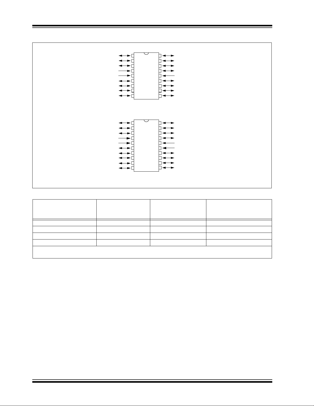
PIC16F62X
Pin Diagrams
PDIP, SOIC
RA4/TOCKI/CMP2
SSOP
RA2/AN2/V
RA3/AN3/CMP1
RA5/MCLR/V
REF
VSS
RB0/INT
RB1/RX/DT
RB2/TX/CK
RB3/CCP1
•1
2
3
PP
4
5
6
7
8
9
18
PIC16F62X
17
16
15
14
13
12
11
10
RA1/AN1
RA0/AN0
RA7/OSC1/CLKIN
RA6/OSC2/CLKOUT
DD
V
RB7/T1OSI/PGD
RB6/T1OSO/T1CKI/PGC
RB5
RB4/PGM
RA2/AN2/V
RA3/AN3/CMP1
RA4/TOCKI/CMP2
RA5/MCLR/V
REF
V
VSS
RB0/INT
RB1/RX/DT
RB2/TX/CK
RB3/CCP1
•1
2
PP
SS
3
4
5
6
7
8
9
10 11
20
19
PIC16F62X
18
17
16
15
14
13
12
RA1/AN1
RA0/AN0
RA7/OSC1/CLKIN
RA6/OSC2/CLKOUT
VDD
VDD
RB7/T1OSI/PGD
RB6/T1OSO/T1CKI/PGC
RB5
RB4/PGM
Device Differences
Device
Vol tag e
Range
Oscillator
PIC16F627 3.0 - 5.5 (Note 1) 0.7
PIC16F628 3.0 - 5.5 (Note 1) 0.7
PIC16LF627 2.0 - 5.5 (Note 1) 0.7
PIC16LF628 2.0 - 5.5 (Note 1) 0.7
Note 1: If you change from this device to another device, please verify oscillator characteristics in your
application.
Process
Technology
(Microns)
DS40300C-page 2 Preliminary 2003 Microchip Technology Inc.
Page 5

PIC16F62X
Table of Contents
1.0 General Description...................................................................................................................................................................... 5
2.0 PIC16F62X Device Varieties........................................................................................................................................................ 7
3.0 Architectural Overview ................................................................................................................................................................. 9
4.0 Memory Organization ................................................................................................................................................................. 15
5.0 I/O Ports ..................................................................................................................................................................................... 29
6.0 Timer0 Module ........................................................................................................................................................................... 43
7.0 Timer1 Module ........................................................................................................................................................................... 46
8.0 Timer2 Module ........................................................................................................................................................................... 50
9.0 Comparator Module.................................................................................................................................................................... 53
10.0 Voltage Reference Module......................................................................................................................................................... 59
11.0 Capture/Compare/PWM (CCP) Module ..................................................................................................................................... 61
12.0 Universal Synchronous/ Asynchronous Receiver/ Transmitter (USART) Module...................................................................... 67
13.0 Data EEPROM Memory ............................................................................................................................................................. 87
14.0 Special Features of the CPU...................................................................................................................................................... 91
15.0 Instruction Set Summary .......................................................................................................................................................... 107
16.0 Development Support............................................................................................................................................................... 121
17.0 Electrical Specifications............................................................................................................................................................ 127
18.0 DC and AC Characteristics Graphs and Tables....................................................................................................................... 143
19.0 Packaging Information.............................................................................................................................................................. 157
TO OUR VALUED CUSTOMERS
It is our intention to provide our valued customers with the best documentation possible to ensure successful use of your Microchip
products. To this end, we will continue to improve our publications to better suit your needs. Our publications will be refined and
enhanced as new volumes and updates are introduced.
If you have any questions or comments regarding this publication, please contact the Marketing Communications Department via
E-mail at docerrors@mail.microchip.com or fax the Reader Response Form in the back of this data sheet to (480) 792-4150.
We welcome your feedback.
Most Current Data Sheet
To obtain the most up-to-date version of this data sheet, please register at our Worldwide Web site at:
http://www.microchip.com
You can determine the version of a data sheet by examining its literature number found on the bottom outside corner of any page.
The last character of the literature number is the version number, (e.g., DS30000A is version A of document DS30000).
Errata
An errata sheet, describing minor operational differences from the data sheet and recommended workarounds, may exist for current
devices. As device/documentation issues become known to us, we will publish an errata sheet. The errata will specify the revision
of silicon and revision of document to which it applies.
To determine if an errata sheet exists for a particular device, please check with one of the following:
• Microchip’s Worldwide Web site; http://www.microchip.com
• Your local Microchip sales office (see last page)
• The Microchip Corporate Literature Center; U.S. FAX: (480) 792-7277
When contacting a sales office or the literature center, please specify which device, revision of silicon and data sheet (include liter-
ature number) you are using.
Customer Notification System
Register on our web site at www.microchip.com/cn to receive the most current information on all of our products.
2003 Microchip Technology Inc. Preliminary DS40300C-page 3
Page 6

PIC16F62X
NOTES:
DS40300C-page 4 Preliminary 2003 Microchip Technology Inc.
Page 7

PIC16F62X
1.0 PIC16F62X DEVICE VARIETIES
A variety of frequency ranges and packaging options
are available. Depending on application and production
requirements, the proper device option can be selected
using the information in the PIC16F62X Product
Identification System section (Page 167) at the end of
this data sheet. When placing orders, please use this
page of the data sheet to specify the correct part
number.
1.1 FLASH Devices
FLASH devices can be erased and reprogrammed
electrically. This allows the same device to be used for
prototype development, pilot programs and production.
A further advantage of the electrically-erasable FLASH
is that it can be erased and reprogrammed in-circuit, or
by device programmers, such as Microchip's
PICSTART
®
Plus, or PRO MATE® II programmers.
1.2 Quick-Turnaround Production
(QTP) Devices
Microchip offers a QTP Programming Service for
factory production orders. This service is made
available for users who chose not to program a
medium-to-high quantity of units and whose code
patterns have stabilized. The devices are standard
FLASH devices but with all program locations and configuration options already programmed by the factory.
Certain code and prototype verification procedures
apply before production shipments are available.
Please contact your Microchip Technology sales office
for more details.
1.3 Serialized Quick-Turnaround
Production (SQTP
Microchip offers a unique programming service where
a few user-defined locations in each device are
programmed with different serial numbers. The serial
numbers may be random, pseudo-random or
sequential.
Serial programming allows each device to have a
unique number which can serve as an entry-code,
password or ID number.
sm
) Devices
2003 Microchip Technology Inc. Preliminary DS40300C-page 5
Page 8

PIC16F62X
NOTES:
DS40300C-page 6 Preliminary 2003 Microchip Technology Inc.
Page 9

PIC16F62X
2.0 ARCHITECTURAL OVERVIEW
The high performance of the PIC16F62X family can be
attributed to a number of architectural features
commonly found in RISC microprocessors. To begin
with, the PIC16F62X uses a Harvard architecture, in
which, program and data are accessed from separate
memories using separate buses. This improves
bandwidth over traditional Von Neumann architecture
where program and data are fetched from the same
memory. Separating program and data memory further
allows instructions to be sized differently than 8-bit
wide data word. Instruction opcodes are 14-bits wide
making it possible to have all single-word instructions.
A 14-bit wide program memory access bus fetches a
14-bit instruction in a single cycle. A two-stage pipeline
overlaps fetch and execution of instructions.
Consequently, all instructions (35) execute in a single
cycle (200 ns @ 20 MHz) except for program
branches.
The Table below lists program memory (FLASH, Data
and EEPROM).
TABLE 2-1: DEVICE DESCRIPTION
Memory
Device
PIC16F627 1024 x 14 224 x 8 128 x 8
PIC16F628 2048 x 14 224 x 8 128 x 8
PIC16LF627 1024 x 14 224 x 8 128 x 8
PIC16LF628 2048 x 14 224 x 8 128 x 8
FLASH
Program
RAM
Data
EEPROM
Data
The ALU is 8-bit wide and capable of addition,
subtraction, shift and logical operations. Unless
otherwise mentioned, arithmetic operations are two's
complement in nature. In two-operand instructions,
typically one operand is the working register
(W register). The other operand is a file register or an
immediate constant. In single operand instructions, the
operand is either the W register or a file register.
The W register is an 8-bit working register used for ALU
operations. It is not an addressable register.
Depending on the instruction executed, the ALU may
affect the values of the Carry (C), Digit Carry (DC), and
Zero (Z) bits in the STATUS register. The C and DC bits
operate as a Borrow
respectively, bit in subtraction. See the SUBLW and
SUBWF instructions for examples.
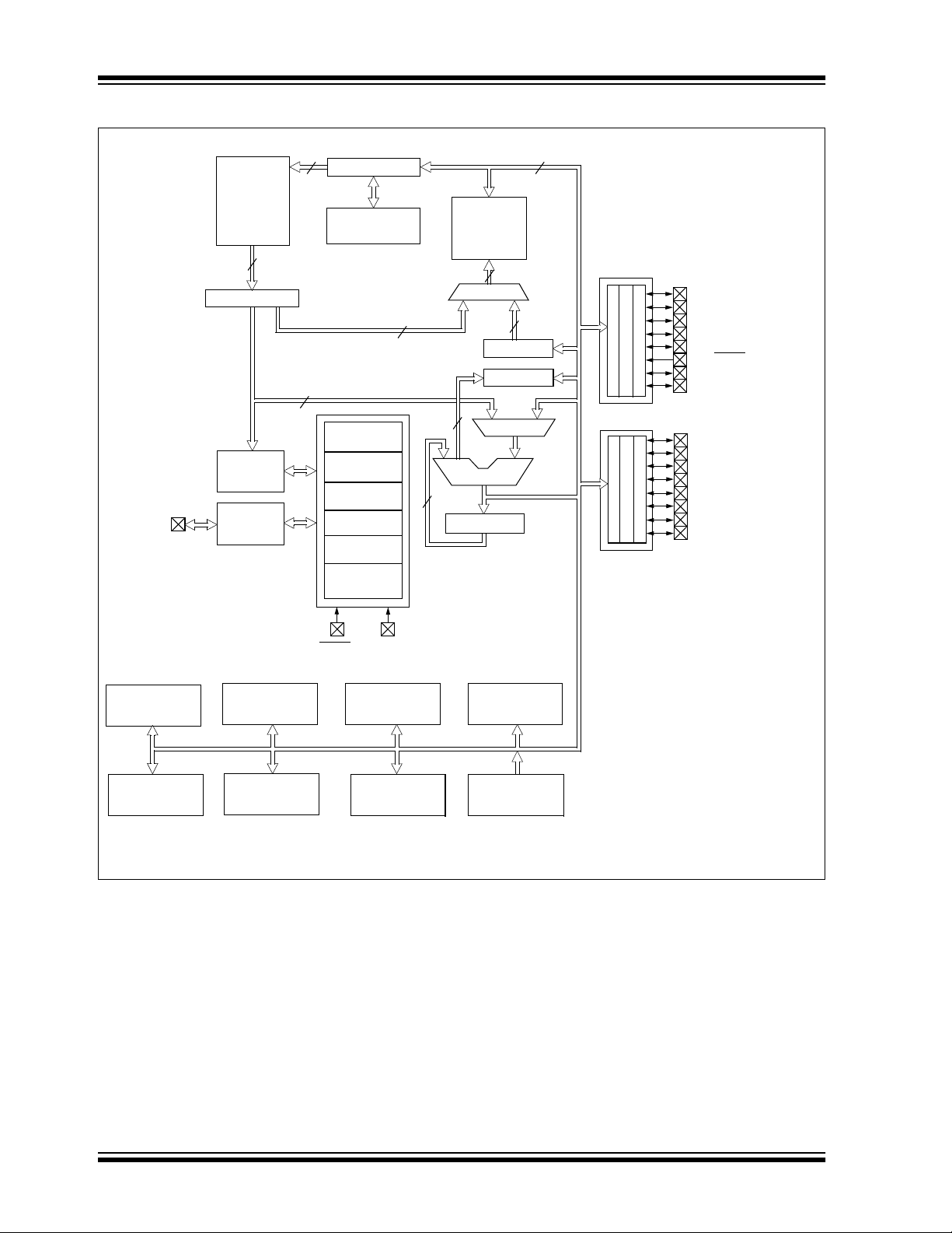
A simplified block diagram is shown in Figure 2-1, and
a description of the device pins in Table 2-1.
Two types of data memory are provided on the
PIC16F62X devices. Non-volatile EEPROM data
memory is provided for long term storage of data such
as calibration values, lookup table data, and any other
data which may require periodic updating in the field.
This data is not lost when power is removed. The other
data memory provided is regular RAM data memory.
Regular RAM data memory is provided for temporary
storage of data during normal operation. It is lost when
power is removed.
and Digit Borrow out bit,
The PIC16F62X can directly or indirectly address its
register files or data memory. All Special Function
registers, including the program counter, are mapped in
the data memory. The PIC16F62X have an orthogonal
(symmetrical) instruction set that makes it possible to
carry out any operation, on any register, using any
Addressing mode. This symmetrical nature, and lack of
‘special optimal situations’ make programming with the
PIC16F62X simple yet efficient. In addition, the learning
curve is reduced significantly.
The PIC16F62X devices contain an 8-bit ALU and
working register. The ALU is a general purpose
arithmetic unit. It performs arithmetic and Boolean
functions between data in the working register and any
register file.
2003 Microchip Technology Inc. Preliminary DS40300C-page 7
Page 10
PIC16F62X
FIGURE 2-1: BLOCK DIAGRAM
Program
Bus
OSC1/CLKIN
OSC2/CLKOUT
FLASH
Program
Memory
14
Instruction reg
Instruction
Decode &
Control
Timing
Generation
13
Program Counter
8-Level Stack
Direct Addr
8
Power-up
Oscillator
Start-up Timer
Power-on
Watchdog
Brown-out
Low-voltage
Programming
(13-bit)
Timer
Reset
Timer
Detect
RAM Addr (1)
7
8
Data Bus
3
RAM
File
Registers
9
Addr MUX
8
FSR reg
STATUS reg
MUX
ALU
W reg
8
Indirect
Addr
PORTA
PORTB
RA0/AN0
RA1/AN1
RA2/AN2/VREF
RA3/AN3/CMP1
RA4/T0CK1/CMP2
RA5/MCLR
RA6/OSC2/CLKOUT
RA7/OSC1/CLKIN
RB0/INT
RB1/RX/DT
RB2/TX/CK
RB3/CCP1
RB4/PGM
RB5
RB6/T1OSO/T1CKI/PGC
RB7/T1OSI/PGD
/VPP
VDD, VSS
MCLR
Comparator
VREF
Time r0 Timer1 Timer2
CCP1
USART
Note 1: Higher order bits are from the STATUS register.
Data EEPROM
DS40300C-page 8 Preliminary 2003 Microchip Technology Inc.
Page 11
PIC16F62X
TABLE 2-1: PIC16F62X PINOUT DESCRIPTION
Name Function Input Type Output Type Description
RA0/AN0 RA0 ST CMOS Bi-directional I/O port
AN0 AN — Analog comparator input
RA1/AN1 RA1 ST CMOS Bi-directional I/O port
AN1 AN — Analog comparator input
RA2/AN2/V
RA3/AN3/CMP1 RA3 ST CMOS Bi-directional I/O port
RA4/T0CKI/CMP2 RA4 ST OD Bi-directional I/O port
RA5/MCLR
RA6/OSC2/CLKOUT RA6 ST CMOS Bi-directional I/O port
RA7/OSC1/CLKIN RA7 ST CMOS Bi-directional I/O port
RB0/INT RB0 TTL CMOS Bi-directional I/O port. Can be software
RB1/RX/DT RB1 TTL CMOS Bi-directional I/O port. Can be software
RB2/TX/CK RB2 TTL CMOS Bi-directional I/O port.
RB3/CCP1 RB3 TTL CMOS Bi-directional I/O port. Can be software
Legend: O = Output CMOS = CMOS Output P = Power
REF RA2 ST CMOS Bi-directional I/O port
AN2 AN — Analog comparator input
REF —ANVREF output
V
AN3 AN — Analog comparator input
CMP1 — CMOS Comparator 1 output
T0CKI ST — Timer0 clock input
CMP2 — OD Comparator 2 output
/VPP RA5
MCLR
PP — — Programming voltage input. When configured
V
OSC2 XTAL — Oscillator crystal output. Connects to crystal
CLKOUT — CMOS In ER/INTRC mode, OSC2 pin can output
OSC1 XTAL — Oscillator crystal input
CLKIN ST — External clock source input. ER biasing pin.
INT ST — External interrupt.
RX ST — USART receive pin
DT ST CMOS Synchronous data I/O.
TX — CMOS USART transmit pin
CK ST CMOS Synchronous clock I/O. Can be software
CCP1 ST CMOS Capture/Compare/PWM I/O
— = Not used I = Input ST = Schmitt Trigger Input
TTL = TTL Input OD = Open Drain Output AN = Analog
ST — Input port
ST — Master clear
as MCLR
the device. Voltage on MCLR
exceed V
or resonator in Crystal Oscillator mode.
CLKOUT, which has 1/4 the frequency of
OSC1
programmed for internal weak pull-up.
programmed for internal weak pull-up.
programmed for internal weak pull-up.
programmed for internal weak pull-up.
, this pin is an active low RESET to
DD during normal device operation.
/VPP must not
2003 Microchip Technology Inc. Preliminary DS40300C-page 9
Page 12
PIC16F62X
TABLE 2-1: PIC16F62X PINOUT DESCRIPTION (CONTINUED)
Name Function Input Type Output Type Description
RB4/PGM RB4 TTL CMOS Bi-directional I/O port. Can be software
programmed for internal weak pull-up.
PGM ST — Low voltage programming input pin. Interrupt-
on-pin change. When low voltage programming is enabled, the interrupt-on-pin change
and weak pull-up resistor are disabled.
RB5 RB5 TTL CMOS Bi-directional I/O port. Interrupt-on-pin
change. Can be software programmed for
internal weak pull-up.
RB6/T1OSO/T1CKI/PGC RB6 TTL CMOS
T1OSO — XTAL Timer1 oscillator output.
T1CKI ST — Timer1 clock input.
PGC ST — ICSP™ Programming Clock.
RB7/T1OSI/PGD RB7 TTL CMOS Bi-directional I/O port. Interrupt-on-pin
T1OSI XTAL — Timer1 oscillator input. Wake-up from SLEEP
PGD ST CMOS ICSP Data I/O
SS
V
DD VDD Power — Positive supply for logic and I/O pins
V
Legend: O = Output CMOS = CMOS Output P = Power
— = Not used I = Input ST = Schmitt Trigger Input
TTL = TTL Input OD = Open Drain Output AN = Analog
SS
V
Power — Ground reference for logic and I/O pins
Bi-directional I/O port. Interrupt-on-pin
change. Can be software programmed for
internal weak pull-up.
change. Can be software programmed for
internal weak pull-up.
on pin change. Can be software programmed
for internal weak pull-up.
DS40300C-page 10 Preliminary 2003 Microchip Technology Inc.
Page 13
PIC16F62X
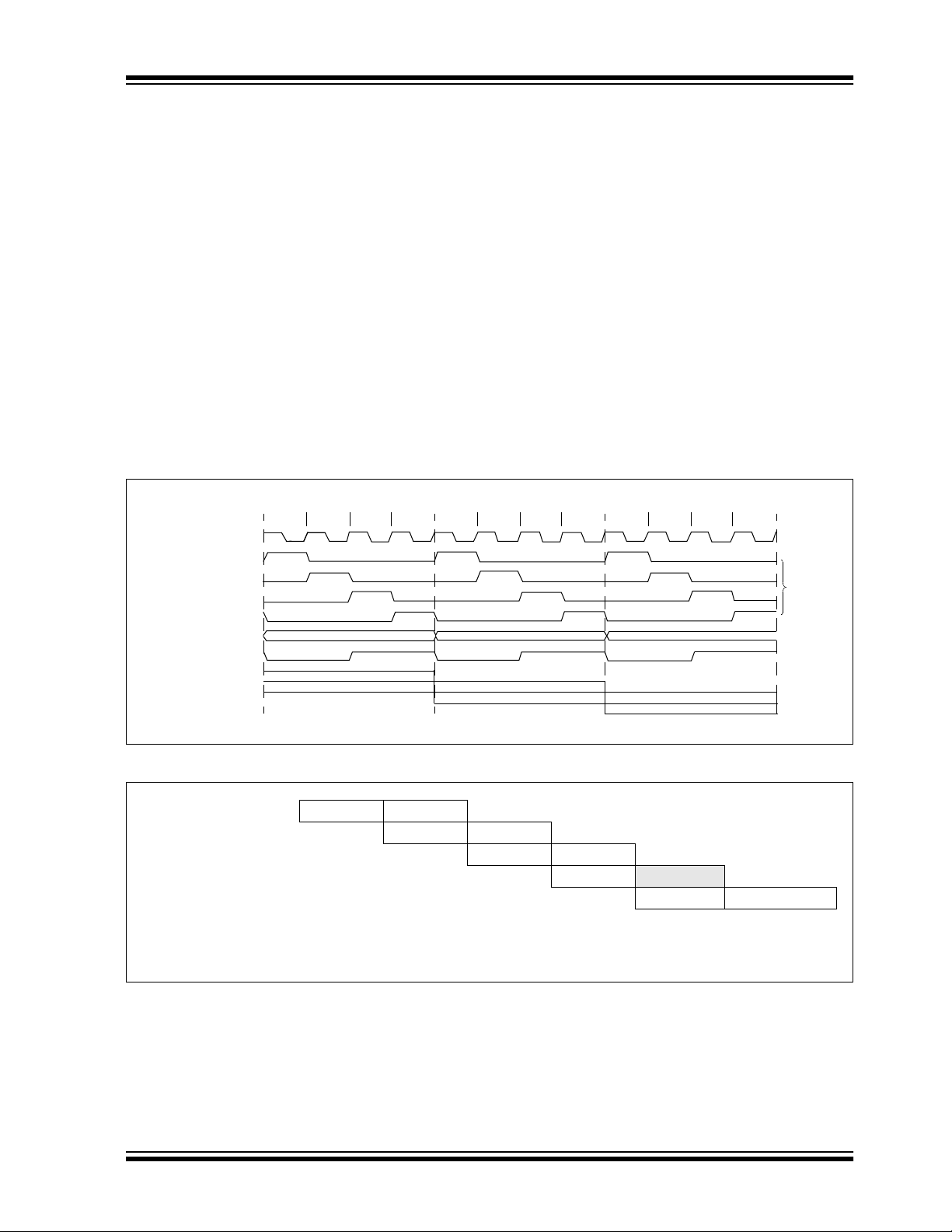
2.1 Clocking Scheme/Instruction
Cycle
The clock input (OSC1/CLKIN/RA7 pin) is internally
divided by four to generate four non-overlapping
quadrature clocks namely Q1, Q2, Q3 and Q4.
Internally, the program counter (PC) is incremented
every Q1, the instruction is fetched from the program
memory and latched into the instruction register in Q4.
The instruction is decoded and executed during the
following Q1 through Q4. The clocks and instruction
execution flow is shown in Figure 2-2.
FIGURE 2-2: CLOCK/INSTRUCTION CYCLE
Q2 Q3 Q4
OSC1
Q1
Q2
Q3
Q4
PC
CLKOUT
Q1
PC PC+1 PC+2
Fetch INST (PC)
Execute INST (PC-1) Fetch INST (PC+1)
Q1
2.2 Instruction Flow/Pipelining
An “Instruction Cycle” consists of four Q cycles (Q1,
Q2, Q3 and Q4). The instruction fetch and execute are
pipelined such that fetch takes one instruction cycle
while decode and execute takes another instruction
cycle. However, due to the pipelining, each instruction
effectively executes in one cycle. If an instruction
causes the program counter to change, (e.g., GOTO)
then two cycles are required to complete the instruction
(Example 2-1).
A fetch cycle begins with the program counter (PC)
incrementing in Q1.
In the execution cycle, the fetched instruction is latched
into the “Instruction Register (IR)” in cycle Q1. This
instruction is then decoded and executed during the
Q2, Q3, and Q4 cycles. Data memory is read during Q2
(operand read) and written during Q4 (destination
write).
Q2 Q3 Q4
Execute INST (PC) Fetch INST (PC+2)
Q2 Q3 Q4
Q1
Execute INST (PC+1)
Internal
phase
clock
EXAMPLE 2-1: INSTRUCTION PIPELINE FLOW
1. MOVLW 55h
2. MOVWF PORTB
3. CALL SUB_1
4. BSF PORTA, 3
All instructions are single cycle, except for any program branches. These take two cycles since the fetch instruction
is “flushed” from the pipeline while the new instruction is being fetched and then executed.
2003 Microchip Technology Inc. Preliminary DS40300C-page 11
Fetch 1 Execute 1
Fetch 2 Execute 2
Fetch 3 Execute 3
Fetch 4 Flush
Fetch SUB_1 Execute SUB_1
Page 14

PIC16F62X
NOTES:
DS40300C-page 12 Preliminary 2003 Microchip Technology Inc.
Page 15
PIC16F62X
3.0 MEMORY ORGANIZATION
3.1 Program Memory Organization
The PIC16F62X has a 13-bit program counter capable
of addressing an 8K x 14 program memory space. Only
the first 1K x 14 (0000h - 03FFh) for the PIC16F627
and 2K x 14 (0000h - 07FFh) for the PIC16F628 are
physically implemented. Accessing a location above
these boundaries will cause a wrap-around within the
first 1K x 14 space (PIC16F627) or 2K x 14 space
(PIC16F628). The RESET vector is at 0000h and the
interrupt vector is at 0004h (Figure 3-1).
FIGURE 3-1: PROGRAM MEMORY MAP
AND STACK
PC<12:0>
CALL, RETURN
RETFIE, RETLW
Stack Level 1
Stack Level 2
Stack Level 8
RESET Vector
13
000h
3.2 Data Memory Organization
The data memory (Figure 3-2) is partitioned into four
banks, which contain the general purpose registers and
the Special Function Registers (SFR). The SFR’s are
located in the first 32 locations of each Bank. Register
locations 20-7Fh, A0h-FFh, 120h-14Fh, 170h-17Fh
and 1F0h-1FFh are general purpose registers
implemented as static RAM.
The Table below lists how to access the four banks of
registers:
RP1 RP0
Bank0 00
Bank1 01
Bank2 10
Bank3 11
Addresses F0h-FFh, 170h-17Fh and 1F0h-1FFh are
implemented as common RAM and mapped back to
addresses 70h-7Fh.
3.2.1 GENERAL PURPOSE REGISTER
FILE
The register file is organized as 224 x 8 in the
PIC16F62X. Each is accessed either directly or
indirectly through the File Select Register FSR (See
Section 3.4).
Interrupt Vector
On-chip Program
Memory
PIC16F627 and
PIC16F628
On-chip Program
Memory
PIC16F628 only
0004
0005
03FFh
07FFh
1FFFh
2003 Microchip Technology Inc. Preliminary DS40300C-page 13
Page 16
PIC16F62X
FIGURE 3-2: DATA MEMORY MAP OF THE PIC16F627 AND PIC16F628
File
Address
Indirect addr.
TMR0
PCL
STATUS
FSR
PORTA
PORTB
PCLATH
INTCON
PIR1
TMR1L
TMR1H
T1CON
TMR2
T2CON
CCPR1L
CCPR1H
CCP1CON
RCSTA
TXREG
RCREG
CMCON
General
Purpose
Register
80 Bytes
16 Bytes
Bank 0
PCL
FSR
TRISB
(1)
180h
181h
182h
183h
184h
185h
186h
187h
188h
189h
18Ah
18Bh
18Ch
18Dh
18Eh
18Fh
1EFh
1F0h
1FFh
TMR0
PCL
FSR
(1)
100h
101h
102h
103h
104h
105h
106h
107h
108h
109h
10Ah
10Bh
10Ch
10Dh
10Eh
10Fh
11Fh
120h
14Fh
150h
16Fh
170h
17Fh
Indirect addr.
OPTION
STATUS
PCLATH
INTCON
accesses
70h - 7Fh
Bank 3
PCL
FSR
PIE1
PCON
PR2
(1)
80h
81h
82h
83h
84h
85h
86h
87h
88h
89h
8Ah
8Bh
8Ch
8Dh
8Eh
8Fh
90h
91h
92h
93h
94h
95h
96h
97h
98h
99h
9Ah
9Bh
9Ch
(1)
9Dh
9Eh
9Fh
A0h
EFh
F0h
FFh
Indirect addr.
STATUS
PORTB
PCLATH
INTCON
General
Purpose
Register
48 Bytes
accesses
70h-7Fh
Bank 2
(1)
00h
01h
02h
03h
04h
05h
06h
07h
08h
09h
0Ah
0Bh
0Ch
0Dh
0Eh
0Fh
10h
11h
12h
13h
14h
15h
16h
17h
18h
19h
1Ah
1Bh
1Ch
1Dh
1Eh
1Fh
20h
6Fh
70h
7Fh
Indirect addr.
OPTION
STATUS
TRISA
TRISB
PCLATH
INTCON
TXSTA
SPBRG
EEDATA
EEADR
EECON1
EECON2
VRCON
General
Purpose
Register
80 Bytes
accesses
70h-7Fh
Bank 1
Unimplemented data memory locations, read as '0'.
Note 1: Not a physical register.
DS40300C-page 14 Preliminary 2003 Microchip Technology Inc.
Page 17
PIC16F62X
3.2.2 SPECIAL FUNCTION REGISTERS
The SFRs are registers used by the CPU and Peripheral functions for controlling the desired operation of
the device (Table 3-1). These registers are static RAM.
The special registers can be classified into two sets
(core and peripheral). The SFRs associated with the
“core” functions are described in this section. Those
related to the operation of the peripheral features are
described in the section of that peripheral feature.
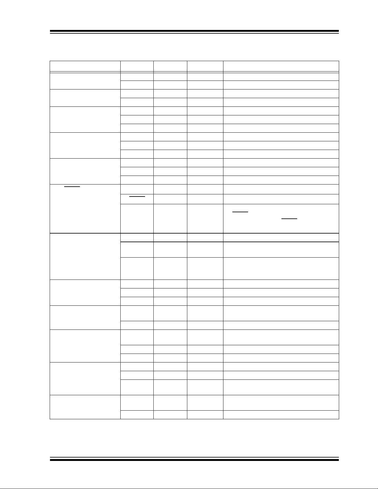
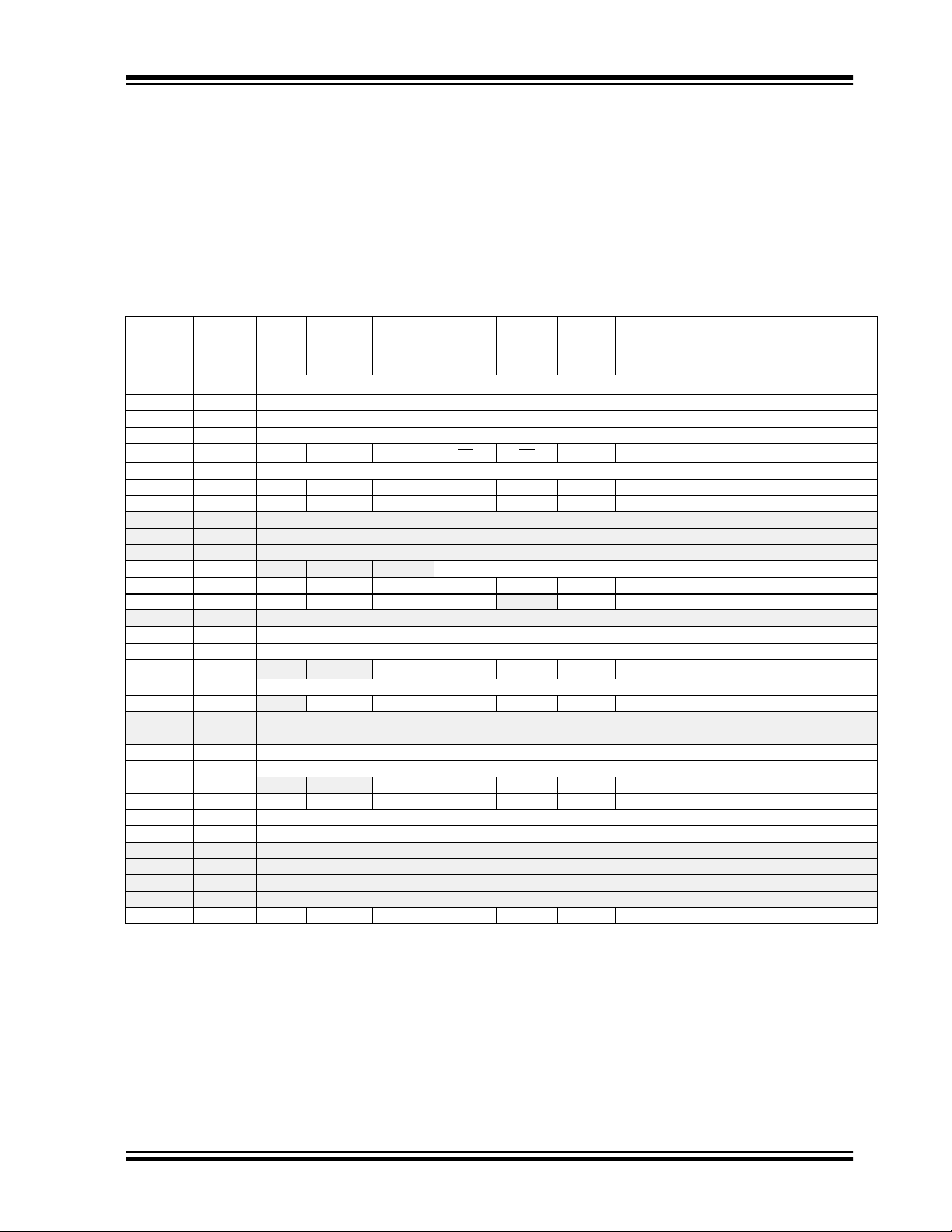
TABLE 3-1: SPECIAL REGISTERS SUMMARY BANK 0
Value on
Address Name Bit 7 Bit 6 Bit 5 Bit 4 Bit 3 Bit 2 Bit 1 Bit 0
POR
Reset
Bank 0
00h INDF Addressing this location uses contents of FSR to address data memory (not a physical register) xxxx xxxx 25
01h TMR0 Timer0 Module’s Register xxxx xxxx 43
02h PCL Program Counter's (PC) Least Significant Byte 0000 0000 13
03h STATUS
04h FSR Indirect data memory address pointer xxxx xxxx 25
05h PORTA
06h PORTB RB7 RB6 RB5 RB4 RB3 RB2 RB1 RB0 xxxx xxxx 34
07h — Unimplemented — —
08h — Unimplemented — —
09h — Unimplemented — —
0Ah PCLATH — — — Write buffer for upper 5 bits of program counter ---0 0000 25
0Bh INTCON GIE PEIE T0IE INTE RBIE T0IF INTF RBIF 0000 000x 21
0Ch PIR1
0Dh — Unimplemented — —
0Eh TMR1L Holding register for the Least Significant Byte of the 16-bit TMR1 xxxx xxxx 46
0Fh TMR1H Holding register for the Most Significant Byte of the 16-bit TMR1 xxxx xxxx 46
10h T1CON
11h TMR2 TMR2 module’s register 0000 0000 50
12h T2CON
13h — Unimplemented — —
14h — Unimplemented — —
15h CCPR1L Capture/Compare/PWM register (LSB) xxxx xxxx 61
16h CCPR1H Capture/Compare/PWM register (MSB) xxxx xxxx 61
17h CCP1CON
18h RCSTA SPEN RX9 SREN CREN ADEN FERR OERR RX9D 0000 -00x 67
19h TXREG USART Transmit data register 0000 0000 74
1Ah RCREG USART Receive data register 0000 0000 77
1Bh — Unimplemented — —
1Ch — Unimplemented — —
1Dh — Unimplemented — —
1Eh — Unimplemented — —
1Fh CMCON C2OUT C1OUT
IRP RP1 RP0 TO
RA7 RA6 RA5 RA4 RA3 RA2 RA1 RA0 xxxx 0000 29
EEIF CMIF RCIF TXIF — CCP1IF TMR2IF TMR1IF 0000 -000 23
— — T1CKPS1 T1CKPS0 T1OSCEN T1SYNC TMR1CS TMR1ON --00 0000 46
— TOUTPS3 TOUTPS2 TOUTPS1 TOUTPS0 TMR2ON T2CKPS1 T2CKPS0 -000 0000 50
— — CCP1X CCP1Y CCP1M3 CCP1M2 CCP1M1 CCP1M0 --00 0000 61
C2INV C1INV CIS CM2 CM1 CM0 0000 0000 53
PD ZDCC
Legend: — = Unimplemented locations read as ‘0’, u = unchanged, x = unknown, q = value depends on condition,
shaded = unimplemented
Note 1: For the Initialization Condition for Registers Tables, refer to Table 14-7 and Table 14-8 on page 98.
0001 1xxx 19
(1)
Details
on Page
2003 Microchip Technology Inc. Preliminary DS40300C-page 15
Page 18
PIC16F62X
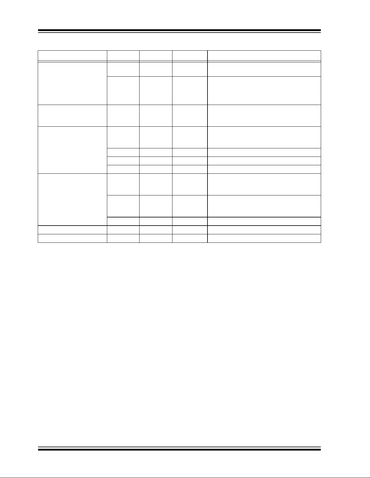
TABLE 3-2: SPECIAL FUNCTION REGISTERS SUMMARY BANK 1
Value on
Address Name Bit 7 Bit 6 Bit 5 Bit 4 Bit 3 Bit 2 Bit 1 Bit 0
POR
Reset
Bank 1
80h INDF Addressing this location uses contents of FSR to address data memory (not a physical
81h OPTION RBPU
82h PCL Program Counter's (PC) Least Significant Byte 0000 0000 25
83h STATUS IRP RP1 RP0 TO
84h FSR Indirect data memory address pointer xxxx xxxx 25
85h TRISA TRISA7 TRISA6 TRISA5 TRISA4 TRISA3 TRISA2 TRISA1 TRISA0 1111 1111 29
86h TRISB TRISB7 TRISB6 TRISB5 TRISB4 TRISB3 TRISB2 TRISB1 TRISB0 1111 1111 34
87h — Unimplemented — —
88h — Unimplemented — —
89h — Unimplemented — —
8Ah PCLATH
8Bh INTCON GIE PEIE T0IE INTE RBIE T0IF INTF RBIF 0000 000x 21
8Ch PIE1 EEIE CMIE RCIE TXIE — CCP1IE TMR2IE TMR1IE 0000 -000 22
8Dh — Unimplemented — —
8Eh PCON
8Fh — Unimplemented — —
90h — Unimplemented — —
91h — Unimplemented — —
92h PR2 Timer2 Period Register 1111 1111 50
93h — Unimplemented — —
94h — Unimplemented — —
95h — Unimplemented — —
96h — Unimplemented — —
97h — Unimplemented — —
98h TXSTA CSRC TX9 TXEN SYNC
99h SPBRG Baud Rate Generator Register 0000 0000 69
9Ah EEDATA EEPROM data register xxxx xxxx 87
9Bh EEADR
9Ch EECON1
9Dh EECON2 EEPROM control register 2 (not a physical register) -------- 87
9Eh — Unimplemented — —
9Fh VRCON VREN VROE VRR
register)
INTEDG T0CS T0SE PSA PS2 PS1 PS0 1111 1111 20
PD ZDCC0001 1xxx 19
— — — Write buffer for upper 5 bits of program counter ---0 0000 25
— — — — OSCF —PORBOD ---- 1-0x 24
— BRGH TRMT TX9D 0000 -010 69
— EEPROM address register xxxx xxxx 87
— — — — WRERR WREN WR RD ---- x000 87
— VR3 VR2 VR1 VR0 000- 0000 59
Legend: — = Unimplemented locations read as ‘0’, u = unchanged, x = unknown, q = value depends on condition, shaded = unim-
plemented
Note 1: For the Initialization Condition for Registers Tables, refer to Table 14-7 and Table 14-8 on page 98.
xxxx xxxx 25
(1)
Details on
Page
DS40300C-page 16 Preliminary 2003 Microchip Technology Inc.
Page 19
PIC16F62X
TABLE 3-3: SPECIAL FUNCTION REGISTERS SUMMARY BANK 2
Value on
Address Name Bit 7 Bit 6 Bit 5 Bit 4 Bit 3 Bit 2 Bit 1 Bit 0
POR
Reset
Bank 2
100h INDF Addressing this location uses contents of FSR to address data memory (not a physical reg-
101h TMR0 RBPU
102h PCL Program Counter's (PC) Least Significant Byte 0000 0000 25
103h STATUS IRP RP1 RP0 TO
104h FSR Indirect data memory address pointer xxxx xxxx 2 5
105h — Unimplemented — —
106h PORTB RB7 RB6 RB5 RB4 RB3 RB2 RB1 RB0 xxxx xxxx 34
107h — Unimplemented — —
108h — Unimplemented — —
109h — Unimplemented — —
10Ah PCLATH
10Bh INTCON GIE PEIE T0IE INTE RBIE T0IF INTF RBIF 0000 000x 21
10Ch — Unimplemented — —
10Dh — Unimplemented — —
10Eh — Unimplemented — —
10Fh — Unimplemented — —
110h — Unimplemented — —
111h — Unimplemented — —
112h — Unimplemented — —
113h — Unimplemented — —
114h — Unimplemented — —
115h — Unimplemented — —
116h — Unimplemented — —
117h — Unimplemented — —
118h — Unimplemented — —
119h — Unimplemented — —
11A h — Unimplemented — —
11B h — Unimplemented — —
11C h — Unimplemented — —
11D h — Unimplemented — —
11E h — Unimplemented — —
11Fh — Unimplemented — —
ister)
INTEDG T0CS T0SE PSA PS2 PS1 PS0 1111 1111 43
PD ZDCC0001 1xxx
— — — Write buffer for upper 5 bits of program counter ---0 0000 25
Legend: — = Unimplemented locations read as ‘0’, u = unchanged, x = unknown, q = value depends on condition, shaded = unim-
plemented.
Note 1: For the Initialization Condition for Registers Tables, refer to Table 14-7 and Table 14-8 on page 98.
xxxx xxxx 25
(1)
Details on
Page
19
2003 Microchip Technology Inc. Preliminary DS40300C-page 17
Page 20
PIC16F62X
TABLE 3-4: SPECIAL FUNCTION REGISTERS SUMMARY BANK 3
Value on
Address Name Bit 7 Bit 6 Bit 5 Bit 4 Bit 3 Bit 2 Bit 1 Bit 0
POR
Reset
Bank 3
180h INDF Addressing this location uses contents of FSR to address data memory (not a physical reg-
181h OPTION RBPU
182h PCL Program Counter's (PC) Least Significant Byte 0000 0000 25
183h STATUS IRP RP1 RP0 TO
184h FSR Indirect data memory address pointer xxxx xxxx 25
185h — Unimplemented — —
186h TRISB TRISB7 TRISB6 TRISB5 TRISB4 TRISB3 TRISB2 TRISB1 TRISB0 1111 1111 34
187h — Unimplemented — —
188h — Unimplemented — —
189h — Unimplemented — —
18Ah PCLATH
18Bh INTCON GIE PEIE T0IE INTE RBIE T0IF INTF RBIF 0000 000x 21
18Ch — Unimplemented — —
18Dh — Unimplemented — —
18Eh — Unimplemented — —
18Fh — Unimplemented — —
190h — Unimplemented — —
191h — Unimplemented — —
192h — Unimplemented — —
193h — Unimplemented — —
194h — Unimplemented — —
195h — Unimplemented — —
196h — Unimplemented — —
197h — Unimplemented — —
198h — Unimplemented — —
199h — Unimplemented — —
19Ah — Unimplemented — —
19Bh — Unimplemented — —
19Ch — Unimplemented — —
19Dh — Unimplemented — —
19Eh — Unimplemented — —
19Fh — Unimplemented — —
ister)
INTEDG T0CS T0SE PSA PS2 PS1 PS0 1111 1111 20
PD ZDCC 0001 1xxx 19
— — — Write buffer for upper 5 bits of program counter ---0 0000 25
Legend: — = Unimplemented locations read as ‘0’, u = unchanged, x = unknown, q = value depends on condition, shaded = unim-
plemented
Note 1: For the Initialization Condition for Registers Tables, refer to Table 14-7 and Table 14-8 on page 98.
xxxx xxxx 25
(1)
Details on
Page
DS40300C-page 18 Preliminary 2003 Microchip Technology Inc.
Page 21
PIC16F62X
3.2.2.1 STATUS Register
The STATUS register, shown in Register 3-1, contains
the arithmetic status of the ALU, the RESET status and
the bank select bits for data memory (SRAM).
The STATUS register can be the destination for any
instruction, like any other register. If the STATUS
register is the destination for an instruction that affects
the Z, DC or C bits, then the write to these three bits is
disabled. These bits are set or cleared according to the
device logic. Furthermore, the TO
writable. Therefore, the result of an instruction with the
STATUS register as destination may be different than
intended.
and PD bits are not
For example, CLRF STATUS will clear the upper-three
bits and set the Z bit. This leaves the STATUS register
as 000uu1uu (where u = unchanged).
It is recommended, therefore, that only BCF, BSF,
SWAPF and MOVWF instructions are used to alter the
STATUS register because these instructions do not
affect any STATUS bit. For other instructions, not
affecting any STATUS bits, see the “Instruction Set
Summary”.
Note 1: The C and DC bits operate as a Borrow
and Digit Borrow out bit, respectively, in
subtraction. See the SUBLW and SUBWF
instructions for examples.
REGISTER 3-1: STATUS REGISTER (ADDRESS: 03h, 83h, 103h, 183h)
R/W-0 R/W-0 R/W-0 R-1 R-1 R/W-x R/W-x R/W-x
IRP RP1 RP0 TO
bit 7 bit 0
bit 7 IRP: Register Bank Select bit (used for indirect addressing)
1 = Bank 2, 3 (100h - 1FFh)
0 = Bank 0, 1 (00h - FFh)
bit 6-5 RP1:RP0: Register Bank Select bits (used for direct addressing)
00 = Bank 0 (00h - 7Fh)
01 = Bank 1 (80h - FFh)
10 = Bank 2 (100h - 17Fh)
11 = Bank 3 (180h - 1FFh)
bit 4 TO
bit 3 PD
bit 2 Z: Zero bit
bit 1 DC: Digit carry/borrow
bit 0 C: Carry/borrow
: Timeout bit
1 = After power-up, CLRWDT instruction, or SLEEP instruction
0 = A WDT timeout occurred
: Power-down bit
1 = After power-up or by the CLRWDT instruction
0 = By execution of the SLEEP instruction
1 = The result of an arithmetic or logic operation is zero
0 = The result of an arithmetic or logic operation is not zero
bit (ADDWF, ADDLW,SUBLW,SUBWF instructions) (for borrow the polarity
is reversed)
1 = A carry-out from the 4th low order bit of the result occurred
0 = No carry-out from the 4th low order bit of the result
bit (ADDWF, ADDLW,SUBLW,SUBWF instructions)
1 = A carry-out from the Most Significant bit of the result occurred
0 = No carry-out from the Most Significant bit of the result occurred
Note 1: For borrow
complement of the second operand. For rotate (RRF, RLF) instructions, this bit is
loaded with either the high or low order bit of the source register.
Legend:
R = Readable bit W = Writable bit U = Unimplemented bit, read as ‘0’
-n = Value at POR ’1’ = Bit is set ’0’ = Bit is cleared x = Bit is unknown
the polarity is reversed. A subtraction is executed by adding the two’s
PD ZDCC
2003 Microchip Technology Inc. Preliminary DS40300C-page 19
Page 22

PIC16F62X
3.2.2.2 OPTION Register
The OPTION register is a readable and writable
register which contains various control bits to configure
the TMR0/WDT prescaler, the external RB0/INT
interrupt, TMR0, and the weak pull-ups on PORTB.
REGISTER 3-2: OPTION REGISTER (ADDRESS: 81h, 181h)
R/W-1 R/W-1 R/W-1 R/W-1 R/W-1 R/W-1 R/W-1 R/W-1
RBPU
bit 7 bit 0
INTEDG T0CS T0SE PSA PS2 PS1 PS0
Note: To achieve a 1:1 prescaler assignment for
TMR0, assign the prescaler to the WDT
(PSA = 1). See Section 6.3.1
bit 7 RBPU
: PORTB Pull-up Enable bit
1 = PORTB pull-ups are disabled
0 = PORTB pull-ups are enabled by individual port latch values
bit 6 INTEDG: Interrupt Edge Select bit
1 = Interrupt on rising edge of RB0/INT pin
0 = Interrupt on falling edge of RB0/INT pin
bit 5 T0CS: TMR0 Clock Source Select bit
1 = Transition on RA4/T0CKI pin
0 = Internal instruction cycle clock (CLKOUT)
bit 4 T0SE: TMR0 Source Edge Select bit
1 = Increment on high-to-low transition on RA4/T0CKI pin
0 = Increment on low-to-high transition on RA4/T0CKI pin
bit 3 PSA: Prescaler Assignment bit
1 = Prescaler is assigned to the WDT
0 = Prescaler is assigned to the Timer0 module
bit 2-0 PS2:PS0: Prescaler Rate Select bits
Bit Value TMR0 Rate WDT Rate
000
001
010
011
100
101
110
111
1 : 2
1 : 4
1 : 8
1 : 16
1 : 32
1 : 64
1 : 128
1 : 256
1 : 1
1 : 2
1 : 4
1 : 8
1 : 16
1 : 32
1 : 64
1 : 128
Legend:
R = Readable bit W = Writable bit U = Unimplemented bit, read as ‘0’
-n = Value at POR ’1’ = Bit is set ’0’ = Bit is cleared x = Bit is unknown
DS40300C-page 20 Preliminary 2003 Microchip Technology Inc.
Page 23
PIC16F62X
3.2.2.3 INTCON Register
The INTCON register is a readable and writable
register which contains the various enable and flag bits
for all interrupt sources except the comparator module.
See Section 3.2.2.4 and Section 3.2.2.5 for a
description of the comparator enable and flag bits.
Note: Interrupt flag bits get set when an interrupt
condition occurs regardless of the state of
its corresponding enable bit or the global
enable bit, GIE (INTCON<7>).
REGISTER 3-3: INTCON REGISTER (ADDRESS: 0Bh, 8Bh, 10Bh, 18Bh)
R/W-0 R/W-0 R/W-0 R/W-0 R/W-0 R/W-0 R/W-0 R/W-x
GIE PEIE T0IE INTE RBIE T0IF INTF RBIF
bit 7 bit 0
bit 7 GIE: Global Interrupt Enable bit
1 = Enables all unmasked interrupts
0 = Disables all interrupts
bit 6 PEIE: Peripheral Interrupt Enable bit
1 = Enables all unmasked peripheral interrupts
0 = Disables all peripheral interrupts
bit 5 T0IE: TMR0 Overflow Interrupt Enable bit
1 = Enables the TMR0 interrupt
0 = Disables the TMR0 interrupt
bit 4 INTE: RB0/INT External Interrupt Enable bit
1 = Enables the RB0/INT external interrupt
0 = Disables the RB0/INT external interrupt
bit 3 RBIE: RB Port Change Interrupt Enable bit
1 = Enables the RB port change interrupt
0 = Disables the RB port change interrupt
bit 2 T0IF: TMR0 Overflow Interrupt Flag bit
1 = TMR0 register has overflowed (must be cleared in software)
0 = TMR0 register did not overflow
bit 1 INTF: RB0/INT External Interrupt Flag bit
1 = The RB0/INT external interrupt occurred (must be cleared in software)
0 = The RB0/INT external interrupt did not occur
bit 0 RBIF: RB Port Change Interrupt Flag bit
1 = When at least one of the RB7:RB4 pins changed state (must be cleared in software)
0 = None of the RB7:RB4 pins have changed state
Legend:
R = Readable bit W = Writable bit U = Unimplemented bit, read as ‘0’
-n = Value at POR ’1’ = Bit is set ’0’ = Bit is cleared x = Bit is unknown
2003 Microchip Technology Inc. Preliminary DS40300C-page 21
Page 24

PIC16F62X
3.2.2.4 PIE1 Register
This register contains interrupt enable bits.
REGISTER 3-4: PIE1 REGISTER (ADDRESS: 8Ch)
R/W-0 R/W-0 R/W-0 R/W-0 U-0 R/W-0 R/W-0 R/W-0
EEIE CMIE RCIE TXIE
bit 7 bit 0
bit 7 EEIE: EE Write Complete Interrupt Enable Bit
1 = Enables the EE write complete interrupt
0 = Disables the EE write complete interrupt
bit 6 CMIE: Comparator Interrupt Enable bit
1 = Enables the comparator interrupt
0 = Disables the comparator interrupt
bit 5 RCIE: USART Receive Interrupt Enable bit
1 = Enables the USART receive interrupt
0 = Disables the USART receive interrupt
bit 4 TXIE: USART Transmit Interrupt Enable bit
1 = Enables the USART transmit interrupt
0 = Disables the USART transmit interrupt
bit 3 Unimplemented: Read as ‘0’
bit 2 CCP1IE: CCP1 Interrupt Enable bit
1 = Enables the CCP1 interrupt
0 = Disables the CCP1 interrupt
bit 1 TMR2IE: TMR2 to PR2 Match Interrupt Enable bit
1 = Enables the TMR2 to PR2 match interrupt
0 = Disables the TMR2 to PR2 match interrupt
bit 0 TMR1IE: TMR1 Overflow Interrupt Enable bit
1 = Enables the TMR1 overflow interrupt
0 = Disables the TMR1 overflow interrupt
— CCP1IE TMR2IE TMR1IE
Legend:
R = Readable bit W = Writable bit U = Unimplemented bit, read as ‘0’
-n = Value at POR ’1’ = Bit is set ’0’ = Bit is cleared x = Bit is unknown
DS40300C-page 22 Preliminary 2003 Microchip Technology Inc.
Page 25

PIC16F62X
3.2.2.5 PIR1 Register
This register contains interrupt flag bits.
REGISTER 3-5: PIR1 REGISTER (ADDRESS: 0Ch)
R/W-0 R/W-0 R-0 R-0 U-0 R/W-0 R/W-0 R/W-0
EEIF CMIF RCIF TXIF
bit 7 bit 0
bit 7 EEIF: EEPROM Write Operation Interrupt Flag bit
1 = The write operation completed (must be cleared in software)
0 = The write operation has not completed or has not been started
bit 6 CMIF: Comparator Interrupt Flag bit
1 = Comparator output has changed
0 = Comparator output has not changed
bit 5 RCIF: USART Receive Interrupt Flag bit
1 = The USART receive buffer is full
0 = The USART receive buffer is empty
bit 4 TXIF: USART Transmit Interrupt Flag bit
1 = The USART transmit buffer is empty
0 = The USART transmit buffer is full
bit 3 Unimplemented: Read as ‘0’
bit 2 CCP1IF: CCP1 Interrupt Flag bit
Capture Mode
1 = A TMR1 register capture occurred (must be cleared in software)
0 = No TMR1 register capture occurred
Compare Mode
1 = A TMR1 register compare match occurred (must be cleared in software)
0 = No TMR1 register compare match occurred
PWM Mode
Unused in this mode
bit 1 TMR2IF: TMR2 to PR2 Match Interrupt Flag bit
1 = TMR2 to PR2 match occurred (must be cleared in software)
0 = No TMR2 to PR2 match occurred
bit 0 TMR1IF: TMR1 Overflow Interrupt Flag bit
1 = TMR1 register overflowed (must be cleared in software)
0 = TMR1 register did not overflow
Note: Interrupt flag bits get set when an interrupt
condition occurs regardless of the state of
its corresponding enable bit or the global
enable bit, GIE (INTCON<7>). User
software should ensure the appropriate
interrupt flag bits are clear prior to enabling
an interrupt.
— CCP1IF TMR2IF TMR1IF
Legend:
R = Readable bit W = Writable bit U = Unimplemented bit, read as ‘0’
-n = Value at POR ’1’ = Bit is set ’0’ = Bit is cleared x = Bit is unknown
2003 Microchip Technology Inc. Preliminary DS40300C-page 23
Page 26
PIC16F62X
3.2.2.6 PCON Register
The PCON register contains flag bits to differentiate
between a Power-on Reset, an external MCLR
WDT Reset or a Brown-out Detect.
Reset,
REGISTER 3-6: PCON REGISTER (ADDRESS: 0Ch)
U-0 U-0 U-0 U-0 R/W-1 U-0 R/W-q R/W-q
— — — — OSCF —PORBOD
bit 7 bit 0
bit 7-4 Unimplemented: Read as '0'
bit 3 OSCF: INTRC/ER oscillator frequency
1 = 4 MHz typical
0 = 37 KHz typical
bit 2 Unimplemented: Read as '0'
bit 1 POR
bit 0 BOD
: Power-on Reset STATUS bit
1 = No Power-on Reset occurred
0 = A Power-on Reset occurred (must be set in software after a Power-on Reset occurs)
: Brown-out Detect STATUS bit
1 = No Brown-out Reset occurred
0 = A Brown-out Reset occurred (must be set in software after a Brown-out Reset occurs)
Note 1: When in ER Oscillator mode, setting OSCF = 1 will cause the oscillator frequency to
(1)
change to the frequency specified by the external resistor.
Note: BOD is unknown on Power-on Reset. It
must then be set by the user and checked
on subsequent RESETS to see if BOD
cleared, indicating a brown-out has
occurred. The BOD
care” and is not necessarily predictable if
the brown-out circuit is disabled (by
clearing the BODEN bit in the
Configuration word).
STATUS bit is a “don't
is
Legend:
R = Readable bit W = Writable bit U = Unimplemented bit, read as ‘0’
-n = Value at POR ’1’ = Bit is set ’0’ = Bit is cleared x = Bit is unknown
DS40300C-page 24 Preliminary 2003 Microchip Technology Inc.
Page 27
PIC16F62X
3.3 PCL and PCLATH
The program counter (PC) is 13-bits wide. The low byte
comes from the PCL register, which is a readable and
writable register. The high byte (PC<12:8>) is not
directly readable or writable and comes from PCLATH.
On any RESET, the PC is cleared. Figure 3-3 shows
the two situations for the loading of the PC. The upper
example in the figure shows how the PC is loaded on a
write to PCL (PCLATH<4:0> → PCH). The lower exam-
ple in the figure shows how the PC is loaded during a
CALL or GOTO instruction (PCLATH<4:3> → PCH).
FIGURE 3-3: LOADING OF PC IN
DIFFERENT SITUATIONS
PCH PCL
12 8 7 0
PC
PCLATH<4:0>
5
PCLATH
PCH PCL
12 11 10 0
PC
2
87
PCLATH<4:3>
PCLATH
11
8
Instruction with
PCL as
Destination
ALU result
GOTO, CALL
Opcode <10:0>
The stack operates as a circular buffer. This means that
after the stack has been PUSHed eight times, the ninth
push overwrites the value that was stored from the first
push. The tenth push overwrites the second push (and
so on).
Note 1: There are no STATUS bits to indicate
stack overflow or stack underflow
conditions.
2: There are no instructions/mnemonics
called PUSH or POP. These are actions
that occur from the execution of the
CALL, RETURN, RETLW and RETFIE
instructions, or the vectoring to an
interrupt address.
3.4 Indirect Addressing, INDF and
FSR Registers
The INDF register is not a physical register. Addressing
the INDF register will cause indirect addressing.
Indirect addressing is possible by using the INDF
register. Any instruction using the INDF register actually accesses data pointed to by the file select register
(FSR). Reading INDF itself indirectly will produce 00h.
Writing to the INDF register indirectly results in a nooperation (although STATUS bits may be affected). An
effective 9-bit address is obtained by concatenating the
8-bit FSR register and the IRP bit (STATUS<7>), as
shown in Figure 3-4.
A simple program to clear RAM location 20h-2Fh using
indirect addressing is shown in Example 3-1.
3.3.1 COMPUTED GOTO
A computed GOTO is accomplished by adding an offset
to the program counter (ADDWF PCL). When doing a
table read using a computed GOTO method, care
should be exercised if the table location crosses a PCL
memory boundary (each 256 byte block). Refer to the
application note “Implementing a Table Read” (AN556).
3.3.2 STACK
The PIC16F62X family has an 8-level deep x 13-bit
wide hardware stack (Figure 3-1 and Figure 3-2). The
stack space is not part of either program or data space
and the stack pointer is not readable or writable. The
PC is PUSHed onto the stack when a CALL instruction
is executed or an interrupt causes a branch. The stack
is POPed in the event of a RETURN, RETLW or a
RETFIE instruction execution. PCLATH is not affected
by a PUSH or POP operation.
EXAMPLE 3-1: Indirect Addressing
movlw 0x20 ;initialize pointer
movwf FSR ;to RAM
NEXT clrf INDF ;clear INDF register
incf FSR ;inc pointer
btfss FSR,4 ;all done?
goto NEXT ;no clear next
;yes continue
2003 Microchip Technology Inc. Preliminary DS40300C-page 25
Page 28
PIC16F62X
FIGURE 3-4: DIRECT/INDIRECT ADDRESSING PIC16F62X
RP1 RP0 6
from opcode
0
Indirect AddressingDirect Addressing
IRP FSR register
7
0
bank select location select
00 01 10 11
00h
RAM
File
Registers
7Fh
Bank 0 Bank 1 Bank 2 Bank 3
Note: For memory map detail see Figure 3-2.
bank select
180h
1FFh
location select
DS40300C-page 26 Preliminary 2003 Microchip Technology Inc.
Page 29
PIC16F62X
4.0 GENERAL DESCRIPTION
The PIC16F62X are 18-Pin FLASH-based members of
the versatile PIC16CXX family of low cost, high performance, CMOS, fully static, 8-bit microcontrollers.
®
All PICmicro
RISC architecture. The PIC16F62X have enhanced
core features, eight-level deep stack, and multiple
internal and external interrupt sources. The separate
instruction and data buses of the Harvard architecture
allow a 14-bit wide instruction word with the separate 8bit wide data. The two-stage instruction pipeline allows
all instructions to execute in a single cycle, except for
program branches (which require two cycles). A total of
35 instructions (reduced instruction set) are available.
Additionally, a large register set gives some of the
architectural innovations used to achieve a very high
performance.
PIC16F62X microcontrollers typically achieve a 2:1
code compression and a 4:1 speed improvement over
other 8-bit microcontrollers in their class.
PIC16F62X devices have special features to reduce
external components, thus reducing system cost,
enhancing system reliability and reducing power consumption.
The PIC16F62X has eight oscillator configurations.
The single pin ER oscillator provides a low cost solution. The LP oscillator minimizes power consumption,
XT is a standard crystal, INTRC is a self-contained
internal oscillator. The HS is for High Speed crystals.
The EC mode is for an external clock source.
microcontrollers employ an advanced
The SLEEP (Power-down) mode offers power savings.
The user can wake-up the chip from SLEEP through
several external interrupts, internal interrupts, and
RESETS.
A highly reliable Watchdog Timer with its own on-chip
RC oscillator provides protection against software lockup.
Table 4-1 shows the features of the PIC16F62X midrange microcontroller families.
A simplified block diagram of the PIC16F62X is shown
in Figure 2.1.
The PIC16F62X series fits in applications ranging from
battery chargers to low power remote sensors. The
FLASH technology makes customization of application
programs (detection levels, pulse generation, timers,
etc.) extremely fast and convenient. The small footprint
packages make this microcontroller series ideal for all
applications with space limitations. Low cost, low
power, high performance, ease of use and I/O flexibility
make the PIC16F62X very versatile.
4.1 Development Support
The PIC16F62X family is supported by a full featured
macro assembler, a software simulator, an in-circuit
emulator, a low cost development programmer and a
full-featured programmer. A Third Party “C” compiler
support tool is also available.
TABLE 4-1: PIC16F62X FAMILY OF DEVICES
PIC16F627 PIC16F628 PIC16LF627 PIC16LF628
Clock Maximum Frequency of Operation
Memory RAM Data Memory (bytes) 224 224 224 224
Peripherals Capture/Compare/PWM modules 1 1 1 1
Features Voltage Range (Volts) 3.0-5.5 3.0-5.5 2.0-5.5 2.0-5.5
All PICmicro® Family devices have Power-on Reset, selectable Watchdog Timer, selectable code protect and high I/O current capability. All
PIC16F62X Family devices use serial programming with clock pin RB6 and data pin RB7.
(MHz)
FLASH Program Memory (words) 1024 2048 1024 2048
EEPROM Data Memory (bytes) 128 128 128 128
Timer Module(s) TMR0, TMR1, TMR2 TMR0, TMR1, TMR2 TMR0, TMR1, TMR2 TMR0, TMR1, TMR2
Comparator(s) 2 2 2 2
Serial Communications USART USART USART USART
Internal Voltage Reference Yes Yes Yes Yes
Interrupt Sources 10 10 10 10
I/O Pins 16 16 16 16
Brown-out Detect Yes Yes Yes Yes
Packages 18-pin DIP, SOIC,
20 20 4 4
20-pin SSOP
18-pin DIP, SOIC,
20-pin SSOP
18-pin DIP, SOIC,
20-pin SSOP
18-pin DIP, SOIC,
20-pin SSOP
2003 Microchip Technology Inc. Preliminary DS40300C-page 27
Page 30

PIC16F62X
NOTES:
DS40300C-page 28 Preliminary 2003 Microchip Technology Inc.
Page 31

PIC16F62X
5.0 I/O PORTS
The PIC16F62X have two ports, PORTA and PORTB.
Some pins for these I/O ports are multiplexed with an
alternate function for the peripheral features on the
device. In general, when a peripheral is enabled, that
pin may not be used as a general purpose I/O pin.
5.1 PORTA and TRISA Registers
PORTA is an 8-bit wide latch. RA4 is a Schmitt Trigger
input and an open drain output. Port RA4 is multiplexed
with the T0CKI clock input. RA5 is a Schmitt Trigger
input only and has no output drivers. All other RA port
pins have Schmitt Trigger input levels and full CMOS
output drivers. All pins have data direction bits (TRIS
registers) which can configure these pins as input or
output.
A '1' in the TRISA register puts the corresponding output driver in a Hi-impedance mode. A '0' in the TRISA
register puts the contents of the output latch on the
selected pin(s).
Reading the PORTA register reads the status of the
pins whereas writing to it will write to the port latch. All
write operations are read-modify-write operations. So a
write to a port implies that the port pins are first read,
then this value is modified and written to the port data
latch.
The PORTA pins are multiplexed with comparator and
voltage reference functions. The operation of these
pins are selected by control bits in the CMCON
(comparator control register) register and the VRCON
(voltage reference control register) register. When
selected as a comparator input, these pins will read
as '0's.
Note: RA5 shares function with VPP. When VPP
voltage levels are applied to RA5, the
device will enter Programming mode.
Note 1: On RESET, the TRISA register is set to all
inputs. The digital inputs are disabled and
the comparator inputs are forced to
ground to reduce current consumption.
2: TRISA<6:7> is overridden by oscillator
configuration. When PORTA<6:7> is
overridden, the data reads ‘0’ and the
TRISA<6:7> bits are ignored.
TRISA controls the direction of the RA pins, even when
they are being used as comparator inputs. The user
must make sure to keep the pins configured as inputs
when using them as comparator inputs.
The RA2 pin will also function as the output for the
voltage reference. When in this mode, the V
very high impedance output. The user must configure
TRISA<2> bit as an input and use high impedance
loads.
In one of the Comparator modes defined by the
CMCON register, pins RA3 and RA4 become outputs
of the comparators. The TRISA<4:3> bits must be
cleared to enable outputs to use this function.
REF pin is a
EXAMPLE 5-1: Initializing PORTA
CLRF PORTA ;Initialize PORTA by
;setting output data latches
MOVLW 0x07 ;Turn comparators off and
MOVWF CMCON ;enable pins for I/O
;functions
BCF STATUS, RP1
BSF STATUS, RP0;Select Bank1
MOVLW 0x1F ;Value used to initialize
;data direction
MOVWF TRISA ;Set RA<4:0> as inputs
;TRISA<5> always
;read as ‘1’.
;TRISA<7:6>
;depend on oscillator mode
2003 Microchip Technology Inc. Preliminary DS40300C-page 29
Page 32

PIC16F62X
FIGURE 5-1: BLOCK DIAGRAM OF
RA0/AN0:RA1/AN1 PINS
Data
Bus
WR
PORTA
WR
TRISA
RD
TRISA
RD PORTA
To Comparator
Data Latch
TRIS Latch
CK
CK
QD
Q
QD
Q
Analog
Input Mode
Schmitt Trigger
Input Buffer
DQ
EN
VDD
VSS
I/O Pin
FIGURE 5-2: BLOCK DIAGRAM OF
RA2/VREF PIN
Data
Bus
WR
PORTA
WR
TRISA
RD
TRISA
RD PORTA
To Comparator
Data Latch
TRIS Latch
CK
CK
VROE
QD
Q
QD
Q
Analog
Input Mode
Schmitt Trigger
Input Buffer
EN
VDD
VSS
DQ
RA2 Pin
FIGURE 5-3: BLOCK DIAGRAM OF THE RA3/AN3 PIN
Data
Bus
WR
PORTA
WR
TRISA
RD
TRISA
RD PORTA
CK
Data Latch
CK
TRIS Latch
QD
Comparator Output
Q
QD
Q
Comparator Mode = 110
1
0
VREF
Input Mode
DQ
EN
Analog
Schmitt Trigger
Input Buffer
VDD
RA3 Pin
VSS
To Comparator
DS40300C-page 30 Preliminary 2003 Microchip Technology Inc.
Page 33

FIGURE 5-4: BLOCK DIAGRAM OF RA4/T0CKI PIN
Data
Bus
WR
PORTA
WR
TRISA
RD PORTA
CK
Data Latch
CK
TRIS Latch
RD TRISA
QD
Comparator Output
Q
QD
Q
Comparator Mode = 110
PIC16F62X
1
0
N
Vss
Schmitt Trigger
Input Buffer
DQ
EN
VDD
RA4 Pin
Vss
TMR0 Clock Input
FIGURE 5-5: BLOCK DIAGRAM OF THE
/VPP PIN
RA5/MCLR/VPP
VSS
MCLR
circuit
Program
mode
Data
Bus
RD
TRISA
RD
PORTA
MCLRE
MCLR
HV Detect
RA5/MCLR
Filter
Schmitt Trigger
Input Buffer
VSS
DQ
EN
FIGURE 5-6: BLOCK DIAGRAM OF
RA6/OSC2/CLKOUT PIN
From OSC1
CLKOUT(FOSC/4)
WR
PORTA
(FOSC =
101, 111)
WR
TRISA
RD
TRISA
F
OSC =
100, 110
RD PORTA
Note 1: INTRC with RA6 = I/O or ER with RA6 = I/O.
DCKQ
Q
Data Latch
(2)
DCKQ
Q
TRIS Latch
(1)
2: INTRC with RA6 = CLKOUT or ER with RA6 = CLK-
OUT.
1
0
QD
EN
OSC
Circuit
VDD
VSS
Schmitt
Trigger
Input Buffer
2003 Microchip Technology Inc. Preliminary DS40300C-page 31
Page 34

PIC16F62X
FIGURE 5-7: BLOCK DIAGRAM OF RA7/OSC1/CLKIN PIN
To OS C 2
CLKIN to core
Data Bus
WR PORTA
WR TRISA
RD TRISA
OSC = 100, 101
F
CK
Data Latch
D
CK
TRIS Latch
(1)
QD
Q
Q
Q
Oscillator
Circuit
EN
VDD
RA7/OSC1/CLKIN Pin
VSS
DQ
Schmitt Trigger
Input Buffer
RD PORTA
Note 1: INTRC with CLKOUT, and INTRC with I/O.
DS40300C-page 32 Preliminary 2003 Microchip Technology Inc.
Page 35

PIC16F62X
TABLE 5-1: PORTA FUNCTIONS
Name
RA0/AN0 RA0 ST CMOS Bi-directional I/O port
RA1/AN1 RA1 ST CMOS Bi-directional I/O port
RA2/AN2/V
RA3/AN3/CMP1 RA3 ST CMOS Bi-directional I/O port
RA4/T0CKI/CMP2 RA4 ST OD Bi-directional I/O port
RA5/MCLR
RA6/OSC2/CLKOUT RA6 ST CMOS Bi-directional I/O port.
RA7/OSC1/CLKIN RA7 ST CMOS Bi-directional I/O port
Legend: ST = Schmitt Trigger input HV = High Voltage OD = Open Drain AN = Analog
REF RA2 ST CMOS Bi-directional I/O port
/VPP RA5 ST —
FunctionInput
Type
AN0 AN — Analog comparator input
AN1 AN — Analog comparator input
AN2 AN — Analog comparator input
REF —ANVREF output
V
AN3 AN — Analog comparator input
CMP1 — CMOS Comparator 1 output
T0CKI ST — External clock input for TMR0 or comparator output. Output
CMP2 — OD Comparator 2 output
MCLR
V
PP HV —
OSC2 XTAL — Oscillator crystal output. Connects to crystal resonator in
CLKOUT — CMOS In ER/INTRC mode, OSC2 pin can output CLKOUT, which
OSC1 XTAL — Oscillator crystal input
CLKIN ST — External clock source input. ER biasing pin.
ST —
Output
Type
Description
is open drain type
Input port
Master clear
Programming voltage input. When configured as MCLR
this pin is an active low RESET to the device. Voltage on
/VPP must not exceed VDD during normal device
MCLR
operation
Crystal Oscillator mode.
has 1/4 the frequency of OSC1
,
2003 Microchip Technology Inc. Preliminary DS40300C-page 33
Page 36

PIC16F62X
TABLE 5-2: SUMMARY OF REGISTERS ASSOCIATED WITH PORTA
Address Name Bit 7 Bit 6 Bit 5 Bit 4 Bit 3 Bit 2 Bit 1 Bit 0
05h PORTA RA7 RA6 RA5 RA4 RA3 RA2 RA1 RA0 xxxx 0000 xxxu 0000
85h TRISA TRISA7 TRISA6 TRISA5 TRISA4 TRISA3 TRISA2 TRISA1 TRISA0 1111 1111 1111 1111
1Fh CMCON
9Fh VRCON VREN VROE
Legend: — = Unimplemented locations, read as ‘0’, u = unchanged, x = unknown
Note 1: Shaded bits are not used by PORTA.
5.2 PORTB and TRISB Registers
PORTB is an 8-bit wide bi-directional port. The
corresponding data direction register is TRISB. A '1' in
the TRISB register puts the corresponding output driver
in a Hi-impedance mode. A '0' in the TRISB register
puts the contents of the output latch on the selected
pin(s).
PORTB is multiplexed with the external interrupt,
USART, CCP module and the TMR1 clock input/output.
The standard port functions and the alternate port
functions are shown in Table 5-3. Alternate port
functions override TRIS setting when enabled.
Reading PORTB register reads the status of the pins,
whereas writing to it will write to the port latch. All write
operations are read-modify-write operations. So a write
to a port implies that the port pins are first read, then
this value is modified and written to the port data latch.
Each of the PORTB pins has a weak internal pull-up
(≈200 µA typical). A single control bit can turn on all the
pull-ups. This is done by clearing the RBPU
(OPTION<7>) bit. The weak pull-up is automatically
turned off when the port pin is configured as an output.
The pull-ups are disabled on Power-on Reset.
Four of PORTB’s pins, RB<7:4>, have an interrupt-onchange feature. Only pins configured as inputs can
cause this interrupt to occur (i.e., any RB<7:4> pin configured as an output is excluded from the interrupt-onchange comparison). The input pins (of RB7:RB4) are
compared with the old value latched on the last read of
PORTB. The “mismatch” outputs of RB7:RB4 are
OR’ed together to generate the RBIF interrupt (flag
latched in INTCON<0>).
This interrupt can wake the device from SLEEP. The
user, in the interrupt service routine, can clear the
interrupt in the following manner:
a) Any read or write of PORTB. This will end the
mismatch condition.
b) Clear flag bit RBIF.
A mismatch condition will continue to set flag bit RBIF.
Reading PORTB will end the mismatch condition and
allow flag bit RBIF to be cleared.
C2OUT C1OUT C2INV C1INV CIS CM2 CM1 CM0 0000 0000 0000 0000
VRR — VR3 VR2 VR1 VR0 000- 0000 000- 0000
This interrupt on mismatch feature, together with
software configurable pull-ups on these four pins allow
easy interface to a key pad and make it possible for
wake-up on key-depression. (See AN552)
Note: If a change on the I/O pin should occur
when a read operation is being executed
(start of the Q2 cycle), then the RBIF interrupt flag may not get set.
The interrupt-on-change feature is recommended for
wake-up on key depression operation and operations
where PORTB is only used for the interrupt-on-change
feature. Polling of PORTB is not recommended while
using the interrupt-on-change feature.
(1)
Value on
POR
Value on
All Other
RESETS
DS40300C-page 34 Preliminary 2003 Microchip Technology Inc.
Page 37

PIC16F62X
FIGURE 5-8: BLOCK DIAGRAM OF
RB0/INT PIN
DD
TTL
Input
Buffer
V
Weak Pull-up
P
VDD
VSS
RB0/INT
RBPU
Data Bus
WR PORTB
WR TRISB
RD TRISB
RD PORTB
INT
D
Q
Q
CK
Data Latch
D
Q
Q
CK
TRIS Latch
Schmitt
Trigger
QD
EN
EN
FIGURE 5-9: BLOCK DIAGRAM OF
RB1/RX/DT PIN
TTL
Input
Buffer
VDD
P
Weak
Pull-up
VDD
VSS
RBPU
PORT/PERIPHERAL
USART Data Output
Data Bus
WR PORTB
WR TRISB
Peripheral OE
RD TRISB
RD PORTB
USART Receive Input
Note 1: Port/Peripheral select signal selects between port
(2)
data and peripheral output.
2: Peripheral OE
peripheral select is active.
(1)
Select
0
D
Q
Q
CK
Data Latch
D
Q
Q
CK
TRIS Latch
Schmitt
Trigger
(output enable) is only active if
1
QD
EN
RB1/
RX/DT
2003 Microchip Technology Inc. Preliminary DS40300C-page 35
Page 38

PIC16F62X
FIGURE 5-10: BLOCK DIAGRAM OF
RB2/TX/CK PIN
TTL
Input
Buffer
VDD
P
Weak
Pull-up
VDD
VSS
RBPU
PORT/PERIPHERAL
USART TX/CK Output
Data Bus
WR PORTB
WR TRISB
Peripheral OE
RD TRISB
RD PORTB
(2)
(1)
Select
D
Q
Q
CK
Data Latch
D
Q
CK
TRIS Latch
0
1
Q
QD
EN
RB2/
TX/CK
FIGURE 5-11: BLOCK DIAGRAM OF
RB3/CCP1 PIN
TTL
Input
Buffer
VDD
P
Weak
Pull-up
VDD
VSS
RBPU
PORT/PERIPHERAL
USART TX/CK output
Data Bus
WR PORTB
WR TRISB
Peripheral OE
RD TRISB
RD PORTB
(2)
(1)
Select
D
Q
Q
CK
Data Latch
D
Q
Q
CK
TRIS Latch
0
1
QD
EN
RB3/
CCP1
USART Slave Clock In
Schmitt
Trigger
Note 1: Port/Peripheral select signal selects between port
data and peripheral output.
2: Peripheral OE
peripheral select is active.
(output enable) is only active if
USART Slave Clock In
Schmitt
Trigger
Note 1: Port/Peripheral select signal selects between port
data and peripheral output.
2: Peripheral OE
peripheral select is active.
(output enable) is only active if
DS40300C-page 36 Preliminary 2003 Microchip Technology Inc.
Page 39

FIGURE 5-12: BLOCK DIAGRAM OF RB4/PGM PIN
RBPU
PIC16F62X
VDD
P
weak pull-up
Data Bus
WR PORTB
WR TRISB
RD TRISB
LVP
RD PORTB
PGM input
D
CK
Data Latch
D
CK
TRIS Latch
Q
Q
Q
Q
Schmitt
Trigger
QD
TTL
input
buffer
VDD
RB4/PGM
VSS
EN
Set RBIF
From other
RB<7:4> pins
QD
EN
Note 1: The low voltage programming disables the interrupt-on-change and the weak pull-ups on RB4.
Q1
Q3
2003 Microchip Technology Inc. Preliminary DS40300C-page 37
Page 40

PIC16F62X
FIGURE 5-13: BLOCK DIAGRAM OF RB5 PIN
RBPU
V
P
DD
weak
pull-up
VDD
Data Bus
WR PORTB
WR TRISB
RD TRISB
RD PORTB
Set RBIF
D
Q
CK
Data Latch
D
Q
CK
TRIS Latch
From other
RB<7:4> pins
Q
RB5 pin
VSS
Q
TTL
input
buffer
QD
EN
QD
EN
Q1
Q3
DS40300C-page 38 Preliminary 2003 Microchip Technology Inc.
Page 41

FIGURE 5-14: BLOCK DIAGRAM OF RB6/T1OSO/T1CKI PIN
PIC16F62X
RBPU
Data Bus
WR PORTB
WR TRISB
RD TRISB
T1OSCEN
RD PORTB
TMR1 Clock
From RB7
D
CK
Data Latch
D
CK
TRIS Latch
VDD
P
weak pull-up
Q
Q
Q
Q
Schmitt
Trigger
TTL
input
buffer
VDD
VSS
RB6/
T1OSO/
T1CKI
pin
Serial programming clock
Set RBIF
From other
RB<7:4> pins
TMR1 oscillator
QD
EN
QD
EN
Q3
2003 Microchip Technology Inc. Preliminary DS40300C-page 39
Page 42

PIC16F62X
FIGURE 5-15: BLOCK DIAGRAM OF THE RB7/T1OSI PIN
RBPU
VDD
weak pull-up
P
To RB 6
Data Bus
WR PORTB
WR TRISB
RD TRISB
T10SCEN
RD PORTB
Serial programming input
D
CK
Data Latch
D
CK
TRIS Latch
TMR1 oscillator
VDD
Q
Q
Q
Q
Schmitt
Trigger
QD
RB7/T1OSI
pin
VSS
TTL
input
buffer
Set RBIF
From other
RB<7:4> pins
EN
QD
EN
DS40300C-page 40 Preliminary 2003 Microchip Technology Inc.
Page 43

PIC16F62X
TABLE 5-3: PORTB FUNCTIONS
Name Function Input Type
RB0/INT RB0 TTL CMOS Bi-directional I/O port. Can be software programmed for
INT ST — External interrupt.
RB1/RX/DT RB1 TTL CMOS Bi-directional I/O port. Can be software programmed for
RX ST — USART Receive Pin
DT ST CMOS Synchronous data I/O
RB2/TX/CK RB2 TTL CMOS Bi-directional I/O port
TX — CMOS USART Transmit Pin
CK ST CMOS Synchronous Clock I/O. Can be software programmed
RB3/CCP1 RB3 TTL CMOS Bi-directional I/O port. Can be software programmed for
CCP1 ST CMOS Capture/Compare/PWM/I/O
RB4/PGM RB4 TTL CMOS Bi-directional I/O port. Can be software programmed for
PGM ST — Low voltage programming input pin. Interrupt-on-pin
RB5 RB5 TTL CMOS Bi-directional I/O port. Interrupt-on-pin change. Can be
RB6/T1OSO/T1CKI/
PGC
RB7/T1OSI/PGD RB7 TTL CMOS Bi-directional I/O port. Interrupt-on-pin change. Can be
Legend: O = Output CMOS = CMOS Output P = Power
— = Not used I = Input ST = Schmitt Trigger Input
TTL = TTL Input OD = Open Drain Output AN = Analog
RB6 TTL CMOS Bi-directional I/O port. Interrupt-on-pin change. Can be
T1OSO — XTAL Timer1 Oscillator Output
T1CKI ST — Timer1 Clock Input
PGC ST — ICSP Programming Clock
T1OSI XTAL — Timer1 Oscillator Input
PGD ST CMOS ICSP Data I/O
Output
Type
Description
internal weak pull-up.
internal weak pull-up.
for internal weak pull-up.
internal weak pull-up.
internal weak pull-up.
change. When low voltage programming is enabled, the
interrupt-on-pin change and weak pull-up resistor are
disabled.
software programmed for internal weak pull-up.
software programmed for internal weak pull-up.
software programmed for internal weak pull-up.
TABLE 5-4: SUMMARY OF REGISTERS ASSOCIATED WITH PORTB
Address Name Bit 7 Bit 6 Bit 5 Bit 4 Bit 3 Bit 2 Bit 1 Bit 0
06h, 106h PORTB RB7 RB6 RB5 RB4 RB3 RB2 RB1 RB0 xxxx xxxx uuuu uuuu
86h, 186h TRISB TRISB7 TRISB6 TRISB5 TRISB4 TRISB3 TRISB2 TRISB1 TRISB0 1111 1111 1111 1111
81h, 181h OPTION RBPU
Legend: u = unchanged, x = unknown
Note 1: Shaded bits are not used by PORTB.
2003 Microchip Technology Inc. Preliminary DS40300C-page 41
INTEDG T0CS T0SE PSA PS2 PS1 PS0 1111 1111 1111 1111
(1)
Value on
POR
Value on
All Other
RESETS
Page 44

PIC16F62X
5.3 I/O Programming Considerations
5.3.1 BI-DIRECTIONAL I/O PORTS
Any instruction which writes, operates internally as a
read followed by a write operation. The BCF and BSF
instructions, for example, read the register into the
CPU, execute the bit operation and write the result
back to the register. Caution must be used when these
instructions are applied to a port with both inputs and
outputs defined. For example, a BSF operation on Bit 5
of PORTB will cause all eight bits of PORTB to be read
into the CPU. Then the BSF operation takes place on
Bit 5 and PORTB is written to the output latches. If
another bit of PORTB is used as a bi-directional I/O pin
(e.g., Bit 0) and it is defined as an input at this time, the
input signal present on the pin itself would be read into
the CPU and rewritten to the data latch of this particular
pin, overwriting the previous content. As long as the pin
stays in the Input mode, no problem occurs. However,
if Bit 0 is switched into Output mode later on, the
content of the data latch may now be unknown.
Reading a port register, reads the values of the port
pins. Writing to the port register writes the value to the
port latch. When using read-modify-write instructions
(ex. BCF, BSF, etc.) on a port, the value of the port pins
is read, the desired operation is done to this value, and
this value is then written to the port latch.
Example 5-2 shows the effect of two sequential readmodify-write instructions (ex., BCF, BSF, etc.) on an
I/O port.
A pin actively outputting a Low or High should not be
driven from external devices at the same time in order
to change the level on this pin (“wired-or”, “wired-and”).
The resulting high output currents may damage
the chip.
EXAMPLE 5-2: READ-MODIFY-WRITE
INSTRUCTIONS ON AN
I/O PORT
;Initial PORT settings:PORTB<7:4> Inputs
;
; PORTB<3:0> Outputs
;PORTB<7:6> have external pull-up and are not
;connected to other circuitry
;
; PORT latchPORT Pins
---------- ---------BCF STATUS, RP0 ;
BCF PORTB, 7 ;01pp pppp 11pp pppp
BSF STATUS, RP0 ;
BCF TRISB, 7 ;10pp pppp 11pp pppp
BCF TRISB, 6 ;10pp pppp 10pp pppp
;
;Note that the user may have expected the pin
;values to be 00pp pppp. The 2nd BCF caused
;RB7 to be latched as the pin value (High).
5.3.2 SUCCESSIVE OPERATIONS ON I/O
PORTS
The actual write to an I/O port happens at the end of an
instruction cycle, whereas for reading, the data must be
valid at the beginning of the instruction cycle (Figure 5-
16). Therefore, care must be exercised if a write
followed by a read operation is carried out on the same
I/O port. The sequence of instructions should be such
to allow the pin voltage to stabilize (load dependent)
before the next instruction which causes that file to be
read into the CPU is executed. Otherwise, the previous
state of that pin may be read into the CPU rather than
the new state. When in doubt, it is better to separate
these instructions with a NOP or another instruction not
accessing this I/O port.
FIGURE 5-16: SUCCESSIVE I/O OPERATION
Q1 Q2 Q3 Q4
PC
Instruction
fetched
Note 1: This example shows write to PORTB followed by a read from PORTB.
2: Data setup time = (0.25 T
Therefore, at higher clock frequencies, a write followed by a read may be problematic.
DS40300C-page 42 Preliminary 2003 Microchip Technology Inc.
PC
MOWF PORTB
Write to PORTB
CY - TPD) where TCY = instruction cycle and TPD = propagation delay of Q1 cycle to output valid.
Q1 Q2 Q3 Q4 Q1 Q2 Q3 Q4 Q1 Q2 Q3 Q4
PC + 1
MOWF PORTB, W
Read to PORTB
TPD
Execute
MOVWF
PORTB
PC + 2 PC + 3
NOP NOP
Port pin
sampled here
Execute
MOVWF
PORTB
Execute
NOP
Page 45

PIC16F62X
6.0 TIMER0 MODULE
The Timer0 module timer/counter has the following
features:
• 8-bit timer/counter
• Readable and writable
• 8-bit software programmable prescaler
• Internal or external clock select
• Interrupt on overflow from FFh to 00h
• Edge select for external clock
Figure 6-1 is a simplified block diagram of the Timer0
module. Additional information available in the
PICmicro™ Mid-Range MCU Family Reference
Manual, DS31010A.
Timer mode is selected by clearing the T0CS bit
(OPTION<5>). In Timer mode, the TMR0 will increment
every instruction cycle (without prescaler). If Timer0 is
written, the increment is inhibited for the following two
cycles. The user can work around this by writing an
adjusted value to TMR0.
Counter mode is selected by setting the T0CS bit. In
this mode Timer0 will increment either on every rising
or falling edge of pin RA4/T0CKI. The incrementing
edge is determined by the source edge (T0SE) control
bit (OPTION<4>). Clearing the T0SE bit selects the
rising edge. Restrictions on the external clock input are
discussed in detail in Section 6.2.
The prescaler is shared between the Timer0 module
and the Watchdog Timer. The prescaler assignment is
controlled in software by the control bit PSA
(OPTION<3>). Clearing the PSA bit will assign the
prescaler to Timer0. The prescaler is not readable or
writable. When the prescaler is assigned to the Timer0
module, prescale value of 1:2, 1:4,..., 1:256 are
selectable. Section 6.3 details the operation of the
prescaler.
6.2 Using Timer0 with External Clock
When an external clock input is used for Timer0, it must
meet certain requirements. The external clock
requirement is due to internal phase clock (T
synchronization. Also, there is a delay in the actual
incrementing of Timer0 after synchronization.
6.2.1 EXTERNAL CLOCK
SYNCHRONIZATION
When no prescaler is used, the external clock input is
the same as the prescaler output. The synchronization
of T0CKI with the internal phase clocks is
accomplished by sampling the prescaler output on the
Q2 and Q4 cycles of the internal phase clocks
(Figure 6-1). Therefore, it is necessary for T0CKI to be
high for at least 2T
and low for at least 2T
20 ns). Refer to the electrical specification of the
desired device.
When a prescaler is used, the external clock input is
divided by the asynchronous ripple-counter type
prescaler so that the prescaler output is symmetrical.
For the external clock to meet the sampling
requirement, the ripple-counter must be taken into
account. Therefore, it is necessary for T0CKI to have a
period of at least 4T
divided by the prescaler value. The only requirement
on T0CKI high and low time is that they do not violate
the minimum pulse width requirement of 10 ns. Refer to
parameters 40, 41 and 42 in the electrical specification
of the desired device. See Table 17-7.
OSC (and a small RC delay of 20 ns)
OSC (and a small RC delay of
OSC (and a small RC delay of 40 ns)
OSC)
6.1 TIMER0 Interrupt
Timer0 interrupt is generated when the TMR0 register
timer/counter overflows from FFh to 00h. This overflow
sets the T0IF bit. The interrupt can be masked by
clearing the T0IE bit (INTCON<5>). The T0IF bit
(INTCON<2>) must be cleared in software by the
Timer0 module interrupt service routine before reenabling this interrupt. The Timer0 interrupt cannot
wake the processor from SLEEP since the timer is shut
off during SLEEP.
2003 Microchip Technology Inc. Preliminary DS40300C-page 43
Page 46
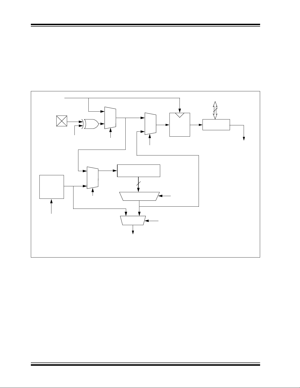
PIC16F62X
6.3 Timer0 Prescaler
An 8-bit counter is available as a prescaler for the
Timer0 module, or as a postscaler for the Watchdog
Timer. A prescaler assignment for the Timer0 module
means that there is no postscaler for the Watchdog
Timer, and vice-versa.
The PSA and PS2:PS0 bits (OPTION<3:0>) determine
the prescaler assignment and prescale ratio.
When assigned to the Timer0 module, all instructions
writing to the TMR0 register (e.g., CLRF 1,
MOVWF 1, BSF 1, x....etc.) will clear the pres-
caler. When assigned to WDT, a CLRWDT instruction
will clear the prescaler along with the Watchdog Timer.
The prescaler is not readable or writable.
FIGURE 6-1: BLOCK DIAGRAM OF THE TIMER0/WDT
F
OSC/4
0
T0CKI
Pin
T0SE
1
T0CS
0
WDT Postscaler/
TMR0 Prescaler
1
0
PSA
SYNC
2
Cycles
Data Bus
8
TMR0 reg
Set Flag Bit T0IF
on Overflow
Watchdog
Timer
WDT Enable bit
Note 1: T0SE, T0CS, PSA, PS0-PS2 are bits in the Option Register.
1
PSA
.
8
8-to-1MUX
01
WDT
Timeout
PS0 - PS2
PSA
DS40300C-page 44 Preliminary 2003 Microchip Technology Inc.
Page 47

PIC16F62X
6.3.1 SWITCHING PRESCALER
ASSIGNMENT
The prescaler assignment is fully under software
control (i.e., it can be changed “on the fly” during
program execution). Use the instruction sequences,
shown in Example 6-1, when changing the prescaler
assignment from Timer0 to WDT, to avoid an
unintended device RESET.
EXAMPLE 6-1: CHANGING PRESCALER
(TIMER0→WDT)
BCF STATUS, RP0 ;Skip if already in
;Bank 0
CLRWDT ;Clear WDT
CL RF TM R0 ;Clear TMR0 & Prescaler
BSF STATUS, RP0 ;Bank 1
MOVLW '00101111’b ;These 3 lines
;(5, 6, 7)
MOVWF OPTION_REG ;are required only
;if desired PS<2:0>
;are
CLRWDT ;000 or 001
MOVLW '00101xxx’b ;Set Postscaler to
MOVWF OPTION_REG ;desired WDT rate
BCF STATUS, RP0 ;Return to Bank 0
To change prescaler from the WDT to the TMR0
module use the sequence shown in Example 6-2. This
precaution must be taken even if the WDT is disabled.
EXAMPLE 6-2: CHANGING PRESCALER
(WDT→TIMER0)
CLRWDT ;Clear WDT and
;prescaler
BSF STATUS, RP0
MOVLW b'xxxx0xxx' ;Select TMR0, new
;prescale value and
;clock source
MOVWF OPTION_REG
BCF STATUS, RP0
TABLE 6-1: REGISTERS ASSOCIATED WITH TIMER0
Address Name Bit 7 Bit 6 Bit 5 Bit 4 Bit 3 Bit 2 Bit 1 Bit 0
01h TMR0 Timer0 module register xxxx xxxx uuuu uuuu
0Bh/8Bh/
10Bh/18Bh
81h, 181h
85h TRISA
Legend: — = Unimplemented locations, read as ‘0’, u = unchanged, x = unknown
Note 1: Shaded bits are not used by TMR0 module.
INTCON GIE
(2)
OPTION
2: Option is referred by OPTION_REG in MPLAB.
RBPU INTEDG T0CS T0SE PSA PS2 PS1 PS0 1111 1111 1111 1111
TRISA7 TRISA6
PEIE T0IE INTE RBIE T0IF INTF RBIF 0000 000x 0000 000u
TRISA5
TRISA4
TRISA3 TRISA2 TRISA1 TRISA0 1111 1111 1111 1111
Value on
POR
Value on
All Other
RESETS
2003 Microchip Technology Inc. Preliminary DS40300C-page 45
Page 48

PIC16F62X
7.0 TIMER1 MODULE
The Timer1 module is a 16-bit timer/counter consisting
of two 8-bit registers (TMR1H and TMR1L) which are
readable and writable. The TMR1 Register pair
(TMR1H:TMR1L) increments from 0000h to FFFFh
and rolls over to 0000h. The TMR1 Interrupt, if enabled,
is generated on overflow which is latched in interrupt
flag bit TMR1IF (PIR1<0>). This interrupt can be
enabled/disabled by setting/clearing TMR1 interrupt
enable bit TMR1IE (PIE1<0>).
Timer1 can operate in one of two modes:
• As a timer
• As a counter
The Operating mode is determined by the clock select
bit, TMR1CS (T1CON<1>).
In Timer mode, Timer1 increments every instruction
cycle. In Counter mode, it increments on every rising
edge of the external clock input.
Timer1 can be enabled/disabled by setting/clearing
control bit TMR1ON (T1CON<0>).
Timer1 also has an internal “RESET input”. This
RESET can be generated by the CCP module
(Section 11.0). Register 7-1 shows the Timer1 Control
register.
For the PIC16F627 and PIC16F628, when the Timer1
oscillator is enabled (T1OSCEN is set), the RB7/T1OSI
and RB6/T1OSO/T1CKI pins become inputs. That is,
the TRISB<7:6> value is ignored.
REGISTER 7-1: T1CON: TIMER1 CONTROL REGISTER (ADDRESS: 10h)
U-0 U-0 R/W-0 R/W-0 R/W-0 R/W-0 R/W-0 R/W-0
— — T1CKPS1 T1CKPS0 T1OSCEN T1SYNC TMR1CS TMR1ON
bit 7 bit 0
bit 7-6 Unimplemented: Read as '0'
bit 5-4 T1CKPS1:T1CKPS0: Timer1 Input Clock Prescale Select bits
11 = 1:8 Prescale value
10 = 1:4 Prescale value
01 = 1:2 Prescale value
00 = 1:1 Prescale value
bit 3 T1OSCEN: Timer1 Oscillator Enable Control bit
1 = Oscillator is enabled
0 = Oscillator is shut off
bit 2 T1SYNC: Timer1 External Clock Input Synchronization Control bit
TMR1CS =
1 = Do not synchronize external clock input
0 = Synchronize external clock input
T
MR1CS = 0
This bit is ignored. Timer1 uses the internal clock when TMR1CS = 0.
bit 1 TMR1CS: Timer1 Clock Source Select bit
1 = External clock from pin RB6/T1OSO/T1CKI (on the rising edge)
0 = Internal clock (F
bit 0 TMR1ON: Timer1 On bit
1 = Disables Timer1
0 = Stops Timer1
Note 1: The oscillator inverter and feedback resistor are turned off to eliminate power drain.
Legend:
R = Readable bit W = Writable bit U = Unimplemented bit, read as ‘0’
-n = Value at POR ’1’ = Bit is set ’0’ = Bit is cleared x = Bit is unknown
1
(1)
OSC/4)
DS40300C-page 46 Preliminary 2003 Microchip Technology Inc.
Page 49

PIC16F62X
7.1 Timer1 Operation in Timer Mode
Timer mode is selected by clearing the TMR1CS
(T1CON<1>) bit. In this mode, the input clock to the
timer is F
OSC/4. The synchronize control bit T1SYNC
(T1CON<2>) has no effect since the internal clock is
always in sync.
7.2 Timer1 Operation in Synchronized
Counter Mode
Counter mode is selected by setting bit TMR1CS. In
this mode the timer increments on every rising edge of
clock input on pin RB7/T1OSI when bit T1OSCEN is
set or pin RB6/T1OSO/T1CKI when bit T1OSCEN is
cleared.
If T1SYNC
synchronized with internal phase clocks. The synchronization is done after the prescaler stage. The
prescaler stage is an asynchronous ripple-counter.
In this configuration, during SLEEP mode, Timer1 will
not increment even if the external clock is present,
since the synchronization circuit is shut off. The
prescaler however will continue to increment.
is cleared, then the external clock input is
7.2.1 EXTERNAL CLOCK INPUT TIMING
FOR SYNCHRONIZED COUNTER
MODE
When an external clock input is used for Timer1 in
Synchronized Counter mode, it must meet certain
requirements. The external clock requirement is due to
internal phase clock (Tosc) synchronization. Also, there
is a delay in the actual incrementing of TMR1 after
synchronization.
When the prescaler is 1:1, the external clock input is
the same as the prescaler output. The synchronization
of T1CKI with the internal phase clocks is accomplished by sampling the prescaler output on the Q2 and
Q4 cycles of the internal phase clocks. Therefore, it is
necessary for T1CKI to be high for at least 2Tosc (and
a small RC delay of 20 ns) and low for at least 2Tosc
(and a small RC delay of 20 ns). Refer to the appropriate electrical specifications, parameters 45, 46, and 47.
When a prescaler other than 1:1 is used, the external
clock input is divided by the asynchronous ripplecounter type prescaler so that the prescaler output is
symmetrical. In order for the external clock to meet the
sampling requirement, the ripple-counter must be
taken into account. Therefore, it is necessary for T1CKI
to have a period of at least 4Tosc (and a small RC delay
of 40 ns) divided by the prescaler value. The only
requirement on T1CKI high and low time is that they do
not violate the minimum pulse width requirements of 10
ns). Refer to the appropriate electrical specifications,
parameters 40, 42, 45, 46, and 47.
FIGURE 7-1: TIMER1 BLOCK DIAGRAM
Set flag bit
TMR1IF on
Overflow
RB6/T1OSO/T1CKI
RB7/T1OSI
Note 1: When the T1OSCEN bit is cleared, the inverter and feedback resistor are turned off. This eliminates power drain.
TMR1H
T1OSC
TMR1
TMR1L
T1OSCEN
Enable
Oscillator(1)
OSC/4
F
Internal
Clock
TMR1ON
1
0
T1CKPS1:T1CKPS0
TMR1CS
0
1
T1SYNC
Prescaler
1, 2, 4, 8
2
Synchronized
Clock Input
Synchronize
SLEEP Input
det
2003 Microchip Technology Inc. Preliminary DS40300C-page 47
Page 50

PIC16F62X
7.3 Timer1 Operation in
Asynchronous Counter Mode
If control bit T1SYNC (T1CON<2>) is set, the external
clock input is not synchronized. The timer continues to
increment asynchronous to the internal phase clocks.
The timer will continue to run during SLEEP and can
generate an interrupt on overflow which will wake-up
the processor. However, special precautions in software are needed to read/write the timer (Section 7.3.2).
In Asynchronous Counter mode, Timer1 can not be
used as a time-base for capture or compare
operations.
7.3.1 EXTERNAL CLOCK INPUT TIMING
WITH UNSYNCHRONIZED CLOCK
If control bit T1SYNC is set, the timer will increment
completely asynchronously. The input clock must meet
certain minimum high-time and low-time requirements.
Refer to the appropriate Electrical Specifications
section, Timing Parameters 45, 46, and 47.
7.3.2 READING AND WRITING TIMER1 IN
ASYNCHRONOUS COUNTER
MODE
EXAMPLE 7-1: READING A 16-BIT FREE-
RUNNING TIMER
; All interrupts are disabled
MOVF TMR1H, W ;Read high byte
MOVWF TMPH ;
MOVF TMR1L, W ;Read low byte
MOVWF TMPL ;
MOVF TMR1H, W ;Read high byte
SUBWF TMPH, W ;Sub 1st read
; with 2nd read
BTFSC STATUS,Z ;Is result = 0
GOTO CONTINUE ;Good 16-bit read
;
; TMR1L may have rolled over between the read
; of the high and low bytes. Reading the high
; and low bytes now will read a good value.
;
MOVF TMR1H, W ;Read high byte
MOVWF TMPH ;
MOVF TMR1L, W ;Read low byte
MOVWF TMPL ;
; Re-enable the Interrupts (if required)
CONTINUE ;Continue with your code
Reading TMR1H or TMR1L while the timer is running,
from an external asynchronous clock, will ensure a
valid read (taken care of in hardware). However, the
user should keep in mind that reading the 16-bit timer
in two 8-bit values itself poses certain problems since
the timer may overflow between the reads.
For writes, it is recommended that the user simply stop
the timer and write the desired values. A write
contention may occur by writing to the timer registers
while the register is incrementing. This may produce an
unpredictable value in the timer register.
Reading the 16-bit value requires some care.
Example 7-1 is an example routine to read the 16-bit
timer value. This is useful if the timer cannot be
stopped.
DS40300C-page 48 Preliminary 2003 Microchip Technology Inc.
Page 51

PIC16F62X
7.4 Timer1 Oscillator
A crystal oscillator circuit is built in between pins T1OSI
(input) and T1OSO (amplifier output). It is enabled by
setting control bit T1OSCEN (T1CON<3>). The oscillator is a low power oscillator rated up to 200 kHz. It will
continue to run during SLEEP. It is primarily intended
for a 32 kHz crystal. Table 7-1 shows the capacitor
selection for the Timer1 oscillator.
The Timer1 oscillator is identical to the LP oscillator.
The user must provide a software time delay to ensure
proper oscillator start-up.
TABLE 7-1: CAPACITOR SELECTION FOR
THE TIMER1 OSCILLATOR
Osc Type Freq C1 C2
LP 32 kHz 33 pF 33 pF
100 kHz 15 pF 15 pF
200 kHz 15 pF 15 pF
Note 1: These values are for design guidance only.
Consult AN826 (DS00826A) for further
information on Crystal/Capacitor Selection.
7.5 Resetting Timer1 Using a CCP
Trigger Output
If the CCP1 module is configured in Compare mode to
generate a “special event trigger” (CCP1M3:CCP1M0
= 1011), this signal will reset Timer1.
Note: The special event triggers from the CCP1
module will not set interrupt flag bit
TMR1IF (PIR1<0>).
Timer1 must be configured for either Timer or Synchronized Counter mode to take advantage of this feature.
If Timer1 is running in Asynchronous Counter mode,
this RESET operation may not work.
In the event that a write to Timer1 coincides with a
special event trigger from CCP1, the write will take
precedence.
In this mode of operation, the CCPRxH:CCPRxL
registers pair effectively becomes the period register
for Timer1.
7.6 Resetting of Timer1 Register Pair
(TMR1H, TMR1L)
TMR1H and TMR1L registers are not reset to 00h on a
POR or any other RESET except by the CCP1 special
event triggers.
T1CON register is reset to 00h on a Power-on Reset or
a Brown-out Reset, which shuts off the timer and
leaves a 1:1 prescale. In all other RESETS, the register
is unaffected.
7.7 Timer1 Prescaler
The prescaler counter is cleared on writes to the
TMR1H or TMR1L registers.
TABLE 7-2: REGISTERS ASSOCIATED WITH TIMER1 AS A TIMER/COUNTER
Address Name Bit 7 Bit 6 Bit 5 Bit 4 Bit 3 Bit 2 Bit 1 Bit 0
0Bh/8Bh/
10Bh/18Bh
0Ch PIR1
8Ch PIE1
0Eh TMR1L Holding register for the Least Significant Byte of the 16-bit TMR1 register xxxx xxxx uuuu uuuu
0Fh TMR1H Holding register for the Most Significant Byte of the 16-bit TMR1 register xxxx xxxx uuuu uuuu
10h T1CON
Legend: x = unknown, u = unchanged, - = unimplemented read as '0'. Shaded cells are not used by the Timer1 module.
INTCON GIE PEIE T0IE INTE RBIE T0IF INTF RBIF 0000 000x 0000 000u
EEIF CMIF RCIF TXIF — CCP1IF TMR2IF TMR1IF 0000 -000 0000 -000
EEIE CMIE RCIE TXIE — CCP1IE TMR2IE TMR1IE 0000 -000 0000 -000
— — T1CKPS1 T1CKPS0 T1OSCEN T1SYNC TMR1CS TMR1ON --00 0000 --uu uuuu
Value on
POR
Value on
all other
RESETS
2003 Microchip Technology Inc. Preliminary DS40300C-page 49
Page 52

PIC16F62X
8.0 TIMER2 MODULE
Timer2 is an 8-bit timer with a prescaler and a
postscaler. It can be used as the PWM time-base for
PWM mode of the CCP module. The TMR2 register is
readable and writable, and is cleared on any device
RESET.
The input clock (F
1:4 or 1:16, selected by control bits
T2CKPS1:T2CKPS0 (T2CON<1:0>).
The Timer2 module has an 8-bit Period Register PR2.
Timer2 increments from 00h until it matches PR2 and
then resets to 00h on the next increment cycle. PR2 is
a readable and writable register. The PR2 register is
initialized to FFh upon RESET.
The match output of TMR2 goes through a 4-bit
postscaler (which gives a 1:1 to 1:16 scaling inclusive)
to generate a TMR2 interrupt (latched in flag bit
TMR2IF, (PIR1<1>)).
Timer2 can be shut off by clearing control bit TMR2ON
(T2CON<2>) to minimize power consumption.
Register 8-1 shows the Timer2 Control register.
OSC/4) has a prescale option of 1:1,
8.1 Timer2 Prescaler and Postscaler
The prescaler and postscaler counters are cleared
when any of the following occurs:
• A write to the TMR2 register
• A write to the T2CON register
• Any device RESET (Power-on Reset, MCLR
Reset, Watchdog Timer Reset, or Brown-out
Reset)
TMR2 is not cleared when T2CON is written.
8.2 Output of TMR2
The output of TMR2 (before the postscaler) is fed to the
Synchronous Serial Port module which optionally uses
it to generate shift clock.
FIGURE 8-1: TIMER2 BLOCK DIAGRAM
Sets flag
bit TMR2IF
Postscaler
1:1 1:16
TOUTPS<3:0>
to
TMR2
output (1)
RESET
4
EQ
TMR2 reg
Comparator
PR2 reg
Prescaler
1:1, 1:4, 1:16
2
T2CKPS<1:0>
OSC/4
F
Note 1: TMR2 register output can be software selected by the
SSP Module as a baud clock.
DS40300C-page 50 Preliminary 2003 Microchip Technology Inc.
Page 53

REGISTER 8-1: T2CON: TIMER CONTROL REGISTER (ADDRESS: 12h)
U-0 R/W-0 R/W-0 R/W-0 R/W-0 R/W-0 R/W-0 R/W-0
— TOUTPS3 TOUTPS2 TOUTPS1 TOUTPS0 TMR2ON T2CKPS1 T2CKPS0
bit 7 bit 0
bit 7 Unimplemented: Read as '0'
bit 6-3 TOUTPS3:TOUTPS0: Timer2 Output Postscale Select bits
0000 = 1:1 Postscale Value
0001 = 1:2 Postscale Value
•
•
•
1111 = 1:16 Postscale
bit 2 TMR2ON: Timer2 On bit
1 = Timer2 is on
0 = Timer2 is off
bit 1-0 T2CKPS1:T2CKPS0: Timer2 Clock Prescale Select bits
00 = 1:1 Prescaler Value
01 = 1:4 Prescaler Value
1x = 1:16 Prescaler Value
PIC16F62X
Legend:
R = Readable bit W = Writable bit U = Unimplemented bit, read as ‘0’
-n = Value at POR ’1’ = Bit is set ’0’ = Bit is cleared x = Bit is unknown
TABLE 8-1: REGISTERS ASSOCIATED WITH TIMER2 AS A TIMER/COUNTER
Address Name Bit 7 Bit 6 Bit 5 Bit 4 Bit 3 Bit 2 Bit 1 Bit 0
0Bh/8Bh/
10Bh/18Bh
0Ch PIR1
8Ch PIE1
11h TMR2 Timer2 module’s register
12h T2CON
92h PR2 Timer2 Period Register
Legend: x = unknown, u = unchanged, - = unimplemented read as '0'. Shaded cells are not used by the Timer2 module.
INTCON GIE PEIE T0IE INTE RBIE T0IF INTF RBIF
EEIF CMIF RCIF TXIF — CCP1IF TMR2IF TMR1IF
EEIE CMIE RCIE TXIE — CCP1IE TMR2IE TMR1IE
— TOUTPS3 TOUTPS2 TOUTPS1 TOUTPS0 TMR2ON T2CKPS1 T2CKPS0
Value o n
POR
0000 000x 0000 000u
0000 -000 0000 -000
0000 -000 0000 -000
0000 0000 0000 0000
-000 0000 -000 0000
1111 1111 1111 1111
Value on
all other
RESETS
2003 Microchip Technology Inc. Preliminary DS40300C-page 51
Page 54

PIC16F62X
NOTES:
DS40300C-page 52 Preliminary 2003 Microchip Technology Inc.
Page 55

PIC16F62X
9.0 COMPARATOR MODULE
The CMCON register, shown in Register 9-1, controls
the comparator input and output multiplexers. A block
The Comparator module contains two analog
diagram of the comparator is shown in Figure 9-1.
comparators. The inputs to the comparators are
multiplexed with the RA0 through RA3 pins. The Onchip Voltage Reference (Section 10.0) can also be an
input to the comparators.
REGISTER 9-1: CMCON REGISTER (ADDRESS: 01Fh)
R-0 R-0 R/W-0 R/W-0 R/W-0 R/W-0 R/W-0 R/W-0
C2INV C1INV CIS CM2 CM1 CM0
bit 7
bit 6
C2OUT C1OUT
bit 7 bit 0
C2OUT: Comparator 2 Output
When C2INV = 0:
1 = C2 VIN+ > C2 VIN0 = C2 V
When C2INV = 1:
1 = C2 VIN+ < C2 VIN0 = C2 V
C1OUT: Comparator 1 Output
When C1INV = 0:
1 = C1 VIN+ > C1 VIN0 = C1 V
IN+ < C2 VIN-
IN+ > C2 VIN-
IN+ < C1 VIN-
bit 5
bit 4
bit 3
bit 2-0
When C1INV = 1:
1 = C1 VIN+ < C1 VIN0 = C1 V
C2INV: Comparator 2 Output Inversion
1 = C2 Output inverted
0 = C2 Output not inverted
C1INV: Comparator 1 Output Inversion
1 = C1 Output inverted
0 = C1 Output not inverted
CIS: Comparator Input Switch
When CM2:CM0: = 001
Then:
1 = C1 V
0 = C1 V
When CM2:CM0 = 010
Then:
1 = C1 V
C2 V
0 = C1 V
C2 V
CM2:CM0: Comparator Mode
Figure 9-1 shows the Comparator modes and CM2:CM0 bit settings
IN+ > C1 VIN-
IN- connects to RA3
IN- connects to RA0
IN- connects to RA3
IN- connects to RA2
IN- connects to RA0
IN- connects to RA1
Legend:
R = Readable bit W = Writable bit U = Unimplemented bit, read as ‘0’
-n = Value at POR ’1’ = Bit is set ’0’ = Bit is cleared x = Bit is unknown
2003 Microchip Technology Inc. Preliminary DS40300C-page 53
Page 56

PIC16F62X
9.1 Comparator Configuration
There are eight modes of operation for the
comparators. The CMCON register is used to select
the mode. Figure 9-1 shows the eight possible modes.
mode is changed, the comparator output level may not
be valid for the specified mode change delay shown
in Table 17-1.
Note: Comparator interrupts should be disabled
The TRISA register controls the data direction of the
comparator pins for each mode. If the Comparator
FIGURE 9-1: COMPARATOR I/O OPERATING MODES
Comparators Reset (POR Default Value)
CM2:CM0 = 000
A
RA0/AN0
RA3/AN3/CMP1
RA1/AN1
RA2/AN2
VIN-
C1
V
A
A
A
IN+
V
IN-
C2
IN+
V
Two Independent Comparators
CM2:CM0 = 100
A
V
RA0/AN0
RA3/AN3/CMP1
RA1/AN1
RA2/AN2
A
A
A
IN-
V
IN+
VIN-
IN+
V
C1
C2
Off (Read as '0')
Off (Read as '0')
C1V
OUT
C2VOUT
Comparators Off
CM2:CM0 = 111
RA0/AN0
RA3/AN3/CMP1
RA1/AN1
RA2/AN2
Four Inputs Multiplexed to Two Comparators
CM2:CM0 = 010
RA0/AN0
RA3/AN3/CMP1
RA1/AN1
RA2/AN2
during a Comparator mode change otherwise a false interrupt may occur.
D
VIN-
IN-
IN+
IN+
Off (Read as '0')
Off (Read as '0')
C1
C2
From VREF
C1VOUT
C2VOUT
Module
C1
V
D
D
D
IN+
VIN-
C2
IN+
V
SS
V
A
CIS = 0
A
CIS = 1
V
V
A
CIS = 0
A
CIS = 1
VIN-
V
Two Common Reference Comparators
CM2:CM0 = 011
A
V
RA0/AN0
RA3/AN3/CMP1
RA1/AN1
RA2/AN2
D
A
A
IN-
C1
IN+
V
IN-
V
C2
IN+
V
One Independent Comparator
CM2:CM0 = 101
D
RA0/AN0
RA3/AN3/CMP1
VIN-
C1
V
D
IN+
Off (Read as '0')
VSS
RA1/AN1
RA2/AN2
A
A
IN-
V
C2
V
IN+
C2V
A = Analog Input, port reads zeros always.
D = Digital Input.
CIS (CMCON<3>) is the Comparator Input Switch.
C1VOUT
C2VOUT
OUT
Two Common Reference Comparators with Outputs
CM2:CM0 = 110
A
RA0/AN0
RA3/AN3/CMP1
RA1/AN1
RA2/AN2/CMP2
RA4/T0CKI/C20
VIN-
V
D
A
V
V
A
Open Drain
IN+
IN-
IN+
C1
C2
C1VOUT
C2VOUT
Three Inputs Multiplexed to Two Comparators
CM2:CM0 = 001
This mode is disfunctional and has been corrected in the ‘A’
Revision Devices.
RA0/AN0
RA3/AN3/CMP1
RA1/AN1
RA2/AN2
A
CIS = 0
CIS = 1
A
A
A
V
IN-
IN+
IN-
IN+
C1
+
C2
+
V
V
V
C1VOUT
C2VOUT
DS40300C-page 54 Preliminary 2003 Microchip Technology Inc.
Page 57

PIC16F62X
The code example in Example 9-1 depicts the steps
required to configure the Comparator module. RA3 and
RA4 are configured as digital output. RA0 and RA1 are
configured as the V- inputs and RA2 as the V+ input to
both comparators.
EXAMPLE 9-1: INITIALIZING
COMPARATOR MODULE
FLAG_REG EQU 0X20
CLRF FLAG_REG ;Init flag register
CLRF PORTA ;Init PORTA
MOVF CMCON, W ;Load comparator bits
ANDLW 0xC0 ;Mask comparator bits
IORWF FLAG_REG,F ;Store bits in flag register
MOVLW 0x03 ;Init comparator mode
MOVWF CMCON ;CM<2:0> = 011
BSF STATUS,RP0 ;Select Bank1
MOVLW 0x07 ;Initialize data direction
MOVWF TRISA ;Set RA<2:0> as inputs
;RA<4:3> as outputs
;TRISA<7:5> always read ‘0’
BCF STATUS,RP0 ;Select Bank 0
CALL DELAY10 ;10µs delay
MOVF CMCON,F ;Read CMCON to end change condition
BCF PIR1,CMIF ;Clear pending interrupts
BSF STATUS,RP0 ;Select Bank 1
BSF PIE1,CMIE ;Enable comparator interrupts
BCF STATUS,RP0 ;Select Bank 0
BSF INTCON,PEIE ;Enable peripheral interrupts
BSF INTCON,GIE ;Global interrupt enable
FIGURE 9-2: SINGLE COMPARATOR
IN-
V
VIN+
Result
ViN+
V
IN-
+
Result
–
9.3.1 EXTERNAL REFERENCE SIGNAL
When external voltage references are used, the
comparator module can be configured to have the
comparators operate from the same or different
reference sources. However, threshold detector
applications may require the same reference. The
reference signal must be between V
can be applied to either pin of the comparator(s).
SS and VDD, and
9.2 Comparator Operation
A single comparator is shown in Figure 9-2 along with
the relationship between the analog input levels and
the digital output. When the analog input at V
than the analog input V
IN-, the output of the comparator
is a digital low level. When the analog input at V
greater than the analog input V
IN-, the output of the
IN+ is less
IN+ is
comparator is a digital high level. The shaded areas of
the output of the comparator in Figure 9-2 represent
the uncertainty due to input offsets and response time.
9.3 Comparator Reference
An external or internal reference signal may be used
depending on the Comparator Operating mode. The
analog signal that is present at V
signal at V
IN+, and the digital output of the comparator
is adjusted accordingly (Figure 9-2).
IN- is compared to the
9.3.2 INTERNAL REFERENCE SIGNAL
The Comparator module also allows the selection of an
internally generated voltage reference for the
comparators. Section 10.0, Voltage Reference Manual,
contains a detailed description of the Voltage Reference module that provides this signal. The internal
reference signal is used when the comparators are in
mode CM<2:0>=010 (Figure 9-1). In this mode, the
internal voltage reference is applied to the V
IN+ pin of
both comparators.
9.4 Comparator Response Time
Response time is the minimum time, after selecting a
new reference voltage or input source, before the
comparator output is ensured to have a valid level. If
the internal reference is changed, the maximum delay
of the internal voltage reference must be considered
when using the comparator outputs. Otherwise the
maximum delay of the comparators should be used
(Table 17-1).
2003 Microchip Technology Inc. Preliminary DS40300C-page 55
Page 58

PIC16F62X
9.5 Comparator Outputs
The comparator outputs are read through the CMCON
register. These bits are read only. The comparator
outputs may also be directly output to the RA3 and RA4
I/O pins. When the CM<2:0> = 110, multiplexors in the
output path of the RA3 and RA4/T0CK1 pins will switch
and the output of each pin will be the unsynchronized
output of the comparator. The uncertainty of each of the
comparators is related to the input offset voltage and
the response time given in the specifications. Figure 93 shows the comparator output block diagram.
The TRISA bits will still function as an output enable/
disable for the RA3 and RA4/T0CK1 pins while in this
mode.
Note 1: When reading the PORT register, all pins
configured as analog inputs will read as a
‘0’. Pins configured as digital inputs will
convert an analog input according to the
Schmitt Trigger input specification.
2: Analog levels on any pin that is defined as
a digital input may cause the input buffer
to consume more current than is
specified.
FIGURE 9-3: COMPARATOR OUTPUT BLOCK DIAGRAM
CnINV
To RA3 or RA4/T0CK1 pin
To Da ta B us
CMCON<7:6>
RD CMCON
Set CMIF bit
From other Comparator
EN
DQ
CL
EN
CnVOUT
DQ
Q1
RESET
DS40300C-page 56 Preliminary 2003 Microchip Technology Inc.
Page 59

PIC16F62X
9.6 Comparator Interrupts
The Comparator Interrupt flag is set whenever there is
a change in the output value of either comparator.
Software will need to maintain information about the
status of the output bits, as read from CMCON<7:6>, to
determine the actual change that has occurred. The
CMIF bit, PIR1<6>, is the Comparator Interrupt Flag.
The CMIF bit must be RESET by clearing ‘0’. Since it is
also possible to write a '1' to this register, a simulated
interrupt may be initiated.
The CMIE bit (PIE1<6>) and the PEIE bit
(INTCON<6>) must be set to enable the interrupt. In
addition, the GIE bit must also be set. If any of these
bits are clear, the interrupt is not enabled, though the
CMIF bit will still be set if an interrupt condition occurs.
Note: If a change in the CMCON register
(C1OUT or C2OUT) should occur when a
read operation is being executed (start of
the Q2 cycle), then the CMIF (PIR1<6>)
interrupt flag may not get set.
The user, in the interrupt service routine, can clear the
interrupt in the following manner:
a) Any write or read of CMCON. This will end the
mismatch condition.
b) Clear flag bit CMIF.
A mismatch condition will continue to set flag bit CMIF.
Reading CMCON will end the mismatch condition, and
allow flag bit CMIF to be cleared.
9.7 Comparator Operation During
SLEEP
When a comparator is active and the device is placed
in SLEEP mode, the comparator remains active and
the interrupt is functional if enabled. This interrupt will
wake-up the device from SLEEP mode when enabled.
While the comparator is powered-up, higher SLEEP
currents than shown in the power-down current
specification will occur. Each comparator that is
operational will consume additional current as shown in
the comparator specifications. To minimize power
consumption while in SLEEP mode, turn off the
comparators, CM<2:0> = 111, before entering SLEEP.
If the device wakes-up from SLEEP, the contents of the
CMCON register are not affected.
9.8 Effects of a RESET
A device RESET forces the CMCON register to its
RESET state. This forces the Comparator module to be
in the comparator RESET mode, CM2:CM0 = 000.
This ensures that all potential inputs are analog inputs.
Device current is minimized when analog inputs are
present at RESET time. The comparators will be
powered-down during the RESET interval.
9.9 Analog Input Connection
Considerations
A simplified circuit for an analog input is shown in
Figure 9-4. Since the analog pins are connected to a
digital output, they have reverse biased diodes to V
and VSS. The analog input therefore, must be between
V
SS and VDD. If the input voltage deviates from this
range by more than 0.6V in either direction, one of the
diodes is forward biased and a latchup may occur. A
maximum source impedance of 10 kΩ is
recommended for the analog sources. Any external
component connected to an analog input pin, such as
a capacitor or a Zener diode, should have very little
leakage current.
DD
2003 Microchip Technology Inc. Preliminary DS40300C-page 57
Page 60

PIC16F62X
FIGURE 9-4: ANALOG INPUT MODE
V
DD
R
VA
S < 10K
VT = 0.6V
A
IN
CPIN
5pF
V
T = 0.6V
ILEAKAGE
±500 nA
V
SS
IC
R
Legend CPIN = Input Capacitance
T = Threshold Voltage
V
LEAKAGE = Leakage Current At The Pin
I
IC = Interconnect Resistance
R
S = Source Impedance
R
VA = Analog Voltage
TABLE 9-1: REGISTERS ASSOCIATED WITH COMPARATOR MODULE
Address Name Bit 7 Bit 6 Bit 5 Bit 4 Bit 3 Bit 2 Bit 1 Bit 0
1Fh CMCON C2OUT C1OUT C2INV C1NV CIS CM2 CM1 CM0 0000 0000 0000 0000
0Bh/8Bh/
10Bh/18Bh
0Ch PIR1
8Ch PIE1
85h TRISA
INTCON GIE PEIE
EEIF CMIF RCIF TXIF — CCP1IF TMR2IF TMR1IF 0000 -000 0000 -000
EEIE CMIE RCIE TXIE — CCP1IE TMR2IE TMR1IE 0000 -000 0000 -000
TRISA7 TRISA6 TRISA5 TRISA4 TRISA3 TRISA2 TRISA1 TRISA0 1111 1111 1111 1111
T0IE INTE RBIE T0IF INTF RBIF 0000 000x 0000 000u
Value on
POR
Legend: x = Unknown, u = Unchanged, - = Unimplemented, read as ‘0’
Value on
All Other
RESETS
DS40300C-page 58 Preliminary 2003 Microchip Technology Inc.
Page 61

PIC16F62X
10.0 VOLTAGE REFERENCE MODULE
The Voltage Reference is a 16-tap resistor ladder
network that provides a selectable voltage reference.
The resistor ladder is segmented to provide two ranges
REF values and has a power-down function to
of V
10.1 Configuring the Voltage Reference
The Voltage Reference can output 16 distinct voltage
levels for each range.
The equations used to calculate the output of the
Voltage Reference are as follows:
conserve power when the reference is not being used.
The VRCON register controls the operation of the
reference as shown in Figure 10-1. The block diagram
is given in Figure 10-1.
The setting time of the Voltage Reference must be
considered when changing the V
(Table 17-2). Example 10-1 shows an example of how
to configure the Voltage Reference for an output
voltage of 1.25V with V
REGISTER 10-1: VRCON REGISTER (ADDRESS: 9Fh)
R/W-0 R/W-0 R/W-0 U-0 R/W-0 R/W-0 R/W-0 R/W-0
REN VROE VRR —VR3 VR2 VR1 VR0
V
bit 7 bit 0
bit 7 V
bit 6 V
bit 5 V
bit 4 Unimplemented: Read as '0'
bit 3-0 V
REN: VREF Enable
1 = V
REF circuit powered on
REF circuit powered down, no IDD drain
0 = V
ROE: VREF Output Enable
1 = V
REF is output on RA2 pin
REF is disconnected from RA2 pin
0 = V
RR: VREF Range selection
1 = Low Range
0 = High Range
R<3:0>: VREF value selection 0 ≤ VR [3:0] ≤ 15
When V
RR = 1: VREF = (VR<3:0>/ 24) * VDD
When VRR = 0: VREF = 1/4 * VDD + (VR<3:0>/ 32) * VDD
RR = 1: VREF = (VR<3:0>/24) x VDD
if V
if VRR = 0: VREF = (VDD x 1/4) + (VR<3:0>/32) x
V
DD
REF output
DD = 5.0V.
Legend:
R = Readable bit W = Writable bit U = Unimplemented bit, read as ‘0’
-n = Value at POR ’1’ = Bit is set ’0’ = Bit is cleared x = Bit is unknown
FIGURE 10-1: VOLTAGE REFERENCE BLOCK DIAGRAM
VDD
VREN
Vref
Note 1: R is defined in Table 17-2.
2003 Microchip Technology Inc. Preliminary DS40300C-page 59
8R
R
R
16 Stages
16-1 Analog Mux
R
R
8R
VSS VSS
Vr3
Vr0
Vrr
(From VRCON<3:0>)
Page 62
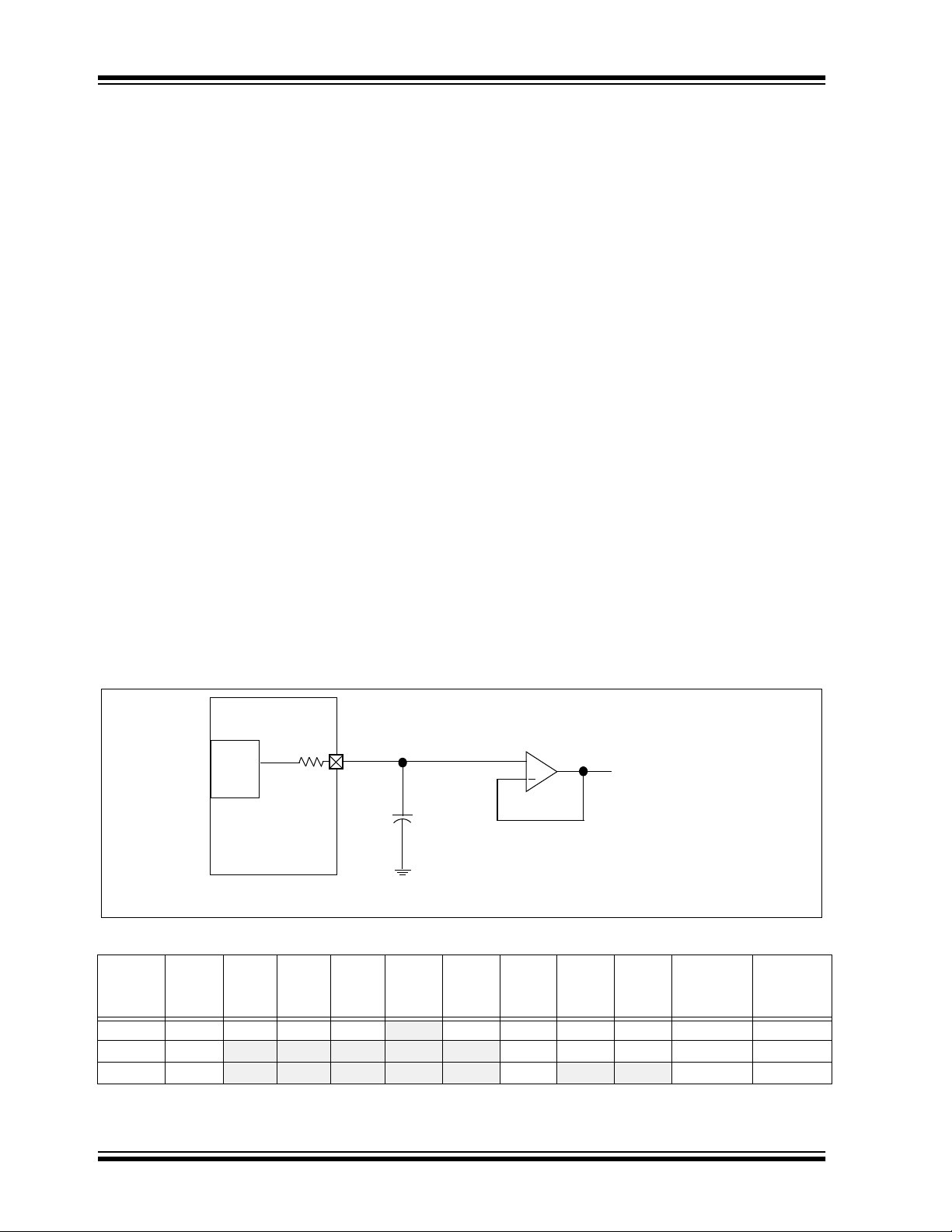
PIC16F62X
EXAMPLE 10-1: VOLTAGE REFERENCE
CONFIGURATION
MOVLW 0x02 ; 4 Inputs Muxed
MOVWF CMCON ; to 2 comps.
BSF STATUS,RP0 ; go to Bank 1
MOVLW 0x07 ; RA3-RA0 are
MOVWF TRISA ; outputs
MOVLW 0xA6 ; enable V
MOVWF VRCON ; low range
; set V
BCF STATUS,RP0 ; go to Bank 0
CALL DELAY10 ; 10µs delay
REF
R<3:0>=6
10.2 Voltage Reference Accuracy/Error
The full range of VSS to VDD cannot be realized due to
the construction of the module. The transistors on the
top and bottom of the resistor ladder network
(Figure 10-1) keep V
The Voltage Reference is V
REF output changes with fluctuations in VDD. The
the V
REF from approaching VSS or VDD.
DD derived and therefore,
tested absolute accuracy of the Voltage Reference can
be found in Table 17-2.
10.3 Operation During SLEEP
10.4 Effects of a RESET
A device RESET disables the Voltage Reference by
clearing bit V
REN (VRCON<7>). This RESET also
disconnects the reference from the RA2 pin by clearing
bit V
ROE (VRCON<6>) and selects the high voltage
range by clearing bit V
RR (VRCON<5>). The VREF
value select bits, VRCON<3:0>, are also cleared.
10.5 Connection Considerations
The Voltage Reference module operates
independently of the Comparator module. The output
of the reference generator may be connected to the
RA2 pin if the TRISA<2> bit is set and the V
VRCON<6>, is set. Enabling the Voltage Reference
output onto the RA2 pin with an input signal present will
increase current consumption. Connecting RA2 as a
digital output with V
REF enabled will also increase
current consumption.
The RA2 pin can be used as a simple D/A output with
limited drive capability. Due to the limited drive
capability, a buffer must be used in conjunction with the
Voltage Reference output for external connections to
REF. Figure 10-2 shows an example buffering
V
technique.
ROE bit,
When the device wakes-up from SLEEP through an
interrupt or a Watchdog Timer timeout, the contents of
the VRCON register are not affected. To minimize
current consumption in SLEEP mode, the Voltage
Reference should be disabled.
FIGURE 10-2: VOLTAGE REFERENCE OUTPUT BUFFER EXAMPLE
(1)
REF
V
Module
Note 1: R is dependent upon the Voltage Reference Configuration VRCON<3:0> and VRCON<5>.
R
Voltage
Reference
Output
Impedance
RA2
Op Amp
+
V
REF Output
TABLE 10-1: REGISTERS ASSOCIATED WITH VOLTAGE REFERENCE
Address Name Bit 7 Bit 6 Bit 5 Bit 4 Bit 3 Bit 2 Bit 1 Bit 0
9Fh VRCON VREN VROE VRR —VR3VR2VR1VR0000- 0000 000- 0000
1Fh CMCON
85h TRISA
C2OUT C1OUT C2INV C1INV CIS CM2 CM1 CM0 0000 0000 0000 0000
TRISA7 TRISA6 TRISA5 TRISA4 TRISA3 TRISA2 TRISA1 TRISA0 1111 1111 1111 1111
Value On
POR
Note 1: — = Unimplemented, read as ‘0’.
Value On
All Other
RESETS
DS40300C-page 60 Preliminary 2003 Microchip Technology Inc.
Page 63

PIC16F62X
11.0 CAPTURE/COMPARE/PWM
TABLE 11-1: CCP MODE - TIMER
(CCP) MODULE
The CCP (Capture/Compare/PWM) module contains a
16-bit register which can operate as a 16-bit capture
register, as a 16-bit compare register or as a PWM
master/slave Duty Cycle register. Table 11-1 shows the
timer resources of the CCP Module modes.
CCP1 Module
Capture/Compare/PWM Register1 (CCPR1) is comprised of two 8-bit registers: CCPR1L (low byte) and
CCPR1H (high byte). The CCP1CON register controls
the operation of CCP1. All are readable and writable.
Additional information on the CCP module is available
in the PICmicro™ Mid-Range Reference Manual,
(DS33023).
REGISTER 11-1: CCP1CON REGISTER (ADDRESS: 17h)
U-0 U-0 R/W-0 R/W-0 R/W-0 R/W-0 R/W-0 R/W-0
— — CCP1X CCP1Y CCP1M3 CCP1M2 CCP1M1 CCP1M0
bit 7 bit 0
bit 7-6 Unimplemented: Read as '0'
bit 5-4 CCP1X:CCP1Y: PWM Least Significant bits
Capture Mode: Unused
Compare Mode: Unused
PWM Mode: These bits are the two LSbs of the PWM duty cycle. The eight MSbs are found in
CCPRxL.
bit 3-0 CCP1M3:CCP1M0: CCPx Mode Select bits
0000 = Capture/Compare/PWM off (resets CCP1 module)
0100 = Capture mode, every falling edge
0101 = Capture mode, every rising edge
0110 = Capture mode, every 4th rising edge
0111 = Capture mode, every 16th rising edge
1000 = Compare mode, set output on match (CCP1IF bit is set)
1001 = Compare mode, clear output on match (CCP1IF bit is set)
1010 = Compare mode, generate software interrupt on match (CCP1IF bit is set, CCP1 pin is
unaffected)
1011 = Compare mode, trigger special event (CCP1IF bit is set; CCP1 resets TMR1
11xx = PWM mode
RESOURCE
CCP Mode Timer Resource
Capture
Compare
PWM
Timer1
Timer1
Timer2
Legend:
R = Readable bit W = Writable bit U = Unimplemented bit, read as ‘0’
-n = Value at POR ’1’ = Bit is set ’0’ = Bit is cleared x = Bit is unknown
2003 Microchip Technology Inc. Preliminary DS40300C-page 61
Page 64

PIC16F62X
11.1 Capture Mode
In Capture mode, CCPR1H:CCPR1L captures the
16-bit value of the TMR1 register when an event occurs
on pin RB3/CCP1. An event is defined as:
• Every falling edge
• Every rising edge
• Every 4th rising edge
• Every 16th rising edge
An event is selected by control bits CCP1M3:CCP1M0
(CCP1CON<3:0>). When a capture is made, the Interrupt Request Flag bit CCP1IF (PIR1<2>) is set. It must
be cleared in software. If another capture occurs before
the value in register CCPR1 is read, the old captured
value will be lost.
11.1.1 CCP PIN CONFIGURATION
In Capture mode, the RB3/CCP1 pin should be
configured as an input by setting the TRISB<3> bit.
Note: If the RB3/CCP1 is configured as an out-
put, a write to the port can cause a capture
condition.
TABLE 11-2: CAPTURE MODE OPERATION
BLOCK DIAGRAM
Set flag bit CCP1IF
Prescaler
³ 1, 4, 16
RB3/CCP1
Pin
and
edge detect
CCP1CON<3:0>
Q’s
11.1.2 TIMER1 MODE SELECTION
Timer1 must be running in Timer mode or Synchronized Counter mode for the CCP module to use the
capture feature. In Asynchronous Counter mode, the
capture operation may not work.
(PIR1<2>)
CCPR1H CCPR1L
Capture
Enable
TMR1H TMR1L
Switching from one capture prescaler to another may
generate an interrupt. Also, the prescaler counter will
not be cleared, therefore the first capture may be from
a non-zero prescaler. Example 11-1 shows the
recommended method for switching between capture
prescalers. This example also clears the prescaler
counter and will not generate the “false” interrupt.
EXAMPLE 11-1: CHANGING BETWEEN
CAPTURE PRESCALERS
CLRF CCP1CON ;Turn CCP module off
MOVLW NEW_CAPT_PS ;Load the W reg with
; the new prescaler
; mode value and CCP ON
MOVWF CCP1CON ;Load CCP1CON with this
; value
11.2 Compare Mode
In Compare mode, the 16-bit CCPR1 register value is
constantly compared against the TMR1 register pair
value. When a match occurs, the RB3/CCP1 pin is:
• Driven High
• Driven Low
• Remains Unchanged
The action on the pin is based on the value of control
bits CCP1M3:CCP1M0 (CCP1CON<3:0>). At the
same time, interrupt flag bit CCP1IF is set.
FIGURE 11-1: COMPARE MODE
OPERATION BLOCK
DIAGRAM
Special Event Trigger will reset Timer1, but not set
interrupt flag bit TMR1IF (PIR1<0>)
Set flag bit CCP1IF
(PIR1<2>)
CCPR1H CCPR1L
QS
RB3/CCP1
Pin
TRISB<3>
Output Enable
Output
Logic
R
CCP1CON<3:0>
Mode Select
match
Comparator
TMR1H TMR1L
11.1.3 SOFTWARE INTERRUPT
When the Capture mode is changed, a false capture
interrupt may be generated. The user should keep bit
CCP1IE (PIE1<2>) clear to avoid false interrupts and
should clear the flag bit CCP1IF following any such
change in Operating mode.
11.1.4 CCP PRESCALER
There are four prescaler settings, specified by bits
CCP1M3:CCP1M0. Whenever the CCP module is
turned off, or the CCP module is not in Capture mode,
the prescaler counter is cleared. This means that any
RESET will clear the prescaler counter.
DS40300C-page 62 Preliminary 2003 Microchip Technology Inc.
11.2.1 CCP PIN CONFIGURATION
The user must configure the RB3/CCP1 pin as an
output by clearing the TRISB<3> bit.
Note: Clearing the CCP1CON register will force
the RB3/CCP1 compare output latch to the
default low level. This is not the data latch.
Page 65

PIC16F62X
11.2.2 TIMER1 MODE SELECTION
Timer1 must be running in Timer mode or Synchronized Counter mode if the CCP module is using the
compare feature. In Asynchronous Counter mode, the
compare operation may not work.
11.2.3 SOFTWARE INTERRUPT MODE
11.2.4 SPECIAL EVENT TRIGGER
In this mode, an internal hardware trigger is generated
which may be used to initiate an action.
The special event trigger output of CCP1 resets the
TMR1 register pair. This allows the CCPR1 register to
effectively be a 16-bit programmable period register for
Timer1.
When generate software interrupt is chosen, the CCP1
pin is not affected. Only a CCP interrupt is generated (if
enabled).
TABLE 11-3: REGISTERS ASSOCIATED WITH CAPTURE, COMPARE, AND TIMER1
Address Name Bit 7 Bit 6 Bit 5 Bit 4 Bit 3 Bit 2 Bit 1 Bit 0
0Bh/8Bh/
10Bh/
18Bh
0Ch PIR1
8Ch PIE1
87h TRISB PORTB Data Direction Register 1111 1111 1111 1111
0Eh TMR1L Holding register for the Least Significant Byte of the 16-bit TMR1 register xxxx xxxx uuuu uuuu
0Fh TMR1H Holding register for the Most Significant Byte of the 16-bit TMR1register xxxx xxxx uuuu uuuu
10h T1CON
15h CCPR1L Capture/Compare/PWM register1 (LSB) xxxx xxxx uuuu uuuu
16h CCPR1H Capture/Compare/PWM register1 (MSB) xxxx xxxx uuuu uuuu
17h CCP1CON
Legend: x = unknown, u = unchanged, - = unimplemented read as '0'. Shaded cells are not used by Capture and Timer1.
INTCON
GIE PEIE
EEIF CMIF RCIF TXIF — CCP1IF TMR2IF TMR1IF
EEIE CMIF RCIE TXIE — CCP1IE TMR2IE TMR1IE
— — T1CKPS1 T1CKPS0 T1OSCEN T1SYNC TMR1CS TMR1ON
— — CCP1X CCP1Y CCP1M3 CCP1M2 CCP1M1 CCP1M0
T0IE INTE RBIE T0IF INTF RBIF
Value o n
POR
0000 000x 0000 000u
0000 -000 0000 -000
0000 -000 0000 -000
--00 0000 --uu uuuu
--00 0000 --00 0000
Value on
all other
RESETS
2003 Microchip Technology Inc. Preliminary DS40300C-page 63
Page 66

PIC16F62X
11.3 PWM Mode
In Pulse Width Modulation (PWM) mode, the CCP1 pin
produces up to a 10-bit resolution PWM output. Since
the CCP1 pin is multiplexed with the PORTB data latch,
the TRISB<3> bit must be cleared to make the CCP1
pin an output.
Note: Clearing the CCP1CON register will force
the CCP1 PWM output latch to the default
low level. This is not the PORTB I/O data
latch.
Figure 11-2 shows a simplified block diagram of the
CCP module in PWM mode.
For a step-by-step procedure on how to set up the CCP
module for PWM operation, see Section 11.3.3.
FIGURE 11-2: SIMPLIFIED PWM BLOCK
DIAGRAM
Duty cycle registers
CCPR1L
CCPR1H (Slave)
Comparator
TMR2
Comparator
PR2
Note 1: 8-bit timer is concatenated with the 2-bit internal
(Note 1)
Clear Timer,
CCP1 pin and
latch D.C.
Q clock, or 2 bits of the prescaler to create 10-bit
time-base.
CCP1CON<5:4>
Q
R
S
RB3/CCP1
TRISB<3>
A PWM output (Figure 11-3) has a time-base (period)
and a time that the output stays high (duty cycle). The
frequency of the PWM is the inverse of the period
(1/period).
FIGURE 11-3: PWM OUTPUT
Period
Duty Cycle
TMR2 = PR2
TMR2 = Duty Cycle
TMR2 = PR2
11.3.1 PWM PERIOD
The PWM period is specified by writing to the
PR2register. The PWM period can be calculated using
the following formula:
PWM period = [(PR2) + 1] • 4 • T
(TMR2 prescale value)
PWM frequency is defined as 1 / [PWM period].
When TMR2 is equal to PR2, the following three events
occur on the next increment cycle:
• TMR2 is cleared
• The CCP1 pin is set (exception: if PWM duty
cycle = 0%, the CCP1 pin will not be set)
• The PWM duty cycle is latched from CCPR1L into
CCPR1H
Note: The Timer2 postscaler (see Section 8.0) is
not used in the determination of the PWM
frequency. The postscaler could be used to
have an interrupt occur at a different frequency than the PWM output.
OSC •
DS40300C-page 64 Preliminary 2003 Microchip Technology Inc.
Page 67

PIC16F62X
11.3.2 PWM DUTY CYCLE
The PWM duty cycle is specified by writing to the
CCPR1L register and to the CCP1CON<5:4> bits. Up
to 10-bit resolution is available: the CCPR1L contains
the eight MSbs and the CCP1CON<5:4> contains the
two LSbs. This 10-bit value is represented by
CCPR1L:CCP1CON<5:4>. The following equation is
used to calculate the PWM duty cycle in time:
EQUATION 11-1: PWM DUTY CYCLE
PWM duty cycle = (CCPR1L:CCP1CON<5:4>) •
Tosc • (TMR2 prescale value)
CCPR1L and CCP1CON<5:4> can be written to at any
time, but the duty cycle value is not latched into
CCPR1H until after a match between PR2 and TMR2
occurs (i.e., the period is complete). In PWM mode,
CCPR1H is a read-only register.
The CCPR1H register and a 2-bit internal latch are
used to double buffer the PWM duty cycle. This double
buffering is essential for glitchless PWM operation.
When the CCPR1H and 2-bit latch match TMR2
concatenated with an internal 2-bit Q clock or 2 bits of
the TMR2 prescaler, the CCP1 pin is cleared.
Maximum PWM resolution (bits) for a given PWM
frequency:
EQUATION 11-2: MAXIMUM PWM
RESOLUTION
Fosc
Fpwm x TMR2 Prescaler
log (2)
PWM
Resolution =
log (
Note: If the PWM duty cycle value is longer than
the PWM period, the CCP1 pin will not be
cleared.
For an example on the PWM period and duty cycle
calculation, see the PICmicro™ Mid-Range Reference
Manual (DS33023).
)
bits
11.3.3 SET-UP FOR PWM OPERATION
The following steps should be taken when configuring
the CCP module for PWM operation:
1. Set the PWM period by writing to the PR2
register.
2. Set the PWM duty cycle by writing to the
CCPR1L register and CCP1CON<5:4> bits.
3. Make the CCP1 pin an output by clearing the
TRISB<3> bit.
4. Set the TMR2 prescale value and enable Timer2
by writing to T2CON.
TABLE 11-4: EXAMPLE PWM FREQUENCIES AND RESOLUTIONS AT 20 MHz
PWM Frequency 1.22 kHz 4.88 kHz 19.53 kHz 78.12 kHz 156.3 kHz 208.3 kHz
Timer Prescaler (1, 4, 16) 1641111
PR2 Value 0xFF 0xFF 0xFF 0x3F 0x1F 0x17
Maximum Resolution (bits) 10 10 10 8 7 6.5
TABLE 11-5: REGISTERS ASSOCIATED WITH PWM AND TIMER2
Address Name Bit 7 Bit 6 Bit 5 Bit 4 Bit 3 Bit 2 Bit 1 Bit 0
0Bh/8Bh/
10Bh/18Bh
0Ch PIR1
8Ch PIE1
87h TRISB PORTB Data Direction Register 1111 1111 1111 1111
11h TMR2 Timer2 module’s register 0000 0000 0000 0000
92h PR2 Timer2 module’s period register 1111 1111 1111 1111
12h T2CON
15h CCPR1L Capture/Compare/PWM register1 (LSB) xxxx xxxx uuuu uuuu
16h CCPR1H Capture/Compare/PWM register1 (MSB) xxxx xxxx uuuu uuuu
17h CCP1CON
Legend: x = unknown, u = unchanged, - = unimplemented read as '0'. Shaded cells are not used by PWM and Timer2.
INTCON GIE PEIE T0IE INTE RBIE T0IF INTF RBIF 0000 000x 0000 000u
EEIF CMIF RCIF TXIF — CCP1IF TMR2IF TMR1IF 0000 -000 0000 -000
EEIE CMIE RCIE TXIE — CCP1IE TMR2IE TMR1IE 0000 -000 0000 -000
— TOUTPS3 TOUTPS2 TOUTPS1 TOUTPS0 TMR2ON T2CKPS1 T2CKPS0 -000 0000 uuuu
— — CCP1X CCP1Y CCP1M3 CCP1M2 CCP1M1 CCP1M0 --00 0000 --00 0000
Value on
POR
Value on
all other
RESETS
2003 Microchip Technology Inc. Preliminary DS40300C-page 65
Page 68

PIC16F62X
NOTES:
DS40300C-page 66 Preliminary 2003 Microchip Technology Inc.
Page 69

PIC16F62X
12.0 UNIVERSAL SYNCHRONOUS/ ASYNCHRONOUS RECEIVER/ TRANSMITTER (USART) MODULE
The Universal Synchronous Asynchronous Receiver
Transmitter (USART) module is one of the two serial
I/O modules. (USART is also known as a Serial
Communications Interface or SCI). The USART can be
The USART can be configured in the following modes:
• Asynchronous (full duplex)
• Synchronous - Master (half duplex)
• Synchronous - Slave (half duplex)
Bit SPEN (RCSTA<7>), and bits TRISB<2:1>, have to
be set in order to configure pins RB2/TX/CK and RB1/
RX/DT as the Universal Synchronous Asynchronous
Receiver Transmitter.
configured as a full duplex asynchronous system that
can communicate with peripheral devices such as CRT
terminals and personal computers, or it can be configured as a half duplex synchronous system that can
communicate with peripheral devices such as A/D or D/
A integrated circuits, Serial EEPROMs etc.
REGISTER 12-1: TXSTA: TRANSMIT STATUS AND CONTROL REGISTER (ADDRESS: 98h)
R/W-0 R/W-0 R/W-0 R/W-0 U-0 R/W-0 R-1 R/W-0
— BRGH TRMT TX9D
bit 7
bit 6
bit 5
bit 4
bit 3
bit 2
bit 1
bit 0
CSRC TX9 TXEN SYNC
bit 7 bit 0
CSRC: Clock Source Select bit
Asynchronous mode
Don’t care
Synchronous mode
1 = Master mode (Clock generated internally from BRG)
0 = Slave mode (Clock from external source)
TX9: 9-bit Transmit Enable bit
1 = Selects 9-bit transmission
0 = Selects 8-bit transmission
TXEN: Transmit Enable bit
1 = Transmit enabled
0 = Transmit disabled
SYNC: USART Mode Select bit
1 = Synchronous mode
0 = Asynchronous mode
Unimplemented: Read as '0'
BRGH: High Baud Rate Select bit
Asynchronous mode
1 = High speed
0 = Low speed
Synchronous mode
Unused in this mode
TRMT: Transmit Shift Register STATUS bit
1 = TSR empty
0 = TSR full
TX9D: 9th bit of transmit data. Can be PARITY bit.
Note 1: SREN/CREN overrides TXEN in SYNC mode.
(1)
Legend:
R = Readable bit W = Writable bit U = Unimplemented bit, read as ‘0’
-n = Value at POR ’1’ = Bit is set ’0’ = Bit is cleared x = Bit is unknown
2003 Microchip Technology Inc. Preliminary DS40300C-page 67
Page 70

PIC16F62X
REGISTER 12-2: RCSTA: RECEIVE STATUS AND CONTROL REGISTER (ADDRESS: 18h)
R/W-0 R/W-0 R/W-0 R/W-0 R/W-0 R-0 R-0 R-x
SPEN RX9 SREN CREN ADEN FERR OERR RX9D
bit 7 bit 0
bit 7
bit 6
bit 5
bit 4
bit 3
bit 2
bit 1
bit 0
SPEN: Serial Port Enable bit
(Configures RB1/RX/DT and RB2/TX/CK pins as serial port pins when bits TRISB<2:17> are set)
1 = Serial port enabled
0 = Serial port disabled
RX9: 9-bit Receive Enable bit
1 = Selects 9-bit reception
0 = Selects 8-bit reception
SREN: Single Receive Enable bit
Asynchronous mode
Don’t care
Synchronous mode - master
1 = Enables single receive
0 = Disables single receive
This bit is cleared after reception is complete.
Synchronous mode - slave
Unused in this mode
CREN: Continuous Receive Enable bit
Asynchronous mode
1 = Enables continuous receive
0 = Disables continuous receive
Synchronous mode
1 = Enables continuous receive until enable bit CREN is cleared (CREN overrides SREN)
0 = Disables continuous receive
ADEN: Address Detect Enable bit
Asynchronous mode 9-bit (RX9 = 1)
1 = Enables address detection, enable interrupt and load of the receive buffer when RSR<8> is set
0 = Disables address detection, all bytes are received, and ninth bit can be used as PARITY bit
Asynchronous mode 8-bit (RX9=0)
Unused in this mode
Synchronous mode
Unused in this mode
FERR: Framing Error bit
1 = Framing error (Can be updated by reading RCREG register and receive next valid byte)
0 = No framing error
OERR: Overrun Error bit
1 = Overrun error (Can be cleared by clearing bit CREN)
0 = No overrun error
RX9D: 9th bit of received data (Can be PARITY bit)
:
:
:
:
:
:
:
Legend:
R = Readable bit W = Writable bit U = Unimplemented bit, read as ‘0’
-n = Value at POR ’1’ = Bit is set ’0’ = Bit is cleared x = Bit is unknown
DS40300C-page 68 Preliminary 2003 Microchip Technology Inc.
Page 71

PIC16F62X
12.1 USART Baud Rate Generator
(BRG)
The BRG supports both the Asynchronous and
Synchronous modes of the USART. It is a dedicated
8-bit baud rate generator. The SPBRG register controls
the period of a free running 8-bit timer. In Asynchronous mode bit BRGH (TXSTA<2>) also controls the
baud rate. In Synchronous mode bit BRGH is ignored.
Table 12-1 shows the formula for computation of the
baud rate for different USART modes which only apply
in Master mode (internal clock).
Given the desired baud rate and Fosc, the nearest
integer value for the SPBRG register can be calculated
using the formula in Table 12-1. From this, the error in
baud rate can be determined.
Example 12-1 shows the calculation of the baud rate
error for the following conditions:
OSC = 16 MHz
F
Desired Baud Rate = 9600
BRGH = 0
SYNC = 0
EXAMPLE 12-1: CALCULATING BAUD
RATE ERROR
Desired Baud rate = FOSC / (64(X + 1))
9600 = 16000000 / (64( +1 ))X
X = î25.042°
Calculated Baud Rate = 16000000 / (64(25 + 1))
= 9615
Error = (Calculated Baud Rate = Desired Baud Rate)
Desired Baud Rate
= (9615 - 9600)/ 9600
= 0.16%
It may be advantageous to use the high baud rate
(BRGH = 1) even for slower baud clocks. This is
because the F
baud rate error in some cases.
Writing a new value to the SPBRG register, causes the
BRG timer to be RESET (or cleared), this ensures the
BRG does not wait for a timer overflow before
outputting the new baud rate.
OSC/(16(X + 1)) equation can reduce the
TABLE 12-1: BAUD RATE FORMULA
SYNC BRGH = 0 (Low Speed) BRGH = 1 (High Speed)
0
1
Legend: X = value in SPBRG (0 to 255)
(Asynchronous) Baud Rate = FOSC/(64(X+1))
(Synchronous) Baud Rate = F
OSC/(4(X+1))
Baud Rate= F
NA
OSC/(16(X+1))
TABLE 12-2: REGISTERS ASSOCIATED WITH BAUD RATE GENERATOR
Address Name Bit 7 Bit 6 Bit 5 Bit 4 Bit 3 Bit 2 Bit 1 Bit 0
98h TXSTA CSRC TX9 TXEN SYNC —BRGHTRMT TX9D 0000 -010 0000 -010
18h RCSTA SPEN
99h SPBRG Baud Rate Generator Register 0000 0000 0000 0000
Legend: x = unknown, - = unimplemented read as '0'.
Shaded cells are not used by the BRG.
RX9 SREN CREN ADEN FERR OERR RX9D 0000 -00x 0000 -00x
Value on
POR
Value on all
other
RESETS
2003 Microchip Technology Inc. Preliminary DS40300C-page 69
Page 72

PIC16F62X
TABLE 12-3: BAUD RATES FOR SYNCHRONOUS MODE
OSC = 20 MHz SPBRG
BAUD
RATE (K)
19.2 19.53 +1.73% 255 19.23 +0.16% 207 19.23 +0.16% 129
76.8 76.92 +0.16% 64 76.92 +0.16% 51 75.76 -1.36% 32
300 294.1 -1.96 16 307.69 +2.56% 12 312.5 +4.17% 7
500 500 0 9 500 0 7 500 0 4
HIGH 5000 — 0 4000 — 0 2500 — 0
LOW 19.53 — 255 15.625 — 255 9.766 — 255
F
KBAUD ERROR KBAUD ERROR KBAUD ERROR
0.3NA— —NA— —NA— —
1.2NA— —NA— —NA— —
2.4NA— —NA— —NA— —
9.6 NA — — NA — — 9.766 +1.73% 255
96 96.15 +0.16% 51 95.24 -0.79% 41 96.15 +0.16% 25
value
(decimal)
16 MHz SPBRG
value
(decimal)
10 MHz SPBRG
value
(decimal)
OSC = 7.15909 MHz SPBRG
BAUD
RATE (K)
19.2 19.24 +0.23% 92 19.2 0 65 19.231 +0.16% 51
76.8 77.82 +1.32 22 79.2 +3.13% 15 75.923 +0.16% 12
300 298.3 -0.57 5 316.8 5.60% 3 NA
500 NA — — NA
HIGH 1789.8 — 0 1267 — 0 100 — 0
LOW 6.991 — 255 4.950 — 255 3.906 — 255
F
KBAUD ERROR KBAUD ERROR KBAUD ERROR
0.3NA— —NA— —NA— —
1.2NA— —NA— —NA— —
2.4NA— —NA— —NA— —
9.6 9.622 +0.23% 185 9.6 0 131 9.615 +0.16% 103
96 94.20 -1.88 18 97.48 +1.54% 12 1000 +4.17% 9
value
(decimal)
5.0688 MHz SPBRG
value
(decimal)
—
—NA— —
4 MHz SPBRG
value
(decimal)
—
—
BAUD
RATE
(K)
0.3 NA — — NA — — 0.303 +1.14% 26
1.2 NA — — 1.202 +0.16% 207 1.170 -2.48% 6
2.4 NA — — 2.404 +0.16% 103 NA
9.6 9.622 +0.23% 92 9.615 +0.16% 25 NA — —
19.2 19.04 -0.83% 46 19.24 +0.16% 12 NA — —
76.8 74.57 -2.90% 11 83.34 +8.51% 2 NA —
96 99.43 +3.57% 8 NA
300 298.3 0.57% 2 NA — — NA — —
500 NA
HIGH 894.9 — 0 250 — 0 8.192 — 0
LOW 3.496 — 255 0.9766 — 255 0.032 — 255
OSC = 3.579545 MHz SPBRG
F
KBAUD ERROR KBAUD ERROR KBAUD ERROR
—
value
(decimal)
1 MHz SPBRG
value
(decimal)
——
—NA— — — —
32.768 MHz SPBRG
value
(decimal)
——
—
NA
—
—
DS40300C-page 70 Preliminary 2003 Microchip Technology Inc.
Page 73

PIC16F62X
TABLE 12-4: BAUD RATES FOR ASYNCHRONOUS MODE (BRGH = 0)
OSC = 20 MHz SPBRG
BAUD
RATE (K)
19.2 19.53 +1.73% 15 19.23 +0.16% 12 19.53 +1.73V 7
76.8 78.13 +1.73% 3 83.33 +8.51% 2 78.13 +1.73% 1
300 312.5 +4.17% 0 NA — — NA — —
500NA——NA——NA——
HIGH 312.5 — 0 250 — 0 156.3 — 0
LOW 1.221 — 255 0.977 — 255 0.6104 — 255
F
KBAUD ERROR KBAUD ERROR KBAUD ERROR
0.3NA——NA ——NA ——
1.2 1.221 +1.73% 255 1.202 +0.16% 207 1.202 +0.16% 129
2.4 2.404 +0.16% 129 2.404 +0.16% 103 2.404 +0.16% 64
9.6 9.469 -1.36% 32 9.615 +0.16% 25 9.766 +1.73% 15
96 104.2 +8.51% 2 NA — — NA — —
value
(decimal)
16 MHz SPBRG
value
(decimal)
10 MHz SPBRG
value
(decimal)
OSC = 7.15909 MHz SPBRG
BAUD
RATE (K)
19.2 18.64 -2.90% 5 19.8 +3.13% 3 NA — —
76.8 NA — — 79.2 +3.13% 0 NA — —
300NA——NA——NA——
500NA——NA——NA——
HIGH 111.9 — 0 79.2 — 0 62.500 — 0
LOW 0.437 — 255 0.3094 — 255 3.906 — 255
F
KBAUD ERROR KBAUD ERROR KBAUD ERROR
0.3 NA — — 0.31 +3.13% 255 0.3005 -0.17% 207
1.2 1.203 +0.23% 92 1.2 0 65 1.202 +1.67% 51
2.4 2.380 -0.83% 46 2.4 0 32 2.404 +1.67% 25
9.6 9.322 -2.90% 11 9.9 +3.13% 7 NA — —
96NA——NA——NA——
value
(decimal)
5.0688 MHz SPBRG
value
(decimal)
4 MHz SPBRG
value
(decimal)
BAUD
RATE
(K)
0.3 0.301 +0.23% 185 0.300 +0.16% 51 0.256 -14.67% 1
1.2 1.190 -0.83% 46 1.202 +0.16% 12 NA — —
2.4 2.432 +1.32% 22 2.232 -6.99% 6 NA — —
9.6 9.322 -2.90% 5 NA — — NA — —
19.2 18.64 -2.90% 2 NA — — NA — —
76.8NA——NA——NA——
96NA——NA——NA——
300NA——NA——NA——
500NA——NA——NA——
HIGH 55.93 — 0 15.63 — 0 0.512 — 0
LOW 0.2185 — 255 0.0610 — 255 0.0020 — 255
OSC = 3.579545 MHz SPBRG
F
KBAUD ERROR KBAUD ERROR KBAUD ERROR
value
(decimal)
1 MHz SPBRG
value
(decimal)
32.768 MHz SPBRG
value
(decimal)
2003 Microchip Technology Inc. Preliminary DS40300C-page 71
Page 74

PIC16F62X
TABLE 12-5: BAUD RATES FOR ASYNCHRONOUS MODE (BRGH = 1)
OSC = 20 MHz SPBRG
BAUD
RATE (K)
9600 9.615 +0.16% 129 9.615 +0.16% 103 9.615 +0.16% 64
19200 19.230 +0.16% 64 19.230 +0.16% 51 18.939 -1.36% 32
38400 37.878 -1.36% 32 38.461 +0.16% 25 39.062 +1.7% 15
57600 56.818 -1.36% 21 58.823 +2.12% 16 56.818 -1.36% 10
115200 113.636 -1.36% 10 111.111 -3.55% 8 125 +8.51% 4
250000 250 0 4 250 0 3 NA — —
625000 625 0 1 NA — — 625 0 0
1250000 1250 0 0 NA — — NA — —
F
KBAUD ERROR KBAUD ERROR KBAUD ERROR
value
(decimal)
16 MHz SPBRG
value
(decimal)
10 MHz SPBRG
value
(decimal)
OSC = 7.16 MHz SPBRG
BAUD
RATE (K)
9600 9.520 -0.83% 46 9598.485 0.016% 32 9615.385 0.160% 25
19200 19.454 +1.32% 22 18632.35 -2.956% 16 19230.77 0.160% 12
38400 37.286 -2.90% 11 39593.75 3.109% 7 35714.29 -6.994% 6
57600 55.930 -2.90% 7 52791.67 -8.348% 5 62500 8.507% 3
115200 111.860 -2.90% 3 105583.3 -8.348% 2 125000 8.507% 1
250000 NA — — 316750 26.700% 0 250000 0.000% 0
625000 NA — — NA — — NA — —
1250000 NA — — NA — — NA — —
F
KBAUD ERROR KBAUD ERROR KBAUD ERROR
value
(decimal)
5.068 MHz SPBRG
value
(decimal)
4 MHz SPBRG
value
(decimal)
BAUD
RATE
(K)
9600 9725.543 1.308% 22 8.928 -6.994% 6 NA NA NA
19200 18640.63 -2.913% 11 20833.3 8.507% 2 NA NA NA
38400 37281.25 -2.913% 5 31250 -18.620% 1 NA NA NA
57600 55921.88 -2.913% 3 62500 +8.507 0 NA NA NA
115200 111243.8 -2.913% 1 NA — — NA NA NA
250000 223687.5 -10.525% 0 NA — — NA NA NA
625000 NA — — NA — — NA NA NA
1250000 NA — — NA — — NA NA NA
OSC = 3.579 MHz SPBRG
F
KBAUD ERROR KBAUD ERROR KBAUD ERROR
value
(decimal)
1 MHz SPBRG
value
(decimal)
32.768 MHz SPBRG
value
(decimal)
DS40300C-page 72 Preliminary 2003 Microchip Technology Inc.
Page 75

The data on the RB1/RX/DT pin is sampled three times
by a majority detect circuit to determine if a high or a
low level is present at the RX pin. If bit BRGH
(TXSTA<2>) is clear (i.e., at the low baud rates), the
sampling is done on the seventh, eighth and ninth
falling edges of a x16 clock (Figure 12-3). If bit BRGH
is set (i.e., at the high baud rates), the sampling is done
on the 3 clock edges preceding the second rising edge
after the first falling edge of a x4 clock (Figure 12-4 and
Figure 12-5).
FIGURE 12-1: RX PIN SAMPLING SCHEME. BRGH = 0
PIC16F62X
(RB1/RX/DT pin)
RX
baud CLK
x16 CLK
1 2 3 4 5 6 7 8 9 10 11 12 13 14 15 16 1 2 3
Samples
START bit
FIGURE 12-2: RX PIN SAMPLING SCHEME, BRGH = 1
RX pin
baud clk
x4 clk
Q2, Q4 clk
START Bit
First falling edge after RX pin goes low
Second rising edge
1234123412
Samples Samples Samples
Bit0 Bit1
Bit0
Baud CLK for all but START bit
FIGURE 12-3: RX PIN SAMPLING SCHEME, BRGH = 1
RX pin
Baud CLK
First falling edge after RX pin goes low
x4 CLK
12 3 4
Q2, Q4 CLK
2003 Microchip Technology Inc. Preliminary DS40300C-page 73
START Bit
Samples
Bit0
Baud CLK for all but START bit
Second rising edge
Page 76

PIC16F62X
FIGURE 12-4: RX PIN SAMPLING SCHEME, BRGH = 0 OR BRGH = 1
(RB1/RX/DT pin)
RX
Baud CLK
x16 CLK
1 2 3 4 5 6 7 8 9 10 11 12 13 14 15 16 1 2 3
12.2 USART Asynchronous Mode
In this mode, the USART uses standard non-return to
zero (NRZ) format (one START bit, eight or nine data
bits and one STOP bit). The most common data format
is 8 bits. A dedicated 8-bit baud rate generator is used
to derive baud rate frequencies from the oscillator. The
USART transmits and receives the LSb first. The
USART’s transmitter and receiver are functionally
independent but use the same data format and baud
rate. The baud rate generator produces a clock either
x16 or x64 of the bit shift rate, depending on bit BRGH
(TXSTA<2>). Parity is not supported by the hardware,
but can be implemented in software (and stored as the
ninth data bit). Asynchronous mode is stopped during
SLEEP.
Asynchronous mode is selected by clearing bit SYNC
(TXSTA<4>).
The USART Asynchronous module consists of the
following important elements:
• Baud Rate Generator
• Sampling Circuit
• Asynchronous Transmitter
• Asynchronous Receiver
12.2.1 USART ASYNCHRONOUS
TRANSMITTER
The USART transmitter block diagram is shown in
Figure 12-5. The heart of the transmitter is the transmit
(serial) shift register (TSR). The shift register obtains its
data from the read/write transmit buffer, TXREG. The
TXREG register is loaded with data in software. The
TSR register is not loaded until the STOP bit has been
transmitted from the previous load. As soon as the
STOP bit is transmitted, the TSR is loaded with new
data from the TXREG register (if available). Once the
TXREG register transfers the data to the TSR register
(occurs in one T
flag bit TXIF (PIR1<4>) is set. This interrupt can be
enabled/disabled by setting/clearing enable bit TXIE
( PIE1<4>). Flag bit TXIF will be set regardless of the
state of enable bit TXIE and cannot be cleared in
CY), the TXREG register is empty and
Samples
START bit
Baud CLK for all but START bit
software. It will RESET only when new data is loaded
into the TXREG register. While flag bit TXIF indicated
the status of the TXREG register, another bit TRMT
(TXSTA<1>) shows the status of the TSR register.
STATUS bit TRMT is a read only bit which is set when
the TSR register is empty. No interrupt logic is tied to
this bit, so the user has to poll this bit in order to
determine if the TSR register is empty.
Note 1: The TSR register is not mapped in data
memory so it is not available to the user.
2: Flag bit TXIF is set when enable bit TXEN
is set.
Transmission is enabled by setting enable bit TXEN
(TXSTA<5>). The actual transmission will not occur
until the TXREG register has been loaded with data
and the baud rate generator (BRG) has produced a
shift clock (Figure 12-5). The transmission can also be
started by first loading the TXREG register and then
setting enable bit TXEN. Normally when transmission
is first started, the TSR register is empty, so a transfer
to the TXREG register will result in an immediate
transfer to TSR resulting in an empty TXREG. A backto-back transfer is thus possible (Figure 12-7). Clearing
enable bit TXEN during a transmission will cause the
transmission to be aborted and will RESET the
transmitter. As a result the RB2/TX/CK pin will revert to
hi-impedance.
In order to select 9-bit transmission, transmit bit TX9
(TXSTA<6>) should be set and the ninth bit should be
written to TX9D (TXSTA<0>). The ninth bit must be
written before writing the 8-bit data to the TXREG
register. This is because a data write to the TXREG
register can result in an immediate transfer of the data
to the TSR register (if the TSR is empty). In such a
case, an incorrect ninth data bit may be loaded in the
TSR register.
Bit0
DS40300C-page 74 Preliminary 2003 Microchip Technology Inc.
Page 77

FIGURE 12-5: USART TRANSMIT BLOCK DIAGRAM
Data Bus
TXIE
TXIF
MSb
(8)
Interrupt
TXREG register
8
2 2 2
TSR register
LSb
0
PIC16F62X
Pin Buffer
and Control
RB2/TX/CK pin
TXEN
Baud Rate CLK
SPBRG
Baud Rate Generator
TX9D
Steps to follow when setting up an Asynchronous
Transmission:
1. Initialize the SPBRG register for the appropriate
baud rate. If a high speed baud rate is desired,
set bit BRGH. (Section 12.1)
2. Enable the asynchronous serial port by clearing
bit SYNC and setting bit SPEN.
3. If interrupts are desired, then set enable bit
TXIE.
4. If 9-bit transmission is desired, then set transmit
bit TX9.
5. Enable the transmission by setting bit TXEN,
which will also set bit TXIF.
6. If 9-bit transmission is selected, the ninth bit
should be loaded in bit TX9D.
7. Load data to the TXREG register (starts
transmission).
TX9
TRMT
SPEN
FIGURE 12-6: ASYNCHRONOUS TRANSMISSION
Write to TXREG
BRG output
(shift clock)
RB2/TX/CK (pin)
TXIF bit
(Transmit buffer
reg. empty flag)
TRMT bit
(Transmit shift
reg. empty flag)
2003 Microchip Technology Inc. Preliminary DS40300C-page 75
Word 1
START Bit Bit 0 Bit 1 Bit 7/8
WORD 1
Transmit Shift Reg
WORD 1
STOP Bit
Page 78

PIC16F62X
FIGURE 12-7: ASYNCHRONOUS TRANSMISSION (BACK TO BACK)
Write to TXREG
BRG output
(shift clock)
RB2/TX/CK (pin)
TXIF bit
(interrupt reg. flag)
TRMT bit
(Transmit shift
reg. empty flag)
Note 1: This timing diagram shows two consecutive transmissions.
WORD 1
WORD 1
Transmit Shift Reg.
.
WORD 2
START Bit
Bit 0 Bit 1
WORD 1
Bit 7/8 Bit 0
STOP Bit
WORD 2
Transmit Shift Reg.
START Bit
WORD 2
TABLE 12-6: REGISTERS ASSOCIATED WITH ASYNCHRONOUS TRANSMISSION
Address Name Bit 7 Bit 6 Bit 5 Bit 4 Bit 3 Bit 2 Bit 1 Bit 0
0Ch PIR1
18h RCSTA
19h TXREG
8Ch PIE1
98h TXSTA
EEIF CMIF RCIF TXIF — CCP1IF TMR2IF TMR1IF 0000 -000 0000 -000
SPEN RX9 SREN CREN ADEN FERR OERR RX9D 0000 -00x 0000 -00x
USART Transmit Register 0000 0000 0000 0000
EEIE CMIE RCIE TXIE — CCP1IE TMR2IE TMR1IE 0000 -000 0000 -000
CSRC TX9 TXEN SYNC — BRGH TRMT TX9D 0000 -010 0000 -010
Value on
POR
99h SPBRG Baud Rate Generator Register 0000 0000 0000 0000
Legend: x = unknown, - = unimplemented locations read as '0'.
Shaded cells are not used for Asynchronous Transmission.
Value o n
all other
RESETS
DS40300C-page 76 Preliminary 2003 Microchip Technology Inc.
Page 79

PIC16F62X
12.2.2 ADEN USART ASYNCHRONOUS
RECEIVER
The receiver block diagram is shown in Figure 12-8.
The data is received on the RB1/RX/DT pin and drives
the data recovery block. The data recovery block is
actually a high speed shifter operating at x16 times the
baud rate, whereas the main receive serial shifter
operates at the bit rate or at F
OSC.
Once Asynchronous mode is selected, reception is
enabled by setting bit CREN (RCSTA<4>).
The heart of the receiver is the Receive (serial) Shift
register (RSR). After sampling the STOP bit, the
received data in the RSR is transferred to the RCREG
register (if it is empty). If the transfer is complete, flag
bit RCIF (PIR1<5>) is set. The actual interrupt can be
enabled/disabled by setting/clearing enable bit RCIE
(PIE1<5>). Flag bit RCIF is a read only bit which is
cleared by the hardware. It is cleared when the RCREG
register has been read and is empty. The RCREG is a
double buffered register ( i.e., it is a two-deep FIFO).
FIGURE 12-8: USART RECEIVE BLOCK DIAGRAM
x64 Baud Rate CLK
CREN
SPBRG
Baud Rate Generator
³ 64
³ 16
or
It is possible for two bytes of data to be received and
transferred to the RCREG FIFO, and a third byte begin
shifting to the RSR register. On the detection of the
STOP bit of the third byte, if the RCREG register is still
full, then overrun error bit OERR (RCSTA<1>) will be
set. The word in the RSR will be lost. The RCREG
register can be read twice to retrieve the two bytes in
the FIFO. Overrun bit OERR has to be cleared in software. This is done by resetting the receive logic (CREN
is cleared and then set). If bit OERR is set, transfers
from the RSR register to the RCREG register are inhibited, so it is essential to clear error bit OERR if it is set.
Framing error bit FERR (RCSTA<2>) is set if a STOP
bit is detected as clear. Bit FERR and the 9th receive
bit are buffered the same way as the receive data.
Reading the RCREG will load bits RX9D and FERR
with new values, therefore it is essential for the user to
read the RCSTA register before
reading the RCREG
register in order not to lose the old FERR and RX9D
information.
FERR
1
LSb
0
Start
MSb
Stop
(8)
OERR
7
RSR register
² ² ²
RB1/RX/DT
Pin Buffer
and Control
SPEN
RX9
ADEN
RX9
ADEN
RSR<8>
Data
Recovery
Interrupt
Enable
Load of
Receive
Buffer
RCIF
RCIE
RX9
RX9D
RX9D
8
8
RCREG register
RCREG register
8
Data Bus
FIFO
2003 Microchip Technology Inc. Preliminary DS40300C-page 77
Page 80

PIC16F62X
FIGURE 12-9: ASYNCHRONOUS RECEPTION WITH ADDRESS DETECT
RB1/RX/DT (PIN)
RCV SHIFT REG
RCV BUFFER REG
READ RCV
BUFFER REG
RCREG
RCIF
(INTERRUPT FLAG)
ADEN = 1
(ADDRESS MATCH
ENABLE)
Note 1: This timing diagram shows a data byte followed by an address byte. The data byte is not read into the RCREG
(Receive Buffer) because ADEN = 1 and Bit 8 = 0.
STAR T
BIT
'1' '1'
BIT1BIT0
BIT8 = 0, DATA BYTE BIT8 = 1, ADDRESS BYTE
BIT8 BIT0STOP
FIGURE 12-10: ASYNCHRONOUS RECEPTION WITH ADDRESS BYTE FIRST
RB1/RX/DT (PIN)
RCV SHIFT
REG
RCV BUFFER REG
READ RCV
BUFFER REG
RCREG
RCIF
(INTERRUPT FLAG)
ADEN = 1
(ADDRESS MATCH
ENABLE)
STAR T
BIT
'1' '1'
BIT1BIT0
BIT8 = 1, ADDRESS BYTE BIT8 = 0, DATA BYTE
BIT8 BIT0STOP
STAR T
BIT BIT8
BIT
STAR T
BIT BIT8
BIT
WORD 1
RCREG
STOP
BIT
STOP
BIT
WORD 1
RCREG
Note 1: This timing diagram shows an address byte followed by an data byte. The data byte is not read into the RCREG
(receive buffer) because ADEN was not updated (still = 1) and Bit 8 = 0.
FIGURE 12-11: ASYNCHRONOUS RECEPTION WITH ADDRESS BYTE FIRST FOLLOWED BY
VALID DATA BYTE
RB1/RX/DT (PIN)
RCV SHIFT
REG
RCV BUFFER REG
READ RCV
BUFFER REG
RCREG
RCIF
(INTERRUPT FLAG)
ADEN
(ADDRESS MATCH
ENABLE)
STAR T
BIT
BIT1BIT0
BIT8 = 1, ADDRESS BYTE BIT8 = 0, DATA BYTE
BIT8 BIT0STOP
Note 1: This timing diagram shows an address byte followed by an data byte. The data byte is read into the RCREG
(Receive Buffer) because ADEN was updated after an address match, and was cleared to a ‘0’, so the contents of
the Receive Shift Register (RSR) are read into the Receive Buffer regardless of the value of Bit 8.
STAR T
BIT BIT8
BIT
WORD 1
RCREG
STOP
BIT
WORD 2
RCREG
DS40300C-page 78 Preliminary 2003 Microchip Technology Inc.
Page 81

Steps to follow when setting up an Asynchronous
Reception:
1. Initialize the SPBRG register for the appropriate
baud rate. If a high speed baud rate is desired,
set bit BRGH. (Section 12.1).
2. Enable the asynchronous serial port by clearing
bit SYNC, and setting bit SPEN.
3. If interrupts are desired, then set enable bit
RCIE.
4. If 9-bit reception is desired, then set bit RX9.
5. Enable the reception by setting bit CREN.
6. Flag bit RCIF will be set when reception is
complete and an interrupt will be generated if
enable bit RCIE was set.
7. Read the RCSTA register to get the ninth bit (if
enabled) and determine if any error occurred
during reception.
8. Read the 8-bit received data by reading the
RCREG register.
9. If any error occurred, clear the error by clearing
enable bit CREN.
PIC16F62X
TABLE 12-7: REGISTERS ASSOCIATED WITH ASYNCHRONOUS RECEPTION
Address Name Bit 7 Bit 6 Bit 5 Bit 4 Bit 3 Bit 2 Bit 1 Bit 0
0Ch PIR1
18h RCSTA SPEN RX9
1Ah RCREG USART Receive Register 0000 0000 0000 0000
8Ch PIE1
98h TXSTA
99h SPBRG Baud Rate Generator Register 0000 0000 0000 0000
Legend: x = unknown, - = unimplemented locations read as '0'. Shaded cells are not used for Asynchronous Reception.
EEIF CMIF RCIF TXIF — CCP1IF TMR2IF TMR1IF 0000 -000 0000 -000
SREN CREN ADEN FERR OERR RX9D 0000 -00x 0000 -00x
EEIE CMIE RCIE TXIE — CCP1IE TMR2IE TMR1IE 0000 -000 0000 -000
CSRC TX9 TXEN SYNC —BRGHTRMT TX9D 0000 -010 0000 -010
Val ue o n
POR
Val ue o n
all other
RESETS
2003 Microchip Technology Inc. Preliminary DS40300C-page 79
Page 82

PIC16F62X
12.3 USART Function
The USART function is similar to that on the
PIC16C74B, which includes the BRGH = 1 fix.
12.3.1 USART 9-BIT RECEIVER WITH
ADDRESS DETECT
When the RX9 bit is set in the RCSTA register, 9 bits
are received and the ninth bit is placed in the RX9D bit
of the RCSTA register. The USART module has a
special provision for multiprocessor communication.
Multiprocessor communication is enabled by setting
the ADEN bit (RCSTA<3>) along with the RX9 bit. The
port is now programmed so when the last bit is
received, the contents of the Receive Shift Register
(RSR) are transferred to the receive buffer. The ninth
bit of the RSR (RSR<8>) is transferred to RX9D, and
the receive interrupt is set if, and only, if RSR<8> = 1.
This feature can be used in a multiprocessor system as
follows:
A master processor intends to transmit a block of data
to one of many slaves. It must first send out an address
byte that identifies the target slave. An address byte is
identified by setting the ninth bit (RSR<8>) to a '1'
(instead of a '0' for a data byte). If the ADEN and RX9
bits are set in the slave’s RCSTA register, enabling multiprocessor communication, all data bytes will be
ignored. However, if the ninth received bit is equal to a
‘1’, indicating that the received byte is an address, the
slave will be interrupted and the contents of the RSR
register will be transferred into the receive buffer. This
allows the slave to be interrupted only by addresses, so
that the slave can examine the received byte to see if it
is being addressed. The addressed slave will then clear
its ADEN bit and prepare to receive data bytes from the
master.
When ADEN is enabled (='1'), all data bytes are
ignored. Following the STOP bit, the data will not be
loaded into the receive buffer, and no interrupt will
occur. If another byte is shifted into the RSR register,
the previous data byte will be lost.
The ADEN bit will only take effect when the receiver is
configured in 9-bit mode (RX9 = '1'). When ADEN is
disabled (='0'), all data bytes are received and the 9th
bit can be used as the PARITY bit.
The USART Receive Block Diagram is shown in
Figure 12-8.
Reception is enabled by setting bit CREN
(RCSTA<4>).
12.3.1.1 Setting up 9-bit mode with Address
Detect
Steps to follow when setting up an Asynchronous or
Synchronous Reception with Address Detect Enabled:
1. Initialize the SPBRG register for the appropriate
baud rate. If a high speed baud rate is desired,
set bit BRGH.
2. Enable asynchronous or synchronous commu-
nication by setting or clearing bit SYNC and
setting bit SPEN.
3. If interrupts are desired, then set enable bit
RCIE.
4. Set bit RX9 to enable 9-bit reception.
5. Set ADEN to enable address detect.
6. Enable the reception by setting enable bit CREN
or SREN.
7. Flag bit RCIF will be set when reception is
complete, and an interrupt will be generated if
enable bit RCIE was set.
8. Read the 8-bit received data by reading the
RCREG register to determine if the device is
being addressed.
9. If any error occurred, clear the error by clearing
enable bit CREN if it was already set.
10. If the device has been addressed (RSR<8> = 1
with address match enabled), clear the ADEN
and RCIF bits to allow data bytes and address
bytes to be read into the receive buffer and
interrupt the CPU.
TABLE 12-8: REGISTERS ASSOCIATED WITH ASYNCHRONOUS RECEPTION
Address Name Bit 7 Bit 6 Bit 5 Bit 4 Bit 3 Bit 2 Bit 1 Bit 0
0Ch PIR1
18h RCSTA SPEN RX9 SREN CREN ADEN FERR OERR RX9D 0000 -00x 0000 -00x
1Ah RCREG RX7 RX6 RX5 RX4 RX3 RX2 RX1 RX0 0000 0000 0000 0000
8Ch PIE1
98h TXSTA
99h SPBRG Baud Rate Generator Register 0000 0000 0000 0000
Legend: x = unknown, - = unimplemented locations read as '0'. Shaded cells are not used for Asynchronous Reception.
DS40300C-page 80 Preliminary 2003 Microchip Technology Inc.
EEIF CMIF RCIF TXIF — CCP1IF TMR2IF TMR1IF 0000 -000 0000 -000
EEIE CMIE RCIE TXIE — CCP1IE TMR2IE TMR1IE 0000 -000 0000 -000
CSRC TX9 TXEN SYNC —BRGHTRMT TX9D 0000 -010 0000 -010
Val ue on
POR
Val ue o n
all other
RESETS
Page 83

PIC16F62X
12.4 USART Synchronous Master
Mode
In Synchronous Master mode, the data is transmitted in
a half-duplex manner (i.e., transmission and reception
do not occur at the same time). When transmitting data,
the reception is inhibited and vice versa. Synchronous
mode is entered by setting bit SYNC (TXSTA<4>). In
addition, enable bit SPEN (RCSTA<7>) is set in order
to configure the RB2/TX/CK and RB1/RX/DT I/O pins
to CK (clock) and DT (data) lines respectively. The
Master mode indicates that the processor transmits the
master clock on the CK line. The Master mode is
entered by setting bit CSRC (TXSTA<7>).
12.4.1 USART SYNCHRONOUS MASTER
TRANSMISSION
The USART Transmitter Block Diagram is shown in
Figure 12-5. The heart of the transmitter is the Transmit
(serial) Shift register (TSR). The Shift register obtains
its data from the read/write transmit buffer register
TXREG. The TXREG register is loaded with data in
software. The TSR register is not loaded until the last
bit has been transmitted from the previous load. As
soon as the last bit is transmitted, the TSR is loaded
with new data from the TXREG (if available). Once the
TXREG register transfers the data to the TSR register
(occurs in one Tcycle), the TXREG is empty and
interrupt bit, TXIF (PIR1<4>) is set. The interrupt can
be enabled/disabled by setting/clearing enable bit TXIE
(PIE1<4>). Flag bit TXIF will be set regardless of the
state of enable bit TXIE and cannot be cleared in software. It will RESET only when new data is loaded into
the TXREG register. While flag bit TXIF indicates the
status of the TXREG register, another bit TRMT
(TXSTA<1>) shows the status of the TSR register.
TRMT is a read only bit which is set when the TSR is
empty. No interrupt logic is tied to this bit, so the user
has to poll this bit in order to determine if the TSR register is empty. The TSR is not mapped in data memory
so it is not available to the user.
Transmission is enabled by setting enable bit TXEN
(TXSTA<5>). The actual transmission will not occur
until the TXREG register has been loaded with data.
The first data bit will be shifted out on the next available
rising edge of the clock on the CK line. Data out is stable around the falling edge of the synchronous clock
(Figure 12-12). The transmission can also be started
by first loading the TXREG register and then setting bit
TXEN (Figure 12-13). This is advantageous when slow
baud rates are selected, since the BRG is kept in
RESET when bits TXEN, CREN, and SREN are clear.
Setting enable bit TXEN will start the BRG, creating a
shift clock immediately. Normally when transmission is
first started, the TSR register is empty, so a transfer to
the TXREG register will result in an immediate transfer
to TSR resulting in an empty TXREG. Back-to-back
transfers are possible.
Clearing enable bit TXEN, during a transmission, will
cause the transmission to be aborted and will RESET
the transmitter. The DT and CK pins will revert to hiimpedance. If either bit CREN or bit SREN is set,
during a transmission, the transmission is aborted and
the DT pin reverts to a hi-impedance state (for a reception). The CK pin will remain an output if bit CSRC is set
(internal clock). The transmitter logic however is not
RESET although it is disconnected from the pins. In
order to RESET the transmitter, the user has to clear bit
TXEN. If bit SREN is set (to interrupt an on-going
transmission and receive a single word), then after the
single word is received, bit SREN will be cleared and
the serial port will revert back to transmitting since bit
TXEN is still set. The DT line will immediately switch
from Hi-impedance Receive mode to transmit and start
driving. To avoid this, bit TXEN should be cleared.
In order to select 9-bit transmission, the TX9
(TXSTA<6>) bit should be set and the ninth bit should
be written to bit TX9D (TXSTA<0>). The ninth bit must
be written before writing the 8-bit data to the TXREG
register. This is because a data write to the TXREG can
result in an immediate transfer of the data to the TSR
register (if the TSR is empty). If the TSR was empty and
the TXREG was written before writing the “new” TX9D,
the “present” value of bit TX9D is loaded.
Steps to follow when setting up a Synchronous Master
Transmission:
1. Initialize the SPBRG register for the appropriate
baud rate (Section 12.1).
2. Enable the synchronous master serial port by
setting bits SYNC, SPEN, and CSRC.
3. If interrupts are desired, then set enable bit
TXIE.
4. If 9-bit transmission is desired, then set bit TX9.
5. Enable the transmission by setting bit TXEN.
6. If 9-bit transmission is selected, the ninth bit
should be loaded in bit TX9D.
7. Start transmission by loading data to the TXREG
register.
2003 Microchip Technology Inc. Preliminary DS40300C-page 81
Page 84

PIC16F62X
TABLE 12-9: REGISTERS ASSOCIATED WITH SYNCHRONOUS MASTER TRANSMISSION
Address Name Bit 7 Bit 6 Bit 5 Bit 4 Bit 3 Bit 2 Bit 1 Bit 0
0Ch PIR1
18h RCSTA SPEN
EEIF CMIF RCIF TXIF — CCP1IF TMR2IF TMR1IF 0000 -000 0000 -000
RX9 SREN CREN ADEN FERR OERR RX9D 0000 -00x 0000 -00x
Val ue o n
POR
19h TXREG USART Transmit Register 0000 0000 0000 0000
8Ch PIE1
98h TXSTA CSRC TX9 TXEN SYNC
EEIE CMIE RCIE TXIE — CCP1IE TMR2IE TMR1IE 0000 -000 0000 -000
— BRGH TRMT TX9D 0000 -010 0000 -010
99h SPBRG Baud Rate Generator Register 0000 0000 0000 0000
Legend: x = unknown, - = unimplemented, read as '0'. Shaded cells are not used for Synchronous Master Transmission.
FIGURE 12-12: SYNCHRONOUS TRANSMISSION
Q1Q2 Q3 Q4 Q1 Q2Q3 Q4Q1 Q2 Q3 Q4Q1 Q2Q3 Q4Q1 Q2 Q3 Q4 Q3Q4 Q1Q2 Q3 Q4 Q1Q2 Q3Q4 Q1Q2 Q3 Q4Q1 Q2 Q3 Q4Q1 Q2Q3 Q4Q1 Q2 Q3 Q4
Value on all
other
RESETS
RB1/RX/DT Pin
RB2/TX/CK Pin
WRITE to
TXREG REG
TXIF Bit
(Interrupt Flag)
TRMT
TRMT Bit
TXEN Bit
Note 1: Sync Master mode; SPBRG = ‘0’. Continuous transmission of two 8-bit words.
Write WORD1 Write WORD2
'1' '1'
Bit 0 Bit 1 Bit 7
WORD 1
Bit 2 Bit 0 Bit 1 Bit 7
WORD 2
FIGURE 12-13: SYNCHRONOUS TRANSMISSION (THROUGH TXEN)
RB1/RX/DT pin
RB2/TX/CK pin
Write to
TXREG reg
TXIF bit
Bit0
Bit1
Bit2
Bit6 Bit7
TRMT bit
TXEN bit
DS40300C-page 82 Preliminary 2003 Microchip Technology Inc.
Page 85

PIC16F62X
12.4.2 USART SYNCHRONOUS MASTER
RECEPTION
Once Synchronous mode is selected, reception is
enabled by setting either enable bit SREN
(RCSTA<5>) or enable bit CREN (RCSTA<4>). Data is
sampled on the RB1/RX/DT pin on the falling edge of
the clock. If enable bit SREN is set, then only a single
word is received. If enable bit CREN is set, the reception is continuous until CREN is cleared. If both bits are
set, then CREN takes precedence. After clocking the
last bit, the received data in the Receive Shift Register
(RSR) is transferred to the RCREG register (if it is
empty). When the transfer is complete, interrupt flag bit
RCIF (PIR1<5>) is set. The actual interrupt can be
enabled/disabled by setting/clearing enable bit RCIE
(PIE1<5>). Flag bit RCIF is a read only bit which is
RESET by the hardware. In this case, it is RESET
when the RCREG register has been read and is empty.
The RCREG is a double buffered register (i.e., it is a
two-deep FIFO). It is possible for two bytes of data to
be received and transferred to the RCREG FIFO and a
third byte to begin shifting into the RSR register. On the
clocking of the last bit of the third byte, if the RCREG
register is still full then overrun error bit OERR
(RCSTA<1>) is set. The word in the RSR will be lost.
The RCREG register can be read twice to retrieve the
two bytes in the FIFO. Bit OERR has to be cleared in
software (by clearing bit CREN). If bit OERR is set,
transfers from the RSR to the RCREG are inhibited, so
it is essential to clear bit OERR if it is set. The 9th
receive bit is buffered the same way as the receive
data. Reading the RCREG register, will load bit RX9D
with a new value, therefore it is essential for the user to
read the RCSTA register before reading RCREG in
order not to lose the old RX9D information.
Steps to follow when setting up a Synchronous Master
Reception:
1. Initialize the SPBRG register for the appropriate
baud rate. (Section 12.1)
2. Enable the synchronous master serial port by
setting bits SYNC, SPEN, and CSRC.
3. Ensure bits CREN and SREN are clear.
4. If interrupts are desired, then set enable bit
RCIE.
5. If 9-bit reception is desired, then set bit RX9.
6. If a single reception is required, set bit SREN.
For continuous reception set bit CREN.
7. Interrupt flag bit RCIF will be set when reception
is complete and an interrupt will be generated if
enable bit RCIE was set.
8. Read the RCSTA register to get the ninth bit (if
enabled) and determine if any error occurred
during reception.
9. Read the 8-bit received data by reading the
RCREG register.
10. If any error occurred, clear the error by clearing
bit CREN.
TABLE 12-10: REGISTERS ASSOCIATED WITH SYNCHRONOUS MASTER RECEPTION
Address Name Bit 7 Bit 6 Bit 5 Bit 4 Bit 3 Bit 2 Bit 1 Bit 0
0Ch PIR1
18h RCSTA SPEN RX9
1Ah RCREG USART Receive Register 0000 0000 0000 0000
8Ch PIE1
98h TXSTA CSRC
99h SPBRG Baud Rate Generator Register 0000 0000 0000 0000
Legend: x = unknown, - = unimplemented read as '0'. Shaded cells are not used for Synchronous Master Reception.
EEIF CMIF RCIF TXIF — CCP1IF TMR2IF TMR1IF 0000 -000 0000 -000
SREN CREN ADEN FERR OERR RX9D 0000 -00x 0000 -00x
EEPIE CMIE RCIE TXIE — CCP1IE TMR2IE TMR1IE -000 0000 -000 -000
TX9 TXEN SYNC — BRGH TRMT TX9D 0000 -010 0000 -010
Val ue o n:
POR
Value on all
other
RESETS
2003 Microchip Technology Inc. Preliminary DS40300C-page 83
Page 86

PIC16F62X
FIGURE 12-14: SYNCHRONOUS RECEPTION (MASTER MODE, SREN)
Q3 Q4 Q1 Q2Q3 Q4 Q1 Q2 Q3 Q4Q2 Q1 Q2 Q3Q4 Q1 Q2 Q3Q4 Q1 Q2 Q3 Q4Q1 Q2 Q3 Q4 Q1 Q2 Q3Q4Q1 Q2 Q3 Q4 Q1 Q2 Q3 Q4
RB1/RX/DT PIN
RB2/TX/CK PIN
WRITE TO
BIT SREN
SREN BIT
CREN BIT
RCIF BIT
(INTERRUPT)
READ
RXREG
Note 1: Timing diagram demonstrates Sync Master mode with bit SREN = ‘1’ and bit BRG = ‘0’.
'0'
BIT0 BIT1 BIT2 BIT3 BIT4 BIT5 BIT6 BIT7
12.5 USART Synchronous Slave Mode
Synchronous Slave mode differs from the Master mode
in the fact that the shift clock is supplied externally at
the RB2/TX/CK pin (instead of being supplied internally
in Master mode). This allows the device to transfer or
receive data while in SLEEP mode. Slave mode is
entered by clearing bit CSRC (TXSTA<7>).
12.5.1 USART SYNCHRONOUS SLAVE
TRANSMIT
The operation of the Synchronous Master and Slave
modes are identical except in the case of the SLEEP
mode.
If two words are written to the TXREG and then the
SLEEP instruction is executed, the following will occur:
a) The first word will immediately transfer to the
TSR register and transmit.
b) The second word will remain in TXREG register.
c) Flag bit TXIF will not be set.
d) When the first word has been shifted out of TSR,
the TXREG register will transfer the second
word to the TSR and flag bit TXIF will now be
set.
e) If enable bit TXIE is set, the interrupt will wake
the chip from SLEEP and if the global interrupt
is enabled, the program will branch to the
interrupt vector (0004h).
Q1 Q2 Q3 Q4
'0'
Steps to follow when setting up a Synchronous Slave
Transmission:
1. Enable the synchronous slave serial port by
setting bits SYNC and SPEN and clearing bit
CSRC.
2. Clear bits CREN and SREN.
3. If interrupts are desired, then set enable bit
TXIE.
4. If 9-bit transmission is desired, then set bit TX9.
5. Enable the transmission by setting enable bit
TXEN.
6. If 9-bit transmission is selected, the ninth bit
should be loaded in bit TX9D.
7. Start transmission by loading data to the TXREG
register.
DS40300C-page 84 Preliminary 2003 Microchip Technology Inc.
Page 87

PIC16F62X
12.5.2 USART SYNCHRONOUS SLAVE
RECEPTION
The operation of the Synchronous Master and Slave
modes is identical except in the case of the SLEEP
mode. Also, bit SREN is a don't care in Slave mode.
If receive is enabled, by setting bit CREN, prior to the
SLEEP instruction, then a word may be received during
SLEEP. On completely receiving the word, the RSR
register will transfer the data to the RCREG register
and if enable bit RCIE bit is set, the interrupt generated
will wake the chip from SLEEP. If the global interrupt is
enabled, the program will branch to the interrupt vector
(0004h).
Steps to follow when setting up a Synchronous Slave
Reception:
1. Enable the synchronous master serial port by
setting bits SYNC and SPEN and clearing bit
CSRC.
2. If interrupts are desired, then set enable bit
RCIE.
3. If 9-bit reception is desired, then set bit RX9.
4. To enable reception, set enable bit CREN.
5. Flag bit RCIF will be set when reception is
complete and an interrupt will be generated, if
enable bit RCIE was set.
6. Read the RCSTA register to get the ninth bit (if
enabled) and determine if any error occurred
during reception.
7. Read the 8-bit received data by reading the
RCREG register.
8. If any error occurred, clear the error by clearing
bit CREN.
TABLE 12-11: REGISTERS ASSOCIATED WITH SYNCHRONOUS SLAVE TRANSMISSION
Address Name Bit 7 Bit 6 Bit 5 Bit 4 Bit 3 Bit 2 Bit 1 Bit 0
0Ch PIR1
18h RCSTA SPEN
19h TXREG USART Transmit Register 0000 0000 0000 0000
8Ch PIE1
98h TXSTA CSRC TX9 TXEN SYNC
99h SPBRG Baud Rate Generator Register 0000 0000 0000 0000
Legend: x = unknown, - = unimplemented read as '0'. Shaded cells are not used for Synchronous Slave Transmission.
EEIF CMIF RCIF TXIF — CCP1IF TMR2IF TMR1IF 0000 -000 0000 -000
RX9 SREN CREN ADEN FERR OERR RX9D 0000 -00x 0000 -00x
EEIE CMIE RCIE TXIE — CCP1IE TMR2IE TMR1IE 0000 -000 0000 -000
— BRGH TRMT TX9D 0000 -010 0000 -010
Value on
POR
Value on all
other
RESETS
TABLE 12-12: REGISTERS ASSOCIATED WITH SYNCHRONOUS SLAVE RECEPTION
Address Name Bit 7 Bit 6 Bit 5 Bit 4 Bit 3 Bit 2 Bit 1 Bit 0
0Ch PIR1
18h RCSTA SPEN RX9
1Ah RCREG USART Receive Register 0000 0000 0000 0000
8Ch PIE1
98h TXSTA CSRC
99h SPBRG Baud Rate Generator Register 0000 0000 0000 0000
Legend: x = unknown, - = unimplemented read as '0'. Shaded cells are not used for Synchronous Slave Reception.
EEIF CMIF RCIF TXIF — CCP1IF TMR2IF TMR1IF 0000 -000 0000 -000
SREN CREN ADEN FERR OERR RX9D 0000 -00x 0000 -00x
EEIE CMIE RCIE TXIE — CCP1IE TMR2IE TMR1IE 0000 -000 0000 -000
TX9 TXEN SYNC — BRGH TRMT TX9D 0000 -010 0000 -010
Value on
POR
Value on all
other
RESETS
2003 Microchip Technology Inc. Preliminary DS40300C-page 85
Page 88

PIC16F62X
NOTES:
DS40300C-page 86 Preliminary 2003 Microchip Technology Inc.
Page 89

PIC16F62X
13.0 DATA EEPROM MEMORY
The EEPROM data memory is readable and writable
during normal operation (full V
is not directly mapped in the register file space. Instead
it is indirectly addressed through the Special Function
Registers (SFRs). There are four SFRs used to read
and write this memory. These registers are:
•EECON1
• EECON2 (Not a physically implemented register)
•EEDATA
•EEADR
EEDATA holds the 8-bit data for read/write, and
EEADR holds the address of the EEPROM location
being accessed. PIC16F62X devices have 128 bytes of
data EEPROM with an address range from 0h to 7Fh.
DD range). This memory
The EEPROM data memory allows byte read and write.
A byte write automatically erases the location and
writes the new data (erase before write). The EEPROM
data memory is rated for high erase/write cycles. The
write time is controlled by an on-chip timer. The writetime will vary with voltage and temperature as well as
from chip to chip. Please refer to AC specifications for
exact limits.
When the device is code protected, the CPU may
continue to read and write the data EEPROM memory.
The device programmer can no longer access
this memory.
Additional information on the Data EEPROM is
available in the PICmicro™ Mid-Range Reference
Manual, (DS33023).
REGISTER 13-1: EEADR REGISTER (ADDRESS: 9Bh)
R/W R/W R/W R/W R/W R/W R/W R/W
Reserved EADR6 EADR5 EADR4 EADR3 EADR2 EADR1 EADR0
bit 7 bit 0
bit 7 Unimplemented Address: Must be set to ‘0’
bit 6-0 EEADR: Specifies one of 128 locations of EEPROM Read/Write Operation
Legend:
R = Readable bit W = Writable bit U = Unimplemented bit, read as ‘0’
-n = Value at POR ’1’ = Bit is set ’0’ = Bit is cleared x = Bit is unknown
13.1 EEADR
The EEADR register can address up to a maximum of
256 bytes of data EEPROM. Only the first 128 bytes of
data EEPROM are implemented and only seven of the
eight bits in the register (EEADR<6:0>) are required.
The upper bit is address decoded. This means that this
bit should always be '0' to ensure that the address is in
the 128 byte memory space.
13.2 EECON1 AND EECON2
REGISTERS
EECON1 is the control register with five low order bits
physically implemented. The upper-three bits are nonexistent and read as '0's.
Control bits RD and WR initiate read and write,
respectively. These bits cannot be cleared, only set, in
software. They are cleared in hardware at completion
of the read or write operation. The inability to clear the
WR bit in software prevents the accidental, premature
termination of a write operation.
The WREN bit, when set, will allow a write operation.
On power-up, the WREN bit is clear. The WRERR bit is
set when a write operation is interrupted by a MCLR
Reset or a WDT Timeout Reset during normal
operation. In these situations, following RESET, the
user can check the WRERR bit and rewrite the
location. The data and address will be unchanged in
the EEDATA and EEADR registers.
Interrupt flag bit EEIF in the PIR1 register is set when
write is complete. This bit must be cleared in software.
EECON2 is not a physical register. Reading EECON2
will read all '0's. The EECON2 register is used
exclusively in the Data EEPROM write sequence.
2003 Microchip Technology Inc. Preliminary DS40300C-page 87
Page 90

PIC16F62X
REGISTER 13-2: EECON1 REGISTER (ADDRESS: 9Ch)
U-0 U-0 U-0 U-0 R/W-x R/W-0 R/S-0 R/S-x
— — — — WRERR WREN WR RD
bit 7 bit 0
bit 7-4 Unimplemented: Read as '0'
bit 3 WRERR: EEPROM Error Flag bit
1 = A write operation is prematurely terminated (any MCLR
normal operation or BOD Reset)
0 = The write operation completed
bit 2 WREN: EEPROM Write Enable bit
1 = Allows write cycles
0 = Inhibits write to the data EEPROM
bit 1 WR: Write Control bit
1 = Initiates a write cycle. (The bit is cleared by hardware once write is complete. The WR bit
can only be set (not cleared) in software.
0 = Write cycle to the data EEPROM is complete
bit 0 RD: Read Control bit
1 = Initiates an EEPROM read (read takes one cycle. RD is cleared in hardware. The RD bit
can only be set (not cleared) in software).
0 = Does not initiate an EEPROM read
Reset, any WDT Reset during
Legend:
R = Readable bit W = Writable bit U = Unimplemented bit, read as ‘0’
-n = Value at POR ’1’ = Bit is set ’0’ = Bit is cleared x = Bit is unknown
DS40300C-page 88 Preliminary 2003 Microchip Technology Inc.
Page 91

PIC16F62X
q
13.3 READING THE EEPROM DATA
MEMORY
To read a data memory location, the user must write the
address to the EEADR register and then set control bit
RD (EECON1<0>). The data is available, in the very
next cycle, in the EEDATA register; therefore it can be
read in the next instruction. EEDATA will hold this value
until another read or until it is written to by the user
(during a write operation).
EXAMPLE 13-1: DATA EEPROM READ
BSF STATUS, RP0 ; Bank 1
MOVLW CONFIG_ADDR ;
MOVWF EEADR ; Address to read
BSF EECON1, RD ; EE Read
MOVF EEDATA, W ; W = EEDATA
BCF STATUS, RP0 ; Bank 0
13.4 WRITING TO THE EEPROM DATA
MEMORY
To write an EEPROM data location, the user must first
write the address to the EEADR register and the data
to the EEDATA register. Then the user must follow a
specific sequence to initiate the write for each byte.
At the completion of the write cycle, the WR bit is
cleared in hardware and the EE Write Complete
Interrupt Flag bit (EEIF) is set. The user can either
enable this interrupt or poll this bit. The EEIF bit in the
PIR1 registers must be cleared by software.
13.5 WRITE VERIFY
Depending on the application, good programming
practice may dictate that the value written to the Data
EEPROM should be verified (Example 13-3) to the
desired value to be written. This should be used in
applications where an EEPROM bit will be stressed
near the specification limit.
EXAMPLE 13-3: WRITE VERIFY
BSF STATUS, RP0 ; Bank 1
MOVF EEDATA, W
BSF EECON1, RD ; Read the
; value written
;
; Is the value written (in W reg) and
; read (in EEDATA) the same?
;
SUBWF EEDATA, W ;
BCF STATUS, RP0 ; Bank0
BTFSS STATUS, Z ; Is difference 0?
GOTO WRITE_ERR ; NO, Write error
: ; YES, Good write
: ; Continue program
EXAMPLE 13-2: DATA EEPROM WRITE
BSF STATUS, RP0 ; Bank 1
BSF EECON1, WREN ; Enable write
BCF INTCON, GIE ; Disable INTs.
MOVLW 55h ;
MOVWF EECON2 ; Write 55h
uence
MOVLW AAh ;
MOVWF EECON2 ; Write AAh
Required
Se
BSF EECON1,WR ; Set WR bit
; begin write
BSF INTCON, GIE ; Enable INTs
The write will not initiate if the above sequence is not
exactly followed (write 55h to EECON2, write AAh to
EECON2, then set WR bit) for each byte. We strongly
recommend that interrupts be disabled during this
code segment. A cycle count is executed during the
required sequence. Any number that is not equal to the
required cycles to execute the required sequence will
cause the data not to be written into the EEPROM.
Additionally, the WREN bit in EECON1 must be set to
enable write. This mechanism prevents accidental
writes to data EEPROM due to errant (unexpected)
code execution (i.e., lost programs). The user should
keep the WREN bit clear at all times, except when
updating EEPROM. The WREN bit is not cleared
by hardware.
After a write sequence has been initiated, clearing the
WREN bit will not affect this write cycle. The WR bit will
be inhibited from being set unless the WREN bit is set.
.
13.6 PROTECTION AGAINST
SPURIOUS WRITE
There are conditions when the device may not want to
write to the data EEPROM memory. To protect against
spurious EEPROM writes, various mechanisms have
been built in. On power-up, WREN is cleared. Also, the
Power-up Timer (72 ms duration) prevents
EEPROM write.
The write initiate sequence, and the WREN bit together
help prevent an accidental write during brown-out,
power glitch, or software malfunction.
13.7 DATA EEPROM OPERATION
DURING CODE PROTECT
When the device is code protected, the CPU is able to
read and write unscrambled data to the Data
EEPROM.
2003 Microchip Technology Inc. Preliminary DS40300C-page 89
Page 92

PIC16F62X
TABLE 13-1: REGISTERS/BITS ASSOCIATED WITH DATA EEPROM
Address Name Bit 7 Bit 6 Bit 5 Bit 4 Bit 3 Bit 2 Bit 1 Bit 0
9Ah EEDATA EEPROM data register xxxx xxxx uuuu uuuu
9Bh EEADR EEPROM address register xxxx xxxx uuuu uuuu
9Ch EECON1
9Dh EECON2
Legend: x = unknown, u = unchanged, - = unimplemented read as '0', q = value depends upon condition.
Shaded cells are not used by data EEPROM.
Note 1: EECON2 is not a physical register
— — — — WRERR WREN WR RD ---- x000 ---- q000
(1)
EEPROM control register 2 ---- ---- ---- ----
Val ue o n
Power-on
Reset
Value on all
other
RESETS
DS40300C-page 90 Preliminary 2003 Microchip Technology Inc.
Page 93

PIC16F62X
14.0 SPECIAL FEATURES OF THE CPU
Special circuits to deal with the needs of real-time
applications are what sets a microcontroller apart from
other processors. The PIC16F62X family has a host of
such features intended to maximize system reliability,
minimize cost through elimination of external
components, provide power saving Operating modes
and offer code protection.
These are:
1. OSC selection
2. RESET
3. Power-on Reset (POR)
4. Power-up Timer (PWRT)
5. Oscillator Start-Up Timer (OST)
6. Brown-out Reset (BOD)
7. Interrupts
8. Watchdog Timer (WDT)
9. SLEEP
10. Code protection
11. ID Locations
12. In-circuit Serial Programming
The PIC16F62X has a Watchdog Timer which is
controlled by configuration bits. It runs off its own RC
oscillator for added reliability. There are two timers that
offer necessary delays on power-up. One is the
Oscillator Start-up Timer (OST), intended to keep the
chip in RESET until the crystal oscillator is stable. The
other is the Power-up Timer (PWRT), which provides a
fixed delay of 72 ms (nominal) on power-up only,
designed to keep the part in RESET while the power
supply stabilizes. There is also circuitry to RESET the
device if a Brown-out occurs, which provides at least a
72 ms RESET. With these three functions on-chip,
most applications need no external RESET circuitry.
The SLEEP mode is designed to offer a very low
current Power-down mode. The user can wake-up from
SLEEP through external RESET, Watchdog Timer
wake-up or through an interrupt. Several oscillator
options are also made available to allow the part to fit
the application. The ER oscillator option saves system
cost while the LP crystal option saves power. A set of
configuration bits are used to select various options.
14.1 Configuration Bits
The configuration bits can be programmed (read as '0')
or left unprogrammed (read as '1') to select various
device configurations. These bits are mapped in
program memory location 2007h.
The user will note that address 2007h is beyond
the user program memory space. In fact, it belongs
to the special configuration memory space (2000h –
3FFFh), which can be accessed only during
programming. See Programming Specification.
2003 Microchip Technology Inc. Preliminary DS40300C-page 91
Page 94

PIC16F62X
REGISTER 14-1: CONFIGURATION WORD
CP1 CP0 CP1 CP0 — CPD LVP BODEN MCLRE FOSC2 PWRTE WDTE F0SC1 F0SC0
bit 13 bit 0
bit 13-10: CP1:CP0: Code Protection bits
bit 9: Unimplemented: Read as ‘0’
bit 8: CPD: Data Code Protection bit
bit 7: LV P: Low Voltage Programming Enable
bit 6: BODEN: Brown-out Detect Reset Enable bit
bit 5: MCLRE: RA5/MCLR
bit 3: PWRTEN: Power-up Timer Enable bit
bit 2: WDTEN: Watchdog Timer Enable bit
bit 4, 1-0: FOSC2:FOSC0: Oscillator Selection bits
Code protection for 2K program memory
11 = Program memory code protection off
10 = 0400h-07FFh code protected
01 = 0200h-07FFh code protected
00 = 0000h-07FFhcode protected
Code protection for 1K program memory
11 = Program memory code protection off
10 = Program memory code protection off
01 = 0200h-03FFh code protected
00 = 0000h-03FFh code protected
1 = Data memory code protection off
0 = Data memory code protected
1 = RB4/PGM pin has PGM function, low voltage programming enabled
0 = RB4/PGM is digital I/O, HV on MCLR
1 = BOD Reset enabled
0 = BOD Reset disabled
1 = RA5/MCLR
0 = RA5/MCLR
1 = PWRT disabled
0 = PWRT enabled
1 = WDT enabled
0 = WDT disabled
111 = ER oscillator: CLKOUT function on RA6/OSC2/CLKOUT pin, Resistor on RA7/OSC1/CLKIN
110 = ER oscillator: I/O function on RA6/OSC2/CLKOUT pin, Resistor on RA7/OSC1/CLKIN
101 = INTRC oscillator: CLKOUT function on RA6/OSC2/CLKOUT pin, I/O function on RA7/OSC1/CLKIN
100 = INTRC oscillator: I/O function on RA6/OSC2/CLKOUT pin, I/O function on RA7/OSC1/CLKIN
011 = EC: I/O function on RA6/OSC2/CLKOUT pin, CLKIN on RA7/OSC1/CLKIN
010 = HS oscillator: High speed crystal/resonator on RA6/OSC2/CLKOUT and RA7/OSC1/CLKIN
001 = XT oscillator: Crystal/resonator on RA6/OSC2/CLKOUT and RA7/OSC1/CLKIN
000 = LP oscillator: Low power crystal on RA6/OSC2/CLKOUT and RA7/OSC1/CLKIN
Note 1: Enabling Brown-out Detect Reset automatically enables Power-up Timer (PWRT) regardless of the value of bit PWRTE
2: All of the CP1:CP0 pairs have to be given the same value to enable the code protection scheme listed.
3: The entire data EEPROM will be erased when the code protection is turned off.
4: When MCLR
pin function select
pin function is MCLR
pin function is digital Input, MCLR internally tied to VDD
Ensure the Power-up Timer is enabled anytime Brown-out Detect Reset is enabled.
(2)
(3)
must be used for programming
(1)
(4)
is asserted in INTRC or ER mode, the internal clock oscillator is disabled.
(1)
.
Legend
R = Readable bit W = Writable bit U = Unimplemented bit, read as ‘0’
-n = Value at POR 1 = bit is set 0 = bit is cleared x = bit is unknown
DS40300C-page 92 Preliminary 2003 Microchip Technology Inc.
Page 95

PIC16F62X
14.2 Oscillator Configurations
14.2.1 OSCILLATOR TYPES
The PIC16F62X can be operated in eight different
oscillator options. The user can program three
configuration bits (FOSC2 thru FOSC0) to select one of
these eight modes:
• LP Low Power Crystal
• XT Crystal/Resonator
• HS High Speed Crystal/Resonator
• ER External Resistor (2 modes)
• INTRC Internal Resistor/Capacitor (2 modes)
• EC External Clock In
14.2.2 CRYSTAL OSCILLATOR / CERAMIC
RESONATORS
In XT, LP or HS modes a crystal or ceramic resonator
is connected to the OSC1 and OSC2 pins to establish
oscillation (Figure 14-1). The PIC16F62X oscillator
design requires the use of a parallel cut crystal. Use of
a series cut crystal may give a frequency out of the
crystal manufacturers specifications. When in XT, LP or
HS modes, the device can have an external clock
source to drive the OSC1 pin (Figure 14-4).
FIGURE 14-1: CRYSTAL OPERATION
(OR CERAMIC
RESONATOR) (HS, XT OR
LP OSC
CONFIGURATION)
TABLE 14-1: CAPACITOR SELECTION FOR
CERAMIC RESONATORS
Ranges Characterized:
Mode Freq OSC1(C1) OSC2(C2)
XT 455 kHz
HS 8.0 MHz
Note 1: Higher capacitance increases the stability of the oscilla-
2.0 MHz
4.0 MHz
16.0 MHz
tor but also increases the start-up time. These values
are for design guidance only. Since each resonator has
its own characteristics, the user should consult the resonator manufacturer for appropriate values of external
components.
22 - 100 pF
15 - 68 pF
15 - 68 pF
10 - 68 pF
10 - 22 pF
22 - 100 pF
15 - 68 pF
15 - 68 pF
10 - 68 pF
10 - 22 pF
TABLE 14-2: CAPACITOR SELECTION FOR
CRYSTAL OSCILLATOR
Mode Freq OSC1(C1) OSC2(C2)
LP 32 kHz
XT 100 kHz
HS 8 MHz
Note 1: Higher capacitance increases the stability of the oscilla-
200 kHz
2 MHz
4 MHz
10 MHz
20 MHz
tor but also increases the start-up time. These values
are for design guidance only. Rs may be required in HS
mode as well as XT mode to avoid overdriving crystals
with low drive level specification. Since each crystal
has its own characteristics, the user should consult the
crystal manufacturer for appropriate values of external
components.
68 - 100 pF
15 - 30 pF
68 - 150 pF
15 - 30 pF
15 - 30 pF
15 - 30 pF
15 - 30 pF
15 - 30 pF
68 - 100 pF
15 - 30 pF
150 - 200 pF
15 - 30 pF
15 - 30 pF
15 - 30 pF
15 - 30 pF
15 - 30 pF
OSC1
C1
XTAL
OSC2
RS
NOTE 1
C2
Note 1: A series resistor may be required for some crys-
tals.
2: See Table 14-1 and Table 14-2 for recommended
values of C1 and C2.
RF
SLEEP
FOSC
PIC16F62X
14.2.3 EXTERNAL CRYSTAL OSCILLATOR
CIRCUIT
Either a prepackaged oscillator can be used, or a
simple oscillator circuit with TTL gates can be built.
Prepackaged oscillators provide a wide operating
range and better stability. A well-designed crystal
oscillator will provide good performance with TTL
gates. Two types of crystal oscillator circuits can be
used; one with series resonance, or one with parallel
resonance.
Figure 14-2 shows implementation of a parallel
resonant oscillator circuit. The circuit is designed to use
the fundamental frequency of the crystal. The 74AS04
inverter performs the 180° phase shift that a parallel
oscillator requires. The 4.7 kΩ resistor provides the
negative feedback for stability. The 10 kΩ
potentiometers bias the 74AS04 in the linear region.
This could be used for external oscillator designs.
2003 Microchip Technology Inc. Preliminary DS40300C-page 93
Page 96

PIC16F62X
FIGURE 14-2: EXTERNAL PARALLEL
RESONANT CRYSTAL
OSCILLATOR CIRCUIT
+5V
10K
4.7K
74AS04
10K
XTAL
10K
C1 C2
Figure 14-3 shows a series resonant oscillator circuit.
This circuit is also designed to use the fundamental
frequency of the crystal. The inverter performs a 180°
phase shift in a series resonant oscillator circuit. The
330 kΩ resistors provide the negative feedback to bias
the inverters in their linear region.
74AS04
TO OTHER
DEVICES
PIC16F62X
CLKIN
FIGURE 14-3: EXTERNAL SERIES
RESONANT CRYSTAL
OSCILLATOR CIRCUIT
TO OTHER
74AS04
DEVICES
PIC16F62X
CLKIN
330 KΩ
74AS04
330 KΩ
74AS04
0.1 PF
14.2.5 ER OSCILLATOR
For timing insensitive applications, the ER (External
Resistor) Clock mode offers additional cost savings.
Only one external component, a resistor to V
SS, is
needed to set the operating frequency of the internal
oscillator. The resistor draws a DC bias current which
controls the oscillation frequency. In addition to the
resistance value, the oscillator frequency will vary from
unit to unit, and as a function of supply voltage and
temperature. Since the controlling parameter is a DC
current and not a capacitance, the particular package
type and lead frame will not have a significant effect on
the resultant frequency.
Figure 14-5 shows how the controlling resistor is
connected to the PIC16F62X. For R
EXT values below
10k, the oscillator operation becomes sensitive to
temperature. For very high R
EXT values (e.g., 1M), the
oscillator becomes sensitive to leakage and may stop
completely. Thus, we recommend keeping R
EXT
between 10k and 1M.
FIGURE 14-5: EXTERNAL RESISTOR
RA7/OSC1/CLKIN
RA6/OSC2/CLKOUT
Table 14-3 shows the relationship between the
resistance value and the operating frequency.
TABLE 14-3: RESISTANCE AND
XTAL
Resistance Frequency
14.2.4 EXTERNAL CLOCK IN
For applications, where a clock is already available
elsewhere, users may directly drive the PIC16F62X
provided that this external clock source meets the
AC/DC timing requirements listed in Section 17.4.
Figure 14-4 shows how an external clock circuit should
be configured.
FIGURE 14-4: EXTERNAL CLOCK INPUT
OPERATION (EC, HS, XT
OR LP OSC
CONFIGURATION)
Clock From
ext. system
RA6
DS40300C-page 94 Preliminary 2003 Microchip Technology Inc.
OSC1/RA7
PIC16F62X
OSC2/RA6
The ER Oscillator mode has two options that control
the unused OSC2 pin. The first allows it to be used as
a general purpose I/O port. The other configures the
pin as an output providing the F
clock divided by 4) for test or external synchronization
purposes.
FREQUENCY RELATIONSHIP
010.4MHz
1K 10 MHz
10K 7.4 MHz
20K 5.3 MHz
47K 3 MHz
100K 1.6 MHz
220K 800 kHz
470K 300 kHz
1M 200 kHz
OSC signal (internal
Page 97

PIC16F62X
14.2.6 INTERNAL 4 MHZ OSCILLATOR
The internal RC oscillator provides a fixed 4 MHz
(nominal) system clock at V
DD = 5V and 25°C, see
“Electrical Specifications” section for information on
variation over voltage and temperature.
14.2.7 CLKOUT
The PIC16F62X can be configured to provide a clock
out signal by programming the configuration word. The
oscillator frequency, divided by 4 can be used for test
purposes or to synchronize other logic.
14.3 Special Feature: Dual Speed
Oscillator Modes
A software programmable Dual Speed Oscillator mode
is provided when the PIC16F62X is configured in either
ER or INTRC Oscillator modes. This feature allows
users to dynamically toggle the oscillator speed
between 4 MHz and 37 kHz. In ER mode, the 4 MHz
setting will vary depending on the value of the external
resistor. Also in ER mode, the 37 kHz operation is fixed
and does not vary with resistor value. Applications that
require low current power savings, but cannot tolerate
putting the part into SLEEP, may use this mode.
The OSCF bit in the PCON register is used to control
Dual Speed mode. See Section 3.2.2.6, Register 3-4.
14.4 RESET
The PIC16F62X differentiates between various kinds of
RESET:
a) Power-on Reset (POR)
b) MCLR
c) MCLR
d) WDT Reset (normal operation)
e) WDT Wake-up (SLEEP)
f) Brown-out Detect (BOD)
Some registers are not affected in any RESET condition; their status is unknown on POR and unchanged in
any other RESET. Most other registers are reset to a
“RESET state” on Power-on Reset, MCLR
Reset and M
affected by a WDT Wake-up, since this is viewed as the
resumption of normal operation. TO
or cleared differently in different RESET situations as
indicated in Table 14-5. These bits are used in software
to determine the nature of the RESET. See Table 14-8
for a full description of RESET states of all registers.
A simplified block diagram of the on-chip RESET circuit
is shown in Figure 14-6.
The MCLR
ignore small pulses. See Table 17-6 for pulse width
specification.
Reset during normal operation
Reset during SLEEP
Reset, WDT
CLR Reset during SLEEP. They are not
and PD bits are set
Reset path has a noise filter to detect and
FIGURE 14-6: SIMPLIFIED BLOCK DIAGRAM OF ON-CHIP RESET CIRCUIT
External
RESET
MCLR/
V
PP Pin
DD
V
OSC1/
CLKIN
Pin
OST/PWRT
On-chip
OSC
Schmitt Trigger Input
WDT
Module
V
DD rise
detect
Brown-out
Detect Reset
OST
PWRT
(1)
SLEEP
WDT
Timeout
Reset
Power-on Reset
BODEN
10-bit Ripple-counter
10-bit Ripple-counter
Enable PWRT
S
See Table 14-4 for timeout situations.
Q
Chip_Reset
R
Q
Enable OST
Note 1: This is a separate oscillator from the INTRC/ER oscillator.
2003 Microchip Technology Inc. Preliminary DS40300C-page 95
Page 98

PIC16F62X
14.5 Power-on Reset (POR), Power-up
Timer (PWRT), Oscillator Start-up
Timer (OST) and Brown-out Detect
(BOD)
14.5.1 POWER-ON RESET (POR)
The on-chip POR circuit holds the chip in RESET until
V
DD has reached a high enough level for proper
operation. To take advantage of the POR, just tie the
pin through a resistor to VDD. This will eliminate
MCLR
external RC components usually needed to create
Power-on Reset. A maximum rise time for V
required. See Electrical Specifications for details.
The POR circuit does not produce an internal RESET
when V
DD declines.
When the device starts normal operation (exits the
RESET condition), device operating parameters (voltage, frequency, temperature, etc.) must be met to
ensure operation. If these conditions are not met, the
device must be held in RESET until the operating
conditions are met.
For additional information, refer to Application Note
AN607, “Power-up Trouble Shooting”.
14.5.2 POWER-UP TIMER (PWRT)
The PWRT provides a fixed 72 ms (nominal) timeout
on power-up only, from POR or Brown-out Detect
Reset. The PWRT operates on an internal RC oscillator. The chip is kept in RESET as long as PWRT is
active. The PWRT delay allows the V
acceptable level. A configuration bit, PWRTE
disable (if set) or enable (if cleared or programmed) the
PWRT. The PWRT should always be enabled when
Brown-out Detect Reset is enabled.
DD to rise to an
DD is
can
The Power-Up Time delay will vary from chip to chip
and due to V
DD, temperature and process variation.
See DC parameters for details.
14.5.3 OSCILLATOR START-UP TIMER
(OST)
The OST provides a 1024 oscillator cycle (from OSC1
input) delay after the PWRT delay is over. This ensures
that the crystal oscillator or resonator has started and
stabilized.
The OST timeout is invoked only for XT, LP and HS
modes and only on Power-on Reset or wake-up from
SLEEP.
14.5.4 BROWN-OUT DETECT (BOD)
RESET
The PIC16F62X members have on-chip BOD circuitry.
A configuration bit, BODEN, can disable (if clear/
programmed) or enable (if set) the BOD Reset circuitry.
DD falls below VBOD for longer than TBOD, the
If V
brown-out situation will RESET the chip. A RESET is
not guaranteed to occur if V
shorter than T
BOD. VBOD and TBOD are defined in
Table 17-1 and Table 17-6, respectively.
On any RESET (Power-on, Brown-out, Watchdog, etc.)
the chip will remain in RESET until V
BOD. The Power-up Timer will now be invoked and will
V
keep the chip in RESET an additional 72 ms.
If V
DD drops below VBOD while the Power-up Timer is
running, the chip will go back into a Brown-out Detect
Reset and the Power-up Timer will be re-initialized.
DD rises above VBOD, the Power-Up Timer will
Once V
execute a 72 ms RESET. The Power-up Timer should
always be enabled when Brown-out Detect is enabled.
Figure 14-7 shows typical Brown-out situations.
DD falls below VBOD for
DD rises above
FIGURE 14-7: BROWN-OUT SITUATIONS
DD
V
≥ TBOD
INTERNAL
RESET
V
DD
INTERNAL
RESET
DD
V
INTERNAL
RESET
DS40300C-page 96 Preliminary 2003 Microchip Technology Inc.
72 MS
<72 MS
72 MS
72 MS
BOD
V
VBOD
BOD
V
Page 99

PIC16F62X
14.5.5 TIMEOUT SEQUENCE
On power-up the timeout sequence is as follows: First
PWRT timeout is invoked after POR has expired. Then
OST is activated. The total timeout will vary based on
oscillator configuration and PWRTE
example, in ER mode with PWRTE
disabled), there will be no timeout at all. Figure 14-8,
Figure 14-9 and Figure 14-10 depict timeout
sequences.
Since the timeouts occur from the POR pulse, if MCLR
is kept low long enough, the timeouts will expire. Then
bringing MCLR
high will begin execution immediately
(see Figure 14-9). This is useful for testing purposes or
to synchronize more than one PIC16F62X device
operating in parallel.
Table 14-7 shows the RESET conditions for some
special registers, while Table 14-8 shows the RESET
bit status. For
bit erased (PWRT
14.5.6 POWER CONTROL (PCON) STATUS
REGISTER
The Power Control/STATUS register, PCON (address
8Eh) has two bits.
Bit0 is BOD
on Reset. It must then be set by the user and checked
on subsequent RESETS to see if BOD
that a brown-out has occurred. The BOD
a don’t care and is not necessarily predictable if the
brown-out circuit is disabled (by setting BODEN bit = 0
in the Configuration word).
Bit1 is POR
Reset and unaffected otherwise. The user must write a
‘1’ to this bit following a Power-on Reset. On a
subsequent RESET if POR
Power-on Reset must have occurred (V
gone too low).
(Brown-out). BOD is unknown on Power-
= 0 indicating
STATUS bit is
(Power-on Reset). It is a ‘0’ on Power-on
is ‘0’, it will indicate that a
DD may have
conditions for all the registers.
TABLE 14-4: TIMEOUT IN VARIOUS SITUATIONS
Oscillator Configuration
Power-up
PWRTE
XT, HS, LP 72 ms + 1024 T
= 0 PWRTE = 1
OSC 1024 TOSC 72 ms + 1024 TOSC 1024 TOSC
ER, INTRC, EC 72 ms — 72 ms —
Brown-out Detect
Reset
Wake-up
from SLEEP
TABLE 14-5: STATUS/PCON BITS AND THEIR SIGNIFICANCE
POR
0X11Power-on Reset
0X0XIllegal, TO
0XX0Illegal, PD is set on POR
10XXBrown-out Detect Reset
110uWDT Reset
1100WDT Wake-up
11uuMCLR
1110MCLR
Legend: u = unchanged, x = unknown.
BOD TO PD
is set on POR
Reset during normal operation
Reset during SLEEP
TABLE 14-6: SUMMARY OF REGISTERS ASSOCIATED WITH BROWN-OUT
Address Name Bit 7 Bit 6 Bit 5 Bit 4 Bit 3 Bit 2 Bit 1 Bit 0
03h STATUS IRP RP1 RPO TO PD Z DC C 0001 1xxx 000q quuu
8Eh PCON
Note 1: Other (non Power-up) Resets include MCLR
tion.
— — — — OSCF Reset POR BOD ---- 1-0x ---- u-uq
Reset, Brown-out Detect Reset and Watchdog Timer Reset during normal opera-
Val ue o n
POR Reset
Value on all
other
RESETS
(1)
2003 Microchip Technology Inc. Preliminary DS40300C-page 97
Page 100

PIC16F62X
TABLE 14-7: INITIALIZATION CONDITION FOR SPECIAL REGISTERS
Condition
Program
Counter
Power-on Reset 000h 0001 1xxx ---- 1-0x
Reset during normal operation 000h 000u uuuu ---- 1-uu
MCLR
Reset during SLEEP 000h 0001 0uuu ---- 1-uu
MCLR
WDT Reset 000h 0000 uuuu ---- 1-uu
WDT Wake-up PC + 1 uuu0 0uuu ---- u-uu
Brown-out Detect Reset 000h 000x xuuu ---- 1-u0
Interrupt Wake-up from SLEEP PC + 1
(1)
Legend: u = unchanged, x = unknown, - = unimplemented bit, reads as ‘0’.
Note 1: When the wake-up is due to an interrupt and global enable bit, GIE is set, the PC is loaded with the interrupt vector
(0004h) after execution of PC+1.
TABLE 14-8: INITIALIZATION CONDITION FOR REGISTERS
• MCLR
Register Address
Power-on
Reset
• MCLR
• WDT Reset
• Brown-out Detect Reset
W—xxxx xxxx uuuu uuuu uuuu uuuu
INDF 00h —— —
TMR0 01h xxxx xxxx uuuu uuuu uuuu uuuu
PCL 02h 0000 0000 0000 0000 PC + 1
STATUS 03h 0001 1xxx 000q quuu
FSR 04h xxxx xxxx uuuu uuuu uuuu uuuu
PORTA 05h xxxx 0000 xxxx u000 xxxx 0000
PORTB 06h xxxx xxxx uuuu uuuu uuuu uuuu
T1CON 10h --00 0000 --uu uuuu --uu uuuu
T2CON 12h -000 0000 -000 0000 -uuu uuuu
CCP1CON 17h --00 0000 --00 0000 --uu uuuu
RCSTA 18h 0000 -00x 0000 -00x uuuu -uuu
CMCON 1Fh 0000 0000 0000 0000 uu-- uuuu
PCLATH 0Ah ---0 0000 ---0 0000 ---u uuuu
INTCON 0Bh 0000 000x 0000 000u uuuu uqqq
PIR1 0Ch 0000 -000 0000 -000 -q-- ----
OPTION 81h 1111 1111 1111 1111 uuuu uuuu
TRISA 85h 11-1 1111 11-- 1111 uu-u uuuu
TRISB 86h 1111 1111 1111 1111 uuuu uuuu
PIE1 8Ch 0000 -000 0000 -000 uuuu -uuu
PCON 8Eh ---- 1-0x ---- 1-uq
TXSTA 98h 0000 -010 0000 -010 uuuu -uuu
EECON1 9Ch ---- x000 ---- q000 ---- uuuu
VRCON 9Fh 000- 0000 000- 0000 uuu- uuuu
Legend: u = unchanged, x = unknown, - = unimplemented bit, reads as ‘0’, q = value depends on condition.
Note 1: If V
DD goes too low, Power-on Reset will be activated and registers will be affected differently.
2: One or more bits in INTCON, PIR1 and/or PIR2 will be affected (to cause wake-up).
3: When the wake-up is due to an interrupt and the GIE bit is set, the PC is loaded with the interrupt vector (0004h).
4: See Table 14-7 for RESET value for specific condition.
5: If wake-up was due to comparator input changing, then Bit 6 = 1. All other interrupts generating a wake-up will cause Bit 6 = u.
6: If RESET was due to brown-out, then Bit 0 = 0. All other RESETS will cause Bit 0 = u.
Reset during normal
operation
Reset during SLEEP
(4)
(1,6)
STATUS
Register
uuu1 0uuu ---- u-uu
• Wake-up from SLEEP through
interrupt
• Wake-up from SLEEP through
WDT timeout
(1)
uuuq quuu
---- --uu
PCON
Register
(3)
(4)
(2)
(2,5)
DS40300C-page 98 Preliminary 2003 Microchip Technology Inc.
 Loading...