


PIC16F5X
Data Sheet
Flash-Based, 8-Bit CMOS
Microcontroller Series
2004 Microchip Technology Inc. DS41213C

Note the following details of the code protection feature on Microchip devices:
• Microchip products meet the specification contained in their particular Microchip Data Sheet.
• Microchip believes that its family of products is one of the most secure families of its kind on the market today, when used in the
intended manner and under normal conditions.
• There are dishonest and possibly illegal methods used to breach the code protection feature. All of these methods, to our
knowledge, require using the Microchip products in a manner outside the operating specifications contained in Microchip’s Data
Sheets. Most likely, the person doing so is engaged in theft of intellectual property.
• Microchip is willing to work with the customer who is concerned about the integrity of their code.
• Neither Microchip nor any other semiconductor manufacturer can guarantee the security of their code. Code protection does not
mean that we are guaranteeing the product as “unbreakable.”
Code protection is constantly evolving. We at Microchip are committed to continuously improving the code protection features of our
products. Attempts to break Microchip’s code protection feature may be a violation of the Digit al Millennium Copyright Act. If suc h a c t s
allow unauthorized access to your software or other copyrighted work, you may have a right to sue for relief under that Act.
Information contained in this publication regarding device
applications and the like is provided only for your convenience
and may be superseded by updates. It is your responsibility to
ensure that your application meets with your specifications.
MICROCHIP MAKES NO REPRESENTATIONS OR
WARRANTIES OF ANY KIND WHETHER EXPRESS OR
IMPLIED, WRITTEN OR ORAL, STATUTORY OR
OTHERWISE, RELATED TO THE INFORMATION,
INCLUDING BUT NOT LIMITED TO ITS CONDITION,
QUALITY, PERFORMANCE, MERCHANTABILITY OR
FITNESS FOR PURPOSE. Microchip disclaims all liability
arising from this information and its use. Use of Mic rochip’s
products as critical components in life support systems is not
authorized except with e xpress written a pproval by M icrochip.
No licenses are con veyed, implicitly or otherwise, u nder any
Microchip intellectual property rights.
Trademarks
The Microchip name and logo, the Microchip logo, Accuron,
dsPIC, K
EELOQ, microID, MPLAB, PIC, PICmicro, PICSTART,
PRO MATE, PowerSmart, rfPIC, and SmartShunt are
registered trademarks of Microchip Technology Incorporated
in the U.S.A. and other countries.
AmpLab, FilterLab, MXDEV, MXLAB, PICMASTER, SEEVAL,
SmartSensor and The Embedded Control Solutions Company
are registered trademarks of Microchip Technology
Incorporated in the U.S.A.
Analog-for-the-Digital Age, Application Maestro, dsPICDEM,
dsPICDEM.net, dsPICworks, ECAN, ECONOMONITOR,
FanSense, FlexROM, fuzzyLAB, In-Circuit Serial
Programming, ICSP, ICEPIC, Migratable Memory, MPASM,
MPLIB, MPLINK, MPSIM, PICkit, PICDEM, PICDEM.net,
PICLAB, PICtail, PowerCal, PowerInfo, PowerMate,
PowerTool, rfLAB, rfPICDEM, Select Mode, Smart Serial,
SmartTel and T ot al Endurance are trademarks of Microchip
Technology Incorporated in the U.S.A. and other countries.
SQTP is a service mark of Microchip Technology Incorporated
in the U.S.A.
All other trademarks mentioned herein are property of their
respective companies.
© 2004, Microchip Technology Incorporated, Printed in the
U.S.A., All Rights Reserved.
Printed on recycled paper.
Microchip received ISO/TS-16949:2002 quality system certification for
its worldwide headquarters, design and wafer fabrication facilities in
Chandler and Tempe, Arizona and Mountain View, California in
October 2003. The Company’s quality system processes and
procedures are for its PICmicro
devices, Serial EEPROMs, microperipherals, nonvolatile memory and
analog products. In addition, Microchip’s quality system for the design
and manufacture of development systems is ISO 9001:2000 certified.
®
8-bit MCUs, KEELOQ
®
code hopping
DS41213C-page ii 2004 Microchip Technology Inc.

PIC16F5X
Flash-Based, 8-Bit CMOS Microcontroller Series
High-Performance RISC CPU
• Only 33 single-word instructions to learn
• All instructions are singl e cycle ex cep t for
program branches which ar e two -cy c le
• Two-level deep hardware stack
• Direct, Indirect and Relative Addressing modes
for data and instructions
• Operating speed:
- DC – 20 MHz clock speed
- DC – 200 ns instruction cycle time
• On-chip Flash program memory:
- 512 x 12 on PIC16F54
- 2048 x 12 on PIC16F57
- 2048 x 12 on PIC16F59
• General Purpose Registers (SRAM):
- 25 x 8 on PIC16F54
- 72 x 8 on PIC16F57
- 134 x 8 on PIC16F59
Special Microcontroller Features
• Power-on Reset (POR)
• Device Reset Tim er (DRT)
• Watchdog Timer (WDT) with its own on-chip
RC oscillator for reliable operation
• Programmable Code Protection
• Power-saving Sleep mo de
• In-Circuit Serial Programming™ (ICSP™)
• Selectable oscillator options:
- RC: Low-cost RC oscillator
- XT: Stand ard cry stal/resonator
- HS: High-speed crystal/resonator
- LP: Power-saving , low-frequency crystal
• Packages:
- 18-pin PDIP and SOIC for PIC16F54
- 20-pin SSOP for PIC16F54
- 28-pin PDIP, SOIC and SSOP for PIC16F57
- 40-pin PDIP for PIC16F59
- 44-pin TQFP for PIC16F59
Low-Power Features
• Operating Current:
-170µA @ 2V, 4 MHz, typical
-15µA @ 2V, 32 kHz, typical
• Standby Current:
- 500 nA @ 2V, typical
Peripheral Features
• 12/20/32 I/O pins:
- Individual direction control
- High current source/sink
• 8-bit real-time clock/counter (TMR0) with 8-bit
programmable prescaler
CMOS Technology
• Wide operating voltage range:
- Industrial: 2.0V to 5.5V
- Extended: 2.0V to 5.5V
• Wide temperature range:
- Industrial: -40°C to 85°C
- Extended: -40°C to 125°C
• High-endurance Flash:
- 100K write/erase cycles
- > 40-year retention
Device
PIC16F54 512 25 12 1
PIC16F57 2048 72 20 1
PIC16F59 2048 134 32 1
2004 Microchip Technology Inc. DS41213C-page 1
Program Memory Data Memory
I/O
Flash (words) SRAM (bytes)
Timers
8-bit
PIC16F5X
Pin Diagrams
PDIP, SOIC
T0CKI
MCLR
SSOP
T0CKI
MCLR
RA2
RA3
/VPP
VSS
RB0
RB1
RB2
RB3
RA2
RA3
/VPP
VSS
VSS
RB0
RB1
RB2
RB3
PDIP, SOIC
PIC16F54
18
17
16
15
14
13
12
11
10
•1
2
3
4
5
6
7
8
9
RA1
RA0
OSC1/CLKIN
OSC2/CLKOUT
V
DD
RB7/ICSPDAT
RB6/ICSPCLK
RB5
RB4
T0CKI
V
DD
N/C
SS
V
N/C
RA0
RA1
RA2
RA3
RB0
RB1
RB2
RB3
RB4
•1
2
3
4
5
6
7
8
9
10
11
12
13
14
PIC16F57
28
27
26
25
24
23
22
21
20
19
18
17
16
15
MCLR
/VPP
OSC1/CLKIN
OSC2/CLKOUT
RC7
RC6
RC5
RC4
RC3
RC2
RC1
RC0
RB7/ICSPDAT
RB6/ICSPCLK
RB5
SSOP
VSS
T0CKI
DD
V
VDD
RA0
RA1
RA2
RA3
RB0
RB1
RB2
RB3
RB4
VSS
PIC16F54
20
19
18
17
16
15
14
13
12
11
•1
2
3
4
5
6
7
8
9
10
RA1
RA0
OSC1/CLKIN
OSC2/CLKOUT
V
DD
VDD
RB7/ICSPDAT
RB6/ICSPCLK
RB5
RB4
•1
2
3
4
5
6
7
8
9
10
11
12
13
14
PIC16F57
28
27
26
25
24
23
22
21
20
19
18
17
16
15
MCLR/VPP
OSC1/CLKIN
OSC2/CLKOUT
RC7
RC6
RC5
RC4
RC3
RC2
RC1
RC0
RB7/ICSPDAT
RB6/ICSPCLK
RB5
PDIP, 0.600"
RA0
RA1
RA2
RA3
GND
RB0
RB1
RB2
RB3
RB4
RB5
RB6/ICSPCLK
RB7/ICSPDAT
/VPP
MCLR
VDD
RC0
RC1
RC2
RC3
RC4
TQFP
•1
2
3
4
5
6
7
8
9
10
11
12
13
14
15
16
17
18
19
20
PIC16F59
40
39
38
37
36
35
34
33
32
31
30
29
28
27
26
25
24
23
22
21
T0CKI
RE7
RE6
RE5
RE4
V
DD
OSC1/CLKIN
OSC2/CLKOUT
RD7
RD6
RD5
RD4
RD3
RD2
RD1
GND
RD0
RC7
RC6
RC5
GND
GND
RB0
RB1
RB2
RB3
RB4
MCLR
RB5
/VPP
RB6/ICSPCLK
RB7/ICSPDAT
RA3
4443424140
1
2
3
4
5
6
7
8
9
10
11
121314
DD
V
RA2
RA1
RA0
PIC16F59
15
DD
RC1
RC0
V
T0CKI
16
RC2
RE7
39
17
RC3
RE6
RE5
RE4
VDDVDD
363435
37
38
1819202122
RC7
RC6
RC5
RC4
33
32
31
30
29
28
27
26
25
24
23
RD0
OSC1/CLKIN
OSC2/CLKOUT
RD7
RD6
RD5
RD4
RD3
RD2
RD1
GND
GND
DS41213C-page 2 2004 Microchip Technology Inc.

PIC16F5X
Table of Contents
1.0 General Description............................................................................ ....... .... .. .... .. .... ...................................................................5
2.0 Architectural Overview................................................................................................................................................................. 7
3.0 Memory Organization................................................................................................................................................................. 13
4.0 Oscillator Configurations............................................................................................................................................................21
5.0 Reset.......................................................................................................................................................................................... 23
6.0 I/O Ports............................................. ............................................................. ........................................................................... 29
7.0 Timer0 Module and TMR0 Register........................................................................................................................................... 33
8.0 Special Feature s of th e CPU.......... ............................... ................................ ............................................................................. 37
9.0 Instruction Set Summary ............................................................................................................................................................ 41
10.0 Development Support.................................................................................................................................................................53
11.0 Electrical Specificat io n s for PIC16F54/57...................................... ................................ ............................................................59
12.0 Electrical Specificat io n s for PIC16F59...................................................... ................ ................................................................. 60
13.0 Packaging Information. ............................... ............................................... ................................................................................. 71
On-Line Support................................................................................................................................................................................... 85
Systems Information and Upgrade Hot Line........................................................................................................................................ 85
Reader Response................................................................................................................................................................................86
Product Identification System .............................................................................................................................................................. 87
TO OUR VALUED CUSTOMERS
It is our intention to provide our valued customers with the best documentation possible to ensure successful use of your Microchip
products. To this end, we will continue to improve our publications to better suit your needs. Our publications will be refined and
enhanced as new volumes and updates are introduced.
If you have any questions or c omm ents regarding t his publication, p lease c ontact the M arket ing Co mmunications Department via
E-mail at docerrors@microchip.com or fax the Reader Response Form in the back of this data sheet to (480) 792-4150. We
welcome your feedback.
Most Current Data Sheet
To obtain the most up-to-date version of this data sheet, please register at our Worldwide Web site at:
http://www.microchip.com
You can determine the version of a data sheet by examining its literature number found on the bottom outside corner of any page.
The last character of the literature number is the version number, (e.g., DS30000A is version A of document DS30000).
Errata
An errata sheet, describing minor operational differences from the data sheet and recommended workarounds, may exist for current
devices. As device/documentation issues become known to us, we will publish an errata sheet. The errata will specify the revision
of silicon and revision of document to which it applies.
To determine if an errata sheet exists for a particular device, please check with one of the following:
• Microchip’s Worldwide Web site; http://www.microchip.com
• Your local Microchip sales office (see last page)
When contacting a sales office, please specify which device, revision of silicon and data sheet (include literature number) you are
using.
Customer Notification System
Register on our web site at www.microchip.com to receive the most current information on all of our products.
2004 Microchip Technology Inc. DS41213C- page 3

PIC16F5X
NOTES:
DS41213C-page 4 2004 Microchip Technology Inc.

PIC16F5X
1.0 GENERAL DESCRIPTION
The PIC16F5X from Microchip Technology is a family
of low-cost, high-performance, 8-bit, fully static, Flashbased CMOS microcontrollers. It employs a RISC
architecture with only 33 single-word/single-cycle
instruction s. All inst ruc tions are si ngle cy cle ex cept for
program branches which take two cycles. The
PIC16F5X delivers p erformanc e an orde r of ma gnitude
higher than its competitors in the same price category.
The 12-bit wide instructions are highly symmetrical
resulting in 2:1 code compression over other 8-bit
microcontrollers in i ts class . The easy-to-us e and easyto-remember instr ucti on se t reduc es de velop ment time
significantly.
The PIC16F5X products are equipped with special
features that reduce system cost and power requirements. The Power-on Reset (POR) and Device Reset
Timer (DRT) eliminate the need for external Reset
circuitry. There are four oscillator configurations to
choose from, including the power-saving LP (Low
Power) oscillator and cost saving RC oscillator. Powersaving Sleep mode, Watchdog T i me r and co de p r ote ction features impro ve system cost, p ower and reliab ility .
The PIC16F5X products are supported by a full-featured
macro assembler, a software simulator, a low-cost development programmer and a full featured programmer. All
the tools are supported on IBM
machines.
PC and compatible
1.1 Applications
The PIC16F5X series fit s perfectly in a pplications ranging from high-speed automotive and appliance motor
control to low-power remote transmitters/receivers,
pointing devices and telecom processors. The Flash
technology makes customizing application programs
(transmitter codes, motor speeds, receiver
frequencies, etc.) extremely fast and convenient. The
small footprint packages, for through hole or surface
mounting, make this microcontroller series perfect for
applications with space limitations. Low-cost, lowpower , high pe rformance, ea se of use and I/O fl exibilit y
make the PIC16F5X series very versatile, even in
areas where no microcontroller use has been
considered before (e.g., timer functions, replacement
of “glue” logic in larger systems, co-processor
applications).
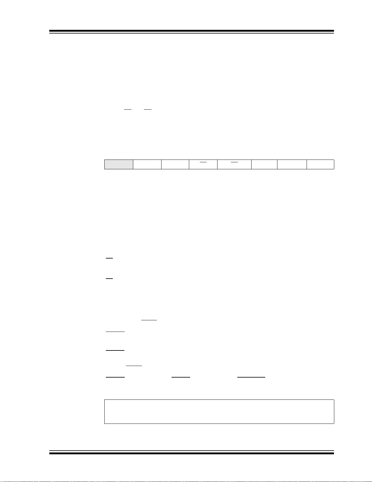
TABLE 1-1: PIC16F5X FAMILY OF DEVICES
Features PIC16F54 PIC16F57 PIC16F59
Maximum Operation Frequency 20 MHz 20 MHz 20 MHz
Flash Program Memory (x12 words) 512 2K 2K
RAM Data Memory (bytes) 25 72 134
Timer Module(s) TMR0 TMR0 TMR0
I/O Pins 12 20 32
Number of Instructions 33 33 33
Packages 18-pin DIP, SOIC;
20-pin SSOP
®
Note: All PICmicro
and high I/O current capability.
Family devices have Power-on Reset, selectable Watchdog Timer, selectable code-protect
28-pin DIP, SOIC;
28-pin SSOP
40-pin DIP, 44-pin TQFP
2004 Microchip Technology Inc. DS41213C-page 5

PIC16F5X
NOTES:
DS41213C-page 6 2004 Microchip Technology Inc.

PIC16F5X
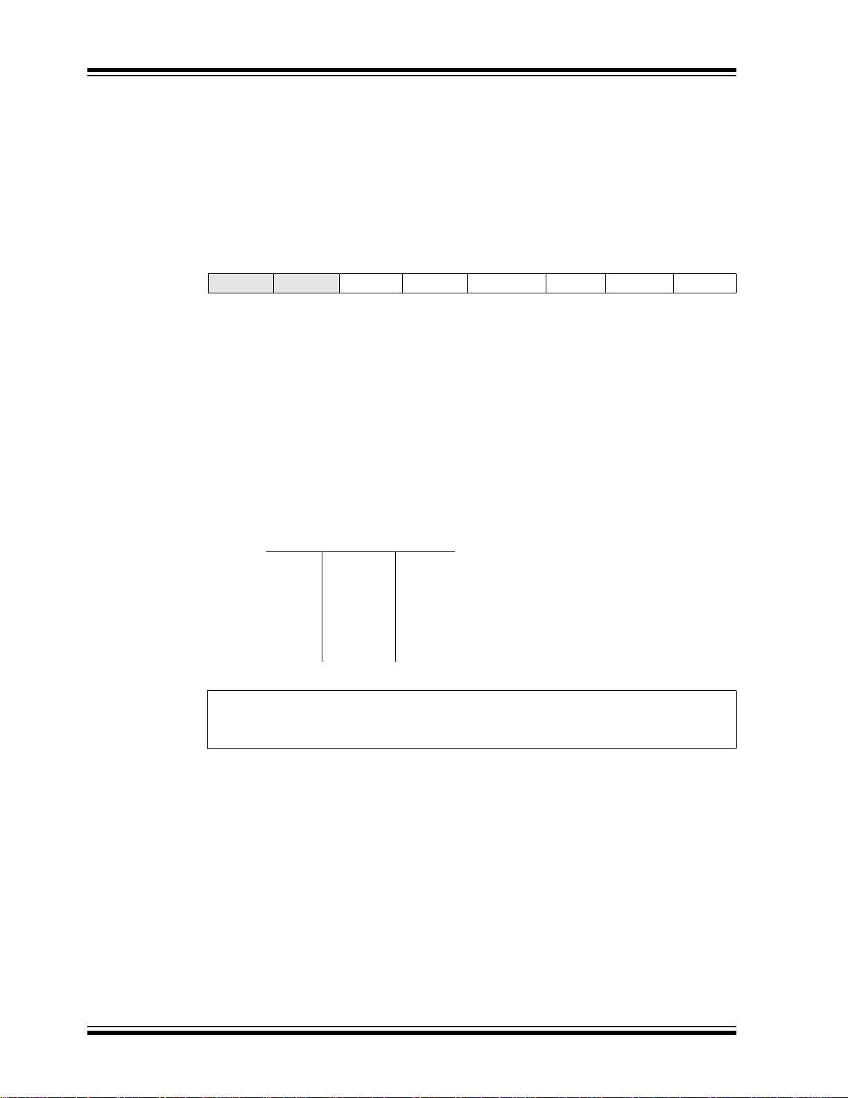
2.0 ARCHITECTURAL OVERVIEW
The high per formance of the P IC16F5X f amily c an be
attributed to a number of architectural features
commonly found in RISC microprocessors. To begin
with, the PIC16F5X uses a Harvard architecture in
which program and data are accessed on separate
buses. This improves bandwidth over traditional von
Neumann architecture where program and data are
fetched on the sam e bus. Sep arating pro gram and da ta
memory further allows instructions to be sized differently than the 8-bit wide data w ord. Instruction o pcodes
are 12-bits wide, making it possible to have all singleword instructions. A 12-bit wide program memory
access bus fetches a 12-b it instruction in a single cycle.
A two-stage pipeline overlaps fetch and execution of
instructions. Con sequently , all instructions (3 3) execute
in a single cycle except for program branches.
The PIC16F54 addresses 512x 12 of program
memory, the PIC16F57 and PIC16F59 addresses
2048 x 12 of program memory. All program memory is
internal.
The PIC16F5X can directly or indirectly address its
register files and data memory. All Special Function
Registers (SFR), including the program counter, are
mapped in the data memory. The PIC16F5X has a
highly orthogonal (symmetrical) instruction set that
makes it possible to carry out any op eration on a ny register using any Addressing mode. This symmetrical
nature and lack o f ‘special opti mal situations ’ make programming with the PIC16F5X simple, yet efficient. In
addition, the learning curve is reduced significantly.
The PIC16F5X device c ont ains an 8- bit ALU and working register. The ALU is a general purpose arithmetic
unit. It performs arithmetic and Boolean functions
between data in the working register and any register
file.
The ALU is 8-bits wide and capable of addition,
subtraction, shift and logical operations. Unless otherwise mentioned, arithmetic operations are two's
complement in nature. In two-operand instructions,
typically one operand is the W (working) register. The
other operand is either a file register or an immediate
constant. In sing le ope ran d inst ruction s, the operan d is
either the W register or a file register.
The W register is an 8-bit workin g register used for ALU
operations. It is not an addressable register.
Depending on the instruction executed, the ALU may
affect the values of the Carry (C), Digit Carry (DC) and
Zero (Z) bits in the Status Register. The C and DC bits
operate as a borrow
respectively, in subtraction. See the SUBWF and ADDWF
instructions for examples.
A simplified block diagram is shown in Figure 2-1 with
the corresponding device pins described in Table 2-1
(for PIC16F54), Table 2-2 (for PIC16F57) and
Table 2-3 (for PIC16F59).
and digit borrow out bit,
2004 Microchip Technology Inc. DS41213C-page 7

PIC16F5X
FIGURE 2-1: PIC16F5X SERIE S BLO CK DI AGRAM
Flash
512 X 12 (F54)
2048 X 12(F57)
2048 x 12(F59)
12
Instruction
Register
12
Instruction
Decoder
8
Literals
W
9-11
PC
Direct Address
Status
ALU
9
9-11
Stack 1
Stack 2
Time-out
8
From W
4
WDT
Direct RAM
Address
TMR0
4
T0CKI
Pin
Watchdog
WDT/TMR0
Prescaler
Data Bus
8
Configuration Word
“Disable”
Timer
6
Option Reg.
From W
From W
“Code-
Protect”
CLKOUT
5
8
“Option”
SFR
8
OSC1 OSC2 MCLR
“Osc
Select”
2
5-7
From W
Oscillator/
Timing &
Control
“Sleep”
General
Purpose
Register
File
(SRAM)
25, 72 or 134
Bytes
8
8
8
TRISA PORTA
“TRIS 5”
RA<3:0> RB<7:0>
From W
4
TRISE
“TRIS 9”
PORTE
RE<7:4>
PIC16F59
only
TRISB
4
8
4
“TRIS 6”
From W
8
TRISD
“TRIS 8”
RD<7:0>
PIC16F59
only
PORTD
PORTB
8
8
TRISC
8
“TRIS 7”
PORTC
8
RC<7:0>
PIC16F57/59
only
DS41213C-page 8 2004 Microchip Technology Inc.

PIC16F5X
TABLE 2-1: PIC16F54 PINOUT DESCRIPTION
Name Function
RA0 RA0 TTL CMOS Bidirectional I/O pin
RA1 RA1 TTL CMOS Bidirectional I/O pin
RA2 RA2 TTL CMOS Bidirectional I/O pin
RA3 RA3 TTL CMOS Bidirectional I/O pin
RB0 RB0 TTL CMOS Bidirectional I/O pin
RB1 RB1 TTL CMOS Bidirectional I/O pin
RB2 RB2 TTL CMOS Bidirectional I/O pin
RB3 RB3 TTL CMOS Bidirectional I/O pin
RB4 RB4 TTL CMOS Bidirectional I/O pin
RB5 RB5 TTL CMOS Bidirectional I/O pin
RB6/ICSPCLK RB6 TTL CMOS Bidirectional I/O pin
ICSPCLK ST — Serial Programming Clock
RB7/ICSPDAT RB7 TTL CMOS Bidirectional I/O pin
ICSPDAT ST CMOS Serial Programming I/O
T0CKI T0CKI ST — Clock input to Timer0. Must be tied to V
MCLR/VPP MCLR ST — Active-low Reset to device. Voltage on the MCLR/VPP pin must
VPP HV —
OSC1/CLKIN OSC1 XTAL — Oscillator crystal input
CLKIN ST — External clock source input
OSC2/CLKOUT OSC2 — XTAL Oscillator crystal output. Connects to crystal or resonator in
CLKOUT — CMOS In RC mode, OSC2 pin can output CLKOUT, which has 1/4 the
V
DD VDD Power — Positive supply for logic and I/O pins
VSS VSS Power — Ground reference for logic and I/O pins
Legend: I = input I/O = input/output CMOS = CMOS output
O = output — = Not Used XTAL = Crystal input/output
ST = Schmitt Trigger input TTL = TTL input HV = High Voltage
Input
Type
Output
Type
Description
reduce curr ent consumption.
not exceed V
mode.
Programming voltage input
Crystal Oscillator mode.
frequency of OSC1.
DD to avoid unintended entering of Programming
SS or VDD, if not in use, to
2004 Microchip Technology Inc. DS41213C-page 9

PIC16F5X
TABLE 2-2: PIC16F57 PINOUT DESCRIPTION
Name Function
RA0 RA0 TTL CMOS Bidirectional I/O pin
RA1 RA1 TTL CMOS Bidirectional I/O pin
RA2 RA2 TTL CMOS Bidirectional I/O pin
RA3 RA3 TTL CMOS Bidirectional I/O pin
RB0 RB0 TTL CMOS Bidirectional I/O pin
RB1 RB1 TTL CMOS Bidirectional I/O pin
RB2 RB2 TTL CMOS Bidirectional I/O pin
RB3 RB3 TTL CMOS Bidirectional I/O pin
RB4 RB4 TTL CMOS Bidirectional I/O pin
RB5 RB5 TTL CMOS Bidirectional I/O pin
RB6/ICSPCLK RB6 TTL CMOS Bidirectional I/O pin
ICSPCLK ST — Serial programming clock
RB7/ICSPDAT RB7 TTL CMOS Bidirectional I/O pin
ICSPDAT ST CMOS Serial programming I/O
RC0 RC0 TTL CMOS Bidirectional I/O pin
RC1 RC1 TTL CMOS Bidirectional I/O pin
RC2 RC2 TTL CMOS Bidirectional I/O pin
RC3 RC3 TTL CMOS Bidirectional I/O pin
RC4 RC4 TTL CMOS Bidirectional I/O pin
RC5 RC5 TTL CMOS Bidirectional I/O pin
RC6 RC6 TTL CMOS Bidirectional I/O pin
RC7 RC7 TTL CMOS Bidirectional I/O pin
T0CKI T0CKI ST — Clock input to Timer0. Must be tied to V
MCLR/VPP MCLR ST — Active-low Reset to device. Voltage on the MCLR/VPP pin must
VPP HV —
OSC1/CLKIN OSC1 XTAL — Oscillator crystal input
CLKIN ST — External clock source in put
OSC2/CLKOUT OSC2 — XTAL Oscillator crystal output. Connects to crystal or resonator in
CLKOUT — CMOS In RC mode, OSC2 pin outputs CLKOUT, which has 1/4 the
DD VDD Power — Positive supply for logic and I/O pins
V
SS VSS Power — Ground reference for logic and I/O pins
V
N/C N/C — — Unused, do no t connect
Legend: I = input I/O = input/output CMOS = CMOS output
O = output — = Not Used XTAL = Crystal input/output
ST = Schmitt Trigger input TTL = TTL input HV = High Voltage
Input
Type
Output
Type
Description
reduce curr ent consumption.
not exceed V
mode.
Programming voltage input
Crystal Oscillator mode.
frequency of OSC1.
DD to avoid unintended entering of Programming
SS or VDD, if not in use, to
DS41213C-page 10 2004 Microchip Technology Inc.

PIC16F5X
TABLE 2-3: PIC16F59 PINOUT DESCRIPTION
Name Function
RA0 RA0 TTL CMOS Bidirectional I/O pin
RA1 RA1 TTL CMOS Bidirectional I/O pin
RA2 RA2 TTL CMOS Bidirectional I/O pin
RA3 RA3 TTL CMOS Bidirectional I/O pin
RB0 RB0 TTL CMOS Bidirectional I/O pin
RB1 RB1 TTL CMOS Bidirectional I/O pin
RB2 RB2 TTL CMOS Bidirectional I/O pin
RB3 RB3 TTL CMOS Bidirectional I/O pin
RB4 RB4 TTL CMOS Bidirectional I/O pin
RB5 RB5 TTL CMOS Bidirectional I/O pin
RB6/ICSPCLK RB6 TTL CMOS Bidirectional I/O pin
ICSPCLK ST — Serial programming clock
RB7/ICSPDAT RB7 TTL CMOS Bidirectional I/O pin
ICSPDAT ST C MOS Serial programming I/O
RC0 RC0 TTL CMOS Bidirectional I/O pin
RC1 RC1 TTL CMOS Bidirectional I/O pin
RC2 RC2 TTL CMOS Bidirectional I/O pin
RC3 RC3 TTL CMOS Bidirectional I/O pin
RC4 RC4 TTL CMOS Bidirectional I/O pin
RC5 RC5 TTL CMOS Bidirectional I/O pin
RC6 RC6 TTL CMOS Bidirectional I/O pin
RC7 RC7 TTL CMOS Bidirectional I/O pin
RD0 RD0 TTL CMOS Bidirectional I/O pin
RD1 RD1 TTL CMOS Bidirectional I/O pin
RD2 RD2 TTL CMOS Bidirectional I/O pin
RD3 RD3 TTL CMOS Bidirectional I/O pin
RD4 RD4 TTL CMOS Bidirectional I/O pin
RD5 RD5 TTL CMOS Bidirectional I/O pin
RD6 RD6 TTL CMOS Bidirectional I/O pin
RD7 RD7 TTL CMOS Bidirectional I/O pin
RE4 RE4 TTL CMOS Bidirectional I/O pin
RE5 RE5 TTL CMOS Bidirectional I/O pin
RE6 RE6 TTL CMOS Bidirectional I/O pin
RE7 RE7 TTL CMOS Bidirectional I/O pin
T0CKI T0CKI ST — Clock input to Timer0. Must be tied to V
MCLR
/VPP MCLR ST — Active-low Reset to device. Voltage on the MCLR/VPP pin must not
V
PP HV —
OSC1/CLKIN OSC1 XTAL — Oscillator crystal input
CLKIN ST — External clock source input
OSC2/CLKOUT OSC2 — XTAL Oscillator crystal output. Connects to crystal or resonator in Crystal
CLKOUT — CMOS In RC mode, OSC2 pin outputs CLKOUT, which has 1/4 the frequency of
DD VDD Power — Positive supply for logic and I/O pins
V
SS VSS Power — Ground reference for logic and I/O pins
V
Legend: I = input I/O = input/output CMOS = CMOS output
O = output — = Not Used XTAL = Crystal input/output
ST = Schmitt Trigger input TTL = TTL input HV = High Voltage
Input
Type
Output
Type
Description
SS or VDD, if not in use, to reduce
current consumption.
exceed VDD to avoid unintended entering of Programming mode.
Programming voltage input
Oscillator mode.
OSC1.
2004 Microchip Technology Inc. DS41213C-page 11

PIC16F5X
2.1 Clocking Scheme/Instruction
Cycle
The clock input (OSC1/CLKIN pin) is internally divided
by four to generate four non-overlapping quadrature
clocks, namely Q1, Q2, Q3 and Q4. Internally, the
Program Counter (PC) is incremented every Q1 and
the instruction is fetched from program memory and
latched into the instru cti on register in Q4. It is decoded
and executed during the following Q1 through Q4. The
clocks and instruction execution flow are shown in
Figure 2-2 and Example 2-1.
FIGURE 2-2 : CLOCK/INS T RU CTI O N CYC L E
Q2 Q3 Q4
OSC1
Q1
Q2
Q3
Q4
PC
OSC2/CLKOUT
(RC mode)
Q1
PC PC+1 PC+2
Fetch INST (PC)
Execute INST (PC - 1) Fetch INST (PC + 1)
Q1
2.2 Instruction Flow/Pipelining
An instruction cycle consists of four Q cycles (Q1, Q2,
Q3 and Q4). The instruction fetch and execute are
pipelined such that fetch takes one instruction cycle,
while decode and execute takes another instruction
cycle. However, due to the pipelining, each instruction
effectively executes in one cycle. If an instruction
causes the Program Counter to change (e.g., GOTO),
then two cycles are req uired to c omplete the ins truction
(Example 2-1).
A fetch cycle begins with the Program Counter (PC)
incrementing in Q1.
In the execution cy cle, the fetched instruction i s latched
into the instruction register in cycle Q1. This instruction
is then decoded and executed during the Q2, Q3 and
Q4 cycles. Data memory is read during Q2 (operand
read) and written during Q4 (destination write).
Q2 Q3 Q4
Execute INST (PC) Fetch INST (PC + 2)
Q2 Q3 Q4
Q1
Execute INST (PC + 1)
Internal
phase
clock
EXAMPLE 2-1: INSTRUCTION PIPELINE FLOW
1. MOVLW H'55'
2. MOVWF PORTB
3. CALL SUB_1
4. BSF PORTA, BIT3
All instructions are sing le cycle, except fo r any program branc hes. These take two cycles since the fetch instructio n
is “flushed” from the pipeline, while the new instruction is being fetched and then executed.
DS41213C-page 12 2004 Microchip Technology Inc.
Fetch 1 Execute 1
Fetch 2 Execute 2
Fetch 3 Execute 3
Fetch 4 Flush
Fetch SUB_1 Execute SUB_1
PIC16F5X
3.0 MEMORY ORGANIZATION
PIC16F5X memory is organized into program memory
and data memory. For the PIC16F57 and PIC16F59,
which have more than 512 words of program memory,
a paging scheme is used. Program memory pages are
accessed using one or two Status register bits. For the
PIC16F57 and PIC16F59, which have a data memory
register file of more than 32 registers, a banking
scheme is used. Data memory banks are accessed
using the File Selection Register (FSR).
3.1 Program Memory Organization
The PIC16F54 has a 9-bit Program Counter (PC)
capable of addressing a 512 x 12 program memory
space (Figure 3-1). The PIC16F57 and PIC16F59 have
an 11-bit Program Counter capable of addressing a 2K
x 12 program memory sp a ce (Fi gure3-2). Accessing a
location above the ph ysicall y implem ented addres s will
cause a wraparound.
A NOP at the Reset vector location will cause a restart
at location 000h. The R eset v ec tor fo r the P IC16F 54 i s
at 1FFh. The Reset vector for the PIC16F57 and
PIC16F59 is at 7FFh. See Section 3.5 “Program
Counter” for additional information using CALL and
GOTO instructions.
FIGURE 3-2: PIC16F57/PIC16F59
PROGRAM MEMORY MAP
AND STACK
PC<10:0>
CALL, RETLW
Space
User Memory
Stack Level 1
Stack Level 2
On-chip Program
Memory (Page 0)
On-chip Program
Memory (Page 1)
On-chip Program
Memory (Page 2)
On-chip Program
Memory (Page 3)
Reset Vector
11
000h
0FFh
100h
1FFh
200h
2FFh
300h
3FFh
400h
4FFh
500h
5FFh
600h
6FFh
700h
7FFh
FIGURE 3-1: PIC16F54 PROGRAM
MEMORY MAP AND
STAC K
PC<8:0>
CALL, RETLW
Space
User Memory
Stack Level 1
Stack Level 2
On-chip
Program
Memory
Reset Vector
9
000h
0FFh
100h
1FFh
2004 Microchip Technology Inc. DS41213C-page 13
PIC16F5X
3.2 Data Memory Organization
Data memory is composed of registers or bytes of
RAM. Therefore, d ata memory for a dev ic e i s sp ec ifie d
by its register file. The register file is divided into two
functional groups: Special Function Registers (SFR)
and General Purpose Registers (GPR).
The Special Function Registers include the TMR0
register , the Program Counter (PC), the S t atus register ,
the I/O registers (ports) and the File Select Register
(FSR). In addition, Special Purpose Registers are used
to control the I/O port configuration and prescaler
options.
The General Purpose Registers are used for data and
control information under com mand of the instructions .
For the PIC16F54, the register file is composed of 7
Special Function Registers and 25 General Purpose
Registers (Figure 3-3).
For the PIC16F57, the register file is composed of 8
Special Function Registers, 8 General Purpose
Registers and 64 additional General Purpose
Registers that may be addressed using a banking
scheme (Figure 3-4).
For the PIC16F59, the register file is composed of 10
Special Function Registers, 6 General Purpose
Registers and 128 additional General Purpose
Registers that may be addressed using a banking
scheme (Figure 3-5).
3.2.1 GENERAL PURPOSE REGISTER
FILE
The register file is accessed either directly or indirectly
through the File Select Register (FSR). The FSR
register is described in Section3.7 “Indirect Data
Addressing; INDF and FSR Registers”.
FIGURE 3-3: PIC16F54 REGISTER FILE
MAP
File Address
(1)
.
INDF
TMR0
PCL
STATUS
FSR
PORTA
PORTB
General
Purpose
Registers
00h
01h
02h
03h
04h
05h
06h
07h
1Fh
Note 1: Not a physical register. See Section 3.7
“Indirect Data Addressing; INDF and FSR
Registers”
FIGURE 3-4: PIC16F57 REGISTER FILE MAP
FSR<6:5> 00 01 10 11
File Address
00h
01h
02h
03h
04h
05h
06h
07h
08h
0Fh
10h
1Fh
Note 1: Not a physical register. See Section 3.7 “Indirect Data Addressing; INDF and FSR Registers”.
(1)
INDF
TMR0
PCL
STATUS
FSR
PORTA
PORTB
PORTC
General
Purpose
Registers
General
Purpose
Registers
Bank 0 Bank 1 Bank 2 Bank 3
20h
2Fh
30h
3Fh
General
Purpose
Registers
40h
Addresses map back to
addresses in Bank 0.
4Fh
50h
General
Purpose
Registers
5Fh
60h
6Fh
70h
General
Purpose
Registers
7Fh
DS41213C-page 14 2004 Microchip Technology Inc.
FIGURE 3-5: PIC16F59 REGISTER FILE MAP
PIC16F5X
FSR<7:5>
File Address
00h
01h
02h
03h
04h
05h
06h
07h
08h
09h
0Ah
0Fh
10h
1Fh
000 001 010 011
(1)
INDF
TMR0
PCL
STATUS
FSR
PORTA
PORTB
PORTC
PORTD
PORTE
General
Purpose
Registers
General
Purpose
Registers
Bank 0 Bank 1 Bank 2 Bank 3
20h
2Fh
30h
General
Purpose
Registers
3Fh
40h
4Fh
50h
General
Purpose
Registers
5Fh
60h
6Fh
70h
General
Purpose
Registers
7Fh
100 101 110 111
80h
Addresses map back to addresses in Bank 0.
8Fh
90h
General
Purpose
Registers
9Fh
Bank 4 Bank 5 Bank 6 Bank 7
A0h
AFh
B0h
General
Purpose
Registers
BFh
C0h
CFh
D0h
General
Purpose
Registers
DFh
E0h
EFh
F0h
General
Purpose
Registers
FFh
Note 1: Not a physical register.
2004 Microchip Technology Inc. DS41213C-page 15

PIC16F5X
3.2.2 SPECIAL FUNCTION REGISTERS
The Special Function Registers (SFR) are registers
used by the CPU and per ipheral functio ns to con trol the
operation of the devic e (Table 3-1).
The Special Function Registers can be classified into
two sets. The Special Function Re gisters associated
with the “core” functions are described in this section.
Those related to the operation of the peripheral
features are described in the section for each
peripheral feature.
TABLE 3-1: SPECIAL FUNCTION REGISTER SUMMARY
Value on
Address Name Bit 7 Bit 6 Bit 5 Bit 4 Bit 3 Bit 2 Bit 1 Bit 0
Power-on
Reset
N/A TRIS I/O Control Registers (TRISA, TRISB, TRISC, TRISD, TRISE) 1111 1111 29
N/A OPTION Contains control bits to configure Timer0 and Timer0/WDT
--11 1111 18
prescaler
00h INDF Uses contents of FSR to address data memory (not a physical
xxxx xxxx 20
register)
01h TMR0 Timer0 Module Register xxxx xxxx 34
02h PCL
(1)
03h STATUS
04h FSR
04h FSR
04h FSR
(3)
(4)
(5)
05h PORTA
Low order 8 bits of PC 1111 1111 19
PA2 PA1 PA0 TO PD ZDCC0001 1xxx 17
Indirect data memory address pointer 111x xxxx 20
Indirect data memory address pointer 1xxx xxxx 20
Indirect data memory address pointer xxxx xxxx 20
(6)
— — — — RA3 RA2 RA1 RA0 ---- xxxx 29
06h PORTB RB7 RB6 RB5 RB4 RB3 RB2 RB1 RB0 xxxx xxxx 29
07h PORTC
08h PORTD
09h PORTE
(2)
(7)
(6), (7)
RC7 RC6 RC5 RC4 RC3 RC2 RC1 RC0 xxxx xxxx 29
RD7 RD6 RD5 RD4 RD3 RD2 RD1 RD0 xxxx xxxx 29
RE7 RE6 RE5 RE4 — — — — xxxx ---- 29
Legend: Shaded cells = unimplemented or unused, – = unimplemented, read as ‘0’ (if applicable), x = unknown,
u = unchanged
Note 1: The upper byte of the Program Counter is not directly accessible. See Section 3.5 “Program Counter”
for an explanation of how to access these bits.
2: File address 07h is a General Purpose Register on the PIC16F54.
3: PIC16F54 only.
4: PIC16F57 only.
5: PIC16F59 only.
6: Unimplemented bits are read as ‘0’s.
7: File address 08h and 09h are General Purpose Registers on the PIC16F54 and PIC16F57.
Details
on Page
DS41213C-page 16 2004 Microchip Technology Inc.
PIC16F5X
3.3 Status Register
This register contains the arithmetic status of the ALU,
the Reset status and the page preselect bits for
program memories larger than 512 words.
The Status register can be the destination for any
instruction, as with any other register. If the Status
register is the destination for an instruction that affects
the Z, DC or C bits, then the write to these three bits is
disabled. These bit s are set or cleared ac cording to the
device logic. Furthermore, the TO
and PD bits are not
For example, CLRF STATUS will clear the upper three
bits and set the Z bit. Thi s leav es the Status register as
000u u1uu (where u = unchanged).
Therefore, it is recommended that only BCF, BSF,
MOVWF and SWAPF instructions be used to alter the
Stat us register be cause the se instruct ions do not af fect
the Z, DC or C bits from the Status register. For other
instructions which do affect Status bits, see
Section 9.0 “Instruction Set Summary”.
writable. Therefore, the result of an instruction with the
Status register as destination may be different than
intended.
REGISTER 3-1: STATUS REGISTER (ADDRESS: 03h)
R/W-0 R/W-0 R/W-0 R-1 R-1 R/W-x R/W-x R/W-x
PA2 PA1 PA0 TO PD ZDCC
bit 7 bit 0
bit 7 PA2: Reserved, do not use
Use of the PA2 bit as a general purpose read/write bit is not recommended, since this may affect upward
compatibility with future products.
bit 6-5 PA<1:0>: Program Page Preselect bits (PIC16F57/PIC16F59)
00 = Page 0 (000h-1FFh)
01 = Page 1 (200h-3FFh)
10 = Page 2 (400h-5FFh)
11 = Page 3 (600h-7FFh)
Each page is 512 words. Using the PA<1:0> bits as general purpose read/write bits in devices which do
not use them for program page preselect is not recommended. This may affect upward compatibility with
future products.
bit 4 TO
bit 3 PD
bit 2 Z: Zero bit
bit 1 DC: Digit Carry/Bo
bit 0 C: Carry/Bo
: Time-Out bit
1 = After power-up, CLRWDT instruction or SLEEP instruction
0 = A WDT time-out occurred
: Power-Down bit
1 = After power-up or by the CLRWDT instruction
0 = By execution of the SLEEP instruction
1 = The result of an arithmetic or logic operation is zero
0 = The result of an arithmetic or logic operation is not zero
rrow bit (for ADDWF and SUBWF instructions)
ADDWF
1 = A carry to the 4th low order bit of the result occurred
0 = A carry from the 4th low order bit of th e result did not occur
SUBWF
1 = A borrow to the 4th low order bit of the result did not occur
0 = A borrow from the 4th low order bit of the result occurred
rrow bit (for ADDWF, SUBWF and RRF, RLF instructions)
ADDWF
1 = A carry occurred 1 = A borrow did not occur Loaded with LSb or MSb, respectively
0 = A carry did not occur 0 = A borrow occurred
SUBWF RRF or RLF
Legend:
R = Readable bit W = Writable bit U = Unimplemented bit, read as ‘0’
- n = Value at POR ‘1’ = Bit is set ‘0’ = Bit is cleared x = Bit is unknown
2004 Microchip Technology Inc. DS41213C-page 17
PIC16F5X
3.4 Option Register
The Option register is a 6-bit wide, write-only register
which contains various control bits to configure the
Timer0/WDT prescaler and Timer0.
By executin g the OPTION instruction, the contents of
the W register will be transfe rred to the Option registe r.
A Reset sets the Option<5:0> bits.
REGISTER 3-2: OPTION REGISTER
U-0 U-0 W-1 W-1 W-1 W-1 W-1 W-1
— — T0CS T0SE PSA PS2 PS1 PS0
bit 7 bit 0
bit 7-6 Unimplemented: Read as ‘0’
bit 5 T0CS: Timer0 Clock Source Select bit
1 = Transition on T0CKI pin
0 = Internal instruction cycle clock (CLKOUT)
bit 4 T0SE: Timer0 Source Edge Select bit
1 = Increment on high-to-low transition on T0CKI pin
0 = Increment on low-to-high transition on T0CKI pin
bit 3 PSA: Prescaler Assignment bit
1 = Prescaler assigned to the WDT
0 = Prescaler assigned to Timer0
bit 2-0 PS<2:0>: Prescaler rate select bits
Bit Value Timer0 Rate WDT Rate
000
001
010
011
100
101
110
111
1 : 2
1 : 4
1 : 8
1 : 16
1 : 32
1 : 64
1 : 128
1 : 256
1 : 1
1 : 2
1 : 4
1 : 8
1 : 16
1 : 32
1 : 64
1 : 128
Legend:
R = Readable bit W = Writable bit U = Unimplemented bit, read as ‘0’
- n = Value at POR ‘1’ = Bit is set ‘0’ = Bit is cleared x = Bit is unknown
DS41213C-page 18 2004 Microchip Technology Inc.

PIC16F5X
3.5 Program Counter
As a program instruction is executed, the Program
Counter (PC) will contain the address of the next
program instruction to be executed. The PC value is
increased by one, every instruction cycle, unless an
instruction changes the PC.
For a GOTO instruction, bits 8:0 of the PC are provided
by the GOTO inst ruction word . The PC Latch (P CL) is
mapped to PC<7:0> (Figure 3-6 and Figure 3-7).
For the PIC16F57 and PIC16F59, a page number must
be supplied as well. Bit 5 and bit 6 of the S t atus register
provide page information to bit 9 and bit 10 of the PC
(Figure 3-6 and Figure 3-7).
For a CALL instruction, or any instruction where the
PCL is the destination, bits 7:0 of the PC again are
provided by the instruction word. However, PC<8>
does not come from the instruct ion word, but is alway s
cleared (Figure 3-6 and Figure 3-7).
Instructions where t he PCL is the des tinati on or modif y
PCL instructions, include MOVWF PCL, ADDWF PCL,
and BSF PCL,5.
For the PIC16F57 and PIC16F59, a page number
again must be supplied. Bit 5 and bit 6 of the Status
register provide page information to bit 9 and bit 10 of
the PC (Figure 3-6 and Figure 3-7).
FIGURE 3-7: LOADING OF PC BR ANCH
INSTRUCTIONS – PIC16F57
AND PIC16F59
GOTO Instruction
910
87 0
PC
2
PA<1:0>
70
Status
CALL or Modify PCL Instruction
87 0
910
PC
Reset to ‘0’
2
PA<1:0>
70
Status
PCL
Instruction Word
PCL
Instruction Word
Note: Because PC<8> is cleared in the CALL
instruction or any modified PCL instruction, all subroutine calls or computed
jumps are limited to the first 256 locations
of any program memory page (512 words
long).
FIGURE 3-6: LOADING OF PC BRANCH
INSTRUCTIONS – PIC16F54
GOTO Instruction
87 0
PC
CALL or Modify PCL Instruction
87 0
PC
Reset to '0'
PCL
Instruction Word
PCL
Instruction Word
3.5.1 PAGING CONSIDERATIONS
PIC16F57 AND PIC16F59
If the PC is pointing to the last address of a selected
memory page, when i t incremen ts, it w ill cause t he program to continue in the next h igher p age . Howe ver, the
page preselect bits in the Status register will not be
updated. Therefore, the next GOTO, CALL or MODIFY
PCL instruction will send the program to the page
specified by the page preselect bits (PA0 or PA<1:0>).
For example, a NOP at location 1FFh (page 0)
increments the PC to 200h (page 1). A GOTO xxx at
200h will return the program to address xxh on page 0
(assuming that PA<1:0> are clear).
To prevent this, the page preselect bits must be
updated under program control .
3.5.2 EFFECTS OF RESET
The PC is set upon a Reset, which means that the PC
addresses the last location in the last page (i.e., the
Reset vector).
The Status register page preselect bits are cleared
upon a Reset , whic h me ans that page 0 is prese lecte d.
Therefore, upon a Reset, a GOTO instruction at the
Reset vector location will automatically cause the
program to jump to page 0.
2004 Microchip Technology Inc. DS41213C-page 19

PIC16F5X
3.6 Stack
The PIC16F54 device has a 9- bi t wide, tw o-l ev el ha rdware PUSH/POP stack. The PIC16F57 and PIC16F59
devices have an 11-bit wide, two-level hardware
PUSH/POP stack.
A CALL instruction will PUSH the current value of stack 1
into stack 2 and t hen PUSH the c urren t pr ogram c ounte r
value, incre mented by one, into stack lev el 1. If more tha n
two sequenti al CALL’ s are executed, only the most recent
two return addresse s are stored .
A RETLW i nstruction will POP th e contents of s tack level
1 into the program counter and then copy stack level 2
contents into level 1. If more than two sequential
RETLW’s are executed, the stack will be filled with the
address previously stored in level 2.
Note: The W register will be loaded with the
literal value specified in the instruction.
This is particularly useful for the
implementation of data look-up tables
within the program memory.
For the RETLW instruction, the PC is loaded with the
Top-of-Stack (TOS) contents. All of the devices covered in this data sheet have a two-level stack. The
stack has the same bit width as the devic e PC, there fore, paging is not an issue when returning from a subroutine.
3.7 Indirect Data Addressing; INDF
and FSR Registers
The INDF register is not a physi cal register. Addressing
INDF actually address es the reg ister whos e addres s is
contained in the FSR Register (FSR is a pointer). T h is
is indirect addressing.
EXAMPLE 3-1: INDIRECT ADDRESSING
• Register file 08 contains the value 10h
• Register file 09 contains the value 0Ah
• Load the value 08 into the FSR regi ster
• A read of the INDF register will return the value
of 10h
• Increment the value of the FSR register by one
(FSR = 09h)
• A read of the INDF register now will return the
value of 0Ah.
Reading INDF itself indirectly (FSR = 0) will produce
00h. Writing to the INDF register indirectly results in a
no-operation (although Status bits may be affected).
A simple program to clear RAM locations 10h-1Fh
using indirect addressing is shown in Example 3-2.
EXAMPLE 3-2: HOW TO CLEAR RAM
USING INDIRECT
ADDRESSING
MOVLW H'10' ;initialize pointer
MOVWF FSR ;to RAM
NEXT CLRF INDF ;clear INDF Register
INCF FSR,F ;inc pointer
BTFSC FSR,4 ;all done?
GOTO NEXT ;NO, clear next
CONTINUE
: ;YES, continue
The FSR is either a 5-bit (PIC 16F54 ), 7-bit (PIC1 6F57)
or 8-bit (PIC16F59) wide register. It is used in conj unc tion with the INDF register t o indirectly addr ess the dat a
memory area.
The FSR<4:0> bits are used to select data memory
addresses 00h to 1Fh.
PIC16F54: This does not us e banking. FSR<7 :5> bits
are unimplemented and read as ‘1’s.
PIC16F57: FSR<7> bit is unimp lemented and read a s
‘1’. FSR<6:5> are the bank select bits and are used to
select the bank to be addressed (00 = Bank 0,
01 = Bank 1, 10 = Bank 2, 11 = Bank 3).
PIC16F59: FSR<7:5> are the bank select bits and are
used to select the bank to be addressed
(000 = Bank 0, 001 = Bank 1, 010 = Bank 2,
011 = Bank 3, 100 = Bank 4, 101 = Bank 5,
110 = Bank 6, 111 = Bank 7).
Note: A CLRF FSR instruction may not result in
an FSR value of 00h if there are
unimplemented bits present in the FSR.
DS41213C-page 20 2004 Microchip Technology Inc.
PIC16F5X
4.0 OSCILLATOR CONFIGURATIONS
4.1 Oscillator Types
The PIC16F5X devices can be operated in four different oscillator mode s. The user can progra m two configuration bits (FOS C1:FOSC0) to select one of these four
modes:
• LP: Low-power Crystal
• XT: Crystal/Resonator
• HS: High-speed Crystal/Resonator
• RC: Resistor/Capacitor
4.2 Crystal Oscillator/Ceramic
Resonators
In XT, LP or HS modes, a crystal or ceramic resonator
is connected to the OSC1/CLKIN and OSC2/CLKOUT
pins to establish oscillation (Figure 4-1). The
PIC16F5X oscillator design requires the use of a
parallel cut crystal. Use of a series cut crystal may give
a frequency outside of the crystal manufacturers
specifications. When in XT, LP or HS modes, the
device can have an external clock source drive the
OSC1/CLKIN pin (Figure 4-2).
FIGURE 4-1 : CRYST AL/C E RAMI C
RESONATO R OPER ATI ON
(HS, XT OR LP OSC
CONFIGURATION)
(1)
C1
(1)
C2
Note 1: See Capacitor Selection tables for
recommended values of C1 and C2.
2: A series resistor (RS) may be required.
3: RF varies with the Oscillator mode chosen
(approx. value = 10 MΩ).
FIGURE 4-2: EXTERNAL CLOCK INPUT
Clock from
ext. system
Open
XTAL
RS
(2)
OSC1
RF
OSC2
PIC16F5X
(3)
OPERATION (HS, XT OR LP
OSC CONFIGURATION)
OSC1
PIC16F5X
OSC2
Sleep
To internal
logic
T ABLE 4-1: CAPACITOR SELECTION FOR
CERAMIC RESONATORS
Osc
Type
XT 455 kHz
HS 8.0 MHz
These values are for design guidance only. Since
each resonator has its own characteristics, the user
should consult the resonator man ufa ctu rer for
appropriate values of external components.
Resonator
Freq.
2.0 MHz
4.0 MHz
16.0 MHz
Cap. RangeC1Cap. Range
C2
68-100 pF
15-33 pF
10-22 pF
10-22 pF
10 pF
68-100 pF
15-33 pF
10-22 pF
10-22 pF
10 pF
T ABLE 4-2: CAPACITOR SELECTION FOR
CRYSTAL OSCILLATOR
Osc
Type
LP 32 kHz
XT 100 kHz
HS 4 MHz
Note 1: For V
These values are for design guidance only. Rs may
be required in HS mode, as well as XT mode, to
avoid overdriving crystals with low drive level specifications. Since each crystal has its own characteristics, the user sho uld c onsul t the cryst al manu fact urer
for appropriate values of external components.
Note 1: This device has been des igned to perform
Crystal
Freq.
200 kHz
455 kHz
1MHz
2MHz
4MHz
8MHz
20 MHz
DD > 4.5V, C1 = C2 ≈ 30 pF is
recommended.
to the parame ter s of i ts da ta s he e t. I t ha s
been tested to an electrical specification
designed to determine its conformance
with these parameters. Due to process
differences in the manufacture of this
device, this device may have different
performance characteristics than its
earlier version. These differences may
cause this device to perform differently in
your application tha n the earlier v ersion of
this device.
2: The user should verify that the device
oscillator starts and performs as
expected. Adjusting the loading capacitor
values and/or the Os cillator mode ma y be
required.
(1)
Cap.Range
C1
15 pF 15 pF
15-30 pF
15-30 pF
15-30 pF
15-30 pF
15 pF
15 pF
15 pF
15 pF
15 pF
Cap. Range
200-300 pF
100-200 pF
C2
15-100 pF
15-30 pF
15 pF
15 pF
15 pF
15 pF
15 pF
2004 Microchip Technology Inc. DS41213C-page 21

PIC16F5X
4.3 External Crystal Oscillator Circuit
Either a pre-packaged oscillator or a simple oscillator
circuit with TTL gates can be used as an external
crystal oscillator circuit. Pre-packaged oscillators
provide a wide operating range and better stability. A
well designed cryst al oscilla tor will provide g ood performance with TTL gates. Two types of crystal oscillator
circuits can b e used: one with parallel resonance or one
with series resonance.
Figure 4-3 shows an implementation example of a
parallel resonant oscillator circuit. The circuit is
designed to use the fundamental frequency of the
crystal. The 74AS 04 i nvert er perf orm s th e 180° phase
shift that a parallel oscillator requires. The 4.7 kΩ
resistor provides the negative feedback for stability.
The 10 kΩ potentiometers bias the 74AS04 in the
linear region. This circuit could be used for external
oscillator designs.
FIGURE 4-3: EXTERNAL PARALLEL
RESONANT CRY ST A L
OSCILLATOR CIRCUIT
(USING XT, HS OR LP
OSCILLATOR MODE)
+5V
10k
4.7k
74AS04
10k
XTAL
10k
20 pF
20 pF
Figure 4-4 shows a series resonant oscillator circuit.
This circuit is also designed to use the fundamental
frequency of the crystal. The inverters perform a 360°
phase shift in a series resonant oscillator circuit. The
330 kΩ resistors provide the negative feedback to bias
the inverters in their linear region.
74AS04
Open
To Other
Devices
PIC16F5X
CLKIN
OSC2
FIGURE 4-4: EXTERNAL SERIES
RESONANT CRY ST A L
OSCILLATOR CIRCUIT
(USING XT, HS OR LP
OSCILLATOR MODE)
74AS04
To Other
Devices
Open
PIC16F5X
CLKIN
OSC2
KK
330
74AS04
330
74AS04
0.1 µF
XTAL
4.4 RC Oscillator
For applications where precise timing is not a requirement, the RC oscillator option is available. The
operation and functionality of the RC oscillator is
dependent upon a number of variables. The RC
oscillator frequency is a function of:
• Supply voltage
• Resistor (R
• Operating temperature.
The oscillator frequency will vary from unit to unit due
to normal process parameter variation. The difference
in lead frame capacitance between package types will
also affect the oscillation frequency, especially for low
CEXT values. The user also needs to account for the
tolerance of the external R and C components.
Figure 4-5 shows how the R/C combination is
connected.
The oscillator frequency, divided by 4, is available on
the OSC2/CLKOUT pin and can be used for test
purposes or to synchronize other logic.
FIGURE 4-5: RC OSCILLA TOR M ODE
REXT
CEXT
VSS
EXT) and capacitor (CEXT) values
VDD
OSC1
N
Internal
clock
PIC16F5X
F
OSC/4
DS41213C-page 22 2004 Microchip Technology Inc.
OSC2/CLKOUT
PIC16F5X
5.0 RESET
The PIC16F5X devices may be reset in one of the
following ways:
• Power-on Reset (POR)
•MCLR
•MCLR Wake-up Reset (from Sleep)
• WDT Reset (normal operation)
• WDT Wake-up Reset (from Sleep)
Table 5-1 shows these Reset conditions for the PCL
and Status registers.
Some registers are no t af fected in a ny Rese t conditio n.
Their status is unk nown on POR and uncha nged in any
other Reset. Most other registers are reset to a “Reset
state” on Power-on Reset (POR), MCLR
Reset. A MCLR
results in a device Reset and not a continuation of
operation before Sleep.
Reset (normal operation)
or WDT
or WDT wake-up from Sleep also
The TO
depending on the different Reset conditions (Table 5-1).
These bits may be used to determine the nature of the
Reset.
Table 5-3 lists a full description of Reset states of all
registers. Figure 5-1 shows a simplified block diagram
of the on-chip Reset circuit.
and PD bits (Status <4:3>) are set or cleared
TABLE 5-1: STATUS BITS AND THEIR SIGNIFICANCE
Condition TO PD
Power-on Reset 11
Reset (normal operation) uu
MCLR
Wake-up (from Sleep) 10
MCLR
WDT Reset (normal operation) 01
WDT Wake-up (from Sleep) 00
Legend: u = unchanged, x = unknown, — = unimplemented read as ‘0’.
TABLE 5-2: SUMMARY OF REGISTERS ASSOCIATED WITH RESET
Address Name Bit 7 Bit 6 Bit 5 Bit 4 Bit 3 Bit 2 Bit 1 Bit 0
03h STA TUS
Legend: u = unchanged, x = unknown, q = see Table 5-1 for possible values.
PA2 PA1 PA0 TO PD Z DC C 0001 1xxx 000q quuu
Value on
POR
Value on
MCLR
and
WDT Reset
2004 Microchip Technology Inc. DS41213C-page 23
PIC16F5X
TABLE 5-3: RESET CONDITIONS FOR ALL REGISTERS
Register Address Power-on Reset MCLR or WDT Reset
WN/Axxxx xxxx uuuu uuuu
TRIS N/A 1111 1111 1111 1111
OPTION N/A --11 1111 --11 1111
INDF 00h xxxx xxxx uuuu uuuu
TMR0 01h xxxx xxxx uuuu uuuu
PCL 02h 1111 1111 1111 1111
STATUS 03h 0001 1xxx 000q quuu
(1)
FSR
(2)
FSR
(3)
FSR
PORTA 05h ---- xxxx ---- uuuu
PORTB 06h xxxx xxxx uuuu uuuu
PORTC
PORTD
PORTE
(4)
(5)
(5)
Legend: u = unchanged, x = unknown, — = unimplemented, read as ‘0’, q = see tables in Table 5-1 for possible
values.
Note 1: PIC16F54 only.
2: PIC16F57 only.
3: PIC16F59 only.
4: General purpose register file on PIC16F54.
5: General purpose register file on PIC16F54 and PIC16F57.
04h 111x xxxx 111u uuuu
04h 1xxx xxxx 1uuu uuuu
04h xxxx xxxx uuuu uuuu
07h xxxx xxxx uuuu uuuu
08h xxxx xxxx uuuu uuuu
09h xxxx ---- uuuu ----
FIGURE 5-1: SIMPLIFIE D BLOC K DIAG RAM O F ON-C HIP RE SE T CIRC UIT
VDD
POR
MCLR/VPP
MCLR
Filter
WDT
Module
DRT
Reset
S
R
Q
Chip Reset
DS41213C-page 24 2004 Microchip Technology Inc.
PIC16F5X
5.1 Power-on Reset (POR)
The PIC16F5X family of devices incorporate on-chip
Power-on Reset (POR) circuitry which provides an
internal chip Reset for most power-up situations. To
use this feature, the user merely ties the MCLR
DD. A simplified block diagram of the on-chip
to V
Power-on Reset circuit is shown in Figure 5-1.
The Power-on Reset circuit and the Device Reset
Timer (Section 5.2) circuit are closely related. On
power-up, the Reset latch is set and the DRT is reset.
The DRT timer begins counting once it detects MCLR
to be high. After the time-out period, which is typically
18 ms, it will reset the Res et lat ch and thus end th e onchip Reset signal.
A power-up example where MCLR
shown in Figure 5-3. V
before bringing MCLR
out of Reset T
DRT msec after MCLR goes high.
DD is allowed to rise and stabilize
high. The chip will actual ly come
is not tied to VDD is
In Figure 5-4, the on-chip Power-on Reset feature is
being used (MCLR and VDD are ti ed together). The VDD
is stable bef ore the st art-up tim er times out and the re is
no problem in getting a proper Reset. However,
Figure 5-5 depic ts a pro blem situ ation whe re VDD rises
too slowly. The time between when the DRT senses a
high on the MCLR
V
DD) actually reach their full va lue is too long. In this sit-
/VPP pin and the MCL R/VPP pin (and
uation, when the start-up timer times out, V
reached the V
DD (min) value and the chip is, therefo r e,
not ensured to function correctly. For such situations,
we recommend that external RC circuits be used to
achieve longer POR delay times (Figure 5-2).
Note 1: When the device starts normal operation
(exits the Reset condition), device
operating parameters (voltage, frequency , tempe rature, etc.) m ust be met to
ensure operation. If these conditions are
not met, the device must be hel d in Reset
until the operating conditions are met.
2: The POR is disabled when the device is
in Sleep.
For more information on the PIC16F5X POR, see
Application Note AN522, “Power-Up Considerations”
at www.microchip.com.
/VPP pin
DD has not
FIGURE 5-2: EXTERNAL POWER-ON
RESET CIRCUIT (FOR
SLOW V
VDDVDD
D
• External Power-on Reset circuit is required
only if V
helps dischar ge the capacito r quickly when
VDD powers down.
•R < 40kΩ is recommended to make sure th at
voltage drop across R does not violate the
device electrical specification.
•R1 = 100Ω to 1 kΩ will limit any current
flowing into MCLR from external capacitor C
in the event of MCLR
Electrostatic Discha rge (ESD) or Electric al
Overstress (EOS).
R
DD power-up is too slow. The diode D
DD POWER-UP)
R1
C
MCLR
PIC16F5X
pin breakdown due to
2004 Microchip Technology Inc. DS41213C-page 25

PIC16F5X
FIGURE 5-3: TIME-OUT SEQUENCE ON POWER-UP (MCLR NOT TIED TO VDD)
VDD
MCLR
Internal POR
DRT Time-out
Internal Reset
TDRT
FIGURE 5-4: TIME-OUT SEQUENCE ON POWER-UP (MCLR
VDD
MCLR
Internal POR
DRT Time-out
Internal Reset
TDRT
FIGURE 5-5: TIME-OUT SEQUENCE ON POWER-UP (MCLR
V1
VDD
MCLR
Internal POR
TDRT
TIED TO VDD): FAST VDD RISE TIME
TIED TO VDD): SLOW VDD RISE TIME
DRT Time-out
Internal Reset
Note : When VDD rises slowly, the TDRT time-out expires long before VDD has reached its final value. In t his example, the
chip will reset properly if, and only if, V1 ≥ V
DS41213C-page 26 2004 Microchip Technology Inc.
DD min.

PIC16F5X
5.2 Device Reset Timer (DRT)
The Device Reset Timer (DRT) provides an 18 ms
nominal time-out on Reset regardless of the oscillator
mode used. The DRT operates on an internal RC
oscillator . T he proces sor is kep t in Re set as l ong as the
DRT is active. The DRT delay allows V
DD min. and for the chosen oscillator to stabilize.
V
Oscillator circuit s, based on cry stals or cerami c resona-
tors, require a certain time after power-up to establish
a stable oscillation. The on-chip DRT keeps the device
in a Reset condition for approximately 18 ms after the
voltage on the MCLR
IH) level. T hus, extern al RC network s connected t o
(V
the MCLR
allowing for savings in cost-sensitive and/or space
restricted applications.
The device Reset time delay will vary from chi p-to-chip
due to V
AC parameters for details.
The DRT will also be tri ggered upon a Watchdog T im er
time-out. This is particularly important for applications
using the WDT to wake the PIC16F5X from Sleep
mode automatically.
input are not required in most cases,
DD, temperature and process variation. See
/VPP pin has reached a logic high
DD to rise above
5.3 Reset on Brown-Out
A Brown-out is a condition where device power (VDD)
dips below its minimum value, but no t to zero, and the n
recovers. The device should be reset in the event of a
Brown-out.
To reset PIC16F5X devices when a Brown-out occurs,
external Brown-out protection circuits may be built, as
shown in Figure 5-6, Figure 5-7 and Figure 5-8.
FIGURE 5-6: EXTERNAL BROWN-OUT
PROTECTION CIRCUIT 1
VDD
DD
V
33k
10k
Q1
40k
MCLR
PIC16F5X
FIGURE 5-7: EXTERNAL BROWN-OUT
PROTECTION CIRCUIT 2
VDD
VDD
R1
Q1
MCLR
R2
This brown-out circuit is less expensive, although
less accurate. Transistor Q1 turns off when V
below a certain level such that:
VDD •
40k
R1
R1 + R2
PIC16F5X
DD is
= 0.7V
FIGURE 5-8: EXTERNAL BROWN-OUT
PROTECTION CIRCUIT 3
VDD
VDD
MCP809
RST
VSS
This brown-out protection circuit employs
Microchip Technology’s MCP809 microcontroller
supervisor. The MCP8XX and MCP1XX families
of supervisors provi de pu sh -pul l and open col lec tor outputs with both “active-high and active-low”
Reset pins. There are 7 different trip point
selections to accommodate 5V and 3V systems.
Bypass
Capacitor
VDD
MCLR
PIC16F5X
This circuit will act ivate Reset when VDD goes below
Vz + 0.7V (where Vz = Zener voltage).
2004 Microchip Technology Inc. DS41213C-page 27

PIC16F5X
NOTES:
DS41213C-page 28 2004 Microchip Technology Inc.
PIC16F5X
6.0 I/O PORTS
As with any othe r register, the I/O registers can be written and read under program control. However, read
instructions (e.g., MOVF PORTB, W) always read th e I/O
pins independent of the pin’s Input/Output modes. On
Reset, all I/O ports are defined as input (inputs are at
high-impedance), since the I/O control registers
(TRISA, TRISB, TRISC, TRISD and TRISE) are all set.
6.1 PORTA
PORTA is a 4-bit I/O register. Only the low order 4 bits
are used (PORTA<3:0>). The high order 4 bits
(PORTA<7:4>) are unimplemented and read as ‘0’s.
6.2 PORTB
PORTB is an 8-bit I/O register (PORTB<7:0>).
6.3 PORTC
PORTC is an 8-bit I/O register (PORTC<7:0>) for the
PIC16F57 and PIC16F59.
PORTC is a General Purpose Register for the
PIC16F54.
6.4 PORTD
PORTD is an 8-bit I/O register (PORTD<7:0>) for the
PIC16F59.
PORTD is a General Purpose Register for the
PIC16F54 and PIC16F57.
6.5 PORTE
PORTE is an 4-bit I/O register for the PIC16F59. Only
the high order 4 bits are used (PORTE<7:4>). The low
order 4 bits (PORTE<3:0>) are unimplemented and
read as ‘0’s.
PORTE is a General Purpose Register for the
PIC16F54 and PIC16F57.
6.6 TRIS Registers
The output driver control registers are loaded with the
contents of the W register by executing the TRIS f
instruction. A ‘1’ from a TRIS register bit pu ts the corresponding output driver in a High-impedance (Input)
mode. A ‘0’ puts the contents of the output data latch
on the selected pins, enabling the output buffer.
Note: A read of the ports reads the pins, not the
output data latches. That is, if an output
driver on a pin is enab led and driven high,
but the external system is holding it low, a
read of the port will indicate that the pin is
low.
The TRIS registers are “write-only” and are set (output
drivers disabled) upon Reset.
6.7 I/O Interfacing
The equivalent circuit for an I/O port pin is shown in
Figure 6-1. All ports may be used for both input and
output operation. For input operations, these ports are
non-latching. Any input must be present until read by
an input instruction (e.g., MOVF PORTB, W). The out-
puts are latched an d remain u nchanged unt il the output
latch is rewritten. To use a port pin as output, the
corresponding direction control bit (in TRISA, TRISB,
TRISC, TRISD and TRISE) must be cleared (= 0). For
use as an input, the corresponding TRIS bit must be
set. Any I/O pin can be programmed individually as
input or output.
FIGURE 6-1: EQUIVALENT CI RCUI T
FOR A SINGLE I/O P IN
Data
Bus
WR
Port
W
Reg
TRIS ‘f’
CK
CK
Data
Latch
TRIS
Latch
QD
VDD
VDD
Q
QD
Q
P
VSS
I/O
pin
N
SS
V
Reset
DQ
E
RD Port
2004 Microchip Technology Inc. DS41213C-page 29

PIC16F5X
TABLE 6-1: SUMMARY OF PORT REGISTERS
Value on
AddressName Bit 7Bit 6Bit 5Bit 4Bit 3Bit 2 Bit 1Bit 0
N/A TRIS I/O Control Registers (TRISA, TRISB , TRISC, TRISD and TRISE) 1111 1111 1111 1111
05h PORTA — — — — RA3 RA2 RA1 RA0 ---- xxxx ---- uuuu
06h PORTB RB7 RB6 RB5 RB4 RB3 RB2 RB1 RB0 xxxx xxxx uuuu uuuu
(1)
07h PORTC
08h PORTD
09h PORTE
Legend: Shaded cells = unimplemented, read as ‘0’, — = unimplemented, read as ‘0’, x = unknown,
u = unchanged
Note 1: File address 07h is a General Purpose Register on the PIC16F54.
2: File address 08h and 09h are General Purpose Registers on the PIC16F54 and PIC16F57.
RC7 RC6 RC5 RC4 RC3 RC2 RC1 RC0 xxxx xxxx uuuu uuuu
(2)
RD7 RD6 RD5 RD4 RD3 RD2 RD1 RD0 xxxx xxxx uuuu uuuu
(2)
RE7 RE6 RE5 RE4 — — — — xxxx ---- uuuu ----
Power-on
Reset
Value on
MCLR and
WDT Reset
DS41213C-page 30 2004 Microchip Technology Inc.

PIC16F5X
6.8 I/O Programming Considerations
6.8.1 BIDIRECTIONAL I/O PORTS
Some instructions operate internally as read followed
by write operations. The BCF and BSF instructions, for
example, read the entire po rt into the CPU, execute the
bit operation and re-write the result. Caution must be
used when these instructions are applied to a port
where one or more pins are used as input/ outputs. For
example, a BSF operation o n bit 5 of POR TB wil l cause
all eight bits of POR T B to be re ad into the CPU, bit 5 to
be set and the PORT B value to be w ritten to the outp ut
latches. If another bit of PORTB is used as a
bidirectional I/O pin (say bit ‘0’), and it is defined as an
input at this time, the input signal present on the pin
itself would be read into the CPU and rewritten to the
data latch of this particular pin, overwriting the previous
content. As long as the pin stays in the Input mode, no
problem occurs. However, if bit ‘0’ is switched into
Output mode later o n, the con tent of the dat a latch ma y
now be unknown.
Example 6-1 shows the effect of two sequential readmodify-write instructions (e.g., BCF, BSF, etc.) on an
I/O port.
A pin actively outputting a high or a low should not be
driven from external devices at the same time in order
to change the level o n this pin (“wired-or”, “wired-and”).
The resulting high output currents may damage the
chip.
EXAMPLE 6-1: READ-MODIFY-WRITE
INSTRUCTIONS ON AN I/O
PORT
;Initial PORT Settings
;PORTB<7:4> Inputs
;PORTB<3:0> Outputs
;PORTB<7:6> have external pull-ups and are
;not connected to other circuitry
;
; PORT latch PORT pins
; --- --- ---------------
BCF PORTB, 7 ;01pp pppp 11pp pppp
BCF PORTB, 6 ;10pp pppp 11pp pppp
MOVLW H'3F' ;
TRIS PORTB ;10pp pppp 10pp pppp
;
;Note that the user may have expected the
pin
;values to be 00pp pppp. The 2nd BCF caused
;RB7 to be latched as the pin value (High).
6.8.2 SUCCESSIVE OPERATIONS ON I/O
PORTS
The actual write to an I/O por t happens a t the end of an
instruction cycle, whereas for r eading, the data must be
valid at the beginning of the instruction cycle (see
Figure 6-2). Therefore, care must be exercised if a write
followed by a read operation is carried out on the same
I/O port. The sequence of instructions should allow the pin
voltage to stabilize (load dependent) before the next
instruction, which causes that file to be read into the CPU,
is executed. Otherwise, the previous state of that pin may
be read into the CPU rather than the new state. When in
doubt, it is better to separate these instructions with a NOP
or another instruction not accessing this I/O port.
FIGURE 6-2: SUCCESSIVE I/O OPERATION
Q1
Instruction
fetched
RB<7:0>
Instruction
executed
Execute INST (PC - 1) Fetch INST (PC + 1)
2004 Microchip Technology Inc. DS41213C-page 31
Q3
Q2
PC PC + 1 PC + 2
MOVWF PORTB
Fetch INST (PC)
Q1 Q2
Q4
MOVF PORTB,W
Q3 Q4
Port pin
written here
MOVWF PORTB
(Write to
PORTB)
Execute INST (PC) Fetch INST (PC + 2)
Execute INST (PC + 1)
Q1 Q2
NOP
sampled here
(Read
PORTB)
Q3
Port pin
Q1 Q2
Q4
PC + 3
NOP
NOPMOVF PORTB,W
Fetch INST (PC + 3)
Execute INST (PC + 2)
Q3 Q4
This example shows a write
to PORTB followed by a read
from PORTB.

PIC16F5X
NOTES:
DS41213C-page 32 2004 Microchip Technology Inc.

PIC16F5X
7.0 TIMER0 MODULE AND TMR0 REGISTER
The Timer0 module has the following features:
• 8-bit Timer/Counter register, TMR0
- Readable and writable
• 8-bit software programmable prescaler
• Internal or external clock select
- Edge select for external clock
Figure 7-1 is a simplified block diagram of the Timer0
module.
Timer mode is selected by clearing the T0CS bit
(OPTION<5>). In Timer mode, the Timer0 module will
increment every ins tru cti on cy cl e (w i tho ut p r es ca ler). If
TMR0 register is written, the increment is inhibited for
the following two cycles (Figure 7-2 and Figure 7-3).
The user can work around this by writing an adjusted
value to the TMR0 register.
FIGURE 7-1: TIMER0 BLOCK DIAGRAM
FOSC/4
T0CKI
pin
T0SE(1)
0
1
Programmable
Prescaler(2)
Counter mode is selected by setting the T0CS bit
(OPTION<5>). In this mode, Timer0 will increment
either on every rising or falling edge of pin T0CKI. The
incrementing edge is determined by the source edge
select bit T0SE (OPTION<4>). Clearing the T0SE bit
selects the rising edge. Restrictions on the external
clock input are discussed in detail in Section 7.1
“Using Timer0 with an External Clock”.
Note: The prescaler may be used by either the
Timer0 m odule or the W atchdo g Time r, b ut
not both.
The prescaler assignment is controlled in software by
the control bit PSA (OPTION<3>). Cl earing the PSA bit
will assign the prescaler to T imer0. Th e presca ler is n ot
readable or writabl e. When the prescaler is assi gned to
the Timer0 module, prescale values of 1:2, 1:4,...,
1:256 are selectable. Section 7.2 “Prescaler” details
the operation of the prescaler.
A summary of registers associated with the Timer0
module is found in Table 7-1.
Data Bus
1
0
PSout
Sync with
Internal
Clocks
(2 cycle delay)
TMR0 reg
PSout
Sync
8
3
PS2, PS1, PS0(1)
PSA(1)
T0CS(1)
Note 1: Bits T0CS, T0SE, PSA, PS2, PS1 and PS0 are located in Section 3.4 “Option Register”.
2: The prescaler is shared with the Watchdog Timer (Figure 7-5).
FIGURE 7-2: TIMER0 TIMING: INTERNAL CLOCK/NO PRESCALER
PC
(Program
Counter)
Instruction
Fetch
Timer0
Instruction
Executed
Q1 Q2 Q3 Q4
PC - 1
T0
Q1 Q2 Q3 Q4 Q1 Q2 Q3 Q4 Q1 Q2 Q3 Q4 Q1 Q2 Q3 Q4 Q1 Q2 Q3 Q4 Q1 Q2 Q3 Q4 Q1 Q2 Q3 Q4
PC PC + 1 PC + 2 PC + 3 PC + 4 PC + 5 PC + 6
MOVWF TMR0 MOVF TMR0,W MOVF TMR0,W MOVF TMR0,W MOVF TMR0,W MOVF TMR0,W
T0 + 1 T0 + 2 NT0 NT0 NT0 NT0 + 1 NT0 + 2
Write TMR0
executed
Read TMR0
reads NT0
Read TMR0
reads NT0
Read TMR0
reads NT0
Read TMR0
reads NT0 + 1
Read TMR0
reads NT0 + 2
2004 Microchip Technology Inc. DS41213C-page 33

PIC16F5X
FIGURE 7-3: TIMER0 TIMING: INTERNAL CLOCK/PRESCALER 1:2
PC
(Program
Counter)
Instruction
Fetch
Timer0
Instruction
Execute
Q1 Q2 Q3 Q4
PC - 1
T0 NT0 + 1
Q1 Q2 Q3 Q4 Q1 Q2 Q3 Q4 Q1 Q2 Q3 Q4 Q1 Q2 Q3 Q4 Q1 Q2 Q3 Q4 Q1 Q2 Q3 Q4 Q1 Q2 Q3 Q4
PC PC + 1 PC + 2 PC + 3 PC + 4 PC + 5 PC + 6
MOVWF TMR0 MOVF TMR0,W MOVF TMR0,W MOVF TMR0,W MOVF TMR0,W MOVF TMR0,W
T0 + 1
Write TMR0
executed
Read TMR0
reads NT0
NT0
Read TMR0
reads NT0
Read TMR0
reads NT0
Read TMR0
reads NT0
Read TMR0
reads NT0 + 1
TABLE 7-1: REGISTERS ASSOCIATED WITH TIMER0
Value on
Address Name Bit 7 Bit 6 Bit 5 Bit 4 Bit 3 Bit 2 Bit 1 Bit 0
Power-on
Reset
01h TMR0 Timer0 - 8-bit real-time clock/counter xxxx xxxx uuuu uuuu
N/A OPTION — — T0CS T0SE PSA PS2 PS1 PS0 --11 1111 --11 1111
Legend: Shaded cells not used by T im er0, - = unimplemented, x = unknown, u = unchanged.
Value on
MCLR and
WDT Reset
DS41213C-page 34 2004 Microchip Technology Inc.

PIC16F5X
7.1 Using Timer0 with an External
Clock
When an external clock input i s used for T i mer0, it must
meet certain requirements. The external clock
requirement is due to internal phase clock (TOSC)
synchronization. Also, there is a delay in the actual
incrementing of Timer0 after synchronization.
When a prescaler is used, the external clock input is
divided by the asynchronous ripple counter-type
prescaler so that the prescaler output is symmetrical.
For the external clock to meet the sampling requirement, the ripple counter must be taken into account.
Therefore, it is necessa ry for T0CKI to have a p eriod of
at least 4T
by the prescaler value. The on ly requirem ent on T0CKI
high and low time is that they do not violate the
7.1.1 EXTERNAL CLOCK
SYNCHRONIZATION
When no prescaler is used, the external clock is the
Timer0 input. The synchronization of T0CKI with the
internal phase clocks is accomplished by sampling the
prescaler output on the Q2 and Q4 cycles of the internal phase clocks (Figure 7-4). Therefore, it is necessary for T0CKI to be hi gh for at least 2 T
RC delay of 20 ns) and low for at least 2T
small RC delay of 20 ns). Refer to the electrical
specification of the desired device.
OSC (and a small
OSC (and a
minimum pulse width requirement of 10 ns. Refer to
parameters 40 , 41 a nd 42 in the electrical specifica tion
of the desired device.
7.1.2 TIMER0 INCREMENT DELAY
Since the prescaler output is synchronized with the
internal clocks, there is a small delay from the time the
external clock edge occurs to the time the Timer0
module is actually incremented. Figure7-4 shows the
delay from the external clock edge to the timer
incrementing.
FIGURE 7-4: TIMER0 TIMING WITH EXTERNAL CLOCK
Q1 Q2 Q3 Q4 Q1 Q2 Q3 Q4 Q1 Q2 Q3 Q4 Q1 Q2 Q3 Q4
External Clock Input or
Prescaler Output
External Clock/Prescaler
Output After Sampling
(1)
(3)
(2)
OSC (and a small RC delay of 40ns) divided
Small pulse
misses sampling
Increment Timer0 (Q4)
Timer0
Note 1: External clock if no prescaler selected; prescaler output otherwise.
2: The arrows indicate the points in time where sampling occurs.
3: Delay from clock input change to Timer0 increment is 3T
in measuring the interval between two edges on Timer0 input = ± 4T
7.2 Prescaler
T0 T0 + 1 T0 + 2
OSC to 7TOSC (duration of Q = TOSC). Therefore, the error
The PSA and PS<2:0> bits (OPTION<3:0>) determine
prescaler assignment and prescale ratio.
An 8-bit counter is available as a prescaler for the
Timer0 module, or as a postscaler for the Watchdog
Timer (WDT), respectively (Section 8.2.1 “WDT
Period”). For simplicity, this counter is being referred
to as “prescaler” throughout this data sheet. Note that
the prescaler may b e used by either the Ti mer0 module
or the WDT, but not both. Thus, a prescaler as signment
When assigned to the Timer0 module, all instructions
writing to the TMR0 register (e.g., CLRF 1, MOVWF 1,
BSF 1, x, etc.) will clear the pre scaler. When assigned
to WDT, a CLRWDT inst ruction will clea r the prescaler
along with the WDT. The prescaler is neither readable
nor writable. O n a R eset, t he prescal er cont ains a ll ‘0’s.
for the Timer0 mo dule means that there is no presc aler
for the WDT, and vice-versa.
OSC max.
2004 Microchip Technology Inc. DS41213C-page 35

PIC16F5X
7.2.1 SWITCHING PRESCALER
ASSIGNMENT
The prescaler assignment is fully under software control
(i.e., it can be changed “on-the-fly” during program
execution). To avoid an unintended dev ice Reset, the
following instruction sequence (Example 7-1) must be
executed when changing the prescaler assignment
from Timer0 to the WDT.
To change prescaler from the WDT to the Timer0
module, use the se quence show n in Examp le 7-2. This
sequence must be us ed ev en if th e WDT is disab led. A
CLRWDT instruction should be executed before
switching the prescaler.
EXAMPLE 7-2: CHANGIN G PRESCALER
(WDT→TIMER0)
CLRWDT ;Clear WDT and
EXAMPLE 7-1: CHANGING PRESCALER
(TIMER0→WDT)
CLRWDT ;Clear WDT
CLRF TMR0 ;Clear TMR0 & ;Prescaler
MOVLW B'00xx1111’ ;Last 3 instructions
;in this example
OPTION ;are required only if
;desired
CLRWDT ;PS<2:0> are 000 or 001
MOVLW B'00xx1xxx’ ;Set Prescaler to
OPTION ;desired WDT rate
MOVLW B'xxxx0xxx' ;Select TMR0, new
OPTION
FIGURE 7-5: BLOCK DIAGRAM OF THE TIMER0/WDT PRESCALER
TCY ( = FOSC/4)
0
T0CKI
pin
T0SE
M
U
1
X
(1)
T0CS
(1)
1
0
PSA
M
U
X
(1)
Sync
2
Cycles
;prescaler
;prescale value and
;clock source
Data Bus
8
TMR0 reg
0
M
U
X
Watchdog
Timer
WDT Enable bit
Note 1: T0CS, T0SE, PSA PS<2:0> are bits in the Option register.
DS41213C-page 36 2004 Microchip Technology Inc.
1
PSA
(1)
8-bit Prescaler
8
8 - to - 1MUX
0
MUX
WDT
Time-Out
PS<2:0>
1
(1)
PSA
(1)

PIC16F5X
8.0 SPECIAL FEATURES OF THE CPU
What sets a mic rocontroller apart from other processors are special circuits that deal with the n eeds of rea ltime applications. The PIC16F5X family of microcontrollers have a host of such features intended to
maximize system reliability, minimize cost through
elimination of external components, provide powersaving operating modes and offer code protection.
These features are:
• Oscillator Selection
• Reset
• Power-on R eset
• Device Reset T im er
• Watchdog Timer (WDT)
• Sleep
• Code protection
• User ID locations
• In-Circuit Serial Programming™ (ICSP™)
The PIC16F5X family has a W atchd og T imer which can
be shut off only through configurati on bit WDTE. It run s
off of its o wn RC osci llator for adde d relia bility. There is
an 18 ms delay provided by the Device Reset Timer
(DRT), intended to keep the chip in Reset until the
crystal oscillator is stable. With this timer on-chip, most
applications need no external Reset circuitry.
The Sleep mode is des igned to offer a very low-current
Power-down mode. The user can wake-up from Sleep
through external Reset or through a Watchdog Timer
time-out. Several oscillator options are also made
available to allow th e p a rt to fit the application. Th e R C
oscillator option saves system cost, while the LP c rystal
option saves power. A set of configuration bits are used
to select various options.
8.1 Configuration Bits
Configuration bit s can be programme d to select variou s
device conf igur ati ons . Two bits are for t he sele ctio n of
the oscillator type; one bit is the Watchdog Timer
enable bit; one bit is for code protection for the
PIC16F5X devices (Register 8-1).
REGISTER 8-1: CONFIGURATION WORD FOR PIC16F5X
— — — — — — — —CPWDTE FOSC1 FOSC0
bit 11 bit 0
bit 11-4: Unimplemented: Read as ‘1’
bit 3: CP
bit 2: WDTE: Watchdog Timer Enable bit
bit 1-0: FOSC1:FOSC0: Oscillator Selection bits
: Code Protection bit.
1 = Code protection off
0 = Code protection on
1 = WDT enabled
0 = WDT disabled
00 = LP oscillator
01 = XT oscillator
10 = HS oscillator
11 = RC oscillator
Note 1: Refer to the PIC16F54, PIC16F57 and PIC16F59 Program ming Specifications t o determine how
to access the Configuration Word. The se do cu me nts can be found on th e M ic roc hi p web site at
www.microchip.com.
Legend:
R = Readable bit W = Writable bit U = Unimplemented bit, read as ‘0’
-n = Value at POR ‘1’ = bit is set ‘0’ = bit is cleared x = bit is unknown
2004 Microchip Technology Inc. DS41213C-page 37
PIC16F5X
)
8.2 Watchdog Ti mer (WDT)
The Watchdog Timer (WDT) is a free running on-chip
RC oscillator which does not require any external
components. This RC oscillator is separate from the
RC oscillator of the OSC1/CLKI N pin. Tha t mea ns that
the WDT will run even if the clock on the OSC1/CLKIN
and OSC2/CLKOUT pins have been stopped, for
example, by ex ecution of a SLEEP inst ruction. During
normal operation or Sleep, a WDT Reset or Wake-up
Reset generates a device Reset.
The TO
Watchdog Timer Reset (Section 3.3 “Status
Register”).
The WDT can be permanently disabled by programming the co nfigu ra tion bit WDT E as a ‘0’ ( Section 8.1
“Configuration Bits”). Refer to the PIC16F54 and
PIC16F57 Programming Specifications to determine
how to access the Configuration Word. These
documents can be found on the Microchip web site at
www.microchip.com.
8.2.1 WDT PERIOD
An 8-bit counter is available as a prescaler for the
Timer0 module (Section 7.2 “Prescaler”), or as a
postscaler for the Watchdog Timer (WDT), respectively. For simplicity, this counter is being referred to as
“prescaler” throughout this data sheet.
The PSA and PS<2:0> bits (OPTION<3:0>) determine
prescaler assignment and prescale ratio (Section 3.4
“Option Register”).
The WDT has a nominal time -out period of 18 ms (with
no prescaler). If a longer time-out period is desired, a
prescaler with a division ratio of up to 1:128 can be
assigned to the WDT (under software control) by writing to the Option register. Thus time-out, a period of a
nominal 2.3 seconds, can be realized. These periods
vary with temperature, V
variations (see Device Characterization).
Under worst case conditio ns (VDD = Min., Temperature
= Max., WDT prescaler = 1:128), it may take several
seconds before a WDT time-out occurs.
bit (Status<4>) will be cleared upon a
Note: The prescaler may be used by either the
Timer0 module or the WDT, but not both.
Thus, a prescaler assignment for the
Timer0 module means that there is no
prescaler for the WDT, and vice-versa.
DD and part-to-part process
8.2.2 WDT PROGRAMMING
CONSIDERATIONS
The CLRWDT instruction clears the WDT and the
prescaler, if assigned to the WDT, and prevents it from
timing out and generating a device Reset.
The SLEEP instruction resets the WDT and the
prescaler, if assigned to the WDT. This gives the
maximum Sleep time before a WDT Wake-up Reset.
FIGURE 8-1: WATCHDOG TIMER
BLOCK DIAGRAM
From TMR0 Clock Source
0
M
Watchdog
Timer
WDTE
Note 1: T0CS, T0SE, PSA, PS<2:0> are bits i n the
Option register.
1
PSA
U
X
Prescaler
(1)
8-to-1
01
MUX
WDT Time-out
MUX
PS<2:0>
To TMR0
(1)
PSA
(1
TABLE 8-1: SUMMARY OF REGISTERS ASSOCIATED WITH THE WATCHDOG TIMER
Value on
Address Name Bit 7 Bit 6 Bit 5 Bit 4 Bit 3 Bit 2 Bit 1 Bit 0
Power-on
Reset
N/A OPTION — — T0CS T0SE PSA PS2 PS1 PS0 --11 1111 --11 1111
Legend: Shaded cells not used by W atc hdog Timer, - = unimplemented, read as ‘0’, u = unchanged
DS41213C-page 38 2004 Microchip Technology Inc.
Value on
MCLR and
WDT Reset

PIC16F5X
8.3 Power-Down Mode (Sleep)
A device may be powered down (Sleep) and later
powered up (wake-up from Sleep).
8.3.1 SLEEP
The Power-down mode is entered by executing a
SLEEP instruction.
If enabled, the Watchdog Timer will be cleared but
keeps running, the TO
(Sta tus<3>) is cle ared and the os cillator driv er is turned
off. The I/O ports maintain the status they had before
the SLEEP instruction was executed (driving high,
driving low or high-impedance).
It should be noted that a Reset generated by a WDT
time-out does not drive the MCLR
For lowest cur rent consumpt ion while pow ered down,
the T0CKI input should be at VDD or VSS and the
/VPP pin must be at a logic high level
MCLR
= VIH).
(MCLR
bit (Statu s<4>) is set, the PD bit
/VPP pin low.
8.3.2 WAKE-UP FROM SLEEP
The device can wake -up from Sleep through one of th e
following events:
1. An external Reset input on MCLR/VPP pin.
2. A Watchdog Timer time-out Reset (if WDT was
enabled).
Both of these events cause a device Reset. The TO
and PD bits can be used to determine the cause of
device Reset. The TO
occurred (a nd caused w ake-up). The PD
set on power-up, is cleared when SLEEP is invoked.
The WDT is cleared when the device wakes from
Sleep, regardless of the wake-up source.
bit is cleared if a WDT time-out
bit, which is
8.4 Program Verification/Code
Protection
If the code protecti on bit has not been programmed, the
on-chip program memory can be read out for
verification purposes.
Once code protection is enabled, all program memory
locations above 0x3F read all ‘0’s. Program memory
locations 0x00-0x3F are always unprotected. The user
ID locations and the Conf iguration Word read out in an
unprotected fashion. It is possible to program the user
ID locations and the Configuration Word after code
protect is enabled.
8.5 User ID Locations
Four memory location s are d esignated as user ID l ocations where the user can store checksum or other
code-identification numbers. These locations are not
accessible during normal execution, but are readable
and writable during Program/ Verify.
Use only the lower 4 bits of the user ID locations and
always program the upper 8 bits as ‘1’s.
Note: Microchip will assign a unique pattern
number for QTP and SQ TP reque st s. Thi s
pattern number will be unique and traceable to the submitted code.
8.6 In-Circuit Serial Programming™
(ICSP™)
The PIC16F5X microcontrollers can be serially
programmed while in t he end a pplicati on circu it. Th is i s
simply done with two lines for clock and dat a, and three
other lines for power, ground and programming
voltage. This allows customers to manufacture boards
with unprogrammed devices and then program the
microcontroller just before shipping the product. Thus,
the most recent firmware or custom firmware can be
programmed.
The device i s placed into a Program/ Ve rify mode by
holding the RB6 and RB7 pins low while raising the
(VPP) pin from VIL to VIHH (see programming
MCLR
specification). RB6 becomes the programming clock
and RB7 becomes the programming data. Both RB6
and RB7 are Schmitt Trigger inputs in this mode.
A 6-bit command is then supplied to the device.
Depending on the command, 14 bits of program data
are then supplied to or from the device, depending if
the command was a Load or a Read. For complete
details of serial programming, please refer to the
respective Programming Specifications: “PIC16F54
Memory Programming Specification” (DS41207),
“PIC16F57 Memory Programming Specification”
(DS41208), and “PIC16F59 Memory Programming
Specification” (DS41243).
A typical In-Circuit Serial Programming connection is
shown in Figure 8-1.
2004 Microchip Technology Inc. DS41213C-page 39
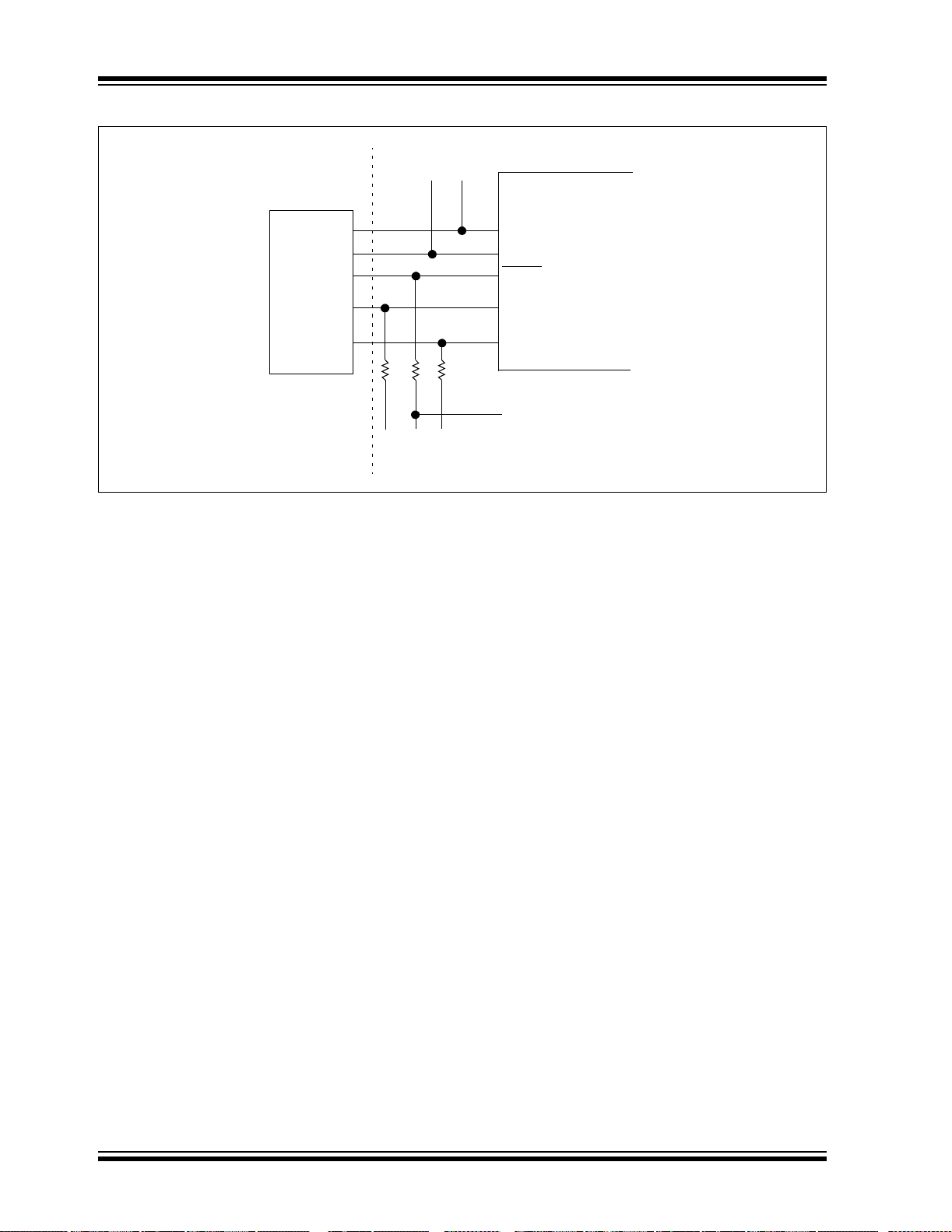
PIC16F5X
FIGURE 8-1: TYPICAL IN-CIRCUIT SERIAL PROGRAMMING™ CONNECTION
External
Connector
Signals
+5V
V
CLK
Data I/O
0V
PP
To Normal
Connections
To Normal
Connections
PIC16F5X
V
DD
VSS
MCLR/VPP
RB6/ICSPCLK
RB7/ICSPDAT
V
DD
DS41213C-page 40 2004 Microchip Technology Inc.

PIC16F5X
9.0 INSTRUCTION SET SUMMARY
Each PIC16F5X instructio n is a 12-bit word divid ed into
an opcode, which specifies the instruction type, and
one or more operands which furt her sp ec ify the ope ration of the instruction. The PIC16F5X instruction set
summary in Table 9-2 groups the inst ructions int o byteoriented, bit-oriented, and literal and control operations. Table 9-1 shows the opcode field descriptions.
For byte-oriented instructions, ‘f’ represents a file
register designator and ‘d’ represents a destination
designator. The file register designator is used to
specify which on e o f the 32 file registers in that b ank is
to be used by the instruction.
The destination des ignator specifies w here the result of
the operation is to be placed. If ‘d’ is ‘0’, the result is
placed in the W register. If ‘d’ is ‘1’, the result is placed
in the file register specified in the instruction.
For bit-oriented instructions, ‘b’ represents a bit field
designator which selects the numb er o f th e bi t affected
by the operation, whil e ‘ f’ represents the number of the
file in which the bit is located.
For literal and control operations, ‘k’ re presents an
8- or 9-bit constan t or literal value.
TABLE 9-1: OPCODE FIELD
DESCRIPTIONS
Field Description
f Register file address (0x00 to 0x1F)
W Working register (accumulator)
b Bit address within an 8-bit file register
k Literal field, constant data or label
x Don't care location (= 0 or 1)
The assembler will generate code with
x = 0. It is the recommended form of use
for compatibility with all Microchip
software tools.
d Destination select;
d = 0 (store result in W)
d = 1 (store result in file register ‘f’)
Default is d = 1
label Label name
TOS Top-of-Stack
PC Program Coun ter
WDT Watchdog Timer Counter
TO
PD Power-dow n bit
dest Destination, either the W register or the
[ ] Options
( ) Contents
→ Assigned to
< > Register bit field
italics User defined term
Time-out bit
specified register file location
∈ In the set of
All instructions are executed within one single instruction cycle, unless a conditional test is true or the
program counter is changed as a result of an instruction. In this case, the execution takes two instruction
cycles. One instruction cycle consists of four oscillator
periods. Thus, for an oscill ator frequenc y of 4 MHz, the
normal instruction execution time would be 1µs. If a
conditional test is true or the program counter is
changed as a result of an instruction, the instruction
execution time would be 2 µs.
Figure 9-1 shows the three general formats that the
instructions can have. All examples in the figure use
the following format to represent a hexadecimal
number:
0xhhh
where ‘h’ signifies a hexadecimal digit.
FIGURE 9-1 : GENERAL FORM AT FO R
INSTRUCTIONS
Byte-oriented file register operations
11 6 5 4 0
OPCODE d f (FILE #)
d = 0 for destination W
d = 1 for destination f
f = 5-bit file register address
Bit-oriented file register operations
11 8 7 5 4 0
OPCODE b (BIT #) f (FILE #)
b = 3-bit bit address
f = 5-bit file register address
Literal and control operations (except GOTO)
11 8 7 0
OPCODE k (literal)
k = 8-bit immediate value
Literal and control operations - GOTO instruction
11 9 8 0
OPCODE k (literal)
k = 9-bit immediate value
2004 Microchip Technology Inc. DS41213C-page 41

PIC16F5X
TABLE 9-2: INSTRUCTION SET SUMMARY
Mnemonic,
Operands
ADDWF
ANDWF
CLRF
CLRW
COMF
DECF
DECFSZ
INCF
INCFSZ
IORWF
MOVF
MOVWF
NOP
RLF
RRF
SUBWF
SWAPF
XORWF
BIT-ORIENTED FILE REGISTER OPERATIONS
BCF
BSF
BTFSC
BTFSS
LITERAL AND CONTROL OPERATIONS
ANDL W
CALL
CLRWDT
GOTO
IORLW
MOVLW
OPTION
RETLW
SLEEP
TRIS
XORLW
Note 1: The 9th bit of the program counter will be for ced to a ‘0’ by any ins truction that writes to the PC except for
f, d
f, d
f
—
f, d
f, d
f, d
f, d
f, d
f, d
f, d
f
—
f, d
f, d
f, d
f, d
f, d
f, b
f, b
f, b
f, b
k
k
—
k
k
k
—
k
—
f
k
GOTO (see Section 3.5 “Program Counter” for more on program counter).
2: When an I/O register is modified as a fu nc tion o f itself (e.g., MOVF PORTB , 1), th e v al ue us ed will be that
value present on th e pins the msel ves. F or exampl e, if the dat a la tch is ‘1’ for a pin co nfigure d as in put and
is driven low by an external device, the data will be written back with a ‘0’.
3: The instruction TRIS f, where f = 5, 6 or 7 causes the contents of the W register to be written to the
tri-state latch es of PO RTA, B or C respectively. A ‘1’ forces the pin t o a hi gh -imped ance st a te and disa bles
the output buffers.
4: If this instruction is executed on the TMR0 register (and, where applicable, d = 1), the prescaler will be
cleared (if assigned to TMR0).
Add W and f
AND W with f
Clear f
Clear W
Complement f
Decrement f
Decrement f, Skip if 0
Increment f
Increment f, Skip if 0
Inclusive OR W with f
Move f
Move W to f
No Operation
Rotate left f through Carry
Rotate right f through Carry
Subtract W from f
Swap f
Exclusive OR W with f
Bit Clear f
Bit Set f
Bit Test f, Skip if Clear
Bit Test f, Skip if Set
AND literal with W
Subroutine Call
Clear Watchdo g Timer
Unconditional branch
Inclusive OR Literal with W
Move Literal to W
Load OPTION register
Return, place Literal in W
Go into Standby mode
Load TRIS register
Exclusive OR Literal to W
Description Cycles
1
1
1
1
1
1
(2)
1
1
(2)
1
1
1
1
1
1
1
1
1
1
1
1
(2)
1
(2)
1
1
2
1
2
1
1
1
2
1
1
1
12-Bit Opcode
MSb LSb
0001
11df
ffff
0001
01df
ffff
0000
011f
ffff
0000
0100
0000
0010
01df
ffff
0000
11df
ffff
0010
11df
ffff
0010
10df
ffff
0011
11df
ffff
0001
00df
ffff
0010
00df
ffff
0000
001f
ffff
0000
0000
0000
0011
01df
ffff
0011
00df
ffff
0000
10df
ffff
0011
10df
ffff
0001
10df
ffff
0100
bbbf
ffff
0101
bbbf
ffff
0110
bbbf
ffff
0111
bbbf
ffff
1110
kkkk
kkkk
1001
kkkk
kkkk
0000
0000
0100
101k
kkkk
kkkk
1101
kkkk
kkkk
1100
kkkk
kkkk
0000
0000
0010
1000
kkkk
kkkk
0000
0000
0011
0000
0000
0fff
1111
kkkk
kkkk
Status
Affected
C,DC,Z
Z
Z
Z
Z
Z
None
Z
None
Z
Z
None
None
C
C
C,DC,Z
None
Z
None
None
None
None
Z
None
, PD
TO
None
Z
None
None
None
, PD
TO
None
Z
Notes
1, 2, 4
2, 4
4
2, 4
2, 4
2, 4
2, 4
2, 4
2, 4
1, 4
2, 4
2,4
1, 2, 4
2, 4
2, 4
2, 4
2, 4
1
3
DS41213C-page 42 2004 Microchip Technology Inc.

PIC16F5X
ADDWF Add W and f
Syntax: [ label ] ADDWF f, d
Operands: 0 ≤ f ≤ 31
d ∈ [0,1]
Operation: (W) + (f) → (dest)
Status Affected: C, DC, Z
Encoding: 0001 11df ffff
Description: Add the contents of the W register
and register ‘f’. If ‘d’ is ‘0’, the
result is stored in the W register. If
‘d’ is ‘1’, the result i s st ored ba ck i n
register 'f'.
Words: 1
Cycles: 1
Example
: ADDWF TEMP_REG, 0
Before Instruction
W =0x17
TEMP_REG = 0xC2
After Instruction
W=0xD9
TEMP_REG = 0xC2
ANDWF AND W with f
Syntax: [ label ] ANDWF f, d
Operands: 0 ≤ f ≤ 31
d ∈ [0,1]
Operation: (W) .AND. (f) → (dest)
Status Affected: Z
Encoding: 0001 01df ffff
Description: The contents of the W register are
AND’ed with register ‘f’. If ‘d’ is ‘0’,
the result is stored in the W
register. If ‘d’ is ‘1’, the result is
stored back in register ‘f’.
Words: 1
Cycles: 1
Example
: ANDWF TEMP_REG, 1
Before Instruction
W=0x17
TEMP_REG = 0xC2
After Instruction
W =0x17
TEMP_REG = 0x02
ANDLW AND literal with W
Syntax: [ label ] ANDLW k
Operands: 0 ≤ k ≤ 255
Operation: (W).AND. (k) → (W)
Status Affected: Z
Encoding: 1110 kkkk kkkk
Description: The contents of the W register are
AND’ed with the eight -bit li tera l ‘ k’ .
The result is placed in the W
register.
Words: 1
Cycles: 1
Example
: ANDLW H'5F'
Before Instruction
W=0xA3
After Instruction
W=0x03
BCF Bit Clear f
Syntax: [ label ] BCF f, b
Operands: 0 ≤ f ≤ 31
0 ≤ b ≤ 7
Operation: 0 → (f<b>)
Status Affected: None
Encoding: 0100 bbbf ffff
Description: Bit ‘b’ in register ‘f’ is cleared.
Words: 1
Cycles: 1
Example
: BCF FLAG_REG, 7
Before Instruction
FLAG_REG = 0xC7
After Instruction
FLAG_REG = 0x47
2004 Microchip Technology Inc. DS41213C-page 43

PIC16F5X
BSF Bit Set f
Syntax: [ label ] BSF f, b
Operands: 0 ≤ f ≤ 31
0 ≤ b ≤ 7
Operation: 1 → (f<b>)
Status Affected: None
Encoding: 0101 bbbf ffff
Description: Bit ‘b’ in register ‘f’ is set.
Words: 1
Cycles: 1
Example
BTFSC Bit Test f, Skip if Clear
Syntax: [ label ] BTFSC f, b
Operands: 0 ≤ f ≤ 31
Operation: skip if (f<b>) = 0
Status Affected: None
Encoding: 0110 bbbf ffff
Description: If bit ‘b’ in register ‘f’ is ‘0’, the n the
Words: 1
Cycles: 1(2)
Example
: BSF FLAG_REG, 7
Before Instruction
FLAG_REG = 0x0A
After Instruction
FLAG_REG = 0x8A
0 ≤ b ≤ 7
next instruction is skipped.
If bit ‘b’ is ‘0’, the n the nex t ins tru c-
tion fetched during the current
instruction execution is discarded
and a NOP is executed instead,
making this a two-cycle instruction.
: HERE
FALSE
TRUE
Before Instruction
PC = address (HERE)
After Instruction
if FLAG<1> = 0,
PC = address (TRUE);
if FLAG<1> = 1,
PC = address(FALSE)
BTFSC
GOTO
•
•
•
FLAG,1
PROCESS_CODE
BTFSS Bit Test f, Skip if Set
Syntax: [ label ] BTFSS f, b
Operands: 0 ≤ f ≤ 31
0 ≤ b < 7
Operation: skip if (f<b>) = 1
Status Affected: None
Encoding: 0111 bbbf ffff
Description: If bit ‘b’ in register ‘f’ is ‘1’, then the
next instruction is skipped.
If bit ‘b’ is ‘1’, then the next instruc-
tion fetched during the current
instruction execution is discarded
and a NOP is executed instead,
making this a two-cy cle i nstruc tion.
Words: 1
Cycles: 1(2)
Example
: HERE BTFSS FLAG,1
FALSE GOTO PROCESS_CODE
TRUE •
•
•
Before Instruction
PC = address (HERE)
After Instruction
If FLAG<1 > = 0,
PC = address (FALSE);
if FLAG<1> = 1,
PC = address (TRUE)
DS41213C-page 44 2004 Microchip Technology Inc.
PIC16F5X
CALL Subroutine Call
Syntax: [ label ] CALL k
Operands: 0 ≤ k ≤ 255
Operation: (PC) + 1→ TOS;
k → PC<7:0>;
(Status<6:5>) → PC<10:9>;
0 → PC<8>
Status Affected: None
Encoding: 1001 kkkk kkkk
Description: Subroutine call. First, return
address (PC + 1) is pushed onto
the stack. The eight-bit immediate
address is loaded into PC bits
<7:0>. The upper bits PC<10:9>
are loaded from Status<6:5>,
PC<8> is cleared. CALL is a
two-cycle instruction.
Words: 1
Cycles: 2
Example
CLRF Clear f
Syntax: [ label ] CLRF f
Operands: 0 ≤ f ≤ 31
Operation: 00h → (f);
Status Affected: Z
Encoding: 0000 011f ffff
Description: The contents of register ‘f’ are
Words: 1
Cycles: 1
Example
: HERE CALL THERE
Before Instruction
PC = address (HERE)
After Instruction
PC = address (THERE)
TOS = address (HERE + 1)
1 → Z
cleared and the Z bit is set.
: CLRF FLAG_REG
Before Instruction
FLAG_REG = 0x5A
After Instruction
FLAG_REG = 0x00
Z=1
CLRW Clear W
Syntax: [ label ] CLRW
Operands: None
Operation: 00h → (W);
1 → Z
Status Affected: Z
Encoding: 0000 0100 0000
Description: The W register is cleared. Zero bit
(Z) is set.
Words: 1
Cycles: 1
Example
CLRWDT Clear Watchdog Timer
Syntax: [ label ] CLRWDT
Operands: None
Operation: 00h → WDT;
Status Affected: TO, PD
Encoding: 0000 0000 0100
Description: The CLRWDT instruction resets the
Words: 1
Cycles: 1
Example
: CLRW
Before Instruction
W=0x5A
After Instruction
W=0x00
Z=1
0 → WDT prescaler (if assigned);
1 → TO;
1 → PD
WDT. It also resets the prescaler if
the prescaler is assigned to the
WDT and not Timer0. Status bits
and PD are set.
TO
: CLRWDT
Before Instruction
WDT counter = ?
After Instruction
WDT counter = 0x00
WDT prescaler = 0
TO
PD
=1
=1
2004 Microchip Technology Inc. DS41213C-page 45

PIC16F5X
COMF Complement f
Syntax: [ label ] COMF f, d
Operands: 0 ≤ f ≤ 31
d ∈ [0,1]
Operation: (f
Status Affected: Z
Encoding: 0010 01df ffff
Description: The contents of register ‘f’ are
Words: 1
Cycles: 1
Example
DECF Decrement f
Syntax: [ label ] DECF f, d
Operands: 0 ≤ f ≤ 31
Operation: (f) – 1 → (dest)
Status Affected: Z
Encoding: 0000 11df ffff
Description: Decrement register ‘f’. If ‘d’ is ‘0’,
Words: 1
Cycles: 1
Example
: COMF REG1,0
Before Instruction
REG1 = 0x13
After Instruction
REG1 = 0x13
W=0xEC
: DECF CNT, 1
Before Instruction
CNT = 0x01
Z=0
After Instruction
CNT = 0x00
Z=1
) → (dest)
complemented. If ‘d’ is ‘0’, the
result is stored in the W register. If
‘d’ is ‘1’, the result i s st ored ba ck i n
register ‘f’.
d ∈ [0,1]
the result is stored in the W
register. If ‘d’ is ‘1’, the result is
stored back in register ‘f’.
DECFSZ Decrement f, Skip if 0
Syntax: [ label ] DECFSZ f, d
Operands: 0 ≤ f ≤ 31
d ∈ [0,1]
Operation: (f) – 1 → d; skip if result = 0
Status Affected: None
Encoding: 0010 11df ffff
Descriptio n: The contents of register ‘f’ are
decremented. If ‘d’ is ‘0’, the result
is placed in the W register. If ‘d’ is
‘1’. the result is placed back in
register ‘f’. If the result is ‘0’, the
next instruction, which is already
fetched, is discarded and a NOP is
executed instead making it a
two-cycle instruction.
Words: 1
Cycles: 1(2)
Example
: HERE DECFSZ CNT, 1
GOTO LOOP
CONTINUE •
•
•
Before Instruction
PC = address(HERE)
After Instruction
CNT = CNT - 1;
if CNT = 0,
PC = address (CONTINUE);
if CNT ≠ 0,
PC = address (HERE+1)
DS41213C-page 46 2004 Microchip Technology Inc.

PIC16F5X
GOTO Unconditional Branch
Syntax: [ label ] GOTO k
Operands: 0 ≤ k ≤ 511
Operation: k → PC<8:0>;
Status<6:5> → PC<10:9>
Status Affected: None
Encoding: 101k kkkk kkkk
Description: GOTO is an unconditional branch.
The 9-bit immediate value is
loaded into PC bits <8:0>. The
upper bits of PC are loaded from
Status<6:5>. GOTO is a two-cycle
instruction.
Words: 1
Cycles: 2
Example
INCF Increment f
Syntax: [ label ] INCF f, d
Operands: 0 ≤ f ≤ 31
Operation: (f) + 1 → (dest)
Status Affected: Z
Encoding: 0010 10df ffff
Description: The contents of register ‘f’ are
Words: 1
Cycles: 1
Example
: GOTO THERE
After Instruction
PC = address (THERE)
d ∈ [0,1]
incremented. If ‘d’ is ‘0’, the result
is placed in the W register. If ‘d’ is
‘1’, the result is placed back in
register ‘f’.
: INCF CNT, 1
Before Instruction
CNT = 0xFF
Z=0
After Instruction
CNT = 0x00
Z=1
INCFSZ Increment f, Skip if 0
Syntax: [ label ] INCFSZ f, d
Operands: 0 ≤ f ≤ 31
d ∈ [0,1]
Operation: (f) + 1 → (dest), skip if result = 0
Status Affected: None
Encoding: 0011 11df ffff
Descriptio n: The contents of register ‘f’ are
incremented. If ‘d’ is ‘0’, the result
is placed in the W register. If ‘d’ is
‘1’, the result is placed back in
register ‘f’. If the result is ‘0’, then
the next instruction, which is
already fetched, is discarded and
a NOP is executed instead making
it a two-cycle instruction.
Words: 1
Cycles: 1(2)
Example
: HERE INCFSZ CNT, 1
GOTO LOOP
CONTINUE •
•
•
Before Instruction
PC = address (HERE)
After Instruction
CNT = CNT + 1;
if CNT = 0,
PC = address (CONTINUE);
if CNT ≠ 0,
PC = address (HERE +1)
2004 Microchip Technology Inc. DS41213C-page 47

PIC16F5X
IORLW Inclusive OR literal with W
Syntax: [ label ] IORLW k
Operands: 0 ≤ k ≤ 255
Operation: (W) .OR. (k) → (W)
Status Affected: Z
Encoding: 1101 kkkk kkkk
Description: The contents of the W register are
OR’ed with the eight-bit literal ‘k’.
The result is placed in the W
register.
Words: 1
Cycles: 1
Example
IORWF Inclusive OR W with f
Syntax: [ label ] IORWF f, d
Operands: 0 ≤ f ≤ 31
Operation: (W).OR. (f) → (dest)
Status Affected: Z
Encoding: 0001 00df ffff
Description: Inclusive OR the W register with
Words: 1
Cycles: 1
Example
: IORLW 0x35
Before Instruction
W= 0x9A
After Instruction
W= 0xBF
Z=0
d ∈ [0,1]
register ‘f’. If ‘d’ is ‘0’, the result is
placed in the W regis ter. If ‘d’ is ‘1’,
the result is placed back in
register ‘f’.
: IORWF RESULT, 0
Before Instruction
RESUL T = 0x13
W = 0x91
After Instruction
RESUL T = 0x13
W = 0x93
Z=0
MOVF Move f
Syntax: [ label ] MOVF f, d
Operands: 0 ≤ f ≤ 31
d ∈ [0,1]
Operation: (f) → (dest)
Status Affected: Z
Encoding: 0010 00df ffff
Descriptio n: The contents of register ‘f’ is
moved to destina tion ‘d’. I f ‘d’ is ‘0’,
destination is the W register. If ‘d’
is ‘1’, the destination is file
register ‘f’. ‘d’ is ‘1’ is useful to test
a file register sinc e Status flag Z is
affected.
Words: 1
Cycles: 1
Example
MOVLW Move Literal to W
Syntax: [ label ] MOVLW k
Operands: 0 ≤ k ≤ 255
Operation: k → (W)
Status Affected: None
Encoding: 1100 kkkk kkkk
Description: The eight-bit literal ‘k’ is loaded
Words: 1
Cycles: 1
Example
: MOVF FSR, 0
After Instruction
W = value in FSR register
into the W register.
: MOVLW 0x5A
After Instruction
W = 0x5A
DS41213C-page 48 2004 Microchip Technology Inc.

PIC16F5X
MOVWF Move W to f
Syntax: [ label ] MOVWF f
Operands: 0 ≤ f ≤ 31
Operation: (W) → (f)
Status Affected: None
Encoding: 0000 001f ffff
Description: Move data from the W register to
register ‘f’.
Words: 1
Cycles: 1
Example
NOP No Operation
Syntax: [ label ] NOP
Operands: None
Operation: No operation
Status Affected: None
Encoding: 0000 0000 0000
Description: No operation.
Words: 1
Cycles: 1
Example
: MOVWF TEMP_REG
Before Instruction
TEMP_REG = 0xFF
W = 0x4F
After Instruction
TEMP_REG = 0x4F
W = 0x4F
: NOP
OPTION Load OPTION Register
Syntax: [ label ] OPTION
Operands: None
Operation: (W) → OPTION
Status Affected: None
Encoding: 0000 0000 0010
Description: The content of the W register is
loaded into the Option register.
Words: 1
Cycles: 1
Example
RETLW Return with Literal in W
Syntax: [ label ] RETLW k
Operands: 0 ≤ k ≤ 255
Operation: k → (W);
Status Affected: None
Encoding: 1000 kkkk kkkk
Description: The W register is loaded with the
Words: 1
Cycles: 2
Example
TABLE
: OPTION
Before Instruction
W = 0x07
After Instruction
OPTION = 0x07
TOS → PC
eight-bit literal ‘k’. The program
counter is loaded from the top of
the stack (the re turn address). This
is a two-cycle instruction.
:
Before Instruction
W=0x07
After Instruction
W = value of k8
CALL TABLE;W contains
• ;W now has table
• ;value.
•
ADDWF PC ;W = offset
RETLW k1 ;Begin table
RETLW k2 ;
•
•
•
RETLW kn ; End of table
;table offset
;value.
2004 Microchip Technology Inc. DS41213C-page 49
PIC16F5X
RLF Rotate Left f through Carry
Syntax: [ label ] RLF f, d
Operands: 0 ≤ f ≤ 31
d ∈ [0,1]
Operation: See description below
Status Affected: C
Encoding: 0011 01df ffff
Description: The contents of register ‘f’ are
rotated one bit to the left through
the Carry Flag (S tatus<0>). If ‘d’ is
‘0’, the result is placed in the W
register. If ‘d’ is ‘1’, the result is
stored back in register ‘f’.
register 'f'
Words: 1
Cycles: 1
Example
: RLF REG1,0
Before Instruction
REG1 = 1110 0110
C=0
After Instruction
REG1 = 1110 0110
W=1100 1100
C=1
C
RRF Rotate Right f through Carry
Syntax: [ label ] RRF f, d
Operands: 0 ≤ f ≤ 31
d ∈ [0,1]
Operation: See description below
Status Affected: C
Encoding: 0011 00df ffff
Descriptio n: The contents of register ‘f’ are
rotated one bit to the right through
the Carry Flag (Status<0>). If ‘d’ is
‘0’, the result is placed in the W
register. If ‘d’ is ‘1’, the result is
placed back in register ‘f’.
register 'f'
Words: 1
Cycles: 1
Example
: RRF REG1,0
Before Instruction
REG1 = 1110 0110
C=0
After Instruction
REG1 = 1110 0110
W=0111 0011
C=0
C
Sleep Go into Standby Mode
Syntax: [ label ] Sleep
Operands: None
Operation: 00h → WDT;
0 → WDT prescaler; if assigned
1 → TO
0 → PD
Status Affected: TO, PD
Encoding: 0000 0000 0011
Description: Time-out S tatus bit (TO
power-down Status bit (PD
cleared. The WDT and its
prescaler are cleared.
The processor is put into Sleep
mode with the oscillator stopped.
See section on Sleep for more
details.
Words: 1
Cycles: 1
Example
: SLEEP
;
) is set. The
) is
DS41213C-page 50 2004 Microchip Technology Inc.

PIC16F5X
SUBWF Subtract W from f
Syntax: [ label ] SUBWF f, d
Operands: 0 ≤ f ≤ 31
d ∈ [0,1]
Operation: (f) – (W) → (dest)
Status Affected: C, DC, Z
Encoding: 0000 10df ffff
Description: Subtract (2’s complement method)
the W register from re gister ‘f’. If ‘d’
is ‘0’, the result is stored in the W
register. If ‘d’ is ‘1’, the result is
stored back in register ‘f’.
Words: 1
Cycles: 1
Example 1
Example 2
Example 3
: SUBWF REG1, 1
Before Instruction
REG1 = 3
W=2
C=?
After Instruction
REG1 = 1
W=2
C = 1 ; result is positive
:
Before Instruction
REG1 = 2
W=2
C=?
After Instruction
REG1 = 0
W=2
C = 1 ; result is zero
:
Before Instruction
REG1 = 1
W=2
C=?
After Instruction
REG1 = 0xFF
W=2
C = 0 ; result is negative
SWAPF Swap Nibbles in f
Syntax: [ label ] SWAPF f, d
Operands: 0 ≤ f ≤ 31
d ∈ [0,1]
Operation: (f<3:0>) → (dest<7:4>);
(f<7:4>) → (dest<3:0>)
Status Affected: None
Encoding: 0011 10df ffff
Description: The upper and lower nibbles of
register ‘f’ are exchanged. If ‘d’ is
‘0’, the result is placed in W
register. If ‘d’ is ‘1’, the result is
placed in register ‘f’.
Words: 1
Cycles: 1
Example
TRIS Load TRIS Register
Syntax: [ label ] TRIS f
Operands: f = 5, 6, 7, 8 or 9
Operation: (W) → TRIS register f
Status Affected: None
Encoding: 0000 0000 0fff
Description: TRIS register ‘f’ (f = 5, 6 or 7) is
Words: 1
Cycles: 1
Example
: SWAPF REG1, 0
Before Instruction
REG1 = 0xA5
After Instruction
REG1 = 0xA5
W = 0x5A
loaded with the contents of the W
register.
: TRIS PORTB
Before Instruction
W=0xA5
After Instruction
TRISB = 0xA5
2004 Microchip Technology Inc. DS41213C-page 51

PIC16F5X
XORLW Exclusive OR literal with W
Syntax: [ label ]XORLW k
Operands: 0 ≤ k ≤ 255
Operation: (W) .XOR. k → (W)
Status Affected: Z
Encoding: 1111 kkkk kkkk
Description: The contents of the W register are
XOR’ed with the eight- bit lite ral ‘k ’.
The result is placed in the W
register.
Words: 1
Cycles: 1
Example
: XORLW 0xAF
Before Instruction
W=0xB5
After Instruction
W=0x1A
XORWF Exclusive OR W with f
Syntax: [ label ] XORWF f, d
Operands: 0 ≤ f ≤ 31
d ∈ [0,1]
Operation: (W) .XOR. (f) → (dest)
Status Affected: Z
Encoding: 0001 10df ffff
Description: Exclusive OR the contents of the
W register with register ‘f’. If ‘d’ is
‘0’, the result is stored in the W
register. If ‘d’ is ‘1’, the result is
stored back in register ‘f’.
Words: 1
Cycles: 1
Example
: XORWF REG,1
Before Instruction
REG = 0xAF
W=0xB5
After Instruction
REG = 0x1A
W=0xB5
DS41213C-page 52 2004 Microchip Technology Inc.

PIC16F5X
10.0 DEVELOPMENT SUPPORT
The PICmicro® microcontrollers are supported with a
full range of ha rdware a nd softwa re develo pment to ols:
• Integrated Development Environment
- MPLAB
• Assemblers/Compilers/Linkers
- MPASMTM Assembler
- MPLAB C17 and MPLAB C18 C Compilers
-MPLINK
MPLIB
- MPLAB C30 C Compiler
- MPLAB ASM30 Assembler/Linker/Library
• Simulators
- MPLAB SIM Software Simulator
- MPLAB dsPIC30 Software Simulator
•Emulators
- MPLAB ICE 2000 In-Circuit Emulator
- MPLAB ICE 4000 In-Circuit Emulator
• In-Circuit Debugger
- MPLAB ICD 2
• Device Programmers
-PRO MATE
- PICSTART® Plus Development Programmer
- MPLAB PM3 Device Programmer
• Low-Cost Demonstration Boards
- PICDEM
- PICDEM.netTM Demonstrat ion Board
- PICDEM 2 Plus Demonstration Board
- PICDEM 3 Demonstration Board
- PICDEM 4 Demonstration Board
- PICDEM 17 Demonstration Board
- PICDEM 18R Demonstration Board
- PICDEM LIN Demonstration Board
- PICDEM USB Demonstration Board
• Evaluation Kits
-K
- PICDEM MSC
-microID
-CAN
- PowerSmart
-Analog
®
IDE Software
TM
TM
Object Librarian
TM
®
EELOQ
®
Object Linker/
®
II Universal Device Programmer
1 Demonstration Board
Security ICs
RFID
®
Battery Management
10.1 MPLAB Integrated Development
Environment Software
The MPLAB IDE so ftware brin gs an ease of sof tware
development previously unseen in the 8/16-bit microcontroller market. The MPLAB IDE is a Windows
based application that contains:
• An inter face to debugging tools
- simulator
- programmer (sold separately)
- emulator (sold separately)
- in-circuit debugger (sold separately)
• A full-featured editor with color coded context
• A multiple project manager
• Customizable data windows with direct edit of
contents
• High-level source code debugging
• Mouse over variable inspection
• Extensive on-line help
The MPLAB IDE allows you to:
• Edit your s ource files (either assembly or C)
• One touch assemble (or compile) and download
to PICmicro emulator and simulator tools
(automatically updates all project information)
• Debug using:
- source files (assembly or C)
- mixed assembly and C
- machine code
MPLAB IDE supports multiple debugging tools in a
single development paradigm, from the cost effective
simulators, through low-cost in-circuit debuggers, to
full-featured emulators. This eliminates the learning
curve when upgrading to tools with increasin g flexibilit y
and power.
10.2 MPASM Assembler
The MPASM assembler is a full-featured, universal
macro assembler for all PICmicro MCUs.
The MPASM assembler generates relocatable object
files for the MPLINK object linker, Intel
files, MAP files to detail memory usage and symbol
reference, absolut e LST fi les that contain source l ines
and generated machine code and COFF files for
debugging.
The MPASM assembler features include:
• Integration into MPLAB IDE projects
• User defined macros to strea mline asse mbly c ode
• Conditional assembl y for multi-purpose source
files
• Directives that allow complete control over the
assembly process
®
standard hex
®
2004 Microchip Technology Inc. DS41213C-page 53

PIC16F5X
10.3 MPLAB C17 and MPLAB C18
C Compilers
The MPLAB C17 and MPLAB C18 Code Development
Systems are complete ANSI C compilers for
Microchip’s PIC17CXXX and PIC18CXXX family of
microcontrollers. These compilers provide powerful
integration capabilities, superior code optimization and
ease of use not found with other compilers.
For easy source level debuggi ng, the compil ers provide
symbol information that is opt imized to the MPLAB IDE
debugger.
10.4 MPLINK Object Linker/
MPLIB Object Librarian
The MPLINK object linker combines relocatable
objects created by the MPASM assembler and the
MPLAB C17 and MPLAB C18 C compilers. It can link
relocatable objects from precompiled libraries, using
directives from a linker script.
The MPLIB object librarian manages the creation and
modification of library files of precompiled code. When
a routine from a library is called from a source file , only
the modules that contain that routine will be linked in
with the application. This allows large libraries to be
used efficiently in many different applications.
The object linker/library features include:
• Efficient linking of single libraries instead of many
smaller files
• Enhanced code maintainability by grouping
related modules together
• Flexible creation of libraries with easy module
listing, replacement, deletion and extraction
10.5 MPLAB C30 C Compiler
The MPLAB C30 C compiler is a full-featured, ANSI
compliant, optimizing compiler that translates standard
ANSI C programs into dsPIC30F assembly language
source. The compiler also supports many command
line options and language extensions to take full
advantage of the ds PIC30 F dev ice ha rdwar e capab ilities and afford fine control of the compiler code
generator.
MPLAB C30 is distributed with a complete ANSI C
standard library. All library functions have been validated and conform to the ANSI C li brary standard. The
library includes functions for string manipulation,
dynamic memory allocation, data conversion, timekeeping and math func tions (trigon ometric, expone ntial
and hyperbolic). The compiler provides symbolic
information for high-level source debugging with the
MPLAB IDE.
10.6 MPLAB ASM30 Assembler, Linker
and Librarian
MPLAB ASM30 assembler produces relocatable
machine code from symbolic assembly language for
dsPIC30F devices. MPLAB C30 compiler uses the
assembler to produce it’s object file. The assembler
generates relocatable object files that can then be
archived or linke d with other relocat able object fi les and
archives t o cr eat e an e xec utabl e fi le. Notab le f eat ures
of the assembler include:
• Support for the entire dsPIC30F instruction set
• Support for fixed-point and floating-point data
• Command line interface
• Rich directive set
• Flexible macro language
• MPLAB IDE compatibility
10.7 MPLAB SIM Software Simulator
The MPLAB SIM software simulat or allows code deve lopment in a PC hosted environment by simulating the
PICmicro series microcontrollers on an instruction
level. On any given instruction, the data areas can be
examined or modified and stimuli can be applied from
a file, or user de fined key p ress, to any pin. The ex ecution can be performed in Single-Step, Execute Until
Break or Trace mod e.
The MPLAB SIM simulator fully supports symbolic
debugging using the MPLAB C17 and MPLAB C18
C Compilers, as well as the MPASM assembler. The
software simulator offers the flexibility to develop and
debug code outside of the laboratory environment,
making it an excellent, economical software
development tool.
10.8 MPLAB SIM30 Software Simulator
The MPLAB SIM30 software simulator allows code
development in a PC h osted environmen t by simulating
the dsPIC3 0F series microcontrollers on an instruction
level. On any given instruction, the data areas can be
examined or modified and stimuli can be applied from
a file, or user defined key press, to any of the pins.
The MPLAB SI M30 simulator fully su pports symbolic
debugging using the MPLAB C30 C Compiler and
MPLAB ASM30 assembler . The sim ulator runs in either
a Command Line mode for automated tasks, or from
MPLAB IDE. This high-speed simulator is designed to
debug, analyze and optimize time intensive DSP
routines.
DS41213C-page 54 2004 Microchip Technology Inc.

PIC16F5X
10.9 MPLAB ICE 2000 HighPerformance Universal In-Circuit
Emulator
The MPLAB ICE 2000 universal in-circuit emulator is
intended to provide the product development engineer
with a complete microcontroller design tool set for
PICmicro microcontrollers. Software control of the
MPLAB ICE 2000 in-circuit emulator is advanced by
the MPLAB Integrated Development Environment,
which allows editi ng, b uildin g, do wnlo ading and sourc e
debugging from a single environm en t.
The MPLAB ICE 2000 is a full-featured emulator system with enhanced trace, trigger and data monitoring
features. Interchan geable processo r modules al low the
system to be easily reconfigure d for emula tion of dif ferent processors. The universal architecture of the
MPLAB ICE in-circuit emulator allows expansion to
support new PICmicro microcontrollers.
The MPLAB ICE 2000 in-circuit emulator system has
been designed as a real-time emulation system with
advanced features that are typically found on more
expensive development tools. The PC platform and
Microsoft
chosen to best make these features available in a
simple, unified application.
®
Windows 32-bit operating system were
10.10 MPLAB ICE 4000 HighPerformance Universal In-Circuit
Emulator
The MPLAB ICE 4000 universal in-circuit emulator is
intended to provide the product development engineer
with a complete mi crocontroller de sign tool set for highend PICmicro microcontrollers. Software control of the
MPLAB ICE in-circuit emulator is provided by the
MPLAB Integrated Development Environment, which
allows editing, building, downloading and source
debugging from a single environm en t.
The MPLAB ICD 4000 is a premium emulator system,
providing the features of MPLAB ICE 2000, but with
increased emulation memory and high-speed performance for dsPIC30F and PIC18XXXX devices. Its
advanced emula tor features inc lude comple x triggering
and timing, up to 2 Mb of emulati on memory and the
ability to view variables in real-time.
The MPLAB ICE 4000 in-circuit emulator system has
been designed as a real-time emulation system with
advanced features that are typically found on more
expensive development tools. The PC platform and
Microsoft Windows 32-bit operating system were
chosen to best make these features available in a
simple, unified application.
10.11 MPLAB ICD 2 In-Circuit Debugger
Microchip’s In-Circuit Debugger, MPLAB ICD 2, is a
powerful, low-cost, run-time development tool,
connecting to the host PC via an RS-232 or high-speed
USB interface. This tool is based on the Flash
PICmicro MCUs and can be used to develop for these
and other PICmicro microcontrollers. The MPLAB
ICD 2 utilizes the in-circuit debugging capability built
into the Flash devices. This feature, along with
Microchip’s In-Circuit Serial Programming
protocol, offe rs cost ef fectiv e in-circuit Flash debug ging
from the graphical user interface of the MPLAB
Integrated Development Environment. This enables a
designer to develop and debug source code by setting
breakpoints, single-stepping and watching variables,
CPU status and peripheral registers. Running at full
speed enables testing hardware and applications in
real-time. MPLAB ICD 2 also serves as a development
programmer for selected PICmicro devices.
TM
(ICSPTM)
10.12 PRO MATE II Universal Device
Programmer
The PRO MATE II is a universal, CE compliant device
programmer with programmable voltage verification at
VDDMIN and VDDMAX for maximum reli abili ty. It features
an LCD display for instructions and error messages
and a modular detachable socket assembly to support
various package types. In Stand-Alone mode, the
PRO MATE II device programmer can read, verify and
program PICmicro devices without a PC connection. It
can also set code protection in this mode.
10.13 MPLAB PM3 Device Programmer
The MPLAB PM3 is a universal, CE compliant device
programmer with programmable voltage verification at
DDMIN and VDDMAX for maximum reli abili ty. It features
V
a large LCD display (128 x 64) for menus and error
messages and a modular detachable socket assembly
to support various package types. The ICSP™ cable
assembly is included as a standard item. In StandAlone mode, the MPLAB PM3 device pr ogra mmer ca n
read, verify and program PICmicro devices without a
PC connection. It can also set code protection in this
mode. MPLAB PM3 con nects t o the host PC via an RS232 or USB cable. MPLAB PM3 has high-speed communications and optimized algorithms for quick programming of large memory devices and incorporates
an SD/MMC card for fi le stora ge and secure d ata a pplications.
2004 Microchip Technology Inc. DS41213C-page 55

PIC16F5X
10.14 PICSTART Plus Development
Programmer
The PICSTART Plus dev elopment programme r is an
easy-to-use, low-cost, prototype programmer. It connects to the PC via a COM (RS-232) port. MPLAB
Integrated Devel opmen t Envi ronme nt sof tware makes
using the programmer simple and efficient. The
PICSTART Plus development programmer supports
most PICmicro devices up to 40 pins. Larger pin count
devices, such as the PIC16C92X and PIC17C76X,
may be supported with an adapter socket. The
PICSTART Plus development programmer is CE
compliant.
10.15 PICDEM 1 PICmicro
Demonstration Board
The PICDEM 1 demonstrat ion board de mons trates the
capabilities of the PIC16C5X (PIC16C54 to
PIC16C58A), PIC16C61, PIC16C62X, PIC16C71,
PIC16C8X, PIC17C42, PIC17C43 and PIC17C44. All
necessary hardware and software is included to run
basic demo programs. The sample microcontrollers
provided wi t h the P IC DE M 1 de mo ns t rat i on bo ar d c an
be programme d with a PRO MATE II device pr ogrammer or a PICSTART Plus development programmer.
The PICDEM 1 demonstrati on board can be co nnected
to the MPLAB ICE in-circuit emulator for testing. A
prototype area ex tends th e circu itry for a dditional application components. Features include an RS-232
interface, a potentiometer for simulated analog input,
push button switches and eight LEDs.
10.16 PICDEM.net Internet/Ethernet
Demonstration Board
The PICDEM.net demonstration board is an Internet/
Ethernet demonstration board using the PIC18F452
microcontroller and TCP/IP firmware. The board
supports any 40-pin DIP device that conforms to the
standard pinout used by the PIC16F877 or
PIC18C452. This kit features a user friendly TCP/IP
stack, web server with HTML, a 24L256 Serial
EEPROM for Xmodem download to web pages into
Serial EEPROM, ICSP/MPLAB ICD 2 interface connector, an Ethernet interface, RS-232 interface and a
16 x 2 LCD display. Also included is the book and
CD-ROM “TCP/IP Lean, Web Servers for Embedded
Systems,” by Jeremy Bentham
10.17 PICDEM 2 Plus
Demonstration Board
The PICDEM 2 Plus demonstration board supports
many 18, 28 and 40-pin microcontrollers, including
PIC16F87X and PIC18FXX2 devices. All the necessary hardware and softw are is inc luded to run the dem onstration programs. The sample microcontrollers
provided with the PICDEM 2 demonstration board can
be programmed with a PRO MATE II device programmer, PICSTART Plus development programmer, or
MPLAB ICD 2 with a Universal Programmer Adapter.
The MPLAB ICD 2 and MPLAB IC E in-circuit emul ators
may also be used with the PICDEM 2 demonstration
board to test firmware. A prototype area extends the
circuitry for additional application components. Some
of the features include an RS-232 interface, a 2 x 16
LCD display , a pie zo speaker , an o n-board temperatu re
sensor, four LEDs and sample PIC18F452 and
PIC16F877 Flash microcontrollers.
10.18 PICDEM 3 PIC16C92X
Demonstration Board
The PICDEM 3 demonstration board supports the
PIC16C923 and PIC16C924 in the PLCC package. All
the necessary hardware and software is included to run
the demonstration programs.
10.19 PICDEM 4 8/14/18-Pin
Demonstration Board
The PICDEM 4 can be used to demonstrate the capabilities of the 8, 14 and 18-pin PIC16XXXX and
PIC18XXXX MCUs, including the PIC16F818/819,
PIC16F87/88, PIC16F62XA and the PIC18F1320
family of microcontrollers. PICDEM 4 is intended to
showcase the many features of these low pin count
parts, including LIN and Motor Control using ECCP.
Special provisions are made for low-power operation
with the supercapacitor circuit and jumpers allow onboard hardware to be disabled to eliminate current
draw in this mode. Include d on the demo board are pr ovisions for Crystal, RC or Canned Oscillator modes, a
five volt regulator for use with a nine volt wall adapter
or battery, DB-9 RS -232 interface, ICD connector for
programming via ICSP and development with MPLAB
ICD 2, 2 x 16 liquid crystal display , PCB footprin ts for HBridge motor driver, LIN transceiver and EEPROM.
Also included are: header for expansion, eight LEDs,
four potentiometers, three push buttons and a prototyping area. Included with the kit is a PIC1 6F6 27A and
a PIC18F1320. T utoria l fir mware is inclu ded alo ng with
the User’s Guide.
DS41213C-page 56 2004 Microchip Technology Inc.

PIC16F5X
10.20 PICDEM 17 Demonstration Board
The PICDEM 17 demonstration board is an evaluation
board that demonstrates the capabilities of several
Microchip microcontrollers, including PIC17C752,
PIC17C756A, PIC17C762 and PIC17C766. A programmed sample i s included. T he PRO MA TE I I device
programmer, or the PICSTART Plus development programmer , can be used to reprogram the dev ice for user
tailored application development. The PICDEM 17
demonstration board supports program download and
execution from external on-board Flash memory. A
generous prototyp e area is av ailab le for user h ardware
expansion.
10.21 PICDEM 18R PIC18C601/801
Demonstration Board
The PICDEM 18R demonstration board serves to assist
development of the PIC18C601/801 family of Microchip
microcontrollers. It p rovides hardware implementation
of both 8-bit Multiplexed/Demultiplexed and 16-bit
Memory modes. The board includes 2 Mb external
Flash memory and 128 Kb SRAM memory, as well as
serial EEPROM, allowing access to the wi de range of
memory types supported by the PIC18C601/801.
10.22 PICDEM LIN PIC16C43X
Demonstration Board
The powerful LIN hardw are a nd s of tw are kit inc lu des a
series of boards and three PICmicro microcontrollers.
The small footprint PIC16C432 and PIC16C433 are
used as slaves in the LIN communication and feature
on-board LIN transceivers. A PIC16F874 Flash
microcontroller serves as the master. All three microcontrollers are programmed with firmware to provide
LIN bus communication.
10.23 PICkit
TM
1 Flash Starter Kit
10.24 PICDEM USB PIC16C7X5
Demonstration Board
The PICDEM USB Demonstrati on Board sho w s o f f th e
capabilities of the PIC16C745 and PIC16C765 USB
microcontrollers. This board provides the basis for
future USB products.
10.25 Evaluation and
Programming Tools
In addition to the PICDEM se ries of circuits, Microchi p
has a line of evaluation kits and demonstration software
for these products.
EELOQ evaluation and programming tools for
•K
Microchip’s HCS Secure Data Products
• CAN developers kit for automotive network
applications
• Analog design boards and filter design software
• PowerSmart battery charging ev aluation/
calibration kits
®
•IrDA
• microID development and rfLabTM development
• SEEVAL
• PICDEM MSC demo boards for Switching mode
Check the Microchip web page and the latest Product
Selector Guide for the complete list of demonstration
and evaluation kits.
development kit
software
endurance calculations
power supply, high-power IR driver, delta sigma
ADC and flow rate sensor
®
designer kit for mem ory ev al uat ion an d
A complete “development system in a box”, the PICkit
Flash Starter Kit includes a convenient multi-section
board for programming, evaluation a nd developm ent of
8/14-pin Flash PIC
USB, the board operates under a s imple Windows GUI.
The PICkit 1 Starter Kit includes the User’s Guide (on
CD ROM), PICkit
various applications. Also included are MPLAB
(Integrated Development Environment) software,
software and hardware “Tips 'n Tricks for 8-pin Flash
®
Microcontrollers” Handbook and a USB interface
PIC
cable. Supports all current 8/14-pin Flash PIC
microcontrollers, as well as many future planned
devices.
2004 Microchip Technology Inc. DS41213C-page 57
®
microcontrollers. Powered via
1 tutorial software and code for
®
IDE

PIC16F5X
NOTES:
DS41213C-page 58 2004 Microchip Technology Inc.

PIC16F5X
11.0 ELECTRICAL SPECIFICATIONS FOR PIC16F54/57
Absolute Maximum Ratings
Ambient Temperature under bias.........................................................................................................-40°C to +125°C
Storage Temperature ...........................................................................................................................-65°C to +150°C
Voltage on V
Voltage on MCLR
DD with respect to VSS ............................................................................................................ 0V to +6.5V
with respect to VSS
Voltage on all other pins with respect to V
Total power dissipation
Max. current out of V
Max. current into V
SS pin................................ ...... ...... ..... ...... ...... ............................................ ...... .................150 mA
DD pin...................................................................................................................................100 mA
Max. current into an input pin (T0CKI only)........................................................... ............................................±500 µA
Input clamp current, I
IK (VI < 0 or VI > VDD).......................................................................................................±20 mA
Output clamp current, I
Max. output current sunk by any I/O pin..............................................................................................................25 mA
Max. output current sourced by any I/O pin.........................................................................................................25 mA
Max. output current sourced by a single I/O port (PORTA, B or C) .....................................................................50 mA
Max. output current sunk by a single I/O port (PORTA, B or C)...........................................................................50 mA
Note 1: Voltage spikes below V
Thus, a series r esistor of 50 to 100Ω should be used when applying a “low” level to the MCLR
than pulling this pin directly to V
2: Power Dissipation is calcula ted as fo llows: Pdi s = V
(†)
(1)
................................................................................................... 0V to +13.5V
SS ............................................................................... -0.6V to (VDD + 0.6V)
(2)
..................................................................................................................................800 mW
OK (VO < 0 or VO > VDD) ................................................................................................±20 mA
SS at the MCLR pin, inducing cur rents greater than 80 mA, may cause latch-up.
pin rather
SS.
DD x {IDD – ∑ IOH} + ∑ {(VDD – VOH) x IOH} + ∑(VOL x IOL)
†NOTICE: Stresses above those listed under “Absolute Maximum Ratings” may cause permanent damage to the
device. This is a stres s rating only and functi onal op eration of the dev ice at th ose or an y other c onditio ns abo ve thos e
indicated in the operation listings of this specification is not implied. Exposure to maximum rating conditions for
extended periods may affect device reliability.
2004 Microchip Technology Inc. DS41213C-page 59

PIC16F5X
11.0 ELECTRICAL SPECIFICATIONS FOR PIC16F59 (continued)
Absolute Maximum Ratings
Ambient Temperature under bias.........................................................................................................-40°C to +125°C
Storage Temperature............................................................................................................................-65°C to +150°C
Voltage on V
Voltage on MCLR
DD with respect to VSS ............................................................................................................ 0V to +6.5V
with respect to VSS
Voltage on all other pins with respect to V
Total power dissipation
Max. current out of V
Max. current into V
SS pins.............................................................................. ..... ............................................250 mA
DD pins .................................................................................................................................200 mA
Max. current into an input pin (T0CKI only)...................................... ...... ..... ...... ..... ........................................... ±500 µA
Input clamp current, I
IK (VI < 0 or VI > VDD) ....................................................................................................... ±20 mA
Output clamp current, I
Max. output current sunk by any I/O pin...............................................................................................................2 5 mA
Max. output current sourced by any I/O pin.........................................................................................................25 mA
Max. output current sourced by a single I/O port (PORTA, B, C, D or E)...........................................................100 mA
Max. output current sunk by a single I/O port (PORTA, B, C, D or E)................................................................100 mA
Note 1: Voltage spikes below V
Thus, a series r esistor of 50 to 100Ω should be used when applying a “low” level to the MCLR
than pulling this pin directly to V
2: Power Dissipation is calcula ted as fo llows: Pdi s = V
(†)
(1)
...................................................................................................0V to +13.5V
SS................................................................................-0.6V to (VDD + 0.6V)
(2)
..................................................................................................................................900 mW
OK (VO < 0 or VO > VDD) ................................................................................................±20 mA
SS at the MCLR pin, inducing cur rents greater than 80 mA, may cause latch-up.
pin rather
SS.
DD x {IDD – ∑ IOH} + ∑ {(VDD – VOH) x IOH} + ∑(VOL x IOL)
†NOTICE: Stresses above those listed under “Absolute Maximum Ratings” may cause permanent damage to the
device. This is a stres s rating only and functi onal op eration of the dev ice at th ose or an y other c onditi ons abo ve thos e
indicated in the operation listings of this specification is not implied. Exposure to maximum rating conditions for
extended periods may affect device reliability.
DS41213C-page 60 2004 Microchip Technology Inc.

PIC16F5X
FIGURE 11-1: PIC16F5X VOLTAGE-FREQUENCY GRAPH, -40°C ≤ TA ≤ +125°C
5.5
5.0
4.5
4.0
V
DD
(Volts)
3.5
3.0
2.5
2.0
0
Note 1: The shaded region indicates the permissible combinations of voltage and frequency.
4
81612 2010
Frequency (MHz)
2004 Microchip Technology Inc. DS41213C-page 61

PIC16F5X
11.1 DC Characteristics: PIC16F5X (Industrial)
DC CHARACTERISTICS
Param
D001 V
Sym Characteristic/Device Min Typ† Max Units Conditions
No.
DD Supply Voltage 2.0 — 5.5 V
D002 VDR RAM Data Retention Voltage
D003 V
POR VDD Start Voltage to ensure
Power-on Reset
D004 S
VDD VDD Rise Rate to ensure
Power-on Reset
D010 I
DD Supply Current
(2)
Standard Operating Conditions (unless otherwise specified)
Operating Temperature -40°C ≤ T
(1)
— 1.5* — V Device in Sleep mode
A ≤ +85°C for industrial
— Vss — V See Section 5.1 “Power-on Reset
(POR)” for details on Power-on Reset
0.05* — — V/ms See Section 5.1 “Power-on Reset
(POR)” for details on Power-on Reset
—
170
350
µA
FOSC = 4 MHz, VDD = 2.0V, XT or RC
(3)
mode
—
0.4
1.0
mA
FOSC = 10 MHz, VDD = 3.0V, HS mode
—
—
1.7
15
5.0
22.5
OSC = 20 MHz, VDD = 5.0V, HS mode
mA
F
F
µA
OSC = 32 kHz, VDD = 2.0V, LP mode,
WDT disabled
D020 I
PD Power-down Current
(2)
——1.0
0.5
6.0
2.5µAµA
VDD = 2.0V, WDT enabled
DD = 2.0V, WDT disabled
V
* These parameters are characterized but not tested.
† Data in “Typ” column is base d on c haract erization results at 25°C. This data is for design guidance on ly and
is not tested.
Note 1: This is the limit to which V
DD can be lowered in Sleep mode without losing RAM data.
2: The supply current is mainly a function of the operating voltage and frequency. Other factors such as bus
loading, oscillator ty pe, b us rate , in tern al c od e ex ec uti on pattern and temperature , al so h av e an im p a ct o n
the current consumption.
a) The test conditions for all I
wave, from rail-to-rail; al l I/O pins t ri-st ated, p ulled to V
DD measurements in Active Operation mode are: OSC1 = external square
SS, T0CKI = VDD, MCLR = VDD; WDT enable d/
disabled as specified.
b) For standby current measurements, the conditions are the same, except that the device is in Sleep
mode. The Power-down Current in Sleep mode does not depend on the oscillator type.
3: Does not include current through R
R =VDD/2REXT (mA) with REXT in kΩ.
I
EXT. The current through the resistor can be estimated by the formula:
DS41213C-page 62 2004 Microchip Technology Inc.

11.2 DC Characteristics: PIC16F5X (Extended)
PIC16F5X
DC CHARACTERISTICS
Param
D001 V
D002 V
Sym Characteristic/Device Min Typ† Max Units Conditions
No.
DD Supply Voltage 2.0 — 5.5 V
DR RAM Data Retention Voltage
D003 VPOR VDD Start Voltage to ensure
Power-on Reset
D004 S
VDD VDD Rise Rate to ensure
Power-on Reset
D010 I
DD Supply Current
(2)
Standard Operating Conditions (unless otherwise specified)
Operating Temperature -40°C ≤ T
(1)
— 1.5* — V Device in Sleep mode
A ≤ +125°C for extended
—VSS —VSee Section 5.1 “Power-on Reset
(POR)” for details on Power-on Reset
0.05* — — V/ms See Section 5.1 “Power-on Reset
(POR)” for details on Power-on Reset
—
—
—
—
170
0.4
1.7
15
450
2.0
7.0
40
OSC = 4 MHz, VDD = 2.0V, XT or RC
µA
F
(3)
mode
FOSC = 10 MHz, VDD = 3.0V, HS mode
mA
OSC = 20 MHz, VDD = 5.0V, HS mode
F
mA
OSC = 32 kHz, VDD = 2.0V, LP mode,
F
µA
WDT disabled
D020 I
PD Power-down Current
(2)
——1.0
0.5
15.0
8.0µAµA
VDD = 2.0V, WDT enabled
V
DD = 2.0V, WDT disabled
* These parameters are characterized but not tested.
† Data in “Typ” column is b ased o n cha racteri zation resul ts at 25 °C. This data is for design guidance only and
is not tested.
Note 1: This is the limit to which V
DD can be lowered in Sleep mode without losing RAM data.
2: The supply current is mainly a function of the operating voltage and frequency. Other factors such as bus
loading, oscillator ty pe, bus rate , internal code execution p at tern and tem pe r atu re, a ls o ha ve an i mpact on
the current consumption.
a) The test conditions for all I
wave, from rail-to-rail ; all I /O pin s tri-s tat ed, pulle d to V
DD measurements in Active Operation mode are: OSC1 = external square
SS, T0CKI = VDD, MCLR = VDD; WDT enabled/
disabled as specified.
b) For standby current measurements, the conditions are the same, except that the device is in Sleep
mode. The Power-down Current in Sleep mode does not depend on the oscillator type.
3: Does not include current through R
I
R =VDD/2REXT (mA) with REXT in kΩ.
EXT. The current through the resistor can be estimated by the formula:
2004 Microchip Technology Inc. DS41213C-page 63

PIC16F5X
11. 3 DC Characteristics PIC16F5X
Standard Operating Conditions (unless otherwise specified)
DC CHARACTERISTICS
Param
Sym Characteristic Min Typ† Max Units Conditions
No.
IL Input Low Voltage
V
D030 I/O Ports
I/O Ports
(Schmitt Trigger)
MCLR
T0CKI (Schmitt Trigger)
OSC1 (Schmitt Trigger)
OSC1
VIH Input High Voltage
D040 I/O ports
I/O ports
(Schmitt Trigger)
MCLR
T0CKI (Schmitt Trigger)
OSC1 (Schmitt Trigger)
OSC1
IIL Input Leakage Current
D060 I/O ports
MCLR
T0CKI
OSC1
OL Output Low Voltage
V
D080
D083
I/O ports
OSC2/CLKOUT
(RC mode)
V
OH Output High Voltage
D090
D092
I/O ports
OSC2/CLKOUT
(2)
(RC mode)
* These parameters are characterized but not tested.
† Data in the Typical (“Typ”) column is based on characterization results at 25°C. This data is for design
guidance only and is not tested.
Note 1: The leakage current on the MC L R
specified levels represent normal operating conditions. Higher leakage current may be measured at
different input voltage.
2: Negative current is defined as coming out of the pin.
3: For the RC mode, the OSC1/CLKIN pin is a Schmitt Trigger input. It is not recommended that the
PIC16F5X be driven with external clock in RC mode.
Operating Temperature -40°C ≤ TA ≤ +85°C for industrial
0.25 V
(1, 2)
SS
V
VSS
VSS
VSS
VSS
VSS
VSS
VSS
2.0
DD + 0.8
DD
0.85 V
0.85 VDD
0.85 VDD
0.7 VDD
1.6
1.6
—
—
—
—
—
—
—
—
—
—
—
—
—
—
—
—
—
—
-40°C ≤ T
0.8V
0.15 V
0.15 VDD
0.15 VDD
0.15 VDD
0.3 VDD
0.3
0.3
DD
V
VDD
VDD
VDD
VDD
VDD
VDD
VDD
±1.0
A ≤ +125°C for extended
V
4.5V <V
DD
V
DD ≤ 4.5V
V
V
V
RC mode
V
HS mode
V
XT mode
V
LP mode
V
V
4.5V < V
DD ≤ 4.5V
V
V
V
V
RC mode
V
HS mode
V
XT mode
V
LP mode
V
SS ≤ VPIN ≤ VDD,
µA
V
pin at high-impedance
—
—
—
—
—
—
±5.0
±5.0
±5.0
SS ≤ VPIN ≤ VDD
µA
V
µA
VSS ≤ VPIN ≤ VDD
VSS ≤ VPIN ≤ VDD,
µA
XT, HS and LP modes
(2)
—
—
DD – 0.7
V
V
DD – 0.7
—
—
—
—
0.6
0.6
—
—
VVIOL = 8.5 mA, VDD = 4.5V
OL = 1.6 mA, VDD = 4.5V
I
OH = -3.0 mA, VDD = 4.5V
VVI
I
OH = -1.3 mA, VDD = 4.5V
/VPP pin is strongly dependent on the applied voltage level. The
DD ≤ 5.5V
(3)
DD ≤ 5.5V
(3)
DS41213C-page 64 2004 Microchip Technology Inc.

11. 4 Timing Parameter Symbology and Load Conditions
The timing parameter symbols have been created with one of the following formats:
1. TppS2ppS
2. TppS
T
F Frequency T Time
Lowercase letters (pp) and their meanings:
pp
2to mcMCLR
ck CLKOUT osc oscillator
cy cycle time os OSC1
drt device reset timer t0 T0CKI
io I/O port wdt watchdog timer
Uppercase le tters and their meanings:
S
FFall PPeriod
HHigh RRise
I Invalid (High-impedance) V Valid
L Low Z High-impedance
PIC16F5X
FIGURE 11-2: LOAD CONDITI ONS FO R D EV I CE TIMING SPECI FI CA TI ON S – PIC16F5X
Pin
CL
VSS
Legend:
L = 50 pF for all pins and OSC2 for RC mode
C
0-15 pF for OSC2 in XT, HS or LP modes when
external clock is used to drive OSC1
11. 5 Timing Diagrams and Specifications
FIGURE 11-3: EXTERNAL CLOC K T I MIN G
OSC1
CLKOUT
Q4
Q1 Q2
133
2
Q3 Q4 Q1
44
2004 Microchip Technology Inc. DS41213C-page 65

PIC16F5X
TABLE 11-1: EXTERNAL CLOCK TIMING REQUIREMENTS
Standard Operating Conditions (unless otherwise specified)
AC CHARACTERISTICS
Parameter
No.
1T
2T
Sym Characteristic Min Typ† Max Units Conditions
OSC
F
OSC External CLKIN Period
CY Instruction Cycle Time
3 TosL, TosH Clock in (OSC1) Low or High
4 TosR, TosF Clock in (OSC1) Rise or Fall
* These parameters are characterized but not tested.
† Data in the Typical (“Typ”) column is at 5V, 25°C unless otherwise stated . These p aramete rs are for d esign
guidance only and are not tested.
Note 1: All specified values are based on characterization data for that particular oscillator type under standard
operating conditions with the device executing code. Exceeding these specified limits may result in an
unstable oscillator operation and/or higher than expected current consumption.
When an external clock input is used, the “max” cycle time limit is “DC” (no clock) for all devices.
2: Instruction cycle period (T
Operating Temperature -40°C ≤ TA ≤ +85°C for industrial
External CLKIN Frequency
-40°C ≤ T
(1)
A ≤ +125°C for extended
DC — 4.0 MHz XT Osc mode
DC — 20 MHz HS Os c mode
DC — 200 kHz LP Osc mode
Oscillator Frequency
(1)
DC — 4.0 MHz RC Osc mode
0.1 — 4.0 MHz XT Osc mode
4.0 — 20 MHz HS Osc mode
5.0 — 200 kHz LP Osc mode
(1)
250 — — ns XT Osc mode
50 — — ns HS Osc mode
5.0 — — µsLP Osc mode
Oscillator Period
(1)
250 — — ns RC Osc mode
250 — 10,000 ns XT Osc mode
50 — 250 ns HS Osc mode
5.0 — — µsLP Osc mode
(2)
—4/FOSC ——
50* — — ns XT oscillator
Time
20* — — ns HS oscillator
2.0* — — µs LP oscillator
— — 25* ns XT oscillator
Time
— — 5* ns HS oscillator
— — 50* ns LP oscillator
CY) equals four times the input oscillator time base period.
DS41213C-page 66 2004 Microchip Technology Inc.

FIGURE 11-4: CLKOUT AND I/O TI MING – PIC16F 5X
PIC16F5X
OSC1
CLKOUT
I/O Pin
(input)
I/O Pin
(output)
Q4
Old Value
10
13
17
14
20, 21
Q1
19
Q2 Q3
18
15
Note: Please refer to Figure 11-2 for load conditions.
TABLE 11-2: CLKOUT AND I/O TIMING REQUIREMENTS – PIC16F5X
Param
No.
10 TosH2
11 TosH2CKHOSC1↑ to CLKOUT↑
12 T
13 TCKF CLKOUT fall time
14 TCKL2IOVCLKOUT↓ to Port out valid
15 T
16 TCKH2IOI Port in hold after CLKOUT↑
17 TOSH2IOVOSC1↑ (Q1 cycle) to Port out valid
18 T
19 T
20 T
20 TIOR Port output rise time
21 T
21 TIOF Port output fall time
Legend: TBD = To Be Determined.
Note 1: Measurements are taken in RC mode where CLKOUT output is 4 x T
Sym Characteristic Min Typ† Max Units
(1)
(1)
(1)
(1)
(1)
(1)
(1)
(2)
— 15 30** ns
— 15 30** ns
— 5.0 15** ns
— 5.0 15** ns
— — 40** ns
0.25 TCY+30* — — ns
0* — — ns
— — 100* ns
TBD — — ns
CKLOSC1↑ to CLKOUT↓
CKRCLKOUT rise time
IOV2CKH Port in valid before CLKOUT↑
OSH2IOIOSC1↑ (Q2 cycle) to Port input invalid
(I/O in hold time)
IOV2OSH Port input valid to OSC1↑
TBD — — ns
(I/O in setup time)
IOR Port output rise time
IOF Port output fall time
(2, 3)
(2, 4)
(2, 3)
(2, 4)
— 10 25** ns
— 10 50** ns
— 10 25** ns
— 10 50** ns
* These parameters are characterized but not tested.
** These parameters are design targets and are not tested. No characterization data available at this time.
† Data in the Typical (“Typ”) column is at 5.0V, 25°C unless otherwise stated. These parameters are for
design guidance only and are not tested.
OSC.
2: Please refer to Figure 11-2 for load conditions.
3: PIC16F54/57 only.
4: PIC16F59 only.
11
12
16
New Value
2004 Microchip Technology Inc. DS41213C-page 67

PIC16F5X
FIGURE 1 1-5: RESET, WATCHDOG T I MER, AND DEVICE RESET TIMER TIMING -– PIC 16F5 X
VDD
MCLR
30
Internal
POR
DRT
Time-out
Internal
RESET
Watchdog
Timer
Reset
32
32
32
31
(1)
I/O pin
Note 1: Please refer to Figure 11-2 for load conditions.
34
34
TABLE 11-3: RESET, WATCHDOG TIMER AND DEVICE RESET TIMER – PIC16F5X
Standard Ope ratin g Cond itions (un less otherwise specified)
AC CHARACTERISTICS
Param
No.
Sym Characteristic Min Typ† Max Units Conditions
30 TMCLMCLR Pulse Width (low) 2000* — — ns VDD = 5.0V
31 TWDT Watchdog Timer T ime-o ut Period
(No Prescaler)
32 TDRT Device Reset Timer Period 9.0*
34 T
IOZ I/O high-impedance from MCLR
Low
* These parameters are characterized but not tested.
† Data in the Typical (“Typ”) column is at 5.0V, 25°C unless otherwise stated. These parameters are for
design guidance only and are not tested.
Operating Temperature -40°C ≤ TA ≤ +85°C for industrial
A ≤ +125°C for extended
V
DD = 5.0V (extended)
DD = 5.0V (extended)
V
9.0*
9.0*
9.0*
18*
18*
18*
18*
-40°C ≤ T
30*
ms VDD = 5.0V (industrial)
40*
30*
ms VDD = 5.0V (industrial)
40*
100* 300* 2000* ns
DS41213C-page 68 2004 Microchip Technology Inc.

FIGURE 11-6: TIMER0 CLOCK T IMIN GS – PIC16 F5X
T0CKI
40 41
42
Note: Please refer to Figure 11-2 for load conditions.
TABLE 11-4: TIMER0 CLOCK REQUIREMENTS – PIC16F5X
Standard Opera ting Conditi ons (unle ss otherw is e speci fied)
AC CHARACTERISTICS
Param
No.
40 Tt0H T0CKI High Pulse Width:
41 Tt0L T0CKI Low Pulse Width:
42 Tt0P T0CKI Period 20 or T
Sym Characteristic Min Typ† Max Units Conditions
No Prescaler 0.5 T
With Prescaler 10* — — ns
No Prescaler 0.5 T
With Prescaler 10* — — ns
* These parameters are characterized but not tested.
† Data in the Typical (“Typ”) column is at 5.0V, 25°C unless otherwise stated. These parameters are for
design guidance only and are not tested.
Operating Temperature -40°C ≤ TA ≤ +85°C for industrial
CY + 20* — — ns
CY + 20* — — ns
CY + 40*
N
PIC16F5X
-40°C ≤ T
— — ns Whichever is greater.
A ≤ +125°C for extended
N = Prescale Value
(1, 2, 4,..., 256)
2004 Microchip Technology Inc. DS41213C-page 69

PIC16F5X
NOTES:
DS41213C-page 70 2004 Microchip Technology Inc.

12.0 PACKAGING INFORMATION
12.1 Package Marketing Information
PIC16F5X
18-Lead PDIP
XXXXXXXXXXXXXXXXX
XXXXXXXXXXXXXXXXX
YYWWNNN
18-Lead SOIC
XXXXXXXXXXXX
XXXXXXXXXXXX
XXXXXXXXXXXX
YYWWNNN
20-Lead SSOP
XXXXXXXXXXX
XXXXXXXXXXX
YYWWNNN
Example
PIC16F54-I/P
0423CBA
Example
PIC16F54-E/SO
0418CDK
Example
PIC16F54-E/SS
0420CBP
28-Lead PDIP
XXXXXXXXXXXXXXX
XXXXXXXXXXXXXXX
XXXXXXXXXXXXXXX
YYWWNNN
>h >h
Legend: XX...X Customer specific information*
Y Year code (last digit of calendar year)
YY Year code (last 2 digits of calendar year)
WW Week code (week of January 1 is week ‘01’)
NNN Alphanumeric traceability code
Note: In the event the full Microchip par t number can not be ma rked on on e li ne, it will
be carried over to the next line thus limiti ng the number of available charact ers
for customer specific information.
* Standard PICmicro device marking consists of Microchip part number, year code, week code, and
traceability code. For PICmicro device marking beyond this, certain price adders apply. Please check
with your Microchip Sales Office. For QTP devices, any special marking adders are included in QTP
price.
Example
PIC16F57-I/P
0423CBA
2004 Microchip Technology Inc. DS41213C-page 71

PIC16F5X
Package Marking Information (Continued)
28-Lead SOIC
XXXXXXXXXXXXXXXXXXXX
XXXXXXXXXXXXXXXXXXXX
XXXXXXXXXXXXXXXXXXXX
YYWWNNN
28-Lead SSOP
XXXXXXXXXXXX
XXXXXXXXXXXX
YYWWNNN
28-Lead SPDIP (.300")
XXXXXXXXXXXXXXXXX
XXXXXXXXXXXXXXXXX
YYWWNNN
>h
Example
PIC16F57-E/SO
0418CDK
Example
PIC16F57-E/SS
0425CBK
Example
PIC16F57-I/P
0417HAT
>h
40-Lead PDIP (.600")
XXXXXXXXXXXXXXXXXX
XXXXXXXXXXXXXXXXXX
XXXXXXXXXXXXXXXXXX
YYWWNNN
>h
44-Lead TQFP
M
XXXXXXXXXX
XXXXXXXXXX
XXXXXXXXXX
YYWWNNN
PIC16F59-I/P
0412SAA
>h
M
PIC16F59
-04/PT
0411HAT
DS41213C-page 72 2004 Microchip Technology Inc.

18-Lead Plastic Dual In-line (P) – 300 mil Body (PDIP)
E1
D
2
n
1
PIC16F5X
α
E
A
c
A1
β
eB
Number of Pins
Pitch
Lead Thickne ss
Mold Draft Angle Top
Mold Draft Angle Bottom
* Controlling Parameter
§ Significant Characteristic
Notes:
Dimensions D and E1 do not include mold flash or protrusions. Mold flash or protrusions shall not exceed
.010” (0.254mm) per side.
JEDEC Equivalent: MS-001
Drawing No. C04-007
n
p
c
α
β
B1
B
0.38.015A1Base to Seating Plane
p
MILLIMETERSINCHES*Units
1818
2.54.100
A2
L
MAXNOMMINMAXNOMMINDimension Limits
4.323.943.56.170.155.140ATop to Seating Plane
3.683.302.92.145.130.115A2Molded Package Thickness
8.267.947.62.325.313.300EShoulder to Shoulder Width
6.606.356.10.260.250.240E1Molded Package Width
22.9922.8022.61.905.898.890DOverall Length
3.433.303.18.135.130.125LTip to Seating Plane
0.380.290.20.015.012.008
1.781.461.14.070.058.045B1Upper Lead Width
0.560.460.36.022.018.014BLower Lead Width
10.929.407.87.430.370.310eBOverall Row Spacing §
1510515105
1510515105
2004 Microchip Technology Inc. DS41213C-page 73

PIC16F5X
18-Lead Plastic Small Outline (SO) – Wide, 300 mil Body (SOIC)
p
B
n
45°
c
β
E1
E
D
2
1
h
A
φ
L
A1
α
A2
MILLIMETERSINCHES*Units
Number of Pins
Pitch
Foot Angle
Lead Thickne ss
Mold Draft Angle Top
Mold Draft Angle Bottom
* Controlling Parameter
§ Significant Characteristic
Notes:
Dimensions D and E1 do not include mold flash or protrusions. Mold flash or protrusions shall not exceed
.010” (0.254mm) per side.
JEDEC Equivalent: MS-013
Drawing No. C04-051
n
p
φ
c
α
β
048048
1818
1.27.050
MAXNOMMINMAXNOMMINDimension Limits
2.642.502.36.104.099.093AOverall Height
2.392.312.24.094.091.088A2Molded Package Thickness
0.300.200.10.012.008.004A1Standoff §
10.6710.3410.01.420.407.394EOverall Width
7.597.497.39.299.295.291E1Molded Package Width
11.7311.5311.33.462.454.446DOverall Length
0.740.500.25.029.020.010hChamfer Distance
1.270.840.41.050.033.016LFoot Length
0.300.270.23.012.011.009
0.510.420.36.020.017.014BLead Width
1512015120
1512015120
DS41213C-page 74 2004 Microchip Technology Inc.

20-Lead Plastic Shrink Small Outline (SS) – 209 mil, 5.30 mm (SSOP)
E
E1
p
D
PIC16F5X
B
n
c
Number of Pins
Pitch
Lead Thickness
Foot Angle
*Controlling Parameter
Notes:
Dimensions D and E1 do not include mold flash or protrusions. Mold flash or protrusions
shall not exceed .010" (0.254mm) per side.
n
p
c
f
2
1
A
f
L
A1
A2
MILLIMETERS*INCHESUnits
MAXNOMMINMAXNOMMINDimension Limits
2020
0.65.026
2.00--.079--AOverall Height
1.851.751.65.073.069.065A2Molded Package Thickness
--0.05--.002A1Standoff
8.207.807.40.323.307.291EOverall Width
5.605.305.00.220.209.197E1Molded Package Width
7.507.20.295.289.283.272DOverall Length
0.950.750.55.037.030.022LFoot Length
0.25-0.09.010-.004
8°4°0°8°4°0°
0.38-0.22.015-.009BLead Width
JEDEC Equivalent: MO-150
Drawing No. C04-072
Revised 11/03/03
2004 Microchip Technology Inc. DS41213C-page 75

PIC16F5X
28-Lead Skinny Plastic Dual In-line (SP) – 300 mil Body (PDIP)
E1
D
2
n
1
α
E
A
c
β
eB
Number of Pins
Pitch
Lead Thickness
Overall Row Spacing §
Mold Draft Angle Top
Mold Draft Angle Bottom
* Controlling Parameter
§ Significant Characteristic
Notes:
Dimension D and E1 do not include mold flash or protrusions. Mold flash or protr usions shall not exceed
.010” (0.254mm) per side.
JEDEC Equivalent: MO-095
A1
n
p
c
eB
α
β
B1
B
0.38.015A1Base to Seating Plane
Drawing No. C04-070
A2
L
p
MILLIMETERSINCHES*Units
MAXNOMMINMAXNOMMINDimension Limits
2828
2.54.100
4.063.813.56.160.150.140ATop to Seating Plane
3.433.303.18.135.130.125A2Molded Package Thickness
8.267.877.62.325.310.300EShoulder to Shoulder Width
7.497.246.99.295.285.275E1Molded Package Width
35.1834.6734.161.3851.3651.345DOverall Length
3.433.303.18.135.130.125LTip to Seating Plane
0.380.290.20.015.012.008
1.651.331.02.065.053.040B1Upper Lead Width
0.560.480.41.022.019.016BLower Lead Width
10.928.898.13.430.350.320
1510515105
1510515105
DS41213C-page 76 2004 Microchip Technology Inc.

28-Lead Plastic Dual In-line (P) – 600 mil Body (PDIP)
E1
D
2
n
1
PIC16F5X
α
E
A
c
β
eB
Number of Pins
Pitch
Molded Package Thickness
Lead Thickness
Overall Row Spacing §
Mold Draft Angle Top
Mold Draft Angle Bottom
* Controlling Parameter
§ Significant Characteristic
Notes:
Dimensions D and E1 do not include mold flash or protrusions. Mold flash or protrusions shall not exceed
.010” (0.254mm) per side.
JEDEC Equivalent: MO-011
Drawing No. C04-079
A1
n
p
A2
c
eB
α
β
B1
B
0.38.015A1Base to Seating Plane
p
MILLIMETERSINCHES*Units
2828
2.54.100
A2
L
MAXNOMMINMAXNOMMINDimension Limits
4.834.454.06.190.175.160ATop to Seating Plane
4.063.813.56.160.150.140
15.8815.2415.11.625.600.595EShoulder to Shoulder Width
14.2213.8412.83.560.545.505E1Molded Package Width
37.2136.3235.431.4651.4301.395DOverall Length
3.433.303.05.135.130.120LTip to Seating Plane
0.380.290.20.015.012.008
1.781.270.76.070.050.030B1Upper Lead Width
0.560.460.36.022.018.014BLower Lead Width
17.2716.5115.75.680.650.620
1510515105
1510515105
2004 Microchip Technology Inc. DS41213C-page 77

PIC16F5X
28-Lead Plastic Small Outline (SO) – Wide, 300 mil Body (SOIC)
E
p
E1
D
B
n
h
45°
c
β
Number of Pins
Pitch
Foot Angle Top
Lead Thickness
Mold Draft Angle Top
Mold Draft Angle Bottom
* Controlling Parameter
§ Significant Characteristic
Notes:
Dimensions D and E1 do not include mold flash or protrusions. Mold flash or protrusions shall not exceed
.010” (0.254mm) per side.
JEDEC Equivalent: MS-013
Drawing No. C04-052
2
1
A
φ
L
n
p
φ
c
α
β
A1
MILLIMETERSINCHES*Un its
2828
1.27.050
048048
α
A2
MAXNOMMINMAXNOMMINDimension Limits
2.642.502.36.104.099.093AOverall Height
2.392.312.24.094.091.088A2Molded Package Thickness
0.300.200.10.012.008.004A1Standoff §
10.6710.3410.01.420.407.394EOverall Width
7.597.497.32.299.295.288E1Molded Package Width
18.0817.8717.65.712.704.695DOverall Length
0.740.500.25.029.020.010hChamfer Distance
1.270.840.41.050.033.016LFoot Length
0.330.280.23.013.011.009
0.510.420.36.020.017.014BLead Width
1512015120
1512015120
DS41213C-page 78 2004 Microchip Technology Inc.

28-Lead Plastic Shrink Small Outline (SS) – 209 mil, 5.30 mm (SSOP)
E
E1
p
D
B
2
n
c
1
A
PIC16F5X
f
Number of Pins
Pitch
Lead Thickness
Foot Angle
*Controlling Parameter
Notes:
Dimensions D and E1 do not include mold flash or protrusions. Mold flash or protrusions
shall not exceed .010" (0.254mm) per side.
JEDEC Equivalent: MO-150
Drawing No. C04-073
n
p
c
f
A1
L
A2
MILLIMETERS*INCHESUnits
MAXNOMMINMAXNOMMINDimension Limits
2828
0.65.026
2.0--.079--AOverall Height
1.851.751.65.073.069.065A2Molded Package Thickness
--0.05--.002A1Standoff
8.207.807.49.323.307.295EOverall Width
5.605.305.00.220.209.009E1Molded Package Width
10.5010.209.90.413.402.390DOverall Length
0.950.750.55.037.030.022LFoot Length
0.25-0.09.010-.004
8°4°0°8°4°0°
0.38-0.22.015-.009BLead Width
2004 Microchip Technology Inc. DS41213C-page 79
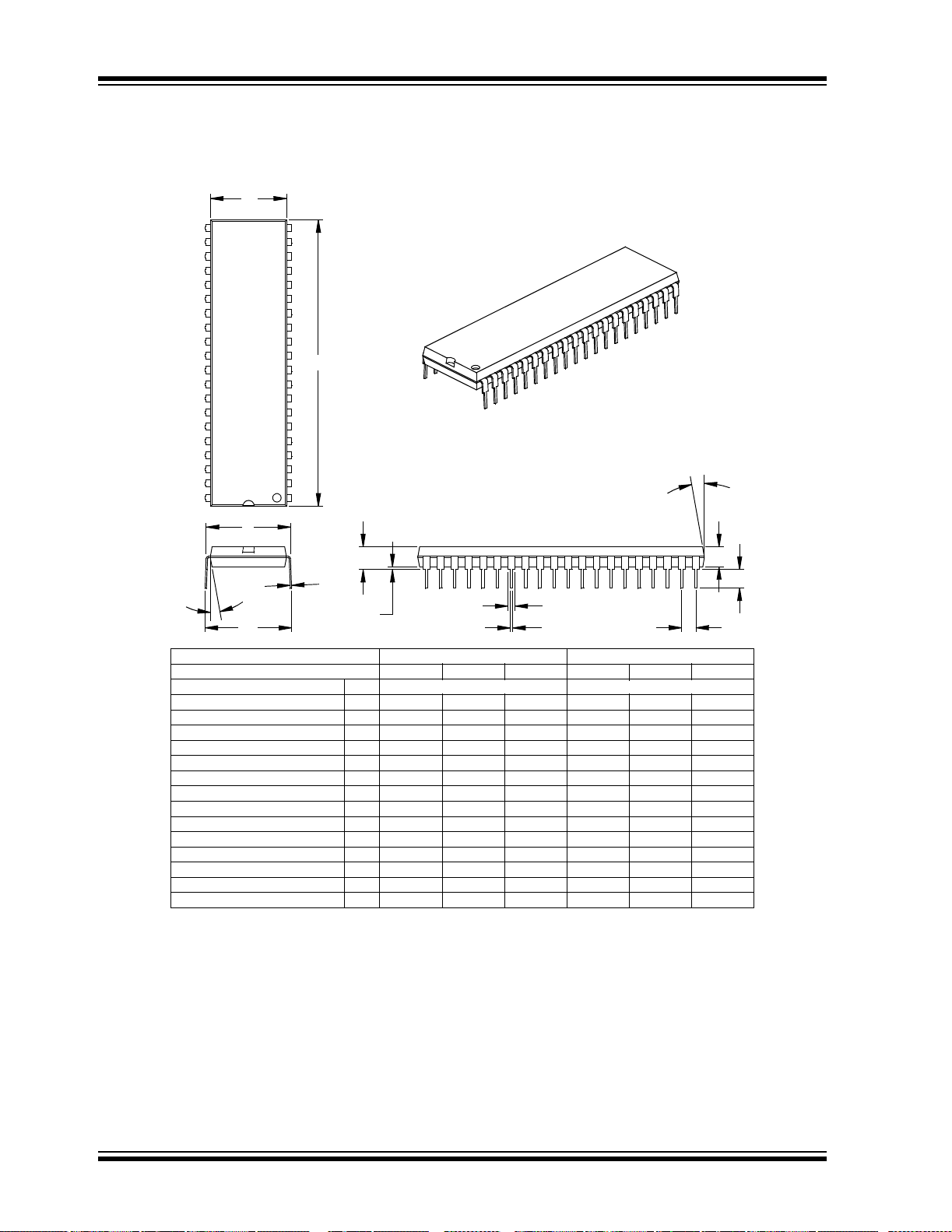
PIC16F5X
40-Lead Plastic Dual In-line (P) – 600 mil Body (PDIP)
E1
D
2
n
E
β
eB
Number of Pins
Pitch
Base to Seating Plane
Lead Thickness
Mold Draft Angle Top
Mold Draft Angle Bottom
* Controlling Parameter
§ Significant Characteristic
Notes:
Dimensions D and E1 do not include mold flash or protrusions. Mold flash or protrusions shall not exceed
.010” (0.254mm) per side.
JEDEC Equivalent: MO-011
Drawing No. C04-016
1
A
c
A1
n
p
A1
c
α
β
B1
B
MILLIMETERSINCHES*Units
4040
2.54.100
0.38.015
α
A2
L
p
MAXNOMMINMAXNOMMINDimension Limits
4.834.454.06.190.175.160ATop to Seating Plane
4.063.813.56.160.150.140A2Molded Package Thickness
15.8815.2415.11.625.600.595EShoulder to Shoulder Width
14.2213.8413.46.560.545.530E1Molded Package Width
52.4552.2651.942.0652.0582.045DOverall Length
3.433.303.05.135.130.120LTip to Seating Plane
0.380.290.20.015.012.008
1.781.270.76.070.050.030B1Upper Lead Width
0.560.460.36.022.018.014BLower Lead Width
17.2716.5115.75.680.650.620eBOverall Row Spacing §
1510515105
1510515105
DS41213C-page 80 2004 Microchip Technology Inc.
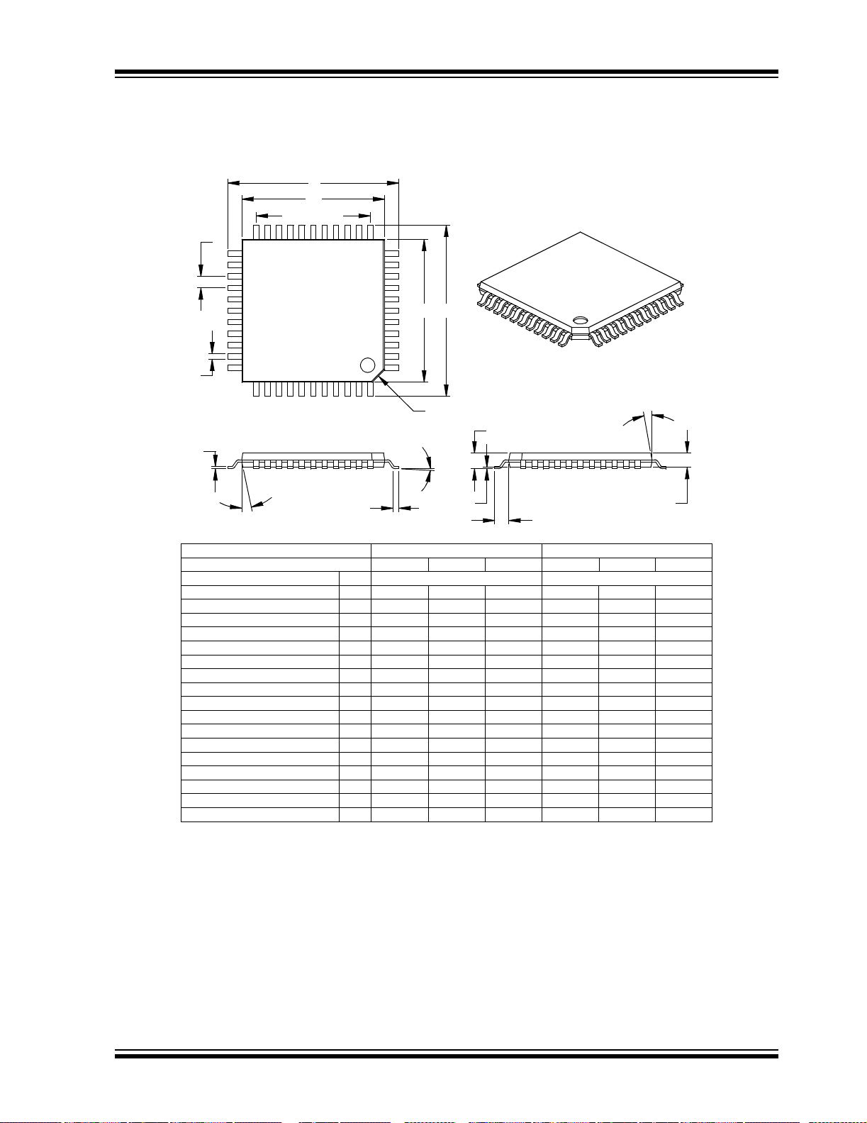
PIC16F5X
44-Lead Plastic Thin Quad Flatpack (PT) 10x10x1 mm Body , 1.0/0.10 mm Lead Form (TQFP)
E
E1
#leads=n1
p
D1 D
2
B
1
n
c
β
Number of Pins
Dimension Limits MIN NOM MAX MIN NOM MAX
Pitch
Pins per Side n1 11 11
Overall Height A .039 .043 .047 1.00 1.10 1.20
Molded Package Thickness A2 .037 .039 .041 0.95 1.00 1.05
Standoff § A1 .002 .004 .006 0.05 0.10 0.15
Foot Length L .018 .024 .030 0.45 0.60 0.75
Footprint (Reference)
Foot Angle
Overall Width E .463 .472 .482 11.75 12.00 12.25
Overall Length D .463 .472 .482 11.75 12.00 12.25
Molded Package Width E1 .390 .394 .398 9.90 10.00 10.10
Molded Package Length D1 .390 .394 .398 9.90 10.00 10.10
Lead Thickness
Lead Width B .012 .015 .017 0.30 0.38 0.44
Mold Draft Angle Top
Mold Draft Angle Bottom
* Controlling Parameter
§ Significant Characteristic
Notes:
Dimensions D1 and E1 do not include mold flash or protrusions. Mold flash or protrusions shall not exceed
.010” (0.254mm) per side.
JEDEC Equivalent: MS-026
Drawing No. C04-076
Units INCHES MILLIMETERS*
n
p
(F)
φ
c
α
β
φ
L
03.5 7 03.5 7
.004 .006 .008 0.09 0.15 0.20
51015 51015
51015 51015
°
CH x 45
A
A1 A2
(F)
44 44
.031 0.80
1.00.039
α
1.140.890.64.045.035.025CHPin 1 Corner Chamfer
2004 Microchip Technology Inc. DS41213C-page 81

PIC16F5X
NOTES:
DS41213C-page 82 2004 Microchip Technology Inc.

PIC16F5X
A
Absolute Maximum Ratings
PIC1654/57.................................................................59
PIC1659......................................................................60
ADDWF...............................................................................43
ALU.......................................................................................7
ANDLW...............................................................................43
ANDWF...............................................................................43
Applications...........................................................................5
Architectural Overview..........................................................7
Assembler
MPASM Assembler.....................................................53
B
Block Diagram
On-Chip Reset Circuit........................ ................. ........24
PIC16F5X Series..........................................................8
Timer0.........................................................................33
TMR0/WDT Prescaler.................................................36
Watchdog Timer..........................................................38
Brown-Out Protection Circuit ..............................................27
BSF.....................................................................................44
BTFSC................................................................................44
BTFSS ................................................................................ 44
C
C Compilers
MPLAB C17................................................................54
MPLAB C18................................................................54
MPLAB C30................................................................54
CALL.............................................................................19, 45
Carry (C) bit ................................ ....................................7, 17
Clocking Scheme................................................................12
CLRF...................................................................................45
CLRW .................................................................................45
CLRWDT.............................................................................45
Code Protection ............................................................37, 39
COMF .................................................................................46
Configuration Bits................................................................37
D
DC Characteristics
Commercial.................................................................64
Extended. ....................................................................63
Industrial ...............................................................62, 64
DECF ..................................................................................46
DECFSZ..............................................................................46
Demonstration Boards
PICDEM 1.............................................. .....................56
PICDEM 17............... ............................... ...................57
PICDEM 18R ................ ................. .............................57
PICDEM 2 Plus............................................... ............56
PICDEM 3.............................................. .....................56
PICDEM 4.............................................. .....................56
PICDEM LIN ................................ ...............................57
PICDEM USB........................................... ...................57
PICDEM.net Internet/Ethernet....................................56
Development Support .........................................................53
Device Reset Timer (DRT)............ ................. ................. ....27
Digit Carry (DC) bit..........................................................7, 17
DRT.....................................................................................27
E
Electrical Specifications
PIC16F54/57.............................................................. 59
PIC16F59 ................................................................... 60
Errata.................................................................................... 3
Evaluation and Programming Tools....................................57
External Power-On Reset Circuit........................................ 25
F
FSR Register...................................................................... 20
Value on Reset (PIC16F54) ....................................... 24
Value on Reset (PIC16F57) ....................................... 24
Value on Reset (PIC16F59) ....................................... 24
G
GOTO........................................................................... 19, 47
H
High-Performance RISC CPU .............................................. 1
I
I/O Interfacing............................................ ......................... 29
I/O Ports ................. ............................... .............................29
I/O Programming Considerations ....................................... 31
ID Locations.................................................................. 37, 39
INCF................................................................................... 47
INCFSZ............................................................................... 47
INDF Register..................................................................... 20
Value on Reset........................................................... 24
Indirect Data Addressing.................................................... 20
Instruction Cycle................................................................. 12
Instruction Flow/Pipelining.................................................. 12
Instruction Set Summary.................................................... 41
IORLW................................................................................ 48
IORWF................................................................................ 48
L
Loading of PC..................................................................... 19
M
MCLR Reset
Register values on.............................................. ........ 24
Memory Map
PIC16F54 ................................................................... 13
PIC16F57/59.............................................................. 13
Memory Organization ......................................................... 13
MOVF................................................................................. 48
MOVLW..............................................................................48
MOVWF.............................................................................. 49
MPLAB ASM30 Assembler, Li n ker, Librarian......... ............ 54
MPLAB ICD 2 In-Circuit Debugger ..................................... 55
MPLAB ICE 2000 High-Performance Universal
In-Circuit Emulator........................................... .......... 55
MPLAB ICE 4000 High-Performance Universal
In-Circuit Emulator........................................... .......... 55
MPLAB Integrated Development Environment Software.... 53
MPLAB PM3 Device Programmer...................................... 55
MPLINK Obje ct Linker/MPL IB Object Librari a n......... ......... 54
N
NOP.................................................................................... 49
2004 Microchip Technology Inc. DS41213C-page 83

PIC16F5X
O
Option.................................................................................. 49
Option Register...................................................................18
Value on Reset...........................................................24
Oscillator Configurations ..................................................... 21
Oscillator Types
HS...............................................................................21
LP................................................................................21
RC...............................................................................21
XT ...............................................................................21
P
PA0 bit......................................... ........................................17
PA1 bit......................................... ........................................17
Paging.................................................................................19
PC.......................................................................................19
Value on Reset...........................................................24
bit ............................................................................17, 23
PD
PICkit 1 Flash Starter Kit.....................................................57
PICSTART Plu s D e ve l o p ment Programm e r ............. .. .. ......5 6
Pinout Description - PIC16F54..............................................9
Pinout Description - PIC16F57............................................10
Pinout Description - PIC16F59............................................11
PORTA................................................................................29
Value on Reset...........................................................24
PORTB................................................................................29
Value on Reset...........................................................24
PORTC................................................................................29
Value on Reset...........................................................24
PORTD
Value on Reset...........................................................24
PORTE
Value on Reset...........................................................24
Power-down Mode..............................................................39
Power-on Reset (POR).............................................. .........25
Register values on.................... ................................ ..24
Prescaler .............................................................................35
PRO MATE II Universal Device Programmer .....................55
Program Counter.................................................................19
Program Memory Organization...........................................13
Program Verification/Code Protection.................................39
Q
Q cycles............................. ............................................... ..12
R
RC Oscillator.......................................................................22
Read-Modify-Write..............................................................31
Register File Map
PIC16F54....................................................................14
PIC16F57....................................................................14
PIC16F59....................................................................15
Registers
Special Function .........................................................16
Value on Reset...........................................................24
Reset...................................................................................23
Reset on Brown-out.......................... ................................ ..27
RETLW................................................................................49
RLF .....................................................................................50
RRF.....................................................................................50
S
Sleep.......................................................................37, 39, 50
Software Simulator ( MP L AB SIM )......................................54
Software Simulator (MPLAB SIM30) .................................. 54
Special Features of the CPU..............................................37
Special Function Registers................................................. 16
Stack................................................................................... 20
Status Register................. ..............................................7, 17
Value on Reset...........................................................24
SUBWF...............................................................................51
SWAPF............................................................................... 51
T
Timer0
Switching Pre scaler Assignment .. .. .............. . ............. 36
Timer0 (TMR0) Module............................................... 33
TMR0 register - Value on Reset................................. 24
TMR0 with External Clock .......................................... 35
Timing Diagrams and Specifications
....................................................................................65
Timing Parameter Symbology and Load Conditions
....................................................................................65
bit............................................................................17, 23
TO
TRIS....................................................................................51
TRIS Registers............. ............................... ....................... 29
Value on Reset...........................................................24
W
W Register
Value on Reset...........................................................24
Wake-up from Sleep.....................................................23, 39
Watchdog Timer (WDT)................................................ 37, 38
Period.........................................................................38
Programming Consideratio n s........................... .......... 38
Register Values on Reset................................. ..........24
WWW, On-Line Support....................................................... 3
X
XORLW............................................................................... 52
XORWF ..............................................................................52
Z
Zero (Z) bit...................................................................... 7, 17
DS41213C-page 84 2004 Microchip Technology Inc.

PIC16F5X
ON-LINE SUPPORT
Microchip provides on-line support on the Microchip
World Wide Web site.
The web site is used b y Mic rochip as a me ans to m ake
files and information easily available to customers. To
view the site, the use r must have access to the Intern et
and a web browser, such as Netscape
Internet Explorer. Files are also available for FTP
download from our FTP site.
Connecting to the Microchip Internet
Web Site
The Microchip web site is available at the following
URL:
www.microchip.com
The file transfer site is available by using an FTP
service to connect to:
ftp://ftp.microchip.com
The web site and file transfer site provide a variety of
services. Users may download files for the latest
Development Tools, Data Sheets, Application Notes,
User's Guides, Articles and Sample Programs. A variety of Micr ochip specific bu siness informatio n is also
available, including listings of Microchip sales offices,
distributors and factory representatives. Other data
available for consideration is:
• Latest Microchip Press Releases
• Technical Support Section with Frequently Asked
Questions
• Design Tips
• Device Errata
• Job Postings
• Microchip Consultant Program Member Listing
• Links to other useful web sites related to
Microchip Products
• Conferences for p roducts, D evelopment Systems,
technical information and more
• Listing of seminars and events
®
or Microsoft
SYSTEMS INFORMATION AND UPGRADE HOT LINE
The Systems Information and Upgrade Line provides
system users a listing of the latest versions of all of
Microchip's development systems software products.
®
Plus, this line provides information on how customers
can receive the most c urrent upgra de kit s.The Hot Lin e
Numbers are:
1-800-755-2345 for U.S. and most of Canada, and
1-480-792-7302 for the rest of the world.
042003
2004 Microchip Technology Inc. DS41213C-page 85

PIC16F5X
READER RESPONSE
It is our intentio n to pro vi de you with the best docu me nt a tion possible to ensure suc c es sfu l u se of y ou r M ic roc hip pro duct. If you wish to provid e your c omment s on org anizatio n, clarity, subject matter , and ways in w hich o ur document atio n
can better serve you, please FAX your comments to the Technical Publications Manager at (480) 792-4150.
Please list the following information, and use this outline to provide us with your comments about this document.
To:
RE: Reader Response
From:
Application (optional):
Would you like a reply? Y N
Device: Literature Number:
Questions:
1. What are the best features of this document?
2. How does this document meet your hardware and software development needs?
3. Do you find the organization of this document easy to follow? If not, why?
Technical Publications Manager
Name
Company
Address
City / State / ZIP / Country
Telephone: (_______) _________ - _________
Total Pages Sent ________
FAX: (______) _________ - _________
DS41213CPIC16F5X
4. What additions to the document do you think would enhance the structure and subject?
5. What deletions from the document could be made without affecting the overall usefulness?
6. Is there any incorrect or misleading information (what and where)?
7. How would you improve this document?
DS41213C-page 86 2004 Microchip Technology Inc.

PRODUCT IDENTIFICATION SYSTEM
To order or obtain information, e.g., on pricing or delivery, refer to the factory or the listed sales office.
PART NO. X /XX XXX
Device
PatternPackageTemperature
Range
Device PIC16F5 4 – VDD rang e 2.0V to 5.5V
PIC16F54T
PIC16F57 – V
PIC16F57T
(1)
– VDD range 2.0V to 5.5V
DD range 2.0V to 5.5V
(1)
– VDD range 2.0V to 5.5V
Examples:
a) PIC16F54–I/P = Industrial temp, PDIP package
b) PIC16F54T–I/SSG = Industrial temp, SSOP
package (Pb -free), t ape and reel
c) PIC16F57–E/SP6 = Extended temp, Skinny
Plastic DIP package (Pb-free)
d) PIC16F57T–E/SS = Extended temp, SSOP
package, tape and reel
e) PIC16F54–I/SOG = Industrial temp, SOIC
package (Pb-free)
PIC16F5X
Temperature Range I = -40°C to +85°C (Industrial)
Package SO = SOIC
Pattern QTP, SQTP, Code or Special Requirements (blank otherwise)
E= -40°C to +125°C (Extended)
SS = SSOP
P=PDIP
SP = Skinny Plastic DIP (SPDIP)
SOG = S OIC (P b- fre e)
SSG = SOIC (Pb-free)
PG = SOIC (Pb-free)
SPG = SOIC (Pb-free)
(2)
PART NO. X /XX XXX
Device
PatternPackageTemperature
Range
Device PIC16F5 9 – VDD rang e 2.0V to 5.5V
PIC16F59T
(1)
– VDD range 2.0V to 5.5V
Note 1: T = in tape and reel SOIC and SSOP
packages only.
2: PIC16F57 only
Examples:
a) PIC16F59–I/P = Industrial temp, PDIP package
(Pb -free).
b) PIC16F59T–I/PT = Industrial temp, TQFP
package (Pb -free), t ape and reel.
Temperature Range I = -40°C to +85°C (Industrial)
Package P = PDIP
Pattern QTP, SQTP, Code or Special Requirements (blank otherwise)
E= -40°C to +125°C (Extended)
PT = TQFP
Note 1: T = in tape and reel TQFP packages only.
2004 Microchip Technology Inc. DS41213C-page 87

WORLDWIDE SALES AND SERVICE
AMERICAS
Corporate Office
2355 West Chandler Blvd.
Chandler, AZ 85224-6199
Tel: 480-792-7200
Fax: 480-792-7277
Technical Support:
http:\\support.microchip.com
Web Address:
www.microchip.com
Atlanta
Alpharetta, GA
Tel: 770-640-0034
Fax: 770-640-0307
Boston
Westford, MA
Tel: 978-692-3848
Fax: 978-692-3821
Chicago
Itasca, IL
Tel: 630-285-0071
Fax: 630-285-0075
Dallas
Addison, TX
Tel: 972-818-7423
Fax: 972-818-2924
Detroit
Farmington Hills, MI
Tel: 248-538-2250
Fax: 248-538-2260
Kokomo
Kokomo, IN
Tel: 765-864-8360
Fax: 765-864-8387
Los Angeles
Mission Viejo, CA
Tel: 949-462-9523
Fax: 949-462-9608
San Jose
Mountain View, CA
Tel: 650-215-1444
Fax: 650-961-0286
Toronto
Mississauga, Ontario,
Canada
Tel: 905-673-0699
Fax: 905-673-6509
ASIA/PACIFIC
Australia - Sydney
Tel: 61-2-9868-6733
Fax: 61-2-9868-6755
China - Beijing
Tel: 86-10-8528-2100
Fax: 86-10-8528-2104
China - Chengdu
Tel: 86-28-8676-6200
Fax: 86-28-8676-6599
China - Fuzhou
Tel: 86-591-750-3506
Fax: 86-591-750-3521
China - Hong Kong SAR
Tel: 852-2401-1200
Fax: 852-2401-3431
China - Shanghai
Tel: 86-21-5407-5533
Fax: 86-21-5407-5066
China - Shenyang
Tel: 86-24-2334-2829
Fax: 86-24-2334-2393
China - Shenzhen
Tel: 86-755-8203-2660
Fax: 86-755-8203-1760
China - Shunde
Tel: 86-757-2839-5507
Fax: 86-757-2839-5571
China - Qingdao
Tel: 86-532-502-7355
Fax: 86-532-502-7205
ASIA/PACIFIC
India - Bangalore
Tel: 91-80-2229-0061
Fax: 91-80-2229-0062
India - New Delhi
Tel: 91-11-5160-8631
Fax: 91-11-5160-8632
Japan - Kanagawa
Tel: 81-45-471- 6166
Fax: 81-45-471-6122
Korea - Seoul
Tel: 82-2-554-7200
Fax: 82-2-558-5932 or
82-2-558-5934
Singapore
Tel: 65-6334-8870
Fax: 65-6334-8850
Taiwan - Kaohsiung
Tel: 886-7-536-4818
Fax: 886-7-536-4803
Taiwan - Taipei
Tel: 886-2-2500-6610
Fax: 886-2-2508-0102
Taiwan - Hsinchu
Tel: 886-3-572-9526
Fax: 886-3-572-6459
EUROPE
Austria - Weis
Tel: 43-7242-2244-399
Fax: 43-7242-2244-393
Denmark - Ballerup
Tel: 45-4420-9895
Fax: 45-4420-9910
France - Massy
Tel: 33-1-69-53-63-20
Fax: 33-1-69-30-90-79
Germany - Ismaning
Tel: 49-89-627-144-0
Fax: 49-89-627-144-44
Italy - Milan
Tel: 39-0331-742611
Fax: 39-0331-466781
Netherlands - Drunen
Tel: 31-416-690399
Fax: 31-416-690340
England - Berkshire
Tel: 44-118-921-5869
Fax: 44-118-921-5820
09/27/04
DS41213C-page 88 2004 Microchip Technology Inc.
 Loading...