


PIC12F510/16F506
Data Sheet
8/14-Pin, 8-Bit Flash Microcontroller
*8-bit, 8-pin Devices Protected by Microchip’s Low Pin Count Patent: U.S. Patent No. 5,847,450. Additional U.S. and
foreign patents and applications may be issued or pending.
© 2005 Microchip Technology Inc. Preliminary DS41268A

Note the following details of the code protection feature on Microchip devices:
• Microchip products meet the specification contained in their particular Microchip Data Sheet.
• Microchip believes that its family of products is one of the most secure families of its kind on the market today, when used in the
intended manner and under normal conditions.
• There are dishonest and possibly illegal methods used to breach the code protection feature. All of these methods, to our
knowledge, require using the Microchip products in a manner outside the operating specifications contained in Microchip’s Data
Sheets. Most likely, the person doing so is engaged in theft of intellectual property.
• Microchip is willing to work with the customer who is concerned about the integrity of their code.
• Neither Microchip nor any other semiconductor manufacturer can guarantee the security of their code. Code protection does not
mean that we are guaranteeing the product as “unbreakable.”
Code protection is constantly evolving. We at Microchip are committed to continuously improving the code protection features of our
products. Attempts to break Microchip’s code protection feature may be a violation of the Digit al Millennium Copyright Act. If suc h a c t s
allow unauthorized access to your software or other copyrighted work, you may have a right to sue for relief under that Act.
Information contained in this publication regarding device
applications and the like is provided only for your convenience
and may be superseded by updates. It is your responsibility to
ensure that your application meets with your specifications.
MICROCHIP MAKES NO REPRESENTATIONS OR WARRANTIES OF ANY KIND WHETHER EXPRESS OR IMPLIED,
WRITTEN OR ORAL, STATUTORY OR OTHERWISE,
RELATED TO THE INFORMATION, INCLUDING BUT NOT
LIMITED TO ITS CONDITION, QUALITY, PERFORMANCE,
MERCHANTABILITY OR FITNESS FOR PURPOSE.
Microchip disclaims all liability arising from this information and
its use. Use of M icrochip’s prod ucts as critical components in
life support systems is not authorized except with express
written approval by Microchip. No licenses are conveyed,
implicitly or otherwise, under any Microchip intellectual property
rights.
Trademarks
The Microchip name and logo, the Microchip logo, Accuron,
dsPIC, K
EELOQ, microID, MPLAB, PIC, PICmicro, PICSTART,
PRO MATE, PowerSmart, rfPIC, and SmartShunt are
registered trademarks of Microchip Technology Incorporated
in the U.S.A. and other countries.
AmpLab, FilterLab, Migratable Memory, MXDEV, MXLAB,
PICMASTER, SEEVAL, SmartSensor and The Embedded
Control Solutions Company are registered trademarks of
Microchip Technology Incorporated in the U.S.A.
Analog-for-the-Digital Age, Application Maestro, dsPICDEM,
dsPICDEM.net, dsPICworks, ECAN, ECONOMONITOR,
FanSense, FlexROM, fuzzyLAB, In-Circuit Serial
Programming, ICSP, ICEPIC, Linear Active Thermistor,
MPASM, MPLIB, MPLINK, MPSIM, PICkit, PICDEM,
PICDEM.net, PICLAB, PICtail, PowerCal, PowerInfo,
PowerMate, PowerTool, rfLAB, rfPICDEM, Select Mode,
Smart Serial, SmartTel, Total Endurance and WiperLock are
trademarks of Microchip Technology Incorporated in the
U.S.A. and other countries.
SQTP is a service mark of Microchip Technology Incorporated
in the U.S.A.
All other trademarks mentioned herein are property of their
respective companies.
© 2005, Microchip Technology Incorporated, Printed in the
U.S.A., All Rights Reserved.
Printed on recycled paper.
Microchip received ISO/TS-16949:2002 quality system certification for
its worldwide headquarters, design and wafer fabrication facilities in
Chandler and Tempe, Arizona and Mountain View, California in
October 2003. The Company’s quality system processes and
procedures are for its PICmicro
devices, Serial EEPROMs, microperipherals, nonvolatile memory and
analog products. In addition, Microchip’s quality system for the design
and manufacture of development systems is ISO 9001:2000 certified.
®
8-bit MCUs, KEELOQ
®
code hopping
DS41268A-page ii Preliminary © 2005 Microchip Technology Inc.

PIC12F510/16F506
8/14-Pin, 8-Bit Flash Microcontroller
Devices Included In This Data Sheet:
•PIC16F506
•PIC12F510
High-Performance RISC CPU:
• Only 33 single-word instructions to learn
• All single-cycle instructions except for program
branches, which are two-cycle
• 12-bit wide instructions
• 2-level deep hardware stack
• Direct, Indirect and Relative Addressing modes
for data and instructions
• 8-bit wide data path
• 10 Special Function Hardware registers
(PIC12F510)
• 13 Special Function Hardware registers
(PIC16F506)
• Operating speed:
- DC – 8 MHz Crystal Oscillator (PIC12F510)
- DC – 500 ns instruction cycle (PIC12F510)
- DC – 20 MHz Crystal Oscillator (PIC16F506)
- DC – 200 ns instruction cycle (PIC16F506)
Special Microcontroller Features:
• 4 or 8 MHz selectable precision internal oscillator:
- Factory calibrated to ±1%
• In-Circuit Serial Programming™ (ICSP™)
• In-Circuit Debugging (ICD) support
• Power-on Reset (POR)
• Device Reset Tim er (DRT)
- Short DRT (1.125 ms, typical) for INTOSC,
EXTRC and EC
- DRT (18 ms, typical) for HS, XT and LP
• Watchdog Timer (WDT) with dedicated on-chip
RC oscillator for reliable operation
• Programmable code protection
• Multiplexed MCLR
• Selectable internal weak pull-ups on I/O pins
• Power-saving Sleep mode
• Wake-up from Sleep on pin change
• Wake-up from Sleep on comparator change
input pin
• Selectable oscil la tor opti ons :
- INTOSC: 4/8 MHz precision Internal
oscillator
- EXTRC: External low-cost RC oscillator
- XT: Standard crystal/resonator
- HS: High-speed crystal/resonator
(PIC16F506 only)
- LP: Power-saving, low-frequenc y cry stal
- EC: High-speed external clock input
(PIC16F506 only)
• Analog-to-Digital (A/D) Converter
- 8-bit resolution
- 4-input channels (1 channel is dedicated to
conversion of the internal 0.6V absolute
voltage reference)
• High current sink/source for direct LED drive
• 8-bit real-time clock/counter (TMR0) with 8-bit
programmable prescaler
Low-Power Features/CMOS Technology:
• Operating Current:
- < 350 μA @ 2V, 4 MHz
• Standby Current:
- 100 nA @ 2V, typical
• Low-power, high-speed Flash technology:
- 100,000 cycle Flash endurance
- > 40-year retention
• Fully static design
• Wide operating voltage range: 2.0V to 5.5V
• Wide temperature range:
- Industrial: -40°C to +85°C
- Extended: -40°C to +125°C
Peripheral Features (PIC12F510):
• 6 I/O pins:
- 5 I/O pins with individual direction control
- 1 input only pin
• 1 Analog Comparator with absolute refe renc e
Peripheral Features (PIC16F506):
• 12 I/O pins:
- 11 I/O pins w ith ind iv idu al dire ct ion contro l
- 1 input only pin
• 2 Analog Comparators with absolute reference
and programmable reference
© 2005 Microchip Technology Inc. Preliminary DS41268A-page 3

PIC12F510/16F506
Device
Program Memory Data Memory
I/O
Timers
Flash (words) SRAM (bytes)
PIC16F506 1024 67 12 1
PIC12F510 1024 38 6 1
Pin Diagrams
PDIP, SOIC and TS SOP
VSS
RB0/AN0/C1IN+/ICSPDAT
RB1/AN1/C1IN-/ICSPCLK
RB2/AN2/C1OUT
RC0/C2IN+
RC1/C2IN-
REF
RC2/CV
VSS
GP0/AN0/C1IN+/ICSPDAT
GP1/AN1/C1IN-//ICSPCLK
GP2/AN2/T0CKI/C1OUT
PDIP, SOIC, MSOP
VDD
RB5/OSC1/CLKIN
RB4/OSC2/CLKOUT
RB3/MCLR
GP5/OSC1/CLKIN
GP3/MCLR
/VPP
RC5/T0CKI
RC4/C2OUT
RC3
VDD
GP4/OSC2
/VPP
1
2
3
4
5
6
7
1
2
3
4
PIC16F506
PIC12F510
14
13
12
11
10
9
8
8
7
6
5
8-bit
DS41268A-page 4 Preliminary © 2005 Microchip Technology Inc.

PIC12F510/16F506
Table of Contents
1.0 General Description............................................................................ ....... .... .. .... .. .... ................................................................... 7
2.0 PIC12F510/16F506 Device Varieties ..........................................................................................................................................9
3.0 Architectural Overview...............................................................................................................................................................11
4.0 Memory Organization................................................................................................................................................................. 17
5.0 I/O Port................................ ............. ........................................................... ............................................................................... 29
6.0 TMR0 Module and TMR0 Register.............................................................................................................................................41
7.0 Comparator(s)............................................................................................................................................................................ 45
8.0 Comparator Voltage Reference Module..................................................................................................................................... 51
9.0 Analog-to-Digital (A/D) Converter...............................................................................................................................................53
10.0 Special Features Of The CPU............ ............. ............ ............. ............ ...................................................................................... 57
11.0 Instruction Set Summary ............................................................................................................................................................ 73
12.0 Development Support.................................................................................................................................................................81
13.0 Electrical Characteristics............................................................................................................................................................ 85
14.0 DC and AC Characteristics Graphs and Charts.............................................. .... .... ........... .... .... .... ............................................ 97
15.0 Packaging................................................................................................................................................................................... 99
Index ..................................................................................................................................................................................................109
The Microchip Web Site........................... .......................................................................................................................................... 111
Customer Change Notification Service .............................................................................................................................................. 111
Customer Support.............................................................................................................................................................................. 111
Reader Response. .............................................................................................................................................................................112
Product Identification System............................................................................................................................................................ 113
TO OUR VALUED CUSTOMERS
It is our intention to provide our valued customers with the best documentation possible to ensure successful use of your Microchip
products. To this end, we will continue to improve our publications to better suit your needs. Our publications will be refined and
enhanced as new volumes and updates are introduced.
If you have any questions or c omm ents regarding t his publication, p lease c ontact the M arket ing Co mmunications Department via
E-mail at docerrors@microchip.com or fax the Reader Response Form in the back of this data sheet to (480) 792-4150. We
welcome your feedback.
Most Current Data Sheet
To obtain the most up-to-date version of this data sheet, please register at our Worldwide Web site at:
http://www.microchip.com
You can determine the version of a data sheet by examining its literature number found on the bottom outside corner of any page.
The last character of the literature number is the version number, (e.g., DS30000A is version A of document DS30000).
Errata
An errata sheet, describing minor operational differences from the data sheet and recommended workarounds, may exist for current
devices. As device/documentation issues become known to us, we will publish an errata sheet. The errata will specify the revision
of silicon and revision of document to which it applies.
To determine if an errata sheet exists for a particular device, please check with one of the following:
• Microchip’s Worldwide Web site; http://www.microchip.com
• Your local Microchip sales office (see last page)
When contacting a sales office, please specify which device, revision of silicon and data sheet (include literature number) you are
using.
Customer Notification System
Register on our web site at www.microchip.com to receive the most current information on all of our products.
© 2005 Microchip Technology Inc. Preliminary DS41268A-page 5

PIC12F510/16F506
NOTES:
DS41268A-page 6 Preliminary © 2005 Microchip Technology Inc.

PIC12F510/16F506
1.0 GENERAL DESCRIPTION
The PIC12F510/16F506 devices from Microchip
T ec hnology are lo w-cost, hig h-performance , 8-bit, fullystatic, Flash-based CMOS microcontrollers. They
employ a RISC architecture with only 33 single-word/
single-cycle instructions. All instructions are singlecycle except for program branches, which take two
cycles. The PIC12F510/16F506 devices deliver
performance in an o rder of m agnitu de hig her than their
competitors in the same pric e category . The 12-bi t wide
instructions are highly symmetrical, resulting in a
typical 2:1 code compression over other 8-bit
microcontrollers in i ts class . The easy-to-use a nd easyto-remember instr ucti on se t reduc es de velop ment time
significantly.
The PIC12F510/16F506 products are equipped with
special features that reduce system cost and power
requirements. The Power-on Reset (POR) and Device
Reset Timer (DRT) eliminate the need for external
reset circuitry. There are four oscillator configurations
to choose from (six on the PIC16F506), including
INTOSC Internal Oscillator mode and the power-saving
LP (Low-pow er) Osci llator mode. Po wer-sa ving Sle ep
mode, Watchdog Timer and code protection features
improve system cost, power and reliability.
The PIC12F510/16 F506 de vi ce s a ll ow th e c us tom er to
take full advantage of Microchip’s price leadership in
Flash programmable microcontrollers, while benefiting
from the Flash programmable flexibi lit y.
The PIC12F510/16F506 products are supported by a
full-featured macr o assembl er , a s oftware simulator, an
in-circuit emulator, a ‘C’ compiler, a low-cost
development programmer and a full featured programmer. All the tools are supported on IBM
compatible machines.
®
PC and
1.1 Applications
The PIC12F510/16F506 devices fit in applications
ranging from personal care appliances and security
systems to low-power remote transmitters/receivers.
The Flash technology makes customizing application
programs (transmitter codes, appliance settings,
receiver frequencies, etc.) extremely fast and convenient. The small footpri nt p ackag es, for t hrough h ole or
surface mounting, make these microcontrollers perfect
for applications with space limitations. Low-cost, lowpower, high-performance, ease-of-use and I/O flexibility make the PIC12F510/16F506 devices very versatile, even in areas where no microcontroller use has
been considered b efore (e.g., tim er functions, lo gic and
PLDs in larger system s and co processor applications ).
T ABLE 1-1: PIC12F510/16F506 DEVICES
PIC16F506 PIC12F510
Clock Maximum Frequency of Operation (MHz) 20 8
Memory Flash Program Memory 1024 1024
Data Memory (bytes) 67 38
Peripherals Timer Module(s) TMR0 TMR0
Wake-up from Sleep on Pin Change Yes Yes
Features I/O Pins 11 5
Input Only Pin 1 1
Internal Pull-ups Yes Yes
In-Circuit Serial Programming Yes Yes
Number of Instructions 33 33
Packages 14-pin PDIP, SOIC,
TSSOP
The PIC12F510/16F506 devices have Power-on Reset, selectable Watchdog Timer, selectable code-protect, high I/O current
capability and precision internal oscillator.
The PIC12F510/16F506 device uses serial programming with data pin RB0/GP0 and clock pin RB1/GP1.
© 2005 Microchip Technology Inc. Preliminary DS41268A-page 7
8-pin PDIP, SOIC, MSOP

PIC12F510/16F506
NOTES:
DS41268A-page 8 Preliminary © 2005 Microchip Technology Inc.

PIC12F510/16F506
2.0 PIC12F510/16F506 DEVICE VARIETIES
A variety of packaging options are available. Depending on application and production requirements, the
proper device option can be selected using the
information in th is section. Wh en placing orde rs, please
use the PIC12F510/16F506 Product Identification
System at the back of this data sheet to specify the
correct part number.
2.1 Quick Turn Programming (QTP)
Devices
Microchip offers a QTP programming service for
factory production orders. This service is made
available for users who choose not to program
medium-to-high quantity units and whose code
patterns have stabilized. The devices are identical to
the Flash devices, bu t w ith all Fla sh l oc ati ons and fus e
options already programmed by the factory. Certain
code and prototype verification procedures do apply
before production shipments are available. Please
contact your loc al Microchi p Techn ology sales office for
more details.
2.2 Serialized Quick Turn
Programming
Microchip offers a unique programming service, where
a few user-defined locations in each device are
programmed with different serial numbers. The serial
numbers may be random, pseudo-random or
sequential.
Serial programming allows each device to have a
unique number, which can serve as an entry code,
password or ID number.
SM
(SQTPSM) Devices
© 2005 Microchip Technology Inc. Preliminary DS41268A-page 9

PIC12F510/16F506
NOTES:
DS41268A-page 10 Preliminary © 2005 Microchip Technology Inc.

PIC12F510/16F506
3.0 ARCHITECTURAL OVERVIEW
The high performance of the PIC12F510/16F506
devices can be attributed to a number of architectural
features commonly found in RISC microprocessors.
The PIC12F510/16F506 devices use a Harvard architecture in which program and data are accessed on
separate buses. This improves bandwidth over traditional von Neumann architectures where program and
data are fetch ed on the sa me bu s. Separating progra m
and data memor y further allow s instructions to be sized
differently than the 8-bit wide data word. Instruction
opcodes are 12 bit s wide, making it p ossible to have all
single-word instructions. A 12-bit wide program memory access bus fetches a 12-bit instruction in a single
cycle. A two-stage pipeline overlaps fetch and execution of instructions. Consequently, all instructions (33)
execute in a si ngle cycle (200 ns @ 20 MHz, 1 μs @
4 MHz) except for program branches.
Table 3-1 lists program memory (Flash) and data
memory (RAM) for the PIC12F510/16F506 devices.
T ABLE 3-1: PIC12F510/16F506 MEMORY
Memory
Device
Program Data
PIC12F510 1024 x 12 38 x 8
PIC16F506 1024 x 12 67 x 8
The PIC12F510/16F506 devices can directly or indirectly address its register files and data memory. All
Special Function Registers (SFR), including the PC,
are mapped in the data memory. The PIC12F510/
16F506 devices have a highly orthogonal (symmetrical) instruc tion set that makes it possible to carry ou t
any operat ion, on any regis ter, using any addressing
mode. This symmetrical nature and lack of “special
optimal situations” make programming with the
PIC12F510/16F506 devices simple, yet efficient. In
addition, the learning curve is reduced significantly.
The PIC12F510/16F506 devices contain an 8-bit ALU
and working register. The ALU is a general purpose
arithmetic unit. It performs arithmetic and Boolean
functions between d ata in the worki ng register and an y
register file.
The ALU is 8 bits wide and capable of addition, subtraction, shift and logical operations. Unless otherwise
mentioned, arithmetic operations are two’s complement in nature. In two-operand instructions, one
operand is typica lly t he W (working) regis ter. T he oth er
operand is either a file register or an immediate
constant. In sing le-operand instr uctions, the operan d is
either the W register or a file register.
The W register is an 8-bit workin g register used for ALU
operations. It is not an addressable register.
Depending on the instruction executed, the ALU may
affect the values of the Carry (C), Digit Carry (DC) and
Zero (Z) bits in the ST ATUS register . The C and DC bit s
operate as a borrow
tively, in subtraction. See the SUBWF and ADDWF
instructions for examples.
A simplified block diagram is shown in Figure 3-1 for
PIC12F510 with the corresponding device pins described
in Table 3-2. A simplified block diagram for PIC16F506 is
shown in Figure 3-2 with the corresponding device pins
described in T able 3-3.
and digit borrow out bit, respec-
© 2005 Microchip Technology Inc. Preliminary DS41268A-page 11

PIC12F510/16F506
T
FIGURE 3-1: PIC12F510 SERIES BLOCK DIAGRAM
OSC2/OSC1/CLKIN
Program
Bus
Flash
1K x 12
Program
Memory
12
Instruction Reg
Instruction
Decode &
Control
Timing
Generation
10-11
Program Counter
Direct Addr
8
Device Reset
Watchdog
Internal RC
MCLR
STACK 1
STACK 2
Timer
Power-on
Reset
Timer
Clock
VDD, VSS
RAM Addr
5
3
8
Data Bus
RAM
38 bytes
File
Registers
Addr MUX
5-7
FSR Reg
STATUS Reg
ALU
W Reg
Timer0
9
MUX
Indirect
Addr
8
GPIO
Comparator
VREF
8-bit ADC
GP0/ICSPDAT
GP1/ICSPCLK
GP2/T0CKI
GP3/MCLR/VPP
GP4/OSC2
GP5/OSC1/CLKIN
C1IN+
C1INC1OU
AN0
AN1
AN2
DS41268A-page 12 Preliminary © 2005 Microchip Technology Inc.

PIC12F510/16F506
T ABLE 3-2: PIN DESCRIPTIONS – PIC12F510
Name I/O/P Type Input Type Output Type Description
GP0/AN0/C1IN+/ICSPDAT GP0 TTL CMOS Bidirectional I/O port. Can be software programmed
AN0 AN — ADC channel input.
C1IN+ AN — Comparator input.
ICSPDAT ST CMOS In-Circuit Serial Programming data pin.
GP1/AN1/C1IN-/ICSPCLK GP1 TTL CMOS Bidirectional I/O port. Can be software programmed
AN1 AN — ADC channel input.
C1IN- AN — Comparator input.
ICSPCLK ST CMOS In-Circuit Serial Programming clock pin.
GP2/AN2/T0CKI/C1OUT GP2 TTL CMOS Bidirectional I/O port.
AN2 AN — ADC channel input.
T0CKI ST — Timer0 clock input.
C1OUT CMOS — Comparator output.
GP3/MCLR/
GP4/OSC2 GP4 TTL CMOS Bidirectional I/O port.
GP5/OSC1/CLKIN GP5 TTL CMOS Bidirectional I/O port.
DD VDD P — Positive supply for logic and I/O pins.
V
SS VSS P — Ground reference for logic and I/O pins.
V
Legend: I = input, O = output, I/O = input/output, P = power, — = Not Used, TTL = TTL input, ST = Schmitt Trigger input,
VPP GP3 TTL — Standard TTL input. Can be software programmed
ST — MCLR input – weak pull-up always enabled in this
AN = Analog Voltage
MCLR
PP High Voltage — Program ming Voltage input.
V
OSC2 — XTAL XTAL oscillator output pin.
OSC1 XTAL — XTAL oscillator input pin.
CLKIN ST — E XTRC Sc hmitt Trigger input.
for internal weak pull-up and wake-up from Sleep on
pin change.
for internal weak pull-up and wake-up from Sleep on
pin change.
for internal weak pull-up and wake-up from Sleep on
pin change.
mode.
© 2005 Microchip Technology Inc. Preliminary DS41268A-page 13

PIC12F510/16F506
FIGURE 3-2: PIC16F506 SERIES BLOCK DIAGRAM
OSC1/CLKIN
OSC2/CLKOUT
Program
Bus
Flash
1K x 12
Program
Memory
10
Instruction Reg
Instruction
Decode &
Control
Timing
Generation
10
Program Counter
Direct Addr
8
Device Reset
Watchdog
Internal RC
MCLR
STACK 1
STACK 2
Timer
Power-on
Reset
Timer
Clock
VDD, VSS
RAM Addr
5
3
8
Data Bus
RAM
67 bytes
File
Registers
Addr MUX
5-7
FSR Reg
STATUS Reg
ALU
W Reg
Timer0
9
MUX
Indirect
Addr
8
PORTB
PORTC
Comparator 1
VREF
Comparator 2
CVREF
8-bit ADC
RB0/ICSPDAT
RB1/ICSPCLK
RB2
RB3/MCLR/VPP
RB4/OSC2/CLKOUT
RB5/OSC1/CLKIN
RC0
RC1
RC2
RC3
RC4
RC5/T0CKI
C1IN+
C1INC1OUT
C2IN+
C2INC2OUT
CVREF
CVREF
AN0
AN1
AN2
VREF
DS41268A-page 14 Preliminary © 2005 Microchip Technology Inc.

PIC12F510/16F506
T ABLE 3-3: PIN DESCRIPTIONS – PIC16F506
Name Function Input Type Output Type Description
RB0/AN0/C1IN+/ICSPDAT RB0 TTL CMOS Bidirectional I/O port. Can be software programmed for
AN0 AN — ADC channel input.
C1IN+ AN — Comparator 1 input.
ICSPDAT ST CMOS In-Circuit Serial Programming data pin.
RB1/AN1/C1IN-/ICSPCLK RB1 TTL CMOS Bidirectional I/O port. Can be software programmed for
AN1 AN — ADC channel input.
C1IN- AN — Comparator 1 input.
ICSPCLK ST — In-Circuit Serial Programming data pin.
RB2/AN2/C1OUT RB2 TTL CMOS Bidirectional I/O port.
AN2 AN — ADC channel input.
C1OUT — CMOS Comparator 1 output.
RB3/MCLR
RB4/OSC2/CLKOUT RB4 TTL CMOS Bidirectional I/O port. Can be software programmed for
RB5/OSC1/CLKIN RB5 TTL CMOS Bidirectional I/O port.
RC0/C2IN+ RC0 TTL CMOS Bidirectional I/O port.
RC1/C2IN- RC1 TTL CMOS Bidirectional I/O port.
RC2/CV
RC3 RC3 TTL CMOS Bidirectional I/O port.
RC4/C2OUT RC4 TTL CMOS Bidirectional I/O port.
RC5/T0CKI RC5 TTL CMOS Bidirectional I/O port.
DD VDD P — Positive supply for logic and I/O pins.
V
SS VSS P — Ground reference for logic and I/O pins.
V
Legend: I = input, O = output, I/O = input/output, P = power, — = Not Used, TTL = TTL input, ST = Schmitt Trigger input,
/VPP RB3 TTL — Standard TTL input. Can be software programmed for
MCLR
PP High Voltage — Test mode High Voltage pin.
V
OSC2 — XTA L XTAL oscillator output pin.
CLKOUT — CMOS EXTRC/INTOSC CLKOUT pin (F
OSC1 XTAL — XTAL oscillator input pin.
CLKIN ST — EXTR C/EC Schmitt Trigger input.
C2IN+ AN — Comparator 2 input.
C2IN- AN — Comparator 2 input.
REF RC2 TTL CMOS Bidirectional I/O port.
CV
REF — AN Programmable Voltage Reference output.
C2OUT — CMOS Comparator 2 output.
T0CKI ST — Timer0 Schmitt Trigger input pin.
AN = Analog Voltage
ST — MCLR input – weak pull-up always enabled in this mode.
internal weak pull-up and wake-up from Sleep on pin
change.
internal weak pull-up and wake-up from Sleep on pin
change.
internal weak pull-up and wake-up from Sleep on pin
change.
internal weak pull-up and wake-up from Sleep on pin
change.
OSC/4).
© 2005 Microchip Technology Inc. Preliminary DS41268A-page 15

PIC12F510/16F506
3.1 Clocking Scheme/Instruction
Cycle
The clock input (OSC1/CLKIN pin) is internally divided
by four to generate four non-overlapping quadrature
clocks, namely Q1, Q2, Q3 and Q4. Internally, the PC
is incremented every Q1 and the instruction is fetched
from program memory and latched into the instruction
register in Q4. It is decoded and executed during the
following Q1 through Q4. The clocks and instruction
execution flow is s hown in Figure3-3 and Example 3-1.
FIGURE 3-3: CLOCK/INSTRUCTION CYCLE
Q2 Q3 Q4
OSC1
Q1
Q2
Q3
Q4
PC
Q1
PC
Q1
3.2 Instruction Flow/Pipelining
An instruction cy cle consists of four Q cycles (Q1, Q2,
Q3 and Q4). The instruction fetch and execute are
pipelined such that fetch takes one instruction cycle,
while decode and execute take another instruction
cycle. However, due to the pipelining, each instruction
effectively executes in one cycle. If an instruction
causes the PC to change (e.g ., GOTO), t hen two c yc le s
are required to complete the ins tructi on (Exampl e 3-1).
A fetch cycle begins with the PC incrementing in Q1.
In the execution cy cle, the fetched instruction i s latched
into the Instruction Register (IR) in cycle Q1. This
instruction is then decoded and executed during the
Q2, Q3 and Q4 c ycles. Dat a m emory is read during Q2
(operand read) and written during Q4 (destination
write).
Q2 Q3 Q4
PC + 1 PC + 2
Q1
Q2 Q3 Q4
Internal
Phase
Clock
Fetch INST (PC)
Execute INST (PC – 1)
Fetch INST (PC + 1)
Execute INST (PC)
Fetch INST (PC + 2)
Execute INST (PC + 1)
EXAMPLE 3-1: INSTRUCTION PIPELINE FLOW
1. MOVLW 03H Fetch 1 Execute 1
2. MOVWF PORTB Fetch 2 Execute 2
3. CALL SUB_1 Fetch 3 Execute 3
4. BSF PORTB, BIT1 Fetch 4
All instructions are si ngle cycle, except for any program bra nches. These tak e two cycles, since th e fetch instruction
is “flushed” from the pipeline, while the new instruction is being fetched and then executed.
Flush
Fetch SUB_1 Execute SUB_1
DS41268A-page 16 Preliminary © 2005 Microchip Technology Inc.

PIC12F510/16F506
4.0 MEMORY ORGANIZATION
The PIC12F510/16F506 memories are organized into
program memory and data memory. For devices with
more than 512 bytes of program memory, a paging
scheme is used. Program memory pages are accessed
using one ST A TUS regi ster bit. For the PIC12F510 and
PIC16F506, with data memory register files of more
than 32 registers, a banking scheme is used. Data
memory banks are accessed using the File Select
Register (FSR).
4.1 Program Memory Organization for
the PIC12F510/16F506
The PIC12F510/16F506 devices have a 10-bit
Program Counter (PC) c apable o f addressing a 2K x 12
program memory space.
Only the first 1K x 12 (0000 h-03FFh) are physically
implemented (see Figure 4- 1). Accessing a location
above these boundaries will cause a wraparound
within the 1K x 12 space. The effective Reset vector
is a 0000h (see Figure 4-1). Location 03FFh contains
the internal clock oscillator calibration value. This
value should never be overwritten.
FIGURE 4-1: PROGRAM MEMORY MAP
AND STACK FOR THE
PIC12F510/16F506
PC<11:0>
CALL, RETLW
Stack Level 1
Stack Level 2
Reset Vector
On-chip Program
Memory
512 Word
Space
User Memory
On-chip Program
Memory
1024 Word
10
(1)
0000h
01FFh
0200h
03FFh
0400h
7FFh
Note 1: Address 0000h becomes the effective
Reset vector. Location 03FFh contains
the MOVLW XX internal oscillator
calibration value.
© 2005 Microchip Technology Inc. Preliminary DS41268A-page 17

PIC12F510/16F506
4.2 Data Memory Organization
Data memory is composed of registers or bytes of
RAM. Therefore, d ata memory for a device is spec ifie d
by its register file. The register file is divided into two
functional groups: Special Function Registers (SFR)
and General Purpose Registers (GPR).
The Special Function Registers include the TMR0
register, the Program Counter (PCL), the STATUS
register, the I/O registers (ports) and the File Select
Register (FSR). In addition, Specia l Function Registe rs
are used to control the I/O port configuration and
prescaler options.
The General Purpose Registers are used for data and
control information under com mand of the instructions .
For the PIC12F510, the register file is composed of 10
Special Function Registers, 6 General Purpose
Registers and 32 General Purpose Registers acces sed
by banking (see Figure 4-5).
For the PIC16F506, the register file is composed of 13
Special Function Registers, 3 General Purpose
Registers and 64 General Purpose Registers acces sed
by banking (see Figure 4-6).
4.2.1 GENERAL PURPOSE REGISTER
FILE
The General Pu rpose Registe r file is accessed either
directly or indirectly through the File Select Register
(FSR). See Section 4.8 “Indirect Data Addressing:
INDF and FSR Registers”.
FIGURE 4-2: PIC12F510 REGISTER
FILE MAP
FSR<5> 0 1
File Address
00h
01h
02h
03h
04h
05h
06h
07h
08h
09h
0Ah
0Fh
10h
1Fh
Note 1: Not a physical register.
(1)
INDF
TMR0
PCL
STATUS
FSR
OSCCAL
GPIO
CM1CON0
ADCON0
ADRES
General
Purpose
Registers
General
Purpose
Registers
Bank 0 Bank 1
20h
Addresses
map back to
addresses in
Bank 0.
2Fh
30h
General
Purpose
Registers
3Fh
FIGURE 4-3: PIC16F506 REGISTER FILE MAP
FSR<6:5> 00 01 10 11
File Address
00h
01h
02h
03h
04h
05h
06h
07h
08h
09h
0Ah
0Bh
0Ch
0Dh
0Fh
10h
1Fh
Note 1: Not a physical register.
(1)
INDF
TMR0
PCL
STATUS
FSR
OSCCAL
PORTB
PORTC
CM1CON0
ADCON0
ADRES
CM2CON0
VRCON
General
Purpose
Registers
General
Purpose
Registers
Bank 0 Bank 1 Bank 2 Bank 3
20h
Addresses map back to
addresses in Bank 0.
2Fh 4Fh 6Fh
30h
General
Purpose
Registers
3Fh
40h
50h
5Fh
General
Purpose
Registers
60h
70h
7Fh
General
Purpose
Registers
DS41268A-page 18 Preliminary © 2005 Microchip Technology Inc.

PIC12F510/16F506
4.2.2 SPECIAL FUNCTION REGISTERS
The Special Function Registers (SFRs) are registers
used by the CPU and per ipheral functio ns to con trol the
operation of the device (see Table 4-1).
The Special Function Registers can be classified into
two sets. The Special Function Registers associated
with the “core” functions are described in this section.
Those related to the operation of the peripheral
features are described in the section for each
peripheral feature.
TABLE 4-1: SPECIAL FUNCTION REGISTER SUMMARY – PIC12F510
Address Name Bit 7 Bit 6 Bit 5 Bit 4 Bit 3 Bit 2 Bit 1 Bit 0
N/A TRIS I/O Control Registers (TRISGPIO) --11 1111
N/A OPTION Contains control bits to configure Ti mer0 and Timer0/WDT Prescaler 1111 1111
00h INDF Uses contents of FSR to address data memory (not a physical register) xxxx xxxx
01h TMR0 Timer0 Module Regis t er xxxx xxxx
(1)
02h
03h STATUS GPWUF CWUF PA0 TO
04h FSR Indirect Data Memory Address Pointer
05h OSCCAL CAL6 CAL5 CAL4 CAL3 CAL2 CAL1 CAL0
06h GPIO
07h CM1CON0 C1OUT C1OUTEN
08h ADCON0 ANS1 ANS0 ADCS 1 ADCS0 CHS1 CHS0 GO/D ONE
09h ADRES ADC Conversion Result xxxx xxxx
Legend: x = unknown, u = unchanged, – = unimplemented, read as '0' (if applicable). Shaded cells = unimplemented or unused.
Note 1: The upper byte of th e Program Counter is not directly accessible. See Section 4.4 “OPTION Register” for an explanation of
PCL Low Order 8 bits of PC 1111 1111
PD ZDCC0001 1xxx
— 1111 111-
— — GP5 GP4 GP3 GP2 GP1 GP0 --xx xxxx
C1POL C1T0CS C1ON C1NREF C1PREF C1WU 1111 1111
ADON 1111 1100
how to access these bits.
Value on
Power-on
Reset
110x xxxx
TABLE 4-2: SPECIAL FUNCTION REGISTER SUMMARY – PIC16F506
Address Name Bit 7 Bit 6 Bit 5 Bit 4 Bit 3 Bit 2 Bit 1 Bit 0
N/A TRIS I/O Control Registers (TRISB, TRISC) --11 1111
N/A OPTION Contains control bits to configure Timer0 and Timer0/WDT Prescaler 1111 1111
00h INDF Uses contents of FSR to address data memory (not a physical register) xxxx xxxx
01h TMR0 Timer0 Module Register xxxx xxxx
(1)
02h
03h STATUS RBWUF CWUF PA0 TO
04h FSR Indirect Data Memory Address Pointer 100x xxxx
05h OSCCAL CAL6 CAL5 CAL4 CAL3 CAL2 CAL1 CAL0
06h PORTB
07h PORTC
08h CM1CON0 C1OUT C1OUTEN
09h ADCON0 ANS1 ANS0 ADCS1 ADCS0 CHS1 CHS0 GO/DONE
0Ah ADRES ADC Conversion Result xxxx xxxx
0Bh CM2CON0 C2OUT C2OUTEN
0Ch VRCON VREN VROE VRR
Legend: x = unknown, u = unchanged, – = unimplemented, read as '0' (if applicable). Shaded cells = unimplemented or unused.
Note 1: The upper byte of th e Program Counter is not directly accessible. See Section 4.4 “OPTION Register” for an explanation of
PCL Low Order 8 bits of PC 1111 1111
PD ZDCC0001 1xxx
— 1111 111-
— — RB5 RB4 RB3 RB2 RB1 RB0 --xx xxxx
— — RC5 RC4 RC3 RC2 RC1 RC0 --xx xxxx
C1POL C1T0CS C1ON C1NREF C1PREF C1WU 1111 1111
ADON 1111 1100
C2POL C2PREF2 C2ON C2NREF C2PREF1 C2WU 1111 1111
—VR3VR2VR1VR0001- 1111
how to access these bits.
Value on
Power-on
Reset
© 2005 Microchip Technology Inc. Preliminary DS41268A-page 19

PIC12F510/16F506
4.3 STATUS Register
This register contains the arithmetic status of the ALU,
the Reset status and the page preselect bit.
The STATUS register can be the destination for any
instruction, as with any other register. If the STATUS
register is the destination for an instruction that affects
the Z, DC or C bits, then the write to these three bits is
disabled. These bit s are set or cleared ac cording to the
device logic. Furthermore, the TO
and PD bits are not
For example, CLRF STATUS, will c lea r the up per three
bits and set the Z bit. This leaves the STATUS register
as 000u u1uu (where u = unchanged).
Therefore, it is recommended that only BCF, BSF and
MOVWF instructions be used to alter the STATUS register. The se in structions do not affect the Z, DC or C bits
from the STATUS register. For other instructions which
do affect Status bits, see Section 11.0 “Instruction
Set Summary”.
writable. Therefore, the result of an instruction with the
STATUS regis ter as destina tion may be differ ent than
intended.
REGISTER 4-1: STATUS REGISTER (ADDRESS: 03h) (PIC12F510)
R/W-0 R/W-0 R/W-0 R-1 R-1 R/W-X R/W-X R/ W-X
GPWUF CWUF PA0 TO
bit 7 bit 0
bit 7 GPWUF: GPIO Reset bit
1 = Reset due to wake-up from Sleep on pin change
0 = After power-up or other Reset
bit 6 CWUF: Comparator Reset bit
1 = Reset due to wake-up from Sleep on comparator change
0 = After power-up or other Reset
bit 5 PA0: Program Page Preselect bits
1 = Page 1 (200h-3FFh)
0 = Page 0 (000h-1FFh)
Each page is 512 bytes.
Using the PA0 bit as a general purpose read/write bit in devices which do not use it for prog ram page
preselect is not recommended, since this may affect upward compatibility with future products.
bit 4 TO
bit 3 PD
bit 2 Z: Zero bit
bit 1 DC: Digit carry/borrow
bit 0 C: Carry/borrow
: Time-out bit
1 = After power-up, CLRWDT instruction, or SLEEP instruction
0 = A WDT time-out occurred
: Power-down bit
1 = After power-up or by the CLRWDT instruction
0 = By execution of the SLEEP instructi on
1 = The result of an arithmetic or logic operation is zero
0 = The result of an arithmetic or logic operation is not zero
bit (for ADDWF and SUBWF instructions)
ADDWF:
1 = A carry from the 4th low-order bit of the result occurred
0 = A carry from the 4th low-order bit of the result did not occur
SUBWF:
1 = A borrow from the 4th low-order bit of the result did not occur
0 = A borrow from the 4th low-order bit of the result occurred
bit (for ADDWF, SUBWF and RRF, RLF instructions)
ADDWF: SUBWF: RRF or RLF:
1 = A carry occurred 1 = A borrow did not occur Load bit with LSb or MSb, respectively
0 = A carry did not occur 0 = A borrow occurred
PD ZDCC
Legend:
R = Readable bit W = Writable bit U = Unimplemented bit, read as ‘0’
-n = Value at POR ‘1’ = Bit is set ‘0’ = Bit is cleared x = Bit is unknown
DS41268A-page 20 Preliminary © 2005 Microchip Technology Inc.

PIC12F510/16F506
REGISTER 4-2: STATUS REGISTER (ADDRESS: 03h) (PIC16F506)
R/W-0 R/W-0 R/W-0 R-1 R-1 R/W-X R/W-X R/W-X
RBWUF CWUF PA0 TO
bit 7 bit 0
bit 7 RBWUF: PORTB Reset bit
1 = Reset due to wake-up from Sleep on pin change
0 = After power-up or other Reset
bit 6 CWUF: Comparator Reset bit
1 = Reset due to wake-up from Sleep on comparator change
0 = After power-up or other Reset
bit 5 PA0: Program Page Preselect bits
1 = Page 1 (200h-3FFh)
0 = Page 0 (000h-1FFh)
Each page is 512 bytes.
Using the PA0 bit as a general purpose read/write bit in devices which do not use it for program page preselect is not recommended, since this may affect upward compatibility with future products.
bit 4 TO
bit 3 PD
bit 2 Z: Zero bit
bit 1 DC: Digit carry/borrow
bit 0 C: Carry/borrow
: Time-out bit
1 = After power-up, CLRWDT instruction, or SLEEP instruction
0 = A WDT time-out occurred
: Power-down bit
1 = After power-up or by the CLRWDT instruction
0 = By execution of the SLEEP instructi on
1 = The result of an arithmetic or logic operation is zero
0 = The result of an arithmetic or logic operation is not zero
bit (for ADDWF and SUBWF instructions)
ADDWF:
1 = A carry from the 4th low-order bit of the result occurred
0 = A carry from the 4th low-order bit of the result did not occur
SUBWF:
1 = A borrow from the 4th low-order bit of the result did not occur
0 = A borrow from the 4th low-order bit of the result occurred
bit (for ADDWF, SUBWF and RRF, RLF instructions)
ADDWF: SUBWF: RRF or
1 = A carry occurred 1 = A borrow did not occur Load bit with LSb or MSb, respectively
0 = A carry did not occur 0 = A borrow occurred
PD ZDCC
RLF:
Legend:
R = Readable bit W = Writable bit U = Unimplemented bit, read as ‘0’
-n = Value at POR ‘1’ = Bit is set ‘0’ = Bit is cleared x = Bit is unknown
© 2005 Microchip Technology Inc. Preliminary DS41268A-page 21

PIC12F510/16F506
4.4 OPTION Register
The OPTION re gister is a 8-bit wid e, write-only register ,
that contains various control bits to configure the
Timer0/WDT prescaler and Timer0.
By executin g the OPTION instruction, the contents of
the W register will be transferred to the OPTION
register. A Reset sets the OPTION<7:0> bits.
Note 1: If TRIS bit is set to ‘0’, the wake-up on
change and pull-up functions are
disabled for that pin (i.e., note that TRIS
overrides Option control of GPPU
and GPWU/RBWU).
2: If the T0CS bit is set to ‘1’, it wil l ove r ri de
the TRIS function on the T0CKI pin.
REGISTER 4-3: OPTION REGISTER (PIC12F510)
W-1 W-1 W-1 W-1 W-1 W-1 W-1 W-1
GPWU
bit 7 bit 0
GPPU T0CS T0SE PSA PS2 PS1 PS0
/RBPU
bit 7 GPWU
bit 6 GPPU
bit 5 T0CS: Timer0 Clock Source Select bit
bit 4 T0SE: Timer0 Source Edge Select bit
bit 3 PSA: Prescaler Assignment bit
bit 2-0 PS<2:0>: Prescaler Rate Select bits
: Enable Wake-up On Pin Change bit (GP0, GP1, GP3)
1 = Disabled
0 = Enabled
: Enable Weak Pull-ups bit (GP0, GP1, GP3)
1 = Disabled
0 = Enabled
1 = Transition on T0CKI pin
0 = Internal instruction cycle clock (CLKOUT)
1 = Increment on high-to-low transition on T0CKI pin
0 = Increment on low-to-high transition on T0CKI pin
1 = Prescaler assigned to the WDT
0 = Prescaler assigned to Timer0
Bit Value Timer0 Rate WDT Rate
000
001
010
011
100
101
110
111
1 : 2
1 : 4
1 : 8
1 : 16
1 : 32
1 : 64
1 : 128
1 : 256
1 : 1
1 : 2
1 : 4
1 : 8
1 : 16
1 : 32
1 : 64
1 : 128
Legend:
R = Readable bit W = Writable bit U = Unimplemented bit, read as ‘0’
-n = V alue at POR ‘1’ = Bit is set ‘0’ = Bit is cleared x = Bit is unknown
DS41268A-page 22 Preliminary © 2005 Microchip Technology Inc.

REGISTER 4-4: OPTION REGISTER (PIC16F506)
W-1 W-1 W-1 W-1 W-1 W-1 W-1 W-1
RBWU
bit 7 bit 0
RBPU T0CS T0SE PSA PS2 PS1 PS0
PIC12F510/16F506
bit 7 R
bit 6 R
bit 5 T0CS: Timer0 Clock Source Select bit
bit 4 T0SE: Timer0 Source Edge Select bit
bit 3 PSA: Prescaler Assignment bit
bit 2-0 PS<2:0>: Prescaler Rate Select bits
BWU: Enable Wake-up On Pin Change bit (RB0, RB1, RB3, RB4)
1 = Disabled
0 = Enabled
BPU: Enable Weak Pull-ups bit (RB0, RB1, RB3, RB4)
1 = Disabled
0 = Enabled
1 = Transition on T0CKI pin
0 = Internal instruction cycle clock (CLKOUT)
1 = Increment on high-to-low transition on T0CKI pin
0 = Increment on low-to-high transition on T0CKI pin
1 = Prescaler assigned to the WDT
0 = Prescaler assigned to Timer0
Bit Value Timer0 Rate WDT Rate
000
001
010
011
100
101
110
111
1 : 2
1 : 4
1 : 8
1 : 16
1 : 32
1 : 64
1 : 128
1 : 256
1 : 1
1 : 2
1 : 4
1 : 8
1 : 16
1 : 32
1 : 64
1 : 128
Legend:
R = Readable bit W = Writable bit U = Unimplemented bit, read as ‘0’
-n = V alue at POR ‘1’ = Bit is set ‘0’ = Bit is cleared x = Bit is unknown
© 2005 Microchip Technology Inc. Preliminary DS41268A-page 23

PIC12F510/16F506
4.5 OSCCAL Register
The Oscillator Calibrati on (OSCCAL) register is used to
calibrate the internal precision 4/8 MHz oscillator. It
contains seven bit s for cal ibra tio n
Note: Erasing the device will also erase the pre-
programmed internal calibration value for
the internal oscillator. The calibration
value must be read prior to erasing the
part so it can be reprogramm ed correctly
later.
After you move in the calibration constant, do not change
the value. See Section 10.2.5 “Internal 4/8 MHz RC
Oscillator”.
REGISTER 4-5: OSCCAL REGISTER (ADDRESS: 05h)
R/W-1 R/W-1 R/W-1 R/W-1 R/W-1 R/W-1 R/W-1 U-0
bit 7 bit 0
bit 7-1 CAL<6:0>: Oscillator Calibration bits
0111111 = Maximum frequency
•
•
•
0000001
0000000 = Center frequency
1111111
•
•
•
1000000 = Minimum frequency
bit 0 Unimplemented: Read as ‘0’
.
CAL6 CAL5 CAL4 CAL3 CAL2 CAL1 CAL0
—
Legend:
R = Readable bit W = Writable bit U = Unimplemented bit, read as ‘0’
-n = Value at POR ‘1’ = Bit is set ‘0’ = Bit is cleared x = Bit is unknown
DS41268A-page 24 Preliminary © 2005 Microchip Technology Inc.

PIC12F510/16F506
4.6 Program Counter
As a program instruction is executed, the Program
Counter (PC) will contain the address of the next
program instruction to be executed. The PC value is
increased by one every instruction cycle, unless an
instruction changes the PC.
For a GOTO instruction, bits 8:0 of the PC are provided
by the GOTO instruction word. The Program Counter
(PCL) is mapped to PC<7:0>. Bit 5 of the STATUS
register provides page information to bit 9 of the PC
(Figure4-4).
For a CALL instruction, or any instruction where the
PCL is the destination, bits 7:0 of the PC again are
provided by the instruction word. However, PC<8>
does not come from the instruct ion word, but is alway s
cleared (Figure 4-4).
Instructions where t he PCL is the des tinati on or modif y
PCL instructi ons include MOVWF PC, ADDWF PC and
BSF PC, 5.
Note: Because PC<8> is cleared in the CALL
instruction or any modify PCL instruction,
all subroutine calls or computed jumps are
limited to the first 256 locations of any
program me mory page (512 words long).
FIGURE 4-4: LOADING OF PC
BRANCH INSTRUCTIONS
GOTO Instruction
87 0
9
PC
70
STATUS
PCL
Instruction Word
PA0
4.6.1 EFFECTS OF RESET
The PC is set upon a Reset, which means that the PC
addresses the last location in the last page (i.e., the
oscillator calibration instruction). After executing
MOVLW XX, the PC will roll over to location 00h and
begin executing user code.
The STATUS register page preselect bits are cleared
upon a Reset, which m eans that p age0 is preselected.
Therefore, upon a Reset, a GOTO instruction will
automatically c ause the program t o jump to page0 until
the value of the page bits is altered.
4.7 Stack
The PIC12F510/16F 506 de vi ce s h av e a 2-d ee p, 12-bit
wide hardware PUSH/POP stack.
A CALL instru ction will PUSH the curre nt value of S t ack
1 into Stack 2 and then PUSH the current PC value,
incremented by one, into Stack Level 1. If more than
two sequential CALLs are executed, only the most
recent two return addresses are stored.
A RETLW instruction will POP the contents of Stack
Level 1 into the PC and then copy Stack Level 2
contents into S t ack Level 1. If more tha n two sequentia l
RETLWs are execute d, the stack will be fi lled with the
address previously stored in Stack Level 2.
Note 1: The W register will be loaded with the lit-
eral value spec ified in the ins truction. This
is particularly useful for the implementation of data look-up tables within the
program memory.
2: There are no Status bits to indicate stack
overflows or stack underflow conditions.
3: There are no instruction mnemonics
called PUSH or POP. These are actions
that occur from the e xecution of the CALL
and RETLW instructions.
CALL or Modify PCL Instruction
87 0
9
PC
Reset to ‘0’
PA0
70
STATUS
© 2005 Microchip Technology Inc. Preliminary DS41268A-page 25
PCL
Instruction Word

PIC12F510/16F506
4.8 Indirect Data Addressing: INDF
EXAMPLE 4-1: HOW TO CLEAR RAM
and FSR Registers
The INDF register is not a physi cal register. Addressing
INDF actually address es the reg ister whos e addres s is
contained in the FSR regis ter (FSR is a pointer). This is
indirect addressing.
NEXT CLRF INDF ;clear INDF register
4.8.1 INDIRECT ADDRESSING EXAMPLE
• Register file 07 contains the value 10h
• Register file 08 contains the value 0Ah
• Load the value 07 into the FSR register
• A read of the INDF regi ster will return the value
of 10h
• Increment the value of the FSR register by one
(FSR = 08)
• A read of the INDR register now will return the
value of 0Ah.
Reading INDF itself indirectly (FSR = 0) will produce
00h. Writing to the INDF register indirectly results in a
no operation (although Status bits may be affected).
A simple program to clear RAM locations 10h-1Fh
using indirect addres sing is shown in Example 4-1.
CONTINUE
The FSR is a 5-bit wide register. It is used in conjunction with the INDF regis ter to indirectly a ddress the dat a
memory area.
The FSR<4:0> bits are used to select data memory
addresses 00h to 1Fh.
PIC16F506 – Uses FSR<6:5>. Selects from Bank 0 to
Bank 3. FSR<7> is unimplemented, read as ‘1’.
PIC12F510 – Uses FSR<5>. Selects from Bank 0 to
Bank 1. FSR<7:6> are unimplemented, read as ‘11’.
FIGURE 4-5: DIRECT/INDIRECT ADDRESSING (PIC12F510)
Direct Addressing
(FSR)
6
5
(opcode)
321
04
MOVLW 0x10 ;initialize pointer
MOVWF FSR ;to RAM
INCF FSR,F ;inc pointer
BTFSC FSR,4 ;all done?
GOTO NEXT ;NO, clear next
USING INDIRECT
ADDRESSING
: ;YES, continue
:
Indirect Addressing
6
(FSR)
1
5
2
3
4
0
bank select
Note 1: For register map detail, see Figure 4-2.
location select
Data
Memory
00 01
00h
0Fh
(1)
10h
1Fh 3Fh
Bank 0 Bank 1
Addresses map back to
addresses in Bank 0.
bank
select
location select
DS41268A-page 26 Preliminary © 2005 Microchip Technology Inc.

PIC12F510/16F506
FIGURE 4-6: DIRECT/INDIRECT ADDRESSING (PIC16F506)
Direct Addressing
(FSR)
65 43210
Bank Select Location Select
Note 1: For register map detail, see Figure 4-3.
(opcode)
Data
Memory
00 01 10 11
00h
0Fh
(1)
10h
1Fh 3Fh 5Fh 7Fh
Bank 0 Bank 1 Bank 2 Bank 3
Addresses
map back to
addresses
in Bank 0.
Indirect Addressing
(FSR)
6543210
Bank
Location Select
© 2005 Microchip Technology Inc. Preliminary DS41268A-page 27

PIC12F510/16F506
NOTES:
DS41268A-page 28 Preliminary © 2005 Microchip Technology Inc.

PIC12F510/16F506
5.0 I/O PORT
As with any other register, the I/O register(s) can be
written and read under pro gram contro l. However, read
instructions (e.g., MOVF PORTB, W) always read th e I/O
pins independent of the pin’s Input/Output modes. On
Reset, all I/O ports are defined as input (inputs are at
high-impedance) since the I/O control registers are all
set.
Note: On the PIC12F510, I/O PORTB is refer-
enced as GPIO. On the PIC16F506, I/O
PORTB is referenced as PORTB.
5.1 PORTB/GPIO
PORTB/GPIO is an 8-bit I/O register. Only the loworder 6 bits a re used ( RB/GP<5: 0>). Bits 7 and 6 are
unimplemented and read as ‘0’s. Please note that RB3/
GP3 is an input only pin. The Configuration Word can
set several I/O ’ s t o a lte rnate fu nc tio ns. When acting as
alternate function s, the pins wil l read as ‘0’ during a port
read. Pins RB0/GP0, RB1/GP1, RB3/GP3 and RB4
(PIC16F506 only) can be configured with weak pull-up
and also for wake-up on change. The wake-up on
change and weak pull-up functions are not pin selectable. If RB3/GP3/MCLR
pull-up is always on and wake-u p on change for this pin
is not enabled.
5.2 PORTC (PIC16F506 Only)
PORTC is an 8-bit I/O register . Only the lo w-order 6 bits
are used (RC<5:0>). Bits 7 and 6 are unimplemented
and read as ‘0’s.
is configured as MCLR, weak
5.4 I/O Interfacing
The equivalent circuit for an I/O port pin is shown in
Figure 5-1. All port pins, except RB3/GP3 which is
input only, may be used for both input and output operations. For input operations, these ports are non-latching. Any input must be present until read by an input
instruction (e.g., MOVF PORTB, W). The outputs are
latched and remain unchanged until the output latch is
rewritten. To use a port pin as output, the corresponding directio n contro l bit in TR IS must be c leared (= 0).
For use as an input, the corresponding TRIS bit must
be set. Any I/O pin (except RB3/GP3) can be
programmed individually as input or output.
FIGURE 5-1: PIC12F510/16F506
Data
Bus
Data
Bus
Interface
D
CK
Reset
EQUIVALENT CIRCUIT
FOR PIN DRIVE
Q
Q
VDD
P
N
V
SS
(2)
VDD
(1)
I/O
pin
VSS
5.3 TRIS Registers
The Output Driver Control register is loaded with the
contents of the W register by executing the TRIS f
Note 1: GP3/RB3 has protection diode to V
2: For pin specific information, see Figure 5-2
through Figure 5-1 3.
SS only.
instruction. A ‘1’ from a TRIS register bi t puts the corresponding output driver in a High-Impedance mode. A
‘0’ puts the contents of the output data latch on the
selected pins, e nabling the outp ut buffer . The exception
is RB3/GP3, which are input only, and the T0CKI pin,
which may be controlled by the OPTION register. See
Register 4-3.
Note: A read of the port reads the pins, not the
output data latches. That is, if an output
driver on a pin is enabled and driven high
but the external system is holding it low, a
read of the port will indicate that the pin is
low.
Note: The TRIS registers are “write-only” and
are set (output drivers disabled) upon
Reset.
© 2005 Microchip Technology Inc. Preliminary DS41268A-page 29

PIC12F510/16F506
)
FIGURE 5-2: BLOCK DIAGRAM OF
GP0/RB0 AND GP1/RB1
GPPU
RBPU
Data
Bus
WR
Port
W
Reg
TRIS ‘f’
CK
CK
ADC pin Ebl
COMP pin Ebl
Data
Latch
TRIS
Latch
Reset
QD
I/O Pin
Q
QD
Q
FIGURE 5-3: BLOCK DIAGRAM OF
GP3/RB3 (With Weak
Pull-up And Wake-up On
Change)
GPPU
RBPU
MCLRE
(1)
Reset
(1
I/O Pin
Data Bus
RD Port
Q
D
RD Port
CK
D
Q
Mis-Match
ADC
COMP
Note 1: I/O pins have protection diodes to VDD and
SS.
V
CK
Mis-match
Note 1: GP3/MCLR pin has a protection diode to VSS
only.
DS41268A-page 30 Preliminary © 2005 Microchip Technology Inc.

PIC12F510/16F506
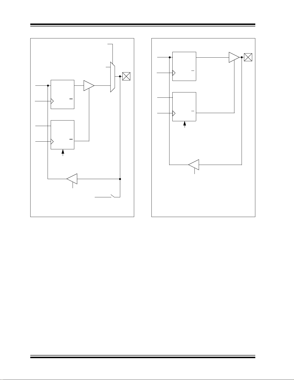
FIGURE 5-4: BLOCK DIAGRAM OF GP2 FIGURE 5-5: BLOCK DIAGRAM OF RB2
Data
Bus
WR
Port
W
Reg
TRIS ‘f’
QD
Data
Latch
CK
CK
T0CS
C1T0CS
ADC Pin Enable
Q
C1OUTEN
QD
TRIS
Latch
Q
Reset
RD Port
C1OUT
T0CKI
0
1
I/O Pin
(1)
Data
Bus
WR
Port
W
Reg
TRIS ‘f’
C1OUT
Data
Latch
CK
C1OUTEN
TRIS
Latch
CK
Reset
ADC Pin Enable
RD Port
0
1
QD
Q
QD
Q
I/O Pin
(1)
ADC
Note 1: I/O pins have protection diodes to VDD and
SS.
V
ADC
Note 1: I/O pins have protection diodes to VDD and
SS.
V
© 2005 Microchip Technology Inc. Preliminary DS41268A-page 31

PIC12F510/16F506
.
r
)
FIGURE 5-6: BLOCK DIAGRAM OF RB4 FIGURE 5-7: BLOCK DIAGRAM OF GP4
RBPU
Data
Data
Bus
WR
Port
W
Reg
TRIS ‘f’
Data
Latch
CK
TRIS
Latch
CK
Reset
QD
Q
FOSC/4
QD
Q
Bus
WR
0
1
I/O
pin
(1
Port
W
Reg
TRIS ‘f’
CK
CK
QD
Data
Latch
Q
QD
TRIS
Latch
Q
Reset
INTOSC/RC
I/O
pin
(1)
INTOSC/RC/EC
CLKOUT Enable
(Note 2)
RD Port
Oscillator
OSC1
Note 1: I/O pins have protection diodes to VDD and VSS
2: Input mode is disabled when pin is used fo
oscillator.
Circuit
RD Port
OSC1
Note 1: I/O pins have protection diodes to VDD and
V
SS.
Oscillator
Circuit
DS41268A-page 32 Preliminary © 2005 Microchip Technology Inc.

PIC12F510/16F506
FIGURE 5-8: BLOCK DIAGRAM OF
RB5/GP5
Data
Bus
WR
Port
W
Reg
TRIS ‘f’
CK
CK
QD
Data
Latch
Q
QD
TRIS
Latch
Q
Reset
(Note 2)
RD Port
I/O
pin
FIGURE 5-9: BLOCK DIAGRAM OF
RC0/RC1
Data
Bus
(1)
WR
Port
W
Reg
TRIS ‘f’
CK
CK
QD
Data
Latch
Q
QD
TRIS
Latch
Q
Reset
Comp Pin Enable
I/O
pin
(1)
SS.
Oscillator
Circuit
OSC2
Note 1: I/O pins have protection diodes to VDD and
V
2: Input mode is disabled when pin is used for
oscillator.
RD Port
COMP2
Note 1: I/O pins have protection diodes to VDD and
V
SS.
© 2005 Microchip Technology Inc. Preliminary DS41268A-page 33
PIC12F510/16F506
)
d
)
FIGURE 5-10: BLOCK DIAGRAM OF RC2 FIGURE 5-11: BLOCK DIAGRAM OF RC3
Data
Bus
WR
Port
W
Reg
TRIS ‘f’
Data
Latch
CK
TRIS
Latch
CK
Reset
VROE
Data
Bus
CVREF
QD
Q
QD
Q
1
0
I/O PIN
(1
WR
Port
W
Reg
TRIS ‘f’
CK
CK
QD
Data
Latch
Q
QD
TRIS
Latch
Q
Reset
RD Port
I/O Pin
(1
RD Port
COMP2
Note 1: I/O pins have protection diodes to VDD and
SS.
V
Note 1: I/O pins have protection diodes to VDD an
VSS.
DS41268A-page 34 Preliminary © 2005 Microchip Technology Inc.

PIC12F510/16F506
)
FIGURE 5-12: BLOCK DIAGRAM OF RC4 FIGURE 5-13: BLOCK DIAGRAM OF RC5
Data
Bus
WR
Port
W
Reg
TRIS ‘f’
Data
Latch
CK
TRIS
Latch
CK
Reset
C2OUT
QD
Q
C2OUTEN
QD
Q
RD Port
0
1
I/O Pin
(1
(1)
Data
Bus
WR
Port
W
Reg
TRIS ‘f’
Data
Latch
CK
TRIS
Latch
CK
Reset
QD
Q
QD
Q
T0CS
RD Port
I/O Pin
T0CKI
Note 1: I/O pins have protection diodes to VDD and
SS.
V
Note 1: I/O pins have protection diodes to VDD and
SS.
V
© 2005 Microchip Technology Inc. Preliminary DS41268A-page 35

PIC12F510/16F506
TABLE 5-1: SUMMARY OF PORT REGISTERS
Address Name Bit 7 Bit 6 Bit 5 Bit 4 Bit 3 Bit 2 Bit 1 Bit 0
(1)
N/A TRISGPIO
N/A TRISB
N/A TRISC
N/A OPTION
N/A OPTION
03h STATUS
03h STATUS
06h GPIO
06h PORTB
07h PORTC
Legend: – = unimplemented read as ‘0’, x = unknown, u = unchanged, q = depends on condition.
Note 1: PIC12F510 only.
2: PIC16F506 only.
3: If Reset was due to wake-up on pin change, then bit 7 = 1. All other Resets will cause bit 7 = 0.
(2)
(2)
(1)
(2)
(1)
(2)
(1)
(2)
(2)
— — I/O Control Register --11 1111 --11 1111
— — I/O Control Register --11 1111 --11 1111
— — I/O Control Register --11 1111 --11 1111
GPWU GPPU T0CS TOSE PSA PS2 PS1 PS0 1111 1111 1111 1111
RBWU RBPU T0CS TOSE PSA PS2 PS1 PS0 1111 1111 1111 1111
GPWUF CWUF PA0 TO PD ZDCC0001 1xxx qq0q quuu
RBWUF CWUF PA0 TO PD ZDCC0001 1xxx qq0q quuu
— — GP5 GP4 GP3 GP2 GP1 GP0 --xx xxxx --uu uuuu
— — RB5 RB4 RB3 RB2 RB1 RB0 --xx xxxx --uu uuuu
— — RC5 RC4 RC3 RC2 RC1 RC0 --xx xxxx --uu uuuu
TABLE 5-2: I/O PIN FUNCTION ORDER OF PRECEDENCE (PIC16F506)
Priority RB0 RB1 RB2 RB3 RB4 RB5
Value on
Power-On
Reset
Value on
All Other
Resets
(3)
(3)
1 AN0/C1IN+ AN1/C1IN- C1OUT Input/MCLR OSC2/CLKOUT OSC1/CLKIN
2 TRISB TRISB AN2 — TRISIO TRISIO
3 — —TRISB— — —
TABLE 5-3: I/O PIN FUNCTION ORDER OF PRECEDENCE (PIC16F506)
Priority RC0 RC1 RC2 RC3 RC4 RC5
1C2IN+C2IN-CV
REF TRISC C2OUT T0CKI
2 TRISC TRISC TRISC —TRISCTRISC
TABLE 5-4: I/O PIN FUNCTION ORDER OF PRECEDENCE (PIC12F510)
Priority GP0 GP1 GP2 GP3 GP4 GP5
1 AN0/C1IN+ AN1/C1IN- C1OUT Input/MCLR OSC2 OSC1/CLKIN
2 TRISIO TRISIO AN2 — TRISIO TRISIO
3 — —T0CKI— — —
4 — —TRISIO— — —
DS41268A-page 36 Preliminary © 2005 Microchip Technology Inc.

PIC12F510/16F506
TABLE 5-5: REQUIREMENTS FOR DIGITAL PIN OPERATION (PIC12F510)
GP0 GP0 GP1 GP1 GP2 GP2 GP3 GP4 GP5
CM1CON0
C1ON 01 0 101
C1PREF — 0 — 1 — — — — —
C1NREF — — — 0 — — — — —
C1T0CS — — — — — 1 — — —
— — —
C1OUTEN
CM2CON0
C2ON
C2PREF1 — — — — — — — — —
C2PREF2 — — — — — — — — —
C2NREF
C2OUTEN
VRCON0
VROE
VREN — — — — — — — — —
OPTION
T0CS
ADCON0
ANS<1:0> 00, 01 00, 01 00, 01, 10 00, 01, 10 00 00 — — —
CONFIG
MCLRE
INTOSC — — — — — — — — —
LP
EXTRC — — — — — — — — Disabled
XT — — — — — — — Disabled Disabled
Note 1: Multiple column entries for a pin demonstrate the different permutations to arrive at digital functionality for
the pin.
2: Shaded cells indicate the bit status does not affect the pins digital functionality.
— — — — — 1 — — —
— — — — — — — — —
— — — — — — — — —
— — — — — — — — —
— — — — — — — — —
— — — — — 0 — — —
— — — — — — — — —
— — — — — — — Disabled Disabled
© 2005 Microchip Technology Inc. Preliminary DS41268A-page 37

PIC12F510/16F506
TA BLE 5-6: REQUIREMENTS FOR DIGITA L PIN OPERATION (PIC16F506 PORTB
RB0 RB0 RB0 RB1 RB1 RB2 RB2 RB3 RB4 RB5
CM1CON0
C1ON
C1PREF
C1NREF — — — — 0 — — — — —
C1T0CS
C1OUTEN
CM2CON0
C2ON 1
C2PREF1 0 — — — — — — — — —
C2PREF2 1
C2NREF — — — — — — — — — —
C2OUTEN
OPTION
T0CS — — — — — — — — — —
ADCON0
ANS<1:0> 00, 01 00, 01 00, 01 00, 01, 10 00, 01, 10 00 00
CONFIG
MCLRE
INTOSC — — — — — — — — — —
LP — — — — — — — — Disabled Disabled
EXTRC
XT — — — — — — — — Disabled Disabled
EC — — — — — — — — — Disabled
HS
INTOSC CLKOUT — — — — — — — — Disabled Disabled
EXTRC CLOCKOUT — — — — — — — — Disabled Disabled
Note 1: Multiple column entries for a pin demonstrate the different permutations to arrive at digital functionality for
the pin.
2: Shaded cells indicate the bit status does not affect the pins digital functionality.
— 01 0 1 01— — —
— — 0 — — — — — — —
— — — — — — — — — —
— — — — — — 1 — — —
— — — — — — — — —
— — — — — — — — —
— — — — — — — — — —
— — — — — — — 0 — —
— — — — — — — — — Disabled
— — — — — — — — Disabled Disabled
(1), (2)
— — —
(1), (2)
TA BLE 5-7: REQUIREMENTS FOR DIGITA L PIN OPERATION (PIC16F506 PORTC)
RC0 RC0 RC1 RC1 RC2 RC3 RC4 RC4 RC5 RC5
CM2CON0
C2ON 0101
C2PREF1 — 0 — — — — — — — —
C2PREF2
C2NREF — — — 0 — — — — — —
C2OUTEN
VRCON0
VROE
OPTION
T0CS — — — — — — — — 0 —
Note 1: Multiple column entries for a pin demonstrate the different permutations to arrive at digital functionality for
the pin.
2: Shaded cells indicate the bit status does not affect the pins digital functionality.
DS41268A-page 38 Preliminary © 2005 Microchip Technology Inc.
— 0 — — — — — — — —
— — — — — — — 1 — —
— — — — 0 — — ———
— — 01— —
PIC12F510/16F506
5.5 I/O Programming Considerations
5.5.1 BI DIREC TION AL I/O PORTS
Some instructions operate internally as read followed
by write operations. For example, the BCF and BSF
instructions read the entire port into the CPU, execute
the bit operation and re-write the result. Caution must
be used when these inst ructions ar e applied to a port
where one or more pins are used as input/ outputs. For
example, a BSF operation on bit 5 of PORTB/ GPIO wil l
cause all eight bit s of PORTB/GPIO to be read into the
CPU, bit 5 to be set a nd th e P ORTB /G P IO val u e to be
written to the output latches. If another bit of PORTB/
GPIO is used as a bidirectional I/O pi n (say bit ‘0’) and
it is defined as an input at this time, the input signal
present on the pin itself wo uld be read into the CPU and
rewritten to the data latch o f this p articular pin , overwriting the previous c ontent. As l ong as the p in stay s in the
Input mode, no problem occurs. However, if bit ‘0’ is
switched into Output mode later on, the content of the
data latch m ay now be unknown.
Example 5-1 shows the effect of two sequential
Read-Modify-Write instructions (e.g., BCF, BSF, etc.)
on an I/O port.
A pin actively outputting a high or a low should not be
driven from external devices at the same time in order
to change the level on this pin (“wired OR”, “wired
AND”). The resulting high out put current s may damag e
the chip.
EXAMPLE 5-1: READ-MODIFY -WRITE
INSTRUCTIONS ON AN
I/O PORT(e.g. PIC16F506)
;Initial PORTB Settings
;PORTB<5:3> Inputs
;PORTB<2:0> Outputs
;
; PORTB latch PORTB pins
; ---------- ----------
BCF PORTB, 5 ;--01 -ppp --11 pppp
BCF PORTB, 4 ;--10 -ppp --11 pppp
MOVLW 007h;
TRIS PORTB ;--10 -ppp --11 pppp
;
Note: The user may have expected the pin values to
be ‘--00 pppp’. The 2nd BCF caused RB5 to
be latched as the pin value (High).
5.5.2 SUCCESSIVE OPERATIONS ON I/O
PORTS
The actual write to a n I/O port happen s at the e nd of an
instructio n cycle. Where as for readi ng, the data mu st
be valid at the beginning of the instruction cycle
(Figure 5-14). Therefore, care must be exercised if a
write followed by a read operation is carried out on the
same I/O port. The sequence of instructions should
allow the pin voltage to stabilize (load dependent)
before the next instruction causes the file to be read
into the CPU. Otherwise, the prev ious state of that pin
may be read into the CPU rather than the new state.
When in doubt, it is better to separate these
instructions with a NOP or another instruction not
accessing this I/O port.
FIGURE 5-14: SUCCESSIVE I/O OPERATION (PIC16F506)
Q1 Q2 Q3 Q4 Q1 Q2 Q3 Q4 Q1 Q2 Q3 Q4 Q1 Q2 Q3 Q4
Instruction
Fetched
RB<5:0>
Instruction
Executed
PC PC + 1 PC + 2
MOVWF PORTB
MOVF PORTB, W
Port pin
written here
MOVWF PORTB
(Write to PORTB)
NOP
Port pin
sampled here
(Read PORTB)
PC + 3
NOP
NOPMOVF PORTB,W
This exampl e sh ows a wr ite to P OR TB f ol lowe d by a
read from PORTB.
Data setup time = (0.25 T
where: T
CY = instruction cycle
T
PD = propagation delay
Therefore, at higher clock frequencies, a
write followed by a read may be problematic.
CY – TPD)
© 2005 Microchip Technology Inc. Preliminary DS41268A-page 39

PIC12F510/16F506
NOTES:
DS41268A-page 40 Preliminary © 2005 Microchip Technology Inc.

PIC12F510/16F506
6.0 TMR0 MODULE AND TMR0 REGISTER
The Timer0 module has the following features:
• 8-bit timer/counter register, TMR0
• Readable and writable
• 8-bit software programmable prescaler
• Internal or external clock select:
- Edge select for external clock
- External clock from either the T0CKI pin or
from the output of the comparator
Figure 6-1 is a simplified block diagram of the Timer0
module.
Timer mode is selected by clearing the T0CS bit
(OPTION<5>). In Timer mode, the Ti mer0 module will
increment every ins tru cti on cy cl e (w i tho ut p r es ca ler). If
TMR0 register is written, the increment is inhibited for
the following two cycles (Figure 6-2 and Figure 6-3).
The user can work around this by writing an adjusted
value to the TMR0 register.
There are two types of Counter mo de. The first Counter
mode uses the T0CKI pin to increment Timer0. It is
selected by setting th e T0CKI bit (OP TION<5>), se tting
the CMPT0CS
COUTEN
increment either on every rising or falling edge of pin
T0CKI. The T0SE bit (OPTION<4>) determines the
source edge. Clearing the T0SE bit selects the rising
edge. Restrictions on the external clock input are
discussed in det ail in Sec tion 6.1 “Using Timer0 With
An External Clock (Feature2)”.
bit (CM1CON0<4>) and setting the
bit (CM1CON0<6>). In this mode , Ti mer0 will
The second Counter mode u ses th e output of the comparator to increment Timer0. It can be entered in two
different ways. The first way is selected by setting the
T0CS bit (OPTION <5>), and c learing the CMP T0CS
(CMCON<4>) (COUTEN
[CMCON<6>] does no t af fect
bit
this mode of operation). This enables an internal
connection between the comparator and the Timer0.
The second way is selected by setting the T0CS bit
(OPTION<5>), setting the CMPT0CS
and clearing the COUTEN
bit (CM1CON0<6>). This
bit (CM1CON0)
allows the output of t he compa rator onto the T0 CKI pin,
while keeping the T0CKI input active. Therefore, any
comparator change on the COUT pin is fed back into
the T0CKI input. The T0SE bit (OPTION<4>) determines the source edge. Clearing the T0SE bit selects
the rising edge. Res trictio ns on t he exte rnal c lock inp ut
as discussed in Section 6.1 “Using Timer0 With An
External Clock (Feature2)”
The prescaler may be used by either the Timer0
module or the Watchdog Timer, but not both. The
prescaler assignment is controlled in software by the
control bit PSA (OPTION<3>). Cleari ng the PSA bit will
assign the prescaler to Timer0. The prescaler is not
readable or writabl e. When the prescaler is assi gned to
the Timer0 module, prescale values of 1:2, 1:4,...,
1:256 are selectable. Section 6.2 “Prescaler” details
the operation of the prescaler.
A summary of registers associated with the Timer0
module is found in Table 6-1.
FIGURE 6-1: TIMER0 BLOCK DIAGRAM
T0CKI
Pin
FOSC/4
Internal
Comparator
Output
Note 1: Bits T0CS, T0SE, PSA, PS2, PS1 and PS0 are located in the OPTION register.
2: The prescaler is shared with the Watchdog Timer (Figure 6-5).
3: Bit CMPT0CS
1
0
CMPT0CS
(1)
T0SE
(3)
is located in the CM1CON0 register, CM1CON0<4>.
0
T0CS
1
(1)
Programmable
Prescaler
3
PS2, PS1, PS0
OUT
PS
1
(2)
0
PSA
(1)
(1)
Sync with
Internal
Clocks
(2 TCY delay)
Data Bus
8
TMR0 Reg
PSOUT
Sync
© 2005 Microchip Technology Inc. Preliminary DS41268A-page 41

PIC12F510/16F506
FIGURE 6-2: TIMER0 TIMING: INTERNAL CLOCK/NO PRESCALE
PC
(Program
Counter)
Instruction
Fetch
Timer0
Instruction
Executed
Q1 Q2 Q3 Q4
PC - 1
T0
Q1 Q2 Q3 Q4 Q1 Q2 Q3 Q4 Q1 Q2 Q3 Q4 Q1 Q2 Q3 Q4 Q1 Q2 Q3 Q4 Q1 Q2 Q3 Q4 Q1 Q2 Q3 Q4
PC PC + 1 PC + 2 PC + 3 PC + 4 PC + 6
MOVWF TMR0 MOVF TMR0,W MOVF TMR0,W MOVF TMR0,W MOVF TMR0,W MOVF TMR0,W
T0 + 1 T0 + 2 NT0
Write TMR0
executed
Read TMR0
reads NT0
Read TMR0
reads NT0
Read TMR0
reads NT0
FIGURE 6-3: TIMER0 TIMING: INTERNAL CLOCK/PRESCALE 1:2
PC
(Program
Counter)
Instruction
Fetch
Timer0
Instruction
Executed
Q1 Q2 Q3 Q4
PC - 1
T0
Q1 Q2 Q3 Q4 Q1 Q2 Q3 Q4 Q1 Q2 Q3 Q4 Q1 Q2 Q3 Q4 Q1 Q2 Q3 Q4 Q1 Q2 Q3 Q4 Q1 Q2 Q3 Q4
PC PC + 1 PC + 2 PC + 3 PC + 4 PC + 6
MOVWF TMR0 MOVF TMR0,W MOVF TMR0,W MOVF TMR0,W MOVF TMR0,W MOVF TMR0,W
T0 + 1 NT0
Write TMR0
executed
Read TMR0
reads NT0
Read TMR0
reads NT0
Read TMR0
reads NT0
PC + 5
NT0 + 1
Read TMR0
reads NT0 + 1
PC + 5
Read TMR0
reads NT0 + 1
NT0 + 2
Read TMR0
reads NT0 + 2
NT0 + 1
Read TMR0
reads NT0 + 2
TABLE 6-1: REGISTERS ASSOCIATED WITH TIMER0
Val ue on
Addr Name Bit 7 Bit 6 Bit 5 Bit 4 Bit 3 Bit 2 Bit 1 Bit 0
Power-On
Reset
01h TMR0 Timer0 – 8-bit Real-Time Clock/Counter xxxx xxxx uuuu uuuu
07h
CM1CON0
08h CM1CON0
N/A OPTION
N/A TRISGPIO
(2)
C1OUT C1OUTEN C1POL C1T0CS C1ON C1NREF C1PREF C1WU
(3)
C1OUT C1OUTEN C1POL C1T0CS C1ON C1NREF C1PREF C1WU 1111 1111 uuuu uuuu
GPWU GPPU T0CS T0SE PSA PS2 PS1 PS0 1111 1111 1111 1111
(1)
— — I/O Control Register ---- 1111 --11 1111
1111 1111 uuuu uuuu
Legend: Shaded cells not used by Timer0, – = unimplemented, x = unknown, u = unchanged.
Note 1: The TRIS of the T0CKI pin is overridden when T0CS = 1.
2: For PIC12F510.
3: For PIC16F506.
Val ue on
All Other
Resets
DS41268A-page 42 Preliminary © 2005 Microchip Technology Inc.

PIC12F510/16F506
6.1 Using Timer0 With An External
Clock (Feature2)
When an external clock input i s used for T i mer0, it must
meet certain requ ir e me nts. The ex t er na l cl oc k req u ir ement is due to internal phas e clock (TOSC) synchroniza-
tion. Also, there is a dela y in the ac tual inc remen ting of
Timer0 after synchronization.
When a prescaler is used, the external clock input is
divided by the asynchronous ripple counter-type
prescaler, so that t he presc aler out put is symmetric al.
For the external clock to meet the sampling requirement, the ripple counter must be taken into ac count.
Therefore, it is necessary for T0CKI or the comparator
output to ha ve a peri od of at least 4T
RC delay of 4Tt0H) divid ed by the pres caler valu e. The
only requirement on T0CKI or the comparator output
6.1.1 EXT ERN AL CLOC K
SYNCHRONIZATION
When no pr escal er is us ed, t he ex ternal clock inpu t is
the same as the prescaler outp ut. Th e synchronization
of an external clock with the internal phase clocks is
accomplished by sampling the prescaler output on the
Q2 and Q4 cycles of the internal phase clocks
(Figure 6-4). Therefore, it is necessary for T0CKI or the
comparator output to be high for at least 2T
small RC delay of 2Tt0H) and low for at least 2T
(and a small RC dela y of 2Tt 0H). R efer to the electri cal
specification of the desired device.
OSC (and a
OSC
high and low time is that they do not violate the
minimum pulse width requirement of Tt0H. Refer to
parameters 40 , 41 a nd 42 in the electrical specification
of the desired device.
6.1.2 TIMER0 INCREMENT DELAY
Since the prescaler output is synchronized with the
internal clocks, there is a small delay from the time the
external clock edge occurs to the time the Timer0
module is actually incremented. Figure 6-4 shows the
delay from the external clock edge to the timer
incrementing.
FIGURE 6-4: TIMER0 TIMING WITH EXTERNAL CLOCK
Q1 Q2 Q3 Q4 Q1 Q2 Q3 Q4 Q1 Q2 Q3 Q4 Q1 Q2 Q3 Q4
External Clock Input or
Prescaler Output
External Clock/Prescaler
Output After Sampling
(2)
(1)
(3)
OSC (and a small
Small pulse
misses sampling
Increment Timer0 (Q4)
Timer0
Note 1: Delay from clock input change to Timer0 increment is 3T
in measuring the interval between two edges on Timer0 input = ±4T
2: External clock if no prescaler selected; prescaler output otherwise.
3: The arrows indicate the points in time where sampling occurs.
6.2 Prescaler
An 8-bit counter is available as a prescaler for the
Timer0 module or as a postscaler for the Watchdog
Timer (WDT), respectiv ely (see Section FIGURE 10-
12: “Watchdog Timer Block Diagram”). For simplicity, this counter is being referred to as “prescaler”
throughout this data sheet.
Note: The prescaler may be used by either the
Timer0 module or the WDT, but not both.
Thus, a prescaler assignment for the
Timer0 module means that there is no
prescaler for the WDT and vice-versa.
T0 T0 + 1 T0 + 2
OSC to 7TOSC. (Duration of Q = TOSC). Therefore, the error
OSC max.
The PSA and PS<2:0> bits (OPTION<3:0>) determine
prescaler assignment and prescale ratio.
When assigned to the Timer0 module, all instructions
writing to the TMR0 register (e.g., CLRF 1,
MOVWF 1, BSF 1, x, etc.) will clear the prescaler.
When assigned to WDT, a CLRWDT instruction will clear
the prescaler along with the WDT. The prescaler is
neither readable nor writable. On a Reset, the
prescaler contains all ‘0’s.
© 2005 Microchip Technology Inc. Preliminary DS41268A-page 43

PIC12F510/16F506
6.2.1 SWITCHIN G PRESCALE R
ASSIGNMENT
The prescaler assignment is fully under software
control (i. e., it can b e changed “ on-the- fly” dur ing program execution). To avoid an unintended de vice Rese t,
the following instruction sequence (Example6-1) must
be executed when changing the prescaler assignment
To change prescaler from the WDT to the Timer0
module, use the se quence show n in Examp le 6-2. This
sequence must be us ed ev en if th e WDT is disab led. A
CLRWDT instruction should be executed before
switching the prescaler.
EXAMPLE 6-2: CHANGIN G PRESCALER
from Timer0 to the WDT.
CLRWDT ;Clear WDT and
EXAMPLE 6-1: CHANGING PRESCALER
(TIMER0 → WDT)
CLRWDT ;Clear WDT
CLRF TMR0 ;Clear TMR0 & Prescaler
MOVLW ‘00xx1111’b ;These 3 lines (5, 6, 7)
OPTION ;are required only if
;desired
CLRWDT ;PS<2:0> are 000 or 001
MOVLW ‘00xx1xxx’b ;Set Postscaler to
OPTION ;desired WDT rate
MOVLW ‘xxxx0xxx’ ;Select TMR0, new
OPTION
FIGURE 6-5: BLOCK DIAGRAM OF THE TIMER0/WDT PRESCALER
(2)
T0CKI
Pin
Comparator
Output
TCY (= FOSC/4)
1
0
0
M
U
X
1
1
M
U
X
0
(WDT→TIMER0)
;prescaler
;prescale value and
;clock source
Data Bus
Sync
2
Cycles
TMR0 Reg
8
(1)
T0SE
CMPT0CS
Watchdog
WDT Enable bit
Note 1: T0CS, T0SE, PSA, PS<2:0> are bits in the OPTION register.
2: T0CKI is shared with pin GP2 on the PIC12F510 and shared with RC5 on the PIC16F506.
3: Bit CMPT0CS
(3)
0
M
U
X
1
Timer
(1)
PSA
is located in the CM1CON0 register.
T0CS
(1)
8-bit Prescaler
8 - to - 1 MUX
0
Time-Out
8
MUX
WDT
1
PSA
(1)
PS<2:0>
(1)
PSA
(1)
DS41268A-page 44 Preliminary © 2005 Microchip Technology Inc.

PIC12F510/16F506
7.0 COMPARATOR(S)
The PIC12F510 contains one analog comparator
module. The PIC16F506 contains two comparators
and a comparator vol t ag e refe ren ce. The s ec ond com parator is designed to give the device some additional
comparator functionality.
REGISTER 7-1: CM1CON0 REGISTER (ADDRESS: 07h) (PIC12F510)
R-1 R/W-1 R/W-1 R/W-1 R/W-1 R/W-1 R/W-1 R/W-1
C1OUT C1OUTEN
bit 7 bit 0
bit 7 C1OUT: Comparator Output bit
IN+ > VIN-
1 = V
IN+ < VIN-
0 = V
bit 6 C1OUTEN: Comparator Output Enable bit
1 = Output of comparator is NOT placed on the C1OUT pin
0 = Output of comparator is placed in the C1OUT pin
bit 5 C1POL: Comparator Output Polarity bit
1 = Output of comparator not inverted
0 = Output of comparator inverted
bit 4 C1 T0CS
: Comparator TMR0 Clock Source bit
1 = TMR0 clock source selected by T0CS control bit
0 = Comparator output used as TMR0 clock source
bit 3 C1ON: Comparator Enable bit
1 = Comparator is on
0 = Comparator is off
bit 2 C1NREF: Comparator Negative Reference Select bit
1 = CIN- pin
0 = V
REF
bit 1 C1PREF: Comparator Positive Reference Select bit
1 = CIN+ pin
0 = CIN- pin
bit 0 C1WU
: Comparator Wake-up On Change Enable bit
1 = Wake-up On Comp arator Change is disabled
0 = Wake-up On Comp arator Change is enabled.
Note 1: Overrides T0CS bit for TRIS control of GP2
2: When comparator turned on, these control bits assert themselves. Otherwise, the
other registers have precedence.
Legend:
R = Readable bit W = Writable bit U = Unimplemented bit, read as ‘0’
-n = Value at POR ‘1’ = Bit is set ‘0’ = Bit is cleared x = Bit is unknown
C1POL C1T0CS C1ON C1NREF C1PREF C1WU
(1), (2)
(2)
(2)
(2)
(2)
(2)
© 2005 Microchip Technology Inc. Preliminary DS41268A-page 45

PIC12F510/16F506
REGISTER 7-2: CM1CON0 REGISTER (ADDRESS: 08h) (PIC16F506)
R-1 R/W-1 R/W-1 R/W-1 R/W-1 R/W-1 R/W-1 R/W-1
C1OUT C1OUTEN
bit 7 bit 0
bit 7 C1OUT: Comparator Output bit
IN+ > VIN-
1 = V
IN+ < VIN-
0 = V
bit 6 C1OUTEN: Comparator Output Enable bit
1 = Output of comparator is NOT placed on the C1OUT pin
0 = Output of comparator is placed in the C1OUT pin
bit 5 C1POL: Comparator Output Polarity bit
1 = Output of comparator not inverted
0 = Output of comparator inverted
bit 4 C1 T0CS
: Comparator TMR0 Clock Source bit
1 = TMR0 clock source selected by TOCS control bit
0 = Comparator output used as TMR0 clock source
bit 3 C1ON: Comparator Enable bit
1 = Comparator is on
0 = Comparator is off
bit 2 C1NREF: Comparator Negative Reference Select bit
1 = CIN- pin
0 = V
REF
bit 1 C1PREF: Comparator Positive Reference Select bit
1 = CIN+ pin
0 = CIN- pin
bit 0 C1WU
: Comparator Wake-up On Change Enable bit
1 = Wake-up On Comp arator Change is disabled
0 = Wake-up On Comp arator Change is enabled.
Note 1: Overrides T0CS bit for TRIS control of RC5
2: When comparator turned on, these control bits assert themselves. Otherwise, the
other registers have precedence.
Legend:
R = Readable bit W = Writable bit U = Unimplemented bit, read as ‘0’
-n = Value at POR ‘1’ = Bit is set ‘0’ = Bit is cleared x = Bit is unknown
C1POL C1T0CS C1ON C1NREF C1PREF C1WU
(1), (2)
(2)
(2)
(2)
(2)
(2)
DS41268A-page 46 Preliminary © 2005 Microchip Technology Inc.

PIC12F510/16F506
REGISTER 7-3: CM2CON0 REGISTER (ADDRESS: 0Bh) (PIC16F506)
R-1 R/W-1 R/W-1 R/W-1 R/W-1 R/W-1 R/W-1 R/W-1
C2OUT C2OUTEN
bit 7 bit 0
bit 7 C2OUT: Comparator Output bit
IN+ > VIN-
1 = V
IN+ < VIN-
0 = V
bit 6 C2OUTEN: Comparator Output Enable bit
1 = Output of comparator is NOT placed on the C2OUT pin
0 = Output of comparator is placed in the C2OUT pin
bit 5 C2POL: Comparator Output Polarity bit
1 = Output of comparator not inverted
0 = Output of comparator inverted
bit 4 C2PREF2: Comparator Posi tive Reference Select bit
1 = C1IN+ pin
0 = C2IN- pin
bit 3 C2ON: Comparator Enable bit
1 = Comparator is on
0 = Comparator is off
bit 2 C2NREF: Comparator Negative Reference Select bit
1 = C1IN- pin
0 = V
REF
bit 1 C2PREF1: Comparator Positive Reference Select bit
1 = C2IN+ pin
0 = C2PREF2 controls analog input selection
bit 0 C
2WU: Comparator Wake-up on Change Enable bit
1 = Wake-up on Comparator change is disabled
0 = Wake-up on Comparator change is enabled.
Note 1: Overrides TOCS bit for TRIS control of RC4.
2: When comparator turned on, these control bits assert themselves. Otherwise, the
other registers have precedence.
Legend:
R = Readable bit W = Writable bit U = Unimplemented bit, read as ‘0’
-n = Value at POR ‘1’ = Bit is set ‘0’ = Bit is cleared x = Bit is unknown
C2POL C2PREF2 C2ON C2NREF C2PREF1 C2WU
(1), (2)
(2)
(2)
(2)
(2)
(2)
© 2005 Microchip Technology Inc. Preliminary DS41268A-page 47

PIC12F510/16F506
FIGURE 7-1: BLOCK DIAGRAM OF THE COMPARATOR FOR THE PIC12F510
C1PREF
C1IN-
C1IN+
C2NREF
0
MUX
RD_CM2CON0
1
DQ
C1ON
Q3*RD_CM1CON0
(1)
NRESET
EN
CL
C1WU
C1 Output Enable
To
Data Bus
C1WUF
C1IN-
0.6 VREF
1
MUX
0
+
C1
C1OUT
C1POL
Note 1: When C1ON = 0, the C1 comparator will produce a ‘0’ output to the XOR Gate.
FIGURE 7-2: BLOCK DIAGRAM OF THE COMPARATOR FOR THE PIC16F506
RD_CM2CON0
NRESET
C2OUT
DQ
EN
CL
C2WU
C2 Output Enable
C1IN+
C2IN-
C2PREF2
C2PREF1
(1)
C2ON
C2NREF
1
C2VN
C2VP
+
C2
-
C2POL
MUX
0
1
C2IN+
1
MUX
0
C2IN-
Q3*RD_CM2CON0
C1OUT
To
Data Bus
C2WUF
C2OUT
CV
REF
Note 1: When C2ON = 0, the C2 comparator will produce a ‘0’ output to the XOR Gate.
MUX
0
DS41268A-page 48 Preliminary © 2005 Microchip Technology Inc.

7.1 Comparator Operation
A single comparator is shown in Figure 7-3 along with
the relationship between the analog input levels and
the digital output . When the analo g input a t V
than the analog input V
is a digital low level. The shaded area of the output of
the comparator in Figure 7-3 represent the uncertainty
due to input offse ts and respo nse time. See Table 13-1
for Common Mode Voltage.
IN-, the output of the compara tor
FIGURE 7-3: SINGLE COMPARATOR
VIN+
IN-
V
+
–
IN+ is less
Result
PIC12F510/16F506
Note: Analog levels on any pin that is defin ed as
a digital input may cause the input buffer
to consume more current than is specified.
7.5 Comparator Wake-up Flag
The Comparator Wake-up Flag is set whenever all of
the following conditions are met:
1WU = 0 (CM1CON0<0>) or
•C
= 0 (CM2CON0<0>)
C2WU
• CM1CON0 or CM2CON0 has been read to latch
the last known state of the CMPOUT bit (MOVF
CM1CON0, W)
• Device is in Sleep
• The output of the comparator has changed state
The wake-up flag may be cleared in software or by
another device Reset.
VIN-
VIN+
Result
7.2 Comparator Reference
An internal reference signa l may be used depend ing on
the comparator operatin g mode. T he analo g signal th at
is present at V in- is c ompa red to the signal a t V in+, and
the digital outpu t of the com parator is adjusted accordingly (Figure 7-3). Please see Section 8.0 “Compara-
tor Voltage Reference Module” for internal reference
specifications.
7.3 Comparator Response Time
Response time is the minimum time after selecting a
new reference voltage or input source before the comparator output is to ha ve a valid level. If the co mpara tor
inputs are changed, a delay must be used to allow the
comparator to settle to its new state. Please see
Table 13-1 for comparator response time
specifications.
7.4 Comparator Output
The comparator output is read through the CM1CON0
or CM2CON0 register. This bit is read-only. The
comparator output may also be used internally, see
Figure 7-3.
7.6 Comparator Operation During
Sleep
When the compa rator is activ e and the devi ce is place d
in Sleep mode, the comparator remains active. While
the comparator is powered-up, higher Sleep currents,
shown in the power-down current specification, will
occur. To minimize power consumption while in Sleep
mode, turn off the comparator before entering Sleep.
7.7 Effects of Reset
A POR Reset forces the CM2CON0 register to its
Reset state. This forces the Comparator module to be
in the comparator Reset mode. This ensures that all
potential inputs are analog inputs. Device current is
minimized when analog inputs are present at Reset
time. The comp arat or w il l be powe r ed-d own d uri ng th e
Reset interval.
7.8 Analog Input Connection
Considerations
A simplified circuit for an analog input is shown in
Figure 7-4. Since the analog pins are connected to a
digital output, they have reverse biased diodes to VDD
and VSS. The analog input, th erefore, must be b etween
V
SS and VDD. If the input voltage deviates from this
range by more than 0.6V in either direction, one of the
diodes is forward biased and a latch-up may occur. A
maximum source impedance of 10 kΩ is recommended for the analog sources. Any external component connected to an analog input pin, such as a
capacitor or a Zener diode, should have very little
leakage current.
© 2005 Microchip Technology Inc. Preliminary DS41268A-page 49

PIC12F510/16F506
FIGURE 7-4: ANALOG INPUT MODE
VDD
R
VA
S < 10 K
VT = 0.6V
A
IN
CPIN
5pF
VT = 0.6V
ILEAKAGE
±500 nA
V
SS
RIC
Legend: CPIN = Input Capacitance
T = Threshold Voltage
V
LEAKAGE = Leakage Current at the Pin
I
R
IC = I nterconnect Resistance
S = Source Impedance
R
VA = Analog Voltage
TABLE 7-1: REGISTERS ASSOCIATED WITH COMPARATOR MODULE
Add Name Bit 7 Bit 6 Bit 5 Bit 4 Bit 3 Bit 2 Bit 1 Bit 0
03h STATUS GPWUF CWUF
07h CM1CON0
08h CM1CON0
0Bh CM2CON0
N/A TRISB
N/A TRISC
N/A TRISGPIO
Legend: x = Unknown, u = Unchanged, – = Unimplemented, read as ‘0’, q = Depends on condition.
Note 1: PIC12F510 only.
2: PIC16F506 only.
(1)
C1OUT C1OUTEN C1POL C1T0CS C1ON C1NREF C1PREF C1WU 1111 1111 uuuu uuuu
(2)
C1OUT C1OUTEN C1POL C1T0CS C1ON C1NREF C1PREF C1WU 1111 1111 uuuu uuuu
(2)
(2)
(2)
C2OUT C2OUTEN C2POL C2PREF2 C2ON C2NREF C2PREF1 C2WU 1111 1111 uuuu uuuu
— — I/O Control Register --11 1111 --11 1111
— — I/O Control Register --11 1111 --11 1111
(1)
— — I/O Control Register --11 1111 --11 1111
—TOPD ZDCC0001 1xxx qq0q quuu
Value on
POR
Val ue on
All Other
Resets
DS41268A-page 50 Preliminary © 2005 Microchip Technology Inc.

PIC12F510/16F506
8.0 COMPARATOR VOLTAGE REFERENCE MODULE
The Comparator Voltage Reference module also
allows the selection of an internally generated voltage
reference for one of the comparator inputs. The
VRCON register (Register 8-1) controls the Voltage
Reference module shown in Figure 8-1.
8.1 Configuring The Voltage
Reference
The voltage reference can output 32 distinct voltage
levels; 16 in a high range and 16 in a low range.
Equation 8-1 determines the output voltages:
EQUATION 8-1:
VRR = 1 (low range): CVREF = (VR3:VR0/24) x VDD
VRR = 0 (high range):
CV
REF = (VDD/4) + (VR3:VR0 x VDD/32)
8.2 Voltage Reference Accuracy/Error
The full range of VSS to VDD cannot be realized due to
construction of the module. The transistors on the top
and bottom of the resistor ladder network (Figure 8-1)
keep CV
tion is when the module is disabled by clearing the
VREN bit (VRCON<7>). When disabl ed, the reference
voltage is V
(VRCON<5>) bit is set. This allows the comparator to
detect a zero-crossing and not consume the CV
module current.
The voltage reference is V
the CV
The tested absolute accuracy of the comparator
voltage reference can be found in Section 13.2 “DC
Characteristics: PIC12F510/16F506 (Extended)” .
REF from approaching VSS or VDD. The exce p-
SS when VR<3:0> is ‘0000’ and the VRR
REF output changes with fluctuations in VDD.
REGISTER 8-1: VRCON – PIC16F506 ONLY (ADDRESS: 0Ch)
R/W-0 R/W-0 R/W-1 U-0 R/W-1 R/W-1 R/W-1 R/W-1
VREN VROE VRR — VR3 VR2 VR1 VR0
bit 7 bit 0
REF
DD derived and, therefore,
bit 7 VREN: CV
1 = CVREF is powered on
0 = CV
bit 6 VROE: CVREF Output Enable b it
1 = VREF output is enabled
0 = V
bit 5 VRR: CV
1 = Low range
0 = High range
bit 4 Unimplemented: Read as ‘0’
bit 3-0 VR<3:0> CV
When VRR = 1: CVREF= (VR<3:0>/24)*VDD
When VRR = 0: CVREF= VDD/4+(VR<3:0>/32)*VDD
Note 1: When this bit is set, the TRIS for the VREF pin is overridden and the analog volt age
Legend:
R = Readable bit W = Writable bit U = Unimplemented bit, read as ‘0’
-n = Value at POR ‘1’ = Bit is set ‘0’ = Bit is cleared x = Bit is unknown
REF Enable bit
REF is powered down, no current is drawn
REF output is disabled
REF Range Selection bit
REF Value Selection bit
is placed on the V
REF controls for ratio me tric ref erence appli es to C ompa rato r 2 on the PIC 12F50 6
2: V
only.
REF pin.
(1)
© 2005 Microchip Technology Inc. Preliminary DS41268A-page 51

PIC12F510/16F506
FIGURE 8-1: COMPARATOR VOLTAGE REFERENCE BLOCK DIAGRAM
16 Stages
8R R R
RR
VDD
8R
16-1 Analog
VREN
MUX
CVREF to
Comparator
Input
RC3/VREF
VR3:VR0
VREN
VR3:VR0 = ‘0000’
VRR
TABLE 8-1: REGISTERS ASSOCIATED WITH COMPARATOR VOLTAGE REFERENCE
Add Name Bit 7 Bit 6 Bit 5 Bit 4 Bit 3 Bit 2 Bit 1 Bit 0
0Ch VRCON VREN VROE VRR
(1)
07h CM1CON0
08h CM1CON0
0Bh CM2CON0
Legend: x = unknown, u = unchanged, – = unimplemented, read as ‘0’.
Note 1: PIC12F510 only.
2: PIC16F506 only.
C1OUT C1OUTEN C1POL C1T0CS C1ON C1NREF C1PREF C1WU 1111 1111 uuuu uuuu
(2)
C1OUT C1OUTEN C1POL C1T0CS C1ON C1NREF C1PREF C1WU 1111 1111 uuuu uuuu
(2)
C2OUT C2OUTEN C2POL C2PREF2 C2ON C2NREF C2PREF1 C2WU 1111 1111 uuuu uuuu
— VR3 VR2 VR1 VR0 001- 1111 001- 1111
Value on
POR
VRR
Value on all
other Resets
DS41268A-page 52 Preliminary © 2005 Microchip Technology Inc.

9.0 ANALOG-TO-DIGITAL (A/D) CONVERTER
The A/D Converter allows conversion of an analog
signal into an 8-bit digital signal.
9.1 Clock Divisors
The ADC has 4 clock source settings ADCS<1:0>.
There are 3 divisor values 32, 16 and 8. The fourth setting is INTOSC with a divisor of 4. These settings will
allow a proper conv ersion when usin g an external os cillator at speeds from 20 MHz to 350 kHz. Using an
external oscillator at a frequency below 350 kHz
requires the ADC oscillator setting to be INTOSC/8 for
valid ADC results.
The ADC requires 13 T
conversion. The div isor values do no t affect the nu mber
of TAD periods required to perform a conversion. The
divisor values determine the length of the T
When the ADCS<1:0> bits are changed while an ADC
conversion is in pro cess, the new ADC c lock source will
not be selected un til the next co nversion is st arted. This
clock source selection will be lost when the device
enters Sleep.
Note: The ADC clock is derived from the instruc-
tion clock. The ADCS divisors are then
applied to create the ADC clock
9.1.1 VOLTAGE REFERENCE
There is no external vo ltage reference for the ADC. The
ADC reference voltage will always be V
9.1.2 ANALOG MODE SELECTION
The ANS<1:0> bits are used to configure pins for analog input. Upon any Reset ANS<1:0> defaults to 11.
This configures pins AN0, AN1 and AN2 as analog
inputs. The comparator output C1OUT will override
AN2 as an input if the comparator output is enabled.
Pins configured as analog inputs are not available for
digital output. Users should not change the ANS bits
while a conversion is in process. ANS bits are active
regardless of the condition of ADON.
AD periods to complete a
AD period.
DD.
PIC12F510/16F506
Note: It is the users responsibility to ensure that
use of the ADC and comparator simultaneously on the same pin, does not
adversely affect the signal being
monitored or adversely effect device
operation.
When the CHS<1:0> bits are changed during an ADC
conversion, the new channel will not be selected until
the current conversion is completed. This allows the
current conversion to complete with valid results. All
channel selection information will be lost when the
device enters Sleep.
TABLE 9-1: CHANNEL SELECT (ADCS)
BITS AFTER AN EVENT
Event ADCS<1:0>
MCLR 11
Conversion complete d CS<1:0>
Conversion terminated CS<1:0>
Power-on 11
Wake from Sleep 11
9.1.4 THE GO/DON E
The GO/DONE bit is used to determine the status of a
conversion, to start a co nversion and to m anually halt a
conversion in process. Setting the GO/DONE
a conversion. When the conversion is complete, the
ADC module clears the GO/DONE bit. A conversion
can be terminated by manually clearing the GO/DONE
bit while a conversio n is in proce ss. Manual term ination
of a conversion may result in a partially converted
result in AD RES.
The GO/DONE
Sleep, stopping the cu rrent conve rsion. Th e ADC doe s
not have a dedicate d oscill ator , i t runs of f of t he instruction clock. There fore, no conve rsion ca n occur in sl eep.
The GO/DONE
bit is cleared when the device enters
bit cannot be set when ADON is clear.
BIT
bit starts
9.1.3 ADC CHANNEL SELECTION
The CHS bits are used to select the analog channel to
be sampled by th e ADC. The CHS<1:0> bits ca n be
changed at any time without adversely effecting a conversion. To acquire an analog signal the CHS<1:0>
selection must match one of the pin(s) selected by the
ANS<1:0> bits. When the ADC is on (ADON = 1) and a
channel is selected that is also being used by the
comparator, then both the comparato r and the ADC will
see the analog voltage on the pin.
© 2005 Microchip Technology Inc. Preliminary DS41268A-page 53

PIC12F510/16F506
9.1.5 SLEEP
This ADC does not have a dedicated ADC clock, and
therefore, no conversion in Sleep is possible. If a
conversion is underway and a Sleep command is
executed, the GO/DONE
This will stop any conversion in process and powerdown the ADC module to conserve power. D ue to the
nature of the conv ersion process, the ADRES may contain a partial conversion. At least 1 bit must have been
converted prior t o Sleep to ha ve partia l conversi on data
in ADRES. The ADCS and CHS bits are reset to their
default condition; ANS<1: 0> = 11 and CHS<1: 0> = 11.
TABLE 9-2: TAD FOR ADCS SETTINGS WITH VARIOUS OSCILLATORS
Source
INTOSC 11 8.5μs1μs
FOSC 10 8
FOSC 01 16 .4 μs.5μs1μs2μs8μs16μs23μs40μs 80 μs 250 μs
FOSC 00 32 .8 μs1μs2μs4μs16μs32μs46μs
ADCS
<1:0>
and ADON bit will be cleared.
Divisor
20
MHz
.2 μs .25 μs.5μs1μs4μs8μs11μs20μs40μs 125 μs
16
MHz
8MHz 4MHz 1MHz
500
kHz
350
kHz
200
kHz
80 μs 160 μs 500 μs
100
kHz
32 kHz
For accurate conversions, T AD must meet the followi ng:
•500ns < T
•TAD = 1/(FOSC/divisor)
Shaded areas indicate T
conversions. If analog input is desired at these
frequencies, use INTOSC/8 for the ADC clock source.
AD < 50 μs
AD out of range for ac curate
9.1.6 ANALOG CONVERSION RESULT
REGISTER
The ADRES register contains the results of the last
conversion. These results are present during the sampling period of the next analog conversion process.
After the sampling period is over, ADRES is cleared
(= 0). A ‘leading one’ is then right shifted into the
ADRES to serve as an internal conversion complete
bit. As each bit weight, starting with the MSB, is converted, the leading one is shifted right and the converted bit is stuffed into ADRES. After a total of 9 right
shifts of the ‘l eading on e’ have t aken pl ace, the conversion is complete ; the ‘ leadin g one ’ has been shifte d out
and the GO/DONE
If the GO/DONE
version, the conversion stops. The data in ADRES is
the partial conv ersion result. This data is valid for the b it
weights that h ave bee n conv erte d. The po siti on of t he
‘leading one’ determines the number of bits that have
been converted. The bits that were not converted
before the GO/DONE
bit is cleared.
bit is cleared in software during a co n-
was cleared are unrecoverable.
DS41268A-page 54 Preliminary © 2005 Microchip Technology Inc.

REGISTER 9-1: ADCON0 REGIST ER
R/W-1 R/W-1 R/W-1 R/W-1 R/W-1 R/W-1 R/W-0 R/W-0
ANS1 ANS0 ADCS1 ADCS0 CHS1 CHS0 GO/DONE
bit 7 bit 0
PIC12F510/16F506
ADON
bit 7-6 ANS<1:0>: ADC Analog Input Pin Select bits for PIC16F506
00 = No pins configured for analog input
01 = GP2/AN2 configured as an analog input
10 = GP2/AN2 and GP0/AN0 configured as analog inputs.
11 = GP2/AN2, GP1/AN1 and GP0/AN0 configured as analog inputs
bit 5-4 ADCS<1:0>: ADC Conversion Clock Select bits
OSC/32
00 = F
01 = F
OSC/16
OSC/8
10 = F
11 = INTOSC/8
bit 3-2 CHS<1:0>: ADC Channel Select bits for PIC16F506
00 = Channel 00 (GP0/AN0)
01 = Channel 01 (GP1/AN1)
10 = Channel 02 (GP2/AN2)
11 = 0.6V absolute voltage reference
bit 1 GO/DONE
1 = ADC conversion in progress. Setting this bit starts an ADC conversio n cycle. This bit is
0 = ADC conversion completed/not in progress. Manually clearing this bit while a conversion
bit 0 ADON: ADC Enable bit
1 = ADC module is operating
0 = ADC module is shut-off and consumes no power
Note 1: On the PIC16F506, the term is RBx, on PIC12F510, the term is GPx.
: ADC Conversion Status bit
automatically cleared by hardware when the ADC is done converting.
is in process terminates the current conversion.
2: When the ANS bits are set, the channels selected will automatica lly be forced into
Analog mode, regardless of the pin fu nction pre viously defi ned. The on ly excep tion
to this is the comparator, where the analog input to the comparator and the ADC
will be active at the s am e ti me . It i s t he users responsibility to ensure that th e ADC
loading on the comparat or input does not affect their application
3: The ANS<1:0> bits are active regardless of the condition of ADON.
4: CHS<1:0> bits default to 11 after any Reset.
5: If the ADON bit is clear, the GO/DONE
6: C1OUT when enabled, overrides AN2.
(5)
(4), (6)
bit cannot be set.
(1), (2), (3), (6)
Legend:
R = Readable bit W = Writable bit U = Unimplemented bit, read as ‘0’
-n = Value at POR ‘1’ = Bit is set ‘0’ = Bit is cleared x = Bit is unknown
© 2005 Microchip Technology Inc. Preliminary DS41268A-page 55

PIC12F510/16F506
;
REGISTER 9-2: ADRES REGISTER
R/W-1 R/W-1 R/W-1 R/W-1 R/W-1 R/W-1 R/W-0 R/W-0
ADRES7 ADRES6 ADRES5 ADRES4 ADRES3 ADRES2 ADRES1 ADRES0
bit 7 bit 0
Legend:
R = Readable bit W = Writable bit U = Unimplemented bit, read as ‘0’
- n = Value at POR ‘1’ = Bit is set ‘0’ = Bit is cleared x = Bit is unknown
REGISTER 9-3: EFFECTS OF SLEEP UPON ADRES0
ANS1 ANS0 ADCS1 ADCS0 CHS1 CHS0 GO/DONE
Entering
Sleep
Wake or
Reset
Unchanged Unchanged 111100
11111100
ADON
EXAMPLE 9-1: PERFORMIN G AN
ANALOG-TO-DIGITAL
CONVERSION
Sample code operates out of BANK0
MOVLW 0xF1 ;configure A/D
MOVWF ADCON0
loop0 BTFSC ADCON0, 1;wait for ‘DONE’
loop1 BTFSC ADCON0, 1;wait for ‘DONE’
loop2 BTFSC ADCON0, 1;wait for ‘DONE’
BSF ADCON0, 1 ;start conversion
GOTO loop0
MOVF ADRES, W ;read result
MOVWF result0 ;save result
BSF ADCON0, 2 ;setup for read of
;channel 1
BSF ADCON0, 1 ;start conversion
GOTO loop1
MOVF ADRES, W ;read result
MOVWF result1 ;save result
BSF ADCON0, 3 ;setup for read of
BCF ADCON0, 2 ;channel 2
BSF ADCON0, 1 ;start conversion
GOTO loop2
MOVF ADRES, W ;read result
MOVWF result2 ;save result
EXAMPLE 9-2: CHANNEL SELECTION
CHANGE DURING
CONVERSION
MOVLW 0xF1 ;configure A/D
MOVWF ADCON0
BSF ADCON0, 1 ;start conversion
BSF ADCON0, 2 ;setup for read of
;channel 1
loop0 BTFSC ADCON0, 1;wait for ‘DONE’
GOTO loop0
MOVF ADRES, W ;read result
MOVWF result0 ;save result
BSF ADCON0, 1 ;start conversion
BSF ADCON0, 3 ;setup for read of
BCF ADCON0, 2 ;channel 2
loop1 BTFSC ADCON0, 1;wait for ‘DONE’
GOTO loop1
MOVF ADRES, W ;read result
MOVWF result1 ;save result
BSF ADCON0, 1 ;start conversion
loop2 BTFSC ADCON0, 1;wait for ‘DONE’
GOTO loop2
MOVF ADRES, W ;read result
MOVWF result2 ;save result
CLRF ADCON0 ;optional: returns
;pins to Digital mode and turns off
;the ADC module
DS41268A-page 56 Preliminary © 2005 Microchip Technology Inc.

PIC12F510/16F506
10.0 SPECIAL FEATURES OF THE CPU
What sets a mic rocontroller apart from other processors are special circuits that deal with the n eeds of rea ltime applications. The PIC12F510/16F506
microcontrollers have a host of such features intended
to maximize syst em reliability, minimize cost through
elimination of external components, provide powersaving operating modes and offer code protection.
These features are:
• Oscillator Selection
• Reset:
- Power-on Reset (P OR)
- Device Reset Timer (DR T)
- Wake-up from Sleep on Pin Change
• Watchdog Timer (WDT)
• Sleep
• Code Protection
• ID Locations
• In-Circuit Serial Programming™ (ICSP™)
•Clock Out
The PIC12F510/16F506 devices have a Watchdog
Timer, which can be shut off only thr ough Configur ation
bit WDTE. It runs off of its own RC oscillator for added
reliability . If using HS (PIC16F506), XT or LP sel ectable
oscillator optio ns, ther e is alw ays a del ay, provided by
the Device Reset Timer (DRT), intended to keep the
chip in Reset until the crystal oscilla tor is stable. If u sing
INTOSC, EXTRC or EC the re is an 1.12 5 ms (nominal)
delay only o n V
most applications need no external Reset circuitry.
The Sleep mode is designed to offer a very low curre nt
Power-Down mode. The user can wa ke -up fro m Slee p
through a change-on-input pin or through a Watchdog
Timer time-out. Several oscillator options are also
made availab le to allow the par t to fit the applic ation,
including an internal 4/8 MHz oscillator. The EXTRC
oscillator option saves system cost while the LP crystal
option saves power. A set of Configuration bits are
used to select various options.
DD power-up. With this timer on-chip,
10.1 Configuration Bits
The PIC12F510/16F506 C onfiguration Words consist
of 12 bits. Configuration bits can be programmed to
select various device configurations. Three bits are for
the selection of the oscillator type; (two bits on the
PIC12F510), one bit is the Watchdog Timer enable bit,
one bit is the MCLR
protection (Register 10-1, Register 10-2).
enab le bi t and one bit is for code
© 2005 Microchip Technology Inc. Preliminary DS41268A-page 57

PIC12F510/16F506
REGISTER 10-1: CONFIGURATION WORD – PIC12F510
— — — — — — IOSCFS MCLRE CP WDTE FOSC1 FOSC0
bit 11 bit 0
bit 11-6: Unimplemented: Read as ‘1’
bit 5 IOSCFS: Internal Oscillator Frequency Select bit
1 = 8 MHz INTOSC speed
0 = 4 MHz INTOSC speed
bit 4: MCLRE: Master Clear Enable bit
1 = GP3/MCLR
0 = GP3/MCLR pin functions as GP3, MCLR internally tied to VDD
bit 3: CP: Code Protection bit
1 = Code protection off
0 = Code protection on
bit 2: WDTE: Watchdog Timer Enable bit
1 = WDT enabled
0 = WDT disabled
bit 1-0: FOSC1:FOSC0: Oscillator Selection bits
00 = LP oscillator with 18 ms DRT
01 = XT oscillator with 18 ms DRT
10 = INTOSC with 1.125 ms DRT
11 = EXTRC with 1.125 ms DRT
pin functions as MCLR
(1), (2)
(1), (2)
Note 1: Refer to the “PIC12F510 Memory Programming Specification”, DS41257 and the “PIC16F506
Memory Programming Specification”, DS41258, to determine how to access the Configuration
Word.
2: It is the responsibility of the application designer to ensure the use of the 1.125 ms (nominal)
DRT will result in acceptable operation. Refer to Electrical Specifications for V
stability requirements for this mode of operatio n.
Legend:
R = Readable bit W = Writable bit U = Unimplemented bit, read as ‘0’
-n = Value at POR ‘1’ = bit is set ‘0’ = bit is cleared x = bit is unknown
DD rise time and
DS41268A-page 58 Preliminary © 2005 Microchip Technology Inc.

PIC12F510/16F506
REGISTER 10-2: CONFIGURATION WORD – PIC16F506
— — — — — IOSCFS MCLRE CP WDTE FOSC2 FOSC1 FOSC0
bit 11 bit 0
bit 11-7: Unimplemented: Read as ‘1’
bit 6: IOSCFS: Internal Oscillator Frequency Select bit
1 = 8 MHz INTOSC speed
0 = 4 MHz INTOSC speed
bit 5: MCLRE: Master Clear Enable bit
1 = RB3/MCLR
0 = RB3/MCLR pin functions as RB3, MCLR tied internally to VDD
bit 4: CP: Code Protection bit
1 = Code protection off
0 = Code protection on
bit 3: WDTE: Watchdog Timer Enable bit
1 = WDT enabled
0 = WDT disabled
bit 2-0: FOSC2:FOSC0: Oscillator Selection bits
000 = LP oscillator and 18 ms DRT
001 = XT oscillator and 18 ms DRT
010 = HS oscillator and 18 ms DRT
011 = EC oscillator with RB4 function on RB4/OSC 2/CLKOUT and 1.125 ms DRT
100 = INTOSC with RB4 function on RB4/OSC2/CLKOUT and 1.125 ms DRT
101 = INTOSC with CLKOUT function on RB4/OSC2/CLKOUT and 1.125 ms DRT
110 = EXTRC with RB4 function on RB4/OSC2/CLKOUT and 1.125 ms DRT
111 = EXTRC with CLKOUT function on RB4/OSC2/CLKOUT and 1.125 ms DRT
pin functio ns as MCLR
(1), (2)
(1), (2)
(1), (2)
(1), (2)
(1), (2)
Note 1: Refer to the “PIC12F510 Memory Programming Specification”, DS41257 and the “PIC16F506
Memory Programming Specification”, DS41258, to determine how to access the Configuration
Word.
2: It is the responsibility of the application designer to ensure the use of the 1.125 ms (nominal)
DRT will result in acceptable operation. Refer to Electrical Specifications for V
stability requirements for this mode of operatio n.
Legend:
R = Readable bit W = Writable bit U = Unimplemented bit, read as ‘0’
-n = bLANK ‘1’ = bit is set ‘0’ = bit is cleared x = bit is unknown
DD rise time and
© 2005 Microchip Technology Inc. Preliminary DS41268A-page 59

PIC12F510/16F506
10.2 Oscillator Configurations
10.2.1 OSCILLATOR TYPES
The PIC12F510/16F50 6 devic es can be opera ted in u p
to six different oscillator modes. Th e us er ca n pro gra m
up to three Configuration bits (FOSC<1:0>
[PIC12F510], FOSC<2:0> [PIC16F506] ). To select one
of these modes:
• LP: Low-Power Crystal
• XT: Crystal/Resonator
• HS: High-Speed Crystal/Resonator
(PIC16F506 only)
• INTOSC: Internal 4/8 MHz Oscillator
• EXTRC: External Resistor/Capacitor
• EC: External High-Speed Clock Input
(PIC16F506 only)
10.2.2 CRYSTAL OSCILLATOR/CERAMIC
RESONATORS
In HS (PIC16F506), XT or LP modes, a crystal or
ceramic resonator is connected to the (GP5/RB5)/
OSC1/(CLKIN) and (GP4/RB4)/OSC2/(CLKOUT) pins
to establish os cillation (Figure 10-1). The PIC12F510/
16F506 oscillator designs require the use of a parallel
cut crystal. Use of a se ries cut crystal ma y give a f requency out of the crystal manufacturers specifications.
When in HS (PIC16F506), XT o r LP modes , the dev ice
can have an external clock source drive the (GP5/
RB5)/OSC1/CLKIN pin (Figure 10-2).
FIGURE 10-1: CRYSTAL OPERATION
(OR CERAMIC
RESONATOR)
(HS, XT OR LP OSC
CONFIGURATION)
(1)
C1
(1)
C2
Note 1: See Capacitor Selection tables for
recommended values of C1 and C2.
2: A series resistor (RS) may be required for AT
strip cut crystals.
3: RF approx. value = 10 MΩ.
XTAL
RS
(2)
OSC1
RF
OSC2
(3)
PIC12F510
PIC16F506
Sleep
To internal
logic
FIGURE 10-2: EXTERNAL CLOCK INPUT
OPERATION (HS, XT OR
LP OSC
CONFIGURATION)
Clock from
ext. system
Open
OSC1
OSC2
PIC12F510
PIC16F506
Note 1: This device has been designed to per-
form to the parameters of its data sheet.
It has been tested to an electrical
specification designed to determine its
conformance with these parameters.
Due to process differences in the
manufacture of this device, this device
may have differ ent perfor mance cha racteristics than its earlier version. These
differences may cause this device to
perform differently in your application
than the earlier version of this device.
2: The user should verify that the device
oscillator starts and performs as
expected. Adjustin g the loading capa citor
values and/or the Oscillator mode may
be required.
T ABLE 10-1: CAPACITOR SELECTION FOR
CERAMIC RESONATORS –
PIC12F510/16F506
Osc.
Type
XT 4.0 MHz 30 pF 30 pF
HS
Note 1: These values are for design guidance
Resonator
Cap. RangeC1Cap. Range
Freq.
(2)
16 MHz 10-47 pF 10-47 pF
only. Since each resonator has its own
characteristics, the user should consult
the resonator manufacturer for
appropriate values of external
components.
2: PIC16F506 only.
(1)
C2
DS41268A-page 60 Preliminary © 2005 Microchip Technology Inc.

PIC12F510/16F506
TABLE 10-2: CAPACITOR SELECTION FOR
CRYSTAL OSCILLATOR –
PIC12F510/16F506
Osc.
Type
LP 32 kHz
XT 200 kHz
HS
Note 1: For V
Resonator
Freq.
(1)
Cap.Range
C1
15 pF 15 pF
47-68 pF
1 MHz
4 MHz
(3)
20 MHz 15-47 pF 15-47 pF
DD > 4.5V, C1 = C2 ≈ 30 pF is
15 pF
15 pF
recommended.
2: These values are for design guidance
only. Rs may be required to avoid overdriving crystal s with lo w drive le vel spe cification. Since each crystal has its own
characteristics, the user should consult
the crystal manufacturer for appropriate
values of external components.
3: PIC16F506 only.
(2)
Cap. Range
C2
47-68 pF
15 pF
15 pF
10.2.3 EXTERNAL CRYSTAL OSCILLATOR
CIRCUIT
Either a prepackaged oscillator or a simple oscillator
circuit with TTL gates can be used as an external
crystal oscillator circuit. Prepackaged oscillators
provide a wide operating range and better stability. A
well-designed cry stal oscillat or will provid e good performance with TTL gates. Two types of crystal oscillator
circuits can b e used: one with parallel resonance or one
with series resonance.
Figure 10-3 shows implementation of a parallel resonant oscillator circu it. Th e circu it is desi gned to u se the
fundamental frequency of the crystal. The 74AS04
inverter performs the 180-degree phase shift that a
parallel oscill ator requires. The 4 .7 kΩ resistor provides
the negative feedback for stability. The 10 kΩ potentiometers bias the 74AS04 in the linear region. This
circuit could be used for external oscillator designs.
FIGURE 10-3: EXTERNAL PARALLEL
RESONANT CRYSTAL
OSCILLATOR CIRCUIT
+5V
10k
4.7k
74AS04
10k
XTAL
10k
20 pF
20 pF
Figure 10-4 shows a series resonant oscillator circuit.
This circuit is also designed to use the fundamental
frequency of the crystal. The inverter performs a 180degree phase shift in a series resonant oscillator
circuit. The 330Ω resistors provide the negative
feedback to bias the inverters in their linear region.
74AS04
To Other
Devices
CLKIN
PIC12F510
PIC16F506
FIGURE 10-4: EXTERNAL SERIES
RESONANT CRYSTAL
OSCILLATOR CIRCUIT
To Other
330
74AS04
330
74AS04
0.1 mF
XTAL
Devices
74AS04
CLKIN
PIC12F510
PIC16F506
10.2.4 EXTERNAL RC OSCILLATOR
For timing insensitive applications, the EXTRC device
option offers ad ditional cos t savings. Th e EXTRC oscillator frequency is a function of the supply voltage, the
resistor (R
operating temperatu re. In a ddition to this, the oscillator
frequency will vary from unit to unit due to normal process paramete r variatio n. Further more, the d ifference
in lead frame capacitance between package types will
also affect the oscillation frequency, especially for low
EXT values. The user also needs to take into account
C
variation due to tolerance of external R and C
components used.
Figure 10-5 shows how the R/C combination is
connected to the PIC12F510/16F506 devices. For
EXT values below 5.0 kΩ, the oscillator op eration may
R
become unstable or stop completely. For very high
REXT values (e.g., 1 MΩ), the oscillator becomes
sensitive to noise, humidity and leakage. Thus, we
recommend keeping REXT between 5.0 kΩ and
100 kΩ.
EXT) and capacitor (CEXT) values, and the
© 2005 Microchip Technology Inc. Preliminary DS41268A-page 61

PIC12F510/16F506
Although the oscillator will operate with no external
capacitor (C
EXT = 0 pF), we recommend using values
above 20 pF for noise and stability reasons. With no
capacitanc e or small external capacitance, the oscillation frequency ca n vary dramatically due to changes in
external capacit a nce s, such as PC B trace ca pacitance
or package lead frame capacitance.
Section 13.0 “Electrical Characteristics”, shows RC
frequency variation from part-to-part due to normal
process variation. The variation is larger for larger values of R (since leakage current variation will affect RC
frequency more for large R) and for smal ler values of C
(since variation of input capacitance will affect RC
frequency more).
Also, see the Electrical Specifications section for
variation of oscillator frequency due to V
R
EXT/CEXT values, as well as frequency variation due
to operating temperature for given R, C and V
DD for given
DD
values.
FIGURE 10-5: EXTERNAL RC
OSCILLATOR MODE
VDD
REXT
CEXT
VSS
FOSC/4
OSC1
N
OSC2/CLKOUT
Internal
clock
PIC12F510
PIC16F506
10.2.5 INTERNAL 4/8 MHz RC
OSCILLATOR
The internal RC oscillator provides a fixed 4/8 MHz
(nominal) syst em clock at V
DD = 5V and 25°C, (see
Section 13.0 “Electrical Characteristics” for
information on v ariation over volt age and temperature ).
10.2.6 EXTERNAL CLOCK IN
For applications where a clock is already available
elsewhere, users may directly drive the PIC12F510/
16F506 devices provided that this external clock
source meets the AC/DC timing requirements listed in
Section 10.6 “Watchdog Timer (WDT)”. Figure 10-6
below shows how an external clock circuit should be
configured.
FIGURE 10-6: EXTERNAL CLOCK INPUT
OPERATION
PIC16F506: EC, HS, XT, LP
Clock From
ext. system
OSC2/CLKOUT/RB4
PIC12F510: XT, LP
Clock From
ext. system
OSC2
Note 1: RB4 is available in EC mode only.
In addition, a ca librati on in structi on is progra mmed into
the last address of me mory, which contains the calib ration value for the internal RC oscillator. This location is
always uncode protected, regardless of the code-protect settings. This valu e is programmed as a MOVLW XX
instruction where XX is the calibration value, and is
placed at the Re set v ector. This will load the W reg ister
with the calibration value upon Reset and the PC will
then roll over to the users program at address 0x000.
The user then has the op tion of writing the value to the
OSCCAL Register (05h) or ignoring it.
OSCCAL, when writte n to with the cali bration value, will
“trim” the internal oscillator to remove process variation
from the oscillator frequency.
Note: Erasing the device will also erase the pre-
programmed internal calibration value for
the internal oscillator. The calibration
value must be read prior to erasing the
part so it can be reprogramm ed correctly
later.
For the PIC12F510/16F506 devices, only bits <7:1> of
OSCCAL are implemented. Bits CAL6-CAL0 are used
for calibration. Adjusting CAL6-CAL0 from ‘0000000’
to ‘1111111’ changes the clock speed. See
Register 4-3 for more information.
Note: The 0 bit of OSCCAL is unimplemented
and should be written as ‘0’ when modifying OSCCAL for compatibility with future
devices.
RB5/OSC1/CLKIN
OSC2/CLKOUT/RB4
GP5/OSC1/CLKIN
GP4/OSC2
(1)
DS41268A-page 62 Preliminary © 2005 Microchip Technology Inc.

10.3 Reset
The device differentiates between various kinds of
Reset:
• Power-on Reset (POR)
•MCLR
•MCLR
• WDT time-out Reset during normal operation
• WDT time-out Reset during Sleep
• Wake-up from Sleep on pin change
• Wake-up from Sleep on comparator change
Some registers are not reset in any way, they are
unknown on P OR an d uncha nged i n any other R eset.
Most other registers are reset to “Reset state” on
Power-on Reset (POR), MCLR
pin change Reset during normal operation. They are
not affected by a WDT Reset during Sleep or MCLR
Reset during Sleep, since these Resets are viewed as
resumption of normal operation. The exceptions are
TO, PD, CWUF and RBWUF/GPWUF bits. T hey are
set or cleared differently in different Reset situations.
These bits are use d in softwar e to determine the nature
of Reset. See Table 10-4 for a full description of Reset
states of all registers.
Reset during normal operation
Reset during Sleep
, WDT or Wake-up on
PIC12F510/16F506
TABLE 10-3: RESET CONDITIONS FOR REGISTERS – PIC12F510
Reset, WDT Time-out,
MCLR
Register Address Power-on Reset
W—qqqq qqqu
INDF 00h xxxx xxxx uuuu uuuu
TMR0 01h xxxx xxxx uuuu uuuu
PC 02h 1111 1111 1111 1111
STATUS 03h 0001 1xxx qq0q quuu
(4)
FSR
(5)
FSR
OSCCAL 05h 1111 111- uuuu uuu-
GPIO 06h --xx xxxx --uu uuuu
CM1CON0 07h 1111 1111 uuuu uuuu
ADCON0 08h 1111 1100 uu11 1100
ADRES 09h xxxx xxxx uuuu uuuu
OPTION — 1111 1111 1111 1111
TRIS — --11 1111 --11 1111
Legend: u = unchanged, x = unknown, – = unimplemented bit, read as ‘0’, q = value depends on condition.
Note 1: Bits <7:2> of W register contain oscillator calibration values due to MOVLW XX instruction at top of
memory.
2: See Table 10-8 for Reset value for specific conditions.
3: If Reset was due to wake-up on pin change, then bit 7 = 1. All other Resets will cause bit 7 = 0.
4: PIC12F510 only.
5: PIC16F506 only.
04h 110x xxxx 11uu uuuu
04h 111x xxxx 111u uuuu
(1)
Wake-up On Pin Change, Wake-up on
Comparator Chang e
qqqq qqqu
(1)
(2), (3)
© 2005 Microchip Technology Inc. Preliminary DS41268A-page 63

PIC12F510/16F506
TABLE 10-4: RESET CONDITIONS FOR REGISTERS – PIC16F506
Reset, WDT Time-out,
MCLR
Register Address Power-on Reset
W—qqqq qqqu
INDF 00h xxxx xxxx uuuu uuuu
TMR0 01h xxxx xxxx uuuu uuuu
PC 02h 1111 1111 1111 1111
STATUS 03h 0001 1xxx qq0q quuu
FSR 04h 110x xxxx 11uu uuuu
OSCCAL 05h 1111 111- uuuu uuu-
PORTB 06h --xx xxxx --uu uuuu
PORTC 07h --xx xxxx --uu uuuu
CM1CON0 08h 1111 1111 uuuu uuuu
ADCON0 09h 1111 1100 uu11 1100
ADRES 0Ah xxxx xxxx uuuu uuuu
CM2CON0 0Bh 1111 1111
VRCON 0Ch 001- 1111
OPTION — 1111 1111 1111 1111
TRISB — --11 1111 --11 1111
TRISC — --11 1111 --11 1111
Legend: u = unchanged, x = unknown, – = unimplemented bit, read as ‘0’, q = value depends on condition.
Note 1: Bits <7:2> of W register contain oscillator calibration values due to MOVLW XX instruction at top of
memory.
2: See Table 10-8 for Reset value for specific conditions.
3: If Reset was due to wake-up on pin change, then bit 7 = 1. All other Resets will cause bit 7 = 0.
(1)
Wake-up On Pin Change, Wake-up on
Comparator Change
qqqq qqqu
(1)
(2), (3)
TABLE 10-5: RESET CONDITION FOR SPECIAL REGISTERS
STATUS Addr: 03h PCL Addr: 02h
Power-on Reset 0001 1xxx 1111 1111
Reset during normal operation 000u uuuu 1111 1111
MCLR
Reset during Sleep 0001 0uuu 1111 1111
MCLR
WDT Reset during Sleep 0000 0uuu 1111 1111
WDT Reset normal operation 0000 uuuu 1111 1111
Wake-up from Sleep on pin change 1001 0uuu 1111 1111
Wake from Sleep on Comparator Change 0101 0uuu 1111 1111
Legend: u = unchanged, x = unknown, – = unimplemented bit, read as ‘0’.
DS41268A-page 64 Preliminary © 2005 Microchip Technology Inc.

PIC12F510/16F506
10.3.1 MCLR ENABLE
This Configuration bit, when unprogrammed (left in the
‘1’ state), en ables the external M CLR
programmed, the MCLR
V
DD and the pin is assigned to be a I/O. See
function is tied to the internal
function. When
Figure 10-7.
FIGURE 10-7: MCLR SELECT
GPWU/RBWU
(GP3/RB3)/MCLR/VPP
MCLRE
Internal MCLR
10.4 Power-on Reset (POR)
The PIC12F510/16F506 devices incorporate an onchip Power-on Reset (POR) circuitry, which provides
an internal chip Reset for most power-up situations.
The on-chip POR circuit holds the chip in Reset until
DD has reached a high enough level for proper oper-
V
ation. To take advantage of the internal POR, program
the (GP3/RB3)/MCLR/VPP pin as MCLR and tie
through a resistor to V
RB3). An internal weak pull-up resistor is implemented
using a transistor (refer to Table 13-4 for the pull-up
resistor ranges). T his will elimi nate external RC co mponents usually needed to create a Power-on Reset. A
maximum rise time for V
Section 13.0 “Electrical Characteristics” for details.
When the devices start normal operation (exit the
Reset condition), device operating parameters (voltage, frequency, temperature,...) must be m et to en su re
operation. If these conditions are not met, the devices
must be held in Reset until the operating parameters
are met.
DD or program th e pin as (GP3/
DD is specified. See
A simplified block diagram of the on-chip Power-on
Reset circuit is shown in Figure 10-8.
The Power-on Reset circuit and the Device Reset
Timer (see Section 10.5 “Device Reset Timer
(DRT)”) circuit are closely related. On power-up, the
Reset latch is set and the DRT is reset. The DRT timer
begins counting once it detects MCLR
to be high. After
the time-out period, it will reset the Reset latch and thus
end the on-chip Reset signal.
A power-up example where MCLR
in Figure 10-9. V
before bringing MC LR
out of Reset T
DD is allowed to rise and stabilize
high. The chip will act ually come
DRT msec after MCLR goes high.
is held low is sho wn
In Figure 10-10, the on-ch ip Power -on Reset fea ture is
being used (MCLR and VDD are tied together or the pin
is programmed to be (GP3/RB3). The V
DD is stable
before the Start-up timer times out and there is no problem in getting a proper Reset. Ho wever, Figu re 10-11
depicts a problem situation where V
The time between when the DRT senses that MC LR
high and when MCLR
and VDD actually r each their ful l
DD rises too slowly.
is
value, is too long. In this situation, wh en the start-up
timer times out, V
DD has not reached the VDD (min)
value and the chip may not function correctl y. For such
situations, we recommend tha t external RC circuits be
used to achieve longer POR delay times (Figure 10-10).
Note: When the devices start normal operation
(exit the Reset condition), device operating parameters (voltage, frequency, temperature, etc.) must be met to ensure
operation. If these conditions are not met,
the device must be held in Reset until the
operating conditions are met.
For additional information, refer to Application Notes
AN522 “Power-Up Considerations” (DS00522) and
AN607 “Power-up Trouble Shooting” (DS00607).
© 2005 Microchip Technology Inc. Preliminary DS41268A-page 65

PIC12F510/16F506
FIGURE 10-8: SIMPLIFIED BLOCK DIAGRAM OF ON-CHIP RESET CIRCUIT
VDD
Power-up
Detect
(GP3/RB3)/MCLR/VPP
POR (Power-on Reset)
MCLR
Reset
SQ
MCLRE
WDT Time-out
Pin Change
Sleep
Comparator Change
Wake-up on
Comparator Change
WDT Reset
(10 ms, 1.125 ms
Wake-up on pin Change Reset
FIGURE 10-9: TIME-OUT SEQUENCE ON POWER-UP (MCLR
VDD
MCLR
Internal POR
DRT Time-out
Internal Reset
Start-up Timer
or 18 ms)
PULLED LOW)
R
Q
CHIP Reset
TDRT
FIGURE 10-10: TIME-OUT SEQUENCE ON POWER-UP (MCLR
TIED TO VDD): FAST VDD RISE
TIME
VDD
MCLR
Internal POR
DRT Time-out
Internal Reset
DS41268A-page 66 Preliminary © 2005 Microchip Technology Inc.
TDRT

PIC12F510/16F506
FIGURE 10-11: TIME-OUT SEQUENCE ON POWER-UP (MCLR TIED TO VDD): SLOW VDD RISE
TIME
V1
VDD
MCLR
Internal POR
DRT Time-out
Internal Reset
Note: When VDD rises slowly, the TDRT time-out expires long before VDD has reached its final
value. In this example, the chip will reset properly if, and only if, V1 ≥ V
TDRT
DD min.
© 2005 Microchip Technology Inc. Preliminary DS41268A-page 67

PIC12F510/16F506
10.5 Device Reset Timer (DRT)
On the PIC12F510/16F506 devices, the DRT runs any
time the device is powered up. DRT runs from Reset
and varies based on oscillator s election an d Reset typ e
(see Table 10-6).
The DRT operates on an internal RC oscillator. The
processor is kept in Reset as long as the D RT is active.
The DRT delay allows V
and for the oscillator to stabilize.
Oscillator circuit s, based on cry stals or cerami c resonators, require a certain time after power-up to establish
a stable osc illation. The on -chip DRT k eeps the de vices
in a Reset for a set period, as stated in T able 10-6, after
has reached a logic high (VIH MCLR) level.
MCLR
Programming (GP3/RB3)/MCLR
using an external RC network connected to the MCLR
input is not required in most case s. This allo ws savings
in cost-sensi tive and/or space restr icted applications,
as well as allowing the use of the (GP3/RB3)/MCLR/
PP pin as a general purpose input.
V
The DRT del ay s will v ary from chip-to-chip due to V
temperature and process variation. See AC
parameters for details.
The DRT will also be tri ggered upon a Watchdog Timer
time-out from Sleep. This is particularly important for
applications using the WDT to wake from Sleep mode
automatically.
Reset sources are P O R, MCLR
up on Pin Change and Wake-up on Comparator
Change. See Section 10.9.2 “Wake-up from Sleep”,
Notes 1, 2 and 3.
DD to rise above VDD mini mum
/VPP as MCLR and
DD,
, WDT time-out, Wake-
10.6 Watchdog Timer (WDT)
The Watchdog Timer (WDT) is a free running on-chip
RC oscillator that does not require any external
components. This RC oscillator is separate from the
external RC oscillator of the (GP5/RB5)/OSC1/CLKIN
pin and the interna l 4/8 MHz oscillator. Th is means that
the WDT will run even if the main processor clock has
been stopped, for example, by execution of a SLEEP
instruction. During normal operation or Sleep, a WDT
Reset or wake-up Reset generates a device Reset.
The TO
Watchdog Timer Reset.
The WDT can be permanently disabled by programming the configuration WDTE as a ‘0’ (see
Section 10.1 “Configuration Bits”). Refer to the
PIC12F510/16F506 Programming Specifications to
determine how to access the Configuration Word.
bit (STATUS<4>) will be cleared upon a
TABLE 10-6: TYPICAL DRT PERIODS
Oscillator
Configuration
LP 18 ms 18 ms
XT 18 ms 18 ms
(1)
HS
(1)
EC
INTOSC 1.125 ms 10 μs
EXTRC 1.125 ms 10 μs
Note 1: PIC16F506 only
Note: It is the responsibility of the application
designer to ensure the use of the
1.125 ms nominal DRT will result in
acceptable operation. Refer to Electrical
Specifications for V
stability requirements for this mode of
operation.
POR Reset
18 ms 18 ms
1.125 ms 10 μs
Subsequent
Resets
DD rise time and
10.6.1 WDT PERIOD
The WDT has a nomin al time-out p eriod of 18 ms, (with
no prescaler). If a longer time-out period is desired, a
prescaler with a division ratio of up to 1:128 can be
assigned to the WDT (under software control) by
writing to the OPTION register. Thus, a time-out period
of a nominal 2.3 seconds can be realized. These
periods vary with temperature, V
process variations (see DC specs).
Under worst case condi tions ( VDD = Min., Temperature
= Max., max. WDT prescaler), it may take several
seconds before a WDT time-out occurs .
DD and part-to-part
10.6.2 WDT PROGRAMMING
CONSIDERATIONS
The CLRWDT instruction clears the WDT and the
postscaler , if as signed to the WDT, and prevents it from
timing out and generating a device Reset.
The SLEEP instruction resets the WDT and the
postscaler, if assigned to the WDT. This gives the
maximum Sleep time before a WDT wake-up Reset.
DS41268A-page 68 Preliminary © 2005 Microchip Technology Inc.

FIGURE 10-12: WATCHDOG TIMER BLOCK DIAGRAM
From Timer0 Clock Source
(Figure 6-5)
0
M
Watchdog
Timer
1
U
X
PIC12F510/16F506
Postscaler
Postscaler
8-to-1 MUX
WDTE
Note 1: T0CS, T0SE, PSA, PS<2:0> are bits in the OPTION register.
PSA
0
MUX
WDT Time-out
1
PS<2:0>
To Timer0
PSA
(Figure 6-4)
TABLE 10-7: SUMMARY OF REGISTERS ASSOCIATED WITH THE WATCHDOG TIMER
Value on
Address Name Bit 7 Bit 6 Bit 5 Bit 4 Bit 3 Bit 2 Bit 1 Bit 0
(1)
N/A OPTION
N/A OPTION
GPWU GPPU T0CS T0SE PSA PS2 PS1 PS0 1111 1111 1111 1111
(2)
RBWU RBPU T0CS T0SE PSA PS2 PS1 PS0 1111 1111 1111 1111
Legend: Shaded boxes = Not used by Watchdog Timer. – = unimplemented, read as ‘0’, u = unchanged.
Note 1: PIC12F510 only.
2: PIC16F506 only.
Power-On
Reset
Value on
All Other
Resets
© 2005 Microchip Technology Inc. Preliminary DS41268A-page 69

PIC12F510/16F506
s
-
10.7 Time-out Sequence, Power-down
and Wake-up from Sleep Status
Bits (TO
The TO, PD and (GPW UF/RBWUF) bit s in the ST A TU S
register can be tested to determine if a Reset condition
has been caused by a power-up condition, a MCLR or
Watchdog Timer (WDT) Reset.
TABLE 10-8: TO/PD/(GPWUF/RBWUF)
CWUF
Legend: u = unchanged
GPWUF/
RBWUF
0000WDT wake-up from
000uWDT time-out (not from
0010MCLR
0011Power-up
00uuMCLR
0110Wake-up from Sleep on
1010Wake-up from Sleep on
, PD, GPWUF/RBWUF)
STATUS AFTER RESET
TO PD Reset Caused By
Sleep
Sleep)
wake-up from
Sleep
not during Sleep
pin change
comparator change
10.8 Reset on Brown-out
A brown-out is a condition where device power (VDD)
dips below its minimum value, but no t to zero, and the n
recovers. The device should be reset in the event of a
brown-out.
To reset PIC12F510/16F506 devices when a brownout occurs, external brown-out protection circuits may
be built, as shown in Figure 10-13 and Figure 10-14.
FIGURE 10-13: BROWN-OUT
PROTECTION CIRCUIT 1
VDD
VDD
FIGURE 10-14: BROWN-OUT
PROTECTION CIRCUIT 2
VDD
VDD
R1
Q1
MCLR
R2
Note 1: This brown-out circuit is less expensive,
although less accurate. Transistor Q1 turns
off when V
that:
2: Pin must be configured as MCLR
DD is below a certain level such
V
DD •
40k
R1
R1 + R2
(1)
= 0.7V
PIC12F510
PIC16F506
(2)
.
FIGURE 10-15: BROWN-OUT
PROTECTION CIRCUIT 3
VDD
MCP809
VSS
RST
Note: This brown-out protection circuit employ
Bypass
Capacitor
VDD
Microchip Technology’s MCP809 microcon
troller supervisor. There are 7 different trip
point selections to accommodate 5V to 3V
systems.
VDD
MCLR
PIC12F510
PIC16F506
33k
Q1
40k
MCLR
(1)
10k
Note 1: This circuit will activate Reset when VDD goes
below Vz + 0.7V (where Vz = Zener voltage).
2: Pin must be configured as MCLR
DS41268A-page 70 Preliminary © 2005 Microchip Technology Inc.
PIC12F510
PIC16F506
(2)
.

10.9 Power-Down Mode (Sleep)
A device may be powered down (Sleep) and later
powered up (wake-up from Sleep).
10.9.1 SLEEP
The Power-Down mode is entered by executing a
SLEEP instruction.
If enabled, the Watchdog Timer will be cleared but
keeps running, the TO
bit (STATUS<3>) is cleared and the oscillator driver is
turned off. The I/O ports maintain the status they had
before the SLEEP instruction was executed (driving
high, driving low or high-impedance).
Note: A device Reset generated by a WDT
time-will not drive the MCLR
For lowest current consumption while powered down,
the T0CKI input should be at V
(GP3/RB3)/MCLR
level if MCLR
is enabled.
10.9.2 WAKE-UP FR OM SLEEP
The device can wake -up from Sleep through one of th e
following events:
1. An external Reset input on (GP3/RB3)/MCLR/
PP pin when configured as MCLR.
V
2. A Watchdog Timer Time-out Reset (if WDT was
enabled).
3. A change-on-input pin GP0/RB0, GP1/RB1,
GP3/RB3 or RB4 when wake-up on change is
enabled.
4. A change in the comparator ouput bits, C1OUT
and C2OUT (if co mparat or wake-u p is enable d).
These events cause a device Reset. The TO
CWUF and GPWUF/RBWU F bits can be used to determine the cause of device Reset. The TO bit is cleared
if a WDT time-ou t occurre d (and cau sed wake -up). The
PD bit, which is set on power-up, is cleared when
SLEEP is invoked. The CWUF bit i ndica tes a chang e in
comparator output state while the device wa s i n Sleep.
The GPWUF/RB WUF bit indicates a cha nge in state
while in Sleep at pins GP0/RB0, GP1/RB1, GP3/RB3
or RB4 (since the last file or bit operation on GP/RB
port).
bit (STATUS<4>) is set, the PD
pin low.
DD or VSS and the
/VPP pin must be at a logic high
, PD,
PIC12F510/16F506
Note 1: Caution: Right before entering Sleep,
read the comparator Configuration register(s) CM1CON0 and CM2CON0
When in Sleep, wake -up occurs w hen the
comparator output bit C1OUT and
C2OUT
were in at the last reading. If a wake-up
on comparator change occurs and the
pins are not read before re-entering
Sleep, a wake-up will occur immediately,
even if no pins change while in Sleep
mode.
2: For 16F506 only.
The WDT is cleared when the device wakes from
Sleep, regardless of the wake-up source.
(1)
change from the state they
10.10 Program Verification/Code
Protection
If the code protecti on bit has not been p rogrammed, the
on-chip program memory can be read out for
verification purposes.
The first 64 locations and the last location (OSCCAL)
can be read, regardless of the code protection bit
setting.
The last memory loca tion can be read reg ardless of the
code protection bit setting on the PIC12F510/16F506
devices.
10.11 ID Locations
Four memory locations are designated as ID locations
where the user can store checksum or other code
identification numbers. These locations are not
accessible during normal execution, but are readable
and writable during Program/ Verify.
Use only the lower 4 bit s of the ID locati ons and alw ays
program the upper 8 bits as ‘0’s.
(1)
.
Note: Caution: Right before entering Sleep,
read the input pins. When in Sleep, wakeup occurs when the values at the pins
change from the state they were in at the
last reading. If a wake-up on change
occurs and the pi ns are not read before reentering Sleep, a wake-up will occur
immediately even if no pins change while
in Sleep mode.
© 2005 Microchip Technology Inc. Preliminary DS41268A-page 71

PIC12F510/16F506
10.12 In-Circuit Serial Programming™
(ICSP™)
The PIC12F510/16F506 microcontrollers can be
serially programme d while in the en d application circuit.
This is simply done with two lines for clock and data,
and three other lines for power, ground and the
programming voltage. This allows customers to manufacture boards with unprogrammed devices and then
program the microcontroller just before shipping the
product. This a lso al lows the m ost rec ent f irmw are, o r
a custom firmware, to be programmed.
The devices are placed into a Program/Verify mode by
holding the G P1/RB1 and GP0/RB0 p ins low whil e raising the MCLR
ming specification). GP1/RB1 becomes the
programming clock and GP0/RB0 becomes the
programmi ng data. Both GP1/R B1 and GP0/RB0 ar e
Schmitt Trigger inputs in this mode.
After Reset, a 6-bit command is supplied to the device.
Depending on the command and if the command was a
Load or a Read, 14 bits of program data are then supplied to or from the device. For co mplete det ails of serial
programming, please refer to the PIC12F510/16F506
Programming Specifications.
A typical In-Circuit Serial Programming connection is
shown in Figure 10-16.
(VPP) pin from VIL to VIHH (see program-
FIGURE 10-16: TYPICAL IN-CIRCUIT
SERIAL PROGRAMMING
CONNECTION
To Normal
External
Connector
Signals
+5V
0V
V
PP
CLK
Data I/O
Connections
To Normal
Connections
PIC12F510
PIC16F506
DD
V
VSS
MCLR/VPP
GP1/RB1
GP0/RB0
DD
V
DS41268A-page 72 Preliminary © 2005 Microchip Technology Inc.

PIC12F510/16F506
11.0 INSTRUCTION SET SUMMARY
The PIC16 instruction set is highly orthogonal and is
comprised of three basic categories.
• Byte-oriented operations
• Bit-oriented operations
• Literal and control operations
Each PIC16 instruction is a 12-bit word divided into an
opcode, which specifies the instruction type, and one
or more operands which further specify the operation
of the instruction. The formats for each of the categories is presented in Figure 11-1, while the various
opcode fields are summarized in Table 11-1.
For byte-oriented instructions, ‘f’ represents a file
register designator and ‘d’ represents a destination
designator. The file register designator specifies which
file register is to be used by the instruction.
The destination des ignator specifies w here the result of
the operation is to be placed. If ‘d’ is ‘0’, the result is
placed in the W register. If ‘d’ is ‘1’, the result is placed
in the file register specified in the instruction.
For bit-oriented instru ctions, ‘b’ represents a bit field
designator which selects the number of the bits
affected by the operation, while ‘f’ represents the
number of the file in which the bit is located.
For literal and control operations, ‘k’ represents an
8 or 9-bit constant or literal value.
All instructions are executed within a single instruction
cycle, unless a conditional test is true or the program
counter is changed as a result of an instruction. In this
case, the execution takes two instruction cycles. One
instruction cycle consists of four oscillator periods.
Thus, for an oscillator frequency of 4 MHz, the normal
instruction exec ution time is 1 μs. If a conditional test is
true or the program counter is changed as a result of an
instruction, the instruction execution time is 2 μs.
Figure 11-1 shows the three general formats that the
instructions can have. All examples in the figure use
the following format to represent a hexadecimal
number:
0xhhh
where ‘h’ signifies a hexadecimal digit.
FIGURE 11-1: GENERAL FORMAT FOR
INSTRUCTIONS
Byte-oriented file register operations
11 6 5 4 0
OPCODE d f (FILE #)
d = 0 for destination W
d = 1 for destination f
f = 5-bit file register address
Bit-oriented file register operations
11 8 7 5 4 0
OPCODE b (BIT #) f (FILE #)
TABLE 11-1: OPCODE FIELD
DESCRIPTIONS
Field Description
f R egis t er file addr ess (0x00 to 0x7F)
W Working register (accumulator)
b Bit address within an 8-bit file register
k Literal field, constant data or label
x Don’t care location (= 0 or 1)
The assembler will generate code with x = 0. It is the
recommended form of use for compatibility with all
Microchip software tools.
d Destination select;
d = 0 (store result in W)
d = 1 (store result in file register ‘f’)
Default is d = 1
label Label name
TOS Top-of-Stack
PC Program Counter
WDT Watchdog Timer counter
Time-out bit
TO
Power-down bit
PD
dest Destination, either the W register or the specified
register file location
[ ] Options
( ) Contents
→ Assigned to
< > Regist er bit fiel d
∈ In the set of
italics User defined term (font is courier)
b = 3-bit bit address
f = 5-bit file register address
Literal and control operations (except GOTO)
11 8 7 0
OPCODE k (literal)
k = 8-bit immediate value
Literal and control operations – GOTO instruction
11 9 8 0
OPCODE k (literal)
k = 9-bit immediate value
© 2005 Microchip Technology Inc. Preliminary DS41268A-page 73

PIC12F510/16F506
TABLE 11-2: INSTRUCTION SET SUMMARY
Mnemonic,
Operands
ADDWF
ANDWF
CLRF
CLRW
COMF
DECF
DECFSZ
INCF
INCFSZ
IORWF
MOVF
MOVWF
NOP
RLF
RRF
SUBWF
SWAPF
XORWF
BCF
BSF
BTFSC
BTFSS
ANDL W
CALL
CLRWDT
GOTO
IORLW
MOVLW
OPTION
RETLW
SLEEP
TRIS
XORLW
Note 1: The 9th bit of the Program Counter will be for ced to a ‘0’ by any instruc tion th at writ es to the PC except fo r
f, d
f, d
f
–
f, d
f, d
f, d
f, d
f, d
f, d
f, d
f
–
f, d
f, d
f, d
f, d
f, d
f, b
f, b
f, b
f, b
k
k
–
k
k
k
–
k
–
f
k
GOTO. See Section 4.6 “Program Counter”.
2: When an I/O register is modified as a function of itself (e.g. MOVF PORTB, 1), the value used will be that
value present on the pins t hemse lves . For examp le, if the dat a la tch is ‘1’ for a pi n conf igured a s inpu t and
is driven low by an external device, the data will be written back with a ‘0’.
3: The instruction TRIS f, where f = 6, causes the contents of the W register to be written to the tri-state
latches of PORTB. A ‘1’ forces the pin to a high-impedance state and disables the output buffers.
4: If this instruction is executed on the TMR0 register (and, where applicable, d = 1), the prescaler will be
cleared (if assigned to TMR0).
Add W and f
AND W with f
Clear f
Clear W
Complement f
Decrement f
Decrement f, Skip if 0
Increment f
Increment f, Skip if 0
Inclusive OR W with f
Move f
Move W to f
No Operation
Rotate left f through Carry
Rotate right f through Carry
Subtract W from f
Swap f
Exclusive OR W with f
Bit Clear f
Bit Set f
Bit Test f, Skip if Clear
Bit Test f, Skip if Set
AND literal with W
Call Subroutine
Clear Watchdo g Timer
Unconditional branch
Inclusive OR literal with W
Move literal to W
Load OPTION register
Return, place literal in W
Go into Standby mode
Load TRIS register
Exclusive OR literal to W
Description Cycles
1
1
1
1
1
1
(2)
1
1
(2)
1
1
1
1
1
1
1
1
1
1
BIT-ORIENTED FILE REGISTER OPERATIONS
1
1
(2)
1
(2)
1
LITERAL AND CONTROL OPERATIONS
1
2
1
2
1
1
1
2
1
1
1
12-Bit Opcode
MSb LSb
0001
0001
0000
0000
0010
0000
0010
0010
0011
0001
0010
0000
0000
0011
0011
0000
0011
0001
0100
0101
0110
0111
1110
1001
0000
101k
1101
1100
0000
1000
0000
0000
1111
11df
01df
011f
0100
01df
11df
11df
10df
11df
00df
00df
001f
0000
01df
00df
10df
10df
10df
bbbf
bbbf
bbbf
bbbf
kkkk
kkkk
0000
kkkk
kkkk
kkkk
0000
kkkk
0000
0000
kkkk
ffff
ffff
ffff
0000
ffff
ffff
ffff
ffff
ffff
ffff
ffff
ffff
0000
ffff
ffff
ffff
ffff
ffff
ffff
ffff
ffff
ffff
kkkk
kkkk
0100
kkkk
kkkk
kkkk
0010
kkkk
0011
0fff
kkkk
Status
Affected
C, DC, Z
Z
Z
Z
Z
Z
None
Z
None
Z
Z
None
None
C
C
C, DC, Z
None
Z
None
None
None
None
Z
None
, PD
TO
None
Z
None
None
None
, PD
TO
None
Z
Notes
1, 2, 4
2, 4
4
2, 4
2, 4
2, 4
2, 4
2, 4
2, 4
1, 4
2, 4
2, 4
1, 2, 4
2, 4
2, 4
2, 4
2, 4
1
3
DS41268A-page 74 Preliminary © 2005 Microchip Technology Inc.

PIC12F510/16F506
ADDWF Add W and f
Syntax: [ label ] ADDWF f,d
Operands: 0 ≤ f ≤ 31
d ∈ [0,1]
Operation: (W) + (f) → (dest)
Status
Affected:
Description: Add the contents of the W register
ANDLW AND literal with W
Syntax: [ label ] ANDLW k
Operands: 0 ≤ k ≤ 255
Operation: (W).AND. (k) → (W)
Status Affected: Z
Description: The contents of the W register are
C, DC, Z
and register ‘f’. If ‘d’ is’0’, the result
is stored in the W register. If ‘d’ is
‘1’, the result is stored back in
register ‘f’.
AND’ed with the eight-bit literal ‘k’.
The result is placed in the W
register.
BCF Bit Clear f
Syntax: [ label ] BCF f,b
Operands: 0 ≤ f ≤ 31
0 ≤ b ≤ 7
Operation: 0 → (f<b>)
Status Affected: None
Description: Bit ‘b’ in register ‘f’ is cleared.
BSF Bit Set f
Syntax: [ label ] BSF f,b
Operands: 0 ≤ f ≤ 31
0 ≤ b ≤ 7
Operation: 1 → (f<b>)
Status Affected: None
Description: Bit ‘b’ in register ‘f’ is set.
ANDWF AND W with f
Syntax: [ label ] ANDWF f,d
Operands: 0 ≤ f ≤ 31
d ∈ [0,1]
Operation: (W) .AND. (f) → (dest)
Status Affected: Z
Description: The contents of the W register are
AND’ed with register ‘f’. If ‘d ’ is ‘0’,
the result is stored in the W regis-
ter. If ‘d’ is ‘1’, the result is stored
back in register ‘f’.
BTFSC Bit Test f, Skip if Clear
Syntax: [ label ] BTFSC f,b
Operands: 0 ≤ f ≤ 31
0 ≤ b ≤ 7
Operation: skip if (f<b>) = 0
Status Affected: None
Description: If bit ‘b’ in regis ter ‘f’ is ‘0’, then the
next instruction is skipped.
If bit ‘b’ is ‘0’, then the next instruc-
tion fetched during the current
instruction execution is discarded,
and a NOP is executed instead,
making this a two-cy cle i nstruc tion.
© 2005 Microchip Technology Inc. Preliminary DS41268A-page 75

PIC12F510/16F506
BTFSS Bit Test f, Skip if Set
Syntax: [ label ] BTFSS f,b
Operands: 0 ≤ f ≤ 31
0 ≤ b < 7
Operation: skip if (f<b>) = 1
Status Affected: None
Description: If bit ‘b’ in reg ister ‘f’ is ‘1’, the n the
next instruction is skipped.
If bit ‘b’ is ‘1’, the n the nex t ins tru c-
tion fetched during the current
instruction execution, is discarded
and a NOP is executed instead,
making this a two-cycle instruction.
CALL Subroutine Call
Syntax: [ label ] CALL k
Operands: 0 ≤ k ≤ 255
Operation: (PC) + 1→ Top-of-Stack;
k → PC<7:0>;
(STATUS <6:5>) → PC<10:9>;
0 → PC<8>
Status Affected: None
Description: Subroutine call. First, return
address (PC + 1) is PUSHed onto
the stack. The eight-bit immediate
address is loaded into PC
bits <7:0>. The upper bits
PC<10:9> are loaded from
ST ATUS <6:5>, PC<8> is cleared.
CALL is a two-cycle instruction.
CLRW Clear W
Syntax: [ label ] CLRW
Operands: None
Operation: 00h → (W);
1 → Z
Status Affected: Z
Description: The W register is cleared. Zero bit
(Z) is set.
CLRWDT Clear Watchdog Timer
Syntax: [ label ] CLRWDT
Operands: None
Operation: 00h → WDT;
0 → WDT prescaler (if assigned);
1 → TO;
1 → PD
Status Affected: TO, PD
Description: The CLRWDT instruction resets the
WDT. It also resets the prescaler,
if the prescaler is assigned to the
WDT and not Timer0. Status bits
and PD are set.
TO
CLRF Clear f
Syntax: [ label ] CLRF f
Operands: 0 ≤ f ≤ 31
Operation: 00h → (f);
1 → Z
Status Affected: Z
Description: The contents of register ‘f’ are
cleared and the Z bit is set.
DS41268A-page 76 Preliminary © 2005 Microchip Technology Inc.
COMF Complement f
Syntax: [ label ] COMF f,d
Operands: 0 ≤ f ≤ 31
d ∈ [0,1]
Operation: (f
Status Affected: Z
Descriptio n: The contents of register ‘f’ are
) → (dest)
complemented. If ‘d’ is ‘0’, the
result is stored in the W register. If
‘d’ is ‘1’, the result is stor ed back in
register ‘f’.

PIC12F510/16F506
DECF Decrement f
Syntax: [ label ] DECF f,d
Operands: 0 ≤ f ≤ 31
d ∈ [0,1]
Operation: (f) – 1 → (dest)
Status Affected: Z
Description: Decrement register ‘f’. If ‘d’ is ‘0’,
the result is stored in the W
register. If ‘d’ is ‘1’, the result is
stored back in register ‘f’.
DECFSZ Decrement f, Skip if 0
Syntax: [ label ] DECFSZ f,d
Operands: 0 ≤ f ≤ 31
d ∈ [0,1]
Operation: (f) – 1 → d; skip if result = 0
Status Affected: None
Description: The contents of register ‘f’ are
decremented. If ‘d’ is ‘0’, the res ult
is placed in the W register. If ‘d’ is
‘1’, the result is placed back in
register ‘f’.
If the result is ‘0’, the next instruc-
tion, which is already fetched, is
discarded and a NOP is executed
instead making it a two-cycle
instruction.
INCF Increment f
Syntax: [ label ] INCF f,d
Operands: 0 ≤ f ≤ 31
d ∈ [0,1]
Operation: (f) + 1 → (dest)
Status Affected: Z
Descriptio n: The contents of register ‘f’ are
incremented. If ‘d’ is ‘0’, the result
is placed in the W register. If ‘d’ is
‘1’, the result is placed back in
register ‘f’.
INCFSZ Increment f, Skip if 0
Syntax: [ label ] INCFSZ f,d
Operands: 0 ≤ f ≤ 31
d ∈ [0,1]
Operation: (f) + 1 → (dest), skip if result = 0
Status Affected: None
Descriptio n: The contents of register ‘f’ are
incremented. If ‘d’ is ‘0’, the result
is placed in the W register. If ‘d’ is
‘1’, the result is placed back in
register ‘f’.
If the result is ‘0’, then the next
instruction, which is already
fetched, is discarded and a NOP is
executed instead making it a
two-cycle instruction.
GOTO Unconditional Branch
Syntax: [ label ] GOTO k
Operands: 0 ≤ k ≤ 511
Operation: k → PC<8:0>;
STATUS <6:5> → PC<10:9>
Status Affected: None
Description: GOTO is an unconditional branch.
The 9-bit immediate value is
loaded into PC bits <8:0>. The
upper bits of PC are loaded from
STATUS <6:5>. GOTO is a two-
cycle instruction.
© 2005 Microchip Technology Inc. Preliminary DS41268A-page 77
IORLW Inclusive OR literal with W
Syntax: [ label ] IORLW k
Operands: 0 ≤ k ≤ 255
Operation: (W) .OR. (k) → (W)
Status Affected: Z
Description: The contents of the W register are
OR’ed with the eight-bit literal ‘k’.
The result is placed in the
W register .

PIC12F510/16F506
IORWF Inclusive OR W with f
Syntax: [ label ] IORWF f,d
Operands: 0 ≤ f ≤ 31
d ∈ [0,1]
Operation: (W).OR. (f) → (dest)
Status Affected: Z
Description: Inclusive OR the W register with
register ‘f’. If ‘d’ is ‘0’, the result is
placed in the W regis ter. If ‘d’ is ‘1’,
the result is placed back in register
‘f’.
MOVF Move f
Syntax: [ label ] MOVF f,d
Operands: 0 ≤ f ≤ 31
d ∈ [0,1]
Operation: (f) → (dest)
Status Affected: Z
Description: The contents of register ‘f’ are
moved to destina tion ‘d’. If ‘d’ is ‘0’,
destination is the W register. If ‘d’
is ‘1’, the destination is file
register ‘f’. ‘d’ = 1 is useful as a
test of a file register, since Status
flag Z is affected.
MOVWF Move W to f
Syntax: [ label ] MOVWF f
Operands: 0 ≤ f ≤ 31
Operation: (W) → (f)
Status Affected: None
Description: Move data from the W register to
register ‘f’.
NOP No Operation
Syntax: [ label ] NOP
Operands: None
Operation: No operation
Status Affected: None
Description: No operation.
MOVLW Move Literal to W
Syntax: [ label ] MOVLW k
Operands: 0 ≤ k ≤ 255
Operation: k → (W)
Status Affected: None
Description: The eight-bit literal ‘k’ is loaded
into the W register. The “don’t
cares” will be assembled as ‘0’s.
OPTION Load OPTION Register
Syntax: [ label ] Option
Operands: None
Operation: (W) → Option
Status Affected: None
Description: The content of the W register is
loaded into the OPTION register.
DS41268A-page 78 Preliminary © 2005 Microchip Technology Inc.

PIC12F510/16F506
RETLW Return with Literal in W
Syntax: [ label ] RETLW k
Operands: 0 ≤ k ≤ 255
Operation: k → (W);
TOS → PC
Status Affected: None
Description: The W register is loaded with the
eight-bit literal ‘k’. The program
counter is loaded from the top of
the stack (the return address).
This is a two-cycle instruction.
RLF Rotate Left f through Carry
Syntax: [ label ] RLF f,d
Operands: 0 ≤ f ≤ 31
d ∈ [0,1]
Operation: See description below
Status Affected: C
Description: The contents of register ‘f’ are
rotated one bit to the left through
the Carry flag. If ‘d’ is ‘0’, the res ult
is placed in the W register. If ‘d’ is
‘1’, the result is stored back in
register ‘f’.
C
register ‘f’
SLEEP Enter SLEEP Mode
Syntax: [label ]SLEEP
Operands: None
Operation: 00h → WDT;
0 → WDT prescaler;
1 → TO
0 → PD
Status Affected: TO, PD, RBWUF
Description: Time-out Status bit (TO
The Power-down S tat us bit (PD
cleared.
RBWUF is unaffected.
The WDT and its prescaler are
cleared.
The processor is put into Sleep
mode with the oscillator stopped.
See Section 10.9 “Power-Down
Mode (Sleep)” on Sleep for more
details.
SUBWF Subtract W from f
Syntax: [label ] SUBWF f,d
Operands: 0 ≤ f ≤ 31
d ∈ [0,1]
Operation: (f) – (W) → (dest)
Stat us Affected: C, DC, Z
Description: Subtract (2’s comp lement method)
the W register from register ‘ f’. If ‘d’
is ‘0’, the result is stored in the W
register. If ‘d’ is ‘1’, the result is
stored back in register ‘f’.
;
) is set.
) is
RRF Rotate Right f through Carry
Syntax: [ label ] RRF f,d
Operands: 0 ≤ f ≤ 31
d ∈ [0,1]
Operation: See description below
Status Affected: C
Description: The contents of register ‘f’ are
rotated one bit to the right through
the Carry flag. If ‘d’ is ‘0’, the res ult
is placed in the W register. If ‘d’ is
‘1’, the result is placed back in
register ‘f’.
C
© 2005 Microchip Technology Inc. Preliminary DS41268A-page 79
register ‘f’
SWAPF Swap Nibbles in f
Syntax: [ label ] SWAPF f,d
Operands: 0 ≤ f ≤ 31
d ∈ [0,1]
Operation: (f<3:0>) → (dest<7:4>);
(f<7:4>) → (dest<3:0>)
Status Affected: None
Description: The upper and lower ni bbles of
register ‘f’ are exchanged. If ‘d’ is
‘0’, the result is placed in W
register. If ‘d’ is ‘1’, the result is
placed in register ‘f’.

PIC12F510/16F506
TRIS Load TRIS Register
Syntax: [ label ] TRIS f
Operands: f =
Operation: (W) → TRIS register f
Status Affected: None
Description: TRIS register ‘f’ (f = 6 or 7) is
XORLW Exclusive OR literal with W
Syntax: [label ]XORLW k
Operands: 0 ≤ k ≤ 255
Operation: (W) .XOR. k → (W)
Status Affected: Z
Description: The contents of the W register are
6
loaded with the contents of the W
register
XOR’ed with the eight- bit lite ral ‘k ’.
The result is placed in the W
register.
XORWF Exclusive OR W with f
Syntax: [ label ] XORWF f,d
Operands: 0 ≤ f ≤ 31
d ∈ [0,1]
Operation: (W) .XOR. (f) → (dest)
Status Affected: Z
Description: Exclusive OR the contents of the
W register with register ‘f’. If ‘d’ is
‘0’, the result is stored in the W
register. If ‘d’ is ‘1’, the result is
stored back in register ‘f’.
DS41268A-page 80 Preliminary © 2005 Microchip Technology Inc.

PIC12F510/16F506
12.0 DEVELOPMENT SUPPORT
The PICmicro® microcontrollers are supported with a
full range of ha rdware a nd softwa re develo pment to ols:
• Integrated Development Environment
- MPLAB
• Assemblers/Compilers/Linkers
- MPASMTM Assembler
- MPLAB C18 and MPLAB C30 C Compilers
-MPLINK
- MPLAB ASM30 Assembler/Linker/Library
• Simulators
- MPLAB SIM Software Simulator
•Emulators
- MPLAB ICE 2000 In-Circuit Emulator
- MPLAB ICE 4000 In-Circuit Emulator
• In-Circuit Debugger
- MPLAB ICD 2
• Device Programmers
- PICSTART
- MPLAB PM3 Device Programmer
• Low-Cost Demonstration and Development
Boards and Evaluation Kits
MPLIB
®
IDE Software
TM
Object Linker/
TM
Object Librarian
®
Plus Development Programmer
12.1 MPLAB Integrated Development
Environment Software
The MPLAB IDE so ftware brin gs an ease of sof tware
development previously unseen in the 8/16-bit microcontroller market. The MPLAB IDE is a Windows
operating system-bas ed application that contains:
• A single graphical interface to all debugging tools
- Simulator
- Programmer (sold separately)
- Emulator (sold separately)
- In-Circuit Deb ugger (sol d separately)
• A full-featured editor with color-coded context
• A multiple project manager
• Customizable data windows with direct edit of
contents
• High-level source code debugging
• Visual device initializer for easy register
initialization
• Mouse over variable inspection
• Drag and drop variables from source to w atch
windows
• Extensive on-line help
• Integration of select third party tools, such as
HI-TECH Software C Compilers and IAR
C Compilers
The MPLAB IDE allows you to:
• Edit your s ource files (either assembly or C)
• One touch assemble (or compile) and download
to PICmicro MCU emulator and simulator tools
(automatically updates all project information)
• Debug using:
- Source files (assembly or C)
- Mixed assembly and C
- Machine code
MPLAB IDE supports multiple debugging tools in a
single development paradigm, from the cost-effective
simulators, through low-cost in-circuit debuggers, to
full-featured emulators. This eliminates the learning
curve when upgrading to tools with increased flexibility
and power.
®
© 2005 Microchip Technology Inc. Preliminary DS41268A-page 81

PIC12F510/16F506
12.2 MPASM Assembler
The MPASM Assembler is a full-featured, universal
macro assembler for all PICmicro MCUs.
The MPASM Assembler generates relocatable object
files for the MPLINK Ob ject Linker, Intel
files, MAP files to detail memory usage and symbol
reference, absolute LST files that contain source lines
and generated machine code and COFF files for
debugging.
The MPASM Assembler features include:
• Integration into MPLAB IDE projects
• User-defined macros to streamline
assembly code
• Conditional assembly for multi-purpose
source files
• Directives that allow complete control over the
assembly process
®
standard HEX
12.3 MPLAB C18 and MPLAB C30
C Compilers
The MPLAB C18 and MPLAB C30 Code Development
Systems are complete ANSI C compilers for
Microchip’s PIC18 family of microcontrollers and
dsPIC30F family of digital signal controllers. These
compilers provide powerful integration capabilities,
superior code optimization and ease of use not found
with other compilers.
For easy source level debuggi ng, the compil ers provide
symbol information that is opt imized to the MPLAB IDE
debugger.
12.4 MPLINK Object Linker/
MPLIB Object Librarian
The MPLINK Object Linker combines relocatable
objects created by the MPASM Assembler and the
MPLAB C18 C Compiler. It can link relocatable objects
from precompiled libraries, using directives from a
linker script.
The MPLIB Object Librar ian manag es the cre ation an d
modification of library files of precompiled code. When
a routine from a library is called from a source file , only
the modules that contain that routine will be linked in
with the application. This allows large libraries to be
used efficiently in many different applications.
The object linker/library features include:
• Efficient linking of single libraries instead of many
smaller files
• Enhanced code maintainability by grouping
related modules together
• Flexible creation of libraries with easy module
listing, replacement, deletion and extraction
12.5 MPLAB ASM30 Assembler, Linker
and Librarian
MPLAB ASM30 Assembler produces relocatable
machine code from symbolic assembly language for
dsPIC30F devices. MPLAB C30 C Compiler uses the
assembler to produce its object file. The assembler
generates relocatable object files that can then be
archived or linke d with other relocat able object fi les and
archives t o cr eat e an e xec utabl e fi le. Notab le f eat ures
of the assembler include:
• Support for the entire dsPIC30F instruction set
• Support for fixed-point and floating-point data
• Command line interface
• Rich directive set
• Flexible macro language
• MPLAB IDE compatibility
12.6 MPLAB SIM Software Simulator
The MPLAB SIM Software Simulator allows code
developmen t in a PC-hosted env ironment by simu lating the PICmicro MCUs and dsPIC® DSCs on an
instruction level. On any given instruction, the data
areas can be examined or modified and stimuli can be
applied from a comprehensive stimulus controller.
Registers can be logged to files for further run-time
analysis. The trace buffer and logic analyzer display
extend the power of the simulator to record and track
program ex ecution, actions on I/O, as well as intern al
registers.
The MPLAB SIM Software Simulator fully supports
symbolic debugging using the MPLAB C18 and
MPLAB C30 C Compilers, and the MPASM and
MPLAB ASM30 Assemblers. The software simulator
offers the flexibility to develop and debug code ou tside
of the laboratory environment, making it an excellent,
economical software development tool.
DS41268A-page 82 Preliminary © 2005 Microchip Technology Inc.

PIC12F510/16F506
12.7 MPLAB ICE 2000
High-Performance
In-Circuit Emulator
The MPLAB ICE 2000 In-Circuit Emulator is intended
to provide the product development engineer with a
complete microcontroller design tool set for PICmicro
microcontrollers. Software control of the MPLAB ICE
2000 In-Circuit Emulator is advanced by the MPLAB
Integrated Development Environment, which allows
editing, building, downloading and source debugging
from a single environment.
The MPLAB ICE 2000 is a full-featured emulator
system with enhanced trace, trigger and data monitoring features. Interc hangeabl e proces sor modul es allow
the system to be easily reconfigured for emulation of
different processors. The architecture of the MPLAB
ICE 2000 In-Circuit Emulator allows expansion to
support new PICmicro microcontrollers.
The MPLAB ICE 2000 In-Circuit Emulator system has
been designed as a real-time emulation system with
advanced features that are typically found on more
expensive development tools. The PC platform and
Microsoft
chosen to best make these features available in a
simple, unified application.
®
Windows® 32-bit operating system were
12.8 MPLAB ICE 4000
High-Performance
In-Circuit Emulator
The MPLAB ICE 4000 In-Circuit Emulator is intended to
provide the product development engineer with a
complete microcontroller design tool set for high-end
PICmicro MCUs and dsPIC DSCs. Software control of
the MPLAB ICE 4000 In-Circuit Emulator is provided by
the MPLAB Integrated Development Environment,
which allows editing, building, downloading and source
debugging from a single environment.
The MPLAB ICE 4000 is a premium emulator system,
providing the features of MPLAB ICE 2000, but with
increased emulation memory and high-speed performance for dsPIC30F and PIC18XXXX devices. Its
advanced emula tor features inc lude comple x triggering
and timing, and up to 2 Mb of emulation memory.
The MPLAB ICE 4000 In-Circuit Emulator system has
been designed as a real-time emulation system with
advanced features that are typically found on more
expensive development tools. The PC platform and
Microsoft Windows 32-bit operating system were
chosen to best make these features available in a
simple, unified application.
12.9 MPLAB ICD 2 In-Circuit Debugger
Microchip’s In-Circuit Debugger, MPLAB ICD 2, is a
powerful, low-cost, run-time development tool,
connecting to the host PC via an RS-232 or high-speed
USB interface. This tool is based on the Flash PICmicro
MCUs and can be used to develop for these and other
PICmicro MCUs and dsPIC DSCs. The MPLAB ICD 2
utilizes the in-circuit debugging capability built into
the Flash devices. This feature, along with Microchip’s
In-Circuit Serial Programming
offers cost-effective, in-circuit Flash debugging from the
graphical user interface of the MPLAB Integrated
Development Environment. This enables a designer to
develop and debu g source code b y setting bre akpoints,
single stepping and watching variables, and CPU
status and peripheral registers. Running at full speed
enables testing hardware and applications in real
time. MPLAB ICD 2 also serves as a development
programmer for selected PICmicro devices.
TM
(ICSPTM) protocol,
12.10 MPLAB PM3 Device Programmer
The MPLAB PM3 Device Programmer is a universal,
CE compliant device programmer with programmable
voltage verification at VDDMIN and VDDMAX for
maximum reliability. It features a large LCD display
(128 x 64) for menus an d error m essag es and a m odular, detachable socket assembly to support various
package type s. The ICSP™ cable as sembly is incl uded
as a standard item. In Stand-Alone mode, the MPLAB
PM3 Device Programmer can rea d, verify an d program
PICmicro devices without a PC connection. It can also
set code protection in this mode. The MPLAB PM3
connects to the host PC via an RS-232 or USB cable.
The MPLAB PM3 has high-spe ed comm unicatio ns and
optimized algorithms for quick programming of large
memory devices and in corporates an SD/MMC card f or
file storage and secure data applications.
© 2005 Microchip Technology Inc. Preliminary DS41268A-page 83

PIC12F510/16F506
12.1 1 PICSTART Plus Development
Programmer
The PICSTART Plus Develo pment Program mer is an
easy-to-use, low-cost, prototype programmer. It
connects to the PC via a COM (RS-232) port. MPLAB
Integrated Devel opmen t Envi ronme nt sof tware makes
using the programmer simple and efficient. The
PICSTART Plus Development Programmer supports
most PICmicro devices in DIP packages up to 40 pins.
Larger pin count devices, such as the PIC16C92X and
PIC17C76X, may be sup ported with a n adapter socke t.
The PICSTART Plus Development Programmer is CE
compliant.
12.12 Demonstration, Development and
Evaluation Boards
A wide variety of demonstration, development and
evaluation boards for various PICmicro MCUs and dsPIC
DSCs allows qui ck applicatio n development o n fully functional syst ems. Most boards inc lude prototy ping areas for
adding custom circuitry and provide application firmware
and source code for examination and modification.
The boards suppo rt a variety of fea tures, including LEDs,
temperature sensors, switches, speakers, RS-232
interfaces, LCD displays, potentiometers and additional
EEPROM memory.
The demonstration and development boards can be
used in teaching environments, for prototyping custom
circuits and for learning about various microcontroller
applications.
In addition to the PICDEM™ and dsPICDEM™ demonstration/development board series of circuits, Microchip
has a line of evaluation kits and demonstration software
for analog filter design, K
®
, PowerSmart® battery management, SEEVAL
IrDA
evaluation system, Sigma-Delta ADC, flow rate
sensing, plus many more.
Check the Microchip web page (www.microchip.com)
and the latest “Product Selector Guide” (DS00148) for
the complete list of demonstration, development and
evaluation kits.
EELOQ
®
security ICs, CAN,
®
DS41268A-page 84 Preliminary © 2005 Microchip Technology Inc.

PIC12F510/16F506
13.0 ELECTRICAL CHARACTERISTICS
Absolute Maximum Ratings†
Ambient temperature under bias..........................................................................................................-40°C to +125°C
Storage temperature............................................................................................................................-65°C to +150°C
Voltage on V
Voltage on MCLR
Voltage on all other pins with respect to V
Total power dissipation
Max. current out of V
Max. current into V
Input clamp current, I
Output clamp current, I
Max. output current sunk by any I/O pin..............................................................................................................25 mA
Max. output current sourced by any I/O pin.........................................................................................................25 mA
Max. output current sourced by I/O port ............................................................................................................100 mA
Max. output current sunk by I/O port .................................................................................................................100 mA
Note 1: Power dissipation is calculated as follows: P
†
NOTICE: Stresses above those listed under “Absolute Maximum Ratings” may cause permanent damage to the
device. This is a stress rating only and functional operation of the device at those or any other conditions above
those indi c at e d in t he o pe rat i o n l is tin g s o f t his s pec if i ca t io n is not i mp li e d. Ex po su r e to m ax im um r at i ng c ond it i on s
for extended periods may affect device reliability.
DD with respect to VSS ...............................................................................................................0 to +7.0V
with respect to VSS.............................................................................................................0 to +14V
SS ...............................................................................-0.3V to (VDD + 0.3V)
(1)
..................................................................................................................................700 mW
SS pin........................... ..... ...... ...... ..... .................................................................... ..... ......200 mA
DD pin...................................................................................................................................150 mA
IK (VI < 0 or VI > VDD)...................................................................................................................±20 mA
OK (VO < 0 or VO > VDD)...........................................................................................................±20 mA
DIS = VDD x {IDD - ∑ IOH} + ∑ {(VDD-VOH) x IOH} + ∑(VOL x IOL)
© 2005 Microchip Technology Inc. Preliminary DS41268A-page 85

PIC12F510/16F506
FIGURE 13-1:
DD
V
(Volts)
VOLTAGE-FREQUENCY GRAPH, -40°C ≤ T
6.0
5.5
5.0
4.5
4.0
3.5
3.0
2.5
2.0
0
410
8
Frequency (MHz)
A ≤ +125°C (PIC12F510)
20
25
FIGURE 13-2:
MAXIMUM OSCILLATOR FREQUENCY TABLE (PIC12F510)
LP
XT
EXTRC
INTOSC
Oscillator Mode
0 200 kHz 4 MHz
Frequency (MHz)
8MHz 20MHz
DS41268A-page 86 Preliminary © 2005 Microchip Technology Inc.
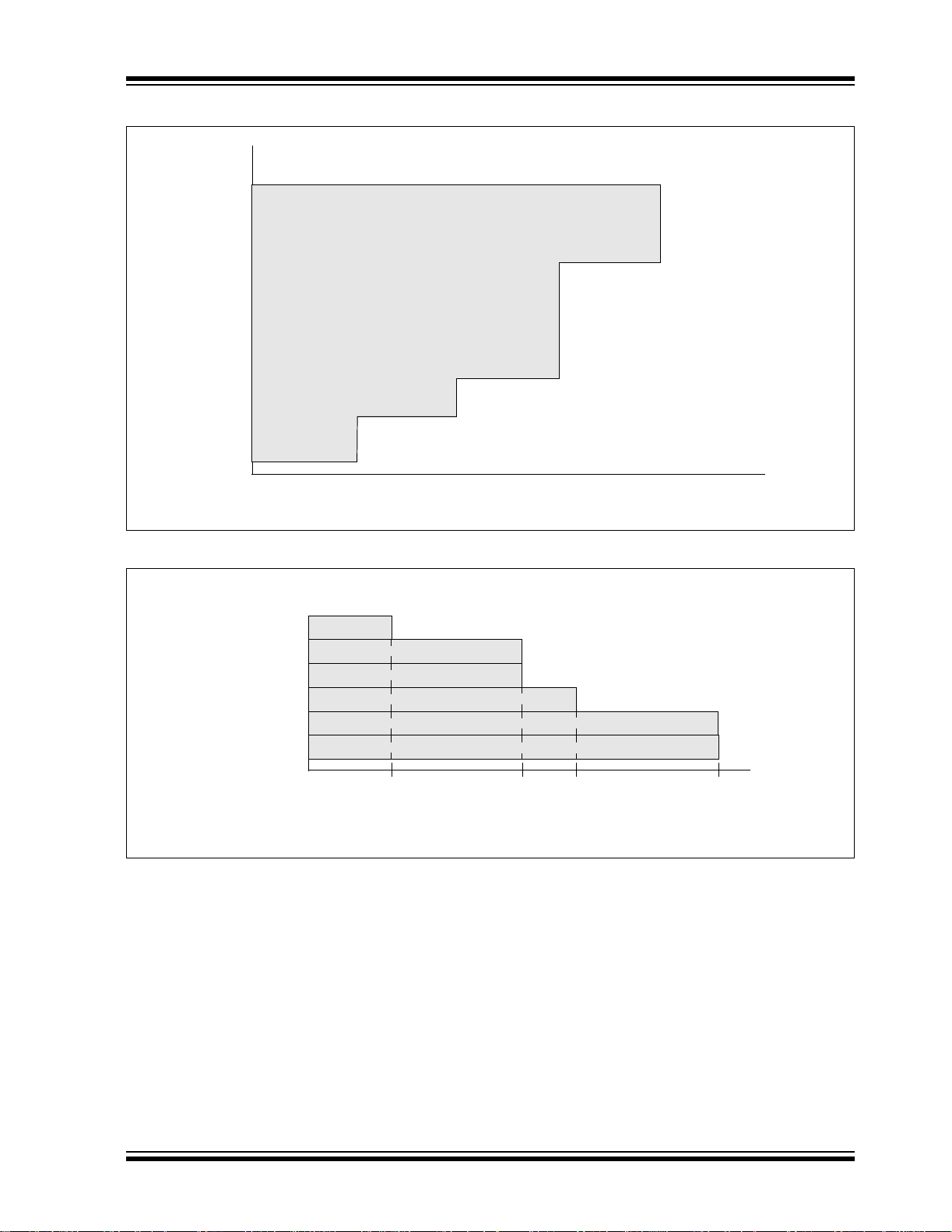
PIC12F510/16F506
FIGURE 13-3:
V
DD
(Volts)
FIGURE 13-4:
VOLTAGE FREQUENCY GRAPH, -40°C ≤ T
6.0
5.5
5.0
4.5
4.0
3.5
3.0
2.5
2.0
0
410
8
Frequency (MHz)
A ≤ +125°C (PIC16F506)
MAXIMUM OSCILLATOR FREQUENCY TABLE (PIC16F506)
20
25
Oscillator Mode
LP
XT
EXTRC
INTOSC
EC
HS
0 200 kHz 4 MHz
Frequency (MHz)
8MHz 20MHz
© 2005 Microchip Technology Inc. Preliminary DS41268A-page 87

PIC12F510/16F506
13.1
DC Characteristics: PIC12F510/16F506 (Industrial)
Standard Operating Conditions (unless otherwise specified)
DC CHARACTERISTICS
Parm
No.
Sym Characteristic Min Typ
Operating Temperature -40°C ≤ TA ≤ +85°C (Industrial)
-40°C ≤ T
(1)
Max Units Conditions
A ≤ +125°C (Extended)
D001 VDD Supply Voltage 2.0 — 5.5 V See Fi gure 13-1
D002 V
D003 V
D004 S
D010 I
DR RAM Data Retention
Voltage
POR VDD Start Voltage to
(2)
ensure Power-on Reset
VDD VDD Rise Rate to ensure
Power-on Reset
DD Supply Current
(3)
— 1.5* — V Device in Sleep mode
—Vss— VSee Section 1 0.4 “Power-on Reset
(POR)”
0.05* — — V/ms See Section 10.4 “Power-on Reset
(POR)” for details
—170TBDμAFOSC = 4 MHz, VDD = 2.0V
(4)
—0.4TBDmAFOSC = 8 MHz, VDD = 3.0V
—1.7TBDmAF
OSC = 20 MHz, VDD = 5.0V
—15TBDμAFOSC = 32 kHz, VDD = 2.0V, WDT
disabled
D020 I
PD Power-Down Current
D022 ΔIWDT WDT Current
(5)
(5)
—0.1TBDμAVDD = 2.0V
—1.0TBDμAVDD = 2.0V
D023 ΔICMP Comparator Current —15TBDμAVDD = 2.0V
D024 ΔI
D025 ΔIVREF Internal Reference
ADC ADC Current —100TBDμAVDD = 2.0V
—80TBDμAVDD = 2.0V
Current
D026 ΔCV
REF Comparator Voltage
—58TBDμAVDD = 2.0V
Reference Current
Legend: TBD = To be determined.
* These parameters are characterized but not tested.
Note 1: Data in the Typical (“Typ”) column is based on characterization results at 25°C. This data is for design
guidance only and is not tested.
2: This is the limit to which V
DD can be lowered in Sleep mode without losing RAM data.
3: The supply current is mainly a function of the operating voltage and frequency. Other factors such as bus
loading, oscilla tor type, bus rate, internal code execution pattern and tem pera ture als o h ave an i mpact on
the current consumption.
a) The test conditions for all I
OSC1 = external square wave, from rail-to-rail; all I/O pins tri-stated, pulled to V
= VDD;
MCLR
DD measurements in active operation mode are:
SS, T0CKI = VDD,
WDT enabled/disabled as specified.
b) For standby current measurements, the conditions are the same, except that the device is in Sleep
mode.
4: Does not include current through R
EXT (in EXTRC mode only). The current through the resistor can be
estimated by the formula:
I = VDD/2REXT (mA) with REXT in kΩ.
5: The power-down current in Sleep mode does not depend on the oscillator type. Power-down current is
measured with the part in Sleep mode, with all I/O pins in high-impedance state and tied to V
DD or VSS.
DS41268A-page 88 Preliminary © 2005 Microchip Technology Inc.

PIC12F510/16F506
13.2 DC Characteristics: PIC12F510/16F506 (Extended)
Standard Operating Conditions (unless otherwise specified)
DC CHARACTERISTICS
Parm
No.
Sym Characteristic Min Ty p
D001 VDD Supply Voltage 2.0 — 5.5 V See Figure 13-1
D002 V
D003 V
DR RAM Data Retention
Voltage
POR VDD Start Voltage to
(2)
ensure Power-on Reset
D004 S
VDD VDD Rise Rate to ensure
Power-on Reset
D010 I
D020 I
DD Supply Current
PD Power-Down Current
D022 ΔIWDT WDT Current
(3)
(5)
D023 ΔICMP Comparator Current —15TBDμAVDD = 2.0V
D024 ΔI
ADC ADC Current —100TBDμAVDD = 2.0V
D025 ΔIVREF Internal Reference
Current
D026 ΔCV
REF Comparator Volt age
Reference Current
Legend: TBD = To be determined.
* These parameters are characterized but not tested.
Note 1: Data in the Typical (“Typ”) column is based on characterization results at 25°C. This data is for design
guidance only and is not tested.
2: This is the limit to which V
DD can be lowered in Sleep mode without losing RAM data.
3: The supply current is mainly a function of the operating voltage and frequency. Other factors such as bus
loading, oscillator type, bus rate, internal code execu tio n p attern and temperature also have an imp act on
the current consumption.
a) The test conditions for all I
OSC1 = external square wave, from rail-to-rail; all I/O pins tri-stated, pulled to V
= VDD;
MCLR
WDT enabled/disabled as specified.
b) For standby current measurements, the conditions are the same, except that the device is in Sleep
mode.
4: Does not include current through R
estimated by the formula:
I = VDD/2REXT (mA) with REXT in kΩ.
5: The power-down current in Sleep mode does not depend on the oscillator type. Power-down current is
measured with the part in Sleep mode, with all I/O pins in high-impedance state and tied to V
Operating Temperature -40°C ≤ TA ≤ +85°C (Industrial)
-40°C ≤ T
(1)
Max Units Conditions
A ≤ +125°C (Extended)
— 1.5* — V Device in Sleep mode
—Vss— VSee Section 10.4 “Power-on Reset
(POR)”
0.05* — — V/ms See Section 10.4 “Power-on Reset
(POR)” for details
—170TBDμAFOSC = 4 MHz, VDD = 2.0V
—0.4TBDmAFOSC = 8 MHz, VDD = 3.0V
—1.7TBDmAF
OSC = 20 MHz, VDD = 5.0V
—15TBDμAFOSC = 32 kHz, VDD = 2.0V, WDT
disabled
(5)
—0.1TBDμAVDD = 2.0V
—1.0TBDμAVDD = 2.0V
—80TBDμAVDD = 2.0V
—58TBDμAVDD = 2.0V
DD measurements in active operation mode are:
SS, T0CKI = VDD,
EXT (in EXTRC mode only). The current through the resistor can be
(4)
DD or VSS.
© 2005 Microchip Technology Inc. Preliminary DS41268A-page 89

PIC12F510/16F506
13.3 DC Characteristics: PIC12F510/16F506 (Industrial, Extended)
DC CHARACTERISTICS
Param
Sym Characteristic Min Typ† Max Units Conditions
No.
V
IL Input Low Voltage
Standard Operating Conditions (unless otherwise specified)
Operating Temperature -40°C ≤ TA ≤ +85°C (industrial)
A ≤ +125°C (extended)
-40°C ≤ T
I/O ports
D030 with TTL buffer V
D030A V
D031 with Schmitt Trigger buffer V
D032 MCLR
D033 OSC1 (in EXTRC), EC
, T0CKI VSS —0.15VDD V
(1)
D033 OSC1 (in HS) V
D033 OSC1 (in XT and LP) V
V
IH Input High Voltage
SS —0.8V VFor 4.5 ≤ VDD ≤ 5.5V
SS —0.15VDD V otherwise
SS —0.15VDD V
VSS —0.15 VDD V
SS —0.3VDD V
SS —0.3 V
I/O ports —
D040 with TTL buffer 2.0 — V
D040A 0.25 V
DD —VDD V Otherwise
DD V4.5 ≤ VDD ≤ 5.5V
+ 0.8V
D041 with Schmitt Trigger buffer 0.85 V
D042 MCLR
D043 OSC1 (in EXTRC), EC
, T0CKI 0.85 VDD —VDD V
(1)
D043 OSC1 (in HS) 0.7 V
D043 OSC1 (in XT and LP) 1.6 — V
D070 I
PUR GPIO/PORTB Weak Pull-up Current
IIL Input Leakage Current
(2), (3)
(4)
DD —VDD V For ent i re VDD range
0.85 VDD —VDD V
DD —VDD V
DD V
TBD 250 TBD μAVDD = 5V, VPIN = VSS
D060 I/O ports — — ±1 μA Vss ≤ VPIN ≤ VDD, Pin at high-impedance
D061 GP3/RB3/MCLR
D061A GP3/RB3/MCLR
(5)
(6)
——±30μA Vss ≤ VPIN ≤ VDD
——±5μA Vss ≤ VPIN ≤ VDD
D063 OSC1 — — ±5 μA Vss ≤ VPIN ≤ VDD, XT, HS and LP oscillator
configuration
Output Low Voltage
D080 V
D080A — — 0.6 V I
D083 OSC2 — — 0.6 V I
D083A — — 0.6 V I
OL I/O ports/CLKOUT — — 0.6 V IOL = 8.5 mA, VDD = 4.5V, –40°C to +85°C
OL = 7.0 mA, VDD = 4.5V, –40°C to +125°C
OL = 1.6 mA, VDD = 4.5V, –40°C to +85°C
OL = 1.2 mA, VDD = 4.5V, –40°C to +125°C
Output High Voltage
D090 V
OH I/O ports/CLKOUT
D090A V
D092 OSC2 V
D092A V
(3)
VDD – 0.7 — — V IOH = -3.0 mA, VDD = 4.5V, –40°C to +85°C
DD – 0.7 — — V IOH = -2.5 mA, VDD = 4.5V, –40°C to +125°C
DD – 0.7 — — V IOH = -1.3 mA, VDD = 4.5V, –40°C to +85°C
DD – 0.7 — — V IOH = -1.0 mA, VDD = 4.5V, –40°C to +125°C
Capacitive Loading Specs on Output Pins
D100 C
D101 C
OSC2 OSC2 pin — — 15 pF In XT, HS and LP modes when external
IO All I/O pins — — 50 pF
clock is used to drive OSC1.
Legend: TBD = To be determined.
† Data in “Typ” column is at 5V, 25°C unless otherwise stated. These parameters are for design guidance only and are not tested.
Note 1: In EXTRC oscillator configuration, the OSC1/CLKIN pin is a Schmitt Trigger input. It is not recommended that the PIC12F510/16F506 be
driven with external clock in RC mode.
2: The leakage current on the MCLR
conditions. Higher leakage current may be measured at different input voltages.
pin is strongly dependent on the applied voltage level. The specified levels represent normal operating
3: Negative current is defined as coming out of the pin.
4: Does not include GP3. For GP3 see parameters D061 and D061A.
5: This specification applies to GP3/MCLR
6: This specification applies when GP3/MCLR
configured as external MCLR and GP3/MCLR configured as input with internal pull-up enabled.
is configured as an input with pull-up disabled. The leakage current of the MCLR circuit is
higher than the standard I/O logic.
DS41268A-page 90 Preliminary © 2005 Microchip Technology Inc.

PIC12F510/16F506
TABLE 13-1: COMPARATOR SPECIFICATIONS
Sym Characteristics Min Typ Max Units Comments
V
OS Input Offset Voltage — ±3 ±10 mV
VCM Input Common Mode Voltage 0 — VDD – 1.5 V
MRR Common Mode Rejection Ratio +55* — — dB
C
TRT Response Time
* These parameters are characterized but not tested.
Note 1: Response time measured with one comparator input at (VDD – 1.5)/2, while the other input transitions
SS to VDD – 1.5V.
from V
(1)
— 150 400* ns Internal
TABLE 13-2: COMPARATOR VOLTAGE REFERENCE (V
REF) SPECIFICATIONS
Sym Characteristics Min Typ Max Units Comments
RES Resolution —
CV
Absolute Accuracy —
Unit Resistor Value (R) —
—
—
VDD/24*
V
DD/32
—
—
—
—
±1/4*
±1/2*
2K* — Ω
LSb
LSb
LSb
LSb
Low Range (V
High Range (V
Low Range (VRR = 1)
High Range (V
—
Settling Time
(1)
——10*μs
* These parameters are characterized but not tested.
Note 1: Settling time measured while VRR = 1 and VR<3:0> transitions from 0000 to 1111.
TABLE 13-3: A/D CONVERTER CHARACTERISTICS
Param
No.
A01 N
A02 EABS Total Absolute Error*
A03 EIL Integral Error — — TBD LSb VDD = 5.0V
A04 E
A05 EFS Full-scale Range 2.2* — 5.5* V VDD
A06 EOFF Offset Error — — TBD LSb VREF = 5.0V
A07 EGN Gain Error — — TBD LSb VREF = 5.0V
A10 — Monotonicity — guaranteed
A25 V
A30 ZAIN Recommended Impedance
Note 1: Total Absolute Error includes integral, differential, offset and gain errors.
Sym Characteristic Min Typ† Max Units Conditions
R Resolution — — 8 bits bit
(1)
DL Differential Error — — TBD LSb No missing codes to 8 bits
AIN Analog Input Voltage — VDD —V
——TBDLSbVDD = 5.0V
DD = 5.0V
V
(2)
——VSS ≤ VAIN ≤ V REF+
——10kΩ
of Analog Vol t age Source
* These parameters are characterized but not tested.
† Data in the “Typ” column is at 5.0V, 25°C unless otherwise stated. These parameters are for design
guidance only are not tested.
2: The A/D conversion result never decreases with an increase in the input voltage and has no missing
codes.
3: V
REF current is from external VREF or VDD pin, whichever is selected as reference input.
4: When A/D is off, it will not consume any current other than leakage current. The power-down current
specification includes any such leakage from the A/D module.
RR = 1)
RR = 0)
RR = 0)
© 2005 Microchip Technology Inc. Preliminary DS41268A-page 91

PIC12F510/16F506
13.4 Timing Parameter Symbology and Load Conditions
The timing parameter symbols have been created following one of the following formats:
1. TppS2ppS
2. TppS
T
F Frequency T Time
Lowercase (pp) and their meanings:
pp
2To mcMCLR
ck CLKOUT osc Oscillator
cy Cycle Time os OSC1
drt Device Reset Timer t0 T0CKI
io I/O port wdt Watchdog Timer
Uppercase le tters and th eir meanings:
S
FFall PPeriod
HHigh RRise
I Invalid (High-impedance) V Valid
L Low Z High-impedance
FIGURE 13-5: LOAD CONDITIONS
Pin
Cl
SS
V
FIGURE 13-6: EXTERNAL CLOCK TIMING
Q4
OSC1
Q1 Q2
133
Legend:
CL = 50 pF for all pins except OSC2
15 pF for OSC2 in XT, HS or LP
modes when external clock
is used to drive OSC1
Q3 Q4 Q1
44
2
DS41268A-page 92 Preliminary © 2005 Microchip Technology Inc.

PIC12F510/16F506
TABLE 13-4: EXTERNAL CLOCK TIMING REQUIREMENTS
Standard O perating Conditions (unless othe rwise spec ified)
AC CHARACTERISTICS
Para
No.
1A F
1T
2T
3TosL,
4TosR,
Sym Characteristic Min Typ
OSC External CLKIN Frequency
Oscillator Frequency
OSC External CLKIN Period
Oscillator Period
CY Instruction Cycle Time 200 4/FOSC —ns
(2)
(2)
(2)
Clock in (OSC1) Low or High
TosH
Time
Clock in (OSC1) Rise or Fall
TosF
Time
* These parameters are characterized but not tested.
Note 1: Data in the Typical (“Typ”) column is at 5V, 25°C unless otherwise stated. These parame ters are for
design guidance only and are not tested.
2: All specified values are based on characterization data for that particular oscillator type under standard
operating conditions with the device executing code. Exceeding these specified limits may result in an
unstable oscillator operation and/or higher than expected current consumption.
When an external clock input is used, the “max” cycle time limit is “DC” (no clock) for all devices.
Operating Temperature -40°C ≤ TA ≤ +85°C (industrial),
-40°C ≤ T
(1)
Max Units Conditions
(2)
DC — 4 MHz XT Oscillator mode
A ≤ +125°C (extended)
DC — 20 MHz HS/EC Oscillator mode
(PIC16F5 06 only)
DC — 200 kHz LP Oscillator mode
— — 4 MHz EXTRC Oscillato r mode
0.1 — 4 MHz XT Oscillator mode
4 — 20 MHz HS/EC Oscillator mode
(PIC16F5 06 only)
— — 200 kHz LP Oscillator mode
250 — — ns XT Oscillator mode
50 — — ns HS/EC Oscillator mode
(PIC16F5 06 only)
5——μs LP Oscillator mode
250 — — ns EXTRC Oscillator mode
250 — 10,000 ns XT Oscillator mode
50 — 250 ns HS/EC Oscillator mode
(PIC16F5 06 only)
5——μs LP Oscillator mode
50* — — ns XT Oscillator
2* — — μs LP Oscillator
10 — — ns HS/EC Oscillator
(PIC16F5 06 only)
— — 25* ns XT Oscillator
— — 50* ns LP Oscillator
— — 15 ns HS/EC Oscillator
(PIC16F5 06 only)
© 2005 Microchip Technology Inc. Preliminary DS41268A-page 93

PIC12F510/16F506
TABLE 13-5: CALIBRATED INTERNAL RC FREQUENCIES
Standard Operating Conditions (unless otherwise specified)
AC CHARACTERISTICS
Param
F10 FOSC Internal Calibrated INT OSC
Sym Characteristic
No.
Frequency
(1)
* These parameters are characterized but not tested.
Note 1: Data in the Typical (“Typ”) c olumn is a t 5V, 25°C unless otherw ise state d. These p arameters ar e for design
guidance only and are not tested.
FIGURE 13-7: I/O TIMING
Operating Temperature -40°C ≤ TA ≤ +85°C (industrial),
Freq.
Tolerance
±1%
±2%
±5%
Min Typ
7.92
7.84
7.60
8.00
8.00
8.00
-40°C ≤ T
(1)
Max* Units Conditions
8.08
8.16
8.40
A ≤ +125°C (extended)
V
MHz
MHz
MHz
DD and temperature TBD
2.5V ≤ V
0°C ≤ T
2.0V ≤ V
-40°C ≤ T
-40°C ≤ T
DD ≤ 5.5V
A ≤ +85°C
DD ≤ 5.5V
A ≤ +85°C (Ind.)
A ≤ +125°C (Ext.)
Q4
Q1
Q2 Q3
OSC1
I/O Pin
(input)
I/O Pin
(output)
17
Old Value
19
18
New Value
20, 21
Note: All tests must be done with specified capacitive loads (see data sheet) 50 pF on I/O pins and CLKOUT.
DS41268A-page 94 Preliminary © 2005 Microchip Technology Inc.

PIC12F510/16F506
T ABLE 13-6: TIMING REQUIREMENTS
Standard Operating Conditions (unless otherwise specified)
AC CHARACTERISTICS
Param
No.
17 T
Sym Characteristic Min Typ
OSH2IOVOSC1↑ (Q1 cycle) to Port out valid
18 TOSH2IOIOSC1↑ (Q2 cycle) to Port input invalid
19 T
IOV2OSH Port input valid to OSC1↑ (I/O i n setup time) TBD — — ns
20 TIOR Port output rise time
21 TIOF Port output fall time
* These parameters are characterized but not tested.
** These parameters are design targets and are not tested.
Note 1: Data in the T yp ical (“T yp”) co lumn is at 5V, 25°C unless otherwise st ated. These p aramete rs are for design
guidance only and are not tested.
2: Measurements are taken in EXTRC mode.
3: See Figure 13-5 for loading conditions.
FIGURE 13-8: RESET, WATCHDOG TIMER, AND DEVICE RESET TIMER TIMING
Operating Temperature -40°C ≤ TA ≤ +85°C (industrial)
(I/O in hold time)
-40°C ≤ T
(2)
(2), (3)
(2), (3)
A ≤ +125°C (extended)
(2), (3)
— — 100* ns
TBD — — ns
— 10 25** ns
— 10 25** ns
(1)
Max Units
VDD
MCLR
Internal
POR
DRT
(2)
Timeout
Internal
Reset
Watchdog
Timer Reset
(1)
I/O pin
Note 1: I/O pins must be taken out of High-Impedance mode by enabling the output drivers in software.
2: Runs in MCLR
32
or WDT Reset only in XT, LP and HS modes.
34
30
32
31
34
32
© 2005 Microchip Technology Inc. Preliminary DS41268A-page 95

PIC12F510/16F506
TABLE 13-7: RESET, WATCHDOG T IMER AND DEVICE RESET TIMER
Standard Operat ing Conditi ons (unle ss otherw is e speci fied)
AC CHARACTERISTICS
Param
Sym Characteristic Min Typ
No.
Operating Temperature -40°C ≤ TA ≤ +85°C (industrial)
-40°C ≤ T
(1)
Max Units Conditions
A ≤ +125°C (extended)
30 T
31 TWDT Watchdog Timer Time-out Period
32 T
MCLMCLR Pulse Width (low) 2000* — — ns VDD = 5.0V
(No Prescaler)
DRT Device Reset Timer Period
Standard 9*
Short 0.5*
9*
9*
9*
0.5*
18*
18*
18*
18*
30*
40*
30*
40*
1.125*
1.125*2*2.5*
msmsVDD = 5.0V (Commercial)
DD = 5.0V (Extended)
V
msmsVDD = 5.0V (Industrial)
DD = 5.0V (Extended)
V
msmsV
DD = 5.0V (Industrial)
DD = 5.0V (Extended)
V
34 TIOZ I/O high-imped ance fro m MCLR low — — 2000* ns
* These parameters are characterized but not tested.
Note 1: Data in the Typical (“Typ ”) colu mn is at 5V, 25°C unless otherwise stated. The se p arame ters are for des ign
guidance only and are not tested.
FIGURE 13-9: TIMER0 CLOCK TIMINGS
T0CKI
40 41
42
TABLE 13-8: TIMER0 CLOCK REQUIREMENTS
AC CHARACTERISTICS
Parm
Sym Characteristic Min Typ
No.
Standard Operating Conditions (unless otherwise specified)
Operating Temperature -40°C ≤ TA ≤ +85°C (industrial)
-40°C ≤ T
A ≤ +125°C (extended)
(1)
Max Units Conditions
40 Tt0H T0CKI High Pulse Width No Prescaler 0.5 T
With Prescaler 10* — — ns
41 Tt0L T0CKI Low Pulse Width No Prescaler 0.5 T
With Prescaler 10* — — ns
42 Tt0P T0CKI Period 20 or T
* These parameters are characterized but not tested.
Note 1: Data in the Typical (“Ty p”) column is at 5V, 25°C unless otherwise stated. These parameters are for design guidance
only and are not tested.
DS41268A-page 96 Preliminary © 2005 Microchip Technology Inc.
CY + 20* — — ns
CY + 20* — — ns
CY + 40* N — — ns Whichever is greater.
N = Prescale Value
(1, 2, 4,..., 256)

14.0 DC AND AC CHARACTERISTICS GRAPHS AND CHARTS
Graphs and charts are not available at this time.
PIC12F510/16F506
© 2005 Microchip Technology Inc. Preliminary DS41268A-page 97

PIC12F510/16F506
NOTES:
DS41268A-page 98 Preliminary © 2005 Microchip Technology Inc.

15.0 PACKAGING
.
s
15.1 Package Marking Information
PIC12F510/16F506
8-Lead PDIP
XXXXXXXX
XXXXXNNN
YYWW
14-Lead PDIP
XXXXXXXXXXXXXX
XXXXXXXXXXXXXX
YYWWNNN
8-Lead SOIC (.150”)
XXXXXXXX
XXXXYYWW
NNN
Example
12F510/P
017
0410
Example
PIC16F506-I/P
0410017
Example
PIC12F510-I
/SN0410
017
Legend: XX...X Customer-specific information
Y Year code (last digit of calendar year)
YY Year code (last 2 digits of calendar year)
WW Week code (week of January 1 is week ‘01’)
NNN Alphanumeric traceability code
3
e
Pb-free JEDEC designator for Matte Tin (Sn)
* This package is Pb-free. The Pb-free JEDEC designator ( )
can be found on the outer packaging for this package.
Note: In the event the full Microchip p art numb er canno t be marked on one line , it will
be carried over to the next line, thus limiting the number of available
characters for customer-specific information.
* Standard PICmicro devic e marking c onsist s of Mi crochip part nu mber , y ear code , week cod e and trac eability code
For PICmicro device marking beyond this, ce rtain price adders apply. Please check with your Microchip Sale
Office. For QTP de vices, any special marking adders are included in QTP price.
© 2005 Microchip Technology Inc. Preliminary DS41268A-page 99
3
e

PIC12F510/16F506
15.2 Package Marking Information (Cont’d)
14-Lead SOIC (.150”)
XXXXXXXXXXX
XXXXXXXXXXX
YYWWNNN
8-Lead MSOP
XXXXXX
YWWNNN
14-Lead TSSOP
XXXXXXXX
YYWW
NNN
Example
PIC16F506
-I/SL
0410017
Example
602/MS
310017
Example
16F506/ST
0410
017
DS41268A-page 100 Preliminary © 2005 Microchip Technology Inc.
 Loading...