


PIC16C925/926
Data Sheet
64/68-Pin CMOS Microcontrollers
with LCD Driver
2001 Microchip Technology Inc. Preliminary DS39544A

“All rights reserved. Copyright © 2001, Microchip Technology
Incorporated, USA. Information contained in this publication
regarding device applications and the like is intended through
suggestion only and may be superseded by updates. No representation or warranty is given and no liability is assumed by
Microchip Technology Incorporated with respect to the accuracy or use of such information, or infringement of patents or
other intellectual property rights arising from such use or otherwise. Use of Microchip’s products as critical components in
life support systems is not authorized except with express
written approval by Microchip. No licenses are conveyed,
implicitly or otherwise, under any intellectual property rights.
The Microchip logo and name are registered trademarks of
Microchip Technology Inc. in the U.S.A. and other countries.
All rights reserved. All other trademarks mentioned herein are
the property of their respective companies. No licenses are
conveyed, implicitly or otherwise, under any intellectual property rights.”
Trademarks
The Microchip name, logo, PIC, PICmicro, PICMASTER, PICSTART, PRO MATE, K
EELOQ, SEEVAL, MPLAB and The
Embedded Control Solutions Company are registered trademarks of Microchip Technology Incorporated in the U.S.A. and
other countries.
Total Endurance, ICSP, In-Circuit Serial Programming, FilterLab, MXDEV, microID, FlexROM, fuzzyLAB, MPASM,
MPLINK, MPLIB, PICDEM, ICEPIC, Migratable Memory,
FanSense, ECONOMONITOR, SelectMode and microPort
are trademarks of Microchip Technology Incorporated in the
U.S.A.
Serialized Quick T erm Programming (SQTP) is a service mark
of Microchip Technology Incorporated in the U.S.A.
All other trademarks mentioned herein are property of their
respective companies.
© 2001, Microchip Technology Incorporated, Printed in the
U.S.A., All Rights Reserved.
Microchip received QS-9000 quality system
certification for its worldwide headquarters,
design and wafer fabrication facilities in
Chandler and Tempe, Arizona in July 1999. The
Company’s quality system processes and
procedures are QS-9000 compliant for its
PICmicro
devices, Serial EEPROMs and microperipheral
products. In addition, Microchip’s quality
system for the design and manufacture of
development systems is ISO 9001 certified.
®
8-bit MCUs, KEELOQ
®
code hoppin g
DS39544A - page ii Preliminary 2001 Microchip Technology Inc.
PIC16C925/926
64/68-Pin CMOS Microcontrollers with LCD Driver
High Performance RISC CPU:
• Only 35 single word instructions to learn
• All single cycle instructions except for program
branches which are two-cycle
• Operating speed: DC - 20 MHz clock input
DC - 200 ns instruction cycle
• Up to 8K x 14-bit words of EPROM program memory,
336 bytes general purpose registe r s (SRA M),
60 special function registers
• Pinout compatible with PIC16C923/924
Peripheral Features:
• 25 I/O pins with individual direction control and
25-27 input only pins
• Timer0 module: 8-bit timer/counter with program-
mable 8-bit prescaler
• Timer1 module: 16-bit timer/counte r, can be incre-
mented during SLEEP via external cryst al/clo ck
• Timer2 module: 8-bit timer/counter with 8-bit
period register, prescaler, and postscaler
• One Capture, Compare, PWM module
• Synchronous Serial Port (SSP) module with
two modes of operation:
- 3-wire SPI™ (supports all 4 SPI modes)
2
C™ Slave mode
-I
• Programmable LCD timing module:
- Multiple LCD timing sources available
- Can drive LCD panel while in SLEEP mode
- Static, 1/2, 1/3, 1/4 multiplex
- Static drive and 1/3 bias capability
- 16 bytes of dedicated LCD RAM
- Up to 32 segments, up to 4 commons
Analog Features:
• 10-bit 5-channel Analog -to-Digital Converter (A/D)
• Brown-out Reset (BOR)
Special Microcontroller Features:
• Power-on Reset (POR)
• Power-up Timer (PWRT) and Oscillator Start-up
Timer (OST)
• Watchdog Timer (WDT) with its own on-chip RC
oscillator for reliable operation
• Programmable code protection
• Selectable oscilla tor opti ons
• In-Circuit Serial Programming™ (ICSP™) via
two pins
• Processor read access to program memo ry
CMOS Technology:
• Low power, high speed CMOS/EPROM
technology
• Fully static design
• Wide operating voltage range: 2.5V to 5.5V
• Commercial and Industrial temperature ranges
• Low power consumption
Common Segment Pixels
13232
23162
33090
429116
2001 Microchip Technology Inc. Preliminary DS39544A-page 1
PIC16C925/926
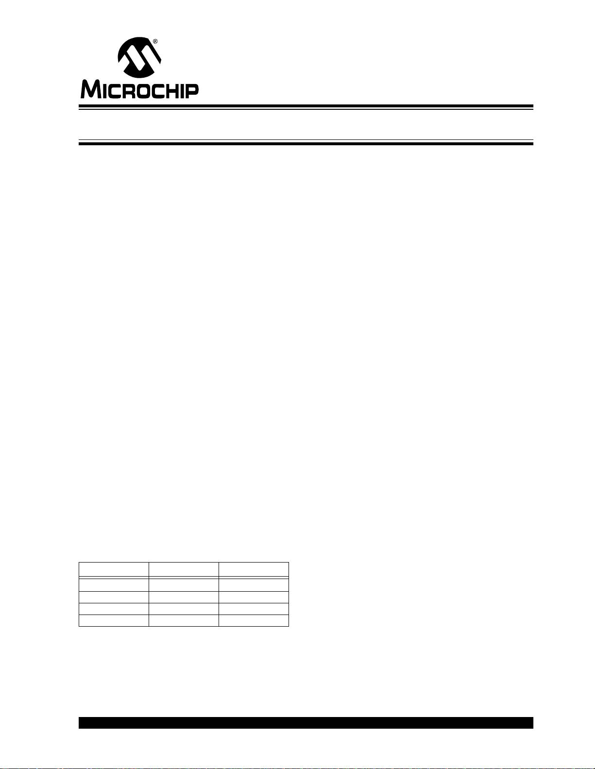
Pin Diagrams
PLCC, CLCC
REF-
/VPP
SS
RA3/AN3/VREF+
RA1/AN1
RA0/AN0
RB2
RB3
MCLR
N/C
RB4
RB5
RB7
RB6
VDDCOM0
RD7/SEG31/COM1
RA2/AN2/V
V
RD6/SEG30/COM2
RA4/T0CKI
RA5/AN4/SS
RC3/SCK/SCL
RC4/SDI/SDA
OSC1/CLKIN
OSC2/CLKOUT
RC0/T1OSO/T1CKI
RB1
RB0/INT
RC5/SDO
C1
C2
LCD2
V
LCD3
V
VDD
A
VDD
VSS
987654321
10
11
12
13
14
15
16
17
18
19
20
21
22
23
24
25
26
2728293031323334353637383940414243
RC1/T1OSI
PIC16C92X
LCD1
V
VLCDADJ
RC2/CCP1
RD0/SEG00
RD1/SEG01
68676665646362
RE7/SEG27
RD2/SEG02
RD3/SEG03
RD4/SEG04
RE0/SEG05
RE1/SEG06
RE2/SEG07
RE3/SEG08
RE4/SEG09
RE5/SEG10
61
60
59
58
57
56
55
54
53
52
51
50
49
48
47
46
45
44
RE6/SEG11
RD5/SEG29/COM3
RG6/SEG26
RG5/SEG25
RG4/SEG24
RG3/SEG23
RG2/SEG22
RG1/SEG21
RG0/SEG20
RG7/SEG28
RF7/SEG19
RF6/SEG18
RF5/SEG17
RF4/SEG16
RF3/SEG15
RF2/SEG14
RF1/SEG13
RF0/SEG12
LEGEND:
Input Pin
Output Pin
Input/Output Pin
Digital Input/LCD Output Pin
LCD Output Pin
DS39544A-page 2 Preliminary 2001 Microchip Technology Inc.
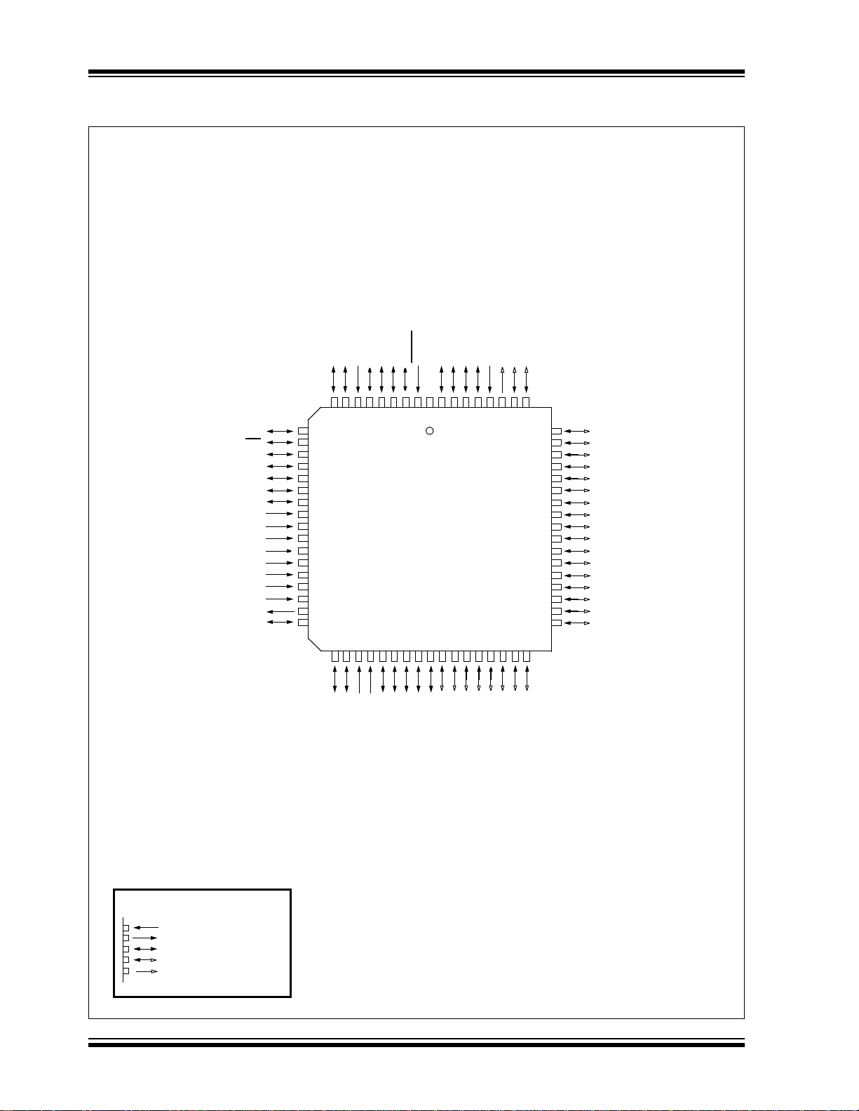
Pin Diagrams (Continued)
TQFP
PIC16C925/926
REF-
RA4/T0CKI
RA5/AN4/SS
RC3/SCK/SCL
RC4/SDI/SDA
OSC1/CLKIN
OSC2/CLKOUT
RC0/T1OSO/T1CKI
RB1
RB0/INT
RC5/SDO
C1
C2
LCD2
V
LCD3
V
V
DD
VSS
SS
RA3/AN3/VREF+
RA1/AN1
RA2/AN2/V
V
646362616059585756555453525150
1
2
3
4
5
6
7
8
9
10
11
12
13
14
15
16
171819202122232425262728293031
MCLR/VPP
RA0/AN0
RB2
RB4
RB5
RB3
RB7
PIC16C92X
DD
COM0
V
RD7/SEG31/COM1
RB6
RD6/SEG30/COM2
49
48
47
46
45
44
43
42
41
40
39
38
37
36
35
34
33
32
RD5/SEG29/COM3
RG6/SEG26
RG5/SEG25
RG4/SEG24
RG3/SEG23
RG2/SEG22
RG1/SEG21
RG0/SEG20
RF7/SEG19
RF6/SEG18
RF5/SEG17
RF4/SEG16
RF3/SEG15
RF2/SEG14
RF1/SEG13
RF0/SEG12
LCD1
V
VLCDADJ
RC2/CCP1
RC1/T1OSI
LEGEND:
Input Pin
Output Pin
Input/Output Pin
Digital Input/LCD Output Pin
LCD Output Pin
2001 Microchip Technology Inc. Preliminary DS39544A-page 3
RD0/SEG00
RD1/SEG01
RE0/SEG05
RE1/SEG06
RE2/SEG07
RE3/SEG08
RE4/SEG09
RE6/SEG11
RD2/SEG02
RD3/SEG03
RD4/SEG04
RE5/SEG10

PIC16C925/926
Table of Contents
1.0 Device Overview ...................................................................................................................................................5
2.0 Memory Organization ..........................................................................................................................................11
3.0 Reading Program Memory.................................................................................................................................. 27
4.0 I/O Ports ..............................................................................................................................................................29
5.0 Timer0 Module ....................................................................................................................................................41
6.0 Timer1 Module ....................................................................................................................................................47
7.0 Timer2 Module ....................................................................................................................................................51
8.0 Capture/Compare/PWM (CCP) Module ..............................................................................................................53
9.0 Synchronous Serial Port (SSP) Module ..............................................................................................................59
10.0 Analog-to-Digital Converter (A/D) Module ...........................................................................................................75
11.0 LCD Module ........................................................................................................................................................83
12.0 Special Features of the CPU............................................................................................................................... 97
13.0 Instruction Set Summary ...................................................................................................................................113
14.0 Development Support .......................... ...... ..... ........................................ ..... ...... ...... .........................................133
15.0 Electrical Characteristics ...................................................................................................................................139
16.0 DC and AC Characteristics Graphs and Tables ................................................................................................159
17.0 Packaging Information ......................................................................................................................................161
Appendix A: Revision History.................................................................................................................................... 167
Appendix B: Device Differences ............................................................................................................................... 167
Appendix C: Conversion Considerations .................................................................................................................. 168
Index .......................................................................................................................................................................... 169
On-Line Support......................................................................................................................................................... 175
Reader Response...................................................................................................................................................... 176
PIC16C925/926 Product Identifica tio n Syst em........................................... ....................................... ........................ 177
TO OUR VALUED CUSTOMERS
It is our intention to provide our valued customers with the best documentation possible to ensure successful use of your Microchip
products. To this end, we will continue to improve our publications to better suit your needs. Our publications will be refined and
enhanced as new volumes and updates are introduced.
If you have any questions or c omm ents regarding th is publication, p lease c ontact the M a rketing Communications Department via
E-mail at docerrors@mail.microchip.com or fax the Reader Response Form in the back of this data sheet to (480) 792-4150.
We welcome your feedback.
Most Current Data Sheet
To obtain the most up-to-date version of this data sheet, please register at our Worldwide Web site at:
http://www.microchip.com
You can determine the version of a data sheet by examining its literature number found on the bottom outside corner of any page.
The last character of the literature number is the version number, (e.g., DS30000A is version A of document DS30000).
Errata
An errata sheet, describing minor operational differences from the data sheet and recommended workarounds, may exist for current
devices. As device/documentation issues become known to us, we will publish an errata sheet. The errata will specify the revision
of silicon and revision of document to which it applies.
To determine if an errata sheet exists for a particular device, please check with one of the following:
• Microchip’s Worldwide Web site; http://www.microchip.com
• Your local Microchip sales office (see last page)
• The Microchip Corporate Literature Center; U.S. FAX: (480) 792-7277
When contacting a sales office or the literature center, please specify which device, revision of silicon and data sheet (include literature number) you are using.
Customer Notification System
Register on our web site at www.microchip.com/cn to receive the most current information on all of our products.
DS39544A-page 4 Preliminary 2001 Microchip Technology Inc.
PIC16C925/926
1.0 DEVICE OVERVIEW
This document cont a ins dev ice -sp ec ifi c info rm ation for
the following devices:
1. PIC16C925
2. PIC16C926
The PIC16C925/926 series is a family of low cost, high
performanc e, CM OS , f u ll y stati c, 8 -b it m ic roc o nt ro ll ers
with an integrated LCD Driver module, in the
PIC16CXXX mid-range family.
For the PIC16C925/926 family, there are two device
“types” as indicated in the device number:
1. C, as in PIC16C926. These devices operate
over the standard voltage range.
2. LC, as in PIC16LC926. These devices operate
over an extended volta ge rang e.
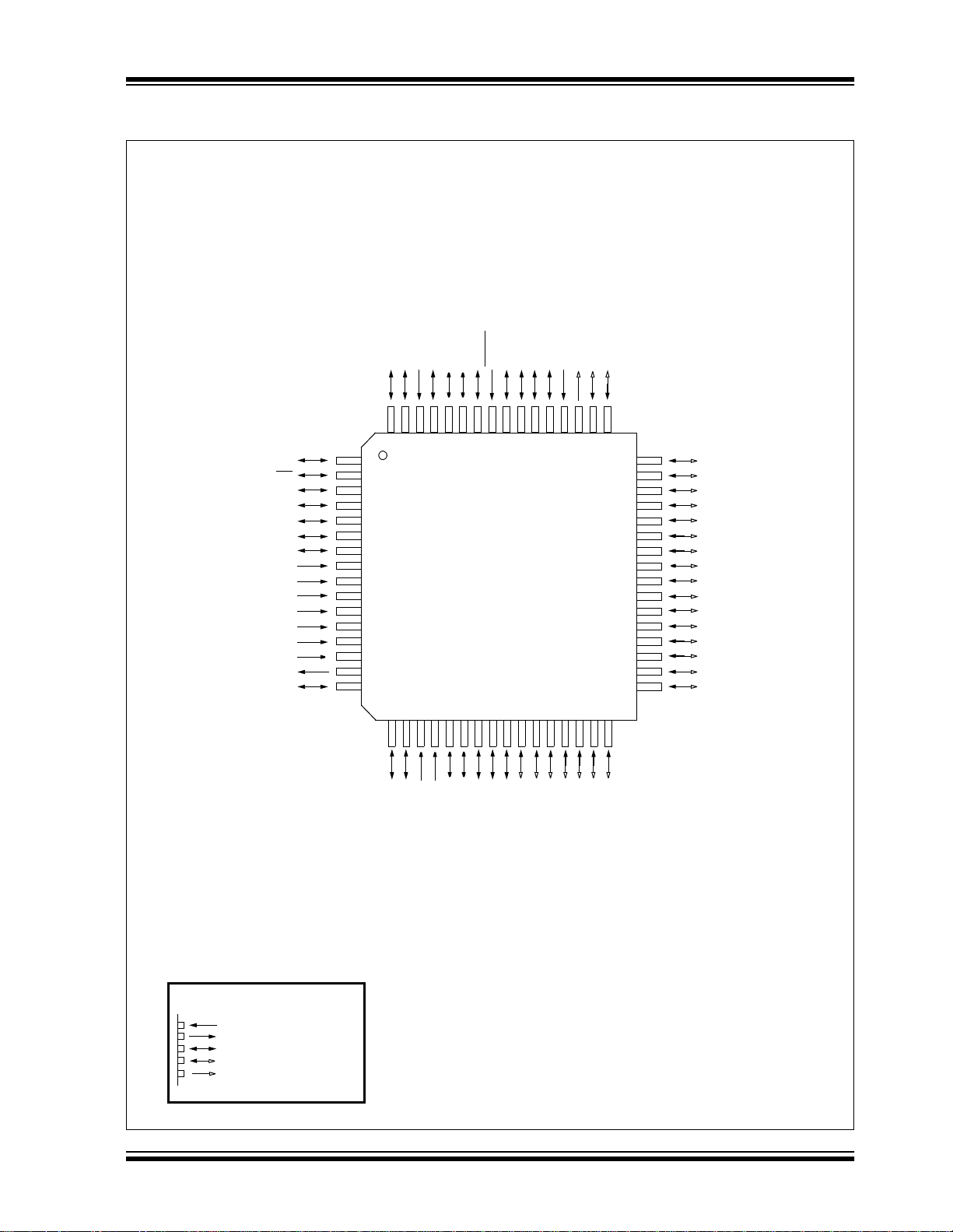
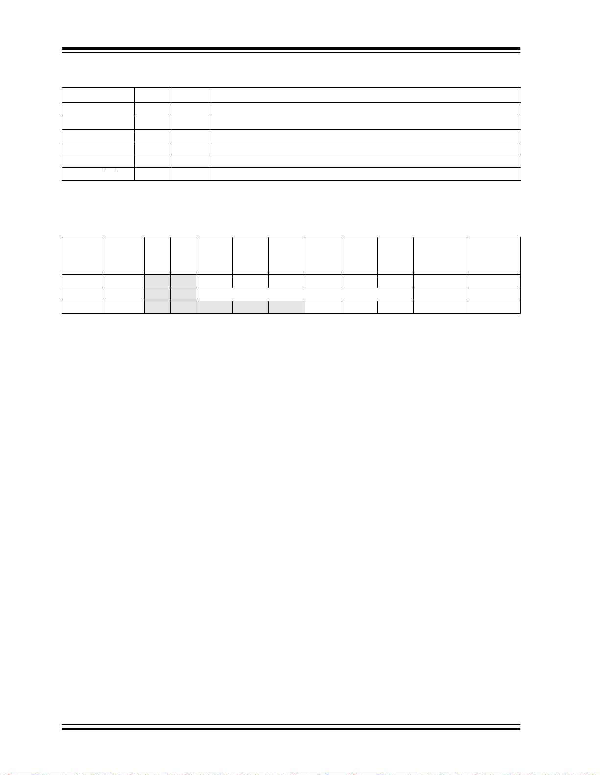
TABLE 1-1: PIC16C925/926 DEVICE FEATURES
Features PIC16C925 PIC16C926
Operating Frequency DC-20 MHz DC-20 MHz
EPROM Program Memory (words) 4K 8K
Data Memory (bytes) 176 336
Timer Module(s) TMR0,TMR1,TMR2 TMR0,TMR1,TMR2
Capture/Compa re/PW M Mo dul e(s ) 1 1
Serial Port(s)
2
C, USART)
(SPI/I
Parallel Slave Port ——
A/D Converter (10-bit) Channels 5 5
LCD Module 4 Com, 32 Seg 4 Com, 32 Seg
Interrupt Sources 9 9
I/O Pins 25 25
Input Pins 27 27
Voltage Range (V) 2.5-5.5 2.5-5.5
In-Circuit Serial Programming Yes Yes
Brown-out Reset Yes Yes
Packages
68-pin CLCC (CERQUAD)
These devices c ome in 64-pin and 68-pin p ackages, as
well as die form. Both configurations offer identical
peripheral devices and other features. The only difference between the PIC16C925 and PIC16C926 is the
additional EPROM and data memory offered in the latter. An overview of features is presented in Table 1-1.
A UV-erasab le, CERQUAD package d version (compa tible with PLCC) is also available for both the
PIC16C925 and PIC16C926. This version is ideal for
cost effective code development.
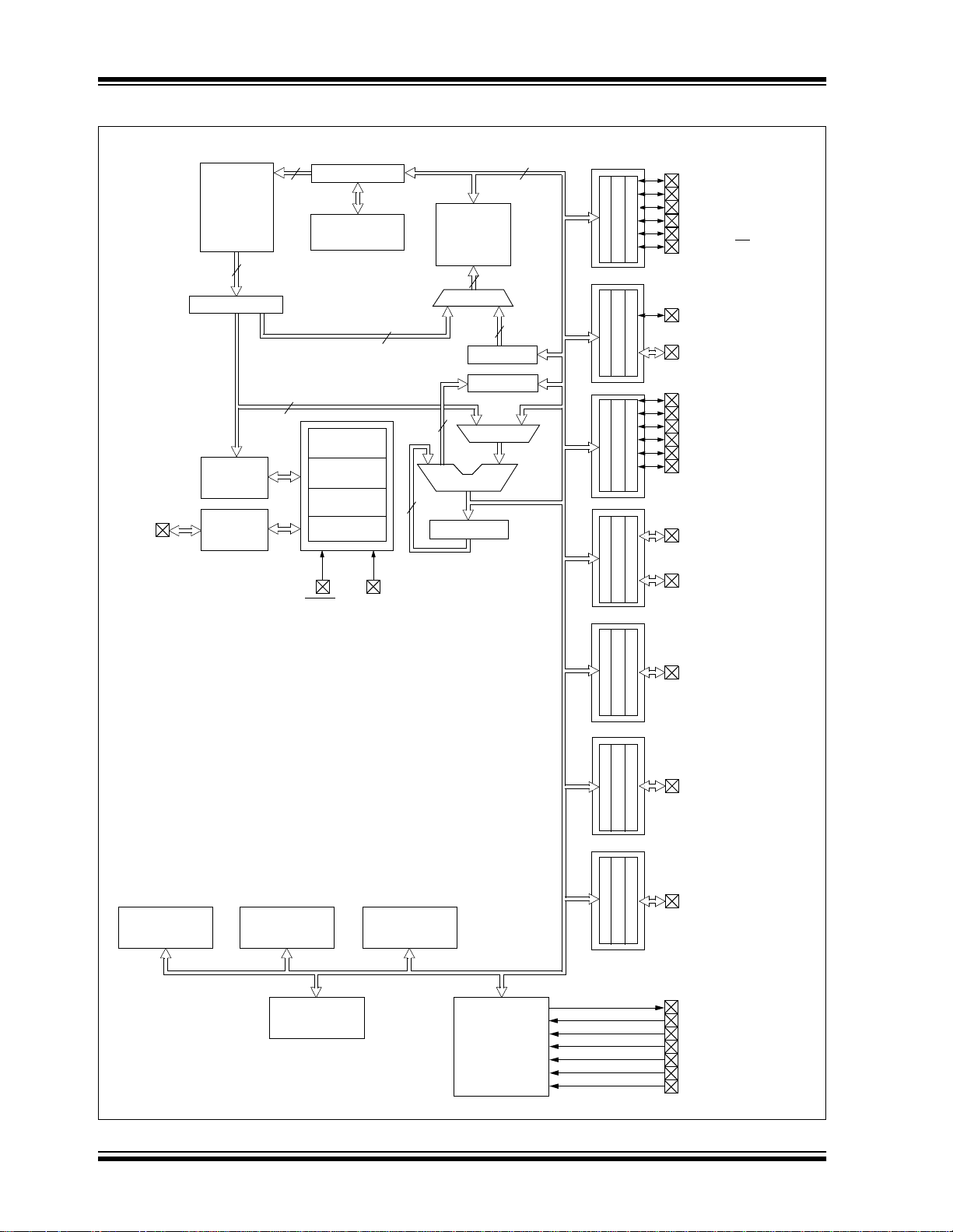
A block diagram for the PIC16C925/926 family architecture is presented in Figure 1-1.
2
C SPI/I2C
SPI/I
64-pin TQFP
68-pin PLCC
Die
64-pin TQFP
68-pin PLCC
68-pin CLCC (CERQUAD)
Die
2001 Microchip Technology Inc. Preliminary DS39544A-page 5
PIC16C925/926
FIGURE 1-1: PIC16C925/926 BLOCK DIAGRAM
Program
Bus
OSC1/CLKIN
OSC2/CLKOUT
EPROM
Program
Memory
14
Instruction reg
Instruction
Decode &
Control
Timing
Generation
13
Program Counter
8 Level Stack
Direct Addr
8
Power-up
Oscillator
Start-up Timer
Power-on
Watchdog
MCLR
(13-bit)
Timer
Reset
Timer
V
DD, VSS
RAM Addr
7
8
Data Bus
RAM
File
Registers
Addr MUX
FSR reg
STATUS reg
3
ALU
W reg
9
MUX
Indirect
8
8
Addr
PORTA
PORTB
PORTC
PORTD
PORTE
RA0/AN0
RA1/AN1
RA2/AN2
RA3/AN3/VREF
RA4/T0CKI
RA5/AN4/SS
RB0/INT
RB1-RB7
RC0/T1OSO/T1CKI
RC1/T1OSI
RC2/CCP1
RC3/SCK/SCL
RC4/SDI/SDA
RC5/SDO
RD0-RD4/SEGnn
RD5-RD7/SEGnn/COMn
Timer0
A/D
Synchronous
Serial Port
Timer1, Timer2,
CCP1
LCD
PORTF
PORTG
RE0-RE7/SEGnn
RF0-RF7/SEGnn
RG0-RG7/SEGnn
COM0
VLCD1
VLCD2
VLCD3
C1
C2
VLCDADJ
DS39544A-page 6 Preliminary 2001 Microchip Technology Inc.
TABLE 1-2: PIC16C925/926 PINOUT DESCRIPTION
PIC16C925/926
PLCC,
Pin Name
OSC1/CLKIN 24 14 I ST/CMOS Oscillator crystal input or external clock source input. This
OSC2/CLKOUT 25 15 O — Oscillator crystal output. Connects to crystal or resonator in
/VPP 2 57 I/P ST Master Clear (Reset) input or programming voltage input. This
MCLR
RA0/AN0 5 60 I/O TTL RA0 can also be Analog input0.
RA1/AN1 6 61 I/O TTL RA1 can also be Analog input1.
RA2/AN2 8 63 I/O TTL RA2 can also be Analog input2.
RA3/AN3/V
RA4/T0CKI 10 1 I/O ST RA4 can also be the clock input to the Timer0
RA5/AN4/SS
RB0/INT 13 4 I/O TTL/ST RB0 can also be the external interrupt pin. This buffer is a
RB1 12 3 I/O TTL
RB2 4 59 I/O TTL
RB3 3 58 I/O TTL
RB4 68 56 I/O TTL Interrupt-on-change pin.
RB5 67 55 I/O TTL Interrupt-on-change pin.
RB6 65 53 I/O TTL/ST Interrupt-on-change pin. Serial programming clock. This
RB7 66 54 I/O TTL/ST Interrupt-on-change pin. Serial programming data. This
RC0/T1OSO/T1CKI 26 16 I/O ST RC0 can also be the Timer1 oscillator output or Timer1
RC1/T1OSI 27 17 I/O ST RC1 can also be the Timer1 oscillator input.
RC2/CCP1 28 18 I/O ST RC2 can also be the Capture1 input/Compare1
RC3/SCK/SCL 14 5 I/O ST RC3 can also be the synchronous serial clock input/
RC4/SDI/SDA 15 6 I/O ST RC4 can also be the SPI Data In (SPI mode) or
RC5/SDO 16 7 I/O ST RC5 can also be the SPI Data Out (SPI mode).
C1 17 8 P LCD Voltage Generation.
C2 18 9 P LCD Voltage Generation.
COM0 63 51 L Comm on Driver0.
Legend: I = input O = output P = power L = LCD Driver
REF 9 64 I/O TTL RA3 can also be Analog input3 or A/D Voltage
— = Not used TTL = TTL input ST = Schmitt Trigger input
CLCC
Pin#
11 2 I/O TTL RA5 can be the slave select for the synchronous serial port
TQFP
Pin#
Pin
Type
Buffer
Type
Description
buffer is a Schmitt Trigger input when configured in RC
oscillator mode and a CMOS input otherwise.
crystal oscillator mode. In RC mode, OSC2 pin outputs
CLKOUT, which has 1/4 the frequency of OSC1 and denotes
the instruction cycle rate.
pin is an active low RESET to the device.
PORTA is a bi-directional I/O port.
Reference.
timer/counter. Output is open drain type.
or Analog input4.
PORTB is a bi-directional I/O port. PORTB can be software
programmed for internal weak pull-ups on all inputs.
Schmitt Trigger input when configured as an
external interrupt.
buffer is a Schmitt Trigger input when used in Serial
Programming mode.
buffer is a Schmitt Trigger input when used in Serial
Programming mode.
PORTC is a bi-directional I/O port.
clock input.
output/PWM1 output.
2
output for both SPI and I
2
data I/O (I
C mode).
C modes.
2001 Microchip Technology Inc. Preliminary DS39544A-page 7

PIC16C925/926
TABLE 1-2: PIC16C925/926 PINOUT DESCRIPTION (CONTINUED)
Pin Name
RD0/SEG00 31 21 I/O/L ST Segment Driver 00/Digital input/output.
RD1/SEG01 32 22 I/O/L ST Segment Driver 01/Digital input/output.
RD2/SEG02 33 23 I/O/L ST Segment Driver 02/Digital input/output.
RD3/SEG03 34 24 I/O/L ST Segment Driver 03/Digital input/output.
RD4/SEG04 35 25 I/O/L ST Segment Driver04/Digital input/output.
RD5/SEG29/COM3 60 48 I/L ST Segment Driver29/Common Driver 3/Digital input.
RD6/SEG30/COM2 61 49 I/L ST Segment Driver30/Common Driver 2/Digital input.
RD7/SEG31/COM1 62 50 I/L ST Segment Driver31/Common Driver 1/Digital input.
RE0/SEG05 37 26 I/L ST Segment Driver 05.
RE1/SEG06 38 27 I/L ST Segment Driver 06.
RE2/SEG07 39 28 I/L ST Segment Driver 07.
RE3/SEG08 40 29 I/L ST Segment Driver 08.
RE4/SEG09 41 30 I/L ST Segment Driver 09.
RE5/SEG10 42 31 I/L ST Segment Driver 10.
RE6/SEG11 43 32 I/L ST Segment Driver 11.
RE7/SEG27 36 - I/L ST Segment Driver 27 (not available on 64-pin devices).
RF0/SEG12 44 33 I/L ST Segm ent Driver 12.
RF1/SEG13 45 34 I/L ST Segm ent Driver 13.
RF2/SEG14 46 35 I/L ST Segm ent Driver 14.
RF3/SEG15 47 36 I/L ST Segm ent Driver 15.
RF4/SEG16 48 37 I/L ST Segm ent Driver 16.
RF5/SEG17 49 38 I/L ST Segm ent Driver 17.
RF6/SEG18 50 39 I/L ST Segm ent Driver 18.
RF7/SEG19 51 40 I/L ST Segm ent Driver 19.
RG0/SEG20 53 41 I/L ST Segment Driver 20.
RG1/SEG21 54 42 I/L ST Segment Driver 21.
RG2/SEG22 55 43 I/L ST Segment Driver 22.
RG3/SEG23 56 44 I/L ST Segment Driver 23.
RG4/SEG24 57 45 I/L ST Segment Driver 24.
RG5/SEG25 58 46 I/L ST Segment Driver 25.
RG6/SEG26 59 47 I/L ST Segment Driver 26.
RG7/SEG28 52 — I/L ST Segment Driver 28 (not available on 64-pin devices).
VLCDADJ 30 20 P — LCD Voltage Generation.
VDD 21 — P — Analog Power (PLCC and CLCC packages only).
A
LCD12919P— LCD Voltage.
V
LCD21910P— LCD Voltage.
V
V
LCD32011P— LCD Voltage.
DD 22, 64 12, 52 P — Digital power.
V
SS 7, 23 13, 62 P — Ground reference.
V
NC 1 —— — These pins are not internally connected. These pins should be
Legend: I = input O = output P = power L = LCD Driver
— = Not used TTL = TTL input ST = Schmitt Trigger input
PLCC,
CLCC
Pin#
TQFP
Pin#
Pin
Type
Buffer
Type
Description
PORTD is a digital input/output port. These pins are also used
as LCD Segment and/or Common Drivers.
PORTE is a Digital input or LCD Segment Driver port.
PORTF is a Digital input or LCD Segment Driver port.
PORTG is a Digital input or LCD Segment Driver port.
left unconnected.
DS39544A-page 8 Preliminary 2001 Microchip Technology Inc.
PIC16C925/926
1.1 Clocking Scheme/Instruction
Cycle
The clock input (from OSC1) is internally divided by
four to generate four non-overlapping quadrature
clocks, namely Q1, Q2, Q3 and Q4. Internally, the program counter (PC) is incremented every Q1, the
instruction is fetched from the program memory and
latched into the instruction register in Q4. The instruction is decoded and executed during the following Q1
through Q4. The clocks and instruction execution flow
are shown in Figure1-2.
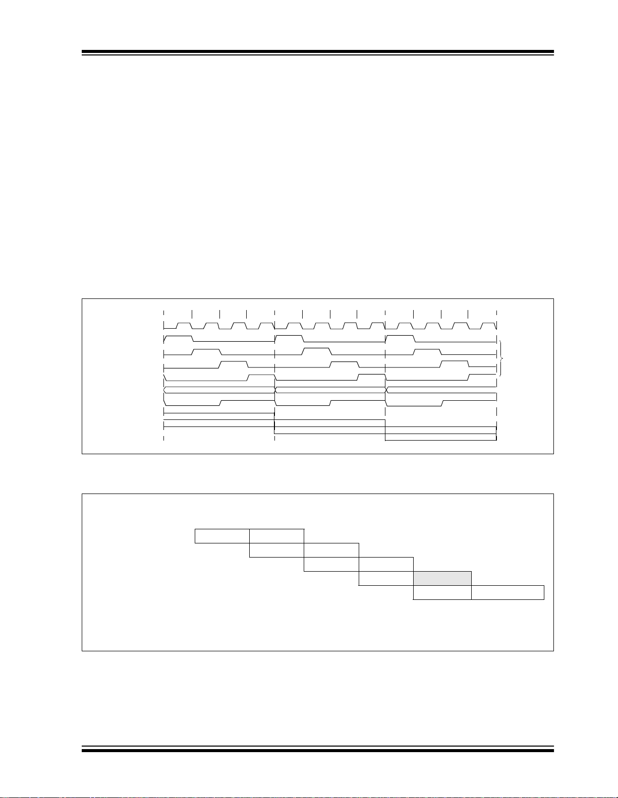
FIGURE 1-2: CLOCK/INSTRUCTION CYCLE
Q2 Q3 Q4
OSC1
Q1
Q2
Q3
Q4
PC
OSC2/CLKOUT
(RC mode)
Q1
PC PC+1 PC+2
Fetch INST (PC)
Execute INST (PC-1) Fetch INST (PC+1)
Q1
Execute INST (PC) Fetch INST (PC+2)
1.2 Instruction Flow/Pipelining
An “Instruction Cycle” consists of four Q cycles (Q1,
Q2, Q3 and Q4). The instruc tio n fetch and execute are
pipelined, such that fetch takes one instruction cycle,
while decode and execute takes another instruction
cycle. However, due to the pipelining, each instruction
effectively executes in one cycle. If an instruction
causes the program counter to change (e.g. GOTO),
then two cycles are req uired to c omplete the ins truction
(Example 1-1).
A fetch cycle begins with the program counter (PC)
incrementing in Q1.
In the execution cy cle, the fetch ed instruction i s latched
into the “Instruction Register” in cycle Q1. This instruction is then decoded and executed during the Q2, Q3,
and Q4 cycles. Data memory is read during Q2 (operand read) and written during Q4 (destination write).
Q2 Q3 Q4
Q2 Q3 Q4
Q1
Execute INST (PC+1)
Internal
Phase
Clock
EXAMPLE 1-1: INSTRUCTION PIPELINE FLOW
TCY0TCY1TCY2TCY3TCY4TCY5
1. MOVLW 55h
2. MOVWF PORTB
3. CALL SUB_1
4. BSF PORTA, BIT3 (Forced NOP)
5. Instruction @ address SUB_1
All instructions are s ingle cycle, exce pt for any program br anches. These t ake two cycl es, since the fetch in struction
is “flushed” from the pipeline while the new instruction is being fetched and then executed.
2001 Microchip Technology Inc. Preliminary DS39544A-page 9
Fetch 1 Execute 1
Fetch 2 Execute 2
Fetch 3 Execute 3
Fetch 4 Flush
Fetch SUB_1 Execute SUB_1

PIC16C925/926
NOTES:
DS39544A-page 10 Preliminary 2001 Microchip Technology Inc.
2.0 MEMORY ORGANIZATION
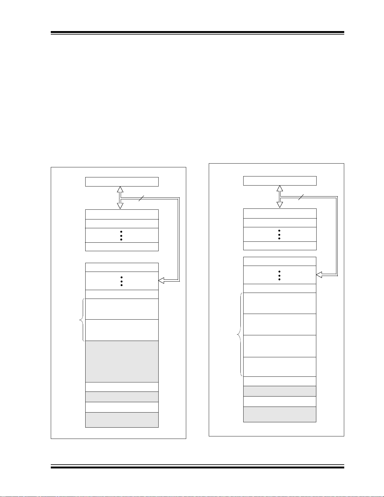
2.1 Program Memory Organization
The PIC16C925/926 family has a 13-bit program
counter capable of addressing an 8K x 14 program
memory space.
For the PIC16C925, only the first 4K x 14 (0000h0FFFh) are physically implemented. Accessing a location above the physically implemented addresses will
cause a wraparound. The RESET vector is at 0000h
and the interrupt vector is at 0004h.
PIC16C925/926
FIGURE 2-1: PROGRAM MEMORY MAP
AND STACK FOR
PIC16C925
PC<12:0>
CALL, RETURN
RETFIE, RETLW
On-chip
Program
Memory
Stack Level 1
Stack Level 2
Stack Level 8
RESET Vector
Interrupt Vector
Page 0
Page 1
Reads
0000h-0FFFh
ID Locations
Reserved
Configuration Word
Reserved
13
0000h
0004h
0005h
07FFh
0800h
0FFFh
1000h
1FFFh
2000h
2003h
2004h
2007h
3FFFh
FIGURE 2-2: PROGRAM MEMORY MAP
AND STACK FOR
PIC16C926
PC<12:0>
CALL, RETURN
RETFIE, RETLW
On-chip
Program
Memory
Stack Level 1
St ac k Lev el 2
Stac k Lev el 8
RESET Vector
Interru pt Vector
Page 0
Page 1
Page 2
Page 3
ID Locations
Reserved
Configuration Wo rd
Reserved
13
0000h
0004h
0005h
07FFh
0800h
0FFFh
1000h
17FFh
1800h
1FFFh
2000h
2003h
2004h
2007h
3FFFh
2001 Microchip Technology Inc. Preliminary DS39544A-page 11

PIC16C925/926
2.2 Data Memory Organization
The data memory is partitioned into four banks which
contain the General Purpose Reg isters a nd the Special
Function Registers. Bits RP1 and RP0 are the bank
select bits.
RP1:RP0
(STATUS<6:5>)
11
10
01
00
The lower locations of each Bank are reserved for the
Special Function Registers. Above the Special Function Registers are General Purpose Registers implemented as static RAM. All four banks contain special
function registers. Some “high use” special function
registers are mirrored in other banks for code reduc tion
and quicker access.
Bank
3 (180h-1FFh)
2 (100h-17Fh)
1 (80h-FFh)
0 (00h-7Fh )
2.2.1 GENERAL PURPOSE REGISTER FILE
The register file can be acces sed either directly, or indirectly through the File Select Register FSR
(Section 2.6).
The following General Purp ose Register s are not physically implemented:
• F0h-FFh of Bank 1
• 170h-17Fh of Bank 2
• 1F0h-1FFh of Bank 3
These locations are used for common access across
banks.
DS39544A-page 12 Preliminary 2001 Microchip Technology Inc.
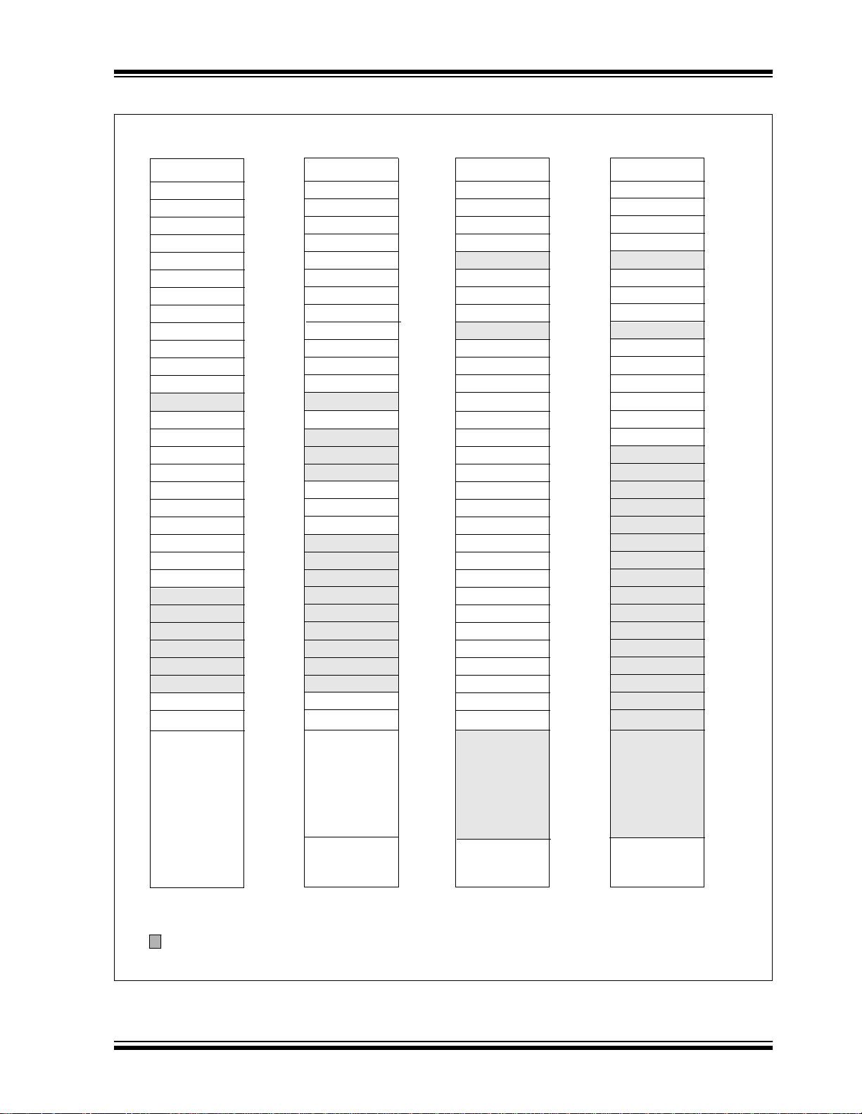
FIGURE 2-3: REGISTER FILE MAP — PIC16C925
PIC16C925/926
Indirect addr.(*)
TMR0
PCL
STATUS
FSR
PORTA
PORTB
PORTC
PORTD
PORTE
PCLATH
INTCON
PIR1
TMR1L
TMR1H
T1CON
TMR2
T2CON
SSPBUF
SSPCON
CCPR1L
CCPR1H
CCP1CON
ADRESH
ADCON0
File
Address
00h
01h
02h
03h
04h
05h
06h
07h
08h
09h
0Ah
0Bh
0Ch
0Dh
0Eh
0Fh
10h
11h
12h
13h
14h
15h
16h
17h
18h
19h
1Ah
1Bh
1Ch
1Dh
1Eh
1Fh
20h
Indirect addr.(*)
OPTION
PCL
STATUS
FSR
TRISA
TRISB
TRISC
TRISD
TRISE
PCLATH
INTCON
PIE1
PCON
PR2
SSPADD
SSPSTAT
ADRESL
ADCON1
File
Address
80h
81h
82h
83h
84h
85h
86h
87h
88h
89h
8Ah
8Bh
8Ch
8Dh
8Eh
8Fh
90h
91h
92h
93h
94h
95h
96h
97h
98h
99h
9Ah
9Bh
9Ch
9Dh
9Eh
9Fh
A0h
Indirect addr.(*)
TMR0
PCL
STATUS
FSR
PORTB
PORTF
PORTG
PCLATH
INTCON
PMCON1
LCDSE
LCDPS
LCDCON
LCDD00
LCDD01
LCDD02
LCDD03
LCDD04
LCDD05
LCDD06
LCDD07
LCDD08
LCDD09
LCDD10
LCDD11
LCDD12
LCDD13
LCDD14
LCDD15
File
Address
100h
101h
102h
103h
104h
105h
106h
107h
108h
109h
10Ah
10Bh
10Ch
10Dh
10Eh
10Fh
110h
111h
112h
113h
114h
115h
116h
117h
118h
119h
11Ah
11Bh
11Ch
11Dh
11Eh
11Fh
120h
Indirect addr.(*)
OPTION
PCL
STATUS
FSR
TRISB
TRISF
TRISG
PCLATH
INTCON
PMDATA
PMADR
PMDATH
PMADRH
File
Address
180h
181h
182h
183h
184h
185h
186h
187h
188h
189h
18Ah
18Bh
18Ch
18Dh
18Eh
18Fh
190h
191h
192h
193h
194h
195h
196h
197h
198h
199h
19Ah
19Bh
19Ch
19Dh
19Eh
19Fh
1A0h
General
Purpose
General
Purpose
Register
7Fh
Bank 0
Un implemented data memory locations, read as ’0’.
* Not a physical register.
2001 Microchip Technology Inc. Preliminary DS39544A-page 13
Register
accesses
70h - 7Fh
Bank 1
EFh
F0h
FFh
accesses
70h - 7Fh
Bank 2
16Fh
170h
17Fh
accesses
70h - 7Fh
Bank 3
1EFh
1F0h
1FFh
PIC16C925/926
FIGURE 2-4: REGISTER FILE MAP— PIC16C926
Indirect addr.(*)
TMR0
PCL
STATUS
FSR
PORTA
PORTB
PORTC
PORTD
PORTE
PCLATH
INTCON
PIR1
TMR1L
TMR1H
T1CON
TMR2
T2CON
SSPBUF
SSPCON
CCPR1L
CCPR1H
CCP1CON
ADRESH
ADCON0
General
Purpose
Register
96 Bytes
Bank 0
File
Address
00h
01h
02h
03h
04h
05h
06h
07h
08h
09h
0Ah
0Bh
0Ch
0Dh
0Eh
0Fh
10h
11h
12h
13h
14h
15h
16h
17h
18h
19h
1Ah
1Bh
1Ch
1Dh
1Eh
1Fh
20h
7Fh
Indirect addr.(*)
OPTION
PCL
STATUS
FSR
TRISA
TRISB
TRISC
TRISD
TRISE
PCLATH
INTCON
PIE1
PCON
PR2
SSPADD
SSPSTAT
ADRESL
ADCON1
General
Purpose
Register
80 Bytes
accesses
70h - 7Fh
Bank 1
File
Address
80h
81h
82h
83h
84h
85h
86h
87h
88h
89h
8Ah
8Bh
8Ch
8Dh
8Eh
8Fh
90h
91h
92h
93h
94h
95h
96h
97h
98h
99h
9Ah
9Bh
9Ch
9Dh
9Eh
9Fh
A0h
BFh
C0h
EFh
F0h
FFh
Indirect addr.(*)
TMR0
PCL
STATUS
FSR
PORTB
PORTF
PORTG
PCLATH
INTCON
PMCON1
LCDSE
LCDPS
LCDCON
LCDD00
LCDD01
LCDD02
LCDD03
LCDD04
LCDD05
LCDD06
LCDD07
LCDD08
LCDD09
LCDD10
LCDD11
LCDD12
LCDD13
LCDD14
LCDD15
General
Purpose
Register
80 Bytes
accesses
70h - 7Fh
Bank 2
File
Address
100h
101h
102h
103h
104h
105h
106h
107h
108h
109h
10Ah
10Bh
10Ch
10Dh
10Eh
10Fh
110h
111h
112h
113h
114h
115h
116h
117h
118h
119h
11Ah
11Bh
11Ch
11Dh
11Eh
11Fh
120h
16Fh
170h
17Fh
Indirect addr.(*)
OPTION
PCL
STATUS
FSR
TRISB
TRISF
TRISG
PCLATH
INTCON
PMDATA
PMADR
PMDATH
PMADRH
General
Purpose
Register
80 Bytes
accesses
70h - 7Fh
Bank 3
File
Address
180h
181h
182h
183h
184h
185h
186h
187h
188h
189h
18Ah
18Bh
18Ch
18Dh
18Eh
18Fh
190h
191h
192h
193h
194h
195h
196h
197h
198h
199h
19Ah
19Bh
19Ch
19Dh
19Eh
19Fh
1A0h
1EFh
1F0h
1FFh
Unimplemented data memory locations, read as ’0’.
* Not a physical register.
DS39544A-page 14 Preliminary 2001 Microchip Technology Inc.
PIC16C925/926
2.3 Special Function Registers
The Special Function Registers (SFRs) are registers
used by the CPU and Peripheral Modules for controlling the desired operation of the device. These registers are implemented as static RAM.
The special function regi sters can be classified into tw o
sets, core and peripheral. Those registers associated
with the “core” functions are described in this section.
Those related to the operation of the peripheral
features are described in the section of that peripheral
feature.
TABLE 2-1: SPECIAL FUNCTION REGISTER SUMMARY
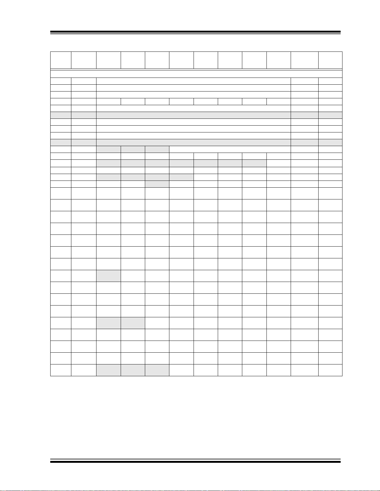
Address Name Bit 7 Bit 6 Bit 5 Bit 4 Bit 3 Bit 2 Bit 1 Bit 0
Bank 0
00h INDF Addressing this location uses contents of FSR to address data memory (not a physical register)
01h TMR0 Timer0 Module Register
02h PCL Program Counter (PC) Least Significant Byte
03h STATUS IRP RP1 RP0 TO PD Z DC C
04h FSR Indirect Data Memory Address Pointer
05h PORTA
06h PORTB PORTB Data Latch when writt en: PORTB pins when read
07h PORTC
08h PORTD PORTD Data Latch when written: PORTD pins when read
09h PORTE PORTE pins when read
0Ah PCLATH
0Bh INTCON GIE PEIE TMR0IE INTE RBIE TMR0IF INTF RBIF
0Ch PIR1 LCDIF ADIF
0Dh — Unimplemented — —
0Eh TMR1L Holding register for the Least Significant Byte of the 16-bit TMR1 Register
0Fh TMR1H Holding register for the Most Significant Byte of the 16-bit TMR1 Register
10h T1CON
11h TMR2 Timer2 Module Register
12h T2CON
13h SSPBUF Synchronous Ser i al Po rt Receive Buffer/Transmit Register
14h SSPCON WCOL SSPOV SSPEN CKP SSPM3 SSPM2 SSPM1 SSPM0
15h CCPR1L Capture/Compare/PWM Register (LSB)
16h CCPR1H Capture/Compare/PWM Register (MSB)
17h CCP1CON
18h — Unimplemented — —
19h — Unimplemented — —
1Ah — Unimplemented — —
1Bh — Unimplemented — —
1Ch — Unimplemented — —
1Dh — Unimplemented — —
1Eh ADRESH A/D Result Register High
1Fh ADCON0 ADCS1 ADCS0 CHS2 CHS1 CHS0 GO/DONE
Legend:
Note 1: These pixels do not display, but can be used as general purpose RAM.
x = unknown, u = unchanged, q = value depends on condition, - = unimplemented, read as '0'.
Shaded locations are unimplemented, read as ‘0’.
— — PORTA Data Latch when written: PORTA pins when read --0x 0000 29
— — PORTC Data Latch when written: PORTC pins when read --xx xxxx 33
— — — Write Buffer for the upper 5 bits of the Program Counter ---0 0000 25
— — SSPIF CCP1IF TMR2IF TMR1IF 00-- 0000 23
— — T1CKPS1 T1CKPS0 T1OSCEN T1SYNC TMR1CS TMR1ON --00 0000 47
— TOUTPS3 TOUTPS2 TOUTPS1 TOUTPS0 TMR2ON T2CKPS1 T2CKPS0 -000 0000 52
— — CCP1X CCP1Y CCP1M3 CCP1M2 CCP1M1 CCP1M0 --00 0000 53
— ADON 0000 0000 75
Value on
Power-on
Reset
0000 0000 26
xxxx xxxx 41
0000 0000 25
0001 1xxx 19
xxxx xxxx 26
xxxx xxxx 31
0000 0000 34
0000 0000 36
0000 000x 21
xxxx xxxx 47
xxxx xxxx 47
0000 0000 51
xxxx xxxx 64, 72
0000 0000 60
xxxx xxxx 58
xxxx xxxx 58
xxxx xxxx 80, 81
Details on
page
2001 Microchip Technology Inc. Preliminary DS39544A-page 15
PIC16C925/926
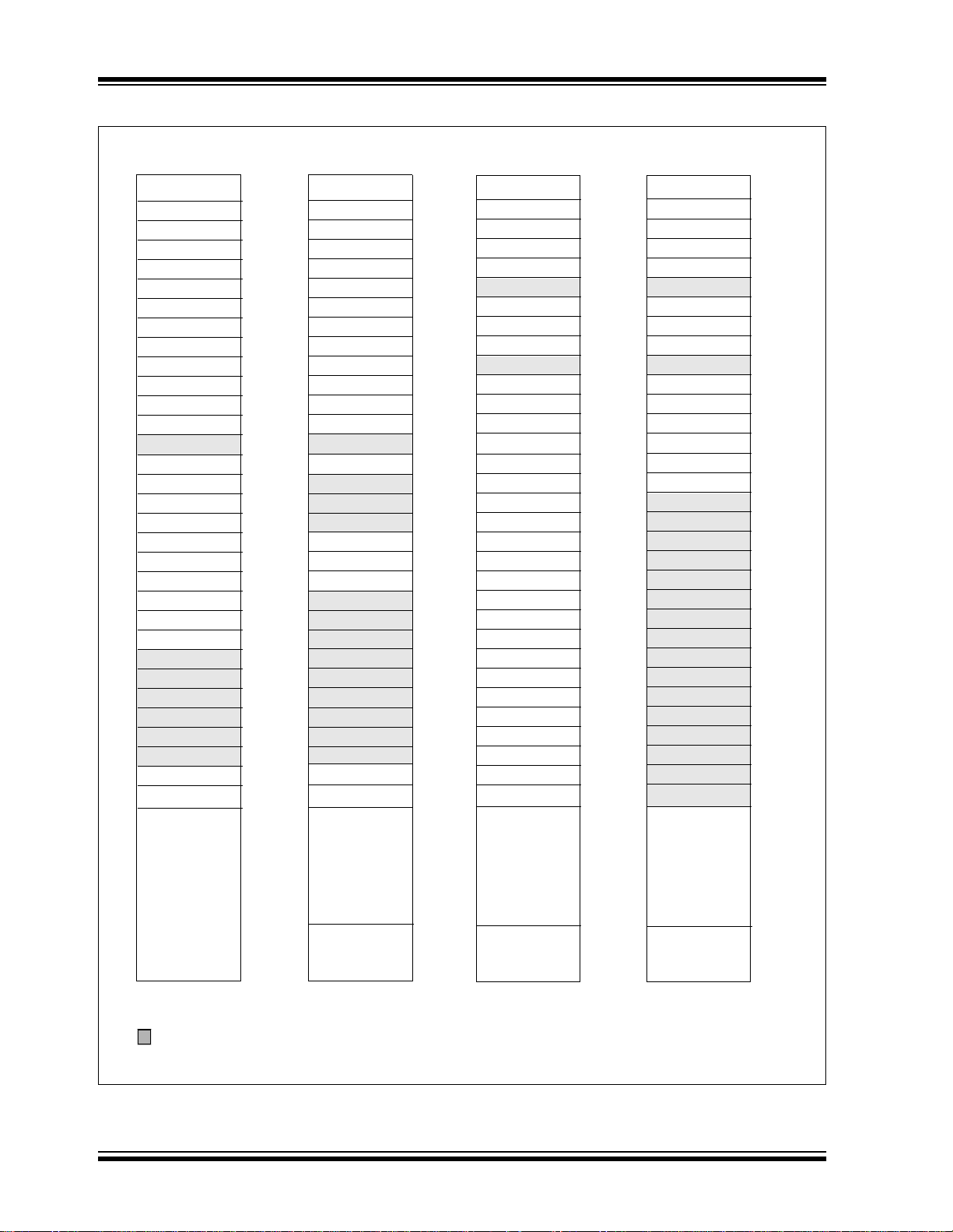
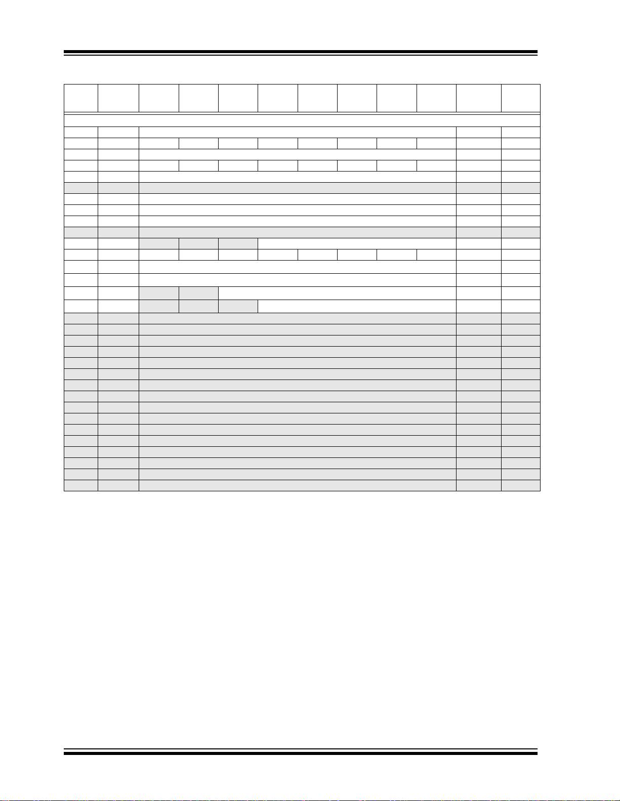
TABLE 2-1: SPECIAL FUNCTION REGISTER SUMMARY (CONTINUED)
Address Name Bit 7 Bit 6 Bit 5 Bit 4 Bit 3 Bit 2 Bit 1 Bit 0
Bank 1
80h INDF Addressing this location uses contents of FSR to address data memory (not a physical register)
81h OPTION RBPU INTEDG T0CS T0SE PSA PS2 PS1 PS0
82h PCL Program Counter (PC) Least Significant Byte
83h STATUS IRP RP1 RP0 TO PD Z DC C
84h FSR Indirect Data Memory Address Pointer
85h TRISA
86h TRISB PORTB Data Direction Register
87h TRISC
88h TRISD PORTD Data Direction Register
89h TRISE PORTE Data Direction Register
8Ah PCLATH
8Bh INTCON GIE PEIE TMR0IE INTE RBIE TMR0IF INTF RBIF
8Ch PIE1 LCDIE ADI E
8Dh — Unimplemented — —
8Eh PCON
8Fh — Unimplemented — —
90h — Unimplemented — —
91h — Unimplemented — —
92h PR2 Timer2 Period Register
93h SSPADD Synchronous Serial Port (I
94h SSPSTAT SMP CKE D/A
95h — Unimplemented — —
96h — Unimplemented — —
97h — Unimplemented — —
98h — Unimplemented — —
99h — Unimplemented — —
9Ah — Unimplemented — —
9Bh — Unimplemented — —
9Ch — Unimplemented — —
9Dh — Unimplemented — —
9Eh ADRESL A/D Result Register Low
9Fh ADCON1
Legend:
Note 1: These pixels do not display, but can be used as general purpose RAM.
x = unknown, u = unchanged, q = value depends on condition, - = unimplemented, read as '0'.
Shaded locations are unimplemented, read as ‘0’.
— — PORTA Data Direction Register --11 1111 29
— — PORTC Data Direction Register --11 1111 33
— — — Write Buffer for the upper 5 bits of the PC ---0 0000 25
— — SSPIE CCP1IE TMR2IE TMR1IE 00-- 0000 24
— — — — — — POR BOR ---- --0- 24
2
C mode) Address Register 0000 0000 69, 72
PSR/WUA BF 0000 0000 59
— — — — — PCFG2 PCFG1 PCFG0 ---- -000 76
Value on
Power-on
Reset
0000 0000 26
1111 1111 20
0000 0000 25
0001 1xxx 19
xxxx xxxx 26
1111 1111 31
1111 1111 34
1111 1111 36
0000 000x 21
1111 1111 51
xxxx xxxx 79
Details on
page
DS39544A-page 16 Preliminary 2001 Microchip Technology Inc.
PIC16C925/926
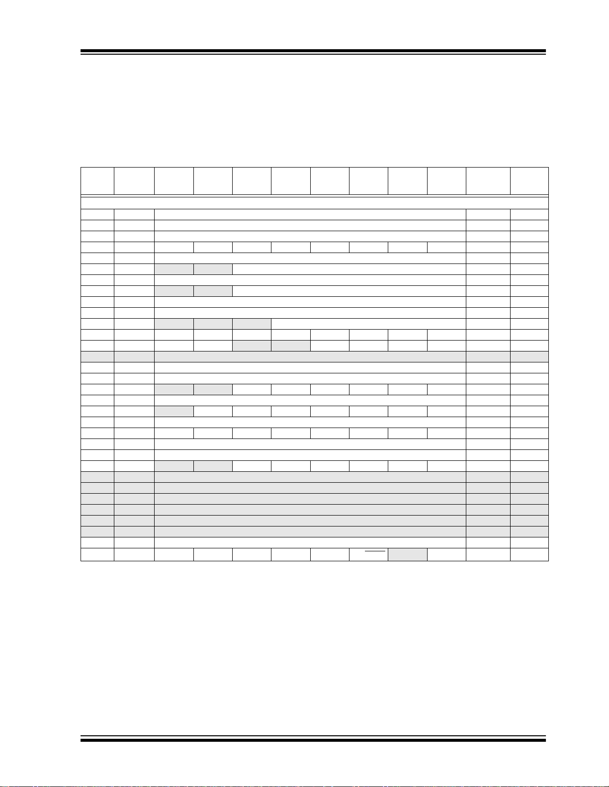
TABLE 2-1: SPECIAL FUNCTION REGISTER SUMMARY (CONTINUED)
Address Name Bit 7 Bit 6 Bit 5 Bit 4 Bit 3 Bit 2 Bit 1 Bit 0
Bank 2
100h INDF Addressing this location uses contents of FSR to address data memory (not a physical register)
101h TMR0 Timer0 Module Register
102h PCL Program Counter (PC) Least Significant Byte
103h STATUS IRP RP1 RP0 TO PD Z DC C
104h FSR Indirect Data Memory Address Pointer
105h — Unimplemented — —
106h PORTB PORTB Data Latch when writt en: PORTB pins when read
107h PORTF PORTF pins when read
108h PORTG PORTG pins when read
109h — Unimplemented — —
10Ah PCLATH
10Bh INTCON GIE PEIE TMR0IE INTE RBIE TMR0IF INTF RBIF
10Ch PMCON1
10Dh LCDSE SE29 SE27 SE20 SE16 SE12 SE9 SE5 SE0
10Eh LCDPS
10Fh LCDCON LCDEN SLPEN
110h LCDD00 SEG07
111h LCDD01 SEG15
112h LCDD02 SEG23
113h LCDD03 SEG31
114h LCDD04 SEG07
115h LCDD05 SEG15
116h LCDD06 SEG23
117h LCDD07
118h LCDD08 SEG07
119h LCDD09 SEG15
11Ah LCDD10 SEG23
11Bh LCDD11
11Ch LCDD12 SEG07
11Dh LCDD13 SEG15
11Eh LCDD14 SEG23
11Fh LCDD15
Legend:
Note 1: These pixels do not display, but can be used as general purpose RAM.
x = unknown, u = unchanged, q = value depends on condition, - = unimplemented, read as '0'.
Shaded locations are unimplemented, read as ‘0’.
— — — Write Buffer for the upper 5 bits of the PC ---0 0000 25
reserved — — — — — —
— — — — LP3 LP2 LP1 LP0 ---- 0000 84
— VGEN CS1 CS0 LMUX1 LMUX0 00-0 0000 83
COM0
COM0
COM0
COM0
COM1
COM1
COM1
SEG31
COM1
COM2
COM2
COM2
SEG31
COM2
COM3
COM3
COM3
SEG31
COM3
SEG06
COM0
SEG14
COM0
SEG22
COM0
SEG30
COM0
SEG06
COM1
SEG14
COM1
SEG22
COM1
SEG30
(1)
COM1
SEG06
COM2
SEG14
COM2
SEG22
COM2
SEG30
(1)
COM2
SEG06
COM3
SEG14
COM3
SEG22
COM3
SEG30
(1)
COM3
SEG05
COM0
SEG13
COM0
SEG21
COM0
SEG29
COM0
SEG05
COM1
SEG13
COM1
SEG21
COM1
SEG29
COM1
SEG05
COM2
SEG13
COM2
SEG21
COM2
SEG29
(1)
COM2
SEG05
COM3
SEG13
COM3
SEG21
COM3
SEG29
(1)
COM3
SEG04
COM0
SEG12
COM0
SEG20
COM0
SEG28
COM0
SEG04
COM1
SEG12
COM1
SEG20
COM1
SEG28
COM1
SEG04
COM2
SEG12
COM2
SEG20
COM2
SEG28
COM2
SEG04
COM3
SEG12
COM3
SEG20
COM3
SEG28
(1)
COM3
SEG03
COM0
SEG11
COM0
SEG19
COM0
SEG27
COM0
SEG03
COM1
SEG11
COM1
SEG19
COM1
SEG27
COM1
SEG03
COM2
SEG11
COM2
SEG19
COM2
SEG27
COM2
SEG03
COM3
SEG11
COM3
SEG19
COM3
SEG27
COM3
SEG02
COM0
SEG10
COM0
SEG18
COM0
SEG26
COM0
SEG02
COM1
SEG10
COM1
SEG18
COM1
SEG26
COM1
SEG02
COM2
SEG10
COM2
SEG18
COM2
SEG26
COM2
SEG02
COM3
SEG10
COM3
SEG18
COM3
SEG26
COM3
SEG01
COM0
SEG09
COM0
SEG17
COM0
SEG25
COM0
SEG01
COM1
SEG09
COM1
SEG17
COM1
SEG25
COM1
SEG01
COM2
SEG09
COM2
SEG17
COM2
SEG25
COM2
SEG01
COM3
SEG09
COM3
SEG17
COM3
SEG25
COM3
RD
SEG00
COM0
SEG08
COM0
SEG16
COM0
SEG24
COM0
SEG00
COM1
SEG08
COM1
SEG16
COM1
SEG24
COM1
SEG00
COM2
SEG08
COM2
SEG16
COM2
SEG24
COM2
SEG00
COM3
SEG08
COM3
SEG16
COM3
SEG24
COM3
Value on
Power-on
Reset
0000 0000 26
xxxx xxxx 41
0000 0000 25
0001 1xxx 19
xxxx xxxx 26
xxxx xxxx 31
0000 0000 37
0000 0000 38
0000 000x 21
1--- ---0 27
1111 1111 94
xxxx xxxx 92
xxxx xxxx 92
xxxx xxxx 92
xxxx xxxx 92
xxxx xxxx 92
xxxx xxxx 92
xxxx xxxx 92
xxxx xxxx 92
xxxx xxxx 92
xxxx xxxx 92
xxxx xxxx 92
xxxx xxxx 92
xxxx xxxx 92
xxxx xxxx 92
xxxx xxxx 92
xxxx xxxx 92
Details on
page
2001 Microchip Technology Inc. Preliminary DS39544A-page 17
PIC16C925/926
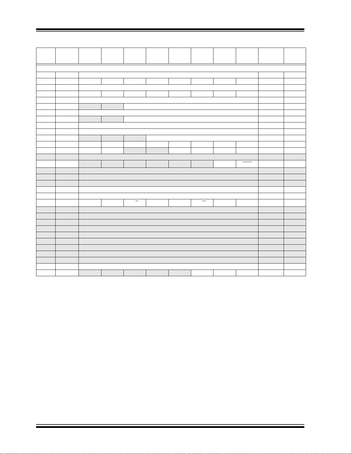
TABLE 2-1: SPECIAL FUNCTION REGISTER SUMMARY (CONTINUED)
Address Name Bit 7 Bit 6 Bit 5 Bit 4 Bit 3 Bit 2 Bit 1 Bit 0
Bank 3
180h INDF Addressing this location uses contents of FSR to address data memory (not a physical register)
181h OPTION RBPU INTEDG T0CS T0SE PSA PS2 PS1 PS0
182h PCL Program Counter’s (PC) Least Significant Byte
183h STATUS IRP RP1 RP0 TO PD Z DC C
184h FSR Indirect Data Memory Address Pointer
185h — Unimplemented — —
186h TRISB PORTB Data Direction Register
187h TRISF PORTF Data Directi on Register
188h TRISG PORTG Data Direction Register
189h — Unimplemented — —
18Ah PCLATH
18Bh INTCON GIE PEIE TMR0IE INTE RBIE TMR0IF INTF RBIF
18Ch PMDATA Data Register Low Byte
18Dh PMADR Address Register Low Byte
18Eh PMDATH
18Fh PMADRH
190h — Unimplemented — —
191h — Unimplemented — —
192h — Unimplemented — —
193h — Unimplemented — —
194h — Unimplemented — —
195h — Unimplemented — —
196h — Unimplemented — —
197h — Unimplemented — —
198h — Unimplemented — —
199h — Unimplemented — —
19Ah — Unimplemented — —
19Bh — Unimplemented — —
19Ch — Unimplemented — —
19Dh — Unimplemented — —
19Eh — Unimplemented — —
19Fh — Unimplemented — —
Legend:
Note 1: These pixels do not display, but can be used as general purpose RAM.
x = unknown, u = unchanged, q = value depends on condition, - = unimplemented, read as '0'.
Shaded locations are unimplemented, read as ‘0’.
— — — Write Buffer for the upper 5 bits of the PC ---0 0000 25
— — Data Regist er Hi gh Byt e xxxx xxxx 27
— — —
Address Register High Byte
Value on
Power-on
Reset
0000 0000 26
1111 1111 20
0000 0000 25
0001 1xxx 19
xxxx xxxx 26
1111 1111 31
1111 1111 37
1111 1111 38
0000 000x 21
xxxx xxxx 27
xxxx xxxx 27
xxxx xxxx
Details on
page
27
DS39544A-page 18 Preliminary 2001 Microchip Technology Inc.
PIC16C925/926
2.3.1 STATUS REGISTER
The STATUS register, shown in Register2-1, contains
the arithmetic st atus of th e ALU, the RE SET statu s and
the bank select bits for data memory.
The STATUS register can be the destination for any
instruction, as with any other register. If the STATUS
register is the destination for an instruction that affects
the Z, DC or C bits, then the write to these three bits is
disabled. These bit s are set or cleared ac cording to the
device logic. Furthermore, the TO
writable. Therefore, the result of an instruction with the
STATUS register as dest ination may be di fferent than
intended.
and PD bits are not
For example, CLRF STATUS will clear the upper-three
bits and set the Z bit. This leaves the STATUS register
as 000u u1uu (where u = unchanged).
It is recommended, therefore, that only BCF, BSF,
SWAPF and MOVWF instructions are used to alter the
STATUS register because these instructions do not
affect the Z, C or DC bits from the ST ATUS reg ister . For
other instructions, no t affecting any status bi ts, see the
“Instruction Set Summary.”
Note: The C and DC bits operate as a borrow
and digit borrow bit, respectively, in subtraction. See the SUBLW and SUBWF
instructions for examples.
REGISTER 2-1: STATUS REGISTER (ADDRESS 03h, 83h, 103h, 183h)
R/W-0 R/W-0 R/W-0 R-1 R-1 R/W-x R/W-x R/W-x
IRP RP1 RP0 TO
bit 7 bit 0
bit 7 IRP: Register Bank Select bit (used for indirect addressing)
1 = Bank 2, 3 (100h - 1FFh)
0 = Bank 0, 1 (00h - FFh)
bit 6-5 RP1:RP0: Register Bank Select bits (used for direct addressing)
11 = Bank 3 (180h - 1FFh)
10 = Bank 2 (100h - 17Fh)
01 = Bank 1 (80h - FFh)
00 = Bank 0 (00h - 7Fh)
bit 4 TO: Time-out bit
1 = After power-up, CLRWDT instruction, or SLEEP instruction
0 = A WDT time-out occurred
bit 3 PD
bit 2 Z: Zero bit
bit 1 DC: Digit carry/borrow bit (ADDWF, ADDLW,SUBLW,SUBWF instructions)
bit 0 C: Carry/borrow
: Power-down bit
1 = After power-up or by the CLRWDT instruction
0 = By execution of the SLEEP instruction
1 = The result of an arithmetic or logic operation is zero
0 = The result of an arithmetic or logic operation is not zero
(for borrow
1 = A carry-out from the 4th low order bit of the result occurred
0 = No carry-out from the 4th low order bit of the result
(for borrow
1 = A carry-out from the Most Significant bit of the result occurred
0 = No carry-out from the Most Significant bit of the result occurred
the polarity is reversed)
bit (ADDWF, ADDLW,SUBLW,SUBWF instructions)
the polarity is reversed)
PD ZDCC
Note: A subtraction is executed by adding the two’s complement of the second operand.
For rotate (RRF, RLF) instructions, thi s bi t is l oad ed w ith ei the r th e h igh or low order
bit of the source register.
Legend:
R = Readable bit W = Writable bit U = Unimplemented bit, read as ‘0’
- n = Value at POR ’1’ = Bit is set ’0’ = Bit is cleared x = Bit is unknown
2001 Microchip Technology Inc. Preliminary DS39544A-page 19

PIC16C925/926
2.3.2 OPTION REGISTER
The OPTION register is a readable and writable register, which contains various control bits to configure the
TMR0/WDT prescaler, the external RB0/INT pin interrupt, TMR0, and the weak pull-ups on PORTB.
REGISTER 2-2: OPTION REGISTER (ADDRESS 81h, 181h)
R/W-1 R/W-1 R/W-1 R/W-1 R/W-1 R/W-1 R/W-1 R/W-1
RBPU INTEDG T0CS T0SE PSA PS2 PS1 PS0
bit 7 bit 0
Note: To achieve a 1:1 prescaler assignment for
the TMR0 register, assign the prescaler to
the Watchdog Timer.
bit 7 RBPU
bit 6 INTEDG: Interrupt Edge Select bit
bit 5 T0CS: TMR0 Clock Source Select bit
bit 4 T0SE: TMR0 Source Edge Select bit
bit 3 PSA: Prescaler Assignment bit
bit 2-0 PS2:PS0: Prescaler Rate Select bits
: PORTB Pull-up Enable bit
1 = PORTB pull-ups are disabled
0 = PORTB pull-ups are enabled by individual port latch values
1 = Interrupt on rising edge of RB0/INT pin
0 = Interrupt on falling edge of RB0/INT pin
1 = Transition on RA 4/T0CKI pin
0 = Internal instruction cycle clock (CLKOUT)
1 = Increment on high-to-low transition on RA4/T0CKI pin
0 = Increment on low-to-high transition on RA4/T0CKI pin
1 = Prescaler is assigned to the WDT
0 = Prescaler is assigned to the Timer0 module
Bit Value TMR0 Rate WDT Rate
000
001
010
011
100
101
110
111
1 : 2
1 : 4
1 : 8
1 : 16
1 : 32
1 : 64
1 : 128
1 : 256
1 : 1
1 : 2
1 : 4
1 : 8
1 : 16
1 : 32
1 : 64
1 : 128
Legend:
R = Readable bit W = Writable bit U = Unimplemented bit, read as ‘0’
- n = Value at POR ’1’ = Bit is set ’0’ = Bit is cleared x = Bit is unknown
DS39544A-page 20 Preliminary 2001 Microchip Technology Inc.
PIC16C925/926
2.3.3 INTCON REGISTER
The INTCON Register is a readabl e and writ able register which contains various enable and flag bits for the
TMR0 register overflow, RB Port change and external
RB0/INT pin interrupts.
Note: Interrupt flag bit s are set whe n an in terrupt
condition occurs, regardless of the state of
its corresponding enable bit or the global
enable bit, GIE (INTCON<7>).
REGISTER 2-3: INTCON REGISTER (ADDRESS 0Bh, 8Bh, 10Bh, 18Bh)
R/W-0 R/W-0 R/W-0 R/W-0 R/W-0 R/W-0 R/W-0 R/W-x
GIE PEIE TMR0IE INTE RBIE TMR0IF INTF RBIF
bit 7 bit 0
bit 7 GIE: Global Interrupt Enable bit
1 = Enables all unmasked interrupts
0 = Disables all interrupts
bit 6 PEIE/GEIL: Peripheral Interrupt Enable bit
1 = Enables all unmasked peripheral interrupts
0 = Disables all peripheral interrupts
bit 5 TMR0IE: TMR0 Overflow Interrupt Enable bit
1 = Enables the TMR0 overflow interrupt
0 = Disables the TMR0 overflow interrupt
bit 4 INTE: RB0/INT0 External Interrupt Enable bit
1 = Enables the RB0/INT external interrupt
0 = Disables the RB0/INT external interrupt
bit 3 RBIE: RB Port Change Interrupt Enable bit
1 = Enables the RB port change interrupt
0 = Disables the RB port change interrupt
bit 2 TMR0IF: TMR0 Overflow Interrupt Flag bit
1 = TMR0 register has overflowed (must be cleared in software)
0 = TMR0 register did not overflow
bit 1 INTF: RB0/INT0 External Interrupt Flag bit
1 = The RB0/INT external interrupt occurred (must be cleared in software)
0 = The RB0/INT external interrupt did not occur
bit 0 RBIF: RB Port Change Interrupt Flag bit
1 = At least one of the RB7:RB4 pins changed state (must be cleared in software)
0 = None of the RB7:RB4 pins have changed state
Legend:
R = Readable bit W = Writable bit U = Unimplemented bit, read as ‘0’
- n = Value at POR reset ’1’ = Bit is set ’0’ = Bit is cleared x = Bit is unknown
2001 Microchip Technology Inc. Preliminary DS39544A-page 21
PIC16C925/926
2.3.4 PIE1 REGISTER
This register contains the individual enable bits for the
peripheral interrupts.
REGISTER 2-4: PIE1 REGISTER (ADDRESS 8Ch)
R/W-0 R/W-0 U-0 U-0 R/W-0 R/W-0 R/W-0 R/W-0
LCDIE ADIE
bit 7 bit 0
bit 7 LCDIE: LCD Interrupt Enable bit
1 = Enables the LCD interrupt
0 = Disables the LCD interrupt
bit 6 ADIE: A/D Converter Interrupt Enable bit
1 = Enables the A/D interrupt
0 = Disables the A/D interrupt
bit 5-4 Unimplemented: Read as ‘0’
bit 3 SSPIE: Synchronous Serial Port Interrupt Enable bit
1 = Enables the SSP interrupt
0 = Disables the SSP interrupt
bit 2 CCP1IE: CCP1 Interrupt Enable bit
1 = Enables the CCP1 interrupt
0 = Disables the CCP1 interrupt
bit 1 TMR2IE: TMR2 to PR2 Match Interrupt Enable bit
1 = Enables the TMR2 to PR2 match interrupt
0 = Disables the TMR2 to PR2 match interrupt
bit 0 TMR1IE: TMR1 Overflow Interrupt Enable bit
1 = Enables the TMR1 overflow interrupt
0 = Disables the TMR1 overflow interrupt
— — SSPIE CCP1IE TMR2IE TMR1IE
Note: Bit PEIE (INTCON<6>) must be set to
enable any peripheral interrupt.
Legend:
R = Readable bit W = Writable bit U = Unimplemented bit, read as ‘0’
- n = Value at POR ’1’ = Bit is set ’0’ = Bit is cleared x = Bit is unknown
DS39544A-page 22 Preliminary 2001 Microchip Technology Inc.

2.3.5 PIR1 REGISTER
This register contains the individual flag bits for the
peripheral interrupts.
Note: Interrupt flag bits are se t w he n an interrupt
condition occurs, re gardless of the state of
its corresponding enable bit or the global
enable bit, GIE (INTCON<7>). User software should ensure the appropriate interrupt flag bits are clear prior to enabling an
interrupt.
REGISTER 2-5: PIR1 REGISTER (ADDRESS 0Ch)
R/W-0 R/W-0 U-0 U-0 R/W-0 R/W-0 R/W-0 R/W-0
LCDIF ADIF
bit 7 bit 0
bit 7 LCDIF: LCD Interrupt Flag bit
1 = LCD interrupt has occurred (must be cleared in software)
0 = LCD interrupt did not occur
bit 6 ADIF: A/D Converter Interrupt Flag bit
1 = An A/D conversion completed (must be cleared in software)
0 = The A/D conversion is not complete
bit 5-4 Unimplemented: Read as ‘0’
bit 3 SSPIF: Master Synchronous Serial Port Interrupt Flag bit
1 = The transmission/reception is complete (must be cleared in software)
0 = Waiting to transmit/receive
bit 2 CCP1IF: CCP1 Interrupt Flag bit
Capture mode:
1 = A TMR1 register capture occurred (must be cleared in software)
0 = No TMR1 register capture occurred
Compare mode:
1 = A TMR1 register compare match occurred (must be cleared in software)
0 = No TMR1 register compare match occurred
PWM mode:
Unused in this mode
bit 1 TMR2IF: TMR2 to PR2 Match Interrupt Flag bit
1 = TMR2 to PR2 match occurred (must be cleared in software)
0 = No TMR2 to PR2 match occurred
bit 0 TMR1IF: TMR1 Overflow Interrupt Flag bit
1 = TMR1 register overflowed (must be cleared in software)
0 = TMR1 register did not overflow
— — SSPIF CCP1IF TMR2IF TMR1IF
PIC16C925/926
Legend:
R = Readable bit W = Writable bit U = Unimplemented bit, read as ‘0’
- n = Value at POR rese t ’1’ = Bit is set ’0’ = Bit is cleared x = Bit is unknown
2001 Microchip Technology Inc. Preliminary DS39544A-page 23
PIC16C925/926
2.3.6 PCON REGISTER
The Power Control (PCON) register contains a flag bit
to allow differentiation between a Power-on Reset
(POR) to an external MCLR
For various RESET conditions, see Table 12-4 and
Table 12-5.
REGISTER 2-6: PCON REGISTER (ADDRESS 8Eh)
bit 7-2 Unimplemented: Read as '0'
bit 1 POR
bit 0 BOR
Reset or WDT Reset.
U-0 U-0 U-0 U-0 U-0 U-0 R/W-0 R/W-1
— — — — — — POR BOR
bit 7 bit 0
: Power-on Reset Status bit
1 = No Power-on Reset occurred
0 = A Power-on Reset occurred (must be set in software after a Power-on Reset occurs)
: Brown-out Reset Status bit
1 = No Brown-out Reset occurred
0 = A Brown-out Reset occurred (must be set in software after a Brown-out Reset occurs)
Legend:
R = Readable bit W = Writable bit U = Unimplemented bit, read as ‘0’
- n = Value at POR ’1’ = Bit is set ’0’ = Bit is cleared x = Bit is unknown
DS39544A-page 24 Preliminary 2001 Microchip Technology Inc.

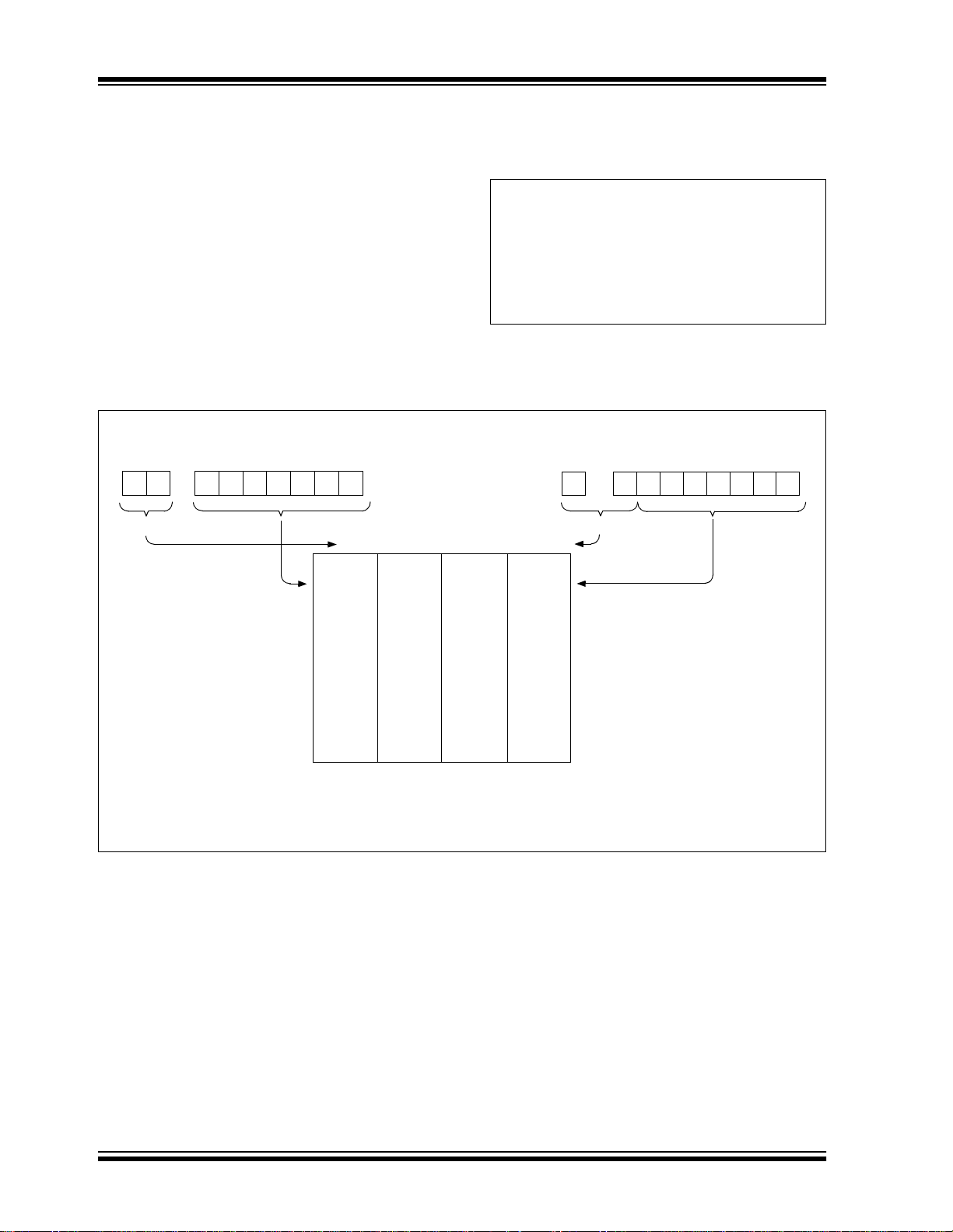
2.4 PCL and PCLATH
The program counter (PC) is 13-bits wid e. The low byte
comes from the PCL register, which is a readable and
writable register. The upper bits (PC<12:8>) are not
readable, but are indirectly writable through the
PCLA TH reg is ter. On any RESET, the up per bi t s of the
PC will be cleared. Fig ure2-5 shows the two situations
for the loading of the PC. The up per ex ample in th e figure shows how the PC is loaded on a write to PCL
(PCLATH<4:0> → PCH). The lower exampl e i n th e fi gure shows how the PC is loaded during a CALL or GOTO
instruction (PCLATH<4:3> → PCH).
FIGURE 2-5: LOADING OF PC IN
DIFFERENT SITUATIONS
PIC16C925/926
2.5 Program Memory Paging
PIC16C925/926 devices are capable of addressing a
continuous 8K word block of program memory. The
CALL and GOTO instructions provide only 11-bits of
address to allow branching within any 2K program
memory page. When doing a CALL or GOTO instruction,
the upper 2-bits of the address are provided by
PCLATH<4:3>. When doing a CALL or GOTO instruction, the user must ensu re tha t the p age select bits are
programmed so that the desired program memory
page is addressed. If a return from a CALL instruction
(or interrupt) is executed, the en tire 13-bit PC is pushed
onto the stack. Therefore, manipulation of the
PCLATH<4:3> bits is not required for the RETURN
instructions (which POPs the address from the stack).
2.4.1 COMPUTED GOTO
A computed GOTO is accomplish ed by adding an offset
to the program counter (ADDWF PCL). When doing a
table read using a computed GOTO method, care
should be exercise d i f the t able loca tio n cros ses a PCL
memory boundary (each 256 byte block). Refer to the
application note “I mplementing a Table Read” (AN556).
2.4.2 STACK
The PIC16CXXX family has an 8-level deep x 13-bit
wide hardware stack. The stack space is not part of
either program or data space and the stack pointer is not
readable or writable. The PC is PUSHed onto the stack
when a CALL instruction is executed, or an interrupt
causes a branch. The stack is POPed in the event of a
RETURN, RETLW or a RETFIE instruction execution.
PCLATH is not affected by a PUSH or POP operation.
The stack opera tes as a circular buf fer . This means that
after the st ack h as be en PUSHed ei ght ti mes, th e nin th
push overwrites the v alue tha t was stored fro m the first
push. The tenth pus h ov erwri t es the se co nd p us h (an d
so on).
Example 2-1 shows the calling of a subroutine in
2001 Microchip Technology Inc. Preliminary DS39544A-page 25
PIC16C925/926
2.6 Indirect Addressing, INDF and FSR Registers
The INDF register is not a physi cal register. Addressing
the INDF register will cause indirect addressing.
Indirect addressing is possible by using the INDF register. Any instruc tion using the INDF register actual ly
accesses the register pointed to by the File Sele ct Register (FSR). Reading the INDF register itself, indirectly
(FSR = ’0’), w ill produc e 00h . W rit ing to the INDF re gister indirectly results in a no operation (although status
bits may be affected). An effective 9-bit address is
obtained by co ncatenating the 8-bit FSR re gister and
the IRP bit (STATUS<7>), as shown in Figure 2-6.
FIGURE 2-6: DIRECT/INDIRECT ADDRESSING
RP1:RP0 6
Bank Select Location Select
From Opcode
00h
0
00 01 10 11
A simple program to clear RAM locations 20h-2Fh
using indirect addressing is shown in Example 2-2.
EXAMPLE 2-2: INDIRECT ADDRESSING
MOVLW 0x20 ;initialize pointer
NEXT CLRF INDF ;clear INDF register
CONTINUE
MOVWF FSR ;to RAM
INCF FSR,F ;inc pointer
BTFSS FSR,4 ;all done?
GOTO NEXT ;no clear next
: ;yes continue
Indirect AddressingDirect Addressing
IRP FSR Register
Bank Select
7
Location Select
00h
0
Data
Memory
7Fh
Bank 0 Bank 1 Bank 2 Bank 3
Note: For memory map detail, see Figure 2-3.
7Fh
DS39544A-page 26 Preliminary 2001 Microchip Technology Inc.

PIC16C925/926
3.0 READING PROGRAM MEMORY
The Program Memory is readable during normal operation over the entire V
addressed through Special Function R egisters ( SFR).
Up to 14-bit numbers can be stored in memory for use
as calibration param eters, serial nu mbers, packe d 7-bit
ASCII, etc. Executing a pro gram m em ory location containing data tha t forms an inval id instructi on result s in a
NOP.
There are five SFRs used to read the program and
memory. These registers are:
• PMCON1
• PMDATA
• PMDATH
• PMADR
• PMADRH
The program memory allows word reads. Program
memory access allows for checksum calculation and
reading calibration t abl es .
DD range. It is indirectly
When interfacing to the program memory block, the
PMDATH:PMDATA registers form a two-byte word,
which holds the 14-bit data for reads. The
PMADRH:PMADR registers form a two-byte word,
which holds the 13-bit address of the location being
accessed. These devices can have from 4K words to
8K words of program memory, with an address range
from 0h to 3FFFh.
The unused upper bits in both the PMDATH and
PMADRH registers are not implemented and read as
“0’s”.
3.1 PMADR
The address registers can address up to a maxim um of
8K words of program memory.
When selecting a program address value, the MSByte
of the address is written to the PMADRH register and
the LSByte is written to the PMADR regi ster . The upper
MSbits of PMADRH must always be clear.
3.2 PMCON1 Register
PMCON1 is the control register for memory accesses.
The control bit RD initiates read operations. This bit
cannot be cleared, only set , in sof tware. It is cleared in
hardware at the completion of the read operation.
REGISTER 3-1: PMCON1 REGISTER (ADDRESS 10Ch)
R-1 U-0 U-0 U-0 U-x U-0 U-0 R/S-0
r — — — — — — RD
bit 7 bit 0
bit 7 Reserved: Read as ‘1’
bit 6-1 Unimplemented: Read as ‘0’
bit 0 RD: Read Control bit
1 = Initiates a read, RD is cleared in hardware. The RD bit can only be set (not cleared)
in software.
0 = Does not initiate a read
Legend:
R = Readable bit W = Writable bit U = Unimplemented bit, read as ‘0’
- n = Value at POR reset ’1’ = Bit is set ’0’ = Bit is cleared x = Bit is unknown
2001 Microchip Technology Inc. Preliminary DS39544A-page 27
PIC16C925/926
3.3 Reading the Program Memory
A program memory loca tion may be read by wri ting two
bytes of the address to the PMADR and PMADRH registers, and then setting control bit RD (PMCON1<0>).
Once the read control bit is set, the microcontroller will
data is available in the PMDATA and PMDATH registers after the NOP instruction. Therefore, it can be read
as two bytes in the f ollowin g instruct ions. The PMDATA
and PMDA TH re gisters w ill hold this value unti l another
read operation.
use the next two instruction cy cles to read the data. The
EXAMPLE 3-1: PROGRAM READ
BSF STATUS, RP1 ;
BSF STATUS, RP0 ; Bank 3
MOVLW MS_PROG_PM_ADDR ;
MOVWF PMADRH ; MS Byte of Program Address to read
MOVLW LS_PROG_PM_ADDR ;
MOVWF PMADR ; LS Byte of Program Address to read
BCF STATUS, RP0 ; Bank 2
BSF PMCON1, RD ; PM Read
;
BSF STATUS, RP0 ; Bank 3
;
NOP ; Any instructions here are ignored as program
;
MOVF PMDATA, W ; W = LS Byte of Program PMDATA
MOVF PMDATH, W ; W = MS Byte of Program PMDATA
; First instruction after BSF PMCON1,RD executes normally
; memory is read in second cycle after BSF PMCON1,RD
3.4 Operation During Code Protect
If the progra m memory is not co de prot ected, the pro gram memory control can read anywhere within the
program memory.
If the entire program memory is code protected, the
program memory control can re ad anywh ere within the
program memory.
TABLE 3-1: REGISTERS ASSOCIATED WITH PROGRAM MEMORY
Address Name Bit 7 Bit 6 Bit 5 Bit 4 B it 3 Bit 2 Bit 1 Bit 0
10Ch PMCON1 (1)
18Ch PMDATA Data Register Low Byte xxxx xxxx uuuu uuuu
18Dh PMADR Address Register Low Byte xxxx xxxx uuuu uuuu
18Eh PMDATH — — Data Register High Byte xxxx xxxx uuuu uuuu
18Fh PMADRH — — — Address Register High Byte xxxx xxxx uuuu uuuu
Legend: x = unknown, u = unchanged, r = reserved, - = unimplemented, read as '0'.
Shaded cells are not used during FLASH access.
Note 1: This bit always reads as a ‘1’.
— — — — — — RD 1--- ---0 1--- ---0
If only part of the program memory is code protected,
the program memory control can read the unprotected
segment and cannot read the protected segment. The
protected area cannot be read, because it may be
possible to write a downloading routine into the
unprotected segment.
Value o n:
POR, BOR
Value on
all other
RESETS
DS39544A-page 28 Preliminary 2001 Microchip Technology Inc.

PIC16C925/926
4.0 I/O PORTS
Some pins for thes e port s are m ultiplex ed with a n alt ernate function for the peripheral features on the device.
In general, when a peripheral is enabled, that pin may
not be used as a general purpose I/O pin.
4.1 PORTA and TRISA Register
The RA4/T0CKI pin is a Schmitt Trigger input and an
open drain output. All other RA port pins have TTL
input levels and full CMOS output drivers. All RA pins
have data direction bits (TRISA register), which can
configure these pins as output or input.
Setting a bit in the TR ISA regi ster pu ts the co rrespon ding output driver in a Hi-Impedance mode. Clearing a
bit in the TRISA regi ster pu ts the c ontent s o f the o utput
latch on the selected pin.
Reading the PORTA register reads the status of the
pins, whereas writing to i t will wri te to th e po rt latch. All
write operations are read-modify-write operations.
Therefore, a write to a port implies that the port pins are
read, this value is mod ified, and the n writ ten to th e port
data latch.
Pin RA4 is multiplexed with the Timer0 module clock
input to become the RA4/T0 CKI pin. The othe r PORTA
pins are multiplexed with analog inputs and the analog
REF input. The operation of each pin is selected by
V
clearing/setting the co ntrol bit s in the ADCON1 reg ister
(A/D Control Register1).
FIGURE 4-1: BLOCK DIAGRAM OF
PINS RA3:RA0 AND RA5
Note: On a Power-on Reset, thes e pins are con-
figured as analog inputs and read as ’0’.
The TRISA register controls the direction of the RA
pins, even when they are be ing us ed as ana lo g inputs.
The user must ensure the bits in the TRISA regi ster are
maintained set when using them as analog inputs.
EXAMPLE 4-1: INITIALIZING PORTA
FIGURE 4-2: BLOCK DIAGRAM OF
RA4/T0CKI PIN
2001 Microchip Technology Inc. Preliminary DS39544A-page 29
PIC16C925/926
TABLE 4-1: PORTA FUNCTIONS
Name Bit# Buffer Function
RA0/AN0 bit0 TTL Input/output or analog input.
RA1/AN1 bit1 TTL Input/output or analog input.
RA2/AN2 bit2 TTL Input/output or analog input.
RA3/AN3/VREF bit3 TTL Input/output or analog input or VREF.
RA4/T0CKI bit4 ST Input/output or external clock input for Timer0. Output is open drain type.
RA5/AN4/SS
Legend: TTL = TTL input, ST = Schmitt Trig ge r input
TABLE 4-2: SUMMARY OF REGISTERS ASSOCIATED WITH PORTA
bit5 TTL Input/output or analog input or slave select input for synchronous serial port.
Address Name Bit 7 Bit 6 Bit 5 Bit 4 Bit 3 Bit 2 Bit 1 Bit 0
05h PORTA
85h TRISA — — PORTA Data Direction Control Register --11 1111 --11 1111
9Fh ADCON1 — — — — — PCFG2 PCFG1 PCFG0 ---- -000 ---- -000
Legend: x = unknown, u = unchanged, - = unimplemented locations read as '0'. Shaded cells are not used by PORTA.
— — RA5 RA4 RA3 RA2 RA1 RA0 --0x 0000 --0x 0000
Value on
Power-on
Reset
Val ue on
all other
RESETS
DS39544A-page 30 Preliminary 2001 Microchip Technology Inc.

PIC16C925/926
4.2 PORTB and TRISB Register
PORTB is an 8-bit wide, bi-directional port. The corresponding data direction register is TRISB. Setting a bit
in the TRISB register puts the corresponding output
driver in a Hi-Impedance Input mode. Clearing a bit in
the TRISB register puts the c ontents of the ou tput latch
on the selected pin(s).
EXAMPLE 4-2: INITIALIZING PORTB
BCF STATUS, RP0 ; Select Bank0
BCF STATUS, RP1
CLRF PORTB ; Initialize PORTB
BSF STATUS, RP0 ; Select Bank1
MOVLW 0xCF ; Value used to
; initialize data
; direction
MOVWF TRISB ; Set RB<3:0> as inputs
; RB<5:4> as outputs
; RB<7:6> as inputs
Each of the PORTB pi ns has a w eak i nternal pul l-up. A
single control bit can turn on all the pull-ups. This is performed by clearing bit RBPU
pull-up is automatically turned off when the port pin is
configured as an ou tput. The pu ll-ups are also disa bled
on a Power-on Reset.
FIGURE 4-3: BLOCK DIAGRAM OF
(2)
RBPU
Data Bus
WR Port
WR TRIS
RD TRIS
RD Port
RB0/INT
Data Latch
CK
TRIS Latch
D
CK
(OPTION<7>). The weak
RB3:RB0 PINS
QD
Q
Schmitt Trigger
Buffer
TTL
Input
Buffer
QD
EN
DD
V
Weak
P
Pull-up
RD Port
I/O
pin
(1)
Four of the PORTB pins (RB7:RB4) have an
interrupt-on-change feature. Only pins configured as
inputs can cause this interrupt to occur (i.e., any
RB7:RB4 pin configured as an output is excluded from
the interrupt-on-change comparison). The input pins (of
RB7:RB4) are compared with the old value latched on
the last read of PORTB. The “mismatch” outputs of
RB7:RB4 are OR’ed together to generate the RB Port
Change Interrupt with flag bit RBIF (INTCON<0>).
This interrupt can wake the device from SLEEP. The
user, in the Interrupt Service Routine, can clear the
interrupt in the following manner:
a) Any read or write of PORTB. This will end the
mismatch condition.
b) Clear flag bit RBIF.
A mismatch c ond it i on wi ll cont i n ue to s et f lag bi t RB IF.
Reading PORTB will end the mismatch condition, and
allow flag bit RBIF to be cleared.
This interrupt-on-mismatch feature, together with software configurable pull-ups on these four pins, allow easy
interface to a keypad and make it possible for wake-up on
key depression. Refer to the Embedded Contr ol Hand-
book, “Implementing Wake-Up on Key Stroke” (AN552).
The interrupt-on-change feature is recommended for
wake-up on key depression operation and operations
where PORTB is only used for the interrupt-on-change
feature. Polling of PORTB is not recommended while
using the interrupt-on-change feature.
FIGURE 4-4: BLOCK DIAGRAM OF
RB7:RB4 PINS
DD
EN
TTL
Input
Buffer
V
P
Weak
Pull-up
I/O
pin
ST
Buffer
Q1
(1)
RBPU
Data Bus
WR Port
WR TRIS
RD TRIS
RD Port
Set RBIF
(2)
Data Latch
QD
CK
TRIS Latch
QD
CK
Latch
QD
Note 1: I/O pins have diode protection to VDD and VSS.
2: To enable weak pull-ups, set the appr opriate TRIS
bit(s) and clear the RBPU
bit (OPTION<7>).
From other
RB7:RB4 pins
RB7:RB6 in Serial Programming Mode
Note 1: I/O pins have diode protection to V
2: To enable weak pull-u ps, set th e ap pro pr iate T RIS
bit(s) and clear the RBPU
QD
EN
bit (OPTION<7>).
RD Port
Q3
DD and VSS.
2001 Microchip Technology Inc. Preliminary DS39544A-page 31

PIC16C925/926
TABLE 4-3: PORTB FUNCTIONS
Name Bit# Buffer Function
RB0/INT bit0 TTL/ST Input/output pin or external interrupt input. Internal software
programmable weak pull-up. This buffer is a Schmitt Trigger input when
configured as the external interrupt.
RB1 bit1 TTL Input/output pin. Internal software programmable weak pull-up.
RB2 bit2 TTL Input/output pin. Internal software programmable weak pull-up.
RB3 bit3 TTL Input/output pin. Internal software programmable weak pull-up.
RB4 bit4 TTL Input/output pin (with interrupt-o n-change) . Internal soft ware progra mmable
weak pull-up.
RB5 bit5 TTL Input/output pin (with interrupt-o n-change) . Internal soft ware progra mmable
weak pull-up.
RB6 bit6 TTL/ST Input/output pin (with interru pt-on-chan ge). Inter nal sof tware programmabl e
weak pull-up. Serial programming clock. This buffer is a Schmitt Trigger
input when used in Serial Programming mode.
RB7 bit7 TTL/ST Input/output pin (with interru pt-on-chan ge). Inter nal sof tware programmabl e
weak pull-up. Serial programming data. This buffer is a Schmitt Trigger
input when used in Serial Programming mode.
Legend: TTL = TTL input, ST = Schmitt Trigger input
TABLE 4-4: SUMMARY OF REGISTERS ASSOCIATED WITH PORTB
Address Name Bit 7 Bit 6 Bit 5 Bit 4 Bit 3 Bit 2 Bit 1 Bit 0
06h, 106h PORTB RB7 RB6 RB5 RB4 RB3 RB2 RB1 RB0
86h, 186h TRISB PORTB Data Direction Control Register 1111 1111 1111 1111
81h, 181h OPTION RBPU INTEDG T0CS T0SE PSA PS2 PS1 PS0 1111 1111 1111 1111
Legend: x
= unknown, u = unchanged. Shaded cells are not used by PORTB.
Value o n
Power-on
Reset
xxxx xxxx uuuu uuuu
Value on all
other
RESETS
DS39544A-page 32 Preliminary 2001 Microchip Technology Inc.

PIC16C925/926
4.3 PORTC and TRISC Register
PORTC is a 6-b it, bi-directiona l port. Each pin is individually configurable as an input or output through the
TRISC register. PORTC is multiplexed with several
peripheral functions (Table 4-5). PORTC pins have
Schmitt Trigger input buffers.
When enabling peripheral functions, care should be
taken in defining TRIS bit s fo r each POR TC pin. Some
peripherals override the TRIS bit to make a pin an output, while other peripherals override the TRIS bit to
make a pin an input. Since the TRIS bit override is in
effect while the peripheral is enabled, readmodify-write instructions (BSF, BCF, XORWF) with
TRISC as destination should be avoided. The user
should refer to the co rrespondin g periphera l section for
the correct TRIS bit settings.
EXAMPLE 4-3: INITIALIZING PORTC
BCF STATUS,RP0 ; Select Bank0
BCF STATUS,RP1
CLRF PORTC ; Initialize PORTC
BSF STATUS,RP0 ; Select Bank1
MOVLW 0xCF ; Value used to
; initialize data
; direction
MOVWF TRISC ; Set RC<3:0> as inputs
; RC<5:4> as outputs
; RC<7:6> always read 0
FIGURE 4-5: PORTC BLOCK DIAGRAM
(PERIPHERAL OUTPUT
OVERRIDE)
DD
EN
TTL
Input
Buffer
V
Weak
P
Pull-up
RD Port
I/O
pin
(1)
(2)
RBPU
Data Bus
WR Port
WR TRIS
RD TRIS
RD Port
RB0/INT
Note 1: I/O pins have diode protection to VDD and VSS.
2: To enable weak pull-ups, set the appropriate TRIS
bit(s) and clear the RBPU
Data Latch
QD
CK
TRIS Latch
QD
CK
Schmitt Trigger
Buffer
QD
bit (OPTION<7>).
TABLE 4-5: PORTC FUNCTIONS
Name Bit# Buffer Type Function
RC0/T1OSO/T1CKI bit0 ST Input/output port pin or Timer1 oscillator output or Timer1 clock input.
RC1/T1OSI bit1 ST Input/output port pin or Timer1 oscillator input.
RC2/CCP1 bit2 ST Input/output port pin or Capture input/Compare output/PWM output.
RC3/SCK/SCL bit3 ST Input/output port pin or the synchronous serial clock for both SPI and
RC4/SDI/SDA bit4 ST Input/output port pin or the SPI Data In (SPI mode) or data I/O
2
C modes.
I
2
C mode).
(I
RC5/SDO bit5 ST Input/output port pin or Synchronous Serial Port data out.
Legend: ST = Schmitt Trigger inpu t
TABLE 4-6: SUMMARY OF REGISTERS ASSOCIATED WITH PORTC
Value o n
Address N a m e Bit 7 Bit 6 Bit 5 Bit 4 Bit 3 Bit 2 Bit 1 Bit 0
07h PORTC
87h TRISC — — PORTC Data Direction Control Register --11 1111 --11 1111
Legend: x
= unknown, u = unchanged, - = unimplemented, read as '0'. Shaded cells are not used by PORTC.
— — RC5 RC4 RC3 RC2 RC1 RC0 --xx xxxx --uu uuuu
Power-on
Reset
Value on all
other
RESETS
2001 Microchip Technology Inc. Preliminary DS39544A-page 33

PIC16C925/926

TABLE 4-7: PORTD FUNCTIONS
PIC16C925/926
Name Bit#
RD0/SEG00 bit0 ST Input/output port pin or Segment Driver00.
RD1/SEG01 bit1 ST Input/output port pin or Segment Driver01.
RD2/SEG02 bit2 ST Input/output port pin or Segment Driver02.
RD3/SEG03 bit3 ST Input/output port pin or Segment Driver03.
RD4/SEG04 bit4 ST Input/output port pin or Segment Driver04.
RD5/SEG29/COM3 bit5 ST Digital input pin or Segment Driver29 or Common Driver3.
RD6/SEG30/COM2 bit6 ST Digital input pin or Segment Driver30 or Common Driver2.
RD7/SEG31/COM1 bit7 ST Digital input pin or Segment Driver31 or Common Driver1.
Legend: ST = Schmitt Trigger input
Buffer
Type
Function
TABLE 4-8: SUMMARY OF REGISTERS ASSOCIATED WITH PORTD
Address Name Bit 7 Bit 6 Bit 5 Bit 4 Bit 3 Bit 2 Bit 1 Bit 0
08h PORTD RD7 RD6 RD5 RD4 RD3 RD2 RD1 RD0
88h TRISD P ORTD Data Direction Control Register 1111 1111 1111 1111
10Dh LCDSE SE29 SE27 SE20 SE16 SE 12 SE9 SE5 SE0 1111 1111 1111 1111
Legend: Shaded cells are not used by PORTD.
Val ue on
Power-on
Reset
0000 0000 0000 0000
Value on all
other
RESETS
2001 Microchip Technology Inc. Preliminary DS39544A-page 35

PIC16C925/926
4.5 PORTE and TRISE Register
PORTE is a digital input only port. Each pin is multiplexed with an LCD segment driver. These pins have
Schmitt Trigger input buffers.
Note 1: On a Power-on Reset, these pins are
configured as LCD segment drivers.
2: To configure the pins as a digital port, the
corresponding bits in the LCDSE register
must be cleared. Any b it set in the LCDSE
register overrides any bit settings in the
corresponding TRIS register.
EXAMPLE 4-5: INITIALIZING PORTE
BCF STATUS, RP0 ;Select Bank2
BSF STATUS, RP1 ;
BCF LCDSE, SE27 ;Make all PORTE
BCF LCDSE, SE5 ;and PORTG<7>
BCF LCDSE, SE9 ;digital inputs
FIGURE 17-1: PORTE BLOCK DIAGRAM
LCD
Segment Data
LCD Segment
Output Enable
LCD
Common Data
LCD Common
Output Enable
LCDSE<n>
Data Bus
RD Port
QD
EN
V
DD
EN
Digital Input/
LCD Output pin
Schmitt
Trigger
Input
Buffer
RD TRIS
TABLE 4-9: PORTE FUNCTIONS
Name Bit# Buffer Type Function
RE0/SEG05 bit0 ST Digital input or Segment Driver05.
RE1/SEG06 bit1 ST Digital input or Segment Driver06.
RE2/SEG07 bit2 ST Digital input or Segment Driver07.
RE3/SEG08 bit3 ST Digital input or Segment Driver08.
RE4/SEG09 bit4 ST Digital input or Segment Driver09.
RE5/SEG10 bit5 ST Digital input or Segment Driver10.
RE6/SEG11 bit6 ST Digital input or Segment Driver11.
RE7/SEG27 bit7 ST Digital input or Segment Driver27 (not available on 64-pin devices).
Legend: ST = Schmitt Trigger input
TABLE 4-10: SUMMARY OF REGISTERS ASSOCIATED WITH PORTE
Address Name Bit 7 Bi t 6 Bit 5 Bit 4 Bit 3 B i t 2 Bit 1 Bit 0
09h PORTE RE7 RE6 RE5 RE4 RE3 RE2 RE1 RE0
89h TRISE PORTE Data Direction Control Register 1111 1111 1111 1111
10Dh LCDSE SE29 SE27 SE20 SE16 SE12 SE9 SE5 SE0 1111 1111 1111 1111
Legend: Shaded cells are not used by PORTE.
Value o n
Power-on
Reset
0000 0000 0000 0000
Value on all
other
RESETS
DS39544A-page 36 Preliminary 2001 Microchip Technology Inc.
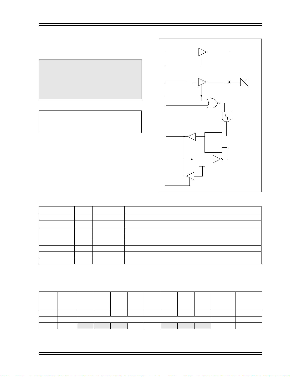
PIC16C925/926
4.6 PORTF and TRISF Register
PORTF is a digital input only port. Each pin is multiplexed with an LCD segment driver. These pins have
Schmitt Trigger input buffers.
Note 1: On a Power-on Reset, these pins are
configured as LCD segment drivers.
2: To configure the pins as a digital port, the
correspon din g b its i n t h e LC DS E r e gist e r
must be cleared. Any b it set in the LCDSE
register overrides any bit settings in the
corresponding TRIS register.
EXAMPLE 4-6: INITIALIZING PORTF
BCF STATUS, RP0 ;Select Bank2
BSF STATUS, RP1 ;
BCF LCDSE, SE16 ;Make all PORTF
BCF LCDSE, SE12 ;digital inputs
FIGURE 4-8: PORTF BLOCK DIAGRAM
LCD
Segment Data
LCD Segment
Output Enable
LCD
Common Data
LCD Common
Output Enable
LCDSE<n>
Data Bus
RD Port
QD
EN
V
DD
EN
Digital Input/
LCD Output pin
Schmitt
Trigger
Input
Buffer
RD TRIS
TABLE 4-11: PORTF FUNCTIONS
Name Bit# Buffer Type Function
RF0/SEG12 bit0 ST Digital input or Segment Driver12.
RF1/SEG13 bit1 ST Digital input or Segment Driver13.
RF2/SEG14 bit2 ST Digital input or Segment Driver14.
RF3/SEG15 bit3 ST Digital input or Segment Driver15.
RF4/SEG16 bit4 ST Digital input or Segment Driver16.
RF5/SEG17 bit5 ST Digital input or Segment Driver17.
RF6/SEG18 bit6 ST Digital input or Segment Driver18.
RF7/SEG19 bit7 ST Digital input or Segment Driver19.
Legend: ST = Schmitt Trigger input
TABLE 4-12: SUMMARY OF REGISTERS ASSOCIATED WITH PORTF
Address Name Bit 7 Bi t 6 Bit 5 Bit 4 Bit 3 B i t 2 Bit 1 Bit 0
107h PORTF RF7 RF6 RF5 RF4 RF3 RF2 RF1 RF0
187h TRISF PORTF Data Direction Control Register 1111 1111 1111 1111
10Dh LCDSE SE29 SE 27 SE20 SE16 SE12 SE9 SE5 SE0 1111 1111 1111 1111
Legend: Shaded cells are not used by PORTF.
Value o n
Power-on
Reset
0000 0000 0000 0000
Value on all
other
RESETS
2001 Microchip Technology Inc. Preliminary DS39544A-page 37

PIC16C925/926
4.7 PORTG and TRISG Register
PORTG is a digital input only port. Each pin is multiplexed with an LCD segment driver. These pins have
Schmitt Trigger input buffers.
Note 1: On a Power-on Reset, these pins are
configured as LCD segment drivers.
2: To configure the pins as a digital port, the
corresponding bits in the LCDSE register
must be cleared. Any b it set in the LCDSE
register overrides any bit settings in the
corresponding TRIS register.
EXAMPLE 4-7: INITIALIZING PORTG
BCF STATUS, RP0 ;Select Bank2
BSF STATUS, RP1 ;
BCF LCDSE, SE27 ;Make all PORTG
BCF LCDSE, SE20 ;and PORTE<7>
;digital inputs
FIGURE 4-9: PORTG BLOCK DIAGRAM
LCD
Segment Data
LCD Segment
Output Enable
LCD
Common Data
LCD Common
Output Enable
LCDSE<n>
Data Bus
RD Port
QD
EN
EN
V
DD
Digital Input/
LCD Output pin
Schmitt
Trigger
Input
Buffer
RD TRIS
TABLE 4-13: PORTG FUNCTIONS
Name Bit# Buffer Type Function
RG0/SEG20 bit0 ST Digital input or Segment Driver20.
RG1/SEG21 bit1 ST Digital input or Segment Driver21.
RG2/SEG22 bit2 ST Digital input or Segment Driver22.
RG3/SEG23 bit3 ST Digital input or Segment Driver23.
RG4/SEG24 bit4 ST Digital input or Segment Driver24.
RG5/SEG25 bit5 ST Digital input or Segment Driver25.
RG6/SEG26 bit6 ST Digital input or Segment Driver26.
RG7/SEG28 bit7 ST Digital input or Segment Driver28 (not available on 64-pin devices).
Legend: ST = Schmitt Trigger input
TABLE 4-14: SUMMARY OF REGISTERS ASSOCIATED WITH PORTG
DS39544A-page 38 Preliminary 2001 Microchip Technology Inc.
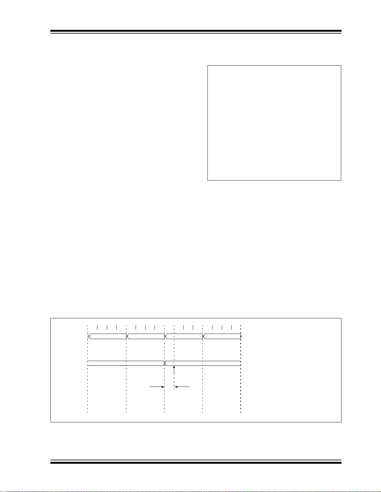
PIC16C925/926
4.8 I/O Programming Considerations
4.8.1 BI-DIRECTIONAL I/O PORTS
Any instruction which writes, operates internally as a
read followed by a write operation. The BCF and BSF
instructions, for example, read the register into the
CPU, execute the bit operation and write the result
back to the register. Caution must be used when thes e
instructions are applied to a port with both inputs and
outputs defined. For example, a BSF operation on bit5
of PORTB will caus e all ei ght bit s of POR TB to b e read
into the CPU. Then the BSF operation takes place on
bit5 and PORTB is written to the output latches. If
another bit of PORTB is used as a bi-dire ctional I/O pin
(e.g., bit0) and it is defined as an input at this time, the
input signal presen t on th e pi n it s elf wo uld be rea d in to
the CPU and rewritten to the dat a latch of this p articular
pin, overwriting the previous co ntent. As long as the pin
stays in the input mode, no problem occurs. However,
if bit0 is switched into output mode later on, the contents of the data latch may now be unknown.
Reading the port register reads the values of the port
pins. Writing to the port register , writes the val ue to the
port latch. When using read-modify-write instructions
(e.g. BCF, BSF) on a port, the valu e of the po rt pi ns i s
read, the desired operation is done to this value, and
this value is then written to the port latch.
Example 4-8 shows the effect of two sequential
read-modify-write instructions on an I/O port. A pin
actively outputting a Low or High should not be driven
from external devices at the same time, in order to
change the level on this pin (“wired-or”, “wired-and”).
The resulting high output currents may damage the
chip.
EXAMPLE 4-8: READ-MODIFY-WRITE
INSTRUCTIONS ON AN
I/O PORT
;Initial PORT settings: PORTB<7:4> Inputs
; PORTB<3:0> Outputs
;PORTB<7:6> have external pull-ups and are
;not connected to other circuitry
;
; PORT latch PORT pins
; ---------- -------- BCF PORTB, 7 ; 01pp pppp 11pp pppp
BCF PORTB, 6 ; 10pp pppp 11pp pppp
BCF STATUS, RP1 ; Select Bank1
BSF STATUS, RP0 ;
BCF TRISB, 7 ; 10pp pppp 11pp pppp
BCF TRISB, 6 ; 10pp pppp 10pp pppp
;
;Note that the user may have expected the
;pin values to be 00pp ppp. The 2nd BCF
;caused RB7 to be latched as the pin value
;(high).
4.8.2 SUCCESSIVE OPERATIONS ON I/O PORTS
The actual write to a n I/O port happen s at the e nd of an
instruction cycle, whereas for reading, the data must be
valid at the beginning of the instruction cycle
(Figure 4-10). Therefore, care must be exercised if a
write followed by a read operation is carried out on the
same I/O port. The sequence of instructions should be
such to allow the pin voltage to stabilize (load dependent) before the next ins truc tio n, wh ic h c aus es tha t fil e
to be read into the CPU, is executed. Otherwise, the
previous state of that pin may be read into the CPU,
rather than the new state. When in doubt, it is bet ter to
separate these instructions with a NOP, or another
instruction not accessing this I/O port.
FIGURE 4-10: SUCCESSIVE I/O OPERATION
Q1 Q2 Q3
PC
Instruction
Fetched
RB7:RB0
Instruction
Executed
2001 Microchip Technology Inc. Preliminary DS39544A-page 39
MOVWF PORTB
write to
PORTB
Q4
Q1 Q2 Q3
PC PC + 1 PC + 2
MOVF PORTB,W
MOVWF PORTB
write to
PORTB
Q4
Q1 Q2 Q3
Port pin
sampled here
TPD
MOVF PORTB,W
NOP
Q4
Q1 Q2 Q3
PC + 3
NOP
NOP
Note:
Q4
This example shows a wr ite to PORTB
followed by a read from PORTB.
Note that:
data setup time = (0.25T
where T
CY = instruction cycle
T
PD = propagation delay
Therefore, at higher clock frequencies,
a write followed by a read may be
problematic.
CY - TPD)

PIC16C925/926
NOTES:
DS39544A-page 40 Preliminary 2001 Microchip Technology Inc.
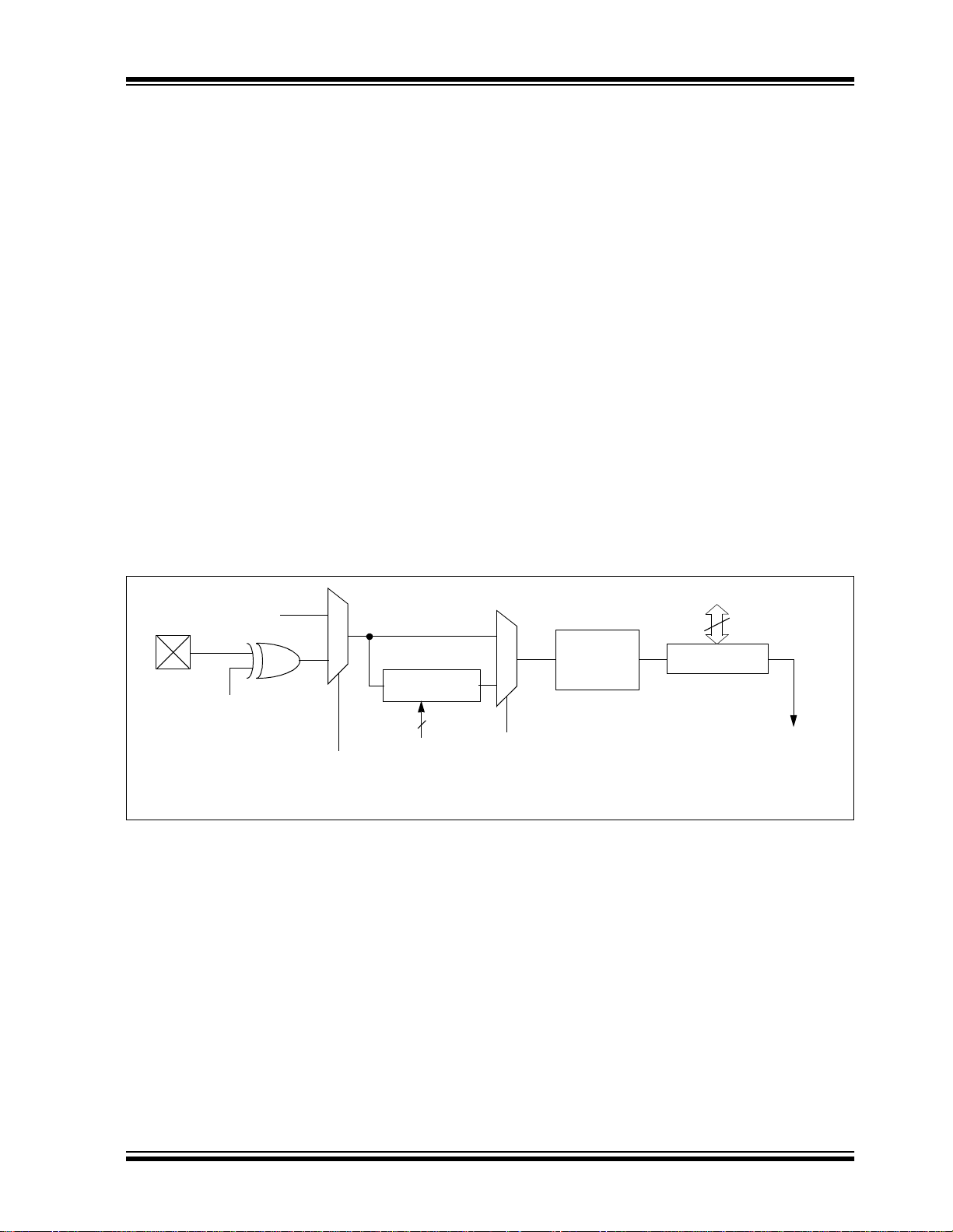
PIC16C925/926
5.0 TIMER0 MODULE
The Timer0 module has the following features:
• 8-bit timer/counter
• Readable and writable
• 8-bit software programmable prescaler
• Internal or external clock select
• Interrupt-on-overflow from FFh to 00h
• Edge select for external clock
Figure 5-1 is a simplified block diagram of the Timer0
module.
Timer mode is selected by clearing bit T0CS
(OPTION<5>). In Timer mode, the Timer0 module will
increment every ins tru cti on cy cl e (w i tho ut p r es ca ler). If
the TMR0 register is written, the increment is inhibited
for the following two instruction cycles (Figure 5-2 and
Figure 5-3). The user can work around this by writing
an adjusted value to the TMR0 register.
Counter mode is selected by setting bit T0CS
(OPTION<5>). In Counte r mode, Timer0 will increment
either on every rising, or fall ing edge of pin R A4/T0CKI.
The incrementing edge is determined by the Timer0
Source Edge Select bit T0SE (OPTION<4>). Clearing
FIGURE 5-1: TIMER0 BLOCK DIAGRAM
bit T0SE selects the rising edge. Restrictions on the
external clock input are discussed in detail in
Section 5.2.
The prescaler is mutually exclusively shared between
the Timer0 module and the Watchdog Timer. The
prescaler assignment is controlled in software by control bit PSA (OPTION<3>). Clearing bi t PSA will assign
the prescal er to the Timer0 modul e. The prescale r is
not readable or writable. When the prescaler is
assigned to the Timer0 module, prescale values o f 1: 2,
1:4,..., 1:256 are selectable. Section 5.3 details the
operation of the prescaler.
5.1 Timer0 Interrupt
The TMR0 interrupt is generated when the TMR0 register overflows from FFh to 00h. This overflow sets bit
TMR0IF (INTCON<2>). The interrupt can be masked
by clearing bit T0IE (INTCON<5 >). Bit TMR0IF must be
cleared in soft ware by the T imer0 mo dule Interrupt Service Routine before re-enabling this interrupt. The
TMR0 interrupt cannot awaken the processor from
SLEEP, since the timer is shut-off during SLEEP.
Figure 5-4 displays the Timer0 interrupt timing.
FOSC/4
RA4/T0CKI
pin
Note 1: T0CS, T0SE, PSA, PS2:PS0 (OPTION<5:0>).
T0SE
2: The prescaler is shared with the Watchdog Timer (refer to Figure 5-6 for detailed block diagram).
0
1
T0CS
Programmable
Prescaler
PS2, PS1, PS0
Data Bus
PSout
1
0
3
PSA
Sync with
Internal
Clocks
(2 cycle delay)
PSout
8
TMR0
Set Interrupt
Flag bit TMR0IF
on Overflow
2001 Microchip Technology Inc. Preliminary DS39544A-page 41

PIC16C925/926
FIGURE 5-2: TIMER0 TIMING: INTERNAL CLOCK/NO PRESCALE
PC
(Program
Counter)
Instruction
Fetched
TMR0
Instruction
Executed
Q1 Q2 Q3 Q4 Q1 Q2 Q3 Q4 Q1 Q2 Q3 Q4 Q1 Q2 Q3 Q4 Q1 Q2 Q3 Q4 Q1 Q2 Q3 Q4 Q1 Q2 Q3 Q4 Q1 Q2 Q3 Q4
PC-1
T0
PC PC+1 PC+2 PC+3 PC+4 PC+5 PC+6
MOVWF TMR0
T0+1 T0+2 NT0 NT0 NT0 NT0+1 NT0+2 T0
MOVF TM R0 ,W MOVF T MR0 ,W MOVF TMR0 ,W MOVF TM R0 ,W MOVF TMR0,W
Write TMR0
executed
Read TMR0
reads NT0
Read TMR0
reads NT0
Read TMR0
reads NT0
FIGURE 5-3: TIMER0 TIMING: INTERNAL CLOCK/PRESCALE 1:2
PC
(Program
Counter)
Instruction
Fetched
TMR0
Instruction
Executed
Q1 Q2 Q3 Q4 Q1 Q2 Q3 Q4 Q1 Q2 Q3 Q4 Q1 Q2 Q3 Q4 Q1 Q2 Q3 Q4 Q1 Q2 Q3 Q4 Q1 Q2 Q3 Q4 Q1 Q2 Q3 Q4
PC-1
T0 NT0+1
PC PC+1 PC+2 PC+3 PC+4 PC+5 PC+6
MOVWF TMR0
MOVF TMR0,W MOVF TMR0,W MOVF TMR0,W MOVF TMR0,W M OVF TMR0,W
T0+1
Write TMR0
executed
Read TMR0
reads NT0
NT0
Read TMR0
reads NT0
Read TMR0
reads NT0
Read TMR0
reads NT0 + 1
Read TMR0
reads NT0
Read TMR0
reads NT0 + 2
Read TMR0
reads NT0 + 1
PC+6
FIGURE 5-4: TIMER0 INTERRUPT TIMING
Q2Q1 Q3 Q4Q2Q1 Q3 Q4 Q2Q1 Q3 Q4 Q2Q1 Q3 Q4 Q2Q1 Q3 Q4
OSC1
OSC1
(3)
CLKOUT
Timer0
TMR0IF bit
(INTCON<2>)
GIE bit
(INTCON<7>)
INSTRUCTION
FLOW
PC
Instruction
Fetched
Instruction
Executed
Note 1: Interrupt flag bit TMR0IF is sampled here (every Q1).
FEh
1
PC
Inst (PC)
Inst (PC-1)
2: Interrupt latency = 4T
3: CLKOUT is available only in RC oscillator mode.
FFh 00h 01h 02h
1
PC +1 PC +1 0004h 0005h
Inst (PC+1)
Inst (PC)
CY where TCY = instruction cycle time.
Inst (0004h) Inst (0005h)
Inst (0004h)Dummy cycle Dummy cycle
DS39544A-page 42 Preliminary 2001 Microchip Technology Inc.

PIC16C925/926
5.2 Using Timer0 with an External Clock
When an external clock input i s used for T i mer0, it must
meet certain requirements. The requirements ensure
the external clock can be synchronized with the internal
phase clock (T
incrementing of Timer0 after synchronization.
OSC). Also, there is a delay in the actual
When a prescaler is used, the external clock input is
divided by the asynchronous ripple counter type prescaler, so that the prescaler output is symmetrical. For
the external clock to meet the sampling requirement,
the ripple counter must be taken into account. Therefore, it is necessary for T0CKI to have a period of at
least 4T
OSC (and a small RC delay of 40 ns) divided by
the prescaler value. The only requirement on T0CKI
high and low time is that they do not violate the mini-
5.2.1 EXTERNAL CLOCK
SYNCHRONIZATION
When no pr escal er is us ed, t he ex ternal clock inpu t is
the same as the prescaler outp ut. Th e synchronization
of T0CKI with the internal phase clocks is accomplished by sampli ng the prescale r output on the Q2 and
Q4 cycles of the internal phase clocks (Figure 5-5).
Therefore, it is necessary for T0CKI to be high for at
least 2T
at least 2T
OSC (and a small RC dela y of 20 ns) and lo w for
OSC (and a small RC delay of 20 ns). Refer
mum pulse width requirement of 10 ns. Refer to parameters 40, 41 and 42 in the electrical specificatio n of th e
desired device.
5.2.2 TMR0 INCREMENT DELAY
Since the prescaler output is synchronized with the
internal clocks, there is a small delay from the time the
external clock edge o ccurs to th e time the T imer0 module is actually incremen ted. Figu re 5-5 show s the de lay
from the external cloc k e dge to the timer incrementing.
to the electrical specification of the desired device.
FIGURE 5-5: TIMER0 TIMING WITH EXTERNAL CLOCK
Q1 Q2 Q3 Q4 Q1 Q2 Q3 Q4 Q1 Q2 Q3 Q4 Q1 Q2 Q3 Q4
External Clock Input or
Prescaler Output
External Clock/Prescaler
Output after sampling
Increment Timer0 (Q4)
(2)
(1)
(3)
Small pulse
misses sampling
Timer0
Note 1: Delay from clock input change to Timer0 increment is 3TOSC to 7TOSC. (Duration of Q = TOSC.) Therefore, the error
in measuring the interval between two edges on Timer0 input = ±4T
2: External clock if no prescaler selected, prescaler output otherwise.
3: The arrows indicate the points in time where sampling occurs.
T0 T0 + 1 T0 + 2
OSC max.
2001 Microchip Technology Inc. Preliminary DS39544A-page 43

PIC16C925/926
5.3 Prescaler
DS39544A-page 44 Preliminary 2001 Microchip Technology Inc.

PIC16C925/926
5.3.1 SWITCHING PRESCALER
Note: To avoid an unintended device RESET,
ASSIGNMENT
The prescaler assignment is fully under software control, i.e., it can be changed “on the fly” during program
execution.
EXAMPLE 5-1: CHANGING PRESCALER (TIMER0→WDT)
Lines 2 and 3 do NOT have to
be included if the final desired
prescale value is o the r th an 1:1.
If 1:1 is final desired value, then
a temporary prescale value is
set in lines 2 and 3 and the final
prescale value will be set in lines
10 and 11.
To change prescaler from the WDT to the Time r0 module use the precaution shown in Example 5-2.
1) BSF STATUS, RP0 ;Select Bank1
2) MOVLW b’xx0x0xxx’ ;Select clock source and prescale value of
3) MOVWF OPTION_REG ;other than 1:1
4) BCF STATUS, RP0 ;Select Bank0
5) CLRF TMR0 ;Clear TMR0 and prescaler
6) BSF STATUS, RP1 ;Select Bank1
7) MOVLW b’xxxx1xxx’ ;Select WDT, do not change prescale value
8) MOVWF OPTION_REG ;
9) CLRWDT ;Clears WDT and prescaler
10) MOVLW b’xxxx1xxx’ ;Select new prescale value and WDT
11) MOVWF OPTION_REG ;
12) BCF STATUS, RP0 ;Select Bank0
the following instruction sequence (shown
in Example 5-1) must be executed when
changing the prescaler assignment from
Timer0 to the WDT. This precaution must
be followed even if the WDT is disabled.
EXAMPLE 5-2: CHANGING PRESCALER (WDT→TIMER0)
CLRWDT ;Clear WDT and precaler
BSF STATUS, RP0 ;Select Bank1
MOVLW b’xxxx0xxx’ ;Select TMR0,
MOVWF OPTION_REG ;clock source
BCF STATUS, RP0 ;Select Bank0
;new prescale value and
TABLE 5-1: REGISTERS ASSOCIATED WITH TIMER0
Address Name Bit 7 Bit 6 Bit 5 Bit 4 Bit 3 Bit 2 Bit 1 Bit 0
01h, 101 h TMR0 Timer0 Module Register
0Bh, 8Bh,
10Bh, 18Bh
INTCON GIE
81h, 181h OPTION RBPU INTEDG T0CS T0SE PSA PS2 PS1 PS0
85h TRISA — — PORT A Data Direction Control Register
Legend: x = unknown, u = unchanged, - = unimplemented locations read as '0'.
Shaded cells are not used by T ime r0.
PEIE TMR0IE INTE RBIE TMR0IF INTF RBIF
Value on
Power-on
Reset
xxxx xxxx uuuu uuuu
0000 000x 0000 000u
1111 1111 1111 1111
--11 1111 --11 1111
Value on
all other
RESETS
2001 Microchip Technology Inc. Preliminary DS39544A-page 45

PIC16C925/926
NOTES:
DS39544A-page 46 Preliminary 2001 Microchip Technology Inc.

PIC16C925/926
6.0 TIMER1 MODULE
Timer1 is a 16-bit timer/counter consisting of two 8-bit
registers (TMR1H and TMR1L), which are readable
and writable. The TMR1 Register pair
(TMR1H:TMR1L) increments from 0000h to FFFFh
and rolls over to 0000 h. The TMR1 Inte rrupt, if enabled,
is generated on overflow, which is latched in interrupt
flag bit, TMR1IF (PIR1<0>). This interrupt can be
enabled/disabled by setting/clearing TMR1 interrupt
enable bit, TMR1IE (PIE1<0>).
Timer1 can operate in one of two modes:
• As a timer
• As a counter
The operating mode is determined by the clock select
bit, TMR1CS (T1CON<1>).
In Timer mode, Timer1 increments every instruction
cycle. In Counter mode, it increments on every rising
edge of the external clock input.
Timer1 can be turned on and off using the control bit
TMR1ON (T1CON<0>).
Timer1 also has an internal “RESET input”. This
RESET can be generated by the CCP module
(Section 8.0). Register 6-1 shows the Timer1 control
register.
When the Timer1 oscillator is enabled (T1OSCEN is
set), the RC1/T1OSI and RC0/T1OSO/T1CKI pins
become inputs, regardless of the TRISC<1:0>. RC1
and RC0 will be read as ‘0’.
REGISTER 6-1: T1CON: TIMER1 CONTROL REGISTER (ADDRESS 10h)
U-0 U-0 R/W-0 R/W-0 R/W-0 R/W-0 R/W-0 R/W-0
— — T1CKPS1 T1CKPS0 T1OSCEN T1SYNC TMR1CS TMR1ON
bit 7 bit 0
bit 7-6 Unimplemented: Read as '0'
bit 5-4 T1CKPS1:T1CKPS0: Timer1 Input Clock Prescale Select bits
11 = 1:8 Prescale value
10 = 1:4 Prescale value
01 = 1:2 Prescale value
00 = 1:1 Prescale value
bit 3 T1OSCEN: Timer1 Oscillator Enable Control bit
1 = Oscillator is enabled
0 = Oscillator is shut-off
Note: The oscillator inverter and feedback resistor are turned off to eliminate power drain.
bit 2 T1SYNC
TMR1CS = 1:
1 = Do not synchronize external clock input
0 = Synchronize external clock input
TMR1CS = 0:
This bit is ignored. Timer1 uses the internal clock when TMR1CS = 0.
bit 1 TMR1CS: Timer1 Clock Source Select bit
1 = External clock from pin T1CKI (on the rising edge)
0 = Internal clock (F
bit 0 TMR1ON: Timer1 On bit
1 = Enables Timer1
0 = Stops Timer1
Legend:
R = Readable bit W = Writable bit U = Unimplemented bit, read as ‘0’
- n = Value at POR ’1’ = Bit is set ’0’ = Bit is cleared x = Bit is unknown
2001 Microchip Technology Inc. Preliminary DS39544A-page 47
: Timer1 External Clock Input Synchronization Control bit
OSC/4)
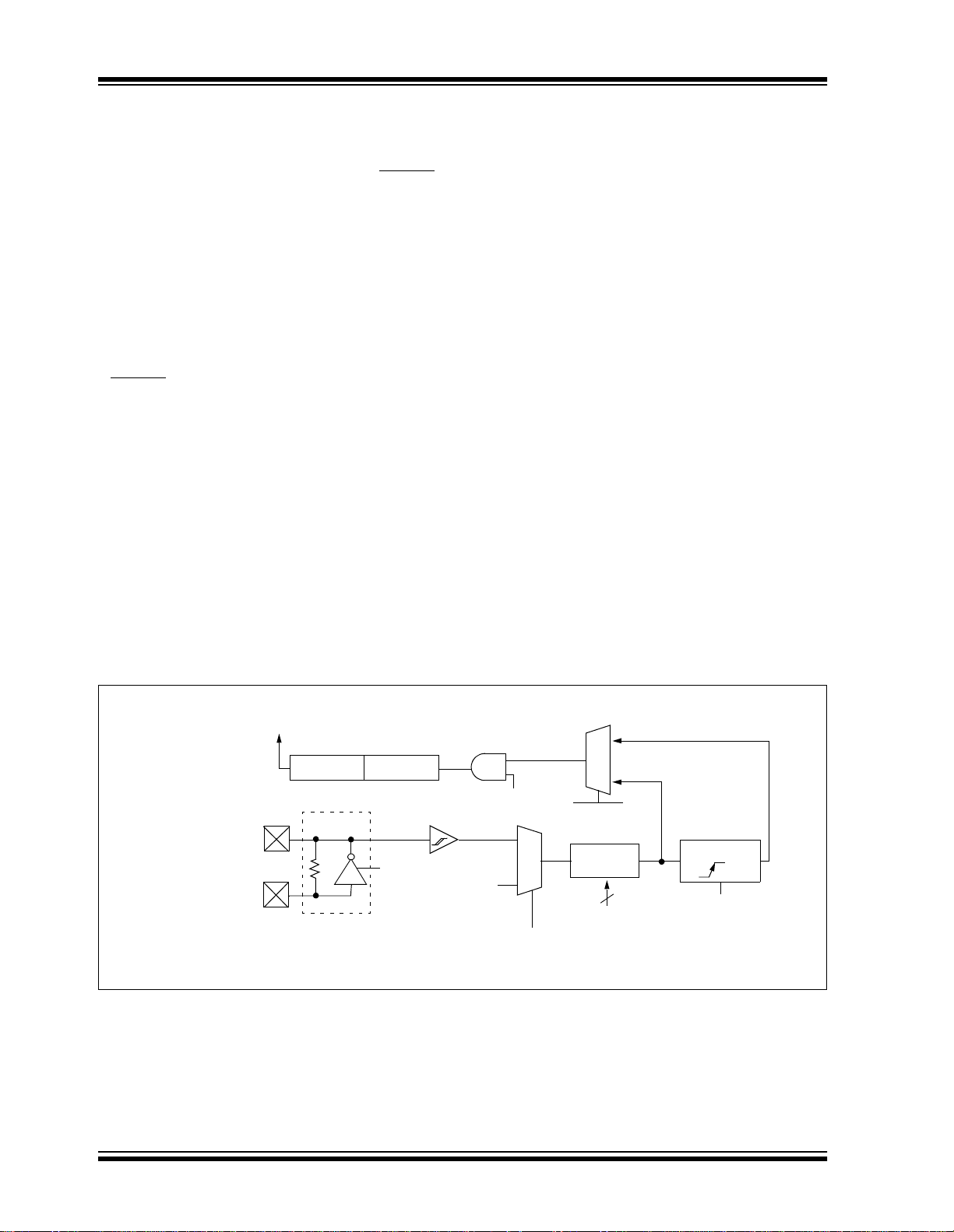
PIC16C925/926
6.1 Timer1 Operation in Timer Mode
Timer mode is selected by clearing the TMR1CS
(T1CON<1>) bit. In this mode, the input clock to the
timer is F
OSC/4. The synchronize control bit T1SYNC
(T1CON<2>) has no effect since t he internal clo ck is
always in sync.
6.2 Timer1 Operation in Synchronized Counter Mode
Counter mode is selected by setting bit TMR1CS. In
this mode, the timer increm ents on every risin g edge of
clock input on pin RC1/T1OSI when bit T1OSCEN is
set, or pin RC0/T1OSO/T1CKI when bit T1OSCEN is
cleared.
If T1SYNC
synchronized with internal phase clocks. The synchronization is done after the prescaler stage. The prescaler is an asynchronous ripple counter.
In this configuration, during SLEEP mode, Timer1 will
not increment even if the external clock is present,
since the sy nchroniz ation circ uit is shu t-off. The p rescaler however will continue to increment.
is cleared, th en the extern al clock input is
6.2.1 EXTERNAL CLOCK INPUT TIMING FOR SYNCHRONIZED COUNTER MODE
When an external c lock in put is used for T imer1 in Sy nchronized Counter mode, it must meet certain requirements. The external clock requirement is due to
internal phase clock (T
there is a delay in the actual incrementing of TMR1
after synchronization.
When the prescaler is 1:1, the external clock input is
the same as the prescaler outp ut. The synch ronization
of T1CKI with the internal phase clocks is accomplished by sampli ng the presc aler output on the Q2 and
Q4 cycles of the internal phase clocks. Therefore, it is
necessary for T1CKI to be high for at leas t 2T
a small RC delay of 20 ns), and low for at least 2T
(and a small RC delay of 20 ns). Refer to the approp riate electrical specif ications, par ameters 45, 46, and 47.
When a prescaler other than 1:1 is used, the external
clock input is divided by the asynchronous ripple
counter type prescaler, so that the prescaler output is
symmetrical. In order for the external clock to meet the
sampling requirement, the ripple counter must be taken
into accoun t. Therefore, it is ne cessary for T1CKI to
have a period of at least 4T
of 40 ns), divided by the prescaler value. The only
requirement on T1CKI hi gh and low tim e is that th ey do
not violate the minimum pulse width requirements of
10 ns). Refer to the appropriate electrical specifications, parameters 40, 42, 45, 46, and 47.
OSC) synchronization. Also,
OSC (and
OSC
OSC (and a small RC delay
FIGURE 6-1: TIMER1 BLOCK DIAGRAM
Set Flag bit
TMR1IF on
Overflow
RC0/T1OSO/T1CKI
RC1/T1OSI
Note 1: When the T1OSCEN bit is cleared, the inverter and feedback resistor are turned off. This eliminates power drain.
TMR1H
T1OSC
TMR1
TMR1L
T1OSCEN
Enable
Oscillator
(1)
FOSC/4
Internal
Clock
TMR1ON
On/Off
1
0
T1CKPS1:T1CKPS0
TMR1CS
0
1
T1SYNC
Prescaler
1, 2, 4, 8
2
Synchronized
Clock Input
Synchronize
SLEEP Input
det
DS39544A-page 48 Preliminary 2001 Microchip Technology Inc.

PIC16C925/926
6.3 Timer1 Operation in Asynchronous Counter Mode
If control bit T1SYNC (T1CON<2>) is set, the external
clock input is not synchronized. The timer continues to
increment asynchronous to the internal phase clocks.
The timer will continue to run during SLEEP and can
generate an interrupt-on-overflow which will wake-up
the processor. However, special precautions in software are needed to read from, or write to the Timer1
register pair (TMR1H:TMR1L) (Section 6.3.2).
In Asynchronous Counter mode, Timer1 cannot be
used as a time-base for capture or compare operations.
6.3.2 READING AND WRITING TMR1 IN ASYNCHRONOUS COUNTER MODE
Reading TMR1H or TMR1L, while the timer is running
from an external asynchronous clock, will ensure a
valid read (taken care of in hardware). However, the
user should keep in mind that reading the 16-bit timer
in two 8-bit values it self, poses certain pro ble ms , si nc e
the timer may overflow between the reads.
For writes, it is recommend ed that th e user s imply sto p
the timer and write the desired values. A write contention may occur by writing to the timer registers while the
register is incrementing. This may produce an unpredictable value in the timer register.
6.3.1 E XTERNAL CLOCK INPUT TIMING WITH UNSYNCHRONIZED CLOCK
If control bit T1SYNC is set, the timer will increment
completely asynch ronous ly. The input clock must meet
Reading the 16-bit value requires some care.
Example 6 -1 is an exam ple routine to read the 16-bit
timer value. This is useful if the timer cannot be
stopped.
certain minimum high time and low time requirements,
as specified in timing parameters 45, 46, and 47.
EXAMPLE 6-1: READING A 16-BIT FREE-RUNNING TIMER
; All interrupts are disabled
;
MOVF TMR1H, W ;Read high byte
MOVWF TMPH ;
MOVF TMR1L, W ;Read low byte
MOVWF TMPL ;
MOVF TMR1H, W ;Read high byte
SUBWF TMPH, W ;Sub 1st read with 2nd read
BTFSC STATUS,Z ;Is result = 0
GOTO CONTINUE ;Good 16-bit read
;
; TMR1L may have rolled over between the read of the high and low bytes.
; Reading the high and low bytes now will read a good value.
;
MOVF TMR1H, W ;Read high byte
MOVWF TMPH ;
MOVF TMR1L, W ;Read low byte
MOVWF TMPL ;
; Re-enable the Interrupt (if required)
;
CONTINUE ;Continue with your code
2001 Microchip Technology Inc. Preliminary DS39544A-page 49

PIC16C925/926
6.4 Timer1 Oscillator
A crystal oscillator ci rcuit is built-in betwee n pins T1OSI
(input) and T1OSO (amplifier output). It is enabled by
setting control bit T1OSCEN (T 1CON<3>). The oscill ator is a low power oscillator rated up to 200 kHz. It will
continue to run during SLEEP. It is primarily intended
for a 32 kHz crystal. Table 6-1 shows the capacitor
selection for the Timer1 oscillator.
The Timer1 oscillator is identical to the LP oscillator.
The user must provide a so f t wa re tim e de lay to en sure
proper oscillator start-up.
TABLE 6-1: CAPACITOR SELECTION FOR
THE TIMER1 OSCILLATOR
Osc Type Freq C1 C2
LP 32 kHz 33 pF 33 pF
100 kHz 15 pF 15 pF
200 kHz 15 pF 15 pF
These values are for design guidance only.
Crystals Tested:
32.768 kHz Epson C-001R32.768K-A ± 20 PPM
100 kHz Epson C-2 100.00 KC-P ± 20 PPM
200 kHz STD XTL 200.000 kHz ± 20 PPM
Note 1: Higher capacitance increases the stability
of the oscillator but also increases the
start-up time.
2: Since each resonator/crystal has its own
characteristics , the user sh ould co nsult the
resonator/crystal manufacturer for appropriate values of external components.
6.5 Resetting Timer1 Using the CCP Trigger Output
If the CCP1 module is configured in Compare mode to
generate a “special event trigger” (CCP1M3:CCP1M0
= 1011), this signal will reset Timer1.
Note: The special event trigger from the CCP1
module will not set interrupt flag bit
TMR1IF (PIR1<0>).
Timer1 mu st be confi gured for eit her T ime r or Synchronized Counter mode, to t a ke adv antage of this feature.
If Timer1 is running in Asynchronous Counter mode,
this reset operation may not work.
In the event that a write to Timer1 coincides with a
special event trigge r from CCP1, the write will tak e precedence.
In this mode of operation, the CCPR1H:CCPR1L registers pair effectively become the period register for
Timer1.
6.6 Resetting of Timer1 Register Pair (TMR1H:TMR1L)
TMR1H and TMR1L registers are not reset on a POR
or any other RESET, except by the CCP1 specia l event
trigger.
T1CON register is reset to 00h on a Power-on Reset.
In any other RESET, the register is unaffected.
6.7 Timer1 Prescaler
The prescaler counter is cleared on writes to the
TMR1H or TMR1L registers.
TABLE 6-2: REGISTERS ASSOCIATED WITH TIMER1 AS A TIMER/COUNTER
Address Name Bit 7 Bit 6 Bit 5 Bit 4 Bit 3 Bit 2 Bit 1 Bit 0
0Bh, 8Bh,
10Bh, 18Bh
0Ch PIR1 LCDIF ADIF — — SSPIF CCP1IF TMR2IF TMR1IF 00-- 0000 00-- 0000
8Ch PIE1 LCDIE ADIE — — SSPIE CCP1IE TMR2IE TMR1IE 00-- 0000 00-- 0000
0Eh TMR1L Holding register for the Least Significant Byte of the 16-bit TMR1 Register xxxx xxxx uuuu uuuu
0Fh TMR1H Holding register for the Most Significant Byte of the 16-bit TMR1 Register xxxx xxxx uuuu uuuu
10h T1CON — — T1CKPS1 T1CKPS0 T1OSCEN T1SYNC TMR1CS TMR1ON --00 0000 --uu uuuu
Legend:
DS39544A-page 50 Preliminary 2001 Microchip Technology Inc.
INTCON GIE PEIE
x = unknown, u = unchanged, - = unimplemented, read as '0'. Shaded cells are not used by theTimer1 module.
TMR0IE INTE RBIE TMR0IF INTF RBIF 0000 000x 0000 000u
Value o n
Power-on
Reset
Value o n
all other
RESETS

PIC16C925/926
7.0 TIMER2 MODULE
Timer2 is an 8-bit timer with a prescaler and a
postscaler. It can be used as the PW M time-base fo r
the PWM mode of the CCP m odule. It can als o be used
as a time-base for the Master mode SPI clock. The
TMR2 register is readable and writable, and is cleared
on any device RESET.
The input cloc k (F
1:4, or 1:16 (selected by control bits
T2CKPS1:T2CKPS0 (T2CON<1:0>)).
The Timer2 module has an 8-bit period register, PR2.
TMR2 increm ents from 00h until it m atches PR2 a nd
then resets to 00h on the next increment cycle. PR2 is
a readable and writable register. The PR2 register is
set during RESET.
The match output of TMR2 goes through a 4-bit
postscaler (which gives a 1:1 to 1:16 scaling inclusive)
to generate a TMR2 interrupt (latched in flag bit
TMR2IF, (PIR1<1>)).
Timer2 c an b e s hu t-off by clearing control bit TMR2O N
(T2CON<2>) to minimize power consumption.
Figure 7-1 shows the Timer2 control register.
OSC/4) has a prescale option of 1:1,
7.1 Timer2 Prescaler and Postscaler
The prescaler and postscaler counters are cleared
when any of the following occurs:
• a write to the TMR2 register
• a write to the T2CON register
• any device RESET (Power-on Reset, MCLR
Reset, or Watchdog Timer Reset)
TMR2 will not clear when T2CON is written.
7.2 Output of TMR2
The output of TMR2 (before the post scaler) is fed to the
Synchronous Serial Port m odule, which optionally use s
it to generate the shift clock.
FIGURE 7-1: TIMER2 BLOCK DIAGRAM
(1)
Postscaler
1:16
4
Sets Flag
bit TMR2IF
1:1
to
F
OSC/4
Prescaler
1:1, 1:4, 1:16
2
TMR2 reg
Comparator
PR2 reg
TMR2
Output
RESET
EQ
Note 1: TMR2 register output can be software selected by the
SSP Module as the source clock.
2001 Microchip Technology Inc. Preliminary DS39544A-page 51

PIC16C925/926
REGISTER 7-1: T2CON: TIMER2 CONTROL REGISTER (ADDRESS 12h)
U-0 R/W-0 R/W-0 R/W-0 R/W-0 R/W-0 R/W-0 R/W-0
— TOUTPS3 TOUTPS2 TOUTPS1 TOUTPS0 TMR2ON T2CKPS1 T2CKPS0
bit 7 bit 0
bit 7 Unimplemented: Read as '0'
bit 6-3 TOUTPS3:TOUTPS0: Timer2 Output Postscale Select bits
0000 = 1:1 Postscale
0001 = 1:2 Postscale
•
•
•
1111 = 1:16 Postscale
bit 2 TMR2ON: Timer2 On bit
1 = Timer2 is on
0 = Timer2 is off
bit 1-0 T2CKPS1:T2CKPS0: Timer2 Clock Prescale Select bits
00 = Prescaler is 1
01 = Prescaler is 4
1x = Prescaler is 16
Legend:
R = Readable bit W = Writable bit U = Unimplemented bit, read as ‘0’
- n = Value at POR ’1’ = Bit is set ’0’ = Bit is cleared x = Bit is unknown
TABLE 7-1: REGISTERS ASSOCIATED WITH TIMER2 AS A TIMER/COUNTER
Address Name Bit 7 Bit 6 Bit 5 Bit 4 Bit 3 Bit 2 Bit 1 Bit 0
0Bh, 8Bh,
10Bh, 18Bh
0Ch PIR1 LCDIF ADIF — — SSPIF CCP1IF TMR2IF TMR1IF 00-- 0000 00-- 0000
8Ch PIE1 LCDIE ADIE — — SSPIE CCP1IE TMR2IE TMR1IE 00-- 0000 00-- 0000
11h TMR2 Timer2 Module’s Register 0000 0000 0000 0000
12h T2CON — TOUTPS3 TOUTPS2 TOUTPS1 TOUTPS0 TM R2ON T2CKPS1 T2CKPS0 -000 0000 -000 0000
92h PR2 Timer2 Period Register 1111 1111 1111 1111
Legend: x = unknown, u = unchanged, - = unimplemented, read as ’0’. Shaded cells are not used by the Timer2 module.
INTCON GIE PEIE
TMR0IE INTE RBIE TMR0IF INTF RBIF 0000 000x 0000 000u
Value on
Power-on
Reset
Val ue on
all other
RESETS
DS39544A-page 52 Preliminary 2001 Microchip Technology Inc.
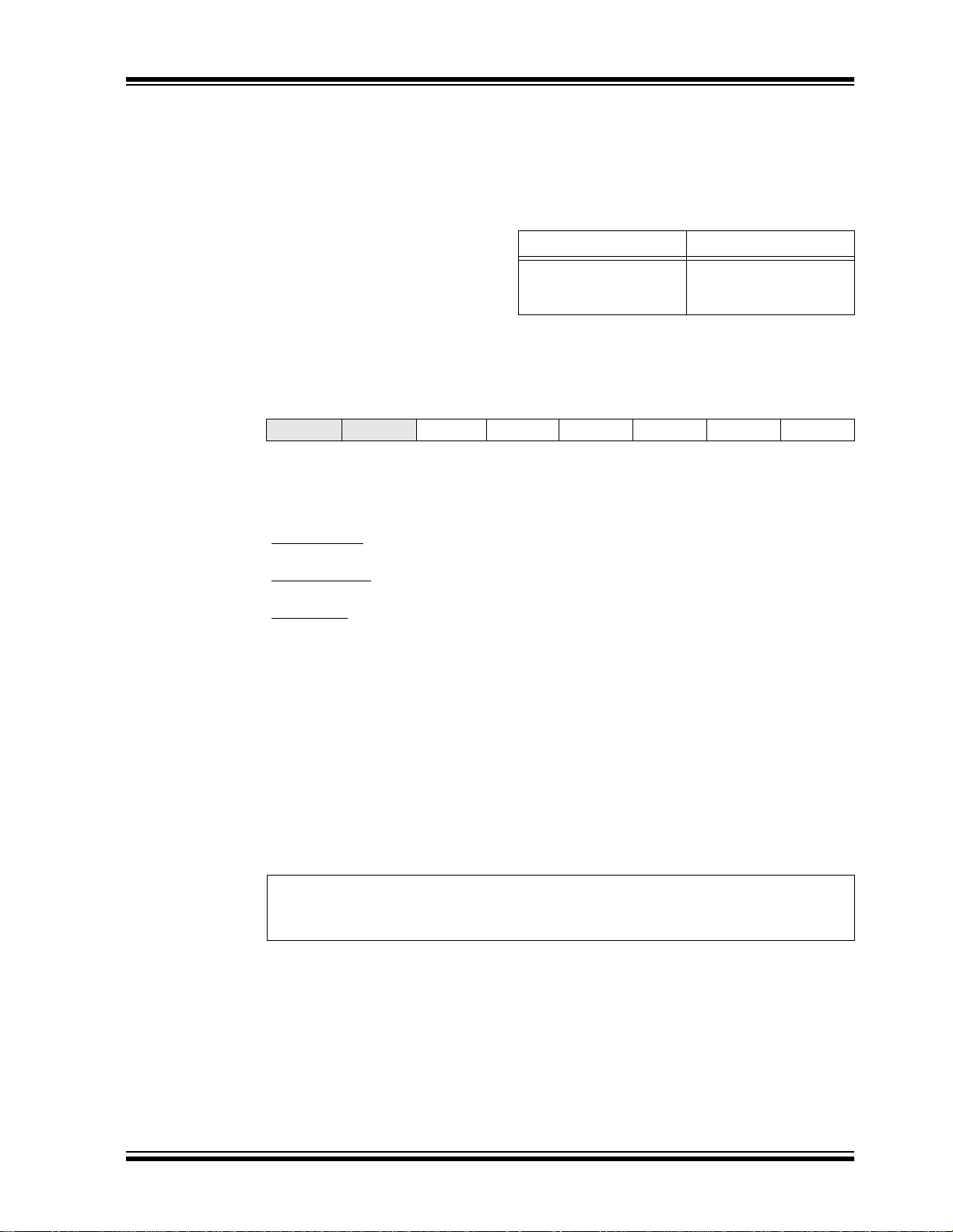
PIC16C925/926
8.0 CAPTURE/COMPARE/PWM (CCP) MODULE
The CCP (Capture/Comp a r e/PW M) m od ule co nt ai ns a
16-bit register which can operate as a 16-bit capture
register, as a 16-bit compare register, or as a PWM
master/slave duty cycle register. Table 8-1 shows the
timer resources used by the CCP module.
The Capture/Compare/PWM Register1 (CCPR1) is
comprised of t wo 8-bit registers: CCP R1L (low byte)
and CCPR1H (high byte). The CCP1CO N register controls the operation of CCP1 . All thre e are read abl e an d
writable.
Register 8-1 shows the CCP1CON register.
For use of the CCP module, refer to the Embedded
Control Handbook, “Using the CCP Modules” (AN594).
TABLE 8-1: CCP MODE - TIMER
CCP Mode Timer Resource
Capture
Compare
PWM
REGISTER 8-1: CCP1CON REGISTER (ADDRESS 17h)
U-0 U-0 R/W-0 R/W-0 R/W-0 R/W-0 R/W-0 R/W-0
— — CCP1X CCP1Y CCP1M3 CCP1M2 CCP1M1 CCP1M0
bit 7 bit 0
bit 7-6 Unimplemented: Read as '0'
bit 5-4 CCP1X:CCP1Y: PWM Least Significant bits
Capture mode:
Unused
Compare mode:
Unused
PWM mode:
These bits are the two LSbs of the PWM duty cycle. The eight MSbs are found in CCPR1L.
bit 3-0 CCP1M3:CCP1M0: CCP1 Mode Select bits
0000 = Capture/Compare/PWM disabled (resets CCP1 module)
0100 = Capture mode, every falling edge
0101 = Capture mode, every rising edge
0110 = Capture mode, every 4th rising edge
0111 = Capture mode, every 16th rising edge
1000 = Compare mode, set output on match (bit CCP1IF is set)
1001 = Compare mode, clear output on match (bit CCP1IF is set)
1010 = Compare mode, gen erate sof tware in terrupt-o n-match (bi t CCP1IF is set, CCP1 pi n is
unaffected)
1011 = Compare mode, trigger special event (CCP1IF bit is set; CCP1 resets TMR1)
11xx = PWM mode
RESOURCE
Timer1
Timer1
Timer2
Legend:
R = Readable bit W = Writable bit U = Unimplemented bit, read as ‘0’
- n = Value at POR ’1’ = Bit is set ’0’ = Bit is cleared x = Bit is unknown
2001 Microchip Technology Inc. Preliminary DS39544A-page 53

PIC16C925/926
8.1 Capture Mode
In Capture mode, CCPR1H:CCPR1L captures the
16-bit value of the TMR1 regi ster when an event occu rs
on pin RC2/CCP1 (Figure 8-1). An event can be
selected to be one of the following:
• Every falling edge
• Every rising edge
• Every 4th rising edge
• Every 16th rising edge
An event is selected by control bits CCP1M3:CCP1M0
(CCP1CON<3:0>). When a capture is made, the interrupt request flag bit CCP1IF (PIR1<2>) is set. It must
be cleared in so ftware. If another ca pture occurs b efore
the value in register CCPR1 is read, the old captured
value is overwritten with the new captured value.
8.1.1 CCP PIN CONFIGURATION
In Capture mode, the R C2/ CCP 1 pin sh oul d b e configured as an input by setting the TRISC<2> bit.
Note: If the RC2/CCP1 pin is configured as an
output, a write to the port can cause a capture condition.
FIGURE 8-1: CAPTURE MODE
OPERATION BLOCK
DIAGRAM
8.1.3 SOFTWARE INTERRUPT
When the Capture mode is changed, a false capture
interrupt may be generated. The user should keep
enable bit CCP1IE (PIE1<2>) c lear to av oid fal se int errupts and should clear flag bit CCP1IF following any
such change in operating mode.
8.1.4 CCP PRESCALER
There are four prescaler settings, specified by bits
CCP1M3:CCP1M0. Whenever the CCP module is
turned off, or the CCP module is not in Capture mode,
the prescaler counter is cleared. This means that any
RESET will clear the prescaler counter.
Switching from one capture prescaler to another may
generate an interrupt. Also, the prescaler counter will
not be cleared, therefore, the first cap ture may be from
a non-zero prescaler. Example8-1 shows the recommended method for switching between capture prescalers. This example also clears the prescaler counter
and will not generate the “false” interrupt.
EXAMPLE 8-1: CHANGING BETWEEN
CAPTURE PRESCALERS
CLRF CCP1CON ; Turn CCP module off
MOVLW NEW_CAPT_PS ; Load the W reg with
; the new prescaler
; mode value and CCP ON
MOVWF CCP1CON ; Load CCP1CON with
; this value
CCP
RC2/CCP1
pin
Prescaler
÷ 1, 4, 16
and
edge detect
Q’s
Set CCP1IF
PIR1<2>
CCP1CON<3:0>
CCPR1H CCPR1L
Capture
Enable
TMR1H TMR1L
8.1.2 TIMER1 MODE SELECTION
Timer1 must be running in Timer mode, or Synchronized Counter mode, for the CCP module to use the
capture feature. In Asynchronous Counter mode, the
capture operation may not work.
DS39544A-page 54 Preliminary 2001 Microchip Technology Inc.

PIC16C925/926
8.2 Compare Mode
In Compare mo de, th e 16- bit CCP R1 re gist er valu e is
constantly compared against the TMR1 register pair
value. When a match occurs, the RC2/C CP 1 pin is:
• Driven high
• Driven low
• Remains unchanged
The action on the pin is based on the value of control
bits CCP1M3:CCP1M0 (CCP1CON<3:0>). At the
same time, a compare interrupt is also generated.
FIGURE 8-2: COMPARE MODE
OPERATION BLOCK
DIAGRAM
Special event trigger will reset Timer1, but not
set interrupt flag bit TMR1IF (PIR1<0>).
Set CCP1IF
PIR1<2>
CCPR1H CCPR1L
Match
TMR1H TMR1L
Comparator
RC2/CCP1
TRISC<2>
Output Enable
QS
Output
Logic
R
CCP1CON<3:0>
Mode Select
Trigger
8.2.2 TIMER1 MODE SELECT ION
Timer1 must be running in Timer mode, or Synchronized Counter mode, if the CCP module is using the
compare feature. In Asynchronous Counter mode, the
compare operation may not work.
8.2.3 SOFTWARE INTERRUPT MODE
When Generate Software Interrupt is chosen, the
CCP1 pin is not affected. Only a CCP interrupt is generated (if enabled).
8.2.4 SPECIAL EVENT TRIGGER
In this mode, an internal hardware trigger is generated
which may be used to initiate an action.
The special event trigger output of CCP1 resets the
TMR1 register pair and starts an A/D conversion. This
allows the CCPR1H:CCPR1L register pair to effectively
be a 16-bit programmable period register for Timer1.
Note: The “special event trigger” from the CCP1
module will not set interrupt flag bit
TMR1IF (PIR1<0>).
8.2.1 CCP PIN CONFIGURATION
The user must configure the RC2/CCP1 pin as an output by clearing the TRISC<2> bi t.
Note: Clearing the CCP1CON register will force
the RC2/CCP1 compare outp ut latch to the
default low level. This is not the PORTC
I/O data latch.
2001 Microchip Technology Inc. Preliminary DS39544A-page 55
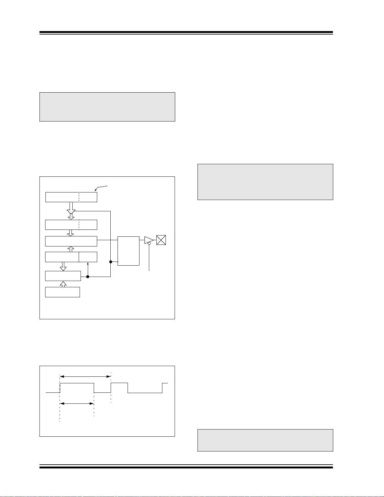
PIC16C925/926
8.3 PWM Mode
In Pulse Width Modulation (PWM) mode, the CCP1 pin
produces up to a 10-bit resolution PWM output. Since
the CCP1 pin is mul tiplexed with th e PORTC dat a latch,
the TRISC<2> bit must be cleared to make the CCP1
pin an output.
Note: Clearing the CCP1CON register will force
the CCP1 PWM output latch to the default
low level. This is not the PORTC I/O data
latch.
Figure 8-3 shows a simplified block diagram of the
CCP module in PWM mode.
For a step-by-step procedure on how to set up the C CP
module for PWM operation, see Section 8 .3.3.
FIGURE 8-3: SIMPLIFIED PWM BLOCK
DIAGRAM
Duty Cycle Registers
CCPR1L
CCPR1H (Slave)
Comparator
TMR2
Comparator
PR2
Note 1: 8-bit timer is concatenated with 2-bit internal Q clock
or 2 bits of the prescaler to create 10-bit time-base.
(Note 1)
Clear Timer,
CCP1 pin and
latch D.C.
A PWM output (Figure 8-4) has a time-base (period)
and a time that the output stays high (duty cycle). The
frequency of the PWM is the inverse of the period
(1/period).
FIGURE 8-4: PWM OUTPUT
Period
CCP1CON<5:4>
Q
R
S
RC2/CCP1
TRISC<2>
8.3.1 PWM PERIOD
The PWM period is spec ified by writi ng to the PR2 re gister. The PWM period can be calculated using the following formula:
PWM period = [ (PR2) + 1 ] • 4 • T
OSC •
(TMR2 prescale value)
PWM frequency is defined as 1 / [PWM period].
When TMR2 is eq ual to PR2, t he following three event s
occur on the next increment cycle:
• TMR2 is cleared
• The CCP1 pin is set (exception: if PWM duty
cycle = 0%, the CCP1 pin will not be set)
• The PWM duty cycle is latc hed from CC PR1L into
CCPR1H
Note: The Timer2 postscaler (Section 7.0) is not
used in the determination of the PWM frequency. The postscaler could be used to
have a servo update rate at a different frequency than the PWM output.
8.3.2 PWM DUTY CYCLE
The PWM duty cycle is specified by writing to the
CCPR1L register and to the CCP1CON<5:4> bits. Up
to 10-bit r esoluti on is a vailabl e; the CCPR1L contains
the eight MSbs and CCP1CON<5:4> contains the two
LSbs. This 10-bit value is represented by
CCPR1L:CCP1CON<5:4>. The following equation is
used to calculate the PWM duty cycle in time:
PWM duty cycle = (CCPR1L:CCP1CON<5:4>) •
OSC • (TMR2 prescale value)
T
CCPR1L and CCP1CON<5:4> can be written to at any
time, but the duty cycle value is not latched into
CCPR1H until after a match between PR2 and TMR2
occurs (i.e., the period is complete). In PWM mode,
CCPR1H is a read only register.
The CCPR1H register and a 2-bit internal latch are
used to double buf fer the PWM duty cycle. Thi s doubl e
buffering is essential f or glitchless PWM operation.
When the CCPR1H and 2-bit latch match TMR2, concatenated with an internal 2-b it Q clo ck, or 2 bits of the
TMR2 prescaler, the CCP1 pin is cleared.
The maximum PWM resolution (bits) for a given PWM
frequency is given by the equation:
FOS C
---------------
log
FPWM
----------------------------- bi t s=
2()log
Duty Cycle
TMR2 = PR2
PWM Resolution (max)
TMR2 = Duty Cycle
TMR2 = PR2
Note: If the PWM duty cycle value is longer than
the PWM period, the CCP1 pin will not be
cleared.
DS39544A-page 56 Preliminary 2001 Microchip Technology Inc.
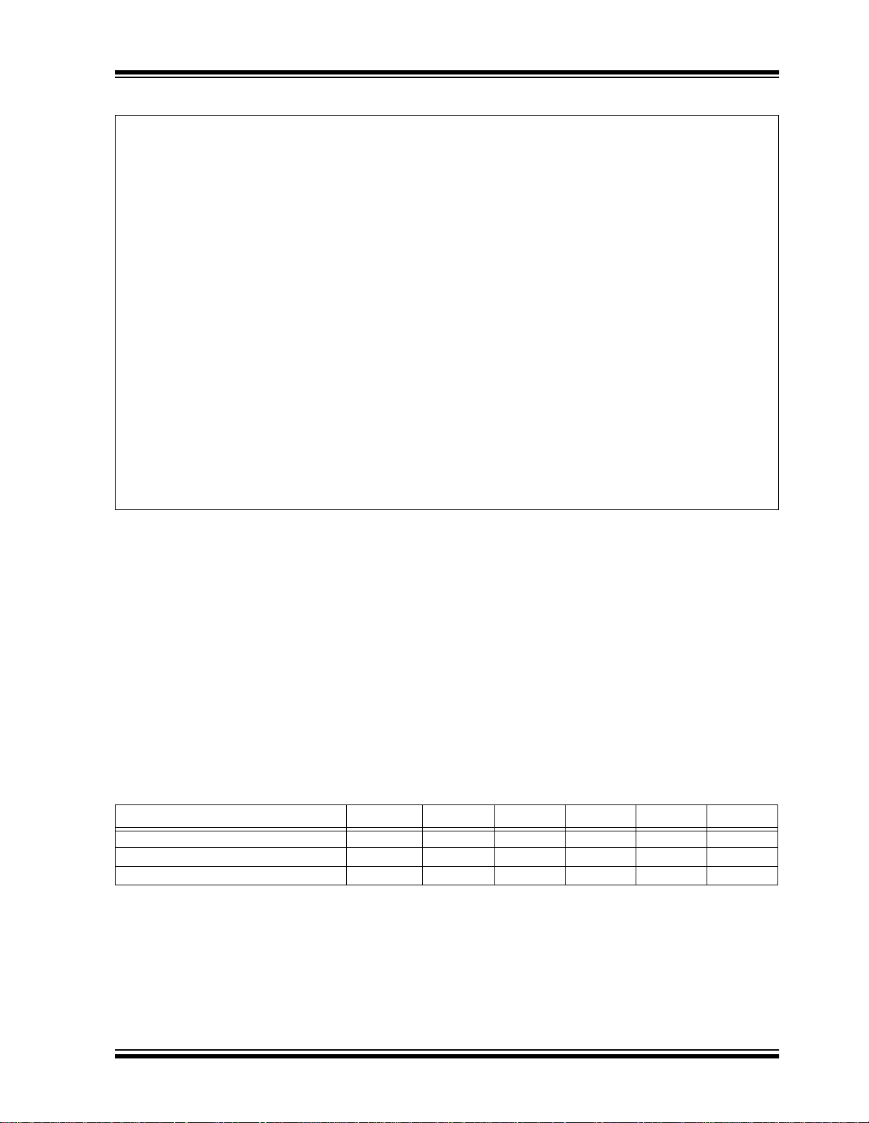
PIC16C925/926
EQUATION 8-1: EXAMPLES OF PWM PERIOD AND DUTY CYCLE CALCULATION
1. Find the value of the PR2 register, given:
• Desired PWM frequency = 31.25 kHz
• F
OSC = 8 MHz
• TMR2 prescale = 1
From the equation for PWM period in Section 8.3.1,
1 / 31.25 kHz = [ (PR2) + 1 ] • 4 • 1/8 MHz • 1
or
32 µs = [ (PR2) + 1 ] • 4 • 125 ns • 1 = [ (PR2) + 1 ] • 0.5 µs
PR2 = (32 µs / 0.5 µs) - 1
PR2 = 63
2. Find the maximum resolution of the duty cycle that can be used with a 31.25 kHz frequency and
8 MHz oscillator.
From the equation from maximum PWM resolution in Section 8.3.2,
1 / 31.25 kHz = 2
or
32 µs= 2
256 = 2
log(256) = (PWM Resolution) • log(2)
8.0 = PWM Resolution
PWM RESOLUTION
PWM RESOLUTION
PWM RESOLUTION
• 1 / 8 MHz • 1
• 125 ns • 1
At most, an 8-bit resolution duty cycle can be obtained
from a 31.25 kHz fre quency and a 8 MHz osci llator , i.e .,
0 ≤ CCPR1L:CCP1CON<5:4> ≤ 25 5. Any value grea ter
than 255 will result in a 100% duty cycle.
In order to achieve higher resolution, the PWM frequency must be decreased. In order to achieve higher
PWM frequency, the resolution must be decreased.
Table 8-2 lists example PWM frequencies and resolutions for F
ues are also shown.
OSC = 8 MHz. TMR2 prescaler and PR2 val-
8.3.3 SET-UP FOR PWM OPERATION
The following steps should be taken when configuring
the CCP module for PWM operation:
1. Set the PWM period by writing to the PR2
register.
2. Set the PWM duty cycle by writing to the
CCPR1L register and CCP1CON<5:4> bits.
3. Make the CCP1 pin an output by clearing the
TRISC<2> bit.
4. Set the TMR2 prescale value a nd enable T imer2
by writing to T2CON.
5. Configure the CCP module for PWM operation.
TABLE 8-2: EXAMPLE PWM FREQUENCIES AND RESOLUTIONS AT 8 MHz
PWM Frequency 488 Hz 1.95 kHz 7.81 kHz 31.25 kHz 62.5 kHz 250 kHz
Timer Prescaler (1, 4, 16) 16 4 1 1 1 1
PR2 Value 0xFF 0xFF 0xFF 0x3F 0x1F 0x07
Maximum Resolution (bits) 10 10 10 8 7 5
2001 Microchip Technology Inc. Preliminary DS39544A-page 57

PIC16C925/926
TABLE 8-3: REGISTERS ASSOCIATED WITH TIMER1, CAPTURE AND COMPARE
Address Name Bit 7 Bit 6 Bit 5 Bit 4 Bit 3 Bit 2 Bit 1 Bit 0
0Bh, 8Bh,
10Bh, 18Bh
0Ch PIR1 LCDIF ADIF — — SSPIF CCP1IF TMR2IF TMR1IF 00-- 0000 00-- 0000
8Ch PIE1 LCDIE ADIE — — SSPIE CCP1IE TMR2IE TMR1IE 00-- 0000 00-- 0000
87h TRISC — — PORTC Data Direct ion Co ntrol Regi ster --11 1111 --11 1111
0Eh TMR1L Holding register for the Least Significant Byte of the 1 6-bi t TMR1 Re giste r xxxx xxxx uuuu uuuu
0Fh TMR1H Holding register for the Most Significant Byte of the 16-b it TMR1 Regist er xxxx xxxx uuuu uuuu
10h T1CON — — T1CKPS1 T1CKPS0 T1OSCEN T1SYNC TMR1CS TMR1ON --00 0000 --uu uuuu
15h CCPR1L Capture/Compare/PWM1 (LSB) xxxx xxxx uuuu uuuu
16h CCPR1H Capture/Compare/PWM1 (MSB) xxxx xxxx uuuu uuuu
17h CCP1CON — — CCP1X CCP1Y CCP1M3 CCP1M2 CCP1M1 CCP1M0 --00 0000 --00 0000
Legend: x = unknown, u = unchanged, - = unimplemented locations read as '0’. Shaded cells are not used in these modes.
INTCON GIE PEIE
TMR0IE INTE RBIE TMR0IF INTF RBIF 0000 000x 0000 000u
Val ue on
Power-on
Reset
Value o n
all other
RESETS
TABLE 8-4: REGISTERS ASSOCIATED WITH PWM AND TIMER2
Address Name Bit 7 Bit 6 Bit 5 Bit 4 Bi t 3 B i t 2 B it 1 B it 0
0Bh, 8Bh,
10Bh, 18Bh
0Ch PIR1 LCDIF ADIF — — SSPIF CCP1IF TMR2IF TMR1IF 00-- 0000 00-- 0000
8Ch PIE1 LCDIE ADIE — — SSPIE CCP1IE TMR2IE TMR1IE 00-- 0000 00-- 0000
87h TRISC — — PORTC Data Direction Control Register --11 1111 --11 1111
11h TMR2 Timer2 Module Register 0000 0000 0000 0000
92h PR2 Timer2 Module Period Register 1111 1111 1111 1111
12h T2CON — TOUTPS3 TOUTPS2 TOUTPS1 TOUTPS0 TMR2ON T2CKPS1 T2CKPS0 -000 0000 -000 0000
15h CCPR1L Capture/Compare/PWM 1 (LSB) xxxx xxxx uuuu uuuu
16h CCPR1H Capture/Compare/PWM1 (MSB) xxxx xxxx uuuu uuuu
17h CCP1CON — — CCP1X CCP1Y CCP1M3 CCP1M2 CCP1M1 CCP1M0 --00 0000 --00 0000
Legend: x = unknown, u = unchanged, - = unimplemented locations read as '0’. Shaded cells are not used in this mode.
INTCON GIE PEIE
TMR0IE INTE RBIE TMR0IF INTF RBIF 0000 000x 0000 000u
Value o n
Power-on
Reset
Value on
all other
RESETS
DS39544A-page 58 Preliminary 2001 Microchip Technology Inc.

PIC16C925/926
TM
9.0 SYNCHRONOUS SERIAL PORT (SSP) MODULE
The Synchronous Serial Port (SSP) module is a serial
interface useful for communicating with other periph-
• Serial Peripheral Interface (SPI
• Inter-Integrated Circuit (I2CTM)
Refer to Application Note AN578, "Use of the SSP
Module in the I
2
C Multi-Master Environment.”
eral or microcontroller devices. These peripheral
devices may be serial EEPROMs, shift registers, display drivers, A/D conv erte rs, et c. The SSP m odu le ca n
operate in one of two modes:
REGISTER 9-1: SSPSTAT: SERIAL PORT STATUS REGISTER (ADDRESS 94h)
R/W-0 R/W-0 R-0 R-0 R-0 R-0 R-0 R-0
SMP CKE D/A
bit 7 bit 0
bit 7 SMP: SPI Data Input Sample Phase bit
SPI Master mode:
1 = Input data sampled at end of data output time
0 = Input data sampled at middle of data output time
SPI Slave mode:
SMP must be cleared when SPI is used in Slave mode
bit 6 CKE: SPI Clock Edge Select bit (see Figure 9-3, Figure 9-4, and Figure 9-5)
CKP = 0:
1 = Data transmitted on rising edge of SCK
0 = Data transmitted on falling edge of SCK
CKP = 1:
1 = Data transmitted on falling edge of SCK
0 = Data transmitted on rising edge of SCK
bit 5 D/A
bit 4 P: STOP bit (I
bit 3 S: START bit (I
bit 2 R/W
bit 1 UA: Update Address (10-bit I
bit 0 BF: Buffer Full Status bit
: Data/Address bit (I2C mode only)
1 = Indicates that the last byte received or transmitted was data
0 = Indicates that the last byte received or transmitted was address
bit was detected last.)
1 = Indicates that a STOP bit has been detected last (this bit is ’0’ on RESET)
0 = STOP bit was not detected last
bit was detected last.)
1 = Indicates that a START bit has been detected last (this bit is ’0’ on RESET)
0 = START bit was not detected last
: Read/Write bit Information (I2C mode only)
This bit holds the R/W bit information following the last address match. This bit is only valid from the
address match to the next START bit, STOP bit, or ACK
1 = Read
0 = Write
1 = Indicates that the user needs to update the address in the SSPADD register
0 = Address does not need to be updated
Receive (SPI and I
1 = Receive complete, SSPBUF is full
0 = Receive not complete, SSPB UF is empty
Transmit (I
1 = Transmit in progress, SSPBUF is full
0 = Transmit complete, SSPBUF is empty
2
C mode only. This bit is cleared when the SSP module is disabled, or when the STA RT
2
C mode only. This bit is cleared when the SSP module is disabled, or when the STOP
2
C mode only)
2
C modes):
2
C mode only)
PSR/WUA BF
bit.
)
Legend:
R = Readable bit W = Writable bit U = Unimplemented bit, read as ‘0’
- n = Value at POR ’1’ = Bit is set ’0’ = Bit is cleared x = Bit is unknown
2001 Microchip Technology Inc. Preliminary DS39544A-page 59

PIC16C925/926
REGISTER 9-2: SSPCON: SYNC SERIAL PORT CONTROL REGISTER (ADDRESS 14h)
R/W-0 R/W-0 R/W-0 R/W-0 R/W-0 R/W-0 R/W-0 R/W-0
WCOL SSPOV SSPEN CKP SSPM3 SSPM2 SSPM1 SSPM0
bit 7 bit 0
bit 7 WCOL: Write Collision Detect bit
1 = SSPBUF register is written while still transmitting the previous word (must be cleared in software)
0 = No collision
bit 6 SSPOV: Receive Overflow Indicator bit
In SPI mode:
1 = A new byte is received while SSPBUF is holding previous data. Data in SSPSR is lost on overflow.
Overflow only occurs in Slave mode. The user must read the SSPBUF, even if only transmitting data,
to avoid setting overflows. In Master mode, the overflow bit is not set since each operation is initiated
by writing to the SSPBUF register. (Must be cleared in software.)
0 = No overflow
2
In I
C mode:
1 = A byte is received while the SSPBUF is holding the previous byte. SSPOV is a “don’t care” in transmit
mode. (Must be cleared in software.)
0 = No overflow
bit 5 SSPEN: Synchronous Serial Port Enable bit
In SPI mode:
When enabled, these pins must be properly configured as input or output.
1 = Enables serial port and configures SCK, SDO, SDI, and SS as the source of the serial port pins
0 = Disables serial port and configures these pins as I/O port pins
2
In I
C mode:
When enabled, these pins must be properly configured as input or output.
1 = Enables the serial port and configures the SDA and SCL pins as the source of the serial port pins
0 = Disables serial port and configures these pins as I/O port pins
bit 4 CKP: Clock Polarity Select bit
In SPI mode:
1 = Idle state for clock is a high level
0 = Idle state for clock is a low level
2
In I
C mode:
SCK release control
1 = Enable clock
0 = Holds clock low (clock stretch). (Used to ensure data setup time.)
bit 3-0 SSPM3:SSPM0: Synchronous Serial Port Mode Select bits
0000 = SPI Master mode, clock = FOSC/4
0001 = SPI Master mode, clock = FOSC/16
0010 = SPI Master mode, clock = FOSC/64
0011 = SPI Master mode, clock = TMR2 output/2
0100 = SPI Slave mode, clock = SCK pin (SS pin control enabled)
0101 = SPI Slave mode, clock = SCK pin (SS pin control disabled, SS can be used as I/O pin)
0110 = I
0111 =I
1011 =I
1110 =I
1111 = I
1000, 1001, 1010, 1100, 1101 = reserved
2
C Slave mode, 7-bit address
2
C Slave mode, 10-bit address
2
C firmware controlled Master mode (slave idle)
2
C firmware controlled Master mode, 7-bit address with START and STOP bit interrupts enabled
2
C firmware controlled Master mode, 10-bit address with START and STOP bit interrupts enabled
Legend:
R = Readable bit W = Writable bit U = Unimplemented bit, read as ‘0’
- n = Value at POR ’1’ = Bit is set ’0’ = Bit is cleared x = Bit is unknown
DS39544A-page 60 Preliminary 2001 Microchip Technology Inc.
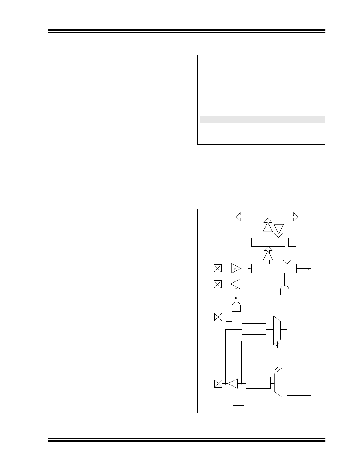
PIC16C925/926
9.1 SPI Mode
The SPI mode allows 8-bits of data to be synchronously transmitted and received simultaneously. To
accomplish communication, typically three pins are
used:
• Serial Data Out (SDO) RC5/SDO
• Serial Data In (SDI) RC4/SDI
• Serial Clock (SCK) RC3/SCK
Additionally, a fourth pin may be used when in a Slave
mode of operation:
• Slave Select (SS
When initializing the SPI, several options need to be
specified. This is done by pro gramming th e appropriate
control bits in the SSPCON register (SSPCON<5:0>)
and SSPSTAT<7:6>. These control bits allow the following to be specified:
• Master mode (SCK is the clock output)
• Slave mode (SCK is the clock input)
• Clock Polarity (Idle state of SCK)
• Clock Edge (output data on rising/falling edge of
SCK)
• Clock Rate (Master mode only)
• Slave Select mode (Slave mode only)
The SSP consists of a transmit/receive shift register
(SSPSR) and a buffer register (SSPBUF). The SSPSR
shifts the data in and out of the device, MSb first. The
SSPBUF holds the data tha t was written to the SSPSR,
until the received data is ready. Once the 8-bits of data
have been received, that byte is moved to the SSPBUF
register. Then, the buffer full detect bit, BF
(SSPSTAT<0>), and interrupt flag bit, SSPIF
(PIR1<3>), are set. This double buffering of the
received data (SSPBUF) allows the next byte to start
reception before reading the data that was just
received. Any write to the SSPBUF register during
transmission/reception of data will be ignored, and the
write collision detect bit, WCOL (SSPCON<7>), will be
set. User software must clear the WCOL bit so that it
can be determined if the following write(s) to the
SSPBUF register completed successfully. When the
application software is expecting to receive valid data,
the SSPBUF should be read before the next byte of
data to transfer is written to th e SSPBUF. Buffer full bit,
BF (SSPST AT<0>), indicates when SSPBUF has been
loaded with the received data (transmission is complete). When the SSPBUF is read, bit BF is cleared.
This data may be irrelev ant if the SPI is only a transmitter. Generally, the SSP interrupt is used to determine
when the transmission/reception has completed. The
SSPBUF must be read and/or written. If the interrupt
method is not going to be used, then software polling
can be done to ensure that a write collision does not
occur. Example 9-1 shows the loading of the SSPBUF
(SSPSR) for data transmission. The MOVWF RXDATA
instruction (shaded) i s only required if the received dat a
is meaningf ul.
) RA5/AN4/SS
EXAMPLE 9-1: LOADING THE SSPBUF
(SSPSR) REGISTER
BCF STATUS, RP1 ;Select Bank1
BSF STATUS, RP0 ;
LOOP BTFSS SSPSTAT, BF ;Has data been
GOTO LOOP ;No
BCF STATUS, RP0 ;Select Bank0
MOVF SSPBUF, W ;W reg = contents
MOVWF RXDATA ;Save in user RAM
MOVF TXDATA, W ;W reg = contents
MOVWF SSPBUF ;New data to xmit
;received
;(transmit
;complete)?
;of SSPBUF
; of TXDATA
The block diagram of the SSP module, when in SPI
mode (Figure 9-1), shows that the SSPSR is not
directly readable o r writa ble, and c an only be a ccessed
from addressing the SSPBUF reg ister. Additionally , the
SSP status register (SSPSTAT) indicates the various
status conditions.
FIGURE 9-1: SSP BLOCK DIAGRAM
(SPI MODE)
Internal
Data Bus
Read Write
SSPBUF reg
SSPSR reg
RC4/SDI/SDA
RC5/SDO
RA5/AN4/SS
RC3/SCK/
SCL
bit0
Control
SS
Enable
Edge
Select
SSPM3:SSPM0
Edge
Select
TRISC<3>
Clock Select
4
2
TMR2 Output
Prescaler
4, 16, 64
Shift
Clock
2
CY
T
2001 Microchip Technology Inc. Preliminary DS39544A-page 61
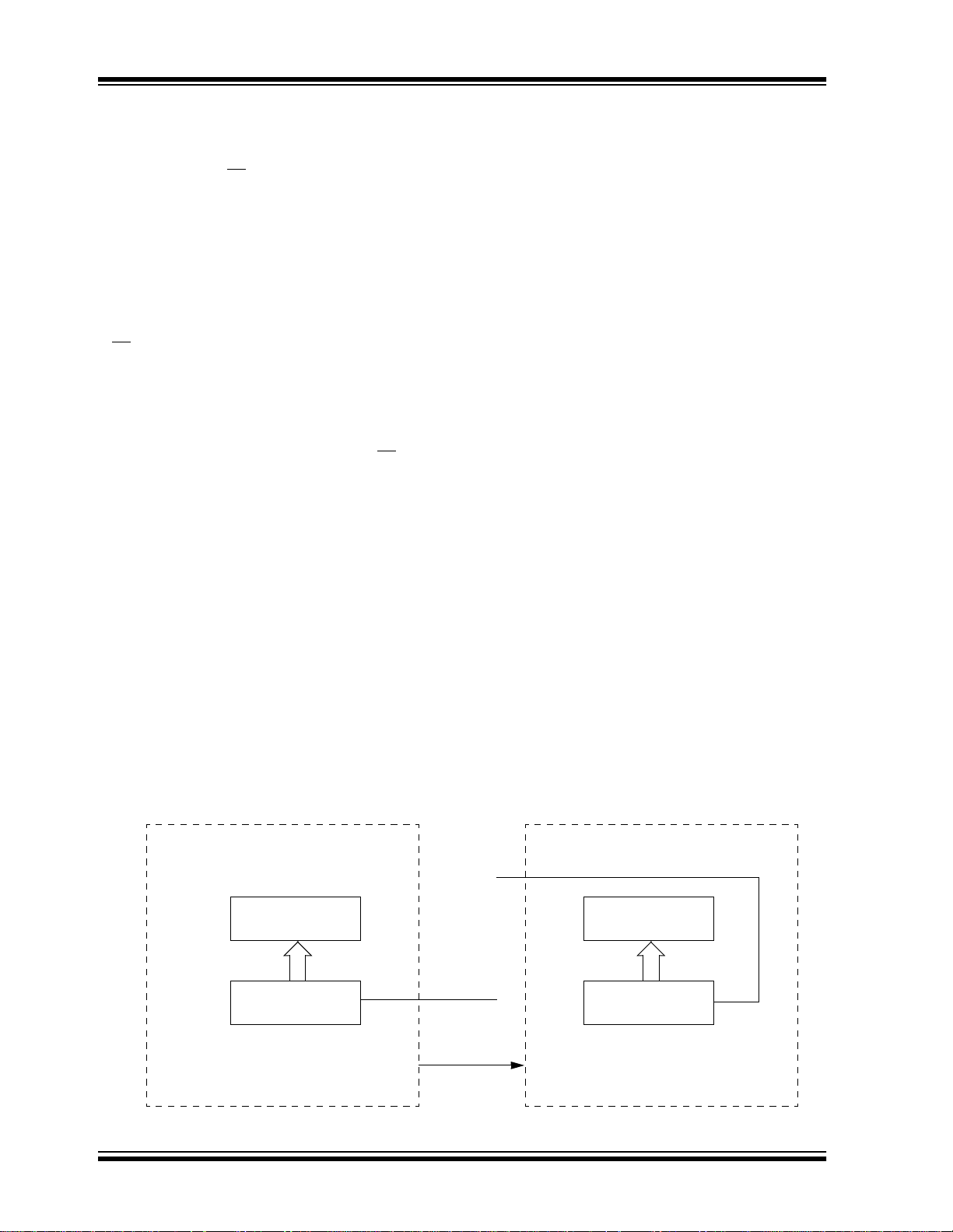
PIC16C925/926
To enable the serial port, SSP enable bit, SSPEN
(SSPCON<5>) must be set. To reset or reconfigure
SPI mode, clear bit SSPEN, re-initialize the SSPCON
register, and then set bit SSPEN. This configures the
SDI, SDO, SCK, and SS
pins as serial po rt pins. For the
pins to behave as the serial port function, they must
have their data direction bits (in the TRISC register)
appropriately programmed. That is:
• SDI must have TRISC<4> set
• SDO must have TRISC<5> cleared
• SCK (Master mode) must have TRISC<3>
cleared
• SCK (Slave mode) must have TRISC<3> set
S must have TRISA<5> set and ADCON must
• S
be configured such that RA5 is a digital I/O
Any serial port fu nction th at is not de sired ma y be overridden by programming the corresponding data direction (TRIS) register to the opposite value. An example
would be in Mast er mo de, whe r e yo u ar e on l y se ndi ng
data (to a display driver), then both SDI and SS
could
be used as general purpose outputs by clearing their
corresponding TRIS register bits.
Figure 9-2 shows a typical connection between two
microcontrollers. The master controller (Processor 1)
initiates the data transfer by sending the SCK signal.
Data is shifted out of both shift registers on their programmed clock edge, and latched on the opposite
edge of the clock. Both processors should be programmed to sa me Clock Polarity (CKP), then both co ntrollers would send and receive data at the same time.
Whether the data is meaningful (or dummy data),
depends on the application software. This leads to
three scenarios for data transmission:
• Master sends data — Slave sends dummy data
• Master sends data — Slave sends data
• Master sends dummy data — Slave sends data
The master can initiate the data transfer at any time
because it controls the SCK. The master determines
when the slave (Processor 2) is to broadcast data by
the firmware protocol.
In Master mode, the data is transmitted/received as
soon as the SSPBUF register is written to. If the SPI is
only going to receive, the SC K output could be disable d
(programmed as an input). The SSPSR register will
continue to shift in the signal present on the SDI pin at
the programmed clock rate. As each byte is rec eived, it
will be loaded into the SSPBUF register as if a normal
received byte (interrupts and status bits appropriately
set). This could be useful in receiver applications as a
“line activity monitor” mode.
In Slave mode, the data is tra ns mi tted and rece iv ed a s
the external clock pulses appear on SCK. When the
last bit is latched, the interrupt fl ag bit SSPIF (PIR1<3>)
is set.
The clock polarity is selected by appropriately program ming bit CKP (SSPCON<4>). This then, would give
waveforms for SPI communication as shown in
Figure 9-3, Figure 9-4, and Fig ure9-5, where the MSB
is transmitted first. In Master mode, the SPI clock rate
(bit rate) is user programmable to be one of the
following:
OSC/4 (or TCY)
• F
• FOSC/16 (or 4 • TCY)
• F
OSC/64 (or 16 • TCY)
• Timer2 output/2
This allows a maximum bit clock frequency (at 8 MHz)
of 2 MHz. When in Sl ave mode, th e external cl ock must
meet the minimum high and low times.
In SLEEP mode, the slave can transmit and receive
data and wake the device from SLEEP.
FIGURE 9-2: SPI MASTER/SLAVE CONNECTION
SPI Master SSPM3:SSPM0 =
Serial Input Buffer
(SSPBUF)
Shift Register
(SSPSR)
MSb
PROCESSOR 1
DS39544A-page 62 Preliminary 2001 Microchip Technology Inc.
00xxb
SDO
SDI
LSb
SCK
SPI Slave SSPM3:SSPM0 =
SDI
Serial Input Buffer
SDO
SCK
Shift Register
MSb
010xb
(SSPBUF)
(SSPSR)
LSb
PROCESSOR 2

The SS pin allows a Synchronous Slave mode. The
SPI must be in Slave mode (SSPCON<3:0> = 04h)
and the TRISA<5> bit must be set for the Synchronous Slave mode to be enabled. When the SS
pin
is low, transmission and reception are enabled and
the SDO pin is driven. When the SS
pin goes high,
the SDO pin is no longer driven, even if in the middle of a transmitted byte and becomes a floating
output. External pull-up/pull-down resistors may be
desirable, depending on the application.
FIGURE 9-3: SPI MODE TIMING, MASTER MODE
SCK (CKP = 0,
CKE = 0)
SCK (CKP = 0,
CKE = 1)
SCK (CKP = 1,
CKE = 0)
SCK (CKP = 1,
CKE = 1)
PIC16C925/926
Note 1: When the SPI is in Slave mode with SS
pin control enabled (SSPCON<3:0> =
0100), the SPI module will reset if the SS
pin is set to VDD.
2: If the SPI is used in Slave mode with
CKE = ’1’, then the SS
enabled.
To emulate two-wire communication, the SDO pin can
be connected to the SDI pin. When the SPI needs to
operate as a receiver, the SDO pin can be configured
as an input. This dis ables tran smissi ons from the SD O.
The SDI can always be left as an input (SDI function)
since it cannot create a bus conflict.
pin control must b e
SDO
SDI (SMP = 0)
SDI (SMP = 1)
SSPIF
bit7
bit7
bit7 bit0
bit6 bit5
bit4
bit3
FIGURE 9-4: SPI MODE TIMING (SLAVE MODE WITH CKE = 0)
SS (optional)
SCK (CKP = 0)
SCK (CKP = 1)
SDO
bit7
bit6 bit5
bit4
bit3
bit2
bit2
bit1 bit0
bit0
bit1 bit0
SDI (SMP = 0)
bit7 bit0
SSPIF
2001 Microchip Technology Inc. Preliminary DS39544A-page 63
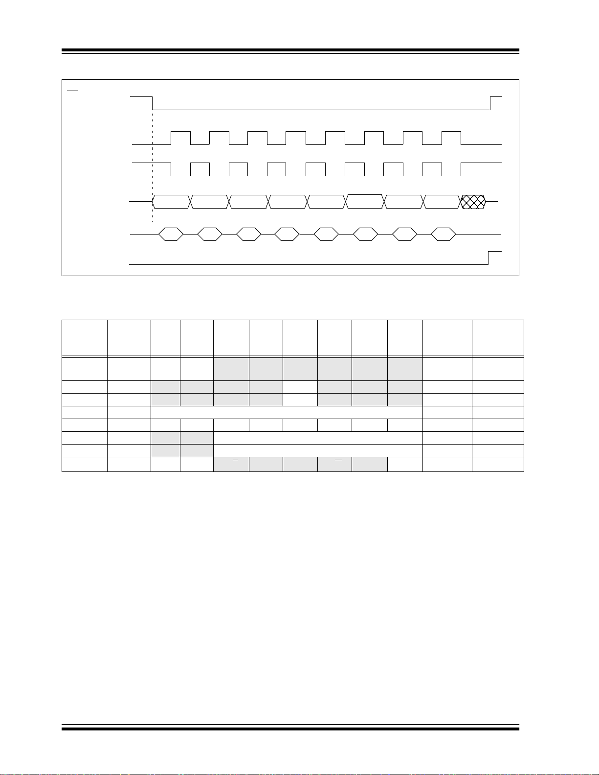
PIC16C925/926
FIGURE 9-5: SPI MODE TIMING (SLAVE MODE WITH CKE = 1)
SS
(not optional)
SCK (CKP = 0)
SCK (CKP = 1)
SDO
SDI (SMP = 0)
SSPIF
bit7
bit7 bit0
bit6 bit5
bit4
bit3
bit2
bit1 bit0
TABLE 9-1: REGISTERS ASSOCIATED WITH SPI OPERATION
Address Name Bit 7 Bit 6 Bit 5 Bit 4 Bit 3 Bit 2 Bit 1 Bit 0
0Bh, 8Bh,
10Bh, 18Bh
0Ch PIR1 LCDIF ADIF — — SSPIF CCP1IF TMR2IF TMR1IF 00-- 0000 00-- 0000
8Ch PIE1 LCDIE ADIE — — SSPIE CCP1IE TMR2IE TMR1IE 00-- 0000 00-- 0000
13h SSPBUF Synchronous Serial Port Receive Buffer/Transmit Register xxxx xxxx uuuu uuuu
14h SSPCON WCOL SSPOV SSPEN CKP SSPM3 SSPM2 SSPM1 SSPM0 0000 0000 0000 0000
85h TRISA — — PORTA Data Direction Control Register --11 1111 --11 1111
87h TRISC — — PORTC Data Direction Control Register --11 1111 --11 1111
94h SSPSTAT SMP CKE D/A P S R/W UA BF 0000 0000 0000 0000
Legend: x = unknown, u = unchanged, - = unimplemented, read as '0'. Shaded cells are not used by the SSP in SPI mode.
INTCON GIE PEIE
TMR0IE INTE RBIE TMR0IF INTF RBIF 0000 000x 0000 000u
Val ue on
Power-on
Reset
Value on all
other
RESETS
DS39544A-page 64 Preliminary 2001 Microchip Technology Inc.

PIC16C925/926
9.2 I2C Overview
This section provides an overview of the InterIntegrated Circuit (I
ing the operation of the SSP module in I
2
C bus is a two-wire se rial in terf ace de velop ed by
The I
the Philips Corporation. The original specification, or
standard mode, was for data transfers of up to 100
Kbps. An enhanced specification, or fast mode is not
supported. This device will communicate with fast
mode devices if attached to the same bus.
2
C interface employs a c omprehensive pr otocol to
The I
ensure reliable transmission and reception of data.
When transmitting data, one device is the “master”
which initiates transfer on the bus and generates the
clock signals to permit that transfer, while the other
device(s) acts as the “slave.” All portions of the slave
protocol are implemented in the SSP module’s hardware, except general ca ll s up port , w hil e po rtio ns of th e
master protocol need to be addressed in the
PIC16CXXX software. Table 9-2 defines some of the
2
C bus terminology. For additional information on the
I
2
I
C interface specification, refer to the Philips document #939839340011, “The I
which can be obtained from the Philips Corporation.
2
In the I
C interface protocol, each device has an
address. When a mas ter wishe s to initiate a dat a transfer, it first transmits the address of the device that it
wishes to “talk” to. All de vices “listen” to see if this is
their address. Within this address, a bit specifies if the
master wishes to read from/write to the slave device.
The master and slave are always in opposite modes
(transmitter/receiver) of operation during a data transfer. Th at is, they can be thought of as operating in either
of these two relations:
• Master-transmitter and Slave-receiver
• Slave-transmitter and Master-receiver
In both cases, the master generates the clock signal.
2
C) bus, with Se ction 9.3 d iscuss-
2
C bus and how to use it”,
2
C mode.
The output stages of the clock (SCL) and data (SDA)
lines must have an open drain or open collector, in
order to perform the wired-AND function of the bus.
External pull-up resistors are used to ensure a high
level when no de vice is pulling the li ne down. T he number of devices that may be attached to the I
2
C bus is
limited onl y by the maxi mum bus l oading sp ecifi cation
of 400 pF.
9.2.1 INITIATING AND TERMINATING
DATA TRANSFER
During times of no data transfer (idle time), both the
clock line (SCL) and the dat a line (SDA) are pulle d high
through the external pull-up resistors. The START and
STOP conditions determine the start and stop of data
transmission. The START condition is defined as a
high to low trans iti on of th e SD A whe n the SC L is h ig h.
The STOP condition is defined as a low to high transition of the SDA when the SC L is high. Figure 9-6 shows
the START and STOP conditions. The master generates these conditions for starting and terminating data
transfer. Due to the definition of the START and STOP
conditions, when data is being transmitted, the SDA
line can only change state when the SCL line is low.
FIGURE 9-6: START AND STOP
CONDITIONS
SDA
S
SCL
START
Condition
Change
of Data
Allowed
Change
of Data
Allowed
P
STOP
Condition
TABLE 9-2: I
2
C BUS TERMINOLOGY
Term Description
Transmitter The device that sends the data to the bus.
Receiver The device that receives the data from the bus.
Master The device which initiates the transfer, generates the clock and terminates the transfer.
Slave The device addressed by a master.
Multi-master More than one master device in a system. These masters can attempt to control the bus at the
same time without corrupting the message.
Arbitration Procedure that ensures that only on e of the m aster d evice s will c ontrol th e bus. T his ens ures th at
the transfer data does not get corrupted.
Synchronization Procedure where the clock signals of two or more devices are synchronized.
2001 Microchip Technology Inc. Preliminary DS39544A-page 65

PIC16C925/926
9.2.2 ADDRESSING I2C DEVICES
There are two address formats. The simplest is the
7-bit address format with a R/W
more complex is the 10-bit address with a R/W
bit (Figure 9-7). The
bit
(Figure 9-8). For 10-bit addr ess forma t, two b ytes mus t
be transmitted with the firs t five bits sp ecifying this to be
a 10-bit address.
FIGURE 9-7: 7-BIT ADDRESS FORMAT
MSb LSb
ACK
S
S
START Condition
R/W Read/Write pulse
Acknowledge
ACK
FIGURE 9-8: I
Slave Address
2
C 10-BIT ADDRESS
R/W
Sent by
Slave
FORMAT
S 1 1 1 1 0 A9 A8 R/W ACK A7 A6 A5 A4 A3 A2 A1 A0 ACK
Sent by Slave
- START Condition
S
- Read/Write Pulse
R/W
ACK
- Acknowledge
= 0 for Write
9.2.3 TRANSFER ACKNOWLEDGE
All data must be transmitted per byte, with no limit to
the number of bytes transm itted per da ta t ransfe r. After
each byte, the slave-receiver generates an Acknowledge bit (ACK
) (see Figure 9-9). When a slave-receiv er
doesn’t acknowledge the slave address or received
data, the master must abort the transfer. The slave
must leave SDA high so that the master can generate
the STOP condition (Figure 9-6).
FIGURE 9-9: SLAVE-RECEIVER
ACKNOWLEDGE
Data
Output by
Transmitter
Data
Output by
Receiver
SCL from
Master
S
START
Condition
If the master is receiving the data (master-receiver), it
generates an Acknowledge signal for each received
byte of data, except for the last byte. To signal the end
of data to the slave-transmitter, the master does not
generate an Acknowledge (Not Acknowledge). The
slave then releases the SDA line so the master can
generate the STOP condition. The master can also
generate the STOP condition during the Acknowledge
pulse for valid termination of data transfer.
If the slave needs to dela y th e tra nsm is s ion of the nex t
byte, holding the SC L l ine l ow will force the m ast er in to
a wait state. Data transfer continues when the slave
releases the S CL line. This allows the slave to move
the received data, or fetch the data it needs to transfer
before allowing the clock to start. This wait state technique can also be implemented at the bit level,
Figure 9-10. The slave will inherently stretch the clock
when it is a transmitter , but wi ll not when it is a receive r .
The slave will have to clear the SSPCON<4> bit to
enable clock stretching when it is a receiver.
1
Not Acknowledge
Acknowledge
2
8
Clock Pulse for
Acknowledgment
9
FIGURE 9-10: DATA TRANSFER WAIT STATE
SDA
MSB Acknowledgment
SCL
S
START
Condition
DS39544A-page 66 Preliminary 2001 Microchip Technology Inc.
12 789 123 • 89
Address R/W
Signal from Receiver
Byte Complete
Interrupt with Receiver
Clock Line Held Low while
Interrupts are Serviced
ACK Wait
State
Acknowledgment
Signal from Receiver
Data ACK
P
STOP
Condition

PIC16C925/926
Figure 9-11 and Figure 9-12 show master-transmitter
and Master-receiver data transfer sequences.
When a master does not wish to relinquish the bus (by
generating a STOP condition), a Repeated START
condition (Sr) must be generated. This condition is
identical to the ST AR T condition (SDA go es high-to-low
while SCL is high), but occurs after a data transfer
Acknowledge pulse (not the bus-fr ee state). This allows
a master to send “commands” to the slave and then
receive the requested information, or to address a different slave device. This sequence is shown in
Figure 9-13.
FIGURE 9-11: MASTER-TRANSMITTER SEQUENCE
For 7-bit address:
S
Slave AddressR/W ADataADataA/AP
'0' (write) data transferred
A master-transmitter addresses a slave-receiver with a
7-bit address. The transfer direction is not changed.
From master to slave
From slave to master
(n bytes - Acknowledge)
A = Acknowledge (SDA low)
= Not Acknowledge (SDA high)
A
S = START Condition
P = STOP Condition
For 10-bit address:
SR/W
FIGURE 9-12: MASTER-RECEIVER SEQUENCE
For 7-bit address:
Slave AddressR/W
S
'1' (read) data transferred
A master reads a slave immediately after the first byte.
From master to slave
From slave to master
ADataAData A P
(n bytes - Acknowledge)
A = Acknowledge (SDA low)
A
= Not Acknowledge (SDA high)
S = START Condition
P = STOP Condition
For 10-bit address:
Slave Address
SR/W
Slave Address
First 7 bits
(write)
Data A Data P
A master-transmitter addresses a slave-receiver
with a 10-bit address.
First 7 bits
(write)
Slave Address
Sr R/W A3 AData A PData
First 7 bits
A master-transmitter addresses a slave-receiver
with a 10-bit address.
A1Slave Address
Second byte
A/A
A1Slave Address
Second byte
(read)
A2
A2
FIGURE 9-13: COMBINED FORMAT
(read or write)
(n bytes + Acknowledge)
S
Slave AddressR/W ADataA/ASr P
(read) Sr = repeated
Transfer direction of data and Acknowledgment bits depends on R/W bits.
Combined format:
Slave Address
Sr R/W A
First 7 bits
(write)
Combined format - A master addresses a slave with a 10-bit address, then transmits
From master to slave
From slave to master
2001 Microchip Technology Inc. Preliminary DS39544A-page 67
data to this slave and reads data from this slave.
START Condition
Slave Address
Second byte
A = Acknowledge (SDA low)
= Not Acknowledge (SDA high)
A
S = STAR T Cond iti on
P = STOP Condition
Slave Address R/W
(write) Direction of transfer
Data Sr Slave Address
ADataA/A
may change at this point
R/W ADataA APA ADataA/A Data
First 7 bits
(read)
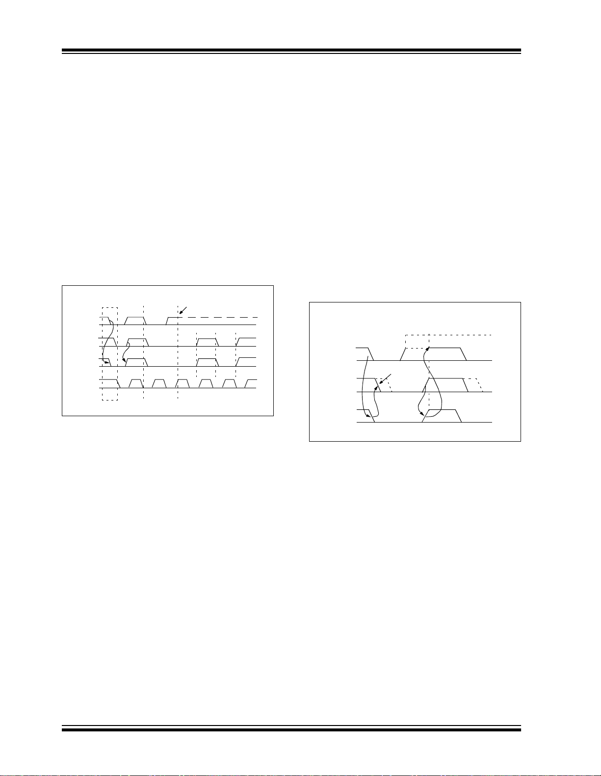
PIC16C925/926
9.2.4 MULTI-MASTER
The I2C protocol allows a system to have more than
one master. This is called multi-master. When two or
more masters try to transfer data at the same time,
arbitration and synchron iz ati on occ ur.
9.2.4.1 Arbitration
Arbitration takes place on the SDA line, while the SCL
line is high. The master, which transmits a high when
the other master transmits a low, loses arbitration
(Figure 9-14) and turns of f its data outpu t stage. A master, which lost arbitration can generate clock pulses
until the end of the data byte where it lost arbitration.
When the master devices are addressing the same
device, arbitration continues into the data.
FIGURE 9-14: MULTI-MASTER
ARBITRATION
(TWO MASTERS)
Transmitter 1 Loses Arbitration
DATA 1 SDA
DATA 1
DATA 2
SDA
SCL
9.2.4.2 Clock Synchronization
Clock synchronization occurs after the devices have
started arbitration. This is performed using a
wired-AND connection to the SCL line. A high to low
transition on the SCL line causes the concerned
devices to start counting off their low period. Once a
device clock has gone low, it will hold the SCL line low
until its SCL high stat e is reached. The low to high transition of this cloc k ma y not c hange the s tate of the SCL
line, if another device clock is still within its low period.
The SCL line is held low by th e device with the longest
low period. Device s with shorter low periods en ter a
high wait state , until the SCL line comes high. When the
SCL line comes high, all devices start counting off their
high periods. The first device to complete its high
period will pull the SCL line l ow . The SCL line high tim e
is determined by the device with the shortest high
period, Figure 9-15.
FIGURE 9-15: CLOCK
SYNCHRONIZATION
Start Counting
HIGH Period
CLK
1
CLK
2
State
Counter
Reset
Wait
Masters that also incorporate the slave function and
have lost arbitration, must immediately switch over to
Slave-Receiver mode. This is because the winning
master-transmitter may be addressing it.
Arbitration is not allowed between:
• A Repeated START condition
• A STOP condition and a data bit
• A Repeated START condition and a STOP
condition
Care needs to be t a ken to ensure that t hese c ondit ions
do not occur.
SCL
DS39544A-page 68 Preliminary 2001 Microchip Technology Inc.

PIC16C925/926
9.3 SSP I2C Operation
The SSP module in I2C mode fully imp lements all slave
functions, except general call support, and provides
interrupts on START and STOP bits in hardware to
facilitate firmware implementations of the master functions. The SSP module im plement s the st andard m ode
specifications as well as 7-bit and 10-bit addressing.
Two pins are used for data transfer. These are the
RC3/SCK/SCL pin, which is the clock (SCL), and the
RC4/SDI/SDA pin, which is the data (SDA). The user
must configure these pins as inputs or outputs through
the TRISC<4:3> bits. The SSP module functions are
enabled by setting SSP enable bit, SSPEN
(SSPCON<5>).
FIGURE 9-16: SSP BLOCK DIAGRAM
Read Write
RC3/SCK/SCL
RC4/
SDI/
SDA
The SSP module has five registers for I2C operation.
These are the:
• SSP Control Register (SSPCON)
• SSP Status Register (SSPSTAT)
• Serial Receive/Transmit Buffer (SSPBUF)
• SSP Shift Register (SSPSR) - Not directly
accessible
• SSP Address Register (SSPADD)
2
(I
C MODE)
SSPBUF reg
Shift
Clock
SSPSR reg
MSb
Match Detect
SSPADD reg
START and
STOP bit Dete c t
Internal
Data Bus
LSb
Addr Match
Set, Reset
S, P bits
(SSPSTAT reg)
The SSPCON register allows control of the I
tion. Four mode selection bits (SSPCON<3:0>) allow
one of the following I
2
C Slave mode (7-bit address)
• I
2
• I
C Slave mode (10-bit address)
2
C modes to be selected:
2
C opera-
• I2C Slave mode (7-bit address), with START and
STOP bit interrupts enabled
2
C Slave mode (10-bit address ), with ST AR T and
• I
STOP bit interrupts enabled
2
C Firmware controlled Master mode, slave is
• I
idle
2
Selection of any I
C mode, with the SSPEN bit set,
forces the SCL and SDA pins to be open drain, provided these pins are programmed to inputs by setting
the appropriate TRISC bits.
The SSPSTAT register gives the status of the data
transfer. This information includes detection of a
START or STOP bit, specifies if the received byte was
data or address, if the next byte is the completion of
10-bit address, and if this will be a read or write data
transfer. The SSPSTAT register is read only.
The SSPBUF is the register to which transfer data is
written to or read from. The SSPSR register shifts the
data in or out of the device. In re ceive oper atio ns, the
SSPBUF and SSPSR create a doubled buffered
receiver . This allo ws reception of the next by te to begin
before reading the last by te of receiv ed data. Wh en the
complete byte is received, it is transferred to the
SSPBUF register and flag bit SSPIF is set. If another
complete byte is received before the SSPBUF register
is read, a receiver overflow has occurred and bit
SSPOV (SSPCON<6>) is set and the byte in the
SSPSR is lost.
The SSPADD register holds the slave address. In
10-bit mode, the use r needs to write th e high byte of the
address (1111 0 A9 A8 0). Following the high byte
address match, the l ow byte of the address needs to be
loaded (A7:A0).
2001 Microchip Technology Inc. Preliminary DS39544A-page 69

PIC16C925/926
9.3.1 SLAVE MODE
In Slave mode, the SCL and SDA pins must be confi gured as inputs (TRISC<4:3> set). The SSP module will
override the input state with the output data when
required (slave-transmitter).
When an address is matched or the data transfer after
an address m atch i s re ceiv ed, the ha rd ware autom ati cally will generate the Acknowledge (ACK
then load the SSPBUF register with th e re ce ive d valu e
currently in the SSPSR register.
There are certain conditions that will cause the SSP
module not to give thi s ACK
(or both):
a) The buffer full bit BF (SSPSTAT<0>) was set
before the transfer was received.
b) The overflow bit SSPOV (SSPCON<6>) was set
before the transfer was received.
In this case, the SSPSR register value is not loaded
into the SSPBUF, but bit SSPIF (PIR1<3>) is set.
Table 9-3 shows what happens when a data transfer
byte is received, given the status of bits BF and
SSPOV. The shaded cells show the condition where
user software d id no t prope rly c lear th e ove rflow cond ition. Flag bit BF is cleared by read ing the SSPBUF register while bit SSPOV is cleared through software.
The SCL clock input must have a minimum high and
low time for proper operation. The high and low times
2
of the I
the SSP module is shown in timing parameter #100
and parameter #101.
C specification as well as the requirement of
pulse. These are if either
) pulse, and
address is compared on the falling edge of the eighth
clock (SCL) pulse. If the addresses match, and the BF
and SSPOV bits are clear, the following events occur:
a) The SSPSR register value is loaded into the
SSPBUF register.
b) The buffer full bit, BF is set.
c) An ACK
d) SSP interrupt flag bit, SSPIF (PIR1<3>) is set
(interrupt is generated if en abled) - on the fal ling
edge of the ninth SCL pulse.
In 10-bit Address mode, two address bytes need to be
pulse is generated.
9.3.1.1 Addressing
Once the SSP module has been enabled, it waits for a
ST AR T conditi on to occu r. Following the START condition, the 8-bits are shifted into the SSPSR register. All
incoming bits are sampled with the rising edge of the
clock (SCL) line. The value of register SSPSR<7:1> is
compared to the value of the SSPADD register. The
DS39544A-page 70 Preliminary 2001 Microchip Technology Inc.

PIC16C925/926
9.3.1.2 Reception
When the R/W bit of the address byte is clear and an
address match occurs, the R/W
register is cleare d. The re ceive d addre ss is loa ded in to
the SSPBUF register.
bit of the SSPSTAT
When the address byte overflow condition exists, then
no Acknowledge (ACK
condition is defined as either bit BF (SSPSTAT<0>) is
set, or bit SSPOV (SSPCON<6>) is set.
An SSP interrupt is generated for each data transfer
byte. Flag bit SSPIF (PIR1<3>) must be cleared in sof tware. The SSPSTAT register is used to determine the
status of the byte.
FIGURE 9-17: I2C WAVEFORMS FOR RECEPTION (7-BIT ADDRESS)
Receiving Address
A7 A6 A5 A4
1234
S
SCL
SSPIF (PIR1<3>)
BF (SSPSTAT<0>)
SSPOV (SSPCON<6>)
A3 A2 A1SDA
R/W=0
ACK
7
6
5
9
8
9.3.1.3 Transmission
When the R/W bit of the incoming address byte is set
and an address match occurs, the R/W
SSPSTAT register is set. The received address is
loaded into the SSPBUF register. The ACK pulse wi ll
be sent on the ninth bit, and pin RC3/SCK/SCL is held
low. The transmit data must be loaded into the
SSPBUF register, which also loads the SSPSR register. The n, pin RC3/SCK/SCL shou ld be enabled by setting bit CKP (SSPCON<4>). The master must monitor
the SCL pin prior to asse rtin g another clock pulse. The
slave devices may be holding off the master by stretching the clock. The eight data bits are shifted out on the
falling edge of the SCL input. This ensures that the
SDA signal is valid during the SCL high time
(Figure 9-18).
bit of the
Receiving Data
D5
D6D7
1234
Cleared in software
SSPBUF register is read
Bit SSPOV is set because the SSPBUF register is still full.
Receiving Data
D5
D6D7
123
D2
D3D4
56
D1
7
ACK
D0
89
An SSP interrupt is generated for each data transfer
byte. Flag bit SSPIF must be cleared in software, and
the SSPSTAT register is used to determine the status
of the byte. Flag bit SSPIF is set on the falling edge of
the ninth clock pulse.
As a slave-tra nsmitter, the ACK
ter-receiver is latched on the rising edge of the ninth
SCL input pulse. If the SDA line was high (not ACK
then the data transfer is complete. When the ACK
latched by the slave, the slave logic is reset and the
slave then monitors for another occurrence of the
ST AR T bit. If the SDA line was low (ACK
data must be loaded into the SSPBUF register, which
also loads the SSPSR register. Then, pin
RC3/SCK/SCL should be enabled by setting bit CKP.
) pulse is given. An overflow
ACK
D0
D2
D1
D3D4
9
5
4
ACK is not sent.
8
76
P
Bus Master
terminates
transfer
pulse from the mas-
), the transmit
),
is
FIGURE 9-18: I2C WAVEFORMS FOR TRANSMISSION (7-BIT ADDRESS)
Transmitting DataR/W = 1Receiving Address
SDA
SCL
SSPIF (PIR1<3>)
BF (SSPSTAT<0>)
CKP (SSPCON<4>)
2001 Microchip Technology Inc. Preliminary DS39544A-page 71
A7 A6 A5 A4 A3 A2 A1 ACK D7 D6 D5 D4 D3 D2 D1 D0
123456789 123456789
S
Data in
sampled
SCL held low
while CPU
responds to SSPIF
Cleared in software
SSPBUF is written in software
Set bit after writing to SSPBUF
(the SSPBUF must be written-to
before the CKP bit can be set)
From SSP Interrupt
Service Routine
ACK
P
PIC16C925/926
9.3.2 MASTER MODE
Master mode of operation is supported, in firmware,
using interrupt generation on the detection of the
START and STOP conditions. The STOP (P) and
ST ART (S) bit s are cle ared from a RESET, or when the
SSP module is disabled. The STOP and START bits
will toggle based on the START and STOP conditions.
Control of the I
set, or the bus is idle with both the S and P bits clear.
In Master mode, the SCL and SDA lines are manipulated by clearing the c orresp onding TRISC<4 :3> bit(s ).
The output level is always low, irrespective of the
value(s) in PORT C <4:3 >. So wh en transmitting data, a
’1’ data bit must have the TRISC<4> bit set (input) and
a ’0’ dat a bit must have the TRISC<4> bit cleared (o utput). The same scenario is true for the SCL li ne with the
TRISC<3> bit.
The following events will cause SSP Interrupt Flag bit,
SSPIF, to be set (SSP Interrupt if enabled):
• START condition
• STOP condition
• Data transfer byte transmitted/received
Master mode of operation can be done with either the
Slave mode idle (SSPM3:SSPM0 = 1011), or with the
slave active. When both Master and Slave modes are
enabled, the software needs to differentiate the
source(s) of the interrupt.
2
C bus may be taken when the P bit is
9.3.3 MULTI-MASTER MODE
In Multi-Master mode, the interrupt generation on the
detection of the START and STOP conditions allows
the determination of when the bus is free. The STOP
(P) and START (S) bits are cleared from a RESET or
when the SSP module is disabled. The STOP and
ST ART bits will toggle based on the START and STOP
conditions. Control of the I
bit P (SSPST AT<4>) is set, or the bus is idle, with both
the S and P b its cl e ar. When t h e bu s is b us y, enabling
the SSP interrupt will generate the interrupt when the
STOP condition occurs.
In multi-master operation, the SDA line must be monitored to see if the signal level is the expected output
level. This check only needs to be done when a high
level is output. If a h igh level is exp ected and a low le vel
is present , the device need s to release th e SDA and
SCL lines (set TRISC<4:3>). There are two stages
where this arbitration can be lost, they are:
• Address Trans fer
• Data Transfer
When the slave log ic is enab led, the s lave co nti nues to
receive. If arbitrati on was los t during the address transfer stage, communication to the device may be in
progress. If addressed, an ACK
ated. If arbitration was lost during the data transfer
stage, the device will need to re-transfer the data at a
later time.
2
C bus may be taken when
pulse will be gener-
TABLE 9-4: REGISTERS ASSOCIATED WITH I2C OPERATION
Val ue on
Address Name Bit 7 Bit 6 Bit 5 Bit 4 Bit 3 Bit 2 Bit 1 Bit 0
0Bh, 8Bh,
10Bh, 18Bh
0Ch PIR1 LCDIF ADIF — — SSPIF CCP1IF TMR2IF TMR1IF 00-- 0000 00-- 0000
8Ch PIE1 LCDIE ADIE — — SSPIE CCP1IE TMR2IE TMR1IE 00-- 0000 00-- 0000
13h SSPBUF Synchronous Serial Port Receive Buffer/Transmit Register xxxx xxxx uuuu uuuu
93h SSPADD Synchronous Serial Port (I2C mode) Address Register 0000 0000 0000 0000
14h SSPCON WCOL SSPOV SSPEN CKP SSPM3 SSPM2 SSPM1 SSPM0 0000 0000 0000 0000
94h SSPSTA T SMP CKE D/A PSR/WUA BF 0000 0000 0000 0000
87h TRISC — — PORTC Data Direction Control Re gis ter --11 1111 --11 1111
Legend: x = unknown, u = unchanged, - = unimplemented, read as '0'. Shaded cells are not used by SSP in I2C mode.
INTCON GIE PEIE
TMR0IE INTE RBIE TMR0IF INTF RBIF 0000 000x 0000 000u
Power-on
Reset
Value on all
other
RESETS
DS39544A-page 72 Preliminary 2001 Microchip Technology Inc.

PIC16C925/926
FIGURE 9-19: OPERATION OF THE I2C MODULE IN IDLE_MODE, RCV_MODE OR XMIT_MODE
IDLE_MODE (7-bit):
if (Addr_match) { Set interrupt;
if (R/W
= 1) { Send ACK = 0;
set XMIT_MODE;
}
else if (R/W
}
RCV_MODE:
if ((SSPBUF = Full) OR (SSPOV = 1))
{ Set SSPOV ;
Do not acknowledge;
}
else { transfer SSPSR → SSPBUF;
send ACK
}
Receive 8-bits in SSPSR;
Set interr u p t;
XMIT_MODE:
While ((SSPBUF = Empty) AND (CKP=0)) Hold SCL Low;
Send byte;
Set interr u p t;
Received = 1) { End of transmission;
if ( ACK
else if ( ACK
IDLE_MODE (10-Bit):
If (High_byte_addr_match AND (R/W
else if (High_byte_addr_match AND (R/W
Received = 0) Go back to XMIT_MODE;
{ PRIOR_ADDR_MATCH = FALSE;
Set interrupt;
if ((SSPBUF = Full) OR ((SSPOV = 1))
else { Set UA = 1;
}
{ if (PRIOR_ADDR_MATCH)
else PRIOR_ADDR_MATCH = FALSE;
}
= 0;
Go back to IDLE_MODE;
}
= 0))
{ Set SSPOV;
Do not acknowledge;
}
Send ACK
While (SSPADD not updated) Hold SCL low;
Clear UA = 0;
Receive Low_addr_byte;
Set interrupt;
Set UA = 1;
If (Low_byte_addr_match)
}
{ send ACK
set XMIT_MODE;
}
= 0;
{ PRIOR_ADDR_MATCH = TRUE;
}
= 1))
= 0;
= 0) set RCV_MODE;
Send ACK
while (SSPADD not updated) Hold SCL low;
Clear UA = 0;
Set RCV_MODE;
= 0;
2001 Microchip Technology Inc. Preliminary DS39544A-page 73

PIC16C925/926
NOTES:
DS39544A-page 74 Preliminary 2001 Microchip Technology Inc.

PIC16C925/926
10.0 ANALOG-TO-DIGITAL CONVERTER (A/D) MODULE
The Analog-to-Digital (A/D) Converter module has five
inputs.
The analog inpu t cha rges a sam ple a nd hol d ca pac itor.
The output of the sample and hold capacitor is the input
into the converter. The converter then generates a digital result of th is analog level via successi ve approximation. The A/D conversion of the analog input signal
results in a corresponding 10-bit digital number. The
A/D module has high and low voltage reference input,
that is softw are select able to som e combinati on of V
V
SS, RA2 or RA3.
The A/D converter has a unique feature of being able
to operate while the device is in SLEEP mode. To
operate in SLE E P, the A/D clock must be deri ved f r om
the A/D’s internal RC oscillator.
DD,
The A/D module has four registers. These registers
are:
• A/D Result High Register (ADRESH)
• A/D Result Low Register (ADRESL)
• A/D Control Register0 (ADCON0)
• A/D Control Register1 (ADCON1)
2001 Microchip Technology Inc. Preliminary DS39544A-page 75
PIC16C925/926
REGISTER 10-2: ADCON1 REGISTER (ADDRESS 9Fh)
U-0 U-0 R/W-0 U-0 R/W-0 R/W-0 R/W-0 R/W-0
ADFM
bit 7 bit 0
bit 7 ADFM: A/D Result Format Select bit
1 = Right justified. 6 Most Significan t bit s of ADRESH are read as ‘0’.
0 = Left justified. 6 Least Significant bits of ADRESL are read as ‘0’.
bit 6-4 Unimplemented: Read as '0'
bit 3-0 PCFG<3:0>: A/D Port Configuration Control bits:
— — — PCFG3 PCFG2 PCFG1 PCFG0
PCFG<3:0>
AN4
RA5
AN3
RA3
AN2
RA2
AN1
RA1
AN0
RA0
REF+VREF-
V
HAN/
C
Refs
(1)
0000 AAAAAVDD VSS 5/0
0001 AVREF+AAARA3VSS 4/1
0010 AAAAAV
0011 AV
REF+AAARA3VSS 4/1
DD VSS 5/0
0100 DADAAVDD VSS 3/0
0101 DV
011x DDDDDV
REF+D A A RA3VSS 2/1
DD VSS 0/0
1000 AVREF+VREF-A A RA3RA2 3/2
1001 AAAAAV
1010 AV
REF+AAARA3VSS 4/1
DD VSS 5/0
1011 AVREF+VREF-A A RA3RA2 3/2
1100 AV
1101 DV
REF+VREF-A A RA3RA2 3/2
REF+VREF-A A RA3RA2 2/2
1110 DDDDAVDD VSS 1/0
1111 DV
REF+VREF-D A RA3RA2 1/2
A = Analog input D = Digital I/O
Note 1: This column indicates the number of analog channels available as A/D inputs and
the number of analog channels used as voltage reference inputs.
Legend:
R = Readable bit W = Writable bit U = Unimplemented bit, read as ‘0’
- n = Value at POR ’1’ = Bit is set ’0’ = Bit is cleared x = Bit is unknown
The ADRESH:ADRESL registers contain the 10-bit
result of the A/D conversion. W hen the A/D con versio n
is complete, the resu lt is lo aded into this A/D re sult register pair, the GO/DONE
bit (ADCON0<2>) is cleared
and the A/D interrupt fla g bit ADIF is s et. The bl ock diagram of the A/D module is shown in Figure 10-1.
After the A/D module has been configured as desired,
the selected channel must be acquired before the conversion is started. The analog input channels must
have their corresponding TRIS bits selected as inputs.
To determine sample time, see Section10.1. After this
acquisition time has elapsed, the A/D conversion can
be started.
DS39544A-page 76 Preliminary 2001 Microchip Technology Inc.
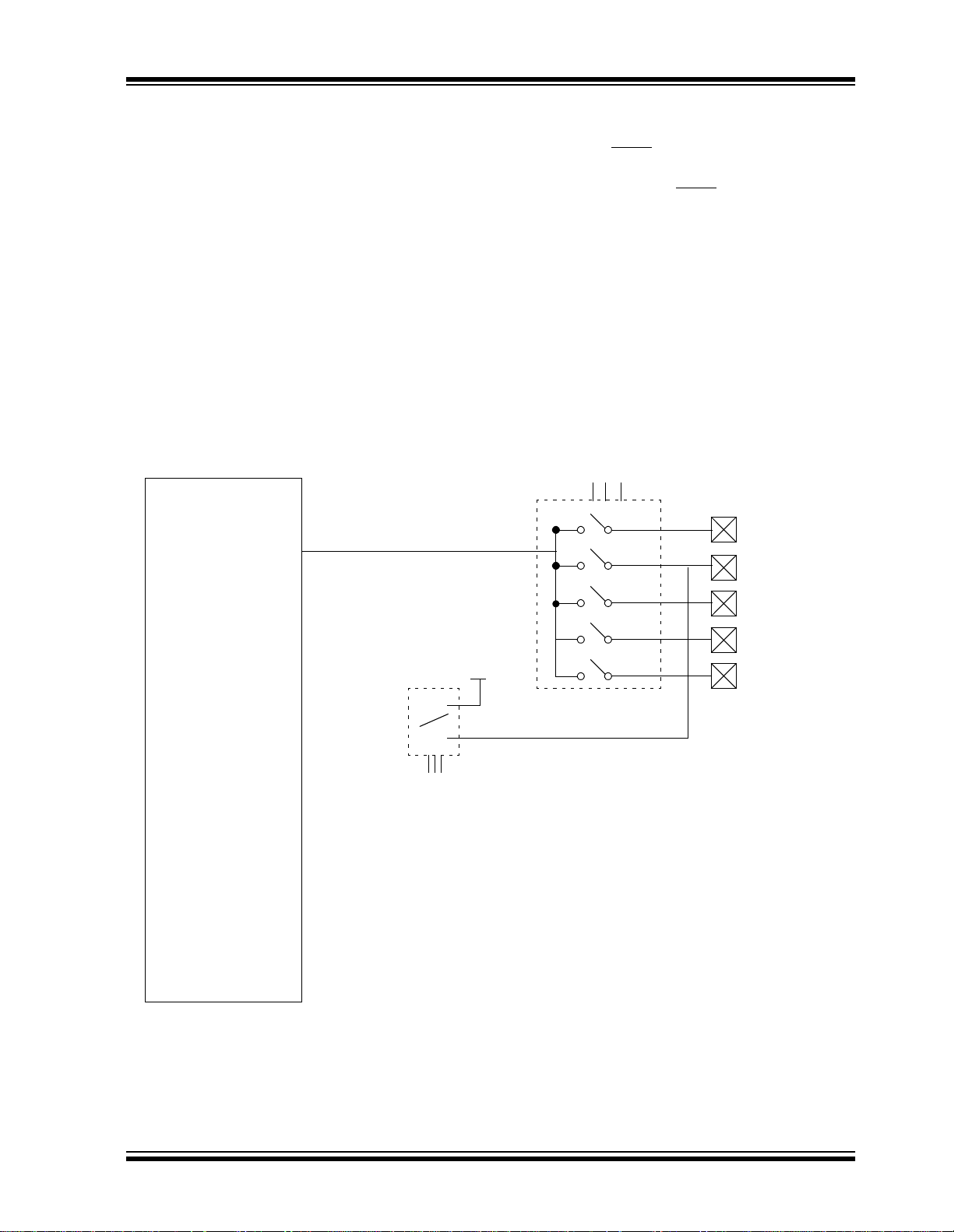
PIC16C925/926
The following step s should be fol lowed for doing an A/D
conversion:
1. Configure the A/D module:
• Configure analog pins/voltage reference/
and digital I/O (ADCON1)
• Select A/D input channel (ADCON0)
• Select A/D conversion clock (ADCON0)
• Turn on A/D module (ADCON0)
2. Configure A/D interrupt (if desired):
• Clear ADIF bit
• Set ADIE bit
• Set PEIE bit
• Set GIE bit
FIGURE 10-1: A/D BLOCK DIAGRAM
AIN
V
(Input Voltage)
3. Wait the required acquisition time.
4. Start conversion:
• Set GO/DONE
bit (ADCON0)
5. Wait for A/D conversion to complete, by either:
• Polling for the GO/DONE
bit to be cleared
(interrupts disabled)
OR
• Waiting for the A/D interrupt
6. Read A/D Result register pair
(ADRESH:ADRESL), clear bit ADIF if required.
7. For next conversion, go to step 1 or step 2 as
required. The A/D conversion time per bit is
defined as T
AD. A minimum wait of 2TAD is
required before next acquisition starts.
CHS<2:0>
100
011
010
001
DD
V
000
RA5/AN4
RA3/AN3/V
RA2/AN2/V
RA1/AN1
RA0/AN0
REF+
REF-
A/D
Converter
VREF+
(Reference
Voltage)
PCFG<3:0>
2001 Microchip Technology Inc. Preliminary DS39544A-page 77

PIC16C925/926
10.1 A/D Acquisition Requirements
For the A/D co nverter to meet its s pecified accuracy,
the charge holding capacitor (C
to fully charge to the input channel voltage level. The
analog input model is shown in Figure 10-2. The
source impedance (R
switch (R
SS) impedance directly affect the time
S) and the internal sampling
required to charge the capacitor C
switch (R
(V
SS) impedance varies over the devic e volt age
DD), see Figure 10-2. The maximum recom-
mended impedance for analog sources is 10 kΩ. As
the impedance is decreased, the acquisition time may
EQUATION 10-1: ACQUISITION TIME EXAMPLE
TACQ
=
Amplifier Settling Time +
Hold Capacitor Charging Time +
Temperature Coefficient
AMP + TC + TCOFF
=
T
2µS + TC + [(Temperature -25°C)(0.05µS/°C)]
=
TC
TACQ
C
HOLD (RIC + RSS + RS) In(1/2047)
=
- 120pF (1kΩ + 7kΩ + 10kΩ) In(0.0004885)
=
16.47µS
=
2µS + 16.47µS + [(50°C -25°C)(0.05µS/°C)
=
19.72µS°
=
HOLD) must be allowed
HOLD. The sampling
be decreased. After the analog input channel is
selected (changed), this acquisition must be done
before the conversion can be started.
To calculate the minimum acquisition time,
Equation 10-1 may be used. This equation assumes
that 1/2 LSb error is used (1024 st eps for the A/D). The
1/2 LSb error is the maximu m error all owed for the A/D
to meet its specified resolution.
To calculate the minimum acquisition time, T
ACQ, see
the PICmicro™ Mid-Range Reference Manual
(DS33023).
FIGURE 10-2: ANALOG INPUT MODEL
DS39544A-page 78 Preliminary 2001 Microchip Technology Inc.
PIC16C925/926
10.2 Selecting the A/D Conversion Clock
The A/D conversion time per bit is defined as TAD. The
A/D conversion requires a minimum 12T
conversion. The source of the A/D conversion clock is
software selected. The four possible options for T
are:
OSC
• 2T
• 8TOSC
• 32T OSC
• Internal A/D module RC oscillator
AD per 10-bit
AD
For correct A/D conversions, the A/D conversion clock
AD) must be selected to ensure a minimum TAD time
(T
of 1.6 µs.
Table 10-1 shows the resultant T
the device operating frequencies and the A/D clock
source selected.
AD times derive d f ro m
TABLE 10-1: TAD vs. MAXIMUM DEVICE OPERATING FREQUENCIES (STANDARD DEVICES (C))
AD Clock Source (TAD) Maximum Device Frequency
Operation ADCS<1:0> Max.
OSC 00 1.25 MHz
2T
OSC 01 5 MHz
8T
32TOSC 10 20 MHz
(1, 2, 3)
RC
Note 1: The RC source has a typical T
2: When the device frequencies are greater than 1 MHz, the RC A/D conversion clock source is only recom-
mended for SLEEP operation.
3: For extended voltage devices (LC), please refer to the Electrical Specifications section.
AD time of 4 µs, but can vary between 2-6 µs.
11 (Note 1)
2001 Microchip Technology Inc. Preliminary DS39544A-page 79

PIC16C925/926
10.3 Configuring Analog Port Pins
The ADCON1 and TRI S re gis te rs control the operatio n
of the A/D port pins. The port pins that are desired as
analog inputs must have their corresponding TRIS bits
set (input). If the TRIS bit is cleare d (output) , the digit al
output level (V
The A/D operation is independent of the state of the
CHS<2:0> bits and the TRIS bits.
Note 1: When reading the port register, any pin
FIGURE 10-3: A/D CONVERSION TAD CYCLES
OH or VOL) will be converted.
configured as an a nalog inpu t chann el wil l
read as cleared (a low level). Pins configured as digital inputs will convert an analog input. Analog levels on a digitally
configured input w i ll not af fect the conversion accuracy.
2: Analog levels on any pin that is defin ed as
a digital input (including the AN<4:0>
pins), may cause the input buffer to consume current that is out of the device
specifications.
10.4 A/D Conversions
Clearing the GO/DONE bit during a conversion will
abort the current conversion. The A/D result register
pair will NOT be updated with the partially completed
A/D conversion sample. That is, the ADRESH:ADRESL
registers will continue to contain the value of the last
completed conversion (or the last value written to the
ADRESH:ADRESL registers). After the A/D conversion
is aborted, a 2T
acquisition is started. After this 2T
on the selected channel is automatically started. After
this, the GO/DONE bit can be set to start the
conversion.
In Figure 10-3, after the GO bit is set, th e first time segment has a minimum of T
Note: The GO/DONE bit should NOT be set in
AD wait is required before the next
AD wait, acquisition
CY and a maximum o f TAD.
the same instruction that turns on the A/D.
TCY to TAD
Holding capacitor is disconnected from analog input (typically 100 ns)
Set GO bit
TAD1
TAD2
b9 b8 b7 b6 b5 b4 b3 b2
Conversion Starts
TAD3
TAD4
TAD5 TAD6
10.4.1 A/D RESULT REGISTERS
The ADRESH:ADRESL register pair is the location
where the 10-bit A/D result is loaded at the completion
of the A/D conversio n. This register p air is 16-bit s wide.
The A/D module gives the fl exibility to le ft or right justif y
the 10-bit result in the 16-bit result register. The A/D
Format Select bit (ADFM) controls this justification.
Figure 10-4 shows the operation of the A/D result jus tification. The ext ra bits are loaded wi th ’0’s’. When an
A/D result will not overwrite these locations (A/D disable), these registers ma y be used as two general purpose 8-bit registers.
TAD9
TAD7 TAD8
ADRES is loaded,
GO bit is cleared,
ADIF bit is set,
holding capacitor is connected to analog input.
AD wait is necessary before the next
A 2T
acquisition is started.
TAD10 TAD11
b1 b0
DS39544A-page 80 Preliminary 2001 Microchip Technology Inc.

FIGURE 10-4: A/D RESULT JUSTIFICATION
10-Bit Result
PIC16C925/926
ADFM = 1
2 1 0 77
0000 00
ADRESH ADRESL
10-bit Result
Right Justified
0
10.5 A/D Operation During SLEEP
The A/D module can ope rate during SLEEP mode. This
requires that the A/D clock source be set to RC
(ADCS<1:0> = 11). When the RC clock source is
selected, the A/D module waits one instruction cycle
before starting the conversion. This allows the SLEEP
instruction to be executed, which eliminates all digital
switching noise fro m the convers ion. When th e conversion is comple ted, the GO /DONE
the result loaded into the ADRES register. If the A/D
interrupt is enabled, the device will wake-up from
SLEEP . If the A/D interr upt is not enabled , the A/D module will then be turned off, although the ADON bit will
remain set.
When the A/D clock sour ce is anoth er clo ck optio n (not
RC), a SLEEP instruction will caus e the present conversion to be aborte d and the A/D mod ule to be turned of f,
though the ADON bit will remain set.
bit will be cleared and
ADFM = 0
7
ADRESH ADRESL
10-bit Result
0 7 6 5 0
0000 00
Left Justified
Turning off the A/D places the A/D modu le in it s lowes t
current consumption state.
Note: For the A/D module to operate in SLEEP,
the A/D clock source must be set to RC
(ADCS<1:0> = 11). To allow the conversion to occur during SLEEP, ensure the
SLEEP instruction immediately follows the
instruction that sets the GO/DONE
bit.
10.6 Effects of a RESET
A device RESET forces all registers to their RESET
state. This forces the A/D module to be turned off, and
any conversion is aborted. All A/D input pins are configured as analog inputs.
The value that is in the ADRESH:ADRESL registers is
not modified for a Power-on Reset. The
ADRESH:ADRESL registers will contai n unknown dat a
after a Power-on Reset.
TABLE 10-2: REGISTERS/BITS ASSOCIATED WITH A/D
Address Name B it 7 Bit 6 Bit 5 Bit 4 Bit 3 Bit 2 Bit 1 Bit 0
0Bh INTCON GIE PEIE
0Ch PIR1 LCDIF ADIF (1) (1) SSPIF CCP1IF TMR2IF TMR1IF r0rr 0000 r0rr 0000
8Ch PIE1 LCDIE ADIE (1) (1) SSPIE CCP1IE TMR2IE TMR1IE r0rr 0000 r0rr 0000
1Eh ADRESH A/D Result Register High Byte xxxx xxxx uuuu uuuu
9Eh ADR ESL A/D Result Register Low Byte xxxx xxxx uuuu uuuu
1Fh ADCON0 ADCS1 ADCS0 CHS2 CHS1 CHS0 GO/DONE — ADON 0000 00-0 0000 00-0
9Fh ADCON1 ADFM — — — PCFG3 PCFG2 PCFG1 PCFG0 --0- 0000 --0- 0000
85h TRISA — — PORTA Data Direction Register --11 1111 --11 1111
05h PORTA — — P ORTA Data Latch when written: PORTA pins when read --0x 0000 --0u 0000
Legend: x = unknown, u = unchanged, - = unimplemented, read as '0'. Shaded cells are not used for A/D conversion.
Note 1: These bits are reserved; always maintain these bits clear.
2001 Microchip Technology Inc. Preliminary DS39544A-page 81
TMR0IE INTE RBIE TMR0IF INTF RBIF 0000 000x 0000 000u
POR,
BOR
MCLR
WDT
,

PIC16C925/926
NOTES:
DS39544A-page 82 Preliminary 2001 Microchip Technology Inc.

PIC16C925/926
11.0 LCD MODULE
The LCD module generates the timing control to drive
a static or mult iplexed LCD p anel, with supp ort for up to
32 segments multiplexed with up to four commons. It
also provides control of the LCD pixel data.
The interface to the module consists of 3 control registers (LCDCON, LCDSE, and LCDPS), used to define
the timing r equirements of the LCD panel and up to 16
LCD data registers (LCD00-LCD15) that represent the
array of the pixel data. In normal operation, the control
registers are configured to match the LCD panel being
used. Primarily, the initialization information consi st s of
selecting the numbe r of com mons require d by the LCD
panel, and then specif yi ng the LCD frame clock rate to
be used by the panel.
Once the module is initialized for the LCD panel, the
individual bit s of the LCD dat a re gisters are c leared /set
to represent a clear/dark pixel, respectively.
Once the module is configured, the LCDEN
(LCDCON<7>) bit is used t o enable or disab le the LCD
module. The LCD panel can also operate during
SLEEP by clearing the SLPEN (LCDCON<6>) bit.
Figure 11-2 through Figure 11-5 provides waveforms
for static, half-duty cycle, one-third-duty cycle, and
quarter-duty cycle drive s.
REGISTER 11-1: LCDCON REGISTER (ADDRESS 10Fh)
R/W-0 R/W-0 R/W-0 R/W-0 R/W-0 R/W-0 R/W-0 R/W-0
LCDEN SLPEN WERR BIAS CS1 CS0 LMUX1 LMUX0
bit 7 bit 0
bit 7 LCDEN: Module Drive Enable bit
1 = LCD drive enabled
0 = LCD drive disabled
bit 6 SLPEN: LCD Display Enabled to SLEEP bit
1 = LCD module will stop driving in SLEEP
0 = LCD module will continue driving in SLEEP
bit 5 WERR: Write Failed Error bit
1 = System tried to write LCDD register during disallowed time. (Must be reset in software.)
0 = No error
bit 4 BIAS: Bias Generator Enable bit
0 = Internal bias generator powered down, bias is expected to be provided externally
1 = Internal bias generator enabled, powered up
bit 3-2 CS<1:0>: Clock Source bits
OSC/256
00 = F
01 = T1CKI (Timer1)
1x = Internal RC oscillator
bit 1-0 LMUX<1:0>: Common Selection bits
Specifie s the num be r of comm ons
00 = Static(COM0)
01 = 1/2 (COM0, 1)
10 = 1/3 (COM0, 1, 2)
11 = 1/4 (COM0, 1, 2, 3)
Legend:
R = Readable bit W = Writable bit U = Unimplemented bit, read as ‘0’
- n = Value at POR ’1’ = Bit is set ’0’ = Bit is cleared x = Bit is unknown
2001 Microchip Technology Inc. Preliminary DS39544A-page 83

PIC16C925/926
FIGURE 11-1: LCD MODULE BLOCK DIAGRAM
Data Bus
Internal RC osc
T1CKI
FOSC/4
LCD
RAM
32 x 4
Timing Control
LCDCON
LCDPS
LCDSE
Clock
Source
Select
and
Divide
128
to
32
MUX
COM3:COM0
SEG<31:0>
To I/O Pads
To I/O Pads
REGISTER 11-2: LCDPS REGISTER (ADDRESS 10Eh)
U-0 U-0 U-0 U-0 R/W-0 R/W-0 R/W-0 R/W-0
— — — — LP3 LP2 LP1 LP0
bit 7 bit 0
bit 7-4 Unimplemented: Read as '0'
bit 3-0 LP<3:0>: Frame Clock Prescale Selection bits (see Section 11.1.2)
LMUX1:LMUX0 Multiplex Frame Frequency
00 Static Clock source/(128 * (LP3:LP0 + 1))
01 1/2 Clock source/(128 * (LP3:LP0 + 1))
10 1/3 Clock source/(96 * (LP3:LP0 + 1))
11 1/4 Clock source/(128 * (LP3:LP0 + 1))
Legend:
R = Readable bit W = Writable bit U = Unimplemented bit, read as ‘0’
- n = Value at POR ’1’ = Bit is set ’0’ = Bit is cleared x = Bit is unknown
DS39544A-page 84 Preliminary 2001 Microchip Technology Inc.

FIGURE 11-2: WAVEFORMS IN STATIC DRIVE
PIC16C925/926
Liquid Crystal Display
and Ter minal Connection
SEG0
SEG1
SEG2
SEG3
SEG4
COM0
SEG7
SEG6
SEG5
COM0 - SEG0
Selected Waveform
1/1 V
PIN
COM0
0/1 V
1/1 V
PIN
SEG0
0/1 V
1/1 V
PIN
SEG1
0/1 V
1/1 V
0/1 V
Non-selected Waveform
COM0 - SEG1
1 frame
t
f
-1/1 V
0/1 V
2001 Microchip Technology Inc. Preliminary DS39544A-page 85

PIC16C925/926
FIGURE 11-3: WAVEFORMS IN HALF-DUTY CYCLE DRIVE (B TYPE)
Liquid Crystal Display
and Terminal Connection
SEG0
SEG1
SEG2
2/2 V
PIN
COM0
COM1
COM0
SEG3
COM0 - SEG0
Selected Waveform
PIN
COM1
PIN
SEG0
PIN
SEG1
1/2 V
0/2 V
2/2 V
1/2 V
0/2 V
2/2 V
0/2 V
2/2 V
0/2 V
2/2 V
1/2 V
0/2 V
-1/2 V
-2/2 V
2/2 V
0/2 V
Non-selected Waveform
DS39544A-page 86 Preliminary 2001 Microchip Technology Inc.
COM0 - SEG1
1 frame
t
f
-2/2 V
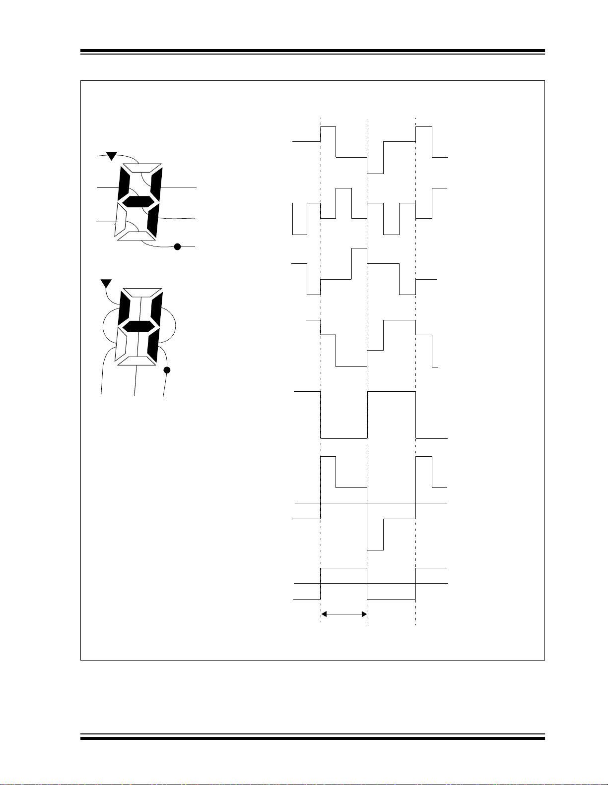
PIC16C925/926
FIGURE 11-4: WAVEFORMS IN ONE-THIRD DUTY CYCLE DRIVE (B TYPE)
Liquid Crystal Display
and Terminal Connection
SEG2SEG0
SEG1
COM2
COM1
COM0
PIN
COM0
PIN
COM1
PIN
COM2
PIN
SEG0
PIN
SEG1
3/3 V
2/3 V
1/3 V
0/3 V
3/3 V
2/3 V
1/3 V
0/3 V
3/3 V
2/3 V
1/3 V
0/3 V
3/3 V
2/3 V
1/3 V
0/3 V
3/3 V
2/3 V
1/3 V
0/3 V
COM0 - SEG1
Selected Waveform
COM0 - SEG0
Non-selected Waveform
1 frame
t
f
3/3 V
2/3 V
1/3 V
0/3 V
-1/3 V
-2/3 V
-3/3 V
1/3 V
0/3 V
-1/3 V
2001 Microchip Technology Inc. Preliminary DS39544A-page 87
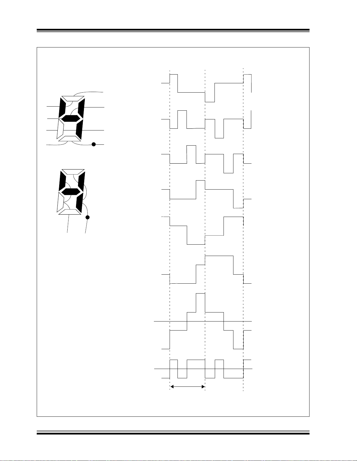
PIC16C925/926
FIGURE 11-5: WAVEFORMS IN QUARTER-DUTY CYCLE DRIVE (B TYPE)
Liquid Crystal Display
and Terminal Connection
SEG0
SEG1
COM3
COM2
COM1
COM0
PIN
COM0
PIN
COM1
PIN
COM2
PIN
COM3
PIN
SEG0
3/3 V
2/3 V
1/3 V
0/3 V
3/3 V
2/3 V
1/3 V
0/3 V
3/3 V
2/3 V
1/3 V
0/3 V
3/3 V
2/3 V
1/3 V
0/3 V
3/3 V
2/3 V
1/3 V
0/3 V
PIN
SEG1
COM3 - SEG0
Selected Waveform
COM0 - SEG0
Non-selected Waveform
1 frame
t
f
3/3 V
2/3 V
1/3 V
0/3 V
3/3 V
2/3 V
1/3 V
0/3 V
-1/3 V
-2/3 V
-3/3 V
1/3 V
0/3 V
-1/3 V
DS39544A-page 88 Preliminary 2001 Microchip Technology Inc.
PIC16C925/926
11. 1 LCD Timing
The LCD module has 3 possible clock source inputs
and supports static, 1/2, 1/3, and 1/4 multiplexing.
11.1.1 TIMING CLOCK SOURCE
SELECTION
The clock sources for the LCD timing generation are:
• Internal RC oscillator
• Timer1 oscillat or
• System clock divided by 256
The first timing source is an internal RC oscillator whic h
runs at a nominal frequency of 14 kHz. This oscillator
provides a lower speed clock which may be used to
continue running the LCD while the processor is in
SLEEP. The RC oscillator will power-down when it is
not selected or when the LCD module is disabled.
FIGURE 11-6: LCD CLOCK GENERATION
FOSC
÷256
The second source is the Timer1 external oscillator.
This oscillator p rovide s a low er sp eed cl ock whi ch ma y
be used to continue runn ing the LC D w hil e the pro ces sor is in SLEEP. It is assumed that the frequency provided on this oscillator will be 32 kHz. To use the
Timer1 oscillator as a LCD module clock source, it is
only necessary to set the T1OSCEN (T1CON<3>) bit.
The third source is the system clock divided by 256.
This divider ratio is chosen to provide about 32 kHz
output when the external oscillator is 8 MHz. The
divider is not progra mmab le. Ins tead the LCD PS regis ter is used to set the LCD frame clock rate.
All of the clock s ource s a re sel ected with bit s CS1 :CS0
(LCDCON<3:2>). Refer to Register 11-1 for details of
the register programming.
CPCLK
LCDPH
COMn
COMnLCK
LCDCLK
TMR1 32 kHz
Crystal Oscillator
Internal RC Oscillator
Nominal F
RC = 14 kHz
CS1:CS0
÷4
÷2
LMUX1:LMUX0
Static
1/2
1/3
1/4
4-bit Programmable
Prescaler
LCDPS<3:0>
internal
Data Bus
÷32
÷1,2,3,4
Ring Counter
LMUX1:LMUX0
2001 Microchip Technology Inc. Preliminary DS39544A-page 89

PIC16C925/926
11.1.2 MULTIPLEX TIMING GENERATION
The timing generat ion circu itry will ge nerate one to four
common clocks based on the display mode selected.
The mode is specified by bits LMUX1:LMUX0
(LCDCON<1:0>). Table 11-1 shows the formulas for
calculating the frame frequenc y.
TABLE 11-1: FRAME FREQUENCY
FORMULAS
Multiplex Frame Frequency =
Static Clock source/(128 * (LP3:LP0 + 1))
1/2 Clock source/(128 * (LP3:LP0 + 1))
1/3 Clock source/(96 * (LP3:LP0 + 1))
1/4 Clock source/(128 * (LP3:LP0 + 1))
TABLE 11-2: APPROXIMATE FRAME
FREQUENCY (IN Hz)
USING TIMER1 @ 32.768 kHz
OR F
OSC @ 8 MHz
LP3:LP0 Static 1/2 1/3 1/4
2 85 85 114 85
3 64 64 85 64
4 51 51 68 51
5 43 43 57 43
6 37 37 49 37
7 32 32 43 32
TABLE 11-3: APPROXIMATE FRAME
FREQUENCY (IN Hz)
USING INTERNAL RC OSC
@ 14 kHz
LP3:LP0 Static 1/2 1/3 1/4
0 109 109 146 109
1 55 55 73 55
2 36 36 49 36
3 27 27 36 27
DS39544A-page 90 Preliminary 2001 Microchip Technology Inc.
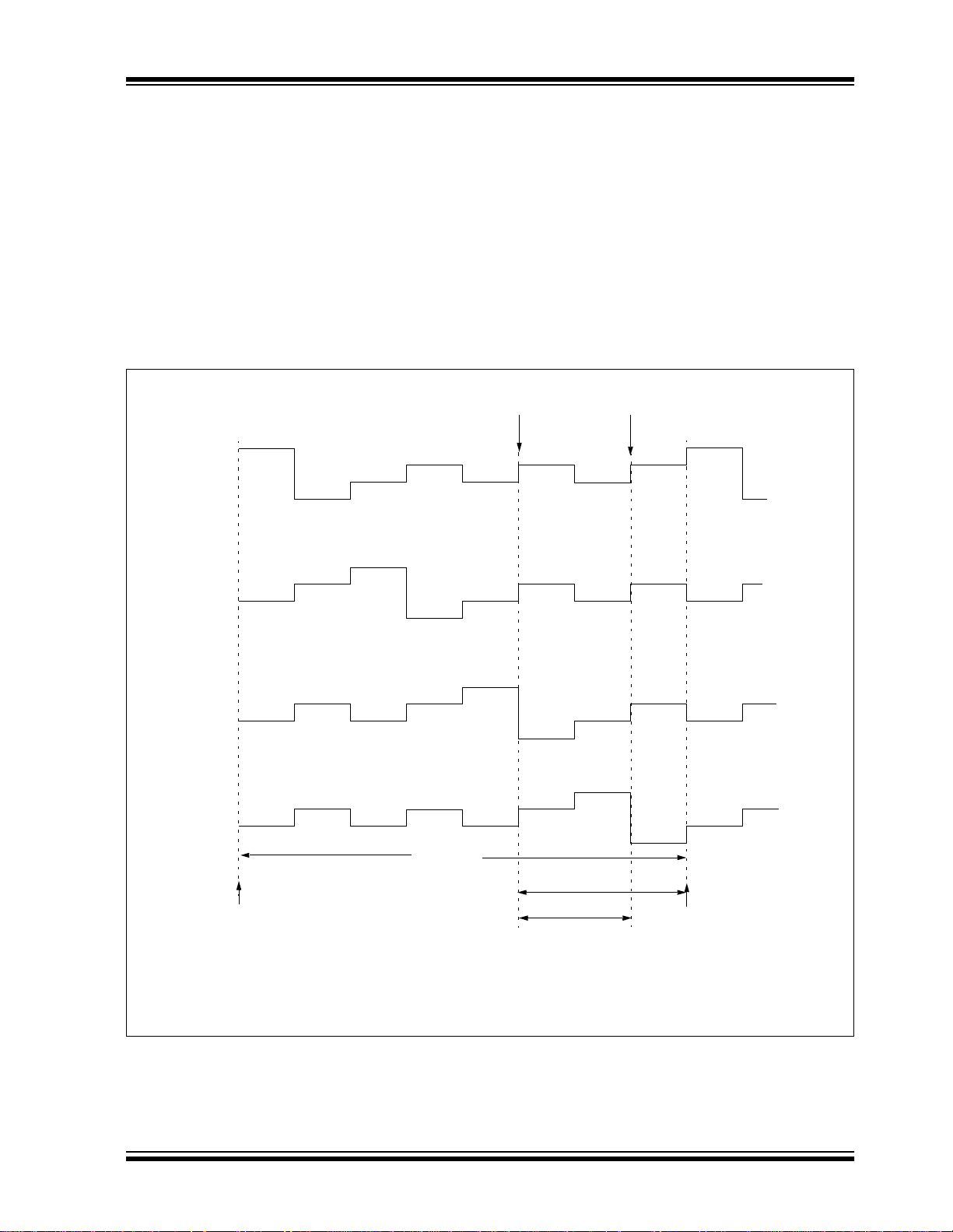
PIC16C925/926
11.2 LCD Interrupts
The LCD timing generation provides an interrupt that
defines the LCD frame timing. This interrupt can be
used to coordinate the wr itin g of the pixel data with the
start of a new frame. Writing pixel data at the frame
boundary allows a visual ly crisp transit ion of the imag e.
This interrupt can als o be us ed to s ynchr onize externa l
events to the LCD. For example, the interface to an
external segment driver, such as a Microchip AY0438,
can be synchronized for segment data update to the
LCD frame.
A new frame is defined to begin at the leading edge of
the COM0 common signal. The interrupt will be set
immediately after the LCD controller completes
accessing all pixel data required for a frame. This will
occur at a fixed interval before the frame boundary
FINT), as shown in Figure 11-7. The LCD controller
(T
will begin to access data for the next frame within the
interval from the i nte rrupt to w h en the c ont roll er beg ins
to access data after the interrupt (T
must be written within T
controller will begin to access the data for the next
frame.
FIGURE 11-7: EXAMPLE WAVEFORMS AND INTERRUPT TIMING
IN QUARTER-DUTY CYCLE DRIVE
LCD
Interrupt
Occurs
COM0
FWR). New data
FWR, as this is when the LCD
Controller Accesses
Next Frame Data
3/3 V
2/3 V
1/3 V
0/3 V
COM1
COM2
COM3
1 Frame
Frame
Boundary
TFWR = TFRAME/(LMUX1:LMUX0 + 1) + TCY/2
FINT = (TFWR /2 - (2TCY + 40 ns)) → minimum = 1.5(TFRAME/4) - (2TCY + 40ns)
T
(T
FWR /2 - (1TCY + 40 ns)) → maximum = 1.5(TFRAME/4) - (1TCY + 40 ns)
TFINT
TFWR
3/3 V
2/3 V
1/3 V
0/3 V
3/3 V
2/3 V
1/3 V
0/3 V
3/3 V
2/3 V
1/3 V
0/3 V
Frame
Boundary
2001 Microchip Technology Inc. Preliminary DS39544A-page 91

PIC16C925/926
11. 3 Pixel Control
11.3.1 LCDD (PIXEL DATA) REGISTERS
The pixel registers cont ain bits which defi ne the state of
each pixel. Each bit defines one unique pixel.
Table 11-4 shows the correlation of each bit in the
LCDD registers to the respective common and segment signals.
Any LCD pixel location not being used for display can
be used as general purpose RAM.
REGISTER 11-3: GENERIC LCDD REGISTER LAYOUT
R/W-x R/W-x R/W-x R/W-x R/W-x R/W-x R/W-x R/W-x
SEGs
COMc
bit 7 bit 0
bit 7-0 SEGsCOMc: Pixel Data bit for Segment S and Common C
1 = Pixel on (d ark)
0 = Pixel off (clear)
Legend:
R = Readable bit W = Writable bit U = Unimplemented bit, read as ‘0’
- n = Value at POR ’1’ = Bit is set ’0’ = Bit is cleared x = Bit is unknown
SEGs
COMc
SEGs
COMc
SEGs
COMc
SEGs
COMc
SEGs
COMc
SEGs
COMc
SEGs
COMc
DS39544A-page 92 Preliminary 2001 Microchip Technology Inc.
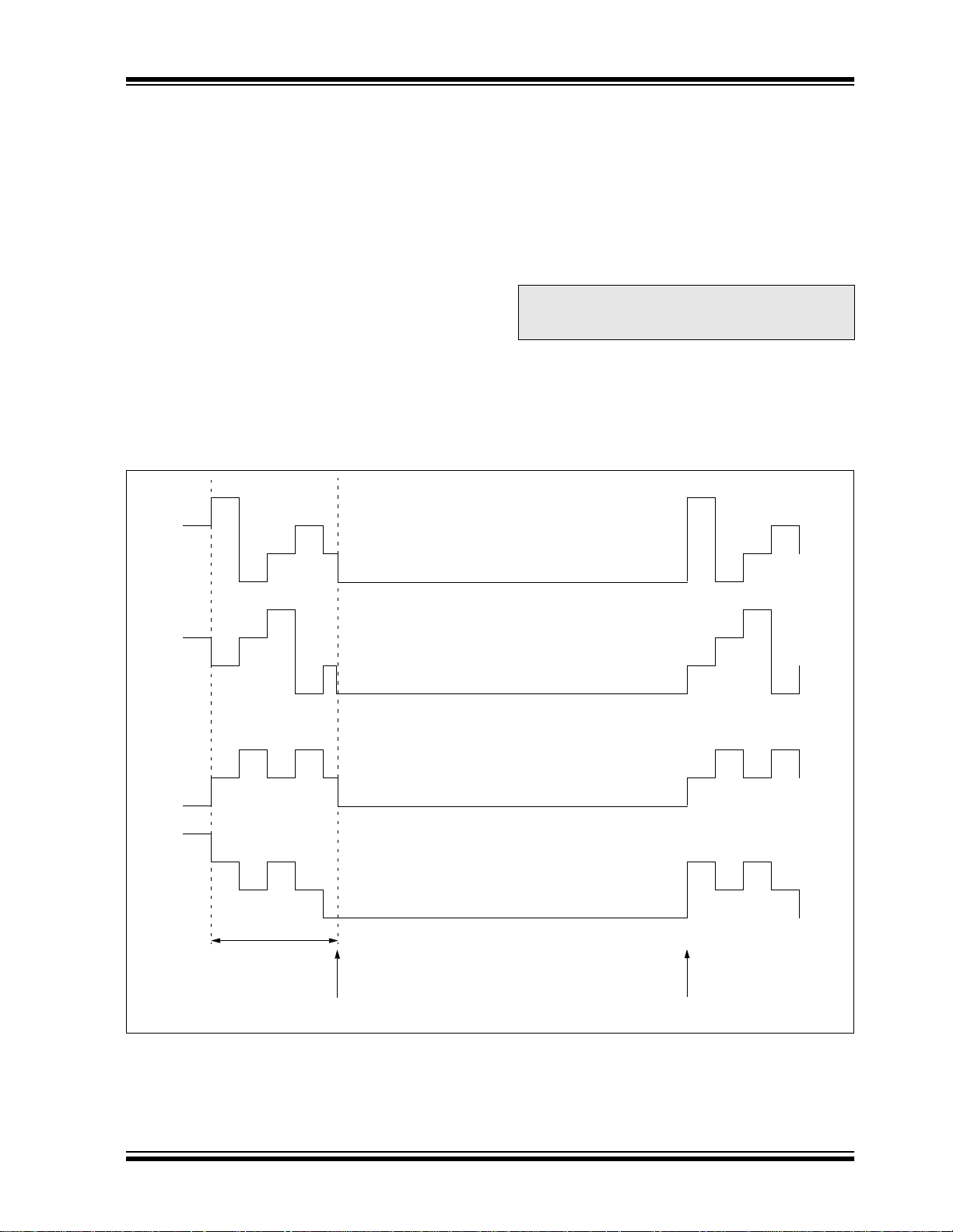
PIC16C925/926
11.4 Operation During SLEEP
The LCD module can operate during SLEEP. The
selection is controlled by bit SLPEN (LCDCON<6>).
Setting the SLPEN bit allows the LCD module to go to
SLEEP. Clearing the SLPEN bit allows the module to
continue to operate during SLEEP.
If a SLEEP instruction is execut ed and SLPEN = ’1’, the
LCD module will cease all functions and go into a very
low current consumption mode. The module will stop
operation immediately and drive the minimum LCD
voltage on both segment and common lines. Figure
1 1-8 shows this operation. To ensure that the LCD completes the frame, the SLEEP instruction should be exe-
If a SLEEP instruction is execute d and SLPEN = ’0’, the
module will continue to display the current contents of
the LCDD registers. To allow the module to continue
operation while in SLEEP, the clock source must be
either the internal RC oscillator or Timer1 external
oscillator. While in SLEEP, the LCD data cannot be
changed. The LCD module current consumption will
not decrease in this mode, however, the overall consumption of t he device will be lowe r due to shut-d own
of the core and other peripheral functions.
Note: The internal RC oscillator or external
Timer1 oscillator must be used to operate
the LCD module during SLEEP.
cuted immediately after a LCD frame boundary. The
LCD interrupt can be used to determine the frame
boundary. See Section 11.2 for the formulas to calculate the delay.
FIGURE 11-8: SLEEP ENTRY/EXIT WHEN SLPEN = 1 OR CS1:CS0 = 00
Pin
COM0
3/3V
2/3V
1/3V
Pin
COM1
Pin
COM3
Pin
SEG0
Interrupted
Frame
SLEEP Instruction Execution
0/3V
3/3V
2/3V
1/3V
0/3V
3/3V
2/3V
1/3V
0/3V
3/3V
2/3V
1/3V
0/3V
Wake-up
2001 Microchip Technology Inc. Preliminary DS39544A-page 93

PIC16C925/926
11.4.1 SEGMENT ENABLES
The LCDSE register is used to select the pin function
for groups of p ins. T he sel ection allow s each group o f
pins to operate as either LCD drivers or digital only
pins. To configure the pins as a digi tal port , the corr esponding bits in the LCDSE register must be cleared.
If the pin is a di gital I/O the correspondin g TRIS bit controls the data dire cti on. Any bit set in the LCDSE re gi ster overrides any bit setting s in the correspon ding TRIS
register.
Note 1: On a Power-on Reset, these pins are
configured as LCD drivers.
2: The LMUX1:LMUX0 takes precedence
over the LCDSE bit settings for pins RD7,
RD6 and RD5.
EXAMPLE 11-1: STATIC MUX WITH 32
BCF STATUS,RP0 ;Select Bank 2
BSF STATUS,RP1 ;
BCF LCDCON,LMUX1 ;Select Static MUX
BCF LCDCON,LMUX0 ;
MOVLW 0xFF ;Make PortD,E,F,G
MOVWF LCDSE ;LCD pins
. . . ;configure rest of LCD
EXAMPLE 11-2: ONE-THIRD DUTY CYCLE
BCF STATUS,RP0 ;Select Bank 2
BSF STATUS,RP1 ;
BSF LCDCON,LMUX1 ;Select 1/3 MUX
BCF LCDCON,LMUX0 ;
MOVLW 0x87 ;Make PORTD<7:0> &
MOVWF LCDSE ;PORTE<6:0> LCD pins
. . . ;configure rest of LCD
REGISTER 11-4: LCDSE REGISTER (ADDRESS 10Dh)
R/W-1 R/W-1 R/W-1 R/W-1 R/W-1 R/W-1 R/W-1 R/W-1
SE29 SE27 SE20 SE16 SE12 SE9 SE5 SE0
bit 7 bit 0
SEGMENTS
WITH 13 SEGMENTS
bit 7 SE29: Pin Function Select RD7/COM1/SEG31 - RD5/COM3/SEG29
1 = Pins have LCD drive function
0 = Pins have digital Input function
bit 6 SE27: Pin Function Select RG7/SEG28 and RE7/SEG27
1 = Pins have LCD drive function
0 = Pins have LCD drive function
bit 5 SE20: Pin Function Select RG6/SEG26 - RG0/SEG20
1 = Pins have LCD drive function
0 = Pins have digital Input function
bit 4 SE16: Pin Function Select RF7/SEG19 - RF4/SEG16
1 = Pins have LCD drive function
0 = Pins have digital Input function
bit 3 SE12: Pin Function Select RF3/SEG15 - RF0/SEG12
1 = Pins have LCD drive function
0 = Pins have digital Input function
bit 2 SE9: Pin Function Select RE6/SEG11 - RE4/SEG09
1 = Pins have LCD drive function
0 = Pins have digital Input function
bit 1 SE5: Pin Function Select RE3/SEG08 - RE0/SEG05
1 = Pins have LCD drive function
0 = Pins have digital Input function
bit 0 SE0: Pin Function Select RD4/SEG04 - RD0/SEG00
1 = Pins have LCD drive function
0 = Pins have digital Input function
Legend:
R = Readable bit W = Writable bit U = Unimplemented bit, read as ‘0’
- n = Value at POR ’1’ = Bit is set ’0’ = Bit is cleared x = Bit is unknown
DS39544A-page 94 Preliminary 2001 Microchip Technology Inc.

PIC16C925/926
11.5 Voltage Generation
There are two methods for LCD voltage generation:
internal charge pump, or external resistor ladder.
11.5.1 CHARGE PUMP
The LCD charge pump is shown in Figure 11-9. The
1.0V - 2.3V regu lator will establ ish a stable base volt -
age from the varying battery voltage. This regulator is
adjustable through the range by connecting a variable
external resistor from VLCD ADJ to g r oun d. T he p ote ntiometer provides c ontrast adjustmen t for the LCD. Thi s
base voltage is connected to V
LCD1 on the charge
pump. The charge pump boosts V
LCD1 and VLCD3 = 3 * VLCD1. When the charge
2*V
pump is not operating, Vlcd3 will be internally tied to
VDD. See the Electrical Specifications section for
charge pump capacitor and potentiometer values.
11.5.2 EXTERNAL R-LADDER
The LCD module ca n a ls o u se an ex te rnal res is tor ladder (R-Ladder) to generate the LCD voltages.
Figure 11-9 shows external connections for static and
1/3 bias. The VGEN (LCDCON<4>) bit must be cleared
to use an external R-Ladder.
FIGURE 11-9: CHARGE PUMP AND RESISTOR LADDER
CPCLK
VGEN
VDD
3
Regulator
2
Control
Logic
3 2 C
3
C
2
LCD1 into VLCD2 =
C+ VGEN
VGEN
VLCD3
LCD2
V
V
LCD1
VLCD0
Connections for
internal charge
pump, VGEN = 1
To
LCD
Drivers
2001 Microchip Technology Inc. Preliminary DS39544A-page 95

PIC16C925/926
11. 6 Configuring the LCD Module
The following is the sequ ence of st ep s to foll ow to configure the LCD module.
1. Select the frame clock prescale using bits
LP3:LP0 (LCDPS<3:0>).
2. Configure the appropriate pins to function as
4. Write initial values to pixel data registers,
LCDD00 through LCDD15.
5. Clear LCD interrupt flag, LCDIF (PIR1<7>), an d
if desired, enable the interrupt by setting bit
LCDIE (PIE1<7>).
6. Enable the LCD module, by setting bit LCDEN
(LCDCON<7>).
segment drivers using the LCDSE register.
3. Configure the LCD module for the following
using the LCDCON register:
- Multiplex mode and Bias, bits
LMUX1:LMUX0
- Timing source, bits CS1:CS0
- Voltage generation, bit VGEN
- SLEEP mode, bit SLPEN
TABLE 11-4: SUMMARY OF REGISTERS ASSOCIATED WITH THE LCD MODULE
Address Name Bit 7 Bit 6 Bit 5 Bit 4 Bit 3 Bit 2 Bit 1 Bit 0
0Bh, 8Bh,
10Bh, 18Bh
0Ch PIR1 LCDIF ADIF — — SSPIF CCP1IF TMR2IF TMR1IF 00-- 0000 00-- 0000
8Ch PIE1 LCDIE ADIE — — SSPIE CCP1IE TMR2IE TMR1IE 00-- 0000 00-- 0000
10h T1CON — — T1CKPS1 T1CKPS0 T1OSCEN T1SYNC TMR1CS TMR1ON
110h LCDD00
111h LCDD01
112h LCDD02
113h LCDD03
114h LCDD04
115h LCDD05
116h LCDD06
117h LCDD07
118h LCDD08
119h LCDD09
11Ah LCDD10
11Bh LCDD11
11Ch LCDD12
11Dh LCDD13
11Eh LCDD14
11Fh LCDD1 5
10Dh LCDSE SE29 SE27 SE20 SE16 SE12 SE9 SE5 SE0
10Eh LCDPS — — — — LP3 LP2 LP1 LP0
10Fh LCDCON LCDEN SLPEN — VGEN CS1 CS0 LMUX1 LMUX0
Legend: x = unknown, u = unchanged, - = unimplemented, read as '0'. Shaded cells are not used by the LCD module.
Note 1: These pixels do not display, but can be used as general purpose RAM.
INTCON GIE PEIE
SEG07
COM0
SEG15
COM0
SEG23
COM0
SEG31
COM0
SEG07
COM1
SEG15
COM1
SEG23
COM1
SEG31
COM1
SEG07
COM2
SEG15
COM2
SEG23
COM2
SEG31
COM2
SEG07
COM3
SEG15
COM3
SEG23
COM3
SEG31
COM3
(1)
(1)
(1)
SEG06
COM0
SEG14
COM0
SEG22
COM0
SEG30
COM0
SEG06
COM1
SEG14
COM1
SEG22
COM1
SEG30
COM1
SEG06
COM2
SEG14
COM2
SEG22
COM2
SEG30
COM2
SEG06
COM3
SEG14
COM3
SEG22
COM3
SEG30
COM3
TMR0IE INTE RBIE TMR0IF INTF RBIF 0000 000x 0000 000u
SEG05
COM0
SEG13
COM0
SEG21
COM0
SEG29
COM0
SEG05
COM1
SEG13
COM1
SEG21
COM1
SEG29
COM1
SEG05
COM2
SEG13
COM2
SEG21
COM2
SEG29
(1)
COM2
SEG05
COM3
SEG13
COM3
SEG21
COM3
SEG29
(1)
COM3
SEG04
COM0
SEG12
COM0
SEG20
COM0
SEG28
COM0
SEG04
COM1
SEG12
COM1
SEG20
COM1
SEG28
COM1
SEG04
COM2
SEG12
COM2
SEG20
COM2
SEG28
COM2
SEG04
COM3
SEG12
COM3
SEG20
COM3
SEG28
(1)
COM3
SEG03
COM0
SEG11
COM0
SEG19
COM0
SEG27
COM0
SEG03
COM1
SEG11
COM1
SEG19
COM1
SEG27
COM1
SEG03
COM2
SEG11
COM2
SEG19
COM2
SEG27
COM2
SEG03
COM3
SEG11
COM3
SEG19
COM3
SEG27
COM3
SEG02
COM0
SEG10
COM0
SEG18
COM0
SEG26
COM0
SEG02
COM1
SEG10
COM1
SEG18
COM1
SEG26
COM1
SEG02
COM2
SEG10
COM2
SEG18
COM2
SEG26
COM2
SEG02
COM3
SEG10
COM3
SEG18
COM3
SEG26
COM3
SEG01
COM0
SEG09
COM0
SEG17
COM0
SEG25
COM0
SEG01
COM1
SEG09
COM1
SEG17
COM1
SEG25
COM1
SEG01
COM2
SEG09
COM2
SEG17
COM2
SEG25
COM2
SEG01
COM3
SEG09
COM3
SEG17
COM3
SEG25
COM3
SEG00
COM0
SEG08
COM0
SEG16
COM0
SEG24
COM0
SEG00
COM1
SEG08
COM1
SEG16
COM1
SEG24
COM1
SEG00
COM2
SEG08
COM2
SEG16
COM2
SEG24
COM2
SEG00
COM3
SEG08
COM3
SEG16
COM3
SEG24
COM3
Value on
Power-on
Reset
--00 0000 --uu uuuu
xxxx xxxx uuuu uuuu
xxxx xxxx uuuu uuuu
xxxx xxxx uuuu uuuu
xxxx xxxx uuuu uuuu
xxxx xxxx uuuu uuuu
xxxx xxxx uuuu uuuu
xxxx xxxx uuuu uuuu
xxxx xxxx uuuu uuuu
xxxx xxxx uuuu uuuu
xxxx xxxx uuuu uuuu
xxxx xxxx uuuu uuuu
xxxx xxxx uuuu uuuu
xxxx xxxx uuuu uuuu
xxxx xxxx uuuu uuuu
xxxx xxxx uuuu uuuu
xxxx xxxx uuuu uuuu
1111 1111 1111 1111
---- 0000 ---- 0000
00-0 0000 00-0 0000
Value on all
other
RESETS
DS39544A-page 96 Preliminary 2001 Microchip Technology Inc.

PIC16C925/926
12.0 SPECIAL FEATURES OF THE
CPU
What sets a mic rocontroller apart from other processors are special circuits to deal with the needs of real
time applications. The PIC16CXXX fam ily has a host of
such features, intended to maximize system reliability,
minimize cost through elimination of external components, provide p ower saving opera ting mode s and offer
code protection. These are:
• Oscillator S election
• RESET
- Power-on Reset (POR)
- Power-up Timer (PWRT)
- Oscillator Start-up Timer (OST)
- Brown-out Reset (BOR)
• Interrupts
• Watchdog Timer (WDT)
• SLEEP
• Code Protection
• ID Locations
• In-Circuit Serial Programming
The PIC16CXXX has a Watchdog Timer which can be
shut-off only through configuration bits. It runs off its
own RC oscillator for added reliability.
There are two timers that offer necessary delays on
power-up. One is the Oscillator Start-up Timer (OST),
intended to keep the chip in RESET until the crystal
oscillator is stable. The other is the Power-up Timer
(PWRT), which provides a fixed delay of 72 ms (nominal) on power-up only, designed to keep the part in
RESET while the power supply stabilizes. With these
two timers on-chip, mo st a pp lic ati ons ne ed no external
RESET circuitry .
SLEEP mode is designed to offer a very low current
power-down mode. The user can w ake-up from SLEEP
through external RESET, Watchdog T imer W ake-up , or
through an interrupt.
Several oscillator options are also made available to
allow the part to fit the application. The RC oscillator
option saves system cost, while the LP crystal option
saves power. A set of configuration bits are used to
select various options.
12.1 Configuration Bits
The configuration b its can be program med (read as '0'),
or left unprogrammed (read as '1'), to select various
device configurations. These bits are mapped in program memory location 2007h.
The user will note that address 2007h is beyond the user
program memory space and can be accessed only during programming.
2001 Microchip Technology Inc. Preliminary DS39544A-page 97

PIC16C925/926
REGISTER 12-1: CONFIGURATION WORD (ADDRESS 2007h)
— — — — — — — BOREN CP1 CP0 PWRTE WDTE F0SC1 F0SC0
bit13 bit0
bit 13-7 Unimplemented
bit 6 BOREN: Brown-out Reset Enable bit
1 = BOR enabled
0 = BOR disabled
bit 5-4 CP1:CP0: Program Memory Code Protection bits
PIC16C926 (8K program memory):
11 = Code protection off
10 = 0000h to 0FFFh code protected (1/2 protected)
01 = 0000h to 1EFFh code protected (all but last 256 protected)
00 = 0000h to 1FFFh code protected (all protected)
PIC16C925 (4K program memory):
11 = Code protection off
10 = 0000h to 07FFh code protected (1/2 protected)
01 = 0000h to 0EFFh code protected (all but last 256 protected)
00 = 0000h to 0FFFh code protected (all protected)
1000h to 1FFFh wraps around to 0000h to 0FFFh
bit 3 PWRTE
1 = PWRT disabled
0 = PWRT enabled
bit 2 WDTE: Watchdog Timer Enable bit
1 = WDT enabled
0 = WDT disabled
bit 1-0 FOSC1:FOSC0: Oscillator Selection bits
11 = RC oscillator
10 = HS oscillator
01 = XT oscillator
00 = LP oscillator
: Power-up Timer Enable bit
DS39544A-page 98 Preliminary 2001 Microchip Technology Inc.
 Loading...