

Page 1

General Description
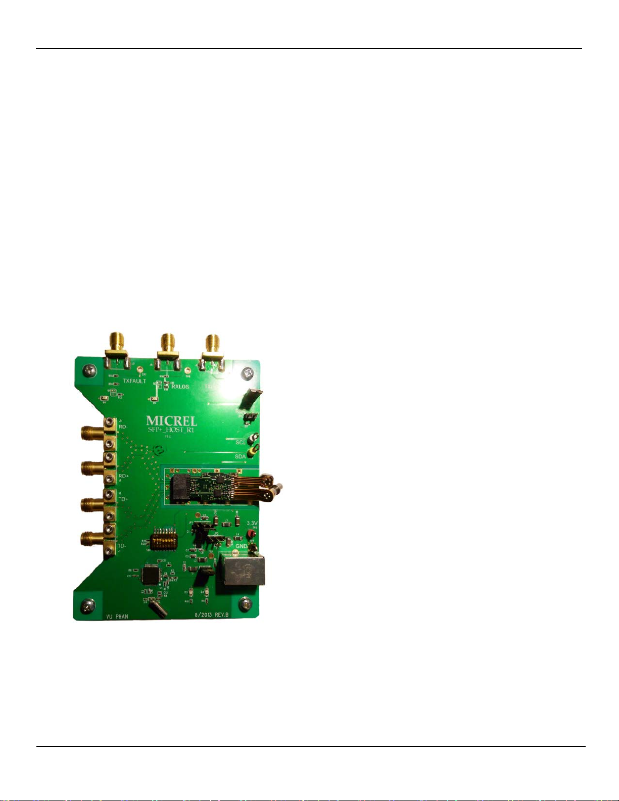
This evaluation board is a complete SFP+ module as
defined in the SFP+ MSA document. The design uses
Micrel’s MIC3003 co ntroller, the 10G DFB/FP laser driver
SY88022AL, and any of the following 10G limiting
amplifiers: SY88053C/073L. A picture of the fully loaded
board is shown on the next page.
Datasheets and support documentation are available on
Micrel’s web site at: www.micrel.com
.
Related Support Documentation
• MIC3003 datasheet: Fibre optic module controller
featuring digital diagnostic monitoring interface, as per
SFF-8472/SFF-8432, with internal/external calibration
and full laser control with bias and modulation current
compensation for temperature variations using lookup
tables.
• SY88022AL datasheet
• SY88053CL datasheet
• SY88073L
• MIC3003 software user’s guide.
SFP+ Module Reference Design
SFP_022AL_R0
Features
• Compliant with SFP+ MSA
• Allows for easy and fast evaluation of Micrel’s chipset
for SFP+ module
• Multi-rate operation up to 10Gbps
• Single, wide range power supply: 3.3V ±10%
• Industrial temperature range: –4 0°C to +85°C
Transmitter – FP/DFP Laser Diode Driver
• Operates from a single 3.3V supply
• Modulation current up to 60mA
• Fast edge rates of 25ps
• Bias current up to 80mA
• Input equalizer
• Small form factor 3mm × 3mm QFN package
Receiver – Limiting Post Amplifier
• External crosspoint adjustment (053CL/073L)
• Digital offset correction (063CL/083L)
• Wide differential input range (5mV
• Wide SD de-assert or LOS assert threshold range
− 3mV
to 30mVPP with 4dB typical electrical
PP
hysteresis
• Fast SD/LOS assert/de-assert time (053CL/063CL)
− 75ns typical; 120ns maximum
• Selectable LOS or SD status signal indicator
• Selectable RXOUT+/RXOUT- polarity (053CL/073L)
• Available in a tiny 3mm × 3mm QFN package
to 1800mVPP)
PP
Controller
• Extensive temperature range
• Alarms and warnings interrupt and TXFAULT masks
• Capability to support up to four chips on the serial
interface
• Integrated digital temperature sensor
• Temperature compensation of modulation, bias, and
fault levels via NVRAM lookup tables
• User-writeable EEPROM scratchpad
• Option to be used with Cisco security chip
• Diagnostic monitoring interface per SFF-8472/8432
• Space saving 3mm × 3mm package available
(MIC3003GFL)
Micrel Inc. • 2180 Fortune Drive • San Jose, CA 95131 • USA • tel +1 (408) 944-0800 • fax + 1 (408) 474-1000 • http://www.micrel.com
May 13, 2015
Revision 1.0
Page 2
Micrel, Inc.
SFP_022AL_R0 Reference Design
May
Evaluation Board
Evaluation Board Setup
TOSA and ROSA Installation
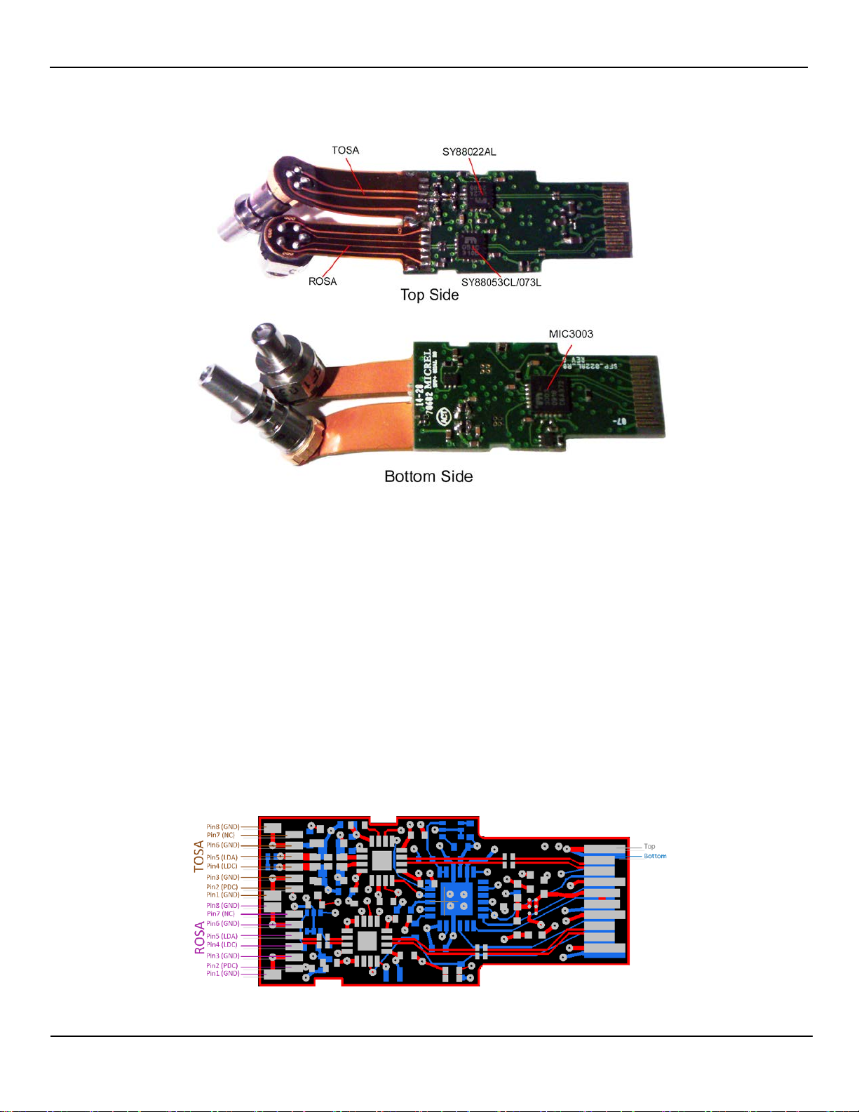
Check the pin config uration of the TOSA and ROSA and
install them according to the diagram shown in Figure 1.
Driver Laser Coupling
The laser is AC-coupled to the driver. Compensation for
laser parasitics can be im proved by choosing appropriate
values for R9 and C1. The laser’s response can be
improved by tuning, in addition to R9/C1, R1/R5 and
L1/L2/L5/L6/R6/R7. The optimal values of these
components depend on the length of the laser leads/flex
and can vary from one famil y of lasers to another. It is up
to the user to tune the values in order to achi eve the best
compensation for the laser used with this board.
Receiver Sensitivity and Hysteresis Setting
The limiting amplifier has a receive signal LOS/SD
indicator. The LOS/SD sensitivity is set by the voltage at
SD/LOSLVL (pin 8) adjusted by the value of R28, which
forms a voltage divider with the 2.8kΩ internal resistor
terminated to VCC-1.3V.
Figure 1. Mounting of TOSA and ROSA
13, 2015 2
Revision 1.0
Page 3
Micrel, Inc.
SFP_022AL_R0 Reference Design
May
Setup and Operation
1. Set the desired frequency on a pattern generator with
amplitude between 200mV
data patterns are 2
7
-1 or 223-1 PRBS patterns,
and 1800mVPP. Typical
PP
depending on the application. Because the inputs to
the board are AC-coupled, the voltage offset of the
pattern generator is not significant, so it can be set
between GND and VCC.
2. Connect the pattern generator with differential outputs
as a data source to the TXIN+ and TXIN- inputs on the
host board. Use matched length differential cables.
3. Connect the USB plug-in of the host board to the USB
port of the computer.
4. Connect the 3.3V red post on the host board to the
output of the 3.3V power supply and the black post to
the GND and install a jumper between pin 2 and pin 3
of SW1.
5. Plug the SFP module into the host board connector
and connect the laser to the optical plug-in of the
scope.
6. Turn on the power supply.
7. Launch the MIC3003 software, select the serial
address of the device to be scanned (A0 is the default
address), and then click initialization. The main
window will open.
8. Memory content can be read and/or modified on the
panels or by accessing the registers directly by
selecting ALL REGISTERS, enter the serial address
13, 2015 3
and register address, then select GET to read the
content or enter a new value, and select SET NEW to
write. In this procedure, the bits are set on the panels.
9. Refer to the MIC3003 Software User’s Guide for the
detailed settings and illustrations.
10. On the Panels list, select OEM CONFIG 3-4 and
select EXTERNAL CALIBRATION (default setting),
LOS COMPARATOR ENABLE, SHDN, RXLUT
INPUT TEMPERATURE, and RSOUT. If needed, later
set ISTART to a different value to speed up the APC
loop during laser turn ON after a FAULT occurrence.
Close this window to return to the main window.
11. On the Calibration list, select EXTERNAL
CALIBRATION. Set all the OFFSETS to 0 and
SLOPES to 1. For RXPWR, set only RX_PWR(1) to 1.
These parameters might need to be changed later to
correct the measured values (calibration). Close this
window to return to the main window.
12. On the Panels list, select OEM CONFIG 0-2 to open
the OEM configuration windows for registers 0, 1, and
2. Check the default setting of each and reset the
parameters to the correct values (below) if needed.
a. In the OEM Configuration Register 0 window, set
ENABLE/DISABLE to DISABLE, and set VMOD
REFERENCE to GND.
b. In the OEM Configuration Register 1 window, set
APC OP-AMP TYPE to EMITTER FOLLOWER,
select the voltage to report VINH:VINL, and set the
feedback voltage source to 1.22V. Also set
FEEDBACK BIAS REF and RES TERMINATION
to GND and set VBIAS DRIVE to SOURCE
(NPN). Set INTERNAL FEEDBACK RESISTOR
to INF.
c. In the OEM Configuration Register 2 window, the
MIC3003 address can be modif ied.
13. In the OEM Configuration Register 0 window, set
ENABLE/DISABLE to ENABLE.
14. On the Panels list, select User. Chec k APCSET0 and
MODSET0 in the USER CONTROL REGISTER
(default setting). All the other parameters’ functionality
can be checked later. Return to the main window.
15. On the Panels list, select OEM Sett in gs and enter the
following valu e s :
a. Enter 255 for the IBIAS FAULT and TX PWR
FAULT thresholds.
b. Enter 0 for LOSS-OF-SIGNAL threshold and 0 for
FAULT SUPPRESSION TIMER.
c. Enter desired DAC values for bias and modulation
between 0 and 255.
Revision 1.0
Page 4

Micrel, Inc.
SFP_022AL_R0 Reference Design
May
d. After entering these values, select SET NEW.
Select GET CURRENT to ensure the set values
are written to the registers. You may come back to
this panel to mask the faults by checking them at
the bottom of the window. Now return to the main
window.
16. On the Panels list, select Result. The values of the
five monitored parameters as per the SFF-8472 should
now display. Set the alarm and warning thresholds
(optional) and select SET NEW LIMITS. Select GET
CURRENT LIMITS to check that the set values are
written into the registers. Return to the main window.
17. After setting the new value for bias or modulation
current, toggle TXDISABLE/TXENABLE in the main
window or WARMRESET in the OEMCFG0-2 window.
18. Connect the laser to a variable optical attenuator
(VOA) and adjust the attenuation to bring the optical
power to the desired level at the input of the receiver.
Then connect the output of the VOA to the input of the
receiver using an appropriate fiber jumper.
19. If the installed receiver has RSSI signal, the value of
the received power should display, but may need
calibration.
20. At this stage, the masked faults should be unmasked.
If there is a fault indication, mask the indicated fault in
the OEMCONFG register (step 9) and try to find the
cause of the fault by checking the monitored values
and taking appropriate measurements.
21. Once the module runs without fault indication, proceed
to BER measurement, eye diagram analysis, and laser
driver and post amplifier performance evaluation.
13, 2015 4
Revision 1.0
Page 5
Micrel, Inc.
SFP_022AL_R0 Reference Design
May
Laser Response Tuning
Overshoot/Undershoot
The damping resistors R1 and R5 installed in series with
the laser are 5Ω. This value might be replaced with higher
values to minimize or suppress any overshoot or
undershoot on the optical signal out of the laser. Keep in
mind that higher value dam ping r es istor s will lea d to h i gher
rise/fall time and less modulation current driving the
laser.The compens atio n n e twor k comprised of R6/C1 5 c an
also be used for that purpose and to compensate for the
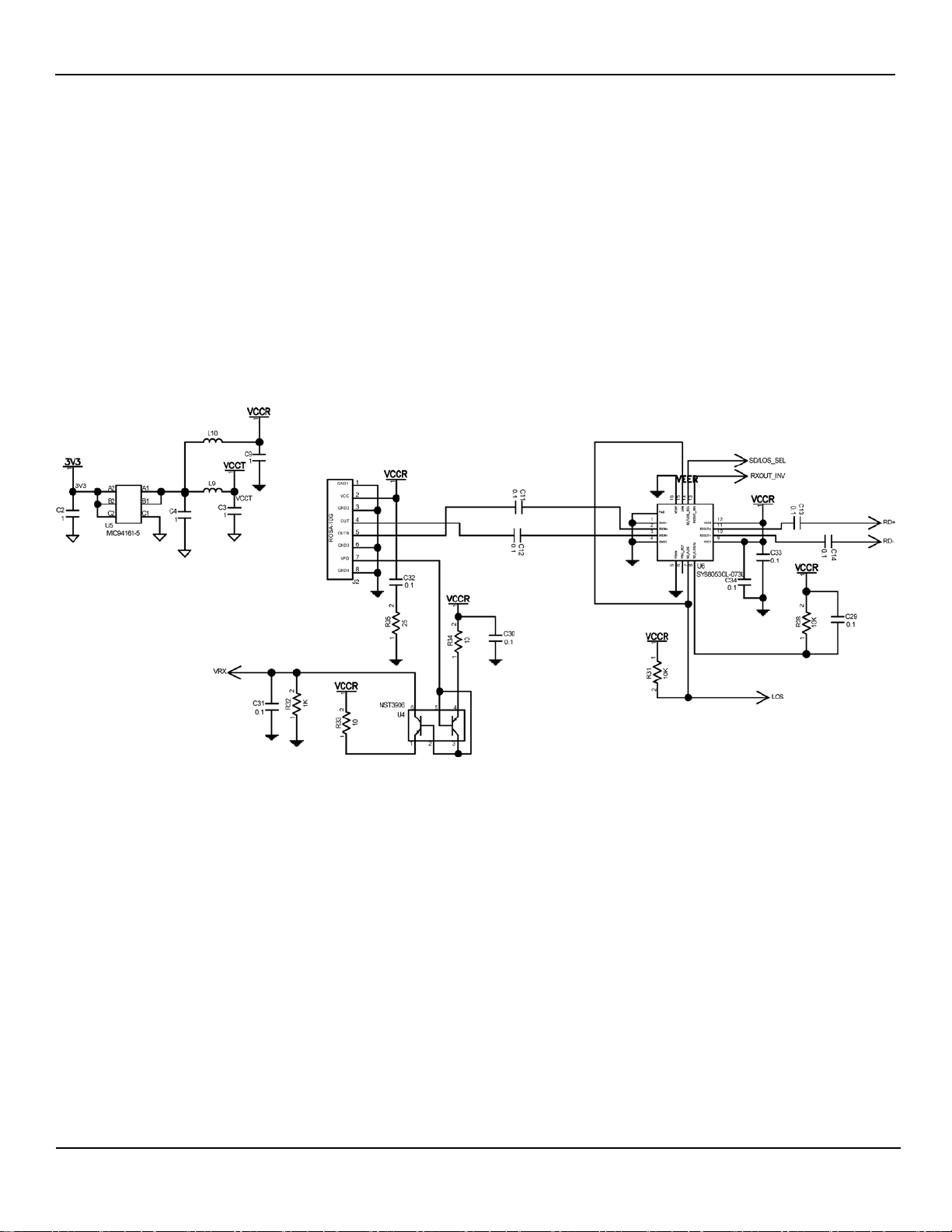
Evaluation Board Schematic
laser package’s parasitic inductance. The values indicated
on the schematic and pre-installed on the board
accordingly to the BOM may be replaced with different
values to optimize the laser response. Other components
that can be adjusted to improve the laser response are the
elements of the output termination network (L2, L3, R2,
R3, R4, R13).
Power and Receiver
13, 2015 5
Revision 1.0
Page 6
Micrel, Inc.
SFP_022AL_R0 Reference Design
May
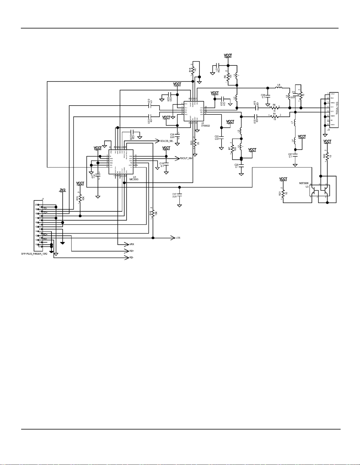
Evaluation Board Schematic (Continued)
13, 2015 6
Transmitter
Revision 1.0
Page 7
Micrel, Inc.
SFP_022AL_R0 Reference Design
May
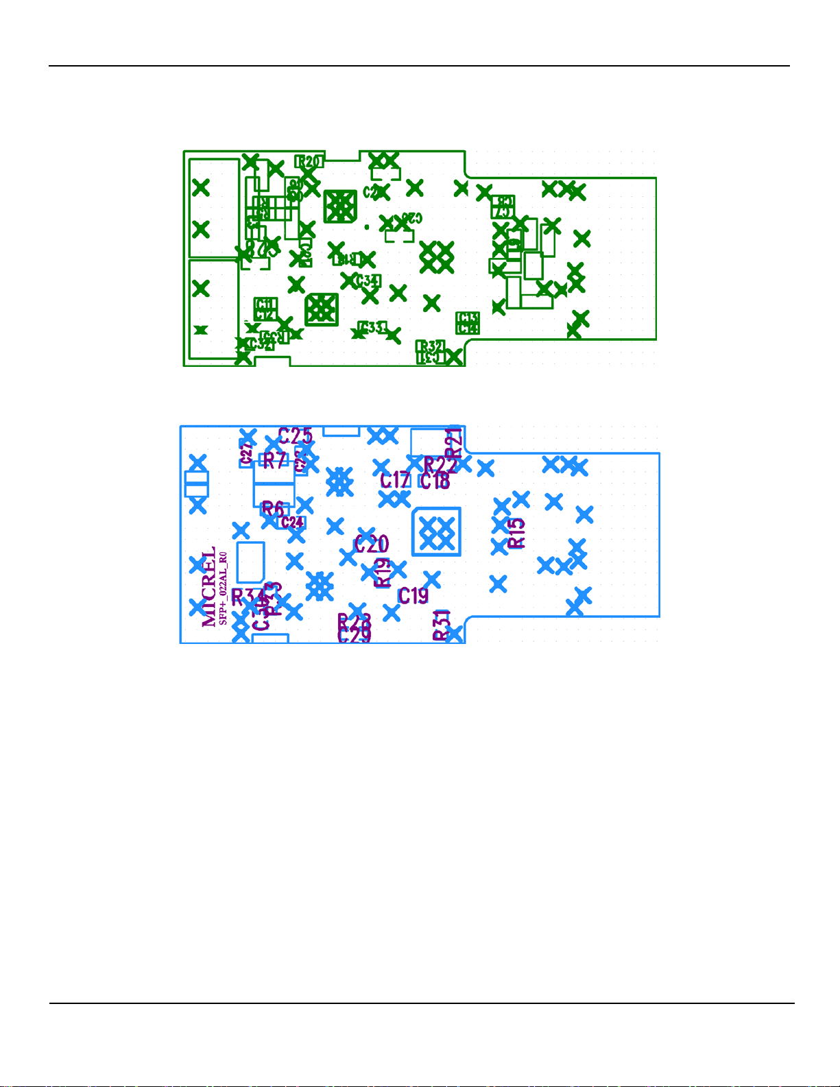
PCB Assembly
Top
13, 2015 7
Bottom
Revision 1.0
Page 8

Micrel, Inc.
SFP_022AL_R0 Reference Design
May
(Error! Reference
(6)
(7)
Bill of Materials
Item Part Number Manufacturer Description Qty.
C1 ECJZEC1E010C Panasonic
C5-8 GRM033R71A103KA01D Murata
C17, C21-23,
C26
C1005X7R1E103K050BB
TDK
source not found.)
C20 ECJ0EB1C183K Panasonic
C2-4, C9, C18-
19, C24-25, C27-
C1005X7R1C104K050BC TDK CAP CER 0.1µF 16V 10% X7R 0402 16
34
C11-14 ECJZEB1A104M Panasonic CAP CER 0.1µF 16V 10% X7R 0201 4
C4 C1005X5R0J106M050B TDK CAP CER 10µF 6.3V 20% X5R 0402 1
L4-6, L8-10 BLM15BD121SN1 Murata
L1-3, L7
HZ0402A601R-10 or
BLM15HG601
Technologies
Reference source not found.)
or Murata
R1, R5 ERJ-1GEF15R0C Panasonic RES 15 OHM 1/10W 1% 0201 SMD 2
R21-22, R33-34 ERJ-2GEJ100X Panasonic RES 10 OHM 1/10W 5% 0402 SMD 4
R20, R35 ERJ-2RKF24R9X Panasonic RES 24.9 OHM 1/10W 1% 0402 SMD 1
R6-7 ERJ-2GEJ101X Panasonic RES 100 OHM 1/10W 5% 0402 SMD 2
R18 ERJ-2GEJ131X Panasonic RES 130 OHM 1/10W 1% 0402 SMD 1
R9 ERJ-1GEF1470C Panasonic RES 147 OHM 1/10W 1% 0201 SMD 1
R20 ERJ-2RKF4993X Vishay
R32 ERJ-2GEJ102X Panasonic RES 1K OHM 1/10W 5% 0402 SMD 2
R15, R19, R28,
R31
ERJ-2GEJ103X Panasonic RES 10K OHM 1/10W 5% 0402 SMD 4
U3-4 NST3001 ON Semi
U1 MIC3003GML Micrel, Inc.
U2 SY88022AL Micrel, Inc. 10G DFB Laser Diode Driver 1
U5 MIC94161-5 Micrel, Inc. Dual output LDO 1
U6 SY88053CL Micrel, Inc. 10 Limiting Post Amplifier 1
SFP_022AL_R0 Micrel, Inc. SFP+ module PCB 1
Note:
1. Panasonic: www.panasonic.com
2. Murata: www.murata.com.
3. TDK: www.tdk.com.
4. Laird Technologies: www.lairdtech.com.
5. Vishay: www.vishay.com.
6. On Semi: www.onsemi.com.
7. Micrel, Inc.: www.micrel.com.
.
(1)
CAP CER 1PF 0201 1
(3)
0.01µF, 25V, 10% Ceramic Capacitor, Size
0201, X5R, Dielectric
0.01µF, 25V, 10% Ceramic Capacitor, Size
0402, X5R, Dielectric
0.018µF, 25V, 10% Ceramic Capacitor, Size
0402, X5R, Dielectric
Ferrite, Filter Chip, 120 OHM@100Mhz 1.5A,
0402
Laird
(Error!
Ferrite, 600 OHM@100Mhz 100mA, 0402 2
RES 499K OHM 1/10W 1% 0402 SMD 1
Dual PNP transistor 2
(7)
FOM Controller 1
4
5
1
6
13, 2015 8
Revision 1.0
Page 9

Micrel, Inc.
SFP_022AL_R0 Reference Design
May
MICREL, INC. 2180 FORTUNE DRIVE SAN JOSE, CA 95131 USA
can reasonably be expected to result in personal injury. Life support devices or systems are devices or systems that (a) are intended for surgical implant
nd Purchaser agrees to fully
TCG Support
Hotline: 408-955-1690
Email Support: [email protected]
Application Hints and Notes
For application notes on high-speed termination on high
bandwidth FOM and clock synthesizer products, SONET
jitter measurement, and other hig h bandwid th products , go
to Micrel’s website at: http://www.micrel.com.
TEL +1 (408) 944-0800 FAX +1 (408) 474-1000 WEB http://www.micrel.com
Micrel, Inc. is a leading global manufacturer of IC solutions for the worldwide high performance linear and power, LAN, and timing & communications
markets. The Company’s products include advanced mixed-signal, analog & power semiconductors; high-performance communication, clock
management, MEMs-based clock oscillators & crystal-less clock generators, Ethernet switches, and physical layer transceiver ICs. Company
customers include leading manufacturers of enterprise, consumer, industrial, m obile, t el ecommunications, automotive, and computer products.
Corporation headquarters and state-of-the-art wafer fabrication facilities are locat ed in San Jose, CA, with regional sales and support offices and
advanced technology design centers situated throughout the Americas, Europe, and Asia. Additionally, the Company maintains an extensive network
Micrel makes no representations or warranties with respect to the accuracy or completeness of the information furnished in this datasheet. This
information is not intended as a warranty and Micrel does not assume responsibility for its use. Micrel reserves the right to change circuitry,
specifications and descriptions at any time without notice. No license, whether express, implied, arising by estoppel or otherwise, to any intellectual
property rights is granted by this document. Except as provided in Micrel’s terms and conditions of sale for such products, Micrel assumes no liability
whatsoever, and Micrel disclaims any express or implied warranty relating to the sale and/or use of Micrel products including liabil ity or warranties
relating to fitness for a particular purpose, merchantability, or infringem ent of any patent, copyright, or other int ellect ual propert y right.
Micrel Products are not designed or authorized for use as components in life support appliances, devices or systems where malfunction of a product
into the body or (b) support or sustain life, and whose failure to perform can be reasonably expected to result in a significant injury to the user. A
Purchaser’s use or sale of Micrel Products for use in life support appliances, devices or systems is a Purchaser’s own risk a
13, 2015 9
of distributors and reps worldwide.
indemnify Micrel for any damages resulting from such use or sale.
© 2015 Micrel, Incorporated.
Revision 1.0
 Loading...