

MIC59P60 Micrel
UVLO
I LIMIT
THERMAL
SHUTDOWN
10
9
8
7
6
5
4
3
2
1
SUB
SUB
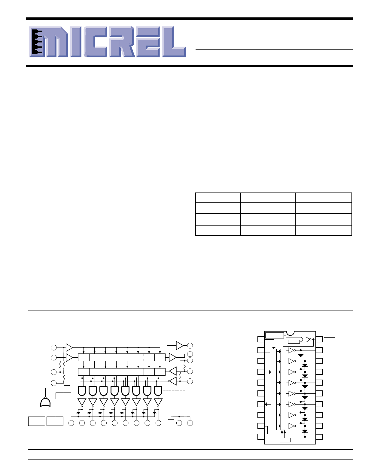
SHIFT REGISTER
LATCHES
20
19
18
17
16
15
14
13
12
11
CLEAR
V
EE
CLOCK
SERIAL DATA IN
V
SS
V
DD
SERIAL DATA OUT
STROBE
ENABLE/RESET
V
EE
OUTPUT
FLAG
OUTPUT 1
OUTPUT 2
OUTPUT 3
OUTPUT 4
OUTPUT 5
OUTPUT 6
OUTPUT 7
OUTPUT 8
K
MIC59P60
8-Bit Serial-Input Protected Latched Driver
General Description
The MIC59P60 serial-input latched driver is a high-voltage
(80V), high-current (500mA) integrated circuit comprised of
eight CMOS data latches, a bipolar Darlington transistor
driver for each latch, and CMOS control circuitry for the
common CLEAR, STROBE, CLOCK, SERIAL DATA INPUT,
and OUTPUT ENABLE functions. Similar to the MIC5842,
additional protection circuitry supplied on this device includes
thermal shutdown, under voltage lockout (UVLO), and overcurrent shutdown.
The bipolar/CMOS combination provides an extremely lowpower latch with maximum interface flexibility. The MIC59P60
has open-collector outputs capable of sinking 500mA and
integral diodes for inductive load transient suppression with
a minimum output breakdown voltage rating of 80V (50V
sustaining). The drivers can be operated with a split supply,
where the negative supply is down to –20V and may be
paralleled for higher load current capability.
Using a 5V logic supply, the MIC59P60 will typically operate
at better than 5MHz. With a 12V logic supply, significantly
higher speeds are obtained. The CMOS inputs are compatible with standard CMOS, PMOS, and NMOS circuits. TTL
circuits may require pull-up resistors. By using the serial data
output, drivers may be cascaded for interface applications
requiring additional drive lines.
Features
• 3.3 MHz Minimum Data-Input Rate
• Output Current Shutdown (500mA Typical)
• Under Voltage Lockout
• Thermal Shutdown
• Output Fault Flag
• CMOS, PMOS, NMOS, and TTL Compatible
• Internal Pull-Up/Pull-Down Resistors
• Low Power CMOS Logic and Latches
• High Voltage Current Sink Outputs
• Output Transient-Protection Diodes
• Single or Split Supply Operation
Ordering Information
Part Number Temperature Range Package
MIC59P60BN –40°C to +85°C 20-Pin Plastic DIP
MIC59P60BV –40°C to +85°C 20-Pin PLCC
MIC59P60BWM –40°C to +85°C 20-Pin Wide SOIC
Each of these eight outputs has an independent over current
shutdown of 500 mA. Upon over-current shutdown, the
affected channel will turn OFF and the flag will go low until V
is cycled or the ENABLE/RESET pin is pulsed high. Current
pulses less than 2µs will not activate current shutdown.
Temperatures above 165°C will shut down the device and
activate the error flag. The UVLO circuit prevents operation
at low VDD; hysteresis of 0.5V is provided.
Functional Diagram
THERMAL
SHUTDOWN
January 2000 1 MIC59P60
DD
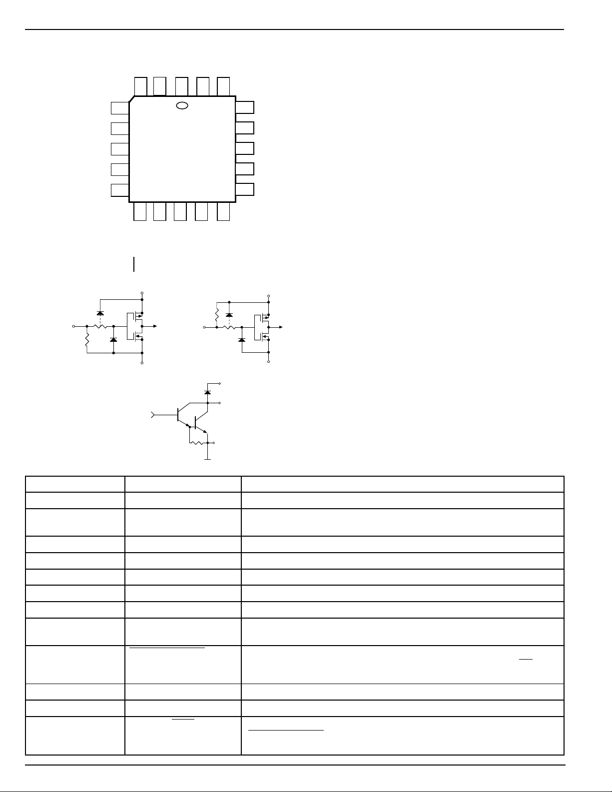
Pin Configuration
(DIP and SOIC)
FLAG
MOS
2 10
V
EE
20
7
SERIAL DATA OUT
V
6
DD
STROBE
8
OUTPUT
9
ENABLE/RESET
CLOCK
3
SERIAL
4
DATA IN
V
5
SS
1
CLEAR
I
LIMIT
Micrel, Inc. • 1849 Fortune Drive • San Jose, CA 95131 • USA • tel + 1 (408) 944-0800 • fax + 1 (408) 944-0970 • http://www.micrel.com
UVLO
11 19 18 17 16 15 13 12
K OUT 1 OUT 2 OUT 3 OUT 4 OUT 5 OUT 6 OUT 7 OUT 8
8-BIT SERIAL–PARALLEL SHIFT REGISTER
LATCHES
14
BIPOLAR
SUB
MIC59P60 Micrel
PLCC Pin
Configuration
CLOCK
SERIAL DATA IN
V
V
SERIAL DATA OUT
STROBE
SS
DD
4
5
MIC59P60BV
6
7
8
9 10
OE/RESET
Typical Inputs
CLOCK
SERIAL
DATA IN
V
DD
V
SS
Typical Output Driver
V
V
EE
EE
CLEAR
123
K
STROBE
OUTPUT
ENABLE
FLAG
20 19
12 1311
OUT 8
OUT 1
OUT 7
K
OUT
N
17
16
15
14
18
OUT 2
OUT 3
OUT 4
OUT 5
OUT 6
V
DD
V
SS
Absolute Maximum Ratings V
= 0; TA = 25°C
SS
Output Voltage (VCE) ....................................................80V
Output Voltage (V
V
with Reference to VSS...........................................15V
DD
CE(SUS)
) ...............................50V, Note 1
VDD with Reference to VEE...........................................25V
Emitter Supply Voltage (V
Input Voltage (V
) ............................... –0.3V to VDD+0.3V
IN
) ......................................–20V
EE
Protected Current............................................1.5A, Note 2
Power Dissipation (P
)
D
Plastic DIP (N).........................................................2.0W
Derate above T
= +25°C ............................20mW/°C
A
PLCC (V).................................................................1.4W
Derate above TA = +25°C ............................14mW/°C
Wide SOIC (WM) ....................................................1.2W
Derate above TA = +25°C ............................12mW/°C
Operating Temperature (T
)
A
Plastic DIP (N), PLCC (V), SOIC (WM)..–40°C to +85°C
Storage Temperature (T
) .......................–65°C to +150°C
S
Junction Temperature (TJ) ......................................+150°C
ESD .........................................................................Note 3
Note 1: For inductive load applications.
Note 2: Each channel. VEE connection must be designed to minimize
Note 3: Devices are input-static protected but can be damaged by
inductance and resistance.
extremetly high static charges.
Pin Description
Pin Name Description
1 CLEAR Sets All Latches OFF (open).
2,10 V
3 CLOCK Serial Data Clock. A CLEAR must also be clocked into the latches.
4 SERIAL DATA IN Serial Data Input pin.
5V
6V
7 SERIAL DATA OUT Serial Data Output pin. (Flow through).
8 STROBE Output Strobe pin. Loads output latches when High. A STROBE is needed
9 OUTPUT ENABLE/RESET When Low, Outputs are active. When High, device is inactive and reset
11 K Transient suppression diode's cathode common pin.
12—19 OUTPUT N Open Collector outputs 8 through 1.
20 FLAG Error Flag. Flag is Low upon Overcurrent Fault or Overtemperature fault.
EE
SS
DD
3K
V
EE
SUB
Output Ground (Substrate). Most negative voltage in the system connects
here.
Logic reference (Ground) pin.
Logic Positive Supply voltage.
to CLEAR latches.
from a fault condition. An under voltage condition emulates a high OE/
RESET input.
OUTPUT ENABLE/RESET must be pulled high to reset the flag and fault
condition.
MIC59P60 2 January 2000

MIC59P60 Micrel
Electrical Characteristics
VDD = 5V, VSS = VEE = 0V; TA = +25°C; unless noted.
Limits
Characteristic Symbol Test Conditions Min. Typ. Max. Unit
V
Output Leakage Current I
Collector-Emitter V
CEX
CE(SAT)
Saturation Voltage I
Collector-Emitter V
CE(SUS)
Sustaining Voltage
Input Voltage V
Input Resistance R
Flag Output Current I
Flag Output Leakage I
Supply Current I
Clamp Diode I
IN(0)
V
IN(1)
IN
OL
OH
DD(ON)
I
DD (1 OUTPUT)
I
DD(OFF)
R
Leakage Current
Clamp Diode V
Forward Voltage
Over Current I
F
LIM
Shutdown Threshold
Start Up Voltage V
Minimum Supply (VDD)V
SU
DD MIN
Thermal Shutdown 165 °C
Thermal Shutdown Hysteresis 10 °C
Note 4: Operation of these devices with standard TTL or DTL may require the use of appropriate pull-up resistors to insure a minimum logic "1".
Note 5: Undervoltage lockout is guaranteed to release device at no more than 4.5V, and disable the device at no less than 3.0V
= 80V 50 µA
OUT
V
= 80V, TA = +70°C100
OUT
I
= 100mA 0.9 1.1 V
OUT
= 200mA 1.1 1.3
OUT
I
= 350mA 1.3 1.6
OUT
I
= 350mA, L = 2mH 50 V
OUT
1.0 V
VDD = 12V 10.5 V
= 10V 8.5
V
DD
VDD = 5.0V, Note 4 3.5
VDD = 12V 50 200 kΩ
= 10V 50 300
V
DD
VDD = 5.0V 50 600
VOL = 0.4V 15 mA
VOH = 12.0V 50 nA
All Drivers ON, VDD = 12V 6.4 10.0 mA
All Drivers ON, V
= 10V 6.0 9.0
DD
All Drivers ON, VDD = 5.0V 4.6 7.5
One Driver ON, All others OFF, VDD = 12V 3.1 4.5 mA
One Driver ON, All others OFF, V
= 10V 2.9 4.5
DD
One Driver ON, All others OFF, VDD = 5V 2.3 3.6
All Drivers OFF, VDD = 12V 2.6 4.2 mA
All Drivers OFF, V
= 10V 2.4 3.6
DD
All Drivers OFF, VDD = 5.0V 1.9 3.0
VR = 80V 50 µA
IF = 350mA 1.7 2.0 V
500 mA
Note 5 3.5 4.0 4.5 V
3.0 3.5 4.0 V
January 2000 3 MIC59P60
MIC59P60 Micrel
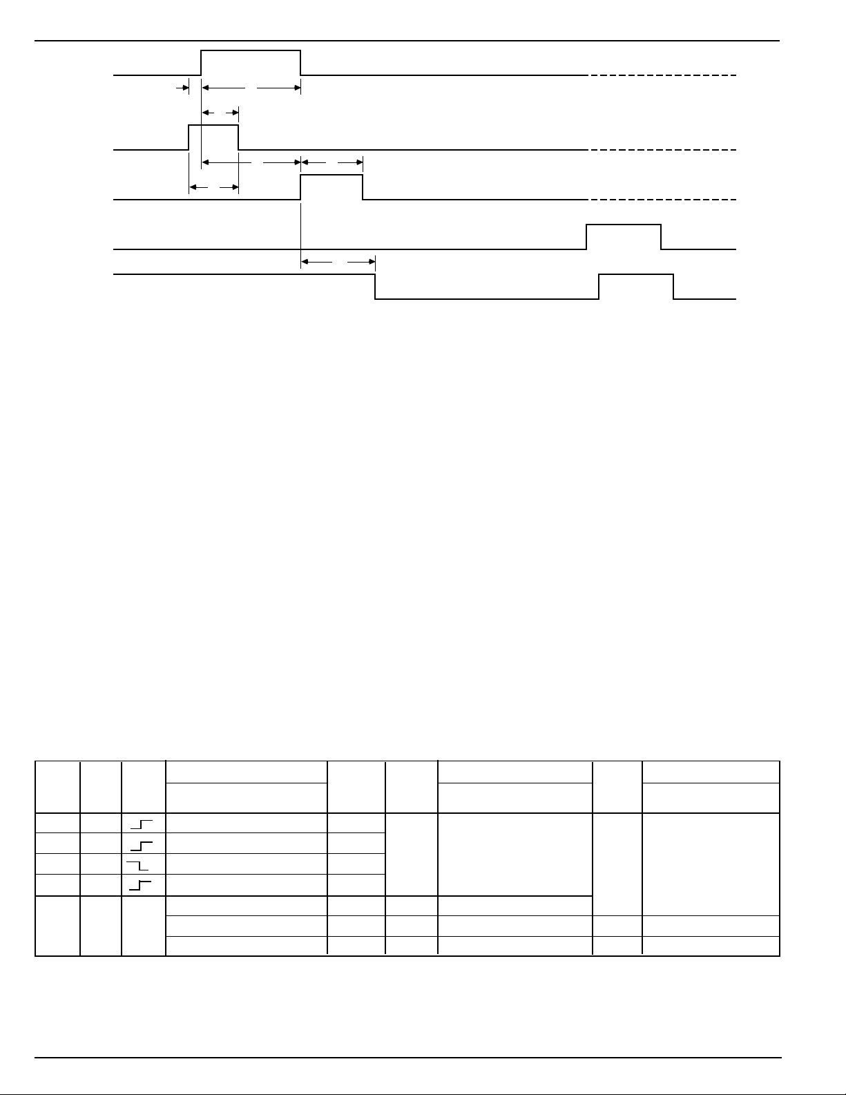
CLOCK
D
B
E
C
F
G
DATA IN
STROBE
OUTPUT
ENABLE
OUT
A
N
Timing Conditions
(TA = +25°C, Logic Levels are VDD and V
SS, VDD
A. Typical Data Active Time Before Clock Pulse (Data Set-Up Time) ...........................................................................75 ns
B. Minimum Data Active Time After Clock Pulse (Data Hold Time)..............................................................................75 ns
C. Minimum Data Pulse Width .....................................................................................................................................150 ns
D. Minimum Clock Pulse Width....................................................................................................................................150 ns
E. Minimum Time Between Clock Activation and Strobe .............................................................................................300 ns
F. Minimum Strobe Pulse Width...................................................................................................................................100 ns
G. Typical Time Between Strobe Activation and Output Transition .............................................................................500 ns
= 5V)
SERIAL DATA present at the input is transferred to the shift register on the logic “0” to logic “1” transition of the CLOCK input
pulse. On succeeding CLOCK pulses, the registers shift data information towards the SERIAL DATA OUTPUT. The SERIAL
DATA must appear at the input prior to the rising edge of the CLOCK input waveform. Holding CLEAR high results in a data
logic "0" being clocked into the shift register, turning off respective channels.
Information present at any register is transferred to its respective latch when the STROBE is high (serial-to-parallel conversion).
The latches will continue to accept new data as long as the STROBE is held high. Applications where the latches are bypassed
(STROBE tied high) will require that the ENABLE input be high to prevent invalid output states.
When the ENABLE input is high, all of the output buffers are disabled (OFF) without affecting information stored in the latches
or shift register. With the ENABLE input low, the outputs are controlled by the state of the latches. A positive OE/RESET pulse
resets the FLAG and the output after a current shutdown fault. Over-temperature faults are not latched and require no reset
pulse.
MIC59P60 T ruth T able
Serial Shift Register Contents Serial Latch Contents Output Contents
Data Clear Clock Data Strobe Output
Input Input Input I
HHR
LLR
XR1R2R
H OOO…… OL
L = Low Logic Level
H = High Logic Level
X = Irrelevant
P = Present State
R = Previous State
O = Output OFF
I
1
2I3
1R2
1R2
XXX…… XXLR
P1P2P3…… P
…… I8Output Input I1I
…… R
…… R
…… R
3
7
7
8
8
R
7
R
7
R
8
P
HP1P2P3…… P
8
2I3
1R2R3
XX X…… XH HHH…… H
…… I8Enable I1I
…… R
8
LP1P2P3……P
8
2I3
…… I
8
8
MIC59P60 4 January 2000

MIC59P60 Micrel
0
1
2
3
4
5
6
7
–50 0 50 100 150
SUPPLY CURRENT (mA)
TEMPERATURE (°C)
Supply Current
vs. Temperature
ALL OUTPUTS ON
ALL OUTPUTS OFF
VDD = 12V
0
2
4
6
8
10
12
14
16
18
20
0.3 0.4 0.5 0.6 0.7 0.8 0.9
CURRENT LIMIT DELAY (µS)
OUTPUT CURRENT (A)
Current Shutdown
Delay vs. Output Current
VDD = 12V
VDD = 5V
0
1
2
3
4
5
–50 0 50 100 150
SUPPLY CURRENT (mA)
TEMPERATURE (°C)
ALL OUTPUTS ON
ALL OUTPUTS OFF
Supply Current
vs. Temperature
VDD = 5V
Typical Characteristic Curves
Output Saturation
Voltage vs. Temperature
1.5
1.4
1.3
1.2
1.1
1
0.9
0.8
0.7
0.6
SATURATION VOLTAGE (V)
0.5
–50 0 50 100 150
IL = 350mA
VDD = 5V to 12V
IL = 100mA
TEMPERATURE (°C)
Output Saturation
Voltage vs. Temperature
1.5
1.4
1.3
1.2
1.1
1
0.9
0.8
0.7
0.6
SATURATION VOLTAGE (V)
0.5
-50 0 50 100 150
TEMPERATURE (°C)
IL = 350mA
VDD = 12V
IL = 100mA
Current Shutdown
Threshold vs. Temperature
0.60
0.55
0.50
0.45
0.40
0.35
SHUTDOWN THRESHOLD (A)
–50 0 50 100 150
TEMPERATURE (°C)
V
DD
= 12V
VDD = 5V
January 2000 5 MIC59P60

MIC59P60 Micrel
Maximum Allowable Duty Cycle (Plastic DIP)
VDD = 5.0V
VDD = 12V
Number of Outputs ON
(I
= 200mA Max. Allowable Duty Cycle at Ambient Temperature of
OUT
V
= 5.0V) 25°C40°C50°C60°C70°C
DD
8 85% 72% 64% 55% 46%
7 97% 82% 73% 63% 53%
6 100% 96% 85% 73% 62%
5 100% 100% 100% 88% 75%
4 100% 100% 100% 100% 93%
3 100% 100% 100% 100% 100%
2 100% 100% 100% 100% 100%
1 100% 100% 100% 100% 100%
Number of Outputs ON
(I
= 200mA Max. Allowable Duty Cycle at Ambient Temperature of
OUT
V
= 12V) 25°C40°C50°C60°C70°C
DD
8 80% 68% 60% 52% 44%
7 91% 77% 68% 59% 50%
6 100% 90% 79% 69% 58%
5 100% 100% 95% 82% 69%
4 100% 100% 100% 100% 86%
3 100% 100% 100% 100% 100%
2 100% 100% 100% 100% 100%
1 100% 100% 100% 100% 100%
Typical Applications
FLAG
CLEAR
CLOCK
SERIAL
DATA IN
ENABLE
Protected Solenoid Driver with Output Enable
+5V
10k
THERMAL
0.1µ
SHUTDOWN
1
2
SUB
3
4
5
6
SHIFT REGISTER
7
8
9
I LIMIT
LATCHES
20
19
18
17
16
15
14
13
12
22µ
+48V
+
10
SUB
UVLO
11
MIC59P60 6 January 2000

MIC59P60 Micrel
Hammer Driver
+5V
+28V
FLAG
CLOCK
DATA IN
STROBE
FLAG
CLEAR
CLOCK
SERIAL
DATA IN
0.1µ
10k
10
1
2
3
4
5
6
7
8
9
THERMAL
SHUTDOWN
SUB
SUB
I LIMIT
LATCHES
SHIFT REGISTER
UVLO
+
22µ
20
19
18
17
16
15
14
13
12
11
28V
Protected Negative/Positive PIN Diode Driver Transmit/Receive Switch
10k
1
2
3
4
+5V
THERMAL
SHUTDOWN
SUB
I LIMIT
20
19
18
17
15
1000p
+75V
10k
+75V
RFC
Transmitter
D1
Antenna
16
15
14
13
12
11
25
25
1000p
+75V
0.01µ
10k
RFC1000p
+75V
10k
RFC
PIN Diodes: UM9651
D2
RFC
Receiver
D3
100µ
5
+5V
0.1µ
6
SHIFT REGISTER
7
LATCHES
8
9
10
+
0.01µ
SUB
UVLO
Diode
D1 D2 D3
–5V
(Latch 1) (Latch 5) (Latch 8)
Receive OFF ACTIVE OFF
Transmit ACTIVE OFF ACTIVE
January 2000 7 MIC59P60

MIC59P60 Micrel
Package Information
1.070
MAX
(27.178)
PIN 1
.250±0.005
(6.350±0.127)
0.060±0.005
(1.524±0.127)
0.130±0.005
(3.302±0.127)
0.020
MIN
(0.508)
0.040
TYP
(1.016)
0.018±0.003
(0.457±0.076)
0.100±0.010
(2.540±0.254)
20-Pin Plastic DIP (N)
0.030-0.110
(0.762-2.794)
0.020
(0.508)
0.125
(3.175)
MIN
RAD
0.290-0.320
(7.336-8.128)
0°-10°
+0.025
0.325
–0.015
+0.635
8.255
()
–0.381
0.301 (7.645)
0.297 (7.544)
0.027 (0.686)
0.031 (0.787)
0.094 (2.388)
0.090 (2.286)
0.050 (1.270)
TYP
0.509 (12.929)
0.505 (12.827)
PIN 1
0.016 (0.046)
TYP
0.103 (2.616)
0.099 (2.515)
SEATING
PLANE
0.015
(0.381)
0.015
(0.381)
MIN
TYP
R
20-Pin Wide SOP (WM)
DIMENSIONS:
INCHES (MM)
0.297 (7.544)
0.293 (7.442)
7°
0.330 (8.382)
0.326 (8.280)
0.032 (0.813) TYP
0.408 (10.363)
0.404 (10.262)
0.022 (0.559)
0.018 (0.457)
10° TYP
5°
TYP
MIC59P60 8 January 2000

MIC59P60 Micrel
TOP VIEW
DETAIL A
0.110
0.027
0.018
0.045
0.045
0.351
±0.003
0.390
±0.020
0.050
0.080
0.030 DIA
x
0.015 R DEPTH
BOTTOM VIEW
0.300
DETAIL A
20-Pin PLCC (V)
0.045
0.045
SIDE VIEW
0.170
0.110
0.035 R
±0.015
0.310
±.015
January 2000 9 MIC59P60

MIC59P60 Micrel
MIC59P60 10 January 2000

MIC59P60 Micrel
January 2000 11 MIC59P60

MIC59P60 Micrel
MICREL INC. 1849 FORTUNE DRIVE SAN JOSE, CA 95131 USA
TEL + 1 (408) 944-0800 FAX + 1 (408) 944-0970 WEB http://www.micrel.com
This information is believed to be accurate and reliable, however no responsibility is assumed by Micrel for its use nor for any infringement of patents or
other rights of third parties resulting from its use. No license is granted by implication or otherwise under any patent or patent right of Micrel Inc.
© 2000 Micrel Incorporated
MIC59P60 12 January 2000
 Loading...