

Page 1
F
General Description
MIC5255
150mA Low Noise µCap CMOS LDO
Features
The MIC5255 is an efficient, precise CMOS voltage
regulator optimized for ultra-low-noise applications. It
offers 1% initial accuracy, extremely-low dropout voltage
(135mV at 150mA) and low ground current (typically
90µA). The MIC5255 provides a very-low-noise output,
ideal for RF applications where a clean voltage source is
required. A noise bypass pin is also available for further
reduction of output noise.
Designed specifically for handheld and battery-powered
devices, the MIC5255 provides a TTL-logic-compatible enable pin. When disabled, power consumption drops nearly
to zero.
The MIC5255 also works with low-ESR ceramic
capacitors, reducing the amount of board space necessary
for power applications, critical in handheld wireless
devices.
Key features include current limit, thermal shutdown, faster
transient response, and an active clamp to speed up
device turn-off. Available in the 6-pin 2mm × 2mm MLF
package, the IttyBitty
Thin SOT-23-5, which offers the same footprint as the
standard IttyBitty
®
SOT-23-5 package and the new
®
SOT-23-5, but only 1mm tall. The
MIC5255 offers a range of output voltages.
Data sheets and support documentation can be found on
Micrel’s web site at www.micrel.com.
• Input voltage range: 2.7V to 6.0V
• Thin SOT package: 1mm height SOT-23-5
• Ultra-low output noise: 30µV(rms)
• Stability with ceramic output capacitors
• Ultra-low dropout: 135mV @ 150mA
• High output accuracy:
– 1.0% initial accuracy
– 2.0% over temperature
• Low quiescent current: 90µA
• Tight load and line regulation
• TTL-Logic-controlled enable input
• “Zero” off-mode current
• Thermal shutdown and current limit protection
Applications
®
• Cellular phones and pagers
• Cellular accessories
• Battery-powered equipment
• Laptop, notebook, and palmtop computers
• Consumer/personal electronics
___________________________________________________________________________________________________________
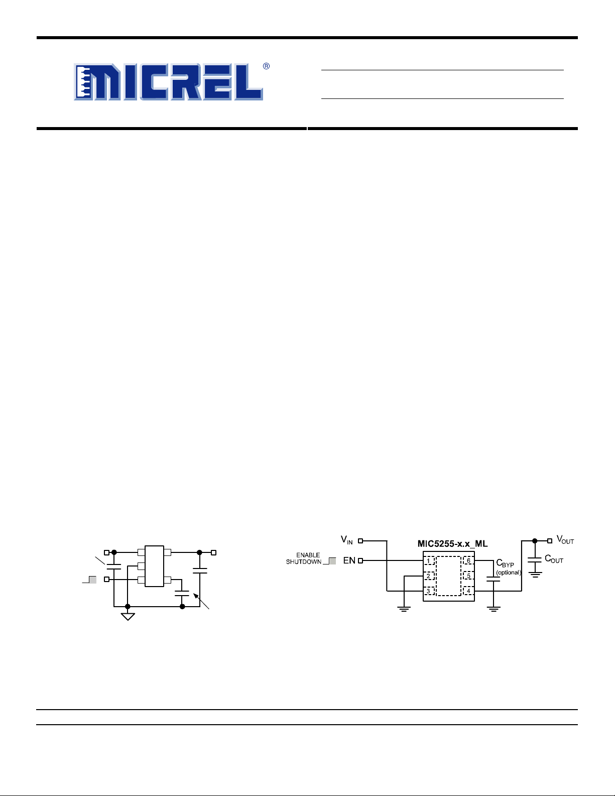
Typical Application
MIC5255-x.x_M5
V
EN
IN
15
2
3
4
= 1.0µF
C
IN
Ceramic
Enable
Shutdown
EN (pin 3) may be
connected directly
to IN (pin 1).
IttyBitty is a registered trademark of Micrel, Inc
MLF and MicroLeadFrame are registered trademarks of Amkor Technology, Inc.
Micrel Inc. • 2180 Fortune Drive • San Jose, CA 95131 • USA • tel +1 (
November 2006
V
OUT
C
OUT
Ceramic
C
BYP
= 1.0µF
= 0.01µ
Ultra-Low-Noise Regulator Application
408
) 944-0800 • fax + 1 (408) 474-1000 • http://www.micrel.com
1
M9999-110906
Page 2
Micrel, Inc. MIC5255
Ordering Information
Part Number Marking
Standard Pb-Free Standard Pb-Free**
MIC5255-2.5BD5 MIC5255-2.5YD5 NW25 NW25 2.5V –40° to +125°C 5-Pin TSOT-23
MIC5255-2.5BM5 MIC5255-2.5YM5 LW25 KW25 2.5V –40° to +125°C 5-Pin SOT-23
MIC5255-2.6BD5 MIC5255-2.6YD5 NW26 NW26 2.6V –40° to +125°C 5-Pin TSOT-23
MIC5255-2.6BM5 MIC5255-2.6YM5 LW26 KW26 2.6V –40° to +125°C 5-Pin SOT-23
MIC5255-2.7BD5 MIC5255-2.7YD5 NW27 NW27 2.7V –40° to +125°C 5-Pin TSOT-23
MIC5255-2.7BM5 MIC5255-2.7YM5 LW27 KW27 2.7V –40° to +125°C 5-Pin SOT-23
MIC5255-2.75BM5 MIC5255-2.75YM5 LW2H KW2H 2.75V –40° to +125°C 5-Pin SOT-23
MIC5255-2.8BD5 MIC5255-2.8YD5 NW28 NW28 2.8V –40° to +125°C 5-Pin TSOT-23
MIC5255-2.8BM5 MIC5255-2.8YM5 LW28 KW28 2.8V –40° to +125°C 5-Pin SOT-23
MIC5255-2.8BML MIC5255-2.8YML W28 W28*** 2.8V –40° to +125°C 6-Pin 2x2 MLF®
MIC5255-2.85BD5 MIC5255-2.85YD5 NW2J NW2J 2.85V –40° to +125°C 5-Pin TSOT-23
MIC5255-2.85BM5 MIC5255-2.85YM5 LW2J KW2J 2.85V –40° to +125°C 5-Pin SOT-23
MIC5255-2.85BML MIC5255-2.85YML W2J W2J*** 2.85V –40° to +125°C 6-Pin 2x2 MLF®
MIC5255-2.9BD5 MIC5255-2.9YD5 NW29 NW29 2.9V –40° to +125°C 5-Pin TSOT-23
MIC5255-2.9BM5 MIC5255-2.9YM5 LW29 KW29 2.9V –40° to +125°C 5-Pin SOT-23
MIC5255-3.0BD5 MIC5255-3.0YD5 NW30 NW30 3.0V –40° to +125°C 5-Pin TSOT-23
MIC5255-3.0BM5 MIC5255-3.0YM5 LW30 KW30 3.0V –40° to +125°C 5-Pin SOT-23
MIC5255-3.0BML MIC5255-3.0YML W30 W30*** 3.0V –40° to +125°C 6-Pin 2x2 MLF®
MIC5255-3.1BM5 MIC5255-3.1YM5 LW31 KW31 3.1V –40° to +125°C 5-Pin SOT-23
MIC5255-3.2BM5 MIC5255-3.2YM5 LW32 KW32 3.2V –40° to +125°C 5-Pin SOT-23
MIC5255-3.3BD5 MIC5255-3.3YD5 NW33 NW33 3.3V –40° to +125°C 5-Pin TSOT-23
MIC5255-3.3BM5 MIC5255-3.3YM5 LW33 KW33 3.3V –40° to +125°C 5-Pin SOT-23
MIC5255-3.3BML MIC5255-3.3YML W33 W33*** 3.3V –40° to +125°C 6-Pin 2x2 MLF®
MIC5255-3.5BM5 MIC5255-3.5YM5 LW35 KW35 3.5V –40° to +125°C 5-Pin SOT-23
Notes:
* Other Voltage available. Contact Micrel for details.
** Under bar / Over bar symbol may not be to scale.
*** Over bar symbol located after Pin 1 identifier.
Voltage*
Junction
Temp. Range
Package
November 2006
2
M9999-110906
Page 3
Micrel, Inc. MIC5255
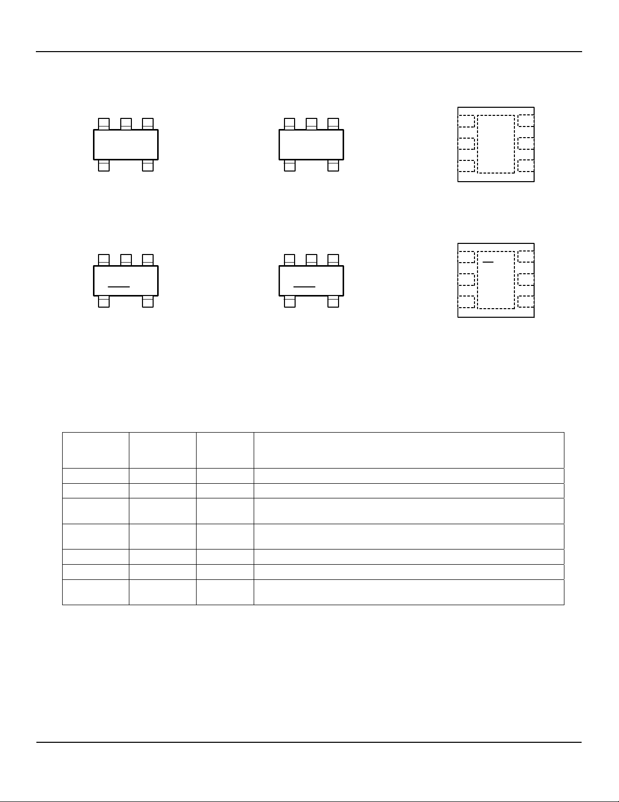
Pin Configuration
EN
BYP
MIC5255-x.xBM5
5-Pin SOT23 (M5)
EN
BYP
MIC5255-x.xYM5
5-Pin SOT23 (M5)
IN
GND
2
13
EN
GND
2
IN
13
1EN
6 BYP
Wxx
NC
GND
LWxx
45
OUT
IN
GND
13
2
5-Pin Thin SOT23 (D5)
NWxx
45
BYP
MIC5255-x.xBD5
EN
GND
2
OUT
IN
13
2
IN
3
MIC5255-x.xBML
6-Pin 2x2 MLF
1EN
5
4
®
(ML)
6 BYP
OUT
Wxx
NC
KWxx
45
OUT
5-Pin Thin SOT23 (D5)
NWxx
45
BYP
MIC5255-x.xYD5
OUT
GND
2
IN
3
MIC5255-x.xYML
6-Pin 2x2 MLF
5
4
®
(ML)
OUT
Pin Description
Pin Number
SOT23-5
TSOT23-5
1 3 IN Supply Input.
2 2 GND Ground.
3 1 EN
4 6 BYP
5 4 OUT Regulator Output.
– 5 NC No internal connection.
– EP GND
Pin Number
6-MLF
Pin Name Pin Name
Enable/Shutdown (Input): CMOS compatible input. Logic high = enable;
logic low = shutdown. Do not leave open.
Reference Bypass: Connect external 0.01µF CBYP 1.0µF capacitor
to GND to reduce output noise. May be left open.
Ground: Internally connected to the exposed pad. Connect externally to
GND pin.
November 2006
3
M9999-110906
Page 4

Micrel, Inc. MIC5255
Absolute Maximum Ratings
Supply Voltage (VIN)............................................. 0V to +7V
Enable Voltage (V
Power Dissipation (P
Junction Temperature (T
Storage Temperature (T
Lead Temperature (soldering, 5 sec.)........................ 260°C
EDS Rating
(4)
)............................................ 0V to +7V
EN
) ........................... Internally Limited
D
) ........................–40°C to +125°C
J
) .........................–60°C to +150°C
s
.................................................................. 2kV
(1)
Operating Ratings
Supply Voltage (VIN)........................................ +2.7V to +6V
Enable Voltage (V
(3)
Junction Temperature (T
Thermal Resistance
SOT23-5 (
2x2 MLF-6 (
EN
θ
) ..................................................235°C/W
JA
θ
JA
Electrical Characteristics
VIN = V
Symbol Parameter Condition Min Typ Max Units
VO Output Voltage Accuracy I
V
V
VIN – V
IQ Quiescent Current VEN 0.4V (shutdown) 0.2
GND
PSRR Ripple Rejection
I
LIM
en Output Voltage Noise
Enable Input
VIL Enable Input Logic-Low Voltage VIN = 2.7V to 5.5V, regulator shutdown
VIH Enable Input Logic-High Voltage VIN = 2.7V to 5.5V, regulator enabled
Shutdown Resistance Discharge 500
Thermal Protection
Thermal Shutdown Temperature 150 °C
Thermal Shutdown Hysteresis 10 °C
+ 1V, VEN = VIN; I
OUT
Line Regulation VIN = V
LNR
Load Regulation
LDR
Dropout Voltage
OUT
Ground Pin Current
OUT
Current Limit V
(5)
= 100µA; TJ = 25°C,
(7)
(8)
bold
values indicate –40°C TJ +125°C; unless noted.
= 100µA
OUT
+ 1V to 6V 0.02 0.05 %/V
OUT
I
= 0.1mA to 150mA
OUT
I
= 100µA 0.1 5 mV
OUT
I
= 100mA 90 150 mV
OUT
= 150mA 135
I
OUT
I
= 0mA 90 150 µA I
OUT
= 150mA 117 µA
I
OUT
f = 10Hz, C
= 1.0µF, C
OUT
f = 100Hz, VIN = V
f = 10kHz, V
= 0V 160 425 mV
OUT
C
= 1.0µF, C
OUT
IN
= V
(6)
= 0.01µF 60 dB
BYP
+1 60 dB
OUT
+1 50 dB
OUT
= 0.01µF,
BYP
f = 10Hz to 100kHz
VIL 0.4V, regulator shutdown 0.01 µA IEN Enable Input Current
V
1.6V, regulator enabled 0.01 µA
IH
(2)
).............................................. 0V to VIN
) ........................–40°C to +125°C
J
) .................................................90°C/W
–1
–2
1
2
1.5 2.5 %
200
250
1
30 µV(rms)
0.4
1.6
V
%
%
mV
mV
µA
V
November 2006
4
M9999-110906
Page 5

Micrel, Inc. MIC5255
Notes:
1. Exceeding the absolute maximum rating may damage the device.
2. The device is not guaranteed to function outside its operating rating.
3. The maximum allowable power dissipation of any T
dissipation will result in excessive die temperature, and the regulator will go into thermal shutdown. The
235°C/W on a PC board. See “Thermal Considerations” section for further details.
4. Devices are ESD sensitive. Handling precautions recommended. Human body model, 1.5k in series with 100pF.
5. Specification for packaged product only.
6. Regulation is measured at constant junction temperature using low duty cycle pulse testing. Parts are tested for load regulation in the load range
from 1.0mA to 150mA. Changes in output voltage due to heating effects are covered by the thermal regulation specification.
7. Dropout Voltage is defined as the input-to-output differential at which the output voltage drops 2% below its nominal value measured at 1V
differential. For outputs below 2.7V, dropout voltage is the input-to-output voltage differential with the minimum input voltage 2.7V. Minimum input
operating voltage is 2.7V.
8. Ground pin current is the regulator quiescent current. The total current drawn from the supply is the sum of the load current plus the ground pin
current.
(ambient temperature) is P
A
D(max)
= (T
– TA) / JA. Exceeding the maximum allowable power
J(max)
of the MIC5255-x.xBM5 (all versions) is
JA
November 2006
5
M9999-110906
Page 6
Micrel, Inc. MIC5255
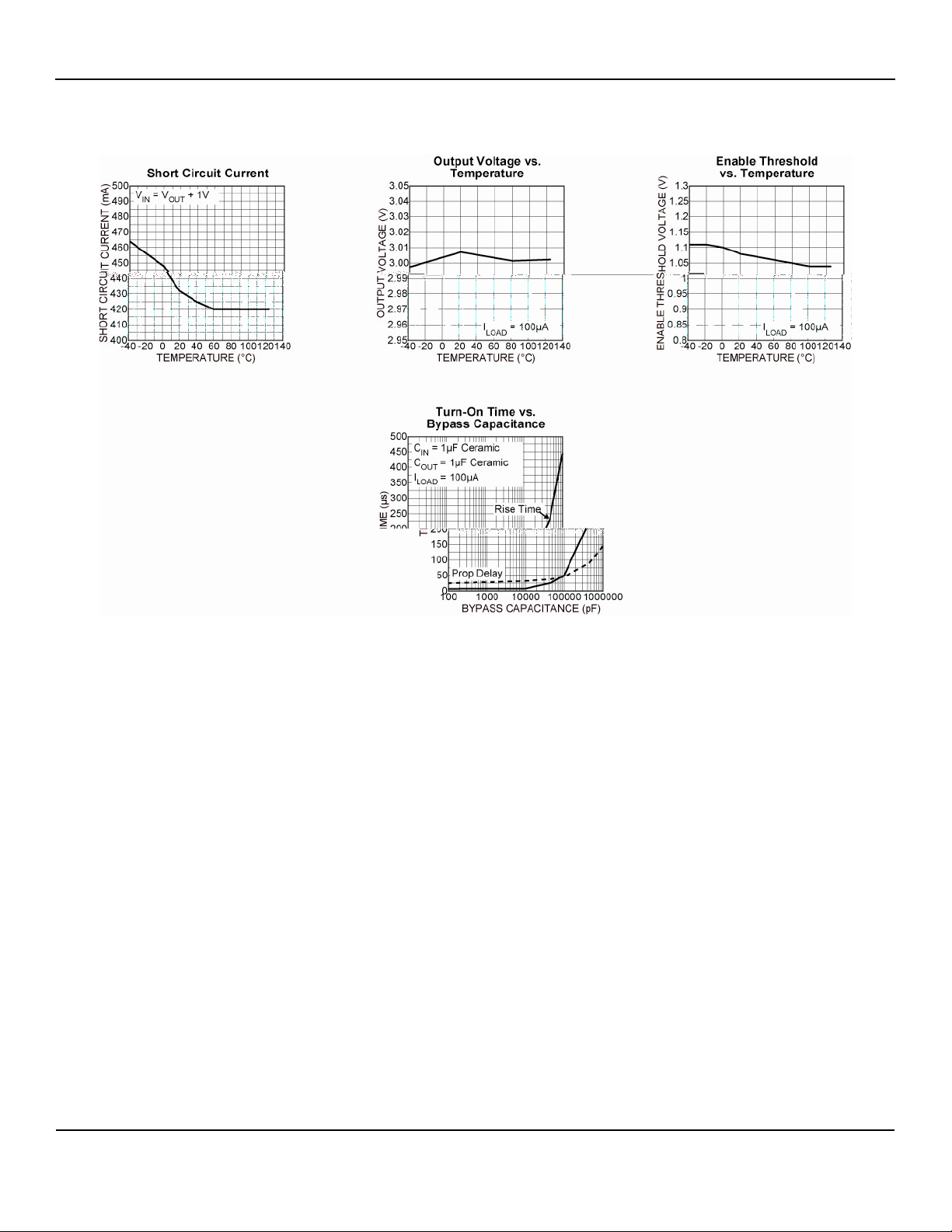
Typical Characteristics
November 2006
6
M9999-110906
Page 7
Micrel, Inc. MIC5255
Typical Characteristics
November 2006
7
M9999-110906
Page 8
Micrel, Inc. MIC5255
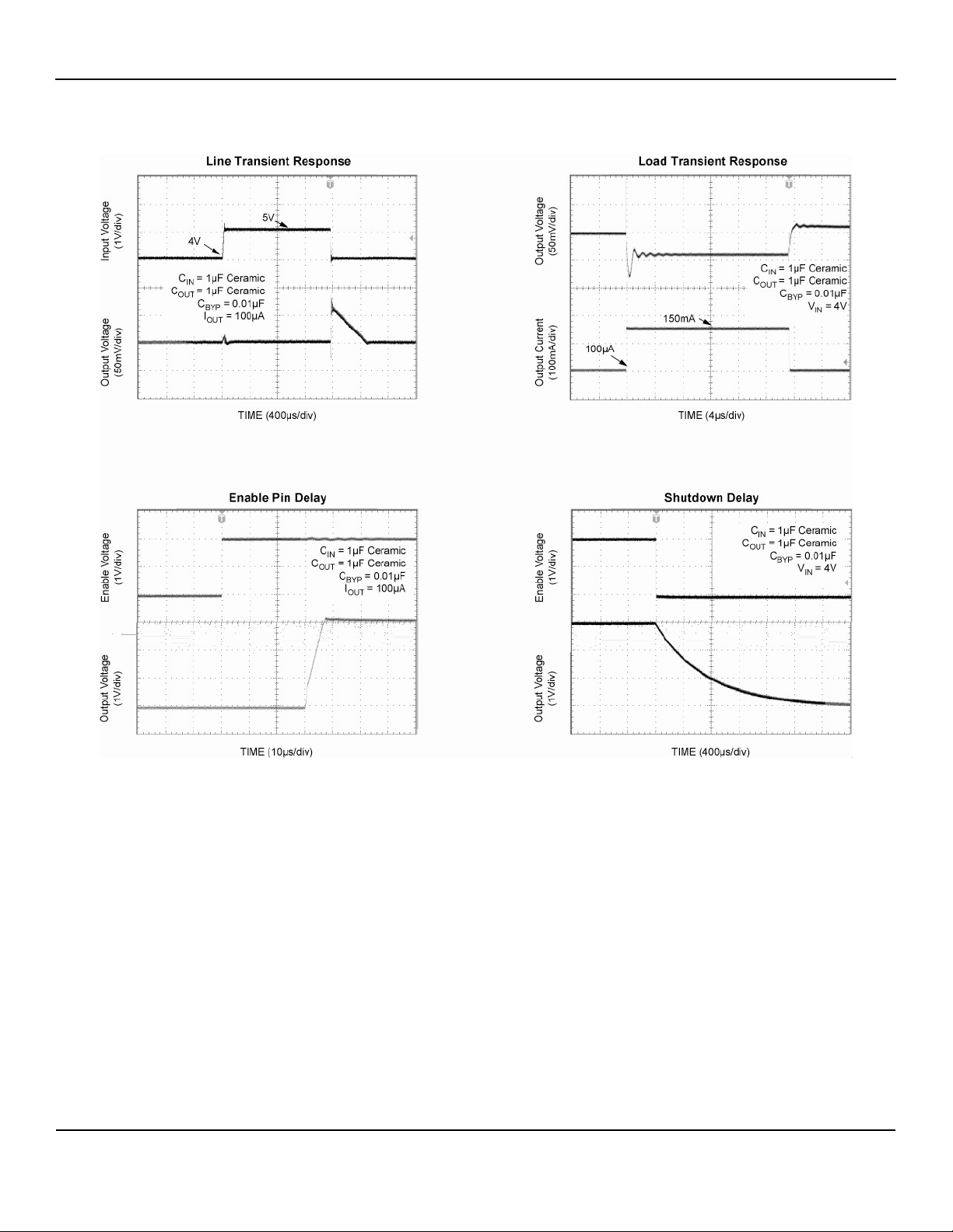
Functional Characteristics
November 2006
8
M9999-110906
Page 9
Micrel, Inc. MIC5255
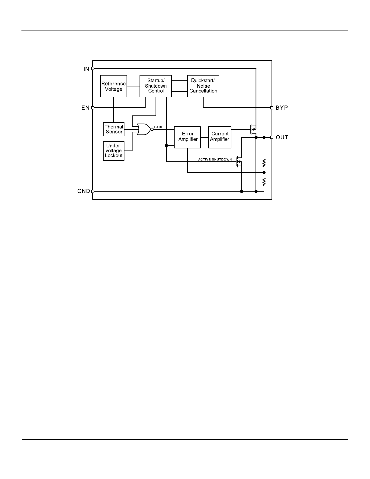
Functional Diagram
November 2006
9
M9999-110906
Page 10

Micrel, Inc. MIC5255
Application Information
Enable/Shutdown
The MIC5255 comes with an active-high enable pin that
allows the regulator to be disabled. Forcing the enable
pin low disables the regulator and sends it into a “zero”
off-mode-current state. In this state, current consumed
by the regulator goes nearly to zero. Forcing the enable
pin high enables the output voltage. This part is CMOS
and the enable pin cannot be left floating; a floating
enable pin may cause an indeterminate state on the
output.
Input Capacitor
The MIC5255 is a high performance, high bandwidth
device. Therefore, it requires a well-bypassed input
supply for optimal performance. A 1µF capacitor is
required from the input to ground to provide stability.
Low-ESR ceramic capacitors provide optimal
performance at a minimum of space. Additional high
frequency capacitors, such as small valued NPO
dielectric type capacitors, help filter out high frequency
noise and are good practice in any RF-based circuit.
Output Capacitor
The MIC5255 requires an output capacitor for stability.
The design requires 1µF or greater on the output to
maintain stability. The design is optimized for use with
low-ESR ceramic chip capacitors. High ESR capacitors
may cause high frequency oscillation. The maximum
recommended ESR is 300m. The output capacitor can
be increased, but performance has been optimized for a
1µF ceramic output capacitor and does not improve
significantly with larger capacitance.
X7R/X5R dielectric-type ceramic capacitors are recommended because of their temperature performance.
X7R-type capacitors change capacitance by 15% over
their operating temperature range and are the most
stable type of ceramic capacitors. Z5U and Y5V
dielectric capacitors change value by as much as 50%
and 60%, respectively, over their operating temperature
ranges. To use a ceramic chip capacitor with Y5V
dielectric, the value must be much higher than an X7R
ceramic capacitor to ensure the same minimum
capacitance over the equivalent operating temperature
range.
Bypass Capacitor
A capacitor can be placed from the noise bypass pin to
ground to reduce output voltage noise. The capacitor
bypasses the internal reference. A 0.01µF capacitor is
recommended for applications that require low-noise
outputs. The bypass capacitor can be increased, further
reducing noise and improving PSRR. Turn-on time
increases slightly with respect to bypass capacitance. A
unique quick-start circuit allows the MIC5255 to drive a
November 2006
large capacitor on the bypass pin without significantly
slowing turn-on time. Refer to the “
istics
” section for performance with different bypass
Typical Character-
capacitors.
Active Shutdown
The MIC5255 also features an active shutdown clamp,
which is an N-Channel MOSFET that turns on when the
device is disabled. This allows the output capacitor and
load to discharge, de-energizing the load.
No-Load Stability
The MIC5255 will remain stable and in regulation with no
load unlike many other voltage regulators. This is
especially important in CMOS RAM keep-alive
applications.
Thermal Considerations
The MIC5255 is designed to provide 150mA of
continuous current in a very small package. Maximum
power dissipation can be calculated based on the output
current and the voltage drop across the part. To
determine the maximum power dissipation of the
package, use the junction-to-ambient thermal resistance
of the device and the following basic equation:
−
⎛
⎜
T
J(max)
P
is the maximum junction temperature of the die,
125°C, and T
=
D(max)
⎜
⎝
is the ambient operating temperature. JA
A
TT
⎞
AJ(max)
⎟
JA
⎟
⎠
is layout dependent; Table 1 shows examples of
junction-to-ambient thermal resistance for the MIC5255.
Package
SOT23-5
(M5 or D5)
Recommended
θ
JA
Minimum Footprint
235°C/W 185°C/W 145°C/W
Table 1. SOT-23-5 Thermal Resistance
θ
1” Square
JA
Copper Clad
The actual power dissipation of the regulator circuit can
be determined using the equation:
P
Substituting P
= (VIN – V
D
D(max)
) I
OUT
OUT
+ VIN I
GND
for PD and solving for the operating
conditions that are critical to the application will give the
maximum operating conditions for the regulator circuit.
For example, when operating the MIC5255-3.0BM5 at
50°C with a minimum footprint layout, the maximum
input voltage for a set output current can be determined
as follows:
°−°
C50C125
P
D(max)
P
D(max)
⎛
=
⎜
⎝
= 315mW
°
C/W235
⎞
⎟
⎠
10
M9999-110906
θ
JC
Page 11

Micrel, Inc. MIC5255
The junction-to-ambient thermal resistance for the
minimum footprint is 235°C/W, from Table 1. The
maximum power dissipation must not be exceeded for
proper operation. Using the output voltage of 3.0V and
an output current of 150mA, the maximum input voltage
can be determined. Because this device is CMOS and
the ground current is typically 100µA over the load
range, the power dissipation contributed by the ground
current is < 1% and can be ignored for this calculation:
315mW = (V
315mW = V
810mW = V
V
IN(max)
= 5.4V
– 3.0V) 150mA
IN
× 150mA – 450mW
IN
× 150mA
IN
Therefore, a 3.0V application at 150mA of output current
can accept a maximum input voltage of 5.4V in a SOT23-5 package. For a full discussion of heat sinking and
thermal effects on voltage regulators, refer to the “
ulator Thermals
” section of Micrel’s Designing with Low-
Dropout Voltage Regulators handbook.
Reg-
November 2006
11
M9999-110906
Page 12
Micrel, Inc. MIC5255
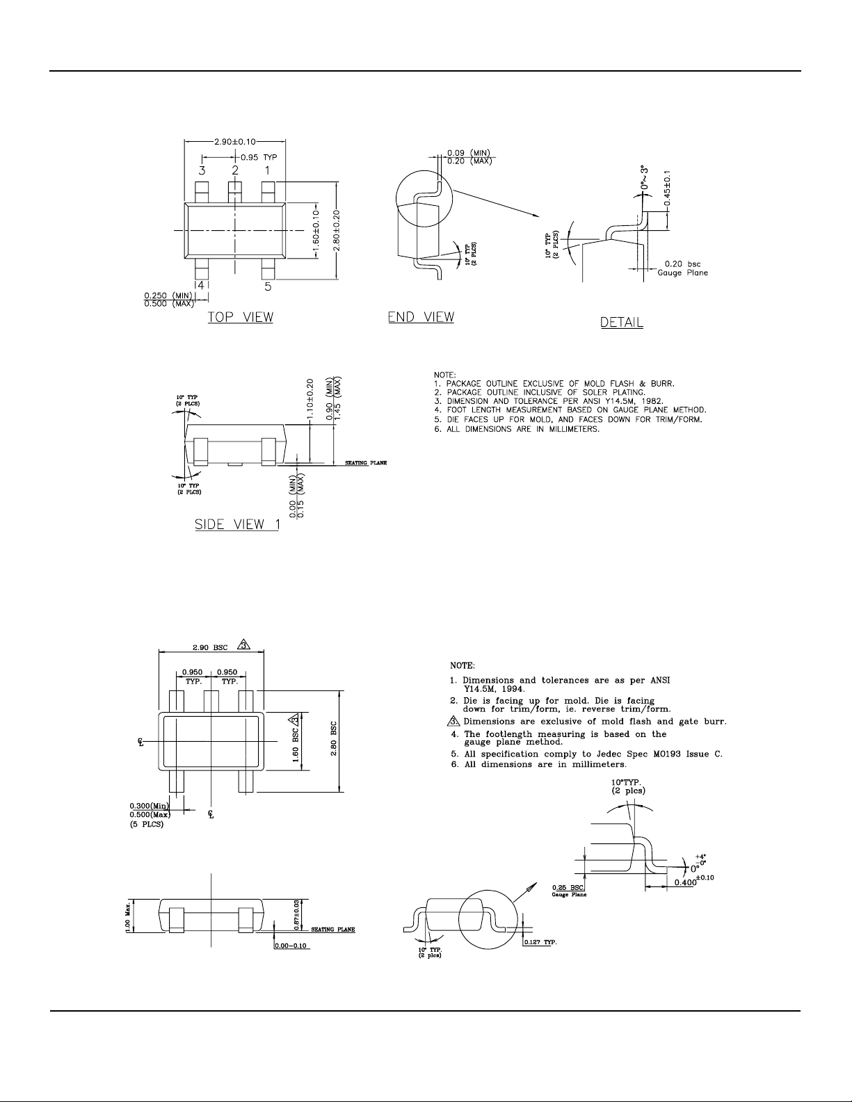
Package Information
5-Pin SOT (M5)
November 2006
5-Pin Thin SOT (D5)
12
M9999-110906
Page 13
Micrel, Inc. MIC5255
November 2006
13
M9999-110906
 Loading...