

MIC5233 Micrel
MIC5233
High Input Voltage, Low IQ µCap LDO Regulator
General Description
The MIC5233 is a 100mA highly accurate, low dropout
regulator with high input voltage and ultra-low ground current.
This combination of high voltage and low ground current
makes the MIC5233 ideal for multi-cell Li-Ion battery
systems.
A µCap LDO design, the MIC5233 is stable with either
ceramic or tantalum output capacitor. It only requires a 2.2µF
capacitor for stability.
Features of the MIC5233 include enable input, thermal shutdown, current limit, reverse battery protection, and
reverse leakage protection.
Available in fixed and adjustable output voltage versions, the
MIC5233 is offered in the IttyBitty™ SOT-23-5 package with
a junction temperature range of –40°C to +125°C.
Ordering Information
Features
• Wide input voltage range: 2.3V to 36V
• Ultra low ground current: 18µA
• Low dropout voltage of 270mV at 100mA
• High output accuracy of ±2.0% over temperature
• µCap: stable with ceramic or tantalum capacitors
• Excellent line and load regulation specifications
• Zero shutdown current
• Reverse battery protection
• Reverse leakage protection
• Thermal shutdown and current limit protection
• IttyBitty™ SOT-23-5 package
Applications
• Keep-alive supply in notebook and portable computers
• USB power supply
• Logic supply for high-voltage batteries
• Automotive electronics
• Battery powered systems
• 3-4 cell Li-Ion battery input range
Part Number Marking Voltage Junction Temp. Range Package
MIC5233-1.8BM5 L318 1.8V –40°C to +125°C SOT-23-5
MIC5233-2.5BM5 L325 2.5V –40°C to +125°C SOT-23-5
MIC5233-3.0BM5 L330 3.0V –40°C to +125°C SOT-23-5
MIC5233-3.3BM5 L333 3.3V –40°C to +125°C SOT-23-5
MIC5233-5.0BM5 L350 5.0V –40°C to +125°C SOT-23-5
MIC5233BM5 L3AA ADJ. –40°C to +125°C SOT-23-5
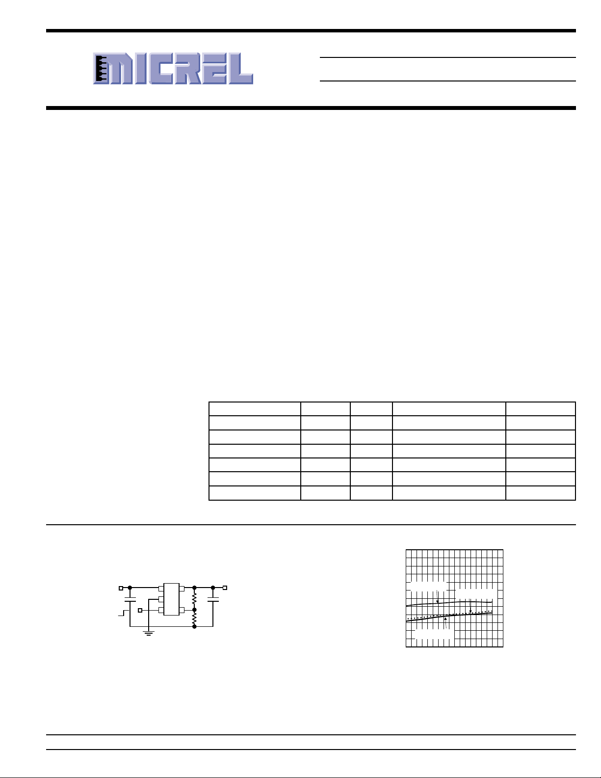
Typical Application
IN
ON
MIC5233BM5
15
2
34
EN
V
OUT
C
R
1
R
2
=2.2µF
OUT
ceramic
I
=18µA
GND
V
C
=1.0µF
IN
OFF
Ultra-Low Current Adjustable Regulator Application
40
35
30
I
= 1mA
OUT
25
20
15
I
GROUND CURRENT (µA)
OUT
10
4 8 12 16 20 24 28 32 36 40
INPUT VOLTAGE (V)
= 10µA
I
OUT
= 100µA
Ground Current vs. Input Voltage
IttyBitty is a trademark of Micrel, Inc.
Micrel, Inc. • 1849 Fortune Drive • San Jose, CA 95131 • USA • tel + 1 (408) 944-0800 • fax + 1 (408) 944-0970 • http://www.micrel.com
August 2003 1 MIC5233
MIC5233 Micrel
Pin Configuration
GND
2
IN
13
EN
L3xx
45
NC or
ADJ.
OUT
SOT-23-5
Pin Description
SOT-23-5 Pin Name Pin Function
1 IN Supply Input.
2 GND Ground.
3 EN Enable (Input): Logic low = shutdown; logic high = enable
4 NC (fixed) No Connect.
ADJ (ADJ.) Adjust (Input): Feedback input. Connect to resistive voltage-divider network.
5 OUT Regulator Output.
MIC5233 2 August 2003

MIC5233 Micrel
Absolute Maximum Ratings (Note 1)
Input Supply Voltage ....................................... –20V to 38V
Enable Input Voltage...................................... –0.3V to 38V
Power Dissipation .................................... Internally Limited
Junction Temperature .............................. –40°C to +125°C
Storage Temperature ...............................–65°C to +150°C
Operating Ratings (Note 2)
Input Supply Voltage ........................................ 2.3V to 36V
Enable Input Voltage........................................... 0V to 36V
Junction Temperature (T
Package Thermal Resistance
SOT-23-5 (θJA)..................................................235°C/W
) ....................... –40°C to +125°C
J
ESD Rating, Note 3
Electrical Characteristics (Note 4)
TA = 25°C with VIN = V
Parameter Condition Min Typ Max Units
Output Voltage Accuracy Variation from nominal V
Line Regulation VIN = V
Load Regulation I
Dropout Voltage I
Ground Current I
Ground Current in Shutdown VEN ≤ 0.6V; VIN = 36V 0.1 1 µA
Short Circuit Current V
Output Leakage, Load = 500Ω; V
Reverse Polarity Input
Enable Input
Input Low Voltage Regulator OFF 0.6 V
Input High Voltage Regulator ON 2.0 V
Enable Input Current V
OUT
+ 1V; I
= 100µA; VEN ≥ 2V; Bold values indicate –40°C<TJ< +125°C; unless otherwise specified.
OUT
OUT
+ 1V to 36V 0.04 0.5 %
OUT
= 100µA to 100mA 0.25 1 %
OUT
= 100µA50mV
OUT
= 50mA 230 300 mV
I
OUT
–1.0 +1.0 %
–2.0 +2.0 %
400 mV
I
= 100mA 270 400 mV
OUT
450 mV
= 100µA1830µA
OUT
35 µA
I
= 50mA 0.35 0.70 mA
OUT
I
= 100mA 1 2 mA
OUT
= 0V 190 350 mA
OUT
= –15V –0.1 µA
IN
= 0.6V; Regulator OFF –1.0 0.01 1.0 µA
EN
= 2.0V; Regulator ON 0.1 1.0 µA
V
EN
VEN = 36V; Regulator ON 0.5 2.5 µA
Note 1. Exceeding the absolute maximum rating may damage the device.
Note 2. The device is not guaranteed to function outside its operating rating.
Note 3. Devices are ESD sensitive. Handling precautions recommended. Human body model, 1.5k in series with 100pF.
Note 4. Specification for packaged product only.
August 2003 3 MIC5233

MIC5233 Micrel
)
)
)
)
Typical Characteristics
Power Supply
Rejection Ratio
70
60
50
40
30
PSRR (dB)
20
10
0
0.01 0.1 1 10 100 1000
I
= 100mA
OUT
FREQUENCY (kHz)
Dropout
3.5
3.0
2.5
2.0
1.5
1.0
OUTPUT VOLTAGE (V)
0.5
0.0
Characteristics
I
= 100µA
LOAD
I
= 50mA
LOAD
I
= 100mA
LOAD
0 0.5 1 1.5 2 2.5 3 3.5 4
INPUT VOLTAGE (V)
Dropout Voltage
vs. Output Current
350
300
250
200
150
100
50
DROPOUT VOLTAGE (mV)
0
0 20406080100
OUTPUT CURRENT (mA
Ground Pin Current
1000
GROUND CURRENT (µA)
vs. Output Current
900
800
700
600
500
400
300
200
100
0
0 102030405060708090100
OUTPUT CURRENT (mA)
VIN = 4V
Dropout Voltage
500
450
400
350
300
250
200
150
100
DROPOUT VOLTAGE (mV)
vs. Temperature
I
= 100mA
OUT
50
0
-40 -20 0 20 40 60 80 100120
TEMPERATURE (°C)
Ground Pin Current
vs. Output Current
30
28
26
VIN = 24V
24
22
20
18
VIN = 12V
16
14
GROUND CURRENT (µA)
12
10
0 100 200 300 400 500
OUTPUT CURRENT (µA)
VIN = 36V
VIN = 4V
Ground Pin Current
vs. Temperature
80
I
75
70
65
60
55
50
GROUND CURRENT (µA)
45
40
-40 -20 0 20 40 60 80 100 120
TEMPERATURE (°C
LOAD
= 10mA
Ground Pin Current
vs. Input Voltage
100
90
I
= 10µA
OUT
80
70
60
I
= 1mA
50
OUT
40
30
20
GROUND CURRENT (µA)
10
0
1.5 2 2.5 3 3.5 4
INPUT VOLTAGE (V
I
OUT
I
OUT
= 10µA
= 100µA
Ground Pin Current
400
380
360
340
320
300
280
260
240
GROUND CURRENT (µA)
220
200
vs. Temperature
I
= 50mA
LOAD
-40 -20 0 20 40 60 80 100 120
TEMPERATURE (°C
Ground Pin Current
1200
1100
1000
GROUND CURRENT (µA)
900
800
700
600
500
400
300
200
vs. Input Voltage
I
=100mA
OUT
I
= 50mA
OUT
1.5 2 2.5 3 3.5 4
INPUT VOLTAGE (V)
Ground Pin Current
1.20
1.15
1.10
1.05
1.00
0.95
0.90
0.85
GROUND CURRENT (mA)
0.80
vs. Temperature
I
= 100mA
LOAD
-40 -20 0 20 40 60 80 100 120
TEMPERATURE (°C)
Ground Pin Current
vs. Input Voltage
40
35
30
I
= 1mA
OUT
25
20
15
I
GROUND CURRENT (µA)
OUT
10
4 8 12 16 20 24 28 32 36 40
INPUT VOLTAGE (V)
= 10µA
I
OUT
= 100µA
MIC5233 4 August 2003

MIC5233 Micrel
)
0
50
100
150
200
250
300
-40 -20 0 20 40 60 80 100120
SHORT CIRCUIT CURRENT (mA)
TEMPERATURE (°C)
Short Circuit Current
vs. Temperature
VIN = 4V
Input Current
vs. Supply Voltage
120
100
80
60
VEN = 5V
= 30Ω
R
40
LOAD
20
INPUT CURRENT (mA)
0
-20 -10 0 10
SUPPLY VOLTAGE (V)
Output Voltage
3.05
3.04
3.03
3.02
3.01
3.00
2.99
2.98
2.97
OUTPUT VOLTAGE (V)
2.96
2.95
vs. Temperature
I
= 100µA
LOAD
-40 -20 0 20 40 60 80 100 120
TEMPERATURE (°C
Load Transient Response
August 2003 5 MIC5233
(200mV/div.)
OUTPUT VOL TAGE
(100mA/div.)
OUTPUT CURRENT
TIME (400µs/div.)
VIN = 4V
= 3V
V
OUT
= 4.7µF ceramic
C
OUT
100mA
0mA

MIC5233 Micrel
Functional Diagrams
EN
IN
EN
IN
ENABLE
R1
V
REF
R2
GND
OUT
Block Diagram – Fixed Output Voltage
OUT
ENABLE
R1
V
REF
GND
Block Diagram – Adjustable Output Voltage
ADJ
R2
MIC5233 6 August 2003

MIC5233 Micrel
P
125 C 50 C
235 C/W
D(MAX)
=
°− °
°
Applications Information
Enable/Shutdown
The MIC5233 comes with an active-high enable pin that
allows the regulator to be disabled. Forcing the enable pin low
disables the regulator and sends it into a “zero” off-modecurrent state. In this state, current consumed by the regulator
goes nearly to zero. Forcing the enable pin high enables the
output voltage.
Input Capacitor
The MIC5233 has high input voltage capability up to 36V. The
input capacitor must be rated to sustain voltages that may be
used on the input. An input capacitor may be required when
the device is not near the source power supply or when
supplied by a battery. Small, surface mount, ceramic capacitors can be used for bypassing. A larger value may be
required if the source supply has high ripple.
Output Capacitor
The MIC5233 requires an output capacitor for stability. The
design requires 2.2µF or greater on the output to maintain
stability. The design is optimized for use with low-ESR
ceramic chip capacitors. High-ESR capacitors may cause
high frequency oscillation. The maximum recommended
ESR is 3Ω. The output capacitor can be increased without
limit. Larger valued capacitors help to improve transient
response.
X7R/X5R dielectric-type ceramic capacitors are recommended because of their temperature performance. X7Rtype capacitors change capacitance by 15% over their operating temperature range and are the most stable type of
ceramic capacitors. Z5U and Y5V dielectric capacitors change
value by as much as 50% and 60% respectively over their
operating temperature ranges. To use a ceramic chip capacitor with Y5V dielectric, the value must be much higher than an
X7R ceramic capacitor to ensure the same minimum capacitance over the equivalent operating temperature range.
No-Load Stability
The MIC5233 will remain stable and in regulation with no load
unlike many other voltage regulators. This is especially
important in CMOS RAM keep-alive applications.
Thermal Consideration
The MIC5233 is designed to provide 100mA of continuous
current in a very small package. Maximum power dissipation
can be calculated based on the output current and the voltage
drop across the part. To determine the maximum power
dissipation of the package, use the junction-to-ambient thermal resistance of the device and the following basic equation:
TT
=
T
J(MAX)
P
D(MAX)
is the maximum junction temperature of the die,
125°C, and TA is the ambient operating temperature. θJA is
layout dependent; Table 1 shows examples of the junctionto-ambient thermal resistance for the MIC5233.
−
J(MAX) A
θ
JA
Package
θθ
θJA Recommended
θθ
Minimum Footprint
SOT-23-5 235°C/W
Table 1. SOT-23-5 Thermal Resistance
The actual power dissipation of the regulator circuit can be
determined using the equation:
PD = (VIN – V
Substituting P
OUT)IOUT
for PD and solving for the operating
D(MAX)
+ VIN×I
GND
conditions that are critical to the application will give the
maximum operating conditions for the regulator circuit. For
example, when operating the MIC5233-3.0BM5 at 50°C with
a minimum footprint layout, the maximum input voltage for a
set output current can be determined as follows:
P
D(MAX)
= 319mW
The junction-to-ambient (θJA) thermal resistance for the
minimum footprint is 235°C/W, from Table 1. It is important
that the maximum power dissipation not be exceeded to
ensure proper operation. Since the MIC5233 was designed
to operate with high input voltages, careful consideration
must be given so as not to overheat the device. With very high
input-to-output voltage differentials, the output current is
limited by the total power dissipation. Total power dissipation
is calculated using the following equation:
PD = (VIN – V
OUT)IOUT
+ VIN x I
GND
Due to the potential for input voltages up to 36V, ground
current must be taken into consideration.
If we know the maximum load current, we can solve for the
maximum input voltage using the maximum power dissipation calculated for a 50°C ambient, 319mV.
P
DMAX
= (VIN – V
OUT)IOUT
+ VIN x I
GND
319mW = (VIN – 3V)100mA + VIN x 2.8mA
Ground pin current is estimated using the typical characteristics of the device.
619mW = VIN (102.8mA)
VIN = 6.02V
For higher current outputs only a lower input voltage will work
for higher ambient temperatures.
Assuming a lower output current of 10mA, the maximum input
voltage can be recalculated:
319mW = (VIN – 3V)10mA + VIN x 0.1mA
349mW = VIN x 10.1mA
VIN = 34.9V
Maximum input voltage for a 10mA load current at 50°C
ambient temperature is 34.9V, utilizing virtually the entire
operating voltage range of the device.
August 2003 7 MIC5233

MIC5233 Micrel
Adjustable Regulator Application
The MIC5233BM5 can be adjusted from 1.24V to 20V by
using two external resistors (Figure 1). The resistors set the
output voltage based on the following equation:
VV
OUT
Where V
=+
= 1.24V.
REF
REF
1
R
1
R
2
Feedback resistor R2 should be no larger than 300kΩ.
V
1.0µF
IN
MIC5233BM5
IN
EN
GND
OUT
ADJ.
V
OUT
R
1
2.2µF
R
2
Figure 1. Adjustable Voltage Application
MIC5233 8 August 2003

MIC5233 Micrel
Package Information
1.90 (0.075) REF
0.95 (0.037) REF
3.02 (0.119)
2.80 (0.110)
0.50 (0.020)
0.35 (0.014)
1.75 (0.069)
1.50 (0.059)
1.30 (0.051)
0.90 (0.035)
0.15 (0.006)
0.00 (0.000)
SOT-23-5 (M5)
3.00 (0.118)
2.60 (0.102)
10°
0°
DIMENSIONS:
MM (INCH)
0.20 (0.008)
0.09 (0.004)
0.60 (0.024)
0.10 (0.004)
MICREL, INC. 1849 FORTUNE DRIVE SAN JOSE, CA 95131 USA
The information furnished by Micrel in this datasheet is believed to be accurate and reliable. However, no responsibility is assumed by Micrel for its use.
Micrel reserves the right to change circuitry and specifications at any time without notification to the customer.
Micrel Products are not designed or authorized for use as components in life support appliances, devices or systems where malfunction of a product can
reasonably be expected to result in personal injury. Life support devices or systems are devices or systems that (a) are intended for surgical implant into
the body or (b) support or sustain life, and whose failure to perform can be reasonably expected to result in a significant injury to the user. A Purchaser’s
use or sale of Micrel Products for use in life support appliances, devices or systems is at Purchaser’s own risk and Purchaser agrees to fully indemnify
TEL + 1 (408) 944-0800 FAX + 1 (408) 944-0970 WEB http://www.micrel.com
Micrel for any damages resulting from such use or sale.
© 2003 Micrel, Incorporated.
August 2003 9 MIC5233
 Loading...