

查询MLX90269LUF-1供应商
Features and Benefits
Absolute Integrated Pressure sensor
Less than ±1% error range overall
Programmable through the connector (3 pins)
Trimmable offset and sensitivity
On-Chip Signal Conditioning
Output proportional to the applied pressure
Ratiometric output
Rail-to-rail output
Diagnostics of broken supply wires and broken sensor
Output protected against short-circuits at both battery terminals
Different pressure ranges available
Application Examples
Water pressure
Oil pressure
Manifold Air Pressure
MLX90269
Absolute Integrated Pressure Sensor
Ordering Information
Part No. Temperature Suffix Package Code Option Description
MLX90269 L (-40°C to 150°C) UF (die on foil) - 1 1.2 to 3 Bar Full Scale
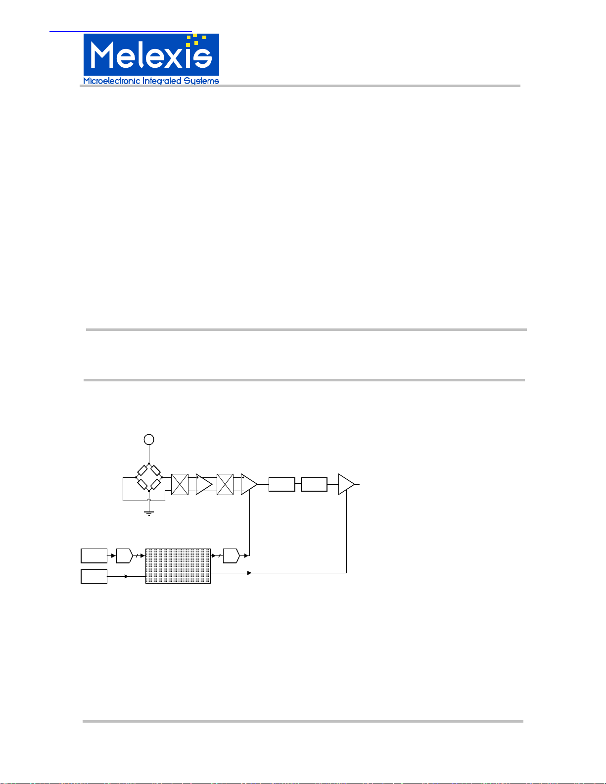
1. Functional Diagram
VDD
Chopper
demodulator
Temperature
sensor
Diagnostics
applied pressure with an adjustable slope and offset. It is ratiometric and goes rail-to-rail with a 3mA
source and sink capability. Different pressure ranges are available (from 1.2 to 7 Bar full scale ranges,
see above ordering information).
ADC
DIGITAL CORE
DAC
Gain
calibration
OUT
2. Description
The MLX90269 is an integrated
absolute pressure sensor (0 Bar
= vacuum) realized in CMOS
technology with micromachining
options. It consists of an analog
signal chain that interacts with
the digital core and on-chip
temperature sensor in order to
provide uniform overall sensing
characteristics after calibration
and to cancel the temperature
related parameter drifts.
The output is proportional to the
3901090269 Page 1 of 9 Data Sheet
Rev. 006 Mar/08

Absolute Integrated Pressure Sensor
TABLE OF CONTENTS
MLX90269
1. FUNCTIONAL DIAGRAM...................................................................................................................... 1
2. DESCRIPTION....................................................................................................................................... 2
3. ABSOLUTE MAXIMUM RATINGS ....................................................................................................... 3
4. MLX90269 ELECTRICAL SPECIFICATIONS ...................................................................................... 3
5. GENERAL DESCRIPTION .................................................................................................................... 4
6. UNIQUE FEATURES ............................................................................................................................. 4
7. PERFORMANCE GRAPHS................................................................................................................... 5
8. APPLICATION INFORMATION ............................................................................................................ 6
9. DIE DIMENSION AND PAD COORDINATES....................................................................................... 7
10. CALIBRATION AND PROGRAMMING PROCEDURE ........................................................................ 7
11. ESD PRECAUTIONS............................................................................................................................. 8
12. DISCLAIMER ......................................................................................................................................... 9
3901090269 Page 2 of 9 Data Sheet
Rev. 006 Mar/08

MLX90269
Absolute Integrated Pressure Sensor
3. Absolute Maximum Ratings
Parameter Min Max
Supply Voltage, VDD -14V 16V
Output Voltage, V
Storage Temperature Range, TS
ESD Sensitivity (AEC Q100 002) -2 kV 2 kV
Exceeding the absolute maximum ratings may cause permanent damage. Exposure to absolutemaximum-rated conditions for extended periods may affect device reliability.
4. MLX90269 Electrical Specifications
DC Operating Parameters TA = -40oC to 150oC, VDD = 5V (unless otherwise specified)
Parameter Symbol Test Conditions Min Typ Max Units
-0.5V 16V
out
-55°C 165°C
OPERATIONAL FEATURES
Supply Voltage VDD Operating 4.5 5 5.5 V
Supply Current IDD V
= 5V ± 10%, excluding
DD
4 6 10 mA
output current
Output Current Capability I
Pressure output @ zero pressure V
Pressure output @ full scale pressure V
Low Clamping Level
High Clamping Level
DIAGNOSTIC FEATURES
V
out
out
out
V
out
V
out
= 5V -3 3 mA
DD
V
= 5V 0.46 0.5 0.54 V
DD
V
= 5V 4.46 4.5 4.54 V
DD
5
90
10
95 % VDD
% V
DD
Output when sensor is broken Sensor broken 2 % VDD
Output when VDD is broken Pull-Up > 4.7K 5
Output when VSS is broken Pull-Down > 10K
95
% VDD
% VDD
Response Time (to reach 1% error) 2 ms
3901090269 Page 3 of 9 Data Sheet
Rev. 006 Mar/08

MLX90269
Absolute Integrated Pressure Sensor
5. General Description
This chip integrates a pressure sensor and the associated signal conditioning on the same die. The
supply voltage VDD directly supplies the pressure sensor.
A chopped instrumentation stage amplifies the differential output signal of the sensor. The gain of this
amplifier can be adjusted with 3 bits. The input stage is followed by a differential to single-ended
conversion. The reference voltage for this stage is generated by a 10 bit DAC and varies linearly with
temperature in order to perform the offset and offset drift compensation. A digital hardware multiplier
calculates this compensation. The temperature signal, serving as input for this multiplier, is generated
from the ADC of the output signal of the internal temperature sensor.
The chopped signal is demodulated with a switched capacitor stage. The buffered output serves as
reference for a 10 bit DAC to perform the span and span drift compensation. The DAC is controlled by the
digital part.
Finally the signal is given out by a class AB rail-to-rail amplifier capable of sourcing and sinking large
currents.
A 3-point temperature and 2-point pressure calibration is required (room temperature, a low temperature
and a high temperature), to achieve an error less than ±1% over the complete pressure and temperature
range (the output error is referred to the output span).
PTC (Programming Through Connector) protocol is used to perform calibration.
6. Unique Features
Diagnostic Limits
Diagnostic of broken sensor: The output will be forced to ground (or a very low level) when the sensor
membrane breaks.
Diagnostic of broken wires: The output will be forced to ground (or a very low level) when the supply wire
breaks, even when a pull-up is still connected to the output pin.
The output will be forced to the supply voltage (or a very high level) when the ground wire breaks, even
when a pull-down is still connected to the output pin.
Output Protection
The output is protected against short-circuits at either battery terminals. The output can handle voltages
between -0.5V and 16V (independent of supply voltage).
Memlock Function
The memory consists of ZAP cells. When all calibration parameters are programmed, the chip can be
locked. This to avoid unwanted data to be written into the memory cells.
Once the chip is locked in a normal application, it is not possible to unlock.
Clamping Levels
The user can enable the clamping of the output to ensure that the output can not enter the fault band in
normal application.
3901090269 Page 4 of 9 Data Sheet
Rev. 006 Mar/08

MLX90269
Vout versus Pressure with Ta = -50..150 C
Vout %Vdd
Absolute Integrated Pressure Sensor
7. Performance Graphs
The graphs below show measured output voltages (on a 4 Bar full scale sensor) taken at 15 pressure
points (500 mBar to 4000 mBar), at 21 ambient temperature points (-50 to 150 Celsius) and with Vdd set
to 4.5 V, 5 V and 5.5 V.
100
90
80
70
60
50
40
30
20
10
0
0 1 0 20 30 40 50 60 70 80 90 100
Note : FS means Output Voltage Full Scale (4 V).
Measured Error is below 1 % of FS for all ambient temperature and pressure points (see graphs below).
Error versus Ambient Temperature with P = 500..4000 mBar
1.5
Pressure %FS (FS = 4000 mBar)
1
0.5
0
Error in % of FS
-0.5
-1
-1.5
-50 -30 -10 10 30 50 70 90 110 130 150
Ambient Temperature C
3901090269 Page 5 of 9 Data Sheet
Rev. 006 Mar/08

MLX90269
Absolute Integrated Pressure Sensor
Error versus Pressure with Ta = - 50..150 C
1.5
1
0.5
0
Error in % of FS
-0.5
-1
-1.5
0 250 500 750 1000 1250 1500 1750 2000 2250 2500 2750 3000 3250 35 00 3750 4000
4.5V and 5.5V Ratiometricity Error versus Pressure with Ta = - 50..150 C
0.5
0.4
0.3
0.2
0.1
0
-0.1
Error in % of FS
-0.2
-0.3
-0.4
-0.5
0 250 500 750 1000 1250 1500 1750 2000 2250 2500 2750 3000 3250 35 00 3750 4000
Pressure mBar
Pressure mBar
8. Application Information
Very few off-chip components are needed (only 2 decoupling capacitors).
Only 3 pins are used (Vdd, Vss, Out), see pad layout drawing in paragraph 9.
Calibration and Programming is made through Out pin.
3901090269 Page 6 of 9 Data Sheet
Rev. 006 Mar/08

MLX90269
Absolute Integrated Pressure Sensor
9. Die dimension and pad coordinates
Available upon request.
10. Calibration and Programming Procedure
Programming in Temporary Memory
The programming is done through the connector: only the application pins (supply, ground and output)
need to be used. The programming can be enabled by forcing the supply high enough (VCC_T). Through
the OUT pin one can input the data. The data is Pulse Width Modulated.
At the end of the programming, keep OUT high until VCC has reached its normal level (VCC_N).
Thereafter disconnect OUT. The time in between should be less than 100us.
Zapping of the Permanent Memory
Only 1 bit can be zapped at a time. First program 1 bit to ‘1’. A higher supply (VCC_Z) is needed to be
able to zap the bit. The zapping is done when OUT is high (OUT_Z).
A high current will flow during zapping. It is recommended to limit this current to 200mA.
The memlock-bit should be zapped as last bit, as this disables programming function.
3901090269 Page 7 of 9 Data Sheet
Rev. 006 Mar/08

MLX90269
Absolute Integrated Pressure Sensor
In order to check zapping, one can program Test Mode 22 = 10110b. Also 1 bit of the temporary memory
should be ‘1’. If the zap cell – corresponding to the place of the ‘1’ in the temporary memory – is zapped,
then the supply current will be at least 35mA. Otherwise the supply current will be approximately the same
as in normal mode (maximum 10mA). Values in between indicate a bad zap.
Parameters
Parameter Minimum Maximum Meaning
t0n 1us 100us Rise Time of Supply from 0V to VCC_N
t0p 2us 200us Rise Time of Supply from 0V to VCC_P
tpz 1us 100us Rise Time of Supply from VCC_P to VCC_Z
tpn 1us 100us Fall Time of Supply from VCC_P to VCC_N
tz0 2us 300us Fall Time of Supply from VCC_Z to 0V
tr 0.5us 5us Rise Time of Out from OUT_L to OUT_H
tf 0.5us 5us Fall Time of Out from OUT_H to OUT_L
trz 0.5us 15us Rise Time of Out from OUT_H to OUT_Z
tfz 0.5us 20us Fall Time of Out from OUT_Z to OUT_L
th0 50us 100us High Time for 0
tl0 200us 300us Low Time for 0
th1 200us 300us High Time for 1
tl1 50us 100us Low Time for 1
tz 5ms 6ms zap time
tz0 100us 1ms OUT & VCC = Z & 0V
td0 100us 1ms OUT & VCC = OUT_L & 0V
tdp 100us 1ms OUT & VCC = OUT_L & VCC_P
tuz 100us 1ms OUT & VCC = OUT_H & VCC_Z
tun 5us 50us OUT & VCC = OUT_H & VCC_N
tdz 5us 50us OUT & VCC = OUT_L & VCC_Z
VCC_N 4.5V 5.5V Normal Supply
VCC_P 8V 12V Programming Supply
VCC_Z 14V 16V Zapping Supply
OUT_L 0V 1V Low Output
OUT_H 4V 5V High Output
OUT_Z 12V 14V Output for zapping
An application note describes in more details this calibration procedure.
Calibration software is also available on request.
11. ESD Precautions
Electronic semiconductor products are sensitive to Electro Static Discharge (ESD).
Always observe Electro Static Discharge control procedures whenever handling semiconductor products.
3901090269 Page 8 of 9 Data Sheet
Rev. 006 Mar/08

MLX90269
Absolute Integrated Pressure Sensor
12. Disclaimer
Devices sold by Melexis are covered by the warranty and patent indemnification provisions appearing in
its Term of Sale. Melexis makes no warranty, express, statutory, implied, or by description regarding the
information set forth herein or regarding the freedom of the described devices from patent infringement.
Melexis reserves the right to change specifications and prices at any time and without notice. Therefore,
prior to designing this product into a system, it is necessary to check with Melexis for current information.
This product is intended for use in normal commercial applications. Applications requiring extended
temperature range, unusual environmental requirements, or high reliability applications, such as military,
medical life-support or life-sustaining equipment are specifically not recommended without additional
processing by Melexis for each application.
The information furnished by Melexis is believed to be correct and accurate. However, Melexis shall not
be liable to recipient or any third party for any damages, including but not limited to personal injury,
property damage, loss of profits, loss of use, interrupt of business or indirect, special incidental or
consequential damages, of any kind, in connection with or arising out of the furnishing, performance or
use of the technical data herein. No obligation or liability to recipient or any third party shall arise or flow
out of Melexis’ rendering of technical or other services.
© 2002 Melexis NV. All rights reserved.
For the latest version of this document. Go to our website at
www.melexis.com
Or for additional information contact Melexis Direct:
Europe and Japan: All other locations:
Phone: +32 1367 0495 Phone: +1 603 223 2362
3901090269 Page 9 of 9 Data Sheet
Rev. 006 Mar/08
E-mail: sales_europe@melexis.com E-mail: sales_usa@melexis.com
ISO/TS 16949 and ISO14001 Certified
 Loading...