

查询MLX90255BA供应商
Datasheet
MLX90255BA
Linear Optical Array
Features and Benefits
128 x 1 Sensor-Element Organization (1 Not Connected, 1 dummy, 128 real, 1 dummy
and 1 Dark Pixel)
385 Dots-Per-Inch (DPI) Sensor Pitch
High Linearity and Uniformity for 256 Gray-Scale (8-Bit) Applications
High Sensitivity: 1.7V @ 10µW/cm²
@ 0.7ms integration time
Special Gain Compensation for use with single LED light source
Output Referenced to Ground
Low Image Lag
Single 5V Supply
Replacement for Texas Instruments TSL1301 & TSL1401 and MLX90255AA
Operation to 1MHz
Applications
Position Sensing
Electrical Power Assist Steering (EPAS)
Spectrometer Applications
Ordering Information
Part No. Temperature Suffix Package Option Temperature Range
MLX90255 K LA -BA -40°C to 125°C Automotive
MLX90255 K JA -BA -40°C to 125°C Automotive
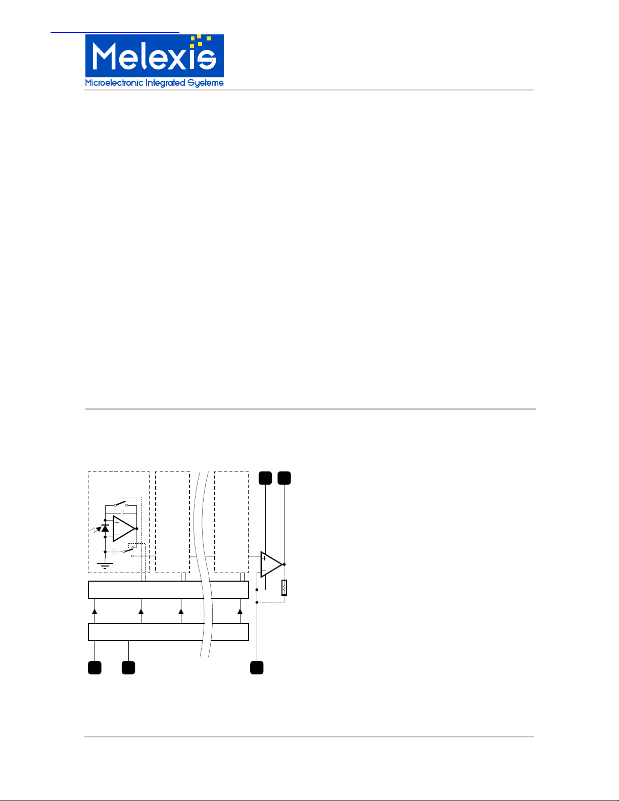
Functional Diagram
Pixel 2Pixel 1 Pixel 132
Integrator Reset
Sample
Switching Logic
Hold Q1 Q2 Q132
132-Bit Shift Register
CLK
2 1
SI
5
4
VDD
External
Load
GND
3
Analog OUT
Description
The MLX90255BA linear sensor array consists
of a 128 x 1 array of photodiodes, associated
charge amplifier circuitry and a pixel data-hold
function that provides simultaneous-integration
start and stop times for all pixels. The pixels
measure 200µm (H) by 66 µm (W) and 8 µm
spacing between pixels. Operation is simplified
by internal control logic that requires only a
serial-input (SI) signal and a clock.
The sensor consists of 128 photodiodes
arranged in a linear array. Light energy falling on
a photodiode generates photocurrent, which is
integrated by the active integration circuitry
associated with that pixel. During the integration
period, a sampling capacitor connects to the
output of the integrator through an analog
switch. The amount of charge accumulated at
each pixel is directly proportional to the light
intensity and the integration time. The output
and reset of the integrators is controlled by a
132-bit shift register and reset logic. An output
cycle is initiated by clocking in a logic 1 on SI.
This causes all 132 sampling capacitors to be
disconnected from their respective integrators
and starts an integrator reset period.
(continued on page 4)
MLX90255BA Linear Optical Array Page 1 Rev 1.2 08-Aug-01
3901090255
Datasheet
MLX90255BA
Linear Optical Array
MLX90255BA Electrical Specifications
DC Operating Parameters TA = -40oC to 125oC, VDD = 4.5V to 5.5V (unless otherwise specified)
parameter symbol test conditions Min typ max units
Supply voltage Vdd 4.5 5 5.5 V
Input voltage Vi 0 Vdd V
High-level input voltage Vih Vdd*0.7 Vdd V
Low-level input voltage Vil 0 Vdd*0.3 V
Hysteresis on SI and CLK 0.2 0.4 0.8 V
Wavelength of light source 400 1000 nm
Clock frequency Fclock 64 1024 kHz
Sensor integration time below
60°C (1)
Sensor integration time (full
temperature range) (2)
Pixel charge transfer time (full
temp range)
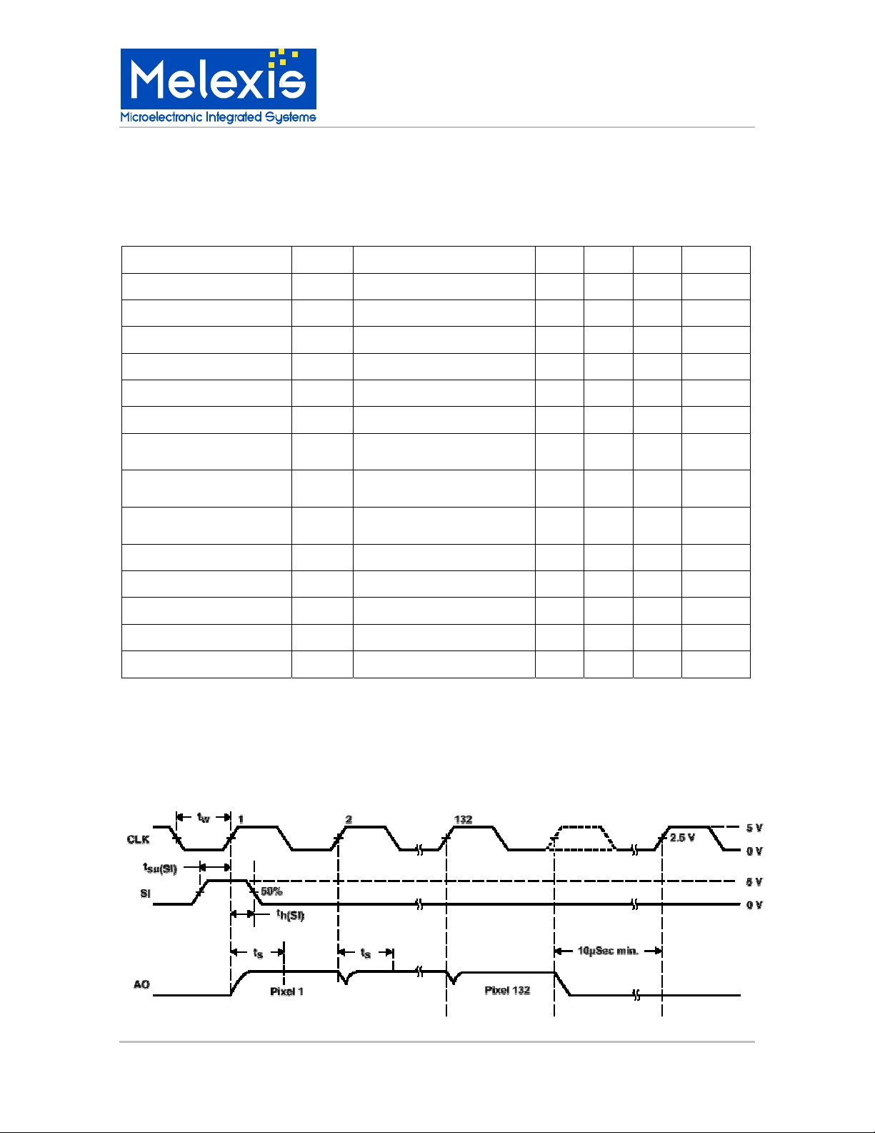
Setup time, serial input Tsu(SI) 350
Hold time, serial input (3) Th(SI) 40
Operating free-air temperature Ta -40 125 °C
Clock pulse duration (high) Tw(H) 320 ns
Clock pulse duration (low) Tw(L) 320 ns
Notes:
(1) Reset until clock pulse 18 (on declining flank).
Minimum integration time = (133-18) * CLK period + 10µs (this is the time the S&H cap needs to follow).
At 1MHz clock speed, the minimum integration time becomes 0.125ms.
(2) At 125°C, the integration time should be limited to 2ms.
(3) The SI pulse must go low before the rising edge of the next clock pulse.
Tint 0.125 100 ms
Tint 0.125 2
Tqt 8
ms
µs
ns
ns
MLX90255BA Linear Optical Array Page 2 Rev 1.2 08-Aug-01
3901090255

Datasheet
MLX90255BA
Linear Optical Array
MLX90255BA Electrical specifications
All tests are made with 0.7ms integration time, at 10mW/cm² light = 100% at 25°C at 880nm and with a
clock speed of 500kHz in, 250kHz out, and 500kHz, unless otherwise specified in the Test Conditions.
100 % light under Test Conditions means that the light is set in such a way that there is 2.4V at the output
of the chip.
Parameter Symbol Test Conditions Min Typ Max Units
Illumination Illum100 At 25°C, 2.4V at output 11.4 14 16 µW/cm²
Average analog output (1) VaoLight At 25°C, 100% light 1.5 1.7 2.1 V
Average analog output Initial offset At 25°C, 0% light 0 0.15 0.3 V
Average analog output VaoDark At 125°C, 0% light 0 0.40 1.4 V
Highest Dark Pixel Vaodarkmax At 125°C, 0.25ms integration time 0.8 V
Non Linearity Nlao1 All Temp
Pixel Response Non Uniformity (2) PRNU All Temp, 100% light
±0.5% ±1.2%
±
4.0% ±8.5%
FS
FS
Pixel Interaction Test (3) PIT AT 25°C 5% FS
Noise Level (4) Vn All Temp 3 6 mV (RMS)
Hold spec, same as PRNU PRNUH All Temp, 100% light, 62.5kHz
±4.0% ±8.5%
FS
Output Settling Time Ts All Temp 450 750 ns
Array Lag (5) Alag At 25°C 0.5% FS
Dark Signal Non Uniformity (6) DSNU At 25°C
At 125°C
80
140
120
440
mV
mV
Analog Output Saturation All Temp 3.0 V
Change in sensitivity with
0 0.3 0.8 %/°C
Temperature at 880nm (7)
Operating Free Temp -40 125 °C
Supply Current (8) Idd 2 5 8 mA
(0) After power on, the first integration scan is not guaranteed correct. This scan is needed for initializing digital levels on chip. After a SI and 133 proper
CLK signals, the system is fully initialized and all further scans are valid. The next SI will provide a valid scan.
(1) Absolute Light measurements are very test-setup dependent and should be regarded with caution. Relative measurements are possible with
accuracy.
(2) PRNU is defined as the worst case deviation of any PixelValue (pixel 3 till 130) to the average light value. PixelValue = (Vout of a pixel at 100% light
– Vout of same pixel at 0% light) The 90255BA has a cosign shaped gain: external pixels have 15% more gain than middle pixels.
(3) PIT = (Vout of pixel 132 @ 10µW – Vout of pixel 132 @0µW) / (Vaverage @10µW – Vaverage @10µW)
(4) Noise: We compare 5 different measurements, normalize them and then take the RMS value.
(5) Array Lag is defined as: (Vaverage 0µW
light level. (there can still be some light effects). 0µW
(6) DSNU is defined as: (max Vout of pixel I @ 0% light) - (min Vout of pixel j @ 0% light) for pixels 3 thru 130
(7) Sensitivity always increases with rising temperature.
(8) Idd is measured with Rload disconnected from the output pin.
1
Vaverage 0µW2) / ((Vaverage 10µW Vaverage 0µW2). Where 0µW1 is a 0% light level, 1ms after a 100%
2
is a 0% light level, 10ms after a 100% light level, which should be a true dark reference.
±1%
MLX90255BA Linear Optical Array Page 3 Rev 1.2 08-Aug-01
3901090255

Datasheet
MLX90255BA
Linear Optical Array
General Description
(continued from page 1)
As the SI pulse is clocked through the shift
register, the charge stored on the sampling
capacitors is sequentially connected to a chargecoupled output amplifier that generates a voltage
on the analog output AO. Two dummy pixel
values are shifted out first, then the 128 actual
pixel bits, followed by two additional dummy
pixel bits, for a total of 132 data bits. Although
there are only 132 pixels, 133 clock pulses are
necessary for a complete shift out. The final
pulse is used to re-initialize the shift register.
The integrator reset period ends 18 clock cycles
after the SI pulse is clocked in. So the lightintegration starts after the 18
light-integration ends at the next SI pulse.
Between the end of the 133
next SI pulse, a minimum time of 10µs is
necessary for an effective S&H function. So the
minimum integration time of the MLX90255BA is
(133 -18) * Ts + 10µs and thus dependent on
clock speed. (Ts = clock period) After the 132
data bits are clocked out, the output becomes
high impedance. (see figure) The AO is driven
by a source follower that requires an external
pulldown resistor. (typically 330Ω) The output is
nominally 125mV for no light input and 2.4V for a
nominal full-scale output. The pixel gain is 15%
bigger at the edges than in the middle (cosine
correction) in order to get a flat output when
illuminating the device with a single LED light
source.
The MLX90255BA is intended for use in a wide
variety of applications, including: image
scanning, mark and code reading, optical
character recognition (OCR) and contact
imaging, edge detection and positioning, and
optical linear and rotary encoding. The
MLX90255BA is a replacement for the Texas
Instruments' TSL1301 and TSL1401 parts.
th
CLK pulse. The
th
clock pulse and the
Absolute Maximum Ratings
Supply Voltage, Vdd +7V
Digital Input Current Range -20 to 20 mA
Operating Free-Air temperature
range, Ta
Storage temperature range,
Tstg
Lead Temperature
1.6mm (1/16 inch) from case for
10 seconds
Stresses beyond those listed under "absolute
maximum ratings" may cause permanent
damage to the device.
These are stress ratings only, and functional
operation of the device at these or any other
conditions beyond those indicated under
"recommended operating conditions" is not
implied.
Exposure to absolute-maximum -rated
conditions for extended periods may affect
device reliability.
-40°C to 125°C
(automotive compliant
optical package)
-40°C to 125°C
260°C
MLX90255BA Linear Optical Array Page 4 Rev 1.2 08-Aug-01
3901090255

Performance Graphs
Typical Photodiode Spectral Response Curve (%), without Anti
Reflection Coating*
Datasheet
MLX90255BA
Linear Optical Array
*There is also an option for an
ripples in the figure above. With this special Anti Reflection Coating, the sensitivity curve in
function of wavelength will be somewhat lower (typically 4%) but will no longer display
interference ripples.
Anti Reflection Coating
. This will remove the interference
MLX90255 Timing Diagram
MLX90255BA Linear Optical Array Page 5 Rev 1.2 08-Aug-01
3901090255

Disclaimer
Melexis reserves the right to periodically make
modifications to product specifications. The
information included herein is believed to be
accurate and reliable. However, Melexis
assumes no responsibility for its use; nor for
any infringements of patents or other rights of
third parties which may result from its use.
Melexis
Datasheet
MLX90255BA
Linear Optical Array
MLX90255BA Linear Optical Array Page 6 Rev 1.2 08-Aug-01
3901090255

Datasheet
MLX90255BA (SMD8) LA package dimensions
MLX90255BA
Linear Optical Array
5678
1234
MLX90255BA Linear Optical Array Page 7 Rev 1.2 08-Aug-01
3901090255

Datasheet
9
MLX90255BA
Linear Optical Array
LA (SMD8) Pin Description
Pin Symb
1 SI Serial Input. Si defines the start of
2 CLK Clock. CLK controls the charge
3 A0 Analog Output
4 Vdd Supply voltage, for both analog
5, 6, 7, 8 Vss Ground (substrate). All Vss Pins
Note: All 4 Vss pins are internally connected to form a large
ground plane to get better EMC characteristics.
MLX90255BA (GLP5) JA package dimensions
Description
ol
the data-out sequence
transfer, pixel output and reset
(together with SI)
and digital circuits
are referenced to the substrate.
12345
MLX90255BA Linear Optical Array Page 8 Rev 1.2 08-Aug-01
3901090255
QS

Datasheet
MLX90255BA
Linear Optical Array
JA (GLP5) Pin Description
Pin Symb
ol
1 SI Serial Input. Si defines the start of
2 CLK Clock. CLK controls the charge
3 A0 Analog Output
4 Vdd Supply voltage, for both analog
5 Vss Ground (substrate). All Vss Pins
Description
the data-out sequence
transfer, pixel output and reset
(together with SI)
and digital circuits
are referenced to the substrate.
MLX90255BA Linear Optical Array Page 9 Rev 1.2 08-Aug-01
3901090255

Datasheet
MLX90255BA Leadframes
JA (GLP5) Leadframe LA (SMD8) Leadframe
MLX90255BA
Linear Optical Array
For the latest version of this document, go to our website at:
www.melexis.com
Or for additional information contact Melexis Direct:
Europe and Japan: All other locations:
Phone: +32 13 61 16 31 Phone: +1 603 223 2362
E-mail: sales_europe@melexis.com E-mail: sales_usa@melexis.com
MLX90255BA Linear Optical Array Page 10 Rev 1.2 08-Aug-01
3901090255
QS9000, VDA6.1 and ISO14001 Certified
 Loading...